KR102630641B1 - Display apparatus and method of manufacturing thereof - Google Patents
Display apparatus and method of manufacturing thereofDownload PDFInfo
- Publication number
- KR102630641B1 KR102630641B1KR1020180009607AKR20180009607AKR102630641B1KR 102630641 B1KR102630641 B1KR 102630641B1KR 1020180009607 AKR1020180009607 AKR 1020180009607AKR 20180009607 AKR20180009607 AKR 20180009607AKR 102630641 B1KR102630641 B1KR 102630641B1
- Authority
- KR
- South Korea
- Prior art keywords
- layer
- thin film
- film transistor
- electrode
- insulating
- Prior art date
- Legal status (The legal status is an assumption and is not a legal conclusion. Google has not performed a legal analysis and makes no representation as to the accuracy of the status listed.)
- Active
Links
Images


Classifications
- H—ELECTRICITY
- H10—SEMICONDUCTOR DEVICES; ELECTRIC SOLID-STATE DEVICES NOT OTHERWISE PROVIDED FOR
- H10K—ORGANIC ELECTRIC SOLID-STATE DEVICES
- H10K59/00—Integrated devices, or assemblies of multiple devices, comprising at least one organic light-emitting element covered by group H10K50/00
- H—ELECTRICITY
- H10—SEMICONDUCTOR DEVICES; ELECTRIC SOLID-STATE DEVICES NOT OTHERWISE PROVIDED FOR
- H10K—ORGANIC ELECTRIC SOLID-STATE DEVICES
- H10K59/00—Integrated devices, or assemblies of multiple devices, comprising at least one organic light-emitting element covered by group H10K50/00
- H10K59/10—OLED displays
- H10K59/12—Active-matrix OLED [AMOLED] displays
- H10K59/121—Active-matrix OLED [AMOLED] displays characterised by the geometry or disposition of pixel elements
- H10K59/1213—Active-matrix OLED [AMOLED] displays characterised by the geometry or disposition of pixel elements the pixel elements being TFTs
- H—ELECTRICITY
- H10—SEMICONDUCTOR DEVICES; ELECTRIC SOLID-STATE DEVICES NOT OTHERWISE PROVIDED FOR
- H10D—INORGANIC ELECTRIC SEMICONDUCTOR DEVICES
- H10D86/00—Integrated devices formed in or on insulating or conducting substrates, e.g. formed in silicon-on-insulator [SOI] substrates or on stainless steel or glass substrates
- H10D86/01—Manufacture or treatment
- H10D86/021—Manufacture or treatment of multiple TFTs
- H—ELECTRICITY
- H10—SEMICONDUCTOR DEVICES; ELECTRIC SOLID-STATE DEVICES NOT OTHERWISE PROVIDED FOR
- H10D—INORGANIC ELECTRIC SEMICONDUCTOR DEVICES
- H10D86/00—Integrated devices formed in or on insulating or conducting substrates, e.g. formed in silicon-on-insulator [SOI] substrates or on stainless steel or glass substrates
- H10D86/40—Integrated devices formed in or on insulating or conducting substrates, e.g. formed in silicon-on-insulator [SOI] substrates or on stainless steel or glass substrates characterised by multiple TFTs
- H10D86/421—Integrated devices formed in or on insulating or conducting substrates, e.g. formed in silicon-on-insulator [SOI] substrates or on stainless steel or glass substrates characterised by multiple TFTs having a particular composition, shape or crystalline structure of the active layer
- H10D86/427—Integrated devices formed in or on insulating or conducting substrates, e.g. formed in silicon-on-insulator [SOI] substrates or on stainless steel or glass substrates characterised by multiple TFTs having a particular composition, shape or crystalline structure of the active layer having different thicknesses of the semiconductor bodies in different TFTs
- H—ELECTRICITY
- H10—SEMICONDUCTOR DEVICES; ELECTRIC SOLID-STATE DEVICES NOT OTHERWISE PROVIDED FOR
- H10D—INORGANIC ELECTRIC SEMICONDUCTOR DEVICES
- H10D86/00—Integrated devices formed in or on insulating or conducting substrates, e.g. formed in silicon-on-insulator [SOI] substrates or on stainless steel or glass substrates
- H10D86/40—Integrated devices formed in or on insulating or conducting substrates, e.g. formed in silicon-on-insulator [SOI] substrates or on stainless steel or glass substrates characterised by multiple TFTs
- H10D86/441—Interconnections, e.g. scanning lines
- H—ELECTRICITY
- H10—SEMICONDUCTOR DEVICES; ELECTRIC SOLID-STATE DEVICES NOT OTHERWISE PROVIDED FOR
- H10D—INORGANIC ELECTRIC SEMICONDUCTOR DEVICES
- H10D86/00—Integrated devices formed in or on insulating or conducting substrates, e.g. formed in silicon-on-insulator [SOI] substrates or on stainless steel or glass substrates
- H10D86/40—Integrated devices formed in or on insulating or conducting substrates, e.g. formed in silicon-on-insulator [SOI] substrates or on stainless steel or glass substrates characterised by multiple TFTs
- H10D86/451—Integrated devices formed in or on insulating or conducting substrates, e.g. formed in silicon-on-insulator [SOI] substrates or on stainless steel or glass substrates characterised by multiple TFTs characterised by the compositions or shapes of the interlayer dielectrics
- H—ELECTRICITY
- H10—SEMICONDUCTOR DEVICES; ELECTRIC SOLID-STATE DEVICES NOT OTHERWISE PROVIDED FOR
- H10D—INORGANIC ELECTRIC SEMICONDUCTOR DEVICES
- H10D86/00—Integrated devices formed in or on insulating or conducting substrates, e.g. formed in silicon-on-insulator [SOI] substrates or on stainless steel or glass substrates
- H10D86/40—Integrated devices formed in or on insulating or conducting substrates, e.g. formed in silicon-on-insulator [SOI] substrates or on stainless steel or glass substrates characterised by multiple TFTs
- H10D86/471—Integrated devices formed in or on insulating or conducting substrates, e.g. formed in silicon-on-insulator [SOI] substrates or on stainless steel or glass substrates characterised by multiple TFTs having different architectures, e.g. having both top-gate and bottom-gate TFTs
- H—ELECTRICITY
- H10—SEMICONDUCTOR DEVICES; ELECTRIC SOLID-STATE DEVICES NOT OTHERWISE PROVIDED FOR
- H10D—INORGANIC ELECTRIC SEMICONDUCTOR DEVICES
- H10D86/00—Integrated devices formed in or on insulating or conducting substrates, e.g. formed in silicon-on-insulator [SOI] substrates or on stainless steel or glass substrates
- H10D86/40—Integrated devices formed in or on insulating or conducting substrates, e.g. formed in silicon-on-insulator [SOI] substrates or on stainless steel or glass substrates characterised by multiple TFTs
- H10D86/481—Integrated devices formed in or on insulating or conducting substrates, e.g. formed in silicon-on-insulator [SOI] substrates or on stainless steel or glass substrates characterised by multiple TFTs integrated with passive devices, e.g. auxiliary capacitors
- H—ELECTRICITY
- H10—SEMICONDUCTOR DEVICES; ELECTRIC SOLID-STATE DEVICES NOT OTHERWISE PROVIDED FOR
- H10D—INORGANIC ELECTRIC SEMICONDUCTOR DEVICES
- H10D86/00—Integrated devices formed in or on insulating or conducting substrates, e.g. formed in silicon-on-insulator [SOI] substrates or on stainless steel or glass substrates
- H10D86/40—Integrated devices formed in or on insulating or conducting substrates, e.g. formed in silicon-on-insulator [SOI] substrates or on stainless steel or glass substrates characterised by multiple TFTs
- H10D86/60—Integrated devices formed in or on insulating or conducting substrates, e.g. formed in silicon-on-insulator [SOI] substrates or on stainless steel or glass substrates characterised by multiple TFTs wherein the TFTs are in active matrices
- H—ELECTRICITY
- H10—SEMICONDUCTOR DEVICES; ELECTRIC SOLID-STATE DEVICES NOT OTHERWISE PROVIDED FOR
- H10F—INORGANIC SEMICONDUCTOR DEVICES SENSITIVE TO INFRARED RADIATION, LIGHT, ELECTROMAGNETIC RADIATION OF SHORTER WAVELENGTH OR CORPUSCULAR RADIATION
- H10F39/00—Integrated devices, or assemblies of multiple devices, comprising at least one element covered by group H10F30/00, e.g. radiation detectors comprising photodiode arrays
- H10F39/80—Constructional details of image sensors
- H10F39/802—Geometry or disposition of elements in pixels, e.g. address-lines or gate electrodes
- H—ELECTRICITY
- H10—SEMICONDUCTOR DEVICES; ELECTRIC SOLID-STATE DEVICES NOT OTHERWISE PROVIDED FOR
- H10K—ORGANIC ELECTRIC SOLID-STATE DEVICES
- H10K50/00—Organic light-emitting devices
- H10K50/80—Constructional details
- H10K50/84—Passivation; Containers; Encapsulations
- H—ELECTRICITY
- H10—SEMICONDUCTOR DEVICES; ELECTRIC SOLID-STATE DEVICES NOT OTHERWISE PROVIDED FOR
- H10K—ORGANIC ELECTRIC SOLID-STATE DEVICES
- H10K59/00—Integrated devices, or assemblies of multiple devices, comprising at least one organic light-emitting element covered by group H10K50/00
- H10K59/10—OLED displays
- H10K59/12—Active-matrix OLED [AMOLED] displays
- H10K59/121—Active-matrix OLED [AMOLED] displays characterised by the geometry or disposition of pixel elements
- H10K59/1216—Active-matrix OLED [AMOLED] displays characterised by the geometry or disposition of pixel elements the pixel elements being capacitors
- H—ELECTRICITY
- H10—SEMICONDUCTOR DEVICES; ELECTRIC SOLID-STATE DEVICES NOT OTHERWISE PROVIDED FOR
- H10K—ORGANIC ELECTRIC SOLID-STATE DEVICES
- H10K59/00—Integrated devices, or assemblies of multiple devices, comprising at least one organic light-emitting element covered by group H10K50/00
- H10K59/10—OLED displays
- H10K59/12—Active-matrix OLED [AMOLED] displays
- H10K59/124—Insulating layers formed between TFT elements and OLED elements
- H—ELECTRICITY
- H10—SEMICONDUCTOR DEVICES; ELECTRIC SOLID-STATE DEVICES NOT OTHERWISE PROVIDED FOR
- H10K—ORGANIC ELECTRIC SOLID-STATE DEVICES
- H10K59/00—Integrated devices, or assemblies of multiple devices, comprising at least one organic light-emitting element covered by group H10K50/00
- H10K59/10—OLED displays
- H10K59/12—Active-matrix OLED [AMOLED] displays
- H10K59/126—Shielding, e.g. light-blocking means over the TFTs
- H—ELECTRICITY
- H10—SEMICONDUCTOR DEVICES; ELECTRIC SOLID-STATE DEVICES NOT OTHERWISE PROVIDED FOR
- H10K—ORGANIC ELECTRIC SOLID-STATE DEVICES
- H10K71/00—Manufacture or treatment specially adapted for the organic devices covered by this subclass
Landscapes
- Engineering & Computer Science (AREA)
- Microelectronics & Electronic Packaging (AREA)
- Physics & Mathematics (AREA)
- Geometry (AREA)
- Manufacturing & Machinery (AREA)
- Optics & Photonics (AREA)
- Thin Film Transistor (AREA)
- Electroluminescent Light Sources (AREA)
- Devices For Indicating Variable Information By Combining Individual Elements (AREA)
Abstract
Translated fromKoreanDescription
Translated fromKorean본 발명은 표시장치 및 그의 제조 방법에 관한 것이다.The present invention relates to a display device and a method of manufacturing the same.
표시장치는 표시소자 및 표시소자에 인가되는 전기적 신호를 제어하기 위한 전자소자들을 포함한다. 전자소자들은 박막 트랜지스터(TFT; Thin Film Transistor), 커패시터 및 복수의 배선들을 포함한다.A display device includes a display element and electronic elements for controlling electrical signals applied to the display element. Electronic devices include a thin film transistor (TFT), a capacitor, and a plurality of wires.
표시장치의 해상도 증가 및 하나의 표시소자에 전기적으로 연결되는 박막 트랜지스터들의 개수 증가에 따라, 화소의 개구율이 감소하는 문제점이 있다.As the resolution of the display device increases and the number of thin film transistors electrically connected to one display element increases, there is a problem in that the aperture ratio of the pixel decreases.
본 발명의 실시예들은 고해상도를 구현할 수 있는 표시장치를 제공하는 것을 목적으로 한다. 그러나 이러한 과제는 예시적인 것으로, 이에 의해 본 발명의 범위가 한정되는 것은 아니다.Embodiments of the present invention aim to provide a display device capable of implementing high resolution. However, these tasks are illustrative and do not limit the scope of the present invention.
본 발명의 일 실시예에 다른 표시장치는, 기판 상부에, 제1 활성층을 갖는 제1 박막 트랜지스터; 상기 제1 박막 트랜지스터 상부에, 상기 제1 박막 트랜지스터와 중첩하는 제2 활성층을 갖는 제2 박막 트랜지스터; 상기 제1 박막 트랜지스터와 상기 제2 박막 트랜지스터 사이에, 제1 절연층 및, 상기 제1 절연층의 상부에 배치되고, 상기 제1 절연층의 상부면과 일치하는 상부면을 갖는 제2 절연층을 포함하는 제1 평탄화층; 및 상기 제1 평탄화층과 상기 제2 박막 트랜지스터 사이의 제1 버퍼층;을 포함한다.A display device according to an embodiment of the present invention includes a first thin film transistor having a first active layer on an upper part of a substrate; a second thin film transistor on top of the first thin film transistor and having a second active layer overlapping with the first thin film transistor; Between the first thin film transistor and the second thin film transistor, a first insulating layer and a second insulating layer disposed on top of the first insulating layer and having an upper surface that coincides with the upper surface of the first insulating layer. A first planarization layer comprising; and a first buffer layer between the first planarization layer and the second thin film transistor.
상기 제1 버퍼층은 실리콘산화물을 포함할 수 있다.The first buffer layer may include silicon oxide.
상기 표시장치는, 상기 제1 박막 트랜지스터와 상기 제1 평탄화층 사이에, 상기 제2 활성층과 중첩하는 도전층;을 더 포함할 수 있다.The display device may further include a conductive layer between the first thin film transistor and the first planarization layer and overlapping the second active layer.
상기 도전층은 DC 전압을 가질 수 있다.The conductive layer may have a DC voltage.
상기 도전층은 적어도 발광 구간에 DC 전압을 가질 수 있다.The conductive layer may have a DC voltage at least in the light emitting section.
상기 도전층은 상기 제2 박막 트랜지스터의 게이트 전극보다 클 수 있다.The conductive layer may be larger than the gate electrode of the second thin film transistor.
상기 도전층의 중심과 상기 제2 박막 트랜지스터의 게이트 전극의 중심의 이격 거리는 3㎛ 이내일 수 있다.The separation distance between the center of the conductive layer and the center of the gate electrode of the second thin film transistor may be within 3 μm.
상기 제2 활성층의 두께는 상기 제1 활성층의 두께보다 얇을 수 있다.The thickness of the second active layer may be thinner than the thickness of the first active layer.
상기 제2 활성층의 두께는 상기 제1 활성층의 두께의 80% 이하일 수 있다.The thickness of the second active layer may be 80% or less of the thickness of the first active layer.
상기 표시장치는, 상기 제2 박막 트랜지스터 상부에, 상기 제2 박막 트랜지스터와 중첩하고 상기 제1 박막 트랜지스터와 연결된 표시소자;를 더 포함할 수 있다.The display device may further include a display element on top of the second thin film transistor, overlapping with the second thin film transistor, and connected to the first thin film transistor.
상기 표시장치는, 상기 제2 박막 트랜지스터와 상기 표시소자 사이에, 제3 절연층 및, 상기 제3 절연층의 상부에 배치되고, 상기 제3 절연층의 상부면과 일치하는 상부면을 갖는 제4 절연층을 포함하는 제2 평탄화층; 및 상기 제2 평탄화층 상부의 제2 버퍼층;을 더 포함할 수 있다.The display device includes a third insulating layer between the second thin film transistor and the display element, and a third insulating layer disposed on top of the third insulating layer and having an upper surface that coincides with the upper surface of the third insulating layer. 4 a second planarization layer including an insulating layer; and a second buffer layer on top of the second planarization layer.
상기 표시장치는, 상기 제2 박막 트랜지스터와 상기 표시소자 사이의 제5 절연층;을 더 포함할 수 있다.The display device may further include a fifth insulating layer between the second thin film transistor and the display element.
상기 제2 버퍼층은 실리콘질화물을 포함할 수 있다.The second buffer layer may include silicon nitride.
상기 표시장치는, 상기 제1 활성층으로부터 연장된 제3 활성층을 갖는 제3 박막 트랜지스터;를 더 포함할 수 있다.The display device may further include a third thin film transistor having a third active layer extending from the first active layer.
상기 표시장치는, 상기 제2 박막 트랜지스터 상부에, 상기 제2 활성층과 적어도 일부 중첩하는 커패시터;를 더 포함할 수 있다.The display device may further include a capacitor on top of the second thin film transistor and at least partially overlapping the second active layer.
본 발명의 일 실시예에 따른 표시장치의 제조방법은, 기판 상부에 제1 활성층을 갖는 제1 박막 트랜지스터를 형성하는 단계; 상기 제1 박막 트랜지스터 상부에, 제1 절연막 및 제2 절연막을 형성하는 단계; 상기 제1 절연막의 상부면과 상기 제2 절연막의 상부면이 일치하도록 상기 제2 절연막을 식각하여 제1 평탄화층을 형성하는 단계; 상기 제1 평탄화층 상부에 제1 버퍼층을 형성하는 단계; 및 상기 제1 버퍼층의 상부에, 상기 제1 박막 트랜지스터와 중첩하는 제2 활성층을 갖는 제2 박막 트랜지스터를 형성하는 단계;를 포함한다.A method of manufacturing a display device according to an embodiment of the present invention includes forming a first thin film transistor having a first active layer on an upper portion of a substrate; forming a first insulating film and a second insulating film on the first thin film transistor; forming a first planarization layer by etching the second insulating film so that the top surface of the first insulating film matches the top surface of the second insulating film; Forming a first buffer layer on top of the first planarization layer; and forming a second thin film transistor having a second active layer overlapping the first thin film transistor on top of the first buffer layer.
상기 제조방법은, 상기 제2 박막 트랜지스터 형성 단계 이전에, 상기 제1 평탄화층 및 상기 제1 버퍼층의 열 처리를 수행하는 단계;를 더 포함할 수 있다.The manufacturing method may further include performing heat treatment on the first planarization layer and the first buffer layer before forming the second thin film transistor.
상기 제조방법은, 기 제1 절연막 및 제2 절연막 형성 단계 이전에, 상기 제1 박막 트랜지스터 상부에, 상기 제1 활성층과 중첩하는 도전층을 형성하는 단계;를 더 포함하고, 상기 제2 박막 트랜지스터는 상기 도전층과 중첩할 수 있다.The manufacturing method further includes forming a conductive layer overlapping the first active layer on the first thin film transistor before forming the first insulating film and the second insulating film, wherein the second thin film transistor may overlap with the conductive layer.
상기 제조방법은, 상기 제2 박막 트랜지스터 상부에, 상기 제2 박막 트랜지스터와 중첩하고 상기 제1 박막 트랜지스터와 연결된 표시소자를 형성하는 단계;를 더 포함할 수 있다.The manufacturing method may further include forming a display element on top of the second thin film transistor, overlapping with the second thin film transistor, and connected to the first thin film transistor.
상기 제조방법은, 상기 표시소자 형성 단계 이전에, 상기 제2 박막 트랜지스터 상부에 제3 절연막 및 제4 절연막을 형성하는 단계; 상기 제3 절연막의 상부면과 상기 제4 절연막의 상부면이 일치하도록 상기 제4 절연막을 식각하여 제2 평탄화층을 형성하는 단계; 및 상기 제2 평탄화층의 상부에 제2 버퍼층을 형성하는 단계;를 더 포함할 수 있다.The manufacturing method includes forming a third insulating film and a fourth insulating film on the second thin film transistor before forming the display element; forming a second planarization layer by etching the fourth insulating film so that the top surface of the third insulating film matches the top surface of the fourth insulating film; and forming a second buffer layer on top of the second planarization layer.
본 발명의 실시예들에 따른 표시장치는 화소 내 박막 트랜지스터의 배열을 최적화하여 고해상도 구현이 가능한 표시장치를 제공할 수 있다. 물론 이러한 효과에 의해 본 발명의 범위가 한정되는 것은 아니다.A display device according to embodiments of the present invention can provide a display device capable of implementing high resolution by optimizing the arrangement of thin film transistors within a pixel. Of course, the scope of the present invention is not limited by this effect.
도 1은 본 발명의 일 실시예에 따른 반도체 장치를 도시한 단면도이다.
도 1a는 도 1에 도시된 반도체 장치의 일부를 나타낸 평면도이다.
도 2는 본 발명의 다른 실시예에 따른 반도체 장치를 도시한 단면도이다.
도 2a는 도 2에 도시된 반도체 장치의 일부를 나타낸 평면도이다.
도 3a 내지 도 3c는 도 2에 도시된 도전층과 제2 게이트 전극의 위치 및 전압 관계를 나타내는 도면이다.
도 4a 내지 도 8은 본 발명의 일 실시예에 따른 반도체 장치의 제조 공정을 개략적으로 설명하는 도면이다.
도 9는 본 발명의 일 실시예 따른 표시장치를 개략적으로 나타낸 사시도이다.
도 10은 본 발명의 일 실시예에 따른 표시장치를 개략적으로 나타낸 평면도이다.
도 11은 본 발명의 일 실시예에 따른 제1 화소의 회로도이다.
도 12는 도 11에 도시된 화소의 일부 단면도이다.
도 13은 본 발명의 다른 실시예에 따른 제2 화소의 회로도이다.
도 14 및 도 15는 도 13에 도시된 화소의 일부 단면도이다.1 is a cross-sectional view showing a semiconductor device according to an embodiment of the present invention.
FIG. 1A is a plan view showing a portion of the semiconductor device shown in FIG. 1.
Figure 2 is a cross-sectional view showing a semiconductor device according to another embodiment of the present invention.
FIG. 2A is a plan view showing a portion of the semiconductor device shown in FIG. 2.
FIGS. 3A to 3C are diagrams showing the positions and voltage relationships between the conductive layer and the second gate electrode shown in FIG. 2.
4A to 8 are diagrams schematically explaining a manufacturing process of a semiconductor device according to an embodiment of the present invention.
Figure 9 is a perspective view schematically showing a display device according to an embodiment of the present invention.
Figure 10 is a plan view schematically showing a display device according to an embodiment of the present invention.
Figure 11 is a circuit diagram of a first pixel according to an embodiment of the present invention.
FIG. 12 is a partial cross-sectional view of the pixel shown in FIG. 11.
Figure 13 is a circuit diagram of a second pixel according to another embodiment of the present invention.
14 and 15 are partial cross-sectional views of the pixel shown in FIG. 13.
본 발명은 다양한 변환을 가할 수 있고 여러 가지 실시예를 가질 수 있는 바, 특정 실시예들을 도면에 예시하고 상세한 설명에 상세하게 설명하고자 한다. 본 발명의 효과 및 특징, 그리고 그것들을 달성하는 방법은 도면과 함께 상세하게 후술되어 있는 실시예들을 참조하면 명확해질 것이다. 그러나 본 발명은 이하에서 개시되는 실시예들에 한정되는 것이 아니라 다양한 형태로 구현될 수 있다.Since the present invention can be modified in various ways and can have various embodiments, specific embodiments will be illustrated in the drawings and described in detail in the detailed description. The effects and features of the present invention and methods for achieving them will become clear by referring to the embodiments described in detail below along with the drawings. However, the present invention is not limited to the embodiments disclosed below and may be implemented in various forms.
이하의 실시예에서, 제1, 제2 등의 용어는 한정적인 의미가 아니라 하나의 구성 요소를 다른 구성 요소와 구별하는 목적으로 사용되었다.In the following embodiments, terms such as first and second are used not in a limiting sense but for the purpose of distinguishing one component from another component.
이하의 실시예에서, 단수의 표현은 문맥상 명백하게 다르게 뜻하지 않는 한, 복수의 표현을 포함한다.In the following examples, singular terms include plural terms unless the context clearly dictates otherwise.
이하의 실시예에서, 포함하다 또는 가지다 등의 용어는 명세서상에 기재된 특징, 또는 구성요소가 존재함을 의미하는 것이고, 하나 이상의 다른 특징들 또는 구성요소가 부가될 가능성을 미리 배제하는 것은 아니다.In the following embodiments, terms such as include or have mean that the features or components described in the specification exist, and do not exclude in advance the possibility of adding one or more other features or components.
이하의 실시예에서, 막, 영역, 구성 요소 등의 부분이 다른 부분 위에 또는 상에 있다고 할 때, 다른 부분의 바로 위에 있는 경우뿐만 아니라, 그 중간에 다른 막, 영역, 구성 요소 등이 개재되어 있는 경우도 포함한다.In the following embodiments, when a part of a film, region, component, etc. is said to be on or on another part, it is not only the case where it is directly on top of the other part, but also when another film, region, component, etc. is interposed between them. Also includes cases where there are.
도면에서는 설명의 편의를 위하여 구성 요소들이 그 크기가 과장 또는 축소될 수 있다. 예컨대, 도면에서 나타난 각 구성의 크기 및 두께는 설명의 편의를 위해 임의로 나타내었으므로, 본 발명이 반드시 도시된 바에 한정되지 않는다.In the drawings, the sizes of components may be exaggerated or reduced for convenience of explanation. For example, the size and thickness of each component shown in the drawings are arbitrarily shown for convenience of explanation, so the present invention is not necessarily limited to what is shown.
어떤 실시예가 달리 구현 가능한 경우에 특정한 공정 순서는 설명되는 순서와 다르게 수행될 수도 있다. 예를 들어, 연속하여 설명되는 두 공정이 실질적으로 동시에 수행될 수도 있고, 설명되는 순서와 반대의 순서로 진행될 수 있다.In cases where an embodiment can be implemented differently, a specific process sequence may be performed differently from the described sequence. For example, two processes described in succession may be performed substantially at the same time, or may be performed in an order opposite to that in which they are described.
이하, 첨부된 도면을 참조하여 본 발명의 실시예들을 상세히 설명하기로 하며, 도면을 참조하여 설명할 때 동일하거나 대응하는 구성 요소는 동일한 도면부호를 부여하고 이에 대한 중복되는 설명은 생략하기로 한다.Hereinafter, embodiments of the present invention will be described in detail with reference to the accompanying drawings. When describing with reference to the drawings, identical or corresponding components will be assigned the same reference numerals and redundant description thereof will be omitted. .
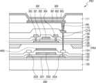
도 1은 본 발명의 일 실시예에 따른 반도체 장치를 도시한 단면도이다. 도 1a는 도 1에 도시된 반도체 장치의 일부를 나타낸 평면도이다.1 is a cross-sectional view showing a semiconductor device according to an embodiment of the present invention. FIG. 1A is a plan view showing a portion of the semiconductor device shown in FIG. 1.
도 1을 참조하면, 일 실시예에 따른 반도체 장치(10a)는 기판(100) 상부의 제1 박막 트랜지스터(200) 및 제2 박막 트랜지스터(300)를 포함할 수 있다. 제1 박막 트랜지스터(200)와 제2 박막 트랜지스터(300)는 서로 다른 층에 배치되어, 단면상 상하로 중첩 배치될 수 있다.Referring to FIG. 1 , the
제1 박막 트랜지스터(200)는 제1 활성층(201), 제1 게이트 전극(202), 제1 소스 전극(203) 및 제1 드레인 전극(204)을 포함할 수 있다. 제1 활성층(201)은 제1 소스 전극(203) 및 제1 드레인 전극(204)과 각각 컨택하는 소스 영역 및 드레인 영역과 그 사이의 채널 영역을 포함할 수 있다.The first
제1 박막 트랜지스터(200)는 제1 버퍼층(101) 상부에 배치될 수 있다. 제1 버퍼층(101)은 생략될 수 있다.The first
제2 박막 트랜지스터(300)는 제2 활성층(301), 제2 게이트 전극(302), 제2 소스 전극(303) 및 제2 드레인 전극(304)을 포함할 수 있다. 제2 활성층(301)은 제2 소스 전극(303) 및 제2 드레인 전극(304)과 각각 컨택하는 소스 영역 및 드레인 영역과 그 사이의 채널 영역을 포함할 수 있다.The second
제2 활성층(301)은 제1 활성층(201)과 적어도 일부가 중첩할 수 있다. 제2 활성층(301)의 두께는 제1 활성층(201)의 두께보다 얇다. 제2 활성층(301)의 두께는 제1 활성층(201)의 두께의 80% 이하일 수 있으며, 이때, 제2 박막 트랜지스터(200)의 특성에 따라 제1 활성층(201)의 두께의 하한이 결정될 수 있다.The second
일 실시예에서, 제2 박막 트랜지스터(300)의 하부에 배치되는 배선 및/또는 전극은 일정한 DC 전압을 인가받는 배선 및/또는 전극일 수 있다. 다른 실시예에서, 제2 박막 트랜지스터(300)의 하부에 배치되는 배선 및/또는 전극은 AC 전압을 인가받는 배선 및/또는 전극일 수 있다. 이 경우, AC 전압을 인가받는 배선 및/또는 전극은 적어도 일정 기간에 일정한 전압이 인가되는 배선 및/또는 전극일 수 있다. 일 실시예에서, AC 전압을 인가받는 배선 및/또는 전극은 제2 박막 트랜지스터(300)의 일 전극과의 커플링에 의해 휘도에 영향을 주는 기간, 예를 들어, 적어도 문턱전압 보상 기간, 데이터 기입 기간 및 발광 기간에는 각각 일정한 전압이 인가되는 배선 및/또는 전극일 수 있다.In one embodiment, the wiring and/or electrode disposed below the second
제2 박막 트랜지스터(300)의 하부에 배치되는 배선 및/또는 전극은 제2 게이트 전극(302)보다 큰 사이즈 또는 큰 면적을 가질 수 있다. 제2 박막 트랜지스터(300)의 하부에 배치되는 배선 및/또는 전극의 적어도 일 에지는 제2 게이트 전극(302)의 일 에지보다 소정 길이 확장될 수 있다. 예를 들어, 제2 박막 트랜지스터(300)의 하부에 배치되는 배선 및/또는 전극의 에지는 제2 게이트 전극(302)의 에지보다 1.5㎛ 이상 확장될 수 있다.The wiring and/or electrode disposed below the second
제1 박막 트랜지스터(200)의 제1 게이트 전극(202)이 제2 박막 트랜지스터(300)의 하부에 배치되는 전극의 예일 수 있다. 도 1a는 제1 박막 트랜지스터(200)의 제1 게이트 전극(202)과 제2 박막 트랜지스터(300)의 제2 게이트 전극(302)의 위치 및 크기 관계를 나타낸 평면도이다. 도 1a를 함께 참조하면, 제1 게이트 전극(202)의 일 에지는 제2 게이트 전극(302)의 일 에지보다 소정 길이(L)만큼 확장될 수 있다. 도 1 및 도 1a에서는 제1 게이트 전극(202)의 양 단 에지가 확장되고 있으나, 본 발명의 실시예는 이에 한정되지 않고, 제1 게이트 전극(202)의 적어도 일 에지가 제2 게이트 전극(302)의 에지로부터 확장될 수 있다. 제1 게이트 전극(202)의 양 단 에지들의 확장 길이(L)는 서로 상이할 수 있다.The
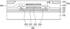
제1 박막 트랜지스터(200)와 제2 박막 트랜지스터(300) 사이에는 제1 박막 트랜지스터(200)를 덮고, 제3 절연층(104) 및 제4 절연층(105)을 포함하는 평탄화층(PAV)이 배치될 수 있다. 평탄화층(PAV)은 제3 절연층(104)의 일부에 제4 절연층(105)이 삽입되어 두 개의 절연층이 혼합된 구조를 가질 수 있다. 이에 따라 제1 박막 트랜지스터(200)에 의해 제3 절연층(104)이 갖는 요철 형태의 비평탄성이 제거될 수 있다.Between the first
제4 절연층(105)은 제3 절연층(104) 일부의 상부에 배치되고, 제3 절연층(104)의 상부면과 제4 절연층(105)의 상부면은 대략 일치하여 전체적으로 평탄한 상부면을 형성할 수 있다.The fourth insulating
평탄화층(PAV)의 상부에는 제2 버퍼층(106)이 배치될 수 있다. 제2 박막 트랜지스터(300)는 제2 버퍼층(106) 상부에 배치될 수 있다.A
도 2는 본 발명의 다른 실시예에 따른 반도체 장치를 도시한 단면도이다. 도 2a는 도 2에 도시된 반도체 장치의 일부를 나타낸 평면도이다.Figure 2 is a cross-sectional view showing a semiconductor device according to another embodiment of the present invention. FIG. 2A is a plan view showing a portion of the semiconductor device shown in FIG. 2.
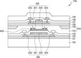
도 2에 도시된 반도체 장치(10b)는 도 1에 도시된 반도체 장치(10a)에 도전층(400)이 추가된 점에서 차이가 있다. 이하에서는 도 1과 관련하여 설명한 내용과 중복하는 내용의 설명은 생략한다.The
도 2의 실시예에서, 도전층(400)은 제1 박막 트랜지스터(200)와 제2 박막 트랜지스터(300) 사이에 배치될 수 있다. 도전층(400)은 제1 박막 트랜지스터(200)의 제1 게이트 전극(202)과 제2 박막 트랜지스터(300)의 제2 게이트 전극(302)과 적어도 일부 중첩하도록 배치될 수 있다.In the embodiment of FIG. 2, the
도전층(400)은 제2 박막 트랜지스터(300)의 하부에 배치되는 전극의 예일 수 있다. 이 경우, 도전층(400)은 제2 게이트 전극(302)보다 큰 사이즈 또는 큰 면적을 가질 수 있다. 도전층(400)의 적어도 일 에지는 제2 게이트 전극(302)의 일 에지보다 소정 길이 확장될 수 있다. 예를 들어, 도전층(400)의 에지는 제2 게이트 전극(302)의 에지보다 1.5㎛ 이상 확장될 수 있다.The
도 2a는 도전층(400)과 제2 박막 트랜지스터(300)의 제2 게이트 전극(302)의 위치 및 크기 관계를 나타낸 평면도이다. 도 2a를 함께 참조하면, 도전층(400)의 일 에지는 제2 게이트 전극(302)의 일 에지보다 소정 길이(L)만큼 확장될 수 있다. 도 2 및 도 2a에서는 도전층(400)의 양 단 에지가 확장되고 있으나, 본 발명의 실시예는 이에 한정되지 않고, 도전층(400)의 적어도 일 에지가 제2 게이트 전극(302)의 에지로부터 확장될 수 있다. 도전층(400)의 양 단 에지들의 확장 길이(L)는 서로 상이할 수 있다.FIG. 2A is a plan view showing the position and size relationship between the
표 1은 도전층(400)이 구비되지 않는 경우, 제1 게이트 전극(202)의 전압(VGAT1)이 변함에 따른 제2 박막 트랜지스터(300)의 문턱 전압(Vth_sat)의 변화량의 실험 결과를 나타낸다.Table 1 shows the experimental results of the amount of change in the threshold voltage (Vth_sat) of the second
표 1에서 보여지듯이, 제1 게이트 전극(202)의 전압 변화가 커짐에 따라 제2 박막 트랜지스터(300)의 문턱 전압(Vth_sat)의 변화량이 커짐을 확인할 수 있다.As shown in Table 1, it can be seen that as the voltage change of the
한편, 실험에 의해 제2 게이트 전극(302)의 전압이 변하더라도 제1 박막 트랜지스터(200)의 전류 특성 변화는 미비함을 확인하였다. 이는 제1 게이트 전극(202)의 차폐 효과에 의해 제2 게이트 전극(302)의 전압 변화가 제1 박막 트랜지스터(200)의 채널에 영향을 주지 않기 때문이다.Meanwhile, through experiments, it was confirmed that even if the voltage of the
도 2에 도시된 실시예는 제1 박막 트랜지스터(200)와 제2 박막 트랜지스터(300) 사이에 도전층(400)을 구비하여, 제1 박막 트랜지스터(200)와 제2 박막 트랜지스터(300) 간의 커플링을 차단함으로써 제2 박막 트랜지스터(300)의 동작을 보다 안정적으로 구동시킬 수 있다.The embodiment shown in FIG. 2 has a
도전층(400)은 일정한 DC 전압을 인가받을 수 있다. DC 전압은 반도체 장치(10b)에 인가되는 DC 전원들 중 하나이거나, 이들과 별개로 추가된 전압일 수 있다. 일 실시예에서, 도전층(400)은 제1 박막 트랜지스터(200)의 제1 게이트 전극(202)을 일 전극으로 하는 커패시터의 타 전극일 수 있다.The
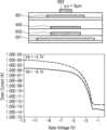
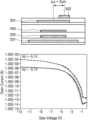
도 3a 내지 도 3c는 도 2에 도시된 도전층과 제2 게이트 전극의 위치 및 전압 관계를 나타내는 도면이다. 도 3a 내지 도 3c에서는 설명의 편의를 위해 제1 활성층(201), 제1 게이트 전극(202), 도전층(400), 제2 활성층(301), 및 제2 게이트 전극(302)만을 도시하였다.FIGS. 3A to 3C are diagrams showing the positions and voltage relationships between the conductive layer and the second gate electrode shown in FIG. 2. 3A to 3C, for convenience of explanation, only the first
도 3a 내지 도 3c는, 제1 게이트 전극(201)에 5V와 -30V를 스윕하는 게이트 전압이 인가되고, 도전층(400)에 9V의 전압이 인가되는 예이다. 도 3a 내지 도 3c는, 제2 박막 트랜지스터(300)의 드레인 전압(Vd)이 0.1V와 -5.1V 일 때, 제2 박막 트랜지스터(300)의 드레인 전류와 게이트 전압의 관계를 나타내는 그래프를 함께 도시하고 있다. 도 3a 내지 도 3c는, 도전층(400)과 제2 활성층(301)의 중심이 일치하는 경우이다.3A to 3C are examples in which a gate voltage sweeping between 5V and -30V is applied to the
도 3a를 참조하면, 제2 게이트 전극(제2 게이트 전극의 중심)(302)의 위치가 도전층(도전층의 중심)(400)으로부터 왼쪽으로 대략 2㎛ 벗어난 경우, 제2 박막 트랜지스터(300)의 포화 영역에서 문턱전압(Vth)의 변화량(ΔVth)은 대략 0.18V이다.Referring to FIG. 3A, when the position of the second gate electrode (center of the second gate electrode) 302 deviates from the conductive layer (center of the conductive layer) 400 by approximately 2 μm to the left, the second thin film transistor 300 ), the amount of change (ΔVth) in the threshold voltage (Vth) in the saturation region is approximately 0.18V.
도 3b를 참조하면, 제2 게이트 전극(제2 게이트 전극의 중심)(302)과 도전층(도전층의 중심)(400)의 위치가 일치하는 경우, 제2 박막 트랜지스터(300)의 포화 영역에서 문턱전압(Vth)의 변화량(ΔVth)은 대략 0.1V이다.Referring to FIG. 3B, when the positions of the second gate electrode (center of the second gate electrode) 302 and the conductive layer (center of the conductive layer) 400 coincide, the saturation region of the second
도 3c를 참조하면, 제2 게이트 전극(제2 게이트 전극의 중심)(302)의 위치가 도전층(도전층의 중심)(400)으로부터 오른쪽으로 대략 2㎛ 벗어난 경우, 제2 박막 트랜지스터(300)의 포화 영역에서 문턱전압(Vth)의 변화량(ΔVth)은 대략 0.25V이다.Referring to FIG. 3C, when the position of the second gate electrode (center of the second gate electrode) 302 deviates approximately 2 μm to the right from the conductive layer (center of the conductive layer) 400, the second thin film transistor 300 ), the amount of change (ΔVth) in the threshold voltage (Vth) in the saturation region is approximately 0.25V.
표 2는 도 3a 내지 도 3c의 예에서 도전층(400)의 전압이 -2V, 0V, 9V 일 때 제2 박막 트랜지스터(300)의 포화 영역에서 문턱전압(Vth)의 변화량(ΔVth)을 나타낸다.Table 2 shows the amount of change (ΔVth) in the threshold voltage (Vth) in the saturation region of the second
표 2를 참조하면, 도전층(400)에 대한 제2 게이트 전극(302)의 위치 이동(shift)이 제2 박막 트랜지스터(300)의 문턱전압(Vth)에 미치는 영향은, 도전층(400)의 전압이 제2 박막 트랜지스터(300)의 문턱전압(Vth)에 미치는 영향보다 큼을 알 수 있다.Referring to Table 2, the effect of the positional shift of the
본 발명의 실시예에서 도전층(400)과 제2 게이트 전극(302)의 정렬 오차(misalign) 범위는 제2 박막 트랜지스터(300)의 문턱전압(Vth)의 변화량(ΔVth)이 0.44V보다 작아지도록 설정할 수 있다. 정렬 오차는 도전층(400)의 중심과 제2 게이트 전극(302)의 중심 간의 거리일 수 있다. 도전층(400)과 제2 게이트 전극(302)의 정렬 오차 범위는 대략 0 내지 3㎛일 수 있다.In an embodiment of the present invention, the misalignment range of the
도 4a 내지 도 8은 본 발명의 일 실시예에 따른 반도체 장치의 제조 공정을 개략적으로 설명하는 도면이다.4A to 8 are diagrams schematically explaining the manufacturing process of a semiconductor device according to an embodiment of the present invention.
도 4a를 참조하면, 기판(100) 상부에 제1 박막 트랜지스터(200)가 형성될 수 있다.Referring to FIG. 4A, a first
기판(100) 상부에 제1 버퍼층(101)이 배치될 수 있다.A
기판(100)은 유리, 금속 또는 플라스틱 등 다양한 소재로 구성될 수 있다. 일 실시예에 따르면, 기판(100)은 플렉서블 소재의 기판을 포함할 수 있다. 여기서, 플렉서블 소재의 기판이란 잘 휘어지고 구부러지며 접거나 말 수 있는 기판을 지칭한다. 이러한 플렉서블 소재의 기판은 초박형 유리, 금속 또는 플라스틱으로 구성될 수 있다.The
제1 버퍼층(101)은 기판(100)을 통해 불순 원소가 침투하는 것을 차단하고, 표면을 평탄화하는 기능을 수행하며 실리콘질화물(SiNx) 및/또는 실리콘산화물(SiOx)과 같은 무기물로 단층 또는 복수층으로 형성될 수 있다. 제1 버퍼층(101)은 생략될 수 있다.The
제1 버퍼층(101) 상부에 반도체층을 형성한 후, 반도체층을 패터닝하여 제1 박막 트랜지스터(200)의 제1 활성층(201)을 형성할 수 있다. 반도체층은 다양한 물질을 함유할 수 있다. 예를 들면, 반도체층은 비정질 실리콘 또는 결정질 실리콘과 같은 무기 반도체 물질을 함유할 수 있다. 다른 예로서 반도체층은 산화물 반도체를 함유하거나 유기 반도체 물질을 함유할 수 있다.After forming a semiconductor layer on the
기판(100) 상부에 제1 활성층(201)을 덮으며 제1 절연층(102)이 형성될 수 있다. 제1 절연층(102)은 무기 절연막일 수 있다. 제1 절연층(102)은 SiOx, SiNx, 실리콘산질화물(SiON), Al2O3, TiO2, Ta2O5, HfO2, ZrO2, BST, PZT 가운데 선택된 하나 이상의 절연막이 단층 또는 복수층으로 형성될 수 있다.A first insulating
제1 절연층(102) 상부에 제1 게이트 전극(202)이 형성될 수 있다.A
제1 게이트 전극(202)은 다양한 도전성 물질로 형성할 수 있다. 예컨대, 제1 게이트 전극(202)은 알루미늄(Al), 백금(Pt), 팔라듐(Pd), 은(Ag), 마그네슘(Mg), 금(Au), 니켈(Ni), 네오디뮴(Nd), 이리듐(Ir), 크롬(Cr), 리튬(Li), 칼슘(Ca), 몰리브덴(Mo), 티타늄(Ti), 텅스텐(W), 구리(Cu) 중 하나 이상의 물질로 단층 또는 다층으로 형성될 수 있다. 제1 게이트 전극(202)은 제1 활성층(201)의 적어도 일부와 중첩될 수 있다.The
일 실시예에서, 제1 게이트 전극(202)을 마스크로 하여 B 또는 P 이온 불순물을 제1 활성층(201)에 도핑할 수 있다. 이에 따라 제1 활성층(201)은 이온 불순물이 도핑된 소스 영역 및 드레인 영역과, 그 사이의 채널 영역을 구비할 수 있다.In one embodiment, the first
제1 게이트 전극(202) 상부에 제2 절연층(103)을 형성할 수 있다. 제2 절연층(103)은 무기 절연막일 수 있다. 제2 절연층(103)은 SiOx, SiNx, SiON, Al2O3, TiO2, Ta2O5, HfO2, ZrO2, BST, PZT 가운데 선택된 하나 이상의 절연막이 단층 또는 복수층으로 형성될 수 있다. 다른 실시예에서, 제2 절연층(103)은 유기 절연막일 수 있다.A second insulating
제1 절연층(102) 및 제2 절연층(103)이 패터닝되어 제1 활성층(201)의 소스 영역 및 드레인 영역의 일부를 노출하는 컨택홀(CH1)이 형성될 수 있다.The first insulating
제2 절연층(103) 상부에 제1 소스 전극(203) 및 제1 드레인 전극(204)이 형성될 수 있다. 제1 소스 전극(203) 및 제1 드레인 전극(204)은 다양한 도전성 물질로 형성할 수 있다. 예컨대, 제1 소스 전극(203) 및 제1 드레인 전극(204)은 알루미늄(Al), 백금(Pt), 팔라듐(Pd), 은(Ag), 마그네슘(Mg), 금(Au), 니켈(Ni), 네오디뮴(Nd), 이리듐(Ir), 크롬(Cr), 리튬(Li), 칼슘(Ca), 몰리브덴(Mo), 티타늄(Ti), 텅스텐(W), 구리(Cu) 중 하나 이상의 물질로 단층 또는 다층으로 형성될 수 있다. 제1 소스 전극(203) 및 제1 드레인 전극(204)은 제1 게이트 전극(202)과 동일한 물질 또는 상이한 물질로 형성될 수 있다. 제1 소스 전극(203) 및 제1 드레인 전극(204)은 컨택홀(CH)을 통해 제1 활성층(201)의 소스 영역 및 드레인 영역과 각각 컨택할 수 있다.A
도 4b를 참조하면, 제2 절연층(103) 상부에 도전층(400)이 더 형성될 수 있다. 도전층(400)은 알루미늄(Al), 백금(Pt), 팔라듐(Pd), 은(Ag), 마그네슘(Mg), 금(Au), 니켈(Ni), 네오디뮴(Nd), 이리듐(Ir), 크롬(Cr), 리튬(Li), 칼슘(Ca), 몰리브덴(Mo), 티타늄(Ti), 텅스텐(W), 구리(Cu) 중 하나 이상의 물질로 단층 또는 다층으로 형성될 수 있다. 도전층(400)은, 제1 게이트 전극(202), 제1 소스 전극(203) 및 제1 드레인 전극(204)과 동일한 물질 또는 상이한 물질로 형성될 수 있다. 즉, 도전층(400)은 제1 소스 전극(203) 및 제1 드레인 전극(204)의 형성과 동시에 또는 별개 공정으로 형성될 수 있다.Referring to FIG. 4B, a
도 5를 참조하면, 기판(100) 상부에 도전층(400)을 덮으며 제3 절연막(104a) 및 제4 절연막(105a)을 차례로 증착할 수 있다. 제3 절연막(104a)은 하부의 제1 박막 트랜지스터(200) 구조물에 의해 볼록부와 오목부에 의한 단차(ΔH)를 가질 수 있다.Referring to FIG. 5 , the third insulating film 104a and the fourth insulating
제3 절연막(104a)은 SiOx, SiNx, SiON, Al2O3, TiO2, Ta2O5, HfO2, ZrO2, BST, PZT 가운데 선택된 하나 이상의 절연막이 단층 또는 복수층으로 형성될 수 있다.The third insulating film 104amay be formedofoneormoreinsulating films selectedfromamong SiO You can.
제4 절연막(105a)은 SiOx, SiNx, SiON, Al2O3, TiO2, Ta2O5, HfO2, ZrO2, BST, PZT 가운데 선택된 하나 이상의 절연막이 단층 또는 복수층으로 형성될 수 있다.Thefourth insulating
제4 절연막(105a)의 조성물은 제3 절연막(104a)의 조성물과 상이한 것이 바람직하다. 제4 절연막(105a)의 조성물은 적어도 제3 절연막(104a)의 상부막의 조성물과 상이한 것이 바람직하다. 예를 들어, 제3 절연막(104a)은 SiOx를 포함하는 절연막이거나, SiOx를 포함하는 하부 절연막과 SiNx를 포함하는 상부 절연막의 다층막일 수 있다. 제4 절연막(105a)은 SiOx를 포함하는 절연막일수 있다.The composition of the fourth insulating
도 6을 참조하면, 제3 절연막(104a)의 상부면이 노출되도록 제4 절연막(105a)을 제거하여 제3 절연층(104) 및 제4 절연층(105)을 포함하는 평탄화층(PAV)을 형성할 수 있다. 제4 절연막(105a)을 제거하는 동안 제3 절연막(104a)의 일부가 함께 제거될 수 있다.Referring to FIG. 6, the fourth insulating
제4 절연막(105a)은 다양한 식각 공정에 의해 제거될 수 있다. 예를 들어, 식각 공정은 건식 식각 또는 화학적 기계 연마(Chemical Mechanical Polishing: CMP) 등의 연마법을 포함할 수 있다. 여기서 CMP는 피가공물의 표면을 화학적 및 기계적 작용에 의해 평탄화하는 기법이다. CMP는 연마패드(Pad)의 표면 위에 피가공물을 접촉하도록 한 상태에서 슬러리를 공급하여 피가공물 표면을 화학적으로 반응시키면서 플래튼(platen)과 연마헤드(Polishing Head)를 상대운동시켜 기계적으로 피가공물 표면을 평탄화하는 기법이다.The fourth
도 6에 따른 식각 공정에 의해, 하부의 제1 박막 트랜지스터(200) 및 도전층(400)에 의해 볼록부 및 오목부를 포함하는 제3 절연막(104a)의 오목부가 제4 절연막(105a)에 의해 채워질 수 있다.By the etching process according to FIG. 6, the concave portion of the third insulating film 104a, which includes convex portions and concave portions, is formed by the lower first
제3 절연층(104)의 상부면은 제4 절연층(105)의 상부면과 일치하여 전체적으로 평탄면을 형성할 수 있다. 이로써 이후 형성되는 상부 막들에 대한 하부 배선 패턴의 영향을 줄여 상부 막의 피복성을 향상시킬 수 있다. 식각 공정 후, 제3 절연층(104)의 단차(ΔH')는 도 5의 공정에서의 제3 절연막(104a)의 단차(ΔH) 이하일 수 있다.The upper surface of the third insulating
도 7을 참조하면, 제3 절연층(104) 및 제4 절연층(105)의 상부 평탄면 상에 제2 버퍼층(106)을 형성할 수 있다.Referring to FIG. 7, the
제2 버퍼층(106)은 SiOx, SiNx, SiON, Al2O3, TiO2, Ta2O5, HfO2, ZrO2, BST, PZT 가운데 선택된 하나 이상의 절연막이 단층 또는 복수층으로 형성될 수 있다. 예를 들어, 제2 버퍼층(106)은 SiOx, 보다 구체적으로, SiO2를 포함하는 절연막일 수 있다. 또는 제2 버퍼층(106)은 SiO2를 포함하는 하부 절연막 및 SiON을 포함하는 상부 절연막의 다층 절연막일 수 있다.The secondbuffer layer106is formedofoneormore insulating films selected fromSiO You can. For example, the
다음으로, 제2 버퍼층(106) 및 평탄화층(PAV)의 열처리를 수행할 수 있다. 열처리는 탈수소 처리를 포함할 수 있다.Next, heat treatment of the
제2 버퍼층(106)은 하부 절연층들로부터 발생하는 수소(H2)가 상부 막으로 확산되는 것을 막는 베리어(barrier) 기능을 수행할 수 있다.The
도 8을 참조하면, 제2 버퍼층(106) 상부에 제2 박막 트랜지스터(300)를 형성할 수 있다.Referring to FIG. 8, a second
제2 버퍼층(106) 상부에 반도체층을 형성한 후, 반도체층을 패터닝하여 제2 박막 트랜지스터(300)의 제2 활성층(301)을 형성할 수 있다. 반도체층은 다양한 물질을 함유할 수 있다. 예를 들면, 반도체층은 비정질 실리콘 또는 결정질 실리콘과 같은 무기 반도체 물질을 함유할 수 있다. 다른 예로서 반도체층은 산화물 반도체를 함유하거나 유기 반도체 물질을 함유할 수 있다. 반도체층은 ELA(Excimer Laser Annealing)에 의해 결정화될 수 있다.After forming a semiconductor layer on the
제2 활성층(301)의 두께는 제1 활성층(201)의 두께의 80% 이하일 수 있다. ELA에 의한 반도체층의 결정화 시에 레이저 에너지가 높으면 하부 막들이 손상될 수 있다. 따라서, 본 발명의 실시예에서 제2 활성층(301)의 두께를 얇게 하여 하부 막에 영향을 주지 않는 레이저 에너지 영역대에서 ELA 결정화를 수행하도록 한다. 제2 활성층(301)의 두께의 하한은 소자의 특성을 고려하여 결정할 수 있다.The thickness of the second
기판(100) 상부에 제2 활성층(301)을 덮으며 제5 절연층(107)이 형성될 수 있다. 제5 절연층(107)은 무기 절연막일 수 있다. 제5 절연층(107)은 SiOx, SiNx, SiON, Al2O3, TiO2, Ta2O5, HfO2, ZrO2, BST, PZT 가운데 선택된 하나 이상의 절연막이 단층 또는 복수층으로 형성될 수 있다.A fifth insulating
제5 절연층(107) 상부에 제2 게이트 전극(302)이 형성될 수 있다.A
제2 게이트 전극(302)은 다양한 도전성 물질로 형성할 수 있다. 예컨대, 제2 게이트 전극(302)은 알루미늄(Al), 백금(Pt), 팔라듐(Pd), 은(Ag), 마그네슘(Mg), 금(Au), 니켈(Ni), 네오디뮴(Nd), 이리듐(Ir), 크롬(Cr), 리튬(Li), 칼슘(Ca), 몰리브덴(Mo), 티타늄(Ti), 텅스텐(W), 구리(Cu) 중 하나 이상의 물질로 단층 또는 다층으로 형성될 수 있다. 제2 게이트 전극(302)은 제2 활성층(301)의 적어도 일부와 중첩될 수 있다.The
일 실시예에서, 제2 게이트 전극(302)을 마스크로 하여 B 또는 P 이온 불순물을 제2 활성층(301)에 도핑할 수 있다. 이에 따라 제2 활성층(301)은 이온 불순물이 도핑된 소스 영역 및 드레인 영역과, 그 사이의 채널 영역을 구비할 수 있다.In one embodiment, the second
제2 게이트 전극(302) 상부에 제6 절연층(108)을 형성할 수 있다. 제6 절연층(108)은 무기 절연막일 수 있다. 제6 절연층(108)은 SiOx, SiNx, SiON, Al2O3, TiO2, Ta2O5, HfO2, ZrO2, BST, PZT 가운데 선택된 하나 이상의 절연막이 단층 또는 복수층으로 형성될 수 있다. 다른 실시예에서, 제6 절연층(108)은 유기 절연막일 수 있다.A sixth insulating
제5 절연층(107) 및 제6 절연층(108)이 패터닝되어 제2 활성층(301)의 소스 영역 및 드레인 영역의 일부를 노출하는 컨택홀(CH2)이 형성될 수 있다.The fifth insulating
제6 절연층(108) 상부에 제2 소스 전극(303) 및 제2 드레인 전극(304)이 형성될 수 있다. 제2 소스 전극(303) 및 제2 드레인 전극(304)은 다양한 도전성 물질로 형성할 수 있다. 예컨대, 제2 소스 전극(303) 및 제2 드레인 전극(304)은 알루미늄(Al), 백금(Pt), 팔라듐(Pd), 은(Ag), 마그네슘(Mg), 금(Au), 니켈(Ni), 네오디뮴(Nd), 이리듐(Ir), 크롬(Cr), 리튬(Li), 칼슘(Ca), 몰리브덴(Mo), 티타늄(Ti), 텅스텐(W), 구리(Cu) 중 하나 이상의 물질로 단층 또는 다층으로 형성될 수 있다. 제2 소스 전극(303) 및 제2 드레인 전극(304)은 제2 게이트 전극(302)과 동일한 물질 또는 상이한 물질로 형성될 수 있다. 제2 소스 전극(303) 및 제2 드레인 전극(304)은 컨택홀(CH)을 통해 제2 활성층(301)의 소스 영역 및 드레인 영역과 각각 컨택할 수 있다.A
다음으로, 기판(100) 상부에 제2 소스 전극(303) 및 제2 드레인 전극(304)을 덮으며 제7 절연층(109, 도 1 및 도 2 참조)을 형성할 수 있다. 제7 절연층(109)은 SiOx, SiNx, SiON, Al2O3, TiO2, Ta2O5, HfO2, ZrO2, BST, PZT 가운데 선택된 하나 이상의 무기 절연막이 단층 또는 복수층으로 형성될 수 있다. 다른 실시예에서, 제7 절연층(109)은 일반 범용고분자(PMMA, PS), phenol 그룹을 갖는 고분자 유도체, 아크릴계 고분자, 이미드계 고분자, 아릴에테르계 고분자, 아마이드계 고분자, 불소계고분자, p-자일렌계 고분자, 비닐알콜계 고분자 및 이들의 블렌드 등 가운데 선택된 하나 이상의 유기 절연막이 단층 또는 복수층으로 형성될 수 있다.Next, a seventh insulating layer 109 (see FIGS. 1 and 2) can be formed on the
도 9는 본 발명의 일 실시예 따른 표시장치를 개략적으로 나타낸 사시도이고, 도 10은 본 발명의 일 실시예에 따른 표시장치를 개략적으로 나타낸 평면도이다.FIG. 9 is a perspective view schematically showing a display device according to an embodiment of the present invention, and FIG. 10 is a plan view schematically showing a display device according to an embodiment of the present invention.
도 9 및 도 10을 참조하면, 본 발명의 일 실시예에 따른 표시장치(1)는 제3 방향으로 차례로 적층된 기판(100), 기판(100) 상의 표시부(130) 및 표시부(130)를 덮는 봉지부재(150)를 포함한다.9 and 10, the
표시장치(1)는 액정 표시장치(Liquid crystal display), 유기발광표시장치 (organic light emitting display), 전기영동 표시장치(electrophoretic display), 또는 일렉트로웨팅 표시장치(electrowetting display panel) 등일 수 있다. 이하에서는 유기발광표시장치를 예로서 설명한다.The
기판(100)은 표시영역(DA)과 표시영역(DA) 외측의 주변영역(PA)을 포함한다.The
표시영역(DA)에는 복수의 화소(PX)들이 제1 방향 및 제2 방향으로 배치되는 표시부(130)가 형성될 수 있다. 화소(PX)는 표시소자 및 표시소자에 전기적으로 연결된 화소회로를 포함할 수 있다. 화소회로는 적어도 하나의 박막 트랜지스터 및 적어도 하나의 커패시터를 포함할 수 있다.A
봉지부재(150)는 디스플레이부(130) 상에 적층된 하나 이상의 박막을 포함할 수 있다. 일 실시예에서, 봉지부재(150)는 복수의 박막을 포함하여 외부로부터의 수분 및/또는 공기가 표시부(130)로 침투하는 것을 방지할 수 있다.The
도 11은 본 발명의 일 실시예에 따른 제1 화소(PX1)의 회로도이다.Figure 11 is a circuit diagram of the first pixel (PX1) according to an embodiment of the present invention.
도 11을 참조하면, 일 실시예에 따른 표시장치(1)의 제1 화소(PX1)는 화소회로 및 화소회로에 연결된 표시소자(ED)를 포함할 수 있다. 화소회로는 제1 트랜지스터(T11), 제2 트랜지스터(T12) 및 커패시터(C11)를 포함할 수 있다.Referring to FIG. 11, the first pixel PX1 of the
제1 트랜지스터(T11)는 제2 트랜지스터(T12)의 제2 전극에 연결된 게이트 전극, 제1 전원전압(ELVDD)을 입력받는 제1 전극, 및 표시소자(ED)에 연결된 제2 전극을 포함한다.The first transistor T11 includes a gate electrode connected to the second electrode of the second transistor T12, a first electrode receiving the first power voltage ELVDD, and a second electrode connected to the display element ED. .
제2 트랜지스터(T12)는 주사선(SL)에 연결된 게이트 전극, 데이터선(DL)에 연결된 제1 전극, 및 제1 트랜지스터(T11)의 게이트 전극에 연결된 제2 전극을 포함한다.The second transistor T12 includes a gate electrode connected to the scan line SL, a first electrode connected to the data line DL, and a second electrode connected to the gate electrode of the first transistor T11.
커패시터(C11)는 제1 트랜지스터(T11)의 게이트 전극 및 제2 트랜지스터(T12)의 제2 전극에 연결된 제1 전극, 및 제1 전원전압(ELVDD)을 입력받는 제2 전극을 포함한다.The capacitor C11 includes a first electrode connected to the gate electrode of the first transistor T11 and the second electrode of the second transistor T12, and a second electrode that receives the first power voltage ELVDD.
표시소자(ED)는 제1 트랜지스터(T11)를 통해 화소회로에 연결될 수 있다. 표시소자(ED)는 유기발광소자(OLED)일 수 있다. 유기발광소자(OLED)는 제1 트랜지스터(T11)의 제2 전극에 연결된 제1 전극, 제2 전원전압(ELVSS)을 입력받는 제2 전극, 및 제1 전극과 제2 전극 사이의 발광층을 포함한다.The display element ED may be connected to the pixel circuit through the first transistor T11. The display device (ED) may be an organic light emitting device (OLED). The organic light emitting device (OLED) includes a first electrode connected to the second electrode of the first transistor (T11), a second electrode that receives the second power voltage (ELVSS), and a light emitting layer between the first electrode and the second electrode. do.
제1 전원전압(ELVDD)은 제2 전원전압(ELVSS)보다 높은 전압일 수 있다.The first power supply voltage (ELVDD) may be a higher voltage than the second power supply voltage (ELVSS).
도 11에서는, P형 트랜지스터로 구현된 화소를 도시하였으나, 본 발명의 실시예의 화소는 N형 트랜지스터로 구현될 수 있음은 물론이다.In Figure 11, a pixel implemented with a P-type transistor is shown, but of course, the pixel in the embodiment of the present invention can be implemented with an N-type transistor.
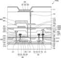
도 12는 도 11에 도시된 화소의 일부 단면도이다.FIG. 12 is a partial cross-sectional view of the pixel shown in FIG. 11.
도 12의 실시예에서, 트랜지스터의 제1 전극 및 제2 전극은 각각 박막 트랜지스터의 소스 전극 및 드레인 전극으로 혼용하여 설명한다.In the embodiment of FIG. 12, the first and second electrodes of the transistor are interchangeably referred to as the source electrode and drain electrode of the thin film transistor, respectively.
도 12를 참조하면, 제1 화소(PX1)는 전술된 반도체 장치(10a, 10b)의 제1 박막 트랜지스터(200) 및 제2 박막 트랜지스터(300)를 이용할 수 있다. 제1 박막 트랜지스터(200) 및 제2 박막 트랜지스터(300)의 제조 공정은 전술된 반도체 장치의 제조 공정과 동일하다.Referring to FIG. 12, the first pixel PX1 may use the first
제1 트랜지스터(T11)는 전술한 제1 박막 트랜지스터(200)로 구현될 수 있다. 제1 박막 트랜지스터(200)는 제1 활성층(201), 제1 게이트 전극(202), 제1 소스 전극(203) 및 제1 드레인 전극(204)을 포함할 수 있다. 제1 소스 전극(203) 및 제1 드레인 전극(204)은 각각 컨택홀(CH1)을 통해 제1 활성층(201)의 소스 영역 및 드레인 영역과 전기적으로 연결될 수 있다.The first transistor T11 may be implemented as the first
제2 트랜지스터(T12)는 전술한 제2 박막 트랜지스터(300)로 구현될 수 있다. 제2 박막 트랜지스터(300)는 제2 활성층(301), 제2 게이트 전극(302), 제2 소스 전극(303) 및 제2 드레인 전극(304)을 포함할 수 있다.The second transistor T12 may be implemented as the second
커패시터(C11)는 제1 게이트 전극(202)을 제1 전극으로 하고, 도전층(400)을 제2 전극으로 하여 구현될 수 있다.The capacitor C11 may be implemented using the
도전층(400)에는 일정한 전압, 즉 제1 전원전압(ELVDD)이 인가될 수 있다.A constant voltage, that is, the first power supply voltage (ELVDD), may be applied to the
제2 박막 트랜지스터(200)의 제2 활성층(301) 및 제2 게이트 전극(302)은 도전층(400)과 적어도 일부 중첩하도록 배치될 수 있다. 또한 도전층(400)은 제2 박막 트랜지스터(200)의 백 채널(back channel)에 영향을 주지 않도록 제2 게이트 전극(302)보다 크게 형성될 수 있다. 도전층(400)의 에지는 제2 게이트 전극(302)의 에지로부터 대략 1.5㎛ 이상 확장될 수 있다. 따라서, 도전층(400)이 차폐층으로 기능하여, 제2 박막 트랜지스터(200)에 대한 제1 게이트 전극(202) 등의 하부 배선 및/또는 전극의 전위에 의한 영향을 최소화할 수 있다.The second
제1 박막 트랜지스터(200)와 제2 박막 트랜지스터(300) 사이에는 제3 절연층(104)과 제4 절연층(105)을 포함하는 평탄화층(PAV)이 배치될 수 있다. 평탄화층(PAV) 상부에는 버퍼층(106)이 배치될 수 있다.A planarization layer (PAV) including a third
기판(100) 상부에 제2 박막 트랜지스터(300)를 덮으며 제7 절연층(109)이 배치될 수 있다.A seventh insulating
제3 내지 제7 절연층(104 내지 109)에는 제1 박막 트랜지스터(200)의 제1 소스 전극(203) 및 제1 드레인 전극(204) 중의 하나(도 12에서는 제1 드레인 전극(204))의 일부를 노출하는 컨택홀(CH3)이 구비될 수 있다.The third to seventh insulating
제7 절연층(109) 상부에 컨택홀(CH3)을 채우며 연결 전극(500)이 배치될 수 있다. 연결 전극(500)은 제1 드레인 전극(204)과 컨택할 수 있다. 연결 전극(500)은 알루미늄(Al), 백금(Pt), 팔라듐(Pd), 은(Ag), 마그네슘(Mg), 금(Au), 니켈(Ni), 네오디뮴(Nd), 이리듐(Ir), 크롬(Cr), 리튬(Li), 칼슘(Ca), 몰리브덴(Mo), 티타늄(Ti), 텅스텐(W), 구리(Cu) 중 하나 이상의 물질로 단층 또는 다층으로 형성될 수 있다.A connection electrode 500 may be disposed on the seventh insulating
제7 절연층(109) 상부에 연결 전극(500)을 덮으며 제8 절연층(110)이 배치될 수 있다. 제8 절연층(110)은 유기 물질로 구성된 단층 또는 복수층일 수 있다. 제8 절연층(110)은 일반 범용고분자(PMMA, PS), phenol 그룹을 갖는 고분자 유도체, 아크릴계 고분자, 이미드계 고분자, 아릴에테르계 고분자, 아마이드계 고분자, 불소계고분자, p-자일렌계 고분자, 비닐알콜계 고분자 및 이들의 블렌드 등을 포함할 수 있다. 예를 들어, 제8 절연층(110)은 폴리이미드, 폴리아마이드, 아크릴 수지 등을 포함할 수 있다. 제8 절연층(110)은 상부면이 평탄한 평탄화층으로 기능할 수 있다.An eighth insulating
제8 절연층(110)에는 연결 전극(500)의 일부를 노출하는 비아홀(VIA)이 구비될 수 있다.The eighth insulating
제8 절연층(110) 상부에 표시소자(600)가 배치될 수 있다. 표시소자(600)는 제1 전극(601), 제1 전극(601)에 대향하는 제2 전극(603), 및 제1 전극(601)과 제2 전극(603) 사이의 중간층(602)을 포함할 수 있다.A
제1 전극(601)은 비아홀(VIA)을 채우며 연결 전극(500)과 컨택할 수 있다. 이에 따라 제1 전극(601)은 제1 박막 트랜지스터(200)와 전기적으로 연결될 수 있다.The
제8 절연층(110) 상부에 제1 전극(601)의 가장자리를 덮으며 제9 절연층(111)이 배치될 수 있다. 제9 절연층(111)은 SiOx, SiNx, SiON, Al2O3, TiO2, Ta2O5, HfO2, ZrO2, BST, PZT 가운데 선택된 하나 이상의 무기 절연막이 단층 또는 복수층으로 형성될 수 있다. 다른 실시예에서, 제7 절연층(109)은 일반 범용고분자(PMMA, PS), phenol 그룹을 갖는 고분자 유도체, 아크릴계 고분자, 이미드계 고분자, 아릴에테르계 고분자, 아마이드계 고분자, 불소계고분자, p-자일렌계 고분자, 비닐알콜계 고분자 및 이들의 블렌드 등 가운데 선택된 하나 이상의 유기 절연막이 단층 또는 복수층으로 형성될 수 있다.A ninth insulating
제1 전극(601)은 은(Ag), 마그네슘(Mg), 알루미늄(Al), 백금(Pt), 납(Pd), 금(Au), 니켈(Ni), 네오디뮴(Nd), 이리듐(Ir), 크롬(Cr) 및 이들의 화합물 등의 반사 도전 물질을 포함하는 반사막일 수 있다. 일 실시예에서 제1 전극(601)은 인듐틴옥사이드(ITO; indium tin oxide), 인듐징크옥사이드(IZO; indium zinc oxide), 징크옥사이드(ZnO; zinc oxide), 인듐옥사이드(In2O3; indium oxide), 인듐갈륨옥사이드(IGO; indium gallium oxide), 및 알루미늄징크옥사이드(AZO; aluminium zinc oxide)를 포함하는 그룹에서 선택된 적어도 어느 하나 이상의 투명 도전성 산화물을 포함하는 투명 도전막일 수 있다. 일 실시예에서 제1 전극(601)은 상기 반사막과 상기 투명 도전막의 적층 구조일 수 있다.The
제1 전극(601)의 상부에는 발광층을 포함하는 중간층(602)이 형성될 수 있다. 발광층은 저분자 유기물 또는 고분자 유기물로 구성될 수 있다. 발광층의 종류에 따라 표시소자(ED)는 적색, 녹색 및 청색의 광을 각각 방출할 수 있다. 그러나, 본 발명은 이에 한정되지 않으며, 복수의 유기 발광층이 하나의 표시소자(ED)에 배치될 수 있다. 예를 들어, 적색, 녹색, 및 청색의 광을 방출하는 복수의 유기 발광층이 수직으로 적층되거나 혼합 형성되어 백색광을 방출할 수 있다. 이 경우 방출된 백색광을 소정의 컬러로 변환하는 색변환층이나 컬러 필터가 더 구비될 수 있다. 상기 적색, 녹색, 및 청색은 예시적인 것으로, 백색광을 방출하기 위한 색의 조합은 이에 한정되지 않는다.An
중간층(602)은 제1 전극(601)과 발광층 사이 및/또는 발광층과 제2 전극(603) 사이에 정공 주입층(hole injection layer), 정공 수송층(hole transport layer), 전자 수송층(electron transport layer) 및 전자 주입층(electron injection layer) 중 적어도 하나의 기능층을 포함할 수 있다. 일 실시예에 따르면, 중간층(602)은 상술한 층들 외에 기타 다양한 기능층을 더 포함할 수 있다.The
도 12에서는 중간층(602)이 제1 전극(601)에만 대응되도록 패터닝된 것으로 도시되어 있으나 이는 편의상 그와 같이 도시한 것이며, 중간층(602)은 인접한 화소의 중간층(602)과 일체로 형성될 수도 있음은 물론이다. 또한 중간층(602) 중 일부의 층은 화소별로 형성되고, 다른 층은 인접한 화소의 중간층(602)과 일체로 형성될 수도 있는 등 다양한 변형이 가능하다.In FIG. 12, the
중간층(602) 상부에 제2 전극(603)이 기판(100)의 표시 영역(DA)의 전면에 형성될 수 있다. 제2 전극(603)은 다양한 도전성 재료로 구성될 수 있다. 예를 들어, 제2 전극(603)은 리튬(Li), 칼슘(Ca), 불화리튬(LiF), 알루미늄(Al), 마그네슘(Mg) 및 은(Ag)을 포함하는 그룹에서 선택된 적어도 어느 하나를 포함하는 반투과 반사막을 포함하거나, ITO, IZO, ZnO 등의 광투과성 금속 산화물을 포함할 수 있으며, 단층 또는 복수층으로 형성될 수 있다.A
도 12에서는 표시소자(600)가 하부의 제1 박막 트랜지스터(200) 및 제2 박막 트랜지스터(300)와 중첩하도록 배치되어 있으나, 다른 실시예에서 표시소자(600)는제1 박막 트랜지스터(200) 및 제2 박막 트랜지스터(300)와 비중첩하거나, 적어도 일부 중첩하도록 배치될 수 있다.In FIG. 12, the
도 13은 본 발명의 다른 실시예에 따른 제2 화소(PX2)의 회로도이다.Figure 13 is a circuit diagram of the second pixel PX2 according to another embodiment of the present invention.
도 13을 참조하면, 일 실시예에 따른 표시장치(1)의 제2 화소(PX2)는 화소회로 및 화소회로에 연결된 표시소자(ED)를 포함할 수 있다. 화소회로는 제1 트랜지스터(T21), 제2 트랜지스터(T22), 제3 트랜지스터(T23) 및 제1 커패시터(C21), 제2 커패시터(C22)를 포함할 수 있다.Referring to FIG. 13, the second pixel PX2 of the
제1 트랜지스터(T21)는 제2 트랜지스터(T22)의 제1 전극에 연결된 게이트 전극, 제1 전원전압(ELVDD)을 입력받는 제1 전극, 및 표시소자(ED)에 연결된 제2 전극을 포함한다.The first transistor T21 includes a gate electrode connected to the first electrode of the second transistor T22, a first electrode receiving the first power voltage ELVDD, and a second electrode connected to the display element ED. .
제2 트랜지스터(T22)는 주사선(SL)에 연결된 게이트 전극, 제1 트랜지스터(T21)의 게이트 전극에 연결된 제1 전극, 및 제1 트랜지스터(T21)의 제2 전극에 연결된 제2 전극을 포함한다.The second transistor T22 includes a gate electrode connected to the scan line SL, a first electrode connected to the gate electrode of the first transistor T21, and a second electrode connected to the second electrode of the first transistor T21. .
제3 트랜지스터(T23)는 제어선(CL)에 연결된 게이트 전극, 초기화 전압(VINT)을 입력받는 제1 전극, 및 제1 트랜지스터(T21)의 제2 전극 및 제2 트랜지스터(T22)의 제2 전극에 연결된 제2 전극을 포함한다.The third transistor T23 includes a gate electrode connected to the control line CL, a first electrode receiving the initialization voltage VINT, a second electrode of the first transistor T21, and a second electrode of the second transistor T22. It includes a second electrode connected to the electrode.
제1 커패시터(C21)는 데이터선(DL)에 연결된 제1 전극과, 제1 트랜지스터(T21)의 제2 전극에 연결된 제2 전극을 포함한다. 제1 커패시터(C21)는 데이터선(DL)에 인가된 데이터 전압을 저장할 수 있다.The first capacitor C21 includes a first electrode connected to the data line DL and a second electrode connected to the second electrode of the first transistor T21. The first capacitor C21 may store the data voltage applied to the data line DL.
제2 커패시터(C22)는 초기화 전압(VINT)을 입력받는 제1 전극, 및 제1 트랜지스터(T21)의 게이트 전극에 연결된 제2 전극을 포함한다.The second capacitor C22 includes a first electrode that receives the initialization voltage (VINT) and a second electrode connected to the gate electrode of the first transistor (T21).
표시소자(ED)는 제1 트랜지스터(T21)를 통해 화소회로에 연결될 수 있다. 표시소자(ED)는 유기발광소자(OLED)일 수 있다. 유기발광소자(OLED)는 제1 트랜지스터(T21)의 제2 전극에 연결된 제1 전극, 제2 전원전압(ELVSS)을 입력받는 제2 전극, 및 제1 전극과 제2 전극 사이의 발광층을 포함한다.The display element ED may be connected to the pixel circuit through the first transistor T21. The display device (ED) may be an organic light emitting device (OLED). The organic light emitting device (OLED) includes a first electrode connected to the second electrode of the first transistor (T21), a second electrode receiving the second power voltage (ELVSS), and a light emitting layer between the first electrode and the second electrode. do.
제1 전원전압(ELVDD)은 제2 전원전압(ELVSS)보다 높은 전압일 수 있다.The first power supply voltage (ELVDD) may be a higher voltage than the second power supply voltage (ELVSS).
제2 화소(PX2)는 표시소자(ED)의 제1 전극을 초기화하는 제1 구간, 제1 트랜지스터(T21)의 문턱 전압을 보상하는 제2 구간, 데이터 전압을 기입하는 제3 구간 및 표시소자(ED)가 발광하는 제4 구간으로 동작할 수 있다.The second pixel PX2 includes a first section for initializing the first electrode of the display element ED, a second section for compensating the threshold voltage of the first transistor T21, a third section for writing the data voltage, and a display element. (ED) may operate as a fourth section in which light is emitted.
제1 구간에, 제2 트랜지스터(T22) 및 제3 트랜지스터(T23)가 턴온되어 표시소자(ED)의 제1 전극이 초기화 전압(VINT)으로 초기화될 수 있다.In the first section, the second transistor T22 and the third transistor T23 are turned on so that the first electrode of the display element ED can be initialized to the initialization voltage VINT.
제2 구간에, 제2 트랜지스터(T22)가 턴온되어 제1 트랜지스터(T21)가 다이오드 연결됨으로써 제1 트랜지스터(T21)의 문턱 전압이 보상될 수 있다.In the second period, the second transistor T22 is turned on and the first transistor T21 is diode-connected, thereby compensating the threshold voltage of the first transistor T21.
제3 구간에, 제2 트랜지스터(T22)가 턴온되고, 제1 트랜지스터(T21) 및 제3 트랜지스터(T23)는 턴오프되어 제1 커패시터(C21)와 제2 커패시터(C22)가 노드(N)에서 직렬 연결될 수 있다. 그리고, 데이터선(DL)으로 데이터 전압이 인가될 수 있다. 이에 따라 데이터 전압은 제1 커패시터(C21)와 제2 커패시터(C22)에 분배되어 노드(N)에 분배 전압이 인가될 수 있다.In the third section, the second transistor T22 is turned on, the first transistor T21 and the third transistor T23 are turned off, so that the first capacitor C21 and the second capacitor C22 are connected to the node N. can be connected in series. And, a data voltage may be applied to the data line DL. Accordingly, the data voltage may be distributed to the first capacitor C21 and the second capacitor C22 and the divided voltage may be applied to the node N.
제4 구간에, 초기화전압(VINT)이 노드(N)에 인가됨에 따라 제1 트랜지스터(T21)가 턴온되고, 제1 트랜지스터(T21)의 게이트 전극(노드 N)에 인가된 전압에 대응하는 구동 전류가 표시소자(ED)에 흐름에 따라 표시소자(ED)가 발광할 수 있다.In the fourth section, as the initialization voltage (VINT) is applied to the node (N), the first transistor (T21) is turned on and driven corresponding to the voltage applied to the gate electrode (node N) of the first transistor (T21). As current flows through the display element (ED), the display element (ED) may emit light.
도 14 및 도 15는 도 13에 도시된 화소의 일부 단면도이다.14 and 15 are partial cross-sectional views of the pixel shown in FIG. 13.
도 14 및 도 15의 실시예에서, 트랜지스터의 제1 전극 및 제2 전극은 각각 박막 트랜지스터의 소스 전극 및 드레인 전극으로 혼용하여 설명한다.14 and 15, the first and second electrodes of the transistor are interchangeably referred to as the source electrode and drain electrode of the thin film transistor, respectively.
도 14를 참조하면, 제2 화소(PX2b)는 전술된 반도체 장치(10a, 10b)의 제1 박막 트랜지스터(200) 및 제2 박막 트랜지스터(300)를 이용할 수 있다.Referring to FIG. 14, the second pixel PX2b may use the first
제1 트랜지스터(T21)는 전술한 제1 박막 트랜지스터(200)로 구현될 수 있다. 제1 박막 트랜지스터(200)는 제1 활성층(201), 제1 게이트 전극(202), 제1 소스 전극(203) 및 제1 드레인 전극(204)을 포함할 수 있다. 제1 소스 전극(203) 및 제1 드레인 전극(204)은 각각 컨택홀(CH1)을 통해 제1 활성층(201)의 소스 영역 및 드레인 영역과 전기적으로 연결될 수 있다.The first transistor T21 may be implemented as the first
제2 트랜지스터(T22)는 전술한 제2 박막 트랜지스터(300)로 구현될 수 있다. 제2 박막 트랜지스터(300)는 제2 활성층(301), 제2 게이트 전극(302), 제2 소스 전극(303) 및 제2 드레인 전극(304)을 포함할 수 있다. 제2 소스 전극(303) 및 제2 드레인 전극(304)은 각각 제2 활성층(301)의 소스 영역 및 드레인 영역에 해당한다.The second transistor T22 may be implemented as the second
제2 박막 트랜지스터(300)의 제2 소스 전극(303)은 연결 전극들(501, 502)을 통해 제1 박막 트랜지스터(200)의 제1 게이트 전극(202)과 전기적으로 연결될 수 있다. 연결 전극(501)은 제2 절연층(103) 상부에 형성되고, 제2 절연층(103)에 형성된 컨택홀(CH4)을 통해 노출된 제1 게이트 전극(202)의 일부와 컨택할 수 있다. 연결 전극(502)은 제6 절연층(108) 상부에 형성되고, 제3 절연층(104) 내지 제6 절연층(108)에 형성된 컨택홀(CH5)을 통해 노출된 연결 전극(501)의 일부 및 제2 소스 전극(303)의 일부와 컨택할 수 있다.The
제1 박막 트랜지스터(200)와 제2 박막 트랜지스터(300) 사이에는 제3 절연층(104)과 제4 절연층(105)을 포함하는 평탄화층(PAV)이 배치될 수 있다. 평탄화층(PAV) 상부에는 버퍼층(106)이 배치될 수 있다.A planarization layer (PAV) including a third
제3 트랜지스터(T23)는 제3 박막 트랜지스터(700)로 구현될 수 있다. 제3 박막 트랜지스터(700)는 제3 활성층(701), 제3 게이트 전극(702), 제3 소스 전극(703) 및 제3 드레인 전극(704)을 포함할 수 있다. 제3 활성층(701)은 제1 활성층(201)으로부터 연장될 수 있다. 제3 소스 전극(703) 및 제3 드레인 전극(704)은 각각 컨택홀(CH1)을 통해 노출된 제3 활성층(701)의 소스 영역 및 드레인 영역과 전기적으로 연결될 수 있다. 제3 박막 트랜지스터(700)의 제3 드레인 전극(704)은 제1 박막 트랜지스터(200)의 제1 드레인 전극(204)일 수 있다.The third transistor T23 may be implemented as the third
제1 커패시터(C21)는 제1 전극(801) 및 제2 전극(802)을 포함하는 커패시터(800)로 구현될 수 있다. 제1 전극(801)은 제7-2 절연층(109b) 상부에 형성되고, 제2 전극(802)은 제7-3 절연층(109c) 상부에 형성될 수 있다.The first capacitor C21 may be implemented as a
제1 전극(801) 및 제2 전극(802)은 알루미늄(Al), 백금(Pt), 팔라듐(Pd), 은(Ag), 마그네슘(Mg), 금(Au), 니켈(Ni), 네오디뮴(Nd), 이리듐(Ir), 크롬(Cr), 리튬(Li), 칼슘(Ca), 몰리브덴(Mo), 티타늄(Ti), 텅스텐(W), 구리(Cu) 중 하나 이상의 물질로 단층 또는 다층으로 형성될 수 있다. 예를 들어, 제1 전극(801) 및 제2 전극(802)은 Ti/Al/Ti의 삼층 구조를 가질 수 있다.The
제2 커패시터(C22)는 제1 게이트 전극(202)을 제1 전극으로 하고, 도전층(400)을 제2 전극으로 하여 구현될 수 있다.The second capacitor C22 may be implemented using the
제1 박막 트랜지스터(200)의 제1 소스 전극(203)은 제1 전원전압(ELVDD)을 인가하는 제1 전원선(901)과 전기적으로 연결될 수 있다. 제1 전원선(901)은 제7-1 절연층(109a) 상부에 형성되고, 제3 내지 제7-1 절연층(104 내지 109a)에 형성된 컨택홀(CH6)을 통해 노출된 제1 소스 전극(203)의 일부와 컨택할 수 있다.The
제1 박막 트랜지스터(200)의 제1 드레인 전극(204) 및 제3 박막 트랜지스터(700)의 제3 드레인 전극(704)은 제3 내지 제7-3 절연층(104 내지 109c)에 형성된 컨택홀(CH7)을 통해 제1 커패시터(C21)의 제2 전극(802)과 전기적으로 연결될 수 있다.The
제2 박막 트랜지스터(300)의 제2 드레인 전극(304)은 제5 내지 제7-3 절연층(107 내지 109c)에 형성된 컨택홀(CH8)을 통해 제1 커패시터(C21)의 제2 전극(802)과 전기적으로 연결될 수 있다.The
제3 박막 트랜지스터(700)의 제3 게이트 전극(702)은 연결 전극(503)을 이용하여 제어선(902)에 전기적으로 연결될 수 있다. 연결 전극(503)은 제2 절연층(103) 상부에 형성되고, 제2 절연층(103)에 형성된 컨택홀(CH9)을 통해 노출된 제3 게이트 전극(702)의 일부와 컨택할 수 있다. 제어선(902)은 제6 절연층(108) 상부에 형성되고, 제3 내지 제6 절연층(104 내지 108)에 형성된 컨택홀(CH10)을 통해 노출된 연결 전극(503)의 일부와 컨택할 수 있다.The
제3 박막 트랜지스터(700)의 제3 소스 전극(703)은 연결 전극(504)을 이용하여 초기화 전압(VINT)을 인가하는 제2 전원선(903)에 전기적으로 연결될 수 있다. 연결 전극(504)은 제6 절연층(108) 상부에 형성되고, 제3 내지 제6 절연층(104 내지 108)에 형성된 컨택홀(CH11)을 통해 노출된 제3 소스 전극(703)의 일부와 컨택할 수 있다. 제2 전원선(903)은 제7-1 절연층(109a) 상부에 형성되고, 제7-1 절연층(109a)에 형성된 컨택홀(CH12)을 통해 노출된 연결 전극(504)의 일부와 컨택할 수 있다.The
제7-3 절연층(109c) 상부에 제1 커패시터(800)를 덮으며 제8 절연층(110)이 배치될 수 있다. 제8 절연층(110)에는 제1 커패시터(C21)의 제2 전극(802)의 일부를 노출하는 비아홀(VIA)이 구비될 수 있다.An eighth insulating
제8 절연층(110) 상부에 표시소자(600)가 배치될 수 있다. 표시소자(600)는 제1 전극(601), 제1 전극(601)에 대향하는 제2 전극(603), 및 제1 전극(601)과 제2 전극(603) 사이의 중간층(602)을 포함할 수 있다.A
제7-1 절연층(109a), 제7-2 절연층(109b), 제7-3 절연층(109c)은 SiOx, SiNx, SiON, Al2O3, TiO2, Ta2O5, HfO2, ZrO2, BST, PZT 가운데 선택된 하나 이상의 무기 절연막이 단층 또는 복수층으로 형성될 수 있다. 다른 실시예에서, 제7-1 절연층(109a), 제7-2 절연층(109b), 제7-3 절연층(109c)은 일반 범용고분자(PMMA, PS), phenol 그룹을 갖는 고분자 유도체, 아크릴계 고분자, 이미드계 고분자, 아릴에테르계 고분자, 아마이드계 고분자, 불소계고분자, p-자일렌계 고분자, 비닐알콜계 고분자 및 이들의 블렌드 등 가운데 선택된 하나 이상의 유기 절연막이 단층 또는 복수층으로 형성될 수 있다.The 7-1 insulating layer (109a), the 7-2 insulating layer (109b), and the 7-3 insulating layer (109c) are SiOx , SiNx , SiON, Al2 O3 , TiO2 , Ta2 O5 , HfO2 , ZrO2 , BST, or PZT, one or more inorganic insulating films may be formed as a single layer or multiple layers. In another embodiment, the 7-1st insulating layer (109a), the 7-2nd insulating layer (109b), and the 7-3rd insulating layer (109c) are general-purpose polymers (PMMA, PS) or polymer derivatives having a phenol group. , one or more organic insulating films selected from acrylic polymers, imide polymers, aryl ether polymers, amide polymers, fluorine polymers, p-xylene polymers, vinyl alcohol polymers, and blends thereof may be formed as a single layer or multiple layers. there is.
연결 전극(501 내지 504), 제1 전원선(901), 제어선(902), 및 제2 전원선(903)은 각각, 알루미늄(Al), 백금(Pt), 팔라듐(Pd), 은(Ag), 마그네슘(Mg), 금(Au), 니켈(Ni), 네오디뮴(Nd), 이리듐(Ir), 크롬(Cr), 리튬(Li), 칼슘(Ca), 몰리브덴(Mo), 티타늄(Ti), 텅스텐(W), 구리(Cu) 중 하나 이상의 물질로 단층 또는 다층으로 형성될 수 있다.The
도 15에 도시된 제2 화소(PX2b)는 제2 박막 트랜지스터(300)와 표시소자(600) 사이의 절연층에 평탄화층이 형성된 점에서, 도 14에 도시된 제2 화소(PX2a)와 차이가 있다. 이하에서는 도 14에 도시된 제2 화소(PX2a)와 상이한 구성을 중심으로 설명하겠다.The second pixel (PX2b) shown in FIG. 15 is different from the second pixel (PX2a) shown in FIG. 14 in that a planarization layer is formed on the insulating layer between the second
도 15를 참조하면, 제7-1 절연층(109a) 상부에 제1 절연막과 제1 절연막 상부에 제2 절연막을 차례로 적층한 후, 제1 절연막의 상부면이 노출되도록 제2 절연막을 제거하여 제7-21 절연층(109b1)과 제7-22 절연층(109b2)을 포함하는 평탄화층을 형성할 수 있다. 제2 절연막을 제거하는 동안 제1 절연막의 일부가 함께 제거될 수 있다.Referring to FIG. 15, after sequentially stacking a first insulating film on top of the 7-1
제2 절연막은 다양한 식각 공정에 의해 제거될 수 있다. 예를 들어, 식각 공정은 건식 식각 또는 화학적 기계 연마(Chemical Mechanical Polishing: CMP) 등의 연마법을 포함할 수 있다.The second insulating film can be removed by various etching processes. For example, the etching process may include a polishing method such as dry etching or chemical mechanical polishing (CMP).
제7-22 절연층(109b2)은 제7-21 절연층(10b1) 상부에 배치되고, 제7-21 절연층(10b1)의 상부면과 제7-22 절연층(109b2)의 상부면은 대략 일치하여 전체적으로 평탄한 상부면을 형성할 수 있다.The 7-22nd insulating layer (109b2) is disposed on the 7-21st insulating layer (10b1), and the top surface of the 7-21st insulating layer (10b1) and the top surface of the 7-22nd insulating layer (109b2) are They can be roughly matched to form an overall flat upper surface.
제7-21 절연층(10b1) 및 제7-22 절연층(109b2)의 상부에는 제3 버퍼층(109b3)이 배치될 수 있다. 제1 커패시터(800)는 제3 버퍼층(109b3) 상부에 배치될 수 있다.A third buffer layer 109b3 may be disposed on the 7-21st insulating layer 10b1 and the 7-22nd insulating layer 109b2. The
화소를 구성하는 복수의 배선들이 복수의 층들에 배치됨에 따라 절연층들의 단차가 커질 수 있다. 도 15에 도시된 실시예와 같이, 복수의 절연층들의 중간에 평탄화층을 구비함으로써 하부 배선 및/또는 전극들에 의한 절연층의 과도한 단차를 줄일 수 있어, 상부에 배치될 막 및/또는 배선의 피복성을 향상시킬 수 있다.As a plurality of wires constituting a pixel are arranged in a plurality of layers, the level difference between the insulating layers may increase. As in the embodiment shown in FIG. 15, by providing a planarization layer in the middle of a plurality of insulating layers, excessive steps in the insulating layer due to the lower wiring and/or electrodes can be reduced, thereby reducing the film and/or wiring to be disposed on the upper portion. Coverage can be improved.
제7-21 절연층(109b1)과 제7-22 절연층(109b2)은 SiOx, SiNx, SiON, Al2O3, TiO2, Ta2O5, HfO2, ZrO2, BST, PZT 가운데 선택된 하나 이상의 무기 절연막이 단층 또는 복수층으로 형성될 수 있다. 다른 실시예에서, 제7-21 절연층(109b1)과 제7-22 절연층(109b2)은 일반 범용고분자(PMMA, PS), phenol 그룹을 갖는 고분자 유도체, 아크릴계 고분자, 이미드계 고분자, 아릴에테르계 고분자, 아마이드계 고분자, 불소계고분자, p-자일렌계 고분자, 비닐알콜계 고분자 및 이들의 블렌드 등 가운데 선택된 하나 이상의 유기 절연막이 단층 또는 복수층으로 형성될 수 있다.The 7-21st insulating layer 109b1 and the 7-22nd insulating layer 109b2 are SiOx , SiNx , SiON, Al2 O3 , TiO2 , Ta2 O5 , HfO2 , ZrO2 , BST, PZT One or more selected inorganic insulating films may be formed as a single layer or multiple layers. In another embodiment, the 7-21st insulating layer (109b1) and the 7-22nd insulating layer (109b2) are general-purpose polymers (PMMA, PS), polymer derivatives with phenol groups, acrylic polymers, imide polymers, and aryl ethers. One or more organic insulating films selected from polymers, amide-based polymers, fluorine-based polymers, p-xylene-based polymers, vinyl alcohol-based polymers, and blends thereof may be formed as a single layer or multiple layers.
제7-22 절연층(109b2)의 조성물은 제7-21 절연층(109b1)의 조성물과 상이한 것이 바람직하다. 제7-22 절연층(109b2)의 조성물은 적어도 제7-21 절연층(109b1)의 상부막의 조성물과 상이한 것이 바람직하다. 예를 들어, 제7-21 절연층(109b1)은 SiOx를 포함하는 절연막이거나, SiOx를 포함하는 하부 절연막과 SiNx를 포함하는 상부 절연막의 다층막일 수 있다. 제7-22 절연층(109b2)은 SiOx를 포함하는 절연막일 수 있다.The composition of the 7-22nd insulating layer (109b2) is preferably different from the composition of the 7-21st insulating layer (109b1). It is preferable that the composition of the 7-22nd insulating layer 109b2 is at least different from the composition of the upper film of the 7-21st insulating layer 109b1. For example, the 7-21st insulating layer 109b1 may be an insulating film containing SiOx , or may be a multilayer film of a lower insulating film containing SiOx and an upper insulating film containing SiNx . The 7-22nd insulating layer 109b2 may be an insulating film containing SiOx .
제3 버퍼층(109b3)은 SiOx, SiNx, SiON, Al2O3, TiO2, Ta2O5, HfO2, ZrO2, BST, PZT 가운데 선택된 하나 이상의 절연막이 단층 또는 복수층으로 형성될 수 있다. 예를 들어, 제3 버퍼층(109b3)은 SiNx를 포함하는 절연막일 수 있다.The thirdbuffer layer109b3is formedofoneormore insulating films selected fromSiO You can. For example, the third buffer layer 109b3 may be an insulating film containing SiNx .
선택적으로, 제3 버퍼층(109b3) 및 제7-21 절연층(109b1)과 제7-22 절연층(109b2)의 평탄화층의 열처리가 수행될 수 있다. 열처리는 탈수소 처리를 포함할 수 있다.Optionally, heat treatment of the third buffer layer 109b3 and the planarization layers of the 7-21st insulating layer 109b1 and 7-22nd insulating layer 109b2 may be performed. Heat treatment may include dehydrogenation treatment.
도 15의 실시예에서 두 번의 평탄화층이 형성되고 있으나, 본 발명의 실시예는 화소를 구성하는 배선 및/또는 전극에 따라 두 번 이상의 평탄화층이 형성될 수 있다.Although two planarization layers are formed in the embodiment of FIG. 15, two or more planarization layers may be formed depending on the wiring and/or electrodes constituting the pixel in the embodiment of the present invention.
도 12, 도 14 및 도 15의 실시예에서, 제2 박막 트랜지스터(300) 하부에 일정한 전원전압이 인가되는 커패시터(C11, C22)의 일 전극으로서 도전층(400)이 배치되고 있으나, 본 발명은 이에 한정되지 않는다. 예를 들어, 도전층(400)은 화소 구동 기간 중 적어도 문턱전압 보상기간, 데이터 기입기간, 발광기간에 일정한 DC 전압이 인가되는 배선 및/또는 전극일 수 있다.12, 14, and 15, the
이와 같이 본 발명은 도면에 도시된 일 실시예를 참고로 하여 설명하였으나 이는 예시적인 것에 불과하며 당해 분야에서 통상의 지식을 가진 자라면 이로부터 다양한 변형 및 실시예의 변형이 가능하다는 점을 이해할 것이다. 따라서, 본 발명의 진정한 기술적 보호 범위는 첨부된 특허청구범위의 기술적 사상에 의하여 정해져야 할 것이다.As such, the present invention has been described with reference to an embodiment shown in the drawings, but this is merely an example, and those skilled in the art will understand that various modifications and variations of the embodiment are possible therefrom. Therefore, the true scope of technical protection of the present invention should be determined by the technical spirit of the appended claims.
Claims (21)
Translated fromKorean상기 제1 박막 트랜지스터 상부에, 상기 제1 박막 트랜지스터와 중첩하는 제2 활성층을 갖는 제2 박막 트랜지스터;
상기 제1 박막 트랜지스터와 상기 제2 박막 트랜지스터 사이의 도전층; 및
제1전극 및 상기 제1전극 상부에 배치되고, 상기 제1전극에 중첩하는 제2전극을 포함하는 커패시터;를 포함하고,
상기 커패시터의 제1전극은 상기 제1 박막 트랜지스터의 게이트전극을 포함하고, 상기 커패시터의 제2전극은 상기 도전층을 포함하고,
상기 도전층은 상기 제1박막 트랜지스터의 게이트전극에 중첩하고,
상기 제1 활성층의 채널 영역과 상기 제2 활성층의 채널 영역이 중첩하는, 표시장치.A first thin film transistor having a first active layer on top of the substrate;
a second thin film transistor on top of the first thin film transistor and having a second active layer overlapping with the first thin film transistor;
A conductive layer between the first thin film transistor and the second thin film transistor; and
A capacitor including a first electrode and a second electrode disposed on the first electrode and overlapping the first electrode,
The first electrode of the capacitor includes the gate electrode of the first thin film transistor, and the second electrode of the capacitor includes the conductive layer,
The conductive layer overlaps the gate electrode of the first thin film transistor,
A display device wherein a channel area of the first active layer and a channel area of the second active layer overlap.
상기 제1 박막 트랜지스터와 상기 제2 박막 트랜지스터 사이의 제1평탄화층; 및
상기 제1 평탄화층과 상기 제2 박막 트랜지스터 사이의 제1 버퍼층;을 포함하고,
상기 제1 버퍼층은 실리콘산화물을 포함하는, 표시장치.According to paragraph 1,
a first planarization layer between the first thin film transistor and the second thin film transistor; and
It includes a first buffer layer between the first planarization layer and the second thin film transistor,
The first buffer layer includes silicon oxide.
상기 제1 평탄화층은 제1 절연층 및, 상기 제1 절연층의 상부에 배치되고, 상기 제1 절연층의 상부면과 일치하는 상부면을 갖는 제2 절연층을 포함하는, 표시장치.According to paragraph 2,
The first planarization layer includes a first insulating layer and a second insulating layer disposed on top of the first insulating layer and having an upper surface that matches the upper surface of the first insulating layer.
상기 도전층은 DC 전압을 갖는, 표시장치.According to paragraph 1,
The display device wherein the conductive layer has a DC voltage.
상기 도전층은 적어도 발광 구간에 DC 전압을 갖는, 표시장치.According to paragraph 1,
The display device wherein the conductive layer has a DC voltage at least in the light emission section.
상기 도전층은 상기 제2 박막 트랜지스터의 게이트 전극보다 큰, 표시장치.According to paragraph 1,
The display device wherein the conductive layer is larger than the gate electrode of the second thin film transistor.
상기 도전층의 중심과 상기 제2 박막 트랜지스터의 게이트 전극의 중심의 이격 거리는 3㎛ 이내인, 표시장치.According to paragraph 1,
The display device wherein the separation distance between the center of the conductive layer and the center of the gate electrode of the second thin film transistor is within 3 μm.
상기 제2 활성층의 두께는 상기 제1 활성층의 두께보다 얇은, 표시장치.According to paragraph 1,
A display device wherein the thickness of the second active layer is thinner than the thickness of the first active layer.
상기 제2 활성층의 두께는 상기 제1 활성층의 두께의 80% 이하인, 표시장치.According to paragraph 1,
A display device wherein the thickness of the second active layer is 80% or less of the thickness of the first active layer.
상기 제2 박막 트랜지스터 상부에, 상기 제2 박막 트랜지스터와 중첩하고 상기 제1 박막 트랜지스터와 연결된 표시소자;를 더 포함하는 표시장치.According to paragraph 1,
A display device further comprising: a display element on top of the second thin film transistor, overlapping with the second thin film transistor, and connected to the first thin film transistor.
제3 절연층 및, 상기 제3 절연층의 상부에 배치되고, 상기 제3 절연층의 상부면과 일치하는 상부면을 갖는 제4 절연층을 포함하는 제2 평탄화층; 및
상기 제2 평탄화층 상부의 제2 버퍼층;을 더 포함하는 표시장치.The method of claim 10, between the second thin film transistor and the display element,
a second planarization layer including a third insulating layer and a fourth insulating layer disposed on top of the third insulating layer and having an upper surface that coincides with the upper surface of the third insulating layer; and
A display device further comprising a second buffer layer on top of the second planarization layer.
상기 제2 박막 트랜지스터와 상기 표시소자 사이의 제5 절연층;을 더 포함하는 표시장치.According to clause 10,
A display device further comprising a fifth insulating layer between the second thin film transistor and the display element.
상기 제2 버퍼층은 실리콘질화물을 포함하는, 표시장치.According to clause 11,
The second buffer layer includes silicon nitride.
상기 제1 활성층으로부터 연장된 제3 활성층을 갖는 제3 박막 트랜지스터;를 더 포함하는 표시장치.According to paragraph 1,
A display device further comprising a third thin film transistor having a third active layer extending from the first active layer.
상기 제2 박막 트랜지스터 상부에, 상기 제2 활성층과 적어도 일부 중첩하는 제2커패시터;를 더 포함하는 표시장치.According to clause 14,
The display device further includes a second capacitor on top of the second thin film transistor and at least partially overlapping the second active layer.
상기 제1 박막 트랜지스터 상부에, 제1 절연막 및 제2 절연막을 형성하는 단계;
상기 제1 절연막의 상부면과 상기 제2 절연막의 상부면이 일치하도록 상기 제2 절연막을 식각하여 제1 평탄화층을 형성하는 단계;
상기 제1 평탄화층 상부에 제1 버퍼층을 형성하는 단계; 및
상기 제1 버퍼층의 상부에, 상기 제1 박막 트랜지스터와 중첩하는 제2 활성층을 갖는 제2 박막 트랜지스터를 형성하는 단계;를 포함하는 표시장치의 제조방법.Forming a first thin film transistor having a first active layer on an upper part of a substrate;
forming a first insulating film and a second insulating film on the first thin film transistor;
forming a first planarization layer by etching the second insulating film so that the top surface of the first insulating film matches the top surface of the second insulating film;
Forming a first buffer layer on top of the first planarization layer; and
Forming a second thin film transistor having a second active layer overlapping the first thin film transistor on top of the first buffer layer.
상기 제1 평탄화층 및 상기 제1 버퍼층의 열 처리를 수행하는 단계;를 더 포함하는 표시장치의 제조방법.The method of claim 16, before forming the second thin film transistor,
The method of manufacturing a display device further comprising: performing heat treatment on the first planarization layer and the first buffer layer.
상기 제1 박막 트랜지스터 상부에, 상기 제1 활성층과 중첩하는 도전층을 형성하는 단계;를 더 포함하고,
상기 제2 박막 트랜지스터는 상기 도전층과 중첩하는, 표시장치의 제조방법.The method of claim 16, before forming the first insulating film and the second insulating film,
It further includes forming a conductive layer overlapping the first active layer on the first thin film transistor,
The second thin film transistor overlaps the conductive layer.
상기 제2 박막 트랜지스터 상부에, 상기 제2 박막 트랜지스터와 중첩하고 상기 제1 박막 트랜지스터와 연결된 표시소자를 형성하는 단계;를 더 포함하는 표시장치의 제조방법.According to clause 16,
The method of manufacturing a display device further comprising forming a display element on the second thin film transistor, overlapping with the second thin film transistor and connected to the first thin film transistor.
상기 제2 박막 트랜지스터 상부에 제3 절연막 및 제4 절연막을 형성하는 단계;
상기 제3 절연막의 상부면과 상기 제4 절연막의 상부면이 일치하도록 상기 제4 절연막을 식각하여 제2 평탄화층을 형성하는 단계; 및
상기 제2 평탄화층의 상부에 제2 버퍼층을 형성하는 단계;를 더 포함하는 표시장치의 제조방법.The method of claim 19, before forming the display element,
forming a third insulating film and a fourth insulating film on the second thin film transistor;
forming a second planarization layer by etching the fourth insulating film so that the top surface of the third insulating film matches the top surface of the fourth insulating film; and
A method of manufacturing a display device further comprising forming a second buffer layer on top of the second planarization layer.
상기 제1 활성층은 실리콘 반도체를 포함하고, 상기 제2 활성층은 산화물 반도체를 포함하는, 표시장치.According to paragraph 1,
The first active layer includes a silicon semiconductor, and the second active layer includes an oxide semiconductor.
Priority Applications (7)
| Application Number | Priority Date | Filing Date | Title |
|---|---|---|---|
| KR1020180009607AKR102630641B1 (en) | 2018-01-25 | 2018-01-25 | Display apparatus and method of manufacturing thereof |
| EP19153798.4AEP3518287B1 (en) | 2018-01-25 | 2019-01-25 | Display apparatus and method of manufacturing the same |
| US16/257,693US10629626B2 (en) | 2018-01-25 | 2019-01-25 | Display apparatus and method of manufacturing the same |
| JP2019011438AJP7370708B2 (en) | 2018-01-25 | 2019-01-25 | Display device and its manufacturing method |
| CN201910073188.5ACN110085628B (en) | 2018-01-25 | 2019-01-25 | Display device and method of manufacturing the same |
| US16/846,240US11056511B2 (en) | 2018-01-25 | 2020-04-10 | Display apparatus and method of manufacturing the same |
| US17/352,357US11824067B2 (en) | 2018-01-25 | 2021-06-21 | Display apparatus and method of manufacturing the same |
Applications Claiming Priority (1)
| Application Number | Priority Date | Filing Date | Title |
|---|---|---|---|
| KR1020180009607AKR102630641B1 (en) | 2018-01-25 | 2018-01-25 | Display apparatus and method of manufacturing thereof |
Publications (2)
| Publication Number | Publication Date |
|---|---|
| KR20190090906A KR20190090906A (en) | 2019-08-05 |
| KR102630641B1true KR102630641B1 (en) | 2024-01-30 |
Family
ID=65241133
Family Applications (1)
| Application Number | Title | Priority Date | Filing Date |
|---|---|---|---|
| KR1020180009607AActiveKR102630641B1 (en) | 2018-01-25 | 2018-01-25 | Display apparatus and method of manufacturing thereof |
Country Status (5)
| Country | Link |
|---|---|
| US (3) | US10629626B2 (en) |
| EP (1) | EP3518287B1 (en) |
| JP (1) | JP7370708B2 (en) |
| KR (1) | KR102630641B1 (en) |
| CN (1) | CN110085628B (en) |
Families Citing this family (20)
| Publication number | Priority date | Publication date | Assignee | Title |
|---|---|---|---|---|
| KR102703645B1 (en)* | 2018-10-22 | 2024-09-06 | 엘지디스플레이 주식회사 | Display device comprising thin film trnasistors overlaped each other |
| US11765935B2 (en)* | 2019-07-04 | 2023-09-19 | Lg Display Co., Ltd. | Display apparatus |
| KR102612405B1 (en)* | 2019-07-09 | 2023-12-12 | 엘지디스플레이 주식회사 | Electronic device |
| KR102805320B1 (en)* | 2019-08-20 | 2025-05-13 | 삼성디스플레이 주식회사 | Display device and method of fabricating the same |
| KR102837404B1 (en)* | 2019-09-09 | 2025-07-23 | 삼성디스플레이 주식회사 | Display device |
| KR102797540B1 (en)* | 2019-10-22 | 2025-04-21 | 삼성디스플레이 주식회사 | Display Device and Method of manufacturing of the display device |
| KR20210052635A (en) | 2019-10-29 | 2021-05-11 | 삼성디스플레이 주식회사 | Display apparatus |
| CN112038325B (en)* | 2020-08-20 | 2022-08-23 | 武汉华星光电半导体显示技术有限公司 | Display panel |
| CN112420794B (en)* | 2020-11-18 | 2023-04-14 | 京东方科技集团股份有限公司 | Display substrate and display device |
| KR20220078017A (en)* | 2020-12-02 | 2022-06-10 | 삼성디스플레이 주식회사 | Display panel and display device including the same |
| CN214898447U (en)* | 2021-03-19 | 2021-11-26 | 京东方科技集团股份有限公司 | Array substrate, display panel |
| CN113066841B (en)* | 2021-03-23 | 2024-05-24 | 京东方科技集团股份有限公司 | Display substrate and manufacturing method thereof |
| CN113193010A (en)* | 2021-04-07 | 2021-07-30 | 武汉华星光电技术有限公司 | Array substrate, preparation method thereof and OLED display panel |
| JP2024521642A (en)* | 2021-05-07 | 2024-06-04 | アプライド マテリアルズ インコーポレイテッド | Thin film transistors for circuits for use in display devices |
| CN113745241B (en)* | 2021-07-30 | 2022-09-27 | 惠科股份有限公司 | Array substrate and manufacturing method thereof, display panel and control method thereof, and display device |
| US20230074433A1 (en)* | 2021-09-03 | 2023-03-09 | Lg Display Co., Ltd. | Thin film transistor substrate and display device comprising the same |
| CN114242736A (en)* | 2021-12-17 | 2022-03-25 | 湖北长江新型显示产业创新中心有限公司 | A display panel and display device |
| CN115632063A (en)* | 2022-09-20 | 2023-01-20 | 武汉华星光电技术有限公司 | Array substrate and display panel |
| CN116544246A (en)* | 2023-07-07 | 2023-08-04 | 深圳市华星光电半导体显示技术有限公司 | Array substrate and display panel |
| US20250081730A1 (en)* | 2023-09-05 | 2025-03-06 | Apple Inc. | Display with Vertically Stacked Components |
Citations (1)
| Publication number | Priority date | Publication date | Assignee | Title |
|---|---|---|---|---|
| JP2015188070A (en)* | 2014-03-07 | 2015-10-29 | 株式会社半導体エネルギー研究所 | semiconductor device |
Family Cites Families (24)
| Publication number | Priority date | Publication date | Assignee | Title |
|---|---|---|---|---|
| JP3382467B2 (en) | 1995-09-14 | 2003-03-04 | キヤノン株式会社 | Active matrix substrate manufacturing method |
| JP3777857B2 (en)* | 1999-03-08 | 2006-05-24 | セイコーエプソン株式会社 | Manufacturing method of electro-optical device |
| JP5121103B2 (en)* | 2000-09-14 | 2013-01-16 | 株式会社半導体エネルギー研究所 | Semiconductor device, method for manufacturing semiconductor device, and electric appliance |
| SG148819A1 (en) | 2000-09-14 | 2009-01-29 | Semiconductor Energy Lab | Semiconductor device and manufacturing method thereof |
| KR100663360B1 (en)* | 2005-04-20 | 2007-01-02 | 삼성전자주식회사 | Semiconductor Devices Having Thin Film Transistors and Manufacturing Methods Thereof |
| KR101100426B1 (en) | 2005-05-10 | 2011-12-30 | 삼성전자주식회사 | A semiconductor device comprising a single crystal silicon layer, a semiconductor device including the same, and a flat panel display device and a method of manufacturing the semiconductor device |
| KR20110071698A (en)* | 2009-12-21 | 2011-06-29 | 삼성모바일디스플레이주식회사 | Flat panel display |
| JP6034048B2 (en)* | 2012-04-23 | 2016-11-30 | 株式会社半導体エネルギー研究所 | Display device, electronic equipment |
| KR20130138616A (en)* | 2012-06-11 | 2013-12-19 | 삼성디스플레이 주식회사 | Display device and operating method thereof |
| CN103077957B (en) | 2013-02-22 | 2015-09-02 | 深圳市华星光电技术有限公司 | Active matrix organic LED display device and preparation method thereof |
| KR102034254B1 (en)* | 2013-04-04 | 2019-10-21 | 삼성디스플레이 주식회사 | Thin film transistor array substrate, organic light emitting diode display includung thereof and maethod of manufacturing the organic light emitting diode display |
| KR102117109B1 (en) | 2013-10-22 | 2020-06-01 | 삼성디스플레이 주식회사 | Organic light-emitting display apparatus |
| KR102306200B1 (en)* | 2014-01-24 | 2021-09-30 | 가부시키가이샤 한도오따이 에네루기 켄큐쇼 | Semiconductor device |
| CN103779390B (en)* | 2014-02-11 | 2016-08-17 | 京东方科技集团股份有限公司 | A kind of flexible display substrates and preparation method thereof |
| JP6518890B2 (en) | 2014-03-31 | 2019-05-29 | 株式会社Joled | Display device and electronic device |
| US9647129B2 (en)* | 2014-07-04 | 2017-05-09 | Semiconductor Energy Laboratory Co., Ltd. | Semiconductor device |
| CN105390504B (en)* | 2014-08-29 | 2019-02-01 | 乐金显示有限公司 | Thin film transistor base plate and the display device for using it |
| KR102226236B1 (en) | 2014-10-13 | 2021-03-11 | 엘지디스플레이 주식회사 | Organic light emitting display |
| JP6683503B2 (en) | 2015-03-03 | 2020-04-22 | 株式会社半導体エネルギー研究所 | Semiconductor device |
| KR102394650B1 (en)* | 2015-08-31 | 2022-05-06 | 엘지디스플레이 주식회사 | Organic light emitting display device |
| KR102517127B1 (en) | 2015-12-02 | 2023-04-03 | 삼성디스플레이 주식회사 | Thin film transistor array panel and organic light emitting diode display including the same |
| JP2017162852A (en)* | 2016-03-07 | 2017-09-14 | 株式会社ジャパンディスプレイ | Semiconductor device and display device |
| CN106711178B (en) | 2016-12-28 | 2019-08-30 | 武汉华星光电技术有限公司 | Double-sided OLED display and its manufacturing method |
| KR102126552B1 (en)* | 2017-12-19 | 2020-06-24 | 엘지디스플레이 주식회사 | Display device |
- 2018
- 2018-01-25KRKR1020180009607Apatent/KR102630641B1/enactiveActive
- 2019
- 2019-01-25EPEP19153798.4Apatent/EP3518287B1/enactiveActive
- 2019-01-25CNCN201910073188.5Apatent/CN110085628B/enactiveActive
- 2019-01-25USUS16/257,693patent/US10629626B2/enactiveActive
- 2019-01-25JPJP2019011438Apatent/JP7370708B2/enactiveActive
- 2020
- 2020-04-10USUS16/846,240patent/US11056511B2/enactiveActive
- 2021
- 2021-06-21USUS17/352,357patent/US11824067B2/enactiveActive
Patent Citations (1)
| Publication number | Priority date | Publication date | Assignee | Title |
|---|---|---|---|---|
| JP2015188070A (en)* | 2014-03-07 | 2015-10-29 | 株式会社半導体エネルギー研究所 | semiconductor device |
Also Published As
| Publication number | Publication date |
|---|---|
| US11824067B2 (en) | 2023-11-21 |
| US20190229131A1 (en) | 2019-07-25 |
| EP3518287A1 (en) | 2019-07-31 |
| CN110085628B (en) | 2024-07-16 |
| JP7370708B2 (en) | 2023-10-30 |
| CN110085628A (en) | 2019-08-02 |
| US11056511B2 (en) | 2021-07-06 |
| EP3518287B1 (en) | 2024-04-03 |
| US20200243571A1 (en) | 2020-07-30 |
| JP2019128601A (en) | 2019-08-01 |
| US20210343756A1 (en) | 2021-11-04 |
| US10629626B2 (en) | 2020-04-21 |
| KR20190090906A (en) | 2019-08-05 |
Similar Documents
| Publication | Publication Date | Title |
|---|---|---|
| KR102630641B1 (en) | Display apparatus and method of manufacturing thereof | |
| US11355568B2 (en) | Organic light emitting diode display device | |
| CN102117824B (en) | Organic light emitting display apparatus and method of manufacturing the same | |
| US20220130941A1 (en) | Organic light emitting diode display device | |
| US10361260B2 (en) | Semiconductor device and method of manufacturing the same | |
| KR20170129339A (en) | Display apparatus and manufacturing method of the same | |
| US20200273940A1 (en) | Organic light emitting diode display device | |
| US12336385B2 (en) | Display device and method of manufacturing display device | |
| US11619605B2 (en) | Display apparatus | |
| US20230074191A1 (en) | Circuit substrate | |
| KR101996438B1 (en) | Substrate for display device, display device and method of manufacturing the same | |
| US12224353B2 (en) | Thin-film transistor circuit and method of manufacturing thin-film transistor circuit | |
| US12249652B2 (en) | Oxide semiconductor thin-film transistor and method of manufacturing oxide semiconductor thin-film transistor | |
| KR20150048508A (en) | Display apparatus, method for manufacturing the same, and organic light emitting display | |
| US20240324304A1 (en) | Display apparatus and method of manufacturing the same | |
| KR20170122360A (en) | Organic light emitting display device and method for manufacturing the same | |
| KR20250024583A (en) | Display apparatus |
Legal Events
| Date | Code | Title | Description |
|---|---|---|---|
| PA0109 | Patent application | Patent event code:PA01091R01D Comment text:Patent Application Patent event date:20180125 | |
| PG1501 | Laying open of application | ||
| A201 | Request for examination | ||
| PA0201 | Request for examination | Patent event code:PA02012R01D Patent event date:20210107 Comment text:Request for Examination of Application Patent event code:PA02011R01I Patent event date:20180125 Comment text:Patent Application | |
| E902 | Notification of reason for refusal | ||
| PE0902 | Notice of grounds for rejection | Comment text:Notification of reason for refusal Patent event date:20221026 Patent event code:PE09021S01D | |
| E90F | Notification of reason for final refusal | ||
| PE0902 | Notice of grounds for rejection | Comment text:Final Notice of Reason for Refusal Patent event date:20230413 Patent event code:PE09021S02D | |
| E701 | Decision to grant or registration of patent right | ||
| PE0701 | Decision of registration | Patent event code:PE07011S01D Comment text:Decision to Grant Registration Patent event date:20231024 | |
| GRNT | Written decision to grant | ||
| PR0701 | Registration of establishment | Comment text:Registration of Establishment Patent event date:20240124 Patent event code:PR07011E01D | |
| PR1002 | Payment of registration fee | Payment date:20240125 End annual number:3 Start annual number:1 | |
| PG1601 | Publication of registration |