KR102626048B1 - Memory controller, memory system having the same and operating method thereof - Google Patents
Memory controller, memory system having the same and operating method thereofDownload PDFInfo
- Publication number
- KR102626048B1 KR102626048B1KR1020180032856AKR20180032856AKR102626048B1KR 102626048 B1KR102626048 B1KR 102626048B1KR 1020180032856 AKR1020180032856 AKR 1020180032856AKR 20180032856 AKR20180032856 AKR 20180032856AKR 102626048 B1KR102626048 B1KR 102626048B1
- Authority
- KR
- South Korea
- Prior art keywords
- memory
- execution time
- memory unit
- expected execution
- unit
- Prior art date
- Legal status (The legal status is an assumption and is not a legal conclusion. Google has not performed a legal analysis and makes no representation as to the accuracy of the status listed.)
- Active
Links
Images


Classifications
- G—PHYSICS
- G06—COMPUTING OR CALCULATING; COUNTING
- G06F—ELECTRIC DIGITAL DATA PROCESSING
- G06F3/00—Input arrangements for transferring data to be processed into a form capable of being handled by the computer; Output arrangements for transferring data from processing unit to output unit, e.g. interface arrangements
- G06F3/06—Digital input from, or digital output to, record carriers, e.g. RAID, emulated record carriers or networked record carriers
- G06F3/0601—Interfaces specially adapted for storage systems
- G06F3/0628—Interfaces specially adapted for storage systems making use of a particular technique
- G06F3/0655—Vertical data movement, i.e. input-output transfer; data movement between one or more hosts and one or more storage devices
- G06F3/0659—Command handling arrangements, e.g. command buffers, queues, command scheduling
- G—PHYSICS
- G11—INFORMATION STORAGE
- G11C—STATIC STORES
- G11C16/00—Erasable programmable read-only memories
- G11C16/02—Erasable programmable read-only memories electrically programmable
- G11C16/06—Auxiliary circuits, e.g. for writing into memory
- G11C16/32—Timing circuits
- G—PHYSICS
- G06—COMPUTING OR CALCULATING; COUNTING
- G06F—ELECTRIC DIGITAL DATA PROCESSING
- G06F3/00—Input arrangements for transferring data to be processed into a form capable of being handled by the computer; Output arrangements for transferring data from processing unit to output unit, e.g. interface arrangements
- G06F3/06—Digital input from, or digital output to, record carriers, e.g. RAID, emulated record carriers or networked record carriers
- G06F3/0601—Interfaces specially adapted for storage systems
- G06F3/0628—Interfaces specially adapted for storage systems making use of a particular technique
- G06F3/0655—Vertical data movement, i.e. input-output transfer; data movement between one or more hosts and one or more storage devices
- G06F3/0658—Controller construction arrangements
- G—PHYSICS
- G06—COMPUTING OR CALCULATING; COUNTING
- G06F—ELECTRIC DIGITAL DATA PROCESSING
- G06F11/00—Error detection; Error correction; Monitoring
- G06F11/07—Responding to the occurrence of a fault, e.g. fault tolerance
- G06F11/08—Error detection or correction by redundancy in data representation, e.g. by using checking codes
- G06F11/10—Adding special bits or symbols to the coded information, e.g. parity check, casting out 9's or 11's
- G06F11/1008—Adding special bits or symbols to the coded information, e.g. parity check, casting out 9's or 11's in individual solid state devices
- G06F11/1044—Adding special bits or symbols to the coded information, e.g. parity check, casting out 9's or 11's in individual solid state devices with specific ECC/EDC distribution
- G—PHYSICS
- G06—COMPUTING OR CALCULATING; COUNTING
- G06F—ELECTRIC DIGITAL DATA PROCESSING
- G06F11/00—Error detection; Error correction; Monitoring
- G06F11/07—Responding to the occurrence of a fault, e.g. fault tolerance
- G06F11/08—Error detection or correction by redundancy in data representation, e.g. by using checking codes
- G06F11/10—Adding special bits or symbols to the coded information, e.g. parity check, casting out 9's or 11's
- G06F11/1008—Adding special bits or symbols to the coded information, e.g. parity check, casting out 9's or 11's in individual solid state devices
- G06F11/1068—Adding special bits or symbols to the coded information, e.g. parity check, casting out 9's or 11's in individual solid state devices in sector programmable memories, e.g. flash disk
- G—PHYSICS
- G06—COMPUTING OR CALCULATING; COUNTING
- G06F—ELECTRIC DIGITAL DATA PROCESSING
- G06F13/00—Interconnection of, or transfer of information or other signals between, memories, input/output devices or central processing units
- G06F13/14—Handling requests for interconnection or transfer
- G06F13/16—Handling requests for interconnection or transfer for access to memory bus
- G06F13/1668—Details of memory controller
- G06F13/1673—Details of memory controller using buffers
- G—PHYSICS
- G06—COMPUTING OR CALCULATING; COUNTING
- G06F—ELECTRIC DIGITAL DATA PROCESSING
- G06F13/00—Interconnection of, or transfer of information or other signals between, memories, input/output devices or central processing units
- G06F13/14—Handling requests for interconnection or transfer
- G06F13/16—Handling requests for interconnection or transfer for access to memory bus
- G06F13/18—Handling requests for interconnection or transfer for access to memory bus based on priority control
- G—PHYSICS
- G06—COMPUTING OR CALCULATING; COUNTING
- G06F—ELECTRIC DIGITAL DATA PROCESSING
- G06F3/00—Input arrangements for transferring data to be processed into a form capable of being handled by the computer; Output arrangements for transferring data from processing unit to output unit, e.g. interface arrangements
- G06F3/06—Digital input from, or digital output to, record carriers, e.g. RAID, emulated record carriers or networked record carriers
- G06F3/0601—Interfaces specially adapted for storage systems
- G06F3/0602—Interfaces specially adapted for storage systems specifically adapted to achieve a particular effect
- G06F3/061—Improving I/O performance
- G06F3/0611—Improving I/O performance in relation to response time
- G—PHYSICS
- G06—COMPUTING OR CALCULATING; COUNTING
- G06F—ELECTRIC DIGITAL DATA PROCESSING
- G06F3/00—Input arrangements for transferring data to be processed into a form capable of being handled by the computer; Output arrangements for transferring data from processing unit to output unit, e.g. interface arrangements
- G06F3/06—Digital input from, or digital output to, record carriers, e.g. RAID, emulated record carriers or networked record carriers
- G06F3/0601—Interfaces specially adapted for storage systems
- G06F3/0602—Interfaces specially adapted for storage systems specifically adapted to achieve a particular effect
- G06F3/061—Improving I/O performance
- G06F3/0613—Improving I/O performance in relation to throughput
- G—PHYSICS
- G06—COMPUTING OR CALCULATING; COUNTING
- G06F—ELECTRIC DIGITAL DATA PROCESSING
- G06F3/00—Input arrangements for transferring data to be processed into a form capable of being handled by the computer; Output arrangements for transferring data from processing unit to output unit, e.g. interface arrangements
- G06F3/06—Digital input from, or digital output to, record carriers, e.g. RAID, emulated record carriers or networked record carriers
- G06F3/0601—Interfaces specially adapted for storage systems
- G06F3/0628—Interfaces specially adapted for storage systems making use of a particular technique
- G06F3/0653—Monitoring storage devices or systems
- G—PHYSICS
- G06—COMPUTING OR CALCULATING; COUNTING
- G06F—ELECTRIC DIGITAL DATA PROCESSING
- G06F3/00—Input arrangements for transferring data to be processed into a form capable of being handled by the computer; Output arrangements for transferring data from processing unit to output unit, e.g. interface arrangements
- G06F3/06—Digital input from, or digital output to, record carriers, e.g. RAID, emulated record carriers or networked record carriers
- G06F3/0601—Interfaces specially adapted for storage systems
- G06F3/0668—Interfaces specially adapted for storage systems adopting a particular infrastructure
- G06F3/0671—In-line storage system
- G06F3/0673—Single storage device
- G06F3/0679—Non-volatile semiconductor memory device, e.g. flash memory, one time programmable memory [OTP]
- G—PHYSICS
- G06—COMPUTING OR CALCULATING; COUNTING
- G06F—ELECTRIC DIGITAL DATA PROCESSING
- G06F3/00—Input arrangements for transferring data to be processed into a form capable of being handled by the computer; Output arrangements for transferring data from processing unit to output unit, e.g. interface arrangements
- G06F3/06—Digital input from, or digital output to, record carriers, e.g. RAID, emulated record carriers or networked record carriers
- G06F3/0601—Interfaces specially adapted for storage systems
- G06F3/0668—Interfaces specially adapted for storage systems adopting a particular infrastructure
- G06F3/0671—In-line storage system
- G06F3/0683—Plurality of storage devices
- G—PHYSICS
- G11—INFORMATION STORAGE
- G11C—STATIC STORES
- G11C29/00—Checking stores for correct operation ; Subsequent repair; Testing stores during standby or offline operation
- G11C29/02—Detection or location of defective auxiliary circuits, e.g. defective refresh counters
- G11C29/023—Detection or location of defective auxiliary circuits, e.g. defective refresh counters in clock generator or timing circuitry
- G—PHYSICS
- G11—INFORMATION STORAGE
- G11C—STATIC STORES
- G11C29/00—Checking stores for correct operation ; Subsequent repair; Testing stores during standby or offline operation
- G11C29/04—Detection or location of defective memory elements, e.g. cell constructio details, timing of test signals
- G11C29/08—Functional testing, e.g. testing during refresh, power-on self testing [POST] or distributed testing
- G11C29/12—Built-in arrangements for testing, e.g. built-in self testing [BIST] or interconnection details
- G11C29/14—Implementation of control logic, e.g. test mode decoders
- G—PHYSICS
- G11—INFORMATION STORAGE
- G11C—STATIC STORES
- G11C29/00—Checking stores for correct operation ; Subsequent repair; Testing stores during standby or offline operation
- G11C29/04—Detection or location of defective memory elements, e.g. cell constructio details, timing of test signals
- G11C29/08—Functional testing, e.g. testing during refresh, power-on self testing [POST] or distributed testing
- G11C29/12—Built-in arrangements for testing, e.g. built-in self testing [BIST] or interconnection details
- G11C29/38—Response verification devices
- G—PHYSICS
- G11—INFORMATION STORAGE
- G11C—STATIC STORES
- G11C29/00—Checking stores for correct operation ; Subsequent repair; Testing stores during standby or offline operation
- G11C29/04—Detection or location of defective memory elements, e.g. cell constructio details, timing of test signals
- G11C29/50—Marginal testing, e.g. race, voltage or current testing
- G11C29/50012—Marginal testing, e.g. race, voltage or current testing of timing
- G—PHYSICS
- G11—INFORMATION STORAGE
- G11C—STATIC STORES
- G11C16/00—Erasable programmable read-only memories
- G11C16/02—Erasable programmable read-only memories electrically programmable
- G11C16/04—Erasable programmable read-only memories electrically programmable using variable threshold transistors, e.g. FAMOS
- G11C16/0483—Erasable programmable read-only memories electrically programmable using variable threshold transistors, e.g. FAMOS comprising cells having several storage transistors connected in series
Landscapes
- Engineering & Computer Science (AREA)
- Theoretical Computer Science (AREA)
- Physics & Mathematics (AREA)
- General Engineering & Computer Science (AREA)
- General Physics & Mathematics (AREA)
- Human Computer Interaction (AREA)
- Quality & Reliability (AREA)
- Read Only Memory (AREA)
Abstract
Translated fromKoreanDescription
Translated fromKorean본 발명은, 메모리 컨트롤러 및 이를 포함하는 메모리 시스템에 관한 것으로, 보다 구체적으로는 인터리빙 방식을 이용하는 메모리 컨트롤러, 이를 포함하는 메모리 시스템 및 이의 동작 방법에 관한 것이다.The present invention relates to a memory controller and a memory system including the same, and more specifically, to a memory controller using an interleaving method, a memory system including the same, and a method of operating the same.
메모리 시스템(memory system)은, 메모리 장치(memory device) 및 메모리 컨트롤러(memory controller)를 포함할 수 있다.A memory system may include a memory device and a memory controller.
메모리 장치는, 메모리 컨트롤러의 제어에 따라 데이터를 저장하거나 저장된 데이터를 출력할 수 있다. 예를 들어, 메모리 장치는, 전압 공급이 차단되면 저장된 데이터가 소멸되는 휘발성 메모리 장치, 또는 전압 공급이 차단되더라도 저장된 데이터가 유지되는 비휘발성 메모리 장치로 이루어질 수 있다.A memory device can store data or output stored data under the control of a memory controller. For example, the memory device may be a volatile memory device in which stored data is lost when the voltage supply is cut off, or a non-volatile memory device in which stored data is maintained even if the voltage supply is cut off.
메모리 컨트롤러는, 호스트(host)와 메모리 장치 사이의 데이터 통신을 제어할 수 있다.A memory controller can control data communication between a host and a memory device.
호스트는, PCI-E(Peripheral Component Interconnect-Express), ATA(Advanced Technology Attachment), SATA(Serial ATA), PATA(Parallel ATA) 또는 SAS(serial attached SCSI) 등의 인터페이스 프로토콜을 사용하여 메모리 시스템과 통신을 수행할 수 있다. 호스트와 메모리 시스템 간의 인터페이스 프로토콜들은 상술한 예에 한정되지 않는다. 예를 들어, 호스트는, USB(Universal Serial Bus), MMC(Multi-Media Card), ESDI(Enhanced Small Disk Interface) 또는 IDE(Integrated Drive Electronics) 등의 다양한 인터페이스를 이용하여 메모리 시스템과 통신할 수 있다.The host communicates with the memory system using interface protocols such as Peripheral Component Interconnect-Express (PCI-E), Advanced Technology Attachment (ATA), Serial ATA (SATA), Parallel ATA (PATA), or serial attached SCSI (SAS). can be performed. Interface protocols between the host and the memory system are not limited to the examples described above. For example, the host can communicate with the memory system using various interfaces such as Universal Serial Bus (USB), Multi-Media Card (MMC), Enhanced Small Disk Interface (ESDI), or Integrated Drive Electronics (IDE). .
본 발명의 실시 예들은, 인터리빙 방식을 이용하는 메모리 컨트롤러, 이를 포함하는 메모리 시스템 및 이의 동작 방법을 제공한다.Embodiments of the present invention provide a memory controller using an interleaving method, a memory system including the same, and a method of operating the same.
본 발명의 일 실시 예에 따른 메모리 컨트롤러는, 복수의 메모리 유닛들 각각이 동작을 수행하는 데 필요한 예상 수행 시간을 기반으로, 상기 메모리 유닛들에 대한 액세스 순서를 결정하는 인터리빙부; 및 상기 동작이 인터리빙 방식으로 수행될 수 있도록 상기 결정된 액세스 순서에 따라 상기 메모리 유닛들에 액세스하는 중앙 처리 장치를 포함한다.A memory controller according to an embodiment of the present invention includes an interleaving unit that determines an access order for a plurality of memory units based on an expected execution time required for each of the plurality of memory units to perform an operation; and a central processing unit that accesses the memory units according to the determined access order so that the operations can be performed in an interleaving manner.
본 발명의 일 실시 예에 따른 메모리 시스템은, 인터리빙 방식으로 동작을 수행하는 복수의 메모리 유닛들; 및 상기 메모리 유닛들 각각이 상기 동작을 수행하는 데 필요한 예상 수행 시간을 기반으로 상기 메모리 유닛들에 대한 액세스 순서를 결정하고, 상기 결정된 액세스 순서에 따라 상기 메모리 유닛에 액세스하는 메모리 컨트롤러를 포함한다.A memory system according to an embodiment of the present invention includes a plurality of memory units that perform operations in an interleaving manner; and a memory controller that determines an access order for the memory units based on an expected execution time required for each of the memory units to perform the operation, and accesses the memory units according to the determined access order.
본 발명의 일 실시 예에 따른 메모리 컨트롤러의 동작 방법은, 복수의 메모리 유닛들 각각이 동작을 수행하는 데 필요한 예상 수행 시간을 획득하는 단계; 상기 획득된 예상 수행 시간을 기반으로 상기 메모리 유닛들에 대한 액세스 순서를 결정하는 단계; 및 상기 동작이 인터리빙 방식으로 수행될 수 있도록 상기 결정된 액세스 순서에 따라 상기 메모리 유닛들에 액세스하는 단계를 포함한다.A method of operating a memory controller according to an embodiment of the present invention includes obtaining an expected execution time required for each of a plurality of memory units to perform an operation; determining an access order for the memory units based on the obtained expected execution time; and accessing the memory units according to the determined access order so that the operation can be performed in an interleaving manner.
본 기술에 따르면, 각 메모리 유닛의 동작 수행 시간에 따라 메모리 유닛들에 대한 액세스 순서를 결정할 수 있으므로, 인터리빙 방식으로 수행되는 동작의 전체 수행 시간이 감소될 수 있어, 메모리 시스템의 속도를 향상시킬 수 있다.According to the present technology, the access order for memory units can be determined according to the operation execution time of each memory unit, so the overall execution time of operations performed in an interleaving manner can be reduced, thereby improving the speed of the memory system. there is.
도 1은 본 발명의 일 실시 예에 따른 메모리 시스템을 설명하기 위한 도면이다.
도 2는 도 1에 도시된 메모리 컨트롤러를 구체적으로 설명하기 위한 예시도이다.
도 3은 도 1에 도시된 메모리 장치를 구체적으로 설명하기 위한 예시도이다.
도 4은 도 3에 도시된 다이를 설명하기 위한 예시도이다.
도 5는 도 4에 도시된 다이를 구체적으로 설명하기 위한 예시도이다.
도 6은 메모리 블록을 설명하기 위한 예시도이다.
도 7은 3차원으로 구성된 메모리 블록의 일 실시 예를 설명하기 위한 도면이다.
도 8은 3차원으로 구성된 메모리 블록의 다른 실시 예를 설명하기 위한 도면이다.
도 9는 본 발명의 일 실시 예에 따른 메모리 컨트롤러의 동작 방법을 설명하기 위한 흐름도이다.
도 10 및 도 11은 예상 수행 시간을 고려하지 않고 인터리빙을 제어하는 경우를 설명하기 위한 도면들이다.
도 12 및 도 13은 예상 수행 시간을 고려하여 인터리빙을 제어하는 경우를 설명하기 위한 도면들이다.
도 14 내지 도 17은 도 1 내지 도 3에 도시된 메모리 컨트롤러를 포함하는 메모리 시스템의 다른 예를 설명하기 위한 도면이다.1 is a diagram for explaining a memory system according to an embodiment of the present invention.
FIG. 2 is an example diagram for specifically explaining the memory controller shown in FIG. 1.
FIG. 3 is an example diagram for specifically explaining the memory device shown in FIG. 1.
FIG. 4 is an example diagram for explaining the die shown in FIG. 3.
FIG. 5 is an example diagram for specifically explaining the die shown in FIG. 4.
Figure 6 is an example diagram for explaining a memory block.
Figure 7 is a diagram for explaining an embodiment of a three-dimensional memory block.
Figure 8 is a diagram for explaining another embodiment of a three-dimensional memory block.
Figure 9 is a flowchart for explaining a method of operating a memory controller according to an embodiment of the present invention.
Figures 10 and 11 are diagrams to explain a case where interleaving is controlled without considering the expected execution time.
Figures 12 and 13 are diagrams to explain a case where interleaving is controlled considering the expected execution time.
FIGS. 14 to 17 are diagrams for explaining another example of a memory system including the memory controller shown in FIGS. 1 to 3 .
본 발명의 이점 및 특징, 그리고 그것을 달성하는 방법은 첨부되는 도면과 함께 상세하게 후술되어 있는 실시 예들을 통해 설명될 것이다. 그러나 본 발명은 여기에서 설명되는 실시 예들에 한정되지 않고 다른 형태로 구체화될 수도 있다. 단지, 본 실시 예들은 본 발명이 속하는 기술분야에서 통상의 지식을 가진 자에게 본 발명의 기술적 사상을 용이하게 실시할 수 있을 정도로 상세히 설명하기 위하여 제공되는 것이다.The advantages and features of the present invention and methods for achieving the same will be explained through embodiments described in detail below along with the accompanying drawings. However, the present invention is not limited to the embodiments described herein and may be embodied in other forms. However, these embodiments are provided to explain in detail enough to enable those skilled in the art to easily implement the technical idea of the present invention.
명세서 전체에서, 어떤 부분이 다른 부분과 "연결"되어 있다고 할 때, 이는 "직접적으로 연결"되어 있는 경우뿐 아니라, 그 중간에 다른 소자를 사이에 두고 "간접적으로 연결"되어 있는 경우도 포함한다. 명세서 전체에서, 어떤 부분이 어떤 구성요소를 "포함"한다고 할 때, 이는 특별히 반대되는 기재가 없는 한 다른 구성요소를 제외하는 것이 아니라 다른 구성요소를 더 포함할 수 있는 것을 의미한다.Throughout the specification, when a part is said to be "connected" to another part, this includes not only the case where it is "directly connected," but also the case where it is "indirectly connected" with another element in between. . Throughout the specification, when a part is said to “include” a certain element, this means that it may further include other elements rather than excluding other elements, unless specifically stated to the contrary.
이하, 첨부되는 도면을 참조하여 본 발명의 실시 예들을 설명한다.Hereinafter, embodiments of the present invention will be described with reference to the accompanying drawings.
도 1은 본 발명의 일 실시 예에 따른 메모리 시스템을 설명하기 위한 도면이다.1 is a diagram for explaining a memory system according to an embodiment of the present invention.
도 1을 참조하면, 메모리 시스템(memory system; 2000)은, 데이터가 저장되는 메모리 장치(memory device; 2200) 및 호스트(host; 1000)의 제어에 따라 메모리 장치(2200)를 제어하는 메모리 컨트롤러(memory controller; 2100)를 포함할 수 있다.Referring to FIG. 1, a
호스트(1000)는, PCI-E(Peripheral Component Interconnect - Express), ATA(Advanced Technology Attachment), SATA(Serial ATA), PATA(Parallel ATA) 또는 SAS(serial attached SCSI) 등의 인터페이스 프로토콜을 사용하여 메모리 시스템(2000)과 통신할 수 있다. 호스트(1000)와 메모리 시스템(2000) 간에 이용되는 인터페이스 프로토콜들은 상술한 예에 한정되지 않으며, USB(Universal Serial Bus), MMC(Multi-Media Card), ESDI(Enhanced Small Disk Interface) 또는 IDE(Integrated Drive Electronics) 등의 인터페이스 프로토콜이 이용될 수도 있다.The
메모리 컨트롤러(2100)는, 메모리 시스템(2000)의 동작을 전반적으로 제어하며, 호스트(1000)와 메모리 장치(2200) 사이의 데이터 교환을 제어할 수 있다. 예를 들어, 메모리 컨트롤러(2100)는 호스트(1000)와 메모리 장치(2200) 사이에서 커맨드(command), 어드레스(address) 및 데이터(data)가 통신될 수 있도록 수신된 정보를 변환하고 변환된 정보를 저장 및 출력할 수 있다. 예를 들어, 프로그램 동작 시, 메모리 컨트롤러(2100)는, 커맨드(command), 어드레스(address) 및 데이터(data) 등을 메모리 장치(2200)에 전송할 수 있다.The
메모리 컨트롤러(2100)는, 메모리 장치(2200)에 포함된 메모리 유닛들이 인터리빙 방식으로 동작을 수행할 수 있도록 제어할 수 있다. 즉, 메모리 컨트롤러(2100)는, 메모리 유닛들에 대한 인터리빙 제어를 수행할 수 있다. 메모리 유닛들은, 독립적으로 동작을 수행할 수 있는 유닛들일 수 있다. 예를 들어, 메모리 유닛들은, 다이들 또는 플래인들일 수 있다.The
메모리 컨트롤러(2100)는, 메모리 유닛들에 대한 인터리빙 제어를 수행하기 위하여, 각 메모리 유닛들에 대한 액세스 순서를 결정할 수 있다. 메모리 컨트롤러(2100)는, 메모리 유닛들 각각이 동작을 수행하는 데 필요한 예상 수행 시간을 기반으로 액세스 순서를 결정할 수 있다. 예를 들어, 메모리 컨트롤러(2100)는, 긴 예상 수행 시간을 갖는 메모리 유닛일수록 빠른 액세스 순서를 갖도록 결정하고, 짧은 예상 수행 시간을 갖는 메모리 유닛일수록 늦은 액세스 순서를 갖도록 결정할 수 있다. 예상 수행 시간은, 메모리 유닛들로부터 수신되거나, 메모리 유닛들에 대한 테스트 동작을 수행함으로써 계산될 수 있다.The
메모리 컨트롤러(2100)는, 결정된 액세스 순서를 기반으로 인터리빙 제어를 수행할 수 있다. 즉, 메모리 컨트롤러(2100)는, 메모리 유닛들에 대한 인터리빙 제어를 수행할 때, 결정된 액세스 순서에 따라 메모리 유닛들에 액세스할 수 있다.The
메모리 장치(2200)는, 메모리 컨트롤러(2100)로부터 수신된 커맨드에 따라 동작을 수행할 수 있다. 예를 들어, 메모리 장치(2200)는, 프로그램 커맨드, 리드 커맨드 및 소거 커맨드 등을 메모리 컨트롤러(2100)로부터 수신할 수 있다. 메모리 장치(2200)에 포함된 메모리 유닛들은, 컨트롤러(2100)로부터 수신된 커맨드에 따라 인터리빙 방식으로 동작할 수 있다.The
도 2는 도 1에 도시된 메모리 컨트롤러를 구체적으로 설명하기 위한 예시도이다.FIG. 2 is an example diagram for specifically explaining the memory controller shown in FIG. 1.
도 2를 참조하면, 메모리 컨트롤러(2100)는, 호스트 인터페이스(host interface; 2110), ECC 유닛(Error Correcting Code unit; 2120), 메모리 인터페이스(memory interface; 2130), 버퍼 메모리(buffer memory; 2140), 인터리빙부(2150), 중앙 처리 장치(Central Processing Unit; CPU; 2160) 및 내부 메모리(internal memory; 2170)을 포함할 수 있다. 호스트 인터페이스(2110), ECC 유닛(2120), 메모리 인터페이스(2130), 버퍼 메모리(2140), 인터리빙부(2150) 및 내부 메모리(2170)는 CPU(2160)에 의해 제어될 수 있다.Referring to FIG. 2, the
호스트 인터페이스(2110)는, 통신 프로토콜을 이용하여 호스트(1000)와 데이터 교환을 수행할 수 있다.The
ECC 유닛(2120)은, 프로그램 동작 또는 리드 동작 시 에러를 검출하고 검출된 에러를 정정할 수 있다.The
메모리 인터페이스(2130)는, 통신 프로토콜을 이용하여 메모리 장치(2200)와 통신을 수행할 수 있다.The
버퍼 메모리(2140)는, 메모리 컨트롤러(2100)가 메모리 장치(2200)를 제어하는 동안 데이터를 임시로 저장할 수 있다. 예를 들어, 호스트(1000)로부터 수신된 데이터는, 프로그램 동작이 완료될 때까지 버퍼 메모리(2140)에 임시로 저장될 수 있다. 또한, 리드 동작 시 메모리 장치(2200)로부터 리드된 데이터가 버퍼 메모리(2140)에 임시로 저장될 수도 있다. 실시 예에 따라, 버퍼 메모리(2140)는 메모리 컨트롤러(2100)의 외부에 포함될 수도 있다.The
인터리빙부(2150)는, 메모리 장치(2200)에 포함된 메모리 유닛들 각각이 동작을 수행하는 데 필요한 예상 수행 시간을 획득할 수 있다. 여기서, 동작은, 프로그램 동작, 리드 동작 및 소거 동작 중 어느 하나일 수 있다. 인터리빙부(2150)는, 인터리빙의 대상이 되는 동작에 대응하는 예상 수행 시간을 획득할 수 있다. 예를 들어, 인터리빙부(2150)는, 인터리빙의 대상이 되는 동작이 프로그램 동작인 경우 프로그램 동작에 대응하는 예상 수행 시간을 획득할 수 있고, 인터리빙의 대상이 되는 동작이 리드 동작인 경우 리드 동작에 대응하는 예상 수행 시간을 획득할 수 있으며, 인터리빙의 대상이 되는 동작이 소거 동작인 경우 소거 동작에 대응하는 예상 수행 시간을 획득할 수 있다. 예상 수행 시간의 획득은, 주기적으로 이루어지거나, CPU(2160)의 요청이 있는 경우에 이루어질 수 있다.The
일 실시 예에서, 인터리빙부(2150)는, 메모리 장치(2200)에 포함된 메모리 유닛들로부터 예상 수행 시간을 수신할 수 있다. 예를 들어, 메모리 장치(2200)에 포함된 다이들 각각은 해당 다이에 대응하는 예상 수행 시간을 저장할 수 있으며, 인터리빙부(2150)는 다이들 각각으로부터 해당 다이에 대응하는 예상 수행 시간을 수신할 수 있다. 메모리 장치(2200)에 포함된 다이들 각각은 해당 다이에 포함된 플래인들 각각에 대응하는 예상 수행 시간을 저장할 수도 있으며, 이러한 경우 인터리빙부(2150)는 다이들 각각으로부터 해당 다이에 포함된 플래인들 각각에 대응하는 예상 수행 시간을 수신할 수 있다. 여기서, 메모리 유닛들은 프로그램 동작, 리드 동작 및 소거 동작들 각각에 대응하는 예상 수행 시간을 저장할 수 있으며, 인터리빙부(2150)는 각각의 동작에 대응하는 예상 수행 시간을 수신할 수 있다. 인터리빙부(2150)는, 수신된 예상 수행 시간을 저장할 수 있다.In one embodiment, the
일 실시 예에서, 인터리빙부(2150)는, 메모리 유닛들에 대한 테스트 동작을 수행함으로써 해당 메모리 유닛에 대한 예상 수행 시간을 계산할 수 있다. 예를 들어, 인터리빙부(2150)는, 메모리 유닛들 각각이 프로그램 동작, 리드 동작 및 소거 동작 중 어느 하나에 해당하는 테스트 동작을 수행하도록 제어할 수 있다. 인터리빙부(2150)는, 메모리 유닛들 각각이 테스트 동작을 수행하는 데 소요된 테스트 동작 수행 시간을 계산하고, 계산된 테스트 동작 수행 시간을 해당 메모리 유닛에 대한 예상 수행 시간으로 결정할 수 있다. 인터리빙부(2150)는, 계산된 테스트 동작 수행 시간, 즉 예상 수행 시간을 저장할 수 있다. 여기서, 인터리빙부(2150)는, 프로그램 동작, 리드 동작 및 소거 동작들 각각에 대응하는 예상 수행 시간을 저장할 수 있다. 일 실시 예에서, 인터리빙부(2150)는 메모리 유닛에 포함된 하나 또는 복수의 블록에 대한 테스트 동작을 수행하고, 해당 테스트 동작을 수행하는 데 소요된 테스트 동작 수행 시간을 해당 메모리 유닛에 대한 예상 수행 시간으로 결정할 수도 있다.In one embodiment, the
인터리빙부(2150)는, 획득된 예상 수행 시간을 기반으로 각 메모리 유닛들에 대한 액세스 순서를 결정할 수 있다. 예를 들어, 인터리빙부(2150)는, 긴 예상 수행 시간을 갖는 메모리 유닛일수록 빠른 액세스 순서를 갖도록 결정하고, 짧은 예상 수행 시간을 갖는 메모리 유닛일수록 늦은 액세스 순서를 갖도록 결정할 수 있다.The
CPU(2160)는, 메모리 장치(2200)의 동작을 제어하기 위하여, 각종 연산을 수행하거나 커맨드 및 어드레스를 생성할 수 있다. 예를 들어, CPU(2160)는, 프로그램 동작, 리드 동작, 소거 동작, 서스펜드 동작 및 카피백 동작들에 필요한 다양한 커맨드들(commands)을 생성할 수 있다.The
CPU(2160)는, 메모리 유닛들이 인터리빙 방식으로 동작을 수행하도록 제어할 수 있으며, 이 때 인터리빙부(2150)에서 결정된 액세스 순서에 따라 메모리 유닛들에 액세스할 수 있다. 예를 들어, CPU(2160)는, 액세스 순서가 가장 빠른 메모리 유닛에 가장 먼저 커맨드를 전송하고, 액세스 순서가 가장 늦은 메모리 유닛에 가장 마지막으로 커맨드를 전송할 수 있다.The
내부 메모리(2170)는, 메모리 컨트롤러(2100)의 동작에 필요한 다양한 정보들을 저장하는 저장부(storage unit)로서 사용될 수 있다. 내부 메모리(2170)는 맵 테이블(map table)을 포함할 수 있다. 예를 들어, 맵 테이블에는 물리-논리 어드레스 정보와 논리-물리 어드레스 정보가 저장될 수 있다.The
도 3은 도 1에 도시된 메모리 장치를 구체적으로 설명하기 위한 예시도이다.FIG. 3 is an example diagram for specifically explaining the memory device shown in FIG. 1.
도 3에 도시된 메모리 컨트롤러(2100) 및 메모리 장치(2200)는, 도 1 및 도 2를 참조하여 설명한 메모리 컨트롤러(2100) 및 메모리 장치(2200)와 동일한 구성을 가질 수 있으며, 동일한 동작을 수행할 수 있다.The
도 3을 참조하여 설명하는 실시 예에서는, 도 1 및 도 2를 참조하여 설명한 실시 예와 중복되는 내용은 생략한다.In the embodiment described with reference to FIG. 3, content that overlaps with the embodiment described with reference to FIGS. 1 and 2 will be omitted.
도 3을 참조하면, 메모리 컨트롤러(2100)는, 복수의 채널들(CH1, ..., CHk)을 통해 메모리 장치(2200)에 연결될 수 있다. 메모리 장치(2200)는 복수의 다이들(dies; D1~DN; N은 양의 정수)을 포함할 수 있다. 복수의 다이들(D1~DN)은 복수의 채널들(CH1, ..., CHk)을 통해 메모리 컨트롤러(2100)와 통신할 수 있다. 예를 들어, 채널들(CH1~CHk) 각각에는 복수의 다이들(D1~DN)이 연결될 수 있다. 서로 다른 채널에 연결된 다이들은 서로 독립적으로 동작할 수 있다. 예를 들어, 채널(CH1)에 연결된 다이(D1)와 채널(CHk)에 연결된 다이(D1)는 동시에 동작할 수 있다. 서로 다른 채널에 연결된 다이들 간에, 또는 서로 동일한 채널에 연결된 다이들 간에는 인터리빙 방식이 이용될 수 있다.Referring to FIG. 3, the
인터리빙 방식이 이용되는 경우, 동일한 채널에 연결된 다이들(D1~DN)은 서로 독립적으로 동작할 수 있다. 예를 들어, 인터리빙 방식이 이용되는 경우, 채널(CH1)에 연결된 다이(D1)와 채널(CH1)에 연결된 다이(D2)는 동시에 동작할 수 있다.When the interleaving method is used, dies D1 to DN connected to the same channel can operate independently of each other. For example, when an interleaving method is used, die D1 connected to channel CH1 and die D2 connected to channel CH1 may operate simultaneously.
도 4은 도 3에 도시된 다이를 설명하기 위한 예시도이다. 도 3에 도시된 다이들(D1~DN)은 서로 동일하게 구성될 수 있으므로, 이 중에서 어느 하나의 다이(D1)를 예를 들어 설명하도록 한다.FIG. 4 is an example diagram for explaining the die shown in FIG. 3. Since the dies D1 to DN shown in FIG. 3 may be configured identically to each other, one die D1 among them will be described as an example.
도 4를 참조하면, 다이(D1)는, 제어 로직(2210), 주변 회로들(2220) 및 메모리 셀 어레이(2240)를 포함할 수 있다. 주변 회로들(2220)은, 전압 생성 회로(voltage generation circuit; 2222), 로우 디코더(row decoder; 2224), 입출력 회로(input/output circuit; 2226), 칼럼 디코더(column decoder; 2228), 페이지 버퍼 그룹(page buffer group; 2232) 및 전류 센싱 회로(current sensing circuit; 2234)를 포함할 수 있다.Referring to FIG. 4 , die D1 may include
제어 로직(2210)은, 도 2에 도시된 메모리 컨트롤러(2100)의 제어 하에 주변 회로들(2220)을 제어할 수 있다. 제어 로직(2210)은, 입출력 회로(2226)를 통하여 메모리 컨트롤러(2100)로부터 수신되는 커맨드(CMD) 및 어드레스(ADD)에 응답하여 주변 회로들(2220)을 제어할 수 있다. 예를 들어, 제어 로직(2210)은, 커맨드(CMD) 및 어드레스(ADD)에 응답하여 동작 신호(OP_CMD), 로우 어드레스(RADD), 페이지 버퍼 제어 신호들(PBSIGNALS) 및 허용 비트(VRY_BIT<#>)를 출력할 수 있다. 제어 로직(2210)은, 전류 센싱 회로(2234)로부터 수신되는 패스 신호(PASS) 또는 페일 신호(FAIL)에 응답하여 검증 동작이 패스되었는지 또는 페일되었는지 여부를 판단할 수 있다.The
제어 로직(2210)은, 예상 수행 시간 저장부(2212)를 포함할 수 있다. 예상 수행 시간 저장부(2212)는, 메모리 유닛들 각각이 동작을 수행하는 데 필요한 예상 수행 시간을 저장할 수 있다. 예를 들어, 예상 수행 시간 저장부(2212)는, 다이(D1)에 대응하는 예상 수행 시간을 저장할 수 있다. 실시 예에 따라, 예상 수행 시간 저장부(2212)는, 다이(D1)에 포함된 플래인들(2240a, 2240b) 각각에 대응하는 예상 수행 시간을 저장할 수도 있다. 예상 수행 시간 저장부(2212)는, 각각의 동작에 대응하는 예상 수행 시간을 저장할 수 있다. 예를 들어, 예상 수행 시간 저장부(2212)는, 메모리 유닛들 각각이 프로그램 동작을 수행하는 데 필요한 예상 수행 시간을 저장하거나, 메모리 유닛들 각각이 리드 동작을 수행하는 데 필요한 예상 수행 시간을 저장하거나, 메모리 유닛들 각각이 소거 동작을 수행하는 데 필요한 예상 수행 시간을 저장할 수 있다. 예상 수행 시간은, 메모리 장치(2200)의 제조 단계에서 테스트 동작을 통해 저장될 수 있다. 예를 들면, 테스트 동작은 테스트 프로그램 동작, 테스트 리드 동작 및 테스트 소거 동작을 포함할 수 있다.The
주변 회로들(2220)은, 메모리 셀 어레이(2240)에 데이터를 저장하기 위한 프로그램 동작(program operation), 메모리 셀 어레이(2240)에 저장된 데이터를 출력하기 위한 리드 동작(read operation), 메모리 셀 어레이(2240)에 저장된 데이터를 소거하기 위한 소거 동작(erase operation)을 수행할 수 있다.The
전압 생성 회로(2222)는, 제어 로직(2210)으로부터 수신되는 동작 신호(OP_CMD)에 응답하여 프로그램 동작, 리드 동작 및 소거 동작에 이용되는 다양한 동작 전압들(Vop)을 생성할 수 있다. 예를 들어, 전압 생성 회로(2222)는, 프로그램 전압, 검증 전압, 패스 전압, 보상 프로그램 전압, 리드 전압, 소거 전압 및 턴-온 전압 등을 글로벌 라인들을 통해 로우 디코더(2224)로 전달할 수 있다.The
로우 디코더(2224)는, 제어 로직(2210)으로부터 수신되는 로우 어드레스(RADD)에 응답하여 메모리 셀 어레이(2240)에 포함된 메모리 블록들 중 선택된 메모리 블록에 연결된 로컬 라인들(Local Lines; LL)에 동작 전압들(Vop)을 전달할 수 있다. 로컬 라인들(LL)은, 로컬 워드 라인들(local word lines), 로컬 드레인 셀렉트 라인들(local drain select lines) 및 로컬 소스 셀렉트 라인들(local source select lines)을 포함할 수 있다. 이 외에도, 로컬 라인들(LL)은 소스 라인(source line) 등 메모리 블록에 연결된 다양한 라인들을 포함할 수 있다.The
입출력 회로(2226)는, 입출력 라인들(IO)을 통해 메모리 컨트롤러로부터 수신되는 커맨드(CMD) 및 어드레스(ADD)를 제어 로직(2210)에 전달하거나, 칼럼 디코더(2228)와 데이터(DATA)를 주고 받을 수 있다.The input/
칼럼 디코더(2228)는, 제어 로직(2210)으로부터 수신되는 칼럼 어드레스(CADD)에 응답하여 입출력 회로(2226)와 페이지 버퍼 그룹(2232) 사이에서 데이터를 전달할 수 있다. 예를 들어, 칼럼 디코더(2228)는, 데이터 라인들(DL)을 통해 페이지 버퍼들(PB1~PBm)과 데이터를 주고 받거나, 칼럼 라인들(CL)을 통해 입출력 회로(2226)와 데이터를 주고 받을 수 있다.The
페이지 버퍼 그룹(2232)은, 메모리 블록들(BLK1~BLKi)에 공통으로 연결된 비트 라인들(BL1~BLm)에 연결될 수 있다. 페이지 버퍼 그룹(2232)은, 비트 라인들(BL1~BLm)에 연결된 복수의 페이지 버퍼들(PB1~PBm)을 포함할 수 있다. 예를 들어, 각각의 비트 라인마다 하나의 페이지 버퍼가 연결될 수 있다. 페이지 버퍼들(PB1~PBm)은, 제어 로직(2210)으로부터 수신되는 페이지 버퍼 제어 신호들(PBSIGNALS)에 응답하여 동작할 수 있다. 예를 들어, 페이지 버퍼들(PB1~PBm)은, 프로그램 동작 시 메모리 컨트롤러로부터 수신된 프로그램 데이터를 임시로 저장하고, 프로그램 데이터에 따라 비트 라인들(BL1~BLm)에 인가되는 전압을 조절할 수 있다. 또한, 페이지 버퍼들(PB1~PBm)은, 리드 동작 시 비트 라인들(BL1~BLm)을 통하여 수신되는 데이터를 임시로 저장하거나, 비트 라인들(BL1~BLm)의 전압 또는 전류를 센싱할 수 있다. 페이지 버퍼 그룹(2232)은 플래인들(2240a, 2240b) 각각에 대응하여 하나씩 배치될 수 있다.The page buffer group 2232 may be connected to bit lines BL1 to BLm commonly connected to the memory blocks BLK1 to BLKi. The page buffer group 2232 may include a plurality of page buffers (PB1 to PBm) connected to bit lines (BL1 to BLm). For example, one page buffer may be connected to each bit line. The page buffers (PB1 to PBm) may operate in response to page buffer control signals (PBSIGNALS) received from the
전류 센싱 회로(2234)는, 리드 동작 또는 검증 동작 시 제어 로직(2210)으로부터 수신되는 허용 비트(VRY_BTI<#>)에 응답하여 기준 전류를 생성하고, 기준 전류에 의하여 생성된 기준 전압과 페이지 버퍼 그룹(2232)으로부터 수신되는 센싱 전압(VPB)을 비교하여 패스 신호(PASS) 또는 페일 신호(FAIL)를 출력할 수 있다.The
메모리 셀 어레이(2240)는, 복수의 플래인들(2240a, 2240b)을 포함할 수 있다. 도 4에는 두 개의 플래인들(2240a, 2240b)을 도시하였으나, 다이(D1)에 포함되는 플래인들의 개수는 이에 한정되지 않는다. 복수의 플래인들(2240a, 2240b) 각각은, 데이터가 저장되는 복수의 메모리 블록들(BLK1~BLKi)을 포함할 수 있다. 메모리 블록들(BLK1~BLKi)에는 사용자 데이터(user data) 및 메모리 장치(2200)의 동작에 필요한 다양한 정보가 저장될 수 있다. 메모리 블록들(BLK1~BLKi)은, 2차원 구조로 구현되거나 3차원 구조로 구현될 수 있으며, 서로 동일하게 구성될 수 있다.The
도 5는 도 4에 도시된 다이를 구체적으로 설명하기 위한 예시도이다.FIG. 5 is an example diagram for specifically explaining the die shown in FIG. 4.
설명의 편의를 위하여 'D1'을 제 1 다이라고 하고, 'D2'를 제 2 다이라고 정의한다.For convenience of explanation, 'D1' is defined as the first die and 'D2' is defined as the second die.
제 1 및 제 2 다이들(D1, D2) 각각은, 복수의 플래인들(Planes)을 포함할 수 있다. 예를 들어, 제 1 다이(D1)는 제 1 및 제 2 플래인들(2242a, 2242b)을 포함할 수 있고, 제 2 다이(D2)는 제 1 및 제 2 플래인들(2244a, 2244b)을 포함할 수 있다. 도 5에는 하나의 다이에 두 개의 플래인들이 포함된 것으로 도시되었으나, 각각의 다이에 포함되는 플래인의 수는 이에 한정되지 않는다.Each of the first and second dies D1 and D2 may include a plurality of planes. For example, first die D1 may include first and
제 1 및 제 2 플래인들(2242a, 2242b, 2244a, 2244b) 각각에는, 페이지 버퍼 그룹들(2232a, 2232b, 2234a, 2234b)이 연결될 수 있다.
인터리빙 방식이 이용되는 경우, 제 1 다이(D1)와 제 2 다이(D2)가 서로 동일한 채널들에 연결되어 있더라도, 제 1 다이(D1)와 제 2 다이(D2)는 메모리 컨트롤러(도 3의 2100)로부터 수신된 커맨드에 응답하여 서로 독립적으로 동작을 수행할 수 있다. 즉, 제 1 다이(D1) 및 제 2 다이(D2)가 인터리빙 방식으로 제어되는 경우, 제 1 다이(D1) 및 제 2 다이(D2)는 인터리빙의 대상이 되는 동작을 동시에 처리할 수 있다.When the interleaving method is used, even if the first die (D1) and the second die (D2) are connected to the same channels, the first die (D1) and the second die (D2) are connected to the memory controller (Figure 3). Operations may be performed independently of each other in response to commands received from 2100). That is, when the first die (D1) and the second die (D2) are controlled in an interleaving manner, the first die (D1) and the second die (D2) can simultaneously process operations subject to interleaving.
마찬가지로, 인터리빙 방식이 이용되는 경우, 제 1 및 제 2 플래인들(2242a, 2242b, 2244a, 2244b)은, 서로 독립적으로 동작을 수행할 수 있다. 예를 들어, 제 1 다이(D1)에 포함된 플래인들(2242a, 2242b)은 동시에 동작할 수 있고, 제 2 다이(D2)에 포함된 플래인들(2244a, 2244b)은 동시에 동작할 수 있다. 또한, 제 1 다이(D1)에 포함된 제 1 및 제 2 플래인들(2242a, 2242b) 중 적어도 하나와, 제 2 다이(D2)에 포함된 제 1 및 제 2 플래인들(2244a, 2244b) 중 적어도 하나는 동시에 동작할 수 있다.Likewise, when the interleaving method is used, the first and
도 6은 메모리 블록을 설명하기 위한 예시도이다.Figure 6 is an example diagram for explaining a memory block.
도 6을 참조하면, 메모리 블록(BLKi)은 제 1 셀렉트 라인과 제 2 셀렉트 라인 사이에 서로 평행하게 배열된 복수의 워드 라인들이 연결될 수 있다. 여기서, 제 1 셀렉트 라인은 소스 셀렉트 라인(SSL)일 수 있고, 제 2 셀렉트 라인은 드레인 셀렉트 라인(DSL)일 수 있다. 구체적으로, 메모리 블록(BLKi)은, 비트 라인들(BL1~BLn)과 소스 라인(SL) 사이에 연결된 복수의 스트링들(strings; ST)을 포함할 수 있다. 비트 라인들(BL1~BLn)은 스트링들(ST)에 각각 연결될 수 있고, 소스 라인(SL)은 스트링들(ST)에 공통으로 연결될 수 있다. 스트링들(ST)은 서로 동일하게 구성될 수 있으므로, 제 1 비트 라인(BL1)에 연결된 스트링(ST)을 예를 들어 구체적으로 설명하도록 한다.Referring to FIG. 6 , the memory block BLKi may include a plurality of word lines arranged in parallel between a first select line and a second select line. Here, the first select line may be a source select line (SSL), and the second select line may be a drain select line (DSL). Specifically, the memory block BLKi may include a plurality of strings (ST) connected between the bit lines BL1 to BLn and the source line SL. The bit lines BL1 to BLn may be respectively connected to the strings ST, and the source line SL may be commonly connected to the strings ST. Since the strings ST may be configured identically to each other, the string ST connected to the first bit line BL1 will be described in detail as an example.
스트링(ST)은 소스 라인(SL)과 제 1 비트 라인(BL1) 사이에서 서로 직렬로 연결된 소스 셀렉트 트랜지스터(SST), 복수의 메모리 셀들(F1~F16) 및 드레인 셀렉트 트랜지스터(DST)를 포함할 수 있다. 하나의 스트링(ST)에는 소스 셀렉트 트랜지스터(SST)와 드레인 셀렉트 트랜지스터(DST)가 적어도 하나 이상씩 포함될 수 있으며, 메모리 셀들(F1~F16) 또한 도면에 도시된 개수보다 더 많이 포함될 수 있다.The string ST may include a source select transistor SST, a plurality of memory cells F1 to F16, and a drain select transistor DST connected in series between the source line SL and the first bit line BL1. You can. One string (ST) may include at least one source select transistor (SST) and at least one drain select transistor (DST), and may also include more memory cells (F1 to F16) than the number shown in the drawing.
소스 셀렉트 트랜지스터(SST)의 소스(source)는 소스 라인(SL)에 연결될 수 있고, 드레인 셀렉트 트랜지스터(DST)의 드레인(drain)은 제 1 비트 라인(BL1)에 연결될 수 있다. 메모리 셀들(F1~F16)은 소스 셀렉트 트랜지스터(SST)와 드레인 셀렉트 트랜지스터(DST) 사이에서 직렬로 연결될 수 있다. 서로 다른 스트링들(ST)에 포함된 소스 셀렉트 트랜지스터들(SST)의 게이트들은 소스 셀렉트 라인(SSL)에 연결될 수 있고, 드레인 셀렉트 트랜지스터들(DST)의 게이트들은 드레인 셀렉트 라인(DSL)에 연결될 수 있고, 메모리 셀들(F1~F16)의 게이트들은 복수의 워드 라인들(WL1~WL16)에 연결될 수 있다. 서로 다른 스트링들(ST)에 포함된 메모리 셀들 중에서 동일한 워드 라인에 연결된 메모리 셀들의 그룹을 물리 페이지(physical page; PPG)라 할 수 있다. 따라서, 메모리 블록(BLKi)에는 워드 라인들(WL1~WL16)의 개수만큼의 물리 페이지들(PPG)이 포함될 수 있다.The source of the source select transistor (SST) may be connected to the source line (SL), and the drain of the drain select transistor (DST) may be connected to the first bit line (BL1). The memory cells F1 to F16 may be connected in series between the source select transistor (SST) and the drain select transistor (DST). The gates of the source select transistors (SST) included in the different strings (ST) may be connected to the source select line (SSL), and the gates of the drain select transistors (DST) may be connected to the drain select line (DSL). and the gates of the memory cells F1 to F16 may be connected to a plurality of word lines WL1 to WL16. Among memory cells included in different strings ST, a group of memory cells connected to the same word line may be referred to as a physical page (PPG). Accordingly, the memory block BLKi may include as many physical pages PPG as the number of word lines WL1 to WL16.
하나의 메모리 셀은 1비트 데이터를 저장할 수 있다. 이를 싱글 레벨 셀(single level cell; SLC)이라고 부른다. 이 경우 하나의 물리 페이지(PPG)는 하나의 논리 페이지(logical page; LPG) 데이터를 저장할 수 있다. 하나의 논리 페이지(LPG) 데이터는 하나의 물리 페이지(PPG)에 포함된 셀 개수만큼의 데이터 비트들을 포함할 수 있다. 또는, 하나의 메모리 셀은 2 이상의 비트 데이터를 저장할 수 있다. 이를 멀티 레벨 셀(multi-level cell; MLC)이라고 부른다. 이 경우 하나의 물리 페이지(PPG)는 2 이상의 논리 페이지(logical page; LPG) 데이터를 저장할 수 있다.One memory cell can store 1 bit of data. This is called a single level cell (SLC). In this case, one physical page (PPG) can store one logical page (LPG) data. One logical page (LPG) data may include as many data bits as the number of cells included in one physical page (PPG). Alternatively, one memory cell can store two or more bits of data. This is called a multi-level cell (MLC). In this case, one physical page (PPG) can store data of two or more logical pages (LPG).
하나의 물리 페이지(PPG)에 포함된 복수의 메모리 셀들은 동시에 프로그램 될 수 있다. 다시 말해 메모리 장치(1100)는 물리 페이지(PPG)의 단위로 프로그램 동작을 수행할 수 있다. 하나의 메모리 블록에 포함된 복수의 메모리 셀들은 동시에 소거될 수 있다. 다시 말해 메모리 장치(1100)는 메모리 블록(BLKi)의 단위로 소거 동작을 수행할 수 있다. 이때 메모리 블록(BLKi)을 소거 단위 블록(erase unit block)이라고 부를 수 있다. 예를 들면, 하나의 메모리 블록(BLKi)에 저장된 데이터의 일부를 업데이트 하기 위해서는 해당 메모리 블록(BLKi)에 저장된 데이터 전체를 리드 하여 그 중 업데이트가 필요한 데이터를 변경한 후 다시 전체 데이터를 다른 메모리 블록(BLKi)에 프로그램 할 수 있다.Multiple memory cells included in one physical page (PPG) can be programmed simultaneously. In other words, the memory device 1100 can perform program operations in units of physical pages (PPG). A plurality of memory cells included in one memory block may be erased simultaneously. In other words, the memory device 1100 may perform an erase operation in units of memory blocks BLKi. At this time, the memory block BLKi may be called an erase unit block. For example, in order to update part of the data stored in one memory block (BLKi), read all of the data stored in the corresponding memory block (BLKi), change the data that needs to be updated, and then update the entire data again in another memory block. (BLKi) can be programmed.
도 7은 3차원으로 구성된 메모리 블록의 일 실시 예를 설명하기 위한 도면이다.Figure 7 is a diagram for explaining an embodiment of a three-dimensional memory block.
도 7을 참조하면, 메모리 셀 어레이(2240)는 복수의 메모리 블록들(BLK1~BLKi)을 포함할 수 있다. 제 1 메모리 블록(BLK1)을 예를 들어 설명하면, 제 1 메모리 블록(BLK1)은 복수의 스트링들(ST11~ST1m, ST21~ST2m)을 포함할 수 있다. 실시 예로서, 복수의 스트링들(ST11~ST1m, ST21~ST2m) 각각은 'U'자형으로 형성될 수 있다. 제 1 메모리 블록(BLK1) 내에서, 행 방향(X 방향)으로 m개의 스트링들이 배열될 수 있다. 도 7에서, 열 방향(Y 방향)으로 2개의 스트링들이 배열되는 것으로 도시되었으나, 이는 설명의 편의를 위한 것으로서 열 방향(Y 방향)으로 3개 이상의 스트링들이 배열될 수 있다.Referring to FIG. 7 , the
복수의 스트링들(ST11~ST1m, ST21~ST2m) 각각은 적어도 하나의 소스 셀렉트 트랜지스터(SST), 제 1 내지 제 n 메모리 셀들(MC1~MCn), 파이프 트랜지스터(PT) 및 적어도 하나의 드레인 셀렉트 트랜지스터(DST)를 포함할 수 있다.Each of the plurality of strings (ST11 to ST1m, ST21 to ST2m) includes at least one source select transistor (SST), first to nth memory cells (MC1 to MCn), a pipe transistor (PT), and at least one drain select transistor. (DST) may be included.
소스 및 드레인 셀렉트 트랜지스터들(SST 및 DST)과 메모리 셀들(MC1~MCn)은 서로 유사한 구조를 가질 수 있다. 예를 들면, 소스 및 드레인 셀렉트 트랜지스터들(SST 및 DST)과 메모리 셀들(MC1~MCn) 각각은 채널막, 터널 절연막, 전하 트랩막 및 블로킹 절연막을 포함할 수 있다. 예를 들면, 채널막을 제공하기 위한 필라(pillar)가 각 스트링에 제공될 수 있다. 예를 들면, 채널막, 터널 절연막, 전하 트랩막 및 블로킹 절연막 중 적어도 하나를 제공하기 위한 필라가 각 스트링에 제공될 수 있다.The source and drain select transistors (SST and DST) and the memory cells (MC1 to MCn) may have similar structures. For example, each of the source and drain select transistors (SST and DST) and the memory cells (MC1 to MCn) may include a channel film, a tunnel insulating film, a charge trap film, and a blocking insulating film. For example, a pillar to provide a channel film may be provided in each string. For example, a pillar for providing at least one of a channel film, a tunnel insulating film, a charge trap film, and a blocking insulating film may be provided in each string.
각 스트링의 소스 셀렉트 트랜지스터(SST)는 소스 라인(SL)과 메모리 셀들(MC1~MCp) 사이에 연결될 수 있다.The source select transistor (SST) of each string may be connected between the source line (SL) and the memory cells (MC1 to MCp).
실시 예로서, 동일한 행에 배열된 스트링들의 소스 셀렉트 트랜지스터들은 행 방향으로 연장되는 소스 셀렉트 라인에 연결될 수 있고, 상이한 행에 배열된 스트링들의 소스 셀렉트 트랜지스터들은 상이한 소스 셀렉트 라인들에 연결될 수 있다. 도 7에서, 제 1 행의 스트링들(ST11~ST1m)의 소스 셀렉트 트랜지스터들은 제 1 소스 셀렉트 라인(SSL1)에 연결될 수 있다. 제 2 행의 스트링들(ST21~ST2m)의 소스 셀렉트 트랜지스터들은 제 2 소스 셀렉트 라인(SSL2)에 연결될 수 있다.As an embodiment, source select transistors of strings arranged in the same row may be connected to source select lines extending in the row direction, and source select transistors of strings arranged in different rows may be connected to different source select lines. In FIG. 7 , the source select transistors of the strings ST11 to ST1m in the first row may be connected to the first source select line SSL1. The source select transistors of the strings (ST21 to ST2m) in the second row may be connected to the second source select line (SSL2).
다른 실시 예로서, 스트링들(ST11~ST1m, ST21~ST2m)의 소스 셀렉트 트랜지스터들은 하나의 소스 셀렉트 라인에 공통으로 연결될 수 있다.As another example, the source select transistors of the strings (ST11 to ST1m and ST21 to ST2m) may be commonly connected to one source select line.
각 스트링의 제 1 내지 제 n 메모리 셀들(MC1~MCn)은 소스 셀렉트 트랜지스터(SST)와 드레인 셀렉트 트랜지스터(DST) 사이에 연결될 수 있다.The first to nth memory cells (MC1 to MCn) of each string may be connected between the source select transistor (SST) and the drain select transistor (DST).
제 1 내지 제 n 메모리 셀들(MC1~MCn)은 제 1 내지 제 p 메모리 셀들(MC1~MCp)과 제 p+1 내지 제 n 메모리 셀들(MCp+1~MCn)로 구분될 수 있다. 제 1 내지 제 p 메모리 셀들(MC1~MCp)은 수직 방향(Z 방향)으로 순차적으로 배열될 수 있으며, 소스 셀렉트 트랜지스터(SST)와 파이프 트랜지스터(PT) 사이에서 서로 직렬로 연결될 수 있다. 제 p+1 내지 제 n 메모리 셀들(MCp+1~MCn)은 수직 방향(Z 방향)으로 순차적으로 배열될 수 있으며, 파이프 트랜지스터(PT)와 드레인 셀렉트 트랜지스터(DST) 사이에서 서로 직렬로 연결될 수 있다. 제 1 내지 제 p 메모리 셀들(MC1~MCp)과 제 p+1 내지 제n 메모리 셀들(MCp+1~MCn)은 파이프 트랜지스터(PT)를 통해 서로 연결될 수 있다. 각 스트링의 제 1 내지 제 n 메모리 셀들(MC1~MCn)의 게이트들은 각각 제 1 내지 제n 워드 라인들(WL1~WLn)에 연결될 수 있다.The first to nth memory cells MC1 to MCn may be divided into first to pth memory cells MC1 to MCp and p+1 to nth memory cells MCp+1 to MCn. The first to pth memory cells MC1 to MCp may be sequentially arranged in the vertical direction (Z direction) and may be connected in series between the source select transistor SST and the pipe transistor PT. The p+1th to nth memory cells (MCp+1 to MCn) may be sequentially arranged in the vertical direction (Z direction) and may be connected in series between the pipe transistor (PT) and the drain select transistor (DST). there is. The first to p-th memory cells (MC1 to MCp) and the p+1 to n-th memory cells (MCp+1 to MCn) may be connected to each other through a pipe transistor (PT). Gates of the first to nth memory cells MC1 to MCn of each string may be connected to the first to nth word lines WL1 to WLn, respectively.
실시 예로서, 제 1 내지 제 n 메모리 셀들(MC1~MCn) 중 적어도 하나는 더미 메모리 셀로서 이용될 수 있다. 더미 메모리 셀이 제공되는 경우, 해당 스트링의 전압 또는 전류는 안정적으로 제어될 수 있다. 각 스트링의 파이프 트랜지스터(PT)의 게이트는 파이프 라인(PL)에 연결될 수 있다.As an embodiment, at least one of the first to nth memory cells MC1 to MCn may be used as a dummy memory cell. If a dummy memory cell is provided, the voltage or current of the corresponding string can be stably controlled. The gate of the pipe transistor (PT) of each string may be connected to the pipe line (PL).
각 스트링의 드레인 셀렉트 트랜지스터(DST)는 비트 라인과 메모리 셀들(MCp+1~MCn) 사이에 연결될 수 있다. 행 방향으로 배열되는 스트링들은 행 방향으로 연장되는 드레인 셀렉트 라인에 연결될 수 있다. 제 1 행의 스트링들(ST11~ST1m)의 드레인 셀렉트 트랜지스터들은 제 1 드레인 셀렉트 라인(DSL1)에 연결될 수 있다. 제 2 행의 스트링들(ST21~ST2m)의 드레인 셀렉트 트랜지스터들은 제 2 드레인 셀렉트 라인(DSL2)에 연결될 수 있다.The drain select transistor (DST) of each string may be connected between the bit line and the memory cells (MCp+1 to MCn). Strings arranged in the row direction may be connected to a drain select line extending in the row direction. Drain select transistors of the first row of strings (ST11 to ST1m) may be connected to the first drain select line (DSL1). The drain select transistors of the strings (ST21 to ST2m) in the second row may be connected to the second drain select line (DSL2).
열 방향으로 배열되는 스트링들은 열 방향으로 연장되는 비트 라인들에 연결될 수 있다. 도 7에서 제 1 열의 스트링들(ST11, ST21)은 제 1 비트 라인(BL1)에 연결될 수 있다. 제 m 열의 스트링들(ST1m, ST2m)은 제 m 비트 라인(BLm)에 연결될 수 있다.Strings arranged in the column direction may be connected to bit lines extending in the column direction. In FIG. 7 , the strings ST11 and ST21 in the first row may be connected to the first bit line BL1. The m-th row of strings (ST1m, ST2m) may be connected to the m-th bit line (BLm).
행 방향으로 배열되는 스트링들 중에서 동일한 워드 라인에 연결되는 메모리 셀들은 하나의 페이지(page)를 구성할 수 있다. 예를 들면, 제 1 행의 스트링들(ST11~ST1m) 중 제 1 워드 라인(WL1)에 연결된 메모리 셀들은 하나의 페이지를 구성할 수 있다. 제 2 행의 스트링들(ST21~ST2m) 중 제 1 워드 라인(WL1)에 연결된 메모리 셀들은 다른 하나의 페이지를 구성할 수 있다. 드레인 셀렉트 라인들(DSL1, DSL2) 중 어느 하나가 선택됨으로써 하나의 행 방향으로 배열되는 스트링들이 선택될 것이다. 워드 라인들(WL1~WLn) 중 어느 하나가 선택됨으로써 선택된 스트링들 중 하나의 페이지가 선택될 것이다.Among strings arranged in a row direction, memory cells connected to the same word line may form one page. For example, memory cells connected to the first word line WL1 among the strings ST11 to ST1m in the first row may constitute one page. Memory cells connected to the first word line (WL1) among the strings (ST21 to ST2m) in the second row may configure another page. When one of the drain select lines DSL1 and DSL2 is selected, strings arranged in one row will be selected. When one of the word lines (WL1 to WLn) is selected, one page of the selected strings will be selected.
도 8은 3차원으로 구성된 메모리 블록의 다른 실시 예를 설명하기 위한 도면이다.Figure 8 is a diagram for explaining another embodiment of a three-dimensional memory block.
도 8을 참조하면, 메모리 셀 어레이(2240)는 복수의 메모리 블록들(BLK1~BLKi)을 포함할 수 있다. 제 1 메모리 블록(BLK1)을 예를 들어 설명하면, 제 1 메모리 블록(BLK1)은 복수의 스트링들(ST11'~ST1m', ST21'~ST2m')을 포함할 수 있다. 복수의 스트링들(ST11'~ST1m', ST21'~ST2m') 각각은 수직 방향(Z 방향)을 따라 연장될 수 있다. 메모리 블록(BLKi) 내에서, 행 방향(X 방향)으로 m개의 스트링들이 배열될 수 있다. 도 8에서는 열 방향(Y 방향)으로 2개의 스트링들이 배열되는 것으로 도시되어 있으나, 이는 설명의 편의를 위한 것으로서 열 방향(Y 방향)으로 3개 이상의 스트링들이 배열될 수 있다.Referring to FIG. 8, the
복수의 스트링들(ST11'~ST1m', ST21'~ST2m') 각각은, 적어도 하나의 소스 선택 트랜지스터(SST), 제 1 내지 제 n 메모리 셀들(MC1~MCn), 그리고 적어도 하나의 드레인 선택 트랜지스터(DST)를 포함할 수 있다.Each of the plurality of strings (ST11'~ST1m', ST21'~ST2m') includes at least one source selection transistor (SST), first to nth memory cells (MC1 to MCn), and at least one drain selection transistor. (DST) may be included.
각 스트링의 소스 선택 트랜지스터(SST)는 소스 라인(SL)과 메모리 셀들(MC1~MCn) 사이에 연결될 수 있다. 동일한 행에 배열된 스트링들의 소스 선택 트랜지스터들은 동일한 소스 선택 라인에 연결될 수 있다. 제 1 행에 배열된 스트링들(ST11'~ST1m')의 소스 선택 트랜지스터들은 제 1 소스 선택 라인(SSL1)에 연결될 수 있다. 제 2 행에 배열된 스트링들(ST21'~ST2m')의 소스 선택 트랜지스터들은 제 2 소스 선택 라인(SSL2)에 연결될 수 있다. 다른 실시 예로서, 스트링들(ST11'~ST1m', ST21'~ST2m')의 소스 선택 트랜지스터들은 하나의 소스 선택 라인에 공통으로 연결될 수 있다.The source select transistor (SST) of each string may be connected between the source line (SL) and the memory cells (MC1 to MCn). Source selection transistors of strings arranged in the same row may be connected to the same source selection line. The source selection transistors of the strings ST11' to ST1m' arranged in the first row may be connected to the first source selection line SSL1. The source selection transistors of the strings ST21' to ST2m' arranged in the second row may be connected to the second source selection line SSL2. As another example, the source selection transistors of the strings ST11' to ST1m' and ST21' to ST2m' may be commonly connected to one source selection line.
각 스트링의 제 1 내지 제 n 메모리 셀들(MC1~MCn)은 소스 선택 트랜지스터(SST)와 드레인 선택 트랜지스터(DST) 사이에서 서로 직렬로 연결될 수 있다. 제 1 내지 제 n 메모리 셀들(MC1~MCn)의 게이트들은 각각 제 1 내지 제 n 워드 라인들(WL1~WLn)에 연결될 수 있다.The first to nth memory cells MC1 to MCn of each string may be connected in series between the source selection transistor SST and the drain selection transistor DST. Gates of the first to nth memory cells MC1 to MCn may be connected to the first to nth word lines WL1 to WLn, respectively.
실시 예로서, 제 1 내지 제 n 메모리 셀들(MC1~MCn) 중 적어도 하나는 더미 메모리 셀로서 이용될 수 있다. 더미 메모리 셀이 제공되는 경우, 해당 스트링의 전압 또는 전류는 안정적으로 제어될 수 있다. 이에 따라 제 1 메모리 블록(BLK1)에 저장된 데이터의 신뢰성이 향상될 수 있다.As an embodiment, at least one of the first to nth memory cells MC1 to MCn may be used as a dummy memory cell. If a dummy memory cell is provided, the voltage or current of the corresponding string can be stably controlled. Accordingly, the reliability of data stored in the first memory block BLK1 may be improved.
각 스트링의 드레인 선택 트랜지스터(DST)는 비트 라인과 메모리 셀들(MC1~MCn) 사이에 연결될 수 있다. 행 방향으로 배열되는 스트링들의 드레인 선택 트랜지스터들(DST)은 행 방향으로 연장되는 드레인 선택 라인에 연결될 수 있다. 제 1 행의 스트링들(CS11'~CS1m')의 드레인 선택 트랜지스터들(DST)은 제 1 드레인 선택 라인(DSL1)에 연결될 수 있다. 제 2 행의 스트링들(CS21'~CS2m')의 드레인 선택 트랜지스터들(DST)은 제 2 드레인 선택 라인(DSL2)에 연결될 수 있다.The drain select transistor (DST) of each string may be connected between the bit line and the memory cells (MC1 to MCn). Drain select transistors DST of strings arranged in the row direction may be connected to a drain select line extending in the row direction. The drain select transistors DST of the first row of strings CS11' to CS1m' may be connected to the first drain select line DSL1. The drain select transistors DST of the strings CS21' to CS2m' in the second row may be connected to the second drain select line DSL2.
즉, 각 스트링에 파이프 트랜지스터(PT)가 제외된 것을 제외하면 도 8의 제 1 메모리 블록(BLK1)은 도 7의 제 1 메모리 블록(BLK1)과 유사한 등가 회로를 가질 수 있다.That is, the first memory block BLK1 of FIG. 8 may have an equivalent circuit similar to the first memory block BLK1 of FIG. 7 except that the pipe transistor PT is excluded from each string.
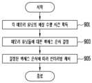
도 9는 본 발명의 일 실시 예에 따른 메모리 컨트롤러의 동작 방법을 설명하기 위한 흐름도이다.Figure 9 is a flowchart for explaining a method of operating a memory controller according to an embodiment of the present invention.
도 9를 참조하여 설명하는 실시 예는, 도 1 내지 도 3을 참조하여 설명한 메모리 컨트롤러에 적용될 수 있다.The embodiment described with reference to FIG. 9 may be applied to the memory controller described with reference to FIGS. 1 to 3 .
단계 '901'에서, 메모리 컨트롤러는, 복수의 메모리 유닛들 각각이 동작을 수행하는 데 필요한 예상 수행 시간을 획득할 수 있다.In step '901', the memory controller may obtain the expected execution time required for each of the plurality of memory units to perform an operation.
일 실시 예에서, 메모리 컨트롤러는, 메모리 유닛들 각각으로부터 예상 수행 시간을 수신할 수 있다. 예를 들어, 메모리 장치에 포함된 다이들 각각은 해당 다이에 대응하는 예상 수행 시간을 저장하거나, 해당 다이에 포함된 플래인들 각각에 대응하는 예상 수행 시간을 저장할 수 있으며, 메모리 컨트롤러는 다이에 예상 수행 시간을 요청하고 이를 수신할 수 있다. 메모리 컨트롤러는, 인터리빙의 대상이 되는 동작에 대응하는 예상 수행 시간을 수신할 수 있다. 예를 들어, 메모리 유닛들은 프로그램 동작, 리드 동작 및 소거 동작 각각에 대응하는 예상 수행 시간을 저장할 수 있으며, 메모리 컨트롤러는 인터리빙의 대상이 되는 동작에 대응하는 예상 수행 시간을 메모리 유닛으로부터 수신할 수 있다.In one embodiment, the memory controller may receive an expected execution time from each of the memory units. For example, each die included in the memory device may store the expected execution time corresponding to that die, or may store the expected execution time corresponding to each of the planes included in the die, and the memory controller may store the expected execution time corresponding to each die. You can request and receive estimated execution times. The memory controller may receive an expected execution time corresponding to an operation subject to interleaving. For example, the memory units may store the expected execution time corresponding to each of the program operation, read operation, and erase operation, and the memory controller may receive the expected execution time corresponding to the operation subject to interleaving from the memory unit. .
일 실시 예에서, 메모리 컨트롤러는, 메모리 유닛들에 대한 테스트 동작을 수행함으로써 메모리 유닛들 각각에 대한 예상 수행 시간을 계산할 수 있다. 예를 들어, 메모리 컨트롤러는, 메모리 유닛들 각각의 프로그램 동작, 리드 동작 및 소거 동작 중 어느 하나에 해당하는 테스트 동작을 수행하도록 제어할 수 있다. 메모리 컨트롤러는, 메모리 유닛들 각각이 테스트 동작을 수행하는 데 소요된 테스트 동작 수행 시간을 계산하고, 계산된 테스트 동작 수행 시간을 해당 메모리 유닛에 대한 예상 수행 시간으로 결정할 수 있다.In one embodiment, the memory controller may calculate an expected execution time for each memory unit by performing a test operation on the memory units. For example, the memory controller may control each memory unit to perform a test operation corresponding to one of a program operation, a read operation, and an erase operation. The memory controller may calculate the test operation execution time required for each of the memory units to perform the test operation, and determine the calculated test operation execution time as the expected execution time for the corresponding memory unit.
단계 '903'에서, 메모리 컨트롤러는, 메모리 유닛들에 대한 액세스 순서를 결정할 수 있다. 예를 들어, 메모리 컨트롤러는, 메모리 유닛들 각각에 대응하는 예상 수행 시간을 기반으로, 메모리 유닛들에 대한 액세스 순서를 결정할 수 있다. 예를 들어, 메모리 컨트롤러는, 긴 예상 수행 시간을 갖는 메모리 유닛일수록 빠른 액세스 순서를 갖도록 결정하고, 짧은 예상 수행 시간을 갖는 메모리 유닛일수록 늦은 액세스 순서를 갖도록 결정할 수 있다.At step '903', the memory controller may determine the access order for memory units. For example, the memory controller may determine the access order for memory units based on the expected execution time corresponding to each of the memory units. For example, the memory controller may determine that memory units with a longer expected execution time have an earlier access order, and that memory units with a shorter expected execution time may have a later access order.
단계 '905'에서, 메모리 컨트롤러는, 결정된 액세스 순서에 따라 인터리빙을 제어할 수 있다. 즉, 메모리 컨트롤러는, 인터리빙 제어를 위하여, 결정된 액세스 순서에 따라 메모리 유닛들에 액세스할 수 있다.In step '905', the memory controller may control interleaving according to the determined access order. That is, the memory controller can access memory units according to the determined access order for interleaving control.
도 10 및 도 11은 예상 수행 시간을 고려하지 않고 인터리빙을 제어하는 경우를 설명하기 위한 도면들이다.Figures 10 and 11 are diagrams to explain a case where interleaving is controlled without considering the expected execution time.
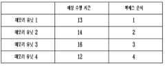
도 10에는, 복수의 메모리 유닛들에 대응하는 예상 수행 시간과 복수의 메모리 유닛들에 대한 액세스 순서를 도시하였다.FIG. 10 shows expected execution times corresponding to a plurality of memory units and an access order for the plurality of memory units.
도 10을 참조하여 설명하는 실시 예에서, 예상 수행 시간은, 프로그램 동작, 리드 동작 또는 소거 동작 중 어느 하나의 동작에 대한 예상 수행 시간인 것으로 가정한다. 또한, 메모리 유닛들은, 다이들 또는 플래인들인 것으로 가정한다.In the embodiment described with reference to FIG. 10, the expected execution time is assumed to be the expected execution time for any one of a program operation, a read operation, and an erase operation. Additionally, it is assumed that the memory units are dies or planes.
도 10을 참조하면, 메모리 유닛들 각각에 대응하는 예상 수행 시간이 서로 다름을 알 수 있다. 예를 들어, 메모리 유닛 1이 동작을 수행하는 데 필요한 예상 수행 시간은 13이고, 메모리 유닛 2가 동작을 수행하는 데 필요한 예상 수행 시간은 14이며, 메모리 유닛 3이 동작을 수행하는 데 필요한 예상 수행 시간은 16이고, 메모리 유닛 4가 동작을 수행하는 데 필요한 예상 수행 시간은 12이다. 편의상 시간의 단위는 생략하여 도시였으며, 높은 숫자일수록 예상 수행 시간이 긴 것을 의미한다.Referring to FIG. 10, it can be seen that the expected execution time corresponding to each memory unit is different. For example, the expected execution time required for
여기서, 도시된 바와 같이, 메모리 유닛들에 대한 액세스 순서가 예상 수행 시간과 무관하게 결정되었다고 가정한다. 즉, 인터리빙 방식으로 메모리 유닛들을 제어할 때, 메모리 유닛 1에 대한 액세스가 가장 먼저 이루어지고, 이후 순차적으로 메모리 유닛 2, 메모리 유닛 3 및 메모리 유닛 4에 대한 액세스가 이루어진다고 가정한다.Here, as shown, it is assumed that the access order for memory units is determined regardless of the expected execution time. That is, when controlling memory units in an interleaving manner, it is assumed that access to
도 11에는 도 10에 도시된 액세스 순서에 따라 메모리 유닛들에 액세스하는 경우의 동작 시간을 도시하였다.FIG. 11 shows the operation time when accessing memory units according to the access order shown in FIG. 10.
도 11을 참조하여 설명하는 실시 예에서, 메모리 유닛들이 실제로 동작을 수행하는 데 소요된 시간은, 메모리 유닛들 각각에 대응하는 예상 수행 시간과 동일한 것으로 가정한다. 또한, 메모리 유닛들 각각에게 동작을 명령하는 데 소요된 시간인 전송 시간(transfer time)은 1인 것으로 가정한다. 전송 시간(transfer time)은, 커맨드 및 어드레스가 전송되는 데 소요된 시간이거나, 커맨드, 어드레스 및 데이터가 전송되는 데 소요된 시간일 수 있다.In the embodiment described with reference to FIG. 11, it is assumed that the time taken for memory units to actually perform an operation is the same as the expected execution time corresponding to each of the memory units. Additionally, it is assumed that the transfer time, which is the time required to command an operation to each of the memory units, is 1. Transfer time may be the time it takes for a command and address to be transmitted, or the time it takes for a command, address, and data to be transmitted.
도 11을 참조하면, 인터리빙 방식으로 동작을 수행하는 메모리 유닛들 중 메모리 유닛 3의 동작이 가장 마지막에 완료된 것을 알 수 있다. 여기서, 메모리 유닛들의 전체 동작 시간, 즉, 메모리 유닛 1으로 커맨드가 전송되기 시작한 시점부터 메모리 유닛3의 동작이 완료된 시점 사이의 시간은, 19임을 알 수 있다.Referring to FIG. 11, it can be seen that among memory units that perform operations in an interleaving manner, the operation of
도 12 및 도 13은 예상 수행 시간을 고려하여 인터리빙을 제어하는 경우를 설명하기 위한 도면들이다.Figures 12 and 13 are diagrams to explain a case where interleaving is controlled considering the expected execution time.
도 12에는, 도 10과 마찬가지로, 복수의 메모리 유닛들에 대응하는 예상 수행 시간과 복수의 메모리 유닛들에 대한 액세스 순서를 도시하였다.In FIG. 12 , similar to FIG. 10 , expected execution times corresponding to a plurality of memory units and an access order for the plurality of memory units are shown.
다만, 도 12에는, 도 10과 다르게, 복수의 메모리 유닛들에 대응하는 예상 수행 시간을 기반으로 메모리 유닛들에 대한 액세스 순서가 결정된 예를 도시하였다. 즉, 도 12에 도시된 액세스 순서에 따라 인터리빙을 제어하는 경우, 메모리 유닛 3에 대한 액세스가 가장 먼저 이루어지고, 이후 순차적으로 메모리 유닛 2, 메모리 유닛 1 및 메모리 유닛 4에 대한 액세스가 이루어질 것이다.However, in FIG. 12, unlike FIG. 10, an example in which the access order for memory units is determined based on the expected execution time corresponding to a plurality of memory units is shown. That is, when interleaving is controlled according to the access order shown in FIG. 12, access to
도 13에는 도 12에 도시된 액세스 순서에 따라 메모리 유닛들에 액세스하는 경우의 동작 시간을 도시하였다.FIG. 13 shows the operation time when accessing memory units according to the access order shown in FIG. 12.
도 13을 참조하여 설명하는 실시 예에서는, 도 11을 참조하여 설명한 실시 예와 마찬가지로, 메모리 유닛들이 실제로 동작을 수행하는 데 소요된 시간은, 메모리 유닛들 각각에 대응하는 예상 수행 시간과 동일한 것으로 가정한다. 또한, 메모리 유닛들 각각에게 동작을 명령하는 데 소요된 시간인 전송 시간(transfer time)은 1인 것으로 가정한다. 전송 시간(transfer time)은, 커맨드 및 어드레스가 전송되는 데 소요된 시간이거나, 커맨드, 어드레스 및 데이터가 전송되는 데 소요된 시간일 수 있다.In the embodiment described with reference to FIG. 13, like the embodiment described with reference to FIG. 11, it is assumed that the time taken for the memory units to actually perform the operation is the same as the expected execution time corresponding to each of the memory units. do. Additionally, it is assumed that the transfer time, which is the time required to command an operation to each of the memory units, is 1. Transfer time may be the time it takes for a command and address to be transmitted, or the time it takes for a command, address, and data to be transmitted.
도 13을 참조하면, 인터리빙 방식으로 동작을 수행하는 메모리 유닛들 중 메모리 유닛 4의 동작이 가장 마지막에 완료된 것을 알 수 있다. 여기서, 메모리 유닛들의 전체 동작 시간, 즉, 메모리 유닛 3으로 커맨드가 전송되기 시작한 시점부터 메모리 유닛 4의 동작이 완료된 시점 사이의 시간은, 16임을 알 수 있다.Referring to FIG. 13, it can be seen that among memory units that perform operations in an interleaving manner, the operation of
도 11을 참조하여 설명한 경우와 비교하면, 메모리 유닛들에 대응하는 예상 수행 시간을 기반으로 액세스 순서를 결정하는 경우, 메모리 유닛들의 전체 동작 시간이 단축됨을 알 수 있다.Compared to the case described with reference to FIG. 11 , it can be seen that when the access order is determined based on the expected execution time corresponding to the memory units, the overall operation time of the memory units is shortened.
도 14는 도 1 내지 도 3에 도시된 메모리 컨트롤러를 포함하는 메모리 시스템의 다른 예를 설명하기 위한 도면이다.FIG. 14 is a diagram for explaining another example of a memory system including the memory controller shown in FIGS. 1 to 3.
도 14를 참조하면, 메모리 시스템(Memory System; 30000)은, 이동 전화기(cellular phone), 스마트폰(smart phone), 태블릿(tablet), PC(personal computer), PDA(personal digital assistant) 또는 무선 통신 장치로 구현될 수 있다. 메모리 시스템(30000)은, 메모리 장치(2200)와 상기 메모리 장치(2200)의 동작을 제어할 수 있는 메모리 컨트롤러(2100)를 포함할 수 있다. 도 14에 도시된 메모리 장치(2200)는, 도 1 내지 도 3에 도시된 메모리 장치(2200)에 대응될 수 있다. 도 14에 도시된 메모리 컨트롤러(2100)는, 도 1 내지 도 3에 도시된 메모리 컨트롤러(2100)에 대응될 수 있다.Referring to FIG. 14, the memory system (Memory System; 30000) is a cellular phone, a smart phone, a tablet, a personal computer (PC), a personal digital assistant (PDA), or a wireless communication device. It can be implemented as a device. The
메모리 컨트롤러(2100)는, 프로세서(Processor; 3100)의 제어에 따라 메모리 장치(2200)의 데이터 액세스 동작, 예컨대 프로그램(program) 동작, 소거(erase) 동작 또는 리드(read) 동작 등을 제어할 수 있다.The
메모리 장치(2200)에 프로그램된 데이터는 메모리 컨트롤러(2100)의 제어에 따라 디스플레이(Display; 3200)를 통하여 출력될 수 있다.Data programmed in the
무선 송수신기(RADIO TRANSCEIVER; 3300)는, 안테나(ANT)를 통하여 무선 신호를 주고받을 수 있다. 예컨대, 무선 송수신기(3300)는, 안테나(ANT)를 통하여 수신된 무선 신호를 프로세서(3100)에서 처리(process)될 수 있는 신호로 변경할 수 있다. 따라서, 프로세서(3100)는, 무선 송수신기(3300)로부터 출력된 신호를 처리(process)하고 처리(process)된 신호를 메모리 컨트롤러(2100) 또는 디스플레이(3200)로 전송할 수 있다. 메모리 컨트롤러(2100)는, 프로세서(3100)에 의하여 처리(process)된 신호를 메모리 장치(2200)에 전송할 수 있다. 또한, 무선 송수신기(3300)는, 프로세서(3100)로부터 출력된 신호를 무선 신호로 변경하고 변경된 무선 신호를 안테나(ANT)를 통하여 외부 장치로 출력할 수 있다. 입력 장치(Input Device; 3400)는, 프로세서(3100)의 동작을 제어하기 위한 제어 신호 또는 프로세서(3100)에 의하여 처리(process)될 데이터를 입력할 수 있는 장치로서, 터치 패드(touch pad)와 컴퓨터 마우스(computer mouse)와 같은 포인팅 장치(pointing device), 키패드(keypad) 또는 키보드로 구현될 수 있다. 프로세서(3100)는, 메모리 컨트롤러(2100)로부터 출력된 데이터, 무선 송수신기(3300)로부터 출력된 데이터, 또는 입력 장치(3400)로부터 출력된 데이터가 디스플레이(3200)를 통하여 출력될 수 있도록 디스플레이(3200)의 동작을 제어할 수 있다.The wireless transceiver (RADIO TRANSCEIVER; 3300) can send and receive wireless signals through an antenna (ANT). For example, the
실시 예에 따라, 메모리 장치(2200)의 동작을 제어할 수 있는 메모리 컨트롤러(2100)는, 프로세서(3100)의 일부로서 구현될 수도 있고, 프로세서(3100)와는 별도의 칩으로 구현될 수 있다.Depending on the embodiment, the
도 15는 도 1 내지 도 3에 도시된 메모리 컨트롤러를 포함하는 메모리 시스템의 다른 예를 설명하기 위한 도면이다.FIG. 15 is a diagram for explaining another example of a memory system including the memory controller shown in FIGS. 1 to 3.
도 15를 참조하면, 메모리 시스템(Memory System; 40000)은 PC(personal computer), 태블릿(tablet), 넷-북(net-book), e-리더(e-reader), PDA(personal digital assistant), PMP(portable multimedia player), MP3 플레이어, 또는 MP4 플레이어로 구현될 수 있다.Referring to FIG. 15, the memory system (Memory System) 40000 is used in a personal computer (PC), tablet, net-book, e-reader, and personal digital assistant (PDA). , can be implemented as a portable multimedia player (PMP), MP3 player, or MP4 player.
메모리 시스템(40000)은, 메모리 장치(2200)와 상기 메모리 장치(2200)의 데이터 처리 동작을 제어할 수 있는 메모리 컨트롤러(2100)를 포함할 수 있다. 도 15에 도시된 메모리 장치(2200)는, 도 1 내지 도 3에 도시된 메모리 장치(2200)에 대응될 수 있다. 도 15에 도시된 메모리 컨트롤러(2100)는, 도 1 내지 도 3에 도시된 메모리 컨트롤러(2100)에 대응될 수 있다.The
프로세서(Processor; 4100)는, 입력 장치(Input Device; 4200)를 통하여 입력된 데이터에 따라 메모리 장치(2200)에 저장된 데이터를 디스플레이(Display; 4300)를 통하여 출력할 수 있다. 예컨대, 입력 장치(4200)는, 터치 패드 또는 컴퓨터 마우스와 같은 포인팅 장치, 키패드, 또는 키보드로 구현될 수 있다.The
프로세서(4100)는, 메모리 시스템(40000)의 전반적인 동작을 제어할 수 있고 메모리 컨트롤러(2100)의 동작을 제어할 수 있다. 실시 예에 따라, 메모리 장치(2200)의 동작을 제어할 수 있는 메모리 컨트롤러(2100)는, 프로세서(4100)의 일부로서 구현되거나, 프로세서(4100)와는 별도의 칩으로 구현될 수 있다.The
도 16은 도 1 내지 도 3에 도시된 메모리 컨트롤러를 포함하는 메모리 시스템의 다른 예를 설명하기 위한 도면이다.FIG. 16 is a diagram for explaining another example of a memory system including the memory controller shown in FIGS. 1 to 3.
도 16을 참조하면, 메모리 시스템(50000)은, 이미지 처리 장치, 예컨대 디지털 카메라, 디지털 카메라가 부착된 이동 전화기, 디지털 카메라가 부착된 스마트 폰, 또는 디지털 카메라가 부착된 태블릿 PC로 구현될 수 있다.Referring to FIG. 16, the
메모리 시스템(50000)은, 메모리 장치(2200)와 상기 메모리 장치(2200)의 데이터 처리 동작, 예컨대 프로그램 동작, 소거 동작 또는 리드 동작을 제어할 수 있는 메모리 컨트롤러(2100)를 포함한다. 도 16에 도시된 메모리 장치(2200)는, 도 1 내지 도 3에 도시된 메모리 장치(2200)에 대응될 수 있다. 도 16에 도시된 메모리 컨트롤러(2100)는, 도 1 내지 도 3에 도시된 메모리 컨트롤러(2100)에 대응될 수 있다.The
메모리 시스템(50000)의 이미지 센서(Image Sensor; 5200)는, 광학 이미지를 디지털 신호들로 변환할 수 있고, 변환된 디지털 신호들은 프로세서(Processor; 5100) 또는 메모리 컨트롤러(2100)로 전송될 수 있다. 프로세서(5100)의 제어에 따라, 상기 변환된 디지털 신호들은 디스플레이(Display; 5300)를 통하여 출력되거나 메모리 컨트롤러(2100)를 통하여 메모리 장치(2200)에 저장될 수 있다. 또한, 메모리 장치(2200)에 저장된 데이터는, 프로세서(5100) 또는 메모리 컨트롤러(2100)의 제어에 따라 디스플레이(5300)를 통하여 출력될 수 있다.The
실시 예에 따라, 메모리 장치(2200)의 동작을 제어할 수 있는 메모리 컨트롤러(2100)는, 프로세서(5100)의 일부로서 구현되거나 프로세서(5100)와는 별개의 칩으로 구현될 수 있다.Depending on the embodiment, the
도 17은 도 1 내지 도 3에 도시된 메모리 컨트롤러를 포함하는 메모리 시스템의 다른 예를 설명하기 위한 도면이다.FIG. 17 is a diagram for explaining another example of a memory system including the memory controller shown in FIGS. 1 to 3.
도 17을 참조하면, 메모리 시스템(Memory System; 70000)은, 메모리 카드(memory card) 또는 스마트 카드(smart card)로 구현될 수 있다. 메모리 시스템(70000)은 메모리 장치(2200), 메모리 컨트롤러(2100) 및 카드 인터페이스(Card Interface; 7100)를 포함할 수 있다. 도 17에 도시된 메모리 장치(2200)는, 도 1 내지 도 3에 도시된 메모리 장치(2200)에 대응될 수 있다. 도 17에 도시된 메모리 컨트롤러(2100)는, 도 1 내지 도 3에 도시된 메모리 컨트롤러(2100)에 대응될 수 있다.Referring to FIG. 17, a memory system (Memory System) 70000 may be implemented as a memory card or smart card. The
메모리 컨트롤러(2100)는, 메모리 장치(2200)와 카드 인터페이스(7100) 사이에서 데이터의 교환을 제어할 수 있다. 실시 예에 따라, 카드 인터페이스(7100)는, SD(secure digital) 카드 인터페이스 또는 MMC(multi-media card) 인터페이스일 수 있으나 이에 한정되는 것은 아니다.The
카드 인터페이스(7100)는, 호스트(HOST; 60000)의 프로토콜에 따라 호스트(60000)와 메모리 컨트롤러(2100) 사이에서 데이터 교환을 인터페이스할 수 있다. 실시 예에 따라, 카드 인터페이스(7100)는, USB(Universal Serial Bus) 프로토콜, IC(InterChip)-USB 프로토콜을 지원할 수 있다. 여기서, 카드 인터페이스(7100)는, 호스트(60000)가 이용하는 프로토콜을 지원할 수 있는 하드웨어, 상기 하드웨어에 탑재된 소프트웨어 또는 신호 전송 방식을 의미할 수 있다.The
메모리 시스템(70000)이 PC, 태블릿 PC, 디지털 카메라, 디지털 오디오 플레이어, 이동 전화기, 콘솔 비디오 게임 하드웨어, 또는 디지털 셋-탑 박스와 같은 호스트(60000)의 호스트 인터페이스(6200)와 접속될 때, 호스트 인터페이스(6200)는 마이크로프로세서(Microprocessor; μP; 6100)의 제어에 따라 카드 인터페이스(7100)와 메모리 컨트롤러(2100)를 통하여 메모리 장치(2200)와 데이터 통신을 수행할 수 있다.When
본 발명의 상세한 설명에서는 구체적인 실시 예에 관하여 설명하였으나, 본 발명의 범위와 기술적 사상에서 벗어나지 않는 한도 내에서 다양한 변경이 가능하다. 그러므로 본 발명의 범위는 상술한 실시 예에 국한되어 정해져서는 안되며 후술하는 특허청구범위뿐만 아니라 이 발명의 특허청구범위와 균등한 것들에 의해 정해져야 한다.In the detailed description of the present invention, specific embodiments have been described, but various changes are possible without departing from the scope and technical spirit of the present invention. Therefore, the scope of the present invention should not be limited to the above-described embodiments, but should be determined by the claims and equivalents of the present invention as well as the claims described later.
호스트 : 1000
메모리 시스템 : 2000
메모리 컨트롤러 : 2100
메모리 장치 : 2200
인터리빙부 : 2150
CPU : 2160Host: 1000
Memory system: 2000
Memory Controller: 2100
Memory device: 2200
Interleaving Department: 2150
CPU: 2160
Claims (20)
Translated fromKorean상기 제1 메모리 유닛 및 상기 제2 메모리 유닛 각각의 상기 동작이 인터리빙 방식으로 수행될 수 있도록 상기 결정된 액세스 순서에 따라 상기 제1 메모리 유닛의 상기 동작을 제어하는 커맨드를 상기 제1 메모리 유닛으로 전송한 뒤, 상기 제2 메모리 유닛의 상기 동작을 제어하는 커맨드를 상기 제2 메모리 유닛으로 전송하는 중앙 처리 장치
를 포함하는, 메모리 컨트롤러.
Based on the expected execution time required for each of the plurality of memory units to perform an operation, the expected execution time of the first memory unit among the plurality of memory units is the second memory unit among the plurality of memory units. an interleaving unit that determines that an access sequence to the first memory unit is faster than an access sequence to the second memory unit if the expected execution time is longer than the expected execution time; and
Transmitting a command for controlling the operation of the first memory unit to the first memory unit according to the determined access order so that the operations of each of the first memory unit and the second memory unit can be performed in an interleaving manner. Then, a central processing unit that transmits a command to control the operation of the second memory unit to the second memory unit.
Containing a memory controller.
상기 중앙 처리 장치는, 상기 메모리 유닛들 각각이 프로그램 동작, 리드 동작 및 소거 동작 중 어느 하나에 해당하는 테스트 동작을 수행하도록 제어하고, 상기 메모리 유닛들 각각이 상기 테스트 동작을 수행하는 데 소요된 테스트 동작 수행 시간을 계산하며,
상기 인터리빙부는, 상기 계산된 테스트 동작 수행 시간을 해당 메모리 유닛에 대한 예상 수행 시간으로 결정하는
메모리 컨트롤러.
According to claim 1,
The central processing unit controls each of the memory units to perform a test operation corresponding to any one of a program operation, a read operation, and an erase operation, and the test required for each of the memory units to perform the test operation. Calculate the time to perform an action,
The interleaving unit determines the calculated test operation execution time as the expected execution time for the corresponding memory unit.
Memory controller.
다이들 또는 상기 다이들에 포함된 플래인들을 포함하는
메모리 컨트롤러.
The method of claim 1, wherein the memory units are:
Containing dies or planes included in the dies
Memory controller.
상기 다이들로부터 상기 예상 수행 시간을 수신하는
메모리 컨트롤러.
The method of claim 4, wherein the interleaving unit:
Receiving the expected execution time from the dies
Memory controller.
프로그램 동작, 리드 동작 또는 소거 동작인
메모리 컨트롤러.
The method of claim 1, wherein the operation is:
Program operation, read operation or erase operation
Memory controller.
상기 메모리 유닛들 각각이 상기 동작을 수행하는 데 필요한 예상 수행 시간을 기반으로, 상기 복수의 메모리 유닛들 중 제1 메모리 유닛이 갖는 상기 예상 수행 시간이 상기 복수의 메모리 유닛들 중 제2 메모리 유닛이 갖는 상기 예상 수행 시간보다 길다면, 상기 제1 메모리 유닛에 대한 액세스 순서가 상기 제2 메모리 유닛에 대한 상기 액세스 순서보다 빨라지도록 결정하고, 상기 결정된 액세스 순서에 따라 상기 제1 메모리 유닛의 상기 동작을 제어하는 커맨드를 상기 제1 메모리 유닛으로 전송한 뒤, 상기 제2 메모리 유닛의 상기 동작을 제어하는 커맨드를 상기 제2 메모리 유닛으로 전송하는 메모리 컨트롤러
를 포함하는, 메모리 시스템.
A plurality of memory units performing operations in an interleaving manner; and
Based on the expected execution time required for each of the memory units to perform the operation, the expected execution time of the first memory unit among the plurality of memory units is the second memory unit among the plurality of memory units. If it is longer than the expected execution time, it is determined that the access order for the first memory unit is faster than the access order for the second memory unit, and the operation of the first memory unit is controlled according to the determined access order. A memory controller that transmits a command to the first memory unit and then transmits a command to control the operation of the second memory unit to the second memory unit.
Including a memory system.
상기 메모리 유닛들 각각이 프로그램 동작, 리드 동작 및 소거 동작 중 어느 하나에 해당하는 테스트 동작을 수행하도록 제어하고, 상기 메모리 유닛들 각각이 상기 테스트 동작을 수행하는 데 소요된 테스트 동작 수행 시간을 계산하며, 상기 계산된 테스트 동작 수행 시간을 해당 메모리 유닛에 대한 예상 수행 시간으로 결정하는
메모리 시스템.
The memory controller of claim 7, wherein:
Controlling each of the memory units to perform a test operation corresponding to one of a program operation, a read operation, and an erase operation, and calculating a test operation time required for each of the memory units to perform the test operation; , determining the calculated test operation execution time as the expected execution time for the corresponding memory unit.
memory system.
다이들 또는 상기 다이들에 포함된 플래인들을 포함하는
메모리 시스템.
The method of claim 7, wherein the memory units are:
Containing dies or planes included in the dies
memory system.
상기 다이들 각각은 상기 예상 수행 시간을 저장하고,
상기 메모리 컨트롤러는, 상기 다이들로부터 상기 예상 수행 시간을 수신하는
메모리 시스템.
According to claim 10,
Each of the dies stores the expected execution time,
The memory controller receives the expected execution time from the dies.
memory system.
프로그램 동작, 리드 동작 또는 소거 동작인
메모리 시스템.
The method of claim 7, wherein the operation is:
Program operation, read operation or erase operation
memory system.
상기 획득된 예상 수행 시간을 기반으로 상기 제1 메모리 유닛이 갖는 상기 예상 수행 시간이 상기 제2 메모리 유닛이 갖는 상기 예상 수행 시간보다 길다면, 상기 제1 메모리 유닛에 대한 액세스 순서가 상기 제2 메모리 유닛에 대한 상기 액세스 순서보다 빨라지도록 결정하는 단계;
상기 제1 메모리 유닛의 상기 동작을 제어하는 커맨드를 상기 제1 메모리 유닛으로 전송하는 단계; 및
상기 제2 메모리 유닛의 상기 동작을 제어하는 커맨드를 상기 제2 메모리 유닛으로 전송하는 단계
를 포함하는, 메모리 컨트롤러의 동작 방법.
Obtaining an expected execution time required for each of the first memory unit and the second memory unit, which performs an operation in an interleaving manner, to perform the operation;
Based on the obtained expected execution time, if the expected execution time of the first memory unit is longer than the expected execution time of the second memory unit, the access order for the first memory unit is changed to the second memory unit. determining to be faster than the access sequence for;
transmitting a command to control the operation of the first memory unit to the first memory unit; and
Transmitting a command to control the operation of the second memory unit to the second memory unit
A method of operating a memory controller, including.
상기 제1 메모리 유닛 및 상기 제2 메모리 유닛 각각이 프로그램 동작, 리드 동작 및 소거 동작 중 어느 하나에 해당하는 테스트 동작을 수행하도록 제어하는 단계; 및
상기 제1 메모리 유닛 및 상기 제2 메모리 유닛 각각이 상기 테스트 동작을 수행하는 데 소요된 시간을 해당 메모리 유닛에 대응하는 예상 수행 시간으로 결정하는 단계
를 포함하는 메모리 컨트롤의 동작 방법.
The method of claim 13, wherein the step of obtaining the expected execution time includes:
controlling each of the first memory unit and the second memory unit to perform a test operation corresponding to one of a program operation, a read operation, and an erase operation; and
Determining the time taken for each of the first memory unit and the second memory unit to perform the test operation as an expected execution time corresponding to the corresponding memory unit.
Operation method of memory control including.
다이들 또는 상기 다이들 각각에 포함된 플래인들인
메모리 컨트롤의 동작 방법.
The method of claim 13, wherein the first memory unit and the second memory unit are:
Dies or planes included in each of the dies
How memory control works.
상기 다이들로부터 상기 예상 수행 시간을 수신하는 단계
를 포함하는 메모리 컨트롤의 동작 방법.
The method of claim 16, wherein the step of obtaining the expected execution time includes:
Receiving the expected execution time from the dies
Operation method of memory control including.
프로그램 동작, 리드 동작 또는 소거 동작인
메모리 컨트롤의 동작 방법.The method of claim 13, wherein the operation is:
Program operation, read operation or erase operation
How memory control works.
Priority Applications (4)
| Application Number | Priority Date | Filing Date | Title |
|---|---|---|---|
| KR1020180032856AKR102626048B1 (en) | 2018-03-21 | 2018-03-21 | Memory controller, memory system having the same and operating method thereof |
| TW107139572ATWI825042B (en) | 2018-03-21 | 2018-11-07 | Memory controller, memory system having the same, and method of operating the same |
| US16/184,328US10831406B2 (en) | 2018-03-21 | 2018-11-08 | Memory controller, memory system having the same, and method of operating the same |
| CN201811486780.XACN110297786A (en) | 2018-03-21 | 2018-12-06 | Memory Controller, storage system and its operating method with the controller |
Applications Claiming Priority (1)
| Application Number | Priority Date | Filing Date | Title |
|---|---|---|---|
| KR1020180032856AKR102626048B1 (en) | 2018-03-21 | 2018-03-21 | Memory controller, memory system having the same and operating method thereof |
Publications (2)
| Publication Number | Publication Date |
|---|---|
| KR20190110869A KR20190110869A (en) | 2019-10-01 |
| KR102626048B1true KR102626048B1 (en) | 2024-01-18 |
Family
ID=67985239
Family Applications (1)
| Application Number | Title | Priority Date | Filing Date |
|---|---|---|---|
| KR1020180032856AActiveKR102626048B1 (en) | 2018-03-21 | 2018-03-21 | Memory controller, memory system having the same and operating method thereof |
Country Status (4)
| Country | Link |
|---|---|
| US (1) | US10831406B2 (en) |
| KR (1) | KR102626048B1 (en) |
| CN (1) | CN110297786A (en) |
| TW (1) | TWI825042B (en) |
Families Citing this family (6)
| Publication number | Priority date | Publication date | Assignee | Title |
|---|---|---|---|---|
| KR102670866B1 (en)* | 2018-11-28 | 2024-05-30 | 삼성전자주식회사 | Nonvolatile memory device including memory planes and memory system including the same |
| US11657858B2 (en) | 2018-11-28 | 2023-05-23 | Samsung Electronics Co., Ltd. | Nonvolatile memory devices including memory planes and memory systems including the same |
| KR20220050677A (en)* | 2020-10-16 | 2022-04-25 | 에스케이하이닉스 주식회사 | Memory device and operating method thereof |
| US12211553B2 (en) | 2021-11-15 | 2025-01-28 | Samsung Electronics Co., Ltd. | Storage system and operating method of storage controller |
| TWI803211B (en)* | 2022-02-25 | 2023-05-21 | 南亞科技股份有限公司 | Random command generation system and random command generation method |
| KR102783145B1 (en)* | 2024-08-21 | 2025-03-19 | 리벨리온 주식회사 | Data processing method and electromic device using dma |
Family Cites Families (13)
| Publication number | Priority date | Publication date | Assignee | Title |
|---|---|---|---|---|
| JPH08235058A (en)* | 1995-02-27 | 1996-09-13 | Fuji Electric Co Ltd | Memory access control method and control device |
| EP1808861B1 (en)* | 2000-12-20 | 2010-08-04 | Fujitsu Semiconductor Limited | Multi-port memory based on a plurality of memory cores |
| US8219379B2 (en)* | 2004-11-29 | 2012-07-10 | Arm Limited | System, method and computer program product for testing software |
| KR101005997B1 (en)* | 2009-01-29 | 2011-01-05 | 주식회사 하이닉스반도체 | Nonvolatile Memory Device and Its Operation Method |
| US20120179883A1 (en)* | 2011-01-12 | 2012-07-12 | Broadcom Corpotation | System and method for dynamically adjusting memory performance |
| US9477590B2 (en)* | 2011-09-16 | 2016-10-25 | Apple Inc. | Weave sequence counter for non-volatile memory systems |
| KR101893864B1 (en)* | 2012-02-06 | 2018-08-31 | 에스케이하이닉스 주식회사 | Non-Volatile Memory Apparatus and Program Method, Data Processing System Using the Same |
| US8996782B2 (en)* | 2012-03-23 | 2015-03-31 | Kabushiki Kaisha Toshiba | Memory system and bank interleaving method |
| US9032177B2 (en)* | 2012-12-04 | 2015-05-12 | HGST Netherlands B.V. | Host read command return reordering based on time estimation of flash read command completion |
| US9152555B2 (en)* | 2013-11-15 | 2015-10-06 | Sandisk Enterprise IP LLC. | Data management with modular erase in a data storage system |
| KR20160143371A (en)* | 2015-06-05 | 2016-12-14 | 에스케이하이닉스 주식회사 | Memory system and operating method thereof |
| US20170123666A1 (en) | 2015-10-30 | 2017-05-04 | Sandisk Technologies Inc. | System and method for managing maintenance scheduling in a non-volatile memory |
| KR102449776B1 (en)* | 2016-01-28 | 2022-10-04 | 에스케이하이닉스 주식회사 | Semiconductor memory device and operating method thereof |
- 2018
- 2018-03-21KRKR1020180032856Apatent/KR102626048B1/enactiveActive
- 2018-11-07TWTW107139572Apatent/TWI825042B/enactive
- 2018-11-08USUS16/184,328patent/US10831406B2/enactiveActive
- 2018-12-06CNCN201811486780.XApatent/CN110297786A/enactivePending
Non-Patent Citations (5)
| Title |
|---|
| 미국공개특허 제2012-0179883호(2012.07.12.) 1부.* |
| 일본공개특허 제08-235058호(1996.09.13.) 1부.* |
| 한국공개특허 제10-2002-0050092호(2002.06.26.) 1부.* |
| 한국공개특허 제10-2013-0090574호(2013.08.14.) 1부.* |
| 한국공개특허 제10-2014-0071938호(2014.06.12.) 1부.* |
Also Published As
| Publication number | Publication date |
|---|---|
| TWI825042B (en) | 2023-12-11 |
| CN110297786A (en) | 2019-10-01 |
| KR20190110869A (en) | 2019-10-01 |
| US20190294372A1 (en) | 2019-09-26 |
| US10831406B2 (en) | 2020-11-10 |
| TW201941067A (en) | 2019-10-16 |
Similar Documents
| Publication | Publication Date | Title |
|---|---|---|
| KR102626048B1 (en) | Memory controller, memory system having the same and operating method thereof | |
| KR102567373B1 (en) | Memory device and memory system having the same | |
| KR102409799B1 (en) | Memory system and operating method thereof | |
| KR102608825B1 (en) | Memory controller and operating method thereof | |
| KR102578188B1 (en) | Memory controller and operating method thereof | |
| KR20200027858A (en) | Memory controller and memory system having the same | |
| KR20190106278A (en) | Memory controller and memory system having the same | |
| KR102409798B1 (en) | Memory system and operating method thereof | |
| KR102479483B1 (en) | Memory system and operation method thereof | |
| US10936421B2 (en) | Memory system having storage device and memory controller and operating method thereof | |
| TW202038225A (en) | Memory device and operating method thereof | |
| KR20190092941A (en) | Memory device, Memory system including the memory device and Method of operating the memory system | |
| US20200042245A1 (en) | Memory system, memory controller, and operating method thereof | |
| KR20200050673A (en) | Memory device and operating method thereof | |
| KR20190094964A (en) | Memory system and operating method thereof | |
| KR102542299B1 (en) | Memory controller, memory system having the memory controller and operating method thereof | |
| KR102505920B1 (en) | Memory controller, memory system having the same and operating method thereof | |
| KR102781452B1 (en) | Memory controller, memory system having the memory controller and operating method thereof | |
| KR20240002571A (en) | Memory device, memory system including the memory device and operating method of the memory system | |
| KR102591888B1 (en) | Memory controller, memory system having the same and operating method thereof | |
| KR102689981B1 (en) | Memory system | |
| KR102715392B1 (en) | Semiconductor memory device and operating method thereof |
Legal Events
| Date | Code | Title | Description |
|---|---|---|---|
| PA0109 | Patent application | St.27 status event code:A-0-1-A10-A12-nap-PA0109 | |
| R17-X000 | Change to representative recorded | St.27 status event code:A-3-3-R10-R17-oth-X000 | |
| PG1501 | Laying open of application | St.27 status event code:A-1-1-Q10-Q12-nap-PG1501 | |
| P11-X000 | Amendment of application requested | St.27 status event code:A-2-2-P10-P11-nap-X000 | |
| P13-X000 | Application amended | St.27 status event code:A-2-2-P10-P13-nap-X000 | |
| PA0201 | Request for examination | St.27 status event code:A-1-2-D10-D11-exm-PA0201 | |
| R17-X000 | Change to representative recorded | St.27 status event code:A-3-3-R10-R17-oth-X000 | |
| D13-X000 | Search requested | St.27 status event code:A-1-2-D10-D13-srh-X000 | |
| D14-X000 | Search report completed | St.27 status event code:A-1-2-D10-D14-srh-X000 | |
| E902 | Notification of reason for refusal | ||
| PE0902 | Notice of grounds for rejection | St.27 status event code:A-1-2-D10-D21-exm-PE0902 | |
| P11-X000 | Amendment of application requested | St.27 status event code:A-2-2-P10-P11-nap-X000 | |
| P13-X000 | Application amended | St.27 status event code:A-2-2-P10-P13-nap-X000 | |
| E90F | Notification of reason for final refusal | ||
| PE0902 | Notice of grounds for rejection | St.27 status event code:A-1-2-D10-D21-exm-PE0902 | |
| E13-X000 | Pre-grant limitation requested | St.27 status event code:A-2-3-E10-E13-lim-X000 | |
| P11-X000 | Amendment of application requested | St.27 status event code:A-2-2-P10-P11-nap-X000 | |
| P13-X000 | Application amended | St.27 status event code:A-2-2-P10-P13-nap-X000 | |
| E701 | Decision to grant or registration of patent right | ||
| PE0701 | Decision of registration | St.27 status event code:A-1-2-D10-D22-exm-PE0701 | |
| PR0701 | Registration of establishment | St.27 status event code:A-2-4-F10-F11-exm-PR0701 | |
| PR1002 | Payment of registration fee | St.27 status event code:A-2-2-U10-U11-oth-PR1002 Fee payment year number:1 | |
| PG1601 | Publication of registration | St.27 status event code:A-4-4-Q10-Q13-nap-PG1601 |