KR102624516B1 - Display device and method of manufacturing display device - Google Patents
Display device and method of manufacturing display deviceDownload PDFInfo
- Publication number
- KR102624516B1 KR102624516B1KR1020180154438AKR20180154438AKR102624516B1KR 102624516 B1KR102624516 B1KR 102624516B1KR 1020180154438 AKR1020180154438 AKR 1020180154438AKR 20180154438 AKR20180154438 AKR 20180154438AKR 102624516 B1KR102624516 B1KR 102624516B1
- Authority
- KR
- South Korea
- Prior art keywords
- electrode
- insulating layer
- light emitting
- disposed
- auxiliary
- Prior art date
- Legal status (The legal status is an assumption and is not a legal conclusion. Google has not performed a legal analysis and makes no representation as to the accuracy of the status listed.)
- Active
Links
Images


Classifications
- H—ELECTRICITY
- H10—SEMICONDUCTOR DEVICES; ELECTRIC SOLID-STATE DEVICES NOT OTHERWISE PROVIDED FOR
- H10H—INORGANIC LIGHT-EMITTING SEMICONDUCTOR DEVICES HAVING POTENTIAL BARRIERS
- H10H29/00—Integrated devices, or assemblies of multiple devices, comprising at least one light-emitting semiconductor element covered by group H10H20/00
- H10H29/10—Integrated devices comprising at least one light-emitting semiconductor component covered by group H10H20/00
- H10H29/14—Integrated devices comprising at least one light-emitting semiconductor component covered by group H10H20/00 comprising multiple light-emitting semiconductor components
- H10H29/142—Two-dimensional arrangements, e.g. asymmetric LED layout
- G—PHYSICS
- G09—EDUCATION; CRYPTOGRAPHY; DISPLAY; ADVERTISING; SEALS
- G09G—ARRANGEMENTS OR CIRCUITS FOR CONTROL OF INDICATING DEVICES USING STATIC MEANS TO PRESENT VARIABLE INFORMATION
- G09G3/00—Control arrangements or circuits, of interest only in connection with visual indicators other than cathode-ray tubes
- G09G3/20—Control arrangements or circuits, of interest only in connection with visual indicators other than cathode-ray tubes for presentation of an assembly of a number of characters, e.g. a page, by composing the assembly by combination of individual elements arranged in a matrix no fixed position being assigned to or needed to be assigned to the individual characters or partial characters
- G09G3/22—Control arrangements or circuits, of interest only in connection with visual indicators other than cathode-ray tubes for presentation of an assembly of a number of characters, e.g. a page, by composing the assembly by combination of individual elements arranged in a matrix no fixed position being assigned to or needed to be assigned to the individual characters or partial characters using controlled light sources
- G09G3/30—Control arrangements or circuits, of interest only in connection with visual indicators other than cathode-ray tubes for presentation of an assembly of a number of characters, e.g. a page, by composing the assembly by combination of individual elements arranged in a matrix no fixed position being assigned to or needed to be assigned to the individual characters or partial characters using controlled light sources using electroluminescent panels
- G09G3/32—Control arrangements or circuits, of interest only in connection with visual indicators other than cathode-ray tubes for presentation of an assembly of a number of characters, e.g. a page, by composing the assembly by combination of individual elements arranged in a matrix no fixed position being assigned to or needed to be assigned to the individual characters or partial characters using controlled light sources using electroluminescent panels semiconductive, e.g. using light-emitting diodes [LED]
- H—ELECTRICITY
- H10—SEMICONDUCTOR DEVICES; ELECTRIC SOLID-STATE DEVICES NOT OTHERWISE PROVIDED FOR
- H10H—INORGANIC LIGHT-EMITTING SEMICONDUCTOR DEVICES HAVING POTENTIAL BARRIERS
- H10H20/00—Individual inorganic light-emitting semiconductor devices having potential barriers, e.g. light-emitting diodes [LED]
- H10H20/80—Constructional details
- H10H20/85—Packages
- H10H20/857—Interconnections, e.g. lead-frames, bond wires or solder balls
- H01L27/156—
- H—ELECTRICITY
- H01—ELECTRIC ELEMENTS
- H01L—SEMICONDUCTOR DEVICES NOT COVERED BY CLASS H10
- H01L25/00—Assemblies consisting of a plurality of semiconductor or other solid state devices
- H01L25/03—Assemblies consisting of a plurality of semiconductor or other solid state devices all the devices being of a type provided for in a single subclass of subclasses H10B, H10D, H10F, H10H, H10K or H10N, e.g. assemblies of rectifier diodes
- H01L25/04—Assemblies consisting of a plurality of semiconductor or other solid state devices all the devices being of a type provided for in a single subclass of subclasses H10B, H10D, H10F, H10H, H10K or H10N, e.g. assemblies of rectifier diodes the devices not having separate containers
- H01L25/075—Assemblies consisting of a plurality of semiconductor or other solid state devices all the devices being of a type provided for in a single subclass of subclasses H10B, H10D, H10F, H10H, H10K or H10N, e.g. assemblies of rectifier diodes the devices not having separate containers the devices being of a type provided for in group H10H20/00
- H01L25/0753—Assemblies consisting of a plurality of semiconductor or other solid state devices all the devices being of a type provided for in a single subclass of subclasses H10B, H10D, H10F, H10H, H10K or H10N, e.g. assemblies of rectifier diodes the devices not having separate containers the devices being of a type provided for in group H10H20/00 the devices being arranged next to each other
- H01L33/005—
- H01L33/405—
- H—ELECTRICITY
- H10—SEMICONDUCTOR DEVICES; ELECTRIC SOLID-STATE DEVICES NOT OTHERWISE PROVIDED FOR
- H10H—INORGANIC LIGHT-EMITTING SEMICONDUCTOR DEVICES HAVING POTENTIAL BARRIERS
- H10H20/00—Individual inorganic light-emitting semiconductor devices having potential barriers, e.g. light-emitting diodes [LED]
- H10H20/01—Manufacture or treatment
- H—ELECTRICITY
- H10—SEMICONDUCTOR DEVICES; ELECTRIC SOLID-STATE DEVICES NOT OTHERWISE PROVIDED FOR
- H10H—INORGANIC LIGHT-EMITTING SEMICONDUCTOR DEVICES HAVING POTENTIAL BARRIERS
- H10H20/00—Individual inorganic light-emitting semiconductor devices having potential barriers, e.g. light-emitting diodes [LED]
- H10H20/80—Constructional details
- H10H20/83—Electrodes
- H10H20/832—Electrodes characterised by their material
- H10H20/835—Reflective materials
- G—PHYSICS
- G09—EDUCATION; CRYPTOGRAPHY; DISPLAY; ADVERTISING; SEALS
- G09G—ARRANGEMENTS OR CIRCUITS FOR CONTROL OF INDICATING DEVICES USING STATIC MEANS TO PRESENT VARIABLE INFORMATION
- G09G2300/00—Aspects of the constitution of display devices
- G09G2300/04—Structural and physical details of display devices
- G09G2300/0421—Structural details of the set of electrodes
- H—ELECTRICITY
- H10—SEMICONDUCTOR DEVICES; ELECTRIC SOLID-STATE DEVICES NOT OTHERWISE PROVIDED FOR
- H10H—INORGANIC LIGHT-EMITTING SEMICONDUCTOR DEVICES HAVING POTENTIAL BARRIERS
- H10H20/00—Individual inorganic light-emitting semiconductor devices having potential barriers, e.g. light-emitting diodes [LED]
- H10H20/01—Manufacture or treatment
- H10H20/032—Manufacture or treatment of electrodes
- H—ELECTRICITY
- H10—SEMICONDUCTOR DEVICES; ELECTRIC SOLID-STATE DEVICES NOT OTHERWISE PROVIDED FOR
- H10H—INORGANIC LIGHT-EMITTING SEMICONDUCTOR DEVICES HAVING POTENTIAL BARRIERS
- H10H20/00—Individual inorganic light-emitting semiconductor devices having potential barriers, e.g. light-emitting diodes [LED]
- H10H20/01—Manufacture or treatment
- H10H20/036—Manufacture or treatment of packages
- H10H20/0364—Manufacture or treatment of packages of interconnections
Landscapes
- Engineering & Computer Science (AREA)
- Power Engineering (AREA)
- Microelectronics & Electronic Packaging (AREA)
- Physics & Mathematics (AREA)
- Computer Hardware Design (AREA)
- General Physics & Mathematics (AREA)
- Condensed Matter Physics & Semiconductors (AREA)
- Theoretical Computer Science (AREA)
- Electroluminescent Light Sources (AREA)
- Devices For Indicating Variable Information By Combining Individual Elements (AREA)
Abstract
Translated fromKorean
Description
Translated fromKorean본 발명은 신뢰성이 향상된 표시장치 및 이의 제조 방법에 관한 것이다.The present invention relates to a display device with improved reliability and a method of manufacturing the same.
발광 다이오드(Light Emitting Diode, 이하 발광 소자)는 열악한 환경조건에서도 우수한 내구성을 나타내며, 수명 및 휘도 측면에서도 우수한 성능을 보유한다. 최근, 이러한 발광 소자는 다양한 발광 장치에 적용하기 위한 연구가 활발히 진행되고 있다. Light emitting diodes (hereinafter referred to as light emitting devices) exhibit excellent durability even under harsh environmental conditions and have excellent performance in terms of lifespan and brightness. Recently, research is being actively conducted to apply these light-emitting devices to various light-emitting devices.
이러한 연구의 일환으로서, 무기 결정 구조, 일 예로 질화물계 반도체를 성장시킨 구조를 이용하여 마이크로 스케일이나 나노 스케일 정도로 작은 초소형의 막대형 발광 소자를 제작하는 기술이 개발되고 있다. 일례로, 막대형 발광 소자는 자발광 표시패널의 화소 등을 구성할 수 있을 정도로 작은 크기로 제작될 수 있다.As part of this research, technology is being developed to produce ultra-small rod-shaped light emitting devices as small as micro or nano scale using an inorganic crystal structure, for example, a structure grown from a nitride-based semiconductor. For example, a rod-shaped light emitting device can be manufactured in a size small enough to form a pixel of a self-luminous display panel.
본 발명의 목적은 초소형으로 제공된 복수 개의 발광 소자들을 포함한 표시장치 및 이의 제조 방법에 관한 것이다.An object of the present invention relates to a display device including a plurality of ultra-small light emitting elements and a method of manufacturing the same.
본 발명의 목적을 달성하기 위한 본 발명의 일 실시 예에 따르면, 표시장치는 베이스층, 상기 베이스층 상에 배치된 화소 회로, 상기 화소 회로를 커버하며 상기 베이스층 상에 배치된 절연층, 상기 화소 회로와 전기적으로 연결되며 상기 절연층 상에 배치된 제1 전극, 상기 화소 회로와 전기적으로 연결되고, 제1 방향에서 상기 제1 전극과 이격되어 상기 절연층 상에 배치된 제2 전극, 상기 제1 전극 및 상기 제2 전극 사이에 배치되며, 상기 제1 전극 및 상기 제2 전극과 전기적으로 연결된 발광 소자, 상기 제1 전극 및 상기 발광 소자를 연결하고, 상기 제2 전극 및 상기 발광 소자를 연결하는 연결 전극, 상기 발광 소자 상에 배치된 제1 보조 절연층, 상기 제1 보조 절연층 상에 배치되고, 상기 제1 보조 절연층에 중첩한 제1 절연 부분 및 상기 제1 절연 부분을 에워싸며 상기 제1 보조 절연층과 비중첩하는 제2 절연 부분을 포함하는 제2 보조 절연층 포함한다.According to one embodiment of the present invention for achieving the object of the present invention, a display device includes a base layer, a pixel circuit disposed on the base layer, an insulating layer covering the pixel circuit and disposed on the base layer, A first electrode electrically connected to the pixel circuit and disposed on the insulating layer, a second electrode electrically connected to the pixel circuit and disposed on the insulating layer and spaced apart from the first electrode in a first direction, A light emitting element disposed between the first electrode and the second electrode and electrically connected to the first electrode and the second electrode, connecting the first electrode and the light emitting element, and connecting the second electrode and the light emitting element. A connecting electrode for connecting, a first auxiliary insulating layer disposed on the light emitting element, a first insulating portion disposed on the first auxiliary insulating layer and overlapping the first auxiliary insulating layer, and surrounding the first insulating portion. It is wrapped and includes a second auxiliary insulating layer including a second insulating portion that does not overlap with the first auxiliary insulating layer.
본 발명의 실시 예에 따르면, 상기 베이스층의 평면상에서, 상기 제1 보조 절연층의 너비는 상기 제2 보조 절연층의 너비보다 작은 것을 특징으로 한다.According to an embodiment of the present invention, on the plane of the base layer, the width of the first auxiliary insulating layer is smaller than the width of the second auxiliary insulating layer.
본 발명의 실시 예에 따르면, 상기 평면상에서, 상기 제2 보조 절연층의 너비는 상기 발광 소자의 너비보다 작고, 상기 제1 보조 절연층은 상기 제2 보조 절연층에 전체적으로 중첩하고, 상기 제2 보조 절연층은 상기 발광 소자에 전체적으로 중첩한다.According to an embodiment of the present invention, in the plane, the width of the second auxiliary insulating layer is smaller than the width of the light emitting device, the first auxiliary insulating layer entirely overlaps the second auxiliary insulating layer, and the second auxiliary insulating layer The auxiliary insulating layer entirely overlaps the light emitting device.
본 발명의 실시 예에 따르면, 상기 제1 보조 절연층은 SiOx를 포함하고, 상기 제2 보조 절연층은 SiNx를 포함한다.According to an embodiment of the present invention, the first auxiliary insulating layer includes SiOx, and the second auxiliary insulating layer includes SiNx.
본 발명의 실시 예에 따르면, 상기 베이스층의 두께 방향에서, 상기 제1 절연 부분 및 상기 발광 소자 간의 이격 거리는 상기 제2 절연 부분 및 상기 발광 소자 간의 이격 거리와 동일하다.According to an embodiment of the present invention, in the thickness direction of the base layer, the separation distance between the first insulating part and the light-emitting device is the same as the separation distance between the second insulating part and the light-emitting device.
본 발명의 실시 예에 따르면, 상기 연결 전극은, 상기 제2 보조 절연층 상에 배치된 더미 연결 전극, 상기 제1 전극 및 상기 발광 소자를 연결하는 제1 연결 전극, 상기 제1 연결 전극과 이격되며 상기 제2 전극 및 상기 발광 소자를 연결하는 제2 연결 전극을 포함하고, 상기 더미 연결 전극은 상기 제1 연결 전극 및 상기 제2 연결 전극과 이격된다.According to an embodiment of the present invention, the connection electrode includes a dummy connection electrode disposed on the second auxiliary insulating layer, a first connection electrode connecting the first electrode and the light emitting device, and spaced apart from the first connection electrode. and includes a second connection electrode connecting the second electrode and the light emitting device, and the dummy connection electrode is spaced apart from the first connection electrode and the second connection electrode.
본 발명의 실시 예에 따르면, 상기 베이스층의 평면상에서, 상기 제1 연결 전극 및 상기 제2 연결 전극은 상기 제1 보조 절연층을 사이에 두고 서로 이격된다.According to an embodiment of the present invention, on the plane of the base layer, the first connection electrode and the second connection electrode are spaced apart from each other with the first auxiliary insulating layer interposed therebetween.
본 발명의 실시 예에 따르면, 상기 베이스층의 두께 방향에서, 상기 발광 소자 상에 배치된 상기 제1 연결 전극과 상기 제2 보조 절연층 간의 이격 거리는 상기 발광 소자 상에 배치된 상기 제2 연결 전극과 상기 제2 보조 절연층 간의 이격 거리와 동일한 것을 특징으로 한다.According to an embodiment of the present invention, in the thickness direction of the base layer, the separation distance between the first connection electrode disposed on the light emitting device and the second auxiliary insulating layer is the second connection electrode disposed on the light emitting device. and the separation distance between the second auxiliary insulating layer and the second auxiliary insulating layer.
본 발명의 실시 예에 따르면, 상기 더미 연결 전극은 상기 제1 절연 부분 및 상기 제2 절연 부분에 전체적으로 배치된다.According to an embodiment of the present invention, the dummy connection electrode is entirely disposed in the first insulating portion and the second insulating portion.
본 발명의 실시 예에 따르면, 상기 베이스층의 평면상에서, 상기 연결 전극은 상기 발광 소자에 전체적으로 중첩한다.According to an embodiment of the present invention, on the plane of the base layer, the connection electrode entirely overlaps the light emitting device.
본 발명의 실시 예에 따르면, 상기 제1 전극과 상기 절연층 사이에 배치된 제1 격벽, 상기 제2 전극과 상기 절연층 사이에 배치된 제2 격벽을 더 포함하고, 상기 발광 소자는 상기 제1 격벽 및 상기 제2 격벽 사이에 배치된다.According to an embodiment of the present invention, the light emitting device further includes a first barrier rib disposed between the first electrode and the insulating layer, and a second barrier rib disposed between the second electrode and the insulating layer. It is disposed between the first partition and the second partition.
본 발명의 실시 예에 따르면, 상기 제1 전극은 상기 화소 회로와 전기적으로 연결되며 반사성 물질을 포함하는 제1 반사 전극, 및 상기 제1 반사 전극을 커버하는 제1 캡핑 전극을 포함하고, 상기 제2 전극은 전원 전압을 수신하며 반사성 물질을 포함하는 제2 반사 전극, 및 상기 제2 반사 전극을 커버하는 제2 캡핑 전극을 포함한다.According to an embodiment of the present invention, the first electrode is electrically connected to the pixel circuit and includes a first reflective electrode including a reflective material, and a first capping electrode covering the first reflective electrode. The two electrodes include a second reflective electrode that receives the power voltage and includes a reflective material, and a second capping electrode that covers the second reflective electrode.
본 발명의 실시 예에 따르면, 상기 발광 소자 및 상기 절연층 상에 배치된 보조 절연층을 더 포함한다.According to an embodiment of the present invention, it further includes an auxiliary insulating layer disposed on the light emitting device and the insulating layer.
본 발명의 목적을 달성하기 위한 본 발명의 다른 실시 예에 따르면, 표시장치는 베이스층, 상기 베이스층 상에 배치된 화소 회로, 상기 화소 회로를 커버하며 상기 베이스층 상에 배치된 절연층, 상기 화소 회로와 전기적으로 연결되며 상기 절연층 상에 배치된 제1 전극, 상기 화소 회로와 전기적으로 연결되고, 제1 방향에서 상기 제1 전극과 이격되어 상기 절연층 상에 배치된 제2 전극, 상기 제1 전극 및 상기 제2 전극 사이에 배치되며, 상기 제1 전극 및 상기 제2 전극과 전기적으로 연결된 발광 소자, 상기 발광 소자 상에 배치된 제1 보조 절연층, 상기 제1 보조 절연층 상에 배치된 제2 보조 절연층, 상기 제2 보조 절연층 상에 배치된 더미 연결 전극, 상기 제1 전극 및 상기 발광 소자를 연결하는 제1 연결 전극, 상기 제1 연결 전극과 이격되며 상기 제2 전극 및 상기 발광 소자를 연결하는 제2 연결 전극을 포함하는 연결 전극을 포함한다.According to another embodiment of the present invention for achieving the object of the present invention, a display device includes a base layer, a pixel circuit disposed on the base layer, an insulating layer covering the pixel circuit and disposed on the base layer, A first electrode electrically connected to the pixel circuit and disposed on the insulating layer, a second electrode electrically connected to the pixel circuit and disposed on the insulating layer and spaced apart from the first electrode in a first direction, A light emitting element disposed between the first electrode and the second electrode and electrically connected to the first electrode and the second electrode, a first auxiliary insulating layer disposed on the light emitting element, and on the first auxiliary insulating layer. A second auxiliary insulating layer disposed, a dummy connection electrode disposed on the second auxiliary insulating layer, a first connection electrode connecting the first electrode and the light emitting device, and the second electrode spaced apart from the first connection electrode. and a connection electrode including a second connection electrode connecting the light emitting device.
본 발명의 실시 예에 따르면, 상기 더미 연결 전극은 상기 제1 연결 전극 및 상기 제2 연결 전극과 이격되며 상기 제2 보조 절연층 상에 전체적으로 배치된다.According to an embodiment of the present invention, the dummy connection electrode is spaced apart from the first connection electrode and the second connection electrode and is entirely disposed on the second auxiliary insulating layer.
본 발명의 실시 예에 따르면, 상기 베이스층의 평면상에서, 상기 제1 보조 절연층의 너비는 상기 제2 보조 절연층의 너비보다 작고, 상기 제2 보조 절연층의 너비는 상기 발광 소자의 너비보다 작은 것을 특징으로 한다.According to an embodiment of the present invention, on the plane of the base layer, the width of the first auxiliary insulating layer is smaller than the width of the second auxiliary insulating layer, and the width of the second auxiliary insulating layer is larger than the width of the light emitting device. Characterized by small size.
본 발명의 목적을 달성하기 위한 본 발명의 다른 실시 예에 따르면, 표시장치의 제조 방법은 베이스층 상에 화소 회로를 형성하는 단계, 상기 화소 회로를 커버하는 절연층을 상기 베이스층 상에 형성하는 단계, 상기 절연층 상에 제1 전극, 상기 제1 전극과 이격된 제2 전극, 및 상기 제1 전극 및 상기 제2 전극 사이에 배치되는 발광 소자를 형성하는 단계, 상기 발광 소자를 커버하는 제1 보조층을 상기 절연층 상에 형성하는 단계, 제2 보조층을 상기 제1 보조층 상에 형성하는 단계, 상기 발광 소자에 중첩한 포토레지스트 패턴을 상기 제2 보조층 상에 형성하는 단계, 가스를 통해 상기 제2 보조층 중 상기 포토레지스트 패턴으로부터 노출된 부분을 제거함으로써 제2 보조 절연층을 형성하는 단계, 상기 가스를 통해 상기 제1 보조층 중 상기 제2 보조 절연층으로부터 노출된 부분을 제거함으로써 제1 보조 절연층을 형성하는 단계, 상기 제1 전극 및 상기 발광 소자를 연결하는 제1 연결 전극, 상기 제2 전극 및 상기 발광 소자를 연결하는 제2 연결 전극, 및 상기 제2 보조 절연층 상에 배치된 더미 연결 전극을 동시에 형성하는 단계를 포함한다.According to another embodiment of the present invention for achieving the object of the present invention, a method of manufacturing a display device includes forming a pixel circuit on a base layer, forming an insulating layer covering the pixel circuit on the base layer. A step of forming a first electrode on the insulating layer, a second electrode spaced apart from the first electrode, and a light emitting device disposed between the first electrode and the second electrode, and a second electrode covering the light emitting device. Forming a first auxiliary layer on the insulating layer, forming a second auxiliary layer on the first auxiliary layer, forming a photoresist pattern overlapping the light emitting device on the second auxiliary layer, forming a second auxiliary insulating layer by removing a portion of the second auxiliary layer exposed from the photoresist pattern through a gas, the portion of the first auxiliary layer exposed from the second auxiliary insulating layer through a gas; forming a first auxiliary insulating layer by removing a first connection electrode connecting the first electrode and the light emitting device, a second connection electrode connecting the second electrode and the light emitting device, and the second auxiliary and simultaneously forming a dummy connection electrode disposed on the insulating layer.
본 발명의 실시 예에 따르면, 상기 제1 보조 절연층의 식각 선택비는 상기 제2 보조 절연층의 식각 선택비보다 큰 것을 특징으로 한다.According to an embodiment of the present invention, the etch selectivity of the first auxiliary insulating layer is greater than the etch selectivity of the second auxiliary insulating layer.
본 발명의 실시 예에 따르면, 상기 제1 연결 전극 및 상기 제2 연결 전극은 상기 제1 보조 절연층에 의해 상기 더미 연결 전극과 이격된다.According to an embodiment of the present invention, the first connection electrode and the second connection electrode are spaced apart from the dummy connection electrode by the first auxiliary insulating layer.
본 발명의 실시 예에 따르면, 상기 발광 소자를 사이에 두고 이격된 제1 격벽 및 제2 격벽을 형성하는 단계를 더 포함한다.According to an embodiment of the present invention, the method further includes forming a first barrier rib and a second barrier rib spaced apart from each other with the light emitting device interposed therebetween.
본 발명의 실시 예에 따르면, 한 번의 증착 공정으로 제1 전극 및 발광 소자를 연결하는 제1 연결 전극과 제2 전극 및 발광 소자를 연결하는 제2 연결 전극이 동시에 형성될 수 있다.According to an embodiment of the present invention, a first connection electrode connecting the first electrode and the light emitting device and a second connection electrode connecting the second electrode and the light emitting device may be formed simultaneously through a single deposition process.
그 결과, 표시장치의 전반적인 공정 시간 및 공정 비용이 줄어들 수 있다.As a result, the overall process time and process cost of the display device can be reduced.
도 1은 본 발명의 실시 예에 따른 표시장치의 사시도이다.
도 2a는 본 발명의 실시 예에 따른 표시장치의 블록도이다.
도 2b는 본 발명의 실시 예에 따른 화소의 등가 회로도이다.
도 3은 본 발명의 실시 예에 다른 표시장치의 단면도이다.
도 4a는 본 발명의 실시 예에 따른 표시패널의 평면도이다.
도 4b는 본 발명의 다른 실시 예에 따른 표시패널의 평면도이다.
도 5는 본 발명의 실시 예에 따른 표시패널의 일 부분을 도시한 단면도이다.
도 6은 도 5에 도시된 AA 영역을 확대하여 도시한 단면도이다.
도 7a는 본 발명의 실시 예에 따른 발광 소자의 단면도이다.
도 7b는 본 발명의 실시 예에 따른 발광 소자의 단면도이다.
도 7c는 본 발명의 실시 예에 따른 발광 소자의 단면도이다.
도 7d는 본 발명의 실시 예에 따른 발광 소자의 단면도이다.
도 8a 내지 도 8h은 본 발명의 실시 예에 따른 표시장치의 제조 공정 중 일부를 도시한 도면들이다.1 is a perspective view of a display device according to an embodiment of the present invention.
Figure 2A is a block diagram of a display device according to an embodiment of the present invention.
Figure 2b is an equivalent circuit diagram of a pixel according to an embodiment of the present invention.
Figure 3 is a cross-sectional view of a display device according to an embodiment of the present invention.
Figure 4a is a plan view of a display panel according to an embodiment of the present invention.
Figure 4b is a plan view of a display panel according to another embodiment of the present invention.
Figure 5 is a cross-sectional view showing a portion of a display panel according to an embodiment of the present invention.
FIG. 6 is an enlarged cross-sectional view of area AA shown in FIG. 5.
Figure 7a is a cross-sectional view of a light-emitting device according to an embodiment of the present invention.
Figure 7b is a cross-sectional view of a light-emitting device according to an embodiment of the present invention.
Figure 7c is a cross-sectional view of a light-emitting device according to an embodiment of the present invention.
Figure 7d is a cross-sectional view of a light emitting device according to an embodiment of the present invention.
8A to 8H are diagrams illustrating a portion of the manufacturing process of a display device according to an embodiment of the present invention.
본 명세서에서, 어떤 구성요소(또는 영역, 층, 부분 등)가 다른 구성요소 "상에 있다", "연결 된다", 또는 "결합된다"고 언급되는 경우에 그것은 다른 구성요소 상에 직접 배치/연결/결합될 수 있거나 또는 그들 사이에 제3의 구성요소가 배치될 수도 있다는 것을 의미한다.In this specification, when a component (or region, layer, portion, etc.) is referred to as being “on,” “connected to,” or “coupled to” another component, it is directly placed/on the other component. This means that they can be connected/combined or a third component can be placed between them.
동일한 도면부호는 동일한 구성요소를 지칭한다. 또한, 도면들에 있어서, 구성요소들의 두께, 비율, 및 치수는 기술적 내용의 효과적인 설명을 위해 과장된 것이다.Like reference numerals refer to like elements. Additionally, in the drawings, the thickness, proportions, and dimensions of components are exaggerated for effective explanation of technical content.
"및/또는"은 연관된 구성들이 정의할 수 있는 하나 이상의 조합을 모두 포함한다. “And/or” includes all combinations of one or more that the associated configurations may define.
제1, 제2 등의 용어는 다양한 구성요소들을 설명하는데 사용될 수 있지만, 상기 구성요소들은 상기 용어들에 의해 한정되어서는 안 된다. 상기 용어들은 하나의 구성요소를 다른 구성요소로부터 구별하는 목적으로만 사용된다. 예를 들어, 본 발명의 권리 범위를 벗어나지 않으면서 제1 구성요소는 제2 구성요소로 명명될 수 있고, 유사하게 제2 구성요소도 제1 구성요소로 명명될 수 있다. 단수의 표현은 문맥상 명백하게 다르게 뜻하지 않는 한, 복수의 표현을 포함한다.Terms such as first, second, etc. may be used to describe various components, but the components should not be limited by the terms. The above terms are used only for the purpose of distinguishing one component from another. For example, a first component may be named a second component, and similarly, the second component may also be named a first component without departing from the scope of the present invention. Singular expressions include plural expressions unless the context clearly dictates otherwise.
또한, "아래에", "하측에", "상에", "상측에" 등의 용어는 도면에 도시된 구성들의 연관관계를 설명하기 위해 사용된다. 상기 용어들은 상대적인 개념으로, 도면에 표시된 방향을 기준으로 설명된다.Additionally, terms such as “below,” “on the lower side,” “on” and “on the upper side” are used to describe the relationship between the components shown in the drawings. The above terms are relative concepts and are explained based on the direction indicated in the drawings.
다르게 정의되지 않는 한, 본 명세서에서 사용된 모든 용어 (기술 용어 및 과학 용어 포함)는 본 발명이 속하는 기술 분야의 당업자에 의해 일반적으로 이해되는 것과 동일한 의미를 갖는다. 또한, 일반적으로 사용되는 사전에서 정의된 용어와 같은 용어는 관련 기술의 맥락에서 의미와 일치하는 의미를 갖는 것으로 해석되어야 하고, 이상적인 또는 지나치게 형식적인 의미로 해석되지 않는 한, 명시적으로 여기에서 정의됩니다.Unless otherwise defined, all terms (including technical terms and scientific terms) used in this specification have the same meaning as commonly understood by a person skilled in the art to which the present invention pertains. Additionally, terms such as those defined in commonly used dictionaries should be construed as having a meaning consistent with their meaning in the context of the relevant technology, and unless interpreted in an idealized or overly formal sense, are explicitly defined herein. It's possible.
"포함하다" 또는 "가지다" 등의 용어는 명세서 상에 기재된 특징, 숫자, 단계, 동작, 구성요소, 부품 또는 이들을 조합한 것이 존재함을 지정하려는 것이지, 하나 또는 그 이상의 다른 특징들이나 숫자, 단계, 동작, 구성요소, 부분품 또는 이들을 조합한 것들의 존재 또는 부가 가능성을 미리 배제하지 않는 것으로 이해되어야 한다.Terms such as “include” or “have” are intended to designate the presence of features, numbers, steps, operations, components, parts, or combinations thereof described in the specification, but do not include one or more other features, numbers, or steps. , it should be understood that it does not exclude in advance the possibility of the existence or addition of operations, components, parts, or combinations thereof.
이하, 도면을 참조하여 본 발명의 실시예들을 설명한다.Hereinafter, embodiments of the present invention will be described with reference to the drawings.
도 1은 본 발명의 실시 예에 따른 표시장치의 사시도이다. 도 2a는 본 발명의 실시 예에 따른 표시장치의 블록도이다. 도 2b는 본 발명의 실시 예에 따른 화소의 등가 회로도이다.1 is a perspective view of a display device according to an embodiment of the present invention. Figure 2A is a block diagram of a display device according to an embodiment of the present invention. Figure 2b is an equivalent circuit diagram of a pixel according to an embodiment of the present invention.
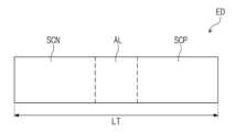
도 1을 참조하면, 표시장치(DD)는 표시 영역(DA)을 통해 이미지를 표시 할 수 있다. 도 1에서는 표시 영역(DA)이 제1 방향(DR1) 및 제1 방향(DR1)과 교차하는 제2 방향(DR2)이 정의하는 면에 제공된 것을 예시적으로 도시하였다. 하지만, 본 발명의 다른 실시 예에서 표시장치의 표시 영역은 휘어진 면에 제공될 수 있다. 또한, 도 1을 통해 도시되지 않았지만, 다른 예에 따르면, 표시장치(DD)는 표시 영역(DA)에 인접한 비표시 영역을 더 포함하고, 비표시 영역은 영상이 시인되지 않은 영역일 수 있다. 비표시 영역은 표시 영역(DA)의 일 영역에 인접하게 배치되거나, 표시 영역(DA)을 에워쌀 수 있다.Referring to FIG. 1, the display device DD can display an image through the display area DA. FIG. 1 exemplarily shows that the display area DA is provided on a surface defined by the first direction DR1 and the second direction DR2 intersecting the first direction DR1. However, in another embodiment of the present invention, the display area of the display device may be provided on a curved surface. In addition, although not shown in FIG. 1 , according to another example, the display device DD further includes a non-display area adjacent to the display area DA, and the non-display area may be an area in which an image is not visible. The non-display area may be placed adjacent to one area of the display area DA or may surround the display area DA.
표시장치(DD)의 두께 방향은 제3 방향(DR3)이 지시한다. 제1 내지 제3 방향들(DR1, DR2, DR3)이 지시하는 방향은 상대적인 개념으로서 다른 방향으로 변환될 수 있다. 본 명세서 내에서 "평면 상에서 보았을 때 또는 평면상에서"의 의미는 제3 방향(DR3)에서 바라보는 경우를 의미할 수 있다. 또한, "두께 방향"은 제3 방향(DR3)일 수 있다.The thickness direction of the display device DD is indicated by the third direction DR3. The directions indicated by the first to third directions DR1, DR2, and DR3 are relative concepts and can be converted to other directions. In this specification, “when viewed on a plane or on a plane” may mean when viewed in the third direction DR3. Additionally, the “thickness direction” may be the third direction DR3.
도 1에서는 표시장치(DD)가 텔레비전인 것을 예시적으로 도시하였다. 하지만, 표시장치(DD)는 모니터, 또는 외부 광고판과 같은 대형 전자장치를 비롯하여, 퍼스널 컴퓨터, 노트북 컴퓨터, 개인 디지털 단말기, 자동차 내비게이션 유닛, 게임기, 스마트폰, 태블릿, 및 카메라와 같은 중소형 전자 장치 등에 사용될 수도 있다. 또한, 이것들은 단지 실시 예로서 제시된 것들로서, 본 발명의 개념에서 벗어나지 않은 이상 다른 전자 기기에도 채용될 수 있음은 물론이다.FIG. 1 exemplarily shows that the display device DD is a television. However, the display device (DD) is used in large electronic devices such as monitors or external billboards, as well as small and medium-sized electronic devices such as personal computers, laptop computers, personal digital terminals, car navigation units, game consoles, smartphones, tablets, and cameras. It may also be used. Additionally, these are presented only as examples, and of course, they can be applied to other electronic devices as long as they do not deviate from the concept of the present invention.
도 2a를 참조하면, 표시장치(DD)는 표시패널(DP), 신호 제어회로(TC), 데이터 구동회로(DDV), 및 스캔 구동회로(GDV)를 포함할 수 있다. 신호 제어회로(TC), 데이터 구동회로(DDV) 및 스캔 구동회로(GDV) 각각은 복수 개의 회로들을 포함할 수 있다.Referring to FIG. 2A, the display device (DD) may include a display panel (DP), a signal control circuit (TC), a data driving circuit (DDV), and a scan driving circuit (GDV). Each of the signal control circuit (TC), data driving circuit (DDV), and scan driving circuit (GDV) may include a plurality of circuits.
본 발명의 실시 예에 따르면, 표시패널(DP)은 초소형 발광 소자를 포함하는 초소형 발광 소자 표시패널(DP)일 수 있다. 예를 들어, 표시패널(DP)은 마이크로 엘이디 표시패널(DP)일 수 있다. 초소형 발광 소자를 포함한 표시패널(DP)의 구조는 도 4a 내지 도 5를 통해 보다 자세히 설명된다.According to an embodiment of the present invention, the display panel DP may be an ultra-small light-emitting device display panel DP that includes ultra-small light-emitting elements. For example, the display panel (DP) may be a micro LED display panel (DP). The structure of the display panel DP including ultra-small light emitting devices is explained in more detail through FIGS. 4A to 5.
표시패널(DP)은 복수의 데이터 라인들(DL1-DLm), 복수의 스캔 라인들(SL1-SLn) 및 복수의 화소들(PX)을 포함할 수 있다.The display panel DP may include a plurality of data lines DL1-DLm, a plurality of scan lines SL1-SLn, and a plurality of pixels PX.
복수의 데이터 라인들(DL1-DLm)은 제2 방향(DR2)으로 연장되며, 제2 방향(DR2)과 교차하는 제1 방향(DR1)을 따라 배열될 수 있다. 복수의 스캔 라인들(SL1-SLn)은 제1 방향(DR1)으로 연장되며, 제2 방향(DR2)을 따라 배열될 수 있다.The plurality of data lines DL1 - DLm extend in the second direction DR2 and may be arranged along the first direction DR1 that intersects the second direction DR2. The plurality of scan lines SL1-SLn extend in the first direction DR1 and may be arranged along the second direction DR2.
화소들(PX) 각각은 초소형 발광 소자(이하, 발광 소자로 설명) 및 발광 소자와 전기적으로 연결된 화소 회로를 포함할 수 있다. 화소 회로는 복수의 트랜지스터들을 포함할 수 있다. 제1 전원전압(ELVDD) 및 제2 전원전압(ELVSS)은 화소들(PX) 각각으로 제공될 수 있다.Each of the pixels PX may include an ultra-small light emitting device (hereinafter described as a light emitting device) and a pixel circuit electrically connected to the light emitting device. A pixel circuit may include a plurality of transistors. The first power voltage ELVDD and the second power voltage ELVSS may be provided to each of the pixels PX.
화소들(PX)은 표시패널(DP)의 평면상에서 일정한 규칙으로 배치될 수 있다. 화소들(PX) 각각은 주요색(primary color) 중 하나 또는 혼합색 중 하나를 표시할 수 있다. 상기 주요색은 레드, 그린, 및 블루를 포함할 수 있고, 상기 혼합색은 옐로우, 시안, 마젠타 및 화이트 등 다양한 색상을 포함할 수 있다. 다만, 화소들(PX)이 표시하는 색상이 이에 제한되는 것은 아니다.The pixels PX may be arranged in a certain regularity on the plane of the display panel DP. Each pixel (PX) may display one of the primary colors or one of the mixed colors. The main colors may include red, green, and blue, and the mixed colors may include various colors such as yellow, cyan, magenta, and white. However, the colors displayed by the pixels PX are not limited to this.
자세하게, 도 2b를 참조하면, 복수의 화소들(PX) 중 일 화소(PX, 이하 화소)의 등가 회로도를 도시하였다. 화소(PX)는 복수의 신호 라인들과 연결될 수 있다. 도 2b에 도시된 바에 따르면, 신호 라인들 중 스캔 라인(SL), 데이터 라인(DL), 제1 전원 라인(PL1), 및 제2 전원 라인(PL2)을 예시적으로 도시하였다. 다만, 이에 한정되지 않으며, 화소(PX)는 다양한 신호 라인들에 추가적으로 연결될 수 있다.In detail, referring to FIG. 2B, an equivalent circuit diagram of one pixel (PX, hereinafter referred to as pixel) among a plurality of pixels (PX) is shown. The pixel PX may be connected to a plurality of signal lines. As shown in FIG. 2B, among the signal lines, a scan line (SL), a data line (DL), a first power line (PL1), and a second power line (PL2) are shown as examples. However, the present invention is not limited to this, and the pixel PX may be additionally connected to various signal lines.
화소(PX)는 발광 소자(ED), 제1 전극(E1), 제2 전극(E2), 및 화소 회로(PXC)를 포함할 수 있다. 화소 회로(PXC)는 제1 박막 트랜지스터(TR1), 커패시터(CAP), 및 제2 박막 트랜지스터(TR2)를 포함할 수 있다. 이는 예시적으로 도시한 것일 뿐, 화소 회로(PXC)가 포함하는 박막 트랜지스터 및 커패시터의 수가 도 2b에 도시된 것으로 한정되는 것은 아니다. 예를 들어, 본 발명의 다른 실시 예에 따르면, 화소 회로(PXC)는 복수 개의 박막 트랜지스터들 및 복수 개의 커패시터들을 포함할 수도 있다.The pixel PX may include a light emitting element ED, a first electrode E1, a second electrode E2, and a pixel circuit PXC. The pixel circuit (PXC) may include a first thin film transistor (TR1), a capacitor (CAP), and a second thin film transistor (TR2). This is only shown as an example, and the number of thin film transistors and capacitors included in the pixel circuit PXC is not limited to those shown in FIG. 2B. For example, according to another embodiment of the present invention, the pixel circuit PXC may include a plurality of thin film transistors and a plurality of capacitors.
제1 박막 트랜지스터(TR1)는 화소(PX)의 온-오프를 제어하는 스위칭 트랜지스터일 수 있다. 제1 박막 트랜지스터(TR1)는 스캔 라인(SL)을 통해 전달된 스캔 신호에 응답하여 데이터 라인(DL)을 통해 전달된 데이터 신호를 전달 또는 차단할 수 있다.The first thin film transistor TR1 may be a switching transistor that controls on-off of the pixel PX. The first thin film transistor TR1 may transmit or block the data signal transmitted through the data line DL in response to the scan signal transmitted through the scan line SL.
커패시터(CAP)는 제1 박막 트랜지스터(TR1)와 제1 전원 라인(PL1)에 연결된다. 커패시터(CAP)는 제1 박막 트랜지스터(TR1)로부터 전달된 데이터 신호와 제1 전원 라인(PL1)에 인가된 제1 전원전압(ELVDD) 사이의 전압 차이에 대응하는 전하량을 충전한다.The capacitor CAP is connected to the first thin film transistor TR1 and the first power line PL1. The capacitor CAP charges an amount of charge corresponding to the voltage difference between the data signal transmitted from the first thin film transistor TR1 and the first power voltage ELVDD applied to the first power line PL1.
제2 박막 트랜지스터(TR2)는 제1 박막 트랜지스터(TR1), 커패시터(CAP), 및 발광 소자(ED)에 연결된다. 제2 박막 트랜지스터(TR2)는 커패시터(CAP)에 저장된 전하량에 대응하여 발광 소자(ED)에 흐르는 구동 전류를 제어한다. 커패시터(CAP)에 충전된 전하량에 따라 제2 박막 트랜지스터(TR2)의 턴-온 시간이 결정될 수 있다.The second thin film transistor TR2 is connected to the first thin film transistor TR1, the capacitor CAP, and the light emitting device ED. The second thin film transistor TR2 controls the driving current flowing through the light emitting device ED in response to the amount of charge stored in the capacitor CAP. The turn-on time of the second thin film transistor TR2 may be determined depending on the amount of charge charged in the capacitor CAP.
본 발명에 따르면, 제1 박막 트랜지스터(TR1) 및 제2 박막 트랜지스터(TR2)가 P 타입의 트랜지스터로 제공되나, 이에 한정되지 않는다. 다른 실시 예에 따르면, 제1 박막 트랜지스터(TR1) 및 제2 박막 트랜지스터(TR2)는 N 타입의 박막 트랜지스터 또는 P타입의 박막 트랜지스터로 제공될 수 있다. 다른 실시 예에 따르면, 제1 박막 트랜지스터(TR1) 및 제2 박막 트랜지스터(TR2) 중 적어도 하나는 N 타입의 박막 트랜지스터로, 다른 하나는 P 타입의 박막 트랜지스터로 제공될 수 있다.According to the present invention, the first thin film transistor TR1 and the second thin film transistor TR2 are provided as P-type transistors, but are not limited thereto. According to another embodiment, the first thin film transistor TR1 and the second thin film transistor TR2 may be provided as an N-type thin film transistor or a P-type thin film transistor. According to another embodiment, at least one of the first thin film transistor TR1 and the second thin film transistor TR2 may be an N-type thin film transistor, and the other may be a P-type thin film transistor.
발광 소자(ED)는 제2 박막 트랜지스터(TR2)와 제2 전원 라인(PL2)에 연결된다. 예를 들어, 발광 소자(ED)는 제2 박막 트랜지스터(TR2)와 전기적으로 연결된 제1 전극(E1) 및 제2 전원 라인(PL2)에 연결된 제2 전극(E2)에 연결될 수 있다. 제1 전극(E1)은 화소 회로(PXC)와 전기적으로 연결되고, 제2 전극(E2)은 제2 전원전압(ELVSS)을 제2 전원 라인(PL2)을 통해 수신할 수 있다.The light emitting element (ED) is connected to the second thin film transistor (TR2) and the second power line (PL2). For example, the light emitting device ED may be connected to the first electrode E1 electrically connected to the second thin film transistor TR2 and the second electrode E2 connected to the second power line PL2. The first electrode E1 is electrically connected to the pixel circuit PXC, and the second electrode E2 can receive the second power voltage ELVSS through the second power line PL2.
발광 소자(ED)는 제2 박막 트랜지스터(TR2)를 통해 전달된 전원 신호와 제2 전원 라인(PL2)을 통해 수신된 제2 전원전압(ELVSS) 사이의 차이에 대응하는 전압으로 발광한다.The light emitting element ED emits light with a voltage corresponding to the difference between the power signal transmitted through the second thin film transistor TR2 and the second power voltage ELVSS received through the second power line PL2.
본 발명의 실시 예에 따르면, 발광 소자(ED)는 초소형 엘이디 소자일 수 있다. 초소형 엘이디 소자는 수 나노 미터 내지 수백 마이크로 미터 사이의 길이를 갖는 엘이디 소자일 수 있다. 다만, 초소형 엘이디 소자의 길이는 일 예로 기재한 것일 뿐, 초소형 엘이디 소자의 길이가 상기 수치 범상에 한정되는 것은 아니다.According to an embodiment of the present invention, the light emitting device (ED) may be an ultra-small LED device. The ultra-small LED device may be an LED device with a length ranging from several nanometers to hundreds of micrometers. However, the length of the ultra-small LED element is only described as an example, and the length of the ultra-small LED element is not limited to the above numerical range.
한편, 도 2b에 도시된 바에 따르면, 제2 박막 트랜지스터(TR2) 및 제2 전원 라인(PL2) 사이에 하나의 발광 소자(ED)가 연결된 구조가 예시적으로 도시되었으나, 발광 소자(ED)는 복수 개로 제공될 수 있다. 복수 개로 제공된 발광 소자들(ED)은 서로 병렬로 연결될 수 있다.Meanwhile, as shown in FIG. 2B, a structure in which one light emitting device (ED) is connected between the second thin film transistor (TR2) and the second power line (PL2) is shown as an example, but the light emitting device (ED) is It may be provided in plural pieces. A plurality of light emitting elements ED may be connected to each other in parallel.
다시 도 2a를 참조하면, 신호 제어회로(TC)는 외부로부터 제공되는 영상 데이터(RGB)를 수신한다. 신호 제어회로(TC)는 영상 데이터(RGB)를 표시패널(DP)의 동작에 부합하도록 변환하여 변환 영상 데이터(R'G'B')를 생성하고, 변환 영상 데이터(R'G'B')를 데이터 구동회로(DDV)로 출력한다.Referring again to FIG. 2A, the signal control circuit (TC) receives image data (RGB) provided from the outside. The signal control circuit (TC) converts the image data (RGB) to match the operation of the display panel (DP) and generates converted image data (R'G'B'). ) is output to the data driving circuit (DDV).
또한, 신호 제어회로(TC)는 외부로부터 제공되는 제어 신호(CS)를 수신할 수 있다. 제어 신호(CS)는 수직동기신호, 수평동기신호, 메인 클럭신호, 및 데이터 인에이블 신호 등을 포함할 수 있다. 신호 제어회로(TC)는 제1 제어 신호(CONT1)를 데이터 구동회로(DDV)로 제공하고, 제2 제어 신호(CONT2)를 스캔 구동회로(GDV)로 제공한다. 제1 제어 신호(CONT1)는 데이터 구동회로(DDV)를 제어하기 위한 신호이고, 제2 제어 신호(CONT2)를 스캔 구동회로(GDV)를 제어하기 위한 신호이다.Additionally, the signal control circuit (TC) can receive a control signal (CS) provided from the outside. The control signal CS may include a vertical synchronization signal, a horizontal synchronization signal, a main clock signal, and a data enable signal. The signal control circuit (TC) provides the first control signal (CONT1) to the data driving circuit (DDV) and the second control signal (CONT2) to the scan driving circuit (GDV). The first control signal CONT1 is a signal for controlling the data driving circuit DDV, and the second control signal CONT2 is a signal for controlling the scan driving circuit GDV.
데이터 구동회로(DDV)는 신호 제어회로(TC)로부터 수신한 제1 제어 신호(CONT1)에 응답해서 복수의 데이터 라인들(DL1-DLm)을 구동할 수 있다. 데이터 구동회로(DDV)는 독립된 집적 회로로 구현되어서 표시패널(DP)의 일 측에 전기적으로 연결되거나, 표시패널(DP) 상에 직접 실장될 수 있다. 또한, 데이터 구동회로(DDV)는 단일 칩으로 구현되거나 복수의 칩들을 포함할 수 있다.The data driving circuit DDV may drive the plurality of data lines DL1-DLm in response to the first control signal CONT1 received from the signal control circuit TC. The data driving circuit (DDV) may be implemented as an independent integrated circuit and may be electrically connected to one side of the display panel (DP) or may be directly mounted on the display panel (DP). Additionally, the data driving circuit (DDV) may be implemented as a single chip or may include multiple chips.
스캔 구동회로(GDV)는 표시패널(DP)의 소정 영역에 집적될 수 있다. 예를 들어, 스캔 구동회로(GDV)는 화소들(PX)의 화소 회로와 동일한 공정, 예컨대 LTPS(Low Temperature Polycrystaline Silicon) 공정 또는 LTPO(Low Temperature Polycrystalline Oxide) 공정을 통해 형성된 복수 개의 박막 트랜지스터들을 포함할 수 있다. 또한, 스캔 구동회로(GDV)는 독립된 집적 회로 칩으로 구현되어 표시패널(DP)의 일측에 전기적으로 연결될 수 있다.The scan driving circuit (GDV) may be integrated in a predetermined area of the display panel (DP). For example, the scan driving circuit (GDV) includes a plurality of thin film transistors formed through the same process as the pixel circuit of the pixels (PX), such as a low temperature polycrystaline silicon (LTPS) process or a low temperature polycrystalline oxide (LTPO) process. can do. Additionally, the scan driving circuit (GDV) may be implemented as an independent integrated circuit chip and electrically connected to one side of the display panel (DP).
스캔 구동회로(GDV)는 신호 제어회로(TC)로부터의 제2 제어 신호(CONT2)에 응답해서 스캔 라인들(SL1-SLn)을 구동한다. 예를 들어, 복수의 스캔 라인들(SL1-SLn) 중 하나의 스캔 라인에 게이트 전압이 인가된 동안, 이에 연결된 한 행의 화소들 각각의 스위칭 트랜지스터가 턴 온 된다. 이때 데이터 구동회로(DDV)는 데이터 구동 신호들을 데이터 라인들(DL1-DLm)로 제공한다. 데이터 라인들(DL1-DLm)로 공급된 데이터 구동 신호들은 턴-온 된 스위칭 트랜지스터를 통해 해당 화소에 인가된다. 데이터 구동 신호들은 영상 데이터들의 계조 값에 대응하는 아날로그 전압들일 수 있다.The scan driving circuit (GDV) drives the scan lines (SL1-SLn) in response to the second control signal (CONT2) from the signal control circuit (TC). For example, while a gate voltage is applied to one of the plurality of scan lines (SL1-SLn), the switching transistor of each pixel in a row connected to it is turned on. At this time, the data driving circuit (DDV) provides data driving signals to the data lines (DL1-DLm). Data driving signals supplied to the data lines DL1-DLm are applied to the corresponding pixel through the turned-on switching transistor. Data driving signals may be analog voltages corresponding to grayscale values of image data.
도 3은 본 발명의 실시 예에 다른 표시장치의 단면도이다. 도 3에 도시된 표시장치(DD)는 표시패널(DP) 및 표시패널(DP) 상에 배치된 입력 감지 유닛(ISU, 또는 터치감지유닛)을 포함한다. 표시패널(DP) 및 입력 감지 유닛(ISU)은 표시모듈(DM)에 포함된 구성으로 설명된다. 실시 예에 따라, 입력 감지 유닛(ISU)은 표시모듈(DM)에 포함되거나 생략될 수 있다.Figure 3 is a cross-sectional view of a display device according to an embodiment of the present invention. The display device DD shown in FIG. 3 includes a display panel DP and an input detection unit (ISU, or touch detection unit) disposed on the display panel DP. The display panel (DP) and input detection unit (ISU) are described as components included in the display module (DM). Depending on the embodiment, the input detection unit (ISU) may be included in the display module (DM) or may be omitted.
자세하게, 도 3을 참조하면, 표시패널(DP)은 제1 베이스층(BL1), 회로층(COL), 표시 소자층(EDL), 및 제2 베이스층(BL2)을 포함한다. 표시패널(DP)은 표시 영역(DP-DA) 및 비표시 영역(DP-NDA)을 포함한다. 표시패널(DP)의 표시 영역(DP-DA)은 도 1을 통해 설명된 표시장치(DD)의 표시 영역(DA)에 대응할 수 있다. 또한, 비표시 영역(DP-NDA)은 표시 영역(DP-DA)의 일 측에 인접하거나 표시 영역(DP-DA)을 에워쌀 수 있다. 다른 예로, 비표시 영역(DP-NDA)은 생략될 수도 있다.In detail, referring to FIG. 3 , the display panel DP includes a first base layer BL1, a circuit layer COL, a display element layer EDL, and a second base layer BL2. The display panel DP includes a display area (DP-DA) and a non-display area (DP-NDA). The display area DP-DA of the display panel DP may correspond to the display area DA of the display device DD described with reference to FIG. 1 . Additionally, the non-display area DP-NDA may be adjacent to one side of the display area DP-DA or may surround the display area DP-DA. As another example, the non-display area (DP-NDA) may be omitted.
제1 베이스층(BL1)은 표시패널(DP)의 구성들 및 입력 감지 유닛(ISU)을 전반적으로 지지하며, 플렉서블한 물질을 포함할 수 있다. 예를 들어, 제1 베이스층(BL1)은 플라스틱 기판, 유리 기판, 또는 유/무기 복합재료 기판 등을 포함할 수 있다. 또는, 제1 베이스층(BL1)은 복수의 절연층들을 포함하는 적층 구조체일 수 있다. 플라스틱 기판은 아크릴계 수지, 메타크릴계 수지, 폴리이소프렌, 비닐계 수지, 에폭시계 수지, 우레탄계 수지, 셀룰로오스계 수지, 실록산계 수지, 폴리이미드계 수지, 폴리아미드계 수지 및 페릴렌계 수지 중 적어도 어느 하나를 포함할 수 있다.The first base layer BL1 generally supports the components of the display panel DP and the input sensing unit ISU, and may include a flexible material. For example, the first base layer BL1 may include a plastic substrate, a glass substrate, or an organic/inorganic composite material substrate. Alternatively, the first base layer BL1 may be a stacked structure including a plurality of insulating layers. The plastic substrate is at least one of acrylic resin, methacrylic resin, polyisoprene, vinyl resin, epoxy resin, urethane resin, cellulose resin, siloxane resin, polyimide resin, polyamide resin, and perylene resin. may include.
회로층(COL)은 복수의 절연층들, 복수의 도전층들 및 반도체층을 포함할 수 있다. 회로층(COL)의 복수의 도전층들은 신호 배선들 또는 화소의 화소 회로를 구성할 수 있다.The circuit layer COL may include a plurality of insulating layers, a plurality of conductive layers, and a semiconductor layer. A plurality of conductive layers of the circuit layer (COL) may form signal wires or a pixel circuit of a pixel.
표시 소자층(EDL)은 표시 영역(DP-DA)에 중첩하며, 회로층(COL) 상에 배치된다. 표시 소자층(EDL)은 발광 소자, 예컨대 초소형 발광 소자들을 포함한다. 다만, 이에 제한되는 것은 아니고, 표시패널(DP)의 종류에 따라, 표시 소자층(EDL)은 유기발광 다이오드, 무기발광 다이오드들 또는 유기-무기 하이브리드 발광 다이오드들을 포함할 수 있다.The display element layer EDL overlaps the display area DP-DA and is disposed on the circuit layer COL. The display device layer (EDL) includes light-emitting devices, for example, ultra-small light-emitting devices. However, the present invention is not limited thereto, and depending on the type of the display panel DP, the display element layer EDL may include organic light emitting diodes, inorganic light emitting diodes, or organic-inorganic hybrid light emitting diodes.
제2 베이스층(BL2)은 표시 소자층(EDL)을 밀봉한다. 일 예로, 제2 베이스층(BL2)은 표시 영역(DP-DA) 및 비표시 영역(DP-NDA)에 각각 중첩하거나, 비표시 영역(DP-NDA)에 비중첩할 수 있다.The second base layer BL2 seals the display element layer EDL. As an example, the second base layer BL2 may overlap the display area DP-DA and the non-display area DP-NDA, respectively, or may not overlap the non-display area DP-NDA.
실시 예에 따르면, 제2 베이스층(BL2)은 봉지 기판일 수 있다. 제2 베이스층(BL2)은 수분, 산소, 및 먼지 입자와 같은 이물질로부터 표시 소자층(EDL)을 보호한다. 제2 베이스층(BL2)은 실링부재(SLP)를 통해 제1 베이스층(BL1)과 결합될 수 있다. 실링부재(SLP)는 프릿(frit)을 포함할 수 있다. 다만, 이는 예시적인 것으로 실링부재(SLP)를 구성하는 물질이 이에 제한되는 것은 아니다.According to an embodiment, the second base layer BL2 may be an encapsulation substrate. The second base layer BL2 protects the display device layer EDL from foreign substances such as moisture, oxygen, and dust particles. The second base layer BL2 may be coupled to the first base layer BL1 through a sealing member SLP. The sealing member (SLP) may include a frit. However, this is an example and the material constituting the sealing member (SLP) is not limited thereto.
입력 감지 유닛(ISU)은 표시 영역(DP-DA)에 중첩하며 제2 베이스층(BL2) 상에 배치될 수 있다. 입력 감지 유닛(ISU)은 제2 베이스층(BL2) 상에 직접 배치될 수 있다. 본 명세서에서 "A 구성이 B 구성 상에 직접 배치된다"는 것은 A 구성과 B 구성 사이에 접착층이 배치되지 않는 것을 의미한다.The input detection unit (ISU) may overlap the display area (DP-DA) and be disposed on the second base layer (BL2). The input sensing unit (ISU) may be placed directly on the second base layer (BL2). As used herein, “component A is disposed directly on component B” means that no adhesive layer is disposed between component A and component B.
입력 감지 유닛(ISU)은 예컨대, 정전용량 방식으로 외부에서 인가되는 입력을 감지할 수 있다. 외부에서 인가되는 입력은 다양한 형태로 제공될 수 있다. 예를 들어, 외부 입력은 사용자 신체의 일부, 스타일러스 펜, 광, 열, 또는 압력 등 다양한 형태의 외부 입력들을 포함한다. 또한, 사용자의 손 등 신체의 일부가 접촉하는 입력은 물론, 근접하거나 인접하는 공간 터치(예를 들어, 호버링)도 입력의 일 형태일 수 있다.The input detection unit (ISU) may detect an input applied from the outside using, for example, a capacitance method. Inputs applied from the outside can be provided in various forms. For example, external input includes various types of external input, such as a part of the user's body, a stylus pen, light, heat, or pressure. Additionally, input that involves contact with a part of the user's body, such as the user's hand, as well as touching a nearby or adjacent space (for example, hovering) may be a form of input.
본 발명에 따른 입력 감지 유닛(ISU)의 동작방식은 특별히 제한되지 않고, 입력 감지 유닛(ISU)은 전자기 유도방식 또는 압력 감지방식으로 외부입력을 감지할 수도 있다. 한편, 본 발명의 다른 실시 예에 따르면, 입력 감지 유닛(ISU)은 별도로 제조되어 접착층에 의해 표시패널(DP)에 부착되거나, 입력 감지 유닛(ISU)은 생략될 수 있다.The operation method of the input sensing unit (ISU) according to the present invention is not particularly limited, and the input sensing unit (ISU) may sense an external input using an electromagnetic induction method or a pressure sensing method. Meanwhile, according to another embodiment of the present invention, the input sensing unit (ISU) may be manufactured separately and attached to the display panel DP with an adhesive layer, or the input sensing unit (ISU) may be omitted.
한편, 도 3에서는 제2 베이스층(BL2) 상에 입력 감지 유닛(ISU)이 연속 공정에 의해 직접 형성된 것을 예로 들었으나, 이에 한정되는 것은 아니다. 예를 들어, 입력 감지 유닛(ISU)과 제2 베이스층(BL2) 사이에 접착 부재(미도시)가 제공될 수 있고, 접착 부재에 의해 입력 감지 유닛(ISU)과 제2 베이스층(BL2)이 서로 접착될 수 있다.Meanwhile, in FIG. 3 , an example in which the input sensing unit (ISU) is formed directly on the second base layer BL2 through a continuous process is given as an example, but the present invention is not limited thereto. For example, an adhesive member (not shown) may be provided between the input sensing unit (ISU) and the second base layer BL2, and the input sensing unit (ISU) and the second base layer BL2 may be connected by the adhesive member. These can be glued together.
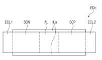
도 4a는 본 발명의 실시 예에 따른 표시패널의 평면도이다. 도 4b는 본 발명의 다른 실시 예에 따른 표시패널의 평면도이다. 도 4a 및 도 4b에서는 도 2b를 통해 도시된 화소(PX) 중 발광 소자(ED), 제1 전극(E1), 및 제2 전극(E2)의 구성이 도시되었으며, 설명의 편의를 위해 나머지 구성들은 생략되었다.Figure 4a is a plan view of a display panel according to an embodiment of the present invention. Figure 4b is a plan view of a display panel according to another embodiment of the present invention. 4A and 4B show the configuration of the light emitting element (ED), the first electrode (E1), and the second electrode (E2) among the pixel (PX) shown in FIG. 2B, and for convenience of explanation, the remaining configuration is shown. have been omitted.
도 4a를 참조하면, 하나의 화소(PX)에 포함된 발광 소자(ED), 제1 전극(E1), 및 제2 전극(E2)이 도시되었다. 도 4a에 도시된 바와 같이, 발광 소자(ED)는 복수 개로 제공되며, 복수 개로 제공될 발광 소자들(ED)은 병렬로 연결될 수 있다. 예시적으로, 도 4a를 통해서는 3열에 각각 배치된 복수 개의 발광 소자들(ED)이 도시되었다.Referring to FIG. 4A, a light emitting element (ED), a first electrode (E1), and a second electrode (E2) included in one pixel (PX) are shown. As shown in FIG. 4A, a plurality of light-emitting devices ED are provided, and the plurality of light-emitting devices ED may be connected in parallel. By way of example, FIG. 4A shows a plurality of light emitting elements ED arranged in three rows.
제1 전극(E1)은 제1 방향(DR1)을 따라 연장된 제1 서브 전극(E1a) 및 제1 서브 전극(E1a)으로부터 제2 방향(DR2)으로 분기된 복수 개의 제1 분기 전극들(E1b)을 포함한다. 제1 분기 전극들(E1b)은 제1 방향(DR1)에서 서로 이격될 수 있다.The first electrode E1 includes a first sub-electrode E1a extending along the first direction DR1 and a plurality of first branch electrodes branched from the first sub-electrode E1a in the second direction DR2 ( E1b). The first branch electrodes E1b may be spaced apart from each other in the first direction DR1.
제2 전극(E2)은 제1 방향(DR1)을 따라 연장된 제2 서브 전극(E2a) 및 제2 서브 전극(E2a)으로부터 제2 방향(DR2)으로 분기된 복수 개의 제2 분기 전극들(E2b)을 포함한다. 제2 분기 전극들(E2b)은 제1 방향(DR1)에서 서로 이격될 수 있다.The second electrode E2 includes a second sub-electrode E2a extending along the first direction DR1 and a plurality of second branch electrodes branched from the second sub-electrode E2a in the second direction DR2 ( E2b). The second branch electrodes E2b may be spaced apart from each other in the first direction DR1.
제1 서브 전극(E1a) 및 제2 서브 전극(E2a)은 제2 방향(DR2)에서 이격되고, 서로 마주할 수 있다. 또한, 제1 분기 전극들(E1b) 및 제2 분기 전극들(E2b)은 제1 서브 전극(E1a) 및 제2 서브 전극(E2a) 사이에서 제1 방향(DR1)을 따라 교번적으로 배치되며, 서로 이격될 수 있다.The first sub-electrode E1a and the second sub-electrode E2a may be spaced apart from each other in the second direction DR2 and face each other. Additionally, the first branch electrodes E1b and the second branch electrodes E2b are alternately arranged along the first direction DR1 between the first sub-electrodes E1a and the second sub-electrodes E2a. , can be spaced apart from each other.
평면상에서, 발광 소자들(ED)은 제1 방향(DR1)에서 서로 마주하는 제1 분기 전극(E1b) 및 제2 분기 전극(E2b) 사이에 배치될 수 있다. 발광 소자들(ED)은 제1 방향(DR1)으로 연장되며 제2 방향(DR2)으로 나열될 수 있다. 또한, 발광 소자들(ED)은 제2 방향(DR2)에서 서로 이격될 수 있다.In a plan view, the light emitting elements ED may be disposed between the first branch electrode E1b and the second branch electrode E2b facing each other in the first direction DR1. The light emitting elements ED may extend in the first direction DR1 and be arranged in the second direction DR2. Additionally, the light emitting elements ED may be spaced apart from each other in the second direction DR2.
평면상에서, 발광 소자들(ED)은 제1 전극(E1) 및 제2 전극(E2)과 비중첩할 수 있다. 즉, 발광 소자들(ED)은 제1 전극(E1) 및 제2 전극(E2)과 직접적으로 연결되지 않는다.On a plane, the light emitting elements ED may not overlap the first electrode E1 and the second electrode E2. That is, the light emitting elements ED are not directly connected to the first electrode E1 and the second electrode E2.
본 발명의 실시 예에 따르면, 발광 소자들(ED)은 연결 전극(CNE)을 통해 제1 전극(E1) 및 제2 전극(E2)과 전기적으로 연결될 수 있다. 평면상에서, 연결 전극(CNE)은 제1 분기 전극들(E1b), 제2 분기 전극들(E2b), 및 발광 소자들(ED)과 중첩할 수 있다. 특히, 각 열에 제공된 복수 개의 발광 소자들(ED)은 연결 전극(CNE)에 전체적으로 중첩할 수 있다.According to an embodiment of the present invention, the light emitting elements ED may be electrically connected to the first electrode E1 and the second electrode E2 through the connection electrode CNE. In a plan view, the connection electrode CNE may overlap the first branch electrodes E1b, the second branch electrodes E2b, and the light emitting elements ED. In particular, the plurality of light emitting elements ED provided in each row may entirely overlap the connection electrode CNE.
자세하게, 연결 전극(CNE)은 제1 연결 전극(CNE1), 제2 연결 전극(CNE2), 및 더미 연결 전극(CNEd)을 포함한다. 더미 연결 전극(CNEd)은 제1 연결 전극(CNE1) 및 제2 연결 전극(CNE2) 사이에 배치될 수 있다.In detail, the connection electrode CNE includes a first connection electrode CNE1, a second connection electrode CNE2, and a dummy connection electrode CNEd. The dummy connection electrode CNEd may be disposed between the first connection electrode CNE1 and the second connection electrode CNE2.
도 4a에 도시된 실시 예에 따르면, 제1 연결 전극(CNE1)은 두 개의 열들에 각각 제공된 복수 개의 발광 소자들에 전기적으로 연결된다. 또한, 제2 연결 전극(CNE2)은 다른 두 개의 열들에 각각 배치된 복수 개의 발광 소자들에 전기적으로 연결될 수 있다. 예를 들어, 제1 연결 전극(CNE1)은 제1 열에 제공된 발광 소자들의 일단들 및 제2 열에 제공된 발광 소자들의 일단들에 전기적으로 연결된다. 제2 연결 전극(CNE2)은 제2 열에 제공된 발광 소자들의 타단들 및 제3 열에 제공된 발광 소자들의 일단들에 전기적으로 연결된다.According to the embodiment shown in FIG. 4A, the first connection electrode CNE1 is electrically connected to a plurality of light emitting elements provided in two columns, respectively. Additionally, the second connection electrode CNE2 may be electrically connected to a plurality of light emitting devices respectively arranged in the other two columns. For example, the first connection electrode CNE1 is electrically connected to one end of the light emitting elements provided in the first row and one end of the light emitting elements provided in the second row. The second connection electrode CNE2 is electrically connected to other ends of the light emitting elements provided in the second row and to ends of the light emitting elements provided in the third row.
발광 소자들(ED) 각각은 제1 연결 전극(CNE1)을 통해 제1 전극(E1)과 연결되며, 제2 연결 전극(CNE2)을 통해 제2 전극(E2)과 연결된다. 한편, 더미 연결 전극(CNEd)은 제1 연결 전극(CNE1) 및 제2 연결 전극(CNE2)과 전기적으로 분리된다. 즉, 더미 연결 전극(CNEd)은 제1 연결 전극(CNE1) 및 제2 연결 전극(CNE2)과 각각 이격될 수 있다. 그 결과, 더미 연결 전극(CNEd)은 제1 전극(E1) 및 제2 전극(E2)과 전기적으로 분리될 수 있다.Each of the light emitting elements ED is connected to the first electrode E1 through the first connection electrode CNE1 and to the second electrode E2 through the second connection electrode CNE2. Meanwhile, the dummy connection electrode CNEd is electrically separated from the first connection electrode CNE1 and the second connection electrode CNE2. That is, the dummy connection electrode CNEd may be spaced apart from the first connection electrode CNE1 and the second connection electrode CNE2, respectively. As a result, the dummy connection electrode CNEd may be electrically separated from the first electrode E1 and the second electrode E2.
상술된 바에 따르면, 도 4a에 도시된 연결 전극(CNE)은 한 번의 증착 공정을 통해 진행될 수 있다. 예를 들어, 한 번의 증착 공정을 통해 제1 연결 전극(CNE1), 제2 연결 전극(CNE2), 및 더미 연결 전극(CNEd)을 포함한 연결 전극(CNE)이 형성될 수 있다. 본 발명에 따른 연결 전극(CNE)은 한 번의 증착 공정을 통해 형성됨에 따라, 표시장치(DD)의 전반적인 공정 시간이 축소되며 공정 비용이 절감될 수 있다. 연결 전극(CNE)의 공정 과정에 대해서는 추후 제조 방법을 통해 자세히 설명된다.As described above, the connection electrode (CNE) shown in FIG. 4A can be formed through a single deposition process. For example, the connection electrode CNE including the first connection electrode CNE1, the second connection electrode CNE2, and the dummy connection electrode CNEd may be formed through a single deposition process. Since the connection electrode CNE according to the present invention is formed through a single deposition process, the overall process time of the display device DD can be reduced and process costs can be reduced. The processing process of the connecting electrode (CNE) will be described in detail later through the manufacturing method.
도 4b에 도시된 화소 구조는 도 4a에 도시된 화소 구조와 비교하여 연결 전극(CNEa)의 구조가 변형되었을 뿐, 나머지 구성들의 구조는 실질적으로 동일 할 수 있다. 이하, 도 4b를 통해 연결 전극(CNEa)의 구조를 중점으로 설명되며, 나머지 구성들의 설명은 생략된다.The pixel structure shown in FIG. 4B only has a modified structure of the connection electrode CNEa compared to the pixel structure shown in FIG. 4A, but the structures of the remaining components may be substantially the same. Hereinafter, the structure of the connection electrode CNEa will be mainly described through FIG. 4B, and descriptions of the remaining components will be omitted.
도 4b를 참조하면, 제1 서브 전극(E1a) 및 제2 서브 전극(E2a) 사이에 배치된 연결 전극(CNEa)은 복수 개로 제공될 수 있으며, 도 4b를 통해서는 3 개의 연결 전극들(CNEa)이 예시적으로 도시된다. 복수 개의 연결 전극들(CNEa)은 제1 방향(DR1)에서 서로 이격될 수 있다. 복수 개의 연결 전극들(CNEa) 각각은 제1 연결 전극(CNE1a), 제2 연결 전극(CNE2a), 및 더미 연결 전극(CNEda)을 포함한다. 평면상에서, 더미 연결 전극(CNEda)은 제1 연결 전극(CNE1a) 및 제2 연결 전극(CNE2a) 사이에 배치될 수 있다.Referring to FIG. 4B, a plurality of connection electrodes (CNEa) disposed between the first sub-electrode (E1a) and the second sub-electrode (E2a) may be provided, and through FIG. 4B, three connection electrodes (CNEa) ) is shown as an example. The plurality of connection electrodes CNEa may be spaced apart from each other in the first direction DR1. Each of the plurality of connection electrodes CNEa includes a first connection electrode CNE1a, a second connection electrode CNE2a, and a dummy connection electrode CNEda. In plan view, the dummy connection electrode CNEda may be disposed between the first connection electrode CNE1a and the second connection electrode CNE2a.
도 4b에 도시된 실시 예에 따르면, 복수 개의 제1 연결 전극들(CEN1a) 중 제1 영역에 제공된 제1 연결 전극은 제1 열에 제공된 발광 소자들(ED)의 일단들에 전기적으로 연결되고, 복수 개의 제2 연결 전극들(CNE2a) 중 상기 제1 영역에 제공된 제2 연결 전극은 제1 열에 제공된 발광 소자들(ED)의 타단들에 전기적으로 연결된다. 여기서, 제1 영역은 제1 열에 제공된 발광 소자들(ED)에 연결된 어느 하나의 제1 연결 전극 및 어느 하나의 제2 연결 전극을 포함하는 영역일 수 있다.According to the embodiment shown in FIG. 4B, the first connection electrode provided in the first region among the plurality of first connection electrodes CEN1a is electrically connected to ends of the light emitting elements ED provided in the first row, Among the plurality of second connection electrodes CNE2a, the second connection electrode provided in the first area is electrically connected to other ends of the light emitting elements ED provided in the first row. Here, the first area may be an area including one first connection electrode and one second connection electrode connected to the light emitting elements ED provided in the first row.
제1 열에 제공된 발광 소자들(ED) 각각은 제1 연결 전극(CNE1a)을 통해 제2 전극(E2)과 연결되며, 제2 연결 전극(CNE2a)을 통해 제1 전극(E1)과 연결된다. 제1 연결 전극의 더미 연결 전극(CNEda)은 제1 전극(E1) 및 제2 전극(E2)과 전기적으로 분리된다. 또한, 제1 연결 전극의 더미 연결 전극(CNEda)은 제1 연결 전극(CNE1a) 및 제2 연결 전극(CNE2a)과 전기적으로 분리된다.Each of the light emitting elements ED provided in the first row is connected to the second electrode E2 through the first connection electrode CNE1a and to the first electrode E1 through the second connection electrode CNE2a. The dummy connection electrode CNEda of the first connection electrode is electrically separated from the first electrode E1 and the second electrode E2. Additionally, the dummy connection electrode CNEda of the first connection electrode is electrically separated from the first connection electrode CNE1a and the second connection electrode CNE2a.
또한, 복수 개의 제1 연결 전극들(CEN1a) 중 제2 영역에 제공된 제1 연결 전극은 제1 열에 인접한 제2 열에 제공된 발광 소자들(ED)의 일단들에 전기적으로 연결되고, 복수 개의 제2 연결 전극들(CNE2a) 중 상기 제2 영역에 제공된 제2 연결 전극은 제2 열에 제공된 발광 소자들(ED)의 타단들에 전기적으로 연결된다. 여기서, 제2 영역은 제2 열에 제공된 발광 소자들(ED)에 연결된 다른 하나의 제1 연결 전극 및 다른 하나의 제2 연결 전극을 포함하는 영역일 수 있다.In addition, the first connection electrode provided in the second region among the plurality of first connection electrodes CEN1a is electrically connected to ends of the light emitting elements ED provided in the second row adjacent to the first row, and the plurality of second connection electrodes CEN1a are electrically connected to ends of the light emitting elements ED provided in the second row adjacent to the first row. Among the connection electrodes CNE2a, a second connection electrode provided in the second region is electrically connected to other ends of the light emitting elements ED provided in the second row. Here, the second area may be an area including another first connection electrode and another second connection electrode connected to the light emitting elements ED provided in the second row.
이 경우, 제2 열에 제공된 발광 소자들(ED) 각각은 제1 연결 전극(CNE1a)을 통해 제1 전극(E1)과 연결되며, 제2 연결 전극(CNE2a)을 통해 제2 전극(E2)과 연결될 수 있다.In this case, each of the light emitting elements ED provided in the second row is connected to the first electrode E1 through the first connection electrode CNE1a, and is connected to the second electrode E2 through the second connection electrode CNE2a. can be connected
또한, 복수 개의 제1 연결 전극들(CEN1a) 중 제3 영역에 제공된 제1 연결 전극은 제1 열에 인접한 제3 열에 제공된 발광 소자들(ED)의 일단들에 전기적으로 연결되고, 복수 개의 제2 연결 전극들(CNE2a) 중 상기 제3 영역에 제공된 제2 연결 전극은 제3 열에 제공된 발광 소자들(ED)의 타단들에 전기적으로 연결된다. 여기서, 제3 영역은 제3 열에 제공된 발광 소자들(ED)에 연결된 다른 하나의 제1 연결 전극 및 다른 하나의 제2 연결 전극을 포함하는 영역일 수 있다.In addition, among the plurality of first connection electrodes CEN1a, the first connection electrode provided in the third region is electrically connected to ends of the light emitting elements ED provided in the third column adjacent to the first column, and the plurality of second connection electrodes CEN1a are electrically connected to the ends of the light emitting elements ED provided in the third column adjacent to the first column. Among the connection electrodes CNE2a, a second connection electrode provided in the third region is electrically connected to other ends of the light emitting elements ED provided in the third row. Here, the third area may be an area including another first connection electrode and another second connection electrode connected to the light emitting elements ED provided in the third row.
이 경우, 제3 열에 제공된 발광 소자들(ED) 각각은 제1 연결 전극(CNE1a)을 통해 제1 전극(E1)과 연결되며, 제2 연결 전극(CNE2a)을 통해 제2 전극(E2)과 연결될 수 있다.In this case, each of the light emitting elements ED provided in the third row is connected to the first electrode E1 through the first connection electrode CNE1a, and to the second electrode E2 through the second connection electrode CNE2a. can be connected
한편, 도 4a 및 도 4b를 통해 하나의 화소에 포함된 제1 전극(E1), 제2 전극(E2), 발광 소자(ED), 및 연결 전극(CNE, CNEa)의 구조가 각각 도시되었으나, 본 발명의 실시 예는 이에 한정되지 않는다. 즉, 제1 전극(E1), 제2 전극(E2), 및 발광 소자(ED)의 구조는 다양하게 변형될 수 있다. 예를 들어, 도 4a 및 도 4b를 통해 제1 분기 전극들(E1b) 및 제2 분기 전극들(E2b)이 각각 2개인 것으로 도시되었으나, 두 개의 제1 분기 전극들(E1b) 사이에 배치된 하나의 제2 분기 전극(E2b)이 제공될 수 있다. 반대로, 두 개의 제2 분기 전극들(E2b) 사이에 배치된 하나의 제1 분기 전극(E1b)이 제공될 수 있다.Meanwhile, the structures of the first electrode (E1), the second electrode (E2), the light emitting element (ED), and the connection electrodes (CNE and CNEa) included in one pixel are shown in FIGS. 4A and 4B, respectively. Embodiments of the present invention are not limited thereto. That is, the structures of the first electrode E1, the second electrode E2, and the light emitting device ED may be modified in various ways. For example, although it is shown in FIGS. 4A and 4B that there are two first branch electrodes E1b and two second branch electrodes E2b, the two first branch electrodes E1b are disposed between the two first branch electrodes E1b. One second branch electrode (E2b) may be provided. Conversely, one first branch electrode E1b disposed between two second branch electrodes E2b may be provided.
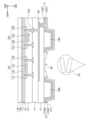
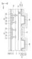
도 5는 본 발명의 실시 예에 따른 표시패널의 일 부분을 도시한 단면도이다. 도 6은 도 5에 도시된 AA 영역을 확대하여 도시한 단면도이다.Figure 5 is a cross-sectional view showing a portion of a display panel according to an embodiment of the present invention. FIG. 6 is an enlarged cross-sectional view of area AA shown in FIG. 5.
도 5에 도시된 제1 박막 트랜지스터(TR1), 제2 박막 트랜지스터(TR2), 및 컨택 전극(CN)은 도 3에 도시된 회로층(COL)에 포함되고, 제1 전극(E1), 제2 전극(E2), 제1 연결 전극(CNE1), 제2 연결 전극(CNE2), 더미 연결 전극(CNEd), 및 발광 소자(ED)는 표시 소자층(EDL)에 포함된다.The first thin film transistor TR1, the second thin film transistor TR2, and the contact electrode CN shown in FIG. 5 are included in the circuit layer COL shown in FIG. 3, and the first electrode E1 and the contact electrode CN are included in the circuit layer COL shown in FIG. 3. The second electrode E2, the first connection electrode CNE1, the second connection electrode CNE2, the dummy connection electrode CNEd, and the light emitting device ED are included in the display device layer EDL.
도 5를 참조하면, 제1 베이스층(BL1) 및 제2 베이스층(BL2)은 서로 마주할 수 있다. 예를 들어, 제1 베이스층(BL1) 및 제2 베이스층(BL2) 각각은 실리콘 기판, 플라스틱 기판, 유리 기판, 절연 필름, 또는 복수의 절연층들을 포함하는 적층 구조체일 수 있다.Referring to FIG. 5 , the first base layer BL1 and the second base layer BL2 may face each other. For example, each of the first base layer BL1 and the second base layer BL2 may be a silicon substrate, a plastic substrate, a glass substrate, an insulating film, or a laminated structure including a plurality of insulating layers.
제1 베이스층(BL1) 상에는 버퍼층(BFL)이 배치될 수 있다. 버퍼층(BFL) 상에는 도 2b를 통해 도시된 제1 박막 트랜지스터(TR1) 및 제2 박막 트랜지스터(TR2)가 배치될 수 있다.A buffer layer (BFL) may be disposed on the first base layer (BL1). The first thin film transistor TR1 and the second thin film transistor TR2 shown in FIG. 2B may be disposed on the buffer layer BFL.
자세하게, 제1 박막 트랜지스터(TR1)는 제1 제어 전극(CE1), 제1 입력 전극(IE1), 제1 출력 전극(OE1), 및 제1 반도체 패턴(SP1)을 포함할 수 있다. 제2 박막 트랜지스터(TR2)는 제2 제어 전극(CE2), 제2 입력 전극(IE2), 제2 출력 전극(OE2), 및 제2 반도체 패턴(SP2)을 포함할 수 있다.In detail, the first thin film transistor TR1 may include a first control electrode CE1, a first input electrode IE1, a first output electrode OE1, and a first semiconductor pattern SP1. The second thin film transistor TR2 may include a second control electrode (CE2), a second input electrode (IE2), a second output electrode (OE2), and a second semiconductor pattern (SP2).
제1 반도체 패턴(SP1) 및 제2 반도체 패턴(SP2)은 버퍼층(BFL) 상에 배치될 수 있다. 버퍼층(BFL)은 제1 반도체 패턴(SP1) 및 제2 반도체 패턴(SP2)에 개질된 표면을 제공할 수 있다. 이 경우, 제1 반도체 패턴(SP1) 및 제2 반도체 패턴(SP2)은 제1 베이스층(BL1) 상에 직접 형성될 때보다 버퍼층(BFL)에 대해 높은 접착력을 가질 수 있다. 또는, 버퍼층(BFL)은 제1 반도체 패턴(SP1) 및 제2 반도체 패턴(SP2) 각각의 하면을 보호하는 배리어층일 수 있다. 이 경우, 버퍼층(BFL)은 제1 베이스층(BL1) 자체 또는 제1 베이스층(BL1)을 통해 유입되는 오염이나 습기 등이 제1 반도체 패턴(SP1) 및 제2 반도체 패턴(SP2)으로 침투되는 것을 차단할 수 있다. The first semiconductor pattern SP1 and the second semiconductor pattern SP2 may be disposed on the buffer layer BFL. The buffer layer BFL may provide a modified surface to the first semiconductor pattern SP1 and the second semiconductor pattern SP2. In this case, the first semiconductor pattern SP1 and the second semiconductor pattern SP2 may have higher adhesion to the buffer layer BFL than when formed directly on the first base layer BL1. Alternatively, the buffer layer BFL may be a barrier layer that protects the lower surfaces of each of the first semiconductor pattern SP1 and the second semiconductor pattern SP2. In this case, the buffer layer (BFL) allows the first base layer (BL1) itself or contamination or moisture flowing through the first base layer (BL1) to penetrate into the first semiconductor pattern (SP1) and the second semiconductor pattern (SP2). You can block it from happening.
제1 절연층(L1)은 버퍼층(BFL) 상에 배치되며 제1 반도체 패턴(SP1) 및 제2 반도체 패턴(SP2)을 커버할 수 있다. 본 발명에 따르면, "커버"라고 언급되는 경우, 제1 구성이 제2 구성을 전체적으로 감싸는 것을 의미한다. 제1 절연층(L1)은 무기 물질을 포함할 수 있다. 예를 들어, 무기 물질은 실리콘 나이트라이드, 실리콘 옥시 나이트라이드, 실리콘 옥사이드, 티타늄옥사이드, 또는 알루미늄옥사이드 일 수 있으나, 이에 제한되는 것은 아니다.The first insulating layer L1 is disposed on the buffer layer BFL and may cover the first semiconductor pattern SP1 and the second semiconductor pattern SP2. According to the present invention, when reference is made to “cover” it is meant that the first component entirely surrounds the second component. The first insulating layer L1 may include an inorganic material. For example, the inorganic material may be, but is not limited to, silicon nitride, silicon oxy nitride, silicon oxide, titanium oxide, or aluminum oxide.
제1 절연층(L1) 상에는 제1 제어 전극(CE1) 및 제2 제어 전극(CE2)이 배치될 수 있다. 제2 절연층(L2)은 제1 절연층(L1) 상에 배치되며, 제1 제어 전극(CE1) 및 제2 제어 전극(CE2)을 커버할 수 있다. 제2 절연층(L2)은 무기 물질을 포함할 수 있다.A first control electrode (CE1) and a second control electrode (CE2) may be disposed on the first insulating layer (L1). The second insulating layer L2 is disposed on the first insulating layer L1 and may cover the first control electrode CE1 and the second control electrode CE2. The second insulating layer L2 may include an inorganic material.
커패시터(CAP, 도 2b 참조)는 제1 캡 전극(미도시) 및 제2 캡 전극(CPa)을 포함할 수 있다. 예를 들어, 상기 제1 캡 전극은 제2 제어 전극(CE2)으로부터 분기될 수 있고, 제2 캡 전극(CPa)은 제2 절연층(L2) 상에 배치될 수 있다.The capacitor (CAP, see FIG. 2B) may include a first cap electrode (not shown) and a second cap electrode (CPa). For example, the first cap electrode may be branched from the second control electrode CE2, and the second cap electrode CPa may be disposed on the second insulating layer L2.
제3 절연층(L3)은 제2 절연층(L2) 상에 배치되며, 제2 캡 전극(CPa)을 커버한다. 제1 입력 전극(IE1), 제1 출력 전극(OE1), 제2 입력 전극(IE2), 및 제2 출력 전극(OE2)은 제3 절연층(L3) 상에 배치될 수 있다. 제1 입력 전극(IE1) 및 제1 출력 전극(OE1)은 제1 내지 제3 절연층들(L1, L2, L3)을 관통하는 관통홀들을 통해 제1 반도체 패턴(SP1)과 연결될 수 있다. 제2 입력 전극(IE2), 및 제2 출력 전극(OE2)은 제1 내지 제3 절연층들(L1, L2, L3)을 관통하는 관통홀들을 통해 제2 반도체 패턴(SP2)과 연결될 수 있다. 제3 절연층(L3) 상에는 제1 입력 전극(IE1), 제1 출력 전극(OE1), 제2 입력 전극(IE2), 및 제2 출력 전극(OE2)뿐만 아니라, 신호 배선들, 예를 들어, 스캔 라인들 또는 데이터 라인들, 중 각각의 적어도 일부가 배치될 수 있다.The third insulating layer L3 is disposed on the second insulating layer L2 and covers the second cap electrode CPa. The first input electrode (IE1), the first output electrode (OE1), the second input electrode (IE2), and the second output electrode (OE2) may be disposed on the third insulating layer (L3). The first input electrode IE1 and the first output electrode OE1 may be connected to the first semiconductor pattern SP1 through through holes penetrating the first to third insulating layers L1, L2, and L3. The second input electrode IE2 and the second output electrode OE2 may be connected to the second semiconductor pattern SP2 through through holes penetrating the first to third insulating layers L1, L2, and L3. . On the third insulating layer L3, there are a first input electrode (IE1), a first output electrode (OE1), a second input electrode (IE2), and a second output electrode (OE2), as well as signal wires, for example , at least a portion of each of the scan lines or data lines may be disposed.
제4 절연층(L4)은 제3 절연층(L3) 상에 배치되며, 제1 입력 전극(IE1), 제1 출력 전극(OE1), 제2 입력 전극(IE2), 및 제2 출력 전극(OE2)을 커버할 수 있다. 제4 절연층(L4)은 단일의 층 또는 복수의 층일 수 있고, 제4 절연층(L4)은 유기 물질 및/또는 무기 물질을 포함할 수 있다.The fourth insulating layer (L4) is disposed on the third insulating layer (L3), and includes a first input electrode (IE1), a first output electrode (OE1), a second input electrode (IE2), and a second output electrode ( OE2) can be covered. The fourth insulating layer L4 may be a single layer or multiple layers, and the fourth insulating layer L4 may include an organic material and/or an inorganic material.
제4 절연층(L4) 상에는 컨택 전극(CN)이 배치될 수 있다. 제4 절연층(L4) 상에는 컨택 전극(CN)뿐만 아니라, 신호 배선들, 예를 들어, 스캔 라인들 또는 데이터 라인들 각각의 적어도 다른 일부가 배치될 수 있다. 컨택 전극(CN)은 제4 절연층(L4)을 관통하는 관통홀을 통해 제2 출력 전극(OE2)과 연결될 수 있다.A contact electrode CN may be disposed on the fourth insulating layer L4. On the fourth insulating layer L4, not only the contact electrode CN but also at least another portion of signal wires, for example, scan lines or data lines, may be disposed. The contact electrode CN may be connected to the second output electrode OE2 through a through hole penetrating the fourth insulating layer L4.
제5 절연층(L5)은 제4 절연층(L4) 상에 배치되며, 컨택 전극(CN)을 커버할 수 있다. 제5 절연층(L5)은 유기물을 포함할 수 있다. 제5 절연층(L5) 상에는 발광 소자(ED), 제1 격벽(BR1), 및 제2 격벽(BR2)이 배치된다. 제1 격벽(BR1) 및 제2 격벽(BR2)은 유기물을 포함하며, 제1 방향(DR1)에서 서로 이격될 수 있다.The fifth insulating layer L5 is disposed on the fourth insulating layer L4 and may cover the contact electrode CN. The fifth insulating layer L5 may include an organic material. The light emitting element ED, the first barrier rib BR1, and the second barrier rib BR2 are disposed on the fifth insulating layer L5. The first partition BR1 and the second partition BR2 include organic material and may be spaced apart from each other in the first direction DR1.
제1 전극(E1)은 제1 격벽(BR1)을 커버하고, 제2 전극(E2)은 제2 격벽(BR2)을 커버할 수 있다. 즉, 제1 전극(E1)과 제5 절연층(L5) 사이에 제1 격벽(BR1)이 배치되고, 제2 전극(E2)과 제5 절연층(L5) 사이에 제2 격벽(BR2)이 배치될 수 있다.The first electrode E1 may cover the first partition BR1, and the second electrode E2 may cover the second partition BR2. That is, the first partition BR1 is disposed between the first electrode E1 and the fifth insulating layer L5, and the second partition BR2 is disposed between the second electrode E2 and the fifth insulating layer L5. This can be placed.
제5 절연층(L5)에는 관통홀이 제공되고, 상기 관통홀에 의해 컨택 전극(CN)이 노출될 수 있다. 제1 전극(E1)은 노출된 컨택 전극(CN)에 전기적으로 연결될 수 있다. 제2 전극(E2)은 도시되지 않았으나, 제2 전원 라인(PL2, 도2b 참조)에 전기적으로 연결될 수 있다. 즉, 제2 전극(E2)에는 제2 전원전압(ELVSS, 도2b 참조)이 제공될 수 있다.A through hole is provided in the fifth insulating layer L5, and the contact electrode CN may be exposed through the through hole. The first electrode E1 may be electrically connected to the exposed contact electrode CN. The second electrode E2 is not shown, but may be electrically connected to the second power line PL2 (see FIG. 2B). That is, the second power voltage (ELVSS, see FIG. 2B) may be provided to the second electrode (E2).
제1 전극(E1)은 제1 반사 전극(RFE1) 및 제1 캡핑 전극(CPE1)을 포함한다. 제2 전극(E2)은 제2 반사 전극(RFE2) 및 제2 캡핑 전극(CPE2)을 포함한다. 제1 반사 전극(RFE1) 및 제2 반사 전극(RFE2) 각각은 반사성 물질을 포함할 수 있다. 제1 반사 전극(RFE1) 및 제2 반사 전극(RFE2) 각각은 단층 구조를 가질 수도 있고, 복수의 적층 구조를 가질 수도 있다. 예를 들어, 제1 반사 전극(RFE1) 및 제2 반사 전극(RFE2) 각각은 인듐주석 산화물(ITO), 은(Ag), 및 인듐주석 산화물(ITO)이 순차적으로 적층된 구조를 가질 수 있다.The first electrode E1 includes a first reflective electrode RFE1 and a first capping electrode CPE1. The second electrode E2 includes a second reflective electrode RFE2 and a second capping electrode CPE2. Each of the first reflective electrode (RFE1) and the second reflective electrode (RFE2) may include a reflective material. Each of the first reflective electrode (RFE1) and the second reflective electrode (RFE2) may have a single-layer structure or a plurality of stacked structures. For example, each of the first reflective electrode (RFE1) and the second reflective electrode (RFE2) may have a structure in which indium tin oxide (ITO), silver (Ag), and indium tin oxide (ITO) are sequentially stacked. .
제1 캡핑 전극(CPE1)은 제1 반사 전극(RFE1)을 캡핑하고, 제2 캡핑 전극(CPE2)은 제2 반사 전극(RFE2)을 캡핑할 수 있다. 예를 들어, 제1 캡핑 전극(CPE1) 및 제2 캡핑 전극(CPE2) 각각은 인듐아연 산화물(IZO), 인듐주석 산화물(ITO), 인듐갈륨 산화물(IGO), 인듐아연갈륨 산화물(IGZO), 및 이들의 혼합물/화합물 중 적어도 어느 하나를 포함할 수 있다.The first capping electrode CPE1 may cap the first reflective electrode RFE1, and the second capping electrode CPE2 may cap the second reflective electrode RFE2. For example, the first capping electrode (CPE1) and the second capping electrode (CPE2) each include indium zinc oxide (IZO), indium tin oxide (ITO), indium gallium oxide (IGO), indium zinc gallium oxide (IGZO), and mixtures/compounds thereof.
발광 소자(ED)는 제1 전극(E1) 및 제2 전극(E2) 사이에 배치될 수 있다. 제1 방향(DR1)에서, 발광 소자(ED)는 제1 전극(E1) 및 제2 전극(E2)과 각각 이격될 수 있다. 발광 소자(ED)는 제1 연결 전극(CNE1)을 통해 제1 전극(E1)과 전기적으로 연결된다. 제1 연결 전극(CNE1)은 제1 전극(E1) 및 발광 소자(ED)의 일 부분에 직접적으로 연결될 수 있다. 발광 소자(ED)의 일단은 제2 박막 트랜지스터(TR2)로부터 전달된 전원 신호를 제1 연결 전극(CNE1)을 통해 수신할 수 있다.The light emitting element ED may be disposed between the first electrode E1 and the second electrode E2. In the first direction DR1, the light emitting device ED may be spaced apart from the first electrode E1 and the second electrode E2, respectively. The light emitting element ED is electrically connected to the first electrode E1 through the first connection electrode CNE1. The first connection electrode CNE1 may be directly connected to the first electrode E1 and a portion of the light emitting device ED. One end of the light emitting element (ED) may receive the power signal transmitted from the second thin film transistor (TR2) through the first connection electrode (CNE1).
또한, 발광 소자(ED)는 제2 연결 전극(CNE2)을 통해 제2 전극(E2)과 전기적으로 연결된다. 제2 연결 전극(CNE2)은 제2 전극(E2) 및 발광 소자(ED)의 일 부분에 직접적으로 연결될 수 있다. 발광 소자(ED)의 타단은 제2 전원 라인(PL2, 도2b 참조)으로부터 전달된 제2 전원 전압(ELVSS)을 제2 연결 전극(CNE2)을 통해 수신할 수 있다.Additionally, the light emitting element ED is electrically connected to the second electrode E2 through the second connection electrode CNE2. The second connection electrode CNE2 may be directly connected to the second electrode E2 and a portion of the light emitting device ED. The other end of the light emitting device ED may receive the second power voltage ELVSS transmitted from the second power line PL2 (see FIG. 2B) through the second connection electrode CNE2.
한편, 제1 연결 전극(CNE1)이 제1 전극(E1)에 직접적으로 연결되고, 제2 연결 전극(CNE2)이 제2 전극(E2)에 직접적으로 연결된 것으로 설명되나, 이에 한정되지 않는다. 예를 들어, 도 4b에 도시된 바와 같이, 복수 개의 제1 연결 전극(CNE1) 중 제1 발광 소자의 일단에 연결된 제1 연결 전극은 제1 전극(E1)에 연결된다. 이 경우, 제1 발광 소자의 타단에 연결된 제2 연결 전극은 제2 전극(E2)에 연결된다. 다른 예로, 복수 개의 제1 연결 전극(CNE1) 중 제1 발광 소자에 인접한 제2 발광 소자의 일단에 연결된 제1 연결 전극은 제2 전극(E2)에 연결될 수 있다. 이 경우, 제2 발광 소자의 타단에 연결된 제2 연결 전극은 제1 전극(E1)에 연결될 수 있다.Meanwhile, the first connection electrode (CNE1) is described as being directly connected to the first electrode (E1) and the second connection electrode (CNE2) is directly connected to the second electrode (E2), but the present invention is not limited thereto. For example, as shown in FIG. 4B, the first connection electrode connected to one end of the first light emitting device among the plurality of first connection electrodes CNE1 is connected to the first electrode E1. In this case, the second connection electrode connected to the other end of the first light emitting device is connected to the second electrode E2. As another example, the first connection electrode connected to one end of the second light-emitting device adjacent to the first light-emitting device among the plurality of first connection electrodes CNE1 may be connected to the second electrode E2. In this case, the second connection electrode connected to the other end of the second light emitting device may be connected to the first electrode E1.
제1 연결 전극(CNE1) 및 제2 연결 전극(CNE2)은 도전 물질을 포함할 수 있다. 예를 들어, 상기 도전 물질은 인듐아연 산화물(IZO), 인듐주석 산화물(ITO), 인듐갈륨 산화물(IGO), 인듐아연갈륨 산화물(IGZO), 및 이들의 혼합물/화합물 중 적어도 어느 하나를 포함할 수 있다. 하지만, 본 발명이 이에 제한되는 것은 아니다. 예를 들어, 상기 도전 물질은 금속 물질일 수 있고, 상기 금속 물질은 예컨대, 몰리브덴, 은, 티타늄, 구리, 알루미늄, 또는 이들의 합금을 포함할 수 있다.The first connection electrode (CNE1) and the second connection electrode (CNE2) may include a conductive material. For example, the conductive material may include at least one of indium zinc oxide (IZO), indium tin oxide (ITO), indium gallium oxide (IGO), indium zinc gallium oxide (IGZO), and mixtures/compounds thereof. You can. However, the present invention is not limited thereto. For example, the conductive material may be a metallic material, and the metallic material may include, for example, molybdenum, silver, titanium, copper, aluminum, or an alloy thereof.
본 발명의 실시 예에 따르면, 발광 소자(ED) 상에 제1 보조 절연층(LX1)이 배치되고, 제1 보조 절연층(LX1) 상에 제2 보조 절연층(LX2)이 배치된다. 제2 보조 절연층(LX2) 상에는 더미 연결 전극(CNEd)이 배치될 수 있다. 도 5에 도시된 바와 같이, 더미 연결 전극(CNEd)이 제1 연결 전극(CNE1) 및 제2 연결 전극(CNE2)과 전기적으로 분리됨으로써, 제1 연결 전극(CNE1) 및 제2 연결 전극(CNE2)이 전기적으로 접속되지 않는다.According to an embodiment of the present invention, a first auxiliary insulating layer (LX1) is disposed on the light emitting device (ED), and a second auxiliary insulating layer (LX2) is disposed on the first auxiliary insulating layer (LX1). A dummy connection electrode CNEd may be disposed on the second auxiliary insulating layer LX2. As shown in FIG. 5, the dummy connection electrode CNEd is electrically separated from the first connection electrode CNE1 and the second connection electrode CNE2, so that the first connection electrode CNE1 and the second connection electrode CNE2 ) is not electrically connected.
자세하게, 도 6을 참조하면, 제1 베이스층(BL1)의 평면상에서, 발광 소자(ED)는 제1 너비를 가지며, 제1 보조 절연층(LX1)은 제2 너비를 가지며, 제2 보조 절연층(LX2)은 제3 너비를 가질 수 있다. 본 발명에 따르면, 평면상에서 제1 보조 절연층(LX1)의 제2 너비는 제2 보조 절연층(LX2)의 제3 너비 보다 작을 수 있다. 또한, 평면상에서 제2 보조 절연층(LX2)의 제3 너비는 발광 소자(ED)의 제1 너비 보다 작을 있다.In detail, referring to FIG. 6, on the plane of the first base layer BL1, the light emitting element ED has a first width, the first auxiliary insulating layer LX1 has a second width, and the second auxiliary insulating layer LX1 has a second width. Layer LX2 may have a third width. According to the present invention, the second width of the first auxiliary insulating layer (LX1) may be smaller than the third width of the second auxiliary insulating layer (LX2) in plan view. Additionally, the third width of the second auxiliary insulating layer LX2 may be smaller than the first width of the light emitting device ED in plan view.
또한, 도 6에 도시된 바와 같이, 제1 방향(DR1)에서, 발광 소자(ED)는 제1 길이(D1)로 제공되고, 제1 보조 절연층(LX1)은 제2 길이(D2)로 제공되고, 제2 보조 절연층(LX2)은 제3 길이(D3)로 제공된다. 제2 길이(D2)는 제3 길이(D3) 보다 짧으며, 제3 길이(D3)는 제1 길이(D1) 보다 짧을 수 있다.In addition, as shown in FIG. 6, in the first direction DR1, the light emitting element ED is provided at a first length D1, and the first auxiliary insulating layer LX1 is provided at a second length D2. The second auxiliary insulating layer LX2 is provided to have a third length D3. The second length D2 may be shorter than the third length D3, and the third length D3 may be shorter than the first length D1.
상술된 바에 따르면, 평면상에서, 제2 보조 절연층(LX2)은 발광 소자(ED)에 전체적으로 중첩하며, 제1 보조 절연층(LX1)을 전체적으로 커버할 수 있다.As described above, in a plan view, the second auxiliary insulating layer LX2 entirely overlaps the light emitting device ED and may entirely cover the first auxiliary insulating layer LX1.
본 발명에 따르면, 제1 보조 절연층(LX1) 및 제2 보조 절연층(LX2)이 형성된 후에, 제2 보조 절연층(LX2)의 상부로부터 연결 전극(CNE)을 형성하기 위한 도전성 증착 물질이 도포될 수 있다. 이 경우, 제1 보조 절연층(LX1)이 제2 보조 절연층(LX2)에 의해 커버됨에 따라, 증착 물질이 제1 전극(E1), 제2 전극(E2), 제2 보조 절연층(LX2), 및 발광 소자(ED)의 일 부분에 증착될 뿐, 제1 보조 절연층(LX1)에는 증착되지 않는다.According to the present invention, after the first auxiliary insulating layer (LX1) and the second auxiliary insulating layer (LX2) are formed, a conductive deposition material for forming the connection electrode (CNE) is deposited from the top of the second auxiliary insulating layer (LX2). It can be applied. In this case, as the first auxiliary insulating layer (LX1) is covered by the second auxiliary insulating layer (LX2), the deposition material is deposited on the first electrode (E1), the second electrode (E2), and the second auxiliary insulating layer (LX2). ), and is only deposited on a portion of the light emitting device (ED), and is not deposited on the first auxiliary insulating layer (LX1).
그 결과, 제1 보조 절연층(LX1) 및 제2 보조 절연층(LX2)은 언더 컷 형상으로 제공될 수 있다. 언더 컷 형상은 제1 보조 절연층(LX1) 및 제2 보조 절연층(LX2) 간에 내측 공간이 형성된 것을 의미할 수 있다.As a result, the first auxiliary insulating layer LX1 and the second auxiliary insulating layer LX2 may be provided in an undercut shape. The undercut shape may mean that an inner space is formed between the first auxiliary insulating layer (LX1) and the second auxiliary insulating layer (LX2).
자세하게, 제2 보조 절연층(LX2)은 제1 보조 절연층(LX1)에 전체적으로 중첩하는 제1 절연 부분(LX2a) 및 평면상에서 제1 절연 부분(LX2a)을 에워싸며 제1 절연 부분(LX2a)으로부터 연장된 제2 절연 부분(LX2b)을 포함한다. 제2 절연 부분(LX2b)은 제1 보조 절연층(LX1)과 비중첩할 수 있다. 더미 연결 전극(CNEd)은 제1 절연 부분(LX2a) 및 제2 절연 부분(LX2b)을 전체적으로 커버할 수 있다.In detail, the second auxiliary insulating layer (LX2) has a first insulating part (LX2a) that entirely overlaps the first auxiliary insulating layer (LX1) and a first insulating part (LX2a) that surrounds the first insulating part (LX2a) on a plane. It includes a second insulating portion (LX2b) extending from. The second insulating portion LX2b may not overlap the first auxiliary insulating layer LX1. The dummy connection electrode CNEd may entirely cover the first insulating part LX2a and the second insulating part LX2b.
또한, 제3 방향(DR3)에서, 발광 소자(ED) 상에 배치된 제1 연결 전극(CNE1)과 제2 보조 절연층(LX2) 간의 이격 거리(SR)는 발광 소자(ED) 상에 배치된 제2 연결 전극(CNE2)과 제2 보조 절연층(LX2) 간의 이격 거리(SR)와 동일할 수 있다.Additionally, in the third direction DR3, the separation distance SR between the first connection electrode CNE1 and the second auxiliary insulating layer LX2 disposed on the light emitting device ED is The separation distance SR between the second connection electrode CNE2 and the second auxiliary insulating layer LX2 may be equal to the distance SR.
더미 연결 전극(CNEd)은 제2 보조 절연층(LX2) 상에만 배치될 수 있다.The dummy connection electrode CNEd may be disposed only on the second auxiliary insulating layer LX2.
본 발명에 따른 제1 연결 전극(CNE1), 제2 연결 전극(CNE2), 및 더미 연결 전극(CNEd)은 한 번의 증착 공정을 통해 제공될 수 있다. 즉, 한 번의 증착 공정을 통해, 제2 보조 절연층(LX2) 상에 배치된 더미 연결 전극(CNEd)과 제1 보조 절연층(LX1)에 의해 분리된 제1 전극(E1) 상에 배치된 제1 연결 전극(CNE1) 및 제2 전극(E2) 상에 배치된 제2 연결 전극(CNE2)이 제공될 수 있다.The first connection electrode (CNE1), the second connection electrode (CNE2), and the dummy connection electrode (CNEd) according to the present invention can be provided through a single deposition process. That is, through one deposition process, the dummy connection electrode (CNEd) disposed on the second auxiliary insulating layer (LX2) and the first electrode (E1) separated by the first auxiliary insulating layer (LX1) A second connection electrode (CNE2) disposed on the first connection electrode (CNE1) and the second electrode (E2) may be provided.
다시 도 5를 참조하면, 발광 소자(ED) 상에는 제6 절연층(L6, 또는 절연 패턴)이 배치될 수 있다. 제6 절연층(L6)은 제1 연결 전극(CNE1), 제2 연결 전극(CNE2), 및 더미 연결 전극(CNEd)을 커버할 수 있다. 본 발명의 다른 실시 예에 따르면, 제6 절연층(L6)은 생략될 수도 있다.Referring again to FIG. 5 , a sixth insulating layer (L6, or insulating pattern) may be disposed on the light emitting device ED. The sixth insulating layer L6 may cover the first connection electrode CNE1, the second connection electrode CNE2, and the dummy connection electrode CNEd. According to another embodiment of the present invention, the sixth insulating layer L6 may be omitted.
제1 베이스층(BL1)과 마주하는 제2 베이스층(BL2)의 일 면에는 차광층(BM)이 배치될 수 있다. 차광층(BM)에는 개구부가 제공되고, 파장 변환부(CL)는 개구부를 커버할 수 있다. 개구부에 의해 노출된 영역은 화소 발광 영역(PXA)에 대응될 수 있다.A light blocking layer (BM) may be disposed on one side of the second base layer (BL2) facing the first base layer (BL1). An opening is provided in the light blocking layer (BM), and the wavelength conversion unit (CL) may cover the opening. The area exposed by the opening may correspond to the pixel emission area (PXA).
파장 변환부(CL)는 발광체를 포함할 수 있다. 예를 들어, 발광체는 발광 소자(ED)에서 제공되는 제1 광을 흡수하여, 제1 광의 파장을 변환하여 제1 광과 상이한 색의 제2 색 광을 방출할 수 있다. 상기 발광체는 예를 들어, 양자점일 수 있다. 상기 제1 광은 청색 광일 수 있고, 상기 제2 색 광은 녹색 광 또는 적색 광일 수 있다. 다만, 이는 예시적인 것으로 본 발명이 이에 제한되는 것은 아니다. 또한, 본 발명의 다른 일 실시예에서, 파장 변환부(CL)는 컬러 필터로 치환될 수 있다. 상기 컬러 필터는 특정 파장의 광을 흡수하여 색을 구현할 수 있다. 본 발명의 또 다른 일 실시예에서, 파장 변환부(CL)는 생략될 수도 있다. 이 경우, 발광 소자(ED)는 청색 광, 녹색 광 또는 적색 광을 방출할 수 있다.The wavelength converter CL may include a light emitter. For example, the light emitting body may absorb the first light provided from the light emitting element ED, convert the wavelength of the first light, and emit a second color light of a different color from the first light. For example, the light emitting body may be a quantum dot. The first color light may be blue light, and the second color light may be green light or red light. However, this is an example and the present invention is not limited thereto. Additionally, in another embodiment of the present invention, the wavelength converter CL may be replaced with a color filter. The color filter can realize color by absorbing light of a specific wavelength. In another embodiment of the present invention, the wavelength converter CL may be omitted. In this case, the light emitting element ED may emit blue light, green light, or red light.
파장 변환부(CL)와 제6 절연층(L6) 사이에 제7 절연층(L7)이 배치될 수 있다. 예를 들어, 제7 절연층(L7)에 의해 화소 회로(PXC, 도2b 참조) 및 발광 소자(ED)가 배치된 제1 베이스층(BL1)과 파장 변환부(CL) 및 차광층(BM)가 배치된 제2 베이스층(BL2)이 결합될 수 있다. 예를 들어, 제7 절연층(L7)은 광학투명접착필름(Optically Clear Adhesive film), 광학투명접착수지(Optically Clear Resin) 또는 감압접착필름(Pressure Sensitive Adhesive film)일 수 있다.A seventh insulating layer (L7) may be disposed between the wavelength converter (CL) and the sixth insulating layer (L6). For example, a first base layer (BL1) on which a pixel circuit (PXC, see Figure 2b) and a light emitting element (ED) are disposed by the seventh insulating layer (L7), a wavelength converter (CL), and a light blocking layer (BM) ) may be combined with the second base layer BL2. For example, the seventh insulating layer L7 may be an optically clear adhesive film, an optically clear adhesive resin, or a pressure sensitive adhesive film.
도 7a는 본 발명의 실시 예에 따른 발광 소자의 단면도이다. 도 7b는 본 발명의 실시 예에 따른 발광 소자의 단면도이다. 도 7c는 본 발명의 실시 예에 따른 발광 소자의 단면도이다. 도 7d는 본 발명의 실시 예에 따른 발광 소자의 단면도이다.Figure 7a is a cross-sectional view of a light-emitting device according to an embodiment of the present invention. Figure 7b is a cross-sectional view of a light-emitting device according to an embodiment of the present invention. Figure 7c is a cross-sectional view of a light-emitting device according to an embodiment of the present invention. Figure 7d is a cross-sectional view of a light-emitting device according to an embodiment of the present invention.
도 7a를 참조하면, 발광 소자(ED)는 원기둥 형상 또는 다각 기둥 형상 등 다양한 형상을 가질 수 있다.Referring to FIG. 7A, the light emitting device ED may have various shapes, such as a cylindrical shape or a polygonal pillar shape.
발광 소자(ED)는 n형 반도체층(SCN), p형 반도체층(SCP), 및 활성층(AL)을 포함할 수 있다. 활성층(AL)은 n형 반도체층(SCN)과 p형 반도체층(SCP) 사이에 배치될 수 있다.The light emitting device (ED) may include an n-type semiconductor layer (SCN), a p-type semiconductor layer (SCP), and an active layer (AL). The active layer (AL) may be disposed between the n-type semiconductor layer (SCN) and the p-type semiconductor layer (SCP).
n형 반도체층(SCN)은 반도체층에 n형의 도펀트가 도핑되어 제공될 수 있고, p형 반도체층(SCP)은 반도체층에 p형의 도펀트가 도핑되어 제공될 수 있다. 상기 반도체층은 반도체 물질을 포함할 수 있고, 반도체 물질은 예를 들어, GaN, AlN, AlGaN, InGaN, InN, InAlGaN, 또는 AlInN일 수 있으며, 이에 제한되는 것은 아니다. 상기 n형 도펀트는 규소(Si), 게르마늄(Ge), 주석(Sn), 셀레늄(Se), 텔루륨(Te) 또는 이들의 조합일 수 있으며, 이에 제한되는 것은 아니다. 상기 p형 도펀트는 마그네슘(Mg), 아연(Zn), 칼슘(Ca), 스트론튬(Sr), 또는 바륨(Ba), 또는 이들의 조합일 수 있으며, 이에 제한되는 것은 아니다.The n-type semiconductor layer (SCN) may be provided by doping a semiconductor layer with an n-type dopant, and the p-type semiconductor layer (SCP) may be provided by doping a semiconductor layer with a p-type dopant. The semiconductor layer may include a semiconductor material, and the semiconductor material may be, for example, GaN, AlN, AlGaN, InGaN, InN, InAlGaN, or AlInN, but is not limited thereto. The n-type dopant may be silicon (Si), germanium (Ge), tin (Sn), selenium (Se), tellurium (Te), or a combination thereof, but is not limited thereto. The p-type dopant may be magnesium (Mg), zinc (Zn), calcium (Ca), strontium (Sr), or barium (Ba), or a combination thereof, but is not limited thereto.
활성층(AL)은 단일 양자 우물 구조, 다중 양주 우물 구조, 양자선 구조, 또는 양자점 구조 중 적어도 어느 하나로 형성될 수 있다. 활성층(AL)은 n형 반도체층(SCN)을 통해서 주입되는 전자와 p형 반도체층(SCP)을 통해서 주입되는 정공이 재결합되는 영역일 수 있다. 활성층(AL)은 물질 고유의 에너지 밴드에 의해서 결정되는 에너지를 갖는 광을 방출하는 층이다. 활성층(AL)의 위치는 다이오드의 종류에 따라 다양하게 변경될 수 있다.The active layer AL may be formed of at least one of a single quantum well structure, a multiple quantum well structure, a quantum wire structure, and a quantum dot structure. The active layer (AL) may be a region where electrons injected through the n-type semiconductor layer (SCN) and holes injected through the p-type semiconductor layer (SCP) are recombined. The active layer (AL) is a layer that emits light with energy determined by the material's unique energy band. The position of the active layer (AL) may vary depending on the type of diode.
n형 반도체층(SCN)은 도 5에 도시된 제1 전극(E1) 및 제2 전극(E2) 중 어느 하나와 접속되고, p형 반도체층(SCP)은 제1 전극(E1) 및 제2 전극(E2) 중 다른 하나와 접속될 수 있다.The n-type semiconductor layer (SCN) is connected to one of the first electrode (E1) and the second electrode (E2) shown in FIG. 5, and the p-type semiconductor layer (SCP) is connected to the first electrode (E1) and the second electrode (E2). It may be connected to another one of the electrodes E2.
발광 소자(ED)의 길이(LT)는 수 나노 미터 내지 수백 마이크로 미터 사이일 수 있다. 예를 들어, 발광 소자(ED)의 길이(LT)는 1 마이크로 미터 내지 100 마이크로 미터일 수 있다.The length (LT) of the light emitting element (ED) may be between several nanometers and hundreds of micrometers. For example, the length (LT) of the light emitting element (ED) may be 1 micrometer to 100 micrometers.
도 7b를 참조하면, 발광 소자(EDa)는 도 7a의 발광 소자(ED)와 비교하였을 때, 제1 전극층(ECL1) 및 제2 전극층(ECL2)을 더 포함할 수 있다.Referring to FIG. 7B , compared to the light emitting device ED of FIG. 7A , the light emitting device EDa may further include a first electrode layer ECL1 and a second electrode layer ECL2.
제1 전극층(ECL1)은 n형 반도체층(SCN)에 인접하고, 제2 전극층(ECL2)은 p형 반도체층(SCP)에 인접할 수 있다. 예를 들어, 제1 전극층(ECL1), n형 반도체층(SCN), 활성층(AL), p형 반도체층(SCP), 및, 제2 전극층(ECL2)이 순차적으로 적층될 수 있다.The first electrode layer (ECL1) may be adjacent to the n-type semiconductor layer (SCN), and the second electrode layer (ECL2) may be adjacent to the p-type semiconductor layer (SCP). For example, the first electrode layer (ECL1), the n-type semiconductor layer (SCN), the active layer (AL), the p-type semiconductor layer (SCP), and the second electrode layer (ECL2) may be sequentially stacked.
제1 전극층(ECL1) 및 제2 전극층(ECL2) 각각은 금속 또는 금속들의 합금으로 이루어질 수 있다. 예를 들어, 제1 전극층(ECL1) 및 제2 전극층(ECL2) 각각은 몰리브덴(Mo), 크롬(Cr), 니켈(Ni), 금(Au), 알루미늄(Al), 타이타늄(Ti), 백금(Pt), 바나듐(V), 텅스텐(W), 납 (Pd), 구리(Cu), 로듐(Rh) 및 이리듐(Ir) 중에서 선택된 어느 하나의 금속 또는 상기 금속들의 합금으로 이루어질 수 있다. 제1 전극층(ECL1) 및 제2 전극층(ECL2)은 서로 동일한 물질을 포함할 수도 있고, 서로 상이한 물질을 포함할 수도 있다.Each of the first electrode layer (ECL1) and the second electrode layer (ECL2) may be made of metal or an alloy of metals. For example, the first electrode layer (ECL1) and the second electrode layer (ECL2) each include molybdenum (Mo), chromium (Cr), nickel (Ni), gold (Au), aluminum (Al), titanium (Ti), and platinum. It may be made of any one metal selected from (Pt), vanadium (V), tungsten (W), lead (Pd), copper (Cu), rhodium (Rh), and iridium (Ir) or an alloy of these metals. The first electrode layer ECL1 and the second electrode layer ECL2 may include the same material or different materials.
도 7c를 참조하면, 발광 소자(EDb)는 도 7a의 발광 소자(ED)와 비교하였을 때, 절연막(IL)을 더 포함할 수 있다. 예를 들어, 발광 소자(EDb)는 코어-쉘 구조일 수 있다.Referring to FIG. 7C , the light emitting device EDb may further include an insulating layer IL when compared to the light emitting device ED of FIG. 7A. For example, the light emitting device EDb may have a core-shell structure.
절연막(IL)은 n형 반도체층(SCN), p형 반도체층(SCP), 및 활성층(AL)을 커버하며, n형 반도체층(SCN), p형 반도체층(SCP), 및 활성층(AL)의 외부면을 보호할 수 있다. 본 발명의 다른 일 실시예에서, 절연막(IL)은 활성층(AL)만을 커버할 수도 있다.The insulating film (IL) covers the n-type semiconductor layer (SCN), the p-type semiconductor layer (SCP), and the active layer (AL). ) can protect the outer surface of the. In another embodiment of the present invention, the insulating film IL may cover only the active layer AL.
도 7d를 참조하면, 발광 소자(EDc)는 도 7b의 발광 소자(EDa)와 비교하였을 때, 절연막(ILa)을 더 포함할 수 있다.Referring to FIG. 7D , the light emitting device EDc may further include an insulating layer ILa when compared to the light emitting device EDa of FIG. 7B.
절연막(ILa)은 n형 반도체층(SCN), p형 반도체층(SCP), 및 활성층(AL)을 커버하고, 제1 전극(EL1) 및 제2 전극(EL2)을 커버하지 않을 수 있다. 하지만, 본 발명의 다른 일 실시예에서, 절연막(ILa)은 제1 전극(EL1) 및 제2 전극(EL2) 중 적어도 일부를 커버하거나, 제1 전극(EL1) 및 제2 전극(EL2)을 모두 커버할 수도 있다.The insulating film ILa may cover the n-type semiconductor layer (SCN), the p-type semiconductor layer (SCP), and the active layer (AL), and may not cover the first electrode (EL1) and the second electrode (EL2). However, in another embodiment of the present invention, the insulating film ILa covers at least a portion of the first electrode EL1 and the second electrode EL2, or covers the first electrode EL1 and the second electrode EL2. You can also cover them all.
도 8a 내지 도 8h은 본 발명의 실시 예에 따른 표시장치의 제조 공정 중 일부를 도시한 도면들이다. 도 8a 내지 도 8h는 도 5에 도시된 표시패널(DP)을 제조하는 과정 중 일부를 도시한 것이다. 도 5를 참조하여 설명한 구성과 동일한 구성에 대한 중복된 설명은 생략한다. 특히, 도 8a 내지 도 8h를 통해서는 한 번의 증착 공정을 통해 제1 연결 전극(CNE1), 제2 연결 전극(CNE2), 및 더미 연결 전극(CNEd)이 형성되는 방법에 대해 중점적으로 설명된다.8A to 8H are diagrams illustrating a portion of the manufacturing process of a display device according to an embodiment of the present invention. FIGS. 8A to 8H illustrate part of the process of manufacturing the display panel DP shown in FIG. 5. Redundant description of the same configuration as that described with reference to FIG. 5 will be omitted. In particular, FIGS. 8A to 8H will focus on explaining how to form the first connection electrode (CNE1), the second connection electrode (CNE2), and the dummy connection electrode (CNEd) through a single deposition process.
먼저, 도 8a에 도시된 공정 사항은 제1 베이스층(BL1) 상에 화소 회로(PXC, 도2b 참조)가 형성되고, 이후 화소 회로(PXC)를 커버하는 제5 절연층(L5)이 형성된다. 생략되었지만, 제1 내지 제4 절연층들(L1, L2, L3, L4)은 화소 회로(PXC)의 형성 과정에서 형성될 수 있다.First, in the process shown in FIG. 8A, the pixel circuit (PXC, see FIG. 2B) is formed on the first base layer (BL1), and then the fifth insulating layer (L5) covering the pixel circuit (PXC) is formed. do. Although omitted, the first to fourth insulating layers L1, L2, L3, and L4 may be formed during the formation of the pixel circuit PXC.
도 8a를 참조하면, 제5 절연층(L5) 상에 제1 전극(E1) 및 제2 전극(E2)이 배치된다. 특히, 제1 격벽(BR1)은 제1 전극(E1) 및 제5 절연층(L5) 사이에 배치되며, 제1 전극(E1)에 의해 커버될 수 있다. 제2 격벽(BR2)은 제2 전극(E2) 및 제5 절연층(L5) 사이에 배치되며, 제2 전극(E2)에 의해 커버될 수 있다.Referring to FIG. 8A, the first electrode E1 and the second electrode E2 are disposed on the fifth insulating layer L5. In particular, the first partition BR1 is disposed between the first electrode E1 and the fifth insulating layer L5, and may be covered by the first electrode E1. The second partition BR2 is disposed between the second electrode E2 and the fifth insulating layer L5, and may be covered by the second electrode E2.
도 8b를 참조하면, 제1 전극(E1) 및 제2 전극(E2)을 커버하는 보조 절연층(Lcy)이 제5 절연층(L5) 상에 형성될 수 있다. 도 8b에 도시된 바에 따르면, 보조 절연층(Lcy)이 제5 절연층(L5) 상에 형성된 후, 제1 격벽(BR1) 및 제2 격벽(BR2) 사이에 배치된 제5 절연층(L5)의 영역 중 일 영역이 제거될 수 있다. 예를 들어, 상기 일 영역은 제3 방향(DR3)으로 함몰될 수 있다. 그 결과, 보조 절연층(Lcy)에 상기 일 영역에 대응하는 함몰 영역(HO)이 정의될 수 있다.Referring to FIG. 8B, an auxiliary insulating layer (Lcy) covering the first electrode (E1) and the second electrode (E2) may be formed on the fifth insulating layer (L5). As shown in FIG. 8B, after the auxiliary insulating layer Lcy is formed on the fifth insulating layer L5, the fifth insulating layer L5 is disposed between the first partition BR1 and the second partition BR2. ) of the areas may be removed. For example, the one region may be depressed in the third direction DR3. As a result, a recessed area HO corresponding to the area may be defined in the auxiliary insulating layer Lcy.
본 발명에 따른 보조 절연층(Lcy)은 발광 소자(ED)가 형성될 경우, 제1 전극(ED1) 및 제2 전극(ED2)으로부터 발광 소자(ED)를 전기적으로 절연할 수 있다. 다만, 본 발명의 실시 예는 이에 한정되지 않으며, 보조 절연층(Lcy)은 실시 예에 따라 생략될 수도 있다. 이 경우, 발광 소자(ED)는 제5 절연층(L5) 상에 직접적으로 형성될 수 있다.When the light emitting device ED is formed, the auxiliary insulating layer Lcy according to the present invention can electrically insulate the light emitting device ED from the first electrode ED1 and the second electrode ED2. However, the embodiment of the present invention is not limited to this, and the auxiliary insulating layer (Lcy) may be omitted depending on the embodiment. In this case, the light emitting device ED may be formed directly on the fifth insulating layer L5.
도 8c를 참조하면, 발광 소자(ED)가 포함된 잉크 또는 페이스트 등의 용매를 함몰 영역(HO)에 상에 제공한다. 상기 용매는 상온 또는 열에 의해 기화될 수 있는 물질일 수 있다. 제1 전극(E1) 및 제2 전극(E2)에 전원을 인가하여, 제1 전극(E1)과 제2 전극(E2) 사이에 전기장을 형성한다. 상기 전기장에 의해 발광 소자(ED)에 쌍 극성이 유도되고, 발광 소자(ED)는 유전 영동 힘에 의해 제1 전극(E1) 및 제2 전극(E2) 사이에 정렬될 수 있다.Referring to FIG. 8C, a solvent such as ink or paste containing the light emitting element (ED) is provided on the recessed area (HO). The solvent may be a substance that can be vaporized at room temperature or by heat. Power is applied to the first electrode (E1) and the second electrode (E2) to form an electric field between the first electrode (E1) and the second electrode (E2). The electric field induces dipolarity in the light emitting device ED, and the light emitting device ED can be aligned between the first electrode E1 and the second electrode E2 by the dielectrophoretic force.
한편, 도 8c에 도시된 보조 절연층(Lcy)은 제1 전극(ED1) 및 제2 전극(ED2) 사이와 중첩한 영역을 제외하고 전부 제거되도록 패터닝될 수 있다.Meanwhile, the auxiliary insulating layer Lcy shown in FIG. 8C may be patterned so that all of the auxiliary insulating layer Lcy is removed except for the overlapping area between the first electrode ED1 and the second electrode ED2.
도 8d를 참조하면, 보조 절연층(Lc)을 통해 제1 전극(E1) 및 제2 전극(E2)이 노출될 수 있다. 이후, 제1 보조층(LX1y)은 제1 전극(E1), 제2 전극(E2), 및 발광 소자(ED)를 커버하며 보조 절연층(Lc) 상에 형성될 수 있다. 제2 보조층(LX2y)은 제1 보조층(LX1y) 상에 형성될 수 있다.Referring to FIG. 8D, the first electrode E1 and the second electrode E2 may be exposed through the auxiliary insulating layer Lc. Thereafter, the first auxiliary layer (LX1y) covers the first electrode (E1), the second electrode (E2), and the light emitting device (ED) and may be formed on the auxiliary insulating layer (Lc). The second auxiliary layer (LX2y) may be formed on the first auxiliary layer (LX1y).
도 8e를 참조하면, 발광 소자(ED)와 중첩하게 제2 보조층(LX2y) 상에 포토레지스트 패턴(OLP)을 형성한다. 포토레지스트 패턴(OLP)은 포지티브 포토레지스트층 또는 네가티브 포토레지스트층을 형성 후, 이를 패터닝하여 제공될 수 있다. 그 결과, 제2 보조층(LX2y)의 일부는 포토레지스트 패턴(OLP)에 의해 커버되며, 나머지 부분은 외부에 노출될 수 있다.Referring to FIG. 8E, a photoresist pattern (OLP) is formed on the second auxiliary layer (LX2y) to overlap the light emitting device (ED). A photoresist pattern (OLP) can be provided by forming a positive photoresist layer or a negative photoresist layer and then patterning it. As a result, a portion of the second auxiliary layer LX2y may be covered by the photoresist pattern OLP, and the remaining portion may be exposed to the outside.
본 발명의 실시 예에 따르면, 포토레지스트 패턴(OLP)이 형성된 후, 제1 식각 가스(ET1)를 통해 외부에 노출된 제2 보조층(LX2y)의 나머지 부분을 제거할 수 있다.According to an embodiment of the present invention, after the photoresist pattern OLP is formed, the remaining portion of the second auxiliary layer LX2y exposed to the outside may be removed through the first etching gas ET1.
도 8f를 참조하면, 제1 식각 가스(ET1)를 통해 제2 보조층(LX2y)의 상기 나머지 부분이 제거됨에 따라, 도 6에 도시된 제2 보조 절연층(LX2)이 형성될 수 있다. 한편, 제2 보조층(LX2y)의 일부가 제거된 제2 보조 절연층(LX2)이 형성됨에 따라, 제1 보조층(LX1y)이 외부에 노출될 수 있다. 즉, 제1 보조층(LX1y)의 일부는 제2 보조 절연층(LX2)에 의해 커버되며, 나머지 부분은 외부에 노출될 수 있다.Referring to FIG. 8F , as the remaining portion of the second auxiliary layer LX2y is removed through the first etching gas ET1, the second auxiliary insulating layer LX2 shown in FIG. 6 may be formed. Meanwhile, as the second auxiliary insulating layer LX2 is formed by removing a portion of the second auxiliary layer LX2y, the first auxiliary layer LX1y may be exposed to the outside. That is, a portion of the first auxiliary layer (LX1y) is covered by the second auxiliary insulating layer (LX2), and the remaining portion may be exposed to the outside.
본 발명의 실시 예에 따르면, 제2 식각 가스(ET2)를 통해 외부에 노출된 제2 보조층(LX2y)의 나머지 부분을 제거할 수 있다. 제2 식각 가스(ET2)는 제1 식각 가스(ET1)와 실질적으로 동일한 재료로 제공될 수 있다.According to an embodiment of the present invention, the remaining portion of the second auxiliary layer LX2y exposed to the outside can be removed through the second etching gas ET2. The second etching gas ET2 may be provided with substantially the same material as the first etching gas ET1.
도 8g를 참조하면, 제2 식각 가스(ET2)를 통해 제1 보조층(LX1y)의 상기 나머지 부분이 제거됨에 따라, 도 6에 도시된 제1 보조 절연층(LX1)이 형성될 수 있다. 이후, 포토레지스트 패턴(OLP)은 제거될 수 있다.Referring to FIG. 8G , as the remaining portion of the first auxiliary layer LX1y is removed through the second etching gas ET2, the first auxiliary insulating layer LX1 shown in FIG. 6 may be formed. Afterwards, the photoresist pattern (OLP) can be removed.
본 발명의 실시 예에 따르면, 제1 보조 절연층(LX1)의 식각 선택비는 제2 보조 절연층(LX2)의 식각 선택비보다 클 수 있다. 제2 보조 절연층(LX2)에 비해 제1 보조 절연층(LX1)의 식각 진행이 더 빠를 수 있다. 특히, 본 발명에 따른 제1 보조 절연층(LX1) 및 제2 보조 절연층(LX2)은 서로 다른 재료로 제공될 수 있다.According to an embodiment of the present invention, the etch selectivity of the first auxiliary insulating layer (LX1) may be greater than the etch selectivity of the second auxiliary insulating layer (LX2). The etching process of the first auxiliary insulating layer (LX1) may be faster than that of the second auxiliary insulating layer (LX2). In particular, the first auxiliary insulating layer (LX1) and the second auxiliary insulating layer (LX2) according to the present invention may be provided from different materials.
본 발명의 실시 예에 따르면, 제1 보조 절연층(LX1)은 SiOx를 포함하고, 제2 보조 절연층(LX2)은 SiNx를 포함한다. 동일한 식각 가스를 사용하여 제1 보조층(LX1y) 및 제2 보조층(LX2y)을 식각할 경우, 제2 보조층(LX2y)에 비해 제1 보조층(LX1y)의 식각 선택비가 더 클 수 있다.According to an embodiment of the present invention, the first auxiliary insulating layer (LX1) includes SiOx, and the second auxiliary insulating layer (LX2) includes SiNx. When the first auxiliary layer (LX1y) and the second auxiliary layer (LX2y) are etched using the same etching gas, the etch selectivity of the first auxiliary layer (LX1y) may be greater than that of the second auxiliary layer (LX2y). .
한편, 제1 보조 절연층(LX1) 및 제2 보조 절연층(LX2)의 재료는 이에 한정되지 않는다. 즉, 제1 보조 절연층(LX1)의 식각 선택비가 제2 보조 절연층(LX2의 식각 선택비 보다 큰 조건을 만족하는 다양한 재료로 제1 보조 절연층(LX1) 및 제2 보조 절연층(LX2)의 재료가 제공될 수 있다.Meanwhile, the materials of the first auxiliary insulating layer LX1 and the second auxiliary insulating layer LX2 are not limited thereto. That is, the first auxiliary insulating layer (LX1) and the second auxiliary insulating layer (LX2) are made of various materials that satisfy the condition that the etch selectivity of the first auxiliary insulating layer (LX1) is greater than the etch selectivity of the second auxiliary insulating layer (LX2). ) materials may be provided.
따라서, 도 8g에 도시된 바와 같이, 제1 보조 절연층(LX1) 및 제2 보조 절연층(LX2) 간에 언더 컷 형상이 형성될 수 있다. 예를 들어, 제1 보조 절연층(LX1)은 제2 보조 절연층(LX2)에 의해 전체적으로 커버되며, 제1 보조 절연층(LX1)의 너비가 제2 보조 절연층(LX2)의 너비보다 작게 형성될 수 있다.Therefore, as shown in FIG. 8G, an undercut shape may be formed between the first auxiliary insulating layer LX1 and the second auxiliary insulating layer LX2. For example, the first auxiliary insulating layer (LX1) is entirely covered by the second auxiliary insulating layer (LX2), and the width of the first auxiliary insulating layer (LX1) is smaller than the width of the second auxiliary insulating layer (LX2). can be formed.
도 8h를 참조하면, 제1 전극(E1) 및 발광 소자(ED)를 연결하는 제1 연결 전극(CNE1), 제2 전극(E2) 및 발광 소자(ED)를 연결하는 제2 연결 전극(CNE2), 및 제2 보조 절연층(LX2) 상에 배치된 더미 연결 전극(CNEd)이 동시에 형성될 수 있다.Referring to FIG. 8H, a first connection electrode (CNE1) connects the first electrode (E1) and the light emitting device (ED), and a second connection electrode (CNE2) connects the second electrode (E2) and the light emitting device (ED). ), and a dummy connection electrode (CNEd) disposed on the second auxiliary insulating layer (LX2) may be formed simultaneously.
자세하게, 제1 전극(E1), 제2 전극(E2), 발광 소자(ED), 및 제2 보조 절연층(LX2) 상에 도전층이 형성될 수 있다. 예를 들어, 도전층은 인듐주석 산화물(ITO), 은(Ag), 또는 인듐주석 산화물(ITO) 등의 도전 물질을 포함할 수 있다.In detail, a conductive layer may be formed on the first electrode E1, the second electrode E2, the light emitting element ED, and the second auxiliary insulating layer LX2. For example, the conductive layer may include a conductive material such as indium tin oxide (ITO), silver (Ag), or indium tin oxide (ITO).
본 발명의 실시 예에 따르면, 제1 보조 절연층(LX1)은 제2 보조 절연층(LX2)에 의해 전체적으로 커버될 수 있다. 제2 보조 절연층(LX2)에 의해 제1 보조 절연층(LX1)에는 도전 물질이 증착되지 않을 수 있다. 따라서, 도전층은 제2 보조 절연층(LX2) 상에 배치된 더미 연결 전극(CNEd), 제1 전극(E1) 및 발광 소자(ED)의 일 부분에 증착된 제1 연결 전극(CNE1), 및 제2 전극(E2) 및 발광 소자(ED)의 다른 부분에 증착된 제2 연결 전극(CNE2)으로 제공될 수 있다.According to an embodiment of the present invention, the first auxiliary insulating layer (LX1) may be entirely covered by the second auxiliary insulating layer (LX2). A conductive material may not be deposited on the first auxiliary insulating layer LX1 due to the second auxiliary insulating layer LX2. Accordingly, the conductive layer includes a dummy connection electrode (CNEd) disposed on the second auxiliary insulating layer (LX2), a first connection electrode (CNE1) deposited on a portion of the first electrode (E1) and the light emitting element (ED), and a second connection electrode (CNE2) deposited on other parts of the second electrode (E2) and the light emitting device (ED).
특히, 제1 보조 절연층(LX1)에 의해 더미 연결 전극(CNEd)은 제1 연결 전극(CNE1) 및 제2 연결 전극(CNE2)가 전기적으로 분리 될 수 있다. 그 결과, 제1 연결 전극(CNE1) 및 제2 연결 전극(CNE2) 역시 전기적으로 분리될 수 있다.In particular, the dummy connection electrode CNEd may be electrically separated from the first connection electrode CNE1 and the second connection electrode CNE2 by the first auxiliary insulating layer LX1. As a result, the first connection electrode (CNE1) and the second connection electrode (CNE2) can also be electrically separated.
이상에서와 같이 도면과 명세서에서 실시 예가 개시되었다. 여기서 특정한 용어들이 사용되었으나, 이는 단지 본 발명을 설명하기 위한 목적에서 사용된 것이지 의미 한정이나 특허 청구범상에 기재된 본 발명의 범위를 제한하기 위하여 사용된 것은 아니다. 그러므로 본 기술분야의 통상의 지식을 가진 자라면 이로부터 다양한 변형 및 균등한 타 실시 예가 가능하다는 점을 이해할 것이다. 따라서 본 발명의 진정한 기술적 보호 범위는 첨부된 특허 청구범위의 기술적 사상에 의해 정해져야 할 것이다.As above, embodiments are disclosed in the drawings and specifications. Although specific terms are used here, they are used only for the purpose of describing the present invention and are not used to limit the meaning or scope of the present invention described in the patent claims. Therefore, those skilled in the art will understand that various modifications and other equivalent embodiments are possible. Therefore, the true scope of technical protection of the present invention should be determined by the technical spirit of the attached patent claims.
DD: 표시장치
DP: 표시패널
GDV: 스캔 구동회로
DDV: 데이터 구동회로
TC: 신호 제어회로
ED: 발광 소자
CNE1: 제1 연결 전극
CNE2: 제2 연결 전극
CNEd: 더미 연결 전극
E1: 제1 전극
E2: 제2 전극DD: display device
DP: display panel
GDV: scan driving circuit
DDV: data driving circuit
TC: signal control circuit
ED: light emitting element
CNE1: first connection electrode
CNE2: second connection electrode
CNEd: dummy connection electrode
E1: first electrode
E2: second electrode
Claims (20)
Translated fromKorean상기 베이스층 상에 배치된 화소 회로;
상기 화소 회로를 커버하며 상기 베이스층 상에 배치된 절연층;
상기 화소 회로와 전기적으로 연결되며 상기 절연층 상에 배치된 제1 전극;
상기 화소 회로와 전기적으로 연결되고, 제1 방향에서 상기 제1 전극과 이격되어 상기 절연층 상에 배치된 제2 전극;
상기 제1 전극 및 상기 제2 전극 사이에 배치되며, 상기 제1 전극 및 상기 제2 전극과 전기적으로 연결된 발광 소자;
상기 제1 전극 및 상기 발광 소자를 연결하고, 상기 제2 전극 및 상기 발광 소자를 연결하는 연결 전극;
상기 발광 소자 상에 배치된 제1 보조 절연층; 및
상기 제1 보조 절연층 상에 배치되고, 상기 제1 보조 절연층에 중첩한 제1 절연 부분 및 상기 제1 절연 부분을 에워싸며 상기 제1 보조 절연층과 비중첩하는 제2 절연 부분을 포함하는 제2 보조 절연층; 을 포함하는 표시장치.base layer;
a pixel circuit disposed on the base layer;
an insulating layer covering the pixel circuit and disposed on the base layer;
a first electrode electrically connected to the pixel circuit and disposed on the insulating layer;
a second electrode electrically connected to the pixel circuit and disposed on the insulating layer and spaced apart from the first electrode in a first direction;
a light emitting element disposed between the first electrode and the second electrode and electrically connected to the first electrode and the second electrode;
a connecting electrode connecting the first electrode and the light emitting device and connecting the second electrode and the light emitting device;
a first auxiliary insulating layer disposed on the light emitting device; and
Disposed on the first auxiliary insulating layer, comprising a first insulating part overlapping the first auxiliary insulating layer and a second insulating part surrounding the first insulating part and not overlapping with the first auxiliary insulating layer. a second auxiliary insulating layer; A display device including a.
상기 베이스층의 평면상에서, 상기 제1 보조 절연층의 너비는 상기 제2 보조 절연층의 너비보다 작은 것을 특징으로 하는 표시장치.According to claim 1,
A display device, wherein, on a plane of the base layer, a width of the first auxiliary insulating layer is smaller than a width of the second auxiliary insulating layer.
상기 평면상에서, 상기 제2 보조 절연층의 너비는 상기 발광 소자의 너비보다 작고,
상기 제1 보조 절연층은 상기 제2 보조 절연층에 중첩하고, 상기 제2 보조 절연층은 상기 발광 소자에 중첩하는 표시장치.According to claim 2,
On the plane, the width of the second auxiliary insulating layer is smaller than the width of the light emitting device,
The first auxiliary insulating layer overlaps the second auxiliary insulating layer, and the second auxiliary insulating layer overlaps the light emitting device.
상기 제1 보조 절연층은 SiOx를 포함하고, 상기 제2 보조 절연층은 SiNx를 포함하는 표시장치.According to claim 1,
The first auxiliary insulating layer includes SiOx, and the second auxiliary insulating layer includes SiNx.
상기 베이스층의 두께 방향에서, 상기 제1 절연 부분 및 상기 발광 소자 간의 이격 거리는 상기 제2 절연 부분 및 상기 발광 소자 간의 이격 거리와 동일한 표시장치.According to claim 1,
A display device in which, in the thickness direction of the base layer, a separation distance between the first insulating part and the light-emitting element is equal to a separation distance between the second insulating part and the light-emitting element.
상기 연결 전극은,
상기 제2 보조 절연층 상에 배치된 더미 연결 전극;
상기 제1 전극 및 상기 발광 소자를 연결하는 제1 연결 전극; 및
상기 제1 연결 전극과 이격되며 상기 제2 전극 및 상기 발광 소자를 연결하는 제2 연결 전극을 포함하고,
상기 더미 연결 전극은 상기 제1 연결 전극 및 상기 제2 연결 전극과 이격된 표시장치.According to claim 1,
The connection electrode is,
a dummy connection electrode disposed on the second auxiliary insulating layer;
a first connection electrode connecting the first electrode and the light emitting device; and
It includes a second connection electrode spaced apart from the first connection electrode and connecting the second electrode and the light emitting device,
The dummy connection electrode is spaced apart from the first connection electrode and the second connection electrode.
상기 베이스층의 평면상에서, 상기 제1 연결 전극 및 상기 제2 연결 전극은 상기 제1 보조 절연층을 사이에 두고 서로 이격된 표시장치.According to claim 6,
On a plane of the base layer, the first connection electrode and the second connection electrode are spaced apart from each other with the first auxiliary insulating layer interposed therebetween.
상기 베이스층의 두께 방향에서, 상기 발광 소자 상에 배치된 상기 제1 연결 전극과 상기 제2 보조 절연층 간의 이격 거리는 상기 발광 소자 상에 배치된 상기 제2 연결 전극과 상기 제2 보조 절연층 간의 이격 거리와 동일한 것을 특징으로 하는 표시장치.According to claim 6,
In the thickness direction of the base layer, the separation distance between the first connection electrode disposed on the light emitting device and the second auxiliary insulating layer is the distance between the second connection electrode disposed on the light emitting device and the second auxiliary insulating layer. A display device characterized by the same separation distance.
상기 더미 연결 전극은 상기 제1 절연 부분 및 상기 제2 절연 부분에 배치되는 표시장치.According to claim 6,
The display device wherein the dummy connection electrode is disposed on the first insulating portion and the second insulating portion.
상기 베이스층의 평면상에서, 상기 연결 전극은 상기 발광 소자에 중첩하는 표시장치.According to claim 1,
A display device wherein, on a plane of the base layer, the connection electrode overlaps the light emitting element.
상기 제1 전극과 상기 절연층 사이에 배치된 제1 격벽; 및
상기 제2 전극과 상기 절연층 사이에 배치된 제2 격벽을 더 포함하고,
상기 발광 소자는 상기 제1 격벽 및 상기 제2 격벽 사이에 배치되는 표시장치.According to claim 1,
a first partition disposed between the first electrode and the insulating layer; and
Further comprising a second partition disposed between the second electrode and the insulating layer,
A display device wherein the light emitting element is disposed between the first barrier rib and the second barrier rib.
상기 제1 전극은 상기 화소 회로와 전기적으로 연결되며 반사성 물질을 포함하는 제1 반사 전극, 및 상기 제1 반사 전극을 커버하는 제1 캡핑 전극을 포함하고,
상기 제2 전극은 전원 전압을 수신하며 반사성 물질을 포함하는 제2 반사 전극, 및 상기 제2 반사 전극을 커버하는 제2 캡핑 전극을 포함하는 표시장치.According to claim 1,
The first electrode is electrically connected to the pixel circuit and includes a first reflective electrode including a reflective material, and a first capping electrode covering the first reflective electrode,
The second electrode receives a power voltage and includes a second reflective electrode including a reflective material, and a second capping electrode covering the second reflective electrode.
상기 발광 소자 및 상기 절연층 상에 배치되고, 상기 제1 전극, 상기 제2 전극, 상기 연결 전극, 상기 제1 보조 절연층, 및 상기 제2 보조 절연층을 커버하는 절연 패턴을 더 포함하는 표시장치.According to claim 1,
A display further comprising an insulating pattern disposed on the light emitting element and the insulating layer and covering the first electrode, the second electrode, the connection electrode, the first auxiliary insulating layer, and the second auxiliary insulating layer. Device.
상기 베이스층 상에 배치된 화소 회로;
상기 화소 회로를 커버하며 상기 베이스층 상에 배치된 절연층;
상기 화소 회로와 전기적으로 연결되며 상기 절연층 상에 배치된 제1 전극;
상기 화소 회로와 전기적으로 연결되고, 제1 방향에서 상기 제1 전극과 이격되어 상기 절연층 상에 배치된 제2 전극;
상기 제1 전극 및 상기 제2 전극 사이에 배치되며, 상기 제1 전극 및 상기 제2 전극과 전기적으로 연결된 발광 소자;
상기 발광 소자 상에 배치된 제1 보조 절연층;
상기 제1 보조 절연층 상에 배치된 제2 보조 절연층; 및
상기 제2 보조 절연층 상에 배치된 더미 연결 전극, 상기 제1 전극 및 상기 발광 소자를 연결하는 제1 연결 전극, 및 상기 제1 연결 전극과 이격되며 상기 제2 전극 및 상기 발광 소자를 연결하는 제2 연결 전극을 포함하는 연결 전극을 포함하는 표시장치.base layer;
a pixel circuit disposed on the base layer;
an insulating layer covering the pixel circuit and disposed on the base layer;
a first electrode electrically connected to the pixel circuit and disposed on the insulating layer;
a second electrode electrically connected to the pixel circuit and disposed on the insulating layer and spaced apart from the first electrode in a first direction;
a light emitting element disposed between the first electrode and the second electrode and electrically connected to the first electrode and the second electrode;
a first auxiliary insulating layer disposed on the light emitting device;
a second auxiliary insulating layer disposed on the first auxiliary insulating layer; and
A dummy connection electrode disposed on the second auxiliary insulating layer, a first connection electrode connecting the first electrode and the light-emitting device, and a dummy connection electrode spaced apart from the first connection electrode and connecting the second electrode and the light-emitting device. A display device including a connection electrode including a second connection electrode.
상기 더미 연결 전극은 상기 제1 연결 전극 및 상기 제2 연결 전극과 이격되며 상기 제2 보조 절연층 상에 배치된 표시장치.According to claim 14,
The dummy connection electrode is spaced apart from the first connection electrode and the second connection electrode and is disposed on the second auxiliary insulating layer.
상기 베이스층의 평면상에서, 상기 제1 보조 절연층의 너비는 상기 제2 보조 절연층의 너비보다 작고, 상기 제2 보조 절연층의 너비는 상기 발광 소자의 너비보다 작은 것을 특징으로 하는 표시장치.According to claim 14,
On the plane of the base layer, the width of the first auxiliary insulating layer is smaller than the width of the second auxiliary insulating layer, and the width of the second auxiliary insulating layer is smaller than the width of the light emitting device.
상기 화소 회로를 커버하는 절연층을 상기 베이스층 상에 형성하는 단계;
상기 절연층 상에 제1 전극, 상기 제1 전극과 이격된 제2 전극, 및 상기 제1 전극 및 상기 제2 전극 사이에 배치되는 발광 소자를 형성하는 단계;
상기 발광 소자를 커버하는 제1 보조층을 상기 절연층 상에 형성하는 단계;
제2 보조층을 상기 제1 보조층 상에 형성하는 단계;
상기 발광 소자에 중첩한 포토레지스트 패턴을 상기 제2 보조층 상에 형성하는 단계;
가스를 통해 상기 제2 보조층 중 상기 포토레지스트 패턴으로부터 노출된 부분을 제거함으로써 제2 보조 절연층을 형성하는 단계;
상기 가스를 통해 상기 제1 보조층 중 상기 제2 보조 절연층으로부터 노출된 부분을 제거함으로써 제1 보조 절연층을 형성하는 단계; 및
상기 제1 전극 및 상기 발광 소자를 연결하는 제1 연결 전극, 상기 제2 전극 및 상기 발광 소자를 연결하는 제2 연결 전극, 및 상기 제2 보조 절연층 상에 배치된 더미 연결 전극을 동시에 형성하는 단계를 포함하는 표시장치의 제조 방법.forming a pixel circuit on the base layer;
forming an insulating layer covering the pixel circuit on the base layer;
forming a first electrode on the insulating layer, a second electrode spaced apart from the first electrode, and a light emitting element disposed between the first electrode and the second electrode;
forming a first auxiliary layer covering the light emitting device on the insulating layer;
forming a second auxiliary layer on the first auxiliary layer;
forming a photoresist pattern overlapping the light emitting device on the second auxiliary layer;
forming a second auxiliary insulating layer by removing a portion of the second auxiliary layer exposed from the photoresist pattern using gas;
forming a first auxiliary insulating layer by removing a portion of the first auxiliary layer exposed from the second auxiliary insulating layer through the gas; and
Simultaneously forming a first connection electrode connecting the first electrode and the light-emitting device, a second connection electrode connecting the second electrode and the light-emitting device, and a dummy connection electrode disposed on the second auxiliary insulating layer. A method of manufacturing a display device comprising the following steps.
상기 제1 보조 절연층의 식각 선택비는 상기 제2 보조 절연층의 식각 선택비보다 큰 것을 특징으로 하는 표시장치의 제조 방법.According to claim 17,
A method of manufacturing a display device, wherein the etch selectivity of the first auxiliary insulating layer is greater than the etch selectivity of the second auxiliary insulating layer.
상기 제1 연결 전극 및 상기 제2 연결 전극은 상기 제1 보조 절연층에 의해 상기 더미 연결 전극과 이격되는 표시장치의 제조 방법.According to claim 17,
A method of manufacturing a display device, wherein the first connection electrode and the second connection electrode are spaced apart from the dummy connection electrode by the first auxiliary insulating layer.
상기 베이스층 상에, 서로 이격된 제1 격벽 및 제2 격벽을 형성하는 단계를 더 포함하는 표시장치의 제조 방법.According to claim 17,
A method of manufacturing a display device further comprising forming a first barrier rib and a second barrier rib spaced apart from each other on the base layer.
Priority Applications (3)
| Application Number | Priority Date | Filing Date | Title |
|---|---|---|---|
| KR1020180154438AKR102624516B1 (en) | 2018-12-04 | 2018-12-04 | Display device and method of manufacturing display device |
| US16/698,834US11211534B2 (en) | 2018-12-04 | 2019-11-27 | Display device and method of fabricating the same |
| CN201911211756.XACN111276090B (en) | 2018-12-04 | 2019-12-02 | Display device and method of manufacturing the same |
Applications Claiming Priority (1)
| Application Number | Priority Date | Filing Date | Title |
|---|---|---|---|
| KR1020180154438AKR102624516B1 (en) | 2018-12-04 | 2018-12-04 | Display device and method of manufacturing display device |
Publications (2)
| Publication Number | Publication Date |
|---|---|
| KR20200068150A KR20200068150A (en) | 2020-06-15 |
| KR102624516B1true KR102624516B1 (en) | 2024-01-16 |
Family
ID=70849394
Family Applications (1)
| Application Number | Title | Priority Date | Filing Date |
|---|---|---|---|
| KR1020180154438AActiveKR102624516B1 (en) | 2018-12-04 | 2018-12-04 | Display device and method of manufacturing display device |
Country Status (3)
| Country | Link |
|---|---|
| US (1) | US11211534B2 (en) |
| KR (1) | KR102624516B1 (en) |
| CN (1) | CN111276090B (en) |
Families Citing this family (24)
| Publication number | Priority date | Publication date | Assignee | Title |
|---|---|---|---|---|
| KR102721238B1 (en)* | 2018-10-08 | 2024-10-25 | 삼성디스플레이 주식회사 | Display device and method of manufacturing display device |
| JP7525878B2 (en)* | 2020-06-17 | 2024-07-31 | 東北マイクロテック株式会社 | Stacked semiconductor device, and mounted components, base body, and bump connector used therein |
| KR102851079B1 (en)* | 2020-06-25 | 2025-08-28 | 삼성전자주식회사 | Thin film transistor and display module having the same |
| KR20220002797A (en)* | 2020-06-30 | 2022-01-07 | 삼성디스플레이 주식회사 | Pixel and display device including the same |
| KR102843276B1 (en)* | 2020-07-28 | 2025-08-06 | 삼성디스플레이 주식회사 | Display device |
| KR20220019141A (en)* | 2020-08-06 | 2022-02-16 | 삼성디스플레이 주식회사 | Display device and method of fabricating the same |
| KR102863578B1 (en)* | 2020-08-21 | 2025-09-25 | 삼성디스플레이 주식회사 | Display device |
| CN114093241B (en)* | 2020-08-25 | 2023-08-15 | 合肥鑫晟光电科技有限公司 | Driving backboard, manufacturing method thereof and display device |
| KR20220039986A (en)* | 2020-09-22 | 2022-03-30 | 삼성디스플레이 주식회사 | Ink, method for manufacturing display device using the same, and display device |
| KR20220048505A (en) | 2020-10-12 | 2022-04-20 | 삼성디스플레이 주식회사 | Display device and method of fabricating the same |
| KR20220054480A (en) | 2020-10-23 | 2022-05-03 | 삼성디스플레이 주식회사 | Light emitting element and display device comprising the same |
| KR20220072067A (en) | 2020-11-24 | 2022-06-02 | 삼성디스플레이 주식회사 | Display device and method of fabricating the same |
| KR20220088565A (en)* | 2020-12-18 | 2022-06-28 | 삼성디스플레이 주식회사 | Display device |
| KR20220100746A (en)* | 2021-01-08 | 2022-07-18 | 삼성디스플레이 주식회사 | Display device |
| CN114823761A (en)* | 2021-01-27 | 2022-07-29 | 群创光电股份有限公司 | Display device |
| KR20220110381A (en) | 2021-01-29 | 2022-08-08 | 삼성디스플레이 주식회사 | Display device |
| KR102845535B1 (en)* | 2021-04-06 | 2025-08-13 | 삼성디스플레이 주식회사 | Display device and method of manufacturing the same |
| KR102839156B1 (en)* | 2021-04-08 | 2025-07-28 | 삼성디스플레이 주식회사 | Display device |
| US12364075B2 (en)* | 2021-05-13 | 2025-07-15 | Samsung Display Co., Ltd. | Display device including reflective electrode on bank pattern configured to improve luminous efficiency, and method of manufacturing the same |
| KR20220169064A (en)* | 2021-06-17 | 2022-12-27 | 삼성디스플레이 주식회사 | Display device and manufacturing method for thereof |
| KR20220169061A (en)* | 2021-06-17 | 2022-12-27 | 삼성디스플레이 주식회사 | Display device and method of fabricating the same |
| KR20230000037A (en)* | 2021-06-23 | 2023-01-02 | 삼성디스플레이 주식회사 | Display device and method of fabricating the display device |
| KR20230136819A (en)* | 2022-03-18 | 2023-09-27 | 삼성디스플레이 주식회사 | Display device and method for fabrication thereof |
| KR20240060995A (en) | 2022-10-31 | 2024-05-08 | 엘지디스플레이 주식회사 | Display device |
Family Cites Families (13)
| Publication number | Priority date | Publication date | Assignee | Title |
|---|---|---|---|---|
| KR101085443B1 (en) | 2004-10-08 | 2011-11-21 | 삼성전자주식회사 | Display board with thin film protective layer and thin film protective layer |
| KR102004305B1 (en) | 2011-02-11 | 2019-07-26 | 가부시키가이샤 한도오따이 에네루기 켄큐쇼 | Light-emitting device and manufacturing method thereof, lighting device, and display device |
| KR101877448B1 (en)* | 2011-06-30 | 2018-07-12 | 엘지디스플레이 주식회사 | Array substrate for fringe field switching mode liquid crystal display device and method of fabricating the same |
| KR102540372B1 (en)* | 2015-05-28 | 2023-06-05 | 엘지디스플레이 주식회사 | Organic light emitting display device and method of manufacturing the same |
| KR102699567B1 (en)* | 2016-07-11 | 2024-08-29 | 삼성디스플레이 주식회사 | Pixel structure, display apparatus including the pixel structure and method of manufacturing the same |
| KR102608419B1 (en) | 2016-07-12 | 2023-12-01 | 삼성디스플레이 주식회사 | Display Apparatus and Method for manufacturing the same |
| KR102574603B1 (en)* | 2016-07-15 | 2023-09-07 | 삼성디스플레이 주식회사 | Light emitting device and fabricating method thereof |
| KR102543639B1 (en)* | 2016-07-18 | 2023-06-15 | 삼성디스플레이 주식회사 | Display panel, manufacturing method thereof and display apparatus having the same |
| KR102568252B1 (en) | 2016-07-21 | 2023-08-22 | 삼성디스플레이 주식회사 | Light emitting device and fabricating method thereof |
| KR102633079B1 (en)* | 2016-10-28 | 2024-02-01 | 엘지디스플레이 주식회사 | Light emitting diode display apparatus |
| KR102717808B1 (en)* | 2016-11-30 | 2024-10-15 | 엘지디스플레이 주식회사 | Display device having a plurality of insulating layer disposed between two electrodes |
| KR102587215B1 (en)* | 2016-12-21 | 2023-10-12 | 삼성디스플레이 주식회사 | Light emitting device and display device having the same |
| KR102422091B1 (en)* | 2017-12-07 | 2022-07-18 | 엘지디스플레이 주식회사 | Light emitting device and display device using the same |
- 2018
- 2018-12-04KRKR1020180154438Apatent/KR102624516B1/enactiveActive
- 2019
- 2019-11-27USUS16/698,834patent/US11211534B2/enactiveActive
- 2019-12-02CNCN201911211756.XApatent/CN111276090B/enactiveActive
Also Published As
| Publication number | Publication date |
|---|---|
| KR20200068150A (en) | 2020-06-15 |
| CN111276090B (en) | 2024-11-22 |
| CN111276090A (en) | 2020-06-12 |
| US20200176656A1 (en) | 2020-06-04 |
| US11211534B2 (en) | 2021-12-28 |
Similar Documents
| Publication | Publication Date | Title |
|---|---|---|
| KR102624516B1 (en) | Display device and method of manufacturing display device | |
| CN111162093B (en) | Display device and method of manufacturing the same | |
| KR102645630B1 (en) | Display device and manufacturing method thereof | |
| KR102572340B1 (en) | Display device and method of manufacturing display device | |
| KR102526778B1 (en) | Display device and method of manufacturing display device | |
| US10838565B2 (en) | Display device, with touch sensor, to suppress disconnection of lead-out wiring | |
| KR102702808B1 (en) | Display device and method of manufacturing display device | |
| KR102579915B1 (en) | Display device and manufacturing method thereof | |
| KR20200038342A (en) | Display device | |
| KR102711158B1 (en) | Display device and method of manufacturing display device | |
| KR102790132B1 (en) | Display device | |
| KR20210105451A (en) | Display device | |
| KR20250071903A (en) | Light emitting diode(LED) display device including sensor | |
| CN111009543B (en) | Display device and method for manufacturing the same | |
| CN111146228B (en) | Pixel | |
| KR20230069283A (en) | Display device | |
| KR20230132031A (en) | Display device and method of manufacturing for the same | |
| CN116364744A (en) | Display device |
Legal Events
| Date | Code | Title | Description |
|---|---|---|---|
| PA0109 | Patent application | Patent event code:PA01091R01D Comment text:Patent Application Patent event date:20181204 | |
| PG1501 | Laying open of application | ||
| A201 | Request for examination | ||
| PA0201 | Request for examination | Patent event code:PA02012R01D Patent event date:20211101 Comment text:Request for Examination of Application Patent event code:PA02011R01I Patent event date:20181204 Comment text:Patent Application | |
| E902 | Notification of reason for refusal | ||
| PE0902 | Notice of grounds for rejection | Comment text:Notification of reason for refusal Patent event date:20230719 Patent event code:PE09021S01D | |
| E701 | Decision to grant or registration of patent right | ||
| PE0701 | Decision of registration | Patent event code:PE07011S01D Comment text:Decision to Grant Registration Patent event date:20231012 | |
| GRNT | Written decision to grant | ||
| PR0701 | Registration of establishment | Comment text:Registration of Establishment Patent event date:20240109 Patent event code:PR07011E01D | |
| PR1002 | Payment of registration fee | Payment date:20240110 End annual number:3 Start annual number:1 | |
| PG1601 | Publication of registration |