KR102622472B1 - Display device, tiliing display device and method for compensation luminance difference by using the same - Google Patents
Display device, tiliing display device and method for compensation luminance difference by using the sameDownload PDFInfo
- Publication number
- KR102622472B1 KR102622472B1KR1020180151776AKR20180151776AKR102622472B1KR 102622472 B1KR102622472 B1KR 102622472B1KR 1020180151776 AKR1020180151776 AKR 1020180151776AKR 20180151776 AKR20180151776 AKR 20180151776AKR 102622472 B1KR102622472 B1KR 102622472B1
- Authority
- KR
- South Korea
- Prior art keywords
- light
- disposed
- piezoelectric element
- substrate
- piezoelectric
- Prior art date
- Legal status (The legal status is an assumption and is not a legal conclusion. Google has not performed a legal analysis and makes no representation as to the accuracy of the status listed.)
- Active
Links
Images


Classifications
- G—PHYSICS
- G09—EDUCATION; CRYPTOGRAPHY; DISPLAY; ADVERTISING; SEALS
- G09G—ARRANGEMENTS OR CIRCUITS FOR CONTROL OF INDICATING DEVICES USING STATIC MEANS TO PRESENT VARIABLE INFORMATION
- G09G3/00—Control arrangements or circuits, of interest only in connection with visual indicators other than cathode-ray tubes
- G09G3/20—Control arrangements or circuits, of interest only in connection with visual indicators other than cathode-ray tubes for presentation of an assembly of a number of characters, e.g. a page, by composing the assembly by combination of individual elements arranged in a matrix no fixed position being assigned to or needed to be assigned to the individual characters or partial characters
- G09G3/22—Control arrangements or circuits, of interest only in connection with visual indicators other than cathode-ray tubes for presentation of an assembly of a number of characters, e.g. a page, by composing the assembly by combination of individual elements arranged in a matrix no fixed position being assigned to or needed to be assigned to the individual characters or partial characters using controlled light sources
- G09G3/30—Control arrangements or circuits, of interest only in connection with visual indicators other than cathode-ray tubes for presentation of an assembly of a number of characters, e.g. a page, by composing the assembly by combination of individual elements arranged in a matrix no fixed position being assigned to or needed to be assigned to the individual characters or partial characters using controlled light sources using electroluminescent panels
- G09G3/32—Control arrangements or circuits, of interest only in connection with visual indicators other than cathode-ray tubes for presentation of an assembly of a number of characters, e.g. a page, by composing the assembly by combination of individual elements arranged in a matrix no fixed position being assigned to or needed to be assigned to the individual characters or partial characters using controlled light sources using electroluminescent panels semiconductive, e.g. using light-emitting diodes [LED]
- G—PHYSICS
- G09—EDUCATION; CRYPTOGRAPHY; DISPLAY; ADVERTISING; SEALS
- G09G—ARRANGEMENTS OR CIRCUITS FOR CONTROL OF INDICATING DEVICES USING STATIC MEANS TO PRESENT VARIABLE INFORMATION
- G09G2300/00—Aspects of the constitution of display devices
- G09G2300/02—Composition of display devices
- G09G2300/026—Video wall, i.e. juxtaposition of a plurality of screens to create a display screen of bigger dimensions
- G—PHYSICS
- G09—EDUCATION; CRYPTOGRAPHY; DISPLAY; ADVERTISING; SEALS
- G09G—ARRANGEMENTS OR CIRCUITS FOR CONTROL OF INDICATING DEVICES USING STATIC MEANS TO PRESENT VARIABLE INFORMATION
- G09G2320/00—Control of display operating conditions
- G09G2320/02—Improving the quality of display appearance
- G09G2320/0233—Improving the luminance or brightness uniformity across the screen
- G—PHYSICS
- G09—EDUCATION; CRYPTOGRAPHY; DISPLAY; ADVERTISING; SEALS
- G09G—ARRANGEMENTS OR CIRCUITS FOR CONTROL OF INDICATING DEVICES USING STATIC MEANS TO PRESENT VARIABLE INFORMATION
- G09G2320/00—Control of display operating conditions
- G09G2320/02—Improving the quality of display appearance
- G09G2320/0242—Compensation of deficiencies in the appearance of colours
- G—PHYSICS
- G09—EDUCATION; CRYPTOGRAPHY; DISPLAY; ADVERTISING; SEALS
- G09G—ARRANGEMENTS OR CIRCUITS FOR CONTROL OF INDICATING DEVICES USING STATIC MEANS TO PRESENT VARIABLE INFORMATION
- G09G2320/00—Control of display operating conditions
- G09G2320/02—Improving the quality of display appearance
- G09G2320/029—Improving the quality of display appearance by monitoring one or more pixels in the display panel, e.g. by monitoring a fixed reference pixel
- G—PHYSICS
- G09—EDUCATION; CRYPTOGRAPHY; DISPLAY; ADVERTISING; SEALS
- G09G—ARRANGEMENTS OR CIRCUITS FOR CONTROL OF INDICATING DEVICES USING STATIC MEANS TO PRESENT VARIABLE INFORMATION
- G09G2360/00—Aspects of the architecture of display systems
- G09G2360/14—Detecting light within display terminals, e.g. using a single or a plurality of photosensors
- G09G2360/145—Detecting light within display terminals, e.g. using a single or a plurality of photosensors the light originating from the display screen
- G09G2360/147—Detecting light within display terminals, e.g. using a single or a plurality of photosensors the light originating from the display screen the originated light output being determined for each pixel
- G09G2360/148—Detecting light within display terminals, e.g. using a single or a plurality of photosensors the light originating from the display screen the originated light output being determined for each pixel the light being detected by light detection means within each pixel
Landscapes
- Engineering & Computer Science (AREA)
- Physics & Mathematics (AREA)
- Computer Hardware Design (AREA)
- General Physics & Mathematics (AREA)
- Theoretical Computer Science (AREA)
- Devices For Indicating Variable Information By Combining Individual Elements (AREA)
- Electroluminescent Light Sources (AREA)
Abstract
Translated fromKorean
Description
Translated fromKorean본 발명은 표시 장치에 관한 것으로서, 보다 상세하게는 압전 소자를 사용하여 발광 소자에서 발광된 광을 수광하여 휘도 편차 보상이 가능한 표시 장치에 관한 것이다.The present invention relates to a display device, and more specifically, to a display device capable of compensating for luminance deviation by receiving light emitted from a light-emitting element using a piezoelectric element.
컴퓨터의 모니터나 TV, 핸드폰 등에 사용되는 표시 장치에는 스스로 광을 발광하는 유기 발광 표시 장치(Organic Light Emitting Display; OLED) 등과 별도의 광원을 필요로 하는 액정 표시 장치(Liquid Crystal Display; LCD)등이 있다.Display devices used in computer monitors, TVs, mobile phones, etc. include organic light emitting displays (OLED) that emit light on their own, and liquid crystal displays (LCD) that require a separate light source. there is.
표시 장치는 컴퓨터의 모니터 및 TV 뿐만 아니라 개인 휴대 기기까지 그 적용 범위가 다양해지고 있으며, 넓은 표시 면적을 가지면서도 감소된 부피 및 무게를 갖는 표시 장치에 대한 연구가 진행되고 있다.The scope of application of display devices is becoming more diverse, including not only computer monitors and TVs but also personal portable devices, and research is being conducted on display devices that have a large display area but reduced volume and weight.
한편, 최근에는 표시 장치를 복수 개 연결하여 표시 면적을 대형화한 타일링 표시 장치를 벽면 등에 부착하여 광고판 등으로 사용한다. Meanwhile, recently, tiling display devices in which a plurality of display devices are connected to enlarge the display area are attached to walls and used as advertising boards.
먼저, 표시 장치는 핸드폰 등에 사용되는 소형 크기의 전자기기부터 대형 TV와 같은 대형 크기의 전자기기에까지 사용되고 있다. 이처럼 소형 크기부터 수십 인치의 대형 크기로 표시 장치를 제작하여 다양한 용도로 사용하고 있다. 다만, 표시 장치를 수백 인치 이상의 초대형 크기로 제작하는 것은 기술적으로 어려운 상황으로, 대신 복수의 표시 장치를 연결하여 표시 면적을 대형화한 타일링 표시 장치를 사용하고 있다. 그리고 복수의 표시 장치로 이루어진 타일링 표시 장치를 벽면에 부착하여 광고판으로 사용하거나, 경기장의 대형 전광판 또는 옥외 광고 전광판 등으로 사용하고 있다.First, display devices are used in everything from small-sized electronic devices such as mobile phones to large-sized electronic devices such as large TVs. In this way, display devices are manufactured in sizes ranging from small to large sizes of tens of inches and are used for various purposes. However, it is technically difficult to manufacture a display device in a very large size of hundreds of inches or more, so instead, a tiling display device that connects multiple display devices to enlarge the display area is used. Additionally, a tiling display device consisting of a plurality of display devices is attached to a wall and used as an advertising board, a large electronic display board in a stadium, or an outdoor advertising electronic display board.
이와 같은 타일링 표시 장치를 이루는 복수의 표시 장치 각각에는 복수의 발광 소자 및 복수의 발광 소자를 구동하기 위한 복수의 반도체 소자가 배치될 수 있다. 그리고 복수의 표시 장치의 출고 이전, 복수의 발광 소자와 복수의 반도체 소자의 특성 등의 편차를 먼저 보상한 이후 출고할 수 있다. 다만, 표시 장치를 구동함에 따라, 복수의 발광 소자의 열화 및 복수의 반도체 소자 등의 문턱 전압이나 이동도 변화로 인한 편차 등이 발생하여 표시 장치 내에서 휘도 편차 및 색 편차가 발생할 수 있다.A plurality of light-emitting elements and a plurality of semiconductor elements for driving the plurality of light-emitting elements may be disposed in each of the plurality of display devices forming such a tiling display device. In addition, before shipping a plurality of display devices, deviations such as the characteristics of the plurality of light-emitting devices and the plurality of semiconductor devices can be compensated for before shipping. However, as the display device is driven, luminance deviation and color deviation may occur within the display device due to deterioration of the plurality of light-emitting elements and deviations due to changes in threshold voltage or mobility of the plurality of semiconductor elements.
이에, 본 발명의 발명자들은 표시 장치의 구동에 따라 표시 장치의 휘도 편차 및 색 편차가 발생하게 되고, 휘도 편차 및 색 편차에 의해 영상 시청이 방해될 수 있는 문제점을 인식하였다. 아울러, 본 발명의 발명자들은 복수의 표시 장치로 이루어진 타일링 표시 장치에서도 복수의 표시 장치 간의 휘도 편차 및 색 편차가 발생할 수 있는 문제점을 인식하였다.Accordingly, the inventors of the present invention recognized the problem that luminance deviation and color deviation of the display device occur as the display device is driven, and viewing of images may be hindered by the luminance deviation and color deviation. In addition, the inventors of the present invention recognized the problem that luminance deviation and color deviation between a plurality of display devices may occur even in a tiling display device composed of a plurality of display devices.
따라서, 본 발명의 발명자들은 표시 장치의 출고 이전 및 출고 이후에도 하나의 표시 장치 내의 복수의 발광 소자 간의 휘도 편차 및 색 편차를 보상하기 위한 방법을 발명하였다. 또한, 본 발명의 발명자들은 출고 이전 및 출고 이후에도 복수의 표시 장치로 이루어진 타일링 표시 장치에서, 복수의 표시 장치 간의 휘도 편차 및 색 편차를 보상하기 위한 방법을 발명하였다.Accordingly, the inventors of the present invention have invented a method for compensating for luminance deviation and color deviation between a plurality of light emitting elements in one display device before and after the display device is shipped. Additionally, the inventors of the present invention have invented a method for compensating for luminance deviation and color deviation between a plurality of display devices in a tiling display device consisting of a plurality of display devices before and after shipment.
이에, 본 발명이 해결하고자 하는 과제는 하나의 표시 장치 내에서 휘도 편차 및 색 편차 보상이 실시간으로 가능한 표시 장치를 제공하는 것이다.Accordingly, the problem to be solved by the present invention is to provide a display device capable of compensating for luminance deviation and color deviation in real time within one display device.
본 발명의 해결하고자 하는 다른 과제는 출고 이후에도 하나의 표시 장치 내에서 발광 소자의 열화 및 구동 회로의 편차 등에 따른 휘도 편차 및 색 편차 보상이 가능한 표시 장치를 제공하는 것이다.Another problem to be solved by the present invention is to provide a display device capable of compensating for luminance deviation and color deviation due to deterioration of the light emitting element and deviation of the driving circuit within a single display device even after shipment.
본 발명의 해결하고자 하는 또 다른 과제는 휘도 편차 및 색 편차 보상 시에만 발광 소자로부터의 광을 수광 소자로 반사시켜, 영상을 표시할 때에는 표시 장치의 휘도를 저감하지 않는 표시 장치를 제공하는 것이다.Another problem to be solved by the present invention is to provide a display device that reflects light from a light emitting element to a light receiving element only when compensating for luminance deviation and color deviation, and does not reduce the luminance of the display device when displaying an image.
본 발명의 해결하고자 하는 또 다른 과제는 복수의 표시 장치를 타일링 표시 장치로 구현할 때, 복수의 표시 장치 간의 휘도 편차 및 색 편차를 용이하게 보상 가능한 표시 장치를 제공하는 것이다.Another problem to be solved by the present invention is to provide a display device that can easily compensate for luminance deviation and color deviation between a plurality of display devices when implementing a plurality of display devices as a tiling display device.
본 발명의 과제들은 이상에서 언급한 과제들로 제한되지 않으며, 언급되지 않은 또 다른 과제들은 아래의 기재로부터 당업자에게 명확하게 이해될 수 있을 것이다.The problems of the present invention are not limited to the problems mentioned above, and other problems not mentioned will be clearly understood by those skilled in the art from the description below.
본 발명의 일 실시예에 따른 표시 장치는, 적어도 하나의 제1 서브 픽셀을 포함하는 복수의 서브 픽셀이 정의된 기판, 복수의 서브 픽셀 각각에 배치된 복수의 발광 소자, 제1 서브 픽셀의 일 측에 배치되고, 반사부를 구비하는 압전 소자 및 제1 서브 픽셀의 타 측에 배치된 수광 소자를 포함한다. 따라서, 압전 소자의 반사부를 이용하여 발광 소자로부터의 광을 수광 소자로 입사시켜 발광 소자의 휘도를 측정할 수 있고, 복수의 서브 픽셀 간의 휘도 편차를 저감할 수 있는 휘도 편차 보상 계수를 생성할 수 있다.A display device according to an embodiment of the present invention includes a substrate on which a plurality of subpixels including at least one first subpixel are defined, a plurality of light emitting elements disposed in each of the plurality of subpixels, and one of the first subpixels. It includes a piezoelectric element disposed on one side and having a reflection portion, and a light receiving element disposed on the other side of the first subpixel. Therefore, the luminance of the light-emitting device can be measured by incident light from the light-emitting device onto the light-receiving device using the reflection part of the piezoelectric device, and a luminance deviation compensation coefficient that can reduce the luminance deviation between a plurality of subpixels can be generated. there is.
본 발명의 다른 실시예에 따른 표시 장치는, 복수의 발광 소자가 배치된 기판, 기판 상에 배치되고, 일단이 벤딩 가능하도록 구성된 압전 소자 및 기판 상에 배치되어, 복수의 발광 소자 중 일부의 발광 소자로부터 발광된 광을 수광하도록 구성된 수광 소자를 포함하고, 압전 소자는 압전 소자의 일단 측에 배치된 반사부를 포함하고, 일부의 발광 소자 간의 휘도 편차를 측정하여 휘도를 보상하도록, 압전 소자는 일부의 발광 소자로부터의 광을 수광 소자 측으로 반사시킬 수 있다.A display device according to another embodiment of the present invention includes a substrate on which a plurality of light-emitting elements are arranged, a piezoelectric element disposed on the substrate, one end of which is configured to be bendable, and a substrate arranged on the substrate to emit light from some of the plurality of light-emitting elements. It includes a light-receiving element configured to receive light emitted from the element, and the piezoelectric element includes a reflection portion disposed on one end of the piezoelectric element, and some of the piezoelectric elements are configured to compensate for luminance by measuring the luminance deviation between some of the light-emitting elements. Light from the light emitting element can be reflected toward the light receiving element.
본 발명의 일 실시예에 따른 타일링 표시 장치는 복수 개의 표시 장치가 타일 형태로 배치된다.In a tiling display device according to an embodiment of the present invention, a plurality of display devices are arranged in the form of tiles.
본 발명의 일 실시예에 따른 표시 장치의 휘도 편차 보상 방법은, 기판 상의 복수의 서브 픽셀 중 제1 서브 픽셀에 배치된 발광 소자를 점등시키는 단계, 제1 서브 픽셀의 일 측에 배치되고, 반사부를 구비한 압전 소자를 온(On) 시켜 발광 소자로부터의 광을 제1 서브 픽셀의 타 측에 배치된 수광 소자 측으로 반사시키는 단계, 수광 소자로부터의 광 전류를 데이터 구동부로 전달하는 단계 및 광 전류로부터 도출된 휘도 편차 보상 계수를 데이터 전압에 반영하는 단계를 포함한다.A luminance deviation compensation method of a display device according to an embodiment of the present invention includes the steps of lighting a light emitting element disposed in a first subpixel among a plurality of subpixels on a substrate, the light emitting element disposed on one side of the first subpixel, and reflecting Turning on the piezoelectric element provided with the light emitting element to reflect the light from the light emitting element to the light receiving element disposed on the other side of the first subpixel, transferring the photo current from the light receiving element to the data driver, and photo current It includes reflecting the luminance deviation compensation coefficient derived from to the data voltage.
기타 실시예의 구체적인 사항들은 상세한 설명 및 도면들에 포함되어 있다.Specific details of other embodiments are included in the detailed description and drawings.
본 발명은 하나의 표시 장치에서의 휘도 균일도 및 색 균일도를 향상시킬 수 있다.The present invention can improve luminance uniformity and color uniformity in one display device.
본 발명은 복수의 표시 장치 간의 휘도 균일도 및 색 균일도를 향상시킬 수 있다.The present invention can improve luminance uniformity and color uniformity between a plurality of display devices.
본 발명은 복잡한 보상 회로 대신 압전 소자 및 수광 소자만을 사용하여 휘도 편차 및 색 편차를 용이하게 보상할 수 있다.The present invention can easily compensate for luminance deviation and color deviation by using only a piezoelectric element and a light receiving element instead of a complex compensation circuit.
본 발명에 따른 효과는 이상에서 예시된 내용에 의해 제한되지 않으며, 더욱 다양한 효과들이 본 발명 내에 포함되어 있다.The effects according to the present invention are not limited to the details exemplified above, and further various effects are included within the present invention.
도 1은 본 발명의 일 실시예에 따른 표시 장치의 개략적인 구성도이다.
도 2a는 본 발명의 일 실시예에 따른 표시 장치의 하나의 제1 픽셀에 대한 평면도이다.
도 2b는 본 발명의 일 실시예에 따른 표시 장치의 하나의 제2 픽셀에 대한 평면도이다.
도 3은 도 2a의 Ⅲ-Ⅲ'에 따른 표시 장치의 단면도이다.
도 4는 본 발명의 일 실시예에 따른 표시 장치에서 휘도 편차 보상 방법을 설명하기 위한 순서도이다.
도 5a 내지 도 5d는 본 발명의 일 실시예에 따른 표시 장치에서 휘도 편차 보상 방법을 설명하기 위한 개략적인 도면들이다.
도 6a 내지 도 6c는 본 발명의 다양한 실시예들에 따른 타일링 표시 장치의 개략적인 평면도이다.1 is a schematic configuration diagram of a display device according to an embodiment of the present invention.
FIG. 2A is a top view of one first pixel of a display device according to an embodiment of the present invention.
FIG. 2B is a top view of one second pixel of a display device according to an embodiment of the present invention.
FIG. 3 is a cross-sectional view of the display device taken along line III-III' of FIG. 2A.
FIG. 4 is a flowchart illustrating a method for compensating for luminance deviation in a display device according to an embodiment of the present invention.
5A to 5D are schematic diagrams for explaining a method of compensating for luminance deviation in a display device according to an embodiment of the present invention.
6A to 6C are schematic plan views of tiling display devices according to various embodiments of the present invention.
본 발명의 이점 및 특징, 그리고 그것들을 달성하는 방법은 첨부되는 도면과 함께 상세하게 후술되어 있는 실시예들을 참조하면 명확해질 것이다. 그러나, 본 발명은 이하에서 개시되는 실시예들에 제한되는 것이 아니라 서로 다른 다양한 형태로 구현될 것이며, 단지 본 실시예들은 본 발명의 개시가 완전하도록 하며, 본 발명이 속하는 기술 분야에서 통상의 지식을 가진 자에게 발명의 범주를 완전하게 알려주기 위해 제공되는 것이며, 본 발명은 청구항의 범주에 의해 정의될 뿐이다.The advantages and features of the present invention and methods for achieving them will become clear by referring to the embodiments described in detail below along with the accompanying drawings. However, the present invention is not limited to the embodiments disclosed below and will be implemented in various different forms, but the present embodiments only serve to complete the disclosure of the present invention, and are not limited to the embodiments disclosed below, and are known to those skilled in the art in the technical field to which the present invention pertains. It is provided to fully inform those who have the scope of the invention, and the present invention is only defined by the scope of the claims.
본 발명의 실시예를 설명하기 위한 도면에 개시된 형상, 면적, 비율, 각도, 개수 등은 예시적인 것이므로 본 발명이 도시된 사항에 제한되는 것은 아니다. 명세서 전체에 걸쳐 동일 참조 부호는 동일 구성 요소를 지칭한다. 또한, 본 발명을 설명함에 있어서, 관련된 공지 기술에 대한 구체적인 설명이 본 발명의 요지를 불필요하게 흐릴 수 있다고 판단되는 경우 그 상세한 설명은 생략한다. 본 발명 상에서 언급된 '포함한다', '갖는다', '이루어진다' 등이 사용되는 경우 '~만'이 사용되지 않는 이상 다른 부분이 추가될 수 있다. 구성 요소를 단수로 표현한 경우에 특별히 명시적인 기재 사항이 없는 한 복수를 포함하는 경우를 포함한다.The shape, area, ratio, angle, number, etc. disclosed in the drawings for explaining embodiments of the present invention are illustrative and the present invention is not limited to the matters shown. Like reference numerals refer to like elements throughout the specification. Additionally, in describing the present invention, if it is determined that a detailed description of related known technologies may unnecessarily obscure the gist of the present invention, the detailed description will be omitted. When 'comprises', 'has', 'consists of', etc. mentioned in the present invention are used, other parts may be added unless 'only' is used. When a component is expressed in the singular, the plural is included unless specifically stated otherwise.
구성 요소를 해석함에 있어서, 별도의 명시적 기재가 없더라도 오차 범위를 포함하는 것으로 해석한다.When interpreting a component, it is interpreted to include the margin of error even if there is no separate explicit description.
위치 관계에 대한 설명일 경우, 예를 들어, '~상에', '~상부에', '~하부에', '~옆에' 등으로 두 부분의 위치 관계가 설명되는 경우, '바로' 또는 '직접'이 사용되지 않는 이상 두 부분 사이에 하나 이상의 다른 부분이 위치할 수도 있다.In the case of a description of a positional relationship, for example, if the positional relationship of two parts is described as 'on top', 'on the top', 'on the bottom', 'next to', etc., 'immediately' Alternatively, there may be one or more other parts placed between the two parts, unless 'directly' is used.
소자 또는 층이 다른 소자 또는 층 "위 (on)"로 지칭되는 것은 다른 소자 바로 위에 또는 중간에 다른 층 또는 다른 소자를 개재한 경우를 모두 포함한다.When an element or layer is referred to as “on” another element or layer, it includes instances where the other layer or other element is directly on top of or interposed between the other elements.
또한 제 1, 제 2 등이 다양한 구성 요소들을 서술하기 위해서 사용되나, 이들 구성 요소들은 이들 용어에 의해 제한되지 않는다. 이들 용어들은 단지 하나의 구성 요소를 다른 구성 요소와 구별하기 위하여 사용하는 것이다. 따라서, 이하에서 언급되는 제 1 구성 요소는 본 발명의 기술적 사상 내에서 제 2 구성 요소일 수도 있다.Additionally, first, second, etc. are used to describe various components, but these components are not limited by these terms. These terms are merely used to distinguish one component from another. Accordingly, the first component mentioned below may also be the second component within the technical spirit of the present invention.
명세서 전체에 걸쳐 동일 참조 부호는 동일 구성 요소를 지칭한다.Like reference numerals refer to like elements throughout the specification.
도면에서 나타난 각 구성의 면적 및 두께는 설명의 편의를 위해 도시된 것이며, 본 발명이 도시된 구성의 면적 및 두께에 반드시 한정되는 것은 아니다.The area and thickness of each component shown in the drawings are shown for convenience of explanation, and the present invention is not necessarily limited to the area and thickness of the components shown.
본 발명의 여러 실시예들의 각각 특징들이 부분적으로 또는 전체적으로 서로 결합 또는 조합 가능하고, 기술적으로 다양한 연동 및 구동이 가능하며, 각 실시예들이 서로에 대하여 독립적으로 실시 가능할 수도 있고 연관 관계로 함께 실시할 수도 있다.Each feature of the various embodiments of the present invention can be combined or combined with each other, partially or entirely, and various technological interconnections and operations are possible, and each embodiment can be implemented independently of each other or together in a related relationship. It may be possible.
이하에서는 도면을 참조하여 본 발명에 대해 설명하기로 한다.Hereinafter, the present invention will be described with reference to the drawings.
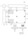
도 1은 본 발명의 일 실시예에 따른 표시 장치의 개략적인 구성도이다. 도 1을 참조하면, 본 발명의 일 실시예에 따른 표시 장치(100)는 타이밍 컨트롤러(TC), 게이트 구동부(GD), 데이터 구동부(DD), 복수의 배선(LL), 기판(110) 및 복수의 픽셀(PX)을 포함한다.1 is a schematic configuration diagram of a display device according to an embodiment of the present invention. Referring to FIG. 1, the
타이밍 컨트롤러(TC)는 외부로부터 입력된 영상 데이터를 정렬하여 데이터 구동부(DD)에 전달한다. 타이밍 컨트롤러(TC)는 외부로부터 입력되는 동기 신호들, 예를 들어 수직/수평 동기신호(Vsync, Hsync), 데이터 인에이블 신호(Data Enable), 도트 클락(DCLK) 등을 이용해 게이트 제어 신호 및 데이터 제어 신호를 출력할 수 있다. 그리고 타이밍 컨트롤러(TC)는 생성된 게이트 제어 신호 및 데이터 제어 신호를 각각 게이트 구동부(GD) 및 데이터 구동부(DD)에 전달하여, 게이트 구동부(GD) 및 데이터 구동부(DD)를 제어할 수 있다.The timing controller (TC) sorts image data input from the outside and transmits it to the data driver (DD). The timing controller (TC) controls gate control signals and data using external synchronization signals, such as vertical/horizontal synchronization signals (Vsync, Hsync), data enable signals (Data Enable), and dot clock (DCLK). Control signals can be output. Additionally, the timing controller TC may transmit the generated gate control signal and data control signal to the gate driver GD and the data driver DD, respectively, to control the gate driver GD and the data driver DD.
게이트 구동부(GD)는 타이밍 컨트롤러(TC)로부터 전달된 다수의 게이트 제어 신호에 따라 기판(110)의 복수의 픽셀(PX) 각각으로 스캔 전압을 전달한다.The gate driver (GD) transmits a scan voltage to each of the plurality of pixels (PX) of the
데이터 구동부(DD)는 타이밍 컨트롤러(TC)로부터 전달된 다수의 데이터 제어 신호에 따라 타이밍 컨트롤러(TC)로부터 전달된 영상 데이터를 데이터 전압으로 변환한다. 그리고 변환된 데이터 전압을 복수의 픽셀(PX) 각각으로 전달한다.The data driver DD converts image data transmitted from the timing controller TC into data voltage according to a plurality of data control signals transmitted from the timing controller TC. Then, the converted data voltage is transmitted to each of the plurality of pixels (PX).
데이터 구동부(DD) 및 게이트 구동부(GD)와 기판(110)에 각각 연결된 복수의 배선(LL)이 배치된다. 복수의 배선(LL)은 복수의 픽셀(PX)과 게이트 구동부(GD) 및 데이터 구동부(DD)를 전기적으로 연결할 수 있다.A plurality of wires LL connected to the data driver DD, the gate driver GD, and the
복수의 배선(LL)은 복수의 제1 배선(LL1) 및 복수의 제2 배선(LL2)을 포함한다. 복수의 제1 배선(LL1)은 게이트 구동부(GD)로부터의 전압을 전달받아 복수의 픽셀(PX) 각각으로 전달할 수 있다. 복수의 제2 배선(LL2)은 데이터 구동부(DD)로부터의 전압을 전달받아 복수의 픽셀(PX) 각각으로 전달할 수 있다. 예를 들어, 복수의 제1 배선(LL1)은 게이트 배선이고, 복수의 제2 배선(LL2)은 데이터 배선일 수도 있고, 복수의 제1 배선(LL1) 및 복수의 제2 배선(LL2)은 전원 배선 또는 공통 배선 등일 수도 있으며, 이에 제한되지 않는다.The plurality of wirings LL includes a plurality of first wirings LL1 and a plurality of second wirings LL2. The plurality of first wires LL1 may receive the voltage from the gate driver GD and transmit it to each of the plurality of pixels PX. The plurality of second wires LL2 may receive voltage from the data driver DD and transmit it to each of the plurality of pixels PX. For example, the plurality of first wires LL1 may be gate wires, the plurality of second wires LL2 may be data wires, and the plurality of first wires LL1 and the plurality of second wires LL2 may be power lines. It may be a wiring or a common wiring, but is not limited thereto.
한편, 게이트 구동부(GD) 및 데이터 구동부(DD)와 같은 구동 회로의 경우, 복수의 픽셀(PX)과 함께 기판(110) 상에 배치될 수도 있고, 기판(110)의 배면에 배치될 수도 있다. 이때, 게이트 구동부(GD) 및 데이터 구동부(DD)가 배치된 영역에는 복수의 픽셀(PX)의 발광 소자가 배치되기 어렵고, 실질적으로 영상이 표시되지 않는 영역일 수 있다. 기판(110)의 상면에 게이트 구동부(GD) 및 데이터 구동부(DD) 등을 배치하는 경우, 기판(110)의 상면에서 영상이 표시되지 않는 영역이 존재할 수 있다. 반면, 기판(110)의 배면에 게이트 구동부(GD) 및 데이터 구동부(DD) 등을 배치하는 경우, 기판(110)의 상면에서 영상이 표시되지 않는 영역을 최소화할 수 있다. 즉, 기판(110)의 상면에서 복수의 픽셀(PX)만이 배치되도록 할 수 있고, 실질적으로 베젤 영역이 존재하지 않는 제로 베젤을 구현할 수 있다. 이하에서는 게이트 구동부(GD) 및 데이터 구동부(DD)가 기판(110)의 배면에 배치된 것으로 가정하여 설명하기로 하나, 게이트 구동부(GD) 및 데이터 구동부(DD)의 배치는 다양하게 설계될 수 있으며, 이에 제한되지 않는다.Meanwhile, in the case of a driving circuit such as the gate driver (GD) and the data driver (DD), it may be disposed on the
기판(110)은 표시 장치(100)에 포함된 다양한 구성을 지지하기 위한 것으로, 절연 물질로 이루어질 수 있다. 예를 들어, 기판(110)은 유리 또는 폴리이미드 등과 같은 플라스틱 물질로 이루어질 수 있다.The
기판(110) 상에 복수의 픽셀(PX)이 정의될 수 있다. 그리고 복수의 픽셀(PX)은 제1 픽셀(PX1) 및 제2 픽셀(PX2)을 포함한다. 제1 픽셀(PX1)은 복수의 제1 서브 픽셀(SPX1)로 이루어질 수 있고, 제2 픽셀(PX2)은 복수의 제2 서브 픽셀(SPX2)로 이루어질 수 있다. 복수의 제1 서브 픽셀(SPX1) 및 복수의 제2 서브 픽셀(SPX2)은 화면을 구성하는 최소 단위로, 복수의 제1 서브 픽셀(SPX1)의 조합으로 제1 픽셀(PX1)에서 다양한 색상의 광을 발광할 수 있고, 복수의 제2 서브 픽셀(SPX2)의 조합으로 제2 픽셀(PX2)에서 다양한 색상의 광을 발광할 수 있다. 예를 들어, 복수의 제1 서브 픽셀(SPX1) 및 복수의 제2 서브 픽셀(SPX2) 각각은 적색 서브 픽셀, 녹색 서브 픽셀 및 청색 서브 픽셀로 이루어질 수 있으나, 이에 제한되지 않는다.A plurality of pixels (PX) may be defined on the
복수의 제1 서브 픽셀(SPX1) 및 복수의 제2 서브 픽셀(SPX2) 각각에는 발광 소자 및 발광 소자를 구동하기 위한 구동 회로 등이 배치될 수 있다. 발광 소자는 표시 장치(100)의 종류에 따라 상이하게 정의될 수 있다. 예를 들어, 표시 장치(100)가 유기 발광 표시 장치인 경우, 발광 소자는 애노드, 유기 발광층 및 캐소드를 포함하는 유기 발광 소자일 수 있고, 예를 들어, 표시 장치(100)가 무기 발광 표시 장치인 경우, 발광 소자는 n형 반도체층, p형 반도체층 및 발광층을 포함하는 LED(Light Emitting Diode) 또는 마이크로 LED(Micro LED)일 수 있다. 다만, 발광 소자는 다양하게 구성될 수 있으며, 이에 제한되지 않는다.A light-emitting element and a driving circuit for driving the light-emitting element may be disposed in each of the first plurality of subpixels SPX1 and the plurality of second subpixels SPX2. Light emitting elements may be defined differently depending on the type of
발광 소자를 구동하기 위한 구동 회로는 복수의 반도체 소자 및 스토리지 커패시터 등을 포함할 수 있다. 예를 들어, 구동 회로는 스위칭 박막 트랜지스터, 구동 박막 트랜지스터, 센싱 박막 트랜지스터, 스토리지 커패시터 등을 포함할 수 있으나, 이에 제한되지 않는다.A driving circuit for driving a light emitting device may include a plurality of semiconductor devices and a storage capacitor. For example, the driving circuit may include, but is not limited to, a switching thin film transistor, a driving thin film transistor, a sensing thin film transistor, a storage capacitor, etc.
한편, 상술한 바와 같이, 복수의 제1 픽셀(PX1) 및 복수의 제2 픽셀(PX2) 각각은 복수의 제1 서브 픽셀(SPX1) 및 복수의 제2 서브 픽셀(SPX2)의 조합으로 다양한 색상의 광을 발광할 수 있다. 이에, 제1 픽셀(PX1)의 경우, 제1 픽셀(PX1)을 이루는 복수의 제1 서브 픽셀(SPX1)은 적색 광을 발광하는 제1 적색 서브 픽셀(RSPX1), 녹색 광을 발광하는 제1 녹색 서브 픽셀(GSPX1), 청색 광을 발광하는 제1 청색 서브 픽셀(BSPX1)을 포함할 수 있다. 그리고 제2 픽셀(PX2)의 경우, 제2 픽셀(PX2)을 이루는 복수의 제2 서브 픽셀(SPX2)은 적색 광을 발광하는 제2 적색 서브 픽셀(RSPX2), 녹색 광을 발광하는 제2 녹색 서브 픽셀(GSPX2), 청색 광을 발광하는 제2 청색 서브 픽셀(BSPX2)을 포함할 수 있다. 이하에서는 설명의 편의를 위해 제1 픽셀(PX1)은 제1 적색 서브 픽셀(RSPX1), 제1 녹색 서브 픽셀(GSPX1) 및 제1 청색 서브 픽셀(BSPX1)로 이루어지고, 제2 픽셀(PX2)은 제2 적색 서브 픽셀(RSPX2), 제2 녹색 서브 픽셀(GSPX2) 및 제2 청색 서브 픽셀(BSPX2)로 이루어지는 것으로 가정하여 설명하기로 하나, 이에 제한되지 않는다.Meanwhile, as described above, each of the plurality of first pixels (PX1) and the plurality of second pixels (PX2) has various colors through a combination of the plurality of first subpixels (SPX1) and the plurality of second subpixels (SPX2). can emit light. Accordingly, in the case of the first pixel (PX1), the plurality of first subpixels (SPX1) forming the first pixel (PX1) include a first red subpixel (RSPX1) that emits red light, and a first red subpixel (RSPX1) that emits green light. It may include a green subpixel (GSPX1) and a first blue subpixel (BSPX1) that emits blue light. In the case of the second pixel PX2, the plurality of second subpixels SPX2 forming the second pixel PX2 include a second red subpixel RSPX2 emitting red light, and a second green subpixel RSPX2 emitting green light. It may include a subpixel (GSPX2) and a second blue subpixel (BSPX2) that emits blue light. Hereinafter, for convenience of explanation, the first pixel (PX1) includes a first red subpixel (RSPX1), a first green subpixel (GSPX1), and a first blue subpixel (BSPX1), and the second pixel (PX2) will be described assuming that it consists of a second red subpixel (RSPX2), a second green subpixel (GSPX2), and a second blue subpixel (BSPX2), but is not limited thereto.
한편, 복수의 제2 서브 픽셀(SPX2)과 비교하여 복수의 제1 서브 픽셀(SPX1) 각각에는 발광 소자 및 구동 회로 외에 압전 소자 및 수광 소자가 더 배치될 수 있다. 압전 소자 및 수광 소자는 복수의 제1 서브 픽셀(SPX1)의 복수의 발광 소자로부터 발광된 광의 휘도를 측정하도록 구성될 수 있다. 이에, 압전 소자 및 수광 소자가 더 배치된 복수의 제1 서브 픽셀(SPX1)은 하나의 표시 장치(100) 내에서 휘도 편차 및 색 편차를 측정 및 보상하기 위한 기준 픽셀로 기능할 수 있다.Meanwhile, compared to the plurality of second subpixels SPX2, each of the plurality of first subpixels SPX1 may be further disposed with a piezoelectric element and a light receiving element in addition to the light emitting element and the driving circuit. The piezoelectric element and the light receiving element may be configured to measure the luminance of light emitted from the plurality of light emitting elements of the plurality of first subpixels SPX1. Accordingly, the plurality of first subpixels SPX1, in which the piezoelectric element and the light receiving element are further disposed, may function as a reference pixel for measuring and compensating for luminance deviation and color deviation within one
이 경우, 복수의 제1 서브 픽셀(SPX1)로 이루어진 제1 픽셀(PX1)은 기판(110) 내에 다양한 위치에 배치될 수 있다. 예를 들어, 제1 픽셀(PX1)은 기판(110)의 중앙에 배치될 수도 있고, 기판(110)의 최외곽 픽셀(PX) 중 기판(110)의 네 모서리에 각각 배치될 수도 있다. 그리고 제1 픽셀(PX1)은 기판(110)의 최외곽 픽셀 중 적어도 하나일 수 있다. 예를 들어, 제1 픽셀(PX1)은 기판(110)의 최외곽 픽셀 중 기판(110)의 복수의 엣지 각각의 중앙에 배치된 최외곽 픽셀일 수 있다. 도 1에서는 기판(110) 상에 9개의 제1 픽셀(PX1)이 배치된 것으로 도시하였으나, 제1 픽셀(PX1)의 배치 및 개수는 달라질 수 있으며, 이에 제한되지 않는다.In this case, the first pixel PX1 comprised of a plurality of first subpixels SPX1 may be disposed at various positions within the
이하에서는 도 2a 내지 도 5d를 참조하여 제1 픽셀(PX1)과 제1 픽셀(PX1)을 이용한 휘도 편차 보상 방법에 대하여 보다 상세히 설명하기로 한다.Hereinafter, the first pixel PX1 and the luminance deviation compensation method using the first pixel PX1 will be described in more detail with reference to FIGS. 2A to 5D.
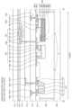
도 2a는 본 발명의 일 실시예에 따른 표시 장치의 하나의 제1 픽셀에 대한 평면도이다. 도 2b는 본 발명의 일 실시예에 따른 표시 장치의 하나의 제2 픽셀에 대한 평면도이다. 도 3은 도 2a의 Ⅲ-Ⅲ'에 따른 표시 장치의 단면도이다. 구체적으로, 도 2a는 제1 픽셀(PX1)의 제1 적색 서브 픽셀(RSPX1), 제1 녹색 서브 픽셀(GSPX1) 및 제1 청색 서브 픽셀(BSPX1) 각각에 대한 개략적인 평면도이다. 도 2b는 제2 픽셀(PX2)의 제2 적색 서브 픽셀(RSPX2), 제2 녹색 서브 픽셀(GSPX2) 및 제2 청색 서브 픽셀(BSPX2) 각각에 대한 개략적인 평면도이다. 도 3은 제1 적색 서브 픽셀(RSPX1), 제1 녹색 서브 픽셀(GSPX1) 및 제1 청색 서브 픽셀(BSPX1) 중 제1 적색 서브 픽셀(RSPX1)에 대한 단면도이다.FIG. 2A is a top view of one first pixel of a display device according to an embodiment of the present invention. FIG. 2B is a top view of one second pixel of a display device according to an embodiment of the present invention. FIG. 3 is a cross-sectional view of the display device taken along line III-III' of FIG. 2A. Specifically, FIG. 2A is a schematic plan view of each of the first red subpixel (RSPX1), first green subpixel (GSPX1), and first blue subpixel (BSPX1) of the first pixel (PX1). FIG. 2B is a schematic plan view of each of the second red subpixel (RSPX2), the second green subpixel (GSPX2), and the second blue subpixel (BSPX2) of the second pixel (PX2). FIG. 3 is a cross-sectional view of the first red subpixel (RSPX1) among the first red subpixel (RSPX1), the first green subpixel (GSPX1), and the first blue subpixel (BSPX1).
도 2a 내지 도 3을 참조하면, 본 발명의 일 실시예에 따른 표시 장치(100)는 기판(110), 복수의 반도체 소자(120), 게이트 절연층(111), 패시베이션층(112), 제1 절연층(113), 제2 절연층(114), 제3 절연층(115), 복수의 패드 전극(PE), 복수의 발광 소자(130, 140, 150), 압전 소자(160), 수광 소자(170), 복수의 배선(LL), 복수의 추가 배선(LLA), 접착층(180) 및 보호 필름(190)을 포함한다.2A to 3, the
도 2a 및 도 2b를 참조하면, 기판(110) 상에 복수의 발광 소자(130, 140, 150)가 배치된다. 구체적으로, 복수의 발광 소자(130, 140, 150) 각각은 제1 픽셀(PX1)의 복수의 제1 서브 픽셀(SPX1) 및 제2 픽셀(PX2)의 복수의 제2 서브 픽셀(SPX2) 각각에 배치된다. 복수의 발광 소자(130, 140, 150)는 전압이 인가될 시, 빛을 발광하는 발광 소자이다. 복수의 발광 소자(130, 140, 150)에는 적색 광, 녹색 광, 청색 광 등을 발광하는 발광 소자들이 있고, 이들의 조합으로 백색을 포함하는 다양한 색상의 광을 구현할 수 있다.Referring to FIGS. 2A and 2B , a plurality of light emitting
만약, 복수의 발광 소자(130, 140, 150) 각각이 서로 다른 색상의 광을 발광하는 경우, 제1 적색 서브 픽셀(RSPX1) 및 제2 적색 서브 픽셀(RSPX2)에 배치된 발광 소자는 적색 광을 발광하는 적색 발광 소자(130)일 수 있고, 제1 녹색 서브 픽셀(GSPX1) 및 제2 녹색 서브 픽셀(GSPX2)에 배치된 발광 소자는 녹색 광을 발광하는 녹색 발광 소자(140)일 수 있고, 제1 청색 서브 픽셀(BSPX1) 및 제2 청색 서브 픽셀(BSPX2)에 배치된 발광 소자는 청색 광을 발광하는 청색 발광 소자(150)일 수 있다.If each of the plurality of light emitting
반면, 복수의 발광 소자(130, 140, 150) 각각이 동일한 색상의 광을 발광하는 경우, 복수의 발광 소자(130, 140, 150) 각각의 상부에 광 변환층이나 컬러 필터 등과 같은 광 변환 부재를 사용하여 복수의 발광 소자(130, 140, 150)에서 발광된 광을 다양한 색상으로 변환할 수 있다. 이하에서는 복수의 발광 소자(130, 140, 150) 각각이 서로 다른 색상의 광을 발광하는 것으로 가정하여 설명하기로 하나, 이에 제한되지 않는다.On the other hand, when each of the plurality of light-emitting
복수의 픽셀(PX) 각각에 복수의 배선(LL)이 배치된다. 복수의 배선(LL)은 제1 픽셀(PX1)의 복수의 제1 서브 픽셀(SPX1) 각각과 제2 픽셀(PX2)의 복수의 제2 서브 픽셀(SPX2) 각각에 전기적으로 연결될 수 있다. 복수의 배선(LL)은 게이트 구동부(GD) 및 데이터 구동부(DD)로부터의 전압을 복수의 제1 서브 픽셀(SPX1) 및 복수의 제2 서브 픽셀(SPX2) 각각의 발광 소자(130, 140, 150) 및 반도체 소자(120)를 포함하는 구동 회로로 전달하여 복수의 제1 서브 픽셀(SPX1) 및 복수의 제2 서브 픽셀(SPX2)을 구동시킬 수 있다.A plurality of wires LL are disposed in each of the plurality of pixels PX. The plurality of lines LL may be electrically connected to each of the plurality of first subpixels SPX1 of the first pixel PX1 and each of the plurality of second subpixels SPX2 of the second pixel PX2. The plurality of lines LL transmit voltages from the gate driver GD and the data driver DD to the
한편, 도 2a를 참조하면, 복수의 픽셀(PX) 중 제1 픽셀(PX1)에만 복수의 추가 배선(LLA)이 더 배치된다. 복수의 추가 배선(LLA)은 제1 픽셀(PX1)의 복수의 제1 서브 픽셀(SPX1) 각각의 압전 소자(160) 및 수광 소자(170)에 전기적으로 연결될 수 있다. 도면에 도시되지는 않았으나, 복수의 추가 배선(LLA)은 게이트 구동부(GD) 및/또는 데이터 구동부(DD) 측으로 연장되어 게이트 구동부(GD) 및/또는 데이터 구동부(DD)로부터 전압을 압전 소자(160) 및 수광 소자(170)로 전달할 수 있다.Meanwhile, referring to FIG. 2A , a plurality of additional lines LLA are further disposed only in the first pixel PX1 among the plurality of pixels PX. The plurality of additional wires LLA may be electrically connected to the
복수의 추가 배선(LLA)은 제1 추가 배선(LLA1), 제2 추가 배선(LLA2), 제3 추가 배선(LLA3) 및 제4 추가 배선(LLA4)을 포함한다.The plurality of additional wiring lines LLA includes a first additional wiring LLA1, a second additional wiring LLA2, a third additional wiring LLA3, and a fourth additional wiring LLA4.
복수의 추가 배선(LLA) 중 제1 추가 배선(LLA1) 및 제2 추가 배선(LLA2)은 압전 소자(160)에 전기적으로 연결될 수 있다. 제1 추가 배선(LLA1) 및 제2 추가 배선(LLA2)은 게이트 구동부(GD) 및/또는 데이터 구동부(DD) 등으로부터 전압을 압전 소자(160)로 전달할 수도 있고, 별도의 구동 IC 등으로부터 전압을 압전 소자(160)로 전달할 수 있으며, 이에 제한되지 않는다.Among the plurality of additional wiring lines LLA, the first additional wiring LLA1 and the second additional wiring LLA2 may be electrically connected to the
복수의 추가 배선(LLA) 중 제3 추가 배선(LLA3) 및 제4 추가 배선(LLA4)은 수광 소자(170)에 전기적으로 연결될 수 있다. 제3 추가 배선(LLA3) 및 제4 추가 배선(LLA4)은 게이트 구동부(GD) 및/또는 데이터 구동부(DD) 등으로부터의 역 바이어스 전압을 수광 소자(170)에 전달할 수도 있고, 별도의 구동 IC 등으로부터 전압을 압전 소자(160)로 전달할 수 있으며, 이에 제한되지 않는다. 또한, 제3 추가 배선(LLA3) 및 제4 추가 배선(LLA4)은 수광 소자(170)로부터의 광 전류를 데이터 구동부(DD) 또는 별도의 구동 IC 등으로 전달할 수도 있다.Among the plurality of additional wiring lines LLA, the third additional wiring LLA3 and the fourth additional wiring LLA4 may be electrically connected to the
복수의 제1 서브 픽셀(SPX1) 각각에 반사부(167)를 구비하는 압전 소자(160)가 배치된다. 압전 소자(160)는 복수의 제1 서브 픽셀(SPX1) 각각의 일 측에 배치된다. 압전 소자(160)는 제1 추가 배선(LLA1) 및 제2 추가 배선(LLA2)으로부터의 제공받은 전압을 기계적 에너지로 변환시키는 소자이다. 즉, 압전 소자(160)는 전기 에너지에 의해 기계적인 변위를 일으키는 소자로, 예를 들어 압전 소자(160)는 제1 추가 배선(LLA1) 및 제2 추가 배선(LLA2)의 전압에 의해 형상이 변형될 수 있다. 예를 들어, 압전 소자(160)는 압전 재료로 이루어진 압전 액추에이터일 수 있고, 유니모프 액추에이터(Unimorph actuator), 바이모프 액추에이터(Bimorph actuator), 적층형 액추에이터(Multimorph actuator) 등일 수 있다. 이하에서는, 압전 소자(160)가 바이모프 액추에이터인 것으로 가정하여 설명하기로 하나, 압전 소자(160)의 종류는 이에 제한되지 않는다.A
한편, 압전 소자(160)는 제1 추가 배선(LLA1) 및 제2 추가 배선(LLA2)으로부터 전압이 인가됨에 의해 벤딩될 수 있다. 예를 들어, 압전 소자(160)는 타단의 지지부(161)가 고정된 상태에서 일단이 상측으로 벤딩될 수 있고, 이로 인해 일단의 반사부(167)가 이동할 수 있다. 압전 소자(160)에 전압이 인가됨에 따른 압전 소자(160)의 변형 및 반사부(167)의 기능에 대하여 도 5a 내지 도 5d를 참조하여 상세히 후술하기로 한다.Meanwhile, the
복수의 제1 서브 픽셀(SPX1) 각각에 수광 소자(170)가 배치된다. 수광 소자(170)는 복수의 제1 서브 픽셀(SPX1) 각각의 타 측에 배치된다. 즉, 수광 소자(170)는 제1 픽셀(PX1)의 복수의 발광 소자(130, 140, 150)를 사이에 두고 압전 소자(160)와 반대편에 배치될 수 있다.A
수광 소자(170)는 제3 추가 배선(LLA3) 및 제4 추가 배선(LLA4)으로부터의 역 바이어스 전압이 인가된 상태에서, 광 에너지를 전기 에너지로 변환하는 소자이다. 수광 소자(170)는 광을 흡수하여 전기 에너지, 즉, 광 전류로 변환할 수 있고, 수광 소자(170)에서 발생된 광 전류 값을 측정하여 복수의 발광 소자(130, 140, 150)로부터 광의 휘도를 측정할 수 있다. 수광 소자(170)는 예를 들어, PIN 포토 다이오드(PIN Photo Diode), Avalanch 포토 다이오드 등일 수 있다. 이하에서는, 수광 소자(170)가 PIN 포토 다이오드인 것으로 가정하여 설명하기로 하나, 이에 제한되지 않는다.The
이하에서는 도 3을 함께 참조하여, 제1 픽셀(PX1)의 복수의 제1 서브 픽셀(SPX1) 중 제1 적색 서브 픽셀(RSPX1)에 대해 보다 상세히 설명하기로 한다.Hereinafter, with reference to FIG. 3 , the first red subpixel (RSPX1) among the plurality of first subpixels (SPX1) of the first pixel (PX1) will be described in more detail.
도 3을 참조하면, 기판(110) 상에 반도체 소자(120)가 배치된다. 반도체 소자(120)는 복수의 픽셀(PX) 각각에 배치된 복수의 발광 소자(130, 140, 150)를 구동하기 위한 구동 회로에 포함되는 구성이다. 즉, 반도체 소자(120)는 표시 장치(100)의 구동 소자로 사용될 수 있다. 반도체 소자(120)는 복수의 배선(LL) 중 제1 배선(LL1) 또는 제2 배선(LL2) 중 어느 하나와 전기적으로 연결되어 게이트 구동부(GD) 또는 데이터 구동부(DD)로부터의 전압을 전달받을 수 있다.Referring to FIG. 3, a
반도체 소자(120)는 예를 들어, 박막 트랜지스터(Thin Film Transistor; TFT), N형 금속 산화막 반도체(N-channel Metal Oxide Semiconductor; NMOS), P형 금속 산화막 반도체(P-channel Metal Oxide Semiconductor; PMOS), 상보성 금속 산화막 반도체(Complementary Metal Oxide Semiconductor; CMOS), 전계 효과 트랜지스터(Field Effect Transistor; FET) 등일 수 있으나, 이에 제한되지 않는다. 이하에서는, 반도체 소자(120)가 박막 트랜지스터인 것으로 가정하여 설명하기로 하나, 이에 제한되지 않는다.The
반도체 소자(120)는 게이트 전극(121), 액티브층(122), 소스 전극(123) 및 드레인 전극(124)을 포함한다.The
기판(110) 상에 게이트 전극(121)이 배치된다. 게이트 전극(121)은 도전성 물질, 예를 들어, 구리(Cu), 알루미늄(Al), 몰리브덴(Mo), 티타늄(Ti), 또는 이들의 합금으로 구성될 수 있으나, 이에 제한되지 않는다.A
게이트 전극(121) 상에 게이트 절연층(111)이 배치된다. 게이트 절연층(111)은 게이트 전극(121)과 액티브층(122)을 절연시키기 위한 층으로, 절연 물질로 이루어질 수 있다. 예를 들어, 게이트 절연층(111)은 실리콘 산화물(SiOx) 또는 실리콘 질화물(SiNx)의 단일층 또는 복층으로 구성될 수 있으나, 이에 제한되지 않는다.A
게이트 절연층(111) 상에 액티브층(122)이 배치된다. 예를 들어, 액티브층(122)은 산화물 반도체, 비정질 실리콘(a-Si) 또는 폴리 실리콘(Poly-Si) 등으로 이루어질 수 있으나, 이에 제한되지 않는다.The
액티브층(122) 상에 소스 전극(123) 및 드레인 전극(124)이 서로 이격되어 배치된다. 소스 전극(123) 및 드레인 전극(124)은 액티브층(122)과 전기적으로 연결될 수 있다. 소스 전극(123) 및 드레인 전극(124)은 도전성 물질, 예를 들어, 구리(Cu), 알루미늄(Al), 몰리브덴(Mo), 티타늄(Ti), 또는 이들의 합금으로 구성될 수 있으나, 이에 제한되는 것은 아니다.The
반도체 소자(120) 상에 패시베이션층(112)이 배치된다. 패시베이션층(112)은 패시베이션층(112) 하부의 구성을 보호하기 위한 절연층이다. 예를 들어, 패시베이션층(112)은 실리콘 산화물(SiOx) 또는 실리콘 질화물(SiNx)의 단일층 또는 복층으로 구성될 수 있으나, 이에 제한되지 않는다.A
패시베이션층(112) 상에 제1 절연층(113)이 배치되고, 제1 절연층(113) 상에 제3 추가 배선(LLA3)이 배치된다. 제1 절연층(113)은 복수의 반도체 소자(120)를 포함하는 기판(110)의 상부를 보호하기 위한 절연층이다. 예를 들어, 제1 절연층(113)은 아크릴(acryl)계 등의 유기물이거나, 실리콘 산화물(SiOx) 또는 실리콘 질화물(SiNx) 등의 무기물의 단일층 또는 복층으로 구성될 수 있으나, 이에 제한되지 않는다. 또한, 도 3에서는 제1 절연층(113)의 상면이 평탄한 것으로 도시하였으나, 제1 절연층(113)의 상면은 패시베이션층(112)과 같이 반도체 소자(120)의 형상을 따라 배치될 수도 있으며, 이에 제한되지 않는다.The first insulating
제1 절연층(113) 및 제3 추가 배선(LLA3) 상에 제2 절연층(114)이 배치되고, 제2 절연층(114) 상에 제1 추가 배선(LLA1) 및 제4 추가 배선(LLA4)이 배치된다. 제2 절연층(114)은 제3 추가 배선(LLA3) 및 복수의 반도체 소자(120)를 포함하는 기판(110)의 상부를 보호하기 위한 절연층이다. 또한, 제2 절연층(114)은 제2 절연층(114) 하부의 제3 추가 배선(LLA3)과, 제2 절연층(114) 상부의 제1 추가 배선(LLA1) 및 제4 추가 배선(LLA4)의 전기적인 쇼트를 최소화할 수 있다. 예를 들어, 제2 절연층(114)은 아크릴(acryl)계 등의 유기물이거나, 실리콘 산화물(SiOx) 또는 실리콘 질화물(SiNx) 등의 무기물의 단일층 또는 복층으로 구성될 수 있으나, 이에 제한되지 않는다. 또한, 도 3에서는 제2 절연층(114)의 상면이 평탄한 것으로 도시하였으나, 제2 절연층(114)의 상면은 제2 절연층(114) 하부의 제3 추가 배선(LLA3) 및 제1 절연층(113)의 형상을 따라 배치될 수도 있으며, 이에 제한되지 않는다.A second insulating
제1 추가 배선(LLA1), 제4 추가 배선(LLA4) 및 제2 절연층(114) 상에 제3 절연층(115)이 배치된다. 제3 절연층(115)은 제1 추가 배선(LLA1), 제4 추가 배선(LLA4), 제3 추가 배선(LLA3) 및 반도체 소자(120)를 포함하는 기판(110)의 상부를 보호하기 위한 절연층이다. 또한, 제3 절연층(115)은 제3 절연층(115) 하부의 제1 추가 배선(LLA1) 및 제4 추가 배선(LLA4)과, 제3 절연층(115) 상부의 제2 추가 배선(LLA2) 및 복수의 패드 전극(PE) 간의 전기적인 쇼트를 최소화할 수 있다. 예를 들어, 제3 절연층(115)은 아크릴(acryl)계 등의 유기물이거나, 실리콘 산화물(SiOx) 또는 실리콘 질화물(SiNx) 등의 무기물의 단일층 또는 복층으로 구성될 수 있으나, 이에 제한되지 않는다. 또한, 도 3에서는 제3 절연층(115)의 상면이 평탄한 것으로 도시하였으나, 제3 절연층(115)의 상면은 제3 절연층(115) 하부의 제1 추가 배선(LLA1), 제4 추가 배선(LLA4) 및 제2 절연층(114)의 형상을 따라 배치될 수도 있으며, 이에 제한되지 않는다.A third insulating
한편, 도 3에서는 제1 절연층(113) 상에 제3 추가 배선(LLA3)이 배치되고, 제3 추가 배선(LLA3) 상에 제1 추가 배선(LLA1) 및 제4 추가 배선(LLA4)이 배치되고, 제1 추가 배선(LLA1) 및 제4 추가 배선(LLA4) 상에 제2 추가 배선(LLA2)이 배치된 것으로 도시하였으나, 복수의 추가 배선(LLA) 각각의 적층 순서는 달라질 수 있으며, 이에 제한되지 않는다.Meanwhile, in FIG. 3 , the third additional wiring LLA3 is disposed on the first insulating
제3 절연층(115) 상에 복수의 패드 전극(PE)이 배치된다. 복수의 패드 전극(PE)은 복수의 추가 배선(LLA)과 반도체 소자(120)를 압전 소자(160), 적색 발광 소자(130) 및 수광 소자(170) 각각에 전기적으로 연결시키기 위한 전극이다. 복수의 패드 전극(PE)은 제1 패드 전극(PE1), 제2 패드 전극(PE2), 제3 패드 전극(PE3), 제4 패드 전극(PE4), 제5 패드 전극(PE5) 및 제6 패드 전극(PE6)을 포함한다.A plurality of pad electrodes (PE) are disposed on the third insulating
제1 패드 전극(PE1) 및 제2 패드 전극(PE2) 각각은 복수의 추가 배선(LLA)과 압전 소자(160)를 전기적으로 연결시키기 위한 전극이다. 제1 패드 전극(PE1)은 제1 추가 배선(LLA1)과 압전 소자(160)를 전기적으로 연결시킬 수 있고, 제2 패드 전극(PE2)은 제2 추가 배선(LLA2)과 압전 소자(160)를 전기적으로 연결시킬 수 있다. 구체적으로, 제3 절연층(115)에 제1 추가 배선(LLA1)을 노출시키는 컨택홀이 배치될 수 있고, 제1 패드 전극(PE1)은 제3 절연층(115)의 컨택홀을 통해 제1 추가 배선(LLA1)과 압전 소자(160)를 전기적으로 연결시킬 수 있다. 그리고 제2 패드 전극(PE2)은 제3 절연층(115) 상에 배치된 제2 추가 배선(LLA2)으로부터 연장되어 배치되고, 제2 패드 전극(PE2)은 제2 추가 배선(LLA2)과 압전 소자(160)를 전기적으로 연결시킬 수 있다. 즉, 제2 패드 전극(PE2)은 제2 추가 배선(LLA2)과 일체로 이루어질 수 있으나, 이에 제한되지 않는다.Each of the first pad electrode PE1 and the second pad electrode PE2 is an electrode for electrically connecting the plurality of additional wiring lines LLA and the
제3 패드 전극(PE3) 및 제4 패드 전극(PE4) 각각은 복수의 배선(LL) 및 복수의 서브 픽셀(PX) 각각의 구동 회로와 적색 발광 소자(130)를 전기적으로 연결시키기 위한 전극이다. 예를 들어, 제3 패드 전극(PE3)은 구동 회로의 반도체 소자(120)와 적색 발광 소자(130)를 전기적으로 연결시킬 수 있고, 제4 패드 전극(PE4)은 복수의 배선(LL)과 적색 발광 소자(130)를 전기적으로 연결시킬 수 있다. 구체적으로, 제1 절연층(113), 제2 절연층(114) 및 제3 절연층(115)에 반도체 소자(120)의 드레인 전극(124)을 노출시키는 컨택홀이 배치될 수 있고, 제3 패드 전극(PE3)은 컨택홀을 통해 반도체 소자(120)의 드레인 전극(124)과 적색 발광 소자(130)를 전기적으로 연결시킬 수 있다. 그리고 제4 패드 전극(PE4)은 제3 절연층(115) 상에 배치된 복수의 배선(LL)의 제1 배선(LL1) 또는 제2 배선(LL2) 중 어느 하나로부터 연장되어 배치되고, 제4 패드 전극(PE4)은 제1 배선(LL1) 또는 제2 배선(LL2) 중 어느 하나와 적색 발광 소자(130)를 전기적으로 연결시킬 수 있다.Each of the third pad electrode (PE3) and the fourth pad electrode (PE4) is an electrode for electrically connecting the driving circuit of each of the plurality of lines (LL) and the plurality of subpixels (PX) and the red light-emitting
제5 패드 전극(PE5) 및 제6 패드 전극(PE6) 각각은 복수의 추가 배선(LLA)과 수광 소자(170)를 전기적으로 연결시키기 위한 전극이다. 제5 패드 전극(PE5)은 제3 추가 배선(LLA3)과 수광 소자(170)를 전기적으로 연결시킬 수 있고, 제6 패드 전극(PE6)은 제4 추가 배선(LLA4)과 수광 소자(170)를 전기적으로 연결시킬 수 있다. 구체적으로, 제2 절연층(114) 및 제3 절연층(115)에 제3 추가 배선(LLA3)을 노출시키는 컨택홀이 배치될 수 있고, 제5 패드 전극(PE5)은 컨택홀을 통해 제3 추가 배선(LLA3)과 수광 소자(170)를 전기적으로 연결시킬 수 있다. 그리고 제3 절연층(115)에 제4 추가 배선(LLA4)을 노출시키는 컨택홀이 배치될 수 있고, 제6 패드 전극(PE6)은 컨택홀을 통해 제4 추가 배선(LLA4)과 수광 소자(170)를 전기적으로 연결시킬 수 있다.Each of the fifth pad electrode PE5 and the sixth pad electrode PE6 is an electrode for electrically connecting the plurality of additional wiring lines LLA and the
복수의 패드 전극(PE) 및 제3 절연층(115) 상에 뱅크(116)가 배치된다. 뱅크(116)는 서로 인접한 복수의 제1 서브 픽셀(SPX1) 및 복수의 제2 서브 픽셀(SPX2) 각각을 구분하기 위한 절연층이다. 또한, 뱅크(116)는 복수의 제1 서브 픽셀(SPX1)에서, 적색 발광 소자(130), 압전 소자(160) 및 수광 소자(170) 각각을 구분하기 위한 절연층일 수 있다. 뱅크(116)는 복수의 패드 전극(PE) 각각의 일부를 개구시키도록 배치될 수 있고, 뱅크(116)는 복수의 패드 전극(PE) 각각의 엣지를 덮도록 배치된 유기 절연 물질일 수 있다.The
뱅크(116)로부터 노출된 제1 패드 전극(PE1) 및 제2 패드 전극(PE2) 상에 압전 소자(160)가 배치된다. 압전 소자(160)는 상술한 바와 같이, 전기적 에너지에 의해 기계적인 변위를 일으키는 소자이다. 압전 소자(160)는 제1 추가 배선(LLA1) 및 제2 추가 배선(LLA2)으로부터 제공받은 전압에 의해 형상이 변형될 수 있고, 예를 들어, 압전 소자(160)에 전압이 인가되어, 압전 소자(160)가 온(on) 되는 경우, 압전 소자(160)의 일단이 기판(110)의 상측을 향하도록 벤딩될 수 있다.The
압전 소자(160)는 제1 컨택 전극(168), 제2 컨택 전극(169), 지지부(161), 제1 전극(162), 제1 압전층(163), 제2 전극(164), 제2 압전층(165), 제3 전극(166) 및 반사부(167)를 포함한다.The
제1 컨택 전극(168) 및 제2 컨택 전극(169) 각각은 제1 패드 전극(PE1) 및 제2 패드 전극(PE2)과 전기적으로 연결된다. 제1 컨택 전극(168)은 제1 패드 전극(PE1)을 통해 제1 추가 배선(LLA1)으로부터 전압을 전달받을 수 있고, 제2 컨택 전극(169)은 제2 패드 전극(PE2)을 통해 제2 추가 배선(LLA2)으로부터 전압을 전달받을 수 있다.Each of the
제1 컨택 전극(168) 및 제2 컨택 전극(169) 상에 지지부(161)가 배치된다. 지지부(161)는 제1 전극(162), 제1 압전층(163), 제2 전극(164), 제2 압전층(165) 및 제3 전극(166)의 타단을 지지할 수 있다. 지지부(161)는 예를 들어, 실리콘(Si) 등과 같은 절연 물질로 이루어진 베이스 기판 상에 제1 전극(162), 제1 압전층(163), 제2 전극(164), 제2 압전층(165) 및 제3 전극(166)을 형성한 후, 베이스 기판을 지지부(161)의 형상으로 식각하여 형성될 수 있다. 제1 전극(162), 제1 압전층(163), 제2 전극(164), 제2 압전층(165) 및 제3 전극(166)의 타단을 지지하는 지지부(161)가 배치됨에 따라 압전 소자(160)는 외팔보(Cantilever)의 형태로 이루어질 수 있다.A
지지부(161) 상에 제1 전극(162), 제1 압전층(163), 제2 전극(164), 제2 압전층(165) 및 제3 전극(166)이 순차적으로 배치된다. 제1 압전층(163)은 제1 전극(162) 및 제2 전극(164)의 전압에 의해 수축 또는 팽창할 수 있고, 제2 압전층(165)은 제2 전극(164) 및 제3 전극(166)의 전압에 의해 수축 또는 팽창할 수 있다. 제1 압전층(163) 및 제2 압전층(165)은 예를 들어, 수정, 티탄산 바륨(BaTiO3), 티탄산연(PbTiO3), 압전 세라믹(PZT) 등의 압전 현상을 나타내는 물질로 이루어질 수 있다.A
그리고 제1 압전층(163) 및 제2 압전층(165)은 서로 다른 분극 방향을 가질 수 있다. 예를 들어, 제1 압전층(163)은 상부 영역 또는 하부 영역에 전자가 모이고, 하부 영역 또는 상부 영역에 정공이 모이는 분극이 형성될 수 있고, 이와 반대로 제2 압전층(165)은 하부 영역 또는 상부 영역에 정공이 모이고, 상부 영역 또는 하부 영역에 전자가 모이는 분극이 형성될 수 있다.And the first
제1 전극(162) 및 제3 전극(166)에는 동일한 전압이 인가되고, 제2 전극(164)에는 제1 전극(162) 및 제3 전극(166)과 서로 상이한 전압이 인가될 수 있다. 예를 들어, 제1 전극(162) 및 제3 전극(166)은 제1 패드 전극(PE1) 또는 제2 패드 전극(PE2) 중 어느 하나와 연결되고, 제2 전극(164)은 나머지 하나와 연결될 수 있다.The same voltage may be applied to the
제1 압전층(163) 및 제2 압전층(165)에 분극 방향과 동일한 방향의 전압이 인가되면, 제1 압전층(163) 및 제2 압전층(165)은 수축할 수 있고, 제1 압전층(163) 및 제2 압전층(165) 각각에 분극 방향과 반대 방향의 전압이 인가되면, 제1 압전층(163) 및 제2 압전층(165)은 팽창할 수 있다.When a voltage in the same direction as the polarization direction is applied to the first
그리고 압전 소자(160)에 전압을 인가하는 경우, 제1 압전층(163) 또는 제2 압전층(165) 중 어느 하나가 수축하고, 나머지 하나가 팽창할 수 있고, 제1 압전층(163) 및 제2 압전층(165)은 일 방향으로 휘어질 수 있다. 이하에서는 압전 소자(160)에 전압을 인가하여 압전 소자(160)가 온 되는 경우, 지지부(161)가 배치되지 않은 제1 전극(162), 제1 압전층(163), 제2 전극(164), 제2 압전층(165) 및 제3 전극(166)의 일단이 기판(110)의 상측을 향해 벤딩되는 것으로 가정하여 설명하기로 한다.And when voltage is applied to the
제1 전극(162)의 하면에 반사부(167)가 배치된다. 반사부(167)는 제1 전극(162)의 하면에서 제1 전극(162)의 일단에 배치될 수 있다. 압전 소자(160)가 온 된 경우, 반사부(167)는 복수의 제1 서브 픽셀(SPX1) 각각의 발광 소자(130, 140, 150)로부터 발광된 광을 수광 소자(170) 측으로 반사시킬 수 있다. 반사부(167)는 반사 물질로 이루어질 수 있고, 예를 들어, 알루미늄(Al) 또는 은(Ag)과 같은 반사성이 높은 물질로 이루어질 수 있다.A
한편, 도 2a에서는 반사부(167)가 제1 전극(162)의 폭보다 더 큰 폭을 가지고, 제1 전극(162)의 일단의 외측으로 돌출되지 않은 것으로 도시하였으나, 반사부(167)는 제1 전극(162)의 폭과 동일하거나 더 작은 폭을 가질 수도 있고, 제1 전극(162)의 일단의 외측으로 돌출될 수도 있으며, 이에 제한되지 않는다. 또한, 도 2a 내지 도 3에서는 반사부(167)가 평평한 직사각형 플레이트 형상인 것으로 도시하였으나, 반사부(167)는 오목 또는 볼록한 표면을 가질 수도 있으며, 반사부(167)의 형상 및 크기는 이에 제한되지 않는다.Meanwhile, in FIG. 2A, the
뱅크(116)로부터 노출된 제3 패드 전극(PE3) 및 제4 패드 전극(PE4) 상에 적색 발광 소자(130)가 배치된다. 적색 발광 소자(130)는 압전 소자(160)와 동일 평면 상에 배치될 수 있다. 적색 발광 소자(130)는 복수의 배선(LL) 및 반도체 소자(120)로부터의 전압에 의해 광을 발광할 수 있다. 이하에서는 적색 발광 소자(130)를 포함하는 복수의 발광 소자(130, 140, 150)가 LED 또는 마이크로 LED인 것으로 가정하여 설명하기로 하나, 복수의 발광 소자(130, 140, 150)는 표시 장치(100)의 종류에 따라 달라질 수 있으며, 이에 제한되지 않는다.The red
한편, 복수의 발광 소자(130, 140, 150)가 LED인 경우, 수평형(lateral), 수직형(vertical), 플립칩(flip chip) 등 다양한 구조로 형성될 수 있다. 수평형 구조의 LED는 발광층과 발광층의 양측에서 수평으로 배치된 N형 전극 및 P형 전극을 포함한다. 수평형 구조의 LED는 N형 전극을 통해 발광층으로 전달된 전자와, P형 전극을 통해 발광층으로 전달된 정공이 결합하여 광을 발광할 수 있다. 수직형 구조의 LED는 발광층, 발광층 상하에 배치된 N형 전극 및 P형 전극을 포함한다. 수직형 LED 또한 수평형 LED와 마찬가지로, 전극으로부터 전달된 전자 및 정공의 결합으로 광을 발광할 수 있다. 플립칩 LED는 수평형 LED와 실질적으로 동일한 구조이다. 다만, 플립칩 구조의 LED는 금속 와이어와 같은 매개체를 생략하고, 직접 인쇄회로기판 등에 부착될 수 있다. 이하에서는 설명의 편의를 위해, 복수의 발광 소자(130, 140, 150)가 플립칩 구조인 것으로 가정하여 설명하기로 하나, 이에 제한되지 않는다.Meanwhile, when the plurality of light emitting
도 3을 참조하면, 적색 발광 소자(130)는 제3 컨택 전극(134), 제4 컨택 전극(135), 제1 반도체층(131), 발광층(132) 및 제2 반도체층(133)을 포함한다.Referring to FIG. 3, the red
제3 컨택 전극(134) 및 제4 컨택 전극(135) 각각은 제3 패드 전극(PE3) 및 제4 패드 전극(PE4)과 전기적으로 연결된다. 제3 컨택 전극(134)은 제3 패드 전극(PE3)을 통해 전달된 반도체 소자(120)의 드레인 전극(124)으로부터 전압을 제1 반도체층(131)으로 전달할 수 있고, 제4 컨택 전극(135)은 제4 패드 전극(PE4)을 통해 전달된 전압을 제2 반도체층(133)으로 전달할 수 있다.Each of the
제3 컨택 전극(134) 상에 제1 반도체층(131)이 배치되고, 제1 반도체층(131) 상에 제2 반도체층(133)이 배치된다. 제1 반도체층(131) 및 제2 반도체층(133)은 질화갈륨(GaN)에 N형 또는 P형의 불순물을 주입하여 형성된 층일 수 있다. 예를 들어, 제1 반도체층(131)이 질화갈륨에 P형의 불순물을 주입하여 형성된 P형 반도체층이고, 제2 반도체층(133)이 질화갈륨에 N형의 불순물을 주입하여 형성된 N형 반도체층일 수 있으나, 이에 제한되지 않는다. 그리고 P형의 불순물은 마그네슘(Mg), 아연(Zn), 베릴륨(Be) 등일 수 있고, N형의 불순물은 실리콘(Si), 게르마늄(Ge), 주석(Sn) 등일 수 있으나, 이에 제한되지 않는다.A
제1 반도체층(131)과 제2 반도체층(133) 사이에 발광층(132)이 배치된다. 발광층(132)은 제1 반도체층(131) 및 제2 반도체층(133)으로부터 정공 및 전자를 전달받아 빛을 발광할 수 있다. 발광층(132)은 단층 또는 양자우물(Multi-Quantum Well; MQW)구조로 이루어질 수 있다. 예를 들어, 발광층(132)은 인듐 갈륨 질화물(InGaN) 또는 질화갈륨(GaN) 등으로 이루어질 수 있으며, 이에 제한되지 않는다.A
이때, 복수의 제1 서브 픽셀(SPX1) 중 제1 적색 서브 픽셀(RSPX1)과 복수의 제2 서브 픽셀(SPX2) 중 제2 적색 서브 픽셀(RSPX2)에 배치된 적색 발광 소자(130)의 발광층(132)으로부터 적색 광이 방출될 수 있다. 그리고 제1 녹색 서브 픽셀(GSPX1) 및 제2 녹색 서브 픽셀(GSPX2)에 배치된 녹색 발광 소자(140)의 발광층(132)으로부터 녹색 광이 방출될 수 있고, 제1 청색 서브 픽셀(BSPX1) 및 제2 청색 서브 픽셀(BSPX2)에 배치된 청색 발광 소자(150)의 발광층(132)으로부터 청색 광이 방출될 수 있다.At this time, the light emitting layer of the red
한편, 제2 반도체층(133)의 일부분은 발광층(132)과 제1 반도체층(131)의 외측으로 돌출된다. 다르게 말하면, 발광층(132) 및 제1 반도체층(131)은 제2 반도체층(133)의 하면을 노출시키도록 제2 반도체층(133)보다 작은 면적을 가질 수 있다. 제2 반도체층(133)은 제4 컨택 전극(135)과 전기적으로 연결되기 위해, 발광층(132) 및 제1 반도체층(131)으로부터 노출될 수 있다.Meanwhile, a portion of the
뱅크(116)로부터 노출된 제5 패드 전극(PE5) 및 제6 패드 전극(PE6) 상에 수광 소자(170)가 배치된다. 수광 소자(170)는 광을 전기적 에너지로 변환하는 소자로, 적색 발광 소자(130)로부터 발광된 광의 휘도를 측정할 수 있다. 그리고 수광 소자(170)는 압전 소자(160) 및 적색 발광 소자(130)와 동일 평면 상에 배치될 수 있다.The
수광 소자(170)는 제5 컨택 전극(174), 제6 컨택 전극(175), P형 반도체층(171), 진성 반도체층(172) 및 N형 반도체층(173)을 포함한다.The
먼저, P형 반도체층(171) 및 N형 반도체층(173) 각각은 P형의 불순물 및 N형의 불순물이 주입되어 형성된 층일 수 있다. 예를 들어, P형 반도체층(171)은 실리콘에 붕소(Boron)와 같은 P형 불순물을 주입하여 형성될 수 있고, N형 반도체층(173)은 실리콘에 인(phosphorus)과 같은 N형 불순물을 주입하여 형성될 수 있다.First, each of the P-
P형 반도체층(171)과 N형 반도체층(173) 사이에 진성 반도체층(172)이 배치된다. 진성 반도체층(172)은 불순물이 첨가되지 않은 미세 결정 실리콘으로 이루어질 수 있다.An
한편, P형 반도체층(171)의 일 면은 기판(110)에 대해 경사를 갖도록 배치된다. P형 반도체층(171)의 복수의 면 중 적색 발광 소자(130)와 가장 인접한 P형 반도체층(171)의 일 면이 기판(110)에 대해 경사를 갖도록 배치될 수 있다. 예를 들어, 적색 발광 소자(130)와 대향하는 P형 반도체층(171)의 측면이 기판(110)에 대해 경사를 갖도록 배치될 수 있다. P형 반도체층(171)의 일 면으로 반사부(167)로부터의 광이 입사할 수 있으며, 이에 대하여 도 5a 내지 도 5d를 참조하여 상세히 후술하기로 한다.Meanwhile, one side of the P-
제5 컨택 전극(174) 및 제6 컨택 전극(175) 각각은 제5 패드 전극(PE5) 및 제6 패드 전극(PE6)과 전기적으로 연결된다. 제5 컨택 전극(174)은 제5 패드 전극(PE5)을 통해 제3 추가 배선(LLA3)과 P형 반도체층(171)을 전기적으로 연결시킬 수 있다. 제6 컨택 전극(175)은 제6 패드 전극(PE6)을 통해 제4 추가 배선(LLA4)과 N형 반도체층(173)을 전기적으로 연결시킬 수 있다.Each of the
한편, 수광 소자(170)에 전압을 인가하는 경우, 진성 반도체층(172)이 P형 반도체층(171)과 N형 반도체층(173)에 의해 공핍(Depletion)이 되어 전기장이 발생하게 되고, 광에 의해 생성된 정공과 전자가 전기장에 의해 드리프트(Drift)되어 각각 P형 반도체층(171) 및 N형 반도체층(173)으로 향하여 전류가 발생할 수 있다. 그리고 광의 세기에 따라 생성되는 전류량도 더 증가할 수 있다. 이에, 생성된 전류량을 통해 수광 소자(170)로 입사한 광의 세기를 측정할 수 있다.Meanwhile, when a voltage is applied to the
압전 소자(160), 복수의 발광 소자(130, 140, 150) 및 수광 소자(170) 상에 접착층(180) 및 보호 필름(190)이 배치된다.An
접착층(180)은 보호 필름(190)을 기판(110) 상에 접착시키기 위해 사용될 수 있다. 이 경우, 접착층(180)은 복수의 발광 소자(130, 140, 150)로부터 발광된 광을 투과해야 하므로, 우수한 투과성 및 접착력이 필요하다. 이에, 접착층(180)은 투과성이 우수한 접착 물질로 이루어질 수 있으며, 예를 들어, 접착층(180)은 OCA(Optical Clear Adhesive) 등으로 이루어질 수 있으나, 이에 제한되지 않는다.The
한편, 접착층(180)은 기판(110) 전면에서 제1 픽셀(PX1)을 제외한 영역에 중첩하도록 배치될 수 있다. 구체적으로, 접착층(180)은 복수의 압전 소자(160) 및 복수의 수광 소자(170)가 배치된 복수의 제1 서브 픽셀(SPX1)로 이루어진 제1 픽셀(PX1)에 중첩하도록 배치되지 않고, 복수의 압전 소자(160) 및 복수의 수광 소자(170)가 배치되지 않은 복수의 제2 서브 픽셀(SPX2)로 이루어진 제2 픽셀(PX2)에만 중첩하도록 배치될 수 있다. 즉, 접착층(180)은 압전 소자(160) 및 수광 소자(170)를 덮도록 배치되지 않고, 복수의 발광 소자(130, 140, 150) 중 제2 픽셀(PX2)에 배치된 발광 소자(130, 140, 150)만을 덮도록 배치될 수 있다.Meanwhile, the
접착층(180)이 제1 픽셀(PX1)을 덮지 않도록 배치됨에 따라, 제1 픽셀(PX1)에서 복수의 압전 소자(160)가 벤딩되는 것을 방해하지 않을 수 있다. 아울러, 압전 소자(160)의 반사부(167)로부터 반사된 광의 경로가 변경되지 않도록 하여 수광 소자(170)로 제1 픽셀(PX1)의 복수의 발광 소자(130, 140, 150)의 광이 용이하게 입사될 수 있도록 할 수 있다.As the
접착층(180) 상에 보호 필름(190)이 배치된다. 보호 필름(190)은 기판(110) 상의 여러 구성 요소들을 보호하기 위한 보호 부재이다. 보호 필름(190)은 보호 필름(190) 하부의 구성들을 외부의 충격, 습기, 열 등으로부터 보호할 수 있다. 보호 필름(190)은 내충격성 및 광투과성을 갖는 물질로 이루어질 수 있다. 예를 들어, 보호 필름(190)은 폴리메틸메타아크릴레이트(polymethylmethacrylate, PMMA), 폴리이미드, 폴리에틸렌 테레프탈레이트(polyethylene terephthalate, PET)와 같은 플라스틱 물질로 이루어진 박형의 필름일 수 있으나, 이에 제한되지 않는다.A
도 3에서는 설명의 편의를 위해 제1 적색 서브 픽셀(RSPX1)에 대한 단면도만을 도시하였으나, 제1 적색 서브 픽셀(RSPX1)과 비교하여 제1 녹색 서브 픽셀(GSPX1) 및 제1 청색 서브 픽셀(BSPX1) 각각은 적색 발광 소자(130) 대신 녹색 발광 소자(140) 및 청색 발광 소자(150)가 배치될 뿐, 제1 녹색 서브 픽셀(GSPX1) 및 제1 청색 서브 픽셀(BSPX1)에 대한 단면도 또한 도 3의 단면도와 실질적으로 동일하다.In FIG. 3 , for convenience of explanation, only the cross-sectional view of the first red subpixel (RSPX1) is shown. However, compared to the first red subpixel (RSPX1), the first green subpixel (GSPX1) and the first blue subpixel (BSPX1) are shown in FIG. ) Instead of the red
이하에서는 도 4 내지 도 5d를 참조하여, 표시 장치(100)의 복수의 픽셀(PX) 간의 휘도 편차를 보상하는 방법을 상세히 설명하기로 한다.Hereinafter, a method of compensating for the luminance difference between the plurality of pixels PX of the
도 4는 본 발명의 일 실시예에 따른 표시 장치에서 휘도 편차 보상 방법을 설명하기 위한 순서도이다. 도 5a 내지 도 5d는 본 발명의 일 실시예에 따른 표시 장치에서 휘도 편차 보상 방법을 설명하기 위한 개략적인 도면들이다.FIG. 4 is a flowchart illustrating a method for compensating for luminance deviation in a display device according to an embodiment of the present invention. 5A to 5D are schematic diagrams for explaining a method of compensating for luminance deviation in a display device according to an embodiment of the present invention.
도 5a를 참조하면, 제1 픽셀의 복수의 발광 소자를 점등 시킨다(S110).Referring to FIG. 5A, a plurality of light emitting devices in the first pixel are turned on (S110).
구체적으로, 제1 픽셀(PX1)의 제1 적색 서브 픽셀(RSPX1)의 적색 발광 소자(130)를 점등시킨다. 제1 적색 서브 픽셀(RSPX1)의 적색 발광 소자(130)를 온(On) 시킬 수 있다. 이 경우, 복수의 제1 적색 서브 픽셀(RSPX1) 각각의 적색 발광 소자(130)의 휘도 편차 및 색 편차를 측정하기 위해서, 복수의 제1 적색 서브 픽셀(RSPX1) 각각으로 동일한 전압이 전달될 수 있다.Specifically, the red
한편, 상술한 바와 같이, 복수의 제1 픽셀(PX1)의 복수의 제1 서브 픽셀(SPX1)은 제1 적색 서브 픽셀(RSPX1), 제1 녹색 서브 픽셀(GSPX1) 및 제1 청색 서브 픽셀(BSPX1)로 이루어진다. 만약, 복수의 제1 픽셀(PX1) 중 하나의 제1 픽셀(PX1)의 제1 적색 서브 픽셀(RSPX1)의 적색 발광 소자(130)를 점등시키고, 다른 하나의 제1 픽셀(PX1)의 제1 녹색 서브 픽셀(GSPX1)의 녹색 발광 소자(140)를 점등시키는 경우, 적색 발광 소자(130) 및 녹색 발광 소자(140) 각각이 서로 다른 색상의 광을 발광하기 때문에, 적색 광에 대한 휘도 편차와 색 편차를 측정할 수 없다. 이에, 기판(110) 상의 복수의 제1 픽셀(PX1)에서, 동일한 색상의 광을 발광하는 제1 서브 픽셀(SPX1)의 발광 소자만을 선택적으로 발광시킬 수 있다. 예를 들어, 복수의 제1 픽셀(PX1) 각각에서 제1 적색 서브 픽셀(RSPX1), 제1 녹색 서브 픽셀(GSPX1) 또는 제1 청색 서브 픽셀(BSPX1)로 특정 전압을 인가하여 제1 적색 서브 픽셀(RSPX1), 제1 녹색 서브 픽셀(GSPX1) 또는 제1 청색 서브 픽셀(BSPX1) 각각에 배치된 발광 소자(130, 140, 150)를 점등시킬 수 있다.Meanwhile, as described above, the plurality of first subpixels SPX1 of the plurality of first pixels PX1 include the first red subpixel RSPX1, the first green subpixel GSPX1, and the first blue subpixel ( BSPX1). If the red
이하에서는 설명의 편의를 위해, 복수의 제1 서브 픽셀(SPX1)에서 제1 적색 서브 픽셀(RSPX1)의 적색 발광 소자(130)를 점등시켜 적색 광에 대한 휘도 편차 및 색 편차를 보상하는 것으로 가정하여 설명하기로 한다. 다만, 제1 녹색 서브 픽셀(GSPX1)의 녹색 발광 소자(140) 및 제1 청색 서브 픽셀(BSPX1)의 청색 발광 소자(150)를 점등시켜 휘도 편차 및 색 편차를 보상하는 과정은 제1 적색 서브 픽셀(RSPX1)의 적색 발광 소자(130)를 점등시켜 휘도 편차 및 색 편차를 보상하는 과정과 동일할 수 있다.Hereinafter, for convenience of explanation, it is assumed that the luminance deviation and color deviation for red light are compensated by lighting the red
한편, 적색 발광 소자(130)로부터 발광된 광은 방사형으로 방출될 수 있다. 예를 들어, 적색 발광 소자(130)로부터 발광된 광이 방사되는 영역을 방사 영역이라 지칭하는 경우, 방사 영역이 이루는 방사 각도(θ)는 약 120도일 수 있으나, 이에 제한되지 않는다.Meanwhile, light emitted from the red
이어서, 도 5a를 참조하면, 압전 소자를 온(On) 시킨다(S120).Next, referring to FIG. 5A, the piezoelectric element is turned on (S120).
구체적으로, 적색 발광 소자(130)를 점등 시킨 상태에서, 압전 소자(160)를 온 시킬 수 있다. 압전 소자(160)의 제1 전극(162), 제2 전극(164) 및 제3 전극(166)으로 전압을 전달하여, 제1 압전층(163) 및 제2 압전층(165)을 수축 및 팽창시킬 수 있다. 이에, 압전 소자(160)가 벤딩될 수 있고, 지지부(161)와 이격된 압전 소자(160)의 일단은 기판(110)의 상측을 향해 벤딩될 수 있다.Specifically, the
그리고 압전 소자(160)가 온 된 경우, 제1 전극(162)의 하면에서 제1 전극(162)의 일단에 배치된 반사부(167)도 함께 기판(110)의 상측을 향해 이동될 수 있다. 반사부(167)가 기판(110)의 상측을 향해 이동될 때, 반사부(167)는 기판(110)의 상면과 경사를 갖도록 이동될 수 있다. 즉, 압전 소자(160)의 일단이 기판(110)의 상측을 향해 벤딩될 때, 압전 소자(160)의 일단은 기판(110)의 상면과 경사를 갖도록 벤딩될 수 있고, 제1 전극(162) 일단의 반사부(167) 또한 기판(110)의 상면과 경사를 갖도록 배치될 수 있다.And when the
한편, 압전 소자(160)가 온 된 경우, 반사부(167)는 기판(110)을 기준으로 적색 발광 소자(130)보다 더 높이 배치될 수 있다. 압전 소자(160)가 온 된 경우, 반사부(167)는 적색 발광 소자(130)보다 더 보호 필름(190)에 인접하게 배치될 수 있다. 압전 소자(160)가 온 된 경우, 압전 소자(160)의 일단은 기판(110)을 기준으로 적색 발광 소자(130)보다 더 높이 배치될 수 있다.Meanwhile, when the
한편, 적색 발광 소자(130)보다 더 높이 배치된 반사부(167)는 적색 발광 소자(130)로부터 발광된 광이 방사되는 방사 영역 내측에 배치될 수 있다. 예를 들어, 압전 소자(160)가 오프(Off) 된 경우, 압전 소자(160)의 반사부(167)는 적색 발광 소자(130)의 방사 영역 외측에 배치되지만, 압전 소자(160)가 온 된 경우, 적색 발광 소자(130)의 방사 영역 내측에 배치될 수 있다.Meanwhile, the
이에, 압전 소자(160)가 온 된 경우, 반사부(167)는 적색 발광 소자(130)의 방사 영역 내측에 배치되고, 적색 발광 소자(130)로부터 발광된 광을 반사시킬 수 있다. 구체적으로, 반사부(167)는 적색 발광 소자(130)로부터 발광된 광을 수광 소자(170)의 P형 반도체층(171) 측으로 반사시킬 수 있다. 도 2를 참조하여 상술한 바와 같이, 적색 발광 소자(130)를 사이에 두고 압전 소자(160) 및 수광 소자(170)는 일직선으로 배치된다. 이에, 반사부(167)로부터 반사된 광은 반사부(167)와 일직선 상에 배치된 수광 소자(170) 측으로 반사될 수 있다.Accordingly, when the
다음으로, 도 5a 및 도 5b를 함께 참조하면, 수광 소자에서 광의 휘도를 측정한다(S130). 이어서, 제1 서브 픽셀에서 측정된 광의 휘도 값들을 분석한다(S140).Next, referring to FIGS. 5A and 5B together, the luminance of light is measured at the light receiving element (S130). Next, the luminance values of light measured in the first subpixel are analyzed (S140).
도 5a 및 도 5b를 참조하면, 적색 발광 소자(130)가 점등되고, 압전 소자(160)가 온 된 경우, 압전 소자(160)의 반사부(167)는 적색 발광 소자(130)의 방사 영역 내측에서, 기판(110)의 상면과 경사를 갖도록 배치될 수 있고, 적색 발광 소자(130)로부터의 광은 반사부(167)에 의해 수광 소자(170) 측으로 반사될 수 있다.Referring to FIGS. 5A and 5B, when the red light-emitting
이어서, 수광 소자(170)의 P형 반도체층(171)으로 반사부(167)로부터의 광이 입사할 수 있다. 수광 소자(170)는 P형 반도체층(171)의 일 면으로 입사한 광으로부터 광 전류를 생성할 수 있다. 이 경우, 광 전류량은 반사부(167)로부터의 광의 휘도에 따라 달라질 수 있으며, 광 전류량으로부터 광의 휘도를 측정할 수 있다.Subsequently, light from the
이 경우, P형 반도체층(171)의 일 면은 기판(110)에 대해 경사를 갖도록 배치된다. 이에, 반사부(167)로부터의 광이 수광 소자(170)의 P형 반도체층(171)으로 입사할 수 있다. 즉, 압전 소자(160)가 온 된 경우, 반사부(167)가 기판(110)과 갖는 경사 각도 및 적색 발광 소자(130)로부터 발광된 광의 방사 영역을 고려하여, 반사부(167)로부터의 광이 P형 반도체층(171)의 일 면으로 입사할 수 있도록 P형 반도체층(171)의 일 면을 경사지게 형성할 수 있다.In this case, one side of the P-
이어서, 도 5b를 참조하면, 수광 소자(170)는 반사부(167)로부터의 광을 흡수하여 광 전류를 생성할 수 있다. 그리고 기판(110)에 정의된 복수의 제1 적색 서브 픽셀(RSPX1) 각각의 수광 소자(170)로부터 광 전류는 데이터 구동부(DD)로 전달될 수 있다.Next, referring to FIG. 5B, the
예를 들어, 수광 소자(170)로부터의 광 전류는 수광 소자(170)와 데이터 구동부(DD) 각각에 전기적으로 연결된 제3 추가 배선(LLA3)을 통해 데이터 구동부(DD)로 전달될 수 있다. 다만, 도 5b에서는 제3 추가 배선(LLA3)을 통해 데이터 구동부(DD)로 수광 소자(170)로부터 광 전류가 전달되는 것으로 도시하였으나, 제3 추가 배선(LLA3) 외에 제4 추가 배선(LLA4) 또는 별도의 배선을 통해 광 전류가 전달될 수도 있으며, 이에 제한되지 않는다.For example, the photo current from the
그리고 데이터 구동부(DD)로 전달된 광 전류 값들을 분석할 수 있다. 예를 들어, 광 전류 값들을 분석하여 복수의 제1 적색 서브 픽셀(RSPX1) 각각의 적색 발광 소자(130)의 휘도 값을 비교할 수 있다. 예를 들어, 하나의 제1 적색 서브 픽셀(RSPX1)의 적색 발광 소자(130)의 휘도 값과, 하나의 제1 적색 서브 픽셀(RSPX1)에 가장 인접한 제1 적색 서브 픽셀(RSPX1)의 적색 발광 소자(130)의 휘도 값 간의 차이가 있는지 등을 분석할 수 있다. 예를 들어, 복수의 제1 적색 서브 픽셀(RSPX1) 각각의 적색 발광 소자(130)의 휘도 값 간의 편차 또는 휘도 값 간의 평균 값 등을 분석할 수 있다.And the light current values transmitted to the data driver DD can be analyzed. For example, the luminance values of the red
이 경우, 데이터 구동부(DD)에서 수광 소자(170)로부터 광 전류 값을 전달받아 분석하는 것으로 설명하였으나, 데이터 구동부(DD)가 아닌 별도의 구동 IC 등에서 제1 적색 서브 픽셀(RSPX1)의 적색 발광 소자(130)의 휘도 값을 분석할 수 있으며, 이에 제한되지 않는다.In this case, it has been explained that the data driver (DD) receives the photo current value from the
다음으로, 도 5c 및 도 5d를 참조하면, 휘도 편차 보상 계수를 도출한다(S150). 이어서, 휘도 편차 보상 계수를 반영하여 복수의 서브 픽셀로 보상된 데이터 전압을 전달한다(S160).Next, referring to FIGS. 5C and 5D, a luminance deviation compensation coefficient is derived (S150). Next, the compensated data voltage is transmitted to a plurality of subpixels by reflecting the luminance deviation compensation coefficient (S160).
도 5c를 참조하면, 데이터 구동부(DD)에서 휘도 편차 보상 계수를 도출할 수 있다. 구체적으로, 데이터 구동부(DD)에서 복수의 제1 적색 서브 픽셀(RSPX1) 각각의 수광 소자(170)로부터의 광 전류 값을 분석할 수 있다. 그리고 수광 소자(170)로부터의 광 전류 값을 분석하여 복수의 적색 발광 소자(130) 간의 휘도 편차를 확인할 수 있고, 복수의 적색 발광 소자(130) 간의 휘도 편차를 보상할 수 있는 휘도 편차 보상 계수를 도출할 수 있다.Referring to FIG. 5C, the luminance deviation compensation coefficient can be derived from the data driver DD. Specifically, the data driver DD may analyze the photocurrent value from the
이 경우, 복수의 제1 녹색 서브 픽셀(GSPX1) 및 복수의 제1 청색 서브 픽셀(BSPX1) 각각에 대해서도 상술한 과정을 반복하여 복수의 녹색 발광 소자(140) 및 복수의 청색 발광 소자(150) 간의 휘도 편차를 보상할 수 있는 휘도 편차 보상 계수를 도출할 수 있다.In this case, the above-described process is repeated for each of the plurality of first green subpixels (GSPX1) and the plurality of first blue subpixels (BSPX1) to produce a plurality of green light-emitting
구체적으로, 휘도 편차 보상 계수는 적색 발광 소자(130), 녹색 발광 소자(140) 및 청색 발광 소자(150) 각각에 대한 휘도 편차 보상 계수로 이루어질 수 있다. 그리고 적색 발광 소자(130), 녹색 발광 소자(140) 및 청색 발광 소자(150) 각각에 대한 휘도 편차 보상 계수를 이용하여 적색 광, 녹색 광 및 청색 광 각각에 대한 휘도 편차 및 색 편차를 보상할 수 있다. 예를 들어, 적색 발광 소자(130)에 대한 휘도 편차 보상 계수를 이용하여 제1 적색 서브 픽셀(RSPX1) 및 제2 적색 서브 픽셀(RSPX2) 각각의 휘도 편차 및 색 편차를 보상할 수 있다. 녹색 발광 소자(140)에 대한 휘도 편차 보상 계수를 이용하여 제1 녹색 서브 픽셀(GSPX1) 및 제2 녹색 서브 픽셀(GSPX2) 각각의 휘도 편차 및 색 편차를 보상할 수 있다. 청색 발광 소자(150)에 대한 휘도 편차 보상 계수를 이용하여 제1 청색 서브 픽셀(BSPX1) 및 제2 청색 서브 픽셀(BSPX2) 각각의 휘도 편차 및 색 편차를 보상할 수 있다.Specifically, the luminance deviation compensation coefficient may be composed of a luminance deviation compensation coefficient for each of the red light-emitting
도 5c 및 도 5d를 참조하면, 휘도 편차 보상 계수를 반영하여 복수의 제1 픽셀(PX1) 및 복수의 제2 픽셀(PX2) 각각으로 보상된 데이터 전압을 전달할 수 있다. 구체적으로, 데이터 구동부(DD)와 같은 구동 IC에서 복수의 제1 적색 서브 픽셀(RSPX1) 각각의 수광 소자(170)로부터 측정된 휘도 값을 분석하여, 적색 광에 대한 휘도 편차를 보상할 수 있는 휘도 편차 보상 계수를 도출할 수 있다. 그리고 타이밍 컨트롤러(TC) 및 데이터 구동부(DD)를 통해 복수의 제1 적색 서브 픽셀(RSPX1) 및 복수의 제2 적색 서브 픽셀(RSPX2)로 전달되는 데이터 전압에 휘도 편차 보상 계수를 반영하여 보상된 데이터 전압을 도출할 수 있다. 그리고 보상된 데이터 전압을 기판(110)의 복수의 제1 적색 서브 픽셀(RSPX1) 및 복수의 제2 적색 서브 픽셀(RSPX2)로 전달하여, 휘도 균일도가 향상된 영상을 표시할 수 있다.Referring to FIGS. 5C and 5D , the compensated data voltage may be transmitted to each of the first pixels PX1 and the second pixels PX2 by reflecting the luminance deviation compensation coefficient. Specifically, a driving IC such as the data driver DD analyzes the luminance value measured from the
마찬가지로, 데이터 구동부(DD)와 같은 구동 IC에서 복수의 제1 녹색 서브 픽셀(GSPX1) 각각의 수광 소자(170)로부터 측정된 휘도 값을 분석하여, 녹색 광에 대한 휘도 편차를 보상할 수 있는 휘도 편차 보상 계수를 도출할 수 있다. 그리고 타이밍 컨트롤러(TC) 및 데이터 구동부(DD)를 통해 복수의 제1 녹색 서브 픽셀(GSPX1) 및 복수의 제2 녹색 서브 픽셀(GSPX2)로 전달되는 데이터 전압에 휘도 편차 보상 계수를 반영하여 보상된 데이터 전압을 도출할 수 있다. 그리고 보상된 데이터 전압을 기판(110)의 복수의 제1 녹색 서브 픽셀(GSPX1) 및 복수의 제2 녹색 서브 픽셀(GSPX2)로 전달하여, 휘도 균일도가 향상된 영상을 표시할 수 있다.Likewise, a driving IC such as the data driver DD analyzes the luminance value measured from the
마지막으로, 데이터 구동부(DD)와 같은 구동 IC에서 복수의 제1 청색 서브 픽셀(BSPX1) 각각의 수광 소자(170)로부터 측정된 휘도 값을 분석하여, 청색 광에 대한 휘도 편차를 보상할 수 있는 휘도 편차 보상 계수를 도출할 수 있다. 그리고 타이밍 컨트롤러(TC) 및 데이터 구동부(DD)를 통해 복수의 제1 청색 서브 픽셀(BSPX1) 및 복수의 제2 청색 서브 픽셀(BSPX2)로 전달되는 데이터 전압에 휘도 편차 보상 계수를 반영하여 보상된 데이터 전압을 도출할 수 있다. 그리고 보상된 데이터 전압을 기판(110)의 복수의 제1 청색 서브 픽셀(BSPX1) 및 복수의 제2 청색 서브 픽셀(BSPX2)로 전달하여, 휘도 균일도가 향상된 영상을 표시할 수 있다.Finally, a driving IC such as the data driver DD analyzes the luminance value measured from the
따라서, 보상된 데이터 전압을 복수의 제1 서브 픽셀(SPX1) 및 복수의 제2 서브 픽셀(SPX2)로 전달하여 휘도 편차가 저감된 영상을 구현할 수 있다.Accordingly, an image with reduced luminance deviation can be implemented by transferring the compensated data voltage to the plurality of first subpixels (SPX1) and the plurality of second subpixels (SPX2).
한편, 휘도 편차 보상 계수의 도출 및 데이터 전압의 보상 방법은 예시적인 것이며, 이에 제한되지 않는다.Meanwhile, the derivation of the luminance deviation compensation coefficient and the compensation method for the data voltage are illustrative and are not limited thereto.
도 5d를 참조하면, 복수의 제1 서브 픽셀(SPX1) 및 복수의 제2 서브 픽셀(SPX2)에 보상된 데이터 전압을 전달하여 영상을 표시할 때, 압전 소자(160)는 오프 되어 복수의 발광 소자(130, 140, 150)로부터의 광이 방출되는 것을 방해하지 않을 수 있다.Referring to FIG. 5D, when displaying an image by transferring a compensated data voltage to a plurality of first subpixels (SPX1) and a plurality of second subpixels (SPX2), the
구체적으로, 압전 소자(160)는 오프 되어 벤딩되지 않을 수 있고, 제1 전극(162)의 일단에 배치된 반사부(167)는 복수의 발광 소자(130, 140, 150)로부터 발광된 광이 방사되는 방사 영역 외측에 배치될 수 있다.Specifically, the
그리고 압전 소자(160)가 오프 된 경우, 제1 전극(162), 제1 압전층(163), 제2 전극(164), 제2 압전층(165) 및 제3 전극(166)은 뱅크(116)의 상면에 대해 평행하게 배치될 수 있고, 반사부(167) 또한 제1 전극(162)과 같이 뱅크(116)의 상면에 대해 평행하게 배치될 수 있다. 압전 소자(160)가 오프 된 경우, 반사부(167)는 복수의 발광 소자(130, 140, 150)의 측면에 배치될 수 있고, 반사부(167)는 기판(110)을 기준으로 복수의 발광 소자(130, 140, 150)와 비슷하거나 낮게 배치될 수 있다.And when the
본 발명의 일 실시예에 따른 표시 장치(100)는 복수의 발광 소자(130, 140, 150) 간의 휘도 편차 및 색 편차를 보상할 수 있다. 구체적으로, 복수의 픽셀(PX) 중 제1 픽셀(PX1)에 복수의 발광 소자(130, 140, 150)와 함께 압전 소자(160) 및 수광 소자(170)를 함께 배치한다. 그리고 발광 소자(130, 140, 150)를 점등시킨 상태에서, 압전 소자(160)를 온 시켜 압전 소자(160)의 일단이 기판(110)의 상측을 향하도록 벤딩시킬 수 있다. 이에, 압전 소자(160)의 반사부(167)는 기판(110)의 상측을 향해 이동될 수 있고, 압전 소자(160)의 반사부(167)는 발광 소자(130, 140, 150)로부터 발광된 광을 반사시킬 수 있다. 그리고 반사부(167)로부터 반사된 광은 수광 소자(170)로 입사할 수 있다. 이어서, 수광 소자(170)는 입사된 광으로부터 광 전류를 생성하여 데이터 구동부(DD)와 같은 구동 IC로 전달할 수 있다. 데이터 구동부(DD)와 같은 구동 IC에서는 복수의 제1 픽셀(PX1)로부터의 광 전류 값을 분석하여 휘도 편차 및 색 편차를 보상할 수 있는 휘도 편차 보상 계수를 도출할 수 있고, 이후 복수의 픽셀(PX)로 전달되는 데이터 전압에 휘도 편차 보상 계수를 반영한 데이터 전압을 복수의 픽셀(PX)로 전달할 수 있다. 그러므로, 복수의 픽셀(PX) 중 적어도 하나 이상의 픽셀(PX)에 압전 소자(160) 및 수광 소자(170)를 배치하여, 발광 소자(130, 140, 150)로부터의 광의 휘도를 측정할 수 있고, 측정된 휘도 값으로부터 복수의 발광 소자(130, 140, 150) 간의 휘도 편차 및 색 편차를 보상할 수 있다. 따라서, 본 발명의 일 실시예에 따른 표시 장치(100)에서는 수광 소자(170) 및 압전 소자(160)를 더 배치하여 표시 장치(100)에서 표시되는 영상의 휘도 균일도 및 색 균일도를 향상시킬 수 있고, 영상의 품질을 향상시킬 수 있다.The
본 발명의 일 실시예에 따른 표시 장치(100)는 발광 소자(130, 140, 150), 수광 소자(170) 및 압전 소자(160)가 동일 평면 상에 배치되더라도, 기판(110)의 상측으로 방사되는 발광 소자(130, 140, 150)로부터의 광의 휘도를 용이하게 측정할 수 있다. 먼저, 발광 소자(130, 140, 150)의 경우, 전사 공정을 통해 기판(110) 상에 전사될 수 있다. 이 경우, 수광 소자(170) 및 압전 소자(160) 또한 발광 소자(130, 140, 150)와 같은 전사 공정을 통해 기판(110) 상에 전사될 수 있다. 다만, 발광 소자(130, 140, 150)로부터 발광된 광은 발광 소자(130, 140, 150)의 상측을 향해 방사되므로, 발광 소자(130, 140, 150)의 측면에 배치된 수광 소자(170)에서는 발광 소자(130, 140, 150)의 광을 측정하기 어렵다. 이에, 본 발명의 일 실시예에 따른 표시 장치(100)는 기판(110)의 상측으로 방사되는 발광 소자(130, 140, 150)로부터의 광을 기판(110) 측의 수광 소자(170)로 반사시키는 압전 소자(160)를 배치하여, 발광 소자(130, 140, 150)로부터의 광의 휘도를 용이하게 측정할 수 있다.In the
본 발명의 일 실시예에 따른 표시 장치(100)는 출고 이후에도 반도체 소자(120)의 특성 변화, 발광 소자(130, 140, 150)의 열화 등으로 인해 발생하는 휘도 편차 및 색 편차를 계속해서 보상할 수 있다. 복잡한 보상 회로를 더 배치할 필요 없이 기판(110) 상에 발광 소자(130, 140, 150)를 전사할 때, 수광 소자(170) 및 발광 소자(130, 140, 150)를 함께 전사하여 발광 소자(130, 140, 150)의 광의 휘도를 용이하게 측정할 수 있다. 그리고 표시 장치(100)의 휘도 편차 및 색 편차를 보상할 때에만 압전 소자(160) 및 수광 소자(170)를 선택적으로 구동시킬 수 있다. 그리고 압전 소자(160) 및 수광 소자(170)로부터 발광 소자(130, 140, 150)의 광의 휘도를 측정하여 휘도 편차 보상 계수를 도출할 수 있고, 표시 장치(100)에서 표시되는 영상의 휘도 균일도 및 색 균일도를 향상시킬 수 있다.The
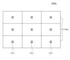
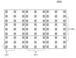
도 6a 내지 도 6c는 본 발명의 다양한 실시예들에 따른 타일링 표시 장치의 개략적인 평면도이다. 도 6a 내지 도 6c의 타일링 표시 장치(1000a, 1000b, 1000c)는 복수의 표시 장치(100a, 100b, 100c)를 연결하여 구현한 것으로, 타일링 표시 장치(1000a, 1000b, 1000c) 각각을 이루는 복수의 표시 장치(100a, 100b, 100c)는 도 1 내지 도 5d의 표시 장치(100)와 비교하여 복수의 제1 픽셀(PX1)의 배치가 상이할 뿐, 다른 구성은 실질적으로 동일하므로 중복 설명은 생략한다.6A to 6C are schematic plan views of tiling display devices according to various embodiments of the present invention. The
먼저, 표시 장치(100a, 100b, 100c)를 수백 인치 이상의 초대형 크기로 제작하는 것이 어렵기 때문에 복수의 표시 장치(100a, 100b, 100c)를 연결하여 표시 면적을 대형화한 타일링 표시 장치(1000a, 1000b, 1000c)를 사용하고 있다. 예를 들어, 복수의 표시 장치(100a, 100b, 100c)는 마치 하나의 표시 장치처럼 보이도록 타일 형태로 배열되어 타일링 표시 장치(1000a, 1000b, 1000c)로 구현될 수 있다. 그리고 복수의 표시 장치(100a, 100b, 100c)로 이루어진 타일링 표시 장치(1000a, 1000b, 1000c)는 대형 전광판이나 옥외 광고 전광판 등으로 사용될 수 있다.First, since it is difficult to manufacture the display devices (100a, 100b, 100c) in a very large size of hundreds of inches or more, a tiling display device (1000a, 1000b) in which the display area is enlarged by connecting a plurality of display devices (100a, 100b, 100c) , 1000c) is used. For example, the plurality of
이 경우, 타일링 표시 장치(1000a, 1000b, 1000c)를 이루는 복수의 표시 장치(100a, 100b, 100c)는 하나의 표시 장치처럼 구동될 수 있다. 예를 들어, 복수의 표시 장치(100a, 100b, 100c) 각각은 별도의 케이블 등을 통해 전기적으로 연결될 수도 있고, 무선 통신 방식으로 전기적으로 연결될 수 있다. 이 경우, 복수의 표시 장치(100a, 100b, 100c) 각각을 하나의 표시 장치처럼 구동하더라도, 복수의 표시 장치(100a, 100b, 100c) 간의 휘도 편차 및 색 편차가 발생할 수 있다. 예를 들어, 복수의 표시 장치(100a, 100b, 100c) 중 일부의 표시 장치(100a, 100b, 100c)는 특정 전압에서 상대적으로 고휘도의 영상이 구현되고, 다른 일부의 표시 장치(100a, 100b, 100c)는 동일한 특정 전압에서 상대적으로 저휘도의 영상이 구현될 수 있다. 이와 같이, 복수의 표시 장치(100a, 100b, 100c) 간의 휘도 편차 및 색 편차가 존재하는 경우, 타일링 표시 장치(1000a, 1000b, 1000c)에서 표시되는 영상의 품질이 저하될 수 있다. 이에, 본 발명의 일 실시예에 따른 타일링 표시 장치(1000a, 1000b, 1000c)에서는 복수의 표시 장치(100a, 100b, 100c) 각각에 제1 픽셀(PX1)을 배치하여 복수의 표시 장치(100a, 100b, 100c) 각각의 휘도를 측정 및 분석하여 휘도 편차 및 색 편차를 보상할 수 있고, 타일링 표시 장치(1000a, 1000b, 1000c)의 휘도 균일도 및 색 균일도를 향상시킬 수 있다.In this case, the plurality of
도 6a를 참조하면, 타일링 표시 장치(1000a)를 이루는 복수의 표시 장치(100a) 각각의 중앙에 제1 픽셀(PX1)이 배치된다. 복수의 표시 장치(100a) 각각의 중앙 영역에 제1 픽셀(PX1)을 배치하여 복수의 표시 장치(100a) 간의 휘도 값을 측정하여 비교 및 분석할 수 있고, 분석 결과로부터 복수의 표시 장치(100a) 간의 휘도 균일도 및 색 균일도를 향상시킬 수 있다. 도 6a의 타일링 표시 장치(1000a)는 복수의 표시 장치(100a) 각각에 최소한의 제1 픽셀(PX1)을 배치하여 복수의 표시 장치(100a) 간의 휘도 편차 및 색 편차를 보상할 수 있다.Referring to FIG. 6A , the first pixel PX1 is disposed at the center of each of the plurality of
도 6b를 참조하면, 타일링 표시 장치(1000b)를 이루는 복수의 표시 장치(100b) 각각의 최외곽 픽셀(PX) 중 네 모서리에 제1 픽셀(PX1)이 배치된다. 복수의 표시 장치(100b) 각각의 네 모서리에 제1 픽셀(PX1)을 배치하여 복수의 표시 장치(100b) 간의 휘도 값을 측정하여 비교할 수 있다.Referring to FIG. 6B, first pixels PX1 are disposed at four corners among the outermost pixels PX of each of the plurality of
이 경우, 복수의 표시 장치(100b) 간의 휘도 편차 및 색 편차가 존재하는 경우, 복수의 표시 장치(100b) 간의 경계 영역에서 복수의 표시 장치(100b) 간의 휘도 편차 및 색 편차가 용이하게 시인될 수 있다. 특히, 복수의 표시 장치(100b)가 타일 형태로 배치될 때, 복수의 표시 장치(100b) 중 4개의 표시 장치(100b) 각각의 모서리가 서로 이웃하는 지점에서 휘도 편차 및 색 편차가 용이하게 시인될 수 있다.In this case, if there is a luminance deviation and color deviation between the plurality of
이에, 복수의 표시 장치(100b) 각각의 휘도 편차 및 색 편차가 용이하게 시인되는 복수의 표시 장치(100b) 각각의 네 모서리에 제1 픽셀(PX1)을 배치하여 복수의 표시 장치(100b) 각각의 휘도 값을 측정하여 비교할 수 있고, 복수의 표시 장치(100b) 각각의 휘도 편차 및 색 편차를 보상할 수 있다.Accordingly, the first pixel (PX1) is disposed at the four corners of each of the plurality of
또한, 하나의 표시 장치(100b) 내에 복수의 제1 픽셀(PX1)이 배치되기 때문에, 복수의 표시 장치(100b) 간의 휘도 편차 및 색 편차를 보상할 수 있을 뿐만 아니라, 하나의 표시 장치(100b) 내에서의 휘도 편차 및 색 편차를 보상할 수 있다.In addition, since a plurality of first pixels PX1 are disposed within one
도 6c를 참조하면, 타일링 표시 장치(1000c)를 이루는 복수의 표시 장치(100c) 각각의 중앙에 제1 픽셀(PX1)이 배치되고, 최외곽 픽셀(PX) 중 네 모서리에 제1 픽셀(PX1)이 배치되고, 및 최외곽 픽셀(PX) 중 표시 장치(100c)의 복수의 엣지 각각의 중앙에 제1 픽셀(PX1)이 배치된다. 복수의 표시 장치(100c) 각각에 복수의 제1 픽셀(PX1)을 배치하여 하나의 표시 장치(100c) 내의 복수의 발광 소자(130, 140, 150) 간의 휘도 편차 및 색 편차를 보상할 수 있고, 복수의 표시 장치(100c) 간의 휘도 편차 및 색 편차를 보상할 수 있다.Referring to FIG. 6C, the first pixel (PX1) is disposed at the center of each of the plurality of display devices (100c) forming the tiling display device (1000c), and the first pixel (PX1) is located at the four corners of the outermost pixels (PX). ) is disposed, and among the outermost pixels PX, the first pixel PX1 is disposed at the center of each of the plurality of edges of the
하나의 표시 장치(100c) 내의 복수의 제1 픽셀(PX1) 각각에서 측정한 발광 소자(130, 140, 150)의 휘도 값으로부터 하나의 표시 장치(100c) 내의 휘도 편차 및 색 편차를 보상할 수 있다.The luminance deviation and color deviation within one
그리고 복수의 표시 장치(100c)의 복수의 제1 픽셀(PX1)각각에서 측정한 발광 소자(130, 140, 150)의 휘도 값으로부터 복수의 표시 장치(100c) 간의 휘도 편차 및 색 편차를 보상할 수 있다.In addition, the luminance deviation and color deviation between the plurality of
본 발명의 일 실시예에 따른 타일링 표시 장치(1000a, 1000b, 1000c)는 타일링 표시 장치(1000a, 1000b, 1000c)를 이루는 복수의 표시 장치(100a, 100b, 100c) 각각에 적어도 하나 이상의 제1 픽셀(PX1)을 배치하여 복수의 표시 장치(100a, 100b, 100c) 내의 휘도 편차 및 색 편차와 복수의 표시 장치(100a, 100b, 100c) 간의 휘도 편차 및 색 편차를 보상할 수 있다. 구체적으로, 발광 소자(130, 140, 150) 외에 압전 소자(160) 및 수광 소자(170)를 포함하는 제1 픽셀(PX1)을 복수의 표시 장치(100a, 100b, 100c) 각각에 배치할 수 있다. 예를 들어, 도 6a의 타일링 표시 장치(1000a)의 경우, 복수의 표시 장치(100a) 각각의 중앙에 제1 픽셀(PX1)이 배치되고, 도 6b의 타일링 표시 장치(1000b)의 경우, 복수의 표시 장치(100b) 각각의 네 모서리에 제1 픽셀(PX1)이 배치될 수 있다. 그리고 도 6c의 타일링 표시 장치(1000c)의 경우, 복수의 표시 장치(100c) 각각의 중앙 및 네 모서리에 각각 제1 픽셀(PX1)이 배치되고, 최외곽 서브 픽셀(PX) 중 표시 장치(100c)의 복수의 엣지의 중앙에 제1 픽셀(PX1)이 배치될 수 있다. 즉, 타일링 표시 장치(1000a, 1000b, 1000c)의 설계에 따라 복수의 표시 장치(100a, 100b, 100c) 각각에 적어도 하나 이상의 제1 픽셀(PX1)을 배치하여 하나의 표시 장치(100a, 100b, 100c) 내의 휘도 편차 및 색 편차를 보상할 수 있고, 복수의 표시 장치(100a, 100b, 100c) 내의 휘도 편차 및 색 편차를 보상할 수 있다. 따라서, 본 발명의 일 실시예에 따른 타일링 표시 장치(1000a, 1000b, 1000c)는 복수의 표시 장치(100a, 100b, 100c)에 적어도 하나 이상의 제1 픽셀(PX1)을 배치하여 복수의 표시 장치(100a, 100b, 100c) 각각과, 복수의 표시 장치(100a, 100b, 100c) 간의 휘도 균일도 및 색 균일도를 향상시킬 수 있다.The
본 발명의 다양한 실시예들에 따른 표시 장치 및 표시 장치의 제조 방법은 다음과 같이 설명될 수 있다.A display device and a method of manufacturing the display device according to various embodiments of the present invention can be described as follows.
본 발명의 일 실시예에 따른 표시 장치는, 적어도 하나의 제1 서브 픽셀을 포함하는 복수의 서브 픽셀이 정의된 기판, 복수의 서브 픽셀 각각에 배치된 복수의 발광 소자, 제1 서브 픽셀의 일 측에 배치되고, 반사부를 구비하는 압전 소자 및 제1 서브 픽셀의 타 측에 배치된 수광 소자를 포함한다.A display device according to an embodiment of the present invention includes a substrate on which a plurality of subpixels including at least one first subpixel are defined, a plurality of light emitting elements disposed in each of the plurality of subpixels, and one of the first subpixels. It includes a piezoelectric element disposed on one side and having a reflection portion, and a light receiving element disposed on the other side of the first subpixel.
본 발명의 다른 특징에 따르면, 압전 소자는, 제1 전극, 제1 전극 상의 제1 압전층, 제1 압전층 상의 제2 전극, 제2 전극 상의 제2 압전층, 제2 압전층 상의 제3 전극 및 제1 전극, 제1 압전층, 제2 전극, 제2 압전층 및 제3 전극을 지지하는 지지부를 포함하고, 반사부는 제1 전극의 하면에서 제1 전극의 일단에 배치될 수 있다.According to another feature of the present invention, the piezoelectric element includes a first electrode, a first piezoelectric layer on the first electrode, a second electrode on the first piezoelectric layer, a second piezoelectric layer on the second electrode, and a third piezoelectric layer on the second electrode. It includes an electrode and a support portion supporting the first electrode, the first piezoelectric layer, the second electrode, the second piezoelectric layer, and the third electrode, and the reflector may be disposed at one end of the first electrode on the lower surface of the first electrode.
본 발명의 또 다른 특징에 따르면, 압전 소자가 오프(off)된 경우, 압전 소자의 일단은 복수의 발광 소자로부터 발광된 광이 방사되는 방사 영역 외측에 배치되고, 압전 소자가 온(on)된 경우, 반사부는 기판과 경사를 갖도록 배치되고, 압전 소자의 일단은 방사 영역 내에 배치될 수 있다.According to another feature of the present invention, when the piezoelectric element is turned off, one end of the piezoelectric element is disposed outside the radiation area where the light emitted from the plurality of light emitting elements is radiated, and when the piezoelectric element is turned on, In this case, the reflector may be disposed to have an inclination with the substrate, and one end of the piezoelectric element may be disposed within the radiation area.
본 발명의 또 다른 특징에 따르면, 압전 소자가 온 된 경우, 반사부는 기판을 기준으로 복수의 발광 소자보다 높이 배치되어, 복수의 발광 소자로부터 발광된 광 중 일부를 수광 소자 측으로 반사시킬 수 있다.According to another feature of the present invention, when the piezoelectric element is turned on, the reflector is disposed higher than the plurality of light-emitting elements based on the substrate, so that some of the light emitted from the plurality of light-emitting elements can be reflected toward the light-receiving element.
본 발명의 또 다른 특징에 따르면, 복수의 발광 소자, 압전 소자 및 수광 소자 상에 배치된 접착층 및 보호 필름을 더 포함하고, 접착층은 복수의 서브 픽셀 중 제1 서브 픽셀을 제외한 서브 픽셀에만 중첩할 수 있다.According to another feature of the present invention, it further includes an adhesive layer and a protective film disposed on the plurality of light-emitting elements, the piezoelectric element, and the light-receiving element, and the adhesive layer overlaps only the sub-pixels excluding the first sub-pixel among the plurality of sub-pixels. You can.
본 발명의 또 다른 특징에 따르면, 압전 소자가 온 된 경우에서 압전 소자의 일단으로부터 보호 필름의 하면까지의 거리는, 압전 소자가 오프 된 경우에서 압전 소자의 일단으로부터 보호 필름의 하면까지의 거리보다 작을 수 있다.According to another feature of the present invention, when the piezoelectric element is turned on, the distance from one end of the piezoelectric element to the lower surface of the protective film is smaller than the distance from one end of the piezoelectric element to the lower surface of the protective film when the piezoelectric element is turned off. You can.
본 발명의 또 다른 특징에 따르면, 수광 소자는, 제1 서브 픽셀에 배치된 발광 소자와 가장 인접하게 배치된 P형 반도체층, P형 반도체층의 타 측에 배치된 진성 반도체층 및 진성 반도체층의 타 측에 배치된 N형 반도체층을 포함하고, P형 반도체층의 일 면은 기판에 대해 경사를 갖도록 배치될 수 있다.According to another feature of the present invention, the light receiving element includes a P-type semiconductor layer disposed closest to the light-emitting element disposed in the first subpixel, an intrinsic semiconductor layer disposed on the other side of the P-type semiconductor layer, and an intrinsic semiconductor layer. and an N-type semiconductor layer disposed on the other side, and one side of the P-type semiconductor layer may be disposed to be inclined with respect to the substrate.
본 발명의 또 다른 특징에 따르면, 복수의 발광 소자, 압전 소자 및 수광 소자는 동일 평면 상에 배치될 수 있다.According to another feature of the present invention, a plurality of light emitting elements, piezoelectric elements, and light receiving elements may be arranged on the same plane.
본 발명의 또 다른 특징에 따르면, 제1 서브 픽셀은 복수의 서브 픽셀 중 기판의 중앙에 배치된 서브 픽셀을 포함할 수 있다.According to another feature of the present invention, the first subpixel may include a subpixel disposed at the center of the substrate among a plurality of subpixels.
본 발명의 또 다른 특징에 따르면, 제1 서브 픽셀은 복수의 서브 픽셀 중 기판 최외곽의 서브 픽셀 중 적어도 하나일 수 있다.According to another feature of the present invention, the first subpixel may be at least one of the outermost subpixels of the substrate among a plurality of subpixels.
본 발명의 다른 실시예에 따른 표시 장치는, 복수의 발광 소자가 배치된 기판, 기판 상에 배치되고, 일단이 벤딩 가능하도록 구성된 압전 소자 및 기판 상에 배치되어, 복수의 발광 소자 중 일부의 발광 소자로부터 발광된 광을 수광하도록 구성된 수광 소자를 포함하고, 압전 소자는 압전 소자의 일단 측에 배치된 반사부를 포함하고, 일부의 발광 소자 간의 휘도 편차를 측정하여 휘도를 보상하도록, 압전 소자는 일부의 발광 소자로부터의 광을 수광 소자 측으로 반사시킬 수 있다.A display device according to another embodiment of the present invention includes a substrate on which a plurality of light-emitting elements are arranged, a piezoelectric element disposed on the substrate, one end of which is configured to be bendable, and a substrate arranged on the substrate to emit light from some of the plurality of light-emitting elements. It includes a light-receiving element configured to receive light emitted from the element, and the piezoelectric element includes a reflection portion disposed on one end of the piezoelectric element, and some of the piezoelectric elements are configured to compensate for luminance by measuring the luminance deviation between some of the light-emitting elements. Light from the light emitting element can be reflected toward the light receiving element.
본 발명의 다른 특징에 따르면, 압전 소자가 오프(off)된 경우, 압전 소자는 비벤딩되고, 반사부는 일부의 발광 소자의 측면에 인접하게 배치되며, 압전 소자가 온(on)된 경우, 압전 소자는 벤딩되고, 반사부는 일부의 발광 소자의 상측에 배치될 수 있다.According to another feature of the present invention, when the piezoelectric element is off, the piezoelectric element is non-bended, the reflecting portion is disposed adjacent to the side of some of the light emitting elements, and when the piezoelectric element is on, the piezoelectric element is non-bended. The device may be bent, and the reflector may be placed on top of some of the light emitting devices.
본 발명의 또 다른 특징에 따르면, 압전 소자가 온 된 경우, 일부의 발광 소자로부터 발광된 광 중 적어도 일부는 반사부로 입사할 수 있다.According to another feature of the present invention, when the piezoelectric element is turned on, at least some of the light emitted from some of the light-emitting elements may enter the reflection unit.
본 발명의 또 다른 특징에 따르면, 수광 소자는, 일 면이 기판과 경사를 갖도록 배치된 P형 반도체층, P형 반도체층의 일 면의 반대 면 측에 배치된 N형 반도체층 및 P형 반도체층과 N형 반도체층 사이에 배치된 진성 반도체층을 포함하고, 반사부로부터 반사된 광은 P형 반도체층의 일면으로 입사할 수 있다.According to another feature of the present invention, the light receiving element includes a P-type semiconductor layer disposed so that one side is inclined to the substrate, an N-type semiconductor layer disposed on the opposite side of one side of the P-type semiconductor layer, and a P-type semiconductor layer. It includes an intrinsic semiconductor layer disposed between the layer and the N-type semiconductor layer, and light reflected from the reflector may be incident on one surface of the P-type semiconductor layer.
본 발명의 또 다른 특징에 따르면, 기판 상에 배치되고, 복수의 발광 소자 각각과 전기적으로 연결된 복수의 배선 및 기판 상에 배치되고, 압전 소자 및 수광 소자와 전기적으로 연결된 추가 배선을 더 포함할 수 있다.According to another feature of the present invention, it may further include a plurality of wirings disposed on the substrate and electrically connected to each of the plurality of light emitting elements, and additional wirings disposed on the substrate and electrically connected to the piezoelectric element and the light receiving element. there is.
본 발명의 또 다른 특징에 따르면, 복수의 발광 소자를 덮도록 배치된 접착층 및 접착층 상의 보호 필름을 더 포함하고, 접착층 및 보호 필름은 압전 소자 및 수광 소자와 이격될 수 있다.According to another feature of the present invention, it further includes an adhesive layer disposed to cover a plurality of light emitting elements and a protective film on the adhesive layer, and the adhesive layer and the protective film may be spaced apart from the piezoelectric element and the light receiving element.
본 발명의 일 실시예에 따른 타일링 표시 장치는 복수 개의 표시 장치가 타일 형태로 배치된다.In a tiling display device according to an embodiment of the present invention, a plurality of display devices are arranged in the form of tiles.
본 발명의 일 실시예에 따른 표시 장치의 휘도 편차 보상 방법은, 기판 상의 복수의 서브 픽셀 중 제1 서브 픽셀에 배치된 발광 소자를 점등시키는 단계, 제1 서브 픽셀의 일 측에 배치되고, 반사부를 구비한 압전 소자를 온(On) 시켜 발광 소자로부터의 광을 제1 서브 픽셀의 타 측에 배치된 수광 소자 측으로 반사시키는 단계, 수광 소자로부터의 광 전류를 데이터 구동부로 전달하는 단계 및 광 전류로부터 도출된 휘도 편차 보상 계수를 데이터 전압에 반영하는 단계를 포함한다.A luminance deviation compensation method of a display device according to an embodiment of the present invention includes the steps of lighting a light emitting element disposed in a first subpixel among a plurality of subpixels on a substrate, the light emitting element disposed on one side of the first subpixel, and reflecting Turning on the piezoelectric element provided with the light emitting element to reflect the light from the light emitting element to the light receiving element disposed on the other side of the first subpixel, transferring the photo current from the light receiving element to the data driver, and photo current It includes reflecting the luminance deviation compensation coefficient derived from to the data voltage.
본 발명의 또 다른 특징에 따르면, 압전 소자를 온(On)시켜 발광 소자로부터의 광을 수광 소자 측으로 반사시키는 단계는, 반사부를 발광 소자로부터 발광된 광이 방사되는 방사 영역 내측에 배치시키는 단계이고, 수광 소자로부터의 광 전류를 데이터 구동부로 전달하는 단계는, 방사 영역 내측에 배치된 반사부에 의해 수광 소자로 입사된 광으로부터 광 전류를 생성하여 데이터 구동부로 전달하는 단계일 수 있다.According to another feature of the present invention, the step of turning on the piezoelectric element to reflect the light from the light-emitting element toward the light-receiving element is the step of disposing the reflector inside the radiation area where the light emitted from the light-emitting element is radiated. , the step of transferring the photo current from the light receiving element to the data driver may be a step of generating a photo current from light incident on the light receiving element by a reflector disposed inside the radiation area and transferring it to the data driver.
본 발명의 또 다른 특징에 따르면, 광 전류로부터 도출된 휘도 편차 보상 계수를 데이터 전압에 반영하는 단계는, 데이터 구동부에서 제1 서브 픽셀의 수광 소자로부터 광 전류를 분석하여 복수의 서브 픽셀 간의 휘도 편차를 보상하는 휘도 편차 보상 계수를 생성하는 단계 및 휘도 편차 보상 계수를 복수의 서브 픽셀 각각으로 전달되는 데이터 전압에 반영하는 단계를 포함할 수 있다.According to another feature of the present invention, the step of reflecting the luminance deviation compensation coefficient derived from the photo current to the data voltage includes analyzing the photo current from the light receiving element of the first sub-pixel in the data driver to determine the luminance deviation between the plurality of sub-pixels. It may include generating a luminance deviation compensation coefficient that compensates for and reflecting the luminance deviation compensation coefficient to the data voltage transmitted to each of the plurality of subpixels.
이상 첨부된 도면을 참조하여 본 발명의 실시예들을 더욱 상세하게 설명하였으나, 본 발명은 반드시 이러한 실시예로 국한되는 것은 아니고, 본 발명의 기술사상을 벗어나지 않는 범위 내에서 다양하게 변형실시될 수 있다. 따라서, 본 발명에 개시된 실시예들은 본 발명의 기술 사상을 제한하기 위한 것이 아니라 설명하기 위한 것이고, 이러한 실시예에 의하여 본 발명의 기술 사상의 범위가 제한되는 것은 아니다. 그러므로, 이상에서 기술한 실시예들은 모든 면에서 예시적인 것이며 제한적이 아닌 것으로 이해해야만 한다. 본 발명의 보호 범위는 아래의 청구범위에 의하여 해석되어야 하며, 그와 동등한 범위 내에 있는 모든 기술 사상은 본 발명의 권리범위에 포함되는 것으로 해석되어야 할 것이다.Although embodiments of the present invention have been described in more detail with reference to the accompanying drawings, the present invention is not necessarily limited to these embodiments, and various modifications may be made without departing from the technical spirit of the present invention. . Accordingly, the embodiments disclosed in the present invention are not intended to limit the technical idea of the present invention but are for illustrative purposes, and the scope of the technical idea of the present invention is not limited by these embodiments. Therefore, the embodiments described above should be understood in all respects as illustrative and not restrictive. The scope of protection of the present invention should be interpreted in accordance with the claims below, and all technical ideas within the equivalent scope should be construed as being included in the scope of rights of the present invention.
1000a, 1000b, 1000c: 타일링 표시 장치
100, 100a, 100b, 100c: 표시 장치
110: 기판
111: 게이트 절연층
112: 패시베이션층
113: 제1 절연층
114: 제2 절연층
115: 제3 절연층
116: 뱅크
120: 반도체 소자
121: 게이트 전극
122: 액티브층
123: 소스 전극
124: 드레인 전극
130: 적색 발광 소자
131: 제1 반도체층
132: 발광층
133: 제2 반도체층
134: 제3 컨택 전극
135: 제4 컨택 전극
140: 녹색 발광 소자
150: 청색 발광 소자
160: 압전 소자
161: 지지부
162: 제1 전극
163: 제1 압전층
164: 제2 전극
165: 제2 압전층
166: 제3 전극
167: 반사부
168: 제1 컨택 전극
169: 제2 컨택 전극
170: 수광 소자
171: P형 반도체층
172: 진성 반도체층
173: N형 반도체층
174: 제5 컨택 전극
175: 제6 컨택 전극
180: 접착층
190: 보호 필름
GD: 게이트 구동부
DD: 데이터 구동부
TC: 타이밍 컨트롤러
LL: 복수의 배선
LL1: 제1 배선
LL2: 제2 배선
LLA: 복수의 추가 배선
LLA1: 제1 추가 배선
LLA2: 제2 추가 배선
LLA3: 제3 추가 배선
LLA4: 제4 추가 배선
PX: 복수의 픽셀
PX1: 제1 픽셀
PX2: 제2 픽셀
SPX1: 복수의 제1 서브 픽셀
RSPX1: 제1 적색 서브 픽셀
GSPX1: 제1 녹색 서브 픽셀
BSPX1: 제1 청색 서브 픽셀
SPX2: 복수의 제2 서브 픽셀
RSPX2: 제2 적색 서브 픽셀
GSPX2: 제2 녹색 서브 픽셀
BSPX2: 제2 청색 서브 픽셀
PE: 복수의 패드 전극
PE1: 제1 패드 전극
PE2: 제2 패드 전극
PE3: 제3 패드 전극
PE4: 제4 패드 전극
PE5: 제5 패드 전극
PE6: 제6 패드 전극
θ: 방사 각도1000a, 1000b, 1000c: tiling display devices
100, 100a, 100b, 100c: display device
110: substrate
111: Gate insulating layer
112: Passivation layer
113: first insulating layer
114: second insulating layer
115: third insulating layer
116: bank
120: semiconductor device
121: Gate electrode
122: Active layer
123: source electrode
124: drain electrode
130: Red light emitting device
131: first semiconductor layer
132: light emitting layer
133: second semiconductor layer
134: third contact electrode
135: fourth contact electrode
140: Green light-emitting device
150: Blue light emitting element
160: Piezoelectric element
161: support part
162: first electrode
163: first piezoelectric layer
164: second electrode
165: second piezoelectric layer
166: third electrode
167: reflection part
168: first contact electrode
169: second contact electrode
170: light receiving element
171: P-type semiconductor layer
172: Intrinsic semiconductor layer
173: N-type semiconductor layer
174: Fifth contact electrode
175: sixth contact electrode
180: Adhesive layer
190: Protective film
GD: Gate driver
DD: data driving unit
TC: Timing Controller
LL: Multiple wiring
LL1: first wiring
LL2: 2nd wiring
LLA: Multiple additional wiring
LLA1: first additional wiring
LLA2: Second additional wiring
LLA3: Third additional wiring
LLA4: Fourth additional wiring
PX: Multiple Pixels
PX1: first pixel
PX2: Second pixel
SPX1: plurality of first subpixels
RSPX1: first red subpixel
GSPX1: first green subpixel
BSPX1: first blue subpixel
SPX2: plurality of second subpixels
RSPX2: Second red subpixel
GSPX2: Second green subpixel
BSPX2: Second blue subpixel
PE: multiple pad electrodes
PE1: first pad electrode
PE2: second pad electrode
PE3: third pad electrode
PE4: fourth pad electrode
PE5: fifth pad electrode
PE6: sixth pad electrode
θ: radiation angle
Claims (20)
Translated fromKorean상기 복수의 서브 픽셀 각각에 배치된 복수의 발광 소자;
상기 제1 서브 픽셀의 일 측에 배치되고, 일단에 반사부를 구비하는 압전 소자; 및
상기 제1 서브 픽셀의 타 측에 배치된 수광 소자를 포함하고,
상기 제1 서브 픽셀에서 상기 압전 소자와 상기 수광 소자는 상기 복수의 발광 소자를 사이에 두고 일직선 상에 배치되고,
상기 압전 소자가 오프(off)된 경우, 상기 압전 소자는 비벤딩되어 상기 압전 소자의 일단은 상기 복수의 발광 소자로부터 발광된 광이 방사되는 방사 영역 외측에 배치되고,
상기 압전 소자가 온(on)된 경우, 상기 압전 소자는 벤딩되어 상기 반사부가 구비된 상기 압전 소자의 일단이 상기 기판과 경사를 갖도록 배치되면서 상기 기판을 기준으로 상기 복수의 발광 소자보다 높이 배치되고, 상기 압전 소자의 일단은 상기 방사 영역 내에 배치되고,
상기 압전 소자가 온된 경우, 상기 복수의 발광 소자로부터 발광된 광 중 적어도 일부는 상기 방사 영역 내에 배치된 상기 압전 소자의 일단의 상기 반사부로 입사하고, 상기 반사부는 상기 복수의 발광 소자로부터 발광된 광 중 적어도 일부를 상기 수광 소자 측으로 반사시키도록 구성된, 표시 장치.a substrate on which a plurality of subpixels including at least one first subpixel are defined;
a plurality of light emitting elements disposed in each of the plurality of subpixels;
a piezoelectric element disposed on one side of the first subpixel and having a reflection portion at one end; and
A light receiving element disposed on the other side of the first subpixel,
In the first subpixel, the piezoelectric element and the light receiving element are arranged in a straight line with the plurality of light emitting elements interposed therebetween,
When the piezoelectric element is turned off, the piezoelectric element is unbended and one end of the piezoelectric element is disposed outside the radiation area where the light emitted from the plurality of light-emitting elements is radiated,
When the piezoelectric element is turned on, the piezoelectric element is bent so that one end of the piezoelectric element equipped with the reflection part is disposed at an angle to the substrate and is placed higher than the plurality of light emitting elements with respect to the substrate. , one end of the piezoelectric element is disposed within the radiation area,
When the piezoelectric element is turned on, at least some of the light emitted from the plurality of light-emitting elements is incident on the reflecting part of one end of the piezoelectric element disposed in the radiation area, and the reflecting part reflects the light emitted from the plurality of light-emitting elements. A display device configured to reflect at least a portion of the light toward the light receiving element.
상기 압전 소자는,
제1 전극;
상기 제1 전극 상의 제1 압전층;
상기 제1 압전층 상의 제2 전극;
상기 제2 전극 상의 제2 압전층;
상기 제2 압전층 상의 제3 전극; 및
상기 제1 전극, 상기 제1 압전층, 상기 제2 전극, 상기 제2 압전층 및 상기 제3 전극을 지지하는 지지부를 포함하고,
상기 반사부는 상기 제1 전극의 하면에서 상기 제1 전극의 일단에 배치되는, 표시 장치.According to paragraph 1,
The piezoelectric element is,
first electrode;
a first piezoelectric layer on the first electrode;
a second electrode on the first piezoelectric layer;
a second piezoelectric layer on the second electrode;
a third electrode on the second piezoelectric layer; and
It includes a support portion supporting the first electrode, the first piezoelectric layer, the second electrode, the second piezoelectric layer, and the third electrode,
The display device wherein the reflector is disposed on a lower surface of the first electrode and at one end of the first electrode.
상기 복수의 발광 소자, 상기 압전 소자 및 상기 수광 소자 상에 배치된 접착층 및 보호 필름을 더 포함하고,
상기 접착층은 상기 복수의 서브 픽셀 중 상기 제1 서브 픽셀을 제외한 서브 픽셀에만 중첩하는, 표시 장치.According to paragraph 1,
Further comprising an adhesive layer and a protective film disposed on the plurality of light-emitting elements, the piezoelectric element, and the light-receiving element,
The adhesive layer overlaps only subpixels, excluding the first subpixel, among the plurality of subpixels.
상기 압전 소자가 온 된 경우에서 상기 압전 소자의 일단으로부터 상기 보호 필름의 하면까지의 거리는, 상기 압전 소자가 오프 된 경우에서 상기 압전 소자의 일단으로부터 상기 보호 필름의 하면까지의 거리보다 작은, 표시 장치.According to clause 5,
A display device in which the distance from one end of the piezoelectric element to the lower surface of the protective film when the piezoelectric element is turned on is smaller than the distance from one end of the piezoelectric element to the lower surface of the protective film when the piezoelectric element is turned off. .
상기 수광 소자는,
상기 제1 서브 픽셀에 배치된 상기 발광 소자와 가장 인접하게 배치된 P형 반도체층;
상기 P형 반도체층의 타 측에 배치된 진성 반도체층; 및
상기 진성 반도체층의 타 측에 배치된 N형 반도체층을 포함하고,
상기 P형 반도체층의 일 면은 상기 기판에 대해 경사를 갖도록 배치되는, 표시 장치.According to paragraph 1,
The light receiving element is,
a P-type semiconductor layer disposed closest to the light emitting device disposed in the first subpixel;
an intrinsic semiconductor layer disposed on the other side of the P-type semiconductor layer; and
It includes an N-type semiconductor layer disposed on the other side of the intrinsic semiconductor layer,
A display device wherein one side of the P-type semiconductor layer is disposed to be inclined with respect to the substrate.
상기 복수의 발광 소자, 상기 압전 소자 및 상기 수광 소자는 동일 평면 상에 배치되는, 표시 장치.According to paragraph 1,
A display device wherein the plurality of light-emitting elements, the piezoelectric element, and the light-receiving element are disposed on the same plane.
상기 제1 서브 픽셀은 상기 복수의 서브 픽셀 중 상기 기판의 중앙에 배치된 서브 픽셀을 포함하는, 표시 장치.According to paragraph 1,
The first subpixel includes a subpixel disposed at the center of the substrate among the plurality of subpixels.
상기 제1 서브 픽셀은 상기 복수의 서브 픽셀 중 상기 기판 최외곽의 서브 픽셀 중 적어도 하나인, 표시 장치.According to clause 9,
The first subpixel is at least one of the outermost subpixels of the substrate among the plurality of subpixels.
상기 기판 상에 배치되고, 일단이 벤딩 가능하도록 구성된 압전 소자; 및
상기 기판 상에 배치되어, 상기 복수의 발광 소자 중 일부의 발광 소자로부터 발광된 광을 수광하도록 구성된 수광 소자를 포함하고,
상기 압전 소자와 상기 수광 소자는 상기 일부의 발광 소자를 사이에 두고 일직선 상에 배치되고,
상기 압전 소자는 상기 압전 소자의 일단 측에 배치된 반사부를 포함하고,
상기 압전 소자가 오프(off)된 경우, 상기 압전 소자는 비벤딩되어 상기 압전 소자의 일단은 상기 일부의 발광 소자로부터 발광된 광이 방사되는 방사 영역 외측에 배치되고,
상기 압전 소자가 온(on)된 경우, 상기 압전 소자는 상기 반사부가 구비된 상기 압전 소자의 일단이 상기 기판과 경사를 갖도록 배치되면서 상기 기판을 기준으로 상기 복수의 발광 소자보다 높이 배치되도록 벤딩되어 상기 압전 소자의 일단이 상기 방사 영역 내에 배치되고,
상기 압전 소자가 온된 경우, 상기 일부의 발광 소자 간의 휘도 편차를 측정하여 휘도를 보상하도록, 상기 일부의 발광 소자로부터 발광된 광 중 적어도 일부는 상기 방사 영역 내에 배치된 상기 압전 소자의 일단의 상기 반사부로 입사하고, 상기 압전 소자의 상기 반사부는 상기 일부의 발광 소자로부터의 광 중 적어도 일부를 상기 수광 소자 측으로 반사시키는, 표시 장치.A substrate on which a plurality of light emitting elements are arranged;
a piezoelectric element disposed on the substrate and configured to have one end capable of bending; and
a light-receiving element disposed on the substrate and configured to receive light emitted from some of the plurality of light-emitting elements,
The piezoelectric element and the light-receiving element are arranged in a straight line with the part of the light-emitting element interposed therebetween,
The piezoelectric element includes a reflection portion disposed on one end of the piezoelectric element,
When the piezoelectric element is turned off, the piezoelectric element is unbended so that one end of the piezoelectric element is disposed outside the radiation area where the light emitted from the part of the light emitting element is radiated,
When the piezoelectric element is turned on, the piezoelectric element is bent so that one end of the piezoelectric element equipped with the reflection part is disposed at an angle to the substrate and is positioned higher than the plurality of light-emitting elements with respect to the substrate. One end of the piezoelectric element is disposed within the radiation area,
When the piezoelectric element is turned on, at least a portion of the light emitted from the light-emitting elements is reflected by one end of the piezoelectric element disposed in the radiation area so as to compensate for luminance by measuring a luminance difference between the light-emitting elements. A display device wherein the light is incident on the light emitting element, and the reflecting part of the piezoelectric element reflects at least a part of the light from the part of the light emitting element toward the light receiving element.
상기 압전 소자가 오프(off)된 경우, 상기 압전 소자는 비벤딩되고, 상기 반사부는 상기 일부의 발광 소자의 측면에 인접하게 배치되는, 표시 장치.According to clause 11,
When the piezoelectric element is turned off, the piezoelectric element is non-bended, and the reflection portion is disposed adjacent to a side of the part of the light emitting element.
상기 수광 소자는,
일 면이 상기 기판과 경사를 갖도록 배치된 P형 반도체층;
상기 P형 반도체층의 일 면의 반대 면 측에 배치된 N형 반도체층; 및
상기 P형 반도체층과 상기 N형 반도체층 사이에 배치된 진성 반도체층을 포함하고,
상기 반사부로부터 반사된 광은 상기 P형 반도체층의 일면으로 입사하는, 표시 장치.According to clause 11,
The light receiving element is,
a P-type semiconductor layer arranged so that one side is inclined to the substrate;
an N-type semiconductor layer disposed on a side opposite to one side of the P-type semiconductor layer; and
Comprising an intrinsic semiconductor layer disposed between the P-type semiconductor layer and the N-type semiconductor layer,
The display device wherein light reflected from the reflector is incident on one surface of the P-type semiconductor layer.
상기 기판 상에 배치되고, 상기 복수의 발광 소자 각각과 전기적으로 연결된 복수의 배선; 및
상기 기판 상에 배치되고, 상기 압전 소자 및 상기 수광 소자와 전기적으로 연결된 추가 배선을 더 포함하는, 표시 장치.According to clause 11,
a plurality of wires disposed on the substrate and electrically connected to each of the plurality of light emitting devices; and
The display device further includes an additional wiring disposed on the substrate and electrically connected to the piezoelectric element and the light-receiving element.
상기 복수의 발광 소자를 덮도록 배치된 접착층 및 상기 접착층 상의 보호 필름을 더 포함하고,
상기 접착층 및 상기 보호 필름은 상기 압전 소자 및 상기 수광 소자와 이격된, 표시 장치.According to clause 11,
Further comprising an adhesive layer disposed to cover the plurality of light emitting devices and a protective film on the adhesive layer,
The adhesive layer and the protective film are spaced apart from the piezoelectric element and the light-receiving element.
상기 복수 개의 표시 장치는 서로 연결된, 타일링 표시 장치.Comprising a plurality of display devices according to any one of claims 1, 2, 5 to 12, and 14 to 16,
A tiling display device wherein the plurality of display devices are connected to each other.
상기 제1 서브 픽셀의 일 측에 배치되고, 일단에 반사부를 구비한 압전 소자를 온(On) 시켜 상기 발광 소자로부터의 광을 상기 제1 서브 픽셀의 타 측에 배치된 수광 소자 측으로 반사시키는 단계;
상기 수광 소자로부터의 광 전류를 데이터 구동부로 전달하는 단계; 및
상기 광 전류로부터 도출된 휘도 편차 보상 계수를 데이터 전압에 반영하는 단계를 포함하고,
상기 압전 소자를 온(On)시켜 상기 발광 소자로부터의 광을 상기 수광 소자 측으로 반사시키는 단계는, 상기 압전 소자를 벤딩시켜 상기 반사부가 구비된 상기 압전 소자의 일단이 상기 기판과 경사를 갖도록 배치되면서 상기 기판을 기준으로 상기 복수의 발광 소자보다 높이 배치되도록 하여 상기 반사부를 상기 발광 소자로부터 발광된 광이 방사되는 방사 영역 내측에 배치시키는 단계이고,
상기 수광 소자로부터의 상기 광 전류를 상기 데이터 구동부로 전달하는 단계는, 상기 방사 영역 내측에 배치된 상기 반사부에 의해 상기 수광 소자로 입사된 광으로부터 상기 광 전류를 생성하여 상기 데이터 구동부로 전달하는 단계이며,
상기 압전 소자와 상기 수광 소자는 상기 발광 소자를 사이에 두고 일직선 상에 배치되는, 표시 장치의 휘도 편차 보상 방법.Turning on a light emitting device disposed in a first subpixel among a plurality of subpixels on a substrate;
Turning on a piezoelectric element disposed on one side of the first subpixel and having a reflection portion at one end to reflect light from the light emitting element toward a light receiving element disposed on the other side of the first subpixel. ;
transferring the photo current from the light receiving element to a data driver; and
Comprising a step of reflecting the luminance deviation compensation coefficient derived from the photo current to the data voltage,
The step of turning on the piezoelectric element to reflect the light from the light-emitting element toward the light-receiving element includes bending the piezoelectric element so that one end of the piezoelectric element equipped with the reflection part is disposed to be inclined with the substrate. A step of arranging the reflector so that it is higher than the plurality of light-emitting devices relative to the substrate and inside a radiation area where light emitted from the light-emitting devices is radiated,
The step of transferring the photo current from the light receiving element to the data driver includes generating the photo current from light incident on the light receiving element by the reflector disposed inside the radiation area and transmitting the photo current to the data driver. It is a step,
The method of compensating luminance deviation of a display device, wherein the piezoelectric element and the light receiving element are disposed in a straight line with the light emitting element interposed therebetween.
상기 광 전류로부터 도출된 상기 휘도 편차 보상 계수를 상기 데이터 전압에 반영하는 단계는,
상기 데이터 구동부에서 상기 제1 서브 픽셀의 상기 수광 소자로부터 상기 광 전류를 분석하여 복수의 서브 픽셀 간의 휘도 편차를 보상하는 상기 휘도 편차 보상 계수를 생성하는 단계; 및
상기 휘도 편차 보상 계수를 상기 복수의 서브 픽셀 각각으로 전달되는 상기 데이터 전압에 반영하는 단계를 포함하는, 표시 장치의 휘도 편차 보상 방법.According to clause 18,
The step of reflecting the luminance deviation compensation coefficient derived from the photo current to the data voltage includes:
generating the luminance deviation compensation coefficient for compensating luminance deviation between a plurality of subpixels by analyzing the photo current from the light receiving element of the first subpixel in the data driver; and
A luminance discrepancy compensation method for a display device, comprising: reflecting the luminance discrepancy compensation coefficient to the data voltage transmitted to each of the plurality of subpixels.
Priority Applications (1)
| Application Number | Priority Date | Filing Date | Title |
|---|---|---|---|
| KR1020180151776AKR102622472B1 (en) | 2018-11-30 | 2018-11-30 | Display device, tiliing display device and method for compensation luminance difference by using the same |
Applications Claiming Priority (1)
| Application Number | Priority Date | Filing Date | Title |
|---|---|---|---|
| KR1020180151776AKR102622472B1 (en) | 2018-11-30 | 2018-11-30 | Display device, tiliing display device and method for compensation luminance difference by using the same |
Publications (2)
| Publication Number | Publication Date |
|---|---|
| KR20200065383A KR20200065383A (en) | 2020-06-09 |
| KR102622472B1true KR102622472B1 (en) | 2024-01-05 |
Family
ID=71082833
Family Applications (1)
| Application Number | Title | Priority Date | Filing Date |
|---|---|---|---|
| KR1020180151776AActiveKR102622472B1 (en) | 2018-11-30 | 2018-11-30 | Display device, tiliing display device and method for compensation luminance difference by using the same |
Country Status (1)
| Country | Link |
|---|---|
| KR (1) | KR102622472B1 (en) |
Families Citing this family (5)
| Publication number | Priority date | Publication date | Assignee | Title |
|---|---|---|---|---|
| WO2022049612A1 (en)* | 2020-09-01 | 2022-03-10 | シャープ株式会社 | Light emitting element and display device |
| KR102818858B1 (en) | 2020-11-02 | 2025-06-12 | 삼성디스플레이 주식회사 | Display apparatus and method of driving the same |
| KR20230095441A (en) | 2021-12-22 | 2023-06-29 | 엘지디스플레이 주식회사 | Display device |
| CN117769734A (en)* | 2022-06-30 | 2024-03-26 | 京东方科技集团股份有限公司 | Spliced display screen and display method thereof |
| KR20240120329A (en) | 2023-01-31 | 2024-08-07 | 엘지디스플레이 주식회사 | Display apparatus |
Citations (1)
| Publication number | Priority date | Publication date | Assignee | Title |
|---|---|---|---|---|
| JP2004504705A (en) | 2000-07-18 | 2004-02-12 | ゼネラル・エレクトリック・カンパニイ | Micro-electromechanical system controlled organic LEDs and pixel arrays, and uses and methods for making same |
Family Cites Families (1)
| Publication number | Priority date | Publication date | Assignee | Title |
|---|---|---|---|---|
| JP3235760B2 (en)* | 1994-10-18 | 2001-12-04 | オムロン株式会社 | Optical device |
- 2018
- 2018-11-30KRKR1020180151776Apatent/KR102622472B1/enactiveActive
Patent Citations (1)
| Publication number | Priority date | Publication date | Assignee | Title |
|---|---|---|---|---|
| JP2004504705A (en) | 2000-07-18 | 2004-02-12 | ゼネラル・エレクトリック・カンパニイ | Micro-electromechanical system controlled organic LEDs and pixel arrays, and uses and methods for making same |
Also Published As
| Publication number | Publication date |
|---|---|
| KR20200065383A (en) | 2020-06-09 |
Similar Documents
| Publication | Publication Date | Title |
|---|---|---|
| KR102622472B1 (en) | Display device, tiliing display device and method for compensation luminance difference by using the same | |
| JP7290008B2 (en) | Display device and manufacturing method thereof | |
| EP3573431B1 (en) | Display device using semiconductor light-emitting element | |
| CN113064294B (en) | Display device and multi-screen display device | |
| KR102633079B1 (en) | Light emitting diode display apparatus | |
| KR102835926B1 (en) | Light emitting display panel | |
| CN108230991A (en) | Light emitting display device | |
| CN108269823A (en) | Light emitting display device and use its multiscreen display apparatus | |
| KR20190067524A (en) | Light emitting device and display device using the same | |
| CN112802873B (en) | Luminous display panel | |
| KR20190003198A (en) | Light emitting diode display apparatus | |
| KR20190070588A (en) | Light emitting device and display device using the same | |
| KR101888857B1 (en) | Light emitting device and display device using the same | |
| KR101800884B1 (en) | Display Device | |
| JP2022146602A (en) | Display device | |
| KR102640035B1 (en) | display device | |
| US20230387144A1 (en) | Display module, display apparatus and method for manufacturing same | |
| CN112863418A (en) | Light emitting display panel | |
| KR101895600B1 (en) | Display device and manufacturing method of the same | |
| CN118117026A (en) | Display device | |
| CN115377139A (en) | display screen | |
| US20250218848A1 (en) | Method of manufacturing display device | |
| KR102856470B1 (en) | Display device using light emitting diode | |
| US20250017066A1 (en) | Display device | |
| US20240365484A1 (en) | Display device |
Legal Events
| Date | Code | Title | Description |
|---|---|---|---|
| PA0109 | Patent application | Patent event code:PA01091R01D Comment text:Patent Application Patent event date:20181130 | |
| PG1501 | Laying open of application | ||
| A201 | Request for examination | ||
| PA0201 | Request for examination | Patent event code:PA02012R01D Patent event date:20211102 Comment text:Request for Examination of Application Patent event code:PA02011R01I Patent event date:20181130 Comment text:Patent Application | |
| E902 | Notification of reason for refusal | ||
| PE0902 | Notice of grounds for rejection | Comment text:Notification of reason for refusal Patent event date:20230223 Patent event code:PE09021S01D | |
| E902 | Notification of reason for refusal | ||
| PE0902 | Notice of grounds for rejection | Comment text:Notification of reason for refusal Patent event date:20230811 Patent event code:PE09021S01D | |
| E701 | Decision to grant or registration of patent right | ||
| PE0701 | Decision of registration | Patent event code:PE07011S01D Comment text:Decision to Grant Registration Patent event date:20231012 | |
| GRNT | Written decision to grant | ||
| PR0701 | Registration of establishment | Comment text:Registration of Establishment Patent event date:20240103 Patent event code:PR07011E01D | |
| PR1002 | Payment of registration fee | Payment date:20240103 End annual number:3 Start annual number:1 | |
| PG1601 | Publication of registration |