KR102621455B1 - Semiconductor devices and methods of manufacturing semiconductor devices - Google Patents
Semiconductor devices and methods of manufacturing semiconductor devicesDownload PDFInfo
- Publication number
- KR102621455B1 KR102621455B1KR1020197038585AKR20197038585AKR102621455B1KR 102621455 B1KR102621455 B1KR 102621455B1KR 1020197038585 AKR1020197038585 AKR 1020197038585AKR 20197038585 AKR20197038585 AKR 20197038585AKR 102621455 B1KR102621455 B1KR 102621455B1
- Authority
- KR
- South Korea
- Prior art keywords
- insulator
- oxide
- conductor
- region
- film
- Prior art date
- Legal status (The legal status is an assumption and is not a legal conclusion. Google has not performed a legal analysis and makes no representation as to the accuracy of the status listed.)
- Active
Links
- 239000004065semiconductorSubstances0.000titleclaimsabstractdescription376
- 238000000034methodMethods0.000titleclaimsdescription227
- 238000004519manufacturing processMethods0.000titleclaimsdescription58
- 239000012212insulatorSubstances0.000claimsabstractdescription785
- 239000004020conductorSubstances0.000claimsabstractdescription606
- 239000011229interlayerSubstances0.000claimsabstractdescription32
- 229910052760oxygenInorganic materials0.000claimsdescription224
- 239000001301oxygenSubstances0.000claimsdescription221
- QVGXLLKOCUKJST-UHFFFAOYSA-Natomic oxygenChemical compound[O]QVGXLLKOCUKJST-UHFFFAOYSA-N0.000claimsdescription217
- 230000006870functionEffects0.000claimsdescription196
- 239000010410layerSubstances0.000claimsdescription192
- 229910052751metalInorganic materials0.000claimsdescription165
- 239000002184metalSubstances0.000claimsdescription147
- 229910052739hydrogenInorganic materials0.000claimsdescription144
- 239000001257hydrogenSubstances0.000claimsdescription143
- IJGRMHOSHXDMSA-UHFFFAOYSA-NAtomic nitrogenChemical compoundN#NIJGRMHOSHXDMSA-UHFFFAOYSA-N0.000claimsdescription133
- UFHFLCQGNIYNRP-UHFFFAOYSA-NHydrogenChemical compound[H][H]UFHFLCQGNIYNRP-UHFFFAOYSA-N0.000claimsdescription122
- 239000000758substrateSubstances0.000claimsdescription112
- 239000012535impuritySubstances0.000claimsdescription106
- 238000004544sputter depositionMethods0.000claimsdescription77
- 230000015572biosynthetic processEffects0.000claimsdescription75
- 238000010438heat treatmentMethods0.000claimsdescription70
- 229910052782aluminiumInorganic materials0.000claimsdescription62
- XAGFODPZIPBFFR-UHFFFAOYSA-NaluminiumChemical compound[Al]XAGFODPZIPBFFR-UHFFFAOYSA-N0.000claimsdescription60
- 229910052757nitrogenInorganic materials0.000claimsdescription60
- 230000008569processEffects0.000claimsdescription54
- 239000007789gasSubstances0.000claimsdescription52
- 229910052721tungstenInorganic materials0.000claimsdescription44
- 239000010937tungstenSubstances0.000claimsdescription44
- 238000012545processingMethods0.000claimsdescription43
- WFKWXMTUELFFGS-UHFFFAOYSA-NtungstenChemical compound[W]WFKWXMTUELFFGS-UHFFFAOYSA-N0.000claimsdescription41
- RTAQQCXQSZGOHL-UHFFFAOYSA-NTitaniumChemical compound[Ti]RTAQQCXQSZGOHL-UHFFFAOYSA-N0.000claimsdescription35
- 238000005530etchingMethods0.000claimsdescription35
- 229910052719titaniumInorganic materials0.000claimsdescription35
- 239000010936titaniumSubstances0.000claimsdescription35
- XKRFYHLGVUSROY-UHFFFAOYSA-NArgonChemical compound[Ar]XKRFYHLGVUSROY-UHFFFAOYSA-N0.000claimsdescription32
- 239000012298atmosphereSubstances0.000claimsdescription28
- 229910052715tantalumInorganic materials0.000claimsdescription28
- GUVRBAGPIYLISA-UHFFFAOYSA-Ntantalum atomChemical compound[Ta]GUVRBAGPIYLISA-UHFFFAOYSA-N0.000claimsdescription28
- KJTLSVCANCCWHF-UHFFFAOYSA-NRutheniumChemical compound[Ru]KJTLSVCANCCWHF-UHFFFAOYSA-N0.000claimsdescription18
- 238000001312dry etchingMethods0.000claimsdescription18
- 229910052707rutheniumInorganic materials0.000claimsdescription18
- 229910052786argonInorganic materials0.000claimsdescription17
- VYZAMTAEIAYCRO-UHFFFAOYSA-NChromiumChemical compound[Cr]VYZAMTAEIAYCRO-UHFFFAOYSA-N0.000claimsdescription15
- 229910052804chromiumInorganic materials0.000claimsdescription15
- 239000011651chromiumSubstances0.000claimsdescription15
- 229910052733galliumInorganic materials0.000claimsdescription14
- 229910052727yttriumInorganic materials0.000claimsdescription8
- 230000010354integrationEffects0.000abstractdescription15
- 239000010408filmSubstances0.000description546
- 230000015654memoryEffects0.000description237
- 210000004027cellAnatomy0.000description211
- 229910044991metal oxideInorganic materials0.000description133
- 150000004706metal oxidesChemical class0.000description122
- 230000002829reductive effectEffects0.000description88
- 239000000463materialSubstances0.000description71
- 239000003990capacitorSubstances0.000description69
- VYPSYNLAJGMNEJ-UHFFFAOYSA-NSilicium dioxideChemical compoundO=[Si]=OVYPSYNLAJGMNEJ-UHFFFAOYSA-N0.000description63
- 229910052814silicon oxideInorganic materials0.000description63
- 238000005229chemical vapour depositionMethods0.000description53
- XUIMIQQOPSSXEZ-UHFFFAOYSA-NSiliconChemical compound[Si]XUIMIQQOPSSXEZ-UHFFFAOYSA-N0.000description51
- 229910052710siliconInorganic materials0.000description51
- 239000010703siliconSubstances0.000description51
- TWNQGVIAIRXVLR-UHFFFAOYSA-Noxo(oxoalumanyloxy)alumaneChemical compoundO=[Al]O[Al]=OTWNQGVIAIRXVLR-UHFFFAOYSA-N0.000description50
- 230000004888barrier functionEffects0.000description48
- XLYOFNOQVPJJNP-UHFFFAOYSA-NwaterSubstancesOXLYOFNOQVPJJNP-UHFFFAOYSA-N0.000description47
- 229910001868waterInorganic materials0.000description47
- 238000010586diagramMethods0.000description41
- 229910052735hafniumInorganic materials0.000description40
- 238000009792diffusion processMethods0.000description37
- 229910052581Si3N4Inorganic materials0.000description35
- HQVNEWCFYHHQES-UHFFFAOYSA-Nsilicon nitrideChemical compoundN12[Si]34N5[Si]62N3[Si]51N64HQVNEWCFYHHQES-UHFFFAOYSA-N0.000description35
- 239000011701zincSubstances0.000description34
- 150000004767nitridesChemical class0.000description32
- 238000003860storageMethods0.000description32
- RYGMFSIKBFXOCR-UHFFFAOYSA-NCopperChemical group[Cu]RYGMFSIKBFXOCR-UHFFFAOYSA-N0.000description31
- 239000010949copperChemical group0.000description31
- VBJZVLUMGGDVMO-UHFFFAOYSA-Nhafnium atomChemical compound[Hf]VBJZVLUMGGDVMO-UHFFFAOYSA-N0.000description31
- 229910052802copperInorganic materials0.000description30
- 230000007547defectEffects0.000description29
- 238000004549pulsed laser depositionMethods0.000description29
- 238000001451molecular beam epitaxyMethods0.000description28
- 125000004429atomChemical group0.000description27
- 238000004891communicationMethods0.000description27
- 150000002500ionsChemical class0.000description25
- 239000002019doping agentSubstances0.000description24
- 229910000449hafnium oxideInorganic materials0.000description24
- WIHZLLGSGQNAGK-UHFFFAOYSA-Nhafnium(4+);oxygen(2-)Chemical compound[O-2].[O-2].[Hf+4]WIHZLLGSGQNAGK-UHFFFAOYSA-N0.000description24
- -1hydrogenChemical compound0.000description23
- OKTJSMMVPCPJKN-UHFFFAOYSA-NCarbonChemical compound[C]OKTJSMMVPCPJKN-UHFFFAOYSA-N0.000description22
- 150000002431hydrogenChemical class0.000description22
- 229910052799carbonInorganic materials0.000description21
- 239000013078crystalSubstances0.000description20
- 239000010409thin filmSubstances0.000description19
- 238000011282treatmentMethods0.000description19
- PXHVJJICTQNCMI-UHFFFAOYSA-NNickelChemical group[Ni]PXHVJJICTQNCMI-UHFFFAOYSA-N0.000description18
- 229910052738indiumInorganic materials0.000description18
- APFVFJFRJDLVQX-UHFFFAOYSA-Nindium atomChemical compound[In]APFVFJFRJDLVQX-UHFFFAOYSA-N0.000description18
- 239000011347resinSubstances0.000description17
- 229920005989resinPolymers0.000description17
- 238000013528artificial neural networkMethods0.000description16
- NRTOMJZYCJJWKI-UHFFFAOYSA-NTitanium nitrideChemical compound[Ti]#NNRTOMJZYCJJWKI-UHFFFAOYSA-N0.000description15
- MZLGASXMSKOWSE-UHFFFAOYSA-Ntantalum nitrideChemical compound[Ta]#NMZLGASXMSKOWSE-UHFFFAOYSA-N0.000description15
- 230000005684electric fieldEffects0.000description14
- 230000003071parasitic effectEffects0.000description13
- 239000002356single layerSubstances0.000description13
- ZOXJGFHDIHLPTG-UHFFFAOYSA-NBoronChemical compound[B]ZOXJGFHDIHLPTG-UHFFFAOYSA-N0.000description12
- GYHNNYVSQQEPJS-UHFFFAOYSA-NGalliumChemical group[Ga]GYHNNYVSQQEPJS-UHFFFAOYSA-N0.000description12
- ZOKXTWBITQBERF-UHFFFAOYSA-NMolybdenumChemical group[Mo]ZOKXTWBITQBERF-UHFFFAOYSA-N0.000description12
- 229910052796boronInorganic materials0.000description12
- 238000004364calculation methodMethods0.000description12
- 229910001873dinitrogenInorganic materials0.000description12
- 229910052750molybdenumInorganic materials0.000description12
- 239000011733molybdenumChemical group0.000description12
- 102100040862Dual specificity protein kinase CLK1Human genes0.000description11
- OAICVXFJPJFONN-UHFFFAOYSA-NPhosphorusChemical compound[P]OAICVXFJPJFONN-UHFFFAOYSA-N0.000description11
- 238000006243chemical reactionMethods0.000description11
- 230000007423decreaseEffects0.000description11
- 239000000203mixtureSubstances0.000description11
- 230000035515penetrationEffects0.000description11
- 229910052698phosphorusInorganic materials0.000description11
- 239000011574phosphorusSubstances0.000description11
- YCKRFDGAMUMZLT-UHFFFAOYSA-NFluorine atomChemical compound[F]YCKRFDGAMUMZLT-UHFFFAOYSA-N0.000description10
- FYYHWMGAXLPEAU-UHFFFAOYSA-NMagnesiumChemical compound[Mg]FYYHWMGAXLPEAU-UHFFFAOYSA-N0.000description10
- MWUXSHHQAYIFBG-UHFFFAOYSA-NNitric oxideChemical compoundO=[N]MWUXSHHQAYIFBG-UHFFFAOYSA-N0.000description10
- 238000004458analytical methodMethods0.000description10
- 230000008859changeEffects0.000description10
- 229910052731fluorineInorganic materials0.000description10
- 239000011737fluorineSubstances0.000description10
- 229910052749magnesiumInorganic materials0.000description10
- 239000011777magnesiumSubstances0.000description10
- 238000000899pressurised-fluid extractionMethods0.000description10
- 238000001039wet etchingMethods0.000description10
- QCWXUUIWCKQGHC-UHFFFAOYSA-NZirconiumChemical group[Zr]QCWXUUIWCKQGHC-UHFFFAOYSA-N0.000description9
- 230000014759maintenance of locationEffects0.000description9
- 229910052759nickelInorganic materials0.000description9
- 230000002441reversible effectEffects0.000description9
- 229910052726zirconiumInorganic materials0.000description9
- XEEYBQQBJWHFJM-UHFFFAOYSA-NIronChemical group[Fe]XEEYBQQBJWHFJM-UHFFFAOYSA-N0.000description8
- HCHKCACWOHOZIP-UHFFFAOYSA-NZincChemical compound[Zn]HCHKCACWOHOZIP-UHFFFAOYSA-N0.000description8
- 238000004140cleaningMethods0.000description8
- 230000006378damageEffects0.000description8
- 238000013461designMethods0.000description8
- 229910052732germaniumInorganic materials0.000description8
- GNPVGFCGXDBREM-UHFFFAOYSA-Ngermanium atomChemical group[Ge]GNPVGFCGXDBREM-UHFFFAOYSA-N0.000description8
- 239000011159matrix materialSubstances0.000description8
- 238000000926separation methodMethods0.000description8
- 229910052725zincInorganic materials0.000description8
- XLOMVQKBTHCTTD-UHFFFAOYSA-NZinc monoxideChemical compound[Zn]=OXLOMVQKBTHCTTD-UHFFFAOYSA-N0.000description7
- 229910052784alkaline earth metalInorganic materials0.000description7
- 238000007599dischargingMethods0.000description7
- 238000003475laminationMethods0.000description7
- 230000003647oxidationEffects0.000description7
- 238000007254oxidation reactionMethods0.000description7
- RVTZCBVAJQQJTK-UHFFFAOYSA-Noxygen(2-);zirconium(4+)Chemical compound[O-2].[O-2].[Zr+4]RVTZCBVAJQQJTK-UHFFFAOYSA-N0.000description7
- 239000000123paperSubstances0.000description7
- 238000009832plasma treatmentMethods0.000description7
- 239000002994raw materialSubstances0.000description7
- 230000007704transitionEffects0.000description7
- 229910001928zirconium oxideInorganic materials0.000description7
- GWEVSGVZZGPLCZ-UHFFFAOYSA-NTitan oxideChemical compoundO=[Ti]=OGWEVSGVZZGPLCZ-UHFFFAOYSA-N0.000description6
- 230000000295complement effectEffects0.000description6
- 230000000694effectsEffects0.000description6
- 230000005669field effectEffects0.000description6
- 239000011261inert gasSubstances0.000description6
- 229910052746lanthanumInorganic materials0.000description6
- FZLIPJUXYLNCLC-UHFFFAOYSA-Nlanthanum atomChemical group[La]FZLIPJUXYLNCLC-UHFFFAOYSA-N0.000description6
- 238000001459lithographyMethods0.000description6
- 150000002736metal compoundsChemical class0.000description6
- 239000002159nanocrystalSubstances0.000description6
- QGLKJKCYBOYXKC-UHFFFAOYSA-NnonaoxidotritungstenChemical compoundO=[W]1(=O)O[W](=O)(=O)O[W](=O)(=O)O1QGLKJKCYBOYXKC-UHFFFAOYSA-N0.000description6
- 230000001590oxidative effectEffects0.000description6
- 125000004430oxygen atomChemical groupO*0.000description6
- BPUBBGLMJRNUCC-UHFFFAOYSA-Noxygen(2-);tantalum(5+)Chemical compound[O-2].[O-2].[O-2].[O-2].[O-2].[Ta+5].[Ta+5]BPUBBGLMJRNUCC-UHFFFAOYSA-N0.000description6
- BASFCYQUMIYNBI-UHFFFAOYSA-NplatinumChemical compound[Pt]BASFCYQUMIYNBI-UHFFFAOYSA-N0.000description6
- 229910001936tantalum oxideInorganic materials0.000description6
- OGIDPMRJRNCKJF-UHFFFAOYSA-Ntitanium oxideInorganic materials[Ti]=OOGIDPMRJRNCKJF-UHFFFAOYSA-N0.000description6
- 229910001930tungsten oxideInorganic materials0.000description6
- VWQVUPCCIRVNHF-UHFFFAOYSA-Nyttrium atomChemical group[Y]VWQVUPCCIRVNHF-UHFFFAOYSA-N0.000description6
- 229910052779NeodymiumInorganic materials0.000description5
- 229910052783alkali metalInorganic materials0.000description5
- 150000001340alkali metalsChemical class0.000description5
- 150000001342alkaline earth metalsChemical class0.000description5
- 239000000956alloySubstances0.000description5
- 239000004760aramidSubstances0.000description5
- 229920003235aromatic polyamidePolymers0.000description5
- 230000005540biological transmissionEffects0.000description5
- AJNVQOSZGJRYEI-UHFFFAOYSA-Ndigallium;oxygen(2-)Chemical compound[O-2].[O-2].[O-2].[Ga+3].[Ga+3]AJNVQOSZGJRYEI-UHFFFAOYSA-N0.000description5
- 238000010894electron beam technologyMethods0.000description5
- 229910001195gallium oxideInorganic materials0.000description5
- 229910003437indium oxideInorganic materials0.000description5
- PJXISJQVUVHSOJ-UHFFFAOYSA-Nindium(iii) oxideChemical compound[O-2].[O-2].[O-2].[In+3].[In+3]PJXISJQVUVHSOJ-UHFFFAOYSA-N0.000description5
- 239000011810insulating materialSubstances0.000description5
- 239000007769metal materialSubstances0.000description5
- 238000002156mixingMethods0.000description5
- QEFYFXOXNSNQGX-UHFFFAOYSA-Nneodymium atomChemical compound[Nd]QEFYFXOXNSNQGX-UHFFFAOYSA-N0.000description5
- 239000002245particleSubstances0.000description5
- 230000009467reductionEffects0.000description5
- 238000001004secondary ion mass spectrometryMethods0.000description5
- 238000002230thermal chemical vapour depositionMethods0.000description5
- 229910052720vanadiumInorganic materials0.000description5
- JBRZTFJDHDCESZ-UHFFFAOYSA-NAsGaChemical compound[As]#[Ga]JBRZTFJDHDCESZ-UHFFFAOYSA-N0.000description4
- ZAMOUSCENKQFHK-UHFFFAOYSA-NChlorine atomChemical compound[Cl]ZAMOUSCENKQFHK-UHFFFAOYSA-N0.000description4
- 229910001218Gallium arsenideInorganic materials0.000description4
- 239000004677NylonSubstances0.000description4
- 239000004952PolyamideSubstances0.000description4
- 239000004642PolyimideSubstances0.000description4
- NIXOWILDQLNWCW-UHFFFAOYSA-Nacrylic acid groupChemical groupC(C=C)(=O)ONIXOWILDQLNWCW-UHFFFAOYSA-N0.000description4
- 238000003491arrayMethods0.000description4
- 229910052790berylliumInorganic materials0.000description4
- ATBAMAFKBVZNFJ-UHFFFAOYSA-Nberyllium atomChemical group[Be]ATBAMAFKBVZNFJ-UHFFFAOYSA-N0.000description4
- 239000000460chlorineSubstances0.000description4
- 229910052801chlorineInorganic materials0.000description4
- 238000013527convolutional neural networkMethods0.000description4
- PMHQVHHXPFUNSP-UHFFFAOYSA-Mcopper(1+);methylsulfanylmethane;bromideChemical compoundBr[Cu].CSCPMHQVHHXPFUNSP-UHFFFAOYSA-M0.000description4
- 238000000151depositionMethods0.000description4
- 238000005516engineering processMethods0.000description4
- YBMRDBCBODYGJE-UHFFFAOYSA-Ngermanium oxideInorganic materialsO=[Ge]=OYBMRDBCBODYGJE-UHFFFAOYSA-N0.000description4
- 229910052734heliumInorganic materials0.000description4
- 125000004435hydrogen atomChemical group[H]*0.000description4
- AMGQUBHHOARCQH-UHFFFAOYSA-Nindium;oxotinChemical compound[In].[Sn]=OAMGQUBHHOARCQH-UHFFFAOYSA-N0.000description4
- 238000005468ion implantationMethods0.000description4
- 229910052742ironInorganic materials0.000description4
- MRELNEQAGSRDBK-UHFFFAOYSA-Nlanthanum(3+);oxygen(2-)Chemical compound[O-2].[O-2].[O-2].[La+3].[La+3]MRELNEQAGSRDBK-UHFFFAOYSA-N0.000description4
- 229910052451lead zirconate titanateInorganic materials0.000description4
- 230000007246mechanismEffects0.000description4
- 239000012528membraneSubstances0.000description4
- 238000012544monitoring processMethods0.000description4
- PLDDOISOJJCEMH-UHFFFAOYSA-Nneodymium(3+);oxygen(2-)Chemical compound[O-2].[O-2].[O-2].[Nd+3].[Nd+3]PLDDOISOJJCEMH-UHFFFAOYSA-N0.000description4
- 239000012299nitrogen atmosphereSubstances0.000description4
- 229920001778nylonPolymers0.000description4
- 238000005457optimizationMethods0.000description4
- SIWVEOZUMHYXCS-UHFFFAOYSA-Noxo(oxoyttriooxy)yttriumChemical compoundO=[Y]O[Y]=OSIWVEOZUMHYXCS-UHFFFAOYSA-N0.000description4
- PVADDRMAFCOOPC-UHFFFAOYSA-NoxogermaniumChemical compound[Ge]=OPVADDRMAFCOOPC-UHFFFAOYSA-N0.000description4
- 229920002647polyamidePolymers0.000description4
- 229920000515polycarbonatePolymers0.000description4
- 239000004417polycarbonateSubstances0.000description4
- 229910021420polycrystalline siliconInorganic materials0.000description4
- 229920000728polyesterPolymers0.000description4
- 229920001721polyimidePolymers0.000description4
- 229920000098polyolefinPolymers0.000description4
- 238000004904shorteningMethods0.000description4
- GPPXJZIENCGNKB-UHFFFAOYSA-NvanadiumChemical group[V]#[V]GPPXJZIENCGNKB-UHFFFAOYSA-N0.000description4
- YVTHLONGBIQYBO-UHFFFAOYSA-Nzinc indium(3+) oxygen(2-)Chemical compound[O--].[Zn++].[In+3]YVTHLONGBIQYBO-UHFFFAOYSA-N0.000description4
- 239000011787zinc oxideSubstances0.000description4
- 229910052684CeriumInorganic materials0.000description3
- MUBZPKHOEPUJKR-UHFFFAOYSA-NOxalic acidChemical compoundOC(=O)C(O)=OMUBZPKHOEPUJKR-UHFFFAOYSA-N0.000description3
- 229910000577Silicon-germaniumInorganic materials0.000description3
- BQCADISMDOOEFD-UHFFFAOYSA-NSilverChemical compound[Ag]BQCADISMDOOEFD-UHFFFAOYSA-N0.000description3
- 238000004380ashingMethods0.000description3
- 239000000969carrierSubstances0.000description3
- ZMIGMASIKSOYAM-UHFFFAOYSA-NceriumChemical compound[Ce][Ce][Ce][Ce][Ce][Ce][Ce][Ce][Ce][Ce][Ce][Ce][Ce][Ce][Ce][Ce][Ce][Ce][Ce][Ce][Ce][Ce][Ce][Ce][Ce][Ce][Ce][Ce][Ce][Ce][Ce][Ce][Ce][Ce][Ce][Ce][Ce][Ce]ZMIGMASIKSOYAM-UHFFFAOYSA-N0.000description3
- 238000000576coating methodMethods0.000description3
- 239000002131composite materialSubstances0.000description3
- 239000000470constituentSubstances0.000description3
- 238000013135deep learningMethods0.000description3
- 238000007667floatingMethods0.000description3
- 235000013305foodNutrition0.000description3
- 239000011521glassSubstances0.000description3
- PCHJSUWPFVWCPO-UHFFFAOYSA-NgoldChemical compound[Au]PCHJSUWPFVWCPO-UHFFFAOYSA-N0.000description3
- 229910052737goldInorganic materials0.000description3
- 239000010931goldSubstances0.000description3
- 239000001307heliumSubstances0.000description3
- SWQJXJOGLNCZEY-UHFFFAOYSA-Nhelium atomChemical compound[He]SWQJXJOGLNCZEY-UHFFFAOYSA-N0.000description3
- 238000007654immersionMethods0.000description3
- 238000010348incorporationMethods0.000description3
- 238000009616inductively coupled plasmaMethods0.000description3
- 239000007788liquidSubstances0.000description3
- 230000007774longtermEffects0.000description3
- WPBNNNQJVZRUHP-UHFFFAOYSA-Lmanganese(2+);methyl n-[[2-(methoxycarbonylcarbamothioylamino)phenyl]carbamothioyl]carbamate;n-[2-(sulfidocarbothioylamino)ethyl]carbamodithioateChemical compound[Mn+2].[S-]C(=S)NCCNC([S-])=S.COC(=O)NC(=S)NC1=CC=CC=C1NC(=S)NC(=O)OCWPBNNNQJVZRUHP-UHFFFAOYSA-L0.000description3
- 238000005259measurementMethods0.000description3
- 229910052758niobiumInorganic materials0.000description3
- 239000010955niobiumSubstances0.000description3
- GUCVJGMIXFAOAE-UHFFFAOYSA-Nniobium atomChemical compound[Nb]GUCVJGMIXFAOAE-UHFFFAOYSA-N0.000description3
- 125000004433nitrogen atomChemical groupN*0.000description3
- 229910052756noble gasInorganic materials0.000description3
- 230000001151other effectEffects0.000description3
- 229910052697platinumInorganic materials0.000description3
- 238000011160researchMethods0.000description3
- 229910001925ruthenium oxideInorganic materials0.000description3
- WOCIAKWEIIZHES-UHFFFAOYSA-Nruthenium(iv) oxideChemical compoundO=[Ru]=OWOCIAKWEIIZHES-UHFFFAOYSA-N0.000description3
- 229910052709silverInorganic materials0.000description3
- 239000004332silverSubstances0.000description3
- 238000004088simulationMethods0.000description3
- 239000007787solidSubstances0.000description3
- 230000003068static effectEffects0.000description3
- 229910019311(Ba,Sr)TiOInorganic materials0.000description2
- MYMOFIZGZYHOMD-UHFFFAOYSA-NDioxygenChemical compoundO=OMYMOFIZGZYHOMD-UHFFFAOYSA-N0.000description2
- KRHYYFGTRYWZRS-UHFFFAOYSA-NFluoraneChemical compoundFKRHYYFGTRYWZRS-UHFFFAOYSA-N0.000description2
- 238000000342Monte Carlo simulationMethods0.000description2
- NBIIXXVUZAFLBC-UHFFFAOYSA-NPhosphoric acidChemical compoundOP(O)(O)=ONBIIXXVUZAFLBC-UHFFFAOYSA-N0.000description2
- NINIDFKCEFEMDL-UHFFFAOYSA-NSulfurChemical compound[S]NINIDFKCEFEMDL-UHFFFAOYSA-N0.000description2
- ATJFFYVFTNAWJD-UHFFFAOYSA-NTinChemical compound[Sn]ATJFFYVFTNAWJD-UHFFFAOYSA-N0.000description2
- 229910001080W alloyInorganic materials0.000description2
- 238000004833X-ray photoelectron spectroscopyMethods0.000description2
- LEVVHYCKPQWKOP-UHFFFAOYSA-N[Si].[Ge]Chemical compound[Si].[Ge]LEVVHYCKPQWKOP-UHFFFAOYSA-N0.000description2
- 230000005856abnormalityEffects0.000description2
- 239000000370acceptorSubstances0.000description2
- 230000001154acute effectEffects0.000description2
- 229910045601alloyInorganic materials0.000description2
- 238000005275alloyingMethods0.000description2
- 229910021417amorphous siliconInorganic materials0.000description2
- 238000013459approachMethods0.000description2
- 229910052785arsenicInorganic materials0.000description2
- RQNWIZPPADIBDY-UHFFFAOYSA-Narsenic atomChemical compound[As]RQNWIZPPADIBDY-UHFFFAOYSA-N0.000description2
- 238000005452bendingMethods0.000description2
- 230000008901benefitEffects0.000description2
- 229910000416bismuth oxideInorganic materials0.000description2
- 230000000903blocking effectEffects0.000description2
- 230000036772blood pressureEffects0.000description2
- 229910052795boron group elementInorganic materials0.000description2
- 210000004556brainAnatomy0.000description2
- 229910052800carbon group elementInorganic materials0.000description2
- JJWKPURADFRFRB-UHFFFAOYSA-Ncarbonyl sulfideChemical groupO=C=SJJWKPURADFRFRB-UHFFFAOYSA-N0.000description2
- 230000003247decreasing effectEffects0.000description2
- 230000002950deficientEffects0.000description2
- 238000001514detection methodMethods0.000description2
- TYIXMATWDRGMPF-UHFFFAOYSA-Ndibismuth;oxygen(2-)Chemical compound[O-2].[O-2].[O-2].[Bi+3].[Bi+3]TYIXMATWDRGMPF-UHFFFAOYSA-N0.000description2
- 229910001882dioxygenInorganic materials0.000description2
- 235000013399edible fruitsNutrition0.000description2
- 239000003337fertilizerSubstances0.000description2
- 239000000835fiberSubstances0.000description2
- 238000003384imaging methodMethods0.000description2
- 238000002347injectionMethods0.000description2
- 239000007924injectionSubstances0.000description2
- 238000010884ion-beam techniqueMethods0.000description2
- 230000001788irregularEffects0.000description2
- 229910052743kryptonInorganic materials0.000description2
- DNNSSWSSYDEUBZ-UHFFFAOYSA-Nkrypton atomChemical compound[Kr]DNNSSWSSYDEUBZ-UHFFFAOYSA-N0.000description2
- 238000010030laminatingMethods0.000description2
- HFGPZNIAWCZYJU-UHFFFAOYSA-Nlead zirconate titanateChemical compound[O-2].[O-2].[O-2].[O-2].[O-2].[Ti+4].[Zr+4].[Pb+2]HFGPZNIAWCZYJU-UHFFFAOYSA-N0.000description2
- CPLXHLVBOLITMK-UHFFFAOYSA-Nmagnesium oxideInorganic materials[Mg]=OCPLXHLVBOLITMK-UHFFFAOYSA-N0.000description2
- 239000000395magnesium oxideSubstances0.000description2
- AXZKOIWUVFPNLO-UHFFFAOYSA-Nmagnesium;oxygen(2-)Chemical compound[O-2].[Mg+2]AXZKOIWUVFPNLO-UHFFFAOYSA-N0.000description2
- 238000002844meltingMethods0.000description2
- 150000002739metalsChemical class0.000description2
- MGRWKWACZDFZJT-UHFFFAOYSA-Nmolybdenum tungstenChemical compound[Mo].[W]MGRWKWACZDFZJT-UHFFFAOYSA-N0.000description2
- 229910052754neonInorganic materials0.000description2
- GKAOGPIIYCISHV-UHFFFAOYSA-Nneon atomChemical compound[Ne]GKAOGPIIYCISHV-UHFFFAOYSA-N0.000description2
- RUFLMLWJRZAWLJ-UHFFFAOYSA-Nnickel silicideChemical compound[Ni]=[Si]=[Ni]RUFLMLWJRZAWLJ-UHFFFAOYSA-N0.000description2
- 229910021334nickel silicideInorganic materials0.000description2
- 229910000484niobium oxideInorganic materials0.000description2
- URLJKFSTXLNXLG-UHFFFAOYSA-Nniobium(5+);oxygen(2-)Chemical compound[O-2].[O-2].[O-2].[O-2].[O-2].[Nb+5].[Nb+5]URLJKFSTXLNXLG-UHFFFAOYSA-N0.000description2
- 230000000149penetrating effectEffects0.000description2
- 239000000575pesticideSubstances0.000description2
- 238000000623plasma-assisted chemical vapour depositionMethods0.000description2
- 229910052696pnictogenInorganic materials0.000description2
- 238000005498polishingMethods0.000description2
- 229920005591polysiliconPolymers0.000description2
- 230000001681protective effectEffects0.000description2
- 238000011084recoveryMethods0.000description2
- 230000000306recurrent effectEffects0.000description2
- 239000011669seleniumSubstances0.000description2
- 229910021332silicideInorganic materials0.000description2
- 238000004611spectroscopical analysisMethods0.000description2
- 238000005507sprayingMethods0.000description2
- VEALVRVVWBQVSL-UHFFFAOYSA-Nstrontium titanateChemical compound[Sr+2].[O-][Ti]([O-])=OVEALVRVVWBQVSL-UHFFFAOYSA-N0.000description2
- 239000000126substanceSubstances0.000description2
- 229910052717sulfurInorganic materials0.000description2
- 239000011593sulfurSubstances0.000description2
- 229910052718tinInorganic materials0.000description2
- 238000004402ultra-violet photoelectron spectroscopyMethods0.000description2
- 238000004506ultrasonic cleaningMethods0.000description2
- 235000012431wafersNutrition0.000description2
- 230000003313weakening effectEffects0.000description2
- 229910052724xenonInorganic materials0.000description2
- FHNFHKCVQCLJFQ-UHFFFAOYSA-Nxenon atomChemical compound[Xe]FHNFHKCVQCLJFQ-UHFFFAOYSA-N0.000description2
- POFFJVRXOKDESI-UHFFFAOYSA-N1,3,5,7-tetraoxa-4-silaspiro[3.3]heptane-2,6-dioneChemical compoundO1C(=O)O[Si]21OC(=O)O2POFFJVRXOKDESI-UHFFFAOYSA-N0.000description1
- 210000002925A-likeAnatomy0.000description1
- 102100040844Dual specificity protein kinase CLK2Human genes0.000description1
- 101000749294Homo sapiens Dual specificity protein kinase CLK1Proteins0.000description1
- 101000749291Homo sapiens Dual specificity protein kinase CLK2Proteins0.000description1
- 206010021143HypoxiaDiseases0.000description1
- DGAQECJNVWCQMB-PUAWFVPOSA-MIlexoside XXIXChemical compoundC[C@@H]1CC[C@@]2(CC[C@@]3(C(=CC[C@H]4[C@]3(CC[C@@H]5[C@@]4(CC[C@@H](C5(C)C)OS(=O)(=O)[O-])C)C)[C@@H]2[C@]1(C)O)C)C(=O)O[C@H]6[C@@H]([C@H]([C@@H]([C@H](O6)CO)O)O)O.[Na+]DGAQECJNVWCQMB-PUAWFVPOSA-M0.000description1
- GPXJNWSHGFTCBW-UHFFFAOYSA-NIndium phosphideChemical compound[In]#PGPXJNWSHGFTCBW-UHFFFAOYSA-N0.000description1
- WHXSMMKQMYFTQS-UHFFFAOYSA-NLithiumChemical compound[Li]WHXSMMKQMYFTQS-UHFFFAOYSA-N0.000description1
- 235000007688Lycopersicon esculentumNutrition0.000description1
- 240000007594Oryza sativaSpecies0.000description1
- 235000007164Oryza sativaNutrition0.000description1
- BUGBHKTXTAQXES-UHFFFAOYSA-NSeleniumChemical compound[Se]BUGBHKTXTAQXES-UHFFFAOYSA-N0.000description1
- 240000003768Solanum lycopersicumSpecies0.000description1
- 244000061456Solanum tuberosumSpecies0.000description1
- 235000002595Solanum tuberosumNutrition0.000description1
- 238000003917TEM imageMethods0.000description1
- 241000607479Yersinia pestisSpecies0.000description1
- 238000010521absorption reactionMethods0.000description1
- MDPILPRLPQYEEN-UHFFFAOYSA-Naluminium arsenideChemical compound[As]#[Al]MDPILPRLPQYEEN-UHFFFAOYSA-N0.000description1
- 229910000147aluminium phosphateInorganic materials0.000description1
- 230000003321amplificationEffects0.000description1
- 239000007864aqueous solutionSubstances0.000description1
- 208000003464asthenopiaDiseases0.000description1
- GPBUGPUPKAGMDK-UHFFFAOYSA-NazanylidynemolybdenumChemical compound[Mo]#NGPBUGPUPKAGMDK-UHFFFAOYSA-N0.000description1
- 239000002585baseSubstances0.000description1
- 230000036760body temperatureEffects0.000description1
- 239000011248coating agentSubstances0.000description1
- 150000001875compoundsChemical class0.000description1
- 238000010411cookingMethods0.000description1
- 238000012937correctionMethods0.000description1
- 230000008878couplingEffects0.000description1
- 238000010168coupling processMethods0.000description1
- 238000005859coupling reactionMethods0.000description1
- 230000018044dehydrationEffects0.000description1
- 238000006297dehydration reactionMethods0.000description1
- 238000006356dehydrogenation reactionMethods0.000description1
- 238000003795desorptionMethods0.000description1
- 230000002542deteriorative effectEffects0.000description1
- 239000000386donorSubstances0.000description1
- 235000013601eggsNutrition0.000description1
- 238000002474experimental methodMethods0.000description1
- 238000011049fillingMethods0.000description1
- 239000011888foilSubstances0.000description1
- 238000004868gas analysisMethods0.000description1
- 230000007274generation of a signal involved in cell-cell signalingEffects0.000description1
- 229910002804graphiteInorganic materials0.000description1
- 239000010439graphiteSubstances0.000description1
- 235000015220hamburgersNutrition0.000description1
- 230000006872improvementEffects0.000description1
- RHZWSUVWRRXEJF-UHFFFAOYSA-Nindium tinChemical compound[In].[Sn]RHZWSUVWRRXEJF-UHFFFAOYSA-N0.000description1
- 230000010365information processingEffects0.000description1
- 230000002401inhibitory effectEffects0.000description1
- 238000009413insulationMethods0.000description1
- 229910052741iridiumInorganic materials0.000description1
- GKOZUEZYRPOHIO-UHFFFAOYSA-Niridium atomChemical compound[Ir]GKOZUEZYRPOHIO-UHFFFAOYSA-N0.000description1
- 230000001678irradiating effectEffects0.000description1
- 238000004093laser heatingMethods0.000description1
- 239000004973liquid crystal related substanceSubstances0.000description1
- 229910052744lithiumInorganic materials0.000description1
- 230000004807localizationEffects0.000description1
- 230000007787long-term memoryEffects0.000description1
- 238000012423maintenanceMethods0.000description1
- 230000007257malfunctionEffects0.000description1
- 239000011156metal matrix compositeSubstances0.000description1
- 238000002488metal-organic chemical vapour depositionMethods0.000description1
- 238000010295mobile communicationMethods0.000description1
- 229910021421monocrystalline siliconInorganic materials0.000description1
- 239000002105nanoparticleSubstances0.000description1
- 150000002835noble gasesChemical class0.000description1
- 238000003199nucleic acid amplification methodMethods0.000description1
- 230000010355oscillationEffects0.000description1
- 235000006408oxalic acidNutrition0.000description1
- 238000004806packaging method and processMethods0.000description1
- 230000002093peripheral effectEffects0.000description1
- 230000035699permeabilityEffects0.000description1
- 229920002120photoresistant polymerPolymers0.000description1
- 230000000704physical effectEffects0.000description1
- 238000005268plasma chemical vapour depositionMethods0.000description1
- 238000001020plasma etchingMethods0.000description1
- 238000007747platingMethods0.000description1
- 239000011148porous materialSubstances0.000description1
- 235000012015potatoesNutrition0.000description1
- 239000002243precursorSubstances0.000description1
- 238000000746purificationMethods0.000description1
- 238000011002quantificationMethods0.000description1
- 239000010453quartzSubstances0.000description1
- 230000005855radiationEffects0.000description1
- 235000021067refined foodNutrition0.000description1
- 230000003252repetitive effectEffects0.000description1
- 230000000717retained effectEffects0.000description1
- 235000009566riceNutrition0.000description1
- 229910052594sapphireInorganic materials0.000description1
- 239000010980sapphireSubstances0.000description1
- 229910052706scandiumInorganic materials0.000description1
- SIXSYDAISGFNSX-UHFFFAOYSA-Nscandium atomChemical compound[Sc]SIXSYDAISGFNSX-UHFFFAOYSA-N0.000description1
- 229910052711seleniumInorganic materials0.000description1
- 230000035939shockEffects0.000description1
- LIVNPJMFVYWSIS-UHFFFAOYSA-Nsilicon monoxideChemical class[Si-]#[O+]LIVNPJMFVYWSIS-UHFFFAOYSA-N0.000description1
- 238000009751slip formingMethods0.000description1
- 229910052708sodiumInorganic materials0.000description1
- 239000011734sodiumSubstances0.000description1
- 229910002076stabilized zirconiaInorganic materials0.000description1
- 229910052712strontiumInorganic materials0.000description1
- CIOAGBVUUVVLOB-UHFFFAOYSA-Nstrontium atomChemical compound[Sr]CIOAGBVUUVVLOB-UHFFFAOYSA-N0.000description1
- 238000006467substitution reactionMethods0.000description1
- XOLBLPGZBRYERU-UHFFFAOYSA-Ntin dioxideChemical compoundO=[Sn]=OXOLBLPGZBRYERU-UHFFFAOYSA-N0.000description1
- 229910001887tin oxideInorganic materials0.000description1
- 238000012546transferMethods0.000description1
- 229910052723transition metalInorganic materials0.000description1
- 150000003624transition metalsChemical class0.000description1
- 238000007740vapor depositionMethods0.000description1
- 235000013311vegetablesNutrition0.000description1
- 239000011800void materialSubstances0.000description1
- 229910001233yttria-stabilized zirconiaInorganic materials0.000description1
Images


Classifications
- H—ELECTRICITY
- H10—SEMICONDUCTOR DEVICES; ELECTRIC SOLID-STATE DEVICES NOT OTHERWISE PROVIDED FOR
- H10D—INORGANIC ELECTRIC SEMICONDUCTOR DEVICES
- H10D30/00—Field-effect transistors [FET]
- H10D30/60—Insulated-gate field-effect transistors [IGFET]
- H10D30/67—Thin-film transistors [TFT]
- H10D30/674—Thin-film transistors [TFT] characterised by the active materials
- H10D30/6755—Oxide semiconductors, e.g. zinc oxide, copper aluminium oxide or cadmium stannate
- H01L29/7869—
- H—ELECTRICITY
- H01—ELECTRIC ELEMENTS
- H01L—SEMICONDUCTOR DEVICES NOT COVERED BY CLASS H10
- H01L21/00—Processes or apparatus adapted for the manufacture or treatment of semiconductor or solid state devices or of parts thereof
- H01L21/02—Manufacture or treatment of semiconductor devices or of parts thereof
- H01L21/04—Manufacture or treatment of semiconductor devices or of parts thereof the devices having potential barriers, e.g. a PN junction, depletion layer or carrier concentration layer
- H01L21/34—Manufacture or treatment of semiconductor devices or of parts thereof the devices having potential barriers, e.g. a PN junction, depletion layer or carrier concentration layer the devices having semiconductor bodies not provided for in groups H01L21/18, H10D48/04 and H10D48/07, with or without impurities, e.g. doping materials
- H01L21/46—Treatment of semiconductor bodies using processes or apparatus not provided for in groups H01L21/428
- H01L21/461—Treatment of semiconductor bodies using processes or apparatus not provided for in groups H01L21/428 to change their surface-physical characteristics or shape, e.g. etching, polishing, cutting
- H01L21/469—Treatment of semiconductor bodies using processes or apparatus not provided for in groups H01L21/428 to change their surface-physical characteristics or shape, e.g. etching, polishing, cutting to form insulating layers thereon, e.g. for masking or by using photolithographic techniques; After-treatment of these layers
- H01L21/4757—After-treatment
- H01L21/47573—Etching the layer
- G—PHYSICS
- G11—INFORMATION STORAGE
- G11C—STATIC STORES
- G11C11/00—Digital stores characterised by the use of particular electric or magnetic storage elements; Storage elements therefor
- G11C11/21—Digital stores characterised by the use of particular electric or magnetic storage elements; Storage elements therefor using electric elements
- G11C11/34—Digital stores characterised by the use of particular electric or magnetic storage elements; Storage elements therefor using electric elements using semiconductor devices
- G11C11/40—Digital stores characterised by the use of particular electric or magnetic storage elements; Storage elements therefor using electric elements using semiconductor devices using transistors
- G11C11/401—Digital stores characterised by the use of particular electric or magnetic storage elements; Storage elements therefor using electric elements using semiconductor devices using transistors forming cells needing refreshing or charge regeneration, i.e. dynamic cells
- G11C11/403—Digital stores characterised by the use of particular electric or magnetic storage elements; Storage elements therefor using electric elements using semiconductor devices using transistors forming cells needing refreshing or charge regeneration, i.e. dynamic cells with charge regeneration common to a multiplicity of memory cells, i.e. external refresh
- G11C11/405—Digital stores characterised by the use of particular electric or magnetic storage elements; Storage elements therefor using electric elements using semiconductor devices using transistors forming cells needing refreshing or charge regeneration, i.e. dynamic cells with charge regeneration common to a multiplicity of memory cells, i.e. external refresh with three charge-transfer gates, e.g. MOS transistors, per cell
- H—ELECTRICITY
- H01—ELECTRIC ELEMENTS
- H01L—SEMICONDUCTOR DEVICES NOT COVERED BY CLASS H10
- H01L21/00—Processes or apparatus adapted for the manufacture or treatment of semiconductor or solid state devices or of parts thereof
- H01L21/02—Manufacture or treatment of semiconductor devices or of parts thereof
- H01L21/02104—Forming layers
- H01L21/02365—Forming inorganic semiconducting materials on a substrate
- H01L21/02518—Deposited layers
- H01L21/02521—Materials
- H01L21/02565—Oxide semiconducting materials not being Group 12/16 materials, e.g. ternary compounds
- H—ELECTRICITY
- H01—ELECTRIC ELEMENTS
- H01L—SEMICONDUCTOR DEVICES NOT COVERED BY CLASS H10
- H01L21/00—Processes or apparatus adapted for the manufacture or treatment of semiconductor or solid state devices or of parts thereof
- H01L21/02—Manufacture or treatment of semiconductor devices or of parts thereof
- H01L21/04—Manufacture or treatment of semiconductor devices or of parts thereof the devices having potential barriers, e.g. a PN junction, depletion layer or carrier concentration layer
- H01L21/34—Manufacture or treatment of semiconductor devices or of parts thereof the devices having potential barriers, e.g. a PN junction, depletion layer or carrier concentration layer the devices having semiconductor bodies not provided for in groups H01L21/18, H10D48/04 and H10D48/07, with or without impurities, e.g. doping materials
- H01L21/46—Treatment of semiconductor bodies using processes or apparatus not provided for in groups H01L21/428
- H01L21/477—Thermal treatment for modifying the properties of semiconductor bodies, e.g. annealing, sintering
- H01L21/8234—
- H01L27/06—
- H01L27/088—
- H01L29/788—
- H01L29/792—
- H—ELECTRICITY
- H03—ELECTRONIC CIRCUITRY
- H03K—PULSE TECHNIQUE
- H03K19/00—Logic circuits, i.e. having at least two inputs acting on one output; Inverting circuits
- H03K19/02—Logic circuits, i.e. having at least two inputs acting on one output; Inverting circuits using specified components
- H03K19/173—Logic circuits, i.e. having at least two inputs acting on one output; Inverting circuits using specified components using elementary logic circuits as components
- H03K19/177—Logic circuits, i.e. having at least two inputs acting on one output; Inverting circuits using specified components using elementary logic circuits as components arranged in matrix form
- H—ELECTRICITY
- H10—SEMICONDUCTOR DEVICES; ELECTRIC SOLID-STATE DEVICES NOT OTHERWISE PROVIDED FOR
- H10B—ELECTRONIC MEMORY DEVICES
- H10B12/00—Dynamic random access memory [DRAM] devices
- H—ELECTRICITY
- H10—SEMICONDUCTOR DEVICES; ELECTRIC SOLID-STATE DEVICES NOT OTHERWISE PROVIDED FOR
- H10B—ELECTRONIC MEMORY DEVICES
- H10B41/00—Electrically erasable-and-programmable ROM [EEPROM] devices comprising floating gates
- H10B41/70—Electrically erasable-and-programmable ROM [EEPROM] devices comprising floating gates the floating gate being an electrode shared by two or more components
- H—ELECTRICITY
- H10—SEMICONDUCTOR DEVICES; ELECTRIC SOLID-STATE DEVICES NOT OTHERWISE PROVIDED FOR
- H10D—INORGANIC ELECTRIC SEMICONDUCTOR DEVICES
- H10D30/00—Field-effect transistors [FET]
- H10D30/60—Insulated-gate field-effect transistors [IGFET]
- H10D30/67—Thin-film transistors [TFT]
- H—ELECTRICITY
- H10—SEMICONDUCTOR DEVICES; ELECTRIC SOLID-STATE DEVICES NOT OTHERWISE PROVIDED FOR
- H10D—INORGANIC ELECTRIC SEMICONDUCTOR DEVICES
- H10D30/00—Field-effect transistors [FET]
- H10D30/60—Insulated-gate field-effect transistors [IGFET]
- H10D30/67—Thin-film transistors [TFT]
- H10D30/6729—Thin-film transistors [TFT] characterised by the electrodes
- H10D30/673—Thin-film transistors [TFT] characterised by the electrodes characterised by the shapes, relative sizes or dispositions of the gate electrodes
- H10D30/6733—Multi-gate TFTs
- H10D30/6734—Multi-gate TFTs having gate electrodes arranged on both top and bottom sides of the channel, e.g. dual-gate TFTs
- H—ELECTRICITY
- H10—SEMICONDUCTOR DEVICES; ELECTRIC SOLID-STATE DEVICES NOT OTHERWISE PROVIDED FOR
- H10D—INORGANIC ELECTRIC SEMICONDUCTOR DEVICES
- H10D30/00—Field-effect transistors [FET]
- H10D30/60—Insulated-gate field-effect transistors [IGFET]
- H10D30/67—Thin-film transistors [TFT]
- H10D30/6757—Thin-film transistors [TFT] characterised by the structure of the channel, e.g. transverse or longitudinal shape or doping profile
- H—ELECTRICITY
- H10—SEMICONDUCTOR DEVICES; ELECTRIC SOLID-STATE DEVICES NOT OTHERWISE PROVIDED FOR
- H10D—INORGANIC ELECTRIC SEMICONDUCTOR DEVICES
- H10D30/00—Field-effect transistors [FET]
- H10D30/60—Insulated-gate field-effect transistors [IGFET]
- H10D30/68—Floating-gate IGFETs
- H—ELECTRICITY
- H10—SEMICONDUCTOR DEVICES; ELECTRIC SOLID-STATE DEVICES NOT OTHERWISE PROVIDED FOR
- H10D—INORGANIC ELECTRIC SEMICONDUCTOR DEVICES
- H10D30/00—Field-effect transistors [FET]
- H10D30/60—Insulated-gate field-effect transistors [IGFET]
- H10D30/69—IGFETs having charge trapping gate insulators, e.g. MNOS transistors
- H—ELECTRICITY
- H10—SEMICONDUCTOR DEVICES; ELECTRIC SOLID-STATE DEVICES NOT OTHERWISE PROVIDED FOR
- H10D—INORGANIC ELECTRIC SEMICONDUCTOR DEVICES
- H10D62/00—Semiconductor bodies, or regions thereof, of devices having potential barriers
- H10D62/80—Semiconductor bodies, or regions thereof, of devices having potential barriers characterised by the materials
- H—ELECTRICITY
- H10—SEMICONDUCTOR DEVICES; ELECTRIC SOLID-STATE DEVICES NOT OTHERWISE PROVIDED FOR
- H10D—INORGANIC ELECTRIC SEMICONDUCTOR DEVICES
- H10D84/00—Integrated devices formed in or on semiconductor substrates that comprise only semiconducting layers, e.g. on Si wafers or on GaAs-on-Si wafers
- H10D84/01—Manufacture or treatment
- H10D84/0123—Integrating together multiple components covered by H10D12/00 or H10D30/00, e.g. integrating multiple IGBTs
- H10D84/0126—Integrating together multiple components covered by H10D12/00 or H10D30/00, e.g. integrating multiple IGBTs the components including insulated gates, e.g. IGFETs
- H—ELECTRICITY
- H10—SEMICONDUCTOR DEVICES; ELECTRIC SOLID-STATE DEVICES NOT OTHERWISE PROVIDED FOR
- H10D—INORGANIC ELECTRIC SEMICONDUCTOR DEVICES
- H10D84/00—Integrated devices formed in or on semiconductor substrates that comprise only semiconducting layers, e.g. on Si wafers or on GaAs-on-Si wafers
- H10D84/01—Manufacture or treatment
- H10D84/02—Manufacture or treatment characterised by using material-based technologies
- H10D84/03—Manufacture or treatment characterised by using material-based technologies using Group IV technology, e.g. silicon technology or silicon-carbide [SiC] technology
- H10D84/038—Manufacture or treatment characterised by using material-based technologies using Group IV technology, e.g. silicon technology or silicon-carbide [SiC] technology using silicon technology, e.g. SiGe
- H—ELECTRICITY
- H10—SEMICONDUCTOR DEVICES; ELECTRIC SOLID-STATE DEVICES NOT OTHERWISE PROVIDED FOR
- H10D—INORGANIC ELECTRIC SEMICONDUCTOR DEVICES
- H10D84/00—Integrated devices formed in or on semiconductor substrates that comprise only semiconducting layers, e.g. on Si wafers or on GaAs-on-Si wafers
- H10D84/80—Integrated devices formed in or on semiconductor substrates that comprise only semiconducting layers, e.g. on Si wafers or on GaAs-on-Si wafers characterised by the integration of at least one component covered by groups H10D12/00 or H10D30/00, e.g. integration of IGFETs
- H10D84/82—Integrated devices formed in or on semiconductor substrates that comprise only semiconducting layers, e.g. on Si wafers or on GaAs-on-Si wafers characterised by the integration of at least one component covered by groups H10D12/00 or H10D30/00, e.g. integration of IGFETs of only field-effect components
- H10D84/83—Integrated devices formed in or on semiconductor substrates that comprise only semiconducting layers, e.g. on Si wafers or on GaAs-on-Si wafers characterised by the integration of at least one component covered by groups H10D12/00 or H10D30/00, e.g. integration of IGFETs of only field-effect components of only insulated-gate FETs [IGFET]
- H—ELECTRICITY
- H10—SEMICONDUCTOR DEVICES; ELECTRIC SOLID-STATE DEVICES NOT OTHERWISE PROVIDED FOR
- H10D—INORGANIC ELECTRIC SEMICONDUCTOR DEVICES
- H10D86/00—Integrated devices formed in or on insulating or conducting substrates, e.g. formed in silicon-on-insulator [SOI] substrates or on stainless steel or glass substrates
- H10D86/01—Manufacture or treatment
- H10D86/021—Manufacture or treatment of multiple TFTs
- H10D86/0221—Manufacture or treatment of multiple TFTs comprising manufacture, treatment or patterning of TFT semiconductor bodies
- H—ELECTRICITY
- H10—SEMICONDUCTOR DEVICES; ELECTRIC SOLID-STATE DEVICES NOT OTHERWISE PROVIDED FOR
- H10D—INORGANIC ELECTRIC SEMICONDUCTOR DEVICES
- H10D86/00—Integrated devices formed in or on insulating or conducting substrates, e.g. formed in silicon-on-insulator [SOI] substrates or on stainless steel or glass substrates
- H10D86/40—Integrated devices formed in or on insulating or conducting substrates, e.g. formed in silicon-on-insulator [SOI] substrates or on stainless steel or glass substrates characterised by multiple TFTs
- H10D86/421—Integrated devices formed in or on insulating or conducting substrates, e.g. formed in silicon-on-insulator [SOI] substrates or on stainless steel or glass substrates characterised by multiple TFTs having a particular composition, shape or crystalline structure of the active layer
- H10D86/423—Integrated devices formed in or on insulating or conducting substrates, e.g. formed in silicon-on-insulator [SOI] substrates or on stainless steel or glass substrates characterised by multiple TFTs having a particular composition, shape or crystalline structure of the active layer comprising semiconductor materials not belonging to the Group IV, e.g. InGaZnO
- H—ELECTRICITY
- H10—SEMICONDUCTOR DEVICES; ELECTRIC SOLID-STATE DEVICES NOT OTHERWISE PROVIDED FOR
- H10D—INORGANIC ELECTRIC SEMICONDUCTOR DEVICES
- H10D86/00—Integrated devices formed in or on insulating or conducting substrates, e.g. formed in silicon-on-insulator [SOI] substrates or on stainless steel or glass substrates
- H10D86/40—Integrated devices formed in or on insulating or conducting substrates, e.g. formed in silicon-on-insulator [SOI] substrates or on stainless steel or glass substrates characterised by multiple TFTs
- H10D86/441—Interconnections, e.g. scanning lines
- H—ELECTRICITY
- H10—SEMICONDUCTOR DEVICES; ELECTRIC SOLID-STATE DEVICES NOT OTHERWISE PROVIDED FOR
- H10D—INORGANIC ELECTRIC SEMICONDUCTOR DEVICES
- H10D86/00—Integrated devices formed in or on insulating or conducting substrates, e.g. formed in silicon-on-insulator [SOI] substrates or on stainless steel or glass substrates
- H10D86/40—Integrated devices formed in or on insulating or conducting substrates, e.g. formed in silicon-on-insulator [SOI] substrates or on stainless steel or glass substrates characterised by multiple TFTs
- H10D86/481—Integrated devices formed in or on insulating or conducting substrates, e.g. formed in silicon-on-insulator [SOI] substrates or on stainless steel or glass substrates characterised by multiple TFTs integrated with passive devices, e.g. auxiliary capacitors
- H—ELECTRICITY
- H10—SEMICONDUCTOR DEVICES; ELECTRIC SOLID-STATE DEVICES NOT OTHERWISE PROVIDED FOR
- H10D—INORGANIC ELECTRIC SEMICONDUCTOR DEVICES
- H10D86/00—Integrated devices formed in or on insulating or conducting substrates, e.g. formed in silicon-on-insulator [SOI] substrates or on stainless steel or glass substrates
- H10D86/40—Integrated devices formed in or on insulating or conducting substrates, e.g. formed in silicon-on-insulator [SOI] substrates or on stainless steel or glass substrates characterised by multiple TFTs
- H10D86/60—Integrated devices formed in or on insulating or conducting substrates, e.g. formed in silicon-on-insulator [SOI] substrates or on stainless steel or glass substrates characterised by multiple TFTs wherein the TFTs are in active matrices
- H—ELECTRICITY
- H10—SEMICONDUCTOR DEVICES; ELECTRIC SOLID-STATE DEVICES NOT OTHERWISE PROVIDED FOR
- H10D—INORGANIC ELECTRIC SEMICONDUCTOR DEVICES
- H10D87/00—Integrated devices comprising both bulk components and either SOI or SOS components on the same substrate
- H—ELECTRICITY
- H10—SEMICONDUCTOR DEVICES; ELECTRIC SOLID-STATE DEVICES NOT OTHERWISE PROVIDED FOR
- H10D—INORGANIC ELECTRIC SEMICONDUCTOR DEVICES
- H10D99/00—Subject matter not provided for in other groups of this subclass
Landscapes
- Engineering & Computer Science (AREA)
- Computer Hardware Design (AREA)
- Microelectronics & Electronic Packaging (AREA)
- Physics & Mathematics (AREA)
- Mathematical Physics (AREA)
- Manufacturing & Machinery (AREA)
- General Physics & Mathematics (AREA)
- Power Engineering (AREA)
- Condensed Matter Physics & Semiconductors (AREA)
- Computing Systems (AREA)
- General Engineering & Computer Science (AREA)
- Semiconductor Memories (AREA)
- Thin Film Transistor (AREA)
- Logic Circuits (AREA)
- Dram (AREA)
- Metal-Oxide And Bipolar Metal-Oxide Semiconductor Integrated Circuits (AREA)
Abstract
Translated fromKorean
Description
Translated fromKorean본 발명의 일 형태는 반도체 장치, 그리고 반도체 장치의 제작 방법에 관한 것이다. 또는, 본 발명의 일 형태는 반도체 웨이퍼, 모듈, 및 전자 기기에 관한 것이다.One aspect of the present invention relates to a semiconductor device and a method of manufacturing the semiconductor device. Alternatively, one aspect of the present invention relates to semiconductor wafers, modules, and electronic devices.
또한, 본 명세서 등에서 반도체 장치란, 반도체 특성을 이용함으로써 기능할 수 있는 장치 전반을 가리킨다. 트랜지스터 등의 반도체 소자를 비롯하여, 반도체 회로, 연산 장치, 기억 장치는, 반도체 장치의 일 형태이다. 표시 장치(액정 표시 장치, 발광 표시 장치 등), 투영 장치, 조명 장치, 전기 광학 장치, 축전 장치, 기억 장치, 반도체 회로, 촬상 장치, 및 전자 기기 등은 반도체 장치를 가진다고 할 수 있는 경우가 있다.In addition, in this specification and the like, a semiconductor device refers to a general device that can function by utilizing semiconductor characteristics. Semiconductor devices such as transistors, semiconductor circuits, arithmetic devices, and memory devices are one type of semiconductor device. Display devices (liquid crystal displays, light emitting displays, etc.), projection devices, lighting devices, electro-optical devices, power storage devices, memory devices, semiconductor circuits, imaging devices, and electronic devices may be said to have semiconductor devices. .
또한, 본 발명의 일 형태는 상기 기술분야에 한정되지 않는다. 본 명세서 등에서 개시(開示)하는 발명의 일 형태는 물건, 방법, 또는 제조 방법에 관한 것이다. 또는, 본 발명의 일 형태는 공정(process), 기계(machine), 제품(manufacture), 또는 조성물(composition of matter)에 관한 것이다.Additionally, one form of the present invention is not limited to the above technical field. One form of the invention disclosed in this specification and the like relates to an article, a method, or a manufacturing method. Alternatively, one aspect of the invention relates to a process, machine, manufacture, or composition of matter.
트랜지스터에 적용할 수 있는 반도체 박막으로서 실리콘계 반도체 재료가 널리 알려져 있지만, 그 외의 재료로서 산화물 반도체가 주목을 받고 있다. 산화물 반도체로서는, 예를 들어 산화 인듐, 산화 아연 등의 일원계 금속의 산화물뿐만 아니라, 다원계 금속의 산화물도 알려져 있다. 다원계 금속의 산화물 중에서도 특히 In-Ga-Zn 산화물(이하, IGZO라고도 부름)에 관한 연구가 활발하게 진행되고 있다.Although silicon-based semiconductor materials are widely known as semiconductor thin films that can be applied to transistors, oxide semiconductors are attracting attention as other materials. As oxide semiconductors, not only oxides of monoelement metals such as indium oxide and zinc oxide, but also oxides of multi-element metals are known. Among multi-metal oxides, research on In-Ga-Zn oxide (hereinafter also referred to as IGZO) is being actively conducted.
IGZO에 관한 연구에 의하여, 산화물 반도체에서 단결정도 비정질도 아닌, CAAC(c-axis aligned crystalline) 구조 및 nc(nanocrystalline) 구조가 발견되었다(비특허문헌 1 내지 비특허문헌 3 참조). 비특허문헌 1 및 비특허문헌 2에서는, CAAC 구조를 가지는 산화물 반도체를 사용하여 트랜지스터를 제작하는 기술도 개시되어 있다. 또한, CAAC 구조 및 nc 구조보다 결정성이 낮은 산화물 반도체이더라도, 미소한 결정을 가지는 것이 비특허문헌 4 및 비특허문헌 5에 나타나 있다.Through research on IGZO, CAAC (c-axis aligned crystalline) structures and nc (nanocrystalline) structures, which are neither single crystalline nor amorphous, were discovered in oxide semiconductors (see Non-Patent
또한, 산화물 반도체를 사용한 트랜지스터로서, 셀프 얼라인 구조의 트랜지스터가 제안되어 있다. 상기 셀프 얼라인 구조의 트랜지스터로서, 소스 영역 및 드레인 영역 위에 금속막을 형성하고, 상기 금속막에 대하여 열처리를 수행함으로써, 금속막을 고저항화시키면서 소스 영역 및 드레인 영역을 저저항화시키는 방법이 개시되어 있다(특허문헌 2 참조).Additionally, as a transistor using an oxide semiconductor, a transistor with a self-aligned structure has been proposed. As a transistor with the self-aligned structure, a method of forming a metal film on the source region and the drain region and performing heat treatment on the metal film to increase the resistance of the metal film and lower the resistance of the source region and drain region is disclosed. (Refer to Patent Document 2).
또한, 산화물 반도체를 사용한 트랜지스터의 제작 방법으로서, 소스 영역 및 드레인 영역 위에 금속막을 형성한 후 열처리를 수행하고, 그 후 상기 금속막을 통과하여 도펀트를 도입함으로써, 소스 영역 및 드레인 영역을 저저항화시키는 방법이 개시되어 있다(특허문헌 3 참조).In addition, a method of manufacturing a transistor using an oxide semiconductor includes forming a metal film on the source region and the drain region, performing heat treatment, and then introducing a dopant through the metal film, thereby lowering the resistance of the source region and the drain region. This is disclosed (see Patent Document 3).
또한, IGZO를 활성층으로서 사용한 트랜지스터는 매우 낮은 오프 전류를 가지고(비특허문헌 6 참조), 그 특성을 이용한 LSI 및 디스플레이가 보고되어 있다(특허문헌 1, 특허문헌 4, 비특허문헌 7, 및 비특허문헌 8 참조).In addition, a transistor using IGZO as an active layer has a very low off-current (see Non-Patent Document 6), and LSI and displays using this characteristic have been reported (
특허문헌 2에서는, 소스 영역 및 드레인 영역을 저저항화시킬 때, 소스 영역 및 드레인 영역 위에 금속막을 형성하고, 상기 금속막에 대하여 산소 분위기하에서 열처리를 수행하고 있다. 열처리를 수행함으로써, 산화물 반도체막의 소스 영역 및 드레인 영역 내에 금속막의 구성 원소가 도펀트로서 들어가, 저저항화시키고 있다. 또한, 산소 분위기하에서 열처리를 수행함으로써, 도전막을 산화시켜, 상기 도전막을 고저항화시키고 있다. 다만, 산소 분위기하에서 열처리를 수행하고 있기 때문에, 산화물 반도체막 내로부터 금속막이 산소를 추출하는 작용이 낮다.In
또한, 특허문헌 2에서는, 채널 형성 영역의 산소 농도에 대해서는 기재되어 있지만, 물, 수소 등의 불순물의 농도에 대해서는 언급되지 않았다. 즉, 채널 형성 영역의 고순도화(물, 수소 등의 불순물의 저감화, 대표적으로는 탈수·탈수소화)가 수행되지 않았기 때문에, 노멀리 온의 트랜지스터 특성이 되기 쉽다는 문제가 있었다. 또한, 노멀리 온의 트랜지스터 특성이란, 게이트에 전압을 인가하지 않아도 채널이 존재하고, 트랜지스터에 전류가 흐르게 되는 상태를 말한다. 한편, 노멀리 오프의 트랜지스터 특성이란, 게이트에 전압을 인가하지 않은 상태에서는 트랜지스터에 전류가 흐르지 않는 상태이다.Additionally, in
상술한 문제를 감안하여, 본 발명의 일 형태는 트랜지스터의 소스 영역 및 드레인 영역을 안정적으로 저저항화시키면서, 채널 형성 영역을 고순도화시킴으로써 양호한 전기 특성을 가지는 반도체 장치를 제공하는 것을 과제의 하나로 한다.In view of the above-mentioned problems, one aspect of the present invention has one object to provide a semiconductor device with good electrical characteristics by stably reducing the resistance of the source and drain regions of the transistor and improving the purity of the channel formation region. .
또는, 본 발명의 일 형태는 미세화 또는 고집적화가 가능한 반도체 장치를 제공하는 것을 과제의 하나로 한다. 본 발명의 일 형태는, 양호한 전기 특성을 가지는 반도체 장치를 제공하는 것을 과제의 하나로 한다. 본 발명의 일 형태는, 생산성이 높은 반도체 장치를 제공하는 것을 과제의 하나로 한다.Alternatively, one aspect of the present invention aims to provide a semiconductor device capable of miniaturization or high integration. One aspect of the present invention has as one object to provide a semiconductor device with good electrical characteristics. One aspect of the present invention has as one object to provide a semiconductor device with high productivity.
본 발명의 일 형태는, 장기간의 데이터 유지가 가능한 반도체 장치를 제공하는 것을 과제의 하나로 한다. 본 발명의 일 형태는, 정보의 기록 속도가 빠른 반도체 장치를 제공하는 것을 과제의 하나로 한다. 본 발명의 일 형태는, 설계 자유도가 높은 반도체 장치를 제공하는 것을 과제의 하나로 한다. 본 발명의 일 형태는, 소비전력을 억제할 수 있는 반도체 장치를 제공하는 것을 과제의 하나로 한다. 본 발명의 일 형태는, 신규 반도체 장치를 제공하는 것을 과제의 하나로 한다.One aspect of the present invention has as its object to provide a semiconductor device capable of long-term data retention. One aspect of the present invention has as an object to provide a semiconductor device with a high recording speed of information. One of the problems of one embodiment of the present invention is to provide a semiconductor device with a high degree of design freedom. One aspect of the present invention has as its object to provide a semiconductor device capable of reducing power consumption. One aspect of the present invention has as one object to provide a new semiconductor device.
또한, 이들 과제의 기재는 다른 과제의 존재를 방해하는 것이 아니다. 또한, 본 발명의 일 형태는, 이들 과제 모두를 해결할 필요는 없는 것으로 한다. 또한, 이들 외의 과제는 명세서, 도면, 청구항 등의 기재로부터 저절로 명백해지는 것이며 명세서, 도면, 청구항 등의 기재로부터 이들 외의 과제를 추출할 수 있다.Additionally, the description of these tasks does not interfere with the existence of other tasks. Additionally, one embodiment of the present invention does not necessarily solve all of these problems. Additionally, issues other than these are naturally apparent from descriptions such as specifications, drawings, claims, etc., and issues other than these can be extracted from descriptions such as specifications, drawings, and claims.
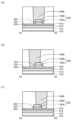
본 발명의 일 형태는, 채널 형성 영역에 산화물을 가지는 반도체 장치로서, 반도체 장치는 트랜지스터, 층간막, 및 제 1 도전체를 가지고, 트랜지스터는 제 1 절연체 위의 산화물과, 산화물 위의 제 2 도전체와, 산화물과 제 2 도전체 사이에 제공되며 제 2 도전체의 측면과 접하도록 제공된 제 2 절연체와, 제 2 절연체를 사이에 두고 제 2 도전체의 측면에 제공된 제 3 절연체를 가지고, 산화물은 제 1 영역, 제 2 영역, 및 제 3 영역을 가지고, 제 1 영역은 제 2 도전체와 중첩되고, 제 2 영역은 제 1 영역과 제 3 영역 사이에 제공되고, 제 3 영역은 제 2 영역보다 저저항이고, 제 2 영역은 제 1 영역보다 저저항이고, 층간막은 제 1 절연체 위 및 산화물 위에 제공되고, 제 1 도전체는 제 3 영역과 전기적으로 접속되고, 제 3 영역은 제 3 절연체, 제 1 도전체, 및 층간막 중 어느 하나와 중첩되고, 제 3 절연체의 상면은 층간막의 상면과 실질적으로 일치하는 반도체 장치이다.One form of the present invention is a semiconductor device having an oxide in a channel formation region, wherein the semiconductor device has a transistor, an interlayer film, and a first conductor, and the transistor has an oxide on a first insulator and a second conductor on the oxide. It has a body, a second insulator provided between the oxide and the second conductor and in contact with the side surface of the second conductor, and a third insulator provided on the side surface of the second conductor with the second insulator interposed therebetween, the oxide has a first region, a second region, and a third region, where the first region overlaps the second conductor, the second region is provided between the first region and the third region, and the third region overlaps the second conductor. region, the second region has a lower resistance than the first region, an interlayer film is provided on the first insulator and on the oxide, the first conductor is electrically connected to the third region, and the third region is electrically connected to the third region. It is a semiconductor device that overlaps one of an insulator, a first conductor, and an interlayer film, and the top surface of the third insulator substantially coincides with the top surface of the interlayer film.
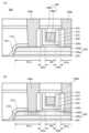
본 발명의 일 형태는, 채널 형성 영역에 산화물을 가지는 반도체 장치로서, 반도체 장치는 트랜지스터, 용량, 층간막, 및 제 1 도전체를 가지고, 트랜지스터는, 제 1 절연체 위의 산화물과, 산화물 위의 제 2 도전체와, 산화물과 제 2 도전체 사이에 제공되며 제 2 도전체의 측면과 접하도록 제공된 제 2 절연체와, 제 2 절연체를 사이에 두고 제 2 도전체의 측면에 제공된 제 3 절연체를 가지고, 산화물은 제 1 영역, 한 쌍의 제 2 영역, 및 한 쌍의 제 3 영역을 가지고, 제 1 영역은 제 2 도전체와 중첩되고, 제 1 영역은 한 쌍의 제 2 영역 사이에 제공되고, 제 1 영역 및 한 쌍의 제 2 영역은 한 쌍의 제 3 영역 사이에 제공되고, 제 3 영역은 제 2 영역보다 저저항이고, 제 2 영역은 제 1 영역보다 저저항이고, 층간막은 제 1 절연체 위 및 산화물 위에 제공되고, 제 1 도전체는 한 쌍의 제 3 영역의 한쪽과 전기적으로 접속되고, 용량은 한 쌍의 제 3 영역의 다른 쪽과 전기적으로 접속되고, 제 3 절연체의 상면은 층간막의 상면과 실질적으로 일치하는 것이 바람직하다.One form of the present invention is a semiconductor device having an oxide in a channel formation region, wherein the semiconductor device has a transistor, a capacitor, an interlayer film, and a first conductor, and the transistor has an oxide on a first insulator and an oxide on the oxide. a second conductor, a second insulator provided between the oxide and the second conductor and in contact with the side of the second conductor, and a third insulator provided on the side of the second conductor with the second insulator in between. Having, the oxide has a first region, a pair of second regions, and a pair of third regions, the first region overlapping the second conductor, and the first region provided between the pair of second regions. The first region and the pair of second regions are provided between the pair of third regions, the third region has lower resistance than the second region, the second region has lower resistance than the first region, and the interlayer film is provided over a first insulator and over an oxide, wherein the first conductor is electrically connected to one side of the pair of third regions, the capacitor is electrically connected to the other side of the pair of third regions, and the first conductor is electrically connected to the other side of the pair of third regions, It is preferable that the upper surface substantially coincides with the upper surface of the interlayer film.
상기에서, 한 쌍의 제 3 영역의 다른 쪽은 용량의 한쪽의 전극으로서 기능하는 것이 바람직하다.In the above, the other side of the pair of third regions preferably functions as an electrode of one side of the capacitor.
상기에서, 층간막은 한 쌍의 제 3 영역의 다른 쪽의 적어도 일부를 노출시키는 개구를 가지고, 용량은 개구에서 한 쌍의 제 3 영역의 다른 쪽 위의 제 4 절연체와 제 4 절연체 위의 제 3 도전체를 가지고, 한 쌍의 제 3 영역의 다른 쪽은 용량의 한쪽의 전극으로서 기능하고, 제 4 절연체는 용량의 유전체로서 기능하고, 제 3 도전체는 용량의 다른 쪽의 전극으로서 기능하는 것이 바람직하다.In the above, the interlayer has an opening exposing at least a portion of the other side of the pair of third regions, and the capacitance extends from the opening to the fourth insulator on the other side of the pair of third regions and the third over the fourth insulator. With a conductor, the other side of the pair of third regions functions as an electrode on one side of the capacitor, the fourth insulator functions as a dielectric of the capacitor, and the third conductor functions as an electrode on the other side of the capacitor. desirable.
상기에서, 제 3 도전체는 개구 내에 매립되도록 형성되어 있는 것이 바람직하다.In the above, the third conductor is preferably formed to be buried in the opening.
상기에서, 산화물은 In과, 원소 M(M은 Al, Ga, Y, 또는 Sn)과, Zn을 포함하는 것이 바람직하다.In the above, the oxide preferably contains In, an element M (M is Al, Ga, Y, or Sn), and Zn.
상기에서, 산화물은 원자수비에 있어서, 원소 M보다 In이 더 많은 것이 바람직하다.In the above, it is preferable that the oxide contains more In than the element M in terms of atomic ratio.
상기에서, 제 3 영역은 제 2 영역보다 캐리어 밀도가 크고, 제 2 영역은 제 1 영역보다 캐리어 밀도가 큰 것이 바람직하다.In the above, it is preferable that the third area has a higher carrier density than the second area, and the second area has a higher carrier density than the first area.
상기에서, 제 3 영역은 알루미늄, 루테늄, 타이타늄, 탄탈럼, 크로뮴, 및 텅스텐 중 적어도 하나를 가지는 것이 바람직하다.In the above, the third region preferably has at least one of aluminum, ruthenium, titanium, tantalum, chromium, and tungsten.
상기에서, 제 3 영역은 질소를 더 가지는 것이 바람직하다.In the above, it is preferable that the third region further contains nitrogen.
상기에서, 제 2 영역은 제 1 영역보다 아르곤 농도가 높은 것이 바람직하다.In the above, the second region preferably has a higher argon concentration than the first region.
상기에서, 제 1 영역은 제 2 영역보다 수소 농도가 낮은 것이 바람직하다.In the above, it is preferable that the first region has a lower hydrogen concentration than the second region.
상기에서, 제 1 영역은 제 2 영역 및 제 3 영역보다 수소 농도가 낮은 것이 바람직하다.In the above, the first region preferably has a lower hydrogen concentration than the second region and the third region.
상기에서, 트랜지스터는 노멀리 오프형인 것이 바람직하다.In the above, the transistor is preferably of the normally off type.
본 발명의 일 형태는, 기판 위에 제 1 절연체를 형성하고, 제 1 절연체 위에 산화물층을 형성하고, 산화물층 위에 제 1 절연막 및 더미 게이트막을 순차적으로 성막하고, 제 1 절연막 및 더미 게이트막을 가공하여 제 2 절연체 및 더미 게이트층을 형성하고, 적어도 산화물층에 접하며 금속을 포함하는 제 1 막을 형성하고, 제 1 막 및 산화물층에 대하여 질소를 포함하는 분위기에서 가열 처리를 수행하고, 제 1 막을 제거하고, 제 1 절연체, 산화물층, 제 2 절연체, 및 더미 게이트층을 덮어 제 2 절연막을 성막하고, 제 2 절연막을 가공함으로써, 제 2 절연체의 측면 및 더미 게이트층의 측면에 제 3 절연체를 형성하고, 제 1 절연체, 산화물층, 더미 게이트층, 및 제 3 절연체를 덮어 제 3 절연막을 성막하고, 제 1 CMP 처리를 수행하고, 더미 게이트층의 일부가 노출될 때까지 제 3 절연막의 일부를 제거함으로써 제 4 절연체를 형성하고, 더미 게이트층을 에칭함으로써 제 2 절연체를 노출시키고, 제 2 절연체를 에칭함으로써 산화물층을 노출시키고, 산화물 및 제 3 절연체의 측면에 접하도록 제 4 절연막을 성막하고, 제 4 절연막 위에 도전체막을 성막하고, 제 2 CMP 처리를 수행함으로써 도전체막의 일부 및 제 4 절연막의 일부를 제 4 절연체가 노출될 때까지 제거하여 제 1 도전체층 및 제 1 도전체층의 측면과 하면을 덮는 제 5 절연체를 형성하고, 제 4 절연체에 개구를 형성하고, 개구를 매립하도록 제 2 도전체를 형성하는 반도체 장치의 제작 방법이다.One form of the present invention includes forming a first insulator on a substrate, forming an oxide layer on the first insulator, sequentially forming a first insulating film and a dummy gate film on the oxide layer, and processing the first insulating film and the dummy gate film. Forming a second insulator and a dummy gate layer, forming a first film containing a metal and at least in contact with the oxide layer, performing heat treatment on the first film and the oxide layer in an atmosphere containing nitrogen, and removing the first film. Then, a second insulating film is formed to cover the first insulator, the oxide layer, the second insulator, and the dummy gate layer, and the second insulating film is processed to form a third insulator on the side of the second insulator and the side of the dummy gate layer. Then, a third insulating film is formed to cover the first insulator, the oxide layer, the dummy gate layer, and the third insulator, a first CMP process is performed, and a portion of the third insulating film is removed until a portion of the dummy gate layer is exposed. forming a fourth insulator by removing the dummy gate layer, exposing the second insulator by etching the dummy gate layer, exposing the oxide layer by etching the second insulator, and forming a fourth insulating film in contact with the side surfaces of the oxide and the third insulator; , a conductor film is deposited on the fourth insulating film, and a second CMP process is performed to remove a part of the conductor film and a part of the fourth insulating film until the fourth insulator is exposed, thereby removing the first conductor layer and the side surfaces of the first conductor layer. This is a method of manufacturing a semiconductor device in which a fifth insulator is formed to cover the upper and lower surfaces, an opening is formed in the fourth insulator, and a second conductor is formed to fill the opening.
상기에서, 제 1 막은 아르곤, 질소, 및 산소 중에서 선택되는 어느 하나 또는 복수의 가스를 사용하여, 스퍼터링법으로 형성되는 것이 바람직하다.In the above, the first film is preferably formed by sputtering using one or more gases selected from argon, nitrogen, and oxygen.
상기에서, 제 1 막은 알루미늄, 루테늄, 타이타늄, 탄탈럼, 크로뮴, 및 텅스텐 중 적어도 하나를 가지는 것이 바람직하다.In the above, the first film preferably has at least one of aluminum, ruthenium, titanium, tantalum, chromium, and tungsten.
상기에서, 제 1 막은 알루미늄 및 타이타늄을 가지는 것이 바람직하다.In the above, the first film preferably has aluminum and titanium.
상기에서, 제 1 막은 질소 및 산소 중 어느 한쪽 또는 양쪽을 더 가지는 것이 바람직하다.In the above, it is preferable that the first film further contains either or both nitrogen and oxygen.
상기에서, 제 1 막은 0.5nm 이상 5nm 미만인 것이 바람직하다.In the above, the first film is preferably 0.5 nm or more and less than 5 nm.
상기에서, 가열 처리를 수행함으로써 산화물층의, 산화물층과 제 1 막의 계면 근방에 포함되는 산소가 제 1 막으로 추출되는 것이 바람직하다.In the above, it is preferable that oxygen contained in the oxide layer near the interface between the oxide layer and the first film is extracted into the first film by performing the heat treatment.
상기에서, 개구는 산화물층의 상면의 일부 및 산화물층의 측면의 일부가 노출되도록 형성되는 것이 바람직하다.In the above, the opening is preferably formed so that a portion of the upper surface of the oxide layer and a portion of the side surface of the oxide layer are exposed.
상기에서, 제 2 절연막의 가공은 드라이 에칭법을 사용하여 이방성 에칭을 수행하는 것이 바람직하다.In the above, the processing of the second insulating film is preferably anisotropic etching using a dry etching method.
상기에서, 더미 게이트층 형성 후에, 더미 게이트층과 중첩되는 산화물의 일부에 불순물을 첨가하는 것이 바람직하다.In the above, after forming the dummy gate layer, it is preferable to add impurities to a portion of the oxide that overlaps the dummy gate layer.
상기에서, 불순물은 아르곤 또는 질소인 것이 바람직하다.In the above, the impurity is preferably argon or nitrogen.
본 발명의 일 형태에 의하여, 양호한 전기 특성을 가지는 반도체 장치를 제공할 수 있다. 본 발명의 일 형태에 의하여, 미세화 또는 고집적화가 가능한 반도체 장치를 제공할 수 있다. 본 발명의 일 형태에 의하여 생산성이 높은 반도체 장치를 제공할 수 있다.According to one embodiment of the present invention, a semiconductor device having good electrical characteristics can be provided. According to one embodiment of the present invention, a semiconductor device capable of miniaturization or high integration can be provided. According to one embodiment of the present invention, a semiconductor device with high productivity can be provided.
또는, 장기간의 데이터 유지가 가능한 반도체 장치를 제공할 수 있다. 또는, 데이터의 기록 속도가 빠른 반도체 장치를 제공할 수 있다. 또는, 설계 자유도가 높은 반도체 장치를 제공할 수 있다. 또는, 소비전력을 억제할 수 있는 반도체 장치를 제공할 수 있다. 또는, 신규 반도체 장치를 제공할 수 있다.Alternatively, a semiconductor device capable of long-term data retention can be provided. Alternatively, a semiconductor device with a high data recording speed can be provided. Alternatively, a semiconductor device with a high degree of design freedom can be provided. Alternatively, a semiconductor device capable of suppressing power consumption can be provided. Alternatively, a new semiconductor device can be provided.
또한 이들 효과의 기재는 다른 효과의 존재를 방해하는 것은 아니다. 또한, 본 발명의 일 형태는 이들 효과 모두를 가질 필요는 없다. 또한, 이들 외의 효과는 명세서, 도면, 청구항 등의 기재로부터 저절로 명백해지는 것이며 명세서, 도면, 청구항 등의 기재로부터 이들 외의 효과를 추출할 수 있다.Additionally, the description of these effects does not preclude the existence of other effects. Additionally, one embodiment of the present invention does not need to have all of these effects. In addition, these other effects are naturally apparent from the description, drawings, claims, etc., and these other effects can be extracted from the description, drawings, claims, etc.
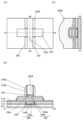
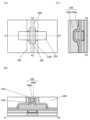
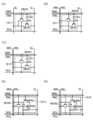
도 1은 본 발명의 일 형태에 따른 반도체 장치의 상면도 및 단면도.
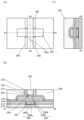
도 2는 본 발명의 일 형태에 따른 반도체 장치의 단면도.
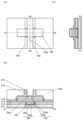
도 3은 본 발명의 일 형태에 따른 반도체 장치의 단면도.
도 4는 본 발명의 일 형태에 따른 반도체 장치의 제작 방법을 도시한 상면도 및 단면도.
도 5는 본 발명의 일 형태에 따른 반도체 장치의 제작 방법을 도시한 상면도 및 단면도.
도 6은 본 발명의 일 형태에 따른 반도체 장치의 제작 방법을 도시한 상면도 및 단면도.
도 7은 본 발명의 일 형태에 따른 반도체 장치의 제작 방법을 도시한 상면도 및 단면도.
도 8은 본 발명의 일 형태에 따른 반도체 장치의 제작 방법을 도시한 상면도 및 단면도.
도 9는 본 발명의 일 형태에 따른 반도체 장치의 제작 방법을 도시한 상면도 및 단면도.
도 10은 본 발명의 일 형태에 따른 반도체 장치의 제작 방법을 도시한 상면도 및 단면도.
도 11은 본 발명의 일 형태에 따른 반도체 장치의 제작 방법을 도시한 상면도 및 단면도.
도 12는 본 발명의 일 형태에 따른 반도체 장치의 제작 방법을 도시한 상면도 및 단면도.
도 13은 본 발명의 일 형태에 따른 반도체 장치의 제작 방법을 도시한 상면도 및 단면도.
도 14는 본 발명의 일 형태에 따른 반도체 장치의 제작 방법을 도시한 상면도 및 단면도.
도 15는 본 발명의 일 형태에 따른 반도체 장치의 제작 방법을 도시한 상면도 및 단면도.
도 16은 본 발명의 일 형태에 따른 반도체 장치의 제작 방법을 도시한 상면도 및 단면도.
도 17은 본 발명의 일 형태에 따른 반도체 장치의 제작 방법을 도시한 상면도 및 단면도.
도 18은 본 발명의 일 형태에 따른 반도체 장치의 제작 방법을 도시한 상면도 및 단면도.
도 19는 본 발명의 일 형태에 따른 반도체 장치의 제작 방법을 도시한 상면도 및 단면도.
도 20은 본 발명의 일 형태에 따른 반도체 장치의 제작 방법을 도시한 상면도 및 단면도.
도 21은 본 발명의 일 형태에 따른 반도체 장치의 제작 방법을 도시한 상면도 및 단면도.
도 22는 본 발명의 일 형태에 따른 반도체 장치의 제작 방법을 도시한 상면도 및 단면도.
도 23은 본 발명의 일 형태에 따른 반도체 장치의 제작 방법을 도시한 상면도 및 단면도.
도 24는 본 발명의 일 형태에 따른 반도체 장치의 제작 방법을 도시한 상면도 및 단면도.
도 25는 산화물 반도체의 에너지 밴드 구조를 설명하는 도면.
도 26은 본 발명의 일 형태에 따른 반도체 장치의 상면도 및 단면도.
도 27은 본 발명의 일 형태에 따른 반도체 장치의 회로도 및 단면도.
도 28은 본 발명의 일 형태에 따른 반도체 장치의 회로도 및 단면도.
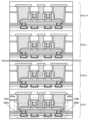
도 29는 본 발명의 일 형태에 따른 기억 장치의 구성을 도시한 단면도.
도 30은 본 발명의 일 형태에 따른 기억 장치의 구성을 도시한 단면도.
도 31은 본 발명의 일 형태에 따른 기억 장치의 구성을 도시한 단면도.
도 32는 본 발명의 일 형태에 따른 기억 장치의 구성을 도시한 단면도.
도 33은 본 발명의 일 형태에 따른 기억 장치의 회로도 및 단면도.
도 34는 본 발명의 일 형태에 따른 기억 장치의 구성을 도시한 단면도.
도 35는 본 발명의 일 형태에 따른 기억 장치의 구성을 도시한 단면도.
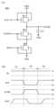
도 36은 인버터 회로의 구성예를 도시한 회로도와, 그 동작예를 나타낸 타이밍 차트.
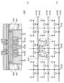
도 37은 본 발명의 일 형태에 따른 기억 장치의 구성예를 도시한 블록도.
도 38은 본 발명의 일 형태에 따른 기억 장치의 구성예를 도시한 회로도.
도 39는 본 발명의 일 형태에 따른 기억 장치의 구성예를 도시한 회로도.
도 40은 본 발명의 일 형태에 따른 기억 장치의 구성예를 도시한 블록도.
도 41은 본 발명의 일 형태에 따른 기억 장치의 구성예를 도시한 블록도 및 회로도.
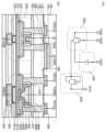
도 42는 본 발명의 일 형태에 따른 반도체 장치의 회로도.
도 43은 본 발명의 일 형태에 따른 반도체 장치의 구성예를 도시한 단면도.
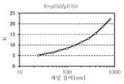
도 44는 트랜지스터의 μFE의 채널 길이 의존성을 나타낸 도면.
도 45는 트랜지스터의 μFE의 채널 길이 의존성을 나타낸 도면.
도 46은 OS 트랜지스터의 μFE에 대한 Si 트랜지스터의 μFE의 비율을 채널 길이 의존성으로 나타낸 도면.
도 47은 본 발명의 일 형태에 따른 반도체 장치의 구성예를 도시한 블록도.
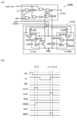
도 48은 본 발명의 일 형태에 따른 반도체 장치의 구성예를 도시한 블록도, 회로도, 및 반도체 장치의 동작예를 나타낸 타이밍 차트.
도 49는 본 발명의 일 형태에 따른 반도체 장치의 구성예를 도시한 블록도.
도 50은 본 발명의 일 형태에 따른 반도체 장치의 구성예를 도시한 회로도 및 반도체 장치의 동작예를 나타낸 타이밍 차트.
도 51은 본 발명의 일 형태에 따른 기억 장치의 모식도.
도 52는 본 발명의 일 형태에 따른 AI 시스템의 구성예를 도시한 블록도.
도 53은 본 발명의 일 형태에 따른 AI 시스템의 응용예를 설명하는 블록도.
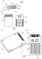
도 54는 본 발명의 일 형태에 따른 AI 시스템을 제공한 IC의 구성예를 도시한 사시 모식도.
도 55는 본 발명의 일 형태에 따른 전자 기기를 도시한 도면.
도 56은 본 발명의 일 형태에 따른 전자 기기를 도시한 도면.
도 57은 본 실시예의 시료의 시트 저항을 설명하는 도면.1 is a top view and a cross-sectional view of a semiconductor device according to one embodiment of the present invention.
2 is a cross-sectional view of a semiconductor device according to one embodiment of the present invention.
3 is a cross-sectional view of a semiconductor device according to one embodiment of the present invention.
4 is a top view and a cross-sectional view showing a method of manufacturing a semiconductor device according to one embodiment of the present invention.
5 is a top view and a cross-sectional view showing a method of manufacturing a semiconductor device according to one embodiment of the present invention.
6 is a top view and a cross-sectional view showing a method of manufacturing a semiconductor device according to one embodiment of the present invention.
7 is a top view and a cross-sectional view showing a method of manufacturing a semiconductor device according to one embodiment of the present invention.
8 is a top view and a cross-sectional view showing a method of manufacturing a semiconductor device according to one embodiment of the present invention.
9 is a top view and a cross-sectional view showing a method of manufacturing a semiconductor device according to one embodiment of the present invention.
10 is a top view and a cross-sectional view showing a method of manufacturing a semiconductor device according to one embodiment of the present invention.
11 is a top view and a cross-sectional view showing a method of manufacturing a semiconductor device according to one embodiment of the present invention.
12 is a top view and a cross-sectional view showing a method of manufacturing a semiconductor device according to one embodiment of the present invention.
13 is a top view and cross-sectional view showing a method of manufacturing a semiconductor device according to one embodiment of the present invention.
14 is a top view and cross-sectional view showing a method of manufacturing a semiconductor device according to one embodiment of the present invention.
15 is a top view and a cross-sectional view showing a method of manufacturing a semiconductor device according to one embodiment of the present invention.
16 is a top view and cross-sectional view showing a method of manufacturing a semiconductor device according to one embodiment of the present invention.
17 is a top view and cross-sectional view showing a method of manufacturing a semiconductor device according to one embodiment of the present invention.
18 is a top view and a cross-sectional view showing a method of manufacturing a semiconductor device according to one embodiment of the present invention.
19 is a top view and a cross-sectional view showing a method of manufacturing a semiconductor device according to one embodiment of the present invention.
20 is a top view and a cross-sectional view showing a method of manufacturing a semiconductor device according to one embodiment of the present invention.
21 is a top view and a cross-sectional view showing a method of manufacturing a semiconductor device according to one embodiment of the present invention.
22 is a top view and a cross-sectional view showing a method of manufacturing a semiconductor device according to one embodiment of the present invention.
23 is a top view and a cross-sectional view showing a method of manufacturing a semiconductor device according to one embodiment of the present invention.
24 is a top view and a cross-sectional view showing a method of manufacturing a semiconductor device according to one embodiment of the present invention.
Figure 25 is a diagram explaining the energy band structure of an oxide semiconductor.
26 is a top view and a cross-sectional view of a semiconductor device according to one embodiment of the present invention.
27 is a circuit diagram and cross-sectional view of a semiconductor device according to one embodiment of the present invention.
28 is a circuit diagram and cross-sectional view of a semiconductor device according to one embodiment of the present invention.
Fig. 29 is a cross-sectional view showing the configuration of a storage device according to one embodiment of the present invention.
Figure 30 is a cross-sectional view showing the configuration of a storage device according to one embodiment of the present invention.
31 is a cross-sectional view showing the configuration of a storage device according to one embodiment of the present invention.
Figure 32 is a cross-sectional view showing the configuration of a storage device according to one embodiment of the present invention.
33 is a circuit diagram and cross-sectional view of a memory device according to one embodiment of the present invention.
Figure 34 is a cross-sectional view showing the configuration of a storage device according to one embodiment of the present invention.
Figure 35 is a cross-sectional view showing the configuration of a storage device according to one embodiment of the present invention.
Fig. 36 is a circuit diagram showing an example of the configuration of an inverter circuit and a timing chart showing an example of its operation.
Fig. 37 is a block diagram showing a configuration example of a storage device according to one embodiment of the present invention.
Fig. 38 is a circuit diagram showing a configuration example of a storage device according to one embodiment of the present invention.
Fig. 39 is a circuit diagram showing a configuration example of a storage device according to one embodiment of the present invention.
Fig. 40 is a block diagram showing a configuration example of a storage device according to one embodiment of the present invention.
Figure 41 is a block diagram and circuit diagram showing a configuration example of a storage device according to one embodiment of the present invention.
42 is a circuit diagram of a semiconductor device according to one embodiment of the present invention.
43 is a cross-sectional view showing a configuration example of a semiconductor device according to one embodiment of the present invention.
Figure 44 is a diagram showing the dependence of μFE of the transistor on the channel length.
Figure 45 is a diagram showing the dependence of μFE of the transistor on the channel length.
Figure 46 is a diagram showing the ratio of μFE of a Si transistor to μFE of an OS transistor in dependence on channel length.
47 is a block diagram showing a configuration example of a semiconductor device according to one embodiment of the present invention.
48 is a block diagram showing an example of the configuration of a semiconductor device according to one embodiment of the present invention, a circuit diagram, and a timing chart showing an example of operation of the semiconductor device.
Fig. 49 is a block diagram showing a configuration example of a semiconductor device according to one embodiment of the present invention.
50 is a circuit diagram showing an example of the configuration of a semiconductor device according to one embodiment of the present invention, and a timing chart showing an example of operation of the semiconductor device.
Figure 51 is a schematic diagram of a storage device according to one embodiment of the present invention.
Figure 52 is a block diagram showing a configuration example of an AI system according to one form of the present invention.
53 is a block diagram illustrating an application example of an AI system according to one form of the present invention.
Figure 54 is a perspective schematic diagram showing a configuration example of an IC that provides an AI system according to one form of the present invention.
Figure 55 is a diagram showing an electronic device according to one embodiment of the present invention.
56 is a diagram showing an electronic device according to one embodiment of the present invention.
Figure 57 is a diagram explaining the sheet resistance of the sample of this example.
이하에서, 실시형태에 대하여 도면을 참조하면서 설명한다. 다만, 실시형태는 많은 상이한 형태로 실시할 수 있고, 취지 및 그 범위에서 벗어남이 없이 그 형태 및 자세한 사항을 다양하게 변경할 수 있는 것은 통상의 기술자라면 용이하게 이해할 수 있다. 따라서, 본 발명은 이하의 실시형태의 기재 내용에 한정하여 해석되는 것은 아니다.Below, embodiments will be described with reference to the drawings. However, the embodiment can be implemented in many different forms, and those skilled in the art can easily understand that the form and details can be changed in various ways without departing from the spirit and scope. Accordingly, the present invention should not be construed as limited to the description of the embodiments below.
또한, 도면에서, 크기, 층의 두께, 또는 영역은 명료화를 위하여 과장되어 있는 경우가 있다. 따라서, 반드시 그 스케일에 한정되는 것은 아니다. 또한, 도면은 이상적인 예를 모식적으로 나타낸 것이며, 도면에 나타낸 형상 또는 값 등에 한정되지 않는다. 예를 들어, 실제의 제조 공정에서, 에칭 등의 처리에 의하여 층이나 레지스트 마스크 등이 의도치 않게 감소되는 경우가 있지만, 이해를 용이하게 하기 위하여 이를 생략하는 경우가 있다. 또한, 도면에서, 동일한 부분 또는 같은 기능을 가지는 부분에는 동일한 부호를 상이한 도면 사이에서 공통적으로 사용하고, 이의 반복적인 설명은 생략하는 경우가 있다. 또한, 같은 기능을 가지는 부분을 가리키는 경우에는, 해치 패턴을 동일하게 하고, 특별히 부호를 붙이지 않는 경우가 있다.Additionally, in the drawings, sizes, layer thicknesses, or areas may be exaggerated for clarity. Therefore, it is not necessarily limited to that scale. Additionally, the drawings schematically show an ideal example and are not limited to the shapes or values shown in the drawings. For example, in the actual manufacturing process, there are cases where the layer or resist mask is unintentionally reduced due to processing such as etching, but this may be omitted to facilitate understanding. Additionally, in the drawings, the same symbols are commonly used in different drawings for parts that are the same or have the same function, and repetitive description thereof may be omitted. Additionally, when referring to parts with the same function, the hatch patterns may be the same and no special symbols may be attached.
또한, 특히 상면도('평면도'라고도 함)나 사시도 등에서, 발명의 이해를 용이하게 하기 위하여 일부의 구성 요소의 기재를 생략하는 경우가 있다. 또한, 일부의 숨은선 등의 기재를 생략하는 경우가 있다.Additionally, in order to facilitate understanding of the invention, especially in top views (also referred to as "top views") or perspective views, the description of some components may be omitted. Additionally, description of some hidden lines, etc. may be omitted.
또한, 본 명세서 등에서, 제 1, 제 2 등으로 붙여지는 서수사는 편의상 사용하는 것이며, 공정 순서 또는 적층 순서를 나타내는 것이 아니다. 그러므로, 예를 들어 '제 1'을 '제 2' 또는 '제 3' 등으로 적절히 치환하여 설명할 수 있다. 또한, 본 명세서 등에 기재되어 있는 서수사와, 본 발명의 일 형태를 특정하기 위하여 사용되는 서수사는 일치하지 않는 경우가 있다.Additionally, in this specification and the like, ordinal numbers such as first, second, etc. are used for convenience and do not indicate the process order or stacking order. Therefore, for example, '1st' can be explained by appropriately replacing '2nd' or '3rd'. Additionally, the ordinal numbers described in this specification and the like may not match the ordinal numbers used to specify one form of the present invention.
또한, 본 명세서에서, '위', '아래' 등 배치를 나타내는 말은, 구성끼리의 위치 관계를 도면을 참조하여 설명하기 위하여, 편의상 사용하고 있다. 또한, 구성끼리의 위치 관계는 각 구성을 묘사하는 방향에 따라 적절히 변화되는 것이다. 따라서, 명세서에서 설명된 말에 한정되지 않고, 상황에 따라 적절히 환언할 수 있다.In addition, in this specification, words indicating arrangement such as 'up' and 'down' are used for convenience in order to explain the positional relationship between components with reference to the drawings. Additionally, the positional relationship between components changes appropriately depending on the direction in which each component is depicted. Therefore, it is not limited to the words described in the specification, and may be rephrased appropriately depending on the situation.
예를 들어, 본 명세서 등에서, X와 Y가 접속되어 있다고 명시적으로 기재되어 있는 경우에는, X와 Y가 전기적으로 접속되어 있는 경우와, X와 Y가 기능적으로 접속되어 있는 경우와, X와 Y가 직접 접속되어 있는 경우가, 본 명세서 등에 개시되어 있는 것으로 한다. 따라서, 소정의 접속 관계, 예를 들어 도면 또는 문장에 나타낸 접속 관계에 한정되지 않고, 도면 또는 문장에 나타낸 접속 관계 이외의 것도, 도면 또는 문장에 기재되어 있는 것으로 한다.For example, in this specification, etc., when it is explicitly stated that X and Y are connected, the case where X and Y are electrically connected, the case where The case where Y is directly connected is assumed to be disclosed in this specification and the like. Therefore, it is not limited to the predetermined connection relationship, for example, the connection relationship shown in the drawing or text, and connection relationships other than those shown in the drawing or text are also described in the drawing or text.
여기서, X, Y는 대상물(예를 들어 장치, 소자, 회로, 배선, 전극, 단자, 도전막, 층 등)인 것으로 한다.Here, X and Y are assumed to be objects (e.g., devices, elements, circuits, wiring, electrodes, terminals, conductive films, layers, etc.).
X와 Y가 직접적으로 접속되어 있는 경우의 일례로서는, X와 Y의 전기적인 접속을 가능하게 하는 소자(예를 들어 스위치, 트랜지스터, 용량 소자, 인덕터, 저항 소자, 다이오드, 표시 소자, 발광 소자, 부하 등)가 X와 Y 사이에 접속되어 있지 않은 경우이고, X와 Y의 전기적인 접속을 가능하게 하는 소자(예를 들어 스위치, 트랜지스터, 용량 소자, 인덕터, 저항 소자, 다이오드, 표시 소자, 발광 소자, 부하 등)를 통하지 않고 X와 Y가 접속되어 있는 경우이다.As an example of a case where X and Y are directly connected, elements that enable electrical connection between load, etc.) is not connected between X and Y, and elements that enable electrical connection between This is a case where X and Y are connected without passing through an element, load, etc.).
X와 Y가 전기적으로 접속되어 있는 경우의 일례로서는, X와 Y의 전기적인 접속을 가능하게 하는 소자(예를 들어 스위치, 트랜지스터, 용량 소자, 인덕터, 저항 소자, 다이오드, 표시 소자, 발광 소자, 부하 등)가 X와 Y 사이에 하나 이상 접속될 수 있다. 또한, 스위치는 온, 오프가 제어되는 기능을 가진다. 즉, 스위치는 도통 상태(온 상태) 또는 비도통 상태(오프 상태)가 되고, 전류를 흘릴지 여부를 제어하는 기능을 가진다. 또는, 스위치는 전류를 흘리는 경로를 선택하여 전환하는 기능을 가진다. 또한, X와 Y가 전기적으로 접속되어 있는 경우에는, X와 Y가 직접적으로 접속되어 있는 경우를 포함하는 것으로 한다.As an example of a case where X and Y are electrically connected, elements that enable electrical connection between load, etc.) may be connected between X and Y. Additionally, the switch has the function of being controlled on and off. That is, the switch is in a conductive state (on state) or non-conductive state (off state) and has the function of controlling whether or not current flows. Alternatively, a switch has the function of selecting and switching a path through which current flows. Additionally, the case where X and Y are electrically connected includes the case where X and Y are directly connected.
X와 Y가 기능적으로 접속되어 있는 경우의 일례로서는, X와 Y의 기능적인 접속을 가능하게 하는 회로(예를 들어 논리 회로(인버터, NAND 회로, NOR 회로 등), 신호 변환 회로(DA 변환 회로, AD 변환 회로, 감마 보정 회로 등), 전위 레벨 변환 회로(전원 회로(승압 회로, 강압 회로 등), 신호의 전위 레벨을 변환시키는 레벨 시프터 회로 등), 전압원, 전류원, 전환 회로, 증폭 회로(신호 진폭 또는 전류량 등을 크게 할 수 있는 회로, 연산 증폭기, 차동 증폭 회로, 소스 폴로어 회로, 버퍼 회로 등), 신호 생성 회로, 기억 회로, 제어 회로 등)가 X와 Y 사이에 하나 이상 접속될 수 있다. 또한, 일례로서, X와 Y 사이에 다른 회로를 끼워도, X로부터 출력된 신호가 Y로 전달되는 경우에는, X와 Y는 기능적으로 접속되어 있는 것으로 한다. 또한, X와 Y가 기능적으로 접속되어 있는 경우에는, X와 Y가 직접적으로 접속되어 있는 경우와 X와 Y가 전기적으로 접속되어 있는 경우를 포함하는 것으로 한다.An example of a case where X and Y are functionally connected include circuits that enable functional connection of , AD conversion circuit, gamma correction circuit, etc.), potential level conversion circuit (power circuit (boosting circuit, step-down circuit, etc.), level shifter circuit that converts the potential level of the signal, etc.), voltage source, current source, switching circuit, amplification circuit ( One or more circuits (operational amplifiers, differential amplifier circuits, source follower circuits, buffer circuits, etc.) that can increase signal amplitude or current amount, signal generation circuits, memory circuits, control circuits, etc.) are connected between X and Y. You can. Additionally, as an example, even if another circuit is inserted between X and Y, if the signal output from X is transmitted to Y, X and Y are assumed to be functionally connected. Additionally, the case where X and Y are functionally connected includes the case where X and Y are directly connected and the case where X and Y are electrically connected.
또한, 본 명세서 등에서, 트랜지스터란, 게이트와, 드레인과, 소스를 포함하는 적어도 3개의 단자를 가지는 소자이다. 그리고, 드레인(드레인 단자, 드레인 영역, 또는 드레인 전극)과 소스(소스 단자, 소스 영역, 또는 소스 전극) 사이에 채널이 형성되는 영역을 가지고, 채널이 형성되는 영역을 통하여 소스와 드레인 사이에 전류를 흘릴 수 있다. 또한, 본 명세서 등에서 채널이 형성되는 영역이란 전류가 주로 흐르는 영역을 말한다.Additionally, in this specification and the like, a transistor is an element having at least three terminals including a gate, drain, and source. And, it has a region where a channel is formed between the drain (drain terminal, drain region, or drain electrode) and the source (source terminal, source region, or source electrode), and a current flows between the source and the drain through the region where the channel is formed. can shed Additionally, in this specification and the like, the area where the channel is formed refers to the area where current mainly flows.
또한, 소스나 드레인의 기능은 상이한 극성의 트랜지스터를 채용하는 경우나, 회로 동작에서 전류의 방향이 변화하는 경우 등에는 바뀌는 경우가 있다. 그러므로, 본 명세서 등에서는, 소스나 드레인의 용어는 바꾸어 사용할 수 있는 경우가 있다.Additionally, the functions of the source and drain may change when transistors of different polarities are employed or when the direction of current changes during circuit operation. Therefore, in this specification and the like, the terms source and drain may be used interchangeably.
또한, 채널 길이란, 예를 들어 트랜지스터의 상면도에서, 반도체(또는 트랜지스터가 온 상태일 때 반도체 내에서 전류가 흐르는 부분)와 게이트 전극이 서로 중첩되는 영역, 또는 채널이 형성되는 영역에서의 소스(소스 영역 또는 소스 전극)와 드레인(드레인 영역 또는 드레인 전극) 사이의 거리를 말한다. 또한, 하나의 트랜지스터에서, 채널 길이가 모든 영역에서 같은 값을 취한다고 할 수는 없다. 즉, 하나의 트랜지스터의 채널 길이는, 하나의 값으로 정해지지 않는 경우가 있다. 그러므로, 본 명세서에서 채널 길이는 채널이 형성되는 영역에서의 어느 하나의 값, 최댓값, 최솟값, 또는 평균값으로 한다.In addition, the channel length refers to, for example, in the top view of a transistor, the area where the semiconductor (or the part where the current flows in the semiconductor when the transistor is on) and the gate electrode overlap each other, or the source area in the area where the channel is formed. It refers to the distance between (source region or source electrode) and drain (drain region or drain electrode). Additionally, in one transistor, it cannot be said that the channel length takes the same value in all areas. In other words, the channel length of one transistor may not be determined by a single value. Therefore, in this specification, the channel length is defined as any one value, maximum value, minimum value, or average value in the area where the channel is formed.
채널 폭이란, 예를 들어 트랜지스터의 상면도에서, 반도체(또는 트랜지스터가 온 상태일 때 반도체 내에서 전류가 흐르는 부분)와 게이트 전극이 서로 중첩되는 영역, 또는 채널이 형성되는 영역에서의 채널 길이 방향을 기준으로 하여 수직 방향의 채널이 형성되는 영역의 길이를 말한다. 또한, 하나의 트랜지스터에서 채널 폭이 모든 영역에서 같은 값을 취한다고 할 수는 없다. 즉, 하나의 트랜지스터의 채널 폭은 하나의 값으로 정해지지 않는 경우가 있다. 그러므로, 본 명세서에서 채널 폭은 채널이 형성되는 영역에서의 어느 하나의 값, 최댓값, 최솟값, 또는 평균값으로 한다.For example, in the top view of a transistor, the channel width is the area where the semiconductor (or the part where the current flows in the semiconductor when the transistor is on) and the gate electrode overlap each other, or the channel length direction in the area where the channel is formed. Refers to the length of the area where a vertical channel is formed based on . Additionally, it cannot be said that the channel width in one transistor takes the same value in all areas. In other words, the channel width of one transistor may not be set to one value. Therefore, in this specification, the channel width is defined as any one value, maximum value, minimum value, or average value in the area where the channel is formed.
또한, 트랜지스터의 구조에 따라서는, 실제로 채널이 형성되는 영역에서의 채널 폭(이하, '실효적인 채널 폭'이라고도 함)과 트랜지스터의 상면도에 나타내는 채널 폭(이하, '외관상 채널 폭'이라고도 함)이 상이한 경우가 있다. 예를 들어, 게이트 전극이 반도체의 측면을 덮는 경우, 실효적인 채널 폭이 외관상 채널 폭보다 커져, 그 영향을 무시할 수 없는 경우가 있다. 예를 들어, 미세하고 게이트 전극이 반도체의 측면을 덮는 트랜지스터에서는, 반도체의 측면에 형성되는 채널 형성 영역의 비율이 커지는 경우가 있다. 이 경우에는 외관상 채널 폭보다 실효적인 채널 폭이 커진다.Additionally, depending on the structure of the transistor, the channel width in the area where the channel is actually formed (hereinafter also referred to as 'effective channel width') and the channel width shown in the top view of the transistor (hereinafter also referred to as 'apparent channel width') ) may be different. For example, when the gate electrode covers the side surface of the semiconductor, the effective channel width becomes larger than the apparent channel width, and there are cases where the effect cannot be ignored. For example, in a transistor whose fine gate electrode covers the side surface of the semiconductor, the ratio of the channel formation area formed on the side surface of the semiconductor may increase. In this case, the effective channel width becomes larger than the apparent channel width.
이러한 경우, 실효적인 채널 폭을 실측에 의하여 어림잡기 어려워지는 경우가 있다. 예를 들어, 설계값으로부터 실효적인 채널 폭을 어림잡기 위해서는, 반도체의 형상이 미리 알려져 있다는 가정이 필요하다. 따라서, 반도체의 형상을 정확하게 알 수 없는 경우에는 실효적인 채널 폭을 정확하게 측정하기 어렵다.In this case, it may be difficult to estimate the effective channel width through actual measurement. For example, in order to estimate the effective channel width from the design value, it is necessary to assume that the shape of the semiconductor is known in advance. Therefore, if the shape of the semiconductor is not accurately known, it is difficult to accurately measure the effective channel width.
따라서, 본 명세서에서는, 외관상 채널 폭을 '둘러싸인 채널 폭(SCW: Surrounded Channel Width)'이라고 부르는 경우가 있다. 또한, 본 명세서에서 단순히 채널 폭이라고 기재한 경우에는, 둘러싸인 채널 폭 또는 외관상 채널 폭을 가리키는 경우가 있다. 또는, 본 명세서에서 단순히 채널 폭이라고 기재한 경우에는, 실효적인 채널 폭을 가리키는 경우가 있다. 또한, 채널 길이, 채널 폭, 실효적인 채널 폭, 외관상 채널 폭, 및 둘러싸인 채널 폭 등은, 단면 TEM 이미지 등의 해석 등에 의하여 값을 결정할 수 있다.Therefore, in this specification, the apparent channel width is sometimes called 'Surrounded Channel Width (SCW)'. Additionally, when simply referring to a channel width in this specification, it may refer to an enclosed channel width or an apparent channel width. Alternatively, when simply referring to a channel width in this specification, it may refer to an effective channel width. Additionally, the values of channel length, channel width, effective channel width, apparent channel width, and enclosed channel width can be determined through analysis of cross-sectional TEM images, etc.
또한, 반도체의 불순물이란, 예를 들어 반도체를 구성하는 주성분 외의 것을 말한다. 예를 들어, 농도가 0.1atomic% 미만인 원소는 불순물이라고 할 수 있다. 불순물이 포함됨으로써, 예를 들어 반도체의 DOS(Density of States)가 높아지거나, 결정성의 저하 등이 일어나는 경우가 있다. 반도체가 산화물 반도체인 경우, 반도체의 특성을 변화시키는 불순물로서는, 예를 들어 1족 원소, 2족 원소, 13족 원소, 14족 원소, 15족 원소, 및 산화물 반도체의 주성분 외의 전이 금속(transition metal) 등이 있고, 예를 들어 수소, 리튬, 소듐, 실리콘, 붕소, 인, 탄소, 질소 등이 있다. 산화물 반도체의 경우, 물도 불순물로서 기능하는 경우가 있다. 또한, 산화물 반도체의 경우, 예를 들어 불순물의 혼입으로 인하여 산소 결손이 형성되는 경우가 있다. 또한, 반도체가 실리콘인 경우, 반도체의 특성을 변화시키는 불순물로서는, 예를 들어 산소, 수소를 제외한 1족 원소, 2족 원소, 13족 원소, 및 15족 원소 등이 있다.In addition, impurities of a semiconductor refer to things other than the main components constituting the semiconductor, for example. For example, elements with a concentration of less than 0.1 atomic% can be considered impurities. When impurities are included, for example, the DOS (Density of States) of the semiconductor may increase or crystallinity may decrease. When the semiconductor is an oxide semiconductor, impurities that change the characteristics of the semiconductor include, for example,
또한, 본 명세서 등에서, 산화질화 실리콘막이란, 그 조성으로서 질소보다 산소의 함유량이 많은 것이다. 예를 들어, 바람직하게는 산소가 55atomic% 이상 65atomic% 이하, 질소가 1atomic% 이상 20atomic% 이하, 실리콘이 25atomic% 이상 35atomic% 이하, 수소가 0.1atomic% 이상 10atomic% 이하인 농도 범위에서 포함되는 것을 말한다. 또한, 질화산화 실리콘막이란, 그 조성으로서 산소보다 질소의 함유량이 많은 것이다. 예를 들어, 바람직하게는 질소가 55atomic% 이상 65atomic% 이하, 산소가 1atomic% 이상 20atomic% 이하, 실리콘이 25atomic% 이상 35atomic% 이하, 수소가 0.1atomic% 이상 10atomic% 이하의 농도 범위에서 포함되는 것을 말한다.In addition, in this specification and the like, a silicon oxynitride film is one whose composition contains more oxygen than nitrogen. For example, preferably, oxygen is contained in a concentration range of 55 atomic% to 65 atomic%, nitrogen is 1 atomic% to 20 atomic%, silicon is 25 atomic% to 35 atomic%, and hydrogen is contained in a concentration range of 0.1 atomic% to 10 atomic%. . Additionally, the silicon nitride oxide film is one whose composition contains more nitrogen than oxygen. For example, preferably nitrogen is contained in a concentration range of 55 atomic% to 65 atomic%, oxygen is 1 atomic% to 20 atomic%, silicon is contained in a concentration range of 25 atomic% to 35 atomic%, and hydrogen is contained in a concentration range of 0.1 atomic% to 10 atomic%. says
또한, 본 명세서 등에서, '막'이라는 용어와 '층'이라는 용어는 서로 바꿀 수 있다. 예를 들어, '도전층'이라는 용어를 '도전막'이라는 용어로 변경할 수 있는 경우가 있다. 또는, 예를 들어 '절연막'이라는 용어를 '절연층'이라는 용어로 변경할 수 있는 경우가 있다.Additionally, in this specification and the like, the terms 'film' and 'layer' are interchangeable. For example, there are cases where the term 'conductive layer' can be changed to the term 'conductive film'. Or, for example, there are cases where the term 'insulating film' can be changed to the term 'insulating layer'.
또한, 본 명세서 등에서, '절연체'라는 용어를 절연막 또는 절연층이라고 환언할 수 있다. 또한, '도전체'라는 용어를 도전막 또는 도전층이라고 환언할 수 있다. 또한, '반도체'라는 용어를 반도체막 또는 반도체층이라고 환언할 수 있다.Additionally, in this specification and the like, the term 'insulator' may be rephrased as an insulating film or insulating layer. Additionally, the term 'conductor' can be rephrased as a conductive film or conductive layer. Additionally, the term 'semiconductor' can be rephrased as a semiconductor film or semiconductor layer.
또한, 본 명세서 등에 나타내는 트랜지스터는, 명시되어 있는 경우를 제외하고, 전계 효과 트랜지스터로 한다. 또한, 본 명세서 등에 나타내는 트랜지스터는, 명시되어 있는 경우를 제외하고, n채널형 트랜지스터로 한다. 따라서, 그 문턱 전압('Vth'라고도 함)은 명시되어 있는 경우를 제외하고, 0V보다 큰 것으로 한다.Additionally, transistors shown in this specification and the like are considered field effect transistors, except where specified. Additionally, the transistors shown in this specification and the like are n-channel transistors, except where specified. Therefore, the threshold voltage (also referred to as 'Vth') is assumed to be greater than 0V, except where specified.
또한, 본 명세서 등에서, '평행'이란, 2개의 직선이 -10° 이상 10° 이하의 각도로 배치되어 있는 상태를 말한다. 따라서, -5° 이상 5° 이하의 경우도 포함된다. 또한, '실질적으로 평행'이란, 2개의 직선이 -30° 이상 30° 이하의 각도로 배치되어 있는 상태를 말한다. 또한, '수직'이란, 2개의 직선이 80° 이상 100° 이하의 각도로 배치되어 있는 상태를 말한다. 따라서, 85° 이상 95° 이하의 경우도 포함된다. 또한 '실질적으로 수직'이란, 2개의 직선이 60° 이상 120° 이하의 각도로 배치되어 있는 상태를 말한다.In addition, in this specification and the like, 'parallel' refers to a state in which two straight lines are arranged at an angle of -10° or more and 10° or less. Therefore, cases of -5° or more and 5° or less are also included. Additionally, 'substantially parallel' refers to a state in which two straight lines are arranged at an angle of -30° or more and 30° or less. Additionally, 'perpendicular' refers to a state in which two straight lines are arranged at an angle of 80° or more and 100° or less. Therefore, cases of 85° or more and 95° or less are also included. Additionally, 'substantially perpendicular' refers to a state in which two straight lines are arranged at an angle of 60° or more and 120° or less.
또한, 본 명세서에서, 결정이 삼방정계 또는 능면체정(rhombohedral crystal)계인 경우, 육방정계로서 나타낸다.Additionally, in this specification, if the crystal is a trigonal or rhombohedral crystal, it is indicated as a hexagonal crystal.
또한, 본 명세서에서, 배리어막이란, 수소 등의 불순물 및 산소의 투과를 억제하는 기능을 가지는 막이고, 상기 배리어막이 도전성을 가지는 경우에는, 도전성 배리어막이라고 부르는 경우가 있다.In addition, in this specification, a barrier film is a film that has the function of suppressing the transmission of oxygen and impurities such as hydrogen, and when the barrier film has conductivity, it may be called a conductive barrier film.
본 명세서 등에서, 금속 산화물(metal oxide)이란 넓은 의미에서의 금속의 산화물이다. 금속 산화물은, 산화물 절연체, 산화물 도전체(투명 산화물 도전체를 포함함), 산화물 반도체(Oxide Semiconductor 또는 단순히 OS라고도 함) 등으로 분류된다. 예를 들어, 트랜지스터의 활성층에 금속 산화물을 사용한 경우, 상기 금속 산화물을 산화물 반도체라고 부르는 경우가 있다. 즉, OS FET라고 기재하는 경우에는, 산화물 또는 산화물 반도체를 가지는 트랜지스터로 환언할 수 있다.In this specification and the like, metal oxide refers to an oxide of a metal in a broad sense. Metal oxides are classified into oxide insulators, oxide conductors (including transparent oxide conductors), and oxide semiconductors (also called oxide semiconductors or simply OS). For example, when a metal oxide is used in the active layer of a transistor, the metal oxide is sometimes called an oxide semiconductor. That is, when it is described as OS FET, it can be rephrased as a transistor having an oxide or an oxide semiconductor.
또한, 본 명세서 등에서 노멀리 오프란, 게이트에 전압을 인가하지 않거나, 또는 게이트에 접지 전위를 공급하였을 때, 트랜지스터를 흐르는 채널 폭 1μm당 전류가 실온에서 1×10-20A 이하, 85℃에서 1×10-18A 이하, 또는 125℃에서 1×10-16A 이하인 것을 말한다.Additionally, in this specification, normally off means that when no voltage is applied to the gate or a ground potential is supplied to the gate, the current flowing through the transistor per 1 μm of channel width is 1 × 10-20 A or less at room temperature and 85°C. It refers to 1×10-18 A or less, or 1×10-16 A or less at 125℃.
(실시형태 1)(Embodiment 1)
이하에서는, 본 발명의 일 형태에 따른 트랜지스터(200)를 가지는 반도체 장치의 일례에 대하여 설명한다.Below, an example of a semiconductor device including a
<반도체 장치의 구성예 1><Configuration example 1 of semiconductor device>
도 1은, 본 발명의 일 형태에 따른 트랜지스터(200) 및 트랜지스터(200) 주변의 상면도 및 단면도이다.Figure 1 is a top view and a cross-sectional view of a
도 1의 (A)는 트랜지스터(200)를 가지는 반도체 장치의 상면도이다. 또한, 도 1의 (B) 및 (C)는 상기 반도체 장치의 단면도이다. 여기서, 도 1의 (B)는 도 1의 (A)에 A1-A2의 일점쇄선으로 나타낸 부분의 단면도이고, 트랜지스터(200)의 채널 길이 방향의 단면도이기도 하다. 또한, 도 1의 (C)는 도 1의 (A)에 A3-A4의 일점쇄선으로 나타낸 부분의 단면도이고, 트랜지스터(200)의 채널 폭 방향의 단면도이기도 하다. 또한, 도 1의 (A)의 상면도에서는, 도면의 명료화를 위하여 일부의 요소를 생략하여 도시하였다.FIG. 1 (A) is a top view of a semiconductor device including a
본 발명의 일 형태의 반도체 장치는, 트랜지스터(200)와, 층간막으로서 기능하는 절연체(210), 절연체(212), 절연체(280), 절연체(282), 및 절연체(283)를 가진다. 또한, 트랜지스터(200)와 전기적으로 접속되고, 배선으로서 기능하는 도전체(203) 및 플러그로서 기능하는 도전체(240)(도전체(240a) 및 도전체(240b))를 가진다.A semiconductor device of one embodiment of the present invention has a
또한, 도전체(203)는 절연체(212)에 매립되도록 형성된다. 여기서, 도전체(203)의 상면의 높이와 절연체(212)의 상면의 높이는 같은 정도로 할 수 있다. 또한, 도전체(203)를 단층으로 하는 구성에 대하여 나타내었지만, 본 발명은 이에 한정되는 것이 아니다. 예를 들어, 도전체(203)를 2층 이상의 다층막 구조로 하여도 좋다. 또한, 구조체가 적층 구조를 가지는 경우, 형성 순으로 서수를 부여하여 구별하는 경우가 있다.Additionally, the
또한, 도전체(240)는 절연체(273), 절연체(280), 절연체(282), 및 절연체(283)의 개구의 내벽에 접하여 형성되어 있다. 여기서, 도전체(240)의 상면의 높이와 절연체(283)의 상면의 높이는 같은 정도로 할 수 있다. 또한, 트랜지스터(200)에서는 도전체(240)가 단층인 구성에 대하여 나타내었지만, 본 발명은 이에 한정되는 것이 아니다. 예를 들어, 도전체(240)는 2층 이상의 적층 구조이어도 좋다. 또한, 절연체(270)의 상면의 높이와, 절연체(280)의 상면의 높이는 실질적으로 일치되어 배치된다.Additionally, the conductor 240 is formed in contact with the
[트랜지스터(200)][Transistor (200)]
도 1에 도시된 바와 같이, 트랜지스터(200)는 절연체(214)와, 절연체(216)와, 도전체(205)(도전체(205a) 및 도전체(205b))와, 절연체(220)와, 절연체(222)와, 절연체(224)와, 절연체(224) 위에 배치된 산화물(230)(산화물(230a) 및 산화물(230b))과, 산화물(230c)과, 절연체(250)와, 도전체(260)(도전체(260a) 및 도전체(260b))와, 절연체(270)와, 절연체(272)와, 절연체(275)를 가진다.As shown in FIG. 1, the
구체적으로는, 절연체(214)는 기판(도시하지 않았음) 위에 배치되고, 절연체(216)는 절연체(214) 위에 배치되고, 도전체(205)(도전체(205a) 및 도전체(205b))는 절연체(214) 및 절연체(216)에 매립되도록 배치된다. 또한, 절연체(220), 절연체(222), 및 절연체(224)는 절연체(216)와 도전체(205) 위에 순차적으로 적층되어 배치된다. 또한, 산화물(230)(산화물(230a), 산화물(230b))은 절연체(224) 위에 배치되고, 산화물(230c)은 산화물(230) 위에 배치된다.Specifically, the
도전체(260)는 도전체(260a) 및 도전체(260b)를 가지고, 도전체(260b)의 저면 및 측면을 감싸도록 도전체(260a)가 배치된다. 또한, 절연체(270)는 도전체(260) 위에 배치된다. 또한, 절연체(250)는 산화물(230c) 위에, 도전체(260)의 저면 및 측면과 절연체(270)의 측면을 감싸도록 배치된다.The
또한, 절연체(272)는 산화물(230c)의 측면 및 절연체(250)의 측면에 배치된다. 또한, 절연체(273)는 절연체(272)의 측면에 배치된다.Additionally, the
상기 구조를 제공하기 위해서는, 예를 들어 더미층을 사용하는 것이 좋다. 더미층이란, 가공하여 임시적인 구조체로서 사용하는 층이다. 더미층의 측면에 접하는 절연체(272), 절연체(272)의 측면에 접하는 절연체(275), 및 절연체(275)의 측면에 접하는 절연체(280)를 형성한다. 그 후, 더미층을 제거함으로써 형성된 개구에, 게이트 절연막으로서 기능하는 절연체(250), 게이트 전극으로서 기능하는 도전체(260) 및 절연체(270)를 제공함으로써, 도 1에 도시된 구조를 제공할 수 있다.To provide this structure, it is advisable to use, for example, a dummy layer. A dummy layer is a layer that is processed and used as a temporary structure. An
즉, 더미층의 폭으로 형성된 개구에 절연체(250) 및 도전체(260)를 매립하도록 제공한다. 이때, 더미층의 폭을 최소 가공 치수로 함으로써, 최소 가공 치수보다 미세한 도전체(260)를 제공할 수 있다.That is, the
또한, 트랜지스터(200)에서는 산화물(230a), 산화물(230b), 및 산화물(230c)의 3층을 적층하는 구성에 대하여 나타내었지만, 본 발명은 이에 한정되는 것이 아니다. 예를 들어, 산화물(230b)의 단층, 산화물(230b)과 산화물(230a)의 2층 구조, 산화물(230b)과 산화물(230c)의 2층 구조, 또는 4층 이상의 적층 구조를 제공하는 구성으로 하여도 좋다. 또한, 트랜지스터(200)에서는 도전체(260a) 및 도전체(260b)를 적층하는 구성에 대하여 나타내었지만, 본 발명은 이에 한정되는 것이 아니다.In addition, in the
또한, 트랜지스터(200)는 채널이 형성되는 영역(이하, 채널 형성 영역이라고도 함)을 포함하는 산화물(230)(산화물(230a), 산화물(230b)), 및 산화물(230c)에 산화물 반도체로서 기능하는 금속 산화물(이하, 산화물 반도체라고도 함)을 사용하는 것이 바람직하다.In addition, the
채널 형성 영역에 산화물 반도체를 사용한 트랜지스터(200)는 비도통 상태에서 누설 전류가 매우 작기 때문에, 저소비전력의 반도체 장치를 제공할 수 있다. 또한, 산화물 반도체는 스퍼터링법 등을 사용하여 성막할 수 있기 때문에, 고집적형 반도체 장치를 구성하는 트랜지스터(200)에 사용할 수 있다.The
예를 들어, 산화물(230)로서 In-M-Zn 산화물(원소 M은 알루미늄, 갈륨, 이트륨, 구리, 바나듐, 베릴륨, 붕소, 타이타늄, 철, 니켈, 저마늄, 지르코늄, 몰리브데넘, 란타넘, 세륨, 네오디뮴, 하프늄, 탄탈럼, 텅스텐, 또는 마그네슘 등에서 선택된 1종류 또는 복수 종류) 등의 금속 산화물을 사용하는 것이 좋다. 또한, 산화물(230)로서 In-Ga 산화물, In-Zn 산화물을 사용하여도 좋다.For example, as the
여기서, 산화물 반도체는 산화물 반도체를 구성하는 원소 외에, 알루미늄, 루테늄, 타이타늄, 탄탈럼, 크로뮴, 텅스텐 등의 금속 원소를 첨가함으로써, 금속 화합물이 되어 저저항화하는 경우가 있다. 또한, 바람직하게는 알루미늄, 타이타늄, 탄탈럼, 텅스텐 등을 사용하는 것이 바람직하다. 산화물 반도체에 금속 원소를 첨가하기 위해서는, 예를 들어 산화물 반도체 위에, 상기 금속 원소를 포함하는 금속막, 금속 원소를 가지는 질화막, 또는 금속 원소를 가지는 산화막을 제공하는 것이 좋다. 또한, 상기 막을 제공함으로써, 상기 막과 산화물 반도체의 계면, 또는 상기 계면 근방에 위치하는 산화물 반도체 내의 일부의 산소가 상기 막 등에 흡수됨으로써 산소 결손이 형성되어, 산화물 반도체의 상기 계면 근방이 저저항화하는 경우가 있다.Here, the oxide semiconductor may be converted into a metal compound and have low resistance by adding metal elements such as aluminum, ruthenium, titanium, tantalum, chromium, and tungsten in addition to the elements constituting the oxide semiconductor. Additionally, it is preferable to use aluminum, titanium, tantalum, tungsten, etc. In order to add a metal element to an oxide semiconductor, for example, it is good to provide a metal film containing the metal element, a nitride film containing the metal element, or an oxide film containing the metal element on the oxide semiconductor. In addition, by providing the film, some oxygen in the oxide semiconductor located at or near the interface between the film and the oxide semiconductor is absorbed into the film, thereby forming oxygen vacancies, thereby lowering the resistance near the interface of the oxide semiconductor. There are cases where it happens.
상기 계면 근방에 형성된 산소 결손의 주변은 변형을 가진다. 또한, 상기 막을 스퍼터링법으로 성막하는 경우, 스퍼터링 가스에 희가스가 포함되면 상기 막의 성막 중에 희가스가 산화물 반도체 내에 혼입하는 경우가 있다. 산화물 반도체 내에 희가스가 혼입함으로써, 상기 계면 근방 및 희가스의 주변에서는, 변형 또는 구조의 불균일이 생긴다. 또한, 상기 희가스로서는 He, Ar 등을 들 수 있다. 또한, He보다 Ar가, 원자 반지름이 크기 때문에 더 바람직하다. 상기 Ar가 산화물 반도체 내에 혼입함으로써, 적합하게 변형되거나, 또는 구조의 불균일이 생긴다. 이들 변형, 또는 구조가 불균일한 영역에서는, 결합한 산소의 수가 적은 금속 원자가 증가할 것으로 생각된다. 결합한 산소의 수가 적은 금속 원자가 증가함으로써 상기 계면 근방 및 희가스의 주변이 저저항화하는 경우가 있다.The area around the oxygen vacancy formed near the interface is deformed. Additionally, when forming the film by sputtering, if the sputtering gas contains a rare gas, the rare gas may be mixed into the oxide semiconductor during the film formation. When a rare gas is mixed into the oxide semiconductor, deformation or structural irregularity occurs near the interface and around the rare gas. Additionally, examples of the rare gas include He and Ar. Additionally, Ar is more preferable than He because it has a larger atomic radius. When the Ar is incorporated into the oxide semiconductor, it is appropriately deformed or structural irregularity occurs. In these regions where the strain or structure is non-uniform, it is thought that the number of metal atoms with a small number of bonded oxygen will increase. As the number of metal atoms with a small number of bound oxygen increases, the resistance near the interface and around the rare gas may be reduced.
또한, 산화물 반도체로서, 결정성의 산화물 반도체를 사용하는 경우, 상기 변형, 또는 구조가 불균일한 영역에서는, 결정성이 무너지고 비정질인 것처럼 관찰되는 경우가 있다.Additionally, when a crystalline oxide semiconductor is used as the oxide semiconductor, in the region where the strain or structure is non-uniform, the crystallinity may be broken and the oxide semiconductor may be observed to be amorphous.
또한, 산화물 반도체 위에, 금속막, 금속 원소를 가지는 질화막, 또는 금속 원소를 가지는 산화막을 제공한 후, 질소를 포함하는 분위기하에서 열처리를 수행하면 좋다. 질소를 포함하는 분위기하에서의 열처리에 의하여, 금속막으로부터 금속 원소가 산화물 반도체로 확산되고, 산화물 반도체에 금속 원소를 첨가할 수 있다.Additionally, after providing a metal film, a nitride film containing a metal element, or an oxide film containing a metal element on the oxide semiconductor, heat treatment may be performed in an atmosphere containing nitrogen. By heat treatment in an atmosphere containing nitrogen, the metal element diffuses from the metal film into the oxide semiconductor, and the metal element can be added to the oxide semiconductor.
또한, 산화물 반도체에 존재하는 수소는, 산화물 반도체의 저저항화한 영역으로 확산되고, 저저항화한 영역에 존재하는 산소 결손 내에 들어간 경우, 비교적 안정적인 상태가 된다. 또한, 산화물 반도체에 존재하는 산소 결손 내의 수소는, 250℃ 이상의 열처리에 의하여 산소 결손으로부터 빠져나가 산화물 반도체의 저저항화한 영역으로 확산되고, 저저항화한 영역에 존재하는 산소 결손 내에 들어가, 비교적 안정적인 상태가 되는 것이 알려져 있다. 따라서, 열처리에 의하여, 산화물 반도체의 저저항화한 영역은 더 저저항화하고, 저저항화하지 않은 산화물 반도체는 고순도화(물, 수소 등의 불순물의 저감)하고, 더 고저항화하는 경향이 있다.Additionally, hydrogen present in the oxide semiconductor diffuses into the low-resistance region of the oxide semiconductor, and when it enters the oxygen vacancies existing in the low-resistance region, it is in a relatively stable state. Additionally, hydrogen in the oxygen vacancies present in the oxide semiconductor escapes from the oxygen vacancies through heat treatment at 250°C or higher, diffuses into the low-resistance region of the oxide semiconductor, enters the oxygen vacancies present in the low-resistance region, and is relatively It is known to be in a stable state. Therefore, through heat treatment, the regions of the oxide semiconductor that have had low resistance tend to have a lower resistance, and the oxide semiconductors that have not had their resistance lowered tend to have higher purity (reduction of impurities such as water and hydrogen) and have a higher resistance. there is.
또한, 산화물 반도체는 수소 또는 질소 등의 불순물 원소가 존재하면 캐리어 밀도가 증가한다. 산화물 반도체 내의 수소는 금속 원자와 결합하는 산소와 반응하여 물이 되어, 산소 결손을 형성하는 경우가 있다. 상기 산소 결손에 수소가 들어감으로써, 캐리어 밀도가 증가한다. 또한 수소의 일부가 금속 원자와 결합하는 산소와 결합하여, 캐리어인 전자를 생성하는 경우가 있다. 즉, 질소 또는 수소를 가지는 산화물 반도체는 저저항화된다.Additionally, the carrier density of an oxide semiconductor increases when impurity elements such as hydrogen or nitrogen are present. Hydrogen in the oxide semiconductor reacts with oxygen bonded to the metal atom to become water, forming oxygen vacancies. As hydrogen enters the oxygen vacancies, the carrier density increases. Additionally, there are cases where part of the hydrogen combines with oxygen, which bonds to a metal atom, to generate carrier electrons. In other words, the resistance of the oxide semiconductor containing nitrogen or hydrogen is reduced.
따라서, 산화물 반도체에 대하여, 선택적으로 금속 원소, 그리고 수소 및 질소 등의 불순물 원소를 첨가함으로써, 산화물 반도체에 고저항 영역 및 저저항 영역을 제공할 수 있다. 즉, 산화물(230)을 선택적으로 저저항화함으로써, 섬 형상으로 가공한 산화물(230)에 캐리어 밀도가 낮은 반도체로서 기능하는 영역과, 소스 영역 또는 드레인 영역으로서 기능하는 저저항화한 영역을 제공할 수 있다.Therefore, by selectively adding a metal element and impurity elements such as hydrogen and nitrogen to the oxide semiconductor, a high-resistance region and a low-resistance region can be provided to the oxide semiconductor. That is, by selectively lowering the resistance of the
여기서, 도 1의 (B)에서 파선으로 둘러싼, 선택적으로 저저항화한 산화물(230b)을 포함하는 영역(239)의 확대도를 도 3에 도시하였다.Here, an enlarged view of the
도 3의 (A)에 도시된 바와 같이, 산화물(230)은 트랜지스터의 채널 형성 영역으로서 기능하는 영역(234)과, 소스 영역 또는 드레인 영역으로서 기능하는 영역(231)(영역(231a) 및 영역(231b))과, 영역(234)과 영역(231) 사이에 제공되는 영역(232)(영역(232a) 및 영역(232b))을 가진다.As shown in (A) of FIG. 3, the
소스 영역 또는 드레인 영역으로서 기능하는 영역(231)은 산소 농도가 낮고 캐리어 밀도가 낮은 저저항화한 영역이다. 또한, 채널 형성 영역으로서 기능하는 영역(234)은, 소스 영역 또는 드레인 영역으로서 기능하는 영역(231)보다 산소 농도가 높고 캐리어 밀도가 낮은 고저항 영역이다. 또한, 영역(232)은, 소스 영역 또는 드레인 영역으로서 기능하는 영역(231)보다 산소 농도가 높고 캐리어 밀도가 낮으며, 채널 형성 영역으로서 기능하는 영역(234)보다 산소 농도가 낮고 캐리어 밀도가 높은 영역이다.The region 231, which functions as a source region or a drain region, is a low-resistance region with a low oxygen concentration and low carrier density. Additionally, the
또한, 영역(231)은 금속 원소, 희가스, 그리고 수소 및 질소 등의 불순물 원소 중 적어도 하나의 농도가 영역(232) 및 영역(234)보다 높은 것이 바람직하다.In addition, the region 231 preferably has a higher concentration of at least one of metal elements, rare gases, and impurity elements such as hydrogen and nitrogen than the
예를 들어, 영역(231)은 산화물(230) 외에, 알루미늄, 루테늄, 타이타늄, 탄탈럼, 텅스텐, 크로뮴 등의 금속 원소 중에서 선택되는 어느 하나 또는 복수의 금속 원소를 가지는 것이 바람직하다. 산화물(230)에 금속 원소를 첨가함으로써, 영역(231)을 저저항화할 수 있다. 또한, 영역(231)은 산화물(230) 내의 금속 원소와, 첨가된 금속 원소가 합금화한 영역을 가져도 좋다.For example, the region 231 preferably contains one or more metal elements selected from metal elements such as aluminum, ruthenium, titanium, tantalum, tungsten, and chromium, in addition to the
영역(232)은 절연체(250) 및 절연체(272)와 중첩되는 영역을 가진다. 영역(232)은 알루미늄, 루테늄, 타이타늄, 탄탈럼, 텅스텐, 크로뮴 등의 금속 원소, 그리고 수소 및 질소 등의 불순물 원소 중 적어도 하나의 농도가 영역(234)보다 높은 것이 바람직하다. 영역(232)을 형성하기 위해서는, 예를 들어 산화물(230)의 영역(231)에 접하여 금속막, 금속 원소를 가지는 산화막, 또는 금속 원소를 가지는 질화막을 제공하면 좋다. 이로써, 상기 막 내의 금속 원소가 산화물 반도체에 첨가되고, 산화물 반도체 내에 금속 화합물을 형성하는 경우가 있다. 상기 금속 화합물은 산화물(230)에 포함되는 수소를 끌어당기는 경우가 있다. 이로써, 영역(231)의 근방인 영역(232)의 수소의 농도가 높아지는 경우가 있다.Area 232 has an area overlapping with
또한, 영역(232a) 및 영역(232b) 중 어느 한쪽 또는 양쪽은 도전체(260)와 중첩되는 영역을 가지는 구성으로 하여도 좋다. 상기 구성으로 함으로써, 도전체(260)와 영역(232a) 및 영역(232b)을 오버랩시킬 수 있게 된다.Additionally, either or both of the
트랜지스터(200)에서 영역(232)을 제공함으로써, 소스 영역 및 드레인 영역으로서 기능하는 영역(231)과 채널이 형성되는 영역(234) 사이에 고저항 영역이 형성되지 않기 때문에, 트랜지스터의 온 전류 및 이동도를 크게 할 수 있다. 또한, 영역(232)을 가짐으로써, 채널 길이 방향에서, 소스 영역 및 드레인 영역과 게이트 전극이 중첩되지 않기 때문에 불필요한 용량이 형성되는 것을 억제할 수 있다. 또한, 영역(232)을 가짐으로써, 비도통 시의 누설 전류를 작게 할 수 있다.By providing the region 232 in the
또한, 도 1 및 도 3의 (A)에서는, 영역(234), 영역(231), 및 영역(232)이 산화물(230b)에 형성되어 있지만, 이에 한정되지 않는다. 예를 들어, 이들 영역은 산화물(230a) 및 산화물(230c)에도 형성되어 있어도 좋다. 또한, 도 1 및 도 3의 (A)에서는, 각 영역의 경계를 산화물(230)의 상면에 대하여 실질적으로 수직으로 표시하였지만, 본 실시형태는 이에 한정되는 것이 아니다. 예를 들어, 영역(232)이 산화물(230b)의 표면 근방에서는 도전체(260) 측으로 돌출되고, 산화물(230b)의 하면 근방에서는 도전체(240a) 측 또는 도전체(240b) 측으로 후퇴하는 형상이 되는 경우가 있다.In addition, in FIGS. 1 and 3 (A),
또한, 산화물(230)에서, 각 영역의 경계는 명확히 검출하기가 어려운 경우가 있다. 각 영역 내에서 검출되는 금속 원소, 그리고 수소 및 질소 등의 불순물 원소의 농도는 영역마다의 단계적인 변화에 한정되지 않고, 각 영역 내에서도 연속적으로 변화(그러데이션이라고도 함)되어도 좋다. 즉, 채널 형성 영역에 가까운 영역일수록 금속 원소, 그리고 수소 및 질소 등의 불순물 원소의 농도가 감소되어 있으면 좋다.Additionally, in the
산화물(230)을 선택적으로 저저항화하기 위해서는, 예를 들어 알루미늄, 루테늄, 타이타늄, 탄탈럼, 텅스텐, 크로뮴, 인듐 등의 도전성을 높이는 금속 원소 및 불순물 중 적어도 하나를 원하는 영역에 첨가하면 좋다. 또한, 불순물로서는, 산소 결손을 형성하는 원소 또는 산소 결손에 포획되는 원소 등을 사용하면 좋다. 예를 들어, 상기 원소로서 수소, 붕소, 탄소, 질소, 플루오린, 인, 황, 염소, 타이타늄, 희가스 등을 들 수 있다. 또한, 희가스 원소의 대표 예로서는 헬륨, 네온, 아르곤, 크립톤, 및 제논 등이 있다.In order to selectively lower the resistance of the
따라서, 영역(231)은 상술한 도전성을 높이는 금속 원소, 산소 결손을 형성하는 원소, 또는 산소 결손에 포획되는 원소의 함유율을 높임으로써, 캐리어 밀도를 높이고 저저항화를 도모할 수 있다.Accordingly, the region 231 can increase the carrier density and achieve low resistance by increasing the content of the above-mentioned metal element that increases conductivity, an element that forms oxygen vacancies, or an element that is captured by oxygen vacancies.
예를 들어, 영역(231)을 저저항화하기 위해서는, 더미층을 마스크로 하여 희가스 등의 불순물을 역스퍼터링 처리, 이온 도핑법 등을 사용하여 영역(231)에 혼입함으로써, 산화물 반도체를 저저항화할 수 있다.For example, in order to reduce the resistance of the region 231, using the dummy layer as a mask, impurities such as rare gases are mixed into the region 231 using reverse sputtering, ion doping, etc. to make the oxide semiconductor have low resistance. You can get angry.
또한, 본 명세서 등에서, 역스퍼터링 처리란, 기판 측에 RF(Radio Frequency) 전원을 사용하여 전압을 인가하고, 기판 근방에 플라스마를 형성하여 표면을 개질하는 처리를 가리킨다. 상기 역스퍼터링 처리는, 처리실에 불활성 가스(예를 들어, 아르곤, 헬륨 등의 희가스나 질소 등)를 도입하여 수행하는 것이 바람직하다.In addition, in this specification and the like, the reverse sputtering process refers to a process in which a voltage is applied to the substrate using an RF (Radio Frequency) power source and plasma is formed near the substrate to modify the surface. The reverse sputtering process is preferably performed by introducing an inert gas (for example, a rare gas such as argon or helium or nitrogen) into the treatment chamber.
또한, 희가스 등의 불순물의 첨가 방법으로서는, 이온화된 원료 가스를 질량 분리하여 첨가하는 이온 주입법, 이온화된 원료 가스를 질량 분리하지 않고 첨가하는 이온 도핑법, 플라스마 잠입 이온 주입법 등을 사용할 수 있다. 질량 분리를 수행하는 경우, 첨가하는 이온 종류 및 그 농도를 엄밀하게 제어할 수 있다. 한편, 질량 분리를 수행하지 않는 경우, 단시간에 고농도의 이온을 첨가할 수 있다. 또한, 원자 또는 분자의 클러스터를 생성하여 이온화하는 이온 도핑법을 사용하여도 좋다. 또한, 첨가하는 불순물 및 금속 원소를 원소, 도펀트, 이온, 도너, 또는 억셉터 등으로 환언하여도 좋다.Additionally, as a method for adding impurities such as rare gases, an ion implantation method in which ionized source gas is added by mass separation, an ion doping method in which ionized source gas is added without mass separation, a plasma immersion ion implantation method, etc. can be used. When performing mass separation, the type of ion added and its concentration can be strictly controlled. On the other hand, when mass separation is not performed, a high concentration of ions can be added in a short time. Additionally, ion doping may be used to create clusters of atoms or molecules and ionize them. Additionally, the impurities and metal elements to be added may be rephrased as elements, dopants, ions, donors, or acceptors.
또한, 영역(231)을 저저항화하기 위하여, 예를 들어 산화물(230)의 영역(231)에 접하여 금속막, 금속 원소를 가지는 산화막, 또는 금속 원소를 가지는 질화막 등을 성막하여도 좋다. 구체적으로는, 더미층을 개재(介在)하여 금속막, 금속 원소를 가지는 산화막, 또는 금속 원소를 가지는 질화막은 적어도 산화물(230) 위에 제공하는 것이 바람직하다.Additionally, in order to lower the resistance of the region 231, for example, a metal film, an oxide film containing a metal element, or a nitride film containing a metal element may be formed in contact with the area 231 of the
산화물(230)의 영역(231)에 접하여 금속막, 금속 원소를 가지는 산화막, 또는 금속 원소를 가지는 질화막을 제공함으로써, 금속 원소가 상기 막으로부터 산화물(230)의 영역(231)으로 확산되고, 영역(231)에 금속 화합물이 형성되고 저저항화한다. 또한, 영역(231)과, 금속막, 금속 원소를 가지는 산화막, 또는 금속 원소를 가지는 질화막의 계면 또는 상기 계면 근방에 위치하는 산화물(230) 내의 산소의 일부가 상기 막으로 흡수되고, 영역(231)에 산소 결손을 형성하고 저저항화하는 경우가 있다. 또한, 도 3에서, 산화물(230)의 저저항화한 영역을 일례로서 사선으로 나타낸다. 또한, 본 명세서 등에서, 사선으로 나타낸 범위에 대해서는, 도 3의 범위에 한정되지 않는다. 예를 들어, 산화물(230)과 도전체(240)의 계면 근방의 영역, 또는 영역(231)에서의, 산화물(230)의 상면으로부터 산화물(230)의 하면까지의 영역에, 상기 저저항화한 영역(또는 범위)이 형성되는 경우가 있다. 또한, 다른 도면에서도 마찬가지이다.By providing a metal film, an oxide film containing a metal element, or a nitride film containing a metal element in contact with the area 231 of the
또한, 영역(231)과, 금속막, 금속 원소를 가지는 질화막, 또는 금속 원소를 가지는 산화막이 접한 상태에서, 질소를 포함하는 분위기하에서 열처리를 수행하면 좋다. 상기 열처리에 의하여, 금속막으로부터 산화물(230)의 영역(231)으로 금속 원소가 확산되고, 영역(231)에 금속 원소를 첨가할 수 있다. 또한, 그 때 산화물(230)의 영역(231)과 금속 원소가 합금화하여도 좋다. 산화물(230)의 영역(231)과 금속 원소가 합금화함으로써, 산화물 반도체에 첨가된 금속 원소는 비교적 안정적인 상태가 되기 때문에, 신뢰성이 높은 반도체 장치를 제공할 수 있다.Additionally, heat treatment may be performed in an atmosphere containing nitrogen while the region 231 is in contact with a metal film, a nitride film containing a metal element, or an oxide film containing a metal element. By the heat treatment, the metal element diffuses from the metal film to the region 231 of the
또한, 산화물(230) 내의 수소는 영역(231)으로 확산되고, 영역(231)에 존재하는 산소 결손 내에 들어간 경우, 비교적 안정적인 상태가 된다. 또한, 영역(234)에 존재하는 산소 결손 내의 수소는, 250℃ 이상의 열처리에 의하여 산소 결손으로부터 빠져나가 영역(231)으로 확산되고, 영역(231)에 존재하는 산소 결손 내에 들어가, 비교적 안정적인 상태가 된다. 따라서, 열처리에 의하여 영역(231)은 더 저저항화하고, 영역(234)은 고순도화(물, 수소 등의 불순물의 저감)하고, 더 고저항화한다.Additionally, hydrogen in the
한편, 산화물(230)에서 도전체(260), 절연체(250), 및 절연체(272)와 중첩되는 영역(영역(234) 및 영역(232))은 금속막, 금속 원소를 가지는 산화막, 또는 금속 원소를 가지는 질화막 사이에, 도전체(260), 절연체(250), 및 절연체(272)가 배치되어 있기 때문에 금속 원소의 첨가가 억제된다. 또한, 산화물(230)의 영역(234) 및 영역(232)에서, 산화물(230) 내의 산소 원자가 상술한 금속막, 금속 원소를 가지는 질화막, 또는 금속 원소를 가지는 산화막으로 흡수되는 것이 억제된다.Meanwhile, the regions (
여기서, 영역(232)을 저저항화하기 위하여, 희가스 등의 불순물을 이온 도핑법 등을 사용하여 영역(232)으로 혼입함으로써, 산화물 반도체를 저저항화할 수 있다.Here, in order to lower the resistance of the region 232, the oxide semiconductor can be lowered in resistance by mixing impurities such as rare gases into the region 232 using ion doping or the like.
예를 들어, 희가스 등의 불순물의 첨가 방법으로서는, 도펀트의 진행 방향과 기판의 법선 방향을 상이하게 하여 수행하면 좋다. 예를 들어, 더미층을 마스크로 하여 기판을 기울이고 희가스 등의 불순물을 첨가함으로써, 산화물(230)에서 절연체(250)와 중첩되는 영역에 영역(232)을 제공할 수 있다. 또는, 산화물(230)의 캐리어 밀도를 증대시키고, 저저항화시킬 수 있는 원소를 도펀트로서 첨가함으로써, 저저항화한 영역을 형성하여도 좋다.For example, the method of adding impurities such as rare gases may be performed by changing the direction of propagation of the dopant and the normal direction of the substrate. For example, by tilting the substrate using the dummy layer as a mask and adding impurities such as rare gases, the region 232 can be provided in the area of the
도펀트로서는, 산소 결손을 형성하는 원소, 또는 산소 결손과 결합하는 원소 등을 사용하면 좋다. 이와 같은 원소로서는, 대표적으로는 붕소 또는 인을 들 수 있다. 또한, 수소, 탄소, 질소, 플루오린, 황, 염소, 타이타늄, 희가스 등을 사용하여도 좋다. 또한, 희가스 원소의 대표적인 예로서는, 헬륨, 네온, 아르곤, 크립톤, 및 제논 등이 있다. 또한, 알루미늄, 크로뮴, 구리, 은, 금, 백금, 탄탈럼, 니켈, 타이타늄, 몰리브데넘, 텅스텐, 하프늄, 바나듐, 나이오븀, 망가니즈, 마그네슘, 지르코늄, 베릴륨, 인듐, 루테늄, 이리듐, 스트론튬, 란타넘 등의 금속 원소 중에서 선택되는 어느 하나 또는 복수의 금속 원소를 첨가하여도 좋다. 상술한 것 중에서도, 도펀트로서는 붕소 및 인이 바람직하다. 붕소, 인을 도펀트로서 사용하는 경우, 비정질 실리콘 또는 저온 폴리실리콘의 제조 라인의 장치를 사용할 수 있기 때문에, 설비 투자를 억제할 수 있다. 상기 원소의 농도는 이차 이온 질량 분석법(SIMS: Secondary Ion Mass Spectrometry) 등을 사용하여 측정하면 좋다.As a dopant, an element that forms oxygen vacancies or an element that combines with oxygen vacancies may be used. Representative examples of such elements include boron or phosphorus. Additionally, hydrogen, carbon, nitrogen, fluorine, sulfur, chlorine, titanium, rare gases, etc. may be used. Additionally, representative examples of noble gas elements include helium, neon, argon, krypton, and xenon. Additionally, aluminum, chromium, copper, silver, gold, platinum, tantalum, nickel, titanium, molybdenum, tungsten, hafnium, vanadium, niobium, manganese, magnesium, zirconium, beryllium, indium, ruthenium, iridium, and strontium. One or more metal elements selected from metal elements such as lanthanum and lanthanum may be added. Among those mentioned above, boron and phosphorus are preferable as dopants. When boron and phosphorus are used as dopants, equipment investment can be suppressed because equipment for the production line of amorphous silicon or low-temperature polysilicon can be used. The concentration of the element may be measured using secondary ion mass spectrometry (SIMS) or the like.
특히, 저저항화하는 영역에 첨가하는 원소로서, 산화물을 형성하기 쉬운 원소를 사용하는 것이 바람직하다. 이와 같은 원소로서는, 대표적으로는 붕소, 인, 알루미늄, 마그네슘 등이 있다. 저저항화하는 영역에 첨가된 상기 원소는 산화물(230) 내의 산소를 빼앗아 산화물을 형성할 수 있다. 그 결과, 저저항화하는 영역에는 많은 산소 결손이 생긴다. 상기 산소 결손과 산화물(230) 내의 수소가 결합함으로써 캐리어가 생겨, 저항이 매우 낮은 영역이 된다. 또한, 저저항화하는 영역에 첨가된 원소는 안정적인 산화물의 상태에서 저저항화하는 영역에 존재하기 때문에, 그 추후의 공정에서 높은 온도가 필요한 처리가 수행되더라도, 저저항화하는 영역으로부터 이탈되기 어렵다. 즉, 저저항화하는 영역에 첨가하는 원소로서, 산화물을 형성하기 쉬운 원소를 사용함으로써, 산화물(230) 내에 고온의 프로세스를 거쳐도 고저항화하기 어려운 영역을 형성할 수 있다.In particular, it is preferable to use an element that easily forms an oxide as an element added to the region to lower the resistance. Representative examples of such elements include boron, phosphorus, aluminum, and magnesium. The element added to the low-resistance region can take away oxygen in the
도펀트의 첨가에 의하여 저저항화한 영역을 형성하는 경우, 예를 들어 절연체(272), 도전체(260), 절연체(250), 및 산화물(230c)을 마스크로 하여 도펀트를 첨가하면 좋다. 이로써, 산화물(230)의 상기 마스크가 중첩되지 않은 영역에 상기 원소를 포함하는 저저항화하는 영역을 형성할 수 있다. 또한, 절연체(272), 도전체(260), 절연체(250), 및 산화물(230c)을 마스크로 하는 대신에, 더미 게이트를 형성하여 마스크로 하여도 좋다. 이 경우, 도펀트의 첨가 후에 절연체(272), 도전체(260), 절연체(250), 및 산화물(230c)을 형성하면 좋다.When forming a low-resistance region by adding a dopant, for example, the dopant may be added using the
도펀트의 첨가 방법으로서는, 이온화된 원료 가스를 질량 분리하여 첨가하는 이온 주입법, 이온화된 원료 가스를 질량 분리하지 않고 첨가하는 이온 도핑법, 플라스마 잠입 이온 주입법 등을 사용할 수 있다. 질량 분리를 수행하는 경우, 첨가하는 이온 종류 및 그 농도를 엄밀하게 제어할 수 있다. 한편, 질량 분리를 수행하지 않는 경우, 단시간에 고농도의 이온을 첨가할 수 있다. 또한, 원자 또는 분자의 클러스터를 생성하여 이온화하는 이온 도핑법을 사용하여도 좋다. 또한, 도펀트를 이온, 도너, 억셉터, 불순물, 또는 원소 등으로 환언하여도 좋다.As a method for adding a dopant, an ion injection method in which ionized raw material gas is added by mass separation, an ion doping method in which ionized raw material gas is added without mass separation, a plasma immersion ion injection method, etc. can be used. When performing mass separation, the type of ion added and its concentration can be strictly controlled. On the other hand, when mass separation is not performed, a high concentration of ions can be added in a short time. Additionally, ion doping may be used to create clusters of atoms or molecules and ionize them. In addition, the dopant may be rephrased as an ion, donor, acceptor, impurity, or element.
여기서, 금속막, 금속 원소를 가지는 산화막, 또는 금속 원소를 가지는 질화막이 수소를 흡수하는 특성을 가지는 경우, 산화물(230) 내의 수소는 상기 막으로 흡수된다. 따라서, 산화물(230) 내의 불순물인 수소를 저감할 수 있다. 또한, 금속막, 금속 원소를 가지는 산화막, 또는 금속 원소를 가지는 질화막은 추후의 공정에서, 산화물(230)로부터 흡수한 수소와 함께 제거하여도 좋다.Here, when a metal film, an oxide film containing a metal element, or a nitride film containing a metal element has the property of absorbing hydrogen, hydrogen in the
또한, 금속막, 금속 원소를 가지는 산화막, 또는 금속 원소를 가지는 질화막은 반드시 제거할 필요는 없다. 예를 들어, 금속막, 금속 원소를 가지는 산화막, 또는 금속 원소를 가지는 질화막이 산화물(230)로부터 흡수한 산소에 의하여 산화되어, 절연체가 되고 고저항화되어 있는 경우에는, 잔존시켜도 좋다. 그 경우, 층간막으로서 기능하는 경우가 있다.Additionally, it is not necessarily necessary to remove the metal film, the oxide film containing a metal element, or the nitride film containing a metal element. For example, if a metal film, an oxide film containing a metal element, or a nitride film containing a metal element is oxidized by oxygen absorbed from the
또한, 예를 들어 금속막, 금속 원소를 가지는 산화막, 또는 금속 원소를 가지는 질화막에서, 도전성을 가지는 영역이 잔존하는 경우, 열처리를 수행하여 산화시킴으로써, 절연체가 되고, 고저항화한다. 상기 열처리는, 예를 들어 산화성 분위기하에서 수행하는 것이 바람직하다. 또한, 금속막, 금속 원소를 가지는 산화막, 또는 금속 원소를 가지는 질화막의 근방에 산소를 가지는 구조체가 있는 경우, 열처리를 수행함으로써, 금속막, 금속 원소를 가지는 산화막, 또는 금속 원소를 가지는 질화막은 상기 구조체가 가지는 산소와 반응하여, 산화되는 경우가 있다.Additionally, for example, in a metal film, an oxide film containing a metal element, or a nitride film containing a metal element, if a conductive region remains, heat treatment is performed to oxidize the area to become an insulator and have high resistance. The heat treatment is preferably performed, for example, in an oxidizing atmosphere. Additionally, when there is a structure containing oxygen in the vicinity of the metal film, the oxide film containing a metal element, or the nitride film containing a metal element, by performing heat treatment, the metal film, the oxide film containing a metal element, or the nitride film containing a metal element is formed as described above. There are cases where it reacts with the oxygen contained in the structure and becomes oxidized.
예를 들어, 금속막, 금속 원소를 가지는 산화막, 또는 금속 원소를 가지는 질화막은, 0.5nm 이상 5nm 이하, 바람직하게는 1nm 이상 2nm 이하의 막 두께로 제공하는 것이 바람직하다. 예를 들어, 0.5nm 이상 5nm 이하의 알루미늄을 가열 처리에 의하여 산화시키면 0.7nm 이상 8nm 이하의 산화 알루미늄이 되는 경우가 있다. 또한, 상기 산화성 분위기하에서 열처리를 수행하는 경우에는, 산화물(230)과, 금속막, 금속 원소를 가지는 산화막, 또는 금속 원소를 가지는 질화막이 접한 상태로, 질소를 포함하는 분위기하에서 한 번 열처리를 수행한 후에 진행하면 적합하다. 질소를 포함하는 분위기하에서, 한 번 열처리를 수행함으로써, 산화물(230) 내의 산소가 금속막, 금속 원소를 가지는 산화막, 또는 금속 원소를 가지는 질화막으로 확산되기 쉬워진다.For example, it is desirable to provide a metal film, an oxide film containing a metal element, or a nitride film containing a metal element with a film thickness of 0.5 nm or more and 5 nm or less, and preferably 1 nm or more and 2 nm or less. For example, when aluminum of 0.5 nm or more and 5 nm or less is oxidized by heat treatment, it may become aluminum oxide of 0.7 nm or more and 8 nm or less. In addition, when performing heat treatment in the oxidizing atmosphere, heat treatment is performed once in an atmosphere containing nitrogen while the
여기서, 산화물 반도체를 사용한 트랜지스터는, 산화물 반도체 내의 채널이 형성되는 영역에 불순물 및 산소 결손이 존재하면, 전기 특성이 변동되기 쉽고, 신뢰성이 떨어지는 경우가 있다. 또한, 산화물 반도체 내의 채널이 형성되는 영역에 산소 결손이 포함되어 있으면 트랜지스터는 노멀리 온 특성이 되기 쉽다. 따라서, 채널이 형성되는 영역(234) 내의 산소 결손은 가능한 한 저감되어 있는 것이 바람직하다.Here, in a transistor using an oxide semiconductor, if impurities and oxygen vacancies exist in a region where a channel is formed in the oxide semiconductor, the electrical characteristics tend to fluctuate and reliability may decrease. Additionally, if oxygen vacancies are included in the area where the channel in the oxide semiconductor is formed, the transistor is likely to have normally-on characteristics. Therefore, it is desirable that oxygen vacancies in the
절연체(273)로서, 산화물을 스퍼터링법으로 성막하는 것이 좋다. 산화물의 성막에 스퍼터링법을 사용함으로써, 물 또는 수소 등의 불순물이 적은 절연체를 성막할 수 있다. 스퍼터링법을 사용하는 경우에는, 예를 들어 대향 타깃형 스퍼터링 장치를 사용하여 성막하는 것이 바람직하다. 대향 타깃형 스퍼터링 장치는 대향하는 타깃 사이의 고전계 영역에 피성막면이 노출되지 않고 성막할 수 있기 때문에, 피성막면이 플라스마로 인한 손상을 받기 어렵게 하면서 성막할 수 있어, 절연체(275)가 되는 절연체의 성막 시에 산화물(230)에 대한 성막 대미지를 작게 할 수 있기 때문에 바람직하다. 대향 타깃형 스퍼터링 장치를 사용한 성막법을 VDSP(Vapor Deposition SP)(등록 상표)라고 부를 수 있다.As the
스퍼터링법에 의한 성막 시에는, 타깃과 기판 사이에는 이온과 스퍼터링된 입자가 존재한다. 예를 들어, 타깃은 전원이 접속되어 있고, 전위 E0이 공급된다. 또한, 기판은 접지 전위 등의 전위 E1이 공급된다. 다만, 기판이 전기적으로 플로팅이 되어 있어도 좋다. 또한, 타깃과 기판 사이에는 전위 E2가 되는 영역이 존재한다. 각 전위의 대소 관계는 E2>E1>E0이다.When forming a film by the sputtering method, ions and sputtered particles exist between the target and the substrate. For example, the target is connected to a power source and potential E0 is supplied. Additionally, the substrate is supplied with a potential E1, such as a ground potential. However, the substrate may be electrically floating. Additionally, a region serving as the potential E2 exists between the target and the substrate. The magnitude relationship of each potential is E2>E1>E0.
플라스마 내의 이온이 전위차 E2-E0에 의하여 가속되고 타깃에 충돌함으로써, 타깃으로부터 스퍼터링된 입자가 튀어나온다. 이 스퍼터링된 입자가 성막 표면에 부착되고, 퇴적함으로써 성막이 수행된다. 또한, 일부의 이온은 타깃에 의하여 반도(反跳)되고, 반도 이온으로서 형성된 막을 통과하고, 피성막면과 접하는 절연체(272)에 들어가는 경우가 있다. 또한, 플라스마 내의 이온은 전위차 E2-E1에 의하여 가속되어, 성막 표면을 충격한다. 이때, 일부의 이온은 절연체(272) 내부까지 도달한다. 이온이 절연체(272)에 들어감으로써, 이온이 들어간 영역이 절연체(272)에 형성된다. 즉, 이온이 산소를 포함하는 이온인 경우에서, 절연체(272)에 과잉 산소 영역이 형성된다. 따라서, 절연체(273)는 스퍼터링법으로 성막된 산화 알루미늄을 사용하는 것이 바람직하다.Ions in the plasma are accelerated by the potential difference E2-E0 and collide with the target, causing sputtered particles to jump out from the target. Film formation is performed by attaching and depositing these sputtered particles to the film formation surface. Additionally, some ions may be repelled by the target, pass through the film formed as penumbra ions, and enter the
도 1 및 도 3의 (A)에 도시된 바와 같이, 절연체(273)는 절연체(272)와 접하고, 절연체(272)는 절연체(224), 절연체(250), 및 산화물(230c)과 접하는 영역을 가진다. 상술한 바와 같이, 화학량론적 조성을 만족시키는 산소보다 많은 산소(과잉 산소라고 도 함)를 포함하는 절연체(272)를 제공할 수 있다. 즉, 절연체(272)가 가지는 과잉 산소가 산화물(230)의 영역(234)으로 확산함으로써, 산화물(230)의 영역(234)에서의 산소 결손을 저감할 수 있다.As shown in (A) of FIGS. 1 and 3, the
또한, 산화 알루미늄은 산화물(230)과 접한 상태에서 열처리를 수행함으로써, 산화물(230) 내의 수소를 추출하는 경우가 있다. 따라서, 산화물(230) 내의 수소 농도를 저감할 수 있다.Additionally, aluminum oxide may be subjected to heat treatment while in contact with the
상기 구성 또는 상기 공정을 조합하여 불순물을 첨가함으로써, 채널 길이가 10nm 내지 30nm 정도로 미세화된 트랜지스터에서도 자기 정합(自己 整合)적으로, 영역(231), 영역(232), 및 영역(234)을 제공할 수 있다.By adding impurities by combining the above configuration or the above process, the
따라서, 더미층을 마스크로 함으로써, 자기 정합적으로 산화물(230)은 저저항화한다. 그러므로, 복수의 트랜지스터(200)를 동시에 형성하는 경우, 트랜지스터 사이의 전기 특성 편차를 작게 할 수 있다. 또한, 트랜지스터(200)의 채널 길이는 더미층의 폭에 의하여 결정된다. 즉, 더미층의 폭을 최소 가공 치수로 하고, 더미층을 마스크로 하여 산화물(230)의 저저항 영역을 형성함으로써, 최소 가공 치수보다 미세한 트랜지스터(200)의 제작이 가능하게 된다.Therefore, by using the dummy layer as a mask, the resistance of the
상술한 바와 같이, 각 영역의 범위를 적절히 선택함으로써, 회로 설계에 맞추어 요구에 걸맞은 전기 특성을 가지는 트랜지스터를 용이하게 제공할 수 있다.As described above, by appropriately selecting the range of each region, it is possible to easily provide a transistor with electrical characteristics suitable for the circuit design and requirements.
또한, 산화물 반도체는 스퍼터링법 등을 사용하여 성막할 수 있기 때문에, 고집적형 반도체 장치를 구성하는 트랜지스터에 사용할 수 있다. 또한, 채널 형성 영역에 산화물 반도체를 사용한 트랜지스터는, 비도통 상태에서 누설 전류(오프 전류)가 매우 작기 때문에, 저소비전력의 반도체 장치를 제공할 수 있다.Additionally, since oxide semiconductors can be formed into a film using a sputtering method or the like, they can be used in transistors that make up highly integrated semiconductor devices. Additionally, a transistor using an oxide semiconductor in the channel formation region has a very small leakage current (off current) in a non-conducting state, so it is possible to provide a semiconductor device with low power consumption.
이상으로부터, 온 전류가 큰 트랜지스터를 가지는 반도체 장치를 제공할 수 있다. 또는, 오프 전류가 작은 트랜지스터를 가지는 반도체 장치를 제공할 수 있다. 또는, 전기 특성의 변동을 억제하고, 안정된 전기 특성을 가지면서 신뢰성을 향상시킨 반도체 장치를 제공할 수 있다.From the above, a semiconductor device having a transistor with a large on-state current can be provided. Alternatively, a semiconductor device having a transistor with a small off-current can be provided. Alternatively, it is possible to provide a semiconductor device that suppresses fluctuations in electrical characteristics, has stable electrical characteristics, and improves reliability.
이하에서는, 본 발명의 일 형태에 따른 트랜지스터(200)를 가지는 반도체 장치의 자세한 구성에 대하여 설명한다.Below, the detailed configuration of a semiconductor device including the
도전체(203)는 도 1의 (A) 및 (C)에 도시된 바와 같이, 채널 폭 방향으로 연장되어 있고, 도전체(205)에 전위를 인가하는 배선으로서 기능한다. 또한, 도전체(203)는 절연체(212)에 매립되어 제공되는 것이 바람직하다.As shown in Figures 1 (A) and (C), the
도전체(205)는 산화물(230) 및 도전체(260)와 중첩되도록 배치된다. 또한, 도전체(205)는 도전체(203) 위에 접하여 제공하는 것이 좋다. 또한, 도전체(205)는 절연체(214) 및 절연체(216)에 매립되어 제공되는 것이 바람직하다.The
여기서, 도전체(260)는 제 1 게이트(톱 게이트라고도 함) 전극으로서 기능하는 경우가 있다. 또한, 도전체(205)는 제 2 게이트(보텀 게이트라고도 함) 전극으로서 기능하는 경우가 있다. 그 경우, 도전체(205)에 인가하는 전위를 도전체(260)에 인가하는 전위와 연동시키지 않고 독립적으로 변화시킴으로써, 트랜지스터(200)의 문턱 전압을 제어할 수 있다. 특히, 도전체(205)에 음의 전위를 인가함으로써 트랜지스터(200)의 문턱 전압을 0V보다 크게 하고, 오프 전류를 저감할 수 있게 된다. 따라서, 도전체(205)에 음의 전위를 인가하는 것이, 인가하지 않은 경우보다 도전체(260)에 인가하는 전위가 0V일 때의 드레인 전류를 더 작게 할 수 있다.Here, the
또한, 도전체(203) 위에 도전체(205)를 제공함으로써, 제 1 게이트 전극 및 배선으로서의 기능을 가지는 도전체(260)와 도전체(203)의 거리를 적절히 설계할 수 있게 된다. 즉, 도전체(203)와 도전체(260) 사이에 절연체(214) 및 절연체(216) 등이 제공됨으로써, 도전체(203)와 도전체(260) 사이의 기생 용량을 저감하여, 도전체(203)와 도전체(260) 사이의 절연 내압을 높일 수 있다.Additionally, by providing the
또한, 도전체(203)와 도전체(260) 사이의 기생 용량을 저감함으로써, 트랜지스터(200)의 스위칭 속도를 향상시켜, 높은 주파수 특성을 가지는 트랜지스터로 할 수 있다. 또한, 도전체(203)와 도전체(260) 사이의 절연 내압을 높임으로써, 트랜지스터(200)의 신뢰성을 향상시킬 수 있다. 따라서, 절연체(214) 및 절연체(216)의 막 두께를 두껍게 하는 것이 바람직하다. 또한, 도전체(203)의 연장 방향은 이에 한정되지 않고, 예를 들어 트랜지스터(200)의 채널 길이 방향으로 연장되어도 좋다.Additionally, by reducing the parasitic capacitance between the
또한, 도전체(205)는 도 1의 (A)에 도시된 바와 같이, 산화물(230) 및 도전체(260)와 중첩되도록 배치한다. 또한, 도전체(205)는 산화물(230)에서의 영역(234)보다 크게 제공하는 것이 좋다. 특히, 도 1의 (C)에 도시된 바와 같이, 도전체(205)는 산화물(230)의 영역(234)의 채널 폭 방향과 교차되는 단부보다 외측의 영역에서도 연장되어 있는 것이 바람직하다. 즉, 산화물(230)의 채널 폭 방향에서의 측면에서 도전체(205)와 도전체(260)가 절연체를 개재하여 중첩되는 것이 바람직하다.Additionally, the
상기 구성을 가짐으로써, 도전체(260) 및 도전체(205)에 전위를 인가한 경우, 도전체(260)로부터 발생하는 전계와 도전체(205)로부터 발생하는 전계가 연결되고, 산화물(230)에 형성되는 채널 형성 영역을 덮을 수 있다.By having the above configuration, when a potential is applied to the
즉, 제 1 게이트 전극으로서의 기능을 가지는 도전체(260)의 전계와 제 2 게이트 전극으로서의 기능을 가지는 도전체(205)의 전계에 의하여 영역(234)의 채널 형성 영역을 전기적으로 둘러쌀 수 있다. 본 명세서에서 제 1 게이트 전극 및 제 2 게이트 전극의 전계에 의하여, 채널 형성 영역을 전기적으로 둘러싸는 트랜지스터의 구조를 surrounded channel(S-channel) 구조라고 부른다.That is, the channel formation area of the
또한, 도전체(205)는 절연체(214) 및 절연체(216)의 개구의 내벽에 접하여 제 1 도전체가 형성되고, 더 내측에 제 2 도전체가 형성되어 있다. 여기서, 제 1 도전체 및 제 2 도전체의 상면의 높이와 절연체(216)의 상면의 높이는 같은 정도로 할 수 있다. 또한, 트랜지스터(200)에서는, 제 1 도전체 및 제 2 도전체를 적층하는 구성에 대하여 나타내었지만, 본 발명은 이에 한정되는 것이 아니다. 예를 들어, 도전체(205)는 단층, 또는 3층 이상의 적층 구조로서 제공되는 구성으로 하여도 좋다.Additionally, the
여기서, 도전체(205) 또는 도전체(203)의 제 1 도전체는 수소 원자, 수소 분자, 물 분자, 질소 원자, 질소 분자, 산화 질소 분자(N2O, NO, NO2 등), 구리 원자 등의 불순물의 확산을 억제하는 기능을 가지는(상기 불순물이 투과하기 어려운) 도전성 재료를 사용하는 것이 바람직하다. 또는, 산소(예를 들어, 산소 원자, 산소 분자 등 중 적어도 하나)의 확산을 억제하는 기능을 가지는(상기 산소가 투과하기 어려운) 도전성 재료를 사용하는 것이 바람직하다. 또한, 본 명세서에서, 불순물 또는 산소의 확산을 억제하는 기능이란, 상기 불순물 또는 상기 산소 중 어느 하나 또는 모두의 확산을 억제하는 기능으로 한다.Here, the first conductor of the
도전체(205) 또는 도전체(203)의 제 1 도전체가 산소의 확산을 억제하는 기능을 가짐으로써, 도전체(205) 또는 도전체(203)의 제 2 도전체가 산화되어 도전율이 저하하는 것을 억제할 수 있다. 산소의 확산을 억제하는 기능을 가지는 도전성 재료로서는, 예를 들어 탄탈럼, 질화 탄탈럼, 루테늄, 또는 산화 루테늄 등을 사용하는 것이 바람직하다. 따라서, 도전체(205) 또는 도전체(203)의 제 1 도전체로서는, 상기 도전성 재료를 단층 또는 적층으로 하면 좋다. 이로써, 수소, 물 등의 불순물이 도전체(203) 및 도전체(205)를 통하여 트랜지스터(200) 측으로 확산되는 것을 억제할 수 있다.Since the first conductor of the
또한, 도전체(205)의 제 2 도전체는 텅스텐, 구리, 또는 알루미늄을 주성분으로 하는 도전성 재료를 사용하는 것이 바람직하다. 또한, 도전체(205)의 제 2 도전체를 단층으로 도시하였지만, 적층 구조로 하여도 좋고, 예를 들어 타이타늄, 질화 타이타늄과 상기 도전성 재료의 적층으로 하여도 좋다.Additionally, it is preferable to use a conductive material containing tungsten, copper, or aluminum as a main component as the second conductor of the
또한, 도전체(203)의 제 2 도전체는 배선으로서 기능하기 때문에, 도전체(205)의 제 2 도전체보다 도전성이 높은 도전체를 사용하는 것이 바람직하다. 예를 들어, 구리 또는 알루미늄을 주성분으로 하는 도전성 재료를 사용할 수 있다. 또한, 도전체(203)의 제 2 도전체는 적층 구조로 하여도 좋고, 예를 들어 타이타늄, 질화 타이타늄과 상기 도전성 재료의 적층으로 하여도 좋다.Additionally, since the second conductor of the
특히, 도전체(203)에 구리를 사용하는 것이 바람직하다. 구리는 저항이 작기 때문에, 배선 등으로 사용하는 것이 바람직하다. 한편, 구리는 확산되기 쉽기 때문에, 산화물(230)로 확산됨으로써 트랜지스터(200)의 전기 특성을 저하시키는 경우가 있다. 그러므로, 예를 들어 절연체(214)에는 구리의 투과성이 낮은 산화 알루미늄 또는 산화 하프늄 등의 재료를 사용함으로써, 구리의 확산을 억제할 수 있다.In particular, it is desirable to use copper for the
또한, 도전체(205), 절연체(214), 및 절연체(216)는 반드시 제공하지 않아도 된다. 그 경우, 도전체(203)의 일부가 제 2 게이트 전극으로서 기능할 수 있다.Additionally, the
절연체(210) 및 절연체(214)는 물 또는 수소 등의 불순물이 기판 측으로부터 트랜지스터(200)로 혼입하는 것을 억제하는 배리어 절연막으로서 기능하는 것이 바람직하다. 따라서, 절연체(210) 및 절연체(214)는, 수소 원자, 수소 분자, 물 분자, 질소 원자, 질소 분자, 산화 질소 분자(N2O, NO, NO2 등), 구리 원자 등의 불순물의 확산을 억제하는 기능을 가지는(상기 불순물이 투과하기 어려운) 절연성 재료를 사용하는 것이 바람직하다. 또는, 산소(예를 들어, 산소 원자, 산소 분자 등 중 적어도 하나)의 확산을 억제하는 기능을 가지는(상기 산소가 투과하기 어려운) 절연성 재료를 사용하는 것이 바람직하다.The
예를 들어, 절연체(210)로서 산화 알루미늄 등을 사용하고, 절연체(214)로서 질화 실리콘 등을 사용하는 것이 바람직하다. 이로써, 수소, 물 등의 불순물이 절연체(210) 및 절연체(214)보다 기판 측으로부터 트랜지스터(200) 측으로 확산되는 것을 억제할 수 있다. 또는, 절연체(224) 등에 포함되는 산소가 절연체(210) 및 절연체(214)보다 기판 측으로 확산되는 것을 억제할 수 있다.For example, it is desirable to use aluminum oxide or the like as the
또한, 도전체(203) 위에 도전체(205)를 적층하여 제공하는 구성으로 함으로써, 도전체(203)와 도전체(205) 사이에 절연체(214)를 제공할 수 있다. 여기서, 도전체(203)의 제 2 도전체에 구리 등 확산되기 쉬운 금속을 사용하여도, 절연체(214)로서 질화 실리콘 등을 제공함으로써, 상기 금속이 절연체(214)보다 위의 층으로 확산되는 것을 억제할 수 있다.Additionally, by providing a structure in which the
또한, 층간막으로서 기능하는 절연체(212), 절연체(216), 및 절연체(280)는, 절연체(210) 또는 절연체(214)보다 유전율이 낮은 것이 바람직하다. 유전율이 낮은 재료를 층간막으로 함으로써, 배선 사이에 생기는 기생 용량을 저감할 수 있다.Additionally, the
예를 들어, 절연체(212), 절연체(216), 및 절연체(280)로서 산화 실리콘, 산화질화 실리콘, 질화산화 실리콘, 산화 알루미늄, 산화 하프늄, 산화 탄탈럼, 산화 지르코늄, 타이타늄산 지르콘산 연(PZT), 타이타늄산 스트론튬(SrTiO3), 또는 (Ba,Sr)TiO3(BST) 등의 절연체를 단층 또는 적층으로 사용할 수 있다. 또는 이들 절연체에, 예를 들어 산화 알루미늄, 산화 비스무트, 산화 저마늄, 산화 나이오븀, 산화 실리콘, 산화 타이타늄, 산화 텅스텐, 산화 이트륨, 산화 지르코늄을 첨가하여도 좋다. 또는 이들 절연체를 질화 처리하여도 좋다. 상기 절연체에 산화 실리콘, 산화질화 실리콘, 또는 질화 실리콘을 적층하여 사용하여도 좋다.For example, the
절연체(220), 절연체(222), 및 절연체(224)는 게이트 절연체로서의 기능을 가진다.The
여기서, 산화물(230)과 접하는 절연체(224)에는 화학량론적 조성을 만족시키는 산소보다 많은 산소를 포함하는 산화물 절연체를 사용하는 것이 바람직하다. 즉, 절연체(224)에는 과잉 산소 영역이 형성되어 있는 것이 바람직하다. 이와 같은 과잉 산소를 포함하는 절연체를 산화물(230)에 접하여 제공함으로써, 산화물(230) 내의 산소 결손을 저감하여, 트랜지스터(200)의 신뢰성을 향상시킬 수 있다.Here, it is preferable to use an oxide insulator containing more oxygen than that satisfying the stoichiometric composition for the
과잉 산소 영역을 가지는 절연체로서, 구체적으로는 가열에 의하여 일부의 산소가 이탈되는 산화물 재료를 사용하는 것이 바람직하다. 가열에 의하여 산소가 이탈되는 산화물이란, TDS(Thermal Desorption Spectroscopy) 분석에서 산소 분자로 환산한 산소의 이탈량이 1.0×10¹⁸molecules/cm3 이상, 바람직하게는 1.0×10¹⁹molecules/cm3 이상, 더 바람직하게는 2.0×10¹⁹molecules/cm3, 또는 3.0×10²⁰molecules/cm3 이상인 산화물막이다. 또한, 상기 TDS 분석 시에서의 막의 표면 온도로서는 100℃ 이상 700℃ 이하, 또는 100℃ 이상 400℃ 이하의 범위가 바람직하다.As an insulator having an excess oxygen region, it is specifically preferable to use an oxide material from which some oxygen is released when heated. An oxide from which oxygen is released by heating is one in which the amount of oxygen released in terms of oxygen molecules in TDS (Thermal Desorption Spectroscopy) analysis is 1.0×10¹⁸ molecules/cm3 or more, preferably 1.0×10¹⁹ molecules/cm3 or more. More preferably, it is an oxide film of 2.0×10¹⁹ molecules/cm3 or more than 3.0×10²⁰ molecules/cm3 . Additionally, the surface temperature of the film in the TDS analysis is preferably in the range of 100°C to 700°C, or 100°C to 400°C.
또한, 절연체(224)가 과잉 산소 영역을 가지는 경우, 절연체(222)는 산소(예를 들어, 산소 원자, 산소 분자 등 중 적어도 하나)의 확산을 억제하는 기능을 가지는(상기 산소가 투과하기 어려운) 것이 바람직하다.In addition, when the
절연체(222)가 산소의 확산을 억제하는 기능을 가짐으로써, 절연체(224)가 가지는 과잉 산소 영역의 산소는 절연체(220) 측으로 확산되지 않고, 효율적으로 산화물(230)에 공급할 수 있다. 또한, 절연체(224)가 가지는 과잉 산소 영역의 산소와 도전체(205)가 반응하는 것을 억제할 수 있다.Since the
절연체(222)에는 예를 들어 산화 알루미늄, 산화 하프늄, 산화 탄탈럼, 산화 지르코늄, 타이타늄산 지르콘산 연(PZT), 타이타늄산 스트론튬(SrTiO3), 또는 (Ba,Sr)TiO3(BST) 등의 소위 high-k 재료를 포함하는 절연체를 단층 또는 적층으로 사용하는 것이 바람직하다. 트랜지스터의 미세화 및 고집적화가 진행되면, 게이트 절연체의 박막화로 인하여 누설 전류 등의 문제가 생기는 경우가 있다. 게이트 절연체로서 기능하는 절연체에 high-k 재료를 사용함으로써, 물리적 막 두께를 유지하면서, 트랜지스터 동작 시의 게이트 전위의 저감이 가능하게 된다.The
특히, 불순물 및 산소 등의 확산을 억제하는 기능을 가지는(상기 산소가 투과하기 어려운) 절연성 재료인 알루미늄 및 하프늄 중 한쪽 또는 양쪽의 산화물을 포함하는 절연체를 사용하는 것이 좋다. 알루미늄 및 하프늄 중 한쪽 또는 양쪽의 산화물을 포함하는 절연체로서, 산화 알루미늄, 산화 하프늄, 알루미늄 및 하프늄을 포함하는 산화물(하프늄 알루미네이트) 등을 사용하는 것이 바람직하다. 이와 같은 재료를 사용하여 절연체(222)를 형성한 경우, 절연체(222)는 산화물(230)로부터의 산소의 방출이나, 트랜지스터(200)의 주변부로부터 산화물(230)로의 수소 등의 불순물의 혼입을 억제하는 층으로서 기능한다.In particular, it is advisable to use an insulator containing one or both oxides of aluminum and hafnium, which are insulating materials that have the function of suppressing the diffusion of impurities and oxygen (making it difficult for oxygen to pass through). As an insulator containing an oxide of one or both of aluminum and hafnium, it is preferable to use aluminum oxide, hafnium oxide, an oxide containing aluminum and hafnium (hafnium aluminate), etc. When the
또는, 이들 절연체에, 예를 들어 산화 알루미늄, 산화 비스무트, 산화 저마늄, 산화 나이오븀, 산화 실리콘, 산화 타이타늄, 산화 텅스텐, 산화 이트륨, 산화 지르코늄을 첨가하여도 좋다. 또는 이들 절연체를 질화 처리하여도 좋다. 상기 절연체에 산화 실리콘, 산화질화 실리콘, 또는 질화 실리콘을 적층하여 사용하여도 좋다.Alternatively, for example, aluminum oxide, bismuth oxide, germanium oxide, niobium oxide, silicon oxide, titanium oxide, tungsten oxide, yttrium oxide, and zirconium oxide may be added to these insulators. Alternatively, these insulators may be nitrided. Silicon oxide, silicon oxynitride, or silicon nitride may be laminated on the insulator.
또한, 절연체(220)는 열적으로 안정적인 것이 바람직하다. 예를 들어, 산화 실리콘 및 산화질화 실리콘은 열적으로 안정적이기 때문에, high-k 재료의 절연체와 절연체(222)를 조합함으로써, 열적으로 안정적이며 비유전율이 높은 적층 구조로 할 수 있다.Additionally, the
또한, 절연체(220), 절연체(222), 및 절연체(224)가 2층 이상의 적층 구조를 가져도 좋다. 그 경우, 같은 재료로 이루어지는 적층 구조에 한정되지 않고, 상이한 재료로 이루어지는 적층 구조이어도 좋다.Additionally, the
산화물(230)은 산화물(230a)과, 산화물(230a) 위의 산화물(230b)을 가지고, 또한, 산화물(230) 위에 산화물(230c)을 가진다. 산화물(230b) 아래에 산화물(230a)을 가짐으로써, 산화물(230a)보다 아래쪽에 형성된 구조물로부터 산화물(230b)로의 불순물의 확산을 억제할 수 있다. 또한, 산화물(230b) 위에 산화물(230c)을 가짐으로써, 산화물(230c)보다 위쪽에 형성된 구조물로부터 산화물(230b)로의 불순물의 확산을 억제할 수 있다.The
또한, 산화물(230)은, 각 금속 원자의 원자수비가 상이한 산화물로, 적층 구조를 가지는 것이 바람직하다. 구체적으로는, 산화물(230a)에 사용하는 금속 산화물에서, 구성 원소 중의 원소 M의 원자수비가 산화물(230b)에 사용하는 금속 산화물에서의 구성 원소 중의 원소 M의 원자수비보다 큰 것이 바람직하다. 또한, 산화물(230a)에 사용하는 금속 산화물에서 In에 대한 원소 M의 원자수비가 산화물(230b)에 사용하는 금속 산화물에서의 In에 대한 원소 M의 원자수비보다 큰 것이 바람직하다. 또한, 산화물(230b)에 사용하는 금속 산화물에서 원소 M에 대한 In의 원자수비가 산화물(230a)에 사용하는 금속 산화물에서의 원소 M에 대한 In의 원자수비보다 큰 것이 바람직하다. 또한, 산화물(230c)은 산화물(230a) 또는 산화물(230b)에 사용할 수 있는 금속 산화물을 사용할 수 있다.Additionally, the
또한, 산화물(230a) 및 산화물(230c)의 전도대 하단의 에너지가 산화물(230b)의 전도대 하단의 에너지보다 높아지는 것이 바람직하다. 또한, 환언하면 산화물(230a) 및 산화물(230c)의 전자 친화력이 산화물(230b)의 전자 친화력보다 작은 것이 바람직하다.Additionally, it is desirable that the energy at the bottom of the conduction band of the
여기서, 산화물(230a), 산화물(230b), 및 산화물(230c)의 접합부에서 전도대 하단의 에너지 준위는 완만하게 변화한다. 환언하면, 산화물(230a), 산화물(230b), 및 산화물(230c)의 접합부에서의 전도대 하단의 에너지 준위는 연속적으로 변화 또는 연속 접합한다고도 할 수 있다. 이와 같이 하기 위해서는, 산화물(230a)과 산화물(230b)의 계면 및 산화물(230b)과 산화물(230c)의 계면에서 형성되는 혼합층의 결함 준위 밀도를 낮추는 것이 좋다.Here, the energy level at the bottom of the conduction band at the junction of the
구체적으로는, 산화물(230a)과 산화물(230b), 산화물(230b)과 산화물(230c)이, 산소 이외에 공통의 원소를 가짐으로써(주성분으로 함으로써), 결함 준위 밀도가 낮은 혼합층을 형성할 수 있다. 예를 들어, 산화물(230b)이 In-Ga-Zn 산화물인 경우, 산화물(230a) 및 산화물(230c)로서 In-Ga-Zn 산화물, Ga-Zn 산화물, 산화 갈륨 등을 사용하는 것이 좋다.Specifically, the
이때, 캐리어의 주된 경로는 산화물(230b)이 된다. 산화물(230a), 산화물(230c)을 상술한 구성으로 함으로써, 산화물(230a)과 산화물(230b)의 계면, 및 산화물(230b)과 산화물(230c)의 계면에서의 결함 준위 밀도를 낮출 수 있다. 그러므로, 계면 산란으로 인한 캐리어 전도로의 영향이 작아지고, 트랜지스터(200)는 높은 온 전류를 얻을 수 있다.At this time, the main path of the carrier is the
전자 친화력 또는 전도대 하단의 에너지 준위 Ec는, 도 25에 도시된 바와 같이, 진공 준위와 가전자대 상단의 에너지 Ev의 차인 이온화 퍼텐셜 Ip와, 밴드 갭 Eg로부터 구할 수 있다. 이온화 퍼텐셜 Ip는 예를 들어, 자외선 광전자 분광 분석(UPS: Ultraviolet Photoelectron Spectroscopy) 장치를 사용하여 측정할 수 있다. 에너지 갭 Eg는 예를 들어 분광 엘립소미터를 사용하여 측정할 수 있다.The electron affinity or energy level Ec at the bottom of the conduction band can be obtained from the ionization potential Ip, which is the difference between the vacuum level and the energy Ev at the top of the valence band, and the band gap Eg, as shown in FIG. 25. The ionization potential Ip can be measured using, for example, an Ultraviolet Photoelectron Spectroscopy (UPS) device. The energy gap Eg can be measured using, for example, a spectroscopic ellipsometer.
또한, 산화물(230)은 영역(231), 영역(232), 및 영역(234)을 가진다. 또한, 영역(231)의 적어도 일부는 절연체(273)와 접하는 영역을 가진다. 또한, 영역(232)은 적어도 절연체(250) 및 절연체(272)와 중첩되는 영역을 가진다.Additionally, the
또한, 트랜지스터(200)를 온으로 하면 영역(231a) 또는 영역(231b)은 소스 영역 또는 드레인 영역으로서 기능한다. 한편, 영역(234)의 적어도 일부는 채널이 형성되는 영역으로서 기능한다. 영역(231)과 영역(234) 사이에 영역(232)을 가짐으로써, 트랜지스터(200)에서 온 전류를 크게 하며 비도통 시의 누설 전류(오프 전류)를 작게 할 수 있다.Additionally, when the
트랜지스터(200)에서 영역(232)을 제공함으로써, 소스 영역 및 드레인 영역으로서 기능하는 영역(231)과 채널이 형성되는 영역(234) 사이에 고저항 영역이 형성되지 않기 때문에, 트랜지스터의 온 전류 및 이동도를 크게 할 수 있다. 또한, 영역(232)을 가짐으로써, 채널 길이 방향에서, 소스 영역 및 드레인 영역과, 제 1 게이트 전극(도전체(260))이 중첩되지 않기 때문에 이들 사이에서 불필요한 용량이 형성되는 것을 억제할 수 있다. 또한, 영역(232)을 가짐으로써, 비도통 시의 누설 전류를 작게 할 수 있다.By providing the region 232 in the
즉, 각 영역의 범위를 적절히 선택함으로써, 회로 설계에 맞추어, 요구에 걸맞은 전기 특성을 가지는 트랜지스터를 용이하게 제공할 수 있다.In other words, by appropriately selecting the range of each region, it is possible to easily provide a transistor with electrical characteristics suitable for the circuit design and requirements.
산화물(230)은 산화물 반도체로서 기능하는 금속 산화물(이하, 산화물 반도체라고도 함)을 사용하는 것이 바람직하다. 예를 들어, 영역(234)이 되는 금속 산화물로서는 밴드 갭이 2eV 이상, 바람직하게는 2.5eV 이상인 것을 사용하는 것이 바람직하다. 이와 같이, 밴드 갭이 큰 금속 산화물을 사용함으로써, 트랜지스터의 오프 전류를 저감할 수 있다.It is preferable to use a metal oxide (hereinafter also referred to as an oxide semiconductor) that functions as an oxide semiconductor as the
산화물 반도체를 사용한 트랜지스터는 비도통 상태에서 누설 전류가 매우 작기 때문에, 저소비전력의 반도체 장치를 제공할 수 있다. 또한, 산화물 반도체는 스퍼터링법 등을 사용하여 성막할 수 있기 때문에, 고집적형 반도체 장치를 구성하는 트랜지스터에 사용할 수 있다.A transistor using an oxide semiconductor has a very small leakage current in a non-conducting state, so it is possible to provide a semiconductor device with low power consumption. Additionally, since oxide semiconductors can be formed into a film using a sputtering method or the like, they can be used in transistors that make up highly integrated semiconductor devices.
절연체(250)는 게이트 절연체로서 기능한다. 절연체(250)는 산화물(230c)의 상면 및 절연체(272)의 측면에 접하여 배치하는 것이 바람직하다. 또한, 절연체(250)는 가열에 의하여 산소가 방출되는 절연체를 사용하여 형성하는 것이 바람직하다. 예를 들어, 승온 이탈 가스 분광법 분석(TDS 분석)에서, 산소 분자로 환산한 산소의 이탈량이 1.0×10¹⁸molecules/cm3 이상, 바람직하게는 1.0×10¹⁹molecules/cm3 이상, 더 바람직하게는 2.0×10¹⁹molecules/cm3, 또는 3.0×10²⁰molecules/cm3인 산화물막이다. 또한, 상기 TDS 분석 시에서의 막의 표면 온도로서는 100℃ 이상 700℃ 이하의 범위가 바람직하다.The
구체적으로는, 과잉 산소를 가지는 산화 실리콘, 과잉 산소를 가지는 산화질화 실리콘, 과잉 산소를 가지는 질화산화 실리콘, 질화 실리콘, 플루오린을 첨가한 산화 실리콘, 탄소를 첨가한 산화 실리콘, 탄소 및 질소를 첨가한 산화 실리콘, 공공(空孔)을 가지는 산화 실리콘을 사용할 수 있다. 특히, 산화 실리콘 및 산화질화 실리콘은 열에 대하여 안정적이기 때문에 바람직하다.Specifically, silicon oxide with excess oxygen, silicon oxynitride with excess oxygen, silicon nitride oxide with excess oxygen, silicon nitride, silicon oxide with fluorine added, silicon oxide with carbon added, and carbon and nitrogen added. Silicon oxide or silicon oxide having vacancies can be used. In particular, silicon oxide and silicon oxynitride are preferred because they are stable against heat.
가열에 의하여 산소가 방출되는 절연체를 절연체(250)로서 산화물(230c)의 상면에 접하여 제공함으로써, 절연체(250)로부터, 산화물(230b)의 영역(234)에 효과적으로 산소를 공급할 수 있다. 또한, 절연체(224)와 마찬가지로, 절연체(250) 내의 물 또는 수소 등의 불순물 농도가 저감되어 있는 것이 바람직하다. 절연체(250)의 막 두께는, 1nm 이상 20nm 이하로 하는 것이 바람직하다.By providing an insulator that releases oxygen when heated as the
또한, 절연체(250)가 가지는 과잉 산소를 효율적으로 산화물(230)에 공급하기 위하여, 금속 산화물을 절연체(250) 위에 제공하여도 좋다. 그 경우, 금속 산화물은 절연체(250)로부터의 산소 확산을 억제하는 것이 바람직하다. 산소의 확산을 억제하는 금속 산화물을 제공함으로써, 절연체(250)로부터 도전체(260)로의 과잉 산소의 확산이 억제된다. 즉, 산화물(230)에 공급하는 과잉 산소량의 감소를 억제할 수 있다. 또한, 과잉 산소로 인한 도전체(260)의 산화를 억제할 수 있다.Additionally, in order to efficiently supply excess oxygen contained in the
또한, 금속 산화물은 게이트 절연체의 일부로서의 기능을 가지는 경우가 있다. 따라서, 절연체(250)에 산화 실리콘이나 산화질화 실리콘 등을 사용하는 경우, 금속 산화물에는 비유전율이 높은 high-k 재료인 금속 산화물을 사용하는 것이 바람직하다. 상기 적층 구조로 함으로써, 열에 대하여 안정적이며 비유전율이 높은 적층 구조로 할 수 있다. 따라서, 물리적 막 두께를 유지한 채, 트랜지스터 동작 시에 인가하는 게이트 전위의 저감이 가능하게 된다. 또한, 게이트 절연체로서 기능하는 절연체의 등가 산화 막 두께(EOT)의 박막화가 가능하게 된다.Additionally, metal oxides sometimes have a function as part of a gate insulator. Therefore, when using silicon oxide or silicon oxynitride for the
또한, 금속 산화물은 제 1 게이트 전극의 일부로서의 기능을 가져도 좋다. 예를 들어, 산화물(230)로서 사용할 수 있는 산화물 반도체를 금속 산화물로서 사용할 수 있다. 그 경우, 도전체(260)를 스퍼터링법으로 성막함으로써, 상기 금속 산화물의 전기 저항값을 저하시켜 도전체로 할 수 있다. 이를 OC(Oxide Conductor) 전극이라고 부를 수 있다. 상기 금속 산화물을 가짐으로써, 도전체(260)로부터의 전계의 영향을 약화시키지 않고, 트랜지스터(200)의 온 전류의 향상을 도모할 수 있다.Additionally, the metal oxide may have a function as a part of the first gate electrode. For example, an oxide semiconductor that can be used as the
또한, 절연체(250)와 금속 산화물의 물리적인 두께에 의하여, 도전체(260)와 산화물(230) 사이의 거리를 유지함으로써, 도전체(260)와 산화물(230) 사이의 누설 전류를 억제할 수 있다. 또한, 절연체(250)와 금속 산화물의 적층 구조를 제공함으로써, 도전체(260)와 산화물(230) 사이의 물리적인 거리, 및 도전체(260)로부터 산화물(230)로 가해지는 전계 강도를 용이하게 적절히 조정할 수 있다.In addition, by maintaining the distance between the
구체적으로는, 금속 산화물로서, 하프늄, 알루미늄, 갈륨, 이트륨, 지르코늄, 텅스텐, 타이타늄, 탄탈럼, 니켈, 저마늄, 또는 마그네슘 등에서 선택된 1종류 또는 2종류 이상이 포함된 금속 산화물을 사용할 수 있다. 또한, 산화물(230)에 사용할 수 있는 산화물 반도체를 저저항화함으로써, 금속 산화물로서 사용할 수 있다.Specifically, as the metal oxide, a metal oxide containing one or two or more types selected from hafnium, aluminum, gallium, yttrium, zirconium, tungsten, titanium, tantalum, nickel, germanium, or magnesium can be used. Additionally, by reducing the resistance of the oxide semiconductor that can be used for the
특히, 알루미늄 또는 하프늄 중 한쪽 또는 양쪽의 산화물을 포함하는 절연체인, 산화 알루미늄, 산화 하프늄, 알루미늄 및 하프늄을 포함하는 산화물(하프늄 알루미네이트) 등을 사용하는 것이 바람직하다. 특히, 하프늄 알루미네이트는 산화 하프늄막보다 내열성이 높다. 그러므로, 추후의 공정에서의 열 이력에서, 결정화하기 어렵기 때문에 바람직하다.In particular, it is preferable to use aluminum oxide, hafnium oxide, an oxide containing aluminum and hafnium (hafnium aluminate), etc., which are insulators containing one or both oxides of aluminum or hafnium. In particular, hafnium aluminate has higher heat resistance than a hafnium oxide film. Therefore, it is desirable because it is difficult to crystallize in the heat history of the later process.
제 1 게이트 전극으로서 기능하는 도전체(260)는 도전체(260a) 및 도전체(260b)를 가진다. 도전체(260a)는 도전체(205)의 제 1 도전체와 마찬가지로, 수소 원자, 수소 분자, 물 분자, 질소 원자, 질소 분자, 산화 질소 분자(N2O, NO, NO2 등), 구리 원자 등의 불순물의 확산을 억제하는 기능을 가지는 도전성 재료를 사용하는 것이 바람직하다. 또는, 산소(예를 들어, 산소 원자, 산소 분자 등 중 적어도 하나)의 확산을 억제하는 기능을 가지는 도전성 재료를 사용하는 것이 바람직하다.The
도전체(260a)가 산소의 확산을 억제하는 기능을 가짐으로써, 절연체(250) 및 금속 산화물이 가지는 과잉 산소에 의하여, 도전체(260b)가 산화되어 도전율이 저하하는 것을 억제할 수 있다. 산소의 확산을 억제하는 기능을 가지는 도전성 재료로서는, 예를 들어 탄탈럼, 질화 탄탈럼, 루테늄, 또는 산화 루테늄 등을 사용하는 것이 바람직하다.Since the
또한, 도전체(260b)는 텅스텐, 구리, 또는 알루미늄을 주성분으로 하는 도전성 재료를 사용하는 것이 바람직하다. 또한, 도전체(260)는 배선으로서 기능하기 때문에, 도전성이 높은 도전체를 사용하는 것이 바람직하다. 예를 들어, 텅스텐, 구리, 또는 알루미늄을 주성분으로 하는 도전성 재료를 사용할 수 있다. 또한, 도전체(260b)는 적층 구조로 하여도 좋고, 예를 들어 타이타늄, 질화 타이타늄과 상기 도전성 재료의 적층으로 하여도 좋다.Additionally, the
또한, 도 1의 (C)에 도시된 바와 같이, 도전체(205)가 산화물(230)의 채널 폭 방향과 교차되는 단부보다 외측의 영역에서 연장되어 있는 경우, 도전체(260)는 상기 영역에서 절연체(250)를 개재하여 중첩되어 있는 것이 바람직하다. 즉, 산화물(230)의 측면의 외측에서, 도전체(205)와, 절연체(250)와, 도전체(260)는 적층 구조를 형성하는 것이 바람직하다.In addition, as shown in (C) of FIG. 1, when the
상기 구성을 가짐으로써, 도전체(260) 및 도전체(205)에 전위를 인가한 경우, 도전체(260)로부터 발생하는 전계와 도전체(205)로부터 발생하는 전계가 연결되고, 산화물(230)에 형성되는 채널 형성 영역을 덮을 수 있다.By having the above configuration, when a potential is applied to the
즉, 제 1 게이트 전극으로서의 기능을 가지는 도전체(260)의 전계와 제 2 게이트 전극으로서의 기능을 가지는 도전체(205)의 전계에 의하여 영역(234)의 채널 형성 영역을 전기적으로 둘러쌀 수 있다.That is, the channel formation area of the
또한, 도전체(260) 위에 버퍼층으로서 기능하는 절연체(270)를 배치하여도 좋다. 절연체(270)를 제공함으로써, 예를 들어 소스 영역 또는 드레인 영역에 전위를 공급하는 플러그로서 기능하는 도전체(240)가 제 1 게이트 전극으로서 기능하는 도전체(260)와 중첩한 경우에도, 도전체(240)와 도전체(260) 사이에 생기는 기생 용량을 저감할 수 있다. 도전체(240)와 도전체(260) 사이에 생기는 기생 용량을 저감함으로써, 트랜지스터(200)를 고속으로 동작시킬 수 있다.Additionally, an
따라서, 절연체(270)는 비유전율이 작은 재료를 사용하는 것이 좋다. 예를 들어, 절연체(270)의 비유전율은 4 미만이 바람직하고, 3 미만이 더 바람직하다. 절연체(270)로서는, 예를 들어 산화 실리콘, 산화질화 실리콘을 사용할 수 있다.Therefore, it is better to use a material with a low relative dielectric constant as the
배리어막 및 버퍼층으로서 기능하는 절연체(272)는 산화물(230c)의 측면 및 절연체(250)의 측면에 접하여 제공한다.The
예를 들어, 절연체(272)로서, ALD법을 사용하여 성막하는 것이 바람직하다. ALD법을 사용함으로써, 치밀한 박막을 성막할 수 있다.For example, as the
절연체(272)로서 산화 실리콘, 산화질화 실리콘, 질화산화 실리콘, 질화 실리콘, 플루오린을 첨가한 산화 실리콘, 탄소를 첨가한 산화 실리콘, 탄소 및 질소를 첨가한 산화 실리콘, 공공을 가지는 산화 실리콘, 또는 수지 등을 가지는 것이 바람직하다. 특히, 산화 실리콘 및 산화질화 실리콘은 열적으로 안정적이기 때문에 바람직하다. 특히, 산화 실리콘, 공공을 가지는 산화 실리콘은 추후의 공정에서 용이하게 과잉 산소 영역을 형성할 수 있기 때문에 바람직하다. 예를 들어, 절연체(272)의 형성 후에 절연체(273)가 되는 절연막을 스퍼터링법으로 산화 알루미늄을 성막함으로써, 절연체(272)에 용이하게 과잉 산소 영역을 형성할 수 있다.The
또는, 절연체(272)는 물 또는 수소 등의 불순물 및 산소의 투과를 억제하는 기능을 가지는 절연성 재료를 사용하여도 좋다. 예를 들어, 산화 알루미늄 또는 산화 하프늄 등을 사용하는 것이 바람직하다. 이로써, 절연체(250) 및 금속 산화물 내의 산소가 외부로 확산되는 것을 억제할 수 있다. 또한, 절연체(250) 및 금속 산화물의 단부 등으로부터 산화물(230)에 수소, 물 등의 불순물이 혼입하는 것을 억제할 수 있다. 따라서, 산화물(230)과 절연체(250)의 계면에서의 산소 결손의 형성이 억제되고, 트랜지스터(200)의 신뢰성을 향상시킬 수 있다.Alternatively, the
또한, 절연체(272)를 제공함으로써, 물 또는 수소 등의 불순물 및 산소의 투과를 억제하는 기능을 가지는 절연체로 절연체(250)의 측면을 덮을 수 있다. 이로써, 트랜지스터(200)의 위쪽으로부터 물 또는 수소 등의 불순물이 절연체(250) 및 도전체(260)를 통하여, 산화물(230)에 혼입하는 것을 억제할 수 있다. 따라서, 절연체(272)는 게이트 전극 및 게이트 절연체의 측면을 보호하는 사이드 배리어로서의 기능을 가진다.Additionally, by providing the
절연체(272)로서 ALD법을 사용하여 산화 알루미늄을 제공하는 경우, 절연체(272)의 막 두께는 0.5nm 이상 3.0nm 이하로 하는 것이 바람직하다. 상기 구성으로 함으로써, 도전체(260)의 산화를 억제하면서, 절연체(275)가 가지는 과잉 산소를 절연체(250)에 공급할 수 있게 된다.When aluminum oxide is provided as the
또한, 절연체(272)의 측면에 버퍼층 및 도전체(240)를 제공할 때의 에칭 스토퍼층으로서 기능하는 절연체(275)를 배치하여도 좋다. 도전체(240)와 도전체(260) 사이에 생기는 기생 용량은 도전체(260)와 도전체(240) 사이에 배치되는 절연체의 채널 길이 방향의 막 두께를 크게 함으로써 저감된다.Additionally, an
트랜지스터(200)에, 절연체(272)에 더하여 절연체(275)를 제공함으로써, 기생 용량을 저감할 수 있다. 절연체(275)의 채널 길이 방향의 막 두께와 절연체(272)의 채널 길이 방향의 막 두께의 합계값이 산화 실리콘막으로 환산한 막 두께(EOT: Equivalent Oxide Thickness)로 하여 10nm 이상 50nm 이하, 바람직하게는 15nm 이상 30nm로 한다. 또한, 절연체(275)로서는, 예를 들어 산화 알루미늄, 산화 실리콘, 산화질화 실리콘, 질화산화 실리콘, 및 질화 실리콘을 사용할 수 있다. 기생 용량을 저감함으로써, 트랜지스터(200)를 고속으로 동작시킬 수 있다.By providing the
또한, 산화물(230c), 절연체(250), 및 도전체(260)의 측면에 절연체(272) 및 절연체(275)를 개재하여 절연체(273)를 제공한다. 상술한 바와 같이 절연체(273)가 되는 절연체의 성막에 의하여, 절연체(272)는 과잉 산소 영역을 가지는 것이 바람직하다. 여기서, 절연체(224)가 섬 형상으로 가공되어 있는 경우, 절연체(224)의 외측에서 절연체(224)와 절연체(272)가 접하는 구조로 하면 좋다. 상기 구조로 함으로써, 절연체(272)의 과잉 산소를 절연체(224)를 통하여, 산화물(230)에 공급할 수 있다.Additionally, an
또한, 산화물(230), 절연체(273)를 덮어 층간막으로서 기능하는 절연체(280)를 제공하는 것이 바람직하다. 절연체(280)는 절연체(224) 등과 마찬가지로 막 내의 물 또는 수소 등의 불순물 농도가 저감되어 있는 것이 바람직하다.Additionally, it is desirable to provide an
또한, 절연체(280) 위에 절연체(282)를 제공하여도 좋다. 절연체(282)는 절연체(210)와 마찬가지로 제공할 수 있다. 절연체(282)를 스퍼터링법으로 성막함으로써, 절연체(280)의 불순물을 저감할 수 있다.Additionally, an
또한, 절연체(272)의 상면과 접하도록, 배리어막으로서 기능하는 절연체(282)를 배치하는 것이 바람직하다. 절연체(282)에는 물 또는 수소 등의 불순물, 및 산소의 투과를 억제하는 기능을 가지는 절연성 재료를 사용하는 것이 좋다. 예를 들어, 산화 알루미늄 또는 산화 하프늄 등을 사용하는 것이 바람직하다. 이로써, 절연체(282)보다 위쪽으로부터의 산소로 도전체(260)가 산화되는 것을 억제할 수 있다. 또한, 절연체(282)보다 위쪽으로부터의 물 또는 수소 등의 불순물이 도전체(260) 및 절연체(250)를 통하여, 산화물(230)에 혼입하는 것을 억제할 수 있다.Additionally, it is desirable to arrange the
또한, 절연체(282) 위에 절연체(280)와 같은 절연체(283)를 제공하여도 좋다.Additionally, an
또한, 절연체(283), 절연체(282), 절연체(280), 및 절연체(273)에 형성된 개구에 도전체(240a) 및 도전체(240b)를 배치한다. 도전체(240a) 및 도전체(240b)는 도전체(260)를 사이에 두고 대향하여 제공된다. 또한, 도전체(240a) 및 도전체(240b)의 상면의 높이는 절연체(283)의 상면과 동일 평면상으로 하여도 좋다.Additionally, the
도전체(240a)는 트랜지스터(200)의 소스 영역 및 드레인 영역 중 한쪽으로서 기능하는 영역(231a)과 접하고, 도전체(240b)는 트랜지스터(200)의 소스 영역 및 드레인 영역의 다른 쪽으로서 기능하는 영역(231b)과 접한다. 따라서, 도전체(240a)는 소스 전극 및 드레인 전극 중 한쪽으로서 기능할 수 있고, 도전체(240b)는 소스 전극 및 드레인 전극 중 다른 쪽으로서 기능할 수 있다.The
또한, 절연체(283), 절연체(282), 절연체(280), 및 절연체(273)의 개구의 내벽에 접하여 도전체(240a)가 형성되어 있다. 상기 개구의 바닥부의 적어도 일부에는 산화물(230)의 영역(231a)이 위치하고, 도전체(240a)가 영역(231a)과 접한다. 마찬가지로, 절연체(280) 및 절연체(273)의 개구의 내벽에 접하여 도전체(240b)가 형성되어 있다. 상기 개구의 바닥부의 적어도 일부에는 산화물(230)의 영역(231b)이 위치하고, 도전체(240b)가 영역(231b)과 접한다.Additionally, a
여기서, 도 1에 도시된 바와 같이, 절연체(283), 절연체(282), 및 절연체(280)의 개구는, 절연체(280)의 내벽이 절연체(275)의 측면에 접하도록 형성하는 것이 바람직하다. 이와 같이 형성하기 위해서는, 절연체(282) 및 절연체(280)의 개구 형성 시에 절연체(275)의 에칭 속도가 절연체(280)의 에칭 속도에 비하여 현저히 낮은 개구 조건으로 하는 것이 바람직하다. 절연체(275)의 에칭 속도를 1로 하면 절연체(280)의 에칭 속도는 5 이상이 바람직하고, 더 바람직하게는 10 이상이다. 이와 같이 개구함으로써, 자기 정합적으로 개구를 형성할 수 있어, 개구와 게이트 전극의 얼라인먼트의 마진이 넓어지고, 개구와 게이트 전극의 간격을 작게 설계할 수 있기 때문에, 반도체 장치의 고집적화가 가능하게 된다.Here, as shown in FIG. 1, the
또한, 본 발명의 일 형태인 트랜지스터(200)의 구성에서는, 예를 들어 개구 형성 시에 절연체(270)의 상면과 중첩되는 위치로 개구가 어긋난 경우에도, 도전체(260)와 도전체(240a) 또는 도전체(240b)가 전기적으로 단락하는 것을 방지할 수 있다. 즉, 개구 형성 시에 절연체(275)와 마찬가지로, 절연체(270)의 에칭 속도가 절연체(280)의 에칭 속도에 비하여 현저히 낮은 개구 조건으로 하면 좋다. 따라서, 절연체(270)로서는 절연체(275)와 같은 재료를 사용할 수 있다.In addition, in the configuration of the
여기서, 절연체(283), 절연체(282), 및 절연체(280)에 형성된 개구에 도전체(240a) 및 도전체(240b)를 배치한다. 도전체(240a) 및 도전체(240b)는 도전체(260)를 사이에 두고 대향하여 제공된다. 또한, 도전체(240a) 및 도전체(240b)의 상면의 높이는 절연체(282)의 상면과 동일 평면상으로 하여도 좋다.Here, the
도전체(240a)는 트랜지스터(200)의 소스 영역 및 드레인 영역 중 한쪽으로서 기능하는 영역(231a)과 접하고, 도전체(240b)는 트랜지스터(200)의 소스 영역 및 드레인 영역의 다른 쪽으로서 기능하는 영역(231b)과 접한다. 따라서, 도전체(240a)는 소스 전극 및 드레인 전극 중 한쪽으로서 기능할 수 있고, 도전체(240b)는 소스 전극 및 드레인 전극 중 다른 쪽으로서 기능할 수 있다.The
또한, 절연체(283), 절연체(282), 절연체(280), 및 절연체(273)의 개구의 내벽에 접하여 도전체(240a)가 형성되어 있다. 상기 개구의 바닥부의 적어도 일부에는 산화물(230)의 영역(231a)이 위치하고, 도전체(240a)가 영역(231a)과 접한다. 마찬가지로, 절연체(283), 절연체(282), 절연체(280), 및 절연체(273)의 개구의 내벽에 접하여 도전체(240b)가 형성되어 있다. 상기 개구의 바닥부의 적어도 일부에는 산화물(230)의 영역(231b)이 위치하고, 도전체(240b)가 영역(231b)과 접한다.Additionally, a
또한, 도 2는 도 1의 (A)에 A5-A6의 일점쇄선으로 나타낸 부분의 단면도이고, 트랜지스터(200)의 채널 폭 방향의 도전체(240b)와 산화물(230)이 접하는 영역의 단면도이다. 또한, 도전체(240a)와 산화물(230)이 접하는 영역에 대해서도 같은 구성이다.In addition, FIG. 2 is a cross-sectional view of the portion indicated by the dashed-dotted line A5-A6 in FIG. 1 (A), and is a cross-sectional view of the area where the
도 2의 (A)에서, 도전체(240a) 및 도전체(240b)는 적어도 산화물(230)의 상면과 접하고, 또한 산화물(230)의 측면과 접하는 것이 바람직하다. 특히, 도전체(240a) 및 도전체(240b)는 산화물(230)의 채널 폭 방향과 교차되는 측면 중 A5 측의 측면과 A6 측의 측면의 양쪽 또는 한쪽과 접하는 것이 바람직하다. 즉, 도전체(240a) 및 도전체(240b)와 산화물(230)이 접하는 영역이 안장과 같은 단면 형상을 가진다(안장형 곡면 콘택트라고 부를 수 있음). 또한, 도전체(240a) 및 도전체(240b)가 산화물(230)의 채널 길이 방향과 교차되는 측면 중 A1 측의 측면과 A2 측의 측면의 양쪽 또는 한쪽과 접하는 구성으로 하여도 좋다. 또한, 도전체(240a) 및 도전체(240b)와 산화물(230)이 접하는 영역은 도 2의 (A)의 일례에 한정되지 않고, 예를 들어 도 2의 (B)에 도시된 바와 같이, 산화물(230)의 상면 및 산화물(230)의 측면과 접하는 영역을 가져도 좋다. 또한, 도전체(240a) 및 도전체(240b)가 산화물(230)의 채널 길이 방향과 교차되는 측면 중 A1 측의 측면과 A2 측의 측면의 양쪽 또는 한쪽과 접하는 구성으로 하여도 좋다. 도 2의 (B)는, 도전체(240a) 및 도전체(240b)와 산화물(230)의 A5 측의 측면이 접하는 영역의 일례를 도시한 것이지만, 도 2의 (C)에 도시된 바와 같이, 도전체(240a) 및 도전체(240b)와 산화물(230)의 A6 측의 측면이 접하는 영역을 가져도 좋다. 이와 같은 구성으로 함으로써, 도전체(240a) 및 도전체(240b)와 산화물(230)이 접하는 영역의 면적을 크게 할 수 있기 때문에, 도전체(240a) 및 도전체(240b)와 산화물(230)의 콘택트 저항을 낮게 할 수 있어 바람직하다. 이로써, 트랜지스터의 소스 전극 및 드레인 전극의 미세화를 도모하면서 온 전류를 크게 할 수 있다. 도전체(240a) 및 도전체(240b)에는 텅스텐, 구리, 또는 알루미늄을 주성분으로 하는 도전성 재료를 사용하는 것이 바람직하다. 또한, 도전체(240a) 및 도전체(240b)는 적층 구조로 하여도 좋다.In Figure 2 (A), the
여기서, 도 3의 (B)에 도시된 바와 같이, 예를 들어 절연체(280)에 개구를 형성할 때, 산화물(230)에서 영역(231)의 저저항화한 영역이 제거되어도 좋다. 그 경우, 도전체(240)에 사용하는 도전체로서, 금속막, 금속 원소를 가지는 질화막, 또는 금속 원소를 가지는 산화막을 사용하는 것이 좋다. 즉, 산화물(230)과 도전체(240)가 접함으로써, 산화물(230) 내에 새로운 저저항화한 영역이 형성된다. 상기 저저항화한 영역이 형성됨으로써, 산화물(230)과 도전체(240)의 콘택트 저항을 저감할 수 있다. 도전체(240)는, 예를 들어 알루미늄, 루테늄, 타이타늄, 탄탈럼, 텅스텐 등의 금속 원소를 포함하는 것이 바람직하다. 도 3의 (B)에 새로운 저저항화한 영역의 근방을 일점쇄선의 테두리로 둘러싸여 도시하였다.Here, as shown in FIG. 3B, for example, when forming an opening in the
또한, 도전체(240)를 적층 구조로 하는 경우, 절연체(283), 절연체(282), 절연체(280), 및 절연체(273)와 접하는 도전체에는, 도전체(205)의 제 1 도전체 등과 마찬가지로, 물 또는 수소 등의 불순물의 투과를 억제하는 기능을 가지는 도전성 재료를 사용하는 것이 바람직하다. 예를 들어, 탄탈럼, 질화 탄탈럼, 타이타늄, 질화 타이타늄, 루테늄, 또는 산화 루테늄 등을 사용하는 것이 바람직하다. 또한, 물 또는 수소 등의 불순물의 투과를 억제하는 기능을 가지는 도전성 재료는, 단층 또는 적층으로 사용하여도 좋다. 상기 도전성 재료를 사용함으로써, 절연체(283)보다 위층으로부터 수소, 물 등의 불순물이 도전체(240a) 및 도전체(240b)를 통하여 산화물(230)에 혼입하는 것을 억제할 수 있다.In addition, when the conductor 240 has a laminated structure, the first conductor of the
또한, 도시하지 않았지만 도전체(240a)의 상면 및 도전체(240b)의 상면에 접하여 배선으로서 기능하는 도전체를 배치하여도 좋다. 배선으로서 기능하는 도전체에는 텅스텐, 구리, 또는 알루미늄을 주성분으로 하는 도전성 재료를 사용하는 것이 바람직하다. 또한, 상기 도전체는 적층 구조로 하여도 좋고, 예를 들어 타이타늄, 질화 타이타늄과 상기 도전성 재료의 적층으로 하여도 좋다. 또한, 상기 도전체는 도전체(203) 등과 마찬가지로, 절연체에 제공된 개구에 매립되도록 형성하여도 좋다.Additionally, although not shown, a conductor that functions as a wiring may be disposed in contact with the top surface of the
<반도체 장치의 구성 재료><Constitutive materials of semiconductor devices>
이하에서는, 반도체 장치에 사용할 수 있는 구성 재료에 대하여 설명한다.Below, structural materials that can be used in semiconductor devices will be explained.
<<기판>><<substrate>>
트랜지스터(200)를 형성하는 기판으로서는, 예를 들어 절연체 기판, 반도체 기판, 또는 도전체 기판을 사용하면 좋다. 절연체 기판으로서는, 예를 들어 유리 기판, 석영 기판, 사파이어 기판, 안정화 지르코니아 기판(이트리아 안정화 지르코니아 기판 등), 수지 기판 등이 있다. 또한, 반도체 기판으로서는, 예를 들어 실리콘, 저마늄 등의 반도체 기판, 또는 탄소화 실리콘, 실리콘 저마늄, 비소화 갈륨, 인화 인듐, 산화 아연, 산화 갈륨으로 이루어지는 화합물 반도체 기판 등이 있다. 또한, 상술한 반도체 기판 내부에 절연체 영역을 가지는 반도체 기판, 예를 들어 SOI(Silicon On Insulator) 기판 등이 있다. 도전체 기판으로서는, 흑연 기판, 금속 기판, 합금 기판, 도전성 수지 기판 등이 있다. 또는, 금속의 질화물을 가지는 기판, 금속의 산화물을 가지는 기판 등이 있다. 또한, 절연체 기판에 도전체 또는 반도체가 제공된 기판, 반도체 기판에 도전체 또는 절연체가 제공된 기판, 도전체 기판에 반도체 또는 절연체가 제공된 기판 등이 있다. 또는, 이들 기판에 소자가 제공된 것을 사용하여도 좋다. 기판에 제공되는 소자로서는, 용량 소자, 저항 소자, 스위칭 소자, 발광 소자, 기억 소자 등이 있다.As a substrate for forming the
또한, 기판으로서 가요성 기판을 사용하여도 좋다. 또한, 가요성 기판 위에 트랜지스터를 제공하는 방법으로서는, 비가요성 기판 위에 트랜지스터를 제작한 후, 트랜지스터를 박리하고, 가요성 기판인 기판으로 전치(轉置)하는 방법도 있다. 그 경우에는, 비가요성 기판과 트랜지스터 사이에 박리층을 제공하는 것이 좋다. 또한, 기판이 신축성을 가져도 좋다. 또한, 기판은 구부리거나 당기는 것을 중지하였을 때, 원래의 형상으로 되돌아가는 성질을 가져도 좋다. 또는, 원래의 형상으로 되돌아가지 않는 성질을 가져도 좋다. 기판은, 예를 들어 5μm 이상 700μm 이하, 바람직하게는 10μm 이상 500μm 이하, 더 바람직하게는 15μm 이상 300μm 이하의 두께가 되는 영역을 가진다. 기판을 얇게 하면, 트랜지스터를 가지는 반도체 장치를 경량화할 수 있다. 또한, 기판을 얇게 함으로써, 유리 등을 사용한 경우에도 신축성을 가지는 경우나, 구부리거나 당기는 것을 중지하였을 때 원래의 형상으로 되돌아가는 성질을 가지는 경우가 있다. 그러므로, 낙하 등으로 인하여 기판 위의 반도체 장치에 가해지는 충격 등을 완화할 수 있다. 즉, 튼튼한 반도체 장치를 제공할 수 있다.Additionally, a flexible substrate may be used as the substrate. Additionally, as a method of providing a transistor on a flexible substrate, there is also a method of manufacturing the transistor on a non-flexible substrate, then peeling off the transistor and transferring it to a substrate that is a flexible substrate. In that case, it is advisable to provide a release layer between the non-flexible substrate and the transistor. Additionally, the substrate may have elasticity. Additionally, the substrate may have the property of returning to its original shape when bending or pulling is stopped. Alternatively, it may have the property of not returning to its original shape. The substrate has a region having a thickness of, for example, 5 μm or more and 700 μm or less, preferably 10 μm or more and 500 μm or less, and more preferably 15 μm or more and 300 μm or less. By making the substrate thinner, a semiconductor device containing a transistor can be made lighter. In addition, by making the substrate thin, even when glass or the like is used, it may have elasticity or have the property of returning to its original shape when bending or pulling is stopped. Therefore, shock applied to the semiconductor device on the substrate due to falling, etc. can be alleviated. In other words, a robust semiconductor device can be provided.
가요성 기판인 기판으로서는, 예를 들어 금속, 합금, 수지, 또는 유리, 또는 이들의 섬유 등을 사용할 수 있다. 또한, 기판으로서, 섬유를 짠 시트, 필름, 또는 박(箔) 등을 사용하여도 좋다. 가요성 기판인 기판은 선팽창률이 낮을수록 환경으로 인한 변형이 억제되어 바람직하다. 가요성 기판인 기판으로서는, 예를 들어 선팽창률이 1×10⁻³/K 이하, 5×10⁻⁵/K 이하, 또는 1×10⁻⁵/K 이하인 재질을 사용하면 좋다. 수지로서는, 예를 들어 폴리에스터, 폴리올레핀, 폴리아마이드(나일론, 아라미드 등), 폴리이미드, 폴리카보네이트, 아크릴 등이 있다. 특히, 아라미드는 선팽창률이 낮기 때문에, 가요성 기판인 기판으로서 적합하다.As a flexible substrate, for example, metal, alloy, resin, glass, or fibers thereof can be used. Additionally, as a substrate, a sheet, film, or foil made of woven fibers may be used. For flexible substrates, the lower the coefficient of linear expansion, the more desirable it is to suppress deformation due to the environment. As a flexible substrate, for example, a material having a coefficient of linear expansion of 1 × 10⁻³ /K or less, 5 × 10⁻⁵ /K or less, or 1 × 10⁻⁵ /K or less may be used. Resins include, for example, polyester, polyolefin, polyamide (nylon, aramid, etc.), polyimide, polycarbonate, acrylic, etc. In particular, aramid has a low coefficient of linear expansion, so it is suitable as a flexible substrate.
<<절연체>><<Insulator>>
절연체로서는, 절연성을 가지는 산화물, 질화물, 산화질화물, 질화산화물, 금속 산화물, 금속 산화질화물, 금속 질화산화물 등이 있다.Examples of insulators include oxides, nitrides, oxynitrides, nitride oxides, metal oxides, metal oxynitrides, and metal nitride oxides, which have insulating properties.
예를 들어, 트랜지스터의 미세화 및 고집적화가 진행되면, 게이트 절연체의 박막화로 인하여 누설 전류 등의 문제가 생기는 경우가 있다. 게이트 절연체로서 기능하는 절연체에 high-k 재료를 사용함으로써, 물리적 막 두께를 유지하면서 트랜지스터 동작 시의 저전압화가 가능하게 된다. 한편, 층간막으로서 기능하는 절연체에는 비유전율이 낮은 재료를 사용함으로써, 배선 사이에 생기는 기생 용량을 저감할 수 있다. 따라서, 절연체의 기능에 따라 재료를 선택하는 것이 좋다.For example, as transistors become miniaturized and highly integrated, problems such as leakage current may occur due to thinning of the gate insulator. By using a high-k material for the insulator that functions as a gate insulator, it becomes possible to lower the voltage during transistor operation while maintaining the physical film thickness. On the other hand, by using a material with a low relative dielectric constant for the insulator that functions as an interlayer film, parasitic capacitance occurring between wiring lines can be reduced. Therefore, it is better to select the material according to its function as an insulator.
또한, 비유전율이 높은 절연체로서는, 산화 갈륨, 산화 하프늄, 산화 지르코늄, 알루미늄 및 하프늄을 가지는 산화물, 알루미늄 및 하프늄을 가지는 산화질화물, 실리콘 및 하프늄을 가지는 산화물, 실리콘 및 하프늄을 가지는 산화질화물, 또는 실리콘 및 하프늄을 가지는 질화물 등이 있다.Additionally, insulators with a high relative dielectric constant include gallium oxide, hafnium oxide, zirconium oxide, oxides containing aluminum and hafnium, oxynitrides containing aluminum and hafnium, oxides containing silicon and hafnium, oxynitrides containing silicon and hafnium, or silicon. and nitrides containing hafnium.
또한, 비유전율이 낮은 절연체로서는, 산화 실리콘, 산화질화 실리콘, 질화산화 실리콘, 질화 실리콘, 플루오린을 첨가한 산화 실리콘, 탄소를 첨가한 산화 실리콘, 탄소 및 질소를 첨가한 산화 실리콘, 공공을 가지는 산화 실리콘, 또는 수지 등이 있다.Additionally, insulators with a low relative dielectric constant include silicon oxide, silicon oxynitride, silicon nitride oxide, silicon nitride, silicon oxide with fluorine added, silicon oxide with carbon added, silicon oxide with carbon and nitrogen added, and those with vacancies. There are silicon oxides, resins, etc.
또한, 특히 산화 실리콘 및 산화질화 실리콘은 열적으로 안정적이다. 그러므로, 예를 들어 수지와 조합함으로써, 열적으로 안정적이며 비유전율이 낮은 적층 구조로 할 수 있다. 수지로서는, 예를 들어 폴리에스터, 폴리올레핀, 폴리아마이드(나일론, 아라미드 등), 폴리이미드, 폴리카보네이트, 또는 아크릴 등이 있다. 또한, 예를 들어 산화 실리콘 및 산화질화 실리콘은 비유전율이 높은 절연체와 조합함으로써, 열적으로 안정적이며 비유전율이 높은 적층 구조로 할 수 있다.Additionally, silicon oxide and silicon oxynitride in particular are thermally stable. Therefore, for example, by combining it with resin, a laminated structure that is thermally stable and has a low relative dielectric constant can be created. Resins include, for example, polyester, polyolefin, polyamide (nylon, aramid, etc.), polyimide, polycarbonate, or acrylic. Additionally, for example, by combining silicon oxide and silicon oxynitride with an insulator having a high relative dielectric constant, a thermally stable and high relative dielectric constant laminated structure can be formed.
또한, 산화물 반도체를 사용한 트랜지스터는, 수소 등의 불순물 및 산소의 투과를 억제하는 기능을 가지는 절연체로 둘러쌈으로써, 트랜지스터의 전기 특성을 안정적으로 할 수 있다.Additionally, a transistor using an oxide semiconductor can have stable electrical characteristics by surrounding it with an insulator that has the function of suppressing the transmission of impurities such as hydrogen and oxygen.
수소 등의 불순물 및 산소의 투과를 억제하는 기능을 가지는 절연체로서는, 예를 들어 붕소, 탄소, 질소, 산소, 플루오린, 마그네슘, 알루미늄, 실리콘, 인, 염소, 아르곤, 갈륨, 저마늄, 이트륨, 지르코늄, 란타넘, 네오디뮴, 하프늄, 또는 탄탈럼을 포함하는 절연체를 단층으로 또는 적층으로 사용하면 좋다. 구체적으로는, 수소 등의 불순물 및 산소의 투과를 억제하는 기능을 가지는 절연체로서, 산화 알루미늄, 산화 마그네슘, 산화 갈륨, 산화 저마늄, 산화 이트륨, 산화 지르코늄, 산화 란타넘, 산화 네오디뮴, 산화 하프늄, 또는 산화 탄탈럼 등의 금속 산화물, 질화산화 실리콘, 또는 질화 실리콘 등을 사용할 수 있다.Insulators that have the function of suppressing the penetration of impurities such as hydrogen and oxygen include, for example, boron, carbon, nitrogen, oxygen, fluorine, magnesium, aluminum, silicon, phosphorus, chlorine, argon, gallium, germanium, yttrium, Insulators containing zirconium, lanthanum, neodymium, hafnium, or tantalum can be used as a single layer or as a lamination. Specifically, it is an insulator that has the function of suppressing the penetration of impurities such as hydrogen and oxygen, and includes aluminum oxide, magnesium oxide, gallium oxide, germanium oxide, yttrium oxide, zirconium oxide, lanthanum oxide, neodymium oxide, hafnium oxide, Alternatively, metal oxides such as tantalum oxide, silicon nitride oxide, or silicon nitride can be used.
예를 들어, 절연체(275) 및 절연체(276)로서, 하프늄, 알루미늄, 갈륨, 이트륨, 지르코늄, 텅스텐, 타이타늄, 탄탈럼, 니켈, 저마늄, 또는 마그네슘 등에서 선택된 1종류 또는 2종류 이상이 포함된 금속 산화물을 사용할 수 있다.For example, the
특히, 산화 알루미늄은 배리어성이 높고, 0.5nm 이상 3.0nm 이하의 박막이어도, 수소 및 질소의 확산을 억제할 수 있다. 또한, 산화 하프늄은 산화 알루미늄보다 배리어성이 낮지만, 막 두께를 두껍게 함으로써 배리어성을 높일 수 있다. 따라서, 산화 하프늄의 막 두께를 조정함으로써, 수소 및 질소의 적절한 첨가량을 조정할 수 있다.In particular, aluminum oxide has high barrier properties and can suppress diffusion of hydrogen and nitrogen even if it is a thin film of 0.5 nm or more and 3.0 nm or less. Additionally, although hafnium oxide has lower barrier properties than aluminum oxide, the barrier properties can be increased by increasing the film thickness. Therefore, by adjusting the film thickness of hafnium oxide, the appropriate addition amounts of hydrogen and nitrogen can be adjusted.
예를 들어, 게이트 절연체의 일부로서 기능하는 절연체(224) 및 절연체(250)는 과잉 산소 영역을 가지는 절연체인 것이 바람직하다. 예를 들어, 과잉 산소 영역을 가지는 산화 실리콘 또는 산화질화 실리콘을 산화물(230)과 접하는 구조로 함으로써, 산화물(230)이 가지는 산소 결손을 보상할 수 있다.For example, the
또한, 예를 들어 게이트 절연체의 일부로서 기능하는 절연체(222)에서, 알루미늄, 하프늄, 및 갈륨 중 1종류 또는 복수 종류의 산화물을 포함하는 절연체를 사용할 수 있다. 특히, 알루미늄 및 하프늄 중 한쪽 또는 양쪽의 산화물을 포함하는 절연체로서 산화 알루미늄, 산화 하프늄, 알루미늄 및 하프늄을 포함하는 산화물(하프늄 알루미네이트) 등을 사용하는 것이 바람직하다.Additionally, for example, in the
예를 들어, 절연체(220)에는 열에 대하여 안정적인 산화 실리콘 또는 산화질화 실리콘을 사용하는 것이 바람직하다. 게이트 절연체로서, 열에 대하여 안정적인 막과 비유전율이 높은 막의 적층 구조로 함으로써, 물리적 막 두께를 유지한 채, 게이트 절연체의 등가 산화 막 두께(EOT)를 얇게 할 수 있게 된다.For example, it is desirable to use heat-stable silicon oxide or silicon oxynitride for the
상기 적층 구조로 함으로써, 게이트 전극으로부터의 전계의 영향을 약하게 하지 않고, 온 전류의 향상을 도모할 수 있다. 또한, 게이트 절연체의 물리적인 두께에 의하여, 게이트 전극과 채널이 형성되는 영역 사이의 거리를 유지함으로써, 게이트 전극과 채널 형성 영역 사이의 누설 전류를 억제할 수 있다.By using the above-described laminated structure, the on-current can be improved without weakening the influence of the electric field from the gate electrode. Additionally, by maintaining the distance between the gate electrode and the channel formation area by using the physical thickness of the gate insulator, leakage current between the gate electrode and the channel formation area can be suppressed.
절연체(212), 절연체(216), 절연체(272), 절연체(273), 절연체(280), 및 절연체(283)는 비유전율이 낮은 절연체를 가지는 것이 바람직하다. 예를 들어, 절연체(212), 절연체(216), 절연체(272), 절연체(273), 절연체(280), 및 절연체(283)는, 산화 실리콘, 산화질화 실리콘, 질화산화 실리콘, 질화 실리콘, 플루오린을 첨가한 산화 실리콘, 탄소를 첨가한 산화 실리콘, 탄소 및 질소를 첨가한 산화 실리콘, 공공을 가지는 산화 실리콘, 또는 수지 등을 가지는 것이 바람직하다. 또는, 절연체(212), 절연체(216), 절연체(272), 절연체(273), 절연체(280), 및 절연체(283)는 산화 실리콘, 산화질화 실리콘, 질화산화 실리콘, 질화 실리콘, 플루오린을 첨가한 산화 실리콘, 탄소를 첨가한 산화 실리콘, 탄소 및 질소를 첨가한 산화 실리콘, 또는 공공을 가지는 산화 실리콘과 수지의 적층 구조를 가지는 것이 바람직하다. 산화 실리콘 및 산화질화 실리콘은 열적으로 안정적이기 때문에, 수지와 조합함으로써 열적으로 안정적이며 비유전율이 낮은 적층 구조로 할 수 있다. 수지로서는, 예를 들어 폴리에스터, 폴리올레핀, 폴리아마이드(나일론, 아라미드 등), 폴리이미드, 폴리카보네이트, 또는 아크릴 등이 있다.It is preferable that the
절연체(210), 절연체(214), 절연체(222), 절연체(270), 및 절연체(282)로서는, 수소 등의 불순물 및 산소의 투과를 억제하는 기능을 가지는 절연체를 사용하면 좋다. 절연체(210), 절연체(214), 절연체(222), 절연체(270), 및 절연체(282)로서는, 예를 들어 산화 알루미늄, 산화 하프늄, 산화 마그네슘, 산화 갈륨, 산화 저마늄, 산화 이트륨, 산화 지르코늄, 산화 란타넘, 산화 네오디뮴, 또는 산화 탄탈럼 등의 금속 산화물, 질화산화 실리콘 또는 질화 실리콘 등을 사용하면 좋다.As the
<<도전체>><<Conductor>>
도전체로서는, 알루미늄, 크로뮴, 구리, 은, 금, 백금, 탄탈럼, 니켈, 타이타늄, 몰리브데넘, 텅스텐, 하프늄, 바나듐, 나이오븀, 망가니즈, 마그네슘, 지르코늄, 베릴륨, 인듐, 루테늄 등에서 선택된 금속 원소를 1종류 이상 포함하는 재료를 사용할 수 있다. 또한, 인 등의 불순물 원소를 함유시킨 다결정 실리콘으로 대표되는, 전기 전도도가 높은 반도체, 니켈실리사이드 등의 실리사이드를 사용하여도 좋다.The conductor is selected from aluminum, chromium, copper, silver, gold, platinum, tantalum, nickel, titanium, molybdenum, tungsten, hafnium, vanadium, niobium, manganese, magnesium, zirconium, beryllium, indium, ruthenium, etc. Materials containing one or more types of metal elements can be used. Additionally, semiconductors with high electrical conductivity, such as polycrystalline silicon containing impurity elements such as phosphorus, and silicides such as nickel silicide may be used.
또한, 상기 재료로 형성되는 도전층을 복수 적층하여 사용하여도 좋다. 예를 들어, 상술한 금속 원소를 포함하는 재료와, 산소를 포함하는 도전성 재료를 조합한 적층 구조로 하여도 좋다. 또한, 상술한 금속 원소를 포함하는 재료와, 질소를 포함하는 도전성 재료를 조합한 적층 구조로 하여도 좋다. 또한, 상술한 금속 원소를 포함하는 재료와, 산소를 포함하는 도전성 재료와, 질소를 포함하는 도전성 재료를 조합한 적층 구조로 하여도 좋다.Additionally, a plurality of conductive layers formed from the above materials may be laminated and used. For example, a laminate structure may be formed by combining a material containing the above-mentioned metal element and a conductive material containing oxygen. Additionally, a laminate structure may be formed by combining a material containing the above-mentioned metal element and a conductive material containing nitrogen. Additionally, a laminate structure may be used in which a material containing the above-described metal element, a conductive material containing oxygen, and a conductive material containing nitrogen are combined.
또한, 트랜지스터의 채널 형성 영역에 산화물을 사용하는 경우에서, 게이트 전극으로서 기능하는 도전체에는 상술한 금속 원소를 포함하는 재료와 산소를 포함하는 도전성 재료를 조합한 적층 구조를 사용하는 것이 바람직하다. 이 경우에는, 산소를 포함하는 도전성 재료를 채널 형성 영역 측에 제공하는 것이 좋다. 산소를 포함하는 도전성 재료를 채널 형성 영역 측에 제공함으로써, 상기 도전성 재료로부터 이탈된 산소가 채널 형성 영역에 공급되기 쉬워진다.In addition, when oxide is used in the channel formation region of a transistor, it is preferable to use a laminate structure combining a material containing the above-described metal element and a conductive material containing oxygen for the conductor functioning as the gate electrode. In this case, it is better to provide a conductive material containing oxygen on the channel formation area side. By providing a conductive material containing oxygen on the channel formation region side, oxygen released from the conductive material becomes easy to be supplied to the channel formation region.
특히, 게이트 전극으로서 기능하는 도전체로서, 채널이 형성되는 금속 산화물에 포함되는 금속 원소 및 산소를 포함하는 도전성 재료를 사용하는 것이 바람직하다. 또한, 상술한 금속 원소 및 질소를 포함하는 도전성 재료를 사용하여도 좋다. 예를 들어, 질화 타이타늄, 질화 탄탈럼 등의 질소를 포함하는 도전성 재료를 사용하여도 좋다. 또한, 인듐 주석 산화물, 산화 텅스텐을 포함하는 인듐 산화물, 산화 텅스텐을 포함하는 인듐 아연 산화물, 산화 타이타늄을 포함하는 인듐 산화물, 산화 타이타늄을 포함하는 인듐 주석 산화물, 인듐 아연 산화물, 실리콘을 첨가한 인듐 주석 산화물을 사용하여도 좋다. 또한, 질소를 포함하는 인듐 갈륨 아연 산화물을 사용하여도 좋다. 이와 같은 재료를 사용함으로써, 채널이 형성되는 금속 산화물에 포함되는 수소를 포획할 수 있는 경우가 있다. 또는, 외방의 절연체 등으로부터 혼입되는 수소를 포획할 수 있는 경우가 있다.In particular, as a conductor functioning as a gate electrode, it is preferable to use a conductive material containing oxygen and a metal element contained in the metal oxide in which the channel is formed. Additionally, a conductive material containing the above-mentioned metal elements and nitrogen may be used. For example, a conductive material containing nitrogen such as titanium nitride or tantalum nitride may be used. Also, indium tin oxide, indium oxide containing tungsten oxide, indium zinc oxide containing tungsten oxide, indium oxide containing titanium oxide, indium tin oxide containing titanium oxide, indium zinc oxide, indium tin with addition of silicon. Oxides may also be used. Additionally, indium gallium zinc oxide containing nitrogen may be used. By using such a material, it is sometimes possible to capture hydrogen contained in the metal oxide in which the channel is formed. Alternatively, there are cases where hydrogen mixed from an external insulator, etc. can be captured.
도전체(260), 도전체(203), 도전체(205), 및 도전체(240)로서는, 알루미늄, 크로뮴, 구리, 은, 금, 백금, 탄탈럼, 니켈, 타이타늄, 몰리브데넘, 텅스텐, 하프늄, 바나듐, 나이오븀, 망가니즈, 마그네슘, 지르코늄, 베릴륨, 인듐, 루테늄 등에서 선택된 금속 원소를 1종류 이상 포함하는 재료를 사용할 수 있다. 또한, 인 등의 불순물 원소를 함유시킨 다결정 실리콘으로 대표되는, 전기 전도도가 높은 반도체, 니켈실리사이드 등의 실리사이드를 사용하여도 좋다.The
<<금속 산화물>><<Metal oxide>>
산화물(230)로서, 산화물 반도체로서 기능하는 금속 산화물(이하, 산화물 반도체라고도 함)을 사용하는 것이 바람직하다. 이하에서는, 본 발명에 따른 산화물(230)에 적용 가능한 금속 산화물에 대하여 설명한다.As the
금속 산화물은, 적어도 인듐 또는 아연을 포함하는 것이 바람직하다. 특히 인듐 및 아연을 포함하는 것이 바람직하다. 또한, 이들에 더하여, 알루미늄, 갈륨, 이트륨, 또는 주석 등이 포함되어 있는 것이 바람직하다. 또한, 붕소, 타이타늄, 철, 니켈, 저마늄, 지르코늄, 몰리브데넘, 란타넘, 세륨, 네오디뮴, 하프늄, 탄탈럼, 텅스텐, 또는 마그네슘 등에서 선택된 1종류 또는 복수 종류가 포함되어 있어도 좋다.The metal oxide preferably contains at least indium or zinc. It is particularly preferred that it contains indium and zinc. Additionally, it is preferable that aluminum, gallium, yttrium, tin, etc. are contained in addition to these. Additionally, one or more types selected from boron, titanium, iron, nickel, germanium, zirconium, molybdenum, lanthanum, cerium, neodymium, hafnium, tantalum, tungsten, or magnesium may be contained.
여기서는, 금속 산화물이 인듐, 원소 M, 및 아연을 가지는 In-M-Zn 산화물인 경우를 생각한다. 또한, 원소 M은 알루미늄, 갈륨, 이트륨, 또는 주석 등으로 한다. 그 외의 원소 M에 적용 가능한 원소로서는 붕소, 타이타늄, 철, 니켈, 저마늄, 지르코늄, 몰리브데넘, 란타넘, 세륨, 네오디뮴, 하프늄, 탄탈럼, 텅스텐, 마그네슘 등이 있다. 다만, 원소 M으로서 상술한 원소를 복수 조합하여도 되는 경우가 있다.Here, we consider the case where the metal oxide is In-M-Zn oxide containing indium, elements M, and zinc. Additionally, the element M is aluminum, gallium, yttrium, or tin. Other elements applicable to element M include boron, titanium, iron, nickel, germanium, zirconium, molybdenum, lanthanum, cerium, neodymium, hafnium, tantalum, tungsten, and magnesium. However, there are cases where multiple elements described above may be combined as element M.
또한, 본 명세서 등에서, 질소를 가지는 금속 산화물도 금속 산화물(metal oxide)이라고 총칭하는 경우가 있다. 또한, 질소를 가지는 금속 산화물을 금속 산질화물(metal oxynitride)이라고 불러도 좋다.Additionally, in this specification and the like, metal oxides containing nitrogen may also be collectively referred to as metal oxides. Additionally, metal oxides containing nitrogen may be called metal oxynitrides.
[금속 산화물의 구성][Composition of metal oxide]
이하에서는 본 발명의 일 형태에 개시되는 트랜지스터에 사용할 수 있는 CAC(Cloud-Aligned Composite)-OS의 구성에 대하여 설명한다.Below, the configuration of a CAC (Cloud-Aligned Composite)-OS that can be used in the transistor disclosed in one embodiment of the present invention will be described.
또한, 본 명세서 등에서, CAAC(c-axis aligned crystal) 및 CAC(Cloud-Aligned Composite)라고 기재하는 경우가 있다. 또한, CAAC는 결정 구조의 일례를 나타내고, CAC는 기능 또는 재료의 구성의 일례를 나타낸다.Additionally, in this specification and the like, it may be referred to as CAAC (c-axis aligned crystal) and CAC (Cloud-Aligned Composite). Additionally, CAAC represents an example of a crystal structure, and CAC represents an example of a function or material composition.
CAC-OS 또는 CAC-metal oxide란, 재료의 일부에서는 도전성의 기능을 가지고, 재료의 일부에서는 절연성의 기능을 가지고, 재료의 전체에서는 반도체로서의 기능을 가진다. 또한, CAC-OS 또는 CAC-metal oxide를 트랜지스터의 활성층에 사용하는 경우, 도전성의 기능은 캐리어가 되는 전자(또는 정공)를 흘리는 기능이고, 절연성의 기능은 캐리어가 되는 전자를 흘리지 않는 기능이다. 도전성의 기능과 절연성의 기능을 각각 상보적으로 작용시킴으로써, 스위칭시키는 기능(On/Off시키는 기능)을 CAC-OS 또는 CAC-metal oxide에 부여할 수 있다. CAC-OS 또는 CAC-metal oxide에서 각각의 기능을 분리시킴으로써, 양쪽의 기능을 최대한 높일 수 있다.CAC-OS or CAC-metal oxide has a conductive function in part of the material, an insulating function in part of the material, and a semiconductor function in the entire material. Additionally, when CAC-OS or CAC-metal oxide is used in the active layer of a transistor, the conductive function is to allow carrier electrons (or holes) to flow, and the insulating function is to prevent carrier electrons from flowing. By making the conductive and insulating functions complementary, a switching function (on/off function) can be given to CAC-OS or CAC-metal oxide. By separating each function in CAC-OS or CAC-metal oxide, both functions can be maximized.
또한, CAC-OS 또는 CAC-metal oxide는 도전성 영역 및 절연성 영역을 가진다. 도전성 영역은 상술한 도전성의 기능을 가지고, 절연성 영역은 상술한 절연성의 기능을 가진다. 또한, 재료 내에서 도전성 영역과 절연성 영역은 나노 입자 레벨로 분리되어 있는 경우가 있다. 또한, 도전성 영역과 절연성 영역은 각각 재료 내에 편재하는 경우가 있다. 또한, 도전성 영역은 주변이 흐릿해져 클라우드상으로 연결되어 관찰되는 경우가 있다.Additionally, CAC-OS or CAC-metal oxide has a conductive region and an insulating region. The conductive area has the above-described conductive function, and the insulating area has the above-described insulating function. Additionally, the conductive region and the insulating region within the material may be separated at the nano-particle level. Additionally, the conductive region and the insulating region may each be localized within the material. Additionally, the surrounding area of the conductive area may become blurred and may be observed connected as a cloud.
또한, CAC-OS 또는 CAC-metal oxide에서 도전성 영역과 절연성 영역은 각각 0.5nm 이상 10nm 이하, 바람직하게는 0.5nm 이상 3nm 이하의 크기로 재료 내에 분산되어 있는 경우가 있다.In addition, in CAC-OS or CAC-metal oxide, the conductive region and the insulating region may be dispersed within the material in sizes of 0.5 nm or more and 10 nm or less, respectively, and preferably 0.5 nm or more and 3 nm or less.
또한, CAC-OS 또는 CAC-metal oxide는 상이한 밴드 갭을 가지는 성분으로 구성된다. 예를 들어, CAC-OS 또는 CAC-metal oxide는 절연성 영역에 기인하는 와이드 갭을 가지는 성분과 도전성 영역에 기인하는 내로 갭을 가지는 성분으로 구성된다. 상기 구성의 경우, 캐리어를 흘릴 때 내로 갭을 가지는 성분에서 주로 캐리어가 흐른다. 또한, 내로 갭을 가지는 성분이 와이드 갭을 가지는 성분에 상보적으로 작용하고, 내로 갭을 가지는 성분에 연동하여 와이드 갭을 가지는 성분에도 캐리어가 흐른다. 그러므로, 상기 CAC-OS 또는 CAC-metal oxide를 트랜지스터의 채널 형성 영역에 사용하는 경우, 트랜지스터의 온 상태에서 높은 전류 구동력, 즉 큰 온 전류, 및 높은 전계 효과 이동도를 얻을 수 있다.Additionally, CAC-OS or CAC-metal oxide is composed of components with different band gaps. For example, CAC-OS or CAC-metal oxide is composed of a component with a wide gap due to the insulating region and a component with a narrow gap due to the conductive region. In the case of the above configuration, the carrier flows mainly from the component that has an internal gap when the carrier flows. Additionally, the component with an inner gap acts complementary to the component with a wide gap, and carriers also flow to the component with a wide gap in conjunction with the component with an inner gap. Therefore, when the CAC-OS or CAC-metal oxide is used in the channel formation region of the transistor, high current driving power, that is, large on-current, and high field effect mobility can be obtained in the on state of the transistor.
즉, CAC-OS 또는 CAC-metal oxide는 매트릭스 복합재(matrix composite) 또는 금속 매트릭스 복합재(metal matrix composite)라고 부를 수도 있다.That is, CAC-OS or CAC-metal oxide may also be called matrix composite or metal matrix composite.
[금속 산화물의 구조][Structure of metal oxide]
산화물 반도체(금속 산화물)는 단결정 산화물 반도체와 이 외의 비단결정 산화물 반도체로 나누어진다. 비단결정 산화물 반도체로서는, 예를 들어 CAAC-OS(c-axis aligned crystalline oxide semiconductor), 다결정 산화물 반도체, nc-OS(nanocrystalline oxide semiconductor), a-like OS(amorphous-like oxide semiconductor), 및 비정질 산화물 반도체 등이 있다.Oxide semiconductors (metal oxides) are divided into single crystal oxide semiconductors and non-single crystal oxide semiconductors. Non-single crystal oxide semiconductors include, for example, c-axis aligned crystalline oxide semiconductor (CAAC-OS), polycrystalline oxide semiconductor, nanocrystalline oxide semiconductor (nc-OS), amorphous-like oxide semiconductor (a-like OS), and amorphous oxide. Semiconductors, etc.
CAAC-OS는 c축 배향성을 가지며 a-b면 방향에서 복수의 나노 결정이 연결되어 변형을 가지는 결정 구조가 되어 있다. 또한, 변형이란, 복수의 나노 결정이 연결되는 영역에서, 격자 배열이 정렬된 영역과 격자 배열이 정렬된 다른 영역 사이에서 격자 배열의 방향이 변화되어 있는 부분을 가리킨다.CAAC-OS has c-axis orientation and has a crystal structure with deformation in which multiple nanocrystals are connected in the a-b plane direction. In addition, strain refers to a portion in which the direction of the lattice array is changed between the region where the lattice array is aligned and another region where the lattice array is aligned in the region where a plurality of nanocrystals are connected.
나노 결정은 기본적으로 육각형이지만, 정육각형에 한정되지 않고, 비정육각형인 경우가 있다. 또한, 변형에서 오각형 및 칠각형 등의 격자 배열을 가지는 경우가 있다. 또한, CAAC-OS에서, 변형 근방에서도 명확한 결정립계(그레인 바운더리라고도 함)를 확인하는 것은 어렵다. 즉, 격자 배열의 변형에 의하여 결정립계의 형성이 억제되어 있는 것을 알 수 있다. 이는, CAAC-OS가 a-b면 방향에서 산소 원자의 배열이 조밀하지 않거나, 금속 원소가 치환됨으로써 원자 사이의 결합 거리가 변화되는 것 등에 의하여, 변형을 허용할 수 있기 때문이다.Nanocrystals are basically hexagonal, but are not limited to regular hexagons and may be non-regular hexagons in some cases. Additionally, there are cases where variations have a lattice arrangement such as pentagon or heptagon. Additionally, in CAAC-OS, it is difficult to identify clear grain boundaries (also called grain boundaries) even in the vicinity of deformation. In other words, it can be seen that the formation of grain boundaries is suppressed by the deformation of the lattice arrangement. This is because the CAAC-OS can tolerate deformation due to a lack of dense arrangement of oxygen atoms in the a-b plane direction or a change in the bond distance between atoms due to substitution of a metal element.
또한, CAAC-OS는 인듐 및 산소를 가지는 층(이하, In층)과 원소 M, 아연, 및 산소를 가지는 층(이하, (M, Zn)층)이 적층된 층상의 결정 구조(층상 구조라고도 함)를 가지는 경향이 있다. 또한 인듐과 원소 M은 서로 치환할 수 있고, (M, Zn)층의 원소 M이 인듐과 치환된 경우, (In, M, Zn)층이라고 나타낼 수도 있다. 또한 In층의 인듐이 원소 M과 치환된 경우, (In, M)층이라고 나타낼 수도 있다.In addition, CAAC-OS has a layered crystal structure (also called layered structure) in which a layer containing indium and oxygen (hereinafter referred to as In layer) and a layer containing elements M, zinc, and oxygen (hereinafter referred to as (M, Zn) layer) are stacked. tends to have). Additionally, indium and the element M can be substituted for each other, and when the element M of the (M, Zn) layer is substituted with indium, it can also be referred to as the (In, M, Zn) layer. Additionally, when indium in the In layer is substituted with element M, it may be referred to as an (In, M) layer.
CAAC-OS는 결정성이 높은 금속 산화물이다. 한편, CAAC-OS는 명확한 결정립계를 확인하기 어렵기 때문에, 결정립계에 기인하는 전자 이동도의 저하가 일어나기 어렵다고 할 수 있다. 또한, 금속 산화물의 결정성은 불순물의 혼입이나 결함의 생성 등에 의하여 저하하는 경우가 있기 때문에, CAAC-OS는 불순물이나 결함(산소 결손(Vo: oxygen vacancy라고도 함) 등)이 적은 금속 산화물이라고도 할 수 있다. 따라서, CAAC-OS를 가지는 금속 산화물은 물리적 성질이 안정된다. 그러므로, CAAC-OS를 가지는 금속 산화물은 열에 강하고 신뢰성이 높다.CAAC-OS is a highly crystalline metal oxide. On the other hand, since it is difficult to confirm clear grain boundaries in CAAC-OS, it can be said that a decrease in electron mobility due to grain boundaries is unlikely to occur. In addition, since the crystallinity of metal oxides may decrease due to the incorporation of impurities or the creation of defects, CAAC-OS can also be said to be a metal oxide with few impurities or defects (oxygen vacancies (Vo: also known as oxygen vacancy), etc.). there is. Therefore, the metal oxide having CAAC-OS has stable physical properties. Therefore, metal oxides with CAAC-OS are resistant to heat and have high reliability.
nc-OS는 미소한 영역(예를 들어 1nm 이상 10nm 이하의 영역, 특히 1nm 이상 3nm 이하의 영역)에서 원자 배열에 주기성을 가진다. 또한, nc-OS는 상이한 나노 결정 사이에서 결정 방위에 규칙성이 보이지 않는다. 그러므로 막 전체에서 배향성이 보이지 않는다. 따라서, nc-OS는 분석 방법에 따라서는 a-like OS나 비정질 산화물 반도체와 구별이 되지 않는 경우가 있다.The nc-OS has periodicity in the atomic arrangement in a microscopic region (for example, a region between 1 nm and 10 nm, especially a region between 1 nm and 3 nm). Additionally, nc-OS shows no regularity in crystal orientation between different nanocrystals. Therefore, no orientation is visible throughout the film. Therefore, depending on the analysis method, nc-OS may be indistinguishable from a-like OS or amorphous oxide semiconductor.
또한, 인듐과, 갈륨과, 아연을 가지는 금속 산화물의 1종류인 인듐-갈륨-아연 산화물(이하, IGZO)은 상술한 나노 결정으로 함으로써 안정적인 구조를 취하는 경우가 있다. 특히, IGZO는 대기 중에서는 결정 성장이 어려운 경향이 있기 때문에, 큰 결정(여기서는 수mm 또는 수cm)보다 작은 결정(예를 들어, 상술한 나노 결정)으로 하는 것이 구조적으로 더 안정되는 경우가 있다.Additionally, indium-gallium-zinc oxide (hereinafter referred to as IGZO), which is a type of metal oxide containing indium, gallium, and zinc, may have a stable structure by forming the above-mentioned nanocrystals. In particular, since crystal growth of IGZO tends to be difficult in the air, small crystals (e.g., the nanocrystals described above) may be structurally more stable than large crystals (here, several mm or several cm). .
a-like OS는, nc-OS와 비정질 산화물 반도체의 중간의 구조를 가지는 금속 산화물이다. a-like OS는, 공동(void) 또는 저밀도 영역을 가진다. 즉, a-like OS는 nc-OS 및 CAAC-OS에 비하여 결정성이 낮다.a-like OS is a metal oxide with a structure intermediate between nc-OS and an amorphous oxide semiconductor. A-like OS has void or low-density areas. In other words, a-like OS has lower determinism than nc-OS and CAAC-OS.
산화물 반도체(금속 산화물)는 다양한 구조를 취하며, 각각이 상이한 특성을 가진다. 본 발명의 일 형태의 산화물 반도체는 비정질 산화물 반도체, 다결정 산화물 반도체, a-like OS, nc-OS, CAAC-OS 중 2종류 이상을 가져도 좋다.Oxide semiconductors (metal oxides) take on a variety of structures, each with different properties. The oxide semiconductor of one form of the present invention may include two or more types of an amorphous oxide semiconductor, a polycrystalline oxide semiconductor, a-like OS, nc-OS, and CAAC-OS.
[금속 산화물을 가지는 트랜지스터][Transistor with metal oxide]
이어서, 상기 금속 산화물을 트랜지스터의 채널 형성 영역에 사용하는 경우에 대하여 설명한다.Next, a case where the metal oxide is used in the channel formation region of the transistor will be described.
또한, 상기 금속 산화물을 트랜지스터의 채널 형성 영역에 사용함으로써, 높은 전계 효과 이동도의 트랜지스터를 실현할 수 있다. 또한, 신뢰성이 높은 트랜지스터를 실현할 수 있다.Additionally, by using the metal oxide in the channel formation region of the transistor, a transistor with high field effect mobility can be realized. Additionally, a highly reliable transistor can be realized.
또한, 트랜지스터에는 캐리어 밀도가 낮은 금속 산화물을 사용하는 것이 바람직하다. 금속 산화물막의 캐리어 밀도를 낮추는 경우에서는, 금속 산화물막 내의 불순물 농도를 낮추고, 결함 준위 밀도를 낮추면 좋다. 본 명세서 등에서, 불순물 농도가 낮고 결함 준위 밀도가 낮은 것을 고순도 진성 또는 실질적으로 고순도 진성이라고 한다. 예를 들어, 금속 산화물은 캐리어 밀도가 8×10¹¹/cm3 미만, 바람직하게는 1×10¹¹/cm3 미만, 더 바람직하게는 1×10¹⁰/cm3 미만이고, 1×10⁻⁹/cm3 이상으로 하면 좋다.Additionally, it is desirable to use a metal oxide with a low carrier density in the transistor. In the case of lowering the carrier density of the metal oxide film, it is good to lower the impurity concentration in the metal oxide film and lower the defect level density. In this specification and the like, a low impurity concentration and low defect level density is referred to as high purity intrinsic or substantially high purity intrinsic. For example, the metal oxide has a carrier density of less than 8×10¹¹ /cm3 , preferably less than 1×10¹¹ /cm3 , more preferably less than 1×10¹⁰ /cm3 and 1×10⁻⁹ /cm3 or more is recommended.
또한, 고순도 진성 또는 실질적으로 고순도 진성인 금속 산화물막은 결함 준위 밀도가 낮기 때문에, 트랩 준위 밀도도 낮아지는 경우가 있다.Additionally, since a high-purity intrinsic or substantially high-purity intrinsic metal oxide film has a low density of defect states, the density of trap states may also be low.
또한, 금속 산화물의 트랩 준위에 포획된 전하는, 소실될 때까지 필요한 시간이 길고, 마치 고정 전하처럼 작용하는 경우가 있다. 그러므로, 트랩 준위 밀도가 높은 금속 산화물을 채널 형성 영역에 가지는 트랜지스터는 전기 특성이 불안정하게 되는 경우가 있다.Additionally, the charge trapped in the trap level of the metal oxide takes a long time to disappear, and sometimes acts like a fixed charge. Therefore, the electrical characteristics of a transistor having a metal oxide with a high density of trap states in the channel formation region may become unstable.
따라서, 트랜지스터의 전기 특성을 안정적으로 하기 위해서는, 금속 산화물 내의 불순물 농도를 저감하는 것이 유효하다. 또한, 금속 산화물 내의 불순물 농도를 저감하기 위해서는, 근접한 막 내의 불순물 농도도 저감하는 것이 바람직하다. 불순물로서는, 수소, 질소, 알칼리 금속, 알칼리 토금속, 철, 니켈, 실리콘 등이 있다.Therefore, in order to stabilize the electrical characteristics of the transistor, it is effective to reduce the concentration of impurities in the metal oxide. Additionally, in order to reduce the impurity concentration in the metal oxide, it is desirable to also reduce the impurity concentration in the adjacent film. Impurities include hydrogen, nitrogen, alkali metal, alkaline earth metal, iron, nickel, silicon, etc.
트랜지스터의 반도체에 사용하는 산화물 반도체로서, 결정성이 높은 박막을 사용하는 것이 바람직하다. 상기 박막을 사용함으로써, 트랜지스터의 안정성 또는 신뢰성을 향상시킬 수 있다. 상기 박막으로서, 예를 들어 단결정 산화물 반도체의 박막 또는 다결정 산화물 반도체의 박막을 들 수 있다. 그러나, 단결정 산화물 반도체의 박막 또는 다결정 산화물 반도체의 박막을 기판 위에 형성하기 위해서는, 고온 또는 레이저 가열의 공정이 필요하게 된다. 따라서, 제조 공정의 비용이 증가하고, 또한, 스루풋도 저하된다.As an oxide semiconductor used in a transistor semiconductor, it is desirable to use a thin film with high crystallinity. By using the thin film, the stability or reliability of the transistor can be improved. Examples of the thin film include a single crystal oxide semiconductor thin film or a polycrystalline oxide semiconductor thin film. However, in order to form a thin film of a single crystal oxide semiconductor or a thin film of a polycrystalline oxide semiconductor on a substrate, a high temperature or laser heating process is required. Therefore, the cost of the manufacturing process increases and throughput also decreases.
2009년에 CAAC 구조를 가지는 In-Ga-Zn 산화물(CAAC-IGZO라고 부름)이 발견된 것이 비특허문헌 1 및 비특허문헌 2에서 보고되어 있다. 여기서는, CAAC-IGZO는 c축 배향성을 가지고, 결정립계가 명확히 확인되지 않고, 저온에서 기판 위에 형성 가능하다는 것이 보고되어 있다. 또한, CAAC-IGZO를 사용한 트랜지스터는, 우수한 전기 특성 및 신뢰성을 가진다는 것이 보고되어 있다.The discovery of In-Ga-Zn oxide (referred to as CAAC-IGZO) having a CAAC structure in 2009 was reported in
또한, 2013년에는 nc 구조를 가지는 In-Ga-Zn 산화물(nc-IGZO라고 부름)이 발견되었다(비특허문헌 3 참조). 여기서는, nc-IGZO는 미소한 영역(예를 들어, 1nm 이상 3nm 이하의 영역)에서 원자 배열에 주기성을 가지고, 상이한 상기 영역 사이에서 결정 방위에 규칙성이 보이지 않는다는 것이 보고되어 있다.Additionally, In-Ga-Zn oxide (referred to as nc-IGZO) having an nc structure was discovered in 2013 (see Non-Patent Document 3). Here, it is reported that nc-IGZO has periodicity in the atomic arrangement in a microscopic region (for example, a region of 1 nm to 3 nm) and that no regularity is observed in the crystal orientation between the different regions.
비특허문헌 4 및 비특허문헌 5에서는, 상기 CAAC-IGZO, nc-IGZO, 및 결정성이 낮은 IGZO의 각각의 박막에 대한 전자선의 조사에 의한 평균 결정 크기의 추이(推移)가 나타나 있다. 결정성이 낮은 IGZO의 박막에서 전자선이 조사되기 전에서도 1nm 정도의 결정성 IGZO가 관찰되어 있다. 따라서, 여기서는 IGZO에서 완전한 비정질 구조(completely amorphous structure)의 존재가 확인되지 않았다고 보고되어 있다. 또한, 결정성이 낮은 IGZO의 박막에 비하여, CAAC-IGZO의 박막 및 nc-IGZO의 박막은 전자선 조사에 대한 안정성이 높은 것이 나타나 있다. 따라서, 트랜지스터의 반도체로서 CAAC-IGZO의 박막 또는 nc-IGZO의 박막을 사용하는 것이 바람직하다.In Non-Patent Document 4 and
산화물 반도체를 사용한 트랜지스터는, 비도통 상태에서 누설 전류가 매우 작고, 구체적으로는 트랜지스터의 채널 폭 1μm당 오프 전류가 yA/μm(10-24A/μm) 오더인 것이 비특허문헌 6에 나타나 있다. 예를 들어, 산화물 반도체를 사용한 트랜지스터의 누설 전류가 낮다는 특성을 응용한 저소비전력의 CPU 등이 개시되어 있다(비특허문헌 7 참조).Transistors using oxide semiconductors have a very small leakage current in a non-conducting state, and specifically, non-patent document 6 shows that the off current per 1 μm channel width of the transistor is on the order of yA/μm (10-24 A/μm). . For example, a CPU with low power consumption that utilizes the low leakage current characteristic of a transistor using an oxide semiconductor has been disclosed (see Non-Patent Document 7).
또한, 산화물 반도체를 사용한 트랜지스터의 누설 전류가 낮다는 특성을 이용한, 상기 트랜지스터의 표시 장치로의 응용이 보고되어 있다(비특허문헌 8 참조). 표시 장치에서는 표시되는 화상이 1초간에 수십 번 전환된다. 1초간당 화상 전환 횟수는 리프레시 레이트라고 불린다. 또한, 리프레시 레이트를 구동 주파수라고 부르는 경우도 있다. 이와 같이, 사람의 눈으로 지각하기 어려운 고속의 화면 전환이 눈의 피로의 원인으로 생각되고 있다. 그러므로, 표시 장치의 리프레시 레이트를 저하시켜, 화상의 재기록 횟수를 줄이는 것이 제안되어 있다. 또한, 리프레시 레이트를 저하시킨 구동에 의하여, 표시 장치의 소비전력을 저감할 수 있다. 이와 같은 구동 방법을 아이들링 스톱(idling stop(IDS)) 구동이라고 부른다.Additionally, the application of a transistor using an oxide semiconductor to a display device has been reported, taking advantage of the low leakage current characteristic of the transistor (see Non-Patent Document 8). In a display device, the displayed image switches dozens of times per second. The number of image transitions per second is called the refresh rate. Additionally, the refresh rate is sometimes called the driving frequency. In this way, high-speed screen transitions that are difficult to perceive by the human eye are thought to be a cause of eye fatigue. Therefore, it has been proposed to lower the refresh rate of the display device and reduce the number of times images are rewritten. Additionally, the power consumption of the display device can be reduced by driving with a reduced refresh rate. This driving method is called idling stop (IDS) driving.
CAAC 구조 및 nc 구조의 발견은 CAAC 구조 또는 nc 구조를 가지는 산화물 반도체를 사용한 트랜지스터의 전기 특성 및 신뢰성의 향상, 그리고 제조 공정의 비용 저하 및 스루풋의 향상에 기여하고 있다. 또한, 상기 트랜지스터의 누설 전류가 낮다는 특성을 이용한, 상기 트랜지스터의 표시 장치 및 LSI로의 응용 연구가 진행되고 있다.The discovery of the CAAC structure and nc structure has contributed to improving the electrical characteristics and reliability of transistors using oxide semiconductors with a CAAC structure or nc structure, as well as lowering the cost and improving throughput of the manufacturing process. In addition, research is being conducted on the application of the transistor to display devices and LSI, taking advantage of the low leakage current characteristic of the transistor.
[불순물][impurities]
여기서, 금속 산화물 내에서의 각 불순물의 영향에 대하여 설명한다.Here, the influence of each impurity in the metal oxide will be explained.
금속 산화물에서 14족 원소 중 하나인 실리콘이나 탄소가 포함되면, 금속 산화물에서 결함 준위가 형성된다. 그러므로, 금속 산화물에서의 실리콘이나 탄소의 농도와 금속 산화물과의 계면 근방의 실리콘이나 탄소의 농도(이차 이온 질량 분석법(SIMS: Secondary Ion Mass Spectrometry)에 의하여 얻어지는 농도)를 2×10¹⁸atoms/cm3 이하, 바람직하게는 2×10¹⁷atoms/cm3 이하로 한다.When silicon or carbon, one of the group 14 elements, is included in the metal oxide, a defect level is formed in the metal oxide. Therefore, the concentration of silicon or carbon in the metal oxide and the concentration of silicon or carbon near the interface with the metal oxide (concentration obtained by secondary ion mass spectrometry (SIMS)) are 2 × 10¹⁸ atoms/cm.3 or less, preferably 2×10¹⁷ atoms/cm3 or less.
또한, 금속 산화물에 알칼리 금속 또는 알칼리 토금속이 포함되면, 결함 준위를 형성하여 캐리어를 생성하는 경우가 있다. 따라서, 알칼리 금속 또는 알칼리 토금속이 포함되어 있는 금속 산화물을 채널 형성 영역에 사용한 트랜지스터는 노멀리 온 특성이 되기 쉽다. 그러므로, 금속 산화물 내의 알칼리 금속 또는 알칼리 토금속의 농도를 저감하는 것이 바람직하다. 구체적으로는, SIMS에 의하여 얻어지는 금속 산화물 내의 알칼리 금속 또는 알칼리 토금속의 농도를 1×10¹⁸atoms/cm3 이하, 바람직하게는 2×10¹⁶atoms/cm3 이하로 한다.Additionally, when the metal oxide contains an alkali metal or alkaline earth metal, defect levels may be formed to generate carriers. Therefore, a transistor using a metal oxide containing an alkali metal or an alkaline earth metal in the channel formation region is prone to normally-on characteristics. Therefore, it is desirable to reduce the concentration of alkali metal or alkaline earth metal in the metal oxide. Specifically, the concentration of alkali metal or alkaline earth metal in the metal oxide obtained by SIMS is set to 1×10¹⁸ atoms/cm3 or less, preferably 2×10¹⁶ atoms/cm3 or less.
또한, 금속 산화물에서 질소가 포함되면, 캐리어인 전자가 생김으로써 캐리어 밀도가 증가하여 n형화하기 쉽다. 이 결과, 질소가 포함되어 있는 금속 산화물을 채널 형성 영역에 사용한 트랜지스터는 노멀리 온 특성이 되기 쉽다. 따라서, 상기 금속 산화물에서, 채널 형성 영역의 질소는 가능한 한 저감되어 있는 것이 바람직하다. 예를 들어, 금속 산화물 내의 질소 농도는, SIMS에서, 5×10¹⁹atoms/cm3 미만, 바람직하게는 5×10¹⁸atoms/cm3 이하, 더 바람직하게는 1×10¹⁸atoms/cm3 이하, 더욱 바람직하게는 5×10¹⁷atoms/cm3 이하로 한다.Additionally, when nitrogen is included in the metal oxide, carrier electrons are generated, which increases the carrier density and makes it easy to become n-type. As a result, a transistor using a metal oxide containing nitrogen in the channel formation region is prone to normally-on characteristics. Therefore, in the metal oxide, it is desirable that nitrogen in the channel formation region is reduced as much as possible. For example, the nitrogen concentration in the metal oxide, in SIMS, is less than 5×10¹⁹ atoms/cm3 , preferably less than 5×10¹⁸ atoms/cm3 , more preferably less than 1×10¹⁸ atoms/cm3 , more preferably 5×10¹⁷ atoms/cm3 or less.
또한, 금속 산화물에 포함되는 수소는 금속 원자와 결합하는 산소와 반응하여 물이 되기 때문에, 산소 결손을 형성하는 경우가 있다. 상기 산소 결손에 수소가 들어감으로써 캐리어인 전자가 생성되는 경우가 있다. 또한 수소의 일부가 금속 원자와 결합하는 산소와 결합하여, 캐리어인 전자를 생성하는 경우가 있다. 따라서, 수소가 포함된 금속 산화물을 사용한 트랜지스터는 노멀리 온 특성이 되기 쉽다.Additionally, hydrogen contained in the metal oxide reacts with oxygen bonded to the metal atom to form water, so oxygen vacancies may be formed. When hydrogen enters the oxygen vacancy, carrier electrons may be generated. Additionally, there are cases where part of the hydrogen combines with oxygen, which bonds to a metal atom, to generate carrier electrons. Therefore, transistors using metal oxides containing hydrogen tend to have normally-on characteristics.
또한, 금속 산화물에 포함되는 수소는, 금속 산화물 내에 얕은 결함 준위(sDOS: shallow level Density of States)를 형성하는 경우가 있다. 얕은 결함 준위란, 전도대 하단의 가까이에 위치하는 계면 준위를 가리킨다. 얕은 결함 준위는 금속 산화물 내의 고밀도 영역과 저밀도 영역의 경계 근방에 존재하는 것으로 추정된다. 여기서는, 금속 산화물 내의 고밀도 영역과 저밀도 영역은 영역에 포함되는 수소의 양으로 구별한다. 즉, 저밀도 영역과 비교하여 고밀도 영역은 수소를 더 많이 포함하는 영역으로 한다. 금속 산화물 내의 고밀도 영역과 저밀도 영역의 경계 근방은 양쪽 영역 사이의 응력변형에 의하여, 미소한 크랙이 생기기 쉽고, 상기 크랙 근방에 산소 결손 및 인듐의 댕글링 본드가 발생하고, 여기에 수소 또는 물 등의 불순물이 국재함으로써, 얕은 결함 준위가 형성되는 것으로 추정된다.Additionally, hydrogen contained in the metal oxide may form shallow defect levels (sDOS: shallow level density of states) within the metal oxide. A shallow defect level refers to an interface level located near the bottom of the conduction band. Shallow defect levels are presumed to exist near the boundary between high-density and low-density regions in the metal oxide. Here, the high-density region and low-density region within the metal oxide are distinguished by the amount of hydrogen contained in the region. That is, compared to the low-density region, the high-density region is a region containing more hydrogen. Near the boundary between the high-density region and the low-density region in the metal oxide, microcracks are likely to occur due to stress strain between both regions, and oxygen vacancies and dangling bonds of indium occur near the cracks, and hydrogen, water, etc. It is presumed that a shallow defect level is formed due to the localization of impurities.
또한, 상기 금속 산화물 내의 고밀도 영역은 저밀도 영역보다 결정성이 높아지는 경우가 있다. 또한, 상기 금속 산화물 내의 고밀도 영역은 저밀도 영역보다 막 밀도가 높아지는 경우가 있다. 또한, 상기 금속 산화물이 인듐과, 갈륨과, 아연을 가지는 조성의 경우, 고밀도 영역은 인듐과, 갈륨과, 아연을 가지고, 저밀도 영역은 인듐과, 아연을 가지는 경우가 있다. 환언하면, 저밀도 영역은 고밀도 영역보다 갈륨의 비율이 적은 경우가 있다.Additionally, the high-density region within the metal oxide may have higher crystallinity than the low-density region. Additionally, the high-density region within the metal oxide may have a higher film density than the low-density region. Additionally, in the case where the metal oxide has a composition containing indium, gallium, and zinc, the high-density region may contain indium, gallium, and zinc, and the low-density region may contain indium and zinc. In other words, the low-density region may have a smaller proportion of gallium than the high-density region.
또한, 상기 얕은 결함 준위는 산소 결손에 기인하는 것으로 추정된다. 금속 산화물 내의 산소 결손이 증가하면 얕은 결함 준위와 함께 깊은 결함 준위(dDOS: deep level Density of States)도 증가하는 것으로 추정된다. 이는, 깊은 결함 준위도 산소 결손으로 인한 것으로 생각되기 때문이다. 또한, 깊은 결함 준위란, 밴드 갭의 중앙 부근에 위치하는 결함 준위를 가리킨다.Additionally, it is assumed that the shallow defect level is due to oxygen vacancies. It is estimated that as oxygen vacancies in metal oxides increase, deep defect levels (dDOS: deep level density of states) increase along with shallow defect levels. This is because deep defect levels are also thought to be caused by oxygen vacancies. Additionally, the deep defect level refers to a defect level located near the center of the band gap.
따라서, 금속 산화물 내의 산소 결손을 억제함으로써, 얕은 결함 준위 및 깊은 결함 준위의 양쪽의 준위를 저감시킬 수 있게 된다. 또한, 얕은 결함 준위에 대해서는, 금속 산화물의 성막 시의 온도를 조정함으로써, 어느 정도 제어할 수 있는 가능성이 있다. 구체적으로는, 금속 산화물의 성막 시의 온도를 170℃ 또는 그 근방, 바람직하게는 130℃ 또는 그 근방, 더 바람직하게는 실온으로 함으로써, 얕은 결함 준위를 저감할 수 있다.Therefore, by suppressing oxygen vacancies in the metal oxide, it is possible to reduce both shallow defect levels and deep defect levels. Additionally, there is a possibility that shallow defect levels can be controlled to some extent by adjusting the temperature at the time of metal oxide film formation. Specifically, the shallow defect level can be reduced by setting the temperature at the time of forming the metal oxide film to 170°C or near it, preferably at or near 130°C, and more preferably at room temperature.
또한, 금속 산화물의 얕은 결함 준위는 금속 산화물을 반도체로서 사용한 트랜지스터의 전기 특성에 영향을 준다. 즉, 얕은 결함 준위에 의하여, 트랜지스터의 드레인 전류-게이트 전압(Id-Vg) 특성에서, 게이트 전압 Vg에 대한 드레인 전류 Id의 변화가 완만하게 되어, 트랜지스터의 오프 상태로부터 온 상태로의 상승 특성의 양부의 기준의 하나인 S값(Subthreshold Swing, SS라고도 함)이 악화된다. 이는 얕은 결함 준위에 전자가 트랩되기 때문이라고 생각된다.Additionally, the shallow defect level of the metal oxide affects the electrical characteristics of a transistor using the metal oxide as a semiconductor. That is, due to the shallow defect level, in the drain current-gate voltage (Id-Vg) characteristics of the transistor, the change in drain current Id with respect to the gate voltage Vg becomes gradual, and the rise characteristic from the off state to the on state of the transistor is reduced. The S value (also known as Subthreshold Swing, SS), which is one of the criteria for good quality, worsens. This is thought to be because electrons are trapped in shallow defect levels.
그러므로, 금속 산화물 내의 수소는 가능한 한 저감되어 있는 것이 바람직하다. 구체적으로는, 금속 산화물에서 SIMS에 의하여 얻어지는 수소 농도를 1×10²⁰atoms/cm3 미만, 바람직하게는 1×10¹⁹atoms/cm3 미만, 더 바람직하게는 5×10¹⁸atoms/cm3 미만, 더 바람직하게는 1×10¹⁸atoms/cm3 미만으로 한다. 불순물이 충분히 저감된 금속 산화물을 트랜지스터의 채널 형성 영역에 사용함으로써, 안정된 전기 특성을 부여할 수 있다.Therefore, it is desirable that hydrogen in the metal oxide is reduced as much as possible. Specifically, the hydrogen concentration obtained by SIMS in the metal oxide is less than 1×10²⁰ atoms/cm3 , preferably less than 1×10¹⁹ atoms/cm3 , and more preferably less than 5×10¹⁸ atoms/cm3 , more preferably less than 1×10¹⁸ atoms/cm3 . By using a metal oxide with sufficiently reduced impurities in the channel formation region of a transistor, stable electrical characteristics can be imparted.
<반도체 장치의 제작 방법><Method for manufacturing semiconductor devices>
다음으로, 도 1에 도시된 본 발명에 따른 트랜지스터(200)를 가지는 반도체 장치에 대하여, 제작 방법을 도 4 내지 도 24를 사용하여 설명한다. 또한, 도 4 내지 도 24에서, 각 도면의 (A)는 상면도를 도시한 것이다. 또한, 각 도면의 (B)는 (A)에 도시된 A1-A2의 일점쇄선으로 나타낸 부분에 대응하는 단면도이고, 트랜지스터(200)의 채널 길이 방향의 단면도이기도 하다. 또한, 각 도면의 (C)는 (A)에 A3-A4의 일점쇄선으로 나타낸 부분에 대응하는 단면도이고, 트랜지스터(200)의 채널 폭 방향의 단면도이기도 하다. 또한, 각 도면의 (A)의 상면도에서는, 도면의 명료화를 위하여 일부의 요소를 생략하여 도시하였다.Next, the manufacturing method for the semiconductor device having the
우선, 기판(도시하지 않았음)을 준비하고, 상기 기판 위에 절연체(210)를 성막한다. 절연체(210)의 성막은 스퍼터링법, 화학 기상 성장(CVD: Chemical Vapor Deposition)법, 분자선 에피택시(MBE: Molecular Beam Epitaxy)법, 펄스 레이저 퇴적(PLD: Pulsed Laser Deposition)법, 또는 ALD(Atomic Layer Deposition)법 등을 사용하여 수행할 수 있다.First, a substrate (not shown) is prepared, and an
또한, CVD법은 플라스마를 이용하는 플라스마 CVD(PECVD: Plasma Enhanced CVD)법, 열을 이용하는 열 CVD(TCVD: Thermal CVD)법, 광을 이용하는 광 CVD(Photo CVD)법 등으로 분류할 수 있다. 또한, 사용하는 원료 가스에 따라 금속 CVD(MCVD: Metal CVD)법, 유기 금속 CVD(MOCVD: Metal Organic CVD)법으로 나눌 수 있다.In addition, CVD methods can be classified into plasma enhanced CVD (PECVD) using plasma, thermal CVD (TCVD) using heat, and photo CVD (Photo CVD) using light. In addition, depending on the raw material gas used, it can be divided into metal CVD (MCVD: Metal CVD) and metal organic CVD (MOCVD: Metal Organic CVD) methods.
플라스마 CVD법은 비교적 저온에서 고품질의 막을 얻을 수 있다. 또한, 열 CVD법은 플라스마를 사용하지 않기 때문에, 피처리물에 대한 플라스마 대미지를 작게 할 수 있는 성막 방법이다. 예를 들어, 반도체 장치에 포함되는 배선, 전극, 소자(트랜지스터, 용량 소자 등) 등은 플라스마로부터 전하를 받음으로써 차지 업하는 경우가 있다. 이때, 축적된 전하에 의하여 반도체 장치에 포함되는 배선, 전극, 소자 등이 파괴되는 경우가 있다. 한편, 플라스마를 사용하지 않는 열 CVD법의 경우, 이와 같은 플라스마 대미지가 생기지 않기 때문에, 반도체 장치의 수율을 높일 수 있다. 또한, 열 CVD법에서는 성막 중의 플라스마 대미지가 생기지 않기 때문에 결함이 적은 막을 얻을 수 있다.The plasma CVD method can obtain high-quality films at relatively low temperatures. Additionally, since the thermal CVD method does not use plasma, it is a film forming method that can reduce plasma damage to the object to be processed. For example, wiring, electrodes, and elements (transistors, capacitors, etc.) included in semiconductor devices may be charged up by receiving electric charges from plasma. At this time, wiring, electrodes, elements, etc. included in the semiconductor device may be destroyed due to the accumulated charges. On the other hand, in the case of a thermal CVD method that does not use plasma, such plasma damage does not occur, so the yield of semiconductor devices can be increased. Additionally, in the thermal CVD method, plasma damage does not occur during film formation, so a film with few defects can be obtained.
또한, ALD법도 피처리물에 대한 플라스마 대미지를 작게 할 수 있는 성막 방법이다. 또한, ALD법은 성막 중의 플라스마 대미지가 생기지 않기 때문에, 결함이 적은 막을 얻을 수 있다. 또한, ALD법에서 사용하는 전구체에는 탄소 등의 불순물을 포함하는 것이 있다. 그러므로, ALD법으로 제공된 막은, 다른 성막법으로 제공된 막과 비교하여 탄소 등의 불순물을 많이 포함하는 경우가 있다. 또한, 불순물의 정량은 X선 광전자 분광법(XPS: X-ray Photoelectron Spectroscopy)을 사용하여 수행할 수 있다.Additionally, the ALD method is also a film forming method that can reduce plasma damage to the object to be processed. Additionally, since the ALD method does not cause plasma damage during film formation, a film with few defects can be obtained. Additionally, some precursors used in the ALD method contain impurities such as carbon. Therefore, films provided by the ALD method sometimes contain more impurities such as carbon than films provided by other film formation methods. Additionally, quantification of impurities can be performed using X-ray Photoelectron Spectroscopy (XPS).
CVD법 및 ALD법은 타깃 등으로부터 방출되는 입자가 퇴적되는 성막 방법과 달리, 피처리물의 표면에서의 반응에 의하여 막이 형성되는 성막 방법이다. 따라서, 피처리물의 형상의 영향을 받기 어렵고, 양호한 단차 피복성을 가지는 성막 방법이다. 특히, ALD법은 우수한 단차 피복성과 우수한 두께 균일성을 가지기 때문에, 아스펙트비가 높은 개구부의 표면을 피복하는 경우 등에 적합하다. 다만, ALD법은 성막 속도가 비교적 느리기 때문에, 성막 속도가 빠른 CVD법 등의 다른 성막 방법과 조합하여 사용하는 것이 바람직한 경우도 있다.The CVD method and the ALD method are film formation methods in which a film is formed by a reaction on the surface of the object to be treated, unlike film formation methods in which particles emitted from a target or the like are deposited. Therefore, it is a film forming method that is less susceptible to the influence of the shape of the object to be processed and has good step coverage. In particular, the ALD method has excellent step coverage and excellent thickness uniformity, so it is suitable for covering the surface of an opening with a high aspect ratio. However, since the ALD method has a relatively slow film formation speed, it may be desirable to use it in combination with another film formation method such as the CVD method, which has a fast film formation speed.
CVD법 및 ALD법은 원료 가스의 유량비에 의하여, 얻어지는 막의 조성을 제어할 수 있다. 예를 들어, CVD법 및 ALD법에서는 원료 가스의 유량비에 의하여 임의의 조성의 막을 성막할 수 있다. 또한, 예를 들어 CVD법 및 ALD법에서는 성막하면서 원료 가스의 유량비를 변화시킴으로써, 조성이 연속적으로 변화된 막을 성막할 수 있다. 원료 가스의 유량비를 변화시키면서 성막하는 경우, 복수의 성막실을 사용하여 성막하는 경우에 비하여, 반송이나 압력 조정에 걸리는 시간이 불필요한 만큼, 성막에 걸리는 시간을 짧게 할 수 있다. 따라서, 반도체 장치의 생산성을 높일 수 있는 경우가 있다.In the CVD method and the ALD method, the composition of the obtained film can be controlled by the flow rate ratio of the raw material gas. For example, in the CVD method and the ALD method, a film of any composition can be formed depending on the flow rate ratio of the raw material gas. Additionally, for example, in the CVD method and the ALD method, a film whose composition is continuously changed can be formed by changing the flow rate ratio of the raw material gas during film formation. When forming a film while changing the flow rate ratio of the raw material gas, compared to the case of forming a film using a plurality of film formation chambers, the time required for transport or pressure adjustment is unnecessary, so the time required for film formation can be shortened. Therefore, there are cases where the productivity of a semiconductor device can be increased.
본 실시형태에서는, 절연체(210)로서 스퍼터링법으로 산화 알루미늄을 성막한다. 또한, 절연체(210)는 다층 구조로 하여도 좋다. 예를 들어, 스퍼터링법으로 산화 알루미늄을 성막하고, 상기 산화 알루미늄 위에, ALD법으로 산화 알루미늄을 성막하는 구조로 하여도 좋다. 또는, ALD법으로 산화 알루미늄을 성막하고, 상기 산화 알루미늄 위에 스퍼터링법으로 산화 알루미늄을 성막하는 구조로 하여도 좋다.In this embodiment, aluminum oxide is formed as the
다음으로 절연체(210) 위에 도전체(203)가 되는 도전막을 성막한다. 도전체(203)가 되는 도전막의 성막은 스퍼터링법, CVD법, MBE법, PLD법, 또는 ALD법 등을 사용하여 수행할 수 있다. 또한, 도전체(203)가 되는 도전막은 다층막으로 할 수 있다. 본 실시형태에서는, 도전체(203)가 되는 도전막으로서 텅스텐을 성막한다.Next, a conductive film to become the
다음으로, 리소그래피법을 사용하여 도전체(203)가 되는 도전막을 가공하여 도전체(203)를 형성한다.Next, the
또한, 리소그래피법에서는, 우선 마스크를 통하여 레지스트를 노광한다. 다음으로, 노광된 영역을 현상액을 사용하여 제거 또는 잔존시켜 레지스트 마스크를 형성한다. 다음으로, 상기 레지스트 마스크를 통하여 에칭 처리함으로써 도전체, 반도체, 또는 절연체 등을 원하는 형상으로 가공할 수 있다. 예를 들어, KrF 엑시머 레이저 광, ArF 엑시머 레이저 광, EUV(Extreme Ultraviolet)광 등을 사용하여, 레지스트를 노광함으로써 레지스트 마스크를 형성하면 좋다. 또한, 기판과 투영 렌즈 사이에 액체(예를 들어 물)를 채워 노광하는, 액침 기술을 사용하여도 좋다. 또한, 상술한 광 대신에, 전자 빔이나 이온 빔을 사용하여도 좋다. 또한, 전자 빔이나 이온 빔을 사용하는 경우에는 마스크는 불필요하다. 또한, 레지스트 마스크의 제거에는, 애싱 등의 드라이 에칭 처리를 수행하거나, 웨트 에칭 처리를 수행하거나, 드라이 에칭 처리 후에 웨트 에칭 처리를 수행하거나, 또는 웨트 에칭 처리 후에 드라이 에칭 처리를 수행할 수 있다.Additionally, in the lithography method, the resist is first exposed through a mask. Next, the exposed area is removed or remains using a developer to form a resist mask. Next, a conductor, semiconductor, or insulator can be processed into a desired shape by etching through the resist mask. For example, a resist mask may be formed by exposing the resist using KrF excimer laser light, ArF excimer laser light, EUV (Extreme Ultraviolet) light, etc. Additionally, a liquid immersion technique may be used to expose the substrate by filling a liquid (eg, water) between the substrate and the projection lens. Additionally, instead of the light described above, an electron beam or an ion beam may be used. Additionally, a mask is unnecessary when using an electron beam or ion beam. Additionally, to remove the resist mask, dry etching such as ashing may be performed, wet etching may be performed, dry etching may be followed by wet etching, or wet etching may be followed by dry etching.
또한, 레지스트 마스크 대신에 절연체나 도전체로 이루어지는 하드 마스크를 사용하여도 좋다. 하드 마스크를 사용하는 경우, 도전체(203)가 되는 도전막 위에 하드 마스크 재료가 되는 절연막이나 도전막을 형성하고, 그 위에 레지스트 마스크를 형성하고, 하드 마스크 재료를 에칭함으로써 원하는 형상의 하드 마스크를 형성할 수 있다. 도전체(203)가 되는 도전막의 에칭은 레지스트 마스크를 제거한 후에 수행하여도 좋고 레지스트 마스크를 남긴 채 수행하여도 좋다. 후자의 경우, 에칭 중에 레지스트 마스크가 소실되는 경우가 있다. 도전체(203)가 되는 도전막의 에칭 후에 하드 마스크를 에칭에 의하여 제거하여도 좋다. 한편, 하드 마스크의 재료가 후공정에 영향이 없거나, 또는 후공정에서 이용할 수 있는 경우, 반드시 하드 마스크를 제거할 필요는 없다.Additionally, a hard mask made of an insulator or conductor may be used instead of the resist mask. When using a hard mask, an insulating film or a conductive film to be a hard mask material is formed on the conductive film to be the
드라이 에칭 장치로서는 평행 평판형 전극을 가지는 용량 결합형 플라스마(CCP: Capacitively Coupled Plasma) 에칭 장치를 사용할 수 있다. 평행 평판형 전극을 가지는 용량 결합형 플라스마 에칭 장치는 평행 평판형 전극의 한쪽의 전극에 고주파 전원을 인가하는 구성이어도 좋다. 또는 평행 평판형 전극의 한쪽의 전극에 복수의 상이한 고주파 전원을 인가하는 구성이어도 좋다. 또는 평행 평판형 전극 각각에 같은 주파수의 고주파 전원을 인가하는 구성이어도 좋다. 또는 평행 평판형 전극 각각에 주파수가 상이한 고주파 전원을 인가하는 구성이어도 좋다. 또는 고밀도 플라스마원을 가지는 드라이 에칭 장치를 사용할 수 있다. 고밀도 플라스마원을 가지는 드라이 에칭 장치로서는, 예를 들어 유도 결합형 플라스마(ICP: Inductively Coupled Plasma) 에칭 장치 등을 사용할 수 있다.As a dry etching device, a capacitively coupled plasma (CCP: Capacitively Coupled Plasma) etching device having parallel plate-shaped electrodes can be used. A capacitively coupled plasma etching device having a parallel plate-shaped electrode may be configured to apply a high-frequency power source to one electrode of the parallel plate-shaped electrode. Alternatively, a configuration may be used in which a plurality of different high-frequency power supplies are applied to one electrode of a parallel plate-type electrode. Alternatively, a configuration may be used in which high-frequency power of the same frequency is applied to each of the parallel plate-shaped electrodes. Alternatively, a configuration may be used in which high-frequency power sources with different frequencies are applied to each of the parallel plate-shaped electrodes. Alternatively, a dry etching device having a high-density plasma source can be used. As a dry etching device having a high-density plasma source, for example, an inductively coupled plasma (ICP: Inductively Coupled Plasma) etching device can be used.
다음으로, 절연체(210) 위, 도전체(203) 위에 절연체(212)가 되는 절연막을 성막한다. 절연체(212)가 되는 절연체의 성막은 스퍼터링법, CVD법, MBE법, PLD법, 또는 ALD법 등을 사용하여 수행할 수 있다. 본 실시형태에서는, 절연체(212)가 되는 절연막으로서, CVD법으로 산화 실리콘을 성막한다.Next, an insulating film to become the
여기서, 절연체(212)가 되는 절연막의 막 두께는 도전체(203)의 막 두께 이상으로 하는 것이 바람직하다. 예를 들어, 도전체(203)의 막 두께를 1로 하면 절연체(212)가 되는 절연막의 막 두께는 1 이상 3 이하로 한다. 본 실시형태에서는, 도전체(203)의 막 두께의 막 두께를 150nm로 하고, 절연체(212)가 되는 절연막의 막 두께를 350nm로 한다.Here, the thickness of the insulating film that becomes the
다음으로, 절연체(212)가 되는 절연막에 CMP(Chemical Mechanical Polishing) 처리를 수행함으로써, 절연체(212)가 되는 절연막의 일부를 제거하여 도전체(203)의 표면을 노출시킨다. 이로써, 상면이 평탄한 도전체(203)와 절연체(212)를 형성할 수 있다(도 4 참조).Next, a CMP (Chemical Mechanical Polishing) process is performed on the insulating film that becomes the
여기서는, 상기와 다른 도전체(203)의 형성 방법에 대하여 이하에서 설명한다.Here, a method of forming the
절연체(210) 위에 절연체(212)를 성막한다. 절연체(212)의 성막은 스퍼터링법, CVD법, MBE법, PLD법, 또는 ALD법 등을 사용하여 수행할 수 있다.An
다음으로, 절연체(212)에, 절연체(210)에 도달하는 개구를 형성한다. 개구란, 예를 들어 홈이나 슬릿 등도 포함된다. 또한, 개구가 형성된 영역을 가리키고 개구부라고 하는 경우가 있다. 개구의 형성은 웨트 에칭을 사용하여도 좋지만, 드라이 에칭을 사용하는 것이 미세 가공에는 더 바람직하다. 또한, 절연체(210)는 절연체(212)를 에칭하여 홈을 형성할 때의 에칭 스토퍼막으로서 기능하는 절연체를 선택하는 것이 바람직하다. 예를 들어, 홈을 형성하는 절연체(212)에 산화 실리콘막을 사용한 경우에는, 절연체(210)는 질화 실리콘막, 산화 알루미늄막, 산화 하프늄막을 사용하는 것이 좋다.Next, an opening is formed in the
개구의 형성 후에, 도전체(203)가 되는 도전막을 성막한다. 상기 도전막은 산소의 투과를 억제하는 기능을 가지는 도전체를 포함하는 것이 바람직하다. 예를 들어, 질화 탄탈럼, 질화 텅스텐, 질화 타이타늄 등을 사용할 수 있다. 또는 탄탈럼, 텅스텐, 타이타늄, 몰리브데넘, 알루미늄, 구리, 몰리브데넘 텅스텐 합금과의 적층막으로 할 수 있다. 도전체(203)가 되는 도전막의 성막은 스퍼터링법, CVD법, MBE법, PLD법, 또는 ALD법 등을 사용하여 수행할 수 있다.After forming the opening, a conductive film to become the
본 실시형태에서는, 도전체(203)가 되는 도전막으로서, 다층 구조로한다. 우선, 스퍼터링법으로 질화 탄탈럼, 또는 질화 탄탈럼 위에 질화 타이타늄을 적층한 막을 성막한다. 이와 같은 금속 질화물을 도전체(203)가 되는 도전막의 아래층에 사용함으로써, 후술하는 도전체(203)가 되는 도전막의 위층의 도전막으로서 구리 등의 확산되기 쉬운 금속을 사용하여도, 상기 금속이 도전체(203)로부터 밖으로 확산되는 것을 방지할 수 있다.In this embodiment, the conductive film that becomes the
다음으로, 도전체(203)가 되는 도전막의 위층의 도전막을 성막한다. 상기 도전막의 성막은 도금법, 스퍼터링법, CVD법, MBE법, PLD법, 또는 ALD법 등을 사용하여 수행할 수 있다. 본 실시형태에서는, 도전체(203)가 되는 도전막의 위층의 도전막으로서 구리 등의 저저항 도전성 재료를 성막한다.Next, a conductive film on the upper layer of the conductive film that becomes the
다음으로, CMP 처리를 수행함으로써, 도전체(203)가 되는 도전막의 위층, 그리고 도전체(203)가 되는 도전막의 아래층의 일부를 제거하여 절연체(212)를 노출시킨다. 그 결과, 개구부에만 도전체(203)가 되는 도전막이 잔존한다. 이로써, 상면이 평탄한 도전체(203)를 형성할 수 있다. 또한, 상기 CMP 처리에 의하여 절연체(212)의 일부가 제거되는 경우가 있다. 이상이 도전체(203)의 다른 형성 방법이다.Next, by performing CMP processing, the upper layer of the conductive film that becomes the
다음으로, 절연체(212) 및 도전체(203) 위에 절연체(214)를 성막한다. 절연체(214)의 성막은 스퍼터링법, CVD법, MBE법, PLD법, 또는 ALD법 등을 사용하여 수행할 수 있다. 본 실시형태에서는, 절연체(214)로서 CVD법으로 질화 실리콘을 성막한다. 이와 같이, 절연체(214)로서 질화 실리콘 등의 구리가 투과하기 어려운 절연체를 사용함으로써, 도전체(203)의 제 2 도전체에 구리 등 확산되기 쉬운 금속을 사용하여도, 상기 금속이 절연체(214)보다 위의 층으로 확산되는 것을 억제할 수 있다.Next, an
다음으로, 절연체(214) 위에 절연체(216)를 성막한다. 절연체(216)의 성막은, 스퍼터링법, CVD법, MBE법, PLD법, 또는 ALD법 등을 사용하여 수행할 수 있다. 본 실시형태에서는, 절연체(216)로서 CVD법으로 산화 실리콘을 성막한다.Next, the
다음으로, 절연체(214) 및 절연체(216)에 도전체(203)에 도달하는 개구를 형성한다. 개구의 형성에는 웨트 에칭법을 사용하여도 좋지만, 드라이 에칭법을 사용하는 것이 미세 가공에는 더 바람직하다.Next, an opening is formed in the
개구의 형성 후에, 도전체(205a)가 되는 도전막을 성막한다. 도전체(205a)가 되는 도전막은 산소의 투과를 억제하는 기능을 가지는 도전성 재료를 포함하는 것이 바람직하다. 예를 들어, 질화 탄탈럼, 질화 텅스텐, 질화 타이타늄 등을 사용할 수 있다. 또는 탄탈럼, 텅스텐, 타이타늄, 몰리브데넘, 알루미늄, 구리, 몰리브데넘 텅스텐 합금과의 적층막으로 할 수 있다. 도전체(205a)가 되는 도전막의 성막은 스퍼터링법, CVD법, MBE법, PLD법, 또는 ALD법 등을 사용하여 수행할 수 있다.After forming the opening, a conductive film to become the
본 실시형태에서는, 도전체(205a)가 되는 도전막으로서 스퍼터링법으로 질화 탄탈럼을 성막한다.In this embodiment, tantalum nitride is formed as a conductive film that becomes the
다음으로, 도전체(205a)가 되는 도전막 위에 도전체(205b)가 되는 도전막을 성막한다. 상기 도전막의 성막은 스퍼터링법, CVD법, MBE법, PLD법, 또는 ALD법 등을 사용하여 수행할 수 있다.Next, a conductive film to become the
본 실시형태에서는, 도전체(205b)가 되는 도전막으로서, CVD법으로 질화 타이타늄을 성막하고, 상기 질화 타이타늄 위에 CVD법으로 텅스텐을 성막한다.In this embodiment, titanium nitride is formed as a conductive film that becomes the
다음으로, CMP 처리를 수행함으로써, 도전체(205a)가 되는 도전막, 그리고 도전체(205b)가 되는 도전막의 일부를 제거하여 절연체(216)를 노출시킨다. 그 결과, 개구부에만 도전체(205a)가 되는 도전막 및 도전체(205b)가 되는 도전막이 잔존한다. 이로써, 상면이 평탄한 도전체(205a) 및 도전체(205b)를 포함하는 도전체(205)를 형성할 수 있다(도 4 참조). 또한, 상기 CMP 처리에 의하여, 절연체(216)의 일부가 제거되는 경우가 있다.Next, by performing CMP processing, the conductive film that becomes the
다음으로, 절연체(216) 및 도전체(205) 위에 절연체(220)를 성막한다. 절연체(220)의 성막은 스퍼터링법, CVD법, MBE법, PLD법, 또는 ALD법 등을 사용하여 수행할 수 있다. 본 실시형태에서는, 절연체(220)로서 CVD법으로 산화 실리콘을 성막한다.Next, an
다음으로, 절연체(220) 위에 절연체(222)를 성막한다. 절연체(222)로서 알루미늄 및 하프늄 중 한쪽 또는 양쪽의 산화물을 포함하는 절연체를 성막하는 것이 좋다. 또한, 알루미늄 및 하프늄 중 한쪽 또는 양쪽의 산화물을 포함하는 절연체로서 산화 알루미늄, 산화 하프늄, 알루미늄 및 하프늄을 포함하는 산화물(하프늄 알루미네이트) 등을 사용하는 것이 바람직하다. 알루미늄 및 하프늄 중 한쪽 또는 양쪽의 산화물을 포함하는 절연체는 산소, 수소, 및 물에 대한 배리어성을 가진다. 절연체(222)가 수소 및 물에 대한 배리어성을 가짐으로써, 트랜지스터(200)의 주변에 제공된 구조체에 포함되는 수소 및 물이 절연체(222)를 통하여 트랜지스터(200)의 내측으로 확산되는 것이 억제되고, 산화물(230) 내의 산소 결손의 생성을 억제할 수 있다.Next, the
절연체(222)의 성막은 스퍼터링법, CVD법, MBE법, PLD법, 또는 ALD법 등을 사용하여 수행할 수 있다.The
다음으로, 절연체(222) 위에 절연막(224A)을 성막한다. 절연막(224A)의 성막은 스퍼터링법, CVD법, MBE법, PLD법, 또는 ALD법 등을 사용하여 수행할 수 있다(도 4 참조). 본 실시형태에서는, 절연막(224A)으로서, CVD법으로 산화 실리콘을 성막한다.Next, an insulating
이어서, 가열 처리를 수행하는 것이 바람직하다. 가열 처리는 250℃ 이상 650℃ 이하, 바람직하게는 300℃ 이상 500℃ 이하, 더 바람직하게는 320℃ 이상 450℃ 이하에서 수행하면 좋다. 또한, 가열 처리는, 질소 또는 불활성 가스 분위기, 또는 산화성 가스를 10ppm 이상, 1% 이상, 또는 10% 이상 포함하는 분위기에서 수행한다. 또한, 가열 처리는 감압 상태에서 수행하여도 좋다. 또는, 가열 처리는 질소 또는 불활성 가스 분위기에서 가열 처리한 후에, 이탈된 산소를 보충하기 위하여 산화성 가스를 10ppm 이상, 1% 이상, 또는 10% 이상 포함하는 분위기에서 가열 처리를 수행하여도 좋다.Subsequently, it is preferable to perform heat treatment. Heat treatment may be performed at 250°C or higher and 650°C or lower, preferably 300°C or higher and 500°C or lower, and more preferably 320°C or higher and 450°C or lower. Additionally, the heat treatment is performed in a nitrogen or inert gas atmosphere, or an atmosphere containing 10 ppm or more, 1% or more, or 10% or more of an oxidizing gas. Additionally, the heat treatment may be performed under reduced pressure. Alternatively, the heat treatment may be performed in a nitrogen or inert gas atmosphere and then in an atmosphere containing 10 ppm or more, 1% or more, or 10% or more of an oxidizing gas to replenish the escaped oxygen.
본 실시형태에서는, 가열 처리로서, 절연막(224A)의 성막 후에 질소 분위기에 있어서 400℃의 온도에서 1시간의 처리를 수행한다. 상기 가열 처리에 의하여, 절연막(224A)에 포함되는 수소나 물 등의 불순물의 제거 등을 할 수 있다.In this embodiment, as heat treatment, treatment is performed for 1 hour at a temperature of 400° C. in a nitrogen atmosphere after forming the insulating
또한, 가열 처리는 절연체(220)의 성막 후 및 절연체(222)의 성막 후의 각각의 타이밍에서 수행할 수도 있다. 상기 가열 처리에는 상술한 가열 처리 조건을 사용할 수 있지만, 절연체(220) 성막 후의 가열 처리는 질소를 포함하는 분위기 중에서 수행하는 것이 바람직하다.In addition, heat treatment may be performed at each timing after the film formation of the
여기서, 절연막(224A)에 과잉 산소 영역을 형성하기 위하여, 감압 상태에서 산소를 포함하는 플라스마 처리를 수행하여도 좋다. 산소를 포함하는 플라스마 처리에는, 예를 들어 마이크로파를 사용한 고밀도 플라스마를 발생시키는 전원을 가지는 장치를 사용하는 것이 바람직하다. 또는, 기판 측에 RF(Radio Frequency)를 인가하는 전원을 가져도 좋다. 고밀도 플라스마를 사용함으로써, 고밀도의 산소 라디칼을 생성할 수 있어, 기판 측에 RF를 인가함으로써, 고밀도 플라스마에 의하여 생성된 산소 라디칼을 효율적으로 절연막(224A) 내에 도입할 수 있다. 또는, 이 장치를 사용하여 불활성 가스를 포함하는 플라스마 처리를 수행한 후에, 이탈된 산소를 보충하기 위하여 산소를 포함하는 플라스마 처리를 수행하여도 좋다. 또한, 상기 플라스마 처리의 조건을 적절히 선택함으로써, 절연막(224A)에 포함되는 수소나 물 등의 불순물을 제거할 수 있다. 그 경우, 가열 처리는 수행하지 않아도 된다.Here, in order to form an excess oxygen region in the insulating
다음으로, 절연막(224A) 위에 산화물(230a)이 되는 산화막(230A)과 산화물(230b)이 되는 산화막(230B)을 순차적으로 성막한다(도 4 참조). 또한, 상기 산화막은 대기 환경에 노출시키지 않고 연속적으로 성막하는 것이 바람직하다. 대기 개방하지 않고 성막함으로써, 산화막(230A) 및 산화막(230B) 위에 대기 환경으로부터의 불순물 또는 수분이 부착되는 것을 방지할 수 있고, 산화막(230A)과 산화막(230B)의 계면 근방을 청정하게 유지할 수 있다.Next, an
산화막(230A) 및 산화막(230B)의 성막은 스퍼터링법, CVD법, MBE법, PLD법, 또는 ALD법 등을 사용하여 수행할 수 있다.The
예를 들어, 산화막(230A) 및 산화막(230B)을 스퍼터링법으로 성막하는 경우에는, 스퍼터링 가스로서 산소 또는 산소와 희가스의 혼합 가스를 사용한다. 스퍼터링 가스에 포함되는 산소의 비율을 높임으로써, 성막되는 산화막 내의 과잉 산소를 증가시킬 수 있다. 또한, 상기 산화막을 스퍼터링법으로 성막하는 경우에는, 상기 In-M-Zn 산화물 타깃을 사용할 수 있다.For example, when the
특히, 산화막(230A)의 성막 시에, 스퍼터링 가스에 포함되는 산소의 일부가 절연막(224A)에 공급되는 경우가 있다. 따라서, 산화막(230A)의 스퍼터링 가스에 포함되는 산소의 비율은 70% 이상, 바람직하게는 80% 이상, 더 바람직하게는 100%로 하면 좋다.In particular, when forming the
또한, 산화막(230B)을 스퍼터링법으로 형성하는 경우, 스퍼터링 가스에 포함되는 산소의 비율을 1% 이상 30% 이하, 바람직하게는 5% 이상 20% 이하로 하여 성막하면, 산소 결핍형 산화물 반도체가 형성된다. 산소 결핍형 산화물 반도체를 채널 형성 영역에 사용한 트랜지스터는, 비교적 높은 전계 효과 이동도를 얻을 수 있다.In addition, when forming the
본 실시형태에서는, 산화막(230A)으로서 스퍼터링법으로, In:Ga:Zn=1:3:4[원자수비]의 타깃을 사용하여 성막한다. 또한, 산화막(230B)으로서 스퍼터링법으로, In:Ga:Zn=4:2:4.1[원자수비]의 타깃을 사용하여 성막한다. 또한, 각 산화막은 성막 조건 및 원자수비를 적절히 선택함으로써, 산화물(230)에 요구되는 특성에 맞추어 형성되는 것이 좋다.In this embodiment, the
다음으로, 가열 처리를 수행하여도 좋다. 가열 처리에는 상술한 가열 처리 조건을 사용할 수 있다. 가열 처리에 의하여 산화막(230A) 및 산화막(230B) 내의 수소나 물 등의 불순물의 제거 등을 할 수 있다. 본 실시형태에서는, 질소 분위기에 있어서 400℃의 온도에서 1시간의 처리를 수행한 후에, 연속적으로 산소 분위기에 있어서 400℃의 온도에서 1시간의 처리를 수행한다.Next, heat treatment may be performed. The heat treatment conditions described above can be used for heat treatment. Impurities such as hydrogen or water in the
다음으로, 산화막(230A) 및 산화막(230B)을 섬 형상으로 가공하여, 산화물(230a) 및 산화물(230b)을 형성한다. 또한, 상기 공정에서, 절연막(224A)을 섬 형상으로 가공하여 절연체(224)를 형성하여도 좋다. 그 경우, 절연체(222)를 에칭 스토퍼막으로서 사용할 수 있다(도 5 참조).Next, the
여기서, 산화물(230a) 및 산화물(230b)은 적어도 일부가 도전체(205)와 중첩되도록 형성한다. 또한, 산화물(230a) 및 산화물(230b)의 측면은 절연체(222)의 상면에 대하여 실질적으로 수직인 것이 바람직하다. 산화물(230a) 및 산화물(230b)의 측면을 절연체(222)의 상면에 대하여 실질적으로 수직으로 함으로써, 복수의 트랜지스터(200)를 제공할 때, 소면적화 및 고밀도화가 가능하게 된다. 또는, 산화물(230a) 및 산화물(230b)의 측면과 절연체(222)의 상면이 이루는 각이 낮은 각도가 되는 구성으로 하여도 좋다. 그 경우, 산화물(230a) 및 산화물(230b)의 측면과 절연체(222)의 상면이 이루는 각은 60° 이상 70° 미만이 바람직하다. 이와 같은 형상으로 함으로써, 이후의 공정에서, 산화물(230a) 및 산화물(230b)의 측면에 절연체(272)가 형성되지 않도록 할 수 있다.Here, the
또한, 산화물(230a) 및 산화물(230b)의 측면과 산화물(230b)의 상면 사이에 만곡면을 가진다. 즉, 측면의 단부와 상면의 단부는 만곡되어 있는 것이 바람직하다(이하, 라운드 형상이라고도 함). 만곡면은, 예를 들어 산화물(230b)의 단부에서, 곡률 반경이 3nm 이상 10nm 이하, 바람직하게는 5nm 이상 6nm 이하로 한다. 단부에 각을 가지지 않음으로써, 추후의 성막 공정에서의 막의 피복성이 향상된다.Additionally, there is a curved surface between the side surfaces of the
또한, 상기 산화막의 가공은 리소그래피법을 사용하여 수행하면 좋다. 또한, 상기 가공은 드라이 에칭법이나 웨트 에칭법을 사용할 수 있다. 드라이 에칭법에 의한 가공은 미세 가공에 적합하다.Additionally, the processing of the oxide film may be performed using a lithography method. Additionally, the above processing can use a dry etching method or a wet etching method. Processing by dry etching is suitable for fine processing.
또한, 드라이 에칭 등의 처리를 수행함으로써, 에칭 가스 등에 기인한 불순물이 산화물(230a) 및 산화물(230b) 등의 표면 또는 내부에 부착 또는 확산되는 경우가 있다. 불순물로서는, 예를 들어 플루오린 또는 염소 등이 있다.Additionally, by performing a process such as dry etching, impurities caused by etching gas, etc. may adhere to or diffuse on the surface or inside of the
상기 불순물 등을 제거하기 위하여 세정을 수행한다. 세정 방법으로서는, 세정액 등을 사용한 웨트 세정, 플라스마를 사용한 플라스마 처리, 또는 열처리에 의한 세정 등이 있고, 상기 세정을 적절히 조합하여 수행하여도 좋다.Cleaning is performed to remove the above impurities. Cleaning methods include wet cleaning using a cleaning liquid or the like, plasma treatment using plasma, or cleaning by heat treatment, and the above cleaning may be performed in appropriate combination.
웨트 세정으로서는, 옥살산, 인산, 또는 플루오린화 수소산 등을 탄산수 또는 순수로 희석한 수용액을 사용하여 세정 처리를 수행하여도 좋다. 또는, 순수 또는 탄산수를 사용한 초음파 세정을 수행하여도 좋다. 본 실시형태에서는, 순수 또는 탄산수를 사용한 초음파 세정을 수행한다.As wet cleaning, the cleaning treatment may be performed using an aqueous solution of oxalic acid, phosphoric acid, or hydrofluoric acid diluted with carbonated water or pure water. Alternatively, ultrasonic cleaning may be performed using pure water or carbonated water. In this embodiment, ultrasonic cleaning is performed using pure water or carbonated water.
이어서, 가열 처리를 수행하여도 좋다. 가열 처리의 조건은 상술한 가열 처리의 조건을 사용할 수 있다.Subsequently, heat treatment may be performed. The conditions for heat treatment can be the heat treatment conditions described above.
다음으로, 절연체(224), 산화물(230a), 및 산화물(230b) 위에 산화막(230C)을 성막한다(도 6 참조).Next, an
산화막(230C)의 성막은 스퍼터링법, CVD법, MBE법, PLD법, 또는 ALD법 등을 사용하여 수행할 수 있다. 산화물(230c)에 요구되는 특성에 맞추어 산화막(230A) 또는 산화막(230B)과 같은 성막 방법을 사용하여 산화막(230C)을 성막하면 좋다. 본 실시형태에서는, 산화막(230C)으로서, 스퍼터링법으로, In:Ga:Zn=1:3:4[원자수비]의 타깃을 사용하여 성막한다.The
이어서, 산화막(230C) 위에 더미 게이트 절연막(252A) 및 더미 게이트막(262A)을 순차적으로 성막한다(도 6 참조).Next, a dummy
우선, 더미 게이트 절연막(252A)을 성막한다. 더미 게이트 절연막(252A)은 가공하여 더미 게이트 절연체로서 사용한다. 더미 게이트 절연체란, 임시적인 게이트 절연체이다. 즉, 더미 게이트 절연막(252A)을 가공함으로써, 임시적인 게이트 절연체를 형성하고, 추후의 공정에서 상기 더미 게이트 절연체를 제거하여 게이트 절연체를 형성한다. 따라서, 더미 게이트 절연막(252A)은 미세 가공이 용이하며 제거도 용이한 막을 사용하는 것이 바람직하다. 또한, 더미 게이트 절연막(252A)은 산화물(230)의 채널 형성 영역이 되는 영역과 접하여 제공된다. 따라서, 불순물이 적거나, 또는 과잉 산소 영역을 가지는 절연체를 사용하는 것이 바람직하다.First, a dummy
더미 게이트 절연막(252A)은 스퍼터링법, CVD법, MBE법, PLD법, 또는 ALD법 등을 사용하여 성막할 수 있다. 예를 들어, 더미 게이트 절연막(252A)으로서, CVD법으로 산화질화 실리콘을 성막하는 것이 바람직하다. 또한, 절연막(250A)을 성막할 때의 성막 온도는 350℃ 이상 450℃ 미만, 특히 400℃ 전후로 하는 것이 바람직하다. 더미 게이트 절연막(252A)을 400℃에서 성막함으로써, 불순물이 적은 절연체를 성막할 수 있다.The dummy
또한, 마이크로파로 산소를 여기시키고, 고밀도의 산소 플라스마를 발생시키고, 상기 산소 플라스마에 더미 게이트 절연막(252A)을 노출시킴으로써, 더미 게이트 절연막(252A)으로 산소를 도입할 수 있다.Additionally, oxygen can be introduced into the dummy
또한, 가열 처리를 수행하여도 좋다. 가열 처리에는 상술한 가열 처리 조건을 사용할 수 있다. 상기 가열 처리에 의하여, 더미 게이트 절연막(252A)의 수분 농도 및 수소 농도를 저감시킬 수 있다.Additionally, heat treatment may be performed. The heat treatment conditions described above can be used for heat treatment. By the heat treatment, the moisture concentration and hydrogen concentration of the dummy
이어서, 더미 게이트막(262A)을 성막한다. 더미 게이트막(262A)은 가공하여 더미 게이트로서 사용한다. 더미 게이트란, 임시적인 게이트 전극이다. 즉, 더미 게이트막(262A)을 가공함으로써, 임시적인 게이트 전극을 형성하고, 추후의 공정에서 상기 더미 게이트를 제거하여, 대신에 도전막 등에 의한 게이트 전극을 형성한다. 따라서, 더미 게이트막(262A)은 미세 가공이 용이하며 제거도 용이한 막을 사용하는 것이 바람직하다.Next, a
더미 게이트막(262A)의 성막은 스퍼터링법, CVD법, MBE법, PLD법, 또는 ALD법 등을 사용하여 수행할 수 있다. 예를 들어, 절연체, 반도체, 또는 도전체를 사용할 수 있다. 구체적으로는, 폴리실리콘이나 비정질 실리콘 등의 실리콘, 알루미늄, 타이타늄, 텅스텐 등의 금속막 등을 사용하면 좋다. 또는, 도포법을 사용하여 수지막을 형성하여도 좋다. 예를 들어, 포토 레지스트, 폴리에스터, 폴리올레핀, 폴리아마이드(나일론, 아라미드 등), 폴리이미드, 폴리카보네이트, 또는 아크릴 등이 있다. 수지막을 도포법으로 형성함으로써, 더미 게이트막(262A)의 표면을 평탄하게 할 수 있다. 이와 같이, 더미 게이트막(262A)의 표면을 평탄하게 함으로써, 미세 가공이 용이해지고, 또한 제거도 용이하다.The
또한, 더미 게이트막(262A)은 상이한 막 종류를 사용하여 다층막으로 할 수도 있다. 예를 들어, 더미 게이트막(262A)을 도전막과 상기 도전막 위에 수지막을 형성하는 2층 구조의 막으로 할 수 있다. 더미 게이트막을 이와 같은 구조로 함으로써, 예를 들어 추후의 CMP 공정에서, 상기 도전막이 CMP 처리의 스토퍼막으로서 기능하는 경우가 있다. 또는, CMP 처리의 종점 검출이 가능하게 되는 경우가 있고, 가공 편차의 저감이 가능하게 되는 경우가 있다.Additionally, the
다음으로, 리소그래피법으로 산화막(230C), 더미 게이트 절연막(252A), 및 더미 게이트막(262A)을 에칭하여 산화물(230c), 더미 게이트 절연체(252), 및 더미 게이트층(262B)을 형성한다(도 7 참조). 산화물(230c), 더미 게이트 절연체(252), 및 더미 게이트층(262B)은 적어도 일부가 도전체(205) 및 산화물(230)과 중첩되도록 형성한다.Next, the
여기서, 더미 게이트 절연체(252) 및 더미 게이트층(262B)을 마스크로 하여, 희가스 등의 도펀트를 산화물(230)에 혼입시켜 산화물 반도체의 저저항화를 수행한다. 상기 공정에서는, 산화물(230)에서 영역(232)을 포함하는 영역을 저저항화한다. 따라서, 산화물(230)에서 더미 게이트 절연체(252) 및 더미 게이트층(262B)과 중첩되는 영역에도 희가스 등의 도펀트를 혼입시킬 필요가 있다.Here, using the
그러므로, 희가스 등의 도펀트의 혼입에는 이온 도핑법 등을 사용하는 것이 좋다. 예를 들어, 산화물(230)에서 더미 게이트 절연체(252) 및 더미 게이트층(262B)과 중첩되는 영역에 도펀트를 첨가하기 위하여, 도펀트의 진행 방향과 기판의 법선 방향을 상이하게 하여 수행하면 좋다. 예를 들어, 더미 게이트 절연체(252) 및 더미 게이트층(262B)을 마스크로 하고, 기판을 기울이고 희가스 등의 불순물을 수행함으로써, 산화물(230)에서 절연체(250)와 중첩되는 영역에 영역(232)을 제공할 수 있다(도 7 참조: 도면 중 화살표는 도펀트의 진행 방향을 나타냄).Therefore, it is better to use an ion doping method or the like to incorporate dopants such as rare gases. For example, in order to add a dopant to a region of the
구체적으로는, 기판(도시하지 않았음)의 법선 방향이 도펀트의 진행 방향으로부터 +θ(θ는 1° 이상 60° 이하, 바람직하게는 3° 이상 45° 이하, 더 바람직하게는 5° 이상 30° 이하) 기울어지도록 기판을 기울이고, 도펀트의 첨가를 수행한다. 이때, 더미 게이트 절연체(252), 더미 게이트층(262B), 및 산화물(230c)과 중첩되는 산화물(230b) 및 산화물(230a)에도 영역(232a)이 형성된다.Specifically, the normal direction of the substrate (not shown) is +θ (θ is 1° or more and 60° or less, preferably 3° or more and 45° or less, more preferably 5° or more and 30° from the direction of propagation of the dopant. ° or less) the substrate is tilted and the addition of the dopant is performed. At this time, a
한편, 더미 게이트 절연체(252), 더미 게이트층(262B), 및 산화물(230c)을 축으로 하여 영역(232a)의 반대에 위치하는 산화물(230c), 산화물(230b), 및 산화물(230a)의 일부 영역에는, 도전체(260) 등이 마스크가 되어 금속 원소가 첨가되지 않는다.Meanwhile, the
다음으로, 기체(基體)의 법선 방향이 도펀트의 진행 방향으로부터 -θ(θ는 1° 이상 60° 이하, 바람직하게는 3° 이상 45° 이하, 더 바람직하게는 5° 이상 30° 이하) 기울어지도록 기판을 기울이고, 금속 원소의 첨가를 수행한다. 이때, 더미 게이트 절연체(252), 더미 게이트층(262B), 및 산화물(230c)과 중첩되는 산화물(230b) 및 산화물(230a)에도 영역(232b)이 형성된다.Next, the normal direction of the base is inclined -θ (θ is 1° to 60°, preferably 3° to 45°, more preferably 5° to 30°) from the dopant's direction of progression. The substrate is tilted so that the metal element is added. At this time, a
이와 같이, 도펀트의 진행 방향과 기판의 법선 방향을 상이하게 하여 금속 원소의 첨가를 수행함으로써, 더미 게이트 절연체(252), 더미 게이트층(262B), 및 산화물(230c)과 중첩되는 산화물(230b) 및 산화물(230a)에 영역(232)을 형성할 수 있다.In this way, the addition of the metal element is performed by changing the direction of progress of the dopant and the normal direction of the substrate, thereby forming the
또한, 산화물(230c)의 측면, 더미 게이트 절연체(252)의 측면, 및 더미 게이트층(262B)의 측면은 동일면 내에 있는 것이 바람직하다.Additionally, it is preferable that the side surfaces of the
또한, 산화물(230c)의 측면, 더미 게이트 절연체(252)의 측면, 및 더미 게이트층(262B)의 측면이 공유하는 동일면은, 기판의 상면에 대하여, 실질적으로 수직인 것이 바람직하다. 즉, 단면 형상에서 산화물(230c), 더미 게이트 절연체(252), 더미 게이트층(262B)은 산화물(230)의 상면에 대한 각도가 예각이며 클수록 바람직하다. 또한, 단면 형상에서 산화물(230c), 더미 게이트 절연체(252), 및 더미 게이트층(262B)의 측면과, 산화물(230)의 상면이 이루는 각이 예각이 되는 구성으로 하여도 좋다. 그 경우, 산화물(230c), 더미 게이트 절연체(252), 및 더미 게이트층(262B)의 측면과 산화물(230)의 상면이 이루는 각은 클수록 바람직하다.In addition, it is preferable that the same surface shared by the side surface of the
다음으로, 산화물(230), 산화물(230c), 더미 게이트 절연체(252), 및 더미 게이트층(262B)을 덮어 절연막(272A)을 성막한다(도 8 참조). 절연막(272A)의 성막은 스퍼터링법, CVD법, MBE법, PLD법, 또는 ALD법 등을 사용하여 성막할 수 있다.Next, an insulating
절연막(272A)은 피복성이 우수한 ALD법으로 성막하는 것이 바람직하다. ALD법을 사용함으로써, 더미 게이트층(262B) 등에 의하여 형성된 단차부에서도, 산화물(230c), 절연체(250), 및 더미 게이트층(262B)의 측면에 대하여, 균일한 두께를 가지는 절연막(272A)을 형성할 수 있다. 또한, ALD법을 사용함으로써, 치밀한 박막을 성막할 수 있다.The insulating
절연막(272A)으로서, 산화 실리콘, 산화질화 실리콘, 질화산화 실리콘, 질화 실리콘, 플루오린을 첨가한 산화 실리콘, 탄소를 첨가한 산화 실리콘, 탄소 및 질소를 첨가한 산화 실리콘, 공공을 가지는 산화 실리콘, 또는 수지 등을 가지는 것이 바람직하다. 특히, 산화 실리콘 및 산화질화 실리콘은 열적으로 안정적이기 때문에 바람직하다. 특히, 산화 실리콘, 공공을 가지는 산화 실리콘은 추후의 공정에서 용이하게 과잉 산소 영역을 형성할 수 있기 때문에 바람직하다.The insulating
한편, 절연막(272A)으로서, 배리어성을 가지는 산화 알루미늄 등을 제공하여도 좋다. 예를 들어, 도전체(260)가 산화되기 쉬운 금속막인 경우, 배리어성을 가지는 절연체를 사용함으로써, 도전체(260)가 절연체(272)의 외방으로부터의 산소로 인하여 산화되는 것을 억제할 수 있다. 이로써, 도전체(260)의 저항값이 상승되는 것을 억제할 수 있다.On the other hand, aluminum oxide or the like having barrier properties may be provided as the insulating
절연막(272A)으로서, ALD법을 사용하여 산화 알루미늄을 제공하는 경우, 절연막(272A)의 막 두께는 0.5nm 이상 20nm 이하, 바람직하게는 1nm 이상 10nm 이하로 한다. 상기 구성으로 함으로써, 추후의 공정에서 도전체(260)의 산화를 억제하면서, 절연체(275)가 가지는 과잉 산소를 절연체(250)에 공급할 수 있게 된다.When aluminum oxide is provided as the insulating
다음으로, 절연막(272A)에 이방성 에칭 처리를 수행하고, 절연체(272B)를 형성한다(도 9 참조).Next, an anisotropic etching process is performed on the insulating
상기 이방성 에칭 처리로서는 드라이 에칭 처리를 수행하는 것이 바람직하다. 이로써, 기판 면에 실질적으로 평행한 면에 성막된 상기 절연막을 제거하여 절연체(272B)를 자기 정합적으로 형성할 수 있다.As the anisotropic etching treatment, it is preferable to perform dry etching treatment. As a result, the insulating
또한, 산화물(230)의 측면에 접하여 절연막(272A)이 잔존하여 절연체(272)를 형성하는 경우도 있다. 절연체(272)를 산화물(230)의 측면에 접하여 제공함으로써, 산화물(230)에 혼입하는 물 또는 수소 등의 불순물을 저감하여, 산화물(230)로부터 산소가 외방 확산되는 것을 방지할 수 있는 경우가 있다.Additionally, there are cases where the insulating
이어서, 산화물(230c), 절연체(252), 더미 게이트층(262B), 및 절연체(272B)를 개재하여 절연체(222), 절연체(224), 및 산화물(230) 위에 막(242A)을 성막한다(도 10 참조). 또한, 막(242A)은 0.5nm 이상 5nm 이하, 바람직하게는 1nm 이상 3nm 이하의 막 두께로 하는 것이 좋다. 막(242A)은 금속막, 금속 원소를 가지는 질화막, 또는 금속 원소를 가지는 산화막을 사용한다. 막(242A)은, 예를 들어 알루미늄, 루테늄, 타이타늄, 탄탈럼, 텅스텐, 크로뮴 등의 금속 원소를 포함하는 막으로 한다. 또한, 막(242A)의 성막은 스퍼터링법, CVD법, MBE법, PLD법, 또는 ALD법 등을 사용하여 수행할 수 있다.Next, a
이어서, 가열 처리를 수행한다. 가열 처리는 250℃ 이상 650℃ 이하, 바람직하게는 300℃ 이상 500℃ 이하, 더 바람직하게는 320℃ 이상 450℃ 이하에서 수행하면 좋다. 또한, 가열 처리는 질소 또는 불활성 가스 분위기에서 수행한다. 또한, 가열 처리는 감압 상태에서 수행하여도 좋다. 예를 들어, 가열 처리로서 막(242A)의 성막 후에, 질소 분위기에 있어서 400℃의 온도에서 1시간의 처리를 수행한다.Next, heat treatment is performed. Heat treatment may be performed at 250°C or higher and 650°C or lower, preferably 300°C or higher and 500°C or lower, and more preferably 320°C or higher and 450°C or lower. Additionally, heat treatment is performed in a nitrogen or inert gas atmosphere. Additionally, the heat treatment may be performed under reduced pressure. For example, after forming the
질소를 포함하는 분위기하에서의 열처리에 의하여, 막(242A)으로부터 상술한 금속 원소가 산화물(230)로 확산되고, 산화물(230)에 금속 원소를 첨가할 수 있다. 또한, 산화물(230)의 막(242A)과의 계면 근방에서의 산소가 막(242A)으로 흡수되는 경우가 있다. 그 결과, 산화물(230)의 막(242A)과의 계면 근방이 금속 화합물이 되어 저저항화한다. 또한, 그 때, 산화물(230)의 일부와 상술한 금속 원소가 합금화되어도 좋다. 산화물(230)의 일부와 금속 원소가 합금화됨으로써, 산화물(230)에 첨가된 금속 원소는 비교적 안정적인 상태가 되기 때문에, 신뢰성이 높은 반도체 장치를 제공할 수 있다.By heat treatment in an atmosphere containing nitrogen, the above-mentioned metal element diffuses from the
또한, 산화물(230) 내의 수소는 영역(231)으로 확산되고, 영역(231)에 존재하는 산소 결손 내에 들어간 경우, 비교적 안정적인 상태가 된다. 또한, 영역(234)에 존재하는 산소 결손 내의 수소는, 250℃이상의 열처리에 의하여 산소 결손으로부터 빠져나가 영역(231)으로 확산되고, 영역(231)에 존재하는 산소 결손 내에 들어가, 비교적 안정적인 상태가 된다. 따라서, 열처리에 의하여 영역(231)은 더 저저항화하고, 영역(234)은 고순도화(물, 수소 등의 불순물의 저감)하고, 더 고저항화한다.Additionally, hydrogen in the
또한, 질소 또는 불활성 가스 분위기에서 가열 처리한 후에, 산화성 가스를 10ppm 이상, 1% 이상, 또는 10% 이상 포함하는 분위기에서 가열 처리를 수행하여도 좋다. 가열 처리는 250℃ 이상 650℃ 이하, 바람직하게는 300℃ 이상 500℃ 이하, 더 바람직하게는 320℃ 이상 450℃ 이하에서 수행하면 좋다.Additionally, after heat treatment in a nitrogen or inert gas atmosphere, heat treatment may be performed in an atmosphere containing 10 ppm or more, 1% or more, or 10% or more of an oxidizing gas. Heat treatment may be performed at 250°C or higher and 650°C or lower, preferably 300°C or higher and 500°C or lower, and more preferably 320°C or higher and 450°C or lower.
또한, 막(242A)에 도전성을 가지는 영역이 잔존하는 경우, 산화성 분위기하에서 열처리를 수행하여 산화시킴으로써, 절연체가 되어 고저항화한다. 막(242A)을 절연체로서 잔존시킴으로써, 층간막으로서 기능시킬 수 있다.Additionally, if a conductive region remains in the
상기 공정에 의하여, 산화물(230)의 영역(231) 및 영역(232)은 n형이 되어 저저항화된다.Through the above process, the regions 231 and 232 of the
이어서, 막(242A)을 제거한다. 또한, 금속막, 금속 원소를 가지는 산화막, 또는 금속 원소를 가지는 질화막은 반드시 제거할 필요는 없다. 예를 들어, 금속막, 금속 원소를 가지는 산화막, 또는 금속 원소를 가지는 질화막이 산화물(230)로부터 흡수한 산소에 의하여 산화되어, 절연체가 되고 고저항화되어 있는 경우에는, 잔존시켜도 좋다. 그 경우, 층간막으로서 기능하는 경우가 있다. 본 공정에서는, 드라이 에칭법이나 웨트 에칭법을 사용할 수 있다. 막(242A)을 제거함으로써, 막(242A)에 흡수된 산화물(230) 내의 수소를 동시에 제거할 수 있다. 따라서, 트랜지스터(200) 내의 불순물인 수소를 저감할 수 있다. 또한, 산화물(230)의 저저항화한 영역 근방에 사선을 부여하여 나타내었다(도 11 참조).Next, the
또한, 본 실시형태에서는, 도 10 및 도 11에 도시된 막(242A)을 형성하고, 그 후 열처리를 수행한 후, 막(242A)을 제거하는 방법에 대하여 예시하였지만, 이에 한정되지 않는다. 예를 들어, 도 7에 도시된 희가스 등의 도펀트를 산화물(230)에 혼입하고, 산화물 반도체의 저저항화를 수행하는 공정만으로, 산화물 반도체가 충분히 저저항화하는 경우에서는 도 10 및 도 11에 도시된 공정을 생략하여도 좋다.In addition, in this embodiment, a method of forming the
다음으로, 절연체(222), 산화물(230), 절연체(272B), 및 더미 게이트층(262B)을 덮어 절연막(275A)을 성막한다. 절연막(275A)의 성막은 스퍼터링법, CVD법, MBE법, PLD법, 또는 ALD법 등을 사용하여 수행할 수 있다(도 12 참조).Next, an insulating
다음으로, 절연막(275A)에 이방성 에칭 처리를 수행하여 절연체(275B)를 형성한다(도 13 참조).Next, an anisotropic etching process is performed on the insulating
상기 이방성 에칭 처리로서는 드라이 에칭 처리를 수행하는 것이 바람직하다. 이로써, 기판 면에 실질적으로 평행한 면에 성막된 상기 절연막을 제거하여 절연체(275B)를 자기 정합적으로 형성할 수 있다.As the anisotropic etching treatment, it is preferable to perform dry etching treatment. Accordingly, the insulating
다음으로, 절연체(222), 산화물(230), 절연체(275B), 절연체(272B), 및 더미 게이트층(262B)을 덮어 절연막(273A)을 성막한다(도 14 참조). 절연막(273A)의 성막은 스퍼터링법, CVD법, MBE법, PLD법, 또는 ALD법 등을 사용하여 수행할 수 있다. 예를 들어, 스퍼터링법을 사용하여 산화 알루미늄을 성막하는 것이 바람직하다.Next, an insulating
다음으로, 절연막(273A)을 덮어 절연체(280)가 되는 절연막을 성막한다. 절연체(280)가 되는 절연막의 성막은 스퍼터링법, CVD법, MBE법, PLD법, 또는 ALD법 등을 사용하여 수행할 수 있다.Next, an insulating film to become the
다음으로, 절연체(280)가 되는 절연막, 절연막(273A), 더미 게이트층(262B), 절연체(272B), 및 절연체(275B)의 일부를 더미 게이트층(262B)의 일부가 노출될 때까지 제거하여 절연체(280), 절연체(273), 더미 게이트(262), 절연체(272), 및 절연체(275)를 형성한다(도 15 참조). 절연체(280), 절연체(273), 더미 게이트(262), 절연체(272), 및 절연체(275)의 형성에는 CMP 처리를 사용하는 것이 바람직하다.Next, parts of the insulating film that becomes the
또한, 상술한 바와 같이, 더미 게이트막(262A)을, 예를 들어 도전막과, 상기 도전막 위에 수지막을 형성하는 2층 구조의 막으로 함으로써, CMP 공정에서 상기 도전막이 CMP 처리의 스토퍼막으로서 기능하는 경우가 있다. 또는, 상기 도전막이 CMP 처리의 종점 검출이 가능하게 되는 경우가 있고, 더미 게이트(262)의 높이의 편차의 저감이 가능하게 되는 경우가 있다. 도면에 도시된 바와 같이, 더미 게이트(262)의 상면과, 절연체(275), 절연체(272), 절연체(273), 및 절연체(280)의 상면이 실질적으로 일치한다.In addition, as described above, the
다음으로, 더미 게이트 절연체(252) 및 더미 게이트(262)를 제거한다. 더미 게이트 절연체(252) 및 더미 게이트(262)의 제거는 웨트 에칭, 드라이 에칭, 또는 애싱 등을 사용하여 수행할 수 있다. 또는, 적절히 상기 처리를 복수 조합하여 수행하여도 좋다. 예를 들어, 애싱 처리 후에, 웨트 에칭 처리를 수행할 수도 있다. 더미 게이트 절연체(252) 및 더미 게이트(262)를 제거함으로써, 산화물(230c)의 표면이 노출된다(도 16 참조).Next, the
이어서, 절연막(250A)을 성막한다(도 17 참조). 절연막(250A)은 스퍼터링법, CVD법, MBE법, PLD법, 또는 ALD법 등을 사용하여 성막할 수 있다. 절연막(250A)으로서, CVD법으로 산화질화 실리콘을 성막하는 것이 바람직하다. 또한, 절연막(250A)을 성막할 때의 성막 온도는 350℃ 이상 450℃ 미만, 특히 400℃ 전후로 하는 것이 바람직하다. 절연막(250A)을 400℃에서 성막함으로써, 불순물이 적은 절연체를 성막할 수 있다.Next, an insulating
여기서, 절연막(250A)에 대하여, 산소를 주입하는 처리를 수행하여도 좋다. 산소를 주입하는 처리로서는, 산소를 포함하는 가스를 사용한 플라스마 처리, 이온 주입 장치를 사용하여 산소 이온을 주입하는 처리 등이 있다. 예를 들어, 고밀도 플라스마원을 가지는 장치를 사용하여, 산소를 포함하는 가스에 의한 플라스마를 조사함으로써, 산소를 절연막(250A)에 주입할 수 있다. 또는, 이온 주입 장치를 사용하여 산소 이온을 절연막(250A)에 주입할 수 있다. 이상과 같은 방법에 의하여 절연막(250A)에 산소를 첨가하여, 산화물(230)에 산소를 공급할 수 있게 된다. 이로써, 도 3에 도시된 산화물(230)의 영역(234)의 산소 결손을 저감할 수 있다(도 17 참조).Here, a process of injecting oxygen may be performed on the insulating
또한, 가열 처리를 수행하여도 좋다. 가열 처리에는 상술한 가열 처리 조건을 사용할 수 있다. 상기 가열 처리에 의하여, 절연막(250A)의 수분 농도 및 수소 농도를 저감시킬 수 있다.Additionally, heat treatment may be performed. The heat treatment conditions described above can be used for heat treatment. By the heat treatment, the moisture concentration and hydrogen concentration of the insulating
또는, 도전성 산화물의 성막에 의해서도 산소를 절연막(250A)에 주입할 수 있다. 예를 들어, 산화물(230a) 또는 산화물(230b)로서 사용할 수 있는 금속 산화물을 사용할 수 있다. 특히, In-Ga-Zn계 산화물 중에서 도전성이 높은, 금속의 원자수비가 [In]:[Ga]:[Zn]=4:2:3 내지 4.1, 및 그 근방값인 것을 사용하는 것이 바람직하다. 이와 같은 도전성 산화물을 스퍼터링법을 사용하여 성막함으로써, 절연막(250A)에 산소를 첨가하여, 산화물(230)에 산소를 공급할 수 있게 된다. 이에 의하여, 산화물(230)의 영역(234)의 산소 결손을 저감할 수 있다.Alternatively, oxygen can be injected into the insulating
본 실시형태에서는, 상술한 바와 같이 도전성이 높은 금속 산화물을 성막함으로써, 산소를 절연막(250A)에 주입한다. 절연막(250A)에 산소를 공급함으로써 소스 영역 또는 드레인 영역으로서의 기능을 가지는 영역(231a) 또는 영역(231b)으로부터 채널 형성 영역을 가지는 영역(234)으로 산소 결손이 확산된 경우에도, 바로 소실시킬 수 있다. 따라서, 유효 채널 길이가 짧아지는 것을 억제할 수 있다. 즉, 채널 길이가 매우 짧은 경우에도 온, 오프비가 높은, 양호한 전기 특성의 트랜지스터를 제작할 수 있다.In this embodiment, oxygen is injected into the insulating
다음으로, 도전막(260Aa) 및 도전막(260Ab)을 성막한다. 도전막(260Aa) 및 도전막(260Ab)의 성막은 스퍼터링법, CVD법, MBE법, PLD법, 또는 ALD법 등을 사용하여 수행할 수 있다. 예를 들어, CVD법을 사용하는 것이 바람직하다. 본 실시형태에서는, ALD법을 사용하여, 도전막(260Aa)을 성막하고, CVD법을 사용하여 도전막(260Ab)을 성막한다(도 18 및 도 19 참조).Next, a conductive film 260Aa and a conductive film 260Ab are formed. The conductive film 260Aa and the conductive film 260Ab may be formed using a sputtering method, CVD method, MBE method, PLD method, or ALD method. For example, it is desirable to use CVD method. In this embodiment, the conductive film 260Aa is formed using the ALD method, and the conductive film 260Ab is formed using the CVD method (see FIGS. 18 and 19).
다음으로, CMP 처리에 의하여, 절연막(250A), 도전막(260Aa), 및 도전막(260Ab)을 절연체(280)가 노출될 때까지 연마함으로써, 절연체(250)와, 도전체(260Ba) 및 도전체(260Bb)를 가지는 도전체(260B)를 형성한다(도 20 참조).Next, by CMP processing, the insulating
다음으로, 도전체(260Ba) 및 도전체(260Bb)의 일부를 제거하여 도전체(260B)를 박막화함으로써, 도전체(260a) 및 도전체(260b)를 형성한다. 박막화에는 웨트 에칭 또는 드라이 에칭을 사용할 수 있다. 또한, 박막화하는 양은 도전체(260B)의 두께의 1/4 정도로 하는 것이 바람직하다(도 21 참조).Next, a portion of the conductor 260Ba and 260Bb is removed to thin the
여기서, 더미층의 폭이 최소 가공 치수인 경우, 상기 개구 내에 형성되는 도전체(260)(도전체(260a) 및 도전체(260b))는 절연체(250)의 막 두께에 따라, 최소 가공 치수보다 작은 폭을 가진다. 이로써, 최소 가공 치수보다 미세한 도전체(260)를 제공할 수 있다. 구체적으로는, 더미층의 폭보다 절연체(250)의 막 두께의 2배만큼 작은 폭을 가지는 도전체(260)를 제공할 수 있다.Here, when the width of the dummy layer is the minimum processing dimension, the conductors 260 (
다음으로, 절연체(270)가 되는 절연막을 성막한다. 절연체(270)가 되는 절연막의 성막은 스퍼터링법, CVD법, MBE법, PLD법, 또는 ALD법 등을 사용하여 수행할 수 있다. 예를 들어, 절연체(270)가 되는 절연막으로서, 절연체(275)와 같은 재료를 사용하는 것이 바람직하다.Next, an insulating film to become the
다음으로, CMP 처리에 의하여, 절연체(270)가 되는 절연막을 절연체(280)가 노출될 때까지 연마함으로써, 절연체(270)를 형성할 수 있다(도 22 참조).Next, through CMP processing, the insulating film that becomes the
다음으로, 절연체(270) 및 절연체(280) 위에 절연체(282)가 되는 절연막을 형성하여도 좋다. 절연체(282)가 되는 절연막의 성막은 스퍼터링법, CVD법, MBE법, PLD법, 또는 ALD법 등을 사용하여 수행할 수 있다. 절연체(282)가 되는 절연막으로서는, 예를 들어 스퍼터링법으로, 산화 알루미늄막을 성막하는 것이 바람직하다. 다음으로 절연체(282) 위에 절연체(283)가 되는 절연체를 성막하여도 좋다. 절연체(283)가 되는 절연막의 성막은 스퍼터링법, CVD법, MBE법, PLD법, 또는 ALD법 등을 사용하여 수행할 수 있다.Next, an insulating film to become the
다음으로, 절연체(280), 절연체(282), 및 절연체(283)에, 산화물(230)의 영역(231)에 도달하는 개구를 형성한다(도 23 참조). 상기 개구의 형성은 리소그래피법을 사용하여 수행하면 좋다. 여기서, 도전체(240)가 절연체(275)의 측면에 접하여 제공되도록 상기 개구를 형성한다. 상기 개구 조건은 절연체(275)를 거의 에칭하지 않는 조건, 즉 절연체(275)의 에칭 속도에 비하여 절연체(280)의 에칭 속도가 큰 것이 바람직하다. 절연체(275)의 에칭 속도를 1로 하면 절연체(280)의 에칭 속도는 5 이상이 바람직하고, 더 바람직하게는 10 이상이다. 이와 같은 개구 조건으로 함으로써, 개구부를 영역(231)에 자기 정합적으로 배치할 수 있기 때문에 미세한 트랜지스터를 제작할 수 있다. 또한, 예를 들어 절연체(270)의 상면과 중첩되는 위치로 개구가 어긋난 경우에도, 절연체(270)의 에칭 속도가, 절연체(275)와 마찬가지로 절연체(280)의 에칭 속도에 비하여 현저히 낮은 개구 조건으로 하면, 개구는 도전체(260)에 도달하지 않는다. 즉, 도전체(260)와, 도전체(240a) 또는 도전체(240b)가 전기적으로 단락되는 것을 방지할 수 있다. 따라서, 리소그래피 공정에서, 도전체(260)와 개구의 위치 어긋남에 대한 허용 범위가 커지기 때문에 수율의 향상을 기대할 수 있다.Next, an opening reaching the region 231 of the
다음으로, 도전체(240a) 및 도전체(240b)가 되는 도전막을 성막한다. 도전체(240a) 및 도전체(240b)가 되는 도전막은 물 또는 수소 등 불순물의 투과를 억제하는 기능을 가지는 도전체를 포함하는 적층 구조로 하는 것이 바람직하다. 예를 들어, 질화 탄탈럼, 질화 타이타늄 등과, 텅스텐, 몰리브데넘, 구리 등의 적층으로 할 수 있다. 도전체(240)가 되는 도전막의 성막은 스퍼터링법, CVD법, MBE법, PLD법, 또는 ALD법 등을 사용하여 수행할 수 있다.Next, conductive films that become the
여기서, 예를 들어 절연체(280), 절연체(282), 및 절연체(283)에 개구를 형성할 때, 산화물(230)에서의 영역(231)의 저저항화한 영역을 제거하여도 좋다. 이와 같은 개구에 도전체(240a) 및 도전체(240b)가 되는 도전막을 성막하면, 산화물(230)과, 도전체(240a) 및 도전체(240b)가 되는 도전막이 접하는 영역을 가지기 때문에, 상기 영역에 금속 화합물 또는 산소 결손이 형성되고, 산화물(230)과, 도전체(240a) 및 도전체(240b)가 되는 도전막의 접촉 영역을 저저항화할 수 있다. 상기 접촉 영역을 저저항화함으로써, 산화물(230)과, 도전체(240a) 및 도전체(240b)의 충분한 옴 접촉을 확보할 수 있다. 따라서, 도전체(240a) 및 도전체(240b)가 되는 도전막은, 예를 들어 알루미늄, 루테늄, 타이타늄, 탄탈럼, 텅스텐, 크로뮴 등의 금속 원소를 포함하는 것이 바람직하다.Here, for example, when forming openings in the
다음으로, CMP 처리를 수행함으로써, 도전체(240a) 및 도전체(240b)가 되는 도전막의 일부를 제거하여, 절연체(282)를 노출시킨다. 그 결과, 상기 개구에만, 상기 도전막이 잔존함으로써 상면이 평탄한 도전체(240a) 및 도전체(240b)를 형성할 수 있다(도 24 및 도 1 참조).Next, by performing CMP processing, part of the conductive film that becomes the
또한, 개구의 측벽부에 산화 알루미늄을 형성한 후에, 도전체(240a) 및 도전체(240b)를 형성하여도 좋다. 개구의 측벽부에 산화 알루미늄을 형성함으로써, 외방으로부터의 산소의 투과를 억제하여, 도전체(240a) 및 도전체(240b)의 산화를 방지할 수 있다. 또한, 도전체(240a) 및 도전체(240b)로부터, 물, 수소 등의 불순물이 외부로 확산되는 것을 방지할 수 있다. 상기 산화 알루미늄의 형성은 개구에 ALD법 등을 사용하여 산화 알루미늄을 성막하고, 이방성 에칭을 수행함으로써 형성할 수 있다.Additionally, the
이상으로부터, 트랜지스터(200)를 가지는 반도체 장치를 제작할 수 있다. 도 4 내지 도 24에 도시된 바와 같이, 본 실시형태에 나타내는 반도체 장치의 제작 방법을 사용함으로써, 트랜지스터(200)를 작성할 수 있다.From the above, a semiconductor device having the
본 발명의 일 형태에 의하여, 양호한 전기 특성을 가지는 반도체 장치를 제공할 수 있다. 또는, 본 발명의 일 형태에 의하여 오프 전류가 작은 반도체 장치를 제공할 수 있다. 또는, 본 발명의 일 형태에 의하여 온 전류가 큰 반도체 장치를 제공할 수 있다. 또는, 본 발명의 일 형태에 의하여 신뢰성이 높은 반도체 장치를 제공할 수 있다. 또는, 본 발명의 일 형태에 의하여 미세화 또는 고집적화가 가능한 반도체 장치를 제공할 수 있다. 또는, 본 발명의 일 형태에 의하여 소비전력이 저감된 반도체 장치를 제공할 수 있다. 또는, 본 발명의 일 형태에 의하여 생산성이 높은 반도체 장치를 제공할 수 있다.According to one embodiment of the present invention, a semiconductor device having good electrical characteristics can be provided. Alternatively, a semiconductor device with a small off-state current can be provided by one embodiment of the present invention. Alternatively, a semiconductor device with a large on-state current can be provided by one embodiment of the present invention. Alternatively, a highly reliable semiconductor device can be provided by one embodiment of the present invention. Alternatively, a semiconductor device capable of miniaturization or high integration can be provided by one embodiment of the present invention. Alternatively, a semiconductor device with reduced power consumption can be provided by one embodiment of the present invention. Alternatively, a semiconductor device with high productivity can be provided by one embodiment of the present invention.
이상, 본 실시형태에 나타내는 구성, 방법 등은 다른 실시형태 및 실시예에 나타내는 구성, 방법 등과 적절히 조합하여 사용할 수 있다.As mentioned above, the structure, method, etc. shown in this embodiment can be used in appropriate combination with the structure, method, etc. shown in other embodiments and examples.
(실시형태 2)(Embodiment 2)
이하에서는, 본 발명의 일 형태에 따른 트랜지스터(200)를 가지는 반도체 장치의 일례에 대하여 설명한다.Below, an example of a semiconductor device including a
<반도체 장치의 구성예><Configuration example of semiconductor device>
도 26의 (A), (B), 및 (C)는, 본 발명의 일 형태에 따른 트랜지스터(200), 용량 소자(100), 및 트랜지스터(200) 주변의 상면도 및 단면도이다. 또한, 본 명세서에서는 하나의 용량 소자 및 적어도 하나의 트랜지스터를 가지는 기억 장치를 셀이라고 한다.Figures 26 (A), (B), and (C) are top and cross-sectional views of the
도 26의 (A)는, 트랜지스터(200) 및 용량 소자(100)를 가지는 셀(600)의 상면도이다. 또한, 도 26의 (B) 및 (C)는 셀(600)의 단면도이다. 여기서, 도 26의 (B)는, 도 26의 (A)에 A1-A2의 일점쇄선으로 나타낸 부분의 단면도이고, 트랜지스터(200)의 채널 길이 방향의 단면도이기도 하다. 또한, 도 26의 (C)는, 도 26의 (A)에 A3-A4의 일점쇄선으로 나타낸 부분의 단면도이고, 트랜지스터(200)의 채널 폭 방향의 단면도이기도 하다. 도 26의 (A)의 상면도에서는, 도면의 명료화를 위하여 일부의 요소를 생략하여 도시하였다.FIG. 26A is a top view of the
[셀(600)][cell(600)]
본 발명의 일 형태의 반도체 장치는, 트랜지스터(200), 용량 소자(100), 및 층간막으로서 기능하는 절연체(280), 절연체(282), 및 절연체(283)를 가진다. 또한, 트랜지스터(200)와 전기적으로 접속되고 플러그로서 기능하는 도전체(240)(도전체(240a) 및 도전체(240b))를 가진다.A semiconductor device of one embodiment of the present invention has a
도 26에 도시된 셀(600)은 트랜지스터(200)와 용량 소자(100)를 같은 층에 제공함으로써, 트랜지스터(200)를 구성하는 구조의 일부를 용량 소자(100)가 구성하는 구조의 일부와 병용할 수 있다. 즉, 트랜지스터(200)의 구조의 일부는 용량 소자(100)의 구조의 일부로서 기능하는 경우가 있다.The
또한, 트랜지스터(200)에 용량 소자(100)의 일부 또는 전체가 중첩됨으로써, 트랜지스터(200)의 투영 면적 및 용량 소자(100)의 투영 면적을 합계한 면적을 작게 할 수 있다.Additionally, by partially or entirely overlapping the
또한, 트랜지스터(200)와 전기적으로 접속하는 플러그 또는 배선으로서 기능하는 도전체(240b) 및 도전체(207)를 용량 소자(100) 및 트랜지스터(200)가 중첩되는 영역의 하부에 제공함으로써, 셀(600)의 미세화 또는 고집적화가 용이하게 된다. 또한, 도전체(207)는 트랜지스터(200)의 구성물인 도전체(205)와 같은 공정으로 형성할 수 있기 때문에, 공정 단축이 가능하게 된다. 또한, 용량 소자(100)에서, 트랜지스터(200)와 마찬가지로 도전체(207)의 하면에 접하여 배선으로서 기능하는 도전체(203)를 제공하여도 좋다.In addition, by providing the
또한, 용량 소자(100)에서 필요한 용량값에 따라, 트랜지스터(200) 및 용량 소자(100)의 레이아웃을 적절히 설계할 수 있다.Additionally, the layout of the
예를 들어, 용량 소자(100)의 면적은 산화물(230)의 영역(231b)과 도전체(120)가 절연체(278)를 개재하여 중첩하는 면적에 의하여 결정된다. 따라서, 셀(600)에 필요한 용량값을 도 26의 (A) 및 (B)에 도시된 용량 소자(100)로는 얻을 수 없는 경우, 영역(231b)의 A3-A4 방향의 폭을 영역(234)의 A3-A4 방향의 폭보다 크게 함으로써, 용량값을 크게 할 수 있다.For example, the area of the
또한, 예를 들어 영역(231b)의 A1-A2 방향의 길이를 도전체(120)의 A1-A2 방향의 길이보다 길게 하여도 좋다. 그 경우, 도전체(240b)를 절연체(280) 및 절연체(282)에 매립할 수 있다. 즉, 영역(231b)과 도전체(120)가 중첩되지 않는 영역에서 영역(231b)과 도전체(240b)가 접하도록 제공하여도 좋다. 따라서, 도전체(240a) 및 도전체(240b)를 동일 공정으로 형성함으로써, 공정을 단축할 수 있다.Additionally, for example, the length of the
상기 구조를 가짐으로써, 미세화 또는 고집적화가 가능하다. 또한, 설계 자유도를 높일 수 있다. 또한, 트랜지스터(200)는 용량 소자(100)와 동일한 공정에서 형성한다. 따라서, 공정을 단축할 수 있기 때문에, 생산성을 향상시킬 수 있다.By having the above structure, miniaturization or high integration is possible. Additionally, the degree of design freedom can be increased. Additionally, the
[트랜지스터(200)][Transistor (200)]
트랜지스터(200)의 구조는, 앞의 실시형태에서 설명한 반도체 장치가 가지는 트랜지스터를 사용하면 좋다. 또한, 도 26에 도시된 트랜지스터(200)는 일례이며, 그 구조에 한정되지 않고, 회로 구성이나 구동 방법에 따라 적절한 트랜지스터를 사용하면 좋다.The structure of the
[용량 소자(100)][Capacitance element (100)]
도 26에 도시된 바와 같이, 용량 소자(100)는 트랜지스터(200)와 공통의 구조를 가지는 구성이다. 본 실시형태에서는, 트랜지스터(200)의 산화물(230)에 제공된 영역(231b)을 용량 소자(100)의 전극의 한쪽으로서 기능시키는 용량 소자(100)의 예에 대하여 나타낸다.As shown in FIG. 26, the
용량 소자(100)는 산화물(230)의 영역(231b), 영역(231b) 위에 절연체(278), 절연체(278) 위에 도전체(120)를 가진다. 도전체(120)는 절연체(278) 위에 적어도 일부가 산화물(230)의 영역(231b)과 중첩되도록 배치되는 것이 바람직하다.The
산화물(230)의 영역(231b)은 용량 소자(100)의 전극의 한쪽으로서 기능하고, 도전체(120)는 용량 소자(100)의 전극의 다른 쪽으로서 기능한다. 절연체(278)는 용량 소자(100)의 유전체로서 기능한다. 산화물(230)의 영역(231b)은 저저항화되어 있고, 도전성 산화물이다. 따라서, 용량 소자(100)의 전극의 한쪽으로서 기능할 수 있다.The
절연체(278)는 비유전율이 큰 절연체를 사용하는 것이 바람직하고, 절연체(222) 등에 사용할 수 있는 절연체를 사용하면 좋다. 예를 들어 알루미늄 및 하프늄 중 한쪽 또는 양쪽의 산화물을 포함하는 절연체를 사용할 수 있다. 알루미늄 및 하프늄 중 한쪽 또는 양쪽의 산화물을 포함하는 절연체로서, 산화 알루미늄, 산화 하프늄, 알루미늄 및 하프늄을 포함하는 산화물(하프늄 알루미네이트) 등을 사용하는 것이 바람직하다. 또한, 절연체(278)는 적층 구조이어도 좋다. 예를 들어, 산화 실리콘, 산화질화 실리콘, 질화산화 실리콘, 질화 실리콘, 산화 알루미늄, 산화 하프늄, 알루미늄 및 하프늄을 포함하는 산화물(하프늄 알루미네이트) 등으로부터 2층 이상을 선택하여 적층 구조로 하여도 좋다. 예를 들어, ALD법으로 산화 하프늄, 산화 알루미늄, 및 산화 하프늄을 순차적으로 성막하고, 적층 구조로 하는 것이 바람직하다. 산화 하프늄 및 산화 알루미늄의 막 두께는, 각각 0.5nm 이상 5nm 이하로 한다. 이와 같은 적층 구조로 함으로써, 용량값이 크며 누설 전류가 작은 용량 소자(100)로 할 수 있다.It is desirable to use an insulator with a high relative dielectric constant as the
도 26의 (B)에 도시된 바와 같이, 도전체(120)의 저면 및 측면을 감싸도록 절연체(278)가 배치된다. 도전체(120)에는 텅스텐, 구리, 또는 알루미늄을 주성분으로 하는 도전성 재료를 사용하는 것이 바람직하다. 또한, 도시하지 않았지만 도전체(120)는 적층 구조로 하여도 좋고, 예를 들어 타이타늄, 질화 타이타늄과 상기 도전성 재료의 적층으로 하여도 좋다.As shown in (B) of FIG. 26, the
<셀 어레이의 구조><Structure of cell array>
여기서, 본 실시형태의 셀 어레이의 일례를 도 27 및 도 28에 도시하였다. 예를 들어, 도 26에 도시된 트랜지스터(200) 및 용량 소자(100)를 가지는 셀(600)을 행렬 또는 매트릭스상으로 배치함으로써, 셀 어레이를 구성할 수 있다.Here, an example of the cell array of this embodiment is shown in Figures 27 and 28. For example, a cell array can be formed by arranging the
도 27의 (A)는, 도 26에 도시된 셀(600)을 매트릭스상으로 배치한 일 형태를 도시한 회로도이다. 도 27의 (A)에서는, 행 방향으로 인접된 셀(600)이 가지는 트랜지스터의 소스 및 드레인 중 한쪽이 공통의 BL(BL01, BL02, BL03)과 전기적으로 접속한다. 또한, 상기 BL은 열 방향으로 배치된 셀이 가지는 트랜지스터의 소스 및 드레인 중 한쪽과도 전기적으로 접속한다. 한편, 행 방향으로 인접한 셀(600)이 가지는 트랜지스터의 제 1 게이트는, 상이한 WL(WL01 내지 WL06)과 전기적으로 접속한다. 또한, 각 셀(600)이 가지는 트랜지스터에는 제 2 게이트 BG가 제공되어 있어도 좋다. BG에 인가되는 전위에 의하여, 트랜지스터의 문턱값을 제어할 수 있다. 또한, 셀(600)이 가지는 용량의 제 1 전극은 트랜지스터의 소스 및 드레인 중 다른 쪽과 전기적으로 접속한다. 이때, 용량의 제 1 전극은 트랜지스터를 구성하는 구조의 일부로 이루어지는 경우가 있다. 또한, 셀(600)이 가지는 용량의 제 2 전극은 PL과 전기적으로 접속한다.FIG. 27(A) is a circuit diagram showing one form in which the
도 27의 (B)는, 도 27의 (A)에서의 행의 일부로서 WL04와 BL02에 전기적으로 접속된 셀(600a), 및 WL03과 BL02에 전기적으로 접속된 셀(600b)을 포함하는 회로(610)를 추출한 단면도이다. 도 27의 (B)는, 셀(600a) 및 셀(600b)의 단면도를 도시하였다.Figure 27(B) is a circuit including a
셀(600a)은 트랜지스터(200a) 및 용량 소자(100a)를 가진다. 셀(600b)은 트랜지스터(200b) 및 용량 소자(100b)를 가진다.
트랜지스터(200a)의 소스 및 드레인 중 한쪽과 트랜지스터(200b)의 소스 및 드레인 중 한쪽은 모두 BL02와 전기적으로 접속되어 있다.One of the source and drain of the
상기 구성에서 소스 및 드레인 중 한쪽과 전기적으로 접속하는 배선을 공통화함으로써, 셀 어레이의 점유 면적을 더 축소할 수 있다.In the above configuration, by commonizing the wiring electrically connected to one of the source and drain, the occupied area of the cell array can be further reduced.
도 28의 (A)는, 도 30에 도시된 셀(600)을 매트릭스상으로 배치한 회로에서, 도 27의 (A)와 상이한 형태를 도시한 회로도이다. 도 28의 (A)에서는, 행 방향으로 배치된 셀(600)이 가지는 트랜지스터의 제 1 게이트가 공통의 WL(WL01, WL02, WL03)과 전기적으로 접속한다. 또한, 열 방향으로 배치된 셀이 가지는 트랜지스터의 소스 및 드레인 중 한쪽이 공통의 BL(BL01 내지 BL06)과 전기적으로 접속한다. 또한, 각 셀(600)이 가지는 트랜지스터에는 제 2 게이트 BG가 제공되어 있어도 좋다. BG에 인가되는 전위에 의하여, 트랜지스터의 문턱값을 제어할 수 있다. 또한, 셀(600)이 가지는 용량의 제 1 전극은 트랜지스터의 소스 및 드레인 중 다른 쪽과 전기적으로 접속한다. 이때, 용량의 제 1 전극은 트랜지스터를 구성하는 구조의 일부로 이루어지는 경우가 있다. 또한, 셀(600)이 가지는 용량의 제 2 전극은 PL과 전기적으로 접속한다. 여기서, 도 28의 (A)에 도시된 바와 같이, 셀(600)의 용량의 제 2 전극은 상기 셀(600)에 인접한 셀(600)의 용량의 제 2 전극과, 공통의 PL에 전기적으로 접속하는 구성으로 하여도 좋다.FIG. 28(A) is a circuit diagram showing a different form from FIG. 27(A) in a circuit in which the
도 28의 (B)는, 도 28의 (A)에서의 행의 일부로서 WL02와 BL03에 전기적으로 접속된 셀(600a), 및 WL02와 BL04에 전기적으로 접속된 셀(600b)을 포함하는 회로(620)를 추출한 단면도이다. 도 28의 (B)는 셀(600a) 및 셀(600b)의 단면도를 도시한 것이다.Figure 28(B) is a circuit including a
셀(600a)은 트랜지스터(200a) 및 용량 소자(100a)를 가진다. 셀(600b)은 트랜지스터(200b) 및 용량 소자(100b)를 가진다.
용량 소자(100a)의 제 2 전극과 용량 소자(100b)의 제 2 전극은 공통의 도전체를 사용하고 있고, 상기 도전체는 PL과 전기적으로 접속되어 있다.The second electrode of the
또한, 셀(600)을 평면에 배치하는 구성으로 하여도 좋고, 적층하여 배치하는 구성으로 하여도 좋다. 도 29에 회로(610)를 포함하는 셀 어레이를 n+1층 적층하는 구성의 단면도를 도시하였다. 도 29에 도시된 바와 같이, 복수의 셀 어레이를 적층함으로써, 셀 어레이의 점유 면적을 증가시키지 않고, 셀을 집적하여 배치할 수 있다. 즉, 3D 셀 어레이를 구성할 수 있다.Additionally, the
이상, 본 실시형태에 나타내는 구성, 구조, 방법 등은 다른 실시형태 및 실시예에 나타내는 구성, 구조, 방법 등과 적절히 조합하여 사용할 수 있다.As mentioned above, the configuration, structure, method, etc. shown in this embodiment can be used in appropriate combination with the configuration, structure, method, etc. shown in other embodiments and examples.
(실시형태 3)(Embodiment 3)
본 실시형태에서는, 반도체 장치의 일 형태를 도 30 내지 도 35를 사용하여 설명한다.In this embodiment, one form of a semiconductor device is explained using FIGS. 30 to 35.
<기억 장치 1><
도 30, 도 31, 및 도 32에 도시된 기억 장치는 트랜지스터(300), 트랜지스터(200), 및 용량 소자(100)를 가진다. 도 30 및 도 32는 트랜지스터(200) 및 트랜지스터(300)의 채널 길이 방향의 단면도이다. 도 31에는, 트랜지스터(300) 및 트랜지스터(300) 근방의 채널 폭 방향의 단면도를 도시하였다.The memory devices shown in FIGS. 30, 31, and 32 have a
트랜지스터(200)는 산화물 반도체를 가지는 반도체층에 채널이 형성되는 트랜지스터이다. 트랜지스터(200)는 오프 전류가 작기 때문에, 이를 기억 장치에 사용함으로써 장기간에 걸쳐 기억 내용을 유지할 수 있다. 즉, 리프레시 동작을 필요로 하지 않거나, 또는 리프레시 동작의 빈도가 매우 적기 때문에, 기억 장치의 소비전력을 충분히 저감할 수 있다.The
도 30 및 도 32에 도시된 기억 장치에서, 배선(1001)은 트랜지스터(300)의 소스와 전기적으로 접속되고, 배선(1002)은 트랜지스터(300)의 드레인과 전기적으로 접속되어 있다. 또한, 배선(1003)은 트랜지스터(200)의 소스 및 드레인 중 한쪽과 전기적으로 접속되고, 배선(1004)은 트랜지스터(200)의 톱 게이트와 전기적으로 접속되고, 배선(1006)은 트랜지스터(200)의 보텀 게이트와 전기적으로 접속되어 있다. 그리고, 트랜지스터(300)의 게이트 및 트랜지스터(200)의 소스 및 드레인 중 다른 쪽은 용량 소자(100)의 전극의 한쪽과 전기적으로 접속되고, 배선(1005)은 용량 소자(100)의 전극의 다른 쪽과 전기적으로 접속되어 있다.In the memory devices shown in FIGS. 30 and 32, the
도 30 및 도 32에 도시된 기억 장치는, 트랜지스터(300)의 게이트의 전위를 유지할 수 있다는 특성을 가짐으로써, 이하에 나타내는 바와 같이, 정보의 기록, 유지, 판독이 가능하다.The memory devices shown in FIGS. 30 and 32 have the characteristic of being able to maintain the potential of the gate of the
정보의 기록 및 유지에 대하여 설명한다. 우선, 배선(1004)의 전위를 트랜지스터(200)가 도통 상태가 되는 전위로 하여, 트랜지스터(200)를 도통 상태로 한다. 이로써, 배선(1003)의 전위가 트랜지스터(300)의 게이트 및 용량 소자(100)의 전극의 한쪽과 전기적으로 접속하는 노드(SN)에 공급된다. 즉, 트랜지스터(300)의 게이트에는 소정의 전하가 인가된다(기록). 여기서는, 상이한 2개의 전위 레벨을 제공하는 전하(이하 Low 레벨 전하, High 레벨 전하라고 함) 중 어느 한쪽이 인가되는 것으로 한다. 그 후, 배선(1004)의 전위를 트랜지스터(200)가 비도통 상태가 되는 전위로 하여, 트랜지스터(200)를 비도통 상태로 함으로써, 노드(SN)에 전하가 유지된다(유지).Explains recording and maintaining information. First, the potential of the
트랜지스터(200)의 오프 전류가 작은 경우, 노드(SN)의 전하는 장기간에 걸쳐 유지된다.When the off current of the
다음으로 정보의 판독에 대하여 설명한다. 배선(1001)에 소정의 전위(정(定)전위)를 공급한 상태에서, 배선(1005)에 적절한 전위(판독 전위)를 공급하면 배선(1002)은 노드(SN)에 유지된 전하량에 대응하는 전위를 취한다. 이는 트랜지스터(300)를 n채널형으로 하면, 트랜지스터(300)의 게이트에 High 레벨 전하가 인가된 경우의 외관상 문턱 전압(Vth_H)은, 트랜지스터(300)의 게이트에 Low 레벨 전하가 인가된 경우의 외관상 문턱 전압(Vth_L)보다 낮아지기 때문이다. 여기서, 외관상 문턱 전압이란, 트랜지스터(300)를 '도통 상태'로 하기 위하여 필요한 배선(1005)의 전위를 말하는 것으로 한다. 따라서, 배선(1005)의 전위를 Vth_H와 Vth_L 사이의 전위 V0으로 함으로써, 노드(SN)에 인가된 전하를 판별할 수 있다. 예를 들어, 기록에서 노드(SN)에 High 레벨 전하가 인가된 경우에는, 배선(1005)의 전위가 V0(>Vth_H)이 되면 트랜지스터(300)는 '도통 상태'가 된다. 한편, 노드(SN)에 Low 레벨 전하가 인가된 경우에는, 배선(1005)의 전위가 V0(<Vth_L)이 되어도 트랜지스터(300)는 '비도통 상태'를 유지한다. 그러므로, 배선(1002)의 전위를 판별함으로써, 노드(SN)에 유지되어 있는 정보를 판독할 수 있다.Next, reading of information will be explained. When a predetermined potential (static potential) is supplied to the
<기억 장치 1의 구조><Structure of
본 발명의 일 형태의 기억 장치는, 도 30에 도시된 바와 같이 트랜지스터(300), 트랜지스터(200), 용량 소자(100)를 가진다. 트랜지스터(200)는 트랜지스터(300)의 위쪽에 제공되고, 용량 소자(100)는 트랜지스터(300) 및 트랜지스터(200)의 위쪽에 제공되어 있다.A memory device of one form of the present invention has a
트랜지스터(300)는 기판(311) 위에 제공되고, 도전체(316), 절연체(315), 기판(311)의 일부로 이루어지는 반도체 영역(313), 및 소스 영역 또는 드레인 영역으로서 기능하는 저저항 영역(314a) 및 저저항 영역(314b)을 가진다.The
트랜지스터(300)는, 도 31에 도시된 바와 같이 반도체 영역(313)의 상면 및 채널 폭 방향의 측면이 절연체(315)를 개재하여 도전체(316)로 덮여 있다. 이와 같이, 트랜지스터(300)를 Fin형으로 함으로써, 실효적인 채널 폭이 증대함으로써 트랜지스터(300)의 온 특성을 향상시킬 수 있다. 또한, 게이트 전극의 전계의 기여를 높일 수 있기 때문에, 트랜지스터(300)의 오프 특성을 향상시킬 수 있다.In the
트랜지스터(300)는 p채널형 및 n채널형 중 어느 것이어도 좋다.The
반도체 영역(313)의 채널이 형성되는 영역, 그 근방의 영역, 소스 영역 또는 드레인 영역이 되는 저저항 영역(314a), 및 저저항 영역(314b) 등에서 실리콘계 반도체 등의 반도체를 포함하는 것이 바람직하고, 단결정 실리콘을 포함하는 것이 바람직하다. 또는, Ge(저마늄), SiGe(실리콘 저마늄), GaAs(갈륨 비소), GaAlAs(갈륨 알루미늄 비소) 등을 가지는 재료로 형성하여도 좋다. 결정 격자에 응력을 가하여, 격자 간격을 변화시킴으로써 유효 질량을 제어한 실리콘을 사용한 구성으로 하여도 좋다. 또는 GaAs와 GaAlAs 등을 사용함으로써, 트랜지스터(300)를 HEMT(High Electron Mobility Transistor)로 하여도 좋다.It is preferable to include a semiconductor such as a silicon-based semiconductor in the region where the channel of the
저저항 영역(314a) 및 저저항 영역(314b)은 반도체 영역(313)에 적용되는 반도체 재료에 더하여 비소, 인 등의 n형 도전성을 부여하는 원소 또는 붕소 등의 p형 도전성을 부여하는 원소를 포함한다.In addition to the semiconductor material applied to the
게이트 전극으로서 기능하는 도전체(316)는 비소, 인 등의 n형 도전성을 부여하는 원소, 또는 붕소 등의 p형 도전성을 부여하는 원소를 포함하는 실리콘 등의 반도체 재료, 금속 재료, 합금 재료, 또는 금속 산화물 재료 등의 도전성 재료를 사용할 수 있다.The
또한, 도전체의 재료에 따라 일함수가 정해지기 때문에, 도전체의 재료를 변경함으로써 문턱 전압을 조정할 수 있다. 구체적으로는, 도전체에 질화 타이타늄이나 질화 탄탈럼 등의 재료를 사용하는 것이 바람직하다. 또한 도전성과 매립성을 양립하기 위하여 도전체에 텅스텐이나 알루미늄 등의 금속 재료를 적층으로 사용하는 것이 바람직하고, 특히 텅스텐을 사용하는 것이 내열성의 관점에서 바람직하다.Additionally, since the work function is determined depending on the material of the conductor, the threshold voltage can be adjusted by changing the material of the conductor. Specifically, it is desirable to use materials such as titanium nitride or tantalum nitride for the conductor. In addition, in order to achieve both conductivity and embedding, it is preferable to use a lamination of a metal material such as tungsten or aluminum as a conductor, and it is especially preferable to use tungsten from the viewpoint of heat resistance.
또한, 도 30에 도시된 트랜지스터(300)는 일례이며, 그 구조에 한정되지 않고, 회로 구성이나 구동 방법에 따라 적절한 트랜지스터를 사용하면 좋다.Additionally, the
트랜지스터(300)를 덮어 절연체(320), 절연체(322), 절연체(324), 및 절연체(326)가 순차적으로 적층되어 제공되어 있다.An
절연체(320), 절연체(322), 절연체(324), 및 절연체(326)로서, 예를 들어 산화 실리콘, 산화질화 실리콘, 질화산화 실리콘, 질화 실리콘, 산화 알루미늄, 산화질화 알루미늄, 질화산화 알루미늄, 질화 알루미늄 등을 사용하면 좋다.
절연체(322)는, 그 아래쪽에 제공되는 트랜지스터(300) 등에 의하여 생기는 단차를 평탄화하는 평탄화막으로서의 기능을 가져도 좋다. 예를 들어, 절연체(322)의 상면은 평탄성을 높이기 위하여 화학 기계 연마(CMP)법 등을 사용한 평탄화 처리에 의하여 평탄화되어 있어도 좋다.The
또한, 절연체(324)에는 기판(311) 또는 트랜지스터(300) 등으로부터 트랜지스터(200)가 제공되는 영역으로 수소나 불순물이 확산되지 않도록 하는 배리어성을 가지는 막을 사용하는 것이 바람직하다.In addition, it is preferable to use a film for the
수소에 대한 배리어성을 가지는 막의 일례로서, 예를 들어 CVD법으로 형성한 질화 실리콘을 사용할 수 있다. 여기서, 트랜지스터(200) 등의 산화물 반도체를 가지는 반도체 소자로 수소가 확산됨으로써 상기 반도체 소자의 특성이 저하하는 경우가 있다. 따라서, 트랜지스터(200)와 트랜지스터(300) 사이에 수소의 확산을 억제하는 막을 사용하는 것이 바람직하다. 수소의 확산을 억제하는 막이란, 구체적으로는 수소의 이탈량이 적은 막으로 한다.As an example of a film having barrier properties against hydrogen, silicon nitride formed by a CVD method can be used, for example. Here, hydrogen diffuses into a semiconductor device including an oxide semiconductor, such as the
수소의 이탈량은, 예를 들어 승온 이탈 가스 분석법(TDS) 등을 사용하여 분석할 수 있다. 예를 들어, 절연체(324)의 수소의 이탈량은 TDS 분석에서 막의 표면 온도가 50℃ 내지 500℃의 범위에서 수소 원자로 환산한 이탈량이 절연체(324)의 면적당으로 환산하여, 10×1015atoms/cm2 이하, 바람직하게는 5×10¹⁵atoms/cm2 이하인 것이 좋다.The amount of hydrogen released can be analyzed using, for example, temperature-elevated gas analysis (TDS). For example, the amount of hydrogen released from the
또한, 절연체(326)는 절연체(324)보다 유전율이 낮은 것이 바람직하다. 예를 들어, 절연체(326)의 비유전율은 4 미만이 바람직하고, 3 미만이 더 바람직하다. 또한, 예를 들어 절연체(326)의 비유전율은 절연체(324)의 비유전율의 0.7배 이하가 바람직하고, 0.6배 이하가 더 바람직하다. 유전율이 낮은 재료를 층간막으로 함으로써, 배선 사이에 생기는 기생 용량을 저감할 수 있다.Additionally, the
또한, 절연체(320), 절연체(322), 절연체(324), 및 절연체(326)에는 용량 소자(100) 또는 트랜지스터(200)와 전기적으로 접속되는 도전체(328) 및 도전체(330) 등이 매립되어 있다. 또한, 도전체(328) 및 도전체(330)는 플러그 또는 배선으로서 기능한다. 또한, 플러그 또는 배선으로서 기능하는 도전체에는 복수의 구조를 합쳐 동일한 부호를 부여하는 경우가 있다. 또한, 본 명세서 등에서, 배선과, 배선과 전기적으로 접속되는 플러그가 일체물이어도 좋다. 즉, 도전체의 일부가 배선으로서 기능하는 경우 및 도전체의 일부가 플러그로서 기능하는 경우도 있다.In addition, the
각 플러그 및 배선(도전체(328) 및 도전체(330) 등)의 재료로서는, 금속 재료, 합금 재료, 금속 질화물 재료, 또는 금속 산화물 재료 등의 도전성 재료를 단층으로 또는 적층하여 사용할 수 있다. 내열성과 도전성을 양립하는 텅스텐이나 몰리브데넘 등의 고융점 재료를 사용하는 것이 바람직하고, 텅스텐을 사용하는 것이 바람직하다. 또는, 알루미늄이나 구리 등의 저저항 도전성 재료로 형성하는 것이 바람직하다. 저저항 도전성 재료를 사용함으로써 배선 저항을 낮출 수 있다.As the material for each plug and wiring (
절연체(326) 및 도전체(330) 위에 배선층을 제공하여도 좋다. 예를 들어, 도 30에서, 절연체(350), 절연체(352), 및 절연체(354)가 순차적으로 적층되어 제공되어 있다. 또한, 절연체(350), 절연체(352), 및 절연체(354)에는 도전체(356)가 형성되어 있다. 도전체(356)는 플러그 또는 배선으로서 기능한다. 또한 도전체(356)는 도전체(328) 및 도전체(330)와 같은 재료를 사용하여 제공할 수 있다.A wiring layer may be provided on the
또한, 예를 들어 절연체(350)는 절연체(324)와 마찬가지로, 수소에 대한 배리어성을 가지는 절연체를 사용하는 것이 바람직하다. 또한, 도전체(356)는 수소에 대한 배리어성을 가지는 도전체를 포함하는 것이 바람직하다. 특히, 수소에 대한 배리어성을 가지는 절연체(350)가 가지는 개구부에, 수소에 대한 배리어성을 가지는 도전체가 형성된다. 상기 구성에 의하여, 트랜지스터(300)와 트랜지스터(200)는 배리어층에 의하여 분리할 수 있어, 트랜지스터(300)로부터 트랜지스터(200)로의 수소의 확산을 억제할 수 있다.Also, for example, it is desirable to use an
또한, 수소에 대한 배리어성을 가지는 도전체로서는, 예를 들어 질화 탄탈럼 등을 사용하면 좋다. 또한, 질화 탄탈럼과 도전성이 높은 텅스텐을 적층함으로써, 배선으로서의 도전성을 유지한 채, 트랜지스터(300)로부터의 수소의 확산을 억제할 수 있다. 이 경우, 수소에 대한 배리어성을 가지는 질화 탄탈럼층이, 수소에 대한 배리어성을 가지는 절연체(350)와 접하는 구조인 것이 바람직하다.Additionally, as a conductor having barrier properties against hydrogen, for example, tantalum nitride or the like may be used. Additionally, by laminating tantalum nitride and highly conductive tungsten, diffusion of hydrogen from the
절연체(350) 및 도전체(356) 위에 배선층을 제공하여도 좋다. 예를 들어, 도 30에서, 절연체(360), 절연체(362), 및 절연체(364)가 순차적으로 적층되어 제공되어 있다. 또한, 절연체(360), 절연체(362), 및 절연체(364)에는 도전체(366)가 형성되어 있다. 도전체(366)는 플러그 또는 배선으로서 기능한다. 또한, 도전체(366)는 도전체(328) 및 도전체(330)와 같은 재료를 사용하여 제공할 수 있다.A wiring layer may be provided on the
또한, 예를 들어 절연체(360)에는, 절연체(324)와 마찬가지로 수소에 대한 배리어성을 가지는 절연체를 사용하는 것이 바람직하다. 또한, 도전체(366)는 수소에 대한 배리어성을 가지는 도전체를 포함하는 것이 바람직하다. 특히, 수소에 대한 배리어성을 가지는 절연체(360)가 가지는 개구부에 수소에 대한 배리어성을 가지는 도전체가 형성된다. 상기 구성에 의하여, 트랜지스터(300)와 트랜지스터(200)는 배리어층에 의하여 분리할 수 있어, 트랜지스터(300)로부터 트랜지스터(200)로의 수소의 확산을 억제할 수 있다.Additionally, for example, it is desirable to use an insulator having barrier properties against hydrogen as the
절연체(364) 및 도전체(366) 위에 배선층을 제공하여도 좋다. 예를 들어, 도 30에서, 절연체(370), 절연체(372), 및 절연체(374)가 순차적으로 적층되어 제공되어 있다. 또한, 절연체(370), 절연체(372), 및 절연체(374)에는 도전체(376)가 형성되어 있다. 도전체(376)는 플러그 또는 배선으로서 기능한다. 또한 도전체(376)는 도전체(328) 및 도전체(330)와 같은 재료를 사용하여 제공할 수 있다.A wiring layer may be provided on the
또한, 예를 들어 절연체(370)에는, 절연체(324)와 마찬가지로 수소에 대한 배리어성을 가지는 절연체를 사용하는 것이 바람직하다. 또한, 도전체(376)는 수소에 대한 배리어성을 가지는 도전체를 포함하는 것이 바람직하다. 특히, 수소에 대한 배리어성을 가지는 절연체(370)가 가지는 개구부에 수소에 대한 배리어성을 가지는 도전체가 형성된다. 상기 구성에 의하여, 트랜지스터(300)와 트랜지스터(200)는 배리어층에 의하여 분리할 수 있어, 트랜지스터(300)로부터 트랜지스터(200)로의 수소의 확산을 억제할 수 있다.Additionally, for example, it is desirable to use an insulator that has barrier properties against hydrogen as the
절연체(374) 및 도전체(376) 위에 배선층을 제공하여도 좋다. 예를 들어, 도 30에서, 절연체(380), 절연체(382), 및 절연체(384)가 순차적으로 적층되어 제공되어 있다. 또한, 절연체(380), 절연체(382), 및 절연체(384)에는 도전체(386)가 형성되어 있다. 도전체(386)는 플러그 또는 배선으로서 기능한다. 또한, 도전체(386)는 도전체(328) 및 도전체(330)와 같은 재료를 사용하여 제공할 수 있다.A wiring layer may be provided on the
또한, 예를 들어 절연체(380)에는, 절연체(324)와 마찬가지로 수소에 대한 배리어성을 가지는 절연체를 사용하는 것이 바람직하다. 또한, 도전체(386)는 수소에 대한 배리어성을 가지는 도전체를 포함하는 것이 바람직하다. 특히, 수소에 대한 배리어성을 가지는 절연체(380)가 가지는 개구부에 수소에 대한 배리어성을 가지는 도전체가 형성된다. 상기 구성에 의하여, 트랜지스터(300)와 트랜지스터(200)는 배리어층에 의하여 분리할 수 있어, 트랜지스터(300)로부터 트랜지스터(200)로의 수소의 확산을 억제할 수 있다.Additionally, for example, it is desirable to use an insulator that has barrier properties against hydrogen as the
상기에서, 도전체(356)를 포함하는 배선층, 도전체(366)를 포함하는 배선층, 도전체(376)를 포함하는 배선층, 및 도전체(386)를 포함하는 배선층에 대하여 설명하였지만, 본 실시형태에 따른 기억 장치는 이에 한정되는 것이 아니다. 도전체(356)를 포함하는 배선층과 같은 배선층을 3층 이하로 하여도 좋고, 도전체(356)를 포함하는 배선층과 같은 배선층을 5층 이상으로 하여도 좋다.In the above, the wiring layer including the
절연체(384) 위에는 절연체(210), 절연체(212), 절연체(214), 및 절연체(216)가 순차적으로 적층되어 제공되어 있다. 절연체(210), 절연체(212), 절연체(214), 및 절연체(216) 중 어느 것은 산소나 수소에 대하여 배리어성이 있는 물질을 사용하는 것이 바람직하다.An
예를 들어, 절연체(210) 및 절연체(214)에는, 예를 들어 기판(311) 또는 트랜지스터(300)를 제공하는 영역 등으로부터 트랜지스터(200)를 제공하는 영역으로 수소나 불순물이 확산되지 않도록 하는 배리어성을 가지는 막을 사용하는 것이 바람직하다. 따라서, 절연체(324)와 같은 재료를 사용할 수 있다.For example, the
수소에 대한 배리어성을 가지는 막의 일례로서, CVD법으로 형성한 질화 실리콘을 사용할 수 있다. 여기서, 트랜지스터(200) 등의 산화물 반도체를 가지는 반도체 소자로 수소가 확산됨으로써 상기 반도체 소자의 특성이 저하하는 경우가 있다. 따라서, 트랜지스터(200)와 트랜지스터(300) 사이에 수소의 확산을 억제하는 막을 사용하는 것이 바람직하다. 수소의 확산을 억제하는 막이란, 구체적으로는 수소의 이탈량이 적은 막으로 한다.As an example of a film having barrier properties against hydrogen, silicon nitride formed by the CVD method can be used. Here, hydrogen diffuses into a semiconductor device including an oxide semiconductor, such as the
또한, 수소에 대한 배리어성을 가지는 막으로서, 예를 들어 절연체(210) 및 절연체(214)에는 산화 알루미늄, 산화 하프늄, 산화 탄탈럼 등의 금속 산화물을 사용하는 것이 바람직하다.Additionally, as a film having barrier properties against hydrogen, for example, it is preferable to use a metal oxide such as aluminum oxide, hafnium oxide, or tantalum oxide for the
특히, 산화 알루미늄은 산소 및 트랜지스터의 전기 특성의 변동 요인이 되는 수소, 수분 등의 불순물의 양쪽에 대하여 막을 투과시키지 않도록 하는 차단 효과가 높다. 따라서, 산화 알루미늄은 트랜지스터의 제작 공정 중 및 제작 후에서 수소, 수분 등의 불순물의 트랜지스터(200)로의 혼입을 방지할 수 있다. 또한, 트랜지스터(200)를 구성하는 산화물로부터의 산소의 방출을 억제할 수 있다. 그러므로, 트랜지스터(200)에 대한 보호막으로서 사용하는 것에 적합하다.In particular, aluminum oxide has a high blocking effect that prevents the membrane from penetrating both oxygen and impurities such as hydrogen and moisture, which are factors that cause variations in the electrical characteristics of the transistor. Therefore, aluminum oxide can prevent impurities such as hydrogen and moisture from entering the
또한, 예를 들어 절연체(212) 및 절연체(216)에는 절연체(320)와 같은 재료를 사용할 수 있다. 또한, 비교적 유전율이 낮은 재료를 층간막으로 함으로써, 배선 사이에 생기는 기생 용량을 저감할 수 있다. 예를 들어, 절연체(212) 및 절연체(216)로서 산화 실리콘막이나 산화질화 실리콘막 등을 사용할 수 있다.Also, for example, the same material as the
또한 절연체(210), 절연체(212), 절연체(214), 및 절연체(216)에는 도전체(218) 및 트랜지스터(200)를 구성하는 도전체(도전체(205)) 등이 매립되어 있다. 또한, 도전체(218)는 용량 소자(100) 또는 트랜지스터(300)와 전기적으로 접속하는 플러그 또는 배선으로서의 기능을 가진다. 도전체(218)는, 도전체(328) 및 도전체(330)와 같은 재료를 사용하여 제공할 수 있다.Additionally, a
특히, 절연체(210) 및 절연체(214)와 접하는 영역의 도전체(218)는 산소, 수소, 및 물에 대한 배리어성을 가지는 도전체인 것이 바람직하다. 상기 구성에 의하여, 트랜지스터(300)와 트랜지스터(200)를 산소, 수소, 및 물에 대한 배리어성을 가지는 층에 의하여 분리할 수 있어, 트랜지스터(300)로부터 트랜지스터(200)로의 수소 확산을 억제할 수 있다.In particular, the
절연체(216)의 위쪽에는 트랜지스터(200)가 제공되어 있다. 또한, 트랜지스터(200)의 구조는 앞의 실시형태에서 설명한 반도체 장치가 가지는 트랜지스터를 사용하면 좋다. 또한, 도 30에 도시된 트랜지스터(200)는 일례이며, 그 구조에 한정되지 않고, 회로 구성이나 구동 방법에 따라 적절한 트랜지스터를 사용하면 좋다.A
트랜지스터(200)의 위쪽에는 절연체(280)를 제공한다.An
절연체(280) 위에는 절연체(282)가 제공되어 있다. 절연체(282)는 산소나 수소에 대하여 배리어성이 있는 물질을 사용하는 것이 바람직하다. 따라서, 절연체(282)에는 절연체(214)와 같은 재료를 사용할 수 있다. 예를 들어, 절연체(282)에는 산화 알루미늄, 산화 하프늄, 산화 탄탈럼 등의 금속 산화물을 사용하는 것이 바람직하다.An
특히, 산화 알루미늄은 산소 및 트랜지스터의 전기 특성의 변동 요인이 되는 수소, 수분 등의 불순물의 양쪽에 대하여 막을 투과시키지 않도록 하는 차단 효과가 높다. 따라서, 산화 알루미늄은 트랜지스터의 제작 공정 중 및 제작 후에서 수소, 수분 등의 불순물의 트랜지스터(200)로의 혼입을 방지할 수 있다. 또한, 트랜지스터(200)를 구성하는 산화물로부터의 산소의 방출을 억제할 수 있다. 그러므로, 트랜지스터(200)에 대한 보호막으로서 사용하는 것에 적합하다.In particular, aluminum oxide has a high blocking effect that prevents the membrane from penetrating both oxygen and impurities such as hydrogen and moisture, which are factors that cause variations in the electrical characteristics of the transistor. Therefore, aluminum oxide can prevent impurities such as hydrogen and moisture from entering the
또한, 절연체(282) 위에는 절연체(286)가 제공되어 있다. 절연체(286)는 절연체(320)와 같은 재료를 사용할 수 있다. 또한, 비교적 유전율이 낮은 재료를 층간막으로 함으로써, 배선 사이에 생기는 기생 용량을 저감할 수 있다. 예를 들어, 절연체(286)로서 산화 실리콘막이나 산화질화 실리콘막 등을 사용할 수 있다.Additionally, an
또한, 절연체(220), 절연체(222), 절연체(280), 절연체(282), 및 절연체(286)에는 도전체(246) 및 도전체(248) 등이 매립되어 있다.Additionally, a
도전체(246) 및 도전체(248)는, 용량 소자(100), 트랜지스터(200), 또는 트랜지스터(300)와 전기적으로 접속되는 플러그 또는 배선으로서 기능한다. 도전체(246) 및 도전체(248)는 도전체(328) 및 도전체(330)와 같은 재료를 사용하여 제공할 수 있다.The
이어서, 트랜지스터(200)의 위쪽에는 용량 소자(100)가 제공되어 있다. 용량 소자(100)는 도전체(110), 도전체(120), 및 절연체(130)를 가진다.Next, a
또한, 도전체(246) 및 도전체(248) 위에 도전체(112)를 제공하여도 좋다. 도전체(112)는 용량 소자(100), 트랜지스터(200), 또는 트랜지스터(300)와 전기적으로 접속되는 플러그 또는 배선으로서 기능한다. 도전체(110)는 용량 소자(100)의 전극으로서 기능한다. 또한, 도전체(112) 및 도전체(110)는 동시에 형성할 수 있다.Additionally, the
도전체(112) 및 도전체(110)에는 몰리브데넘, 타이타늄, 탄탈럼, 텅스텐, 알루미늄, 구리, 크로뮴, 네오디뮴, 스칸듐에서 선택된 원소를 포함하는 금속막, 또는 상술한 원소를 성분으로 하는 금속 질화물막(질화 탄탈럼막, 질화 타이타늄막, 질화몰리브데넘막, 질화 텅스텐막) 등을 사용할 수 있다. 또는, 인듐 주석 산화물, 산화 텅스텐을 포함하는 인듐 산화물, 산화 텅스텐을 포함하는 인듐 아연 산화물, 산화 타이타늄을 포함하는 인듐 산화물, 산화 타이타늄을 포함하는 인듐 주석 산화물, 인듐 아연 산화물, 산화 실리콘을 첨가한 인듐 주석 산화물 등의 도전성 재료를 적용할 수도 있다.The
도 30에서는, 도전체(112) 및 도전체(110)는 단층 구조를 도시하였지만, 상기 구성에 한정되지 않고, 2층 이상의 적층 구조로 하여도 좋다. 예를 들어, 배리어성을 가지는 도전체와 도전성이 높은 도전체 사이에 배리어성을 가지는 도전체 및 도전성이 높은 도전체에 대하여 밀착성이 높은 도전체를 형성하여도 좋다.In FIG. 30, the
또한, 도전체(112) 및 도전체(110) 위에 용량 소자(100)의 유전체로서 절연체(130)를 제공한다. 절연체(130)는, 예를 들어 산화 실리콘, 산화질화 실리콘, 질화산화 실리콘, 질화 실리콘, 산화 알루미늄, 산화질화 알루미늄, 질화산화 알루미늄, 질화 알루미늄, 산화 하프늄, 산화질화 하프늄, 질화산화 하프늄, 질화 하프늄 등을 사용하면 좋고, 적층 또는 단층으로 제공할 수 있다.Additionally, an
예를 들어, 절연체(130)에는 산화질화 실리콘 등의 절연 내력이 큰 재료를 사용하는 것이 좋다. 상기 구성에 의하여, 용량 소자(100)는 절연체(130)를 가짐으로써, 절연 내력이 향상되고, 용량 소자(100)의 정전 파괴를 억제할 수 있다.For example, it is recommended to use a material with high dielectric strength such as silicon oxynitride for the
절연체(130) 위에, 도전체(110)와 중첩되도록 도전체(120)를 제공한다. 또한, 도전체(120)에는 금속 재료, 합금 재료, 또는 금속 산화물 재료 등의 도전성 재료를 사용할 수 있다. 내열성과 도전성을 양립하는 텅스텐이나 몰리브데넘 등의 고융점 재료를 사용하는 것이 바람직하고, 특히 텅스텐을 사용하는 것이 바람직하다. 또한, 도전체 등의 다른 구조와 동시에 형성하는 경우에는, 저저항 금속 재료인 Cu(구리)나 Al(알루미늄) 등을 사용하면 좋다.On the
도전체(120) 및 절연체(130) 위에는 절연체(150)가 제공되어 있다. 절연체(150)는 절연체(320)와 같은 재료를 사용하여 제공할 수 있다. 또한, 절연체(150)는 그 아래쪽의 요철 형상을 피복하는 평탄화막으로서 기능하여도 좋다.An
본 구조를 사용함으로써, 산화물 반도체를 가지는 트랜지스터를 사용한 반도체 장치에서 전기 특성의 변동을 억제하면서, 신뢰성을 향상시킬 수 있다. 또는, 온 전류가 큰 산화물 반도체를 가지는 트랜지스터를 제공할 수 있다. 또는, 오프 전류가 작은 산화물 반도체를 가지는 트랜지스터를 제공할 수 있다. 또는, 소비전력이 저감된 반도체 장치를 제공할 수 있다.By using this structure, reliability can be improved while suppressing variations in electrical characteristics in a semiconductor device using a transistor having an oxide semiconductor. Alternatively, a transistor having an oxide semiconductor with a large on-state current can be provided. Alternatively, a transistor having an oxide semiconductor with a small off-current can be provided. Alternatively, a semiconductor device with reduced power consumption can be provided.
<기억 장치 1의 변형예><Variation example of
이하에서는, 도 32를 사용하여, 본 발명의 일 형태에 따른 기억 장치의 일례에 대하여 설명한다.Below, an example of a storage device according to one embodiment of the present invention will be described using FIG. 32.
도 32는 용량 소자(100), 트랜지스터(200), 및 트랜지스터(300)를 가지는 기억 장치의 단면도이다. 또한, 도 32에 도시된 기억 장치에서, 상술한 실시형태 및 <기억 장치 1의 구조>에 나타내는 반도체 장치 및 기억 장치를 구성하는 구조와 같은 기능을 가지는 구조에는, 같은 부호를 부기한다.32 is a cross-sectional view of a memory device having a
도 32에 도시된 기억 장치는, <기억 장치 1의 구조>에 나타내는 기억 장치와, 상술한 실시형태에서 설명한 셀(600)을 제공한 점에서 상이하다.The memory device shown in FIG. 32 differs from the memory device shown in <Structure of
구체적으로는, 도 32에 도시된 바와 같이, 용량 소자(100)와 트랜지스터(200) 대신에, 용량 소자(100)의 구성의 일부와 트랜지스터(200)의 구성의 일부를 공유하는 셀(600)을 가진다.Specifically, as shown in FIG. 32, instead of the
상기 구조에 의하여, 셀(600)과 트랜지스터(300)의 일부 또는 전체가 중첩됨으로써, 기억 장치의 투영 면적을 합계한 면적을 작게 할 수 있다. 따라서, 셀(600)의 미세화 또는 고집적화가 용이하게 된다. 또한, 공정 단축이 가능하게 된다.With the above structure, some or all of the
<기억 장치 2><
도 33에 도시된 반도체 장치는, 트랜지스터(400), 트랜지스터(200), 및 용량 소자(100)를 가지는 기억 장치이다. 이하에서, 기억 장치로서의 일 형태를 도 33을 사용하여 설명한다.The semiconductor device shown in FIG. 33 is a memory device having a
본 실시형태에 나타내는 반도체 장치에서의 트랜지스터(200), 트랜지스터(400), 및 용량 소자(100)의 접속 관계의 일례를 나타낸 회로도를 도 33의 (A)에 도시하였다. 또한, 도 33의 (A)에 도시된 배선(1004) 내지 배선(1010) 등과 대응한 반도체 장치의 단면도를 도 33의 (B)에 도시하였다.A circuit diagram showing an example of the connection relationship between the
기판(도시하지 않았음) 위에 형성된 트랜지스터(200) 및 트랜지스터(400)는 상이한 구성을 가진다. 예를 들어, 트랜지스터(400)는 트랜지스터(200)와 비교하여 보텀 게이트 전압 및 톱 게이트 전압이 0V일 때의 드레인 전류가 작은 구성으로 하면 좋다. 트랜지스터(400)를 스위칭 소자로서, 트랜지스터(200)의 보텀 게이트의 전위를 제어할 수 있는 구성으로 한다. 이로써, 트랜지스터(200)의 보텀 게이트와 접속하는 노드를 원하는 전위로 한 후, 트랜지스터(400)를 오프 상태로 함으로써, 트랜지스터(200)의 보텀 게이트와 접속되는 노드의 전하가 소실되는 것을 억제할 수 있다.The
도 33에 도시된 바와 같이, 트랜지스터(200)는 게이트가 배선(1004)과, 소스 및 드레인 중 한쪽이 배선(1003)과, 소스 및 드레인 중 다른 쪽이 용량 소자(100)의 전극의 한쪽과 전기적으로 접속된다. 또한, 용량 소자(100)의 전극의 다른 쪽이 배선(1005)과 전기적으로 접속된다. 또한, 트랜지스터(400)의 드레인이 배선(1010)과 전기적으로 접속된다. 또한, 도 33의 (B)에 도시된 바와 같이, 트랜지스터(200)의 보텀 게이트와, 트랜지스터(400)의 소스, 톱 게이트, 및 보텀 게이트가 배선(1006), 배선(1007), 배선(1008), 및 배선(1009)을 통하여 전기적으로 접속된다.As shown in FIG. 33, the gate of the
여기서, 배선(1004)에 전위를 인가함으로써, 트랜지스터(200)의 온 상태, 오프 상태를 제어할 수 있다. 트랜지스터(200)를 온 상태로 하여 배선(1003)에 전위를 인가함으로써, 트랜지스터(200)를 통하여 용량 소자(100)에 전하를 공급할 수 있다. 이때, 트랜지스터(200)를 오프 상태로 함으로써, 용량 소자(100)에 공급된 전하를 유지할 수 있다. 또한, 배선(1005)은 임의의 전위를 공급함으로써, 용량 결합에 의하여 트랜지스터(200)와 용량 소자(100)의 접속 부분의 전위를 제어할 수 있다. 예를 들어, 배선(1005)에 접지 전위를 공급하면 상기 전하를 유지하기 쉬워진다. 또한, 배선(1010)에 음의 전위를 인가함으로써, 트랜지스터(400)를 통하여 트랜지스터(200)의 보텀 게이트에 음의 전위를 공급하고, 트랜지스터(200)의 문턱 전압을 0V보다 크게 하고, 오프 전류를 저감하고, 톱 게이트에 인가하는 전압이 0V일 때의 드레인 전류를 작게 할 수 있다.Here, by applying a potential to the
트랜지스터(400)의 톱 게이트 및 보텀 게이트를 소스와 다이오드 접속하고, 트랜지스터(400)의 소스와 트랜지스터(200)의 보텀 게이트를 접속하는 구성으로 함으로써, 배선(1010)에 의하여 트랜지스터(200)의 보텀 게이트 전압을 제어할 수 있다. 트랜지스터(200)의 보텀 게이트의 음의 전위를 유지할 때, 트랜지스터(400)의 톱 게이트와 소스 사이의 전압, 및 보텀 게이트와 소스 사이의 전압은 0V가 된다. 트랜지스터(400)의 톱 게이트에 인가하는 전압이 0V일 때의 드레인 전류가 매우 작고, 문턱 전압이 트랜지스터(200)보다 크기 때문에, 이 구성으로 함으로써 트랜지스터(400)에 전원 공급을 하지 않아도 트랜지스터(200)의 보텀 게이트의 음의 전위를 장시간 유지할 수 있다.By connecting the top gate and bottom gate of the
또한, 트랜지스터(200)의 보텀 게이트의 음의 전위를 유지함으로써, 트랜지스터(200)에 전원 공급을 하지 않아도 트랜지스터(200)의 톱 게이트에 인가하는 전압이 0V일 때의 드레인 전류를 매우 작게 할 수 있다. 즉, 트랜지스터(200) 및 트랜지스터(400)에 전원 공급을 하지 않아도, 용량 소자(100)에 전하를 장시간 유지할 수 있다. 예를 들어, 이와 같은 반도체 장치를 기억 소자로서 사용함으로써, 전원 공급 없이 장시간의 기억 유지를 수행할 수 있다. 따라서, 리프레시 동작의 빈도가 적거나, 또는 리프레시 동작을 필요로 하지 않는 기억 장치를 제공할 수 있다.Additionally, by maintaining the negative potential of the bottom gate of the
또한, 트랜지스터(200), 트랜지스터(400), 및 용량 소자(100)의 접속 관계는 도 33의 (A), (B)에 도시된 것에 한정되지 않는다. 필요한 회로 구성에 따라 적절히 접속 관계를 변경할 수 있다.Additionally, the connection relationship between the
<기억 장치 2의 구조><Structure of
도 33의 (B)는 용량 소자(100), 트랜지스터(200), 및 트랜지스터(400)를 가지는 기억 장치의 단면도이다. 또한, 도 33에 도시된 기억 장치에서, 상술한 실시형태 및 <기억 장치 1의 구조>에 나타내는 반도체 장치 및 기억 장치를 구성하는 구조와 같은 기능을 가지는 구조에는, 같은 부호를 부기한다.Figure 33 (B) is a cross-sectional view of a memory device including a
본 발명의 일 형태의 기억 장치는, 도 33에 도시된 바와 같이 트랜지스터(200), 트랜지스터(400), 및 용량 소자(100)를 가진다. 트랜지스터(200) 및 트랜지스터(400)는 동일한 층에 제공되고, 용량 소자(100)는 트랜지스터(200) 및 트랜지스터(400)의 위쪽에 제공되어 있다.A memory device of one form of the present invention has a
또한, 용량 소자(100) 및 트랜지스터(200)로서는, 상술한 실시형태, 그리고 도 30 및 도 32에서 설명한 반도체 장치 및 기억 장치가 가지는 용량 및 트랜지스터를 사용하면 좋다. 또한, 도 33에 도시된 용량 소자(100), 트랜지스터(200), 및 트랜지스터(400)는 일례이며, 그 구조에 한정되지 않고, 회로 구성이나 구동 방법에 따라 적절한 트랜지스터를 사용하면 좋다.Additionally, as the
트랜지스터(400)는 트랜지스터(200)와 같은 층에 형성되어 있고, 병렬로 제작할 수 있는 트랜지스터이다. 트랜지스터(400)는 톱 게이트 전극으로서 기능하는 도전체(460)(도전체(460a) 및 도전체(460b))와, 보텀 게이트 전극으로서 기능하는 도전체(405)와, 도전체(460)와 중첩되는 절연체(472)와, 절연체(472)와 접하는 절연체(475)와, 게이트 절연층으로서 기능하는 절연체(220), 절연체(222), 절연체(224), 및 절연체(450)와, 채널이 형성되는 영역을 가지는 산화물(430c)과, 소스 및 드레인 중 한쪽으로서 기능하는 산화물(431a) 및 산화물(431b)과, 소스 및 드레인 중 다른 쪽으로서 기능하는 산화물(432a) 및 산화물(432b)을 가진다. 또한, 보텀 게이트 전극으로서 기능하는 도전체(405)는 배선으로서 기능하는 도전체(403)와 전기적으로 접속되어 있다.The
트랜지스터(400)에서, 도전체(405)는 도전체(205)와 같은 층이다. 산화물(431a) 및 산화물(432a)은 산화물(230a)과 같은 층이고, 산화물(431b) 및 산화물(432b)은 산화물(230b)과 같은 층이다. 산화물(430c)은 산화물(230c)과 같은 층이다. 절연체(450)는 절연체(250)와 같은 층이다. 도전체(460)는 도전체(260)와 같은 층이다. 또한, 절연체(470)는 절연체(270)와 같은 층이다. 또한, 절연체(472)는 절연체(272)와 같은 층이다.In
트랜지스터(400)의 활성층으로서 기능하는 산화물(430c)은, 산화물(230) 등과 마찬가지로, 산소 결손이 저감되고 수소 또는 물 등의 불순물이 저감되어 있다. 이로써, 트랜지스터(400)의 문턱 전압을 0V보다 크게 하고, 오프 전류를 저감하고, 보텀 게이트 전압 및 톱 게이트 전압이 0V일 때의 드레인 전류를 매우 작게 할 수 있다.The
또한, 상술한 바와 같이, 산화물(431a) 및 산화물(432a)은 산화물(230a)과 같은 층이고, 산화물(431b) 및 산화물(432b)은 산화물(230b)과 같은 층이다. 따라서, 산화물(431a), 산화물(432a), 산화물(431b), 및 산화물(432b)에는 영역(231a) 및 영역(231b)에 상당하는 저저항 영역이 형성되어 있다.Additionally, as described above, the
본 구조를 사용함으로써, 산화물 반도체를 가지는 트랜지스터를 사용한 반도체 장치에서 전기 특성의 변동을 억제하면서, 신뢰성을 향상시킬 수 있다. 또는, 산화물 반도체를 가지는 트랜지스터를 사용한 반도체 장치에서 소비전력을 저감할 수 있다. 또는, 산화물 반도체를 가지는 트랜지스터를 사용한 반도체 장치에서 미세화 또는 고집적화를 도모할 수 있다. 또는, 미세화 또는 고집적화된 반도체 장치를 좋은 생산성으로 제공할 수 있다.By using this structure, reliability can be improved while suppressing variations in electrical characteristics in a semiconductor device using a transistor having an oxide semiconductor. Alternatively, power consumption can be reduced in a semiconductor device using a transistor having an oxide semiconductor. Alternatively, miniaturization or high integration can be achieved in a semiconductor device using a transistor having an oxide semiconductor. Alternatively, miniaturized or highly integrated semiconductor devices can be provided with good productivity.
<기억 장치 3><
도 34에 도시된 반도체 장치는 트랜지스터(300), 트랜지스터(200), 트랜지스터(400), 및 용량 소자(100)를 가지는 기억 장치이다. 이하에서, 기억 장치로서의 일 형태를, 도 34를 사용하여 설명한다.The semiconductor device shown in FIG. 34 is a memory device having a
트랜지스터(200)는, 산화물 반도체를 가지는 반도체층에 채널이 형성되는 트랜지스터이고, 상기 실시형태에 나타내는 트랜지스터를 사용할 수 있다. 상기 실시형태에 나타내는 트랜지스터는 미세화하여도 좋은 수율로 형성할 수 있기 때문에, 트랜지스터(200)의 미세화를 도모할 수 있다. 이와 같은 트랜지스터를 기억 장치에 사용함으로써, 기억 장치의 미세화 또는 고집적화를 도모할 수 있다. 상기 실시형태에 나타내는 트랜지스터는 오프 전류가 작기 때문에, 이를 기억 장치에 사용함으로써 장기간에 걸쳐 기억 내용을 유지할 수 있다. 즉, 리프레시 동작을 필요로 하지 않거나, 또는 리프레시 동작의 빈도가 매우 적기 때문에, 기억 장치의 소비전력을 충분히 저감할 수 있다.The
도 34에서, 배선(1001)은 트랜지스터(300)의 소스와 전기적으로 접속되고, 배선(1002)은 트랜지스터(300)의 드레인과 전기적으로 접속되어 있다. 또한, 배선(1003)은 트랜지스터(200)의 소스 및 드레인 중 한쪽과 전기적으로 접속되고, 배선(1004)은 트랜지스터(200)의 톱 게이트와 전기적으로 접속되고, 배선(1006)은 트랜지스터(200)의 백 게이트와 전기적으로 접속되어 있다. 그리고, 트랜지스터(300)의 게이트 및 트랜지스터(200)의 소스 및 드레인 중 다른 쪽은 용량 소자(100)의 전극의 한쪽과 전기적으로 접속되고, 배선(1005)은 용량 소자(100)의 전극의 다른 쪽과 전기적으로 접속되어 있다.In Figure 34, the
배선(1007)은 트랜지스터(400)의 소스와 전기적으로 접속되고, 배선(1008)은 트랜지스터(400)의 톱 게이트와 전기적으로 접속되고, 배선(1009)은 트랜지스터(400)의 백 게이트와 전기적으로 접속되고, 배선(1010)은 트랜지스터(400)의 드레인과 전기적으로 접속되어 있다. 여기서, 배선(1006), 배선(1007), 배선(1008), 및 배선(1009)이 전기적으로 접속되어 있다.The
도 34에 도시된 반도체 장치는 트랜지스터(300)의 게이트의 전위를 유지할 수 있다는 특성을 가짐으로써, 이하에 나타내는 바와 같이, 정보의 기록, 유지, 판독이 가능하다.The semiconductor device shown in FIG. 34 has the characteristic of being able to maintain the potential of the gate of the
정보의 기록 및 유지에 대하여 설명한다. 우선, 제 4 배선(1004)의 전위를 트랜지스터(200)가 도통 상태가 되는 전위로 하여, 트랜지스터(200)를 도통 상태로 한다. 이로써, 제 3 배선(1003)의 전위가 트랜지스터(300)의 게이트 및 용량 소자(100)의 전극의 한쪽과 전기적으로 접속하는 노드(SN)에 공급된다. 즉, 트랜지스터(300)의 게이트에는 소정의 전하가 인가된다(기록). 여기서는, 상이한 2개의 전위 레벨을 제공하는 전하(이하 Low 레벨 전하, High 레벨 전하라고 함) 중 어느 한쪽이 인가되는 것으로 한다. 그 후, 제 4 배선(1004)의 전위를 트랜지스터(200)가 비도통 상태가 되는 전위로 하여, 트랜지스터(200)를 비도통 상태로 함으로써, 노드(SN)에 전하가 유지된다(유지).Explains recording and maintaining information. First, the potential of the
트랜지스터(200)의 오프 전류가 작은 경우, 노드(SN)의 전하는 장기간에 걸쳐 유지된다.When the off current of the
다음으로 정보의 판독에 대하여 설명한다. 제 1 배선(1001)에 소정의 전위(정전위)를 공급한 상태에서, 제 5 배선(1005)에 적절한 전위(판독 전위)를 공급하면 제 2 배선(1002)은 노드(SN)에 유지된 전하량에 대응하는 전위를 취한다. 이는 트랜지스터(300)를 n채널형으로 하면, 트랜지스터(300)의 게이트에 High 레벨 전하가 인가된 경우의 외관상 문턱 전압(Vth_H)은, 트랜지스터(300)의 게이트에 Low 레벨 전하가 인가된 경우의 외관상 문턱 전압(Vth_L)보다 낮아지기 때문이다. 여기서, 외관상 문턱 전압이란, 트랜지스터(300)를 '도통 상태'로 하기 위하여 필요한 제 5 배선(1005)의 전위를 말하는 것으로 한다. 따라서, 제 5 배선(1005)의 전위를 Vth_H와Vth_L 사이의 전위 V0으로 함으로써, 노드(SN)에 공급된 전하를 판별할 수 있다. 예를 들어, 기록에서, 노드(SN)에 High 레벨 전하가 인가된 경우에는, 제 5 배선(1005)의 전위가 V0(>Vth_H)이 되면 트랜지스터(300)는 '도통 상태'가 된다. 한편, 노드(SN)에 Low 레벨 전하가 인가된 경우에는, 제 5 배선(1005)의 전위가 V0(<Vth_L)이 되어도, 트랜지스터(300)는 '비도통 상태'를 유지한다. 그러므로, 제 2 배선(1002)의 전위를 판별함으로써, 노드(SN)에 유지되어 있는 정보를 판독할 수 있다.Next, reading of information will be explained. When a predetermined potential (static potential) is supplied to the
<기억 장치 3의 구조><Structure of
도 34는, 용량 소자(100), 트랜지스터(200), 트랜지스터(300), 및 트랜지스터(400)를 가지는 기억 장치의 단면도이다. 또한, 도 34에 도시된 기억 장치에서, 상술한 실시형태, <기억 장치 1의 구조>, 및 <기억 장치 2의 구조>에 나타내는 반도체 장치 및 기억 장치를 구성하는 구조와 같은 기능을 가지는 구조에는, 같은 부호를 부기한다.Figure 34 is a cross-sectional view of a memory device having a
본 발명의 일 형태의 기억 장치는, 도 34에 도시된 바와 같이 트랜지스터(300), 트랜지스터(200), 트랜지스터(400), 및 용량 소자(100)를 가진다. 트랜지스터(200) 및 트랜지스터(400)는 트랜지스터(300)의 위쪽에 제공되고, 용량 소자(100)는 트랜지스터(300), 트랜지스터(200), 및 트랜지스터(400)의 위쪽에 제공되어 있다.A memory device of one form of the present invention has a
또한, 용량 소자(100), 트랜지스터(200), 트랜지스터(300), 및 트랜지스터(400)로서는, 상술한 실시형태 및 도 30 내지 도 33에서 설명한 반도체 장치 및 기억 장치가 가지는 용량 및 트랜지스터를 사용하면 좋다. 또한, 도 34에 도시된 용량 소자(100), 트랜지스터(300), 트랜지스터(200), 및 트랜지스터(400)는 일례이며, 그 구조에 한정되지 않고, 회로 구성이나 구동 방법에 따라 적절한 트랜지스터를 사용하면 좋다.In addition, if the capacitance and transistor of the semiconductor device and memory device described in the above-described embodiment and FIGS. 30 to 33 are used as the
도 34에 도시된 기억 장치에서는, 절연체(212), 절연체(214), 절연체(216), 절연체(220), 절연체(222), 절연체(273), 및 절연체(280)에 개구부(500)를 제공하여, 절연체(210)와 절연체(282)를 접속하는 예를 나타내었다. 이와 같은 구조로 함으로써, 트랜지스터(200) 및 트랜지스터(400)는, 절연체(210)와 절연체(282)에 둘러싸이기 때문에, 물이나 수소 등의 불순물의 영향을 받기 어려워진다. 또한, 산화물이나 절연체 내의 산소의 외부로의 방출이 저감된다. 이와 같은 구조를 가지는 기억 장치는, 신뢰성이 향상되기 때문에 바람직하다. 또한, 개구부(500)는 제공하지 않아도 된다.In the memory device shown in FIG. 34, an
본 구조를 사용함으로써, 산화물 반도체를 가지는 트랜지스터를 사용한 반도체 장치에서 전기 특성의 변동을 억제하면서, 신뢰성을 향상시킬 수 있다. 또는, 산화물 반도체를 가지는 트랜지스터를 사용한 반도체 장치에서 소비전력을 저감할 수 있다. 또는, 산화물 반도체를 가지는 트랜지스터를 사용한 반도체 장치에서 미세화 또는 고집적화를 도모할 수 있다. 또는, 미세화 또는 고집적화된 반도체 장치를 좋은 생산성으로 제공할 수 있다.By using this structure, reliability can be improved while suppressing variations in electrical characteristics in a semiconductor device using a transistor having an oxide semiconductor. Alternatively, power consumption can be reduced in a semiconductor device using a transistor having an oxide semiconductor. Alternatively, miniaturization or high integration can be achieved in a semiconductor device using a transistor having an oxide semiconductor. Alternatively, miniaturized or highly integrated semiconductor devices can be provided with good productivity.
<메모리 셀 어레이의 구조><Structure of memory cell array>
본 실시형태의 메모리 셀 어레이의 일례를 도 35에 도시하였다. 트랜지스터(200)를 메모리 셀로서 매트릭스상으로 배치함으로써, 메모리 셀 어레이를 구성할 수 있다.An example of the memory cell array of this embodiment is shown in Figure 35. A memory cell array can be formed by arranging the
또한, 도 35에 도시된 기억 장치는, 도 30 및 도 34에 도시된 기억 장치를 매트릭스상으로 배치함으로써, 메모리 셀 어레이를 구성하는 반도체 장치이다. 또한, 하나의 트랜지스터(400)는, 복수의 트랜지스터(200)의 백 게이트 전압을 제어할 수 있다. 그러므로, 트랜지스터(400)는 트랜지스터(200)보다 적은 개수를 제공하는 것이 좋다.Additionally, the memory device shown in FIG. 35 is a semiconductor device that constitutes a memory cell array by arranging the memory devices shown in FIGS. 30 and 34 in a matrix. Additionally, one
따라서, 도 35에서는, 도 34에 도시된 트랜지스터(400)는 생략한다. 도 35는, 도 30 및 도 34에 도시된 기억 장치를, 매트릭스상으로 배치한 경우에서의 행의 일부를 추출한 단면도이다.Therefore, in Figure 35, the
또한, 도 34와 트랜지스터(300)의 구성이 상이하다. 도 35에 도시된 트랜지스터(300)는 채널이 형성되는 반도체 영역(313)(기판(311)의 일부)이 볼록 형상을 가진다. 또한, 반도체 영역(313)의 측면 및 상면을 절연체(315)를 개재하여 도전체(316)가 덮도록 제공되어 있다. 또한, 도전체(316)에는 일함수를 조정하는 재료를 사용하여도 좋다. 이와 같은 트랜지스터(300)는 반도체 기판의 볼록부를 이용하기 때문에 Fin형 트랜지스터라고도 불린다. 또한, 볼록부의 상부에 접하여 볼록부를 형성하기 위한 마스크로서 기능하는 절연체를 가져도 좋다. 또한, 여기서는 반도체 기판의 일부를 가공하여 볼록부를 형성하는 경우를 도시하였지만, SOI 기판을 가공하여 볼록 형상을 가지는 반도체막을 형성하여도 좋다.Additionally, the configuration of the
도 35에 도시된 기억 장치에서는, 메모리 셀(650a)과 메모리 셀(650b)이 인접하여 배치되어 있다. 메모리 셀(650a) 및 메모리 셀(650b)은 트랜지스터(300), 트랜지스터(200), 및 용량 소자(100)를 가지고, 배선(1001), 배선(1002), 배선(1003), 배선(1004), 배선(1005), 및 배선(1006)과 전기적으로 접속된다. 또한, 메모리 셀(650a) 및 메모리 셀(650b)에서도 마찬가지로, 트랜지스터(300)의 게이트와 용량 소자(100)의 전극의 한쪽이 전기적으로 접속하는 노드를 노드(SN)로 한다. 또한, 배선(1002)은 인접한 메모리 셀(650a)과 메모리 셀(650b)에서 공통되는 배선이다.In the memory device shown in FIG. 35,
메모리 셀을 어레이상으로 배치하는 경우, 판독 시에는 원하는 메모리 셀의 정보를 판독해야 한다. 예를 들어, 메모리 셀 어레이가 NOR형 구성인 경우, 정보를 판독하지 않는 메모리 셀의 트랜지스터(300)를 비도통 상태로 함으로써, 원하는 메모리 셀의 정보만을 판독할 수 있다. 이 경우, 노드(SN)에 인가된 전하와 상관없이 트랜지스터(300)가 '비도통 상태'가 되는 전위, 즉 Vth_H보다 낮은 전위를, 정보를 판독하지 않는 메모리 셀과 접속되는 배선(1005)에 공급하면 좋다. 또는, 예를 들어 메모리 셀 어레이가 NAND형 구성인 경우, 정보를 판독하지 않는 메모리 셀의 트랜지스터(300)를 도통 상태로 함으로써, 원하는 메모리 셀의 정보만을 판독할 수 있다. 이 경우, 노드(SN)에 인가된 전하와 상관없이 트랜지스터(300)가 '도통 상태'가 되는 전위, 즉 Vth_L보다 높은 전위를, 정보를 판독하지 않는 메모리 셀과 접속되는 배선(1005)에 공급하면 좋다.When memory cells are arranged in an array, the information of the desired memory cell must be read when reading. For example, when the memory cell array has a NOR type configuration, the
본 구조를 사용함으로써, 산화물 반도체를 가지는 트랜지스터를 사용한 반도체 장치에서 전기 특성의 변동을 억제하면서, 신뢰성을 향상시킬 수 있다. 또는, 산화물 반도체를 가지는 트랜지스터를 사용한 반도체 장치에서 소비전력을 저감할 수 있다. 또는, 산화물 반도체를 가지는 트랜지스터를 사용한 반도체 장치에서 미세화 또는 고집적화를 도모할 수 있다. 또는, 미세화 또는 고집적화된 반도체 장치를 좋은 생산성으로 제공할 수 있다.By using this structure, reliability can be improved while suppressing variations in electrical characteristics in a semiconductor device using a transistor having an oxide semiconductor. Alternatively, power consumption can be reduced in a semiconductor device using a transistor having an oxide semiconductor. Alternatively, miniaturization or high integration can be achieved in a semiconductor device using a transistor having an oxide semiconductor. Alternatively, miniaturized or highly integrated semiconductor devices can be provided with good productivity.
이상, 본 실시형태에 나타내는 구성, 구조, 방법 등은 다른 실시형태 및 실시예에 나타내는 구성, 구조, 방법 등과 적절히 조합하여 사용할 수 있다.As mentioned above, the configuration, structure, method, etc. shown in this embodiment can be used in appropriate combination with the configuration, structure, method, etc. shown in other embodiments and examples.
(실시형태 4)(Embodiment 4)
본 실시형태에서는, 상기 실시형태에 나타내는 반도체 장치를 사용한 인버터 회로에 대하여 설명을 한다. 또한, 본 명세서 중에서, 고전원 전압을 H레벨(또는 VDD), 저전원 전압을 L레벨(또는 GND)이라고 부르는 경우가 있다.In this embodiment, an inverter circuit using the semiconductor device shown in the above embodiment will be explained. Additionally, in this specification, the high power supply voltage is sometimes called H level (or VDD), and the low power supply voltage is sometimes called L level (or GND).
<인버터 회로의 구성예><Configuration example of inverter circuit>
도 36의 (A)에 도시된 회로(INV)는 용량 소자(C1)와, 직렬로 접속된 트랜지스터(M1), 트랜지스터(M2), 및 트랜지스터(M3)를 가진다. 회로(INV)는 인버터 회로로서의 기능을 가진다.The circuit INV shown in (A) of FIG. 36 has a capacitive element C1 and a transistor M1, transistor M2, and transistor M3 connected in series. The circuit (INV) functions as an inverter circuit.
트랜지스터(M1 내지 M3)는 n채널형 트랜지스터이다. 회로(INV)는 n채널형 트랜지스터만으로 구성되어 있기 때문에, CMOS 트랜지스터로 구성되는 인버터 회로에 비하여, 제조 비용을 저감시킬 수 있다.The transistors M1 to M3 are n-channel transistors. Since the circuit INV is composed only of n-channel transistors, manufacturing cost can be reduced compared to an inverter circuit composed of CMOS transistors.
트랜지스터(M1 내지 M3)로서, 상기 실시형태에 나타내는 반도체 장치가 가지는 트랜지스터(200) 등을 사용하는 것이 바람직하다.As the transistors M1 to M3, it is preferable to use the
트랜지스터(M1)는 서로 전기적으로 접속된 제 1 게이트와 제 2 게이트를 가진다. 제 1 게이트와 제 2 게이트는 반도체층을 사이에 두고 서로 중첩되는 영역을 가진다. 트랜지스터(M2, M3)에 대해서도 마찬가지이다. 또한, 제 1 게이트를 프런트 게이트, 제 2 게이트를 백 게이트라고 하는 경우가 있다.Transistor M1 has a first gate and a second gate that are electrically connected to each other. The first gate and the second gate have areas that overlap each other with a semiconductor layer in between. The same goes for transistors (M2, M3). In addition, there are cases where the first gate is called the front gate and the second gate is called the back gate.
회로(INV)는 단자(IN), 단자(OUT), 단자(CLK), 및 단자(CLKB)를 가진다. 단자(IN)는 입력 단자로서 기능하고, 단자(OUT)는 출력 단자로서 기능한다. 단자(CLK)에는 클록 신호가 입력되고, 단자(CLKB)에는 단자(CLK)에 입력되는 클록 신호의 반전 신호가 입력된다.The circuit (INV) has a terminal (IN), a terminal (OUT), a terminal (CLK), and a terminal (CLKB). The terminal (IN) functions as an input terminal, and the terminal (OUT) functions as an output terminal. A clock signal is input to the terminal CLK, and an inverted signal of the clock signal input to the terminal CLK is input to the terminal CLKB.
또한, 회로(INV)에는 전원 전압으로서 VDD, VSS가 공급된다. VDD는 고전원 전압이며, 트랜지스터(M1)의 드레인에 입력된다. VSS는 저전원 전압이며, 트랜지스터(M3)의 소스에 입력된다.Additionally, VDD and VSS are supplied to the circuit INV as power supply voltages. VDD is a high power supply voltage and is input to the drain of transistor (M1). VSS is a low supply voltage and is input to the source of transistor (M3).
트랜지스터(M1)에서, 프런트 게이트 및 백 게이트는 단자(CLK)에 전기적으로 접속되고, 소스는 트랜지스터(M2)의 드레인에 전기적으로 접속된다.In transistor M1, the front gate and back gate are electrically connected to the terminal CLK, and the source is electrically connected to the drain of transistor M2.
트랜지스터(M2)에서, 프런트 게이트 및 백 게이트는 단자(CLKB)에 전기적으로 접속되고, 소스는 트랜지스터(M3)의 드레인에 전기적으로 접속된다.In transistor M2, the front gate and back gate are electrically connected to the terminal CLKB, and the source is electrically connected to the drain of transistor M3.
트랜지스터(M3)에서, 프런트 게이트 및 백 게이트는 단자(IN)에 전기적으로 접속된다.In transistor M3, the front gate and back gate are electrically connected to the terminal IN.
용량 소자(C1)의 제 1 단자는 트랜지스터(M1)의 소스에 전기적으로 접속된다. 용량 소자(C1)의 제 2 단자에는 VSS가 입력된다.The first terminal of the capacitive element C1 is electrically connected to the source of the transistor M1. VSS is input to the second terminal of the capacitive element C1.
단자(OUT)는 트랜지스터(M1)의 소스, 트랜지스터(M2)의 드레인, 및 용량 소자(C1)의 제 1 단자에 전기적으로 접속된다.The terminal OUT is electrically connected to the source of the transistor M1, the drain of the transistor M2, and the first terminal of the capacitor C1.
또한, 용량 소자(C1)는 배선의 기생 용량이나 트랜지스터의 게이트 용량으로 대용하여도 좋다. 그 경우, 이들 반도체 장치의 점유 면적을 작게 할 수 있다.Additionally, the capacitance element C1 may be substituted for the parasitic capacitance of a wiring or the gate capacitance of a transistor. In that case, the occupied area of these semiconductor devices can be reduced.
다음으로, 회로(INV)의 동작에 대하여 설명을 한다.Next, the operation of the circuit (INV) will be explained.
도 36의 (B)는 회로(INV)의 동작을 설명하기 위한 타이밍 차트이다. 각각, 단자(IN, CLK, CLKB, OUT)의 전위 변화를 나타낸다. 또한, 도 36의 (B)를 기간 P1, 기간 P2, 기간 P3의 3개의 기간으로 분류하였다.Figure 36 (B) is a timing chart for explaining the operation of the circuit INV. Indicates the potential change of the terminals (IN, CLK, CLKB, OUT), respectively. Additionally, (B) in Figure 36 was classified into three periods: period P1, period P2, and period P3.
단자(IN)는 기간 P1 내지 기간 P3 동안, H레벨이 공급되어 있다. 즉, 기간 P1 내지 기간 P3에서, 트랜지스터(M3)는 온이 되어 있다.The terminal IN is supplied with H level during the period P1 to P3. That is, from period P1 to period P3, transistor M3 is on.
기간 P1에서, 단자(CLK)에 전위 VH가 입력되고, 단자(CLKB)에 전위 VL이 입력된다. 트랜지스터(M1)는 온이 되고, 트랜지스터(M2)는 오프가 된다. 이때, 용량 소자(C1)에 VDD가 공급되고, 용량 소자(C1)는 충전(프리차지)을 시작한다.In the period P1, the potential VH is input to the terminal CLK, and the potential VL is input to the terminal CLKB. Transistor M1 is turned on, and transistor M2 is turned off. At this time, VDD is supplied to the capacitor C1, and the capacitor C1 starts charging (precharge).
또한, VH는, VDD와 트랜지스터(M1)의 문턱 전압(Vth)이 가산된 전압(VDD+Vth) 이상으로 하는 것이 바람직하다. 이로써, 단자(OUT)에 VDD를 정확하게 전할 수 있다. VL은 저전원 전압(또는 GND)으로 하면 좋다. 또한, VH를 고전위, VL를 저전위라고 부르는 경우도 있다.Additionally, it is desirable that VH is equal to or greater than the voltage (VDD+Vth ) obtained by adding VDD and the threshold voltage (Vth ) of the transistor (M1). As a result, VDD can be accurately transmitted to the terminal (OUT). VL should be set to a low power supply voltage (or GND). In addition, VH is sometimes called high potential and VL is called low potential.
기간 P2에서, 단자(CLK)에 VL이 입력되고, 단자(CLKB)에 VH가 입력된다. 트랜지스터(M1)는 오프가 되고, 트랜지스터(M2)는 온이 된다. 이때, 트랜지스터(M3)는 온이기 때문에 용량 소자(C1)의 제 1 단자와 트랜지스터(M3)의 소스가 도통 상태가 되고, 용량 소자(C1)는 방전을 시작한다. 최종적으로 단자(OUT)는 L레벨을 출력한다. 즉, 단자(OUT)는 단자(IN)에 입력된 신호의 반전 신호를 출력한다.In period P2, VL is input to the terminal CLK, and VH is input to the terminal CLKB. Transistor M1 is turned off and transistor M2 is turned on. At this time, since the transistor M3 is on, the first terminal of the capacitor C1 and the source of the transistor M3 become conductive, and the capacitor C1 begins to discharge. Finally, the terminal (OUT) outputs L level. That is, the terminal (OUT) outputs an inverted signal of the signal input to the terminal (IN).
기간 P3에서, 단자(CLK)에 VH가 입력되고, 단자(CLKB)에 VL이 입력된다. 트랜지스터(M1)는 온이 되고, 트랜지스터(M2)는 오프가 된다. 기간 P1과 마찬가지로, 용량 소자(C1)는 다시 프리차지를 시작한다.In period P3, VH is input to the terminal CLK and VL is input to the terminal CLKB. Transistor M1 is turned on, and transistor M2 is turned off. As with the period P1, the capacitor C1 starts precharging again.
기간 P1 내지 기간 P3에서의 단자(IN)의 입력을 L레벨로 한 경우, 기간 P2에서, 단자(OUT)는 H레벨을 출력한다. 즉, 단자(OUT)는 단자(IN)에 입력된 신호의 반전 신호를 출력한다.When the input of the terminal IN in periods P1 to P3 is set to L level, the terminal OUT outputs H level in period P2. That is, the terminal (OUT) outputs an inverted signal of the signal input to the terminal (IN).
이상으로부터, 회로(INV)는 단자(CLK)가 VH일 때 용량 소자(C1)의 프리차지를 수행하고, 단자(CLK)가 VL일 때 인버터 회로로서 동작하는 것을 알 수 있다.From the above, it can be seen that the circuit INV performs precharge of the capacitive element C1 when the terminal CLK is VH, and operates as an inverter circuit when the terminal CLK is VL.
또한, 회로(INV)는 용량 소자(C1)의 충전과 방전을 반복함으로써 동작하는 다이내믹 로직 회로로서 기능하는 것을 알 수 있다. 트랜지스터(M1)는 용량 소자(C1)를 충전하는 프리차지용 트랜지스터로서 기능하고, 트랜지스터(M2)는 용량 소자(C1)에 축적된 전하를 방전하는 방전용 트랜지스터로서 기능한다.Additionally, it can be seen that the circuit INV functions as a dynamic logic circuit that operates by repeating charging and discharging of the capacitive element C1. The transistor M1 functions as a precharge transistor that charges the capacitor C1, and the transistor M2 functions as a discharge transistor that discharges the charge accumulated in the capacitor C1.
트랜지스터(M1 내지 M3)에는 오프 전류가 작은 트랜지스터를 사용하는 것이 바람직하다. 오프 전류가 작은 트랜지스터로서, 채널 형성 영역에 금속 산화물 또는 산화물 반도체를 사용한 트랜지스터(이하, OS 트랜지스터라고도 부름)를 들 수 있다. 또한, 여기서 오프 전류가 작다는 것은, 트랜지스터의 오프 전류가 바람직하게는 10-18A/μm 이하, 더 바람직하게는 10-21A/μm 이하, 더 바람직하게는 10-24A/μm 이하인 것을 말한다.It is desirable to use transistors (M1 to M3) with a small off-state current. Examples of a transistor with a small off-state current include a transistor using a metal oxide or oxide semiconductor in the channel formation region (hereinafter also referred to as an OS transistor). In addition, here, low off-current means that the off-current of the transistor is preferably 10-18 A/μm or less, more preferably 10-21 A/μm or less, and even more preferably 10-24 A/μm or less. says
트랜지스터(M1 내지 M3)에 OS 트랜지스터를 사용함으로써, 회로(INV)는 관통 전류를 작게 할 수 있다. 그 결과, 회로(INV)는 소비전력을 저감시킬 수 있다.By using an OS transistor for the transistors M1 to M3, the circuit INV can reduce the through current. As a result, the circuit INV can reduce power consumption.
또한, 트랜지스터(M1 내지 M3)에 OS 트랜지스터를 사용함으로써, 용량 소자(C1)에 프리차지된 전하가 누설 전류로 인하여 소실되지 않게 된다. 그 결과, 회로(INV)는 더 정확하게 데이터를 전할 수 있다.Additionally, by using an OS transistor for the transistors M1 to M3, the charge precharged in the capacitor C1 is prevented from being lost due to leakage current. As a result, the circuit (INV) can convey data more accurately.
트랜지스터(M1)는 프런트 게이트와 백 게이트를 전기적으로 접속함으로써, 프런트 게이트와 백 게이트로부터 동시에 반도체층에 게이트 전압을 인가하는 것이 가능하게 되어, 온 전류를 증대시킬 수 있다. 트랜지스터(M2) 및 트랜지스터(M3)에 대해서도 마찬가지이다. 그 결과, 회로(INV)는 동작 주파수가 높은 인버터 회로를 실현할 수 있다.By electrically connecting the front gate and back gate of the transistor M1, it becomes possible to simultaneously apply a gate voltage to the semiconductor layer from the front gate and back gate, thereby increasing the on-state current. The same goes for transistor M2 and transistor M3. As a result, the circuit INV can realize an inverter circuit with a high operating frequency.
회로(INV)는 단자(IN)를 트랜지스터(M2)의 프런트 게이트 및 백 게이트에 전기적으로 접속하고, 단자(CLKB)를 트랜지스터(M3)의 프런트 게이트 및 백 게이트에 전기적으로 접속하여도 좋다.In the circuit INV, the terminal IN may be electrically connected to the front gate and back gate of the transistor M2, and the terminal CLKB may be electrically connected to the front gate and back gate of the transistor M3.
또한, 트랜지스터(M1 내지 M3)가 각각 가지는 백 게이트에는 톱 게이트와 상이한 전위를 공급하여도 좋다. 예를 들어, 트랜지스터(M1 내지 M3)가 각각 가지는 백 게이트에 공통의 고정 전위를 공급하여도 좋다. 이로써, 회로(INV)는 트랜지스터(M1 내지 M3)의 문턱 전압을 제어할 수 있다.Additionally, a potential different from the top gate may be supplied to the back gates of each of the transistors M1 to M3. For example, a common fixed potential may be supplied to the back gates of each of the transistors M1 to M3. Accordingly, the circuit INV can control the threshold voltages of the transistors M1 to M3.
또한, 회로(INV)는, 경우에 따라서는 트랜지스터(M1 내지 M3)의 백 게이트를 모두 생략하여도 좋다. 그 경우, 회로(INV)는 제조 공정을 간략화할 수 있다.In addition, in the circuit INV, the back gates of the transistors M1 to M3 may be omitted altogether, depending on the case. In that case, the circuit INV can simplify the manufacturing process.
이상으로부터, 회로(INV)는 소비전력이 작고 단극성인 트랜지스터로 구성되는 인버터 회로를 제공할 수 있다. 또한, 동작 주파수가 높고 단극성인 트랜지스터로 구성되는 인버터 회로를 제공할 수 있다.From the above, the circuit INV can provide an inverter circuit composed of transistors with low power consumption and unipolarity. Additionally, an inverter circuit composed of transistors with a high operating frequency and unipolarity can be provided.
본 실시형태에 나타내는 구성은 다른 실시형태 및 실시예 등에 나타내는 구성과 적절히 조합하여 사용할 수 있다.The configuration shown in this embodiment can be used in appropriate combination with the configuration shown in other embodiments, examples, etc.
(실시형태 5)(Embodiment 5)
본 실시형태에서는, 도 37 내지 도 39를 사용하여, 본 발명의 일 형태에 따른, 산화물을 반도체에 사용한 트랜지스터(이하, OS 트랜지스터라고도 부름), 및 용량 소자가 적용되어 있는 기억 장치의 일례로서, NOSRAM에 대하여 설명한다. NOSRAM(등록 상표)이란 'Nonvolatile Oxide Semiconductor RAM'의 약칭이고, 게인 셀형(2T형, 3T형)의 메모리 셀을 가지는 RAM을 가리킨다. 또한, 이하에서 NOSRAM과 같이 OS 트랜지스터를 사용한 메모리 장치를 OS 메모리라고 부르는 경우가 있다.In this embodiment, using FIGS. 37 to 39, an example of a memory device to which a transistor using an oxide semiconductor (hereinafter also referred to as an OS transistor) and a capacitor according to one embodiment of the present invention is applied, NOSRAM is explained. NOSRAM (registered trademark) is an abbreviation for 'Nonvolatile Oxide Semiconductor RAM' and refers to RAM with gain cell type (2T type, 3T type) memory cells. Additionally, hereinafter, a memory device using an OS transistor, such as NOSRAM, may be referred to as OS memory.
NOSRAM에서는, 메모리 셀에 OS 트랜지스터가 사용되는 메모리 장치(이하, 'OS 메모리'라고 부름)가 적용되어 있다. OS 메모리는 적어도 용량 소자와 용량 소자의 충방전을 제어하는 OS 트랜지스터를 가지는 메모리이다. OS 트랜지스터는 오프 전류가 매우 작은 트랜지스터이기 때문에, OS 메모리는 우수한 유지 특성을 가지고, 비휘발성 메모리로서 기능시킬 수 있다.In NOSRAM, a memory device (hereinafter referred to as 'OS memory') in which OS transistors are used in memory cells is applied. OS memory is a memory that has at least a capacitive element and an OS transistor that controls charging and discharging of the capacitive element. Since the OS transistor is a transistor with a very small off-current, the OS memory has excellent retention characteristics and can function as a non-volatile memory.
<<NOSRAM>><<NOSRAM>>
도 37에 NOSRAM의 구성예를 도시하였다. 도 37에 도시된 NOSRAM(1600)은 메모리 셀 어레이(1610), 컨트롤러(1640), 행 드라이버(1650), 열 드라이버(1660), 출력 드라이버(1670)를 가진다. 또한, NOSRAM(1600)은 하나의 메모리 셀로 멀티 레벨 데이터를 기억하는 멀티 레벨 NOSRAM이다.Figure 37 shows a configuration example of NOSRAM.
메모리 셀 어레이(1610)는 복수의 메모리 셀(1611), 복수의 워드선(WWL, RWL), 비트선(BL), 소스선(SL)을 가진다. 워드선(WWL)은 기록 워드선이고, 워드선(RWL)은 판독 워드선이다. NOSRAM(1600)에서는 하나의 메모리 셀(1611)로 3비트(8레벨)의 데이터를 기억한다.The
컨트롤러(1640)는, NOSRAM(1600) 전체를 통괄적으로 제어하여, 데이터(WDA[31:0])의 기록, 데이터(RDA[31:0])의 판독을 수행한다. 컨트롤러(1640)는 외부로부터의 명령 신호(예를 들어 칩 인에이블 신호, 기록 인에이블 신호 등)를 처리하여, 행 드라이버(1650), 열 드라이버(1660), 및 출력 드라이버(1670)의 제어 신호를 생성한다.The
행 드라이버(1650)는 액세스하는 행을 선택하는 기능을 가진다. 행 드라이버(1650)는 행 디코더(1651) 및 워드선 드라이버(1652)를 가진다.The
열 드라이버(1660)는 소스선(SL) 및 비트선(BL)을 구동한다. 열 드라이버(1660)는 열 디코더(1661), 기록 드라이버(1662), DAC(디지털-아날로그 변환 회로)(1663)를 가진다.The
DAC(1663)는 3비트의 디지털 데이터를 아날로그 전압으로 변환한다. DAC(1663)는 32비트의 데이터(WDA[31:0])를 3비트마다 아날로그 전압으로 변환한다.The DAC (1663) converts 3 bits of digital data into analog voltage. The DAC (1663) converts 32 bits of data (WDA[31:0]) into an analog voltage every 3 bits.
기록 드라이버(1662)는 소스선(SL)을 프리차지하는 기능, 소스선(SL)을 전기적으로 플로팅 상태로 하는 기능, 소스선(SL)을 선택하는 기능, 선택된 소스선(SL)에 DAC(1663)에서 생성한 기록 전압을 입력하는 기능, 비트선(BL)을 프리차지하는 기능, 비트선(BL)을 전기적으로 플로팅 상태로 하는 기능 등을 가진다.The
출력 드라이버(1670)는 실렉터(1671), ADC(아날로그-디지털 변환 회로)(1672), 출력 버퍼(1673)를 가진다. 실렉터(1671)는 액세스하는 소스선(SL)을 선택하고, 선택된 소스선(SL)의 전압을 ADC(1672)로 송신한다. ADC(1672)는 아날로그 전압을 3비트의 디지털 데이터로 변환하는 기능을 가진다. 소스선(SL)의 전압은 ADC(1672)에서 3비트의 데이터로 변환되고, 출력 버퍼(1673)는 ADC(1672)로부터 출력되는 데이터를 유지한다.The
또한, 본 실시형태에 나타내는 행 드라이버(1650), 열 드라이버(1660), 및 출력 드라이버(1670)의 구성은 상기에 한정되지 않는다. 메모리 셀 어레이(1610)의 구성 또는 구동 방법 등에 따라, 이들 드라이버 및 상기 드라이버에 접속되는 배선의 배치를 변경하여도 좋고, 이들 드라이버 및 상기 드라이버에 접속되는 배선이 가지는 기능을 변경 또는 추가하여도 좋다. 예를 들어, 상기 소스선(SL)이 가지는 기능의 일부를 비트선(BL)에 가지게 하는 구성으로 하여도 좋다.Additionally, the configuration of the
또한, 상기에서는 각 메모리 셀(1611)에 유지시키는 정보량을 3비트로 하였지만, 본 실시형태에 나타내는 기억 장치의 구성은 이에 한정되지 않는다. 각 메모리 셀(1611)에 유지시키는 정보량을 2비트 이하로 하여도 좋고, 4비트 이상으로 하여도 좋다. 예를 들어, 각 메모리 셀(1611)에 유지시키는 정보량을 1비트로 하는 경우, DAC(1663) 및 ADC(1672)를 제공하지 않는 구성으로 하여도 좋다.In addition, although the amount of information held in each
<메모리 셀><Memory cell>
도 38의 (A)는 메모리 셀(1611)의 구성예를 도시한 회로도이다. 메모리 셀(1611)은 2T형 게인 셀이고, 메모리 셀(1611)은 워드선(WWL, RWL), 비트선(BL), 소스선(SL), 배선(BGL)에 전기적으로 접속되어 있다. 메모리 셀(1611)은 노드(SN), OS 트랜지스터(MO61), 트랜지스터(MP61), 용량 소자(C61)를 가진다. OS 트랜지스터(MO61)는 기록 트랜지스터이다. 트랜지스터(MP61)는 판독 트랜지스터이고, 예를 들어 p채널형 Si 트랜지스터로 구성된다. 용량 소자(C61)는 노드(SN)의 전압을 유지하기 위한 유지 용량이다. 노드(SN)는 데이터의 유지 노드이고, 여기서는 트랜지스터(MP61)의 게이트에 상당한다.Figure 38(A) is a circuit diagram showing an example of the configuration of the
메모리 셀(1611)의 기록 트랜지스터가 OS 트랜지스터(MO61)로 구성되어 있기 때문에, NOSRAM(1600)은 장시간 데이터를 유지할 수 있다.Since the write transistor of the
도 38의 (A)의 예에서는, 비트선은 기록과 판독에서 공통의 비트선이지만, 도 38의 (B)에 도시된 바와 같이, 기록 비트선으로서 기능하는 비트선(WBL)과 판독 비트선으로서 기능하는 비트선(RBL)을 제공하여도 좋다.In the example of Figure 38 (A), the bit line is a common bit line for writing and reading, but as shown in Figure 38 (B), the bit line (WBL) functioning as a write bit line and a read bit line A bit line (RBL) functioning as a may be provided.
도 38의 (C) 내지 (E)에 메모리 셀의 다른 구성예를 도시하였다. 도 38의 (C) 내지 (E)에는, 기록용 비트선(WBL)과 판독용 비트선(RBL)을 제공한 예를 도시하였지만, 도 38의 (A)와 같이 기록과 판독에서 공유되는 비트선을 제공하여도 좋다.Figures 38 (C) to (E) show other examples of configurations of memory cells. Figures 38 (C) to (E) show an example of providing a write bit line (WBL) and a read bit line (RBL). However, as in Figure 38 (A), bits shared in writing and reading are shown. You may also provide a line.
도 38의 (C)에 도시된 메모리 셀(1612)은 메모리 셀(1611)의 변형예이고, 판독 트랜지스터를 n채널형 트랜지스터(MN61)로 변경한 것이다. 트랜지스터(MN61)는 OS 트랜지스터이어도 좋고, Si 트랜지스터이어도 좋다.The
메모리 셀(1611, 1612)에서 OS 트랜지스터(MO61)는 백 게이트가 없는 OS 트랜지스터이어도 좋다.The OS transistor MO61 in the
도 38의 (D)에 도시된 메모리 셀(1613)은 3T형 게인 셀이고, 워드선(WWL, RWL), 비트선(WBL, RBL), 소스선(SL), 배선(BGL, PCL)에 전기적으로 접속되어 있다. 메모리 셀(1613)은 노드(SN), OS 트랜지스터(MO62), 트랜지스터(MP62), 트랜지스터(MP63), 용량 소자(C62)를 가진다. OS 트랜지스터(MO62)는 기록 트랜지스터이다. 트랜지스터(MP62)는 판독 트랜지스터이고, 트랜지스터(MP63)는 선택 트랜지스터이다.The
도 38의 (E)에 도시된 메모리 셀(1614)은 메모리 셀(1613)의 변형예이고, 판독 트랜지스터 및 선택 트랜지스터를 n채널형 트랜지스터(MN62, MN63)로 변경한 것이다. 트랜지스터(MN62, MN63)는 OS 트랜지스터이어도 좋고, Si 트랜지스터이어도 좋다.The
메모리 셀(1611 내지 1614)에 제공되는 OS 트랜지스터는 백 게이트가 없는 트랜지스터이어도 좋고, 백 게이트가 있는 트랜지스터이어도 좋다.The OS transistors provided in the
상기에서 메모리 셀(1611) 등이 병렬로 접속된 소위 NOR형 기억 장치에 대하여 설명하였지만, 본 실시형태에 나타내는 기억 장치는 이에 한정되지 않는다. 예를 들어, 이하에 나타내는 바와 같이 메모리 셀(1615)이 직렬로 접속된 소위 NAND형 기억 장치로 하여도 좋다.Although the so-called NOR type memory device in which the
도 39는 NAND형 메모리 셀 어레이(1610)의 구성예를 도시한 회로도이다. 도 39에 도시된 메모리 셀 어레이(1610)는 소스선(SL), 비트선(RBL), 비트선(WBL), 워드선(WWL), 워드선(RWL), 배선(BGL), 및 메모리 셀(1615)을 가진다. 메모리 셀(1615)은 노드(SN), OS 트랜지스터(MO63), 트랜지스터(MN64), 용량 소자(C63)를 가진다. 여기서, 트랜지스터(MN64)는, 예를 들어 n채널형 Si 트랜지스터로 구성된다. 이에 한정되지 않고, 트랜지스터(MN64)는 p채널형 Si 트랜지스터이어도 좋고, OS 트랜지스터이어도 좋다.Figure 39 is a circuit diagram showing a configuration example of the NAND type
이하에서는, 도 39에 도시된 메모리 셀(1615a) 및 메모리 셀(1615b)을 예로서 설명한다. 여기서, 메모리 셀(1615a) 및 메모리 셀(1615b) 중 어느 것에 접속되는 배선 또는 회로 소자의 부호에 대해서는 a 또는 b의 부호를 부여하여 나타내었다.Hereinafter, the
메모리 셀(1615a)에서, 트랜지스터(MN64a)의 게이트와, OS 트랜지스터(MO63a)의 소스 및 드레인 중 한쪽과, 용량 소자(C63a)의 전극의 한쪽은 전기적으로 접속되어 있다. 또한, 비트선(WBL)과 OS 트랜지스터(MO63a)의 소스 및 드레인 중 다른 쪽은 전기적으로 접속되어 있다. 또한, 워드선(WWLa)과 OS 트랜지스터(MO63a)의 게이트는 전기적으로 접속되어 있다. 또한, 배선(BGLa)과 OS 트랜지스터(MO63a)의 백 게이트는 전기적으로 접속되어 있다. 그리고, 워드선(RWLa)과 용량 소자(C63a)의 전극의 다른 쪽은 전기적으로 접속되어 있다.In the
메모리 셀(1615b)은 비트선(WBL)과의 콘택트부를 대칭의 축으로 하여, 메모리 셀(1615a)과 대칭적으로 제공할 수 있다. 따라서, 메모리 셀(1615b)에 포함되는 회로 소자도 상기 메모리 셀(1615a)과 마찬가지로 배선과 접속된다.The
또한, 메모리 셀(1615a)이 가지는 트랜지스터(MN64a)의 소스는 메모리 셀(1615b)의 트랜지스터(MN64b)의 드레인과 전기적으로 접속된다. 메모리 셀(1615a)이 가지는 트랜지스터(MN64a)의 드레인은 비트선(RBL)과 전기적으로 접속된다. 메모리 셀(1615b)이 가지는 트랜지스터(MN64b)의 소스는 복수의 메모리 셀(1615)이 가지는 트랜지스터(MN64)를 통하여 소스선(SL)과 전기적으로 접속된다. 이와 같이, NAND형 메모리 셀 어레이(1610)에서는 비트선(RBL)과 소스선(SL) 사이에 복수의 트랜지스터(MN64)가 직렬로 접속된다.Additionally, the source of the transistor MN64a of the
도 39에 도시된 메모리 셀 어레이(1610)를 가지는 기억 장치에서는, 같은 워드선(WWL)(또는 워드선(RWL))에 접속된 복수의 메모리 셀(이하, 메모리 셀 열이라고 부름)마다, 기록 동작 및 판독 동작을 수행한다. 예를 들어, 기록 동작은 다음과 같이 수행할 수 있다. 기록을 수행하는 메모리 셀 열에 접속된 워드선(WWL)에 OS 트랜지스터(MO63)가 온 상태가 되는 전위를 공급하여, 기록을 수행하는 메모리 셀 열의 OS 트랜지스터(MO63)를 온 상태로 한다. 이로써, 지정된 메모리 셀 열의 트랜지스터(MN64)의 게이트 및 용량 소자(C63)의 전극의 한쪽에 비트선(WBL)의 전위가 공급되어, 상기 게이트에 소정의 전하가 인가된다. 그 후 상기 메모리 셀 열의 OS 트랜지스터(MO63)를 오프 상태로 하면, 상기 게이트에 공급된 소정의 전하를 유지할 수 있다. 이와 같이, 지정된 메모리 셀 열의 메모리 셀(1615)에 데이터를 기록할 수 있다.In the memory device having the
또한, 예를 들어 판독 동작은 다음과 같이 수행할 수 있다. 우선, 판독을 수행하는 메모리 셀 열에 접속되지 않은 워드선(RWL)에, 트랜지스터(MN64)의 게이트에 인가된 전하와 상관없이, 트랜지스터(MN64)가 온 상태가 되는 전위를 공급하여 판독을 수행하는 메모리 셀 열 이외의 트랜지스터(MN64)를 온 상태로 한다. 그 후, 판독을 수행하는 메모리 셀 열에 접속된 워드선(RWL)에, 트랜지스터(MN64)의 게이트가 가지는 전하에 따라 트랜지스터(MN64)의 온 상태 또는 오프 상태가 선택되는 전위(판독 전위)를 공급한다. 그리고, 소스선(SL)에 정전위를 공급하고, 비트선(RBL)에 접속되어 있는 판독 회로를 동작 상태로 한다. 여기서, 소스선(SL)-비트선(RBL) 사이의 복수의 트랜지스터(MN64)는, 판독을 수행하는 메모리 셀 열을 제외하고 온 상태가 되어 있기 때문에, 소스선(SL)-비트선(RBL) 사이의 컨덕턴스는 판독을 수행하는 메모리 셀 열의 트랜지스터(MN64)의 상태(온 상태 또는 오프 상태)에 따라 결정된다. 판독을 수행하는 메모리 셀 열의 트랜지스터(MN64)의 게이트가 가지는 전하에 따라 트랜지스터의 컨덕턴스는 상이하기 때문에, 이에 따라, 비트선(RBL)의 전위는 상이한 값을 취하게 된다. 비트선(RBL)의 전위를 판독 회로에 의하여 판독함으로써, 지정된 메모리 셀 열의 메모리 셀(1615)로부터 정보를 판독할 수 있다.Additionally, for example, the read operation can be performed as follows. First, reading is performed by supplying a potential that causes the transistor MN64 to be in the on state, regardless of the charge applied to the gate of the transistor MN64, to the word line RWL, which is not connected to the memory cell row performing reading. Turn on the transistors (MN64) other than the memory cell row. After that, a potential (read potential) that selects the on or off state of the transistor MN64 according to the charge held by the gate of the transistor MN64 is supplied to the word line RWL connected to the memory cell row performing reading. do. Then, a positive potential is supplied to the source line SL, and the read circuit connected to the bit line RBL is brought into operation. Here, since the plurality of transistors (MN64) between the source line (SL) and the bit line (RBL) are in the on state except for the memory cell column that performs reading, the transistors (MN64) between the source line (SL) and the bit line (RBL) are ) is determined depending on the state (on or off) of the transistor (MN64) of the memory cell column performing the read. Since the conductance of the transistor is different depending on the charge of the gate of the transistor MN64 of the memory cell column performing the read, the potential of the bit line RBL takes different values accordingly. By reading the potential of the bit line (RBL) using a read circuit, information can be read from the memory cells 1615 of the specified memory cell column.
용량 소자(C61), 용량 소자(C62), 또는 용량 소자(C63)의 충방전에 의하여 데이터를 재기록하기 때문에, NOSRAM(1600)은 원리적으로는 재기록 횟수에 제약은 없으며 낮은 에너지로 데이터의 기록 및 판독이 가능하다. 또한, 장시간 데이터를 유지할 수 있기 때문에 리프레시 빈도를 저감할 수 있다.Since data is rewritten by charging and discharging the capacitor C61, C62, or C63, the
상기 실시형태에 나타내는 반도체 장치를 메모리 셀(1611, 1612, 1613, 1614, 1615)에 사용하는 경우, OS 트랜지스터(MO61, MO62, MO63)로서 트랜지스터(200)를 사용하고, 용량 소자(C61, C62, C63)로서 용량 소자(100)를 사용하고, 트랜지스터(MP61, MP62, MP63, MN61, MN62, MN63, MN64)로서 트랜지스터(300)를 사용할 수 있다. 이로써, 상면에서 보았을 때의 트랜지스터와 용량 소자 한 쌍당 점유 면적을 저감할 수 있기 때문에, 본 실시형태에 따른 기억 장치를 더 고집적화시킬 수 있다. 따라서, 본 실시형태에 따른 기억 장치의 단위 면적당 기억 용량을 증가시킬 수 있다.When the semiconductor device shown in the above embodiment is used in the
본 실시형태에 나타내는 구성은 다른 실시형태 및 실시예 등에 나타내는 구성과 적절히 조합하여 사용할 수 있다.The configuration shown in this embodiment can be used in appropriate combination with the configuration shown in other embodiments, examples, etc.
(실시형태 6)(Embodiment 6)
본 실시형태에서는, 도 40 내지 도 46을 사용하여, 본 발명의 일 형태에 따른, OS 트랜지스터 및 용량 소자가 적용되어 있는 기억 장치의 일례로서, DOSRAM에 대하여 설명한다. DOSRAM에도 NOSRAM과 마찬가지로 OS 메모리가 적용되어 있다.In this embodiment, DOSRAM will be described as an example of a storage device to which an OS transistor and a capacitor according to one embodiment of the present invention are applied using FIGS. 40 to 46. Like NOSRAM, OS memory is applied to DOSRAM.
<<DOSRAM(1400)>><<DOSRAM(1400)>>
도 40에 DOSRAM의 구성예를 도시하였다. 도 40에 도시된 바와 같이, DOSRAM(1400)은 컨트롤러(1405), 행 회로(1410), 열 회로(1415), 메모리 셀 및 감지 증폭기 어레이(1420)(이하, 'MC-SA 어레이(1420)'라고 부름)를 가진다.Figure 40 shows a configuration example of DOSRAM. As shown in Figure 40,
행 회로(1410)는 디코더(1411), 워드선 드라이버 회로(1412), 열 실렉터(1413), 감지 증폭기 드라이버 회로(1414)를 가진다. 열 회로(1415)는 글로벌 감지 증폭기 어레이(1416), 입출력 회로(1417)를 가진다. 글로벌 감지 증폭기 어레이(1416)는 복수의 글로벌 감지 증폭기(1447)를 가진다. MC-SA 어레이(1420)는 메모리 셀 어레이(1422), 감지 증폭기 어레이(1423), 글로벌 비트선(GBLL, GBLR)을 가진다.The
(MC-SA 어레이(1420))(MC-SA Array (1420))
MC-SA 어레이(1420)는 메모리 셀 어레이(1422)를 감지 증폭기 어레이(1423) 위에 적층한 적층 구조를 가진다. 글로벌 비트선(GBLL, GBLR)은 메모리 셀 어레이(1422) 위에 적층되어 있다. DOSRAM(1400)에서는 비트선의 구조에 로컬 비트선과 글로벌 비트선으로 계층화된 계층 비트선 구조가 채용되어 있다.The MC-
메모리 셀 어레이(1422)는 N개(N은 2 이상의 정수(整數))의 로컬 메모리 셀 어레이(1425<0> 내지 1425<N-1>)를 가진다. 도 41의 (A)에 로컬 메모리 셀 어레이(1425)의 구성예를 도시하였다. 로컬 메모리 셀 어레이(1425)는 복수의 메모리 셀(1445), 복수의 워드선(WL), 복수의 비트선(BLL, BLR)을 가진다. 도 41의 (A)의 예에서는 로컬 메모리 셀 어레이(1425)의 구조는 오픈 비트선형이지만, 폴디드 비트선형이어도 좋다.The
도 41의 (B)에 공통의 비트선(BLL(BLR))에 접속되는, 페어의 한 쌍의 메모리 셀(1445a) 및 메모리 셀(1445b)의 회로 구성예를 도시하였다. 메모리 셀(1445a)은 트랜지스터(MW1a), 용량 소자(CS1a), 단자(B1a, B2a)를 가지고, 워드선(WLa), 비트선(BLL(BLR))에 접속된다. 또한, 메모리 셀(1445b)은 트랜지스터(MW1b), 용량 소자(CS1b), 단자(B1b, B2b)를 가지고, 워드선(WLb), 비트선(BLL(BLR))에 접속된다. 또한, 이하에서, 메모리 셀(1445a) 및 메모리 셀(1445b) 중 어느 쪽에 특별히 한정되지 않는 경우에는, 메모리 셀(1445) 및 이에 부속하는 구성에 a 또는 b의 부호를 부여하지 않는 경우가 있다.Figure 41(B) shows an example circuit configuration of a pair of
트랜지스터(MW1a)는 용량 소자(CS1a)의 충방전을 제어하는 기능을 가지고, 트랜지스터(MW1b)는 용량 소자(CS1b)의 충방전을 제어하는 기능을 가진다. 트랜지스터(MW1a)의 게이트는 워드선(WLa)에 전기적으로 접속되고, 제 1 단자는 비트선(BLL(BLR))에 전기적으로 접속되고, 제 2 단자는 용량 소자(CS1a)의 제 1 단자에 전기적으로 접속되어 있다. 또한, 트랜지스터(MW1b)의 게이트는 워드선(WLb)에 전기적으로 접속되고, 제 1 단자는 비트선(BLL(BLR))에 전기적으로 접속되고, 제 2 단자는 용량 소자(CS1b)의 제 1 단자에 전기적으로 접속되어 있다. 이와 같이, 비트선(BLL(BLR))이 트랜지스터(MW1a)의 제 1 단자와 트랜지스터(MW1b)의 제 1 단자에 공통적으로 사용된다.The transistor MW1a has a function of controlling charging and discharging of the capacitive element CS1a, and the transistor MW1b has a function of controlling the charging and discharging of the capacitive element CS1b. The gate of the transistor MW1a is electrically connected to the word line WLa, the first terminal is electrically connected to the bit line BLL (BLR), and the second terminal is electrically connected to the first terminal of the capacitive element CS1a. are electrically connected. Additionally, the gate of the transistor MW1b is electrically connected to the word line WLb, the first terminal is electrically connected to the bit line BLL (BLR), and the second terminal is electrically connected to the first terminal of the capacitive element CS1b. It is electrically connected to the terminal. In this way, the bit line BLL(BLR) is commonly used for the first terminal of the transistor MW1a and the first terminal of the transistor MW1b.
트랜지스터(MW1)는 용량 소자(CS1)의 충방전을 제어하는 기능을 가진다. 용량 소자(CS1)의 제 2 단자는 단자(B2)에 전기적으로 접속되어 있다. 단자(B2)에는 정전압(예를 들어 저전원 전압)이 입력된다.The transistor MW1 has the function of controlling charging and discharging of the capacitive element CS1. The second terminal of the capacitive element CS1 is electrically connected to the terminal B2. A constant voltage (for example, a low power supply voltage) is input to the terminal B2.
상기 실시형태에 나타내는 반도체 장치를 메모리 셀(1445a, 1445b)에 사용하는 경우, 트랜지스터(MW1a)로서 트랜지스터(200a)를, 트랜지스터(MW1b)로서 트랜지스터(200b)를 사용하고, 용량 소자(CS1a)로서 용량 소자(100a)를 사용하고, 용량 소자(CS1b)로서 용량 소자(100b)를 사용할 수 있다. 이로써, 상면에서 보았을 때의 트랜지스터와 용량 소자 한 쌍당 점유 면적을 저감할 수 있기 때문에, 본 실시형태에 따른 기억 장치를 고집적화시킬 수 있다. 따라서, 본 실시형태에 따른 기억 장치의 단위 면적당 기억 용량을 증가시킬 수 있다.When the semiconductor device shown in the above embodiment is used for the
트랜지스터(MW1)는 백 게이트를 구비하고, 백 게이트는 단자(B1)에 전기적으로 접속되어 있다. 그러므로, 단자(B1)의 전압에 따라, 트랜지스터(MW1)의 문턱 전압을 변경할 수 있다. 예를 들어, 단자(B1)의 전압은 고정 전압(예를 들어 음의 정전압)이어도 좋고, DOSRAM(1400)의 동작에 따라 단자(B1)의 전압을 변화시켜도 좋다.The transistor MW1 has a back gate, and the back gate is electrically connected to the terminal B1. Therefore, depending on the voltage of the terminal B1, the threshold voltage of the transistor MW1 can be changed. For example, the voltage of the terminal B1 may be a fixed voltage (for example, a negative constant voltage), or the voltage of the terminal B1 may be changed according to the operation of the
트랜지스터(MW1)의 백 게이트를 트랜지스터(MW1)의 게이트, 소스, 또는 드레인에 전기적으로 접속되어도 좋다. 또는, 트랜지스터(MW1)에 백 게이트를 제공하지 않아도 된다.The back gate of the transistor MW1 may be electrically connected to the gate, source, or drain of the transistor MW1. Alternatively, there is no need to provide a back gate to the transistor MW1.
도 42는, 로컬 메모리 셀 어레이(1425)의 구성예의 일부를 도시한 회로도이다. 도 42에 도시된 회로에는, 3×6개의 메모리 셀(1445)과, 이에 접속되는 비트선(BLL(BLL01, BLL02, BLL03)), 워드선(WL(WL01a, WL01b, WL02a, WL02b, WL03a, WL03b)), 배선(VL), 및 배선(BGL)이 제공되어 있다.FIG. 42 is a circuit diagram showing a part of a configuration example of the local
도 42에 도시된 바와 같이, 비트선(BLL)과 워드선(WL)은 직교하여 제공되어 있다. 워드선(WL)은 트랜지스터(MW1)의 게이트에 접속된다. 비트선(BLL)은 트랜지스터(MW1a)의 제 1 단자 및 트랜지스터(MW1b)의 제 1 단자에 접속된다. 여기서, 비트선(BLL)은 페어의 메모리 셀(1445)에 포함되는, 트랜지스터(MW1a)의 제 1 단자와 트랜지스터(MW1b)의 제 1 단자에 공통적으로 사용된다.As shown in FIG. 42, the bit line (BLL) and the word line (WL) are provided to be orthogonal to each other. The word line (WL) is connected to the gate of the transistor (MW1). The bit line BLL is connected to the first terminal of the transistor MW1a and the first terminal of the transistor MW1b. Here, the bit line BLL is commonly used for the first terminal of the transistor MW1a and the first terminal of the transistor MW1b, which are included in the pair of
또한, 배선(VL) 및 배선(BGL)은 워드선(WL)과 같은 방향으로 연장되어 제공된다. 즉, 배선(VL) 및 배선(BGL)은 비트선(BLL)과 직교하여 제공되어 있다. 배선(VL)은 단자(B2a) 및 단자(B2b)에 접속된다. 여기서, 배선(VL)은 인접한 페어의 메모리 셀(1445) 사이의 용량 소자(CS1a)의 단자(B2a)와 용량 소자(CS1b)의 단자(B2b)에 공통적으로 사용된다. 또한, 배선(BGL)은 단자(B1a) 및 단자(B1b)에 접속된다.Additionally, the wiring VL and the wiring BGL are provided extending in the same direction as the word line WL. That is, the wiring VL and the wiring BGL are provided orthogonal to the bit line BLL. The wiring VL is connected to terminal B2a and terminal B2b. Here, the wiring VL is commonly used for the terminal B2a of the capacitive element CS1a and the terminal B2b of the capacitive element CS1b between the
또한, 도 43은, 도 42에 도시된 회로도의 점선으로 나타내는 부분에 대응하는, 상기 실시형태에 나타내는 셀(600)의 단면도이다. 상술한 바와 같이, 메모리 셀(1445a)에는 셀(600a)이, 트랜지스터(MW1a)에는 트랜지스터(200a)가, 용량 소자(CS1a)에는 용량 소자(100a)가 대응된다. 또한, 메모리 셀(1445b)도 마찬가지이다.Additionally, FIG. 43 is a cross-sectional view of the
도 43에 도시된 바와 같이, 비트선(BLL02)과 워드선(WL02a), 워드선(WL02b), 워드선(WL03a), 및 워드선(WL03b)이 직교(도면 중 x 방향과 y 방향)하도록 제공할 수 있다. 또한, 도 43에 도시된 바와 같이, 배선(VL) 및 배선(BGL)은 워드선(WL02a) 등이 연장하는 방향(도면 중 x 방향)으로 연장되어 제공될 수 있다. 이 경우, 배선(BLL02)과, 배선(VL) 및 배선(BGL)은 직교한다. 또한, 배선(VL)은 인접한 메모리 셀 사이에서 공유되도록 제공되어 있다.As shown in FIG. 43, the bit line (BLL02), word line (WL02a), word line (WL02b), word line (WL03a), and word line (WL03b) are orthogonal (x direction and y direction in the figure). can be provided. Additionally, as shown in FIG. 43, the wiring VL and the wiring BGL may be provided extending in the direction in which the word line WL02a extends (the x direction in the drawing). In this case, the wiring BLL02, the wiring VL, and the wiring BGL are orthogonal to each other. Additionally, the wiring VL is provided to be shared between adjacent memory cells.
감지 증폭기 어레이(1423)는 N개의 로컬 감지 증폭기 어레이(1426<0> 내지 1426<N-1>)를 가진다. 로컬 감지 증폭기 어레이(1426)는 하나의 스위치 어레이(1444), 복수의 감지 증폭기(1446)를 가진다. 감지 증폭기(1446)에는 비트선쌍이 전기적으로 접속되어 있다. 감지 증폭기(1446)는 비트선쌍을 프리차지하는 기능, 비트선쌍의 전압차를 증폭하는 기능, 이 전압차를 유지하는 기능을 가진다. 스위치 어레이(1444)는 비트선쌍을 선택하고, 선택한 비트선쌍과 글로벌 비트선쌍 사이를 도통 상태로 하는 기능을 가진다.The
여기서, 비트선쌍이란 감지 증폭기에 의하여 동시에 비교되는 2개의 비트선을 가리킨다. 글로벌 비트선쌍이란, 글로벌 감지 증폭기에 의하여 동시에 비교되는 2개의 글로벌 비트선을 가리킨다. 비트선쌍을 한 쌍의 비트선이라고 부를 수 있고, 글로벌 비트선쌍을 한 쌍의 글로벌 비트선이라고 부를 수 있다. 여기서는, 비트선(BLL)과 비트선(BLR)이 한 쌍의 비트선쌍을 이룬다. 글로벌 비트선(GBLL)과 글로벌 비트선(GBLR)이 한 쌍의 글로벌 비트선쌍을 이룬다. 이하, 비트선쌍(BLL, BLR), 글로벌 비트선쌍(GBLL, GBLR)이라고도 나타낸다.Here, a bit line pair refers to two bit lines that are simultaneously compared by a sense amplifier. A global bit line pair refers to two global bit lines that are simultaneously compared by a global sense amplifier. A bit line pair can be called a pair of bit lines, and a global bit line pair can be called a pair of global bit lines. Here, the bit line (BLL) and the bit line (BLR) form a pair of bit lines. The global bit line (GBLL) and the global bit line (GBLR) form a pair of global bit lines. Hereinafter, it is also referred to as bit line pair (BLL, BLR) and global bit line pair (GBLL, GBLR).
(컨트롤러(1405))(Controller (1405))
컨트롤러(1405)는 DOSRAM(1400)의 동작 전반을 제어하는 기능을 가진다. 컨트롤러(1405)는 외부로부터 입력되는 명령 신호를 논리 연산하여 동작 모드를 결정하는 기능, 결정한 동작 모드가 실행되도록 행 회로(1410), 열 회로(1415)의 제어 신호를 생성하는 기능, 외부로부터 입력되는 어드레스 신호를 유지하는 기능, 내부 어드레스 신호를 생성하는 기능을 가진다.The
(행 회로(1410))(row circuit 1410)
행 회로(1410)는 MC-SA 어레이(1420)를 구동하는 기능을 가진다. 디코더(1411)는 어드레스 신호를 디코드하는 기능을 가진다. 워드선 드라이버 회로(1412)는 액세스 대상 행의 워드선(WL)을 선택하는 선택 신호를 생성한다.The
열 실렉터(1413), 감지 증폭기 드라이버 회로(1414)는 감지 증폭기 어레이(1423)를 구동하기 위한 회로이다. 열 실렉터(1413)는 액세스 대상 열의 비트선을 선택하기 위한 선택 신호를 생성하는 기능을 가진다. 열 실렉터(1413)의 선택 신호에 의하여, 각 로컬 감지 증폭기 어레이(1426)의 스위치 어레이(1444)가 제어된다. 감지 증폭기 드라이버 회로(1414)의 제어 신호에 의하여, 복수의 로컬 감지 증폭기 어레이(1426)는 독립적으로 구동된다.The
(열 회로(1415))(Thermal Circuit (1415))
열 회로(1415)는 데이터 신호(WDA[31:0])의 입력을 제어하는 기능을, 데이터 신호(RDA[31:0])의 출력을 제어하는 기능을 가진다. 데이터 신호(WDA[31:0])는 기록 데이터 신호이고, 데이터 신호(RDA[31:0])는 판독 데이터 신호이다.The
글로벌 감지 증폭기(1447)는 글로벌 비트선쌍(GBLL, GBLR)에 전기적으로 접속되어 있다. 글로벌 감지 증폭기(1447)는 글로벌 비트선쌍(GBLL, GBLR) 사이의 전압차를 증폭하는 기능, 이 전압차를 유지하는 기능을 가진다. 글로벌 비트선쌍(GBLL, GBLR)으로의 데이터의 기록 및 판독은 입출력 회로(1417)에 의하여 수행된다.The
DOSRAM(1400)의 기록 동작의 개요를 설명한다. 입출력 회로(1417)에 의하여, 데이터가 글로벌 비트선쌍에 기록된다. 글로벌 비트선쌍의 데이터는 글로벌 감지 증폭기 어레이(1416)에 의하여 유지된다. 어드레스가 지정하는 로컬 감지 증폭기 어레이(1426)의 스위치 어레이(1444)에 의하여 글로벌 비트선쌍의 데이터가 대상 열의 비트선쌍에 기록된다. 로컬 감지 증폭기 어레이(1426)는 기록된 데이터를 증폭하고 유지한다. 지정된 로컬 메모리 셀 어레이(1425)에서 행 회로(1410)에 의하여 대상 행의 워드선(WL)이 선택되고, 선택 행의 메모리 셀(1445)에 로컬 감지 증폭기 어레이(1426)의 유지 데이터가 기록된다.An outline of the write operation of the
DOSRAM(1400)의 판독 동작의 개요를 설명한다. 어드레스 신호에 의하여, 로컬 메모리 셀 어레이(1425)의 1행이 지정된다. 지정된 로컬 메모리 셀 어레이(1425)에서 대상 행의 워드선(WL)이 선택 상태가 되고, 메모리 셀(1445)의 데이터가 비트선에 기록된다. 로컬 감지 증폭기 어레이(1426)에 의하여 각 열의 비트선쌍의 전압차가 데이터로서 검출되며 유지된다. 스위치 어레이(1444)에 의하여 로컬 감지 증폭기 어레이(1426)의 유지 데이터 중, 어드레스가 지정하는 열의 데이터가 글로벌 비트선쌍에 기록된다. 글로벌 감지 증폭기 어레이(1416)는 글로벌 비트선쌍의 데이터를 검출하고 유지한다. 글로벌 감지 증폭기 어레이(1416)의 유지 데이터는 입출력 회로(1417)에 출력된다. 이상으로 판독 동작이 완료된다.An overview of the read operation of the
용량 소자(CS1)의 충방전에 의하여 데이터를 재기록하기 때문에, DOSRAM(1400)에는 원리적으로는 재기록 횟수에 제약은 없으며 낮은 에너지로 데이터의 기록 및 판독이 가능하다. 또한, 메모리 셀(1445)의 회로 구성이 단순하기 때문에 대용량화가 용이하다.Since data is rewritten by charging and discharging the capacitive element CS1, there is, in principle, no limitation on the number of rewrites in the
트랜지스터(MW1)는 OS 트랜지스터이다. OS 트랜지스터는 오프 전류가 매우 작기 때문에, 용량 소자(CS1)로부터 전하가 누설되는 것을 억제할 수 있다. 따라서, DOSRAM(1400)의 유지 시간은 DRAM에 비하여 매우 길다. 따라서 리프레시의 빈도를 저감할 수 있기 때문에, 리프레시 동작에 필요한 전력을 삭감할 수 있다. 따라서, DOSRAM(1400)은 대용량의 데이터를 고빈도로 재기록하는 메모리 장치, 예를 들어 화상 처리에 이용되는 프레임 메모리에 적합하다.The transistor (MW1) is an OS transistor. Since the OS transistor has a very small off-state current, leakage of charge from the capacitor element CS1 can be suppressed. Therefore, the retention time of
MC-SA 어레이(1420)가 적층 구조임으로써, 로컬 감지 증폭기 어레이(1426)의 길이와 같은 정도의 길이로 비트선을 짧게 할 수 있다. 비트선을 짧게 함으로써, 비트선 용량이 작아지므로 메모리 셀(1445)의 유지 용량을 저감할 수 있다. 또한, 로컬 감지 증폭기 어레이(1426)에 스위치 어레이(1444)를 제공함으로써, 긴 비트선의 개수를 줄일 수 있다. 이상의 이유로, DOSRAM(1400)의 액세스 시에 구동하는 부하가 저감되고, 소비전력을 저감할 수 있다.Since the MC-
(DOSRAM의 기록 속도에 대하여)(About the recording speed of DOSRAM)
상술한 DOSRAM의 메모리 셀에 OS 트랜지스터를 적용함으로써, 메모리 셀에 사용되는 용량 소자의 용량을 작게 할 수 있게 되고, DOSRAM은 데이터의 기록을 고속으로 실행할 수 있다. 이하에서는, 이에 대하여 예를 들어 설명한다.By applying an OS transistor to the memory cell of the above-described DOSRAM, the capacity of the capacitor element used in the memory cell can be reduced, and DOSRAM can perform data writing at high speed. Below, this will be explained using an example.
도 44의 (A), (B)는 트랜지스터의 전계 효과 이동도(μFE)의 채널 길이 의존성을 나타낸 것이다(비특허문헌 9 참조). 도 44의 (A)는 OS 트랜지스터의 경우이고, 도 44의 (B)는 Si 트랜지스터의 경우이다.Figures 44 (A) and (B) show the dependence of the field effect mobility (μFE ) of the transistor on the channel length (see Non-Patent Document 9). Figure 44 (A) is a case of an OS transistor, and Figure 44 (B) is a case of a Si transistor.
도 44에서, OS 트랜지스터의 μFE는 Si 트랜지스터의 μFE보다 작지만, 채널 길이가 작아지면서 그 차이가 작아지는 것을 알 수 있다.In Figure 44, the μFE of the OS transistor is smaller than the μFE of the Si transistor, but it can be seen that the difference becomes smaller as the channel length becomes smaller.
도 44의 (A), (B)와 마찬가지로, 도 45의 (A), (B)는 트랜지스터의 μFE의 채널 길이 의존성을 나타낸 것이다. 도 45의 (A)는 OS 트랜지스터의 경우이고, 도 45의 (B)는 Si 트랜지스터의 경우이다.Similar to Figures 44 (A) and (B), Figures 45 (A) and (B) show the channel length dependence of μFE of the transistor. Figure 45 (A) is a case of an OS transistor, and Figure 45 (B) is a case of a Si transistor.
도 45의 (A)의 OS 트랜지스터의 μFE는 이하의 식(1) 내지 식(5)으로부터 계산하였다.μFE of the OS transistor in Figure 45 (A) was calculated from the following equations (1) to (5).
[수학식 1][Equation 1]
상기 식(1) 내지 식(5)은 OS 트랜지스터의 실측 데이터와의 피팅에 의하여 구하였다. 상기 OS 트랜지스터의 채널 형성 영역은 In-Ga-Zn 산화물(원자수비는 In:Ga:Zn=4:2:3)로 이루어진다. 상기 In-Ga-Zn 산화물은 스퍼터링법으로 형성하였다.The above equations (1) to (5) were obtained by fitting with actual measurement data of the OS transistor. The channel formation region of the OS transistor is made of In-Ga-Zn oxide (atomic ratio In:Ga:Zn=4:2:3). The In-Ga-Zn oxide was formed by sputtering.
도 45의 (B)에 도시된 Si 트랜지스터의 μFE는 2차원 디바이스 시뮬레이션에 의하여 구하였다. 시뮬레이션에는 디바이스 시뮬레이터 Atlas(Silvaco, Inc.)를 사용하였다. 또한, 시뮬레이션의 모델로서 몬테카를로법을 사용하였다. 몬테카를로법을 사용함으로써, 매우 미세한 트랜지스터에서의 벌리스틱 효과를 시뮬레이션할 수 있다.μFE of the Si transistor shown in (B) of Figure 45 was obtained by two-dimensional device simulation. The device simulator Atlas (Silvaco, Inc.) was used for simulation. Additionally, the Monte Carlo method was used as a simulation model. By using Monte Carlo methods, it is possible to simulate ballistic effects in very small transistors.
도 46은, 도 45의 (A), (B)로부터 계산한 OS 트랜지스터의 μFE에 대한 Si 트랜지스터의 μFE의 비율(R)의 채널 길이 의존성을 나타낸 것이다. 즉, 도 46은, 도 45의 (B)의 값을 도 45의 (A)의 값으로 나눈 값을 나타낸 것이다.Figure 46 shows the channel length dependence of the ratio (R) of theμFE of the Si transistor to theμFE of the OS transistor calculated from (A) and (B) of Figures 45. That is, Figure 46 shows the value obtained by dividing the value in Figure 45 (B) by the value in Figure 45 (A).
도 46으로부터, 채널 길이가 작아지면서 R의 값도 작아지는 것을 알 수 있다. 즉, 채널 길이가 작아지면서, Si 트랜지스터의 μFE와 OS 트랜지스터의 μFE의 차이가 작아지는 것을 알 수 있다. 채널 길이가 가장 작은 25nm일 때, Si 트랜지스터의 μFE는 OS 트랜지스터의 μFE의 대략 5배이다.From Figure 46, it can be seen that as the channel length decreases, the value of R also decreases. In other words, it can be seen that as the channel length decreases, the difference between μFE of the Si transistor and μFE of the OS transistor decreases. When the channel length is the smallest, 25 nm, the μFE of the Si transistor is approximately 5times that of the OS transistor.
다음으로, 메모리 셀에 Si 트랜지스터를 사용한 경우와, OS 트랜지스터를 사용한 경우의 동작 속도에 관하여 비교를 수행한다. 표 1은 각각의 메모리 셀의 비교를 나타낸 것이다.Next, a comparison is made regarding the operation speed when a Si transistor is used in the memory cell and when an OS transistor is used. Table 1 shows a comparison of each memory cell.
표 1에서, 전계 효과 이동도(μFE)란 메모리 셀에 사용되는 트랜지스터의 μFE를 나타내고, W/L이란 메모리 셀에 사용되는 트랜지스터의 크기를 나타낸다. 또한, W는 트랜지스터의 채널 폭을, L은 트랜지스터의 채널 길이를 나타낸다. 또한, 표 1에서, μFE×W/L이란 μFE와 W/L의 곱, 즉 트랜지스터의 전류 구동 능력을 나타내고, 메모리 셀 용량이란 메모리 셀에 사용되는 용량 소자의 용량값을 나타내고, 기록 속도란 메모리 셀에 데이터를 기록할 때의 속도를 나타낸다. 또한, 표 1에서, DRAM은 메모리 셀에 Si 트랜지스터를 사용하고, DOSRAM은 메모리 셀에 OS 트랜지스터를 사용하고 있다.In Table 1, field effect mobility (μFE ) represents μFE of the transistor used in the memory cell, and W/L represents the size of the transistor used in the memory cell. Additionally, W represents the channel width of the transistor, and L represents the channel length of the transistor. In addition, inTable 1, μFE This refers to the speed at which data is written to a memory cell. Additionally, in Table 1, DRAM uses Si transistors in memory cells, and DOSRAM uses OS transistors in memory cells.
[표 1][Table 1]
표 1에서의 DRAM의 μFE는 채널 길이가 25nm인 Si 트랜지스터의 μFE를 상정하였다. 또한, 표 1에서의 DRAM의 메모리 셀 용량은 채널 길이가 25nm인 DRAM의 테크놀로지 노드로부터 구하였다.The μFE of DRAM in Table 1 assumes the μFE of a Si transistor with a channel length of 25 nm. Additionally, the memory cell capacity of the DRAM in Table 1 was obtained from the technology node of the DRAM with a channel length of 25 nm.
표 1에서의 DOSRAM의 μFE는 채널 길이가 25nm인 OS 트랜지스터의 μFE를 상정하였다. 또한, 다른 실험으로 채널 길이가 60nm의 OS 트랜지스터를 사용하여 메모리 셀을 시제(試製)한 경우, 상기 메모리 셀은 메모리 셀 용량이 3.5fF로 동작하는 것이 확인되어 있다. 표 1에서의 DOSRAM의 메모리 셀 용량은 이때의 값에서 유래한 것이다.The μFE of DOSRAM in Table 1 assumes the μFE of an OS transistor with a channel length of 25 nm. Additionally, in another experiment, when a memory cell was tested using an OS transistor with a channel length of 60 nm, it was confirmed that the memory cell operated with a memory cell capacity of 3.5 fF. The memory cell capacity of DOSRAM in Table 1 is derived from this value.
OS 트랜지스터는 Si 트랜지스터보다 μFE가 낮고, 표 1에서 OS 트랜지스터의 전류 구동 능력(μFE×W/L)은 Si 트랜지스터의 대략 1/3이다.The OS transistor has a lower μFE than the Si transistor, and in Table 1, the current driving ability (μFE × W/L) of the OS transistor is approximately 1/3 of that of the Si transistor.
OS 트랜지스터는 오프 전류가 매우 작기 때문에, 메모리 셀 용량이 작아도 데이터를 장시간 유지할 수 있다. 표 1에 나타낸 바와 같이, DOSRAM은 DRAM보다 메모리 셀 용량을 대략 1/7로 할 수 있다.Because the OS transistor has a very small off-current, data can be retained for a long time even if the memory cell capacity is small. As shown in Table 1, DOSRAM can have a memory cell capacity of approximately 1/7 that of DRAM.
메모리 셀의 동작 속도는 트랜지스터의 전류 구동 능력과 메모리 셀 용량에 의하여 결정된다. DOSRAM은 DRAM보다 트랜지스터의 전류 구동 능력이 작지만, 그 이상으로 메모리 셀 용량이 작다. 결과적으로, DOSRAM은 DRAM의 2배의 속도로 데이터를 기록할 수 있다.The operating speed of a memory cell is determined by the current driving ability of the transistor and the memory cell capacity. DOSRAM has a smaller transistor current driving ability than DRAM, but its memory cell capacity is smaller than that. As a result, DOSRAM can record data at twice the speed of DRAM.
본 실시형태에 나타내는 구성은 다른 실시형태 및 실시예 등에 나타내는 구성과 적절히 조합하여 사용할 수 있다.The configuration shown in this embodiment can be used in appropriate combination with the configuration shown in other embodiments, examples, etc.
(실시형태 7)(Embodiment 7)
본 실시형태에서는, 도 47 내지 도 50을 사용하여, 본 발명의 일 형태에 따른 OS 트랜지스터 및 용량 소자가 적용되어 있는 반도체 장치의 일례로서, FPGA(field programmable gate array)에 대하여 설명한다. 본 실시형태의 FPGA는 컨피규레이션 메모리 및 레지스터에 OS 메모리가 적용되어 있다. 여기서는, 이와 같은 FPGA를 'OS-FPGA'라고 부른다.In this embodiment, an FPGA (field programmable gate array) will be described as an example of a semiconductor device to which an OS transistor and a capacitor according to one embodiment of the present invention are applied using FIGS. 47 to 50. The FPGA of this embodiment has OS memory applied to the configuration memory and registers. Here, such FPGA is called 'OS-FPGA'.
<<OS-FPGA>><<OS-FPGA>>
도 47의 (A)에 OS-FPGA의 구성예를 도시하였다. 도 47의 (A)에 도시된 OS-FPGA(3110)는 멀티 컨텍스트 구조에 의한 컨텍스트 전환, 세립도 파워 게이팅, NOFF(노멀리 오프) 컴퓨팅이 가능하다. OS-FPGA(3110)는 컨트롤러(Controller)(3111), 워드 드라이버(Word driver)(3112), 데이터 드라이버(Data driver)(3113), 프로그래머블 에어리어(Programmable area)(3115)를 가진다.Figure 47(A) shows a configuration example of an OS-FPGA. The OS-
프로그래머블 에어리어(Programmable area)(3115)는 2개의 입출력 블록(IOB)(3117), 코어(Core)(3119)를 가진다. IOB(3117)는 복수의 프로그래머블 입출력 회로를 가진다. 코어(Core)(3119)는 복수의 로직 어레이 블록(LAB)(3120), 복수의 스위치 어레이 블록(SAB)(3130)을 가진다. LAB(3120)는 복수의 PLE(3121)를 가진다. 도 47의 (B)에는, LAB(3120)를 5개의 PLE(3121)로 구성하는 예를 도시하였다. 도 47의 (C)에 도시된 바와 같이 SAB(3130)는 어레이상으로 배열된 복수의 스위치 블록(SB)(3131)을 가진다. LAB(3120)는 그 자체의 입력 단자와 SAB(3130)를 통하여 4(상하좌우)방향의 LAB(3120)에 접속된다.The
도 48의 (A) 내지 (C)를 참조하여, SB(3131)에 대하여 설명한다. 도 48의 (A)에 도시된 SB(3131)에는, data, datab, 신호(context[1:0], word[1:0])가 입력된다. data, datab는 컨피규레이션 데이터이고, data와 datab는 논리가 상보적인 관계에 있다. OS-FPGA(3110)의 컨텍스트 수는 2이고, 신호(context[1:0])는 컨텍스트 선택 신호이다. 신호(word[1:0])는 워드선 선택 신호이고, 신호(word[1:0])가 입력되는 배선이 각각 워드선이다.
SB(3131)는 PRS(프로그래머블 라우팅 스위치)(3133[0], 3133[1])를 가진다. PRS(3133[0], 3133[1])는 상보 데이터를 저장할 수 있는 컨피규레이션 메모리(CM)를 가진다. 또한, PRS(3133[0])와 PRS(3133[1])를 구별하지 않는 경우, PRS(3133)라고 부른다. 다른 요소에 대해서도 마찬가지이다.
도 48의 (B)에 PRS(3133[0])의 회로 구성예를 도시하였다. PRS(3133[0])와 PRS(3133[1])는 같은 회로 구성을 가진다. PRS(3133[0])와 PRS(3133[1])는 입력되는 컨텍스트 선택 신호, 워드선 선택 신호가 상이하다. 신호(context[0], word[0])는 PRS(3133[0])에 입력되고, 신호(context[1], word[1])는 PRS(3133[1])에 입력된다. 예를 들어, SB(3131)에서 신호(context[0])가 "H"가 됨으로써, PRS(3133[0])가 액티브가 된다.Figure 48(B) shows an example circuit configuration of PRS (3133[0]). PRS(3133[0]) and PRS(3133[1]) have the same circuit configuration. PRS (3133[0]) and PRS (3133[1]) have different input context selection signals and word line selection signals. Signals (context[0], word[0]) are input to PRS (3133[0]), and signals (context[1], word[1]) are input to PRS (3133[1]). For example, when the signal (context[0]) becomes “H” in the
PRS(3133[0])는 CM(3135), Si 트랜지스터(M31)를 가진다. Si 트랜지스터(M31)는 CM(3135)에 의하여 제어되는 패스 트랜지스터이다. CM(3135)은 메모리 회로(3137, 3137B)를 가진다. 메모리 회로(3137, 3137B)는 같은 회로 구성이다. 메모리 회로(3137)는 용량 소자(C31), OS 트랜지스터(MO31, MO32)를 가진다. 메모리 회로(3137B)는 용량 소자(CB31), OS 트랜지스터(MOB31, MOB32)를 가진다.PRS (3133[0]) has CM (3135) and Si transistor (M31). Si transistor (M31) is a pass transistor controlled by CM (3135).
상기 실시형태에 나타내는 반도체 장치를 SAB(3130)에 사용하는 경우, OS 트랜지스터(MO31, MOB31)로서 트랜지스터(200)를 사용하고, 용량 소자(C31, CB31)로서 용량 소자(100)를 사용할 수 있다. 이로써, 상면에서 보았을 때의 트랜지스터와 용량 소자 한 쌍당 점유 면적을 저감할 수 있기 때문에, 본 실시형태에 따른 반도체 장치를 고집적화시킬 수 있다.When the semiconductor device shown in the above embodiment is used in the
OS 트랜지스터(MO31, MO32, MOB31, MOB32)는 백 게이트를 가지고, 이들 백 게이트는 각각 고정 전압을 공급하는 전원선에 전기적으로 접속되어 있다.The OS transistors (MO31, MO32, MOB31, and MOB32) have back gates, and each of these back gates is electrically connected to a power line that supplies a fixed voltage.
Si 트랜지스터(M31)의 게이트가 노드(N31)이고, OS 트랜지스터(MO32)의 게이트가 노드(N32)이고, OS 트랜지스터(MOB32)의 게이트가 노드(NB32)이다. 노드(N32, NB32)는 CM(3135)의 전하 유지 노드이다. OS 트랜지스터(MO32)는 노드(N31)와 신호(context[0])용 신호선 사이의 도통 상태를 제어한다. OS 트랜지스터(MOB32)는 노드(N31)와 저전위 전원선(VSS) 사이의 도통 상태를 제어한다.The gate of the Si transistor (M31) is the node (N31), the gate of the OS transistor (MO32) is the node (N32), and the gate of the OS transistor (MOB32) is the node (NB32). Nodes N32 and NB32 are charge retention nodes of the
메모리 회로(3137, 3137B)가 유지하는 데이터는 상보적인 관계에 있다. 따라서, OS 트랜지스터(MO32 또는 MOB32) 중 어느 한쪽이 도통된다.The data held by the
도 48의 (C)를 참조하여, PRS(3133[0])의 동작예를 설명한다. PRS(3133[0])에 컨피규레이션 데이터가 미리 기록되어 있고, PRS(3133[0])의 노드(N32)는 "H"이고, 노드(NB32)는 "L"이다.With reference to (C) of FIG. 48, an operation example of the PRS (3133[0]) will be described. Configuration data is pre-recorded in the PRS 3133[0], the node N32 of the PRS 3133[0] is "H", and the node NB32 is "L".
신호(context[0])가 "L"인 동안 PRS(3133[0])는 비액티브이다. 이 기간에 PRS(3133[0])의 입력 단자가 "H"로 전이되어도, Si 트랜지스터(M31)의 게이트는 "L"이 유지되고, PRS(3133[0])의 출력 단자도 "L"이 유지된다.While the signal (context[0]) is "L", PRS (3133[0]) is inactive. Even if the input terminal of PRS (3133[0]) transitions to "H" during this period, the gate of Si transistor (M31) remains at "L", and the output terminal of PRS (3133[0]) also remains at "L". This is maintained.
신호(context[0])가 "H"인 동안 PRS(3133[0])는 액티브이다. 신호(context[0])가 "H"로 전이되면, CM(3135)이 기억하는 컨피규레이션 데이터에 의하여, Si 트랜지스터(M31)의 게이트는 "H"로 전이된다.PRS (3133[0]) is active while signal (context[0]) is "H". When the signal (context[0]) transitions to “H”, the gate of the Si transistor (M31) transitions to “H” according to the configuration data stored in the
PRS(3133[0])가 액티브인 기간에 입력 단자가 "H"로 전이되면, 메모리 회로(3137)의 OS 트랜지스터(MO32)가 소스 폴로어이기 때문에, 부스팅(boosting)에 의하여 Si 트랜지스터(M31)의 게이트 전압은 상승한다. 그 결과, 메모리 회로(3137)의 OS 트랜지스터(MO32)는 구동 능력을 잃고, Si 트랜지스터(M31)의 게이트는 플로팅 상태가 된다.When the input terminal transitions to “H” while the PRS (3133[0]) is active, the OS transistor (MO32) of the
멀티 컨텍스트 기능을 구비하는 PRS(3133)에서 CM(3135)은 멀티플렉서의 기능을 겸비한다.In the PRS (3133) equipped with a multi-context function, the CM (3135) also functions as a multiplexer.
도 49에 PLE(3121)의 구성예를 도시하였다. PLE(3121)는 LUT 블록(룩업 테이블 블록)(LUT block)(3123), 레지스터 블록(3124), 실렉터(3125), CM(3126)을 가진다. LUT 블록(LUT block)(3123)은, 입력(inA 내지 inD)에 따라 내부의 16비트 CM쌍의 출력을 멀티플렉스하는 구성이다. 실렉터(3125)는 CM(3126)이 저장하는 컨피규레이션에 따라, LUT 블록(LUT block)(3123)의 출력 또는 레지스터 블록(3124)의 출력을 선택한다.Figure 49 shows a configuration example of
PLE(3121)는 파워 스위치(3127)를 통하여 전압 VDD용 전원선에 전기적으로 접속되어 있다. 파워 스위치(3127)의 온, 오프는 CM(3128)이 저장하는 컨피규레이션 데이터에 의하여 설정된다. 각 PLE(3121)에 파워 스위치(3127)를 제공함으로써, 세립도 파워 게이팅이 가능하다. 세립도 파워 게이팅 기능에 의하여 컨텍스트의 전환 후에 사용되지 않는 PLE(3121)를 파워 게이팅할 수 있기 때문에, 대기 전력을 효과적으로 저감할 수 있다.The PLE (3121) is electrically connected to the power supply line for voltage VDD through the power switch (3127). The on and off of the
NOFF 컴퓨팅을 실현하기 위하여 레지스터 블록(3124)은 비휘발성 레지스터로 구성된다. PLE(3121) 내의 비휘발성 레지스터는 OS 메모리를 구비한 플립플롭(이하 [OS-FF]라고 부름)이다.To realize NOFF computing, the
레지스터 블록(3124)은 OS-FF(3140[1], 3140[2])를 가진다. 신호(user_res, load, store)가 OS-FF(3140[1], 3140[2])에 입력된다. 클록 신호(CLK1)는 OS-FF(3140[1])에 입력되고, 클록 신호(CLK2)는 OS-FF(3140[2])에 입력된다. 도 50의 (A)에 OS-FF(3140)의 구성예를 도시하였다.
OS-FF(3140)는 FF(3141), 섀도 레지스터(3142)를 가진다. FF(3141)는 노드(CK, R, D, Q, QB)를 가진다. 노드(CK)에는 클록 신호가 입력된다. 노드(R)에는 신호(user_res)가 입력된다. 신호(user_res)는 리셋 신호이다. 노드(D)는 데이터 입력 노드이고, 노드(Q)는 데이터 출력 노드이다. 노드(Q)와 노드(QB)는 논리가 상보 관계에 있다.OS-FF (3140) has FF (3141) and shadow register (3142).
섀도 레지스터(3142)는 FF(3141)의 백업 회로로서 기능한다. 섀도 레지스터(3142)는 신호(store)에 따라 노드(Q, QB)의 데이터를 각각 백업하고, 또한 신호(load)에 따라, 백업된 데이터를 노드(Q, QB)에 다시 기록한다.The
섀도 레지스터(3142)는 인버터 회로(3188, 3189), Si 트랜지스터(M37, MB37), 메모리 회로(3143, 3143B)를 가진다. 메모리 회로(3143, 3143B)는 PRS(3133)의 메모리 회로(3137)와 같은 회로 구성이다. 메모리 회로(3143)는 용량 소자(C36), OS 트랜지스터(MO35, MO36)를 가진다. 메모리 회로(3143B)는 용량 소자(CB36), OS 트랜지스터(MOB35), OS 트랜지스터(MOB36)를 가진다. 노드(N36, NB36)는 OS 트랜지스터(MO36), OS 트랜지스터(MOB36)의 게이트이고, 각각 전하 유지 노드이다. 노드(N37, NB37)는 Si 트랜지스터(M37, MB37)의 게이트이다.The
상기 실시형태에 나타내는 반도체 장치를 LAB(3120)에 사용하는 경우, OS 트랜지스터(MO35, MOB35)로서 트랜지스터(200)를 사용하고, 용량 소자(C36, CB36)로서 용량 소자(100)를 사용할 수 있다. 이로써, 상면에서 보았을 때의 트랜지스터와 용량 소자 한 쌍당 점유 면적을 저감할 수 있기 때문에, 본 실시형태에 따른 반도체 장치를 고집적화시킬 수 있다.When the semiconductor device shown in the above embodiment is used in the
OS 트랜지스터(MO35, MO36, MOB35, MOB36)는 백 게이트를 가지고, 이들 백 게이트는 각각 고정 전압을 공급하는 전원선에 전기적으로 접속되어 있다.The OS transistors (MO35, MO36, MOB35, and MOB36) have back gates, and each of these back gates is electrically connected to a power line that supplies a fixed voltage.
도 50의 (B)를 참조하여, OS-FF(3140)의 동작 방법 예를 설명한다.Referring to (B) of FIG. 50, an example of an operation method of the OS-FF (3140) will be described.
(백업)(back up)
H의 신호(store)가 OS-FF(3140)에 입력되면, 섀도 레지스터(3142)는 FF(3141)의 데이터를 백업한다. 노드(N36)는 노드(Q)의 데이터가 기록됨으로써 "L"이 되고, 노드(NB36)는 노드(QB)의 데이터가 기록됨으로써 "H"가 된다. 그 후, 파워 게이팅이 실행되고, 파워 스위치(3127)를 오프로 한다. FF(3141)의 노드(Q, QB)의 데이터는 소실되지만, 전원이 오프이어도 섀도 레지스터(3142)는 백업한 데이터를 유지한다.When the signal (store) of H is input to the OS-FF (3140), the shadow register (3142) backs up the data of the FF (3141). The node N36 becomes “L” by recording the data of the node Q, and the node NB36 becomes “H” by recording the data of the node QB. After that, power gating is performed and the
(리커버리)(Recovery)
파워 스위치(3127)를 온으로 하여 PLE(3121)에 전원을 공급한다. 그 후, "H"의 신호(load)가 OS-FF(3140)에 입력되면, 섀도 레지스터(3142)는 백업되어 있는 데이터를 FF(3141)에 다시 기록한다. 노드(N36)는 "L"이기 때문에 노드(N37)는 "L"이 유지되고, 노드(NB36)는 "H"이기 때문에 노드(NB37)는 "H"가 된다. 따라서, 노드(Q)는 "H"가 되고, 노드(QB)는 "L"이 된다. 즉, OS-FF(3140)는 백업 동작 시의 상태로 복귀된다.Turn on the
세립도 파워 게이팅과 OS-FF(3140)의 백업/리커버리 동작을 조합함으로써, OS-FPGA(3110)의 소비전력을 효과적으로 저감할 수 있다.By combining fine-grained power gating and the backup/recovery operation of the OS-FF (3140), the power consumption of the OS-FPGA (3110) can be effectively reduced.
메모리 회로에서 발생될 수 있는 오류로서 방사선의 입사로 인한 소프트 오류를 들 수 있다. 소프트 오류는 메모리나 패키지를 구성하는 재료 등으로부터 방출되는 α선이나, 우주로부터 대기로 입사한 일차 우주선이 대기 중에 존재하는 원자의 원자핵과 핵반응을 일으킴으로써 발생하는 이차 우주선 중성자 등이 트랜지스터에 조사되어 전자 정공쌍이 생성됨으로써, 메모리에 유지된 데이터가 반전하는 등의 오작동이 생기는 현상이다. OS 트랜지스터를 사용한 OS 메모리는 소프트 오류 내성이 높다. 그러므로, OS 메모리를 탑재함으로써, 신뢰성이 높은 OS-FPGA(3110)를 제공할 수 있다.Errors that can occur in memory circuits include soft errors caused by incident radiation. Soft errors occur when the transistor is irradiated with alpha rays emitted from materials that make up memory or packages, or secondary cosmic rays neutrons generated when primary cosmic rays entering the atmosphere from space cause a nuclear reaction with the atomic nuclei of atoms present in the atmosphere. This is a phenomenon in which malfunctions such as data held in memory are reversed due to the creation of electron hole pairs. OS memory using OS transistors has high soft error tolerance. Therefore, by mounting the OS memory, a highly reliable OS-FPGA (3110) can be provided.
본 실시형태에 나타내는 구성은 다른 실시형태 및 실시예 등에 나타내는 구성과 적절히 조합하여 사용할 수 있다.The configuration shown in this embodiment can be used in appropriate combination with the configuration shown in other embodiments, examples, etc.
(실시형태 8)(Embodiment 8)
본 실시형태에서는, 상술한 실시형태에 나타내는 반도체 장치를 사용한 기억 장치의 응용예에 대하여 설명한다. 상술한 실시형태에 나타내는 반도체 장치는, 예를 들어 각종 전자 기기(예를 들어, 정보 단말, 컴퓨터, 스마트폰, 전자 서적 단말, 디지털 카메라(비디오 카메라도 포함함), 녹화 재생 장치, 내비게이션 시스템 등)의 기억 장치에 적용할 수 있다. 또한, 여기서, 컴퓨터란, 태블릿형 컴퓨터나, 노트북형 컴퓨터나, 데스크톱형 컴퓨터 외에, 서버 시스템과 같은 대형의 컴퓨터를 포함하는 것이다. 또는, 상술한 실시형태에 나타내는 반도체 장치는, 메모리 카드(예를 들어, SD 카드), USB 메모리, SSD(solid state drive) 등의 각종의 리무버블 기억 장치에 적용된다. 도 51에 리무버블 기억 장치의 여러 구성예를 모식적으로 도시하였다. 예를 들어, 상술한 실시형태에 나타내는 반도체 장치는 패키징된 메모리 칩으로 가공되고, 다양한 기억 장치, 리무버블 메모리에 사용된다.In this embodiment, an application example of a memory device using the semiconductor device shown in the above-described embodiment will be described. The semiconductor devices shown in the above-described embodiments include, for example, various electronic devices (e.g., information terminals, computers, smartphones, e-book terminals, digital cameras (including video cameras), recording and playback devices, navigation systems, etc. ) can be applied to the memory device. In addition, here, a computer includes a tablet-type computer, a laptop-type computer, a desktop-type computer, as well as a large computer such as a server system. Alternatively, the semiconductor device shown in the above-described embodiment is applied to various removable storage devices such as a memory card (eg, SD card), USB memory, and solid state drive (SSD). Figure 51 schematically shows various configuration examples of a removable storage device. For example, the semiconductor device shown in the above-described embodiment is processed into a packaged memory chip and used in various storage devices and removable memories.
도 51의 (A)는 USB 메모리의 모식도이다. USB 메모리(1100)는 하우징(1101), 캡(1102), USB 커넥터(1103), 및 기판(1104)을 가진다. 기판(1104)은 하우징(1101)에 수납되어 있다. 예를 들어, 기판(1104)에는 메모리 칩(1105), 컨트롤러 칩(1106)이 장착되어 있다. 기판(1104)의 메모리 칩(1105) 등에 상술한 실시형태에 나타내는 반도체 장치를 제공할 수 있다.Figure 51 (A) is a schematic diagram of a USB memory. The
도 51의 (B)는 SD 카드의 외관의 모식도이고, 도 51의 (C)는 SD 카드의 내부 구조의 모식도이다. SD 카드(1110)는 하우징(1111), 커넥터(1112), 및 기판(1113)을 가진다. 기판(1113)은 하우징(1111)에 수납되어 있다. 예를 들어, 기판(1113)에는 메모리 칩(1114), 컨트롤러 칩(1115)이 장착되어 있다. 기판(1113)의 뒷면 측에도 메모리 칩(1114)을 제공함으로써, SD 카드(1110)의 용량을 증가시킬 수 있다. 또한, 무선 통신 기능을 구비한 무선 칩을 기판(1113)에 제공하여도 좋다. 이로써, 호스트 장치와 SD 카드(1110) 사이의 무선 통신에 의하여 메모리 칩(1114)의 데이터의 판독, 기록이 가능하게 된다. 기판(1113)의 메모리 칩(1114) 등에 상술한 실시형태에 나타내는 반도체 장치를 제공할 수 있다.Figure 51 (B) is a schematic diagram of the external appearance of the SD card, and Figure 51 (C) is a schematic diagram of the internal structure of the SD card.
도 51의 (D)는 SSD의 외관의 모식도이고, 도 51의 (E)는 SSD의 내부 구조의 모식도이다. SSD(1150)는 하우징(1151), 커넥터(1152), 및 기판(1153)을 가진다. 기판(1153)은 하우징(1151)에 수납되어 있다. 예를 들어, 기판(1153)에는 메모리 칩(1154), 메모리 칩(1155), 컨트롤러 칩(1156)이 장착되어 있다. 메모리 칩(1155)은 컨트롤러 칩(1156)의 워크 메모리이며, 예를 들어 DRAM 칩을 사용하면 좋다. 기판(1153)의 뒷면 측에도 메모리 칩(1154)을 제공함으로써, SSD(1150)의 용량을 증가시킬 수 있다. 기판(1153)의 메모리 칩(1154) 등에 상술한 실시형태에 나타내는 반도체 장치를 제공할 수 있다.Figure 51 (D) is a schematic diagram of the external appearance of the SSD, and Figure 51 (E) is a schematic diagram of the internal structure of the SSD.
(실시형태 9)(Embodiment 9)
본 실시형태에서는, 도 52를 사용하여, 상기 실시형태에 나타내는 반도체 장치를 적용한 AI 시스템에 대하여 설명을 한다.In this embodiment, an AI system to which the semiconductor device shown in the above embodiment is applied will be explained using FIG. 52.
도 52는 AI 시스템(4041)의 구성예를 도시한 블록도이다. AI 시스템(4041)은 연산부(4010)와, 제어부(4020)와, 입출력부(4030)를 가진다.Figure 52 is a block diagram showing a configuration example of the
연산부(4010)는 아날로그 연산 회로(4011)와, DOSRAM(4012)과, NOSRAM(4013)과, FPGA(4014)를 가진다. DOSRAM(4012), NOSRAM(4013), 및 FPGA(4014)로서 상기 실시형태에 나타내는 DOSRAM(1400), NOSRAM(1600), 및 OS-FPGA(3110)를 사용할 수 있다.The
제어부(4020)는 CPU(Central Processing Unit)(4021)와, GPU(Graphics Processing Unit)(4022)와, PLL(Phase Locked Loop)(4023)과, SRAM(Static Random Access Memory)(4024)과, PROM(Programmable Read Only Memory)(4025)과, 메모리 컨트롤러(4026)와, 전원 회로(4027)와, PMU(Power Management Unit)(4028)를 가진다.The
입출력부(4030)는 외부 기억 제어 회로(4031)와, 음성 코덱(4032)과, 영상 코덱(4033)과, 범용 입출력 모듈(4034)과, 통신 모듈(4035)을 가진다.The input/
연산부(4010)는 신경망에 의한 학습 또는 추론을 실행할 수 있다.The
아날로그 연산 회로(4011)는 A/D(아날로그/디지털) 변환 회로, D/A(디지털/아날로그) 변환 회로, 및 적화 연산 회로를 가진다.The analog
아날로그 연산 회로(4011)는 OS 트랜지스터를 사용하여 형성하는 것이 바람직하다. OS 트랜지스터를 사용한 아날로그 연산 회로(4011)는 아날로그 메모리를 가지고, 학습 또는 추론에 필요한 적화 연산을 저소비전력으로 실행할 수 있게 된다.The
DOSRAM(4012)은 OS 트랜지스터를 사용하여 형성된 DRAM이고, DOSRAM(4012)은 CPU(4021)로부터 송신되는 디지털 데이터를 일시적으로 저장하는 메모리이다. DOSRAM(4012)은 OS 트랜지스터를 포함하는 메모리 셀과, Si 트랜지스터를 포함하는 판독 회로부를 가진다. 상기 메모리 셀과 판독 회로부는 적층된 상이한 층에 제공할 수 있기 때문에, DOSRAM(4012)은 전체의 회로 면적을 작게 할 수 있다.
신경망을 사용한 계산은 입력 데이터가 1000개를 넘는 경우가 있다. 상기 입력 데이터를 SRAM에 저장하는 경우, SRAM은 회로 면적에 제한이 있어 기억 용량이 작기 때문에, 상기 입력 데이터를 작게 나누어 저장할 수밖에 없다. DOSRAM(4012)은 제한된 회로 면적에서도 메모리 셀을 높은 집적도로 배치할 수 있고, SRAM에 비하여 기억 용량이 크다. 그러므로, DOSRAM(4012)은 상기 입력 데이터를 효율적으로 저장할 수 있다.Calculations using neural networks sometimes require more than 1,000 pieces of input data. When storing the input data in SRAM, SRAM has a limited circuit area and small storage capacity, so the input data has no choice but to be divided into small pieces and stored. DOSRAM (4012) can arrange memory cells with high integration even in a limited circuit area, and has a larger memory capacity than SRAM. Therefore,
NOSRAM(4013)은 OS 트랜지스터를 사용한 비휘발성 메모리이다. NOSRAM(4013)은 플래시 메모리나, ReRAM(Resistive Random Access Memory), MRAM(Magnetoresistive Random Access Memory) 등의 다른 비휘발성 메모리에 비하여, 데이터를 기록할 때의 소비전력이 작다. 또한, 플래시 메모리나 ReRAM과 달리, 데이터를 기록할 때 소자가 열화되지 않고, 데이터의 기록 가능 횟수에 제한이 없다.NOSRAM (4013) is a non-volatile memory using an OS transistor.
또한, NOSRAM(4013)은, 1비트의 2레벨 데이터 외에, 2비트 이상의 멀티 레벨 데이터를 기억할 수 있다. NOSRAM(4013)은 멀티 레벨 데이터를 기억함으로써, 1비트당 메모리 셀 면적을 작게 할 수 있다.Additionally, the
또한, NOSRAM(4013)은 디지털 데이터 외에 아날로그 데이터를 기억할 수 있다. 그러므로, 아날로그 연산 회로(4011)는 NOSRAM(4013)을 아날로그 메모리로서 사용할 수도 있다. NOSRAM(4013)은 아날로그 데이터를 그대로 기억할 수 있기 때문에, D/A 변환 회로나 A/D 변환 회로가 불필요하다. 그러므로, NOSRAM(4013)은 주변 회로의 면적을 작게 할 수 있다. 또한, 본 명세서에서 아날로그 데이터란, 3비트(8레벨) 이상의 분해능을 가지는 데이터를 가리킨다. 상술한 멀티 레벨 데이터가 아날로그 데이터에 포함되는 경우도 있다.Additionally,
신경망의 계산에 사용되는 데이터나 파라미터는, 일단 NOSRAM(4013)에 저장할 수 있다. 상기 데이터나 파라미터는, CPU(4021)를 통하여 AI 시스템(4041)의 외부에 제공된 메모리에 저장하여도 좋지만, 내부에 제공된 NOSRAM(4013)이 더 고속으로, 그리고 저소비전력으로 상기 데이터나 파라미터를 저장할 수 있다. 또한, NOSRAM(4013)은 DOSRAM(4012)보다 비트선을 길게 할 수 있기 때문에, 기억 용량을 크게 할 수 있다.Data and parameters used in neural network calculations can be temporarily stored in
FPGA(4014)는 OS 트랜지스터를 사용한 FPGA이다. AI 시스템(4041)은 FPGA(4014)를 사용함으로써, 후술하는 심층 신경망(DNN), 컨볼루셔널 신경망(CNN), 순환 신경망(RNN), 자기 부호화기(autoencorder), 심층 볼츠만 머신(DBM), 심층 신뢰 신경망(DBN) 등의 신경망의 접속을 하드웨어로 구성할 수 있다. 상기 신경망의 접속을 하드웨어로 구성함으로써, 더 고속으로 실행할 수 있다.FPGA (4014) is an FPGA using OS transistors. By using the FPGA (4014), the
FPGA(4014)는 OS 트랜지스터를 가지는 FPGA이다. OS-FPGA는 SRAM으로 구성되는 FPGA보다 메모리의 면적을 작게 할 수 있다. 그러므로, 컨텍스트 전환 기능을 추가하여도 면적 증가가 적다. 또한, OS-FPGA는 부스팅에 의하여 데이터나 파라미터를 고속으로 전할 수 있다.
AI 시스템(4041)은 아날로그 연산 회로(4011), DOSRAM(4012), NOSRAM(4013), 및 FPGA(4014)를 하나의 다이(칩) 위에 제공할 수 있다. 그러므로, AI 시스템(4041)은 고속으로, 그리고 저소비전력으로 신경망의 계산을 실행할 수 있다. 또한, 아날로그 연산 회로(4011), DOSRAM(4012), NOSRAM(4013), 및 FPGA(4014)는 같은 제조 프로세스에서 제작할 수 있다. 그러므로, AI 시스템(4041)은 낮은 비용으로 제작할 수 있다.The
또한, 연산부(4010)는 DOSRAM(4012), NOSRAM(4013), 및 FPGA(4014)를 모두 가질 필요는 없다. AI 시스템(4041)이 해결하려고 하는 과제에 따라 DOSRAM(4012), NOSRAM(4013), 및 FPGA(4014) 중 하나 또는 복수를 선택하여 제공하면 좋다.Additionally, the
AI 시스템(4041)은 해결하려고 하는 과제에 따라 심층 신경망(DNN), 컨볼루셔널 신경망(CNN), 순환 신경망(RNN), 자기 부호화기, 심층 볼츠만 머신(DBM), 심층 신뢰 신경망(DBN) 등의 기법을 실행할 수 있다. PROM(4025)은 이들 기법 중 적어도 하나를 실행하기 위한 프로그램을 저장할 수 있다. 또한, 이들 프로그램의 일부 또는 모두를 NOSRAM(4013)에 저장하여도 좋다.Depending on the task it is trying to solve, the AI system (4041) can be divided into deep neural networks (DNNs), convolutional neural networks (CNNs), recurrent neural networks (RNNs), self-encoders, deep Boltzmann machines (DBMs), and deep trust neural networks (DBNs). The technique can be implemented.
라이브러리로서 존재하는 기존의 프로그램은 GPU의 처리를 전제로 하는 것이 많다. 그러므로, AI 시스템(4041)은 GPU(4022)를 가지는 것이 바람직하다. AI 시스템(4041)은 학습과 추론으로 사용되는 적화 연산 중, 보틀넥이 되는 적화 연산을 연산부(4010)에서 실행하고, 그 이외의 적화 연산을 GPU(4022)에서 실행할 수 있다. 이로써, 학습과 추론을 고속으로 실행할 수 있다.Many existing programs that exist as libraries assume GPU processing. Therefore, it is desirable for the
전원 회로(4027)는 논리 회로용 저전원 전위를 생성할뿐더러, 아날로그 연산을 위한 전위 생성도 수행한다. 전원 회로(4027)는 OS 메모리를 사용하여도 좋다. 전원 회로(4027)는 기준 전위를 OS 메모리에 저장함으로써, 소비전력을 저감할 수 있다.The
PMU(4028)는 AI 시스템(4041)의 전력 공급을 일시적으로 오프로 하는 기능을 가진다.The PMU (4028) has the function of temporarily turning off the power supply to the AI system (4041).
CPU(4021) 및 GPU(4022)는 레지스터로서 OS 메모리를 가지는 것이 바람직하다. CPU(4021) 및 GPU(4022)는 OS 메모리를 가짐으로써, 전력 공급이 오프가 되어도 OS 메모리 내에 데이터(논리값)를 계속 유지할 수 있다. 그 결과, AI 시스템(4041)은 전력을 절약할 수 있다.The
PLL(4023)은 클록을 생성하는 기능을 가진다. AI 시스템(4041)은 PLL(4023)이 생성한 클록을 기준으로 동작을 수행한다. PLL(4023)은 OS 메모리를 가지는 것이 바람직하다. PLL(4023)은 OS 메모리를 가짐으로써, 클록의 발진 주기를 제어하는 아날로그 전위를 유지할 수 있다.The PLL (4023) has the function of generating a clock. The
AI 시스템(4041)은 DRAM 등의 외부 메모리에 데이터를 저장하여도 좋다. 그러므로, AI 시스템(4041)은 외부의 DRAM과의 인터페이스로서 기능하는 메모리 컨트롤러(4026)를 가지는 것이 바람직하다. 또한, 메모리 컨트롤러(4026)는 CPU(4021) 또는 GPU(4022)의 가까이에 배치하는 것이 바람직하다. 이로써, 데이터를 고속으로 주고받을 수 있다.The
제어부(4020)에 나타내는 회로의 일부 또는 전부는, 연산부(4010)와 같은 다이 위에 형성할 수 있다. 이로써, AI 시스템(4041)은 고속으로, 그리고 저소비전력으로 신경망의 계산을 실행할 수 있다.Part or all of the circuit shown in the
신경망의 계산에 사용되는 데이터는 외부 기억 장치(HDD(Hard Disk Drive), SSD(Solid State Drive) 등)에 저장되는 경우가 많다. 그러므로, AI 시스템(4041)은 외부 기억 장치와의 인터페이스로서 기능하는 외부 기억 제어 회로(4031)를 가지는 것이 바람직하다.Data used in neural network calculations are often stored in external storage devices (HDD (Hard Disk Drive), SSD (Solid State Drive), etc.). Therefore, the
신경망을 사용한 학습과 추론은 음성이나 영상을 취급하는 경우가 많기 때문에, AI 시스템(4041)은 음성 코덱(4032) 및 영상 코덱(4033)을 가진다. 음성 코덱(4032)은 음성 데이터의 인코드(부호화) 및 디코드(복호화)를 수행하고, 영상 코덱(4033)은 영상 데이터의 인코드 및 디코드를 수행한다.Because learning and inference using neural networks often handle voice or video, the
AI 시스템(4041)은 외부 센서로부터 얻어진 데이터를 사용하여 학습 또는 추론을 수행할 수 있다. 그러므로, AI 시스템(4041)은 범용 입출력 모듈(4034)을 가진다. 범용 입출력 모듈(4034)은, 예를 들어 USB(Universal Serial Bus)나 I2C(Inter-Integrated Circuit) 등을 포함한다.The
AI 시스템(4041)은 인터넷을 경유하여 얻어진 데이터를 사용하여 학습 또는 추론을 수행할 수 있다. 그러므로, AI 시스템(4041)은 통신 모듈(4035)을 가지는 것이 바람직하다.The
아날로그 연산 회로(4011)는 멀티 레벨의 플래시 메모리를 아날로그 메모리로서 사용하여도 좋다. 그러나, 플래시 메모리는 재기록 가능 횟수에 제한이 있다. 또한, 멀티 레벨의 플래시 메모리는 임베디드로 형성하는(연산 회로와 메모리를 같은 다이 위에 형성하는) 것이 매우 어렵다.The
또한, 아날로그 연산 회로(4011)는 ReRAM을 아날로그 메모리로서 사용하여도 좋다. 그러나, ReRAM은 재기록 가능 횟수에 제한이 있고, 기억 정확도의 관점에서도 문제가 있다. 또한, 2개의 단자로 이루어지는 소자이기 때문에 데이터의 기록과 판독을 나누는 회로 설계가 복잡해진다.Additionally, the
또한, 아날로그 연산 회로(4011)는 MRAM을 아날로그 메모리로서 사용하여도 좋다. 그러나, MRAM은 저항 변화율이 낮기 때문에, 기억 정확도의 관점에서 문제가 있다.Additionally, the
이상을 감안하여, 아날로그 연산 회로(4011)에는 OS 메모리를 아날로그 메모리로서 사용하는 것이 바람직하다.In consideration of the above, it is desirable to use the OS memory as an analog memory in the
본 실시형태에 나타내는 구성은 다른 실시형태 및 실시예 등에 나타내는 구성과 적절히 조합하여 사용할 수 있다.The configuration shown in this embodiment can be used in appropriate combination with the configuration shown in other embodiments, examples, etc.
(실시형태 10)(Embodiment 10)
<AI 시스템의 응용예><Application example of AI system>
본 실시형태에서는, 상기 실시형태에 나타내는 AI 시스템의 응용예에 대하여 도 53을 사용하여 설명한다.In this embodiment, an application example of the AI system shown in the above embodiment will be described using FIG. 53.
도 53의 (A)는, 도 52에서 설명한 AI 시스템(4041)을 병렬로 배치하고, 버스선을 통하여 시스템 사이에서의 신호의 송수신을 가능하게 한 AI 시스템(4041A)이다.Figure 53(A) is an
도 53의 (A)에 도시된 AI 시스템(4041A)은 복수의 AI 시스템(4041_1) 내지 AI 시스템(4041_n)(n은 자연수)을 가진다. AI 시스템(4041_1) 내지 AI 시스템(4041_n)은 버스선(4098)을 통하여 서로 접속되어 있다.The
또한, 도 53의 (B)는, 도 52에서 설명한 AI 시스템(4041)을 도 53의 (A)와 마찬가지로 병렬로 배치하고, 네트워크를 통하여 시스템 사이에서의 신호의 송수신을 가능하게 한 AI 시스템(4041B)이다.In addition, Figure 53 (B) is an AI system ( 4041B).
도 53의 (B)에 도시된 AI 시스템(4041B)은 복수의 AI 시스템(4041_1) 내지 AI 시스템(4041_n)을 가진다. AI 시스템(4041_1) 내지 AI 시스템(4041_n)은 네트워크(4099)를 통하여 서로 접속되어 있다.The
네트워크(4099)는 AI 시스템(4041_1) 내지 AI 시스템(4041_n)의 각각에 통신 모듈을 제공하고, 무선 또는 유선에 의한 통신을 수행하는 구성으로 하면 좋다. 통신 모듈은 안테나를 통하여 통신을 수행할 수 있다. 예를 들어 World Wide Web(WWW)의 기반인 인터넷, 인트라넷, 엑스트라넷, PAN(Personal Area Network), LAN(Local Area Network), CAN(Campus Area Network), MAN(Metropolitan Area Network), WAN(Wide Area Network), GAN(Global Area Network) 등의 컴퓨터 네트워크에 각 전자 기기를 접속시켜, 통신을 수행할 수 있다. 무선 통신을 수행하는 경우, 통신 프로토콜 또는 통신 기술로서, LTE(Long Term Evolution), GSM(Global System for Mobile Communication: 등록 상표), EDGE(Enhanced Data Rates for GSM Evolution), CDMA2000(Code Division Multiple Access 2000), W-CDMA(등록 상표) 등의 통신 규격, 또는 Wi-Fi(등록 상표), Bluetooth(등록 상표), ZigBee(등록 상표) 등의 IEEE에 의하여 통신 규격화된 사양을 사용할 수 있다.The
도 53의 (A), (B)의 구성으로 함으로써, 외부의 센서 등으로 얻어진 아날로그 신호를 별개의 AI 시스템으로 처리할 수 있다. 예를 들어, 생체 정보로서, 뇌파, 맥박, 혈압, 체온 등과 같은 정보를 뇌파 센서, 맥파 센서, 혈압 센서, 온도 센서와 같은 각종 센서로 취득하고, 별개의 AI 시스템으로 아날로그 신호를 처리할 수 있다. 별개의 AI 시스템의 각각에서 신호의 처리 또는 학습을 수행함으로써 하나의 AI 시스템당 정보 처리량을 적게 할 수 있다. 그러므로, 더 적은 연산량으로 신호의 처리 또는 학습을 수행할 수 있다. 그 결과, 인식 정확도를 높일 수 있다. 각각의 AI 시스템으로 얻어진 정보로부터, 복잡하게 변화하는 생체 정보의 변화를 순식간에 통합적으로 파악할 수 있다는 것 등을 기대할 수 있다.By using the configuration shown in Figures 53 (A) and (B), analog signals obtained by external sensors, etc. can be processed by a separate AI system. For example, as biometric information, information such as brain waves, pulse, blood pressure, body temperature, etc. can be acquired through various sensors such as brain wave sensors, pulse wave sensors, blood pressure sensors, and temperature sensors, and the analog signals can be processed by a separate AI system. . By performing signal processing or learning in each of the separate AI systems, the amount of information processing per AI system can be reduced. Therefore, signal processing or learning can be performed with a smaller amount of calculation. As a result, recognition accuracy can be improved. From the information obtained from each AI system, it can be expected that complex changes in biometric information can be grasped in an integrated manner in an instant.
본 실시형태에 나타내는 구성은 다른 실시형태에 나타내는 구성과 적절히 조합하여 사용할 수 있다.The configuration shown in this embodiment can be used in appropriate combination with the configuration shown in other embodiments.
(실시형태 11)(Embodiment 11)
본 실시형태는 상기 실시형태에 나타내는 AI 시스템이 제공된 IC의 일례를 나타낸다.This embodiment shows an example of an IC provided with the AI system shown in the above embodiment.
상기 실시형태에 나타내는 AI 시스템은 CPU 등의 Si 트랜지스터로 이루어지는 디지털 처리 회로, OS 트랜지스터를 사용한 아날로그 연산 회로, OS-FPGA, 및 DOSRAM, NOSRAM 등의 OS 메모리를 하나의 다이에 집적할 수 있다.The AI system shown in the above embodiment can integrate a digital processing circuit made of Si transistors such as a CPU, an analog operation circuit using OS transistors, an OS-FPGA, and OS memories such as DOSRAM and NOSRAM on one die.
도 54에 AI 시스템을 제공한 IC의 일례를 도시하였다. 도 54에 도시된 AI 시스템 IC(7000)는 리드(7001) 및 회로부(7003)를 가진다. AI 시스템 IC(7000)는, 예를 들어 인쇄 기판(7002)에 실장된다. 이와 같은 IC칩이 복수 조합되고, 각각이 인쇄 기판(7002) 위에서 전기적으로 접속됨으로써 전자 부품이 실장된 기판(실장 기판(7004))이 완성된다. 회로부(7003)에는 상기 실시형태에 나타내는 각종 회로가 하나의 다이에 제공되어 있다. 회로부(7003)는, 상술한 실시형태에 나타내는 바와 같이, 적층 구조를 가지고, Si 트랜지스터층(7031), 배선층(7032), OS 트랜지스터층(7033)으로 크게 나누어진다. OS 트랜지스터층(7033)을 Si 트랜지스터층(7031)에 적층하여 제공할 수 있기 때문에, AI 시스템 IC(7000)의 소형화가 용이하다.Figure 54 shows an example of an IC that provides an AI system. The
도 54에서는, AI 시스템 IC(7000)의 패키지에 QFP(Quad Flat Package)를 적용하였지만, 패키지의 형태는 이에 한정되지 않는다.In Figure 54, QFP (Quad Flat Package) is applied to the package of the AI system IC (7000), but the form of the package is not limited to this.
CPU 등의 디지털 처리 회로, OS 트랜지스터를 사용한 아날로그 연산 회로, OS-FPGA, 및 DOSRAM, NOSRAM 등의 OS 메모리는 모두, Si 트랜지스터층(7031), 배선층(7032), 및 OS 트랜지스터층(7033)에 형성할 수 있다. 즉, 상기 AI 시스템을 구성하는 소자는 동일한 제조 프로세스에서 형성할 수 있다. 그러므로, 본 실시형태에 나타내는 IC는 구성하는 소자가 증가하여도 제조 프로세스를 증가시킬 필요가 없어, 상기 AI 시스템을 낮은 비용으로 제공할 수 있다.Digital processing circuits such as CPUs, analog operation circuits using OS transistors, OS-FPGA, and OS memories such as DOSRAM and NOSRAM are all connected to the
본 실시형태에 나타내는 구성은 다른 실시형태 및 실시예에 나타내는 구성과 적절히 조합하여 사용할 수 있다.The configuration shown in this embodiment can be used in appropriate combination with the configuration shown in other embodiments and examples.
(실시형태 12)(Embodiment 12)
<전자 기기><Electronic devices>
본 발명의 일 형태에 따른 반도체 장치는 다양한 전자 기기에 사용할 수 있다. 도 55 및 도 56에 본 발명의 일 형태에 따른 반도체 장치를 사용한 전자 기기의 구체적인 예를 도시하였다.The semiconductor device according to one embodiment of the present invention can be used in various electronic devices. Figures 55 and 56 show specific examples of electronic devices using a semiconductor device according to one embodiment of the present invention.
도 55의 (A)에 도시된 로봇(2000)은, 연산 장치(2001), 센서(2002), 라이트(2003), 리프트(2004), 구동부(2005), 이동 기구(2011)를 구비하고, 이동하면서 정지 화상이나 동영상을 촬영할 수 있다. 이와 같은 로봇은, 경비 시스템이나 감시 시스템으로서 사용할 수 있다.The
로봇(2000)은 통신 수단(2006), 스피커(2007), 마이크로폰(2008), 표시부(2009), 발광부(2010) 등을 더 구비하여도 좋다.The
연산 장치(2001)에는 본 발명의 일 형태에 따른 반도체 장치를 사용할 수 있다. 또한, 연산 장치(2001)에는 본 발명의 일 형태에 따른 AI 시스템이 제공된 IC를 사용할 수 있다. 센서(2002)는 로봇(2000)의 주위를 촬영하는 카메라로서의 기능을 가진다. 라이트(2003)는 센서(2002)로 로봇(2000)의 주위를 촬영할 때의 라이트로서 사용할 수 있다. 또한, 센서(2002)로 정지 화상을 촬영할 때, 라이트(2003)는 플래시 라이트로서 기능하는 것이 바람직하다. 센서(2002)는 리프트(2004)를 통하여 로봇 본체와 접속되어 있다. 센서(2002)의 높이는 리프트(2004)에 의하여 조정할 수 있다. 리프트(2004)는 신축식인 것이 바람직하다. 또한, 리프트(2004)는 복수의 붐(boom)에 의하여 구성된 접이식의 것이어도 좋다. 또한, 로봇(2000)에는 구동부(2005)와, 구동부(2005)에 접속된 이동 기구(2011)가 제공되어 있기 때문에, 센서(2002)에 의한 촬상 범위, 즉 감시 범위가 넓어지므로 바람직하다.A semiconductor device according to one embodiment of the present invention can be used as the
통신 수단(2006)은 센서(2002)에 의하여 촬상된 정보를 관리자나 관리자가 소유하는 서버로 송신할 수 있다. 또한, 센서(2002)에 의하여 촬상된 정보를 연산 장치(2001)로 해석하고, 범죄, 사고, 화재 등의 비상 사태로 판단된 경우에는, 경비 회사, 경찰, 소방, 의료 기관, 토지나 건물의 소유자에게 연락할 수 있다. 스피커(2007)는, 범죄자에 대한 경고, 부상자나 응급 환자에 대한 질문, 피난의 유도 등, 로봇 주위로 정보의 발신을 수행할 수 있다. 마이크로폰(2008)은 로봇(2000)의 주위의 음성의 취득에 사용할 수 있다. 또한, 통신 수단(2006) 및 스피커(2007)와 함께 사용함으로써, 로봇(2000)은 전화로서의 기능을 가질 수 있다. 로봇(2000)의 주위에 있는 사람은 관리자나 임의의 사람과 통화할 수 있다. 표시부(2009)는 임의의 정보를 표시할 수 있다. 비상시의 경우에는 재난 정보나 피난 경로를 표시할 수 있다. 또한, 통신 수단(2006), 스피커(2007), 및 마이크로폰(2008)과 함께 사용함으로써, 로봇(2000)은 텔레비전 전화로서의 기능을 가질 수 있다. 로봇(2000)의 주위에 있는 사람은 표시부(2009)를 보면서 관리자나 임의의 사람과 통화할 수 있다.The communication means 2006 can transmit information captured by the
발광부(2010)는 로봇(2000)의 진행 방향이나 정지 상태를 문자나 광으로 표시할 수 있다. 또한, 비상 사태를 표시하여도 좋다.The
도 55의 (B)는 로봇(2000)의 구성을 도시한 블록도이다. 연산 장치(2001)는 센서(2002)에 의하여 얻어진 영상 등의 정보로부터 라이트(2003)의 점등이나 소등, 밝기의 조정을 수행한다. 또한, 리프트(2004)의 높이의 조정, 또는 구동부(2005)의 제어를 수행하여, 로봇(2000)이나 센서(2002)의 얼라인먼트를 수행한다. 또한, 구동부(2005)의 동작 상황을 발광부(2010)를 사용하여 표시할 수 있다. 또한, 통신 수단(2006)을 사용하여 센서(2002)나 마이크로폰(2008)으로부터 얻어진 로봇(2000)의 주위의 정보를 관리자 또는 관리자가 소유하는 서버로 송신할 수 있다. 또한, 연산 장치(2001)나 관리자의 판단에 의하여 스피커(2007)나 표시부(2009)를 사용하여 로봇(2000)의 주위에 정보를 발신할 수 있다.Figure 55(B) is a block diagram showing the configuration of the
센서(2002)에 사용하는 센서로서, 주위가 어두워도 촬상이 가능한 센서를 사용하는 경우에는, 라이트(2003)는 제공하지 않아도 된다. 이와 같은 센서로서, 수광부에 셀레늄(Se)을 사용한 이미지 센서를 사용할 수 있다.If a sensor used in the
이와 같은 로봇(2000)은 상업 시설이나, 사무실의 경비에 사용할 수 있다. 센서(2002)나 마이크로폰(2008)으로부터 얻어진 정보는 연산 장치(2001)나 서버에 저장된다. 저장된 정보는 AI 시스템에 의하여 해석되어, 물건의 분실이나 파손, 수상한 사람의 침입, 화재 등의 재난 등의 이상의 유무를 판단한다. 정보의 해석에는 심층 학습을 사용하여도 좋다. 이상이 발생하였다고 판단된 경우, 로봇(2000)은 관리자로의 연락 및 주위로의 정보 발신을 수행하고, 주위의 상황을 기록한다.Such a
또한, 로봇(2000)은 농작물의 생육 상황의 감시에 사용하여도 좋다. 논이나 밭에 설치된 로봇(2000)은 센서(2002)에 의하여 농작물의 잎 또는 열매의 형태, 크기, 색을 감시하고, 병에 걸리지 않았는지, 해충의 부착이 없는지를 판단한다. 로봇(2000)에는 이동 기구(2011)가 제공되어 있기 때문에, 넓은 범위의 농작물의 생육 상황을 감시할 수 있다. 또한, 로봇(2000)에는 리프트(2004)가 제공되어 있기 때문에, 농작물의 종류나 생육 상황과 상관없이 임의의 높이의 잎이나 열매를 감시할 수 있다. 감시 결과는 통신 수단(2006)을 사용하여 생산자에게 송신되고, 생산자는 농작물에 필요한 비료나 농약의 종류, 양, 살포 시기를 판단할 수 있다. 또한, 연산 장치(2001)를 사용하여 감시 결과를 AI 시스템에 의하여 해석하고, 농작물에 필요한 비료나 농약의 종류, 양, 살포 시기를 판단하여, 생산자에게 알려도 좋다. 감시 결과의 해석에는 심층 학습을 사용하여도 좋다.Additionally, the
도 56의 (A)는 로봇(6001)을 사용한 분류 시스템(6000)을 도시한 것이다. 로봇(6001)은 연산 장치(6002), 붐(6003), 및 암(6004)을 구비한다. 또한, 로봇(6001)은 유선 또는 무선의 통신 수단(6011)을 구비하여도 좋다. 또한, 분류 시스템(6000)은 센서(6009)를 가지는 하우징(6008)을 구비한다. 하우징(6008)은 통신 수단(6010)을 가진다. 하우징(6008)은 분류 시스템(6000), 또는 분류 작업 영역의 천장, 벽, 들보(모두 도시하지 않았음)에 제공된다. 또한, 하우징(6008)은 로봇(6001)에 제공되어 있어도 좋다. 예를 들어, 붐(6003) 또는 암(6004)에 제공되어 있어도 좋다. 하우징(6008)이 로봇(6001)에 제공되어 있는 경우에는, 센서(6009)에 의하여 얻어진 정보는 통신 수단(6010) 및 통신 수단(6011)을 통하지 않고 연산 장치(6002)로 송신되고, 처리되어도 좋다.Figure 56 (A) shows a
붐(6003)은 가동식이고, 암(6004)을 원하는 위치에 배치할 수 있다. 또한, 암(6004)은 신축식으로 하여도 좋다. 원하는 물건(6007) 위에 배치된 암을 연장시키고 원하는 물건(6007)을 잡고 암(6004)을 단축시킨 후, 붐(6003)에 의하여 암(6004)을 이동하여도 좋다.The
분류 시스템(6000)은 용기(6005) 내의 물건(6007)을 용기(6006)로 이동시킬 수 있다. 용기(6005)와 용기(6006)는 동일 형상이어도 좋고 상이한 형상이어도 좋다. 또한, 하나의 용기(6005)에 들어간 복수의 물건(6007)을 복수의 용기(6006)로 이동시켜 분류하여도 좋다.The
용기(6005) 및 용기(6006)로서, 콘테이너, 골판지 상자, 상품을 포장하는 상자, 케이스, 필름, 또는 봉지, 식품 보관용 바트, 도시락 통 등이 사용된다. 또한, 용기(6005) 및 용기(6006) 중 적어도 한쪽은 냄비나 프라이팬 등의 조리 기구이어도 좋다.As the
연산 장치(6002)에는 본 발명의 일 형태에 따른 반도체 장치를 사용할 수 있다. 또한, 연산 장치(6002)에는 본 발명의 일 형태에 따른 AI 시스템이 제공된 IC를 사용할 수 있다.A semiconductor device according to one embodiment of the present invention can be used as the
센서(6009)는 용기(6005)의 위치, 용기(6006)의 위치, 용기(6005) 내 및 용기(6005) 내의 물건(6007)의 상태를 파악하고, 통신 수단(6010)을 사용하여 연산 장치(6002)로 정보를 송신한다. 정보의 송신은 무선 또는 유선으로 수행된다. 또한, 통신 수단(6010)을 사용하지 않고 유선으로 정보를 송신하여도 좋다. 연산 장치(6002)는 송신된 정보의 해석을 수행한다. 여기서, 물건(6007)의 상태란, 형상, 개수, 물건(6007) 간의 중첩 등을 가리킨다. 연산 장치(6002)는 센서(6009)로부터의 정보를 바탕으로 해석을 수행하고, 물건(6007)의 자세한 정보를 도출한다. 연산 장치(6002) 또는 로봇(6001)과 통신 가능한 서버에 저장된 데이터와 비교하고, 물건(6007)의 3차원 형상이나, 딱딱함(부드러움)을 도출한다. 또한, 물건(6007)의 3차원 형상이나 딱딱함(부드러움)에 따라 암(6004)의 형상을 변경할 수 있다.The
물건(6007)의 자세한 정보를 도출하기 위해서는, AI 시스템을 사용한 해석을 이용할 수 있다. 정보의 해석에는 심층 학습을 사용하여도 좋다.In order to derive detailed information about the
도 56의 (B)는 한 쌍의 판(6021)이 수평 방향으로 이동하고, 물건(6007)을 집을 수 있는 암이다. 한 쌍의 판(6021)이 중심을 향하여 수평 방향으로 이동함으로써, 물건(6007)을 집을 수 있다. 이와 같은 암은 물건(6007)을 면 접촉으로 잡을 수 있어, 입방체나 직방체 등, 기둥 형상을 가지는 물건(6007)을 잡는 데 적합하다. 도 56의 (C)는 복수의 바(6022)가 수평 방향으로 이동하고, 물건(6007)을 집을 수 있는 암이다. 복수의 바(6022)가 중심을 향하여 수평 방향으로 이동함으로써, 물건(6007)을 집을 수 있다. 이와 같은 암은, 물건(6007)을 점 접촉으로 잡을 수 있어, 구상의 형상을 가지는 물건(6007) 또는 물건(6007)의 형상이 일정하지 않는 경우, 즉 부정형의 물건(6007)을 잡는 데 적합하다. 또한, 도 56의 (C)에서는, 바(6022)의 개수를 4개로 하였지만, 본 실시형태는 이에 한정되지 않는다. 바(6022)는 3개이어도 좋고, 5개 이상이어도 좋다. 도 56의 (D)는 한 쌍의 판(6023)이 공통의 축을 중심으로, 서로 가까워지도록 회전함으로써 물건(6007)을 집을 수 있는 암이다. 이와 같은 암은, 물건(6007)을 면 접촉으로 잡을 수 있어, 종이나 필름 등, 박막상의 형상을 가지는 물건(6007)을 잡는 데 적합하다. 도 56의 (E)는 한 쌍의 갈고리 형상의 판(6024)이 공통의 축을 중심으로, 서로 첨단이 가까워지도록 회전함으로써 물건(6007)을 집을 수 있는 암이다. 이와 같은 암은 물건(6007)을 점 접촉 또는 선 접촉으로 잡을 수 있어, 종이나 필름 등, 박막상의 형상을 가지는 물건(6007)이나, 더 작은 입자상의 형상을 가지는 물건(6007)을 잡는 데 적합하다. 또한, 도 56의 (F)에 도시된 바와 같이, 암의 첨단에 주걱(6025)을 장착하고, 더 작은 입자상의 형상을 가지는 물건(6007)을 퍼내어도 좋다.Figure 56 (B) shows an arm in which a pair of
도 56의 (A) 내지 도 2의 (F)에 도시된 암은 일례이며, 본 발명의 일 형태는 이들 형상에 한정되지 않는다. 또한, 각 암의 용도의 설명도 일례이며, 본 발명의 일 형태는 이들 기재에 한정되지 않는다.The arms shown in FIGS. 56A to 2F are examples, and one embodiment of the present invention is not limited to these shapes. In addition, the description of the use of each arm is only an example, and one embodiment of the present invention is not limited to these descriptions.
로봇(6001)은 연산 장치(6002)로부터의 신호에 의거하여, 붐(6003)을 동작시켜, 암(6004)을 용기(6005) 내의 원하는 물건(6007) 위로 이동한다. 신축식의 암(6004)의 경우, 암(6004)을 연장시켜, 암(6004)의 첨단을 물건(6007)의 높이까지 내린다. 암의 첨단을 동작시켜, 원하는 물건(6007)을 잡는다. 물건(6007)을 잡은 채, 암을 단축시킨다. 다시 붐(6003)을 동작시켜, 암(6004)을 용기(6006)의 원하는 위치로 이동한다. 이때, 용기(6006)에 대한 물건(6007)의 각도를 조정하기 위하여 암(6004)을 회전시켜도 좋다. 암(6004)을 연장시켜, 물건(6007)을 용기(6006)에 배치하고, 암(6004)은 물건(6007)을 놓는다. 이상의 조작을 반복적으로 수행하고, 로봇(6001)은 물건(6007)을 용기(6005)로부터 용기(6006)로 이동시킬 수 있다.Based on a signal from the
용기(6005) 및 용기(6006)의 위치 정보, 및 물건(6007)의 상태를 AI 시스템을 사용하여 해석하고 있기 때문에, 물건(6007)의 형상이나 딱딱함과 상관없이, 확실하게 물건(6007)을 이동할 수 있다. 물건(6007)의 예로서는, 입방체 또는 직방체의 상자, 또는 임의의 형상의 상자나 케이스에 담긴 물건뿐만 아니라, 계란, 햄버그나 크로켓 등, 성형된 가공 식품, 감자나 토마토 등, 형상이 일정하지 않는 야채 등의 식품, 나사나 너트 등의 기계 부품, 종이나 필름 등의 박막 등을 들 수 있다. 본 실시형태에 나타내는 분류 시스템(6000)은, 물건(6007)의 형상이나 딱딱함을 고려하여 암의 형상을 변경할 수 있기 때문에, 상기에서 예시한 물건(6007)을 형상이나 딱딱함과 상관없이 용기(6005)로부터 용기(6006)로 이동시킬 수 있다.Since the position information of the
예를 들어, 본 발명의 일 형태의 반도체 장치를 사용한 기억 장치는 상술한 전자 기기의 제어 정보나, 제어 프로그램 등을 장기간 유지할 수 있다. 본 발명의 일 형태에 따른 반도체 장치를 사용함으로써, 신뢰성이 높은 전자 기기를 실현할 수 있다.For example, a memory device using the semiconductor device of one embodiment of the present invention can retain control information, control programs, etc. of the above-described electronic device for a long period of time. By using the semiconductor device according to one embodiment of the present invention, a highly reliable electronic device can be realized.
또한, 예를 들어 상술한 전자 기기의 연산 장치 등에, 상기 AI 시스템이 제공된 IC를 사용할 수 있다. 이로써, 본 실시형태에 나타내는 전자 기기는, AI 시스템에 의하여 상황에 따른 적확한 동작을 저소비전력으로 수행할 수 있다.Additionally, the IC provided with the AI system can be used, for example, in a computing device of the above-described electronic device. As a result, the electronic device shown in this embodiment can perform accurate operation according to the situation with low power consumption by the AI system.
본 실시형태는 다른 실시형태 및 실시예 등에 기재된 구성과 적절히 조합하여 실시할 수 있다.This embodiment can be implemented by appropriately combining the configurations described in other embodiments, examples, etc.
(실시예)(Example)
본 실시예에서는, 시료 A 내지 시료 F를 제작하여, 시트 저항의 평가를 수행하였다.In this example, Samples A to F were produced, and sheet resistance was evaluated.
이하에서, 각 시료의 제작 방법에 대하여 설명한다. 우선, 시료 A 내지 시료 F에서, 기판으로서 실리콘 웨이퍼를 사용하고, 그 위에 열 산화막을 형성하였다. 열 산화막의 형성은, 3volume% HCl을 포함하는 산소 분위기에 있어서 950℃의 온도에서 수행하고, 두께는 100nm로 하였다.Below, the manufacturing method of each sample will be described. First, in samples A to F, a silicon wafer was used as a substrate, and a thermal oxide film was formed thereon. The formation of the thermal oxide film was performed at a temperature of 950°C in an oxygen atmosphere containing 3 volume% HCl, and the thickness was 100 nm.
다음으로, 시료 A 내지 시료 F에 대하여, 열 산화막 위에 DC 스퍼터링법을 사용하여 제 1 금속 산화물막을 성막하였다. 제 1 금속 산화물막은, 막 두께가 5nm인 In-Ga-Zn 산화물이다. 또한, 제 1 금속 산화물막의 성막에는 In:Ga:Zn=1:3:4[원자수비] 타깃을 사용하고, 성막 가스로서 산소 가스 45sccm을 사용하고, 성막 압력을 0.7Pa(CANON ANELVA CORPORATION 제조, Miniature Gauge MG-2에 의하여 계측하였음)로 하고, 성막 전력을 500W로 하고, 기판 온도를 200℃로 하고, 타깃-기판 사이 거리를 60mm로 하였다.Next, for Samples A to F, a first metal oxide film was formed on the thermal oxide film using a DC sputtering method. The first metal oxide film is In-Ga-Zn oxide with a film thickness of 5 nm. In addition, for the formation of the first metal oxide film, a target of In:Ga:Zn = 1:3:4 [atomic ratio] was used, 45 sccm of oxygen gas was used as the film formation gas, and the film formation pressure was set to 0.7 Pa (manufactured by CANON ANELVA CORPORATION, (Measured using Miniature Gauge MG-2), the film formation power was set to 500W, the substrate temperature was set to 200°C, and the distance between the target and the substrate was set to 60mm.
또한, 외기에 노출시키지 않고 연속적으로, 제 1 금속 산화물막 위에 DC 스퍼터링법을 사용하여 제 2 금속 산화물막을 성막하였다. 제 2 금속 산화물막은 막 두께가 50nm인 In-Ga-Zn 산화물이다. 또한, 제 2 금속 산화물막의 성막에는 In:Ga:Zn=4:2:4.1[원자수비] 타깃을 사용하고, 성막 가스로서 아르곤 가스 40sccm 및 산소 가스 5sccm을 사용하고, 성막 압력을 0.7Pa(CANON ANELVA CORPORATION 제조, Miniature Gauge MG-2에 의하여 계측하였음)로 하고, 성막 전력을 500W로 하고, 기판 온도를 130℃로 하고, 타깃-기판 사이 거리를 60mm로 하였다.Additionally, a second metal oxide film was continuously formed on the first metal oxide film using a DC sputtering method without exposure to external air. The second metal oxide film is In-Ga-Zn oxide with a film thickness of 50 nm. In addition, for the formation of the second metal oxide film, a target of In:Ga:Zn = 4:2:4.1 [atomic ratio] was used, 40 sccm of argon gas and 5 sccm of oxygen gas were used as film formation gases, and the film formation pressure was set to 0.7 Pa (CANON (measured using Miniature Gauge MG-2, manufactured by ANELVA CORPORATION), the film forming power was set to 500 W, the substrate temperature was set to 130°C, and the distance between the target and the substrate was set to 60 mm.
다음으로, 시료 A 내지 시료 F에 대하여, 질소 분위기에서 400℃ 1시간의 열처리를 수행하고, 또한 산소 분위기하에서 400℃ 1시간의 열처리를 하였다.Next, for Samples A to F, heat treatment was performed at 400°C for 1 hour in a nitrogen atmosphere, and heat treatment was further performed at 400°C for 1 hour in an oxygen atmosphere.
다음으로, 시료 B 내지 시료 F에 대하여, 질소 가스의 유량비를 변경하고, 역스퍼터링 처리를 수행하였다. 또한, 시료 A에 대해서는 역스퍼터링 처리를 수행하지 않았다. 역스퍼터링 처리는 RF 전원을 사용하고, 압력을 0.7Pa(CANON ANELVA CORPORATION 제조, Miniature Gauge MG-2에 의하여 계측하였음)로 하고, 전력을 200W로 하고, 기판 온도를 실온으로 하고, 타깃-기판 사이 거리를 60mm로 하고, 처리 시간을 60초로 하였다.Next, for samples B to F, the flow rate ratio of nitrogen gas was changed and reverse sputtering treatment was performed. Additionally, reverse sputtering treatment was not performed on Sample A. The reverse sputtering process uses an RF power source, the pressure is set to 0.7 Pa (measured with Miniature Gauge MG-2, manufactured by CANON ANELVA CORPORATION), the power is set to 200 W, the substrate temperature is set to room temperature, and the The distance was set to 60 mm, and the processing time was set to 60 seconds.
시료 B 내지 시료 F에서의 질소 가스의 유량비는 이하와 같이 하였다. 시료 B는 질소 가스 0%(아르곤 가스 50sccm)로 하고, 시료 C는 질소 가스 20%(아르곤 가스 40sccm, 질소 가스 10sccm)로 하고, 시료 D는 질소 가스 50%(아르곤 가스 25sccm, 질소 가스 25sccm)로 하고, 시료 E는 질소 가스 80%(아르곤 가스 10sccm, 질소 가스 40sccm)로 하고, 시료 F는 질소 가스 100%(질소 가스 50sccm)로 하였다.The flow rate ratio of nitrogen gas in Samples B to F was as follows. Sample B was made with 0% nitrogen gas (argon gas 50 sccm), sample C was made with 20% nitrogen gas (argon gas 40 sccm,
이상의 공정에 의하여, 본 실시예에 따른 시료 A 내지 시료 F를 제작하였다.Through the above process, Samples A to F according to this example were produced.
상기 시료 A 내지 시료 F의 시트 저항값의 측정 결과를 도 57에 나타내었다.The measurement results of the sheet resistance values of Samples A to F are shown in Figure 57.
도 57에 도시된 바와 같이, 시료 A의 시트 저항값은 1.2×10⁶Ω/sq.가 되고, 시료 B의 시트 저항값은 6.6×10³Ω/sq.가 되고, 시료 C의 시트 저항값은 8.8×10³Ω/sq.가 되고, 시료 D의 시트 저항값은 1.4×10⁴Ω/sq.가 되고, 시료 E의 시트 저항값은 1.9×10⁴Ω/sq.가 되고, 시료 F의 시트 저항값은 2.4×10⁴Ω/sq.가 되었다.As shown in Figure 57, the sheet resistance value of sample A is 1.2×10⁶ Ω/sq., the sheet resistance value of sample B is 6.6×10³ Ω/sq., and the sheet resistance value of sample C is is 8.8×10³ Ω/sq., the sheet resistance value of sample D is 1.4×10⁴ Ω/sq., the sheet resistance value of sample E is 1.9×10⁴ Ω/sq., and sample F The sheet resistance value was 2.4×10⁴ Ω/sq.
이와 같이, 금속 산화물막에 역스퍼터링 처리를 수행함으로써, 상기 금속 산화물막의 시트 저항값을 저감할 수 있다는 것을 알 수 있었다. 또한, 상기 역스퍼터링 처리에서의 질소 가스의 유량비를 낮춤으로써, 상기 금속 산화물막의 시트 저항값을 더 저감할 수 있다는 것을 알 수 있었다. 이상에 의하여, 상기 실시형태에 따른 반도체 장치의 금속 산화물에 역스퍼터링 처리를 수행함으로써, 저저항 영역을 형성할 수 있다는 것이 나타났다.In this way, it was found that the sheet resistance value of the metal oxide film could be reduced by performing reverse sputtering treatment on the metal oxide film. Additionally, it was found that the sheet resistance value of the metal oxide film could be further reduced by lowering the flow rate ratio of nitrogen gas in the reverse sputtering process. From the above, it was shown that a low-resistance region can be formed by performing reverse sputtering treatment on the metal oxide of the semiconductor device according to the above embodiment.
이상, 본 실시예에 나타내는 구성은 다른 실시형태와 적절히 조합하여 사용할 수 있다.As mentioned above, the configuration shown in this embodiment can be used in appropriate combination with other embodiments.
100: 용량 소자, 100a: 용량 소자, 100b: 용량 소자, 110: 도전체, 112: 도전체, 120: 도전체, 130: 절연체, 150: 절연체, 200: 트랜지스터, 200a: 트랜지스터, 200b: 트랜지스터, 203: 도전체, 205: 도전체, 205a: 도전체, 205b: 도전체, 207: 도전체, 210: 절연체, 212: 절연체, 214: 절연체, 216: 절연체, 218: 도전체, 220: 절연체, 222: 절연체, 224: 절연체, 224A: 절연막, 230: 산화물, 230a: 산화물, 230A: 산화막, 230b: 산화물, 230B: 산화막, 230c: 산화물, 230C: 산화막, 231: 영역, 231a: 영역, 231b: 영역, 232: 영역, 232a: 영역, 232b: 영역, 234: 영역, 239: 영역, 240: 도전체, 240a: 도전체, 240b: 도전체, 242a: 막, 242A: 막, 246: 도전체, 248: 도전체, 250: 절연체, 250A: 절연막, 252: 더미 게이트 절연체, 252A: 더미 게이트 절연막, 260: 도전체, 260a: 도전체, 260Aa: 도전막, 260Ab: 도전막, 260b: 도전체, 260B: 도전체, 260Ba: 도전체, 260Bb: 도전체, 262: 더미 게이트, 262A: 더미 게이트막, 262B: 더미 게이트층, 270: 절연체, 272: 절연체, 272A: 절연막, 272B: 절연체, 273: 절연체, 273A: 절연막, 275: 절연체, 275A: 절연막, 275B: 절연체, 276: 절연체, 278: 절연체, 280: 절연체, 282: 절연체, 283: 절연체, 286: 절연체, 300: 트랜지스터, 311: 기판, 313: 반도체 영역, 314a: 저저항 영역, 314b: 저저항 영역, 315: 절연체, 316: 도전체, 320: 절연체, 322: 절연체, 324: 절연체, 326: 절연체, 328: 도전체, 330: 도전체, 350: 절연체, 352: 절연체, 354: 절연체, 356: 도전체, 360: 절연체, 362: 절연체, 364: 절연체, 366: 도전체, 370: 절연체, 372: 절연체, 374: 절연체, 376: 도전체, 380: 절연체, 382: 절연체, 384: 절연체, 386: 도전체, 400: 트랜지스터, 403: 도전체, 405: 도전체, 430c: 산화물, 431a: 산화물, 431b: 산화물, 432a: 산화물, 432b: 산화물, 450: 절연체, 460: 도전체, 460a: 도전체, 460b: 도전체, 470: 절연체, 472: 절연체, 500: 개구부, 600: 셀, 600a: 셀, 600b: 셀, 610: 회로, 620: 회로, 650a: 메모리 셀, 650b: 메모리 셀, 1001: 배선, 1002: 배선, 1003: 배선, 1004: 배선, 1005: 배선, 1006: 배선, 1007: 배선, 1008: 배선, 1009: 배선, 1010: 배선, 1100: USB 메모리, 1101: 하우징, 1102: 캡, 1103: USB 커넥터, 1104: 기판, 1105: 메모리 칩, 1106: 컨트롤러 칩, 1110: SD 카드, 1111: 하우징, 1112: 커넥터, 1113: 기판, 1114: 메모리 칩, 1115: 컨트롤러 칩, 1150: SSD, 1151: 하우징, 1152: 커넥터, 1153: 기판, 1154: 메모리 칩, 1155: 메모리 칩, 1156: 컨트롤러 칩, 1400: DOSRAM, 1405: 컨트롤러, 1410: 행 회로, 1411: 디코더, 1412: 워드선 드라이버 회로, 1413: 열 실렉터, 1414: 감지 증폭기 드라이버 회로, 1415: 열 회로, 1416: 글로벌 감지 증폭기 어레이, 1417: 입출력 회로, 1420: MC-SA 어레이, 1420: 감지 증폭기 어레이, 1422: 메모리 셀 어레이, 1423: 감지 증폭기 어레이, 1425: 로컬 메모리 셀 어레이, 1426: 로컬 감지 증폭기 어레이, 1444: 스위치 어레이, 1445: 메모리 셀, 1445a: 메모리 셀, 1445b: 메모리 셀, 1446: 감지 증폭기, 1447: 글로벌 감지 증폭기, 1600: NOSRAM, 1610: 메모리 셀 어레이, 1611: 메모리 셀, 1611 내지 1614: 메모리 셀, 1612: 메모리 셀, 1613: 메모리 셀, 1614: 메모리 셀, 1615: 메모리 셀, 1615a: 메모리 셀, 1615b: 메모리 셀, 1640: 컨트롤러, 1650: 행 드라이버, 1651: 행 디코더, 1652: 워드선 드라이버, 1660: 열 드라이버, 1661: 열 디코더, 1662: 드라이버, 1663: DAC, 1670: 출력 드라이버, 1671: 실렉터, 1672: ADC, 1673: 출력 버퍼, 2000: CDMA, 2000: 로봇, 2001: 연산 장치, 2002: 센서, 2003: 라이트, 2004: 리프트, 2005: 구동부, 2006: 통신 수단, 2007: 스피커, 2008: 마이크로폰, 2009: 표시부, 2010: 발광부, 2011: 이동 기구, 3110: OS-FPGA, 3111: 컨트롤러, 3112: 워드 드라이버, 3113: 데이터 드라이버, 3115: 프로그래머블 에어리어, 3117: IOB, 3119: 코어, 3120: LAB, 3121: PLE, 3123: LUT 블록, 3123: 블록, 3124: 레지스터 블록, 3125: 실렉터, 3126: CM, 3127: 파워 스위치, 3128: CM, 3130: SAB, 3131: SB, 3133: PRS, 3135: CM, 3137: 메모리 회로, 3137B: 메모리 회로, 3140: OS-FF, 3141: FF, 3142: 섀도 레지스터, 3143: 메모리 회로, 3143B: 메모리 회로, 3188: 인버터 회로, 3189: 인버터 회로, 4010: 연산부, 4011: 아날로그 연산 회로, 4012: DOSRAM, 4013: NOSRAM, 4014: FPGA, 4020: 제어부, 4021: CPU, 4022: GPU, 4023: PLL, 4025: PROM, 4026: 메모리 컨트롤러, 4027: 전원 회로, 4028: PMU, 4030: 입출력부, 4031: 외부 기억 제어 회로, 4032: 음성 코덱, 4033: 영상 코덱, 4034: 범용 입출력 모듈, 4035: 통신 모듈, 4041: AI 시스템, 4041_n: AI 시스템, 4041_1: AI 시스템, 4041A: AI 시스템, 4041B: AI 시스템, 4098: 버스선, 4099: 네트워크, 6000: 시스템, 6001: 로봇, 6002: 연산 장치, 6003: 붐, 6004: 암, 6005: 용기, 6006: 용기, 6007: 물건, 6008: 하우징, 6009: 센서, 6010: 통신 수단, 6011: 통신 수단, 6021: 판, 6022: 바, 6023: 판, 6024: 판, 6025: 주걱, 7000: AI 시스템IC, 7001: 리드, 7002: 인쇄 기판, 7003: 회로부, 7004: 실장 기판, 7031: Si 트랜지스터층, 7032: 배선층, 7033: OS 트랜지스터층100: capacitive element, 100a: capacitive element, 100b: capacitive element, 110: conductor, 112: conductor, 120: conductor, 130: insulator, 150: insulator, 200: transistor, 200a: transistor, 200b: transistor, 203: conductor, 205: conductor, 205a: conductor, 205b: conductor, 207: conductor, 210: insulator, 212: insulator, 214: insulator, 216: insulator, 218: conductor, 220: insulator, 222: insulator, 224: insulator, 224A: insulating film, 230: oxide, 230a: oxide, 230A: oxide film, 230b: oxide, 230B: oxide film, 230c: oxide, 230C: oxide film, 231: area, 231a: area, 231b: region, 232: region, 232a: region, 232b: region, 234: region, 239: region, 240: conductor, 240a: conductor, 240b: conductor, 242a: film, 242A: film, 246: conductor, 248: conductor, 250: insulator, 250A: insulating film, 252: dummy gate insulator, 252A: dummy gate insulating film, 260: conductor, 260a: conductor, 260Aa: conductive film, 260Ab: conductive film, 260b: conductor, 260B: conductor, 260Ba: conductor, 260Bb: conductor, 262: dummy gate, 262A: dummy gate film, 262B: dummy gate layer, 270: insulator, 272: insulator, 272A: insulating film, 272B: insulator, 273: Insulator, 273A: Insulating film, 275: Insulator, 275A: Insulating film, 275B: Insulator, 276: Insulator, 278: Insulator, 280: Insulator, 282: Insulator, 283: Insulator, 286: Insulator, 300: Transistor, 311: Substrate, 313: semiconductor region, 314a: low-resistance region, 314b: low-resistance region, 315: insulator, 316: conductor, 320: insulator, 322: insulator, 324: insulator, 326: insulator, 328: conductor, 330: conductor Body, 350: insulator, 352: insulator, 354: insulator, 356: conductor, 360: insulator, 362: insulator, 364: insulator, 366: conductor, 370: insulator, 372: insulator, 374: insulator, 376: Conductor, 380: Insulator, 382: Insulator, 384: Insulator, 386: Conductor, 400: Transistor, 403: Conductor, 405: Conductor, 430c: Oxide, 431a: Oxide, 431b: Oxide, 432a: Oxide, 432b: oxide, 450: insulator, 460: conductor, 460a: conductor, 460b: conductor, 470: insulator, 472: insulator, 500: opening, 600: cell, 600a: cell, 600b: cell, 610: circuit , 620: circuit, 650a: memory cell, 650b: memory cell, 1001: wiring, 1002: wiring, 1003: wiring, 1004: wiring, 1005: wiring, 1006: wiring, 1007: wiring, 1008: wiring, 1009: wiring. , 1010: wiring, 1100: USB memory, 1101: housing, 1102: cap, 1103: USB connector, 1104: board, 1105: memory chip, 1106: controller chip, 1110: SD card, 1111: housing, 1112: connector, 1113: substrate, 1114: memory chip, 1115: controller chip, 1150: SSD, 1151: housing, 1152: connector, 1153: substrate, 1154: memory chip, 1155: memory chip, 1156: controller chip, 1400: DOSRAM, 1405 : Controller, 1410: Row circuit, 1411: Decoder, 1412: Word line driver circuit, 1413: Column selector, 1414: Sense amplifier driver circuit, 1415: Column circuit, 1416: Global sense amplifier array, 1417: Input/output circuit, 1420: MC-SA array, 1420: sense amplifier array, 1422: memory cell array, 1423: sense amplifier array, 1425: local memory cell array, 1426: local sense amplifier array, 1444: switch array, 1445: memory cell, 1445a: memory Cell, 1445b: memory cell, 1446: sense amplifier, 1447: global sense amplifier, 1600: NOSRAM, 1610: memory cell array, 1611: memory cell, 1611 to 1614: memory cell, 1612: memory cell, 1613: memory cell, 1614: memory cell, 1615: memory cell, 1615a: memory cell, 1615b: memory cell, 1640: controller, 1650: row driver, 1651: row decoder, 1652: word line driver, 1660: column driver, 1661: column decoder, 1662: Driver, 1663: DAC, 1670: Output Driver, 1671: Selector, 1672: ADC, 1673: Output Buffer, 2000: CDMA, 2000: Robot, 2001: Computation Unit, 2002: Sensor, 2003: Light, 2004: Lift. , 2005: driving unit, 2006: communication means, 2007: speaker, 2008: microphone, 2009: display unit, 2010: light emitting unit, 2011: moving mechanism, 3110: OS-FPGA, 3111: controller, 3112: word driver, 3113: data Driver, 3115: Programmable Area, 3117: IOB, 3119: Core, 3120: LAB, 3121: PLE, 3123: LUT Block, 3123: Block, 3124: Register Block, 3125: Selector, 3126: CM, 3127: Power Switch, 3128: CM, 3130: SAB, 3131: SB, 3133: PRS, 3135: CM, 3137: memory circuit, 3137B: memory circuit, 3140: OS-FF, 3141: FF, 3142: shadow register, 3143: memory circuit, 3143B: memory circuit, 3188: inverter circuit, 3189: inverter circuit, 4010: operation unit, 4011: analog operation circuit, 4012: DOSRAM, 4013: NOSRAM, 4014: FPGA, 4020: control unit, 4021: CPU, 4022: GPU, 4023 : PLL, 4025: PROM, 4026: Memory controller, 4027: Power circuit, 4028: PMU, 4030: Input/output unit, 4031: External memory control circuit, 4032: Voice codec, 4033: Video codec, 4034: General-purpose input/output module, 4035 : Communication module, 4041: AI system, 4041_n: AI system, 4041_1: AI system, 4041A: AI system, 4041B: AI system, 4098: Bus line, 4099: Network, 6000: System, 6001: Robot, 6002: Computation unit , 6003: boom, 6004: arm, 6005: container, 6006: container, 6007: object, 6008: housing, 6009: sensor, 6010: communication means, 6011: communication means, 6021: plate, 6022: bar, 6023: plate , 6024: plate, 6025: spatula, 7000: AI system IC, 7001: lead, 7002: printed board, 7003: circuit part, 7004: mounting board, 7031: Si transistor layer, 7032: wiring layer, 7033: OS transistor layer
Claims (31)
Translated fromKorean트랜지스터;
층간막; 및
제 1 도전체를 포함하고,
상기 트랜지스터는,
제 1 절연체 위의 상기 산화물;
상기 산화물 위의 제 2 도전체;
상기 산화물과 상기 제 2 도전체 사이에 제공되고, 또한 상기 제 2 도전체의 측면과 접하도록 제공된 제 2 절연체; 및
상기 제 2 절연체를 사이에 두고 상기 제 2 도전체의 측면에 제공된 제 3 절연체를 포함하고,
상기 산화물은 제 1 영역, 제 2 영역, 및 제 3 영역을 포함하고,
상기 제 1 영역은 상기 제 2 도전체와 중첩되고,
상기 제 2 영역은 상기 제 1 영역과 상기 제 3 영역 사이에 제공되고,
상기 제 3 영역은 상기 제 2 영역보다 저저항이고,
상기 제 2 영역은 상기 제 1 영역보다 저저항이고,
상기 층간막은 상기 제 1 절연체 위 및 상기 산화물 위에 제공되고,
상기 제 1 도전체는 상기 제 3 영역과 전기적으로 접속되고,
상기 제 3 영역은 상기 제 3 절연체, 상기 제 1 도전체, 및 상기 층간막 중 어느 하나와 중첩되고,
상기 제 3 절연체의 상면은 상기 층간막의 상면과 일치하는, 반도체 장치.A semiconductor device comprising an oxide in a channel formation region,
transistor;
interlayer; and
Comprising a first conductor,
The transistor is,
the oxide on a first insulator;
a second conductor on the oxide;
a second insulator provided between the oxide and the second conductor and in contact with a side surface of the second conductor; and
A third insulator provided on a side of the second conductor with the second insulator in between,
The oxide includes a first region, a second region, and a third region,
The first region overlaps the second conductor,
The second area is provided between the first area and the third area,
The third region has lower resistance than the second region,
The second region has lower resistance than the first region,
The interlayer film is provided on the first insulator and on the oxide,
The first conductor is electrically connected to the third region,
The third region overlaps any one of the third insulator, the first conductor, and the interlayer film,
The semiconductor device wherein the top surface of the third insulator coincides with the top surface of the interlayer film.
상기 산화물은 In과, 원소 M과, Zn을 포함하고,
상기 원소 M은 Al, Ga, Y, 또는 Sn인, 반도체 장치.According to claim 1,
The oxide includes In, elements M, and Zn,
The semiconductor device of claim 1, wherein the element M is Al, Ga, Y, or Sn.
상기 산화물은 원자수비에 있어서, 상기 원소 M보다 상기 In이 더 많은, 반도체 장치.According to claim 2,
A semiconductor device in which the oxide contains more In than the element M in terms of atomic ratio.
상기 제 3 영역은 상기 제 2 영역보다 캐리어 밀도가 크고,
상기 제 2 영역은 상기 제 1 영역보다 캐리어 밀도가 큰, 반도체 장치.According to claim 1,
The third region has a higher carrier density than the second region,
The semiconductor device wherein the second region has a higher carrier density than the first region.
상기 제 3 영역은 알루미늄, 루테늄, 타이타늄, 탄탈럼, 크로뮴, 및 텅스텐 중 적어도 하나를 포함하는, 반도체 장치.According to claim 1,
wherein the third region includes at least one of aluminum, ruthenium, titanium, tantalum, chromium, and tungsten.
상기 제 3 영역은 질소를 더 포함하는, 반도체 장치.According to claim 1,
The semiconductor device wherein the third region further includes nitrogen.
상기 제 2 영역은 상기 제 1 영역보다 아르곤 농도가 높은, 반도체 장치.According to claim 1,
The semiconductor device wherein the second region has a higher argon concentration than the first region.
상기 제 1 영역은 상기 제 2 영역보다 수소 농도가 낮은, 반도체 장치.According to claim 1,
The semiconductor device wherein the first region has a lower hydrogen concentration than the second region.
상기 제 1 영역은 상기 제 2 영역 및 상기 제 3 영역보다 수소 농도가 낮은, 반도체 장치.According to claim 1,
The semiconductor device wherein the first region has a lower hydrogen concentration than the second region and the third region.
상기 트랜지스터는, 노멀리 오프형인, 반도체 장치.According to claim 1,
A semiconductor device in which the transistor is normally off.
트랜지스터;
용량 소자;
층간막; 및
제 1 도전체를 포함하고,
상기 트랜지스터는,
제 1 절연체 위의 상기 산화물;
상기 산화물 위의 제 2 도전체;
상기 산화물과 상기 제 2 도전체 사이에 제공되고, 또한 상기 제 2 도전체의 측면과 접하도록 제공된 제 2 절연체; 및
상기 제 2 절연체를 사이에 두고 상기 제 2 도전체의 측면에 제공된 제 3 절연체를 포함하고,
상기 산화물은 제 1 영역, 한 쌍의 제 2 영역, 및 한 쌍의 제 3 영역을 포함하고,
상기 제 1 영역은 상기 제 2 도전체와 중첩되고,
상기 제 1 영역은 상기 한 쌍의 제 2 영역 사이에 제공되고,
상기 제 1 영역 및 상기 한 쌍의 제 2 영역은 상기 한 쌍의 제 3 영역 사이에 제공되고,
상기 제 3 영역은 상기 제 2 영역보다 저저항이고,
상기 제 2 영역은 상기 제 1 영역보다 저저항이고,
상기 층간막은 상기 제 1 절연체 위 및 상기 산화물 위에 제공되고,
상기 제 1 도전체는 상기 한 쌍의 제 3 영역의 한쪽과 전기적으로 접속되고,
상기 한 쌍의 제 3 영역의 다른 쪽은 상기 용량 소자의 한쪽의 전극으로서 기능하고,
상기 제 3 절연체의 상면은 상기 층간막의 상면과 일치하는, 반도체 장치.A semiconductor device comprising an oxide in a channel formation region,
transistor;
Capacitive element;
interlayer; and
Comprising a first conductor,
The transistor is,
the oxide on a first insulator;
a second conductor on the oxide;
a second insulator provided between the oxide and the second conductor and in contact with a side surface of the second conductor; and
A third insulator provided on a side of the second conductor with the second insulator in between,
The oxide includes a first region, a pair of second regions, and a pair of third regions,
The first region overlaps the second conductor,
The first area is provided between the pair of second areas,
The first area and the pair of second areas are provided between the pair of third areas,
The third region has lower resistance than the second region,
The second region has lower resistance than the first region,
The interlayer film is provided on the first insulator and on the oxide,
The first conductor is electrically connected to one side of the pair of third regions,
The other side of the pair of third regions functions as an electrode of one side of the capacitive element,
The semiconductor device wherein the top surface of the third insulator coincides with the top surface of the interlayer film.
상기 층간막은 상기 한 쌍의 제 3 영역의 다른 쪽의 적어도 일부를 노출시키는 개구를 포함하고,
상기 용량 소자는 상기 개구에서,
상기 한 쌍의 제 3 영역의 다른 쪽 위의 제 4 절연체와,
상기 제 4 절연체 위의 제 3 도전체를 포함하고,
상기 제 4 절연체는 상기 용량 소자의 유전체로서 기능하고,
상기 제 3 도전체는 상기 용량 소자의 다른 쪽의 전극으로서 기능하는, 반도체 장치.According to claim 11,
The interlayer film includes an opening exposing at least a portion of the other side of the pair of third regions,
The capacitive element is in the opening,
a fourth insulator on the other side of the pair of third regions;
comprising a third conductor on the fourth insulator,
The fourth insulator functions as a dielectric of the capacitive element,
The semiconductor device wherein the third conductor functions as an electrode on the other side of the capacitive element.
상기 제 3 도전체는 상기 개구 내에 매립되도록 형성되어 있는, 반도체 장치.According to claim 13,
A semiconductor device, wherein the third conductor is formed to be buried in the opening.
상기 한 쌍의 제 3 영역은 알루미늄, 루테늄, 타이타늄, 탄탈럼, 크로뮴, 및 텅스텐 중 적어도 하나를 포함하는, 반도체 장치.According to claim 11,
The semiconductor device of claim 1, wherein the third region of the pair includes at least one of aluminum, ruthenium, titanium, tantalum, chromium, and tungsten.
상기 한 쌍의 제 3 영역은 질소를 포함하는, 반도체 장치.According to claim 11,
A semiconductor device, wherein the third region of the pair includes nitrogen.
상기 한 쌍의 제 2 영역은 상기 제 1 영역보다 아르곤 농도가 높은, 반도체 장치.According to claim 11,
A semiconductor device, wherein the pair of second regions has a higher argon concentration than the first region.
상기 제 1 영역은 상기 한 쌍의 제 2 영역보다 수소 농도가 낮은, 반도체 장치.According to claim 11,
The semiconductor device, wherein the first region has a lower hydrogen concentration than the pair of second regions.
상기 제 1 영역은 상기 한 쌍의 제 2 영역 및 상기 한 쌍의 제 3 영역보다 수소 농도가 낮은, 반도체 장치.According to claim 11,
The semiconductor device, wherein the first region has a lower hydrogen concentration than the pair of second regions and the pair of third regions.
상기 트랜지스터는, 노멀리 오프형인, 반도체 장치.According to claim 11,
A semiconductor device in which the transistor is normally off.
기판 위에 제 1 절연체를 형성하는 단계;
상기 제 1 절연체 위에 산화물층을 형성하는 단계;
상기 산화물층 위에 제 1 절연막 및 더미 게이트막을 순차적으로 형성하는 단계;
상기 제 1 절연막 및 상기 더미 게이트막을 가공하여 제 2 절연체 및 더미 게이트층을 형성하는 단계;
적어도 상기 산화물층에 접하고, 또한 금속을 포함하는 제 1 막을 형성하는 단계;
상기 제 1 막 및 상기 산화물층에 대하여 질소를 포함하는 분위기에서 가열 처리를 수행하는 단계;
상기 제 1 막을 제거하는 단계;
상기 제 1 절연체, 상기 산화물층, 상기 제 2 절연체, 및 상기 더미 게이트층을 덮어 제 2 절연막을 형성하는 단계;
상기 제 2 절연막을 가공함으로써 상기 제 2 절연체의 측면 및 상기 더미 게이트층의 측면에 제 3 절연체를 형성하는 단계;
상기 제 1 절연체, 상기 산화물층, 상기 더미 게이트층, 및 상기 제 3 절연체를 덮어 제 3 절연막을 형성하는 단계;
제 1 CMP 처리를 수행하여 상기 더미 게이트층의 일부가 노출될 때까지 상기 제 3 절연막의 일부를 제거함으로써 제 4 절연체를 형성하는 단계;
상기 더미 게이트층을 에칭함으로써 상기 제 2 절연체를 노출시키는 단계;
상기 제 2 절연체를 에칭함으로써 상기 산화물층을 노출시키는 단계;
상기 산화물층 및 상기 제 3 절연체의 측면에 접하도록 제 4 절연막을 형성하는 단계;
상기 제 4 절연막 위에 도전체막을 형성하는 단계;
제 2 CMP 처리를 수행함으로써 상기 도전체막의 일부 및 상기 제 4 절연막의 일부를 상기 제 4 절연체가 노출될 때까지 제거하여 제 1 도전체층 및 상기 제 1 도전체층의 측면과 하면을 덮는 제 5 절연체를 형성하는 단계;
상기 제 4 절연체에 개구를 형성하는 단계; 및
상기 개구를 매립하도록 제 2 도전체를 형성하는 단계를 포함하는, 반도체 장치의 제작 방법.A method of manufacturing a semiconductor device, comprising:
forming a first insulator on the substrate;
forming an oxide layer on the first insulator;
sequentially forming a first insulating layer and a dummy gate layer on the oxide layer;
forming a second insulator and a dummy gate layer by processing the first insulating layer and the dummy gate layer;
forming a first film at least in contact with the oxide layer and containing a metal;
performing heat treatment on the first film and the oxide layer in an atmosphere containing nitrogen;
removing the first film;
forming a second insulating film by covering the first insulator, the oxide layer, the second insulator, and the dummy gate layer;
forming a third insulator on a side surface of the second insulator and a side surface of the dummy gate layer by processing the second insulating film;
forming a third insulating film by covering the first insulator, the oxide layer, the dummy gate layer, and the third insulator;
forming a fourth insulator by performing a first CMP process to remove a portion of the third insulating layer until a portion of the dummy gate layer is exposed;
exposing the second insulator by etching the dummy gate layer;
exposing the oxide layer by etching the second insulator;
forming a fourth insulating film in contact with side surfaces of the oxide layer and the third insulator;
forming a conductor film on the fourth insulating film;
By performing a second CMP process, a portion of the conductor film and a portion of the fourth insulating film are removed until the fourth insulator is exposed, thereby forming a first conductor layer and a fifth insulator covering the side and bottom surfaces of the first conductor layer. forming a;
forming an opening in the fourth insulator; and
A method of manufacturing a semiconductor device, comprising forming a second conductor to fill the opening.
상기 제 1 막은 아르곤, 질소, 및 산소 중에서 선택되는 어느 하나 또는 복수의 가스를 사용하여 스퍼터링법으로 형성되는, 반도체 장치의 제작 방법.According to claim 21,
A method of manufacturing a semiconductor device, wherein the first film is formed by a sputtering method using one or more gases selected from argon, nitrogen, and oxygen.
상기 제 1 막은 알루미늄, 루테늄, 타이타늄, 탄탈럼, 크로뮴, 및 텅스텐 중 적어도 하나를 포함하는, 반도체 장치의 제작 방법.According to claim 21,
The method of manufacturing a semiconductor device, wherein the first film includes at least one of aluminum, ruthenium, titanium, tantalum, chromium, and tungsten.
상기 제 1 막은 알루미늄 및 타이타늄을 포함하는, 반도체 장치의 제작 방법.According to claim 21,
A method of manufacturing a semiconductor device, wherein the first film includes aluminum and titanium.
상기 제 1 막은 질소 및 산소 중 어느 한쪽 또는 양쪽을 더 포함하는, 반도체 장치의 제작 방법.According to claim 21,
A method of manufacturing a semiconductor device, wherein the first film further contains one or both of nitrogen and oxygen.
상기 제 1 막의 두께는 0.5nm 이상 5nm 미만인, 반도체 장치의 제작 방법.According to claim 21,
A method of manufacturing a semiconductor device, wherein the first film has a thickness of 0.5 nm or more and less than 5 nm.
상기 가열 처리를 수행함으로써 상기 산화물층의, 상기 산화물층과 상기 제 1 막의 계면 근방에 포함되는 산소가 상기 제 1 막에 추출되는, 반도체 장치의 제작 방법.According to claim 21,
A method of manufacturing a semiconductor device, wherein oxygen contained in the oxide layer and near the interface between the oxide layer and the first film is extracted into the first film by performing the heat treatment.
상기 개구는 상기 산화물층의 상면의 일부 및 상기 산화물층의 측면의 일부가 노출되도록 형성되는, 반도체 장치의 제작 방법.According to claim 21,
The method of manufacturing a semiconductor device, wherein the opening is formed to expose a portion of the top surface of the oxide layer and a portion of a side surface of the oxide layer.
상기 제 2 절연막은 드라이 에칭법을 사용하여 이방성 에칭에 의하여 가공되는, 반도체 장치의 제작 방법.According to claim 21,
A method of manufacturing a semiconductor device, wherein the second insulating film is processed by anisotropic etching using a dry etching method.
상기 더미 게이트층 형성 후에 상기 더미 게이트층과 중첩되는 상기 산화물층의 일부에 불순물을 첨가하는, 반도체 장치의 제작 방법.According to claim 21,
A method of manufacturing a semiconductor device, wherein after forming the dummy gate layer, an impurity is added to a portion of the oxide layer that overlaps the dummy gate layer.
상기 불순물은 아르곤 또는 질소인, 반도체 장치의 제작 방법.According to claim 30,
A method of manufacturing a semiconductor device, wherein the impurity is argon or nitrogen.
Applications Claiming Priority (7)
| Application Number | Priority Date | Filing Date | Title |
|---|---|---|---|
| JPJP-P-2017-125578 | 2017-06-27 | ||
| JPJP-P-2017-125608 | 2017-06-27 | ||
| JP2017125608 | 2017-06-27 | ||
| JP2017125578 | 2017-06-27 | ||
| JPJP-P-2018-032992 | 2018-02-27 | ||
| JP2018032992 | 2018-02-27 | ||
| PCT/IB2018/054487WO2019003047A1 (en) | 2017-06-27 | 2018-06-19 | Semiconductor device, and manufacturing method for semiconductor device |
Publications (2)
| Publication Number | Publication Date |
|---|---|
| KR20200018504A KR20200018504A (en) | 2020-02-19 |
| KR102621455B1true KR102621455B1 (en) | 2024-01-04 |
Family
ID=64741232
Family Applications (1)
| Application Number | Title | Priority Date | Filing Date |
|---|---|---|---|
| KR1020197038585AActiveKR102621455B1 (en) | 2017-06-27 | 2018-06-19 | Semiconductor devices and methods of manufacturing semiconductor devices |
Country Status (4)
| Country | Link |
|---|---|
| US (1) | US11056491B2 (en) |
| JP (1) | JP7235410B2 (en) |
| KR (1) | KR102621455B1 (en) |
| WO (1) | WO2019003047A1 (en) |
Families Citing this family (9)
| Publication number | Priority date | Publication date | Assignee | Title |
|---|---|---|---|---|
| US11532599B2 (en)* | 2012-12-22 | 2022-12-20 | Monolitic 3D Inc. | 3D semiconductor device and structure with metal layers |
| US12300484B2 (en) | 2019-04-10 | 2025-05-13 | Semiconductor Energy Laboratory Co., Ltd. | Semiconductor device and method for manufacturing semiconductor device |
| EP3879706A1 (en)* | 2020-03-13 | 2021-09-15 | Epinovatech AB | Field-programmable gate array device |
| EP3907877A1 (en) | 2020-05-07 | 2021-11-10 | Epinovatech AB | Induction machine |
| CN111725250B (en)* | 2020-06-29 | 2023-11-07 | 京东方科技集团股份有限公司 | Array substrate, preparation method thereof and display panel |
| TWI800998B (en)* | 2021-11-19 | 2023-05-01 | 友達光電股份有限公司 | Phase shifter, antenna cell with the phase shifter and antenna array with the phase shifter |
| CN116209260B (en)* | 2022-11-01 | 2024-07-30 | 北京超弦存储器研究院 | Memory and electronic equipment |
| KR102691606B1 (en)* | 2023-06-09 | 2024-08-05 | 한국과학기술원 | Memory device |
| KR102743561B1 (en)* | 2023-06-09 | 2024-12-17 | 한국과학기술원 | Memory device |
Citations (4)
| Publication number | Priority date | Publication date | Assignee | Title |
|---|---|---|---|---|
| JP2016167591A (en) | 2015-03-03 | 2016-09-15 | 株式会社半導体エネルギー研究所 | Semiconductor device and method of manufacturing the same, and electronic equipment |
| WO2016189425A1 (en) | 2015-05-28 | 2016-12-01 | 株式会社半導体エネルギー研究所 | Method for manufacturing semiconductor device |
| JP2017045989A (en) | 2015-08-26 | 2017-03-02 | 株式会社半導体エネルギー研究所 | Semiconductor device and manufacturing method thereof |
| JP2017050530A (en) | 2015-07-08 | 2017-03-09 | 株式会社半導体エネルギー研究所 | Semiconductor device and manufacturing method thereof |
Family Cites Families (6)
| Publication number | Priority date | Publication date | Assignee | Title |
|---|---|---|---|---|
| JP5708910B2 (en) | 2010-03-30 | 2015-04-30 | ソニー株式会社 | THIN FILM TRANSISTOR, MANUFACTURING METHOD THEREOF, AND DISPLAY DEVICE |
| CN107947763B (en) | 2010-08-06 | 2021-12-28 | 株式会社半导体能源研究所 | Semiconductor integrated circuit having a plurality of transistors |
| JP6005401B2 (en) | 2011-06-10 | 2016-10-12 | 株式会社半導体エネルギー研究所 | Method for manufacturing semiconductor device |
| WO2016055903A1 (en) | 2014-10-10 | 2016-04-14 | Semiconductor Energy Laboratory Co., Ltd. | Semiconductor device, circuit board, and electronic device |
| JP2018073994A (en) | 2016-10-28 | 2018-05-10 | 株式会社半導体エネルギー研究所 | Semiconductor device |
| JP2018201011A (en) | 2017-05-26 | 2018-12-20 | 株式会社半導体エネルギー研究所 | Semiconductor device and manufacture method of semiconductor device |
- 2018
- 2018-06-19WOPCT/IB2018/054487patent/WO2019003047A1/ennot_activeCeased
- 2018-06-19KRKR1020197038585Apatent/KR102621455B1/enactiveActive
- 2018-06-19JPJP2019526392Apatent/JP7235410B2/enactiveActive
- 2018-06-19USUS16/623,648patent/US11056491B2/enactiveActive
Patent Citations (4)
| Publication number | Priority date | Publication date | Assignee | Title |
|---|---|---|---|---|
| JP2016167591A (en) | 2015-03-03 | 2016-09-15 | 株式会社半導体エネルギー研究所 | Semiconductor device and method of manufacturing the same, and electronic equipment |
| WO2016189425A1 (en) | 2015-05-28 | 2016-12-01 | 株式会社半導体エネルギー研究所 | Method for manufacturing semiconductor device |
| JP2017050530A (en) | 2015-07-08 | 2017-03-09 | 株式会社半導体エネルギー研究所 | Semiconductor device and manufacturing method thereof |
| JP2017045989A (en) | 2015-08-26 | 2017-03-02 | 株式会社半導体エネルギー研究所 | Semiconductor device and manufacturing method thereof |
Also Published As
| Publication number | Publication date |
|---|---|
| WO2019003047A1 (en) | 2019-01-03 |
| JPWO2019003047A1 (en) | 2020-07-30 |
| KR20200018504A (en) | 2020-02-19 |
| JP7235410B2 (en) | 2023-03-08 |
| US11056491B2 (en) | 2021-07-06 |
| US20200185386A1 (en) | 2020-06-11 |
Similar Documents
| Publication | Publication Date | Title |
|---|---|---|
| KR102621455B1 (en) | Semiconductor devices and methods of manufacturing semiconductor devices | |
| JP7573570B2 (en) | Semiconductor Device | |
| KR102651186B1 (en) | Semiconductor devices and methods of manufacturing semiconductor devices | |
| KR102608084B1 (en) | Semiconductor devices and methods of manufacturing semiconductor devices | |
| KR102752953B1 (en) | Semiconductor device and manufacturing method for semiconductor device | |
| JP2018201011A (en) | Semiconductor device and manufacture method of semiconductor device | |
| JP2018206841A (en) | Semiconductor device, and method of manufacturing the same | |
| WO2018215878A1 (en) | Semiconductor device, and semiconductor device production method | |
| JP7237822B2 (en) | semiconductor equipment |
Legal Events
| Date | Code | Title | Description |
|---|---|---|---|
| PA0105 | International application | Patent event date:20191227 Patent event code:PA01051R01D Comment text:International Patent Application | |
| PG1501 | Laying open of application | ||
| PA0201 | Request for examination | Patent event code:PA02012R01D Patent event date:20210617 Comment text:Request for Examination of Application | |
| E902 | Notification of reason for refusal | ||
| PE0902 | Notice of grounds for rejection | Comment text:Notification of reason for refusal Patent event date:20221020 Patent event code:PE09021S01D | |
| E90F | Notification of reason for final refusal | ||
| PE0902 | Notice of grounds for rejection | Comment text:Final Notice of Reason for Refusal Patent event date:20230427 Patent event code:PE09021S02D | |
| E701 | Decision to grant or registration of patent right | ||
| PE0701 | Decision of registration | Patent event code:PE07011S01D Comment text:Decision to Grant Registration Patent event date:20231124 | |
| GRNT | Written decision to grant | ||
| PR0701 | Registration of establishment | Comment text:Registration of Establishment Patent event date:20240102 Patent event code:PR07011E01D | |
| PR1002 | Payment of registration fee | Payment date:20240102 End annual number:3 Start annual number:1 | |
| PG1601 | Publication of registration |