KR102612749B1 - Controller, Memory system including the controller and operating method of the memory system - Google Patents
Controller, Memory system including the controller and operating method of the memory systemDownload PDFInfo
- Publication number
- KR102612749B1 KR102612749B1KR1020180165616AKR20180165616AKR102612749B1KR 102612749 B1KR102612749 B1KR 102612749B1KR 1020180165616 AKR1020180165616 AKR 1020180165616AKR 20180165616 AKR20180165616 AKR 20180165616AKR 102612749 B1KR102612749 B1KR 102612749B1
- Authority
- KR
- South Korea
- Prior art keywords
- read
- circuit
- error correction
- voltage
- retry range
- Prior art date
- Legal status (The legal status is an assumption and is not a legal conclusion. Google has not performed a legal analysis and makes no representation as to the accuracy of the status listed.)
- Active
Links
Images


Classifications
- G—PHYSICS
- G06—COMPUTING OR CALCULATING; COUNTING
- G06F—ELECTRIC DIGITAL DATA PROCESSING
- G06F13/00—Interconnection of, or transfer of information or other signals between, memories, input/output devices or central processing units
- G06F13/14—Handling requests for interconnection or transfer
- G06F13/16—Handling requests for interconnection or transfer for access to memory bus
- G06F13/1668—Details of memory controller
- G—PHYSICS
- G11—INFORMATION STORAGE
- G11C—STATIC STORES
- G11C11/00—Digital stores characterised by the use of particular electric or magnetic storage elements; Storage elements therefor
- G11C11/56—Digital stores characterised by the use of particular electric or magnetic storage elements; Storage elements therefor using storage elements with more than two stable states represented by steps, e.g. of voltage, current, phase, frequency
- G11C11/5621—Digital stores characterised by the use of particular electric or magnetic storage elements; Storage elements therefor using storage elements with more than two stable states represented by steps, e.g. of voltage, current, phase, frequency using charge storage in a floating gate
- G11C11/5642—Sensing or reading circuits; Data output circuits
- G—PHYSICS
- G11—INFORMATION STORAGE
- G11C—STATIC STORES
- G11C16/00—Erasable programmable read-only memories
- G11C16/02—Erasable programmable read-only memories electrically programmable
- G11C16/06—Auxiliary circuits, e.g. for writing into memory
- G11C16/26—Sensing or reading circuits; Data output circuits
- G—PHYSICS
- G06—COMPUTING OR CALCULATING; COUNTING
- G06F—ELECTRIC DIGITAL DATA PROCESSING
- G06F11/00—Error detection; Error correction; Monitoring
- G06F11/07—Responding to the occurrence of a fault, e.g. fault tolerance
- G06F11/08—Error detection or correction by redundancy in data representation, e.g. by using checking codes
- G06F11/10—Adding special bits or symbols to the coded information, e.g. parity check, casting out 9's or 11's
- G06F11/1008—Adding special bits or symbols to the coded information, e.g. parity check, casting out 9's or 11's in individual solid state devices
- G06F11/1068—Adding special bits or symbols to the coded information, e.g. parity check, casting out 9's or 11's in individual solid state devices in sector programmable memories, e.g. flash disk
- G—PHYSICS
- G06—COMPUTING OR CALCULATING; COUNTING
- G06F—ELECTRIC DIGITAL DATA PROCESSING
- G06F11/00—Error detection; Error correction; Monitoring
- G06F11/07—Responding to the occurrence of a fault, e.g. fault tolerance
- G06F11/08—Error detection or correction by redundancy in data representation, e.g. by using checking codes
- G06F11/10—Adding special bits or symbols to the coded information, e.g. parity check, casting out 9's or 11's
- G06F11/1008—Adding special bits or symbols to the coded information, e.g. parity check, casting out 9's or 11's in individual solid state devices
- G06F11/1012—Adding special bits or symbols to the coded information, e.g. parity check, casting out 9's or 11's in individual solid state devices using codes or arrangements adapted for a specific type of error
- G06F11/102—Error in check bits
- G—PHYSICS
- G06—COMPUTING OR CALCULATING; COUNTING
- G06F—ELECTRIC DIGITAL DATA PROCESSING
- G06F11/00—Error detection; Error correction; Monitoring
- G06F11/22—Detection or location of defective computer hardware by testing during standby operation or during idle time, e.g. start-up testing
- G06F11/2205—Detection or location of defective computer hardware by testing during standby operation or during idle time, e.g. start-up testing using arrangements specific to the hardware being tested
- G06F11/2215—Detection or location of defective computer hardware by testing during standby operation or during idle time, e.g. start-up testing using arrangements specific to the hardware being tested to test error correction or detection circuits
- G—PHYSICS
- G06—COMPUTING OR CALCULATING; COUNTING
- G06F—ELECTRIC DIGITAL DATA PROCESSING
- G06F3/00—Input arrangements for transferring data to be processed into a form capable of being handled by the computer; Output arrangements for transferring data from processing unit to output unit, e.g. interface arrangements
- G06F3/06—Digital input from, or digital output to, record carriers, e.g. RAID, emulated record carriers or networked record carriers
- G06F3/0601—Interfaces specially adapted for storage systems
- G06F3/0602—Interfaces specially adapted for storage systems specifically adapted to achieve a particular effect
- G06F3/061—Improving I/O performance
- G06F3/0611—Improving I/O performance in relation to response time
- G—PHYSICS
- G06—COMPUTING OR CALCULATING; COUNTING
- G06F—ELECTRIC DIGITAL DATA PROCESSING
- G06F3/00—Input arrangements for transferring data to be processed into a form capable of being handled by the computer; Output arrangements for transferring data from processing unit to output unit, e.g. interface arrangements
- G06F3/06—Digital input from, or digital output to, record carriers, e.g. RAID, emulated record carriers or networked record carriers
- G06F3/0601—Interfaces specially adapted for storage systems
- G06F3/0628—Interfaces specially adapted for storage systems making use of a particular technique
- G06F3/0655—Vertical data movement, i.e. input-output transfer; data movement between one or more hosts and one or more storage devices
- G06F3/0658—Controller construction arrangements
- G—PHYSICS
- G11—INFORMATION STORAGE
- G11C—STATIC STORES
- G11C16/00—Erasable programmable read-only memories
- G11C16/02—Erasable programmable read-only memories electrically programmable
- G11C16/06—Auxiliary circuits, e.g. for writing into memory
- G11C16/30—Power supply circuits
- G—PHYSICS
- G11—INFORMATION STORAGE
- G11C—STATIC STORES
- G11C29/00—Checking stores for correct operation ; Subsequent repair; Testing stores during standby or offline operation
- G11C29/02—Detection or location of defective auxiliary circuits, e.g. defective refresh counters
- G11C29/021—Detection or location of defective auxiliary circuits, e.g. defective refresh counters in voltage or current generators
- G—PHYSICS
- G11—INFORMATION STORAGE
- G11C—STATIC STORES
- G11C29/00—Checking stores for correct operation ; Subsequent repair; Testing stores during standby or offline operation
- G11C29/02—Detection or location of defective auxiliary circuits, e.g. defective refresh counters
- G11C29/028—Detection or location of defective auxiliary circuits, e.g. defective refresh counters with adaption or trimming of parameters
- G—PHYSICS
- G11—INFORMATION STORAGE
- G11C—STATIC STORES
- G11C29/00—Checking stores for correct operation ; Subsequent repair; Testing stores during standby or offline operation
- G11C29/04—Detection or location of defective memory elements, e.g. cell constructio details, timing of test signals
- G11C29/08—Functional testing, e.g. testing during refresh, power-on self testing [POST] or distributed testing
- G11C29/12—Built-in arrangements for testing, e.g. built-in self testing [BIST] or interconnection details
- G11C29/38—Response verification devices
- G11C29/42—Response verification devices using error correcting codes [ECC] or parity check
- G—PHYSICS
- G11—INFORMATION STORAGE
- G11C—STATIC STORES
- G11C29/00—Checking stores for correct operation ; Subsequent repair; Testing stores during standby or offline operation
- G11C29/52—Protection of memory contents; Detection of errors in memory contents
- Y—GENERAL TAGGING OF NEW TECHNOLOGICAL DEVELOPMENTS; GENERAL TAGGING OF CROSS-SECTIONAL TECHNOLOGIES SPANNING OVER SEVERAL SECTIONS OF THE IPC; TECHNICAL SUBJECTS COVERED BY FORMER USPC CROSS-REFERENCE ART COLLECTIONS [XRACs] AND DIGESTS
- Y02—TECHNOLOGIES OR APPLICATIONS FOR MITIGATION OR ADAPTATION AGAINST CLIMATE CHANGE
- Y02D—CLIMATE CHANGE MITIGATION TECHNOLOGIES IN INFORMATION AND COMMUNICATION TECHNOLOGIES [ICT], I.E. INFORMATION AND COMMUNICATION TECHNOLOGIES AIMING AT THE REDUCTION OF THEIR OWN ENERGY USE
- Y02D10/00—Energy efficient computing, e.g. low power processors, power management or thermal management
Landscapes
- Engineering & Computer Science (AREA)
- Theoretical Computer Science (AREA)
- General Engineering & Computer Science (AREA)
- Physics & Mathematics (AREA)
- General Physics & Mathematics (AREA)
- Quality & Reliability (AREA)
- Computer Hardware Design (AREA)
- Read Only Memory (AREA)
- Human Computer Interaction (AREA)
Abstract
Translated fromKoreanDescription
Translated fromKorean본 발명은 전자 장치에 관한 것으로, 보다 구체적으로는 컨트롤러, 이를 포함하는 메모리 시스템 및 메모리 시스템의 동작 방법에 관한 것이다.The present invention relates to electronic devices, and more specifically, to a controller, a memory system including the same, and a method of operating the memory system.
최근 컴퓨터 환경에 대한 패러다임(paradigm)이 언제, 어디서나 컴퓨터 시스템을 사용할 수 있도록 하는 유비쿼터스 컴퓨팅(ubiquitous computing)으로 전환되고 있다. 이로 인해 휴대폰, 디지털 카메라, 노트북 컴퓨터 등과 같은 휴대용 전자 장치의 사용이 급증하고 있다. 이와 같은 휴대용 전자 장치는 일반적으로 메모리 장치를 이용하는 메모리 시스템, 다시 말해 데이터 저장 장치를 사용한다. 데이터 저장 장치는 휴대용 전자 장치의 주 기억 장치 또는 보조 기억 장치로 사용된다.Recently, the paradigm for the computer environment is shifting to ubiquitous computing, which allows computer systems to be used anytime, anywhere. As a result, the use of portable electronic devices such as mobile phones, digital cameras, and laptop computers is rapidly increasing. Such portable electronic devices generally use a memory system using a memory device, that is, a data storage device. Data storage devices are used as main or auxiliary storage devices in portable electronic devices.
메모리 장치를 이용한 데이터 저장 장치는 기계적인 구동부가 없어서 안정성 및 내구성이 뛰어나며, 또한 정보의 액세스 속도가 매우 빠르고 전력 소모가 적다는 장점이 있다. 이러한 장점을 갖는 메모리 시스템의 일 예로 데이터 저장 장치는 USB(Universal Serial Bus) 메모리 장치, 다양한 인터페이스를 갖는 메모리 카드, 솔리드 스테이트 드라이브(SSD: Solid State Drive) 등을 포함한다.Data storage devices using memory devices have the advantage of having excellent stability and durability because they do not have mechanical driving parts, and also have very fast information access speeds and low power consumption. Examples of memory systems with these advantages include data storage devices such as USB (Universal Serial Bus) memory devices, memory cards with various interfaces, and solid state drives (SSD).
메모리 장치는 크게 휘발성 메모리 장치(Volatile memory device)와 불휘발성 메모리 장치(Nonvolatile memory device)로 구분된다.Memory devices are largely divided into volatile memory devices and nonvolatile memory devices.
불휘발성 메모리 장치는 쓰기 및 읽기 속도가 상대적으로 느리지만 전원 공급이 차단되더라도 저장 데이터를 유지한다. 따라서 전원 공급 여부와 관계없이 유지되어야 할 데이터를 저장하기 위해 불휘발성 메모리 장치가 사용된다. 불휘발성 메모리 장치에는 ROM(Read Only Memory), MROM(Mask ROM), PROM(Programmable ROM), EPROM(Erasable Programmable ROM), EEPROM(Electrically Erasable Programmable ROM), 플래시 메모리(Flash memory), PRAM(Phase change Random Access Memory), MRAM(Magnetic RAM), RRAM(Resistive RAM), FRAM(Ferroelectric RAM) 등이 있다. 플래시 메모리는 노어 타입과 낸드 타입으로 구분된다.Non-volatile memory devices have relatively slow writing and reading speeds, but retain stored data even when the power supply is cut off. Therefore, non-volatile memory devices are used to store data that must be maintained regardless of whether power is supplied or not. Non-volatile memory devices include Read Only Memory (ROM), Mask ROM (MROM), Programmable ROM (PROM), Erasable Programmable ROM (EPROM), Electrically Erasable Programmable ROM (EEPROM), Flash memory, and Phase change memory (PRAM). Random Access Memory), MRAM (Magnetic RAM), RRAM (Resistive RAM), and FRAM (Ferroelectric RAM). Flash memory is divided into NOR type and NAND type.
본 발명의 실시 예는 리드 동작 시 리드 전압을 빠르게 설정할 수 있는 컨트롤러, 이를 포함하는 메모리 시스템 및 메모리 시스템의 동작 방법을 제공한다.Embodiments of the present invention provide a controller capable of quickly setting a read voltage during a read operation, a memory system including the same, and a method of operating the memory system.
본 발명의 실시 예에 따른 컨트롤러는 리드 데이터의 에러 비트 수를 확인하고 상기 에러 비트를 정정하는 에러 정정 회로; 상기 에러 비트 수 및 상기 에러 정정 회로의 에러 정정 능력치에 기초하여 상기 리드 데이터에 대한 기 설정된 리드 리트라이 범위를 재설정하는 리드 리트라이 설정 회로; 상기 재설정된 리드 리트라이 범위에 대응하여 상기 설정된 리드 전압을 상기 재설정된 리드 리트라이 범위에 해당하는 전압 중 어느 하나의 전압으로 재설정하는 리드 전압 설정 회로; 및 상기 재설정된 리드 전압을 이용하여 상기 저장된 데이터를 독출하여 리트라이 리드 데이터를 제공하도록 상기 메모리 장치를 제어하는 플래쉬 제어 회로를 포함한다.A controller according to an embodiment of the present invention includes an error correction circuit that checks the number of error bits in read data and corrects the error bits; a read retry setting circuit that resets a preset read retry range for the read data based on the number of error bits and an error correction capability of the error correction circuit; a read voltage setting circuit that resets the set read voltage to one of voltages corresponding to the reset read retry range in response to the reset read retry range; and a flash control circuit that controls the memory device to read the stored data using the reset read voltage and provide retry read data.
본 발명의 실시 예에 따른 메모리 시스템은 에러 정정 회로의 에러 정정 능력치를 판단하여 리드 전압을 설정하고, 호스트의 리드 요청에 응답하여 설정된 상기 리드 전압으로 저장된 데이터를 독출하여 리드 데이터를 제공하도록 메모리 장치를 제어하는 컨트롤러; 및 상기 리드 전압을 이용하여 리드 동작을 수행하며, 리드된 데이터를 상기 컨트롤러로 전송하는 메모리 장치를 포함한다.A memory system according to an embodiment of the present invention is a memory device that determines the error correction capability of the error correction circuit, sets a read voltage, reads stored data with the read voltage set in response to a read request from the host, and provides read data. A controller that controls; and a memory device that performs a read operation using the read voltage and transmits the read data to the controller.
본 발명의 실시 예에 따른 메모리 시스템의 동작 방법은 메모리 시스템에 포함된 에러 정정 회로를 판단하는 단계; 상기 판단 결과에 따라 리드 리트라이 범위를 설정하는 단계; 상기 리드 리트라이 범위 내의 하나의 전압을 리드 전압으로 설정하는 단계; 설정된 상기 리드 전압을 이용하여 메모리 장치의 리드 동작을 수행하는 단계; 상기 리드 동작에 의해 리드된 데이터에 대한 에러 정정 동작을 수행하며, 상기 에러 정정 동작 시 상기 데이터에 포함되는 에러 비트 수를 카운트하는 단계; 및 카운트된 상기 에러 비트 수가 설정 비트 개수보다 클 경우 상기 리드 리트라이 범위를 새롭게 재설정하여 상기 리드 전압을 재설정하는 단계를 포함한다.A method of operating a memory system according to an embodiment of the present invention includes determining an error correction circuit included in the memory system; setting a read retry range according to the determination result; setting one voltage within the read retry range as a read voltage; performing a read operation of a memory device using the set read voltage; performing an error correction operation on data read by the read operation and counting the number of error bits included in the data during the error correction operation; and resetting the read voltage by newly resetting the read retry range when the counted number of error bits is greater than the set number of bits.
본 기술은 메모리 시스템에 포함되는 에러 정정 회로에 기초하여 리드 리트라이 범위를 설정하고, 리드 리트라이 범위 내의 한 전압을 리드 전압으로 설정함으로써, 리드 전압을 빠르게 설정하여 메모리 시스템의 레이턴시(latency)를 개선할 수 있다.This technology sets the read retry range based on the error correction circuit included in the memory system and sets one voltage within the read retry range as the read voltage, thereby quickly setting the read voltage and reducing the latency of the memory system. It can be improved.
도 1은 본 발명의 실시 예에 따른 메모리 시스템을 설명하기 위한 블록도이다.
도 2는 도 1의 컨트롤러의 구성을 설명하기 위한 블록도이다.
도 3은 도 2의 리드 전압 설정 블록을 설명하기 위한 블록도이다.
도 4는 도 1의 반도체 메모리를 설명하기 위한 도면이다.
도 5는 도 4의 메모리 블록을 설명하기 위한 도면이다.
도 6은 3차원으로 구성된 메모리 블록의 실시 예를 설명하기 위한 도면이다.
도 7은 3차원으로 구성된 메모리 블록의 다른 실시 예를 설명하기 위한 도면이다.
도 8은 본 발명의 실시 예에 따른 메모리 시스템의 동작을 설명하기 위한 순서도이다.
도 9는 본 발명의 실시 예에 따른 메모리 시스템의 리드 리트라이 범위를 설명하기 위한 도면이다.
도 10은 본 발명의 다른 실시 예에 따른 메모리 시스템의 동작을 설명하기 위한 순서도이다.
도 11은 메모리 시스템의 다른 실시 예를 설명하기 위한 도면이다.
도 12는 메모리 시스템의 다른 실시 예를 설명하기 위한 도면이다.
도 13은 메모리 시스템의 다른 실시 예를 설명하기 위한 도면이다.
도 14는 메모리 시스템의 다른 실시 예를 설명하기 위한 도면이다.1 is a block diagram for explaining a memory system according to an embodiment of the present invention.
FIG. 2 is a block diagram for explaining the configuration of the controller of FIG. 1.
FIG. 3 is a block diagram for explaining the read voltage setting block of FIG. 2.
FIG. 4 is a diagram for explaining the semiconductor memory of FIG. 1.
FIG. 5 is a diagram for explaining the memory block of FIG. 4.
Figure 6 is a diagram for explaining an embodiment of a three-dimensional memory block.
Figure 7 is a diagram for explaining another embodiment of a three-dimensional memory block.
Figure 8 is a flowchart for explaining the operation of a memory system according to an embodiment of the present invention.
FIG. 9 is a diagram for explaining the read retry range of a memory system according to an embodiment of the present invention.
Figure 10 is a flowchart for explaining the operation of a memory system according to another embodiment of the present invention.
FIG. 11 is a diagram for explaining another embodiment of a memory system.
FIG. 12 is a diagram for explaining another embodiment of a memory system.
FIG. 13 is a diagram for explaining another embodiment of a memory system.
Figure 14 is a diagram for explaining another embodiment of a memory system.
본 명세서 또는 출원에 개시되어 있는 본 발명의 개념에 따른 실시 예들에 대해서 특정한 구조적 내지 기능적 설명들은 단지 본 발명의 개념에 따른 실시 예를 설명하기 위한 목적으로 예시된 것으로, 본 발명의 개념에 따른 실시 예들은 다양한 형태로 실시될 수 있으며 본 명세서 또는 출원에 설명된 실시 예들에 한정되는 것으로 해석되어서는 아니 된다.Specific structural and functional descriptions of the embodiments according to the concept of the present invention disclosed in this specification or application are merely illustrative for the purpose of explaining the embodiments according to the concept of the present invention, and the implementation according to the concept of the present invention The examples may be implemented in various forms and should not be construed as limited to the embodiments described in this specification or application.
본 발명의 개념에 따른 실시 예는 다양한 변경을 가할 수 있고 여러 가지 형태를 가질 수 있으므로 특정 실시 예들을 도면에 예시하고 본 명세서 또는 출원에 상세하게 설명하고자 한다. 그러나, 이는 본 발명의 개념에 따른 실시 예를 특정한 개시 형태에 대해 한정하려는 것이 아니며, 본 발명의 사상 및 기술 범위에 포함되는 모든 변경, 균등물 내지 대체물을 포함하는 것으로 이해되어야 한다.Since embodiments according to the concept of the present invention can make various changes and have various forms, specific embodiments will be illustrated in the drawings and described in detail in the present specification or application. However, this is not intended to limit the embodiments according to the concept of the present invention to a specific disclosed form, and should be understood to include all changes, equivalents, and substitutes included in the spirit and technical scope of the present invention.
제1 및/또는 제2 등의 용어는 다양한 구성 요소들을 설명하는데 사용될 수 있지만, 상기 구성 요소들은 상기 용어들에 의해 한정되어서는 안 된다. 상기 용어들은 하나의 구성 요소를 다른 구성 요소로부터 구별하는 목적으로만, 예컨대 본 발명의 개념에 따른 권리 범위로부터 이탈되지 않은 채, 제1 구성요소는 제2 구성요소로 명명될 수 있고, 유사하게 제2 구성요소는 제1 구성요소로도 명명될 수 있다.Terms such as first and/or second may be used to describe various components, but the components should not be limited by the terms. The above terms are used only for the purpose of distinguishing one component from another component, for example, without departing from the scope of rights according to the concept of the present invention, a first component may be named a second component, and similarly The second component may also be referred to as the first component.
어떤 구성요소가 다른 구성요소에 "연결되어" 있다거나 "접속되어" 있다고 언급된 때에는, 그 다른 구성요소에 직접적으로 연결되어 있거나 또는 접속되어 있을 수도 있지만, 중간에 다른 구성요소가 존재할 수도 있다고 이해되어야 할 것이다. 반면에, 어떤 구성요소가 다른 구성요소에 "직접 연결되어" 있다거나 "직접 접속되어" 있다고 언급된 때에는, 중간에 다른 구성요소가 존재하지 않는 것으로 이해되어야 할 것이다. 구성요소들 간의 관계를 설명하는 다른 표현들, 즉 "~사이에"와 "바로 ~사이에" 또는 "~에 이웃하는"과 "~에 직접 이웃하는" 등도 마찬가지로 해석되어야 한다.When a component is said to be "connected" or "connected" to another component, it is understood that it may be directly connected to or connected to the other component, but that other components may exist in between. It should be. On the other hand, when it is mentioned that a component is “directly connected” or “directly connected” to another component, it should be understood that there are no other components in between. Other expressions that describe the relationship between components, such as "between" and "immediately between" or "neighboring" and "directly adjacent to" should be interpreted similarly.
본 명세서에서 사용한 용어는 단지 특정한 실시 예를 설명하기 위해 사용된 것으로, 본 발명을 한정하려는 의도가 아니다. 단수의 표현은 문맥상 명백하게 다르게 뜻하지 않는 한, 복수의 표현을 포함한다. 본 명세서에서, "포함하다" 또는 "가지다" 등의 용어는 서술된 특징, 숫자, 단계, 동작, 구성요소, 부분품 또는 이들을 조합한 것이 존재함을 지정하려는 것이지, 하나 또는 그 이상의 다른 특징들이나 숫자, 단계, 동작, 구성요소, 부분품 또는 이들을 조합한 것들의 존재 또는 부가 가능성을 미리 배제하지 않는 것으로 이해되어야 한다.The terms used in this specification are merely used to describe specific embodiments and are not intended to limit the present invention. Singular expressions include plural expressions unless the context clearly dictates otherwise. In this specification, terms such as “comprise” or “have” are intended to designate the existence of a described feature, number, step, operation, component, part, or combination thereof, but are not intended to indicate the presence of one or more other features or numbers. It should be understood that this does not preclude the existence or addition of steps, operations, components, parts, or combinations thereof.
다르게 정의되지 않는 한, 기술적이거나 과학적인 용어를 포함해서 여기서 사용되는 모든 용어들은 본 발명이 속하는 기술 분야에서 통상의 지식을 가진 자에 의해 일반적으로 이해되는 것과 동일한 의미를 가지고 있다. 일반적으로 사용되는 사전에 정의되어 있는 것과 같은 용어들은 관련 기술의 문맥상 가지는 의미와 일치하는 의미를 가지는 것으로 해석되어야 하며, 본 명세서에서 명백하게 정의하지 않는 한, 이상적이거나 과도하게 형식적인 의미로 해석되지 않는다.Unless otherwise defined, all terms used herein, including technical or scientific terms, have the same meaning as commonly understood by a person of ordinary skill in the technical field to which the present invention pertains. Terms as defined in commonly used dictionaries should be interpreted as having meanings consistent with the meanings they have in the context of the related technology, and unless clearly defined in this specification, should not be interpreted in an idealized or overly formal sense. No.
실시 예를 설명함에 있어서 본 발명이 속하는 기술 분야에 익히 알려져 있고 본 발명과 직접적으로 관련이 없는 기술 내용에 대해서는 설명을 생략한다. 이는 불필요한 설명을 생략함으로써 본 발명의 요지를 흐리지 않고 더욱 명확히 전달하기 위함이다.In describing the embodiments, description of technical content that is well known in the technical field to which the present invention belongs and that is not directly related to the present invention will be omitted. This is to convey the gist of the present invention more clearly without obscuring it by omitting unnecessary explanation.
이하에서, 본 발명이 속하는 기술분야에서 통상의 지식을 가진 자가 본 발명의 기술적 사상을 용이하게 실시할 수 있을 정도로 상세히 설명하기 위하여, 본 발명의 실시 예를 첨부된 도면을 참조하여 설명하기로 한다.Hereinafter, in order to explain in detail enough to enable a person skilled in the art of the present invention to easily implement the technical idea of the present invention, embodiments of the present invention will be described with reference to the attached drawings. .
도 1은 본 발명의 실시 예에 따른 메모리 시스템을 설명하기 위한 블록도이다.1 is a block diagram for explaining a memory system according to an embodiment of the present invention.
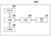
도 1을 참조하면, 메모리 시스템(Memory System; 1000)은 메모리 장치(Memory Device; 1100), 컨트롤러(Controller; 1200), 및 호스트(Host; 1300)를 포함한다. 메모리 장치(1100)는 복수의 반도체 메모리(Memory; 100)들을 포함한다. 복수의 반도체 메모리(100)들은 복수의 그룹들로 분할될 수 있다. 본 발명의 실시 예에서는 호스트(1300)가 메모리 시스템(1000)에 포함되는 것으로 도시 및 설명하였으나, 메모리 시스템(1000)이 컨트롤러(1200) 및 메모리 장치(1100)만을 포함하고, 호스트(1300)는 메모리 시스템(1000)의 외부에 배치되는 것으로 구성될 수도 있다.Referring to FIG. 1, a memory system (Memory System) 1000 includes a memory device (1100), a controller (Controller) 1200, and a host (Host) 1300. The
도 1에서, 메모리 장치(1100)의 복수의 그룹들은 각각 제 1 내지 제 n 채널들(CH1~CHn)을 통해 컨트롤러(1200)와 통신하는 것으로 도시되어 있다. 각 반도체 메모리(100)는 도 4를 참조하여 후술하도록 한다.In FIG. 1 , a plurality of groups of
반도체 메모리(100)들로 구성된 복수의 그룹 각각은 하나의 공통 채널을 통해 컨트롤러(1200)와 통신하도록 구성된다. 컨트롤러(1200)는 복수의 채널들(CH1~CHn)을 통해 메모리 장치(1100)의 복수의 반도체 메모리(100)들을 제어하도록 구성된다.Each of the plurality of groups comprised of
컨트롤러(1200)는 호스트(1300)와 메모리 장치(1100) 사이에 연결된다. 컨트롤러(1200)는 호스트(1300)로부터의 요청에 응답하여 메모리 장치(1100)를 액세스하도록 구성된다. 예를 들어 컨트롤러(1200)는 호스트(1300)로부터 수신되는 호스트 커맨드(Host_CMD)에 응답하여 메모리 장치(1100)의 리드(read), 라이트(write), 이레이즈(erase), 그리고 백그라운드(background) 동작을 제어하도록 구성된다. 라이트 동작 시 호스트(1300)는 호스트 커맨드(Host_CMD)와 함께 데이터와 어드레스를 전송하고, 리드 동작 시 호스트 커맨드(Host_CMD)와 함께 어드레스를 전송할 수 있다. 컨트롤러(1200)는 메모리 장치(1100) 및 호스트(1300) 사이에 인터페이스를 제공하도록 구성된다. 컨트롤러(1200)는 메모리 장치(1100)를 제어하기 위한 펌웨어(firmware)를 구동하도록 구성된다.The
컨트롤러(1200)는 파워 온 동작 시, 또는 호스트(1300)로부터 리드 요청이 수신된 경우, 또는 리드 동작 후 설정 시간이 경과된 후 리드 전압 설정 동작을 수행할 수 있다. 리드 전압 설정 동작 시 컨트롤러(1200)는 컨트롤러(1200)에 포함되는 에러 정정 회로를 판단하여 리드 리트라이(read retry) 범위를 설정하고, 설정된 리드 리트라이 범위 내의 하나의 전압을 리드 전압으로 설정하여 리드 동작을 수행하고, 수행된 리드 동작의 에러 비트가 설정 에러 비트의 수보다 클 경우 리드 리트라이 범위를 재설정할 수 있다.The
호스트(1300)는 컴퓨터, PDA, PMP, MP3 플레이어, 카메라, 캠코더, 모바일 폰 등과 같은 휴대용 전자 장치를 포함한다. 호스트(1300)는 메모리 시스템(1000)의 쓰기 동작, 읽기 동작, 소거 동작 등을 호스트 커맨드(Host_CMD)를 통해 요청할 수 있다. 호스트(1300)는 메모리 장치(1100)의 쓰기 동작을 위해 쓰기 커맨드에 해당하는 호스트 커맨드(Host_CMD), 데이터, 어드레스를 컨트롤러(1200)로 전송하고, 읽기 동작을 위해 읽기 커맨드에 해당하는 호스트 커맨드(Host_CMD) 및 어드레스를 컨트롤러(1200)로 전송할 수 있다. 이때 어드레스는 논리 어드레스(logical address)일 수 있다.The
컨트롤러(1200) 및 메모리 장치(1100)는 하나의 반도체 장치로 집적될 수 있다. 예시적인 실시 예로서, 컨트롤러(1200) 및 메모리 장치(1100)는 하나의 반도체 장치로 집적되어, 메모리 카드를 구성할 수 있다. 예를 들면, 컨트롤러(1200) 및 메모리 장치(1100)는 하나의 반도체 장치로 집적되어 PC 카드(PCMCIA, personal computer memory card international association), 컴팩트 플래쉬 카드(CF), 스마트 미디어 카드(SM, SMC), 메모리 스틱, 멀티미디어 카드(MMC, RS-MMC, MMCmicro), SD 카드(SD, miniSD, microSD, SDHC), 유니버설 플래쉬 기억장치(UFS) 등과 같은 메모리 카드를 구성할 것이다.The
컨트롤러(1200) 및 메모리 장치(1100)는 하나의 반도체 장치로 집적되어 반도체 드라이브(SSD, Solid State Drive)를 구성할 수 있다. 반도체 드라이브(SSD)는 반도체 메모리(100)에 데이터를 저장하도록 구성되는 저장 장치를 포함한다.The
다른 예로서, 메모리 시스템(1000)은 컴퓨터, UMPC (Ultra Mobile PC), 워크스테이션, 넷북(net-book), PDA (Personal Digital Assistants), 포터블(portable) 컴퓨터, 웹 타블렛(web tablet), 무선 전화기(wireless phone), 모바일 폰(mobile phone), 스마트폰(smart phone), e-북(e-book), PMP(portable multimedia player), 휴대용 게임기, 네비게이션(navigation) 장치, 블랙박스(black box), 디지털 카메라(digital camera), 3차원 수상기(3-dimensional television), 디지털 음성 녹음기(digital audio recorder), 디지털 음성 재생기(digital audio player), 디지털 영상 녹화기(digital picture recorder), 디지털 영상 재생기(digital picture player), 디지털 동영상 녹화기(digital video recorder), 디지털 동영상 재생기(digital video player), 정보를 무선 환경에서 송수신할 수 있는 장치, 홈 네트워크를 구성하는 다양한 전자 장치들 중 하나, 컴퓨터 네트워크를 구성하는 다양한 전자 장치들 중 하나, 텔레매틱스 네트워크를 구성하는 다양한 전자 장치들 중 하나, RFID 장치, 또는 컴퓨팅 시스템을 구성하는 다양한 구성 요소들 중 하나 등과 같은 전자 장치의 다양한 구성 요소들 중 하나로 제공된다.As another example, the
예시적인 실시 예로서, 메모리 장치(1100) 또는 메모리 시스템(1000)은 다양한 형태들의 패키지로 실장될 수 있다. 예를 들면, 메모리 장치(1100) 또는 메모리 시스템(1000)은 PoP(Package on Package), Ball grid arrays(BGAs), Chip scale packages(CSPs), Plastic Leaded Chip Carrier(PLCC), Plastic Dual In Line Package(PDIP), Die in Waffle Pack, Die in Wafer Form, Chip On Board(COB), Ceramic Dual In Line Package(CERDIP), Plastic Metric Quad Flat Pack(MQFP), Thin Quad Flatpack(TQFP), Small Outline(SOIC), Shrink Small Outline Package(SSOP), Thin Small Outline(TSOP), System In Package(SIP), Multi Chip Package(MCP), Wafer-level Fabricated Package(WFP), Wafer-Level Processed Stack Package(WSP) 등과 같은 방식으로 패키지화되어 실장될 수 있다.As an exemplary embodiment, the
도 2는 도 1의 컨트롤러를 설명하기 위한 도면이다.FIG. 2 is a diagram for explaining the controller of FIG. 1.
도 2를 참고하면, 컨트롤러(1200)는 호스트 제어 회로(1210), 프로세서(1220), 버퍼 메모리(1230), 리드 전압 설정 블록(1240), 에러 정정 회로(1250), 플래쉬 제어 회로(1260), 및 버스(1270)를 포함할 수 있다.Referring to FIG. 2, the
버스(1270)는 컨트롤러(1200)의 구성 요소들 사이에 채널(channel)을 제공하도록 구성될 수 있다.The
호스트 제어 회로(1210)는 도 1의 호스트(1300)와 버퍼 메모리(1230) 간 데이터 전송을 제어할 수 있다. 예시로서 호스트 제어 회로(1210)는 호스트(1300)로부터 입력된 데이터를 버퍼 메모리(1230)에 버퍼링(buffering) 하는 동작을 제어할 수 있다. 다른 예시로서 호스트 제어 회로(1210)는 버퍼 메모리(1230)에 버퍼링(buffering)된 데이터를 호스트(1300)로 출력하는 동작을 제어할 수 있다.The
호스트 제어 회로(1210)는 호스트 인터페이스를 포함하여 구성될 수 있다.The
프로세서(1220)는 컨트롤러(1200)의 제반 동작을 제어하고, 논리 연산을 수행할 수 있다. 프로세서(1220)는 호스트 제어 회로(1210)를 통해 도 1의 호스트(1300)와 통신하고, 플래쉬 제어 회로(1260)를 통해 도 1의 메모리 장치(1100)와 통신할 수 있다. 또한 프로세서(1220)는 버퍼 메모리(1230)를 동작 메모리, 캐시 메모리(cache memory) 또는 버퍼(buffer)로 사용하여 메모리 시스템(1000)의 동작을 제어할 수 있다. 프로세서(1220)는 호스트(1300)로부터 수신되는 복수의 호스트 커맨드들을 우선 순위에 따라 재정렬하여 커맨드 큐를 생성하여 플래쉬 제어 회로(1260)를 제어할 수 있다. 프로세서(1220)는 플래쉬 변환 계층(FTL: Flash Translation Layer, 이하 'FTL'이라 칭하기로 함, 1221), 및 리드 전압 설정 블록(1240)을 포함하여 구성될 수 있다.The
플래쉬 변환 계층(FTL; 1221)은 펌웨어는 버퍼 메모리(1230) 또는 프로세서(1220)와 직접적으로 연결되는 추가적인 메모리(미도시) 또는 프로세서(1220) 내의 저장 공간에 저장될 수 있다. 플래쉬 변환 계층(FTL; 1221)은 쓰기 동작시 도 1의 호스트(1300)로부터 입력된 어드레스(예를 들어 논리 어드레스(logical address))에 대응하는 물리 어드레스(physical address)를 맵핑할 수 있다. 또한 플래쉬 변환 계층(FTL; 1221)은 리드 동작시 호스트(1300)로부터 입력된 논리 어드레스에 맵핑된 물리 어드레스를 확인한다.The firmware of the flash translation layer (FTL) 1221 may be stored in the
또한 플래쉬 변환 계층(FTL; 1221)은 호스트(1300)로부터 수신되는 호스트 커맨드에 응답하여 플래쉬 제어 회로(1260)를 제어하기 위한 커맨드 큐를 생성할 수 있다.Additionally, the flash translation layer (FTL) 1221 may generate a command queue for controlling the
버퍼 메모리(1230)는 프로세서(1220)의 동작 메모리, 캐시 메모리 또는 버퍼로 사용될 수 있다. 버퍼 메모리(1230)는 프로세서(1220)가 실행하는 코드들 및 커맨드들을 저장할 수 있다. 버퍼 메모리(1230)는 프로세서(1220)에 의해 처리되는 데이터를 저장할 수 있다.The
버퍼 메모리(1230)는 쓰기 버퍼(1231) 및 읽기 버퍼(1232)를 포함하여 구성될 수 있다. 쓰기 버퍼(1231)는 호스트(1300)로부터 라이트 동작 시 수신되는 데이터를 임시 저장한 후 라이트 동작에 대응하는 내부 커맨드가 메모리 장치(1100)로 전송될 때 임시 저장된 데이터를 메모리 장치(1100)로 전송한다. 읽기 버퍼(1232)는 리드 동작 시 메모리 장치(1100)로부터 수신되는 데이터를 임시 저장한 후 임시 저장된 데이터를 호스트(1300)로 전송한다.The
버퍼 메모리(1230)는 SRAM(Static RAM) 또는 DRAM(Dynamic RAM)을 포함할 수 있다.The
리드 전압 설정 블록(1240)은 리드 전압 설정 동작 시 에러 정정 회로(1250)를 판단하고, 판단된 에러 정정 회로의 에러 비트 처리 능력에 따라 리드 리트라이 범위를 설정하고, 설정된 리드 리트라이 범위 내의 하나의 전압을 리드 전압으로 설정하여 리드 동작을 수행한다. 또한 리드 동작에 의해 리드된 데이터에 포함된 에러 비트의 수가 설정 에러 비트의 수보다 클 경우 리드 리트라이 범위를 재설정할 수 있으며, 재설정된 리드 리트라이 범위는 이전 리드 리트라이 범위보다 좁도록 설정할 수 있다. 리드 전압 설정 블록(1240)은 실시 예에 따라 프로세서(1220)에 포함되도록 구성될 수 있다.The read
에러 정정 회로(1250)는 에러 정정을 수행할 수 있다. 에러 정정 회로(1250)는 플래쉬 제어 회로(1260)를 통해 도 1의 메모리 장치(1100)에 기입될 데이터에 기반하여 에러 정정 인코딩(ECC encoding)을 수행할 수 있다. 에러 정정 인코딩된 데이터는 플래쉬 제어 회로(1260)를 통해 메모리 장치(1100)로 전달될 수 있다. 에러 정정 회로(1250)는 메모리 장치(1100)로부터 플래쉬 제어 회로(1260)를 통해 수신되는 데이터에 대해 에러 정정 디코딩(ECC decoding)을 수행할 수 있다. 에러 정정 회로(1250)는 복수의 ECC(Error Correction Code) 회로 중 하나로 구성될 수 있으며, 복수의 ECC 회로는 서로 상이한 에러 정정 능력을 가질 수 있다. 즉, 복수의 ECC 회로마다 서로 상이한 최대 에러 허용 비트 수를 갖는다. 또한 에러 정정 회로(1250)는 리드 동작 시 메모리 장치(1100)로부터 수신되는 데이터의 에러 비트를 검출하여 카운트할 수 있으며, 카운트된 에러 비트 수를 프로세서(1220)로 전송할 수 있다.The
예시적으로, 에러 정정 회로(1250)는 플래쉬 제어 회로(1260)의 구성 요소로서 플래쉬 제어 회로(1260)에 포함될 수 있다. Illustratively, the
플래쉬 제어 회로(1260)는 프로세서(1220)에서 생성된 커맨드 큐에 응답하여 메모리 장치(1100)를 제어하기 위한 내부 커맨드를 생성하여 출력한다. 플래쉬 제어 회로(1260)는 라이트 동작 시 버퍼 메모리(1230)의 쓰기 버퍼(1231)에 버퍼링(buffering)된 데이터를 메모리 장치(1100)에 전송하여 쓰기 동작을 제어할 수 있다. 다른 예시로서 플래쉬 제어 회로(1260)는 리드 동작시 커맨드 큐에 응답하여 메모리 장치(1100)로부터 리드된 데이터를 버퍼 메모리(1230)의 읽기 버퍼(1232)에 버퍼링(buffering) 하는 동작을 제어할 수 있다.The
플래쉬 제어 회로(1260)는 플래쉬 인터페이스를 포함하여 구성될 수 있다.The
도 3은 도 2의 리드 전압 설정 블록(1240)을 설명하기 위한 블록도이다.FIG. 3 is a block diagram for explaining the read
도 3을 참조하면, 리드 전압 설정 블록(1240)은 ECC 회로 판단 회로(1241), 리드 리트라이 범위 설정 회로(1242) 및 리드 전압 설정 회로(1243)를 포함하여 구성될 수 있다.Referring to FIG. 3, the read
ECC 회로 판단 회로(1241)는 도 2의 에러 정정 회로(1250)가 어떠한 ECC 회로로 구성되는지를 판단하여 ECC 판단 신호(ECC_feature)를 생성하여 출력한다. ECC 판단 신호(ECC_feature)는 에러 정정 회로(1250)를 구성하는 ECC 회로에 대한 정보 및 ECC 회로의 에러 정정 능력치에 대한 정보를 포함할 수 있다.The ECC
리드 리트라이 범위 설정 회로(1242)는 ECC 회로 판단 회로(1241)로부터 수신되는 ECC 판단 신호(ECC_feature)에 응답하여 리드 리트라이 범위를 설정하고, 설정된 리드 리트라이 범위 신호(RR_sweeping)를 생성하여 출력한다. 또한 리드 리트라이 범위 설정 회로(1242)는 도 2의 에러 정정 회로(1250)에 의해 카운팅된 에러 비트 수(ECC_fail_bit)에 기초하여 새로운 리드 리트라이 범위를 설정할 수 있다. 예를 들어 리드 동작 시 에러 정정 회로(1250)에 의해 카운팅된 에러 비트 개수(ECC_fail_bit)가 설정된 에러 비트 개수보다 클 경우, 리드 리트라이 범위 설정 회로(1242)는 새로운 리드 리트라이 범위를 설정할 수 있다. 새로운 리드 리트라인 범위는 이전 리드 리트라이 범위 내에 포함되며, 이전 리드 리트라이 범위보다 폭이 감소될 수 있다.The read retry
리드 전압 설정 회로(1243)는 리드 리트라이 범위 설정 회로(1242)에서 출력되는 리드 리트라이 범위 신호(RR_sweeping)에 응답하여 메모리 장치(1100)의 리드 동작시 사용되는 리드 전압을 설정한다. 예를 들어 리드 전압 설정 회로(1243)는 리드 리트라이 범위 설정 회로(1242)에서 설정된 리드 리트라이 범위 내의 하나의 전압을 리드 전압으로 설정한다. 리드 전압은 리드 리트라이 범위의 중간 값일 수 있다.The read
도 4는 도 1의 반도체 메모리(100)를 설명하기 위한 도면이다.FIG. 4 is a diagram for explaining the
도 4를 참조하면, 반도체 메모리(100)는 데이터가 저장되는 메모리 셀 어레이(10)를 포함할 수 있다. 반도체 메모리(100)는 메모리 셀 어레이(10)에 데이터를 저장하기 위한 프로그램 동작(program operation), 저장된 데이터를 출력하기 위한 리드 동작(read operation) 및 저장된 데이터를 소거하기 위한 소거 동작(erase operation)을 수행하도록 구성된 주변 회로들(200)을 포함할 수 있다. 반도체 메모리(100)는 컨트롤러(도 1의 1200)의 제어에 따라 주변 회로들(200)을 제어하는 제어 로직(300)을 포함할 수 있다.Referring to FIG. 4 , the
메모리 셀 어레이(10)는 메모리 블록(MB1~MBk; 11 (k는 양의 정수))을 포함할 수 있다. 각각의 메모리 블록들(MB1~MBk; 11)에는 로컬 라인들(local lines; LL)과 비트 라인들(BL1~BLm; m은 양의 정수)이 연결될 수 있다. 예를 들면, 로컬 라인들(LL)은 제1 선택 라인(first select line), 제2 선택 라인(second select line), 상기 제1 및 제2 선택 라인들 사이에 배열된 다수의 워드 라인들(word lines)을 포함할 수 있다. 또한, 로컬 라인들(LL)은 제1 선택 라인과 워드 라인들 사이, 제2 선택 라인과 워드 라인들 사이에 배열된 더미 라인들을 포함할 수 있다. 여기서, 제1 선택 라인은 소스 선택 라인일 수 있고, 제2 선택 라인은 드레인 선택 라인일 수 있다. 예를 들면, 로컬 라인들(LL)은 워드 라인들, 드레인 및 소스 선택 라인들 및 소스 라인들(SL; source lines)을 포함할 수 있다. 예를 들면, 로컬 라인들(LL)은 더미 라인들(dummy lines)을 더 포함할 수 있다. 예를 들면, 로컬 라인들(LL)은 파이프 라인들(pipe lines)을 더 포함할 수 있다. 로컬 라인들(LL)은 메모리 블록들(MB1~MBk; 11)에 각각 연결될 수 있으며, 비트 라인들(BL1~BLm)은 메모리 블록들(MB1~MBk; 11)에 공통으로 연결될 수 있다. 메모리 블록들(MB1~MBk; 11)은 2차원 또는 3차원 구조로 구현될 수 있다. 예를 들면, 2차원 구조의 메모리 블록들(11)에서 메모리 셀들은 기판에 평행한 방향으로 배열될 수 있다. 예를 들면, 3차원 구조의 메모리 블록들(11)에서 메모리 셀들은 기판에 수직 방향으로 적층될 수 있다.The
주변 회로들(200)은 제어 로직(300)의 제어에 따라 선택된 메모리 블록(11)의 프로그램, 리드 및 소거 동작을 수행하도록 구성될 수 있다. 예를 들면, 주변 회로들(200)은 전압 생성 회로(voltage generating circuit; 210), 로우 디코더(row decoder; 220), 페이지 버퍼 그룹(page buffer group; 230), 컬럼 디코더(column decoder; 240), 입출력 회로(input/output circuit; 250), 패스/페일 판단부(pass/fail check circuit; 260) 및 소스 라인 드라이버(source line driver; 270)를 포함할 수 있다.The
전압 생성 회로(210)는 동작 신호(OP_CMD)에 응답하여 프로그램, 리드 및 소거 동작들에 사용되는 다양한 동작 전압들(Vop)을 생성할 수 있다. 또한, 전압 생성 회로(210)는 동작 신호(OP_CMD)에 응답하여 로컬 라인들(LL)을 선택적으로 디스차지할 수 있다. 예를 들면, 전압 생성 회로(210)는 제어 로직(300)의 제어에 따라 프로그램 전압, 검증 전압, 패스 전압, 및 선택 트랜지스터 동작 전압을 생성할 수 있다.The
로우 디코더(row decoder; 220)는 제어 신호들(AD_signals)에 응답하여 동작 전압들(Vop)을 선택된 메모리 블록(11)에 연결된 로컬 라인들(LL)에 전달할 수 있다. 예를 들어 로우 디코더(220)는 로우 디코더 제어 신호들(AD_signals)에 응답하여 전압 생성 회로(210)에서 생성된 동작 전압들(예를 들어 프로그램 전압, 검증 전압, 패스 전압 등)을 로컬 라인들(LL) 중 워드 라인들에 선택적으로 인가할 수 있다.The
로우 디코더(220)는 프로그램 전압 인가 동작 시 제어 신호들(AD_signals)에 응답하여 전압 생성 회로(210)에서 생성된 프로그램 전압을 로컬 라인들(LL) 중 선택된 워드 라인에 인가하고, 전압 생성 회로(210)에서 생성된 패스 전압을 나머지 비 선택된 워드 라인들에 인가한다. 또한 로우 디코더(220)는 리드 동작 시 제어 신호들(AD_signals)에 응답하여 전압 생성 회로(210)에서 생성된 리드 전압을 로컬 라인들(LL) 중 선택된 워드 라인에 인가하고, 전압 생성 회로(210)에서 생성된 패스 전압을 나머지 비 선택된 워드 라인들에 인가한다.During the program voltage application operation, the
페이지 버퍼 그룹(230)은 비트 라인들(BL1~BLm)에 연결된 다수의 페이지 버퍼들(PB1~PBm; 231)을 포함할 수 있다. 페이지 버퍼들(PB1~PBm; 231)은 페이지 버퍼 제어 신호들(PBSIGNALS)에 응답하여 동작할 수 있다. 예를 들면, 페이지 버퍼들(PB1~PBm; 231)은 프로그램 동작 시 프로그램할 데이터를 임시로 저장하거나, 리드 또는 검증 동작 시 비트 라인들(BL1~BLm)의 전압 또는 전류를 센싱(sensing)할 수 있다.The
컬럼 디코더(240)는 컬럼 어드레스(CADD)에 응답하여 입출력 회로(250)와 페이지 버퍼 그룹(230) 사이에서 데이터를 전달할 수 있다. 예를 들면, 컬럼 디코더(240)는 데이터 라인들(DL)을 통해 페이지 버퍼들(231)과 데이터를 주고받거나, 컬럼 라인들(CL)을 통해 입출력 회로(250)와 데이터를 주고받을 수 있다.The
입출력 회로(250)는 컨트롤러(도 1의 1200)로부터 전달받은 내부 커맨드(CMD) 및 어드레스(ADD)를 제어 로직(300)에 전달하거나, 데이터(DATA)를 컬럼 디코더(240)와 주고받을 수 있다.The input/
패스/페일 판단부(260)는 리드 동작(read operation) 시, 허용 비트(VRY_BIT<#>)에 응답하여 기준 전류를 생성하고, 페이지 버퍼 그룹(230)으로부터 수신된 센싱 전압(VPB)과 기준 전류에 의해 생성된 기준 전압을 비교하여 패스 신호(PASS) 또는 페일 신호(FAIL)를 출력할 수 있다.During a read operation, the pass/
소스 라인 드라이버(270)는 메모리 셀 어레이(10)에 포함된 메모리 셀과 소스 라인(SL)을 통해 연결되고, 소스 라인(SL)에 인가되는 전압을 제어할 수 있다. 소스 라인 드라이버(270)는 제어 로직(300)으로부터 소스 라인 제어 신호(CTRL_SL)를 수신할 수 있고, 소스 라인 제어 신호(CTRL_SL)에 기초하여 소스 라인(SL)에 인가되는 소스 라인 전압을 제어할 수 있다.The
제어 로직(300)은 내부 커맨드(CMD) 및 어드레스(ADD)에 응답하여 동작 신호(OP_CMD), 제어 신호들(AD_signals), 페이지 버퍼 제어 신호들(PBSIGNALS) 및 허용 비트(VRY_BIT<#>)를 출력하여 주변 회로들(200)을 제어할 수 있다. 또한, 제어 로직(300)은 패스 또는 페일 신호(PASS 또는 FAIL)에 응답하여 검증 동작이 패스 또는 페일 되었는지를 판단할 수 있다.The
도 5는 도 4의 메모리 블록을 설명하기 위한 도면이다.FIG. 5 is a diagram for explaining the memory block of FIG. 4.
도 5를 참조하면, 메모리 블록(11)은 제1 선택 라인과 제2 선택 라인 사이에 서로 평행하게 배열된 다수의 워드 라인들이 연결될 수 있다. 여기서, 제1 선택 라인은 소스 선택 라인(SSL)일 수 있고, 제2 선택 라인은 드레인 선택 라인(DSL)일 수 있다. 보다 구체적으로 설명하면, 메모리 블록(11)은 비트 라인들(BL1~BLm)과 소스 라인(SL) 사이에 연결된 다수의 스트링들(strings; ST)을 포함할 수 있다. 비트 라인들(BL1~BLm)은 스트링들(ST)에 각각 연결될 수 있고, 소스 라인(SL)은 스트링들(ST)에 공통으로 연결될 수 있다. 스트링들(ST)은 서로 동일하게 구성될 수 있으므로, 제1 비트 라인(BL1)에 연결된 스트링(ST)을 예를 들어 구체적으로 설명하도록 한다.Referring to FIG. 5 , the
스트링(ST)은 소스 라인(SL)과 제1 비트 라인(BL1) 사이에서 서로 직렬로 연결된 소스 선택 트랜지스터(SST), 다수의 메모리 셀들(F1~F16) 및 드레인 선택 트랜지스터(DST)를 포함할 수 있다. 하나의 스트링(ST)에는 소스 선택 트랜지스터(SST)와 드레인 선택 트랜지스터(DST)가 적어도 하나 이상씩 포함될 수 있으며, 메모리 셀들(F1~F16) 또한 도면에 도시된 개수보다 더 많이 포함될 수 있다.The string (ST) may include a source selection transistor (SST), a plurality of memory cells (F1 to F16), and a drain selection transistor (DST) connected in series between the source line (SL) and the first bit line (BL1). You can. One string (ST) may include at least one source select transistor (SST) and at least one drain select transistor (DST), and may also include more memory cells (F1 to F16) than shown in the drawing.
소스 선택 트랜지스터(SST)의 소스(source)는 소스 라인(SL)에 연결될 수 있고, 드레인 선택 트랜지스터(DST)의 드레인(drain)은 제1 비트 라인(BL1)에 연결될 수 있다. 메모리 셀들(F1~F16)은 소스 선택 트랜지스터(SST)와 드레인 선택 트랜지스터(DST) 사이에서 직렬로 연결될 수 있다. 서로 다른 스트링들(ST)에 포함된 소스 선택 트랜지스터들(SST)의 게이트들은 소스 선택 라인(SSL)에 연결될 수 있고, 드레인 선택 트랜지스터들(DST)의 게이트들은 드레인 선택 라인(DSL)에 연결될 수 있고, 메모리 셀들(F1~F16)의 게이트들은 다수의 워드 라인들(WL1~WL16)에 연결될 수 있다. 서로 다른 스트링들(ST)에 포함된 메모리 셀들 중에서 동일한 워드 라인에 연결된 메모리 셀들의 그룹을 물리 페이지(physical page; PPG)라 할 수 있다. 따라서, 메모리 블록(11)에는 워드 라인들(WL1~WL16)의 개수만큼의 물리 페이지들(PPG)이 포함될 수 있다.The source of the source selection transistor (SST) may be connected to the source line (SL), and the drain of the drain selection transistor (DST) may be connected to the first bit line (BL1). The memory cells F1 to F16 may be connected in series between the source select transistor (SST) and the drain select transistor (DST). The gates of the source select transistors (SST) included in the different strings (ST) may be connected to the source select line (SSL), and the gates of the drain select transistors (DST) may be connected to the drain select line (DSL). and the gates of the memory cells F1 to F16 may be connected to a plurality of word lines WL1 to WL16. Among memory cells included in different strings ST, a group of memory cells connected to the same word line may be referred to as a physical page (PPG). Accordingly, the
하나의 메모리 셀은 1비트의 데이터를 저장할 수 있다. 이를 통상적으로 싱글 레벨 셀(single level cell; SLC)라고 부른다. 이 경우 하나의 물리 페이지(PPG)는 하나의 논리 페이지(logical page; LPG) 데이터를 저장할 수 있다. 하나의 논리 페이지(LPG) 데이터는 하나의 물리 페이지(PPG)에 포함된 셀 개수만큼의 데이터 비트들을 포함할 수 있다. 또한 하나의 메모리 셀은 2 이상의 비트의 데이터를 저장할 수 있다. 이를 통상적으로 멀티 레벨 셀(multi-level cell; MLC)이라고 부른다. 이 경우 하나의 물리 페이지(PPG)는 2 이상의 논리 페이지(logical page; LPG) 데이터를 저장할 수 있다.One memory cell can store 1 bit of data. This is commonly called a single level cell (SLC). In this case, one physical page (PPG) can store one logical page (LPG) data. One logical page (LPG) data may include as many data bits as the number of cells included in one physical page (PPG). Additionally, one memory cell can store two or more bits of data. This is commonly called a multi-level cell (MLC). In this case, one physical page (PPG) can store data of two or more logical pages (LPG).
도 6은 3차원으로 구성된 메모리 블록의 실시예를 설명하기 위한 도면이다.Figure 6 is a diagram for explaining an embodiment of a three-dimensional memory block.
도 6을 참조하면, 메모리 셀 어레이(10)는 메모리 블록(MB11~MBk; 11)을 포함할 수 있다. 메모리 블록(11)은 다수의 스트링들(ST11~ST1m, ST21~ST2m)을 포함할 수 있다. 실시 예로서, 다수의 스트링들(ST11~ST1m, ST21~ST2m) 각각은 'U'자형으로 형성될 수 있다. 제1 메모리 블록(MB1) 내에서, 행 방향(X 방향)으로 m개의 스트링들이 배열될 수 있다. 도 6에서, 열 방향(Y 방향)으로 2개의 스트링들이 배열되는 것으로 도시되었으나, 이는 설명의 편의를 위한 것으로서 열 방향(Y 방향)으로 3개 이상의 스트링들이 배열될 수 있다.Referring to FIG. 6, the
다수의 스트링들(ST11~ST1m, ST21~ST2m) 각각은 적어도 하나의 소스 선택 트랜지스터(SST), 제1 내지 제n 메모리 셀들(MC1~MCn), 파이프 트랜지스터(PT) 및 적어도 하나의 드레인 선택 트랜지스터(DST)를 포함할 수 있다.Each of the plurality of strings (ST11 to ST1m, ST21 to ST2m) includes at least one source selection transistor (SST), first to nth memory cells (MC1 to MCn), a pipe transistor (PT), and at least one drain selection transistor. (DST) may be included.
소스 및 드레인 선택 트랜지스터들(SST 및 DST)과 메모리 셀들(MC1~MCn)은 서로 유사한 구조를 가질 수 있다. 예를 들면, 소스 및 드레인 선택 트랜지스터들(SST 및 DST)과 메모리 셀들(MC1~MCn) 각각은 채널막, 터널 절연막, 전하 트랩막 및 블로킹 절연막을 포함할 수 있다. 예를 들면, 채널막을 제공하기 위한 필라(pillar)가 각 스트링에 제공될 수 있다. 예를 들면, 채널막, 터널 절연막, 전하 트랩막 및 블로킹 절연막 중 적어도 하나를 제공하기 위한 필라가 각 스트링에 제공될 수 있다.The source and drain selection transistors (SST and DST) and the memory cells (MC1 to MCn) may have similar structures. For example, each of the source and drain selection transistors (SST and DST) and the memory cells (MC1 to MCn) may include a channel film, a tunnel insulating film, a charge trap film, and a blocking insulating film. For example, a pillar to provide a channel film may be provided in each string. For example, a pillar for providing at least one of a channel film, a tunnel insulating film, a charge trap film, and a blocking insulating film may be provided in each string.
각 스트링의 소스 선택 트랜지스터(SST)는 소스 라인(SL)과 메모리 셀들(MC1~MCp) 사이에 연결될 수 있다.The source select transistor (SST) of each string may be connected between the source line (SL) and the memory cells (MC1 to MCp).
실시 예로서, 동일한 행에 배열된 스트링들의 소스 선택 트랜지스터들은 행 방향으로 연장되는 소스 선택 라인에 연결될 수 있고, 상이한 행에 배열된 스트링들의 소스 선택 트랜지스터들은 상이한 소스 선택 라인들에 연결될 수 있다. 도 6에서, 제1 행의 스트링들(ST11~ST1m)의 소스 선택 트랜지스터들은 제1 소스 선택 라인(SSL1)에 연결될 수 있다. 제2 행의 스트링들(ST21~ST2m)의 소스 선택 트랜지스터들은 제2 소스 선택 라인(SSL2)에 연결될 수 있다.As an embodiment, source selection transistors of strings arranged in the same row may be connected to source selection lines extending in the row direction, and source selection transistors of strings arranged in different rows may be connected to different source selection lines. In FIG. 6 , the source selection transistors of the strings ST11 to ST1m in the first row may be connected to the first source selection line SSL1. Source selection transistors of the strings ST21 to ST2m in the second row may be connected to the second source selection line SSL2.
다른 실시 예로서, 스트링들(ST11~ST1m, ST21~ST2m)의 소스 선택 트랜지스터들은 하나의 소스 선택 라인에 공통으로 연결될 수 있다.As another example, the source selection transistors of the strings ST11 to ST1m and ST21 to ST2m may be commonly connected to one source selection line.
각 스트링의 제1 내지 제n 메모리 셀들(MC1~MCn)은 소스 선택 트랜지스터(SST)와 드레인 선택 트랜지스터(DST) 사이에 연결될 수 있다.The first to nth memory cells (MC1 to MCn) of each string may be connected between the source selection transistor (SST) and the drain selection transistor (DST).
제1 내지 제n 메모리 셀들(MC1~MCn)은 제1 내지 제p 메모리 셀들(MC1~MCp)과 제p+1 내지 제n 메모리 셀들(MCp+1~MCn)로 구분될 수 있다. 제1 내지 제p 메모리 셀들(MC1~MCp)은 수직 방향(Z 방향)으로 순차적으로 배열될 수 있으며, 소스 선택 트랜지스터(SST)와 파이프 트랜지스터(PT) 사이에서 서로 직렬로 연결될 수 있다. 제p+1 내지 제n 메모리 셀들(MCp+1~MCn)은 수직 방향(Z 방향)으로 순차적으로 배열될 수 있으며, 파이프 트랜지스터(PT)와 드레인 선택 트랜지스터(DST) 사이에서 서로 직렬로 연결될 수 있다. 제1 내지 제p 메모리 셀들(MC1~MCp)과 제p+1 내지 제n 메모리 셀들(MCp+1~MCn)은 파이프 트랜지스터(PT)를 통해 서로 연결될 수 있다. 각 스트링의 제1 내지 제n 메모리 셀들(MC1~MCn)의 게이트들은 각각 제1 내지 제n 워드 라인들(WL1~WLn)에 연결될 수 있다.The first to nth memory cells (MC1 to MCn) may be divided into first to pth memory cells (MC1 to MCp) and p+1 to nth memory cells (MCp+1 to MCn). The first to pth memory cells MC1 to MCp may be sequentially arranged in the vertical direction (Z direction) and may be connected in series between the source selection transistor SST and the pipe transistor PT. The p+1th to nth memory cells (MCp+1 to MCn) may be sequentially arranged in the vertical direction (Z direction) and may be connected in series between the pipe transistor (PT) and the drain select transistor (DST). there is. The first to pth memory cells (MC1 to MCp) and the p+1 to nth memory cells (MCp+1 to MCn) may be connected to each other through a pipe transistor (PT). Gates of the first to nth memory cells (MC1 to MCn) of each string may be connected to the first to nth word lines (WL1 to WLn), respectively.
실시 예로서, 제1 내지 제n 메모리 셀들(MC1~MCn) 중 적어도 하나는 더미 메모리 셀로써 이용될 수 있다. 더미 메모리 셀이 제공되는 경우, 해당 스트링의 전압 또는 전류는 안정적으로 제어될 수 있다. 각 스트링의 파이프 트랜지스터(PT)의 게이트는 파이프 라인(PL)에 연결될 수 있다.As an embodiment, at least one of the first to nth memory cells MC1 to MCn may be used as a dummy memory cell. If a dummy memory cell is provided, the voltage or current of the corresponding string can be stably controlled. The gate of the pipe transistor (PT) of each string may be connected to the pipe line (PL).
각 스트링의 드레인 선택 트랜지스터(DST)는 비트 라인과 메모리 셀들(MCp+1~MCn) 사이에 연결될 수 있다. 행 방향으로 배열되는 스트링들은 행 방향으로 연장되는 드레인 선택 라인에 연결될 수 있다. 제1 행의 스트링들(ST11~ST1m)의 드레인 선택 트랜지스터들은 제1 드레인 선택 라인(DSL1)에 연결될 수 있다. 제2 행의 스트링들(ST21~ST2m)의 드레인 선택 트랜지스터들은 제2 드레인 선택 라인(DSL2)에 연결될 수 있다.The drain select transistor (DST) of each string may be connected between the bit line and the memory cells (MCp+1 to MCn). Strings arranged in the row direction may be connected to a drain selection line extending in the row direction. The drain selection transistors of the strings ST11 to ST1m in the first row may be connected to the first drain selection line DSL1. Drain selection transistors of the strings (ST21 to ST2m) in the second row may be connected to the second drain selection line (DSL2).
열 방향으로 배열되는 스트링들은 열 방향으로 연장되는 비트 라인들에 연결될 수 있다. 도 6에서 제1 열의 스트링들(ST11, ST21)은 제1 비트 라인(BL1)에 연결될 수 있다. 제m 열의 스트링들(ST1m, ST2m)은 제m 비트 라인(BLm)에 연결될 수 있다.Strings arranged in the column direction may be connected to bit lines extending in the column direction. In FIG. 6 , the strings ST11 and ST21 in the first column may be connected to the first bit line BL1. The m-th strings (ST1m, ST2m) may be connected to the m-th bit line (BLm).
행 방향으로 배열되는 스트링들 중에서 동일한 워드 라인에 연결되는 메모리 셀들은 하나의 페이지(page)를 구성할 수 있다. 예를 들면, 제1 행의 스트링들(ST11~ST1m) 중 제1 워드 라인(WL1)에 연결된 메모리 셀들은 하나의 페이지를 구성할 수 있다. 제2 행의 스트링들(ST21~ST2m) 중 제1 워드 라인(WL1)에 연결된 메모리 셀들은 다른 하나의 페이지를 구성할 수 있다. 드레인 선택 라인들(DSL1, DSL2) 중 어느 하나가 선택됨으로써 하나의 행 방향으로 배열되는 스트링들이 선택될 것이다. 워드 라인들(WL1~WLn) 중 어느 하나가 선택됨으로써 선택된 스트링들 중 하나의 페이지가 선택될 것이다.Among strings arranged in a row direction, memory cells connected to the same word line may form one page. For example, memory cells connected to the first word line WL1 among the strings ST11 to ST1m in the first row may form one page. Memory cells connected to the first word line (WL1) among the strings (ST21 to ST2m) in the second row may configure another page. When one of the drain selection lines DSL1 and DSL2 is selected, strings arranged in one row will be selected. When one of the word lines (WL1 to WLn) is selected, one page of the selected strings will be selected.
도 7은 3차원으로 구성된 메모리 블록의 다른 실시예를 설명하기 위한 도면이다.Figure 7 is a diagram for explaining another embodiment of a three-dimensional memory block.
도 7을 참조하면, 메모리 셀 어레이(10)는 다수의 메모리 블록들(MB1~MBk; 11)을 포함할 수 있다. 메모리 블록(11)은 다수의 스트링들(ST11'~ST1m', ST21'~ST2m')을 포함할 수 있다. 다수의 스트링들(ST11'~ST1m', ST21'~ST2m') 각각은 수직 방향(Z 방향)을 따라 연장될 수 있다. 메모리 블록(11) 내에서, 행 방향(X 방향)으로 m개의 스트링들이 배열될 수 있다. 도 7에서 열 방향(Y 방향)으로 2개의 스트링들이 배열되는 것으로 도시되어 있으나, 이는 설명의 편의를 위한 것으로서 열 방향(Y 방향)으로 3개 이상의 스트링들이 배열될 수 있다.Referring to FIG. 7, the
다수의 스트링들(ST11'~ST1m', ST21'~ST2m') 각각은, 적어도 하나의 소스 선택 트랜지스터(SST), 제 1 내지 제 n 메모리 셀들(MC1~MCn), 그리고 적어도 하나의 드레인 선택 트랜지스터(DST)를 포함할 수 있다.Each of the plurality of strings (ST11'~ST1m', ST21'~ST2m') includes at least one source selection transistor (SST), first to nth memory cells (MC1 to MCn), and at least one drain selection transistor. (DST) may be included.
각 스트링의 소스 선택 트랜지스터(SST)는 소스 라인(SL)과 메모리 셀들(MC1~MCn) 사이에 연결될 수 있다. 동일한 행에 배열된 스트링들의 소스 선택 트랜지스터들은 동일한 소스 선택 라인에 연결될 수 있다. 제1 행에 배열된 스트링들(ST11'~ST1m')의 소스 선택 트랜지스터들은 제1 소스 선택 라인(SSL1)에 연결될 수 있다. 제2 행에 배열된 스트링들(ST21'~ST2m')의 소스 선택 트랜지스터들은 제2 소스 선택 라인(SSL2)에 연결될 수 있다. 다른 실시 예로서, 스트링들(ST11'~ST1m', ST21'~ST2m')의 소스 선택 트랜지스터들은 하나의 소스 선택 라인에 공통으로 연결될 수 있다.The source select transistor (SST) of each string may be connected between the source line (SL) and the memory cells (MC1 to MCn). Source selection transistors of strings arranged in the same row may be connected to the same source selection line. Source selection transistors of the strings ST11' to ST1m' arranged in the first row may be connected to the first source selection line SSL1. The source selection transistors of the strings ST21' to ST2m' arranged in the second row may be connected to the second source selection line SSL2. As another example, the source selection transistors of the strings ST11' to ST1m' and ST21' to ST2m' may be commonly connected to one source selection line.
각 스트링의 제1 내지 제n 메모리 셀들(MC1~MCn)은 소스 선택 트랜지스터(SST)와 드레인 선택 트랜지스터(DST) 사이에서 서로 직렬로 연결될 수 있다. 제1 내지 제n 메모리 셀들(MC1~MCn)의 게이트들은 각각 제1 내지 제n 워드 라인들(WL1~WLn)에 연결될 수 있다.The first to nth memory cells (MC1 to MCn) of each string may be connected in series between the source selection transistor (SST) and the drain selection transistor (DST). Gates of the first to nth memory cells MC1 to MCn may be connected to the first to nth word lines WL1 to WLn, respectively.
실시 예로서, 제1 내지 제n 메모리 셀들(MC1~MCn) 중 적어도 하나는 더미 메모리 셀로서 이용될 수 있다. 더미 메모리 셀이 제공되는 경우, 해당 스트링의 전압 또는 전류는 안정적으로 제어될 수 있다. 이에 따라 메모리 블록(11)에 저장된 데이터의 신뢰성이 향상될 수 있다.As an embodiment, at least one of the first to nth memory cells MC1 to MCn may be used as a dummy memory cell. If a dummy memory cell is provided, the voltage or current of the corresponding string can be stably controlled. Accordingly, the reliability of data stored in the
각 스트링의 드레인 선택 트랜지스터(DST)는 비트 라인과 메모리 셀들(MC1~MCn) 사이에 연결될 수 있다. 행 방향으로 배열되는 스트링들의 드레인 선택 트랜지스터들(DST)은 행 방향으로 연장되는 드레인 선택 라인에 연결될 수 있다. 제1 행의 스트링들(CS11'~CS1m')의 드레인 선택 트랜지스터들(DST)은 제1 드레인 선택 라인(DSL1)에 연결될 수 있다. 제2 행의 스트링들(CS21'~CS2m')의 드레인 선택 트랜지스터들(DST)은 제2 드레인 선택 라인(DSL2)에 연결될 수 있다.The drain select transistor (DST) of each string may be connected between the bit line and the memory cells (MC1 to MCn). Drain select transistors DST of strings arranged in the row direction may be connected to a drain select line extending in the row direction. The drain selection transistors DST of the strings CS11' to CS1m' in the first row may be connected to the first drain selection line DSL1. The drain selection transistors DST of the strings CS21' to CS2m' in the second row may be connected to the second drain selection line DSL2.
도 8은 본 발명의 실시 예에 따른 메모리 시스템의 동작을 설명하기 위한 순서도이다.Figure 8 is a flowchart for explaining the operation of a memory system according to an embodiment of the present invention.
도 9는 본 발명의 실시 예에 따른 메모리 시스템의 리드 리트라이 범위를 설명하기 위한 도면이다.FIG. 9 is a diagram for explaining the read retry range of a memory system according to an embodiment of the present invention.
도 1 내지 도 9를 참조하여 본 발명의 실시 예에 따른 메모리 시스템의 동작 방법을 설명하면 다음과 같다.A method of operating a memory system according to an embodiment of the present invention will be described with reference to FIGS. 1 to 9 as follows.
메모리 시스템(1000)이 파워 온(power-on)되면(S810), 리드 전압 성정 블록(1240)은 에러 정정 회로(1250)가 어떠한 ECC 회로로 구성되는지를 판단한다(S820). 예를 들어 리드 전압 성정 블록(1240)의 ECC 회로 판단 회로(1241)는 컨트롤러(1200)에 포함된 에러 정정 회로(1250)를 체크하여 어떠한 ECC 회로로 구성되는지를 판단하고, ECC 판단 신호(ECC_feature)를 생성하여 출력한다.When the
리드 리트라이 범위 설정 회로(1242)는 수신되는 ECC 판단 신호(ECC_feature)에 기초하여 리드 리트라이 범위(RR-1)를 설정한다(S830). 즉, ECC 판단 신호(ECC_feature)에 기초하여 에러 정정 회로(1250)의 ECC 회로의 종류를 판단하고, 판단된 ECC 회로의 에러 정정 능력치에 따라 리드 리트라이 범위(RR-1)를 설정한다. 예를 들어 메모리 장치(1100)에 포함된 메모리 셀들이 제1 프로그램 상태(PV1) 및 제2 프로그램 상태(PV2)로 프로그램되었다고 가정할 경우, 리드 리트라이 범위(RR-1)는 제1 프로그램 상태(PV1) 및 제2 프로그램 상태(PV2)를 구분하기 위한 최소 리드 전압 내지 최대 리드 전압이며, 최소 리드 전압에 의한 리드 동작과 최대 리드 전압에 의한 리드 동작 시 발생하는 에러 비트 수가 에러 정정 회로(1250)의 최대 에러 허용 비트 수 보다 낮도록 리드 리트라이 범위(RR-1)를 설정할 수 있다.The read retry
리드 전압 설정 회로(1243)는 리드 리트라이 범위 설정 회로(1242)에 의해 설정된 리드 리트라이 범위(RR-1) 내에서 하나의 리드 전압(RR-1_Vread)을 설정한다(S840). 리드 전압(RR-1_Vread)은 리드 리트라이 범위(RR-1)의 중간 값일 수 있다.The read
프로세서(1220)는 테스트 리드 동작에 대응하는 커맨드 큐를 생성하고, 플래쉬 제어 회로(1260)는 커맨드 큐에 응답하여 테스트 리드 동작에 대한 내부 커맨드(CMD)를 생성하여 메모리 장치(1100)로 출력한다. 이때 플래쉬 제어 회로(1260)는 리드 전압 설정 회로(1243)에서 설정된 리드 전압에 대한 정보도 함께 메모리 장치(1100)로 출력한다.The
메모리 장치(1100)는 컨트롤러(1200)로부터 수신된 내부 커맨드(CMD)에 응답하여 테스트 리드 동작을 수행하며, 테스트 리드 동작은 컨트롤러(1200)에 의해 설정된 리드 전압을 이용하여 수행한다(S850). 예를 들어 메모리 장치(1100)에 포함된 복수의 반도체 메모리(100) 중 하나의 반도체 메모리(100)를 선택하고, 선택된 반도체 메모리(100)에 포함된 복수의 메모리 블록들(11) 중 하나의 메모리 블록(예를 들어 MB1)을 선택하여 적어도 하나의 물리 페이지(PPG)에 대한 테스트 리드 동작을 수행한다.The
테스트 리드 동작 결과 리드된 데이터는 플래쉬 제어 회로(1260)에 의해 컨트롤러(1200)의 에러 정정 회로(1250)로 전송된다. 에러 정정 회로(1250)는 수신된 데이터의 에러 비트를 검출하여 에러 비트 수를 카운트 한다(S860).Data read as a result of the test read operation is transmitted to the
리드 전압 설정 블록(1240)의 리드 리트라이 범위 설정 회로(1242)는 에러 정정 회로(1250)에 의해 카운팅된 에러 비트 개수(ECC_fail_bit)와 설정 에러 비트 개수를 비교한다(S870). 설정 에러 비트 개수는 에러 정정 회로(1250)의 최대 에러 허용 비트 수 보다 낮은 것이 바람직하다.The read retry
메모리 장치(1100)에 포함된 메모리 셀들은 리텐션 특성에 따라 문턱 전압 분포가 열화될 수 있다. 예를 들어 제2 프로그램 상태는 최초 프로그램 동작 시 PV2와 같은 문턱 전압 분포를 가지며, 문턱 전압 분포 열화 현상에 의해 PV2'와 같이 문턱 전압 분포가 변화될 수 있다. 문턱 전압 분포가 PV2에서 PV2'로 열화된 경우, 리드 전압(RR-1_Vread)을 이용한 리드 동작 시 에러 비트 수가 증가할 수 있다. 즉, 메모리 셀들의 문턱 전압 분포가 정상일 경우 에러 정정 회로(1250)에 의해 카운팅된 에러 비트 개수(ECC_fail_bit)는 설정 에러 비트 개수보다 작거나 같으며, 메모리 셀들의 문턱 전압 분포가 열화된 경우 에러 비트 개수(ECC_fail_bit)는 설정 에러 비트 개수보다 클 수 있다.The threshold voltage distribution of memory cells included in the
상술한 카운팅된 에러 비트 개수(ECC_fail_bit)와 설정 에러 비트 개수의 비교 단계(S870)의 비교 결과, 에러 비트 개수(ECC_fail_bit)가 설정 에러 비트 개수보다 클 경우(예), 리드 리트라이 범위 설정 회로(1242)는 새로운 리드 리트라이 범위(RR-2)를 설정한다(S880). 새로운 리드 리트라이 범위(RR-2)는 이전 리드 리트라이 범위(RR-1) 내에 포함되며, 이전 리드 리트라이 범위(RR-1)보다 폭이 감소될 수 있다.As a result of the comparison step (S870) of the above-mentioned number of counted error bits (ECC_fail_bit) and the number of set error bits, if the number of error bits (ECC_fail_bit) is greater than the number of set error bits (example), the read retry range setting circuit ( 1242) sets a new read retry range (RR-2) (S880). The new read retry range RR-2 is included within the previous read retry range RR-1, and its width may be reduced compared to the previous read retry range RR-1.
이 후, 단계 S840부터 재수행한다. 즉, 리드 전압 설정 회로(1243)는 새로운 리드 리트라이 범위(RR-2) 내에서 하나의 새로운 리드 전압(RR-2_Vread)을 설정하여 테스트 리드 동작을 재수행한다.After this, the process is re-performed starting from step S840. That is, the read
상술한 카운팅된 에러 비트 개수(ECC_fail_bit)와 설정 에러 비트 개수의 비교 단계(S870)의 비교 결과, 에러 비트 개수(ECC_fail_bit)가 설정 에러 비트 개수와 같거나 작을 경우(아니오), 직전 테스트 리드 동작 시 사용된 리드 전압을 메모리 장치의 리드 전압으로 설정한다(S890).As a result of the comparison step (S870) of the above-mentioned number of counted error bits (ECC_fail_bit) and the number of set error bits, if the number of error bits (ECC_fail_bit) is equal to or smaller than the number of set error bits (No), during the previous test lead operation Set the used read voltage to the read voltage of the memory device (S890).
이 후, 호스트(1300)로부터 리드 동작이 요청될 경우, 설정된 리드 전압을 이용한 리드 동작을 수행하도록 메모리 장치(1100)를 제어할 수 있으며, 리드 전압이 설정되고 일정 시간이 지나면 메모리 장치(1100)에 포함된 메모리 셀들의 문턱 전압이 더욱 열화될 수 있으므로 상술한 단계 S830 내지 S890를 재수행하여 새로운 리드 전압을 설정할 수 있다.Afterwards, when a read operation is requested from the
상술한 실시 예에 따르면, 에러 정정 회로(1250)를 구성하는 ECC 회로를 판단하여 에러 정정 회로(1250)의 최대 에러 허용 비트 수 보다 낮은 에러 비트가 검출되는 리드 전압을 빠르게 설정할 수 있어 메모리 시스템(1000)의 레이턴시(latency)를 개선할 수 있다.According to the above-described embodiment, the ECC circuit constituting the
도 10은 본 발명의 다른 실시 예에 따른 메모리 시스템의 동작을 설명하기 위한 순서도이다.Figure 10 is a flowchart for explaining the operation of a memory system according to another embodiment of the present invention.
도 1 내지 도 7, 도 9 및 도 10을 참조하여 본 발명의 다른 실시 예에 따른 메모리 시스템의 동작 방법을 설명하면 다음과 같다.A method of operating a memory system according to another embodiment of the present invention will be described with reference to FIGS. 1 to 7, 9, and 10.
호스트(1300)로부터 리드 요청에 대응하는 호스트 커맨드(Host_CMD)가 수신되면(S910), 컨트롤러(1200)의 프로세서(1220)는 호스트 커맨드(Host_CMD)를 정렬시켜 커맨드 큐를 생성한다.When a host command (Host_CMD) corresponding to a read request is received from the host 1300 (S910), the
또한 리드 전압 성정 블록(1240)은 에러 정정 회로(1250)가 어떠한 ECC 회로로 구성되는지를 판단한다(S920). 예를 들어 리드 전압 성정 블록(1240)의 ECC 회로 판단 회로(1241)는 컨트롤러(1200)에 포함된 에러 정정 회로(1250)를 체크하여 어떠한 ECC 회로로 구성되는지를 판단하고, ECC 판단 신호(ECC_feature)를 생성하여 출력한다.Additionally, the read
리드 리트라이 범위 설정 회로(1242)는 수신되는 ECC 판단 신호(ECC_feature)에 기초하여 리드 리트라이 범위(RR-1)를 설정한다(S930). 즉, ECC 판단 신호(ECC_feature)에 기초하여 에러 정정 회로(1250)의 ECC 회로의 종류를 판단하고, 판단된 ECC 회로의 에러 정정 능력치에 따라 리드 리트라이 범위(RR-1)를 설정한다. 예를 들어 메모리 장치(1100)에 포함된 메모리 셀들이 제1 프로그램 상태(PV1) 및 제2 프로그램 상태(PV2)로 프로그램되었다고 가정할 경우, 리드 리트라이 범위(RR-1)는 제1 프로그램 상태(PV1) 및 제2 프로그램 상태(PV2)를 구분하기 위한 최소 리드 전압 내지 최대 리드 전압이며, 최소 리드 전압에 의한 리드 동작과 최대 리드 전압에 의한 리드 동작 시 발생하는 에러 비트 수가 에러 정정 회로(1250)의 최대 에러 허용 비트 수 보다 낮도록 리드 리트라이 범위(RR-1)를 설정할 수 있다.The read retry
리드 전압 설정 회로(1243)는 리드 리트라이 범위 설정 회로(1242)에 의해 설정된 리드 리트라이 범위(RR-1) 내에서 하나의 리드 전압(RR-1_Vread)을 설정한다(S940). 리드 전압(RR-1_Vread)은 리드 리트라이 범위(RR-1)의 중간 값일 수 있다.The read
플래쉬 제어 회로(1260)는 커맨드 큐에 응답하여 리드 동작에 대한 내부 커맨드(CMD)를 생성하여 메모리 장치(1100)로 출력한다. 이때 플래쉬 제어 회로(1260)는 리드 전압 설정 회로(1243)에서 설정된 리드 전압에 대한 정보도 함께 메모리 장치(1100)로 출력한다.The
메모리 장치(1100)는 컨트롤러(1200)로부터 수신된 내부 커맨드(CMD)에 응답하여 리드 동작을 수행하며, 리드 동작은 컨트롤러(1200)에 의해 설정된 리드 전압을 이용하여 수행한다(S950). 예를 들어 메모리 장치(1100)에 포함된 복수의 반도체 메모리(100) 중 하나의 반도체 메모리(100)를 선택하고, 선택된 반도체 메모리(100)에 포함된 복수의 메모리 블록들(11) 중 하나의 메모리 블록(예를 들어 MB1)을 선택하여 하나의 물리 페이지(PPG)에 대한 리드 동작 또는 적어도 두 개 이상의 하나의 물리 페이지(PPG)들에 대한 리드 동작을 수행한다.The
리드 동작 결과 리드된 데이터는 플래쉬 제어 회로(1260)에 의해 컨트롤러(1200)의 에러 정정 회로(1250)로 전송된다. 에러 정정 회로(1250)는 수신된 데이터의 에러 비트를 검출하여 에러 비트 수를 카운트 한다(S960).As a result of the read operation, the read data is transmitted to the
리드 전압 설정 블록(1240)의 리드 리트라이 범위 설정 회로(1242)는 에러 정정 회로(1250)에 의해 카운팅된 에러 비트 개수(ECC_fail_bit)와 설정 에러 비트 개수를 비교한다(S970). 설정 에러 비트 개수는 에러 정정 회로(1250)의 최대 에러 허용 비트 수 보다 낮은 것이 바람직하다.The read retry
메모리 장치(1100)에 포함된 메모리 셀들은 리텐션 특성에 따라 문턱 전압 분포가 열화될 수 있다. 예를 들어 제2 프로그램 상태는 최초 프로그램 동작 시 PV2와 같은 문턱 전압 분포를 가지며, 문턱 전압 분포 열화 현상에 의해 PV2'와 같이 문턱 전압 분포가 변화될 수 있다. 문턱 전압 분포가 PV2에서 PV2'로 열화된 경우, 리드 전압(RR-1_Vread)을 이용한 리드 동작 시 에러 비트 수가 증가할 수 있다. 즉, 메모리 셀들의 문턱 전압 분포가 정상일 경우 에러 정정 회로(1250)에 의해 카운팅된 에러 비트 개수(ECC_fail_bit)는 설정 에러 비트 개수보다 작거나 같으며, 메모리 셀들의 문턱 전압 분포가 열화된 경우 에러 비트 개수(ECC_fail_bit)는 설정 에러 비트 개수보다 클 수 있다.The threshold voltage distribution of memory cells included in the
상술한 카운팅된 에러 비트 개수(ECC_fail_bit)와 설정 에러 비트 개수의 비교 단계(S970)의 비교 결과, 에러 비트 개수(ECC_fail_bit)가 설정 에러 비트 개수보다 클 경우(예), 리드 리트라이 범위 설정 회로(1242)는 새로운 리드 리트라이 범위(RR-2)를 설정한다(S980). 새로운 리드 리트라이 범위(RR-2)는 이전 리드 리트라이 범위(RR-1) 내에 포함되며, 이전 리드 리트라이 범위(RR-1)보다 폭이 감소될 수 있다.As a result of the comparison step (S970) of the above-mentioned number of counted error bits (ECC_fail_bit) and the number of set error bits, if the number of error bits (ECC_fail_bit) is greater than the number of set error bits (example), the read retry range setting circuit ( 1242) sets a new read retry range (RR-2) (S980). The new read retry range RR-2 is included within the previous read retry range RR-1, and its width may be reduced compared to the previous read retry range RR-1.
이 후, 단계 S940부터 재수행한다. 즉, 리드 전압 설정 회로(1243)는 새로운 리드 리트라이 범위(RR-2) 내에서 하나의 새로운 리드 전압(RR-2_Vread)을 설정하여 앞서 선택된 하나의 메모리 블록(예를 들어 MB1)의 하나의 물리 페이지(PPG)에 대한 리드 동작 또는 적어도 두 개 이상의 하나의 물리 페이지(PPG)들에 대한 리드 동작을 재 수행한다.After this, step S940 is re-performed. That is, the read
상술한 카운팅된 에러 비트 개수(ECC_fail_bit)와 설정 에러 비트 개수의 비교 단계(S870)의 비교 결과, 에러 비트 개수(ECC_fail_bit)가 설정 에러 비트 개수와 같거나 작을 경우(아니오), 직전 리드 동작 시 사용된 리드 전압을 메모리 장치의 리드 전압으로 고정하고, 선택된 메모리 블록(예를 들어 MB1)의 다음 물리 페이지(PPG)들에 대한 리드 동작을 수행한다(S990).As a result of the comparison step (S870) between the counted number of error bits (ECC_fail_bit) and the number of set error bits, if the number of error bits (ECC_fail_bit) is equal to or smaller than the number of set error bits (No), it is used during the previous read operation. The read voltage is fixed as the read voltage of the memory device, and a read operation is performed on the next physical pages (PPG) of the selected memory block (for example, MB1) (S990).
상술한 실시 예에 따르면, 리드 동작 시 에러 정정 회로(1250)를 구성하는 ECC 회로를 판단하여 에러 정정 회로(1250)의 최대 에러 허용 비트 수 보다 낮은 에러 비트가 검출되는 리드 전압을 빠르게 설정할 수 있어 메모리 시스템(1000)의 레이턴시(latency)를 개선할 수 있다.According to the above-described embodiment, the ECC circuit constituting the
도 11은 메모리 시스템의 다른 실시 예를 설명하기 위한 도면이다.FIG. 11 is a diagram for explaining another embodiment of a memory system.
도 11을 참조하면, 메모리 시스템(30000)은 이동 전화기(cellular phone), 스마트폰(smart phone), 태블릿(tablet) PC, PDA(personal digital assistant) 또는 무선 교신 장치로 구현될 수 있다. 메모리 시스템(30000)은 메모리 장치(1100)와 상기 메모리 장치(1100)의 동작을 제어할 수 있는 컨트롤러(1200)를 포함할 수 있다. 컨트롤러(1200)는 프로세서(3100)의 제어에 따라 메모리 장치(1100)의 데이터 액세스 동작, 예컨대 프로그램(program) 동작, 소거(erase) 동작 또는 리드(read) 동작을 제어할 수 있다.Referring to FIG. 11, the
메모리 장치(1100)에 프로그램된 데이터는 컨트롤러(1200)의 제어에 따라 디스플레이(3200)를 통하여 출력될 수 있다.Data programmed in the
무선 송수신기(3300)는 안테나(ANT)를 통하여 무선 신호를 주고받을 수 있다. 예컨대, 무선 송수신기(3300)는 안테나(ANT)를 통하여 수신된 무선 신호를 프로세서(3100)에서 처리(process)될 수 있는 신호로 변경할 수 있다. 따라서, 프로세서(3100)는 무선 송수신기(3300)로부터 출력된 신호를 처리(process)하고 처리(process)된 신호를 컨트롤러(1200) 또는 디스플레이(3200)로 전송할 수 있다. 컨트롤러(1200)는 프로세서(3100)에 의하여 처리(process)된 신호를 메모리 장치(1100)에 프로그램할 수 있다. 또한, 무선 송수신기(3300)는 프로세서(3100)로부터 출력된 신호를 무선 신호로 변경하고 변경된 무선 신호를 안테나(ANT)를 통하여 외부 장치로 출력할 수 있다. 입력 장치(3400)는 프로세서(3100)의 동작을 제어하기 위한 제어 신호 또는 프로세서(3100)에 의하여 처리(process)될 데이터를 입력할 수 있는 장치로서, 터치 패드(touch pad)와 컴퓨터 마우스(computer mouse)와 같은 포인팅 장치(pointing device), 키패드(keypad) 또는 키보드로 구현될 수 있다. 프로세서(3100)는 컨트롤러(1200)로부터 출력된 데이터, 무선 송수신기(3300)로부터 출력된 데이터, 또는 입력 장치(3400)로부터 출력된 데이터가 디스플레이(3200)를 통하여 출력될 수 있도록 디스플레이(3200)의 동작을 제어할 수 있다.The
실시 예에 따라, 메모리 장치(1100)의 동작을 제어할 수 있는 컨트롤러(1200)는 프로세서(3100)의 일부로서 구현될 수 있고 또한 프로세서(3100)와 별도의 칩으로 구현될 수 있다. 또한 컨트롤러(1200)는 도 2에 도시된 컨트롤러의 예시를 통해 구현될 수 있다.Depending on the embodiment, the
도 12는 메모리 시스템의 다른 실시 예를 설명하기 위한 도면이다.FIG. 12 is a diagram for explaining another embodiment of a memory system.
도 12를 참조하면, 메모리 시스템(40000)은 PC(personal computer), 태블릿(tablet) PC, 넷-북(net-book), e-리더(e-reader), PDA(personal digital assistant), PMP(portable multimedia player), MP3 플레이어, 또는 MP4 플레이어로 구현될 수 있다.Referring to FIG. 12, the
메모리 시스템(40000)은 메모리 장치(1100)와 메모리 장치(1100)의 데이터 처리 동작을 제어할 수 있는 컨트롤러(1200)를 포함할 수 있다.The
프로세서(4100)는 입력 장치(4200)를 통하여 입력된 데이터에 따라 메모리 장치(1100)에 저장된 데이터를 디스플레이(4300)를 통하여 출력할 수 있다. 예컨대, 입력 장치(4200)는 터치 패드 또는 컴퓨터 마우스와 같은 포인팅 장치, 키패드, 또는 키보드로 구현될 수 있다.The
프로세서(4100)는 메모리 시스템(40000)의 전반적인 동작을 제어할 수 있고 컨트롤러(1200)의 동작을 제어할 수 있다. 실시 예에 따라 메모리 장치(1100)의 동작을 제어할 수 있는 컨트롤러(1200)는 프로세서(4100)의 일부로서 구현되거나, 프로세서(4100)와 별도의 칩으로 구현될 수 있다. 또한 컨트롤러(1200)는 도 2에 도시된 컨트롤러의 예시를 통해 구현될 수 있다.The
도 13은 메모리 시스템의 다른 실시 예를 설명하기 위한 도면이다.FIG. 13 is a diagram for explaining another embodiment of a memory system.
도 13을 참조하면, 메모리 시스템(50000)은 이미지 처리 장치, 예컨대 디지털 카메라, 디지털 카메라가 부착된 이동 전화기, 디지털 카메라가 부착된 스마트 폰, 또는 디지털 카메라가 부착된 태블릿 PC로 구현될 수 있다.Referring to FIG. 13, the
메모리 시스템(50000)은 메모리 장치(1100)와 상기 메모리 장치(1100)의 데이터 처리 동작, 예컨대 프로그램 동작, 소거 동작 또는 리드 동작을 제어할 수 있는 컨트롤러(1200)를 포함한다.The
메모리 시스템(50000)의 이미지 센서(5200)는 광학 이미지를 디지털 신호들로 변환할 수 있고, 변환된 디지털 신호들은 프로세서(5100) 또는 컨트롤러(1200)로 전송될 수 있다. 프로세서(5100)의 제어에 따라, 상기 변환된 디지털 신호들은 디스플레이(5300)를 통하여 출력되거나 컨트롤러(1200)를 통하여 메모리 장치(1100)에 저장될 수 있다. 또한, 메모리 장치(1100)에 저장된 데이터는 프로세서(5100) 또는 컨트롤러(1200)의 제어에 따라 디스플레이(5300)를 통하여 출력될 수 있다.The
실시 예에 따라 메모리 장치(1100)의 동작을 제어할 수 있는 컨트롤러(1200)는 프로세서(5100)의 일부로서 구현되거나 프로세서(5100)와 별개의 칩으로 구현될 수 있다. 또한 컨트롤러(1200)는 도 2에 도시된 컨트롤러의 예시를 통해 구현될 수 있다.Depending on the embodiment, the
도 14는 메모리 시스템의 다른 실시 예를 설명하기 위한 도면이다.Figure 14 is a diagram for explaining another embodiment of a memory system.
도 14를 참조하면, 메모리 시스템(70000)은 메모리 카드(memory card) 또는 스마트 카드(smart card)로 구현될 수 있다. 메모리 시스템(70000)은 메모리 장치(1100), 컨트롤러(1200) 및 카드 인터페이스(7100)를 포함할 수 있다.Referring to FIG. 14, the
컨트롤러(1200)는 메모리 장치(1100)와 카드 인터페이스(7100) 사이에서 데이터의 교환을 제어할 수 있다. 실시 예에 따라, 카드 인터페이스(7100)는 SD(secure digital) 카드 인터페이스 또는 MMC(multi-media card) 인터페이스일 수 있으나 이에 한정되는 것은 아니다. 또한 컨트롤러(1200)는 도 2에 도시된 컨트롤러(1200)의 예시를 통해 구현될 수 있다.The
카드 인터페이스(7100)는 호스트(HOST; 60000)의 프로토콜에 따라 호스트(60000)와 컨트롤러(1200) 사이에서 데이터 교환을 인터페이스할 수 있다. 실시 예에 따라 카드 인터페이스(7100)는 USB(Universal Serial Bus) 프로토콜, IC(InterChip)-USB 프로토콜을 지원할 수 있다. 여기서, 카드 인터페이스는 호스트(60000)가 사용하는 프로토콜을 지원할 수 있는 하드웨어, 상기 하드웨어에 탑재된 소프트웨어 또는 신호 전송 방식을 의미할 수 있다.The
메모리 시스템(70000)이 PC, 태블릿 PC, 디지털 카메라, 디지털 오디오 플레이어, 이동 전화기, 콘솔 비디오 게임 하드웨어, 또는 디지털 셋-탑 박스와 같은 호스트(60000)의 호스트 인터페이스(6200)와 접속될 때, 호스트 인터페이스(6200)는 마이크로프로세서(6100)의 제어에 따라 카드 인터페이스(7100)와 컨트롤러(1200)를 통하여 메모리 장치(1100)와 데이터 교신을 수행할 수 있다.When
본 발명의 상세한 설명에서는 구체적인 실시 예에 관하여 설명하였으나, 본 발명의 범위와 기술적 사상에서 벗어나지 않는 한도 내에서 여러 가지 변형이 가능하다. 그러므로 본 발명의 범위는 상술한 실시 예에 국한되어 정해져서는 안되며 후술하는 특허청구범위뿐만 아니라 이 발명의 특허청구범위와 균등한 것들에 의해 정해져야 한다.In the detailed description of the present invention, specific embodiments have been described, but various modifications are possible without departing from the scope and technical spirit of the present invention. Therefore, the scope of the present invention should not be limited to the above-described embodiments, but should be determined by the claims and equivalents of this invention as well as the claims described later.
이상과 같이 본 발명은 비록 한정된 실시 예와 도면에 의해 설명되었으나, 본 발명은 상기의 실시 예에 한정되는 것은 아니며, 본 발명이 속하는 분야에서 통상의 지식을 가진 자라면 이러한 기재로부터 다양한 수정 및 변형이 가능하다.As described above, although the present invention has been described with limited examples and drawings, the present invention is not limited to the above-described examples, and various modifications and variations can be made from these descriptions by those skilled in the art. This is possible.
그러므로, 본 발명의 범위는 설명된 실시 예에 국한되어 정해져서는 아니 되며, 후술하는 특허청구범위뿐 아니라 이 특허청구범위와 균등한 것들에 의해 정해져야 한다.Therefore, the scope of the present invention should not be limited to the described embodiments, but should be determined by the claims and equivalents thereof as well as the claims described later.
상술한 실시 예들에서, 모든 단계는 선택적으로 수행의 대상이 되거나 생략의 대상이 될 수 있다. 또한 각 실시 예에서 단계들은 반드시 순서대로 일어날 필요는 없으며, 뒤바뀔 수 있다. 한편, 본 명세서와 도면에 개시된 본 명세서의 실시 예들은 본 명세서의 기술 내용을 쉽게 설명하고 본 명세서의 이해를 돕기 위해 특정 예를 제시한 것일 뿐이며, 본 명세서의 범위를 한정하고자 하는 것은 아니다. 즉 본 명세서의 기술적 사상에 바탕을 둔 다른 변형 예들이 실시 가능하다는 것은 본 명세서가 속하는 기술 분야에서 통상의 지식을 가진 자에게 자명한 것이다.In the above-described embodiments, all steps may be selectively performed or omitted. Additionally, in each embodiment the steps do not necessarily occur in order and may be reversed. Meanwhile, the embodiments of the present specification disclosed in the specification and drawings are merely provided as specific examples to easily explain the technical content of the present specification and aid understanding of the present specification, and are not intended to limit the scope of the present specification. In other words, it is obvious to those skilled in the art that other modifications based on the technical idea of the present specification can be implemented.
한편, 본 명세서와 도면에는 본 발명의 바람직한 실시 예에 대하여 개시하였으며, 비록 특정 용어들이 사용되었으나, 이는 단지 본 발명의 기술 내용을 쉽게 설명하고 발명의 이해를 돕기 위한 일반적인 의미에서 사용된 것이지, 본 발명의 범위를 한정하고자 하는 것은 아니다. 여기에 개시된 실시 예 외에도 본 발명의 기술적 사상에 바탕을 둔 다른 변형 예들이 실시 가능하다는 것은 본 발명이 속하는 기술 분야에서 통상의 지식을 가진 자에게 자명한 것이다.Meanwhile, the specification and drawings disclose preferred embodiments of the present invention, and although specific terms are used, they are used in a general sense to easily explain the technical content of the present invention and to aid understanding of the present invention. It is not intended to limit the scope of the invention. In addition to the embodiments disclosed herein, it is obvious to those skilled in the art that other modifications based on the technical idea of the present invention can be implemented.
1000: 메모리 시스템1100: 메모리 장치
1200: 컨트롤러1300 : 호스트
1210 : 호스트 제어 회로1220 : 프로세서
1221 : 플래쉬 변환 계층1230 : 버퍼 메모리
1240 : 리드 전압 설정 블록1250 : 에러 정정 회로
1260 : 플래쉬 제어 회로100: 반도체 메모리
10 : 메모리 셀 어레이200: 주변 회로들
300: 제어 로직1000: memory system 1100: memory device
1200: Controller 1300: Host
1210: Host control circuit 1220: Processor
1221: Flash conversion layer 1230: Buffer memory
1240: Read voltage setting block 1250: Error correction circuit
1260: Flash control circuit 100: Semiconductor memory
10: Memory cell array 200: Peripheral circuits
300: control logic
Claims (20)
Translated fromKorean상기 리드 데이터의 에러 비트 수를 확인하고 상기 에러 비트를 정정하는 에러 정정 회로;
상기 에러 비트 수 및 상기 에러 정정 회로의 에러 정정 능력치에 기초하여 상기 리드 데이터에 대한 기 설정된 리드 리트라이 범위를 재설정하는 리드 리트라이 설정 회로;
상기 재설정된 리드 리트라이 범위에 대응하여 상기 설정된 리드 전압을 상기 재설정된 리드 리트라이 범위에 해당하는 전압 중 어느 하나의 전압으로 재설정하는 리드 전압 설정 회로; 및
상기 재설정된 리드 전압을 이용하여 상기 저장된 데이터를 독출하여 리트라이 리드 데이터를 제공하도록 상기 메모리 장치를 제어하는 플래쉬 제어 회로를 포함하는 컨트롤러.
A controller that controls a memory device to provide read data by reading stored data with a set read voltage in response to a read request from the host,
an error correction circuit that checks the number of error bits of the read data and corrects the error bits;
a read retry setting circuit that resets a preset read retry range for the read data based on the number of error bits and an error correction capability of the error correction circuit;
a read voltage setting circuit that resets the set read voltage to one of voltages corresponding to the reset read retry range in response to the reset read retry range; and
A controller including a flash control circuit that controls the memory device to read the stored data using the reset read voltage and provide retry read data.
상기 리드 요청에 응답하여 상기 플래쉬 제어 회로를 제어하기 위한 내부 커맨드를 생성하는 플래쉬 변환 계층을 더 포함하는 컨트롤러.
According to claim 1,
A controller further comprising a flash conversion layer that generates an internal command for controlling the flash control circuit in response to the read request.
상기 리드 리트라이 설정 회로는,
상기 에러 정정 회로를 구성하는 ECC(Error Correction Code) 회로를 판단하여 ECC 판단 신호를 생성하여 출력하는 ECC 판단 회로 및 상기 ECC 판단 신호에 응답하여 상기 리드 리트라이 범위를 재설정하고, 상기 재설정된 리드 리트라이 범위에 대응하는 재설정된 리드 리트라이 범위 정보를 출력하는 리드 리트라이 범위 설정 회로를 포함하는 컨트롤러.
According to claim 1,
The read retry setting circuit is,
An ECC decision circuit that determines the ECC (Error Correction Code) circuit constituting the error correction circuit to generate and output an ECC decision signal, and resets the read retry range in response to the ECC decision signal, and the reset read retry range A controller including a read retry range setting circuit that outputs reset read retry range information corresponding to the try range.
상기 리드 전압 설정 회로는,
상기 재설정된 리드 리트라이 범위 정보에 대응하여 상기 재설정된리드 리트라이 범위에 해당하는 전압 중 어느 하나의 전압을 상기 리드 전압으로 재설정하는 컨트롤러.
According to claim 3,
The lead voltage setting circuit is,
A controller that resets one of the voltages corresponding to the reset read retry range to the read voltage in response to the reset read retry range information.
상기 ECC 판단 회로는 상기 ECC 판단 신호에 상기 ECC 회로에 대한 정보 및 상기 ECC 회로의 상기 에러 정정 능력치에 대한 정보를 포함하도록 생성하는 컨트롤러.
According to claim 3,
The ECC decision circuit generates the ECC decision signal to include information about the ECC circuit and information about the error correction capability of the ECC circuit.
상기 에러 정정 회로는 상기 리드 데이터 중 페일 데이터의 비트 수를 카운트하여 상기 에러 비트 수를 출력하는 컨트롤러.
According to claim 3,
The error correction circuit counts the number of bits of failed data among the read data and outputs the number of error bits.
상기 리드 리트라이 설정 회로는 상기 에러 비트 수와 기 설정된 임계 에러 비트 수를 비교하여, 상기 비교 결과에 따라 상기 리드 리트라이 범위를 재설정하는 컨트롤러.
According to claim 6,
The read retry setting circuit compares the number of error bits with a preset threshold error bit number, and resets the read retry range according to the comparison result.
상기 리드 리트라이 범위 설정 회로는 상기 에러 비트 수가 상기 임계 에러 비트 수보다 클 경우, 상기 리드 리트라이 범위를 재설정하는 컨트롤러.
According to claim 7,
The read retry range setting circuit is configured to reset the read retry range when the number of error bits is greater than the critical number of error bits.
상기 리드 리트라이 설정 회로는 상기 재설정된 리드 리트라이 범위가 상기 기 설정된 리드 리트라이 범위 내에 포함되도록 상기 리드 리트라이 범위를 재설정하는 컨트롤러.
According to claim 7,
The read retry setting circuit resets the read retry range so that the reset read retry range is within the preset read retry range.
상기 리드 전압 설정 회로는 상기 어느 하나의 전압을 상기 재설정된 리드 리트라이 범위의 중간 값을 가지는 전압으로 재설정하는 컨트롤러.
According to claim 4,
The read voltage setting circuit resets the one voltage to a voltage having a middle value of the reset read retry range.
상기 리드 전압을 이용하여 리드 동작을 수행하며, 리드된 데이터를 상기 컨트롤러로 전송하는 메모리 장치를 포함하며,
상기 컨트롤러는 상기 리드된 데이터에서 발생한 에러 비트 수 및 상기 에러 정정 회로의 에러 정정 능력치를 비교하여 기 설정된 리드 리트라이 범위를 재설정하도록 구성되는 메모리 시스템.
a controller that controls the memory device to determine the error correction capability of the error correction circuit, set a read voltage, read stored data at the set read voltage in response to a read request from the host, and provide read data; and
It includes a memory device that performs a read operation using the read voltage and transmits the read data to the controller,
The controller is configured to reset a preset read retry range by comparing the number of error bits occurring in the read data and the error correction capability of the error correction circuit.
상기 컨트롤러는
상기 리드 데이터의 상기 에러 비트 수를 확인하고, 상기 에러 비트를 정정하는 상기 에러 정정 회로;
상기 에러 비트 수 및 상기 에러 정정 회로의 에러 정정 능력치에 기초하여 상기 리드 데이터에 대한 기 설정된 리드 리트라이 범위를 재설정하고, 재설정된 상기 리드 리트라이 범위 내의 어느 하나의 전압을 상기 리드 전압으로 재설정하는 리드 전압 설정 블록; 및
상기 재설정된 리드 전압을 이용하여 상기 저장된 데이터를 독출하여 리트라이 리드 데이터를 제공하도록 상기 메모리 장치를 제어하는 플래쉬 제어 회로를 포함하는 메모리 시스템.
According to claim 11,
The controller is
the error correction circuit for checking the number of error bits of the read data and correcting the error bits;
Resetting a preset read retry range for the read data based on the number of error bits and the error correction capability of the error correction circuit, and resetting any one voltage within the reset read retry range to the read voltage. Lead voltage setting block; and
A memory system comprising a flash control circuit that controls the memory device to read the stored data using the reset read voltage and provide retry read data.
상기 리드 전압 설정 블록은 상기 에러 정정 회로를 구성하는 ECC(Error Correction Code) 회로를 판단하여 ECC 판단 신호를 생성하여 출력하는 ECC 판단 회로;
상기 ECC 판단 신호에 응답하여 상기 리드 리트라이 범위를 재설정하되, 상기 에러 비트 수가 설정 비트 개수보다 클 경우 상기 리드 리트라이 범위를 이전의 리드 리트라이 범위 내에 포함되는 새로운 리드 리트라이 범위로 재설정하는 리드 리트라이 범위 설정 회로; 및
상기 리드 리트라이 범위 설정 회로에 의해 재설정된 상기 새로운 리드 리트라이 범위 내의 하나의 전압을 상기 리드 전압으로 재설정하는 리드 전압 설정 회로를 포함하는 메모리 시스템.
According to claim 12,
The read voltage setting block includes an ECC determination circuit that determines an ECC (Error Correction Code) circuit constituting the error correction circuit and generates and outputs an ECC determination signal;
A read retry range that resets the read retry range in response to the ECC decision signal, but resets the read retry range to a new read retry range included within the previous read retry range when the number of error bits is greater than the set number of bits. retry range setting circuit; and
A memory system comprising a read voltage setting circuit that resets one voltage within the new read retry range reset by the read retry range setting circuit as the read voltage.
상기 ECC 판단 신호는 상기 ECC 회로에 대한 정보 및 상기 ECC 회로의 상기 에러 정정 능력치에 대한 정보를 포함하는 메모리 시스템.
According to claim 13,
The ECC decision signal includes information about the ECC circuit and information about the error correction capability of the ECC circuit.
상기 리드 전압 설정 회로는 상기 리드 리트라이 범위의 중간 값을 상기 리드 전압으로 재설정하는 메모리 시스템.
According to claim 12,
A memory system wherein the read voltage setting circuit resets a middle value of the read retry range to the read voltage.
상기 판단 결과에 따라 리드 리트라이 범위를 설정하는 단계;
상기 리드 리트라이 범위 내의 하나의 전압을 리드 전압으로 설정하는 단계;
설정된 상기 리드 전압을 이용하여 메모리 장치의 리드 동작을 수행하는 단계;
상기 리드 동작에 의해 리드된 데이터에 대한 에러 정정 동작을 수행하며, 상기 에러 정정 동작 시 상기 데이터에 포함되는 에러 비트 수를 카운트하는 단계; 및
카운트된 상기 에러 비트 수가, 상기 에러 정정 회로의 에러 정정 능력치에 대응하는 설정 비트 개수보다 클 경우 상기 리드 리트라이 범위를 새롭게 재설정하여 상기 리드 전압을 재설정하는 단계를 포함하는 메모리 시스템의 동작 방법.
determining an error correction circuit included in the memory system;
setting a read retry range according to the determination result;
setting one voltage within the read retry range as a read voltage;
performing a read operation of a memory device using the set read voltage;
performing an error correction operation on data read by the read operation and counting the number of error bits included in the data during the error correction operation; and
A method of operating a memory system comprising resetting the read voltage by newly resetting the read retry range when the counted number of error bits is greater than the set number of bits corresponding to the error correction capability of the error correction circuit.
상기 에러 정정 회로를 판단하는 단계는 상기 에러 정정 회로를 구성하는 ECC(Error Correction Code) 회로 및 상기 ECC 회로의 에러 정정 능력치를 판단하는 메모리 시스템의 동작 방법.
According to claim 16,
A method of operating a memory system in which the step of determining the error correction circuit determines an Error Correction Code (ECC) circuit constituting the error correction circuit and an error correction capability of the ECC circuit.
상기 리드 리트라이 범위 내의 하나의 전압을 상기 리드 전압으로 설정하는 단계는 상기 리드 리트라이 범위의 중간 값을 상기 리드 전압으로 설정하는 메모리 시스템의 동작 방법.
According to claim 16,
The step of setting one voltage within the read retry range as the read voltage includes setting a middle value of the read retry range as the read voltage.
상기 리드 리트라이 범위를 새롭게 재설정하는 단계는 이전 리드 리트라이 범위 내에 포함되며, 상기 이전 리드 리트라이 범위 보다 폭이 좁은 새로운 리드 리트라이 범위를 상기 리드 리트라이 범위로 재설정하는 메모리 시스템의 동작 방법.
According to claim 16,
The step of resetting the read retry range is a method of operating a memory system in which a new read retry range that is included in a previous read retry range and is narrower than the previous read retry range is reset to the read retry range.
상기 리드 리트라이 범위를 설정하는 단계는 상기 메모리 시스템의 파워 온 동작 시 또는 호스트로부터 리드 요청이 수신된 경우 또는 상기 메모리 장치의 리드 동작이 수행되고 설정 시간이 경과된 후 수행되는 메모리 시스템의 동작 방법.
According to claim 16,
The step of setting the read retry range is a method of operating a memory system performed during a power-on operation of the memory system, when a read request is received from a host, or after a read operation of the memory device is performed and a set time has elapsed. .
Priority Applications (3)
| Application Number | Priority Date | Filing Date | Title |
|---|---|---|---|
| KR1020180165616AKR102612749B1 (en) | 2018-12-19 | 2018-12-19 | Controller, Memory system including the controller and operating method of the memory system |
| US16/460,422US11004504B2 (en) | 2018-12-19 | 2019-07-02 | Controller, memory system including the controller, and operating method of the memory system |
| CN201910704077.XACN111338839B (en) | 2018-12-19 | 2019-07-31 | Controller, memory system including the same, and operating method thereof |
Applications Claiming Priority (1)
| Application Number | Priority Date | Filing Date | Title |
|---|---|---|---|
| KR1020180165616AKR102612749B1 (en) | 2018-12-19 | 2018-12-19 | Controller, Memory system including the controller and operating method of the memory system |
Publications (2)
| Publication Number | Publication Date |
|---|---|
| KR20200076487A KR20200076487A (en) | 2020-06-29 |
| KR102612749B1true KR102612749B1 (en) | 2023-12-13 |
Family
ID=71097671
Family Applications (1)
| Application Number | Title | Priority Date | Filing Date |
|---|---|---|---|
| KR1020180165616AActiveKR102612749B1 (en) | 2018-12-19 | 2018-12-19 | Controller, Memory system including the controller and operating method of the memory system |
Country Status (3)
| Country | Link |
|---|---|
| US (1) | US11004504B2 (en) |
| KR (1) | KR102612749B1 (en) |
| CN (1) | CN111338839B (en) |
Families Citing this family (6)
| Publication number | Priority date | Publication date | Assignee | Title |
|---|---|---|---|---|
| US11494254B2 (en)* | 2019-12-20 | 2022-11-08 | Cnex Labs, Inc. | Storage system with predictive adjustment mechanism and method of operation thereof |
| CN112331255B (en)* | 2020-10-21 | 2022-01-25 | 长江存储科技有限责任公司 | Verification statistical circuit and method of 3D NAND memory and 3D NAND memory |
| US11538522B1 (en)* | 2021-06-30 | 2022-12-27 | Micron Technology, Inc. | Systems and methods for adaptive self-referenced reads of memory devices |
| US20230393752A1 (en)* | 2022-06-02 | 2023-12-07 | Micron Technology, Inc. | Voltage window adjustment |
| US12112801B2 (en)* | 2022-08-26 | 2024-10-08 | Micron Technology, Inc. | Forward looking algorithm for vertical integrated cross-point array memory |
| JP2024134357A (en)* | 2023-03-20 | 2024-10-03 | キオクシア株式会社 | Memory System |
Family Cites Families (12)
| Publication number | Priority date | Publication date | Assignee | Title |
|---|---|---|---|---|
| KR101397549B1 (en)* | 2007-08-16 | 2014-05-26 | 삼성전자주식회사 | Non-volatile semiconductor memory device and system capable of fast rogramming and read method thereof |
| KR20130034522A (en)* | 2011-09-28 | 2013-04-05 | 삼성전자주식회사 | Data read method from nonvolatile memory, and apparatus for executing the same |
| KR101967368B1 (en)* | 2012-08-29 | 2019-04-10 | 에스케이하이닉스 주식회사 | Semiconductor memory device and operating method thereof |
| KR101961318B1 (en)* | 2012-09-07 | 2019-07-17 | 삼성전자주식회사 | Recovery code managing method for reducing occupancy time in processor and memory system thereof |
| KR20140045168A (en)* | 2012-10-08 | 2014-04-16 | 삼성전자주식회사 | Non-volatile memory device, memory system and operating method thereof |
| KR102076231B1 (en)* | 2013-07-09 | 2020-02-12 | 에스케이하이닉스 주식회사 | Data storage device, operating method thereof and data processing system including the same |
| KR20150044753A (en)* | 2013-10-17 | 2015-04-27 | 에스케이하이닉스 주식회사 | Operating method for data storage device |
| KR20160143371A (en)* | 2015-06-05 | 2016-12-14 | 에스케이하이닉스 주식회사 | Memory system and operating method thereof |
| KR102378541B1 (en) | 2015-11-27 | 2022-03-25 | 에스케이하이닉스 주식회사 | Data storage device and operating method thereof |
| KR20170111649A (en)* | 2016-03-29 | 2017-10-12 | 에스케이하이닉스 주식회사 | Memory system and operating method thereof |
| KR102788891B1 (en) | 2016-12-05 | 2025-04-01 | 에스케이하이닉스 주식회사 | Apparatus and method for contrlling a memory device |
| CN111104044B (en)* | 2018-10-25 | 2024-04-30 | 上海宝存信息科技有限公司 | Data storage device and adaptive data reading method thereof |
- 2018
- 2018-12-19KRKR1020180165616Apatent/KR102612749B1/enactiveActive
- 2019
- 2019-07-02USUS16/460,422patent/US11004504B2/enactiveActive
- 2019-07-31CNCN201910704077.XApatent/CN111338839B/enactiveActive
Also Published As
| Publication number | Publication date |
|---|---|
| KR20200076487A (en) | 2020-06-29 |
| CN111338839B (en) | 2023-10-03 |
| US20200201726A1 (en) | 2020-06-25 |
| US11004504B2 (en) | 2021-05-11 |
| CN111338839A (en) | 2020-06-26 |
Similar Documents
| Publication | Publication Date | Title |
|---|---|---|
| KR102612749B1 (en) | Controller, Memory system including the controller and operating method of the memory system | |
| US11474890B2 (en) | Memory system and method of operating memory system | |
| US11210004B2 (en) | Controller memory system to perform a single level cell (SLC), or multi level cell (MLC) or triple level cell (TLC) program operation on a memory block | |
| KR20200076491A (en) | Memory system and operating method thereof | |
| KR102735049B1 (en) | Memory system and operating method thereof | |
| KR102791813B1 (en) | Memory device, memory system including the memory device and operating method of the memory system | |
| KR20200038812A (en) | Memory system and operating method thereof | |
| US11113189B2 (en) | Memory system to perform read reclaim and garbage collection, and method of operating the same | |
| US11841805B2 (en) | Memory system for storing map data in host memory and operating method of the same | |
| CN111240585B (en) | Controller, memory system including controller and method of operation thereof | |
| US20200160918A1 (en) | Memory system and method of operating the same | |
| US20200125281A1 (en) | Memory system and method of operating the same | |
| KR102747427B1 (en) | Controller, memory system including the controller and operating method of the memory system | |
| KR102665982B1 (en) | Test device and operating method thereof | |
| CN112017716A (en) | Memory device, memory system including the same, and memory system operating method | |
| KR102747461B1 (en) | Memory device, Memory system including the memory device and Method of operating the memory device |
Legal Events
| Date | Code | Title | Description |
|---|---|---|---|
| PA0109 | Patent application | St.27 status event code:A-0-1-A10-A12-nap-PA0109 | |
| P11-X000 | Amendment of application requested | St.27 status event code:A-2-2-P10-P11-nap-X000 | |
| P13-X000 | Application amended | St.27 status event code:A-2-2-P10-P13-nap-X000 | |
| R15-X000 | Change to inventor requested | St.27 status event code:A-3-3-R10-R15-oth-X000 | |
| R16-X000 | Change to inventor recorded | St.27 status event code:A-3-3-R10-R16-oth-X000 | |
| R17-X000 | Change to representative recorded | St.27 status event code:A-3-3-R10-R17-oth-X000 | |
| PG1501 | Laying open of application | St.27 status event code:A-1-1-Q10-Q12-nap-PG1501 | |
| R17-X000 | Change to representative recorded | St.27 status event code:A-3-3-R10-R17-oth-X000 | |
| P11-X000 | Amendment of application requested | St.27 status event code:A-2-2-P10-P11-nap-X000 | |
| P13-X000 | Application amended | St.27 status event code:A-2-2-P10-P13-nap-X000 | |
| PA0201 | Request for examination | St.27 status event code:A-1-2-D10-D11-exm-PA0201 | |
| E902 | Notification of reason for refusal | ||
| PE0902 | Notice of grounds for rejection | St.27 status event code:A-1-2-D10-D21-exm-PE0902 | |
| P11-X000 | Amendment of application requested | St.27 status event code:A-2-2-P10-P11-nap-X000 | |
| P13-X000 | Application amended | St.27 status event code:A-2-2-P10-P13-nap-X000 | |
| E701 | Decision to grant or registration of patent right | ||
| PE0701 | Decision of registration | St.27 status event code:A-1-2-D10-D22-exm-PE0701 | |
| PR0701 | Registration of establishment | St.27 status event code:A-2-4-F10-F11-exm-PR0701 | |
| PR1002 | Payment of registration fee | St.27 status event code:A-2-2-U10-U11-oth-PR1002 Fee payment year number:1 | |
| PG1601 | Publication of registration | St.27 status event code:A-4-4-Q10-Q13-nap-PG1601 |