KR102610477B1 - Switching circuits using mos field effect transistor - Google Patents
Switching circuits using mos field effect transistorDownload PDFInfo
- Publication number
- KR102610477B1 KR102610477B1KR1020210068736AKR20210068736AKR102610477B1KR 102610477 B1KR102610477 B1KR 102610477B1KR 1020210068736 AKR1020210068736 AKR 1020210068736AKR 20210068736 AKR20210068736 AKR 20210068736AKR 102610477 B1KR102610477 B1KR 102610477B1
- Authority
- KR
- South Korea
- Prior art keywords
- field effect
- effect transistor
- mos field
- channel mos
- state
- Prior art date
- Legal status (The legal status is an assumption and is not a legal conclusion. Google has not performed a legal analysis and makes no representation as to the accuracy of the status listed.)
- Active
Links
Images


Classifications
- H—ELECTRICITY
- H03—ELECTRONIC CIRCUITRY
- H03K—PULSE TECHNIQUE
- H03K17/00—Electronic switching or gating, i.e. not by contact-making and –breaking
- H03K17/51—Electronic switching or gating, i.e. not by contact-making and –breaking characterised by the components used
- H03K17/56—Electronic switching or gating, i.e. not by contact-making and –breaking characterised by the components used by the use, as active elements, of semiconductor devices
- H03K17/687—Electronic switching or gating, i.e. not by contact-making and –breaking characterised by the components used by the use, as active elements, of semiconductor devices the devices being field-effect transistors
- H—ELECTRICITY
- H03—ELECTRONIC CIRCUITRY
- H03K—PULSE TECHNIQUE
- H03K17/00—Electronic switching or gating, i.e. not by contact-making and –breaking
- H03K17/08—Modifications for protecting switching circuit against overcurrent or overvoltage
- H03K17/081—Modifications for protecting switching circuit against overcurrent or overvoltage without feedback from the output circuit to the control circuit
- H03K17/08104—Modifications for protecting switching circuit against overcurrent or overvoltage without feedback from the output circuit to the control circuit in field-effect transistor switches
- H—ELECTRICITY
- H03—ELECTRONIC CIRCUITRY
- H03K—PULSE TECHNIQUE
- H03K17/00—Electronic switching or gating, i.e. not by contact-making and –breaking
- H03K17/16—Modifications for eliminating interference voltages or currents
- H03K17/161—Modifications for eliminating interference voltages or currents in field-effect transistor switches
- H03K17/162—Modifications for eliminating interference voltages or currents in field-effect transistor switches without feedback from the output circuit to the control circuit
Landscapes
- Electronic Switches (AREA)
Abstract
Translated fromKoreanDescription
Translated fromKorean본 발명은 모스 전계 효과 트랜지스터를 이용한 스위칭 회로에 관한 것이다.The present invention relates to a switching circuit using a MOS field effect transistor.
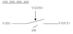
도 1은 종래의 P 채널 모스 전계 효과 트랜지스터를 이용한 스위칭 회로(100)를 나타낸다. 아울러, 도 2는 종래 및 본 발명의 스위칭 회로(100, 200, 300, 400)의 등가 회로도를 나타낸다.Figure 1 shows a
도 1로부터 알 수 있는 바와 같이 종래의 P 채널 모스 전계 효과 트랜지스터를 이용한 스위칭 회로(100)는, 소오스 노드(S)가 입력 노드가 되고, 드레인 노드(D)가 출력 노드가 된다. 아울러, 게이트 노드(G)로 제어 전압(V(CON))을 인가하여 소오스 노드(S)와 드레인 노드(D) 사이를 온 또는 오프로 제어한다. 즉, P 채널 모스 전계 효과 트랜지스터를 이용한 스위칭 회로(100)는, 도 2와 같이 하나의 스위칭 소자(SW)를 포함하는 등가 회로에 의해 표현할 수 있다. 예를 들면, 제어 전압(V(CON))으로 그라운드 전위 또는 음의 전원 전압이 인가되면 스위칭 소자(SW)는 온이 되고, 제어 전압(V(CON))으로 양의 전원 전압이 인가되면 스위칭 소자(SW)는 오프가 된다.As can be seen from Figure 1, in the
아울러, 종래의 P 채널 모스 전계 효과 트랜지스터를 이용한 스위칭 회로(100)에서, P 채널 모스 전계 효과 트랜지스터의 바디(B)에는 양의 전원 전압이 입력되게 된다.In addition, in the
P 채널 모스 전계 효과 트랜지스터를 이용한 스위칭 회로(100)의 오프 시 누설 전류는, 바디(B)와 드레인 노드(D) 사이의 기생 다이오드(Parasitic Diode, D12)에 걸리는 역방향 바이어스(Reverse Bias)에 의해 발생한다.When the
따라서, P 채널 모스 전계 효과 트랜지스터를 이용한 스위칭 회로(100)의 오프 시 누설 전류를 감소시킬 필요가 있다.Therefore, there is a need to reduce leakage current when the
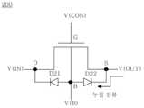
도 3은 종래의 N 채널 모스 전계 효과 트랜지스터를 이용한 스위칭 회로(200)를 나타낸다.Figure 3 shows a
N 채널 모스 전계 효과 트랜지스터를 이용한 스위칭 회로(200)의 오프 시 누설 전류는, 바디(B)와 소오스 노드(S) 사이의 기생 다이오드(Parasitic Diode, D22)에 걸리는 역방향 바이어스(Reverse Bias)에 의해 발생한다.When the
아울러, 종래의 P 채널 모스 전계 효과 트랜지스터를 이용한 스위칭 회로(100) 및 종래의 N 채널 모스 전계 효과 트랜지스터를 이용한 스위칭 회로(200)에서도, 모스 전계 효과 트랜지스터의 온저항(Ron)을 감소시킬 필요가 있다.In addition, in the
본 발명은 전술한 바와 같은 기술적 과제를 해결하는 데 목적이 있는 발명으로서, 모스 전계 효과 트랜지스터를 이용한 스위칭 회로의 오프 시 누설 전류를 감소시킬 수 있을 뿐만 아니라, 온저항을 감소시킬 수 있는 모스 전계 효과 트랜지스터를 이용한 스위칭 회로를 제공하는 것에 그 목적이 있다.The present invention is an invention aimed at solving the technical problems described above, and the MOS field effect can not only reduce leakage current when turning off a switching circuit using a MOS field effect transistor, but also reduce the on-resistance. The purpose is to provide a switching circuit using transistors.
스위칭 회로는, 소오스 노드와 드레인 노드 사이 또는 드레인 노드와 소오스 노드 사이를 온 또는 오프하는 스위칭 소자로서 동작하는 제 1 전계 효과 트랜지스터; 및 상기 제 1 전계 효과 트랜지스터의 바디와 연결된 바디 전원 공급 회로;를 포함한다.The switching circuit includes a first field effect transistor that operates as a switching element that turns on or off between a source node and a drain node or between a drain node and a source node; and a body power supply circuit connected to the body of the first field effect transistor.
구체적으로, 상기 바디 전원 공급 회로는, 제 2 전계 효과 트랜지스터를 이용한 제 1 소오스 팔로워 회로; 상기 제 1 전계 효과 트랜지스터의 바디와 상기 제 2 전계 효과 트랜지스터의 출력 사이를 연결하는 제 1 스위치; 제 3 전계 효과 트랜지스터를 이용한 제 2 소오스 팔로워 회로; 및 상기 제 1 전계 효과 트랜지스터의 바디와 상기 제 3 전계 효과 트랜지스터의 출력 사이를 연결하는 제 2 스위치;를 포함한다.Specifically, the body power supply circuit includes a first source follower circuit using a second field effect transistor; a first switch connecting the body of the first field effect transistor and the output of the second field effect transistor; a second source follower circuit using a third field effect transistor; and a second switch connecting the body of the first field effect transistor and the output of the third field effect transistor.
아울러, 상기 제 1 전계 효과 트랜지스터는, P 채널 모스 전계 효과 트랜지스터 또는 N 채널 모스 전계 효과 트랜지스터 중 하나의 모스 전계 효과 트랜지스터인 것이 바람직하다. 또한, 상기 제 2 전계 효과 트랜지스터는, 상기 제 1 전계 효과 트랜지스터와 동일한 채널의 모스 전계 효과 트랜지스터인 것을 특징으로 한다. 또한, 상기 제 3 전계 효과 트랜지스터는, 상기 제 1 전계 효과 트랜지스터와는 다른 채널의 모스 전계 효과 트랜지스터인 것을 특징으로 한다.In addition, the first field effect transistor is preferably a MOS field effect transistor, either a P-channel MOS field effect transistor or an N-channel MOS field effect transistor. Additionally, the second field effect transistor is characterized as being a MOS field effect transistor of the same channel as the first field effect transistor. Additionally, the third field effect transistor is characterized as being a MOS field effect transistor of a different channel from the first field effect transistor.
바람직하게는, 상기 제 1 전계 효과 트랜지스터가 온 상태일 경우, 상기 제 1 스위치는 온 상태가 되고, 상기 제 1 전계 효과 트랜지스터가 오프 상태일 경우, 상기 제 1 스위치는 오프 상태가 되는 것을 특징으로 한다.Preferably, when the first field effect transistor is in an on state, the first switch is in an on state, and when the first field effect transistor is in an off state, the first switch is in an off state. do.
아울러, 상기 제 2 전계 효과 트랜지스터의 게이트 노드와 상기 제 1 전계 효과 트랜지스터의 소오스 노드는, 서로 연결된 것이 바람직하다.In addition, the gate node of the second field effect transistor and the source node of the first field effect transistor are preferably connected to each other.
또한, 상기 제 1 전계 효과 트랜지스터가 온 상태일 경우, 상기 제 2 스위치는 오프 상태가 되고, 상기 제 1 전계 효과 트랜지스터가 오프 상태일 경우, 상기 제 2 스위치는 온 상태가 되는 것을 특징으로 한다.In addition, when the first field effect transistor is in an on state, the second switch is in an off state, and when the first field effect transistor is in an off state, the second switch is in an on state.
아울러, 상기 제 3 전계 효과 트랜지스터의 게이트 노드와 상기 제 1 전계 효과 트랜지스터가 오프 시의 상기 제 1 전계 효과 트랜지스터의 게이트 노드에는, 동일한 전압이 인가되는 것이 바람직하다.In addition, it is preferable that the same voltage is applied to the gate node of the third field effect transistor and the gate node of the first field effect transistor when the first field effect transistor is turned off.
본 발명의 모스 전계 효과 트랜지스터를 이용한 스위칭 회로에 따르면, 스위칭 회로의 오프 시 누설 전류를 감소시킬 수 있을 뿐만 아니라, 온저항을 감소시킬 수 있다.According to the switching circuit using the MOS field effect transistor of the present invention, not only can leakage current be reduced when the switching circuit is turned off, but also on-resistance can be reduced.
도 1은 종래의 P 채널 모스 전계 효과 트랜지스터를 이용한 스위칭 회로의 구성도.
도 2는 종래 및 본 발명의 스위칭 회로의 등가 회로도.
도 3은 종래의 N 채널 모스 전계 효과 트랜지스터를 이용한 스위칭 회로의 구성도.
도 4는 제 1 실시예에 따른 스위칭 회로의 구성도.
도 5는 제 1 P 채널 모스 전계 효과 트랜지스터의 온 동작 시의 제 1 실시예에 따른 스위칭 회로의 동작 설명도.
도 6은 제 1 P 채널 모스 전계 효과 트랜지스터의 오프 동작 시의 제 1 실시예에 따른 스위칭 회로의 동작 설명도.
도 7은 제 2 실시예에 따른 스위칭 회로의 구성도.
도 8은 제 1 N 채널 모스 전계 효과 트랜지스터의 온 동작 시의 제 2 실시예에 따른 스위칭 회로의 동작 설명도.
도 9는 제 1 N 채널 모스 전계 효과 트랜지스터의 오프 동작 시의 제 2 실시예에 따른 스위칭 회로의 동작 설명도.1 is a configuration diagram of a switching circuit using a conventional P-channel MOS field effect transistor.
2 is an equivalent circuit diagram of a switching circuit of the prior art and the present invention.
Figure 3 is a configuration diagram of a switching circuit using a conventional N-channel MOS field effect transistor.
4 is a configuration diagram of a switching circuit according to the first embodiment.
5 is a diagram illustrating the operation of the switching circuit according to the first embodiment when the first P-channel MOS field effect transistor is turned on.
6 is a diagram illustrating the operation of the switching circuit according to the first embodiment when the first P-channel MOS field effect transistor is turned off.
Figure 7 is a configuration diagram of a switching circuit according to the second embodiment.
Figure 8 is a diagram illustrating the operation of the switching circuit according to the second embodiment when the first N-channel MOS field effect transistor is turned on.
9 is a diagram illustrating the operation of the switching circuit according to the second embodiment when the first N-channel MOS field effect transistor is turned off.
이하, 첨부된 도면을 참조하면서 본 발명의 실시예들에 따른 모스 전계 효과 트랜지스터를 이용한 스위칭 회로에 대해 상세히 설명하기로 한다.Hereinafter, a switching circuit using a MOS field effect transistor according to embodiments of the present invention will be described in detail with reference to the attached drawings.
본 발명의 하기의 실시예들은 본 발명을 구체화하기 위한 것일 뿐 본 발명의 권리 범위를 제한하거나 한정하는 것이 아님은 물론이다. 본 발명의 상세한 설명 및 실시예들로부터 본 발명이 속하는 기술 분야의 전문가가 용이하게 유추할 수 있는 것은 본 발명의 권리 범위에 속하는 것으로 해석된다.Of course, the following examples of the present invention are only intended to embody the present invention and do not limit or limit the scope of the present invention. Anything that can be easily inferred by an expert in the technical field to which the present invention belongs from the detailed description and embodiments of the present invention will be interpreted as falling within the scope of the rights of the present invention.
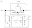
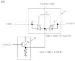
먼저, 도 4는 제 1 실시예에 따른 스위칭 회로(300)의 구성도를 나타낸다.First, Figure 4 shows a configuration diagram of the
도 4로부터 알 수 있는 바와 같이 제 1 실시예에 따른 스위칭 회로(300)는, 제 1 P 채널 모스 전계 효과 트랜지스터(P1) 및 바디 전원 공급 회로(BS)를 포함하여 구성된다.As can be seen from FIG. 4, the
참고로, 제 1 P 채널 모스 전계 효과 트랜지스터(P1)는 파워용으로 큰 크기의 트랜지스터이고, 바디 전원 공급 회로(BS)에 포함되는 트랜지스터는 제 1 P 채널 모스 전계 효과 트랜지스터(P1)에 비해 아주 작은 크기의 것을 사용하는 것이 바람직하다. 즉, 바디 전원 공급 회로(BS)의 트랜지스터에 의한 오프 시 누설 전류 및 온저항은, 제 1 P 채널 모스 전계 효과 트랜지스터(P1)의 오프 시 누설 전류 및 온저항에 비해 무시할 만하다.For reference, the first P-channel MOS field effect transistor (P1) is a large transistor for power, and the transistor included in the body power supply circuit (BS) is very small compared to the first P-channel MOS field effect transistor (P1). It is preferable to use a small size. That is, the off-state leakage current and on-resistance caused by the transistor of the body power supply circuit (BS) are negligible compared to the off-state leakage current and on-resistance of the first P-channel MOS field effect transistor (P1).
제 1 P 채널 모스 전계 효과 트랜지스터(P1)는, 소오스 노드와 드레인 노드 사이를 온 또는 오프하는 스위칭 소자로서 동작한다.The first P-channel MOS field effect transistor P1 operates as a switching element that turns on or off between the source node and the drain node.
도 4로부터 알 수 있는 바와 같이 제 1 실시예에 따른 스위칭 회로(300)는, 소오스 노드가 입력 노드가 되고, 드레인 노드가 출력 노드가 된다. 아울러, 게이트 노드로 제어 전압(V(CON))을 인가하여 소오스 노드와 드레인 노드 사이를 온 또는 오프로 제어한다. 예를 들면, 제어 전압(V(CON))으로 음의 전원 전압(VSS)이 인가되면 제 1 P 채널 모스 전계 효과 트랜지스터(P1)는 온이 되고, 제어 전압(V(CON))으로 양의 전원 전압(VDD)이 인가되면 제 1 P 채널 모스 전계 효과 트랜지스터(P1)는 오프가 된다.As can be seen from FIG. 4, in the
바디 전원 공급 회로(BS)는, 제 1 소오스 팔로워 회로(S1), 제 2 소오스 팔로워 회로(S2), 제 1 스위치(SW1) 및 제 2 스위치(SW2)를 포함하여 구성된다.The body power supply circuit BS includes a first source follower circuit S1, a second source follower circuit S2, a first switch SW1, and a second switch SW2.
제 1 소오스 팔로워 회로(S1)는 제 2 전계 효과 트랜지스터(T2)를 이용하여 구현될 수 있다. 아울러, 제 2 전계 효과 트랜지스터(T2)는, 제 1 P 채널 모스 전계 효과 트랜지스터(P1)와 동일한 채널인 P 채널 모스 전계 효과 트랜지스터인 것을 특징으로 한다. 제 2 소오스 팔로워 회로(S2)는 제 3 전계 효과 트랜지스터(T3)를 이용하여 구현될 수 있다. 아울러, 제 3 전계 효과 트랜지스터(T3)는, 제 1 P 채널 모스 전계 효과 트랜지스터(P1)와는 다른 채널인, N 채널 모스 전계 효과 트랜지스터인 것이 바람직하다.The first source follower circuit (S1) may be implemented using the second field effect transistor (T2). In addition, the second field effect transistor (T2) is characterized as being a P-channel MOS field effect transistor of the same channel as the first P-channel MOS field effect transistor (P1). The second source follower circuit (S2) may be implemented using the third field effect transistor (T3). In addition, the third field effect transistor T3 is preferably an N-channel MOS field effect transistor having a different channel from the first P-channel MOS field effect transistor P1.
제 1 소오스 팔로워 회로(S1) 및 제 2 소오스 팔로워 회로(S2)의 출력은 각각, 제 1 스위치(SW1) 및 제 2 스위치(SW2)를 통해 제 1 P 채널 모스 전계 효과 트랜지스터(P1)의 바디와 연결된다.The outputs of the first source follower circuit (S1) and the second source follower circuit (S2) are connected to the body of the first P-channel MOS field effect transistor (P1) through the first switch (SW1) and the second switch (SW2), respectively. is connected to
제 1 스위치(SW1)는, 제 1 P 채널 모스 전계 효과 트랜지스터(P1)의 바디와 제 2 전계 효과 트랜지스터(T2)의 출력 사이를 연결한다. 아울러, 제 2 스위치(SW2)는 제 1 P 채널 모스 전계 효과 트랜지스터(P1)의 바디와 제 3 전계 효과 트랜지스터(T3)의 출력 사이를 연결한다.The first switch SW1 connects the body of the first P-channel MOS field effect transistor P1 and the output of the second field effect transistor T2. In addition, the second switch (SW2) connects the body of the first P-channel MOS field effect transistor (P1) and the output of the third field effect transistor (T3).
또한, 제 1 스위치(SW1) 및 제 2 스위치(SW2)는 트랜지스터를 이용하여 구현될 수 있다. 제 1 스위치(SW1) 및 제 2 스위치(SW2)의 제어는 제어기(미도시)에 의해 실시될 수 있다.Additionally, the first switch (SW1) and the second switch (SW2) may be implemented using a transistor. Control of the first switch (SW1) and the second switch (SW2) may be performed by a controller (not shown).
제 1 P 채널 모스 전계 효과 트랜지스터(P1)가 온 상태일 경우, 제 1 스위치(SW1)는 온 상태가 되고 제 2 스위치(SW2)는 오프 상태가 된다. 제 1 P 채널 모스 전계 효과 트랜지스터(P1)가 오프 상태일 경우, 제 1 스위치(SW1)는 오프 상태가 되고 제 2 스위치(SW2)는 온 상태가 되는 것이 바람직하다.When the first P-channel MOS field effect transistor P1 is in the on state, the first switch (SW1) is in the on state and the second switch (SW2) is in the off state. When the first P-channel MOS field effect transistor (P1) is in an off state, it is preferable that the first switch (SW1) is in an off state and the second switch (SW2) is in an on state.
제 2 전계 효과 트랜지스터(T2)의 게이트 노드와 제 1 P 채널 모스 전계 효과 트랜지스터(P1)의 소오스 노드는, 스위칭 회로(300)의 입력 노드와 연결되는 것이 바람직하다. 즉, 제 2 전계 효과 트랜지스터(T2)의 게이트 노드와 제 1 P 채널 모스 전계 효과 트랜지스터(P1)의 소오스 노드는 서로 연결된 것을 특징으로 한다. 아울러, 스위칭 회로(300)의 입력 노드의 전압(V(IN))은, 제 1 P 채널 모스 전계 효과 트랜지스터(P1)의 바디 바이어스 전압(V(B)) 및 양의 전원 전압(VDD) 보다 작은 값을 나타낸다. 다시 말해, 스위칭 회로(300)의 입력 노드의 전압(V(IN))은 제 1 P 채널 모스 전계 효과 트랜지스터(P1)의 바디 바이어스 전압(V(B)) 보다 작고, 제 1 P 채널 모스 전계 효과 트랜지스터(P1)의 바디 바이어스 전압(V(B))은 양의 전원 전압(VDD) 보다 작다.The gate node of the second field effect transistor (T2) and the source node of the first P-channel MOS field effect transistor (P1) are preferably connected to the input node of the
아울러, 제 3 전계 효과 트랜지스터(T3)의 게이트 노드와 제 1 P 채널 모스 전계 효과 트랜지스터(P1)가 오프 시의 제 1 P 채널 모스 전계 효과 트랜지스터(P1)의 게이트 노드에는, 동일한 전압인, 양의 전원 전압(VDD)이 인가되는 것이 바람직하다.In addition, when the gate node of the third field effect transistor (T3) and the first P-channel MOS field effect transistor (P1) are turned off, the same voltage, positive, is applied to the gate node of the first P-channel MOS field effect transistor (P1). It is desirable that a power supply voltage (VDD) of .
제 1 P 채널 모스 전계 효과 트랜지스터(P1)가 온 상태인 경우를 가정하자. 이때 제 1 P 채널 모스 전계 효과 트랜지스터(P1)의 게이트에는 음의 전원 전압(VSS)이 인가되는 것이 바람직하다.Assume that the first P-channel MOS field effect transistor (P1) is in the on state. At this time, it is preferable that a negative power supply voltage (VSS) is applied to the gate of the first P-channel MOS field effect transistor (P1).
도 5는 제 1 P 채널 모스 전계 효과 트랜지스터(P1)의 온 동작 시의 제 1 실시예에 따른 스위칭 회로(300)의 동작 설명도를 나타낸다.FIG. 5 illustrates an operation diagram of the
제 1 P 채널 모스 전계 효과 트랜지스터(P1)가 온 상태일 경우, 제 1 스위치(SW1)는 온 상태가 되고 제 2 스위치(SW2)는 오프 상태가 된다. 제 1 P 채널 모스 전계 효과 트랜지스터(P1)의 온저항은, 문턱 전압 파라미터가 낮을수록 작아진다.When the first P-channel MOS field effect transistor P1 is in the on state, the first switch (SW1) is in the on state and the second switch (SW2) is in the off state. The on-resistance of the first P-channel MOS field effect transistor P1 decreases as the threshold voltage parameter decreases.
아울러, 제 1 P 채널 모스 전계 효과 트랜지스터(P1)의 문턱 전압은, 제 1 P 채널 모스 전계 효과 트랜지스터(P1)의 바디와 소오스 사이의 전압차가 작아질수록 낮아진다.In addition, the threshold voltage of the first P-channel MOS field effect transistor (P1) decreases as the voltage difference between the body and the source of the first P-channel MOS field effect transistor (P1) decreases.
이때, 제 1 P 채널 모스 전계 효과 트랜지스터(P1)의 바디를 양의 전원 전압(VDD)에 연결하는 것 보다 제 1 소오스 팔로워 회로(S1)의 출력에 연결하면, 제 1 P 채널 모스 전계 효과 트랜지스터(P1)의 바디와 소오스 사이의 전압차가 작아지며, 이에 따라 제 1 P 채널 모스 전계 효과 트랜지스터(P1)의 온저항이 감소한다.At this time, if the body of the first P-channel MOS field-effect transistor (P1) is connected to the output of the first source follower circuit (S1) rather than connected to the positive power supply voltage (VDD), the first P-channel MOS field-effect transistor The voltage difference between the body and the source of (P1) decreases, and accordingly, the on-resistance of the first P-channel MOS field effect transistor (P1) decreases.
즉, 제 1 소오스 팔로워 회로(S1)가 없는 경우에는, (VDD-V(IN))에 의해 제 1 P 채널 모스 전계 효과 트랜지스터(P1)의 온저항은 결정된다.That is, when there is no first source follower circuit (S1), the on-resistance of the first P-channel MOS field effect transistor (P1) is determined by (VDD-V(IN)).
그런데, 제 1 소오스 팔로워 회로(S1)가 있는 경우에는 제 1 P 채널 모스 전계 효과 트랜지스터(P1)의 바디 바이어스 전압(V(B))이 대략 (V(IN)+Vth(T2))가 된다. 여기서, Vth(T2)는 제 2 전계 효과 트랜지스터(T2)의 문턱 전압이다. 즉, 제 1 소오스 팔로워 회로(S1)가 있는 경우에는, {(V(IN)+Vth(T2))-V(IN)}에 의해 제 1 P 채널 모스 전계 효과 트랜지스터(P1)의 온저항은 결정된다. 즉, 제 1 소오스 팔로워 회로(S1)가 있는 경우의 온저항은 제 1 P 채널 모스 전계 효과 트랜지스터(P1)의 바디 바이어스 전압(V(B))이 낮아짐에 따라, 제 1 소오스 팔로워 회로(S1)가 없는 경우에 비해 작아지는 것을 알 수 있다.However, when there is a first source follower circuit (S1), the body bias voltage (V(B)) of the first P-channel MOS field effect transistor (P1) becomes approximately (V(IN)+Vth(T2)). . Here, Vth(T2) is the threshold voltage of the second field effect transistor (T2). That is, when there is a first source follower circuit (S1), the on-resistance of the first P-channel MOS field effect transistor (P1) is {(V(IN)+Vth(T2))-V(IN)} It is decided. That is, the on-resistance in the case of the first source follower circuit (S1) decreases as the body bias voltage (V(B)) of the first P-channel MOS field effect transistor (P1) decreases. ) can be seen to be smaller than in the case without it.
제 1 P 채널 모스 전계 효과 트랜지스터(P1)가 오프 상태인 경우를 가정하자.Assume that the first P-channel MOS field effect transistor (P1) is in an off state.
도 6은 제 1 P 채널 모스 전계 효과 트랜지스터(P1)의 오프 동작 시의 제 1 실시예에 따른 스위칭 회로(300)의 동작 설명도를 나타낸다.FIG. 6 shows an operation diagram of the
제 1 P 채널 모스 전계 효과 트랜지스터(P1)가 오프 상태일 경우, 제 1 스위치(SW1)는 오프 상태가 되고 제 2 스위치(SW2)는 온 상태가 된다. 아울러, 제 1 P 채널 모스 전계 효과 트랜지스터(P1)가 오프 상태일 경우, 그 게이트에는 양의 전원 전압(VDD)이 인가된다.When the first P-channel MOS field effect transistor (P1) is in the off state, the first switch (SW1) is in the off state and the second switch (SW2) is in the on state. In addition, when the first P-channel MOS field effect transistor (P1) is in an off state, a positive power supply voltage (VDD) is applied to its gate.
제 1 P 채널 모스 전계 효과 트랜지스터(P1)의 오프 시 누설 전류는 바디와 드레인 노드 사이의 기생 다이오드(Parasitic Diode, D12)에 걸리는 역방향 바이어스(Reverse Bias)에 의해 발생한다.When the first P-channel MOS field effect transistor (P1) is turned off, leakage current is generated by reverse bias applied to the parasitic diode (D12) between the body and the drain node.
이때 제 1 P 채널 모스 전계 효과 트랜지스터(P1)의 바디를 양의 전원 전압(VDD)에 연결하는 것 보다는, 제 2 소오스 팔로워 회로(S2)의 출력에 연결하면 역방향 바이어스가 줄어들어 누설 전류가 감소한다.At this time, if the body of the first P-channel MOS field effect transistor (P1) is connected to the output of the second source follower circuit (S2) rather than connected to the positive power supply voltage (VDD), the reverse bias is reduced and the leakage current is reduced. .
즉, 제 2 소오스 팔로워 회로(S2)가 없는 경우에는, (VDD-V(OUT))에 의해 제 1 P 채널 모스 전계 효과 트랜지스터(P1)의 누설 전류가 결정된다.That is, when there is no second source follower circuit (S2), the leakage current of the first P-channel MOS field effect transistor (P1) is determined by (VDD-V(OUT)).
그런데, 제 2 소오스 팔로워 회로(S2)가 있는 경우에는 제 1 P 채널 모스 전계 효과 트랜지스터(P1)의 바디 바이어스 전압(V(B))이 대략 (VDD-Vth(T3))가 된다. 여기서 Vth(T3)는, 제 3 전계 효과 트랜지스터(T3)의 문턱 전압을 나타낸다. 즉, 제 2 소오스 팔로워 회로(S2)가 있는 경우에는, {(VDD-Vth(T3))-V(OUT)}에 의해 제 1 P 채널 모스 전계 효과 트랜지스터(P1)의 누설 전류는 결정된다. 즉, 제 2 소오스 팔로워 회로(S2)가 있는 경우의 누설 전류가 제 3 전계 효과 트랜지스터(T3)의 문턱 전압(Vth(T3))의 효과에 의해, 제 2 소오스 팔로워 회로(S2)가 없는 경우에 비해 작아지는 것을 알 수 있다.However, when the second source follower circuit (S2) is present, the body bias voltage (V(B)) of the first P-channel MOS field effect transistor (P1) becomes approximately (VDD-Vth(T3)). Here, Vth(T3) represents the threshold voltage of the third field effect transistor (T3). That is, when the second source follower circuit S2 is present, the leakage current of the first P-channel MOS field effect transistor P1 is determined by {(VDD-Vth(T3))-V(OUT)}. That is, the leakage current in the case where the second source follower circuit (S2) is present is due to the effect of the threshold voltage (Vth(T3)) of the third field effect transistor (T3), and in the case where the second source follower circuit (S2) is not present. It can be seen that it is smaller than .
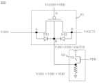
도 7은 제 2 실시예에 따른 스위칭 회로(400)의 구성도를 나타낸다.Figure 7 shows a configuration diagram of the
도 7로부터 알 수 있는 바와 같이 제 2 실시예에 따른 스위칭 회로(400)는, 제 1 N 채널 모스 전계 효과 트랜지스터(N1) 및 바디 전원 공급 회로(BS)를 포함하여 구성된다.As can be seen from FIG. 7, the
참고로, 제 1 N 채널 모스 전계 효과 트랜지스터(N1)는 파워용으로 큰 크기의 트랜지스터이고, 바디 전원 공급 회로(BS)에 포함되는 트랜지스터는 제 1 N 채널 모스 전계 효과 트랜지스터(N1)에 비해 아주 작은 크기의 것을 사용하는 것이 바람직하다. 즉, 바디 전원 공급 회로(BS)의 트랜지스터에 의한 오프 시 누설 전류 및 온저항은, 제 1 N 채널 모스 전계 효과 트랜지스터(N1)의 오프 시 누설 전류 및 온저항에 비해 무시할 만하다.For reference, the first N-channel MOS field effect transistor (N1) is a large transistor for power, and the transistor included in the body power supply circuit (BS) is very small compared to the first N-channel MOS field effect transistor (N1). It is preferable to use a small size. That is, the off-state leakage current and on-resistance caused by the transistor of the body power supply circuit BS are negligible compared to the off-state leakage current and on-resistance of the first N-channel MOS field effect transistor N1.
제 1 N 채널 모스 전계 효과 트랜지스터(N1)는, 소오스 노드와 드레인 노드 사이를 온 또는 오프하는 스위칭 소자로서 동작한다.The first N-channel MOS field effect transistor N1 operates as a switching element that turns on or off between the source node and the drain node.
도 7로부터 알 수 있는 바와 같이 제 2 실시예에 따른 스위칭 회로(400)는, 드레인 노드가 입력 노드가 되고, 소오스 노드가 출력 노드가 된다. 아울러, 게이트 노드로 제어 전압(V(CON))을 인가하여 드레인 노드와 소오스 노드 사이를 온 또는 오프로 제어한다. 예를 들면, 제어 전압(V(CON))으로 양의 전원 전압(VDD)이 인가되면 제 1 N 채널 모스 전계 효과 트랜지스터(N1)는 온이 되고, 제어 전압(V(CON))으로 음의 전원 전압(VSS)이 인가되면 제 1 N 채널 모스 전계 효과 트랜지스터(N1)는 오프가 된다.As can be seen from FIG. 7, in the
바디 전원 공급 회로(BS)는, 제 1 소오스 팔로워 회로(S1), 제 2 소오스 팔로워 회로(S2), 제 1 스위치(SW1) 및 제 2 스위치(SW2)를 포함하여 구성된다.The body power supply circuit BS includes a first source follower circuit S1, a second source follower circuit S2, a first switch SW1, and a second switch SW2.
제 1 소오스 팔로워 회로(S1)는 제 2 전계 효과 트랜지스터(T2)를 이용하여 구현될 수 있다. 아울러, 제 2 전계 효과 트랜지스터(T2)는, 제 1 N 채널 모스 전계 효과 트랜지스터(N1)와 동일한 채널인 N 채널 모스 전계 효과 트랜지스터인 것을 특징으로 한다. 제 2 소오스 팔로워 회로(S2)는 제 3 전계 효과 트랜지스터(T3)를 이용하여 구현될 수 있다. 아울러, 제 3 전계 효과 트랜지스터(T3)는, 제 1 N 채널 모스 전계 효과 트랜지스터(N1)와는 다른 채널인, P 채널 모스 전계 효과 트랜지스터인 것이 바람직하다.The first source follower circuit (S1) may be implemented using the second field effect transistor (T2). In addition, the second field effect transistor (T2) is characterized as being an N-channel MOS field effect transistor of the same channel as the first N-channel MOS field effect transistor (N1). The second source follower circuit (S2) may be implemented using the third field effect transistor (T3). In addition, the third field effect transistor T3 is preferably a P-channel MOS field effect transistor of a different channel from the first N-channel MOS field effect transistor N1.
제 1 소오스 팔로워 회로(S1) 및 제 2 소오스 팔로워 회로(S2)의 출력은 각각, 제 1 스위치(SW1) 및 제 2 스위치(SW2)를 통해 제 1 N 채널 모스 전계 효과 트랜지스터(N1)의 바디와 연결된다.The outputs of the first source follower circuit (S1) and the second source follower circuit (S2) are connected to the body of the first N-channel MOS field effect transistor (N1) through the first switch (SW1) and the second switch (SW2), respectively. is connected to
제 1 스위치(SW1)는, 제 1 N 채널 모스 전계 효과 트랜지스터(N1)의 바디와 제 2 전계 효과 트랜지스터(T2)의 출력 사이를 연결한다. 아울러, 제 2 스위치(SW2)는 제 1 N 채널 모스 전계 효과 트랜지스터(N1)의 바디와 제 3 전계 효과 트랜지스터(T3)의 출력 사이를 연결한다.The first switch SW1 connects the body of the first N-channel MOS field effect transistor N1 and the output of the second field effect transistor T2. In addition, the second switch (SW2) connects the body of the first N-channel MOS field effect transistor (N1) and the output of the third field effect transistor (T3).
또한, 제 1 스위치(SW1) 및 제 2 스위치(SW2)는 트랜지스터를 이용하여 구현될 수 있다. 제 1 스위치(SW1) 및 제 2 스위치(SW2)의 제어는 제어기(미도시)에 의해 실시될 수 있다.Additionally, the first switch (SW1) and the second switch (SW2) may be implemented using transistors. Control of the first switch (SW1) and the second switch (SW2) may be performed by a controller (not shown).
제 1 N 채널 모스 전계 효과 트랜지스터(N1)가 온 상태일 경우, 제 1 스위치(SW1)는 온 상태가 되고 제 2 스위치(SW2)는 오프 상태가 된다. 제 1 N 채널 모스 전계 효과 트랜지스터(N1)가 오프 상태일 경우, 제 1 스위치(SW1)는 오프 상태가 되고 제 2 스위치(SW2)는 온 상태가 되는 것이 바람직하다.When the first N-channel MOS field effect transistor N1 is in the on state, the first switch (SW1) is in the on state and the second switch (SW2) is in the off state. When the first N-channel MOS field effect transistor N1 is in an off state, the first switch SW1 is preferably in an off state and the second switch (SW2) is in an on state.
제 2 전계 효과 트랜지스터(T2)의 게이트 노드와 제 1 N 채널 모스 전계 효과 트랜지스터(N1)의 소오스 노드는, 스위칭 회로(400)의 출력 단자와 연결되는 것이 바람직하다. 즉, 제 2 전계 효과 트랜지스터(T2)의 게이트 노드와 제 1 N 채널 모스 전계 효과 트랜지스터(N1)의 소오스 노드는 서로 연결된 것을 특징으로 한다. 아울러, 스위칭 회로(400)의 출력 노드의 전압(V(OUT))은, 제 1 N 채널 모스 전계 효과 트랜지스터(N1)의 바디 바이어스 전압(V(B)) 및 음의 전원 전압(VSS) 보다 큰 값을 나타낸다. 다시 말해, 스위칭 회로(400)의 출력 노드의 전압(V(OUT))은 제 1 N 채널 모스 전계 효과 트랜지스터(N1)의 바디 바이어스 전압(V(B)) 보다 크고, 제 1 N 채널 모스 전계 효과 트랜지스터(N1)의 바디 바이어스 전압(V(B))은 음의 전원 전압(VSS) 보다 크다.The gate node of the second field effect transistor T2 and the source node of the first N-channel MOS field effect transistor N1 are preferably connected to the output terminal of the
아울러, 제 3 전계 효과 트랜지스터(T3)의 게이트 노드와 제 1 N 채널 모스 전계 효과 트랜지스터(N1)가 오프 시의 제 1 N 채널 모스 전계 효과 트랜지스터(N1)의 게이트 노드에는, 동일한 전압인, 음의 전원 전압(VSS)이 인가되는 것이 바람직하다.In addition, when the gate node of the third field effect transistor (T3) and the first N-channel MOS field effect transistor (N1) are turned off, the gate node of the first N-channel MOS field effect transistor (N1) has the same voltage, negative. It is desirable that a power supply voltage (VSS) of .
제 1 N 채널 모스 전계 효과 트랜지스터(N1)가 온 상태인 경우를 가정하자. 이때 제 1 N 채널 모스 전계 효과 트랜지스터(N1)의 게이트에는 양의 전원 전압(VDD)이 인가되는 것이 바람직하다.Assume that the first N-channel MOS field effect transistor N1 is in the on state. At this time, it is preferable that a positive power supply voltage (VDD) is applied to the gate of the first N-channel MOS field effect transistor (N1).
도 8은 제 1 N 채널 모스 전계 효과 트랜지스터(N1)의 온 동작 시의 제 2 실시예에 따른 스위칭 회로(400)의 동작 설명도를 나타낸다.FIG. 8 shows an operation diagram of the
제 1 N 채널 모스 전계 효과 트랜지스터(N1)가 온 상태일 경우, 제 1 스위치(SW1)는 온 상태가 되고 제 2 스위치(SW2)는 오프 상태가 된다. 제 1 N 채널 모스 전계 효과 트랜지스터(N1)의 온저항은, 제 1 N 채널 모스 전계 효과 트랜지스터(N1)의 문턱 전압 파라미터가 낮을수록 작아진다.When the first N-channel MOS field effect transistor N1 is in the on state, the first switch (SW1) is in the on state and the second switch (SW2) is in the off state. The on-resistance of the first N-channel MOS field effect transistor N1 decreases as the threshold voltage parameter of the first N-channel MOS field effect transistor N1 decreases.
아울러, 제 1 N 채널 모스 전계 효과 트랜지스터(N1)의 문턱 전압은, 제 1 N 채널 모스 전계 효과 트랜지스터(N1)의 소오스와 바디 사이의 전압차가 작아질수록 낮아진다.In addition, the threshold voltage of the first N-channel MOS field effect transistor N1 decreases as the voltage difference between the source and body of the first N-channel MOS field effect transistor N1 decreases.
이때, 제 1 N 채널 모스 전계 효과 트랜지스터(N1)의 바디를 음의 전원 전압(VSS)에 연결하는 것 보다 제 1 소오스 팔로워 회로(S1)의 출력에 연결하면, 제 1 N 채널 모스 전계 효과 트랜지스터(N1)의 소오스와 바디 사이의 전압차가 작아지며, 이에 따라 제 1 N 채널 모스 전계 효과 트랜지스터(N1)의 온저항이 감소한다.At this time, if the body of the first N-channel MOS field-effect transistor (N1) is connected to the output of the first source follower circuit (S1) rather than connected to the negative power supply voltage (VSS), the first N-channel MOS field-effect transistor The voltage difference between the source and body of (N1) decreases, and accordingly, the on-resistance of the first N-channel MOS field effect transistor (N1) decreases.
즉, 제 1 소오스 팔로워 회로(S1)가 없는 경우에는, (V(OUT)-VSS)에 의해 제 1 N 채널 모스 전계 효과 트랜지스터(N1)의 온저항은 결정된다.That is, when there is no first source follower circuit (S1), the on-resistance of the first N-channel MOS field effect transistor (N1) is determined by (V(OUT)-VSS).
그런데, 제 1 소오스 팔로워 회로(S1)가 있는 경우에는, 제 1 N 채널 모스 전계 효과 트랜지스터(N1)의 바디 바이어스 전압(V(B))이 대략 (V(OUT)-Vth(T2))가 된다. 여기서, Vth(T2)는 제 2 전계 효과 트랜지스터(T2)의 문턱 전압을 나타낸다. 즉, 제 1 소오스 팔로워 회로(S1)가 있는 경우에는, {V(OUT)-(V(OUT)-Vth(T2))}에 의해 제 1 N 채널 모스 전계 효과 트랜지스터(N1)의 온저항은 결정된다. 즉, 제 1 소오스 팔로워 회로(S1)가 있는 경우의 온저항은 제 1 P 채널 모스 전계 효과 트랜지스터(P1)의 바디 바이어스 전압(V(B))이 높아짐에 따라, 제 1 소오스 팔로워 회로(S1)가 없는 경우에 비해 작아지는 것을 알 수 있다.However, when there is a first source follower circuit (S1), the body bias voltage (V(B)) of the first N-channel MOS field effect transistor (N1) is approximately (V(OUT)-Vth(T2)). do. Here, Vth(T2) represents the threshold voltage of the second field effect transistor (T2). That is, when there is a first source follower circuit (S1), the on-resistance of the first N-channel MOS field effect transistor (N1) is {V(OUT)-(V(OUT)-Vth(T2))} It is decided. That is, the on-resistance in the case where the first source follower circuit (S1) is present increases as the body bias voltage (V(B)) of the first P-channel MOS field effect transistor (P1) increases. ) can be seen to be smaller than in the case without it.
제 1 N 채널 모스 전계 효과 트랜지스터(N1)가 오프 상태인 경우를 가정하자.Assume that the first N-channel MOS field effect transistor N1 is in an off state.
도 9는 제 1 N 채널 모스 전계 효과 트랜지스터(N1)의 오프 동작 시의 제 2 실시예에 따른 스위칭 회로(400)의 동작 설명도를 나타낸다.FIG. 9 shows an operation diagram of the
제 1 N 채널 모스 전계 효과 트랜지스터(N1)가 오프 상태일 경우, 제 1 스위치(SW1)는 오프 상태가 되고 제 2 스위치(SW2)는 온 상태가 된다. 아울러,제 1 N 채널 모스 전계 효과 트랜지스터(N1)가 오프 상태일 경우, 그 게이트에는 음의 전원 전압(VSS)이 인가된다.When the first N-channel MOS field effect transistor N1 is in an off state, the first switch SW1 is in an off state and the second switch (SW2) is in an on state. In addition, when the first N-channel MOS field effect transistor N1 is in an off state, a negative power supply voltage VSS is applied to its gate.
제 1 N 채널 모스 전계 효과 트랜지스터(N1)의 오프 시 누설 전류는 바디와 드레인 노드 사이의 기생 다이오드(D22)에 걸리는 역방향 바이어스에 의해 발생한다.When the first N-channel MOS field effect transistor N1 is turned off, a leakage current is generated by a reverse bias applied to the parasitic diode D22 between the body and the drain node.
이때 제 1 N 채널 모스 전계 효과 트랜지스터(N1)의 바디를 음의 전원 전압(VSS)에 연결하는 것 보다는, 제 2 소오스 팔로워 회로(S2)의 출력에 연결하면 역방향 바이어스가 줄어들어 누설 전류가 감소한다.At this time, if the body of the first N-channel MOS field effect transistor (N1) is connected to the output of the second source follower circuit (S2) rather than connected to the negative power supply voltage (VSS), the reverse bias is reduced and the leakage current is reduced. .
즉, 제 2 소오스 팔로워 회로(S2)가 없는 경우에는, (V(OUT))-VSS)에 의해 제 1 N 채널 모스 전계 효과 트랜지스터(N1)의 누설 전류가 결정된다.That is, when there is no second source follower circuit (S2), the leakage current of the first N-channel MOS field effect transistor (N1) is determined by (V(OUT))-VSS).
그런데, 제 2 소오스 팔로워 회로(S2)가 있는 경우에는 제 1 P 채널 모스 전계 효과 트랜지스터(P1)의 바디 바이어스 전압(V(B))이 대략 (VSS+Vth(T3))가 된다. 여기서 Vth(T3)는 제 3 전계 효과 트랜지스터(T3)의 문턱 전압을 나타낸다. 즉, 제 2 소오스 팔로워 회로(S2)가 있는 경우에는, {V(OUT)-(VSS+Vth(T3))}에 의해 제 1 N 채널 모스 전계 효과 트랜지스터(N1)의 누설 전류는 결정된다. 즉, 제 2 소오스 팔로워 회로(S2)가 있는 경우의 누설 전류가 제 3 전계 효과 트랜지스터(T3)의 문턱 전압(Vth(T3))의 효과에 의해, 제 2 소오스 팔로워 회로(S2)가 없는 경우에 비해 작아지는 것을 알 수 있다.However, when the second source follower circuit (S2) is present, the body bias voltage (V(B)) of the first P-channel MOS field effect transistor (P1) becomes approximately (VSS+Vth(T3)). Here, Vth(T3) represents the threshold voltage of the third field effect transistor (T3). That is, when the second source follower circuit S2 is present, the leakage current of the first N-channel MOS field effect transistor N1 is determined by {V(OUT)-(VSS+Vth(T3))}. That is, the leakage current in the case where the second source follower circuit (S2) is present is due to the effect of the threshold voltage (Vth(T3)) of the third field effect transistor (T3), and in the case where the second source follower circuit (S2) is not present. It can be seen that it is smaller than .
상술한 바와 같은 제 1 실시예 및 제 2 실시예에 따른 스위칭 회로(300, 400)의 특징을 정리해 보면 다음과 같다.The characteristics of the switching
스위칭 회로(300, 400)는, 소오스 노드와 드레인 노드 사이 또는 드레인 노드와 소오스 노드 사이를 온 또는 오프하는 스위칭 소자로서 동작하는 제 1 전계 효과 트랜지스터(P1, N1); 및 제 1 전계 효과 트랜지스터(P1, N1)의 바디와 연결된 바디 전원 공급 회로(BS);를 포함한다.The switching
구체적으로, 바디 전원 공급 회로(BS)는, 제 2 전계 효과 트랜지스터(T2)를 이용한 제 1 소오스 팔로워 회로(S1); 제 3 전계 효과 트랜지스터(T3)를 이용한 제 2 소오스 팔로워 회로(S2); 제 1 전계 효과 트랜지스터(P1, N1)의 바디와 제 2 전계 효과 트랜지스터(T2)의 출력 사이를 연결하는 제 1 스위치(SW1); 및 제 1 전계 효과 트랜지스터(P1, N1)의 바디와 제 3 전계 효과 트랜지스터(T3)의 출력 사이를 연결하는 제 2 스위치(SW2);를 포함하여 구성된다.Specifically, the body power supply circuit (BS) includes a first source follower circuit (S1) using a second field effect transistor (T2); a second source follower circuit (S2) using a third field effect transistor (T3); a first switch (SW1) connected between the bodies of the first field effect transistors (P1, N1) and the output of the second field effect transistor (T2); and a second switch (SW2) connecting the bodies of the first field effect transistors (P1, N1) and the output of the third field effect transistor (T3).
제 1 전계 효과 트랜지스터(P1, N1)는, P 채널 모스 전계 효과 트랜지스터 또는 N 채널 모스 전계 효과 트랜지스터 중 하나의 모스 전계 효과 트랜지스터인 것을 특징으로 한다. 아울러, 제 2 전계 효과 트랜지스터(T2)는 제 1 전계 효과 트랜지스터(P1, N1)와 동일한 채널의 모스 전계 효과 트랜지스터이고, 제 3 전계 효과 트랜지스터(T3)는 제 1 전계 효과 트랜지스터(P1, N1)와는 다른 채널의 모스 전계 효과 트랜지스터인 것을 특징으로 한다.The first field effect transistors (P1, N1) are characterized as being one of a P-channel MOS field effect transistor or an N-channel MOS field effect transistor. In addition, the second field effect transistor (T2) is a MOS field effect transistor of the same channel as the first field effect transistor (P1, N1), and the third field effect transistor (T3) is a MOS field effect transistor of the same channel as the first field effect transistor (P1, N1). It is characterized by being a MOS field effect transistor of a different channel from that of.
또한, 제 1 전계 효과 트랜지스터(P1, N1)가 온 상태일 경우, 제 1 스위치(SW1)는 온 상태가 되고 제 2 스위치(SW2)는 오프 상태가 된다. 아울러, 제 1 전계 효과 트랜지스터(P1, N1)가 오프 상태일 경우, 제 1 스위치(SW1)는 오프 상태가 되고 제 2 스위치(SW2)는 온 상태가 되는 것을 특징으로 한다.Additionally, when the first field effect transistors (P1, N1) are in the on state, the first switch (SW1) is in the on state and the second switch (SW2) is in the off state. In addition, when the first field effect transistors (P1, N1) are in an off state, the first switch (SW1) is in an off state and the second switch (SW2) is in an on state.
제 2 전계 효과 트랜지스터(T2)의 게이트 노드와 제 1 전계 효과 트랜지스터(P1, N1)의 소오스 노드에는, 동일한 노드로부터 신호가 인가되는 것이 바람직하다. 또한, 제 3 전계 효과 트랜지스터(T3)의 게이트 노드와 제 1 전계 효과 트랜지스터(P1, N1)가 오프 시의 제 1 전계 효과 트랜지스터(P1, N1)의 게이트 노드에는, 동일한 전압이 인가되는 것을 특징으로 한다.It is preferable that a signal is applied to the gate node of the second field effect transistor T2 and the source node of the first field effect transistors P1 and N1 from the same node. In addition, the same voltage is applied to the gate node of the third field effect transistor (T3) and the gate node of the first field effect transistor (P1, N1) when the first field effect transistor (P1, N1) is turned off. Do it as
상술한 바와 같이 스위칭 회로(300, 400)에 따르면, 모스 전계 효과 트랜지스터를 이용한 스위칭 회로(300, 400)의 오프 시 누설 전류를 감소시킬 수 있을 뿐만 아니라, 온저항을 감소시킬 수 있음을 알 수 있다.As described above, according to the switching
100, 200, 300, 400 : 스위칭 회로
P1 : 제 1 P 채널 모스 전계 효과 트랜지스터
N1 : 제 1 N 채널 모스 전계 효과 트랜지스터
BS : 바디 전원 공급 회로
S1 : 제 1 소오스 팔로워 회로
S2 : 제 2 소오스 팔로워 회로
SW1 : 제 1 스위치
SW2 : 제 2 스위치
T2 : 제 2 전계 효과 트랜지스터
T3 : 제 3 전계 효과 트랜지스터100, 200, 300, 400: switching circuit
P1: 1st P-channel MOS field effect transistor
N1: First N-channel MOS field effect transistor
BS: Body power supply circuit
S1: first source follower circuit
S2: second source follower circuit
SW1: first switch
SW2: second switch
T2: second field effect transistor
T3: Third field effect transistor
Claims (8)
Translated fromKorean소오스 노드와 드레인 노드 사이 또는 드레인 노드와 소오스 노드 사이를 온 또는 오프하는 스위칭 소자로서 동작하는 제 1 전계 효과 트랜지스터; 및 상기 제 1 전계 효과 트랜지스터의 바디와 연결된 바디 전원 공급 회로;를 포함하되,
상기 바디 전원 공급 회로는, 제 2 전계 효과 트랜지스터를 이용한 제 1 소오스 팔로워 회로; 상기 제 1 전계 효과 트랜지스터의 바디와 상기 제 2 전계 효과 트랜지스터의 출력 사이를 연결하는 제 1 스위치; 제 3 전계 효과 트랜지스터를 이용한 제 2 소오스 팔로워 회로; 및 상기 제 1 전계 효과 트랜지스터의 바디와 상기 제 3 전계 효과 트랜지스터의 출력 사이를 연결하는 제 2 스위치;를 포함하되,
상기 제 1 전계 효과 트랜지스터는, P 채널 모스 전계 효과 트랜지스터 또는 N 채널 모스 전계 효과 트랜지스터 중 하나의 모스 전계 효과 트랜지스터이고,
상기 제 2 전계 효과 트랜지스터는, 상기 제 1 전계 효과 트랜지스터와 동일한 채널의 모스 전계 효과 트랜지스터이고,
상기 제 3 전계 효과 트랜지스터는, 상기 제 1 전계 효과 트랜지스터와는 다른 채널의 모스 전계 효과 트랜지스터인, 스위칭 회로.In a switching circuit,
a first field effect transistor operating as a switching element that turns on or off between a source node and a drain node or between a drain node and a source node; And a body power supply circuit connected to the body of the first field effect transistor,
The body power supply circuit includes a first source follower circuit using a second field effect transistor; a first switch connecting the body of the first field effect transistor and the output of the second field effect transistor; a second source follower circuit using a third field effect transistor; And a second switch connecting between the body of the first field effect transistor and the output of the third field effect transistor,
The first field effect transistor is one of a P-channel MOS field effect transistor or an N-channel MOS field effect transistor,
The second field effect transistor is a MOS field effect transistor of the same channel as the first field effect transistor,
A switching circuit, wherein the third field effect transistor is a MOS field effect transistor of a different channel from the first field effect transistor.
상기 제 1 전계 효과 트랜지스터가 온 상태일 경우, 상기 제 1 스위치는 온 상태가 되고,
상기 제 1 전계 효과 트랜지스터가 오프 상태일 경우, 상기 제 1 스위치는 오프 상태가 되는, 스위칭 회로.According to paragraph 1,
When the first field effect transistor is in the on state, the first switch is in the on state,
When the first field effect transistor is in the off state, the first switch is in the off state.
상기 제 2 전계 효과 트랜지스터의 게이트 노드와 상기 제 1 전계 효과 트랜지스터의 소오스 노드는,
서로 연결된, 스위칭 회로.According to paragraph 3,
The gate node of the second field effect transistor and the source node of the first field effect transistor are:
Interconnected, switching circuits.
상기 제 1 전계 효과 트랜지스터가 온 상태일 경우, 상기 제 2 스위치는 오프 상태가 되고,
상기 제 1 전계 효과 트랜지스터가 오프 상태일 경우, 상기 제 2 스위치는 온 상태가 되는, 스위칭 회로.According to paragraph 1,
When the first field effect transistor is in the on state, the second switch is in the off state,
When the first field effect transistor is in the off state, the second switch is in the on state.
상기 제 3 전계 효과 트랜지스터의 게이트 노드와 상기 제 1 전계 효과 트랜지스터가 오프 시의 상기 제 1 전계 효과 트랜지스터의 게이트 노드에는,
동일한 전압이 인가되는, 스위칭 회로.In clause 7,
At the gate node of the third field effect transistor and at the gate node of the first field effect transistor when the first field effect transistor is off,
A switching circuit to which the same voltage is applied.
Priority Applications (1)
| Application Number | Priority Date | Filing Date | Title |
|---|---|---|---|
| KR1020210068736AKR102610477B1 (en) | 2021-05-28 | 2021-05-28 | Switching circuits using mos field effect transistor |
Applications Claiming Priority (1)
| Application Number | Priority Date | Filing Date | Title |
|---|---|---|---|
| KR1020210068736AKR102610477B1 (en) | 2021-05-28 | 2021-05-28 | Switching circuits using mos field effect transistor |
Publications (2)
| Publication Number | Publication Date |
|---|---|
| KR20220160732A KR20220160732A (en) | 2022-12-06 |
| KR102610477B1true KR102610477B1 (en) | 2023-12-06 |
Family
ID=84407122
Family Applications (1)
| Application Number | Title | Priority Date | Filing Date |
|---|---|---|---|
| KR1020210068736AActiveKR102610477B1 (en) | 2021-05-28 | 2021-05-28 | Switching circuits using mos field effect transistor |
Country Status (1)
| Country | Link |
|---|---|
| KR (1) | KR102610477B1 (en) |
Citations (1)
| Publication number | Priority date | Publication date | Assignee | Title |
|---|---|---|---|---|
| KR102112794B1 (en)* | 2019-03-25 | 2020-05-19 | 주식회사 레오엘에스아이 | Switching circuits |
Family Cites Families (2)
| Publication number | Priority date | Publication date | Assignee | Title |
|---|---|---|---|---|
| JPS5813027A (en)* | 1981-07-17 | 1983-01-25 | Toshiba Corp | analog switch device |
| US9379698B2 (en) | 2014-02-04 | 2016-06-28 | Triquint Semiconductor, Inc. | Field effect transistor switching circuit |
- 2021
- 2021-05-28KRKR1020210068736Apatent/KR102610477B1/enactiveActive
Patent Citations (1)
| Publication number | Priority date | Publication date | Assignee | Title |
|---|---|---|---|---|
| KR102112794B1 (en)* | 2019-03-25 | 2020-05-19 | 주식회사 레오엘에스아이 | Switching circuits |
Also Published As
| Publication number | Publication date |
|---|---|
| KR20220160732A (en) | 2022-12-06 |
Similar Documents
| Publication | Publication Date | Title |
|---|---|---|
| US9257190B2 (en) | Level shifter | |
| US8344789B2 (en) | Analog switch with internal device body control | |
| US8629706B2 (en) | Power switch and operation method thereof | |
| US8710541B2 (en) | Bi-directional switch using series connected N-type MOS devices in parallel with series connected P-type MOS devices | |
| CN110071715B (en) | High-Range Positive Voltage Level Shifter Using Low-Voltage Devices | |
| US8836380B2 (en) | Bootstrap circuit | |
| CN102761327B (en) | Transmission gate | |
| US10523197B2 (en) | Switch circuit, corresponding device and method | |
| JPH07142990A (en) | Level conversion circuit | |
| CN108336991B (en) | Level shift circuit | |
| KR102610477B1 (en) | Switching circuits using mos field effect transistor | |
| JP4958434B2 (en) | Voltage selection circuit | |
| US11894843B2 (en) | Level shift circuit | |
| US9356584B2 (en) | Level shifter | |
| KR102112794B1 (en) | Switching circuits | |
| US10601405B2 (en) | Buffer circuit | |
| US8723581B1 (en) | Input buffers | |
| US20190326900A1 (en) | Driver circuit for a device circuit | |
| US7782124B2 (en) | Voltage supply circuit of semiconductor device | |
| US20250246901A1 (en) | Protection circuit and semiconductor device | |
| US10965283B2 (en) | Floating switch and drive circuit thereof | |
| US20160261276A1 (en) | D/a conversion circuit | |
| KR200329174Y1 (en) | Buffer for reducing dissipation power | |
| CN110034754B (en) | An integrated circuit and its transmission circuit | |
| CN115720090A (en) | Power switch |
Legal Events
| Date | Code | Title | Description |
|---|---|---|---|
| PA0109 | Patent application | St.27 status event code:A-0-1-A10-A12-nap-PA0109 | |
| PA0201 | Request for examination | St.27 status event code:A-1-2-D10-D11-exm-PA0201 | |
| P11-X000 | Amendment of application requested | St.27 status event code:A-2-2-P10-P11-nap-X000 | |
| P13-X000 | Application amended | St.27 status event code:A-2-2-P10-P13-nap-X000 | |
| E902 | Notification of reason for refusal | ||
| PE0902 | Notice of grounds for rejection | St.27 status event code:A-1-2-D10-D21-exm-PE0902 | |
| PG1501 | Laying open of application | St.27 status event code:A-1-1-Q10-Q12-nap-PG1501 | |
| E13-X000 | Pre-grant limitation requested | St.27 status event code:A-2-3-E10-E13-lim-X000 | |
| P11-X000 | Amendment of application requested | St.27 status event code:A-2-2-P10-P11-nap-X000 | |
| P13-X000 | Application amended | St.27 status event code:A-2-2-P10-P13-nap-X000 | |
| E902 | Notification of reason for refusal | ||
| PE0902 | Notice of grounds for rejection | St.27 status event code:A-1-2-D10-D21-exm-PE0902 | |
| E13-X000 | Pre-grant limitation requested | St.27 status event code:A-2-3-E10-E13-lim-X000 | |
| P11-X000 | Amendment of application requested | St.27 status event code:A-2-2-P10-P11-nap-X000 | |
| P13-X000 | Application amended | St.27 status event code:A-2-2-P10-P13-nap-X000 | |
| E701 | Decision to grant or registration of patent right | ||
| PE0701 | Decision of registration | St.27 status event code:A-1-2-D10-D22-exm-PE0701 | |
| PR0701 | Registration of establishment | St.27 status event code:A-2-4-F10-F11-exm-PR0701 | |
| PR1002 | Payment of registration fee | St.27 status event code:A-2-2-U10-U11-oth-PR1002 Fee payment year number:1 | |
| PG1601 | Publication of registration | St.27 status event code:A-4-4-Q10-Q13-nap-PG1601 |