KR102608902B1 - Method for manufacturing nitride semiconductor substrate - Google Patents
Method for manufacturing nitride semiconductor substrateDownload PDFInfo
- Publication number
- KR102608902B1 KR102608902B1KR1020160073871AKR20160073871AKR102608902B1KR 102608902 B1KR102608902 B1KR 102608902B1KR 1020160073871 AKR1020160073871 AKR 1020160073871AKR 20160073871 AKR20160073871 AKR 20160073871AKR 102608902 B1KR102608902 B1KR 102608902B1
- Authority
- KR
- South Korea
- Prior art keywords
- silicon substrate
- nitride
- growth
- silicon
- layer
- Prior art date
- Legal status (The legal status is an assumption and is not a legal conclusion. Google has not performed a legal analysis and makes no representation as to the accuracy of the status listed.)
- Active
Links
- 150000004767nitridesChemical class0.000titleclaimsabstractdescription169
- 239000000758substrateSubstances0.000titleclaimsabstractdescription157
- 238000000034methodMethods0.000titleclaimsabstractdescription93
- 239000004065semiconductorSubstances0.000titleclaimsabstractdescription25
- 238000004519manufacturing processMethods0.000titleclaimsabstractdescription21
- XUIMIQQOPSSXEZ-UHFFFAOYSA-NSiliconChemical compound[Si]XUIMIQQOPSSXEZ-UHFFFAOYSA-N0.000claimsabstractdescription129
- 239000010703siliconSubstances0.000claimsabstractdescription129
- 229910052710siliconInorganic materials0.000claimsabstractdescription128
- 230000012010growthEffects0.000claimsabstractdescription97
- 239000013078crystalSubstances0.000claimsabstractdescription64
- 150000003377silicon compoundsChemical class0.000claimsabstractdescription32
- 238000002248hydride vapour-phase epitaxyMethods0.000claimsdescription21
- 238000005530etchingMethods0.000claimsdescription18
- 238000003486chemical etchingMethods0.000claimsdescription12
- 238000000059patterningMethods0.000claimsdescription7
- 238000000227grindingMethods0.000claimsdescription6
- 229910052581Si3N4Inorganic materials0.000claimsdescription5
- HQVNEWCFYHHQES-UHFFFAOYSA-Nsilicon nitrideChemical compoundN12[Si]34N5[Si]62N3[Si]51N64HQVNEWCFYHHQES-UHFFFAOYSA-N0.000claimsdescription4
- 230000002093peripheral effectEffects0.000claimsdescription3
- 238000005229chemical vapour depositionMethods0.000claimsdescription2
- 238000001451molecular beam epitaxyMethods0.000claimsdescription2
- 239000000126substanceSubstances0.000claims1
- 229910002601GaNInorganic materials0.000description31
- 239000007789gasSubstances0.000description19
- 235000012431wafersNutrition0.000description10
- 229910002704AlGaNInorganic materials0.000description5
- 229910052782aluminiumInorganic materials0.000description5
- XAGFODPZIPBFFR-UHFFFAOYSA-NaluminiumChemical compound[Al]XAGFODPZIPBFFR-UHFFFAOYSA-N0.000description4
- 238000011065in-situ storageMethods0.000description4
- 229910052594sapphireInorganic materials0.000description4
- 239000010980sapphireSubstances0.000description4
- GYHNNYVSQQEPJS-UHFFFAOYSA-NGalliumChemical compound[Ga]GYHNNYVSQQEPJS-UHFFFAOYSA-N0.000description3
- XOYLJNJLGBYDTH-UHFFFAOYSA-MchlorogalliumChemical compound[Ga]ClXOYLJNJLGBYDTH-UHFFFAOYSA-M0.000description3
- 238000001816coolingMethods0.000description3
- 230000007547defectEffects0.000description3
- 229910052733galliumInorganic materials0.000description3
- 229910052751metalInorganic materials0.000description3
- 239000002184metalSubstances0.000description3
- 238000004544sputter depositionMethods0.000description3
- QGZKDVFQNNGYKY-UHFFFAOYSA-NAmmoniaChemical compoundNQGZKDVFQNNGYKY-UHFFFAOYSA-N0.000description2
- IJGRMHOSHXDMSA-UHFFFAOYSA-NAtomic nitrogenChemical compoundN#NIJGRMHOSHXDMSA-UHFFFAOYSA-N0.000description2
- KRHYYFGTRYWZRS-UHFFFAOYSA-NFluoraneChemical compoundFKRHYYFGTRYWZRS-UHFFFAOYSA-N0.000description2
- NBIIXXVUZAFLBC-UHFFFAOYSA-NPhosphoric acidChemical compoundOP(O)(O)=ONBIIXXVUZAFLBC-UHFFFAOYSA-N0.000description2
- QAOWNCQODCNURD-UHFFFAOYSA-NSulfuric acidChemical compoundOS(O)(=O)=OQAOWNCQODCNURD-UHFFFAOYSA-N0.000description2
- 230000015572biosynthetic processEffects0.000description2
- 230000007423decreaseEffects0.000description2
- 238000010586diagramMethods0.000description2
- 239000012212insulatorSubstances0.000description2
- LIVNPJMFVYWSIS-UHFFFAOYSA-Nsilicon monoxideChemical compound[Si-]#[O+]LIVNPJMFVYWSIS-UHFFFAOYSA-N0.000description2
- 239000002210silicon-based materialSubstances0.000description2
- 239000010409thin filmSubstances0.000description2
- JMASRVWKEDWRBT-UHFFFAOYSA-NGallium nitrideChemical compound[Ga]#NJMASRVWKEDWRBT-UHFFFAOYSA-N0.000description1
- KWYUFKZDYYNOTN-UHFFFAOYSA-MPotassium hydroxideChemical compound[OH-].[K+]KWYUFKZDYYNOTN-UHFFFAOYSA-M0.000description1
- VYPSYNLAJGMNEJ-UHFFFAOYSA-NSilicium dioxideChemical compoundO=[Si]=OVYPSYNLAJGMNEJ-UHFFFAOYSA-N0.000description1
- 229910045601alloyInorganic materials0.000description1
- 239000000956alloySubstances0.000description1
- 229910000147aluminium phosphateInorganic materials0.000description1
- 229910021529ammoniaInorganic materials0.000description1
- 239000006227byproductSubstances0.000description1
- 239000012159carrier gasSubstances0.000description1
- 230000000694effectsEffects0.000description1
- 230000005496eutecticsEffects0.000description1
- 238000010438heat treatmentMethods0.000description1
- 229910052738indiumInorganic materials0.000description1
- 238000002347injectionMethods0.000description1
- 239000007924injectionSubstances0.000description1
- 239000000463materialSubstances0.000description1
- 150000002739metalsChemical class0.000description1
- 229910052757nitrogenInorganic materials0.000description1
- 230000006911nucleationEffects0.000description1
- 238000010899nucleationMethods0.000description1
- 238000002360preparation methodMethods0.000description1
- 230000003252repetitive effectEffects0.000description1
- 230000034655secondary growthEffects0.000description1
- 229910052814silicon oxideInorganic materials0.000description1
- 239000000243solutionSubstances0.000description1
- JLTRXTDYQLMHGR-UHFFFAOYSA-NtrimethylaluminiumChemical compoundC[Al](C)CJLTRXTDYQLMHGR-UHFFFAOYSA-N0.000description1
Images


Classifications
- H—ELECTRICITY
- H01—ELECTRIC ELEMENTS
- H01L—SEMICONDUCTOR DEVICES NOT COVERED BY CLASS H10
- H01L21/00—Processes or apparatus adapted for the manufacture or treatment of semiconductor or solid state devices or of parts thereof
- H01L21/02—Manufacture or treatment of semiconductor devices or of parts thereof
- H01L21/02104—Forming layers
- H01L21/02365—Forming inorganic semiconducting materials on a substrate
- H01L21/02518—Deposited layers
- H01L21/02521—Materials
- H01L21/02538—Group 13/15 materials
- H01L21/0254—Nitrides
- H—ELECTRICITY
- H01—ELECTRIC ELEMENTS
- H01L—SEMICONDUCTOR DEVICES NOT COVERED BY CLASS H10
- H01L21/00—Processes or apparatus adapted for the manufacture or treatment of semiconductor or solid state devices or of parts thereof
- H01L21/02—Manufacture or treatment of semiconductor devices or of parts thereof
- H01L21/02002—Preparing wafers
- H01L21/02005—Preparing bulk and homogeneous wafers
- H01L21/02008—Multistep processes
- H01L21/0201—Specific process step
- H01L21/02024—Mirror polishing
- H—ELECTRICITY
- H01—ELECTRIC ELEMENTS
- H01L—SEMICONDUCTOR DEVICES NOT COVERED BY CLASS H10
- H01L21/00—Processes or apparatus adapted for the manufacture or treatment of semiconductor or solid state devices or of parts thereof
- H01L21/02—Manufacture or treatment of semiconductor devices or of parts thereof
- H01L21/02104—Forming layers
- H01L21/02107—Forming insulating materials on a substrate
- H01L21/02225—Forming insulating materials on a substrate characterised by the process for the formation of the insulating layer
- H01L21/0226—Forming insulating materials on a substrate characterised by the process for the formation of the insulating layer formation by a deposition process
- H01L21/02263—Forming insulating materials on a substrate characterised by the process for the formation of the insulating layer formation by a deposition process deposition from the gas or vapour phase
- H01L21/02271—Forming insulating materials on a substrate characterised by the process for the formation of the insulating layer formation by a deposition process deposition from the gas or vapour phase deposition by decomposition or reaction of gaseous or vapour phase compounds, i.e. chemical vapour deposition
- H01L21/0228—Forming insulating materials on a substrate characterised by the process for the formation of the insulating layer formation by a deposition process deposition from the gas or vapour phase deposition by decomposition or reaction of gaseous or vapour phase compounds, i.e. chemical vapour deposition deposition by cyclic CVD, e.g. ALD, ALE, pulsed CVD
- H—ELECTRICITY
- H01—ELECTRIC ELEMENTS
- H01L—SEMICONDUCTOR DEVICES NOT COVERED BY CLASS H10
- H01L21/00—Processes or apparatus adapted for the manufacture or treatment of semiconductor or solid state devices or of parts thereof
- H01L21/02—Manufacture or treatment of semiconductor devices or of parts thereof
- H01L21/02104—Forming layers
- H01L21/02365—Forming inorganic semiconducting materials on a substrate
- H01L21/02367—Substrates
- H01L21/0237—Materials
- H01L21/02373—Group 14 semiconducting materials
- H01L21/02381—Silicon, silicon germanium, germanium
- H—ELECTRICITY
- H01—ELECTRIC ELEMENTS
- H01L—SEMICONDUCTOR DEVICES NOT COVERED BY CLASS H10
- H01L21/00—Processes or apparatus adapted for the manufacture or treatment of semiconductor or solid state devices or of parts thereof
- H01L21/02—Manufacture or treatment of semiconductor devices or of parts thereof
- H01L21/02104—Forming layers
- H01L21/02365—Forming inorganic semiconducting materials on a substrate
- H01L21/02367—Substrates
- H01L21/0237—Materials
- H01L21/02387—Group 13/15 materials
- H01L21/02389—Nitrides
- H—ELECTRICITY
- H01—ELECTRIC ELEMENTS
- H01L—SEMICONDUCTOR DEVICES NOT COVERED BY CLASS H10
- H01L21/00—Processes or apparatus adapted for the manufacture or treatment of semiconductor or solid state devices or of parts thereof
- H01L21/02—Manufacture or treatment of semiconductor devices or of parts thereof
- H01L21/02104—Forming layers
- H01L21/02365—Forming inorganic semiconducting materials on a substrate
- H01L21/02436—Intermediate layers between substrates and deposited layers
- H01L21/02439—Materials
- H01L21/02455—Group 13/15 materials
- H01L21/02458—Nitrides
- H—ELECTRICITY
- H01—ELECTRIC ELEMENTS
- H01L—SEMICONDUCTOR DEVICES NOT COVERED BY CLASS H10
- H01L21/00—Processes or apparatus adapted for the manufacture or treatment of semiconductor or solid state devices or of parts thereof
- H01L21/02—Manufacture or treatment of semiconductor devices or of parts thereof
- H01L21/02104—Forming layers
- H01L21/02365—Forming inorganic semiconducting materials on a substrate
- H01L21/02436—Intermediate layers between substrates and deposited layers
- H01L21/02494—Structure
- H01L21/02496—Layer structure
- H01L21/02502—Layer structure consisting of two layers
- H—ELECTRICITY
- H01—ELECTRIC ELEMENTS
- H01L—SEMICONDUCTOR DEVICES NOT COVERED BY CLASS H10
- H01L21/00—Processes or apparatus adapted for the manufacture or treatment of semiconductor or solid state devices or of parts thereof
- H01L21/02—Manufacture or treatment of semiconductor devices or of parts thereof
- H01L21/02104—Forming layers
- H01L21/02365—Forming inorganic semiconducting materials on a substrate
- H01L21/02436—Intermediate layers between substrates and deposited layers
- H01L21/02494—Structure
- H01L21/02496—Layer structure
- H01L21/02505—Layer structure consisting of more than two layers
- H01L21/02507—Alternating layers, e.g. superlattice
- H—ELECTRICITY
- H01—ELECTRIC ELEMENTS
- H01L—SEMICONDUCTOR DEVICES NOT COVERED BY CLASS H10
- H01L21/00—Processes or apparatus adapted for the manufacture or treatment of semiconductor or solid state devices or of parts thereof
- H01L21/02—Manufacture or treatment of semiconductor devices or of parts thereof
- H01L21/02104—Forming layers
- H01L21/02365—Forming inorganic semiconducting materials on a substrate
- H01L21/02436—Intermediate layers between substrates and deposited layers
- H01L21/02494—Structure
- H01L21/02496—Layer structure
- H01L21/0251—Graded layers
- H—ELECTRICITY
- H01—ELECTRIC ELEMENTS
- H01L—SEMICONDUCTOR DEVICES NOT COVERED BY CLASS H10
- H01L21/00—Processes or apparatus adapted for the manufacture or treatment of semiconductor or solid state devices or of parts thereof
- H01L21/02—Manufacture or treatment of semiconductor devices or of parts thereof
- H01L21/02104—Forming layers
- H01L21/02365—Forming inorganic semiconducting materials on a substrate
- H01L21/02436—Intermediate layers between substrates and deposited layers
- H01L21/02494—Structure
- H01L21/02513—Microstructure
- H—ELECTRICITY
- H01—ELECTRIC ELEMENTS
- H01L—SEMICONDUCTOR DEVICES NOT COVERED BY CLASS H10
- H01L21/00—Processes or apparatus adapted for the manufacture or treatment of semiconductor or solid state devices or of parts thereof
- H01L21/02—Manufacture or treatment of semiconductor devices or of parts thereof
- H01L21/02104—Forming layers
- H01L21/02365—Forming inorganic semiconducting materials on a substrate
- H01L21/02518—Deposited layers
- H01L21/02587—Structure
- H01L21/0259—Microstructure
- H01L21/02595—Microstructure polycrystalline
- H—ELECTRICITY
- H01—ELECTRIC ELEMENTS
- H01L—SEMICONDUCTOR DEVICES NOT COVERED BY CLASS H10
- H01L21/00—Processes or apparatus adapted for the manufacture or treatment of semiconductor or solid state devices or of parts thereof
- H01L21/02—Manufacture or treatment of semiconductor devices or of parts thereof
- H01L21/02104—Forming layers
- H01L21/02365—Forming inorganic semiconducting materials on a substrate
- H01L21/02518—Deposited layers
- H01L21/02587—Structure
- H01L21/0259—Microstructure
- H01L21/02598—Microstructure monocrystalline
- H—ELECTRICITY
- H01—ELECTRIC ELEMENTS
- H01L—SEMICONDUCTOR DEVICES NOT COVERED BY CLASS H10
- H01L21/00—Processes or apparatus adapted for the manufacture or treatment of semiconductor or solid state devices or of parts thereof
- H01L21/02—Manufacture or treatment of semiconductor devices or of parts thereof
- H01L21/02104—Forming layers
- H01L21/02365—Forming inorganic semiconducting materials on a substrate
- H01L21/02612—Formation types
- H01L21/02617—Deposition types
- H01L21/0262—Reduction or decomposition of gaseous compounds, e.g. CVD
- H—ELECTRICITY
- H01—ELECTRIC ELEMENTS
- H01L—SEMICONDUCTOR DEVICES NOT COVERED BY CLASS H10
- H01L21/00—Processes or apparatus adapted for the manufacture or treatment of semiconductor or solid state devices or of parts thereof
- H01L21/02—Manufacture or treatment of semiconductor devices or of parts thereof
- H01L21/02104—Forming layers
- H01L21/02365—Forming inorganic semiconducting materials on a substrate
- H01L21/02612—Formation types
- H01L21/02617—Deposition types
- H01L21/02631—Physical deposition at reduced pressure, e.g. MBE, sputtering, evaporation
- H—ELECTRICITY
- H01—ELECTRIC ELEMENTS
- H01L—SEMICONDUCTOR DEVICES NOT COVERED BY CLASS H10
- H01L21/00—Processes or apparatus adapted for the manufacture or treatment of semiconductor or solid state devices or of parts thereof
- H01L21/02—Manufacture or treatment of semiconductor devices or of parts thereof
- H01L21/02104—Forming layers
- H01L21/02365—Forming inorganic semiconducting materials on a substrate
- H01L21/02612—Formation types
- H01L21/02617—Deposition types
- H01L21/02636—Selective deposition, e.g. simultaneous growth of mono- and non-monocrystalline semiconductor materials
- H01L21/02639—Preparation of substrate for selective deposition
- H01L21/02642—Mask materials other than SiO2 or SiN
- H—ELECTRICITY
- H01—ELECTRIC ELEMENTS
- H01L—SEMICONDUCTOR DEVICES NOT COVERED BY CLASS H10
- H01L21/00—Processes or apparatus adapted for the manufacture or treatment of semiconductor or solid state devices or of parts thereof
- H01L21/02—Manufacture or treatment of semiconductor devices or of parts thereof
- H01L21/04—Manufacture or treatment of semiconductor devices or of parts thereof the devices having potential barriers, e.g. a PN junction, depletion layer or carrier concentration layer
- H01L21/18—Manufacture or treatment of semiconductor devices or of parts thereof the devices having potential barriers, e.g. a PN junction, depletion layer or carrier concentration layer the devices having semiconductor bodies comprising elements of Group IV of the Periodic Table or AIIIBV compounds with or without impurities, e.g. doping materials
- H01L21/30—Treatment of semiconductor bodies using processes or apparatus not provided for in groups H01L21/20 - H01L21/26
- H01L21/302—Treatment of semiconductor bodies using processes or apparatus not provided for in groups H01L21/20 - H01L21/26 to change their surface-physical characteristics or shape, e.g. etching, polishing, cutting
- H01L21/304—Mechanical treatment, e.g. grinding, polishing, cutting
- H—ELECTRICITY
- H01—ELECTRIC ELEMENTS
- H01L—SEMICONDUCTOR DEVICES NOT COVERED BY CLASS H10
- H01L21/00—Processes or apparatus adapted for the manufacture or treatment of semiconductor or solid state devices or of parts thereof
- H01L21/02—Manufacture or treatment of semiconductor devices or of parts thereof
- H01L21/04—Manufacture or treatment of semiconductor devices or of parts thereof the devices having potential barriers, e.g. a PN junction, depletion layer or carrier concentration layer
- H01L21/18—Manufacture or treatment of semiconductor devices or of parts thereof the devices having potential barriers, e.g. a PN junction, depletion layer or carrier concentration layer the devices having semiconductor bodies comprising elements of Group IV of the Periodic Table or AIIIBV compounds with or without impurities, e.g. doping materials
- H01L21/30—Treatment of semiconductor bodies using processes or apparatus not provided for in groups H01L21/20 - H01L21/26
- H01L21/302—Treatment of semiconductor bodies using processes or apparatus not provided for in groups H01L21/20 - H01L21/26 to change their surface-physical characteristics or shape, e.g. etching, polishing, cutting
- H01L21/306—Chemical or electrical treatment, e.g. electrolytic etching
- H01L21/30604—Chemical etching
- H—ELECTRICITY
- H01—ELECTRIC ELEMENTS
- H01L—SEMICONDUCTOR DEVICES NOT COVERED BY CLASS H10
- H01L21/00—Processes or apparatus adapted for the manufacture or treatment of semiconductor or solid state devices or of parts thereof
- H01L21/70—Manufacture or treatment of devices consisting of a plurality of solid state components formed in or on a common substrate or of parts thereof; Manufacture of integrated circuit devices or of parts thereof
- H01L21/77—Manufacture or treatment of devices consisting of a plurality of solid state components or integrated circuits formed in, or on, a common substrate
- H01L21/78—Manufacture or treatment of devices consisting of a plurality of solid state components or integrated circuits formed in, or on, a common substrate with subsequent division of the substrate into plural individual devices
- H01L21/7806—Manufacture or treatment of devices consisting of a plurality of solid state components or integrated circuits formed in, or on, a common substrate with subsequent division of the substrate into plural individual devices involving the separation of the active layers from a substrate
Landscapes
- Engineering & Computer Science (AREA)
- Microelectronics & Electronic Packaging (AREA)
- Condensed Matter Physics & Semiconductors (AREA)
- General Physics & Mathematics (AREA)
- Manufacturing & Machinery (AREA)
- Computer Hardware Design (AREA)
- Physics & Mathematics (AREA)
- Power Engineering (AREA)
- Chemical & Material Sciences (AREA)
- Materials Engineering (AREA)
- Chemical Kinetics & Catalysis (AREA)
- Crystallography & Structural Chemistry (AREA)
- General Chemical & Material Sciences (AREA)
- Crystals, And After-Treatments Of Crystals (AREA)
Abstract
Translated fromKoreanDescription
Translated fromKorean본 실시예의 기술적 사상은 질화물 반도체 기판 제조방법에 관한 것이다.
The technical idea of this embodiment relates to a method of manufacturing a nitride semiconductor substrate.
질화물 단결정을 성장하기 위한 기판으로는 사파이어 또는 SiC와 같은 이종 기판이 주로 사용되고 있다. 하지만, 이러한 이종 기판은 가격이 비싸거나 경도가 높아 가공에 어려운 단점이 있으므로, GaN과 같은 질화물 반도체 기판의 요구가 높아지고 있다.As a substrate for growing nitride single crystals, heterogeneous substrates such as sapphire or SiC are mainly used. However, these heterogeneous substrates have the disadvantage of being expensive or difficult to process due to their high hardness, so the demand for nitride semiconductor substrates such as GaN is increasing.
질화물 반도체 기판은 사파이어 기판 상에 GaN과 같은 질화물 단결정을 성장시킨 후에, 사파이어 기판을 제거하는 방식으로 제조될 수 있으나, 사파이어 기판을 이용할 경우에는 대구경(예, 6인치 이상) 기판을 제조하기 어렵다.A nitride semiconductor substrate can be manufactured by growing a nitride single crystal, such as GaN, on a sapphire substrate and then removing the sapphire substrate. However, when using a sapphire substrate, it is difficult to manufacture a large diameter (e.g., 6 inches or more) substrate.
이러한 문제를 해결하기 위해, 질화물 반도체 성장에 실리콘 기판을 사용하는 방안이 사용될 수 있으나, 실리콘 기판에 질화물 단결정 박막을 성장시에 그 기판과 박막 사이의 격자 상수 불일치로 인해 전위 밀도(dislocation density)가 커지고, 열팽창 계수의 차이로 인해 플라스틱 변형(plastic deformation)크랙이 발생될 수 있다. 질화물 단결정의 품질을 고려할 경우에 고속성장이 어렵다는 문제점이 있다.
To solve this problem, a method of using a silicon substrate to grow a nitride semiconductor can be used. However, when growing a nitride single crystal thin film on a silicon substrate, the dislocation density decreases due to the lattice constant mismatch between the substrate and the thin film. As it grows larger, plastic deformation cracks may occur due to differences in thermal expansion coefficients. Considering the quality of nitride single crystals, there is a problem that rapid growth is difficult.
본 발명의 해결하고자 하는 과제들 중 하나는, 고품질 질화물 반도체 기판을 제조하는 방법을 제공하는데 있다.
One of the problems to be solved by the present invention is to provide a method of manufacturing a high-quality nitride semiconductor substrate.
본 발명의 일 실시예는, 서로 대향하는 제1 면과 제2 면을 갖는 실리콘 기판을 마련하는 단계와, 제1 성장 챔버에서 상기 실리콘 기판의 제1 면에 질화물 템플릿(nitride template)을 성장시키는 단계 - 상기 질화물 템플릿의 성장 과정에서 상기 실리콘 기판의 제2 면에 실리콘 화합물층이 형성됨 - 와, 상기 실리콘 기판의 제2 면으로부터 상기 실리콘 화합물층을 제거하는 단계와, 제2 성장 챔버에서 상기 질화물 템플릿 상에 Ⅲ족 질화물 단결정을 성장시키는 단계와, 상기 제2 성장 챔버에서 상기 실리콘 기판을 제거하는 단계를 포함하는 질화물 반도체 기판 제조방법을 제공한다.One embodiment of the present invention includes preparing a silicon substrate having a first side and a second side facing each other, and growing a nitride template on the first side of the silicon substrate in a first growth chamber. Step - forming a silicon compound layer on the second side of the silicon substrate during the growth process of the nitride template - removing the silicon compound layer from the second side of the silicon substrate, and forming a silicon compound layer on the nitride template in a second growth chamber. A method of manufacturing a nitride semiconductor substrate is provided, including growing a group III nitride single crystal and removing the silicon substrate from the second growth chamber.
본 발명의 일 실시예는, 서로 대향하는 제1 면과 제2 면을 갖는 실리콘 기판을 마련하는 단계와, 제1 성장 챔버에서 상기 실리콘 기판의 제1 면에 Al 함유 질화물층을 포함한 질화물 템플릿을 성장시키는 단계와, 상기 질화물 템플릿을 성장시킨 후에, 상기 실리콘 기판의 제2 면으로부터 실리콘 기판의 일부를 제거하는 단계와, 제2 성장 챔버에서 상기 질화물 템플릿 상에 Ⅲ족 질화물 단결정을 성장시키는 단계와, 상기 제2 성장 챔버에서 상기 실리콘 기판의 제2 면에 대해 에칭을 적용하여 상기 Al 함유 질화물층까지 제거하는 단계를 포함하는 질화물 반도체 기판 제조방법을 제공한다.
One embodiment of the present invention includes preparing a silicon substrate having a first side and a second side facing each other, and forming a nitride template including an Al-containing nitride layer on the first side of the silicon substrate in a first growth chamber. growing the nitride template, removing a portion of the silicon substrate from the second side of the silicon substrate, and growing a group III nitride single crystal on the nitride template in a second growth chamber; , providing a method of manufacturing a nitride semiconductor substrate including the step of removing the Al-containing nitride layer by applying etching to the second side of the silicon substrate in the second growth chamber.
본 발명의 실시예에 따르면, 고품질의 질화물 반도체 기판을 효과적으로 제조할 수 있다. 일 예에서, 질화물 템플릿을 형성하는 1차 공정 후에, 질화물 템플릿 상에 타겟인 Ⅲ족 질화물 반도체층을 성장하기 전에, 실리콘 기판의 표면(특히, 배면)의 실리콘 화합물층을 제거하는 공정을 도입함으로써, 2차 성장과정에서 실리콘 기판을 효과적으로 제거할 수 있어 열팽창 계수 차이로 인한 크랙 등을 효과적으로 방지할 수 있다.
According to embodiments of the present invention, high quality nitride semiconductor substrates can be effectively manufactured. In one example, after the first process of forming the nitride template, before growing the target group III nitride semiconductor layer on the nitride template, a process of removing the silicon compound layer on the surface (particularly the back) of the silicon substrate is introduced, The silicon substrate can be effectively removed during the secondary growth process, effectively preventing cracks due to differences in thermal expansion coefficient.
도1 내지 도5는 본 발명의 일 실시예에 따른 질화물 반도체 기판 제조방법을 설명하기 위한 공정 단면도이다.
도6은 본 발명의 일 실시예에 따른 질화물 반도체 기판 제조방법에 사용 가능한 HVPE 장치의 단면도이다.
도7은 도6에 도시된 HVPE 장치에 채용된 "A" 부분(서셉터)를 확대하여 본 단면도이며, 도8은 도7에 도시된 서셉터를 나타내는 평면도이다.
도9 내지 도12는 본 발명의 일 실시예에 따른 질화물 반도체 기판 제조방법을 설명하기 위한 공정 단면도이다.
도13은 도9에 도시된 웨이퍼의 평면도이다.
도14 및 도15는 본 발명의 일 실시예에 따른 질화물 반도체 기판 제조방법을 설명하기 위한 공정 단면도이다.
도16 및 도17은 실리콘 화합물층이 제거된 다양한 예들을 나타내는 실리콘 기판의 단면도이다.
도18 및 도19는 본 발명의 일 실시예에 채용 가능한 질화물 템플릿의 다양한 예를 나타내는 웨이퍼의 단면도이다.
도20은 본 발명의 일 실시예에 따른 질화물 반도체 기판 제조방법을 설명하기 위한 공정 흐름도이다.1 to 5 are cross-sectional process views for explaining a method of manufacturing a nitride semiconductor substrate according to an embodiment of the present invention.
Figure 6 is a cross-sectional view of an HVPE device usable in the nitride semiconductor substrate manufacturing method according to an embodiment of the present invention.
Figure 7 is an enlarged cross-sectional view of the "A" portion (susceptor) employed in the HVPE device shown in Figure 6, and Figure 8 is a plan view showing the susceptor shown in Figure 7.
9 to 12 are cross-sectional process views for explaining a method of manufacturing a nitride semiconductor substrate according to an embodiment of the present invention.
Figure 13 is a top view of the wafer shown in Figure 9.
Figures 14 and 15 are cross-sectional process views for explaining a method of manufacturing a nitride semiconductor substrate according to an embodiment of the present invention.
Figures 16 and 17 are cross-sectional views of a silicon substrate showing various examples in which the silicon compound layer has been removed.
Figures 18 and 19 are cross-sectional views of wafers showing various examples of nitride templates that can be employed in one embodiment of the present invention.
Figure 20 is a process flow diagram for explaining a method of manufacturing a nitride semiconductor substrate according to an embodiment of the present invention.
이하, 첨부된 도면을 참조하여, 본 발명의 실시예들을 상세하게 설명한다.
Hereinafter, embodiments of the present invention will be described in detail with reference to the attached drawings.
도1 내지 도5는 본 발명의 일 실시예에 따른 질화물 반도체 기판 제조방법을 설명하기 위한 공정 단면도이다.1 to 5 are cross-sectional process views for explaining a method of manufacturing a nitride semiconductor substrate according to an embodiment of the present invention.
도1에 도시된 바와 같이, 서로 대향하는 제1 면(10A)과 제2 면(10B)을 갖는 실리콘 기판(10)을 마련한다.As shown in Figure 1, a
본 실시예에 채용된 실리콘 기판(10)은 실리콘 물질로만 이루어진 기판뿐만 아니라, 부분적으로 실리콘 물질을 포함한 기판을 포함할 수 있다. 예를 들어, 상기 실리콘 기판(10)으로서 실리콘 온 절연체(silicon on insulator) 기판도 사용될 수 있으며, 이 경우에 상기 절연체는 제2 성장 챔버에서의 실리콘 기판의 제거시에 에칭스톱층으로 사용될 수 있다. 상기 실리콘 기판(10)의 제1 면(10A)은 결정 성장을 위한 면으로 사용될 수 있으며, 예를 들어 Si (111) 면일 수 있다.
The
이어, 도2에 도시된 바와 같이, 제1 성장 챔버(I)에서 실리콘 기판(10)의 제1 면(10A)에 질화물 템플릿(20)을 성장시킬 수 있다.Next, as shown in FIG. 2, the
상기 제1 성장 챔버(Ⅰ)는 HVPE 외의 다른 공정을 이용하여 질화물 단결정을 성장하기 위한 챔버일 수 있다. HVPE보다는 빠른 속도의 성장은 보장되지 않더라도(일반적으로 더 늦더라도), 고품질 결정의 성장을 보장할 수 있는 공정을 위한 챔버일 수도 있다. 예를 들어, 제1 성장 챔버(Ⅰ)는 MOCVD(metal-organic chemical vapor deposition) 성장, MBE(molecular beam epitaxy) 성장 또는 스퍼터링(sputtering) 성장을 위한 챔버일 수 있다.The first growth chamber (I) may be a chamber for growing a nitride single crystal using a process other than HVPE. It may be a chamber for processes that can ensure the growth of high-quality crystals, although growth rates faster than HVPE are not guaranteed (although generally slower). For example, the first growth chamber (I) may be a chamber for metal-organic chemical vapor deposition (MOCVD) growth, molecular beam epitaxy (MBE) growth, or sputtering growth.
상기 질화물 템플릿(20)은 알루미늄(Al)을 함유한 질화물층(22)을 포함할 수 있다. 본 실시예에 채용된 질화물 템플릿(20)은 Al 함유 질화물층(22)과 GaN 응력 완화층(25)을 포함할 수 있다.The
Al 함유 질화물층(22)은 격자 정합(lattice matching)을 위한 버퍼층으로 제공할 수 있으며, 예를 들어, AlN/AlGaN을 포함할 수 있으며, 필요에 따라 AlN/AlGaN을 2회 이상 적층할 수 있다. 이러한 Al 함유 질화물층(22)은 실리콘 기판(10)을 제거하기 위한 에칭 공정에서 에칭 스톱층으로 사용될 수 있다. GaN 응력 완화층(25)은 언도프된 GaN층을 포함할 수 있다. 필요에 따라 GaN 응력 완화층(25)은 언도프된 GaN층 외에 다른 응력 완화요소들이 추가로 포함할 수 있다. 상기 버퍼층(22) 및 상기 GaN 응력 완화층(25)은 다양한 구조로 제공될 수 있다(도18 및 도19 참조).The Al-containing
본 질화물 템플릿(20)의 성장 과정에서 상기 실리콘 기판(10)의 제2 면(10B)에 실리콘 화합물층(12)이 형성될 수 있다. 실리콘 화합물층(12)은 실리콘 질화물(SiNx) 또는 실리콘 산질화물(SiOxNy)일 수 있다. 예를 들어, 고온의 MOCVD 공정을 이용한 질화물 템플릿(20)의 형성과정에서, NH3와 같은 질소 소스 가스와 실리콘 기판(10)이 반응하여 실리콘 기판(10)의 표면에 실리콘 산질화물층이 형성될 수 있다. 도2에는 실리콘 기판(10)의 제2 면(10B)에 한하여 실리콘 화합물층(12)을 도시하였으나, 실제로 실리콘 기판(10)의 측면에도 형성될 수 있다.
During the growth process of the
다음으로, 도3에 도시된 바와 같이, 실리콘 기판(10)의 제2 면(10B)에 배치된 실리콘 화합물층(12)을 제거할 수 있다.Next, as shown in FIG. 3, the
본 단계는 제1 성장 챔버(Ⅰ)에서 제2 성장 챔버(Ⅱ)로 이동하는 과정에, 즉, 제1 성장공정과 제2 성장 공정 사이에 수행될 수 있다. 후속되는 실리콘 기판(10)을 제거하는 과정에서, 실리콘 산질화물과 같은 실리콘 화합물층(12)은 실리콘 기판(10)의 에칭을 방해할 수 있다. 그 결과, 실리콘 기판(10)이 불균일하게 제거되고, 이러한 불균일한 제거는 질화물 단결정을 성장한 후에는 크랙을 야기할 수 있다.This step may be performed during movement from the first growth chamber (I) to the second growth chamber (II), that is, between the first growth process and the second growth process. In the subsequent process of removing the
본 실시예에서, 본 공정은 화학적 에칭 공정으로 구현될 수 있다. 예를 들어, 화학적 에칭에는 NH3F로 완충된(buffered) 불화수소산, 즉 BOE(buffered oxide etch)액을 사용될 수 있다.In this embodiment, this process may be implemented as a chemical etching process. For example, hydrofluoric acid buffered with NH3 F, that is, buffered oxide etch (BOE) solution, may be used for chemical etching.
본 실시예와 달리, 실리콘 화합물층(12)의 제거공정은 다양한 형태로 변형되어 구현될 수 있다. 그라인딩 공정 또는 패터닝 공정에 의해 구현될 수 있으며, 이러한 공정들은 상술된 화학적 에칭와 결합되어 구현될 수 있다.
Unlike the present embodiment, the removal process of the
이어, 도4에 도시된 바와 같이, 제2 성장 챔버(Ⅱ)에서 상기 질화물 템플릿(20) 상에 Ⅲ족 질화물 단결정(30)을 성장시킬 수 있다.Subsequently, as shown in FIG. 4, a group III nitride
상기 제2 성장 챔버(Ⅱ)는 HVPE(hydride vapor phase epitaxy) 성장을 위한 챔버일 수 있다. HVPE 공정을 이용하여, 비교적 고속으로 Ⅲ족 질화물 단결정(30)을 기판으로 사용 가능한 충분한 두께로 형성할 수 있다. 예를 들어, 상기 Ⅲ족 질화물 단결정(30)의 두께(t)는 100㎛∼2000㎛ 범위일 수 있다. 상기 Ⅲ족 질화물 단결정(30)은 미리 형성된 질화물 템플릿(20) 상에 형성되므로, 고품질의 결정을 가질 수 있다.The second growth chamber (II) may be a chamber for HVPE (hydride vapor phase epitaxy) growth. Using the HVPE process, a group III nitride
도5에 도시된 바와 같이, 상기 제2 성장 챔버(Ⅱ)에서 상기 실리콘 기판(10)을 제거할 수 있다.As shown in Figure 5, the
상기 실리콘 기판(10)의 제거는 Ⅲ족 질화물 단결정(30) 성장이 수행된 제2 성장 챔버(Ⅱ)에서 수행되므로, 냉각 과정 등의 후속 과정에서 실리콘과 질화물 단결정의 열팽창 계수 차이로 인한 크랙 발생을 효과적으로 방지할 수 있다.Since the removal of the
본 실시예에서는, Ⅲ족 질화물 단결정(30)을 성장한 후에 실리콘 기판(10)으로 제거하는 것으로 도시되어 있으나, 다른 실시예에서는, 실리콘 기판(10)의 제거는 Ⅲ족 질화물 단결정(30)을 성장하는 동안에 수행될 수도 있다. 예를 들어, Ⅲ족 질화물 단결정(30)의 일부를 성장시킨 후에, 실리콘 기판(10)을 제거하기 위한 에칭 공정을 개시할 수 있다.In this embodiment, it is shown that the group III nitride
이와 같이, Ⅲ족 질화물 단결정(30) 성장 중에 실리콘 기판(10)의 두께를 감소시킴으로써 Ⅲ족 질화물 단결정(30)에 미치는 응력을 완화시킬 수 있다.
In this way, the stress on the group III nitride
본 실시예에서 채용된 제2 성장 챔버는 Ⅲ족 질화물 단결정(30)의 성장과 함께 실리콘 기판의 제거공정을 수행하기 위한 구조를 가질 수 있다. 도6은 본 발명의 일 실시예에 채용 가능한 HVPE 장치로서, 기판의 제거공정을 함께 수행할 수 있는 HVPE 장치를 나타내는 단면도이다.The second growth chamber employed in this embodiment may have a structure for performing a removal process of the silicon substrate along with the growth of the group III nitride
본 실시예에 채용된 HVPE 장치는 수직형 구조로 예시되어 있으나, 이에 한정되지 않으며, 예를 들어 수평형 구조에도 유사하게 적용될 수 있다.The HVPE device employed in this embodiment is illustrated as a vertical structure, but is not limited thereto, and can be similarly applied to, for example, a horizontal structure.
도6을 참조하면, 본 실시예에 따른 HVPE 장치(100)는 성장 챔버(110)와, 상기 성장 챔버(110) 내 배치된 서셉터(140)와, 상기 성장 챔버(110)를 가열하기 위한 히터(H)를 포함한다. 상기 성장 챔버(110)는 제1 가스 공급관(110a), 제2 가스 공급관(110b), 에천트 공급관(120) 및 가스 배출관(150)을 구비할 수 있다.Referring to Figure 6, the
상기 제1 가스 공급관(110a)은 상기 성장 챔버(110)의 내부로 갈륨 소스를 공급하기 위한 통로를 제공한다. 이와 유사하게, 상기 제2 및 제3 가스 공급관(110b,110c)은 각각 상기 성장 챔버(110) 내부로 NH3가스와 N2가스를 공급하기 위한 통로들을 제공할 수 있다.The first
상기 제1 가스 공급관(110a)은 메탈 갈륨(Ga)이 배치된 수용부(112)와 연결되어 웨이퍼(W)를 향하도록 설치된다. 상기 제1 가스 공급관(110a)을 통해 공급되는 HCl 가스는 갈륨(115)과 반응하여 GaCl 가스를 생성하고, 상기 성장 챔버(110) 내로 GaCl 가스가 공급될 수 있다.The first
상기 히터(H)는 공급된 가스들이 반응할 수 있도록 상기 성장 챔버(110) 내부의 온도로 상승시키며, NH3와 GaCl이 반응하여 서셉터(140)에 배치된 웨이퍼(W) 상에 GaN 단결정이 성장될 수 있다. GaN 단결정을 성장시키고 잔류한 가스들을 가시 배출관(150)을 통해서 상기 성장 챔버(110) 외부로 배출될 수 있다.
The heater (H) raises the temperature inside the
상기 HVPE 장치(100)는 성장 과정에서 또는 성장 후에, 질화물 단결정이 성장된 웨이퍼(W)를 상기 챔버 내에 배치한 채, 실리콘 기판을 에칭하여 제거할 수 있도록 구성될 수 있다. 이에 대해서는, 도7 및 도8을 참조하여 상세히 설명한다.The
도7은 도6에 도시된 HVPE 장치에서 "A"로 표시된 서셉터(140)를 확대하여 본 단면도이며, 도8은 도7에 도시된 서셉터를 나타내는 평면도이다. 여기서, 도7은 도8에 도시된 서셉터의 X-X'방향으로 절개한 단면으로 이해될 수 있다.FIG. 7 is an enlarged cross-sectional view of the
도7에 도시된 바와 같이, 상기 서셉터(140)는, 웨이퍼(W)를 수용하기 위한 공간을 제공하는 본체(141)와, 웨이퍼(W)를 거치하도록 상기 본체(141)의 내부에 구비된 복수의 걸림턱(145)을 포함할 수 있다. As shown in Figure 7, the
상기 서셉터(140) 하부에는 내부 공간(S)을 갖는 지지대(130)가 제공되고, 상기 에천트 공급관(120)은 상기 지지대(130)의 내부 공간(S)으로 연결될 수 있다. 복수의 걸림턱(145)을 이용하여 탑재된 웨이퍼(W)는 실리콘 기판(10)의 하면을 지지대(130)의 내부 공간(S)을 향해 노출될 수 있다. 에칭 가스(예, HCl)는 상기 에천트 공급관(120)을 통해서 상기 지지대(130)의 내부 공간(S)으로 유입되고 실리콘 기판(10)이 에칭될 수 있다. 이러한 에칭 공정은 앞서 설명한 질화물 단결정(30) 성장 과정에서 및/또는 성장 후에 수행될 수 있다.A
에칭 가스와 함께 부산물은 서셉터 본체(141)에 마련된 배기홀(v)을 통해 배출되고, 최종적으로 챔버(110)에 마련된 가스 배출관(150)을 통해서 외부로 배출될 수 있다.By-products along with the etching gas are discharged through the exhaust hole (v) provided in the
이와 같이, 본 실시예에 채용된 서셉터(140)는 웨이퍼(W)를 탑재하기 위한 구조를 구비하며, 실리콘 기판(10)의 배면을 에칭할 수 있도록 구성될 수 있다.As such, the
본 실시예에서, 다른 3족 질화물 단결정을 형성하기 위해서 다른 3족 금속(예, Al, In)이 수용된 추가적인 보트를 설치하거나, 상기 보트에 2종 이상의 합금을 배치할 수도 있으며, GaN 외에도 다른 질화물 단결정(예, AlGaN, AlGaInN)을 성장시킬 수 있다.
In this embodiment, in order to form another group 3 nitride single crystal, an additional boat containing other group 3 metals (e.g., Al, In) may be installed, or two or more types of alloys may be placed in the boat, and nitrides other than GaN may be added. Single crystals (e.g. AlGaN, AlGaInN) can be grown.
도9 내지 도12는 본 발명의 일 실시예에 따른 질화물 반도체 기판 제조방법을 설명하기 위한 공정 단면도이며, 도13은 도9에 도시된 실리콘 기판(10)의 평면도이다.Figures 9 to 12 are cross-sectional process views for explaining a method of manufacturing a nitride semiconductor substrate according to an embodiment of the present invention, and Figure 13 is a top view of the
도9 및 도13에 도시된 바와 같이, 상기 실리콘 기판(10)의 모서리, 즉 외주를 따라 비정질층(19)을 형성할 수 있다. 상기 비정질층(19)의 폭(w)은 상기 실리콘 기판(10)의 사이즈에 따라 변경될 수 있으나, 100㎛∼2000㎛ 범위일 수 있다. 상기 비정질층(19)의 두께는 10㎚∼2000㎚ 범위일 수 있다. 예를 들어, 상기 비정질층(19)는 실리콘 산화물, 실리콘 질화물 또는 실리콘 산질화물을 포함할 수 있다. 상기 비정질층(19)은 실리콘 기판(10)을 준비하는 과정에서 스퍼터링이나 CVD 공정을 이용하여 형성될 수 있다.
As shown in Figures 9 and 13, an
도10에 도시된 바와 같이, 제1 성장 챔버(예, MOCVD 챔버)에서 실리콘 기판(10) 상에 질화물 템플릿(20)을 형성할 수 있다. 이러한 성장 공정은 다른 설명이 없는 한, 도2에서 설명된 질화물 템플릿 공정을 참조하여 이해될 수 있다.As shown in FIG. 10, a
상기 실리콘 기판(10)에서 비정질층(19)이 위치하지 않는 메인 영역에서는 Al 함유 질화물층(22)과 GaN 응력 완화층(25)이 순차적으로 성장되어 원하는 질화물 템플릿(20)을 형성할 수 있다. 반면에, 비정질층(19)이 위치한 외주 영역에서는 평탄한(flat) 에피택셜이 성장되지 않고 러프(rough)한 제1 다결정 질화물층(20')이 형성될 수 있다.
In the main region of the
도11에 도시된 바와 같이, 제2 성장 챔버(예, HVPE 챔버)에서 질화물 템플릿(20) 상에 Ⅲ족 질화물 단결정(30)을 형성할 수 있다. 이러한 성장 공정은 다른 설명이 없는 한, 도4에서 설명된 질화물 단결정 공정을 참조하여 이해될 수 있다.As shown in FIG. 11, a group III nitride
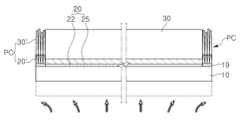
본 공정에서, 질화물 템플릿(20) 상에는 Ⅲ족 질화물 단결정(30)이 형성되지만, 비정질층(19) 상에 위치한 제1 다결정 질화물층(20') 상에는 역시 평탄한 에피택셜 대신에 러프한 제2 다결정 질화물층(30')이 형성될 수 있다. 상기 제2 다결정 질화물층(30')은 제1 다결정 질화물층(20')과 함께 다결정 가이드부(PC)를 구성할 수 있다. 이러한 다결정 가이드(PC)는 Ⅲ족 질화물 단결정(30)의 에지에서 발생될 수 있는 크랙을 방지할 수 있다.In this process, a group III nitride
한편, 본 실시예에서는, Ⅲ족 질화물 단결정(30)의 성장 동안에, 실리콘 기판(10)의 하면에 대한 화학적 에칭 공정이 적용되고, 실리콘 기판(10)이 점차 제거될 수 있다. 도11에서 점선은 에칭 공정 적용 전의 실리콘 기판(10)의 형태를 나타낸다.
Meanwhile, in this embodiment, during the growth of the group III nitride
도12에 도시된 바와 같이, 실리콘 기판(10)이 제거된 후에, 다결정 가이드부(PC)는 상기 Ⅲ족 질화물 단결정(30)으로부터 제거될 수 있다. 이러한 제거 과정은 실리콘 기판(10) 제거와 함께 자발적으로 이루질 수 있다. 예를 들어, 실리콘 기판(10) 제거 후에 냉각과정에서 다결정 가이드부(PC)는 자발적으로 제거될 수 있다. 상기 다결정 가이드부(PC)는 다결정체이므로, 상기 질화물 단결정(30)의 계면을 따라 비교적 깨끗하게 제거될 수 있다. 필요에 따라, 실리콘 기판(10)의 제거 후에 가벼운 충격을 이용하여 다결정 가이드부(PC)를 효과적으로 제거될 수 있다.
As shown in FIG. 12, after the
비정질층을 이용한 다결정 가이드부는 다양한 형태로 구현될 수 있다. 도14 및 도15는 다른 형태의 가이드부를 이용하는 질화물 반도체 기판 제조방법을 설명하기 위한 공정 단면도이다. 본 실시예에서는, 비정질층(29)을 실리콘 기판(10)의 준비과정이 아닌 질화물 템플릿(20)을 형성한 후에 도입한다.
The polycrystalline guide part using an amorphous layer can be implemented in various forms. Figures 14 and 15 are cross-sectional process views for explaining a method of manufacturing a nitride semiconductor substrate using a different type of guide part. In this embodiment, the
도14에 도시된 바와 같이, 상기 질화물 템플릿(20)의 외주를 따라 비정질층(29)을 형성할 수 있다. 상기 비정질층(29)은 도13에 도시된 형태와 유사하게 형성될 수 있다. 예를 들어, 본 공정은 MOCVD 챔버에서 질화물 템플릿(20)을 형성한 후에 HVPE 챔버로 이송되기 전에 수행될 수 있다. 상기 비정질층(29)은 앞선 실시예와 유사한 공정을 이용하여 형성될 수 있다. 본 비정질층(29) 형성 공정은 도3에서 설명된 실리콘 화합물층(12)을 제거하는 공정 전 또는 후에 수행될 수 있다.
As shown in FIG. 14, an
도15에 도시된 바와 같이, 제2 성장 챔버(예, HVPE 챔버)에서 질화물 템플릿(20) 상에 Ⅲ족 질화물 단결정(30)을 형성할 수 있다. 이러한 성장 공정은 다른 설명이 없는 한, 도4에서 설명된 질화물 단결정 공정을 참조하여 이해될 수 있다.As shown in FIG. 15, a group III nitride
상기 비정질층(29)이 위치하지 않는 질화물 템플릿(20) 영역에서는 Ⅲ족 질화물 단결정(30)이 형성되는 반면에, 비정질층(29) 상에는 평탄한 에피택셜 대신에 러프한 다결정 질화물층(30')이 형성될 수 있다. 본 실시예에서는, 상기 제2 다결정 질화물층(30')은 다결정 가이드부(PC)로 제공될 수 있다. 이러한 다결정 가이드(PC)는 Ⅲ족 질화물 단결정(30)의 에지에서 발생될 수 있는 크랙을 방지할 수 있다.While a group III nitride
본 실시예에서도, 도11에서 설명된 바와 같이, Ⅲ족 질화물 단결정(30)의 성장 동안에, 되고, 실리콘 기판(10)이 제거되도록 실리콘 기판(10)의 하면에 대한 화학적 에칭 공정이 적용될 수 있다.In this embodiment as well, as described in FIG. 11, during the growth of the group III nitride
앞선 실시예와 유사하게, 실리콘 기판(10)이 제거된 후에, 다결정 가이드부(PC)는 상기 Ⅲ족 질화물 단결정(30)으로부터 제거될 수 있다. 이러한 제거 과정은 실리콘 기판(10) 제거와 함께 자발적으로 이루질 수 있다.
Similar to the previous embodiment, after the
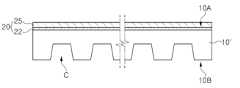
본 질화물 템플릿(25)의 성장 과정에서 상기 실리콘 기판(10)의 제2 면(10B)에 형성된 실리콘 화합물층(12)을 제거하는 과정은 다양하게 구현될 수 있다. 도16 및 도17은 실리콘 화합물층이 제거된 다양한 예들을 나타내는 실리콘 기판의 단면도이다.The process of removing the
도16에 도시된 바와 같이, 실리콘 기판(10')의 제2 면(10B)에 대한 그라인딩 공정을 이용하여 실리콘 기판(10')의 두께를 T0에서 T1으로 감소시킬 수 있다. 이러한 그라인딩 공정을 통해서 두께를 감소시킬 뿐만 아니라, 실리콘 기판(10')의 제2 면(10B)으로부터 실리콘 화합물층(12)도 제거될 수 있다. 실리콘 기판(10')은 감소된 두께(T1)를 가지므로, 후속 공정에서 수행되는 기판 제거공정(도5 참조)이 신속하게 수행될 수 있다.As shown in FIG. 16, the thickness of the silicon substrate 10' can be reduced from T0 to T1 using a grinding process on the
도17에 도시된 바와 같이, 패터닝 공정을 이용하여 실리콘 기판(10")의 제2 면(10B)의 표면적을 증가시킬 수 있다. 본 실시예와 같이, 실리콘 기판(10")의 제2 면(10B)에 반복적인 오목부(C)를 형성함으로써 부분적으로 두께를 감소시킬 뿐만 아니라 전체 표면적을 증가시킬 수 있다. 이러한 패터닝에 의해 얻어진 실리콘 기판(10")은 후속되는 기판의 제거공정에서 더욱 효과적인 에칭 작용을 기대할 수 있다.As shown in Figure 17, the surface area of the
본 패터닝 공정은 화학적 에칭 공정과 결합하여 수행될 수 있다. 예를 들어, 패터닝을 위한 에칭 공정 전 또는 후에, BOE액을 이용한 화학적 에칭을 실리콘 기판(10)의 제2 면(10B)에 적용함으로써 실리콘 화합물층(SiOxNy)을 제거할 수 있다.This patterning process can be performed in combination with a chemical etching process. For example, before or after the etchingprocess for patterning, the silicon compound layer (SiO
다양한 실리콘 화합물층 제거 공정은 제1 성장 챔버(예, MOCVD 챔버)에서 질화물 템플릿을 형성한 후에, Ⅲ족 질화물 단결정을 성장하기 위한 제2 성장 챔버(예, HVPE)로 이동하는 전에, 수행될 수 있다. 이러한 공정에서 실리콘 산질화물과 같은 실리콘 화합물층(12)은 제거하여, 제2 성장 챔버 내에서 실리콘 기판의 원활한 에칭공정을 보장할 수 있다.
Various silicon compound layer removal processes may be performed after forming the nitride template in a first growth chamber (e.g., MOCVD chamber) before moving to a second growth chamber (e.g., HVPE) to grow a group III nitride single crystal. . In this process, the
본 실시예들에 채용가능한 질화물 템플릿은 다양한 구조를 가질 수 있다. 도18 및 도19는 본 발명의 일 실시예에 채용 가능한 질화물 템플릿의 다양한 예를 나타내는 웨이퍼의 단면도이다.Nitride templates employable in the present embodiments may have various structures. Figures 18 and 19 are cross-sectional views of wafers showing various examples of nitride templates that can be employed in one embodiment of the present invention.
도18에 도시된 바와 같이, 본 실시예에 도입된 질화물 템플릿(20)은 Al 함유 질화물층(22)과 GaN 응력 완화층(25) 외에도 실리콘 기판(10) 상에 형성된 AlN 핵성장층(21)을 더 포함할 수 있다.As shown in Figure 18, the
상기 AlN 핵성장층(21)은 실리콘 기판(10)의 (111)면에 형성되어 젖음성(wettability)이 개선된 성장면을 제공할 수 있다. 상기 AlN 핵성장층(21)은 실리콘과 질화물 단결정의 갈륨이 반응하여 공융 금속을 형성하는 멜트-백(melt back) 현상을 방지할 수 있다. 이러한 AlN 핵성장층(21) 형성은 초기에 트리메틸 알루미늄과 같은 알루미늄 소스를 주입하는 공정으로 시작될 수 있다. 이러한 알루미늄(Al) 소스의 우선 주입은 상기 실리콘 기판(10)이 암모니아에 먼저 노출되어 질화되는 것을 방지할 수 있다. 예를 들어, 상기 AlN 핵성장층(21)은 수십 내지 수백 ㎚의 크기를 가질 수 있다.The AlN
도18에 도시된 바와 같이, Al 함유 질화물층(22)은 복수 회 교대로 적층된 AlN층(22a)과 AlGaN층(22b)을 포함한다. 상기 Al 함유 질화물층(22)은 후속 성장될 질화물 결정과의 계면에서 변위루프(dislocation loop)가 형성되어 결함밀도(dislocation density)가 감소될 수 있다. 상기 Al 함유 질화물층(22)은 GaN 응력 완화층(25)과의 격자 부정합 및 열팽창계수 부정합을 완화시킴으로써 결정 성장시 압축응력(compressive stress)을 효과적으로 발생시킬 수 있으며, 냉각시에 발생되는 인장응력(tensile stress)을 감소시킬 수 있다.As shown in Figure 18, the Al-containing
본 실시예와 달리, Al 함유 질화물층(22)은 Alx1Iny1Ga1-x2-y2N/Alx2Iny2Ga1-x2-y2N(0≤x1,x2,y1,y2≤1, x1≠x2 또는 y1≠y2, x1+y1≤1,x2+y2≤1) 또는 그레이드(graded) AlxInyGa1-x-yN (0≤x,y≤1,x+y≤1)일 수 있다. 예를 들어, 그레이드 구조인 Al 함유 질화물층은, 알루미늄(Al) 성분이 연속적으로 또는 스텝으로 감소되어 격자 상수가 점차 커지는 AlGaN일 수 있다.Unlike the present embodiment, the Al-containing
한편, 상기 Al 함유 질화물층(22) 또는 AlN 핵성장층(21)은 실리콘 기판(10)을 HCl과 같은 에칭가스에 의해 제거될 때에 에칭 스톱층으로 활용될 수 있다.Meanwhile, the Al-containing
본 실시예에서, GaN 응력 완화층(25)은 2차원 성장을 통해서 평탄(flat)한 표면을 가질 수 있다.
In this embodiment, the GaN
도19에 도시된 바와 같이, 질화물 템플릿(20)은 상기 실리콘 기판(10)의 제1 면 상에 배치된 AlN 핵성장층(21)과, 상기 AlN 핵성장층(21) 상에 배치된 Al 함유 질화물층(22)과, 상기 Al 함유 질화물층(22) 상에 배치된 GaN 응력 완화층(25)을 포함할 수 있다.As shown in FIG. 19, the
상기 GaN 응력 완화층(25)은 Al 함유 질화물층(22) 상에 배치된 제1 GaN층(25a)과, 상기 제1 GaN층(25a) 상에 배치된 마스크 패턴(26)과, 상기 마스크 패턴(26)이 형성된 상기 제1 GaN층(25a) 상에 배치된 제2 GaN층(25b)을 포함할 수 있다.The GaN
상기 제2 GaN층(25b)은 질화물 단결정 성장(예, HVPE 공정)시에 결함밀도를 감소시키기 위해 3차원 구조의 표면을 가질 수 있다. 구체적으로, 상기 제2 GaN층(25b)은 상기 제1 GaN(25a)층에 인시튜 SiH4 처리하여 마스크 패턴(26)을 형성한 후에 GaN 재성장을 통해 형성될 수 있다. 본 실시예에서는, 인시튜(in-situ) SiH4 처리에 의해 얻어지는 마스크 패턴(26)은 상기 제1 GaN층(25a) 상에 캐리어 가스(예, N2 또는 H2)와 함께, SiH4와 NH3 플로우(flow)를 고온에서 주입하여 형성될 수 있다. 상기 인시튜 SiH4 처리는 500∼1200℃의 온도에서 수행될 수 있다. 이러한 공정에 의해 얻어지는 마스크 패턴(26)은 SiH4와 NH3의 반응으로 얻어지는 실리콘 질화물일 수 있다. 인시튜 SiH4 처리에 의해 제1 GaN층(25a)의 관통 전위 영역은 우선적으로 에칭되어 결함 밀도를 감소시킬 수 있다. 다른 실시예에서, 화학적 에칭을 이용하여 제2 GaN층(25b)을 3 차원 구조로 형성할 수 있다. 상기 화학적 에칭으로 황산과수(H2SO4 + H2O2), 인산(H3PO4) 및/또는 수산화칼륨(KOH)을 사용할 수 있다.The
이러한 에칭 작용을 통해서 후속 HVPE 성장될 질화물 단결정의 결정 품질을 향상시킬 수 있다.
Through this etching action, the crystal quality of nitride single crystals to be subsequently HVPE grown can be improved.
앞서 설명된 여러 실시예들은 서로 반대되는 설명이 없는 한, 서로 결합되어 일련의 질화물 반도체 기판 제조방법으로 구현될 수 있다. 도20은 본 발명의 일 실시예에 따른 질화물 반도체 기판 제조방법을 설명하기 위한 공정 흐름도이다.
Unless otherwise stated, the various embodiments described above may be combined with each other and implemented as a series of nitride semiconductor substrate manufacturing methods. Figure 20 is a process flow diagram for explaining a method of manufacturing a nitride semiconductor substrate according to an embodiment of the present invention.
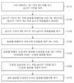
도20을 참조하면, 서로 대향하는 제1 면과 제2 면을 갖는 실리콘 기판을 마련한다(S110, 도1 참조).Referring to Figure 20, a silicon substrate having first and second surfaces facing each other is prepared (S110, see Figure 1).
다음으로, 실리콘 기판의 제1 면에 질화물 템플릿을 성장시킬 수 있다(S120, 도2 참조). 질화물 템플릿 성장은, MOCVD 공정을 사용할 수 있으며, 이 과정에서 실리콘 기판의 제2 면에는 실리콘 산질화물과 같은 실리콘 화합물층이 형성될 수 있다.Next, a nitride template can be grown on the first side of the silicon substrate (S120, see Figure 2). Nitride template growth may use a MOCVD process, and during this process, a silicon compound layer such as silicon oxynitride may be formed on the second side of the silicon substrate.
이어, 실리콘 기판의 제2 면으로부터 실리콘 화합물층을 제거할 수 있다(S130, 도3 참조). BOE를 이용한 화학적 에칭 공정을 사용하여 제거할 수 있다. 화학적 에칭 공정 외에도 그라인딩 공정(도16 참조) 또는 패터닝 공정(도17 참조)을 대체로 또는 화학적 에칭 공정과 결합하여 구현될 수 있다.Next, the silicon compound layer can be removed from the second side of the silicon substrate (S130, see FIG. 3). It can be removed using a chemical etching process using BOE. In addition to the chemical etching process, a grinding process (see FIG. 16) or a patterning process (see FIG. 17) may be implemented as a substitute or in combination with a chemical etching process.
다음으로, 질화물 템플릿의 외주부에 비정질층을 증착할 수 있다(S140). 예를 들어, CVD 및 스퍼터링 공정을 이용하여 형성될 수 있다. 이어, 질화물 템플릿 상에 Ⅲ족 질화물 단결정을 성장시킬 수 있다(S150, 도4 참조). 예를 들어, 본 성장공정은 HVPE 공정을 이용하여 형성될 수 있다. 이러한 Ⅲ족 질화물 단결정 성장과정에서 비정질층 상에는 다결정 질화물이 형성될 수 있다. 본 공정들은 도14 및 도15에 참조하여 설명된 공정을 참조하여 상세히 이해할 수 있다.Next, an amorphous layer can be deposited on the outer periphery of the nitride template (S140). For example, it can be formed using CVD and sputtering processes. Next, a group III nitride single crystal can be grown on the nitride template (S150, see Figure 4). For example, this growth process can be formed using the HVPE process. During this group III nitride single crystal growth process, polycrystalline nitride may be formed on the amorphous layer. These processes can be understood in detail by referring to the processes described with reference to FIGS. 14 and 15.
물론, 비정질층을 이용한 공정은 본 실시예에 따른 공정을 대신하여 도10 내지 도13을 참조하여 설명된 공정으로 유사하게 구현될 수도 있다.
Of course, the process using the amorphous layer may be similarly implemented with the process described with reference to FIGS. 10 to 13 instead of the process according to this embodiment.
이어, Ⅲ족 질화물 단결정 성장과정 또는 후에 실리콘 기판을 제거할 수 있다(S160, 도5 참조). Ⅲ족 질화물 단결정을 성장하기 위한 챔버 내에서 실리콘 기판은 HCl을 이용한 에칭공정에 의해 제거될 수 있다. 이러한 실리콘 기판의 제거과정에서 다결정 질화물은 자발적 분리되거나 가벼운 충격으로 깨끗하게 제거될 수 있다.Subsequently, the silicon substrate can be removed during or after the group III nitride single crystal growth process (S160, see FIG. 5). In a chamber for growing a group III nitride single crystal, the silicon substrate can be removed by an etching process using HCl. During the removal process of the silicon substrate, polycrystalline nitride can be spontaneously separated or removed cleanly with a light impact.
다음으로, 필요에 따라 Ⅲ족 질화물 단결정으로부터 질화물 템플릿을 제거할 수 있다(S170). 질화물 템플릿 표면에 그라인딩 공정을 적용하여 고품질의 질화물 단결정 부분만을 잔류시킬 수 있다.
Next, if necessary, the nitride template can be removed from the group III nitride single crystal (S170). By applying a grinding process to the surface of the nitride template, only high-quality nitride single crystal parts can remain.
이상, 첨부된 도면을 참조하여 본 발명의 실시 예를 설명하였지만, 본 발명이 속하는 기술분야에서 통상의 지식을 가진 자는 본 발명이 그 기술적 사상이나 필수적인 특징을 변경하지 않고서 다른 구체적인 형태로 실시될 수 있다는 것을 이해할 수 있을 것이다. 그러므로 이상에서 기술한 실시 예에는 모든 면에서 예시적인 것이며 한정적이 아닌 것으로 이해해야만 한다.
Above, embodiments of the present invention have been described with reference to the attached drawings, but those skilled in the art will understand that the present invention can be implemented in other specific forms without changing the technical idea or essential features. You will understand that it exists. Therefore, the embodiments described above should be understood in all respects as illustrative and not restrictive.
10: 실리콘 기판
19, 29: 비정질층
20: 질화물 템플릿
21: AlN 핵성장층
22: Al 함유 질화물층
25: GaN 응력완화층
25a, 25b: 제1 및 제2 GaN층
26: 마스크 패턴
30: Ⅲ족 질화물 단결정10: Silicon substrate
19, 29: Amorphous layer
20: Nitride template
21: AlN nuclear growth layer
22: Al-containing nitride layer
25: GaN stress relief layer
25a, 25b: first and second GaN layers
26: Mask pattern
30: Group III nitride single crystal
Claims (10)
Translated fromKorean제1 성장 챔버에서 상기 실리콘 기판의 제1 면에 질화물 템플릿을 성장시키는 단계 - 상기 질화물 템플릿의 성장 과정에서 상기 실리콘 기판의 제2 면에 실리콘 질화물 및 실리콘 산질화물 중 적어도 하나를 포함하는 실리콘 화합물층이 형성됨-;
제1 에천트를 이용한 제1 화학적 에칭을 적용하여 상기 실리콘 기판의 제2 면으로부터 상기 실리콘 화합물층을 제거하는 단계;
제2 성장 챔버에서 상기 질화물 템플릿 상에 Ⅲ족 질화물 단결정을 성장시키는 단계; 및
상기 제2 성장 챔버에서 상기 제1 에천트와 다른 제2 에천트를 이용한 제2 화학적 에칭을 적용하여 상기 실리콘 기판을 제거하는 단계를 포함하는 질화물 반도체 기판 제조방법.
providing a silicon substrate having first and second surfaces facing each other;
Growing a nitride template on the first side of the silicon substrate in a first growth chamber - During the growth of the nitride template, a silicon compound layer including at least one of silicon nitride and silicon oxynitride is formed on the second side of the silicon substrate. Formed-;
removing the silicon compound layer from the second side of the silicon substrate by applying a first chemical etch using a first etchant;
Growing a group III nitride single crystal on the nitride template in a second growth chamber; and
A method of manufacturing a nitride semiconductor substrate comprising removing the silicon substrate by applying a second chemical etching using a second etchant different from the first etchant in the second growth chamber.
상기 제1 성장 챔버는 MOCVD(metal-organic chemical vapor deposition) 성장 또는 MBE(molecular beam epitaxy) 성장을 위한 챔버이며,
상기 제2 성장 챔버는 HVPE(hydride vapor phase epitaxy) 성장을 위한 챔버인 질화물 반도체 기판 제조방법.
According to paragraph 1,
The first growth chamber is a chamber for metal-organic chemical vapor deposition (MOCVD) growth or molecular beam epitaxy (MBE) growth,
A method of manufacturing a nitride semiconductor substrate, wherein the second growth chamber is a chamber for HVPE (hydride vapor phase epitaxy) growth.
상기 실리콘 기판을 제거하는 단계는, 상기 실리콘 기판의 제2 면에 에칭을 적용하는 단계를 포함하는 질화물 반도체 기판 제조방법.
According to paragraph 1,
The step of removing the silicon substrate includes applying etching to a second side of the silicon substrate.
상기 실리콘 기판을 제거하는 단계는, 상기 Ⅲ족 질화물 단결정을 성장시키는 단계 동안에 수행되거나 상기 Ⅲ족 질화물 단결정을 성장시키는 단계 후에 수행되는 질화물 반도체 기판 제조방법.
According to paragraph 1,
The step of removing the silicon substrate is performed during the step of growing the group III nitride single crystal or after the step of growing the group III nitride single crystal.
상기 질화물 템플릿은 상기 실리콘 기판의 제1 면에 Al 함유 질화물층을 포함하며,
상기 실리콘 기판을 제거하는 단계에서, 상기 Al 함유 질화물층은 에칭 스톱층으로 사용되는 질화물 반도체 기판 제조방법.
According to paragraph 1,
The nitride template includes an Al-containing nitride layer on a first side of the silicon substrate,
In the step of removing the silicon substrate, the Al-containing nitride layer is used as an etching stop layer.
제1 성장 챔버에서 상기 실리콘 기판의 제1 면에 질화물 템플릿을 성장시키는 단계 - 상기 질화물 템플릿의 성장 과정에서 상기 실리콘 기판의 실리콘 화합물층이 형성됨-;
상기 실리콘 기판의 제2 면으로부터 상기 실리콘 화합물층을 제거하는 단계;
제2 성장 챔버에서 상기 질화물 템플릿 상에 Ⅲ족 질화물 단결정을 성장시키는 단계; 및
상기 제2 성장 챔버에서 상기 실리콘 기판을 제거하는 단계;를 포함하며,
상기 실리콘 화합물층을 제거하는 단계는, 상기 실리콘 기판의 두께가 감소되도록 상기 실리콘 기판의 제2 면에 대해 그라인딩(grinding)하는 단계를 포함하는 질화물 반도체 기판 제조방법.
providing a silicon substrate having first and second surfaces facing each other;
Growing a nitride template on the first side of the silicon substrate in a first growth chamber - a silicon compound layer of the silicon substrate is formed during the growth of the nitride template;
removing the silicon compound layer from the second side of the silicon substrate;
Growing a group III nitride single crystal on the nitride template in a second growth chamber; and
Removing the silicon substrate from the second growth chamber,
The step of removing the silicon compound layer includes grinding the second surface of the silicon substrate to reduce the thickness of the silicon substrate.
제1 성장 챔버에서 상기 실리콘 기판의 제1 면에 질화물 템플릿을 성장시키는 단계 - 상기 질화물 템플릿의 성장 과정에서 상기 실리콘 기판의 실리콘 화합물층이 형성됨-;
상기 실리콘 기판의 제2 면으로부터 상기 실리콘 화합물층을 제거하는 단계;
제2 성장 챔버에서 상기 질화물 템플릿 상에 Ⅲ족 질화물 단결정을 성장시키는 단계; 및
상기 제2 성장 챔버에서 상기 실리콘 기판을 제거하는 단계;를 포함하며,
상기 실리콘 화합물층을 제거하는 단계는, 상기 실리콘 기판의 제2 면의 표면적이 증가되도록 상기 실리콘 기판의 제2 면을 패터닝하는 단계를 포함하는 질화물 반도체 기판 제조방법.
providing a silicon substrate having first and second surfaces facing each other;
Growing a nitride template on the first side of the silicon substrate in a first growth chamber - a silicon compound layer of the silicon substrate is formed during the growth of the nitride template;
removing the silicon compound layer from the second side of the silicon substrate;
Growing a group III nitride single crystal on the nitride template in a second growth chamber; and
Removing the silicon substrate from the second growth chamber,
The step of removing the silicon compound layer includes patterning the second side of the silicon substrate to increase the surface area of the second side of the silicon substrate.
상기 실리콘 기판의 외주 영역에 비정질층을 형성하는 단계;
제1 성장 챔버에서 상기 실리콘 기판의 제1 면에 질화물 템플릿을 성장시키는 단계 - 상기 질화물 템플릿의 성장 과정에서 상기 실리콘 기판의 제2 면에 실리콘 화합물층이 형성됨-;
상기 실리콘 기판의 제2 면으로부터 상기 실리콘 화합물층을 제거하는 단계;
제2 성장 챔버에서 상기 질화물 템플릿 상에 Ⅲ족 질화물 단결정을 성장시키는 단계; 및
상기 제2 성장 챔버에서 상기 실리콘 기판을 제거하는 단계;를 포함하고,
상기 질화물 템플릿을 성장하는 단계와 상기 질화물 단결정을 성장하는 단계에서, 상기 비정질층 상에는 다결정 질화물층이 성장되는 질화물 반도체 기판 제조방법.
providing a silicon substrate having first and second surfaces facing each other;
forming an amorphous layer in the outer peripheral area of the silicon substrate;
Growing a nitride template on the first side of the silicon substrate in a first growth chamber - forming a silicon compound layer on the second side of the silicon substrate during the growth process of the nitride template;
removing the silicon compound layer from the second side of the silicon substrate;
Growing a group III nitride single crystal on the nitride template in a second growth chamber; and
Removing the silicon substrate from the second growth chamber,
A method of manufacturing a nitride semiconductor substrate in which, in the step of growing the nitride template and the step of growing the nitride single crystal, a polycrystalline nitride layer is grown on the amorphous layer.
상기 실리콘 기판을 제거하는 단계에서 또는 상기 실리콘 기판을 제거하는 단계 후에, 상기 질화물 템플릿의 외주 영역 상에 상기 다결정 질화물층을 제거하는 단계를 더 포함하는 질화물 반도체 기판 제조방법.According to clause 8,
A method of manufacturing a nitride semiconductor substrate further comprising removing the polycrystalline nitride layer on an outer peripheral region of the nitride template during or after removing the silicon substrate.
Priority Applications (2)
| Application Number | Priority Date | Filing Date | Title |
|---|---|---|---|
| KR1020160073871AKR102608902B1 (en) | 2016-06-14 | 2016-06-14 | Method for manufacturing nitride semiconductor substrate |
| US15/399,898US9947530B2 (en) | 2016-06-14 | 2017-01-06 | Method of manufacturing nitride semiconductor substrate |
Applications Claiming Priority (1)
| Application Number | Priority Date | Filing Date | Title |
|---|---|---|---|
| KR1020160073871AKR102608902B1 (en) | 2016-06-14 | 2016-06-14 | Method for manufacturing nitride semiconductor substrate |
Publications (2)
| Publication Number | Publication Date |
|---|---|
| KR20170141308A KR20170141308A (en) | 2017-12-26 |
| KR102608902B1true KR102608902B1 (en) | 2023-12-04 |
Family
ID=60572958
Family Applications (1)
| Application Number | Title | Priority Date | Filing Date |
|---|---|---|---|
| KR1020160073871AActiveKR102608902B1 (en) | 2016-06-14 | 2016-06-14 | Method for manufacturing nitride semiconductor substrate |
Country Status (2)
| Country | Link |
|---|---|
| US (1) | US9947530B2 (en) |
| KR (1) | KR102608902B1 (en) |
Families Citing this family (3)
| Publication number | Priority date | Publication date | Assignee | Title |
|---|---|---|---|---|
| KR102680861B1 (en)* | 2016-12-15 | 2024-07-03 | 삼성전자주식회사 | Manufacturing method of ganllium nitride substrate |
| US11699586B2 (en)* | 2019-08-13 | 2023-07-11 | Enkris Semiconductor, Inc. | Method of manufacturing nitride semiconductor substrate |
| JP6971415B1 (en)* | 2020-12-29 | 2021-11-24 | 京セラ株式会社 | Semiconductor substrates, semiconductor substrate manufacturing methods, semiconductor substrate manufacturing equipment, electronic components and electronic devices |
Citations (2)
| Publication number | Priority date | Publication date | Assignee | Title |
|---|---|---|---|---|
| KR100461505B1 (en) | 2002-03-04 | 2004-12-14 | 한국전자통신연구원 | Method for manufacturing a nitride semiconductor substrate |
| JP2015005635A (en) | 2013-06-21 | 2015-01-08 | 三菱電機株式会社 | Manufacturing method for silicon carbide semiconductor device |
Family Cites Families (45)
| Publication number | Priority date | Publication date | Assignee | Title |
|---|---|---|---|---|
| CN1143394C (en) | 1996-08-27 | 2004-03-24 | 精工爱普生株式会社 | Peeling method, thin film device transfer method and thin film device |
| USRE38466E1 (en) | 1996-11-12 | 2004-03-16 | Seiko Epson Corporation | Manufacturing method of active matrix substrate, active matrix substrate and liquid crystal display device |
| JP4005701B2 (en)* | 1998-06-24 | 2007-11-14 | シャープ株式会社 | Method of forming nitrogen compound semiconductor film and nitrogen compound semiconductor element |
| US7208725B2 (en) | 1998-11-25 | 2007-04-24 | Rohm And Haas Electronic Materials Llc | Optoelectronic component with encapsulant |
| US6652648B2 (en) | 2000-04-27 | 2003-11-25 | Samsung Corning Co., Ltd. | Method for fabricating GaN single crystal substrate |
| KR100366706B1 (en)* | 2000-04-27 | 2003-01-09 | 삼성코닝 주식회사 | Method for fabricating a GaN single crystal substrate |
| JP3906654B2 (en) | 2000-07-18 | 2007-04-18 | ソニー株式会社 | Semiconductor light emitting device and semiconductor light emitting device |
| US6818465B2 (en) | 2001-08-22 | 2004-11-16 | Sony Corporation | Nitride semiconductor element and production method for nitride semiconductor element |
| JP2003218034A (en) | 2002-01-17 | 2003-07-31 | Sony Corp | Selective growth method, semiconductor light emitting device and method of manufacturing the same |
| JP3815335B2 (en) | 2002-01-18 | 2006-08-30 | ソニー株式会社 | Semiconductor light emitting device and manufacturing method thereof |
| KR100499129B1 (en) | 2002-09-02 | 2005-07-04 | 삼성전기주식회사 | Light emitting laser diode and fabricatin method thereof |
| US7002182B2 (en) | 2002-09-06 | 2006-02-21 | Sony Corporation | Semiconductor light emitting device integral type semiconductor light emitting unit image display unit and illuminating unit |
| JP2004107114A (en) | 2002-09-17 | 2004-04-08 | Toyoda Gosei Co Ltd | Method of manufacturing group iii nitride compound semiconductor substrate |
| KR100714639B1 (en) | 2003-10-21 | 2007-05-07 | 삼성전기주식회사 | Light emitting element |
| KR100506740B1 (en) | 2003-12-23 | 2005-08-08 | 삼성전기주식회사 | Nitride semiconductor light emitting device and method of manufacturing the same |
| KR100664985B1 (en) | 2004-10-26 | 2007-01-09 | 삼성전기주식회사 | Nitride-based semiconductor device |
| KR100665222B1 (en) | 2005-07-26 | 2007-01-09 | 삼성전기주식회사 | LED package using diffusion material and manufacturing method thereof |
| US7273798B2 (en) | 2005-08-01 | 2007-09-25 | Avago Technologies Ecbu Ip (Singapore) Pte. Ltd. | Gallium nitride device substrate containing a lattice parameter altering element |
| KR100661614B1 (en) | 2005-10-07 | 2006-12-26 | 삼성전기주식회사 | Nitride-based semiconductor light emitting device and its manufacturing method |
| KR100723247B1 (en) | 2006-01-10 | 2007-05-29 | 삼성전기주식회사 | Chip coated LED package and manufacturing method thereof |
| KR100813561B1 (en) | 2006-03-14 | 2008-03-17 | 주식회사 이츠웰 | Semiconductor substrate and manufacturing method thereof |
| KR100735325B1 (en) | 2006-04-17 | 2007-07-04 | 삼성전기주식회사 | Light emitting diode package and its manufacturing method |
| KR100930171B1 (en) | 2006-12-05 | 2009-12-07 | 삼성전기주식회사 | White light emitting device and white light source module using same |
| KR100855065B1 (en) | 2007-04-24 | 2008-08-29 | 삼성전기주식회사 | Light emitting diode package |
| KR100982980B1 (en) | 2007-05-15 | 2010-09-17 | 삼성엘이디 주식회사 | Surface light source device and LCD backlight unit having same |
| KR101164026B1 (en) | 2007-07-12 | 2012-07-18 | 삼성전자주식회사 | Nitride semiconductor light emitting device and fabrication method thereof |
| KR100891761B1 (en) | 2007-10-19 | 2009-04-07 | 삼성전기주식회사 | Semiconductor light emitting device, manufacturing method thereof and semiconductor light emitting device package using same |
| KR101137905B1 (en) | 2007-12-28 | 2012-05-03 | 삼성코닝정밀소재 주식회사 | Fabrication method of gallium nitride wafer |
| KR101281684B1 (en) | 2008-01-25 | 2013-07-05 | 성균관대학교산학협력단 | Fabrication method of nitride semiconductor substrate |
| US8343824B2 (en)* | 2008-04-29 | 2013-01-01 | International Rectifier Corporation | Gallium nitride material processing and related device structures |
| KR101332794B1 (en) | 2008-08-05 | 2013-11-25 | 삼성전자주식회사 | Light emitting device, light emitting system comprising the same, and fabricating method of the light emitting device and the light emitting system |
| KR20100030470A (en) | 2008-09-10 | 2010-03-18 | 삼성전자주식회사 | Light emitting device and system providing white light with various color temperatures |
| KR101530876B1 (en) | 2008-09-16 | 2015-06-23 | 삼성전자 주식회사 | Light emitting device with increased light emitting amount, light emitting device including same, method of manufacturing light emitting device and light emitting device |
| US8008683B2 (en) | 2008-10-22 | 2011-08-30 | Samsung Led Co., Ltd. | Semiconductor light emitting device |
| WO2011096684A2 (en) | 2010-02-04 | 2011-08-11 | Lg Siltron Inc. | Method for manufacturing galium naitride wafer |
| TWI434329B (en)* | 2010-12-23 | 2014-04-11 | Nat Univ Chung Hsing | Epitaxial structure with etch stop layer and its manufacturing method |
| KR101178504B1 (en) | 2011-01-10 | 2012-09-07 | 주식회사루미지엔테크 | Method of manufacturing a substrate |
| WO2013003420A2 (en) | 2011-06-27 | 2013-01-03 | Saint-Gobain Ceramics & Plastics, Inc. | A semiconductor substrate and method of manufacturing |
| KR20130062736A (en)* | 2011-12-05 | 2013-06-13 | 삼성전자주식회사 | Silicon substrate, epitaxial structure having the same and manufacturing of silicon substrate |
| KR20130078984A (en)* | 2012-01-02 | 2013-07-10 | 삼성코닝정밀소재 주식회사 | Method for fabricating gallium nitride substrate |
| KR20130081956A (en)* | 2012-01-10 | 2013-07-18 | 삼성전자주식회사 | Method for growing nitride semiconductor |
| JP5362085B1 (en) | 2012-09-05 | 2013-12-11 | 株式会社東芝 | Nitride semiconductor wafer, nitride semiconductor device, and method of manufacturing nitride semiconductor wafer |
| KR101878754B1 (en)* | 2012-09-13 | 2018-07-17 | 삼성전자주식회사 | Method of manufacturing large area gallium nitride substrate |
| EP2945185A1 (en)* | 2013-11-06 | 2015-11-18 | Azzurro Semiconductors AG | Epitaxial wafers avoiding edge melt-back-etching and method for fabricating the same |
| KR102188493B1 (en)* | 2014-04-25 | 2020-12-09 | 삼성전자주식회사 | Method of growing nitride single crystal and method of manufacturing nitride semiconductor device |
- 2016
- 2016-06-14KRKR1020160073871Apatent/KR102608902B1/enactiveActive
- 2017
- 2017-01-06USUS15/399,898patent/US9947530B2/enactiveActive
Patent Citations (2)
| Publication number | Priority date | Publication date | Assignee | Title |
|---|---|---|---|---|
| KR100461505B1 (en) | 2002-03-04 | 2004-12-14 | 한국전자통신연구원 | Method for manufacturing a nitride semiconductor substrate |
| JP2015005635A (en) | 2013-06-21 | 2015-01-08 | 三菱電機株式会社 | Manufacturing method for silicon carbide semiconductor device |
Also Published As
| Publication number | Publication date |
|---|---|
| US20170358443A1 (en) | 2017-12-14 |
| KR20170141308A (en) | 2017-12-26 |
| US9947530B2 (en) | 2018-04-17 |
Similar Documents
| Publication | Publication Date | Title |
|---|---|---|
| JP4741572B2 (en) | Nitride semiconductor substrate and manufacturing method thereof | |
| US7811902B2 (en) | Method for manufacturing nitride based single crystal substrate and method for manufacturing nitride based light emitting diode using the same | |
| EP2037013B1 (en) | Method for preparing substrate for growing gallium nitride and method for preparing gallium nitride substrate | |
| JP5371430B2 (en) | Semiconductor substrate, method for manufacturing a self-supporting semiconductor substrate by hydride vapor phase epitaxy, and mask layer used therefor | |
| KR102071034B1 (en) | Method of fabricating nitride substrate | |
| KR101672213B1 (en) | Method for manufacturing semiconductor device | |
| JP2010269970A (en) | Nitride semiconductor substrate | |
| US10892159B2 (en) | Semipolar or nonpolar group III-nitride substrates | |
| WO2015159342A1 (en) | Nitride semiconductor single crystal substrate manufacturing method | |
| KR102608902B1 (en) | Method for manufacturing nitride semiconductor substrate | |
| US7491645B2 (en) | Method for manufacturing a semiconductor device | |
| WO2016013259A1 (en) | Gallium nitride substrate | |
| US20050072353A1 (en) | Method of manufacturing gallium nitride-based single crystal substrate | |
| WO2021226839A1 (en) | Group iii nitride structure and manufacturing method therefor | |
| KR20180070781A (en) | Method of forming nitride semiconductor substrate and method of forming semiconductor device | |
| JP2013049592A (en) | Crystal substrate manufacturing method and substrate holder | |
| US12106959B2 (en) | Nonpolar or semipolar group III-nitride substrates | |
| JP2009084136A (en) | Method for manufacturing semiconductor device | |
| KR101094409B1 (en) | Method for producing gallium nitride single crystal thick film | |
| JP2005057064A (en) | Group III nitride semiconductor layer and growth method thereof | |
| KR101220825B1 (en) | Method of growing single crystal nitride | |
| TWI752256B (en) | Substrate and method of making the same | |
| WO2010112540A1 (en) | Epitaxial methods and structures for reducing surface dislocation density in semiconductor materials | |
| KR20070025081A (en) | Gallium nitride substrate manufacturing method | |
| KR20160063796A (en) | Method of GaN wafer manufacturing for minimization of wafer bowing and cracking |
Legal Events
| Date | Code | Title | Description |
|---|---|---|---|
| PA0109 | Patent application | Patent event code:PA01091R01D Comment text:Patent Application Patent event date:20160614 | |
| PG1501 | Laying open of application | ||
| PA0201 | Request for examination | Patent event code:PA02012R01D Patent event date:20210513 Comment text:Request for Examination of Application Patent event code:PA02011R01I Patent event date:20160614 Comment text:Patent Application | |
| E902 | Notification of reason for refusal | ||
| PE0902 | Notice of grounds for rejection | Comment text:Notification of reason for refusal Patent event date:20230111 Patent event code:PE09021S01D | |
| E701 | Decision to grant or registration of patent right | ||
| PE0701 | Decision of registration | Patent event code:PE07011S01D Comment text:Decision to Grant Registration Patent event date:20230927 | |
| GRNT | Written decision to grant | ||
| PR0701 | Registration of establishment | Comment text:Registration of Establishment Patent event date:20231128 Patent event code:PR07011E01D | |
| PR1002 | Payment of registration fee | Payment date:20231129 End annual number:3 Start annual number:1 | |
| PG1601 | Publication of registration |