KR102605621B1 - Method for manufacturing semiconductor device having buried gate electrodes - Google Patents
Method for manufacturing semiconductor device having buried gate electrodesDownload PDFInfo
- Publication number
- KR102605621B1 KR102605621B1KR1020190010063AKR20190010063AKR102605621B1KR 102605621 B1KR102605621 B1KR 102605621B1KR 1020190010063 AKR1020190010063 AKR 1020190010063AKR 20190010063 AKR20190010063 AKR 20190010063AKR 102605621 B1KR102605621 B1KR 102605621B1
- Authority
- KR
- South Korea
- Prior art keywords
- gate insulating
- insulating layer
- gate
- thickness
- horizontal direction
- Prior art date
- Legal status (The legal status is an assumption and is not a legal conclusion. Google has not performed a legal analysis and makes no representation as to the accuracy of the status listed.)
- Active
Links
- 239000004065semiconductorSubstances0.000titleclaimsabstractdescription64
- 238000004519manufacturing processMethods0.000titleclaimsabstractdescription41
- 238000000034methodMethods0.000titleclaimsdescription196
- 239000000758substrateSubstances0.000claimsabstractdescription81
- 238000002955isolationMethods0.000claimsabstractdescription73
- 230000008569processEffects0.000claimsdescription183
- 230000003647oxidationEffects0.000claimsdescription99
- 238000007254oxidation reactionMethods0.000claimsdescription99
- 238000000231atomic layer depositionMethods0.000claimsdescription10
- 238000005137deposition processMethods0.000claimsdescription10
- 230000015572biosynthetic processEffects0.000claimsdescription7
- 238000010438heat treatmentMethods0.000claimsdescription7
- 238000011065in-situ storageMethods0.000claimsdescription6
- 239000010410layerSubstances0.000description309
- VYPSYNLAJGMNEJ-UHFFFAOYSA-NSilicium dioxideChemical compoundO=[Si]=OVYPSYNLAJGMNEJ-UHFFFAOYSA-N0.000description11
- 229910052814silicon oxideInorganic materials0.000description11
- 239000000463materialSubstances0.000description10
- 229910052751metalInorganic materials0.000description10
- 239000002184metalSubstances0.000description10
- 229910052581Si3N4Inorganic materials0.000description8
- 239000012535impuritySubstances0.000description8
- MRELNEQAGSRDBK-UHFFFAOYSA-Nlanthanum(3+);oxygen(2-)Chemical compound[O-2].[O-2].[O-2].[La+3].[La+3]MRELNEQAGSRDBK-UHFFFAOYSA-N0.000description8
- 229910052710siliconInorganic materials0.000description8
- HQVNEWCFYHHQES-UHFFFAOYSA-Nsilicon nitrideChemical compoundN12[Si]34N5[Si]62N3[Si]51N64HQVNEWCFYHHQES-UHFFFAOYSA-N0.000description8
- XUIMIQQOPSSXEZ-UHFFFAOYSA-NSiliconChemical compound[Si]XUIMIQQOPSSXEZ-UHFFFAOYSA-N0.000description7
- 150000004767nitridesChemical class0.000description7
- 239000010703siliconSubstances0.000description7
- 238000003860storageMethods0.000description7
- ATJFFYVFTNAWJD-UHFFFAOYSA-NTinChemical compound[Sn]ATJFFYVFTNAWJD-UHFFFAOYSA-N0.000description6
- FFBHFFJDDLITSX-UHFFFAOYSA-Nbenzyl N-[2-hydroxy-4-(3-oxomorpholin-4-yl)phenyl]carbamateChemical compoundOC1=C(NC(=O)OCC2=CC=CC=C2)C=CC(=C1)N1CCOCC1=OFFBHFFJDDLITSX-UHFFFAOYSA-N0.000description6
- 239000000460chlorineSubstances0.000description6
- 229910000449hafnium oxideInorganic materials0.000description6
- 229910052718tinInorganic materials0.000description6
- 229910021420polycrystalline siliconInorganic materials0.000description5
- 229910021332silicideInorganic materials0.000description5
- FVBUAEGBCNSCDD-UHFFFAOYSA-Nsilicide(4-)Chemical compound[Si-4]FVBUAEGBCNSCDD-UHFFFAOYSA-N0.000description5
- 229910008482TiSiNInorganic materials0.000description4
- 230000004888barrier functionEffects0.000description4
- 230000007547defectEffects0.000description4
- 229910052735hafniumInorganic materials0.000description4
- VBJZVLUMGGDVMO-UHFFFAOYSA-Nhafnium atomChemical compound[Hf]VBJZVLUMGGDVMO-UHFFFAOYSA-N0.000description4
- QRXWMOHMRWLFEY-UHFFFAOYSA-NisoniazideChemical compoundNNC(=O)C1=CC=NC=C1QRXWMOHMRWLFEY-UHFFFAOYSA-N0.000description4
- TWNQGVIAIRXVLR-UHFFFAOYSA-Noxo(oxoalumanyloxy)alumaneChemical compoundO=[Al]O[Al]=OTWNQGVIAIRXVLR-UHFFFAOYSA-N0.000description4
- KJXBRHIPHIVJCS-UHFFFAOYSA-Noxo(oxoalumanyloxy)lanthanumChemical compoundO=[Al]O[La]=OKJXBRHIPHIVJCS-UHFFFAOYSA-N0.000description4
- SIWVEOZUMHYXCS-UHFFFAOYSA-Noxo(oxoyttriooxy)yttriumChemical compoundO=[Y]O[Y]=OSIWVEOZUMHYXCS-UHFFFAOYSA-N0.000description4
- 229920005591polysiliconPolymers0.000description4
- VEALVRVVWBQVSL-UHFFFAOYSA-Nstrontium titanateChemical compound[Sr+2].[O-][Ti]([O-])=OVEALVRVVWBQVSL-UHFFFAOYSA-N0.000description4
- 239000010936titaniumSubstances0.000description4
- ZAMOUSCENKQFHK-UHFFFAOYSA-NChlorine atomChemical compound[Cl]ZAMOUSCENKQFHK-UHFFFAOYSA-N0.000description3
- 229910052801chlorineInorganic materials0.000description3
- 239000012792core layerSubstances0.000description3
- 239000002356single layerSubstances0.000description3
- OGIDPMRJRNCKJF-UHFFFAOYSA-Ntitanium(II) oxideChemical compound[Ti]=OOGIDPMRJRNCKJF-UHFFFAOYSA-N0.000description3
- 229910018072Al 2 O 3Inorganic materials0.000description2
- 229910003855HfAlOInorganic materials0.000description2
- 229910004129HfSiOInorganic materials0.000description2
- BPQQTUXANYXVAA-UHFFFAOYSA-NOrthosilicateChemical compound[O-][Si]([O-])([O-])[O-]BPQQTUXANYXVAA-UHFFFAOYSA-N0.000description2
- GEIAQOFPUVMAGM-UHFFFAOYSA-NOxozirconiumChemical compound[Zr]=OGEIAQOFPUVMAGM-UHFFFAOYSA-N0.000description2
- 229910020654PbScTaOInorganic materials0.000description2
- 229910010413TiO 2Inorganic materials0.000description2
- 229910008807WSiNInorganic materials0.000description2
- QCWXUUIWCKQGHC-UHFFFAOYSA-NZirconiumChemical compound[Zr]QCWXUUIWCKQGHC-UHFFFAOYSA-N0.000description2
- 229910006501ZrSiOInorganic materials0.000description2
- XWCMFHPRATWWFO-UHFFFAOYSA-N[O-2].[Ta+5].[Sc+3].[O-2].[O-2].[O-2]Chemical compound[O-2].[Ta+5].[Sc+3].[O-2].[O-2].[O-2]XWCMFHPRATWWFO-UHFFFAOYSA-N0.000description2
- CEPICIBPGDWCRU-UHFFFAOYSA-N[Si].[Hf]Chemical compound[Si].[Hf]CEPICIBPGDWCRU-UHFFFAOYSA-N0.000description2
- 238000000137annealingMethods0.000description2
- QVGXLLKOCUKJST-UHFFFAOYSA-Natomic oxygenChemical compound[O]QVGXLLKOCUKJST-UHFFFAOYSA-N0.000description2
- 238000010586diagramMethods0.000description2
- 238000005530etchingMethods0.000description2
- 229910052732germaniumInorganic materials0.000description2
- WIHZLLGSGQNAGK-UHFFFAOYSA-Nhafnium(4+);oxygen(2-)Chemical compound[O-2].[O-2].[Hf+4]WIHZLLGSGQNAGK-UHFFFAOYSA-N0.000description2
- 230000005527interface trapEffects0.000description2
- 239000007769metal materialSubstances0.000description2
- 239000001301oxygenSubstances0.000description2
- 229910052760oxygenInorganic materials0.000description2
- JMOHEPRYPIIZQU-UHFFFAOYSA-Noxygen(2-);tantalum(2+)Chemical compound[O-2].[Ta+2]JMOHEPRYPIIZQU-UHFFFAOYSA-N0.000description2
- 238000012545processingMethods0.000description2
- UVGLBOPDEUYYCS-UHFFFAOYSA-Nsilicon zirconiumChemical compound[Si].[Zr]UVGLBOPDEUYYCS-UHFFFAOYSA-N0.000description2
- CZXRMHUWVGPWRM-UHFFFAOYSA-Nstrontium;barium(2+);oxygen(2-);titanium(4+)Chemical compound[O-2].[O-2].[O-2].[O-2].[Ti+4].[Sr+2].[Ba+2]CZXRMHUWVGPWRM-UHFFFAOYSA-N0.000description2
- 229910052721tungstenInorganic materials0.000description2
- 229910052726zirconiumInorganic materials0.000description2
- GFQYVLUOOAAOGM-UHFFFAOYSA-Nzirconium(iv) silicateChemical compound[Zr+4].[O-][Si]([O-])([O-])[O-]GFQYVLUOOAAOGM-UHFFFAOYSA-N0.000description2
- JBRZTFJDHDCESZ-UHFFFAOYSA-NAsGaChemical compound[As]#[Ga]JBRZTFJDHDCESZ-UHFFFAOYSA-N0.000description1
- 101001022148Homo sapiens FurinProteins0.000description1
- 101000701936Homo sapiens Signal peptidase complex subunit 1Proteins0.000description1
- GPXJNWSHGFTCBW-UHFFFAOYSA-NIndium phosphideChemical compound[In]#PGPXJNWSHGFTCBW-UHFFFAOYSA-N0.000description1
- 102100030313Signal peptidase complex subunit 1Human genes0.000description1
- BQCADISMDOOEFD-UHFFFAOYSA-NSilverChemical compound[Ag]BQCADISMDOOEFD-UHFFFAOYSA-N0.000description1
- GWEVSGVZZGPLCZ-UHFFFAOYSA-NTitan oxideChemical compoundO=[Ti]=OGWEVSGVZZGPLCZ-UHFFFAOYSA-N0.000description1
- 229910052782aluminiumInorganic materials0.000description1
- 229910021417amorphous siliconInorganic materials0.000description1
- 229910052788bariumInorganic materials0.000description1
- DSAJWYNOEDNPEQ-UHFFFAOYSA-Nbarium atomChemical compound[Ba]DSAJWYNOEDNPEQ-UHFFFAOYSA-N0.000description1
- VKJLWXGJGDEGSO-UHFFFAOYSA-Nbarium(2+);oxygen(2-);titanium(4+)Chemical compound[O-2].[O-2].[O-2].[Ti+4].[Ba+2]VKJLWXGJGDEGSO-UHFFFAOYSA-N0.000description1
- FHTCLMVMBMJAEE-UHFFFAOYSA-Nbis($l^{2}-silanylidene)manganeseChemical compound[Si]=[Mn]=[Si]FHTCLMVMBMJAEE-UHFFFAOYSA-N0.000description1
- 239000003990capacitorSubstances0.000description1
- 230000008859changeEffects0.000description1
- 229910017052cobaltInorganic materials0.000description1
- 239000010941cobaltSubstances0.000description1
- GUTLYIVDDKVIGB-UHFFFAOYSA-Ncobalt atomChemical compound[Co]GUTLYIVDDKVIGB-UHFFFAOYSA-N0.000description1
- 150000001875compoundsChemical class0.000description1
- -1crystalline SiChemical compound0.000description1
- 229910021419crystalline siliconInorganic materials0.000description1
- 230000003247decreasing effectEffects0.000description1
- 238000000151depositionMethods0.000description1
- 238000013461designMethods0.000description1
- 238000011161developmentMethods0.000description1
- GNPVGFCGXDBREM-UHFFFAOYSA-Ngermanium atomChemical compound[Ge]GNPVGFCGXDBREM-UHFFFAOYSA-N0.000description1
- 230000035876healingEffects0.000description1
- RPQDHPTXJYYUPQ-UHFFFAOYSA-Nindium arsenideChemical compound[In]#[As]RPQDHPTXJYYUPQ-UHFFFAOYSA-N0.000description1
- 238000009413insulationMethods0.000description1
- 239000012212insulatorSubstances0.000description1
- 230000010354integrationEffects0.000description1
- 238000005468ion implantationMethods0.000description1
- 150000002500ionsChemical class0.000description1
- 238000012986modificationMethods0.000description1
- 230000004048modificationEffects0.000description1
- 229910052750molybdenumInorganic materials0.000description1
- 229910052759nickelInorganic materials0.000description1
- PXHVJJICTQNCMI-UHFFFAOYSA-NnickelSubstances[Ni]PXHVJJICTQNCMI-UHFFFAOYSA-N0.000description1
- RUFLMLWJRZAWLJ-UHFFFAOYSA-Nnickel silicideChemical compound[Ni]=[Si]=[Ni]RUFLMLWJRZAWLJ-UHFFFAOYSA-N0.000description1
- 229910021334nickel silicideInorganic materials0.000description1
- 229910052707rutheniumInorganic materials0.000description1
- HBMJWWWQQXIZIP-UHFFFAOYSA-Nsilicon carbideChemical compound[Si+]#[C-]HBMJWWWQQXIZIP-UHFFFAOYSA-N0.000description1
- 229910052709silverInorganic materials0.000description1
- 239000004332silverSubstances0.000description1
- 125000006850spacer groupChemical group0.000description1
- 229910052719titaniumInorganic materials0.000description1
- WFKWXMTUELFFGS-UHFFFAOYSA-NtungstenChemical compound[W]WFKWXMTUELFFGS-UHFFFAOYSA-N0.000description1
- 239000010937tungstenSubstances0.000description1
- WQJQOUPTWCFRMM-UHFFFAOYSA-Ntungsten disilicideChemical compound[Si]#[W]#[Si]WQJQOUPTWCFRMM-UHFFFAOYSA-N0.000description1
- 229910021342tungsten silicideInorganic materials0.000description1
Images


Classifications
- H—ELECTRICITY
- H10—SEMICONDUCTOR DEVICES; ELECTRIC SOLID-STATE DEVICES NOT OTHERWISE PROVIDED FOR
- H10D—INORGANIC ELECTRIC SEMICONDUCTOR DEVICES
- H10D64/00—Electrodes of devices having potential barriers
- H10D64/20—Electrodes characterised by their shapes, relative sizes or dispositions
- H10D64/27—Electrodes not carrying the current to be rectified, amplified, oscillated or switched, e.g. gates
- H10D64/311—Gate electrodes for field-effect devices
- H10D64/411—Gate electrodes for field-effect devices for FETs
- H10D64/511—Gate electrodes for field-effect devices for FETs for IGFETs
- H10D64/512—Disposition of the gate electrodes, e.g. buried gates
- H10D64/513—Disposition of the gate electrodes, e.g. buried gates within recesses in the substrate, e.g. trench gates, groove gates or buried gates
- H—ELECTRICITY
- H10—SEMICONDUCTOR DEVICES; ELECTRIC SOLID-STATE DEVICES NOT OTHERWISE PROVIDED FOR
- H10B—ELECTRONIC MEMORY DEVICES
- H10B12/00—Dynamic random access memory [DRAM] devices
- H10B12/30—DRAM devices comprising one-transistor - one-capacitor [1T-1C] memory cells
- H10B12/34—DRAM devices comprising one-transistor - one-capacitor [1T-1C] memory cells the transistor being at least partially in a trench in the substrate
- H—ELECTRICITY
- H10—SEMICONDUCTOR DEVICES; ELECTRIC SOLID-STATE DEVICES NOT OTHERWISE PROVIDED FOR
- H10D—INORGANIC ELECTRIC SEMICONDUCTOR DEVICES
- H10D64/00—Electrodes of devices having potential barriers
- H10D64/20—Electrodes characterised by their shapes, relative sizes or dispositions
- H10D64/27—Electrodes not carrying the current to be rectified, amplified, oscillated or switched, e.g. gates
- H10D64/311—Gate electrodes for field-effect devices
- H10D64/411—Gate electrodes for field-effect devices for FETs
- H10D64/511—Gate electrodes for field-effect devices for FETs for IGFETs
- H10D64/512—Disposition of the gate electrodes, e.g. buried gates
- H—ELECTRICITY
- H01—ELECTRIC ELEMENTS
- H01L—SEMICONDUCTOR DEVICES NOT COVERED BY CLASS H10
- H01L21/00—Processes or apparatus adapted for the manufacture or treatment of semiconductor or solid state devices or of parts thereof
- H01L21/70—Manufacture or treatment of devices consisting of a plurality of solid state components formed in or on a common substrate or of parts thereof; Manufacture of integrated circuit devices or of parts thereof
- H01L21/71—Manufacture of specific parts of devices defined in group H01L21/70
- H01L21/76—Making of isolation regions between components
- H01L21/762—Dielectric regions, e.g. EPIC dielectric isolation, LOCOS; Trench refilling techniques, SOI technology, use of channel stoppers
- H01L21/76202—Dielectric regions, e.g. EPIC dielectric isolation, LOCOS; Trench refilling techniques, SOI technology, use of channel stoppers using a local oxidation of silicon, e.g. LOCOS, SWAMI, SILO
- H01L29/42356—
- H—ELECTRICITY
- H01—ELECTRIC ELEMENTS
- H01L—SEMICONDUCTOR DEVICES NOT COVERED BY CLASS H10
- H01L21/00—Processes or apparatus adapted for the manufacture or treatment of semiconductor or solid state devices or of parts thereof
- H01L21/02—Manufacture or treatment of semiconductor devices or of parts thereof
- H01L21/02104—Forming layers
- H01L21/02107—Forming insulating materials on a substrate
- H01L21/02225—Forming insulating materials on a substrate characterised by the process for the formation of the insulating layer
- H01L21/0226—Forming insulating materials on a substrate characterised by the process for the formation of the insulating layer formation by a deposition process
- H01L21/02263—Forming insulating materials on a substrate characterised by the process for the formation of the insulating layer formation by a deposition process deposition from the gas or vapour phase
- H01L21/02271—Forming insulating materials on a substrate characterised by the process for the formation of the insulating layer formation by a deposition process deposition from the gas or vapour phase deposition by decomposition or reaction of gaseous or vapour phase compounds, i.e. chemical vapour deposition
- H01L21/0228—Forming insulating materials on a substrate characterised by the process for the formation of the insulating layer formation by a deposition process deposition from the gas or vapour phase deposition by decomposition or reaction of gaseous or vapour phase compounds, i.e. chemical vapour deposition deposition by cyclic CVD, e.g. ALD, ALE, pulsed CVD
- H—ELECTRICITY
- H01—ELECTRIC ELEMENTS
- H01L—SEMICONDUCTOR DEVICES NOT COVERED BY CLASS H10
- H01L21/00—Processes or apparatus adapted for the manufacture or treatment of semiconductor or solid state devices or of parts thereof
- H01L21/02—Manufacture or treatment of semiconductor devices or of parts thereof
- H01L21/04—Manufacture or treatment of semiconductor devices or of parts thereof the devices having potential barriers, e.g. a PN junction, depletion layer or carrier concentration layer
- H01L21/18—Manufacture or treatment of semiconductor devices or of parts thereof the devices having potential barriers, e.g. a PN junction, depletion layer or carrier concentration layer the devices having semiconductor bodies comprising elements of Group IV of the Periodic Table or AIIIBV compounds with or without impurities, e.g. doping materials
- H01L21/30—Treatment of semiconductor bodies using processes or apparatus not provided for in groups H01L21/20 - H01L21/26
- H01L21/324—Thermal treatment for modifying the properties of semiconductor bodies, e.g. annealing, sintering
- H—ELECTRICITY
- H01—ELECTRIC ELEMENTS
- H01L—SEMICONDUCTOR DEVICES NOT COVERED BY CLASS H10
- H01L21/00—Processes or apparatus adapted for the manufacture or treatment of semiconductor or solid state devices or of parts thereof
- H01L21/70—Manufacture or treatment of devices consisting of a plurality of solid state components formed in or on a common substrate or of parts thereof; Manufacture of integrated circuit devices or of parts thereof
- H01L21/71—Manufacture of specific parts of devices defined in group H01L21/70
- H01L21/76—Making of isolation regions between components
- H01L21/762—Dielectric regions, e.g. EPIC dielectric isolation, LOCOS; Trench refilling techniques, SOI technology, use of channel stoppers
- H01L21/76224—Dielectric regions, e.g. EPIC dielectric isolation, LOCOS; Trench refilling techniques, SOI technology, use of channel stoppers using trench refilling with dielectric materials
- H—ELECTRICITY
- H01—ELECTRIC ELEMENTS
- H01L—SEMICONDUCTOR DEVICES NOT COVERED BY CLASS H10
- H01L21/00—Processes or apparatus adapted for the manufacture or treatment of semiconductor or solid state devices or of parts thereof
- H01L21/70—Manufacture or treatment of devices consisting of a plurality of solid state components formed in or on a common substrate or of parts thereof; Manufacture of integrated circuit devices or of parts thereof
- H01L21/71—Manufacture of specific parts of devices defined in group H01L21/70
- H01L21/76—Making of isolation regions between components
- H01L21/762—Dielectric regions, e.g. EPIC dielectric isolation, LOCOS; Trench refilling techniques, SOI technology, use of channel stoppers
- H01L21/7624—Dielectric regions, e.g. EPIC dielectric isolation, LOCOS; Trench refilling techniques, SOI technology, use of channel stoppers using semiconductor on insulator [SOI] technology
- H01L21/76243—Dielectric regions, e.g. EPIC dielectric isolation, LOCOS; Trench refilling techniques, SOI technology, use of channel stoppers using semiconductor on insulator [SOI] technology using silicon implanted buried insulating layers, e.g. oxide layers, i.e. SIMOX techniques
- H—ELECTRICITY
- H01—ELECTRIC ELEMENTS
- H01L—SEMICONDUCTOR DEVICES NOT COVERED BY CLASS H10
- H01L21/00—Processes or apparatus adapted for the manufacture or treatment of semiconductor or solid state devices or of parts thereof
- H01L21/70—Manufacture or treatment of devices consisting of a plurality of solid state components formed in or on a common substrate or of parts thereof; Manufacture of integrated circuit devices or of parts thereof
- H01L21/71—Manufacture of specific parts of devices defined in group H01L21/70
- H01L21/76—Making of isolation regions between components
- H01L21/762—Dielectric regions, e.g. EPIC dielectric isolation, LOCOS; Trench refilling techniques, SOI technology, use of channel stoppers
- H01L21/7624—Dielectric regions, e.g. EPIC dielectric isolation, LOCOS; Trench refilling techniques, SOI technology, use of channel stoppers using semiconductor on insulator [SOI] technology
- H01L21/76264—SOI together with lateral isolation, e.g. using local oxidation of silicon, or dielectric or polycristalline material refilled trench or air gap isolation regions, e.g. completely isolated semiconductor islands
- H01L21/823462—
- H01L29/407—
- H—ELECTRICITY
- H10—SEMICONDUCTOR DEVICES; ELECTRIC SOLID-STATE DEVICES NOT OTHERWISE PROVIDED FOR
- H10B—ELECTRONIC MEMORY DEVICES
- H10B12/00—Dynamic random access memory [DRAM] devices
- H10B12/01—Manufacture or treatment
- H10B12/02—Manufacture or treatment for one transistor one-capacitor [1T-1C] memory cells
- H10B12/03—Making the capacitor or connections thereto
- H10B12/038—Making the capacitor or connections thereto the capacitor being in a trench in the substrate
- H—ELECTRICITY
- H10—SEMICONDUCTOR DEVICES; ELECTRIC SOLID-STATE DEVICES NOT OTHERWISE PROVIDED FOR
- H10B—ELECTRONIC MEMORY DEVICES
- H10B12/00—Dynamic random access memory [DRAM] devices
- H10B12/01—Manufacture or treatment
- H10B12/02—Manufacture or treatment for one transistor one-capacitor [1T-1C] memory cells
- H10B12/05—Making the transistor
- H10B12/053—Making the transistor the transistor being at least partially in a trench in the substrate
- H—ELECTRICITY
- H10—SEMICONDUCTOR DEVICES; ELECTRIC SOLID-STATE DEVICES NOT OTHERWISE PROVIDED FOR
- H10D—INORGANIC ELECTRIC SEMICONDUCTOR DEVICES
- H10D30/00—Field-effect transistors [FET]
- H10D30/01—Manufacture or treatment
- H10D30/021—Manufacture or treatment of FETs having insulated gates [IGFET]
- H—ELECTRICITY
- H10—SEMICONDUCTOR DEVICES; ELECTRIC SOLID-STATE DEVICES NOT OTHERWISE PROVIDED FOR
- H10D—INORGANIC ELECTRIC SEMICONDUCTOR DEVICES
- H10D30/00—Field-effect transistors [FET]
- H10D30/60—Insulated-gate field-effect transistors [IGFET]
- H—ELECTRICITY
- H10—SEMICONDUCTOR DEVICES; ELECTRIC SOLID-STATE DEVICES NOT OTHERWISE PROVIDED FOR
- H10D—INORGANIC ELECTRIC SEMICONDUCTOR DEVICES
- H10D64/00—Electrodes of devices having potential barriers
- H10D64/111—Field plates
- H10D64/117—Recessed field plates, e.g. trench field plates or buried field plates
- H—ELECTRICITY
- H10—SEMICONDUCTOR DEVICES; ELECTRIC SOLID-STATE DEVICES NOT OTHERWISE PROVIDED FOR
- H10D—INORGANIC ELECTRIC SEMICONDUCTOR DEVICES
- H10D84/00—Integrated devices formed in or on semiconductor substrates that comprise only semiconducting layers, e.g. on Si wafers or on GaAs-on-Si wafers
- H10D84/01—Manufacture or treatment
- H10D84/0123—Integrating together multiple components covered by H10D12/00 or H10D30/00, e.g. integrating multiple IGBTs
- H10D84/0126—Integrating together multiple components covered by H10D12/00 or H10D30/00, e.g. integrating multiple IGBTs the components including insulated gates, e.g. IGFETs
- H10D84/0144—Manufacturing their gate insulating layers
Landscapes
- Engineering & Computer Science (AREA)
- Manufacturing & Machinery (AREA)
- Physics & Mathematics (AREA)
- Condensed Matter Physics & Semiconductors (AREA)
- General Physics & Mathematics (AREA)
- Computer Hardware Design (AREA)
- Microelectronics & Electronic Packaging (AREA)
- Power Engineering (AREA)
- Chemical Kinetics & Catalysis (AREA)
- Chemical & Material Sciences (AREA)
- Insulated Gate Type Field-Effect Transistor (AREA)
- Semiconductor Memories (AREA)
- Metal-Oxide And Bipolar Metal-Oxide Semiconductor Integrated Circuits (AREA)
- Element Separation (AREA)
Abstract
Translated fromKoreanDescription
Translated fromKorean본 발명은 반도체 소자의 제조 방법에 관한 것으로, 더욱 상세하게는 매립 게이트들을 가지는 반도체 소자의 제조 방법에 관한 것이다.The present invention relates to a method of manufacturing a semiconductor device, and more particularly, to a method of manufacturing a semiconductor device having buried gates.
전자 산업의 비약적인 발전 및 사용자의 요구에 따라 전자기기는 더욱 더 소형화 및 경량화되고 있다. 따라서 전자기기에 사용되는 높은 집적도를 가지는 반도체 소자가 요구되어, 반도체 소자의 구성들에 대한 디자인 룰이 감소되고 있다. 고도로 스케일링(scaling)된 반도체 소자를 제조하기 위해서, 게이트 전극들을 반도체 기판 내에 매립하는 매립 게이트 전극들이 도입되고 있다.In accordance with the rapid development of the electronics industry and user demands, electronic devices are becoming increasingly smaller and lighter. Accordingly, semiconductor devices with a high degree of integration used in electronic devices are required, and design rules for the configurations of semiconductor devices are decreasing. In order to manufacture highly scaled semiconductor devices, buried gate electrodes, which bury gate electrodes in a semiconductor substrate, are being introduced.
본 발명의 기술적 과제는 신뢰성과 성능이 향상되며, 매립 게이트들을 가지는 반도체 소자의 제조 방법을 제공하는 것이다.The technical object of the present invention is to provide a method of manufacturing a semiconductor device with buried gates and improved reliability and performance.
상기 기술적 과제를 달성하기 위하여, 본 발명은 다음과 같은 반도체 소자의 제조 방법을 제공한다. 본 발명에 따른 반도체 소자의 제조 방법은, 소자 분리막에 의하여 정의되는 복수의 활성 영역을 가지는 기판에, 상기 복수의 활성 영역을 가로지르며 제1 수평 방향으로 상호 평행하게 연장되는 복수의 게이트 트렌치를 형성하는 단계; 상기 기판의 노출되는 표면 상에 선택적으로 제1 게이트 절연층을 형성하는 단계; 상기 제1 게이트 절연층 및 상기 소자 분리막의 노출되는 표면 상에 상기 제1 게이트 절연층보다 얇은 두께를 가지는 제2 게이트 절연층을 형성하는 단계; 및 상기 제1 게이트 절연층 및 상기 제2 게이트 절연층의 일부분을 제거하여, 상기 복수의 게이트 트렌치의 하측 일부분의 측면 및 저면을 덮는 복수의 게이트 절연층, 및 상기 복수의 게이트 절연층 상에서 상기 복수의 게이트 트렌치의 하측 일부분을 채우는 복수의 매립 게이트 전극을 형성하는 단계;를 포함한다.In order to achieve the above technical problem, the present invention provides the following semiconductor device manufacturing method. The method of manufacturing a semiconductor device according to the present invention includes forming, on a substrate having a plurality of active regions defined by a device isolation film, a plurality of gate trenches extending parallel to each other in a first horizontal direction across the plurality of active regions. steps; selectively forming a first gate insulating layer on the exposed surface of the substrate; forming a second gate insulating layer having a thickness thinner than the first gate insulating layer on exposed surfaces of the first gate insulating layer and the device isolation layer; and a plurality of gate insulating layers covering side and bottom surfaces of lower portions of the plurality of gate trenches by removing portions of the first gate insulating layer and the second gate insulating layer, and the plurality of gate insulating layers on the plurality of gate insulating layers. and forming a plurality of buried gate electrodes that fill a lower portion of the gate trench.
본 발명에 따른 반도체 소자의 제조 방법은, 소자 분리막에 의하여 정의되는 복수의 활성 영역을 가지는 기판에, 상기 복수의 활성 영역을 가로지르며 제1 수평 방향으로 상호 평행하게 연장되는 복수의 게이트 트렌치를 형성하는 단계; 제1 산화 공정에 의하여, 상기 기판의 노출되는 표면 상에 제1 게이트 절연층을 형성하는 단계; 제2 산화 공정에 의하여, 상기 제1 게이트 절연층 및 상기 소자 분리막 상을 컨포멀하게 덮는 제2 게이트 절연층을 형성하는 단계; 및 상기 복수의 게이트 트렌치의 하측 일부분을 채우며 복수의 매립 게이트 전극을 형성하는 단계;를 포함하며, 상기 제1 산화 공정은 O2+H2 분위기에서 수행되는 ISSG 산화 공정이고, 상기 제2 산화 공정은 증착 공정이다.The method of manufacturing a semiconductor device according to the present invention includes forming, on a substrate having a plurality of active regions defined by a device isolation film, a plurality of gate trenches extending parallel to each other in a first horizontal direction across the plurality of active regions. steps; forming a first gate insulating layer on the exposed surface of the substrate by a first oxidation process; forming a second gate insulating layer conformally covering the first gate insulating layer and the device isolation layer by a second oxidation process; and forming a plurality of buried gate electrodes by filling a lower portion of the plurality of gate trenches, wherein the first oxidation process is an ISSG oxidation process performed in an O2 +H2 atmosphere, and the second oxidation process is is a silver deposition process.
본 발명에 따른 반도체 소자의 제조 방법은, 소자 분리막에 의하여 정의되는 복수의 활성 영역을 가지는 기판에, 상기 복수의 활성 영역을 가로지르며 제1 수평 방향으로 상호 평행하게 연장되는 복수의 게이트 트렌치를 형성하는 단계; 상기 기판의 노출되는 표면 상에 선택적으로 형성되는 제1 게이트 절연층의 부분, 및 상기 제1 게이트 절연층 및 상기 소자 분리막의 노출되는 표면 상에 형성되며 상기 제1 게이트 절연층보다 얇은 두께를 가지는 제2 게이트 절연층의 부분으로 각각 이루어지는 복수의 게이트 절연층을 형성하는 단계; 및 상기 복수의 게이트 절연층을 사이에 두고 상기 복수의 게이트 트렌치의 하측 일부분을 채우며 상기 제1 수평 방향으로 상호 평행하게 연장되며, 상기 제1 수평 방향에 수직인 제2 수평 방향에 대하여 상기 복수의 게이트 트렌치가 가로지르는 상기 복수의 활성 영역의 절단면이 양측에 배치되는 부분에서 최소 폭을 가지고, 상기 소자 분리막이 양측에 배치되는 부분에서 최대 폭을 가지는 복수의 매립 게이트 전극을 형성하는 단계;를 포함한다.The method of manufacturing a semiconductor device according to the present invention includes forming, on a substrate having a plurality of active regions defined by a device isolation film, a plurality of gate trenches extending parallel to each other in a first horizontal direction across the plurality of active regions. steps; A portion of the first gate insulating layer is selectively formed on the exposed surface of the substrate, and is formed on the exposed surface of the first gate insulating layer and the device isolation layer and has a thickness thinner than the first gate insulating layer. forming a plurality of gate insulating layers each consisting of a portion of a second gate insulating layer; and filling a lower portion of the plurality of gate trenches with the plurality of gate insulating layers interposed therebetween and extending parallel to each other in the first horizontal direction, with respect to a second horizontal direction perpendicular to the first horizontal direction. A step of forming a plurality of buried gate electrodes having a minimum width at a portion on both sides of a cut surface of the plurality of active regions crossed by a gate trench and a maximum width at a portion where the device isolation layer is disposed on both sides. do.
본 발명에 따른 반도체 소자의 제조 방법은, 게이트 절연층이 상대적으로 우수한 스텝 커버리지를 가지도록 형성할 수 있으므로, 게이트 절연층의 특성을 유지하면서도, 매립 게이트 전극의 폭을 증가시킬 수 있다. 또한, 매립 게이트 전극은 폭을 증가시키는 돌출부를 가지므로, 매립 게이트 전극의 평균 폭이 증가할 수 있다. 따라서, 매립 게이트 전극의 저항값을 감소시킬 수 있어, 반도체 소자의 동작 속도를 향상시킬 수 있다.In the method of manufacturing a semiconductor device according to the present invention, the gate insulating layer can be formed to have relatively excellent step coverage, and thus the width of the buried gate electrode can be increased while maintaining the characteristics of the gate insulating layer. Additionally, since the buried gate electrode has a protrusion that increases its width, the average width of the buried gate electrode may increase. Accordingly, the resistance value of the buried gate electrode can be reduced, and the operating speed of the semiconductor device can be improved.
또한, 본 발명에 따른 반도체 소자의 제조 방법은 게이트 트렌치의 측면에 형성되는 게이트 절연층 부분의 두께를 상대적으로 얇게 만들 수 있으므로, 활성 영역과 전기적으로 연결되는 드레인 전극과 매립 게이트 전극의 오버랩 특성이 개선되어, 반도체 소자의 데이터 쓰기 속도를 향상시킬 수 있다.In addition, the method of manufacturing a semiconductor device according to the present invention can make the thickness of the gate insulating layer formed on the side of the gate trench relatively thin, so that the overlap characteristics of the drain electrode and the buried gate electrode electrically connected to the active region are improved. With improvements, the data writing speed of semiconductor devices can be improved.
그리고, 본 발명에 따른 반도체 소자의 제조 방법은 상대적으로 치밀한 막질을 가지는 제1 게이트 절연층을 제2 게이트 절연층의 두께보다 큰 값을 가지도록 기판 상에 먼저 형성하여, 제1 게이트 절연층 및 제2 게이트 절연층으로 이루어지는 게이트 절연층의 절연 특성을 향상시킬 수 있다.In addition, in the method of manufacturing a semiconductor device according to the present invention, a first gate insulating layer having a relatively dense film quality is first formed on the substrate to have a thickness greater than the thickness of the second gate insulating layer, and the first gate insulating layer and The insulating properties of the gate insulating layer made of the second gate insulating layer can be improved.
또한, 본 발명에 따른 반도체 소자의 제조 방법은 게이트 절연층 중, 증착 공정으로 형성되는 제2 게이트 절연층의 비율이 낮아지므로, 게이트 절연층 내에 Cl(Chlorine) 농도가 감소되고, 게이트 절연층 내의 계면 트랩(interface traps, Nit) 밀도, 및 스트레스도 감소되어, 반도체 소자의 리플레쉬(refresh) 특성을 개선시킬 수 있다.In addition, in the method of manufacturing a semiconductor device according to the present invention, the ratio of the second gate insulating layer formed through the deposition process among the gate insulating layers is lowered, so the Cl (Chlorine) concentration in the gate insulating layer is reduced, and the concentration of Cl (Chlorine) in the gate insulating layer is reduced. The density of interface traps (Nit) and stress can also be reduced, thereby improving the refresh characteristics of the semiconductor device.
도 1 내지 도 12b는 본 발명의 일 실시 예에 따른 반도체 소자의 제조 방법을 단계적으로 나타내는 도면들이다.
도 13 내지 도 15는 각각 본 발명의 일 실시 예에 따른 반도체 소자의 제조 방법을 나타내는 흐름도이다.
도 16은 본 발명의 일 실시 예에 따른 반도체 소자의 제조 방법의 제1 공정을 설명하기 위한 그래프이고, 도 17은 본 발명의 일 실시 예에 따른 반도체 소자의 제조 방법의 제3 공정을 설명하기 위한 그래프이다.
도 18은 본 발명의 일 실시 예에 따른 반도체 소자의 제조 방법에 의하여 제조된 반도체 소자의 주요 구성들을 설명하기 위한 개략적인 평면 레이아웃이다.1 to 12B are diagrams showing step-by-step the manufacturing method of a semiconductor device according to an embodiment of the present invention.
13 to 15 are flowcharts showing a method of manufacturing a semiconductor device according to an embodiment of the present invention, respectively.
FIG. 16 is a graph for explaining the first process of the method for manufacturing a semiconductor device according to an embodiment of the present invention, and FIG. 17 is a graph for explaining the third process for the method for manufacturing a semiconductor device according to an embodiment of the present invention. This is a graph for
Figure 18 is a schematic plan layout for explaining the main components of a semiconductor device manufactured by the semiconductor device manufacturing method according to an embodiment of the present invention.
도 1 내지 도 12b는 본 발명의 일 실시 예에 따른 반도체 소자의 제조 방법을 단계적으로 나타내는 도면들이다.1 to 12B are diagrams showing step-by-step the manufacturing method of a semiconductor device according to an embodiment of the present invention.
도 1은 본 발명의 일 실시 예에 따른 반도체 기판에 활성 영역을 형성하는 단계를 나타내는 평면도이다.1 is a plan view showing the step of forming an active region in a semiconductor substrate according to an embodiment of the present invention.
도 1을 참조하면, 기판(110)에는 소자 분리막(116)이 형성되며, 소자 분리막(116)에 의해 기판(110)에 복수의 활성 영역(118)이 정의된다. 복수의 활성 영역(118)은 각각 단축 및 장축을 가지는 비교적 긴 아일랜드 형상을 가질 수 있다. 예를 들면, 복수의 활성 영역(118)은 제1 수평 방향(X 방향) 및 제2 수평 방향(Y)에 대하여 사선 방향으로 각각 단축 및 장축을 가질 수 있다.Referring to FIG. 1, a
기판(110)은 예를 들면, 실리콘(Si, silicon), 예를 들면 결정질 Si, 다결정질 Si, 또는 비정질 Si을 포함할 수 있다. 또는 기판(110)은 저머늄(Ge, germanium)과 같은 반도체 원소, 또는 SiC (silicon carbide), GaAs(gallium arsenide), InAs (indium arsenide), 및 InP (indium phosphide)와 같은 화합물 반도체를 포함할 수 있다. 또는 기판(110)은 SOI (silicon on insulator) 구조를 가질 수 있다. 예를 들면, 기판(110)은 BOX 층(buried oxide layer)을 포함할 수 있다. 기판(110)은 도전 영역, 예를 들면 불순물이 도핑된 웰 (well), 또는 불순물이 도핑된 구조물을 포함할 수 있다.The
소자 분리막(116)은 예를 들면, 실리콘 산화막, 실리콘 질화막, 실리콘 산화질화막 중 적어도 하나를 포함하는 물질로 이루어질 수 있다. 소자 분리막(116)은 1종류의 절연막으로 이루어지는 단일층, 또는 2종류의 절연막으로 이루어지는 이중층, 또는 적어도 3종류의 절연막들의 조합으로 이루어지는 다중층으로 구성될 수 있다. 예를 들면, 소자 분리막(116)은 2종류의 서로 다른 절연막으로 이루어질 수 있다. 예를 들면, 소자 분리막(116)은 실리콘 산화막과 실리콘 질화막으로 이루어질 수 있다. 예를 들면, 소자 분리막(116)은 실리콘 산화막, 실리콘 질화막 및 실리콘 산화막으로 이루어지는 삼중층으로 이루어질 수 있다.For example, the
도 2는 본 발명의 일 실시 예에 따른 게이트 트렌치를 형성하는 단계를 나타내는 평면도이고, 도 3a 내지 도 3d는 각각 도 2의 A-A' 선, B-B' 선, C-C' 선 및 D-D' 선을 따라서 절단한 단면도들이다.FIG. 2 is a plan view showing the steps of forming a gate trench according to an embodiment of the present invention, and FIGS. 3A to 3D are cut along lines A-A', B-B', C-C', and D-D' of FIG. 2, respectively. These are cross-sectional views.
도 2 내지 도 3d를 함께 참조하면, 기판(110)에 복수의 게이트 트렌치(120T)를 형성한다. 복수의 게이트 트렌치(120T)는 상호 평행하게 연장되며, 각각 복수의 활성 영역(118)을 가로지르는 라인 형상을 가질 수 있다. 게이트 트렌치(120T)의 측면에는 게이트 트렌치(120T)가 가로지르는 복수의 활성 영역(118) 각각의 부분이 노출될 수 있다. 게이트 트렌치(120T)에 가로지르는 각각의 활성 영역(118)의 노출면을 활성 영역(118)의 절단면이라 호칭할 수 있다.Referring to FIGS. 2 to 3D together, a plurality of
예를 들면, 복수의 게이트 트렌치(120T)는 각각 제1 수평 방향(X 방향)을 따라서 연장되며, 제2 수평 방향(Y 방향)을 따라서 대체로 등간격을 가지도록 형성될 수 있다.For example, the plurality of
일부 실시 예에서, 인접하는 한 쌍의 게이트 트렌치(120T)가 하나의 활성 영역(118)을 가로지를 수 있다. 다른 일부 실시 예에서, 복수의 게이트 트렌치(120T)의 측면에는 복수의 활성 영역(118) 중 적어도 일부개의 장축 단부가 노출될 수 있으나, 이에 한정되지 않으며, 복수의 활성 영역(118) 중 적어도 일부개, 또는 전부의 장축 단부는 복수의 게이트 트렌치(120T)의 측면에 노출되지 않을 수도 있다.In some embodiments, a pair of
일부 실시 예에서, 복수의 게이트 트렌치(120T)는 저면에 단차가 형성되도록, 소자 분리막(116) 및 기판(110)을 각각 별도의 식각 공정으로 식각하여, 소자 분리막(116)의 식각 깊이와 기판(110)의 식각 깊이가 서로 다르게 되도록 할 수 있다. 예를 들면, 복수의 게이트 트렌치(120T)은 기판(110)에서의 저면보다 소자 분리막(116)에서의 저면이 낮을 수 있다.In some embodiments, the
일부 실시 예에서, 소자 분리막(116)은 제1 소자 분리막(116A) 및 제2 소자 분리막(116B)을 포함할 수 있다. 제1 소자 분리막(116A) 및 제2 소자 분리막(116B)은 서로 다른 물질로 이루어질 수 있다. 예를 들면, 제1 소자 분리막(116A)은 산화막으로 이루어지고, 제2 소자 분리막(116B)은 질화막으로 이루어질 수 있다. 그러나, 본 발명의 기술적 사상에 따르면, 소자 분리막(116)의 구성은 상술한 바에 한정되는 것은 아니다.In some embodiments, the
도 4는 본 발명의 일 실시 예에 따른 제1 게이트 절연층을 형성하는 단계를 나타내는 평면도이고, 도 5a 내지 도 5c는 각각 도 4의 A-A' 선, B-B' 선, 및 C-C' 선을 따라서 절단한 단면도들이다. 도 6은 도 5a 내지 도 5c에 보인 기준 레벨(LV-R)을 따라서 기판(110)의 주면에 수평 방향으로 절단하여 나타내는 단면도로, 기준 레벨(LV-R)은 도 11a 내지 도 12에 도시한 매립 게이트 전극(120)에 대응되는 레벨을 의미한다. 도 6에는 기준 레벨(LV-R)에서의 형상만이 도시되고, 기준 레벨(LV-R) 이외의 레벨, 예를 들면, 게이트 트렌치(120T)의 저면의 형상은 도시되지 않을 수 있다.Figure 4 is a plan view showing the step of forming a first gate insulating layer according to an embodiment of the present invention, and Figures 5A to 5C are cut along lines A-A', B-B', and C-C' of Figure 4, respectively. These are cross-sectional views. FIG. 6 is a cross-sectional view cut horizontally on the main surface of the
본 명세서에서 레벨이라 함은, 기판(110)의 주면으로부터 수직 방향(Z 방향)으로의 높이를 의미한다.In this specification, level refers to the height in the vertical direction (Z direction) from the main surface of the
도 4 내지 도 6을 함께 참조하면, 활성 영역(118) 상에 제1 게이트 절연층(122a)을 형성한다. 제1 게이트 절연층(122a)은 예를 들면, 게이트 유전막(120)은 실리콘 산화막, 실리콘 질화막, 실리콘 산화질화막, ONO(oxide/nitride/oxide), 및 실리콘 산화막보다 높은 유전 상수를 가지는 고유전막 (high-k dielectric film) 중에서 선택되는 적어도 하나로 이루어질 수 있다.Referring to FIGS. 4 to 6 together, a first
제1 게이트 절연층(122a)은 제1 공정에 의하여 형성될 수 있다. 제1 게이트 절연층(122a)은 활성 영역(118)을 포함하는 기판(110)의 노출되는 표면 상에서 선택적으로 성장하도록 형성할 수 있다. 예를 들면, 제1 공정은 열산화 공정일 수 있다. 제1 공정은 제1 산화 공정이라고도 호칭할 수 있다. 일부 실시 예에서, 제1 산화 공정은 O2+H2 분위기에서 수행되는 ISSG(In Situ Steam Generated) 산화 공정일 수 있다.The first
제1 게이트 절연층(122a)은 대체로 컨포멀(conformal)하게 형성되나, 게이트 트렌치(120T)의 측면 상에서와 저면 상에서 서로 다른 두께를 가지도록 형성될 수 있다.The first
예를 들면, 제1 게이트 절연층(122a)을 ISSG 산화 공정에 의하여 형성하는 경우, 기판(110) 상에 형성된 두께가 상대적으로 얇은 초기에는 게이트 트렌치(120T)의 측면 상에서와 저면 상에서 대체로 동일한 성장 속도를 가지며 형성하다가 기판(110) 상에 형성된 두께가 증가함에 따라 게이트 트렌치(120T)의 측면에서의 성장 속도가 저면 상에서의 성장 속도보다 빠르게 될 수 있다.For example, when the first
이 경우, 게이트 트렌치(120T)의 측면 상에 형성되는 제1 게이트 절연층(122a) 부분의 제1 두께(T1)는, 저면 상에 형성되는 제1 게이트 절연층(122a) 부분의 제2 두께(T2)보다 큰 값을 가질 수 있다. 따라서, 제1 게이트 절연층(122a)의 두께가 증가함에 따라, 게이트 트렌치(120T)의 측면 상에 형성되는 제1 게이트 절연층(122a) 부분의 두께에 대한 저면 상에 형성되는 제1 게이트 절연층(122a) 부분의 두께의 비율인, 제1 게이트 절연층(122a)의 스텝 커버리지(step coverage)는 형성 두께가 증가함에 따라 나빠질 수 있다.In this case, the first thickness T1 of the portion of the first
일부 실시 예에서, 제1 게이트 절연층(122a)는, 제1 두께(T1)가 제2 두께(T2)의 대략 1.5배 이하의 값을 가지도록 형성될 수 있다. 예를 들면, 게이트 트렌치(120T)의 제2 수평 방향(Y 방향)에 대한 폭이 수십 ㎚인 경우, 제1 두께(T1)는 45Å 내지 75Å일 수 있고, 제2 두께(T2)는 30Å 내지 50Å일 수 있다.In some embodiments, the first
제1 게이트 절연층(122a)은 활성 영역(118)을 포함하는 기판(110) 상에 선택적으로 형성될 수 있으므로, 게이트 트렌치(120T)의 측면에 활성 영역(118)이 노출되는 부분, 즉 활성 영역(118)의 절단면이 노출되는 부분에서는 게이트 트렌치(120T)의 폭이 제1 게이트 절연층(122a)에 의하여 감소될 수 있다.Since the first
도 7a 내지 도 8은 본 발명의 일 실시 예에 따른 제2 게이트 절연층을 형성하는 단계를 나타내는 단면도로, 도 7a 내지 도 7c는 각각 도 8의 A-A' 선, B-B' 선, 및 C-C' 선을 따라서 절단한 단면도들이고, 도 8은 도 7a 내지 도 7c에 보인 기준 레벨(LV-R)에 대응하는 위치를 따라서 기판(110)의 주면에 수평 방향으로 절단하여 나타내는 단면도이다. 도 8에는 기준 레벨(LV-R)에서의 형상만이 도시되고, 기준 레벨(LV-R) 이외의 레벨, 예를 들면, 게이트 트렌치(120T)의 저면에 대한 형상은 도시되지 않을 수 있다.FIGS. 7A to 8 are cross-sectional views showing the step of forming a second gate insulating layer according to an embodiment of the present invention, with FIGS. 7A to 7C taken along lines A-A', B-B', and C-C' of FIG. 8, respectively. These are cross-sectional views cut along, and FIG. 8 is a cross-sectional view cut horizontally on the main surface of the
도 7a 내지 도 8을 함께 참조하면, 제1 게이트 절연층(122a) 및 소자 분리막(116)의 노출되는 표면 상에 제2 게이트 절연층(122b)을 형성한다. 제2 게이트 절연층(122b)은 실리콘 산화막, 실리콘 질화막, 실리콘 산화질화막, ONO (oxide/nitride/oxide), 또는 실리콘 산화막보다 높은 유전 상수를 가지는 고유전막 (high-k dielectric film) 중에서 선택되는 적어도 하나로 이루어질 수 있다. 일부 실시 예에서, 제1 게이트 절연층(122a)과 제2 게이트 절연층(122b)은 동일한 물질로 이루어질 수 있다. 다른 일부 실시 예에서, 제1 게이트 절연층(122a)과 제2 게이트 절연층(122b)은 다른 물질로 이루어질 수 있다.Referring to FIGS. 7A to 8 together, a second
예를 들면, 제2 게이트 절연층(122b)은 약 10 내지 25의 유전 상수를 가질 수 있다. 일부 실시 예들에서, 제2 게이트 절연층(122b)은 하프늄 산화물(HfO), 하프늄 실리케이트(HfSiO), 하프늄 산화 질화물(HfON), 하프늄 실리콘 산화 질화물(HfSiON), 란타늄 산화물(LaO), 란타늄 알루미늄 산화물(LaAlO), 지르코늄 산화물(ZrO), 지르코늄 실리케이트(ZrSiO), 지르코늄 산화 질화물(ZrON), 지르코늄 실리콘 산화 질화물(ZrSiON), 탄탈륨 산화물(TaO), 티타늄 산화물(TiO), 바륨 스트론튬 티타늄 산화물(BaSrTiO), 바륨 티타늄 산화물(BaTiO), 스트론튬 티타늄 산화물(SrTiO), 이트륨 산화물(YO), 알루미늄 산화물(AlO), 또는 납 스칸듐 탄탈륨 산화물(PbScTaO) 중에서 선택되는 적어도 하나의 물질로 이루어진다. 예를 들면, 제2 게이트 절연층(122b)은 HfO2, Al2O3, HfAlO3, Ta2O3, 또는 TiO2 로 이루어질 수 있다.For example, the second
제2 게이트 절연층(122b)은 게이트 트렌치(120T)의 측면 상에서와 저면 상에서 대체로 동일한 두께를 가지도록 컨포멀하게 형성될 수 있다. 또한, 제2 게이트 절연층(122b)은 제1 게이트 절연층(122a) 상에서와 소자 분리막(116) 상에서도 대체로 동일한 두께를 가지도록 형성될 수 있다. 제2 게이트 절연층(122b)은 제1 게이트 절연층(122a)보다 얇은 두께를 가지도록 형성될 수 있다.The second
제2 게이트 절연층(122b)은 제1 게이트 절연층(122a) 및 소자 분리막(116) 상을 모두 덮도록 형성할 수 있다. 제2 게이트 절연층(122b)은 제2 공정에 의하여 형성될 수 있다. 제2 공정은 증착 공정일 수 있다. 제2 공정은 제2 산화 공정이라고도 호칭할 수 있다. 제2 산화 공정은 예를 들면, ALD(Atomic Layer Deposition) 공정일 수 있다.The second
제1 게이트 절연층(122a) 및 제2 게이트 절연층(122b)은 함께 게이트 절연 구조체(122P)를 구성할 수 있다. 일부 실시 예에서, 제1 게이트 절연층(122a)과 제2 게이트 절연층(122b)은 동일한 물질로 이루어지는 경우, 제1 게이트 절연층(122a)과 제2 게이트 절연층(122b) 사이에 계면이 관찰되지 않고, 게이트 절연 구조체(122P)이 단일막으로 관찰될 수 있다. 다른 일부 실시 예에서, 제1 게이트 절연층(122a)과 제2 게이트 절연층(122b)은 다른 물질로 이루어지는 경우, 제1 게이트 절연층(122a)과 제2 게이트 절연층(122b) 사이에 계면이 관찰될 수 있다.The first
게이트 절연 구조체(122P)는 기판(110) 상에 형성되는 부분의 두께와 소자 분리막(116) 상에 형성되는 부분의 두께가 서로 다른 값을 가질 수 있다. 예를 들면, 게이트 절연 구조체(122P)는, 기판(110) 상에 형성되는 부분의 두께가 소자 분리막(116) 상에 형성되는 부분의 두께보다 큰 값을 가지도록 형성될 수 있다.The
게이트 트렌치(120T)의 측면 중 기판(110) 상에 형성되는 게이트 절연 구조체(122P) 부분의 제3 두께(T3)와 게이트 트렌치(120)의 저면 중 기판(110) 상에 형성되는 게이트 절연 구조체(122P) 부분의 제4 두께(T4)는 서로 다른 값을 가질 수 있다. 예를 들면, 게이트 절연 구조체(122P)는, 게이트 트렌치(120T)의 측면 중 기판(110) 상에 형성되는 부분의 제3 두께(T3)가 게이트 트렌치(120T)의 저면 중 기판(110) 상에 형성되는 부분의 제4 두께(T4)보다 큰 값을 가지도록 형성될 수 있다.The third thickness T3 of the
게이트 절연 구조체(122P)는 제1 게이트 절연층(122a), 및 제1 게이트 절연층(122a) 상에 형성된 및 제2 게이트 절연층(122b)으로 이루어지고, 제1 게이트 절연층(122a)은 기판(110) 상에만 선택적으로 형성될 수 있고, 제2 게이트 절연층(122b)은 제1 게이트 절연층(122a) 및 소자 분리막(116) 상에 모두 형성될 수 있다.The
기판(110) 상에 형성된 게이트 절연 구조체(122P)의 부분은 제1 게이트 절연층(122a) 및 제2 게이트 절연층(122b)의 적층 구조로 이루어질 수 있고, 소자 분리막(116) 상에 형성된 게이트 절연 구조체(122P)의 부분은 제2 게이트 절연층(122b)의 단일 구조로 이루어질 수 있다.A portion of the
게이트 절연 구조체(122P)는 게이트 트렌치(120T)의 측면 중 소자 분리막(116) 상에 형성되는 부분의 제5 두께(T5)와 게이트 트렌치(120)의 저면 중 소자 분리막(116) 상에 형성되는 부분의 제6 두께(T6)가 대체로 동일한 값을 가질 수 있다. 따라서, 제5 두께(T5)는 게이트 트렌치(120T)의 측면 중 소자 분리막(116) 상에 형성된 제2 게이트 절연층(122b)의 부분의 두께일 수 있고, 제6 두께(T6)는 게이트 트렌치(120)의 저면 중 소자 분리막(116) 상에 형성된 제2 게이트 절연층(122b)의 부분의 두께일 수 있다. 예를 들면, 제5 두께(T5) 및 제6 두께(T6)는 15Å 내지 30Å일 수 있다.The
제2 게이트 절연층(122b)의 두께는 제1 게이트 절연층(122a)의 두께보다 작은 값을 가질 수 있고, 제3 두께(T3)는 제1 게이트 절연층(122a)의 제1 두께(T1)와 제2 게이트 절연층(122b)의 제5 두께(T5)의 합이므로, 제5 두께(T5)는 제3 두께(T3)의 1/2보다 작은 값을 가질 수 있다. 예를 들어, 제1 두께(T1)가 60Å이고, 제5 두께가 20Å인 경우, 제3 두께(T3)는 80Å이므로, 제3 두께(T3)는 제5 두께(T5)의 약 4배의 값을 가질 수 있다.The thickness of the second
게이트 트렌치(120T)의 측면 중 기판(110) 상에 형성되는 게이트 절연 구조체(122P) 부분의 제3 두께(T3)는 제1 두께(도 5a의 T1)와 제5 두께(T5)의 합과 대체로 동일한 값을 가질 수 있고, 게이트 트렌치(120)의 저면 중 기판(110) 상에 형성되는 게이트 절연 구조체(122P) 부분의 제4 두께(T4)는 제2 두께(도 5a의 T2)와 제6 두께(T6)의 합과 대체로 동일한 값을 가질 수 있다.The third thickness T3 of the
일부 실시 예에서, 게이트 절연 구조체(122P)는 제4 두께(T4)가 제3 두께(T3)보다 작은 값을 가지되, 제3 두께(T3)의 75% 이상의 값을 가지도록 형성할 수 있다.In some embodiments, the
제1 게이트 절연층(122a)이 제1 산화 공정, 예를 들면, 열 산화 공정으로 형성되고, 제2 게이트 절연층(122b)이 제2 산화 공정, 예를 들면, 증착 공정으로 형성되는 경우, 제1 게이트 절연층(122a)이 제2 게이트 절연층(122b)보다 상대적으로 치밀한 막질을 가질 수 있다. 제1 게이트 절연층(122a)은 형성 두께가 상대적으로 얇은 초기에는 우수한 스텝 커버리지를 가질 수 있고, 형성 두께가 증가함에 따라 스텝 커버리지가 나빠질 수 있다.When the first
만일, 제1 게이트 절연층(122a)을 형성하기 이전에 기판(110) 상에 다른 산화막, 예를 들면 증착 방법으로 형성되는 제2 게이트 절연층(122b)이 먼저 형성된 경우, 제1 게이트 절연층(122a)의 형성 두께가 상대적으로 얇은 초기에도 이미 형성된 제2 게이트 절연층(122b)의 두께의 영향을 받아, 제1 게이트 절연층(122a)은 형성 두께가 상대적으로 두꺼운 경우와 유사하게 나쁜 스텝 커버리지를 가지며 형성될 수 있다.If another oxide film, for example, a second
그러나, 제1 게이트 절연층(122a)을 형성하기 이전에 기판(110) 상에 다른 산화막이 형성되지 않은 경우, 제1 게이트 절연층(122a)의 형성 두께를 적절히 조절하면 제1 게이트 절연층(122a)이 상대적으로 우수한 스텝 커버리지를 가지도록 형성할 수 있다. 이후에 제1 게이트 절연층(122a)의 두께보다 작은 두께를 가지도록, 제1 게이트 절연층(122a) 상에 제2 게이트 절연층(122b)을 형성하면, 제1 게이트 절연층(122a) 및 제2 게이트 절연층(122b)으로 이루어지는 게이트 절연 구조체(122P)를 상대적으로 우수한 스텝 커버리지를 가지면서도 상대적으로 우수한 막질을 가지도록 형성할 수 있다.However, if no other oxide film is formed on the
도 9a 내지 도 10은 본 발명의 일 실시 예에 따른 예비 게이트 절연층을 형성하는 단계를 나타내는 단면도로, 도 9a 내지 도 9c는 각각 도 10의 A-A' 선, B-B' 선, 및 C-C' 선을 따라서 절단한 단면도들이고, 도 10은 도 9a 내지 도 9c에 보인 기준 레벨(LV-R)에 대응하는 위치를 따라서 기판(110)의 주면에 수평 방향으로 절단하여 나타내는 단면도이다. 도 8에는 기준 레벨(LV-R)에서의 형상만이 도시되고, 기준 레벨(LV-R) 이외의 레벨, 예를 들면, 게이트 트렌치(120T)의 저면에 대한 형상은 도시되지 않을 수 있다.9A to 10 are cross-sectional views showing the step of forming a preliminary gate insulating layer according to an embodiment of the present invention. FIGS. 9A to 9C are taken along lines A-A', B-B', and C-C' of FIG. 10, respectively. Accordingly, they are cross-sectional views cut, and FIG. 10 is a cross-sectional view cut horizontally on the main surface of the
도 9a 내지 도 10을 함께 참조하면, 도 7a 내지 도 8에 보인 제1 게이트 절연층(122a), 및 제2 게이트 절연층(122b)으로 이루어지는 게이트 절연 구조체(122P)로부터 예비 게이트 절연층(122Pa)을 형성한다.Referring to FIGS. 9A to 10 together, the preliminary gate insulating layer 122Pa is formed from the
일부 실시 예에서, 예비 게이트 절연층(122Pa)은 제3 공정에 의하여 형성될 수 있다. 예를 들면, 제3 공정은 열산화 공정일 수 있으며, 제3 산화 공정이라고도 호칭할 수 있다. 일부 실시 예에서, 제3 산화 공정은 O2+H2 분위기에서 수행되는 ISSG 산화 공정이거나, O2+H2 분위기와 O2 분위기로 변화되는 분위기에서 수행되는 ISSG 산화 공정일 수 있다. 다른 일부 실시 예에서, 제3 산화 공정은 건식 산화 공정일 수 있다.In some embodiments, the preliminary gate insulating layer 122Pa may be formed through a third process. For example, the third process may be a thermal oxidation process and may also be referred to as a third oxidation process. In some embodiments, the third oxidation process may be an ISSG oxidation process performed in an O2 +H2 atmosphere, or may be an ISSG oxidation process performed in an atmosphere that changes from an O2 +H2 atmosphere to an O2 atmosphere. In some other embodiments, the third oxidation process may be a dry oxidation process.
일부 실시 예에서, 제3 산화 공정이 O2+H2 분위기와 O2 분위기로 변화되는 분위기에서 수행되는 ISSG 산화 공정인 경우, 제3 산화 공정의 공정 수행 시간 중 O2+H2 분위기의 시간은 O2 분위기의 시간보다 짧을 수 있다. 즉, 제3 산화 공정은 공정 수행 시간 중 H2가 분위기에 존재하는 시간이 상대적으로 짧을 수 있다.In some embodiments, when the third oxidation process is an ISSG oxidation process performed in an atmosphere that changes between an O2 +H2 atmosphere and an O2 atmosphere, the time in the O2 +H2 atmosphere during the process performance time of the third oxidation process may be shorter than the time in the O2 atmosphere. That is, in the third oxidation process, the time during which H2 exists in the atmosphere may be relatively short.
일부 실시 예에서, 제3 산화 공정의 공정 수행 시간은, 도 4 내지 도 6을 통하여 설명한 제1 산화 공정의 공정 수행 시간보다 짧을 수 있다. 여기에서 공정 수행 시간이란, 제1 산화 공정 및 제3 산화 공정을 수행하기 위한 공정 온도 및 공정 분위기가 유지되는 시간을 의미하며, 램프 업(ramp up) 시간 및 쿨 다운(cool down) 시간은 포함되지 않는다.In some embodiments, the process performance time of the third oxidation process may be shorter than the process performance time of the first oxidation process described with reference to FIGS. 4 to 6 . Here, the process performance time refers to the time during which the process temperature and process atmosphere are maintained for performing the first oxidation process and the third oxidation process, and includes ramp up time and cool down time. It doesn't work.
일부 실시 예에서, 제1 산화 공정이 O2+H2 분위기에서 수행되는 ISSG 산화 공정이고, 제3 산화 공정이 O2+H2 분위기에서 수행되는 ISSG 산화 공정 또는 O2+H2 분위기에서 O2 분위기로 변화되는 분위기에서 수행되는 ISSG 산화 공정인 경우, 제3 산화 공정의 공정 수행 시간 중 O2+H2 분위기의 시간은 제1 산화 공정의 공정 수행 시간 중 O2+H2 분위기의 시간보다 짧을 수 있다.In some embodiments, the first oxidation process is an ISSG oxidation process performed in an O2 +H2 atmosphere and the third oxidation process is an ISSG oxidation process performed in an O2 +H2 atmosphere or
다른 일부 실시 예에서, 제3 공정은 열처리 공정일 수 있다. 예를 들면, 열처리 공정은 RTP(Rapid Thermal Processing) 방법 또는 어닐(Anneal) 방법에 의하여 수행될 수 있다.In some other embodiments, the third process may be a heat treatment process. For example, the heat treatment process may be performed by a Rapid Thermal Processing (RTP) method or an annealing method.
제3 공정은, 게이트 절연 구조체(122P) 내에 포함된 불순물을 제거하거나, 게이트 절연 구조체(122P)의 막질을 치밀하게 하거나, 게이트 절연 구조체(122P)와 기판(110) 사이의 계면 결함을 치유하거나, 제1 게이트 절연층(122a)과 제2 게이트 절연층(122b) 사이의 존재하는 결함을 치유할 수 있다. 즉, 예비 게이트 절연층(122Pa)은 제1 게이트 절연층(122a), 및 제2 게이트 절연층(122b)으로 이루어지는 게이트 절연 구조체(122P)에서 불순물이 제거되거나, 막질이 치밀해지거나, 게이트 절연 구조체(122P)와 기판(110) 사이의 계면 결합이 치유된 결과물일 수 있다.The third process removes impurities contained in the
또 다른 일부 실시 예에서, 제3 공정은 별도로 수행되지 않을 수 있고, 도 7a 내지 도 8에 보인 제1 게이트 절연층(122a), 및 제2 게이트 절연층(122b)으로 이루어지는 게이트 절연 구조체(122P)가 예비 게이트 절연층(122Pa)의 기능을 수행할 수 있다.In some other embodiments, the third process may not be performed separately, and the
게이트 트렌치(120T)의 측면 중 기판(110) 상에 형성되는 예비 게이트 절연층(122Pa) 부분의 제1 측면 두께(TS1)와 게이트 트렌치(120)의 저면 중 기판(110) 상에 형성되는 예비 게이트 절연층(122Pa) 부분의 제1 저면 두께(TB1)는 서로 다른 값을 가질 수 있다. 예를 들면, 예비 게이트 절연층(122Pa)은, 게이트 트렌치(120T)의 측면 중 기판(110) 상에 형성되는 부분의 제1 측면 두께(TS1)가 게이트 트렌치(120T)의 저면 중 기판(110) 상에 형성되는 부분의 제1 저면 두께(TB1)보다 큰 값을 가지도록 형성될 수 있다.The first side thickness TS1 of the preliminary gate insulating layer 122Pa formed on the
게이트 트렌치(120T)의 측면 중 소자 분리막(116) 상에 형성되는 예비 게이트 절연층(122Pa) 부분의 제2 측면 두께(TS2)와 게이트 트렌치(120)의 저면 중 소자 분리막(116) 상에 형성되는 부분의 제2 저면 두께(TB2)가 대체로 동일한 값을 가질 수 있다.The second side thickness TS2 of the preliminary gate insulating layer 122Pa formed on the
예비 게이트 절연층(122Pa)을 형성하기 위한 제3 공정은, 공정 수행 시간 중 O2가 분위기에 존재하는 시간이 상대적으로 짧은 산화 공정이거나, 열처리 공정이므로, 예비 게이트 절연층(122Pa)의 두께는 게이트 절연 구조체(122P)의 두께와 대체로 유사하거나, 수Å 이하만큼 큰 값을 가질 수 있다.The third process for forming the preliminary gate insulating layer 122Pa is an oxidation process or a heat treatment process in which O2 exists in the atmosphere for a relatively short time during the process performance, so the thickness of the preliminary gate insulating layer 122Pa is It may be substantially similar to the thickness of the
게이트 트렌치(120T)의 측면 중 기판(110) 상에 형성되는 예비 게이트 절연층(122Pa) 부분의 제1 측면 두께(TS1)는 제3 두께(도 7a의 T3)와 대체로 동일한 값을 가질 수 있고, 게이트 트렌치(120)의 저면 중 기판(110) 상에 형성되는 예비 게이트 절연층(122Pa) 부분의 제1 저면 두께(TB1)는 제4 두께(도 7a의 T4)와 대체로 동일한 값을 가질 수 있다.The first side thickness TS1 of the portion of the preliminary gate insulating layer 122Pa formed on the
게이트 트렌치(120T)의 측면 중 소자 분리막(116) 상에 형성되는 예비 게이트 절연층(122Pa) 부분의 제2 측면 두께(TS2)는 제5 두께(도 7b의 T5)와 대체로 동일한 값을 가질 수 있고, 게이트 트렌치(120)의 저면 중 소자 분리막(116) 상에 형성되는 예비 게이트 절연층(122Pa) 부분의 제2 저면 두께(TB2)는 제6 두께(도 7b의 T6)와 대체로 동일한 값을 가질 수 있다. 제2 측면 두께(TS2)와 제2 저면 두께(TB2)는 대체로 동일한 값을 가질 수 있다.The second side thickness TS2 of the portion of the preliminary gate insulating layer 122Pa formed on the
일부 실시 예에서, 예비 게이트 절연층(122Pa)은, 제1 저면 두께(TB1)가 제1 측면 두께(TS1)보다 작은 값을 가지되, 제1 측면 두께(TS1)의 75% 이상의 값을 가지도록 형성할 수 있다.In some embodiments, the preliminary gate insulating layer 122Pa has a first bottom thickness TB1 that is less than the first side thickness TS1 and a value greater than or equal to 75% of the first side thickness TS1. It can be formed as follows.
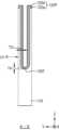
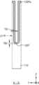
도 11a 내지 도 12b는 본 발명의 일 실시 예에 따른 게이트 절연층 및 매립 게이트 전극을 형성하는 단계를 나타내는 단면도로, 도 11a 내지 도 11c는 각각 도 12의 A-A' 선, B-B' 선, 및 C-C' 선을 따라서 절단한 단면도들이고, 도 12a은 도 11a 내지 도 11c에 보인 기준 레벨(LV-R)에 대응하는 위치를 따라서 기판(110)의 주면에 수평 방향으로 절단하여 나타내는 단면도이고, 도 12b는 도 12a의 XIIB 부분을 확대하여 나타내는 단면도이다.FIGS. 11A to 12B are cross-sectional views showing steps of forming a gate insulating layer and a buried gate electrode according to an embodiment of the present invention. FIGS. 11A to 11C are taken along lines A-A', B-B', and C-C of FIG. 12, respectively. ' These are cross-sectional views cut along a line, and FIG. 12a is a cross-sectional view cut horizontally on the main surface of the
도 11a 내지 도 12를 함께 참조하면, 복수의 게이트 트렌치(120T)의 내부에 복수의 게이트 절연층(122), 복수의 매립 게이트 전극(120), 및 복수의 매몰 절연막(126)을 차례로 형성한다. 일부 실시 예에서, 복수의 매립 게이트 전극(120) 각각과 복수의 매몰 절연막(126) 각각의 사이에는 커버층(124)이 배치될 수 있다.Referring to FIGS. 11A to 12 together, a plurality of
반도체 소자(1)는 복수의 게이트 트렌치(120T)의 하측 일부분을 채우는 복수의 게이트 절연층(122)과 복수의 매립 게이트 전극(120), 그리고 복수의 게이트 트렌치(120T)의 상측 일부분을 채우는 복수의 매몰 절연막(126)을 포함한다.The
복수의 게이트 절연층(122) 및 복수의 매립 게이트 전극(120)는, 복수의 매립 게이트 전극 트렌치(120T) 내부를 채우며 도 9a 내지 도 10에 보인 예비 게이트 절연층(122Pa)을 덮는 예비 게이트 전극을 형성한 후, 활성 영역(118)의 상면 및 소자 분리막(116)의 상면을 덮는 예비 게이트 절연층(122Pa)의 부분 및 예비 게이트 전극의 부분과, 복수의 매립 게이트 전극 트렌치(120T)의 상측 일부분을 채우는 예비 게이트 절연층(122Pa)의 부분 및 예비 게이트 전극의 부분을 제거하여 형성할 수 있다. 복수의 게이트 절연층(122)은 예비 게이트 절연층(122Pa) 중 복수의 게이트 트렌치(120T)의 하측의 측벽 및 저면을 덮는 부분이고, 복수의 매립 게이트 전극(120)은 복수의 게이트 절연층(122) 상에서 복수의 게이트 트렌치(120T)의 하측 일부분을 채우는 부분일 수 있다.The plurality of
복수의 매립 게이트 전극(120)은 복수의 게이트 트렌치(120T)와 같이 제1 수평 방향(X 방향)을 따라서 상호 평행하게 연장될 수 있다.The plurality of buried
일부 실시 예들에서, 매립 게이트 전극(120)을 형성한 후, 매립 게이트 전극(120)의 양측의 기판(110), 즉 복수의 활성 영역(118)의 상측 일부분에 소스/드레인 영역을 형성할 수 있다. 상기 소스/드레인 영역을 형성하기 위하여, 기판(110)에 불순물 이온을 주입할 수 있다. 다른 일부 실시 예들에서, 복수의 매립 게이트 전극(120)을 형성하기 전에 소스/드레인 영역을 형성하기 위한 불순물 이온 주입 공정이 수행될 수 있다.In some embodiments, after forming the buried
복수의 매립 게이트 전극(120) 각각의 상면은 기판(110)의 상면, 즉 활성 영역(118)의 상면보다 낮은 레벨에 위치된다. 복수의 매립 게이트 전극(120)의 저면은 도 3c에 보인 복수의 게이트 트렌치(120T)의 저면을 따라서 요철 형상을 가질 수 있으며, 복수의 활성 영역(118)에는 새들 핀 구조의 트랜지스터 (saddle FINFET)가 형성될 수 있다.The top surface of each of the plurality of buried
게이트 절연층(120)은 실리콘 산화막, 실리콘 질화막, 실리콘 산화질화막, ONO (oxide/nitride/oxide), 또는 실리콘 산화막보다 높은 유전 상수를 가지는 고유전막 (high-k dielectric film) 중에서 선택되는 적어도 하나로 이루어질 수 있다. 예를 들면, 게이트 절연층(120)은 약 10 내지 25의 유전 상수를 가질 수 있다. 일부 실시 예들에서, 게이트 절연층(120)은 하프늄 산화물(HfO), 하프늄 실리케이트(HfSiO), 하프늄 산화 질화물(HfON), 하프늄 실리콘 산화 질화물(HfSiON), 란타늄 산화물(LaO), 란타늄 알루미늄 산화물(LaAlO), 지르코늄 산화물(ZrO), 지르코늄 실리케이트(ZrSiO), 지르코늄 산화 질화물(ZrON), 지르코늄 실리콘 산화 질화물(ZrSiON), 탄탈륨 산화물(TaO), 티타늄 산화물(TiO), 바륨 스트론튬 티타늄 산화물(BaSrTiO), 바륨 티타늄 산화물(BaTiO), 스트론튬 티타늄 산화물(SrTiO), 이트륨 산화물(YO), 알루미늄 산화물(AlO), 또는 납 스칸듐 탄탈륨 산화물(PbScTaO) 중에서 선택되는 적어도 하나의 물질로 이루어진다. 예를 들면, 게이트 절연층(120)은 HfO2, Al2O3, HfAlO3, Ta2O3, 또는 TiO2 로 이루어질 수 있다.The
복수의 매립 게이트 전극(120) 각각의 상면은 기판(110)의 상면보다 낮은 레벨에 위치된다. 복수의 매립 게이트 전극(120)의 저면은 요철 형상을 가질 수 있으며, 복수의 활성 영역(116)에는 새들 핀 구조의 트랜지스터 (saddle FINFET)가 형성될 수 있다. 일부 실시 예들에서, 복수의 매립 게이트 전극(120)은 Ti, TiN, Ta, TaN, W, WN, TiSiN, 또는 WSiN 중에서 선택되는 적어도 하나의 물질로 이루어진다.The top surface of each of the plurality of buried
일부 실시 예들에서, 복수의 매립 게이트 전극(120) 각각은 코어층(120C) 및 코어층과 게이트 절연층(122) 사이에 배치되는 배리어층(120B)으로 이루어질 수 있다. 예를 들면, 코어층(120C)은 W, WN, TiSiN, 또는 WSiN과 같은 금속 물질 또는 도전성 금속 질화물로 이루어질 수 있고, 배리어층(120B)은 Ti, TiN, Ta, 또는 TaN과 같은 금속 물질 또는 도전성 금속 질화물로 이루어질 수 있다.In some embodiments, each of the plurality of buried
복수의 매몰 절연막(126)의 상면은 기판(110)의 상면, 즉 활성 영역(118)의 상면과 대략 동일 레벨에 위치될 수 있다. 매몰 절연막(126)은 실리콘 산화막, 실리콘 질화막, 실리콘 산화질화막, 또는 이들의 조합으로 이루어질 수 있다.The top surface of the plurality of buried insulating
커버층(124)은 예를 들면, 언도프드(un-doped) 폴리 실리콘 또는 도프드(doped) 폴리실리콘으로 이루어질 수 있다. 일부 실시 예에서, 커버층(124)은 생략될 수 있다.The
게이트 절연층(122)은 예비 게이트 절연층(122Pa)의 일부분이므로, 게이트 트렌치(120T)의 측면 중 기판(110) 상에 형성되는 게이트 절연층(122) 부분의 두께는 제1 측면 두께(TS1)일 수 있고, 게이트 트렌치(120)의 저면 중 기판(110) 상에 형성되는 게이트 절연층(122) 부분의 두께는 제1 저면 두께(TB1)일 수 있다. 또한 게이트 트렌치(120T)의 측면 중 소자 분리막(116) 상에 형성되는 게이트 절연층(122) 부분의 두께는 제2 측면 두께(TS2)일 수 있고, 게이트 트렌치(120)의 저면 중 소자 분리막(116) 상에 형성되는 게이트 절연층(122) 부분의 두께는 제2 저면 두께(TB2)일 수 있다.Since the
일부 실시 예에서, 게이트 절연층(122)은 제1 저면 두께(TB1)가 제1 측면 두께(TS1)보다 작은 값을 가지되, 제1 측면 두께(TS1)의 75% 이상의 값을 가지도록 형성할 수 있다. 제2 측면 두께(TS2)와 제2 저면 두께(TB2)는 대체로 동일한 값을 가질 수 있다.In some embodiments, the
또한 제2 측면 두께(TS2)는 제1 측면 두께(TS1)의 1/2보다 작은 값을 가질 수 있다. 예를 들어, 제1 측면 두께(TS1)는 80Å이고, 제2 측면 두께(TS2)는 20Å일 수 있으며, 이 경우 제1 측면 두께(TS1)는 제2 측면 두께(TS2)의 약 4배의 값을 가질 수 있다.Additionally, the second side thickness TS2 may have a value smaller than 1/2 of the first side thickness TS1. For example, the first side thickness TS1 may be 80 Å and the second side thickness TS2 may be 20 Å. In this case, the first side thickness TS1 may be about 4 times the second side thickness TS2. It can have a value.
도 11a 내지 도 12b에는 소자 분리막(116)과 게이트 절연층(122)이 명확히 구분되는 것으로 도시되었으나, 이는 게이트 절연층(122)의 두께 변화 등 게이트 절연층(122)의 형상을 설명하기 위한 것으로, 이에 한정되지 않는다. 예를 들면, 소자 분리막(116)과 게이트 절연층(122)이 유사한 물질, 예를 들면 실리콘 산화물로 이루어진 경우, 소자 분리막(116)과 게이트 절연층(122) 사이의 계면은 관찰되지 않을 수 있다.11A to 12B, the
게이트 트렌치(120T)는 제2 수평 방향(Y 방향)으로 대체로 일정한 값의 폭을 가지며 제1 수평 방향(X 방향)을 따라서 연장될 수 있다. 또한, 게이트 트렌치(120T)는 매립 게이트 전극(120) 및 게이트 절연층(122)으로 채워지므로, 제2 수평 방향(Y 방향)으로의 매립 게이트 전극(120)의 폭은, 게이트 트렌치(120T)의 폭에서 게이트 절연층(122)의 폭을 뺀 값을 가질 수 있다.The
매립 게이트 전극(120)은 일정한 폭(WB)을 가지고 제1 수평 방향(X 방향)으로 연장되는 베이스부(GB) 및 베이스부(GB)로부터 제2 수평 방향(Y 방향)으로 돌출되는 돌출부(GT)로 이루어질 수 있다. 베이스부(GB)의 폭은, 매립 게이트 전극(120)의 최소 폭일 수 있다.The buried
돌출부(GB)는 베이스부(GB)로부터 소자 분리막(116)을 향하여 연장되도록 돌출될 수 있다. 제2 측면 두께(TS2)는 제1 측면 두께(TS1)의 1/2보다 작은 값을 가지므로, 제2 측면 두께(TS2)과 제1 측면 두께(TS1)의 차이는 제1 측면 두께(TS1)의 1/2보다 큰 값을 가질 수 있다. 돌출부(GB)는 제2 측면 두께(TS2)과 제1 측면 두께(TS1)의 차이만큼 제2 수평 방향(Y 방향)으로 돌출될 수 있다. 따라서 제2 수평 방향(Y 방향)으로 돌출부(GB)의 돌출 길이(W1)는 제1 측면 두께(TS1)의 1/2보다 큰 값을 가질 수 있다.The protrusion GB may protrude from the base GB to extend toward the
돌출부(GB)는 베이스부(GB)로부터 양측에 있는 소자 분리막(116) 각각을 향하여, 베이스부(GB)로부터 돌출될 수 있다. 매립 게이트 전극(120)은, 베이스부(GB)로부터 양측으로 돌출되는 한쌍의 돌출부(GB)가 제2 수평 방향(Y 방향)을 따라서 정렬되는 부분에서 최대 폭을 가질 수 있다. 따라서, 매립 게이트 전극(120)은 제2 수평 방향(Y 방향)을 따라서 양측에 소자 분리막(116)이 배치되는 부분에서 최대 폭을 가지고, 양측에 활성 영역(118)의 절단면이 배치되는 부분에서 최소 폭을 가질 수 있다.The protrusion GB may protrude from the base GB toward each of the
따라서, 매립 게이트 전극(120)의 최대 폭과 최소 폭의 차이는 제1 측면 두께(TS1)의 1/2의 2배, 즉 제1 측면 두께(TS1)보다 큰 값을 가질 수 있다.Accordingly, the difference between the maximum and minimum widths of the buried
일부 실시 예에서, 매립 게이트 전극(120)은 활성 영역(118)의 장축 단부에 인접하는 부분에서 베이스부(GB)보다 제2 수평 방향(Y 방향)으로 큰 폭을 가질 수 있다. 활성 영역(118)의 장축 단부에 인접하는 부분에서 매립 게이트 전극(120) 일측에서 제2 수평 방향(Y 방향)으로 증가되는 폭(W2)의 값은, 돌출부(GB)의 돌출 길이(W1)보다 작은 값을 가질 수 있다.In some embodiments, the buried
따라서, 매립 게이트 전극(120)은 제2 수평 방향(Y 방향)으로 양측에 소자 분리막(116)이 배치되는 부분에서 최대 폭을 가지고, 양측에 활성 영역(118)의 절단면이 배치되는 부분에서 최소 폭을 가지고, 적어도 일측에 활성 영역(118)의 장축 단부가 배치되는 부분에서는 최대 폭과 최소 폭의 사이 값의 폭을 가질 수 있다.Accordingly, the buried
본 발명에 따른 반도체 소자(1)는 게이트 절연층(122)이 상대적으로 우수한 스텝 커버리지를 가지므로, 게이트 트렌치(120T)의 측면에 형성되는 게이트 절연층(122) 부분의 두께인 제1 측면 두께(TS1)를 상대적으로 얇게 만들어도, 게이트 트렌치(120T)의 저면에 형성되는 게이트 절연층(122) 부분의 두께인 제1 저면 두께(TB1)를 일정 값 이상을 확보할 수 있다. 따라서, 게이트 절연층(122)의 특성을 유지하면서도, 매립 게이트 전극(120)의 제2 수평 방향(Y 방향)에 대한 폭을 증가시킬 수 있다. 또한, 매립 게이트 전극(120)은 제2 수평 방향(Y 방향)으로 폭을 증가시키는 돌출부(GB)를 가지므로, 매립 게이트 전극(120)의 평균 폭이 증가할 수 있다.Since the
따라서, 반도체 소자(1)가 가지는 매립 게이트 전극(120)의 저항값을 감소시킬 수 있어, 동작 속도를 향상시킬 수 있다. 특히, 게이트 트렌치(120T)의 측면에 형성되는 게이트 절연층(122) 부분의 두께인 제1 측면 두께(TS1)를 상대적으로 얇게 만들 수 있으므로, 활성 영역(118)과 전기적으로 연결되는 드레인 전극과 매립 게이트 전극(120)의 오버랩 특성이 개선되어, 반도체 소자(1)의 데이터 쓰기 속도가 향상될 수 있다.Accordingly, the resistance value of the buried
그리고, 상대적으로 치밀한 막질을 가지는 제1 게이트 절연층(122a)을 기판(110) 상에 먼저 형성하고, 제1 게이트 절연층(122a)의 두께를 제2 게이트 절연층(122b)의 두께보다 큰 값을 가지도록 형성하여, 게이트 절연층(122)의 절연 특성이 향상될 수 있다. 또한, 게이트 절연층(122) 중, 증착 공정으로 형성되는 제2 게이트 절연층(122b)의 비율이 낮아지므로, 게이트 절연층(122) 내에 Cl(Chlorine) 농도가 감소될 수 있고, 게이트 절연층(122) 내의 계면 트랩(interface traps, Nit) 밀도, 및 스트레스도 감소되어, 반도체 소자(1)의 리플레쉬(refresh) 특성이 개선될 수 있다.Then, a first
도 13 내지 도 15는 각각 본 발명의 일 실시 예에 따른 반도체 소자의 제조 방법을 나타내는 흐름도이다.13 to 15 are flowcharts showing a method of manufacturing a semiconductor device according to an embodiment of the present invention, respectively.
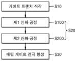
도 13에서는 도 9a 내지 도 10에서 설명한 제3 공정을 수행하지 않고, 게이트 절연층(122)을 형성하는 방법을 설명한다.In FIG. 13 , a method of forming the
도 2 내지 도 3d와 도 13을 함께 참조하면, 기판(110)에 복수의 게이트 트렌치(120T)를 형성한다(S10). 복수의 게이트 트렌치(120T)는 상호 평행하게 연장되며, 각각 복수의 활성 영역(118)을 가로지르는 라인 형상을 가질 수 있다. 게이트 트렌치(120T)의 측면에는 게이트 트렌치(120T)가 가로지르는 복수의 활성 영역(118) 각각의 부분이 노출될 수 있다.Referring to FIGS. 2 to 3D and FIG. 13 together, a plurality of
도 4 내지 도 6과 도 13을 함께 참조하면, 제1 산화 공정에 의하여 활성 영역(118) 상에 제1 게이트 절연층(122a)을 형성한다(S100). 제1 게이트 절연층(122a)은 활성 영역(118)을 포함하는 기판(110) 상에서 선택적으로 성장하도록 형성할 수 있다. 예를 들면, 제1 산화 공정은 열산화 공정일 수 있다. 일부 실시 예에서, 제1 산화 공정은 O2+H2 분위기에서 수행되는 ISSG(In Situ Steam Generated) 산화 공정일 수 있다.Referring to FIGS. 4 to 6 and FIG. 13 together, a first
제1 게이트 절연층(122a)은 게이트 트렌치(120T)의 측면 상에서와 저면 상에서 서로 다른 두께를 가지도록 형성될 수 있다. 예를 들면, 게이트 트렌치(120T)의 측면 상에 형성되는 제1 게이트 절연층(122a) 부분의 제1 두께(T1)는, 저면 상에 형성되는 제1 게이트 절연층(122a) 부분의 제2 두께(T2)보다 큰 값을 가질 수 있다. 일부 실시 예에서, 제1 게이트 절연층(122a)는, 제1 두께(T1)가 제2 두께(T2)의 대략 1.5배 이하의 값을 가지도록 형성될 수 있다.The first
도 7a 내지 도 8과 도 13을 함께 참조하면, 제2 산화 공정에 의하여 제1 게이트 절연층(122a) 및 소자 분리막(116) 상에 제2 게이트 절연층(122b)을 형성한다(S200). 제2 게이트 절연층(122b)은 제1 게이트 절연층(122a)보다 얇은 두께를 가지도록 형성될 수 있다. 제2 게이트 절연층(122b)은 게이트 트렌치(120T)의 측면 상에서와 저면 상에서 대체로 동일한 두께를 가지도록 컨포멀하게 형성될 수 있다.Referring to FIGS. 7A to 8 and FIG. 13 together, a second
제2 게이트 절연층(122b)은 제1 게이트 절연층(122a) 및 소자 분리막(116) 상을 모두 덮도록 형성할 수 있다. 제2 게이트 절연층(122b)은 제1 게이트 절연층(122a) 상에서와 소자 분리막(116) 상에서도 대체로 동일한 두께를 가지도록 형성될 수 있다.The second
예를 들면, 제2 산화 공정은 증착 공정일 수 있다. 일부 실시 예에서, 제2 산화 공정은 예를 들면, ALD(Atomic Layer Deposition) 공정일 수 있다.For example, the second oxidation process may be a deposition process. In some embodiments, the second oxidation process may be, for example, an atomic layer deposition (ALD) process.
도 11a 내지 도 12와 도 13을 함께 참조하면, 제1 게이트 절연층(122a) 및 제2 게이트 절연층(122b)의 일부분을 제거하여, 게이트 트렌치(120T)의 하측 일부분의 측면 및 저면을 덮는 게이트 절연층(122)를 형성한다(S20). 이후, 게이트 절연층(122)을 덮고, 게이트 트렌치(120T)의 하측 일부분을 채우는 매립 게이트 전극을 형성한다(S30).Referring to FIGS. 11A to 12 and 13 together, a portion of the first
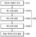
도 14에서는 도 9a 내지 도 10에서 설명한 제3 공정으로 제3 산화 공정을 수행하여 게이트 절연층(122)을 형성하는 방법을 설명한다.In FIG. 14 , a method of forming the
도 2 내지 도 3d와 도 14를 함께 참조하면, 기판(110)에 복수의 게이트 트렌치(120T)를 형성한다(S10). 복수의 게이트 트렌치(120T)는 상호 평행하게 연장되며, 각각 복수의 활성 영역(118)을 가로지르는 라인 형상을 가질 수 있다. 게이트 트렌치(120T)의 측면에는 게이트 트렌치(120T)가 가로지르는 복수의 활성 영역(118) 각각의 부분이 노출될 수 있다.Referring to FIGS. 2 to 3D and FIG. 14 together, a plurality of
도 4 내지 도 6과 도 14을 함께 참조하면, 제1 산화 공정에 의하여 활성 영역(118) 상에 제1 게이트 절연층(122a)을 형성한다(S100). 제1 게이트 절연층(122a)은 활성 영역(118)을 포함하는 기판(110) 상에서 선택적으로 성장하도록 형성할 수 있다. 예를 들면, 제1 산화 공정은 열산화 공정일 수 있다. 일부 실시 예에서, 제1 산화 공정은 O2+H2 분위기에서 수행되는 ISSG(In Situ Steam Generated) 산화 공정일 수 있다.Referring to FIGS. 4 to 6 and FIG. 14 together, a first
제1 게이트 절연층(122a)은 게이트 트렌치(120T)의 측면 상에서와 저면 상에서 서로 다른 두께를 가지도록 형성될 수 있다. 예를 들면, 게이트 트렌치(120T)의 측면 상에 형성되는 제1 게이트 절연층(122a) 부분의 제1 두께(T1)는, 저면 상에 형성되는 제1 게이트 절연층(122a) 부분의 제2 두께(T2)보다 큰 값을 가질 수 있다. 일부 실시 예에서, 제1 게이트 절연층(122a)는, 제1 두께(T1)가 제2 두께(T2)의 대략 1.5배 이하의 값을 가지도록 형성될 수 있다.The first
도 7a 내지 도 8과 도 14를 함께 참조하면, 제2 산화 공정에 의하여 제1 게이트 절연층(122a) 및 소자 분리막(116) 상에 제2 게이트 절연층(122b)을 형성한다(S200). 제2 게이트 절연층(122b)은 제1 게이트 절연층(122a)보다 얇은 두께를 가지도록 형성될 수 있다. 제2 게이트 절연층(122b)은 게이트 트렌치(120T)의 측면 상에서와 저면 상에서 대체로 동일한 두께를 가지도록 컨포멀하게 형성될 수 있다.Referring to FIGS. 7A to 8 and FIG. 14 together, a second
제2 게이트 절연층(122b)은 제1 게이트 절연층(122a) 및 소자 분리막(116) 상을 모두 덮도록 형성할 수 있다. 제2 게이트 절연층(122b)은 제1 게이트 절연층(122a) 상에서와 소자 분리막(116) 상에서도 대체로 동일한 두께를 가지도록 형성될 수 있다.The second
예를 들면, 제2 산화 공정은 증착 공정일 수 있다. 일부 실시 예에서, 제2 산화 공정은 예를 들면, ALD(Atomic Layer Deposition) 공정일 수 있다.For example, the second oxidation process may be a deposition process. In some embodiments, the second oxidation process may be, for example, an atomic layer deposition (ALD) process.
도 9a 내지 도 10과 도 14를 함께 참조하면, 제3 공정 산화 공정에 의하여 제1 게이트 절연층(122a), 및 제2 게이트 절연층(122b)으로 이루어지는 게이트 절연 구조체(122P)로부터 예비 게이트 절연층(122Pa)을 형성한다(S300).Referring to FIGS. 9A to 10 and FIG. 14 together, preliminary gate insulation is obtained from the
예를 들면, 제3 산화 공정은 O2+H2 분위기에서 수행되는 ISSG 산화 공정이거나, O2+H2 분위기와 O2 분위기로 변화되는 분위기에서 수행되는 ISSG 산화 공정일 수 있다. 다른 일부 실시 예에서, 제3 산화 공정은 건식 산화 공정일 수 있다.For example, the third oxidation process may be an ISSG oxidation process performed in an O2 +H2 atmosphere, or an ISSG oxidation process performed in an atmosphere that changes from an O2 +H2 atmosphere to an O2 atmosphere. In some other embodiments, the third oxidation process may be a dry oxidation process.
일부 실시 예에서, 제3 산화 공정이 O2+H2 분위기와 O2 분위기로 변화되는 분위기에서 수행되는 ISSG 산화 공정인 경우, 제3 산화 공정의 공정 수행 시간 중 O2+H2 분위기의 시간은 O2 분위기의 시간보다 짧을 수 있다. 즉, 제3 산화 공정은 공정 수행 시간 중 O2가 분위기에 존재하는 시간이 상대적으로 짧을 수 있다.In some embodiments, when the third oxidation process is an ISSG oxidation process performed in an atmosphere that changes between an O2 +H2 atmosphere and an O2 atmosphere, the time in the O2 +H2 atmosphere during the process performance time of the third oxidation process may be shorter than the time in the O2 atmosphere. That is, in the third oxidation process, the time during which O2 exists in the atmosphere may be relatively short.
일부 실시 예에서, 제1 산화 공정이 O2+H2 분위기에서 수행되는 ISSG 산화 공정이고, 제3 산화 공정이 O2+H2 분위기에서 수행되는 ISSG 산화 공정 또는 O2+H2 분위기와 O2 분위기로 변화되는 분위기에서 수행되는 ISSG 산화 공정인 경우, 제3 산화 공정의 공정 수행 시간 중 O2+H2 분위기의 시간은 제1 산화 공정의 공정 수행 시간 중 O2+H2 분위기의 시간보다 짧을 수 있다.In some embodiments, the first oxidation process is an ISSG oxidation process performed in an O2 +H2 atmosphere and the third oxidation process is an ISSG oxidation process performed in an O2 +H2 atmosphere or an ISSG oxidation process performed in an O2 +H2 atmosphere and O In the case of the ISSG oxidation process performed in an atmosphere that changes to2 atmospheres, the time in the O2 +H2 atmosphere during the process performance time of the third oxidation process is the time in the O2 +H2 atmosphere during the process performance time of the first oxidation process. It can be shorter.
일부 실시 예에서, 제3 산화 공정의 공정 수행 시간은, 제1 산화 공정의 공정 수행 시간보다 짧을 수 있다.In some embodiments, the process performance time of the third oxidation process may be shorter than the process performance time of the first oxidation process.
도 11a 내지 도 12과 도 14를 함께 참조하면, 예비 게이트 절연층(122Pa)의 일부분을 제거하여, 게이트 트렌치(120T)의 하측 일부분의 측면 및 저면을 덮는 게이트 절연층(122)를 형성한다(S22). 이후, 게이트 절연층(122)을 덮고, 게이트 트렌치(120T)의 하측 일부분을 채우는 매립 게이트 전극을 형성한다(S30).Referring to FIGS. 11A to 12 and 14 together, a portion of the preliminary gate insulating layer 122Pa is removed to form a
도 15에서는 도 9a 내지 도 10에서 설명한 제3 공정으로 열처리 공정을 수행하여 게이트 절연층(122)을 형성하는 방법을 설명한다.In FIG. 15 , a method of forming the
도 2 내지 도 3d와 도 15를 함께 참조하면, 기판(110)에 복수의 게이트 트렌치(120T)를 형성한다(S10). 복수의 게이트 트렌치(120T)는 상호 평행하게 연장되며, 각각 복수의 활성 영역(118)을 가로지르는 라인 형상을 가질 수 있다. 게이트 트렌치(120T)의 측면에는 게이트 트렌치(120T)가 가로지르는 복수의 활성 영역(118) 각각의 부분이 노출될 수 있다.Referring to FIGS. 2 to 3D and FIG. 15 together, a plurality of
도 4 내지 도 6과 도 15을 함께 참조하면, 제1 산화 공정에 의하여 활성 영역(118) 상에 제1 게이트 절연층(122a)을 형성한다(S100). 제1 게이트 절연층(122a)은 활성 영역(118)을 포함하는 기판(110) 상에서 선택적으로 성장하도록 형성할 수 있다. 예를 들면, 제1 산화 공정은 열산화 공정일 수 있다. 일부 실시 예에서, 제1 산화 공정은 O2+H2 분위기에서 수행되는 ISSG(In Situ Steam Generated) 산화 공정일 수 있다.Referring to FIGS. 4 to 6 and FIG. 15 together, a first
제1 게이트 절연층(122a)은 게이트 트렌치(120T)의 측면 상에서와 저면 상에서 서로 다른 두께를 가지도록 형성될 수 있다. 예를 들면, 게이트 트렌치(120T)의 측면 상에 형성되는 제1 게이트 절연층(122a) 부분의 제1 두께(T1)는, 저면 상에 형성되는 제1 게이트 절연층(122a) 부분의 제2 두께(T2)보다 큰 값을 가질 수 있다. 일부 실시 예에서, 제1 게이트 절연층(122a)는, 제1 두께(T1)가 제2 두께(T2)의 대략 1.5배 이하의 값을 가지도록 형성될 수 있다.The first
도 7a 내지 도 8과 도 15를 함께 참조하면, 제2 산화 공정에 의하여 제1 게이트 절연층(122a) 및 소자 분리막(116) 상에 제2 게이트 절연층(122b)을 형성한다(S200). 제2 게이트 절연층(122b)은 제1 게이트 절연층(122a)보다 얇은 두께를 가지도록 형성될 수 있다. 제2 게이트 절연층(122b)은 게이트 트렌치(120T)의 측면 상에서와 저면 상에서 대체로 동일한 두께를 가지도록 컨포멀하게 형성될 수 있다.Referring to FIGS. 7A to 8 and FIG. 15 together, a second
제2 게이트 절연층(122b)은 제1 게이트 절연층(122a) 및 소자 분리막(116) 상을 모두 덮도록 형성할 수 있다. 제2 게이트 절연층(122b)은 제1 게이트 절연층(122a) 상에서와 소자 분리막(116) 상에서도 대체로 동일한 두께를 가지도록 형성될 수 있다.The second
예를 들면, 제2 산화 공정은 증착 공정일 수 있다. 일부 실시 예에서, 제2 산화 공정은 예를 들면, ALD(Atomic Layer Deposition) 공정일 수 있다.For example, the second oxidation process may be a deposition process. In some embodiments, the second oxidation process may be, for example, an atomic layer deposition (ALD) process.
도 9a 내지 도 10과 도 15를 함께 참조하면, 열처리 공정에 의하여 제1 게이트 절연층(122a), 및 제2 게이트 절연층(122b)으로 이루어지는 게이트 절연 구조체(122P)로부터 예비 게이트 절연층(122Pa)을 형성한다(S310).Referring to FIGS. 9A to 10 and 15 together, the preliminary gate insulating layer 122Pa is formed from the
예를 들면, 예를 들면, 열처리 공정은 RTP(Rapid Thermal Processing) 방법 또는 어닐(Anneal) 방법에 의하여 수행될 수 있다.For example, the heat treatment process may be performed by a Rapid Thermal Processing (RTP) method or an annealing method.
도 11a 내지 도 12과 도 15를 함께 참조하면, 예비 게이트 절연층(122Pa)의 일부분을 제거하여, 게이트 트렌치(120T)의 하측 일부분의 측면 및 저면을 덮는 게이트 절연층(122)를 형성한다(S24). 이후, 게이트 절연층(122)을 덮고, 게이트 트렌치(120T)의 하측 일부분을 채우는 매립 게이트 전극을 형성한다(S30).Referring to FIGS. 11A to 12 and FIG. 15 together, a portion of the preliminary gate insulating layer 122Pa is removed to form a
도 16은 본 발명의 일 실시 예에 따른 반도체 소자의 제조 방법의 제1 공정을 설명하기 위한 그래프이고, 도 17은 본 발명의 일 실시 예에 따른 반도체 소자의 제조 방법의 제3 공정을 설명하기 위한 그래프이다.FIG. 16 is a graph for explaining the first process of the method for manufacturing a semiconductor device according to an embodiment of the present invention, and FIG. 17 is a graph for explaining the third process for the method for manufacturing a semiconductor device according to an embodiment of the present invention. This is a graph for
도 16 및 도 17을 함께 참조하면, 제1 공정(Process 1)은 O2+H2 분위기에서 수행되는 ISSG(In Situ Steam Generated) 산화 공정일 수 있고, 제3 공정(Process 3)은 O2+H2 분위기에서 O2 분위기로 변화되는 분위기에서 수행되는 ISSG 산화 공정일 수 있다.Referring to FIGS. 16 and 17 together, the first process (Process 1) may be an ISSG (In Situ Steam Generated) oxidation process performed in an O2 +H2 atmosphere, and the third process (Process 3) may be an
제1 공정(Process 1)의 공정 수행 시간은 제1 시간(T1)일 수 있고, 제3 공정(Process 3)의 공정 수행 시간은 제2 시간(T2)과 제3 시간(T3)의 합일 수 있다. 여기에서 공정 수행 시간이란, 제1 공정(Process 1) 및 제3 산화 공정(Process 3)을 수행하기 위한 공정 온도 및 공정 분위기가 유지되는 시간을 의미하며, 램프 업 시간 및 쿨 다운 시간은 포함되지 않는다.The process execution time of the first process (Process 1) may be the first time (T1), and the process execution time of the third process (Process 3) may be the sum of the second time (T2) and the third time (T3). there is. Here, the process execution time refers to the time during which the process temperature and process atmosphere are maintained to perform the first process (Process 1) and the third oxidation process (Process 3), and does not include ramp-up time and cool-down time. No.
제1 공정(Process 1)은 제1 시간(T1) 동안 O2+H2 분위기일 수 있고, 제3 공정(Process 3)은 제2 시간(T2) 동안 O2+H2 분위기이고, 제3 시간(T3) 동안 O2 분위기일 수 있다. 제3 공정(Process 3)에서 제3 시간(T3)은 제2 시간(T2)보다 짧을 수 있고, 제2 시간(T2) 및 제3 시간(T3) 각각은 제1 시간(T1)보다 짧을 수 있다. 일부 실시 예에서, 제2 시간(T2)과 제3 시간(T3)의 합은 제1 시간(T1)보다 짧을 수 있다.The first process (Process 1) may be in an O2 +H2 atmosphere during the first time (T1), and the third process (Process 3) may be in an O2 +H2 atmosphere during the second time (T2). There may be an O2 atmosphere during time T3. In the third process (Process 3), the third time (T3) may be shorter than the second time (T2), and each of the second time (T2) and the third time (T3) may be shorter than the first time (T1). there is. In some embodiments, the sum of the second time T2 and the third time T3 may be shorter than the first time T1.
예를 들면, 제1 시간(T1)은 약 40초이고, 제2 시간(T2)은 약 1초이고, 제3 시간(T3)은 약 20초일 수 있으나, 이는 예시적인 것으로 이에 한정되지는 않는다.For example, the first time (T1) may be about 40 seconds, the second time (T2) may be about 1 second, and the third time (T3) may be about 20 seconds, but this is an example and is not limited thereto. .
제3 공정(Process 3)의 공정 수행 시간 중, 산소가 공급되는 시간, 즉 O2+H2 분위기인 제2 시간(T2)은 제1 공정(Process 1)의 공정 수행 시간 중, 산소가 공급되는 시간, 즉 O2+H2 분위기인 제1 시간(T1)에 비하여 상대적으로 매우 짧을 수 있다. 따라서, 제3 공정(Process 3)을 수행한 후의 예비 게이트 절연층(도 9a 내지 도 10의 122Pa)의 두께는 제3 공정(Process 3)을 수행하기 전의 게이트 절연 구조체(도 7a 내지 도 8의 122P)의 두께와 비교하여 거의 유사하거나, 수Å 이하만큼 큰 값을 가질 수 있다.During the process performance time of the third process (Process 3), the time during which oxygen is supplied, that is, the second time (T2) in the O2 +H2 atmosphere, is the time during which oxygen is supplied during the process performance time of the first process (Process 1). The time may be relatively very short compared to the first time (T1) in the O2 +H2 atmosphere. Therefore, the thickness of the preliminary gate insulating layer (122Pa in FIGS. 9A to 10) after performing the third process (Process 3) is the thickness of the gate insulating structure (122Pa in FIGS. 7A to 8) before performing the third process (Process 3). Compared to the thickness of 122P), it can be almost similar or can have a value that is several Å or less.
즉, 도 1 내지 도 12b, 및 도 14를 참조하여 형성된 게이트 절연층(122)의 두께는 제1 공정(Process 1) 및 제2 공정에 의하여 대부분 결정되고, 제3 공정(Process 3)에서는 게이트 절연 구조체(122P) 내에 포함된 불순물을 제거하거나, 게이트 절연 구조체(122P)의 막질을 치밀하게 하거나, 게이트 절연 구조체(122P)와 기판(110) 사이의 계면 결함을 치유하거나, 제1 게이트 절연층(122a)과 제2 게이트 절연층(122b) 사이의 존재하는 결함을 치유할 수 있고, 게이트 절연층(122)의 두께에는 거의 기여하지 않을 수 있다. 따라서, 제3 공정(Process 3)을 수행하여도, 게이트 절연층(122)의 스텝 커버리지는 큰 변화없이 유지될 수 있다.That is, the thickness of the
도 18은 본 발명의 일 실시 예에 따른 반도체 소자의 제조 방법에 의하여 제조된 반도체 소자의 주요 구성들을 설명하기 위한 개략적인 평면 레이아웃이다. 도 18에 대한 내용 중 도 1 내지 도 17과 중복되는 내용은 생략될 수 있다.Figure 18 is a schematic plan layout for explaining the main components of a semiconductor device manufactured by the semiconductor device manufacturing method according to an embodiment of the present invention. Among the contents of FIG. 18, contents that overlap with FIGS. 1 to 17 may be omitted.
도 18을 참조하면, 반도체 소자(2)는, 기판(110)에 복수의 활성 영역(118)을 정의하는 소자 분리막(116)이 포함한다. 복수의 활성 영역(118)은 각각 단축 및 장축을 가지는 비교적 긴 아일랜드 형상을 가질 수 있다. 예를 들면, 복수의 활성 영역(118)은 제1 수평 방향(X 방향) 및 제2 수평 방향(Y)에 대하여 사선 방향으로 각각 단축 및 장축을 가질 수 있다. 복수의 게이트 트렌치(120T)는 제1 수평 방향(X 방향)을 따라서 상호 평행하게 연장되며, 각각 복수의 활성 영역(118)을 가로지르는 라인 형상일 수 있다. 복수의 매립 게이트 전극(120)은 복수의 게이트 트렌치(120T) 내에서 복수의 활성 영역(118)을 가로질러 제1 수평 방향(X 방향)을 따라 상호 평행하게 연장될 수 있다. 복수의 게이트 트렌치(120T)와 복수의 매립 게이트 전극(120) 사이에는 복수의 게이트 절연층(122)이 개재될 수 있다.Referring to FIG. 18 , the
복수의 매립 게이트 전극(120)은 제2 수평 방향(Y 방향)으로 양측에 소자 분리막(116)이 배치되는 부분에서 증가되는 폭을 가질 수 있어, 매립 게이트 전극(120)의 평균 폭이 증가할 수 있다.The plurality of buried
매립 게이트 전극(120) 위에는 복수의 비트 라인(BL)이 제1 수평 방향(X 방향)과 교차하는 제2 수평 방향(Y 방향)을 따라 상호 평행하게 연장될 수 있다. 복수의 비트 라인(BL)은 다이렉트 콘택(DC)을 통해 복수의 활성 영역(118)에 연결될 수 있다.On the buried
복수의 스토리지 콘택(SC)은 복수의 비트 라인(BL)의 상부에 형성되는 커패시터의 하부 전극(SN)을 활성 영역(118)에 연결시키는 역할을 할 수 있다. 복수의 스토리지 콘택(SC) 각각은 복수의 비트 라인(BL) 중 상호 인접한 2 개의 비트 라인(BL) 사이에 배치되는 베리드 콘택과 상기 베리드 콘택 위에 형성되는 도전성 랜딩 패드로 이루어질 수 있다. 복수의 스토리지 콘택(SC) 각각을 이루는 상기 도전성 랜딩 패드는 상기 베리드 콘택과 적어도 일부가 오버랩되도록 배치될 수 있다.The plurality of storage contacts SC may serve to connect the lower electrode SN of the capacitor formed on the upper part of the plurality of bit lines BL to the
일부 실시예들에서, 다이렉트 콘택(DC)은 Si, Ge, W, WN, Co, Ni, Al, Mo, Ru, Ti, TiN, Ta, TaN, Cu, 또는 이들의 조합으로 이루어질 수 있다. 일부 실시예들에서, 다이렉트 콘택(DC)은 에피택셜(epitaxial) 실리콘층으로 이루어질 수 있다.In some embodiments, the direct contact (DC) may be made of Si, Ge, W, WN, Co, Ni, Al, Mo, Ru, Ti, TiN, Ta, TaN, Cu, or a combination thereof. In some embodiments, the direct contact (DC) may be made of an epitaxial silicon layer.
일부 실시 예에서, 복수의 비트 라인(BL)은 기판(110) 상에 차례로 형성된 하부 도전층, 중간 도전층, 및 상부 도전층을 포함할 수 있으나, 본 발명의 기술적 사상이 이에 한정되는 것은 아니다. 예를 들면, 복수의 비트 라인(BL)은 단일층, 이중층, 또는 4 중층 이상의 복수의 적층 구조로 형성될 수도 있다.In some embodiments, the plurality of bit lines BL may include a lower conductive layer, a middle conductive layer, and an upper conductive layer sequentially formed on the
상기 하부 도전층의 상면과 다이렉트 콘택(DC)의 상면은 동일 평면 상에서 연장될 수 있다. 일부 실시예들에서, 상기 하부 도전층은 도전성 폴리실리콘으로 이루어질 수 있다. 상기 중간 도전층 및 상기 상부 도전층은 각각 TiN, TiSiN, W, 텅스텐 실리사이드, 또는 이들의 조합으로 이루어질 수 있다. 예를 들면, 상기 중간 도전층은 TiN 및/또는 TiSiN으로 이루어지고, 상기 상부 도전층은 W으로 이루어질 수 있다. 복수의 비트 라인(BL) 상에는 복수의 절연 캡핑 패턴이 배치될 수 있다. 상기 복수의 절연 캡핑 패턴은 예를 들면, 실리콘 질화막으로 이루어질 수 있다. 복수의 스토리지 콘택(SC)은 복수의 절연 스페이서(SPC1)를 사이에 두고 복수의 비트 라인(BL)으로부터 이격되어 있다.The top surface of the lower conductive layer and the top surface of the direct contact (DC) may extend on the same plane. In some embodiments, the lower conductive layer may be made of conductive polysilicon. The middle conductive layer and the upper conductive layer may each be made of TiN, TiSiN, W, tungsten silicide, or a combination thereof. For example, the middle conductive layer may be made of TiN and/or TiSiN, and the upper conductive layer may be made of W. A plurality of insulating capping patterns may be disposed on the plurality of bit lines BL. For example, the plurality of insulating capping patterns may be made of a silicon nitride film. The plurality of storage contacts SC are spaced apart from the plurality of bit lines BL with a plurality of insulating spacers SPC1 therebetween.
복수의 스토리지 콘택(SC)을 이루는 복수의 베리드 콘택은, 기판(110) 상에서 복수의 비트 라인(BL) 각각의 사이의 공간을 따라 수직 방향(Z 방향)으로 연장되는 기둥 형상을 가질 수 있다. 상기 복수의 베리드 콘택 각각의 저면은 활성 영역(118)에 접할 수 있다. 상기 복수의 베리드 콘택 각각의 일부는 기판(110) 내에 매립되도록 기판(110)의 상면보다 더 낮은 레벨에 위치될 수 있다. 상기 복수의 베리드 콘택은 불순물이 도핑된 반도체 물질, 금속, 도전성 금속 질화물, 또는 이들의 조합으로 이루어질 수 있으나, 이에 한정되는 것은 아니다.The plurality of buried contacts forming the plurality of storage contacts SC may have a pillar shape extending in the vertical direction (Z direction) along the space between each of the plurality of bit lines BL on the
복수의 스토리지 콘택(SC)을 이루는 복수의 도전성 랜딩 패드는 각각 도전성 배리어막과 도전층을 포함할 수 있다. 상기 도전성 배리어막은 Ti, TiN, 또는 이들의 조합으로 이루어질 수 있다. 상기 도전층은 금속, 금속 질화물, 도전성 폴리실리콘, 또는 이들의 조합으로 이루어질 수 있다. 예를 들면, 상기 도전층은 텅스텐(W)을 포함할 수 있다.The plurality of conductive landing pads forming the plurality of storage contacts SC may each include a conductive barrier film and a conductive layer. The conductive barrier film may be made of Ti, TiN, or a combination thereof. The conductive layer may be made of metal, metal nitride, conductive polysilicon, or a combination thereof. For example, the conductive layer may include tungsten (W).
복수의 도전성 랜딩 패드(LP)는 상기 복수의 도전성 랜딩 패드는 평면에서 볼 때 복수의 아일랜드형 패턴 형상을 가질 수 있다. 상기 복수의 도전성 랜딩 패드는 상기 복수의 도전성 랜딩 패드 주위의 공간을 채우는 절연막에 의해 상호 전기적으로 절연될 수 있다. 상기 절연막은 실리콘 질화막, 실리콘 산화막, 또는 이들의 조합으로 이루어질 수 있다.The plurality of conductive landing pads LP may have a plurality of island-like pattern shapes when viewed from a plan view. The plurality of conductive landing pads may be electrically insulated from each other by an insulating film that fills the space around the plurality of conductive landing pads. The insulating film may be made of a silicon nitride film, a silicon oxide film, or a combination thereof.
복수의 베리드 콘택과 복수의 도전성 랜딩 패드 사이에는 복수의 금속 실리사이드막이 개재될 수 있다. 복수의 스토리지 콘택(SC) 각각에서, 상기 금속 실리사이드막 및 상기 도전성 랜딩 패드는 상기 베리드 콘택과 수직으로 오버랩되도록 배치될 수 있다. 일부 실시예들에서, 상기 금속 실리사이드막은 코발트 실리사이드, 니켈 실리사이드, 또는 망간 실리사이드로 이루어질 수 있으나, 상기 예시된 바에 한정되는 것은 아니다. 상기 복수의 도전성 랜딩 패드는 각각 상기 금속 실리사이드막을 통해 상기 베리트 콘택에 연결될 수 있다.A plurality of metal silicide films may be interposed between the plurality of buried contacts and the plurality of conductive landing pads. In each of the plurality of storage contacts SC, the metal silicide layer and the conductive landing pad may be arranged to vertically overlap the buried contact. In some embodiments, the metal silicide film may be made of cobalt silicide, nickel silicide, or manganese silicide, but is not limited to the above examples. Each of the plurality of conductive landing pads may be connected to the Beret contact through the metal silicide film.
도 18에서는 반도체 소자로서 디램(DRAM) 소자를 예시적으로 설명하나, 본 발명에서 반도체 소자를 디램 소자로 한정하는 것은 아니다. 예를 들면, 본 발명에 따른 반도체 소자는 매립 게이트 전극(120)을 가지는 모든 종류의 반도체 소자일 수 있다.In FIG. 18, a DRAM device is exemplarily explained as a semiconductor device, but the semiconductor device in the present invention is not limited to the DRAM device. For example, the semiconductor device according to the present invention may be any type of semiconductor device having a buried
이상, 본 발명을 바람직한 실시 예를 들어 상세하게 설명하였으나, 본 발명은 실시 예에 한정되지 않고, 본 발명의 기술적 사상 및 범위 내에서 당 분야에서 통상의 지식을 가진 자에 의하여 여러가지 변형 및 변경이 가능하다.Above, the present invention has been described in detail with preferred embodiments, but the present invention is not limited to the embodiments, and various modifications and changes can be made by those skilled in the art within the technical spirit and scope of the present invention. possible.
1, 2 : 반도체 소자, 110 : 기판, 116 : 소자 분리막, 118 : 활성 영역, 120 : 매립 게이트 전극, GB : 베이스부, GT : 돌출부, 120T : 게이트 트렌치, 122 : 게이트 절연층, 122a : 제1 게이트 절연층, 122b : 제2 게이트 절연층, BL : 비트 라인1, 2: semiconductor device, 110: substrate, 116: device isolation film, 118: active region, 120: buried gate electrode, GB: base portion, GT: protrusion, 120T: gate trench, 122: gate insulating layer, 122a: first 1 gate insulating layer, 122b: second gate insulating layer, BL: bit line
Claims (20)
Translated fromKorean상기 기판의 노출되는 표면 상에 선택적으로 제1 게이트 절연층을 형성하는 단계;
상기 제1 게이트 절연층 및 상기 소자 분리막의 노출되는 표면 상에 상기 제1 게이트 절연층보다 얇은 두께를 가지는 제2 게이트 절연층을 형성하는 단계;
상기 제1 게이트 절연층 및 상기 제2 게이트 절연층 상에 예비 게이트 전극을 형성하는 단계, 및
상기 제1 게이트 절연층 및 상기 제2 게이트 절연층의 일부분, 그리고 상기 예비 게이트 전극의 일부분을 제거하여, 상기 복수의 게이트 트렌치의 하측 일부분의 측면 및 저면을 덮는 복수의 게이트 절연층, 그리고 상기 복수의 게이트 절연층 상에서 상기 복수의 게이트 트렌치의 하측 일부분을 채우는 복수의 매립 게이트 전극을 형성하는 단계;를 포함하고,
상기 제1 게이트 절연층은, 상기 복수의 게이트 트렌치의 저면 상의 부분의 두께보다 상기 복수의 게이트 트렌치의 측면 상의 부분의 두께가 큰 값을 가지도록 형성하고,
상기 복수의 매립 게이트 전극 각각은 상기 제1 수평 방향에 수직인 제2 수평 방향에 대하여 일정한 폭을 가지고 상기 제1 수평 방향으로 연장되는 베이스부, 및 상기 베이스부로부터 상기 제2 수평 방향으로 돌출되는 돌출부로 이루어지는 반도체 소자의 제조 방법.forming a plurality of gate trenches extending parallel to each other in a first horizontal direction across the plurality of active regions in a substrate having a plurality of active regions defined by a device isolation layer;
selectively forming a first gate insulating layer on the exposed surface of the substrate;
forming a second gate insulating layer having a thickness thinner than the first gate insulating layer on exposed surfaces of the first gate insulating layer and the device isolation layer;
forming a preliminary gate electrode on the first gate insulating layer and the second gate insulating layer, and
A plurality of gate insulating layers covering side and bottom surfaces of lower portions of the plurality of gate trenches by removing a portion of the first gate insulating layer and a portion of the second gate insulating layer, and a portion of the preliminary gate electrode, and the plurality of gate insulating layers. A step of forming a plurality of buried gate electrodes filling a lower portion of the plurality of gate trenches on the gate insulating layer of,
The first gate insulating layer is formed so that the thickness of the portion on the side surface of the plurality of gate trenches is greater than the thickness of the portion on the bottom surface of the plurality of gate trenches,
Each of the plurality of buried gate electrodes has a base portion that has a constant width with respect to a second horizontal direction perpendicular to the first horizontal direction and extends in the first horizontal direction, and protrudes from the base portion in the second horizontal direction. A method of manufacturing a semiconductor device consisting of a protrusion.
상기 제2 게이트 절연층은, 상기 복수의 게이트 트렌치의 저면 상의 부분의 두께와 상기 복수의 게이트 트렌치의 측면 상의 부분의 두께가 실질적으로 동일한 값을 가지도록 형성하는 것을 특징으로 하는 반도체 소자의 제조 방법.According to claim 1,
A method of manufacturing a semiconductor device, wherein the second gate insulating layer is formed so that the thickness of the portion on the bottom of the plurality of gate trenches and the thickness of the portion on the side surface of the plurality of gate trenches have substantially the same value. .
상기 돌출부는, 상기 베이스부로부터 상기 소자 분리막을 향하여 연장되도록 돌출되도록 형성하는 것을 특징으로 하는 반도체 소자의 제조 방법.According to claim 1,
A method of manufacturing a semiconductor device, wherein the protrusion is formed to protrude so as to extend from the base portion toward the device isolation layer.
상기 돌출부는, 상기 베이스부로부터 상기 제2 수평 방향으로 돌출 길이가, 상기 게이트 절연층의 복수의 게이트 트렌치의 측면 상의 부분의 두께의 1/2보다 큰 값을 가지도록 형성하는 것을 특징으로 하는 반도체 소자의 제조 방법.According to claim 1,
The semiconductor, wherein the protrusion is formed so that a protrusion length from the base portion in the second horizontal direction is greater than 1/2 of a thickness of a portion on the side surface of the plurality of gate trenches of the gate insulating layer. Method of manufacturing the device.
상기 복수의 매립 게이트 전극은, 상기 제1 수평 방향에 수직인 제2 수평 방향에 대하여 최대 폭과 최소 폭의 차이가 상기 게이트 절연층의 복수의 게이트 트렌치의 측면 상의 부분의 두께보다 큰 값을 가지도록 형성하는 것을 특징으로 하는 반도체 소자의 제조 방법.According to claim 1,
The plurality of buried gate electrodes have a difference between a maximum width and a minimum width in a second horizontal direction perpendicular to the first horizontal direction having a value greater than a thickness of a portion on the side of the plurality of gate trenches of the gate insulating layer. A method of manufacturing a semiconductor device, characterized in that the formation is as follows.
상기 복수의 매립 게이트 전극은, 상기 복수의 게이트 트렌치가 가로지르는 상기 복수의 활성 영역의 절단면이 양측에 배치되는 부분에서 상기 제1 수평 방향에 수직인 제2 수평 방향에 대하여 최소 폭을 가지도록 형성하는 것을 특징으로 하는 반도체 소자의 제조 방법.According to claim 1,
The plurality of buried gate electrodes are formed to have a minimum width with respect to a second horizontal direction perpendicular to the first horizontal direction at the portions where the cut surfaces of the plurality of active regions crossed by the plurality of gate trenches are disposed on both sides. A method of manufacturing a semiconductor device, characterized in that.
상기 복수의 매립 게이트 전극 각각은, 상기 소자 분리막이 양측에 배치되는 부분에서 상기 제1 수평 방향에 수직인 제2 수평 방향에 대하여 최대 폭을 가지도록 형성하는 것을 특징으로 하는 반도체 소자의 제조 방법.According to claim 1,
A method of manufacturing a semiconductor device, wherein each of the plurality of buried gate electrodes is formed to have a maximum width in a second horizontal direction perpendicular to the first horizontal direction at the portion where the device isolation layer is disposed on both sides.
상기 제1 게이트 절연층은, O2+H2 분위기에서 수행되는 ISSG(In Situ Steam Generated) 산화 공정에 의하여 형성하는 것을 특징으로 하는 반도체 소자의 제조 방법.According to claim 1,
A method of manufacturing a semiconductor device, wherein the first gate insulating layer is formed by an ISSG (In Situ Steam Generated) oxidation process performed in an O2 +H2 atmosphere.
상기 제2 게이트 절연층은, ALD(Atomic Layer Deposition) 공정에 의하여 형성하는 것을 특징으로 하는 반도체 소자의 제조 방법.According to claim 1,
A method of manufacturing a semiconductor device, wherein the second gate insulating layer is formed by an Atomic Layer Deposition (ALD) process.
제1 산화 공정에 의하여, 상기 기판의 노출되는 표면 상에 제1 게이트 절연층을 형성하는 단계;
제2 산화 공정에 의하여, 상기 제1 게이트 절연층 및 상기 소자 분리막 상을 컨포멀하게 덮는 제2 게이트 절연층을 형성하는 단계; 및
상기 복수의 게이트 트렌치의 하측 일부분을 채우는 복수의 매립 게이트 전극을 형성하는 단계;를 포함하며,
상기 제1 산화 공정은 O2+H2 분위기에서 수행되는 ISSG 산화 공정이고, 상기 제2 산화 공정은 증착 공정이고,
상기 복수의 게이트 트렌치의 저면 중 상기 기판 상에 형성되는 상기 제1 게이트 절연층 및 상기 제2 게이트 절연층 각각의 두께의 합은, 상기 복수의 게이트 트렌치의 측면 중 상기 기판 상에 형성되는 상기 제1 게이트 절연층 및 상기 제2 게이트 절연층 각각의 두께의 합의 75% 이상의 값을 가지는 반도체 소자의 제조 방법.forming a plurality of gate trenches extending parallel to each other in a first horizontal direction across the plurality of active regions in a substrate having a plurality of active regions defined by a device isolation layer;
forming a first gate insulating layer on the exposed surface of the substrate by a first oxidation process;
forming a second gate insulating layer conformally covering the first gate insulating layer and the device isolation layer by a second oxidation process; and
It includes forming a plurality of buried gate electrodes that fill lower portions of the plurality of gate trenches,
The first oxidation process is an ISSG oxidation process performed in an O2 +H2 atmosphere, and the second oxidation process is a deposition process,
The sum of the thicknesses of each of the first gate insulating layer and the second gate insulating layer formed on the substrate among the bottom surfaces of the plurality of gate trenches is the first gate insulating layer formed on the substrate among the side surfaces of the plurality of gate trenches. 1. A method of manufacturing a semiconductor device having a value of 75% or more of the sum of the thicknesses of each of the gate insulating layer and the second gate insulating layer.
상기 제2 게이트 절연층을 형성한 후에, O2+H2 분위기와 O2 분위기로 변화되는 분위기에서 수행되는 ISSG 산화 공정인 제3 산화 공정을 수행하는 단계;를 더 포함하는 것을 특징으로 하는 반도체 소자의 제조 방법.According to claim 12,
After forming the second gate insulating layer, performing a third oxidation process, which is an ISSG oxidation process, performed in an atmosphere changing from an O2 +H2 atmosphere to an O2 atmosphere. Method of manufacturing the device.
상기 제3 산화 공정의 공정 수행 시간은 상기 제1 산화 공정의 공정 수행 시간보다 짧은 것을 특징으로 하는 반도체 소자의 제조 방법.According to claim 13,
A method of manufacturing a semiconductor device, wherein the process execution time of the third oxidation process is shorter than the process execution time of the first oxidation process.
상기 제3 산화 공정의 공정 수행 시간 중, O2+H2 분위기의 시간은 O2 분위기의 시간보다 짧은 것을 특징으로 하는 반도체 소자의 제조 방법.According to claim 13,
Among the process performance times of the third oxidation process, the time in the O2 +H2 atmosphere is shorter than the time in the O2 atmosphere.
상기 제2 게이트 절연층을 형성한 후에, 열처리 공정을 수행하는 단계;를 더 포함하는 것을 특징으로 하는 반도체 소자의 제조 방법.According to claim 12,
A method of manufacturing a semiconductor device further comprising: performing a heat treatment process after forming the second gate insulating layer.
상기 기판의 노출되는 표면 상에 선택적으로 형성되는 제1 게이트 절연층의 부분, 및 상기 제1 게이트 절연층 및 상기 소자 분리막의 노출되는 표면 상에 형성되며 상기 제1 게이트 절연층보다 얇은 두께를 가지는 제2 게이트 절연층의 부분으로 각각 이루어지는 복수의 게이트 절연층을 형성하는 단계; 및
상기 복수의 게이트 절연층을 사이에 두고 상기 복수의 게이트 트렌치의 하측 일부분을 채우며 상기 제1 수평 방향으로 상호 평행하게 연장되며, 상기 제1 수평 방향에 수직인 제2 수평 방향에 대하여 상기 복수의 게이트 트렌치가 가로지르는 상기 복수의 활성 영역의 절단면이 양측에 배치되는 부분에서 최소 폭을 가지고, 상기 소자 분리막이 양측에 배치되는 부분에서 최대 폭을 가지는 복수의 매립 게이트 전극을 형성하는 단계;를 포함하는 반도체 소자의 제조 방법.forming a plurality of gate trenches extending parallel to each other in a first horizontal direction across the plurality of active regions in a substrate having a plurality of active regions defined by a device isolation layer;
A portion of the first gate insulating layer is selectively formed on the exposed surface of the substrate, and is formed on the exposed surface of the first gate insulating layer and the device isolation layer and has a thickness thinner than the first gate insulating layer. forming a plurality of gate insulating layers each consisting of a portion of a second gate insulating layer; and
The plurality of gates fill a lower portion of the plurality of gate trenches with the plurality of gate insulating layers interposed therebetween and extend parallel to each other in the first horizontal direction with respect to a second horizontal direction perpendicular to the first horizontal direction. Forming a plurality of buried gate electrodes having a minimum width at the portions where the cut surfaces of the plurality of active regions crossed by the trench are disposed on both sides and a maximum width at the portions where the device isolation layer is disposed on both sides; comprising: Method for manufacturing semiconductor devices.
상기 제1 게이트 절연층은 열산화 공정에 의하여 형성하고, 상기 제2 게이트 절연층은 증착 공정에 의하여 형성하는 것을 특징으로 하는 반도체 소자의 제조 방법.According to clause 18,
A method of manufacturing a semiconductor device, wherein the first gate insulating layer is formed by a thermal oxidation process, and the second gate insulating layer is formed by a deposition process.
상기 제1 게이트 절연층은 상기 복수의 게이트 트렌치의 저면 상의 부분의 두께보다 상기 복수의 게이트 트렌치의 측면 상의 부분의 두께가 큰 값을 가지도록 형성하고, 상기 제2 게이트 절연층은 상기 복수의 게이트 트렌치의 저면 상의 부분의 두께와 상기 복수의 게이트 트렌치의 측면 상의 부분의 두께가 실질적으로 동일한 값을 가지도록 컨포멀하게 형성하는 것을 특징으로 하는 반도체 소자의 제조 방법.According to clause 18,
The first gate insulating layer is formed to have a thickness of a portion on the side of the plurality of gate trenches greater than a thickness of a portion on the bottom of the plurality of gate trenches, and the second gate insulating layer is formed on the plurality of gate trenches. A method of manufacturing a semiconductor device, characterized in that the semiconductor device is conformally formed so that the thickness of the portion on the bottom of the trench and the thickness of the portion on the side surface of the plurality of gate trenches have substantially the same value.
Priority Applications (5)
| Application Number | Priority Date | Filing Date | Title |
|---|---|---|---|
| KR1020190010063AKR102605621B1 (en) | 2019-01-25 | 2019-01-25 | Method for manufacturing semiconductor device having buried gate electrodes |
| US16/540,228US10930544B2 (en) | 2019-01-25 | 2019-08-14 | Method of manufacturing semiconductor device having buried gate electrodes |
| JP2020003630AJP7012105B2 (en) | 2019-01-25 | 2020-01-14 | Manufacturing method of semiconductor device having embedded gate electrode |
| CN202010049972.5ACN111490095B (en) | 2019-01-25 | 2020-01-16 | Method for manufacturing a semiconductor device having a buried gate electrode |
| US17/167,170US11670537B2 (en) | 2019-01-25 | 2021-02-04 | Method of manufacturing semiconductor device having buried gate electrodes |
Applications Claiming Priority (1)
| Application Number | Priority Date | Filing Date | Title |
|---|---|---|---|
| KR1020190010063AKR102605621B1 (en) | 2019-01-25 | 2019-01-25 | Method for manufacturing semiconductor device having buried gate electrodes |
Publications (2)
| Publication Number | Publication Date |
|---|---|
| KR20200092746A KR20200092746A (en) | 2020-08-04 |
| KR102605621B1true KR102605621B1 (en) | 2023-11-23 |
Family
ID=71732596
Family Applications (1)
| Application Number | Title | Priority Date | Filing Date |
|---|---|---|---|
| KR1020190010063AActiveKR102605621B1 (en) | 2019-01-25 | 2019-01-25 | Method for manufacturing semiconductor device having buried gate electrodes |
Country Status (4)
| Country | Link |
|---|---|
| US (2) | US10930544B2 (en) |
| JP (1) | JP7012105B2 (en) |
| KR (1) | KR102605621B1 (en) |
| CN (1) | CN111490095B (en) |
Families Citing this family (9)
| Publication number | Priority date | Publication date | Assignee | Title |
|---|---|---|---|---|
| KR102595606B1 (en)* | 2018-11-02 | 2023-10-31 | 삼성전자주식회사 | Semiconductor devices |
| US11723218B2 (en)* | 2020-06-29 | 2023-08-08 | Taiwan Semiconductor Manufacturing Company, Ltd. | Semiconductor device and method for forming the same |
| CN113327974B (en)* | 2021-01-29 | 2023-11-24 | 上海先进半导体制造有限公司 | Field effect transistor and manufacturing method |
| JP2023036399A (en)* | 2021-09-02 | 2023-03-14 | キオクシア株式会社 | Semiconductor device, semiconductor storage device, and method for manufacturing semiconductor device |
| US12317571B2 (en) | 2022-06-21 | 2025-05-27 | Nanya Technology Corporation | Semiconductor device and method for manufacturing the same |
| US12268029B2 (en) | 2022-06-21 | 2025-04-01 | Nanya Technology Corporation | Method for manufacturing semiconductor device |
| KR20240006290A (en) | 2022-07-06 | 2024-01-15 | 삼성전자주식회사 | Integrated circuit device |
| CN116017977B (en)* | 2023-03-27 | 2023-08-15 | 长鑫存储技术有限公司 | Semiconductor structure and manufacturing method thereof |
| CN118629456B (en)* | 2024-08-09 | 2025-01-03 | 南京大学 | Three-transistor memory with buried gate and composite dielectric gate structure and its read and write method, storage and computing array |
Citations (1)
| Publication number | Priority date | Publication date | Assignee | Title |
|---|---|---|---|---|
| CN108389837A (en)* | 2018-05-08 | 2018-08-10 | 睿力集成电路有限公司 | Transistor arrangement, memory construction and preparation method thereof |
Family Cites Families (25)
| Publication number | Priority date | Publication date | Assignee | Title |
|---|---|---|---|---|
| US6235651B1 (en)* | 1999-09-14 | 2001-05-22 | Infineon Technologies North America | Process for improving the thickness uniformity of a thin layer in semiconductor wafer fabrication |
| US6605493B1 (en)* | 2001-08-29 | 2003-08-12 | Taiwan Semiconductor Manufacturing Company | Silicon controlled rectifier ESD structures with trench isolation |
| US8115252B2 (en)* | 2005-05-12 | 2012-02-14 | M-Mos Sdn.Bhd | Elimination of gate oxide weak spot in deep trench |
| JP4552908B2 (en)* | 2006-07-26 | 2010-09-29 | エルピーダメモリ株式会社 | Manufacturing method of semiconductor device |
| CN101789401B (en)* | 2009-01-23 | 2011-10-05 | 中芯国际集成电路制造(上海)有限公司 | CMOS (Complementary Metal-Oxide-Semiconductor Transistor) and manufacture method thereof |
| US8247276B2 (en)* | 2009-02-20 | 2012-08-21 | Semiconductor Energy Laboratory Co., Ltd. | Thin film transistor, method for manufacturing the same, and semiconductor device |
| KR101666403B1 (en)* | 2010-06-09 | 2016-10-17 | 삼성전자 주식회사 | Fabricating method of semiconductor device |
| JP2012069864A (en)* | 2010-09-27 | 2012-04-05 | Elpida Memory Inc | Method of manufacturing semiconductor device |
| US20120235228A1 (en)* | 2011-03-16 | 2012-09-20 | Nanya Technology Corp. | Transistor structure and method for preparing the same |
| JP2013135029A (en) | 2011-12-26 | 2013-07-08 | Elpida Memory Inc | Semiconductor device manufacturing method |
| US8603891B2 (en) | 2012-01-20 | 2013-12-10 | Micron Technology, Inc. | Methods for forming vertical memory devices and apparatuses |
| JP2014049707A (en) | 2012-09-04 | 2014-03-17 | Ps4 Luxco S A R L | Semiconductor device and manufacturing method of the same |
| WO2014077209A1 (en)* | 2012-11-14 | 2014-05-22 | ピーエスフォー ルクスコ エスエイアールエル | Semiconductor device and method for manufacturing same |
| KR102054834B1 (en) | 2013-03-15 | 2019-12-12 | 삼성전자주식회사 | Semiconductor memory device and method of forming the same |
| KR101847630B1 (en)* | 2013-04-01 | 2018-05-24 | 삼성전자주식회사 | Semiconductor device and semiconductor module |
| CN104465753A (en)* | 2013-09-25 | 2015-03-25 | 联华电子股份有限公司 | Vertical transistor element and manufacturing method thereof |
| KR102181605B1 (en) | 2013-12-23 | 2020-11-24 | 삼성전자주식회사 | Semiconductor memory device and method of fabricating the same |
| KR20150093384A (en)* | 2014-02-07 | 2015-08-18 | 에스케이하이닉스 주식회사 | Transistor having low resistivity tungsten base-bruied gate structure, method for manufacturing the same and electronic device having the same |
| WO2016039733A1 (en)* | 2014-09-09 | 2016-03-17 | Intel Corporation | Multi-gate high electron mobility transistors and methods of fabrication |
| JP6407644B2 (en) | 2014-09-24 | 2018-10-17 | ルネサスエレクトロニクス株式会社 | Manufacturing method of semiconductor device |
| CN105719947B (en)* | 2014-12-04 | 2018-10-16 | 中芯国际集成电路制造(上海)有限公司 | The forming method of semiconductor devices |
| CN105789179B (en) | 2014-12-22 | 2019-01-11 | 华邦电子股份有限公司 | Active area contact window of dynamic random access memory and manufacturing method thereof |
| KR102336033B1 (en) | 2015-04-22 | 2021-12-08 | 에스케이하이닉스 주식회사 | Semiconductor device having buried gate structure and method for manufacturing the same, memory cell having the same and electronic device having the same |
| KR102543181B1 (en)* | 2016-11-04 | 2023-06-15 | 삼성전자주식회사 | Semiconductor devices |
| CN108346666B (en) | 2017-01-23 | 2022-10-04 | 联华电子股份有限公司 | Semiconductor element and manufacturing method thereof |
- 2019
- 2019-01-25KRKR1020190010063Apatent/KR102605621B1/enactiveActive
- 2019-08-14USUS16/540,228patent/US10930544B2/enactiveActive
- 2020
- 2020-01-14JPJP2020003630Apatent/JP7012105B2/enactiveActive
- 2020-01-16CNCN202010049972.5Apatent/CN111490095B/enactiveActive
- 2021
- 2021-02-04USUS17/167,170patent/US11670537B2/enactiveActive
Patent Citations (1)
| Publication number | Priority date | Publication date | Assignee | Title |
|---|---|---|---|---|
| CN108389837A (en)* | 2018-05-08 | 2018-08-10 | 睿力集成电路有限公司 | Transistor arrangement, memory construction and preparation method thereof |
Also Published As
| Publication number | Publication date |
|---|---|
| US20210183689A1 (en) | 2021-06-17 |
| JP2020120111A (en) | 2020-08-06 |
| US20200243375A1 (en) | 2020-07-30 |
| US10930544B2 (en) | 2021-02-23 |
| CN111490095B (en) | 2025-03-28 |
| JP7012105B2 (en) | 2022-01-27 |
| KR20200092746A (en) | 2020-08-04 |
| CN111490095A (en) | 2020-08-04 |
| US11670537B2 (en) | 2023-06-06 |
Similar Documents
| Publication | Publication Date | Title |
|---|---|---|
| KR102605621B1 (en) | Method for manufacturing semiconductor device having buried gate electrodes | |
| US12069849B2 (en) | Semiconductor devices and methods of forming semiconductor devices | |
| KR102695014B1 (en) | Semiconductor device | |
| KR102759937B1 (en) | Semiconductor device and method of fabricating the same | |
| TWI861712B (en) | Semiconductor apparatus | |
| US20220189967A1 (en) | Semiconductor memory device | |
| KR20230166660A (en) | Semiconductor memory devices | |
| KR20230020611A (en) | Semiconductor memory device and method of fabricating the same | |
| KR102414957B1 (en) | Method for fabricating semiconductor device | |
| US20240074148A1 (en) | Semiconductor device | |
| US20230354590A1 (en) | Semiconductor devices | |
| KR20240052532A (en) | Semiconductor memory devices | |
| KR102791109B1 (en) | Fabrication method of integrated circuit semiconductor device | |
| US20250194076A1 (en) | Semiconductor devices | |
| US20250015135A1 (en) | Vertical channel transistors have enhanced source-to-drain current paths therein | |
| US20240381627A1 (en) | Semiconductor device | |
| US20240306371A1 (en) | Semiconductor memory device | |
| KR20250025242A (en) | Semiconductor device | |
| KR20250071090A (en) | Semiconductor devices | |
| KR20240143558A (en) | Integrated circuit device and method of manufacturing the same | |
| KR20240169837A (en) | Semiconducter memory device and manufacturing method thereof | |
| KR20250128916A (en) | Semiconductor devices |
Legal Events
| Date | Code | Title | Description |
|---|---|---|---|
| PA0109 | Patent application | Patent event code:PA01091R01D Comment text:Patent Application Patent event date:20190125 | |
| PG1501 | Laying open of application | ||
| PA0201 | Request for examination | Patent event code:PA02012R01D Patent event date:20220107 Comment text:Request for Examination of Application Patent event code:PA02011R01I Patent event date:20190125 Comment text:Patent Application | |
| E902 | Notification of reason for refusal | ||
| PE0902 | Notice of grounds for rejection | Comment text:Notification of reason for refusal Patent event date:20230330 Patent event code:PE09021S01D | |
| E701 | Decision to grant or registration of patent right | ||
| PE0701 | Decision of registration | Patent event code:PE07011S01D Comment text:Decision to Grant Registration Patent event date:20230920 | |
| GRNT | Written decision to grant | ||
| PR0701 | Registration of establishment | Comment text:Registration of Establishment Patent event date:20231120 Patent event code:PR07011E01D | |
| PR1002 | Payment of registration fee | Payment date:20231121 End annual number:3 Start annual number:1 | |
| PG1601 | Publication of registration |