KR102604362B1 - Sensor package module and organic light emitting display having the same - Google Patents
Sensor package module and organic light emitting display having the sameDownload PDFInfo
- Publication number
- KR102604362B1 KR102604362B1KR1020180115745AKR20180115745AKR102604362B1KR 102604362 B1KR102604362 B1KR 102604362B1KR 1020180115745 AKR1020180115745 AKR 1020180115745AKR 20180115745 AKR20180115745 AKR 20180115745AKR 102604362 B1KR102604362 B1KR 102604362B1
- Authority
- KR
- South Korea
- Prior art keywords
- light
- light emitting
- package module
- sensor
- area
- Prior art date
- Legal status (The legal status is an assumption and is not a legal conclusion. Google has not performed a legal analysis and makes no representation as to the accuracy of the status listed.)
- Active
Links
Images


Classifications
- G—PHYSICS
- G09—EDUCATION; CRYPTOGRAPHY; DISPLAY; ADVERTISING; SEALS
- G09G—ARRANGEMENTS OR CIRCUITS FOR CONTROL OF INDICATING DEVICES USING STATIC MEANS TO PRESENT VARIABLE INFORMATION
- G09G3/00—Control arrangements or circuits, of interest only in connection with visual indicators other than cathode-ray tubes
- G09G3/20—Control arrangements or circuits, of interest only in connection with visual indicators other than cathode-ray tubes for presentation of an assembly of a number of characters, e.g. a page, by composing the assembly by combination of individual elements arranged in a matrix no fixed position being assigned to or needed to be assigned to the individual characters or partial characters
- G09G3/22—Control arrangements or circuits, of interest only in connection with visual indicators other than cathode-ray tubes for presentation of an assembly of a number of characters, e.g. a page, by composing the assembly by combination of individual elements arranged in a matrix no fixed position being assigned to or needed to be assigned to the individual characters or partial characters using controlled light sources
- G09G3/30—Control arrangements or circuits, of interest only in connection with visual indicators other than cathode-ray tubes for presentation of an assembly of a number of characters, e.g. a page, by composing the assembly by combination of individual elements arranged in a matrix no fixed position being assigned to or needed to be assigned to the individual characters or partial characters using controlled light sources using electroluminescent panels
- G09G3/32—Control arrangements or circuits, of interest only in connection with visual indicators other than cathode-ray tubes for presentation of an assembly of a number of characters, e.g. a page, by composing the assembly by combination of individual elements arranged in a matrix no fixed position being assigned to or needed to be assigned to the individual characters or partial characters using controlled light sources using electroluminescent panels semiconductive, e.g. using light-emitting diodes [LED]
- G09G3/3208—Control arrangements or circuits, of interest only in connection with visual indicators other than cathode-ray tubes for presentation of an assembly of a number of characters, e.g. a page, by composing the assembly by combination of individual elements arranged in a matrix no fixed position being assigned to or needed to be assigned to the individual characters or partial characters using controlled light sources using electroluminescent panels semiconductive, e.g. using light-emitting diodes [LED] organic, e.g. using organic light-emitting diodes [OLED]
- G09G3/3225—Control arrangements or circuits, of interest only in connection with visual indicators other than cathode-ray tubes for presentation of an assembly of a number of characters, e.g. a page, by composing the assembly by combination of individual elements arranged in a matrix no fixed position being assigned to or needed to be assigned to the individual characters or partial characters using controlled light sources using electroluminescent panels semiconductive, e.g. using light-emitting diodes [LED] organic, e.g. using organic light-emitting diodes [OLED] using an active matrix
- G09G3/3233—Control arrangements or circuits, of interest only in connection with visual indicators other than cathode-ray tubes for presentation of an assembly of a number of characters, e.g. a page, by composing the assembly by combination of individual elements arranged in a matrix no fixed position being assigned to or needed to be assigned to the individual characters or partial characters using controlled light sources using electroluminescent panels semiconductive, e.g. using light-emitting diodes [LED] organic, e.g. using organic light-emitting diodes [OLED] using an active matrix with pixel circuitry controlling the current through the light-emitting element
- H—ELECTRICITY
- H04—ELECTRIC COMMUNICATION TECHNIQUE
- H04N—PICTORIAL COMMUNICATION, e.g. TELEVISION
- H04N7/00—Television systems
- H04N7/14—Systems for two-way working
- H04N7/141—Systems for two-way working between two video terminals, e.g. videophone
- H04N7/142—Constructional details of the terminal equipment, e.g. arrangements of the camera and the display
- H04N7/144—Constructional details of the terminal equipment, e.g. arrangements of the camera and the display camera and display on the same optical axis, e.g. optically multiplexing the camera and display for eye to eye contact
- G—PHYSICS
- G02—OPTICS
- G02B—OPTICAL ELEMENTS, SYSTEMS OR APPARATUS
- G02B7/00—Mountings, adjusting means, or light-tight connections, for optical elements
- G02B7/02—Mountings, adjusting means, or light-tight connections, for optical elements for lenses
- G—PHYSICS
- G06—COMPUTING OR CALCULATING; COUNTING
- G06F—ELECTRIC DIGITAL DATA PROCESSING
- G06F3/00—Input arrangements for transferring data to be processed into a form capable of being handled by the computer; Output arrangements for transferring data from processing unit to output unit, e.g. interface arrangements
- G06F3/01—Input arrangements or combined input and output arrangements for interaction between user and computer
- G06F3/03—Arrangements for converting the position or the displacement of a member into a coded form
- G06F3/0304—Detection arrangements using opto-electronic means
- G—PHYSICS
- G09—EDUCATION; CRYPTOGRAPHY; DISPLAY; ADVERTISING; SEALS
- G09G—ARRANGEMENTS OR CIRCUITS FOR CONTROL OF INDICATING DEVICES USING STATIC MEANS TO PRESENT VARIABLE INFORMATION
- G09G3/00—Control arrangements or circuits, of interest only in connection with visual indicators other than cathode-ray tubes
- G09G3/20—Control arrangements or circuits, of interest only in connection with visual indicators other than cathode-ray tubes for presentation of an assembly of a number of characters, e.g. a page, by composing the assembly by combination of individual elements arranged in a matrix no fixed position being assigned to or needed to be assigned to the individual characters or partial characters
- G09G3/22—Control arrangements or circuits, of interest only in connection with visual indicators other than cathode-ray tubes for presentation of an assembly of a number of characters, e.g. a page, by composing the assembly by combination of individual elements arranged in a matrix no fixed position being assigned to or needed to be assigned to the individual characters or partial characters using controlled light sources
- G09G3/30—Control arrangements or circuits, of interest only in connection with visual indicators other than cathode-ray tubes for presentation of an assembly of a number of characters, e.g. a page, by composing the assembly by combination of individual elements arranged in a matrix no fixed position being assigned to or needed to be assigned to the individual characters or partial characters using controlled light sources using electroluminescent panels
- G09G3/32—Control arrangements or circuits, of interest only in connection with visual indicators other than cathode-ray tubes for presentation of an assembly of a number of characters, e.g. a page, by composing the assembly by combination of individual elements arranged in a matrix no fixed position being assigned to or needed to be assigned to the individual characters or partial characters using controlled light sources using electroluminescent panels semiconductive, e.g. using light-emitting diodes [LED]
- G09G3/3208—Control arrangements or circuits, of interest only in connection with visual indicators other than cathode-ray tubes for presentation of an assembly of a number of characters, e.g. a page, by composing the assembly by combination of individual elements arranged in a matrix no fixed position being assigned to or needed to be assigned to the individual characters or partial characters using controlled light sources using electroluminescent panels semiconductive, e.g. using light-emitting diodes [LED] organic, e.g. using organic light-emitting diodes [OLED]
- G09G3/3225—Control arrangements or circuits, of interest only in connection with visual indicators other than cathode-ray tubes for presentation of an assembly of a number of characters, e.g. a page, by composing the assembly by combination of individual elements arranged in a matrix no fixed position being assigned to or needed to be assigned to the individual characters or partial characters using controlled light sources using electroluminescent panels semiconductive, e.g. using light-emitting diodes [LED] organic, e.g. using organic light-emitting diodes [OLED] using an active matrix
- G09G3/3233—Control arrangements or circuits, of interest only in connection with visual indicators other than cathode-ray tubes for presentation of an assembly of a number of characters, e.g. a page, by composing the assembly by combination of individual elements arranged in a matrix no fixed position being assigned to or needed to be assigned to the individual characters or partial characters using controlled light sources using electroluminescent panels semiconductive, e.g. using light-emitting diodes [LED] organic, e.g. using organic light-emitting diodes [OLED] using an active matrix with pixel circuitry controlling the current through the light-emitting element
- G09G3/3241—Control arrangements or circuits, of interest only in connection with visual indicators other than cathode-ray tubes for presentation of an assembly of a number of characters, e.g. a page, by composing the assembly by combination of individual elements arranged in a matrix no fixed position being assigned to or needed to be assigned to the individual characters or partial characters using controlled light sources using electroluminescent panels semiconductive, e.g. using light-emitting diodes [LED] organic, e.g. using organic light-emitting diodes [OLED] using an active matrix with pixel circuitry controlling the current through the light-emitting element the current through the light-emitting element being set using a data current provided by the data driver, e.g. by using a two-transistor current mirror
- H—ELECTRICITY
- H04—ELECTRIC COMMUNICATION TECHNIQUE
- H04N—PICTORIAL COMMUNICATION, e.g. TELEVISION
- H04N23/00—Cameras or camera modules comprising electronic image sensors; Control thereof
- H04N23/10—Cameras or camera modules comprising electronic image sensors; Control thereof for generating image signals from different wavelengths
- H04N23/11—Cameras or camera modules comprising electronic image sensors; Control thereof for generating image signals from different wavelengths for generating image signals from visible and infrared light wavelengths
- H—ELECTRICITY
- H04—ELECTRIC COMMUNICATION TECHNIQUE
- H04N—PICTORIAL COMMUNICATION, e.g. TELEVISION
- H04N23/00—Cameras or camera modules comprising electronic image sensors; Control thereof
- H04N23/50—Constructional details
- H04N23/54—Mounting of pick-up tubes, electronic image sensors, deviation or focusing coils
- H—ELECTRICITY
- H04—ELECTRIC COMMUNICATION TECHNIQUE
- H04N—PICTORIAL COMMUNICATION, e.g. TELEVISION
- H04N23/00—Cameras or camera modules comprising electronic image sensors; Control thereof
- H04N23/50—Constructional details
- H04N23/55—Optical parts specially adapted for electronic image sensors; Mounting thereof
- H—ELECTRICITY
- H04—ELECTRIC COMMUNICATION TECHNIQUE
- H04N—PICTORIAL COMMUNICATION, e.g. TELEVISION
- H04N23/00—Cameras or camera modules comprising electronic image sensors; Control thereof
- H04N23/56—Cameras or camera modules comprising electronic image sensors; Control thereof provided with illuminating means
- H—ELECTRICITY
- H04—ELECTRIC COMMUNICATION TECHNIQUE
- H04N—PICTORIAL COMMUNICATION, e.g. TELEVISION
- H04N23/00—Cameras or camera modules comprising electronic image sensors; Control thereof
- H04N23/57—Mechanical or electrical details of cameras or camera modules specially adapted for being embedded in other devices
- H—ELECTRICITY
- H04—ELECTRIC COMMUNICATION TECHNIQUE
- H04N—PICTORIAL COMMUNICATION, e.g. TELEVISION
- H04N23/00—Cameras or camera modules comprising electronic image sensors; Control thereof
- H04N23/70—Circuitry for compensating brightness variation in the scene
- H—ELECTRICITY
- H10—SEMICONDUCTOR DEVICES; ELECTRIC SOLID-STATE DEVICES NOT OTHERWISE PROVIDED FOR
- H10K—ORGANIC ELECTRIC SOLID-STATE DEVICES
- H10K59/00—Integrated devices, or assemblies of multiple devices, comprising at least one organic light-emitting element covered by group H10K50/00
- H—ELECTRICITY
- H10—SEMICONDUCTOR DEVICES; ELECTRIC SOLID-STATE DEVICES NOT OTHERWISE PROVIDED FOR
- H10K—ORGANIC ELECTRIC SOLID-STATE DEVICES
- H10K59/00—Integrated devices, or assemblies of multiple devices, comprising at least one organic light-emitting element covered by group H10K50/00
- H10K59/80—Constructional details
- H10K59/87—Passivation; Containers; Encapsulations
- H10K59/871—Self-supporting sealing arrangements
- G—PHYSICS
- G09—EDUCATION; CRYPTOGRAPHY; DISPLAY; ADVERTISING; SEALS
- G09G—ARRANGEMENTS OR CIRCUITS FOR CONTROL OF INDICATING DEVICES USING STATIC MEANS TO PRESENT VARIABLE INFORMATION
- G09G2300/00—Aspects of the constitution of display devices
- G09G2300/08—Active matrix structure, i.e. with use of active elements, inclusive of non-linear two terminal elements, in the pixels together with light emitting or modulating elements
- G09G2300/0809—Several active elements per pixel in active matrix panels
- G09G2300/0828—Several active elements per pixel in active matrix panels forming a digital to analog [D/A] conversion circuit
- G—PHYSICS
- G09—EDUCATION; CRYPTOGRAPHY; DISPLAY; ADVERTISING; SEALS
- G09G—ARRANGEMENTS OR CIRCUITS FOR CONTROL OF INDICATING DEVICES USING STATIC MEANS TO PRESENT VARIABLE INFORMATION
- G09G2310/00—Command of the display device
- G09G2310/02—Addressing, scanning or driving the display screen or processing steps related thereto
- G09G2310/0202—Addressing of scan or signal lines
- G09G2310/0205—Simultaneous scanning of several lines in flat panels
- G09G2310/021—Double addressing, i.e. scanning two or more lines, e.g. lines 2 and 3; 4 and 5, at a time in a first field, followed by scanning two or more lines in another combination, e.g. lines 1 and 2; 3 and 4, in a second field
- G—PHYSICS
- G09—EDUCATION; CRYPTOGRAPHY; DISPLAY; ADVERTISING; SEALS
- G09G—ARRANGEMENTS OR CIRCUITS FOR CONTROL OF INDICATING DEVICES USING STATIC MEANS TO PRESENT VARIABLE INFORMATION
- G09G2330/00—Aspects of power supply; Aspects of display protection and defect management
- G09G2330/02—Details of power systems and of start or stop of display operation
- G09G2330/021—Power management, e.g. power saving
- G—PHYSICS
- G09—EDUCATION; CRYPTOGRAPHY; DISPLAY; ADVERTISING; SEALS
- G09G—ARRANGEMENTS OR CIRCUITS FOR CONTROL OF INDICATING DEVICES USING STATIC MEANS TO PRESENT VARIABLE INFORMATION
- G09G2360/00—Aspects of the architecture of display systems
- G09G2360/14—Detecting light within display terminals, e.g. using a single or a plurality of photosensors
- G09G2360/144—Detecting light within display terminals, e.g. using a single or a plurality of photosensors the light being ambient light
- H—ELECTRICITY
- H10—SEMICONDUCTOR DEVICES; ELECTRIC SOLID-STATE DEVICES NOT OTHERWISE PROVIDED FOR
- H10K—ORGANIC ELECTRIC SOLID-STATE DEVICES
- H10K59/00—Integrated devices, or assemblies of multiple devices, comprising at least one organic light-emitting element covered by group H10K50/00
- H10K59/60—OLEDs integrated with inorganic light-sensitive elements, e.g. with inorganic solar cells or inorganic photodiodes
- H10K59/65—OLEDs integrated with inorganic image sensors
Landscapes
- Engineering & Computer Science (AREA)
- Multimedia (AREA)
- Signal Processing (AREA)
- Physics & Mathematics (AREA)
- General Physics & Mathematics (AREA)
- Theoretical Computer Science (AREA)
- General Engineering & Computer Science (AREA)
- Computer Hardware Design (AREA)
- Optics & Photonics (AREA)
- Human Computer Interaction (AREA)
- Electroluminescent Light Sources (AREA)
- Chemical & Material Sciences (AREA)
- Inorganic Chemistry (AREA)
- Life Sciences & Earth Sciences (AREA)
- Sustainable Development (AREA)
- Control Of El Displays (AREA)
Abstract
Translated fromKoreanDescription
Translated fromKorean본 실시예들은 센서 패키지 모듈 및 이를 포함하는 유기 발광 표시장치에 관한 것이다.These embodiments relate to a sensor package module and an organic light emitting display device including the same.
정보화 사회가 발전함에 따라 화상을 표시하기 위한 표시장치에 대한 요구가 다양한 형태로 증가하고 있으며, 액정표시장치(LCD: Liquid Crystal Display Device), 플라즈마표시장치(Plasma Display Device), 유기발광표시장치(OLED: Organic Light Emitting Display Device) 등과 같은 여러 가지 타입의 평판표시장치가 나타났다.As the information society develops, the demand for display devices for displaying images is increasing in various forms, including liquid crystal display devices (LCDs), plasma display devices, and organic light emitting display devices ( Several types of flat panel displays such as OLED (Organic Light Emitting Display Device) have appeared.
최근에 상기의 평판 표시장치 중 박형화가 용이하며, 시야각, 명암비 등이 우수한 유기발광표시장치가 널리 사용되고 있다. 유기발광표시장치는 자발광소자인 유기발광다이오드에 구동전류를 공급함으로써 빛이 발광하여 영상을 표현한다.Recently, among the above flat panel display devices, organic light emitting display devices that are easy to reduce in thickness and have excellent viewing angles, contrast ratios, etc. are being widely used. An organic light emitting display device emits light to express an image by supplying a driving current to an organic light emitting diode, which is a self-luminous device.
표시장치는 다양한 센서들을 포함한다. 특히, 센서들은 빛을 수광하거나 발광하여 근접처리를 하거나 외부광의 세기를 감지하여 다양한 프로그램이 실행되도록 한다.The display device includes various sensors. In particular, sensors receive or emit light for proximity processing or detect the intensity of external light to execute various programs.
이러한 사용상의 용이함과 최근 디자인의 경향으로 표시영역을 최대로 하며 비표시영역을 가능한 작게 형성하는 내로우 베젤이 적용된 표시장치가 널리 개발되고 있다.Due to this ease of use and recent design trends, display devices with narrow bezels that maximize the display area and make the non-display area as small as possible are being widely developed.
하지만, 센서들이 빛을 수광하거나 빛을 발광하기 위해서는 베젤영역에 홀을 형성하여야 하며 이러한 홀이 차지하는 면적으로 인해 내로우 베젤을 적용하는데에 한계가 있다.However, in order for sensors to receive or emit light, holes must be formed in the bezel area, and there are limits to the application of narrow bezels due to the area occupied by these holes.
본 실시예들의 목적은 베젤을 얇게 구현하도록 하기 위한 센서 패키지 모듈 및 그를 이용한 유기발광표시장치를 제공하는 것이다.The purpose of the present embodiments is to provide a sensor package module for implementing a thin bezel and an organic light emitting display device using the same.
또한, 본 실시예들의 다른 목적은 소비전력의 증가와 화질저하를 방지할 수 있는 유기발광표시장치를 제공하는 것이다.Additionally, another purpose of the present embodiments is to provide an organic light emitting display device that can prevent an increase in power consumption and a decrease in image quality.
일측면에서 본 실시예들은, 복수의 서브픽셀이 배치되는 액티브영역과 서브픽셀에 공급되는 신호 및 전압을 전달하는 배선이 배치되는 베젤영역을 포함하는 표시패널, 서브픽셀에 데이터신호를 공급하는 데이터드라이버, 서브픽셀에 데이터신호를 공급하는 게이트드라이버, 데이터드라이버와 게이트드라이버를 제어하는 타이밍컨틀롤러 및 일부가 액티브영역과 중첩되게 배치되는 센서 패키지 모듈을 포함하는 유기 발광 표시장치를 제공하는 것이다.In one aspect, the present embodiments include a display panel including an active area in which a plurality of subpixels are arranged, a bezel area in which wiring that transmits signals and voltages supplied to the subpixels is arranged, and data that supplies data signals to the subpixels. An organic light emitting display device is provided that includes a driver, a gate driver that supplies data signals to subpixels, a timing controller that controls the data driver and the gate driver, and a sensor package module that is partially arranged to overlap the active area.
다른 일측면에서 본 실시예들은, 이미지센서를 구동하는 이미지센서부와, 이미지센서에 빛을 투사하는 렌즈를 구동하는 렌즈구동부 및 이미지센서부와 렌즈구동부를 제어하는 카메라컨트롤러를 포함하는 카메라모듈; 및 빛을 감지하는 수광센서를 구동하는 수광부와, 빛을 방출하는 발광소자를 구동하는 발광부를 포함하되, 수광부와 발광부는 카메라 컨트롤러에 의해 제어되는 근조도센서를 포함하는 센서패키지모듈을 제공하는 것이다.In another aspect, the present embodiments include a camera module including an image sensor unit that drives an image sensor, a lens driver unit that drives a lens that projects light to the image sensor, and a camera controller that controls the image sensor unit and the lens driver unit; And a light receiving unit that drives a light receiving sensor that detects light, and a light emitting unit that drives a light emitting element that emits light, wherein the light receiving unit and the light emitting unit provide a sensor package module including a light sensor controlled by a camera controller. .
본 발명의 실시예들에 의하면, 베젤을 얇게 구현하도록 하기 위한 센서 패키지 모듈 및 그를 이용한 유기발광표시장치를 제공할 수 있다.According to embodiments of the present invention, a sensor package module for implementing a thin bezel and an organic light emitting display device using the same can be provided.
본 발명의 실시예들에 의하면, 소비전력의 증가와 화질저하를 방지할 수 있는 유기발광표시장치를 제공할 수 있다.According to embodiments of the present invention, an organic light emitting display device that can prevent an increase in power consumption and a decrease in image quality can be provided.
도 1은 본 발명의 실시예들에 의한 유기발광표시장치의 일 실시예를 나타내는 구조도이다.
도 2는 도 1에 도시된 서브픽셀의 일 실시예를 나타내는 회로도이다.
도 3은 도 1에 도시된 유기발광표시장치를 채용한 전자장치의 일 실시예를 나타내는 평면도이다.
도 4는 도 3에 도시된 전자장치의 A-A' 단면의 일 실시예를 나타내는 단면도이다.
도 5는 도 4에 도시된 전자장치에 채용된 센서 패키지 모듈을 나타내는 단면도이다.
도 6은 도 1에 도시된 표시패널의 단면을 나타내는 단면도이다.
도 7은 표시패널의 투과율을 나타내는 그래프이다.
도 8은 도 3에 도시된 전자장치의 액티브영역에서 제1영역의 단면을 나타내는 단면도이다.
도 9는 도 3에 도시된 전자장치의 액티브영역에서 제2영역의 단면을 나타내는 단면도이다.
도 10 도 1에 도시된 타이밍컨트롤러의 일 실시예를 나타내는 구조도이다.
도 11은 금속에 따른 캐소드 전극의 투과율을 나타내는 그래프이다.
도 12는 본 발명에 따른 센서 패키지 모듈의 구조를 나타내는 구조도이다.
도 13은 도 11에 도시된 센서 패키지가 채용된 센서 패키지 모듈의 제1실시예를 나타내는 평면도이다.
도 14는 도 11에 도시된 센서가 채용된 센서 패키지 모듈의 제2실시예를 나타내는 평면도이다.
도 15는 도 11에 도시된 센서가 채용된 센서 패키지 모듈의 제3실시예를 나타내는 평면도이다.
도 16은 도 11에 도시된 센서가 채용된 센서 패키지 모듈의 제4실시예를 나타내는 평면도이다.
도 17은 도 11에 도시된 센서 패키지 모듈의 단면의 일 실시예를 나타내는 단면도이다.1 is a structural diagram showing an example of an organic light emitting display device according to embodiments of the present invention.
FIG. 2 is a circuit diagram showing an embodiment of the subpixel shown in FIG. 1.
FIG. 3 is a plan view showing an embodiment of an electronic device employing the organic light emitting display device shown in FIG. 1.
FIG. 4 is a cross-sectional view illustrating an embodiment of the AA' cross-section of the electronic device shown in FIG. 3.
FIG. 5 is a cross-sectional view showing a sensor package module employed in the electronic device shown in FIG. 4.
FIG. 6 is a cross-sectional view showing a cross section of the display panel shown in FIG. 1.
Figure 7 is a graph showing the transmittance of the display panel.
FIG. 8 is a cross-sectional view showing a cross-section of a first area in the active area of the electronic device shown in FIG. 3.
FIG. 9 is a cross-sectional view showing a cross-section of a second area in the active area of the electronic device shown in FIG. 3.
FIG. 10 is a structural diagram showing an embodiment of the timing controller shown in FIG. 1.
Figure 11 is a graph showing the transmittance of the cathode electrode according to metal.
Figure 12 is a structural diagram showing the structure of a sensor package module according to the present invention.
FIG. 13 is a plan view showing a first embodiment of a sensor package module employing the sensor package shown in FIG. 11.
FIG. 14 is a plan view showing a second embodiment of a sensor package module employing the sensor shown in FIG. 11.
FIG. 15 is a plan view showing a third embodiment of a sensor package module employing the sensor shown in FIG. 11.
FIG. 16 is a plan view showing a fourth embodiment of a sensor package module employing the sensor shown in FIG. 11.
FIG. 17 is a cross-sectional view illustrating an example of a cross-section of the sensor package module shown in FIG. 11.
이하, 본 발명의 일부 실시예들을 예시적인 도면을 참조하여 상세하게 설명한다. 각 도면의 구성요소들에 참조부호를 부가함에 있어서, 동일한 구성요소들에 대해서는 비록 다른 도면상에 표시되더라도 가능한 한 동일한 부호를 가질 수 있다. 한, 본 발명을 설명함에 있어, 관련된 공지 구성 또는 기능에 대한 구체적인 설명이 본 발명의 요지를 흐릴 수 있다고 판단되는 경우에는 그 상세한 설명은 생략할 수 있다.Hereinafter, some embodiments of the present invention will be described in detail with reference to the exemplary drawings. In adding reference numerals to components in each drawing, identical components may have the same reference numerals as much as possible even if they are shown in different drawings. In explaining the present invention, if it is determined that a detailed description of a related known configuration or function may obscure the gist of the present invention, the detailed description may be omitted.
또한, 본 발명의 구성 요소를 설명하는 데 있어서, 제 1, 제 2, A, B, (a), (b) 등의 용어를 사용할 수 있다. 이러한 용어는 그 구성 요소를 다른 구성 요소와 구별하기 위한 것일 뿐, 그 용어에 의해 해당 구성 요소의 본질, 차례, 순서 또는 개수 등이 한정되지 않는다. 어떤 구성 요소가 다른 구성요소에 "연결", "결합" 또는 "접속"된다고 기재된 경우, 그 구성 요소는 그 다른 구성요소에 직접적으로 연결되거나 또는 접속될 수 있지만, 각 구성 요소 사이에 다른 구성 요소가 "개재"되거나, 각 구성 요소가 다른 구성 요소를 통해 "연결", "결합" 또는 "접속"될 수도 있다고 이해되어야 할 것이다.Additionally, when describing the components of the present invention, terms such as first, second, A, B, (a), and (b) may be used. These terms are only used to distinguish the component from other components, and the nature, sequence, order, or number of the components are not limited by the term. When a component is described as being “connected,” “coupled,” or “connected” to another component, that component may be directly connected or connected to that other component, but there are no other components between each component. It should be understood that may be “interposed” or that each component may be “connected,” “combined,” or “connected” through other components.
도 1은 본 발명의 실시예들에 의한 유기발광표시장치의 일 실시예를 나타내는 구조도이다.1 is a structural diagram showing an example of an organic light emitting display device according to embodiments of the present invention.
도 1을 참조하면, 유기발광표시장치(100)는 표시패널(110), 데이터드라이버(120), 게이트드라이버(130) 및 타이밍컨트롤러(140)를 포함할 수 있다.Referring to FIG. 1 , the organic light
표시패널(110)은 복수의 게이트라인(GL1,…,GLn)과 복수의 데이터라인(DL1,…,DLm)이 교차되게 배치될 수 있다. 그리고, 복수의 게이트 라인(GL1,…,GLn)과 복수의 데이터라인(DL1,…,DLm)이 교차하는 영역에 대응하여 형성되는 복수의 서브픽셀(P)를 포함할 수 있다. 복수의 서브픽셀(P)은 유기발광다이오드(미도시)와, 유기발광다이오드에 구동전류를 공급하는 픽셀회로(미도시)를 포함할 수 있다. 픽셀회로는 게이트라인(GL1,…,GLn)과 데이터라인(DL1,…,DLm)에 연결되어 유기발광다이오드에 구동전류를 공급할 수 있다. 여기서, 표시패널(110)에 배치되는 배선은 복수의 게이트라인(GL1,…,GLn)과 복수의 데이터라인(DL1,…,DLm)에 한정되는 것은 아니다.The
데이터드라이버(120)는 데이터신호를 복수의 데이터라인(DL1,…,DLm)에 인가할 수 있다. 데이터신호는 계조에 대응할 수 있고, 대응하는 계조에 따라 데이터신호의 전압레벨이 결정될 수 있다. 데이터신호의 전압을 데이터전압이라 칭할 수 있다.The
여기서, 데이터드라이버(120)의 수는 한 개인 것으로 도시되어 있지만, 이에 한정되는 것은 아니며 표시패널(110)의 크기, 해상도에 대응하여 두개 이상일 수 있다. 또한, 데이터드라이버(120)는 집적회로(Integrated circuit)로 구현될 수 있다.Here, the number of
게이트드라이버(130)는 게이트신호를 복수의 게이트라인(GL1,…,GLn)에 인가할 수 있다. 게이트신호가 인가된 복수의 게이트라인(GL1,…,GLn)에 대응하는 서브픽셀(P)은 데이터신호를 전달받을 수 있다. 또한, 게이트드라이버(130)는 센싱신호를 서브픽셀(P)로 전달할 수 있다. 게이트드라이버(130)에서 출력된 센싱신호를 전달받은 서브픽셀(P)은 데이터드라이버(120)에서 출력된 센싱전압을 전달받을 수 있다. 여기서, 게이트드라이버(130)의 수는 한 개인 것으로 도시되어 있지만, 이에 한정되는 것은 아니며, 적어도 두개일 수 있다. 또한, 게이트드라이버(130)는 표시패널(110)의 양측에 배치되고 하나의 게이트드라이버(130)는 복수의 게이트라인(GL1,…,GLn) 중 홀수번째 게이트라인에 연결되고 다른 하나의 게이트드라이버(130)는 복수의 게이트라인(GL1,…,GLn) 중 짝수번째 게이트라인에 연결될 수 있다. 하지만, 이에 한정되는 것은 아니다. 게이트드라이버(130)는 집적회로로 구현될 수 있다.The
타이밍컨트롤러(140)는 데이터드라이버(120)와 게이트드라이버(130)를 제어할 수 있다. 또한, 타이밍컨트롤러(140)는 데이터신호에 대응하는 영상데이터를 데이터드라이버(120)로 전달할 수 있다. 영상데이터는 디지털신호일 수 있다. 타이밍컨트롤러(140)는 영상신호를 보정하여 데이터드라이버(120)에 전달할 수 있다. 타이밍컨트롤러(140)의 동작은 이에 한정되는 것은 아니다. 타이밍컨트롤러(140)는 집적회로로 구현될 수 있다.The
도 2는 도 1에 도시된 서브픽셀의 일 실시예를 나타내는 회로도이다.FIG. 2 is a circuit diagram showing an embodiment of the subpixel shown in FIG. 1.
도 2를 참조하면, 서브픽셀(P)은 유기발광다이오드(OLED)와 유기발광다이오드(OLED)를 구동하는 픽셀회로를 포함할 수 있다. 픽셀회로는 제1트랜지스터(M1), 제2트랜지스터(M2) 및 캐패시터(Cs)를 포함할 수 있다.Referring to FIG. 2, the subpixel P may include an organic light emitting diode (OLED) and a pixel circuit that drives the organic light emitting diode (OLED). The pixel circuit may include a first transistor (M1), a second transistor (M2), and a capacitor (Cs).
제1트랜지스터(M1)는 픽셀고전위전압(EVDD)이 전달되는 제1전원라인(VL1)에 제1전극이 연결되고 제1노드(N1)에 게이트전극이 연결되며 제2노드(N2)에 제2전극이 연결될 수 있다. 제1트랜지스터(M1)는 제2노드(N2)에 전달되는 전압에 대응하여 제2노드(N1)에 전류가 흐르도록 할 수 있다. 제1트랜지스터(M1)의 제1전극은 드레인전극이고, 제2전극은 소스전극일 수 있다. 하지만, 이에 한정되는 것은 아니다.The first transistor (M1) has a first electrode connected to the first power line (VL1) through which the pixel high potential voltage (EVDD) is transmitted, a gate electrode connected to the first node (N1), and a gate electrode connected to the second node (N2). A second electrode may be connected. The first transistor M1 may cause current to flow in the second node N1 in response to the voltage delivered to the second node N2. The first electrode of the first transistor M1 may be a drain electrode, and the second electrode may be a source electrode. However, it is not limited to this.
제2노드(N2)로 흐르는 전류는 하기의 수학식 1에 대응할 수 있다.The current flowing to the second node (N2) may correspond to
여기서, Id는 제2노드(N2)에 흐르는 전류의 양을 의미하고, k는 트랜지스터의 전자이동도를 의미하며, VGS는 제1트랜지스터(M1)의 게이트전극과 소스전극의 전압차이를 의미하며, Vth는 제1트랜지스터(M1)의 문턱전압을 의미한다.Here, Id means the amount of current flowing in the second node (N2), k means the electron mobility of the transistor, and VGS means the voltage difference between the gate electrode and the source electrode of the first transistor (M1). And Vth means the threshold voltage of the first transistor (M1).
따라서, 전자이동도와 문턱전압의 편차에 따라 전류의 양이 달라지게 되기 때문에 전자이동도와 문턱전압의 편차에 대응하여 데이터신호를 보정함으로써 화질이 저하되는 것을 방지할 수 있다.Therefore, since the amount of current varies depending on the deviation between electron mobility and threshold voltage, deterioration of image quality can be prevented by correcting the data signal in response to the deviation between electron mobility and threshold voltage.
제2트랜지스터(M2)는 데이터라인(DL)에 제1전극이 연결되고 게이트라인(GL)에 게이트전극이 연결되며 제1노드(N1)에 제2전극이 연결될 수 있다. 따라서, 제2트랜지스터(M2)는 게이트라인(GL)을 통해 전달되는 게이트신호에 대응하여 제1노드(N1)에 데이터신호에 대응하는 데이터전압(Vdata)이 전달되게 할 수 있다. 제2트랜지스터(M2)의 제1전극은 드레인전극이고, 제2전극은 소스전극일 수 있다. 하지만, 이에 한정되는 것은 아니다.The second transistor M2 may have a first electrode connected to the data line DL, a gate electrode connected to the gate line GL, and a second electrode connected to the first node N1. Accordingly, the second transistor M2 can transmit the data voltage Vdata corresponding to the data signal to the first node N1 in response to the gate signal transmitted through the gate line GL. The first electrode of the second transistor M2 may be a drain electrode, and the second electrode may be a source electrode. However, it is not limited to this.
캐패시터(Cs)는 제1노드(N1)와 제2노드(N2) 사이에 연결될 수 있다. 캐패시터(Cs)는 제1트랜지스터(M1)의 게이트전극의 전압과 소스전극의 전압을 일정하게 유지할 수 있다.The capacitor Cs may be connected between the first node N1 and the second node N2. The capacitor Cs can keep the voltage of the gate electrode and the source electrode of the first transistor M1 constant.
유기발광다이오드(OLED)는 애노드전극이 제2노드(N2)에 연결되고 캐소드전극이 픽셀저전위전압(EVSS)에 연결될 수 있다. 여기서, 픽셀저전위전압 (EVSS)은 접지일 수 있다. 하지만, 이에 한정되는 것은 아니다. 유기발광다이오드(OLED)는 애노드 전극에서 캐소드전극으로 전류가 흐르게 되면 전류의 양에 대응하여 빛을 발광할 수 있다. 유기발광다이오드(OLED)는 적색, 녹색, 청색, 백색 중 어느 하나의 색을 발광할 수 있다. 하지만, 이에 한정되는 것은 아니다.In an organic light emitting diode (OLED), the anode electrode may be connected to the second node (N2) and the cathode electrode may be connected to the pixel low potential voltage (EVSS). Here, the pixel low potential voltage (EVSS) may be ground. However, it is not limited to this. Organic light-emitting diodes (OLEDs) can emit light in response to the amount of current when current flows from the anode electrode to the cathode electrode. Organic light-emitting diodes (OLEDs) can emit any one color among red, green, blue, and white. However, it is not limited to this.
유기발광표시장치(100)에 채용된 서브픽셀의 회로는 이에 한정되는 것은 아니다.The subpixel circuit employed in the organic light emitting
도 3은 도 1에 도시된 유기발광표시장치를 채용한 전자장치의 일 실시예를 나타내는 평면도이다.FIG. 3 is a plan view showing an embodiment of an electronic device employing the organic light emitting display device shown in FIG. 1.
도 3을 참조하면, 전자장치(300)는 영상을 표시하는 액티브영역(AA)과, 액티브영역(AA)에 신호 및/또는 전압을 전달하는 배선들이 배치되는 베젤영역(NAA)을 포함할 수 있다. 액티브영역(AA)은 도 1에 도시된 표시패널(110)이 노출되고 표시되는 영상을 사용자가 인식할 수 있는 영역일 수 있다. 액티브영역(AA)의 형상은 직사각형인 것으로 도시되어 있지만, 이에 한정되는 것은 아니다. 액티브영역(AA)은 상부에 투명물질이 배치될 수 있다. 또한, 액티브영역(AA) 상에는 터치전극(미도시)가 배치될 수 있다. 전자장치(300)는 베젤영역(NAA)의 상부에 제1홀(h1)이 형성될 수 있다. 전자장치(300)이 카메라를 포함하는 경우 제1홀(h1)에는 카메라의 렌즈가 배치될 수 있다. 또한, 베젤영역(NAA)의 상부에 제2홀(h2)이 배치될 수 있다. 제2홀(h2)은 전자장치(300)이 스마트폰인 경우 통화 상의 음성이 출력되는 스피커가 배치될 수 있다. 하지만, 베젤영역(NAA)에 배치되는 홀은 이에 한정되는 것은 아니다.Referring to FIG. 3, the
액티브영역(AA)에는 캐소드전극(104)이 배치될 수 있다. 캐소드전극(104)은 도 2에 도시된 유기발광다이오드(OLED)의 캐소드전극에 대응할 수 있다. 캐소드전극(104)은 공통전극으로 형성되어 액티브영역(AA)에 배치될 수 있다. 또한, 전자장치(300)는 액티브영역(AA)과 적어도 일부가 중첩되는 위치에 센서 패키지 모듈이 배치될 수 있다.A
센서 패키지 모듈은 복수의 센서를 포함할 수 있다. 또한, 센서 패키지모듈은 발광소자를 포함할 수 있다. 센서 패키지 모듈은 적외선과 가시광선을 센싱하여 물체의 근접 정도와 외부광의 세기에 대한 정보를 측정하도록 할 수 있고 적외선을 발광할 수 있다. 센서 패키지 모듈은 근조도 센서일 수 있다. 따라서, 센서 패키지 모듈은 빛을 발광하거나 수광하여야 한다. 빛을 발광하거나 수광하여야 하는 센서 패키지 모듈이 베젤 영역(NAA)에 배치되게 되면, 베젤영역(NAA)에 센서 패키지 모듈이 빛을 발광하거나 수광하게 하기 위한 별도의 홀들이 형성되어야 한다. 베젤영역(NAA)에 홀을 형성하게 되면, 베젤영역(NAA)은 홀이 차지하는 면적이 필요하여 베젤영역(NAA)의 두께를 얇게하는데 한계가 있다. 이로 인해, 내로우 베젤을 구현하는데 방해가 될 수 있다. 하지만, 센서 패키지 모듈에 필요한 홀들이 베젤영역(NAA)에 배치되지 않게 하면 베젤영역(NAA)에 형성되는 홀의 수가 줄어들고 그만큼 전자장치(300)의 베젤영역(NAA)을 얇게 구현할 수 있다. 여기서, 내로부 베젤은 베젤영역(NAA)의 두께를 좁게하는 것은 베젤영역(NAA)이 전자장치의 각변들과 각각 수직되는 방향의 두께를 얇게 하는 것일 수 있다. 하지만, 이에 한정되는 것은 아니다.A sensor package module may include a plurality of sensors. Additionally, the sensor package module may include a light emitting element. The sensor package module can sense infrared and visible light to measure information about the proximity of an object and the intensity of external light, and can emit infrared light. The sensor package module may be a muscle tone sensor. Therefore, the sensor package module must emit or receive light. When a sensor package module that must emit or receive light is placed in the bezel area (NAA), separate holes must be formed in the bezel area (NAA) to allow the sensor package module to emit or receive light. When a hole is formed in the bezel area (NAA), the bezel area (NAA) requires an area occupied by the hole, so there is a limit to thinning the thickness of the bezel area (NAA). This may interfere with implementing a narrow bezel. However, if the holes required for the sensor package module are not arranged in the bezel area (NAA), the number of holes formed in the bezel area (NAA) is reduced, and the bezel area (NAA) of the
전자장치(300)의 액티브영역(AA)이 충분한 양의 빛이 투과되도록 설계하면 센서 패키지 모듈(150)이 액티브영역(AA)을 투과한 빛을 이용할 수 있다. 따라서, 전자장치(300)의 액티브영역(AA)이 소정의 투과율을 갖게 되면 센서 패키지모듈(150)은 액티브영역(AA)과 중첩되게 배치할 수 있고 센서 패키지모듈(150)에 빛이 조사되게 하는 홀이 베젤영역(NAA)에 형성될 필요가 없다. 이로 인해 내로우배젤을 구현하는 것이 보다 용이해진다.If the active area (AA) of the
센서 패키지 모듈은 액티브영역(AA)으로부터 빛을 감지할 수 있다. 센서 패키지 모듈은 적외선을 방출하고 물체에 반사된 적외선을 수신하거나 자연광에 포함되어 있는 가시광선을 수신할 수 있다.The sensor package module can detect light from the active area (AA). The sensor package module can emit infrared rays and receive infrared rays reflected from objects or visible rays included in natural light.
전자장치(300)의 액티브영역(AA)에서 센서패키지모듈과 중첩되지 않은 영역은 제1영역(area1)이라고 칭하고 센서패키지모듈과 중첩된 영역은 제2영역(area2)이라고 칭할 수 있다. 제2영역(area2)은 일부가 액티브영역(AA)에 중첩될 수 있다. 또한, 제2영역(area2)은 액티브영역(AA) 상에서 센서 패키지 모듈의 특정 부위에 대응되는 영역일 수 있다. 즉, 센서 패키지 모듈과 중첩되는 영역 중 일부의 영역만이 제2영역(area2)일 수 있다. In the active area (AA) of the
도 4는 도 3에 도시된 전자장치의 A-A' 단면의 일 실시예를 나타내는 단면도이다.FIG. 4 is a cross-sectional view illustrating an embodiment of the electronic device shown in FIG. 3 along the line A-A'.
도 4를 참조하면, 전자장치(300)는 표시패널(110)과, 표시패널(110)을 보호하는 미드프레임(114)이 배치될 수 있다. 그리고, 표시패널(110)과 미드프레임(114) 사이에는 제1폼패드(111a)와 방열판(112)이 배치될 수 있다. 표시패널(110)과 미드프레임(140) 사이에 배치되는 구조물이 이에 한정되는 것은 아니다. 또한, 표시패널 상(110)에는 커버글라스(113)가 배치될 수 있다. 표시패널(110) 상에는 터치센서(미도시)가 배치된 후 그 상부에 커버글라스(113)가 배치될 수 있다. 미드프레임(114)이 커버글라스(113)와 접하는 면에는 제2폼패드(111b)가 배치될 수 있다. 하지만, 이에 한정되는 것은 아니다.Referring to FIG. 4 , the
그리고, 표시패널(110)에서 방출되는 빛은 커버글라스(113) 방향으로 조사될 수 있다. 표시패널(110)이 커버글라스(113)와 접하는 면을 전면이라고 하고 제1폼패드(111a)와 접하는 면을 배면이라고 할 수 있다. 그리고, 센서 패키지 모듈(150)은 표시패널(110)의 배면에 배치될 수 있다. 센서 패키지 모듈(150)이 위치한 표시패널(110)의 배면은 도 3에 도시된 제2영역(area2)일 수 있다. 센서 패키지 모듈(150)이 표시패널(110)의 배면에 배치되게 하기 위해 제1폼패드(111a)와 방열판(112)의 일부를 제거할 수 있다.Also, light emitted from the
제1폼패드(111a)와 방열판(112)의 일부가 제거된 부분에 센서 패키지 모듈(150)이 표시패널(110)의 배면과 접하도록 배치될 수 있다. 이로 인해 센서 패키지 모듈(150)은 표시패널(110)의 투과한 빛을 수광하거나 커버글라스(113) 방향으로 빛을 조사할 수 있다. 표시패널(110)은 도 3의 액티브영역(AA)에 대응하는 위치에 배치될 수 있다. The
도 5는 도 4에 도시된 전자장치에 채용된 센서 패키지 모듈을 나타내는 단면도이다.FIG. 5 is a cross-sectional view showing a sensor package module employed in the electronic device shown in FIG. 4.
도 5를 참조하면, 센서 패키지 모듈(150)은 하우징(155), 수광센서(151,152) 및 발광소자(153)를 포함할 수 있다. 수광센서(151,152)는 근조도센서일 수 있다. 하지만, 이에 한정되는 것은 아니다. 또한, 발광소자(153)는 적외선을 방출하는 소자일 수 있다. 하지만, 이에 한정되는 것은 아니다. 하우징(155)은 수광센서(151,152) 및 발광소자(153)를 수납할 수 있다. 하우징(155)은 수납된 수광센서(151,152)와 발광소자(153)의 상부에 각각 대응하는 제1홀(hs1)과 제2홀(hs2)이 배치될 수 있다. 또한, 하우징(155)은 수광센서(151,152)와 발광소자(153) 사이에 배치되는 격벽(155)을 포함할 수 있다. 격벽(155)은 발광소자(153)에서 발광하는 빛이 제1홀(hs1)과 제2홀(hs2)을 통하지 않고 직접 수광센서(151,152)로 전달되는 것을 방지할 수 있다. 하우징(154)에 형성된 제1홀(hs1)과 제2홀(hs2)은 지름이 1mm인 원형일 수 있다. 하지만, 제1홀(hs1)과 제2홀(hs2)의 크기와 형상은 이에 한정되는 것은 아니다. 수광센서(151,152) 및 발광소자(153)는 기판에 형성될 수 있고 하우징(155)의 하부는 수광센서(151,152)와 발광소자(153)에 신호 및/또는 전압을 공급하는 배선이 형성되어 있는 기판일 수 있다. 하지만, 이에 한정되는 것은 아니다.Referring to FIG. 5, the
수광센서(151,152)는 제1수광센서(151)와 제2수광센서(152)로 구분되며, 제1수광센서(151)은 자연광에서 가시광선을 수광하고 제2수광센서(152)는 적외선을 수광할 수 있다. 제2수광센서(152)에서 수광하는 적외선은 발광소자(153)에서 발광한 적외선일 수 있다. 하지만, 수광센서(151,152)에서 수광하고 발광소자(153)에서 발광하는 빛은 이에 한정되는 것은 아니다.The
도 6은 도 1에 도시된 표시패널의 단면을 나타내는 단면도이다.FIG. 6 is a cross-sectional view showing a cross section of the display panel shown in FIG. 1.
도 6을 참조하면, 표시패널(110)은, 기판(601), 도 2에 도시된 제1 및 제2트랜지스터(M1,M2), 캐패시터(Cst) 등이 형성되는 소자층(602), 소자층(602)으로부터 전류를 공급받아 빛을 발광하는 유기발광층(603), 캐소드전극층(604), 절연막층(605)을 포함할 수 있다. 또한, 편광막(606)을 포함할 수 있다. 그리고, 표시패널(110)의 전체에 형성되는 것은 기판(601), 캐소드전극(604), 편광막(606)일 수 있다. 그리고, 캐소드전극층(604)은 칼슘(Ca), 알루미늄(Al)/리튬(Li), 마그네슘(Mg)/은(Ag) 등의 일함수가 낮은 금속들을 사용하게 됨으로써 투과율이 낮다.Referring to FIG. 6, the
도 7을 참조하면, 기판(601), 캐소드전극층(604), 편광막(606)에 대한 투과율을 나타낸다. 캐소드전극층(604)의 투과율이 가장 낮은 것을 알 수 있다. 또한, 캐소드전극층(604)은 525-560nm의 파장대인 가시광선 영역에서는 30-50% 범위의 투과율을 나타내고 850-950nm의 파장대인 적외선 영역에서 20-25% 범위의 투과율을 나타낸다. 따라서, 캐소드전극층(604)의 투과율을 높이는 것이 표시패널(110)의 투과율을 높이는 가장 효과적인 방법인 것을 알 수 있다.Referring to FIG. 7, the transmittance for the
캐소드전극층(604)은 두께가 얇아질수록 투과율이 증가하게 된다. 즉, 표시패널(604)의 투과율이 가시광선 파장대에서 10% 이상이고 적외선 파장대에서 투과율이 30% 이상이 되도록 캐소드전극(604)의 두께를 얇게 구현하면 센서 패키지 모듈(150)을 도 3에 도시된 것과 같이 액티브영역(AA)과 중첩되도록 배치할 수 있다. 여기서, 캐소드층(604)는 도 3에 도시된 캐소드전극(104)을 형성하는 층이다.As the thickness of the
도 8은 도 3에 도시된 전자장치의 액티브영역에서 제1영역의 단면을 나타내는 단면도이고, 도 9는 도 3에 도시된 전자장치의 액티브영역에서 제2영역의 단면을 나타내는 단면도이다.FIG. 8 is a cross-sectional view showing a cross-section of the first area in the active area of the electronic device shown in FIG. 3, and FIG. 9 is a cross-sectional view showing a cross-section of the second area in the active area of the electronic device shown in FIG. 3.
도 8 및 도 9를 참조하면, 애노드 전극(801) 상에 픽셀정의막(803)이 형성될 수 있다. 애노드전극(801)은 도 2에 도시된 유기발광다이오드(OLED)의 애노드전극에 대응할 수 있다. 애노드전극(801)의 하부에는 소자층(미도시)이 형성되며 소자층에 형성되어 있는 소스/드레인전극으로부터 구동전류를 공급받을 수 있다. 픽셀정의막(803)에는 캐버티(CV)가 형성될 수 있다. 캐버티(CV) 내에는 유기발광층(802)이 배치될 수 있다. 여기서, 유기발광층(802)은 단일층인 것으로 도시되어 있지만, 이에 한정되는 것은 아니다. 또한, 유기발광층(802)은 물질에 따라 적색, 녹색, 청색의 빛을 발광할 수 있다. 유기발광층(802)에서 발광하는 빛의 색은 이에 한정되는 것은 아니다.Referring to FIGS. 8 and 9 , a
그리고, 유기발광층(802)의 상부에 캐소드전극(804)이 배치될 수 있다. 캐소드전극(804)은 도 2에 도시된 유기발광다이오드(OLED)의 캐소드전극일 수 있다. 캐소드전극(804)는 도 3에 도시되어 있는 것과 같이 액티브영역(AA)에 배치되어 모든 서브픽셀들에 공통인 전극일 수 있다. 이때, 제1영역에서 캐소드전극(804)의 두께는 도 8에 도시된 것과 같이 제1두께(d1)를 가질 수 있다. 또한, 캐소드전극(804)의 두께는 도 9에 도시된 것과 같이 제2두께(d2)를 가질 수 있다. 제2두께(d2)는 제1두께(d1)보다 얇을 수 있다.Additionally, a
캐소드전극(804)의 두께를 얇으면 캐소드전극(804)의 투과율이 높아지게 되지만 캐소드전극(804)의 면저항이 증가되어 소비전력이 증가되는 문제가 발생할 수 있다. 따라서, 캐소드전극(804)은 도 3에 도시된 액티브영역(AA)의 제1영역(area1)에서 제1두께(d1)를 갖고 제2영역(area2)에서 제2두께(d2)를 가질 수 있다. 또한, 캐소드전극(804)의 두께가 얇은 제2영역(area2)에 대응하는 위치에 배치되어 있는 서브픽셀들(P)에는 보상구동을 하여 휘도가 저하되는 것을 방지할 수 있다. 보상구동은 제2영역(area)에 배치되는 서브픽셀(P)에 전달되는 데이터전압의 전압레벨을 가변하여 보상구동을 할 수 있다. 제2영역(area2)은 액티브영역(AA)에서 도 5에 도시된 센서 패키지 모듈의 제1홀(hs1) 및/또는 제2홀(hs2)에 대응하는 영역일 수 있다.If the thickness of the
도 10 도 1에 도시된 타이밍컨트롤러의 일 실시예를 나타내는 구조도이다.FIG. 10 is a structural diagram showing an embodiment of the timing controller shown in FIG. 1.
도 10을 참조하면, 타이밍컨트롤러(140)는 표시패널(110)의 제2영역(area2)의 위치에 대한 정보와 보상알고리즘을 저장하는 메모리(142), 제2영역(ara2)의 위치에 대한 정보와 보상알고리즘에 대응하여 보상 영상신호에 대한 정보를 산출하는 연산부(141)를 포함할 수 있다.Referring to FIG. 10, the
메모리(142)는 룩업테이블을 포함하며, 룩업테이블에는 액티브영역(AA)의 각 서브픽셀의 위치에 대응하는 어드레스와, 어드레스에 대응하는 제1영역(area1)과 제2영역(area2)의 위치정보가 저장될 수 있다. 메모리(142)는 계조값과 색정보에 대응하여 보상되는 영상신호에 대한 정보를 산출하기 위한 보상알고리즘이 저장될 수 있다.The
연산부(141)는 영상신호(RGB)를 전달받고 제2영역(area2)에 대한 위치정보와 보상알고리즘에 대응하여 연산하고 보상영상신호(cRGB)를 출력할 수 있다. 보상영상신호(cRGB)는 데이터드라이버(120)으로 전달될 수 있다. 연산부(141)에서 보상된 보상영상신호(cRGB)는 제2영역(area2)에 대한 정보에 의해서만 보상되는 것은 아니다.The calculating
도 11은 금속에 따른 캐소드 전극의 투과율을 나타내는 그래프이다.Figure 11 is a graph showing the transmittance of the cathode electrode according to metal.
도 11을 참조하면, 도 3에 도시되어 있는 캐소드전극(104)은 다양한 금속으로 형성될 수 있다. a는 캐소드전극(104)이 칼슘(Ca)/은(Ag)의 이중층 경우를 나타내고, b는 캐소드전극(104)이 바륨(Ba)/은(Ag)의 이중층 경우를 나타내고, c는 캐소드전극(104)이 마그네슘(Mg)/은(Ag)의 이중층 경우를 나타내며, d와 e는 캐소드전극(104)이 은(Ag)의 단일층 경우를 나타낸다. 또한, a에서 칼슘(Ca)과 은(Ag)의 두께는 각각 10nm이고, b에서 바륨(Ba)과 은(Ag)의 두께는 각각 10nm이고, c에서 마그네슘(Mg)과 은(Ag)의 두께는 10nm인 경우를 나타낸다. 또한, d는 은(Ag)의 두께가 10nm이고 e는 은(Ag)의 두께가 20nm인 것을 나타낸다.Referring to FIG. 11, the
캐소드전극(104)이 칼슘(Ca)/은(Ag)의 이중층인 경우 또는 바륨(Ba)/은(Ag)의 이중층 경우가 마그네슘(Mg)/은(Ag)의 이중층 또는 은(Ag) 의 단일층인 경우 보다 투과율이 높은 것을 알 수 있다.When the
따라서, 캐소드전극(104)이 칼슘(Ca)/은(Ag)의 이중층 경우 또는 바륨(Ba)/은(Ag)의 이중층 경우에는 도 5에 도시되어 있는 센서패키지 모듈(150)의 홀(hs1,hs2)에 대응하는 위치하는 캐소드전극(104)을 도 9에 도시된 것과 같이 얇게 하지 않더라도 표시패널(110)의 투과율이 높아 센서 패키지 모듈(150)의 수광센서(151,152)에서 적외선 또는 가시광선을 용이하게 수광할 수 있고, 발광소자(153)에서 발광하는 적외선이 용이하게 표시패널(110)을 투과할 수 있다. 따라서, 전자장치(300)의 캐소드전극(104)의 두께가 센서패키지모듈(150)의 위치와 관계없이 액티브영역(AA)에서 일정한 두께를 가지게 할 수 있다. 여기서, 일정한 두께는 공정 상에 발생할 수 있는 오차 범위 내에서 차이가 존재하는 것을 의미할 수 있다.Therefore, when the
도 12는 본 발명에 따른 센서 패키지 모듈의 구조를 나타내는 구조도이다.Figure 12 is a structural diagram showing the structure of a sensor package module according to the present invention.
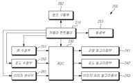
도 12를 참조하면, 센서 패키지 모듈(200)은 이미지센서부(261)와, 렌즈구동부(262)와, 이미지센서부(261)와 렌즈구동부(262)를 제어하는 카메라 컨트롤러(210)를 포함하는 카메라모듈 및 빛을 감지하는 수광부(251,252)와 빛을 방출하는 발광부(253)를 포함하는 근조도센서를 구비할 수 있다. 수광부(251,252)와 발광부(253)는 카메라 컨트롤러(210)에 의해 제어될 수 있다.Referring to FIG. 12, the
이미지센서부(261)는 이미지센서를 구동할 수 있다. 이미지센서부(261)는 이미지센서에 전원 및/또는 신호를 공급하여 이미지센서에서 아날로그이미지신호를 생성하도록 제어할 수 있다. 이미지센서부(261)는 이미지센서를 구동하기 위한 소자 및/또는 그 소자를 구동하는 프로그램일 수 있다. 또한, 이미지센서부(261)은 이미지 센서를 포함할 수 있다.The
렌즈구동부(262)는 렌즈를 구동한다. 렌즈구동부(262)는 피사체에 대한 거리정보를 전달받아 렌즈의 초점이 이미지센서에 맞게 제어할 수 있다. 또한, 외부광의 세기에 대응하여 조리개를 제어할 수 있다. 렌즈구동부(262)는 렌즈를 구동시키기 위한 소자 및/또는 그 소자를 구동하는 프로그램일 수 있다.The
카메라컨트롤러(210)는 이미지센서부(261)와 렌즈구동부(262)에 제어신호를 전달하여 이미지센서부(261)와 렌즈구동부(262)를 제어할 수 있다. 카메라컨트롤러(210)는 특정의 프로그램에 의해 동작하는 연산소자일 수 있다.The
수광부(251,252)는 수광센서를 구동할 수 있다. 수광부(251,252)는 적외선을 수광하는 IR 수광센서를 구동하는 IR 수광부(251)와 가시광선을 수광하는 조도센서를 구동하는 조도 수광부(252)를 포함할 수 있다. IR 수광부(251)와 조도 수광부(252)는 카메라컨트롤러(210)로부터 제어신호를 전달받아 동작한다. IR 수광부(251)와 조도 수광부(252)는 각각 아날로그센싱신호를 발생시킨다. 수광부(251,252)는 IR 수광센서와 조도센서를 구동하는 소자 및/또는 그 소자를 구동하기 위한 프로그램일 수 있다. 수광부(251,252)는 IR 수광센서와 조도센서를 포함할 수 있다.The
발광부(253)은 발광소자를 구동할 수 있다. 발광부(253)는 발광소자를 구동하는 소자 및/또는 그 소자를 구동하기 위한 프로그램일 있다. 발광부(253)은 카메라컨트롤러(210)에 의해 제어될 수 있다.The
센서 패키지 모듈(200)은 이미지센서에서 출력된 아날로그이미지신호를 디지털이미지신호로 변환하고 수광부로부터 전달받은 아날로그센싱신호를 디지털센싱신호로 변환하는 ADC(230)를 포함할 수 있다. 즉, 하나의 ADC(230)에서 아날로그 이미지신호와 아날로그 센싱신호를 디지털 이미지신호와 아날로그센싱신호로 변환할 수 있다. 카메라 컨트롤러(210)는 카메라모듈과 근조도센서를 시분할 구동하도록 제어할 수 있다. 이로 인해, 동시에 카메라모듈과 근조도센서가 구동되지 않아 하나의 ADC(230)에서 아날로그이미지신호를 디지털이미지신호로 변환하고 수광부(251,252)로부터 수신된 아날로그센싱신호를 디지털센싱신호로 변환할 수 있다. 카메라 컨트롤러(210)는 수광부에서 수광된 조도에 대한 정보와 거리정보를 이용하여 렌즈구동부(262)를 제어하여 렌즈의 초점과 조리개를 제어할 수 있다.The
센서 패키지 모듈(200)은 근접알고리즘부(241), 조도알고리즘부(242) 및 이미지처리 알고리즘부(243)을 포함할 수 있다. 근접알고리즘부(241)는 IR 수광부(252)에서 센싱처리한 정보를 이용하여 근접 여부와 위치검출을 할 수 있다. 조도알고리즘부(242)는 조도수광부(252)에서 센싱처리한 정보를 이용하여 외부광의 세기를 판단할 수 있다. 이미지처리알고리즘부(243)은 이미지센서부(261)에서 센싱된 정보를 이용하여 영상에 대한 정보를 생성할 수 있다.The
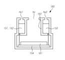
도 13은 도 11에 도시된 센서 패키지가 채용된 센서 패키지 모듈의 제1실시예를 나타내는 평면도이고, 도 14는 도 11에 도시된 센서가 채용된 센서 패키지 모듈의 제2실시예를 나타내는 평면도이고, 도 15는 도 11에 도시된 센서가 채용된 센서 패키지 모듈의 제3실시예를 나타내는 평면도이고, 도 16은 도 11에 도시된 센서가 채용된 센서 패키지 모듈의 제4실시예를 나타내는 평면도이다. 또한, 도 17은 도 11에 도시된 센서 패키지 모듈의 단면의 일 실시예를 나타내는 단면도이다.FIG. 13 is a plan view showing a first embodiment of a sensor package module employing the sensor package shown in FIG. 11, and FIG. 14 is a plan view showing a second embodiment of a sensor package module employing the sensor shown in FIG. 11. , FIG. 15 is a plan view showing a third embodiment of a sensor package module employing the sensor shown in FIG. 11, and FIG. 16 is a plan view showing a fourth embodiment of a sensor package module employing the sensor shown in FIG. 11. . Additionally, FIG. 17 is a cross-sectional view showing an example of the cross section of the sensor package module shown in FIG. 11.
센서 패키지 모듈(160)은 적외선 및/또는 가시광선을 수광하는 수광센서(151,152)와 적외선을 조사하는 발광소자(153)를 포함할 수 있다. 또한, 센서 패키지 모듈(160)은 렌즈(미도시)를 통과한 빛에 의해 영상을 생성하는 이미지센서(154)를 포함할 수 있다. 센서 패키지 모듈(160)은 수광센서(151,152), 발광소자(153) 및 이미지센서(154)를 포함하는 장치일 수 있고, 이러한 장치를 제어하는 소자 및 그 소자를 제어하는 프로그램을 포함할 수 있다.The
이미지센서(154)는 기판(154) 상에 배치될 수 있고 수광센서(151,152)와 발광소자(153) 역시 각각 배선을 통해 기판(154)에 연결될 수 있다. 하지만, 이에 한정되는 것은 아니다. 센서 패키지모듈(160)은 이미지센서(154)에 대응하는 위치에 렌즈홀더부(162)가 배치될 수 있다. 렌즈홀더부(162)는 복수의 렌즈를 지지하며 렌즈구동부에 의해 동작할 수 있다. 또한, 센서패키지 모둘(160)에서 수광센서(151,152)와 발광소자(153)은 도 13에 도시되어 있는 것과 같이 렌즈홀더부(162)의 상부와 하부에 배치될 수 있다. 따라서, 센서 패키지 모듈(160)은 수광센서(151,152)와 발광소자(153)에 대응하는 제1홀(hs1)과 제2홀(hs2)이 렌즈홀더부(162)에 대응되고 렌즈가 배치되는 제3홀(hc)의 상부와 하부에 배치될 수 있다. 이 경우, 렌즈홀더부(162)는소정의 높이를 가지고 있어 도 5에 도시된 격벽(155)의 역할을 수행할 수 있다. 제1홀(hs1)과 제3홀(hc)는 도 3에 도시된 베젤영역(NAA)에 배치되고 제2홀(hs2)는 도 3에 도시된 액티브영역(AA)에 배치될 수 있다.The
또한, 수광센서(151,152)와 발광소자(153)은 도 14에 도시되어 있는 것과 같이 센서 패키지모듈(160)의 오른쪽에 배치될 수 있다. 이 경우, 제1홀(hs1)과 제3홀(hc)는 도 3에 도시된 베젤영역(NAA)에 배치되고 제2홀(hs2)는 도 3에 도시된 액티브영역(AA)에 배치될 수 있다.Additionally, the
또한, 수광센서(151,152)와 발광소자(153)은 도 15에 도시되어 있는 것과 같이 센서 패키지모듈(160)의 왼쪽 하부에서 "L"자 형태로 배치될 수 있다. 이 경우, 제1홀(hs1)과 제3홀(hc)는 도 3에 도시된 베젤영역(NAA)에 배치되고 제2홀(hs2)는 도 3에 도시된 액티브영역(AA)에 배치될 수 있다. 하지만, 이에 한정되는 것은 아니며, 베젤영역(NAA)의 형상에 대응하여 제1홀(hs1)과 제2홀(hs2)은 액티브영역(AA)에 배치될 수 있다.Additionally, the
또한, 수광센서(151,152)와 발광소자(153)은 도 16에 도시되어 있는 것과 같이 센서 패키지모듈(160)의 하부에서 "I"자 형태로 배치될 수 있다. 이 경우, 제3홀(hc)는 도 3에 도시된 베젤영역(NAA)에 배치되고 제1홀(hs1)과 제2홀(hs2)는 도 3에 도시된 액티브영역(AA)에 배치될 수 있다.Additionally, the
하지만, 수광센서(151,152)와 발광소자(153)의 배치가 도 14 내지 도 한정되는 것은 아니다. 또한, 도 3에 도시된 베젤영역(NAA)에 배치되어 있는 제1홀(h1)에 대응하는 위치에 제1홀(hs1)과 제3홀(hc) 또는 제3홀(hc)이 배치될 수 있다.However, the arrangement of the
이상에서의 설명 및 첨부된 도면은 본 발명의 기술 사상을 예시적으로 나타낸 것에 불과한 것으로서, 본 발명이 속하는 기술 분야에서 통상의 지식을 가진 자라면 본 발명의 본질적인 특성에서 벗어나지 않는 범위에서 구성의 결합, 분리, 치환 및 변경 등의 다양한 수정 및 변형이 가능할 것이다. 따라서, 본 발명에 개시된 실시예들은 본 발명의 기술 사상을 한정하기 위한 것이 아니라 설명하기 위한 것이고, 이러한 실시예에 의하여 본 발명의 기술 사상의 범위가 한정되는 것은 아니다. 본 발명의 보호 범위는 아래의 청구범위에 의하여 해석되어야 하며, 그와 동등한 범위 내에 있는 모든 기술 사상은 본 발명의 권리범위에 포함되는 것으로 해석되어야 할 것이다.The above description and attached drawings are merely illustrative of the technical idea of the present invention, and those skilled in the art will be able to combine the components without departing from the essential characteristics of the present invention. , various modifications and transformations such as separation, substitution, and change will be possible. Accordingly, the embodiments disclosed in the present invention are not intended to limit the technical idea of the present invention, but are for illustrative purposes, and the scope of the technical idea of the present invention is not limited by these embodiments. The scope of protection of the present invention should be interpreted in accordance with the claims below, and all technical ideas within the equivalent scope should be construed as being included in the scope of rights of the present invention.
100: 유기발광표시장치
110: 표시패널
120: 게이트드라이버
130: 데이터드라이버
140: 타이밍컨트롤러
P: 서브픽셀100: Organic light emitting display device
110: display panel
120: gate driver
130: data driver
140: Timing controller
P: Subpixel
Claims (20)
Translated fromKorean상기 서브픽셀에 데이터신호를 공급하는 데이터드라이버;
상기 서브픽셀에 게이트신호를 공급하는 게이트드라이버;
상기 데이터드라이버와 상기 게이트드라이버를 제어하는 타이밍컨트롤러; 및
일부가 상기 액티브영역과 중첩되게 배치되는 센서 패키지 모듈을 포함하며,
상기 액티브영역에서 상기 센서 패키지 모듈과 중첩되지 않는 제1영역에서 캐소드 전극의 두께 보다 상기 센서 패키지 모듈과 중첩되는 제2영역에서 캐소드 전극의 두께가 더 얇은 유기 발광 표시장치.
A display panel including an active area where a plurality of subpixels including organic light emitting diodes are arranged and a bezel area where wiring for transmitting signals and voltages supplied to the subpixels is arranged;
a data driver that supplies data signals to the subpixels;
a gate driver that supplies a gate signal to the subpixel;
a timing controller that controls the data driver and the gate driver; and
It includes a sensor package module, a portion of which is arranged to overlap the active area,
An organic light emitting display device in which the thickness of the cathode electrode in the second area overlapping the sensor package module is thinner than the thickness of the cathode electrode in the first area not overlapping the sensor package module in the active area.
상기 표시패널은 상기 액티브영역에서 캐소드전극에 대응하여 투과율이 가시광 파장대에서 10% 이상이고, 적외선 파장대에서 30% 이상인 유기 발광 표시장치.
According to paragraph 1,
The display panel is an organic light emitting display device having a transmittance of 10% or more in the visible light wavelength band and 30% or more in the infrared wavelength band corresponding to the cathode electrode in the active area.
상기 센서 패키지 모듈은 두개의 홀을 포함하고, 상기 제2영역은 상기 두개의 홀에 대응하는 위치에 배치되는 유기발광표시장치.
According to paragraph 1,
The sensor package module includes two holes, and the second area is disposed at a position corresponding to the two holes.
상기 서브픽셀은 캐소드 전극과 애노드 전극 사이에 빛을 발광하는 발광층이 배치되는 유기 발광 표시장치.
According to paragraph 1,
The subpixel is an organic light emitting display device in which a light emitting layer that emits light is disposed between a cathode electrode and an anode electrode.
상기 센서 패키지 모듈은 상기 표시패널의 배면에 배치되는 유기 발광 표시장치
According to paragraph 1,
The sensor package module is an organic light emitting display device disposed on the back of the display panel.
상기 센서 패키지 모듈은
이미지센서를 구동하는 이미지센서부와, 상기 이미지센서에 빛을 투사하는 렌즈를 구동하는 렌즈구동부 및 상기 이미지센서부와 상기 렌즈구동부를 제어하는 카메라컨트롤러를 포함하는 카메라모듈; 및
빛을 감지하는 수광센서를 구동하는 수광부와, 빛을 방출하는 발광소자를 구동하는 발광부를 포함하되, 상기 수광부와 상기 발광부는 상기 카메라 컨트롤러에 의해 제어되는 근조도센서;를 포함하는 유기 발광 표시장치.
According to paragraph 1,
The sensor package module is
A camera module including an image sensor unit that drives an image sensor, a lens driver unit that drives a lens that projects light to the image sensor, and a camera controller that controls the image sensor unit and the lens driver unit; and
An organic light-emitting display device comprising a light-receiving unit that drives a light-receiving sensor that detects light, and a light-emitting unit that drives a light-emitting element that emits light, wherein the light-receiving unit and the light-emitting unit are controlled by the camera controller. .
상기 센서 패키지 모듈은 상기 이미지센서, 상기 수광센서 및 상기 발광소자를 수납하고 상기 렌즈를 지지하는 렌즈홀더부를 포함하는 하우징을 포함하되, 상기 하우징은 상기 렌즈홀더부가 상기 수광센서와 상기 발광소자 사이에 배치되는 유기 발광 표시장치.
In clause 7,
The sensor package module includes a housing including a lens holder portion that accommodates the image sensor, the light-receiving sensor, and the light-emitting device and supports the lens, wherein the lens holder portion is positioned between the light-receiving sensor and the light-emitting device. Organic light emitting display device deployed.
상기 렌즈홀더부에 대응하는 홀은 상기 베젤영역에 중첩되게 배치되고 상기 수광센서 및 상기 발광소자 중 적어도 하나는 상기 액티브영역에 중첩되게 배치되는 유기 발광 표시장치.
According to clause 8,
An organic light emitting display device wherein a hole corresponding to the lens holder portion is disposed to overlap the bezel area, and at least one of the light receiving sensor and the light emitting element is disposed to overlap the active area.
상기 이미지센서부에서 출력된 아날로그이미지신호를 디지털이미지신호로 변환하고 상기 수광부에서 처리된 아날로그센싱신호를 디지털센싱신호로 변환하는 ADC를 포함하는 유기 발광 표시장치.
In clause 7,
An organic light emitting display device comprising an ADC that converts the analog image signal output from the image sensor unit into a digital image signal and converts the analog sensing signal processed by the light receiving unit into a digital sensing signal.
상기 카메라 컨트롤러는 상기 카메라모듈과 상기 근조도센서를 시분할 구동하도록 제어하는 유기 발광 표시장치.
According to clause 10,
The camera controller is an organic light emitting display device that controls the camera module and the muscle condition sensor to be driven in time division.
상기 센서 패키지 모듈은 빛을 방출하는 발광소자, 빛을 수신하는 수광센서 및 상기 발광소자와 상기 수광센서를 수납하되 상기 발광소자에서 발광하는 빛이 방출되는 제1홀과 상기 수광센서에 빛이 입사되게 하는 제2홀을 포함하는 하우징를 포함하며, 상기 제2영역은 상기 제1홀과 상기 제2홀에 대응하는 위치에 배치되는 유기 발광 표시장치.
According to paragraph 1,
The sensor package module stores a light-emitting device that emits light, a light-receiving sensor that receives light, and the light-emitting device and the light-receiving sensor. Light is incident on a first hole through which light emitted from the light-emitting device is emitted and the light-receiving sensor. An organic light emitting display device comprising: a housing including a second hole, wherein the second area is disposed at a position corresponding to the first hole and the second hole.
상기 서브픽셀에 데이터신호를 공급하는 데이터드라이버;
상기 서브픽셀에 게이트신호를 공급하는 게이트드라이버;
상기 데이터드라이버와 상기 게이트드라이버를 제어하는 타이밍컨트롤러; 및
일부가 상기 액티브영역과 중첩되게 배치되는 센서 패키지 모듈을 포함하며,
상기 표시패널의 배면에 상기 표시패널의 하부에 배치된 지지부재가 배치되되, 상기 표시패널과 상기 지지부재 사이에 폼패드가 배치되고 상기 폼패드일부가 제거되어 상기 표시패널의 배면에 센서 패키지 모듈이 배치되는 유기 발광 표시장치.
A display panel including an active area where a plurality of subpixels including organic light emitting diodes are arranged and a bezel area where wiring for transmitting signals and voltages supplied to the subpixels is arranged;
a data driver that supplies data signals to the subpixels;
a gate driver that supplies a gate signal to the subpixel;
a timing controller that controls the data driver and the gate driver; and
It includes a sensor package module, a portion of which is arranged to overlap the active area,
A support member disposed below the display panel is disposed on the back of the display panel, a foam pad is disposed between the display panel and the support member, and a portion of the foam pad is removed to form a sensor package module on the back of the display panel. This is an organic light emitting display device.
상기 타이밍컨트롤러는 상기 표시패널의 상기 제2영역의 위치에 대한 정보를 저장하는 메모리, 상기 제2영역의 위치에 대한 정보에 대응하여 보상된 보상 영상신호에 대한 정보를 산출하는 연산부를 포함하는 유기 발광 표시장치.
According to paragraph 1,
The timing controller includes a memory that stores information about the position of the second area of the display panel, and an operation unit that calculates information about a compensated image signal in response to the information about the position of the second area. Luminous display device.
Priority Applications (3)
| Application Number | Priority Date | Filing Date | Title |
|---|---|---|---|
| KR1020180115745AKR102604362B1 (en) | 2018-09-28 | 2018-09-28 | Sensor package module and organic light emitting display having the same |
| US16/532,586US10818233B2 (en) | 2018-09-28 | 2019-08-06 | Sensor package module and organic light-emitting display having same |
| KR1020230158349AKR102857722B1 (en) | 2018-09-28 | 2023-11-15 | Sensor package module |
Applications Claiming Priority (1)
| Application Number | Priority Date | Filing Date | Title |
|---|---|---|---|
| KR1020180115745AKR102604362B1 (en) | 2018-09-28 | 2018-09-28 | Sensor package module and organic light emitting display having the same |
Related Child Applications (1)
| Application Number | Title | Priority Date | Filing Date |
|---|---|---|---|
| KR1020230158349ADivisionKR102857722B1 (en) | 2018-09-28 | 2023-11-15 | Sensor package module |
Publications (2)
| Publication Number | Publication Date |
|---|---|
| KR20200036287A KR20200036287A (en) | 2020-04-07 |
| KR102604362B1true KR102604362B1 (en) | 2023-11-21 |
Family
ID=69945060
Family Applications (2)
| Application Number | Title | Priority Date | Filing Date |
|---|---|---|---|
| KR1020180115745AActiveKR102604362B1 (en) | 2018-09-28 | 2018-09-28 | Sensor package module and organic light emitting display having the same |
| KR1020230158349AActiveKR102857722B1 (en) | 2018-09-28 | 2023-11-15 | Sensor package module |
Family Applications After (1)
| Application Number | Title | Priority Date | Filing Date |
|---|---|---|---|
| KR1020230158349AActiveKR102857722B1 (en) | 2018-09-28 | 2023-11-15 | Sensor package module |
Country Status (2)
| Country | Link |
|---|---|
| US (1) | US10818233B2 (en) |
| KR (2) | KR102604362B1 (en) |
Families Citing this family (6)
| Publication number | Priority date | Publication date | Assignee | Title |
|---|---|---|---|---|
| US10985148B2 (en)* | 2018-12-27 | 2021-04-20 | Innolux Corporation | Electronic device |
| USD962947S1 (en)* | 2019-08-01 | 2022-09-06 | Lg Display Co., Ltd. | Display module |
| CN111584725A (en)* | 2020-05-15 | 2020-08-25 | 武汉华星光电半导体显示技术有限公司 | OLED panel and manufacturing method thereof |
| KR102699740B1 (en)* | 2020-10-15 | 2024-08-27 | 엘지디스플레이 주식회사 | Display device and manufacturing method for the same |
| US11893959B2 (en) | 2021-05-17 | 2024-02-06 | Samsung Electronics Co., Ltd. | Electronic device including proximity sensor having a plurality of light receiving elements and method of controlling the same |
| USD1019427S1 (en)* | 2021-12-10 | 2024-03-26 | Somfy Activites Sa | Temperature and luminosity sensor |
Citations (2)
| Publication number | Priority date | Publication date | Assignee | Title |
|---|---|---|---|---|
| US20170193643A1 (en)* | 2014-09-30 | 2017-07-06 | Fujifilm Corporation | Image processing apparatus, image processing method, program, and recording medium |
| US20180260079A1 (en)* | 2017-03-07 | 2018-09-13 | Guangdong Oppo Mobile Telecommunications Corp., Ltd. | Display Screen, Mobile Terminal Having Display Screen, Method and Device for Controlling Display Screen |
Family Cites Families (11)
| Publication number | Priority date | Publication date | Assignee | Title |
|---|---|---|---|---|
| JP4647004B2 (en)* | 2008-11-25 | 2011-03-09 | シャープ株式会社 | Photodetection semiconductor device and mobile device |
| US8008613B2 (en)* | 2009-05-05 | 2011-08-30 | Apple Inc. | Light sensing device having a color sensor and a clear sensor for infrared rejection |
| US8143608B2 (en)* | 2009-09-10 | 2012-03-27 | Avago Technologies Ecbu Ip (Singapore) Pte. Ltd. | Package-on-package (POP) optical proximity sensor |
| GB2485996A (en)* | 2010-11-30 | 2012-06-06 | St Microelectronics Res & Dev | A combined proximity and ambient light sensor |
| US8965449B2 (en)* | 2011-04-07 | 2015-02-24 | Apple Inc. | Devices and methods for providing access to internal component |
| US9330606B2 (en)* | 2012-06-08 | 2016-05-03 | Apple Inc. | Electronic device with display brightness control |
| KR20150080198A (en)* | 2013-12-31 | 2015-07-09 | 엘지디스플레이 주식회사 | Organic light emitting diode display device and driving method the same |
| US20170084231A1 (en)* | 2015-09-23 | 2017-03-23 | Intel Corporation | Imaging system management for camera mounted behind transparent display |
| CN115793783A (en)* | 2015-09-28 | 2023-03-14 | 苹果公司 | Electronic device display with extended active area |
| US10331260B2 (en)* | 2015-10-30 | 2019-06-25 | Essential Products, Inc. | Variable transparency layers for electronic devices |
| KR20180050473A (en)* | 2016-11-04 | 2018-05-15 | 삼성디스플레이 주식회사 | Display device |
- 2018
- 2018-09-28KRKR1020180115745Apatent/KR102604362B1/enactiveActive
- 2019
- 2019-08-06USUS16/532,586patent/US10818233B2/enactiveActive
- 2023
- 2023-11-15KRKR1020230158349Apatent/KR102857722B1/enactiveActive
Patent Citations (2)
| Publication number | Priority date | Publication date | Assignee | Title |
|---|---|---|---|---|
| US20170193643A1 (en)* | 2014-09-30 | 2017-07-06 | Fujifilm Corporation | Image processing apparatus, image processing method, program, and recording medium |
| US20180260079A1 (en)* | 2017-03-07 | 2018-09-13 | Guangdong Oppo Mobile Telecommunications Corp., Ltd. | Display Screen, Mobile Terminal Having Display Screen, Method and Device for Controlling Display Screen |
Also Published As
| Publication number | Publication date |
|---|---|
| KR20200036287A (en) | 2020-04-07 |
| KR102857722B1 (en) | 2025-09-09 |
| US10818233B2 (en) | 2020-10-27 |
| KR20230160765A (en) | 2023-11-24 |
| US20200105194A1 (en) | 2020-04-02 |
Similar Documents
| Publication | Publication Date | Title |
|---|---|---|
| KR102604362B1 (en) | Sensor package module and organic light emitting display having the same | |
| US11462156B2 (en) | Display device and method of driving display device | |
| US9001010B2 (en) | Flexible display device and method of compensating for luminance of the flexible display device | |
| KR101590192B1 (en) | Display and electronic devices | |
| US10146996B2 (en) | Display device configured to compensate luminance based on reflected light | |
| KR102082779B1 (en) | Flexible display apparatus and method of operating the same | |
| JP2008176115A (en) | Display apparatus, control computation unit, and display driving method | |
| KR20180047242A (en) | Bendable display panel and bendable display apparatus using the same | |
| KR20150139026A (en) | Organic light emitting display device | |
| CN112420778B (en) | Display device | |
| TWI615828B (en) | Display device, optical compensation system, and optical compensation method thereof | |
| US20210193755A1 (en) | Organic light emitting display apparatus | |
| KR20230124865A (en) | Electroluminescence display | |
| US12374270B2 (en) | Display panel including subpixels each having first and second light-emitting elements, and display apparatus | |
| JP2020519918A (en) | Compensation method, compensation device, and display device for organic electroluminescence display | |
| KR20110122549A (en) | Display Device and Gamma Setting Method | |
| KR102388478B1 (en) | Display device and controlling method for the same | |
| US11610959B2 (en) | Sensor package module and organic light-emitting display device having same | |
| KR20220096221A (en) | Display panel and display device | |
| KR20220047063A (en) | Display device, control circuit and driving method for the same | |
| US9881548B2 (en) | Organic light emitting diode display with shielding portion | |
| US12367812B2 (en) | Transparent display device and method for driving the same | |
| KR102857725B1 (en) | Display device and driving methode for the same | |
| KR20250132045A (en) | Display apparatus | |
| KR20160064319A (en) | Mobile device |
Legal Events
| Date | Code | Title | Description |
|---|---|---|---|
| PA0109 | Patent application | Patent event code:PA01091R01D Comment text:Patent Application Patent event date:20180928 | |
| PG1501 | Laying open of application | ||
| A201 | Request for examination | ||
| PA0201 | Request for examination | Patent event code:PA02012R01D Patent event date:20210708 Comment text:Request for Examination of Application Patent event code:PA02011R01I Patent event date:20180928 Comment text:Patent Application | |
| E902 | Notification of reason for refusal | ||
| PE0902 | Notice of grounds for rejection | Comment text:Notification of reason for refusal Patent event date:20220731 Patent event code:PE09021S01D | |
| E90F | Notification of reason for final refusal | ||
| PE0902 | Notice of grounds for rejection | Comment text:Final Notice of Reason for Refusal Patent event date:20230223 Patent event code:PE09021S02D | |
| E701 | Decision to grant or registration of patent right | ||
| PE0701 | Decision of registration | Patent event code:PE07011S01D Comment text:Decision to Grant Registration Patent event date:20230829 | |
| A107 | Divisional application of patent | ||
| PA0107 | Divisional application | Comment text:Divisional Application of Patent Patent event date:20231115 Patent event code:PA01071R01D | |
| GRNT | Written decision to grant | ||
| PR0701 | Registration of establishment | Comment text:Registration of Establishment Patent event date:20231116 Patent event code:PR07011E01D | |
| PR1002 | Payment of registration fee | Payment date:20231117 End annual number:3 Start annual number:1 | |
| PG1601 | Publication of registration |