KR102601950B1 - Light emitting diode, manufacturing method of light emitting diode and display device including light emitting diode - Google Patents
Light emitting diode, manufacturing method of light emitting diode and display device including light emitting diodeDownload PDFInfo
- Publication number
- KR102601950B1 KR102601950B1KR1020180141291AKR20180141291AKR102601950B1KR 102601950 B1KR102601950 B1KR 102601950B1KR 1020180141291 AKR1020180141291 AKR 1020180141291AKR 20180141291 AKR20180141291 AKR 20180141291AKR 102601950 B1KR102601950 B1KR 102601950B1
- Authority
- KR
- South Korea
- Prior art keywords
- type semiconductor
- semiconductor layer
- layer
- light emitting
- led device
- Prior art date
- Legal status (The legal status is an assumption and is not a legal conclusion. Google has not performed a legal analysis and makes no representation as to the accuracy of the status listed.)
- Active
Links
Images


Classifications
- H—ELECTRICITY
- H10—SEMICONDUCTOR DEVICES; ELECTRIC SOLID-STATE DEVICES NOT OTHERWISE PROVIDED FOR
- H10H—INORGANIC LIGHT-EMITTING SEMICONDUCTOR DEVICES HAVING POTENTIAL BARRIERS
- H10H20/00—Individual inorganic light-emitting semiconductor devices having potential barriers, e.g. light-emitting diodes [LED]
- H10H20/80—Constructional details
- H10H20/81—Bodies
- H10H20/816—Bodies having carrier transport control structures, e.g. highly-doped semiconductor layers or current-blocking structures
- H10H20/8162—Current-blocking structures
- H01L33/145—
- H—ELECTRICITY
- H10—SEMICONDUCTOR DEVICES; ELECTRIC SOLID-STATE DEVICES NOT OTHERWISE PROVIDED FOR
- H10H—INORGANIC LIGHT-EMITTING SEMICONDUCTOR DEVICES HAVING POTENTIAL BARRIERS
- H10H20/00—Individual inorganic light-emitting semiconductor devices having potential barriers, e.g. light-emitting diodes [LED]
- H10H20/80—Constructional details
- H10H20/85—Packages
- H10H20/855—Optical field-shaping means, e.g. lenses
- H10H20/856—Reflecting means
- H—ELECTRICITY
- H01—ELECTRIC ELEMENTS
- H01L—SEMICONDUCTOR DEVICES NOT COVERED BY CLASS H10
- H01L25/00—Assemblies consisting of a plurality of semiconductor or other solid state devices
- H01L25/03—Assemblies consisting of a plurality of semiconductor or other solid state devices all the devices being of a type provided for in a single subclass of subclasses H10B, H10D, H10F, H10H, H10K or H10N, e.g. assemblies of rectifier diodes
- H01L25/04—Assemblies consisting of a plurality of semiconductor or other solid state devices all the devices being of a type provided for in a single subclass of subclasses H10B, H10D, H10F, H10H, H10K or H10N, e.g. assemblies of rectifier diodes the devices not having separate containers
- H01L25/075—Assemblies consisting of a plurality of semiconductor or other solid state devices all the devices being of a type provided for in a single subclass of subclasses H10B, H10D, H10F, H10H, H10K or H10N, e.g. assemblies of rectifier diodes the devices not having separate containers the devices being of a type provided for in group H10H20/00
- H01L25/0753—Assemblies consisting of a plurality of semiconductor or other solid state devices all the devices being of a type provided for in a single subclass of subclasses H10B, H10D, H10F, H10H, H10K or H10N, e.g. assemblies of rectifier diodes the devices not having separate containers the devices being of a type provided for in group H10H20/00 the devices being arranged next to each other
- H—ELECTRICITY
- H01—ELECTRIC ELEMENTS
- H01L—SEMICONDUCTOR DEVICES NOT COVERED BY CLASS H10
- H01L25/00—Assemblies consisting of a plurality of semiconductor or other solid state devices
- H01L25/16—Assemblies consisting of a plurality of semiconductor or other solid state devices the devices being of types provided for in two or more different subclasses of H10B, H10D, H10F, H10H, H10K or H10N, e.g. forming hybrid circuits
- H01L25/167—Assemblies consisting of a plurality of semiconductor or other solid state devices the devices being of types provided for in two or more different subclasses of H10B, H10D, H10F, H10H, H10K or H10N, e.g. forming hybrid circuits comprising optoelectronic devices, e.g. LED, photodiodes
- H01L27/156—
- H01L33/0008—
- H01L33/005—
- H01L33/10—
- H01L33/62—
- H—ELECTRICITY
- H10—SEMICONDUCTOR DEVICES; ELECTRIC SOLID-STATE DEVICES NOT OTHERWISE PROVIDED FOR
- H10H—INORGANIC LIGHT-EMITTING SEMICONDUCTOR DEVICES HAVING POTENTIAL BARRIERS
- H10H20/00—Individual inorganic light-emitting semiconductor devices having potential barriers, e.g. light-emitting diodes [LED]
- H10H20/01—Manufacture or treatment
- H—ELECTRICITY
- H10—SEMICONDUCTOR DEVICES; ELECTRIC SOLID-STATE DEVICES NOT OTHERWISE PROVIDED FOR
- H10H—INORGANIC LIGHT-EMITTING SEMICONDUCTOR DEVICES HAVING POTENTIAL BARRIERS
- H10H20/00—Individual inorganic light-emitting semiconductor devices having potential barriers, e.g. light-emitting diodes [LED]
- H10H20/80—Constructional details
- H10H20/81—Bodies
- H10H20/814—Bodies having reflecting means, e.g. semiconductor Bragg reflectors
- H—ELECTRICITY
- H10—SEMICONDUCTOR DEVICES; ELECTRIC SOLID-STATE DEVICES NOT OTHERWISE PROVIDED FOR
- H10H—INORGANIC LIGHT-EMITTING SEMICONDUCTOR DEVICES HAVING POTENTIAL BARRIERS
- H10H20/00—Individual inorganic light-emitting semiconductor devices having potential barriers, e.g. light-emitting diodes [LED]
- H10H20/80—Constructional details
- H10H20/81—Bodies
- H10H20/816—Bodies having carrier transport control structures, e.g. highly-doped semiconductor layers or current-blocking structures
- H—ELECTRICITY
- H10—SEMICONDUCTOR DEVICES; ELECTRIC SOLID-STATE DEVICES NOT OTHERWISE PROVIDED FOR
- H10H—INORGANIC LIGHT-EMITTING SEMICONDUCTOR DEVICES HAVING POTENTIAL BARRIERS
- H10H20/00—Individual inorganic light-emitting semiconductor devices having potential barriers, e.g. light-emitting diodes [LED]
- H10H20/80—Constructional details
- H10H20/81—Bodies
- H10H20/819—Bodies characterised by their shape, e.g. curved or truncated substrates
- H10H20/821—Bodies characterised by their shape, e.g. curved or truncated substrates of the light-emitting regions, e.g. non-planar junctions
- H—ELECTRICITY
- H10—SEMICONDUCTOR DEVICES; ELECTRIC SOLID-STATE DEVICES NOT OTHERWISE PROVIDED FOR
- H10H—INORGANIC LIGHT-EMITTING SEMICONDUCTOR DEVICES HAVING POTENTIAL BARRIERS
- H10H20/00—Individual inorganic light-emitting semiconductor devices having potential barriers, e.g. light-emitting diodes [LED]
- H10H20/80—Constructional details
- H10H20/81—Bodies
- H10H20/8215—Bodies characterised by crystalline imperfections, e.g. dislocations; characterised by the distribution of dopants, e.g. delta-doping
- H—ELECTRICITY
- H10—SEMICONDUCTOR DEVICES; ELECTRIC SOLID-STATE DEVICES NOT OTHERWISE PROVIDED FOR
- H10H—INORGANIC LIGHT-EMITTING SEMICONDUCTOR DEVICES HAVING POTENTIAL BARRIERS
- H10H20/00—Individual inorganic light-emitting semiconductor devices having potential barriers, e.g. light-emitting diodes [LED]
- H10H20/80—Constructional details
- H10H20/84—Coatings, e.g. passivation layers or antireflective coatings
- H10H20/841—Reflective coatings, e.g. dielectric Bragg reflectors
- H—ELECTRICITY
- H10—SEMICONDUCTOR DEVICES; ELECTRIC SOLID-STATE DEVICES NOT OTHERWISE PROVIDED FOR
- H10H—INORGANIC LIGHT-EMITTING SEMICONDUCTOR DEVICES HAVING POTENTIAL BARRIERS
- H10H20/00—Individual inorganic light-emitting semiconductor devices having potential barriers, e.g. light-emitting diodes [LED]
- H10H20/80—Constructional details
- H10H20/85—Packages
- H10H20/8506—Containers
- H—ELECTRICITY
- H10—SEMICONDUCTOR DEVICES; ELECTRIC SOLID-STATE DEVICES NOT OTHERWISE PROVIDED FOR
- H10H—INORGANIC LIGHT-EMITTING SEMICONDUCTOR DEVICES HAVING POTENTIAL BARRIERS
- H10H20/00—Individual inorganic light-emitting semiconductor devices having potential barriers, e.g. light-emitting diodes [LED]
- H10H20/80—Constructional details
- H10H20/85—Packages
- H10H20/857—Interconnections, e.g. lead-frames, bond wires or solder balls
- H—ELECTRICITY
- H10—SEMICONDUCTOR DEVICES; ELECTRIC SOLID-STATE DEVICES NOT OTHERWISE PROVIDED FOR
- H10H—INORGANIC LIGHT-EMITTING SEMICONDUCTOR DEVICES HAVING POTENTIAL BARRIERS
- H10H29/00—Integrated devices, or assemblies of multiple devices, comprising at least one light-emitting semiconductor element covered by group H10H20/00
- H10H29/10—Integrated devices comprising at least one light-emitting semiconductor component covered by group H10H20/00
- H10H29/14—Integrated devices comprising at least one light-emitting semiconductor component covered by group H10H20/00 comprising multiple light-emitting semiconductor components
- H10H29/142—Two-dimensional arrangements, e.g. asymmetric LED layout
- H—ELECTRICITY
- H10—SEMICONDUCTOR DEVICES; ELECTRIC SOLID-STATE DEVICES NOT OTHERWISE PROVIDED FOR
- H10H—INORGANIC LIGHT-EMITTING SEMICONDUCTOR DEVICES HAVING POTENTIAL BARRIERS
- H10H20/00—Individual inorganic light-emitting semiconductor devices having potential barriers, e.g. light-emitting diodes [LED]
- H10H20/01—Manufacture or treatment
- H10H20/032—Manufacture or treatment of electrodes
- H—ELECTRICITY
- H10—SEMICONDUCTOR DEVICES; ELECTRIC SOLID-STATE DEVICES NOT OTHERWISE PROVIDED FOR
- H10H—INORGANIC LIGHT-EMITTING SEMICONDUCTOR DEVICES HAVING POTENTIAL BARRIERS
- H10H20/00—Individual inorganic light-emitting semiconductor devices having potential barriers, e.g. light-emitting diodes [LED]
- H10H20/01—Manufacture or treatment
- H10H20/034—Manufacture or treatment of coatings
- H—ELECTRICITY
- H10—SEMICONDUCTOR DEVICES; ELECTRIC SOLID-STATE DEVICES NOT OTHERWISE PROVIDED FOR
- H10H—INORGANIC LIGHT-EMITTING SEMICONDUCTOR DEVICES HAVING POTENTIAL BARRIERS
- H10H20/00—Individual inorganic light-emitting semiconductor devices having potential barriers, e.g. light-emitting diodes [LED]
- H10H20/01—Manufacture or treatment
- H10H20/036—Manufacture or treatment of packages
- H10H20/0363—Manufacture or treatment of packages of optical field-shaping means
- H—ELECTRICITY
- H10—SEMICONDUCTOR DEVICES; ELECTRIC SOLID-STATE DEVICES NOT OTHERWISE PROVIDED FOR
- H10H—INORGANIC LIGHT-EMITTING SEMICONDUCTOR DEVICES HAVING POTENTIAL BARRIERS
- H10H20/00—Individual inorganic light-emitting semiconductor devices having potential barriers, e.g. light-emitting diodes [LED]
- H10H20/01—Manufacture or treatment
- H10H20/036—Manufacture or treatment of packages
- H10H20/0364—Manufacture or treatment of packages of interconnections
- H—ELECTRICITY
- H10—SEMICONDUCTOR DEVICES; ELECTRIC SOLID-STATE DEVICES NOT OTHERWISE PROVIDED FOR
- H10H—INORGANIC LIGHT-EMITTING SEMICONDUCTOR DEVICES HAVING POTENTIAL BARRIERS
- H10H20/00—Individual inorganic light-emitting semiconductor devices having potential barriers, e.g. light-emitting diodes [LED]
- H10H20/80—Constructional details
- H10H20/83—Electrodes
Landscapes
- Engineering & Computer Science (AREA)
- Microelectronics & Electronic Packaging (AREA)
- Power Engineering (AREA)
- Physics & Mathematics (AREA)
- Condensed Matter Physics & Semiconductors (AREA)
- General Physics & Mathematics (AREA)
- Computer Hardware Design (AREA)
- Led Devices (AREA)
- Led Device Packages (AREA)
Abstract
Translated fromKoreanDescription
Translated fromKorean본 개시는 LED 소자 및 그 제조 방법, 그리고 LED 소자를 포함하는 디스플레이 장치에 관한 것으로서, 구체적으로 전류 협착 구조를 가지는 플립칩 타입의 LED 소자 및 그 제조 방법, 그리고 위와 같은 LED 소자를 포함하는 디스플레이 장치에 관한 것이다.The present disclosure relates to an LED device, a method of manufacturing the same, and a display device including the LED device. Specifically, a flip-chip type LED device having a current narrowing structure and a method of manufacturing the same, and a display device including the above LED device. It's about.
LED(Light Emitting Diode, LED) 소자는 비교적 높은 발광 효율과 긴 수명으로 다양한 산업 분야에 적용되고 있다. 특히, LED 소자는 일반 조명뿐만 아니라 디스플레이 분야에서 실용화되고 있다.LED (Light Emitting Diode, LED) devices are applied to various industrial fields due to their relatively high luminous efficiency and long lifespan. In particular, LED devices are being put to practical use not only in general lighting but also in the display field.
그런데, 특히 디스플레이 장치의 고성능화 및 고효율화의 추세에 따라, LED 소자의 발광 효율 향상에 대한 요구는 계속되고 있다. 특히, 마이크로 LED 소자와 같은 초소형 LED 소자의 개발 분야에 있어서, 소자의 발광 효율 향상은 공정 상의 효율성 향상과 함께 중요한 해결 과제로 부각되고 있다.However, especially in accordance with the trend toward higher performance and higher efficiency of display devices, the demand for improved luminous efficiency of LED devices continues. In particular, in the field of development of ultra-small LED devices such as micro LED devices, improving the luminous efficiency of the device has emerged as an important problem to be solved along with improving the efficiency of the process.
이에 따라, LED 소자의 발광 효율을 향상시키기 위한 노력도 계속되어 왔다. 구체적으로, 내부 양자 효율(internal quantum efficiency: IQE)을 향상시키기 위한 방안으로서, 전류 협착 구조(current confinement structure)를 가지는 버티컬 타입의 LED 소자가 개발된 바 있다.Accordingly, efforts have been made to improve the luminous efficiency of LED devices. Specifically, as a way to improve internal quantum efficiency (IQE), a vertical type LED device with a current confinement structure has been developed.
그러나, 버티컬 타입의 LED 소자의 경우에는 LED 소자의 발광 표면 상에 전극이 배치되기 때문에, 그에 따라 광추출 효율(light extraction efficiency: LEE)이 감소하여 발광 효율을 저하시킨다는 한계를 갖는다. 따라서, 전류 협착 구조의 형성뿐만 아니라, 발광 효율의 향상에 기여할 수 있는 다양한 요인을 종합적으로 고려한 고효율의 LED 소자의 개발이 필요하다.However, in the case of vertical-type LED devices, since electrodes are disposed on the light-emitting surface of the LED device, light extraction efficiency (LEE) is reduced accordingly, which has a limitation in that light emission efficiency is lowered. Therefore, it is necessary to develop a high-efficiency LED device that comprehensively considers not only the formation of a current constriction structure but also various factors that can contribute to improving luminous efficiency.
뿐만 아니라, 버티컬 타입의 LED 소자의 경우에는 전극층의 형성 공정과 전기적 연결부를 형성하는 전사 공정의 효율성 측면에서도 한계가 있다. 반면, 플립칩 타입의 LED 소자의 경우에는 단일 소자의 소형화, 경량화 및 고집적화에 유리한 구조일 뿐만 아니라, 디스플레이 장치의 제작에 있어서 발광 효율과 전사 공정의 효율성 등을 향상시킬 수 있다는 장점을 가진다.In addition, in the case of vertical-type LED devices, there are limits in terms of the efficiency of the electrode layer formation process and the transfer process to form the electrical connection. On the other hand, flip-chip type LED devices not only have a structure that is advantageous for miniaturization, weight reduction, and high integration of a single device, but also have the advantage of improving luminous efficiency and transfer process efficiency in the production of display devices.
따라서, 상술한 바와 같은 플립칩 타입의 LED 소자가 갖는 장점을 가지면서도, 전류 협착 구조를 비롯한 발광 효율의 개선 구조를 갖춘 LED 소자에 대한 필요성이 대두되고 있다.Accordingly, there is a need for an LED device that has the advantages of the flip-chip type LED device described above and has a structure for improving luminous efficiency, including a current constriction structure.
본 개시는 상술한 바와 같은 필요성에 따라 안출된 것으로서, 본 개시의 목적은 전류 협착 구조를 포함하는 플립칩 타입의 고효율 LED 소자 및 그 제조 방법, 그리고 위와 같은 LED 소자를 포함하는 디스플레이 장치를 제공함에 있다.The present disclosure has been made in response to the above-described need, and the purpose of the present disclosure is to provide a flip-chip type high-efficiency LED device including a current narrowing structure, a method of manufacturing the same, and a display device including the above-mentioned LED device. there is.
상술한 바와 같은 목적을 달성하기 위한 본 개시의 일 실시 예에 따르면, 플립칩(Flip-Chip) 타입의 LED(Light Emitting Diode) 소자는 발광층, 상기 발광층의 상하부에 각각 적층된 n형 반도체층 및 p형 반도체층, 상기 n형 반도체층 및 상기 p형 반도체층과 각각 전기적으로 연결된 n 전극 및 p 전극, 상기 LED 소자의 측벽들(sidewalls) 및 상기 LED 소자의 발광 표면의 반대쪽 표면 상에 형성된 패시베이션층, 상기 발광층에서 방출되는 광을 상기 발광 표면 방향으로 반사시키도록 상기 패시베이션층 상에 형성된 반사층 및 상기 발광층을 통과하여 흐르는 전류가 상기 측벽들로 흐르는 것을 제한하도록 상기 발광층을 둘러싸는 영역에 형성된 저항 영역(resistive area)을 포함한다.According to an embodiment of the present disclosure for achieving the above-described object, a flip-chip type LED (Light Emitting Diode) device includes a light emitting layer, an n-type semiconductor layer each stacked on the top and bottom of the light emitting layer, and A p-type semiconductor layer, an n-electrode and a p-electrode electrically connected to the n-type semiconductor layer and the p-type semiconductor layer, respectively, and a passivation formed on the sidewalls of the LED device and a surface opposite to the light-emitting surface of the LED device. a layer, a reflective layer formed on the passivation layer to reflect light emitted from the light emitting layer toward the light emitting surface, and a resistor formed in an area surrounding the light emitting layer to limit current flowing through the light emitting layer from flowing to the sidewalls. Includes a resistive area.
여기서, 상기 저항 영역은 상기 p형 반도체층 전체, 상기 발광층 전체 및 상기 n형 반도체층의 일부를 포함하는 깊이로 형성될 수 있다.Here, the resistance region may be formed to a depth that includes the entire p-type semiconductor layer, the entire light-emitting layer, and a portion of the n-type semiconductor layer.
한편, 상기 저항 영역은 상기 발광층, 상기 n형 반도체층 및 상기 p형 반도체층에 대한 이온 주입(ion-implantation)에 의해 형성될 수 있다.Meanwhile, the resistance region may be formed by ion-implantation into the light emitting layer, the n-type semiconductor layer, and the p-type semiconductor layer.
한편, 상기 반사층은 금속 반사경 (metal reflector) 또는 분산 브래그 반사경(distributed-bragg-reflector) 구조로 형성될 수 있다.Meanwhile, the reflective layer may be formed as a metal reflector or distributed-bragg-reflector structure.
한편, LED 소자는 상기 p형 반도체층 및 상기 발광층을 통과하도록 형성되어 상기 n 전극이 상기 n형 반도체 층에 전기적으로 연결될 수 있도록 하는 컨택트 홀을 더 포함하고, 상기 저항 영역은 상기 컨택트 홀을 둘러싸는 영역에 형성되어 상기 발광층을 통과하여 흐르는 전류가 상기 컨택트 홀로 흐르는 것을 제한하는 영역을 더 포함할 수 있다.Meanwhile, the LED device further includes a contact hole formed to pass through the p-type semiconductor layer and the light emitting layer so that the n electrode can be electrically connected to the n-type semiconductor layer, and the resistance region surrounds the contact hole. may further include a region formed in the region to restrict current flowing through the light emitting layer from flowing into the contact hole.
한편, 상기 LED 소자는 10,000mm2 이하의 면적을 가지는 LED 소자일 수 있다.Meanwhile, the LED device may have an area of 10,000 mm2 or less.
상술한 바와 같은 목적을 달성하기 위한 본 개시의 일 실시 예에 따르면, 플립칩(Flip-Chip) 타입의 LED(Light Emitting Diode) 소자의 제조 방법은 기판 상에 n형 반도체층, 발광층 및 p형 반도체층을 순차적으로 증착하는 단계, 상기 발광층을 둘러싸는 영역에 저항 영역(resistive area)을 형성하는 단계, 상기 n형 반도체층, 발광층 및 p형 반도체층을 식각하는 단계, 상기 LED 소자의 측벽들(sidewalls) 및 상기 LED 소자의 발광 표면의 반대쪽 표면 상에 패시베이션층을 형성하는 단계, 상기 패시베이션층 상에 반사층을 형성하는 단계, 상기 n형 반도체층 및 상기 p형 반도체층과 각각 전기적으로 연결되도록 n 전극 및 p 전극을 형성하는 단계 및 상기 기판을 제거하는 단계를 포함한다.According to an embodiment of the present disclosure for achieving the above-described object, a method of manufacturing a flip-chip type LED (Light Emitting Diode) device includes an n-type semiconductor layer, a light emitting layer, and a p-type on a substrate. Sequentially depositing semiconductor layers, forming a resistive area in an area surrounding the light-emitting layer, etching the n-type semiconductor layer, the light-emitting layer, and the p-type semiconductor layer, sidewalls of the LED device. (sidewalls) and forming a passivation layer on a surface opposite to the light emitting surface of the LED device, forming a reflective layer on the passivation layer, and electrically connected to the n-type semiconductor layer and the p-type semiconductor layer, respectively. forming n-electrodes and p-electrodes and removing the substrate.
여기서, 상기 저항 영역은 상기 p형 반도체층 전체, 상기 발광층 전체 및 상기 n형 반도체층의 일부를 포함하는 깊이로 형성될 수 있다.Here, the resistance region may be formed to a depth that includes the entire p-type semiconductor layer, the entire light-emitting layer, and a portion of the n-type semiconductor layer.
한편, 상기 저항 영역은 상기 발광층, 상기 n형 반도체층 및 상기 p형 반도체층에 대한 이온 주입(ion-implantation)에 의해 형성될 수 있다.Meanwhile, the resistance region may be formed by ion-implantation into the light emitting layer, the n-type semiconductor layer, and the p-type semiconductor layer.
한편, 상기 반사층은 금속 반사경 (metal reflector) 또는 분산 브래그 반사경(distributed-bragg-reflector) 구조로 형성될 수 있다.Meanwhile, the reflective layer may be formed as a metal reflector or distributed-bragg-reflector structure.
한편, LED 소자의 제조 방법은 상기 n 전극이 상기 n형 반도체 층에 전기적으로 연결될 수 있도록, 상기 p형 반도체층 및 상기 발광층을 통과하는 컨택트 홀을 형성하는 단계를 더 포함하고, 상기 저항 영역은 상기 컨택트 홀을 둘러싸는 영역에 형성되어 상기 발광층을 통과하여 흐르는 전류가 상기 컨택트 홀로 흐르는 것을 제한하는 영역을 더 포함할 수 있다.Meanwhile, the method of manufacturing an LED device further includes forming a contact hole passing through the p-type semiconductor layer and the light emitting layer so that the n electrode can be electrically connected to the n-type semiconductor layer, and the resistance region is It may further include a region formed in a region surrounding the contact hole to restrict current flowing through the light emitting layer from flowing into the contact hole.
한편, 상기 LED 소자는 10,000mm2이하의 면적을 가질 수 있다.Meanwhile, the LED device may have an area of 10,000 mm2 or less.
한편, 상술한 바와 같은 목적을 달성하기 위한 본 개시의 일 실시 예에 따르면, 디스플레이 장치는 디스플레이 패널을 포함하며, 상기 디스플레이 패널은 플립칩(Flip-Chip) 타입인 복수의 LED(Light Emitting Diode) 소자 및 상기 복수의 LED 소자를 구동시키기 위한 복수의 픽셀 구동 회로를 포함한다.Meanwhile, according to an embodiment of the present disclosure for achieving the above-described object, a display device includes a display panel, and the display panel includes a plurality of flip-chip type LEDs (Light Emitting Diodes). and a plurality of pixel driving circuits for driving the plurality of LED elements.
그리고, 상기 복수의 LED 소자는 발광층, 상기 발광층의 상하부에 각각 적층된 n형 반도체층 및 p형 반도체층, 상기 n형 반도체층 및 상기 p형 반도체층과 각각 전기적으로 연결된 n 전극 및 p 전극, 상기 LED 소자의 측벽들(sidewalls) 및 상기 LED 소자의 발광 표면의 반대쪽 표면 상에 형성된 패시베이션층, 상기 발광층에서 방출되는 광을 상기 발광 표면 방향으로 반사시키도록 상기 패시베이션층 상에 형성된 반사층 및 상기 발광층을 통과하여 흐르는 전류가 상기 측벽들로 흐르는 것을 제한하도록 상기 발광층을 둘러싸는 영역에 형성된 저항 영역(resistive area)을 포함한다.In addition, the plurality of LED elements include a light emitting layer, an n-type semiconductor layer and a p-type semiconductor layer respectively stacked on the upper and lower portions of the light-emitting layer, an n electrode and a p electrode electrically connected to the n-type semiconductor layer and the p-type semiconductor layer, respectively, A passivation layer formed on the sidewalls of the LED device and a surface opposite the light-emitting surface of the LED device, a reflective layer formed on the passivation layer to reflect light emitted from the light-emitting layer toward the light-emitting surface, and the light-emitting layer and a resistive area formed in an area surrounding the light-emitting layer to limit current flowing through the sidewalls.
한편, 상기 복수의 픽셀 각각은 적색 LED 소자를 포함하는 R 서브 픽셀, 녹색 LED 소자를 포함하는 G 서브 픽셀 및 청색 LED 소자를 포함하는 B 서브 픽셀을 포함하며, 상기 복수의 픽셀 구동 회로는 상기 R 서브 픽셀, G 서브 픽셀, B 서브 픽셀 각각에 대하여 형성될 수 있다.Meanwhile, each of the plurality of pixels includes an R subpixel including a red LED device, a G subpixel including a green LED device, and a B subpixel including a blue LED device, and the plurality of pixel driving circuits include the R subpixel. It can be formed for each subpixel, G subpixel, and B subpixel.
도 1은 본 개시의 일 실시 예에 따른 LED 소자의 구조를 나타내기 위한 단면도,
도 2a 내지 도 2c는 본 개시의 일 실시 예에 따른 플립칩 타입의 LED 소자의 구조를 다른 타입의 LED 소자와 비교하여 설명하기 위한 단면도,
도 3은 본 개시의 일 실시 예에 따라, 컨택트 홀을 포함하는 LED 소자의 구조를 나타내기 위한 단면도,
도 4는 본 개시의 일 실시 예에 따른 LED 소자의 제조 방법을 순차적으로 나타내기 위한 흐름도,
도 5a 내지 도 5d는 본 개시의 일 실시 예에 따른 LED 소자의 제조 방법의 각 단계를 구체적으로 나타내기 위한 도면, 그리고,
도 6은 본 개시의 일 실시 예에 따른 디스플레이 장치에 포함되는 디스플레이 패널의 구조를 나타내기 위한 도면이다.1 is a cross-sectional view showing the structure of an LED device according to an embodiment of the present disclosure;
2A to 2C are cross-sectional views for explaining the structure of a flip-chip type LED device according to an embodiment of the present disclosure by comparing it with other types of LED devices;
3 is a cross-sectional view showing the structure of an LED device including a contact hole, according to an embodiment of the present disclosure;
4 is a flowchart sequentially showing a method of manufacturing an LED device according to an embodiment of the present disclosure;
5A to 5D are diagrams specifically showing each step of the method of manufacturing an LED device according to an embodiment of the present disclosure, and
FIG. 6 is a diagram illustrating the structure of a display panel included in a display device according to an embodiment of the present disclosure.
본 실시 예들은 다양한 변환을 가할 수 있고 여러 가지 실시 예를 가질 수 있는바, 특정 실시 예들을 도면에 예시하고 상세한 설명에 상세하게 설명하고자 한다. 그러나 이는 특정한 실시 형태에 대해 범위를 한정하려는 것이 아니며, 본 개시의 실시 예의 다양한 변경(modifications), 균등물(equivalents), 및/또는 대체물(alternatives)을 포함하는 것으로 이해되어야 한다. 도면의 설명과 관련하여, 유사한 구성요소에 대해서는 유사한 참조 부호가 사용될 수 있다.Since these embodiments can be modified in various ways and have various embodiments, specific embodiments will be illustrated in the drawings and described in detail in the detailed description. However, this is not intended to limit the scope to specific embodiments, and should be understood to include various modifications, equivalents, and/or alternatives to the embodiments of the present disclosure. In connection with the description of the drawings, similar reference numbers may be used for similar components.
본 개시를 설명함에 있어서, 관련된 공지 기능 혹은 구성에 대한 구체적인 설명이 본 개시의 요지를 불필요하게 흐릴 수 있다고 판단되는 경우 그에 대한 상세한 설명은 생략한다.In describing the present disclosure, if it is determined that a detailed description of a related known function or configuration may unnecessarily obscure the gist of the present disclosure, the detailed description thereof will be omitted.
덧붙여, 하기 실시 예는 여러 가지 다른 형태로 변형될 수 있으며, 본 개시의 기술적 사상의 범위가 하기 실시 예에 한정되는 것은 아니다. 오히려, 이들 실시 예는 본 개시를 더욱 충실하고 완전하게 하고, 당업자에게 본 개시의 기술적 사상을 완전하게 전달하기 위하여 제공되는 것이다.In addition, the following examples may be modified into various other forms, and the scope of the technical idea of the present disclosure is not limited to the following examples. Rather, these embodiments are provided to make the present disclosure more faithful and complete and to completely convey the technical idea of the present disclosure to those skilled in the art.
본 개시에서 사용한 용어는 단지 특정한 실시 예를 설명하기 위해 사용된 것으로, 권리범위를 한정하려는 의도가 아니다. 단수의 표현은 문맥상 명백하게 다르게 뜻하지 않는 한, 복수의 표현을 포함한다.The terms used in this disclosure are merely used to describe specific embodiments and are not intended to limit the scope of rights. Singular expressions include plural expressions unless the context clearly dictates otherwise.
본 개시에서, "가진다," "가질 수 있다," "포함한다," 또는 "포함할 수 있다" 등의 표현은 해당 특징(예: 수치, 기능, 동작, 또는 부품 등의 구성요소)의 존재를 가리키며, 추가적인 특징의 존재를 배제하지 않는다.In the present disclosure, expressions such as “have,” “may have,” “includes,” or “may include” refer to the presence of the corresponding feature (e.g., component such as numerical value, function, operation, or part). , and does not rule out the existence of additional features.
본 개시에서, "A 또는 B," "A 또는/및 B 중 적어도 하나," 또는 "A 또는/및 B 중 하나 또는 그 이상"등의 표현은 함께 나열된 항목들의 모든 가능한 조합을 포함할 수 있다. 예를 들면, "A 또는 B," "A 및 B 중 적어도 하나," 또는 "A 또는 B 중 적어도 하나"는, (1) 적어도 하나의 A를 포함, (2) 적어도 하나의 B를 포함, 또는 (3) 적어도 하나의 A 및 적어도 하나의 B 모두를 포함하는 경우를 모두 지칭할 수 있다.In the present disclosure, expressions such as “A or B,” “at least one of A or/and B,” or “one or more of A or/and B” may include all possible combinations of the items listed together. . For example, “A or B,” “at least one of A and B,” or “at least one of A or B” includes (1) at least one A, (2) at least one B, or (3) it may refer to all cases including both at least one A and at least one B.
본 개시에서 사용된 "제1," "제2," "첫째," 또는 "둘째,"등의 표현들은 다양한 구성요소들을, 순서 및/또는 중요도에 상관없이 수식할 수 있고, 한 구성요소를 다른 구성요소와 구분하기 위해 사용될 뿐 해당 구성요소들을 한정하지 않는다.Expressions such as “first,” “second,” “first,” or “second,” used in the present disclosure can modify various components regardless of order and/or importance, and can refer to one component. It is only used to distinguish from other components and does not limit the components.
어떤 구성요소(예: 제1 구성요소)가 다른 구성요소(예: 제2 구성요소)에 "(기능적으로 또는 통신적으로) 연결되어((operatively or communicatively) coupled with/to)" 있다거나 "접속되어(connected to)" 있다고 언급된 때에는, 상기 어떤 구성요소가 상기 다른 구성요소에 직접적으로 연결되거나, 다른 구성요소(예: 제3 구성요소)를 통하여 연결될 수 있다고 이해되어야 할 것이다.A component (e.g., a first component) is “(operatively or communicatively) coupled with/to” another component (e.g., a second component). When referred to as being “connected to,” it should be understood that any component may be directly connected to the other component or may be connected through another component (e.g., a third component).
반면에, 어떤 구성요소(예: 제1 구성요소)가 다른 구성요소(예: 제2 구성요소)에 "직접 연결되어" 있다거나 "직접 접속되어" 있다고 언급된 때에는, 상기 어떤 구성요소와 상기 다른 구성요소 사이에 다른 구성요소(예: 제 3 구성요소)가 존재하지 않는 것으로 이해될 수 있다.On the other hand, when a component (e.g., a first component) is said to be “directly connected” or “directly connected” to another component (e.g., a second component), It may be understood that no other component (e.g., a third component) exists between other components.
한편, 도면에서의 다양한 요소와 영역은 개략적으로 그려진 것이다. 따라서, 본 발명의 기술적 사상은 첨부한 도면에 그려진 상대적인 크기나 간격에 의해 제한되지 않는다.Meanwhile, various elements and areas in the drawing are schematically drawn. Accordingly, the technical idea of the present invention is not limited by the relative sizes or spacing drawn in the attached drawings.
이하에서는 첨부한 도면을 참고하여 본 개시에 따른 실시 예에 대하여 본 개시가 속하는 기술 분야에서 통상의 지식을 가진 자가 용이하게 실시할 수 있도록 상세히 설명한다.Hereinafter, with reference to the attached drawings, embodiments according to the present disclosure will be described in detail so that those skilled in the art can easily implement them.
본 개시에 따른 LED 소자를 구체적으로 설명하기에 앞서, LED 소자의 발광 효율에 영향을 미치는 요인에 대하여 설명한다. 원칙적으로, LED 소자의 발광 효율은 내부 양자 효율(internal quantum efficiency: IQE) 및 외부 양자 효율(external quantum efficiency: EQE)에 따라 달라진다.Before describing the LED device according to the present disclosure in detail, factors affecting the luminous efficiency of the LED device will be described. In principle, the luminous efficiency of an LED device depends on internal quantum efficiency (IQE) and external quantum efficiency (EQE).
내부 양자 효율은 LED 소자의 내부에서 광자를 생성할 수 있는 능력의 척도이며, LED 소자의 품질 및 구조의 함수이다. 한편, 외부 양자 효율은 방출된 광자의 수를 주입된 전자의 수로 나눈 것으로 정의된다. 외부 양자 효율은 LED 소자의 내부 양자 효율과 광추출 효율(light extraction efficiency: LEE)의 함수이다. 그리고, 광추출 효율은 LED 소자의 광학 설계에 의해 결정된다.Internal quantum efficiency is a measure of the ability to generate photons inside an LED device and is a function of the quality and structure of the LED device. Meanwhile, external quantum efficiency is defined as the number of emitted photons divided by the number of injected electrons. External quantum efficiency is a function of the internal quantum efficiency and light extraction efficiency (LEE) of the LED device. And, light extraction efficiency is determined by the optical design of the LED device.
이하에서는 LED 소자의 내부 양자 효율 및 외부 양자 효율을 향상시킴으로써 LED 소자의 발광 효율을 개선시킬 수 있도록 안출된 LED 소자의 구조 및 그 효과에 대하여 설명한다.Hereinafter, the structure and effects of the LED device designed to improve the luminous efficiency of the LED device by improving the internal and external quantum efficiency of the LED device will be described.
도 1은 본 개시의 일 실시 예에 따른 LED 소자의 구조를 나타내기 위한 단면도이다.1 is a cross-sectional view showing the structure of an LED device according to an embodiment of the present disclosure.
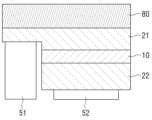
도 1에 도시된 바와 같이, 본 개시의 일 실시 예에 따른 LED 소자(111)는 발광층(활성층)(10), n형 반도체층(21), p형 반도체층(22), n 전극(51), p 전극(52), 패시베이션층(passivation layer)(30), 반사층(40) 및 저항 영역(60)을 포함한다.As shown in FIG. 1, the
발광층(10), n형 반도체층(21) 및 p형 반도체층(22)은 스펙트럼 내의 특정 영역에 대응하는 밴드 갭을 갖는 다양한 반도체로 구성될 수 있다. 예를 들어, 600-750nm의 광 파장을 갖는 적색 LED 소자(111)는 AlInGaP계 반도체를 기반으로 하는 하나 이상의 층을 포함할 수 있다. 그리고, 450-490nm 및 500-570nm의 광 파장을 각각 갖는 청색 및 녹색 LED 소자(111)는 AlInGaN계 반도체를 기반으로하는 하나 이상의 층을 포함 할 수 있다.The
n형 반도체층(21) 및 p형 반도체층(22)은 III-V족, II-VI족 등의 화합물 반도체로 구현될 수 있다. 특히, n형 반도체층(21) 및 p형 반도체층(22)은 질화물 반도체층, 특히 GaN 반도체층으로 구현될 수 있다. 그러나, 본 개시에 따른 n형 반도체층(21) 및 p형 반도체층(22)이 이에 한정되는 것은 아니며, LED 소자(111)에 요구되는 다양한 특성에 따라 다양한 재료로 이루어질 수 있다.The n-
n형 반도체란 전하를 옮기는 캐리어로 자유전자가 사용되는 반도체로서, Si, Ge, Sn, Te 등과 같은 n형 도펀트를 도핑하여 만들어질 수 있다. 그리고, p형 반도체란 전하를 옮기는 캐리어로 정공이 사용되는 반도체로서, Mg, Zn, Ca, Ba 등과 같은 p형 도펀트를 도핑하여 만들어 질 수 있다.An n-type semiconductor is a semiconductor in which free electrons are used as carriers to transfer charge, and can be made by doping n-type dopants such as Si, Ge, Sn, and Te. Additionally, a p-type semiconductor is a semiconductor in which holes are used as carriers to transfer charges, and can be made by doping p-type dopants such as Mg, Zn, Ca, Ba, etc.
발광층(10)은 n형 반도체층(21)과 p형 반도체층(22) 사이에 위치하며, n형 반도체층(21)의 캐리어인 전자와 p형 반도체층(22)의 캐리어인 정공이 만나는 층이다. 발광층(10)에서 전자와 정공이 만나면, 전자와 정공이 재결합함에 따라 전위 장벽이 형성된다. 그리고 인가되는 전압에 따라 전자와 정공이 전위 장벽을 넘어 낮은 에너지 준위로 천이하게 되면, 그에 상응하는 파장의 광을 방출한다.The
여기서, 발광층(10)은 다중 양자 우물 (Multi-Quantum Wells: MQW) 구조일 수 있으나, 본 개시가 이에 한정되는 것은 아니고 단일 양자 우물 (Single-Quantum Well: SQW) 또는 퀀텀닷(Quantum Dot: QD) 구조 등 다양한 구조일 수 있다.Here, the
발광층(10)이 다중 양자 우물 구조로 형성되는 경우, 발광층(10)의 우물층/장벽층은 InGaN/GaN, InGaN/InGaN, GaAs(InGaGs)/AlGaAs와 같은 구조로 형성될 수 있으나, 본 개시가 이와 같은 구조에 한정되는 것은 아니다. 발광층(10)에 포함되는 양자 우물의 개수 또한 특정한 개수에 한정되지 않는다. 이상에서는 발광층(10), n형 반도체층(21) 및 p형 반도체층(22)에 대해서만 설명하였지만, 본 개시에 따른 LED 소자(111)는 그 밖에도 다양한 반도체층을 포함할 수 있다. 예를 들어, 본 개시에 따른 LED 소자(111)는 전류 분포를 개선하여 칩 전체에서 균일한 발광이 가능하도록, 도펀트를 과도핑하여 만들어지는 p+형 반도체층 또는 n+형 반도체층을 더 포함할 수 있다.When the light-emitting
n 전극(51)은 n형 반도체층(21)에 전기적으로 연결되며, p 전극(52)은 p형 반도체층(22)에 전기적으로 연결된다. 구체적으로, n 전극(51) 및 p 전극(52)은 n형 반도체층(21) 및 p형 반도체층(22)과 오믹 접촉(ohmic contact)을 형성함으로써, n형 반도체층(21) 및 p형 반도체층(22)과 전기적으로 연결된다. 그리고, n 전극(51) 및 p 전극(52)은 Al, Ti, Ni, Pd, Ag, Au, Au-Ge, 그리고 인듐 주석 산화물(indium-tin-oxide: ITO) 및 ZnO와 같은 산화물을 포함할 수 있다.The
n 전극(51) 및 p 전극(52)을 통하여 전압이 인가되면, n형 반도체 내의 전자는 (+) 단자 쪽으로, p형 반도체 내의 정공은 (-) 단자 쪽으로 이동하게 되고, 이에 따라 형성된 소수 캐리어에 의하여 전류가 흐르게 된다.When voltage is applied through the
한편, 도 1에 도시되지는 않았으나, 발광층(10), n형 반도체층(21) 및 p형 반도체층(22) 중 적어도 하나를 통과하는 영역에 컨택트 홀(70)이 형성될 수 있으며, n 전극(51) 및 p 전극(52) 중 적어도 하나의 전극은 컨택트 홀(70)을 통하여 n형 반도체층(21) 또는 p형 반도체층(22)과 전기적으로 연결될 수 있다. 본 개시에 따른 LED 소자(111)가 전극과 반도체층의 연결을 위한 컨택트 홀(70)을 포함하는 경우에 관한 실시 예에 대해서는 도 3에 대한 설명에서 상술한다.Meanwhile, although not shown in FIG. 1, a contact hole 70 may be formed in an area passing through at least one of the
한편, n 전극(51) 및 p 전극(52)은 LED 소자(111)에서 광이 방출되는 발광 표면의 반대쪽 표면 상에 형성된다. 즉, 도 1에 도시된 바와 같이, 본 개시에 따른 LED 소자(111)는 n 전극(51) 및 p 전극(52)이 모두 발광 표면의 반대쪽 표면에 형성되는 플립칩(Flip-Chip) 구조를 가진다. 플립칩 타입의 LED 소자(111)에 대해서는 도 2a 내지 도 2c에 대한 설명에서 상술한다.Meanwhile, the
패시베이션층(30)은 LED 소자(111)의 측벽들(sidewalls) 및 LED 소자(111)의 발광 표면의 반대쪽 표면 상에 형성된다. 패시베이션 층은 Al2O3, SiN 및 SiO2와 같은 절연 물질로 이루어질 수 있다. 그리고, 패시베이션층(30)은 발광층(10), n형 반도체층(21) 및 p형 반도체층(22)이 반사층(40)과 전기적으로 구분될 수 있도록 하는 역할을 한다.The
한편, 도 1에 도시된 바와 같이, 패시베이션층(30)은 p 전극(52) 및 n 전극(51)이 p형 반도체층(22) 및 n형 반도체층(21)과 전기적으로 연결될 수 있도록 하는 개구 영역을 갖는다.Meanwhile, as shown in FIG. 1, the
반사층(40)은 상술한 바와 같은 패시베이션층(30) 상에 형성된다. 즉, 반사층(40) 또한 패시베이션층(30)과 마찬가지로, LED 소자(111)의 측벽들 및 LED 소자(111)의 발광 표면의 반대쪽 표면 상에 형성된다. 반사층(40)에는 알루미늄(Al)과 같이 반사도가 높은 다양한 금속재료가 사용될 수 있으며, 다만 본 개시에 따른 반사층(40)이 특정 재료에 한정되는 것은 아니다.The
한편, 반사층(40)은 금속 반사경 (metal reflector) 또는 분산 브래그 반사경(distributed-bragg-reflector: DBR) 구조로 형성될 수 있다.Meanwhile, the
구체적으로, 분산 브래그 반사경 구조는 굴절률이 서로 다른 두 개의 층이 번갈아 가면서 적층된 다층 구조로 구현될 수 있다. 그리고, 이에 따라 서로 다른 두 개 층의 굴절률 차이에 기인하여 각 층의 계면에서 프레넬(fresnel) 반사가 발생하며, 다층 구조에 포함된 물질 및 그 두께에 따라, 반사된 모든 파동이 보강 간섭(constructive interference)을 일으킨다. 이에 따라, 분산 브래그 반사경 구조로 형성된 반사층(40)은 높은 반사도를 가지게 된다.Specifically, the distributed Bragg reflector structure may be implemented as a multilayer structure in which two layers with different refractive indices are alternately stacked. Accordingly, Fresnel reflection occurs at the interface of each layer due to the difference in refractive index of the two different layers, and depending on the material included in the multilayer structure and its thickness, all reflected waves cause constructive interference ( causes constructive interference. Accordingly, the
한편, 본 개시의 일 실시 예에 따르면, LED 소자(111)의 측벽들 상에 형성된 반사층(40)은 발광 표면의 반대쪽 표면을 기준으로 1도 내지 85도의 각도로 형성될 수 있다.Meanwhile, according to an embodiment of the present disclosure, the
상술한 바와 같은 반사층(40)은 발광층(10)에서 방출되는 광을 발광 표면 방향으로 반사시키는 역할을 한다. 구체적으로, 반사층(40)은 발광층(10)에서 방출되는 광이 LED 소자(111)의 측벽들 및 LED 소자(111)의 발광 표면의 반대쪽 표면으로 향하는 경우, 이를 발광 표면 방향으로 반사시킬 수 있으며, 그 결과 LED 소자(111)의 광추출 효율이 향상될 수 있다.The
저항 영역(resistive area)(60) 은 발광층(10)을 둘러싸는 영역에 형성된다. 한편, 저항 영역(60)은 발광층(10)을 둘러싸는 영역뿐만 아니라, p형 반도체층(22) 및 n형 반도체층(21)의 측면을 둘러싸는 영역에도 형성될 수 있다. 구체적으로, 저항 영역(60)은 p형 반도체층(22) 전체, 발광층(10) 전체 및 n형 반도체층(21)의 일부를 포함하는 깊이로 형성될 수 있다. 이는 저항 영역(60)이 후술하는 바와 같은 이온 주입 공정에 의하여 형성되는 경우, 이온 주입이 p형 반도체층(22)의 상부에서 시작하여 n형 반도체층(21)의 상부에 이르기까지 이루어짐에 따른 것이다.A
한편, 저항 영역(60)의 총 너비는 LED 소자(111) 전체 너비의 30%에 해당하도록 형성될 수 있다. 그러나, 이는 일 실시 예에 불과한 것일 뿐이며, 저항 영역(60)의 너비는 저항 영역(60)의 형성에 따른 효과와 함께, 발광층(10)의 너비 감소에 따른 효과를 아울러 고려하여 결정되어야 한다.Meanwhile, the total width of the
저항 영역(60)은 발광층(10)을 통과하여 흐르는 전류의 경로보다 높은 저항성을 가진다. 구체적으로, 저항 영역(60)은 발광층(10)에 포함된 재료보다 높은 저항률을 가지는 재료를 포함할 수 있다. 뿐만 아니라, 저항 영역(60)은 n형 반도체층(21) 및 p형 반도체층(22)에 포함된 재료보다 높은 저항률을 가지는 재료를 포함할 수 있다.The
위와 같은 저항 영역(60)의 재료 특성은 이온 주입(ion-implantation)에 의해 구현될 수 있다. 구체적으로, 저항 영역(60)은 발광층(10), n형 반도체층(21) 및 p형 반도체층(22)에 대한 이온 주입에 의해 형성될 수 있다.The material properties of the
이온 주입 공정은 전하를 띤 이온에 전기장을 가하여 목표물로 가속시켜 주입시키는 공정으로서, 정확한 양의 불순물을 원하는 곳에 도핑하는데 사용된다. 구체적으로, 이온 주입 공정은 이온 소스를 이온화하고, 원하는 이온을 추출한 후, 선택된 이온에 전기장을 가하여 이를 가속화하여 반도체에 충돌시킴으로써, 이온을 반도체에 주입시키는 과정을 통하여 이루어진다.The ion implantation process is a process in which charged ions are accelerated and injected into a target by applying an electric field, and is used to dope a precise amount of impurities into a desired location. Specifically, the ion implantation process is performed by ionizing an ion source, extracting desired ions, and applying an electric field to the selected ions to accelerate them and collide with the semiconductor, thereby injecting the ions into the semiconductor.
이온 주입 공정에 따른 이온 주입의 깊이는 가속 에너지를 조절함으로써 제어할 수 있으며, 불순물의 양은 이온이 주입되는 동안의 이온 전류를 조절함으로써 제어할 수 있다.The depth of ion implantation according to the ion implantation process can be controlled by adjusting the acceleration energy, and the amount of impurities can be controlled by adjusting the ion current during ion implantation.
한편, 본 개시의 일 실시 예에 따를 때, LED 소자(111)가 적색 LED 소자(111)이면, 저항 영역(60)은 H, Al 및 O를 이온 소스로 주입하여 형성될 수 있다. 그리고, LED 소자(111)가 녹색 LED 소자(111)이면, 저항 영역(60)은 N를 이온 소스로 주입하여 형성되고, LED 소자(111)가 청색 LED 소자(111)이면, 저항 영역(60)은 Al, Fe, C를 이온 소스로 주입하여 형성될 수 있다. 그러나, 이는 일 실시 예에 불과할 뿐이며, 본 개시의 목적을 달성할 수 있는 범위 내에서라면, 저항 영역(60)에 주입되는 이온 소스의 종류는 제한되지 않는다.Meanwhile, according to an embodiment of the present disclosure, if the
한편, 본 개시에 따른 저항 영역(60)의 형성이 반드시 이온 주입에 의해서만 이루어질 수 있는 것은 아니며, 저항 영역(60)은 본 개시의 목적을 달성할 수 있는 범위 내의 다양한 방식에 의하여 발광층(10)보다 높은 저항률을 가지는 재료를 포함하도록 구현될 수 있다.Meanwhile, the formation of the
상술한 바와 같은 저항 영역(60)은 발광층(10)을 통과하여 흐르는 전류가 측벽들로 흐르는 것을 제한하는 역할을 한다. 이하에서는 저항 영역(60)의 형성에 따른 효과에 대하여 구체적으로 설명한다.The
LED의 일반적인 제조 공정에 있어서, 발광층(10), n형 반도체층(21) 및 p형 반도체층(22)은 건식 식각(dry etching) 기술에 의하여 식각되는바, 이 때 식각된 측벽(sidewalls) 영역에서 고밀도의 결함을 유발하는 것으로 알려져 있다.In the general manufacturing process of LED, the
이러한 결함이 있는 측벽 영역의 주위에서는 주입된 캐리어의 비방사 재결합(non-radiative recombination)이 일어나게 된다. 비방사 재결합이란 반도체에서 정공과 전자가 재결합할 때 방사를 수반하지 않고, 전자가 가지고 있던 에너지가 열로 방출되는 현상을 말한다. 다시 말해, 비방사 재결합이 일어나면 정공과 전자의 재결합에 의하여 photon 형태의 에너지가 방출되지 않고, phonon 형태의 에너지가 방출된다.Non-radiative recombination of the injected carriers occurs around these defective sidewall regions. Non-radiative recombination refers to a phenomenon in which, when holes and electrons recombine in a semiconductor, the energy contained in the electrons is released as heat without radiation. In other words, when non-radiative recombination occurs, energy in the form of photon is not released due to recombination of holes and electrons, but energy in the form of phonon is released.
따라서, 비방사 재결합이 많이 일어날수록 내부 양자 효율은 감소하게 된다. 특히, 비방사 재결합은 LED 소자(111)의 발광 효율에 현저한 영향을 미치기 때문에, LED 소자(111)의 발광 효율을 향상시키는데 있어서 해결해야 할 중요한 문제 중 하나이다.Therefore, as more non-radiative recombination occurs, the internal quantum efficiency decreases. In particular, since non-radiative recombination significantly affects the luminous efficiency of the
상술한 바와 같이, 본 개시에 따른 LED 소자(111)는 발광층(10)을 둘러싸는 영역에 저항 영역(60)을 포함하며, 이에 따라 발광층(10)을 통과하여 흐르는 전류가 결함 있는 측벽들로 흐르는 것이 제한된다. 그리고, 저항 영역(60)의 형성에 의하여, 본 개시에 따른 LED 소자(111)는 이른바 전류 협착 구조(current confinement structure)를 가지게 된다.As described above, the
즉, 본 개시에 따른 저항 영역(60)은 결함 있는 측벽과 전류의 경로를 멀리 떨어지게 하여 측벽에서의 비방사 재결합을 효과적으로 억제한다. 이에 따라, LED 소자(111) 내부의 내부 양자 효율을 향상시키게 되며, 결과적으로 LED 소자(111)의 발광 효율과 광 출력의 안정성을 현저하게 향상시키게 된다.That is, the
한편, 도 1에 도시된 바와 같이, 본 개시에 따른 LED 소자(111)는 기판(80)을 포함하지 않는다. 즉, 본 개시에 따르면, 발광층(10), n형 반도체층(21) 및 p형 반도체층(22)의 에피택시(epitaxy) 성장을 위한 기판(80)으로서 사용되는 웨이퍼는 제거된다. 본 개시에 따른 기판(80)의 제거 및 그에 따른 효과에 대해서는 도 4 및 도 5a 내지 도 5d에 대한 설명에서 상술한다.Meanwhile, as shown in FIG. 1, the
한편, 본 개시에 따른 LED 소자(111)의 크기에 특별한 제한은 없으나, 본 개시의 일 실시 예에 따르면, LED 소자(111)는 이른바 마이크로 LED 소자(111)일 수 있다. 마이크로 LED 소자(111)는 10,000mm2이하의 면적을 가지는 LED 소자(111)를 말한다. 보다 구체적으로, 마이크로 LED 소자(111)는 가로 및 세로길이가 모두 1mm 이상 100mm 이하로 구현될 수 있다.Meanwhile, there is no particular limitation on the size of the
마이크로 LED는 디스플레이 장치에서 개별적인 픽셀 요소를 형성하는 광원으로서 많은 주목을 받고 있으며, 이러한 응용을 실현하기 위해서는 마이크로 LED 소자(111)의 높은 발광 효율이 요구된다.Micro LED is receiving a lot of attention as a light source that forms individual pixel elements in display devices, and high luminous efficiency of the
그런데, 마이크로 LED는 디바이스 크기에 비하여 측벽의 면적비가 넓기 때문에, 상술한 바와 같은 비방사 재결합에 의한 내부 양자 효율의 감소가 더욱 심화될 수 있다.However, since the micro LED has a large sidewall area ratio compared to the device size, the decrease in internal quantum efficiency due to non-radiative recombination as described above may further intensify.
따라서, 본 개시에 따른 LED 소자(111)의 발광 효율 개선의 효과는 특히 마이크로 LED 소자(111)의 경우에 있어서 더욱 현저하게 나타날 수 있다. 그러나, 본 개시에 따른 LED 소자(111)의 크기에 일정한 제한이 있는 것은 아니며, 본 개시의 목적을 달성할 수 있는 범위 내에서 다양한 크기로 구현될 수 있다.Therefore, the effect of improving the luminous efficiency of the
한편, 상술한 바와 같이, 본 개시의 일 실시 예에 따른 LED 소자(111)는 플립칩(Flip-Chip) 구조를 가진다. 본 개시에 따른 플립칩 타입의 LED 소자(111)의 구조와 그에 따른 광추출 효율의 향상 효과에 대해서는 이하 도 2a 내지 도 2c에서 구체적으로 설명한다.Meanwhile, as described above, the
도 2a 내지 도 2c는 본 개시의 일 실시 예에 따른 플립칩 타입의 LED 소자의 구조를 다른 타입의 LED 소자와 비교하여 설명하기 위한 단면도이다.2A to 2C are cross-sectional views for explaining the structure of a flip-chip type LED device according to an embodiment of the present disclosure by comparing it with other types of LED devices.
즉, 도 2a 내지 도 2c는 본 개시에 따라 채택된 플립칩 타입의 일반적인 구조 및 그 장점을 일반적인 레터럴 타입 및 버티컬 타입의 LED 소자와 비교하여 구체적으로 설명하기 위한 것일 뿐, 본 개시의 기술적 사상이 구현된 것은 아니다. 또한, 도 2a 내지 도 2c에서는 본 개시에 따른 LED 소자의 구성요소와 대응되는 구성요소에 대하여 본 개시에 관한 도면과 동일한 참조 번호를 붙였지만, 이는 설명의 편의를 위한 것에 불과하다.That is, FIGS. 2A to 2C are only for illustrating in detail the general structure and advantages of the flip chip type adopted according to the present disclosure by comparing them with general lateral type and vertical type LED devices, and are consistent with the technical idea of the present disclosure. This has not been implemented. Additionally, in FIGS. 2A to 2C , components corresponding to those of the LED device according to the present disclosure are given the same reference numerals as the drawings related to the present disclosure, but this is merely for convenience of explanation.
일반적으로, LED 소자의 구조는 전극의 배치 형태를 기준으로 크게 레터럴 타입과 버티컬 타입으로 나눌 수 있다. 그리고, 레터럴 타입은 다시 광이 방출되는 표면을 기준으로 상부 방출형과 하부 방출형으로 구분될 수 있다. 여기서, 하부는 LED 소자의 기판이 위치하는 쪽을 의미하며, 그리고 상부는 기판의 반대쪽을 의미한다. 한편, 후술하는 바와 같이, 본 개시에 따른 LED 소자의 경우 그 제조 과정에서 반도체층의 성장을 위한 기판은 제거되는바, 이 경우 하부는 기판이 제거되기 전 기판이 위치하는 쪽으로 해석될 수 있다.In general, the structure of LED devices can be roughly divided into lateral type and vertical type based on the arrangement of the electrodes. In addition, the lateral type can be further divided into a top emission type and a bottom emission type based on the surface from which light is emitted. Here, the bottom refers to the side where the substrate of the LED device is located, and the top refers to the opposite side of the substrate. Meanwhile, as will be described later, in the case of the LED device according to the present disclosure, the substrate for growing the semiconductor layer is removed during the manufacturing process. In this case, the lower part can be interpreted as the side where the substrate is located before the substrate is removed.
레터럴 타입의 LED 소자 중 상부 방출형 LED 소자의 경우, 광이 방출되는 표면과 동일한 표면 상에 전극이 형성된다. 한편, 레터럴 타입의 LED 소자 중 하부 방출 형 LED 소자의 경우, 광이 방출되는 표면의 반대쪽에 전극이 형성된다.In the case of a top-emitting type LED device among lateral type LED devices, an electrode is formed on the same surface as the surface from which light is emitted. Meanwhile, in the case of bottom emission type LED elements among lateral type LED elements, an electrode is formed on the opposite side of the surface from which light is emitted.
레터럴 타입의 LED 소자 중 하부 방출 형 LED 소자는 일반적으로 플립칩 타입의 LED 소자로 불린다. 따라서, 이하에서는 레터럴 타입의 LED 소자 중 상부 방출형 LED 소자는 단순히 레터럴 타입의 LED 소자로 지칭하고, 레터럴 타입의 LED 소자 중 하부 방출 형 LED 소자를 플립칩 타입의 LED 소자로 지칭한다.Among lateral type LED devices, bottom emission type LED devices are generally called flip chip type LED devices. Therefore, hereinafter, the top emission type LED element among the lateral type LED elements will simply be referred to as the lateral type LED element, and the bottom emission type LED element among the lateral type LED elements will be referred to as the flip chip type LED element. .
도 2a는 일반적인 레터럴 타입의 LED 소자, 도 2b는 일반적인 버티컬 타입의 LED 소자, 그리고 도 3b는 본 개시에 따른 LED 소자에서 채택하는 구조인, 플립칩 타입 LED 소자의 일반적인 구조를 나타내는 단면도이다.FIG. 2A is a general lateral type LED device, FIG. 2B is a general vertical type LED device, and FIG. 3B is a cross-sectional view showing the general structure of a flip chip type LED device, which is the structure adopted in the LED device according to the present disclosure.
도 2a에 도시된 바와 같이, 레터럴 타입의 LED 소자는 기판(80) 상에 발광층(10), n형 반도체층(21), p형 반도체층(22), n 전극(51) 및 p 전극(52)을 포함한다. 여기서, n 전극(51) 및 p 전극(52)은 서로 수평으로 배치되어 있으며, 광은 LED 소자의 상부로 방출된다.As shown in FIG. 2A, the lateral type LED device includes a
이처럼, 레터럴 타입의 LED 소자의 경우에는 광이 방출되는 표면 상에 전극이 형성되어 있기 때문에, 전극에 의한 차광 효과(shading effect)에 의하여 광추출 효율이 감소하는 문제가 있다. 뿐만 아니라, LED 소자의 상부에 전극이 위치하고 있기 때문에 하부 방향으로 배치되는 구동 기판(backplane)과 LED 소자를 상호 연결하는데 있어서 와이어를 사용해야 하며, 이에 따라 공정 비용이 발생하게 된다.As such, in the case of lateral type LED devices, since electrodes are formed on the surface from which light is emitted, there is a problem in that light extraction efficiency is reduced due to a shading effect caused by the electrodes. In addition, because the electrode is located on the top of the LED device, wires must be used to interconnect the LED device with a driving substrate (backplane) disposed downward, which results in process costs.
도 2b에 도시된 바와 같이, 버티컬 타입의 LED 소자 역시 발광층(10), n형 반도체층(21), p형 반도체층(22), n 전극(51) 및 p 전극(52)을 포함한다. 여기서 기판(80)은 도전성 기판으로서, p 전극(52)의 역할을 수행한다. 버티컬 타입의 LED 소자의 경우에도 광이 방출되는 표면 상에 전극이 형성되어 있기 때문에, 전극에 의한 차광 효과에 의한 광추출 효율의 감소 문제가 있으며, 또한 LED 소자의 상부에 위치하는 전극과 구동 기판을 상호 연결하는데 있어서 공정 비용이 발생하는 것 역시 레터럴 타입의 LED 소자의 경우와 같다.As shown in FIG. 2B, the vertical type LED device also includes a
구체적으로, 버티컬 타입의 LED 소자의 경우, n 전극(51)과 p 전극(52)이 소자의 다른 면에 위치하기 때문에, LED 소자의 양 측면에 배선이 형성되어야 한다. 특히, 상부 전극을 상호 접속하기 위해서는 비아 형성, 마스킹, 층간 절연층의 형성 및 전기도금(electroplating)과 같은 부가적인 공정이 필수적으로 요구된다.Specifically, in the case of a vertical type LED device, the
한편, 도 3c에 도시된 바와 같이, 플립칩 타입의 LED 소자의 경우에는 n형 반도체층(21)과 전기적으로 연결되는 n 전극(51) 및 p형 반도체층(22)과 전기적으로 연결되는 p 전극(52)이 동일 면 상에 배치되어 있으며, 광은 LED 소자의 기판(80)이 위치하는 쪽인 하부로 방출된다.Meanwhile, as shown in FIG. 3C, in the case of a flip-chip type LED device, the
여기서 동일 면 상에 배치된다는 것은 n 전극(51)과 p 전극(52) 모두 LED 소자의 발광 표면의 반대쪽 표면 상에 형성된다는 것을 의미하는 것이지, n 전극(51)과 p 전극(52)의 일 면이 반드시 동일한 레이어 상에 형성되어야 한다는 의미로 한정 해석되어서는 안 된다.Here, being disposed on the same surface means that both the
상술한 바와 같이, 플립칩 타입의 LED 소자의 경우 광이 방출되는 표면 상에 전극이 형성되지 않기 때문에, 레터럴 타입 또는 버티컬 타입의 LED 소자와는 달리, 차광 효과에 의한 광추출 효율의 감소가 일어나지 않는다.As described above, in the case of flip-chip type LED devices, electrodes are not formed on the surface from which light is emitted, and therefore, unlike lateral type or vertical type LED devices, there is a decrease in light extraction efficiency due to the light blocking effect. It doesn't happen.
뿐만 아니라, 플립칩 타입의 LED 소자의 경우, 구동 기판과의 결합에 있어 와이어와 같은 추가적인 연결 구조나 볼 그리드 어레이(Ball Grid Array: BGA)와 같은 중간 매체를 사용하지 않고 전극 패턴을 이용해 그대로 융착시키게 된다. 따라서, 플립칩 타입의 LED 소자의 경우 전사 공정의 효율성이 높으며, 와이어를 위한 공간을 별도로 필요로 하지 않는다는 점에서 단일 소자의 소형화, 경량화 및 고집적화에 유리하다.In addition, in the case of flip-chip type LED devices, they are fused directly using electrode patterns without using additional connection structures such as wires or intermediate media such as ball grid array (BGA) when bonding with the driving board. It will be done. Therefore, in the case of flip-chip type LED devices, the efficiency of the transfer process is high, and since they do not require separate space for wires, they are advantageous for miniaturization, weight reduction, and high integration of a single device.
도 3은 본 개시의 일 실시 예에 따라, 컨택트 홀을 포함하는 LED 소자의 구조를 나타내기 위한 단면도이다.Figure 3 is a cross-sectional view showing the structure of an LED device including a contact hole, according to an embodiment of the present disclosure.
이상에서는 본 개시에 따른 LED 소자(111)의 예로서, 도 1에 도시된 바와 같은 구조를 전제로 설명하였으나, 본 개시의 목적을 달성하기 위한 범위 내에서라면 본 개시에 따른 LED 소자(111)의 구조는 다양하게 변경될 수도 있다.In the above, as an example of the
도 3을 참조하면, LED 소자(111)는 발광층(10), n형 반도체층(21), p형 반도체층(22), 패시베이션층(30), 반사층(40), n 전극(51), p 전극(52) 및 저항 영역(60)을 포함한다. 이에 대한 설명은 도 1에 대한 설명에서 상술하였으므로, 중복 설명은 생략한다. 다만, 도 3에 도시된 바와 같은 LED 소자(111)의 경우에는 도 1에 도시된 바와 같은 LED 소자(111)의 경우와는 달리 컨택트 홀(70)을 더 포함한다.Referring to FIG. 3, the
즉, 본 개시에 따른 LED 소자(111)는 p형 반도체층(22) 및 발광층(10)을 통과하도록 형성되어 n 전극(51)이 n형 반도체 층에 전기적으로 연결될 수 있도록 하는 컨택트 홀(70)을 더 포함한다.That is, the
그런데, 컨택트 홀(70)은 건식 식각(dry etching)에 의하여 형성될 수 있는바, 따라서 식각된 컨택트 홀(70) 영역에서도 LED 소자(111)의 측벽 영역에서와 마찬가지로 고밀도의 결함이 발생된다.However, the contact hole 70 can be formed by dry etching, so a high density of defects occurs in the etched contact hole 70 area as in the sidewall area of the
그리고, 결함 있는 컨택트 홀(70) 주위에서는 LED 소자(111)의 측벽 영역에서와 같이 주입된 캐리어의 비방사 재결합이 일어나게 되며, 이에 따라 컨택트 홀(70) 주위에서도 비방사 재결합에 따른 내부 양자 효율의 감소가 초래될 수 있다. 따라서, 도 3에 도시된 바와 같이 컨택트 홀(70)이 형성된 LED 소자(111)의 경우에는 발광층(10)을 통과하여 흐르는 전류가 결함 있는 컨택트 홀(70)로 흐르는 것을 제한할 필요가 있다.In addition, non-radiative recombination of injected carriers occurs around the defective contact hole 70 as in the sidewall area of the
따라서, 도 3에 도시된 바와 같은 본 개시의 일 실시 예에 따르면, 저항 영역(60)은 컨택트 홀(70)을 둘러싸는 영역에 추가적으로 형성된다. 그리고, 이에 따라 발광층(10)을 통과하여 흐르는 전류가 컨택트 홀(70)로 흐르는 것이 제한되어, 컨택트 홀(70) 영역에서 비방사 재결합이 일어남에 따른 내부 양자 효율의 감소를 완화할 수 있다.Therefore, according to an embodiment of the present disclosure as shown in FIG. 3, the
도 4는 본 개시의 일 실시 예에 따른 LED 소자의 제조 방법을 순차적으로 나타내기 위한 흐름도이고, 도 5a 내지 도 5d는 본 개시의 일 실시 예에 따른 LED 소자의 제조 방법의 각 단계를 구체적으로 나타내기 위한 도면이다.Figure 4 is a flowchart sequentially showing a method of manufacturing an LED device according to an embodiment of the present disclosure, and Figures 5A to 5D specifically show each step of the method of manufacturing an LED device according to an embodiment of the present disclosure. This is a drawing for representation.
이하에서는 도 4 및 도 5a 내지 도 5d를 함께 참조하여 설명한다. 한편, 본 개시의 일 실시 예에 따른 LED 소자(111)의 구조와 LED 소자(111)에 포함되는 각층의 특성 등에 대해서는 도 1 내지 도3에 대한 설명에서 상술하였으므로, 본 개시에 따른 실시 예를 명확하게 설명하기 위한 경우가 아닌 한, 중복 설명은 생략한다.Hereinafter, the description will be made with reference to FIGS. 4 and 5A to 5D. Meanwhile, the structure of the
본 개시의 일 실시 예에 따른 LED 소자(111)의 제조 방법에 사용되는 기판(80)은 반도체 물질 성장에 적합한 물질이나 캐리어 웨이퍼 등일 수 있다. 구체적으로, 기판(80)은 사파이어(Sapphire, Al2SO4), SiC, GaN, GaAs, ZnO 등과 같은 물질로 이루어 질 수 있으며, 다만 본 개시에 있어 사용되는 기판(80)이 특정 재료에 한정되는 것은 아니다.The
기판(80)이 구비되면, 도 5a에 도시된 바와 같이, 기판(80) 상에 n형 반도체층(21), 발광층(10) 및 p형 반도체층(22)을 순차적으로 증착한다(S410). 구체적으로, 기판(80) 상에 n형 반도체층(21)을 증착하고, 증착된 n형 반도체층(21)의 상부에 발광층(10)을 증착하며, 증착된 발광층(10)의 상부에 p형 반도체층(22)을 증착한다.Once the
그리고, 본 개시에 따른 기술적 사상이 제한되지 않는 범위 내에서, n형 반도체층(21)과 p형 반도체층(22)의 상부 또는 하부에 다양한 성질의 반도체층을 추가로 적층할 수도 있다.Additionally, semiconductor layers of various properties may be additionally stacked on or below the n-
한편, 상술한 바와 같은 증착은 MOVPE(metalorganic vapor phase epitaxy), MOCVD(Metal Organic Chemical Vapor Deposition)나 MBE(Molecular Beam Epitaxy)와 같은 공정 기술을 활용하여 이루어질 수 있다.Meanwhile, deposition as described above may be performed using process technologies such as metal organic vapor phase epitaxy (MOVPE), metal organic chemical vapor deposition (MOCVD), or molecular beam epitaxy (MBE).
n형 반도체층(21), 발광층(10) 및 p형 반도체층(22)이 증착되면, 발광층(10)을 둘러싸는 영역에 저항 영역(resistive area)(60) 을 형성한다(S420). 한편, 저항 영역(60)은 p형 반도체층(22) 전체, 발광층(10) 전체 및 n형 반도체층(21)의 일부를 포함하는 깊이로 형성될 수 있다. 이는 저항 영역(60)이 후술하는 바와 같은 이온 주입 공정에 의하여 형성됨에 따른 것이다.When the n-
저항 영역(60)은 도 5b에 도시된 바와 같이, 마스크(90)를 통해 p형 반도체층(22)의 표면을 마스킹함으로써, 그 너비가 결정된다. 그리고, 이온 주입(ion-implantation) 공정을 통하여 p형 반도체층(22)의 표면 안쪽으로 이온을 주입함으로써 형성된다.The width of the
이온 주입의 깊이는 이온 주입 공정 동안의 이온 종의 가속 전압 또는 그 밖의 변수를 제어함으로써 결정될 수 있다. 도 5b에 도시된 바와 같이, 저항 영역(60)은 p형 반도체층(22) 전체, 발광층(10) 전체 및 n형 반도체층(21)의 일부를 포함하는 깊이로 형성될 수 있다.The depth of ion implantation can be determined by controlling the acceleration voltage or other variables of the ion species during the ion implantation process. As shown in FIG. 5B, the
이온 주입 공정은 전하를 띤 이온에 전기장을 가하여 목표물로 가속시켜 주입시키는 공정으로서, 정확한 양의 불순물을 원하는 곳에 도핑하는데 사용된다. 구체적으로, 이온 주입 공정은 이온 소스를 이온화하고, 원하는 이온을 추출한 후, 선택된 이온에 전기장을 가하여 이를 가속화하여 반도체에 충돌시킴으로써, 이온을 반도체에 주입시키는 과정을 통하여 이루어진다.The ion implantation process is a process in which charged ions are accelerated and injected into a target by applying an electric field, and is used to dope a precise amount of impurities into a desired location. Specifically, the ion implantation process is performed by ionizing an ion source, extracting desired ions, and applying an electric field to the selected ions to accelerate them and collide with the semiconductor, thereby injecting the ions into the semiconductor.
이온 주입 공정에 따른 이온 주입의 깊이는 가속 에너지를 조절함으로써 제어할 수 있으며, 불순물의 양은 이온이 주입되는 동안의 이온 전류를 조절함으로써 제어할 수 있다.The depth of ion implantation according to the ion implantation process can be controlled by adjusting the acceleration energy, and the amount of impurities can be controlled by adjusting the ion current during ion implantation.
한편, 본 개시의 일 실시 예에 따를 때, LED 소자(111)가 적색 LED 소자(111)이면, 저항 영역(60)은 H, Al 및 O를 이온 소스로 주입하여 형성될 수 있다. 그리고, LED 소자(111)가 녹색 LED 소자(111)이면, 저항 영역(60)은 N를 이온 소스로 주입하여 형성되고, LED 소자(111)가 청색 LED 소자(111)이면, 저항 영역(60)은 Al, Fe, C를 이온 소스로 주입하여 형성될 수 있다. 그러나, 이는 일 실시 예에 불과할 뿐이며, 본 개시의 목적을 달성할 수 있는 범위 내에서라면, 저항 영역(60)에 주입되는 이온 소스의 종류는 제한되지 않는다.Meanwhile, according to an embodiment of the present disclosure, if the
한편, 본 개시에 따른 저항 영역(60)의 형성이 반드시 이온 주입에 의해서만 이루어질 수 있는 것은 아니며, 저항 영역(60)은 본 개시의 목적을 달성할 수 있는 범위 내의 다양한 방식에 의하여 발광층(10)보다 높은 저항률을 가지는 재료를 포함하도록 구현될 수 있다.Meanwhile, the formation of the
상술한 바와 같은 저항 영역(60)은 발광층(10)을 통과하여 흐르는 전류가 측벽들로 흐르는 것을 제한하는 역할을 한다. 즉, 본 개시에 따른 저항 영역(60)은 결함 있는 측벽과 전류의 경로를 멀리 떨어지게 하여 측벽에서의 비방사 재결합을 효과적으로 억제한다. 이에 따라, LED 소자(111) 내부의 내부 양자 효율을 향상시키게 되며, 결과적으로 LED 소자(111)의 발광 효율을 향상시키게 된다.The
이하에서는 저항 영역(60)이 형성된 이후의 과정을 간략하게 도시한 도 3c를 참조하여 이어지는 과정을 설명한다. 즉, 도 3c에서는 복수의 공정 과정을 하나의 도면으로 도시하였는바, 이는 공지된 공정 기술을 통하여 수행되는 과정을 간략하게 도시하기 위한 것이다.Hereinafter, the subsequent process will be described with reference to FIG. 3C, which briefly shows the process after the
저항 영역(60)이 형성되면, n형 반도체층(21), 발광층(10) 및 p형 반도체층(22)을 식각(etching)한다(S430). 구체적으로, 식각은 습식 식각(wet etching) 또는 건식 식각(dry etching) 기술을 이용하여 수행될 수 있다. 예를 들어, 식각은 RIE(reactive ion etching), ECR(electro-cyclotron resonance), ICP-RIE(inductively coupled plasma reactive ion etching), CAIBE(chemically assisted ion-beam etching) 등과 같은 건식 식각 기술을 이용하여 수행될 수 있다.When the
상술한 바와 같은 식각 공정에 따라, 본 개시에 따른 LED 소자(111)의 측벽들이 형성되며, LED 소자(111)의 크기 및 전체적인 형태가 결정된다.According to the etching process described above, the sidewalls of the
식각이 이루어지면, LED 소자(111)의 측벽들(sidewalls) 및 LED 소자(111)의 발광 표면의 반대쪽 표면 상에 패시베이션층(passivation layer)(30)을 형성한다(S440).When etching is performed, a
패시베이션층(30)이 형성되면, 패시베이션층(30) 상에 반사층(40)을 형성한다(S450). 패시베이션층(30)은 원자층 증착(atomic layer deposition, ALD), 전자빔 증착(e-beam evaporation), 스퍼터링(sputtering) 및 스핀 코팅(spin coating)과 같은 기술에 의해 형성될 수 있다.When the
그리고, 상술한 바와 같은 패시베이션 층 및 반사층(40)에는 개구 영역이 형성될 수 있다. 구체적으로, 개구 영역은 n 전극(51) 및 p 전극(52)이 n형 반도체층(21) 및 p형 반도체층(22)에 전기적으로 연결될 수 있도록 하는 역할을 한다. 그리고, 개구 영역의 형성은 노광(photolithography) 및 식각 등을 이용하여 이루어 질 수 있다.Additionally, an opening area may be formed in the passivation layer and the
한편, n형 반도체층(21) 및 p형 반도체층(22)과 각각 전기적으로 연결되도록 n 전극(51) 및 p 전극(52)을 형성하는 공정이 수행된다(S460). 구체적으로, n 전극(51) 및 p 전극(52)의 n형 반도체층(21) 및 p형 반도체층(22)에 대한 오믹 접촉은 스퍼터링(sputtering), 증발(evaporation) 및 스핀 코팅(spin coating)과 같은 다양한 기술에 의해 이루어질 수 있다.Meanwhile, a process of forming the
상술한 바와 같은 제조 공정을 수행한 후, 반도체층의 성장을 위한 기판(80)은 제거된다(S470). 즉, 본 개시에 따르면, 발광층(10), n형 반도체층(21) 및 p형 반도체층(22)의 에피택시(epitaxy) 성장을 위한 기판(80)으로서 사용되는 웨이퍼는 제거된다. 기판(80)의 제거는 레이저 리프트 오프(laser lift off) 및 습식 식각(wet etching)과 같은 공지 된 기술에 의해 이루어질 수 있다.After performing the manufacturing process as described above, the
본 개시에 따른 발광 표면 상에 존재하는 기판(80)이 제거되면 광추출 효율이 향상될 뿐만 아니라, 제조된 LED 소자(111)를 구동 기판(backplane)으로 전송하는 공정, 즉 전사 공정의 효율성 또한 향상될 수 있다. 구체적으로, 기판(80)이 제거됨으로써 LED 소자(111)의 두께가 얇아지면, 원통형 롤을 이용하여 LED 소자(111)를 픽업하고 구동 기판에 전사시키는 롤투롤(Roll to Roll) 방식과 같은 전사 공정의 효율성이 향상될 수 있다.When the
상술한 바와 같은 제조 방법에 따라, 도 5d에 도시된 바와 같은 LED 소자(111)가 제조될 수 있다. 이는 도 1에 도시한 바와 같은 LED 소자(111)와 동일한 구조를 가진다.According to the manufacturing method described above, the
한편, 이상에서는 본 개시의 일 실시 예에 따른 LED 소자(111)의 제조 방법에 대하여 순차적으로 설명하였으나, 본 개시가 반드시 상술한 바와 같은 순서에 국한되는 것은 아니다. 따라서, 본 개시의 목적을 달성하기 위한 범위 내라면 상술한 바와 같은 제조 방법의 각 단계 사이의 시간적 순서가 변경될 수 있음은 물론이다.Meanwhile, in the above, the manufacturing method of the
또한, n 전극(51) 및 p 전극(52)을 형성하는 단계 등과 같이, 상호 대등한 복수의 구성을 증착 또는 형성하는 단계의 경우, 각 단계들 사이에 시계열적 요소는 존재하지 아니한다.Additionally, in the case of depositing or forming a plurality of equal components, such as the step of forming the
도 6은 본 개시의 일 실시 예에 따른 디스플레이 장치에 포함되는 디스플레이 패널의 구조를 나타내기 위한 도면이다.FIG. 6 is a diagram illustrating the structure of a display panel included in a display device according to an embodiment of the present disclosure.
본 개시에 따른 디스플레이 장치는 도 6에 도시된 바와 같은 디스플레이 패널(110)을 포함한다. 그리고, 디스플레이 패널(110)은 복수의 LED 소자(111) 및 복수의 LED 소자(111)를 구동시키기 위한 픽셀 구동 회로(113)를 포함한다. 구체적으로, 복수의 LED 소자(111)는 구동 기판(112)에 포함되는 픽셀 구동 회로(113)와 연결된다. 또한, 픽셀 구동 회로(113)는 TFT(Thin Film Transistor)와 같은 스위칭 소자를 포함할 수 있다.A display device according to the present disclosure includes a
한편, 복수의 LED 소자(111)는 도 1 내지 도 5에 대한 설명에서 상술한 바와 같은 전류 협착 구조를 포함하는 플립칩 타입의 LED 소자(111)를 포함한다.Meanwhile, the plurality of
구체적으로, 본 개시에 따른 디스플레이 장치에 포함되는 LED 소자(111)는 발광층(10), 발광층(10)의 상하부에 각각 적층된 n형 반도체층(21) 및 p형 반도체층(22), n형 반도체층(21) 및 p형 반도체층(22)과 각각 전기적으로 연결된 n 전극(51) 및 p 전극(52), LED 소자(111)의 측벽들 및 LED 소자(111)의 발광 표면의 반대쪽 표면 상에 형성된 패시베이션층(30), 발광층(10)에서 방출되는 광을 발광 표면 방향으로 반사시키도록 패시베이션층(30) 상에 형성된 반사층(40) 및 발광층(10)을 통과하여 흐르는 전류가 측벽들로 흐르는 것을 제한하도록 발광층(10)을 둘러싸는 영역에 형성된 저항 영역(60)을 포함한다.Specifically, the
한편, 본 개시에 따른 디스플레이 패널(110)은 매트릭스 형태로 배치된 복수의 픽셀로 구분된다. 복수의 픽셀 각각은 적색 LED 소자(111-1)를 포함하는 R 서브 픽셀, 녹색 LED 소자(111-2)를 포함하는 G 서브 픽셀 및 청색 LED 소자(111-3)를 포함하는 B 서브 픽셀을 포함한다. 그리고, 복수의 픽셀 구동 회로(113)는 R 서브 픽셀, G 서브 픽셀, B 서브 픽셀 각각에 대하여 형성된다.Meanwhile, the
즉, 본 개시에 따른 디스플레이 장치는 자체 발광형 픽셀의 광원으로서 LED 소자(111)를 사용한다. 도 6에 도시하지는 않았으나, 본 개시에 따른 디스플레이 장치의 디스플레이 패널(110)은 패널 구동부(미도시) 및 타이밍 컨트롤러(미도시)를 더 포함할 수 있다.That is, the display device according to the present disclosure uses the
타이밍 컨트롤러는 패널 구동부에 영상 데이터 신호 또는 제어 신호를 전송하여, 패널 구동부를 제어한다. 그리고, 복수의 구동 IC(Diver Integrated Circuit)를 포함하는 패널 구동부는 디스플레이 패널(110)의 구동을 제어한다. 구체적으로, 패널 구동부에 포함된 복수의 구동 IC는 복수의 구동 IC는 복수의 픽셀 구동 회로(113)를 제어함으로써 복수의 픽셀 구동 회로(113) 각각에 연결되는 복수의 LED 소자(111)의 발광을 제어할 수 있다.The timing controller controls the panel driver by transmitting an image data signal or control signal to the panel driver. Additionally, the panel driver including a plurality of driver ICs (Diver Integrated Circuits) controls the driving of the
한편, 상술한 바와 같이 높은 발광 효율을 가지는 LED 소자(111)가 디스플레이 장치에 포함되는 경우, 디스플레이 장치는 고해상도 및 고명암비의 영상을 출력할 수 있으며, 디스플레이 장치의 소비 전력 또한 감소될 수 있다.Meanwhile, when the
상술한 바와 같은 본 개시의 다양한 실시 예에 따르면, LED 소자(111)의 발광 효율이 현저하게 향상될 수 있으며, 아울러 디스플레이 장치의 제조에 있어서 LED 소자(111)의 활용도와 제조 공정상의 효율성이 향상될 수 있다.According to various embodiments of the present disclosure as described above, the luminous efficiency of the
우선, 본 개시에 따른 저항 영역(60)에 따르면, 결함 있는 측벽과 전류의 경로를 멀리 떨어지게 되어 측벽에서의 비방사 재결합이 효과적으로 억제된다. 이에 따라, LED 소자(111) 내부의 내부 양자 효율을 향상시키게 되며, 결과적으로 LED 소자(111)의 발광 효율과 광 출력의 안정성을 현저하게 향상시키게 된다.First, according to the
또한, 본 개시에 따른 플립칩 구조에 따르면, 광이 방출되는 표면 상에 전극이 형성되지 않기 때문에, 레터럴 타입 또는 버티컬 타입의 LED 소자와는 달리, 차광 효과에 의한 광추출 효율의 감소가 일어나지 않는다. 뿐만 아니라, 플립칩 타입의 LED 소자(111)의 경우, 전사 공정의 효율성이 높으며, 단일 소자의 소형화, 경량화 및 고집적화에 유리하다는 점에서, 특히 최근 각광받고 있는 마이크로 LED 분야 등에 있어서 널리 활용될 수 있다.In addition, according to the flip chip structure according to the present disclosure, since electrodes are not formed on the surface from which light is emitted, unlike lateral type or vertical type LED devices, a decrease in light extraction efficiency due to a light blocking effect does not occur. No. In addition, in the case of the flip-chip
그리고, 본 개시에 따른 반사층(40)은 LED 소자(111)의 측벽들 및 LED 소자(111)의 발광 표면의 반대쪽 표면으로 향하는 광을 발광 표면 방향으로 반사시킬 수 있으며, 이에 따라 LED 소자(111)의 광추출 효율이 향상될 수 있다.In addition, the
또한, 본 개시에 따르면, 발광 표면 상에 존재하는 기판(80)이 제거되어 광추출 효율이 향상될 뿐만 아니라, 전사 공정의 효율성 또한 향상될 수 있다.Additionally, according to the present disclosure, not only can light extraction efficiency be improved by removing the
한편, 상술한 바와 같이 높은 발광 효율을 가지는 LED 소자(111)가 디스플레이 장치에 포함되는 경우, 디스플레이 장치는 고해상도 및 고명암비의 영상을 출력할 수 있으며, 디스플레이 장치의 소비 전력 또한 감소될 수 있다.Meanwhile, when the
이상에서는 본 개시의 바람직한 실시 예에 대하여 도시하고 설명하였지만, 본 개시는 상술한 특정의 실시 예에 한정되지 아니하며, 청구범위에서 청구하는 본 개시의 요지를 벗어남이 없이 당해 개시가 속하는 기술분야에서 통상의 지식을 가진 자에 의해 다양한 변형실시가 가능한 것은 물론이고, 이러한 변형실시들은 본 개시의 기술적 사상이나 전망으로부터 개별적으로 이해되어서는 안 될 것이다.In the above, preferred embodiments of the present disclosure have been shown and described, but the present disclosure is not limited to the specific embodiments described above, and may be used in the technical field to which the disclosure pertains without departing from the gist of the disclosure as claimed in the claims. Of course, various modifications can be made by those skilled in the art, and these modifications should not be understood individually from the technical ideas or perspectives of the present disclosure.
10: 발광층21: n형 반도체층
22: p형 반도체층30: 패시베이션층
40: 반사층51: n 전극
52: p 전극60: 저항 영역
70: 컨택트 홀80: 기판
90: 마스크110: 디스플레이 패널
111: LED 소자112: 구동 기판
113: 구동회로10: light emitting layer 21: n-type semiconductor layer
22: p-type semiconductor layer 30: passivation layer
40: reflective layer 51: n electrode
52: p electrode 60: resistance area
70: contact hole 80: substrate
90: mask 110: display panel
111: LED element 112: Driving substrate
113: driving circuit
Claims (14)
Translated fromKorean발광층;
상기 발광층의 상하부에 각각 적층된 n형 반도체층 및 p형 반도체층;
상기 n형 반도체층 및 상기 p형 반도체층과 각각 전기적으로 연결된 n 전극 및 p 전극;
상기 LED 소자의 측벽들(sidewalls) 및 상기 LED 소자의 발광 표면의 반대쪽 표면 상에 형성된 패시베이션층;
상기 발광층에서 방출되는 광을 상기 발광 표면 방향으로 반사시키도록 상기 패시베이션층 상에 형성된 반사층;
상기 p형 반도체층 및 상기 발광층을 통과하도록 형성되어 상기 n 전극이 상기 n형 반도체층에 전기적으로 연결될 수 있도록 하는 컨택트 홀; 및
상기 발광층을 통과하여 흐르는 전류가 상기 측벽들로 흐르는 것을 제한하도록 상기 측벽 측의 영역에 형성된 제1 저항 영역(resistive area) 및 상기 발광층을 통과하여 흐르는 전류가 상기 컨택트 홀로 흐르는 것을 제한하도록 상기 컨택트 홀을 둘러싸는 영역에 형성된 제2 저항 영역; 을 포함하는 LED 소자.
In a flip-chip type LED (Light Emitting Diode) device,
light emitting layer;
an n-type semiconductor layer and a p-type semiconductor layer respectively stacked on the upper and lower portions of the light emitting layer;
an n electrode and a p electrode electrically connected to the n-type semiconductor layer and the p-type semiconductor layer, respectively;
a passivation layer formed on the sidewalls of the LED device and on a surface opposite the light emitting surface of the LED device;
a reflective layer formed on the passivation layer to reflect light emitted from the light emitting layer toward the light emitting surface;
a contact hole formed to pass through the p-type semiconductor layer and the light-emitting layer so that the n electrode can be electrically connected to the n-type semiconductor layer; and
A first resistive area formed on a side of the sidewall to limit the current flowing through the light-emitting layer from flowing into the sidewalls, and the contact hole to limit the current flowing through the light-emitting layer from flowing into the contact hole. a second resistance region formed in an area surrounding; An LED device containing a.
상기 제1 저항 영역 및 상기 제2 저항 영역은,
상기 p형 반도체층 전체, 상기 발광층 전체 및 상기 n형 반도체층의 일부를 포함하는 깊이로 형성된 LED 소자.
According to claim 1,
The first resistance area and the second resistance area are,
An LED device formed with a depth including the entire p-type semiconductor layer, the entire light-emitting layer, and a portion of the n-type semiconductor layer.
상기 제1 저항 영역 및 상기 제2 저항 영역은,
상기 발광층, 상기 n형 반도체층 및 상기 p형 반도체층에 대한 이온 주입(ion-implantation)에 의해 형성된 LED 소자.
According to claim 1,
The first resistance area and the second resistance area are,
An LED device formed by ion-implantation into the light-emitting layer, the n-type semiconductor layer, and the p-type semiconductor layer.
상기 반사층은,
금속 반사경 (metal reflector) 또는 분산 브래그 반사경(distributed-bragg-reflector) 구조로 형성된 LED 소자.
According to claim 1,
The reflective layer is,
An LED device formed with a metal reflector or distributed-bragg-reflector structure.
상기 LED 소자는,
10,000mm2이하의 면적을 가지는 LED 소자.
According to claim 1,
The LED device is,
LED elements with an area of 10,000mm2 or less.
기판 상에 n형 반도체층, 발광층 및 p형 반도체층을 순차적으로 증착하는 단계;
상기 발광층을 둘러싸는 영역에 저항 영역(resistive area)을 형성하는 단계;
상기 n형 반도체층, 발광층 및 p형 반도체층을 식각하는 단계;
상기 LED 소자의 측벽들(sidewalls) 및 상기 LED 소자의 발광 표면의 반대쪽 표면 상에 패시베이션층을 형성하는 단계; 및
상기 패시베이션층 상에 반사층을 형성하는 단계;
상기 n형 반도체층 및 상기 p형 반도체층과 각각 전기적으로 연결되도록 n 전극 및 p 전극을 형성하는 단계; 및
상기 기판을 제거하는 단계; 를 포함하고,
상기 제조 방법은,
상기 n 전극이 상기 n형 반도체층에 전기적으로 연결될 수 있도록, 상기 p형 반도체층 및 상기 발광층을 통과하는 컨택트 홀을 형성하는 단계; 를 더 포함하고,
상기 저항 영역을 형성하는 단계는,
상기 발광층을 통과하여 흐르는 전류가 상기 측벽들로 흐르는 것을 제한하도록 상기 측벽 측의 영역에 제1 저항 영역을 형성하는 단계; 및
상기 발광층을 통과하여 흐르는 전류가 상기 컨택트 홀로 흐르는 것을 제한하도록 상기 컨택트 홀을 둘러싸는 영역에 제2 저항 영역을 형성하는 단계; 를 포함하는 LED 소자의 제조 방법.
In the method of manufacturing a flip-chip type LED (Light Emitting Diode) device,
sequentially depositing an n-type semiconductor layer, a light-emitting layer, and a p-type semiconductor layer on a substrate;
forming a resistive area in an area surrounding the light emitting layer;
etching the n-type semiconductor layer, the light-emitting layer, and the p-type semiconductor layer;
forming a passivation layer on the sidewalls of the LED device and on a surface opposite the light emitting surface of the LED device; and
forming a reflective layer on the passivation layer;
forming an n electrode and a p electrode to be electrically connected to the n-type semiconductor layer and the p-type semiconductor layer, respectively; and
removing the substrate; Including,
The manufacturing method is,
forming a contact hole passing through the p-type semiconductor layer and the light emitting layer so that the n electrode can be electrically connected to the n-type semiconductor layer; It further includes,
The step of forming the resistance area is,
forming a first resistance region in an area on the sidewall to restrict current flowing through the light emitting layer from flowing into the sidewall; and
forming a second resistance region in an area surrounding the contact hole to restrict current flowing through the light emitting layer from flowing into the contact hole; A method of manufacturing an LED device comprising.
상기 저항 영역은,
상기 p형 반도체층 전체, 상기 발광층 전체 및 상기 n형 반도체층의 일부를 포함하는 깊이로 형성되는 LED 소자의 제조 방법.
According to clause 7,
The resistance area is,
A method of manufacturing an LED device formed with a depth including the entire p-type semiconductor layer, the entire light-emitting layer, and a portion of the n-type semiconductor layer.
상기 저항 영역은,
상기 발광층, 상기 n형 반도체층 및 상기 p형 반도체층에 대한 이온 주입(ion-implantation)에 의해 형성되는 LED 소자의 제조 방법.
According to clause 7,
The resistance area is,
A method of manufacturing an LED device formed by ion-implantation into the light-emitting layer, the n-type semiconductor layer, and the p-type semiconductor layer.
상기 반사층은,
금속 반사경 (metal reflector) 또는 분산 브래그 반사경(distributed-bragg-reflector) 구조로 형성되는 LED 소자의 제조 방법.
According to clause 7,
The reflective layer is,
A method of manufacturing an LED device formed with a metal reflector or distributed-bragg-reflector structure.
상기 LED 소자는,
10,000mm2이하의 면적을 가지는 LED 소자의 제조 방법.
According to clause 7,
The LED device is,
Method for manufacturing an LED device having an area of 10,000 mm2 or less.
플립칩(Flip-Chip) 타입인 복수의 LED(Light Emitting Diode) 소자 및 상기 복수의 LED 소자를 구동시키기 위한 복수의 픽셀 구동 회로를 포함하고, 매트릭스 형태로 배치된 복수의 픽셀로 구분되는 디스플레이 패널; 을 포함하고,
상기 복수의 LED 소자는,
발광층;
상기 발광층의 상하부에 각각 적층된 n형 반도체층 및 p형 반도체층;
상기 n형 반도체층 및 상기 p형 반도체층과 각각 전기적으로 연결된 n 전극 및 p 전극;
상기 LED 소자의 측벽들(sidewalls) 및 상기 LED 소자의 발광 표면의 반대쪽 표면 상에 형성된 패시베이션층;
상기 발광층에서 방출되는 광을 상기 발광 표면 방향으로 반사시키도록 상기 패시베이션층 상에 형성된 반사층;
상기 p형 반도체층 및 상기 발광층을 통과하도록 형성되어 상기 n 전극이 상기 n형 반도체층에 전기적으로 연결될 수 있도록 하는 컨택트 홀; 및
상기 발광층을 통과하여 흐르는 전류가 상기 측벽들로 흐르는 것을 제한하도록 상기 측벽 측의 영역에 형성된 제1 저항 영역(resistive area) 및 상기 발광층을 통과하여 흐르는 전류가 상기 컨택트 홀로 흐르는 것을 제한하도록 상기 컨택트 홀을 둘러싸는 영역에 형성된 제2 저항 영역; 을 포함하는 디스플레이 장치.
In the display device,
A display panel including a plurality of flip-chip type LED (Light Emitting Diode) elements and a plurality of pixel driving circuits for driving the plurality of LED elements, and divided into a plurality of pixels arranged in a matrix form. ; Including,
The plurality of LED elements are,
light emitting layer;
an n-type semiconductor layer and a p-type semiconductor layer respectively stacked on the upper and lower portions of the light emitting layer;
an n electrode and a p electrode electrically connected to the n-type semiconductor layer and the p-type semiconductor layer, respectively;
a passivation layer formed on the sidewalls of the LED device and on a surface opposite the light emitting surface of the LED device;
a reflective layer formed on the passivation layer to reflect light emitted from the light emitting layer toward the light emitting surface;
a contact hole formed to pass through the p-type semiconductor layer and the light-emitting layer so that the n electrode can be electrically connected to the n-type semiconductor layer; and
A first resistive area formed on a side of the sidewall to limit the current flowing through the light-emitting layer from flowing into the sidewalls, and the contact hole to limit the current flowing through the light-emitting layer from flowing into the contact hole. a second resistance region formed in an area surrounding; A display device including a.
상기 복수의 픽셀 각각은,
적색 LED 소자를 포함하는 R 서브 픽셀, 녹색 LED 소자를 포함하는 G 서브 픽셀 및 청색 LED 소자를 포함하는 B 서브 픽셀을 포함하며,
상기 복수의 픽셀 구동 회로는,
상기 R 서브 픽셀, G 서브 픽셀, B 서브 픽셀 각각에 대하여 형성되는 디스플레이 장치.
According to claim 13,
Each of the plurality of pixels is,
an R subpixel containing a red LED element, a G subpixel containing a green LED element, and a B subpixel containing a blue LED element,
The plurality of pixel driving circuits are:
A display device formed for each of the R subpixel, G subpixel, and B subpixel.
Priority Applications (5)
| Application Number | Priority Date | Filing Date | Title |
|---|---|---|---|
| KR1020180141291AKR102601950B1 (en) | 2018-11-16 | 2018-11-16 | Light emitting diode, manufacturing method of light emitting diode and display device including light emitting diode |
| PCT/KR2019/015515WO2020101381A1 (en) | 2018-11-16 | 2019-11-14 | Light emitting diode, manufacturing method of light emitting diode and display device including light emitting diode |
| CN201980074274.6ACN112997323B (en) | 2018-11-16 | 2019-11-14 | Light emitting diode, method for manufacturing the same, and display device including the light emitting diode |
| EP19883793.2AEP3837722A4 (en) | 2018-11-16 | 2019-11-14 | LIGHTING DIODE, METHOD OF MANUFACTURING AN LIGHTING DIODE AND DISPLAY DEVICE WITH THE LIGHTING DIODE |
| US16/684,720US11133431B2 (en) | 2018-11-16 | 2019-11-15 | Light emitting diode with ion implanted resistive area, manufacturing method of light emitting diode with ion implanted resistive area and display device including light emitting diode with ion implanted resistive area |
Applications Claiming Priority (1)
| Application Number | Priority Date | Filing Date | Title |
|---|---|---|---|
| KR1020180141291AKR102601950B1 (en) | 2018-11-16 | 2018-11-16 | Light emitting diode, manufacturing method of light emitting diode and display device including light emitting diode |
Publications (2)
| Publication Number | Publication Date |
|---|---|
| KR20200057216A KR20200057216A (en) | 2020-05-26 |
| KR102601950B1true KR102601950B1 (en) | 2023-11-14 |
Family
ID=70728416
Family Applications (1)
| Application Number | Title | Priority Date | Filing Date |
|---|---|---|---|
| KR1020180141291AActiveKR102601950B1 (en) | 2018-11-16 | 2018-11-16 | Light emitting diode, manufacturing method of light emitting diode and display device including light emitting diode |
Country Status (5)
| Country | Link |
|---|---|
| US (1) | US11133431B2 (en) |
| EP (1) | EP3837722A4 (en) |
| KR (1) | KR102601950B1 (en) |
| CN (1) | CN112997323B (en) |
| WO (1) | WO2020101381A1 (en) |
Families Citing this family (26)
| Publication number | Priority date | Publication date | Assignee | Title |
|---|---|---|---|---|
| US10971650B2 (en)* | 2019-07-29 | 2021-04-06 | Lextar Electronics Corporation | Light emitting device |
| US11038088B2 (en) | 2019-10-14 | 2021-06-15 | Lextar Electronics Corporation | Light emitting diode package |
| TWI737306B (en)* | 2020-05-21 | 2021-08-21 | 錼創顯示科技股份有限公司 | Micro light emitting diode |
| CN113451475B (en)* | 2020-06-18 | 2022-03-29 | 重庆康佳光电技术研究院有限公司 | Micro light-emitting diode, manufacturing method thereof and display panel |
| KR102514022B1 (en)* | 2020-07-29 | 2023-03-23 | 고려대학교 산학협력단 | Micro led having omnidirectional reflector structure and manufacturing method of the same |
| JP7491769B2 (en) | 2020-08-04 | 2024-05-28 | 株式会社ジャパンディスプレイ | Circuit board, LED module, display device, and method for manufacturing LED module and method for manufacturing display device |
| KR20220040101A (en)* | 2020-09-23 | 2022-03-30 | 삼성전자주식회사 | Micro led and display module having the same |
| JP7630972B2 (en)* | 2020-11-24 | 2025-02-18 | 株式会社ジャパンディスプレイ | Light-emitting device and electronic device |
| CN114039005B (en)* | 2021-01-27 | 2023-05-19 | 重庆康佳光电技术研究院有限公司 | Light-emitting chip, manufacturing method thereof and display panel |
| KR102845535B1 (en)* | 2021-04-06 | 2025-08-13 | 삼성디스플레이 주식회사 | Display device and method of manufacturing the same |
| WO2023285875A1 (en)* | 2021-07-14 | 2023-01-19 | King Abdullah University Of Science And Technology | Iii-nitride-based light emitting device with a passivated layer and a method for manufacturing thereof |
| TWI792460B (en)* | 2021-07-28 | 2023-02-11 | 友達光電股份有限公司 | Display panel and manufacturing method thereof |
| KR20240050446A (en) | 2021-10-15 | 2024-04-18 | 엘지전자 주식회사 | Semiconductor light emitting devices and display devices |
| US12074146B2 (en) | 2021-12-03 | 2024-08-27 | Wuhan China Star Optoelectronics Semiconductor Display Technology Co., Ltd. | Display panel and manufacturing method thereof |
| CN114188466B (en)* | 2021-12-03 | 2023-11-28 | 武汉华星光电半导体显示技术有限公司 | Display panel and preparation method thereof |
| KR20240144255A (en)* | 2022-01-31 | 2024-10-02 | 제이드 버드 디스플레이(상하이) 리미티드 | Micro LED structure and micro display panel |
| JP2025504032A (en)* | 2022-01-31 | 2025-02-06 | ジェイド バード ディスプレイ(シャンハイ) リミテッド | Micro LED Structure and Micro Display Panel |
| CN118679585A (en)* | 2022-01-31 | 2024-09-20 | 上海显耀显示科技有限公司 | Micro LED structure and micro display panel |
| KR20240160101A (en)* | 2022-03-04 | 2024-11-08 | 엘지전자 주식회사 | Semiconductor light emitting devices and display devices |
| WO2023167350A1 (en)* | 2022-03-04 | 2023-09-07 | 엘지전자 주식회사 | Semiconductor light-emitting element and display device |
| EP4511886A1 (en)* | 2022-04-22 | 2025-02-26 | Applied Materials, Inc. | High-density micro-led arrays with reflective sidewalls |
| CN117199206A (en)* | 2022-05-30 | 2023-12-08 | 华为技术有限公司 | Micro light emitting diode chip, manufacturing method thereof, display panel and electronic equipment |
| WO2024219516A1 (en)* | 2023-04-18 | 2024-10-24 | 엘지전자 주식회사 | Semiconductor light-emitting device for pixels, and display device comprising same |
| CN119896069A (en)* | 2023-09-01 | 2025-04-25 | 上海显耀显示科技有限公司 | Micro LED display panel and preparation method thereof |
| CN117691010A (en)* | 2023-12-29 | 2024-03-12 | 武汉大学 | A kind of preparation method of full-color Micro-LED module and full-color module |
| JP7686099B1 (en) | 2024-02-09 | 2025-05-30 | エルジー ディスプレイ カンパニー リミテッド | display device |
Citations (1)
| Publication number | Priority date | Publication date | Assignee | Title |
|---|---|---|---|---|
| US20170229430A1 (en)* | 2014-12-16 | 2017-08-10 | PlayNitride Inc. | Light emitting device |
Family Cites Families (34)
| Publication number | Priority date | Publication date | Assignee | Title |
|---|---|---|---|---|
| JPS5518078A (en)* | 1978-07-27 | 1980-02-07 | Fujitsu Ltd | Semiconductor light emission device |
| JP2830591B2 (en) | 1992-03-12 | 1998-12-02 | 日本電気株式会社 | Semiconductor optical function device |
| KR970004181A (en)* | 1995-06-16 | 1997-01-29 | Surface-emitting semiconductor laser diode and manufacturing method thereof | |
| US6791119B2 (en)* | 2001-02-01 | 2004-09-14 | Cree, Inc. | Light emitting diodes including modifications for light extraction |
| JP2002280602A (en)* | 2001-03-21 | 2002-09-27 | Toshiba Corp | Vertical cavity type light emitting diode and optical transmission module using the light emitting diode |
| US6746948B2 (en)* | 2001-09-17 | 2004-06-08 | Matsushita Electric Industrial Co., Ltd. | Method for fabricating semiconductor light-emitting device |
| US20030180980A1 (en)* | 2001-12-21 | 2003-09-25 | Tal Margalith | Implantation for current confinement in nitride-based vertical optoelectronics |
| KR100918328B1 (en)* | 2002-02-21 | 2009-09-22 | 소니 가부시끼 가이샤 | Semiconductor light emitting device and optical disk device using same |
| JP5028640B2 (en)* | 2004-03-26 | 2012-09-19 | 日亜化学工業株式会社 | Nitride semiconductor laser device |
| US7592634B2 (en)* | 2004-05-06 | 2009-09-22 | Cree, Inc. | LED fabrication via ion implant isolation |
| JP2006100500A (en) | 2004-09-29 | 2006-04-13 | Sanken Electric Co Ltd | Semiconductor light emitting device and manufacturing method thereof |
| US7579204B2 (en)* | 2005-01-26 | 2009-08-25 | Sony Corporation | Method of production of semiconductor light emission device and method of production of light emission apparatus |
| US7947993B2 (en)* | 2006-12-18 | 2011-05-24 | Seoul Opto Device Co., Ltd. | Light emitting device having isolating insulative layer for isolating light emitting cells from each other and method of fabricating the same |
| JP4290745B2 (en)* | 2007-03-16 | 2009-07-08 | 豊田合成株式会社 | Method for manufacturing group III-V semiconductor device |
| US9583678B2 (en)* | 2009-09-18 | 2017-02-28 | Soraa, Inc. | High-performance LED fabrication |
| WO2011145794A1 (en)* | 2010-05-18 | 2011-11-24 | 서울반도체 주식회사 | Light emitting diode chip having wavelength conversion layer and manufacturing method thereof, and package including same and manufacturing method thereof |
| CN101872824A (en)* | 2010-06-07 | 2010-10-27 | 厦门市三安光电科技有限公司 | Gallium nitride-based flip-chip light-emitting diode with double reflective layers on side and preparation method thereof |
| DE102010026518B4 (en)* | 2010-07-08 | 2025-02-27 | OSRAM Opto Semiconductors Gesellschaft mit beschränkter Haftung | Light-emitting diode chip and method for producing a plurality of light-emitting diode chips |
| KR101900276B1 (en)* | 2012-01-04 | 2018-09-20 | 엘지이노텍 주식회사 | Light emitting device and light emitting apparatus having the same |
| US9450147B2 (en) | 2013-12-27 | 2016-09-20 | Apple Inc. | LED with internally confined current injection area |
| JP6208051B2 (en)* | 2014-03-06 | 2017-10-04 | 大同特殊鋼株式会社 | Point light source light emitting diode |
| US9557954B2 (en)* | 2014-12-23 | 2017-01-31 | X Development Llc | Display panel using direct emission pixel arrays |
| US9484492B2 (en)* | 2015-01-06 | 2016-11-01 | Apple Inc. | LED structures for reduced non-radiative sidewall recombination |
| US10103514B2 (en)* | 2015-03-20 | 2018-10-16 | Kabushiki Kaisha Toshiba | Optical semiconductor device and method for manufacturing the same |
| CN107408606B (en)* | 2015-03-30 | 2019-12-13 | 索尼半导体解决方案公司 | light emitting element, light emitting unit, light emitting panel device, and method of driving light emitting panel device |
| CN109860364B (en)* | 2017-08-30 | 2020-09-01 | 天津三安光电有限公司 | Light emitting diode |
| US11011677B2 (en)* | 2018-03-09 | 2021-05-18 | Innolux Corporation | Display device |
| WO2019181309A1 (en)* | 2018-03-19 | 2019-09-26 | ソニー株式会社 | Semiconductor light-emitting element and semiconductor light-emitting element production method |
| JP2020047783A (en)* | 2018-09-19 | 2020-03-26 | 株式会社東芝 | Semiconductor light emitting device manufacturing method and semiconductor light emitting device |
| KR102655343B1 (en)* | 2018-11-15 | 2024-04-04 | 엘지디스플레이 주식회사 | Display device and method of manufacturing the same |
| KR102673060B1 (en)* | 2018-12-24 | 2024-06-10 | 삼성전자주식회사 | Micro light emitting diode and manufacturing method of micro emitting diode |
| US10944027B2 (en)* | 2019-06-14 | 2021-03-09 | X Display Company Technology Limited | Pixel modules with controllers and light emitters |
| US11488943B2 (en)* | 2019-06-14 | 2022-11-01 | X Display Company Technology Limited | Modules with integrated circuits and devices |
| US11522343B2 (en)* | 2019-06-28 | 2022-12-06 | Sumitomo Electric Industries, Ltd. | Surface-emitting laser and method of manufacturing the same |
- 2018
- 2018-11-16KRKR1020180141291Apatent/KR102601950B1/enactiveActive
- 2019
- 2019-11-14CNCN201980074274.6Apatent/CN112997323B/enactiveActive
- 2019-11-14EPEP19883793.2Apatent/EP3837722A4/enactivePending
- 2019-11-14WOPCT/KR2019/015515patent/WO2020101381A1/ennot_activeCeased
- 2019-11-15USUS16/684,720patent/US11133431B2/enactiveActive
Patent Citations (1)
| Publication number | Priority date | Publication date | Assignee | Title |
|---|---|---|---|---|
| US20170229430A1 (en)* | 2014-12-16 | 2017-08-10 | PlayNitride Inc. | Light emitting device |
Also Published As
| Publication number | Publication date |
|---|---|
| CN112997323B (en) | 2024-11-12 |
| WO2020101381A1 (en) | 2020-05-22 |
| EP3837722A1 (en) | 2021-06-23 |
| KR20200057216A (en) | 2020-05-26 |
| EP3837722A4 (en) | 2021-10-20 |
| US20200161499A1 (en) | 2020-05-21 |
| US11133431B2 (en) | 2021-09-28 |
| CN112997323A (en) | 2021-06-18 |
Similar Documents
| Publication | Publication Date | Title |
|---|---|---|
| KR102601950B1 (en) | Light emitting diode, manufacturing method of light emitting diode and display device including light emitting diode | |
| KR102630680B1 (en) | Light emitting diode, manufacturing method of light emitting diode and display pannel including light emitting diode | |
| CN102315344B (en) | Luminescent device, light emitting device package and comprise its luminescent system | |
| KR101258583B1 (en) | Nano lod light emitting device and method of manufacturing the same | |
| CN102709417B (en) | Luminescent device and its manufacture method | |
| US8362514B2 (en) | Vertical semiconductor light emitting device including a capacitor | |
| US11444117B2 (en) | Light emitting element, light emitting element manufacturing method, and display device including light emitting element | |
| KR20060066870A (en) | Light emitting element | |
| US11404474B2 (en) | Light-emitting device and manufacturing method thereof | |
| US20070007584A1 (en) | Nitride semiconductor light emitting diode and method of manufacturing the same | |
| CN102237461B (en) | Light emitting device, light emitting device package, and lighting system | |
| CN102214763B (en) | Luminescent device, light emitting device package and illuminator | |
| US10535797B2 (en) | Light emitting diode apparatus and method of manufacturing the same | |
| JP2023553850A (en) | Voltage controllable monolithic native RGB array | |
| KR101956048B1 (en) | Light emitting device | |
| KR102416413B1 (en) | Micro light emitting device | |
| KR101171331B1 (en) | Luminous device | |
| KR102649029B1 (en) | Light emitting diode, manufacturing method of light emitting diode and display device including light emitting diode | |
| KR102342713B1 (en) | Light emitting device | |
| US20180219126A1 (en) | Ultraviolet light emitting diode and light emitting diode package | |
| KR102250512B1 (en) | Light emitting device and lighting system | |
| KR20250087404A (en) | Micro light emitting device | |
| KR101057770B1 (en) | Light emitting device and manufacturing method | |
| KR20250028738A (en) | Micro light emitting device | |
| CN117673111A (en) | display device |
Legal Events
| Date | Code | Title | Description |
|---|---|---|---|
| PA0109 | Patent application | Patent event code:PA01091R01D Comment text:Patent Application Patent event date:20181116 | |
| PG1501 | Laying open of application | ||
| PA0201 | Request for examination | Patent event code:PA02012R01D Patent event date:20211007 Comment text:Request for Examination of Application Patent event code:PA02011R01I Patent event date:20181116 Comment text:Patent Application | |
| E902 | Notification of reason for refusal | ||
| PE0902 | Notice of grounds for rejection | Comment text:Notification of reason for refusal Patent event date:20230420 Patent event code:PE09021S01D | |
| E701 | Decision to grant or registration of patent right | ||
| PE0701 | Decision of registration | Patent event code:PE07011S01D Comment text:Decision to Grant Registration Patent event date:20231030 | |
| GRNT | Written decision to grant | ||
| PR0701 | Registration of establishment | Comment text:Registration of Establishment Patent event date:20231109 Patent event code:PR07011E01D | |
| PR1002 | Payment of registration fee | Payment date:20231110 End annual number:3 Start annual number:1 | |
| PG1601 | Publication of registration |