KR102600998B1 - Semiconductor devices - Google Patents
Semiconductor devicesDownload PDFInfo
- Publication number
- KR102600998B1 KR102600998B1KR1020160124959AKR20160124959AKR102600998B1KR 102600998 B1KR102600998 B1KR 102600998B1KR 1020160124959 AKR1020160124959 AKR 1020160124959AKR 20160124959 AKR20160124959 AKR 20160124959AKR 102600998 B1KR102600998 B1KR 102600998B1
- Authority
- KR
- South Korea
- Prior art keywords
- metal
- region
- disposed
- film
- contact plug
- Prior art date
- Legal status (The legal status is an assumption and is not a legal conclusion. Google has not performed a legal analysis and makes no representation as to the accuracy of the status listed.)
- Active
Links
- 239000004065semiconductorSubstances0.000titleclaimsabstractdescription59
- 229910052751metalInorganic materials0.000claimsabstractdescription170
- 239000002184metalSubstances0.000claimsabstractdescription170
- 229910021332silicideInorganic materials0.000claimsabstractdescription80
- FVBUAEGBCNSCDD-UHFFFAOYSA-Nsilicide(4-)Chemical compound[Si-4]FVBUAEGBCNSCDD-UHFFFAOYSA-N0.000claimsabstractdescription80
- 239000000758substrateSubstances0.000claimsabstractdescription26
- 230000004888barrier functionEffects0.000claimsdescription29
- 229910052710siliconInorganic materials0.000claimsdescription18
- XUIMIQQOPSSXEZ-UHFFFAOYSA-NSiliconChemical compound[Si]XUIMIQQOPSSXEZ-UHFFFAOYSA-N0.000claimsdescription17
- 239000010703siliconSubstances0.000claimsdescription17
- 239000010410layerSubstances0.000description114
- 238000000034methodMethods0.000description35
- 230000008569processEffects0.000description35
- 239000011229interlayerSubstances0.000description16
- 230000000903blocking effectEffects0.000description14
- 239000000463materialSubstances0.000description10
- VYPSYNLAJGMNEJ-UHFFFAOYSA-NSilicium dioxideChemical compoundO=[Si]=OVYPSYNLAJGMNEJ-UHFFFAOYSA-N0.000description9
- 229910052814silicon oxideInorganic materials0.000description9
- 125000006850spacer groupChemical group0.000description7
- 229910000577Silicon-germaniumInorganic materials0.000description6
- NRTOMJZYCJJWKI-UHFFFAOYSA-NTitanium nitrideChemical compound[Ti]#NNRTOMJZYCJJWKI-UHFFFAOYSA-N0.000description6
- 238000010586diagramMethods0.000description6
- 238000000231atomic layer depositionMethods0.000description5
- 238000005530etchingMethods0.000description5
- 239000012535impuritySubstances0.000description5
- 238000002955isolationMethods0.000description5
- 238000004519manufacturing processMethods0.000description5
- 239000007769metal materialSubstances0.000description5
- PXHVJJICTQNCMI-UHFFFAOYSA-NnickelSubstances[Ni]PXHVJJICTQNCMI-UHFFFAOYSA-N0.000description5
- BASFCYQUMIYNBI-UHFFFAOYSA-NplatinumSubstances[Pt]BASFCYQUMIYNBI-UHFFFAOYSA-N0.000description5
- MZLGASXMSKOWSE-UHFFFAOYSA-Ntantalum nitrideChemical compound[Ta]#NMZLGASXMSKOWSE-UHFFFAOYSA-N0.000description5
- 239000010936titaniumSubstances0.000description5
- 229910052581Si3N4Inorganic materials0.000description4
- 238000005229chemical vapour depositionMethods0.000description4
- 230000006870functionEffects0.000description4
- 150000004767nitridesChemical class0.000description4
- 238000005240physical vapour depositionMethods0.000description4
- HQVNEWCFYHHQES-UHFFFAOYSA-Nsilicon nitrideChemical compoundN12[Si]34N5[Si]62N3[Si]51N64HQVNEWCFYHHQES-UHFFFAOYSA-N0.000description4
- 229910052719titaniumInorganic materials0.000description4
- 229910021341titanium silicideInorganic materials0.000description4
- 229910052782aluminiumInorganic materials0.000description3
- 230000007423decreaseEffects0.000description3
- 238000000151depositionMethods0.000description3
- 229910052759nickelInorganic materials0.000description3
- 229910052697platinumInorganic materials0.000description3
- 229910052715tantalumInorganic materials0.000description3
- 229910052721tungstenInorganic materials0.000description3
- PIGFYZPCRLYGLF-UHFFFAOYSA-NAluminum nitrideChemical compound[Al]#NPIGFYZPCRLYGLF-UHFFFAOYSA-N0.000description2
- BPQQTUXANYXVAA-UHFFFAOYSA-NOrthosilicateChemical compound[O-][Si]([O-])([O-])[O-]BPQQTUXANYXVAA-UHFFFAOYSA-N0.000description2
- BOTDANWDWHJENH-UHFFFAOYSA-NTetraethyl orthosilicateChemical compoundCCO[Si](OCC)(OCC)OCCBOTDANWDWHJENH-UHFFFAOYSA-N0.000description2
- RTAQQCXQSZGOHL-UHFFFAOYSA-NTitaniumChemical compound[Ti]RTAQQCXQSZGOHL-UHFFFAOYSA-N0.000description2
- 229910045601alloyInorganic materials0.000description2
- 239000000956alloySubstances0.000description2
- 229910052802copperInorganic materials0.000description2
- 230000007547defectEffects0.000description2
- 230000008021depositionEffects0.000description2
- 238000009792diffusion processMethods0.000description2
- 238000010438heat treatmentMethods0.000description2
- 230000010354integrationEffects0.000description2
- MRELNEQAGSRDBK-UHFFFAOYSA-Nlanthanum(3+);oxygen(2-)Chemical compound[O-2].[O-2].[O-2].[La+3].[La+3]MRELNEQAGSRDBK-UHFFFAOYSA-N0.000description2
- 238000005121nitridingMethods0.000description2
- 230000001590oxidative effectEffects0.000description2
- RVTZCBVAJQQJTK-UHFFFAOYSA-Noxygen(2-);zirconium(4+)Chemical compound[O-2].[O-2].[Zr+4]RVTZCBVAJQQJTK-UHFFFAOYSA-N0.000description2
- 230000003071parasitic effectEffects0.000description2
- 229910021420polycrystalline siliconInorganic materials0.000description2
- 229920005591polysiliconPolymers0.000description2
- 239000000126substanceSubstances0.000description2
- 229910001928zirconium oxideInorganic materials0.000description2
- OKTJSMMVPCPJKN-UHFFFAOYSA-NCarbonChemical compound[C]OKTJSMMVPCPJKN-UHFFFAOYSA-N0.000description1
- 229910001218Gallium arsenideInorganic materials0.000description1
- 229910000673Indium arsenideInorganic materials0.000description1
- ZOKXTWBITQBERF-UHFFFAOYSA-NMolybdenumChemical compound[Mo]ZOKXTWBITQBERF-UHFFFAOYSA-N0.000description1
- GWEVSGVZZGPLCZ-UHFFFAOYSA-NTitan oxideChemical compoundO=[Ti]=OGWEVSGVZZGPLCZ-UHFFFAOYSA-N0.000description1
- XWCMFHPRATWWFO-UHFFFAOYSA-N[O-2].[Ta+5].[Sc+3].[O-2].[O-2].[O-2]Chemical compound[O-2].[Ta+5].[Sc+3].[O-2].[O-2].[O-2]XWCMFHPRATWWFO-UHFFFAOYSA-N0.000description1
- ILCYGSITMBHYNK-UHFFFAOYSA-N[Si]=O.[Hf]Chemical compound[Si]=O.[Hf]ILCYGSITMBHYNK-UHFFFAOYSA-N0.000description1
- 239000012790adhesive layerSubstances0.000description1
- XAGFODPZIPBFFR-UHFFFAOYSA-NaluminiumChemical compound[Al]XAGFODPZIPBFFR-UHFFFAOYSA-N0.000description1
- QVGXLLKOCUKJST-UHFFFAOYSA-Natomic oxygenChemical compound[O]QVGXLLKOCUKJST-UHFFFAOYSA-N0.000description1
- IVHJCRXBQPGLOV-UHFFFAOYSA-NazanylidynetungstenChemical compound[W]#NIVHJCRXBQPGLOV-UHFFFAOYSA-N0.000description1
- VKJLWXGJGDEGSO-UHFFFAOYSA-Nbarium(2+);oxygen(2-);titanium(4+)Chemical compound[O-2].[O-2].[O-2].[Ti+4].[Ba+2]VKJLWXGJGDEGSO-UHFFFAOYSA-N0.000description1
- 230000015572biosynthetic processEffects0.000description1
- 229910052799carbonInorganic materials0.000description1
- 230000008859changeEffects0.000description1
- 238000006243chemical reactionMethods0.000description1
- 229910017052cobaltInorganic materials0.000description1
- 239000010941cobaltSubstances0.000description1
- GUTLYIVDDKVIGB-UHFFFAOYSA-Ncobalt atomChemical compound[Co]GUTLYIVDDKVIGB-UHFFFAOYSA-N0.000description1
- 238000004891communicationMethods0.000description1
- 150000001875compoundsChemical class0.000description1
- 238000005137deposition processMethods0.000description1
- 239000003989dielectric materialSubstances0.000description1
- 238000011066ex-situ storageMethods0.000description1
- 238000005429filling processMethods0.000description1
- 229910052735hafniumInorganic materials0.000description1
- VBJZVLUMGGDVMO-UHFFFAOYSA-Nhafnium atomChemical compound[Hf]VBJZVLUMGGDVMO-UHFFFAOYSA-N0.000description1
- 229910000449hafnium oxideInorganic materials0.000description1
- WIHZLLGSGQNAGK-UHFFFAOYSA-Nhafnium(4+);oxygen(2-)Chemical group[O-2].[O-2].[Hf+4]WIHZLLGSGQNAGK-UHFFFAOYSA-N0.000description1
- 238000011065in-situ storageMethods0.000description1
- RPQDHPTXJYYUPQ-UHFFFAOYSA-Nindium arsenideChemical compound[In]#[As]RPQDHPTXJYYUPQ-UHFFFAOYSA-N0.000description1
- 239000011261inert gasSubstances0.000description1
- 239000012212insulatorSubstances0.000description1
- 238000005224laser annealingMethods0.000description1
- JQJCSZOEVBFDKO-UHFFFAOYSA-Nlead zincChemical compound[Zn].[Pb]JQJCSZOEVBFDKO-UHFFFAOYSA-N0.000description1
- 150000002736metal compoundsChemical class0.000description1
- 229910044991metal oxideInorganic materials0.000description1
- 150000004706metal oxidesChemical class0.000description1
- 239000000203mixtureSubstances0.000description1
- 238000012986modificationMethods0.000description1
- 230000004048modificationEffects0.000description1
- 229910003465moissaniteInorganic materials0.000description1
- 229910052750molybdenumInorganic materials0.000description1
- 239000011733molybdenumSubstances0.000description1
- TWNQGVIAIRXVLR-UHFFFAOYSA-Noxo(oxoalumanyloxy)alumaneChemical compoundO=[Al]O[Al]=OTWNQGVIAIRXVLR-UHFFFAOYSA-N0.000description1
- KJXBRHIPHIVJCS-UHFFFAOYSA-Noxo(oxoalumanyloxy)lanthanumChemical compoundO=[Al]O[La]=OKJXBRHIPHIVJCS-UHFFFAOYSA-N0.000description1
- SIWVEOZUMHYXCS-UHFFFAOYSA-Noxo(oxoyttriooxy)yttriumChemical compoundO=[Y]O[Y]=OSIWVEOZUMHYXCS-UHFFFAOYSA-N0.000description1
- 229910052760oxygenInorganic materials0.000description1
- 239000001301oxygenSubstances0.000description1
- BPUBBGLMJRNUCC-UHFFFAOYSA-Noxygen(2-);tantalum(5+)Chemical compound[O-2].[O-2].[O-2].[O-2].[O-2].[Ta+5].[Ta+5]BPUBBGLMJRNUCC-UHFFFAOYSA-N0.000description1
- 230000000149penetrating effectEffects0.000description1
- 238000001020plasma etchingMethods0.000description1
- 230000002265preventionEffects0.000description1
- 230000004044responseEffects0.000description1
- 229910010271silicon carbideInorganic materials0.000description1
- 238000004544sputter depositionMethods0.000description1
- VEALVRVVWBQVSL-UHFFFAOYSA-Nstrontium titanateChemical compound[Sr+2].[O-][Ti]([O-])=OVEALVRVVWBQVSL-UHFFFAOYSA-N0.000description1
- RGZQGGVFIISIHZ-UHFFFAOYSA-Nstrontium titaniumChemical compound[Ti].[Sr]RGZQGGVFIISIHZ-UHFFFAOYSA-N0.000description1
- CZXRMHUWVGPWRM-UHFFFAOYSA-Nstrontium;barium(2+);oxygen(2-);titanium(4+)Chemical compound[O-2].[O-2].[O-2].[O-2].[Ti+4].[Sr+2].[Ba+2]CZXRMHUWVGPWRM-UHFFFAOYSA-N0.000description1
- 238000006467substitution reactionMethods0.000description1
- GUVRBAGPIYLISA-UHFFFAOYSA-Ntantalum atomChemical compound[Ta]GUVRBAGPIYLISA-UHFFFAOYSA-N0.000description1
- 229910001936tantalum oxideInorganic materials0.000description1
- OGIDPMRJRNCKJF-UHFFFAOYSA-Ntitanium oxideInorganic materials[Ti]=OOGIDPMRJRNCKJF-UHFFFAOYSA-N0.000description1
- WFKWXMTUELFFGS-UHFFFAOYSA-NtungstenChemical compound[W]WFKWXMTUELFFGS-UHFFFAOYSA-N0.000description1
- 239000010937tungstenSubstances0.000description1
- 238000009736wettingMethods0.000description1
- GFQYVLUOOAAOGM-UHFFFAOYSA-Nzirconium(iv) silicateChemical compound[Zr+4].[O-][Si]([O-])([O-])[O-]GFQYVLUOOAAOGM-UHFFFAOYSA-N0.000description1
Images


Classifications
- H—ELECTRICITY
- H10—SEMICONDUCTOR DEVICES; ELECTRIC SOLID-STATE DEVICES NOT OTHERWISE PROVIDED FOR
- H10D—INORGANIC ELECTRIC SEMICONDUCTOR DEVICES
- H10D30/00—Field-effect transistors [FET]
- H10D30/60—Insulated-gate field-effect transistors [IGFET]
- H10D30/62—Fin field-effect transistors [FinFET]
- H01L29/785—
- H—ELECTRICITY
- H01—ELECTRIC ELEMENTS
- H01L—SEMICONDUCTOR DEVICES NOT COVERED BY CLASS H10
- H01L21/00—Processes or apparatus adapted for the manufacture or treatment of semiconductor or solid state devices or of parts thereof
- H01L21/02—Manufacture or treatment of semiconductor devices or of parts thereof
- H01L21/04—Manufacture or treatment of semiconductor devices or of parts thereof the devices having potential barriers, e.g. a PN junction, depletion layer or carrier concentration layer
- H01L21/18—Manufacture or treatment of semiconductor devices or of parts thereof the devices having potential barriers, e.g. a PN junction, depletion layer or carrier concentration layer the devices having semiconductor bodies comprising elements of Group IV of the Periodic Table or AIIIBV compounds with or without impurities, e.g. doping materials
- H01L21/28—Manufacture of electrodes on semiconductor bodies using processes or apparatus not provided for in groups H01L21/20 - H01L21/268
- H01L21/283—Deposition of conductive or insulating materials for electrodes conducting electric current
- H01L21/285—Deposition of conductive or insulating materials for electrodes conducting electric current from a gas or vapour, e.g. condensation
- H01L21/28506—Deposition of conductive or insulating materials for electrodes conducting electric current from a gas or vapour, e.g. condensation of conductive layers
- H01L21/28512—Deposition of conductive or insulating materials for electrodes conducting electric current from a gas or vapour, e.g. condensation of conductive layers on semiconductor bodies comprising elements of Group IV of the Periodic Table
- H01L21/28518—Deposition of conductive or insulating materials for electrodes conducting electric current from a gas or vapour, e.g. condensation of conductive layers on semiconductor bodies comprising elements of Group IV of the Periodic Table the conductive layers comprising silicides
- H—ELECTRICITY
- H01—ELECTRIC ELEMENTS
- H01L—SEMICONDUCTOR DEVICES NOT COVERED BY CLASS H10
- H01L21/00—Processes or apparatus adapted for the manufacture or treatment of semiconductor or solid state devices or of parts thereof
- H01L21/02—Manufacture or treatment of semiconductor devices or of parts thereof
- H01L21/04—Manufacture or treatment of semiconductor devices or of parts thereof the devices having potential barriers, e.g. a PN junction, depletion layer or carrier concentration layer
- H01L21/18—Manufacture or treatment of semiconductor devices or of parts thereof the devices having potential barriers, e.g. a PN junction, depletion layer or carrier concentration layer the devices having semiconductor bodies comprising elements of Group IV of the Periodic Table or AIIIBV compounds with or without impurities, e.g. doping materials
- H01L21/30—Treatment of semiconductor bodies using processes or apparatus not provided for in groups H01L21/20 - H01L21/26
- H01L21/31—Treatment of semiconductor bodies using processes or apparatus not provided for in groups H01L21/20 - H01L21/26 to form insulating layers thereon, e.g. for masking or by using photolithographic techniques; After treatment of these layers; Selection of materials for these layers
- H01L21/3205—Deposition of non-insulating-, e.g. conductive- or resistive-, layers on insulating layers; After-treatment of these layers
- H01L21/32051—Deposition of metallic or metal-silicide layers
- H—ELECTRICITY
- H01—ELECTRIC ELEMENTS
- H01L—SEMICONDUCTOR DEVICES NOT COVERED BY CLASS H10
- H01L21/00—Processes or apparatus adapted for the manufacture or treatment of semiconductor or solid state devices or of parts thereof
- H01L21/70—Manufacture or treatment of devices consisting of a plurality of solid state components formed in or on a common substrate or of parts thereof; Manufacture of integrated circuit devices or of parts thereof
- H01L21/71—Manufacture of specific parts of devices defined in group H01L21/70
- H01L21/768—Applying interconnections to be used for carrying current between separate components within a device comprising conductors and dielectrics
- H01L21/76801—Applying interconnections to be used for carrying current between separate components within a device comprising conductors and dielectrics characterised by the formation and the after-treatment of the dielectrics, e.g. smoothing
- H01L21/76802—Applying interconnections to be used for carrying current between separate components within a device comprising conductors and dielectrics characterised by the formation and the after-treatment of the dielectrics, e.g. smoothing by forming openings in dielectrics
- H01L21/76805—Applying interconnections to be used for carrying current between separate components within a device comprising conductors and dielectrics characterised by the formation and the after-treatment of the dielectrics, e.g. smoothing by forming openings in dielectrics the opening being a via or contact hole penetrating the underlying conductor
- H—ELECTRICITY
- H01—ELECTRIC ELEMENTS
- H01L—SEMICONDUCTOR DEVICES NOT COVERED BY CLASS H10
- H01L21/00—Processes or apparatus adapted for the manufacture or treatment of semiconductor or solid state devices or of parts thereof
- H01L21/70—Manufacture or treatment of devices consisting of a plurality of solid state components formed in or on a common substrate or of parts thereof; Manufacture of integrated circuit devices or of parts thereof
- H01L21/71—Manufacture of specific parts of devices defined in group H01L21/70
- H01L21/768—Applying interconnections to be used for carrying current between separate components within a device comprising conductors and dielectrics
- H01L21/76838—Applying interconnections to be used for carrying current between separate components within a device comprising conductors and dielectrics characterised by the formation and the after-treatment of the conductors
- H01L21/76841—Barrier, adhesion or liner layers
- H01L21/76843—Barrier, adhesion or liner layers formed in openings in a dielectric
- H—ELECTRICITY
- H01—ELECTRIC ELEMENTS
- H01L—SEMICONDUCTOR DEVICES NOT COVERED BY CLASS H10
- H01L21/00—Processes or apparatus adapted for the manufacture or treatment of semiconductor or solid state devices or of parts thereof
- H01L21/70—Manufacture or treatment of devices consisting of a plurality of solid state components formed in or on a common substrate or of parts thereof; Manufacture of integrated circuit devices or of parts thereof
- H01L21/71—Manufacture of specific parts of devices defined in group H01L21/70
- H01L21/768—Applying interconnections to be used for carrying current between separate components within a device comprising conductors and dielectrics
- H01L21/76838—Applying interconnections to be used for carrying current between separate components within a device comprising conductors and dielectrics characterised by the formation and the after-treatment of the conductors
- H01L21/76841—Barrier, adhesion or liner layers
- H01L21/76853—Barrier, adhesion or liner layers characterized by particular after-treatment steps
- H01L21/76855—After-treatment introducing at least one additional element into the layer
- H—ELECTRICITY
- H01—ELECTRIC ELEMENTS
- H01L—SEMICONDUCTOR DEVICES NOT COVERED BY CLASS H10
- H01L21/00—Processes or apparatus adapted for the manufacture or treatment of semiconductor or solid state devices or of parts thereof
- H01L21/70—Manufacture or treatment of devices consisting of a plurality of solid state components formed in or on a common substrate or of parts thereof; Manufacture of integrated circuit devices or of parts thereof
- H01L21/71—Manufacture of specific parts of devices defined in group H01L21/70
- H01L21/768—Applying interconnections to be used for carrying current between separate components within a device comprising conductors and dielectrics
- H01L21/76897—Formation of self-aligned vias or contact plugs, i.e. involving a lithographically uncritical step
- H—ELECTRICITY
- H01—ELECTRIC ELEMENTS
- H01L—SEMICONDUCTOR DEVICES NOT COVERED BY CLASS H10
- H01L23/00—Details of semiconductor or other solid state devices
- H01L23/48—Arrangements for conducting electric current to or from the solid state body in operation, e.g. leads, terminal arrangements ; Selection of materials therefor
- H01L23/482—Arrangements for conducting electric current to or from the solid state body in operation, e.g. leads, terminal arrangements ; Selection of materials therefor consisting of lead-in layers inseparably applied to the semiconductor body (electrodes)
- H01L23/485—Arrangements for conducting electric current to or from the solid state body in operation, e.g. leads, terminal arrangements ; Selection of materials therefor consisting of lead-in layers inseparably applied to the semiconductor body (electrodes) consisting of layered constructions comprising conductive layers and insulating layers, e.g. planar contacts
- H—ELECTRICITY
- H01—ELECTRIC ELEMENTS
- H01L—SEMICONDUCTOR DEVICES NOT COVERED BY CLASS H10
- H01L23/00—Details of semiconductor or other solid state devices
- H01L23/52—Arrangements for conducting electric current within the device in operation from one component to another, i.e. interconnections, e.g. wires, lead frames
- H01L23/535—Arrangements for conducting electric current within the device in operation from one component to another, i.e. interconnections, e.g. wires, lead frames including internal interconnections, e.g. cross-under constructions
- H01L29/41791—
- H01L29/66348—
- H01L29/66795—
- H—ELECTRICITY
- H10—SEMICONDUCTOR DEVICES; ELECTRIC SOLID-STATE DEVICES NOT OTHERWISE PROVIDED FOR
- H10D—INORGANIC ELECTRIC SEMICONDUCTOR DEVICES
- H10D12/00—Bipolar devices controlled by the field effect, e.g. insulated-gate bipolar transistors [IGBT]
- H10D12/01—Manufacture or treatment
- H10D12/031—Manufacture or treatment of IGBTs
- H10D12/032—Manufacture or treatment of IGBTs of vertical IGBTs
- H10D12/038—Manufacture or treatment of IGBTs of vertical IGBTs having a recessed gate, e.g. trench-gate IGBTs
- H—ELECTRICITY
- H10—SEMICONDUCTOR DEVICES; ELECTRIC SOLID-STATE DEVICES NOT OTHERWISE PROVIDED FOR
- H10D—INORGANIC ELECTRIC SEMICONDUCTOR DEVICES
- H10D30/00—Field-effect transistors [FET]
- H10D30/01—Manufacture or treatment
- H10D30/021—Manufacture or treatment of FETs having insulated gates [IGFET]
- H10D30/0212—Manufacture or treatment of FETs having insulated gates [IGFET] using self-aligned silicidation
- H—ELECTRICITY
- H10—SEMICONDUCTOR DEVICES; ELECTRIC SOLID-STATE DEVICES NOT OTHERWISE PROVIDED FOR
- H10D—INORGANIC ELECTRIC SEMICONDUCTOR DEVICES
- H10D30/00—Field-effect transistors [FET]
- H10D30/01—Manufacture or treatment
- H10D30/021—Manufacture or treatment of FETs having insulated gates [IGFET]
- H10D30/024—Manufacture or treatment of FETs having insulated gates [IGFET] of fin field-effect transistors [FinFET]
- H—ELECTRICITY
- H10—SEMICONDUCTOR DEVICES; ELECTRIC SOLID-STATE DEVICES NOT OTHERWISE PROVIDED FOR
- H10D—INORGANIC ELECTRIC SEMICONDUCTOR DEVICES
- H10D30/00—Field-effect transistors [FET]
- H10D30/60—Insulated-gate field-effect transistors [IGFET]
- H10D30/62—Fin field-effect transistors [FinFET]
- H10D30/6219—Fin field-effect transistors [FinFET] characterised by the source or drain electrodes
- H—ELECTRICITY
- H10—SEMICONDUCTOR DEVICES; ELECTRIC SOLID-STATE DEVICES NOT OTHERWISE PROVIDED FOR
- H10D—INORGANIC ELECTRIC SEMICONDUCTOR DEVICES
- H10D62/00—Semiconductor bodies, or regions thereof, of devices having potential barriers
- H10D62/10—Shapes, relative sizes or dispositions of the regions of the semiconductor bodies; Shapes of the semiconductor bodies
- H10D62/13—Semiconductor regions connected to electrodes carrying current to be rectified, amplified or switched, e.g. source or drain regions
- H10D62/149—Source or drain regions of field-effect devices
- H10D62/151—Source or drain regions of field-effect devices of IGFETs
- H—ELECTRICITY
- H10—SEMICONDUCTOR DEVICES; ELECTRIC SOLID-STATE DEVICES NOT OTHERWISE PROVIDED FOR
- H10D—INORGANIC ELECTRIC SEMICONDUCTOR DEVICES
- H10D64/00—Electrodes of devices having potential barriers
- H10D64/01—Manufacture or treatment
- H—ELECTRICITY
- H10—SEMICONDUCTOR DEVICES; ELECTRIC SOLID-STATE DEVICES NOT OTHERWISE PROVIDED FOR
- H10D—INORGANIC ELECTRIC SEMICONDUCTOR DEVICES
- H10D64/00—Electrodes of devices having potential barriers
- H10D64/20—Electrodes characterised by their shapes, relative sizes or dispositions
- H10D64/23—Electrodes carrying the current to be rectified, amplified, oscillated or switched, e.g. sources, drains, anodes or cathodes
- H10D64/251—Source or drain electrodes for field-effect devices
- H10D64/256—Source or drain electrodes for field-effect devices for lateral devices wherein the source or drain electrodes are recessed in semiconductor bodies
- H—ELECTRICITY
- H10—SEMICONDUCTOR DEVICES; ELECTRIC SOLID-STATE DEVICES NOT OTHERWISE PROVIDED FOR
- H10D—INORGANIC ELECTRIC SEMICONDUCTOR DEVICES
- H10D84/00—Integrated devices formed in or on semiconductor substrates that comprise only semiconducting layers, e.g. on Si wafers or on GaAs-on-Si wafers
- H10D84/01—Manufacture or treatment
- H10D84/0123—Integrating together multiple components covered by H10D12/00 or H10D30/00, e.g. integrating multiple IGBTs
- H10D84/0126—Integrating together multiple components covered by H10D12/00 or H10D30/00, e.g. integrating multiple IGBTs the components including insulated gates, e.g. IGFETs
- H10D84/0165—Integrating together multiple components covered by H10D12/00 or H10D30/00, e.g. integrating multiple IGBTs the components including insulated gates, e.g. IGFETs the components including complementary IGFETs, e.g. CMOS devices
- H10D84/0193—Integrating together multiple components covered by H10D12/00 or H10D30/00, e.g. integrating multiple IGBTs the components including insulated gates, e.g. IGFETs the components including complementary IGFETs, e.g. CMOS devices the components including FinFETs
- H—ELECTRICITY
- H10—SEMICONDUCTOR DEVICES; ELECTRIC SOLID-STATE DEVICES NOT OTHERWISE PROVIDED FOR
- H10D—INORGANIC ELECTRIC SEMICONDUCTOR DEVICES
- H10D84/00—Integrated devices formed in or on semiconductor substrates that comprise only semiconducting layers, e.g. on Si wafers or on GaAs-on-Si wafers
- H10D84/01—Manufacture or treatment
- H10D84/02—Manufacture or treatment characterised by using material-based technologies
- H10D84/03—Manufacture or treatment characterised by using material-based technologies using Group IV technology, e.g. silicon technology or silicon-carbide [SiC] technology
- H10D84/038—Manufacture or treatment characterised by using material-based technologies using Group IV technology, e.g. silicon technology or silicon-carbide [SiC] technology using silicon technology, e.g. SiGe
- H—ELECTRICITY
- H10—SEMICONDUCTOR DEVICES; ELECTRIC SOLID-STATE DEVICES NOT OTHERWISE PROVIDED FOR
- H10D—INORGANIC ELECTRIC SEMICONDUCTOR DEVICES
- H10D84/00—Integrated devices formed in or on semiconductor substrates that comprise only semiconducting layers, e.g. on Si wafers or on GaAs-on-Si wafers
- H10D84/80—Integrated devices formed in or on semiconductor substrates that comprise only semiconducting layers, e.g. on Si wafers or on GaAs-on-Si wafers characterised by the integration of at least one component covered by groups H10D12/00 or H10D30/00, e.g. integration of IGFETs
- H10D84/82—Integrated devices formed in or on semiconductor substrates that comprise only semiconducting layers, e.g. on Si wafers or on GaAs-on-Si wafers characterised by the integration of at least one component covered by groups H10D12/00 or H10D30/00, e.g. integration of IGFETs of only field-effect components
- H10D84/83—Integrated devices formed in or on semiconductor substrates that comprise only semiconducting layers, e.g. on Si wafers or on GaAs-on-Si wafers characterised by the integration of at least one component covered by groups H10D12/00 or H10D30/00, e.g. integration of IGFETs of only field-effect components of only insulated-gate FETs [IGFET]
- H10D84/85—Complementary IGFETs, e.g. CMOS
- H10D84/853—Complementary IGFETs, e.g. CMOS comprising FinFETs
- H—ELECTRICITY
- H10—SEMICONDUCTOR DEVICES; ELECTRIC SOLID-STATE DEVICES NOT OTHERWISE PROVIDED FOR
- H10D—INORGANIC ELECTRIC SEMICONDUCTOR DEVICES
- H10D64/00—Electrodes of devices having potential barriers
- H10D64/01—Manufacture or treatment
- H10D64/017—Manufacture or treatment using dummy gates in processes wherein at least parts of the final gates are self-aligned to the dummy gates, i.e. replacement gate processes
- H—ELECTRICITY
- H10—SEMICONDUCTOR DEVICES; ELECTRIC SOLID-STATE DEVICES NOT OTHERWISE PROVIDED FOR
- H10D—INORGANIC ELECTRIC SEMICONDUCTOR DEVICES
- H10D86/00—Integrated devices formed in or on insulating or conducting substrates, e.g. formed in silicon-on-insulator [SOI] substrates or on stainless steel or glass substrates
- H10D86/01—Manufacture or treatment
- H10D86/011—Manufacture or treatment comprising FinFETs
- H—ELECTRICITY
- H10—SEMICONDUCTOR DEVICES; ELECTRIC SOLID-STATE DEVICES NOT OTHERWISE PROVIDED FOR
- H10D—INORGANIC ELECTRIC SEMICONDUCTOR DEVICES
- H10D86/00—Integrated devices formed in or on insulating or conducting substrates, e.g. formed in silicon-on-insulator [SOI] substrates or on stainless steel or glass substrates
- H10D86/201—Integrated devices formed in or on insulating or conducting substrates, e.g. formed in silicon-on-insulator [SOI] substrates or on stainless steel or glass substrates the substrates comprising an insulating layer on a semiconductor body, e.g. SOI
- H10D86/215—Integrated devices formed in or on insulating or conducting substrates, e.g. formed in silicon-on-insulator [SOI] substrates or on stainless steel or glass substrates the substrates comprising an insulating layer on a semiconductor body, e.g. SOI comprising FinFETs
Landscapes
- Engineering & Computer Science (AREA)
- Microelectronics & Electronic Packaging (AREA)
- Physics & Mathematics (AREA)
- Condensed Matter Physics & Semiconductors (AREA)
- General Physics & Mathematics (AREA)
- Computer Hardware Design (AREA)
- Power Engineering (AREA)
- Manufacturing & Machinery (AREA)
- Electrodes Of Semiconductors (AREA)
- Insulated Gate Type Field-Effect Transistor (AREA)
- Bipolar Transistors (AREA)
- Heterocyclic Carbon Compounds Containing A Hetero Ring Having Oxygen Or Sulfur (AREA)
- Recrystallisation Techniques (AREA)
- Internal Circuitry In Semiconductor Integrated Circuit Devices (AREA)
Abstract
Translated fromKoreanDescription
Translated fromKorean본 발명은 반도체 장치에 관한 것이다.
The present invention relates to semiconductor devices.
반도체 장치에 대한 고성능, 고속화 및/또는 다기능화 등에 대한 요구가 증가되면서, 반도체 장치의 집적도가 증가되고 있다. 반도체 장치의 고집적화 경향에 대응한 미세 패턴의 반도체 소자를 제조하는 데 있어서, 미세한 폭 또는 미세한 이격 거리를 가지는 패턴들을 구현하는 것이 요구된다. 평면형(planar) MOSFET(metal oxide semiconductor FET)의 한계를 극복하기 위하여, 3차원 구조의 채널을 구비하는 FinFET을 포함하는 반도체 장치도 개발되고 있다.As the demand for high performance, speed, and/or multi-functionality for semiconductor devices increases, the degree of integration of semiconductor devices is increasing. In manufacturing fine-patterned semiconductor devices in response to the trend toward high integration of semiconductor devices, it is required to implement patterns with fine widths or fine spacing. To overcome the limitations of planar MOSFETs (metal oxide semiconductor FETs), semiconductor devices including FinFETs with three-dimensional channels are also being developed.
사이즈의 감소에 따라 소스/드레인 영역들과 상기 소스/드레인 영역들에 연결되는 콘택 플러그 사이에서의 콘택 저항이 반도체 장치의 기생 저항 (parasitic resistance)으로 소자 특성에 영향을 미칠 수 있다. 특히, FinFET에서는 기생 저항의 주된 요소로 작용하므로, 소스/드레인 영역과 콘택 플러그의 사이에서의 콘택 저항을 최소화할 필요가 있다.
As the size decreases, the contact resistance between the source/drain regions and the contact plug connected to the source/drain regions may affect device characteristics as a parasitic resistance of the semiconductor device. In particular, since it acts as a main element of parasitic resistance in FinFET, it is necessary to minimize the contact resistance between the source/drain region and the contact plug.
본 발명이 해결하고자 하는 기술적 과제들 중 하나는, 콘택 플러그와의 콘택 저항이 감소된 반도체 장치 및 제조방법을 제공하는데 있다.
One of the technical problems to be solved by the present invention is to provide a semiconductor device and manufacturing method with reduced contact resistance with a contact plug.
본 발명의 일 실시예는, 활성 영역을 갖는 기판과, 상기 활성 영역에 배치된 게이트 구조물과, 상기 게이트 구조물의 양측에 위치한 상기 활성 영역 내에 배치되며, 각각 리세스 영역이 형성된 상면을 갖는 소스 및 드레인 영역들과, 상기 소스 및 드레인 영역들 상부에 배치되며 상기 리세스 영역의 내부로부터 상기 기판의 상면에 거의 수직 방향으로 형성된 콘택 플러그와, 상기 리세스 영역의 내부 표면을 따라 배치되며, 상기 리세스 영역의 저면과 상기 콘택 플럭그의 하면 사이에 위치한 제1 부분과 상기 제1 부분에 연결되며 상기 리세스 영역의 측벽과 상기 콘택 플러그의 측면 사이에 위치한 제2 부분을 포함하는 금속 실리사이드막과, 상기 금속 실리사이드막의 상단에 연결되며 상기 콘택 플러그의 측면의 일부 영역 상에 배치된 금속층을 포함하는 반도체 장치를 제공한다.
One embodiment of the present invention includes a substrate having an active area, a gate structure disposed in the active area, a source disposed in the active area located on both sides of the gate structure, each having a top surface with a recess area, and Drain regions, a contact plug disposed on top of the source and drain regions and formed in a direction substantially perpendicular to the top surface of the substrate from the inside of the recess region, and disposed along the inner surface of the recess region, the recess region a metal silicide film including a first part located between a bottom surface of a recess area and a bottom surface of the contact plug, and a second part connected to the first part and located between a side wall of the recess area and a side surface of the contact plug; A semiconductor device is provided including a metal layer connected to the top of the metal silicide film and disposed on a portion of a side surface of the contact plug.
본 발명의 일 실시예는, 활성 영역을 갖는 기판과, 상기 기판 상에 배치되며 상기 활성 영역의 내부까지 연결된 콘택 홀을 갖는 절연층과, 상기 콘택 홀에 위치하며 상기 활성 영역의 내부에 위치하는 단부(tip) 영역을 갖는 콘택 플러그와, 상기 활성 영역의 내부 표면을 따라 형성되며 상기 콘택 플러그의 단부를 둘러싸는 금속 실리사이드막과, 상기 금속 실리사이드막의 상단에 연결되며 상기 콘택 홀의 측벽의 일부 영역 상에 배치된 금속층과, 상기 금속 실리사이드막 및 상기 금속층과의 계면들을 따라 상기 콘택 플럭그의 표면에 배치된 도전성 배리어막을 포함하는 반도체 장치를 제공한다.
One embodiment of the present invention includes a substrate having an active area, an insulating layer disposed on the substrate and having a contact hole connected to the inside of the active area, and an insulating layer located in the contact hole and located inside the active area. A contact plug having a tip region, a metal silicide film formed along an inner surface of the active region and surrounding an end of the contact plug, and a metal silicide film connected to the top of the metal silicide film and on a portion of a sidewall of the contact hole. Provided is a semiconductor device including a metal layer disposed on the metal silicide layer and a conductive barrier layer disposed on a surface of the contact plug along interfaces between the metal silicide layer and the metal layer.
금속 실리사이드막을 콘택 플러그의 하면뿐만 아니라 측면의 일부 영역까지 연장시킴으로써, 소스 및 드레인 영역들과 같은 활성 영역과 콘택 플러그의 콘택 저항을 감소시킬 수 있다.
By extending the metal silicide film not only to the bottom surface of the contact plug but also to a portion of the side surface, the contact resistance of the contact plug and active areas such as source and drain regions can be reduced.
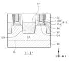
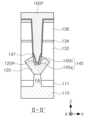
도1는 본 발명의 일 실시예에 따른 반도체 장치의 레이아웃이다.
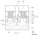
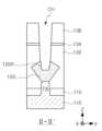
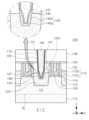
도2a는 도1의 반도체 장치를 Ⅰ-Ⅰ'선으로 절개하여 본 단면도이고, 도2b는 도1의 반도체 장치를 Ⅱ-Ⅱ'선으로 절개하여 본 단면도이며, 도2c는 도2의 반도체 장치의 일부를 나타내는 부분 확대도이다.
도3은 도2a 및 도2b에 도시된 반도체 장치의 주요 구성들을 나타내는 사시도이다.
도4a 내지 도15b는 본 발명의 일 실시예에 따른 반도체 장치의 제조 방법을 설명하기 위하여 공정 순서에 따라 도시한 단면도들이다.
도16은 본 발명의 일 실시예에 따른 반도체 장치를 나타내는 단면도이다.
도17은 본 발명의 일 실시예에 따른 반도체 장치를 나타내는 단면도이다.
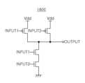
도18은 본 발명의 일 실시예에 따른 반도체 장치인 CMOS 인버터의 회로도이다.
도19는 본 발명의 일 실시예에 따른 반도체 장치인 CMOS NAND의 회로도이다.
도20은 본 발명의 일 실시예에 따른 반도체 장치로 구현된 SoC의 구성을 개략적으로 나타내는 도면이다.1 is a layout of a semiconductor device according to an embodiment of the present invention.
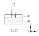
FIG. 2A is a cross-sectional view of the semiconductor device of FIG. 1 taken along line I-I', FIG. 2B is a cross-sectional view of the semiconductor device of FIG. 1 taken along line II-II', and FIG. 2C is a cross-sectional view of the semiconductor device of FIG. 2. This is a partial enlarged view showing part of .
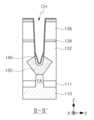
Figure 3 is a perspective view showing main components of the semiconductor device shown in Figures 2A and 2B.
Figures 4A to 15B are cross-sectional views shown in process order to explain a method of manufacturing a semiconductor device according to an embodiment of the present invention.
Figure 16 is a cross-sectional view showing a semiconductor device according to an embodiment of the present invention.
Figure 17 is a cross-sectional view showing a semiconductor device according to an embodiment of the present invention.
Figure 18 is a circuit diagram of a CMOS inverter, a semiconductor device according to an embodiment of the present invention.
Figure 19 is a circuit diagram of CMOS NAND, a semiconductor device according to an embodiment of the present invention.
Figure 20 is a diagram schematically showing the configuration of an SoC implemented as a semiconductor device according to an embodiment of the present invention.
이하, 첨부된 도면을 참조하여 본 발명의 실시예들을 설명하기로 한다.
Hereinafter, embodiments of the present invention will be described with reference to the attached drawings.
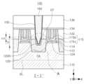
도1는 본 발명의 일 실시예에 따른 반도체 장치의 레이아웃이며, 도2a 및 도2b는 각각 도1의 반도체 장치를 Ⅰ-Ⅰ'선 및 Ⅱ-Ⅱ'선으로 절개하여 본 단면도이다.FIG. 1 is a layout of a semiconductor device according to an embodiment of the present invention, and FIGS. 2A and 2B are cross-sectional views of the semiconductor device of FIG. 1 taken along lines I-I' and II-II', respectively.
도1과 함께 도2a 및 도2b를 참조하면, 반도체 장치(100)는 핀형(fin-type) 활성 영역(FA)을 갖는 기판(110)을 포함한다.Referring to Figures 2A and 2B along with Figure 1, the
상기 기판(110)은 Si 또는 Ge와 같은 반도체, 또는 SiGe, SiC, GaAs, InAs, 또는 InP와 같은 화합물 반도체를 포함할 수 있다. 일부 예에서, 상기 기판(110)은 SOI(silicon on insulator) 구조를 가질 수 있다. 상기 기판(110)은 도전 영역, 예를 들면 불순물이 도핑된 웰(well), 또는 불순물이 도핑된 구조물을 포함할 수 있다.The
상기 기판(110)상에서 상기 핀형 활성 영역(FA)의 저부 측벽은 소자분리막(111)으로 덮여 있으며, 상기 핀형 활성 영역(FA)은 기판(110)의 주면(X-Y 평면)에 수직 방향(Z 방향)을 따라 상기 소자분리막(111) 위로 핀형으로 돌출되어 있다. 상기 핀형 활성 영역(FA)은 제1 방향(X 방향)으로 연장된다. 상기 핀형 활성 영역(FA)의 저면 레벨은 도2a에서 점선(BL)으로 표시되어 있다.On the
도2a 및 도2b에 도시된 바와 같이, 상기 소스/드레인 영역들(120)은 핀형 활성 영역(FA)의 상면보다 더 높은 레벨의 상면(ST)을 가지는 상승된 소스/드레인(raised source/drain: RSD) 구조를 가질 수 있다. 도2b에 도시된 바와 같이, 소스/드레인 영역들(120)은 오각형 형상을 가질 수 있으나, 이에 한정되지 않으며 소스/드레인 영역들(120)은 다양한 형상을 가질 수 있다. 예를 들어, 상기 소스 및 드레인 영역들(120)은, 다각형, 원형 및 직사각형 중 어느 하나의 형상을 가질 수 있다. 일부 실시예에서, 소스/드레인 영역들(120)은 복수(예, 3개)의 핀형 활성 영역(FA) 상에서 서로 합쳐진(merged) 구조로 형성될 수 있다.As shown in FIGS. 2A and 2B, the source/
상기 핀형 활성 영역(FA) 위에는 복수의 인터페이스막(112), 복수의 게이트 절연막(114) 및 복수의 게이트 라인(115)이 배치될 수 있다. 상기 복수의 게이트 절연막(114) 및 복수의 게이트 라인(115)은 핀형 활성 영역(FA) 각각의 상면 및 양 측벽과, 소자 분리막(111)의 상면을 덮으면서 상기 제1 방향(X 방향)에 교차하는 제2 방향(Y 방향)으로 연장될 수 있다. 상기 핀형 활성 영역(FA)과 복수의 게이트 라인(115)이 교차하는 영역에는 복수의 MOS 트랜지스터가 형성될 수 있다. 상기 복수의 MOS 트랜지스터는 각각 핀형 활성 영역(FA)의 상면 및 양 측벽에서 채널이 형성되는 3차원 구조의 MOS 트랜지스터로 이루어질 수 있다.A plurality of
상기 복수의 인터페이스막(112), 복수의 게이트 절연막(114) 및 복수의 게이트 라인(115) 각각의 양 측벽은 절연 스페이서(124)로 덮일 수 있다. 상기 복수의 인터페이스막(112)은 각각 핀형 활성 영역(FA)의 노출 표면을 산화시켜 얻어질 수 있다. 이러한 인터페이스막(112)은 핀형 활성 영역(FA)과 게이트 절연막(114)과의 사이의 계면 불량을 방지하는 역할을 할 수 있다.Both sidewalls of each of the
일부 실시예들에서, 상기 복수의 인터페이스막(112)은 낮은 유전율(예, 9 이하)을 갖는 저유전 물질층, 예를 들면 실리콘 산화막, 실리콘 산질화막, 또는 이들의 조합으로 이루어질 수 있다. 다른 일부 실시예들에서, 상기 복수의 인터페이스막(112)은 실리케이트 또는 실리케이트와 상기한 물질의 조합으로 이루어질 수 있다.In some embodiments, the plurality of
상기 복수의 게이트 절연막(114)은 실리콘 산화막, 고유전막 또는 이들의 조합으로 이루어질 수 있다. 상기 고유전막은 실리콘 산화막보다 유전율(예, 약 10 내지 25)이 더 큰 물질을 포함할 수 있다. 예를 들어, 상기 고유전막은 하프늄 산화물(hafnium oxide), 하프늄 산질화물(hafnium oxynitride), 하프늄 실리콘 산화물(hafnium silicon oxide), 란타늄 산화물 (lanthanum oxide), 란타늄 알루미늄 산화물(lanthanum aluminum oxide), 지르코늄 산화물(zirconium oxide), 지르코늄 실리콘 산화물(zirconium silicon oxide), 탄탈륨 산화물(tantalum oxide), 티타늄 산화물(titanium oxide), 바륨 스트론튬 티타늄 산화물(barium strontium titanium oxide), 바륨 티타늄 산화물(barium titanium oxide), 스트론튬 티타늄 산화물(strontium titanium oxide), 이트륨 산화물(yttrium oxide), 알루미늄 산화물(aluminum oxide), 납 스칸듐 탄탈륨 산화물(lead scandium tantalum oxide) 및 납 아연 니오브산염(lead zinc niobate) 및 이들의 조합 중에서 선택되는 물질로 이루어질 수 있으나, 이에 한정되는 것은 아니다. 상기 게이트 절연막(114)은 ALD (atomic layer deposition), CVD (chemical vapor deposition) 또는 PVD (physical vapor deposition) 공정에 의해 형성될 수 있다.The plurality of gate
상기 복수의 게이트 라인(GL)은 제1 게이트 전극(115a) 및 제2 게이트 전극(115b)을 포함할 수 있다. 상기 제1 게이트 전극(115a)은 일함수를 조절하는 역할을 할 수 있다. 상기 제2 게이트 전극(115b)은 상기 제1 게이트 전극(115a)의 상부에 형성된 공간을 채우는 역할을 할 수 있다. 제1 게이트 전극(115a)은 제2 게이트 전극(115b)에 대한 확산 방지층으로서의 역할을 할 수 있으나, 이에 한정되지는 않는다.The plurality of gate lines GL may include a
제1 및 제2 게이트 전극(115a, 115b)은 서로 다른 물질로 이루어질 수 있다. 제1 게이트 전극(115a)은 예를 들어, 티타늄 질화막(TiN), 탄탈륨 질화막(TaN), 또는 텅스텐 질화막(WN)과 같은 금속 질화물을 포함할 수 있다. 제2 게이트 전극(115b)은 예를 들어, 알루미늄(Al), 텅스텐(W), 또는 몰리브덴(Mo) 등의 금속 물질 또는 도핑된(doped) 폴리 실리콘과 같은 반도체 물질을 포함할 수 있다.The first and
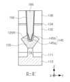
상기 게이트 라인(115)의 일측에서 상기 핀형 활성 영역(FA) 내에 소스/드레인 영역들(120)이 배치된다. 상기 소스/드레인 영역들(120)은 상기 핀형 활성 영역(FA)으로부터 에피텍셜 성장된 반도체층을 포함할 수 있다. 상기 소스/드레인 영역들(120)은 리세스 영역(120R)이 형성된 상면(ST)을 갖는다. 리세스 영역(120R)은 콘택 플러그(160)의 일부가 그 내부에 배치될 수 있도록 충분한 깊이(D)로 형성될 수 있다.Source/
일부 실시예들에서, 상기 소스/드레인 영역들(120)은 선택적 에피택셜 성장된 복수의 SiGe층을 포함하는 임베디드 SiGe 구조를 가질 수 있다. 상기 복수의 SiGe층은 서로 다른 Ge 함량을 가질 수 있다. 다른 일부 실시예들에서, 상기 소스/드레인 영역들(120)은 에피택셜 성장된 Si층 또는 에피택셜 성장된 SiC 층으로 이루어질 수 있다.In some embodiments, the source/
상기 복수의 게이트 라인(115)의 각 사이에는 게이트간 절연막(132)이 형성된다. 상기 게이트간 절연막(132)은 이웃하는 2개의 게이트 라인(115) 사이에서 상기 소스/드레인 영역들(120)을 덮도록 형성될 수 있다. 상기 게이트간 절연막(132)은 실리콘 산화막으로 이루어질 수 있으나, 이에 한정되는 것은 아니다.An inter-gate
상기 복수의 게이트 라인(115) 및 게이트간 절연막(132) 상에는 블로킹 절연막(134)이 형성될 수 있다. 상기 블로킹 절연막(134)은 산소와 같은 원하지 않는 이물질이 복수의 게이트 라인(115)에 침투하는 것을 방지할 수 있다. 또한, 상기 블로킹 절연막(134)은 상기 게이트 라인(115)에서 원하지 않게 문턱 전압(threshold voltage)이 바뀌는 현상, 또는 게이트 라인(GL)과 콘택 플러그(160)의 사이에서 발생될 수 있는 단락 현상을 방지할 수 있다. 예를 들면, 상기 블로킹 절연막(134)은 실리콘 질화막(Si3N4), 실리콘 산질화막(SiON), 탄소함유 실리콘 산질화막(SiCON) 또는 이들의 조합으로 이루어질 수 있다. 일부 실시예들에서, 상기 블로킹 절연막(134)은 약 20 ∼ 50 Å의 두께를 가질 수 있다.A blocking insulating
층간 절연막(136)은 상기 블로킹 절연막(134) 상에 형성될 수 있다. 상기 층간 절연막(136)은 실리콘 산화막으로 이루어질 수 있으나, 이에 한정되는 것은 아니다. 일부 실시예들에서, 상기 게이트간 절연막(132) 및 층간 절연막(136) 중 적어도 하나는 TEOS(tetra ethyl orthosilicate) 막으로 이루어질 수 있다. 다른 일부 실시예들에서, 상기 게이트간 절연막(132)과 층간 절연막(136) 중 적어도 하나는 초저유전상수(예, 약 2.2 ∼ 2.4)를 가지는 ULK(ultra low K)막, 예를 들어 SiOC 막 및 SiCOH 막 중에서 선택되는 막일 수 있다.An interlayer insulating
콘택 플러그(160)는 상기 소스/드레인 영역들(120)에 전기적으로 연결되도록 상기 소스/드레인 영역들(120) 상에 배치된다. 상기 콘택 플러그(160)는 상기 리세스 영역(120R)의 내부로부터 상기 기판(110)의 상면(X-Y면)에 수직인 제3 방향(Z 방향)으로 연장된다. 예를 들면, 상기 콘택 플러그(160)는 X-Y면을 따른 단면 형상이 원형, 타원형, 또는 다각형일 수 있다.Contact plugs 160 are disposed on the source/
콘택 플러그(160)는 상기 층간 절연막(136), 블로킹 절연막(134) 및 게이트간 절연막(132)을 관통할 수 있다. 상기 콘택 플러그(160)는 상기 게이트간 절연막(132)과, 상기 블로킹 절연막(134)과, 상기 층간 절연막(136)에 의해 둘러싸여 다른 도전층들과 상호 절연될 수 있다. 예를 들어, 상기 콘택 플러그(160)는 W, Cu, Al, 이들의 합금 또는 이들의 조합으로 이루어질 수 있다.The
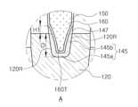
도2a 및 도2b에 도시된 바와 같이, 상기 콘택 플러그(160)는 리세스 영역(120R) 내부에 위치한 단부(tip) 영역(160T)을 갖는다. 상기 금속 실리사이드막(145)은 상기 리세스 영역(120R)의 내부 표면을 따라 형성되어 상기 소스/드레인 영역들(120)과 상기 콘택 플러그(160)(또는 도전성 배리어막(150)) 사이에 배치될 수 있다.As shown in FIGS. 2A and 2B, the
본 실시예에서, 상기 금속 실리사이드막(145)은 상기 리세스 영역(120R)의 저면에 위치한 제1 부분(145A)과, 상기 제1 부분(145A)과 일체로 연결되어 상기 리세스 영역(120R)의 측벽에 위치한 제2 부분(145B)을 포함한다. 금속 실리사이드막(145)의 제1 부분(145A)은 콘택 플러그(160)의 하면에 배치되며, 금속 실리사이드막(145)의 제2 부분(145B)은 콘택 플러그(160)의 측면 일부 영역에도 배치될 수 있다. 이와 같이, 상기 콘택 플러그(160)의 단부 영역(160T)의 거의 전체 표면은 금속 실리사이드막에 둘러싸일 수 있다. 일부 실시예에서, 상기 금속 실리사이드막(145)의 상기 제2 부분(145B)은 상기 제1 부분(145A)으로부터 멀어질수록 작아지는 두께를 가질 수 있다.In this embodiment, the
본 실시예에 따른 반도체 장치(100)는 소스/드레인 영역들(120)에 형성된 리세스 영역(120R)의 저면 및 측벽을 덮는 금속 실리사이드막(145)을 가지므로 상기 금속 실리사이드막(145)이 콘택 플러그(160)와 비교적 넓은 콘택 면적을 가질 수 있고, 이로써 소스/드레인 영역들(120)과 콘택 플러그(160)의 사이에서 콘택 저항을 크게 감소시킬 수 있다.The
상기 금속 실리사이드막(145)은 소스/드레인 영역들(120)의 반도체 물질(예, Si, SiGe, Ge 등)와 반응하여 형성되므로, 소스/드레인 영역들(120)의 상면(ST)까지 형성될 수 있다. 일부 실시예에서, 상기 금속 실리사이드막(145)은 MSixDy로 표시되는 조성을 가질 수 있다. 여기서, M은 금속이고, D는 M 및 Si와는 다른 성분의 원소이고, 0 < x ≤3이고, 0 ≤ y ≤1 일 수 있다. 상기 M은 Ti, Co, Ni, Ta, Pt 또는 이들의 조합이며, 상기 D는 Ge, C, Ar, Kr, Xe, 또는 이들의 조합일 수 있다. 예를 들어, 상기 금속 실리사이드막(145)은 티타늄 실리사이드일 수 있다.Since the
본 실시예에서는, 상기 금속 실리사이드막(145) 상단에는 금속층(147)이 배치될 수 있다. 상기 금속층(145)은 리세스 영역(120R) 외부로 돌출되어 콘택홀의 측벽에 따라 일정한 높이(H1)로 형성될 수 있다. 도2c에 도시된 바와 같이,상기 금속층(147)은 상기 소스 및 드레인 영역들(120)의 상면(ST)보다 높은 레벨에 위치할 수 있다. 상기 금속층(147)은 상기 금속 실리사이드막(145)에 함유된 금속과 동일한 금속을 포함할 수 있다. 일부 실시예에서, 상기 금속층(147)은 티타늄(Ti), 코발트(Co), 니켈(Ni), 탄탈늄(Ta) 및 백금(Pt)으로 구성된 그룹으로부터 선택된 적어도 하나의 금속을 포함할 수 있다. 예를 들면, 상기 금속 실리사이드막(145)이 티타늄 실리사이드인 경우, 상기 금속층(147)은 티타늄일 수 있다.In this embodiment, a
본 실시예에서, 상기 콘택 플러그(160)의 하면 및 측벽은 도전성 배리어막(150)으로 둘러싸인다. 상기 도전성 배리어막(150)은 상기 금속 실리사이드막(145)에 접촉하는 하부 영역과, 상기 콘택 플러그(160)의 측벽을 둘러싸는 상부 영역을 포함한다. 도전성 배리어막(150)의 하부 영역은 상기 금속 실리사이드막(145)은 상기 도전성 배리어막(150)의 하부 영역을 통해 상기 콘택 플러그(160)와 전기적으로 접속될 수 있다. 즉, 도전성 배리어막(150)은 상기 콘택 플러그(160)와 상기 금속 실리사이드막(145)의 계면 및 상기 콘택 플러그(160)와 상기 금속층(147)의 계면을 따라 배치될 수 있다.In this embodiment, the bottom surface and side walls of the
상기 도전성 배리어막(150)은 도전성 금속 질화막으로 이루어질 수 있다. 예를 들어, 상기 도전성 배리어막(150)은 TiN, TaN, AlN, WN 또는 이들의 조합으로 이루어질 수 있다.The
상기 금속 실리사이드막(145)의 제1 부분(145A)은 상기 게이트 라인(115)의 최저면의 레벨(도3 참조)보다 높고, 상기 핀형 활성 영역(FA)의 상면의 레벨(도2a 참조)보다 낮은 레벨에 위치될 수 있다. 즉, 상기 금속 실리사이드막(145)의 제1 부분(145a)은 게이트 라인(115)의 최저면과 핀형 활성 영역(FA)의 상면과의 사이의 레벨에 형성될 수 있다. 상기 금속층(147)은 상기 금속 실리사이드막(145)의 상단에 배치되어 그와 일체로 연결되며, 상기 금속층(147)은 상기 소스 및 드레인 영역들(120)의 상면(ST)보다 높은 레벨에 위치할 수 있다. 상기 금속층(147)은 금속 자체뿐만 아니라, 충분히 실리사이드화되지 않은 금속(예, 실리콘 함유율 30at% 이하)를 포함할 수 있다.
The first portion 145A of the
도4a 내지 도15b는 본 발명의 일 실시예에 따른 반도체 장치의 제조 방법을 설명하기 위하여 주요 공정별 단면도들이다. 본 공정예는 도2a 내지 도3에 도시된 반도체 장치의 제조방법이며, 각 공정별 단면은 도2a 및 도2b에 도시된 단면들에 대응하는 Ⅰ-Ⅰ'선 및 Ⅱ-Ⅱ'로 절개한 단면으로 이해될 수 있다.
Figures 4A to 15B are cross-sectional views of each major process to explain a method of manufacturing a semiconductor device according to an embodiment of the present invention. This process example is a method of manufacturing the semiconductor device shown in FIGS. 2A to 3, and the cross sections for each process are cut along lines I-I' and II-II' corresponding to the cross sections shown in FIGS. 2A and 2B. It can be understood as a cross-section.
도4a 및 도4b를 참조하면, 핀형 활성 영역(FA)을 갖는 기판(110)을 마련한다.Referring to FIGS. 4A and 4B, a
핀형 활성 영역(FA)은 상기 기판(110)의 일부 영역을 선택적으로 식각하여 얻어질 수 있다. 핀형 활성 영역(FA)은 상기 기판(110)의 주면(X-Y 평면)으로부터 상부(Z 방향)로 돌출되면서 일방향(X 방향)으로 연장될 수 있다. 예를 들어, 상기 기판(110)은 P-MOSFET 영역 및/또는 N-MOSFET 영역을 가질 수 있으며, 상기 핀형 활성 영역(FA)은 원하는 MOSFET의 채널 타입에 따라 P 형 또는 N 형의 불순물 확산영역들을 포함할 수 있다.The fin-type active area (FA) can be obtained by selectively etching a partial area of the
이어, 상기 기판(110) 상에 핀형 활성 영역(FA)을 덮는 절연막을 형성하고 상기 핀형 활성 영역(FA)이 일부 노출되도록 절연막을 에치백함으로써, 도4b에 도시된 바와 같이 소자분리막(112)을 형성할 수 있다. 상기 소자분리막(112)은 실리콘 산화막, 실리콘 질화막, 실리콘 산질화막 또는 이들의 조합으로 이루어질 수 있다.
Next, an insulating film covering the fin-type active area (FA) is formed on the
도5a 및 도5b를 참조하면, 핀형 활성 영역(FA) 상에 복수의 더미 게이트 구조체(DG)를 형성한다.5A and 5B, a plurality of dummy gate structures DG are formed on the fin-type active area FA.
상기 복수의 더미 게이트 구조체(DG)는 상기 핀형 활성 영역(FA)에 교차하여 연장되도록 형성되며, 각각 핀형 활성 영역(FA) 위에 순차적으로 적층된 더미 게이트 절연막(D114), 더미 게이트 라인(D116), 및 더미 게이트 캡핑층(D118)을 포함할 수 있다. 일부 실시예들에서, 더미 게이트 절연막(D114)은 실리콘 산화물을 포함할 수 있다. 상기 더미 게이트 라인(D116)은 폴리실리콘을 포함할 수 있다. 상기 더미 게이트 캡핑층(D118)은 실리콘 산화물, 실리콘 질화물, 및 실리콘 산질화물 중 적어도 하나를 포함할 수 있다. 또한. 상기 더미 게이트 구조체(DG)의 양 측벽에 절연 스페이서(124)를 형성한다. 상기 절연 스페이서(124)는 실리콘 질화물, 실리콘 산질화물 또는 이들의 조합으로 이루어질 수 있다.The plurality of dummy gate structures (DG) are formed to extend across the fin-type active area (FA), and a dummy gate insulating film (D114) and a dummy gate line (D116) are sequentially stacked on the fin-type active area (FA), respectively. , and a dummy gate capping layer D118. In some embodiments, the dummy gate insulating layer D114 may include silicon oxide. The dummy gate line D116 may include polysilicon. The dummy gate capping layer D118 may include at least one of silicon oxide, silicon nitride, and silicon oxynitride. also. Insulating
이어, 상기 더미 게이트 구조체(DG)의 양 측에서 노출되는 핀형 활성 영역(FA) 위에 에피택셜 성장 공정에 의해 반도체층(120)을 형성하여 소스/드레인 영역들(120)을 제공할 수 있다. 상기 소스/드레인 영역(120)은 핀형 활성 영역(FA)의 상면보다 더 높은 레벨의 상면(ST)을 가질 수 있다. 상기 소스/드레인 영역들(120)은 불순물이 도핑된 반도체층으로 이루어질 수 있다. 예를 들어, 상기 소스/드레인 영역들(120)은 불순물이 도핑된 Si, SiGe, 또는 SiC로 이루어질 수 있다.Next, the
다음으로, 평탄화된 상면을 가지는 게이트간 절연막(132)을 형성할 수 있다. 상기 게이트간 절연막(132)은, 소스/드레인 영역들(120), 복수의 더미 게이트 구조체(DG) 및 절연 스페이서(124)를 덮도록 충분한 두께로 형성한 후에 상기 복수의 더미 게이트 구조체(DG)가 노출될 수 있도록 상기 절연막이 형성된 결과물을 평탄화함으로써 얻어질 수 있다.
Next, an inter-gate
도6a 및 도6b를 참조하면, 복수의 더미 게이트 구조체(DG)를 제거하여 복수의 게이트 공간(GH)을 형성할 수 있다.Referring to FIGS. 6A and 6B , a plurality of gate spaces GH may be formed by removing a plurality of dummy gate structures DG.
앞서 평탄화 공정에서 노출된 게이트간 절연막(132)을 통해 복수의 더미 게이트 구조체(DG)를 선택적으로 제거할 수 있다. 복수의 게이트 공간(GH)을 통해 절연 스페이서(124) 및 핀형 활성 영역(FA)이 노출될 수 있다.
A plurality of dummy gate structures DG can be selectively removed through the inter-gate
도7a 및 도7b를 참조하면, 복수의 게이트 공간(GH)(도4a 참조) 내에 복수의 인터페이스막(112), 게이트 절연막(114) 및 게이트 라인(115)을 차례로 형성할 수 있다.Referring to FIGS. 7A and 7B , a plurality of
복수의 인터페이스막(112)은 복수의 게이트 공간(GH) 내에서 노출되는 핀형활성 영역(FA)의 일부를 산화시키는 공정으로 형성될 수 있다. 상기 복수의 인터페이스막(112)은 복수의 게이트 절연막(114)과 하부의 핀형 활성 영역(FA)의 사이의 계면 불량을 방지하는 역할을 할 수 있다.The plurality of
상기 게이트 절연막(114) 및 게이트 라인(115)은 복수의 게이트 공간(GH) 내부를 채우면서 게이트간 절연막(132)의 상면을 덮도록 형성될 수 있다. 상기 게이트 절연막(114)은 실리콘 산화막, 고유전막, 또는 이들의 조합으로 이루어질 수 있다. 상기 게이트 라인(115)은 제1 게이트 전극층(115a) 및 제2 게이트 전극층(115b)을 포함할 수 있다. 본 공정에 도입되는 층들은 각각 ALD, MOALD(metal organic ALD), 또는 MOCVD (metal organic CVD) 공정에 의해 형성될 수 있다.The
다른 실시예에서는, 도전성 캡핑층 및/또는 갭필(gap-fill) 금속막을 추가로 형성할 수 있다. 도전성 캡핑층은 상기 게이트 라인(115)의 표면이 산화되는 것을 방지하거나 다른 도전층이 증착될 때 증착을 용이하게 하기 위한 접착층(wetting layer) 역할을 할 수 있다. 예를 들어, 상기 도전성 캡핑층은 금속 질화물, 예를 들면 TiN, TaN 또는 이들의 조합일 수 있다. 상기 갭필 금속막은 상기 핀형 활성 영역(FA) 사이의 공간을 채우면서 상기 도전성 캡핑층 상에 연장될 수 있다. 상기 갭필 금속막은 W막으로 이루어질 수 있다.
In another embodiment, a conductive capping layer and/or a gap-fill metal film may be additionally formed. The conductive capping layer may prevent the surface of the
도8a 및 도8b를 참조하면, 앞선 공정의 결과물에 대하여 평탄화 공정을 적용하여 게이트 라인(115) 및 게이트 절연막(114)을 각각 복수의 게이트 공간(GH)에 잔류할 수 있다.Referring to FIGS. 8A and 8B , the
상기 평탄화 공정의 결과로서, 절연 스페이서(124) 및 게이트간 절연막(132)이 각각의 상면으로부터 소정 두께만큼 제거되고, 복수의 게이트 라인(115)의 상면 주위에서 복수의 게이트 절연막(114)의 상면, 복수의 절연 스페이서(124)의 상면 및 게이트간 절연막(132)의 상면이 거의 동일한 레벨로 노출될 수 있다.
As a result of the planarization process, the insulating
도9a 및 도9b를 참조하면, 복수의 게이트 라인(115) 및 게이트간 절연막(132) 위에 블로킹 절연막(134) 및 층간 절연막(136)을 차례로 형성한다.Referring to Figures 9A and 9B, a blocking insulating
상기 층간 절연막(136)은 평탄화된 상면을 가지도록 형성될 수 있다. 상기 블로킹 절연막(134)은 상기 복수의 게이트 라인(115)의 상면을 덮는 평탄한 막의 형상을 가지는 것으로 예시되었으나, 이에 한정되지 않는다. 예를 들어, 상기 블로킹 절연막(134)은 상기 게이트 라인(115)의 상면과, 양 측벽의 적어도 일부를 덮도록 형성될 수 있으며, 그에 상응하여 상기 블로킹 절연막(134)의 적어도 일부 영역에 단차가 형성된 구조를 가질 수 있다.
The
도10a 및 도10b를 참조하면, 소스/드레인 영역들(120)이 노출되도록 상기 층간 절연막(136), 블로킹 절연막(134) 및 게이트간 절연막(132)을 관통하는 콘택 홀(CH)을 형성한다.Referring to FIGS. 10A and 10B, a contact hole (CH) is formed through the
상기 콘택 홀(CH)은 콘택 플러그 형성영역을 정의할 수 있다. 상기 콘택 홀(CH)은 층간 절연막(136) 상에 마스크 패턴을 형성하고, 마스크 패턴을 식각 마스크로 이용하여 층간 절연막(136), 블로킹 절연막(134) 및 게이트간 절연막(132)을 차례로 에칭함으로써 형성될 수 있다. 상기 콘택홀(CH)을 통해 소스/드레인 영역(120)이 노출될 수 있다.The contact hole CH may define a contact plug formation area. The contact hole (CH) is formed by forming a mask pattern on the
콘택홀(CH)의 형성과정에서 노출된 소스/드레인 영역들(120)의 일부 영역이 일정 깊이(D)로 제거되어 소스/드레인 영역들(120)의 상면(ST)에 리세스 영역(120R)을 형성한다. 상기 리세스 영역(120R)의 깊이(D)는 핀형 활성 영역(FA)의 상면보다 더 낮은 레벨을 가질 수 있다. 상기 리세스 영역(120R)은 콘택 플러그의 일부 영역(즉, 단부영역(160T))가 그 내부에 위치하기 위한 충분한 깊이(D)를 가지므로, 상기 리세스 영역(120R)의 저면뿐만 아니라 측벽도 콘택 면적으로 제공될 수 있다. 이와 같이, 본 실시예에서는, 리세스 영역(120R)의 측벽도 콘택 영역으로 제공되므로, 충분한 콘택 면적을 갖도록 리세스 영역(120R)의 깊이(D)를 적절히 선택할 수 있다.
In the process of forming the contact hole (CH), a portion of the exposed source/
도11a 및 도11b를 참조하면, 상기 리세스 영역(120R)의 저면을 덮는 1차 금속막(140)을 형성한다.Referring to Figures 11A and 11B, a
상기 1차 금속막(140)은 금속 실리사이드를 형성을 위한 금속물질일 수 있다. 예를 들어, 상기 1차 금속막(140)은 Ti, Co, Ni, Ta, Pt 또는 그 조합일 수 있다. 상기 1차 금속막(140)은 PVD 공정을 이용하여 형성될 수 있다. 이러한 증착과정에서 1차 금속막(140)은 상기 리세스 영역(120R)의 저면뿐만 아니라, 상기 층간 절연막(136)의 상면 및 콘택홀(CH)의 내부 측벽에도 퇴적될 수 있다. 특히, 1차 금속막(140)은 콘택홀(CH)의 내부 측벽에 퇴적되더라도 후속 콘택 플러그의 충진공정을 방해하지 않도록 작은 두께로 퇴적될 수 있다. 이를 위해서, 리세스 영역(120R)의 저면에 증착되는 1차 금속막(140)의 두께(t0)를 리세스 영역(120R)의 측벽까지 덮이도록 충분한 두께로 형성하기 어렵다. 따라서, 상기 1차 금속막(140)이 형성된 후에도, 상기 1차 금속막(140) 위에 위치한 상기 리세스 영역(120R)의 측벽의 일부 영역이 노출될 수 있다.
The
도12a 및 도12b를 참조하면, 1차 금속막(140)에 대한 리스퍼터링(re-sputtering) 공정을 통해서 리세스 영역(120R)의 저면 및 측벽에 걸쳐 형성된 2차 금속막(140')을 제공할 수 있다.Referring to FIGS. 12A and 12B, a
리스퍼터링 공정에 의해 1차 금속막(140)은 부분적으로 상기 리세스 영역(120R)의 측벽에 분산되어 상기 리세스 영역(120R)의 측벽에도 연장된 2차 금속막(140')을 형성할 수 있다. 2차 금속막(140')은 상기 리세스 영역(120R)의 내부 표면을 따라 배치될 수 있다. 예를 들어, 리스퍼터링 공정은 Ar, Ne과 같은 비활성 기체를 이용한 플라즈마 에칭공정으로 수행될 수 있다.Through the resputtering process, the
본 공정은 제1 금속막(140) 증착(도11a 및 도11b)과의 사이에서 진공을 파괴하지 않고 인시튜(in-situ)로 수행될 수 있다. 물론, 이에 한정되지 않으며 필요에 따라 다른 챔버로 이송하는 등 엑스-시튜(ex-situ)로 수행될 수 있다. 또한, 본 리스퍼터링을 수행하는 동안에, 도11a 및 도11b의 공정 후에 1차 금속막(140) 표면에 잔류할 수 있는 자연 산화막과 같은 이물질이 함께 제거될 수 있다.This process can be performed in-situ without breaking the vacuum between the deposition of the first metal film 140 (FIGS. 11A and 11B). Of course, it is not limited to this and can be performed ex-situ, such as by transferring it to another chamber if necessary. Additionally, while performing this resputtering, foreign substances such as a natural oxide film that may remain on the surface of the
리스퍼터된 2차 금속막(140')은 상기 리세스 영역(120R)의 저면에 위치한 바닥 부분(140a)과 상기 바닥 부분(140a)에 일체로 연결되며 상기 리세스 영역(120R)의 측벽에 위치한 측벽 부분(140b)을 포함할 수 있다. 상기 2차 금속막(140')의 측벽 부분(140b)은 상기 리세스 영역(120R)의 측벽보다 높은 영역까지 형성될 수 있다. 즉, 상기 측벽 부분(140b)은 리세스 영역(120R)의 외부에서 콘택홀(CH)의 일부 영역에 위치한 금속부분(140T)을 포함할 수 있다. 바닥 부분(140a)의 두께(t1')는 1차 금속막(140)의 두께(t0)보다 감소하며, 측벽 부분(140b)의 두께(t2')는 콘택을 위한 실리사이드를 형성할 수 있는 충분한 두께를 가질 수 있다. 예를 들어, 상기 측벽 부분(140b)의 두께(t2)는 약 1㎚ 이상일 수 있다. 일부 실시예에서, 리스퍼터링 과정에서 금속 물질이 도시된 2차 금속막(140')보다 높게 콘택홀(CH)의 측벽에 상당부분까지 매우 얇은 두께로 퇴적될 수 있다. 이러한 퇴적된 금속막은 질화처리를 이용하여 배리어막을 제공할 수 있다(도16 참조).
The resputtered
도13a 및 도13b를 참조하면, 2차 금속막(140')이 형성된 리세스 영역(120R)과 상기 콘택홀(CH)의 내벽을 덮는 도전성 배리어막(150)을 형성한다.Referring to Figures 13A and 13B, a
상기 도전성 배리어막(150)은 2차 금속막(140')의 노출 표면 및 상기 콘택홀(CH)의 내벽을 컨포멀(conformal)하게 덮도록 형성될 수 있다. 본 공정은 PVD, CVD, 또는 ALD 공정을 이용하여 수행될 수 있다. 예를 들어, 상기 도전성 배리어막(150)은 TiN, TaN, AlN, WN, 또는 이들의 조합으로 이루어질 수 있다.
The
도14a 및 도14b를 참조하면, 도13a 및 도13b에 도시된 결과물을 열처리하여리세스 영역(120R)의 저면 및 측벽에서 금속 실리사이드막(145)을 형성한다.Referring to FIGS. 14A and 14B, the results shown in FIGS. 13A and 13B are heat treated to form a
열처리 과정에서 상기 소스/드레인 영역(120)을 구성하는 반도체 물질과 상기 2차 금속막(140')을 구성하는 금속의 반응을 유도하여 상기 리세스 영역(120R)에서 상기 소스/드레인 영역(120)을 덮는 상기 금속 실리사이드막(145)을 형성할 수 있다. 예를 들어, 상기 금속 실리사이드막(145)을 형성하기 위한 열처리 공정으로 레이저 어닐링을 이용할 수 있다.During the heat treatment process, a reaction is induced between the semiconductor material constituting the source/
상기 금속 실리사이드막(145)이 형성된 후, 상기 2차 금속막(140')에서 반도체 물질과 접속하지 않은 영역, 즉 콘택홀(CH)의 내부 측벽에 위치한 영역은 반도체 물질과 반응하지 못하므로 실리사이드화되지 않은 금속층(147)을 잔류시킬 수 있다. 이러한 금속층(147)은 층간 절연막(132)과 도전성 배리어막(150) 사이에 남아 있을 수 있다. 상기 금속층(147)은 실리콘이 확산 가능한 인접한 범위에 위치할 경우에는 완전한 금속이기보다는 충분히 실리사이드화되지 않은 금속화합물일 수 있다. 예를 들어, 충분히 실리사이드화되지 않은 금속층(147)은 실리콘 함유율이 30at% 이하일 수 있다.After the
상기 금속 실리사이드막(145)은, 상기 리세스 영역(120R)의 저면에 위치한 제1 부분(145a)과, 상기 제1 부분(145a)에 일체로 연결되며 상기 리세스 영역(120R)의 측벽에 위치한 제2 부분(145b)을 포함한다. 실리사이드화 후에, 제1 부분(145a)의 두께(t1)는 2차 금속막(140')의 바닥부분(140a)의 두께(t1')보다 커지고, 제2 부분(145b)의 두께(t2)는 2차 금속막(140')의 측벽부분(140b)의 두께(t2')보다 커질 수 있다. 제2 부분(145b)의 두께(t2)은 상기 기판(110)으로부터 멀어질수록 더 작은 두께를 가질 수 있다. 또한, 금속층(147)은 금속 실리사이드막(145)의 제2 부분(145b)의 두께(t2)보다 작은 두께를 가질 수 있다.
The
도15a 및 도15b를 참조하면, 도14a 및 도14b에 도시된 결과물 상에 콘택홀(CH) 및 리세스 영역(120R)을 채우기에 충분한 두께로 도전막(160P)을 형성한다.Referring to FIGS. 15A and 15B, a
상기 도전막(160P)은 상기 콘택홀(CH) 및 리세스 영역(120R)의 내부를 채우면서 층간 절연막(136)의 상면 위에서 도전성 배리어막(150)을 덮도록 형성될 수 있다. 예를 들어, 상기 도전막(160P)은 W, Cu, Al, 이들의 합금 또는 이들의 조합으로 이루어질 수 있다. 상기 층간 절연막(136) 상면이 노출되고, 상기 도전성 배리어막(150) 및 도전막(160P)이 상기 콘택홀(CH) 및 리세스 영역(120R)의 내부에만 남도록 1차 금속막(140), 도전성 배리어막(150) 부분 및 도전막(160P) 증착시에 상기 층간 절연막(136)의 상면 위에 형성된 불필요한 부분들을 제거할 수 있다. 이러한 제거공정은, CMP 공정 등과 같은 평탄화 공정을 수행할 수 있다.The
그 결과, 도2a 및 도2b에 도시된 바와 같이, 상기 도전막(160P) 중 상기 콘택홀(CH) 및 리세스 영역(120R)의 내부를 채우는 부분으로 이루어지는 콘택 플러그(160)와, 상기 콘택홀(CH) 내에서 상기 콘택 플러그(160)의 주위를 포위하는 도전성 배리어막(150)이 남게 될 수 있다.
As a result, as shown in FIGS. 2A and 2B, a
앞선 실시예들은 FinFET 소자에서 소스 및 드레인 영역들을 위한 콘택 플러그 형성시에 예로 설명되어 있으나, 이에 한정되지 않으며 평판형 MOSFET 소자와 같은 다른 소자의 소스 및 드레인 영역뿐만 아니라 다른 소자의 활성영역에 제공되는 콘택 구조를 형성하는 방안으로도 다양하게 활용될 수 있다.
The preceding embodiments have been described as examples in forming contact plugs for source and drain regions in a FinFET device, but are not limited thereto and are provided in the active region of other devices as well as the source and drain regions of other devices such as planar MOSFET devices. It can also be used in a variety of ways to form a contact structure.
도16은 본 발명의 일 실시예에 따른 반도체 장치를 나타내는 단면도이다. 도16에 도시된 반도체 장치(200)는 도 1에 도시된 레이아웃과 유사한 레이아웃을 가질 수 있으며, Ⅰ-Ⅰ'선으로 절개한 단면 구조이며, 앞선 실시예에서 설명된 동일한 참조 부호는 동일 부재를 나타낸 것으로 이해할 수 있다.
Figure 16 is a cross-sectional view showing a semiconductor device according to an embodiment of the present invention. The
도16을 참조하면, 반도체 장치(200)는 도전성 배리어막(150)의 상부영역과 콘택홀(CH) 사이에 배치된 추가 배리어막(170)과, 금속 실리사이드막(145)와 금속층(147) 사이에 배치된 중간 실리사이드 영역(146)을 더 포함하는 것을 제외하고, 앞선 실시예에 따른 반도체 장치(100)와 거의 동일한 구성을 갖는다.Referring to FIG. 16, the
본 실시예에서, 상기 추가 배리어막(170)은 상기 도전성 배리어막(150)을 형성하기 전에 형성될 수 있다. 추가 배리어막(170)은 금속층(147) 및 금속 실리사이드막(146)에 함유된 금속을 포함한 질화막일 수 있다. 도12a 및 도12b에 도시된 리스퍼터링 공정에서 분산되는 금속물질이 콘택홀(CH)의 내부 측벽 상에 퇴적될 수 있다. 리세스 영역(120R)의 측벽에 비해 매우 적은 양일지라도 콘택홀(CH)의 내부 측벽을 따라 잔류할 수 있다. 이러한 잔류 금속물질을 도전성 배리어막(150)을 형성하기 전에 질화 처리함으로써 추가 배리어막(170)을 제공할 수 있다. 예를 들어, 금속층(147) 및 금속 실리사이드막(145)이 각각 Ti 및 티타늄 실리사이드인 경우에, 추가 배리어막(170)은 TiN일 수 있다. 물론, 후속 도전성 배리어막(150)도 TiN으로 동일하게 형성하는 경우에는 구분되지 않을 수 있으나, 다른 물질(예, TaN 등)로 형성되는 경우에는 배리어막이 2개의 층으로 구분될 수 있다.In this embodiment, the
본 실시예에서, 중간 실리사이드 영역(146)은 리세스 영역(120R)의 표면을 따라 금속 실리사이드막(145)와 금속층(147) 사이에 배치될 수 있다. 중간 실리사이드 영역(146)은 금속 실리사이드막(145)과 금속층(147)과 일체로 형성되며, 중간 실리사이드 영역(146)에 걸쳐 실리콘 함유량이 점차 감소하고 실리콘이 거의 함유되지 않은 금속층(147)이 존재할 수 있다. 중간 실리사이드 영역(146)은 상기 금속의 함유율이 상기 금속 실리사이드막(145)보다 큰 영역을 가질 수 있다. 예를 들어, 상기 중간 실리사이드 영역(146)의 실리콘 함유율은 약 30 at% 이하일 수 있다. 상기 중간 실리사이드 영역(146)은 상기 활성 영역(FA)의 상면에 인접한 영역에 위치하거나 그보다 높은 레벨에 위치할 수 있다. 일부 실시예에서는, 앞서 설명한 바와 같이, 금속 실리사이드막(145)의 상단에는 금속층(147)을 대신하여 실리콘 함유율이 30at% 이하인 중간 실리사이드 영역(146)만이 형성될 수 있다.
In this embodiment, the
도17은 본 발명의 일 실시예에 따른 반도체 장치를 나타내는 단면도이다. 도17에서도 앞선 실시예들과 동일한 참조 부호는 동일 부재를 나타내며, 반복되는 설명을 생략하기로 한다.
Figure 17 is a cross-sectional view showing a semiconductor device according to an embodiment of the present invention. In Figure 17, the same reference numerals as in the previous embodiments indicate the same members, and repeated descriptions will be omitted.
도17을 참조하면, 집적회로 소자(500)에서 기판(110)은 제1 소자 영역(TR1) 및 제2 소자 영역(TR2)을 가진다.Referring to FIG. 17, in the
상기 제1 소자 영역(I) 및 제2 소자 영역(II)은 전기적 특성이 서로 다른 영역들일 수 있다. 일부 실시예들에서, 상기 제1 소자 영역(I) 및 제2 소자 영역(II)은 서로 다른 채널 타입을 가지는 트랜지스터들을 형성하는 영역들일 수 있다. 예를 들면, 상기 제1 소자 영역(TR1)은 PMOS 트랜지스터를 포함하는 영역이고, 상기 제2 소자 영역(TR2)은 NMOS 트랜지스터를 포함하는 영역일 수 있다.The first device region (I) and the second device region (II) may have different electrical characteristics. In some embodiments, the first device region (I) and the second device region (II) may be regions that form transistors having different channel types. For example, the first device region TR1 may include a PMOS transistor, and the second device region TR2 may include an NMOS transistor.
상기 제1 소자 영역(TR1) 및 제2 소자 영역(TR2)은 앞선 실시예들과 유사한 구조를 가질 수 있다. 다만, 제1 소자 영역(TR1)에 형성된 PMOS 트랜지스터의 금속 실리사이드막(145-1)의 저면 레벨인 제1 레벨(L1)과 제2 소자 영역(TR2)에 형성된 NMOS 트랜지스터에 포함되는 금속 실리사이드막(145-2)의 저면 레벨인 제2 레벨(L2)은 서로 다를 수 있다.The first device region TR1 and the second device region TR2 may have a structure similar to that of the previous embodiments. However, the first level L1, which is the bottom level of the metal silicide film 145-1 of the PMOS transistor formed in the first device region TR1, and the metal silicide film included in the NMOS transistor formed in the second device region TR2 The second level (L2), which is the bottom level of (145-2), may be different.
예를 들면, 도17에 도시된 바와 같이, 상기 제1 레벨(L1)은 상기 제2 레벨(L2)보다 더 깊고, 이에 따라 상기 제1 레벨(L1)은 상기 제2 레벨(L2)보다 상기 핀형 활성 영역(FA)의 저면 레벨에 더 가깝게 될 수 있다. 또한, 상기 제1 레벨(L1) 및 상기 제2 레벨(L2)은 각각 핀형 활성 영역(FA)의 상면(FT)의 레벨인 제3 레벨(L3)보다 더 깊고, 이에 따라 상기 제2 레벨(L2)은 상기 제1 레벨(L1)보다 상기 핀형 활성 영역(FA)의 상면(FT)에 더 가깝게 될 수 있다. 이는 PMOS 트랜지스터의 소스/드레인 영역들(10)이 NMOS 트랜지스터의 소스/드레인 영역들(120)보다 에칭률이 다소 높기 때문이다. 따라서, 콘택홀을 형성하기 위한 동일한 에칭 공정(도11a 및 도11b 참조)에서 상기 제1 레벨(L1)은 상기 제2 레벨(L2)보다 더 깊게 나타날 수 있다.For example, as shown in Figure 17, the first level (L1) is deeper than the second level (L2), and thus the first level (L1) is deeper than the second level (L2). It may be closer to the bottom level of the finned active area (FA). In addition, the first level (L1) and the second level (L2) are each deeper than the third level (L3), which is the level of the top surface (FT) of the fin-type active area (FA), and accordingly, the second level ( L2) may be closer to the top surface FT of the fin-shaped active area FA than the first level L1. This is because the source/drain regions 10 of the PMOS transistor have a slightly higher etching rate than the source/
상기 제1 소자 영역(TR1)에서 소스/드레인 영역(120)에 형성되는 리세스 영역(120R1)의 저면의 레벨은 상기 제1 레벨(L1)에 대응할 수 있다. 상기 제2 소자 영역(TR2)에서 소스/드레인 영역(120)에 형성되는 리세스 영역(120R2)의 저면의 레벨은 상기 제2 레벨(L2)에 대응할 수 있다. 반면에, 상기 제1 소자 영역(TR1) 및 제2 소자 영역(TR2)에 각각 형성되는 소스/드레인 영역(120)의 상면의 레벨은 상호 동일할 수 있다.The level of the bottom of the recess region 120R1 formed in the source/
제1 및 제2 소자 영역(TR1)의 금속 실리사이드막(145-1,145-2)은 각각 리세스 영역들(120R1,120R2)의 바닥면에 위치한 제1 부분과 리세스 영역들(120R1,120R2)의 측벽에 위치한 제2 부분을 포함한다. 하지만, 제2 소자 영역(TR2)에서만 금속 실리사이드막(145-2) 상단에만 앞서 설명된 잔류 금속층(147)이 존재하고, 제1 소자 영역(TR1)의 금속 실리사이드막(145-1) 상단에는 금속층이 존재하지 않을 수 있다.The metal silicide films 145-1 and 145-2 of the first and second device regions TR1 have first portions located on the bottom surfaces of the recess regions 120R1 and 120R2, respectively. It includes a second portion located on the side wall of. However, the previously described
양 소자 영역(TR1,TR2)의 콘택홀에, 동일 공정에서 1차 금속막을 형성하고(도12a 및 도12b 참조) 동일한 조건의 리스퍼터링을 적용하였을 때(도13a 및 도13b 참조)에 리세스 영역(또는 콘택홀)의 측벽에 리스퍼터된 측벽 금속부분은 활성 영역(FA)의 상단 레벨(L3)을 기준으로 다른 높이를 가질 수 있다. 일부 실시예에서, 제1 소자 영역(TR1)에서 측벽 금속 부분이 활성 영역(FA)의 상단 레벨(L3)에 거의 맞추어지도록 공정조건을 설정한 경우에는, 상대적으로 콘택홀 깊이가 낮은 제2 소자 영역(TR2)에서 측벽 금속 부분이 활성 영역(FA)의 상단 레벨(L3)보다 높게 위치하게 될 수 있다.When a primary metal film is formed in the contact hole of both device regions (TR1 and TR2) in the same process (see FIGS. 12A and 12B) and resputtering under the same conditions is applied (see FIGS. 13A and 13B), a recess is formed The sidewall metal part resputtered on the sidewall of the area (or contact hole) may have different heights based on the top level L3 of the active area FA. In some embodiments, when the process conditions are set so that the sidewall metal part of the first device region TR1 is almost aligned with the upper level L3 of the active region FA, the second device having a relatively low contact hole depth In the area TR2, the sidewall metal portion may be positioned higher than the top level L3 of the active area FA.
그 결과, 도17에 도시된 바와 같이, 제2 소자 영역(TR2)에 위치한 금속 실리사이드막(145-2)의 상단에만 금속층(147)이 잔류할 수 있다. 다른 실시예에서는, 공정 조건에 따라, 두 소자 영역 모두에서 금속 실리사이드막(145-1,145-2) 상단에 금속층이 존재할 수 있다. 이 경우에도, 금속층들의 크기가 서로 다를 수 있다.
As a result, as shown in FIG. 17, the
도18은 본 발명의 일 실시예에 따른 반도체 장치인 CMOS 인버터의 회로도이다.Figure 18 is a circuit diagram of a CMOS inverter, a semiconductor device according to an embodiment of the present invention.
도18을 참조하면, CMOS 인버터(600)는 CMOS 트랜지스터(610)를 포함한다. CMOS 트랜지스터(610)는 전원 단자와 접지 단자와의 사이에 연결된 PMOS 트랜지스터(620) 및 NMOS 트랜지스터(630)로 이루어진다. CMOS 트랜지스터(610)는 도17을 참조하여 설명한 반도체 장치(500)를 포함할 수 있다.
Referring to Figure 18, the
도19는 본 발명의 일 실시예에 따른 반도체 장치인 CMOS NAND의 회로도이다.Figure 19 is a circuit diagram of CMOS NAND, a semiconductor device according to an embodiment of the present invention.
도19를 참조하면, CMOS NAND 회로(800)는 서로 다른 입력 신호가 전달되는 한 쌍의 CMOS 트랜지스터를 포함한다. 한 쌍의 CMOS 트랜지스터를 구성하는 적어도 하나의 트랜지스터는 도17을 참조하여 설명한 반도체 장치(500)를 포함할 수 있다.
Referring to Figure 19, the CMOS NAND circuit 800 includes a pair of CMOS transistors through which different input signals are transmitted. At least one transistor constituting a pair of CMOS transistors may include the
도20은 본 발명의 일 실시예에 따른 반도체 장치로 구현된 SoC의 구성을 개략적으로 나타내는 도면이다.Figure 20 is a diagram schematically showing the configuration of an SoC implemented as a semiconductor device according to an embodiment of the present invention.
도20을 참조하면, SoC(System on Chip, 1000)는 중앙 처리 유닛(1110), 메모리(1120), 인터페이스(1130), 그래픽 처리 유닛(1140), 기능 블록들(1150) 및 이를 연결하는 버스(1160)를 포함할 수 있다. 중앙 처리 유닛(1110)은 SoC(1100)의 동작을 제어할 수 있다. 중앙 처리 유닛(1110)은 코어(core) 및 L2 캐시(cache)를 포함할 수 있다. 예를 들어, 중앙 처리 유닛(1110)은 멀티-코어를 포함할 수 있다.Referring to Figure 20, SoC (System on Chip, 1000) includes a
멀티-코어의 각 코어는 성능이서로 동일하거나 상이할 수 있다. 또한 멀티-코어의 각 코어는 동시에 활성화되거나 서로 활성화되는 시점을 달리할 수 있다. 메모리(1120)는 중앙 처리 유닛(1110)의 제어에 의해 기능 블록들(1150)에서 처리한 결과 등 저장할 수 있다. 예를 들어, 중앙 처리 유닛(1110)의 L2 캐시에 저장된 내용이 플러시(flush)됨에 따라 메모리(1120)에 저장될 수 있다. 인터페이스(1130)는 외부의 장치들과의 인터페이스를 수행할 수 있다. 예를 들어, 인터페이스(1130)는 카메라, LCD 및 스피커 등과의 인터페이스를 수행할 수 있다.Each core of a multi-core may have the same or different performance. Additionally, each core of a multi-core can be activated at the same time or can be activated at different times. The
그래픽 처리 유닛(1140)은 시스템 온 칩(SoC)에 요구되는 그래픽 기능들을 수행할 수 있다. 예를 들면, 그래픽 처리 유닛(1140)은 비디오 코덱을 수행하거나, 3D 그래픽을 처리할 수 있다. 기능 블록들(1150)은 SoC에 요구되는 다양한 기능들을 수행할 수 있다. 예를 들어, SoC(1100)가 모바일 장치에 사용되는 AP인 경우, 기능 블록들(1150) 중 일부는 통신 기능을 수행할 수 있다. SoC(1000)는 도17을 참조하여 설명한 반도체 장치(500)를 포함할 수 있다.
The
이상에서 설명한 본 발명이 전술한 실시예 및 첨부된 도면에 한정되지 않으며, 본 발명의 기술적 사상을 벗어나지 않는 범위 내에서 여러 가지 치환, 변형 및 변경이 가능하다는 것은, 본 발명이 속하는 기술분야에서 통상의 지식을 가진 자에게 있어 명백할 것이다.The present invention described above is not limited to the above-described embodiments and the accompanying drawings, and various substitutions, modifications and changes are possible without departing from the technical spirit of the present invention, as is commonly known in the technical field to which the present invention pertains. It will be clear to those who have the knowledge of.
Claims (10)
Translated fromKorean상기 활성 영역에 배치된 게이트 구조물;
상기 게이트 구조물의 양측에 위치한 상기 활성 영역 내에 배치되며, 각각 리세스 영역을 갖는 소스 및 드레인 영역들;
상기 소스 및 드레인 영역들 상부에 배치되며 상기 리세스 영역의 내부로부터 상기 기판의 상면에 거의 수직 방향으로 형성된 콘택 플러그;
상기 리세스 영역의 내부 표면을 따라 배치되며, 상기 리세스 영역의 저면과 상기 콘택 플러그의 하면 사이에 위치한 제1 부분과 상기 제1 부분에 연결되며 상기 리세스 영역의 측벽과 상기 콘택 플러그의 측면 사이에 위치한 제2 부분을 포함하는 금속 실리사이드막;
상기 금속 실리사이드막의 상단에 연결되며 상기 콘택 플러그의 측면의 일부 영역 상에 배치되고 상기 금속 실리사이드막에 함유된 금속과 동일한 금속을 포함하는 금속층; 및
상기 금속층과 상기 금속 실리사이드막 사이에 배치되며 상기 금속 실리사이드막의 금속 함유율보다 큰 금속 함유율과, 30 at% 이하의 실리콘 함유율을 갖는 중간 실리사이드 영역;을 포함하는 반도체 장치.
A substrate having an active area;
a gate structure disposed in the active area;
source and drain regions disposed within the active region located on both sides of the gate structure, each having a recess region;
a contact plug disposed above the source and drain regions and formed in a direction substantially perpendicular to the top surface of the substrate from the inside of the recess region;
A first part disposed along the inner surface of the recess area and located between a bottom surface of the recess area and a bottom surface of the contact plug and connected to the first part and having a side wall of the recess area and a side surface of the contact plug. a metal silicide film including a second portion located therebetween;
a metal layer connected to the top of the metal silicide film, disposed on a portion of a side surface of the contact plug, and including the same metal as the metal contained in the metal silicide film; and
A semiconductor device comprising: an intermediate silicide region disposed between the metal layer and the metal silicide film and having a metal content greater than that of the metal silicide film and a silicon content of 30 at% or less.
상기 금속층은 상기 소스 및 드레인 영역들의 상면보다 높은 레벨에 위치하는 것을 특징으로 하는 반도체 장치.
According to paragraph 1,
The semiconductor device is characterized in that the metal layer is located at a higher level than the upper surfaces of the source and drain regions.
상기 중간 실리사이드 영역은 상기 활성 영역의 상면과 인접하거나 그보다 높은 레벨에 위치하는 것을 특징으로 하는 반도체 장치.
According to paragraph 1,
The semiconductor device is characterized in that the intermediate silicide region is located adjacent to or at a higher level than the upper surface of the active region.
상기 금속층은 Ti층이고, 상기 금속 실리사이드막은 Ti 실리사이드막인 것을 특징으로 하는 반도체 장치.
According to paragraph 1,
A semiconductor device, wherein the metal layer is a Ti layer, and the metal silicide film is a Ti silicide film.
상기 활성 영역은 제1 방향으로 연장된 돌출된 핀형(fin-type) 활성 영역을 가지며,
상기 게이트 구조는 상기 핀형 활성 영역 상에 상기 제1 방향과 교차하는 제2 방향으로 배치되고, 상기 소스 및 드레인 영역들은 상기 게이트 구조의 일측에서 상기 핀형 활성 영역 내에 형성되는 것을 특징으로 하는 반도체 장치.
According to paragraph 1,
The active region has a protruding fin-type active region extending in a first direction,
The gate structure is disposed on the fin-type active region in a second direction crossing the first direction, and the source and drain regions are formed in the fin-type active region on one side of the gate structure.
상기 금속 실리사이드막 및 상기 금속층과의 계면들을 따라 상기 콘택 플러그의 하면 및 측면을 둘러싸는 도전성 배리어막을 더 포함하는 반도체 장치.
According to paragraph 1,
The semiconductor device further includes a conductive barrier film surrounding a bottom surface and a side surface of the contact plug along interfaces between the metal silicide film and the metal layer.
상기 활성 영역에 배치되며, 리세스 영역을 갖는 소스/드레인 영역;
상기 소스/드레인 영역 상에 배치되며, 상기 리세스 영역 내에 위치한 하부 영역을 갖는 콘택 플러그;
상기 리세스 영역의 측벽과 상기 콘택 플러그의 하부 영역 사이에 배치된 금속 실리사이드막; 및
상기 금속 실리사이드막 상에 배치되며, 상기 콘택 플러그에 인접한 금속층;를 포함하고,
상기 금속층은 상기 금속 실리사이드막과 동일한 금속을 포함하며, 상기 금속층의 실리콘 함유율은 30 at% 이하이고,
상기 금속층의 최상위의 상면은 상기 소스/드레인 영역의 최상위 상면보다 높게 위치하는 반도체 장치.
A substrate having an active area;
a source/drain region disposed in the active region and having a recess region;
a contact plug disposed on the source/drain region and having a lower region located within the recess region;
a metal silicide film disposed between a sidewall of the recess area and a lower area of the contact plug; and
a metal layer disposed on the metal silicide film and adjacent to the contact plug;
The metal layer contains the same metal as the metal silicide film, and the silicon content of the metal layer is 30 at% or less,
A semiconductor device wherein the uppermost upper surface of the metal layer is located higher than the uppermost upper surface of the source/drain region.
상기 금속층의 제1 두께는 상기 금속층에 인접한 상기 금속 실리사이드막 부분의 제2 두께보다 작은 반도체 장치.
According to clause 8,
A semiconductor device wherein the first thickness of the metal layer is smaller than a second thickness of a portion of the metal silicide layer adjacent to the metal layer.
상기 기판 상에 배치되며 상기 활성 영역의 내부까지 연장된 콘택 홀을 갖는 절연층;
상기 콘택 홀에 위치하며 상기 활성 영역의 내부에 위치하는 단부(tip) 영역을 갖는 콘택 플러그;
상기 활성 영역의 내부 표면을 따라 형성되며 상기 콘택 플러그의 단부를 둘러싸는 금속 실리사이드막;
상기 금속 실리사이드막의 상단에 연결되며 상기 콘택 홀의 측벽 상에 배치된 금속층;
상기 금속 실리사이드막 및 상기 금속층과의 계면들을 따라 상기 콘택 플러그의 표면에 배치되고 상기 금속층의 최하부 영역보다 상기 기판에 인접한 최하부 영역을 갖는 도전성 배리어막; 및
상기 금속층과 상기 금속 실리사이드막 사이에 배치되며 상기 금속 실리사이드막의 금속 함유율보다 큰 금속 함유율과, 30 at% 이하의 실리콘 함유율을 갖는 중간 실리사이드 영역;을 포함하는 반도체 장치.A substrate having an active area;
an insulating layer disposed on the substrate and having a contact hole extending to the inside of the active region;
a contact plug located in the contact hole and having a tip area located inside the active area;
a metal silicide film formed along an inner surface of the active area and surrounding an end of the contact plug;
a metal layer connected to the top of the metal silicide film and disposed on a sidewall of the contact hole;
a conductive barrier film disposed on a surface of the contact plug along interfaces between the metal silicide film and the metal layer and having a lowermost region closer to the substrate than a lowermost region of the metal layer; and
A semiconductor device comprising: an intermediate silicide region disposed between the metal layer and the metal silicide film and having a metal content greater than that of the metal silicide film and a silicon content of 30 at% or less.
Priority Applications (2)
| Application Number | Priority Date | Filing Date | Title |
|---|---|---|---|
| KR1020160124959AKR102600998B1 (en) | 2016-09-28 | 2016-09-28 | Semiconductor devices |
| US15/473,143US10332984B2 (en) | 2016-09-28 | 2017-03-29 | Semiconductor devices having reduced contact resistance |
Applications Claiming Priority (1)
| Application Number | Priority Date | Filing Date | Title |
|---|---|---|---|
| KR1020160124959AKR102600998B1 (en) | 2016-09-28 | 2016-09-28 | Semiconductor devices |
Publications (2)
| Publication Number | Publication Date |
|---|---|
| KR20180035014A KR20180035014A (en) | 2018-04-05 |
| KR102600998B1true KR102600998B1 (en) | 2023-11-13 |
Family
ID=61685741
Family Applications (1)
| Application Number | Title | Priority Date | Filing Date |
|---|---|---|---|
| KR1020160124959AActiveKR102600998B1 (en) | 2016-09-28 | 2016-09-28 | Semiconductor devices |
Country Status (2)
| Country | Link |
|---|---|
| US (1) | US10332984B2 (en) |
| KR (1) | KR102600998B1 (en) |
Families Citing this family (336)
| Publication number | Priority date | Publication date | Assignee | Title |
|---|---|---|---|---|
| US9394608B2 (en) | 2009-04-06 | 2016-07-19 | Asm America, Inc. | Semiconductor processing reactor and components thereof |
| US8802201B2 (en) | 2009-08-14 | 2014-08-12 | Asm America, Inc. | Systems and methods for thin-film deposition of metal oxides using excited nitrogen-oxygen species |
| US9312155B2 (en) | 2011-06-06 | 2016-04-12 | Asm Japan K.K. | High-throughput semiconductor-processing apparatus equipped with multiple dual-chamber modules |
| US10854498B2 (en) | 2011-07-15 | 2020-12-01 | Asm Ip Holding B.V. | Wafer-supporting device and method for producing same |
| US20130023129A1 (en) | 2011-07-20 | 2013-01-24 | Asm America, Inc. | Pressure transmitter for a semiconductor processing environment |
| US9017481B1 (en) | 2011-10-28 | 2015-04-28 | Asm America, Inc. | Process feed management for semiconductor substrate processing |
| US10714315B2 (en) | 2012-10-12 | 2020-07-14 | Asm Ip Holdings B.V. | Semiconductor reaction chamber showerhead |
| US20160376700A1 (en) | 2013-02-01 | 2016-12-29 | Asm Ip Holding B.V. | System for treatment of deposition reactor |
| US10683571B2 (en) | 2014-02-25 | 2020-06-16 | Asm Ip Holding B.V. | Gas supply manifold and method of supplying gases to chamber using same |
| US10167557B2 (en) | 2014-03-18 | 2019-01-01 | Asm Ip Holding B.V. | Gas distribution system, reactor including the system, and methods of using the same |
| US11015245B2 (en) | 2014-03-19 | 2021-05-25 | Asm Ip Holding B.V. | Gas-phase reactor and system having exhaust plenum and components thereof |
| US10858737B2 (en) | 2014-07-28 | 2020-12-08 | Asm Ip Holding B.V. | Showerhead assembly and components thereof |
| US9890456B2 (en) | 2014-08-21 | 2018-02-13 | Asm Ip Holding B.V. | Method and system for in situ formation of gas-phase compounds |
| US10941490B2 (en) | 2014-10-07 | 2021-03-09 | Asm Ip Holding B.V. | Multiple temperature range susceptor, assembly, reactor and system including the susceptor, and methods of using the same |
| US9657845B2 (en) | 2014-10-07 | 2017-05-23 | Asm Ip Holding B.V. | Variable conductance gas distribution apparatus and method |
| US10276355B2 (en) | 2015-03-12 | 2019-04-30 | Asm Ip Holding B.V. | Multi-zone reactor, system including the reactor, and method of using the same |
| US10458018B2 (en) | 2015-06-26 | 2019-10-29 | Asm Ip Holding B.V. | Structures including metal carbide material, devices including the structures, and methods of forming same |
| US10600673B2 (en) | 2015-07-07 | 2020-03-24 | Asm Ip Holding B.V. | Magnetic susceptor to baseplate seal |
| US10211308B2 (en) | 2015-10-21 | 2019-02-19 | Asm Ip Holding B.V. | NbMC layers |
| US11139308B2 (en) | 2015-12-29 | 2021-10-05 | Asm Ip Holding B.V. | Atomic layer deposition of III-V compounds to form V-NAND devices |
| US10529554B2 (en) | 2016-02-19 | 2020-01-07 | Asm Ip Holding B.V. | Method for forming silicon nitride film selectively on sidewalls or flat surfaces of trenches |
| US10343920B2 (en) | 2016-03-18 | 2019-07-09 | Asm Ip Holding B.V. | Aligned carbon nanotubes |
| US10190213B2 (en) | 2016-04-21 | 2019-01-29 | Asm Ip Holding B.V. | Deposition of metal borides |
| US10865475B2 (en) | 2016-04-21 | 2020-12-15 | Asm Ip Holding B.V. | Deposition of metal borides and silicides |
| US10032628B2 (en) | 2016-05-02 | 2018-07-24 | Asm Ip Holding B.V. | Source/drain performance through conformal solid state doping |
| US10367080B2 (en) | 2016-05-02 | 2019-07-30 | Asm Ip Holding B.V. | Method of forming a germanium oxynitride film |
| US11453943B2 (en) | 2016-05-25 | 2022-09-27 | Asm Ip Holding B.V. | Method for forming carbon-containing silicon/metal oxide or nitride film by ALD using silicon precursor and hydrocarbon precursor |
| US9859151B1 (en) | 2016-07-08 | 2018-01-02 | Asm Ip Holding B.V. | Selective film deposition method to form air gaps |
| US10612137B2 (en) | 2016-07-08 | 2020-04-07 | Asm Ip Holdings B.V. | Organic reactants for atomic layer deposition |
| US10714385B2 (en) | 2016-07-19 | 2020-07-14 | Asm Ip Holding B.V. | Selective deposition of tungsten |
| US9812320B1 (en) | 2016-07-28 | 2017-11-07 | Asm Ip Holding B.V. | Method and apparatus for filling a gap |
| US9887082B1 (en) | 2016-07-28 | 2018-02-06 | Asm Ip Holding B.V. | Method and apparatus for filling a gap |
| KR102532607B1 (en) | 2016-07-28 | 2023-05-15 | 에이에스엠 아이피 홀딩 비.브이. | Substrate processing apparatus and method of operating the same |
| US10643826B2 (en) | 2016-10-26 | 2020-05-05 | Asm Ip Holdings B.V. | Methods for thermally calibrating reaction chambers |
| US11532757B2 (en) | 2016-10-27 | 2022-12-20 | Asm Ip Holding B.V. | Deposition of charge trapping layers |
| US10229833B2 (en) | 2016-11-01 | 2019-03-12 | Asm Ip Holding B.V. | Methods for forming a transition metal nitride film on a substrate by atomic layer deposition and related semiconductor device structures |
| US10643904B2 (en) | 2016-11-01 | 2020-05-05 | Asm Ip Holdings B.V. | Methods for forming a semiconductor device and related semiconductor device structures |
| US10714350B2 (en) | 2016-11-01 | 2020-07-14 | ASM IP Holdings, B.V. | Methods for forming a transition metal niobium nitride film on a substrate by atomic layer deposition and related semiconductor device structures |
| US10134757B2 (en) | 2016-11-07 | 2018-11-20 | Asm Ip Holding B.V. | Method of processing a substrate and a device manufactured by using the method |
| KR102546317B1 (en) | 2016-11-15 | 2023-06-21 | 에이에스엠 아이피 홀딩 비.브이. | Gas supply unit and substrate processing apparatus including the same |
| KR102762543B1 (en) | 2016-12-14 | 2025-02-05 | 에이에스엠 아이피 홀딩 비.브이. | Substrate processing apparatus |
| US11581186B2 (en) | 2016-12-15 | 2023-02-14 | Asm Ip Holding B.V. | Sequential infiltration synthesis apparatus |
| US11447861B2 (en) | 2016-12-15 | 2022-09-20 | Asm Ip Holding B.V. | Sequential infiltration synthesis apparatus and a method of forming a patterned structure |
| KR102700194B1 (en) | 2016-12-19 | 2024-08-28 | 에이에스엠 아이피 홀딩 비.브이. | Substrate processing apparatus |
| US10269558B2 (en) | 2016-12-22 | 2019-04-23 | Asm Ip Holding B.V. | Method of forming a structure on a substrate |
| US10867788B2 (en) | 2016-12-28 | 2020-12-15 | Asm Ip Holding B.V. | Method of forming a structure on a substrate |
| US11390950B2 (en) | 2017-01-10 | 2022-07-19 | Asm Ip Holding B.V. | Reactor system and method to reduce residue buildup during a film deposition process |
| US10655221B2 (en) | 2017-02-09 | 2020-05-19 | Asm Ip Holding B.V. | Method for depositing oxide film by thermal ALD and PEALD |
| US10468261B2 (en) | 2017-02-15 | 2019-11-05 | Asm Ip Holding B.V. | Methods for forming a metallic film on a substrate by cyclical deposition and related semiconductor device structures |
| US10529563B2 (en) | 2017-03-29 | 2020-01-07 | Asm Ip Holdings B.V. | Method for forming doped metal oxide films on a substrate by cyclical deposition and related semiconductor device structures |
| USD876504S1 (en) | 2017-04-03 | 2020-02-25 | Asm Ip Holding B.V. | Exhaust flow control ring for semiconductor deposition apparatus |
| KR102457289B1 (en) | 2017-04-25 | 2022-10-21 | 에이에스엠 아이피 홀딩 비.브이. | Method for depositing a thin film and manufacturing a semiconductor device |
| US10770286B2 (en) | 2017-05-08 | 2020-09-08 | Asm Ip Holdings B.V. | Methods for selectively forming a silicon nitride film on a substrate and related semiconductor device structures |
| US10892156B2 (en) | 2017-05-08 | 2021-01-12 | Asm Ip Holding B.V. | Methods for forming a silicon nitride film on a substrate and related semiconductor device structures |
| US12040200B2 (en) | 2017-06-20 | 2024-07-16 | Asm Ip Holding B.V. | Semiconductor processing apparatus and methods for calibrating a semiconductor processing apparatus |
| US11306395B2 (en) | 2017-06-28 | 2022-04-19 | Asm Ip Holding B.V. | Methods for depositing a transition metal nitride film on a substrate by atomic layer deposition and related deposition apparatus |
| US10685834B2 (en) | 2017-07-05 | 2020-06-16 | Asm Ip Holdings B.V. | Methods for forming a silicon germanium tin layer and related semiconductor device structures |
| KR20190009245A (en) | 2017-07-18 | 2019-01-28 | 에이에스엠 아이피 홀딩 비.브이. | Methods for forming a semiconductor device structure and related semiconductor device structures |
| US11018002B2 (en) | 2017-07-19 | 2021-05-25 | Asm Ip Holding B.V. | Method for selectively depositing a Group IV semiconductor and related semiconductor device structures |
| US10541333B2 (en) | 2017-07-19 | 2020-01-21 | Asm Ip Holding B.V. | Method for depositing a group IV semiconductor and related semiconductor device structures |
| US11374112B2 (en) | 2017-07-19 | 2022-06-28 | Asm Ip Holding B.V. | Method for depositing a group IV semiconductor and related semiconductor device structures |
| US10590535B2 (en) | 2017-07-26 | 2020-03-17 | Asm Ip Holdings B.V. | Chemical treatment, deposition and/or infiltration apparatus and method for using the same |
| TWI815813B (en) | 2017-08-04 | 2023-09-21 | 荷蘭商Asm智慧財產控股公司 | Showerhead assembly for distributing a gas within a reaction chamber |
| US10692741B2 (en) | 2017-08-08 | 2020-06-23 | Asm Ip Holdings B.V. | Radiation shield |
| US10770336B2 (en) | 2017-08-08 | 2020-09-08 | Asm Ip Holding B.V. | Substrate lift mechanism and reactor including same |
| US11769682B2 (en) | 2017-08-09 | 2023-09-26 | Asm Ip Holding B.V. | Storage apparatus for storing cassettes for substrates and processing apparatus equipped therewith |
| US10249524B2 (en) | 2017-08-09 | 2019-04-02 | Asm Ip Holding B.V. | Cassette holder assembly for a substrate cassette and holding member for use in such assembly |
| US11139191B2 (en) | 2017-08-09 | 2021-10-05 | Asm Ip Holding B.V. | Storage apparatus for storing cassettes for substrates and processing apparatus equipped therewith |
| USD900036S1 (en) | 2017-08-24 | 2020-10-27 | Asm Ip Holding B.V. | Heater electrical connector and adapter |
| US11830730B2 (en) | 2017-08-29 | 2023-11-28 | Asm Ip Holding B.V. | Layer forming method and apparatus |
| US11295980B2 (en) | 2017-08-30 | 2022-04-05 | Asm Ip Holding B.V. | Methods for depositing a molybdenum metal film over a dielectric surface of a substrate by a cyclical deposition process and related semiconductor device structures |
| KR102491945B1 (en) | 2017-08-30 | 2023-01-26 | 에이에스엠 아이피 홀딩 비.브이. | Substrate processing apparatus |
| US11056344B2 (en) | 2017-08-30 | 2021-07-06 | Asm Ip Holding B.V. | Layer forming method |
| KR102401446B1 (en) | 2017-08-31 | 2022-05-24 | 에이에스엠 아이피 홀딩 비.브이. | Substrate processing apparatus |
| US10607895B2 (en)* | 2017-09-18 | 2020-03-31 | Asm Ip Holdings B.V. | Method for forming a semiconductor device structure comprising a gate fill metal |
| KR102630301B1 (en) | 2017-09-21 | 2024-01-29 | 에이에스엠 아이피 홀딩 비.브이. | Method of sequential infiltration synthesis treatment of infiltrateable material and structures and devices formed using same |
| US10844484B2 (en) | 2017-09-22 | 2020-11-24 | Asm Ip Holding B.V. | Apparatus for dispensing a vapor phase reactant to a reaction chamber and related methods |
| US10658205B2 (en) | 2017-09-28 | 2020-05-19 | Asm Ip Holdings B.V. | Chemical dispensing apparatus and methods for dispensing a chemical to a reaction chamber |
| US10074558B1 (en)* | 2017-09-28 | 2018-09-11 | Taiwan Semiconductor Manufacturing Co., Ltd. | FinFET structure with controlled air gaps |
| US10403504B2 (en) | 2017-10-05 | 2019-09-03 | Asm Ip Holding B.V. | Method for selectively depositing a metallic film on a substrate |
| US10199260B1 (en)* | 2017-10-05 | 2019-02-05 | United Microelectronics Corp. | Contact hole structure and method of fabricating the same |
| US10319588B2 (en) | 2017-10-10 | 2019-06-11 | Asm Ip Holding B.V. | Method for depositing a metal chalcogenide on a substrate by cyclical deposition |
| US10923344B2 (en) | 2017-10-30 | 2021-02-16 | Asm Ip Holding B.V. | Methods for forming a semiconductor structure and related semiconductor structures |
| US10910262B2 (en) | 2017-11-16 | 2021-02-02 | Asm Ip Holding B.V. | Method of selectively depositing a capping layer structure on a semiconductor device structure |
| KR102443047B1 (en) | 2017-11-16 | 2022-09-14 | 에이에스엠 아이피 홀딩 비.브이. | Method of processing a substrate and a device manufactured by the same |
| US11022879B2 (en) | 2017-11-24 | 2021-06-01 | Asm Ip Holding B.V. | Method of forming an enhanced unexposed photoresist layer |
| WO2019103613A1 (en) | 2017-11-27 | 2019-05-31 | Asm Ip Holding B.V. | A storage device for storing wafer cassettes for use with a batch furnace |
| CN111344522B (en) | 2017-11-27 | 2022-04-12 | 阿斯莫Ip控股公司 | Including clean mini-environment device |
| US10510883B2 (en)* | 2017-11-28 | 2019-12-17 | Taiwan Semiconductor Manufacturing Co., Ltd. | Asymmetric source and drain structures in semiconductor devices |
| US10872771B2 (en) | 2018-01-16 | 2020-12-22 | Asm Ip Holding B. V. | Method for depositing a material film on a substrate within a reaction chamber by a cyclical deposition process and related device structures |
| KR102695659B1 (en) | 2018-01-19 | 2024-08-14 | 에이에스엠 아이피 홀딩 비.브이. | Method for depositing a gap filling layer by plasma assisted deposition |
| TWI799494B (en) | 2018-01-19 | 2023-04-21 | 荷蘭商Asm 智慧財產控股公司 | Deposition method |
| USD903477S1 (en) | 2018-01-24 | 2020-12-01 | Asm Ip Holdings B.V. | Metal clamp |
| US11018047B2 (en) | 2018-01-25 | 2021-05-25 | Asm Ip Holding B.V. | Hybrid lift pin |
| USD880437S1 (en) | 2018-02-01 | 2020-04-07 | Asm Ip Holding B.V. | Gas supply plate for semiconductor manufacturing apparatus |
| US11081345B2 (en) | 2018-02-06 | 2021-08-03 | Asm Ip Holding B.V. | Method of post-deposition treatment for silicon oxide film |
| US10896820B2 (en) | 2018-02-14 | 2021-01-19 | Asm Ip Holding B.V. | Method for depositing a ruthenium-containing film on a substrate by a cyclical deposition process |
| WO2019158960A1 (en) | 2018-02-14 | 2019-08-22 | Asm Ip Holding B.V. | A method for depositing a ruthenium-containing film on a substrate by a cyclical deposition process |
| US10731249B2 (en) | 2018-02-15 | 2020-08-04 | Asm Ip Holding B.V. | Method of forming a transition metal containing film on a substrate by a cyclical deposition process, a method for supplying a transition metal halide compound to a reaction chamber, and related vapor deposition apparatus |
| US10658181B2 (en) | 2018-02-20 | 2020-05-19 | Asm Ip Holding B.V. | Method of spacer-defined direct patterning in semiconductor fabrication |
| KR102636427B1 (en) | 2018-02-20 | 2024-02-13 | 에이에스엠 아이피 홀딩 비.브이. | Substrate processing method and apparatus |
| US10975470B2 (en) | 2018-02-23 | 2021-04-13 | Asm Ip Holding B.V. | Apparatus for detecting or monitoring for a chemical precursor in a high temperature environment |
| US11473195B2 (en) | 2018-03-01 | 2022-10-18 | Asm Ip Holding B.V. | Semiconductor processing apparatus and a method for processing a substrate |
| US10535748B2 (en)* | 2018-03-01 | 2020-01-14 | Taiwan Semiconductor Manufacturing Co., Ltd. | Method of forming a contact with a silicide region |
| US11629406B2 (en) | 2018-03-09 | 2023-04-18 | Asm Ip Holding B.V. | Semiconductor processing apparatus comprising one or more pyrometers for measuring a temperature of a substrate during transfer of the substrate |
| US11114283B2 (en) | 2018-03-16 | 2021-09-07 | Asm Ip Holding B.V. | Reactor, system including the reactor, and methods of manufacturing and using same |
| KR102646467B1 (en) | 2018-03-27 | 2024-03-11 | 에이에스엠 아이피 홀딩 비.브이. | Method of forming an electrode on a substrate and a semiconductor device structure including an electrode |
| US11230766B2 (en) | 2018-03-29 | 2022-01-25 | Asm Ip Holding B.V. | Substrate processing apparatus and method |
| US11088002B2 (en) | 2018-03-29 | 2021-08-10 | Asm Ip Holding B.V. | Substrate rack and a substrate processing system and method |
| KR102501472B1 (en) | 2018-03-30 | 2023-02-20 | 에이에스엠 아이피 홀딩 비.브이. | Substrate processing method |
| KR102600229B1 (en) | 2018-04-09 | 2023-11-10 | 에이에스엠 아이피 홀딩 비.브이. | Substrate supporting device, substrate processing apparatus including the same and substrate processing method |
| US10700173B2 (en)* | 2018-04-10 | 2020-06-30 | Globalfoundries Inc. | FinFET device with a wrap-around silicide source/drain contact structure |
| KR102458311B1 (en)* | 2018-04-11 | 2022-10-24 | 삼성전자주식회사 | Integrated circuit device |
| US10522683B2 (en)* | 2018-04-25 | 2019-12-31 | Intel Corporation | Transistors with ballistic or quasi-ballistic carrier behavior and low resistance in source and drain nodes |
| US12025484B2 (en) | 2018-05-08 | 2024-07-02 | Asm Ip Holding B.V. | Thin film forming method |
| TWI811348B (en) | 2018-05-08 | 2023-08-11 | 荷蘭商Asm 智慧財產控股公司 | Methods for depositing an oxide film on a substrate by a cyclical deposition process and related device structures |
| US12272527B2 (en) | 2018-05-09 | 2025-04-08 | Asm Ip Holding B.V. | Apparatus for use with hydrogen radicals and method of using same |
| KR20190129718A (en) | 2018-05-11 | 2019-11-20 | 에이에스엠 아이피 홀딩 비.브이. | Methods for forming a doped metal carbide film on a substrate and related semiconductor device structures |
| US10790368B2 (en)* | 2018-05-16 | 2020-09-29 | Samsung Electronics Co., Ltd. | Vertical FET devices including a contact on protruding portions of a substrate |
| US10685842B2 (en)* | 2018-05-18 | 2020-06-16 | Taiwan Semiconductor Manufacturing Co., Ltd. | Selective formation of titanium silicide and titanium nitride by hydrogen gas control |
| KR102596988B1 (en) | 2018-05-28 | 2023-10-31 | 에이에스엠 아이피 홀딩 비.브이. | Method of processing a substrate and a device manufactured by the same |
| TWI840362B (en) | 2018-06-04 | 2024-05-01 | 荷蘭商Asm Ip私人控股有限公司 | Wafer handling chamber with moisture reduction |
| US11718913B2 (en) | 2018-06-04 | 2023-08-08 | Asm Ip Holding B.V. | Gas distribution system and reactor system including same |
| US11286562B2 (en) | 2018-06-08 | 2022-03-29 | Asm Ip Holding B.V. | Gas-phase chemical reactor and method of using same |
| US10797133B2 (en) | 2018-06-21 | 2020-10-06 | Asm Ip Holding B.V. | Method for depositing a phosphorus doped silicon arsenide film and related semiconductor device structures |
| KR102568797B1 (en) | 2018-06-21 | 2023-08-21 | 에이에스엠 아이피 홀딩 비.브이. | Substrate processing system |
| KR102854019B1 (en) | 2018-06-27 | 2025-09-02 | 에이에스엠 아이피 홀딩 비.브이. | Periodic deposition method for forming a metal-containing material and films and structures comprising the metal-containing material |
| TWI873894B (en) | 2018-06-27 | 2025-02-21 | 荷蘭商Asm Ip私人控股有限公司 | Cyclic deposition methods for forming metal-containing material and films and structures including the metal-containing material |
| US10612136B2 (en) | 2018-06-29 | 2020-04-07 | ASM IP Holding, B.V. | Temperature-controlled flange and reactor system including same |
| KR102686758B1 (en) | 2018-06-29 | 2024-07-18 | 에이에스엠 아이피 홀딩 비.브이. | Method for depositing a thin film and manufacturing a semiconductor device |
| US10388513B1 (en) | 2018-07-03 | 2019-08-20 | Asm Ip Holding B.V. | Method for depositing silicon-free carbon-containing film as gap-fill layer by pulse plasma-assisted deposition |
| US10755922B2 (en) | 2018-07-03 | 2020-08-25 | Asm Ip Holding B.V. | Method for depositing silicon-free carbon-containing film as gap-fill layer by pulse plasma-assisted deposition |
| US10767789B2 (en) | 2018-07-16 | 2020-09-08 | Asm Ip Holding B.V. | Diaphragm valves, valve components, and methods for forming valve components |
| US11053591B2 (en) | 2018-08-06 | 2021-07-06 | Asm Ip Holding B.V. | Multi-port gas injection system and reactor system including same |
| US10883175B2 (en) | 2018-08-09 | 2021-01-05 | Asm Ip Holding B.V. | Vertical furnace for processing substrates and a liner for use therein |
| US10829852B2 (en) | 2018-08-16 | 2020-11-10 | Asm Ip Holding B.V. | Gas distribution device for a wafer processing apparatus |
| US11430674B2 (en) | 2018-08-22 | 2022-08-30 | Asm Ip Holding B.V. | Sensor array, apparatus for dispensing a vapor phase reactant to a reaction chamber and related methods |
| US11024523B2 (en) | 2018-09-11 | 2021-06-01 | Asm Ip Holding B.V. | Substrate processing apparatus and method |
| KR102707956B1 (en) | 2018-09-11 | 2024-09-19 | 에이에스엠 아이피 홀딩 비.브이. | Method for deposition of a thin film |
| US11049751B2 (en) | 2018-09-14 | 2021-06-29 | Asm Ip Holding B.V. | Cassette supply system to store and handle cassettes and processing apparatus equipped therewith |
| CN110970344B (en) | 2018-10-01 | 2024-10-25 | Asmip控股有限公司 | Substrate holding apparatus, system comprising the same and method of using the same |
| US11232963B2 (en) | 2018-10-03 | 2022-01-25 | Asm Ip Holding B.V. | Substrate processing apparatus and method |
| KR102592699B1 (en) | 2018-10-08 | 2023-10-23 | 에이에스엠 아이피 홀딩 비.브이. | Substrate support unit and apparatuses for depositing thin film and processing the substrate including the same |
| US10847365B2 (en) | 2018-10-11 | 2020-11-24 | Asm Ip Holding B.V. | Method of forming conformal silicon carbide film by cyclic CVD |
| US10811256B2 (en) | 2018-10-16 | 2020-10-20 | Asm Ip Holding B.V. | Method for etching a carbon-containing feature |
| KR102546322B1 (en) | 2018-10-19 | 2023-06-21 | 에이에스엠 아이피 홀딩 비.브이. | Substrate processing apparatus and substrate processing method |
| KR102605121B1 (en) | 2018-10-19 | 2023-11-23 | 에이에스엠 아이피 홀딩 비.브이. | Substrate processing apparatus and substrate processing method |
| USD948463S1 (en) | 2018-10-24 | 2022-04-12 | Asm Ip Holding B.V. | Susceptor for semiconductor substrate supporting apparatus |
| US12378665B2 (en) | 2018-10-26 | 2025-08-05 | Asm Ip Holding B.V. | High temperature coatings for a preclean and etch apparatus and related methods |
| US11087997B2 (en) | 2018-10-31 | 2021-08-10 | Asm Ip Holding B.V. | Substrate processing apparatus for processing substrates |
| KR102748291B1 (en) | 2018-11-02 | 2024-12-31 | 에이에스엠 아이피 홀딩 비.브이. | Substrate support unit and substrate processing apparatus including the same |
| US11572620B2 (en) | 2018-11-06 | 2023-02-07 | Asm Ip Holding B.V. | Methods for selectively depositing an amorphous silicon film on a substrate |
| US11031242B2 (en) | 2018-11-07 | 2021-06-08 | Asm Ip Holding B.V. | Methods for depositing a boron doped silicon germanium film |
| US10847366B2 (en) | 2018-11-16 | 2020-11-24 | Asm Ip Holding B.V. | Methods for depositing a transition metal chalcogenide film on a substrate by a cyclical deposition process |
| US10818758B2 (en) | 2018-11-16 | 2020-10-27 | Asm Ip Holding B.V. | Methods for forming a metal silicate film on a substrate in a reaction chamber and related semiconductor device structures |
| US10559458B1 (en) | 2018-11-26 | 2020-02-11 | Asm Ip Holding B.V. | Method of forming oxynitride film |
| US12040199B2 (en) | 2018-11-28 | 2024-07-16 | Asm Ip Holding B.V. | Substrate processing apparatus for processing substrates |
| US11217444B2 (en) | 2018-11-30 | 2022-01-04 | Asm Ip Holding B.V. | Method for forming an ultraviolet radiation responsive metal oxide-containing film |
| KR102636428B1 (en) | 2018-12-04 | 2024-02-13 | 에이에스엠 아이피 홀딩 비.브이. | A method for cleaning a substrate processing apparatus |
| US11158513B2 (en) | 2018-12-13 | 2021-10-26 | Asm Ip Holding B.V. | Methods for forming a rhenium-containing film on a substrate by a cyclical deposition process and related semiconductor device structures |
| TWI874340B (en) | 2018-12-14 | 2025-03-01 | 荷蘭商Asm Ip私人控股有限公司 | Method of forming device structure, structure formed by the method and system for performing the method |
| TWI866480B (en) | 2019-01-17 | 2024-12-11 | 荷蘭商Asm Ip 私人控股有限公司 | Methods of forming a transition metal containing film on a substrate by a cyclical deposition process |
| KR102727227B1 (en) | 2019-01-22 | 2024-11-07 | 에이에스엠 아이피 홀딩 비.브이. | Semiconductor processing device |
| CN111524788B (en) | 2019-02-01 | 2023-11-24 | Asm Ip私人控股有限公司 | Method for forming topologically selective films of silicon oxide |
| TWI838458B (en) | 2019-02-20 | 2024-04-11 | 荷蘭商Asm Ip私人控股有限公司 | Apparatus and methods for plug fill deposition in 3-d nand applications |
| TWI845607B (en) | 2019-02-20 | 2024-06-21 | 荷蘭商Asm Ip私人控股有限公司 | Cyclical deposition method and apparatus for filling a recess formed within a substrate surface |
| TWI873122B (en) | 2019-02-20 | 2025-02-21 | 荷蘭商Asm Ip私人控股有限公司 | Method of filling a recess formed within a surface of a substrate, semiconductor structure formed according to the method, and semiconductor processing apparatus |
| KR102626263B1 (en) | 2019-02-20 | 2024-01-16 | 에이에스엠 아이피 홀딩 비.브이. | Cyclical deposition method including treatment step and apparatus for same |
| TWI842826B (en) | 2019-02-22 | 2024-05-21 | 荷蘭商Asm Ip私人控股有限公司 | Substrate processing apparatus and method for processing substrate |
| KR102782593B1 (en) | 2019-03-08 | 2025-03-14 | 에이에스엠 아이피 홀딩 비.브이. | Structure Including SiOC Layer and Method of Forming Same |
| KR102858005B1 (en) | 2019-03-08 | 2025-09-09 | 에이에스엠 아이피 홀딩 비.브이. | Method for Selective Deposition of Silicon Nitride Layer and Structure Including Selectively-Deposited Silicon Nitride Layer |
| US11742198B2 (en) | 2019-03-08 | 2023-08-29 | Asm Ip Holding B.V. | Structure including SiOCN layer and method of forming same |
| JP2020167398A (en) | 2019-03-28 | 2020-10-08 | エーエスエム・アイピー・ホールディング・ベー・フェー | Door openers and substrate processing equipment provided with door openers |
| KR102809999B1 (en) | 2019-04-01 | 2025-05-19 | 에이에스엠 아이피 홀딩 비.브이. | Method of manufacturing semiconductor device |
| KR20200123380A (en) | 2019-04-19 | 2020-10-29 | 에이에스엠 아이피 홀딩 비.브이. | Layer forming method and apparatus |
| KR20200125453A (en) | 2019-04-24 | 2020-11-04 | 에이에스엠 아이피 홀딩 비.브이. | Gas-phase reactor system and method of using same |
| US11289326B2 (en) | 2019-05-07 | 2022-03-29 | Asm Ip Holding B.V. | Method for reforming amorphous carbon polymer film |
| KR20200130121A (en) | 2019-05-07 | 2020-11-18 | 에이에스엠 아이피 홀딩 비.브이. | Chemical source vessel with dip tube |
| KR20200130652A (en) | 2019-05-10 | 2020-11-19 | 에이에스엠 아이피 홀딩 비.브이. | Method of depositing material onto a surface and structure formed according to the method |
| CN111952367B (en) | 2019-05-15 | 2024-06-07 | 长鑫存储技术有限公司 | Semiconductor structure and method for forming the same |
| JP7598201B2 (en) | 2019-05-16 | 2024-12-11 | エーエスエム・アイピー・ホールディング・ベー・フェー | Wafer boat handling apparatus, vertical batch furnace and method |
| JP7612342B2 (en) | 2019-05-16 | 2025-01-14 | エーエスエム・アイピー・ホールディング・ベー・フェー | Wafer boat handling apparatus, vertical batch furnace and method |
| USD947913S1 (en) | 2019-05-17 | 2022-04-05 | Asm Ip Holding B.V. | Susceptor shaft |
| USD975665S1 (en) | 2019-05-17 | 2023-01-17 | Asm Ip Holding B.V. | Susceptor shaft |
| USD935572S1 (en) | 2019-05-24 | 2021-11-09 | Asm Ip Holding B.V. | Gas channel plate |
| USD922229S1 (en) | 2019-06-05 | 2021-06-15 | Asm Ip Holding B.V. | Device for controlling a temperature of a gas supply unit |
| KR20200141002A (en) | 2019-06-06 | 2020-12-17 | 에이에스엠 아이피 홀딩 비.브이. | Method of using a gas-phase reactor system including analyzing exhausted gas |
| KR20200141931A (en) | 2019-06-10 | 2020-12-21 | 에이에스엠 아이피 홀딩 비.브이. | Method for cleaning quartz epitaxial chambers |
| KR20200143254A (en) | 2019-06-11 | 2020-12-23 | 에이에스엠 아이피 홀딩 비.브이. | Method of forming an electronic structure using an reforming gas, system for performing the method, and structure formed using the method |
| USD944946S1 (en) | 2019-06-14 | 2022-03-01 | Asm Ip Holding B.V. | Shower plate |
| USD931978S1 (en) | 2019-06-27 | 2021-09-28 | Asm Ip Holding B.V. | Showerhead vacuum transport |
| KR20210005515A (en) | 2019-07-03 | 2021-01-14 | 에이에스엠 아이피 홀딩 비.브이. | Temperature control assembly for substrate processing apparatus and method of using same |
| JP7499079B2 (en) | 2019-07-09 | 2024-06-13 | エーエスエム・アイピー・ホールディング・ベー・フェー | Plasma device using coaxial waveguide and substrate processing method |
| CN112216646A (en) | 2019-07-10 | 2021-01-12 | Asm Ip私人控股有限公司 | Substrate supporting assembly and substrate processing device comprising same |
| KR20210010307A (en) | 2019-07-16 | 2021-01-27 | 에이에스엠 아이피 홀딩 비.브이. | Substrate processing apparatus |
| KR102860110B1 (en) | 2019-07-17 | 2025-09-16 | 에이에스엠 아이피 홀딩 비.브이. | Methods of forming silicon germanium structures |
| KR20210010816A (en) | 2019-07-17 | 2021-01-28 | 에이에스엠 아이피 홀딩 비.브이. | Radical assist ignition plasma system and method |
| US11643724B2 (en) | 2019-07-18 | 2023-05-09 | Asm Ip Holding B.V. | Method of forming structures using a neutral beam |
| KR20210010817A (en) | 2019-07-19 | 2021-01-28 | 에이에스엠 아이피 홀딩 비.브이. | Method of Forming Topology-Controlled Amorphous Carbon Polymer Film |
| TWI839544B (en) | 2019-07-19 | 2024-04-21 | 荷蘭商Asm Ip私人控股有限公司 | Method of forming topology-controlled amorphous carbon polymer film |
| TWI851767B (en) | 2019-07-29 | 2024-08-11 | 荷蘭商Asm Ip私人控股有限公司 | Methods for selective deposition utilizing n-type dopants and/or alternative dopants to achieve high dopant incorporation |
| CN112309900A (en) | 2019-07-30 | 2021-02-02 | Asm Ip私人控股有限公司 | Substrate processing apparatus |
| US12169361B2 (en) | 2019-07-30 | 2024-12-17 | Asm Ip Holding B.V. | Substrate processing apparatus and method |
| CN112309899A (en) | 2019-07-30 | 2021-02-02 | Asm Ip私人控股有限公司 | Substrate processing apparatus |
| US11587814B2 (en) | 2019-07-31 | 2023-02-21 | Asm Ip Holding B.V. | Vertical batch furnace assembly |
| US11587815B2 (en) | 2019-07-31 | 2023-02-21 | Asm Ip Holding B.V. | Vertical batch furnace assembly |
| US11227782B2 (en) | 2019-07-31 | 2022-01-18 | Asm Ip Holding B.V. | Vertical batch furnace assembly |
| CN112323048B (en) | 2019-08-05 | 2024-02-09 | Asm Ip私人控股有限公司 | Liquid level sensor for chemical source container |
| CN112342526A (en) | 2019-08-09 | 2021-02-09 | Asm Ip私人控股有限公司 | Heater assembly including cooling device and method of using same |
| USD965524S1 (en) | 2019-08-19 | 2022-10-04 | Asm Ip Holding B.V. | Susceptor support |
| USD965044S1 (en) | 2019-08-19 | 2022-09-27 | Asm Ip Holding B.V. | Susceptor shaft |
| JP2021031769A (en) | 2019-08-21 | 2021-03-01 | エーエスエム アイピー ホールディング ビー.ブイ. | Production apparatus of mixed gas of film deposition raw material and film deposition apparatus |
| USD940837S1 (en) | 2019-08-22 | 2022-01-11 | Asm Ip Holding B.V. | Electrode |
| USD979506S1 (en) | 2019-08-22 | 2023-02-28 | Asm Ip Holding B.V. | Insulator |
| USD930782S1 (en) | 2019-08-22 | 2021-09-14 | Asm Ip Holding B.V. | Gas distributor |
| KR20210024423A (en) | 2019-08-22 | 2021-03-05 | 에이에스엠 아이피 홀딩 비.브이. | Method for forming a structure with a hole |
| USD949319S1 (en) | 2019-08-22 | 2022-04-19 | Asm Ip Holding B.V. | Exhaust duct |
| KR102808645B1 (en) | 2019-08-23 | 2025-05-16 | 삼성전자주식회사 | Semiconductor device |
| KR20210024420A (en) | 2019-08-23 | 2021-03-05 | 에이에스엠 아이피 홀딩 비.브이. | Method for depositing silicon oxide film having improved quality by peald using bis(diethylamino)silane |
| US11286558B2 (en) | 2019-08-23 | 2022-03-29 | Asm Ip Holding B.V. | Methods for depositing a molybdenum nitride film on a surface of a substrate by a cyclical deposition process and related semiconductor device structures including a molybdenum nitride film |
| KR102806450B1 (en) | 2019-09-04 | 2025-05-12 | 에이에스엠 아이피 홀딩 비.브이. | Methods for selective deposition using a sacrificial capping layer |
| KR102733104B1 (en) | 2019-09-05 | 2024-11-22 | 에이에스엠 아이피 홀딩 비.브이. | Substrate processing apparatus |
| US11562901B2 (en) | 2019-09-25 | 2023-01-24 | Asm Ip Holding B.V. | Substrate processing method |
| CN112593212B (en) | 2019-10-02 | 2023-12-22 | Asm Ip私人控股有限公司 | Method for forming topologically selective silicon oxide film by cyclic plasma enhanced deposition process |
| TWI846953B (en) | 2019-10-08 | 2024-07-01 | 荷蘭商Asm Ip私人控股有限公司 | Substrate processing device |
| KR20210042810A (en) | 2019-10-08 | 2021-04-20 | 에이에스엠 아이피 홀딩 비.브이. | Reactor system including a gas distribution assembly for use with activated species and method of using same |
| TW202128273A (en) | 2019-10-08 | 2021-08-01 | 荷蘭商Asm Ip私人控股有限公司 | Gas injection system, reactor system, and method of depositing material on surface of substratewithin reaction chamber |
| TWI846966B (en) | 2019-10-10 | 2024-07-01 | 荷蘭商Asm Ip私人控股有限公司 | Method of forming a photoresist underlayer and structure including same |
| US12009241B2 (en) | 2019-10-14 | 2024-06-11 | Asm Ip Holding B.V. | Vertical batch furnace assembly with detector to detect cassette |
| TWI834919B (en) | 2019-10-16 | 2024-03-11 | 荷蘭商Asm Ip私人控股有限公司 | Method of topology-selective film formation of silicon oxide |
| US11637014B2 (en) | 2019-10-17 | 2023-04-25 | Asm Ip Holding B.V. | Methods for selective deposition of doped semiconductor material |
| KR102845724B1 (en) | 2019-10-21 | 2025-08-13 | 에이에스엠 아이피 홀딩 비.브이. | Apparatus and methods for selectively etching films |
| KR20210050453A (en) | 2019-10-25 | 2021-05-07 | 에이에스엠 아이피 홀딩 비.브이. | Methods for filling a gap feature on a substrate surface and related semiconductor structures |
| US11646205B2 (en) | 2019-10-29 | 2023-05-09 | Asm Ip Holding B.V. | Methods of selectively forming n-type doped material on a surface, systems for selectively forming n-type doped material, and structures formed using same |
| KR20210054983A (en) | 2019-11-05 | 2021-05-14 | 에이에스엠 아이피 홀딩 비.브이. | Structures with doped semiconductor layers and methods and systems for forming same |
| US11289541B2 (en)* | 2019-11-14 | 2022-03-29 | Winbond Electronics Corp. | Resistive random access memory devices and methods for forming the same |
| US11501968B2 (en) | 2019-11-15 | 2022-11-15 | Asm Ip Holding B.V. | Method for providing a semiconductor device with silicon filled gaps |
| KR102861314B1 (en) | 2019-11-20 | 2025-09-17 | 에이에스엠 아이피 홀딩 비.브이. | Method of depositing carbon-containing material on a surface of a substrate, structure formed using the method, and system for forming the structure |
| US11450529B2 (en) | 2019-11-26 | 2022-09-20 | Asm Ip Holding B.V. | Methods for selectively forming a target film on a substrate comprising a first dielectric surface and a second metallic surface |
| CN112951697B (en) | 2019-11-26 | 2025-07-29 | Asmip私人控股有限公司 | Substrate processing apparatus |
| CN112885692B (en) | 2019-11-29 | 2025-08-15 | Asmip私人控股有限公司 | Substrate processing apparatus |
| CN120432376A (en) | 2019-11-29 | 2025-08-05 | Asm Ip私人控股有限公司 | Substrate processing apparatus |
| JP7527928B2 (en) | 2019-12-02 | 2024-08-05 | エーエスエム・アイピー・ホールディング・ベー・フェー | Substrate processing apparatus and substrate processing method |
| KR20210070898A (en) | 2019-12-04 | 2021-06-15 | 에이에스엠 아이피 홀딩 비.브이. | Substrate processing apparatus |
| KR20210078405A (en) | 2019-12-17 | 2021-06-28 | 에이에스엠 아이피 홀딩 비.브이. | Method of forming vanadium nitride layer and structure including the vanadium nitride layer |
| KR20210080214A (en) | 2019-12-19 | 2021-06-30 | 에이에스엠 아이피 홀딩 비.브이. | Methods for filling a gap feature on a substrate and related semiconductor structures |
| JP7636892B2 (en) | 2020-01-06 | 2025-02-27 | エーエスエム・アイピー・ホールディング・ベー・フェー | Channeled Lift Pins |
| JP7730637B2 (en) | 2020-01-06 | 2025-08-28 | エーエスエム・アイピー・ホールディング・ベー・フェー | Gas delivery assembly, components thereof, and reactor system including same |
| US11993847B2 (en) | 2020-01-08 | 2024-05-28 | Asm Ip Holding B.V. | Injector |
| KR20210093163A (en) | 2020-01-16 | 2021-07-27 | 에이에스엠 아이피 홀딩 비.브이. | Method of forming high aspect ratio features |
| KR102675856B1 (en) | 2020-01-20 | 2024-06-17 | 에이에스엠 아이피 홀딩 비.브이. | Method of forming thin film and method of modifying surface of thin film |
| TWI889744B (en) | 2020-01-29 | 2025-07-11 | 荷蘭商Asm Ip私人控股有限公司 | Contaminant trap system, and baffle plate stack |
| TW202513845A (en) | 2020-02-03 | 2025-04-01 | 荷蘭商Asm Ip私人控股有限公司 | Semiconductor structures and methods for forming the same |
| KR20210100010A (en) | 2020-02-04 | 2021-08-13 | 에이에스엠 아이피 홀딩 비.브이. | Method and apparatus for transmittance measurements of large articles |
| US11776846B2 (en) | 2020-02-07 | 2023-10-03 | Asm Ip Holding B.V. | Methods for depositing gap filling fluids and related systems and devices |
| TW202146691A (en) | 2020-02-13 | 2021-12-16 | 荷蘭商Asm Ip私人控股有限公司 | Gas distribution assembly, shower plate assembly, and method of adjusting conductance of gas to reaction chamber |
| KR20210103956A (en) | 2020-02-13 | 2021-08-24 | 에이에스엠 아이피 홀딩 비.브이. | Substrate processing apparatus including light receiving device and calibration method of light receiving device |
| TWI855223B (en) | 2020-02-17 | 2024-09-11 | 荷蘭商Asm Ip私人控股有限公司 | Method for growing phosphorous-doped silicon layer |
| CN113410160A (en) | 2020-02-28 | 2021-09-17 | Asm Ip私人控股有限公司 | System specially used for cleaning parts |
| KR20210113043A (en) | 2020-03-04 | 2021-09-15 | 에이에스엠 아이피 홀딩 비.브이. | Alignment fixture for a reactor system |
| KR20210116240A (en) | 2020-03-11 | 2021-09-27 | 에이에스엠 아이피 홀딩 비.브이. | Substrate handling device with adjustable joints |
| US11876356B2 (en) | 2020-03-11 | 2024-01-16 | Asm Ip Holding B.V. | Lockout tagout assembly and system and method of using same |
| KR102775390B1 (en) | 2020-03-12 | 2025-02-28 | 에이에스엠 아이피 홀딩 비.브이. | Method for Fabricating Layer Structure Having Target Topological Profile |
| US12173404B2 (en) | 2020-03-17 | 2024-12-24 | Asm Ip Holding B.V. | Method of depositing epitaxial material, structure formed using the method, and system for performing the method |
| KR102755229B1 (en) | 2020-04-02 | 2025-01-14 | 에이에스엠 아이피 홀딩 비.브이. | Thin film forming method |
| TWI887376B (en) | 2020-04-03 | 2025-06-21 | 荷蘭商Asm Ip私人控股有限公司 | Method for manufacturing semiconductor device |
| TWI888525B (en) | 2020-04-08 | 2025-07-01 | 荷蘭商Asm Ip私人控股有限公司 | Apparatus and methods for selectively etching silcon oxide films |
| KR20210128343A (en) | 2020-04-15 | 2021-10-26 | 에이에스엠 아이피 홀딩 비.브이. | Method of forming chromium nitride layer and structure including the chromium nitride layer |
| US11821078B2 (en) | 2020-04-15 | 2023-11-21 | Asm Ip Holding B.V. | Method for forming precoat film and method for forming silicon-containing film |
| US11996289B2 (en) | 2020-04-16 | 2024-05-28 | Asm Ip Holding B.V. | Methods of forming structures including silicon germanium and silicon layers, devices formed using the methods, and systems for performing the methods |
| KR20210130646A (en) | 2020-04-21 | 2021-11-01 | 에이에스엠 아이피 홀딩 비.브이. | Method for processing a substrate |
| CN113555279A (en) | 2020-04-24 | 2021-10-26 | Asm Ip私人控股有限公司 | Methods of forming vanadium nitride-containing layers and structures comprising the same |
| KR20210132612A (en) | 2020-04-24 | 2021-11-04 | 에이에스엠 아이피 홀딩 비.브이. | Methods and apparatus for stabilizing vanadium compounds |
| KR20210132600A (en) | 2020-04-24 | 2021-11-04 | 에이에스엠 아이피 홀딩 비.브이. | Methods and systems for depositing a layer comprising vanadium, nitrogen, and a further element |
| TW202208671A (en) | 2020-04-24 | 2022-03-01 | 荷蘭商Asm Ip私人控股有限公司 | Methods of forming structures including vanadium boride and vanadium phosphide layers |
| KR102866804B1 (en) | 2020-04-24 | 2025-09-30 | 에이에스엠 아이피 홀딩 비.브이. | Vertical batch furnace assembly comprising a cooling gas supply |
| KR102783898B1 (en) | 2020-04-29 | 2025-03-18 | 에이에스엠 아이피 홀딩 비.브이. | Solid source precursor vessel |
| KR20210134869A (en) | 2020-05-01 | 2021-11-11 | 에이에스엠 아이피 홀딩 비.브이. | Fast FOUP swapping with a FOUP handler |
| JP7726664B2 (en) | 2020-05-04 | 2025-08-20 | エーエスエム・アイピー・ホールディング・ベー・フェー | Substrate processing system for processing a substrate |
| KR102788543B1 (en) | 2020-05-13 | 2025-03-27 | 에이에스엠 아이피 홀딩 비.브이. | Laser alignment fixture for a reactor system |
| TW202146699A (en) | 2020-05-15 | 2021-12-16 | 荷蘭商Asm Ip私人控股有限公司 | Method of forming a silicon germanium layer, semiconductor structure, semiconductor device, method of forming a deposition layer, and deposition system |
| KR20210143653A (en) | 2020-05-19 | 2021-11-29 | 에이에스엠 아이피 홀딩 비.브이. | Substrate processing apparatus |
| KR20210145079A (en) | 2020-05-21 | 2021-12-01 | 에이에스엠 아이피 홀딩 비.브이. | Flange and apparatus for processing substrates |
| KR102795476B1 (en) | 2020-05-21 | 2025-04-11 | 에이에스엠 아이피 홀딩 비.브이. | Structures including multiple carbon layers and methods of forming and using same |
| TWI873343B (en) | 2020-05-22 | 2025-02-21 | 荷蘭商Asm Ip私人控股有限公司 | Reaction system for forming thin film on substrate |
| KR20210146802A (en) | 2020-05-26 | 2021-12-06 | 에이에스엠 아이피 홀딩 비.브이. | Method for depositing boron and gallium containing silicon germanium layers |
| TWI876048B (en) | 2020-05-29 | 2025-03-11 | 荷蘭商Asm Ip私人控股有限公司 | Substrate processing device |
| TW202212620A (en) | 2020-06-02 | 2022-04-01 | 荷蘭商Asm Ip私人控股有限公司 | Apparatus for processing substrate, method of forming film, and method of controlling apparatus for processing substrate |
| TW202208659A (en) | 2020-06-16 | 2022-03-01 | 荷蘭商Asm Ip私人控股有限公司 | Method for depositing boron containing silicon germanium layers |
| TW202218133A (en) | 2020-06-24 | 2022-05-01 | 荷蘭商Asm Ip私人控股有限公司 | Method for forming a layer provided with silicon |
| TWI873359B (en) | 2020-06-30 | 2025-02-21 | 荷蘭商Asm Ip私人控股有限公司 | Substrate processing method |
| US12431354B2 (en) | 2020-07-01 | 2025-09-30 | Asm Ip Holding B.V. | Silicon nitride and silicon oxide deposition methods using fluorine inhibitor |
| TW202202649A (en) | 2020-07-08 | 2022-01-16 | 荷蘭商Asm Ip私人控股有限公司 | Substrate processing method |
| KR20220010438A (en) | 2020-07-17 | 2022-01-25 | 에이에스엠 아이피 홀딩 비.브이. | Structures and methods for use in photolithography |
| TWI878570B (en) | 2020-07-20 | 2025-04-01 | 荷蘭商Asm Ip私人控股有限公司 | Method and system for depositing molybdenum layers |
| KR20220011092A (en) | 2020-07-20 | 2022-01-27 | 에이에스엠 아이피 홀딩 비.브이. | Method and system for forming structures including transition metal layers |
| US12322591B2 (en) | 2020-07-27 | 2025-06-03 | Asm Ip Holding B.V. | Thin film deposition process |
| KR20220021863A (en) | 2020-08-14 | 2022-02-22 | 에이에스엠 아이피 홀딩 비.브이. | Method for processing a substrate |
| US12040177B2 (en) | 2020-08-18 | 2024-07-16 | Asm Ip Holding B.V. | Methods for forming a laminate film by cyclical plasma-enhanced deposition processes |
| TW202228863A (en) | 2020-08-25 | 2022-08-01 | 荷蘭商Asm Ip私人控股有限公司 | Method for cleaning a substrate, method for selectively depositing, and reaction system |
| US11725280B2 (en) | 2020-08-26 | 2023-08-15 | Asm Ip Holding B.V. | Method for forming metal silicon oxide and metal silicon oxynitride layers |
| TW202229601A (en) | 2020-08-27 | 2022-08-01 | 荷蘭商Asm Ip私人控股有限公司 | Method of forming patterned structures, method of manipulating mechanical property, device structure, and substrate processing system |
| TW202217045A (en) | 2020-09-10 | 2022-05-01 | 荷蘭商Asm Ip私人控股有限公司 | Methods for depositing gap filing fluids and related systems and devices |
| USD990534S1 (en) | 2020-09-11 | 2023-06-27 | Asm Ip Holding B.V. | Weighted lift pin |
| KR20220036866A (en) | 2020-09-16 | 2022-03-23 | 에이에스엠 아이피 홀딩 비.브이. | Silicon oxide deposition method |
| USD1012873S1 (en) | 2020-09-24 | 2024-01-30 | Asm Ip Holding B.V. | Electrode for semiconductor processing apparatus |
| TWI889903B (en) | 2020-09-25 | 2025-07-11 | 荷蘭商Asm Ip私人控股有限公司 | Semiconductor processing method |
| US12009224B2 (en) | 2020-09-29 | 2024-06-11 | Asm Ip Holding B.V. | Apparatus and method for etching metal nitrides |
| KR20220045900A (en) | 2020-10-06 | 2022-04-13 | 에이에스엠 아이피 홀딩 비.브이. | Deposition method and an apparatus for depositing a silicon-containing material |
| CN114293174A (en) | 2020-10-07 | 2022-04-08 | Asm Ip私人控股有限公司 | Gas supply unit and substrate processing apparatus including the same |
| TW202229613A (en) | 2020-10-14 | 2022-08-01 | 荷蘭商Asm Ip私人控股有限公司 | Method of depositing material on stepped structure |
| TW202232565A (en) | 2020-10-15 | 2022-08-16 | 荷蘭商Asm Ip私人控股有限公司 | Method of manufacturing semiconductor device, and substrate treatment apparatus using ether-cat |
| TW202217037A (en) | 2020-10-22 | 2022-05-01 | 荷蘭商Asm Ip私人控股有限公司 | Method of depositing vanadium metal, structure, device and a deposition assembly |
| TW202223136A (en) | 2020-10-28 | 2022-06-16 | 荷蘭商Asm Ip私人控股有限公司 | Method for forming layer on substrate, and semiconductor processing system |
| TW202229620A (en) | 2020-11-12 | 2022-08-01 | 特文特大學 | Deposition system, method for controlling reaction condition, method for depositing |
| TW202229795A (en) | 2020-11-23 | 2022-08-01 | 荷蘭商Asm Ip私人控股有限公司 | A substrate processing apparatus with an injector |
| TW202235649A (en) | 2020-11-24 | 2022-09-16 | 荷蘭商Asm Ip私人控股有限公司 | Methods for filling a gap and related systems and devices |
| TW202235675A (en) | 2020-11-30 | 2022-09-16 | 荷蘭商Asm Ip私人控股有限公司 | Injector, and substrate processing apparatus |
| US12255053B2 (en) | 2020-12-10 | 2025-03-18 | Asm Ip Holding B.V. | Methods and systems for depositing a layer |
| TW202233884A (en) | 2020-12-14 | 2022-09-01 | 荷蘭商Asm Ip私人控股有限公司 | Method of forming structures for threshold voltage control |
| US11946137B2 (en) | 2020-12-16 | 2024-04-02 | Asm Ip Holding B.V. | Runout and wobble measurement fixtures |
| TW202232639A (en) | 2020-12-18 | 2022-08-16 | 荷蘭商Asm Ip私人控股有限公司 | Wafer processing apparatus with a rotatable table |
| TW202242184A (en) | 2020-12-22 | 2022-11-01 | 荷蘭商Asm Ip私人控股有限公司 | Precursor capsule, precursor vessel, vapor deposition assembly, and method of loading solid precursor into precursor vessel |
| TW202231903A (en) | 2020-12-22 | 2022-08-16 | 荷蘭商Asm Ip私人控股有限公司 | Transition metal deposition method, transition metal layer, and deposition assembly for depositing transition metal on substrate |
| TW202226899A (en) | 2020-12-22 | 2022-07-01 | 荷蘭商Asm Ip私人控股有限公司 | Plasma treatment device having matching box |
| US11393908B1 (en)* | 2021-02-04 | 2022-07-19 | Micron Technology, Inc. | Methods of forming a microelectronic device, and related microelectronic devices, memory devices, and electronic systems |
| USD980814S1 (en) | 2021-05-11 | 2023-03-14 | Asm Ip Holding B.V. | Gas distributor for substrate processing apparatus |
| USD981973S1 (en) | 2021-05-11 | 2023-03-28 | Asm Ip Holding B.V. | Reactor wall for substrate processing apparatus |
| USD1023959S1 (en) | 2021-05-11 | 2024-04-23 | Asm Ip Holding B.V. | Electrode for substrate processing apparatus |
| USD980813S1 (en) | 2021-05-11 | 2023-03-14 | Asm Ip Holding B.V. | Gas flow control plate for substrate processing apparatus |
| KR20230026754A (en) | 2021-08-18 | 2023-02-27 | 삼성전자주식회사 | Semiconductor device |
| USD990441S1 (en) | 2021-09-07 | 2023-06-27 | Asm Ip Holding B.V. | Gas flow control plate |
| CN114023820B (en)* | 2021-10-08 | 2023-12-19 | 长鑫存储技术有限公司 | Semiconductor structures and methods of forming them |
| US11973124B2 (en)* | 2021-11-04 | 2024-04-30 | Taiwan Semiconductor Manufacturing Company, Ltd. | Method of manufacturing a semiconductor device and a semiconductor device |
| USD1060598S1 (en) | 2021-12-03 | 2025-02-04 | Asm Ip Holding B.V. | Split showerhead cover |
| KR20240052480A (en)* | 2022-10-14 | 2024-04-23 | 삼성전자주식회사 | Semiconductor devices |
Citations (4)
| Publication number | Priority date | Publication date | Assignee | Title |
|---|---|---|---|---|
| JP2011176372A (en) | 2011-06-09 | 2011-09-08 | Renesas Electronics Corp | Semiconductor device, and method of manufacturing the same |
| US20130119483A1 (en) | 2011-04-29 | 2013-05-16 | International Business Machines Corporation | Silicide contacts having different shapes on regions of a semiconductor device |
| US20150048417A1 (en) | 2013-08-16 | 2015-02-19 | Taiwan Semiconductor Manufacturing Company, Ltd. | Germanium Barrier Embedded in MOS Devices |
| US20160211251A1 (en) | 2015-01-16 | 2016-07-21 | Taiwan Semiconductor Manufacturing Company., Ltd. | Semiconductor device layout, memory device layout, and method of manufacturing semiconductor device |
Family Cites Families (10)
| Publication number | Priority date | Publication date | Assignee | Title |
|---|---|---|---|---|
| KR100431309B1 (en) | 1996-11-02 | 2004-08-31 | 주식회사 하이닉스반도체 | Method for forming metal interconnection in semiconductor device |
| JP2894345B2 (en) | 1998-05-27 | 1999-05-24 | ソニー株式会社 | Method for manufacturing semiconductor device |
| KR20020034307A (en) | 2000-10-31 | 2002-05-09 | 박종섭 | Method of making bitline in semiconductor device |
| US6828199B2 (en) | 2001-12-20 | 2004-12-07 | Advanced Micro Devices, Ltd. | Monos device having buried metal silicide bit line |
| KR100452040B1 (en) | 2002-12-27 | 2004-10-08 | 주식회사 하이닉스반도체 | Method of forming a metal wiring in a semiconductor device |
| US7183600B2 (en)* | 2003-06-03 | 2007-02-27 | Samsung Electronics Co., Ltd. | Semiconductor device with trench gate type transistor and method of manufacturing the same |
| JP4717653B2 (en) | 2006-02-08 | 2011-07-06 | パナソニック株式会社 | Semiconductor device and manufacturing method of semiconductor device |
| DE102006040764B4 (en) | 2006-08-31 | 2010-11-11 | Advanced Micro Devices, Inc., Sunnyvale | Semiconductor device having a locally provided Metallsilizidgebiet in contact areas and production thereof |
| JP5769160B2 (en) | 2008-10-30 | 2015-08-26 | 国立大学法人東北大学 | Contact forming method, semiconductor device manufacturing method, and semiconductor device |
| KR102246880B1 (en)* | 2015-02-10 | 2021-04-30 | 삼성전자 주식회사 | Integrated circuit device and method of manufacturing the same |
- 2016
- 2016-09-28KRKR1020160124959Apatent/KR102600998B1/enactiveActive
- 2017
- 2017-03-29USUS15/473,143patent/US10332984B2/enactiveActive
Patent Citations (4)
| Publication number | Priority date | Publication date | Assignee | Title |
|---|---|---|---|---|
| US20130119483A1 (en) | 2011-04-29 | 2013-05-16 | International Business Machines Corporation | Silicide contacts having different shapes on regions of a semiconductor device |
| JP2011176372A (en) | 2011-06-09 | 2011-09-08 | Renesas Electronics Corp | Semiconductor device, and method of manufacturing the same |
| US20150048417A1 (en) | 2013-08-16 | 2015-02-19 | Taiwan Semiconductor Manufacturing Company, Ltd. | Germanium Barrier Embedded in MOS Devices |
| US20160211251A1 (en) | 2015-01-16 | 2016-07-21 | Taiwan Semiconductor Manufacturing Company., Ltd. | Semiconductor device layout, memory device layout, and method of manufacturing semiconductor device |
Also Published As
| Publication number | Publication date |
|---|---|
| KR20180035014A (en) | 2018-04-05 |
| US20180090583A1 (en) | 2018-03-29 |
| US10332984B2 (en) | 2019-06-25 |
Similar Documents
| Publication | Publication Date | Title |
|---|---|---|
| KR102600998B1 (en) | Semiconductor devices | |
| US11282750B2 (en) | Contact structure and method of fabricating the same | |
| US10243040B1 (en) | Semiconductor device | |
| KR102593707B1 (en) | Semiconductor devices | |
| CN106803505B (en) | semiconductor device | |
| KR100614240B1 (en) | Semiconductor device including field effect transistor and method for forming same | |
| KR102315275B1 (en) | Integrated circuit device and method of manufacturing the same | |
| US9685337B2 (en) | Method for fabricating semiconductor device | |
| KR102384938B1 (en) | Semiconductor device and method for fabricating the same | |
| US11699728B2 (en) | Semiconductor device including fin-FET and misaligned source and drain contacts | |
| US7323375B2 (en) | Fin field effect transistor device and method of fabricating the same | |
| TWI715615B (en) | Semiconductor device and fabrication method thereof | |
| US10978341B2 (en) | Contact openings and methods forming same | |
| US9679965B1 (en) | Semiconductor device having a gate all around structure and a method for fabricating the same | |
| US10396205B2 (en) | Integrated circuit device | |
| KR102262024B1 (en) | Semiconductor devices | |
| US10832967B2 (en) | Tapered fin-type field-effect transistors | |
| US20230327023A1 (en) | Semiconductor device | |
| US7863174B2 (en) | Vertical pillar transistor | |
| US20250040206A1 (en) | Semiconductor device | |
| TW202519021A (en) | Semiconductor devices and methods for manufacturing semiconductor devices |
Legal Events
| Date | Code | Title | Description |
|---|---|---|---|
| PA0109 | Patent application | Patent event code:PA01091R01D Comment text:Patent Application Patent event date:20160928 | |
| PG1501 | Laying open of application | ||
| A201 | Request for examination | ||
| PA0201 | Request for examination | Patent event code:PA02012R01D Patent event date:20210907 Comment text:Request for Examination of Application Patent event code:PA02011R01I Patent event date:20160928 Comment text:Patent Application | |
| E902 | Notification of reason for refusal | ||
| PE0902 | Notice of grounds for rejection | Comment text:Notification of reason for refusal Patent event date:20230321 Patent event code:PE09021S01D | |
| E701 | Decision to grant or registration of patent right | ||
| PE0701 | Decision of registration | Patent event code:PE07011S01D Comment text:Decision to Grant Registration Patent event date:20230912 | |
| GRNT | Written decision to grant | ||
| PR0701 | Registration of establishment | Comment text:Registration of Establishment Patent event date:20231107 Patent event code:PR07011E01D | |
| PR1002 | Payment of registration fee | Payment date:20231108 End annual number:3 Start annual number:1 | |
| PG1601 | Publication of registration |