KR102594085B1 - Multi-layer plasma resistant coating by atomic layer deposition - Google Patents
Multi-layer plasma resistant coating by atomic layer depositionDownload PDFInfo
- Publication number
- KR102594085B1 KR102594085B1KR1020180007305AKR20180007305AKR102594085B1KR 102594085 B1KR102594085 B1KR 102594085B1KR 1020180007305 AKR1020180007305 AKR 1020180007305AKR 20180007305 AKR20180007305 AKR 20180007305AKR 102594085 B1KR102594085 B1KR 102594085B1
- Authority
- KR
- South Korea
- Prior art keywords
- layer
- oxide
- rare earth
- earth metal
- deposition
- Prior art date
- Legal status (The legal status is an assumption and is not a legal conclusion. Google has not performed a legal analysis and makes no representation as to the accuracy of the status listed.)
- Active
Links
Images


Classifications
- H—ELECTRICITY
- H01—ELECTRIC ELEMENTS
- H01L—SEMICONDUCTOR DEVICES NOT COVERED BY CLASS H10
- H01L21/00—Processes or apparatus adapted for the manufacture or treatment of semiconductor or solid state devices or of parts thereof
- H01L21/02—Manufacture or treatment of semiconductor devices or of parts thereof
- H01L21/02104—Forming layers
- H01L21/02107—Forming insulating materials on a substrate
- H01L21/02225—Forming insulating materials on a substrate characterised by the process for the formation of the insulating layer
- H01L21/0226—Forming insulating materials on a substrate characterised by the process for the formation of the insulating layer formation by a deposition process
- H01L21/02263—Forming insulating materials on a substrate characterised by the process for the formation of the insulating layer formation by a deposition process deposition from the gas or vapour phase
- H01L21/02271—Forming insulating materials on a substrate characterised by the process for the formation of the insulating layer formation by a deposition process deposition from the gas or vapour phase deposition by decomposition or reaction of gaseous or vapour phase compounds, i.e. chemical vapour deposition
- H01L21/0228—Forming insulating materials on a substrate characterised by the process for the formation of the insulating layer formation by a deposition process deposition from the gas or vapour phase deposition by decomposition or reaction of gaseous or vapour phase compounds, i.e. chemical vapour deposition deposition by cyclic CVD, e.g. ALD, ALE, pulsed CVD
- H—ELECTRICITY
- H01—ELECTRIC ELEMENTS
- H01J—ELECTRIC DISCHARGE TUBES OR DISCHARGE LAMPS
- H01J37/00—Discharge tubes with provision for introducing objects or material to be exposed to the discharge, e.g. for the purpose of examination or processing thereof
- H01J37/32—Gas-filled discharge tubes
- H01J37/32431—Constructional details of the reactor
- H01J37/32458—Vessel
- H01J37/32477—Vessel characterised by the means for protecting vessels or internal parts, e.g. coatings
- H01J37/32495—Means for protecting the vessel against plasma
- C—CHEMISTRY; METALLURGY
- C23—COATING METALLIC MATERIAL; COATING MATERIAL WITH METALLIC MATERIAL; CHEMICAL SURFACE TREATMENT; DIFFUSION TREATMENT OF METALLIC MATERIAL; COATING BY VACUUM EVAPORATION, BY SPUTTERING, BY ION IMPLANTATION OR BY CHEMICAL VAPOUR DEPOSITION, IN GENERAL; INHIBITING CORROSION OF METALLIC MATERIAL OR INCRUSTATION IN GENERAL
- C23C—COATING METALLIC MATERIAL; COATING MATERIAL WITH METALLIC MATERIAL; SURFACE TREATMENT OF METALLIC MATERIAL BY DIFFUSION INTO THE SURFACE, BY CHEMICAL CONVERSION OR SUBSTITUTION; COATING BY VACUUM EVAPORATION, BY SPUTTERING, BY ION IMPLANTATION OR BY CHEMICAL VAPOUR DEPOSITION, IN GENERAL
- C23C16/00—Chemical coating by decomposition of gaseous compounds, without leaving reaction products of surface material in the coating, i.e. chemical vapour deposition [CVD] processes
- C23C16/22—Chemical coating by decomposition of gaseous compounds, without leaving reaction products of surface material in the coating, i.e. chemical vapour deposition [CVD] processes characterised by the deposition of inorganic material, other than metallic material
- C23C16/30—Deposition of compounds, mixtures or solid solutions, e.g. borides, carbides, nitrides
- C23C16/40—Oxides
- C23C16/405—Oxides of refractory metals or yttrium
- C—CHEMISTRY; METALLURGY
- C23—COATING METALLIC MATERIAL; COATING MATERIAL WITH METALLIC MATERIAL; CHEMICAL SURFACE TREATMENT; DIFFUSION TREATMENT OF METALLIC MATERIAL; COATING BY VACUUM EVAPORATION, BY SPUTTERING, BY ION IMPLANTATION OR BY CHEMICAL VAPOUR DEPOSITION, IN GENERAL; INHIBITING CORROSION OF METALLIC MATERIAL OR INCRUSTATION IN GENERAL
- C23C—COATING METALLIC MATERIAL; COATING MATERIAL WITH METALLIC MATERIAL; SURFACE TREATMENT OF METALLIC MATERIAL BY DIFFUSION INTO THE SURFACE, BY CHEMICAL CONVERSION OR SUBSTITUTION; COATING BY VACUUM EVAPORATION, BY SPUTTERING, BY ION IMPLANTATION OR BY CHEMICAL VAPOUR DEPOSITION, IN GENERAL
- C23C16/00—Chemical coating by decomposition of gaseous compounds, without leaving reaction products of surface material in the coating, i.e. chemical vapour deposition [CVD] processes
- C23C16/04—Coating on selected surface areas, e.g. using masks
- C23C16/045—Coating cavities or hollow spaces, e.g. interior of tubes; Infiltration of porous substrates
- C—CHEMISTRY; METALLURGY
- C23—COATING METALLIC MATERIAL; COATING MATERIAL WITH METALLIC MATERIAL; CHEMICAL SURFACE TREATMENT; DIFFUSION TREATMENT OF METALLIC MATERIAL; COATING BY VACUUM EVAPORATION, BY SPUTTERING, BY ION IMPLANTATION OR BY CHEMICAL VAPOUR DEPOSITION, IN GENERAL; INHIBITING CORROSION OF METALLIC MATERIAL OR INCRUSTATION IN GENERAL
- C23C—COATING METALLIC MATERIAL; COATING MATERIAL WITH METALLIC MATERIAL; SURFACE TREATMENT OF METALLIC MATERIAL BY DIFFUSION INTO THE SURFACE, BY CHEMICAL CONVERSION OR SUBSTITUTION; COATING BY VACUUM EVAPORATION, BY SPUTTERING, BY ION IMPLANTATION OR BY CHEMICAL VAPOUR DEPOSITION, IN GENERAL
- C23C16/00—Chemical coating by decomposition of gaseous compounds, without leaving reaction products of surface material in the coating, i.e. chemical vapour deposition [CVD] processes
- C23C16/06—Chemical coating by decomposition of gaseous compounds, without leaving reaction products of surface material in the coating, i.e. chemical vapour deposition [CVD] processes characterised by the deposition of metallic material
- C—CHEMISTRY; METALLURGY
- C23—COATING METALLIC MATERIAL; COATING MATERIAL WITH METALLIC MATERIAL; CHEMICAL SURFACE TREATMENT; DIFFUSION TREATMENT OF METALLIC MATERIAL; COATING BY VACUUM EVAPORATION, BY SPUTTERING, BY ION IMPLANTATION OR BY CHEMICAL VAPOUR DEPOSITION, IN GENERAL; INHIBITING CORROSION OF METALLIC MATERIAL OR INCRUSTATION IN GENERAL
- C23C—COATING METALLIC MATERIAL; COATING MATERIAL WITH METALLIC MATERIAL; SURFACE TREATMENT OF METALLIC MATERIAL BY DIFFUSION INTO THE SURFACE, BY CHEMICAL CONVERSION OR SUBSTITUTION; COATING BY VACUUM EVAPORATION, BY SPUTTERING, BY ION IMPLANTATION OR BY CHEMICAL VAPOUR DEPOSITION, IN GENERAL
- C23C16/00—Chemical coating by decomposition of gaseous compounds, without leaving reaction products of surface material in the coating, i.e. chemical vapour deposition [CVD] processes
- C23C16/22—Chemical coating by decomposition of gaseous compounds, without leaving reaction products of surface material in the coating, i.e. chemical vapour deposition [CVD] processes characterised by the deposition of inorganic material, other than metallic material
- C23C16/30—Deposition of compounds, mixtures or solid solutions, e.g. borides, carbides, nitrides
- C23C16/40—Oxides
- C23C16/403—Oxides of aluminium, magnesium or beryllium
- C—CHEMISTRY; METALLURGY
- C23—COATING METALLIC MATERIAL; COATING MATERIAL WITH METALLIC MATERIAL; CHEMICAL SURFACE TREATMENT; DIFFUSION TREATMENT OF METALLIC MATERIAL; COATING BY VACUUM EVAPORATION, BY SPUTTERING, BY ION IMPLANTATION OR BY CHEMICAL VAPOUR DEPOSITION, IN GENERAL; INHIBITING CORROSION OF METALLIC MATERIAL OR INCRUSTATION IN GENERAL
- C23C—COATING METALLIC MATERIAL; COATING MATERIAL WITH METALLIC MATERIAL; SURFACE TREATMENT OF METALLIC MATERIAL BY DIFFUSION INTO THE SURFACE, BY CHEMICAL CONVERSION OR SUBSTITUTION; COATING BY VACUUM EVAPORATION, BY SPUTTERING, BY ION IMPLANTATION OR BY CHEMICAL VAPOUR DEPOSITION, IN GENERAL
- C23C16/00—Chemical coating by decomposition of gaseous compounds, without leaving reaction products of surface material in the coating, i.e. chemical vapour deposition [CVD] processes
- C23C16/44—Chemical coating by decomposition of gaseous compounds, without leaving reaction products of surface material in the coating, i.e. chemical vapour deposition [CVD] processes characterised by the method of coating
- C23C16/4401—Means for minimising impurities, e.g. dust, moisture or residual gas, in the reaction chamber
- C23C16/4404—Coatings or surface treatment on the inside of the reaction chamber or on parts thereof
- C—CHEMISTRY; METALLURGY
- C23—COATING METALLIC MATERIAL; COATING MATERIAL WITH METALLIC MATERIAL; CHEMICAL SURFACE TREATMENT; DIFFUSION TREATMENT OF METALLIC MATERIAL; COATING BY VACUUM EVAPORATION, BY SPUTTERING, BY ION IMPLANTATION OR BY CHEMICAL VAPOUR DEPOSITION, IN GENERAL; INHIBITING CORROSION OF METALLIC MATERIAL OR INCRUSTATION IN GENERAL
- C23C—COATING METALLIC MATERIAL; COATING MATERIAL WITH METALLIC MATERIAL; SURFACE TREATMENT OF METALLIC MATERIAL BY DIFFUSION INTO THE SURFACE, BY CHEMICAL CONVERSION OR SUBSTITUTION; COATING BY VACUUM EVAPORATION, BY SPUTTERING, BY ION IMPLANTATION OR BY CHEMICAL VAPOUR DEPOSITION, IN GENERAL
- C23C16/00—Chemical coating by decomposition of gaseous compounds, without leaving reaction products of surface material in the coating, i.e. chemical vapour deposition [CVD] processes
- C23C16/44—Chemical coating by decomposition of gaseous compounds, without leaving reaction products of surface material in the coating, i.e. chemical vapour deposition [CVD] processes characterised by the method of coating
- C23C16/455—Chemical coating by decomposition of gaseous compounds, without leaving reaction products of surface material in the coating, i.e. chemical vapour deposition [CVD] processes characterised by the method of coating characterised by the method used for introducing gases into reaction chamber or for modifying gas flows in reaction chamber
- C23C16/45523—Pulsed gas flow or change of composition over time
- C23C16/45525—Atomic layer deposition [ALD]
- C23C16/45527—Atomic layer deposition [ALD] characterized by the ALD cycle, e.g. different flows or temperatures during half-reactions, unusual pulsing sequence, use of precursor mixtures or auxiliary reactants or activations
- C23C16/45529—Atomic layer deposition [ALD] characterized by the ALD cycle, e.g. different flows or temperatures during half-reactions, unusual pulsing sequence, use of precursor mixtures or auxiliary reactants or activations specially adapted for making a layer stack of alternating different compositions or gradient compositions
- C—CHEMISTRY; METALLURGY
- C23—COATING METALLIC MATERIAL; COATING MATERIAL WITH METALLIC MATERIAL; CHEMICAL SURFACE TREATMENT; DIFFUSION TREATMENT OF METALLIC MATERIAL; COATING BY VACUUM EVAPORATION, BY SPUTTERING, BY ION IMPLANTATION OR BY CHEMICAL VAPOUR DEPOSITION, IN GENERAL; INHIBITING CORROSION OF METALLIC MATERIAL OR INCRUSTATION IN GENERAL
- C23C—COATING METALLIC MATERIAL; COATING MATERIAL WITH METALLIC MATERIAL; SURFACE TREATMENT OF METALLIC MATERIAL BY DIFFUSION INTO THE SURFACE, BY CHEMICAL CONVERSION OR SUBSTITUTION; COATING BY VACUUM EVAPORATION, BY SPUTTERING, BY ION IMPLANTATION OR BY CHEMICAL VAPOUR DEPOSITION, IN GENERAL
- C23C16/00—Chemical coating by decomposition of gaseous compounds, without leaving reaction products of surface material in the coating, i.e. chemical vapour deposition [CVD] processes
- C23C16/44—Chemical coating by decomposition of gaseous compounds, without leaving reaction products of surface material in the coating, i.e. chemical vapour deposition [CVD] processes characterised by the method of coating
- C23C16/455—Chemical coating by decomposition of gaseous compounds, without leaving reaction products of surface material in the coating, i.e. chemical vapour deposition [CVD] processes characterised by the method of coating characterised by the method used for introducing gases into reaction chamber or for modifying gas flows in reaction chamber
- C23C16/45523—Pulsed gas flow or change of composition over time
- C23C16/45525—Atomic layer deposition [ALD]
- C23C16/45527—Atomic layer deposition [ALD] characterized by the ALD cycle, e.g. different flows or temperatures during half-reactions, unusual pulsing sequence, use of precursor mixtures or auxiliary reactants or activations
- C23C16/45531—Atomic layer deposition [ALD] characterized by the ALD cycle, e.g. different flows or temperatures during half-reactions, unusual pulsing sequence, use of precursor mixtures or auxiliary reactants or activations specially adapted for making ternary or higher compositions
- C—CHEMISTRY; METALLURGY
- C23—COATING METALLIC MATERIAL; COATING MATERIAL WITH METALLIC MATERIAL; CHEMICAL SURFACE TREATMENT; DIFFUSION TREATMENT OF METALLIC MATERIAL; COATING BY VACUUM EVAPORATION, BY SPUTTERING, BY ION IMPLANTATION OR BY CHEMICAL VAPOUR DEPOSITION, IN GENERAL; INHIBITING CORROSION OF METALLIC MATERIAL OR INCRUSTATION IN GENERAL
- C23C—COATING METALLIC MATERIAL; COATING MATERIAL WITH METALLIC MATERIAL; SURFACE TREATMENT OF METALLIC MATERIAL BY DIFFUSION INTO THE SURFACE, BY CHEMICAL CONVERSION OR SUBSTITUTION; COATING BY VACUUM EVAPORATION, BY SPUTTERING, BY ION IMPLANTATION OR BY CHEMICAL VAPOUR DEPOSITION, IN GENERAL
- C23C16/00—Chemical coating by decomposition of gaseous compounds, without leaving reaction products of surface material in the coating, i.e. chemical vapour deposition [CVD] processes
- C23C16/44—Chemical coating by decomposition of gaseous compounds, without leaving reaction products of surface material in the coating, i.e. chemical vapour deposition [CVD] processes characterised by the method of coating
- C23C16/455—Chemical coating by decomposition of gaseous compounds, without leaving reaction products of surface material in the coating, i.e. chemical vapour deposition [CVD] processes characterised by the method of coating characterised by the method used for introducing gases into reaction chamber or for modifying gas flows in reaction chamber
- C23C16/45523—Pulsed gas flow or change of composition over time
- C23C16/45525—Atomic layer deposition [ALD]
- C23C16/45544—Atomic layer deposition [ALD] characterized by the apparatus
- C—CHEMISTRY; METALLURGY
- C23—COATING METALLIC MATERIAL; COATING MATERIAL WITH METALLIC MATERIAL; CHEMICAL SURFACE TREATMENT; DIFFUSION TREATMENT OF METALLIC MATERIAL; COATING BY VACUUM EVAPORATION, BY SPUTTERING, BY ION IMPLANTATION OR BY CHEMICAL VAPOUR DEPOSITION, IN GENERAL; INHIBITING CORROSION OF METALLIC MATERIAL OR INCRUSTATION IN GENERAL
- C23C—COATING METALLIC MATERIAL; COATING MATERIAL WITH METALLIC MATERIAL; SURFACE TREATMENT OF METALLIC MATERIAL BY DIFFUSION INTO THE SURFACE, BY CHEMICAL CONVERSION OR SUBSTITUTION; COATING BY VACUUM EVAPORATION, BY SPUTTERING, BY ION IMPLANTATION OR BY CHEMICAL VAPOUR DEPOSITION, IN GENERAL
- C23C16/00—Chemical coating by decomposition of gaseous compounds, without leaving reaction products of surface material in the coating, i.e. chemical vapour deposition [CVD] processes
- C23C16/44—Chemical coating by decomposition of gaseous compounds, without leaving reaction products of surface material in the coating, i.e. chemical vapour deposition [CVD] processes characterised by the method of coating
- C23C16/455—Chemical coating by decomposition of gaseous compounds, without leaving reaction products of surface material in the coating, i.e. chemical vapour deposition [CVD] processes characterised by the method of coating characterised by the method used for introducing gases into reaction chamber or for modifying gas flows in reaction chamber
- C23C16/45563—Gas nozzles
- C23C16/45565—Shower nozzles
- C—CHEMISTRY; METALLURGY
- C23—COATING METALLIC MATERIAL; COATING MATERIAL WITH METALLIC MATERIAL; CHEMICAL SURFACE TREATMENT; DIFFUSION TREATMENT OF METALLIC MATERIAL; COATING BY VACUUM EVAPORATION, BY SPUTTERING, BY ION IMPLANTATION OR BY CHEMICAL VAPOUR DEPOSITION, IN GENERAL; INHIBITING CORROSION OF METALLIC MATERIAL OR INCRUSTATION IN GENERAL
- C23C—COATING METALLIC MATERIAL; COATING MATERIAL WITH METALLIC MATERIAL; SURFACE TREATMENT OF METALLIC MATERIAL BY DIFFUSION INTO THE SURFACE, BY CHEMICAL CONVERSION OR SUBSTITUTION; COATING BY VACUUM EVAPORATION, BY SPUTTERING, BY ION IMPLANTATION OR BY CHEMICAL VAPOUR DEPOSITION, IN GENERAL
- C23C16/00—Chemical coating by decomposition of gaseous compounds, without leaving reaction products of surface material in the coating, i.e. chemical vapour deposition [CVD] processes
- C23C16/44—Chemical coating by decomposition of gaseous compounds, without leaving reaction products of surface material in the coating, i.e. chemical vapour deposition [CVD] processes characterised by the method of coating
- C23C16/50—Chemical coating by decomposition of gaseous compounds, without leaving reaction products of surface material in the coating, i.e. chemical vapour deposition [CVD] processes characterised by the method of coating using electric discharges
- H—ELECTRICITY
- H01—ELECTRIC ELEMENTS
- H01J—ELECTRIC DISCHARGE TUBES OR DISCHARGE LAMPS
- H01J37/00—Discharge tubes with provision for introducing objects or material to be exposed to the discharge, e.g. for the purpose of examination or processing thereof
- H01J37/32—Gas-filled discharge tubes
- H01J37/32431—Constructional details of the reactor
- H01J37/3244—Gas supply means
- H—ELECTRICITY
- H01—ELECTRIC ELEMENTS
- H01J—ELECTRIC DISCHARGE TUBES OR DISCHARGE LAMPS
- H01J37/00—Discharge tubes with provision for introducing objects or material to be exposed to the discharge, e.g. for the purpose of examination or processing thereof
- H01J37/32—Gas-filled discharge tubes
- H01J37/32431—Constructional details of the reactor
- H01J37/32458—Vessel
- H01J37/32477—Vessel characterised by the means for protecting vessels or internal parts, e.g. coatings
- H—ELECTRICITY
- H01—ELECTRIC ELEMENTS
- H01L—SEMICONDUCTOR DEVICES NOT COVERED BY CLASS H10
- H01L21/00—Processes or apparatus adapted for the manufacture or treatment of semiconductor or solid state devices or of parts thereof
- H01L21/02—Manufacture or treatment of semiconductor devices or of parts thereof
- H01L21/02104—Forming layers
- H01L21/02107—Forming insulating materials on a substrate
- H01L21/02225—Forming insulating materials on a substrate characterised by the process for the formation of the insulating layer
- H01L21/0226—Forming insulating materials on a substrate characterised by the process for the formation of the insulating layer formation by a deposition process
- H01L21/02263—Forming insulating materials on a substrate characterised by the process for the formation of the insulating layer formation by a deposition process deposition from the gas or vapour phase
- H01L21/02271—Forming insulating materials on a substrate characterised by the process for the formation of the insulating layer formation by a deposition process deposition from the gas or vapour phase deposition by decomposition or reaction of gaseous or vapour phase compounds, i.e. chemical vapour deposition
- H01L21/02274—Forming insulating materials on a substrate characterised by the process for the formation of the insulating layer formation by a deposition process deposition from the gas or vapour phase deposition by decomposition or reaction of gaseous or vapour phase compounds, i.e. chemical vapour deposition in the presence of a plasma [PECVD]
- H—ELECTRICITY
- H01—ELECTRIC ELEMENTS
- H01J—ELECTRIC DISCHARGE TUBES OR DISCHARGE LAMPS
- H01J2237/00—Discharge tubes exposing object to beam, e.g. for analysis treatment, etching, imaging
- H01J2237/32—Processing objects by plasma generation
- H01J2237/33—Processing objects by plasma generation characterised by the type of processing
- H01J2237/332—Coating
- H01J2237/3321—CVD [Chemical Vapor Deposition]
- H—ELECTRICITY
- H01—ELECTRIC ELEMENTS
- H01J—ELECTRIC DISCHARGE TUBES OR DISCHARGE LAMPS
- H01J2237/00—Discharge tubes exposing object to beam, e.g. for analysis treatment, etching, imaging
- H01J2237/32—Processing objects by plasma generation
- H01J2237/33—Processing objects by plasma generation characterised by the type of processing
- H01J2237/334—Etching
- H—ELECTRICITY
- H01—ELECTRIC ELEMENTS
- H01J—ELECTRIC DISCHARGE TUBES OR DISCHARGE LAMPS
- H01J2237/00—Discharge tubes exposing object to beam, e.g. for analysis treatment, etching, imaging
- H01J2237/32—Processing objects by plasma generation
- H01J2237/33—Processing objects by plasma generation characterised by the type of processing
- H01J2237/335—Cleaning
- H—ELECTRICITY
- H01—ELECTRIC ELEMENTS
- H01L—SEMICONDUCTOR DEVICES NOT COVERED BY CLASS H10
- H01L21/00—Processes or apparatus adapted for the manufacture or treatment of semiconductor or solid state devices or of parts thereof
- H01L21/67—Apparatus specially adapted for handling semiconductor or electric solid state devices during manufacture or treatment thereof; Apparatus specially adapted for handling wafers during manufacture or treatment of semiconductor or electric solid state devices or components ; Apparatus not specifically provided for elsewhere
- H01L21/67005—Apparatus not specifically provided for elsewhere
- H01L21/67011—Apparatus for manufacture or treatment
- H01L21/67017—Apparatus for fluid treatment
- H01L21/67028—Apparatus for fluid treatment for cleaning followed by drying, rinsing, stripping, blasting or the like
- H—ELECTRICITY
- H01—ELECTRIC ELEMENTS
- H01L—SEMICONDUCTOR DEVICES NOT COVERED BY CLASS H10
- H01L21/00—Processes or apparatus adapted for the manufacture or treatment of semiconductor or solid state devices or of parts thereof
- H01L21/67—Apparatus specially adapted for handling semiconductor or electric solid state devices during manufacture or treatment thereof; Apparatus specially adapted for handling wafers during manufacture or treatment of semiconductor or electric solid state devices or components ; Apparatus not specifically provided for elsewhere
- H01L21/67005—Apparatus not specifically provided for elsewhere
- H01L21/67011—Apparatus for manufacture or treatment
- H01L21/67017—Apparatus for fluid treatment
- H01L21/67063—Apparatus for fluid treatment for etching
- H01L21/67069—Apparatus for fluid treatment for etching for drying etching
Landscapes
- Chemical & Material Sciences (AREA)
- Engineering & Computer Science (AREA)
- Chemical Kinetics & Catalysis (AREA)
- General Chemical & Material Sciences (AREA)
- Materials Engineering (AREA)
- Mechanical Engineering (AREA)
- Metallurgy (AREA)
- Organic Chemistry (AREA)
- Physics & Mathematics (AREA)
- Plasma & Fusion (AREA)
- Inorganic Chemistry (AREA)
- Analytical Chemistry (AREA)
- Condensed Matter Physics & Semiconductors (AREA)
- General Physics & Mathematics (AREA)
- Manufacturing & Machinery (AREA)
- Computer Hardware Design (AREA)
- Microelectronics & Electronic Packaging (AREA)
- Power Engineering (AREA)
- Chemical Vapour Deposition (AREA)
- Drying Of Semiconductors (AREA)
- Other Surface Treatments For Metallic Materials (AREA)
- Formation Of Insulating Films (AREA)
- Coating By Spraying Or Casting (AREA)
- Medical Preparation Storing Or Oral Administration Devices (AREA)
- Physical Vapour Deposition (AREA)
Abstract
Translated fromKoreanDescription
Translated fromKorean[0001] 본 개시내용의 실시예들은 물건(article)들, 코팅된 챔버 컴포넌트들, 및 다층 플라즈마 저항성 코팅으로 챔버 컴포넌트들을 코팅하는 방법들에 관한 것이다. 플라즈마 세라믹 코팅은 비정질 응력 완화 층, 및 이트륨-함유 산화물과 같은 하나 또는 그 초과의 희토류 금속들을 함유하는 산화물 층을 갖는다. 코팅의 각각의 층은 원자 층 증착을 사용하여 형성된다.[0001] Embodiments of the present disclosure relate to articles, coated chamber components, and methods of coating chamber components with a multilayer plasma resistant coating. The plasma ceramic coating has an amorphous stress relief layer and an oxide layer containing one or more rare earth metals, such as yttrium-containing oxide. Each layer of coating is formed using atomic layer deposition.
[0002] 다양한 제조 프로세스들은 반도체 프로세스 챔버 컴포넌트들을 고온, 고 에너지 플라즈마, 부식성 가스들의 혼합물, 고 응력, 및 이들의 조합들에 노출시킨다. 이들 가혹한 조건들은 챔버 컴포넌트들을 침식 및/또는 부식시킬 수 있고, 그에 따라, 결함들에 대한 챔버 컴포넌트의 취약성(susceptibility)을 증가시킬 수 있다. 그러한 가혹한 환경들에서, 이들 결함들을 감소시키고 컴포넌트들의 침식 및/또는 부식 저항을 개선하는 것이 바람직하다.[0002] Various manufacturing processes expose semiconductor process chamber components to high temperatures, high energy plasmas, mixtures of corrosive gases, high stresses, and combinations thereof. These harsh conditions can erode and/or corrode chamber components, thereby increasing their susceptibility to defects. In such harsh environments, it is desirable to reduce these defects and improve the erosion and/or corrosion resistance of components.
[0003] 전형적으로, 보호 코팅들은, 열 스프레이, 스퍼터링, 이온 보조 증착(IAD), 플라즈마 스프레이, 또는 증발 기법들과 같은 다양한 방법들에 의해, 챔버 컴포넌트들 상에 증착된다. 이들 기법들은 약 10:1 내지 약 300:1의 종횡비를 갖는 챔버 컴포넌트들의 특정한 피처(feature)들(예컨대, 피트(pit)들, 샤워헤드 홀들 등) 내에 코팅들을 증착하는 것이 불가능하다. 그러한 피처들을 코팅하는 것의 실패는 불량한 품질 막을 초래할 수 있거나, 또는 챔버 컴포넌트의 부분이 전혀 코팅되지 않게 할 수 있다.[0003] Typically, protective coatings are deposited on chamber components by various methods, such as thermal spray, sputtering, ion assisted deposition (IAD), plasma spray, or evaporation techniques. These techniques are not capable of depositing coatings within certain features of chamber components (eg, pits, showerhead holes, etc.) having aspect ratios of about 10:1 to about 300:1. Failure to coat such features may result in a poor quality film, or may result in portions of the chamber component not being coated at all.
[0004] 본원에서 설명되는 실시예들 중 일부는 약 3:1 내지 약 300:1의 종횡비를 갖는 부분을 갖는 물건을 커버한다. 물건은 물건의 부분의 표면 상의 플라즈마 저항성 코팅을 포함한다. 플라즈마 저항성 코팅은 약 10 nm 내지 약 1.5 ㎛의 두께를 갖는 비정질 응력 완화 층, 및 약 10 nm 내지 약 1.5 ㎛의 두께를 갖는 희토류 금속-함유 산화물 층을 포함하고, 여기서, 희토류 금속-함유 산화물 층은 비정질 응력 완화 층을 덮는다. 플라즈마 저항성 코팅은 부분을 균일하게 덮고, 최대 300 ℃의 온도에서 균열 및 박리에 대해 저항적이며, 무-다공성이다.[0004] Some of the embodiments described herein cover objects having portions having aspect ratios from about 3:1 to about 300:1. The article includes a plasma resistant coating on the surface of a part of the article. The plasma resistant coating includes an amorphous stress relief layer having a thickness of about 10 nm to about 1.5 μm, and a rare earth metal-containing oxide layer having a thickness of about 10 nm to about 1.5 μm, wherein the rare earth metal-containing oxide layer covers the amorphous stress relief layer. The plasma-resistant coating uniformly covers the part, is resistant to cracking and delamination at temperatures up to 300° C., and is non-porous.
[0006] 일부 실시예들에서, 방법은 원자 층 증착(ALD) 프로세스를 사용하여 챔버 컴포넌트의 표면 상에 플라즈마 저항성 코팅을 증착하는 단계를 포함한다. ALD 프로세스는, 약 10 nm 내지 약 1.5 ㎛의 두께까지 ALD를 사용하여 표면 상에 비정질 응력 완화 층을 증착하는 것, 및 약 10 nm 내지 약 1.5 ㎛의 두께까지 ALD를 사용하여 응력 완화 층 상에 희토류 금속-함유 산화물 층을 증착하는 것을 포함한다. 플라즈마 저항성 코팅은 챔버 컴포넌트의 표면을 균일하게 덮고, 최대 350 ℃의 온도에서 균열 및 박리에 대해 저항적이며, 무-다공성이다. 일부 실시예들에서, 희토류 금속-함유 산화물을 증착하는 것은, 단상 이트륨-함유 산화물 층을 형성하기 위해, 이트륨-함유 산화물 및 부가적인 금속 산화물을 공동-증착하는 것을 포함한다. 공동-증착하는 것은, 챔버 컴포넌트를 포함하는 증착 챔버 내에 이트륨-함유 산화물을 위한 제1 전구체와 부가적인 금속 산화물을 위한 제2 전구체의 혼합물을 공동-주입하여, 제1 전구체 및 제2 전구체가 비정질 응력 완화 층의 표면 상에 흡착되게 하여, 제1 반 반응(half reaction)을 형성함으로써, 수행될 수 있다. 후속하여, 산소-함유 반응물이 증착 챔버 내에 주입되어, 제2 반 반응을 형성할 수 있다.[0006] In some embodiments, the method includes depositing a plasma resistant coating on a surface of a chamber component using an atomic layer deposition (ALD) process. The ALD process involves depositing an amorphous stress relief layer on a surface using ALD to a thickness of about 10 nm to about 1.5 μm, and depositing an amorphous stress relief layer on the stress relief layer using ALD to a thickness of about 10 nm to about 1.5 μm. and depositing a rare earth metal-containing oxide layer. The plasma-resistant coating uniformly covers the surfaces of the chamber components, is resistant to cracking and delamination at temperatures up to 350° C., and is non-porous. In some embodiments, depositing the rare earth metal-containing oxide includes co-depositing the yttrium-containing oxide and an additional metal oxide to form a single phase yttrium-containing oxide layer. Co-depositing involves co-injecting a mixture of a first precursor for a yttrium-containing oxide and a second precursor for an additional metal oxide into a deposition chamber comprising a chamber component such that the first precursor and the second precursor are amorphous. This can be accomplished by causing adsorption on the surface of the stress relief layer, forming a first half reaction. Subsequently, an oxygen-containing reactant may be injected into the deposition chamber to form a second half reaction.
[0007] 일부 실시예들에서, 방법은 원자 층 증착(ALD) 프로세스를 사용하여 챔버 컴포넌트의 표면 상에 플라즈마 저항성 코팅을 증착하는 단계를 포함한다. ALD 프로세스는 약 10 nm 내지 약 1.5 ㎛의 두께까지 ALD 프로세스의 복수의 사이클들을 사용하여 표면 상에 비정질 응력 완화 층을 증착하는 것을 포함한다. ALD 프로세스는 약 10 nm 내지 약 1.5 ㎛의 두께까지 희토류 금속-함유 산화물과 제2 산화물의 교번 층들의 스택을 후속하여 증착하는 것을 더 포함한다. 희토류 금속-함유 산화물의 층들 각각은 ALD 프로세스의 약 1 내지 30 회의 사이클들을 수행함으로써 형성되고, 약 1 내지 100 옹스트롬의 두께를 갖는다. 제2 산화물의 층들 각각은 ALD 프로세스의 1 내지 2 회의 사이클들을 수행함으로써 형성되고, 약 0.5 내지 4 옹스트롬의 두께를 갖는다. 제2 산화물의 층들은 희토류 금속-함유 산화물의 층들 내의 결정 형성을 방지한다.[0007] In some embodiments, the method includes depositing a plasma resistant coating on a surface of a chamber component using an atomic layer deposition (ALD) process. The ALD process involves depositing an amorphous stress relief layer on a surface using multiple cycles of the ALD process to a thickness of about 10 nm to about 1.5 μm. The ALD process further includes subsequently depositing a stack of alternating layers of a rare earth metal-containing oxide and a second oxide to a thickness of about 10 nm to about 1.5 μm. Each of the layers of rare earth metal-containing oxide is formed by performing about 1 to 30 cycles of an ALD process and has a thickness of about 1 to 100 angstroms. Each of the layers of second oxide is formed by performing one to two cycles of an ALD process and has a thickness of about 0.5 to 4 angstroms. The layers of second oxide prevent crystal formation in the layers of rare earth metal-containing oxide.
[0008] 본 개시내용은 유사한 참조부호들이 유사한 엘리먼트들을 표시하는 첨부 도면들의 도들에서 제한이 아닌 예로써 예시된다. 본 개시내용의 "일" 또는 "하나의" 실시예에 대한 상이한 언급들이 반드시 동일한 실시예에 대한 것은 아니며, 그러한 언급들은 적어도 하나를 의미한다는 것이 유의되어야 한다.
[0009] 도 1은 프로세싱 챔버의 단면도를 도시한다.
[0010] 도 2a는 본원에서 설명되는 바와 같은 원자 층 증착 기법에 따른 증착 프로세스의 일 실시예를 도시한다.
[0011] 도 2b는 본원에서 설명되는 바와 같은 원자 층 증착 기법에 따른 증착 프로세스의 다른 실시예를 도시한다.
[0012] 도 2c는 본원에서 설명되는 바와 같은 원자 층 증착 기법에 따른 증착 프로세스의 다른 실시예를 도시한다.
[0013] 도 3a는 본원에서 설명되는 바와 같은 원자 층 증착을 사용하여 플라즈마 저항성 코팅을 생성하기 위한 방법을 예시한다.
[0014] 도 3b는 본원에서 설명되는 바와 같은 원자 층 증착을 사용하여 플라즈마 저항성 코팅을 생성하기 위한 방법을 예시한다.
[0015] 도 4a는 실시예들에 따른 샤워헤드 챔버 컴포넌트를 도시한다.
[0016] 도 4b는 가스 도관의 확대도를 도시하며, 여기서, 가스 도관의 내부는 본원에서 설명되는 바와 같은 플라즈마 저항성 코팅으로 코팅된다.
[0017] 도 4c는 실시예들에 따른 서멀 파이 챔버 컴포넌트를 도시한다.
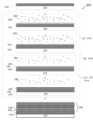
[0018] 도 5는 상이한 재료들에 대해 분당 총 질량 손실(㎍/cm2)로 아웃개싱을 비교하는 차트이다.
[0019] 도 6은 고 종횡비 피처를 갖는 컴포넌트 상의, 본원에서 설명되는 바와 같은 플라즈마 저항성 코팅의 이미지이다.
[0020] 도 7a는 본원에서 설명되는 바와 같은 플라즈마 저항성 코팅의 톱다운(top down) SEM 이미지를 도시한다.
[0021] 도 7b는 도 7a의 플라즈마 저항성 코팅의 TEM 단면 이미지를 도시한다.
[0022] 도 8a는 물건 상의 Al2O3 응력 완화 층을 갖지 않는 Y2O3의 ALD 코팅의 톱다운 SEM 이미지를 도시한다.
[0023] 도 8b는 물건 상의 도 8a의 ALD 코팅의 단면 이미지를 도시한다.
[0024] 도 9는 도 2c에 관하여 설명된 바와 같은, Al 6061 기판 상의 플라즈마 저항성 세라믹 코팅 구조의 측단면 TEM 이미지를 예시한다.
[0025] 도 10은 도 9에서 도시된 플라즈마 저항성 세라믹 샘플의 STEM-EDS(scanning transmission electron microscopy energy-dispersive x-ray spectroscopy) 라인 스캔이다.[0008] The present disclosure is illustrated by way of example and not by way of limitation in the accompanying drawings, where like reference numerals indicate like elements. It should be noted that different references to “one” or “one” embodiment of the present disclosure are not necessarily to the same embodiment, and such references refer to at least one.
[0009] Figure 1 shows a cross-sectional view of a processing chamber.
[0010] Figure 2A shows one embodiment of a deposition process according to an atomic layer deposition technique as described herein.
[0011] Figure 2B shows another embodiment of a deposition process according to an atomic layer deposition technique as described herein.
[0012] Figure 2C shows another embodiment of a deposition process according to an atomic layer deposition technique as described herein.
[0013] Figure 3A illustrates a method for creating a plasma resistant coating using atomic layer deposition as described herein.
[0014] Figure 3B illustrates a method for creating a plasma resistant coating using atomic layer deposition as described herein.
[0015] Figure 4A shows a showerhead chamber component according to embodiments.
[0016] Figure 4B shows an enlarged view of a gas conduit, where the interior of the gas conduit is coated with a plasma resistant coating as described herein.
[0017] Figure 4C shows a thermal pie chamber component according to embodiments.
[0018] Figure 5 is a chart comparing outgassing by total mass loss per minute (μg/cm2 ) for different materials.
[0019] Figure 6 is an image of a plasma resistant coating as described herein on a component with high aspect ratio features.
[0020] Figure 7A shows a top down SEM image of a plasma resistant coating as described herein.
[0021] Figure 7b shows a TEM cross-sectional image of the plasma resistant coating of Figure 7a.
[0022] Figure 8A shows a top-down SEM image of an ALD coating of Y2 O3 without an Al2 O3 stress relieving layer on the article.
[0023] Figure 8B shows a cross-sectional image of the ALD coating of Figure 8A on an object.
[0024] Figure 9 illustrates a cross-sectional TEM image of a plasma resistant ceramic coating structure on an Al 6061 substrate, as described with respect to Figure 2C.
[0025] FIG. 10 is a scanning transmission electron microscopy energy-dispersive x-ray spectroscopy (STEM-EDS) line scan of the plasma resistant ceramic sample shown in FIG. 9.
[0026] 본원에서 설명되는 실시예들은 물건들, 코팅된 챔버 컴포넌트들, 및 방법들을 커버하고, 여기서, 응력 완화 층, 및 이트륨-함유 산화물 층과 같은 희토류 금속-함유 산화물 층을 갖는 플라즈마 저항성 코팅이 컴포넌트들의 표면 상에 증착된다. 본원에서 사용되는 바와 같이, 플라즈마 저항성이라는 용어는 플라즈마뿐만 아니라 케미스트리(chemistry) 및 라디칼들에 대한 저항성을 의미한다. 표면은 알루미늄(예컨대, Al 6061, Al 6063) 또는 세라믹 재료일 수 있다. 증착 프로세스는 희토류 금속-함유 산화물 층을 위한 전구체들의 공동-증착을 포함할 수 있는 원자 층 증착(ALD) 프로세스이다. 플라즈마 저항성 코팅은 이중층 스택으로 구성될 수 있다. 이중층 스택은 비정질 Al2O3와 같은 알루미늄 산화물(Al2O3)의 응력 완화 층 및 이트륨-함유 산화물 층을 포함할 수 있다. 본원의 실시예들은 예로서 이트륨-함유 산화물 층을 이용하여 설명된다. 상단 층이 임의의 희토류 금속 산화물, 또는 희토류 금속 산화물들의 단상 또는 다상 혼합물들(즉, 이트륨을 갖거나 또는 갖지 않음)을 포함할 수 있다는 것이 인식될 것이다.[0026] Embodiments described herein cover articles, coated chamber components, and methods, including a plasma resistant coating having a stress relief layer and a rare earth metal-containing oxide layer, such as a yttrium-containing oxide layer. It is deposited on the surface of these components. As used herein, the term plasma resistance refers to resistance to plasma as well as chemistry and radicals. The surface may be aluminum (eg, Al 6061, Al 6063) or ceramic material. The deposition process is an atomic layer deposition (ALD) process that may include co-deposition of precursors for a rare earth metal-containing oxide layer. Plasma resistant coatings can be comprised of a double layer stack. The double layer stack may include a yttrium-containing oxide layer and a stress relief layer of aluminum oxide (Al2 O3 ), such as amorphous Al2 O3 . Embodiments herein are described using a yttrium-containing oxide layer as an example. It will be appreciated that the top layer may comprise any rare earth metal oxide, or single-phase or multi-phase mixtures of rare earth metal oxides (i.e., with or without yttrium).
[0027] 다층 플라즈마 저항성 코팅 내의 각각의 층의 두께는 약 10 nm 내지 약 1.5 ㎛일 수 있다. 실시예들에서, 응력 완화 층(예컨대, 비정질 Al2O3)은 약 1.0 ㎛의 두께를 가질 수 있고, 희토류 금속-함유 산화물 층은 약 50 nm의 두께를 가질 수 있다. 희토류 금속-함유 산화물 층 두께 대 응력 완화 층 두께의 비율은 200:1 내지 1:200일 수 있다. 두께 비율은 특정한 챔버 애플리케이션들에 따라 선택될 수 있다. 코팅은 2개의 층들 사이에 상호확산된 고체 상태 상을 포함하는 하나, 또는 하나 초과의 중간 층을 생성하기 위해 어닐링될 수 있다. 플라즈마 저항성 코팅은, 약 10:1 내지 약 300:1의 종횡비를 갖는, 물건 내의 피처들의 표면들을 코팅할 수 있거나 또는 덮을 수 있다. 플라즈마 저항성 코팅은 또한, 실질적으로 균일한 두께로 그러한 피처들을 등각적으로 덮을 수 있다. 일 실시예에서, 플라즈마 저항성 코팅은, 약 +/- 20 % 미만의 두께 변동, +/- 10 %의 두께 변동, +/- 5 %의 두께 변동, 또는 더 낮은 두께 변동을 갖는 균일한 두께로 코팅된 아래에 놓인 표면(코팅된 표면 피처들을 포함함)의 등각적 커버리지를 갖는다.[0027] The thickness of each layer within the multilayer plasma resistant coating can be from about 10 nm to about 1.5 μm. In embodiments, the stress relief layer (eg, amorphous Al2 O3 ) may have a thickness of approximately 1.0 μm and the rare earth metal-containing oxide layer may have a thickness of approximately 50 nm. The ratio of rare earth metal-containing oxide layer thickness to stress relief layer thickness may be 200:1 to 1:200. Thickness ratio may be selected depending on specific chamber applications. The coating may be annealed to create one, or more than one intermediate layer comprising a solid state phase interdiffused between the two layers. A plasma resistant coating can coat or cover the surfaces of features in an object, having an aspect ratio of about 10:1 to about 300:1. The plasma resistant coating may also conformally cover such features with a substantially uniform thickness. In one embodiment, the plasma resistant coating has a uniform thickness with a thickness variation of less than about +/- 20%, a thickness variation of +/- 10%, a thickness variation of +/- 5%, or less. It has conformal coverage of the coated underlying surface (including coated surface features).
[0028] 본원에서 설명되는 실시예들은, 응력 완화 층(예컨대, 비정질 Al2O3) 및 그 위의 이트륨-함유 산화물 층(예컨대, 다른 희토류 금속 산화물과 단상으로 증착된 Y2O3)과 같은 희토류 금속-함유 산화물 층을 갖는 플라즈마 저항성 코팅들로, 챔버 컴포넌트들 및 다른 물건들의 고 종횡비 피처들이 효과적으로 코팅될 수 있게 한다. 플라즈마 저항성 코팅들은 고 종횡비 피처 내에서 등각적이고, 실질적으로 균일한 코팅으로(예컨대, 약 +/- 5 % 또는 그 미만의 두께 변동으로) 피처를 덮을 수 있다. 플라즈마 저항성 코팅은 또한, 약 0 %의 다공도로 매우 치밀하다(예컨대, 실시예들에서, 플라즈마 저항성 코팅은 무-다공성일 수 있다). 응력 완화 층 및 희토류 금속-함유 산화물 층을 갖는 플라즈마 저항성 코팅들은, CCl4/CHF3 플라즈마 에칭 케미스트리들, HCl3Si 에칭 케미스트리들, 및 NF3 에칭 케미스트리들과 같은 플라즈마 에칭 케미스트리들로부터의 부식 및 침식에 대해 저항적일 수 있다. 부가적으로, 응력 완화 층 및 희토류 금속-함유 산화물 층을 갖는 본원에서 설명되는 플라즈마 저항성 코팅들은 최대 약 350 ℃의 온도들에서 균열 및 박리에 대해 저항적일 수 있다. 예컨대, 본원에서 설명되는 플라즈마 저항성 코팅을 갖는 챔버 컴포넌트는 약 200 ℃의 온도들까지의 가열을 포함하는 프로세스들에서 사용될 수 있다. 챔버 컴포넌트는, 플라즈마 저항성 코팅에 어떠한 균열들 또는 박리도 도입하지 않으면서, 실온 내지 약 200 ℃의 온도로 열적으로 사이클링될 수 있다.[0028] Embodiments described herein include a stress relief layer (e.g., amorphous Al2 O3 ) and a yttrium-containing oxide layer thereon (e.g., Y2 O3 deposited single phase with another rare earth metal oxide); Plasma resistant coatings with the same rare earth metal-containing oxide layer allow high aspect ratio features of chamber components and other objects to be coated effectively. Plasma resistant coatings are conformal within a high aspect ratio feature and can cover the feature with a substantially uniform coating (e.g., with thickness variation of about +/- 5% or less). The plasma resistant coating is also very dense, with a porosity of about 0% (eg, in embodiments, the plasma resistant coating may be non-porous). Plasma resistant coatings with a stress relief layer and a rare earth metal-containing oxide layer resist corrosion and corrosion from plasma etch chemistries such as CCl4 /CHF3 plasma etch chemistries, HCl3 Si etch chemistries, and NF3 etch chemistries. Can be resistant to erosion. Additionally, the plasma resistant coatings described herein having a stress relief layer and a rare earth metal-containing oxide layer can be resistant to cracking and delamination at temperatures up to about 350 degrees Celsius. For example, a chamber component with a plasma resistant coating described herein can be used in processes involving heating up to temperatures of about 200 degrees Celsius. The chamber component can be thermally cycled from room temperature to about 200° C. without introducing any cracks or delamination in the plasma resistant coating.
[0029] ALD는 물건의 표면과의 화학 반응들을 통해 재료의 제어되는 자기-제한적인 증착을 가능하게 한다. 등각적 프로세스인 것 이외에, ALD는 또한 균일한 프로세스이다. 고 종횡비 피처들(예컨대, 약 10:1 내지 약 300:1)을 포함하는, 물건의 모든 노출되는 측들에는 동일한 또는 대략 동일한 양의 재료가 증착될 것이다. ALD 프로세스의 전형적인 반응 사이클은, 전구체(즉, 단일 화학물 A)가 ALD 챔버 내에 플러딩되고(flooded) 물건의 표면 상에 흡착되는 것으로 시작된다. 이어서, 반응물(즉, 단일 화학물 R)이 ALD 챔버 내에 도입되고 이어서 플러싱(flush)되기 전에, 과도한 전구체가 ALD 챔버 밖으로 플러싱된다. 그러나, 세라믹 코팅들 내의 이트륨-함유 산화물 층(또는 다른 희토류 금속 산화물 층)은 재료들의 공동-증착에 의해 형성될 수 있다. 이를 달성하기 위해, 이트륨-함유 산화물 전구체(A)(예컨대, Y2O3)와 다른 희토류 금속 산화물(B) 전구체와 같은 2개의 전구체들의 혼합물이 임의의 수의 비율들, 예컨대, A90+B10, A70+B30, A50+B50, A30+B70, A10+A90 등으로 챔버 내에 공동-주입(AxBy)되고, 물건의 표면 상에 흡착된다. 이들 예들에서, x 및 y는 Ax+By에 대한 분자비들(mol%)로 표현된다. 예컨대, A90+B10은 A의 90 mol% 및 B의 10 mol%이다. 과도한 전구체들이 플러싱된다. 반응물이 ALD 챔버 내에 도입되고, 흡착된 전구체들과 반응하여, 과도한 화학물들이 플러싱되기 전에 고체 층을 형성한다. ALD의 경우에, 재료의 최종 두께는 실행되는 반응 사이클들의 수에 따라 좌우되는데, 이는 각각의 반응 사이클이, 하나의 원자 층 또는 원자 층의 부분일 수 있는 특정한 두께의 층을 성장시킬 것이기 때문이다.[0029] ALD enables controlled, self-limiting deposition of materials through chemical reactions with the surface of the object. In addition to being a conformal process, ALD is also a uniform process. The same or approximately the same amount of material will be deposited on all exposed sides of the object, including high aspect ratio features (eg, about 10:1 to about 300:1). The typical reaction cycle of an ALD process begins with a precursor (i.e., a single chemical A) being flooded into the ALD chamber and adsorbed onto the surface of the object. Excess precursor is then flushed out of the ALD chamber before reactants (i.e., a single chemical R) are introduced into the ALD chamber and subsequently flushed. However, the yttrium-containing oxide layer (or other rare earth metal oxide layer) in ceramic coatings can be formed by co-deposition of materials. To achieve this, a mixture of two precursors, such as a yttrium-containing oxide precursor (A) (e.g. Y2 O3 ) and another rare earth metal oxide (B) precursor, is mixed in any number of ratios, e.g. A90+B10. , A70+B30, A50+B50, A30+B70, A10+A90, etc. are co-injected (Ax By ) into the chamber and adsorbed on the surface of the object. In these examples, x and y are expressed as molecular ratios (mol%) relative to Ax+By. For example, A90+B10 is 90 mol% of A and 10 mol% of B. Excess precursors are flushed out. Reactants are introduced into the ALD chamber and react with the adsorbed precursors to form a solid layer before excess chemicals are flushed out. In the case of ALD, the final thickness of the material depends on the number of reaction cycles performed, since each reaction cycle will grow a layer of a certain thickness, which may be one atomic layer or a portion of an atomic layer. .
[0030] 고 종횡비 피처들을 갖는 컴포넌트들 상에 코팅들을 증착하기 위해 전형적으로 사용되는 다른 기법들, 이를테면, 플라즈마 스프레이 코팅 및 이온 보조 증착과 달리, ALD 기법은 그러한 피처들 내에(즉, 피처들의 표면들 상에) 재료의 층을 증착할 수 있다. 부가적으로, ALD 기법은 무-다공성(즉, 핀-홀이 없음)인 비교적 얇은(즉, 1 ㎛ 또는 그 미만) 코팅들을 생산하고, 이는 증착 동안에 균열 형성을 제거할 수 있다. 본원에서 사용되는 바와 같은 "무-다공성"이라는 용어는, TEM(transmission electron microscopy)에 의해 측정했을 때 코팅의 전체 깊이를 따라 어떠한 세공들, 핀-홀들, 공극들, 또는 균열들도 없는 것을 의미한다. TEM은 집속 이온 빔 밀링에 의해 준비된 100 nm 두께의 TEM 라멜라(lamella)를 사용하여 수행될 수 있고, TEM은 명시야(bright-field), 암시야(dark-field), 또는 고-해상도 모드에서 200 kV로 동작된다. 반대로, 통상적인 e-빔 IAD 또는 플라즈마 스프레이 기법들을 이용하면, 심지어 5 또는 10 ㎛의 두께들의 증착 시에 균열들이 형성되고, 다공도는 1 내지 3 %일 수 있다.[0030] Unlike other techniques typically used to deposit coatings on components with high aspect ratio features, such as plasma spray coating and ion-assisted deposition, ALD techniques do not deposit coatings within such features (i.e., on the surface of the features). layers of material can be deposited on the Additionally, ALD techniques produce relatively thin (i.e., 1 μm or less) coatings that are non-porous (i.e., free of pin-holes), which can eliminate crack formation during deposition. As used herein, the term "non-porous" means the absence of any pores, pin-holes, voids, or cracks along the entire depth of the coating as measured by transmission electron microscopy (TEM). do. TEM can be performed using 100 nm thick TEM lamellaes prepared by focused ion beam milling, and TEM can be performed in bright-field, dark-field, or high-resolution modes. It operates at 200 kV. In contrast, using conventional e-beam IAD or plasma spray techniques, cracks are formed even upon deposition of thicknesses of 5 or 10 μm, and porosity can be 1 to 3%.
[0031] 챔버 벽들, 샤워헤드들, 노즐들, 플라즈마 생성 유닛들(예컨대, 하우징들을 갖는 무선 주파수 전극들), 확산기들, 및 가스 라인들과 같은 프로세스 챔버 컴포넌트들은, 가혹한 에칭 환경들에서 컴포넌트들을 보호하기 위해 이들 플라즈마 저항성 코팅들을 갖는 것으로부터 이익을 얻을 것이다. 이들 챔버 컴포넌트들 중 다수는 약 10:1 내지 약 300:1의 범위에 있는 종횡비들을 갖고, 이는 통상적인 증착 방법들을 사용하여 이들을 양호하게 코팅하는 것을 어렵게 만든다. 본원에서 설명되는 실시예들은 전술된 프로세스 챔버 컴포넌트들과 같은 고 종횡비 물건들이, 물건들을 보호하는 플라즈마 저항성 코팅들로 코팅될 수 있게 한다. 예컨대, 실시예들은 가스 라인들의 내부들, 노즐들의 내부들, 샤워헤드들 내의 홀들의 내부들 등이 희토류 금속-함유 산화물 세라믹 코팅으로 코팅될 수 있게 한다.[0031] Process chamber components such as chamber walls, showerheads, nozzles, plasma generation units (e.g., radio frequency electrodes with housings), diffusers, and gas lines maintain the components in harsh etching environments. You will benefit from having these plasma resistant coatings to protect yourself. Many of these chamber components have aspect ratios ranging from about 10:1 to about 300:1, making them difficult to coat well using conventional deposition methods. Embodiments described herein allow high aspect ratio objects, such as the process chamber components described above, to be coated with plasma resistant coatings that protect the objects. For example, embodiments allow the interiors of gas lines, interiors of nozzles, interiors of holes in showerheads, etc. to be coated with a rare earth metal-containing oxide ceramic coating.
[0032] 도 1은 실시예들에 따른, 응력 완화 층 및 희토류 금속-함유 산화물 층을 갖는 플라즈마 저항성 코팅으로 코팅된 하나 또는 그 초과의 챔버 컴포넌트들을 갖는 반도체 프로세싱 챔버(100)의 단면도이다. 프로세싱 챔버(100)는 플라즈마 프로세싱 조건들을 갖는 부식성 플라즈마 환경이 제공되는 프로세스들을 위해 사용될 수 있다. 예컨대, 프로세싱 챔버(100)는 플라즈마 에칭기 또는 플라즈마 에칭 반응기, 플라즈마 세정기, 플라즈마 강화 CVD 또는 ALD 반응기들 등을 위한 챔버일 수 있다. 플라즈마 저항성 코팅을 포함할 수 있는 챔버 컴포넌트들의 예들은 복잡한 형상들, 및 고 종횡비들을 갖는 홀들을 갖는 챔버 컴포넌트들을 포함한다. 일부 예시적인 챔버 컴포넌트들은 기판 지지 조립체(148), 정전 척(ESC)(150), 링(예컨대, 프로세스 키트 링 또는 단일 링), 챔버 벽, 베이스, 가스 분배 플레이트, 프로세싱 챔버의 샤워헤드, 가스 라인들, 노즐, 덮개, 라이너, 라이너 키트, 실드, 플라즈마 스크린, 유동 등화기, 냉각 베이스, 챔버 뷰포트, 챔버 덮개 등을 포함한다. 아래에서 더 상세히 설명되는 플라즈마 저항성 코팅은 ALD에 의해 적용된다. ALD는, 고 종횡비들을 갖는 피처들을 갖고 복잡한 형상들을 갖는 컴포넌트들을 포함하는 모든 타입들의 컴포넌트들 상에 무-다공성인 실질적으로 균일한 두께의 등각적 코팅을 적용할 수 있게 한다.[0032] Figure 1 is a cross-sectional view of a
[0033] 플라즈마 저항성 코팅은, 희토류 금속-함유 산화물 층을 형성하기 위해 희토류 금속-함유 산화물을 증착하거나, 또는 하나 또는 그 초과의 부가적인 산화물들과 조합하여 희토류 금속-함유 산화물을 공동-증착하기 위한 하나 또는 그 초과의 전구체들, 및 응력 완화 층을 위한 전구체로 ALD를 사용하여 성장 또는 증착될 수 있다. 일 실시예에서, 희토류 금속-함유 산화물 층은 다결정질 구조를 갖는다. 희토류 금속-함유 산화물은 이트륨, 탄탈럼, 지르코늄, 및/또는 에르븀을 포함할 수 있다. 예컨대, 희토류 금속-함유 산화물은 이트리아(Y2O3), 에르븀 산화물(Er2O3), 지르코늄 산화물(ZrO2), 탄탈럼 산화물(Ta2O5) 등일 수 있다. 실시예들에서, 희토류 금속-함유 산화물은 다결정질 이트리아이다. 다른 실시예들에서, 희토류 금속-함유 산화물은 비정질 이트리아이다. 희토류 금속-함유 산화물은 또한, 이트륨, 지르코늄, 및/또는 에르븀과 같은 하나 또는 그 초과의 희토류 원소들과 혼합된 알루미늄을 포함할 수 있다. 희토류 금속-함유 산화물 층을 형성하기 위해 희토류 금속-함유 산화물과 공동-증착될 수 있는 부가적인 산화물(또는 산화물들)은 지르코늄 산화물(ZrO2), 알루미늄 산화물(Al2O3), 에르븀 산화물(Er2O3), 또는 이들의 조합을 포함할 수 있다. 예컨대, 다층 플라즈마 저항성 코팅을 위한 이트륨-함유 산화물 층은 YxZryOz, YaZrxAlyOz, YxAlyOz, 또는 YxEryOz일 수 있다. 이트륨-함유 산화물은 공간군 Ia-3(206)를 갖는 입방형 구조를 갖는 이트리얼라이트를 갖는 이트리아(Y2O3)일 수 있다.[0033] The plasma resistant coating may be made by depositing a rare earth metal-containing oxide to form a rare earth metal-containing oxide layer, or by co-depositing the rare earth metal-containing oxide in combination with one or more additional oxides. One or more precursors for, and the precursor for the stress relief layer may be grown or deposited using ALD. In one embodiment, the rare earth metal-containing oxide layer has a polycrystalline structure. Rare earth metal-containing oxides may include yttrium, tantalum, zirconium, and/or erbium. For example, the rare earth metal-containing oxide may be yttria (Y2 O3 ), erbium oxide (Er2 O3 ), zirconium oxide (ZrO2 ), tantalum oxide (Ta2 O5 ), etc. In embodiments, the rare earth metal-containing oxide is polycrystalline yttria. In other embodiments, the rare earth metal-containing oxide is amorphous yttria. Rare earth metal-containing oxides may also include aluminum mixed with one or more rare earth elements such as yttrium, zirconium, and/or erbium. Additional oxides (or oxides) that can be co-deposited with the rare earth metal-containing oxide to form a rare earth metal-containing oxide layer include zirconium oxide (ZrO2 ), aluminum oxide (Al2 O3 ), and erbium oxide ( Er2 O3 ), or a combination thereof. For example, the yttrium-containing oxide layer for a multilayer plasma resistant coating can be Yx Zry Oz , Ya Zrx Aly Oz , Yx Aly Oz , or Yx Ery Oz . The yttrium-containing oxide may be yttria (Y2 O3 ) with yttrealite having a cubic structure with the space group Ia-3 (206).
[0034] 일 실시예에서, 희토류 금속-함유 산화물 층은 Y2O3, Er2O3, Y3Al5O12(YAG), Er3Al5O12(EAG), 또는 Y4Al2O9(YAM) 중 하나이다. 희토류 금속-함유 산화물 층은 또한, YAlO3(YAP), Er4Al2O9(EAM), ErAlO3(EAP), Y2O3-ZrO2의 고용체, 및/또는 Y2O3-ZrO2의 고용체 및 Y4Al2O9을 포함하는 세라믹 화합물일 수 있다.[0034] In one embodiment, the rare earth metal-containing oxide layer is Y2 O3 , Er2 O3 , Y3 Al5 O12 (YAG), Er3 Al5 O12 (EAG), or Y4 Al2 It is one of O9 (YAM). The rare earth metal-containing oxide layer may also be a solid solution of YAlO3 (YAP), Er4 Al2 O9 (EAM), ErAlO3 (EAP), Y2 O3 -ZrO2 , and/or Y2 O3 -ZrO It may be a ceramic compound containing a solid solution of2 and Y4 Al2 O9 .
[0035] Y2O3-ZrO2의 고용체에 관하여, 희토류 금속-함유 산화물 층은 10 내지 90 분자비(mol%)의 농도의 Y2O3 및 10 내지 90 mol%의 농도의 ZrO2를 포함할 수 있다. 일부 예들에서, Y2O3-ZrO2의 고용체는 10 내지 20 mol% Y2O3 및 80 내지 90 mol% ZrO2를 포함할 수 있고, 20 내지 30 mol% Y2O3 및 70 내지 80 mol% ZrO2를 포함할 수 있고, 30 내지 40 mol% Y2O3 및 60 내지 70 mol% ZrO2를 포함할 수 있고, 40 내지 50 mol% Y2O3 및 50 내지 60 mol% ZrO2를 포함할 수 있고, 60 내지 70 mol% Y2O3 및 30 내지 40 mol% ZrO2를 포함할 수 있고, 70 내지 80 mol% Y2O3 및 20 내지 30 mol% ZrO2를 포함할 수 있고, 80 내지 90 mol% Y2O3 및 10 내지 20 mol% ZrO2를 포함할 수 있고, 기타 등등을 포함할 수 있다.[0035] Regarding the solid solution of Y2 O3 -ZrO2 , the rare earth metal-containing oxide layer contains Y2 O3 at a concentration of 10 to 90 mol% and ZrO2 at a concentration of 10 to 90 mol%. It can be included. In some examples, the solid solution of Y2 O3 -ZrO2 may include 10 to 20 mol% Y2 O3 and 80 to 90 mol% ZrO2 , 20 to 30 mol% Y2 O3 and 70 to 80 mol% mol% ZrO2 , 30 to 40 mol% Y2 O3 and 60 to 70 mol% ZrO2 , 40 to 50 mol% Y2 O3 and 50 to 60 mol% ZrO2 It may include 60 to 70 mol% Y2 O3 and 30 to 40 mol% ZrO2 , and it may include 70 to 80 mol% Y2 O3 and 20 to 30 mol% ZrO2 and may include 80 to 90 mol% Y2 O3 and 10 to 20 mol% ZrO2 , and the like.
[0036] Y2O3-ZrO2의 고용체 및 Y4Al2O9을 포함하는 세라믹 화합물에 관하여, 일 실시예에서, 세라믹 화합물은 62.93 분자비(mol%) Y2O3, 23.23 mol% ZrO2, 및 13.94 mol% Al2O3를 포함한다. 다른 실시예에서, 세라믹 화합물은 50 내지 75 mol%의 범위에 있는 Y2O3, 10 내지 30 mol%의 범위에 있는 ZrO2, 및 10 내지 30 mol%의 범위에 있는 Al2O3를 포함할 수 있다. 다른 실시예에서, 세라믹 화합물은 40 내지 100 mol%의 범위에 있는 Y2O3, 0.1 내지 60 mol%의 범위에 있는 ZrO2, 및 0.1 내지 10 mol%의 범위에 있는 Al2O3를 포함할 수 있다. 다른 실시예에서, 세라믹 화합물은 40 내지 60 mol%의 범위에 있는 Y2O3, 30 내지 50 mol%의 범위에 있는 ZrO2, 및 10 내지 20 mol%의 범위에 있는 Al2O3를 포함할 수 있다. 다른 실시예에서, 세라믹 화합물은 40 내지 50 mol%의 범위에 있는 Y2O3, 20 내지 40 mol%의 범위에 있는 ZrO2, 및 20 내지 40 mol%의 범위에 있는 Al2O3를 포함할 수 있다. 다른 실시예에서, 세라믹 화합물은 70 내지 90 mol%의 범위에 있는 Y2O3, 0.1 내지 20 mol%의 범위에 있는 ZrO2, 및 10 내지 20 mol%의 범위에 있는 Al2O3를 포함할 수 있다. 다른 실시예에서, 세라믹 화합물은 60 내지 80 mol%의 범위에 있는 Y2O3, 0.1 내지 10 mol%의 범위에 있는 ZrO2, 및 20 내지 40 mol%의 범위에 있는 Al2O3를 포함할 수 있다. 다른 실시예에서, 세라믹 화합물은 40 내지 60 mol%의 범위에 있는 Y2O3, 0.1 내지 20 mol%의 범위에 있는 ZrO2, 및 30 내지 40 mol%의 범위에 있는 Al2O3를 포함할 수 있다. 다른 실시예들에서, 다른 분배들이 또한 세라믹 화합물에 대해 사용될 수 있다.[0036] Regarding the ceramic compound comprising a solid solution of Y2 O3 -ZrO2 and Y4 Al2 O9 , in one embodiment, the ceramic compound has a molecular ratio (mol%) of 62.93 Y2 O3 , 23.23 mol%. ZrO2 , and 13.94 mol% Al2 O3 . In another embodiment, the ceramic compound comprises Y2 O3 in the range of 50 to 75 mol %, ZrO2 in the range of 10 to 30 mol %, and Al2 O3 in the range of 10 to 30 mol %. can do. In another embodiment, the ceramic compound comprises Y2 O3 in the range of 40 to 100 mol %, ZrO2 in the range of 0.1 to 60 mol %, and Al2 O3 in the range of 0.1 to 10 mol %. can do. In another embodiment, the ceramic compound comprises Y2 O3 in the range of 40 to 60 mol %, ZrO2 in the range of 30 to 50 mol %, and Al2 O3 in the range of 10 to 20 mol %. can do. In another embodiment, the ceramic compound comprises Y2 O3 in the range of 40 to 50 mol %, ZrO2 in the range of 20 to 40 mol %, and Al2 O3 in the range of 20 to 40 mol %. can do. In another embodiment, the ceramic compound comprises Y2 O3 in the range of 70 to 90 mol %, ZrO2 in the range of 0.1 to 20 mol %, and Al2 O3 in the range of 10 to 20 mol %. can do. In another embodiment, the ceramic compound comprises Y2 O3 in the range of 60 to 80 mol %, ZrO2 in the range of 0.1 to 10 mol %, and Al2 O3 in the range of 20 to 40 mol %. can do. In another embodiment, the ceramic compound comprises Y2 O3 in the range of 40 to 60 mol %, ZrO2 in the range of 0.1 to 20 mol %, and Al2 O3 in the range of 30 to 40 mol %. can do. In other embodiments, other distributions may also be used for the ceramic compound.
[0037] 일 실시예에서, Y2O3, ZrO2, Er2O3, Gd2O3, 및 SiO2의 조합을 포함하는 대안적인 세라믹 화합물이 희토류 금속-함유 산화물 층을 위해 사용된다. 일 실시예에서, 대안적인 세라믹 화합물은 40 내지 45 mol%의 범위에 있는 Y2O3, 0 내지 10 mol%의 범위에 있는 ZrO2, 35 내지 40 mol%의 범위에 있는 Er2O3, 5 내지 10 mol%의 범위에 있는 Gd2O3, 및 5 내지 15 mol%의 범위에 있는 SiO2를 포함할 수 있다. 제1 예에서, 대안적인 세라믹 화합물은 40 mol% Y2O3, 5 mol% ZrO2, 35 mol% Er2O3, 5 mol% Gd2O3, 및 15 mol% SiO2를 포함한다. 제2 예에서, 대안적인 세라믹 화합물은 45 mol% Y2O3, 5 mol% ZrO2, 35 mol% Er2O3, 10 mol% Gd2O3, 및 5 mol% SiO2를 포함한다. 제3 예에서, 대안적인 세라믹 화합물은 40 mol% Y2O3, 5 mol% ZrO2, 40 mol% Er2O3, 7 mol% Gd2O3, 및 8 mol% SiO2를 포함한다.[0037] In one embodiment, an alternative ceramic compound comprising a combination of Y2 O3 , ZrO2 , Er2 O3 , Gd2 O3 , and SiO2 is used for the rare earth metal-containing oxide layer. In one embodiment, alternative ceramic compounds include Y2 O3 in the range of 40 to 45 mol%, ZrO2 in the range of 0 to 10 mol%, Er2 O3 in the range of 35 to 40 mol%, It may include Gd2 O3 in the range of 5 to 10 mol%, and SiO2 in the range of 5 to 15 mol%. In a first example, alternative ceramic compounds include 40 mol% Y2 O3 , 5 mol% ZrO2 , 35 mol% Er2 O3 , 5 mol% Gd2 O3 , and 15 mol% SiO2 . In a second example, alternative ceramic compounds include 45 mol% Y2 O3 , 5 mol% ZrO2 , 35 mol% Er2 O3 , 10 mol% Gd2 O3 , and 5 mol% SiO2 . In a third example, alternative ceramic compounds include 40 mol% Y2 O3 , 5 mol% ZrO2 , 40 mol% Er2 O3 , 7 mol% Gd2 O3 , and 8 mol% SiO2 .
[0038] 전술된 희토류 금속-함유 산화물 층들 중 임의의 것은 미량의 다른 재료들, 이를테면, ZrO2, Al2O3, SiO2, B2O3, Er2O3, Nd2O3, Nb2O5, CeO2, Sm2O3, Yb2O3, 또는 다른 산화물들을 포함할 수 있다.[0038] Any of the rare earth metal-containing oxide layers described above may contain trace amounts of other materials, such as ZrO2 , Al2 O3 , SiO2 , B2 O3 , Er2 O3 , Nd2 O3 , Nb.2 O5 , CeO2 , Sm2 O3 , Yb2 O3 , or other oxides.
[0039] 응력 완화 층은 비정질 알루미늄 산화물 또는 유사한 재료를 포함할 수 있고, 실시예들에서 최대 약 350 ℃, 또는 200 ℃, 또는 약 200 ℃ 내지 약 350 ℃의 온도들에서의 플라즈마 저항성 코팅의 균열 및 박리에 대한 열 저항뿐만 아니라, 챔버 컴포넌트에 대한 플라즈마 저항성 코팅의 접착을 개선한다.[0039] The stress relief layer may include amorphous aluminum oxide or a similar material and, in embodiments, cracking of the plasma resistant coating at temperatures up to about 350° C., or 200° C., or about 200° C. to about 350° C. and improving adhesion of the plasma resistant coating to chamber components, as well as thermal resistance to delamination.
[0040] 예시된 바와 같이, 일 실시예에 따라, 기판 지지 조립체(148)는 플라즈마 저항성 코팅(136)을 갖는다. 그러나, 챔버 벽들, 샤워헤드들, 가스 라인들, 정전 척들, 노즐들 등과 같은 다른 챔버 컴포넌트들 중 임의의 챔버 컴포넌트가 또한 세라믹 코팅으로 코팅될 수 있다는 것이 이해되어야 한다.[0040] As illustrated, according to one embodiment, the
[0041] 일 실시예에서, 프로세싱 챔버(100)는 챔버 바디(102) 및 샤워헤드(130)를 포함하고, 그 챔버 바디(102) 및 샤워헤드(130)는 내부 볼륨(106)을 밀폐한다. 샤워헤드(130)는 샤워헤드 베이스 및 샤워헤드 가스 분배 플레이트를 포함할 수 있다. 대안적으로, 샤워헤드(130)는, 일부 실시예들에서 덮개 및 노즐에 의해, 또는 다른 실시예들에서 다수의 파이 형상 샤워헤드 컴파트먼트들 및 플라즈마 생성 유닛들에 의해 대체될 수 있다. 챔버 바디(102)는 알루미늄, 스테인리스 강, 또는 다른 적합한 재료로 제작될 수 있다. 챔버 바디(102)는 일반적으로, 측벽들(108) 및 하단부(110)를 포함한다. 샤워헤드(130)(또는 덮개 및/또는 노즐), 측벽들(108), 및/또는 하단부(110) 중 임의의 것은 플라즈마 저항성 코팅을 포함할 수 있다.[0041] In one embodiment, processing
[0042] 외측 라이너(116)가 챔버 바디(102)를 보호하기 위해 측벽들(108)에 인접하게 배치될 수 있다. 외측 라이너(116)는 이중층 코팅으로 제작 및/또는 코팅될 수 있다. 일 실시예에서, 외측 라이너(116)는 알루미늄 산화물로 제작된다.[0042] An
[0043] 배기 포트(126)가 챔버 바디(102)에 정의될 수 있고, 펌프 시스템(128)에 내부 볼륨(106)을 커플링시킬 수 있다. 펌프 시스템(128)은, 프로세싱 챔버(100)의 내부 볼륨(106)의 압력을 조절하고 진공배기(evacuate)시키기 위해 활용되는, 하나 또는 그 초과의 펌프들 및 스로틀 밸브들을 포함할 수 있다.[0043] An
[0044] 샤워헤드(130)는 챔버 바디(102)의 측벽(108) 상에 지지될 수 있다. 샤워헤드(130)(또는 덮개)는 프로세싱 챔버(100)의 내부 볼륨(106)으로의 접근을 가능하게 하도록 개방될 수 있고, 폐쇄되는 동안에는 프로세싱 챔버(100)에 대한 밀봉을 제공할 수 있다. 가스 패널(158)이 샤워헤드(130) 또는 덮개 및 노즐을 통해 내부 볼륨(106)에 프로세스 및/또는 세정 가스들을 제공하기 위해 프로세싱 챔버(100)에 커플링될 수 있다. 샤워헤드(130)는 유전체 에칭(유전체 재료들의 에칭)을 위해 사용되는 프로세싱 챔버들을 위해 사용될 수 있다. 샤워헤드(130)는 가스 분배 플레이트(GDP)(133)를 포함하고, 그 가스 분배 플레이트(GDP)(133)는 GDP(133) 전체에 걸쳐 다수의 가스 전달 홀들(132)을 갖는다. 샤워헤드(130)는 알루미늄 베이스 또는 양극산화된 알루미늄 베이스에 본딩된 GDP(133)를 포함할 수 있다. GDP(133)는 Si 또는 SiC로 제조될 수 있거나, 또는 세라믹, 이를테면 Y2O3, Al2O3, Y3Al5O12(YAG) 등일 수 있다. 샤워헤드(130) 및 전달 홀들(132)은, 도 4a 및 도 4b에 대하여 아래에서 더 상세히 설명되는 바와 같이, 플라즈마 저항성 코팅으로 코팅될 수 있다.[0044] The
[0045] 전도체 에칭(전도성 재료들의 에칭)을 위해 사용되는 프로세싱 챔버들의 경우에, 샤워헤드 대신에 덮개가 사용될 수 있다. 덮개는 덮개의 중앙 홀 내에 피팅된 중앙 노즐을 포함할 수 있다. 덮개는 세라믹, 이를테면 Al2O3, Y2O3, YAG, 또는 Y2O3-ZrO2의 고용체 및 Y4Al2O9을 포함하는 세라믹 화합물일 수 있다. 노즐이 또한, 세라믹, 이를테면 Y2O3, YAG, 또는 Y2O3-ZrO2의 고용체 및 Y4Al2O9을 포함하는 세라믹 화합물일 수 있다. 덮개, 샤워헤드 베이스(104), GDP(133), 및/또는 노즐이 전부, 실시예에 따른 플라즈마 저항성 코팅으로 코팅될 수 있다.[0045] In the case of processing chambers used for conductor etching (etching of conductive materials), a cover may be used instead of a showerhead. The cover may include a central nozzle fitted within a central hole in the cover. The cover may be a ceramic, such as Al2 O3 , Y2 O3 , YAG, or a ceramic compound comprising a solid solution of Y2 O3 -ZrO2 and Y4 Al2 O9 . The nozzle may also be a ceramic, such as Y2 O3 , YAG, or a ceramic compound comprising a solid solution of Y2 O3 -ZrO2 and Y4 Al2 O9 . The lid,
[0046] 프로세싱 챔버(100)에서 기판들을 프로세싱하기 위해 사용될 수 있는 프로세싱 가스들의 예들은, 할로겐-함유 가스들, 이를테면 특히, C2F6, SF6, SiCl4, HBr, NF3, CF4, CHF3, CH2F3, F, NF3, Cl2, CCl4, BCl3 및 SiF4, 및 다른 가스들, 이를테면 O2 또는 N2O를 포함한다. 캐리어 가스들의 예들은 N2, He, Ar, 및 프로세스 가스들(예컨대, 비-반응성 가스들)에 대해 비활성인 다른 가스들을 포함한다. 기판 지지 조립체(148)는 프로세싱 챔버(100)의 내부 볼륨(106)에서 샤워헤드(130) 또는 덮개 아래에 배치된다. 기판 지지 조립체(148)는 프로세싱 동안에 기판(144)을 홀딩한다. 링(146)(예컨대, 단일 링)이 정전 척(150)의 일부를 덮을 수 있고, 프로세싱 동안에 플라즈마에 대한 노출로부터 그 덮인 부분을 보호할 수 있다. 일 실시예에서, 링(146)은 실리콘 또는 석영일 수 있다.[0046] Examples of processing gases that can be used to process substrates in
[0047] 내측 라이너(118)가 기판 지지 조립체(148)의 주변부 상에 코팅될 수 있다. 내측 라이너(118)는 외측 라이너(116)를 참조하여 논의된 것들과 같은 할로겐-함유 가스 저항 재료일 수 있다. 일 실시예에서, 내측 라이너(118)는 외측 라이너(116)의 재료들과 동일한 재료들로 제작될 수 있다. 부가적으로, 내측 라이너(118)가 또한, 본원에서 설명되는 바와 같은 플라즈마 저항성 코팅으로 코팅될 수 있다.[0047] An
[0048] 일 실시예에서, 기판 지지 조립체(148)는 정전 척(150) 및 페데스탈(152)을 지지하는 탑재 플레이트(162)를 포함한다. 정전 척(150)은 열 전도성 베이스(164), 및 본드(138)에 의해 열 전도성 베이스에 본딩된 정전 퍽(166)을 더 포함하고, 그 본드(138)는 일 실시예에서 규소수지 본드(silicone bond)일 수 있다. 예시되는 실시예에서, 정전 퍽(166)의 상부 표면은 이트륨-계 산화물 플라즈마 저항성 코팅(136)에 의해 덮일 수 있다. 플라즈마 저항성 코팅(136)은, 열 전도성 베이스(164) 및 정전 퍽(166)의 외측 및 측면 주변부뿐만 아니라, 정전 척 내의 큰 종횡비들을 갖는 임의의 다른 기하학적으로 복잡한 파트들 또는 홀들을 포함하는, 정전 척(150)의 전체 노출된 표면 상에 배치될 수 있다. 탑재 플레이트(162)는 챔버 바디(102)의 하단부(110)에 커플링되고, 유틸리티들(예컨대, 유체들, 전력 라인들, 센서 리드들 등)을 열 전도성 베이스(164) 및 정전 퍽(166)으로 라우팅하기 위한 통로들을 포함한다.[0048] In one embodiment, the
[0049] 열 전도성 베이스(164) 및/또는 정전 퍽(166)은, 기판 지지 조립체(148)의 측방향 온도 프로파일을 제어하기 위해, 하나 또는 그 초과의 선택적인 매립된 가열 엘리먼트들(176), 매립된 열 아이솔레이터(174), 및/또는 도관들(168, 170)을 포함할 수 있다. 도관들(168, 170)은 도관들(168, 170)을 통해 온도 조절 유체를 순환시키는 유체 소스(172)에 유체적으로 커플링될 수 있다. 일 실시예에서, 매립된 아이솔레이터(174)는 도관들(168, 170) 사이에 배치될 수 있다. 가열기(176)는 가열기 전력 소스(178)에 의해 조절된다. 도관들(168, 170) 및 가열기(176)는 열 전도성 베이스(164)의 온도를 제어하기 위해 활용될 수 있다. 도관들 및 가열기는 정전 퍽(166) 및 프로세싱되고 있는 기판(144)(예컨대, 웨이퍼)을 가열하고 그리고/또는 냉각시킨다. 정전 퍽(166) 및 열 전도성 베이스(164)의 온도는 제어기(195)를 사용하여 모니터링될 수 있는 복수의 온도 센서들(190, 192)을 사용하여 모니터링될 수 있다.[0049] The thermally
[0050] 정전 퍽(166)은 퍽(166)의 상부 표면에 형성될 수 있는 다수의 가스 통로들, 이를테면 그루브(groove)들, 메사(mesa)들, 및 다른 표면 피처들을 더 포함할 수 있다. 이들 표면 피처들은 전부, 실시예에 따른 이트륨-계 산화물 플라즈마 저항성 코팅으로 코팅될 수 있다. 가스 통로들은 정전 퍽(166)에 드릴링된 홀들을 통해 He와 같은 열 전달(또는 배면) 가스의 소스에 유체적으로 커플링될 수 있다. 동작 시에, 배면 가스는 정전 퍽(166)과 기판(144) 사이의 열 전달을 향상시키기 위해 가스 통로들 내로 제어되는 압력으로 제공될 수 있다.[0050]
[0051] 정전 퍽(166)은 척킹 전력 소스(182)에 의해 제어되는 적어도 하나의 클램핑 전극(180)을 포함한다. 클램핑 전극(180)(또는, 정전 퍽(166) 또는 베이스(164)에 배치된 다른 전극)은 추가로, 프로세싱 챔버(100) 내의 프로세스 및/또는 다른 가스들로부터 형성된 플라즈마를 유지하기 위해, 정합 회로(188)를 통해 하나 또는 그 초과의 RF 전력 소스들(184, 186)에 커플링될 수 있다. RF 전력 소스들(184, 186)은 일반적으로, 최대 약 10,000 와트의 전력 및 약 50 kHz 내지 약 3 GHz의 주파수를 갖는 RF 신호를 생성할 수 있다.[0051] The
[0052] 도 2a는 물건 상에 플라즈마 저항성 코팅을 성장시키거나 또는 증착하기 위한 ALD 기법에 따른 증착 프로세스의 일 실시예를 도시한다. 도 2b는 본원에서 설명되는 바와 같은 원자 층 증착 기법에 따른 증착 프로세스의 다른 실시예를 도시한다. 도 2c는 본원에서 설명되는 바와 같은 원자 층 증착 기법에 따른 증착 프로세스의 다른 실시예를 도시한다.[0052] Figure 2A shows one embodiment of a deposition process according to ALD techniques for growing or depositing a plasma resistant coating on an object. 2B shows another embodiment of a deposition process according to atomic layer deposition techniques as described herein. FIG. 2C shows another embodiment of a deposition process according to atomic layer deposition techniques as described herein.
[0053] 다양한 타입들의 ALD 프로세스들이 존재하고, 코팅될 표면, 코팅 재료, 표면과 코팅 재료 사이의 화학적 상호작용 등과 같은 여러 인자들에 기초하여 특정한 타입이 선택될 수 있다. 다양한 ALD 프로세스들에 대한 일반적인 원리는, 자기-제한적인 방식으로 차례로 표면과 화학적으로 반응하는 가스성 화학 전구체들의 펄스들에, 코팅될 표면을 반복적으로 노출시킴으로써, 박막 층을 성장시키는 것을 포함한다.[0053] Various types of ALD processes exist, and a particular type may be selected based on several factors such as the surface to be coated, the coating material, the chemical interaction between the surface and the coating material, etc. The general principle for various ALD processes involves growing a thin film layer by repeatedly exposing the surface to be coated to pulses of gaseous chemical precursors, which in turn chemically react with the surface in a self-limiting manner.
[0054] 도 2a 내지 도 2c는 표면을 갖는 물건(210)을 예시한다. 물건(210)은, 기판 지지 조립체, 정전 척(ESC), 링(예컨대, 프로세스 키트 링 또는 단일 링), 챔버 벽, 베이스, 가스 분배 플레이트, 가스 라인들, 샤워헤드, 플라즈마 전극들, 플라즈마 하우징, 노즐, 덮개, 라이너, 라이너 키트, 실드, 플라즈마 스크린, 유동 등화기, 냉각 베이스, 챔버 뷰포트, 챔버 덮개, 확산기 등을 포함하는(그러나 이에 제한되지 않는) 다양한 챔버 컴포넌트들(예컨대, 반도체 프로세스 챔버 컴포넌트들)을 표현할 수 있다. 물건(210)은 금속(이를테면, 알루미늄, 스테인리스 강), 세라믹, 금속-세라믹 합성물, 폴리머, 폴리머 세라믹 합성물, 마일러(mylar), 폴리에스테르, 또는 다른 적합한 재료들로 제조될 수 있고, AlN, Si, SiC, Al2O3, SiO2등과 같은 재료들을 더 포함할 수 있다.[0054] Figures 2A-2C illustrate an
[0055] ALD의 경우에, 표면 상으로의 전구체의 흡착 또는 흡착된 전구체와 반응물의 반응은 "반-반응"이라고 지칭될 수 있다. 제1 반 반응 동안에, 전구체가 표면 상에 완전히 흡착될 수 있게 할 정도로 충분한 시간 기간 동안 전구체가 물건(210)의 표면 상으로(또는 물건(210) 상에 형성된 층 상으로) 펄싱된다. 전구체가 표면 상의 유한한 수의 이용가능한 부위들 상에 흡착되어, 표면 상에 균일한 연속적인 흡착 층을 형성할 것이므로, 흡착은 자기-제한적이다. 전구체에 의해 이미 흡착된 임의의 부위들은, 균일한 연속적인 코팅 상에 새로운 이용가능한 부위들을 형성하게 될 처리를 흡착된 부위들이 받지 않는 한, 그리고/또는 흡착된 부위들이 그러한 처리를 받을 때까지, 동일한 전구체에 의한 추가적인 흡착에 대해 이용가능하지 않게 될 것이다. 예시적인 처리들은 플라즈마 처리, 라디칼들에 균일한 연속적인 흡착 층을 노출시키는 것에 의한 처리, 또는 표면에 흡착된 가장 최근의 균일한 연속적인 층과 반응할 수 있는 상이한 전구체의 도입일 수 있다.[0055] In the case of ALD, the adsorption of a precursor onto a surface or the reaction of an adsorbed precursor with a reactant may be referred to as a “half-reaction.” During the first half reaction, the precursor is pulsed onto the surface of the article 210 (or onto a layer formed on the article 210) for a period of time sufficient to allow the precursor to fully adsorb onto the surface. Adsorption is self-limiting because the precursor will adsorb on a finite number of available sites on the surface, forming a uniform, continuous adsorption layer on the surface. Any sites already adsorbed by the precursor unless and/or until the adsorbed sites undergo a treatment that will form new usable sites on a uniform continuous coating. It will not be available for further adsorption by the same precursor. Exemplary treatments may be plasma treatment, treatment by exposing a uniform continuous adsorbed layer to radicals, or introduction of a different precursor capable of reacting with the most recent uniform continuous layer adsorbed on the surface.
[0056] 일부 구현들에서, 2개 또는 그 초과의 전구체들이 함께 주입되고, 물건의 표면 상에 흡착된다. 산소-함유 반응물이 (예컨대, YAG, Y2O3-ZrO2의 상 등의) 고체 단상 또는 다상 층을 형성하도록 흡착물들과 반응하기 위해 주입될 때까지, 과도한 전구체들이 밖으로 펌핑된다. 이러한 프레시(fresh) 층은 다음 사이클에서 전구체들을 흡착할 준비가 된다.[0056] In some implementations, two or more precursors are injected together and adsorbed onto the surface of the article. Excess precursor is pumped out until an oxygen-containing reactant (eg, YAG, phase of Y2 O3 -ZrO2 , etc.) is injected to react with the adsorbates to form a solid single-phase or multi-phase layer. This fresh layer is ready to adsorb precursors in the next cycle.
[0057] 도 2a에서, 물건(210)은, 물건(210)의 표면이 흡착 층(214)을 형성하도록 제1 전구체(260)에 의해 완전히 흡착될 때까지 제1 지속기간 동안, 제1 전구체(260)에 도입될 수 있다. 후속하여, 물건(210)은 고체 응력 완화 층(216)을 성장시키도록 흡착 층(214)과 반응하기 위한 제1 반응물(265)에 도입될 수 있다(예컨대, 그에 따라, 응력 완화 층(216)이 완전히 성장 또는 증착되고, 여기서, 성장 및 증착이라는 용어들은 본원에서 교환가능하게 사용될 수 있다). 예컨대, 제1 전구체(260)는 알루미늄 또는 다른 금속을 위한 전구체일 수 있다. 응력 완화 층(216)이 산화물인 경우에, 제1 반응물(265)은 산소, 수증기, 오존, 순수 산소, 산소 라디칼들, 또는 다른 산소 소스일 수 있다. 따라서, ALD가 응력 완화 층(216)을 형성하기 위해 사용될 수 있다.[0057] In FIG. 2A, the
[0058] 응력 완화 층(216)이 알루미나(Al2O3) 응력 완화 층인 예에서, 물건(210)(예컨대, Al6061 기판)은, 표면 상의 모든 반응성 부위들이 소모될 때까지 제1 지속기간 동안, 제1 전구체(260)(예컨대, 트리메틸 알루미늄(TMA))에 도입될 수 있다. 잔여의 제1 전구체(260)가 플러싱되고, 이어서, 제2 절반 사이클을 시작하기 위해 H2O의 제1 반응물(265)이 반응기 내로 주입된다. 제1 반 반응에 의해 생성된 Al 함유 흡착 층과 H2O 분자들이 반응한 후에, Al2O3의 응력 완화 층(216)이 형성된다.[0058] In an example where the
[0059] 응력 완화 층(216)은 균일하고 연속적이고 등각적일 수 있다. 실시예들에서, 응력 완화 층(216)은 무 다공성일 수 있거나(예컨대, 0의 다공도를 가질 수 있음), 또는 대략 0의 다공도(예컨대, 0 % 내지 0.01 %의 다공도)를 가질 수 있다. 일부 실시예들에서, 층(216)은, 단일 ALD 증착 사이클 후에, 하나의 원자 층 미만 내지 수 원자들의 두께를 가질 수 있다. 일부 유기금속 전구체 분자들은 크다. 반응물(265)과 반응한 후에, 큰 유기 리간드들이 사라질 수 있고, 그에 따라, 훨씬 더 작은 금속 원자들이 남게 될 수 있다. (예컨대, 전구체들(260)의 도입에 이은 반응물들(265)의 도입을 포함하는) 하나의 완전한 ALD 사이클은 단일 원자 층 미만의 결과를 발생시킬 수 있다. 예컨대, TMA 및 H2O에 의해 성장된 Al2O3 단분자층은 전형적으로, 약 0.9 내지 1.3 A/사이클의 성장 레이트를 갖는 한편, Al2O3 격자 상수는 a = 4.7 A 및 c = 13 A이다(삼각형 구조의 경우).[0059] The
[0060] 더 두꺼운 응력 완화 층(216)을 증착하기 위해, 다수의 완전한 ALD 증착 사이클들이 구현될 수 있고, (예컨대, 전구체(260)의 도입, 플러싱, 반응물(265)의 도입, 및 다시 플러싱을 포함하는) 각각의 완전한 사이클은 하나의 원자 내지 수 원자들의 부가적인 부분만큼 두께를 증가시킨다. 도시된 바와 같이, 최대 n개의 완전한 사이클들이 응력 완화 층(216)을 성장시키기 위해 수행될 수 있고, 여기서, n은 1보다 더 큰 정수 값이다. 실시예들에서, 응력 완화 층(216)은 약 10 nm 내지 약 1.5 ㎛의 두께를 가질 수 있다. 실시예들에서, 응력 완화 층(216)은 약 10 nm 내지 약 15 nm의 두께를 가질 수 있거나, 또는 다른 실시예들에서, 약 0.8 내지 1.2 ㎛의 두께를 가질 수 있다.[0060] To deposit a thicker
[0061] 응력 완화 층(216)은 견고한 기계적 특성들을 제공한다. 응력 완화 층(216)은 절연 강도를 향상시킬 수 있고, (예컨대, Al6061, Al6063, 또는 세라믹으로 형성된) 컴포넌트에 대한 플라즈마 저항성 코팅의 더 양호한 접착을 제공할 수 있으며, 최대 약 200 ℃, 또는 최대 약 250 ℃, 또는 약 200 ℃ 내지 약 250 ℃의 온도들에서 플라즈마 저항성 코팅의 균열을 방지할 수 있다. 추가적인 실시예들에서, 응력 완화 층(216)은 최대 약 350 ℃의 온도들에서 플라즈마 저항성 코팅의 균열을 방지할 수 있다. 그러한 금속 물건들은 플라즈마 저항성 코팅의 희토류 금속-함유 산화물 층의 열 팽창 계수보다 상당히 더 높을 수 있는 열 팽창 계수를 갖는다. 응력 완화 층(216)을 먼저 적용함으로써, 물건과 희토류 금속-함유 산화물 층 사이의 열 팽창 계수들의 미스매치의 유해한 영향이 관리될 수 있다. ALD가 증착을 위해 사용되므로, 샤워헤드 내의 가스 전달 홀들 또는 가스 전달 라인과 같은 고 종횡비 피처들의 내부 표면들이 코팅될 수 있고, 그에 따라, 컴포넌트의 전체가 부식성 환경에 대한 노출로부터 보호될 수 있다.[0061] The
[0062] 실시예들에서, 층(216)은 비정질 Al2O3와 같은 Al2O3일 수 있다. 비정질 Al2O3는, 예컨대, 이트륨-함유 산화물보다 더 높은 온도 능력을 갖는다. 따라서, 이트륨-함유 산화물 층 또는 다른 희토류 금속-함유 산화물 층 아래의 응력 완화 층으로서의 비정질 Al2O3 층의 부가는, 이트리아/Al6061 계면의 일부 영역들에 집중된 상승된 응력을 완화시킴으로써, 전체적으로 플라즈마 저항성 코팅의 열 저항을 증가시킬 수 있다. 더욱이, Al2O3는 공통 엘리먼트들(즉, 알루미늄)로 인해 알루미늄 기반 컴포넌트에 대해 양호한 접착을 갖는다. 유사하게, Al2O3는, 마찬가지로 공통 엘리먼트들(즉, 산화물들)로 인해, 희토류 금속-함유 산화물들에 대해 양호한 접착을 갖는다. 이들 개선된 계면들은 균열들을 개시하기 쉬운 계면 결함들을 감소시킨다.[0062] In embodiments,
[0063] 부가적으로, 비정질 Al2O3 층은 컴포넌트 또는 물건으로부터 희토류 금속-함유 산화물 층으로의 금속 오염물들(예컨대, Mg, Cu, 등의 미량의 금속들)의 이동을 방지하는 배리어로서 작용할 수 있다. 예컨대, Al2O3 응력 완화 층(216) 위에 구리 소스 층이 증착되었던 테스트가 수행되었다. SIMS(secondary ion mass spectroscopy) 깊이 프로파일은, 4 시간 동안 300 ℃에서 어닐링한 후에, Al2O3 응력 완화 층(216) 내로 또는 Al2O3 응력 완화 층(216)을 통해 구리가 확산되지 않는 것을 나타낸다.[0063] Additionally, the amorphous Al2 O3 layer serves as a barrier to prevent migration of metal contaminants (e.g., trace metals such as Mg, Cu, etc.) from the component or article to the rare earth metal-containing oxide layer. It can work. For example, a test was performed where a copper source layer was deposited over the Al2 O3
[0064] 후속하여, 층(216)을 갖는 물건(210)은, 흡착 층(218)을 형성하도록 응력 완화 층(216)의 표면이 하나 또는 그 초과의 부가적인 전구체들(270)에 의해 완전히 흡착될 때까지 제2 지속기간 동안, 부가적인 하나 또는 그 초과의 전구체들(270)에 도입될 수 있다. 후속하여, 물건(210)은 고체 희토류 금속-함유 산화물 층(220)을 성장시키도록 흡착 층(218)과 반응하기 위한 반응물(275)에 도입될 수 있으며, 그 고체 희토류 금속-함유 산화물 층(220)은 또한, 간략화를 위해 제2 층(220)이라고 지칭된다(예컨대, 그에 따라, 제2 층(220)이 완전히 성장 또는 증착된다). 따라서, ALD를 사용하여 제2 층(220)이 응력 완화 층(216) 위에 완전히 성장 또는 증착된다. 예에서, 전구체(270)는 제1 절반 사이클에서 사용되는 이트륨 함유 전구체일 수 있고, 반응물(275)은 제2 절반 사이클에서 사용되는 H2O일 수 있다.[0064] Subsequently, the
[0065] 제2 층(220)은, 균일하고 연속적이고 등각적일 수 있는, 이트륨-함유 산화물 층 또는 다른 희토류 금속-함유 산화물 층을 형성한다. 제2 층(220)은 실시예들에서 1 % 미만의 매우 낮은 다공도를 가질 수 있거나, 추가적인 실시예들에서 0.1 % 미만의 매우 낮은 다공도를 가질 수 있거나, 실시예들에서 약 0 %의 매우 낮은 다공도를 가질 수 있거나, 또는 더 추가적인 실시예들에서 무-다공성을 가질 수 있다. 제2 층(220)은, 단일 완전한 ALD 증착 사이클 후에, 하나의 원자 미만 내지 수 원자들(예컨대, 2 내지 3개의 원자들)의 두께를 가질 수 있다. 더 두꺼운 제2 층(220)을 증착하기 위해, 다수의 ALD 증착 스테이지들이 구현될 수 있고, 각각의 스테이지는 하나의 원자 내지 수 원자들의 부가적인 부분만큼 두께를 증가시킨다. 도시된 바와 같이, 제2 층(220)이 원하는 두께를 갖게 하기 위해, 완전한 증착 사이클이 m 회 반복될 수 있고, 여기서, m은 1보다 더 큰 정수 값이다. 실시예들에서, 제2 층(220)은 약 10 nm 내지 약 1.5 ㎛의 두께를 가질 수 있다. 제2 층(220)은 실시예들에서 약 10 nm 내지 약 20 nm의 두께를 가질 수 있거나, 또는 일부 실시예들에서 약 50 nm 내지 약 60 nm의 두께를 가질 수 있다. 다른 실시예들에서, 제2 층(220)은 약 90 nm 내지 약 110 nm의 두께를 가질 수 있다.[0065] The
[0066] 희토류 금속-함유 산화물 층 두께 대 응력 완화 층 두께의 비율은 200:1 내지 1:200일 수 있다. 희토류 금속-함유 산화물 층 두께 대 응력 완화 층 두께의 더 높은 비율(예컨대, 200:1, 100:1, 50:1, 20:1, 10:1, 5:1, 2:1 등)이 더 양호한 부식 및 침식 저항을 제공하는 한편, 희토류 금속-함유 산화물 층 두께 대 응력 완화 층 두께의 더 낮은 비율(예컨대, 1:2, 1:5, 1:10, 1:20, 1:50, 1:100, 1:200)은 더 양호한 열 저항(예컨대, 열 사이클링에 의해 야기되는 균열 및/또는 박리에 대한 개선된 저항)을 제공한다. 두께 비율은 특정한 챔버 애플리케이션들에 따라 선택될 수 있다. 예에서, 고 스퍼터 레이트를 갖는 용량성 커플링 플라즈마 환경의 경우에, 1 ㎛의 상단 층이 50 nm 응력 완화 Al2O3 층 상에 증착될 수 있다. 에너제틱 이온 충격을 갖지 않은 고온 화학 또는 라디칼 환경의 경우에, 500 nm의 하단 층과 100 nm의 상단 층이 최적일 수 있다. 두꺼운 하단 층은 또한, 플라즈마 저항성 코팅이 상부에 있는 아래에 놓인 기판 또는 물건으로부터 미량의 금속들이 확산되는 것을 방지할 수 있다.[0066] The ratio of the rare earth metal-containing oxide layer thickness to the stress relief layer thickness may be 200:1 to 1:200. Higher ratios of rare earth metal-containing oxide layer thickness to stress relief layer thickness (e.g., 200:1, 100:1, 50:1, 20:1, 10:1, 5:1, 2:1, etc.) are preferred. While providing good corrosion and erosion resistance, lower ratios of rare earth metal-containing oxide layer thickness to stress relief layer thickness (e.g., 1:2, 1:5, 1:10, 1:20, 1:50, 1:20) :100, 1:200) provides better thermal resistance (e.g., improved resistance to cracking and/or peeling caused by thermal cycling). Thickness ratio may be selected depending on specific chamber applications. In an example, for a capacitively coupled plasma environment with a high sputter rate, a 1 μm top layer may be deposited on a 50 nm stress relieved Al2 O3 layer. For high temperature chemical or radical environments without energetic ionic bombardment, a 500 nm bottom layer and a 100 nm top layer may be optimal. The thick bottom layer can also prevent trace metals from diffusing from the underlying substrate or object with the plasma resistant coating on top.
[0067] 제2 층(220)은 전술된 희토류 금속-함유 산화물 층들 중 임의의 층일 수 있다. 예컨대, 제2 층(220)은 단독으로 Y2O3일 수 있거나, 또는 하나 또는 그 초과의 다른 희토류 금속 산화물들과 조합될 수 있다. 일부 실시예들에서, 제2 층(220)은 ALD에 의해 공동-증착된 적어도 2개의 희토류 금속-함유 산화물 전구체들의 혼합물(예컨대, Y2O3, Er2O3, Al2O3, 및 ZrO2 중 하나 또는 그 초과의 조합들)로부터 형성된 단상 재료이다. 예컨대, 제2 층(220)은 YxZryOz, YxEryOz, Y3Al5O12(YAG), Y4Al2O9(YAM), Y2O3 안정화 ZrO2(YSZ), 또는 Y2O3-ZrO2의 고용체와 Y4Al2O9을 포함하는 세라믹 화합물 중 하나일 수 있다. 일 실시예에서, 응력 완화 층(216)은 비정질 Al2O3이고, 제2 층(220)은, 단독으로, 또는 하나 또는 그 초과의 다른 희토류 금속-함유 산화물 재료와 단상으로, 다결정질 또는 비정질 이트륨-함유 산화물 화합물(예컨대, Y2O3, YxAlyOz, YxZryOz, YxEryOz)이다. 따라서, 응력 완화 층(216)은 이트륨-함유 산화물 층의 증착 전에 증착된 응력 완화 층일 수 있다.[0067] The
[0068] 일부 실시예들에서, 제2 층(220)은 Er2O3, Y2O3, Al2O3, 또는 ZrO2를 포함할 수 있다. 일부 실시예들에서, 제2 층(220)은 ErxAlyOz(예컨대, Er3Al5O12), ErxZryOz, EraZrxAlyOz, YxEryOz, 또는 EraYxZryOz(예컨대, Y2O3, ZrO2, 및 Er2O3의 단상 고용체) 중 적어도 하나의 다-성분 재료이다. 제2 층(220)은 또한, Y3Al5O12(YAG), Y4Al2O9(YAM), Y2O3 안정화 ZrO2(YSZ), 또는 Y2O3-ZrO2의 고용체와 Y4Al2O9을 포함하는 세라믹 화합물 중 하나일 수 있다. 일 실시예에서, 제2 층(220)은 에르븀 함유 화합물(예컨대, Er2O3, ErxAlyOz, ErxZryOz, EraZrxAlyOz, YxEryOz, 또는 EraYxZryOz)이다.[0068] In some embodiments, the
[0069] 도 2b 및 도 2c를 참조하면, 일부 실시예들에서, 플라즈마 저항성 코팅은 2개 초과의 층들을 포함한다. 구체적으로, 플라즈마 저항성 코팅은 응력 완화 층과 희토류 금속-함유 산화물 층의 교번 층들의 시퀀스를 포함할 수 있거나, 또는 희토류 금속-함유 산화물 층에 대한 교번 층들의 시퀀스 및 응력 완화 층을 포함할 수 있다. 일부 실시예들에서, 희토류 금속-함유 산화물 층은 교번 하위층들의 층이다. 예컨대, 희토류 금속-함유 산화물 층은 Y2O3와 Al2O3의 일련의 교번 하위층들, Y2O3와 ZrO2의 일련의 교번 하위층들, Y2O3와 Al2O3와 ZrO2의 일련의 교번 하위층들 등일 수 있다.[0069] Referring to FIGS. 2B and 2C, in some embodiments, the plasma resistant coating includes more than two layers. Specifically, the plasma resistant coating may include a sequence of alternating layers of a stress relief layer and a rare earth metal-containing oxide layer, or may include a sequence of alternating layers of a rare earth metal-containing oxide layer and a stress relief layer. . In some embodiments, the rare earth metal-containing oxide layer is a layer of alternating sublayers. For example, the rare earth metal-containing oxide layer may be a series of alternating sublayers of Y2 O3 and Al2 O3 , a series of alternating sublayers of Y2 O3 and ZrO2 , Y2 O3 and Al2 O3 and ZrO. It may be a series of alternating sublayers of2 , etc.
[0070] 도 2b를 참조하면, 응력 완화 층(216)을 갖는 물건(210)이 증착 챔버 내에 삽입될 수 있다. 응력 완화 층(216)은 도 2a를 참조하여 제시된 바와 같이 형성되었을 수 있다. 응력 완화 층(216)을 갖는 물건(210)은, 흡착 층(222)을 형성하도록 응력 완화 층(216)의 표면이 하나 또는 그 초과의 부가적인 전구체들(280)에 의해 완전히 흡착될 때까지 지속기간 동안, 하나 또는 그 초과의 전구체들(280)에 도입될 수 있다. 후속하여, 물건(210)은 고체 금속 산화물 층(224)을 성장시키도록 흡착 층(222)과 반응하기 위한 반응물(282)에 도입될 수 있다. 따라서, ALD를 사용하여 금속 산화물 층(224)이 응력 완화 층(216) 위에 완전히 성장 또는 증착된다. 예에서, 전구체(280)는 제1 절반 사이클에서 사용되는 이트륨 함유 전구체일 수 있고, 반응물(282)은 제2 절반 사이클에서 사용되는 H2O일 수 있다. 금속 산화물 층(224)은 Y2O3, ZrO2, Al2O3, Er2O3, Ta2O5, 또는 다른 산화물의 제1 층일 수 있다.[0070] Referring to FIG. 2B, an
[0071] 응력 완화 층(216) 및 금속 산화물 층(224)을 갖는 물건(210)은, 흡착 층(226)을 형성하도록 금속 산화물 층(224)의 표면이 하나 또는 그 초과의 전구체들(284)에 의해 완전히 흡착될 때까지 지속기간 동안, 하나 또는 그 초과의 전구체들(284)에 도입될 수 있다. 후속하여, 물건(210)은 부가적인 고체 금속 산화물 층(228)을 성장시키도록 흡착 층(226)과 반응하기 위한 반응물(286)에 도입될 수 있다. 따라서, ALD를 사용하여 부가적인 금속 산화물 층(228)이 금속 산화물 층(224) 위에 완전히 성장 또는 증착된다. 예에서, 전구체(284)는 제1 절반 사이클에서 사용되는 지르코늄 함유 전구체일 수 있고, 반응물(286)은 제2 절반 사이클에서 사용되는 H2O일 수 있다. 금속 산화물 층(224)은 Y2O3, ZrO2, Al2O3, Er2O3, Ta2O5, 또는 다른 산화물의 제2 층일 수 있다.[0071] An article (210) having a stress relief layer (216) and a metal oxide layer (224), wherein the surface of the metal oxide layer (224) is coated with one or more precursors (284) to form an adsorption layer (226). ) may be introduced into one or
[0072] 도시된 바와 같이, 금속 산화물(224) 및 제2 금속 산화물(228)의 증착은 교번 층들의 스택(237)을 형성하기 위해 n 회 반복될 수 있고, 여기서, n은 2보다 더 큰 정수 값이다. N은 타겟팅된 두께 및 특성들에 기초하여 선택된 층들의 유한한 수를 표현할 수 있다. 교번 층들의 스택(237)은 다수의 교번 하위층들을 포함하는 희토류 금속-함유 산화물 층으로서 고려될 수 있다. 따라서, 부가적인 교번 층들(230, 232, 234, 236 등)을 성장시키거나 또는 증착하기 위해, 전구체들(280), 반응물들(284), 전구체들(284), 및 반응물들(286)이 반복적으로 순차적으로 도입될 수 있다. 층들(224, 224, 230, 232, 234, 236 등) 각각은 단일 원자 층 미만 내지 수 원자 층들의 두께를 갖는 매우 얇은 층들일 수 있다. 예컨대, TMA 및 H2O에 의해 성장된 Al2O3 단분자층은 전형적으로, 약 0.9 내지 1.3 A/사이클의 성장 레이트를 갖는 한편, Al2O3 격자 상수는 a = 4.7 A 및 c = 13 A(삼각형의 구조의 경우)이다.[0072] As shown, the deposition of
[0073] 위에서 설명된 교번 층들(224 내지 236)은 1:1 비율을 갖고, 여기서, 제2 금속 산화물의 각각의 단일 층에 대해 제1 금속 산화물의 단일 층이 존재한다. 그러나, 다른 실시예들에서, 상이한 타입들의 금속 산화물 층들 사이에 2:1, 3:1, 4:1 등과 같은 다른 비율들이 존재할 수 있다. 예컨대, 실시예에서, 모든 각각의 ZrO2 층에 대해 2개의 Y2O3 층들이 증착될 수 있다. 부가적으로, 교번 층들(224 내지 236)의 스택(237)은 교번하는 일련의 2개의 타입들의 금속 산화물 층들로서 설명되었다. 그러나, 다른 실시예들에서, 2개 초과의 타입들의 금속 산화물 층들이 교번 스택(237)으로 증착될 수 있다. 예컨대, 스택(237)은 3개의 상이한 교번 층들(예컨대, Y2O3의 제1 층, Al2O3의 제1 층, ZrO2의 제1 층, Y2O3의 제2 층, Al2O3의 제2 층, ZrO2의 제2 층 등)을 포함할 수 있다.[0073] The alternating
[0074] 교번 층들의 스택(237)이 형성된 후에, 상이한 재료들의 교번 층들이 서로 내에 확산되어 단상 또는 다상들을 갖는 복합 산화물을 형성하게 하기 위해, 어닐링 프로세스가 수행될 수 있다. 어닐링 프로세스 후에, 그에 따라, 교번 층들(237)의 스택은 단일 희토류 금속-함유 산화물 층(238)이 될 수 있다. 예컨대, 스택 내의 층들이 Y2O3, Al2O3, 및 ZrO2인 경우에, 결과적인 희토류 금속-함유 산화물 층(238)은 Y2O3-ZrO2의 고용체와 Y4Al2O9을 포함하는 세라믹 화합물일 수 있다. 스택 내의 층들이 Y2O3 및 ZrO2인 경우에, Y2O3-ZrO2의 고용체가 형성될 수 있다.[0074] After the stack of alternating
[0075] 도 2c를 참조하면, 응력 완화 층(216)을 갖는 물건(210)이 증착 챔버 내에 삽입될 수 있다. 응력 완화 층(216)은 도 2a를 참조하여 제시된 바와 같이 형성되었을 수 있다. 응력 완화 층(216)을 갖는 물건(210)은, 흡착 층(240)을 형성하도록 응력 완화 층(216)의 표면이 하나 또는 그 초과의 전구체들(290)에 의해 완전히 흡착될 때까지 지속기간 동안, 하나 또는 그 초과의 전구체들(290)에 도입될 수 있다. 후속하여, 물건(210)은 고체 희토류 산화물 층(242)을 성장시키도록 흡착 층(240)과 반응하기 위한 반응물(292)에 도입될 수 있다. 실시예들에서, 전구체들(290) 및 반응물(292)은 전구체들(270) 및 반응물(275)에 대응할 수 있다. 따라서, ALD를 사용하여 희토류 산화물 층(242)이 응력 완화 층(216) 위에 완전히 성장 또는 증착된다. 희토류 산화물 층(242)이 원하는 두께를 갖게 하기 위해, 전구체들(290)을 도입한 후에 반응물(292)을 도입하는 프로세스가 n 회 반복될 수 있고, 여기서, n은 1보다 더 큰 정수이다.[0075] Referring to FIG. 2C, an
[0076] 응력 완화 층(216) 및 희토류 산화물 층(242)을 갖는 물건(210)은, 흡착 층(244)을 형성하도록 희토류 산화물 층(242)의 표면이 하나 또는 그 초과의 전구체들(294)에 의해 완전히 흡착될 때까지 지속기간 동안, 하나 또는 그 초과의 전구체들(294)에 도입될 수 있다. 후속하여, 물건(210)은 배리어 층(246)을 성장시키도록 흡착 층(244)과 반응하기 위한 반응물(296)에 도입될 수 있다. 실시예들에서, 전구체들(294) 및 반응물들(296)은 전구체들(260) 및 반응물들(265)에 대응할 수 있다. 따라서, 배리어 층(244)은 응력 완화 층(216)과 동일한 재료 조성을 가질 수 있다. ALD를 사용하여 배리어 층(246)이 희토류 산화물 층(242) 위에 완전히 성장 또는 증착된다. 희토류 산화물 층들 내의 결정 성장을 방지할 수 있는 얇은 배리어 층(246)을 형성하기 위해, 전구체들(294)을 도입한 후에 반응물(296)을 도입하는 프로세스가 1 회 또는 2 회 수행될 수 있다.[0076] An
[0077] 도시된 바와 같이, 교번 층들의 스택(248)을 형성하기 위해, 희토류 산화물(242) 및 배리어 층(228)의 증착이 m 회 반복될 수 있고, 여기서, m은 1보다 더 큰 정수 값이다. N은 타겟팅된 두께 및 특성들에 기초하여 선택된 층들의 유한한 수를 표현할 수 있다. 교번 층들의 스택(248)은 다수의 교번 하위층들을 포함하는 희토류 금속-함유 산화물 층으로서 고려될 수 있다.[0077] As shown, the deposition of
[0078] 도 2c에서 도시된 최종 구조는, 희토류 금속-함유 산화물(242)과 제2 산화물 또는 다른 세라믹(228)의 교번 층들의 스택(248) 및 비정질 응력 완화 층(216)을 포함하는 플라즈마 저항성 코팅으로 코팅된 물건(210)의 측단면도이다. 비정질 응력 완화 층(216)은 약 10 nm 내지 약 1.5 ㎛의 두께를 가질 수 있다. 실시예들에서, 응력 완화 층은 약 10 nm 내지 100 nm의 두께를 가질 수 있다. 추가적인 실시예들에서, 응력 완화 층(216)은 약 20 nm 내지 50 nm의 두께를 가질 수 있다. 더 추가적인 실시예들에서, 응력 완화 층(216)은 약 20 nm 내지 30 nm의 두께를 가질 수 있다.[0078] The final structure shown in Figure 2C is a plasma comprising a
[0079] 일부 실시예들에서, 제2 산화물 또는 다른 세라믹은 응력 완화 층(예컨대, Al2O3)을 형성하기 위해 사용된 산화물과 동일한 산화물일 수 있다. 대안적으로, 제2 산화물 또는 세라믹은 응력 완화 층을 형성하기 위해 사용된 산화물과 상이한 산화물일 수 있다.[0079] In some embodiments, the second oxide or other ceramic may be the same oxide as the oxide used to form the stress relief layer (eg, Al2 O3 ). Alternatively, the second oxide or ceramic may be a different oxide than the oxide used to form the stress relief layer.
[0080] 희토류 금속-함유 산화물의 각각의 층은 약 5 내지 10 옹스트롬의 두께를 가질 수 있고, ALD 프로세스의 약 5 내지 10회의 사이클들을 수행함으로써 형성될 수 있으며, 여기서, 각각의 사이클은 희토류 금속-함유 산화물의 나노층(또는, 나노층보다 약간 더 작거나 또는 더 큰 층)을 형성한다. 일 실시예에서, 희토류 금속-함유 산화물의 각각의 층은 약 6 내지 8회의 ALD 사이클들을 사용하여 형성된다. 제2 산화물 또는 다른 세라믹의 각각의 층은 단일 ALD 사이클(또는 수회의 ALD 사이클들)로부터 형성될 수 있고, 하나의 원자 미만 내지 수 원자들의 두께를 가질 수 있다. 희토류 금속-함유 산화물의 층들은 각각, 약 5 내지 100 옹스트롬의 두께를 가질 수 있고, 제2 산화물의 층들은 각각, 실시예들에서 약 1 내지 20 옹스트롬의 두께를 가질 수 있고, 추가적인 실시예들에서 1 내지 4 옹스트롬의 두께를 가질 수 있다. 희토류 금속-함유 산화물(242)과 제2 산화물 또는 다른 세라믹(228)의 교번 층들의 스택(248)은 약 10 nm 내지 약 1.5 ㎛의 총 두께를 가질 수 있다. 추가적인 실시예들에서, 스택(248)은 약 100 nm 내지 약 1.5 ㎛의 두께를 가질 수 있다. 추가적인 실시예들에서, 스택(248)은 약 100 nm 내지 약 300 nm, 또는 약 100 nm 내지 150 nm의 두께를 가질 수 있다. 희토류 금속-함유 산화물의 층들(242) 사이의 제2 산화물 또는 다른 세라믹(246)의 얇은 층들은 희토류 금속-함유 산화물 층들 내의 결정 형성을 방지할 수 있다. 이는 비정질 이트리아 층이 성장되는 것을 가능하게 할 수 있다.[0080] Each layer of rare earth metal-containing oxide can have a thickness of about 5 to 10 Angstroms and can be formed by performing about 5 to 10 cycles of an ALD process, where each cycle is a layer of rare earth metal. -Formation of a nanolayer (or a layer slightly smaller or larger than the nanolayer) of the containing oxide. In one embodiment, each layer of rare earth metal-containing oxide is formed using about 6 to 8 ALD cycles. Each layer of the second oxide or other ceramic may be formed from a single ALD cycle (or several ALD cycles) and may have a thickness of less than one atom to several atoms. The layers of rare earth metal-containing oxide can each have a thickness of about 5 to 100 Angstroms, and the layers of second oxide can each have a thickness of about 1 to 20 Angstroms in embodiments, and further embodiments It may have a thickness of 1 to 4 Angstroms.
[0081] 도 9 및 도 10은 도 2c에서 설명된 기법에 따라 제조된 것에 대한 측정 데이터를 예시한다.[0081] Figures 9 and 10 illustrate measurement data for those manufactured according to the technique described in Figure 2C.
[0082] 도 2a 내지 도 2c를 참조하여 설명된 실시예들에서, 표면 반응들(예컨대, 반-반응들)이 순차적으로 행해지고, 다양한 전구체들 및 반응물들은 실시예들에서 접촉하지 않는다. 새로운 전구체 또는 반응물의 도입 전에, ALD 프로세스가 발생하는 챔버는, 임의의 반응되지 않은 전구체 및/또는 표면-전구체 반응 부산물들을 제거하기 위해, 비활성 캐리어 가스(이를테면, 질소 또는 공기)로 퍼징될 수 있다. 전구체들은 각각의 층에 대해 상이할 것이고, 이트륨-함유 산화물 층 또는 다른 희토류 금속-함유 산화물 층을 위한 제2 전구체는 2개의 희토류 금속-함유 산화물 전구체들의 혼합물일 수 있고, 그에 따라, 단상 재료 층을 형성하기 위한 이들 화합물들의 공동-증착을 가능하게 할 수 있다. 일부 실시예들에서, 적어도 2개의 전구체들이 사용되고, 다른 실시예들에서, 적어도 3개의 전구체들이 사용되고, 더 추가적인 실시예들에서, 적어도 4개의 전구체들이 사용된다.[0082] In the embodiments described with reference to FIGS. 2A-2C, surface reactions (eg, half-reactions) are conducted sequentially, and the various precursors and reactants are not in contact in the embodiments. Prior to introduction of new precursors or reactants, the chamber in which the ALD process occurs may be purged with an inert carrier gas (e.g., nitrogen or air) to remove any unreacted precursor and/or surface-precursor reaction byproducts. . The precursors will be different for each layer, and the second precursor for the yttrium-containing oxide layer or other rare earth metal-containing oxide layer may be a mixture of two rare earth metal-containing oxide precursors, thus forming a single phase material layer. may enable co-deposition of these compounds to form. In some embodiments, at least two precursors are used, in other embodiments, at least three precursors are used, and in still further embodiments, at least four precursors are used.
[0083] ALD 프로세스들은 프로세스의 타입에 따라 다양한 온도들로 실시될 수 있다. 특정한 ALD 프로세스에 대한 최적의 온도 범위는 "ALD 온도 윈도우"라고 지칭된다. ALD 온도 윈도우 미만의 온도들은 불량한 성장 레이트들 및 비-ALD 타입 증착을 초래할 수 있다. ALD 온도 윈도우를 초과하는 온도들은 화학 기상 증착(CVD) 메커니즘을 통해 발생되는 반응들을 초래할 수 있다. ALD 온도 윈도우는 약 100 ℃ 내지 약 400 ℃의 범위에 있을 수 있다. 일부 실시예들에서, ALD 온도 윈도우는 약 120 ℃ 내지 300 ℃이다.[0083] ALD processes can be conducted at various temperatures depending on the type of process. The optimal temperature range for a particular ALD process is referred to as the “ALD temperature window.” Temperatures below the ALD temperature window can result in poor growth rates and non-ALD type deposition. Temperatures exceeding the ALD temperature window can result in reactions occurring through a chemical vapor deposition (CVD) mechanism. The ALD temperature window may range from about 100°C to about 400°C. In some embodiments, the ALD temperature window is about 120°C to 300°C.
[0084] ALD 프로세스는 복잡한 기하학적 형상들, 고 종횡비들을 갖는 홀들, 및 3-차원 구조들을 갖는 표면들 및 물건들 상의 균일한 두께를 갖는 등각적 플라즈마 저항성 코팅을 가능하게 한다. 표면에 대한 각각의 전구체의 충분한 노출 시간은 전구체가 분산될 수 있게 하고, 표면의 모든 3-차원의 복잡한 피처들을 포함하여 전체적으로 표면과 완전히 반응할 수 있게 한다. 고 종횡비 구조들에서 등각적 ALD를 획득하기 위해 활용되는 노출 시간은 종횡비의 제곱에 비례하고, 모델링 기법들을 사용하여 예측될 수 있다. 부가적으로, ALD 기법은 다른 통상적으로 사용되는 코팅 기법들에 비해 유리한데, 이는 ALD 기법이, (분말 공급원료(powder feedstock) 및 소결된 타겟들과 같은) 소스 재료들의 길고 어려운 제작에 대한 필요성 없이, 특정한 조성 또는 구성의 인-시튜 온 디맨드 재료 합성(in-situ on demand material synthesis)을 가능하게 하기 때문이다. 일부 실시예들에서, ALD는 약 10:1 내지 약 300:1의 종횡비들의 물건들을 코팅하기 위해 사용된다.[0084] The ALD process enables conformal plasma resistant coatings with uniform thickness on surfaces and objects with complex geometries, holes with high aspect ratios, and three-dimensional structures. Sufficient exposure time of each precursor to the surface allows the precursor to disperse and fully react with the surface as a whole, including all three-dimensional complex features of the surface. The exposure time utilized to achieve conformal ALD in high aspect ratio structures is proportional to the square of the aspect ratio and can be predicted using modeling techniques. Additionally, ALD techniques have advantages over other commonly used coating techniques because they require long and difficult fabrication of source materials (such as powder feedstock and sintered targets). This is because it enables in-situ on demand material synthesis of a specific composition or configuration. In some embodiments, ALD is used to coat articles with aspect ratios from about 10:1 to about 300:1.
[0085] 본원에서 설명되는 ALD 기법들을 이용하여, 위에서 설명되고 아래의 예들에서 더 상세히 설명되는 바와 같이, 예컨대, 희토류 금속-함유 산화물들을 단독으로, 또는 하나 또는 그 초과의 다른 산화물들과 조합하여 성장시키기 위해 사용되는 전구체들의 적절한 혼합물들에 의해, YxAlyOz(예컨대, Y3Al5O12), YxZryOz 및 YaZrxAlyOz, YxEryOz, YxEryFz, 또는 YwErxOyFz와 같은 다-성분 막들이 성장, 증착, 또는 공동-증착될 수 있다.[0085] Using the ALD techniques described herein, e.g., rare earth metal-containing oxides alone or in combination with one or more other oxides, as described above and in more detail in the examples below, By suitable mixtures of precursors used to grow, Yx Aly Oz(e.g.Y3 Al5 O12), Yx ZryOz and Y Multi-component films such as Oz , Yx Ery Fz , or Yw Erx Oy Fz can be grown, deposited, or co-deposited.
[0086] 도 3a는 실시예들에 따른, 프로세스 챔버 컴포넌트와 같은 물건 상에 응력 완화 층 및 희토류 금속-함유 산화물 층을 포함하는 플라즈마 저항성 코팅을 형성하기 위한 방법(300)을 예시한다. 방법(300)은 약 3:1 내지 약 300:1의 종횡비들(예컨대, 20:1, 50:1, 100:1, 150:1 등의 종횡비들)을 갖는 물건들을 포함하는 임의의 물건들을 코팅하기 위해 사용될 수 있다. 방법은, 플라즈마 저항성 코팅의 이트륨-함유 산화물 층을 위한 조성 및 응력 완화 층을 위한 조성을 선택하는 것에 의해, 선택적으로 시작될 수 있다. 조성 선택 및 형성하는 방법은 동일한 엔티티에 의해 또는 다수의 엔티티들에 의해 수행될 수 있다.[0086] FIG. 3A illustrates a
[0087] 방법은, 블록(305)에서, 산성 용액으로 물건을 세정하는 단계를 선택적으로 포함할 수 있다. 일 실시예에서, 물건은 산성 용액의 배스(bath)에 배싱된다(bathed). 실시예들에서, 산성 용액은 플루오르화 수소산(HF) 용액, 염산(HCl) 용액, 질산(HNO3) 용액, 또는 이들의 조합일 수 있다. 산성 용액은 물건으로부터 표면 오염물들을 제거할 수 있고, 그리고/또는 물건의 표면으로부터 산화물을 제거할 수 있다. 산성 용액으로 물건을 세정하는 것은 ALD를 사용하여 증착되는 코팅의 품질을 개선할 수 있다. 일 실시예에서, 대략 0.1 내지 5.0 vol% HF를 함유하는 산성 용액이 석영으로 제조된 챔버 컴포넌트들을 세정하기 위해 사용된다. 일 실시예에서, 대략 0.1 내지 20 vol% HCl을 함유하는 산성 용액이 Al2O3로 제조된 물건들을 세정하기 위해 사용된다. 일 실시예에서, 대략 5 내지 15 vol% HNO3를 함유하는 산성 용액이 알루미늄 및 다른 금속들로 제조된 물건들을 세정하기 위해 사용된다.[0087] The method may optionally include, at block 305, cleaning the object with an acidic solution. In one embodiment, the article is bathed in a bath of acidic solution. In embodiments, the acidic solution may be a hydrofluoric acid (HF) solution, a hydrochloric acid (HCl) solution, a nitric acid (HNO3 ) solution, or a combination thereof. Acidic solutions can remove surface contaminants from an article and/or remove oxides from the surface of the article. Cleaning an object with an acidic solution can improve the quality of coatings deposited using ALD. In one embodiment, an acidic solution containing approximately 0.1 to 5.0 vol% HF is used to clean chamber components made of quartz. In one embodiment, an acidic solution containing approximately 0.1 to 20 vol% HCl is used to clean objects made of Al2 O3 . In one embodiment, an acidic solution containing approximately 5 to 15 vol% HNO3 is used to clean objects made of aluminum and other metals.
[0088] 블록(310)에서, 물건은 ALD 증착 챔버 내로 로딩된다. 블록(320)에서, 방법은 ALD를 사용하여 물건의 표면 상에 플라즈마 저항성 코팅을 증착하는 단계를 포함한다. 일 실시예에서, 블록(325)에서, 응력 완화 층을 증착하기 위해 ALD가 수행된다. 일 실시예에서, 블록(330)에서, 단독으로, 또는 하나 또는 그 초과의 다른 산화물들과 함께, 희토류 금속-함유 산화물 층을 증착 또는 공동-증착하기 위해 ALD가 수행된다. ALD는 실시예들에서 수행되는 바와 같이 매우 등각적인 프로세스이고, 이는 플라즈마 저항성 코팅의 표면 거칠기가, 코팅되는 물건의 아래 놓인 표면의 표면 거칠기와 매칭되게 할 수 있다. 일부 실시예들에서, 플라즈마 저항성 코팅은 약 20 nm 내지 약 10 ㎛의 총 두께를 가질 수 있다. 다른 실시예들에서, 플라즈마 저항성 코팅은 약 100 nm 내지 약 2 미크론의 두께를 가질 수 있다. 플라즈마 저항성 코팅은 실시예들에서 약 0 %의 다공도를 가질 수 있거나, 또는 실시예들에서 무-다공성일 수 있으며, 약 +/- 5 % 또는 그 미만, +/- 10 % 또는 그 미만, 또는 +/- 20 % 또는 그 미만의 두께 변동을 가질 수 있다.[0088] At block 310, the article is loaded into the ALD deposition chamber. At
[0089] 일 실시예에서, 블록(335)에서, 희토류 금속 함유 산화물과 부가적인 산화물의 교번 층들의 스택을 증착하기 위해 ALD가 수행된다. 부가적인 산화물은 응력 완화 층을 위해 사용된 산화물과 동일할 수 있거나 또는 상이할 수 있다.[0089] In one embodiment, at
[0090] 이트륨-함유 산화물 층은 이트륨-함유 산화물을 포함하고, 하나 또는 그 초과의 부가적인 희토류 금속 산화물들을 포함할 수 있다. 실시예들에서, 이트륨을 포함하는 희토류 금속-함유 산화물 재료들이 플라즈마 저항성 코팅을 형성하기 위해 사용될 수 있는데, 이는 이트륨-함유 산화물들이 일반적으로, 고 안정성, 고 경도, 및 우수한 침식 저항 특성들을 갖기 때문이다. 예컨대, Y2O3는 가장 안정적인 산화물들 중 하나이고, -1816.65 kJ/mol의 표준 깁스 형성 자유 에너지(standard Gibbs free energy of formation)()를 갖는데, 이는 프로세스 화학물들의 대부분과 Y2O3의 반응들이 표준 조건들 하에서 열역학적으로 불리하다는 것을 나타낸다. 본원의 실시예들에 따라 증착된 Y2O3를 갖는 희토류 금속-함유 산화물 및 응력 완화 층을 포함하는 플라즈마 저항성 코팅들은 또한, 다수의 플라즈마 및 케미스트리 환경들에 대해 낮은 침식 레이트를 가질 수 있는데, 이를테면, 500 ℃ 및 200 와트의 바이어스에서 직접적 NF3 플라즈마 케미스트리에 노출되는 경우에 약 0 ㎛/hr의 침식 레이트를 가질 수 있다. 예컨대, 200 와트 및 500 ℃에서의 직접적 NF3 플라즈마의 1 시간 테스트는 측정가능한 침식을 발생시키지 않았다. 본원의 실시예들에 따라 증착된 플라즈마 저항성 코팅들은 또한, 실시예들에서 최대 약 250 ℃, 또는 실시예들에서 최대 약 200 ℃, 또는 추가적인 실시예들에서 약 200 ℃ 내지 약 250 ℃의 온도들에서 균열 및 박리에 대해 저항적일 수 있다. 반대로, 통상적인 플라즈마 스프레이 코팅 또는 이온 보조 증착을 사용하여 형성된 코팅들은 증착 시에 그리고 200 ℃ 또는 그 미만의 온도들에서 균열들을 형성한다.[0090] The yttrium-containing oxide layer includes yttrium-containing oxide and may include one or more additional rare earth metal oxides. In embodiments, rare earth metal-containing oxide materials including yttrium can be used to form a plasma resistant coating because yttrium-containing oxides generally have high stability, high hardness, and excellent erosion resistance properties. am. For example, Y2 O3 is one of the most stable oxides and has a standard Gibbs free energy of formation of -1816.65 kJ/mol ( ), which indicates that the reactions of Y2 O3 with most of the process chemicals are thermodynamically unfavorable under standard conditions. Plasma resistant coatings comprising a stress relief layer and a rare earth metal-containing oxide with Y2 O3 deposited in accordance with embodiments herein can also have low erosion rates for many plasma and chemistry environments, For example, it may have an erosion rate of about 0 μm/hr when exposed to direct NF3 plasma chemistry at 500° C. and a bias of 200 watts. For example, a 1-hour test of direct NF3 plasma at 200 watts and 500° C. did not result in measurable erosion. Plasma resistant coatings deposited according to embodiments herein may also be used at temperatures of up to about 250° C. in embodiments, or up to about 200° C. in embodiments, or from about 200° C. to about 250° C. in further embodiments. Can be resistant to cracking and peeling. In contrast, coatings formed using conventional plasma spray coating or ion-assisted deposition form cracks upon deposition and at temperatures of 200° C. or less.
[0091] 플라즈마 저항성 코팅을 구성할 수 있는 이트륨-함유 산화물 화합물들의 예들은 Y2O3, YxAlyOz(예컨대, Y3Al5O12), YxZryOz, YaZrxAlyOz, 또는 YxEryOz를 포함한다. 플라즈마 저항성 코팅 내의 이트륨 함유량은 약 0.1 at.% 내지 거의 100 at.%의 범위에 있을 수 있다. 이트륨-함유 산화물들의 경우에, 이트륨 함유량은 약 0.1 at.% 내지 거의 100 at.%의 범위에 있을 수 있고, 산소 함유량은 약 0.1 at.% 내지 거의 100 at.%의 범위에 있을 수 있다.[0091] Examples of yttrium-containing oxide compounds that can constitute plasma resistant coatings include Y2 O3 , Yx Aly Oz (e.g. Y3 Al5 O12 ), Yx Zry Oz , Ya Includes Zrx Aly Oz , or Yx Ery Oz . The yttrium content in the plasma resistant coating can range from about 0.1 at.% to nearly 100 at.%. In the case of yttrium-containing oxides, the yttrium content may range from about 0.1 at.% to approximately 100 at.% and the oxygen content may range from about 0.1 at.% to approximately 100 at.%.
[0092] 플라즈마 저항성 코팅을 구성할 수 있는 에르븀-함유 산화물 화합물들의 예들은 Er2O3, ErxAlyOz(예컨대, Er3Al5O12), ErxZryOz, EraZrxAlyOz, YxEryOz, 및 EraYxZryOz(예컨대, Y2O3, ZrO2, 및 Er2O3의 단상 고용체)를 포함한다. 플라즈마 저항성 코팅 내의 에르븀 함유량은 약 0.1 at.% 내지 거의 100 at.%의 범위에 있을 수 있다. 에르븀-함유 산화물들의 경우에, 에르븀 함유량은 약 0.1 at.% 내지 거의 100 at.%의 범위에 있을 수 있고, 산소 함유량은 약 0.1 at.% 내지 거의 100 at.%의 범위에 있을 수 있다.[0092] Examples of erbium-containing oxide compounds that can constitute plasma resistant coatings include Er2 O3 , Erx Aly Oz (e.g. Er3 Al5 O12 ), Erx Zry Oz , EraZr______________ The erbium content in the plasma resistant coating can range from about 0.1 at.% to nearly 100 at.%. In the case of erbium-containing oxides, the erbium content may range from about 0.1 at.% to approximately 100 at.% and the oxygen content may range from about 0.1 at.% to approximately 100 at.%.
[0093] 유리하게, Y2O3 및 Er2O3는 혼화성이다. 단상 고용체는 Y2O3와 Er2O3의 임의의 조합에 대해 형성될 수 있다. 예컨대, 0 mol%를 약간 초과하는 Er2O3와 100 mol%에 약간 못미치는 Y2O3의 혼합물이 조합되고 공동-증착되어, 단상 고용체인 플라즈마 저항성 코팅을 형성할 수 있다. 부가적으로, 0 mol%를 약간 초과하는 E2O3와 100 mol%에 약간 못미치는 Y2O3의 혼합물이 조합되어, 단상 고용체인 플라즈마 저항성 코팅을 형성할 수 있다. YxEryOz의 플라즈마 저항성 코팅들은 0 mol% 초과 내지 100 mol% 미만의 Y2O3 및 0 mol% 초과 내지 100 mol% 미만의 Er2O3를 함유할 수 있다. 일부 주목할 만한 예들은 90 내지 99 mol% Y2O3 및 1 내지 10 mol% Er2O3, 80 내지 89 mol% Y2O3 및 11 내지 20 mol% Er2O3, 70 내지 79 mol% Y2O3 및 21 내지 30 mol% Er2O3, 60 내지 69 mol% Y2O3 및 31 내지 40 mol% Er2O3, 50 내지 59 mol% Y2O3 및 41 내지 50 mol% Er2O3, 40 내지 49 mol% Y2O3 및 51 내지 60 mol% Er2O3, 30 내지 39 mol% Y2O3 및 61 내지 70 mol% Er2O3, 20 내지 29 mol% Y2O3 및 71 내지 80 mol% Er2O3, 10 내지 19 mol% Y2O3 및 81 내지 90 mol% Er2O3, 및 1 내지 10 mol% Y2O3 및 90 내지 99 mol% Er2O3를 포함한다. YxEryOz의 단상 고용체는 약 2330 ℃ 미만의 온도들에서 단사 입방정계 상태(monoclinic cubic state)를 가질 수 있다.[0093] Advantageously, Y2 O3 and Er2 O3 are miscible. Single-phase solid solutions can be formed for any combination of Y2 O3 and Er2 O3 . For example, a mixture of slightly more than 0 mol % Er2 O3 and slightly less than 100 mol % Y2 O3 can be combined and co-deposited to form a plasma resistant coating that is a single phase solid solution. Additionally, a mixture of slightly more than 0 mol% E2 O3 and slightly less than 100 mol % Y2 O3 can be combined to form a plasma resistant coating that is a single phase solid solution.Plasma-resistantcoatingsofY_ Some notable examples are 90 to 99 mol% Y2 O3 and 1 to 10 mol% Er2 O3 , 80 to 89 mol% Y2 O3 and 11 to 20 mol% Er2 O3 , 70 to 79 mol% Y2 O3 and 21 to 30 mol% Er2 O3 , 60 to 69 mol% Y2 O3 and 31 to 40 mol% Er2 O3 , 50 to 59 mol% Y2 O3 and 41 to 50 mol% Er2 O3 , 40 to 49 mol% Y2 O3 and 51 to 60 mol% Er2 O3 , 30 to 39 mol% Y2 O3 and 61 to 70 mol% Er2 O3 , 20 to 29 mol% Y2 O3 and 71 to 80 mol% Er2 O3 , 10 to 19 mol% Y2 O3 and 81 to 90 mol% Er2 O3 , and 1 to 10 mol% Y2 O3 and 90 to 99 mol Contains % Er2 O3 . A single-phase solid solution of Yx Ery Oz may have a monoclinic cubic state at temperatures below about 2330 °C.
[0094] 유리하게, ZrO2는 Y2O3 및 Er2O3와 조합되어, ZrO2, Y2O3, 및 Er2O3(예컨대, EraYxZryOz)의 혼합물을 함유하는 단상 고용체를 형성할 수 있다. YaErxZryOz의 고용체는 입방형, 육방형, 정방형, 및/또는 입방 형석(cubic fluorite) 구조를 가질 수 있다. YaErxZryOz의 고용체는 0 mol% 초과 내지 60 mol% ZrO2, 0 mol% 초과 내지 99 mol% Er2O3, 및 0 mol% 초과 내지 99 mol% Y2O3를 함유할 수 있다. 사용될 수 있는 ZrO2의 일부 주목할 만한 양은 2 mol%, 5 mol%, 10 mol%, 15 mol%, 20 mol%, 30 mol%, 50 mol%, 및 60 mol%를 포함한다. 사용될 수 있는 Er2O3 및/또는 Y2O3의 일부 주목할 만한 양들은 10 mol%, 20 mol%, 30 mol%, 40 mol%, 50 mol%, 60 mol%, 70 mol%, 80 mol%, 및 90 mol%를 포함한다.[0094] Advantageously, ZrO2 is combined with Y2 O3 and Er2 O3 to form a mixture containing ZrO2 , Y 2 O3 , and Er2 O3 (e.g., Era Yx Zry Oz ). A single phase solid solution can be formed. The solid solution of Ya Erx Zry Oz may have a cubic, hexagonal, tetragonal, and/or cubic fluorite structure.ThesolidsolutionofYaEr__ can do. Some notable amounts of ZrO2 that can be used include 2 mol%, 5 mol%, 10 mol%, 15 mol%, 20 mol%, 30 mol%, 50 mol%, and 60 mol%. Some notable amounts of Er2 O3 and/or Y2 O3 that can be used are 10 mol%, 20 mol%, 30 mol%, 40 mol%, 50 mol%, 60 mol%, 70 mol%, 80 mol. %, and 90 mol%.
[0095] YaZrxAlyOz의 플라즈마 저항성 코팅들은 0 % 초과 내지 60 mol% ZrO2, 0 mol% 초과 내지 99 mol% Y2O3, 및 0 mol% 초과 내지 60 mol% Al2O3를 함유할 수 있다. 사용될 수 있는 ZrO2의 일부 주목할 만한 양들은 2 mol%, 5 mol%, 10 mol%, 15 mol%, 20 mol%, 30 mol%, 50 mol%, 및 60 mol%를 포함한다. 사용될 수 있는 Y2O3의 일부 주목할 만한 양들은 10 mol%, 20 mol%, 30 mol%, 40 mol%, 50 mol%, 60 mol%, 70 mol%, 80 mol%, 및 90 mol%를 포함한다. 사용될 수 있는 Al2O3의 일부 주목할 만한 양들은 2 mol%, 5 mol%, 10 mol%, 20 mol%, 30 mol%, 40 mol%, 50 mol%, 및 60 mol%를 포함한다. 일 예에서, YaZrxAlyOz의 플라즈마 저항성 코팅은 42 mol% Y2O3, 40 mol% ZrO2, 및 18 mol% Y2O3를 함유하고, 층상 구조를 갖는다. 다른 예에서, YaZrxAlyOz의 플라즈마 저항성 코팅은 63 mol% Y2O3, 10 mol% ZrO2, 및 27 mol% Er2O3를 함유하고, 층상 구조를 갖는다.[ 0095]PlasmaresistantcoatingsofYaZr It may contain O3 . Some notable amounts of ZrO2 that can be used include 2 mol%, 5 mol%, 10 mol%, 15 mol%, 20 mol%, 30 mol%, 50 mol%, and 60 mol%. Some notable amounts of Y2 O3 that can be used are 10 mol%, 20 mol%, 30 mol%, 40 mol%, 50 mol%, 60 mol%, 70 mol%, 80 mol%, and 90 mol%. Includes. Some notable amounts of Al2 O3 that can be used include 2 mol%, 5 mol%, 10 mol%, 20 mol%, 30 mol%, 40 mol%, 50 mol%, and 60 mol%. In one example, the plasma-resistant coating of Ya Zrx Aly Oz contains 42 mol% Y2 O3 , 40 mol% ZrO2 , and 18 mol% Y2 O3 and has a layered structure. In another example, a plasma-resistant coating of Ya Zrx Aly Oz contains 63 mol% Y2 O3 , 10 mol% ZrO2 , and 27 mol% Er2 O3 and has a layered structure.
[0096] 실시예들에서, Y2O3, YxAlyOz(예컨대, Y3Al5O12), YxZryOz, YaZrxAlyOz, 또는 YxEryOz의 희토류 금속-함유 산화물 층 및 응력 완화 층을 포함하는 플라즈마 저항성 코팅은 낮은 아웃개싱 레이트(outgassing rate), 대략 약 1000 V/㎛의 절연 파괴 전압, 약 1E-8 토르/s 미만의 기밀성(누설 레이트), 약 600 내지 약 950 또는 약 685의 비커스 경도(Vickers hardness), 스크래치 테스트에 의해 측정했을 때 약 75 mN 내지 약 100 mN 또는 약 85 mN의 접착력, 및 실온에서 x-선 회절에 의해 측정했을 때 약 -1000 내지 -2000 MPa(예컨대, 약 -1140 MPa)의 막 응력을 갖는다.[0096] In embodiments, Y2 O3 , Yx Aly Oz (e.g., Y3 Al5 O12 ), Yx Zry Oz , Ya Zrx Aly Oz , or Yx Er A plasma-resistant coating comprising a rare earth metal-containing oxide layer ofy Oz and a stress relief layer has a low outgassing rate, a breakdown voltage of approximately 1000 V/μm, and a dielectric breakdown voltage of less than approximately 1E-8 Torr/s. Tightness (leakage rate), Vickers hardness of about 600 to about 950 or about 685, adhesion force of about 75 mN to about 100 mN or about 85 mN as measured by scratch test, and x-ray diffraction at room temperature. It has a membrane stress of about -1000 to -2000 MPa (e.g., about -1140 MPa) as measured by .
[0097] 도 3b는 실시예에 따른, 프로세스 챔버 컴포넌트와 같은 알루미늄 물건(예컨대, Al6061 또는 Al6063) 상에 이트륨-함유 산화물 플라즈마 저항성 코팅을 형성하기 위한 방법(350)을 예시한다. 방법은, 플라즈마 저항성 코팅을 위한 조성들을 선택하는 것에 의해, 선택적으로 시작될 수 있다. 조성 선택 및 형성하는 방법은 동일한 엔티티에 의해 또는 다수의 엔티티들에 의해 수행될 수 있다.[0097] Figure 3B illustrates a
[0098] 방법(350)의 블록(352)에서, 물건의(예컨대, 프로세스 챔버 컴포넌트의) 표면이 산성 용액을 사용하여 세정된다. 산성 용액은 방법(300)의 블록(305)을 참조하여 위에서 설명된 산성 용액들 중 임의의 산성 용액일 수 있다. 이어서, 물건은 ALD 증착 챔버 내로 로딩될 수 있다.[0098] At block 352 of
[0099] 블록(355)에 따라, 방법은 ALD를 통해 물건의 표면 상에 비정질 Al2O3의 제1 층을 증착하는 단계를 포함한다. 비정질 Al2O3는 약 10 nm 내지 약 1.5 ㎛의 두께를 가질 수 있다. 블록(360)에 따라, 방법은 ALD를 통해 비정질 Al2O3 응력 완화 층 상에 이트륨-함유 산화물 전구체와 다른 산화물 전구체의 혼합물을 공동-증착함으로써(즉, 하나의 단계로) 제2 층을 형성하는 단계를 더 포함한다. 예컨대, 제2 층은 Al2O3 또는 Er2O3 또는 ZrO2와 단상으로 Y2O3를 포함할 수 있다. 대안적으로, 제2 층은 다상, 이를테면, Y4Al2O9의 상, 및 Y2O3-ZrO2의 고용체를 포함하는 다른 상을 포함할 수 있다.[0099] According to block 355, the method includes depositing a first layer of amorphous Al2 O3 on the surface of the object via ALD. Amorphous Al2 O3 may have a thickness of about 10 nm to about 1.5 ㎛. According to block 360, the method includes forming a second layer by co-depositing (i.e., in one step) a mixture of a yttrium-containing oxide precursor and another oxide precursor on the amorphous Al2 O3 stress relief layer via ALD. It further includes a forming step. For example, the second layer may include Al2 O3 or Er2 O3 or ZrO2 and Y2 O3 as a single phase. Alternatively, the second layer may comprise multiple phases, such as a phase of Y4 Al2 O9 and another phase comprising a solid solution of Y2 O3 -ZrO2 .
[00100] 일부 실시예들에서, 응력 완화 층은, ALD의 경우에, 디에틸알루미늄 에톡시드, 트리스(에틸메틸아미도)알루미늄, 알루미늄 이차-부톡시드, 알루미늄 삼브롬화물, 알루미늄 삼염화물, 트리에틸알루미늄, 트리이소부틸알루미늄, 트리메틸알루미늄, 또는 트리스(디에틸아미도)알루미늄으로부터 선택되는 알루미늄 산화물 전구체로 형성될 수 있다.[00100] In some embodiments, the stress relief layer is, for ALD, diethylaluminum ethoxide, tris(ethylmethylamido)aluminum, aluminum secondary-butoxide, aluminum tribromide, aluminum trichloride, trichloride. It may be formed from an aluminum oxide precursor selected from ethyl aluminum, triisobutyl aluminum, trimethyl aluminum, or tris(diethylamido) aluminum.
[00101] 일부 실시예들에서, 희토류 금속-함유 산화물 층은 이트리아이거나 또는 이트리아를 포함하며, 희토류 금속-함유 산화물 층을 형성하기 위해 사용되는 이트륨 산화물 전구체는, ALD의 경우에, 트리스(N,N-비스(트리메틸실릴)아미드)이트륨(III) 또는 이트륨(III)부톡시드를 포함할 수 있거나, 또는 그로부터 선택될 수 있다.[00101] In some embodiments, the rare earth metal-containing oxide layer is or includes yttria, and the yttrium oxide precursor used to form the rare earth metal-containing oxide layer is, in the case of ALD, tris ( N,N-bis(trimethylsilyl)amide)yttrium(III) or yttrium(III)butoxide, or may be selected from them.
[00102] 일부 실시예들에서, 희토류 금속-함유 산화물 층은 지르코늄 산화물을 포함한다. 희토류 금속-함유 산화물 층이 지르코늄 산화물을 포함하는 경우에, 지르코늄 산화물 전구체는, ALD의 경우에, 지르코늄(IV) 브롬화물, 지르코늄(IV) 염화물, 지르코늄(IV) 삼차-부톡시드, 테트라키스(디에틸아미도)지르코늄(IV), 테트라키스(디메틸아미도)지르코늄(IV), 또는 테트라키스(에틸메틸아미도)지르코늄(IV)을 포함할 수 있다. 이들 지르코늄 산화물 전구체들 중 하나 또는 그 초과는 이트륨 산화물 전구체와 함께 공동-증착될 수 있다.[00102] In some embodiments, the rare earth metal-containing oxide layer includes zirconium oxide. When the rare earth metal-containing oxide layer includes zirconium oxide, the zirconium oxide precursor may be, for ALD, zirconium(IV) bromide, zirconium(IV) chloride, zirconium(IV) tertiary-butoxide, tetrakis( It may include diethylamido)zirconium(IV), tetrakis(dimethylamido)zirconium(IV), or tetrakis(ethylmethylamido)zirconium(IV). One or more of these zirconium oxide precursors can be co-deposited with a yttrium oxide precursor.
[00103] 일부 실시예들에서, 희토류 금속-함유 산화물 층은 에르븀 산화물을 더 포함할 수 있다. 에르븀 산화물 전구체는, ALD의 경우에, 트리스-메틸시클로펜타디에닐 에르븀(III)(Er(MeCp)3), 에르븀 보란아미드(Er(BA)3), Er(TMHD)3, 에르븀(III)트리스(2,2,6,6-테트라메틸-3,5-헵탄디오네이트), 또는 트리스(부틸시클로펜타디에닐)에르븀(III)으로부터 선택될 수 있다.[00103] In some embodiments, the rare earth metal-containing oxide layer may further include erbium oxide. Erbium oxide precursors, for ALD, are tris-methylcyclopentadienyl erbium(III) (Er(MeCp)3 ), erbium boranamide (Er(BA)3 ), Er(TMHD)3 , erbium(III) Tris(2,2,6,6-tetramethyl-3,5-heptandionate), or Tris(butylcyclopentadienyl)erbium(III).
[00104] 위에서 논의된 바와 같이, 희토류 금속-함유 산화물 층은 다수의 상이한 산화물들의 혼합물을 포함할 수 있다. 그러한 희토류 금속-함유 산화물 층을 형성하기 위해, 전술된 이트리아 전구체들, 에르븀 산화물 전구체들, 알루미나 전구체들, 및/또는 지르코늄 산화물 전구체들의 임의의 조합이 ALD 증착 챔버 내에 함께 도입되어, 다양한 산화물들이 공동-증착될 수 있고, 단상 또는 다상을 갖는 층이 형성될 수 있다. ALD 증착 또는 공동-증착은, 오존, 물, O-라디칼들, 또는 산소 도너들로서 기능할 수 있는 다른 전구체들의 존재 시에 수행될 수 있다.[00104] As discussed above, the rare earth metal-containing oxide layer may include a mixture of multiple different oxides. To form such a rare earth metal-containing oxide layer, any combination of the above-described yttria precursors, erbium oxide precursors, alumina precursors, and/or zirconium oxide precursors are introduced together into an ALD deposition chamber to form the various oxides. It can be co-deposited and a layer having a single phase or multiple phases can be formed. ALD deposition or co-deposition can be performed in the presence of ozone, water, O-radicals, or other precursors that can function as oxygen donors.
[00105] 블록(370)에서, 부가적인 층들이 부가될 것인지(예컨대, 다층 스택이 형성될 것인지)에 대해 결정이 이루어질 수 있다. 부가적인 층들이 부가될 것인 경우에, 방법은 블록(355)로 리턴할 수 있고, Al2O3의 부가적인 층이 형성될 수 있다. 그렇지 않으면, 방법은 블록(375)으로 진행할 수 있다.[00105] At block 370, a determination may be made as to whether additional layers will be added (e.g., a multilayer stack will be formed). If additional layers are to be added, the method may return to block 355 and an additional layer of Al2 O3 may be formed. Otherwise, the method may proceed to block 375.
[00106] 블록(375)에서, 물건(예컨대, 챔버 컴포넌트) 및 챔버 컴포넌트 상의 플라즈마 저항성 코팅의 층들 둘 모두가 가열된다. 가열은 어닐링 프로세스를 통해, 열 사이클링 프로세스를 통해, 그리고/또는 반도체 프로세싱 동안의 제조 단계를 통해 이루어질 수 있다. 일 실시예에서, 품질 제어를 위해 균열들을 검출하기 위하여, 제조 후의 체크로서 쿠폰(coupon)들에 대해 열 사이클링 프로세스가 수행되고, 여기서, 쿠폰들은 프로세싱 동안에 파트가 겪을 수 있는 최고 온도까지 사이클링된다. 열 사이클링 온도는 파트가 사용될 특정한 애플리케이션 또는 애플리케이션들에 따라 좌우된다. 예컨대, (도 4c에서 도시된) 서멀 파이의 경우에, 쿠폰들은 실온 내지 250 ℃로 사이클링될 수 있다. 온도는, 물건, 표면, 및 막 층들의 무결성을 유지하고 이들 컴포넌트들 중 임의의 컴포넌트 또는 모든 컴포넌트의 변형, 분해, 또는 용융을 억제하기 위해, 물건, 표면, 및 막 층들의 구성의 재료에 기초하여 선택될 수 있다.[00106] At block 375, both the object (e.g., chamber component) and the layers of the plasma resistant coating on the chamber component are heated. Heating may occur through an annealing process, through a thermal cycling process, and/or through a manufacturing step during semiconductor processing. In one embodiment, a thermal cycling process is performed on coupons as a post-manufacturing check to detect cracks for quality control, where the coupons are cycled to the highest temperature the part can experience during processing. Thermal cycling temperature depends on the specific application or applications in which the part will be used. For example, in the case of thermal pie (shown in Figure 4C), coupons can be cycled from room temperature to 250°C. The temperature is based on the material of construction of the article, surface, and membrane layers to maintain the integrity of the article, surface, and membrane layers and to inhibit deformation, decomposition, or melting of any or all of these components. can be selected.
[00107] 도 4a 내지 도 4c는 상이한 실시예들에 따른 플라즈마 저항성 코팅의 변형들을 도시한다. 도 4a는 실시예에 따른 물건(410)의 표면(405)에 대한 다층 플라즈마 저항성 코팅을 예시한다. 표면(405)은 다양한 물건들(410)의 표면일 수 있다. 예컨대, 물건들(410)은, 기판 지지 조립체, 정전 척(ESC), 링(예컨대, 프로세스 키트 링 또는 단일 링), 챔버 벽, 베이스, 가스 분배 플레이트, 가스 라인들, 샤워헤드, 노즐, 덮개, 라이너, 라이너 키트, 실드, 플라즈마 스크린, 유동 등화기, 냉각 베이스, 챔버 뷰포트, 챔버 덮개 등을 포함하는(그러나 이에 제한되지 않는) 다양한 반도체 프로세스 챔버 컴포넌트들을 포함할 수 있다. 반도체 프로세스 챔버 컴포넌트는 금속(이를테면, 알루미늄, 스테인리스 강), 세라믹, 금속-세라믹 합성물, 폴리머, 폴리머 세라믹 합성물, 또는 다른 적합한 재료들로 제조될 수 있고, AlN, Si, SiC, Al2O3, SiO2등과 같은 재료들을 더 포함할 수 있다.[00107] Figures 4A-4C show variations of plasma resistant coating according to different embodiments. FIG. 4A illustrates a multilayer plasma resistant coating on a surface 405 of an object 410 according to an embodiment. Surface 405 may be the surface of various objects 410 . For example, objects 410 may include a substrate support assembly, electrostatic chuck (ESC), ring (e.g., process kit ring or single ring), chamber wall, base, gas distribution plate, gas lines, showerhead, nozzle, cover. , a variety of semiconductor process chamber components including, but not limited to, liners, liner kits, shields, plasma screens, flow equalizers, cooling bases, chamber viewports, chamber covers, etc. Semiconductor process chamber components may be manufactured from metals (e.g., aluminum, stainless steel), ceramics, metal-ceramic composites, polymers, polymer ceramic composites, or other suitable materials, such as AlN, Si, SiC, Al2 O3 , It may further include materials such as SiO2 and the like.
[00108] 도 4a에서, 이중층 코팅 구성은, ALD 프로세스를 사용하여 물건(410)의 표면(405) 상에 코팅된 비정질 알루미늄 산화물의 응력 완화 층, 및 ALD 프로세스를 사용하여 물건(410)의 응력 완화 층 상에 코팅된 희토류 금속-함유 산화물 층을 포함한다.[00108] In FIG. 4A, a double layer coating configuration includes a stress relieving layer of amorphous aluminum oxide coated on a surface 405 of an object 410 using an ALD process, and a stress relief layer of the object 410 using an ALD process. and a rare earth metal-containing oxide layer coated on the relaxation layer.
[00109] 도 4a는 샤워헤드(400)의 저면도를 예시한다. 아래에서 예시적으로 제공되는 샤워헤드는, 단지, 본원의 실시예들에서 제시된 바와 같은 플라즈마 저항성 코팅의 사용에 의해 성능이 개선될 수 있는 예시적인 챔버 컴포넌트일 뿐이다. 본원에서 개시되는 플라즈마 저항성 코팅으로 코팅되는 경우에, 다른 챔버 컴포넌트들의 성능이 또한 개선될 수 있다는 것이 이해될 것이다. 본원에서 도시된 바와 같은 샤워헤드(400)는, 고 종횡비들을 갖는 홀들 및 복잡한 기하형상을 갖는 표면을 갖는 반도체 프로세스 챔버 컴포넌트의 예시로서 선택되었다.[00109] Figure 4A illustrates a bottom view of the showerhead 400. The showerhead provided below as an example is merely an example chamber component whose performance may be improved by the use of a plasma resistant coating as presented in embodiments herein. It will be appreciated that the performance of other chamber components may also be improved when coated with the plasma resistant coating disclosed herein. Showerhead 400, as shown herein, was chosen as an example of a semiconductor process chamber component with holes with high aspect ratios and surfaces with complex geometry.
[00110] 하부 표면(405)의 복잡한 기하형상은 본원의 실시예들에 따른 플라즈마 저항성 코팅을 수용할 수 있다. 샤워헤드(400)의 하부 표면(405)은 균등하게 분배된 동심 링들로 배열된 가스 도관들(410)을 정의한다. 다른 실시예들에서, 가스 도관들(410)은 대안적인 기하학적인 구성들로 구성될 수 있고, 활용되는 프로세스 및/또는 반응기의 타입에 따라 필요한 대로 많거나 또는 적은 가스 도관들을 가질 수 있다. 플라즈마 저항성 코팅은, 홀들의 큰 종횡비들 및 복잡한 기하형상에도 불구하고 표면 상에는 물론 가스 도관 홀들 내에 제로 다공도(즉, 무-다공성) 및 비교적 균일한 두께의 등각적 코팅을 가능하게 하는 ALD 기법을 사용하여, 표면(405) 상에 그리고 가스 도관 홀들(410) 내에 성장 또는 증착된다.[00110] The complex geometry of the lower surface 405 can accommodate a plasma resistant coating according to embodiments herein. The lower surface 405 of the showerhead 400 defines gas conduits 410 arranged in evenly distributed concentric rings. In other embodiments, gas conduits 410 may be configured in alternative geometric configurations and may have as many or as few gas conduits as needed depending on the type of process and/or reactor being utilized. Plasma resistant coatings use ALD techniques that enable conformal coatings of zero porosity (i.e., non-porosity) and relatively uniform thickness on surfaces and within gas conduit holes despite the large aspect ratios and complex geometry of the holes. Thus, it grows or deposits on the surface 405 and within the gas conduit holes 410.
[00111] 샤워헤드(400)는 불소와 같은 부식성 케미스트리들에 노출될 수 있고, 플라즈마와 샤워헤드의 상호작용으로 인해 침식될 수 있다. 플라즈마 저항성 코팅은 그러한 플라즈마 상호작용들을 감소시킬 수 있고, 샤워헤드의 내구성을 개선할 수 있다. 코팅된/코팅되지 않은 경계들이 용량성-커플링 플라즈마 환경에서 아크를 발생시키기 쉽기 때문에, 등각적 코팅은 플라즈마에 노출되는 표면들에 대해 중요하다. ALD로 증착된 플라즈마 저항성 코팅은, 샤워헤드의 기능성을 방해하지 않도록, 하부 표면(405) 및 가스 도관들(410)의 상대적인 형상 및 기하학적인 구성을 유지한다. 유사하게, 다른 챔버 컴포넌트들에 적용되는 경우에, 플라즈마 저항성 코팅은, 컴포넌트의 기능성을 방해하지 않고, 플라즈마 저항을 제공하고, 전체 표면에 걸쳐 침식 및/또는 부식 저항을 개선하기 위해, 코팅하도록 의도된 표면의 형상 및 기하학적인 구성을 유지할 수 있다.[00111] Showerhead 400 may be exposed to corrosive chemistries, such as fluorine, and may be eroded due to the interaction of the plasma with the showerhead. A plasma resistant coating can reduce such plasma interactions and improve the durability of the showerhead. Conformal coatings are important for surfaces exposed to plasma because coated/uncoated boundaries are prone to arcing in a capacitively coupled plasma environment. The plasma resistant coating deposited with ALD maintains the relative shape and geometry of the bottom surface 405 and the gas conduits 410 so as not to interfere with the functionality of the showerhead. Similarly, when applied to other chamber components, the plasma resistant coating is intended to provide plasma resistance and improve erosion and/or corrosion resistance across the entire surface without interfering with the functionality of the component. The shape and geometric composition of the surface can be maintained.
[00112] 플라즈마에 대한 코팅 재료의 저항은, 플라즈마에 대한 노출 및 코팅된 컴포넌트의 동작의 지속기간 전체에 걸친 "에칭 레이트(ER)(에칭 레이트는 미크론/시간(㎛/hr)의 단위를 가질 수 있음)"를 통해 측정된다. 상이한 프로세싱 시간들 후에 측정들이 행해질 수 있다. 예컨대, 측정들은 프로세싱 전, 50 프로세싱 시간 후, 150 프로세싱 시간 후, 200 프로세싱 시간 후 등에 행해질 수 있다. 샤워헤드 또는 임의의 다른 프로세스 챔버 컴포넌트 상에 성장 또는 증착된 플라즈마 저항성 코팅의 조성의 변동들은 다수의 상이한 플라즈마 저항들 또는 침식 레이트 값들을 결과로 발생시킬 수 있다. 부가적으로, 다양한 플라즈마들에 노출되는, 단일 조성을 갖는 플라즈마 저항성 코팅은 다수의 상이한 플라즈마 저항들 또는 침식 레이트 값들을 가질 수 있다. 예컨대, 플라즈마 저항성 재료는 제1 타입의 플라즈마와 연관된 제1 플라즈마 저항 또는 침식 레이트, 및 제2 타입의 플라즈마와 연관된 제2 플라즈마 저항 또는 침식 레이트를 가질 수 있다. 실시예들에서, 1 시간 동안 500 ℃에서의 200 W의 NF3의 직접적 플라즈마에 대한 노출 후에, 검출가능한 에칭이 발생되지 않았다.[00112] The resistance of a coating material to plasma is determined by the “etch rate” (ER) (the etch rate has units of microns per hour (μm/hr)) over the duration of exposure to the plasma and operation of the coated component. can be measured). Measurements can be taken after different processing times. For example, measurements may be taken before processing, after 50 processing hours, after 150 processing hours, after 200 processing hours, etc. Variations in the composition of the plasma resistant coating grown or deposited on the showerhead or any other process chamber component can result in a number of different plasma resistances or erosion rate values. Additionally, a plasma resistant coating with a single composition, exposed to various plasmas, may have multiple different plasma resistances or erosion rate values. For example, the plasma resistant material can have a first plasma resistance or erosion rate associated with a first type of plasma and a second plasma resistance or erosion rate associated with a second type of plasma. In the examples, after exposure to a direct plasma of 200 W of NF3 at 500° C. for 1 hour, no detectable etching occurred.
[00113] 도 4b는 실시예에 따라 코팅된, 고 종횡비를 갖는 가스 도관(410)의 확대도를 도시한다. 가스 도관(410)은 길이(L) 및 직경(D)을 가질 수 있다. 가스 도관(410)은 L:D로서 정의된 고 종횡비를 가질 수 있고, 여기서, 종횡비는 약 10:1 내지 약 300:1의 범위에 있을 수 있다. 일부 실시예들에서, 종횡비는 약 50:1 내지 약 100:1일 수 있다.[00113] Figure 4B shows an enlarged view of a high aspect ratio gas conduit 410 coated according to an embodiment. Gas conduit 410 may have a length (L) and a diameter (D). Gas conduit 410 can have a high aspect ratio, defined as L:D, where the aspect ratio can range from about 10:1 to about 300:1. In some embodiments, the aspect ratio can be from about 50:1 to about 100:1.
[00114] 가스 도관(410)은 플라즈마 저항성 코팅으로 코팅될 수 있는 내부 표면(455)을 가질 수 있다. 플라즈마 저항성 코팅은 응력 완화 층(460) 및 희토류 금속-함유 산화물 층(465)을 포함할 수 있다. 응력 완화 층(460)은 비정질 Al2O3를 포함할 수 있다. 희토류 금속-함유 산화물 층(465)은, 단독으로 또는 부가적인 희토류 금속 산화물(예컨대, 에르븀 산화물, 지르코늄 산화물 등)과 함께, 다결정질 이트륨 산화물을 포함할 수 있다. 희토류 금속-함유 산화물 층(465)은 본원의 위에서 설명된 것들과 같은 임의의 희토류 금속-함유 산화물 재료를 가질 수 있다. 각각의 층은 ALD 프로세스를 사용하여 코팅될 수 있다. ALD 프로세스는, 최종 다-성분 코팅이 또한, 샤워헤드 내의 가스 도관들을 막지 않을 정도로 충분히 얇을 수 있는 것을 보장하면서, 가스 도관(410)의 고 종횡비에도 불구하고 가스 도관(410)의 내부 표면 전체에 걸쳐, 무-다공성인 균일한 두께의 등각적 코팅 층들을 성장시킬 수 있다.[00114] Gas conduit 410 can have an interior surface 455 that can be coated with a plasma resistant coating. The plasma resistant coating may include a stress relief layer 460 and a rare earth metal-containing oxide layer 465. Stress relief layer 460 may include amorphous Al2 O3 . Rare earth metal-containing oxide layer 465 may include polycrystalline yttrium oxide, alone or in combination with additional rare earth metal oxides (e.g., erbium oxide, zirconium oxide, etc.). Rare earth metal-containing oxide layer 465 can have any rare earth metal-containing oxide material, such as those described above herein. Each layer can be coated using an ALD process. The ALD process covers the entire interior surface of the gas conduit 410 despite the high aspect ratio of the gas conduit 410, ensuring that the final multi-component coating can also be thin enough to not clog the gas conduits within the showerhead. Over time, conformal coating layers of uniform thickness that are non-porous can be grown.
[00115] 일부 실시예들에서, 각각의 층은 균일한 두께의 얇은 층들 또는 단분자층들을 포함할 수 있다. 각각의 단분자층 또는 얇은 층은 약 0.1 나노미터 내지 약 100 나노미터의 범위에 있는 두께를 가질 수 있다. 다른 실시예들에서, 층들은 균일한 두께의 두꺼운 층들을 포함할 수 있다. 각각의 두꺼운 층은 약 100 나노미터 내지 약 1.5 마이크로미터의 범위에 있는 두께를 가질 수 있다. 또 다른 실시예들에서, 층들은 단분자층들, 얇은 층들, 및/또는 두꺼운 층들의 조합을 포함할 수 있다.[00115] In some embodiments, each layer may include thin layers or monolayers of uniform thickness. Each monolayer or thin layer can have a thickness ranging from about 0.1 nanometers to about 100 nanometers. In other embodiments, the layers may include thick layers of uniform thickness. Each thick layer can have a thickness ranging from about 100 nanometers to about 1.5 micrometers. In still other embodiments, the layers may include a combination of monolayers, thin layers, and/or thick layers.
[00116] 도 4c는 실시예들에 따른 서멀 파이 챔버 컴포넌트(470)를 도시한다. 서멀 파이 챔버 컴포넌트(470)는 본원의 실시예들에서 설명되는 바와 같은 플라즈마 저항성 코팅을 포함한다. 서멀 파이는 공간적 ALD 챔버에서 사용되는 8개의 상호 격리된 샤워헤드들 중 하나이다. 8개의 샤워헤드들 중 일부는 플라즈마 파이들이고, 일부는 서멀 파이들이다. 웨이퍼들이 프로세싱 동안에 이들 샤워헤드들 아래에 위치되고, 그 샤워헤드들 각각을 지나도록 이동하고, 이들 샤워헤드들이 순차적으로 제공하는 상이한 화학물들 및 플라즈마들에 노출된다. 일 실시예에서, 서멀 파이는 10:1 종횡비 홀들(475)을 갖고, 가혹한 화학물들에 노출된다.[00116] Figure 4C shows a thermal pie chamber component 470 according to embodiments. Thermal pie chamber component 470 includes a plasma resistant coating as described in embodiments herein. Thermal Pi is one of eight mutually isolated showerheads used in the spatial ALD chamber. Of the eight showerheads, some are plasma pipes and some are thermal pipes. Wafers are placed under these showerheads during processing, moved past each of the showerheads, and exposed to the different chemicals and plasmas that these showerheads sequentially provide. In one embodiment, the thermal pie has 10:1 aspect ratio holes 475 and is exposed to harsh chemicals.
[00117] 다음의 예들은 본원에서 설명되는 실시예들을 이해하는 것을 보조하기 위해 제시되고, 본원에서 설명되고 주장되는 실시예들을 구체적으로 제한하는 것으로 해석되지 않아야 한다. 경험적인 설계의 사소한 변화들 또는 구성의 변화들, 및 당업자의 견지 내에 있을 수 있는 현재 알려져 있거나 또는 추후에 개발되는 모든 등가물들의 치환을 포함하는 그러한 변형들은 본원에 포함된 실시예들의 범위 내에 속하는 것으로 간주될 것이다. 이들 예들은 위에서 설명된 방법(300) 또는 방법(350)을 수행함으로써 달성될 수 있다.[00117] The following examples are presented to assist in understanding the embodiments described herein and should not be construed as specifically limiting the embodiments described and claimed herein. Such modifications, including minor changes in empirical design or changes in construction, and substitution of any equivalents now known or later developed that may come within the purview of those skilled in the art, are deemed to be within the scope of the embodiments included herein. will be considered These examples can be accomplished by performing
예 1 ― Al 6061 기판 상에 AlExample 1 - Al on Al 6061 substrate22OO33 응력 완화 층을 형성하고, Y Forming a stress relief layer, Y22OO33-함유 코팅으로 응력 완화 층을 코팅하는 것-coating the stress relief layer with an impregnated coating
[00118] (예컨대, 약 실온 내지 약 300 ℃의 온도에서) Al 6061의 알루미늄 기판 상에 플라즈마 저항성 코팅이 증착되었다. 원자 층 증착을 사용하여 알루미늄 기판 상에 비정질 알루미늄 산화물의 응력 완화 층이 증착되었다. 응력 완화 층을 위한 전구체가, 1 또는 수 밀리토르 내지 1 또는 수 토르의 범위의 압력, 및 약 100 ℃ 내지 250 ℃의 온도로, 기판에 도입되었다. 후속하여, 원자 층 증착을 사용하여 응력 완화 층 상에 다결정질 이트륨-함유 산화물 층이 증착되었다. 이트륨-함유 산화물 층을 위한 전구체는, 1 또는 수 밀리토르 내지 1 또는 수 토르의 범위의 압력, 및 약 100 ℃ 내지 250 ℃의 온도로, 기판에 도입되었다.[00118] A plasma resistant coating was deposited on an aluminum substrate of Al 6061 (e.g., at a temperature from about room temperature to about 300° C.). A stress relief layer of amorphous aluminum oxide was deposited on an aluminum substrate using atomic layer deposition. The precursor for the stress relief layer was introduced to the substrate at a pressure ranging from 1 or several millitorr to 1 or several torr and a temperature of about 100° C. to 250° C. Subsequently, a polycrystalline yttrium-containing oxide layer was deposited on the stress relief layer using atomic layer deposition. The precursor for the yttrium-containing oxide layer was introduced to the substrate at a pressure ranging from 1 or several millitorr to 1 or several torr and a temperature of about 100° C. to 250° C.
[00119] 특히 투과 전자 현미경을 사용하여, 알루미늄 기판 상의 결과적인 플라즈마 저항성 코팅이 특성화되었다. 응력 완화 층의 두께는 약 5 nm 내지 약 15 nm이었고, 이트륨-함유 산화물 층의 두께는 약 90 nm 내지 약 110 nm이었다.[00119] In particular, using transmission electron microscopy, the resulting plasma-resistant coating on an aluminum substrate was characterized. The thickness of the stress relief layer was from about 5 nm to about 15 nm, and the thickness of the yttrium-containing oxide layer was from about 90 nm to about 110 nm.
[00120] 각각의 층 내의 재료의 구조를 결정하기 위해, 선택적 영역 회절(selective area diffraction) 및 컨버전스 빔 전자 회절(convergence beam electron diffraction)이 사용되었다. 응력 완화 층 내의 알루미늄 산화물이 비정질 구조를 가졌던 반면에, 이트륨-함유 산화물 층은 다결정질 구조를 가졌었다. 코팅-전 및 코팅-후 둘 모두의 알루미늄 기판이 SEM(scanning electron microscopy)을 사용하여 특성화되었다. SEM 이미지들은 플라즈마 저항성 코팅이 알루미늄 기판 상의 모든 피처들을 덮은 것을 나타내었다.[00120] To determine the structure of the material within each layer, selective area diffraction and convergence beam electron diffraction were used. While the aluminum oxide in the stress relief layer had an amorphous structure, the yttrium-containing oxide layer had a polycrystalline structure. Aluminum substrates, both pre- and post-coating, were characterized using scanning electron microscopy (SEM). SEM images showed that the plasma resistant coating covered all features on the aluminum substrate.
[00121] 코팅된 기판의 파괴 전압이 또한 측정되었다. 파괴 전압은 1 ㎛ 이트리아에 대해 약 305 내지 약 560이었다. 실시예들에서, 플라즈마 저항성 세라믹 코팅의 파괴 전압은 플라즈마 저항성 세라믹 코팅을 형성하기 위해 사용되는 세라믹들에 대한 고유의 파괴 전압보다 더 낮다. 코팅된 기판은 또한, 500 ℃, 200 W에서 NF3 직접적 플라즈마에 노출되었다. NF3 플라즈마와의 반응으로 인한 관측가능한 에칭 또는 표면 열화가 관측되지 않았다.[00121] The breakdown voltage of the coated substrate was also measured. The breakdown voltage was about 305 to about 560 for 1 μm yttria. In embodiments, the breakdown voltage of the plasma resistant ceramic coating is lower than the inherent breakdown voltage for the ceramics used to form the plasma resistant ceramic coating. The coated substrate was also exposed to NF3 direct plasma at 500 °C and 200 W. No observable etching or surface degradation due to reaction with the NF3 plasma was observed.
[00122] 코팅된 기판은 또한, 200 ℃에서 5개의 열 사이클들을 받았다. SEM 이미지들은, 통상적인 플라즈마 스프레이 또는 이온 보조 증착 코팅들의 경우에 균열들이 관측되었을 것인 반면에, 코팅들에 균열들이 존재하지 않는 것을 나타내었다. 코팅된 기판의 경도가 또한 평가되었다. 기판은 약 500 내지 약 830 또는 약 626.58 ± 98.91, 또는 약 5,500 MPa 내지 약 9,000 MPa 또는 약 6,766 ± 1,068의 비커스 경도를 가졌었다. 코팅된 기판은 약 75 GPa 내지 약 105 GPa 또는 약 91.59 ± 8.23 GPa의 영률을 가졌었다. 코팅된 기판은 약 0.110 ㎛ 내지 약 0.135 ㎛ 또는 약 0.125 ± 0.007 ㎛에서 최대 경도를 보였었다.[00122] The coated substrate was also subjected to five thermal cycles at 200 °C. SEM images showed that there were no cracks in the coatings, whereas cracks would have been observed in the case of conventional plasma spray or ion assisted deposition coatings. The hardness of the coated substrate was also evaluated. The substrate had a Vickers hardness of about 500 to about 830, or about 626.58 ± 98.91, or about 5,500 MPa to about 9,000 MPa, or about 6,766 ± 1,068. The coated substrate had a Young's modulus of about 75 GPa to about 105 GPa, or about 91.59 ± 8.23 GPa. The coated substrate exhibited maximum hardness between about 0.110 μm and about 0.135 μm or about 0.125 ± 0.007 μm.
[00123] 알루미늄 기판에 대한 코팅의 접착력이 스크래치 테스트에 의해 측정되었다. 제1 박리 Lc가 약 75 내지 약 100 mN 또는 약 85.17 ± 9.59에서 발생하였다. 코팅된 기판의 막 응력은 실온에서 x-선 회절에 의해 측정되었다. 막 응력은 약 -1140 MPa 또는 약 -165.4(KSi)이었다.[00123] The adhesion of the coating to the aluminum substrate was measured by a scratch test. The first peel Lc occurred at about 75 to about 100 mN, or about 85.17 ± 9.59. The film stress of the coated substrate was measured by x-ray diffraction at room temperature. The membrane stress was about -1140 MPa or about -165.4 (KSi).
[00124] 도 5는 시간(분)의 함수로서의 총 질량 손실(㎍/cm2)로 125 ℃에서의 아웃개싱 비교 테스트의 결과들(500)을 도시한다. 다음의 재료들이 비교되었다: 3 시간 베이킹된 벌크 이트리아 재료(505), 3 시간 베이킹된 폴리실리콘 및 이트리아 재료(510), 3 시간 베이킹된 Dura HPM 재료(515), 3 시간 베이킹된 베어 SST 재료(520), ALD를 사용하여 코팅된 1500 nm의, 알루미늄 상에 증착된 알루미늄 산화물(525), 및 스테인리스 강(SST) 재료 상의 Parylene® HT(530). 도 5에서 도시된 바와 같이, 알루미늄 상에 증착된 알루미나(525)가 비교적 낮은 아웃개싱을 가졌었다.[00124] Figure 5 shows the
예 2 ― 350 ℃ 열 사이클링 후의, Al 6061 기판 상의 AlExample 2 - Al on Al 6061 substrate after thermal cycling at 350°C22OO33 층 위에 Y Y on the floor22OO33/Al/Al22OO33 교번 하위층들을 갖는 희토류 산화물-함유 층을 갖는 플라즈마 저항성 코팅 Plasma resistant coating with rare earth oxide-containing layer with alternating sublayers
[00125] 도 6은 TEM(transmission electron spectroscopy)에 의해 생성된 바와 같은, 코팅된 기판(605)의 이미지를 도시한다. 기판(605)은 알루미늄(Al6061)으로 구성되었다. ALD를 사용하여 기판(605) 상에 비정질 알루미늄 산화물의 응력 완화 층(610)이 증착되었다. 교번 Y2O3 및 Al2O3 하위층들을 포함하는 희토류 산화물-함유 층(615)이 응력 완화 층(610) 위에 증착되었다. 기판(605)은 피트(630)를 포함한다. 도시된 바와 같이, 층들(610, 615)은 피트(630)의 등각적 커버리지를 제공한다. 예컨대, 피트(630) 내의 채널(632)은 응력 완화 층(610)에 의해 밀봉되었다. 이어서, 피트(630)의 나머지는 희토류 금속-함유 산화물 층(615)에 의해 밀봉되었다. 이어서, 응력 완화 층(610) 및 희토류 금속-함유 산화물 층(615)을 갖는 기판(605)은, 어떠한 균열 또는 박리도 없이, 350 ℃에서 열 사이클링을 받았었다. TEM 이미지에 대한 샘플 상에 배치된 캐핑 층(620)이 도시된다. 그러나, 캐핑 층(620)은 생산 파트들에 대해 사용되지 않는다.[00125] Figure 6 shows an image of the coated substrate 605, as generated by transmission electron spectroscopy (TEM). The substrate 605 was made of aluminum (Al6061). A stress relief layer 610 of amorphous aluminum oxide was deposited on substrate 605 using ALD. A rare earth oxide-containing layer 615 comprising alternating Y2 O3 and Al2 O3 sublayers was deposited over the stress relief layer 610 . Substrate 605 includes pits 630 . As shown, layers 610 and 615 provide conformal coverage of pit 630. For example, channels 632 within pits 630 have been sealed by stress relief layer 610. The remainder of pit 630 was then sealed by a rare earth metal-containing oxide layer 615. Substrate 605 with stress relief layer 610 and rare earth metal-containing oxide layer 615 was then subjected to thermal cycling at 350° C. without any cracking or delamination. A capping layer 620 disposed on the sample is shown for the TEM image. However, capping layer 620 is not used for production parts.
[00126] 도 7a는 본원에서 설명되는 바와 같은 플라즈마 저항성 코팅의 톱다운 SEM 이미지를 도시한다. 도 7b는 도 7a의 플라즈마 저항성 코팅의 TEM 단면 이미지를 도시한다. 이미지들은 톱다운 이미지(705), 및 톱다운 이미지에 도시된 구역(708)으로부터 절취된 쿠폰으로부터 취해진 측단면 이미지(710)를 포함한다. 측단면 이미지(710)에서 도시된 바와 같이, 물건(715)은 응력 완화 층(720) 및 희토류 산화물 층(725)을 포함하는 플라즈마 저항성 코팅을 포함한다. 희토류 산화물 층은 약 600 nm의 두께를 갖고, 응력 완화 층은 약 200 nm의 두께를 갖는다. TEM 이미지들은 열 사이클링이 실온 내지 200 ℃의 온도들 사이에서 수행된 후에 취해졌다. 도시된 바와 같이, 열 사이클링의 결과로서, 플라즈마 저항성 코팅에 균열이 발생하지 않았었고, 플라즈마 저항성 코팅이 물건으로부터 박리되지 않는다. 유사한 테스트들이 250 ℃ 및 300 ℃의 열 사이클링 후에 균열 또는 박리가 없는 대응하는 결과들을 나타내었다.[00126] Figure 7A shows a top-down SEM image of a plasma resistant coating as described herein. Figure 7b shows a TEM cross-sectional image of the plasma resistant coating of Figure 7a. The images include a top-down image 705 and a side cross-sectional image 710 taken from a coupon cut from the region 708 shown in the top-down image. As shown in cross-sectional image 710 , object 715 includes a plasma resistant coating including a stress relief layer 720 and a rare earth oxide layer 725 . The rare earth oxide layer has a thickness of approximately 600 nm and the stress relief layer has a thickness of approximately 200 nm. TEM images were taken after thermal cycling was performed between temperatures between room temperature and 200°C. As shown, as a result of thermal cycling, no cracks occurred in the plasma resistant coating and the plasma resistant coating did not delaminate from the article. Similar tests showed corresponding results with no cracking or delamination after thermal cycling at 250°C and 300°C.
[00127] 도 8a는 물건 상의 Al2O3 응력 완화 층을 갖지 않는 Y2O3의 ALD 코팅(804)의 톱다운 SEM 이미지를 도시한다. 도 8b는 물건(802) 상의 도 8a의 ALD 코팅(804)의 단면 이미지를 도시한다. 도시된 바와 같이, 열 사이클링 후에 Y2O3 코팅(804)에 균열들(805)이 형성되었다.[00127] Figure 8A shows a top-down SEM image of an ALD coating 804 of Y2 O3 without an Al2 O3 stress relieving layer on the article. FIG. 8B shows a cross-sectional image of the ALD coating 804 of FIG. 8A on object 802. As shown, cracks 805 formed in the Y2 O3 coating 804 after thermal cycling.
[00128] 도 9는 도 2c에 관하여 설명된 바와 같은 플라즈마 저항성 세라믹 샘플의 측단면 TEM 이미지를 예시한다. 샘플은 BF(bright-field) TEM 모드에서 200 kV로 동작되는 FEI Tecnai TF-20 FEG/TEM을 이용하여 이미징되었다. 도시된 바와 같이, 샘플은, 약 20 nm의 두께를 갖는 응력 완화 층(915), 및 교번 하위층들의 스택을 포함하는 희토류 금속-함유 산화물 층(920)을 포함하는 플라즈마 저항성 코팅을 갖는 물건(910)을 포함하고, 그 스택은 약 134 nm의 두께를 갖는다. 입자들로부터의 결정 콘트라스트(crystalline contrast)가 교번 층들의 스택(920)에서 보인다. 그러나, 교번 층들의 스택(920)은 예시된 TEM 이미지에서 단범위 규칙(short range order)을 가지면서 대부분 비정질이다.[00128] Figure 9 illustrates a cross-sectional TEM image of a plasma resistant ceramic sample as described with respect to Figure 2C. Samples were imaged using a FEI Tecnai TF-20 FEG/TEM operated at 200 kV in bright-field (BF) TEM mode. As shown, the sample is an
[00129] 도 10은 도 9에서 도시된 플라즈마 저항성 세라믹 샘플의 STEM-EDS(scanning transmission electron microscopy energy-dispersive x-ray spectroscopy) 라인 스캔이다. 도시된 바와 같이, 물건(910)은 알루미늄 6061 기판이다. 응력 완화 층(915)은 약 60 내지 80 원자% 산소(1010), 및 약 20 내지 40 원자% 알루미늄(1025)을 포함한다. 희토류 금속-함유 산화물 층(920)은, 약 5원자% 알루미늄과 함께, 주로 산소(1010) 및 이트륨(1015)으로 구성된다.[00129] Figure 10 is a scanning transmission electron microscopy energy-dispersive x-ray spectroscopy (STEM-EDS) line scan of the plasma resistant ceramic sample shown in Figure 9. As shown,
[00130] 이전의 설명은, 본 발명의 여러 실시예들의 양호한 이해를 제공하기 위해, 특정한 시스템들, 컴포넌트들, 방법들 등의 예들과 같은 다수의 특정한 세부사항들을 제시한다. 그러나, 본 발명의 적어도 일부 실시예들이 이들 특정한 세부사항들 없이도 실시될 수 있다는 것이 당업자에게 자명할 것이다. 다른 경우들에서, 잘-알려진 컴포넌트들 또는 방법들은, 본 발명을 불필요하게 불분명하게 하는 것을 피하기 위해, 상세히 설명되지 않거나, 또는 간단한 블록도 형식으로 제시된다. 따라서, 특정한 세부사항들은 단지 예시적인 것일 뿐이다. 이들 예시적인 세부사항들로부터 특정한 구현들이 변화될 수 있고, 여전히, 본 발명의 범위 내에 있는 것으로 고려될 수 있다.[00130] The preceding description sets forth numerous specific details, such as examples of specific systems, components, methods, etc., to provide a good understanding of various embodiments of the invention. However, it will be apparent to those skilled in the art that at least some embodiments of the invention may be practiced without these specific details. In other cases, well-known components or methods are not described in detail, or are presented in simple block diagram form, to avoid unnecessarily obscuring the invention. Accordingly, specific details are illustrative only. Particular implementations may vary from these example details and still be considered within the scope of the invention.
[00131] 본 명세서 전체에 걸친 "일 실시예" 또는 "실시예"에 대한 언급은 그 실시예와 관련하여 설명되는 특정한 피처, 구조, 또는 특성이 적어도 하나의 실시예에 포함되는 것을 의미한다. 따라서, 본 명세서 전체에 걸친 다양한 개소들의 "일 실시예에서" 또는 "실시예에서"라는 문구의 출현들이 반드시 모두 동일한 실시예를 언급하는 것은 아니다. 부가하여, "또는"이라는 용어는 배타적 "또는"이 아니라 포괄적 "또는"을 의미하도록 의도된다. "약" 또는 "대략"이라는 용어가 본원에서 사용되는 경우에, 이는 제시된 공칭 값이 ± 10 % 내에서 정확한 것을 의미하도록 의도된다.[00131] Reference throughout this specification to “one embodiment” or “an embodiment” means that a particular feature, structure, or characteristic described in connection with that embodiment is included in at least one embodiment. Accordingly, the appearances of the phrases “in one embodiment” or “in an embodiment” in various places throughout this specification are not necessarily all referring to the same embodiment. Additionally, the term “or” is intended to mean an inclusive “or” and not an exclusive “or.” When the terms “about” or “approximately” are used herein, they are intended to mean that the nominal value presented is accurate to within ±10%.
[00132] 본원의 방법들의 동작들이 특정한 순서로 도시 및 설명되지만, 각각의 방법의 동작들의 순서는, 특정한 동작들이 역순으로 수행될 수 있도록, 또는 특정한 동작이 적어도 부분적으로 다른 동작들과 동시에 수행될 수 있도록 변경될 수 있다. 다른 실시예에서, 별개의 동작들의 명령들 또는 하위-동작들은 간헐적 및/또는 교번 방식으로 이루어질 수 있다.[00132] Although the operations of the methods herein are shown and described in a particular order, the order of the operations of each method is such that certain operations may be performed in reverse order, or that certain operations may be performed at least partially concurrently with other operations. It may be changed to allow. In other embodiments, instructions or sub-operations of separate operations may occur intermittently and/or in an alternating manner.
[00133] 위의 설명이 예시적인 것으로 의도되고, 제한적인 것으로 의도되지 않는다는 것이 이해될 것이다. 위의 설명을 읽고 이해할 시에 다수의 다른 실시예들이 당업자에게 자명하게 될 것이다. 따라서, 본 발명의 범위는, 첨부된 청구항들에게 권리가 부여되는 등가물들의 완전한 범위와 함께, 첨부된 청구항들에 관하여 결정되어야 한다.[00133] It will be understood that the above description is intended to be illustrative and not limiting. Many other embodiments will become apparent to those skilled in the art upon reading and understanding the above description. Accordingly, the scope of the invention should be determined with respect to the appended claims, together with the full scope of equivalents to which such claims are entitled.
Claims (18)
Translated fromKorean3:1 내지 300:1의 종횡비를 갖는 부분; 및
상기 물건의 상기 부분의 표면 상의 플라즈마 저항성 코팅
을 포함하며,
상기 플라즈마 저항성 코팅은,
10 nm 내지 1.5 ㎛의 두께를 갖는 응력 완화 층; 및
희토류 금속-함유 산화물과 제2 산화물의 교번 층들의 스택(stack)
을 포함하고,
상기 교번 층들의 스택 내의 제1 층은 상기 희토류 금속-함유 산화물 층이고,
상기 희토류 금속-함유 산화물의 층들 각각은 5 내지 100 옹스트롬의 두께를 갖고,
상기 제2 산화물의 층들 각각은, 1 내지 20 옹스트롬의 두께를 가지며, 상기 제2 산화물의 층들은 상기 희토류 금속-함유 산화물의 층들 내의 결정 형성을 방지하고,
상기 플라즈마 저항성 코팅은 상기 부분을 균일하게 덮고, 최대 350 ℃의 온도에서 균열 및 박리에 대해 저항적이며, 무-다공성(porosity-free)인,
물건.As an object,
a portion having an aspect ratio of 3:1 to 300:1; and
Plasma resistant coating on the surface of said part of said object
Includes,
The plasma resistant coating is,
a stress relief layer having a thickness of 10 nm to 1.5 μm; and
A stack of alternating layers of rare earth metal-containing oxide and secondary oxide.
Including,
wherein the first layer in the stack of alternating layers is the rare earth metal-containing oxide layer,
each of the layers of rare earth metal-containing oxide having a thickness of 5 to 100 angstroms,
each of the layers of the second oxide having a thickness of 1 to 20 angstroms, the layers of the second oxide preventing crystal formation in the layers of the rare earth metal-containing oxide;
The plasma-resistant coating uniformly covers the part, is resistant to cracking and peeling at temperatures up to 350° C., and is porosity-free.
thing.
상기 물건은, 챔버 벽, 플라즈마 생성 유닛, 샤워헤드, 확산기, 노즐, 가스 분배 허브 조립체(gas distribution hub assembly), 및 가스 라인으로 구성된 그룹으로부터 선택되는 챔버 컴포넌트인,
물건.According to claim 1,
The article is a chamber component selected from the group consisting of a chamber wall, a plasma generation unit, a showerhead, a diffuser, a nozzle, a gas distribution hub assembly, and a gas line,
thing.
상기 응력 완화 층은 비정질 Al2O3를 포함하고, 상기 응력 완화 층은 상기 물건으로부터의 불순물들의 확산을 방지하기 위한 배리어 층으로서 작용하는,
물건.According to claim 1,
wherein the stress relief layer comprises amorphous Al2 O3 and acts as a barrier layer to prevent diffusion of impurities from the article.
thing.
상기 희토류 금속-함유 산화물 층은, Y2O3, Y3Al5O12(YAG), Er2O3, Er3Al5O12(EAG), ZrO2, Gd2O3, Y2O3-ZrO2의 고용체, 또는 Y2O3-ZrO2의 고용체 및 Y4Al2O9을 포함하는 세라믹 화합물로 구성된 그룹으로부터 선택되는 재료를 포함하는,
물건.According to claim 1,
The rare earth metal-containing oxide layer is Y2 O3 , Y3 Al5 O12 (YAG), Er2 O3 , Er3 Al5 O12 (EAG), ZrO2 , Gd2 O3 , Y2 O Comprising a material selected from the group consisting of a solid solution of3 -ZrO2 or a solid solution of Y2 O3 -ZrO2 and a ceramic compound comprising Y4 Al2 O9 ,
thing.
상기 제2 산화물의 층들은 상기 응력 완화 층과 동일한 재료 조성을 갖고,
상기 응력 완화 층은 10 nm 내지 1.5 ㎛의 두께를 갖고,
상기 교번 층들의 스택은 10 nm 내지 1.5 ㎛의 총 두께를 갖는,
물건.According to claim 1,
the layers of second oxide have the same material composition as the stress relief layer,
The stress relief layer has a thickness of 10 nm to 1.5 μm,
The stack of alternating layers has a total thickness of 10 nm to 1.5 μm.
thing.
원자 층 증착 프로세스를 사용하여 챔버 컴포넌트의 표면 상에 플라즈마 저항성 코팅을 증착하는 단계를 포함하며,
상기 원자 층 증착 프로세스는,
10 nm 내지 1.5 ㎛의 두께까지 원자 층 증착을 사용하여 상기 표면 상에 응력 완화 층을 증착하는 것; 및
10 nm 내지 1.5 ㎛의 두께까지 원자 층 증착을 사용하여 상기 응력 완화 층 상에 희토류 금속-함유 산화물 층을 증착하는 것
을 포함하고,
상기 플라즈마 저항성 코팅은 상기 챔버 컴포넌트의 표면을 균일하게 덮고, 최대 350 ℃의 온도에서 균열 및 박리에 대해 저항적이며, 무-다공성인,
방법.As a method,
Depositing a plasma resistant coating on the surface of the chamber component using an atomic layer deposition process,
The atomic layer deposition process is,
Depositing a stress relief layer on the surface using atomic layer deposition to a thickness of 10 nm to 1.5 μm; and
Depositing a rare earth metal-containing oxide layer on the stress relief layer using atomic layer deposition to a thickness of 10 nm to 1.5 μm.
Including,
The plasma resistant coating uniformly covers the surfaces of the chamber components, is resistant to cracking and delamination at temperatures up to 350° C., and is non-porous.
method.
상기 응력 완화 층을 증착하는 것은, 비정질 알루미늄 산화물을 증착하는 것을 포함하는,
방법.According to clause 8,
Depositing the stress relief layer includes depositing amorphous aluminum oxide,
method.
상기 희토류 금속-함유 산화물 층을 증착하는 것은, 증착 사이클을 수행함으로써 이트륨-함유 산화물을 증착하는 것을 포함하며,
상기 증착 사이클은,
상기 챔버 컴포넌트를 포함하는 증착 챔버 내에 이트륨-함유 전구체를 주입하여, 상기 이트륨-함유 전구체가 상기 응력 완화 층의 표면 상에 흡착되게 하여, 제1 반 반응을 형성하는 것; 및
상기 증착 챔버 내에 산소-함유 반응물을 주입하여, 제2 반 반응을 형성하는 것; 및
타겟 두께가 달성될 때까지, 상기 증착 사이클을 하나 또는 그 초과의 횟수로 반복하는 것
을 포함하는,
방법.According to clause 8,
Depositing the rare earth metal-containing oxide layer includes depositing yttrium-containing oxide by performing a deposition cycle,
The deposition cycle is,
injecting a yttrium-containing precursor into a deposition chamber comprising the chamber component, causing the yttrium-containing precursor to adsorb on the surface of the stress relief layer, forming a first half reaction; and
injecting an oxygen-containing reactant into the deposition chamber to form a second half reaction; and
Repeating the deposition cycle one or more times until the target thickness is achieved.
Including,
method.
상기 희토류 금속-함유 산화물 층을 증착하는 것은, 증착 사이클을 수행함으로써, 단상 또는 다상 이트륨-함유 산화물 층을 형성하기 위해, 이트륨-함유 산화물 및 하나 또는 그 초과의 부가적인 금속 산화물의 증착을 교번하는 것을 포함하며,
상기 증착 사이클은,
상기 챔버 컴포넌트를 포함하는 증착 챔버 내에 이트륨-함유 전구체를 주입하여, 상기 이트륨-함유 전구체가 상기 응력 완화 층의 표면 상에 흡착되게 하여, 제1 반 반응을 형성하는 것; 및
상기 증착 챔버 내에 산소-함유 반응물을 주입하여, 제2 반 반응 및 제1 층을 형성하는 것;
상기 증착 챔버 내에 금속-함유 전구체를 주입하여, 상기 금속-함유 전구체가 상기 제1 층의 표면 상에 흡착되게 하여, 제3 반 반응을 형성하는 것; 및
상기 증착 챔버 내에 상기 산소-함유 반응물 또는 대안적인 산소-함유 반응물을 주입하여, 제4 반 반응을 형성하는 것; 및
타겟 두께에 도달될 때까지, 상기 증착 사이클을 하나 또는 그 초과의 횟수로 반복하는 것
을 포함하는,
방법.According to clause 8,
Depositing the rare earth metal-containing oxide layer comprises performing deposition cycles alternating deposition of yttrium-containing oxide and one or more additional metal oxides to form a single-phase or multi-phase yttrium-containing oxide layer. Including,
The deposition cycle is,
injecting a yttrium-containing precursor into a deposition chamber comprising the chamber component, causing the yttrium-containing precursor to adsorb on the surface of the stress relief layer, forming a first half reaction; and
injecting an oxygen-containing reactant into the deposition chamber to form a second half reaction and a first layer;
injecting a metal-containing precursor into the deposition chamber, causing the metal-containing precursor to adsorb on the surface of the first layer, forming a third half reaction; and
injecting the oxygen-containing reactant or an alternative oxygen-containing reactant into the deposition chamber to form a fourth half reaction; and
Repeating the deposition cycle one or more times until the target thickness is reached.
Including,
method.
상기 희토류 금속-함유 산화물 층을 증착하는 것은, 증착 사이클을 수행함으로써, 단상 또는 다상 이트륨-함유 산화물 층을 형성하기 위해, 이트륨-함유 산화물 및 부가적인 금속 산화물을 공동-증착(co-depositing)하는 것을 포함하며,
상기 증착 사이클은,
상기 챔버 컴포넌트를 포함하는 증착 챔버 내에 상기 이트륨-함유 산화물을 위한 제1 전구체와 상기 부가적인 금속 산화물을 위한 제2 전구체의 혼합물을 공동-주입(co-injecting)하여, 상기 제1 전구체 및 상기 제2 전구체가 상기 응력 완화 층의 표면 상에 흡착되게 하여, 제1 반 반응을 형성하는 것; 및
상기 증착 챔버 내에 산소-함유 반응물을 주입하여, 제2 반 반응을 형성하는 것; 및
타겟 두께에 도달될 때까지, 상기 증착 사이클을 하나 또는 그 초과의 횟수로 반복하는 것
을 포함하는,
방법.According to clause 8,
Depositing the rare earth metal-containing oxide layer includes performing deposition cycles to co-deposit yttrium-containing oxide and additional metal oxide to form a single-phase or multi-phase yttrium-containing oxide layer. Including,
The deposition cycle is,
Co-injecting a mixture of a first precursor for the yttrium-containing oxide and a second precursor for the additional metal oxide into a deposition chamber comprising the chamber component, thereby forming a mixture of the first precursor and the second precursor. 2 causing a precursor to adsorb on the surface of the stress relief layer, forming a first half reaction; and
injecting an oxygen-containing reactant into the deposition chamber to form a second half reaction; and
Repeating the deposition cycle one or more times until the target thickness is reached.
Including,
method.
상기 부가적인 금속 산화물은 Er2O3, Al2O3, 및 ZrO2로 구성된 그룹으로부터 선택되는,
방법.According to claim 12,
The additional metal oxide is selected from the group consisting of Er2 O3 , Al2 O3 , and ZrO2 .
method.
상기 희토류 금속-함유 산화물 층은, Y3Al5O12(YAG), Y2O3-ZrO2의 고용체, 및 Y2O3-ZrO2의 고용체 및 Y4Al2O9을 포함하는 세라믹 화합물로 구성된 그룹으로부터 선택되는,
방법.According to clause 8,
The rare earth metal-containing oxide layer is Y3 Al5 O12 (YAG), a solid solution of Y2 O3 -ZrO2 , and a ceramic comprising a solid solution of Y2 O3 -ZrO2 and Y4 Al2 O9 selected from the group consisting of compounds,
method.
원자 층 증착(ALD) 프로세스를 사용하여 챔버 컴포넌트의 표면 상에 플라즈마 저항성 코팅을 증착하는 단계를 포함하며,
상기 원자 층 증착(ALD) 프로세스는,
10 nm 내지 1.5 ㎛의 두께까지 상기 ALD 프로세스의 복수의 사이클들을 사용하여 상기 표면 상에 비정질 응력 완화 층을 증착하는 것; 및
10 nm 내지 1.5 ㎛의 두께까지 희토류 금속-함유 산화물과 제2 산화물의 교번 층들의 스택을 증착하는 것
을 포함하고,
상기 희토류 금속-함유 산화물의 층들 각각은 상기 ALD 프로세스의 1 내지 30 회의 사이클들을 수행함으로써 형성되고, 상기 제2 산화물의 층들 각각은 상기 ALD 프로세스의 1 내지 2 회의 사이클들을 수행함으로써 형성되고, 상기 제2 산화물의 층들은 상기 희토류 금속-함유 산화물의 층들 내의 결정 형성을 방지하는,
방법.As a method,
Depositing a plasma resistant coating on the surface of the chamber component using an atomic layer deposition (ALD) process,
The atomic layer deposition (ALD) process,
depositing an amorphous stress relief layer on the surface using multiple cycles of the ALD process to a thickness of 10 nm to 1.5 μm; and
Depositing a stack of alternating layers of rare earth metal-containing oxide and secondary oxide to a thickness of 10 nm to 1.5 μm.
Including,
Each of the layers of the rare earth metal-containing oxide is formed by performing 1 to 30 cycles of the ALD process, and each of the layers of the second oxide is formed by performing 1 to 2 cycles of the ALD process, and 2 layers of oxide prevent crystal formation in the layers of rare earth metal-containing oxide,
method.
상기 희토류 금속-함유 산화물은 자연적으로 결정 구조로 발생하는,
물건.According to claim 1,
The rare earth metal-containing oxide naturally occurs in a crystalline structure,
thing.
상기 제2 산화물의 복수의 층들은 상기 희토류 금속-함유 산화물의 복수의 층들이 결정 구조가 아닌 다결정질 또는 비정질 구조를 가지게 하는,
물건.According to claim 1,
The plurality of layers of the second oxide cause the plurality of layers of the rare earth metal-containing oxide to have a polycrystalline or amorphous structure rather than a crystalline structure.
thing.
상기 희토류 금속-함유 산화물의 복수의 층들과 상기 제2 산화물의 복수의 층들의 두께 비율은 2:1 내지 25:1인,
물건.According to claim 1,
a thickness ratio of the plurality of layers of rare earth metal-containing oxide and the plurality of layers of second oxide is 2:1 to 25:1,
thing.
Priority Applications (1)
| Application Number | Priority Date | Filing Date | Title |
|---|---|---|---|
| KR1020180071505AKR102296911B1 (en) | 2017-01-20 | 2018-06-21 | Multi-layer plasma resistant coating by atomic layer deposition |
Applications Claiming Priority (4)
| Application Number | Priority Date | Filing Date | Title |
|---|---|---|---|
| US15/411,892 | 2017-01-20 | ||
| US15/411,892US10186400B2 (en) | 2017-01-20 | 2017-01-20 | Multi-layer plasma resistant coating by atomic layer deposition |
| US15/849,253 | 2017-12-20 | ||
| US15/849,253US10573497B2 (en) | 2017-01-20 | 2017-12-20 | Multi-layer plasma resistant coating by atomic layer deposition |
Related Child Applications (1)
| Application Number | Title | Priority Date | Filing Date |
|---|---|---|---|
| KR1020180071505ADivisionKR102296911B1 (en) | 2017-01-20 | 2018-06-21 | Multi-layer plasma resistant coating by atomic layer deposition |
Publications (2)
| Publication Number | Publication Date |
|---|---|
| KR20180086157A KR20180086157A (en) | 2018-07-30 |
| KR102594085B1true KR102594085B1 (en) | 2023-10-24 |
Family
ID=62905649
Family Applications (2)
| Application Number | Title | Priority Date | Filing Date |
|---|---|---|---|
| KR1020180007305AActiveKR102594085B1 (en) | 2017-01-20 | 2018-01-19 | Multi-layer plasma resistant coating by atomic layer deposition |
| KR1020180071505AActiveKR102296911B1 (en) | 2017-01-20 | 2018-06-21 | Multi-layer plasma resistant coating by atomic layer deposition |
Family Applications After (1)
| Application Number | Title | Priority Date | Filing Date |
|---|---|---|---|
| KR1020180071505AActiveKR102296911B1 (en) | 2017-01-20 | 2018-06-21 | Multi-layer plasma resistant coating by atomic layer deposition |
Country Status (6)
| Country | Link |
|---|---|
| US (4) | US10186400B2 (en) |
| JP (3) | JP6987646B2 (en) |
| KR (2) | KR102594085B1 (en) |
| CN (3) | CN108330467B (en) |
| SG (1) | SG10201800531WA (en) |
| TW (4) | TWI878752B (en) |
Cited By (1)
| Publication number | Priority date | Publication date | Assignee | Title |
|---|---|---|---|---|
| US20210384033A1 (en)* | 2020-06-03 | 2021-12-09 | Asm Ip Holding B.V. | Shower plate, substrate treatment device, and substrate treatment method |
Families Citing this family (271)
| Publication number | Priority date | Publication date | Assignee | Title |
|---|---|---|---|---|
| US20130023129A1 (en) | 2011-07-20 | 2013-01-24 | Asm America, Inc. | Pressure transmitter for a semiconductor processing environment |
| US20160376700A1 (en) | 2013-02-01 | 2016-12-29 | Asm Ip Holding B.V. | System for treatment of deposition reactor |
| US10941490B2 (en) | 2014-10-07 | 2021-03-09 | Asm Ip Holding B.V. | Multiple temperature range susceptor, assembly, reactor and system including the susceptor, and methods of using the same |
| US10276355B2 (en) | 2015-03-12 | 2019-04-30 | Asm Ip Holding B.V. | Multi-zone reactor, system including the reactor, and method of using the same |
| US11139308B2 (en) | 2015-12-29 | 2021-10-05 | Asm Ip Holding B.V. | Atomic layer deposition of III-V compounds to form V-NAND devices |
| US10529554B2 (en) | 2016-02-19 | 2020-01-07 | Asm Ip Holding B.V. | Method for forming silicon nitride film selectively on sidewalls or flat surfaces of trenches |
| WO2017149205A1 (en) | 2016-03-04 | 2017-09-08 | Beneq Oy | A plasma etch-resistant film and a method for its fabrication |
| US10343920B2 (en) | 2016-03-18 | 2019-07-09 | Asm Ip Holding B.V. | Aligned carbon nanotubes |
| US11326253B2 (en) | 2016-04-27 | 2022-05-10 | Applied Materials, Inc. | Atomic layer deposition of protective coatings for semiconductor process chamber components |
| US11453943B2 (en) | 2016-05-25 | 2022-09-27 | Asm Ip Holding B.V. | Method for forming carbon-containing silicon/metal oxide or nitride film by ALD using silicon precursor and hydrocarbon precursor |
| US9850573B1 (en)* | 2016-06-23 | 2017-12-26 | Applied Materials, Inc. | Non-line of sight deposition of erbium based plasma resistant ceramic coating |
| US10612137B2 (en) | 2016-07-08 | 2020-04-07 | Asm Ip Holdings B.V. | Organic reactants for atomic layer deposition |
| US9859151B1 (en) | 2016-07-08 | 2018-01-02 | Asm Ip Holding B.V. | Selective film deposition method to form air gaps |
| US9887082B1 (en) | 2016-07-28 | 2018-02-06 | Asm Ip Holding B.V. | Method and apparatus for filling a gap |
| US9812320B1 (en) | 2016-07-28 | 2017-11-07 | Asm Ip Holding B.V. | Method and apparatus for filling a gap |
| US11532757B2 (en) | 2016-10-27 | 2022-12-20 | Asm Ip Holding B.V. | Deposition of charge trapping layers |
| US10714350B2 (en) | 2016-11-01 | 2020-07-14 | ASM IP Holdings, B.V. | Methods for forming a transition metal niobium nitride film on a substrate by atomic layer deposition and related semiconductor device structures |
| KR102546317B1 (en) | 2016-11-15 | 2023-06-21 | 에이에스엠 아이피 홀딩 비.브이. | Gas supply unit and substrate processing apparatus including the same |
| US11447861B2 (en) | 2016-12-15 | 2022-09-20 | Asm Ip Holding B.V. | Sequential infiltration synthesis apparatus and a method of forming a patterned structure |
| US11581186B2 (en) | 2016-12-15 | 2023-02-14 | Asm Ip Holding B.V. | Sequential infiltration synthesis apparatus |
| US11390950B2 (en) | 2017-01-10 | 2022-07-19 | Asm Ip Holding B.V. | Reactor system and method to reduce residue buildup during a film deposition process |
| US10186400B2 (en)* | 2017-01-20 | 2019-01-22 | Applied Materials, Inc. | Multi-layer plasma resistant coating by atomic layer deposition |
| US10468261B2 (en) | 2017-02-15 | 2019-11-05 | Asm Ip Holding B.V. | Methods for forming a metallic film on a substrate by cyclical deposition and related semiconductor device structures |
| US10770286B2 (en) | 2017-05-08 | 2020-09-08 | Asm Ip Holdings B.V. | Methods for selectively forming a silicon nitride film on a substrate and related semiconductor device structures |
| US12040200B2 (en) | 2017-06-20 | 2024-07-16 | Asm Ip Holding B.V. | Semiconductor processing apparatus and methods for calibrating a semiconductor processing apparatus |
| US11306395B2 (en) | 2017-06-28 | 2022-04-19 | Asm Ip Holding B.V. | Methods for depositing a transition metal nitride film on a substrate by atomic layer deposition and related deposition apparatus |
| KR20190009245A (en) | 2017-07-18 | 2019-01-28 | 에이에스엠 아이피 홀딩 비.브이. | Methods for forming a semiconductor device structure and related semiconductor device structures |
| US11374112B2 (en) | 2017-07-19 | 2022-06-28 | Asm Ip Holding B.V. | Method for depositing a group IV semiconductor and related semiconductor device structures |
| US10590535B2 (en) | 2017-07-26 | 2020-03-17 | Asm Ip Holdings B.V. | Chemical treatment, deposition and/or infiltration apparatus and method for using the same |
| TWI815813B (en) | 2017-08-04 | 2023-09-21 | 荷蘭商Asm智慧財產控股公司 | Showerhead assembly for distributing a gas within a reaction chamber |
| US10770336B2 (en) | 2017-08-08 | 2020-09-08 | Asm Ip Holding B.V. | Substrate lift mechanism and reactor including same |
| US10692741B2 (en) | 2017-08-08 | 2020-06-23 | Asm Ip Holdings B.V. | Radiation shield |
| US11769682B2 (en) | 2017-08-09 | 2023-09-26 | Asm Ip Holding B.V. | Storage apparatus for storing cassettes for substrates and processing apparatus equipped therewith |
| US11830730B2 (en) | 2017-08-29 | 2023-11-28 | Asm Ip Holding B.V. | Layer forming method and apparatus |
| US11295980B2 (en) | 2017-08-30 | 2022-04-05 | Asm Ip Holding B.V. | Methods for depositing a molybdenum metal film over a dielectric surface of a substrate by a cyclical deposition process and related semiconductor device structures |
| US10658205B2 (en) | 2017-09-28 | 2020-05-19 | Asm Ip Holdings B.V. | Chemical dispensing apparatus and methods for dispensing a chemical to a reaction chamber |
| US10403504B2 (en) | 2017-10-05 | 2019-09-03 | Asm Ip Holding B.V. | Method for selectively depositing a metallic film on a substrate |
| US10923344B2 (en) | 2017-10-30 | 2021-02-16 | Asm Ip Holding B.V. | Methods for forming a semiconductor structure and related semiconductor structures |
| WO2019103613A1 (en) | 2017-11-27 | 2019-05-31 | Asm Ip Holding B.V. | A storage device for storing wafer cassettes for use with a batch furnace |
| CN111344522B (en) | 2017-11-27 | 2022-04-12 | 阿斯莫Ip控股公司 | Including clean mini-environment device |
| US10872771B2 (en) | 2018-01-16 | 2020-12-22 | Asm Ip Holding B. V. | Method for depositing a material film on a substrate within a reaction chamber by a cyclical deposition process and related device structures |
| TWI799494B (en) | 2018-01-19 | 2023-04-21 | 荷蘭商Asm 智慧財產控股公司 | Deposition method |
| KR102695659B1 (en) | 2018-01-19 | 2024-08-14 | 에이에스엠 아이피 홀딩 비.브이. | Method for depositing a gap filling layer by plasma assisted deposition |
| US11081345B2 (en) | 2018-02-06 | 2021-08-03 | Asm Ip Holding B.V. | Method of post-deposition treatment for silicon oxide film |
| US10896820B2 (en) | 2018-02-14 | 2021-01-19 | Asm Ip Holding B.V. | Method for depositing a ruthenium-containing film on a substrate by a cyclical deposition process |
| WO2019158960A1 (en) | 2018-02-14 | 2019-08-22 | Asm Ip Holding B.V. | A method for depositing a ruthenium-containing film on a substrate by a cyclical deposition process |
| US10731249B2 (en) | 2018-02-15 | 2020-08-04 | Asm Ip Holding B.V. | Method of forming a transition metal containing film on a substrate by a cyclical deposition process, a method for supplying a transition metal halide compound to a reaction chamber, and related vapor deposition apparatus |
| KR102636427B1 (en) | 2018-02-20 | 2024-02-13 | 에이에스엠 아이피 홀딩 비.브이. | Substrate processing method and apparatus |
| US10975470B2 (en) | 2018-02-23 | 2021-04-13 | Asm Ip Holding B.V. | Apparatus for detecting or monitoring for a chemical precursor in a high temperature environment |
| US11473195B2 (en) | 2018-03-01 | 2022-10-18 | Asm Ip Holding B.V. | Semiconductor processing apparatus and a method for processing a substrate |
| KR102646467B1 (en) | 2018-03-27 | 2024-03-11 | 에이에스엠 아이피 홀딩 비.브이. | Method of forming an electrode on a substrate and a semiconductor device structure including an electrode |
| US10443126B1 (en) | 2018-04-06 | 2019-10-15 | Applied Materials, Inc. | Zone-controlled rare-earth oxide ALD and CVD coatings |
| KR102600229B1 (en) | 2018-04-09 | 2023-11-10 | 에이에스엠 아이피 홀딩 비.브이. | Substrate supporting device, substrate processing apparatus including the same and substrate processing method |
| US12025484B2 (en) | 2018-05-08 | 2024-07-02 | Asm Ip Holding B.V. | Thin film forming method |
| US12272527B2 (en) | 2018-05-09 | 2025-04-08 | Asm Ip Holding B.V. | Apparatus for use with hydrogen radicals and method of using same |
| KR102596988B1 (en) | 2018-05-28 | 2023-10-31 | 에이에스엠 아이피 홀딩 비.브이. | Method of processing a substrate and a device manufactured by the same |
| US11718913B2 (en) | 2018-06-04 | 2023-08-08 | Asm Ip Holding B.V. | Gas distribution system and reactor system including same |
| KR102568797B1 (en) | 2018-06-21 | 2023-08-21 | 에이에스엠 아이피 홀딩 비.브이. | Substrate processing system |
| US10797133B2 (en) | 2018-06-21 | 2020-10-06 | Asm Ip Holding B.V. | Method for depositing a phosphorus doped silicon arsenide film and related semiconductor device structures |
| KR102854019B1 (en) | 2018-06-27 | 2025-09-02 | 에이에스엠 아이피 홀딩 비.브이. | Periodic deposition method for forming a metal-containing material and films and structures comprising the metal-containing material |
| TWI873894B (en) | 2018-06-27 | 2025-02-21 | 荷蘭商Asm Ip私人控股有限公司 | Cyclic deposition methods for forming metal-containing material and films and structures including the metal-containing material |
| US10388513B1 (en) | 2018-07-03 | 2019-08-20 | Asm Ip Holding B.V. | Method for depositing silicon-free carbon-containing film as gap-fill layer by pulse plasma-assisted deposition |
| US10755922B2 (en) | 2018-07-03 | 2020-08-25 | Asm Ip Holding B.V. | Method for depositing silicon-free carbon-containing film as gap-fill layer by pulse plasma-assisted deposition |
| US11430674B2 (en) | 2018-08-22 | 2022-08-30 | Asm Ip Holding B.V. | Sensor array, apparatus for dispensing a vapor phase reactant to a reaction chamber and related methods |
| US11024523B2 (en) | 2018-09-11 | 2021-06-01 | Asm Ip Holding B.V. | Substrate processing apparatus and method |
| KR102707956B1 (en) | 2018-09-11 | 2024-09-19 | 에이에스엠 아이피 홀딩 비.브이. | Method for deposition of a thin film |
| CN110970344B (en) | 2018-10-01 | 2024-10-25 | Asmip控股有限公司 | Substrate holding apparatus, system comprising the same and method of using the same |
| KR102592699B1 (en) | 2018-10-08 | 2023-10-23 | 에이에스엠 아이피 홀딩 비.브이. | Substrate support unit and apparatuses for depositing thin film and processing the substrate including the same |
| KR102546322B1 (en) | 2018-10-19 | 2023-06-21 | 에이에스엠 아이피 홀딩 비.브이. | Substrate processing apparatus and substrate processing method |
| WO2020086891A2 (en)* | 2018-10-25 | 2020-04-30 | Greene, Tweed Technologies, Inc. | Plasma resistant multi-layer coatings and methods of preparing same |
| US12378665B2 (en)* | 2018-10-26 | 2025-08-05 | Asm Ip Holding B.V. | High temperature coatings for a preclean and etch apparatus and related methods |
| US11087997B2 (en) | 2018-10-31 | 2021-08-10 | Asm Ip Holding B.V. | Substrate processing apparatus for processing substrates |
| KR102748291B1 (en) | 2018-11-02 | 2024-12-31 | 에이에스엠 아이피 홀딩 비.브이. | Substrate support unit and substrate processing apparatus including the same |
| US11572620B2 (en) | 2018-11-06 | 2023-02-07 | Asm Ip Holding B.V. | Methods for selectively depositing an amorphous silicon film on a substrate |
| US10818758B2 (en) | 2018-11-16 | 2020-10-27 | Asm Ip Holding B.V. | Methods for forming a metal silicate film on a substrate in a reaction chamber and related semiconductor device structures |
| US12040199B2 (en) | 2018-11-28 | 2024-07-16 | Asm Ip Holding B.V. | Substrate processing apparatus for processing substrates |
| KR102636428B1 (en) | 2018-12-04 | 2024-02-13 | 에이에스엠 아이피 홀딩 비.브이. | A method for cleaning a substrate processing apparatus |
| KR102621279B1 (en)* | 2018-12-05 | 2024-01-05 | 교세라 가부시키가이샤 | Members for plasma processing devices and plasma processing devices comprising the same |
| US11180847B2 (en)* | 2018-12-06 | 2021-11-23 | Applied Materials, Inc. | Atomic layer deposition coatings for high temperature ceramic components |
| US11562890B2 (en) | 2018-12-06 | 2023-01-24 | Applied Materials, Inc. | Corrosion resistant ground shield of processing chamber |
| US11158513B2 (en) | 2018-12-13 | 2021-10-26 | Asm Ip Holding B.V. | Methods for forming a rhenium-containing film on a substrate by a cyclical deposition process and related semiconductor device structures |
| CN113243040B (en)* | 2018-12-13 | 2025-06-06 | 朗姆研究公司 | Multilayer coating of components for workpiece handling chambers |
| TWI874340B (en) | 2018-12-14 | 2025-03-01 | 荷蘭商Asm Ip私人控股有限公司 | Method of forming device structure, structure formed by the method and system for performing the method |
| KR102697922B1 (en) | 2019-01-09 | 2024-08-22 | 삼성전자주식회사 | Apparatus for atomic layer deposition and method for forming thin film using the same |
| TWI866480B (en) | 2019-01-17 | 2024-12-11 | 荷蘭商Asm Ip 私人控股有限公司 | Methods of forming a transition metal containing film on a substrate by a cyclical deposition process |
| JP2020132947A (en)* | 2019-02-20 | 2020-08-31 | 日本特殊陶業株式会社 | Member with film and method for producing the same |
| TWI838458B (en) | 2019-02-20 | 2024-04-11 | 荷蘭商Asm Ip私人控股有限公司 | Apparatus and methods for plug fill deposition in 3-d nand applications |
| TWI845607B (en) | 2019-02-20 | 2024-06-21 | 荷蘭商Asm Ip私人控股有限公司 | Cyclical deposition method and apparatus for filling a recess formed within a substrate surface |
| TWI873122B (en) | 2019-02-20 | 2025-02-21 | 荷蘭商Asm Ip私人控股有限公司 | Method of filling a recess formed within a surface of a substrate, semiconductor structure formed according to the method, and semiconductor processing apparatus |
| JP7628954B2 (en)* | 2019-02-21 | 2025-02-12 | ラム リサーチ コーポレーション | Macroscopic texture of anodized and coated surfaces |
| US20220130705A1 (en)* | 2019-02-22 | 2022-04-28 | Lam Research Corporation | Electrostatic chuck with powder coating |
| TWI842826B (en) | 2019-02-22 | 2024-05-21 | 荷蘭商Asm Ip私人控股有限公司 | Substrate processing apparatus and method for processing substrate |
| JP2020141123A (en)* | 2019-02-27 | 2020-09-03 | Toto株式会社 | Member for semiconductor manufacturing device, semiconductor manufacturing device having the same, and display manufacturing device |
| US11742198B2 (en) | 2019-03-08 | 2023-08-29 | Asm Ip Holding B.V. | Structure including SiOCN layer and method of forming same |
| WO2020185360A1 (en)* | 2019-03-08 | 2020-09-17 | Applied Materials, Inc. | Porous showerhead for a processing chamber |
| KR102858005B1 (en) | 2019-03-08 | 2025-09-09 | 에이에스엠 아이피 홀딩 비.브이. | Method for Selective Deposition of Silicon Nitride Layer and Structure Including Selectively-Deposited Silicon Nitride Layer |
| US10858741B2 (en) | 2019-03-11 | 2020-12-08 | Applied Materials, Inc. | Plasma resistant multi-layer architecture for high aspect ratio parts |
| JP2020167398A (en) | 2019-03-28 | 2020-10-08 | エーエスエム・アイピー・ホールディング・ベー・フェー | Door openers and substrate processing equipment provided with door openers |
| KR102809999B1 (en) | 2019-04-01 | 2025-05-19 | 에이에스엠 아이피 홀딩 비.브이. | Method of manufacturing semiconductor device |
| KR20200123380A (en) | 2019-04-19 | 2020-10-29 | 에이에스엠 아이피 홀딩 비.브이. | Layer forming method and apparatus |
| KR20200125453A (en) | 2019-04-24 | 2020-11-04 | 에이에스엠 아이피 홀딩 비.브이. | Gas-phase reactor system and method of using same |
| WO2020218265A1 (en)* | 2019-04-26 | 2020-10-29 | 京セラ株式会社 | Member for plasma treatment devices, and plasma treatment device |
| KR20200130121A (en) | 2019-05-07 | 2020-11-18 | 에이에스엠 아이피 홀딩 비.브이. | Chemical source vessel with dip tube |
| KR20200130652A (en) | 2019-05-10 | 2020-11-19 | 에이에스엠 아이피 홀딩 비.브이. | Method of depositing material onto a surface and structure formed according to the method |
| JP7598201B2 (en) | 2019-05-16 | 2024-12-11 | エーエスエム・アイピー・ホールディング・ベー・フェー | Wafer boat handling apparatus, vertical batch furnace and method |
| JP7612342B2 (en) | 2019-05-16 | 2025-01-14 | エーエスエム・アイピー・ホールディング・ベー・フェー | Wafer boat handling apparatus, vertical batch furnace and method |
| USD947913S1 (en) | 2019-05-17 | 2022-04-05 | Asm Ip Holding B.V. | Susceptor shaft |
| USD975665S1 (en) | 2019-05-17 | 2023-01-17 | Asm Ip Holding B.V. | Susceptor shaft |
| KR20200141002A (en) | 2019-06-06 | 2020-12-17 | 에이에스엠 아이피 홀딩 비.브이. | Method of using a gas-phase reactor system including analyzing exhausted gas |
| KR20200141931A (en) | 2019-06-10 | 2020-12-21 | 에이에스엠 아이피 홀딩 비.브이. | Method for cleaning quartz epitaxial chambers |
| KR20200143254A (en) | 2019-06-11 | 2020-12-23 | 에이에스엠 아이피 홀딩 비.브이. | Method of forming an electronic structure using an reforming gas, system for performing the method, and structure formed using the method |
| JP7005082B2 (en)* | 2019-07-03 | 2022-02-04 | 時田シーブイディーシステムズ株式会社 | Composite membranes, parts and manufacturing methods |
| KR20210005515A (en) | 2019-07-03 | 2021-01-14 | 에이에스엠 아이피 홀딩 비.브이. | Temperature control assembly for substrate processing apparatus and method of using same |
| KR102860882B1 (en)* | 2019-07-08 | 2025-09-18 | 주성엔지니어링(주) | The chamber cleaning method of the substrate processing apparatus |
| JP7499079B2 (en) | 2019-07-09 | 2024-06-13 | エーエスエム・アイピー・ホールディング・ベー・フェー | Plasma device using coaxial waveguide and substrate processing method |
| CN112216646A (en) | 2019-07-10 | 2021-01-12 | Asm Ip私人控股有限公司 | Substrate supporting assembly and substrate processing device comprising same |
| KR20210010307A (en) | 2019-07-16 | 2021-01-27 | 에이에스엠 아이피 홀딩 비.브이. | Substrate processing apparatus |
| CN112239858A (en)* | 2019-07-17 | 2021-01-19 | 皮考逊公司 | Method for producing corrosion-resistant coated articles, corrosion-resistant coated articles and use thereof |
| KR102860110B1 (en) | 2019-07-17 | 2025-09-16 | 에이에스엠 아이피 홀딩 비.브이. | Methods of forming silicon germanium structures |
| KR20210010816A (en) | 2019-07-17 | 2021-01-28 | 에이에스엠 아이피 홀딩 비.브이. | Radical assist ignition plasma system and method |
| US11643724B2 (en) | 2019-07-18 | 2023-05-09 | Asm Ip Holding B.V. | Method of forming structures using a neutral beam |
| KR20210010817A (en) | 2019-07-19 | 2021-01-28 | 에이에스엠 아이피 홀딩 비.브이. | Method of Forming Topology-Controlled Amorphous Carbon Polymer Film |
| TWI851767B (en) | 2019-07-29 | 2024-08-11 | 荷蘭商Asm Ip私人控股有限公司 | Methods for selective deposition utilizing n-type dopants and/or alternative dopants to achieve high dopant incorporation |
| CN112309900A (en) | 2019-07-30 | 2021-02-02 | Asm Ip私人控股有限公司 | Substrate processing apparatus |
| US12169361B2 (en) | 2019-07-30 | 2024-12-17 | Asm Ip Holding B.V. | Substrate processing apparatus and method |
| CN112309899A (en) | 2019-07-30 | 2021-02-02 | Asm Ip私人控股有限公司 | Substrate processing apparatus |
| US11227782B2 (en) | 2019-07-31 | 2022-01-18 | Asm Ip Holding B.V. | Vertical batch furnace assembly |
| US11587814B2 (en) | 2019-07-31 | 2023-02-21 | Asm Ip Holding B.V. | Vertical batch furnace assembly |
| US11587815B2 (en) | 2019-07-31 | 2023-02-21 | Asm Ip Holding B.V. | Vertical batch furnace assembly |
| CN112323048B (en) | 2019-08-05 | 2024-02-09 | Asm Ip私人控股有限公司 | Liquid level sensor for chemical source container |
| CN112342526A (en) | 2019-08-09 | 2021-02-09 | Asm Ip私人控股有限公司 | Heater assembly including cooling device and method of using same |
| USD965044S1 (en) | 2019-08-19 | 2022-09-27 | Asm Ip Holding B.V. | Susceptor shaft |
| USD965524S1 (en) | 2019-08-19 | 2022-10-04 | Asm Ip Holding B.V. | Susceptor support |
| JP2021031769A (en) | 2019-08-21 | 2021-03-01 | エーエスエム アイピー ホールディング ビー.ブイ. | Production apparatus of mixed gas of film deposition raw material and film deposition apparatus |
| USD979506S1 (en) | 2019-08-22 | 2023-02-28 | Asm Ip Holding B.V. | Insulator |
| KR20210024423A (en) | 2019-08-22 | 2021-03-05 | 에이에스엠 아이피 홀딩 비.브이. | Method for forming a structure with a hole |
| KR20210024420A (en) | 2019-08-23 | 2021-03-05 | 에이에스엠 아이피 홀딩 비.브이. | Method for depositing silicon oxide film having improved quality by peald using bis(diethylamino)silane |
| US11286558B2 (en) | 2019-08-23 | 2022-03-29 | Asm Ip Holding B.V. | Methods for depositing a molybdenum nitride film on a surface of a substrate by a cyclical deposition process and related semiconductor device structures including a molybdenum nitride film |
| KR102806450B1 (en) | 2019-09-04 | 2025-05-12 | 에이에스엠 아이피 홀딩 비.브이. | Methods for selective deposition using a sacrificial capping layer |
| KR102733104B1 (en) | 2019-09-05 | 2024-11-22 | 에이에스엠 아이피 홀딩 비.브이. | Substrate processing apparatus |
| CN112553598B (en)* | 2019-09-25 | 2023-03-28 | 中微半导体设备(上海)股份有限公司 | Method for enhancing repair of anodic oxidation coating of etching equipment component by using ALD (atomic layer deposition) technology |
| US11562901B2 (en) | 2019-09-25 | 2023-01-24 | Asm Ip Holding B.V. | Substrate processing method |
| CN112553597A (en)* | 2019-09-25 | 2021-03-26 | 中微半导体设备(上海)股份有限公司 | Method for generating anti-corrosion coating on inner wall of gas pipeline by ALD (atomic layer deposition) technology |
| CN112553592B (en)* | 2019-09-25 | 2023-03-31 | 中微半导体设备(上海)股份有限公司 | Method for processing electrostatic chuck by using ALD (atomic layer deposition) process |
| CN110578143B (en)* | 2019-09-30 | 2021-10-22 | 中国科学院金属研究所 | Method for preparing Al-ZrO2/Y2O3 composite coating material by atmospheric plasma spraying |
| CN112593212B (en) | 2019-10-02 | 2023-12-22 | Asm Ip私人控股有限公司 | Method for forming topologically selective silicon oxide film by cyclic plasma enhanced deposition process |
| TW202128273A (en) | 2019-10-08 | 2021-08-01 | 荷蘭商Asm Ip私人控股有限公司 | Gas injection system, reactor system, and method of depositing material on surface of substratewithin reaction chamber |
| TWI846953B (en) | 2019-10-08 | 2024-07-01 | 荷蘭商Asm Ip私人控股有限公司 | Substrate processing device |
| KR20210042810A (en) | 2019-10-08 | 2021-04-20 | 에이에스엠 아이피 홀딩 비.브이. | Reactor system including a gas distribution assembly for use with activated species and method of using same |
| TWI846966B (en) | 2019-10-10 | 2024-07-01 | 荷蘭商Asm Ip私人控股有限公司 | Method of forming a photoresist underlayer and structure including same |
| US12009241B2 (en) | 2019-10-14 | 2024-06-11 | Asm Ip Holding B.V. | Vertical batch furnace assembly with detector to detect cassette |
| KR102848273B1 (en)* | 2019-10-16 | 2025-08-27 | (주)포인트엔지니어링 | Metal part for process chamber and method for forming layer of metal part for process chamber |
| TWI834919B (en) | 2019-10-16 | 2024-03-11 | 荷蘭商Asm Ip私人控股有限公司 | Method of topology-selective film formation of silicon oxide |
| US11637014B2 (en) | 2019-10-17 | 2023-04-25 | Asm Ip Holding B.V. | Methods for selective deposition of doped semiconductor material |
| KR102845724B1 (en) | 2019-10-21 | 2025-08-13 | 에이에스엠 아이피 홀딩 비.브이. | Apparatus and methods for selectively etching films |
| KR20210050453A (en) | 2019-10-25 | 2021-05-07 | 에이에스엠 아이피 홀딩 비.브이. | Methods for filling a gap feature on a substrate surface and related semiconductor structures |
| US11646205B2 (en) | 2019-10-29 | 2023-05-09 | Asm Ip Holding B.V. | Methods of selectively forming n-type doped material on a surface, systems for selectively forming n-type doped material, and structures formed using same |
| KR20210054983A (en) | 2019-11-05 | 2021-05-14 | 에이에스엠 아이피 홀딩 비.브이. | Structures with doped semiconductor layers and methods and systems for forming same |
| US11501968B2 (en) | 2019-11-15 | 2022-11-15 | Asm Ip Holding B.V. | Method for providing a semiconductor device with silicon filled gaps |
| KR102861314B1 (en) | 2019-11-20 | 2025-09-17 | 에이에스엠 아이피 홀딩 비.브이. | Method of depositing carbon-containing material on a surface of a substrate, structure formed using the method, and system for forming the structure |
| CN112951697B (en) | 2019-11-26 | 2025-07-29 | Asmip私人控股有限公司 | Substrate processing apparatus |
| US11450529B2 (en) | 2019-11-26 | 2022-09-20 | Asm Ip Holding B.V. | Methods for selectively forming a target film on a substrate comprising a first dielectric surface and a second metallic surface |
| CN120432376A (en) | 2019-11-29 | 2025-08-05 | Asm Ip私人控股有限公司 | Substrate processing apparatus |
| CN112885692B (en) | 2019-11-29 | 2025-08-15 | Asmip私人控股有限公司 | Substrate processing apparatus |
| JP7527928B2 (en) | 2019-12-02 | 2024-08-05 | エーエスエム・アイピー・ホールディング・ベー・フェー | Substrate processing apparatus and substrate processing method |
| KR20210070898A (en) | 2019-12-04 | 2021-06-15 | 에이에스엠 아이피 홀딩 비.브이. | Substrate processing apparatus |
| KR20210078405A (en) | 2019-12-17 | 2021-06-28 | 에이에스엠 아이피 홀딩 비.브이. | Method of forming vanadium nitride layer and structure including the vanadium nitride layer |
| KR20210080214A (en) | 2019-12-19 | 2021-06-30 | 에이에스엠 아이피 홀딩 비.브이. | Methods for filling a gap feature on a substrate and related semiconductor structures |
| JP7636892B2 (en) | 2020-01-06 | 2025-02-27 | エーエスエム・アイピー・ホールディング・ベー・フェー | Channeled Lift Pins |
| JP7730637B2 (en) | 2020-01-06 | 2025-08-28 | エーエスエム・アイピー・ホールディング・ベー・フェー | Gas delivery assembly, components thereof, and reactor system including same |
| US11993847B2 (en) | 2020-01-08 | 2024-05-28 | Asm Ip Holding B.V. | Injector |
| KR20210093163A (en) | 2020-01-16 | 2021-07-27 | 에이에스엠 아이피 홀딩 비.브이. | Method of forming high aspect ratio features |
| KR102675856B1 (en) | 2020-01-20 | 2024-06-17 | 에이에스엠 아이피 홀딩 비.브이. | Method of forming thin film and method of modifying surface of thin film |
| KR20220131955A (en)* | 2020-01-23 | 2022-09-29 | 램 리써치 코포레이션 | Protective coatings for semiconductor reaction chambers |
| TWI889744B (en) | 2020-01-29 | 2025-07-11 | 荷蘭商Asm Ip私人控股有限公司 | Contaminant trap system, and baffle plate stack |
| TW202513845A (en) | 2020-02-03 | 2025-04-01 | 荷蘭商Asm Ip私人控股有限公司 | Semiconductor structures and methods for forming the same |
| KR20210100010A (en) | 2020-02-04 | 2021-08-13 | 에이에스엠 아이피 홀딩 비.브이. | Method and apparatus for transmittance measurements of large articles |
| US11776846B2 (en) | 2020-02-07 | 2023-10-03 | Asm Ip Holding B.V. | Methods for depositing gap filling fluids and related systems and devices |
| TW202146691A (en) | 2020-02-13 | 2021-12-16 | 荷蘭商Asm Ip私人控股有限公司 | Gas distribution assembly, shower plate assembly, and method of adjusting conductance of gas to reaction chamber |
| KR20210103956A (en) | 2020-02-13 | 2021-08-24 | 에이에스엠 아이피 홀딩 비.브이. | Substrate processing apparatus including light receiving device and calibration method of light receiving device |
| TWI855223B (en) | 2020-02-17 | 2024-09-11 | 荷蘭商Asm Ip私人控股有限公司 | Method for growing phosphorous-doped silicon layer |
| CN113410160A (en) | 2020-02-28 | 2021-09-17 | Asm Ip私人控股有限公司 | System specially used for cleaning parts |
| KR20210113043A (en) | 2020-03-04 | 2021-09-15 | 에이에스엠 아이피 홀딩 비.브이. | Alignment fixture for a reactor system |
| KR102259919B1 (en)* | 2020-03-06 | 2021-06-07 | 주식회사 그린리소스 | Coating member of a chamber and method for manufacturing the same |
| KR20210116240A (en) | 2020-03-11 | 2021-09-27 | 에이에스엠 아이피 홀딩 비.브이. | Substrate handling device with adjustable joints |
| US11876356B2 (en) | 2020-03-11 | 2024-01-16 | Asm Ip Holding B.V. | Lockout tagout assembly and system and method of using same |
| KR102775390B1 (en) | 2020-03-12 | 2025-02-28 | 에이에스엠 아이피 홀딩 비.브이. | Method for Fabricating Layer Structure Having Target Topological Profile |
| US12173404B2 (en) | 2020-03-17 | 2024-12-24 | Asm Ip Holding B.V. | Method of depositing epitaxial material, structure formed using the method, and system for performing the method |
| KR102755229B1 (en) | 2020-04-02 | 2025-01-14 | 에이에스엠 아이피 홀딩 비.브이. | Thin film forming method |
| TWI887376B (en) | 2020-04-03 | 2025-06-21 | 荷蘭商Asm Ip私人控股有限公司 | Method for manufacturing semiconductor device |
| TWI888525B (en) | 2020-04-08 | 2025-07-01 | 荷蘭商Asm Ip私人控股有限公司 | Apparatus and methods for selectively etching silcon oxide films |
| KR20210127620A (en) | 2020-04-13 | 2021-10-22 | 에이에스엠 아이피 홀딩 비.브이. | method of forming a nitrogen-containing carbon film and system for performing the method |
| KR20210128343A (en) | 2020-04-15 | 2021-10-26 | 에이에스엠 아이피 홀딩 비.브이. | Method of forming chromium nitride layer and structure including the chromium nitride layer |
| US11821078B2 (en) | 2020-04-15 | 2023-11-21 | Asm Ip Holding B.V. | Method for forming precoat film and method for forming silicon-containing film |
| US11996289B2 (en) | 2020-04-16 | 2024-05-28 | Asm Ip Holding B.V. | Methods of forming structures including silicon germanium and silicon layers, devices formed using the methods, and systems for performing the methods |
| KR20210130646A (en) | 2020-04-21 | 2021-11-01 | 에이에스엠 아이피 홀딩 비.브이. | Method for processing a substrate |
| TW202208671A (en) | 2020-04-24 | 2022-03-01 | 荷蘭商Asm Ip私人控股有限公司 | Methods of forming structures including vanadium boride and vanadium phosphide layers |
| KR102866804B1 (en) | 2020-04-24 | 2025-09-30 | 에이에스엠 아이피 홀딩 비.브이. | Vertical batch furnace assembly comprising a cooling gas supply |
| KR20210132600A (en) | 2020-04-24 | 2021-11-04 | 에이에스엠 아이피 홀딩 비.브이. | Methods and systems for depositing a layer comprising vanadium, nitrogen, and a further element |
| CN113555279A (en) | 2020-04-24 | 2021-10-26 | Asm Ip私人控股有限公司 | Methods of forming vanadium nitride-containing layers and structures comprising the same |
| KR20210132612A (en) | 2020-04-24 | 2021-11-04 | 에이에스엠 아이피 홀딩 비.브이. | Methods and apparatus for stabilizing vanadium compounds |
| KR102783898B1 (en) | 2020-04-29 | 2025-03-18 | 에이에스엠 아이피 홀딩 비.브이. | Solid source precursor vessel |
| JP7140222B2 (en)* | 2020-04-30 | 2022-09-21 | Toto株式会社 | COMPOSITE STRUCTURES AND SEMICONDUCTOR MANUFACTURING EQUIPMENT WITH COMPOSITE STRUCTURES |
| TWI777504B (en) | 2020-04-30 | 2022-09-11 | 日商Toto股份有限公司 | Composite structure and semiconductor manufacturing apparatus including the composite structure |
| KR20210134869A (en) | 2020-05-01 | 2021-11-11 | 에이에스엠 아이피 홀딩 비.브이. | Fast FOUP swapping with a FOUP handler |
| JP7726664B2 (en) | 2020-05-04 | 2025-08-20 | エーエスエム・アイピー・ホールディング・ベー・フェー | Substrate processing system for processing a substrate |
| KR20210137395A (en) | 2020-05-07 | 2021-11-17 | 에이에스엠 아이피 홀딩 비.브이. | Apparatus and methods for performing an in-situ etch of reaction chambers with fluorine-based radicals |
| KR102788543B1 (en) | 2020-05-13 | 2025-03-27 | 에이에스엠 아이피 홀딩 비.브이. | Laser alignment fixture for a reactor system |
| TW202146699A (en) | 2020-05-15 | 2021-12-16 | 荷蘭商Asm Ip私人控股有限公司 | Method of forming a silicon germanium layer, semiconductor structure, semiconductor device, method of forming a deposition layer, and deposition system |
| KR20210143653A (en) | 2020-05-19 | 2021-11-29 | 에이에스엠 아이피 홀딩 비.브이. | Substrate processing apparatus |
| KR102795476B1 (en) | 2020-05-21 | 2025-04-11 | 에이에스엠 아이피 홀딩 비.브이. | Structures including multiple carbon layers and methods of forming and using same |
| KR20210145079A (en) | 2020-05-21 | 2021-12-01 | 에이에스엠 아이피 홀딩 비.브이. | Flange and apparatus for processing substrates |
| TWI873343B (en) | 2020-05-22 | 2025-02-21 | 荷蘭商Asm Ip私人控股有限公司 | Reaction system for forming thin film on substrate |
| KR20210146802A (en) | 2020-05-26 | 2021-12-06 | 에이에스엠 아이피 홀딩 비.브이. | Method for depositing boron and gallium containing silicon germanium layers |
| TWI876048B (en) | 2020-05-29 | 2025-03-11 | 荷蘭商Asm Ip私人控股有限公司 | Substrate processing device |
| TW202212620A (en) | 2020-06-02 | 2022-04-01 | 荷蘭商Asm Ip私人控股有限公司 | Apparatus for processing substrate, method of forming film, and method of controlling apparatus for processing substrate |
| TW202208659A (en) | 2020-06-16 | 2022-03-01 | 荷蘭商Asm Ip私人控股有限公司 | Method for depositing boron containing silicon germanium layers |
| TW202218133A (en) | 2020-06-24 | 2022-05-01 | 荷蘭商Asm Ip私人控股有限公司 | Method for forming a layer provided with silicon |
| US20210403337A1 (en)* | 2020-06-30 | 2021-12-30 | Applied Materials, Inc. | Yttrium oxide based coating and bulk compositions |
| TWI873359B (en) | 2020-06-30 | 2025-02-21 | 荷蘭商Asm Ip私人控股有限公司 | Substrate processing method |
| TW202202649A (en) | 2020-07-08 | 2022-01-16 | 荷蘭商Asm Ip私人控股有限公司 | Substrate processing method |
| KR20220010438A (en) | 2020-07-17 | 2022-01-25 | 에이에스엠 아이피 홀딩 비.브이. | Structures and methods for use in photolithography |
| KR20220011092A (en) | 2020-07-20 | 2022-01-27 | 에이에스엠 아이피 홀딩 비.브이. | Method and system for forming structures including transition metal layers |
| TWI878570B (en) | 2020-07-20 | 2025-04-01 | 荷蘭商Asm Ip私人控股有限公司 | Method and system for depositing molybdenum layers |
| US12322591B2 (en) | 2020-07-27 | 2025-06-03 | Asm Ip Holding B.V. | Thin film deposition process |
| US20220037126A1 (en)* | 2020-08-03 | 2022-02-03 | Applied Materials, Inc. | Fluoride coating to improve chamber performance |
| KR20220021863A (en) | 2020-08-14 | 2022-02-22 | 에이에스엠 아이피 홀딩 비.브이. | Method for processing a substrate |
| US12040177B2 (en) | 2020-08-18 | 2024-07-16 | Asm Ip Holding B.V. | Methods for forming a laminate film by cyclical plasma-enhanced deposition processes |
| TW202228863A (en) | 2020-08-25 | 2022-08-01 | 荷蘭商Asm Ip私人控股有限公司 | Method for cleaning a substrate, method for selectively depositing, and reaction system |
| US11725280B2 (en) | 2020-08-26 | 2023-08-15 | Asm Ip Holding B.V. | Method for forming metal silicon oxide and metal silicon oxynitride layers |
| TW202229601A (en) | 2020-08-27 | 2022-08-01 | 荷蘭商Asm Ip私人控股有限公司 | Method of forming patterned structures, method of manipulating mechanical property, device structure, and substrate processing system |
| USD990534S1 (en) | 2020-09-11 | 2023-06-27 | Asm Ip Holding B.V. | Weighted lift pin |
| KR20220036866A (en) | 2020-09-16 | 2022-03-23 | 에이에스엠 아이피 홀딩 비.브이. | Silicon oxide deposition method |
| USD1012873S1 (en) | 2020-09-24 | 2024-01-30 | Asm Ip Holding B.V. | Electrode for semiconductor processing apparatus |
| TWI889903B (en) | 2020-09-25 | 2025-07-11 | 荷蘭商Asm Ip私人控股有限公司 | Semiconductor processing method |
| US12009224B2 (en) | 2020-09-29 | 2024-06-11 | Asm Ip Holding B.V. | Apparatus and method for etching metal nitrides |
| KR20220045900A (en) | 2020-10-06 | 2022-04-13 | 에이에스엠 아이피 홀딩 비.브이. | Deposition method and an apparatus for depositing a silicon-containing material |
| CN114293174A (en) | 2020-10-07 | 2022-04-08 | Asm Ip私人控股有限公司 | Gas supply unit and substrate processing apparatus including the same |
| TW202229613A (en) | 2020-10-14 | 2022-08-01 | 荷蘭商Asm Ip私人控股有限公司 | Method of depositing material on stepped structure |
| TW202232565A (en) | 2020-10-15 | 2022-08-16 | 荷蘭商Asm Ip私人控股有限公司 | Method of manufacturing semiconductor device, and substrate treatment apparatus using ether-cat |
| US11557499B2 (en)* | 2020-10-16 | 2023-01-17 | Applied Materials, Inc. | Methods and apparatus for prevention of component cracking using stress relief layer |
| US11996273B2 (en)* | 2020-10-21 | 2024-05-28 | Applied Materials, Inc. | Methods of seasoning process chambers |
| TW202217037A (en) | 2020-10-22 | 2022-05-01 | 荷蘭商Asm Ip私人控股有限公司 | Method of depositing vanadium metal, structure, device and a deposition assembly |
| TW202223136A (en) | 2020-10-28 | 2022-06-16 | 荷蘭商Asm Ip私人控股有限公司 | Method for forming layer on substrate, and semiconductor processing system |
| TW202229620A (en) | 2020-11-12 | 2022-08-01 | 特文特大學 | Deposition system, method for controlling reaction condition, method for depositing |
| TW202229795A (en) | 2020-11-23 | 2022-08-01 | 荷蘭商Asm Ip私人控股有限公司 | A substrate processing apparatus with an injector |
| TW202235649A (en) | 2020-11-24 | 2022-09-16 | 荷蘭商Asm Ip私人控股有限公司 | Methods for filling a gap and related systems and devices |
| TW202235675A (en) | 2020-11-30 | 2022-09-16 | 荷蘭商Asm Ip私人控股有限公司 | Injector, and substrate processing apparatus |
| US12255053B2 (en) | 2020-12-10 | 2025-03-18 | Asm Ip Holding B.V. | Methods and systems for depositing a layer |
| TW202233884A (en) | 2020-12-14 | 2022-09-01 | 荷蘭商Asm Ip私人控股有限公司 | Method of forming structures for threshold voltage control |
| US11946137B2 (en) | 2020-12-16 | 2024-04-02 | Asm Ip Holding B.V. | Runout and wobble measurement fixtures |
| TW202232639A (en) | 2020-12-18 | 2022-08-16 | 荷蘭商Asm Ip私人控股有限公司 | Wafer processing apparatus with a rotatable table |
| TW202226899A (en) | 2020-12-22 | 2022-07-01 | 荷蘭商Asm Ip私人控股有限公司 | Plasma treatment device having matching box |
| TW202242184A (en) | 2020-12-22 | 2022-11-01 | 荷蘭商Asm Ip私人控股有限公司 | Precursor capsule, precursor vessel, vapor deposition assembly, and method of loading solid precursor into precursor vessel |
| TW202231903A (en) | 2020-12-22 | 2022-08-16 | 荷蘭商Asm Ip私人控股有限公司 | Transition metal deposition method, transition metal layer, and deposition assembly for depositing transition metal on substrate |
| CN114695044A (en)* | 2020-12-29 | 2022-07-01 | 中微半导体设备(上海)股份有限公司 | Base assembly and plasma processing equipment |
| EP4308746A4 (en) | 2021-03-19 | 2025-08-06 | Entegris Inc | Substrate with fluorinated yttrium coatings and methods for producing and using the substrates |
| USD980814S1 (en) | 2021-05-11 | 2023-03-14 | Asm Ip Holding B.V. | Gas distributor for substrate processing apparatus |
| USD1023959S1 (en) | 2021-05-11 | 2024-04-23 | Asm Ip Holding B.V. | Electrode for substrate processing apparatus |
| USD981973S1 (en) | 2021-05-11 | 2023-03-28 | Asm Ip Holding B.V. | Reactor wall for substrate processing apparatus |
| USD980813S1 (en) | 2021-05-11 | 2023-03-14 | Asm Ip Holding B.V. | Gas flow control plate for substrate processing apparatus |
| US20220403531A1 (en)* | 2021-06-17 | 2022-12-22 | Applied Materials, Inc. | Conformal yttrium oxide coating |
| USD990441S1 (en) | 2021-09-07 | 2023-06-27 | Asm Ip Holding B.V. | Gas flow control plate |
| USD1060598S1 (en) | 2021-12-03 | 2025-02-04 | Asm Ip Holding B.V. | Split showerhead cover |
| CN118043492A (en)* | 2021-12-10 | 2024-05-14 | 东华隆株式会社 | Film-forming material suitable for members for plasma etching apparatus and method for producing the same |
| KR102762643B1 (en)* | 2022-06-10 | 2025-02-06 | 태영에스티 주식회사 | The coating product with corrosion resistance and the manufacturing method of it |
| WO2024097505A1 (en)* | 2022-10-31 | 2024-05-10 | Lam Research Corporation | Component with a dual layer hermetic atomic layer deposition coatings for a semiconductor processing chamber |
| CN118996362A (en)* | 2023-05-18 | 2024-11-22 | 江苏鲁汶仪器股份有限公司 | Surface coating method and semiconductor device |
| US12404584B2 (en) | 2023-07-18 | 2025-09-02 | Applied Materials, Inc. | Parallel atomic layer deposition of target element interiors |
| CN118547263A (en)* | 2024-05-16 | 2024-08-27 | 深圳市汇芯通信技术有限公司 | Spraying device and chemical vapor deposition equipment |
| CN119663213B (en)* | 2025-02-19 | 2025-05-16 | 武汉工程大学 | A preparation method of Y2O3-BZO composite coating suitable for etching machine parts |
Family Cites Families (115)
| Publication number | Priority date | Publication date | Assignee | Title |
|---|---|---|---|---|
| BE522508A (en) | 1952-10-16 | |||
| JPH03115535A (en) | 1989-09-28 | 1991-05-16 | Nippon Mining Co Ltd | Oxygen reduction method for rare earth metals |
| US5805973A (en)* | 1991-03-25 | 1998-09-08 | General Electric Company | Coated articles and method for the prevention of fuel thermal degradation deposits |
| US5630314A (en) | 1992-09-10 | 1997-05-20 | Hitachi, Ltd. | Thermal stress relaxation type ceramic coated heat-resistant element |
| JP3362113B2 (en) | 1997-07-15 | 2003-01-07 | 日本碍子株式会社 | Corrosion-resistant member, wafer mounting member, and method of manufacturing corrosion-resistant member |
| JP3510993B2 (en) | 1999-12-10 | 2004-03-29 | トーカロ株式会社 | Plasma processing container inner member and method for manufacturing the same |
| FI117979B (en) | 2000-04-14 | 2007-05-15 | Asm Int | Process for making oxide thin films |
| US6685991B2 (en) | 2000-07-31 | 2004-02-03 | Shin-Etsu Chemical Co., Ltd. | Method for formation of thermal-spray coating layer of rare earth fluoride |
| US6660660B2 (en) | 2000-10-10 | 2003-12-09 | Asm International, Nv. | Methods for making a dielectric stack in an integrated circuit |
| US7371633B2 (en) | 2001-02-02 | 2008-05-13 | Samsung Electronics Co., Ltd. | Dielectric layer for semiconductor device and method of manufacturing the same |
| EP1239055B1 (en) | 2001-03-08 | 2017-03-01 | Shin-Etsu Chemical Co., Ltd. | Thermal spray spherical particles, and sprayed components |
| JP2002356387A (en) | 2001-03-30 | 2002-12-13 | Toshiba Ceramics Co Ltd | Plasma resistant material |
| US7670688B2 (en) | 2001-06-25 | 2010-03-02 | Applied Materials, Inc. | Erosion-resistant components for plasma process chambers |
| JP4277973B2 (en) | 2001-07-19 | 2009-06-10 | 日本碍子株式会社 | Yttria-alumina composite oxide film production method, yttria-alumina composite oxide film, and corrosion-resistant member |
| JP4921652B2 (en) | 2001-08-03 | 2012-04-25 | エイエスエム インターナショナル エヌ.ヴェー. | Method for depositing yttrium oxide and lanthanum oxide thin films |
| US20030029563A1 (en) | 2001-08-10 | 2003-02-13 | Applied Materials, Inc. | Corrosion resistant coating for semiconductor processing chamber |
| US7371467B2 (en) | 2002-01-08 | 2008-05-13 | Applied Materials, Inc. | Process chamber component having electroplated yttrium containing coating |
| US6942929B2 (en) | 2002-01-08 | 2005-09-13 | Nianci Han | Process chamber having component with yttrium-aluminum coating |
| US20080213496A1 (en) | 2002-02-14 | 2008-09-04 | Applied Materials, Inc. | Method of coating semiconductor processing apparatus with protective yttrium-containing coatings |
| JP2003277051A (en) | 2002-03-22 | 2003-10-02 | Ngk Insulators Ltd | Multilayer body having yttria - alumina compound oxide film, yttria - alumina compound oxide film, corrosion- resistant member, corrosion-resistant film and method for manufacturing yttria - alumina compound oxide film |
| AU2003224977A1 (en) | 2002-04-19 | 2003-11-03 | Mattson Technology, Inc. | System for depositing a film onto a substrate using a low vapor pressure gas precursor |
| EP1386979B1 (en) | 2002-08-02 | 2008-03-05 | Fujikura Ltd. | Method of producing polycrystalline thin film and method of producing an oxide superconducting element |
| US7780786B2 (en) | 2002-11-28 | 2010-08-24 | Tokyo Electron Limited | Internal member of a plasma processing vessel |
| JP4597972B2 (en) | 2003-03-31 | 2010-12-15 | 東京エレクトロン株式会社 | A method of bonding adjacent coatings on a processing member. |
| US20050037536A1 (en) | 2003-08-12 | 2005-02-17 | Szu Yu Lai | Semiconductor packaging structure and method for forming the same |
| CN1288108C (en) | 2003-10-24 | 2006-12-06 | 东芝陶瓷股份有限会社 | Anti-plasma member,its producing method and method for forming heat spraying coating |
| US7220497B2 (en) | 2003-12-18 | 2007-05-22 | Lam Research Corporation | Yttria-coated ceramic components of semiconductor material processing apparatuses and methods of manufacturing the components |
| JP4606121B2 (en) | 2004-01-29 | 2011-01-05 | 京セラ株式会社 | Corrosion-resistant film laminated corrosion-resistant member and manufacturing method thereof |
| JP4483364B2 (en) | 2004-03-24 | 2010-06-16 | ソニー株式会社 | Manufacturing method of semiconductor device |
| CN1690254B (en)* | 2004-04-13 | 2013-03-13 | 应用材料有限公司 | Process chamber component having electroplated yttrium containing coating |
| US7119032B2 (en) | 2004-08-23 | 2006-10-10 | Air Products And Chemicals, Inc. | Method to protect internal components of semiconductor processing equipment using layered superlattice materials |
| JP2006082474A (en) | 2004-09-17 | 2006-03-30 | Tosoh Corp | Resin member |
| JP2006186306A (en) | 2004-09-30 | 2006-07-13 | Toshiba Ceramics Co Ltd | Gas diffusion plate and manufacturing method thereof |
| KR101226120B1 (en) | 2004-10-26 | 2013-01-24 | 쿄세라 코포레이션 | Corrosion resistance member, and method for manufacturing the same |
| KR20060098936A (en) | 2005-03-09 | 2006-09-19 | 삼성에스디아이 주식회사 | Plasma display panel |
| US8124240B2 (en) | 2005-06-17 | 2012-02-28 | Tohoku University | Protective film structure of metal member, metal component employing protective film structure, and equipment for producing semiconductor or flat-plate display employing protective film structure |
| CN101010448B (en) | 2005-06-23 | 2010-09-29 | 东京毅力科创株式会社 | Constitutional member for semiconductor processing apparatus and method for producing same |
| US7968205B2 (en) | 2005-10-21 | 2011-06-28 | Shin-Etsu Chemical Co., Ltd. | Corrosion resistant multilayer member |
| JP2007217782A (en) | 2006-02-20 | 2007-08-30 | Showa Denko Kk | Corrosion-resistant film having fluoride film of rare earth element, and its manufacturing method |
| US20070237697A1 (en) | 2006-03-31 | 2007-10-11 | Tokyo Electron Limited | Method of forming mixed rare earth oxide and aluminate films by atomic layer deposition |
| US8440049B2 (en) | 2006-05-03 | 2013-05-14 | Applied Materials, Inc. | Apparatus for etching high aspect ratio features |
| JP4546447B2 (en) | 2006-12-22 | 2010-09-15 | トーカロ株式会社 | Thermal spray coating coated member having excellent plasma erosion resistance and method for producing the same |
| JP5252613B2 (en) | 2006-12-25 | 2013-07-31 | 国立大学法人東北大学 | Ion implantation apparatus and ion implantation method |
| TW200840880A (en)* | 2007-04-13 | 2008-10-16 | Hsin-Chih Lin | Method of forming protection layer on contour of workpiece |
| US7696117B2 (en) | 2007-04-27 | 2010-04-13 | Applied Materials, Inc. | Method and apparatus which reduce the erosion rate of surfaces exposed to halogen-containing plasmas |
| US10622194B2 (en) | 2007-04-27 | 2020-04-14 | Applied Materials, Inc. | Bulk sintered solid solution ceramic which exhibits fracture toughness and halogen plasma resistance |
| CN101418435A (en) | 2007-10-26 | 2009-04-29 | 林新智 | Method for forming protective layer on contour of workpiece |
| GB2455993B (en)* | 2007-12-28 | 2012-09-05 | Hauzer Techno Coating Bv | A corrosion resistant coated article |
| US8206829B2 (en) | 2008-11-10 | 2012-06-26 | Applied Materials, Inc. | Plasma resistant coatings for plasma chamber components |
| US8858745B2 (en) | 2008-11-12 | 2014-10-14 | Applied Materials, Inc. | Corrosion-resistant bonding agents for bonding ceramic components which are exposed to plasmas |
| US9017765B2 (en) | 2008-11-12 | 2015-04-28 | Applied Materials, Inc. | Protective coatings resistant to reactive plasma processing |
| TW201100578A (en) | 2009-06-19 | 2011-01-01 | Saint Gobain Ceramics & Plastics Inc | Sealed plasma coatings |
| JP5270476B2 (en) | 2009-07-07 | 2013-08-21 | 株式会社日立国際電気 | Semiconductor device manufacturing method and substrate processing apparatus |
| FI20095947A0 (en) | 2009-09-14 | 2009-09-14 | Beneq Oy | Multilayer Coating, Process for Manufacturing a Multilayer Coating, and Uses for the Same |
| KR20110037282A (en) | 2009-10-06 | 2011-04-13 | (주)티티에스 | Member for substrate processing apparatus, manufacturing method thereof and substrate processing apparatus |
| WO2011049938A2 (en) | 2009-10-20 | 2011-04-28 | Saint-Gobain Ceramics & Plastics, Inc. | Microelectronic processing component having a corrosion-resistant layer, microelectronic workpiece processing apparatus incorporating same, and method of forming an article having the corrosion-resistant layer |
| DE102010015470A1 (en) | 2010-04-16 | 2011-10-20 | Forschungszentrum Jülich GmbH | Process for the internal coating of functional layers with a tempering material |
| TW201209957A (en) | 2010-05-28 | 2012-03-01 | Praxair Technology Inc | Substrate supports for semiconductor applications |
| JP2012059834A (en) | 2010-09-07 | 2012-03-22 | Hitachi Kokusai Electric Inc | Method for manufacturing semiconductor device |
| US8916021B2 (en) | 2010-10-27 | 2014-12-23 | Applied Materials, Inc. | Electrostatic chuck and showerhead with enhanced thermal properties and methods of making thereof |
| JP5761784B2 (en) | 2011-01-31 | 2015-08-12 | ダイハツ工業株式会社 | Oil seal press-fitting method |
| US8288297B1 (en) | 2011-09-01 | 2012-10-16 | Intermolecular, Inc. | Atomic layer deposition of metal oxide materials for memory applications |
| KR20130025025A (en) | 2011-09-01 | 2013-03-11 | 주식회사 코미코 | Electrostatic chuck |
| US20130064973A1 (en) | 2011-09-09 | 2013-03-14 | Taiwan Semiconductor Manufacturing Company, Ltd. | Chamber Conditioning Method |
| US9090046B2 (en) | 2012-04-16 | 2015-07-28 | Applied Materials, Inc. | Ceramic coated article and process for applying ceramic coating |
| US9394615B2 (en) | 2012-04-27 | 2016-07-19 | Applied Materials, Inc. | Plasma resistant ceramic coated conductive article |
| US9023427B2 (en) | 2012-05-16 | 2015-05-05 | Asm Ip Holding B.V. | Methods for forming multi-component thin films |
| US9988702B2 (en) | 2012-05-22 | 2018-06-05 | Kabushiki Kaisha Toshiba | Component for plasma processing apparatus and method for manufacturing component for plasma processing apparatus |
| US9343289B2 (en)* | 2012-07-27 | 2016-05-17 | Applied Materials, Inc. | Chemistry compatible coating material for advanced device on-wafer particle performance |
| CN103794458B (en) | 2012-10-29 | 2016-12-21 | 中微半导体设备(上海)有限公司 | For the parts within plasma process chamber and manufacture method |
| CN103794445B (en) | 2012-10-29 | 2016-03-16 | 中微半导体设备(上海)有限公司 | For electrostatic chuck assembly and the manufacture method of plasma process chamber |
| CN103794460B (en) | 2012-10-29 | 2016-12-21 | 中微半导体设备(上海)有限公司 | The coating improved for performance of semiconductor devices |
| US9685356B2 (en) | 2012-12-11 | 2017-06-20 | Applied Materials, Inc. | Substrate support assembly having metal bonded protective layer |
| CN103215535B (en) | 2013-04-16 | 2014-10-22 | 中国科学院金属研究所 | Method for preparing protective coating layer for surface of plasma etched cavity |
| US9865434B2 (en) | 2013-06-05 | 2018-01-09 | Applied Materials, Inc. | Rare-earth oxide based erosion resistant coatings for semiconductor application |
| US9850568B2 (en) | 2013-06-20 | 2017-12-26 | Applied Materials, Inc. | Plasma erosion resistant rare-earth oxide based thin film coatings |
| US9711334B2 (en) | 2013-07-19 | 2017-07-18 | Applied Materials, Inc. | Ion assisted deposition for rare-earth oxide based thin film coatings on process rings |
| US9583369B2 (en) | 2013-07-20 | 2017-02-28 | Applied Materials, Inc. | Ion assisted deposition for rare-earth oxide based coatings on lids and nozzles |
| US9624593B2 (en) | 2013-08-29 | 2017-04-18 | Applied Materials, Inc. | Anodization architecture for electro-plate adhesion |
| US9440886B2 (en)* | 2013-11-12 | 2016-09-13 | Applied Materials, Inc. | Rare-earth oxide based monolithic chamber material |
| US9725799B2 (en) | 2013-12-06 | 2017-08-08 | Applied Materials, Inc. | Ion beam sputtering with ion assisted deposition for coatings on chamber components |
| CN104715993B (en)* | 2013-12-13 | 2017-02-22 | 中微半导体设备(上海)有限公司 | Plasma processing cavity, gas spraying head and manufacturing method thereof |
| US9975320B2 (en) | 2014-01-13 | 2018-05-22 | Applied Materials, Inc. | Diffusion bonded plasma resisted chemical vapor deposition (CVD) chamber heater |
| WO2015120265A1 (en)* | 2014-02-07 | 2015-08-13 | Entegris, Inc. | Electrostatic chuck and method of making same |
| KR20160119187A (en) | 2014-03-31 | 2016-10-12 | 가부시끼가이샤 도시바 | Plasma-resistant component, method for manufacturing plasma-resistant component, and film deposition device used to manufacture plasma-resistant component |
| US9869013B2 (en)* | 2014-04-25 | 2018-01-16 | Applied Materials, Inc. | Ion assisted deposition top coat of rare-earth oxide |
| US20150311043A1 (en) | 2014-04-25 | 2015-10-29 | Applied Materials, Inc. | Chamber component with fluorinated thin film coating |
| US9976211B2 (en) | 2014-04-25 | 2018-05-22 | Applied Materials, Inc. | Plasma erosion resistant thin film coating for high temperature application |
| US10730798B2 (en) | 2014-05-07 | 2020-08-04 | Applied Materials, Inc. | Slurry plasma spray of plasma resistant ceramic coating |
| US10196728B2 (en) | 2014-05-16 | 2019-02-05 | Applied Materials, Inc. | Plasma spray coating design using phase and stress control |
| CN105088141A (en) | 2014-05-23 | 2015-11-25 | 中微半导体设备(上海)有限公司 | Inductive coupling type plasma processing chamber, anti-corrosion insulation window of inductive coupling type plasma processing chamber and manufacturing method of anti-corrosion insulation window |
| US9551070B2 (en) | 2014-05-30 | 2017-01-24 | Applied Materials, Inc. | In-situ corrosion resistant substrate support coating |
| CN105225997B (en) | 2014-06-12 | 2018-01-23 | 中微半导体设备(上海)有限公司 | A kind of manufacture method of electrostatic chuck and electrostatic chuck |
| KR20160030812A (en) | 2014-09-11 | 2016-03-21 | 삼성전자주식회사 | plasma processing equipment |
| CN105428195B (en)* | 2014-09-17 | 2018-07-17 | 东京毅力科创株式会社 | The component of plasma processing apparatus and the manufacturing method of component |
| US10141582B2 (en) | 2014-12-22 | 2018-11-27 | Sonata Scientific LLC | SOFC interconnect barriers and methods of making same |
| CN109023303A (en)* | 2015-02-13 | 2018-12-18 | 恩特格里斯公司 | Composite atomic layer deposition ALD coating on a substrate portion and method of forming a patterned ALD coating on a substrate portion |
| US20160254125A1 (en)* | 2015-02-27 | 2016-09-01 | Lam Research Corporation | Method for coating surfaces |
| JP6706626B2 (en) | 2015-03-18 | 2020-06-10 | インテグリス・インコーポレーテッド | Articles coated with fluorinated annealed film |
| US9828672B2 (en) | 2015-03-26 | 2017-11-28 | Lam Research Corporation | Minimizing radical recombination using ALD silicon oxide surface coating with intermittent restoration plasma |
| US9790582B2 (en) | 2015-04-27 | 2017-10-17 | Lam Research Corporation | Long lifetime thermal spray coating for etching or deposition chamber application |
| US20160358749A1 (en)* | 2015-06-04 | 2016-12-08 | Lam Research Corporation | Plasma etching device with plasma etch resistant coating |
| US20160379806A1 (en) | 2015-06-25 | 2016-12-29 | Lam Research Corporation | Use of plasma-resistant atomic layer deposition coatings to extend the lifetime of polymer components in etch chambers |
| US20160375515A1 (en)* | 2015-06-29 | 2016-12-29 | Lam Research Corporation | Use of atomic layer deposition coatings to protect brazing line against corrosion, erosion, and arcing |
| US9842054B2 (en)* | 2015-07-08 | 2017-12-12 | Hon Hai Precision Industry Co., Ltd. | Computing device and method for processing data in cache memory of the computing device |
| US20170044930A1 (en)* | 2015-08-14 | 2017-02-16 | General Electric Company | Hot dust resistant environmental barrier coatings |
| KR101916872B1 (en) | 2015-10-15 | 2018-11-08 | 아이원스 주식회사 | Method for restoring coating layer of semiconductor process equipment component and semiconductor process equipment component thereof |
| JP2017092156A (en)* | 2015-11-03 | 2017-05-25 | ナショナル チュン−シャン インスティテュート オブ サイエンス アンド テクノロジー | Aluminum nitride electrostatic chunks used in high density plasma and high temperature semiconductor manufacturing processes |
| US11326253B2 (en) | 2016-04-27 | 2022-05-10 | Applied Materials, Inc. | Atomic layer deposition of protective coatings for semiconductor process chamber components |
| US9850573B1 (en)* | 2016-06-23 | 2017-12-26 | Applied Materials, Inc. | Non-line of sight deposition of erbium based plasma resistant ceramic coating |
| US10186400B2 (en)* | 2017-01-20 | 2019-01-22 | Applied Materials, Inc. | Multi-layer plasma resistant coating by atomic layer deposition |
| US10975469B2 (en)* | 2017-03-17 | 2021-04-13 | Applied Materials, Inc. | Plasma resistant coating of porous body by atomic layer deposition |
| CN207193910U (en) | 2017-06-09 | 2018-04-06 | 郑州工业应用技术学院 | A kind of supporting bridge damping device |
| US10443126B1 (en)* | 2018-04-06 | 2019-10-15 | Applied Materials, Inc. | Zone-controlled rare-earth oxide ALD and CVD coatings |
| US11661650B2 (en)* | 2020-04-10 | 2023-05-30 | Applied Materials, Inc. | Yttrium oxide based coating composition |
- 2017
- 2017-01-20USUS15/411,892patent/US10186400B2/enactiveActive
- 2017-12-20USUS15/849,253patent/US10573497B2/enactiveActive
- 2018
- 2018-01-06JPJP2018000888Apatent/JP6987646B2/enactiveActive
- 2018-01-17TWTW111146157Apatent/TWI878752B/enactive
- 2018-01-17TWTW111101280Apatent/TWI808608B/enactive
- 2018-01-17TWTW107121231Apatent/TWI755549B/enactive
- 2018-01-17TWTW107101670Apatent/TWI755471B/enactive
- 2018-01-19SGSG10201800531WApatent/SG10201800531WA/enunknown
- 2018-01-19KRKR1020180007305Apatent/KR102594085B1/enactiveActive
- 2018-01-22CNCN201810060787.9Apatent/CN108330467B/enactiveActive
- 2018-01-22CNCN202110939273.2Apatent/CN113652669B/enactiveActive
- 2018-01-22CNCN201810645076.8Apatent/CN108642475B/enactiveActive
- 2018-06-21KRKR1020180071505Apatent/KR102296911B1/enactiveActive
- 2018-07-17JPJP2018134044Apatent/JP7026014B2/enactiveActive
- 2020
- 2020-01-06USUS16/734,828patent/US11251023B2/enactiveActive
- 2021
- 2021-11-23USUS17/534,013patent/US12002657B2/enactiveActive
- 2021-12-01JPJP2021195192Apatent/JP7481317B2/enactiveActive
Cited By (1)
| Publication number | Priority date | Publication date | Assignee | Title |
|---|---|---|---|---|
| US20210384033A1 (en)* | 2020-06-03 | 2021-12-09 | Asm Ip Holding B.V. | Shower plate, substrate treatment device, and substrate treatment method |
Also Published As
| Publication number | Publication date |
|---|---|
| TWI755471B (en) | 2022-02-21 |
| SG10201800531WA (en) | 2018-08-30 |
| JP2018150617A (en) | 2018-09-27 |
| TW202314017A (en) | 2023-04-01 |
| CN108642475B (en) | 2021-08-31 |
| US20220157568A1 (en) | 2022-05-19 |
| KR20180086161A (en) | 2018-07-30 |
| JP2022046471A (en) | 2022-03-23 |
| US20180240648A1 (en) | 2018-08-23 |
| JP2018188735A (en) | 2018-11-29 |
| CN108330467A (en) | 2018-07-27 |
| US10573497B2 (en) | 2020-02-25 |
| US20200185200A1 (en) | 2020-06-11 |
| TW202340501A (en) | 2023-10-16 |
| CN113652669A (en) | 2021-11-16 |
| JP6987646B2 (en) | 2022-01-05 |
| KR20180086157A (en) | 2018-07-30 |
| TWI878752B (en) | 2025-04-01 |
| TW201840892A (en) | 2018-11-16 |
| US10186400B2 (en) | 2019-01-22 |
| US11251023B2 (en) | 2022-02-15 |
| CN108642475A (en) | 2018-10-12 |
| TW201840896A (en) | 2018-11-16 |
| CN113652669B (en) | 2024-06-07 |
| US12002657B2 (en) | 2024-06-04 |
| US20180209042A1 (en) | 2018-07-26 |
| TWI755549B (en) | 2022-02-21 |
| CN108330467B (en) | 2021-08-31 |
| KR102296911B1 (en) | 2021-08-31 |
| TWI808608B (en) | 2023-07-11 |
| TW202219299A (en) | 2022-05-16 |
| JP7481317B2 (en) | 2024-05-10 |
| JP7026014B2 (en) | 2022-02-25 |
Similar Documents
| Publication | Publication Date | Title |
|---|---|---|
| KR102594085B1 (en) | Multi-layer plasma resistant coating by atomic layer deposition | |
| KR102593334B1 (en) | Plasma resistant coating of porous body by atomic layer deposition | |
| US20180337026A1 (en) | Erosion resistant atomic layer deposition coatings | |
| TWI893396B (en) | Chamber components having a plasma resistant coating and methods of preparation thereof |
Legal Events
| Date | Code | Title | Description |
|---|---|---|---|
| E13-X000 | Pre-grant limitation requested | St.27 status event code:A-2-3-E10-E13-lim-X000 | |
| PA0109 | Patent application | St.27 status event code:A-0-1-A10-A12-nap-PA0109 | |
| A107 | Divisional application of patent | ||
| PA0107 | Divisional application | St.27 status event code:A-0-1-A10-A18-div-PA0107 St.27 status event code:A-0-1-A10-A16-div-PA0107 | |
| PG1501 | Laying open of application | St.27 status event code:A-1-1-Q10-Q12-nap-PG1501 | |
| A201 | Request for examination | ||
| PA0201 | Request for examination | St.27 status event code:A-1-2-D10-D11-exm-PA0201 | |
| D13-X000 | Search requested | St.27 status event code:A-1-2-D10-D13-srh-X000 | |
| D14-X000 | Search report completed | St.27 status event code:A-1-2-D10-D14-srh-X000 | |
| E902 | Notification of reason for refusal | ||
| PE0902 | Notice of grounds for rejection | St.27 status event code:A-1-2-D10-D21-exm-PE0902 | |
| E13-X000 | Pre-grant limitation requested | St.27 status event code:A-2-3-E10-E13-lim-X000 | |
| P11-X000 | Amendment of application requested | St.27 status event code:A-2-2-P10-P11-nap-X000 | |
| P13-X000 | Application amended | St.27 status event code:A-2-2-P10-P13-nap-X000 | |
| E701 | Decision to grant or registration of patent right | ||
| PE0701 | Decision of registration | St.27 status event code:A-1-2-D10-D22-exm-PE0701 | |
| GRNT | Written decision to grant | ||
| PR0701 | Registration of establishment | St.27 status event code:A-2-4-F10-F11-exm-PR0701 | |
| PR1002 | Payment of registration fee | St.27 status event code:A-2-2-U10-U11-oth-PR1002 Fee payment year number:1 | |
| PG1601 | Publication of registration | St.27 status event code:A-4-4-Q10-Q13-nap-PG1601 | |
| R17-X000 | Change to representative recorded | St.27 status event code:A-5-5-R10-R17-oth-X000 |