KR102593758B1 - Semiconductor devices - Google Patents
Semiconductor devicesDownload PDFInfo
- Publication number
- KR102593758B1 KR102593758B1KR1020180120153AKR20180120153AKR102593758B1KR 102593758 B1KR102593758 B1KR 102593758B1KR 1020180120153 AKR1020180120153 AKR 1020180120153AKR 20180120153 AKR20180120153 AKR 20180120153AKR 102593758 B1KR102593758 B1KR 102593758B1
- Authority
- KR
- South Korea
- Prior art keywords
- active
- sidewall
- substrate
- device isolation
- active area
- Prior art date
- Legal status (The legal status is an assumption and is not a legal conclusion. Google has not performed a legal analysis and makes no representation as to the accuracy of the status listed.)
- Active
Links
Images


Classifications
- H01L27/0886—
- H—ELECTRICITY
- H10—SEMICONDUCTOR DEVICES; ELECTRIC SOLID-STATE DEVICES NOT OTHERWISE PROVIDED FOR
- H10D—INORGANIC ELECTRIC SEMICONDUCTOR DEVICES
- H10D84/00—Integrated devices formed in or on semiconductor substrates that comprise only semiconducting layers, e.g. on Si wafers or on GaAs-on-Si wafers
- H10D84/80—Integrated devices formed in or on semiconductor substrates that comprise only semiconducting layers, e.g. on Si wafers or on GaAs-on-Si wafers characterised by the integration of at least one component covered by groups H10D12/00 or H10D30/00, e.g. integration of IGFETs
- H10D84/82—Integrated devices formed in or on semiconductor substrates that comprise only semiconducting layers, e.g. on Si wafers or on GaAs-on-Si wafers characterised by the integration of at least one component covered by groups H10D12/00 or H10D30/00, e.g. integration of IGFETs of only field-effect components
- H10D84/83—Integrated devices formed in or on semiconductor substrates that comprise only semiconducting layers, e.g. on Si wafers or on GaAs-on-Si wafers characterised by the integration of at least one component covered by groups H10D12/00 or H10D30/00, e.g. integration of IGFETs of only field-effect components of only insulated-gate FETs [IGFET]
- H10D84/834—Integrated devices formed in or on semiconductor substrates that comprise only semiconducting layers, e.g. on Si wafers or on GaAs-on-Si wafers characterised by the integration of at least one component covered by groups H10D12/00 or H10D30/00, e.g. integration of IGFETs of only field-effect components of only insulated-gate FETs [IGFET] comprising FinFETs
- H—ELECTRICITY
- H01—ELECTRIC ELEMENTS
- H01L—SEMICONDUCTOR DEVICES NOT COVERED BY CLASS H10
- H01L21/00—Processes or apparatus adapted for the manufacture or treatment of semiconductor or solid state devices or of parts thereof
- H01L21/70—Manufacture or treatment of devices consisting of a plurality of solid state components formed in or on a common substrate or of parts thereof; Manufacture of integrated circuit devices or of parts thereof
- H01L21/71—Manufacture of specific parts of devices defined in group H01L21/70
- H01L21/76—Making of isolation regions between components
- H01L21/762—Dielectric regions, e.g. EPIC dielectric isolation, LOCOS; Trench refilling techniques, SOI technology, use of channel stoppers
- H01L21/76224—Dielectric regions, e.g. EPIC dielectric isolation, LOCOS; Trench refilling techniques, SOI technology, use of channel stoppers using trench refilling with dielectric materials
- H01L21/76232—Dielectric regions, e.g. EPIC dielectric isolation, LOCOS; Trench refilling techniques, SOI technology, use of channel stoppers using trench refilling with dielectric materials of trenches having a shape other than rectangular or V-shape, e.g. rounded corners, oblique or rounded trench walls
- H01L21/823431—
- H01L29/41791—
- H01L29/7846—
- H01L29/785—
- H—ELECTRICITY
- H10—SEMICONDUCTOR DEVICES; ELECTRIC SOLID-STATE DEVICES NOT OTHERWISE PROVIDED FOR
- H10D—INORGANIC ELECTRIC SEMICONDUCTOR DEVICES
- H10D30/00—Field-effect transistors [FET]
- H10D30/01—Manufacture or treatment
- H10D30/021—Manufacture or treatment of FETs having insulated gates [IGFET]
- H10D30/024—Manufacture or treatment of FETs having insulated gates [IGFET] of fin field-effect transistors [FinFET]
- H—ELECTRICITY
- H10—SEMICONDUCTOR DEVICES; ELECTRIC SOLID-STATE DEVICES NOT OTHERWISE PROVIDED FOR
- H10D—INORGANIC ELECTRIC SEMICONDUCTOR DEVICES
- H10D30/00—Field-effect transistors [FET]
- H10D30/60—Insulated-gate field-effect transistors [IGFET]
- H10D30/62—Fin field-effect transistors [FinFET]
- H10D30/6219—Fin field-effect transistors [FinFET] characterised by the source or drain electrodes
- H—ELECTRICITY
- H10—SEMICONDUCTOR DEVICES; ELECTRIC SOLID-STATE DEVICES NOT OTHERWISE PROVIDED FOR
- H10D—INORGANIC ELECTRIC SEMICONDUCTOR DEVICES
- H10D30/00—Field-effect transistors [FET]
- H10D30/60—Insulated-gate field-effect transistors [IGFET]
- H10D30/791—Arrangements for exerting mechanical stress on the crystal lattice of the channel regions
- H10D30/795—Arrangements for exerting mechanical stress on the crystal lattice of the channel regions being in lateral device isolation regions, e.g. STI
- H—ELECTRICITY
- H10—SEMICONDUCTOR DEVICES; ELECTRIC SOLID-STATE DEVICES NOT OTHERWISE PROVIDED FOR
- H10D—INORGANIC ELECTRIC SEMICONDUCTOR DEVICES
- H10D62/00—Semiconductor bodies, or regions thereof, of devices having potential barriers
- H10D62/10—Shapes, relative sizes or dispositions of the regions of the semiconductor bodies; Shapes of the semiconductor bodies
- H10D62/13—Semiconductor regions connected to electrodes carrying current to be rectified, amplified or switched, e.g. source or drain regions
- H10D62/149—Source or drain regions of field-effect devices
- H10D62/151—Source or drain regions of field-effect devices of IGFETs
- H—ELECTRICITY
- H10—SEMICONDUCTOR DEVICES; ELECTRIC SOLID-STATE DEVICES NOT OTHERWISE PROVIDED FOR
- H10D—INORGANIC ELECTRIC SEMICONDUCTOR DEVICES
- H10D64/00—Electrodes of devices having potential barriers
- H10D64/01—Manufacture or treatment
- H10D64/017—Manufacture or treatment using dummy gates in processes wherein at least parts of the final gates are self-aligned to the dummy gates, i.e. replacement gate processes
- H—ELECTRICITY
- H10—SEMICONDUCTOR DEVICES; ELECTRIC SOLID-STATE DEVICES NOT OTHERWISE PROVIDED FOR
- H10D—INORGANIC ELECTRIC SEMICONDUCTOR DEVICES
- H10D84/00—Integrated devices formed in or on semiconductor substrates that comprise only semiconducting layers, e.g. on Si wafers or on GaAs-on-Si wafers
- H10D84/01—Manufacture or treatment
- H10D84/0123—Integrating together multiple components covered by H10D12/00 or H10D30/00, e.g. integrating multiple IGBTs
- H10D84/0126—Integrating together multiple components covered by H10D12/00 or H10D30/00, e.g. integrating multiple IGBTs the components including insulated gates, e.g. IGFETs
- H10D84/0158—Integrating together multiple components covered by H10D12/00 or H10D30/00, e.g. integrating multiple IGBTs the components including insulated gates, e.g. IGFETs the components including FinFETs
- H—ELECTRICITY
- H10—SEMICONDUCTOR DEVICES; ELECTRIC SOLID-STATE DEVICES NOT OTHERWISE PROVIDED FOR
- H10D—INORGANIC ELECTRIC SEMICONDUCTOR DEVICES
- H10D84/00—Integrated devices formed in or on semiconductor substrates that comprise only semiconducting layers, e.g. on Si wafers or on GaAs-on-Si wafers
- H10D84/01—Manufacture or treatment
- H10D84/02—Manufacture or treatment characterised by using material-based technologies
- H10D84/03—Manufacture or treatment characterised by using material-based technologies using Group IV technology, e.g. silicon technology or silicon-carbide [SiC] technology
- H10D84/038—Manufacture or treatment characterised by using material-based technologies using Group IV technology, e.g. silicon technology or silicon-carbide [SiC] technology using silicon technology, e.g. SiGe
- H—ELECTRICITY
- H10—SEMICONDUCTOR DEVICES; ELECTRIC SOLID-STATE DEVICES NOT OTHERWISE PROVIDED FOR
- H10D—INORGANIC ELECTRIC SEMICONDUCTOR DEVICES
- H10D30/00—Field-effect transistors [FET]
- H10D30/60—Insulated-gate field-effect transistors [IGFET]
- H10D30/791—Arrangements for exerting mechanical stress on the crystal lattice of the channel regions
- H10D30/797—Arrangements for exerting mechanical stress on the crystal lattice of the channel regions being in source or drain regions, e.g. SiGe source or drain
- H—ELECTRICITY
- H10—SEMICONDUCTOR DEVICES; ELECTRIC SOLID-STATE DEVICES NOT OTHERWISE PROVIDED FOR
- H10D—INORGANIC ELECTRIC SEMICONDUCTOR DEVICES
- H10D62/00—Semiconductor bodies, or regions thereof, of devices having potential barriers
- H10D62/80—Semiconductor bodies, or regions thereof, of devices having potential barriers characterised by the materials
- H10D62/82—Heterojunctions
- H10D62/822—Heterojunctions comprising only Group IV materials heterojunctions, e.g. Si/Ge heterojunctions
Landscapes
- Engineering & Computer Science (AREA)
- Physics & Mathematics (AREA)
- Condensed Matter Physics & Semiconductors (AREA)
- General Physics & Mathematics (AREA)
- Manufacturing & Machinery (AREA)
- Computer Hardware Design (AREA)
- Microelectronics & Electronic Packaging (AREA)
- Power Engineering (AREA)
- Insulated Gate Type Field-Effect Transistor (AREA)
- Element Separation (AREA)
Abstract
Translated fromKoreanDescription
Translated fromKorean본 발명은 반도체 장치에 관한 것이다. 보다 상세하게 본 발명은 핀펫을 포함하는 반도체 장치에 관한 것이다.The present invention relates to semiconductor devices. More specifically, the present invention relates to a semiconductor device including a FinFET.
핀펫 형성 시, STI 공정을 통해 액티브 핀들을 형성하고 이들 사이에 소자 분리막을 형성한 후, 식각 마스크를 사용하는 식각 공정을 통해 원하는 영역의 액티브 핀들만을 남기고 나머지 영역의 액티브 핀들을 제거하는 이른 바 DTI 공정을 수행할 수 있다. 그런데, 상기DTI 공정을 통해 소자 분리막 및 액티브 핀들을 제거할 때, 식각 프로파일이 수직 방향보다 작은 각도로 형성되며, 이에 따라 제거되어야 하는 이웃 액티브 핀의 일부가 잔류함으로써 이른 바, ghost fin이 발생하게 된다. 상기 ghost fin 상에는 원하지 않는 소스/드레인 층이 형성되어 전기적 쇼트가 발생할 수 있다.When forming a finFET, active fins are formed through an STI process and a device isolation film is formed between them, and then an etching process using an etch mask is performed to leave only the active fins in the desired area and remove the active fins in the remaining area. DTI process can be performed. However, when removing the device isolation film and active fins through the DTI process, the etch profile is formed at an angle smaller than the vertical direction, and as a result, a portion of the neighboring active fins to be removed remain, resulting in the so-called ghost fin. do. An unwanted source/drain layer may be formed on the ghost fin, causing an electrical short.
본 발명의 과제는 우수한 특성을 갖는 핀펫을 포함하는 반도체 장치를 제공하는 것이다.The object of the present invention is to provide a semiconductor device including a FinFET with excellent characteristics.
본 발명의 과제를 달성하기 위한 예시적인 실시예들에 따른 반도체 장치는 기판 상부로 돌출된 액티브 영역, 상기 액티브 영역 상부로 돌출되어 상기 기판의 상면에 평행한 제1 방향으로 각각 연장되며, 상기 기판 상면에 평행하고 상기 제1 방향과 교차하는 제2 방향으로 배치된 복수의 액티브 핀들, 및 상기 기판 상에 형성되어 상기 액티브 영역의 측벽 및 상기 각 액티브 핀들의 하부 측벽을 커버하는 소자 분리 구조물을 포함할 수 있으며, 상기 액티브 핀들 중에서 상기 제2 방향으로의 제1 가장자리에 형성된 제1 액티브 핀에 인접한 상기 액티브 영역의 제1 측벽은 계단 형상을 가질 수 있다.A semiconductor device according to exemplary embodiments for achieving the object of the present invention includes an active region protruding above the substrate, each protruding above the active region and extending in a first direction parallel to the upper surface of the substrate, and the substrate A plurality of active fins arranged in a second direction parallel to the upper surface and intersecting the first direction, and a device isolation structure formed on the substrate to cover a sidewall of the active area and a lower sidewall of each of the active fins. A first sidewall of the active area adjacent to a first active fin formed at a first edge in the second direction among the active fins may have a step shape.
본 발명의 과제를 달성하기 위한 다른 예시적인 실시예들에 따른 반도체 장치는 기판 상부로 돌출되고, 상기 기판의 상면에 대해 평행한 제2 방향으로 제1 폭을 갖는 하부 및 상기 하부 상에 형성되어 상기 제2 방향으로 상기 제1 폭보다 작은 제2 폭을 갖는 상부를 포함하는 액티브 영역, 상기 액티브 영역 위로 돌출되어 상기 기판 상면에 평행하고 상기 제2 방향과 교차하는 제1 방향으로 연장된 액티브 핀, 및 상기 기판 상에 형성되어 상기 액티브 영역의 측벽 및 상기 액티브 핀의 하부 측벽을 커버하는 소자 분리 구조물을 포함할 수 있다.A semiconductor device according to other exemplary embodiments for achieving the object of the present invention includes a lower portion that protrudes above the substrate and has a first width in a second direction parallel to the upper surface of the substrate, and is formed on the lower portion. an active area including a top having a second width smaller than the first width in the second direction; an active fin protruding above the active area and extending in a first direction parallel to the upper surface of the substrate and intersecting the second direction; , and a device isolation structure formed on the substrate to cover a sidewall of the active region and a lower sidewall of the active fin.
본 발명의 일 과제를 달성하기 위한 또 다른 예시적인 실시예들에 따른 반도체 장치는 기판 상부로 돌출된 액티브 영역, 상기 액티브 영역 상부로 돌출되어 상기 기판의 상면에 평행한 제1 방향으로 각각 연장되며, 상기 기판 상면에 평행하고 상기 제1 방향과 교차하는 제2 방향으로 배치된 복수의 액티브 핀들, 상기 기판 상에 형성되어 상기 액티브 영역의 측벽 및 상기 각 액티브 핀들의 하부 측벽을 커버하는 소자 분리 구조물, 상기 액티브 핀들 및 상기 소자 분리 구조물 상에 상기 제2 방향으로 연장된 게이트 구조물, 및 상기 게이트 구조물에 인접한 상기 액티브 핀들 상에 형성된 소스/드레인 층을 포함할 수 있으며, 상기 액티브 핀들 중에서 상기 제2 방향으로의 제1 가장자리에 형성된 제1 액티브 핀에 인접한 상기 액티브 영역의 제1 측벽은 계단 형상을 가질 수 있다.A semiconductor device according to still other exemplary embodiments for achieving an object of the present invention includes an active region protruding above a substrate, each protruding above the active region extending in a first direction parallel to the upper surface of the substrate; , a plurality of active fins arranged in a second direction parallel to the upper surface of the substrate and intersecting the first direction, a device isolation structure formed on the substrate and covering a sidewall of the active area and a lower sidewall of each of the active fins. , a gate structure extending in the second direction on the active fins and the device isolation structure, and a source/drain layer formed on the active fins adjacent to the gate structure, and the second among the active fins. A first sidewall of the active area adjacent to the first active fin formed at the first edge in the direction may have a stepped shape.
예시적인 실시예들에 따른 반도체 장치에서, 액티브 영역 상에는 원하는 액티브 핀들만이 형성될 수 있으며, 그 상부에만 소스/드레인 층이 형성될 수 있다. 이에 따라, 원하지 않는 액티브 핀 상에 형성되는 소스/드레인 층에 의한 전기적 쇼트가 방지될 수 있다.In the semiconductor device according to example embodiments, only desired active fins may be formed on the active area, and source/drain layers may be formed only on top of the active region. Accordingly, electrical shorts caused by source/drain layers formed on unwanted active fins can be prevented.
도 1 내지 도 19는 예시적인 실시예들에 따른 반도체 장치를 제조하는 방법을 설명하기 위한 평면도들 및 단면도들이다.
도 20 내지 도 22는 비교예에 따른 반도체 장치의 제조 방법을 설명하기 위한 단면도들이다.
도 23 내지 도 28은 예시적인 실시예들에 따른 반도체 장치의 제조 방법을 설명하기 위한 단면도들이다.
도 29 및 30은 비교예에 따른 반도체 장치 제조 방법을 설명하기 위한 단면도들이다.1 to 19 are plan views and cross-sectional views for explaining a method of manufacturing a semiconductor device according to example embodiments.
20 to 22 are cross-sectional views for explaining a method of manufacturing a semiconductor device according to a comparative example.
23 to 28 are cross-sectional views for explaining a method of manufacturing a semiconductor device according to example embodiments.
29 and 30 are cross-sectional views for explaining a semiconductor device manufacturing method according to a comparative example.
이하, 첨부한 도면들을 참조하여 본 발명의 실시예들을 상세히 설명하고자 한다.Hereinafter, embodiments of the present invention will be described in detail with reference to the attached drawings.
이하에서는, 기판 상면에 실질적으로 평행하고 서로 교차하는 2 방향들을 각각 제1 및 제2 방향들로 정의하고, 또한 상기 기판 상면에 실질적으로 수직한 방향을 제3 방향으로 정의한다. 예시적인 실시예들에 있어서, 상기 제1 및 제2 방향들은 서로 실질적으로 직교할 수 있다.Hereinafter, two directions substantially parallel to the upper surface of the substrate and intersecting each other are defined as the first and second directions, respectively, and a direction substantially perpendicular to the upper surface of the substrate is defined as the third direction. In example embodiments, the first and second directions may be substantially orthogonal to each other.
도 1 내지 도 19는 예시적인 실시예들에 따른 반도체 장치를 제조하는 방법을 설명하기 위한 평면도들 및 단면도들이다. 구체적으로 도 1, 3, 6, 8, 11 및 15은 평면도들이고, 도 2, 4-5, 7, 9-10, 12-14 및 16-19는 단면도들이다.1 to 19 are plan views and cross-sectional views for explaining a method of manufacturing a semiconductor device according to example embodiments. Specifically, Figures 1, 3, 6, 8, 11 and 15 are plan views, and Figures 2, 4-5, 7, 9-10, 12-14 and 16-19 are cross-sectional views.
이때, 도 2, 4, 9, 12 및 16은 대응하는 각 평면도들의 A-A'선을 절단한 단면도들이고, 도 5, 13 및 17은 대응하는 평면도의 B-B'선을 절단한 단면도이며, 도 7, 10, 14 및 18은 대응하는 각 평면도들의 C-C'선을 절단한 단면도들이고, 도 19는 대응하는 각 평면도들의 D-D'선을 절단한 단면도이다.At this time, Figures 2, 4, 9, 12, and 16 are cross-sectional views taken along line A-A' of the corresponding plan views, and Figures 5, 13, and 17 are cross-sectional views taken along line B-B' of the corresponding plan views. , FIGS. 7, 10, 14, and 18 are cross-sectional views taken along line C-C' of each corresponding plan view, and FIG. 19 is a cross-sectional view taken along line D-D' of each corresponding plan view.
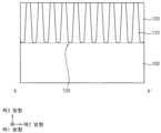
도 1 및 2를 참조하면, 제1 식각 마스크(도시되지 않음)를 사용하는 제1 식각 공정을 통해 기판(100) 상부를 식각함으로써 액티브 핀들(110)을 형성할 수 있다.Referring to FIGS. 1 and 2 , the
기판(100)은 실리콘, 게르마늄, 실리콘-게르마늄과 같은 반도체 물질, 또는 GaP, GaAs, GaSb 등과 같은 Ⅲ-Ⅴ족 화합물을 포함할 수 있다. 일부 실시예들에 따르면, 기판(100)은 실리콘-온-인슐레이터(Silicon-On-Insulator: SOI) 기판 또는 게르마늄-온-인슐레이터(Germanium-On-Insulator: GOI) 기판일 수 있다.The
이하에서는, 기판(100)의 하부, 즉 액티브 핀들(110)의 저면보다 낮은 높이의 기판(100) 부분을 액티브 핀들(110)과 구별하여 기판(100)으로 지칭하기로 한다.Hereinafter, the lower portion of the
예시적인 실시예들에 있어서, 각 액티브 핀들(110)은 상기 제1 방향으로 연장될 수 있으며, 상기 제2 방향을 따라 일정한 간격으로 서로 이격되도록 복수 개로 형성될 수 있다.In exemplary embodiments, each
한편, 일반적인 식각 공정의 특성 상, 상기 제1 식각 공정을 통해 형성되는 각 액티브 핀들(110)은 상기 제3 방향을 따라 기판(100) 상면에 대해 완전히 수직한 측벽을 갖지 않을 수 있으며, 기판(100) 상면에 대해 예를 들어,80도보다 크고 90도보다 작은 각도를 갖도록 형성될 수 있다. 이에 따라, 각 액티브 핀들(110)은 상부에서 하부로 갈수록 점차 커지는 폭을 가질 수 있으며, 액티브 핀들(110) 사이에 형성되는 제1 리세스(125)는 상부에서 하부로 갈수록 그 폭이 점차 줄어들 수 있다.Meanwhile, due to the characteristics of a general etching process, each
이후, 액티브 핀들(110)을 커버하는 제1 소자 분리막을 기판(100) 상에 형성한 후, 액티브 핀들(110)의 상면이 노출될 때까지 상기 제1 소자 분리막을 평탄화함으로써, 제1 리세스(125)를 채우는 제1 소자 분리 패턴(120)을 형성할 수 있다.Thereafter, a first device isolation film covering the
제1 소자 분리 패턴(120)은 예를 들어, 실리콘 산화물과 같은 산화물을 포함할 수 있다. 상기 평탄화 공정은 예를 들어, 화학 기계적 연마(CMP) 공정 및/또는 에치 백 공정을 포함할 수 있다.The first
도 3 내지 도 5를 참조하면, 액티브 핀들(110) 및 제1 소자 분리 패턴(120) 상에 제2 식각 마스크(130)를 형성한 후, 이를 사용하는 제2 식각 공정을 통해 액티브 핀들(110) 중 일부 및 이에 인접하는 제1 소자 분리 패턴(120)을 부분적으로 제거할 수 있으며, 이에 따라 기판(100) 상면을 노출시키는 제1 개구(140)가 형성될 수 있다.Referring to FIGS. 3 to 5 , after forming the
예시적인 실시예들에 있어서, 제1 개구(140)는 상기 제2 방향을 따라 일정한 길이만큼 연장될 수 있으며, 상기 제1 방향을 따라 복수 개로 형성될 수 있다. 일부 영역에 있어서, 상기 제2 방향으로 연장되는 제1 개구들(140)이 서로 연결될 수도 있다.In exemplary embodiments, the
또한, 제1 개구들(140) 사이의 거리가 매우 가까운 경우, 하나의 제2 식각 마스크(130)로만 이들을 모두 형성하기는 어려울 수 있다. 이에 따라, 제2 식각 마스크(130)를 사용하는 상기 제2 식각 공정을 통해서 제1 개구들(140) 중 일부만을 형성하고, 추가로 제3 식각 마스크(도시되지 않음)을 사용하는 제3 식각 공정을 수행함으로써 제1 개구들(140) 중 나머지를 형성할 수도 있다.Additionally, if the distance between the
예시적인 실시예들에 있어서, 상기 제2 식각 공정에 의해 형성되는 제1 개구(140)는 기판(100) 상면을 노출시킬 수 있으며, 나아가 상기 노출된 기판(100) 상면보다 더 낮은 저면을 갖도록 상기 제2 식각 공정에서 기판(100) 상부도 함께 부분적으로 제거될 수 있다. 이에 따라, 제1 개구(140)의 저면은 액티브 핀들(110)의 저면보다 더 낮을 수 있다.In exemplary embodiments, the
한편, 상기 제2 식각 공정 역시 상기 제3 방향을 따라 기판(100) 상면에 대해 완전히 수직 방향으로 수행되지는 않을 수 있으며, 예를 들어 80도보다 크고 90도보다 작은 각도로 수행될 수 있다.Meanwhile, the second etching process may not be performed completely perpendicular to the upper surface of the
도 6 및 7을 참조하면, 제2 식각 마스크(130)를 제거하고, 제1 개구(140)를 채우는 제2 소자 분리 패턴(150)을 형성할 수 있다.Referring to FIGS. 6 and 7 , the
제2 소자 분리 패턴(150)은 제1 개구(140)를 채우는 제2 소자 분리막을 기판(100), 액티브 핀들(110), 및 제1 소자 분리 패턴(120) 상에 형성하고, 액티브 핀들(110)의 상면이 노출될 때까지 상기 제2 소자 분리막을 평탄화함으로써 형성할 수 있다. 제2 소자 분리 패턴(150)은 예를 들어, 실리콘 산화물과 같은 산화물을 포함할 수 있다. 예시적인 실시예들에 있어서, 제2 소자 분리 패턴(150)은 제1 소자 분리 패턴(120)과 실질적으로 동일한 물질을 포함할 수 있으며, 이에 따라 이들은 서로 병합될 수도 있다.The second
이후, 액티브 핀들(110), 및 제1 및 제2 소자 분리 패턴들(120, 150) 상에 제4 식각 마스크(160)를 형성하고, 이를 사용하는 제4 식각 공정을 통해 액티브 핀들(110) 중 일부 및 이에 인접하는 제1 및 제2 소자 분리 패턴들(120, 150)을 부분적으로 제거할 수 있으며, 이에 따라 기판(100) 상면을 노출시키는 제2 개구(170)가 형성될 수 있다.Thereafter, a
예시적인 실시예들에 있어서, 제2 개구(170)는 상기 제1 방향을 따라 일정한 길이만큼 연장될 수 있으며, 상기 제2 방향을 따라 복수 개로 형성될 수 있다. 일부 영역에 있어서, 상기 제1 방향으로 연장되는 제2 개구들(170)이 서로 연결될 수도 있다.In exemplary embodiments, the
예시적인 실시예들에 있어서, 상기 제4 식각 공정에 의해 형성되는 제2 개구(170)는 기판(100) 상면을 노출시킬 수 있으며, 나아가 상기 노출된 기판(100) 상면보다 더 낮은 저면을 갖도록 상기 제4 식각 공정에서 기판(100) 상부도 함께 부분적으로 제거될 수 있다. 이에 따라, 제2 개구(170)의 저면은 액티브 핀들(110)의 저면보다 더 낮을 수 있다. 일 실시예에 있어서, 제2 개구(170)의 저면은 제1 개구(140)의 저면과 실질적으로 동일한 높이에 형성될 수 있으나, 본 발명의 개념은 반드시 이에 한정되지는 않는다.In exemplary embodiments, the
한편, 상기 제4 식각 공정 역시 상기 제3 방향을 따라 기판(100) 상면에 대해 완전히 수직 방향으로 수행되지는 않으며, 예를 들어 80도보다 크고 90도보다 작은 각도로 수행될 수 있다.Meanwhile, the fourth etching process is also not performed in a completely vertical direction with respect to the upper surface of the
도 8 내지 도 10을 참조하면, 제4 식각 마스크(160)를 제거하고, 제2 개구(170)를 채우는 제3 소자 분리 패턴(180)을 형성할 수 있다.Referring to FIGS. 8 to 10 , the
제3 소자 분리 패턴(180)은 제2 개구(170)를 채우는 제3 소자 분리막을 기판(100), 액티브 핀들(110), 및 제1 및 제2 소자 분리 패턴들(120, 150) 상에 형성하고, 액티브 핀들(110)의 상면이 노출될 때까지 상기 제3 소자 분리막을 평탄화함으로써 형성할 수 있다. 제3 소자 분리 패턴(180)은 예를 들어, 실리콘 산화물과 같은 산화물을 포함할 수 있다. 예시적인 실시예들에 있어서, 제3 소자 분리 패턴(180)은 제1 및 제2 소자 분리 패턴들(120, 150)과 실질적으로 동일한 물질을 포함할 수 있으며, 이에 따라 이들은 서로 병합될 수도 있다.The third
이후, 액티브 핀들(110), 및 제1 내지 제3 소자 분리 패턴들(120, 150, 180) 상에 제5 식각 마스크(190)를 형성하고, 이를 사용하는 제5 식각 공정을 통해 액티브 핀들(110) 중 일부 및 이에 인접하는 제1 내지 제3 소자 분리 패턴들(120, 150, 180)을 부분적으로 제거할 수 있으며, 이에 따라 기판(100) 상면을 노출시키는 제3 개구(200)가 형성될 수 있다.Thereafter, the
예시적인 실시예들에 있어서, 제3 개구(200)는 상기 제1 방향을 따라 일정한 길이만큼 연장될 수 있으며, 상기 제2 방향을 따라 복수 개로 형성될 수 있다. 일부 영역에 있어서, 상기 제1 방향으로 연장되는 제3 개구들(200)이 서로 연결될 수도 있다.In exemplary embodiments, the
예시적인 실시예들에 있어서, 제3 개구들(200) 중 일부는 제4 마스크(160)를 통해 형성된 제2 개구들(170) 중 일부와 상기 제2 방향으로 매우 가까운 거리에 형성될 수 있다. 즉, 도 3 내지 도 5를 참조로 설명한 것과 유사하게, 제2 개구들(170) 사이의 거리가 매우 가까운 경우,하나의 제4 식각 마스크(160)만으로 이들을 모두 형성하기 어려울 수 있다. 이에 따라, 도 8 내지 도 10을 참조로 설명하는 상기 제5 식각 공정은, 상기 제1 방향으로 연장되도록 형성하고자 하는 모든 제2 개구들(170) 중에서 상기 제4 식각 공정에서 형성되는 제2 개구들(170)을 제외한 나머지 일부를 형성하기 위한 공정일 수 있다.In example embodiments, some of the
예시적인 실시예들에 있어서, 상기 제5 식각 공정에 의해 형성되는 제3 개구(200)는 기판(100) 상면을 노출시킬 수 있으며, 나아가 상기 노출된 기판(100) 상면보다 더 낮은 저면을 갖도록 상기 제5 식각 공정에서 기판(100) 상부도 함께 부분적으로 제거될 수 있다. 이에 따라, 제3 개구(200)의 저면은 액티브 핀들(110)의 저면보다 더 낮을 수 있다. 일 실시예에 있어서, 제3 개구(200)의 저면은 제1 및 제2 개구들(140, 170)의 저면과 실질적으로 동일한 높이에 형성될 수 있으나, 본 발명의 개념은 반드시 이에 한정되지는 않는다.In exemplary embodiments, the
한편, 상기 제5 식각 공정 역시 상기 제3 방향을 따라 기판(100) 상면에 대해 완전히 수직 방향으로 수행되지는 않으며, 예를 들어 80도보다 크고 90도보다 작은 각도로 수행될 수 있다.Meanwhile, the fifth etching process is also not performed completely perpendicular to the upper surface of the
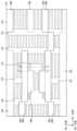
도 11 내지 도 15를 참조하면, 제5 식각 마스크(190)를 제거하고, 제3 개구(200)를 채우는 제4 소자 분리 패턴(210)을 형성할 수 있다.Referring to FIGS. 11 to 15 , the
제4 소자 분리 패턴(210)은 제3 개구(200)를 채우는 제4 소자 분리막을 기판(100), 액티브 핀들(110), 및 제1 내지 제3 소자 분리 패턴들(120, 150, 180) 상에 형성하고, 액티브 핀들(110)의 상면이 노출될 때까지 상기 제4 소자 분리막을 평탄화함으로써 형성할 수 있다. 제4 소자 분리 패턴(210)은 예를 들어, 실리콘 산화물과 같은 산화물을 포함할 수 있다. 예시적인 실시예들에 있어서, 제4 소자 분리 패턴(210)은 제1 내지 제3 소자 분리 패턴들(120, 150, 180)과 실질적으로 동일한 물질을 포함할 수 있으며, 이에 따라 이들은 서로 병합될 수도 있다.The fourth
이후, 액티브 핀들(110), 및 제1 내지 제4 소자 분리 패턴들(120, 150, 180, 210) 상에 제6 식각 마스크(220)를 형성하고, 이를 사용하는 제6 식각 공정을 통해 액티브 핀들(110) 중 일부, 이에 인접하는 제1 내지 제4 소자 분리 패턴들(120, 150, 180, 210), 및 기판(100) 상부를 부분적으로 제거할 수 있으며, 이에 따라 기판(100) 상에 제2 리세스(230)가 형성될 수 있다.Thereafter, a
예시적인 실시예들에 있어서, 상기 제6 식각 공정에 의해 형성되는 제2 리세스(230)의 저면은 액티브 핀들(110)의 저면, 나아가 제1 내지 제4 소자 분리 패턴들(120, 150, 180, 210)의 저면보다 더 낮을 수 있다. 이에 따라, 기판(100) 상에는 제2 리세스(230)에 의해 정의되는 액티브 영역(102)이 형성될 수 있다. 이하에서는, 기판(100)의 하부, 즉 액티브 영역(102)의 저면보다 낮은 높이의 기판(100) 부분을 액티브 영역(102)과 구별하여 기판(100)으로 지칭하기로 한다. 결국, 기판(100) 상에는 액티브 영역(102)이 형성될 수 있으며, 액티브 영역(102) 상에는 액티브 핀들(110)이 형성될 수 있다.In exemplary embodiments, the bottom of the
한편, 상기 제6 식각 공정 역시 상기 제3 방향을 따라 기판(100) 상면에 대해 완전히 수직 방향으로 수행되지는 않으며, 예를 들어 80도보다 크고 90도보다 작은 각도로 수행될 수 있다.Meanwhile, the sixth etching process is also not performed completely perpendicular to the upper surface of the
예시적인 실시예들에 있어서, 상기 제6 식각 공정에서 사용되는 제6 식각 마스크(220) 형성 공정 시 미스얼라인이 발생할 수도 있으며, 이에 따라 예를 들어, 제2 리세스(230)가 당초 원하는 위치보다 상기 제2 방향으로 상기 일정한 거리만큼 이동하여 형성될 수 있다. 이에 따라, 도 12 및 14에 도시된 바와 같이, 예를 들어 액티브 영역(102) 상에 배치된 액티브 핀들(110) 중에서 상기 제2 방향으로의 제1 가장자리에 형성된 제1 액티브 핀(110)의 제1 측벽을 커버하는 제4 소자 분리 패턴(210) 부분이 제2 리세스(230) 형성 공정 시 모두 제거되지 못할 수 있다.In exemplary embodiments, misalignment may occur during the formation process of the
만약, 도 8 내지 도 10을 참조로 설명한 공정 즉, 제5 식각 마스크(190)를 사용하는 제5 식각 공정을 수행하지 않은 경우라면, 제2 리세스(230)가 당초 원하는 위치보다 상기 제2 방향으로 이동하여 형성되므로, 제1 액티브 핀(110)으로부터 상기 제2 방향으로 인접한 제2 액티브 핀(110)이 모두 제거되지 못하고 부분적으로 잔류할 수 있다. 하지만, 예시적인 실시예들에 있어서, 상기 제5 식각 공정을 먼저 수행하여 제2 액티브 핀(110)이 모두 제거되었으므로, 제6 식각 마스크(220) 형성 공정 시 미스얼라인이 발생하더라도, 제2 액티브 핀(110)을 포함하는 원하는 모든 액티브 핀들(110)이 제거될 수 있다. 이에 대해서는 도 20 내지 도 22를 참조로 보다 자세하게 설명하도록 한다.If the process described with reference to FIGS. 8 to 10 , that is, the fifth etch process using the
도 16 내지 도 19를 참조하면, 제6 식각 마스크(220)를 제거하고, 제2 리세스(230)를 채우는 제5 소자 분리 패턴(240)을 형성할 수 있다.Referring to FIGS. 16 to 19 , the
제5 소자 분리 패턴(240)은 제2 리세스(230)를 채우는 제5 소자 분리막을 기판(100), 액티브 핀들(110), 및 제1 내지 제4 소자 분리 패턴들(120, 150, 180, 210) 상에 형성하고, 액티브 핀들(110)의 상면이 노출될 때까지 상기 제5 소자 분리막을 평탄화함으로써 형성할 수 있다. 제5 소자 분리 패턴(240)은 예를 들어, 실리콘 산화물과 같은 산화물을 포함할 수 있다. 예시적인 실시예들에 있어서, 제5 소자 분리 패턴(240)은 제1 내지 제4 소자 분리 패턴들(120, 150, 180, 210)과 실질적으로 동일한 물질을 포함할 수 있으며, 이에 따라 이들은 서로 병합될 수도 있다.The fifth
이하에서는 제1 내지 제5 소자 분리 패턴들(120, 150, 180, 210, 240)은 모두 함께 소자 분리 구조물(250)로 지칭하기로 한다.Hereinafter, the first to fifth
이후, 액티브 핀들(110)의 상부가 노출되도록 소자 분리 구조물(250) 상부를 제거할 수 있다. 이에 따라, 각 액티브 핀들(110)은 소자 분리 구조물(250)에 의해 측벽이 커버된 하부 액티브 패턴(110b) 및 소자 분리 구조물(250) 상부로 돌출된 상부 액티브 패턴(110a)을 포함할 수 있다.Thereafter, the upper part of the
전술한 공정들을 통해 액티브 핀들(110) 및 액티브 영역(102), 및 이들의 측벽을 적어도 부분적으로 커버하는 소자 분리 구조물(250)을 포함하는 상기 반도체 장치를 기판(100) 상에 완성할 수 있다.Through the above-described processes, the semiconductor device including the
전술한 바와 같이, 기판(100) 상에 제2 리세스(230)를 형성하여 액티브 영역(102)을 정의하기 위한 상기 제6 식각 공정을 수행하기 이전에, 제4 및 제5 식각 마스크들(160, 190)을 사용하는 상기 제4 및 제5 식각 공정들을 수행할 수 있다. 상기 제4 및 제5 식각 공정들을 통해 형성되는 제2 및 제3 개구들(170, 200)은 최종적으로 구현하고자 하는 액티브 영역(102)의 상기 제2 방향으로의 양측에 형성될 수 있으며, 이에 따라 상기 제4 및 제5 식각 공정들을 통해서, 액티브 영역(102)의 상기 제2 방향으로의 양측에 형성된 액티브 핀들(110)이 제거될 수 있다. 따라서, 액티브 영역(102) 형성을 위한 상기 제6 식각 공정에 사용되는 제6 식각 마스크(220) 형성 공정 시 미스얼라인이 발생하더라도, 액티브 영역(102) 외곽에는 액티브 핀들(110)이 잔류하지 않을 수 있다.As described above, before performing the sixth etch process to define the
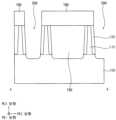
한편, 상기 반도체 장치는 다음과 같은 특징을 가질 수 있다. 예를 들어, 상부에 2개의 액티브 핀들(110)이 형성된 액티브 영역(102)을 포함하는 X 영역에 대해 기술하면 다음과 같다.이때, 상기 2개의 액티브 핀들(110)을 각각 제1 및 제2 액티브 핀들(112, 114)로 지칭하기로 한다.Meanwhile, the semiconductor device may have the following characteristics. For example, the They will be referred to as
기판(100) 상부로 돌출된 액티브 영역(102)은 기판(100)의 상면에 대해 평행한 상기 제2 방향으로 제1 폭(W1)을 갖는 하부(102b), 및 하부(102b) 상에 형성되어 상기 제2 방향으로 제1 폭(W1)보다 작은 제2 폭(W2)을 갖는 상부(102a)를 포함할 수 있다. 즉, 액티브 영역(102)의 상기 제2 방향으로의 양 측벽들 중에서, 제1 액티브 핀(112)에 인접한 액티브 영역(102)의 제1 측벽은 하부(102b)와 상부(102a)의 경계에서 굴곡될 수 있으며, 상기 제1 측벽이 전체적으로 계단 형상을 가짐에 따라서 상부(102a)가 하부(102b)보다 작은 폭을 가질 수 있다.The
이에 따라, 상기 제2 방향을 따라 액티브 영역(102)의 상기 제1 측벽 상부 즉, 액티브 영역(102) 상부(102a)의 측벽으로부터 제1 액티브 핀(112)에 이르는 거리는 상기 제2 방향을 따라 액티브 영역(102)의 상기 제1 측벽 하부 즉, 액티브 영역(102) 하부(102b)의 측벽으로부터 제1 액티브 핀(112)에 이르는 거리보다 더 작을 수 있다.Accordingly, the distance from the upper part of the first sidewall of the
이에 비해, 액티브 영역(102)의 상기 제1 측벽에 대향하는 제2 측벽은 굴곡되지 않고 상기 제3 방향으로 따라 편평할 수 있으며, 이에 따라 기판(100) 상면에 대해 일정한 기울기를 가질 수 있다.In comparison, the second sidewall of the
한편, 각 제1 및 제2 액티브 핀들(112, 114)은 액티브 영역(102) 위로 돌출되어 상기 제1 방향으로 연장될 수 있으며, 액티브 영역(102)의 측벽 및 제1 및 제2 액티브 핀들(112, 114)의 하부 측벽은 기판(100) 상에 형성된 소자 분리 구조물(250)에 의해 커버될 수 있다.Meanwhile, each of the first and second
예시적인 실시예들에 있어서, 제1 액티브 핀(112)과 액티브 영역(102)의 상기 제1 측벽 사이에는 제5 식각 마스크(190)를 사용하는 상기 제5 식각 공정에 의해 제거되는 액티브 핀(110)의 일부 잔류물인 제1 돌출부(115)가 형성될 수 있다. 이때, 제1 돌출부(115)의 최상면의 높이는 소자 분리 구조물(250) 상면의 높이보다 낮을 수 있으며, 이에 따라 이후 도 24 및 25를 참조로 설명되는 선택적 에피택시얼 성장(SEG) 공정에 의해 상부에 소스/드레인 층(370)이 형성되지 않을 수 있다.In exemplary embodiments, an active fin ( The
한편, 제2 액티브 핀(114)의 측벽은 액티브 영역(102)의 상기 제2 측벽과 직접 접촉할 수 있으며, 이들 사이에 제1 돌출부(115)는 형성되지 않을 수 있다.Meanwhile, the sidewall of the second
전술한 바와 같이 소자 분리 구조물(250)은 제1 내지 제5 소자 분리 패턴들(120, 150, 180, 210, 240)을 포함할 수 있으며, 이들은 모두 동일한 높이에 형성된 상면을 가지고, 기판(100) 상면에 평행한 수평 방향으로 배열될 수 있다. 다만 상기 X 영역에서는, 각 제1 및 제2 액티브 핀들(112, 114)의 하부 측벽을 커버하는 제1 및 제2 소자 분리 패턴들(120, 150), 액티브 영역(102)의 상기 제1 측벽의 상부를 커버하는 제4 소자 분리 패턴(210), 액티브 영역(102)의 상기 제1 측벽의 하부를 커버하는 제5 소자 분리 패턴(240)이 형성되어 있다.As described above, the
도 20 내지 도 22는 비교예에 따른 반도체 장치의 제조 방법을 설명하기 위한 단면도들이다. 상기 반도체 장치의 제조 방법은 도 1 내지 도 19를 참조로 설명한 공정들과 실질적으로 동일하거나 유사한 공정들을 포함할 수 있으며, 이에 따라 이들에 대한 자세한 설명은 생략한다.20 to 22 are cross-sectional views for explaining a method of manufacturing a semiconductor device according to a comparative example. The method of manufacturing the semiconductor device may include processes that are substantially the same as or similar to those described with reference to FIGS. 1 to 19, and therefore detailed description thereof will be omitted.
도 20을 참조하면, 먼저 도 1 내지 도 5를 참조로 설명한 공정들과 실질적으로 동일하거나 유사한 공정들을 수행한 후, 도 11 내지 도 14를 참조로 설명한 공정들과 실질적으로 동일하거나 유사한 공정들을 수행할 수 있다.Referring to FIG. 20, first, processes that are substantially the same as or similar to the processes described with reference to FIGS. 1 to 5 are performed, and then processes that are substantially the same or similar to the processes described with reference to FIGS. 11 to 14 are performed. can do.
즉, 도 6 내지 도 10을 참조로 설명한 제4 및 제5 식각 공정들은 수행하지 않고, 제1 내지 제3 식각 공정 후 바로 제6 식각 공정을 수행할 수 있다. 이에 따라, 상기 제6 식각 공정에 사용되는 제6 식각 마스크(220) 형성 시 미스얼라인이 발생하는 경우, 제2 리세스(230)에 의해 제거되어야 하는 액티브 핀들(110) 중 일부가 모두 제거되지 못하고 제2 돌출부(117)로 잔류할 수 있다. 이때, 제2 돌출부(117)는 제1 돌출부(115)에 비해 높은 상면을 가질 수 있다.That is, the fourth and fifth etching processes described with reference to FIGS. 6 to 10 may not be performed, and the sixth etching process may be performed immediately after the first to third etching processes. Accordingly, when misalignment occurs when forming the
도 21 및 22를 참조하면, 도 15 내지 도 19를 참조로 설명한 공정들과 실질적으로 동일하거나 유사한 공정들을 수행하여 상기 반도체 장치를 완성할 수 있다.Referring to FIGS. 21 and 22 , the semiconductor device may be completed by performing processes that are substantially the same or similar to the processes described with reference to FIGS. 15 to 19 .
다만, 제2 돌출부(117)는 소자 분리 구조물(250)에 의해 모두 커버되지 못하고 일부가 상부로 돌출될 수 있다. 이에 따라, 제2 돌출부(117)는 측벽이 소자 분리 구조물(250)에 의해 커버된 하부(117b), 및 소자 분리 구조물(250) 상부로 돌출된 상부(117a)를 포함할 수 있다. 제2 돌출부(117) 상에는 이후 도 29를 참조로 설명되는 선택적 에피택시얼 성장(SEG) 공정에 의해 상부에 소스/드레인 층(370)이 형성될 수 있다.However, the
도 23 내지 도 28은 예시적인 실시예들에 따른 반도체 장치의 제조 방법을 설명하기 위한 단면도들이다. 구체적으로 도 23, 24 및 26은 도 15의 B-B'선을 따라 절단한 단면도들이고, 도 25, 27 및 28은 도 15의 D-D'선을 따라 절단한 단면도들이다.23 to 28 are cross-sectional views for explaining a method of manufacturing a semiconductor device according to example embodiments. Specifically, FIGS. 23, 24, and 26 are cross-sectional views taken along line B-B' of FIG. 15, and FIGS. 25, 27, and 28 are cross-sectional views taken along line D-D' of FIG. 15.
상기 반도체 장치의 제조 방법은 도 1 내지 도 19를 참조로 설명한 공정들을 통해 형성된 액티브 핀들 및 소자 분리 구조물 상에 트랜지스터 및 콘택 플러그를 형성하여 로직 소자를 제조하는 방법에 관한 것이다. The method of manufacturing the semiconductor device relates to a method of manufacturing a logic device by forming a transistor and a contact plug on the active fins and device isolation structure formed through the processes described with reference to FIGS. 1 to 19.
도 23을 참조하면, 기판(100) 상에 더미 게이트 구조물(330)을 형성할 수 있다.Referring to FIG. 23, a
구체적으로, 액티브 핀들(110) 및 소자 분리 구조물(250) 상에 더미 게이트 절연막, 더미 게이트 전극막 및 더미 마스크 막을 순차적으로 형성하고, 상기 더미 게이트 마스크 막을 패터닝하여 더미 게이트 마스크(320)를 형성한 후, 이를 식각 마스크로 사용하여 하부의 상기 더미 게이트 전극막 및 상기 더미 게이트 절연막을 순차적으로 식각함으로써 더미 게이트 구조물(330)을 형성할 수 있다.Specifically, a dummy gate insulating film, a dummy gate electrode film, and a dummy mask film are sequentially formed on the
이에 따라, 기판(100) 상에는 순차적으로 적층된 더미 게이트 절연 패턴(300), 더미 게이트 전극(310) 및 더미 게이트 마스크(320)를 포함하는 더미 게이트 구조물(330)이 형성될 수 있다. 더미 게이트 절연 패턴(300)은 예를 들어 실리콘 산화물과 같은 산화물을 포함할 수 있고, 더미 게이트 전극(310)은 예를 들어, 폴리실리콘을 포함할 수 있으며, 더미 게이트 마스크(320)는 예를 들어, 실리콘 질화물과 같은 질화물을 포함할 수 있다.Accordingly, a
예시적인 실시예들에 있어서, 더미 게이트 구조물(330)은 상기 제2 방향으로 연장될 수 있으며, 상기 제1 방향을 따라 복수 개로 형성될 수 있다.In example embodiments, the
도 24 및 25를 참조하면, 더미 게이트 구조물(330)의 측벽에 게이트 스페이서(340)를 형성할 수 있다.Referring to FIGS. 24 and 25 ,
게이트 스페이서(340)는 액티브 핀들(110) 및 소자 분리 구조물(250) 상에 더미 게이트 구조물(330)을 커버하는 스페이서 막을 형성하고 이를 이방성 식각함으로써 형성할 수 있다. 이때, 게이트 스페이서(340)는 더미 게이트 구조물(330)의 측벽 상에 형성될 수 있으며, 상부 액티브 패턴들(110a)의 각 측벽들 상에는 핀 스페이서(350)가 더 형성될 수 있다. 게이트 스페이서(340) 및 핀 스페이서(350)는 예를 들어, 실리콘 질화물과 같은 질화물을 포함할 수 있다.The
이후, 더미 게이트 구조물(330)에 인접한 액티브 핀들(110)의 상부를 식각하여 제3 리세스(360)를 형성한 후, 제3 리세스(360)를 채우는 소스/드레인 층(370)을 형성할 수 있다.Thereafter, the upper portion of the
구체적으로, 더미 게이트 구조물(330) 및 이의 측벽에 형성된 게이트 스페이서(340)를 식각 마스크로 사용하는 제7 식각 공정을 통해 액티브 핀들(110)의 상부를 제거함으로써 제3 리세스(360)를 형성할 수 있다. 제3 리세스(360)가 형성될 때, 액티브 핀들(110)에 인접하여 형성된 핀 스페이서(350)도 대부분 제거될 수 있으나, 그 하부는 부분적으로 잔류할 수도 있다.Specifically, the third recess 360 is formed by removing the upper portion of the
한편 도면 상에서는, 액티브 핀들(110) 중에서 상부 액티브 패턴들(110a)의 일부만이 식각되어 제3 리세스(360)가 형성됨에 따라서, 제3 리세스(360)의 저면이 하부 액티브 패턴들(110b)의 상면보다 높은 것이 도시되어 있으나, 본 발명의 개념은 반드시 이에 한정되지는 않는다.Meanwhile, in the drawing, as only a portion of the upper
예시적인 실시예들에 있어서, 소스/드레인 층(370)은 제3 리세스(360)에 의해 노출된 액티브 핀들(110)의 상면을 시드로 사용하는 선택적 에피택시얼 성장(SEG) 공정을 수행함으로써 형성될 수 있다.In example embodiments, the source/
예시적인 실시예들에 있어서, 상기 선택적 에피택시얼 성장(SEG) 공정을 수행함에 따라서, 소스/드레인 층(370)으로서 단결정의 실리콘-게르마늄 층이 형성될 수 있다. 또한, 상기 선택적 에피택시얼 성장(SEG) 공정은 p형 불순물 소스 가스를 함께 사용할 수 있으며, 이에 따라 소스/드레인 층(370)으로서 p형 불순물이 도핑된 단결정 실리콘-게르마늄 층이 형성될 수 있다. 이에 따라, 소스/드레인 층(370)은 피모스(PMOS) 트랜지스터의 소스/드레인 영역 역할을 수행할 수 있다.In example embodiments, as the selective epitaxial growth (SEG) process is performed, a single crystalline silicon-germanium layer may be formed as the source/
소스/드레인 층(370)은 수직 방향뿐만 아니라 수평 방향으로도 성장하여 제3 리세스(360)를 채울 수 있으며, 상부가 게이트 스페이서(340) 측벽에 접촉하도록 성장할 수도 있다.The source/
예시적인 실시예들에 있어서, 상기 제2 방향으로 서로 이웃하는 액티브 핀들(110), 즉 상기 X 영역에서는 제1 및 제2 액티브 핀들(112, 114) 상으로 성장하는 각 소스/드레인 층들(370)은 서로 연결되어 병합될 수도 있다.In example embodiments, each source/
지금까지는 피모스(PMOS) 트랜지스터의 소스/드레인 역할을 수행하는 소스/드레인 층(370)에 대해 설명하였으나, 본 발명의 개념은 이에 한정되지는 않으며, 엔모스(NMOS) 트랜지스터의 소스/드레인 역할을 수행하는 소스/드레인 층(370)을 형성할 수도 있다.So far, the source/
이에 따라, 소스/드레인 층(370)으로서 단결정 실리콘 탄화물 층 혹은 단결정 실리콘 층이 형성될 수 있다. 한편, n형 불순물 소스 가스, 예를 들어, 포스핀(PH3) 가스 등이 함께 사용되어 n형 불순물이 도핑된 단결정 실리콘 탄화물 층 혹은 n형 불순물이 도핑된 단결정 실리콘 층이 형성될 수 있다.Accordingly, a single crystal silicon carbide layer or a single crystal silicon layer may be formed as the source/
도 26 및 27을 참조하면, 더미 게이트 구조물(330), 게이트 스페이서(340), 소스/드레인 층들(370), 및 핀 스페이서(350)를 커버하는 제1 층간 절연막(380)을 기판(100) 상에 충분한 높이로 형성한 후, 더미 게이트 구조물(330)에 포함된 더미 게이트 전극(310)의 상면이 노출될 때까지 제1 층간 절연막(380)을 평탄화한다.26 and 27, a first
이때, 더미 게이트 마스크(320)도 함께 제거될 수 있으며, 게이트 스페이서(340)의 상부도 제거될 수 있다. 한편, 병합된 소스/드레인 층들(370)과 소자 분리 구조물(250) 사이에는 제1 층간 절연막(380)이 모두 채워지지 않을 수 있으며, 이에 따라 에어 갭(385)이 형성될 수 있다. 한편, 제1 층간 절연막(380)은 예를 들어, 실리콘 산화물과 같은 산화물을 포함할 수 있다.At this time, the
이후, 노출된 더미 게이트 전극(310) 및 그 하부의 더미 게이트 절연 패턴(300)을 제거하여, 게이트 스페이서(340)의 내측벽 및 액티브 핀들(110)의 상면을 노출시키는 제4 개구(390)를 형성하고, 제4 개구(390)를 채우는 게이트 구조물(440)을 형성할 수 있다.Thereafter, the exposed
게이트 구조물(440)은 예를 들어, 다음과 같은 공정들을 수행함으로써 형성될 수 있다.The
먼저, 제4 개구(390)에 의해 노출된 액티브 핀들(110) 상면에 대한 열산화 공정을 수행하여 인터페이스 패턴(400)을 형성한 후, 인터페이스 패턴(400), 소자 분리 구조물(250), 게이트 스페이서(340) 및 제1 층간 절연막(380) 상에 게이트 절연막 및 일함수 조절막을 순차적으로 형성하고, 제4 개구(390)의 나머지 부분을 충분히 채우는 게이트 전극막을 상기 일함수 조절막 상에 형성한다.First, a thermal oxidation process is performed on the upper surface of the
한편, 인터페이스 패턴(400)은 열산화 공정 대신에 화학 기상 증착(CVD) 공정 또는 원자층 증착(ALD) 공정 등을 통해 형성될 수도 있으며, 이 경우에 인터페이스 패턴(400)은 액티브 핀들(110) 상면뿐만 아니라 소자 분리 구조물(250) 상면, 및 게이트 스페이서(340)의 내측벽 상에도 형성될 수 있다.Meanwhile, the
이후, 제1 층간 절연막(380)의 상면이 노출될 때까지, 상기 게이트 전극막, 상기 일함수 조절막 및 상기 게이트 절연막을 평탄화하여, 인터페이스 패턴(400) 상면, 소자 분리 구조물(250) 상면, 및 게이트 스페이서(340)의 내측벽 상에 순차적으로 적층된 게이트 절연 패턴(410) 및 일함수 조절 패턴(420)을 형성하고, 일함수 조절 패턴(420) 상에 제4 개구(390)의 나머지 부분을 채우는 게이트 전극(430)을 형성할 수 있다. 이에 따라, 게이트 전극(430)의 저면 및 측벽은 일함수 조절 패턴(420)에 의해 커버될 수 있다.Thereafter, the gate electrode film, the work function control film, and the gate insulating film are planarized until the top surface of the first
순차적으로 적층된 인터페이스 패턴(400), 게이트 절연 패턴(410), 일함수 조절 패턴(420) 및 게이트 전극(430)은 게이트 구조물(440)을 형성할 수 있으며, 소스/드레인 층들(370)과 함께 트랜지스터를 형성할 수 있다. 상기 트랜지스터는 소스/드레인 층들(370)의 도전형에 따라서 피모스(PMOS) 트랜지스터 혹은 엔모스(NMOS) 트랜지스터를 형성할 수 있다.The sequentially stacked
인터페이스 패턴(400)은 예를 들어, 실리콘 산화물과 같은 산화물을 포함할 수 있고, 게이트 절연 패턴(410)은 예를 들어, 하프늄 산화물, 지르코늄 산화물 등과 같은 금속 산화물을 포함할 수 있으며, 일함수 조절 패턴(420) 예를 들어, 티타늄 질화물, 탄탈륨 질화물, 텅스텐 질화물 등과 같은 금속 질화물을 포함할 수 있고, 게이트 전극(430)은 예를 들어, 알루미늄, 구리, 티타늄, 탄탈륨 등의 저 저항 금속, 이들의 질화물, 혹은 이들의 합금을 포함할 수 있다.The
이후, 게이트 구조물(440) 상부를 제거하여 제4 리세스를 형성하고, 상기 제4 리세스를 채우는 캐핑 패턴(450)을 형성할 수 있다. 캐핑 패턴(450)은 예를 들어, 실리콘 질화물과 같은 질화물을 포함할 수 있다.Thereafter, the upper portion of the
도 28을 참조하면, 제1 층간 절연막(380), 캐핑 패턴(450), 및 게이트 스페이서(340) 상에 제2 층간 절연막(460)을 형성하고, 제1 및 제2 층간 절연막들(380, 460)을 관통하여 소스/드레인 층(370)의 상면에 접촉하는 제1 콘택 플러그(480)를 형성할 수 있다.Referring to FIG. 28, a second
제1 콘택 플러그(480)은 예를 들어, 다음과 같은 공정들을 수행함으로써 형성될 수 있다.For example, the
먼저, 제1 및 제2 층간 절연막들(380, 460)을 관통하면서 소스/드레인 층(370)의 상면을 노출시키는 제5 개구를 형성하고, 상기 노출된 소스/드레인 층(370)의 상면, 상기 제5 개구의 측벽, 및 제2 층간 절연막(460) 상면에 제1 금속막을 형성한 후, 열처리 공정을 수행하여 소스/드레인 층(370) 상부에 금속 실리사이드 패턴(470)을 형성할 수 있다.First, a fifth opening is formed that penetrates the first and second
이후, 금속 실리사이드 패턴(470) 상면, 상기 제5 개구의 측벽, 및 제2 층간 절연막(460) 상면에 제1 배리어 막을 형성하고, 상기 제1 배리어 막 상에 상기 제5 개구를 채우는 제2 금속막을 형성한 후, 제2 층간 절연막(460) 상면이 노출될 때까지 상기 제2 금속막 및 상기 제1 배리어 막을 평탄화할 수 있다.Thereafter, a first barrier film is formed on the top surface of the
이에 따라, 금속 실리사이드 패턴(470) 상에 상기 제5 개구를 채우는 제1 콘택 플러그(480)가 형성될 수 있다. 이때, 제1 콘택 플러그(480)는 제2 금속 패턴(도시되지 않음) 및 이의 저면 및 측벽을 커버하는 제1 배리어 패턴(도시되지 않음)을 포함할 수 있다.Accordingly, the
한편, 도시하지는 않았으나, 게이트 구조물(440) 상부에 접촉하는 제2 콘택 플러그와, 제1 콘택 플러그(480) 및 상기 제2 콘택 플러그에 전기적으로 연결되는 배선을 더 형성함으로써 상기 반도체 장치가 완성될 수 있다.Meanwhile, although not shown, the semiconductor device may be completed by further forming a second contact plug contacting the upper part of the
전술한 바와 같이, 제거되어야 할 액티브 핀들(110)이 모두 효과적으로 제거됨으로 인해서, 액티브 영역(102) 상에는 당초 의도한 액티브 핀들(110)만이 형성될 수 있으며, 그 상부에만 소스/드레인 층(370)이 형성될 수 있다. 한편, 액티브 핀들(110) 중 일부 잔류하는 제1 돌출부(115) 상에는 소스/드레인 층(370)이 형성되지 않으므로, 이웃하는 게이트 구조물(440) 등과의 전기적 쇼트는 발생하지 않을 수 있다.As described above, since all of the
도 29 및 30은 비교예에 따른 반도체 장치 제조 방법을 설명하기 위한 단면도들이며, 구체적으로 도 15의 D-D'선을 따라 절단한 단면도들이다.FIGS. 29 and 30 are cross-sectional views for explaining a method of manufacturing a semiconductor device according to a comparative example. Specifically, they are cross-sectional views taken along line D-D' of FIG. 15.
상기 반도체 장치의 제조 방법은 도 23 내지 도 28을 참조로 설명한 공정들과 실질적으로 동일하거나 유사한 공정들을 포함할 수 있으며, 이에 따라 이들에 대한 자세한 설명은 생략한다.The method of manufacturing the semiconductor device may include processes that are substantially the same as or similar to those described with reference to FIGS. 23 to 28, and therefore detailed description thereof will be omitted.
도 29를 참조하면, 도 23 내지 도 25를 참조로 설명한 공정들과 실질적으로 동일하거나 유사한 공정들을 수행할 수 있다.Referring to FIG. 29 , processes that are substantially the same as or similar to those described with reference to FIGS. 23 to 25 may be performed.
다만, 액티브 핀들(110)에 이웃하는 제2 돌출부(117)는 소자 분리 구조물(250) 상부로 돌출된 상부(117a)를 포함할 수 있으며, 이에 따라 SEG 공정에 의해 액티브 핀들(110) 상부뿐만 아니라 제2 돌출부(117) 상부에도 기생 소스/드레인 층(375)이 형성될 수 있으며, 인접하는 소스/드레인 층(370)에 병합될 수 있다.However, the
도 30을 참조하면, 도 26 내지 도 28을 참조로 설명한 공정들과 실질적으로 동일하거나 유사한 공정들을 수행함으로써, 상기 반도체 장치를 완성할 수 있다.Referring to FIG. 30 , the semiconductor device can be completed by performing processes that are substantially the same as or similar to the processes described with reference to FIGS. 26 to 28 .
이때, 소스/드레인 층(370) 상에 형성되는 제1 콘택 플러그(480)는 소스/드레인 층(375)에 병합된 기생 소스/드레인 층(375)에도 전기적으로 연결될 수 있으며, 이에 따라 원하지 않는 전류 통로에 의해 전기적 쇼트가 발생할 수 있다.At this time, the
전술한 반도체 장치 및 제조 방법은, 예를 들어 중앙처리장치(CPU, MPU), 애플리케이션 프로세서(AP) 등과 같은 로직 소자, 예를 들어 에스램(SRAM) 장치, 디램(DRAM) 장치 등과 같은 휘발성 메모리 장치, 및 예를 들어 플래시 메모리 장치, 피램(PRAM) 장치, 엠램(MRAM) 장치, 알램(RRAM) 장치 등과 같은 불휘발성 메모리 장치에 적용될 수 있다.The above-described semiconductor devices and manufacturing methods include logic elements such as central processing units (CPUs, MPUs), application processors (APs), and volatile memories such as SRAM devices and DRAM devices. It can be applied to devices, and non-volatile memory devices such as, for example, flash memory devices, PRAM devices, MRAM devices, and RRAM devices.
100: 기판102: 액티브 영역
110: 액티브 핀110a, 110b: 상부, 하부 액티브 패턴
112, 114: 제1, 제2 액티브 핀115, 117: 제1, 제2 돌출부
120, 150, 180, 210, 240: 제1 내지 제5 소자 분리 패턴
125, 230, 360: 제1 내지 제3 리세스
130, 160, 190, 220: 제2, 제4, 제5, 제6 식각 마스크
140, 170, 200, 390: 제1 내지 제4 개구
250: 소자 분리 구조물300: 더미 게이트 절연 패턴
310: 더미 게이트 전극320: 더미 게이트 마스크
330: 더미 게이트 구조물340: 게이트 스페이서
350: 핀 스페이서370: 소스/드레인 층
375: 기생 소스/드레인 층380, 460: 제1, 제2 층간 절연막
400: 인터페이스 패턴410: 게이트 절연 패턴
420: 일함수 조절 패턴430: 게이트 전극
440: 게이트 구조물450: 캐핑 패턴
470: 금속 실리사이드 패턴480: 제1 콘택 플러그100: substrate 102: active area
110:
112, 114: first and second
120, 150, 180, 210, 240: first to fifth element separation patterns
125, 230, 360: first to third recesses
130, 160, 190, 220: 2nd, 4th, 5th, 6th etch mask
140, 170, 200, 390: first to fourth openings
250: device isolation structure 300: dummy gate insulation pattern
310: dummy gate electrode 320: dummy gate mask
330: Dummy gate structure 340: Gate spacer
350: pin spacer 370: source/drain layer
375: parasitic source/
400: Interface pattern 410: Gate insulation pattern
420: Work function control pattern 430: Gate electrode
440: Gate structure 450: Capping pattern
470: Metal silicide pattern 480: First contact plug
Claims (10)
Translated fromKorean상기 액티브 영역 상부로 돌출되어 상기 기판의 상면에 평행한 제1 방향으로 각각 연장되며, 상기 기판 상면에 평행하고 상기 제1 방향과 교차하는 제2 방향으로 배치된 복수의 액티브 핀들; 및
상기 기판 상에 형성되어 상기 액티브 영역의 제1 측벽 및 상기 각 액티브 핀들의 하부 측벽을 커버하는 소자 분리 구조물을 포함하며,
상기 액티브 영역의 상기 제1 측벽은 상기 액티브 핀들 중에서 상기 액티브 영역의 상기 제2 방향으로의 제1 가장자리에 형성된 제1 액티브 핀에 인접하여 형성되고,
상기 액티브 영역의 상기 제1 측벽의 상부, 상기 액티브 영역의 상기 상부의 상면, 및 상기 제1 액티브 핀의 측벽은 계단 형상을 이루며,
상기 제1 액티브 핀과 상기 액티브 영역의 상기 제1 측벽 사이에 형성된 돌출부를 더 포함하는 반도체 장치.an active region that protrudes above the substrate and includes a lower portion and an upper portion;
a plurality of active fins protruding above the active area, each extending in a first direction parallel to the top surface of the substrate, and disposed in a second direction parallel to the top surface of the substrate and intersecting the first direction; and
a device isolation structure formed on the substrate and covering a first sidewall of the active area and a lower sidewall of each of the active fins;
The first sidewall of the active area is formed adjacent to a first active fin formed at a first edge of the active area in the second direction among the active fins,
A top of the first sidewall of the active area, a top surface of the top of the active area, and a sidewall of the first active fin form a step shape,
The semiconductor device further includes a protrusion formed between the first active fin and the first sidewall of the active area.
상기 제2 방향을 따라 상기 제1 측벽의 상부로부터 상기 제1 액티브 핀의 상기 측벽에 이르는 제1 거리는 상기 제2 방향을 따라 상기 제1 측벽의 하부로부터 상기 제1 액티브 핀의 상기 측벽에 이르는 제2 거리보다 더 작고, 상기 제1 및 제2 거리들은 0보다 큰 반도체 장치.According to paragraph 1,
A first distance from the top of the first sidewall to the sidewall of the first active fin along the second direction is a distance from the bottom of the first sidewall to the sidewall of the first active fin along the second direction. A semiconductor device wherein the distance is less than 2, and the first and second distances are greater than 0.
상기 액티브 영역 상부로 돌출되어 상기 기판의 상면에 평행한 제1 방향으로 각각 연장되며, 상기 기판 상면에 평행하고 상기 제1 방향과 교차하는 제2 방향으로 배치된 복수의 액티브 핀들;
상기 기판 상에 형성되어 상기 액티브 영역의 제1 측벽 및 상기 각 액티브 핀들의 하부 측벽을 커버하는 소자 분리 구조물;
상기 액티브 핀들 및 상기 소자 분리 구조물 상에 상기 제2 방향으로 연장된 게이트 구조물; 및
상기 게이트 구조물에 인접한 상기 액티브 핀들 상에 형성된 소스/드레인 층을 포함하며,
상기 액티브 영역의 상기 제1 측벽은 상기 액티브 핀들 중에서 상기 제2 방향으로의 제1 가장자리에 형성된 제1 액티브 핀에 인접하여 형성되고,
상기 액티브 영역의 상기 제1 측벽, 상기 액티브 영역의 상기 상부의 상면, 및 상기 제1 액티브 핀의 측벽은 계단 형상을 이루며,
상기 제1 액티브 핀과 상기 액티브 영역의 상기 제1 측벽 사이에 형성된 돌출부를 더 포함하는 반도체 장치.an active region that protrudes above the substrate and includes a lower portion and an upper portion;
a plurality of active fins protruding above the active area, each extending in a first direction parallel to the top surface of the substrate, and disposed in a second direction parallel to the top surface of the substrate and intersecting the first direction;
a device isolation structure formed on the substrate and covering a first sidewall of the active area and lower sidewalls of each of the active fins;
a gate structure extending in the second direction on the active fins and the device isolation structure; and
a source/drain layer formed on the active fins adjacent to the gate structure,
The first sidewall of the active area is formed adjacent to a first active fin formed at a first edge in the second direction among the active fins,
The first sidewall of the active area, the upper surface of the active area, and the sidewall of the first active fin form a step shape,
The semiconductor device further includes a protrusion formed between the first active fin and the first sidewall of the active area.
Priority Applications (4)
| Application Number | Priority Date | Filing Date | Title |
|---|---|---|---|
| KR1020180120153AKR102593758B1 (en) | 2018-10-10 | 2018-10-10 | Semiconductor devices |
| US16/393,234US11469325B2 (en) | 2018-10-10 | 2019-04-24 | Semiconductor devices |
| CN201910742197.9ACN111029405B (en) | 2018-10-10 | 2019-08-12 | Semiconductor Devices |
| US17/945,921US11935952B2 (en) | 2018-10-10 | 2022-09-15 | Semiconductor devices |
Applications Claiming Priority (1)
| Application Number | Priority Date | Filing Date | Title |
|---|---|---|---|
| KR1020180120153AKR102593758B1 (en) | 2018-10-10 | 2018-10-10 | Semiconductor devices |
Publications (2)
| Publication Number | Publication Date |
|---|---|
| KR20200040373A KR20200040373A (en) | 2020-04-20 |
| KR102593758B1true KR102593758B1 (en) | 2023-10-25 |
Family
ID=70161773
Family Applications (1)
| Application Number | Title | Priority Date | Filing Date |
|---|---|---|---|
| KR1020180120153AActiveKR102593758B1 (en) | 2018-10-10 | 2018-10-10 | Semiconductor devices |
Country Status (3)
| Country | Link |
|---|---|
| US (2) | US11469325B2 (en) |
| KR (1) | KR102593758B1 (en) |
| CN (1) | CN111029405B (en) |
Families Citing this family (2)
| Publication number | Priority date | Publication date | Assignee | Title |
|---|---|---|---|---|
| US12382725B2 (en)* | 2021-08-05 | 2025-08-05 | Taiwan Semiconductor Manufacturing Company, Ltd | Variable-sized active regions for a semiconductor device and methods of making same |
| KR20230105178A (en)* | 2022-01-03 | 2023-07-11 | 삼성전자주식회사 | Semiconductor device and method of fabricating the same |
Citations (1)
| Publication number | Priority date | Publication date | Assignee | Title |
|---|---|---|---|---|
| US20160111524A1 (en) | 2014-10-17 | 2016-04-21 | Seungseok HA | Semiconductor devices including a gate core and a fin active core and methods of fabricating the same |
Family Cites Families (20)
| Publication number | Priority date | Publication date | Assignee | Title |
|---|---|---|---|---|
| KR100577562B1 (en)* | 2004-02-05 | 2006-05-08 | 삼성전자주식회사 | Fin transistor formation method and its structure |
| US8881066B2 (en) | 2011-12-29 | 2014-11-04 | Taiwan Semiconductor Manufacturing Company, Ltd. | Mandrel modification for achieving single fin fin-like field effect transistor (FinFET) device |
| US8601411B2 (en) | 2012-03-29 | 2013-12-03 | Taiwan Semiconductor Manufacturing Co., Ltd. | Pre-colored methodology of multiple patterning |
| US8697515B2 (en)* | 2012-06-06 | 2014-04-15 | Taiwan Semiconductor Manufacturing Company, Ltd. | Method of making a FinFET device |
| US8969974B2 (en) | 2012-06-14 | 2015-03-03 | Taiwan Semiconductor Manufacturing Company, Ltd. | Structure and method for FinFET device |
| US9184101B2 (en) | 2013-03-11 | 2015-11-10 | Taiwan Semiconductor Manufacturing Co., Ltd. | Method for removing semiconductor fins using alternating masks |
| KR102054302B1 (en)* | 2013-06-21 | 2019-12-10 | 삼성전자 주식회사 | Semiconductor device and method for fabricating the same |
| EP3084815A4 (en)* | 2013-12-19 | 2018-01-03 | Intel Corporation | Self-aligned gate edge and local interconnect and method to fabricate same |
| US9946828B2 (en) | 2014-10-30 | 2018-04-17 | Samsung Electronics Co., Ltd. | Integrated circuit and method of designing layout thereof |
| US9343370B1 (en)* | 2014-11-28 | 2016-05-17 | Samsung Electronics Co., Ltd. | Method for fabricating semiconductor device |
| KR102426666B1 (en)* | 2015-03-25 | 2022-07-28 | 삼성전자주식회사 | Integrated circuit device and method for manufacturing the same |
| KR102316119B1 (en) | 2015-04-02 | 2021-10-21 | 삼성전자주식회사 | Semiconductor device |
| KR102460718B1 (en)* | 2015-05-28 | 2022-10-31 | 삼성전자주식회사 | Integrated circuit device |
| KR20170021060A (en)* | 2015-08-17 | 2017-02-27 | 삼성전자주식회사 | Semiconductor device |
| US9659785B2 (en) | 2015-09-01 | 2017-05-23 | International Business Machines Corporation | Fin cut for taper device |
| US9947658B2 (en) | 2015-10-28 | 2018-04-17 | Taiwan Semiconductor Manufacturing Co., Ltd. | Semiconductor device and manufacturing method thereof |
| US9425108B1 (en)* | 2015-12-05 | 2016-08-23 | International Business Machines Corporation | Method to prevent lateral epitaxial growth in semiconductor devices |
| US9911606B2 (en) | 2016-04-28 | 2018-03-06 | Taiwan Semiconductor Manufacturing Co., Ltd. | Mandrel spacer patterning in multi-pitch integrated circuit manufacturing |
| KR102481479B1 (en)* | 2016-04-29 | 2022-12-26 | 삼성전자 주식회사 | Integrated circuit device and method of manufacturing the same |
| KR102367493B1 (en)* | 2017-03-06 | 2022-02-24 | 삼성전자주식회사 | Semiconductor devices and methods of manufacturing the same |
- 2018
- 2018-10-10KRKR1020180120153Apatent/KR102593758B1/enactiveActive
- 2019
- 2019-04-24USUS16/393,234patent/US11469325B2/enactiveActive
- 2019-08-12CNCN201910742197.9Apatent/CN111029405B/enactiveActive
- 2022
- 2022-09-15USUS17/945,921patent/US11935952B2/enactiveActive
Patent Citations (1)
| Publication number | Priority date | Publication date | Assignee | Title |
|---|---|---|---|---|
| US20160111524A1 (en) | 2014-10-17 | 2016-04-21 | Seungseok HA | Semiconductor devices including a gate core and a fin active core and methods of fabricating the same |
Also Published As
| Publication number | Publication date |
|---|---|
| US11935952B2 (en) | 2024-03-19 |
| KR20200040373A (en) | 2020-04-20 |
| US20200119181A1 (en) | 2020-04-16 |
| US11469325B2 (en) | 2022-10-11 |
| CN111029405B (en) | 2025-03-25 |
| CN111029405A (en) | 2020-04-17 |
| US20230021228A1 (en) | 2023-01-19 |
Similar Documents
| Publication | Publication Date | Title |
|---|---|---|
| KR102400375B1 (en) | Semiconductor devices and methods of manufacturing the same | |
| KR102575420B1 (en) | Semiconductor devices and methods of manufacturing the same | |
| KR102451417B1 (en) | Semiconductor devices | |
| KR102328564B1 (en) | Semiconductor devices and methods of manufacturing the same | |
| KR102276546B1 (en) | Moisture blocking structure and/or guard ring, semiconductor device including the same, and method of manufacturing the same | |
| KR102330757B1 (en) | Semiconductor devices and methods of manufacturing the same | |
| KR102401486B1 (en) | A semiconductor device having a contact structure and method of manufacturing the semiconductor device | |
| KR102496973B1 (en) | Semiconductor devices and methods of manufacturing the same | |
| KR102502885B1 (en) | Semiconductor devices and methods of manufacturing the same | |
| US11302585B2 (en) | Methods of manufacturing semiconductor devices by etching active fins using etching masks | |
| US10121735B2 (en) | Method of designing a layout of a semiconductor device, and a semiconductor device including a fin | |
| KR102630392B1 (en) | Semiconductor device, method of designing a layout of a semiconductor device, and method of manufacturing a semiconductor device | |
| US10944003B2 (en) | Vertical field effect transistor and semiconductor device including the same | |
| US11935952B2 (en) | Semiconductor devices | |
| CN111490044B (en) | Semiconductor Devices | |
| US10790282B2 (en) | Semiconductor devices | |
| KR102455609B1 (en) | Semiconductor devices | |
| KR102873747B1 (en) | Semiconductor devices | |
| KR20200137405A (en) | Semiconductor devices |
Legal Events
| Date | Code | Title | Description |
|---|---|---|---|
| PA0109 | Patent application | St.27 status event code:A-0-1-A10-A12-nap-PA0109 | |
| PG1501 | Laying open of application | St.27 status event code:A-1-1-Q10-Q12-nap-PG1501 | |
| P11-X000 | Amendment of application requested | St.27 status event code:A-2-2-P10-P11-nap-X000 | |
| P13-X000 | Application amended | St.27 status event code:A-2-2-P10-P13-nap-X000 | |
| PA0201 | Request for examination | St.27 status event code:A-1-2-D10-D11-exm-PA0201 | |
| E902 | Notification of reason for refusal | ||
| PE0902 | Notice of grounds for rejection | St.27 status event code:A-1-2-D10-D21-exm-PE0902 | |
| E13-X000 | Pre-grant limitation requested | St.27 status event code:A-2-3-E10-E13-lim-X000 | |
| P11-X000 | Amendment of application requested | St.27 status event code:A-2-2-P10-P11-nap-X000 | |
| P13-X000 | Application amended | St.27 status event code:A-2-2-P10-P13-nap-X000 | |
| E701 | Decision to grant or registration of patent right | ||
| PE0701 | Decision of registration | St.27 status event code:A-1-2-D10-D22-exm-PE0701 | |
| PR0701 | Registration of establishment | St.27 status event code:A-2-4-F10-F11-exm-PR0701 | |
| PR1002 | Payment of registration fee | St.27 status event code:A-2-2-U10-U11-oth-PR1002 Fee payment year number:1 | |
| PG1601 | Publication of registration | St.27 status event code:A-4-4-Q10-Q13-nap-PG1601 | |
| P22-X000 | Classification modified | St.27 status event code:A-4-4-P10-P22-nap-X000 |