KR102592972B1 - Sensing Module substrate and Sensing Module including the same - Google Patents
Sensing Module substrate and Sensing Module including the sameDownload PDFInfo
- Publication number
- KR102592972B1 KR102592972B1KR1020160016543AKR20160016543AKR102592972B1KR 102592972 B1KR102592972 B1KR 102592972B1KR 1020160016543 AKR1020160016543 AKR 1020160016543AKR 20160016543 AKR20160016543 AKR 20160016543AKR 102592972 B1KR102592972 B1KR 102592972B1
- Authority
- KR
- South Korea
- Prior art keywords
- film substrate
- sensing
- wiring pattern
- semiconductor chip
- vias
- Prior art date
- Legal status (The legal status is an assumption and is not a legal conclusion. Google has not performed a legal analysis and makes no representation as to the accuracy of the status listed.)
- Active
Links
Images


Classifications
- G—PHYSICS
- G06—COMPUTING OR CALCULATING; COUNTING
- G06V—IMAGE OR VIDEO RECOGNITION OR UNDERSTANDING
- G06V40/00—Recognition of biometric, human-related or animal-related patterns in image or video data
- G06V40/10—Human or animal bodies, e.g. vehicle occupants or pedestrians; Body parts, e.g. hands
- G06V40/12—Fingerprints or palmprints
- G06V40/13—Sensors therefor
- G06V40/1306—Sensors therefor non-optical, e.g. ultrasonic or capacitive sensing
- H—ELECTRICITY
- H01—ELECTRIC ELEMENTS
- H01L—SEMICONDUCTOR DEVICES NOT COVERED BY CLASS H10
- H01L21/00—Processes or apparatus adapted for the manufacture or treatment of semiconductor or solid state devices or of parts thereof
- H01L21/70—Manufacture or treatment of devices consisting of a plurality of solid state components formed in or on a common substrate or of parts thereof; Manufacture of integrated circuit devices or of parts thereof
- H01L21/71—Manufacture of specific parts of devices defined in group H01L21/70
- H01L21/768—Applying interconnections to be used for carrying current between separate components within a device comprising conductors and dielectrics
- H01L21/76801—Applying interconnections to be used for carrying current between separate components within a device comprising conductors and dielectrics characterised by the formation and the after-treatment of the dielectrics, e.g. smoothing
- H01L21/76802—Applying interconnections to be used for carrying current between separate components within a device comprising conductors and dielectrics characterised by the formation and the after-treatment of the dielectrics, e.g. smoothing by forming openings in dielectrics
- H01L21/76805—Applying interconnections to be used for carrying current between separate components within a device comprising conductors and dielectrics characterised by the formation and the after-treatment of the dielectrics, e.g. smoothing by forming openings in dielectrics the opening being a via or contact hole penetrating the underlying conductor
- G—PHYSICS
- G06—COMPUTING OR CALCULATING; COUNTING
- G06V—IMAGE OR VIDEO RECOGNITION OR UNDERSTANDING
- G06V40/00—Recognition of biometric, human-related or animal-related patterns in image or video data
- G06V40/10—Human or animal bodies, e.g. vehicle occupants or pedestrians; Body parts, e.g. hands
- G06V40/12—Fingerprints or palmprints
- G06V40/1365—Matching; Classification
- H—ELECTRICITY
- H01—ELECTRIC ELEMENTS
- H01L—SEMICONDUCTOR DEVICES NOT COVERED BY CLASS H10
- H01L21/00—Processes or apparatus adapted for the manufacture or treatment of semiconductor or solid state devices or of parts thereof
- H01L21/70—Manufacture or treatment of devices consisting of a plurality of solid state components formed in or on a common substrate or of parts thereof; Manufacture of integrated circuit devices or of parts thereof
- H01L21/71—Manufacture of specific parts of devices defined in group H01L21/70
- H01L21/768—Applying interconnections to be used for carrying current between separate components within a device comprising conductors and dielectrics
- H01L21/76838—Applying interconnections to be used for carrying current between separate components within a device comprising conductors and dielectrics characterised by the formation and the after-treatment of the conductors
- H01L21/76877—Filling of holes, grooves or trenches, e.g. vias, with conductive material
- H—ELECTRICITY
- H01—ELECTRIC ELEMENTS
- H01L—SEMICONDUCTOR DEVICES NOT COVERED BY CLASS H10
- H01L21/00—Processes or apparatus adapted for the manufacture or treatment of semiconductor or solid state devices or of parts thereof
- H01L21/70—Manufacture or treatment of devices consisting of a plurality of solid state components formed in or on a common substrate or of parts thereof; Manufacture of integrated circuit devices or of parts thereof
- H01L21/71—Manufacture of specific parts of devices defined in group H01L21/70
- H01L21/768—Applying interconnections to be used for carrying current between separate components within a device comprising conductors and dielectrics
- H01L21/76838—Applying interconnections to be used for carrying current between separate components within a device comprising conductors and dielectrics characterised by the formation and the after-treatment of the conductors
- H01L21/76895—Local interconnects; Local pads, as exemplified by patent document EP0896365
- H—ELECTRICITY
- H01—ELECTRIC ELEMENTS
- H01L—SEMICONDUCTOR DEVICES NOT COVERED BY CLASS H10
- H01L21/00—Processes or apparatus adapted for the manufacture or treatment of semiconductor or solid state devices or of parts thereof
- H01L21/70—Manufacture or treatment of devices consisting of a plurality of solid state components formed in or on a common substrate or of parts thereof; Manufacture of integrated circuit devices or of parts thereof
- H01L21/71—Manufacture of specific parts of devices defined in group H01L21/70
- H01L21/768—Applying interconnections to be used for carrying current between separate components within a device comprising conductors and dielectrics
- H01L21/76897—Formation of self-aligned vias or contact plugs, i.e. involving a lithographically uncritical step
- H—ELECTRICITY
- H05—ELECTRIC TECHNIQUES NOT OTHERWISE PROVIDED FOR
- H05K—PRINTED CIRCUITS; CASINGS OR CONSTRUCTIONAL DETAILS OF ELECTRIC APPARATUS; MANUFACTURE OF ASSEMBLAGES OF ELECTRICAL COMPONENTS
- H05K1/00—Printed circuits
- H05K1/02—Details
- H05K1/03—Use of materials for the substrate
- H05K1/0393—Flexible materials
- H—ELECTRICITY
- H05—ELECTRIC TECHNIQUES NOT OTHERWISE PROVIDED FOR
- H05K—PRINTED CIRCUITS; CASINGS OR CONSTRUCTIONAL DETAILS OF ELECTRIC APPARATUS; MANUFACTURE OF ASSEMBLAGES OF ELECTRICAL COMPONENTS
- H05K1/00—Printed circuits
- H05K1/02—Details
- H05K1/11—Printed elements for providing electric connections to or between printed circuits
- H05K1/115—Via connections; Lands around holes or via connections
Landscapes
- Engineering & Computer Science (AREA)
- Physics & Mathematics (AREA)
- General Physics & Mathematics (AREA)
- Human Computer Interaction (AREA)
- Multimedia (AREA)
- Theoretical Computer Science (AREA)
- Microelectronics & Electronic Packaging (AREA)
- Condensed Matter Physics & Semiconductors (AREA)
- Manufacturing & Machinery (AREA)
- Computer Hardware Design (AREA)
- Power Engineering (AREA)
- Internal Circuitry In Semiconductor Integrated Circuit Devices (AREA)
- Production Of Multi-Layered Print Wiring Board (AREA)
- Structure Of Printed Boards (AREA)
- Measurement Of Length, Angles, Or The Like Using Electric Or Magnetic Means (AREA)
- Solid State Image Pick-Up Elements (AREA)
Abstract
Translated fromKoreanDescription
Translated fromKorean본 발명은 센싱 모듈에 관한 것으로서, 더욱 상세하게는 필름 기판 및 이를 사용한 센싱 모듈에 관한 것이다.The present invention relates to a sensing module, and more specifically, to a film substrate and a sensing module using the same.
지문 인식 센서는 사람의 지문을 감지하는 센서로서, 기존에 널리 적용되던 도어락 등의 장치는 물론, 최근에는 노트북, 휴7대폰 등과 같은 모바일 기기에도 널리 이용되고 있다. 지문 인식 센서는 그 동작 원리에 따라 초음파 방식, 적외선 방식, 정전용량 방식 등으로 구분할 수 있다. 이러한, 지문 인식 센서의 신뢰성 및 민감도를 향상시키기 위한 연구들이 주목받고 있다.A fingerprint recognition sensor is a sensor that detects a person's fingerprint, and has been widely used in devices such as door locks, which were widely used in the past, as well as mobile devices such as laptops and mobile phones. Fingerprint recognition sensors can be classified into ultrasonic, infrared, and capacitive types depending on their operating principles. Research to improve the reliability and sensitivity of fingerprint recognition sensors is attracting attention.
본 발명이 해결하고자 하는 일 과제는 신뢰성 및 민감도가 향상된 센싱 모듈 및 이에 사용되는 필름 기판을 제공하는 것에 있다.The problem to be solved by the present invention is to provide a sensing module with improved reliability and sensitivity and a film substrate used therein.
본 발명이 해결하고자 하는 다른 과제는 소형화된 센싱 모듈 및 이에 사용되는 필름 기판을 제공하는 것에 있다.Another problem to be solved by the present invention is to provide a miniaturized sensing module and a film substrate used therein.
본 발명의 개념에 따르면, 필름 기판 및 센싱 모듈이 제공된다. 본 발명에 따르면, 센싱 모듈은 필름 기판; 상기 필름 기판 상에 배치되며, 그 상면 상에 센싱 플레이트들 및 연결 패드를 갖는 반도체칩, 상기 반도체칩의 상기 상면은 상기 필름 기판을 향하고; 상기 필름 기판을 관통하며, 상기 센싱 플레이트들 상에 각각 제공되는 센싱 비아들; 및 상기 필름 기판 상에서 상기 연결 패드와 전기적으로 연결되는 배선 패턴을 포함할 수 있다.According to the concept of the present invention, a film substrate and a sensing module are provided. According to the present invention, the sensing module includes a film substrate; a semiconductor chip disposed on the film substrate, the semiconductor chip having sensing plates and connection pads on its upper surface, the upper surface of the semiconductor chip facing the film substrate; Sensing vias penetrating the film substrate and provided on each of the sensing plates; and a wiring pattern electrically connected to the connection pad on the film substrate.
실시예에 따르면, 상기 배선 패턴은 평면적 관점에서 상기 센싱 비아들과 옆으로 이격 배치되며, 상기 센싱 비아들과 전기적으로 단절될 수 있다.According to an embodiment, the wiring pattern may be arranged to be laterally spaced apart from the sensing vias in a plan view and may be electrically disconnected from the sensing vias.
실시예에 따르면, 상기 센싱 플레이트들은 평면적 관점에서 어레이를 이루는 배열되고, 상기 연결 패드는 상기 센싱 플레이트들이 이루는 어레이와 옆으로 이격 배치될 수 있다.According to an embodiment, the sensing plates may be arranged to form an array in a plan view, and the connection pad may be arranged to be spaced laterally from the array formed by the sensing plates.
실시예에 따르면, 상기 필름 기판 상에서 상기 배선 패턴과 전기적으로 연결되는 커넥터를 더 포함할 수 있다.According to an embodiment, a connector electrically connected to the wiring pattern on the film substrate may be further included.
실시예에 따르면, 상기 필름 기판을 관통하며, 상기 배선 패턴과 접속하는 연결 비아를 더 포함할 수 있다.According to an embodiment, it may further include a connection via that penetrates the film substrate and connects to the wiring pattern.
실시예에 따르면, 상기 필름 기판은 서로 대향하는 제1 면 및 제2 면을 가지고, 상기 반도체칩은 상기 필름 기판의 상기 제1 면 상에 배치되며, 상기 커넥터는 상기 필름 기판의 상기 제2 면 상에 배치될 수 있다.According to an embodiment, the film substrate has a first side and a second side facing each other, the semiconductor chip is disposed on the first side of the film substrate, and the connector is located on the second side of the film substrate. It can be placed on top.
실시예에 따르면, 상기 배선 패턴은: 상기 필름 기판의 상기 제1 면 상에 상기 연결 패드 및 상기 연결 비아 사이에 제공되는 제1 배선 패턴; 및 상기 필름 기판의 상기 제2 면 상에서 상기 연결 비아 및 상기 커넥터 사이에 제공되는 제2 배선 패턴을 포함할 수 있다.According to an embodiment, the wiring pattern may include: a first wiring pattern provided between the connection pad and the connection via on the first side of the film substrate; and a second wiring pattern provided between the connection via and the connector on the second surface of the film substrate.
실시예에 따르면, 상기 연결 비아는 상기 연결 패드 상에 제공되어, 상기 연결 패드와 전기적으로 연결되고, 상기 배선 패턴은 상기 필름 기판의 상기 제2 면 상에 배치될 수 있다.According to an embodiment, the connection via may be provided on the connection pad to be electrically connected to the connection pad, and the wiring pattern may be disposed on the second side of the film substrate.
본 발명에 따르면, 센싱 모듈은 필름 기판; 상기 필름 기판 상에 제공되며, 그 일면 상에 센싱 픽셀들을 갖는 반도체칩; 및 상기 필름 기판을 관통하며, 상기 센싱 픽셀들 상에 각각 제공되는 센싱 비아들을 포함할 수 있다.According to the present invention, the sensing module includes a film substrate; a semiconductor chip provided on the film substrate and having sensing pixels on one surface thereof; and sensing vias that penetrate the film substrate and are respectively provided on the sensing pixels.
실시예에 따르면, 상기 반도체칩의 상기 일면 상에서 상기 센싱 픽셀들과 옆으로 이격 배치된 연결 패드를 더 포함할 수 있다According to an embodiment, the semiconductor chip may further include a connection pad disposed laterally spaced apart from the sensing pixels on the one surface of the semiconductor chip.
실시예에 따르면, 상기 센싱 비아들은 행 방향 및 열 방향으로 나열된 어레이를 이루며, 상기 연결 패드는 상기 센싱 비아들의 상기 어레이의 일측에 배치될 수 있다.According to an embodiment, the sensing vias form an array arranged in row and column directions, and the connection pad may be disposed on one side of the array of sensing vias.
실시예에 따르면, 상기 필름 기판 상에 제공되며, 상기 센싱 픽셀들과 옆으로 이격 배치되는 배선 패턴을 더 포함할 수 있다According to an embodiment, it is provided on the film substrate and may further include a wiring pattern disposed laterally spaced apart from the sensing pixels.
실시예에 따르면, 상기 필름 기판 상에 제공되며, 상기 배선 패턴과 접속하는 커넥터를 더 포함할 수 있다.According to an embodiment, it is provided on the film substrate and may further include a connector connected to the wiring pattern.
실시예에 따르면, 상기 필름 기판을 관통하며, 상기 배선 패턴과 접속하는 연결 비아를 더 포함할 수 있다.According to an embodiment, it may further include a connection via that penetrates the film substrate and connects to the wiring pattern.
실시예에 따르면,상기 반도체칩은 상기 센싱 픽셀들 각각에 제공되는 센싱 플레이트들을 더 포함하며, 상기 센싱 비아들은 상기 센싱 플레이트들과 접속할 수 있다.According to an embodiment, the semiconductor chip further includes sensing plates provided to each of the sensing pixels, and the sensing vias may be connected to the sensing plates.
실시예에 따르면, 상기 센싱 플레이트들 및 상기 센싱 비아들 사이에 제공되는 센싱 인터포저들을 더 포함할 수 있다.According to an embodiment, it may further include sensing interposers provided between the sensing plates and the sensing vias.
실시예에 따르면, 상기 필름 기판 및 상기 반도체칩 사이에 제공되는 절연 패턴; 및 상기 필름 기판 상에서 상기 반도체칩을 덮는 몰딩막을 더 포함할 수 있다.According to an embodiment, an insulating pattern provided between the film substrate and the semiconductor chip; And it may further include a molding film covering the semiconductor chip on the film substrate.
본 발명에 따른 센싱 모듈 기판은 서로 대향하는 제1 면 및 제2 면을 갖는 필름 기판; 상기 필름 기판을 관통하는 더미 비아들; 및 상기 필름 기판의 상기 제1 면 상에 제공되는 제1 배선 패턴을 포함하되, 상기 더미 비아들은 상기 배선 패턴과 전기적으로 단절될 수 있다.A sensing module substrate according to the present invention includes a film substrate having first and second surfaces facing each other; dummy vias penetrating the film substrate; and a first wiring pattern provided on the first side of the film substrate, wherein the dummy vias may be electrically disconnected from the wiring pattern.
실시예에 따르면, 상기 필름 기판의 상기 제1 면 및 상기 제2 면을 관통하며, 상기 제1 배선 패턴과 접속하는 연결 비아를 더 포함할 수 있다.According to an embodiment, the device may further include a connection via that passes through the first and second surfaces of the film substrate and connects to the first wiring pattern.
실시예에 따르면, 상기 필름 기판의 상기 제2 면 상에 제공되는 제2 배선 패턴을 더 포함하되, 상기 제2 배선 패턴은 상기 연결 비아와 접속할 수 있다.According to an embodiment, the display device may further include a second wiring pattern provided on the second surface of the film substrate, wherein the second wiring pattern may be connected to the connection via.
실시예에 따르면, 상기 더미 비아들은 평면적 관점에서 행 방향 및 열 방향을 따라 배열되는 어레이를 이룰 수 있다.According to an embodiment, the dummy vias may form an array arranged along the row and column directions from a plan view.
본 발명에 따르면, 센싱 플레이트 상에 센싱 비아들이 제공될 수 있다. 센싱 비아들은 사용자의 터치를 반도체칩의 센싱 플레이트들에 전달할 수 있다. 센싱 비아들에 의해, 반도체칩의 센싱 민감도 및 정확도가 향상될 수 있다. 반도체칩은 배선 패턴을 통해 커넥터와 전기적으로 연결되므로, 별도의 본딩 와이어(미도시)가 생략될 수 있다. 커넥터 및 반도체칩이 필름 기판 상에 배치되어, 인쇄회로기판과 같은 별도의 패키지 기판이 생략될 수 있다. 센싱 모듈은 소형화될 수 있다.According to the present invention, sensing vias may be provided on the sensing plate. Sensing vias can transmit the user's touch to the sensing plates of a semiconductor chip. Sensing sensitivity and accuracy of a semiconductor chip can be improved by sensing vias. Since the semiconductor chip is electrically connected to the connector through a wiring pattern, a separate bonding wire (not shown) can be omitted. Connectors and semiconductor chips are placed on a film substrate, so a separate package substrate such as a printed circuit board can be omitted. The sensing module can be miniaturized.
도 1a는 실시예들에 따른 필름 기판을 도시한 평면도이다.
도 1b는 도 1a의 Ⅰ-Ⅱ선을 따라 자른 단면이다.
도 2a는 실시예들에 따른 센싱 모듈을 도시한 평면도이다.
도 2b는 도 2a의 Ⅲ-Ⅳ선을 따라 자른 단면이다.
도 3a는 실시예들에 따른 필름 기판을 도시한 평면도이다.
도 3b는 도 3a의 Ⅰ-Ⅱ선을 따라 자른 단면이다.
도 4a는 실시예들에 따른 센싱 모듈을 도시한 평면도이다.
도 4b는 도 4a의 Ⅲ-Ⅳ선을 따라 자른 단면이다.
도 5a는 실시예들에 따른 필름 기판을 도시한 평면도이다.
도 5b는 도 5a의 Ⅰ-Ⅱ선을 따라 자른 단면이다.
도 6a는 실시예들에 따른 센싱 모듈을 도시한 평면도이다.
도 6b는 도 6a의 Ⅲ-Ⅳ선을 따라 자른 단면이다.
도 7a는 실시예들에 따른 필름 기판을 도시한 평면도이다.
도 7b는 도 7a의 Ⅰ-Ⅱ선을 따라 자른 단면이다.
도 8a는 실시예들에 따른 센싱 모듈을 도시한 평면도이다.
도 8b는 도 8a의 Ⅲ-Ⅳ선을 따라 자른 단면이다.
도 9a는 실시예들에 따른 필름 기판을 도시한 평면도이다.
도 9b는 도 9a의 Ⅰ-Ⅱ선을 따라 자른 단면이다.
도 10a는 실시예들에 따른 센싱 모듈을 도시한 평면도이다.
도 10b는 도 10a의 Ⅲ-Ⅳ선을 따라 자른 단면이다.Figure 1A is a plan view showing a film substrate according to embodiments.
FIG. 1B is a cross-section taken along line I-II of FIG. 1A.
Figure 2a is a plan view showing a sensing module according to embodiments.
Figure 2b is a cross-section taken along line III-IV of Figure 2a.
Figure 3A is a plan view showing a film substrate according to embodiments.
Figure 3b is a cross-section taken along line I-II of Figure 3a.
Figure 4a is a plan view showing a sensing module according to embodiments.
Figure 4b is a cross-section taken along line III-IV of Figure 4a.
Figure 5A is a plan view showing a film substrate according to embodiments.
Figure 5b is a cross-section taken along line I-II of Figure 5a.
Figure 6a is a plan view showing a sensing module according to embodiments.
Figure 6b is a cross-section taken along line III-IV of Figure 6a.
Figure 7a is a plan view showing a film substrate according to embodiments.
Figure 7b is a cross-section taken along line I-II of Figure 7a.
Figure 8a is a plan view showing a sensing module according to embodiments.
Figure 8b is a cross-section taken along line III-IV of Figure 8a.
Figure 9A is a plan view showing a film substrate according to embodiments.
FIG. 9B is a cross-section taken along line I-II of FIG. 9A.
Figure 10a is a plan view showing a sensing module according to embodiments.
Figure 10b is a cross-section taken along line III-IV of Figure 10a.
본 발명의 구성 및 효과를 충분히 이해하기 위하여, 첨부한 도면을 참조하여 본 발명의 바람직한 실시예들을 설명한다. 그러나 본 발명은, 이하에서 개시되는 실시예들에 한정되는 것이 아니라, 여러 가지 형태로 구현될 수 있고 다양한 변경을 가할 수 있다. 단지, 본 실시예들의 설명을 통해 본 발명의 개시가 완전하도록 하며, 본 발명이 속하는 기술 분야의 통상의 지식을 가진 자에게 발명의 범주를 완전하게 알려주기 위하여 제공되는 것이다. 당해 기술분야에서 통상의 기술을 가진 자는 본 발명의 개념이 어떤 적합한 환경에서 수행될 수 있다는 것을 이해할 것이다.In order to fully understand the configuration and effects of the present invention, preferred embodiments of the present invention will be described with reference to the attached drawings. However, the present invention is not limited to the embodiments disclosed below, and can be implemented in various forms and various changes can be made. However, the description of the present embodiments is provided to ensure that the disclosure of the present invention is complete and to fully inform those skilled in the art of the present invention of the scope of the invention. Those of ordinary skill in the art will understand that the inventive concepts can be practiced in any suitable environment.
본 명세서에서 사용된 용어는 실시예들을 설명하기 위한 것이며 본 발명을 제한하고자 하는 것은 아니다. 본 명세서에서, 단수형은 문구에서 특별히 언급하지 않는 한 복수형도 포함한다. 명세서에서 사용되는 ‘포함한다(comprises)’ 및/또는 ‘포함하는(comprising)’은 언급된 구성요소, 단계, 동작 및/또는 소자는 하나 이상의 다른 구성요소, 단계, 동작 및/또는 소자의 존재 또는 추가를 배제하지 않는다.The terminology used herein is for describing embodiments and is not intended to limit the invention. As used herein, singular forms also include plural forms, unless specifically stated otherwise in the context. As used in the specification, 'comprises' and/or 'comprising' refers to the presence of one or more other components, steps, operations and/or elements. or does not rule out addition.
본 명세서에서 어떤 막(또는 층)이 다른 막(또는 층) 또는 기판상에 있다고 언급되는 경우에 그것은 다른 막(또는 층) 또는 기판상에 직접 형성될 수 있거나 또는 그들 사이에 제 3의 막(또는 층)이 개재될 수도 있다.In this specification, when a film (or layer) is referred to as being on another film (or layer) or substrate, it may be formed directly on the other film (or layer) or substrate, or may form a third film (or layer) between them. or layer) may be interposed.
본 명세서의 다양한 실시예들에서 제1, 제2, 제3 등의 용어가 다양한 영역, 막들(또는 층들) 등을 기술하기 위해서 사용되었지만, 이들 영역, 막들이 이 같은 용어들에 의해서 한정되어서는 안 된다. 이들 용어들은 단지 어느 소정 영역 또는 막(또는 층)을 다른 영역 또는 막(또는 층)과 구별시키기 위해서 사용되었을 뿐이다. 따라서, 어느 한 실시예에의 제1막질로 언급된 막질이 다른 실시예에서는 제2막질로 언급될 수도 있다. 여기에 설명되고 예시되는 각 실시예는 그것의 상보적인 실시예도 포함한다. 명세서 전체에 걸쳐서 동일한 참조번호로 표시된 부분들은 동일한 구성요소들을 나타낸다. In various embodiments of the present specification, terms such as first, second, and third are used to describe various regions, films (or layers), etc., but these regions and films should not be limited by these terms. Can not be done. These terms are merely used to distinguish one region or film (or layer) from another region or film (or layer). Accordingly, a film quality referred to as a first film quality in one embodiment may be referred to as a second film quality in another embodiment. Each embodiment described and illustrated herein also includes its complementary embodiment. Parts indicated with the same reference numerals throughout the specification represent the same elements.
또한, 본 명세서에서 기술하는 실시예들은 본 발명의 이상적인 예시도인 단면도 및/또는 평면도들을 참고하여 설명될 것이다. 도면들에 있어서, 막 및 영역들의 두께는 기술적 내용의 효과적인 설명을 위해 과장된 것이다. 따라서, 제조 기술 및/또는 허용 오차 등에 의해 예시도의 형태가 변형될 수 있다. 본 발명의 실시예들은 도시된 특정 형태로 제한되는 것이 아니라 제조 공정에 따라 생성되는 형태의 변화도 포함하는 것이다. 예를 들면, 직각으로 도시된 식각 영역은 라운드지거나 소정 곡률을 가지는 형태일 수 있다. 따라서, 도면에서 예시된 영역들은 개략적인 속성을 가지며, 도면에서 예시된 영역들의 모양은 소자의 영역의 특정 형태를 예시하기 위한 것이며 발명의 범주를 제한하기 위한 것이 아니다.Additionally, embodiments described in this specification will be described with reference to cross-sectional views and/or plan views, which are ideal illustrations of the present invention. In the drawings, the thicknesses of films and regions are exaggerated for effective explanation of technical content. Accordingly, the form of the illustration may be modified depending on manufacturing technology and/or tolerance. Embodiments of the present invention are not limited to the specific form shown, but also include changes in form produced according to the manufacturing process. For example, an etch area shown at a right angle may be rounded or have a shape with a predetermined curvature. Accordingly, the regions illustrated in the drawings have schematic properties, and the shapes of the regions illustrated in the drawings are intended to illustrate a specific shape of the region of the device and are not intended to limit the scope of the invention.
본 발명의 실시예들에서 사용되는 용어들은 다르게 정의되지 않는 한, 해당 기술 분야에서 통상의 지식을 가진 자에게 통상적으로 알려진 의미로 해석될 수 있다.Unless otherwise defined, terms used in the embodiments of the present invention may be interpreted as meanings commonly known to those skilled in the art.
본 발명의 실시예들에 따른 필름 기판 및 이를 포함하는 센싱 모듈을 설명한다.A film substrate and a sensing module including the same according to embodiments of the present invention will be described.
도 1a는 실시예들에 따른 필름 기판을 도시한 평면도이다. 도 1b는 도 1a의 Ⅰ-Ⅱ선을 따라 자른 단면이다.Figure 1A is a plan view showing a film substrate according to embodiments. FIG. 1B is a cross-section taken along line I-II of FIG. 1A.
도 1a 및 도 1b를 참조하면, 필름 기판(100)은 센싱 비아들(110) 및 배선 패턴(130)을 포함할 수 있다. 필름 기판(100)은 서로 대향하는 제1 면(100a) 및 제2 면(100b)을 가질 수 있다. 필름 기판(100)은 제1 면(100a) 및 제2 면(100b)을 잇는 제1 측(100c)을 가질 수 있다. 필름 기판(100)은 폴리머, 예를 들면, 폴리이미드 또는 폴리에스터 등을 포함할 수 있다. 필름 기판(100)은 플렉서블할 수 있다.Referring to FIGS. 1A and 1B , the
센싱 비아들(110)은 도 1a에 도시된 바와 같이 어레이를 이룰 수 있다. 예를 들어, 센싱 비아들(110)은 행들 및 열들을 따라 2차원적으로 배열될 수 있다. 열들은 필름 기판(100)의 제1 측(100c)과 나란하고, 상기 행들은 상기 열들과 교차할 수 있다. 센싱 비아들(110)이 이루는 어레이의 평면적 형상 및 배치는 다양할 수 있다. 센싱 비아들(110)은 도전성 물질, 예를 들어, 금(Au), 구리(Cu), 알루미늄(Al), 주석(Sn), 또는 이들의 합금을 포함할 수 있다. 도 1b와 같이, 센싱 비아들(110)이 필름 기판(100)의 제1 면(100a) 및 제2 면(100b)을 관통하며 제공될 수 있다.
배선 패턴(130)이 필름 기판(100)의 제1 면(100a) 상에 배치될 수 있다. 도 1a와 같이, 평면적 관점에서 배선 패턴(130)은 센싱 비아들(110)과 이격되며, 센싱 비아들(110)과 전기적으로 단절될 수 있다. 배선 패턴(130)은 센싱 비아들(110) 및 필름 기판(100)의 제1 측(100c) 사이에 배치될 수 있다. 배선 패턴(130)은 일 방향을 따라 연장되며, 상기 일 방향은 필름 기판(100)의 제1 측(100c)과 교차할 수 있다. 배선 패턴(130)의 일단은 센싱 비아들(110)과 인접하여 배치되며, 타단은 상기 일단보다 필름 기판(100)의 제1 측(100c)에 인접할 수 있다. 배선 패턴(130)은 도전성 물질, 예를 들어, 구리(Cu) 또는 알루미늄(Al)를 포함할 수 있다.The
도 2a는 실시예들에 따른 센싱 모듈을 도시한 평면도이다. 도 2b는 도 2a의 Ⅲ-Ⅳ선을 따라 자른 단면이다. 이하, 앞서 설명한 바와 중복되는 내용은 생략한다.Figure 2a is a plan view showing a sensing module according to embodiments. Figure 2b is a cross-section taken along line III-IV of Figure 2a. Hereinafter, content that overlaps with what was previously described will be omitted.
도 2a 및 도 2d를 참조하면, 센싱 모듈(1)은 필름 기판(100), 반도체칩(200), 및 커넥터(300)를 포함할 수 있다. 필름 기판(100)은 도 1a 및 도 1b에서 설명한 바와 동일할 수 있다. 예를 들어, 필름 기판(100)은 센싱 비아들(110) 및 배선 패턴(130)을 포함할 수 있다. 필름 기판(100)은 플렉서블하여, 휘어질 수 있다.Referring to FIGS. 2A and 2D , the sensing module 1 may include a
반도체칩(200)이 필름 기판(100)의 제1 면(100a) 상에 제공될 수 있다. 반도체칩(200)의 상면(200b)은 필름 기판(100)의 제1 면(100a)을 향할 수 있다. 반도체칩(200)은 그 상면(200b) 상에 픽셀들(PX)을 가질 수 있다. 도 2a와 같이, 픽셀들(PX)은 복수로 제공되며, 이차원적으로 배열된 어레이를 이룰 수 있다. 일 예로, 픽셀들(PX)은 행들 및 열들을 따라 이차원적으로 배열될 수 있다. 열들은 필름 기판(100)의 제1 측(100c)과 나란하고, 상기 행들은 상기 열들과 교차할 수 있다. 그러나, 픽셀들(PX)이 이루는 어레이의 평면적 형상 및 배치는 다양할 수 있다. 반도체칩(200)의 픽셀들(PX)은 사용자 인식 영역으로 기능할 수 있다. 예를 들어, 픽셀들(PX)은 사용자의 터치에 노출되며, 반도체칩(200)은 사용자의 지문 정보를 인식할 수 있다.A
센싱 플레이트들(210)이 반도체칩(200) 내에서 픽셀들(PX)에 각각 제공될 수 있다. 센싱 플레이트들(210)의 평면적 배열은 반도체칩(200)의 픽셀들(PX)의 평면적 배열과 대응될 수 있다. 센싱 플레이트들(210)은 반도체칩(200)의 상면(200b)에 인접하여 제공될 수 있다. 센싱 플레이트들(210)은 픽셀들(PX)의 캐패시턴스를 측정할 수 있다. 센싱 플레이트들(210) 각각은 사각형의 평면적 형상을 가지는 것으로 도시되었으나, 센싱 플레이트들(210) 각각의 평면적 형상은 원형, 타원형, 또는 다각형 등 다양할 수 있다. 도시되지는 않았으나, 집적 회로들을 포함하는 회로 패턴이 반도체칩(200) 내에서 상면(200b)에 인접하여 제공될 수 있다. 반도체칩(200)의 집적회로들은 픽셀들(PX)의 센싱 플레이트들(210)에서 측정되는 캐패시턴스의 변화를 전기적 신호로 변환시킬 수 있다.
센싱 비아들(110)은 필름 기판(100)을 관통할 수 있다. 센싱 비아들(110)은 반도체칩(200)의 픽셀들(PX)에 각각 제공될 수 있다. 도 2a에 도시된 바와 같이, 센싱 비아들(110)은 평면적 관점에서 픽셀들(PX)과 중첩될 수 있다. 센싱 비아들(110)의 개수는 반도체칩(200)의 픽셀들(PX)의 개수와 동일할 수 있다. 센싱 비아들(110)의 평면적 배열은 반도체칩(200)의 픽셀들(PX)의 평면적 배열과 대응될 수 있다. 센싱 비아들(110)은 어레이를 이룰 수 있다. 센싱 비아들(110)은 센싱 플레이트들(210)과 각각 전기적으로 연결될 수 있다. 본 명세서에서 전기적으로 연결된다/접속한다는 것은 직접적인 접속 또는 다른 도전 구성요소를 통한 간접적인 접속을 포함한다. 센싱 비아들(110)은 도전성 물질, 예를 들어, 구리(Cu), 알루미늄(Al), 주석(Sn), 금(Au), 또는 이들의 합금을 포함할 수 있다. 사용자의 터치는 반도체칩(200)의 픽셀들(PX) 상의 필름 기판(100)의 제2 면(100b) 상에 수행될 수 있다. 센싱 플레이트들(210) 및 터치 사이의 거리가 감소할수록 반도체칩(200)의 센싱 민감도 및 정확도가 증가될 수 있다 센싱 비아들(110)은 사용자의 터치를 반도체칩(200)의 센싱 플레이트들(210)에 전달할 수 있다. 실시예에 따르면, 센싱 비아들(110) 및 터치 사이의 거리는 센싱 플레이트들(210) 및 터치 사이의 거리보다 더 짧을 수 있다. 이에 따라, 반도체칩(200)의 센싱 민감도 및 정확도가 향상될 수 있다.
연결 패드(230)가 반도체칩(200)의 상면(200b) 상에 제공될 수 있다. 연결 패드(230)는 센싱 플레이트들(210)이 이루는 어레이와 옆으로 이격 배치될 수 있다. 연결 패드(230)는 센싱 플레이트들(210)보다 반도체칩(200)의 일측(200c)에 인접할 수 있다. 반도체칩(200)의 일측(200c)은 상기 필름 기판(100)의 제1 측(100c)을 향할 수 있다. 연결 패드(230)는 반도체칩(200)의 집적 회로(미도시)와 전기적으로 연결될 수 있다. 연결 패드(230)는 도전성 물질, 예를 들어, 구리(Cu), 알루미늄(Al), 주석(Sn), 금(Au), 또는 이들의 합금을 포함할 수 있다.A
배선 패턴(130)은 필름 기판(100)의 제1 면(100a) 상에 배치될 수 있다. 배선 패턴(130)의 일단은 연결 패드(230) 상에 배치되어, 연결 패드(230)와 접속할 수 있다.The
커넥터(300)가 필름 기판(100)의 제1 면(100a) 상에 제공될 있다. 커넥터(300)는 반도체칩(200)보다 필름 기판(100)의 제1 측(100c)에 인접하여 제공될 수 있다. 커넥터(300)는 배선 패턴(130)의 타단과 접속할 수 있다. 반도체칩(200)에서 출력된 전기적 신호는 연결 패드(230) 및 배선 패턴(130)을 통하여 커넥터(300)로 전달될 수 있다. 실시예들에 따르면, 커넥터(300) 및 반도체칩(200)이 필름 기판(100) 상에 배치되어, 인쇄회로기판(PCB)과 같은 별도의 패키지 기판(미도시)이 생략될 수 있다. 더불어, 반도체칩(200)은 배선 패턴(130)을 통해 커넥터(300)와 전기적으로 연결되므로, 별도의 본딩 와이어(미도시)가 생략될 수 있다. 이에 따라, 센싱 모듈(1)은 소형화될 수 있다.A
도 3a는 실시예들에 따른 필름 기판을 도시한 평면도이다. 도 3b는 도 3a의 Ⅰ-Ⅱ선을 따라 자른 단면이다. 이하, 앞서 설명한 바와 중복되는 내용은 생략한다.Figure 3A is a plan view showing a film substrate according to embodiments. Figure 3b is a cross-section taken along line I-II of Figure 3a. Hereinafter, content that overlaps with what was previously described will be omitted.
도 3a 및 도 3b를 참조하면, 필름 기판(100)은 센싱 비아들(110) 및 배선 패턴(130)을 포함할 수 있다. 필름 기판(100)은 플렉서블할 수 있다. 필름 기판(100)은 절연성 물질, 예를 들어, 폴리머를 포함할 수 있다.Referring to FIGS. 3A and 3B , the
센싱 비아들(110)이 필름 기판(100)의 제1 면(100a) 및 제2 면(100b)을 관통하며 제공될 수 있다. 센싱 비아들(110)은 어레이를 이루며 배열될 수 있다. 상부 패드들(112)이 필름 기판(100)의 제2 면(100b) 상에서 센싱 비아들(110) 상에 배치될 수 있다. 상부 패드들(112)은 센싱 비아들(110)보다 넓은 평균 너비를 가질 수 있다. 도시되지 않았으나, 상부 패드들(112)의 평면적 배치는 센싱 비아들(110)의 평면적 배치와 대응될 수 있다. 상부 패드들(112)의 개수는 센싱 비아들(110)의 개수와 동일할 수 있다. 하부 패드들(111)이 필름 기판(100)의 제1 면(100a) 상에서 센싱 비아들(110)과 접속할 수 있다. 하부 패드들(111)은 센싱 비아들(110)과 동일하거나 넓은 너비를 가질 수 있다. 하부 패드들(111)의 너비는 상부 패드들(112)의 너비보다 좁을 수 있다. 하부 패드들(111)의 개수는 센싱 비아들(110)의 개수와 동일할 수 있다. 상부 패드들(112) 및 하부 패드들(111)은 도전성 물질, 예를 들어, 구리(Cu), 알루미늄(Al), 주석(Sn), 금(Au), 또는 이들의 합금을 포함할 수 있다. 다른 예로, 상부 패드들(112) 또는 하부 패드들(111)은 생략될 수 있다.
연결 비아(120)가 필름 기판(100)의 제1 면(100a) 및 제2 면(100b)을 관통하며 제공될 수 있다. 연결 비아(120)는 센싱 비아들(110) 및 필름 기판(100)의 제1 측(100c) 사이에 제공될 수 있다. 연결 비아(120)는 센싱 비아들(110)이 이루는 어레이와 이격 배치되며, 센싱 비아들(110)과 전기적으로 단절될 수 있다. 연결 비아(120)는 도전성 물질, 예를 들어, 구리(Cu), 알루미늄(Al), 주석(Sn), 금(Au), 또는 이들의 합금을 포함할 수 있다.A connection via 120 may be provided penetrating the
배선 패턴(130)은 제1 배선 패턴(131) 및 제2 배선 패턴(132)을 포함할 수 있다. 제1 배선 패턴(131)은 필름 기판(100)의 제1 면(100a) 상에 제공될 수 있다. 도 3a와 같이 평면적 관점에서 제1 배선 패턴(131)은 센싱 비아들(110) 및 연결 비아(120) 사이에 제공될 수 있다. 제1 배선 패턴(131)은 연결 비아(120)와 접속할 수 있다. 제2 배선 패턴(132)이 필름 기판(100)의 제2 면(100b) 상에 제공될 수 있다. 제2 배선 패턴(132)은 제1 배선 패턴(131)보다 필름 기판(100)의 제1 측(100c)에 인접하여 배치될 수 있다. 제2 배선 패턴(132)의 일단은 연결 비아(120)와 접속할 수 있다. 제2 배선 패턴(132)의 타단은 필름 기판(100)의 제1 측(100c)을 향할 수 있다. 제1 배선 패턴(131) 및 제2 배선 패턴(132)은 센싱 비아들(110)과 전기적으로 단절될 수 있다. 제1 배선 패턴(131) 및 제2 배선 패턴(132)은 도전성 물질, 예를 들어, 구리(Cu) 또는 알루미늄(Al)를 포함할 수 있다.The
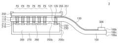
도 4a는 실시예들에 따른 센싱 모듈을 도시한 평면도이다. 도 4b는 도 4a의 Ⅲ-Ⅳ선을 따라 자른 단면이다. 이하, 앞서 설명한 바와 중복되는 내용은 생략한다.Figure 4a is a plan view showing a sensing module according to embodiments. Figure 4b is a cross-section taken along line III-IV of Figure 4a. Hereinafter, content that overlaps with what was previously described will be omitted.
도 4a 및 도 4d를 참조하면, 센싱 모듈(2)은 필름 기판(100), 반도체칩(200), 및 커넥터(300)를 포함할 수 있다. 필름 기판(100)은 도 3a 및 도 3b에서 설명한 바와 동일할 수 있다. 필름 기판(100)은 센싱 비아들(110), 제1 배선 패턴(131), 제2 배선 패턴(132), 및 연결 비아(120)를 포함할 수 있다. 필름 기판(100)은 플렉서블하여, 휘어질 수 있다.Referring to FIGS. 4A and 4D , the sensing module 2 may include a
반도체칩(200)은 필름 기판(100)의 제1 면(100a) 상에 제공될 수 있다. 반도체칩(200)은 도 2a 및 도 2b의 예에서 설명한 바와 동일 또는 유사할 수 있다. 예를 들어, 반도체칩(200)은 그 상면 상에 픽셀들(PX)을 가질 수 있다. 도 4a와 같이, 픽셀들(PX)은 이차원적으로 배열된 어레이를 이룰 수 있다. 센싱 플레이트들(210)이 반도체칩(200) 내에서 픽셀들(PX)에 각각 제공될 수 있다. 센싱 비아들(110)은 필름 기판(100)을 관통하고, 반도체칩(200)의 픽셀들(PX) 상에 각각 제공될 수 있다. 하부 패드들(111) 및 상부 패드들(112)은 필름 기판(100)의 제1 면(100a) 및 제2 면(100b) 상에 배치되며, 반도체칩(200)의 픽셀들(PX)에 각각 제공될 수 있다. 센싱 인터포저들(212)이 필름 기판(100) 및 반도체칩(200) 사이에 개재될 수 있다. 센싱 인터포저들(212)은 센싱 플레이트들(210) 및 하부 패드들(111)과 각각 접속할 수 있다. 센싱 인터포저들(212)은 도전성 물질, 예를 들어, 금(Au), 구리(Cu), 알루미늄(Al), 주석(Sn), 또는 이들의 합금을 포함할 수 있다. 센싱 인터포저들(212)은 범프 또는 솔더와 같은 형상을 가질 수 있다.The
절연 패턴(260)이 반도체칩(200) 및 필름 기판(100) 사이에 제공되어, 센싱 인터포저들(212)의 측벽들 및 연결 인터포저(232)의 측벽을 덮을 수 있다. 절연 패턴(260)은 폴리머, 예를 들어, 에폭시계 물질 또는 폴리이미드계 물질을 포함할 수 있다. 몰딩막(270)이 필름 기판(100)의 제1 면(100a) 상에 제공되어, 반도체칩(200)을 덮을 수 있다. 몰딩막(270)은 에폭시계 몰딩 컴파운드(EMC)를 포함할 수 있다.An
유리층(250)이 필름 기판(100)의 제2 면(100b) 상에 제공될 수 있다. 유리층(250)은 평면적 관점에서 반도체칩(200)의 픽셀들(PX)과 중첩될 수 있다. 터치는 유리층(250)의 상면 상에 수행될 수 있다. 사용자의 터치는 상부 패드들(112), 센싱 비아들(110), 하부 패드들(111), 센싱 인터포저들(212)을 통하여 센싱 플레이트들(210)로 전달될 수 있다. 실시예에 따르면, 상부 패드들(112) 및 터치 사이의 거리는 센싱 플레이트들(210) 및 터치 사이의 거리보다 더 짧을 수 있다. 이에 따라, 반도체칩(200)의 센싱 민감도 및 정확도가 더욱 향상될 수 있다.A
접착층(251)이 필름 기판(100) 및 유리층(250) 사이에 개재될 수 있다. 유리층(250)은 접착층(250)에 의해 필름 기판(100)의 제2 면(100b)에 부착될 수 있다. 접착층(251)은 폴리이미드와 같은 고분자 물질 또는 언더필을 포함할 수 있다. 다른 예로, 컬러 필터층(미도시)가 접착층(251) 및 필름 기판(100) 사이 또는 접착층(251)과 유리층(250) 사이에 더 개재될 수 있다.An
베젤(bezel, 255)이 유리층(250)의 상면, 측면, 및 엣지 부분 상에 배치될 수 있다. 유리층(250)의 엣지 부분은 유리층(250)의 상면 및 측면이 만나는 부분일 수 있다. 유리층(250)은 베젤(255)에 삽입될 수 있다. 베젤(255)은 스테인레스 스틸을 포함할 수 있다.A
연결 패드(230)가 반도체칩(200)의 상면(200b) 상에 제공될 수 있다. 연결 패드(230)는 센싱 플레이트들(210) 보다 반도체칩(200)의 일측(200c)에 인접할 수 있다. 연결 인터포저(232)가 연결 패드(230) 상에 제공되며, 연결 패드(230)와 접속할 수 있다. 연결 인터포저(232)는 센싱 인터포저들(212)의 예에서 설명한 도전성 물질들 중에서 어느 하나를 포함할 수 있다.A
제1 배선 패턴(131)이 필름 기판(100)의 제1 면(100a) 상에 제공될 수 있다. 제1 배선 패턴(131)의 일단은 연결 패드(230)와 접속할 수 있다. 연결 비아(120)가 필름 기판(100)을 관통하며, 제1 배선 패턴(131)의 타단과 접속할 수 있다. 제2 배선 패턴(132)이 필름 기판(100)의 제2 면(100b) 상에 제공될 수 있다. 제2 배선 패턴(132)의 일단은 연결 비아(120)와 접속할 수 있다.A first wiring pattern 131 may be provided on the
소자(310)가 필름 기판(100)의 제2 면(100b) 상에 배치될 수 있다. 일 예로, 소자(310)는 캐패시터, 레지스터, 또는 인덕터와 같은 수동 소자를 포함할 수 있다. 다른 예로, 소자(310)는 메모리칩 또는 로직칩과 같은 능동 소자일 수 있다. 제2 배선 패턴(132)은 소자(310)와 전기적으로 연결될 수 있다. 소자(310)의 배치 및 개수는 도시된 바에 한정되지 않고 다양할 수 있다.The
커넥터(300)가 필름 기판(100)의 제1 면(100a) 상에서, 필름 기판(100)의 제1 측(100c)에 인접하여 제공될 수 있다. 커넥터(300)는 제2 배선 패턴(132)과 접속할 수 있다. 제2 배선 패턴(132)이 소자(310)와 커넥터(300) 사이에 더 제공될 수 있다. 커넥터(300)는 제2 배선 패턴(132), 연결 비아(120), 및 제1 배선 패턴(131)을 통하여, 연결 패드(230)와 전기적으로 연결될 수 있다.The
도 5a는 실시예들에 따른 필름 기판을 도시한 평면도이다. 도 5b는 도 5a의 Ⅰ-Ⅱ선을 따라 자른 단면이다. 이하, 앞서 설명한 바와 중복되는 내용은 생략한다.Figure 5A is a plan view showing a film substrate according to embodiments. Figure 5b is a cross-section taken along line I-II of Figure 5a. Hereinafter, content that overlaps with what was previously described will be omitted.
도 5a 및 도 5b를 참조하면, 필름 기판(100)은 센싱 비아들(110) 및 배선 패턴(130)을 포함할 수 있다. 센싱 비아들(110), 하부 패드들(111), 및 상부 패드들(112)은 도 3a 및 도 3b에서 설명한 바와 동일할 수 있다.Referring to FIGS. 5A and 5B , the
연결 비아(120)가 필름 기판(100)을 관통하며 제공될 수 있다. 연결 비아(120)는 센싱 비아들(110) 및 필름 기판(100)의 제1 측(100c) 사이에 제공될 수 있다. 배선 패턴(130)이 필름 기판(100)의 제2 면(100b) 상에 제공될 수 있다. 배선 패턴(130)의 일단은 연결 비아(120)와 접속할 수 있다. 배선 패턴(130)의 타단은 필름 기판(100)의 제1 측(100c)을 향할 수 있다. 배선 패드(121)가 필름 기판(100)의 제1 면(100a) 상에 배치될 수 있다. 배선 패드(121)는 연결 비아(120)의 하면 상에서 연결 비아(120)와 접속할 수 있다. 배선 패드(121)는 구리(Cu), 알루미늄(Al), 주석(Sn), 금(Au), 또는 이들의 합금을 포함할 수 있다. 다른 예로, 배선 패드(121)는 생략될 수 있다.A connection via 120 may be provided penetrating the
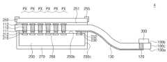
도 6a는 실시예들에 따른 센싱 모듈을 도시한 평면도이다. 도 6b는 도 6a의 Ⅲ-Ⅳ선을 따라 자른 단면이다. 이하, 앞서 설명한 바와 중복되는 내용은 생략한다.Figure 6a is a plan view showing a sensing module according to embodiments. Figure 6b is a cross-section taken along line III-IV of Figure 6a. Hereinafter, content that overlaps with what was previously described will be omitted.
도 6a 및 도 6d를 참조하면, 센싱 모듈(3)은 필름 기판(100), 반도체칩(200), 커넥터(300), 접착층(251), 유리층(250), 베젤(255), 절연 패턴(260), 및 몰딩막(270)을 포함할 수 있다. 반도체칩(200)은 필름 기판(100)의 제1 면(100a) 상에 제공될 수 있다. 필름 기판(100)은 도 5a 및 도 5b에서 설명한 바와 동일할 수 있다. 센싱 플레이트들(210)이 반도체칩(200)의 픽셀들(PX)에 각각 제공될 수 있다. 센싱 인터포저들(212)이 센싱 플레이트들(210) 및 하부 패드들(111) 사이에 개재될 수 있다. 센싱 비아들(110)은 반도체칩(200)의 픽셀들(PX) 상에 각각 제공되며, 센싱 플레이트들(210)과 전기적으로 연결될 수 있다.Referring to FIGS. 6A and 6D, the
연결 패드(230)는 반도체칩(200)의 상면(200b) 상에서 센싱 플레이트들(210)과 옆으로 이격 배치될 수 있다. 도 6a와 같이, 연결 비아(120)는 평면적 관점에서 연결 패드(230)와 중첩될 수 있다. 연결 인터포저(232)는 연결 패드(230) 및 배선 패드(121) 사이에 개재될 수 있다. 연결 비아(120)는 배선 패드(121) 및 연결 인터포저(232)를 통해 연결 패드(230)와 전기적으로 연결될 수 있다. 다른 예로, 연결 인터포저(232) 또는 배선 패드(121)는 생략될 수 있다.The
배선 패턴(130)은 필름 기판(100)의 제2 면(100b) 상에 제공될 수 있다. 배선 패턴(130)의 일단은 연결 비아(120)와 접속할 수 있다.The
커넥터(300)가 필름 기판(100)의 제2 면(100b) 상에 제공될 수 있다. 배선 패턴(130)의 타단은 커넥터(300)와 전기적으로 연결될 수 있다. 도 4a 및 도 4b에서 설명한 소자(310)가 필름 기판(100)의 제2 면(100b) 상에 더 제공될 수 있다. 이 경우, 배선 패턴(130)은 소자(310)와 연결될 수 있다.A
도 7a는 실시예들에 따른 필름 기판을 도시한 평면도이다. 도 7b는 도 7a의 Ⅰ-Ⅱ선을 따라 자른 단면이다. 이하, 앞서 설명한 바와 중복되는 내용은 생략한다.Figure 7a is a plan view showing a film substrate according to embodiments. Figure 7b is a cross-section taken along line I-II of Figure 7a. Hereinafter, content that overlaps with what was previously described will be omitted.
도 7a 및 도 7b를 참조하면, 필름 기판(100)은 센싱 비아들(110), 하부 패드들(111), 상부 패드들(112), 및 배선 패턴(130)을 포함할 수 있다. 센싱 비아들(110), 하부 패드들(111), 및 상부 패드들(112)은 도 3a 및 도 3b에서 설명한 바와 동일할 수 있다.Referring to FIGS. 7A and 7B , the
연결 비아(120)가 필름 기판(100)을 관통하며 제공될 수 있다. 연결 비아(120)는 센싱 비아들(110)과 옆으로 이격되며, 필름 기판(100)의 제1 측(100c)에 인접하여 제공될 수 있다. 배선 패턴(130)이 필름 기판(100)의 제2 면(100b) 상에서 제공될 수 있다. 도 7a와 같이, 배선 패턴(130)은 평면적 관점에서 센싱 비아들(110) 및 필름 기판(100)의 제1 측(100c) 사이에 제공될 수 있다. 배선 패턴(130)의 일단은 센싱 비아들(110)을 향할 수 있다. 배선 패턴(130)의 타단은 필름 기판(100)의 제1 측(100c)을 향하고, 연결 비아(120)와 접속할 수 있다.A connection via 120 may be provided penetrating the
도 8a는 실시예들에 따른 센싱 모듈을 도시한 평면도이다. 도 8b는 도 8a의 Ⅲ-Ⅳ선을 따라 자른 단면이다. 이하, 앞서 설명한 바와 중복되는 내용은 생략한다.Figure 8a is a plan view showing a sensing module according to embodiments. Figure 8b is a cross-section taken along line III-IV of Figure 8a. Hereinafter, content that overlaps with what was previously described will be omitted.
도 8a 및 도 8d를 참조하면, 센싱 모듈(4)은 필름 기판(100), 반도체칩(200), 커넥터(300), 접착층(251), 유리층(250), 베젤(255), 절연 패턴(260), 및 몰딩막(270)을 포함할 수 있다. 필름 기판(100)은 도 7a 및 도 7b에서 설명한 바와 동일할 수 있다. 반도체칩(200)은 필름 기판(100)의 제1 면(100a) 상에 제공될 수 있다. 센싱 플레이트들(210)이 반도체칩(200) 내에서 픽셀들(PX)에 각각 제공될 수 있다. 센싱 비아들(110)은 픽셀들(PX) 상에 각각 제공되며, 센싱 플레이트들(210)과 전기적으로 연결될 수 있다.Referring to FIGS. 8A and 8D, the
연결 패드(230)가 반도체칩(200)의 상면(200b) 상에서 센싱 플레이트들(210)과 이격배치될 수 있다. 연결 인터포저(232)가 연결 패드(230) 상에 배치될 수 있다. 배선 패턴(130)이 필름 기판(100)의 제1 면(100a) 상에 제공될 수 있다. 배선 패턴(130)의 일단은 연결 인터포저(232)와 접속할 수 있다. 배선 패턴(130)의 타단은 필름 기판(100)의 제1 측(100c)에 인접할 수 있다. 연결 비아(120)는 필름 기판(100)을 관통하며, 배선 패턴(130)의 타단과 접속할 수 있다.The
커넥터(300)가 필름 기판(100)의 제2 면(100b) 상에 제공되며, 연결 비아(120)와 접속할 수 있다. 도 8a와 같이 커넥터(300)는 연결 비아(120)와 중첩될 수 있다. 도시되지는 않았으나, 연결 비아(120) 및 커넥터(300) 사이에 패드 또는 범프가 더 개재될 수 있다. 도 4a 및 도 4b에 도시된 바와 같이, 소자(310)가 필름 기판(100)의 제2 면(100b) 상에 더 제공될 수 있다. 이 경우, 소자(310)와 커넥터(300) 사이에 추가적인 배선 패턴(130)이 더 제공될 수 있다.A
도 9a는 실시예들에 따른 필름 기판을 도시한 평면도이다. 도 9b는 도 9a의 Ⅰ-Ⅱ선을 따라 자른 단면이다. 이하, 앞서 설명한 바와 중복되는 내용은 생략한다.Figure 9A is a plan view showing a film substrate according to embodiments. FIG. 9B is a cross-section taken along line I-II of FIG. 9A. Hereinafter, content that overlaps with what was previously described will be omitted.
도 9a 및 도 9b를 참조하면, 필름 기판(100)은 센싱 비아들(110), 배선 패턴(130), 연결 비아(120), 도전 비아(140), 및 도전 패턴(150)을 포함할 수 있다. 센싱 비아들(110), 하부 패드들(111), 상부 패드들(112), 연결 비아(120), 배선 패드(121), 및 배선 패턴(130)은 도 5a 및 도 5b에서 설명한 바와 동일할 수 있다.9A and 9B, the
도전 비아(140)가 필름 기판(100)을 관통하며 제공될 수 있다 도전 비아(140)는 센싱 비아들(110)과 옆으로 이격 배치될 수 있다. 도전 비아(140)가 센싱 비아들(110) 및 필름 기판(100)의 제2 측(100d) 사이에 제공될 수 있다. 필름 기판(100)의 제2 측(100d)은 제1 면(100a) 및 제2 면(100b)을 잇고, 제1 측(100c)과 대향될 수 있다. 도시된 바와 달리, 필름 기판(100)의 제2 측(100d)은 제1 면(100a) 및 제2 면(100b)을 잇되, 제1 측(100c)과 이웃할 수 있다. 도전 패턴(150)이 필름 기판(100)의 제2 면(100b) 상에 배치될 수 있다. 도 7a와 같이, 도전 패턴(150)은 센싱 비아들(110) 및 필름 기판(100)의 제2 측(100d) 사이에 제공될 수 있다. 도전 패턴(150)은 도전 비아(140)와 접속할 수 있다. 도전 비아(140) 및 도전 패턴(150)은 연결 비아(120) 및 배선 패턴(130)과 각각 동일한 물질을 포함할 수 있다.A conductive via 140 may be provided penetrating the
도 10a는 실시예들에 따른 센싱 모듈을 도시한 평면도이다. 도 10b는 도 10a의 Ⅲ-Ⅳ선을 따라 자른 단면이다. 이하, 앞서 설명한 바와 중복되는 내용은 생략한다.Figure 10a is a plan view showing a sensing module according to embodiments. Figure 10b is a cross-section taken along line III-IV of Figure 10a. Hereinafter, content that overlaps with what was previously described will be omitted.
도 10a 및 도 10d를 참조하면, 센싱 모듈(5)은 필름 기판(100), 반도체칩(200), 커넥터(300), 접착층(251), 유리층(250), 베젤(255). 절연 패턴(260), 및 몰딩막(270)을 포함할 수 있다. 반도체칩(200)은 필름 기판(100)의 제1 면(100a) 상에 제공될 수 있다. 필름 기판(100)은 도 9a 및 도 9b에서 설명한 바와 동일할 수 있다. 센싱 비아들(110)이 반도체칩(200)의 픽셀들(PX) 상에 각각 제공되며, 센싱 플레이트들(210)과 전기적으로 연결될 수 있다. 연결 인터포저(232) 및 연결 비아(120)가 연결 패드(230) 상에 각각 배치될 수 있다. 배선 패턴(130)은 필름 기판(100)의 제2 면(100b) 상에 제공되며, 연결 비아(120)와 접속할 수 있다. 연결 비아(120) 및 배선 패턴(130)의 배치 및 전기적 연결은 도 6a 및 도 6b에서 설명한 바와 동일할 수 있다. 커넥터(300)가 필름 기판(100)의 제2 면(100b) 상에 제공될 수 있다. 커넥터(300)는 배선 패턴(130)과 전기적으로 연결될 수 있다.Referring to FIGS. 10A and 10D, the
도전 패드(240)가 반도체칩(200)의 상면(200b) 상에서 센싱 플레이트들(210)보다 반도체칩(200)의 타측(200d)에 인접하여 제공될 수 있다. 반도체칩(200)의 타측(200d)은 일측(200c)과 대향될 수 있다. 도시된 바와 달리, 반도체칩(200)의 타측(200d)은 일측(200c)과 이웃할 수 있다. 여기에서, 반도체칩(200)의 상면(100b)은 일측(200c) 및 타측(200d)을 이을 수 있다. 도전 패드(240)는 반도체칩(200)의 센싱 플레이트들(210)과 옆으로 배치되며, 센싱 플레이트들(210)과 전기적으로 단절될 수 있다. 도전 패드(240)는 반도체칩(200)의 집적 회로와 전기적으로 연결될 수 있다. 도전 비아(140)는 도전 패드(240) 상에 배치될 수 있다. 도전 비아(140) 및 도전 패드(240) 사이에 도전 인터포저(242)가 개재될 수 있다. 도전 패턴(150)은 필름 기판(100)의 제2 면(100b) 상에 제공되며, 도전 비아(140)와 접속할 수 있다. 도전 패턴(150)은 도전 비아(140) 및 도전 인터포저(242)를 통해 도전 패드(240)와 전기적으로 연결될 수 있다. 다른 예로, 도전 인터포저(242)는 생략되고, 도전 비아(140)가 도전 패드(240)와 접촉할 수 있다.The
소자(310)가 필름 기판(100)의 제2 면(100b) 상에서 필름 기판(100)의 제2 측(100d)과 인접하여 제공될 수 있다. 소자(310)는 도전 패턴(150)과 접속할 수 있다. 소자(310)의 배치는 도시된 바에 제한되지 않고, 다양할 수 있다. 예를 들어, 소자(310)는 필름 기판(100)의 제1 면(100a) 상에 배치될 수 있으며, 이 경우, 도전 비아(140)는 생략될 수 있다.The
도 11a는 실시예들에 따른 필름 기판을 도시한 평면도이다. 도 11b는 도 11a의 Ⅰ-Ⅱ선을 따라 자른 단면이다. 이하, 앞서 설명한 바와 중복되는 내용은 생략한다.Figure 11a is a plan view showing a film substrate according to embodiments. FIG. 11B is a cross-section taken along line I-II of FIG. 11A. Hereinafter, content that overlaps with what was previously described will be omitted.
도 11a 및 도 11b를 참조하면, 필름 기판(100)은 센싱 비아들(110) 및 배선 패턴(130)을 포함할 수 있다. 센싱 비아들(110), 하부 패드들(111), 및 상부 패드들(112)은 도 3a 및 도 3b에서 설명한 바와 동일할 수 있다.Referring to FIGS. 11A and 11B , the
연결 비아(120)가 필름 기판(100)을 관통하며 제공될 수 있다. 연결 비아(120)는 센싱 비아들(110) 및 필름 기판(100)의 제1 측(100c) 사이에 제공될 수 있다. 연결 비아(120)은 제1 연결 비아(123) 및 제2 연결 비아(125)를 포함하할 수 있다. 제2 연결 비아(125)는 제1 연결 비아(123)보다 필름 기판(100)의 제1 측(100c)에 더 인접할 수 있다. 배선 패턴(130)이 필름 기판(100)의 제2 면(100b) 상에 제공될 수 있다. 배선 패턴(130)의 일단은 제1 연결 비아(123)와 접속할 수 있다. 배선 패턴(130)의 타단은 제2 연결 비아(125)와 접속할 수 있다. 배선 패드(121)가 필름 기판(100)의 제1 면(100a) 상에 배치될 수 있다. 배선 패드(121)는 연결 비아(120)의 하면 상에서 연결 비아(120)와 접속할 수 있다. 배선 패드(121)는 구리(Cu), 알루미늄(Al), 주석(Sn), 금(Au), 또는 이들의 합금을 포함할 수 있다. 다른 예로, 배선 패드(121)는 생략될 수 있다.A connection via 120 may be provided penetrating the
도 12a는 실시예들에 따른 센싱 모듈을 도시한 평면도이다. 도 12b는 도 12a의 Ⅲ-Ⅳ선을 따라 자른 단면이다. 이하, 앞서 설명한 바와 중복되는 내용은 생략한다.Figure 12a is a plan view showing a sensing module according to embodiments. Figure 12b is a cross-section taken along line III-IV of Figure 12a. Hereinafter, content that overlaps with what was previously described will be omitted.
도 12a 및 도 12d를 참조하면, 센싱 모듈(6)은 필름 기판(100), 반도체칩(200), 커넥터(300), 접착층(251), 유리층(250), 베젤(255), 절연 패턴(260), 및 몰딩막(270)을 포함할 수 있다. 반도체칩(200)은 필름 기판(100)의 제1 면(100a) 상에 제공될 수 있다. 필름 기판(100)은 도 11a 및 도 11b에서 설명한 바와 동일할 수 있다. 센싱 플레이트들(210)이 반도체칩(200)의 픽셀들(PX)에 각각 제공될 수 있다. 센싱 비아들(110)은 반도체칩(200)의 픽셀들(PX) 상에 각각 제공되며, 센싱 플레이트들(210)과 전기적으로 연결될 수 있다.Referring to FIGS. 12A and 12D, the
연결 패드(230)는 반도체칩(200)의 상면(200b) 상에서 센싱 플레이트들(210)과 옆으로 이격 배치될 수 있다. 도 12a와 같이, 제1 연결 비아(123)는 평면적 관점에서 연결 패드(230)와 중첩될 수 있다. 도 12b와 같이, 연결 인터포저(232) 및 배선 패드(121)가 연결 패드(230) 및 제1 연결 비아(123) 사이에 개재될 수 있다. 제1 연결 비아(121)는 배선 패드(121) 및 연결 인터포저(232)를 통해 연결 패드(230)와 전기적으로 연결될 수 있다. 다른 예로, 연결 인터포저(232) 또는 배선 패드(121)는 생략될 수 있다.The
배선 패턴(130)은 필름 기판(100)의 제2 면(100b) 상에 제공될 수 있다. 배선 패턴(130)의 일단은 연결 비아(120)와 접속할 수 있다. 배선 패턴(130)의 타단은 제2 연결 비아(125)와 접속할 수 있다.The
커넥터(300)가 필름 기판(100)의 제1 면(100a) 상에 제공될 수 있다. 제2 연결 비아(125)는 커넥터(300)와 접속할 수 있다. 도 4a 및 도 4b에서 설명한 소자(310)가 필름 기판(100)의 제1 면(100a) 상에 더 제공될 수 있다. 이 경우, 제2 연결 비아(125)가 배선 패턴(130) 및 소자(310) 사이에 더 제공될 수 있다. 다른 예로, 도 4a 및 도 4b의 설명한 소자(310)는 필름 기판(100)의 제2 면(100b) 상에 제공되고, 배선 패턴(130)은 소자(310)와 연결될 수 있다. 연결 비아(120)의 개수 및 배치, 그리고 배선 패턴(130)의 배치는 도시된 바에 제한되지 않고, 다양할 수 있다.A
Claims (20)
Translated fromKorean상기 필름 기판 상에 배치되며, 그 상면 상에 센싱 플레이트들 및 연결 패드를 갖는 반도체칩, 상기 반도체칩의 상기 상면은 상기 필름 기판을 향하고;
상기 필름 기판의 내부에서 연장되어 상기 필름 기판의 상기 제1 면 및 상기 제2 면을 관통하며, 상기 센싱 플레이트들 상에 각각 제공되는 센싱 비아들; 및
상기 필름 기판 상에서 상기 연결 패드와 전기적으로 연결되는 배선 패턴을 포함하는 센싱 모듈a film substrate having first and second surfaces facing each other;
a semiconductor chip disposed on the film substrate, the semiconductor chip having sensing plates and connection pads on its upper surface, the upper surface of the semiconductor chip facing the film substrate;
Sensing vias extending inside the film substrate and penetrating the first and second surfaces of the film substrate, respectively, are provided on the sensing plates; and
A sensing module including a wiring pattern electrically connected to the connection pad on the film substrate.
상기 배선 패턴은 평면적 관점에서 상기 센싱 비아들과 옆으로 이격 배치되며, 상기 센싱 비아들과 전기적으로 단절되는 센싱 모듈.According to claim 1,
A sensing module in which the wiring pattern is arranged to be laterally spaced apart from the sensing vias in a plan view and is electrically disconnected from the sensing vias.
상기 센싱 플레이트들은 평면적 관점에서 어레이를 이루며 배열되고,
상기 연결 패드는 상기 센싱 플레이트들이 이루는 어레이와 옆으로 이격 배치되는 센싱 모듈.According to claim 1,
The sensing plates are arranged in an array from a planar perspective,
A sensing module in which the connection pad is spaced laterally from the array of the sensing plates.
상기 필름 기판 상에서 상기 배선 패턴과 전기적으로 연결되는 커넥터를 더 포함하는 센싱 모듈;According to claim 1,
a sensing module further including a connector electrically connected to the wiring pattern on the film substrate;
상기 필름 기판을 관통하며, 상기 배선 패턴과 접속하는 연결 비아를 더 포함하는 센싱 모듈.According to clause 4,
A sensing module further comprising a connection via that penetrates the film substrate and connects to the wiring pattern.
상기 반도체칩은 상기 필름 기판의 상기 제1 면 상에 배치되며,
상기 커넥터는 상기 필름 기판의 상기 제2 면 상에 배치되는 센싱 모듈.According to clause 5,
The semiconductor chip is disposed on the first side of the film substrate,
The connector is a sensing module disposed on the second side of the film substrate.
상기 배선 패턴은:
상기 필름 기판의 상기 제1 면 상에서 상기 연결 패드 및 상기 연결 비아 사이에 제공되는 제1 배선 패턴; 및
상기 필름 기판의 상기 제2 면 상에서 상기 연결 비아 및 상기 커넥터 사이에 제공되는 제2 배선 패턴을 포함하는 센싱 모듈.According to clause 5,
The wiring pattern is:
a first wiring pattern provided between the connection pad and the connection via on the first side of the film substrate; and
A sensing module comprising a second wiring pattern provided between the connection via and the connector on the second side of the film substrate.
상기 연결 비아는 상기 연결 패드 상에 제공되어, 상기 연결 패드와 전기적으로 연결되고,
상기 배선 패턴은 상기 필름 기판의 상기 제2 면 상에 배치되는 센싱 모듈According to clause 6,
The connection via is provided on the connection pad and is electrically connected to the connection pad,
The wiring pattern is a sensing module disposed on the second side of the film substrate.
상기 필름 기판 상에 제공되며, 그 일면 상에 센싱 픽셀들을 갖는 반도체칩; 및
상기 필름 기판의 내부에서 연장되어 상기 필름 기판의 상기 제1 면 및 상기 제2 면을 관통하며, 상기 센싱 픽셀들 상에 각각 제공되는 센싱 비아들을 포함하는 센싱 모듈.a film substrate having first and second surfaces facing each other;
a semiconductor chip provided on the film substrate and having sensing pixels on one surface thereof; and
A sensing module extending inside the film substrate, penetrating the first side and the second side of the film substrate, and including sensing vias provided on the sensing pixels, respectively.
상기 반도체칩의 상기 일면 상에서 상기 센싱 픽셀들과 옆으로 이격 배치된 연결 패드를 더 포함하는 센싱 모듈.According to clause 9,
A sensing module further comprising a connection pad disposed laterally spaced apart from the sensing pixels on the one surface of the semiconductor chip.
상기 센싱 비아들은 행 방향 및 열 방향으로 나열된 어레이를 이루며, 상기 연결 패드는 상기 센싱 비아들의 상기 어레이의 일측에 배치되는 센싱 모듈.According to claim 10,
The sensing vias form an array arranged in row and column directions, and the connection pad is disposed on one side of the array of sensing vias.
상기 필름 기판 상에 제공되며, 상기 센싱 픽셀들과 옆으로 이격 배치되는 배선 패턴을 더 포함하는 센싱 모듈.According to clause 9,
A sensing module provided on the film substrate and further comprising a wiring pattern spaced laterally from the sensing pixels.
상기 필름 기판 상에 제공되며, 상기 배선 패턴과 접속하는 커넥터를 더 포함하는 센싱 모듈.According to claim 12,
A sensing module provided on the film substrate and further comprising a connector connected to the wiring pattern.
상기 필름 기판을 관통하며, 상기 배선 패턴과 접속하는 연결 비아를 더 포함하는 센싱 모듈.According to claim 12,
A sensing module further comprising a connection via that penetrates the film substrate and connects to the wiring pattern.
상기 반도체칩은 상기 센싱 픽셀들 각각에 제공되는 센싱 플레이트들을 더 포함하며, 상기 센싱 비아들은 상기 센싱 플레이트들과 접속하는 센싱 모듈.According to clause 9,
The semiconductor chip further includes sensing plates provided to each of the sensing pixels, and the sensing vias are connected to the sensing plates.
상기 센싱 플레이트들 및 상기 센싱 비아들 사이에 제공되는 센싱 인터포저들을 더 포함하는 센싱 모듈.According to claim 15,
A sensing module further comprising sensing interposers provided between the sensing plates and the sensing vias.
상기 필름 기판 및 상기 반도체칩 사이에 제공되는 절연 패턴; 및
상기 필름 기판 상에서 상기 반도체칩을 덮는 몰딩막을 더 포함하는 센싱 모듈.According to clause 9,
an insulating pattern provided between the film substrate and the semiconductor chip; and
A sensing module further comprising a molding film covering the semiconductor chip on the film substrate.
상기 필름 기판의 내부에서 연장되어 상기 필름 기판의 상기 제1 면 및 상기 제2 면을 관통하는 더미 비아들; 및
상기 필름 기판의 상기 제1 면 상에 제공되는 제1 배선 패턴을 포함하되,
상기 더미 비아들은 상기 배선 패턴과 전기적으로 단절된 센싱 모듈 기판.a film substrate having first and second surfaces facing each other;
dummy vias extending inside the film substrate and penetrating the first and second surfaces of the film substrate; and
A first wiring pattern provided on the first side of the film substrate,
A sensing module substrate in which the dummy vias are electrically disconnected from the wiring pattern.
상기 필름 기판의 상기 제1 면 및 상기 제2 면을 관통하며, 상기 제1 배선 패턴과 접속하는 연결 비아를 더 포함하는 센싱 모듈 기판.According to clause 18,
The sensing module substrate further includes a connection via that passes through the first and second surfaces of the film substrate and connects to the first wiring pattern.
상기 필름 기판의 상기 제2 면 상에 제공되는 제2 배선 패턴을 더 포함하되, 상기 제2 배선 패턴은 상기 연결 비아와 접속하는 센싱 모듈 기판.According to clause 19,
A sensing module substrate further comprising a second wiring pattern provided on the second surface of the film substrate, wherein the second wiring pattern is connected to the connection via.
Priority Applications (4)
| Application Number | Priority Date | Filing Date | Title |
|---|---|---|---|
| KR1020160016543AKR102592972B1 (en) | 2016-02-12 | 2016-02-12 | Sensing Module substrate and Sensing Module including the same |
| US15/395,623US10282587B2 (en) | 2016-02-12 | 2016-12-30 | Sensing module substrate and sensing module including the same |
| TW106103893ATWI731932B (en) | 2016-02-12 | 2017-02-07 | Sensing module substrate and sensing module including the same |
| CN201710077705.7ACN107085702B (en) | 2016-02-12 | 2017-02-13 | Sensing module substrate and sensing module comprising same |
Applications Claiming Priority (1)
| Application Number | Priority Date | Filing Date | Title |
|---|---|---|---|
| KR1020160016543AKR102592972B1 (en) | 2016-02-12 | 2016-02-12 | Sensing Module substrate and Sensing Module including the same |
Publications (2)
| Publication Number | Publication Date |
|---|---|
| KR20170095462A KR20170095462A (en) | 2017-08-23 |
| KR102592972B1true KR102592972B1 (en) | 2023-10-24 |
Family
ID=59561575
Family Applications (1)
| Application Number | Title | Priority Date | Filing Date |
|---|---|---|---|
| KR1020160016543AActiveKR102592972B1 (en) | 2016-02-12 | 2016-02-12 | Sensing Module substrate and Sensing Module including the same |
Country Status (4)
| Country | Link |
|---|---|
| US (1) | US10282587B2 (en) |
| KR (1) | KR102592972B1 (en) |
| CN (1) | CN107085702B (en) |
| TW (1) | TWI731932B (en) |
Families Citing this family (6)
| Publication number | Priority date | Publication date | Assignee | Title |
|---|---|---|---|---|
| TW201721492A (en)* | 2015-12-10 | 2017-06-16 | 台瀚科技股份有限公司 | Sandwich type fingerprint recognition device |
| CN107203737A (en)* | 2016-03-17 | 2017-09-26 | 台瀚科技股份有限公司 | Thin fingerprint identification device with optical film |
| US10073288B2 (en)* | 2016-10-07 | 2018-09-11 | Keycore Technology Corp. | Liquid crystal module with fingerprint identification function |
| US10073305B2 (en)* | 2016-10-07 | 2018-09-11 | Keycore Technology Corp. | Liquid crystal device with fingerprint identification function |
| US10055637B2 (en)* | 2016-12-07 | 2018-08-21 | Synaptics Incorporated | Optical sensor with substrate light filter |
| TWI626599B (en)* | 2017-09-26 | 2018-06-11 | 速博思股份有限公司 | Small curvature radius fingerprint detector structure |
Family Cites Families (35)
| Publication number | Priority date | Publication date | Assignee | Title |
|---|---|---|---|---|
| JP4160851B2 (en)* | 2003-03-31 | 2008-10-08 | 富士通株式会社 | Semiconductor device for fingerprint recognition |
| KR100546364B1 (en) | 2003-08-13 | 2006-01-26 | 삼성전자주식회사 | Semiconductor package using flexible film and manufacturing method thereof |
| KR20050019233A (en) | 2003-08-18 | 2005-03-03 | 삼성전자주식회사 | Film-Type Package And Circuit Film For Zigzag Pad IC Chip |
| KR20060074089A (en) | 2004-12-27 | 2006-07-03 | 주식회사 하이닉스반도체 | Chip stack package |
| US7964926B2 (en)* | 2005-02-02 | 2011-06-21 | Samsung Electronics Co., Ltd. | Image sensing devices including image sensor chips, image sensor package modules employing the image sensing devices, electronic products employing the image sensor package modules, and methods of fabricating the same |
| WO2008105824A2 (en)* | 2006-08-29 | 2008-09-04 | Nanosphere, Inc. | Direct detection of ligand-antiligand interactions by nanoscale switching |
| KR100813623B1 (en) | 2006-10-17 | 2008-03-17 | 삼성전자주식회사 | Flexible film, semiconductor package and manufacturing method using same |
| US7417310B2 (en)* | 2006-11-02 | 2008-08-26 | Entorian Technologies, Lp | Circuit module having force resistant construction |
| KR20080059836A (en) | 2006-12-26 | 2008-07-01 | 엘지디스플레이 주식회사 | OSF and liquid crystal display comprising the same. |
| EP2667412A1 (en)* | 2007-04-18 | 2013-11-27 | Invisage Technologies, INC. | Materials, systems and methods for optoelectronic devices |
| TWI341020B (en)* | 2007-08-10 | 2011-04-21 | Egis Technology Inc | Fingerprint sensing chip having a flexible circuit board serving as a signal transmission structure and method of manufacturing the same |
| KR101479509B1 (en)* | 2008-08-29 | 2015-01-08 | 삼성전자주식회사 | Semiconductor Package |
| KR101048980B1 (en)* | 2009-01-16 | 2011-07-12 | 삼성모바일디스플레이주식회사 | Touch screen panel and its manufacturing method |
| NO20093601A1 (en)* | 2009-12-29 | 2011-06-30 | Idex Asa | surface Sensor |
| US10276486B2 (en)* | 2010-03-02 | 2019-04-30 | General Electric Company | Stress resistant micro-via structure for flexible circuits |
| KR101661160B1 (en) | 2010-03-31 | 2016-09-29 | 삼성전자주식회사 | Touch screen pannel |
| EP2599115B1 (en)* | 2010-07-27 | 2015-02-25 | TEL Solar AG | Heating arrangement and method for heating substrates |
| US9222350B2 (en)* | 2011-06-21 | 2015-12-29 | Diamond Innovations, Inc. | Cutter tool insert having sensing device |
| KR101376089B1 (en)* | 2011-12-30 | 2014-03-20 | (주)멜파스 | Touch sensing apparatus and method for manufacturing the same |
| JP5939385B2 (en) | 2012-04-13 | 2016-06-22 | 日本電気株式会社 | Infrared sensor package, infrared sensor module, and electronic device |
| US9030440B2 (en) | 2012-05-18 | 2015-05-12 | Apple Inc. | Capacitive sensor packaging |
| KR101951956B1 (en) | 2012-11-13 | 2019-02-26 | 매그나칩 반도체 유한회사 | Flexible printed circuit board for packaging semiconductor device |
| KR20140079062A (en) | 2012-12-18 | 2014-06-26 | 삼성전자주식회사 | Semiconductor package and display device using the same |
| KR102017158B1 (en)* | 2013-03-04 | 2019-09-02 | 삼성전자주식회사 | Chip on film package and display device including the same |
| TWI481938B (en)* | 2013-06-14 | 2015-04-21 | Au Optronics Corp | In-cell touch display panel |
| KR20150018350A (en)* | 2013-08-08 | 2015-02-23 | 삼성전자주식회사 | Fingerprint Recognizing Apparatus And Manufacturing Method Thereof And Electronic Device |
| KR20150078983A (en) | 2013-12-31 | 2015-07-08 | 엘지디스플레이 주식회사 | Chip on film package |
| TWI493187B (en)* | 2014-02-17 | 2015-07-21 | Morevalued Technology Co Let | Biometrics sensor having flat contact surface formed by signal extending structure and method of manufacturing such sensor |
| KR20150108986A (en) | 2014-03-18 | 2015-10-01 | 삼성전자주식회사 | Chip on film package including plurality of output pad connected to film wire |
| CN105225628B (en)* | 2014-06-19 | 2017-10-24 | 元太科技工业股份有限公司 | Display device, display module and pixel structure thereof |
| WO2016060202A1 (en)* | 2014-10-17 | 2016-04-21 | 旭硝子株式会社 | Cover member |
| KR101942141B1 (en)* | 2015-05-12 | 2019-01-24 | 앰코테크놀로지코리아(주) | Package of finger print sensor |
| TWM513407U (en)* | 2015-07-31 | 2015-12-01 | Superc Touch Corp | Fingerprint recognition apparatus |
| CN105159493B (en)* | 2015-08-26 | 2018-01-26 | 广东欧珀移动通信有限公司 | Fingerprint identification device, touch screen and mobile terminal |
| TWI584202B (en)* | 2015-12-31 | 2017-05-21 | 速博思股份有限公司 | Fingerprint identification apparatus |
- 2016
- 2016-02-12KRKR1020160016543Apatent/KR102592972B1/enactiveActive
- 2016-12-30USUS15/395,623patent/US10282587B2/enactiveActive
- 2017
- 2017-02-07TWTW106103893Apatent/TWI731932B/enactive
- 2017-02-13CNCN201710077705.7Apatent/CN107085702B/enactiveActive
Non-Patent Citations (3)
| Title |
|---|
| TWM513407 U* |
| 한국 공개특허공보 제10-2014-0108845호(2014.09.15.) 1부.* |
| 한국 공개특허공보 제10-2015-0018358호(2015.02.23.) 1부.* |
Also Published As
| Publication number | Publication date |
|---|---|
| US20170235997A1 (en) | 2017-08-17 |
| CN107085702A (en) | 2017-08-22 |
| TW201732678A (en) | 2017-09-16 |
| US10282587B2 (en) | 2019-05-07 |
| KR20170095462A (en) | 2017-08-23 |
| CN107085702B (en) | 2022-09-02 |
| TWI731932B (en) | 2021-07-01 |
Similar Documents
| Publication | Publication Date | Title |
|---|---|---|
| KR102592972B1 (en) | Sensing Module substrate and Sensing Module including the same | |
| KR101815754B1 (en) | Semiconductor device | |
| KR102468554B1 (en) | Fingerprint recognition module and manufacturing method of the fingerprint recognition module | |
| KR102157551B1 (en) | A semiconductor package and method of fabricating the same | |
| JP2020503606A5 (en) | ||
| US7936032B2 (en) | Film type package for fingerprint sensor | |
| US10013596B2 (en) | Fingerprint recognition apparatus | |
| US9431374B2 (en) | Semiconductor package | |
| US9129962B1 (en) | Bonding pad arrangment design for multi-die semiconductor package structure | |
| KR20170056071A (en) | Semiconductor package | |
| CN103515345A (en) | Substrate structure and packaging structure | |
| KR20170084941A (en) | Fingerprint sensor package and method for manufacturing the same | |
| US20070099449A1 (en) | Printed circuit board, electronic device, and manufacturing method for printed circuit board | |
| US10055631B1 (en) | Semiconductor package for sensor applications | |
| TWM513407U (en) | Fingerprint recognition apparatus | |
| CN205621726U (en) | Semiconductor package | |
| KR20210053392A (en) | Sensor Device | |
| TWI615928B (en) | Package structure and method for fabricating the same | |
| CN113451253B (en) | Chip-on-film packaging structure | |
| US20170017823A1 (en) | Capacitor sensor structure, circuit board structure with capacitor sensor, and package structure of capacitive sensor | |
| US11922718B2 (en) | Fingerprint sensor package and sensor package | |
| US20250166407A1 (en) | Fingerprint sensor package and device including the same | |
| CN119206802A (en) | Fingerprint recognition module | |
| TW202448229A (en) | Electronic device and method for manufacturing electronic device | |
| US7994644B2 (en) | Package stacking through rotation |
Legal Events
| Date | Code | Title | Description |
|---|---|---|---|
| PA0109 | Patent application | Patent event code:PA01091R01D Comment text:Patent Application Patent event date:20160212 | |
| PG1501 | Laying open of application | ||
| A201 | Request for examination | ||
| PA0201 | Request for examination | Patent event code:PA02012R01D Patent event date:20210208 Comment text:Request for Examination of Application Patent event code:PA02011R01I Patent event date:20160212 Comment text:Patent Application | |
| E902 | Notification of reason for refusal | ||
| PE0902 | Notice of grounds for rejection | Comment text:Notification of reason for refusal Patent event date:20230113 Patent event code:PE09021S01D | |
| E701 | Decision to grant or registration of patent right | ||
| PE0701 | Decision of registration | Patent event code:PE07011S01D Comment text:Decision to Grant Registration Patent event date:20230724 | |
| GRNT | Written decision to grant | ||
| PR0701 | Registration of establishment | Comment text:Registration of Establishment Patent event date:20231018 Patent event code:PR07011E01D | |
| PR1002 | Payment of registration fee | Payment date:20231019 End annual number:3 Start annual number:1 | |
| PG1601 | Publication of registration |