KR102592699B1 - Substrate support unit and apparatuses for depositing thin film and processing the substrate including the same - Google Patents
Substrate support unit and apparatuses for depositing thin film and processing the substrate including the sameDownload PDFInfo
- Publication number
- KR102592699B1 KR102592699B1KR1020180119746AKR20180119746AKR102592699B1KR 102592699 B1KR102592699 B1KR 102592699B1KR 1020180119746 AKR1020180119746 AKR 1020180119746AKR 20180119746 AKR20180119746 AKR 20180119746AKR 102592699 B1KR102592699 B1KR 102592699B1
- Authority
- KR
- South Korea
- Prior art keywords
- unit
- substrate support
- support unit
- substrate
- shield
- Prior art date
- Legal status (The legal status is an assumption and is not a legal conclusion. Google has not performed a legal analysis and makes no representation as to the accuracy of the status listed.)
- Active
Links
- 239000000758substrateSubstances0.000titleclaimsabstractdescription206
- 238000012545processingMethods0.000titleclaimsdescription5
- 239000010409thin filmSubstances0.000titleabstractdescription45
- 238000000151depositionMethods0.000titledescription17
- 238000010438heat treatmentMethods0.000claimsdescription42
- 238000000427thin-film depositionMethods0.000claimsdescription32
- 239000011810insulating materialSubstances0.000claimsdescription8
- 239000007769metal materialSubstances0.000claimsdescription3
- 238000006243chemical reactionMethods0.000abstractdescription50
- 238000007736thin film deposition techniqueMethods0.000abstractdescription12
- 239000007789gasSubstances0.000description81
- 238000000034methodMethods0.000description28
- 239000010408filmSubstances0.000description24
- 239000000463materialSubstances0.000description23
- 239000010410layerSubstances0.000description19
- 230000008021depositionEffects0.000description14
- 230000008569processEffects0.000description14
- VYPSYNLAJGMNEJ-UHFFFAOYSA-NSilicium dioxideChemical compoundO=[Si]=OVYPSYNLAJGMNEJ-UHFFFAOYSA-N0.000description12
- 238000005192partitionMethods0.000description10
- 238000000231atomic layer depositionMethods0.000description9
- 239000002243precursorSubstances0.000description9
- 230000001133accelerationEffects0.000description8
- 238000005530etchingMethods0.000description8
- 150000002500ionsChemical class0.000description8
- 239000012495reaction gasSubstances0.000description7
- 229910003828SiH3Inorganic materials0.000description6
- 230000015572biosynthetic processEffects0.000description6
- 229910052681coesiteInorganic materials0.000description6
- 229910052906cristobaliteInorganic materials0.000description6
- 239000000376reactantSubstances0.000description6
- 239000000377silicon dioxideSubstances0.000description6
- 235000012239silicon dioxideNutrition0.000description6
- OLRJXMHANKMLTD-UHFFFAOYSA-NsilylChemical compound[SiH3]OLRJXMHANKMLTD-UHFFFAOYSA-N0.000description6
- 238000004544sputter depositionMethods0.000description6
- 229910052682stishoviteInorganic materials0.000description6
- 229910052905tridymiteInorganic materials0.000description6
- QVGXLLKOCUKJST-UHFFFAOYSA-Natomic oxygenChemical compound[O]QVGXLLKOCUKJST-UHFFFAOYSA-N0.000description5
- 229910052751metalInorganic materials0.000description5
- 239000002184metalSubstances0.000description5
- 239000001301oxygenSubstances0.000description5
- 229910052760oxygenInorganic materials0.000description5
- 238000010926purgeMethods0.000description5
- 229910052581Si3N4Inorganic materials0.000description4
- XMIJDTGORVPYLW-UHFFFAOYSA-N[SiH2]Chemical compound[SiH2]XMIJDTGORVPYLW-UHFFFAOYSA-N0.000description4
- 230000008859changeEffects0.000description4
- 230000007423decreaseEffects0.000description4
- 230000000694effectsEffects0.000description4
- 238000004519manufacturing processMethods0.000description4
- 238000001039wet etchingMethods0.000description4
- 239000000654additiveSubstances0.000description3
- 230000000996additive effectEffects0.000description3
- 239000011261inert gasSubstances0.000description3
- 239000007787solidSubstances0.000description3
- IJGRMHOSHXDMSA-UHFFFAOYSA-NAtomic nitrogenChemical compoundN#NIJGRMHOSHXDMSA-UHFFFAOYSA-N0.000description2
- 229910007261Si2N3Inorganic materials0.000description2
- 229910004541SiNInorganic materials0.000description2
- BOTDANWDWHJENH-UHFFFAOYSA-NTetraethyl orthosilicateChemical compoundCCO[Si](OCC)(OCC)OCCBOTDANWDWHJENH-UHFFFAOYSA-N0.000description2
- 229910052782aluminiumInorganic materials0.000description2
- XAGFODPZIPBFFR-UHFFFAOYSA-NaluminiumChemical compound[Al]XAGFODPZIPBFFR-UHFFFAOYSA-N0.000description2
- 230000008901benefitEffects0.000description2
- 230000000903blocking effectEffects0.000description2
- 239000003990capacitorSubstances0.000description2
- 238000005137deposition processMethods0.000description2
- 238000010586diagramMethods0.000description2
- 239000003085diluting agentSubstances0.000description2
- IDIOJRGTRFRIJL-UHFFFAOYSA-NiodosilaneChemical classI[SiH3]IDIOJRGTRFRIJL-UHFFFAOYSA-N0.000description2
- 238000010849ion bombardmentMethods0.000description2
- 238000012986modificationMethods0.000description2
- 230000004048modificationEffects0.000description2
- 238000005240physical vapour depositionMethods0.000description2
- 238000001020plasma etchingMethods0.000description2
- HQVNEWCFYHHQES-UHFFFAOYSA-Nsilicon nitrideChemical compoundN12[Si]34N5[Si]62N3[Si]51N64HQVNEWCFYHHQES-UHFFFAOYSA-N0.000description2
- 239000000126substanceSubstances0.000description2
- NSYDOBYFTHLPFM-UHFFFAOYSA-N2-(2,2-dimethyl-1,3,6,2-dioxazasilocan-6-yl)ethanolChemical compoundC[Si]1(C)OCCN(CCO)CCO1NSYDOBYFTHLPFM-UHFFFAOYSA-N0.000description1
- MYMOFIZGZYHOMD-UHFFFAOYSA-NDioxygenChemical compoundO=OMYMOFIZGZYHOMD-UHFFFAOYSA-N0.000description1
- 101000735417Homo sapiens Protein PAPPASProteins0.000description1
- 101000915175Nicotiana tabacum 5-epi-aristolochene synthaseProteins0.000description1
- 102100034919Protein PAPPASHuman genes0.000description1
- 229910007245Si2Cl6Inorganic materials0.000description1
- 229910005096Si3H8Inorganic materials0.000description1
- 229910003910SiCl4Inorganic materials0.000description1
- 229910003818SiH2Cl2Inorganic materials0.000description1
- 230000003213activating effectEffects0.000description1
- 239000012159carrier gasSubstances0.000description1
- 229910010293ceramic materialInorganic materials0.000description1
- 238000005229chemical vapour depositionMethods0.000description1
- 150000001875compoundsChemical class0.000description1
- 239000000470constituentSubstances0.000description1
- 238000001816coolingMethods0.000description1
- PMHQVHHXPFUNSP-UHFFFAOYSA-Mcopper(1+);methylsulfanylmethane;bromideChemical compoundBr[Cu].CSCPMHQVHHXPFUNSP-UHFFFAOYSA-M0.000description1
- 125000004122cyclic groupChemical group0.000description1
- 230000003247decreasing effectEffects0.000description1
- DVSDDICSXBCMQJ-UHFFFAOYSA-Ndiethyl 2-acetylbutanedioateChemical compoundCCOC(=O)CC(C(C)=O)C(=O)OCCDVSDDICSXBCMQJ-UHFFFAOYSA-N0.000description1
- AIHCVGFMFDEUMO-UHFFFAOYSA-NdiiodosilaneChemical compoundI[SiH2]IAIHCVGFMFDEUMO-UHFFFAOYSA-N0.000description1
- 229910001882dioxygenInorganic materials0.000description1
- SDIXRDNYIMOKSG-UHFFFAOYSA-Ldisodium methyl arsenateChemical compound[Na+].[Na+].C[As]([O-])([O-])=OSDIXRDNYIMOKSG-UHFFFAOYSA-L0.000description1
- 238000005516engineering processMethods0.000description1
- 238000002474experimental methodMethods0.000description1
- 230000007274generation of a signal involved in cell-cell signalingEffects0.000description1
- 238000009434installationMethods0.000description1
- 239000007788liquidSubstances0.000description1
- 239000011159matrix materialSubstances0.000description1
- 239000012528membraneSubstances0.000description1
- 229910052752metalloidInorganic materials0.000description1
- 150000002738metalloidsChemical class0.000description1
- 230000005012migrationEffects0.000description1
- 238000013508migrationMethods0.000description1
- 239000000203mixtureSubstances0.000description1
- 150000004767nitridesChemical class0.000description1
- 229910052757nitrogenInorganic materials0.000description1
- QJGQUHMNIGDVPM-UHFFFAOYSA-Nnitrogen groupChemical group[N]QJGQUHMNIGDVPM-UHFFFAOYSA-N0.000description1
- 230000003071parasitic effectEffects0.000description1
- 230000004044responseEffects0.000description1
- 238000007789sealingMethods0.000description1
- 239000004065semiconductorSubstances0.000description1
- 239000012686silicon precursorSubstances0.000description1
- FDNAPBUWERUEDA-UHFFFAOYSA-Nsilicon tetrachlorideChemical compoundCl[Si](Cl)(Cl)ClFDNAPBUWERUEDA-UHFFFAOYSA-N0.000description1
- 239000002356single layerSubstances0.000description1
- 238000001179sorption measurementMethods0.000description1
- 238000006467substitution reactionMethods0.000description1
- 235000013616teaNutrition0.000description1
- LXEXBJXDGVGRAR-UHFFFAOYSA-Ntrichloro(trichlorosilyl)silaneChemical compoundCl[Si](Cl)(Cl)[Si](Cl)(Cl)ClLXEXBJXDGVGRAR-UHFFFAOYSA-N0.000description1
Images


Classifications
- C—CHEMISTRY; METALLURGY
- C23—COATING METALLIC MATERIAL; COATING MATERIAL WITH METALLIC MATERIAL; CHEMICAL SURFACE TREATMENT; DIFFUSION TREATMENT OF METALLIC MATERIAL; COATING BY VACUUM EVAPORATION, BY SPUTTERING, BY ION IMPLANTATION OR BY CHEMICAL VAPOUR DEPOSITION, IN GENERAL; INHIBITING CORROSION OF METALLIC MATERIAL OR INCRUSTATION IN GENERAL
- C23C—COATING METALLIC MATERIAL; COATING MATERIAL WITH METALLIC MATERIAL; SURFACE TREATMENT OF METALLIC MATERIAL BY DIFFUSION INTO THE SURFACE, BY CHEMICAL CONVERSION OR SUBSTITUTION; COATING BY VACUUM EVAPORATION, BY SPUTTERING, BY ION IMPLANTATION OR BY CHEMICAL VAPOUR DEPOSITION, IN GENERAL
- C23C16/00—Chemical coating by decomposition of gaseous compounds, without leaving reaction products of surface material in the coating, i.e. chemical vapour deposition [CVD] processes
- C23C16/44—Chemical coating by decomposition of gaseous compounds, without leaving reaction products of surface material in the coating, i.e. chemical vapour deposition [CVD] processes characterised by the method of coating
- C23C16/455—Chemical coating by decomposition of gaseous compounds, without leaving reaction products of surface material in the coating, i.e. chemical vapour deposition [CVD] processes characterised by the method of coating characterised by the method used for introducing gases into reaction chamber or for modifying gas flows in reaction chamber
- C23C16/45523—Pulsed gas flow or change of composition over time
- C23C16/45525—Atomic layer deposition [ALD]
- C23C16/45527—Atomic layer deposition [ALD] characterized by the ALD cycle, e.g. different flows or temperatures during half-reactions, unusual pulsing sequence, use of precursor mixtures or auxiliary reactants or activations
- C23C16/45536—Use of plasma, radiation or electromagnetic fields
- H—ELECTRICITY
- H01—ELECTRIC ELEMENTS
- H01J—ELECTRIC DISCHARGE TUBES OR DISCHARGE LAMPS
- H01J37/00—Discharge tubes with provision for introducing objects or material to be exposed to the discharge, e.g. for the purpose of examination or processing thereof
- H01J37/32—Gas-filled discharge tubes
- H01J37/32431—Constructional details of the reactor
- H01J37/32532—Electrodes
- H01J37/32577—Electrical connecting means
- C—CHEMISTRY; METALLURGY
- C23—COATING METALLIC MATERIAL; COATING MATERIAL WITH METALLIC MATERIAL; CHEMICAL SURFACE TREATMENT; DIFFUSION TREATMENT OF METALLIC MATERIAL; COATING BY VACUUM EVAPORATION, BY SPUTTERING, BY ION IMPLANTATION OR BY CHEMICAL VAPOUR DEPOSITION, IN GENERAL; INHIBITING CORROSION OF METALLIC MATERIAL OR INCRUSTATION IN GENERAL
- C23C—COATING METALLIC MATERIAL; COATING MATERIAL WITH METALLIC MATERIAL; SURFACE TREATMENT OF METALLIC MATERIAL BY DIFFUSION INTO THE SURFACE, BY CHEMICAL CONVERSION OR SUBSTITUTION; COATING BY VACUUM EVAPORATION, BY SPUTTERING, BY ION IMPLANTATION OR BY CHEMICAL VAPOUR DEPOSITION, IN GENERAL
- C23C16/00—Chemical coating by decomposition of gaseous compounds, without leaving reaction products of surface material in the coating, i.e. chemical vapour deposition [CVD] processes
- C23C16/44—Chemical coating by decomposition of gaseous compounds, without leaving reaction products of surface material in the coating, i.e. chemical vapour deposition [CVD] processes characterised by the method of coating
- C23C16/458—Chemical coating by decomposition of gaseous compounds, without leaving reaction products of surface material in the coating, i.e. chemical vapour deposition [CVD] processes characterised by the method of coating characterised by the method used for supporting substrates in the reaction chamber
- C23C16/4582—Rigid and flat substrates, e.g. plates or discs
- C23C16/4583—Rigid and flat substrates, e.g. plates or discs the substrate being supported substantially horizontally
- C23C16/4586—Elements in the interior of the support, e.g. electrodes, heating or cooling devices
- C—CHEMISTRY; METALLURGY
- C23—COATING METALLIC MATERIAL; COATING MATERIAL WITH METALLIC MATERIAL; CHEMICAL SURFACE TREATMENT; DIFFUSION TREATMENT OF METALLIC MATERIAL; COATING BY VACUUM EVAPORATION, BY SPUTTERING, BY ION IMPLANTATION OR BY CHEMICAL VAPOUR DEPOSITION, IN GENERAL; INHIBITING CORROSION OF METALLIC MATERIAL OR INCRUSTATION IN GENERAL
- C23C—COATING METALLIC MATERIAL; COATING MATERIAL WITH METALLIC MATERIAL; SURFACE TREATMENT OF METALLIC MATERIAL BY DIFFUSION INTO THE SURFACE, BY CHEMICAL CONVERSION OR SUBSTITUTION; COATING BY VACUUM EVAPORATION, BY SPUTTERING, BY ION IMPLANTATION OR BY CHEMICAL VAPOUR DEPOSITION, IN GENERAL
- C23C16/00—Chemical coating by decomposition of gaseous compounds, without leaving reaction products of surface material in the coating, i.e. chemical vapour deposition [CVD] processes
- C23C16/44—Chemical coating by decomposition of gaseous compounds, without leaving reaction products of surface material in the coating, i.e. chemical vapour deposition [CVD] processes characterised by the method of coating
- C23C16/455—Chemical coating by decomposition of gaseous compounds, without leaving reaction products of surface material in the coating, i.e. chemical vapour deposition [CVD] processes characterised by the method of coating characterised by the method used for introducing gases into reaction chamber or for modifying gas flows in reaction chamber
- C23C16/45523—Pulsed gas flow or change of composition over time
- C23C16/45525—Atomic layer deposition [ALD]
- C23C16/45544—Atomic layer deposition [ALD] characterized by the apparatus
- C—CHEMISTRY; METALLURGY
- C23—COATING METALLIC MATERIAL; COATING MATERIAL WITH METALLIC MATERIAL; CHEMICAL SURFACE TREATMENT; DIFFUSION TREATMENT OF METALLIC MATERIAL; COATING BY VACUUM EVAPORATION, BY SPUTTERING, BY ION IMPLANTATION OR BY CHEMICAL VAPOUR DEPOSITION, IN GENERAL; INHIBITING CORROSION OF METALLIC MATERIAL OR INCRUSTATION IN GENERAL
- C23C—COATING METALLIC MATERIAL; COATING MATERIAL WITH METALLIC MATERIAL; SURFACE TREATMENT OF METALLIC MATERIAL BY DIFFUSION INTO THE SURFACE, BY CHEMICAL CONVERSION OR SUBSTITUTION; COATING BY VACUUM EVAPORATION, BY SPUTTERING, BY ION IMPLANTATION OR BY CHEMICAL VAPOUR DEPOSITION, IN GENERAL
- C23C16/00—Chemical coating by decomposition of gaseous compounds, without leaving reaction products of surface material in the coating, i.e. chemical vapour deposition [CVD] processes
- C23C16/44—Chemical coating by decomposition of gaseous compounds, without leaving reaction products of surface material in the coating, i.e. chemical vapour deposition [CVD] processes characterised by the method of coating
- C23C16/46—Chemical coating by decomposition of gaseous compounds, without leaving reaction products of surface material in the coating, i.e. chemical vapour deposition [CVD] processes characterised by the method of coating characterised by the method used for heating the substrate
- C—CHEMISTRY; METALLURGY
- C23—COATING METALLIC MATERIAL; COATING MATERIAL WITH METALLIC MATERIAL; CHEMICAL SURFACE TREATMENT; DIFFUSION TREATMENT OF METALLIC MATERIAL; COATING BY VACUUM EVAPORATION, BY SPUTTERING, BY ION IMPLANTATION OR BY CHEMICAL VAPOUR DEPOSITION, IN GENERAL; INHIBITING CORROSION OF METALLIC MATERIAL OR INCRUSTATION IN GENERAL
- C23C—COATING METALLIC MATERIAL; COATING MATERIAL WITH METALLIC MATERIAL; SURFACE TREATMENT OF METALLIC MATERIAL BY DIFFUSION INTO THE SURFACE, BY CHEMICAL CONVERSION OR SUBSTITUTION; COATING BY VACUUM EVAPORATION, BY SPUTTERING, BY ION IMPLANTATION OR BY CHEMICAL VAPOUR DEPOSITION, IN GENERAL
- C23C16/00—Chemical coating by decomposition of gaseous compounds, without leaving reaction products of surface material in the coating, i.e. chemical vapour deposition [CVD] processes
- C23C16/44—Chemical coating by decomposition of gaseous compounds, without leaving reaction products of surface material in the coating, i.e. chemical vapour deposition [CVD] processes characterised by the method of coating
- C23C16/50—Chemical coating by decomposition of gaseous compounds, without leaving reaction products of surface material in the coating, i.e. chemical vapour deposition [CVD] processes characterised by the method of coating using electric discharges
- C23C16/505—Chemical coating by decomposition of gaseous compounds, without leaving reaction products of surface material in the coating, i.e. chemical vapour deposition [CVD] processes characterised by the method of coating using electric discharges using radio frequency discharges
- C23C16/509—Chemical coating by decomposition of gaseous compounds, without leaving reaction products of surface material in the coating, i.e. chemical vapour deposition [CVD] processes characterised by the method of coating using electric discharges using radio frequency discharges using internal electrodes
- C23C16/5096—Flat-bed apparatus
- H—ELECTRICITY
- H01—ELECTRIC ELEMENTS
- H01J—ELECTRIC DISCHARGE TUBES OR DISCHARGE LAMPS
- H01J37/00—Discharge tubes with provision for introducing objects or material to be exposed to the discharge, e.g. for the purpose of examination or processing thereof
- H01J37/32—Gas-filled discharge tubes
- H01J37/32009—Arrangements for generation of plasma specially adapted for examination or treatment of objects, e.g. plasma sources
- H01J37/32082—Radio frequency generated discharge
- H—ELECTRICITY
- H01—ELECTRIC ELEMENTS
- H01J—ELECTRIC DISCHARGE TUBES OR DISCHARGE LAMPS
- H01J37/00—Discharge tubes with provision for introducing objects or material to be exposed to the discharge, e.g. for the purpose of examination or processing thereof
- H01J37/32—Gas-filled discharge tubes
- H01J37/32431—Constructional details of the reactor
- H01J37/3244—Gas supply means
- H—ELECTRICITY
- H01—ELECTRIC ELEMENTS
- H01J—ELECTRIC DISCHARGE TUBES OR DISCHARGE LAMPS
- H01J37/00—Discharge tubes with provision for introducing objects or material to be exposed to the discharge, e.g. for the purpose of examination or processing thereof
- H01J37/32—Gas-filled discharge tubes
- H01J37/32431—Constructional details of the reactor
- H01J37/32458—Vessel
- H01J37/32522—Temperature
- H—ELECTRICITY
- H01—ELECTRIC ELEMENTS
- H01J—ELECTRIC DISCHARGE TUBES OR DISCHARGE LAMPS
- H01J37/00—Discharge tubes with provision for introducing objects or material to be exposed to the discharge, e.g. for the purpose of examination or processing thereof
- H01J37/32—Gas-filled discharge tubes
- H01J37/32431—Constructional details of the reactor
- H01J37/32532—Electrodes
- H—ELECTRICITY
- H01—ELECTRIC ELEMENTS
- H01J—ELECTRIC DISCHARGE TUBES OR DISCHARGE LAMPS
- H01J37/00—Discharge tubes with provision for introducing objects or material to be exposed to the discharge, e.g. for the purpose of examination or processing thereof
- H01J37/32—Gas-filled discharge tubes
- H01J37/32431—Constructional details of the reactor
- H01J37/32623—Mechanical discharge control means
- H01J37/32651—Shields, e.g. dark space shields, Faraday shields
- H—ELECTRICITY
- H01—ELECTRIC ELEMENTS
- H01J—ELECTRIC DISCHARGE TUBES OR DISCHARGE LAMPS
- H01J37/00—Discharge tubes with provision for introducing objects or material to be exposed to the discharge, e.g. for the purpose of examination or processing thereof
- H01J37/32—Gas-filled discharge tubes
- H01J37/32431—Constructional details of the reactor
- H01J37/32715—Workpiece holder
- H01J37/32724—Temperature
- H—ELECTRICITY
- H01—ELECTRIC ELEMENTS
- H01L—SEMICONDUCTOR DEVICES NOT COVERED BY CLASS H10
- H01L21/00—Processes or apparatus adapted for the manufacture or treatment of semiconductor or solid state devices or of parts thereof
- H01L21/02—Manufacture or treatment of semiconductor devices or of parts thereof
- H01L21/02104—Forming layers
- H01L21/02107—Forming insulating materials on a substrate
- H01L21/02225—Forming insulating materials on a substrate characterised by the process for the formation of the insulating layer
- H01L21/0226—Forming insulating materials on a substrate characterised by the process for the formation of the insulating layer formation by a deposition process
- H01L21/02263—Forming insulating materials on a substrate characterised by the process for the formation of the insulating layer formation by a deposition process deposition from the gas or vapour phase
- H01L21/02271—Forming insulating materials on a substrate characterised by the process for the formation of the insulating layer formation by a deposition process deposition from the gas or vapour phase deposition by decomposition or reaction of gaseous or vapour phase compounds, i.e. chemical vapour deposition
- H01L21/02274—Forming insulating materials on a substrate characterised by the process for the formation of the insulating layer formation by a deposition process deposition from the gas or vapour phase deposition by decomposition or reaction of gaseous or vapour phase compounds, i.e. chemical vapour deposition in the presence of a plasma [PECVD]
- H—ELECTRICITY
- H01—ELECTRIC ELEMENTS
- H01L—SEMICONDUCTOR DEVICES NOT COVERED BY CLASS H10
- H01L21/00—Processes or apparatus adapted for the manufacture or treatment of semiconductor or solid state devices or of parts thereof
- H01L21/67—Apparatus specially adapted for handling semiconductor or electric solid state devices during manufacture or treatment thereof; Apparatus specially adapted for handling wafers during manufacture or treatment of semiconductor or electric solid state devices or components ; Apparatus not specifically provided for elsewhere
- H01L21/67005—Apparatus not specifically provided for elsewhere
- H01L21/67011—Apparatus for manufacture or treatment
- H01L21/67017—Apparatus for fluid treatment
- H—ELECTRICITY
- H01—ELECTRIC ELEMENTS
- H01L—SEMICONDUCTOR DEVICES NOT COVERED BY CLASS H10
- H01L21/00—Processes or apparatus adapted for the manufacture or treatment of semiconductor or solid state devices or of parts thereof
- H01L21/67—Apparatus specially adapted for handling semiconductor or electric solid state devices during manufacture or treatment thereof; Apparatus specially adapted for handling wafers during manufacture or treatment of semiconductor or electric solid state devices or components ; Apparatus not specifically provided for elsewhere
- H01L21/683—Apparatus specially adapted for handling semiconductor or electric solid state devices during manufacture or treatment thereof; Apparatus specially adapted for handling wafers during manufacture or treatment of semiconductor or electric solid state devices or components ; Apparatus not specifically provided for elsewhere for supporting or gripping
- H01L21/687—Apparatus specially adapted for handling semiconductor or electric solid state devices during manufacture or treatment thereof; Apparatus specially adapted for handling wafers during manufacture or treatment of semiconductor or electric solid state devices or components ; Apparatus not specifically provided for elsewhere for supporting or gripping using mechanical means, e.g. chucks, clamps or pinches
- H01L21/68714—Apparatus specially adapted for handling semiconductor or electric solid state devices during manufacture or treatment thereof; Apparatus specially adapted for handling wafers during manufacture or treatment of semiconductor or electric solid state devices or components ; Apparatus not specifically provided for elsewhere for supporting or gripping using mechanical means, e.g. chucks, clamps or pinches the wafers being placed on a susceptor, stage or support
- H01L21/68785—Apparatus specially adapted for handling semiconductor or electric solid state devices during manufacture or treatment thereof; Apparatus specially adapted for handling wafers during manufacture or treatment of semiconductor or electric solid state devices or components ; Apparatus not specifically provided for elsewhere for supporting or gripping using mechanical means, e.g. chucks, clamps or pinches the wafers being placed on a susceptor, stage or support characterised by the mechanical construction of the susceptor, stage or support
Landscapes
- Chemical & Material Sciences (AREA)
- Engineering & Computer Science (AREA)
- Physics & Mathematics (AREA)
- Plasma & Fusion (AREA)
- Chemical Kinetics & Catalysis (AREA)
- Analytical Chemistry (AREA)
- Organic Chemistry (AREA)
- Mechanical Engineering (AREA)
- Metallurgy (AREA)
- General Chemical & Material Sciences (AREA)
- Materials Engineering (AREA)
- Power Engineering (AREA)
- Condensed Matter Physics & Semiconductors (AREA)
- General Physics & Mathematics (AREA)
- Manufacturing & Machinery (AREA)
- Computer Hardware Design (AREA)
- Microelectronics & Electronic Packaging (AREA)
- Electromagnetism (AREA)
- Chemical Vapour Deposition (AREA)
- Plasma Technology (AREA)
Abstract
Translated fromKoreanDescription
Translated fromKorean본 발명은 기판 지지 유닛 및 이를 포함하는 박막 증착 장치와 기판 처리 장치에 관한 것으로, 특히 플라즈마 원자층 증착법을 이용하여 패턴 구조물 상에 박막을 증착하는데 사용되는 기판 지지 유닛 및 박막 증착 장치에 관한 것이다.The present invention relates to a substrate support unit, a thin film deposition apparatus and a substrate processing apparatus including the same, and particularly to a substrate support unit and a thin film deposition apparatus used to deposit a thin film on a pattern structure using plasma atomic layer deposition.
플라즈마 원자층 증착법(PEALD; Plasma Enhanced Atomic Layer Deposition)은 기존의 열에너지 원자층 증착법(Thermal Atomic Layer Deposition)에서 고온에서 증착이 가능한 박막을 저온에서 증착할 수 있다는 장점을 갖는다. 이러한 장점은 반응기체 혹은 소스기체를 시차를 두고 순차적으로 도입하되 상기 기체들 중 적어도 하나를 플라즈마로 이온화시켜 활성화시킴으로써 달성될 수 있다.Plasma Enhanced Atomic Layer Deposition (PEALD) has the advantage of being able to deposit thin films at low temperatures that can be deposited at high temperatures over the existing thermal energy ALD (Thermal Atomic Layer Deposition) method. This advantage can be achieved by sequentially introducing reaction gases or source gases with time difference and activating at least one of the gases by ionizing it into plasma.
PEALD 공정에서는 통상적으로 RF 전력을 반응기의 상부에 위치한 상부 전극, 가령 샤워헤드에 연결하여 반응 공간에서 플라즈마를 발생시킨다. 그러나 기판 상에 패턴 구조물(예를 들어, 트렌치를 갖는 패턴 구조물)에 플라즈마를 이용한 박막을 증착할 때에는, 플라즈마에 직접 노출되는 패턴 상부에 증착되는 박막과 플라즈마에 덜 노출되는 트렌치 벽면 및 하부에 증착되는 박막의 특성이 균일하지 않은 문제가 발생한다.In the PEALD process, RF power is typically connected to an upper electrode located at the top of the reactor, such as a showerhead, to generate plasma in the reaction space. However, when depositing a thin film using plasma on a pattern structure (for example, a pattern structure with a trench) on a substrate, the thin film is deposited on the top of the pattern that is directly exposed to the plasma, and the thin film is deposited on the trench walls and bottom that are less exposed to the plasma. A problem arises where the characteristics of the thin film being formed are not uniform.
본 발명이 해결하고자 하는 과제들 중 하나는, 트렌치 또는 리세스를 갖는 패턴 구조물 상에 균일한 박막을 형성하는데 사용되는 기판 지지 유닛 및 박막 증착 장치를 제공하는 것이다.One of the problems to be solved by the present invention is to provide a substrate support unit and a thin film deposition apparatus used to form a uniform thin film on a pattern structure having a trench or recess.
본 발명이 해결하고자 하는 과제들 중 다른 일부는, 패턴 구조에서 단차의 측벽 부분과 하면 부분에 균일한 막질(film quality)의 박막을 증착하고 후속 습식 식각 공정에서의 WER(wet etch rate)의 정형성(conformality)을 개선하는 방법에 이용되는 장치들을 제공하는 것이다.Another part of the problems to be solved by the present invention is to deposit a thin film of uniform film quality on the sidewall and bottom parts of the step in the pattern structure and determine the wet etch rate (WER) in the subsequent wet etching process. The object is to provide devices used in methods of improving conformality.
본 발명의 기술적 사상에 의한 실시예들의 일 측면에 따르면, 상부에 기판이 안착되는 기판 지지 유닛은, 가열부; RF 전극; 상기 가열부와 연결되는 제1 로드; 상기 RF 전극과 연결되는 제2 로드; 및 상기 제2 로드와 이격되고 상기 제2 로드를 둘러싸도록 배치되며, 상기 제2 로드의 연장 방향을 따라 연장되는 RF 쉴드를 포함할 수 있다.According to one aspect of embodiments according to the technical idea of the present invention, a substrate support unit on which a substrate is mounted includes a heating unit; RF electrode; a first rod connected to the heating unit; a second rod connected to the RF electrode; and an RF shield spaced apart from the second rod and arranged to surround the second rod, and extending along an extension direction of the second rod.
상기 기판 지지 유닛의 일 예에 따르면, 상기 RF 전극은 상기 가열부 상에 배치될 수 있다.According to one example of the substrate support unit, the RF electrode may be disposed on the heating unit.
상기 기판 지지 유닛의 다른 예에 따르면, 상기 RF 전극은 상기 기판의 형상과 대응되는 형상을 가질 수 있다.According to another example of the substrate support unit, the RF electrode may have a shape corresponding to the shape of the substrate.
상기 기판 지지 유닛의 다른 예에 따르면, 상기 기판 지지 유닛은 상기 가열부와 상기 RF 전극 사이에 배치된 절연 물질을 더 포함할 수 있다.According to another example of the substrate support unit, the substrate support unit may further include an insulating material disposed between the heating unit and the RF electrode.
상기 기판 지지 유닛의 다른 예에 따르면, 상기 제2 로드와 상기 RF 쉴드 사이에 배치된 제1 절연 부재를 더 포함할 수 있다.According to another example, the substrate support unit may further include a first insulating member disposed between the second load and the RF shield.
상기 기판 지지 유닛의 다른 예에 따르면, 상기 RF 쉴드는 상기 제2 로드를 통해 흐르는 RF 전류가 상기 제1 로드를 통해 흐르는 신호에 주는 영향을 차단하는 기능을 수행할 수 있다.According to another example of the substrate support unit, the RF shield may perform a function of blocking the influence of RF current flowing through the second load on a signal flowing through the first load.
상기 기판 지지 유닛의 다른 예에 따르면, 상기 기판 지지 유닛은 상기 제2 로드와 플라즈마 생성 유닛을 연결하는 소켓; 상기 RF 쉴드와 그라운드를 연결하는 접지 브라켓; 및 상기 소켓과 상기 접지 브라켓 사이에 배치된 제2 절연 부재를 더 포함할 수 있다.According to another example of the substrate support unit, the substrate support unit includes a socket connecting the second load and the plasma generation unit; A ground bracket connecting the RF shield and ground; And it may further include a second insulating member disposed between the socket and the ground bracket.
상기 기판 지지 유닛의 다른 예에 따르면, 상기 기판 지지 유닛은 상기 RF 쉴드의 위치를 고정하도록 구성된 고정 유닛; 및 상기 고정 유닛을 둘러싸고 상기 고정 유닛을 지지하는 몸체를 더 포함하고, 상기 몸체는 상기 RF 쉴드 및 상기 접지 브라켓과 이격될 수 있다.According to another example of the substrate support unit, the substrate support unit includes a fixing unit configured to fix the position of the RF shield; and a body surrounding the fixing unit and supporting the fixing unit, wherein the body may be spaced apart from the RF shield and the ground bracket.
상기 기판 지지 유닛의 다른 예에 따르면, 상기 고정 유닛은 상기 RF 쉴드의 상부와 접촉하는 상부 고정 유닛 및 상기 RF 쉴드의 하부와 접촉하는 하부 고정 유닛을 포함하고, 상기 하부 고정 유닛의 일부는 상기 RF 쉴드의 원주 전체를 둘러싸고, 상기 하부 고정 유닛의 다른 일부는 상기 RF 쉴드의 원주 일부를 둘러싸며, 상기 하부 고정 유닛에 의해 둘러싸여지지 않은 부분에 상기 에어갭이 형성될 수 있다.According to another example of the substrate support unit, the fixing unit includes an upper fixing unit in contact with the upper part of the RF shield and a lower fixing unit in contact with a lower part of the RF shield, and a portion of the lower fixing unit is connected to the RF shield. Surrounding the entire circumference of the shield, another portion of the lower fixing unit may surround a portion of the circumference of the RF shield, and the air gap may be formed in a portion not surrounded by the lower fixing unit.
상기 기판 지지 유닛의 다른 예에 따르면, 상기 접지 브라켓은, 상기 제2 로드의 연장 방향과 동일한 방향으로 연장되는 제1 부분; 및 상기 제2 로드의 연장 방향과 다른 방향으로 연장되는 제2 부분을 포함하며, 상기 제1 부분은 상기 RF 쉴드와 연결되고, 상기 제2 부분은 상기 그라운드와 연결될 수 있다.According to another example of the substrate support unit, the ground bracket includes: a first portion extending in the same direction as the extension direction of the second rod; and a second part extending in a direction different from the direction in which the second rod extends, wherein the first part may be connected to the RF shield and the second part may be connected to the ground.
상기 기판 지지 유닛의 다른 예에 따르면, 상기 RF 쉴드의 내경과 상기 제2 로드의 직경의 차이는, 상기 제1 부분의 두께와 상기 제2 절연 부재의 두께의 합과 동일할 수 있다.According to another example of the substrate support unit, the difference between the inner diameter of the RF shield and the diameter of the second rod may be equal to the sum of the thickness of the first portion and the thickness of the second insulating member.
상기 기판 지지 유닛의 다른 예에 따르면, 상기 기판 지지 유닛은 상기 제1 로드와 연결되어 상기 가열부에 전력을 공급하도록 구성된 전력 공급 유닛을 더 포함할 수 있다. 추가적인 실시예에서, 상기 기판 지지 유닛은 상기 제1 로드와 상기 전력 공급 유닛 사이에 배치된 제1 저대역 필터를 더 포함할 수 있다. 이 경우 선택적으로 상기 제1 저대역 필터는 플라즈마 생성 유닛이 생성하는 RF 전력의 주파수 미만의 대역을 갖는 신호를 통과시키도록 구성될 수 있다.According to another example of the substrate support unit, the substrate support unit may further include a power supply unit connected to the first load and configured to supply power to the heating unit. In a further embodiment, the substrate support unit may further include a first low-pass filter disposed between the first load and the power supply unit. In this case, the first low-pass filter may optionally be configured to pass a signal having a band lower than the frequency of the RF power generated by the plasma generation unit.
상기 기판 지지 유닛의 다른 예에 따르면, 상기 기판 지지 유닛은 상기 가열부와 연결되는 서모커플(thermocouple); 및 상기 서모커플로부터 전기 신호를 수신하여 상기 전력 공급 유닛을 제어하도록 구성된 온도 조절 유닛을 더 포함할 수 있다. 추가적인 실시예에서, 상기 기판 지지 유닛은 상기 서모커플과 전기적으로 연결되며, 상기 온도 조절 유닛으로 전달되는 신호 중 플라즈마 생성 유닛이 생성하는 RF 전력의 주파수 대역의 신호를 차단하도록 구성된 제2 저대역 필터를 더 포함할 수 있다.According to another example of the substrate support unit, the substrate support unit includes a thermocouple connected to the heating unit; And it may further include a temperature control unit configured to control the power supply unit by receiving an electrical signal from the thermocouple. In a further embodiment, the substrate support unit is electrically connected to the thermocouple, and a second low-pass filter configured to block a signal in the frequency band of the RF power generated by the plasma generation unit among the signals transmitted to the temperature control unit. may further include.
상기 기판 지지 유닛의 다른 예에 따르면, 상기 기판 지지 유닛은 상기 제2 로드와 연결되는 플라즈마 생성 유닛; 및 상기 기판 지지부와 상기 플라즈마 생성 유닛 사이에 배치된 용량성 소자를 더 포함할 수 있다. 이 경우 선택적으로 상기 플라즈마 생성 유닛은 상기 기판 지지 유닛을 향하는 바이어스를 형성하도록 구성될 수 있다.According to another example of the substrate support unit, the substrate support unit includes a plasma generating unit connected to the second rod; And it may further include a capacitive element disposed between the substrate support part and the plasma generation unit. In this case, the plasma generating unit may optionally be configured to form a bias toward the substrate support unit.
본 발명의 기술적 사상에 의한 실시예들에 따른 박막 증착 장치는, 전술한 기판 지지 유닛을 포함하는 박막 증착 장치일 수 있다.A thin film deposition apparatus according to embodiments of the technical spirit of the present invention may be a thin film deposition apparatus including the above-described substrate support unit.
본 발명의 기술적 사상에 의한 다른 실시예들에 따른 박막 증착 장치는, 상부에 기판이 안착되는 기판 지지 유닛; 상기 기판 지지 유닛 상에 배치된 기체 공급 유닛; 및 상기 기판 지지 유닛과 연결된 플라즈마 생성 유닛을 포함할 수 있다.A thin film deposition apparatus according to other embodiments of the present invention includes a substrate support unit on which a substrate is mounted; a gas supply unit disposed on the substrate support unit; And it may include a plasma generation unit connected to the substrate support unit.
본 발명의 기술적 사상에 의한 다른 실시예들에 따른 기판 처리 장치는, 상부에 기판이 안착되는 기판 지지 유닛; 상기 기판 지지 유닛 상에 배치된 기체 공급 유닛; 상기 기판 지지 유닛과 연결된 플라즈마 생성 유닛; 및 상기 기판 지지 유닛에 RF전류를 공급하는 RF 로드 및 RF 로드를 둘러싸도록 배치되는 RF쉴드를 포함할 수 있다.A substrate processing apparatus according to other embodiments of the technical spirit of the present invention includes a substrate support unit on which a substrate is mounted; a gas supply unit disposed on the substrate support unit; a plasma generation unit connected to the substrate support unit; And it may include an RF load that supplies RF current to the substrate support unit and an RF shield arranged to surround the RF load.
도 1은 본 발명의 기술적 사상에 의한 실시예들에 따른 박막 증착 장치를 개략적으로 나타낸다.
도 2는 본 발명의 기술적 사상에 의한 실시예들에 따른 박막 증착 장치를 개략적으로 나타낸다.
도 3은 상부 전극에 RF 전력을 가했을 때 및 하부 전극에 RF 전력을 가했을 때에 있어서의 Vdc의 변화를 보여준다.
도 4는 본 발명에 따라 패턴 구조물에 RF 전력을 공급했을 때 활성종들이 기판상 트렌치 구조물을 향하여 가속되는 모습을 개략적으로 나타낸다.
도 5는 본 발명의 기술적 사상에 의한 실시예들에 따른 박막 증착 방법을 개략적으로 나타낸다.
도 6은 종래의 원자층 증착 공정에서 발생하는 문제점을 설명하는 개략도이다.
도 7은 본 발명의 기술적 사상에 의한 실시예들에 따라 PEALD 방법을 이용하여 하부 전극을 통해 RF 전력을 공급하는 경우에서 증착된 SiO2 박막의 식각 저항성을 보여준다.
도 8 본 발명의 기술적 사상에 의한 실시예들에 따른 박막 증착 방법을 개략적으로 나타낸다.
도 9는 본 발명의 기술적 사상에 의한 실시예들에 따른 박막 증착 장치를 개략적으로 나타낸다.
도 10 내지 도 13은 본 발명의 기술적 사상에 의한 실시예들에 따른 기판 지지 유닛을 보다 구체적으로 도시한 것이다.Figure 1 schematically shows a thin film deposition apparatus according to embodiments of the technical idea of the present invention.
Figure 2 schematically shows a thin film deposition apparatus according to embodiments of the technical idea of the present invention.
Figure 3 shows the change in Vdc when RF power is applied to the upper electrode and when RF power is applied to the lower electrode.
Figure 4 schematically shows how active species are accelerated toward the trench structure on the substrate when RF power is supplied to the pattern structure according to the present invention.
Figure 5 schematically shows a thin film deposition method according to embodiments of the technical idea of the present invention.
Figure 6 is a schematic diagram illustrating problems occurring in the conventional atomic layer deposition process.
Figure 7 shows the etch resistance of a SiO2 thin film deposited when RF power is supplied through the lower electrode using the PEALD method according to embodiments of the technical idea of the present invention.
Figure 8 schematically shows a thin film deposition method according to embodiments of the technical idea of the present invention.
Figure 9 schematically shows a thin film deposition apparatus according to embodiments of the technical idea of the present invention.
10 to 13 illustrate substrate support units according to embodiments of the technical idea of the present invention in more detail.
이하, 첨부된 도면을 참조하여 본 발명의 실시예들을 설명하기로 한다.Hereinafter, embodiments of the present invention will be described with reference to the attached drawings.
본 발명의 실시예들은 당해 기술 분야에서 통상의 지식을 가진 자에게 본 발명을 더욱 완전하게 설명하기 위하여 제공되는 것이며, 아래의 실시예들은 여러 가지 다른 형태로 변형될 수 있으며, 본 발명의 범위가 아래의 실시예들로 한정되는 것은 아니다. 오히려, 이들 실시예는 본 개시를 더욱 충실하고 완전하게 하며 당업자에게 본 발명의 사상을 완전하게 전달하기 위하여 제공되는 것이다.The embodiments of the present invention are provided to more completely explain the present invention to those skilled in the art, and the following embodiments may be modified in various other forms, and the scope of the present invention is limited. It is not limited to the examples below. Rather, these embodiments are provided to make the disclosure more faithful and complete and to fully convey the spirit of the invention to those skilled in the art.
본 명세서에서 사용된 용어는 특정 실시예를 설명하기 위하여 사용되며, 본 발명을 제한하기 위한 것이 아니다. 본 명세서에서 사용된 바와 같이 단수 형태는 문맥상 다른 경우를 분명히 지적하는 것이 아니라면, 복수의 형태를 포함할 수 있다. 또한, 본 명세서에서 사용되는 경우 "포함한다(comprise)" 및/또는 "포함하는(comprising)"은 언급한 형상들, 숫자, 단계, 동작, 부재, 요소 및/또는 이들 그룹의 존재를 특정하는 것이며, 하나 이상의 다른 형상, 숫자, 동작, 부재, 요소 및/또는 그룹들의 존재 또는 부가를 배제하는 것이 아니다. 본 명세서에서 사용된 바와 같이, 용어 "및/또는"은 해당 열거된 항목 중 어느 하나 및 하나 이상의 모든 조합을 포함한다.The terms used herein are used to describe specific embodiments and are not intended to limit the invention. As used herein, the singular forms include the plural forms unless the context clearly indicates otherwise. Additionally, when used herein, “comprise” and/or “comprising” means specifying the presence of stated features, numbers, steps, operations, members, elements and/or groups thereof. and does not exclude the presence or addition of one or more other shapes, numbers, operations, members, elements and/or groups. As used herein, the term “and/or” includes any one and all combinations of one or more of the listed items.
본 명세서에서 제1, 제2 등의 용어가 다양한 부재, 영역 및/또는 부위들을 설명하기 위하여 사용되지만, 이들 부재, 부품, 영역, 층들 및/또는 부위들은 이들 용어에 의해 한정되어서는 안됨은 자명하다. 이들 용어는 특정 순서나 상하, 또는 우열의 의미하지 않으며, 하나의 부재, 영역 또는 부위를 다른 부재, 영역 또는 부위와 구별하기 위하여만 사용된다. 따라서, 이하 상술할 제1 부재, 영역 또는 부위는 본 발명의 가르침으로부터 벗어나지 않고서도 제2 부재, 영역 또는 부위를 지칭할 수 있다.Although terms such as first, second, etc. are used herein to describe various members, regions, and/or portions, it is obvious that these members, parts, regions, layers, and/or portions should not be limited by these terms. do. These terms do not imply any particular order, superiority or inferiority, or superiority or inferiority, and are used only to distinguish one member, region or portion from another member, region or portion. Accordingly, a first member, region or portion described below may refer to a second member, region or portion without departing from the teachings of the present invention.
본 개시서에서, "기체(가스)"는 증발된 고체 및/또는 액체를 포함할 수 있으며, 단일 기체 또는 기체들의 혼합물로 구성될 수 있다. 본 개시서에서, 기체 공급 유닛을 통하여 반응 챔버로 도입된 공정 기체는 전구체 기체 및 부가성 기체를 포함할 수 있다. 상기 전구체 기체 및 상기 부가성 기체는 전형적으로 혼합 기체로서 또는 별도로 반응 공간으로 도입될 수 있다. 상기 전구체 기체는 불활성 기체와 같은 캐리어 기체와 함께 도입될 수 있다. 상기 부가성 기체는 반응물 기체 및 불활성 기체와 같은 희석 기체를 포함할 수 있다. 상기 반응물 기체 및 상기 희석 기체는 혼합하여 또는 별도로 반응 공간으로 도입될 수 있다. 전구체는 둘 이상의 전구체들로 구성될 수 있으며, 그리고 반응물 기체는 둘 이상의 반응물 기체들로 구성될 수 있다. 상기 전구체는 기판 상에 화학흡착된 그리고 유전체 막의 매트릭스의 주요 구조를 구성하는 전형적으로 메탈로이드(metalloid) 또는 금속 원소를 함유하는 기체이며, 퇴적을 위한 상기 반응물 기체는 상기 기체가 상기 기판 상에서 원자층 또는 단층(monolayer)을 형성하기 위해 여기될 때 기판 상에 화학흡착된 상기 전구체와 반응하는 기체이다. "화학흡착(chemisorption)"은 화학적 포화 흡착을 지칭한다. 상기 공정 기체 외의 기체, 즉 상기 기체 공급 유닛을 통하여 통과하지 않고 도입된 기체가 상기 반응 공간을 실링(sealing)하기 위해 사용될 수 있으며, 이것은 불활성 기체와 같은 시일 기체(seal gas)를 포함한다. 일부 실시예들에서, "막(film)"은 전체 타겟 또는 관련된 표면을 피복하도록 실질적으로 핀홀들 없이 두께 방향에 수직한 방향으로 연속적으로 연장되는 층, 또는 단순히 타겟 또는 관련된 표면을 피복하는 층을 지칭한다. 일부 실시예들에서 "층(layer)"은 표면 상에 형성된 어떠한 두께를 갖는 구조물, 또는 막의 동의어, 또는 비막(non-film) 구조물을 지칭한다. 막 또는 층은 어떠한 특성들을 갖는 불연속적 단일 막 또는 층, 또는 다중의 막들 또는 층들로 구성될 수 있으며, 그리고 인접한 막들 또는 층들 사이의 경계는 분명하거나 또는 분명하지 않을 수 있으며, 그리고 물리적, 화학적, 및/또는 어떤 다른 특성들, 형성 공정들 또는 시퀀스, 및/또는 인접한 막들 또는 층들의 기능들 또는 목적들에 기초하여 설정될 수 있다.In this disclosure, “gas” may include vaporized solids and/or liquids and may consist of a single gas or a mixture of gases. In the present disclosure, the process gas introduced into the reaction chamber through the gas supply unit may include a precursor gas and an additive gas. The precursor gas and the additive gas can typically be introduced into the reaction space as mixed gases or separately. The precursor gas may be introduced with a carrier gas such as an inert gas. The additive gases may include reactant gases and diluent gases such as inert gases. The reactant gas and the diluent gas may be introduced into the reaction space mixed or separately. A precursor may be composed of two or more precursors, and a reactant gas may be composed of two or more reactant gases. The precursor is a gas typically containing a metalloid or metal element that is chemisorbed on the substrate and constitutes the main structure of the matrix of the dielectric film, and the reactant gas for deposition is a gas that allows the gas to form atomic layers on the substrate. or a gas that reacts with the precursor chemisorbed on the substrate when excited to form a monolayer. “Chemisorption” refers to chemical saturation adsorption. Gases other than the process gas, i.e. gas introduced without passing through the gas supply unit, can be used to seal the reaction space, and this includes a seal gas such as an inert gas. In some embodiments, a “film” refers to a layer that extends continuously in a direction perpendicular to the thickness direction substantially without pinholes to cover the entire target or related surface, or simply a layer that covers the target or related surface. refers to In some embodiments, “layer” refers to a structure of any thickness formed on a surface, or a synonym for a film, or a non-film structure. A film or layer may be composed of a discontinuous single film or layer, or multiple films or layers, with certain properties, and the boundaries between adjacent films or layers may be clear or unclear, and may be physical, chemical, and/or any other characteristics, formation processes or sequence, and/or functions or purposes of adjacent films or layers.
본 개시서에서, "동일한 물질"이라는 표현은, 주요 구성 성분이 동일함을 의미하는 것으로 해석되어야 한다. 예를 들어, 제1 층과 제2 층은 모두 실리콘 질화층이고 동일한 물질로 형성될 경우, 제1 층은 Si2N, SiN, Si3N4, 및 Si2N3을 포함하는 그룹으로부터 선택될 수 있고, 제2 층 역시 상기 그룹으로부터 선택될 수 있으나 그 구체적인 막일은 제1 층과 상이할 수 있다.In this disclosure, the expression “same material” should be interpreted to mean that the main constituents are the same. For example, if both the first layer and the second layer are silicon nitride layers and are formed of the same material, the first layer may be selected from the group including Si2N, SiN, Si3N4, and Si2N3, and the second layer may also be selected from the group consisting of Si2N, SiN, Si3N4, and Si2N3. It may be selected from the above group, but the specific layer may be different from the first layer.
부가적으로, 본 개시서에서, 실행 가능한 범위가 정례적인 작업에 기초하여 결정될 수 있다는 것에 따라서 어떠한 두 가지의 변수가 상기 변수의 실행가능한 범위를 구성할 수 있으며, 어떠한 지시된 범위는 종료점들을 포함하거나 배제할 수 있다. 부가적으로, 어떠한 지시된 변수들의 값들은(그것들이 "약(about)"으로 지시되었거나 아니거나 상관없이) 정확한 값들 또는 근사값들을 지칭할 수 있으며, 등가물을 포함할 수 있으며, 그리고 일부 실시예들에서 평균값, 중앙값, 대표값, 다수값 등을 지칭할 수 있다.Additionally, in the present disclosure, any two variables may constitute a feasible range of a variable, such that a feasible range may be determined based on routine work, and any indicated range may include endpoints. or can be excluded. Additionally, the values of any indicated variables (regardless of whether they are indicated “about” or not) may refer to exact values or approximate values, may include equivalents, and some embodiments. It can refer to average value, median value, representative value, majority value, etc.
조건들 및/또는 구조들이 특정되지 않은 본 개시서에서, 통상의 기술자는 관례적인 실험의 문제로서, 본 개시서의 견지에서 이러한 조건들 및/또는 구조들을 용이하게 제공할 수 있다. 모든 개시된 실시예들에서, 하나의 실시예에서 사용된 어떠한 구성 요소는 의도된 목적들을 위해, 여기에 명시적으로, 필연적으로 또는 본질적으로 개시된 것들을 포함하여, 그것에 등가적인 어떠한 구성 요소들로 대체될 수 있다, 나아가, 본 발명은 장치들 및 방법들에 동일하게 적용될 수 있다.In the present disclosure where conditions and/or structures are not specified, a person skilled in the art can readily provide such conditions and/or structures in light of the present disclosure as a matter of routine experimentation. In all disclosed embodiments, any element used in an embodiment may be replaced for the intended purposes by any element equivalent thereto, including those explicitly, necessarily or essentially disclosed herein. Furthermore, the present invention can be equally applied to devices and methods.
이하, 본 발명의 기술적 사상에 따른 실시예들을 개략적으로 도시하는 도면들을 참조하여 설명한다. 도면들에 있어서, 예를 들면, 제조 기술 및/또는 공차에 따라, 도시된 형상의 변형들이 예상될 수 있다. 따라서, 본 발명의 실시예는 본 명세서에 도시된 영역의 특정 형상에 제한된 것으로 해석되어서는 아니 되며, 예를 들면 제조상 초래되는 형상의 변화를 포함하여야 한다.Hereinafter, embodiments according to the technical idea of the present invention will be described with reference to drawings schematically showing them. In the drawings, variations of the depicted shape may be expected, for example, depending on manufacturing techniques and/or tolerances. Accordingly, embodiments of the present invention should not be construed as limited to the specific shape of the area shown herein, but should include changes in shape resulting from, for example, manufacturing.
도 1은 본 발명의 기술적 사상에 의한 실시예들에 따른 박막 증착 장치를 개략적으로 나타낸다. 본 명세서에서 설명된 박막 증착 장치의 예로서 반도체 또는 디스플레이 기판의 증착 장치를 들 수 있으나, 본 발명은 이에 제한되지 않음에 유의한다. 박막 증착 장치는 박막 형성을 위한 물질의 퇴적을 수행하는데 필요한 여하의 장치일 수 있다.Figure 1 schematically shows a thin film deposition apparatus according to embodiments of the technical idea of the present invention. Examples of the thin film deposition apparatus described in this specification include deposition apparatus for semiconductor or display substrates, but note that the present invention is not limited thereto. The thin film deposition device may be any device required to perform deposition of materials for thin film formation.
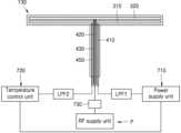
도 1을 참조하면, 박막 증착 장치는 격벽(110), 기체 공급 유닛(120), 기판 지지 유닛(130), 및 배기 통로(140)를 포함할 수 있다.Referring to FIG. 1 , the thin film deposition apparatus may include a
격벽(110)은 박막 증착 장치 내 반응기의 구성요소일 수 있다. 다시 말해, 격벽(110) 구조에 의해 기판의 증착을 위한 반응 공간이 형성될 수 있다. 예를 들어, 격벽(110)은 반응기 측벽 및/또는 반응기 상벽을 포함할 수 있다. 격벽(110) 중 반응기 상벽 부분은 기체 공급 채널(150)을 제공할 수 있고, 상기 기체 공급 채널(150)을 통해 소스 가스, 퍼지 가스, 및/또는 반응 가스가 공급될 수 있다.The
기체 공급 유닛(120)은 기판 지지 유닛(130) 상에 배치될 수 있다. 기체 공급 유닛(120)은 기체 공급 채널(150)에 연결될 수 있다. 기체 공급 유닛(120)은 반응기에 고정될 수 있다. 예를 들어, 기체 공급 유닛(120)은 고정 부재(미도시)를 통해 격벽(110)에 고정될 수 있다. 기체 공급 유닛(120)은 반응 공간(160) 내의 피처리체에 기체를 공급하도록 구성될 수 있다. 예를 들어, 기체 공급 유닛(120)은 샤워헤드 어셈블리일 수 있다.The
기체 공급 유닛(120) 내부에는 기체 공급 채널(150)과 연통하는 기체 흐름 채널(170)이 형성될 수 있다. 기체 흐름 채널(170)은 기체 공급 유닛(120)의 기체 채널(125)(윗부분)과 기체 공급 유닛(120)의 기체 공급 플레이트(127)(아랫 부분) 사이에 형성될 수 있다. 비록 도면에는 기체 채널(125)과 기체 공급 플레이트(127)가 별개의 구조로 도시되었지만, 기체 채널(125)과 기체 공급 플레이트(127)는 일체화된 구조로 형성될 수도 있다.A
기판 지지 유닛(130)은 기판이 안착되는 공간을 제공하고 격벽(110)의 하부 면과 접촉하도록 구성될 수 있다. 기판 지지 유닛(130)은 몸체(200)에 의해 지지될 수 있고, 몸체(200)는 상하 및 회전 운동을 할 수 있다. 몸체(200)의 상하 운동에 의해 기판 지지 유닛(130)이 격벽(110)으로부터 이격되거나 격벽(110)과 접촉함으로써, 반응 공간(160)이 개방되거나 폐쇄될 수 있다.The
기판 지지 유닛(130)은 가열부(310) 및 RF 전극(320)을 더 포함할 수 있다.The
가열부(310)는 기판 지지 유닛(130)의 적어도 일부를 관통하도록 형성될 수 있다. 가열부(310)는 기판 지지 유닛(130) 상에 안착되는 기판 아래에(즉, 기판 지지 유닛(130) 내부에) 배치될 수 있다. 가열부(310)의 가열에 의해 기판 지지 유닛(130) 상에 배치된 기판의 온도 및/또는 반응 공간의 온도가 증가할 수 있다. 가열부(310)는 기판의 형상과 대응되도록 형성된 판(예를 들어, 원판)의 형상을 가질 수도 있고, 기판을 중심으로 대칭되도록 배치되는 로드(rod)의 형상을 가질 수도 있다.The
RF 전극(320)은 기판 지지 유닛(130)의 적어도 일부를 관통할 수 있다. RF 전극(320)은 기판 지지 유닛(130) 상에 안착되는 기판 아래에(즉, 기판 지지 유닛(130) 내부에) 배치될 수 있다. RF 전극(320)을 통해 RF 전력이 반응 공간으로 전달될 수 있고, 그에 따라 반응 공간 내에 플라즈마가 형성될 수 있다.The
RF 전극(320)은 피처리 물체인 기판과 가열부(310) 사이에 배치될 수 있다. 즉, RF 전력이 가열부(310)에 의해 차단되지 않고 기판으로 전달될 수 있도록, RF 전극(320)은 가열부(310) 상에 배치될 수 있다. 가열부(310)와 RF 전극(320) 사이에는 절연 물질이 배치될 수 있다. 선택적인 실시예에서, 상기 절연 물질은 알루미늄 질화물을 포함할 수 있다. 다른 선택적인 실시예에서, 상기 절연 물질은 공기와 같은 저유전율 물질일 수도 있다. 즉, 가열부(310)와 RF 전극(320) 사이에 에어갭이 형성될 수도 있다.The
RF 전극(320)은 기판의 형상과 대응되도록 형성된 형상을 가질 수 있다. 예를 들어 상기 기판이 원판의 형상을 가질 경우 RF 전극(320)도 원판의 형상을 갖도록 형성될 수 있다. 다른 예에서, RF 전극(320)은 기판을 중심으로 대칭되도록 배치되는 로드(rod)의 형상을 가질 수도 있다. 선택적인 실시예에서, RF 전극(320)과 가열부(310) 사이에 그라운드와 연결된 금속부가 추가로 배치될 수 있다. 상기 금속부는 RF 전극(320)의 형상 및/또는 가열부(310)의 형상과 대응되는 형상을 가질 수 있다.The
RF 전극(320)에 의해 공급되는 RF 전력에 의해, 반응 공간에 노출된 기판 상에 전위(예를 들어 음전위)가 형성될 수 있다. 예를 들어, 기판 지지 유닛(130)은 플라즈마 생성 유닛(미도시)과 연결될 수 있고, 플라즈마 생성 유닛에 의해 생성된 RF 전력이 RF 전극(320)에 의해 반응 공간 내 기판으로 전달될 수 있고, 결과적으로 반응 공간 내에 플라즈마가 형성될 수 있다.By RF power supplied by the
보다 구체적으로, RF 전력 공급에 의해, 기판 상에서 제1 플라즈마 셀프 바이어스 전압이 생성되고, 기체 공급 유닛(120) 상에서 제2 플라즈마 셀프 바이어스 전압이 생성될 수 있다. 이 경우 기판 아래의 기판 지지 유닛(130)은 RF 신호 생성부(미도시, 도 2 참조)와 연결되는 반면에 기체 공급 유닛(120)은 그라운드와 연결되므로, 상기 제1 셀프 바이어스 전압은 상기 제2 셀프 바이어스 전압보다 클 수 있다. 따라서 상기 제1 플라즈마 셀프 바이어스 전압에 의해 상기 기판의 상기 노출면은 음으로 대전될 수 있다.More specifically, by supplying RF power, a first plasma self-bias voltage may be generated on the substrate and a second plasma self-bias voltage may be generated on the
상기 플라즈마의 형성에 의해, 기판 중 반응 공간에 노출된 부분 상에 쉬스 전위가 형성될 수 있다. 이러한 쉬스 전위는 일반적으로 스퍼터링을 야기한다. 종래의 기술은 그러한 스퍼터링 현상을 이용하여 증착하는 PVD(Physical Vapor Deposition) 공정 내지 RIE(Reactive Ion Etching) 공정을 이용한다. 반면에, 본원 발명은 쉬스 전위에 의한 스퍼터링을 감소시키는 대신, 이동도(mobility)가 감소된 활성종을 이용하여 기판 상에 활성종 성분을 포함하는 박막을 직접 증착한다는 점에서 종래 기술과 구별됨에 유의한다.By forming the plasma, a sheath dislocation may be formed on a portion of the substrate exposed to the reaction space. These sheath dislocations typically cause sputtering. Conventional technology uses a PVD (Physical Vapor Deposition) process or a RIE (Reactive Ion Etching) process for deposition using the sputtering phenomenon. On the other hand, the present invention is distinguished from the prior art in that instead of reducing sputtering due to sheath dislocation, a thin film containing active species components is directly deposited on a substrate using active species with reduced mobility. Be careful.
다시 도 1을 참조하면, 기판 지지 유닛(130) 아래에서 기판 지지 유닛(130)의 구성요소인 몸체(200)는 제1 로드(410), 제2 로드(420), 및 RF 쉴드(430)를 포함할 수 있다. 가열부(310)는 제1 로드(410)와 연결될 수 있고, RF 전극(320)은 제2 로드(420)와 연결될 수 있다. RF 쉴드(430)의 적어도 일부는 제1 로드(410)와 제2 로드(420) 사이에 배치될 수 있다. 보다 구체적으로, RF 쉴드(430)는 제2 로드(420)와 이격되고 상기 제2 로드(420)를 둘러싸도록 배치될 수 있다. 또한 RF 쉴드(430)는 제2 로드(420)의 연장 방향을 따라 연장될 수 있다.Referring again to FIG. 1, below the
RF 쉴드(430)는 제1 로드(410)를 통해 가열부(310)로 전달되는 제1 신호와 제2 로드(420)를 통해 RF 전극(320)으로 전달되는 제2 신호 간의 영향을 차단하는 기능을 수행할 수 있다. 이를 위해 RF 쉴드(430)는 예를 들어 그라운드와 연결될 수 있다. 다른 선택적인 실시예에서, 제2 로드(420)와 RF 쉴드(430) 사이에는 제1 절연 부재(440)가 배치될 수 있다. 상기 제1 절연 부재(440)는 환형 형상을 가질 수 있고 제2 로드(420)가 통과하는 관통홀을 포함할 수 있다. 제1 절연 부재(440)에 의해 제2 로드(420)와 RF 쉴드(430) 사이의 상대적인 위치관계가 고정될 수 있다.The
비록 도면에 도시되지는 않았지만, 박막 증착 장치는 가열부(310)에 전력을 공급하도록 구성되는 전력 공급 유닛을 더 포함할 수 있다. 전력 공급 유닛은 제1 로드(410)와 연결될 수 있다. 선택적인 실시예에서, 제1 로드(410)와 전력 공급 유닛(미도시) 사이에는 제1 저대역 필터가 배치될 수 있다(도 9 참조). 또한, 추가 실시예에서, 박막 증착 장치는 서모커플 및 온도 조절 유닛을 더 포함할 수 있다. 상기 서모커플은 가열부(310)와 연결되어 가열부(310)의 온도 변화에 응답하여 전기 신호를 생성하도록 구성될 수 있다. 이렇게 생성된 전기 신호는 온도 조절 유닛으로 전달될 수 있고, 온도 조절 유닛은 상기 전기 신호를 기초로 전력 공급 유닛을 제어하도록 구성될 수 있다. 선택적인 실시예에서, 서모커플과 전기적으로 연결된 제2 저대역 필터가 추가로 배치될 수 있다. 상기 제1 및 제2 저대역 필터들은 플라즈마 인가 시 사용되는 RF 전력 신호가 전력 공급 유닛 및 온도 조절 유닛에 영향을 미치지 않도록 하는 기능을 수행할 수 있다. 전술한 구성들에 대해서는 도 9에서 보다 구체적으로 후술하기로 한다.Although not shown in the drawing, the thin film deposition apparatus may further include a power supply unit configured to supply power to the
또한, 비록 도면에 도시되지는 않았지만, 기판 지지 유닛(130)은 소켓 및 접지 브라켓을 더 포함할 수 있다. 소켓을 통해 제2 로드(420)와 플라즈마 생성 유닛(미도시)이 연결될 수 있다. 또한, 접지 브라켓을 통해 RF 쉴드(430)와 그라운드가 연결될 수 있다. 소켓과 접지 브라켓 사이에는 제2 절연 부재가 배치될 수 있으며, 상기 제2 절연 부재를 통해 소켓과 접지 브라켓의 전기적 연결이 방지될 수 있다. 또한, 제2 절연 부재를 통해 소켓과 접지 브라켓이 기계적으로 고정될 수 있다.Additionally, although not shown in the drawing, the
나아가, 기판 지지 유닛(130)의 몸체(200) 내부에는 RF 쉴드(430)의 위치가 고정될 수 있도록, 고정 유닛이 포함될 수 있다. 몸체(200)는 고정 유닛을 둘러싸고 고정 유닛을 지지하도록 배치된다. 따라서 몸체(200)와 고정 유닛에 의해, RF 쉴드(430)의 위치가 고정될 수 있다. 선택적인 실시예에서, 몸체(200)는 RF 쉴드(430) 및 접지 브라켓과 이격될 수 있다. 이들 소켓, 접지 브라켓, 및 고정 유닛 등의 구성에 대해서는 도 10에서 보다 구체적으로 후술하기로 한다.Furthermore, a fixing unit may be included inside the
도 2는 본 발명의 기술적 사상에 의한 실시예들에 따른 박막 증착 장치를 개략적으로 나타낸다. 이 실시예들에 따른 박막 증착 장치는 전술한 실시예들에 따른 박막 증착 장치의 변형예일 수 있다. 이하 실시예들간 중복되는 설명은 생략하기로 한다.Figure 2 schematically shows a thin film deposition apparatus according to embodiments of the technical idea of the present invention. The thin film deposition apparatus according to these embodiments may be a modified example of the thin film deposition apparatus according to the above-described embodiments. Overlapping descriptions between the following embodiments will be omitted.
도 1에서의 기판 지지 유닛에서는 RF 전극이 가열부를 둘러싸도록 형성된 반면에, 도 2에서의 RF 전극(320)은 기판 지지 유닛(130) 내부에 삽입된 형태를 갖도록 형성된다. 그리고 도 1은 격벽과 기판 지지 유닛의 면 실링에 의해 반응 공간이 형성되는 반면에, 도 2는 제1 덮개(240) 및 제2 덮개(250)에 의해 반응 공간이 형성된다. 그러나 본 발명은 이러한 형상들에 제한되지 않으며, 도 1 및 도 2에 도시된 것 이외에 다양한 변형이 가능함에 유의한다.While the RF electrode in the substrate support unit in FIG. 1 is formed to surround the heating unit, the
도 2를 참조하면, 박막 증착 장치는 격벽(110) 및 배기 통로(140)를 제공하는 제1 덮개(240), 기체 공급 유닛(120)을 제공하는 제2 덮개(250), 및 기판 지지 유닛(130)을 포함할 수 있다. 반응 공간(160)의 하부는 기판 지지 유닛(130)에 의해, 반응 공간(160)의 상부는 제1 덮개(240)에 의해, 반응 공간(160)의 양 측면은 제2 덮개(250)에 의해 형성될 수 있다.Referring to FIG. 2, the thin film deposition apparatus includes a
박막 증착 장치의 배기 구조는 하류 배기 구조로 구성될 수 있고, 이 때 상기 하류 배기 구조는 제1 덮개(240)에 의해 구현될 수 있다. 이 경우 증착에 이용되는 기체는 제2 덮개(250)의 샤워헤드를 통해 피처리 기판으로 분사되고 이후 제1 덮개(250)의 배기 통로(140)를 통해 하류로 배기될 수 있다.The exhaust structure of the thin film deposition apparatus may be configured as a downstream exhaust structure, and in this case, the downstream exhaust structure may be implemented by the
전술한 바와 같이, 본 실시예에서 RF 전극(320)은 기판 지지 유닛(130) 내부에 삽입된 형태일 수 있다. 또한, 가열부(미도시)도 기판 지지 유닛(130) 내부에 삽입된 형태일 수 있다. RF 전극(320)과 가열부의 전기적 연결을 막기 위해, 가열부와 RF 전극(320) 사이에 절연 물질이 배치될 수 있다.As described above, in this embodiment, the
박막 증착 장치는 플라즈마 인가부(P) 및 그라운드(G)를 더 포함할 수 있다. 상기 플라즈마 인가부(P)는 RF 신호 생성부(RG) 및 정합부(MC)를 포함할 수 있다.The thin film deposition apparatus may further include a plasma application part (P) and a ground (G). The plasma applying unit (P) may include an RF signal generating unit (RG) and a matching unit (MC).
RF 신호 생성부(RG)는 반응 공간 상의 기판에 인가되는 활성종 및/또는 이온의 에너지를 제어하기에 적합한 주파수의 신호를 출력한다. 상기 신호는 예를 들어 13.56 MHz의 고주파일 수 있고, 바람직하게는 30MHz 이상, 더욱 바람직하게는 60 MHz 이상의 VHF(Very High Frequency) 대역의 신호일 수 있다.The RF signal generator RG outputs a signal with a frequency suitable for controlling the energy of active species and/or ions applied to the substrate in the reaction space. The signal may be a high frequency signal of, for example, 13.56 MHz, preferably in a VHF (Very High Frequency) band of 30 MHz or higher, and more preferably 60 MHz or higher.
정합부(MC)는 RF 신호 생성부(RG)의 임피던스와 부하(예를 들어, 전극, 반응 공간 등)측의 임피던스 사이에서 정합을 취하기 위한 정합 회로를 포함할 수 있다. 또한, 정합부(MC)는 상기 정합 회로 외에 부하 임피던스를 측정하기 위한 RF 센서 및 정합 회로 내의 가변 리액턴스 소자의 값(임피던스 포지션)을 가변 조정하기 위한 컨트롤러, 스텝 모터, 및 냉각용 팬 중 적어도 하나를 포함할 수 있다. 다른 예에서, 정합부(MC)는 자기 바이어스 생성용 블로킹 콘덴서를 더 포함할 수 있다.The matching unit (MC) may include a matching circuit for matching between the impedance of the RF signal generating unit (RG) and the impedance of the load (eg, electrode, reaction space, etc.). In addition, the matching unit (MC) includes at least one of an RF sensor for measuring load impedance, a controller for variably adjusting the value (impedance position) of a variable reactance element in the matching circuit, a step motor, and a cooling fan in addition to the matching circuit. may include. In another example, the matching part MC may further include a blocking capacitor for generating a self-bias.
도 2에 나타난 바와 같이, 본 발명에서는 기존의 상부 전극, 가령 샤워헤드 대신에 하부 전극을 통해 RF 전력을 공급한다. 예를 들어, 기판 지지 유닛(130) 또는 히터 블록 내부에 RF 전극(320)을 삽입하여 반응기 하부에서부터 RF 전력을 공급하여 반응 공간 내로 공급되도록 한다. 상기 RF 전력에 의해 반응기체를 여기시킴으로써, 반응 공간 내에, 구체적으로는 기판 위에 플라즈마를 발생시킨다. 다시 말해, 반응기 하부의 기판 지지 유닛(또는 히터 블록)을 통해 RF 전력을 공급함으로써, 반응 공간내의 라디칼들이 반응기 상부(즉, 기체 공급 유닛(120)) 보다는 하부(즉, 기판)을 향하여 가속된다.As shown in Figure 2, in the present invention, RF power is supplied through a lower electrode instead of a conventional upper electrode, such as a showerhead. For example, the
도 3은 상부 전극(UE)에 RF 전력을 가했을 때(좌측) 및 하부 전극(LE)에 RF 전력을 가했을 때(우측)에 있어서의 Vdc의 변화를 보여준다. 도 3의 Vdc는 플라즈마 셀프-바이어스 전압(plasma self-bias voltage)으로서 이온과 라디칼의 방향성을 결정한다. 즉 Vdc가 큰 쪽으로 이온과 라디칼이 정렬되어 가속하며 이동한다.Figure 3 shows the change in Vdc when RF power is applied to the upper electrode (UE) (left) and when RF power is applied to the lower electrode (LE) (right). Vdc in FIG. 3 is a plasma self-bias voltage and determines the directionality of ions and radicals. In other words, ions and radicals are aligned and accelerate toward the direction where Vdc is greater.
먼저, 상부 전극(UE), 즉 기판이 놓이는 부분과 반대되는 구성(예를 들어 기체 공급 유닛 및/또는 히터 블록)을 통해 RF 전력을 공급하는 경우, 기체 공급 유닛(예를 들어 샤웨헤드 어세블리)과 같은 상부 전극(UE)에서의 Vdc가 기판 지지 유닛과 같은 하부 전극(LE)에서의 Vdc보다 크게 되어, 이온과 라디칼들이 기판을 향하는 방향과 반대로 가속된다. 통상의 플라즈마를 이용한 증착 공정은 이와 같이 이동하는 이온 및/또는 라디칼을 이용하여 증착을 수행하였다.First, when supplying RF power through the upper electrode (UE), i.e., a configuration opposite to the portion on which the substrate is placed (e.g., a gas supply unit and/or heater block), the gas supply unit (e.g., a shower head assembly) ), the Vdc at the upper electrode (UE) becomes greater than the Vdc at the lower electrode (LE), such as the substrate support unit, so that ions and radicals are accelerated opposite to the direction toward the substrate. The deposition process using conventional plasma was performed using ions and/or radicals moving in this manner.
반면에, 본 발명의 기술적 사상에 따르면, 하부 전극(LE), 즉 기판이 놓이는 기판 지지 유닛 아래의 구성요소(예를 들어 히터)를 통해 RF 전력이 공급된다. 이 경우 기판 지지 유닛과 같은 하부 전극(LE)에서의 Vdc가 기체 공급 유닛(120)과 같은 상부 전극(UE)에서의 Vdc보다 크게 되어, 이온과 라디칼들이 기판을 향하여 가속된다. 한편, 기판을 향하여 가속되는 활성종들은 기판과 충돌하여 증착 보다는 오히려 기판 표면 물질을 식각 하는 현상이 발생한다. 따라서 기판쪽으로 가속되는 활성종들이 식각 보다는 기판 상의 증착에 기여할 수 있도록, 활성종의 이동도(mobility)를 조절하거나 감소시킨다.On the other hand, according to the technical idea of the present invention, RF power is supplied through the lower electrode LE, that is, a component (for example, a heater) below the substrate support unit on which the substrate is placed. In this case, the Vdc at the lower electrode LE, such as the substrate support unit, becomes greater than the Vdc at the upper electrode UE, such as the
활성종의 이동도(mobility)를 감소시키기 위한 일 예로서, 본 발명에서는 초고주파(VHF; Very High frequency) RF 전력을 하부 전극(LE)을 통해 공급하였다. VHF는 바람직하게는 30MHz이상, 100MHz의 주파수를 적용할 수 있다. 초고주파의 경우 Vdc가 낮기 때문에 플라즈마 쉬스(plasma sheath)에 의해 가속되는 에너지가 작다. 따라서 쉬스에 의한 가속이 박막의 손상보다는 증착에 더 많이 기여하게 되고, 결과적으로 형성된 박막의 밀도가 증가할 수 있다. As an example of reducing the mobility of active species, in the present invention, very high frequency (VHF) RF power was supplied through the lower electrode (LE). VHF can preferably apply frequencies of 30 MHz or more and 100 MHz. In the case of ultra-high frequencies, Vdc is low, so the energy accelerated by the plasma sheath is small. Therefore, acceleration by the sheath contributes more to deposition than to damage to the thin film, and as a result, the density of the formed thin film can increase.
선택적인 실시예에서, 기판쪽으로 가속되는 활성종들이 식각 보다는 기판 상의 증착에 기여할 수 있도록, 더 많은 활성종의 생성량을 증가시킬 수 있다. 예를 들어, 하부 전극(LE)을 통해 초고주파 RF전력을 공급함으로써, 반응 공간 내에 더 많은 활성종을 생성시킬 수 있다. 뿐만 아니라, 기판을 향하여 더 많은 활성종을 가속시킬 박막 형성에 기여하게 된다.In an alternative embodiment, the production of more active species can be increased such that the active species accelerated toward the substrate contribute to deposition on the substrate rather than etching. For example, by supplying ultra-high frequency RF power through the lower electrode (LE), more active species can be generated in the reaction space. In addition, it contributes to the formation of a thin film that will accelerate more active species toward the substrate.
다른 선택적인 실시예에서, 기판쪽으로 가속되는 활성종들이 식각 보다는 기판 상의 증착에 기여할 수 있도록, 활성종의 이동 에너지 및/또는 가속 에너지를 감소시킬 수 있다. 예를 들어, 플라즈마 인가 동안 생성되는 플라즈마 셀프-바이어스 전압 Vdc를 감소시킴으로써, 활성종의 속도 및/또는 가속도를 감소시킬 수 있다.In another alternative embodiment, the migration energy and/or acceleration energy of the activated species accelerated toward the substrate may be reduced such that the activated species contribute to deposition on the substrate rather than etching. For example, by reducing the plasma self-bias voltage Vdc generated during plasma application, the velocity and/or acceleration of the active species can be reduced.
이와 같이, 본 발명은 종래의 스퍼터링 및/또는 식각에 이용되는 하부 전극(LE) RF 인가 구성을 플라즈마 원자층 공정에 적용하되 반응 공간 내의 활성종의 개수를 증가시키는 구성, 반응 공간 내의 상기 활성종의 이동도(mobility)를 감소시키는 구성, 및 RF 전력에 의해 형성된 바이어스의 크기를 감소시키는 구성 중 적어도 하나의 구성을 도입한다. 이를 통해 복잡한 구조의 패턴 구조물의 트렌치에 증착된 박막의 정형성(conformality)이 개선될 수 있다. 따라서 기판상 물질의 손상을 최소화할 수 있는 고밀도 플라즈마 원자층 증착 공정(high density plasma ALD)의 구현이 가능하다.As such, the present invention applies the lower electrode (LE) RF application configuration used in conventional sputtering and/or etching to the plasma atomic layer process, but increases the number of active species in the reaction space, and the active species in the reaction space At least one of a configuration that reduces the mobility of and a configuration that reduces the size of a bias formed by RF power is introduced. Through this, the conformality of the thin film deposited in the trench of the complex pattern structure can be improved. Therefore, it is possible to implement a high density plasma atomic layer deposition process (high density plasma ALD) that can minimize damage to materials on the substrate.
도 4는 본 발명에 따라 패턴 구조물에 RF 전력을 공급했을 때 활성종들이 기판상 트렌치 구조물을 향하여 가속되는 모습을 개략적으로 나타낸다. 도 4에서는 반응기체로서 질소를 사용하였지만, 본 발명의 기술적 사상은 이에 제한되지 않음에 유의한다. 예를 들어 본 발명의 기술적 사상은 질화물 이외에도 산화물, 혹은 다른 다성분계 박막을 증착하는데 적용될 수 있다.Figure 4 schematically shows how active species are accelerated toward the trench structure on the substrate when RF power is supplied to the pattern structure according to the present invention. Note that although nitrogen is used as the reaction gas in FIG. 4, the technical idea of the present invention is not limited thereto. For example, the technical idea of the present invention can be applied to depositing oxides or other multi-component thin films in addition to nitrides.
도 4를 참조하면, 반응 공간 내에 플라즈마를 형성하기 위해, 기판 지지 유닛(130)에 포함된 RF 전극(320)을 통해 RF 전력이 인가될 수 있고, 상기 RF 전력의 인가로 인해 RF 전극(320)은 음극으로 대전될 수 있다. 그에 따라 기판 지지 유닛(130)의 표면(금속 표면 또는 비금속 표면)도 음극으로 대전될 수 있다. 이 경우, 기판 지지 유닛(130) 상에 배치된 기판(S) 중 기판 지지 유닛(130)과 접하는 제1 부분(S1)은 양으로 대전될 수 있다. 반면에, 기판 지지 유닛(130) 상에 배치된 기판(S) 중 상기 제1 부분(S1)과 반대되는 제2 부분(S2)은 음으로 대전될 수 있다.Referring to FIG. 4, in order to form plasma in the reaction space, RF power may be applied through the
상기 제2 부분(S2)은 반응 공간에 노출되는 부분이며, 상기 제2 부분(S2)에는 상면, 하면, 및 상면과 하면을 연결하는 측면을 갖는 패턴 구조물이 형성된다. 음으로 대전된 제2 부분(S2)과 양으로 대전된 활성종 사이에 인력이 발생할 수 있고, 그에 따라 상기 활성종이 상기 패턴 구조물의 상면, 하면, 및 측면을 향하여 이동할 수 있다.The second part S2 is a part exposed to the reaction space, and a pattern structure having a top surface, a bottom surface, and a side surface connecting the top surface and the bottom surface is formed in the second part S2. An attractive force may occur between the negatively charged second portion S2 and the positively charged active species, and accordingly, the active species may move toward the top, bottom, and side surfaces of the pattern structure.
이와 같이, 본 발명의 기술적 사상에 의한 실시예들에 따르면, 플라즈마 쉬스에 의한 활성종의 이동/가속을 이용할 뿐만 아니라, 패턴 구조물의 대전을 통한 패턴 구조물의 표면(특히 측면 및 하면)과 활성종 사이의 인력을 이용하여 증착 공정을 수행한다. 따라서, 높은 종횡비를 같은 트렌치나 리세스를 갖는 구조물 내의 측면과 하면에 고품질의 박막이 증착될 수 있다.As such, according to the embodiments according to the technical idea of the present invention, not only does the movement/acceleration of active species by the plasma sheath be used, but also the surface (especially the side and bottom) of the pattern structure through charging of the pattern structure and the active species The deposition process is performed using the attractive force between the two. Accordingly, high-quality thin films can be deposited on the side and bottom surfaces of structures with trenches or recesses of the same high aspect ratio.
도 5는 본 발명의 기술적 사상에 의한 실시예들에 따른 박막 증착 방법을 개략적으로 나타낸다. 이 실시예들에 따른 박막 증착 방법은 전술한 실시예들에 따른 박막 증착 장치를 이용하여 수행될 수 있다. 이하 실시예들간 중복되는 설명은 생략하기로 한다.Figure 5 schematically shows a thin film deposition method according to embodiments of the technical idea of the present invention. The thin film deposition method according to these embodiments can be performed using the thin film deposition apparatus according to the above-described embodiments. Overlapping descriptions between the following embodiments will be omitted.
도 5를 참조하면, 기판에 대한 박막 증착을 수행하기 위해, 먼저 반응 공간에 배치된 기판의 노출면 상에 전위(예를 들어, 음전위)를 형성한다(O510). 이를 위해, 기판 아래에 배치된 구성요소(예를 들어, 기판 지지 유닛, 서셉터, 및/또는 히터)를 통해 RF 전력이 공급될 수 있다. RF 전력이 공급됨으로써 기판의 노출면 상에 쉬스 전위가 형성될 수 있다.Referring to FIG. 5, in order to perform thin film deposition on a substrate, a potential (eg, negative potential) is first formed on the exposed surface of the substrate placed in the reaction space (O510). To this end, RF power may be supplied through components disposed beneath the substrate (eg, substrate support unit, susceptor, and/or heater). When RF power is supplied, a sheath potential may be formed on the exposed surface of the substrate.
예를 들어 상기 구성요소가 히터인 경우, 상기 히터 내부에 RF 전극이 삽입될 수 있다. 다른 예로서, 상기 구성요소는 기판 지지 유닛일 수 있고, 상기 기판 지지 유닛 내부에 히터 및 RF 전극이 삽입될 수 있다. 또 다른 예로서 상기 구성요소는 금속 서셉터일 수 있고, 상기 금속 서셉터 내부에 히터가 삽입될 수도 있다.For example, if the component is a heater, an RF electrode may be inserted into the heater. As another example, the component may be a substrate support unit, and a heater and an RF electrode may be inserted inside the substrate support unit. As another example, the component may be a metal susceptor, and a heater may be inserted into the metal susceptor.
선택적인 실시예에서, RF 전력이 공급되기 전, 기판 상에 배치된 기체 공급 유닛에 의해 제공된 물질로부터 상기 활성종이 생성될 수 있다. 또한 RF 전력이 공급되는 동안, 기판 지지 유닛은 RF 신호 생성부와 연결될 수 있고, 기체 공급 유닛은 접지될 수 있다.In an alternative embodiment, the activated species may be generated from material provided by a gas supply unit disposed on the substrate before RF power is applied. Additionally, while RF power is supplied, the substrate support unit may be connected to the RF signal generator and the gas supply unit may be grounded.
이후, 상기 전위를 이용하여 반응 공간 내의 활성종을 기판의 노출면으로 이동시킨다(O520). 예를 들어 반응 공간 내에서 양으로 대전된 활성종은 쉬스 전위에 의해 기판을 향하여 가속되고 이동될 수 있다. 다만 전술한 바와 같이 상기 활성종이 기판 상의 패턴 구조물을 손상시키지 않도록, RF 전력의 파라미터 등을 변화시켜 활성종의 속도 및/또는 가속도를 조절할 수 있다.Afterwards, the active species in the reaction space are moved to the exposed surface of the substrate using the potential (O520). For example, positively charged active species within the reaction space can be accelerated and moved toward the substrate by the sheath potential. However, as described above, the speed and/or acceleration of the activated species can be adjusted by changing the parameters of RF power so that the activated species does not damage the pattern structure on the substrate.
이렇게 이동된 활성종은 패턴 구조물 상의 박막 증착에 기여한다(O530). 결과적으로 반응 공간의 노출면 상에 활성종 성분을 포함하는 박막이 형성될 수 있다.These transferred active species contribute to thin film deposition on the patterned structure (O530). As a result, a thin film containing active species components may be formed on the exposed surface of the reaction space.
일부 실시예에서, 기판의 노출면은 상면, 하면, 및 상기 상면과 하면을 연결하는 측면을 포함할 수 있고, 상기 활성종은 적어도 상기 측면을 향하여 이동할 수 있다. 이러한 활성종의 측면을 향한 이동 및 하면을 향한 이동은 리세스 및 트렌치를 갖는 패턴 구조물 상에 증착되는 박막의 정형성을 개선시킬 수 있다. 정형성이 개선된 박막의 경우, 패턴 구조물 상에 증착된 후 등방성 식각이 수행되더라도, 일정한 두께의 잔류막이 형성될 수 있다.In some embodiments, the exposed surface of the substrate may include an upper surface, a lower surface, and a side connecting the upper surface and the lower surface, and the active species may move toward at least the side surface. This movement of active species toward the side and toward the bottom can improve the formability of a thin film deposited on a patterned structure having recesses and trenches. In the case of a thin film with improved formability, even if isotropic etching is performed after deposition on the pattern structure, a residual film of a certain thickness may be formed.
다른 일부 실시예에서, 활성종 성분을 포함하는 박막이 형성될 수 있도록, 반응 공간 내의 활성종의 개수를 증가시키는 단계가 수행될 수 있다. 반응 공간 내의 활성종의 개수가 많을 수록 활성종이 이동할 수 있는 평균 이동 거리가 감소하여 활성종의 평균 속도가 감소할 수 있다. 속도가 감소한 활성종은 패턴 구조물의 손상(스퍼터링)보다는 박막 형성에 기여할 수 있다.In some other embodiments, a step of increasing the number of active species in the reaction space may be performed so that a thin film containing the active species component can be formed. As the number of active species in the reaction space increases, the average moving distance that the active species can move decreases, and thus the average speed of the active species may decrease. Active species with reduced velocity may contribute to thin film formation rather than damage to the pattern structure (sputtering).
다른 선택적인 실시예에서, 활성종 성분을 포함하는 박막이 형성될 수 있도록, 반응 공간 내의 활성종의 이동도를 감소시키는 단계가 수행될 수 있다. 예를 들어 RF 전력의 주파수를 증가시킬 경우, 활성종의 방향 전환이 증가하는 주파수에 따라 증가하게 되므로, 결과적으로 활성종의 이동도가 감소할 수 있다. 이렇게 이동도가 감소된 활성종은 패턴 구조물의 손상(스퍼터링)보다는 박막 형성에 기여할 수 있다.In another alternative embodiment, steps may be taken to reduce the mobility of the active species within the reaction space so that a thin film comprising the active species component can be formed. For example, when the frequency of RF power is increased, the direction change of the active species increases with the increasing frequency, and as a result, the mobility of the active species may decrease. Active species with reduced mobility may contribute to thin film formation rather than damage (sputtering) to the pattern structure.
또 다른 선택적인 실시예에서, 활성종 성분을 포함하는 박막이 형성될 수 있도록, 바이어스의 크기를 감소시키는 단계가 수행될 수 있다. RF 전력이 공급될 경우 기판을 향하는 바이어스(즉, 플라즈마 셀프 바이어스) 가 생성되는데, 상기 바이어스에 의해 활성종이 상기 기판을 향하여 소정의 속도로 이동 및/또는 소정의 가속도로 가속된다. 이 경우 바이어스의 크기가 이동 및/또는 가속에 영향을 주는데, 바이어스의 크기를 감소시킴으로써 활성종의 이동 에너지 및/또는 가속 에너지가 감소될 수 있다. 이렇게 상기 바이어스의 크기를 조절함으로써 활성종의 속도가 활성종이 기판 상의 증착에 기여할 수 있는 속도가 될 수 있다.In another alternative embodiment, steps may be taken to reduce the size of the bias so that a thin film containing the active species component can be formed. When RF power is supplied, a bias toward the substrate (i.e., plasma self-bias) is generated, and the bias causes active species to move toward the substrate at a predetermined speed and/or accelerate at a predetermined acceleration. In this case, the size of the bias affects movement and/or acceleration, and by reducing the size of the bias, the movement energy and/or acceleration energy of the active species can be reduced. By adjusting the size of the bias in this way, the speed of the active species can be set to a speed at which the active species can contribute to deposition on the substrate.
일부 실시예에서, 증착된 박막의 치밀도를 증가시키기 위해, RF 전력의 크기를 증가시키는 단계가 수행될 수 있다. 증가된 RF 전력의 크기는 더 많은 활성종의 생성으로 귀결될 수 있다. 즉, 보다 많은 활성종이 기판을 향하여 가속됨으로써 보다 치밀하고 단단한 막이 형성될 수 있다.In some embodiments, increasing the magnitude of RF power may be performed to increase the density of the deposited thin film. Increased magnitudes of RF power can result in the production of more active species. That is, as more active species are accelerated toward the substrate, a more dense and solid film can be formed.
다른 일부 실시예에서, 박막 증착 방법은 원자층 증착 방법 및 사이클릭 화학 기상 증착 방법으로 수행될 수 있다. 예를 들어, 박막 증착 방법 동안, 제1 물질을 공급하는 제1 단계 및 상기 제1 물질과 다른 제2 물질을 공급하는 제2 단계가 수행될 수 있다. 본원 발명에 이용되는 활성종은 제1 물질 및/또는 제2 물질로부터 형성될 수 있다. 활성종이 제2 물질로부터 형성되는 경우, 제1 물질과 상기 활성종의 반응에 의해 상기 박막이 형성될 수 있다. 또 다른 일부 실시예에서, 박막 증착 방법은 제1 단계와 제2 단계 사이에 적어도 수행되는 퍼지 단계를 포함할 수도 있다.In some other embodiments, the thin film deposition method may be performed by an atomic layer deposition method and a cyclic chemical vapor deposition method. For example, during a thin film deposition method, a first step of supplying a first material and a second step of supplying a second material different from the first material may be performed. The active species used in the present invention may be formed from a first material and/or a second material. When the active species is formed from a second material, the thin film may be formed by a reaction between the first material and the active species. In some other embodiments, the thin film deposition method may include a purge step performed at least between the first step and the second step.
도 6은 종래의 원자층 증착 공정에서 발생하는 문제점을 설명하는 개략도이다. 도 6의 좌측에서, 패턴 구조물(10) 상에 PEALD 방법으로 박막(20)을 증착한다. 가령 이성분계 화합물을 형성할 경우, 소스기체와 반응기체를 시차를 두고 순차적으로 공급하되, 적어도 두 기체중의 하나의 기체를 플라즈마로 활성화하여 기체간의 화학반응을 유도하여 패턴 구조물상에 박막을 증착한다. 순차적으로 박막을 한층 한층(layer-by-layer) 적층하므로, 트렌치 구조의 상부, 측부 및 하부에 걸쳐 정형성 있는 박막이 균일하게 증착될 수 있다.Figure 6 is a schematic diagram illustrating problems occurring in the conventional atomic layer deposition process. On the left side of FIG. 6, a
이후, 후속 공정인 습식 식각을 진행하게 되는데, 도 6의 우측에서 알 수 있듯이 패턴구조물의 상부(top)에서의 잔류막(A)과 패턴 구조물 트렌치의 측부(side)및 하부(bottom)에서의 잔류막(B)의 정형성이 일정하지 않음을 알 수 있다. 이것은 플라즈마 이온 및 라디칼의 직진성에 기인한 종래 기술의 문제점 중 하나이다. 플라즈마 이온의 진행방향과 수직인 패턴의 상부에 증착된 막은 이온 포격(ion bombardment)효과에 의해 치밀해지나, 트렌치의 측부 및 하부의 경우 라디칼에 의한 이온 포격 효과가 상부에 비해 적고 트렌치 하부까지 라디칼이 침투하기가 어려워 상부 막에 비해 치밀하지 않다. 따라서 습식 식각시에는 트렌치의 측부 및 하부에 형성된 막의 식각율(WER; Wet Etch Rate)이 상부에 형성된 막보다 높다.Afterwards, the follow-up process, wet etching, is performed. As can be seen on the right side of FIG. 6, the residual film (A) on the top of the pattern structure and the residual film (A) on the sides and bottom of the pattern structure trench are It can be seen that the regularity of the residual film (B) is not constant. This is one of the problems with the prior art due to the straight-line nature of plasma ions and radicals. The film deposited on the top of the pattern perpendicular to the direction of plasma ions becomes dense due to the ion bombardment effect, but in the case of the sides and bottom of the trench, the effect of ion bombardment by radicals is less than that of the upper part, and radicals are deposited all the way to the bottom of the trench. It is difficult to penetrate and is not as dense as the upper membrane. Therefore, during wet etching, the etch rate (WER) of the film formed on the sides and bottom of the trench is higher than the film formed on the top.
본 발명의 기술적 사상에 의한 실시예들에 따른 박막 증착 방법은, 이와 같은 문제점을 해결하는 것을 일 목적으로 한다, 즉, 증착 이후 수행되는 습식 식각이 진행된 후에도, 패턴상에 형성된 박막의 정형성이 일정하게 유지될 수 있도록 하는 방법을 제시하고자 하는 것이다.The thin film deposition method according to embodiments of the technical idea of the present invention aims to solve this problem, that is, even after wet etching performed after deposition, the regularity of the thin film formed on the pattern is maintained. The goal is to suggest a method to ensure that it remains constant.
이를 위해 본원 발명은 기체 공급 유닛 아래에 기판을 배치하고, 상기 기체 공급 유닛을 통해 박막을 형성하는 구성 성분이 되는 적어도 하나의 물질을 공급하여 상기 기판 상에 박막을 형성한다. 상기 박막을 형성하는 단계 동안, 상기 기체 공급 유닛을 접지하고, 상기 기판 아래에 배치된 구성요소를 통해 RF 전력을 공급한다. 그리고 RF 전력에 의해 형성된 플라즈마가 증착에 기여할 수 있도록, 상기 반응 공간 내의 상기 활성종 밀도를 증가시키는 단계, 상기 반응 공간 내의 상기 활성종의 이동도(mobility)를 감소시키는 단계, 및 상기 RF 전력에 의해 형성된 바이어스의 크기를 감소시키는 단계 중 적어도 하나의 단계가 수행될 수 있다. 이를 통해, 정형성이 개선된 박막이 패턴 구조물 상에 형성될 수 있다. 또한 보다 많은 라디칼을 기판을 향해 가속시킴으로써, 패턴 구조물의 표면에 보다 치밀하고 식각 저항성이 향상된 박막이 증착될 수 있다.To this end, in the present invention, a substrate is placed under a gas supply unit, and at least one material that forms a thin film is supplied through the gas supply unit to form a thin film on the substrate. During the thin film forming step, the gas supply unit is grounded and RF power is supplied through components disposed beneath the substrate. and increasing the density of the active species in the reaction space, reducing the mobility of the active species in the reaction space, so that the plasma formed by the RF power can contribute to deposition, and At least one step of reducing the size of the bias formed by may be performed. Through this, a thin film with improved formability can be formed on the pattern structure. Additionally, by accelerating more radicals toward the substrate, a thin film that is more dense and has improved etch resistance can be deposited on the surface of the patterned structure.
도 7은 본 발명의 기술적 사상에 의한 실시예들에 따라 PEALD 방법을 이용하여 하부 전극을 통해 RF 전력을 공급하는 경우(도 7의 "BTM(Bottom) Bias" 참조)에서 증착된 SiO2 박막의 식각 저항성을 보여준다. 본 실험은 평판 기판에서 진행하였고 Si 전구체는 BDEAS(Bisdiethylaminosilane)와 TDMAS(Trisdimethylaminosilane)를 사용하였으며, 산소 플라즈마를 반응기체로 사용하였다. RF 전력 주파수는 60 MHz로 설정되었다.FIG. 7 shows etching of the SiO2 thin film deposited in the case of supplying RF power through the lower electrode using the PEALD method according to embodiments of the technical idea of the present invention (see “BTM (Bottom) Bias” in FIG. 7). Shows resistance. This experiment was conducted on a flat substrate, Bisdiethylaminosilane (BDEAS) and Trisdimethylaminosilane (TDMAS) were used as Si precursors, and oxygen plasma was used as a reaction gas. The RF power frequency was set at 60 MHz.
도 7을 참조하면, 하부 전극을 통해 800 와트의 RF 전력을 공급하였을 때의 WER은 약 86 내지 87임을 알 수 있다. 반면에, 상부 전극을 통해 800 와트의 RF 전력을 공급할 때에는 SiO2막의 WER이 약 91.7로서, 하부 전극을 통해 RF 전력하는 경우가 상부 전력을 이용하는 경우보다 더 낮은 WER을 나타냄을 알 수 있다. 이는 하부 바이어스에 의해 보다 많은 활성종이 기판을 향하여 가속됨으로써 보다 치밀하고 단단한 막이 형성되기 때문이다. 또한, 도 7을 참조하면, 하부 전극을 통해 RF 전력을 공급하는 경우에 있어서(도 7의 "BTM Bias" 참조), RF 전력이 증가함에 따라 WER이 감소함을 알 수 있다. 예를 들어, 60 Mhz 이상의 VHF 주파수를 갖는 RF 전력을 공급하되 적어도 800 W의 RF 전력을 공급함으로써, 보다 치밀한 박막이 형성될 수 있다.Referring to FIG. 7, it can be seen that the WER when 800 watts of RF power is supplied through the lower electrode is about 86 to 87. On the other hand, when 800 watts of RF power is supplied through the upper electrode, the WER of the SiO2 film is about 91.7, showing that the WER when RF power is supplied through the lower electrode is lower than when the upper power is used. This is because more active species are accelerated toward the substrate by the lower bias, forming a more dense and solid film. Additionally, referring to FIG. 7, in the case of supplying RF power through the lower electrode (see “BTM Bias” in FIG. 7), it can be seen that the WER decreases as the RF power increases. For example, by supplying RF power with a VHF frequency of 60 Mhz or higher and at least 800 W, a more dense thin film can be formed.
도 8 본 발명의 기술적 사상에 의한 실시예들에 따른 박막 증착 방법을 개략적으로 나타낸다. 이 실시예들에 따른 박막 증착 방법은 전술한 실시예들에 따른 박막 증착 방법의 변형예일 수 있다. 이하 실시예들간 중복되는 설명은 생략하기로 한다.Figure 8 schematically shows a thin film deposition method according to embodiments of the technical idea of the present invention. The thin film deposition method according to these embodiments may be a modified example of the thin film deposition method according to the above-described embodiments. Overlapping descriptions between the following embodiments will be omitted.
도 8을 참조하면, 먼저 상면과 하면 그리고 상기 상면과 하면을 연결하는 측면을 갖는 패턴 구조물이 반응 공간 내로 도입된다. 이후 t0~t1 동안, 제1 물질(예를 들어, 실리콘 전구체)을 반응 공간 내로 공급하여 상기 패턴 구조물 상에 제1 물질이 패턴 구조물 상에 화학흡착되도록 한다. 이후 t1~t2 동안, 상기 제1 물질의 잔여물이 퍼지된다. 도 8에 도시된 바와 같이, 퍼지 기체는 공정 사이클 내내 유동될 수 있다. t2~t3 동안, 제2 물질(예를 들어, 산소 기체)가 반응 공간 내로 공급된다. t2~t3 동안, 기판 아래에 배치된 구성요소를 통해 RF 전력을 공급하여, 상기 반응 공간에 노출된 상기 상면, 상기 하면, 및 상기 측면 상에 전위를 형성한다. 상기 전위에 의해 제2 물질의 활성종은 적어도 상기 측면을 향하여 이동되며, t2~t3 동안 화학흡착된 제1 물질과 상기 활성종이 반응하여 기판 상에 박막이 형성된다. 이후 t3~t4 동안, 상기 제2 물질(및 활성종)의 잔여물이 퍼지된다. 이러한 t0~t4 동안 수행되는 일련의 단계들은 하나의 사이클로 정의될 수 있으며, 상기 사이클은 복수 회 반복될 수 있다.Referring to FIG. 8, first, a pattern structure having an upper surface and a lower surface and a side surface connecting the upper surface and the lower surface is introduced into the reaction space. Then, during t0 to t1, a first material (eg, a silicon precursor) is supplied into the reaction space so that the first material is chemically adsorbed onto the pattern structure. During t1 to t2, the residue of the first material is purged. As shown in Figure 8, purge gas may flow throughout the process cycle. During t2 to t3, a second material (eg, oxygen gas) is supplied into the reaction space. During t2 to t3, RF power is supplied through components disposed beneath the substrate to form electric potentials on the upper surface, lower surface, and side surfaces exposed to the reaction space. Due to the electric potential, the active species of the second material are moved toward at least the side surface, and the chemically adsorbed first material and the active species react during t2 to t3 to form a thin film on the substrate. During t3 to t4, the residue of the second material (and active species) is purged. A series of steps performed during t0 to t4 can be defined as one cycle, and the cycle can be repeated multiple times.
아래 표는 도 8의 실시예를 이용한 SiO2 박막 증착 실험조건을 나타낸다. 예시적인 실시예의 실험 조건으로서, 아래 표와 같이 Si 소스로서 TDMAS를 사용하였고 반응 기체로서 산소를 사용하였다.The table below shows the experimental conditions for SiO2 thin film deposition using the example of FIG. 8. As experimental conditions for the exemplary embodiment, TDMAS was used as the Si source and oxygen was used as the reaction gas, as shown in the table below.
상기 <표 1>에서 Si 소스로서 TDMAS를 사용하였으나 본 발명은 이에 한정되지 않는다. 가령 Si 소스로서 TSA, (SiH3)3N; DSO, (SiH3)2; DSMA, (SiH3)2NMe; DSEA, (SiH3)2NEt; DSIPA, (SiH3)2N(iPr); DSTBA, (SiH3)2N(tBu); DEAS, SiH3NEt2; DIPAS, SiH3N(iPr)2; DTBAS, SiH3N(tBu)2; BDEAS, SiH2(NEt2)2; BDMAS, SiH2(NMe2)2; BTBAS, SiH2(NHtBu)2; BITS, SiH2(NHSiMe3)2; TEOS, Si(OEt)4; SiCl4; HCD, Si2Cl6; DCS, SiH2Cl2; 3DMAS, SiH(N(Me)2)3; BEMAS, Si H2[N(Et)(Me)]2; AHEAD, Si2 (NHEt)6; TEAS, Si(NHEt)4; Si3H8; 및 Si-H를 포함하는 이오도실란(Iodosilanes) 중 적어도 하나, 가령 이오도실란(iodosilane), 디이오도실란(diiodosilane) 및 펜타이오도실란(pentaiodosilane) 중 적어도 하나를 포함할 수 있다. 또한 반응기체인 산소 함유 기체는 O2외에 O3, N2O, NO 중 적어도 하나를 포함할 수 있다. 또 다른 실시예로서 질소 함유 반응기체, 가령 N2, NH3 혹은 NH4+ 중 적어도 하나를 공급함으로써 실리콘 질화물을 기판 상에 증착할 수도 있다. 이외에도 다양한 종류의 박막을 형성할 수 있다.Although TDMAS was used as the Si source in <Table 1>, the present invention is not limited thereto. For example TSA, (SiH3)3N as Si source; DSO, (SiH3)2; DSMA, (SiH3)2NMe; DSEA, (SiH3)2NEt; DSIPA, (SiH3)2N(iPr); DSTBA, (SiH3)2N(tBu); DEAS, SiH3NEt2; DIPAS, SiH3N(iPr)2; DTBAS, SiH3N(tBu)2; BDEAS, SiH2(NEt2)2; BDMAS, SiH2(NMe2)2; BTBAS, SiH2(NHtBu)2; BITS, SiH2(NHSiMe3)2; TEOS, Si(OEt)4; SiCl4; HCD, Si2Cl6; DCS, SiH2Cl2; 3DMAS, SiH(N(Me)2)3; BEMAS, Si H2[N(Et)(Me)]2; AHEAD, Si2(NHEt)6; TEAS, Si(NHEt)4; Si3H8; and at least one of iodosilanes containing Si-H, such as at least one of iodosilane, diiodosilane, and pentaiodosilane. Additionally, the oxygen-containing gas, which is a reactive gas, may include at least one of O3, N2O, and NO in addition to O2. As another example, silicon nitride may be deposited on a substrate by supplying at least one of nitrogen-containing reactive gas, such as N2, NH3, or NH4+. In addition, various types of thin films can be formed.
상기 <표 1> 및 도 8에서 Si 소스 기체와 산소 반응 기체는 시차를 두고 순차적으로 공급될 수 있다. 산소 반응 기체는 RF 전력에 의해 활성화되어 Si 소스와 반응하여 기판 상에 SiO2 박막을 형성할 수 있다. RF 전력은 전술한 바와 같이 하부 전극, 즉 히터에 내장된 RF 전극(320)으로 공급될 수 있다. 따라서 기판 아래의 구성 요소를 통해 기판 위의 반응공간에 플라즈마가 발생된다. 특히, 본 발명에 따라 60MHz의 고주파 RF 전력이 공급될 수 있고, 그에 따라 보다 많은 라디칼이 패턴 구조물의 트렌치 구조에 공급될 수 있다. 따라서 후속 식각 특성이 향상된(즉, 후속 등방성 식각 동안 균일하고도 낮은 WER을 갖는) 막이 증착될 수 있다.In Table 1 and FIG. 8, the Si source gas and oxygen reaction gas may be supplied sequentially with time differences. The oxygen reactive gas can be activated by RF power to react with the Si source to form a SiO2 thin film on the substrate. As described above, RF power may be supplied to the lower electrode, that is, the
아래 표 2는 전술한 표 1 및 도 8에 따라 패턴 구조에 증착된 막의 식각 특성의 변화를 보여준다.Table 2 below shows changes in the etch characteristics of the film deposited on the patterned structure according to the above-mentioned Table 1 and FIG. 8.
(Position in trench)Location in the trench
(Position in trench)
(Top plasma ignition)Upper plasma ignition
(Top plasma ignition)
(Bottom plasma ignition)Bottom plasma ignition
(Bottom plasma ignition)
위 표 2는, 기존의 상부 플라즈마 인가 방식과 본 발명에 따른 하부 플라즈마 인가 방식에 따른 트렌치 구조에서의 SiO2 막의 WER 특성을 비교한 결과이다. 위 표 2에서 알 수 있듯이, 하부 플라즈마 인가 방식에서 트렌치 각 부분의 WER이 상부 플라즈마 인가 방식 대비 약 20% 감소했음을 알 수 있다. 즉, 트렌치 내부에 증착된 박막의 치밀도가 증가했으며 식각 저항성이 향상되었음을 알 수 있다. 이러한 실험 결과는, 본 발명에 따라 초고주파 RF 전력을 하부 전극을 통해 공급하여 반응공간에 플라즈마를 생성시킴으로써, 보다 많은 라디칼을 기판으로 가속시켜, 식각 저항성이 보다 향상된 치밀한 막이 트렌치 내부 표면에 증착될 수 있었기 때문으로 해석될 수 있다.Table 2 above shows the results of comparing the WER characteristics of the SiO2 film in the trench structure according to the existing upper plasma application method and the lower plasma application method according to the present invention. As can be seen in Table 2 above, the WER of each part of the trench in the lower plasma application method decreased by about 20% compared to the upper plasma application method. In other words, it can be seen that the density of the thin film deposited inside the trench has increased and the etch resistance has improved. These experimental results show that, according to the present invention, by supplying ultra-high frequency RF power through the lower electrode to generate plasma in the reaction space, more radicals are accelerated to the substrate, and a dense film with improved etching resistance can be deposited on the inner surface of the trench. This can be interpreted as because there was.
도 9는 본 발명의 기술적 사상에 의한 실시예들에 따른 박막 증착 장치를 개략적으로 나타낸다. 이 실시예들에 따른 박막 증착 장치는 전술한 실시예들에 따른 박막 증착 장치의 변형예일 수 있다. 이하 실시예들간 중복되는 설명은 생략하기로 한다.Figure 9 schematically shows a thin film deposition apparatus according to embodiments of the technical idea of the present invention. The thin film deposition apparatus according to these embodiments may be a modified example of the thin film deposition apparatus according to the above-described embodiments. Overlapping descriptions between the following embodiments will be omitted.
도 9를 참조하면, 기판을 탑재하는 기판 지지 유닛(130)의 상면 아래에는 RF 전극(320)이 내장되어 있고, RF 전극(320)은 RF 로드인 제2 로드(420)를 통해 플라즈마 인가부(P)로부터 RF 전력을 공급받는다. 플라즈마 인가부(P)는 RF 신호 생성부와 정합부(매칭 네트워크)로 이루어져 있다(도 2 참조). 기판 지지 유닛(130)운 그 내부에 기판에 열을 공급하는 가열부(310)를 추가로 포함할 수 있다. 가열부(310)는 저항성이 높은 열선(heating element)으로 이루어져 있으며 전력 공급 유닛(710)으로부터 파워 로드(power rod)인 제1 로드(410)를 통해 전류를 공급받을 수 있다. 가열부(310)의 일 측면은 서모커플(450)과 연결되어 있으며 온도 제어 유닛(720)은 서모커플(450)이 측정한 가열부(310)의 실제 온도와 설정온도를 비교하면서 전력 공급 유닛(710)의 전류 공급을 제어한다.Referring to FIG. 9, an
이와 같이, 본 발명의 기술적 사상에 의한 실시예들에 따른 기판 지지 유닛(130) 또는 기판 지지 유닛(130)을 포함하는 박막 증착 장치에는 RF 쉴드(430)가 장착되어 있으며 RF 로드 주위에 배치된다. RF 쉴드(430)는 RF 로드를 통해 공급되는 RF 전류로 인해 기판 지지 유닛(130) 하부에 기생 플라즈마(parasitic plasma)가 발생하는 것을 방지한다. 또한, RF 쉴드(430)는 RF 전류가 주변 파워 로드 및 전력 공급 유닛(710) 등에 영향을 주는 크로스 토크 효과(Cross-talk effect)를 차단하는 역할도 한다. 상기 RF 쉴드(430)는 알루미늄 재질로 될 수 있고, RF 쉴드(430)의 설치로 인해 가열부(310)에 안정적인 전류 공급 및 온도 제어가 가능해진다. As such, the
선택적인 실시예에서, 제1 로드(410)와 전력 공급 유닛(710) 사이에 배치된 제1 저대역 필터(LPF1)는 플라즈마 생성 유닛이 생성하는 RF 전력의 주파수 미만의 대역을 갖는 신호를 통과시키도록 구성될 수 있다. 예를 들어, RF 전력의 주파수 대역이 60Mhz인 경우, 제1 저대역 필터(LPF1)는 60MHz 미만의 대역을 갖는 신호만을 통과시키도록 구성될 수 있다. 크로스토크에 의해, 플라즈마 생성 유닛이 생성하는 60 MHz 이상 대역의 RF 전력 신호들이 전력 공급 유닛(710)과 연결된 채널(예를 들어, 제1 로드(410)와 전력 공급 유닛(710) 사이의 연결선)로 전달될 수 있다. 이 경우, 전달된 채널 내 신호 성분(즉, RF 전력 신호)가 상기 제1 저대역 필터(LPF1)에 의해 차단될 수 있다. 따라서, 전력 공급 유닛(710)은 RF 전력에 의한 영향 없이 원활하게 동작할 수 있다.In an optional embodiment, a first low-pass filter (LPF1) disposed between
마찬가지로, 서모커플(450)과 전기적으로 연결된 제2 저대역 필터(LPF2)는 온도 조절 유닛(720)으로 전달되는 신호 중 플라즈마 생성 유닛이 생성하는 RF 전력의 주파수 대역의 신호를 차단하도록 구성될 수 있다. 마찬가지의 예로서, RF 전력의 주파수 대역이 60MHz인 경우, 제2 저대역 필터(LPF2)는 60MHz 이상의 대역을 갖는 신호를 차단하도록 구성될 수 있다. 결과적으로, 온도 조절 유닛(720)은 RF 전극에 의한 크로스토크 없이 전기 신호를 수신할 수 있다. 즉, 온도 조절 유닛(720)은 RF 전력 성분이 제거된 온도 정보 신호를 서모커플(450)로부터 수신하고 이를 기초로 전력 공급 유닛(710)을 제어할 수 있다. 선택적인 실시예에서, 제1 저대역 필터(LPF1)와 제2 저대역 필터(LPF2)는 하나의 필터로 통합될 수도 있다.Likewise, the second low-pass filter (LPF2) electrically connected to the
또 다른 실시예에서, 기판 지지 유닛(130)은 제2 로드(420)와 플라즈마 생성 유닛 사이에 배치된 용량성 소자(730)를 더 포함할 수 있다. 상기 용량성 소자(730)는 예를 들어 커패시터를 포함할 수 있다. 상기 용량성 소자(730)는 RF 필드에서는 단락 회로로서 동작하지만, DC 필드에서는 개방 회로와 같이 동작한다. 따라서, 용량성 소자(730)를 RF 전극(320)과 연결함으로써, (플라즈마 생성 유닛에 의해 형성되는 기판 지지 유닛(130)을 향하는 바이어스와 같은) RF 전극(320) 상에서의 바이어스의 형성이 촉진될 수 있다. 바이어스는 직류 전압으로서 DC 필드이기 때문에, RF 전극(320) 상에 형성된 DC 바이어스는 개방 회로로 동작하는 용량성 소자(730)에 의해 유지될 수 있다.In another embodiment, the
도 10 내지 도 13은 본 발명의 기술적 사상에 의한 실시예들에 따른 기판 지지 유닛을 보다 구체적으로 도시한 것이다.10 to 13 illustrate substrate support units according to embodiments of the technical idea of the present invention in more detail.
도 10을 참조하면, 기판 지지 유닛의 상부(1)와 기판 지지 유닛의 하부(2)는 기계적으로 혹은 일체형으로 연결될 수 있다. 기판 지지 유닛의 상하부(1, 2)의 내부에는 상부 고정 유닛(8)과 하부 고정 유닛(9)이 삽입되어 있다. 상부 고정 유닛(8)은 RF 쉴드(430)의 상부와 접촉할 수 있고, 하부 고정 유닛(9)은 RF 쉴드(430)의 하부와 접촉할 수 있다.Referring to FIG. 10, the
도 11에 나타난 바와 같이, 상부 고정 유닛(8)과 하부 고정 유닛(9)에는 내부에 복수의 관통홀들이 형성되어 있고 각각 상응하도록 배치된다. RF 로드(420'), RF 로드(420')를 감싸는 RF 쉴드(430) 그리고 소켓(13)과 연결된 파워 로드(410')는 상기 상부 및 하부 고정 유닛들(8,9)의 관통홀들을 관통하도록 배치된다. 상기 상부 및 하부 고정 유닛들(8,9)은 상기 RF 로드(420'), RF 쉴드(430) 및 파워 로드(410')의 위치를 고정 및 지지하는 역할을 수행할 수 있다.As shown in FIG. 11, a plurality of through holes are formed inside the
선택적인 실시예에서, 하부 고정 유닛(9)의 일부는 RF 쉴드(430)의 원주 전체를 둘러싸도록 형성될 수 있다. 하부 고정 유닛(9)의 다른 일부는 RF 쉴드(430)의 원주를 부분적으로 둘러싸도록 형성될 수 있다. 즉, 상기 다른 일부에서, 상기 하부 고정 유닛(9)에 의해 둘러싸여지지 않은 부분이 형성될 수 있다. 선택적인 실시예에서, 상기 둘러싸여지지 않은 부분은 별도의 절연 물질로 채워지지 않을 수 있으며, 결과적으로 해당 부분에 에어갭(A)이 형성될 수 있다. 다른 선택적인 실시예에서, 에어갭(A)이 형성된 부분에 낮은 유전율의 물질이 채워질 수 있다.In an alternative embodiment, a portion of the
상기 RF 로드(420')의 하단부의 위치는 제2 절연 부재(10) 및 제2 절연 부재(10)와 접촉하는 접지 브라켓(11)에 의해 고정된다. 접지 브라켓은 RF 로드(420')인 제2 로드의 연장 방향과 동일한 방향으로 연장되는 제1 부분 및 상기 제2 로드의 연장 방향과 다른 방향으로 연장되는 제2 부분을 포함할 수 있는데, 이 경우 제1 부분은 RF 쉴드(430)와 연결될 수 있고, 반면에 제2 부분은 그라운드(G)와 연결될 수 있다. 상기 제1 부분과 상기 제2 부분에 의해 접지 브라켓(11)은 'L' 형상을 가질 수 있다. 또한, 상기 제2 절연 부재(10) 및 접지 브라켓(11)의 조립 구성에 따르면, 상기 RF 쉴드(430)의 내경과 상기 제2 로드의 직경의 차이는, 상기 제1 부분의 두께와 상기 제2 절연 부재의 두께의 합과 동일할 수 있다.The position of the lower end of the RF rod 420' is fixed by the second insulating
위치가 고정되고 지지된 RF 로드(420')의 하단 단부에는 소켓(12)이 삽입될 수 있다. 소켓(12)은 RF 케이블 연결부(4)의 일면에 구성된 RF 케이블 연결 포트(14)를 통해 RF 케이블(15)과 연결되어 RF 로드(420')에 RF 전류를 공급한다(도 13 참조). 상기 기판 지지 유닛 하부(2)는 기판 지지 유닛(130)의 하부 지지 몸체(3)에 의해 지지되며 기판 지지 유닛(130)의 하부 지지 몸체(3)는 RF 케이블 연결부(4)의 상부에 삽입되어 기판 지지 유닛(130)의 상하부(1,2), RF 로드(420'), RF 쉴드(430) 및 파워 로드(410')의 위치를 고정 및 지지할 수 있다.A
상기 상부 및 하부 고정 유닛(8,9)은 절연물질, 바람직하게는 세라믹 재질로 이루어져 전류의 누설을 방지할 수 있다. 또한, 상기 RF 쉴드(430)는 상기 RF 로드(420')를 흐르는 RF 전류가 주변 전력 공급부(410')에 영향을 주는 크로스토크 효과를 방지하기 위해 금속물질, 바람직하게는 알루미늄 재질로 구성되며 히터 내부의 RF 로드(420')를 감싸도록 구성된다.The upper and
비록 도 10에 도시되지는 않지만, 서모커플(미도시) 역시 RF 로드(420') 및 파워 로드(410')와 마찬가지로 상부 및 하부 고정 유닛(8,9)에 마련된 관통홀을 통해 연장될 수 있다. 상기 서모커플은 가열부(310)와 온도 제어부(720) 사이에 연결되며, 상기 서모커플을 통해 가열부(310)에서의 발열의 실제 온도와 설정온도가 비교될 수 있고, 그에 따라 전력 공급부의 전력 공급이 제어될 수 있다.Although not shown in FIG. 10, the thermocouple (not shown) can also be extended through through holes provided in the upper and
본 발명을 명확하게 이해시키기 위해 첨부한 도면의 각 부위의 형상은 예시적인 것으로 이해하여야 한다. 도시된 형상 외의 다양한 형상으로 변형될 수 있음에 주의하여야 할 것이다.In order to clearly understand the present invention, the shapes of each part in the attached drawings should be understood as illustrative. Please note that it may be transformed into various shapes other than those shown.
이상에서 설명한 본 발명이 전술한 실시예 및 첨부된 도면에 한정되지 않으며, 본 발명의 기술적 사상을 벗어나지 않는 범위 내에서 여러 가지 치환, 변형 및 변경이 가능하다는 것은, 본 발명이 속하는 기술분야에서 통상의 지식을 가진 자에게 있어 명백할 것이다.The present invention described above is not limited to the above-described embodiments and the accompanying drawings, and various substitutions, modifications and changes are possible without departing from the technical spirit of the present invention, as is commonly known in the technical field to which the present invention pertains. It will be clear to those who have the knowledge of.
Claims (20)
Translated fromKorean가열부;
RF 전극;
상기 가열부와 연결되는 제1 로드;
상기 RF 전극과 연결되는 제2 로드; 및
상기 제2 로드와 이격되고 상기 제2 로드를 둘러싸도록 배치되며, 상기 제2 로드의 연장 방향을 따라 연장되는 RF 쉴드를 포함하고,
상기 RF 쉴드와 상기 제2 로드 사이에 공간이 존재하며,
상기 RF 쉴드는 그라운드와 연결된 금속 물질을 포함하고,
상기 금속 물질은 상기 제2 로드를 통해 흐르는 RF 전류의 상기 제1 로드로의 크로스토크를 방지하도록 구성되는, 기판 지지 유닛.A substrate support unit on which a substrate is mounted,
heating unit;
RF electrode;
a first rod connected to the heating unit;
a second rod connected to the RF electrode; and
It is spaced apart from the second rod and is arranged to surround the second rod, and includes an RF shield extending along an extension direction of the second rod,
A space exists between the RF shield and the second load,
The RF shield includes a metal material connected to ground,
wherein the metallic material is configured to prevent crosstalk of RF current flowing through the second load to the first load.
상기 RF 전극은 상기 가열부 상에 배치되는, 기판 지지 유닛.In claim 1
The RF electrode is disposed on the heating unit.
상기 RF 전극은 상기 기판의 형상과 대응되는 형상을 갖는, 기판 지지 유닛.In claim 1,
The RF electrode has a shape corresponding to the shape of the substrate.
상기 가열부와 상기 RF 전극 사이에 배치된 절연 물질을 더 포함하는, 기판 지지 유닛.In claim 1,
The substrate support unit further comprising an insulating material disposed between the heating unit and the RF electrode.
상기 제2 로드와 상기 RF 쉴드 사이의 상기 공간에 배치된 제1 절연 부재를 더 포함하는, 기판 지지 유닛.In claim 1,
The substrate support unit further comprising a first insulating member disposed in the space between the second rod and the RF shield.
상기 RF 쉴드는 상기 제2 로드를 통해 흐르는 RF 전류가 상기 제1 로드를 통해 흐르는 신호에 주는 영향을 차단하는 기능을 수행하는, 기판 지지 유닛.In claim 1,
The RF shield functions to block the influence of RF current flowing through the second load on the signal flowing through the first load.
상기 제2 로드와 플라즈마 생성 유닛을 연결하는 소켓;
상기 RF 쉴드와 그라운드를 연결하는 접지 브라켓; 및
상기 소켓과 상기 접지 브라켓 사이에 배치된 제2 절연 부재를 더 포함하는, 기판 지지 유닛.In claim 1,
a socket connecting the second rod and the plasma generation unit;
A ground bracket connecting the RF shield and ground; and
The substrate support unit further comprising a second insulating member disposed between the socket and the ground bracket.
상기 RF 쉴드의 위치를 고정하도록 구성된 고정 유닛; 및
상기 고정 유닛을 둘러싸고 상기 고정 유닛을 지지하는 몸체를 더 포함하고,
상기 몸체는 상기 RF 쉴드 및 상기 접지 브라켓과 이격되는, 기판 지지 유닛.In claim 7,
a fixing unit configured to fix the position of the RF shield; and
Further comprising a body surrounding the fixing unit and supporting the fixing unit,
A substrate support unit, wherein the body is spaced apart from the RF shield and the ground bracket.
상기 고정 유닛은 상기 RF 쉴드의 상부와 접촉하는 상부 고정 유닛 및 상기 RF 쉴드의 하부와 접촉하는 하부 고정 유닛을 포함하고,
상기 하부 고정 유닛의 일부는 상기 RF 쉴드의 원주 전체를 둘러싸고, 상기 하부 고정 유닛의 다른 일부는 상기 RF 쉴드의 원주 일부를 둘러싸며, 상기 하부 고정 유닛에 의해 둘러싸여지지 않은 부분에 에어갭이 형성되는, 기판 지지 유닛.In claim 8,
The fixing unit includes an upper fixing unit in contact with the upper part of the RF shield and a lower fixing unit in contact with the lower part of the RF shield,
A portion of the lower fixing unit surrounds the entire circumference of the RF shield, and another part of the lower fixing unit surrounds a portion of the circumference of the RF shield, and an air gap is formed in a portion not surrounded by the lower fixing unit. , substrate support unit.
상기 접지 브라켓은,
상기 제2 로드의 연장 방향과 동일한 방향으로 연장되는 제1 부분; 및
상기 제2 로드의 연장 방향과 다른 방향으로 연장되는 제2 부분을 포함하며,
상기 제1 부분은 상기 RF 쉴드와 연결되고,
상기 제2 부분은 상기 그라운드와 연결되는, 기판 지지 유닛.In claim 7,
The ground bracket is,
a first portion extending in the same direction as the extension direction of the second rod; and
It includes a second portion extending in a direction different from the direction in which the second rod extends,
The first part is connected to the RF shield,
The second portion is connected to the ground.
상기 RF 쉴드의 내경과 상기 제2 로드의 직경의 차이는, 상기 제1 부분의 두께와 상기 제2 절연 부재의 두께의 합과 동일한, 기판 지지 유닛.In claim 10,
The difference between the inner diameter of the RF shield and the diameter of the second rod is equal to the sum of the thickness of the first portion and the thickness of the second insulating member.
상기 제1 로드와 연결되어 상기 가열부에 전력을 공급하도록 구성된 전력 공급 유닛을 더 포함하는, 기판 지지 유닛.In claim 1,
The substrate support unit further comprises a power supply unit connected to the first load and configured to supply power to the heating unit.
상기 제1 로드와 상기 전력 공급 유닛 사이에 배치된 제1 저대역 필터를 더 포함하는, 기판 지지 유닛.In claim 12,
The substrate support unit further comprising a first low-pass filter disposed between the first load and the power supply unit.
상기 제1 저대역 필터는 플라즈마 생성 유닛이 생성하는 RF 전력의 주파수 미만의 대역을 갖는 신호를 통과시키도록 구성되는, 기판 지지 유닛.In claim 13,
The first low-pass filter is configured to pass signals having a band below the frequency of the RF power generated by the plasma generation unit.
상기 가열부와 연결되는 서모커플(thermocouple); 및
상기 서모커플로부터 전기 신호를 수신하여 상기 전력 공급 유닛을 제어하도록 구성된 온도 조절 유닛을 더 포함하는, 기판 지지 유닛.In claim 12,
A thermocouple connected to the heating unit; and
The substrate support unit further comprising a temperature control unit configured to receive an electrical signal from the thermocouple to control the power supply unit.
상기 서모커플과 전기적으로 연결되며, 상기 온도 조절 유닛으로 전달되는 신호 중 플라즈마 생성 유닛이 생성하는 RF 전력의 주파수 대역의 신호를 차단하도록 구성된 제2 저대역 필터를 더 포함하는, 기판 지지 유닛.In claim 15,
A substrate support unit electrically connected to the thermocouple and further comprising a second low-pass filter configured to block a signal in the frequency band of the RF power generated by the plasma generation unit among the signals transmitted to the temperature control unit.
상기 제2 로드와 연결되는 플라즈마 생성 유닛; 및
상기 기판 지지 유닛과 상기 플라즈마 생성 유닛 사이에 배치된 용량성 소자를 더 포함하는, 기판 지지 유닛.In claim 1,
a plasma generating unit connected to the second rod; and
The substrate support unit further comprising a capacitive element disposed between the substrate support unit and the plasma generation unit.
상기 플라즈마 생성 유닛은 상기 기판 지지 유닛을 향하는 바이어스를 형성하도록 구성되는, 기판 지지 유닛.In claim 17,
and wherein the plasma generation unit is configured to form a bias toward the substrate support unit.
청구항 1 내지 청구항 18 중 어느 한 항에 따른 기판 지지 유닛으로서, 상부에 기판이 안착되는 기판 지지 유닛;
상기 기판 지지 유닛 상에 배치된 기체 공급 유닛; 및
상기 기판 지지 유닛과 연결된 플라즈마 생성 유닛을 포함하는, 박막 증착 장치.A thin film deposition device, comprising:
A substrate support unit according to any one of claims 1 to 18, comprising: a substrate support unit on which a substrate is mounted;
a gas supply unit disposed on the substrate support unit; and
A thin film deposition apparatus comprising a plasma generation unit connected to the substrate support unit.
청구항 1 내지 청구항 18 중 어느 한 항에 따른 기판 지지 유닛으로서, 상부에 기판이 안착되는 기판 지지 유닛;
상기 기판 지지 유닛 상에 배치된 기체 공급 유닛;
상기 기판 지지 유닛과 연결된 플라즈마 생성 유닛;
상기 기판 지지 유닛에 RF전류를 공급하는 RF 로드 및 RF 로드를 둘러싸도록 배치되는 RF쉴드를 포함하는 것을 특징으로 하는, 기판 처리 장치.A substrate processing device, comprising:
A substrate support unit according to any one of claims 1 to 18, comprising: a substrate support unit on which a substrate is mounted;
a gas supply unit disposed on the substrate support unit;
a plasma generation unit connected to the substrate support unit;
A substrate processing apparatus comprising an RF load that supplies RF current to the substrate support unit and an RF shield disposed to surround the RF load.
Priority Applications (5)
| Application Number | Priority Date | Filing Date | Title |
|---|---|---|---|
| KR1020180119746AKR102592699B1 (en) | 2018-10-08 | 2018-10-08 | Substrate support unit and apparatuses for depositing thin film and processing the substrate including the same |
| TW108135004ATWI714282B (en) | 2018-10-08 | 2019-09-27 | Substrate support unit, thin film deposition apparatus and substrate processing apparatus |
| CN201910920881.1ACN111005007A (en) | 2018-10-08 | 2019-09-27 | Substrate supporting unit, thin film deposition apparatus and substrate processing apparatus |
| US16/588,807US11414760B2 (en) | 2018-10-08 | 2019-09-30 | Substrate support unit, thin film deposition apparatus including the same, and substrate processing apparatus including the same |
| US17/864,698US20220349058A1 (en) | 2018-10-08 | 2022-07-14 | Substrate support unit, thin film deposition apparatus including the same, and substrate processing apparatus including the same |
Applications Claiming Priority (1)
| Application Number | Priority Date | Filing Date | Title |
|---|---|---|---|
| KR1020180119746AKR102592699B1 (en) | 2018-10-08 | 2018-10-08 | Substrate support unit and apparatuses for depositing thin film and processing the substrate including the same |
Publications (2)
| Publication Number | Publication Date |
|---|---|
| KR20200040331A KR20200040331A (en) | 2020-04-20 |
| KR102592699B1true KR102592699B1 (en) | 2023-10-23 |
Family
ID=70051567
Family Applications (1)
| Application Number | Title | Priority Date | Filing Date |
|---|---|---|---|
| KR1020180119746AActiveKR102592699B1 (en) | 2018-10-08 | 2018-10-08 | Substrate support unit and apparatuses for depositing thin film and processing the substrate including the same |
Country Status (4)
| Country | Link |
|---|---|
| US (2) | US11414760B2 (en) |
| KR (1) | KR102592699B1 (en) |
| CN (1) | CN111005007A (en) |
| TW (1) | TWI714282B (en) |
Families Citing this family (301)
| Publication number | Priority date | Publication date | Assignee | Title |
|---|---|---|---|---|
| US9394608B2 (en) | 2009-04-06 | 2016-07-19 | Asm America, Inc. | Semiconductor processing reactor and components thereof |
| US8802201B2 (en) | 2009-08-14 | 2014-08-12 | Asm America, Inc. | Systems and methods for thin-film deposition of metal oxides using excited nitrogen-oxygen species |
| US20130023129A1 (en) | 2011-07-20 | 2013-01-24 | Asm America, Inc. | Pressure transmitter for a semiconductor processing environment |
| US9017481B1 (en) | 2011-10-28 | 2015-04-28 | Asm America, Inc. | Process feed management for semiconductor substrate processing |
| US10714315B2 (en) | 2012-10-12 | 2020-07-14 | Asm Ip Holdings B.V. | Semiconductor reaction chamber showerhead |
| US20160376700A1 (en) | 2013-02-01 | 2016-12-29 | Asm Ip Holding B.V. | System for treatment of deposition reactor |
| US11015245B2 (en) | 2014-03-19 | 2021-05-25 | Asm Ip Holding B.V. | Gas-phase reactor and system having exhaust plenum and components thereof |
| US10858737B2 (en) | 2014-07-28 | 2020-12-08 | Asm Ip Holding B.V. | Showerhead assembly and components thereof |
| US9890456B2 (en) | 2014-08-21 | 2018-02-13 | Asm Ip Holding B.V. | Method and system for in situ formation of gas-phase compounds |
| US10941490B2 (en) | 2014-10-07 | 2021-03-09 | Asm Ip Holding B.V. | Multiple temperature range susceptor, assembly, reactor and system including the susceptor, and methods of using the same |
| US10276355B2 (en) | 2015-03-12 | 2019-04-30 | Asm Ip Holding B.V. | Multi-zone reactor, system including the reactor, and method of using the same |
| US10458018B2 (en) | 2015-06-26 | 2019-10-29 | Asm Ip Holding B.V. | Structures including metal carbide material, devices including the structures, and methods of forming same |
| US10211308B2 (en) | 2015-10-21 | 2019-02-19 | Asm Ip Holding B.V. | NbMC layers |
| US11139308B2 (en) | 2015-12-29 | 2021-10-05 | Asm Ip Holding B.V. | Atomic layer deposition of III-V compounds to form V-NAND devices |
| US10529554B2 (en) | 2016-02-19 | 2020-01-07 | Asm Ip Holding B.V. | Method for forming silicon nitride film selectively on sidewalls or flat surfaces of trenches |
| US10343920B2 (en) | 2016-03-18 | 2019-07-09 | Asm Ip Holding B.V. | Aligned carbon nanotubes |
| US10190213B2 (en) | 2016-04-21 | 2019-01-29 | Asm Ip Holding B.V. | Deposition of metal borides |
| US10865475B2 (en) | 2016-04-21 | 2020-12-15 | Asm Ip Holding B.V. | Deposition of metal borides and silicides |
| US10367080B2 (en) | 2016-05-02 | 2019-07-30 | Asm Ip Holding B.V. | Method of forming a germanium oxynitride film |
| US11453943B2 (en) | 2016-05-25 | 2022-09-27 | Asm Ip Holding B.V. | Method for forming carbon-containing silicon/metal oxide or nitride film by ALD using silicon precursor and hydrocarbon precursor |
| US9859151B1 (en) | 2016-07-08 | 2018-01-02 | Asm Ip Holding B.V. | Selective film deposition method to form air gaps |
| US10612137B2 (en) | 2016-07-08 | 2020-04-07 | Asm Ip Holdings B.V. | Organic reactants for atomic layer deposition |
| KR102532607B1 (en) | 2016-07-28 | 2023-05-15 | 에이에스엠 아이피 홀딩 비.브이. | Substrate processing apparatus and method of operating the same |
| US9887082B1 (en) | 2016-07-28 | 2018-02-06 | Asm Ip Holding B.V. | Method and apparatus for filling a gap |
| US9812320B1 (en) | 2016-07-28 | 2017-11-07 | Asm Ip Holding B.V. | Method and apparatus for filling a gap |
| US10643826B2 (en) | 2016-10-26 | 2020-05-05 | Asm Ip Holdings B.V. | Methods for thermally calibrating reaction chambers |
| US11532757B2 (en) | 2016-10-27 | 2022-12-20 | Asm Ip Holding B.V. | Deposition of charge trapping layers |
| US10714350B2 (en) | 2016-11-01 | 2020-07-14 | ASM IP Holdings, B.V. | Methods for forming a transition metal niobium nitride film on a substrate by atomic layer deposition and related semiconductor device structures |
| US10229833B2 (en) | 2016-11-01 | 2019-03-12 | Asm Ip Holding B.V. | Methods for forming a transition metal nitride film on a substrate by atomic layer deposition and related semiconductor device structures |
| KR102546317B1 (en) | 2016-11-15 | 2023-06-21 | 에이에스엠 아이피 홀딩 비.브이. | Gas supply unit and substrate processing apparatus including the same |
| KR102762543B1 (en) | 2016-12-14 | 2025-02-05 | 에이에스엠 아이피 홀딩 비.브이. | Substrate processing apparatus |
| US11581186B2 (en) | 2016-12-15 | 2023-02-14 | Asm Ip Holding B.V. | Sequential infiltration synthesis apparatus |
| US11447861B2 (en) | 2016-12-15 | 2022-09-20 | Asm Ip Holding B.V. | Sequential infiltration synthesis apparatus and a method of forming a patterned structure |
| KR102700194B1 (en) | 2016-12-19 | 2024-08-28 | 에이에스엠 아이피 홀딩 비.브이. | Substrate processing apparatus |
| US10269558B2 (en) | 2016-12-22 | 2019-04-23 | Asm Ip Holding B.V. | Method of forming a structure on a substrate |
| US10867788B2 (en) | 2016-12-28 | 2020-12-15 | Asm Ip Holding B.V. | Method of forming a structure on a substrate |
| US11390950B2 (en) | 2017-01-10 | 2022-07-19 | Asm Ip Holding B.V. | Reactor system and method to reduce residue buildup during a film deposition process |
| US10468261B2 (en) | 2017-02-15 | 2019-11-05 | Asm Ip Holding B.V. | Methods for forming a metallic film on a substrate by cyclical deposition and related semiconductor device structures |
| US10529563B2 (en) | 2017-03-29 | 2020-01-07 | Asm Ip Holdings B.V. | Method for forming doped metal oxide films on a substrate by cyclical deposition and related semiconductor device structures |
| KR102457289B1 (en) | 2017-04-25 | 2022-10-21 | 에이에스엠 아이피 홀딩 비.브이. | Method for depositing a thin film and manufacturing a semiconductor device |
| US10770286B2 (en) | 2017-05-08 | 2020-09-08 | Asm Ip Holdings B.V. | Methods for selectively forming a silicon nitride film on a substrate and related semiconductor device structures |
| US10892156B2 (en) | 2017-05-08 | 2021-01-12 | Asm Ip Holding B.V. | Methods for forming a silicon nitride film on a substrate and related semiconductor device structures |
| US10886123B2 (en) | 2017-06-02 | 2021-01-05 | Asm Ip Holding B.V. | Methods for forming low temperature semiconductor layers and related semiconductor device structures |
| US12040200B2 (en) | 2017-06-20 | 2024-07-16 | Asm Ip Holding B.V. | Semiconductor processing apparatus and methods for calibrating a semiconductor processing apparatus |
| US11306395B2 (en) | 2017-06-28 | 2022-04-19 | Asm Ip Holding B.V. | Methods for depositing a transition metal nitride film on a substrate by atomic layer deposition and related deposition apparatus |
| KR20190009245A (en) | 2017-07-18 | 2019-01-28 | 에이에스엠 아이피 홀딩 비.브이. | Methods for forming a semiconductor device structure and related semiconductor device structures |
| US11018002B2 (en) | 2017-07-19 | 2021-05-25 | Asm Ip Holding B.V. | Method for selectively depositing a Group IV semiconductor and related semiconductor device structures |
| US11374112B2 (en) | 2017-07-19 | 2022-06-28 | Asm Ip Holding B.V. | Method for depositing a group IV semiconductor and related semiconductor device structures |
| US10541333B2 (en) | 2017-07-19 | 2020-01-21 | Asm Ip Holding B.V. | Method for depositing a group IV semiconductor and related semiconductor device structures |
| US10590535B2 (en) | 2017-07-26 | 2020-03-17 | Asm Ip Holdings B.V. | Chemical treatment, deposition and/or infiltration apparatus and method for using the same |
| TWI815813B (en) | 2017-08-04 | 2023-09-21 | 荷蘭商Asm智慧財產控股公司 | Showerhead assembly for distributing a gas within a reaction chamber |
| US10770336B2 (en) | 2017-08-08 | 2020-09-08 | Asm Ip Holding B.V. | Substrate lift mechanism and reactor including same |
| US10692741B2 (en) | 2017-08-08 | 2020-06-23 | Asm Ip Holdings B.V. | Radiation shield |
| US11139191B2 (en) | 2017-08-09 | 2021-10-05 | Asm Ip Holding B.V. | Storage apparatus for storing cassettes for substrates and processing apparatus equipped therewith |
| US11769682B2 (en) | 2017-08-09 | 2023-09-26 | Asm Ip Holding B.V. | Storage apparatus for storing cassettes for substrates and processing apparatus equipped therewith |
| US11830730B2 (en) | 2017-08-29 | 2023-11-28 | Asm Ip Holding B.V. | Layer forming method and apparatus |
| KR102491945B1 (en) | 2017-08-30 | 2023-01-26 | 에이에스엠 아이피 홀딩 비.브이. | Substrate processing apparatus |
| US11295980B2 (en) | 2017-08-30 | 2022-04-05 | Asm Ip Holding B.V. | Methods for depositing a molybdenum metal film over a dielectric surface of a substrate by a cyclical deposition process and related semiconductor device structures |
| US11056344B2 (en) | 2017-08-30 | 2021-07-06 | Asm Ip Holding B.V. | Layer forming method |
| KR102401446B1 (en) | 2017-08-31 | 2022-05-24 | 에이에스엠 아이피 홀딩 비.브이. | Substrate processing apparatus |
| KR102630301B1 (en) | 2017-09-21 | 2024-01-29 | 에이에스엠 아이피 홀딩 비.브이. | Method of sequential infiltration synthesis treatment of infiltrateable material and structures and devices formed using same |
| US10844484B2 (en) | 2017-09-22 | 2020-11-24 | Asm Ip Holding B.V. | Apparatus for dispensing a vapor phase reactant to a reaction chamber and related methods |
| US10658205B2 (en) | 2017-09-28 | 2020-05-19 | Asm Ip Holdings B.V. | Chemical dispensing apparatus and methods for dispensing a chemical to a reaction chamber |
| US10403504B2 (en) | 2017-10-05 | 2019-09-03 | Asm Ip Holding B.V. | Method for selectively depositing a metallic film on a substrate |
| US10923344B2 (en) | 2017-10-30 | 2021-02-16 | Asm Ip Holding B.V. | Methods for forming a semiconductor structure and related semiconductor structures |
| US10910262B2 (en) | 2017-11-16 | 2021-02-02 | Asm Ip Holding B.V. | Method of selectively depositing a capping layer structure on a semiconductor device structure |
| US11022879B2 (en) | 2017-11-24 | 2021-06-01 | Asm Ip Holding B.V. | Method of forming an enhanced unexposed photoresist layer |
| US11639811B2 (en) | 2017-11-27 | 2023-05-02 | Asm Ip Holding B.V. | Apparatus including a clean mini environment |
| JP7214724B2 (en) | 2017-11-27 | 2023-01-30 | エーエスエム アイピー ホールディング ビー.ブイ. | Storage device for storing wafer cassettes used in batch furnaces |
| US10872771B2 (en) | 2018-01-16 | 2020-12-22 | Asm Ip Holding B. V. | Method for depositing a material film on a substrate within a reaction chamber by a cyclical deposition process and related device structures |
| US11482412B2 (en) | 2018-01-19 | 2022-10-25 | Asm Ip Holding B.V. | Method for depositing a gap-fill layer by plasma-assisted deposition |
| TWI799494B (en) | 2018-01-19 | 2023-04-21 | 荷蘭商Asm 智慧財產控股公司 | Deposition method |
| US11018047B2 (en) | 2018-01-25 | 2021-05-25 | Asm Ip Holding B.V. | Hybrid lift pin |
| USD880437S1 (en) | 2018-02-01 | 2020-04-07 | Asm Ip Holding B.V. | Gas supply plate for semiconductor manufacturing apparatus |
| US11081345B2 (en) | 2018-02-06 | 2021-08-03 | Asm Ip Holding B.V. | Method of post-deposition treatment for silicon oxide film |
| US10896820B2 (en) | 2018-02-14 | 2021-01-19 | Asm Ip Holding B.V. | Method for depositing a ruthenium-containing film on a substrate by a cyclical deposition process |
| KR102657269B1 (en) | 2018-02-14 | 2024-04-16 | 에이에스엠 아이피 홀딩 비.브이. | Method for depositing a ruthenium-containing film on a substrate by a cyclic deposition process |
| US10731249B2 (en) | 2018-02-15 | 2020-08-04 | Asm Ip Holding B.V. | Method of forming a transition metal containing film on a substrate by a cyclical deposition process, a method for supplying a transition metal halide compound to a reaction chamber, and related vapor deposition apparatus |
| KR102636427B1 (en) | 2018-02-20 | 2024-02-13 | 에이에스엠 아이피 홀딩 비.브이. | Substrate processing method and apparatus |
| US10975470B2 (en) | 2018-02-23 | 2021-04-13 | Asm Ip Holding B.V. | Apparatus for detecting or monitoring for a chemical precursor in a high temperature environment |
| US11473195B2 (en) | 2018-03-01 | 2022-10-18 | Asm Ip Holding B.V. | Semiconductor processing apparatus and a method for processing a substrate |
| US11629406B2 (en) | 2018-03-09 | 2023-04-18 | Asm Ip Holding B.V. | Semiconductor processing apparatus comprising one or more pyrometers for measuring a temperature of a substrate during transfer of the substrate |
| US11114283B2 (en) | 2018-03-16 | 2021-09-07 | Asm Ip Holding B.V. | Reactor, system including the reactor, and methods of manufacturing and using same |
| KR102646467B1 (en) | 2018-03-27 | 2024-03-11 | 에이에스엠 아이피 홀딩 비.브이. | Method of forming an electrode on a substrate and a semiconductor device structure including an electrode |
| US11230766B2 (en) | 2018-03-29 | 2022-01-25 | Asm Ip Holding B.V. | Substrate processing apparatus and method |
| US11088002B2 (en) | 2018-03-29 | 2021-08-10 | Asm Ip Holding B.V. | Substrate rack and a substrate processing system and method |
| KR102501472B1 (en) | 2018-03-30 | 2023-02-20 | 에이에스엠 아이피 홀딩 비.브이. | Substrate processing method |
| KR102600229B1 (en) | 2018-04-09 | 2023-11-10 | 에이에스엠 아이피 홀딩 비.브이. | Substrate supporting device, substrate processing apparatus including the same and substrate processing method |
| TWI843623B (en) | 2018-05-08 | 2024-05-21 | 荷蘭商Asm Ip私人控股有限公司 | Methods for depositing an oxide film on a substrate by a cyclical deposition process and related device structures |
| US12025484B2 (en) | 2018-05-08 | 2024-07-02 | Asm Ip Holding B.V. | Thin film forming method |
| US12272527B2 (en) | 2018-05-09 | 2025-04-08 | Asm Ip Holding B.V. | Apparatus for use with hydrogen radicals and method of using same |
| KR20190129718A (en) | 2018-05-11 | 2019-11-20 | 에이에스엠 아이피 홀딩 비.브이. | Methods for forming a doped metal carbide film on a substrate and related semiconductor device structures |
| KR102596988B1 (en) | 2018-05-28 | 2023-10-31 | 에이에스엠 아이피 홀딩 비.브이. | Method of processing a substrate and a device manufactured by the same |
| TWI840362B (en) | 2018-06-04 | 2024-05-01 | 荷蘭商Asm Ip私人控股有限公司 | Wafer handling chamber with moisture reduction |
| US11718913B2 (en) | 2018-06-04 | 2023-08-08 | Asm Ip Holding B.V. | Gas distribution system and reactor system including same |
| US11286562B2 (en) | 2018-06-08 | 2022-03-29 | Asm Ip Holding B.V. | Gas-phase chemical reactor and method of using same |
| KR102568797B1 (en) | 2018-06-21 | 2023-08-21 | 에이에스엠 아이피 홀딩 비.브이. | Substrate processing system |
| US10797133B2 (en) | 2018-06-21 | 2020-10-06 | Asm Ip Holding B.V. | Method for depositing a phosphorus doped silicon arsenide film and related semiconductor device structures |
| KR102854019B1 (en) | 2018-06-27 | 2025-09-02 | 에이에스엠 아이피 홀딩 비.브이. | Periodic deposition method for forming a metal-containing material and films and structures comprising the metal-containing material |
| TWI815915B (en) | 2018-06-27 | 2023-09-21 | 荷蘭商Asm Ip私人控股有限公司 | Cyclic deposition methods for forming metal-containing material and films and structures including the metal-containing material |
| US10612136B2 (en) | 2018-06-29 | 2020-04-07 | ASM IP Holding, B.V. | Temperature-controlled flange and reactor system including same |
| KR102686758B1 (en) | 2018-06-29 | 2024-07-18 | 에이에스엠 아이피 홀딩 비.브이. | Method for depositing a thin film and manufacturing a semiconductor device |
| US10388513B1 (en) | 2018-07-03 | 2019-08-20 | Asm Ip Holding B.V. | Method for depositing silicon-free carbon-containing film as gap-fill layer by pulse plasma-assisted deposition |
| US10755922B2 (en) | 2018-07-03 | 2020-08-25 | Asm Ip Holding B.V. | Method for depositing silicon-free carbon-containing film as gap-fill layer by pulse plasma-assisted deposition |
| US10767789B2 (en) | 2018-07-16 | 2020-09-08 | Asm Ip Holding B.V. | Diaphragm valves, valve components, and methods for forming valve components |
| US11053591B2 (en) | 2018-08-06 | 2021-07-06 | Asm Ip Holding B.V. | Multi-port gas injection system and reactor system including same |
| US10883175B2 (en) | 2018-08-09 | 2021-01-05 | Asm Ip Holding B.V. | Vertical furnace for processing substrates and a liner for use therein |
| US10829852B2 (en) | 2018-08-16 | 2020-11-10 | Asm Ip Holding B.V. | Gas distribution device for a wafer processing apparatus |
| US11430674B2 (en) | 2018-08-22 | 2022-08-30 | Asm Ip Holding B.V. | Sensor array, apparatus for dispensing a vapor phase reactant to a reaction chamber and related methods |
| KR102707956B1 (en) | 2018-09-11 | 2024-09-19 | 에이에스엠 아이피 홀딩 비.브이. | Method for deposition of a thin film |
| US11024523B2 (en) | 2018-09-11 | 2021-06-01 | Asm Ip Holding B.V. | Substrate processing apparatus and method |
| US11049751B2 (en) | 2018-09-14 | 2021-06-29 | Asm Ip Holding B.V. | Cassette supply system to store and handle cassettes and processing apparatus equipped therewith |
| CN110970344B (en) | 2018-10-01 | 2024-10-25 | Asmip控股有限公司 | Substrate holding apparatus, system comprising the same and method of using the same |
| US11232963B2 (en) | 2018-10-03 | 2022-01-25 | Asm Ip Holding B.V. | Substrate processing apparatus and method |
| KR102592699B1 (en) | 2018-10-08 | 2023-10-23 | 에이에스엠 아이피 홀딩 비.브이. | Substrate support unit and apparatuses for depositing thin film and processing the substrate including the same |
| KR102605121B1 (en) | 2018-10-19 | 2023-11-23 | 에이에스엠 아이피 홀딩 비.브이. | Substrate processing apparatus and substrate processing method |
| KR102546322B1 (en) | 2018-10-19 | 2023-06-21 | 에이에스엠 아이피 홀딩 비.브이. | Substrate processing apparatus and substrate processing method |
| USD948463S1 (en) | 2018-10-24 | 2022-04-12 | Asm Ip Holding B.V. | Susceptor for semiconductor substrate supporting apparatus |
| US12378665B2 (en) | 2018-10-26 | 2025-08-05 | Asm Ip Holding B.V. | High temperature coatings for a preclean and etch apparatus and related methods |
| US11087997B2 (en) | 2018-10-31 | 2021-08-10 | Asm Ip Holding B.V. | Substrate processing apparatus for processing substrates |
| KR102748291B1 (en) | 2018-11-02 | 2024-12-31 | 에이에스엠 아이피 홀딩 비.브이. | Substrate support unit and substrate processing apparatus including the same |
| US11572620B2 (en) | 2018-11-06 | 2023-02-07 | Asm Ip Holding B.V. | Methods for selectively depositing an amorphous silicon film on a substrate |
| US11031242B2 (en) | 2018-11-07 | 2021-06-08 | Asm Ip Holding B.V. | Methods for depositing a boron doped silicon germanium film |
| US10847366B2 (en) | 2018-11-16 | 2020-11-24 | Asm Ip Holding B.V. | Methods for depositing a transition metal chalcogenide film on a substrate by a cyclical deposition process |
| US10818758B2 (en) | 2018-11-16 | 2020-10-27 | Asm Ip Holding B.V. | Methods for forming a metal silicate film on a substrate in a reaction chamber and related semiconductor device structures |
| US12040199B2 (en) | 2018-11-28 | 2024-07-16 | Asm Ip Holding B.V. | Substrate processing apparatus for processing substrates |
| US11217444B2 (en) | 2018-11-30 | 2022-01-04 | Asm Ip Holding B.V. | Method for forming an ultraviolet radiation responsive metal oxide-containing film |
| KR102636428B1 (en) | 2018-12-04 | 2024-02-13 | 에이에스엠 아이피 홀딩 비.브이. | A method for cleaning a substrate processing apparatus |
| US11158513B2 (en) | 2018-12-13 | 2021-10-26 | Asm Ip Holding B.V. | Methods for forming a rhenium-containing film on a substrate by a cyclical deposition process and related semiconductor device structures |
| JP7504584B2 (en) | 2018-12-14 | 2024-06-24 | エーエスエム・アイピー・ホールディング・ベー・フェー | Method and system for forming device structures using selective deposition of gallium nitride - Patents.com |
| TWI866480B (en) | 2019-01-17 | 2024-12-11 | 荷蘭商Asm Ip 私人控股有限公司 | Methods of forming a transition metal containing film on a substrate by a cyclical deposition process |
| KR102727227B1 (en) | 2019-01-22 | 2024-11-07 | 에이에스엠 아이피 홀딩 비.브이. | Semiconductor processing device |
| CN111524788B (en) | 2019-02-01 | 2023-11-24 | Asm Ip私人控股有限公司 | Method for forming topologically selective films of silicon oxide |
| KR102626263B1 (en) | 2019-02-20 | 2024-01-16 | 에이에스엠 아이피 홀딩 비.브이. | Cyclical deposition method including treatment step and apparatus for same |
| US11482533B2 (en) | 2019-02-20 | 2022-10-25 | Asm Ip Holding B.V. | Apparatus and methods for plug fill deposition in 3-D NAND applications |
| TWI845607B (en) | 2019-02-20 | 2024-06-21 | 荷蘭商Asm Ip私人控股有限公司 | Cyclical deposition method and apparatus for filling a recess formed within a substrate surface |
| JP7603377B2 (en) | 2019-02-20 | 2024-12-20 | エーエスエム・アイピー・ホールディング・ベー・フェー | Method and apparatus for filling recesses formed in a substrate surface - Patents.com |
| TWI842826B (en) | 2019-02-22 | 2024-05-21 | 荷蘭商Asm Ip私人控股有限公司 | Substrate processing apparatus and method for processing substrate |
| KR102782593B1 (en) | 2019-03-08 | 2025-03-14 | 에이에스엠 아이피 홀딩 비.브이. | Structure Including SiOC Layer and Method of Forming Same |
| KR102858005B1 (en) | 2019-03-08 | 2025-09-09 | 에이에스엠 아이피 홀딩 비.브이. | Method for Selective Deposition of Silicon Nitride Layer and Structure Including Selectively-Deposited Silicon Nitride Layer |
| US11742198B2 (en) | 2019-03-08 | 2023-08-29 | Asm Ip Holding B.V. | Structure including SiOCN layer and method of forming same |
| KR20200116033A (en) | 2019-03-28 | 2020-10-08 | 에이에스엠 아이피 홀딩 비.브이. | Door opener and substrate processing apparatus provided therewith |
| KR102809999B1 (en) | 2019-04-01 | 2025-05-19 | 에이에스엠 아이피 홀딩 비.브이. | Method of manufacturing semiconductor device |
| KR20200123380A (en) | 2019-04-19 | 2020-10-29 | 에이에스엠 아이피 홀딩 비.브이. | Layer forming method and apparatus |
| KR20200125453A (en) | 2019-04-24 | 2020-11-04 | 에이에스엠 아이피 홀딩 비.브이. | Gas-phase reactor system and method of using same |
| US11289326B2 (en) | 2019-05-07 | 2022-03-29 | Asm Ip Holding B.V. | Method for reforming amorphous carbon polymer film |
| KR20200130121A (en) | 2019-05-07 | 2020-11-18 | 에이에스엠 아이피 홀딩 비.브이. | Chemical source vessel with dip tube |
| KR20200130652A (en) | 2019-05-10 | 2020-11-19 | 에이에스엠 아이피 홀딩 비.브이. | Method of depositing material onto a surface and structure formed according to the method |
| JP7612342B2 (en) | 2019-05-16 | 2025-01-14 | エーエスエム・アイピー・ホールディング・ベー・フェー | Wafer boat handling apparatus, vertical batch furnace and method |
| JP7598201B2 (en) | 2019-05-16 | 2024-12-11 | エーエスエム・アイピー・ホールディング・ベー・フェー | Wafer boat handling apparatus, vertical batch furnace and method |
| USD975665S1 (en) | 2019-05-17 | 2023-01-17 | Asm Ip Holding B.V. | Susceptor shaft |
| USD947913S1 (en) | 2019-05-17 | 2022-04-05 | Asm Ip Holding B.V. | Susceptor shaft |
| USD935572S1 (en) | 2019-05-24 | 2021-11-09 | Asm Ip Holding B.V. | Gas channel plate |
| USD922229S1 (en) | 2019-06-05 | 2021-06-15 | Asm Ip Holding B.V. | Device for controlling a temperature of a gas supply unit |
| KR20200141003A (en) | 2019-06-06 | 2020-12-17 | 에이에스엠 아이피 홀딩 비.브이. | Gas-phase reactor system including a gas detector |
| KR20200141931A (en) | 2019-06-10 | 2020-12-21 | 에이에스엠 아이피 홀딩 비.브이. | Method for cleaning quartz epitaxial chambers |
| KR20200143254A (en) | 2019-06-11 | 2020-12-23 | 에이에스엠 아이피 홀딩 비.브이. | Method of forming an electronic structure using an reforming gas, system for performing the method, and structure formed using the method |
| USD944946S1 (en) | 2019-06-14 | 2022-03-01 | Asm Ip Holding B.V. | Shower plate |
| USD931978S1 (en) | 2019-06-27 | 2021-09-28 | Asm Ip Holding B.V. | Showerhead vacuum transport |
| KR20210005515A (en) | 2019-07-03 | 2021-01-14 | 에이에스엠 아이피 홀딩 비.브이. | Temperature control assembly for substrate processing apparatus and method of using same |
| JP7499079B2 (en) | 2019-07-09 | 2024-06-13 | エーエスエム・アイピー・ホールディング・ベー・フェー | Plasma device using coaxial waveguide and substrate processing method |
| CN112216646A (en) | 2019-07-10 | 2021-01-12 | Asm Ip私人控股有限公司 | Substrate supporting assembly and substrate processing device comprising same |
| KR20210010307A (en) | 2019-07-16 | 2021-01-27 | 에이에스엠 아이피 홀딩 비.브이. | Substrate processing apparatus |
| KR102860110B1 (en) | 2019-07-17 | 2025-09-16 | 에이에스엠 아이피 홀딩 비.브이. | Methods of forming silicon germanium structures |
| KR20210010816A (en) | 2019-07-17 | 2021-01-28 | 에이에스엠 아이피 홀딩 비.브이. | Radical assist ignition plasma system and method |
| US11643724B2 (en) | 2019-07-18 | 2023-05-09 | Asm Ip Holding B.V. | Method of forming structures using a neutral beam |
| TWI839544B (en) | 2019-07-19 | 2024-04-21 | 荷蘭商Asm Ip私人控股有限公司 | Method of forming topology-controlled amorphous carbon polymer film |
| KR20210010817A (en) | 2019-07-19 | 2021-01-28 | 에이에스엠 아이피 홀딩 비.브이. | Method of Forming Topology-Controlled Amorphous Carbon Polymer Film |
| TWI851767B (en) | 2019-07-29 | 2024-08-11 | 荷蘭商Asm Ip私人控股有限公司 | Methods for selective deposition utilizing n-type dopants and/or alternative dopants to achieve high dopant incorporation |
| CN112309899A (en) | 2019-07-30 | 2021-02-02 | Asm Ip私人控股有限公司 | Substrate processing apparatus |
| US12169361B2 (en) | 2019-07-30 | 2024-12-17 | Asm Ip Holding B.V. | Substrate processing apparatus and method |
| CN112309900A (en) | 2019-07-30 | 2021-02-02 | Asm Ip私人控股有限公司 | Substrate processing apparatus |
| US11587814B2 (en) | 2019-07-31 | 2023-02-21 | Asm Ip Holding B.V. | Vertical batch furnace assembly |
| US11227782B2 (en) | 2019-07-31 | 2022-01-18 | Asm Ip Holding B.V. | Vertical batch furnace assembly |
| US11587815B2 (en) | 2019-07-31 | 2023-02-21 | Asm Ip Holding B.V. | Vertical batch furnace assembly |
| CN118422165A (en) | 2019-08-05 | 2024-08-02 | Asm Ip私人控股有限公司 | Liquid level sensor for chemical source container |
| CN112342526A (en) | 2019-08-09 | 2021-02-09 | Asm Ip私人控股有限公司 | Heater assembly including cooling device and method of using same |
| USD965044S1 (en) | 2019-08-19 | 2022-09-27 | Asm Ip Holding B.V. | Susceptor shaft |
| USD965524S1 (en) | 2019-08-19 | 2022-10-04 | Asm Ip Holding B.V. | Susceptor support |
| JP2021031769A (en) | 2019-08-21 | 2021-03-01 | エーエスエム アイピー ホールディング ビー.ブイ. | Production apparatus of mixed gas of film deposition raw material and film deposition apparatus |
| USD940837S1 (en) | 2019-08-22 | 2022-01-11 | Asm Ip Holding B.V. | Electrode |
| USD949319S1 (en) | 2019-08-22 | 2022-04-19 | Asm Ip Holding B.V. | Exhaust duct |
| USD930782S1 (en) | 2019-08-22 | 2021-09-14 | Asm Ip Holding B.V. | Gas distributor |
| USD979506S1 (en) | 2019-08-22 | 2023-02-28 | Asm Ip Holding B.V. | Insulator |
| KR20210024423A (en) | 2019-08-22 | 2021-03-05 | 에이에스엠 아이피 홀딩 비.브이. | Method for forming a structure with a hole |
| US11286558B2 (en) | 2019-08-23 | 2022-03-29 | Asm Ip Holding B.V. | Methods for depositing a molybdenum nitride film on a surface of a substrate by a cyclical deposition process and related semiconductor device structures including a molybdenum nitride film |
| KR20210024420A (en) | 2019-08-23 | 2021-03-05 | 에이에스엠 아이피 홀딩 비.브이. | Method for depositing silicon oxide film having improved quality by peald using bis(diethylamino)silane |
| KR102806450B1 (en) | 2019-09-04 | 2025-05-12 | 에이에스엠 아이피 홀딩 비.브이. | Methods for selective deposition using a sacrificial capping layer |
| KR102733104B1 (en) | 2019-09-05 | 2024-11-22 | 에이에스엠 아이피 홀딩 비.브이. | Substrate processing apparatus |
| US11562901B2 (en) | 2019-09-25 | 2023-01-24 | Asm Ip Holding B.V. | Substrate processing method |
| CN112593212B (en) | 2019-10-02 | 2023-12-22 | Asm Ip私人控股有限公司 | Method for forming topologically selective silicon oxide film by cyclic plasma enhanced deposition process |
| KR20210042810A (en) | 2019-10-08 | 2021-04-20 | 에이에스엠 아이피 홀딩 비.브이. | Reactor system including a gas distribution assembly for use with activated species and method of using same |
| TW202128273A (en) | 2019-10-08 | 2021-08-01 | 荷蘭商Asm Ip私人控股有限公司 | Gas injection system, reactor system, and method of depositing material on surface of substratewithin reaction chamber |
| TWI846953B (en) | 2019-10-08 | 2024-07-01 | 荷蘭商Asm Ip私人控股有限公司 | Substrate processing device |
| TWI846966B (en) | 2019-10-10 | 2024-07-01 | 荷蘭商Asm Ip私人控股有限公司 | Method of forming a photoresist underlayer and structure including same |
| US12009241B2 (en) | 2019-10-14 | 2024-06-11 | Asm Ip Holding B.V. | Vertical batch furnace assembly with detector to detect cassette |
| TWI834919B (en) | 2019-10-16 | 2024-03-11 | 荷蘭商Asm Ip私人控股有限公司 | Method of topology-selective film formation of silicon oxide |
| US11637014B2 (en) | 2019-10-17 | 2023-04-25 | Asm Ip Holding B.V. | Methods for selective deposition of doped semiconductor material |
| KR102845724B1 (en) | 2019-10-21 | 2025-08-13 | 에이에스엠 아이피 홀딩 비.브이. | Apparatus and methods for selectively etching films |
| KR20210050453A (en) | 2019-10-25 | 2021-05-07 | 에이에스엠 아이피 홀딩 비.브이. | Methods for filling a gap feature on a substrate surface and related semiconductor structures |
| US11646205B2 (en) | 2019-10-29 | 2023-05-09 | Asm Ip Holding B.V. | Methods of selectively forming n-type doped material on a surface, systems for selectively forming n-type doped material, and structures formed using same |
| KR20210054983A (en) | 2019-11-05 | 2021-05-14 | 에이에스엠 아이피 홀딩 비.브이. | Structures with doped semiconductor layers and methods and systems for forming same |
| US11501968B2 (en) | 2019-11-15 | 2022-11-15 | Asm Ip Holding B.V. | Method for providing a semiconductor device with silicon filled gaps |
| KR102861314B1 (en) | 2019-11-20 | 2025-09-17 | 에이에스엠 아이피 홀딩 비.브이. | Method of depositing carbon-containing material on a surface of a substrate, structure formed using the method, and system for forming the structure |
| CN112951697B (en) | 2019-11-26 | 2025-07-29 | Asmip私人控股有限公司 | Substrate processing apparatus |
| US11450529B2 (en) | 2019-11-26 | 2022-09-20 | Asm Ip Holding B.V. | Methods for selectively forming a target film on a substrate comprising a first dielectric surface and a second metallic surface |
| CN120432376A (en) | 2019-11-29 | 2025-08-05 | Asm Ip私人控股有限公司 | Substrate processing apparatus |
| CN112885692B (en) | 2019-11-29 | 2025-08-15 | Asmip私人控股有限公司 | Substrate processing apparatus |
| JP7527928B2 (en) | 2019-12-02 | 2024-08-05 | エーエスエム・アイピー・ホールディング・ベー・フェー | Substrate processing apparatus and substrate processing method |
| KR20210070898A (en) | 2019-12-04 | 2021-06-15 | 에이에스엠 아이피 홀딩 비.브이. | Substrate processing apparatus |
| CN112992667A (en) | 2019-12-17 | 2021-06-18 | Asm Ip私人控股有限公司 | Method of forming vanadium nitride layer and structure including vanadium nitride layer |
| US11527403B2 (en) | 2019-12-19 | 2022-12-13 | Asm Ip Holding B.V. | Methods for filling a gap feature on a substrate surface and related semiconductor structures |
| TW202140135A (en) | 2020-01-06 | 2021-11-01 | 荷蘭商Asm Ip私人控股有限公司 | Gas supply assembly and valve plate assembly |
| JP7636892B2 (en) | 2020-01-06 | 2025-02-27 | エーエスエム・アイピー・ホールディング・ベー・フェー | Channeled Lift Pins |
| US11993847B2 (en) | 2020-01-08 | 2024-05-28 | Asm Ip Holding B.V. | Injector |
| KR20210093163A (en) | 2020-01-16 | 2021-07-27 | 에이에스엠 아이피 홀딩 비.브이. | Method of forming high aspect ratio features |
| KR102675856B1 (en) | 2020-01-20 | 2024-06-17 | 에이에스엠 아이피 홀딩 비.브이. | Method of forming thin film and method of modifying surface of thin film |
| TWI889744B (en) | 2020-01-29 | 2025-07-11 | 荷蘭商Asm Ip私人控股有限公司 | Contaminant trap system, and baffle plate stack |
| TW202513845A (en) | 2020-02-03 | 2025-04-01 | 荷蘭商Asm Ip私人控股有限公司 | Semiconductor structures and methods for forming the same |
| TW202146882A (en) | 2020-02-04 | 2021-12-16 | 荷蘭商Asm Ip私人控股有限公司 | Method of verifying an article, apparatus for verifying an article, and system for verifying a reaction chamber |
| US11776846B2 (en) | 2020-02-07 | 2023-10-03 | Asm Ip Holding B.V. | Methods for depositing gap filling fluids and related systems and devices |
| KR20210103953A (en) | 2020-02-13 | 2021-08-24 | 에이에스엠 아이피 홀딩 비.브이. | Gas distribution assembly and method of using same |
| KR20210103956A (en) | 2020-02-13 | 2021-08-24 | 에이에스엠 아이피 홀딩 비.브이. | Substrate processing apparatus including light receiving device and calibration method of light receiving device |
| US11781243B2 (en) | 2020-02-17 | 2023-10-10 | Asm Ip Holding B.V. | Method for depositing low temperature phosphorous-doped silicon |
| CN113410160A (en) | 2020-02-28 | 2021-09-17 | Asm Ip私人控股有限公司 | System specially used for cleaning parts |
| KR20210113043A (en) | 2020-03-04 | 2021-09-15 | 에이에스엠 아이피 홀딩 비.브이. | Alignment fixture for a reactor system |
| KR20210116249A (en) | 2020-03-11 | 2021-09-27 | 에이에스엠 아이피 홀딩 비.브이. | lockout tagout assembly and system and method of using same |
| KR20210116240A (en) | 2020-03-11 | 2021-09-27 | 에이에스엠 아이피 홀딩 비.브이. | Substrate handling device with adjustable joints |
| KR102775390B1 (en) | 2020-03-12 | 2025-02-28 | 에이에스엠 아이피 홀딩 비.브이. | Method for Fabricating Layer Structure Having Target Topological Profile |
| US12173404B2 (en) | 2020-03-17 | 2024-12-24 | Asm Ip Holding B.V. | Method of depositing epitaxial material, structure formed using the method, and system for performing the method |
| KR102755229B1 (en) | 2020-04-02 | 2025-01-14 | 에이에스엠 아이피 홀딩 비.브이. | Thin film forming method |
| TWI887376B (en) | 2020-04-03 | 2025-06-21 | 荷蘭商Asm Ip私人控股有限公司 | Method for manufacturing semiconductor device |
| TWI888525B (en) | 2020-04-08 | 2025-07-01 | 荷蘭商Asm Ip私人控股有限公司 | Apparatus and methods for selectively etching silcon oxide films |
| KR20210128343A (en) | 2020-04-15 | 2021-10-26 | 에이에스엠 아이피 홀딩 비.브이. | Method of forming chromium nitride layer and structure including the chromium nitride layer |
| US11821078B2 (en) | 2020-04-15 | 2023-11-21 | Asm Ip Holding B.V. | Method for forming precoat film and method for forming silicon-containing film |
| US11996289B2 (en) | 2020-04-16 | 2024-05-28 | Asm Ip Holding B.V. | Methods of forming structures including silicon germanium and silicon layers, devices formed using the methods, and systems for performing the methods |
| KR20210130646A (en) | 2020-04-21 | 2021-11-01 | 에이에스엠 아이피 홀딩 비.브이. | Method for processing a substrate |
| JP2021172585A (en) | 2020-04-24 | 2021-11-01 | エーエスエム・アイピー・ホールディング・ベー・フェー | Methods and equipment for stabilizing vanadium compounds |
| TWI884193B (en) | 2020-04-24 | 2025-05-21 | 荷蘭商Asm Ip私人控股有限公司 | Method of forming vanadium nitride–containing layer and structure comprising the same |
| KR20210132600A (en) | 2020-04-24 | 2021-11-04 | 에이에스엠 아이피 홀딩 비.브이. | Methods and systems for depositing a layer comprising vanadium, nitrogen, and a further element |
| TW202208671A (en) | 2020-04-24 | 2022-03-01 | 荷蘭商Asm Ip私人控股有限公司 | Methods of forming structures including vanadium boride and vanadium phosphide layers |
| KR102866804B1 (en) | 2020-04-24 | 2025-09-30 | 에이에스엠 아이피 홀딩 비.브이. | Vertical batch furnace assembly comprising a cooling gas supply |
| KR102783898B1 (en) | 2020-04-29 | 2025-03-18 | 에이에스엠 아이피 홀딩 비.브이. | Solid source precursor vessel |
| KR20210134869A (en) | 2020-05-01 | 2021-11-11 | 에이에스엠 아이피 홀딩 비.브이. | Fast FOUP swapping with a FOUP handler |
| JP7726664B2 (en) | 2020-05-04 | 2025-08-20 | エーエスエム・アイピー・ホールディング・ベー・フェー | Substrate processing system for processing a substrate |
| KR102788543B1 (en) | 2020-05-13 | 2025-03-27 | 에이에스엠 아이피 홀딩 비.브이. | Laser alignment fixture for a reactor system |
| TW202146699A (en) | 2020-05-15 | 2021-12-16 | 荷蘭商Asm Ip私人控股有限公司 | Method of forming a silicon germanium layer, semiconductor structure, semiconductor device, method of forming a deposition layer, and deposition system |
| TW202147383A (en) | 2020-05-19 | 2021-12-16 | 荷蘭商Asm Ip私人控股有限公司 | Substrate processing apparatus |
| KR20210145079A (en) | 2020-05-21 | 2021-12-01 | 에이에스엠 아이피 홀딩 비.브이. | Flange and apparatus for processing substrates |
| KR102795476B1 (en) | 2020-05-21 | 2025-04-11 | 에이에스엠 아이피 홀딩 비.브이. | Structures including multiple carbon layers and methods of forming and using same |
| KR102702526B1 (en) | 2020-05-22 | 2024-09-03 | 에이에스엠 아이피 홀딩 비.브이. | Apparatus for depositing thin films using hydrogen peroxide |
| KR20210146802A (en) | 2020-05-26 | 2021-12-06 | 에이에스엠 아이피 홀딩 비.브이. | Method for depositing boron and gallium containing silicon germanium layers |
| TWI876048B (en) | 2020-05-29 | 2025-03-11 | 荷蘭商Asm Ip私人控股有限公司 | Substrate processing device |
| TW202212620A (en) | 2020-06-02 | 2022-04-01 | 荷蘭商Asm Ip私人控股有限公司 | Apparatus for processing substrate, method of forming film, and method of controlling apparatus for processing substrate |
| KR20210156219A (en) | 2020-06-16 | 2021-12-24 | 에이에스엠 아이피 홀딩 비.브이. | Method for depositing boron containing silicon germanium layers |
| TW202218133A (en) | 2020-06-24 | 2022-05-01 | 荷蘭商Asm Ip私人控股有限公司 | Method for forming a layer provided with silicon |
| TWI873359B (en) | 2020-06-30 | 2025-02-21 | 荷蘭商Asm Ip私人控股有限公司 | Substrate processing method |
| US12431354B2 (en) | 2020-07-01 | 2025-09-30 | Asm Ip Holding B.V. | Silicon nitride and silicon oxide deposition methods using fluorine inhibitor |
| TW202202649A (en) | 2020-07-08 | 2022-01-16 | 荷蘭商Asm Ip私人控股有限公司 | Substrate processing method |
| KR20220010438A (en) | 2020-07-17 | 2022-01-25 | 에이에스엠 아이피 홀딩 비.브이. | Structures and methods for use in photolithography |
| TWI878570B (en) | 2020-07-20 | 2025-04-01 | 荷蘭商Asm Ip私人控股有限公司 | Method and system for depositing molybdenum layers |
| KR20220011092A (en) | 2020-07-20 | 2022-01-27 | 에이에스엠 아이피 홀딩 비.브이. | Method and system for forming structures including transition metal layers |
| US12322591B2 (en) | 2020-07-27 | 2025-06-03 | Asm Ip Holding B.V. | Thin film deposition process |
| KR20220021863A (en) | 2020-08-14 | 2022-02-22 | 에이에스엠 아이피 홀딩 비.브이. | Method for processing a substrate |
| US12040177B2 (en) | 2020-08-18 | 2024-07-16 | Asm Ip Holding B.V. | Methods for forming a laminate film by cyclical plasma-enhanced deposition processes |
| TW202228863A (en) | 2020-08-25 | 2022-08-01 | 荷蘭商Asm Ip私人控股有限公司 | Method for cleaning a substrate, method for selectively depositing, and reaction system |
| TWI874701B (en) | 2020-08-26 | 2025-03-01 | 荷蘭商Asm Ip私人控股有限公司 | Method of forming metal silicon oxide layer and metal silicon oxynitride layer |
| TW202229601A (en) | 2020-08-27 | 2022-08-01 | 荷蘭商Asm Ip私人控股有限公司 | Method of forming patterned structures, method of manipulating mechanical property, device structure, and substrate processing system |
| TW202217045A (en) | 2020-09-10 | 2022-05-01 | 荷蘭商Asm Ip私人控股有限公司 | Methods for depositing gap filing fluids and related systems and devices |
| USD990534S1 (en) | 2020-09-11 | 2023-06-27 | Asm Ip Holding B.V. | Weighted lift pin |
| KR20220036866A (en) | 2020-09-16 | 2022-03-23 | 에이에스엠 아이피 홀딩 비.브이. | Silicon oxide deposition method |
| USD1012873S1 (en) | 2020-09-24 | 2024-01-30 | Asm Ip Holding B.V. | Electrode for semiconductor processing apparatus |
| TWI889903B (en) | 2020-09-25 | 2025-07-11 | 荷蘭商Asm Ip私人控股有限公司 | Semiconductor processing method |
| US12009224B2 (en) | 2020-09-29 | 2024-06-11 | Asm Ip Holding B.V. | Apparatus and method for etching metal nitrides |
| KR20220045900A (en) | 2020-10-06 | 2022-04-13 | 에이에스엠 아이피 홀딩 비.브이. | Deposition method and an apparatus for depositing a silicon-containing material |
| CN114293174A (en) | 2020-10-07 | 2022-04-08 | Asm Ip私人控股有限公司 | Gas supply unit and substrate processing apparatus including the same |
| TW202229613A (en) | 2020-10-14 | 2022-08-01 | 荷蘭商Asm Ip私人控股有限公司 | Method of depositing material on stepped structure |
| TW202232565A (en) | 2020-10-15 | 2022-08-16 | 荷蘭商Asm Ip私人控股有限公司 | Method of manufacturing semiconductor device, and substrate treatment apparatus using ether-cat |
| TW202217037A (en) | 2020-10-22 | 2022-05-01 | 荷蘭商Asm Ip私人控股有限公司 | Method of depositing vanadium metal, structure, device and a deposition assembly |
| TW202223136A (en) | 2020-10-28 | 2022-06-16 | 荷蘭商Asm Ip私人控股有限公司 | Method for forming layer on substrate, and semiconductor processing system |
| TW202229620A (en) | 2020-11-12 | 2022-08-01 | 特文特大學 | Deposition system, method for controlling reaction condition, method for depositing |
| TW202229795A (en) | 2020-11-23 | 2022-08-01 | 荷蘭商Asm Ip私人控股有限公司 | A substrate processing apparatus with an injector |
| TW202235649A (en) | 2020-11-24 | 2022-09-16 | 荷蘭商Asm Ip私人控股有限公司 | Methods for filling a gap and related systems and devices |
| KR102578703B1 (en)* | 2020-11-24 | 2023-09-18 | 세메스 주식회사 | Support unit, substrate treating appartus including the same and temperature control method |
| TW202235675A (en) | 2020-11-30 | 2022-09-16 | 荷蘭商Asm Ip私人控股有限公司 | Injector, and substrate processing apparatus |
| US12255053B2 (en) | 2020-12-10 | 2025-03-18 | Asm Ip Holding B.V. | Methods and systems for depositing a layer |
| TW202233884A (en) | 2020-12-14 | 2022-09-01 | 荷蘭商Asm Ip私人控股有限公司 | Method of forming structures for threshold voltage control |
| US11946137B2 (en) | 2020-12-16 | 2024-04-02 | Asm Ip Holding B.V. | Runout and wobble measurement fixtures |
| TW202232639A (en) | 2020-12-18 | 2022-08-16 | 荷蘭商Asm Ip私人控股有限公司 | Wafer processing apparatus with a rotatable table |
| TW202231903A (en) | 2020-12-22 | 2022-08-16 | 荷蘭商Asm Ip私人控股有限公司 | Transition metal deposition method, transition metal layer, and deposition assembly for depositing transition metal on substrate |
| TW202226899A (en) | 2020-12-22 | 2022-07-01 | 荷蘭商Asm Ip私人控股有限公司 | Plasma treatment device having matching box |
| TW202242184A (en) | 2020-12-22 | 2022-11-01 | 荷蘭商Asm Ip私人控股有限公司 | Precursor capsule, precursor vessel, vapor deposition assembly, and method of loading solid precursor into precursor vessel |
| USD981973S1 (en) | 2021-05-11 | 2023-03-28 | Asm Ip Holding B.V. | Reactor wall for substrate processing apparatus |
| USD1023959S1 (en) | 2021-05-11 | 2024-04-23 | Asm Ip Holding B.V. | Electrode for substrate processing apparatus |
| USD980814S1 (en) | 2021-05-11 | 2023-03-14 | Asm Ip Holding B.V. | Gas distributor for substrate processing apparatus |
| USD980813S1 (en) | 2021-05-11 | 2023-03-14 | Asm Ip Holding B.V. | Gas flow control plate for substrate processing apparatus |
| USD990441S1 (en) | 2021-09-07 | 2023-06-27 | Asm Ip Holding B.V. | Gas flow control plate |
| USD1060598S1 (en) | 2021-12-03 | 2025-02-04 | Asm Ip Holding B.V. | Split showerhead cover |
| KR102801327B1 (en)* | 2022-11-30 | 2025-04-30 | (주)티티에스 | Suceptor |
| KR20250074807A (en)* | 2023-11-20 | 2025-05-28 | 주식회사 아이에스티이 | Substrate process apparatus by double bellows using RF filter |
| WO2025126317A1 (en)* | 2023-12-12 | 2025-06-19 | 日本碍子株式会社 | Ceramic susceptor |
Citations (1)
| Publication number | Priority date | Publication date | Assignee | Title |
|---|---|---|---|---|
| US20020076507A1 (en)* | 2000-12-15 | 2002-06-20 | Chiang Tony P. | Process sequence for atomic layer deposition |
Family Cites Families (5032)
| Publication number | Priority date | Publication date | Assignee | Title |
|---|---|---|---|---|
| US3089507A (en) | 1963-05-14 | Air eject system control valve | ||
| FR686869A (en) | 1930-12-31 | 1930-07-31 | Jacob Ets | Mixer tap |
| GB400010A (en) | 1931-10-05 | 1933-10-19 | Johann Puppe | Improvements in and connected with ingot moulds |
| US2059480A (en) | 1933-09-20 | 1936-11-03 | John A Obermaier | Thermocouple |
| US2161626A (en) | 1937-09-25 | 1939-06-06 | Walworth Patents Inc | Locking device |
| US2240163A (en) | 1938-09-30 | 1941-04-29 | Permutit Co | Valve apparatus for controlling hydraulic or pneumatic machines |
| US2266416A (en) | 1939-01-14 | 1941-12-16 | Western Electric Co | Control apparatus |
| US2280778A (en) | 1939-09-29 | 1942-04-28 | John C Andersen | Garden tool |
| US2410420A (en) | 1944-01-01 | 1946-11-05 | Robert B Bennett | Scraper |
| US2441253A (en) | 1944-10-30 | 1948-05-11 | Rohim Mfg Company Inc | Valve |
| US2563931A (en) | 1946-04-02 | 1951-08-14 | Honeywell Regulator Co | Rate responsive thermocouple |
| US2480557A (en) | 1946-08-02 | 1949-08-30 | Harry S Cummins | Detachable thermocouple housing |
| US2660061A (en) | 1949-03-05 | 1953-11-24 | Dominion Eng Works Ltd | Immersion type thermocouple temperature measuring device |
| US2745640A (en) | 1953-09-24 | 1956-05-15 | American Viscose Corp | Heat exchanging apparatus |
| GB752277A (en) | 1953-10-28 | 1956-07-11 | Canadian Ind 1954 Ltd | Improved thermocouple unit |
| US2847320A (en) | 1956-05-08 | 1958-08-12 | Ohio Commw Eng Co | Method for gas plating with aluminum organo compounds |
| US3094396A (en) | 1959-07-07 | 1963-06-18 | Continental Can Co | Method of and apparatus for curing internal coatings on can bodies |
| US2990045A (en) | 1959-09-18 | 1961-06-27 | Lipe Rollway Corp | Thermally responsive transmission for automobile fan |
| US6482262B1 (en) | 1959-10-10 | 2002-11-19 | Asm Microchemistry Oy | Deposition of transition metal carbides |
| US3038951A (en) | 1961-01-19 | 1962-06-12 | Leeds & Northrup Co | Fast acting totally expendable immersion thermocouple |
| US3197682A (en) | 1961-04-13 | 1965-07-27 | Pure Oil Co | Safet electro-responsive-fluid chuck |
| US3232437A (en) | 1963-03-13 | 1966-02-01 | Champlon Lab Inc | Spin-on filter cartridge |
| US3410349A (en) | 1964-01-02 | 1968-11-12 | Ted R. Troutman | Tubing scraper and method |
| US3263502A (en) | 1964-01-21 | 1966-08-02 | Redwood L Springfield | Multiple thermocouple support |
| FR1408266A (en) | 1964-06-30 | 1965-08-13 | Realisations Electr Et Electro | Connection socket for thermocouples |
| DE1255646B (en) | 1965-02-27 | 1967-12-07 | Hoechst Ag | Process for the production of fluorine in the form of calcium silicofluoride from nitric or hydrochloric acid rock phosphate digestions |
| US3332286A (en) | 1965-09-02 | 1967-07-25 | Gen Electric | Thermocouple pressure gauge |
| NL6706680A (en) | 1966-06-02 | 1967-12-04 | ||
| US3588192A (en) | 1969-06-02 | 1971-06-28 | Trw Inc | Hydraulic skid control system |
| US3647387A (en) | 1970-03-19 | 1972-03-07 | Stanford Research Inst | Detection device |
| US3647716A (en) | 1970-04-03 | 1972-03-07 | Westvaco Corp | Transport reactor with a venturi tube connection to a combustion chamber for producing activated carbon |
| US3634740A (en) | 1970-04-20 | 1972-01-11 | Addressograph Multigraph | Electrostatic holddown |
| US4393013A (en) | 1970-05-20 | 1983-07-12 | J. C. Schumacher Company | Vapor mass flow control system |
| US3713899A (en) | 1970-11-12 | 1973-01-30 | Ford Motor Co | Thermocouple probe |
| US3885504A (en) | 1971-01-09 | 1975-05-27 | Max Baermann | Magnetic stabilizing or suspension system |
| US3718429A (en) | 1971-03-15 | 1973-02-27 | Du Pont | No-no2 analyzer |
| GB1337173A (en) | 1971-05-17 | 1973-11-14 | Tecalemit Engineering | Fluid flow control |
| CA1002299A (en) | 1971-06-24 | 1976-12-28 | William H. Trembley | Installation tool |
| US3833492A (en) | 1971-09-22 | 1974-09-03 | Pollution Control Ind Inc | Method of producing ozone |
| US3796182A (en) | 1971-12-16 | 1974-03-12 | Applied Materials Tech | Susceptor structure for chemical vapor deposition reactor |
| US3862397A (en) | 1972-03-24 | 1975-01-21 | Applied Materials Tech | Cool wall radiantly heated reactor |
| FR2181175A5 (en) | 1972-04-20 | 1973-11-30 | Commissariat Energie Atomique | |
| JPS5132766B2 (en) | 1972-07-25 | 1976-09-14 | ||
| JPS5539903B2 (en) | 1972-10-19 | 1980-10-14 | ||
| DE7242602U (en) | 1972-11-20 | 1976-04-29 | Hoogovens Ijmuiden B.V., Ijmuiden (Niederlande) | |
| DE2427992A1 (en) | 1973-06-13 | 1975-03-13 | Thermal Syndicate Ltd | METHOD OF MEASURING HIGH TEMPERATURES WITH THERMOCOUPLES |
| US3854443A (en) | 1973-12-19 | 1974-12-17 | Intel Corp | Gas reactor for depositing thin films |
| DE2407133B2 (en) | 1974-02-15 | 1976-12-09 | Deutsche Forschungs- und Versuchsanstalt für Luft- und Raumfahrt e.V., 5300 Bonn | METHOD AND DEVICE FOR DETERMINING NITROGEN OXIDE |
| US3904371A (en) | 1974-03-04 | 1975-09-09 | Beckman Instruments Inc | Chemiluminescent ammonia detection |
| US3916270A (en) | 1974-05-02 | 1975-10-28 | Tektronix Inc | Electrostatic holddown apparatus |
| SU494614A1 (en) | 1974-05-05 | 1975-12-05 | Специальное Проектно-Конструкторское Бюро "Главнефтеснабсбыта" Усср | Remote level measurement device |
| US3997638A (en) | 1974-09-18 | 1976-12-14 | Celanese Corporation | Production of metal ion containing carbon fibers useful in electron shielding applications |
| US3887790A (en) | 1974-10-07 | 1975-06-03 | Vernon H Ferguson | Wrap-around electric resistance heater |
| US3962004A (en) | 1974-11-29 | 1976-06-08 | Rca Corporation | Pattern definition in an organic layer |
| SE393967B (en) | 1974-11-29 | 1977-05-31 | Sateko Oy | PROCEDURE AND PERFORMANCE OF LAYING BETWEEN THE STORAGE IN A LABOR PACKAGE |
| US3983401A (en) | 1975-03-13 | 1976-09-28 | Electron Beam Microfabrication Corporation | Method and apparatus for target support in electron projection systems |
| GB1514921A (en) | 1975-04-02 | 1978-06-21 | Kanji S | Record-playing apparatus |
| US4054071A (en) | 1975-06-17 | 1977-10-18 | Aetna-Standard Engineering Company | Flying saw with movable work shifter |
| US4079944A (en) | 1975-12-05 | 1978-03-21 | Durley Iii Benton A | Cueing device for phonographs |
| DE2610556C2 (en) | 1976-03-12 | 1978-02-02 | Siemens AG, 1000 Berlin und 8000 München | Device for distributing flowing media over a flow cross-section |
| US4048110A (en) | 1976-05-12 | 1977-09-13 | Celanese Corporation | Rhenium catalyst composition |
| PL114843B1 (en) | 1976-08-13 | 1981-02-28 | Gewerk Eisenhuette Westfalia | Coupling member for segments of trough-shaped running track of a chain driven scraper coveyor |
| USD249341S (en) | 1976-11-11 | 1978-09-12 | Umc Industries, Inc. | Electro-mechanical pulser |
| US4194536A (en) | 1976-12-09 | 1980-03-25 | Eaton Corporation | Composite tubing product |
| US4181330A (en) | 1977-03-22 | 1980-01-01 | Noriatsu Kojima | Horn shaped multi-inlet pipe fitting |
| US4099041A (en) | 1977-04-11 | 1978-07-04 | Rca Corporation | Susceptor for heating semiconductor substrates |
| US4164959A (en) | 1977-04-15 | 1979-08-21 | The Salk Institute For Biological Studies | Metering valve |
| US4179530A (en) | 1977-05-20 | 1979-12-18 | Wacker-Chemitronic Gesellschaft Fur Elektronik-Grundstoffe Mbh | Process for the deposition of pure semiconductor material |
| US4176630A (en) | 1977-06-01 | 1979-12-04 | Dynair Limited | Automatic control valves |
| US4126027A (en) | 1977-06-03 | 1978-11-21 | Westinghouse Electric Corp. | Method and apparatus for eccentricity correction in a rolling mill |
| US4152760A (en) | 1977-09-16 | 1979-05-01 | The Foxboro Company | Industrial process control system |
| US4149237A (en) | 1977-09-16 | 1979-04-10 | The Foxboro Company | Industrial process control system |
| US4145699A (en) | 1977-12-07 | 1979-03-20 | Bell Telephone Laboratories, Incorporated | Superconducting junctions utilizing a binary semiconductor barrier |
| US4184188A (en) | 1978-01-16 | 1980-01-15 | Veeco Instruments Inc. | Substrate clamping technique in IC fabrication processes |
| US4217463A (en) | 1978-03-13 | 1980-08-12 | National Distillers And Chemical Corporation | Fast responsive, high pressure thermocouple |
| US4241000A (en) | 1978-08-24 | 1980-12-23 | The United States Of America As Represented By The Secretary Of The Army | Process for producing polycrystalline cubic aluminum oxynitride |
| US4229064A (en) | 1978-10-25 | 1980-10-21 | Trw Inc. | Polarizing adapter sleeves for electrical connectors |
| US4314763A (en) | 1979-01-04 | 1982-02-09 | Rca Corporation | Defect detection system |
| FI57975C (en) | 1979-02-28 | 1980-11-10 | Lohja Ab Oy | OVER ANCHORING VIDEO UPDATE FOR AVAILABILITY |
| GB2051875A (en) | 1979-05-29 | 1981-01-21 | Standard Telephones Cables Ltd | Preparing metal coatings |
| US4234449A (en) | 1979-05-30 | 1980-11-18 | The United States Of America As Represented By The United States Department Of Energy | Method of handling radioactive alkali metal waste |
| JPS5651045A (en) | 1979-09-29 | 1981-05-08 | Toshiba Corp | Detector for part between data of record player |
| US4389973A (en) | 1980-03-18 | 1983-06-28 | Oy Lohja Ab | Apparatus for performing growth of compound thin films |
| US4324611A (en) | 1980-06-26 | 1982-04-13 | Branson International Plasma Corporation | Process and gas mixture for etching silicon dioxide and silicon nitride |
| DE3030697A1 (en) | 1980-08-14 | 1982-03-18 | Hochtemperatur-Reaktorbau GmbH, 5000 Köln | GAS-COOLED CORE REACTOR |
| US4322592A (en) | 1980-08-22 | 1982-03-30 | Rca Corporation | Susceptor for heating semiconductor substrates |
| US4355912A (en) | 1980-09-12 | 1982-10-26 | Haak Raymond L | Spring loaded sensor fitting |
| US4479831A (en) | 1980-09-15 | 1984-10-30 | Burroughs Corporation | Method of making low resistance polysilicon gate transistors and low resistance interconnections therefor via gas deposited in-situ doped amorphous layer and heat-treatment |
| US4384918A (en) | 1980-09-30 | 1983-05-24 | Fujitsu Limited | Method and apparatus for dry etching and electrostatic chucking device used therein |
| EP0058571A1 (en) | 1981-02-18 | 1982-08-25 | National Research Development Corporation | Method and apparatus for delivering a controlled flow rate of reactant to a vapour deposition process |
| US4333735A (en) | 1981-03-16 | 1982-06-08 | Exxon Research & Engineering Co. | Process and apparatus for measuring gaseous fixed nitrogen species |
| JPS589954A (en) | 1981-07-10 | 1983-01-20 | Sumitomo Electric Ind Ltd | electrical contact materials |
| US4466766A (en) | 1981-05-20 | 1984-08-21 | Ruska Instrument Corporation | Transfer apparatus |
| NO150532C (en) | 1981-05-22 | 1984-10-31 | Bjoern R Hope | DEVICE FOR LEVELS. |
| US4488506A (en) | 1981-06-18 | 1984-12-18 | Itt Industries, Inc. | Metallization plant |
| USD269850S (en) | 1981-07-22 | 1983-07-26 | Drag Specialties, Inc. | Handlebar grip |
| JPS5819462A (en) | 1981-07-24 | 1983-02-04 | Kawasaki Steel Corp | Electric welded steel pipe |
| US4436674A (en) | 1981-07-30 | 1984-03-13 | J.C. Schumacher Co. | Vapor mass flow control system |
| NL8103979A (en) | 1981-08-26 | 1983-03-16 | Bok Edward | METHOD AND APPARATUS FOR APPLYING A FILM LIQUID MEDIUM TO A SUBSTRATE |
| US4481300A (en) | 1981-08-31 | 1984-11-06 | Raytheon Company | Aluminum oxynitride having improved optical characteristics and method of manufacture |
| US4520116A (en) | 1981-08-31 | 1985-05-28 | Raytheon Company | Transparent aluminum oxynitride and method of manufacture |
| US4720362A (en) | 1981-08-31 | 1988-01-19 | Raytheon Company | Transparent aluminum oxynitride and method of manufacture |
| GB2106325A (en) | 1981-09-14 | 1983-04-07 | Philips Electronic Associated | Electrostatic chuck |
| FR2517790A1 (en) | 1981-12-07 | 1983-06-10 | British Nuclear Fuels Ltd | Process gas valve esp. of uranium isotope separator - with sealed operating arrangement providing back-up for bellows seal |
| JPS58107339A (en) | 1981-12-19 | 1983-06-27 | Takanobu Yamamoto | Engraving method for seal by laser beam |
| US4412133A (en) | 1982-01-05 | 1983-10-25 | The Perkin-Elmer Corp. | Electrostatic cassette |
| US4414492A (en) | 1982-02-02 | 1983-11-08 | Intent Patent A.G. | Electronic ballast system |
| JPS6059104B2 (en) | 1982-02-03 | 1985-12-23 | 株式会社東芝 | electrostatic chuck board |
| NL8200753A (en) | 1982-02-24 | 1983-09-16 | Integrated Automation | METHOD AND APPARATUS FOR APPLYING A COATING TO A SUBSTRATE OR TAPE. |
| US4484061A (en) | 1982-05-13 | 1984-11-20 | Sys-Tec, Inc. | Temperature control system for liquid chromatographic columns employing a thin film heater/sensor |
| US4465716A (en) | 1982-06-02 | 1984-08-14 | Texas Instruments Incorporated | Selective deposition of composite materials |
| FR2529714A1 (en) | 1982-07-01 | 1984-01-06 | Commissariat Energie Atomique | METHOD FOR PRODUCING THE FIELD OXIDE OF AN INTEGRATED CIRCUIT |
| US4401507A (en) | 1982-07-14 | 1983-08-30 | Advanced Semiconductor Materials/Am. | Method and apparatus for achieving spatially uniform externally excited non-thermal chemical reactions |
| JPS5929435A (en) | 1982-08-11 | 1984-02-16 | Hitachi Ltd | Sample support device |
| NL8203318A (en) | 1982-08-24 | 1984-03-16 | Integrated Automation | DEVICE FOR PROCESSING SUBSTRATES. |
| US4454370A (en) | 1982-09-07 | 1984-06-12 | Wahl Instruments, Inc. | Thermocouple surface probe |
| FR2532783A1 (en) | 1982-09-07 | 1984-03-09 | Vu Duy Phach | THERMAL PROCESSING MACHINE FOR SEMICONDUCTORS |
| US4444990A (en) | 1982-09-08 | 1984-04-24 | Servo Corporation Of America | Heat sensing device |
| US5242501A (en) | 1982-09-10 | 1993-09-07 | Lam Research Corporation | Susceptor in chemical vapor deposition reactors |
| JPS5945900U (en) | 1982-09-17 | 1984-03-27 | 住友電気工業株式会社 | Torch for high frequency induced plasma |
| US4512113A (en) | 1982-09-23 | 1985-04-23 | Budinger William D | Workpiece holder for polishing operation |
| US4499354A (en) | 1982-10-06 | 1985-02-12 | General Instrument Corp. | Susceptor for radiant absorption heater system |
| JPS5979545A (en) | 1982-10-29 | 1984-05-08 | Toshiba Corp | Electrostatic chucking device |
| JPS59127847A (en) | 1983-01-13 | 1984-07-23 | Tokuda Seisakusho Ltd | Electrostatic chucking unit for sputtering device |
| JPS60110133A (en) | 1983-01-24 | 1985-06-15 | Toshiba Corp | Abnormality confirmation device in electrostatic chuck |
| US4622918A (en) | 1983-01-31 | 1986-11-18 | Integrated Automation Limited | Module for high vacuum processing |
| US4570328A (en) | 1983-03-07 | 1986-02-18 | Motorola, Inc. | Method of producing titanium nitride MOS device gate electrode |
| JPS59211779A (en) | 1983-05-14 | 1984-11-30 | Toshiba Corp | Compressor |
| US4548688A (en) | 1983-05-23 | 1985-10-22 | Fusion Semiconductor Systems | Hardening of photoresist |
| US4537001A (en) | 1983-05-23 | 1985-08-27 | Uppstroem Leif R | Building elements |
| USD274122S (en) | 1983-06-20 | 1984-06-05 | Drag Specialties, Inc. | Motorcycle handlebar grip |
| US4551192A (en) | 1983-06-30 | 1985-11-05 | International Business Machines Corporation | Electrostatic or vacuum pinchuck formed with microcircuit lithography |
| US4496828A (en) | 1983-07-08 | 1985-01-29 | Ultra Carbon Corporation | Susceptor assembly |
| JPS6050923A (en) | 1983-08-31 | 1985-03-22 | Hitachi Ltd | Method of plasma surface treatment and device therefor |
| JPS6074626A (en) | 1983-09-30 | 1985-04-26 | Fujitsu Ltd | Wafer processing method and equipment |
| GB2154365A (en) | 1984-02-10 | 1985-09-04 | Philips Electronic Associated | Loading semiconductor wafers on an electrostatic chuck |
| US4579080A (en) | 1983-12-09 | 1986-04-01 | Applied Materials, Inc. | Induction heated reactor system for chemical vapor deposition |
| US4655592A (en) | 1983-12-30 | 1987-04-07 | Hamamatsu Systems, Inc. | Particle detection method and apparatus |
| US6784033B1 (en) | 1984-02-15 | 2004-08-31 | Semiconductor Energy Laboratory Co., Ltd. | Method for the manufacture of an insulated gate field effect semiconductor device |
| JPS60135990U (en) | 1984-02-20 | 1985-09-10 | 株式会社富士通ゼネラル | electronic cash register |
| US4735259A (en) | 1984-02-21 | 1988-04-05 | Hewlett-Packard Company | Heated transfer line for capillary tubing |
| USD288556S (en) | 1984-02-21 | 1987-03-03 | Pace, Incorporated | Ornamental design for a frame of circuit elements utilized to replace damaged elements on printed circuit boards |
| US5259881A (en) | 1991-05-17 | 1993-11-09 | Materials Research Corporation | Wafer processing cluster tool batch preheating and degassing apparatus |
| US4527005A (en) | 1984-03-13 | 1985-07-02 | The United States Of America As Represented By The United States Department Of Energy | Spring loaded thermocouple module |
| US4512841A (en) | 1984-04-02 | 1985-04-23 | International Business Machines Corporation | RF Coupling techniques |
| US4724272A (en) | 1984-04-17 | 1988-02-09 | Rockwell International Corporation | Method of controlling pyrolysis temperature |
| US4575636A (en) | 1984-04-30 | 1986-03-11 | Rca Corporation | Deep ultraviolet (DUV) flood exposure system |
| US4611966A (en) | 1984-05-30 | 1986-09-16 | Johnson Lester R | Apparatus for transferring semiconductor wafers |
| US4590326A (en) | 1984-06-14 | 1986-05-20 | Texaco Inc. | Multi-element thermocouple |
| US4534816A (en) | 1984-06-22 | 1985-08-13 | International Business Machines Corporation | Single wafer plasma etch reactor |
| US4858557A (en) | 1984-07-19 | 1989-08-22 | L.P.E. Spa | Epitaxial reactors |
| JPS6138863A (en) | 1984-07-30 | 1986-02-24 | Toshiba Corp | polishing equipment |
| NL8402410A (en) | 1984-08-01 | 1986-03-03 | Bok Edward | IMPROVED PROCESS INSTALLATION WITH DOUBLE-FLOATING TRANSPORT AND PROCESSING OF WAFERS AND TAPE. |
| US4700089A (en) | 1984-08-23 | 1987-10-13 | Fujitsu Limited | Delay circuit for gate-array LSI |
| US4579378A (en) | 1984-10-31 | 1986-04-01 | Snyders Robert V | Mortar joint pointing guide |
| US6786997B1 (en) | 1984-11-26 | 2004-09-07 | Semiconductor Energy Laboratory Co., Ltd. | Plasma processing apparatus |
| JPH0752718B2 (en) | 1984-11-26 | 1995-06-05 | 株式会社半導体エネルギー研究所 | Thin film formation method |
| JPH0236276Y2 (en) | 1985-01-10 | 1990-10-03 | ||
| US4620998A (en) | 1985-02-05 | 1986-11-04 | Haresh Lalvani | Crescent-shaped polygonal tiles |
| US4624728A (en) | 1985-06-11 | 1986-11-25 | Tegal Corporation | Pin lift plasma processing |
| US4653541A (en) | 1985-06-26 | 1987-03-31 | Parker Hannifin Corporation | Dual wall safety tube |
| ATE113757T1 (en) | 1985-08-28 | 1994-11-15 | Fsi Int Inc | METHOD AND DEVICE FOR REMOVING LAYERS FROM SUBSTRATES. |
| US4789294A (en) | 1985-08-30 | 1988-12-06 | Canon Kabushiki Kaisha | Wafer handling apparatus and method |
| US4776744A (en) | 1985-09-09 | 1988-10-11 | Applied Materials, Inc. | Systems and methods for wafer handling in semiconductor process equipment |
| US4721534A (en) | 1985-09-12 | 1988-01-26 | System Planning Corporation | Immersion pyrometer |
| US5512102A (en) | 1985-10-14 | 1996-04-30 | Semiconductor Energy Laboratory Co., Ltd. | Microwave enhanced CVD system under magnetic field |
| US6230650B1 (en) | 1985-10-14 | 2001-05-15 | Semiconductor Energy Laboratory Co., Ltd. | Microwave enhanced CVD system under magnetic field |
| US4949671A (en) | 1985-10-24 | 1990-08-21 | Texas Instruments Incorporated | Processing apparatus and method |
| US4664769A (en) | 1985-10-28 | 1987-05-12 | International Business Machines Corporation | Photoelectric enhanced plasma glow discharge system and method including radiation means |
| DE3544812A1 (en) | 1985-12-18 | 1987-06-25 | Heraeus Schott Quarzschmelze | DOUBLE WALL QUARTZ GLASS TUBE FOR IMPLEMENTING SEMICONDUCTOR TECHNICAL PROCESSES |
| JPH0651909B2 (en) | 1985-12-28 | 1994-07-06 | キヤノン株式会社 | Method of forming thin film multilayer structure |
| KR940000915B1 (en) | 1986-01-31 | 1994-02-04 | 가부시기가이샤 히다찌세이사꾸쇼 | Surface treating method of semiconductor device |
| NL8600255A (en) | 1986-02-03 | 1987-09-01 | Bok Edward | Installation for floating transport and processing of wafers - provides transfer of successive wafers under floating condition through interfacing tunnel passages |
| US4654226A (en) | 1986-03-03 | 1987-03-31 | The University Of Delaware | Apparatus and method for photochemical vapor deposition |
| JPS62222625A (en) | 1986-03-25 | 1987-09-30 | Shimizu Constr Co Ltd | semiconductor manufacturing equipment |
| JPS62237236A (en) | 1986-04-09 | 1987-10-17 | Hitachi Ltd | Constant temperature clean work room |
| US4764076A (en) | 1986-04-17 | 1988-08-16 | Varian Associates, Inc. | Valve incorporating wafer handling arm |
| US4917556A (en) | 1986-04-28 | 1990-04-17 | Varian Associates, Inc. | Modular wafer transport and processing system |
| US4670126A (en) | 1986-04-28 | 1987-06-02 | Varian Associates, Inc. | Sputter module for modular wafer processing system |
| US4770590A (en) | 1986-05-16 | 1988-09-13 | Silicon Valley Group, Inc. | Method and apparatus for transferring wafers between cassettes and a boat |
| US4722298A (en) | 1986-05-19 | 1988-02-02 | Machine Technology, Inc. | Modular processing apparatus for processing semiconductor wafers |
| US4747367A (en) | 1986-06-12 | 1988-05-31 | Crystal Specialties, Inc. | Method and apparatus for producing a constant flow, constant pressure chemical vapor deposition |
| USD309702S (en) | 1986-06-25 | 1990-08-07 | Don Hall | Safety clamp attachment for a hammer |
| US4718637A (en) | 1986-07-02 | 1988-01-12 | Mdc Vacuum Products Corporation | High vacuum gate valve having improved metal vacuum joint |
| US4681134A (en) | 1986-07-23 | 1987-07-21 | Paris Sr Raymond L | Valve lock |
| US5183511A (en) | 1986-07-23 | 1993-02-02 | Semiconductor Energy Laboratory Co., Ltd. | Photo CVD apparatus with a glow discharge system |
| US4812201A (en) | 1986-07-25 | 1989-03-14 | Tokyo Electron Limited | Method of ashing layers, and apparatus for ashing layers |
| US4749416A (en) | 1986-08-01 | 1988-06-07 | System Planning Corporation | Immersion pyrometer with protective structure for sidewall use |
| US4721533A (en) | 1986-08-01 | 1988-01-26 | System Planning Corporation | Protective structure for an immersion pyrometer |
| DE3626724C2 (en) | 1986-08-07 | 1994-06-16 | Siemens Ag | Arrangement for surface inspection |
| US4882199A (en) | 1986-08-15 | 1989-11-21 | Massachusetts Institute Of Technology | Method of forming a metal coating on a substrate |
| KR910003742B1 (en) | 1986-09-09 | 1991-06-10 | 세미콘덕터 에너지 라보라터리 캄파니 리미티드 | Cvd apparatus |
| US5427824A (en) | 1986-09-09 | 1995-06-27 | Semiconductor Energy Laboratory Co., Ltd. | CVD apparatus |
| US4717461A (en) | 1986-09-15 | 1988-01-05 | Machine Technology, Inc. | System and method for processing workpieces |
| US4938815A (en) | 1986-10-15 | 1990-07-03 | Advantage Production Technology, Inc. | Semiconductor substrate heater and reactor process and apparatus |
| DE3635216A1 (en) | 1986-10-16 | 1988-04-21 | Draegerwerk Ag | ELECTRICALLY CONTROLLED VALVE |
| US4725204A (en) | 1986-11-05 | 1988-02-16 | Pennwalt Corporation | Vacuum manifold pumping system |
| GB2199022B (en) | 1986-11-20 | 1991-01-02 | Shimizu Construction Co Ltd | Dust tight storage cabinet apparatus for use in clean rooms |
| JPS63136532A (en) | 1986-11-27 | 1988-06-08 | Nec Kyushu Ltd | Thermal treatment equipment for semiconductor substrate |
| US4775281A (en) | 1986-12-02 | 1988-10-04 | Teradyne, Inc. | Apparatus and method for loading and unloading wafers |
| US5882165A (en) | 1986-12-19 | 1999-03-16 | Applied Materials, Inc. | Multiple chamber integrated process system |
| DE3776118D1 (en) | 1986-12-22 | 1992-02-27 | Siemens Ag | TRANSPORT CONTAINER WITH INTERCHANGEABLE, TWO-PIECE INTERNAL CONTAINER. |
| USD311126S (en) | 1986-12-23 | 1990-10-09 | Joseph Crowley | Shelf extending mounting bracket for additional product display |
| US4753856A (en) | 1987-01-02 | 1988-06-28 | Dow Corning Corporation | Multilayer ceramic coatings from silicate esters and metal oxides |
| SU1408319A1 (en) | 1987-01-06 | 1988-07-07 | Всесоюзный научно-исследовательский институт аналитического приборостроения | Chemoluminescent gas analyzer for nitrogen oxides |
| US4753192A (en) | 1987-01-08 | 1988-06-28 | Btu Engineering Corporation | Movable core fast cool-down furnace |
| US4802441A (en) | 1987-01-08 | 1989-02-07 | Btu Engineering Corporation | Double wall fast cool-down furnace |
| FR2610007B1 (en) | 1987-01-22 | 1990-08-24 | Bmi Fours Ind | INDUSTRIAL VERTICAL OVEN WITH PERIPHERAL VENTILATION |
| IT209910Z2 (en) | 1987-02-06 | 1988-11-04 | Sgs Microelettronica Spa | WAFER HOLDER OR SLICE HURRY, USED FOR THE VACUUM STORAGE AND / OR SHIPMENT OF THE SAME. |
| US4976996A (en) | 1987-02-17 | 1990-12-11 | Lam Research Corporation | Chemical vapor deposition reactor and method of use thereof |
| US4874273A (en) | 1987-03-16 | 1989-10-17 | Hitachi, Ltd. | Apparatus for holding and/or conveying articles by fluid |
| US4863374A (en) | 1987-03-27 | 1989-09-05 | Edward Orton, Jr., Ceramic Foundation | Kiln with ventilation system |
| US5198034A (en) | 1987-03-31 | 1993-03-30 | Epsilon Technology, Inc. | Rotatable substrate supporting mechanism with temperature sensing device for use in chemical vapor deposition equipment |
| US4821674A (en) | 1987-03-31 | 1989-04-18 | Deboer Wiebe B | Rotatable substrate supporting mechanism with temperature sensing device for use in chemical vapor deposition equipment |
| US4790258A (en) | 1987-04-03 | 1988-12-13 | Tegal Corporation | Magnetically coupled wafer lift pins |
| US4812217A (en) | 1987-04-27 | 1989-03-14 | American Telephone And Telegraph Company, At&T Bell Laboratories | Method and apparatus for feeding and coating articles in a controlled atmosphere |
| US4780169A (en) | 1987-05-11 | 1988-10-25 | Tegal Corporation | Non-uniform gas inlet for dry etching apparatus |
| US4827430A (en) | 1987-05-11 | 1989-05-02 | Baxter International Inc. | Flow measurement system |
| US4738618A (en) | 1987-05-14 | 1988-04-19 | Semitherm | Vertical thermal processor |
| US4808387A (en) | 1987-05-15 | 1989-02-28 | Exxon Chemical Patents Inc. | Stabilization of vanadium tetrachloride |
| US4871523A (en) | 1987-05-15 | 1989-10-03 | Exxon Chemical Patents Inc. | Vanadium tetrachloride stabilization |
| US5221556A (en) | 1987-06-24 | 1993-06-22 | Epsilon Technology, Inc. | Gas injectors for reaction chambers in CVD systems |
| US4828224A (en) | 1987-10-15 | 1989-05-09 | Epsilon Technology, Inc. | Chemical vapor deposition system |
| NO161941C (en) | 1987-06-25 | 1991-04-30 | Kvaerner Eng | PROCEDURE AT THE PLANT FOR TRANSPORTING HYDROCARBONS OVER LONG DISTANCE FROM A HYDROCARBON SOURCE TO SEA. |
| NL8701549A (en) | 1987-07-01 | 1989-02-01 | Asm International N V Amtc | Magnetron plasma reactor for plasma etching and depositing IC - is filled with ionisable gas subjected to RF and magnetic fields |
| US4837113A (en) | 1987-07-16 | 1989-06-06 | Texas Instruments Incorporated | Method for depositing compound from group II-VI |
| US5062386A (en) | 1987-07-27 | 1991-11-05 | Epitaxy Systems, Inc. | Induction heated pancake epitaxial reactor |
| USD327534S (en) | 1987-07-30 | 1992-06-30 | CLM Investments, Inc. | Floor drain strainer |
| US4854263B1 (en) | 1987-08-14 | 1997-06-17 | Applied Materials Inc | Inlet manifold and methods for increasing gas dissociation and for PECVD of dielectric films |
| JPH0777211B2 (en) | 1987-08-19 | 1995-08-16 | 富士通株式会社 | Ashing method |
| JPS6455821A (en) | 1987-08-26 | 1989-03-02 | Dainippon Screen Mfg | Rapid cooling type heat treating apparatus |
| US4756794A (en) | 1987-08-31 | 1988-07-12 | The United States Of America As Represented By The Secretary Of The Navy | Atomic layer etching |
| KR970004947B1 (en) | 1987-09-10 | 1997-04-10 | 도오교오 에레구토론 가부시끼가이샤 | Handling equipment |
| US5180435A (en) | 1987-09-24 | 1993-01-19 | Research Triangle Institute, Inc. | Remote plasma enhanced CVD method and apparatus for growing an epitaxial semiconductor layer |
| JPH0165766U (en) | 1987-10-21 | 1989-04-27 | ||
| US4854266A (en) | 1987-11-02 | 1989-08-08 | Btu Engineering Corporation | Cross-flow diffusion furnace |
| US4916091A (en) | 1987-11-05 | 1990-04-10 | Texas Instruments Incorporated | Plasma and plasma UV deposition of SiO2 |
| US4880982A (en) | 1987-11-17 | 1989-11-14 | Impex Production & Development A/S (Ltd.) | Fluid indicator for a containment vessel |
| JPH01165766A (en) | 1987-12-22 | 1989-06-29 | Seiko Epson Corp | Formation of film by reactive sputtering |
| JPH0648217B2 (en) | 1987-12-24 | 1994-06-22 | 川惣電機工業株式会社 | Continuous temperature measuring device for molten metal |
| KR970003885B1 (en) | 1987-12-25 | 1997-03-22 | 도오교오 에레구토론 가부시끼 가이샤 | Etching method and apparatus |
| US4830515A (en) | 1987-12-28 | 1989-05-16 | Omega Engineering, Inc. | Mounting clip for a thermocouple assembly |
| US5028366A (en) | 1988-01-12 | 1991-07-02 | Air Products And Chemicals, Inc. | Water based mold release compositions for making molded polyurethane foam |
| JPH01185176A (en) | 1988-01-18 | 1989-07-24 | Fujitsu Ltd | Processing method using electrostatic adsorption |
| FR2628985B1 (en) | 1988-03-22 | 1990-12-28 | Labo Electronique Physique | EPITAXY REACTOR WITH WALL PROTECTION |
| US5069591A (en) | 1988-03-24 | 1991-12-03 | Tel Sagami Limited | Semiconductor wafer-processing apparatus |
| JP2768685B2 (en) | 1988-03-28 | 1998-06-25 | 株式会社東芝 | Semiconductor device manufacturing method and device |
| US4978567A (en) | 1988-03-31 | 1990-12-18 | Materials Technology Corporation, Subsidiary Of The Carbon/Graphite Group, Inc. | Wafer holding fixture for chemical reaction processes in rapid thermal processing equipment and method for making same |
| JP2859632B2 (en) | 1988-04-14 | 1999-02-17 | キヤノン株式会社 | Film forming apparatus and film forming method |
| US4857382A (en) | 1988-04-26 | 1989-08-15 | General Electric Company | Apparatus and method for photoetching of polyimides, polycarbonates and polyetherimides |
| US4949848A (en) | 1988-04-29 | 1990-08-21 | Fluoroware, Inc. | Wafer carrier |
| US5407867A (en) | 1988-05-12 | 1995-04-18 | Mitsubishki Denki Kabushiki Kaisha | Method of forming a thin film on surface of semiconductor substrate |
| US5174881A (en) | 1988-05-12 | 1992-12-29 | Mitsubishi Denki Kabushiki Kaisha | Apparatus for forming a thin film on surface of semiconductor substrate |
| JPH01296613A (en) | 1988-05-25 | 1989-11-30 | Nec Corp | Method of vapor growth of iii-v compound semiconductor |
| JPH01307229A (en) | 1988-06-06 | 1989-12-12 | Canon Inc | Deposited film formation method |
| JPH01313954A (en) | 1988-06-14 | 1989-12-19 | Fujitsu Ltd | Static chuck |
| KR960012876B1 (en) | 1988-06-16 | 1996-09-25 | 도오교오 에레구토론 사가미 가부시끼가이샤 | Heat treating apparatus with cooling fluid nozzles |
| US5178682A (en) | 1988-06-21 | 1993-01-12 | Mitsubishi Denki Kabushiki Kaisha | Method for forming a thin layer on a semiconductor substrate and apparatus therefor |
| KR0155545B1 (en) | 1988-06-27 | 1998-12-01 | 고다까 토시오 | Heat treatment apparatus of the board |
| US5064337A (en) | 1988-07-19 | 1991-11-12 | Tokyo Electron Limited | Handling apparatus for transferring carriers and a method of transferring carriers |
| US5125358A (en) | 1988-07-26 | 1992-06-30 | Matsushita Electric Industrial Co., Ltd. | Microwave plasma film deposition system |
| IT1227708B (en) | 1988-07-29 | 1991-05-06 | Pomini Farrel Spa | TEMPERATURE DETECTION DEVICE OF THE MATERIAL CONTAINED WITHIN A CLOSED APPLIANCE. |
| US5158128A (en) | 1988-09-01 | 1992-10-27 | Sumitec, Inc. | Thermocouple for a continuous casting machine |
| US4986215A (en) | 1988-09-01 | 1991-01-22 | Kyushu Electronic Metal Co., Ltd. | Susceptor for vapor-phase growth system |
| US4956538A (en) | 1988-09-09 | 1990-09-11 | Texas Instruments, Incorporated | Method and apparatus for real-time wafer temperature measurement using infrared pyrometry in advanced lamp-heated rapid thermal processors |
| JPH0293071A (en) | 1988-09-29 | 1990-04-03 | Toshiba Corp | Method of forming thin film |
| JP2918892B2 (en) | 1988-10-14 | 1999-07-12 | 株式会社日立製作所 | Plasma etching method |
| WO1990004045A1 (en) | 1988-10-14 | 1990-04-19 | Advantage Production Technology Inc. | Semiconductor wafer processing method and apparatus |
| US5107170A (en) | 1988-10-18 | 1992-04-21 | Nissin Electric Co., Ltd. | Ion source having auxillary ion chamber |
| US4837185A (en) | 1988-10-26 | 1989-06-06 | Intel Corporation | Pulsed dual radio frequency CVD process |
| DE3836696C1 (en) | 1988-10-28 | 1989-12-07 | Fraunhofer-Gesellschaft Zur Foerderung Der Angewandten Forschung Ev, 8000 Muenchen, De | Lock for transporting material between clean rooms |
| US4962063A (en) | 1988-11-10 | 1990-10-09 | Applied Materials, Inc. | Multistep planarized chemical vapor deposition process with the use of low melting inorganic material for flowing while depositing |
| US5519234A (en) | 1991-02-25 | 1996-05-21 | Symetrix Corporation | Ferroelectric dielectric memory cell can switch at least giga cycles and has low fatigue - has high dielectric constant and low leakage current |
| US5119760A (en) | 1988-12-27 | 1992-06-09 | Symetrix Corporation | Methods and apparatus for material deposition |
| US5084126A (en) | 1988-12-29 | 1992-01-28 | Texas Instruments Incorporated | Method and apparatus for uniform flow distribution in plasma reactors |
| USD320148S (en) | 1988-12-30 | 1991-09-24 | Andrews Edward A | Drill socket |
| JPH02185038A (en) | 1989-01-11 | 1990-07-19 | Nec Corp | Thermal treatment equipment |
| JPH0834187B2 (en) | 1989-01-13 | 1996-03-29 | 東芝セラミックス株式会社 | Susceptor |
| US5160545A (en) | 1989-02-03 | 1992-11-03 | Applied Materials, Inc. | Method and apparatus for epitaxial deposition |
| EP0382984A1 (en) | 1989-02-13 | 1990-08-22 | L'air Liquide, Societe Anonyme Pour L'etude Et L'exploitation Des Procedes Georges Claude | Thermal decomposition trap |
| JPH0645893B2 (en) | 1989-02-17 | 1994-06-15 | 科学技術庁長官官房会計課長 | Method of forming thin film |
| DE8902307U1 (en) | 1989-02-27 | 1989-08-31 | Söhlbrand, Heinrich, Dr. Dipl.-Chem., 8027 Neuried | Device for thermal treatment of semiconductor materials |
| US5053247A (en) | 1989-02-28 | 1991-10-01 | Moore Epitaxial, Inc. | Method for increasing the batch size of a barrel epitaxial reactor and reactor produced thereby |
| NL8900544A (en) | 1989-03-06 | 1990-10-01 | Asm Europ | TREATMENT SYSTEM, TREATMENT VESSEL AND METHOD FOR TREATING A SUBSTRATE. |
| US5088444A (en) | 1989-03-15 | 1992-02-18 | Kabushiki Kaisha Toshiba | Vapor deposition system |
| US4934831A (en) | 1989-03-20 | 1990-06-19 | Claud S. Gordon Company | Temperature sensing device |
| US5186120A (en) | 1989-03-22 | 1993-02-16 | Mitsubishi Denki Kabushiki Kaisha | Mixture thin film forming apparatus |
| EP0422243B1 (en) | 1989-03-31 | 1994-09-21 | Canon Kabushiki Kaisha | Method of forming polycrystalline film by chemical vapor deposition |
| NL8900980A (en) | 1989-04-19 | 1990-11-16 | Asm Europ | A method for providing a metered vapor stream as well as a device for carrying it out. |
| US4920918A (en) | 1989-04-18 | 1990-05-01 | Applied Materials, Inc. | Pressure-resistant thermal reactor system for semiconductor processing |
| US5194401A (en) | 1989-04-18 | 1993-03-16 | Applied Materials, Inc. | Thermally processing semiconductor wafers at non-ambient pressures |
| US4963506A (en) | 1989-04-24 | 1990-10-16 | Motorola Inc. | Selective deposition of amorphous and polycrystalline silicon |
| JP2779950B2 (en) | 1989-04-25 | 1998-07-23 | 東陶機器株式会社 | Method and apparatus for applying voltage to electrostatic chuck |
| DE69033711T2 (en) | 1989-04-25 | 2001-06-28 | Matsushita Electronics Corp., Kadoma | Method of manufacturing a bipolar transistor |
| US5192717A (en) | 1989-04-28 | 1993-03-09 | Canon Kabushiki Kaisha | Process for the formation of a polycrystalline semiconductor film by microwave plasma chemical vapor deposition method |
| US5360269A (en) | 1989-05-10 | 1994-11-01 | Tokyo Kogyo Kabushiki Kaisha | Immersion-type temperature measuring apparatus using thermocouple |
| US4987856A (en) | 1989-05-22 | 1991-01-29 | Advanced Semiconductor Materials America, Inc. | High throughput multi station processor for multiple single wafers |
| US5313061A (en) | 1989-06-06 | 1994-05-17 | Viking Instrument | Miniaturized mass spectrometer system |
| US5134965A (en) | 1989-06-16 | 1992-08-04 | Hitachi, Ltd. | Processing apparatus and method for plasma processing |
| US5061083A (en) | 1989-06-19 | 1991-10-29 | The United States Of America As Represented By The Department Of Energy | Temperature monitoring device and thermocouple assembly therefor |
| JP2890494B2 (en) | 1989-07-11 | 1999-05-17 | セイコーエプソン株式会社 | Method for producing plasma thin film |
| US5022961B1 (en) | 1989-07-26 | 1997-05-27 | Dainippon Screen Mfg | Method for removing a film on a silicon layer surface |
| US5060322A (en) | 1989-07-27 | 1991-10-29 | Delepine Jean C | Shower room and ceiling element, especially for a shower room |
| US5013691A (en) | 1989-07-31 | 1991-05-07 | At&T Bell Laboratories | Anisotropic deposition of silicon dioxide |
| EP0606114A1 (en) | 1989-08-11 | 1994-07-13 | Seiko Instruments Inc. | Method of producing field effect transistor |
| US5213650A (en) | 1989-08-25 | 1993-05-25 | Applied Materials, Inc. | Apparatus for removing deposits from backside and end edge of semiconductor wafer while preventing removal of materials from front surface of wafer |
| FI83176C (en) | 1989-09-12 | 1991-06-10 | Aitec Oy | A method for controlling the movements of a robot and a piece manipulator during the learning phase of a robot cell |
| US5057436A (en) | 1989-10-02 | 1991-10-15 | Agmaster, Inc. | Method and apparatus for detecting toxic gases |
| JPH03125453A (en) | 1989-10-09 | 1991-05-28 | Toshiba Corp | Semiconductor wafer transfer device |
| US5098865A (en) | 1989-11-02 | 1992-03-24 | Machado Jose R | High step coverage silicon oxide thin films |
| DE69011529T2 (en) | 1989-11-03 | 1994-12-01 | Asm Int | METHOD FOR ETCHING SEMICONDUCTOR DISCS WITH HALOGENIDE IN THE PRESENCE OF WATER. |
| JPH03155625A (en) | 1989-11-14 | 1991-07-03 | Seiko Epson Corp | Manufacturing method of plasma CVD film |
| EP0454846B1 (en) | 1989-11-22 | 1996-09-11 | Nippon Steel Corporation | Thermocouple-type temperature sensor and method of measuring temperature of molten steel |
| US5002632A (en) | 1989-11-22 | 1991-03-26 | Texas Instruments Incorporated | Method and apparatus for etching semiconductor materials |
| US4987102A (en) | 1989-12-04 | 1991-01-22 | Motorola, Inc. | Process for forming high purity thin films |
| USD333606S (en) | 1989-12-12 | 1993-03-02 | Kabushiki Kaisha Kanemitsu | Pulley |
| RU1786406C (en) | 1989-12-12 | 1993-01-07 | Научно-Техническое Кооперативное Предприятие "Акцент" | Method and device for flaw detection of planar reflective surfaces |
| JPH0738407B2 (en) | 1989-12-28 | 1995-04-26 | 株式会社荏原製作所 | Storehouse |
| JP2867526B2 (en) | 1990-01-16 | 1999-03-08 | 富士通株式会社 | Semiconductor manufacturing equipment |
| JP2723324B2 (en) | 1990-01-25 | 1998-03-09 | 日本特殊陶業株式会社 | Alumina sintered substrate |
| USD330900S (en) | 1990-02-08 | 1992-11-10 | Wakegijig William M | Drill adapter |
| JP2936623B2 (en) | 1990-02-26 | 1999-08-23 | 日本電気株式会社 | Method for manufacturing semiconductor device |
| LU87693A1 (en) | 1990-03-07 | 1991-10-08 | Wurth Paul Sa | PROBE FOR TAKING GAS SAMPLES AND THERMAL MEASUREMENTS IN A TANK OVEN |
| JPH03257182A (en) | 1990-03-07 | 1991-11-15 | Hitachi Ltd | surface processing equipment |
| EP0448346B1 (en) | 1990-03-19 | 1997-07-09 | Kabushiki Kaisha Toshiba | Vapor-phase deposition apparatus |
| JPH03277774A (en) | 1990-03-27 | 1991-12-09 | Semiconductor Energy Lab Co Ltd | Photogas phase reactor |
| US5310410A (en) | 1990-04-06 | 1994-05-10 | Sputtered Films, Inc. | Method for processing semi-conductor wafers in a multiple vacuum and non-vacuum chamber apparatus |
| DE4011933C2 (en) | 1990-04-12 | 1996-11-21 | Balzers Hochvakuum | Process for the reactive surface treatment of a workpiece and treatment chamber therefor |
| US5243202A (en) | 1990-04-25 | 1993-09-07 | Casio Computer Co., Ltd. | Thin-film transistor and a liquid crystal matrix display device using thin-film transistors of this type |
| US5328810A (en) | 1990-05-07 | 1994-07-12 | Micron Technology, Inc. | Method for reducing, by a factor or 2-N, the minimum masking pitch of a photolithographic process |
| US5356672A (en) | 1990-05-09 | 1994-10-18 | Jet Process Corporation | Method for microwave plasma assisted supersonic gas jet deposition of thin films |
| CA2016970A1 (en) | 1990-05-16 | 1991-11-16 | Prasad N. Gadgil | Inverted diffusion stagnation point flow reactor for vapor deposition of thin films |
| JPH0429313A (en) | 1990-05-24 | 1992-01-31 | Fujitsu Ltd | Semiconductor crystal manufacturing equipment |
| US5130003A (en) | 1990-06-14 | 1992-07-14 | Conrad Richard H | method of powering corona discharge in ozone generators |
| US5393577A (en) | 1990-06-19 | 1995-02-28 | Nec Corporation | Method for forming a patterned layer by selective chemical vapor deposition |
| US5225366A (en) | 1990-06-22 | 1993-07-06 | The United States Of America As Represented By The Secretary Of The Navy | Apparatus for and a method of growing thin films of elemental semiconductors |
| NL9001451A (en) | 1990-06-25 | 1992-01-16 | Asm Europ | THREE-WAY VALVE. |
| KR0153250B1 (en) | 1990-06-28 | 1998-12-01 | 카자마 겐쥬 | Vertical Heat Treatment Equipment |
| JPH0464025A (en) | 1990-07-02 | 1992-02-28 | Matsushita Electric Ind Co Ltd | Temperature sensor for cooking apparatus |
| US5362328A (en) | 1990-07-06 | 1994-11-08 | Advanced Technology Materials, Inc. | Apparatus and method for delivering reagents in vapor form to a CVD reactor, incorporating a cleaning subsystem |
| EP0493609B1 (en) | 1990-07-18 | 1997-09-10 | Sumitomo Electric Industries, Ltd. | Method and device for manufacturing diamond |
| KR0176715B1 (en) | 1990-07-30 | 1999-04-15 | 오가 노리오 | Dry etching method |
| US5231062A (en) | 1990-08-09 | 1993-07-27 | Minnesota Mining And Manufacturing Company | Transparent aluminum oxynitride-based ceramic article |
| US5082517A (en) | 1990-08-23 | 1992-01-21 | Texas Instruments Incorporated | Plasma density controller for semiconductor device processing equipment |
| JPH04115531A (en) | 1990-09-05 | 1992-04-16 | Mitsubishi Electric Corp | chemical vapor deposition equipment |
| US5273609A (en) | 1990-09-12 | 1993-12-28 | Texas Instruments Incorporated | Method and apparatus for time-division plasma chopping in a multi-channel plasma processing equipment |
| US5261167A (en) | 1990-09-27 | 1993-11-16 | Tokyo Electron Sagami Limited | Vertical heat treating apparatus |
| US5167716A (en) | 1990-09-28 | 1992-12-01 | Gasonics, Inc. | Method and apparatus for batch processing a semiconductor wafer |
| JP2780866B2 (en) | 1990-10-11 | 1998-07-30 | 大日本スクリーン製造 株式会社 | Light irradiation heating substrate temperature measurement device |
| TW214599B (en) | 1990-10-15 | 1993-10-11 | Seiko Epson Corp | |
| JP2714247B2 (en) | 1990-10-29 | 1998-02-16 | キヤノン株式会社 | Method and apparatus for continuously forming large-area functional deposited film by microwave plasma CVD |
| US5228114A (en) | 1990-10-30 | 1993-07-13 | Tokyo Electron Sagami Limited | Heat-treating apparatus with batch scheme having improved heat controlling capability |
| US5304248A (en) | 1990-12-05 | 1994-04-19 | Applied Materials, Inc. | Passive shield for CVD wafer processing which provides frontside edge exclusion and prevents backside depositions |
| US5855687A (en) | 1990-12-05 | 1999-01-05 | Applied Materials, Inc. | Substrate support shield in wafer processing reactors |
| JP2839720B2 (en) | 1990-12-19 | 1998-12-16 | 株式会社東芝 | Heat treatment equipment |
| US5071258A (en) | 1991-02-01 | 1991-12-10 | Vesuvius Crucible Company | Thermocouple assembly |
| EP0499004B1 (en) | 1991-02-15 | 1996-02-14 | L'air Liquide, Societe Anonyme Pour L'etude Et L'exploitation Des Procedes Georges Claude | Process for manufacturing fiber reinforced ceramic materials by chemical vapor infiltration |
| JPH05136218A (en) | 1991-02-19 | 1993-06-01 | Tokyo Electron Yamanashi Kk | Inspection device |
| US6110531A (en) | 1991-02-25 | 2000-08-29 | Symetrix Corporation | Method and apparatus for preparing integrated circuit thin films by chemical vapor deposition |
| JP2740050B2 (en) | 1991-03-19 | 1998-04-15 | 株式会社東芝 | Groove embedded wiring formation method |
| JP2986121B2 (en) | 1991-03-26 | 1999-12-06 | 東京エレクトロン株式会社 | Load lock device and vacuum processing device |
| US5271732A (en) | 1991-04-03 | 1993-12-21 | Tokyo Electron Sagami Kabushiki Kaisha | Heat-treating apparatus |
| JP3323530B2 (en) | 1991-04-04 | 2002-09-09 | 株式会社日立製作所 | Method for manufacturing semiconductor device |
| DE69230493T2 (en) | 1991-04-04 | 2000-05-04 | Seagate Technology, Inc. | HIGH SPEED METHOD AND DEVICE |
| US5182232A (en) | 1991-04-08 | 1993-01-26 | Micron Technology, Inc. | Metal silicide texturizing technique |
| US5116018A (en) | 1991-04-12 | 1992-05-26 | Automax, Inc. | Lockout modules |
| JPH0812847B2 (en) | 1991-04-22 | 1996-02-07 | 株式会社半導体プロセス研究所 | Semiconductor manufacturing apparatus and semiconductor device manufacturing method |
| US5243195A (en) | 1991-04-25 | 1993-09-07 | Nikon Corporation | Projection exposure apparatus having an off-axis alignment system and method of alignment therefor |
| US5125710A (en) | 1991-05-14 | 1992-06-30 | Angelo Gianelo | Under-platform drawer for trucks |
| US5104514A (en) | 1991-05-16 | 1992-04-14 | The United States Of America As Represented By The Secretary Of The Navy | Protective coating system for aluminum |
| US5565038A (en) | 1991-05-16 | 1996-10-15 | Intel Corporation | Interhalogen cleaning of process equipment |
| US5193969A (en) | 1991-05-20 | 1993-03-16 | Fortrend Engineering Corporation | Wafer transfer machine |
| US5234526A (en) | 1991-05-24 | 1993-08-10 | Lam Research Corporation | Window for microwave plasma processing device |
| US5252134A (en) | 1991-05-31 | 1993-10-12 | Stauffer Craig M | Integrated delivery system for chemical vapor from non-gaseous sources for semiconductor processing |
| JP3002013B2 (en) | 1991-06-04 | 2000-01-24 | 松下技研株式会社 | Method and apparatus for manufacturing thin film and multilayer film |
| US5249960A (en) | 1991-06-14 | 1993-10-05 | Tokyo Electron Sagami Kabushiki Kaisha | Forced cooling apparatus for heat treatment apparatus |
| US6095083A (en) | 1991-06-27 | 2000-08-01 | Applied Materiels, Inc. | Vacuum processing chamber having multi-mode access |
| JP3086719B2 (en) | 1991-06-27 | 2000-09-11 | 株式会社東芝 | Surface treatment method |
| DE4122452C2 (en) | 1991-07-06 | 1993-10-28 | Schott Glaswerke | Method and device for igniting CVD plasmas |
| US5221369A (en) | 1991-07-08 | 1993-06-22 | Air Products And Chemicals, Inc. | In-situ generation of heat treating atmospheres using non-cryogenically produced nitrogen |
| JPH0523079A (en) | 1991-07-19 | 1993-02-02 | Shimano Inc | Fishing rod and production thereof |
| US5277932A (en) | 1991-07-29 | 1994-01-11 | Syracuse University | CVD method for forming metal boride films using metal borane cluster compounds |
| JP2580928Y2 (en) | 1991-08-22 | 1998-09-17 | 日本電気株式会社 | Vapor phase growth equipment |
| US5137286A (en) | 1991-08-23 | 1992-08-11 | General Electric Company | Permanent magnet floating shaft seal |
| CA2069132C (en) | 1991-08-29 | 1996-01-09 | Koji Fujii | Light-beam heating apparatus |
| JP3040212B2 (en) | 1991-09-05 | 2000-05-15 | 株式会社東芝 | Vapor phase growth equipment |
| US5294778A (en) | 1991-09-11 | 1994-03-15 | Lam Research Corporation | CVD platen heater system utilizing concentric electric heating elements |
| US5154301A (en) | 1991-09-12 | 1992-10-13 | Fluoroware, Inc. | Wafer carrier |
| JPH05217921A (en) | 1991-09-13 | 1993-08-27 | Motorola Inc | Temperature-controlled treatment for execution of epitaxial growth of material film |
| US5430011A (en) | 1991-09-17 | 1995-07-04 | Sumitomi Electric Industries, Ltd. | Crystal compensated superconducting thin film formed of oxide superconductor material |
| FR2682047B1 (en) | 1991-10-07 | 1993-11-12 | Commissariat A Energie Atomique | GAS PHASE CHEMICAL PROCESSING REACTOR. |
| JPH05118928A (en) | 1991-10-25 | 1993-05-14 | Tokyo Electron Ltd | Contact type temperature measuring method |
| US5219226A (en) | 1991-10-25 | 1993-06-15 | Quadtek, Inc. | Imaging and temperature monitoring system |
| US5387265A (en) | 1991-10-29 | 1995-02-07 | Kokusai Electric Co., Ltd. | Semiconductor wafer reaction furnace with wafer transfer means |
| US5193912A (en) | 1991-11-18 | 1993-03-16 | Saunders Roger I | Probe for sensing and measuring temperature |
| US5199603A (en) | 1991-11-26 | 1993-04-06 | Prescott Norman F | Delivery system for organometallic compounds |
| US6400996B1 (en) | 1999-02-01 | 2002-06-04 | Steven M. Hoffberg | Adaptive pattern recognition based control system and method |
| JPH05171446A (en) | 1991-12-24 | 1993-07-09 | Furukawa Electric Co Ltd:The | Formation of thin film |
| EP0550058B1 (en) | 1991-12-30 | 1998-11-11 | Texas Instruments Incorporated | A programmable multizone gas injector for single-wafer semiconductor processing equipment |
| US5414221A (en) | 1991-12-31 | 1995-05-09 | Intel Corporation | Embedded ground plane and shielding structures using sidewall insulators in high frequency circuits having vias |
| US5443686A (en) | 1992-01-15 | 1995-08-22 | International Business Machines Corporation Inc. | Plasma CVD apparatus and processes |
| US5215588A (en) | 1992-01-17 | 1993-06-01 | Amtech Systems, Inc. | Photo-CVD system |
| US6379466B1 (en) | 1992-01-17 | 2002-04-30 | Applied Materials, Inc. | Temperature controlled gas distribution plate |
| US5480818A (en) | 1992-02-10 | 1996-01-02 | Fujitsu Limited | Method for forming a film and method for manufacturing a thin film transistor |
| JP2506539B2 (en) | 1992-02-27 | 1996-06-12 | 株式会社ジーティシー | Method of forming insulating film |
| US5208961A (en) | 1992-02-28 | 1993-05-11 | National Semiconductor Corporation | Semiconductor processing furnace door alignment apparatus and method |
| NL9200446A (en) | 1992-03-10 | 1993-10-01 | Tempress B V | Apparatus for handling microcircuit disks (wafers). |
| US5226383A (en) | 1992-03-12 | 1993-07-13 | Bell Communications Research, Inc. | Gas foil rotating substrate holder |
| JPH05267186A (en) | 1992-03-18 | 1993-10-15 | Fujitsu Ltd | Vapor phase growth apparatus and vapor phase growth method using the apparatus |
| US5766360A (en) | 1992-03-27 | 1998-06-16 | Kabushiki Kaisha Toshiba | Substrate processing apparatus and substrate processing method |
| JP3191392B2 (en) | 1992-04-07 | 2001-07-23 | 神鋼電機株式会社 | Sealed container for clean room |
| JPH05291142A (en) | 1992-04-15 | 1993-11-05 | Nec Corp | Liquid source supplying equipment |
| US5268989A (en) | 1992-04-16 | 1993-12-07 | Texas Instruments Incorporated | Multi zone illuminator with embeded process control sensors and light interference elimination circuit |
| US5226967A (en) | 1992-05-14 | 1993-07-13 | Lam Research Corporation | Plasma apparatus including dielectric window for inducing a uniform electric field in a plasma chamber |
| US5455069A (en) | 1992-06-01 | 1995-10-03 | Motorola, Inc. | Method of improving layer uniformity in a CVD reactor |
| WO1993024801A1 (en) | 1992-06-03 | 1993-12-09 | Esec S.A. | Device for heat-treating a magazine for lead frames with electronic components |
| US5461214A (en) | 1992-06-15 | 1995-10-24 | Thermtec, Inc. | High performance horizontal diffusion furnace system |
| JP3502096B2 (en) | 1992-06-22 | 2004-03-02 | ラム リサーチ コーポレイション | Plasma cleaning method for removing residue in plasma processing apparatus |
| US5534072A (en) | 1992-06-24 | 1996-07-09 | Anelva Corporation | Integrated module multi-chamber CVD processing system and its method for processing subtrates |
| JP2964779B2 (en) | 1992-06-29 | 1999-10-18 | 松下電器産業株式会社 | Press mold for optical element |
| JP3148004B2 (en) | 1992-07-06 | 2001-03-19 | 株式会社東芝 | Optical CVD apparatus and method for manufacturing semiconductor device using the same |
| US5601641A (en) | 1992-07-21 | 1997-02-11 | Tse Industries, Inc. | Mold release composition with polybutadiene and method of coating a mold core |
| US5306666A (en) | 1992-07-24 | 1994-04-26 | Nippon Steel Corporation | Process for forming a thin metal film by chemical vapor deposition |
| JPH0653210A (en) | 1992-07-28 | 1994-02-25 | Nec Corp | Semiconductor device |
| KR100304127B1 (en) | 1992-07-29 | 2001-11-30 | 이노마다 시게오 | Electromagnetic plate processing system using portable sealed container and its device |
| JP3334911B2 (en) | 1992-07-31 | 2002-10-15 | キヤノン株式会社 | Pattern formation method |
| EP0582019B1 (en) | 1992-08-04 | 1995-10-18 | International Business Machines Corporation | Fully automated and computerized conveyor based manufacturing line architectures adapted to pressurized sealable transportable containers |
| US5271967A (en) | 1992-08-21 | 1993-12-21 | General Motors Corporation | Method and apparatus for application of thermal spray coatings to engine blocks |
| USD363464S (en) | 1992-08-27 | 1995-10-24 | Tokyo Electron Yamanashi Limited | Electrode for a semiconductor processing apparatus |
| US5338362A (en) | 1992-08-29 | 1994-08-16 | Tokyo Electron Limited | Apparatus for processing semiconductor wafer comprising continuously rotating wafer table and plural chamber compartments |
| JP3183575B2 (en) | 1992-09-03 | 2001-07-09 | 東京エレクトロン株式会社 | Processing device and processing method |
| US5326427A (en) | 1992-09-11 | 1994-07-05 | Lsi Logic Corporation | Method of selectively etching titanium-containing materials on a semiconductor wafer using remote plasma generation |
| US5246218A (en) | 1992-09-25 | 1993-09-21 | Intel Corporation | Apparatus for securing an automatically loaded wafer cassette on a wafer processing equipment |
| US5280894A (en) | 1992-09-30 | 1994-01-25 | Honeywell Inc. | Fixture for backside wafer etching |
| US6438502B1 (en) | 1992-10-07 | 2002-08-20 | Dallas Semiconductor Corporation | Environmental condition sensor device and method |
| USD354898S (en) | 1992-10-13 | 1995-01-31 | Verdel Innovations | Egg holder for use with a stand for decorating eggs |
| JP2906873B2 (en) | 1992-10-26 | 1999-06-21 | 日本電気株式会社 | Manufacturing method of gold wiring |
| JP3190745B2 (en) | 1992-10-27 | 2001-07-23 | 株式会社東芝 | Vapor growth method |
| JP3179212B2 (en) | 1992-10-27 | 2001-06-25 | 日本電気株式会社 | Method for manufacturing semiconductor device |
| JP3093487B2 (en) | 1992-10-28 | 2000-10-03 | 松下電子工業株式会社 | Semiconductor device and manufacturing method thereof |
| DE4236324C1 (en) | 1992-10-28 | 1993-09-02 | Schott Glaswerke, 55122 Mainz, De | |
| US6235858B1 (en) | 1992-10-30 | 2001-05-22 | Ppg Industries Ohio, Inc. | Aminoplast curable film-forming compositions providing films having resistance to acid etching |
| JPH06295862A (en) | 1992-11-20 | 1994-10-21 | Mitsubishi Electric Corp | Compound semiconductor fabrication system and organic metal material vessel |
| JPH086181B2 (en) | 1992-11-30 | 1996-01-24 | 日本電気株式会社 | Chemical vapor deposition method and chemical vapor deposition apparatus |
| IT1257434B (en) | 1992-12-04 | 1996-01-17 | Cselt Centro Studi Lab Telecom | STEAM GENERATOR FOR VAPOR PHASE CHEMICAL LAYING PLANTS |
| US5382311A (en) | 1992-12-17 | 1995-01-17 | Tokyo Electron Limited | Stage having electrostatic chuck and plasma processing apparatus using same |
| US5295777A (en) | 1992-12-23 | 1994-03-22 | Materials Research Corporation | Wafer transport module with rotatable and horizontally extendable wafer holder |
| DE4244189C2 (en) | 1992-12-24 | 1995-06-01 | Busch Dieter & Co Prueftech | Contact temperature sensor |
| US5453124A (en) | 1992-12-30 | 1995-09-26 | Texas Instruments Incorporated | Programmable multizone gas injector for single-wafer semiconductor processing equipment |
| CA2114294A1 (en) | 1993-01-05 | 1995-07-27 | Thomas Earle Allen | Apparatus and method for continuously mixing fluids |
| US5478429A (en)* | 1993-01-20 | 1995-12-26 | Tokyo Electron Limited | Plasma process apparatus |
| US5820686A (en) | 1993-01-21 | 1998-10-13 | Moore Epitaxial, Inc. | Multi-layer susceptor for rapid thermal process reactors |
| KR100251873B1 (en) | 1993-01-21 | 2000-04-15 | 마쓰바 구니유키 | Vertical type heat treating apparatus |
| US5444217A (en) | 1993-01-21 | 1995-08-22 | Moore Epitaxial Inc. | Rapid thermal processing apparatus for processing semiconductor wafers |
| US5709745A (en) | 1993-01-25 | 1998-01-20 | Ohio Aerospace Institute | Compound semi-conductors and controlled doping thereof |
| JP3245246B2 (en) | 1993-01-27 | 2002-01-07 | 東京エレクトロン株式会社 | Heat treatment equipment |
| JP2683208B2 (en) | 1993-01-28 | 1997-11-26 | アプライド マテリアルズ インコーポレイテッド | Workpiece alignment method and apparatus for loading and unloading using robot mechanism |
| JP3258748B2 (en) | 1993-02-08 | 2002-02-18 | 東京エレクトロン株式会社 | Heat treatment equipment |
| JPH06319177A (en) | 1993-02-24 | 1994-11-15 | Hewlett Packard Co <Hp> | Adaptive remote control system |
| US5421893A (en) | 1993-02-26 | 1995-06-06 | Applied Materials, Inc. | Susceptor drive and wafer displacement mechanism |
| JP3348936B2 (en) | 1993-10-21 | 2002-11-20 | 東京エレクトロン株式会社 | Vertical heat treatment equipment |
| KR100261532B1 (en) | 1993-03-14 | 2000-07-15 | 야마시타 히데나리 | Multi-chamber system with workpiece conveying device |
| JP3265042B2 (en) | 1993-03-18 | 2002-03-11 | 東京エレクトロン株式会社 | Film formation method |
| JP2948437B2 (en) | 1993-03-18 | 1999-09-13 | 富士通株式会社 | How to create data for logic simulation |
| US5305417A (en) | 1993-03-26 | 1994-04-19 | Texas Instruments Incorporated | Apparatus and method for determining wafer temperature using pyrometry |
| DE4311197A1 (en) | 1993-04-05 | 1994-10-06 | Patent Treuhand Ges Fuer Elektrische Gluehlampen Mbh | Method for operating an incoherently radiating light source |
| US5346961A (en) | 1993-04-07 | 1994-09-13 | Union Carbide Chemicals & Plastics Technology Corporation | Process for crosslinking |
| JP3190165B2 (en) | 1993-04-13 | 2001-07-23 | 東京エレクトロン株式会社 | Vertical heat treatment apparatus and heat treatment method |
| KR100221983B1 (en) | 1993-04-13 | 1999-09-15 | 히가시 데쓰로 | A treating apparatus for semiconductor process |
| EP0621051B1 (en) | 1993-04-17 | 2001-08-22 | MESSER GRIESHEIM AUSTRIA Ges.m.b.H. | Apparatus for the controlled dosage of NO to a patient's air supply |
| JPH06310438A (en) | 1993-04-22 | 1994-11-04 | Mitsubishi Electric Corp | Substrate holder and apparatus for vapor growth of compound semiconductor |
| US5404082A (en) | 1993-04-23 | 1995-04-04 | North American Philips Corporation | High frequency inverter with power-line-controlled frequency modulation |
| USD353452S (en) | 1993-04-27 | 1994-12-13 | Groenhoff Larry C | Window adapter for portable box fans |
| US5637153A (en) | 1993-04-30 | 1997-06-10 | Tokyo Electron Limited | Method of cleaning reaction tube and exhaustion piping system in heat processing apparatus |
| KR100332402B1 (en) | 1993-05-13 | 2002-10-25 | 어드밴스트 세미컨덕터 매티리얼스 냄로즈 베누트스캡 | Semiconductor treatment method using HF and carboxylic acid mixture |
| JPH06330323A (en) | 1993-05-18 | 1994-11-29 | Mitsubishi Electric Corp | Semiconductor device manufacturing apparatus and cleaning method thereof |
| JPH0711446A (en) | 1993-05-27 | 1995-01-13 | Applied Materials Inc | Vapor growth susceptor device |
| JP2508581B2 (en) | 1993-05-28 | 1996-06-19 | 日本電気株式会社 | Chemical vapor deposition |
| US5501740A (en) | 1993-06-04 | 1996-03-26 | Applied Science And Technology, Inc. | Microwave plasma reactor |
| US5354580A (en) | 1993-06-08 | 1994-10-11 | Cvd Incorporated | Triangular deposition chamber for a vapor deposition system |
| US5616264A (en) | 1993-06-15 | 1997-04-01 | Tokyo Electron Limited | Method and apparatus for controlling temperature in rapid heat treatment system |
| JPH0799162A (en) | 1993-06-21 | 1995-04-11 | Hitachi Ltd | CVD reactor device |
| ATE174842T1 (en) | 1993-06-28 | 1999-01-15 | Canon Kk | HEAT GENERATING RESISTOR CONTAINING TANO.8, SUBSTRATE WITH THIS HEAT GENERATING RESISTOR FOR LIQUID JET HEAD, LIQUID JET HEAD WITH THIS SUBSTRATE, AND APPARATUS FOR A LIQUID JET WITH THIS LIQUID JET HEAD |
| US5997768A (en) | 1993-06-29 | 1999-12-07 | Ciba Specialty Chemicals Corporation | Pelletization of metal soap powders |
| US5484484A (en) | 1993-07-03 | 1996-01-16 | Tokyo Electron Kabushiki | Thermal processing method and apparatus therefor |
| US5972196A (en) | 1995-06-07 | 1999-10-26 | Lynntech, Inc. | Electrochemical production of ozone and hydrogen peroxide |
| DE69404397T2 (en) | 1993-07-13 | 1997-11-13 | Applied Materials Inc | Improved susceptor design |
| JPH0729836A (en) | 1993-07-14 | 1995-01-31 | Sony Corp | Deposition of plasma silicon nitride |
| US5312245A (en) | 1993-07-16 | 1994-05-17 | International Business Machines Corporation | Particulate trap for vertical furnace |
| JP3667781B2 (en) | 1993-07-16 | 2005-07-06 | 株式会社日立製作所 | Engine system diagnostic device |
| US5540821A (en)* | 1993-07-16 | 1996-07-30 | Applied Materials, Inc. | Method and apparatus for adjustment of spacing between wafer and PVD target during semiconductor processing |
| US5415753A (en) | 1993-07-22 | 1995-05-16 | Materials Research Corporation | Stationary aperture plate for reactive sputter deposition |
| US5350480A (en) | 1993-07-23 | 1994-09-27 | Aspect International, Inc. | Surface cleaning and conditioning using hot neutral gas beam array |
| FR2708624A1 (en) | 1993-07-30 | 1995-02-10 | Neuville Stephane | Process for deposition of a protective coating based on amorphous diamond pseudocarbon or on modified silicon carbide |
| US5348774A (en) | 1993-08-11 | 1994-09-20 | Alliedsignal Inc. | Method of rapidly densifying a porous structure |
| JPH0766267A (en) | 1993-08-27 | 1995-03-10 | Kokusai Electric Co Ltd | Wafer cassette transfer device |
| JP3418458B2 (en) | 1993-08-31 | 2003-06-23 | 富士通株式会社 | Method for manufacturing semiconductor device |
| JP3576188B2 (en) | 1993-08-31 | 2004-10-13 | 株式会社半導体エネルギー研究所 | Gas phase reaction apparatus and gas phase reaction method |
| US5418382A (en) | 1993-09-23 | 1995-05-23 | Fsi International, Inc. | Substrate location and detection apparatus |
| US5417803A (en) | 1993-09-29 | 1995-05-23 | Intel Corporation | Method for making Si/SiC composite material |
| KR100260120B1 (en) | 1993-09-30 | 2000-07-01 | 마쓰바 구니유키 | Heat treatment apparatus |
| US5378501A (en) | 1993-10-05 | 1995-01-03 | Foster; Robert F. | Method for chemical vapor deposition of titanium nitride films at low temperatures |
| JPH07109576A (en) | 1993-10-07 | 1995-04-25 | Shinko Seiki Co Ltd | Formation of film by plasma cvd |
| US6122036A (en) | 1993-10-21 | 2000-09-19 | Nikon Corporation | Projection exposure apparatus and method |
| US5650082A (en) | 1993-10-29 | 1997-07-22 | Applied Materials, Inc. | Profiled substrate heating |
| JP2682403B2 (en) | 1993-10-29 | 1997-11-26 | 日本電気株式会社 | Method for manufacturing semiconductor device |
| DE69408405T2 (en) | 1993-11-11 | 1998-08-20 | Nissin Electric Co Ltd | Plasma CVD method and device |
| US5413813A (en) | 1993-11-23 | 1995-05-09 | Enichem S.P.A. | CVD of silicon-based ceramic materials on internal surface of a reactor |
| US5463176A (en) | 1994-01-03 | 1995-10-31 | Eckert; C. Edward | Liquid waste oxygenation |
| JPH07209093A (en) | 1994-01-20 | 1995-08-11 | Tokyo Electron Ltd | Thermometer |
| US5616947A (en) | 1994-02-01 | 1997-04-01 | Matsushita Electric Industrial Co., Ltd. | Semiconductor device having an MIS structure |
| US5681779A (en) | 1994-02-04 | 1997-10-28 | Lsi Logic Corporation | Method of doping metal layers for electromigration resistance |
| JPH07225214A (en) | 1994-02-14 | 1995-08-22 | Shimadzu Corp | NOx measuring device |
| JP2844304B2 (en) | 1994-02-15 | 1999-01-06 | 日本原子力研究所 | Plasma facing material |
| US5888304A (en) | 1996-04-02 | 1999-03-30 | Applied Materials, Inc. | Heater with shadow ring and purge above wafer surface |
| US5766365A (en) | 1994-02-23 | 1998-06-16 | Applied Materials, Inc. | Removable ring for controlling edge deposition in substrate processing apparatus |
| US5645646A (en) | 1994-02-25 | 1997-07-08 | Applied Materials, Inc. | Susceptor for deposition apparatus |
| JP2959947B2 (en) | 1994-02-28 | 1999-10-06 | 信越石英株式会社 | Source gas supply method and apparatus |
| US5589002A (en) | 1994-03-24 | 1996-12-31 | Applied Materials, Inc. | Gas distribution plate for semiconductor wafer processing apparatus with means for inhibiting arcing |
| US5900103A (en) | 1994-04-20 | 1999-05-04 | Tokyo Electron Limited | Plasma treatment method and apparatus |
| JP3211548B2 (en) | 1994-03-30 | 2001-09-25 | ウシオ電機株式会社 | Dielectric barrier discharge fluorescent lamp |
| JPH07283149A (en) | 1994-04-04 | 1995-10-27 | Nissin Electric Co Ltd | Thin film vapor growth device |
| US5685914A (en) | 1994-04-05 | 1997-11-11 | Applied Materials, Inc. | Focus ring for semiconductor wafer processing in a plasma reactor |
| DE69419496T2 (en) | 1994-04-20 | 1999-10-28 | Stmicroelectronics S.R.L., Agrate Brianza | Observation of the RF plasma-induced potential on a gate dielectric within a plasma etcher |
| JPH07297271A (en) | 1994-04-22 | 1995-11-10 | Shinko Electric Co Ltd | Support mechanism for supporting wafer cassettes with different sizes arbitrarily |
| US6447232B1 (en) | 1994-04-28 | 2002-09-10 | Semitool, Inc. | Semiconductor wafer processing apparatus having improved wafer input/output handling system |
| US5431734A (en) | 1994-04-28 | 1995-07-11 | International Business Machines Corporation | Aluminum oxide low pressure chemical vapor deposition (LPCVD) system-fourier transform infrared (FTIR) source chemical control |
| RU95106478A (en) | 1994-04-29 | 1997-01-20 | Моторола | Arrangement and method for degradation of chemical compounds |
| US5456207A (en) | 1994-05-16 | 1995-10-10 | The United States Of America As Represented By The Secretary Of The Navy | Synthesis of triisopropylindium diisopropyltelluride adduct and use for semiconductor materials |
| US5775889A (en) | 1994-05-17 | 1998-07-07 | Tokyo Electron Limited | Heat treatment process for preventing slips in semiconductor wafers |
| US5531835A (en) | 1994-05-18 | 1996-07-02 | Applied Materials, Inc. | Patterned susceptor to reduce electrostatic force in a CVD chamber |
| JP3181171B2 (en) | 1994-05-20 | 2001-07-03 | シャープ株式会社 | Vapor phase growth apparatus and vapor phase growth method |
| KR960002534A (en) | 1994-06-07 | 1996-01-26 | 이노우에 아키라 | Pressure reducing and atmospheric pressure treatment device |
| KR0144956B1 (en) | 1994-06-10 | 1998-08-17 | 김광호 | Wiring Structure of Semiconductor Device and Formation Method |
| GB9411911D0 (en) | 1994-06-14 | 1994-08-03 | Swan Thomas & Co Ltd | Improvements in or relating to chemical vapour deposition |
| DE69531654T2 (en) | 1994-06-15 | 2004-07-29 | Seiko Epson Corp. | METHOD FOR PRODUCING A THIN-LAYER SEMICONDUCTOR TRANSISTOR |
| US5518780A (en) | 1994-06-16 | 1996-05-21 | Ford Motor Company | Method of making hard, transparent amorphous hydrogenated boron nitride films |
| US5423942A (en) | 1994-06-20 | 1995-06-13 | Texas Instruments Incorporated | Method and apparatus for reducing etching erosion in a plasma containment tube |
| US5504042A (en) | 1994-06-23 | 1996-04-02 | Texas Instruments Incorporated | Porous dielectric material with improved pore surface properties for electronics applications |
| US5510277A (en) | 1994-06-29 | 1996-04-23 | At&T Corp. | Surface treatment for silicon substrates |
| US5826129A (en) | 1994-06-30 | 1998-10-20 | Tokyo Electron Limited | Substrate processing system |
| JP2709568B2 (en) | 1994-06-30 | 1998-02-04 | 日本プレシジョン・サーキッツ株式会社 | Down flow type spin dryer |
| US6022414A (en) | 1994-07-18 | 2000-02-08 | Semiconductor Equipment Group, Llc | Single body injector and method for delivering gases to a surface |
| US5838029A (en) | 1994-08-22 | 1998-11-17 | Rohm Co., Ltd. | GaN-type light emitting device formed on a silicon substrate |
| US5730801A (en) | 1994-08-23 | 1998-03-24 | Applied Materials, Inc. | Compartnetalized substrate processing chamber |
| JPH0878347A (en) | 1994-09-06 | 1996-03-22 | Komatsu Electron Metals Co Ltd | Susceptor for epitaxial growth apparatus |
| US5669713A (en) | 1994-09-27 | 1997-09-23 | Rosemount Inc. | Calibration of process control temperature transmitter |
| JPH0897167A (en) | 1994-09-28 | 1996-04-12 | Tokyo Electron Ltd | Processing system and heat-treatment system |
| JP3632256B2 (en) | 1994-09-30 | 2005-03-23 | 株式会社デンソー | Manufacturing method of semiconductor device having silicon nitride film |
| US5514439A (en) | 1994-10-14 | 1996-05-07 | Sibley; Thomas | Wafer support fixtures for rapid thermal processing |
| US5576629A (en) | 1994-10-24 | 1996-11-19 | Fourth State Technology, Inc. | Plasma monitoring and control method and system |
| JP2845163B2 (en) | 1994-10-27 | 1999-01-13 | 日本電気株式会社 | Plasma processing method and apparatus |
| EP0792493B1 (en) | 1994-11-08 | 1999-08-11 | Vermeer Technologies, Inc. | An online service development tool with fee setting capabilities |
| US5562947A (en) | 1994-11-09 | 1996-10-08 | Sony Corporation | Method and apparatus for isolating a susceptor heating element from a chemical vapor deposition environment |
| US6699530B2 (en) | 1995-07-06 | 2004-03-02 | Applied Materials, Inc. | Method for constructing a film on a semiconductor wafer |
| US5811022A (en) | 1994-11-15 | 1998-09-22 | Mattson Technology, Inc. | Inductive plasma reactor |
| US5583736A (en) | 1994-11-17 | 1996-12-10 | The United States Of America As Represented By The Department Of Energy | Micromachined silicon electrostatic chuck |
| FI97730C (en) | 1994-11-28 | 1997-02-10 | Mikrokemia Oy | Apparatus for making thin films |
| FI100409B (en) | 1994-11-28 | 1997-11-28 | Asm Int | Process and plant for making thin films |
| FI97731C (en) | 1994-11-28 | 1997-02-10 | Mikrokemia Oy | Method and apparatus for making thin films |
| US5558717A (en) | 1994-11-30 | 1996-09-24 | Applied Materials | CVD Processing chamber |
| JPH08181135A (en) | 1994-12-22 | 1996-07-12 | Sharp Corp | Method for manufacturing semiconductor device |
| US5776254A (en) | 1994-12-28 | 1998-07-07 | Mitsubishi Denki Kabushiki Kaisha | Apparatus for forming thin film by chemical vapor deposition |
| US5716133A (en) | 1995-01-17 | 1998-02-10 | Applied Komatsu Technology, Inc. | Shielded heat sensor for measuring temperature |
| US5586585A (en) | 1995-02-27 | 1996-12-24 | Asyst Technologies, Inc. | Direct loadlock interface |
| JP3151118B2 (en) | 1995-03-01 | 2001-04-03 | 東京エレクトロン株式会社 | Heat treatment equipment |
| AUPN164695A0 (en) | 1995-03-10 | 1995-04-06 | Luminis Pty Limited | Improved induction nozzle and arrangement |
| US5662470A (en) | 1995-03-31 | 1997-09-02 | Asm International N.V. | Vertical furnace |
| US5518549A (en) | 1995-04-18 | 1996-05-21 | Memc Electronic Materials, Inc. | Susceptor and baffle therefor |
| JP3360098B2 (en) | 1995-04-20 | 2002-12-24 | 東京エレクトロン株式会社 | Shower head structure of processing equipment |
| US5852879A (en) | 1995-04-26 | 1998-12-29 | Schumaier; Daniel R. | Moisture sensitive item drying appliance |
| SE506163C2 (en) | 1995-04-27 | 1997-11-17 | Ericsson Telefon Ab L M | Device at a silicon substrate having a recess for receiving an element and method for making such a device |
| US6088216A (en) | 1995-04-28 | 2000-07-11 | International Business Machines Corporation | Lead silicate based capacitor structures |
| US5661263A (en) | 1995-05-10 | 1997-08-26 | Phaeton, Llc | Surface raceway and method |
| JP3028462B2 (en) | 1995-05-12 | 2000-04-04 | 東京エレクトロン株式会社 | Heat treatment equipment |
| US5985032A (en) | 1995-05-17 | 1999-11-16 | Matsushita Electric Industrial Co., Ltd. | Semiconductor manufacturing apparatus |
| US5761328A (en) | 1995-05-22 | 1998-06-02 | Solberg Creations, Inc. | Computer automated system and method for converting source-documents bearing alphanumeric text relating to survey measurements |
| US5708825A (en) | 1995-05-26 | 1998-01-13 | Iconovex Corporation | Automatic summary page creation and hyperlink generation |
| US5698036A (en) | 1995-05-26 | 1997-12-16 | Tokyo Electron Limited | Plasma processing apparatus |
| US5540898A (en) | 1995-05-26 | 1996-07-30 | Vasogen Inc. | Ozone generator with in-line ozone sensor |
| US5663899A (en) | 1995-06-05 | 1997-09-02 | Advanced Micro Devices | Redundant thermocouple |
| US5683517A (en) | 1995-06-07 | 1997-11-04 | Applied Materials, Inc. | Plasma reactor with programmable reactant gas distribution |
| US6190634B1 (en) | 1995-06-07 | 2001-02-20 | President And Fellows Of Harvard College | Carbide nanomaterials |
| US5982931A (en) | 1995-06-07 | 1999-11-09 | Ishimaru; Mikio | Apparatus and method for the manipulation of image containing documents |
| JPH08335558A (en) | 1995-06-08 | 1996-12-17 | Nissin Electric Co Ltd | Thin film vapor phase deposition apparatus |
| JP3380091B2 (en) | 1995-06-09 | 2003-02-24 | 株式会社荏原製作所 | Reactive gas injection head and thin film vapor phase growth apparatus |
| JP3700733B2 (en) | 1995-06-12 | 2005-09-28 | 富士ゼロックス株式会社 | Document management apparatus and document management method |
| US5685912A (en) | 1995-06-20 | 1997-11-11 | Sony Corporation | Pressure control system for semiconductor manufacturing equipment |
| USD392855S (en) | 1995-06-26 | 1998-03-31 | Pillow Daryl R | Floor protection template for use while spray-painting door frames |
| US20020114886A1 (en) | 1995-07-06 | 2002-08-22 | Applied Materials, Inc. | Method of tisin deposition using a chemical vapor deposition process |
| TW283250B (en) | 1995-07-10 | 1996-08-11 | Watkins Johnson Co | Plasma enhanced chemical processing reactor and method |
| TW294820B (en) | 1995-07-10 | 1997-01-01 | Watkins Johnson Co | Gas distribution apparatus |
| US5670786A (en) | 1995-07-18 | 1997-09-23 | Uvp, Inc. | Multiple wavelength light source |
| JPH0936198A (en) | 1995-07-19 | 1997-02-07 | Hitachi Ltd | Vacuum processing apparatus and semiconductor manufacturing line using the same |
| US6093252A (en) | 1995-08-03 | 2000-07-25 | Asm America, Inc. | Process chamber with inner support |
| DE19528746C1 (en) | 1995-08-04 | 1996-10-31 | Siemens Ag | Lateral silicon di:oxide spacer prodn. in semiconductor structure |
| NO953217L (en) | 1995-08-16 | 1997-02-17 | Aker Eng As | Method and arrangement of pipe bundles |
| JPH0964149A (en) | 1995-08-29 | 1997-03-07 | Hitachi Electron Eng Co Ltd | Semiconductor manufacturing equipment |
| AU6962196A (en) | 1995-09-01 | 1997-03-27 | Advanced Semiconductor Materials America, Inc. | Wafer support system |
| US6113702A (en) | 1995-09-01 | 2000-09-05 | Asm America, Inc. | Wafer support system |
| JP3504784B2 (en) | 1995-09-07 | 2004-03-08 | 東京エレクトロン株式会社 | Heat treatment method |
| TW371796B (en) | 1995-09-08 | 1999-10-11 | Semiconductor Energy Lab Co Ltd | Method and apparatus for manufacturing a semiconductor device |
| JPH0989676A (en) | 1995-09-21 | 1997-04-04 | Casio Comput Co Ltd | Electronic thermometer |
| US5791782A (en) | 1995-09-21 | 1998-08-11 | Fusion Systems Corporation | Contact temperature probe with unrestrained orientation |
| DE19535178C2 (en) | 1995-09-22 | 2001-07-19 | Jenoptik Jena Gmbh | Device for locking and unlocking a door of a container |
| US5611448A (en) | 1995-09-25 | 1997-03-18 | United Microelectronics Corporation | Wafer container |
| US5997588A (en) | 1995-10-13 | 1999-12-07 | Advanced Semiconductor Materials America, Inc. | Semiconductor processing system with gas curtain |
| DE29517100U1 (en) | 1995-10-17 | 1997-02-13 | Zimmer, Johannes, Klagenfurt | Flow dividing and reshaping bodies |
| TW356554B (en) | 1995-10-23 | 1999-04-21 | Watkins Johnson Co | Gas injection system for semiconductor processing |
| US5801104A (en) | 1995-10-24 | 1998-09-01 | Micron Technology, Inc. | Uniform dielectric film deposition on textured surfaces |
| US6299404B1 (en) | 1995-10-27 | 2001-10-09 | Brooks Automation Inc. | Substrate transport apparatus with double substrate holders |
| KR100201386B1 (en) | 1995-10-28 | 1999-06-15 | 구본준 | Reaction gas injecting apparatus of chemical vapor deposition apparatus |
| IL115931A0 (en) | 1995-11-09 | 1996-01-31 | Oramir Semiconductor Ltd | Laser stripping improvement by modified gas composition |
| JP3796782B2 (en) | 1995-11-13 | 2006-07-12 | アシスト シンコー株式会社 | Mechanical interface device |
| US5736314A (en) | 1995-11-16 | 1998-04-07 | Microfab Technologies, Inc. | Inline thermo-cycler |
| JPH09148322A (en) | 1995-11-22 | 1997-06-06 | Sharp Corp | Silicon oxide film forming method and plasma CVD film forming apparatus |
| US5796074A (en) | 1995-11-28 | 1998-08-18 | Applied Materials, Inc. | Wafer heater assembly |
| US5768125A (en) | 1995-12-08 | 1998-06-16 | Asm International N.V. | Apparatus for transferring a substantially circular article |
| US5584936A (en) | 1995-12-14 | 1996-12-17 | Cvd, Incorporated | Susceptor for semiconductor wafer processing |
| JPH09172055A (en) | 1995-12-19 | 1997-06-30 | Fujitsu Ltd | Electrostatic chuck and wafer suction method |
| US5954375A (en) | 1995-12-21 | 1999-09-21 | Edstrom Industries, Inc. | Sanitary fitting having ferrule with grooved undercut |
| US5697706A (en) | 1995-12-26 | 1997-12-16 | Chrysler Corporation | Multi-point temperature probe |
| KR100267418B1 (en) | 1995-12-28 | 2000-10-16 | 엔도 마코토 | Plasma treatment method and plasma treatment device |
| US5679215A (en) | 1996-01-02 | 1997-10-21 | Lam Research Corporation | Method of in situ cleaning a vacuum plasma processing chamber |
| US5650351A (en) | 1996-01-11 | 1997-07-22 | Vanguard International Semiconductor Company | Method to form a capacitor having multiple pillars for advanced DRAMS |
| JPH09205130A (en) | 1996-01-17 | 1997-08-05 | Applied Materials Inc | Wafer support device |
| US6017818A (en) | 1996-01-22 | 2000-01-25 | Texas Instruments Incorporated | Process for fabricating conformal Ti-Si-N and Ti-B-N based barrier films with low defect density |
| US5754390A (en) | 1996-01-23 | 1998-05-19 | Micron Technology, Inc. | Integrated capacitor bottom electrode for use with conformal dielectric |
| US5632919A (en) | 1996-01-25 | 1997-05-27 | T.G.M., Inc. | Temperature controlled insulation system |
| JPH09213772A (en) | 1996-01-30 | 1997-08-15 | Dainippon Screen Mfg Co Ltd | Board holder |
| KR100486158B1 (en) | 1996-01-31 | 2005-11-08 | 에이에스엠 아메리카, 인코포레이티드 | Model Base Predictive Control of Heat Treatment |
| US6054013A (en) | 1996-02-02 | 2000-04-25 | Applied Materials, Inc. | Parallel plate electrode plasma reactor having an inductive antenna and adjustable radial distribution of plasma ion density |
| US5554557A (en) | 1996-02-02 | 1996-09-10 | Vanguard International Semiconductor Corp. | Method for fabricating a stacked capacitor with a self aligned node contact in a memory cell |
| US5732957A (en) | 1996-02-09 | 1998-03-31 | Yu; Chung-Hsiung | Roller skate with auxiliary roller for assisting turning and braking action thereof |
| JP3769802B2 (en) | 1996-02-09 | 2006-04-26 | 株式会社日立製作所 | Manufacturing method of semiconductor device |
| US6030902A (en) | 1996-02-16 | 2000-02-29 | Micron Technology Inc | Apparatus and method for improving uniformity in batch processing of semiconductor wafers |
| SE9600705D0 (en) | 1996-02-26 | 1996-02-26 | Abb Research Ltd | A susceptor for a device for epitaxially growing objects and such a device |
| US5837320A (en) | 1996-02-27 | 1998-11-17 | The University Of New Mexico | Chemical vapor deposition of metal sulfide films from metal thiocarboxylate complexes with monodenate or multidentate ligands |
| US5656093A (en) | 1996-03-08 | 1997-08-12 | Applied Materials, Inc. | Wafer spacing mask for a substrate support chuck and method of fabricating same |
| US5732744A (en) | 1996-03-08 | 1998-03-31 | Control Systems, Inc. | Method and apparatus for aligning and supporting semiconductor process gas delivery and regulation components |
| DE19609678C2 (en) | 1996-03-12 | 2003-04-17 | Infineon Technologies Ag | Memory cell arrangement with stripe-shaped, parallel trenches and vertical MOS transistors and method for their production |
| USD411516S (en) | 1996-03-15 | 1999-06-29 | Tokyo Electron Limited | Gas diffusion plate for electrode of semiconductor wafer processing apparatus |
| USD380527S (en) | 1996-03-19 | 1997-07-01 | Cherle Velez | Sink drain shield |
| US5732597A (en) | 1996-03-19 | 1998-03-31 | Hughes Electronics | Pre-loaded self-aligning roller nut assembly for standard micrometer spindle and the like |
| US5653807A (en) | 1996-03-28 | 1997-08-05 | The United States Of America As Represented By The Secretary Of The Air Force | Low temperature vapor phase epitaxial system for depositing thin layers of silicon-germanium alloy |
| US5851293A (en) | 1996-03-29 | 1998-12-22 | Atmi Ecosys Corporation | Flow-stabilized wet scrubber system for treatment of process gases from semiconductor manufacturing operations |
| US6106678A (en) | 1996-03-29 | 2000-08-22 | Lam Research Corporation | Method of high density plasma CVD gap-filling |
| US5667592A (en) | 1996-04-16 | 1997-09-16 | Gasonics International | Process chamber sleeve with ring seals for isolating individual process modules in a common cluster |
| KR100212132B1 (en) | 1996-04-24 | 1999-08-02 | 윤종용 | Profile thermocouple in horizontal diffuser |
| US5819434A (en) | 1996-04-25 | 1998-10-13 | Applied Materials, Inc. | Etch enhancement using an improved gas distribution plate |
| US6440221B2 (en) | 1996-05-13 | 2002-08-27 | Applied Materials, Inc. | Process chamber having improved temperature control |
| USD386076S (en) | 1996-05-14 | 1997-11-11 | Camco Manufacturing, Inc. | Awning clamp |
| US5844683A (en) | 1996-05-22 | 1998-12-01 | Applied Materials, Inc. | Position sensor system for substrate holders |
| US5920798A (en) | 1996-05-28 | 1999-07-06 | Matsushita Battery Industrial Co., Ltd. | Method of preparing a semiconductor layer for an optical transforming device |
| US6001183A (en) | 1996-06-10 | 1999-12-14 | Emcore Corporation | Wafer carriers for epitaxial growth processes |
| US6534133B1 (en) | 1996-06-14 | 2003-03-18 | Research Foundation Of State University Of New York | Methodology for in-situ doping of aluminum coatings |
| US6342277B1 (en) | 1996-08-16 | 2002-01-29 | Licensee For Microelectronics: Asm America, Inc. | Sequential chemical vapor deposition |
| US5801945A (en) | 1996-06-28 | 1998-09-01 | Lam Research Corporation | Scheduling method for robotic manufacturing processes |
| US5779203A (en) | 1996-06-28 | 1998-07-14 | Edlinger; Erich | Adjustable wafer cassette stand |
| US6183565B1 (en) | 1997-07-08 | 2001-02-06 | Asm International N.V | Method and apparatus for supporting a semiconductor wafer during processing |
| US5950327A (en) | 1996-07-08 | 1999-09-14 | Speedfam-Ipec Corporation | Methods and apparatus for cleaning and drying wafers |
| US5820366A (en) | 1996-07-10 | 1998-10-13 | Eaton Corporation | Dual vertical thermal processing furnace |
| US5937142A (en) | 1996-07-11 | 1999-08-10 | Cvc Products, Inc. | Multi-zone illuminator for rapid thermal processing |
| US5837058A (en) | 1996-07-12 | 1998-11-17 | Applied Materials, Inc. | High temperature susceptor |
| US5846332A (en) | 1996-07-12 | 1998-12-08 | Applied Materials, Inc. | Thermally floating pedestal collar in a chemical vapor deposition chamber |
| US5993916A (en) | 1996-07-12 | 1999-11-30 | Applied Materials, Inc. | Method for substrate processing with improved throughput and yield |
| US5915562A (en) | 1996-07-12 | 1999-06-29 | Fluoroware, Inc. | Transport module with latching door |
| EP0818671A3 (en) | 1996-07-12 | 1998-07-08 | Isuzu Ceramics Research Institute Co., Ltd. | A ceramic sheath type thermocouple |
| US5700729A (en) | 1996-07-15 | 1997-12-23 | Taiwan Semiconductor Manufacturing Company, Ltd. | Masked-gate MOS S/D implantation |
| US5827757A (en) | 1996-07-16 | 1998-10-27 | Direct Radiography Corp. | Fabrication of large area x-ray image capturing element |
| JP3122617B2 (en) | 1996-07-19 | 2001-01-09 | 東京エレクトロン株式会社 | Plasma processing equipment |
| EP0821395A3 (en) | 1996-07-19 | 1998-03-25 | Tokyo Electron Limited | Plasma processing apparatus |
| US5781693A (en) | 1996-07-24 | 1998-07-14 | Applied Materials, Inc. | Gas introduction showerhead for an RTP chamber with upper and lower transparent plates and gas flow therebetween |
| US5724748A (en) | 1996-07-24 | 1998-03-10 | Brooks; Ray G. | Apparatus for packaging contaminant-sensitive articles and resulting package |
| US5879128A (en) | 1996-07-24 | 1999-03-09 | Applied Materials, Inc. | Lift pin and support pin apparatus for a processing chamber |
| US5987480A (en) | 1996-07-25 | 1999-11-16 | Donohue; Michael | Method and system for delivering documents customized for a particular user over the internet using imbedded dynamic content |
| JPH1050635A (en) | 1996-07-29 | 1998-02-20 | Kokusai Electric Co Ltd | Method for producing metal thin film and CVD apparatus |
| JPH1050800A (en) | 1996-08-05 | 1998-02-20 | Canon Sales Co Inc | Processing equipment |
| US5891251A (en) | 1996-08-07 | 1999-04-06 | Macleish; Joseph H. | CVD reactor having heated process chamber within isolation chamber |
| US5928426A (en) | 1996-08-08 | 1999-07-27 | Novellus Systems, Inc. | Method and apparatus for treating exhaust gases from CVD, PECVD or plasma etch reactors |
| KR0183912B1 (en) | 1996-08-08 | 1999-05-01 | 김광호 | Pumping facility connected to the multi-reaction chamber and method thereof |
| US5916365A (en) | 1996-08-16 | 1999-06-29 | Sherman; Arthur | Sequential chemical vapor deposition |
| JP3122618B2 (en) | 1996-08-23 | 2001-01-09 | 東京エレクトロン株式会社 | Plasma processing equipment |
| TW344847B (en) | 1996-08-29 | 1998-11-11 | Tokyo Electron Co Ltd | Substrate treatment system, substrate transfer system, and substrate transfer method |
| US5806980A (en) | 1996-09-11 | 1998-09-15 | Novellus Systems, Inc. | Methods and apparatus for measuring temperatures at high potential |
| US5857777A (en) | 1996-09-25 | 1999-01-12 | Claud S. Gordon Company | Smart temperature sensing device |
| US5880980A (en) | 1996-09-30 | 1999-03-09 | Rockwell International Corporation | Distributed decimation sample rate conversion |
| US6048154A (en) | 1996-10-02 | 2000-04-11 | Applied Materials, Inc. | High vacuum dual stage load lock and method for loading and unloading wafers using a high vacuum dual stage load lock |
| USD403949S (en) | 1996-10-03 | 1999-01-12 | Shinagawa Shoko Co., Ltd. | Insulating bushing |
| KR19980026850A (en) | 1996-10-11 | 1998-07-15 | 김광호 | Rapid heat treatment equipment with the function of inspecting warpage of wafer |
| US5950925A (en) | 1996-10-11 | 1999-09-14 | Ebara Corporation | Reactant gas ejector head |
| US6071572A (en) | 1996-10-15 | 2000-06-06 | Applied Materials, Inc. | Forming tin thin films using remote activated specie generation |
| US5818716A (en) | 1996-10-18 | 1998-10-06 | Taiwan Semiconductor Manufacturing Company Ltd. | Dynamic lot dispatching required turn rate factory control system and method of operation thereof |
| US5928389A (en) | 1996-10-21 | 1999-07-27 | Applied Materials, Inc. | Method and apparatus for priority based scheduling of wafer processing within a multiple chamber semiconductor wafer processing tool |
| JP2983476B2 (en) | 1996-10-30 | 1999-11-29 | キヤノン販売株式会社 | Film forming method and method for manufacturing semiconductor device |
| US6073973A (en) | 1996-10-31 | 2000-06-13 | Stanley Aviation Corporation | Lightweight positive lock coupling |
| US6444037B1 (en) | 1996-11-13 | 2002-09-03 | Applied Materials, Inc. | Chamber liner for high temperature processing chamber |
| US6347636B1 (en) | 1996-11-13 | 2002-02-19 | Applied Materials, Inc. | Methods and apparatus for gettering fluorine from chamber material surfaces |
| US6152070A (en) | 1996-11-18 | 2000-11-28 | Applied Materials, Inc. | Tandem process chamber |
| US5855681A (en) | 1996-11-18 | 1999-01-05 | Applied Materials, Inc. | Ultra high throughput wafer vacuum processing system |
| US6126744A (en) | 1996-11-18 | 2000-10-03 | Asm America, Inc. | Method and system for adjusting semiconductor processing equipment |
| DE19648744A1 (en) | 1996-11-25 | 1998-05-28 | Basf Ag | Process for the preparation of a polymer dispersion by radical aqueous emulsion polymerization with a continuously produced aqueous monomer emulsion |
| JP3740587B2 (en) | 1996-11-25 | 2006-02-01 | 山里産業株式会社 | thermocouple |
| JPH10154712A (en) | 1996-11-25 | 1998-06-09 | Fujitsu Ltd | Method for manufacturing semiconductor device |
| JP3901265B2 (en) | 1996-11-26 | 2007-04-04 | 大陽日酸株式会社 | Method and apparatus for transporting thin plate substrate |
| CN1186873A (en) | 1996-11-26 | 1998-07-08 | 西门子公司 | Distribution plate for reaction chamber with multiple gas inlets and separate mass flow control loops |
| US5836483A (en) | 1997-02-05 | 1998-11-17 | Aerotech Dental Systems, Inc. | Self-regulating fluid dispensing cap with safety pressure relief valve for dental/medical unit fluid bottles |
| JPH1160735A (en) | 1996-12-09 | 1999-03-05 | Toshiba Corp | Polysilane and pattern forming method |
| US5753835A (en) | 1996-12-12 | 1998-05-19 | Caterpillar Inc. | Receptacle for holding a sensing device |
| US6367410B1 (en) | 1996-12-16 | 2002-04-09 | Applied Materials, Inc. | Closed-loop dome thermal control apparatus for a semiconductor wafer processing system |
| US5953635A (en) | 1996-12-19 | 1999-09-14 | Intel Corporation | Interlayer dielectric with a composite dielectric stack |
| US6066204A (en) | 1997-01-08 | 2000-05-23 | Bandwidth Semiconductor, Llc | High pressure MOCVD reactor system |
| US6189482B1 (en)* | 1997-02-12 | 2001-02-20 | Applied Materials, Inc. | High temperature, high flow rate chemical vapor deposition apparatus and related methods |
| NL1005102C2 (en) | 1997-01-27 | 1998-07-29 | Advanced Semiconductor Mat | Device for treating semiconductor wafers. |
| US5984391A (en) | 1997-02-03 | 1999-11-16 | Novellus Systems, Inc. | Microfeature wafer handling apparatus and methods |
| US5893741A (en) | 1997-02-07 | 1999-04-13 | National Science Council | Method for simultaneously forming local interconnect with silicided elevated source/drain MOSFET's |
| JP3336897B2 (en) | 1997-02-07 | 2002-10-21 | 三菱住友シリコン株式会社 | Susceptor for vapor phase epitaxy |
| US20020174106A1 (en) | 1997-02-10 | 2002-11-21 | Actioneer, Inc. | Method and apparatus for receiving information in response to a request |
| US6035101A (en) | 1997-02-12 | 2000-03-07 | Applied Materials, Inc. | High temperature multi-layered alloy heater assembly and related methods |
| JP3492135B2 (en) | 1997-02-13 | 2004-02-03 | 三菱重工業株式会社 | Heat flux meter |
| US6127249A (en) | 1997-02-20 | 2000-10-03 | Micron Technology, Inc. | Metal silicidation methods and methods for using same |
| US6447937B1 (en) | 1997-02-26 | 2002-09-10 | Kyocera Corporation | Ceramic materials resistant to halogen plasma and components using the same |
| JPH10239165A (en) | 1997-02-27 | 1998-09-11 | Sony Corp | Method and apparatus for measuring temperature of substrate, and heating method for substrate |
| US6461982B2 (en) | 1997-02-27 | 2002-10-08 | Micron Technology, Inc. | Methods for forming a dielectric film |
| US6096267A (en) | 1997-02-28 | 2000-08-01 | Extraction Systems, Inc. | System for detecting base contaminants in air |
| JP2002517979A (en) | 1997-02-28 | 2002-06-18 | エクストラクション・システムズ・インコーポレーテッド | System for detecting amine and other basic molecule contamination in gases |
| NL1005410C2 (en) | 1997-02-28 | 1998-08-31 | Advanced Semiconductor Mat | System for loading, handling and unloading substrates mounted on a support. |
| US5879459A (en) | 1997-08-29 | 1999-03-09 | Genus, Inc. | Vertically-stacked process reactor and cluster tool system for atomic layer deposition |
| US6174377B1 (en) | 1997-03-03 | 2001-01-16 | Genus, Inc. | Processing chamber for atomic layer deposition processes |
| US5947718A (en) | 1997-03-07 | 1999-09-07 | Semitool, Inc. | Semiconductor processing furnace |
| US6213708B1 (en) | 1997-03-12 | 2001-04-10 | Advanced Micro Devices, Inc. | System for sorting multiple semiconductor wafers |
| NL1005541C2 (en) | 1997-03-14 | 1998-09-18 | Advanced Semiconductor Mat | Method for cooling an oven as well as an oven provided with a cooling device. |
| JP3124506B2 (en) | 1997-03-14 | 2001-01-15 | 白光株式会社 | Heater / sensor complex |
| US5866795A (en) | 1997-03-17 | 1999-02-02 | Applied Materials, Inc. | Liquid flow rate estimation and verification by direct liquid measurement |
| US6214122B1 (en) | 1997-03-17 | 2001-04-10 | Motorola, Inc. | Rapid thermal processing susceptor |
| US6287988B1 (en) | 1997-03-18 | 2001-09-11 | Kabushiki Kaisha Toshiba | Semiconductor device manufacturing method, semiconductor device manufacturing apparatus and semiconductor device |
| JPH10261620A (en) | 1997-03-19 | 1998-09-29 | Hitachi Ltd | Surface treatment equipment |
| US6217662B1 (en) | 1997-03-24 | 2001-04-17 | Cree, Inc. | Susceptor designs for silicon carbide thin films |
| NL1005625C2 (en) | 1997-03-25 | 1998-10-01 | Asm Int | System for transferring wafers from cassettes to ovens and method. |
| US6387827B1 (en) | 1997-03-28 | 2002-05-14 | Imec (Vzw) | Method for growing thin silicon oxides on a silicon substrate using chlorine precursors |
| US5872065A (en) | 1997-04-02 | 1999-02-16 | Applied Materials Inc. | Method for depositing low K SI-O-F films using SIF4 /oxygen chemistry |
| US6891138B2 (en) | 1997-04-04 | 2005-05-10 | Robert C. Dalton | Electromagnetic susceptors with coatings for artificial dielectric systems and devices |
| NL1005802C2 (en) | 1997-04-11 | 1998-10-14 | Asm Int | Drain system for a reactor and process system provided with such a drain system. |
| US6090442A (en) | 1997-04-14 | 2000-07-18 | University Technology Corporation | Method of growing films on substrates at room temperatures using catalyzed binary reaction sequence chemistry |
| US5865205A (en) | 1997-04-17 | 1999-02-02 | Applied Materials, Inc. | Dynamic gas flow controller |
| JP3752578B2 (en) | 1997-04-21 | 2006-03-08 | 株式会社フジキン | Heating device for fluid controller |
| US6029602A (en) | 1997-04-22 | 2000-02-29 | Applied Materials, Inc. | Apparatus and method for efficient and compact remote microwave plasma generation |
| US6026762A (en) | 1997-04-23 | 2000-02-22 | Applied Materials, Inc. | Apparatus for improved remote microwave plasma source for use with substrate processing systems |
| US6190113B1 (en) | 1997-04-30 | 2001-02-20 | Applied Materials, Inc. | Quartz pin lift for single wafer chemical vapor deposition/etch process chamber |
| JP3967424B2 (en) | 1997-04-30 | 2007-08-29 | 東京エレクトロン株式会社 | Vacuum processing apparatus and pressure adjustment method |
| NL1005963C2 (en) | 1997-05-02 | 1998-11-09 | Asm Int | Vertical oven for treating semiconductor substrates. |
| US6053983A (en) | 1997-05-08 | 2000-04-25 | Tokyo Electron, Ltd. | Wafer for carrying semiconductor wafers and method detecting wafers on carrier |
| US5904170A (en) | 1997-05-14 | 1999-05-18 | Applied Materials, Inc. | Pressure flow and concentration control of oxygen/ozone gas mixtures |
| JP3230051B2 (en) | 1997-05-16 | 2001-11-19 | 東京エレクトロン株式会社 | Drying method and apparatus |
| US6390754B2 (en) | 1997-05-21 | 2002-05-21 | Tokyo Electron Limited | Wafer processing apparatus, method of operating the same and wafer detecting system |
| JPH1144799A (en) | 1997-05-27 | 1999-02-16 | Ushio Inc | Optical path split type UV irradiation device |
| US5937323A (en) | 1997-06-03 | 1999-08-10 | Applied Materials, Inc. | Sequencing of the recipe steps for the optimal low-k HDP-CVD processing |
| US6201999B1 (en) | 1997-06-09 | 2001-03-13 | Applied Materials, Inc. | Method and apparatus for automatically generating schedules for wafer processing within a multichamber semiconductor wafer processing tool |
| US6104401A (en) | 1997-06-12 | 2000-08-15 | Netscape Communications Corporation | Link filters |
| EP0887632A1 (en) | 1997-06-24 | 1998-12-30 | Isuzu Ceramics Research Institute Co., Ltd. | A ceramic thermocouple for measuring temperature of molten metal |
| US5968275A (en) | 1997-06-25 | 1999-10-19 | Lam Research Corporation | Methods and apparatus for passivating a substrate in a plasma reactor |
| US5759281A (en) | 1997-06-30 | 1998-06-02 | Emcore Corporation | CVD reactor for uniform heating with radiant heating filaments |
| JP3957818B2 (en) | 1997-07-02 | 2007-08-15 | 富士通株式会社 | Cartridge transfer robot for library equipment |
| NL1006461C2 (en) | 1997-07-03 | 1999-01-05 | Asm Int | Storage assembly for wafers. |
| FI972874A0 (en) | 1997-07-04 | 1997-07-04 | Mikrokemia Oy | Foerfarande och anordning Foer framstaellning av tunnfilmer |
| US6531193B2 (en) | 1997-07-07 | 2003-03-11 | The Penn State Research Foundation | Low temperature, high quality silicon dioxide thin films deposited using tetramethylsilane (TMS) for stress control and coverage applications |
| US6576064B2 (en) | 1997-07-10 | 2003-06-10 | Sandia Corporation | Support apparatus for semiconductor wafer processing |
| US6024799A (en) | 1997-07-11 | 2000-02-15 | Applied Materials, Inc. | Chemical vapor deposition manifold |
| US6312525B1 (en) | 1997-07-11 | 2001-11-06 | Applied Materials, Inc. | Modular architecture for semiconductor wafer fabrication equipment |
| US6083321A (en) | 1997-07-11 | 2000-07-04 | Applied Materials, Inc. | Fluid delivery system and method |
| US5975492A (en) | 1997-07-14 | 1999-11-02 | Brenes; Arthur | Bellows driver slot valve |
| JP3362113B2 (en) | 1997-07-15 | 2003-01-07 | 日本碍子株式会社 | Corrosion-resistant member, wafer mounting member, and method of manufacturing corrosion-resistant member |
| US6176929B1 (en) | 1997-07-22 | 2001-01-23 | Ebara Corporation | Thin-film deposition apparatus |
| US6099596A (en) | 1997-07-23 | 2000-08-08 | Applied Materials, Inc. | Wafer out-of-pocket detection tool |
| US6013553A (en) | 1997-07-24 | 2000-01-11 | Texas Instruments Incorporated | Zirconium and/or hafnium oxynitride gate dielectric |
| US6287965B1 (en) | 1997-07-28 | 2001-09-11 | Samsung Electronics Co, Ltd. | Method of forming metal layer using atomic layer deposition and semiconductor device having the metal layer as barrier metal layer or upper or lower electrode of capacitor |
| KR100385946B1 (en) | 1999-12-08 | 2003-06-02 | 삼성전자주식회사 | Method for forming a metal layer by an atomic layer deposition and a semiconductor device with the metal layer as a barrier metal layer, an upper electrode, or a lower electrode of capacitor |
| US5827420A (en) | 1997-07-29 | 1998-10-27 | World Precision Instruments, Inc. | Method and apparatus for the generation of nitric oxide |
| US6135460A (en) | 1997-07-31 | 2000-10-24 | Texas Instruments Incorporated | Method of and apparatus for purifying reduced pressure process chambers |
| US5884640A (en) | 1997-08-07 | 1999-03-23 | Applied Materials, Inc. | Method and apparatus for drying substrates |
| US7393561B2 (en) | 1997-08-11 | 2008-07-01 | Applied Materials, Inc. | Method and apparatus for layer by layer deposition of thin films |
| US20030049372A1 (en) | 1997-08-11 | 2003-03-13 | Cook Robert C. | High rate deposition at low pressures in a small batch reactor |
| US6321680B2 (en) | 1997-08-11 | 2001-11-27 | Torrex Equipment Corporation | Vertical plasma enhanced process apparatus and method |
| JP3317209B2 (en) | 1997-08-12 | 2002-08-26 | 東京エレクトロンエイ・ティー株式会社 | Plasma processing apparatus and plasma processing method |
| JP3425592B2 (en) | 1997-08-12 | 2003-07-14 | 東京エレクトロン株式会社 | Processing equipment |
| US6121158A (en) | 1997-08-13 | 2000-09-19 | Sony Corporation | Method for hardening a photoresist material formed on a substrate |
| US6530994B1 (en) | 1997-08-15 | 2003-03-11 | Micro C Technologies, Inc. | Platform for supporting a semiconductor substrate and method of supporting a substrate during rapid high temperature processing |
| US6090212A (en) | 1997-08-15 | 2000-07-18 | Micro C Technologies, Inc. | Substrate platform for a semiconductor substrate during rapid high temperature processing and method of supporting a substrate |
| USD404370S (en) | 1997-08-20 | 1999-01-19 | Tokyo Electron Limited | Cap for use in a semiconductor wafer heat processing apparatus |
| USD404372S (en) | 1997-08-20 | 1999-01-19 | Tokyo Electron Limited | Ring for use in a semiconductor wafer heat processing apparatus |
| WO1999008805A1 (en) | 1997-08-20 | 1999-02-25 | Air Liquide Electronics Chemicals & Services, Inc. | Plasma cleaning and etching methods using non-global-warming compounds |
| KR100253664B1 (en) | 1997-08-22 | 2000-04-15 | 이해광 | Operating system of polyimide dryer |
| US6104011A (en) | 1997-09-04 | 2000-08-15 | Watlow Electric Manufacturing Company | Sheathed thermocouple with internal coiled wires |
| AUPO904597A0 (en) | 1997-09-08 | 1997-10-02 | Canon Information Systems Research Australia Pty Ltd | Method for non-linear document conversion and printing |
| US6027163A (en) | 1997-09-10 | 2000-02-22 | Graco Children's Products Inc. | Juvenile carrier with moveable canopy |
| US6258170B1 (en) | 1997-09-11 | 2001-07-10 | Applied Materials, Inc. | Vaporization and deposition apparatus |
| JP3581537B2 (en) | 1997-09-24 | 2004-10-27 | 三菱重工業株式会社 | High frequency heating coil installation gap holding device |
| US6348376B2 (en) | 1997-09-29 | 2002-02-19 | Samsung Electronics Co., Ltd. | Method of forming metal nitride film by chemical vapor deposition and method of forming metal contact and capacitor of semiconductor device using the same |
| US6161500A (en) | 1997-09-30 | 2000-12-19 | Tokyo Electron Limited | Apparatus and method for preventing the premature mixture of reactant gases in CVD and PECVD reactions |
| WO1999018496A1 (en) | 1997-10-07 | 1999-04-15 | Electronics Development Corporation | Transducer assembly with smart connector |
| JPH11118615A (en) | 1997-10-09 | 1999-04-30 | Kakunenryo Cycle Kaihatsu Kiko | Temperature sensor for object to be measured having stretchability |
| US6624064B1 (en) | 1997-10-10 | 2003-09-23 | Applied Materials, Inc. | Chamber seasoning method to improve adhesion of F-containing dielectric film to metal for VLSI application |
| US5908672A (en) | 1997-10-15 | 1999-06-01 | Applied Materials, Inc. | Method and apparatus for depositing a planarized passivation layer |
| EP1029109B1 (en) | 1997-11-03 | 2007-09-26 | ASM America, Inc. | Long life high temperature process chamber |
| KR100551980B1 (en) | 1997-11-03 | 2006-02-20 | 에이에스엠 아메리카, 인코포레이티드 | Wafer processing method and apparatus using low mass support |
| JP2001522142A (en) | 1997-11-03 | 2001-11-13 | エーエスエム アメリカ インコーポレイテッド | Improved low mass wafer support system |
| US6164894A (en) | 1997-11-04 | 2000-12-26 | Cheng; David | Method and apparatus for integrated wafer handling and testing |
| JPH11140648A (en) | 1997-11-07 | 1999-05-25 | Tokyo Electron Ltd | Process chamber device and treating device |
| JP3050193B2 (en) | 1997-11-12 | 2000-06-12 | 日本電気株式会社 | Semiconductor device and manufacturing method thereof |
| US6136211A (en) | 1997-11-12 | 2000-10-24 | Applied Materials, Inc. | Self-cleaning etch process |
| GB9724168D0 (en) | 1997-11-14 | 1998-01-14 | Air Prod & Chem | Gas control device and method of supplying gas |
| US6068441A (en) | 1997-11-21 | 2000-05-30 | Asm America, Inc. | Substrate transfer system for semiconductor processing equipment |
| US6574644B2 (en) | 1997-11-26 | 2003-06-03 | Siemens Corporate Research, Inc | Automatic capturing of hyperlink specifications for multimedia documents |
| EP2099061A3 (en) | 1997-11-28 | 2013-06-12 | Mattson Technology, Inc. | Systems and methods for low contamination, high throughput handling of workpieces for vacuum processing |
| US6013920A (en) | 1997-11-28 | 2000-01-11 | Fortrend Engineering Coirporation | Wafer-mapping load post interface having an effector position sensing device |
| US6106625A (en) | 1997-12-02 | 2000-08-22 | Applied Materials, Inc. | Reactor useful for chemical vapor deposition of titanium nitride |
| US6079356A (en) | 1997-12-02 | 2000-06-27 | Applied Materials, Inc. | Reactor optimized for chemical vapor deposition of titanium |
| US6432479B2 (en) | 1997-12-02 | 2002-08-13 | Applied Materials, Inc. | Method for in-situ, post deposition surface passivation of a chemical vapor deposited film |
| KR100295043B1 (en) | 1997-12-03 | 2001-10-19 | 윤종용 | Method for forming a metal film of a semiconductor device using an insulating film having a low dielectric constant as an interdielectric layer |
| US6248168B1 (en) | 1997-12-15 | 2001-06-19 | Tokyo Electron Limited | Spin coating apparatus including aging unit and solvent replacement unit |
| JPH11319545A (en) | 1997-12-15 | 1999-11-24 | Canon Inc | Plasma processing method and substrate processing method |
| JPH11183264A (en) | 1997-12-16 | 1999-07-09 | Tokyo Yogyo Co Ltd | Temperature measuring instrument with thermocouple |
| JPH11183265A (en) | 1997-12-16 | 1999-07-09 | Tokyo Yogyo Co Ltd | Temperature measuring instrument with thermocouple |
| JP3283459B2 (en) | 1997-12-17 | 2002-05-20 | 日本エー・エス・エム株式会社 | Substrate holding device for semiconductor processing |
| EP0926731A1 (en) | 1997-12-18 | 1999-06-30 | STMicroelectronics S.r.l. | Process for the final passivation of intergrated circuits |
| US5897379A (en) | 1997-12-19 | 1999-04-27 | Sharp Microelectronics Technology, Inc. | Low temperature system and method for CVD copper removal |
| US6093611A (en) | 1997-12-19 | 2000-07-25 | Advanced Micro Devices, Inc. | Oxide liner for high reliability with reduced encroachment of the source/drain region |
| US6099649A (en) | 1997-12-23 | 2000-08-08 | Applied Materials, Inc. | Chemical vapor deposition hot-trap for unreacted precursor conversion and effluent removal |
| JPH11195688A (en) | 1997-12-26 | 1999-07-21 | Mc Electronics Kk | Substrate treatment device |
| KR100273261B1 (en) | 1997-12-26 | 2000-12-15 | 김영환 | Gas mixing apparatus of depositor |
| KR100249391B1 (en) | 1997-12-30 | 2000-03-15 | 김영환 | Heater |
| EP0932194A1 (en) | 1997-12-30 | 1999-07-28 | International Business Machines Corporation | Method and system for semiconductor wafer fabrication process real-time in-situ interactive supervision |
| USD409894S (en) | 1997-12-30 | 1999-05-18 | Mcclurg Ben B | Sheet rock plug |
| KR100269328B1 (en) | 1997-12-31 | 2000-10-16 | 윤종용 | Method for forming conductive layer using atomic layer deposition process |
| JP3314151B2 (en) | 1998-01-05 | 2002-08-12 | 株式会社日立国際電気 | Plasma CVD apparatus and method for manufacturing semiconductor device |
| KR100275727B1 (en) | 1998-01-06 | 2001-01-15 | 윤종용 | Capacitor for semiconductor device & manufacturing method |
| EP1049641A4 (en) | 1998-01-16 | 2004-10-13 | Pri Automation Inc | Semiconductor wafer cassette positioning and detection mechanism |
| JPH11274067A (en) | 1998-01-21 | 1999-10-08 | Mitsubishi Electric Corp | X-ray mask stress adjustment method |
| US6091062A (en) | 1998-01-27 | 2000-07-18 | Kinetrix, Inc. | Method and apparatus for temperature control of a semiconductor electrical-test contractor assembly |
| NL1008143C2 (en) | 1998-01-27 | 1999-07-28 | Asm Int | Wafer handling system. |
| US6039809A (en) | 1998-01-27 | 2000-03-21 | Mitsubishi Materials Silicon Corporation | Method and apparatus for feeding a gas for epitaxial growth |
| US6125789A (en) | 1998-01-30 | 2000-10-03 | Applied Materials, Inc. | Increasing the sensitivity of an in-situ particle monitor |
| TWI237305B (en) | 1998-02-04 | 2005-08-01 | Nikon Corp | Exposure apparatus and positioning apparatus of substrate receiving cassette |
| US7582575B2 (en) | 1998-02-05 | 2009-09-01 | Asm Japan K.K. | Method for forming insulation film |
| US7354873B2 (en) | 1998-02-05 | 2008-04-08 | Asm Japan K.K. | Method for forming insulation film |
| TW437017B (en) | 1998-02-05 | 2001-05-28 | Asm Japan Kk | Silicone polymer insulation film on semiconductor substrate and method for formation thereof |
| US6383955B1 (en) | 1998-02-05 | 2002-05-07 | Asm Japan K.K. | Silicone polymer insulation film on semiconductor substrate and method for forming the film |
| US6352049B1 (en) | 1998-02-09 | 2002-03-05 | Applied Materials, Inc. | Plasma assisted processing chamber with separate control of species density |
| US6635578B1 (en) | 1998-02-09 | 2003-10-21 | Applied Materials, Inc | Method of operating a dual chamber reactor with neutral density decoupled from ion density |
| US6074514A (en) | 1998-02-09 | 2000-06-13 | Applied Materials, Inc. | High selectivity etch using an external plasma discharge |
| US6303523B2 (en) | 1998-02-11 | 2001-10-16 | Applied Materials, Inc. | Plasma processes for depositing low dielectric constant films |
| US6413583B1 (en) | 1998-02-11 | 2002-07-02 | Applied Materials, Inc. | Formation of a liquid-like silica layer by reaction of an organosilicon compound and a hydroxyl forming compound |
| US6050506A (en) | 1998-02-13 | 2000-04-18 | Applied Materials, Inc. | Pattern of apertures in a showerhead for chemical vapor deposition |
| JPH11238688A (en) | 1998-02-23 | 1999-08-31 | Shin Etsu Handotai Co Ltd | Manufacture of thin film |
| US6072163A (en) | 1998-03-05 | 2000-06-06 | Fsi International Inc. | Combination bake/chill apparatus incorporating low thermal mass, thermally conductive bakeplate |
| US5897348A (en) | 1998-03-13 | 1999-04-27 | Texas Instruments - Acer Incorporated | Low mask count self-aligned silicided CMOS transistors with a high electrostatic discharge resistance |
| US7181501B2 (en) | 1998-03-19 | 2007-02-20 | Isochron, Inc. | Remote data acquisition, transmission and analysis system including handheld wireless equipment |
| WO1999049705A1 (en) | 1998-03-20 | 1999-09-30 | Tokyo Electron Limited | Plasma processing apparatus |
| JP3656701B2 (en) | 1998-03-23 | 2005-06-08 | 東京エレクトロン株式会社 | Processing equipment |
| NL1008749C2 (en) | 1998-03-30 | 1999-10-05 | Asm Int | Method of chemically treating a semiconductor substrate. |
| JP3554219B2 (en) | 1998-03-31 | 2004-08-18 | キヤノン株式会社 | Exhaust device and exhaust method, deposited film forming device and deposited film forming method |
| JPH11287715A (en) | 1998-04-02 | 1999-10-19 | Canon Inc | thermocouple |
| SE9801190D0 (en) | 1998-04-06 | 1998-04-06 | Abb Research Ltd | A method and a device for epitaxial growth of objects by Chemical Vapor Deposition |
| US6015465A (en) | 1998-04-08 | 2000-01-18 | Applied Materials, Inc. | Temperature control system for semiconductor process chamber |
| US6296711B1 (en) | 1998-04-14 | 2001-10-02 | Cvd Systems, Inc. | Film processing system |
| KR100265287B1 (en) | 1998-04-21 | 2000-10-02 | 윤종용 | Multi-chamber system for etching equipment for manufacturing semiconductor device |
| US6079927A (en) | 1998-04-22 | 2000-06-27 | Varian Semiconductor Equipment Associates, Inc. | Automated wafer buffer for use with wafer processing equipment |
| KR100376984B1 (en) | 1998-04-30 | 2003-07-16 | 주식회사 하이닉스반도체 | Photoresist polymer and method for forming micropattern by using the same |
| KR100376983B1 (en) | 1998-04-30 | 2003-08-02 | 주식회사 하이닉스반도체 | Photoresist polymer and method for forming micropattern by using the same |
| US6060721A (en) | 1998-05-06 | 2000-05-09 | Taiwan Semiconductor Manufacturing Co., Ltd | Apparatus for detecting correct positioning of a wafer cassette |
| US6287435B1 (en) | 1998-05-06 | 2001-09-11 | Tokyo Electron Limited | Method and apparatus for ionized physical vapor deposition |
| US6126848A (en) | 1998-05-06 | 2000-10-03 | International Business Machines Corporation | Indirect endpoint detection by chemical reaction and chemiluminescence |
| US20010016273A1 (en) | 1998-05-08 | 2001-08-23 | Krishnan Narasimhan | Multilayer cvd coated article and process for producing same |
| EP1093664A4 (en) | 1998-05-11 | 2003-07-09 | Semitool Inc | Temperature control system for a thermal reactor |
| US6218288B1 (en) | 1998-05-11 | 2001-04-17 | Micron Technology, Inc. | Multiple step methods for forming conformal layers |
| NL1009171C2 (en) | 1998-05-14 | 1999-12-10 | Asm Int | Wafer rack equipped with a gas distribution device. |
| KR100309918B1 (en) | 1998-05-16 | 2001-12-17 | 윤종용 | Liquid crystal display having wide viewing angle and method for manufacturing the same |
| US6284050B1 (en) | 1998-05-18 | 2001-09-04 | Novellus Systems, Inc. | UV exposure for improving properties and adhesion of dielectric polymer films formed by chemical vapor deposition |
| JP3208376B2 (en) | 1998-05-20 | 2001-09-10 | 株式会社半導体プロセス研究所 | Film forming method and semiconductor device manufacturing method |
| JPH11343571A (en) | 1998-05-29 | 1999-12-14 | Ngk Insulators Ltd | Susceptor |
| NL1009327C2 (en) | 1998-06-05 | 1999-12-10 | Asm Int | Method and device for transferring wafers. |
| KR20000000946A (en) | 1998-06-05 | 2000-01-15 | 주재현 | Vaporizer and chemical vapor deposition apparatus using the same |
| JPH11354637A (en) | 1998-06-11 | 1999-12-24 | Oki Electric Ind Co Ltd | Connection structure for wiring and formation of connection part of the wiring |
| US6146463A (en) | 1998-06-12 | 2000-11-14 | Applied Materials, Inc. | Apparatus and method for aligning a substrate on a support member |
| US20020009861A1 (en) | 1998-06-12 | 2002-01-24 | Pravin K. Narwankar | Method and apparatus for the formation of dielectric layers |
| US6086677A (en) | 1998-06-16 | 2000-07-11 | Applied Materials, Inc. | Dual gas faceplate for a showerhead in a semiconductor wafer processing system |
| US6148761A (en) | 1998-06-16 | 2000-11-21 | Applied Materials, Inc. | Dual channel gas distribution plate |
| US6302964B1 (en) | 1998-06-16 | 2001-10-16 | Applied Materials, Inc. | One-piece dual gas faceplate for a showerhead in a semiconductor wafer processing system |
| JP2963443B1 (en) | 1998-06-19 | 1999-10-18 | キヤノン販売株式会社 | Semiconductor device manufacturing equipment |
| KR20000002833A (en) | 1998-06-23 | 2000-01-15 | 윤종용 | Semiconductor wafer boat |
| USD412512S (en) | 1998-06-24 | 1999-08-03 | Marc H Boisvert | Tool holding device |
| JP3333135B2 (en) | 1998-06-25 | 2002-10-07 | 東京エレクトロン株式会社 | Heat treatment apparatus and heat treatment method |
| US6015459A (en) | 1998-06-26 | 2000-01-18 | Extreme Devices, Inc. | Method for doping semiconductor materials |
| JP3472482B2 (en) | 1998-06-30 | 2003-12-02 | 富士通株式会社 | Semiconductor device manufacturing method and manufacturing apparatus |
| US6232248B1 (en) | 1998-07-03 | 2001-05-15 | Tokyo Electron Limited | Single-substrate-heat-processing method for performing reformation and crystallization |
| US6335293B1 (en) | 1998-07-13 | 2002-01-01 | Mattson Technology, Inc. | Systems and methods for two-sided etch of a semiconductor substrate |
| US6182603B1 (en) | 1998-07-13 | 2001-02-06 | Applied Komatsu Technology, Inc. | Surface-treated shower head for use in a substrate processing chamber |
| US6210485B1 (en) | 1998-07-21 | 2001-04-03 | Applied Materials, Inc. | Chemical vapor deposition vaporizer |
| JP2000040728A (en) | 1998-07-22 | 2000-02-08 | Nippon Asm Kk | Wafer carrying mechanism |
| JP4641569B2 (en) | 1998-07-24 | 2011-03-02 | 日本碍子株式会社 | Aluminum nitride sintered body, corrosion resistant member, metal burying and semiconductor holding device |
| NL1009767C2 (en) | 1998-07-29 | 2000-02-04 | Asm Int | Method and device for etching a substrate. |
| US20010001384A1 (en) | 1998-07-29 | 2001-05-24 | Takeshi Arai | Silicon epitaxial wafer and production method therefor |
| US6344232B1 (en) | 1998-07-30 | 2002-02-05 | The United States Of America As Represented By The Secretary Of The Air Force | Computer controlled temperature and oxygen maintenance for fiber coating CVD |
| KR100297552B1 (en) | 1998-08-03 | 2001-11-30 | 윤종용 | Insulation Window of Etching Device for Semiconductor Device Manufacturing |
| KR100275738B1 (en) | 1998-08-07 | 2000-12-15 | 윤종용 | Method for producing thin film using atomatic layer deposition |
| USD412270S (en) | 1998-08-10 | 1999-07-27 | David Frank Fredrickson | Article lifter |
| US6462310B1 (en) | 1998-08-12 | 2002-10-08 | Asml Us, Inc | Hot wall rapid thermal processor |
| US6596398B1 (en) | 1998-08-21 | 2003-07-22 | Atofina Chemicals, Inc. | Solar control coated glass |
| JP2000068355A (en) | 1998-08-21 | 2000-03-03 | Dainippon Screen Mfg Co Ltd | Substrate processing equipment |
| US6133161A (en) | 1998-08-27 | 2000-10-17 | Micron Technology, Inc. | Methods of forming a film on a substrate using complexes having tris(pyrazolyl) methanate ligands |
| US6569971B2 (en) | 1998-08-27 | 2003-05-27 | Hyundai Electronics Industries Co., Ltd. | Polymers for photoresist and photoresist compositions using the same |
| US6427622B2 (en) | 1998-08-28 | 2002-08-06 | Mv Systems, Inc. | Hot wire chemical vapor deposition method and apparatus using graphite hot rods |
| JP3830670B2 (en) | 1998-09-03 | 2006-10-04 | 三菱電機株式会社 | Semiconductor manufacturing equipment |
| US6190732B1 (en) | 1998-09-03 | 2001-02-20 | Cvc Products, Inc. | Method and system for dispensing process gas for fabricating a device on a substrate |
| US6323081B1 (en) | 1998-09-03 | 2001-11-27 | Micron Technology, Inc. | Diffusion barrier layers and methods of forming same |
| US6727190B2 (en) | 1998-09-03 | 2004-04-27 | Micron Technology, Inc. | Method of forming fluorine doped boron-phosphorous silicate glass (F-BPSG) insulating materials |
| KR100566905B1 (en) | 1998-09-11 | 2006-07-03 | 에이에스엠지니텍코리아 주식회사 | Chemical Vapor Deposition Using Surface Catalyst_ |
| WO2000015884A1 (en) | 1998-09-11 | 2000-03-23 | Japan Science And Technology Corporation | Combinatorial molecular layer epitaxy device |
| US6284149B1 (en) | 1998-09-18 | 2001-09-04 | Applied Materials, Inc. | High-density plasma etching of carbon-based low-k materials in a integrated circuit |
| KR100646906B1 (en) | 1998-09-22 | 2006-11-17 | 동경 엘렉트론 주식회사 | Substrate processing apparatus and substrate processing method |
| US6187672B1 (en) | 1998-09-22 | 2001-02-13 | Conexant Systems, Inc. | Interconnect with low dielectric constant insulators for semiconductor integrated circuit manufacturing |
| US6800571B2 (en) | 1998-09-29 | 2004-10-05 | Applied Materials Inc. | CVD plasma assisted low dielectric constant films |
| US6143082A (en) | 1998-10-08 | 2000-11-07 | Novellus Systems, Inc. | Isolation of incompatible processes in a multi-station processing chamber |
| US6257758B1 (en) | 1998-10-09 | 2001-07-10 | Claud S. Gordon Company | Surface temperature sensor |
| NL1010317C2 (en) | 1998-10-14 | 2000-05-01 | Asm Int | Sorting / storage device for wafers and method for handling them. |
| USD451893S1 (en) | 1998-10-15 | 2001-12-11 | Meto International Gmbh | Arrangement of aluminum foil coils forming an inductor of a resonant frequency identification element |
| US6462671B2 (en) | 1998-10-20 | 2002-10-08 | Brendyl Trent Bushner | Remote securities based data reception and order system |
| US20030101938A1 (en) | 1998-10-27 | 2003-06-05 | Applied Materials, Inc. | Apparatus for the deposition of high dielectric constant films |
| US6454860B2 (en) | 1998-10-27 | 2002-09-24 | Applied Materials, Inc. | Deposition reactor having vaporizing, mixing and cleaning capabilities |
| JP3234576B2 (en) | 1998-10-30 | 2001-12-04 | アプライド マテリアルズ インコーポレイテッド | Wafer support device in semiconductor manufacturing equipment |
| US6063196A (en) | 1998-10-30 | 2000-05-16 | Applied Materials, Inc. | Semiconductor processing chamber calibration tool |
| KR100317238B1 (en) | 1998-11-03 | 2002-02-19 | 윤종용 | Spike Thermocouple Device for Temperature Detection of Furnace_ |
| US6423613B1 (en) | 1998-11-10 | 2002-07-23 | Micron Technology, Inc. | Low temperature silicon wafer bond process with bulk material bond strength |
| US6183564B1 (en) | 1998-11-12 | 2001-02-06 | Tokyo Electron Limited | Buffer chamber for integrating physical and chemical vapor deposition chambers together in a processing system |
| US6214717B1 (en) | 1998-11-16 | 2001-04-10 | Taiwan Semiconductor Manufacturing Company | Method for adding plasma treatment on bond pad to prevent bond pad staining problems |
| JP2000150617A (en) | 1998-11-17 | 2000-05-30 | Tokyo Electron Ltd | Transporter |
| JP3664897B2 (en) | 1998-11-18 | 2005-06-29 | 東京エレクトロン株式会社 | Vertical heat treatment equipment |
| US6143079A (en) | 1998-11-19 | 2000-11-07 | Asm America, Inc. | Compact process chamber for improved process uniformity |
| US6177688B1 (en) | 1998-11-24 | 2001-01-23 | North Carolina State University | Pendeoepitaxial gallium nitride semiconductor layers on silcon carbide substrates |
| US6113703A (en) | 1998-11-25 | 2000-09-05 | Applied Materials, Inc. | Method and apparatus for processing the upper and lower faces of a wafer |
| US6383300B1 (en) | 1998-11-27 | 2002-05-07 | Tokyo Electron Ltd. | Heat treatment apparatus and cleaning method of the same |
| US6368773B1 (en) | 1998-11-27 | 2002-04-09 | Hyundai Electronics Industries Co., Ltd. | Photoresist cross-linker and photoresist composition comprising the same |
| RU2141647C1 (en) | 1998-11-30 | 1999-11-20 | Войналович Александр Владимирович | Analyzed surface control method and scanning surface analyzer |
| US6283692B1 (en) | 1998-12-01 | 2001-09-04 | Applied Materials, Inc. | Apparatus for storing and moving a cassette |
| JP2000174123A (en) | 1998-12-09 | 2000-06-23 | Nec Corp | Semiconductor device and manufacturing method thereof |
| US6310328B1 (en) | 1998-12-10 | 2001-10-30 | Mattson Technologies, Inc. | Rapid thermal processing chamber for processing multiple wafers |
| US20010052556A1 (en) | 1998-12-14 | 2001-12-20 | Weichi Ting | Injector |
| US6364954B2 (en) | 1998-12-14 | 2002-04-02 | Applied Materials, Inc. | High temperature chemical vapor deposition chamber |
| JP2000183346A (en) | 1998-12-15 | 2000-06-30 | Toshiba Corp | Semiconductor device and manufacturing method thereof |
| JP3375294B2 (en) | 1998-12-17 | 2003-02-10 | 東京エレクトロン株式会社 | Processing apparatus, processing system, and method for supplying clean air in the apparatus |
| US6255221B1 (en) | 1998-12-17 | 2001-07-03 | Lam Research Corporation | Methods for running a high density plasma etcher to achieve reduced transistor device damage |
| US6129954A (en) | 1998-12-22 | 2000-10-10 | General Electric Company | Method for thermally spraying crack-free mullite coatings on ceramic-based substrates |
| US6607948B1 (en) | 1998-12-24 | 2003-08-19 | Kabushiki Kaisha Toshiba | Method of manufacturing a substrate using an SiGe layer |
| US6496819B1 (en) | 1998-12-28 | 2002-12-17 | Oracle Corporation | Rewriting a query in terms of a summary based on functional dependencies and join backs, and based on join derivability |
| KR100281094B1 (en) | 1998-12-30 | 2001-02-01 | 서평원 | Cell navigation method in mobile communication system |
| US6137240A (en) | 1998-12-31 | 2000-10-24 | Lumion Corporation | Universal ballast control circuit |
| US6579805B1 (en) | 1999-01-05 | 2003-06-17 | Ronal Systems Corp. | In situ chemical generator and method |
| JP3433392B2 (en) | 1999-01-12 | 2003-08-04 | セントラル硝子株式会社 | Cleaning gas and cleaning method for vacuum processing apparatus |
| NL1011017C2 (en) | 1999-01-13 | 2000-07-31 | Asm Int | Device for positioning a wafer. |
| KR100331544B1 (en) | 1999-01-18 | 2002-04-06 | 윤종용 | Method for introducing gases into a reactor chamber and a shower head used therein |
| JP3119641B2 (en) | 1999-01-19 | 2000-12-25 | 九州日本電気株式会社 | Vertical heat treatment equipment |
| US6490493B1 (en) | 1999-01-21 | 2002-12-03 | Rosemount Inc. | Industrial process device management software |
| TW455912B (en) | 1999-01-22 | 2001-09-21 | Sony Corp | Method and apparatus for film deposition |
| US7217325B2 (en) | 1999-01-22 | 2007-05-15 | Semitool, Inc. | System for processing a workpiece |
| JP3579278B2 (en) | 1999-01-26 | 2004-10-20 | 東京エレクトロン株式会社 | Vertical heat treatment device and sealing device |
| JP2987148B1 (en) | 1999-01-26 | 1999-12-06 | 国際電気株式会社 | Substrate processing equipment |
| US6250747B1 (en) | 1999-01-28 | 2001-06-26 | Hewlett-Packard Company | Print cartridge with improved back-pressure regulation |
| US6737716B1 (en) | 1999-01-29 | 2004-05-18 | Kabushiki Kaisha Toshiba | Semiconductor device and method of manufacturing the same |
| US6044860A (en) | 1999-02-01 | 2000-04-04 | Spx Corporation | Adjustable lockout device for knife gate valves |
| US6374831B1 (en) | 1999-02-04 | 2002-04-23 | Applied Materials, Inc. | Accelerated plasma clean |
| US6281141B1 (en) | 1999-02-08 | 2001-08-28 | Steag Rtp Systems, Inc. | Process for forming thin dielectric layers in semiconductor devices |
| IT1308606B1 (en) | 1999-02-12 | 2002-01-08 | Lpe Spa | DEVICE FOR HANDLING SUBSTRATES BY MEANS OF A SELF-LEVELING DEPRESSION SYSTEM IN INDUCTION EPISTAXIAL REACTORS WITH SUCCESSOR |
| AU3229600A (en) | 1999-02-12 | 2000-08-29 | Gelest, Inc. | Chemical vapor deposition of tungsten nitride |
| US6190037B1 (en) | 1999-02-19 | 2001-02-20 | Applied Materials, Inc. | Non-intrusive, on-the-fly (OTF) temperature measurement and monitoring system |
| JP2000249058A (en) | 1999-02-26 | 2000-09-12 | Ebara Corp | Trap device |
| US6528171B1 (en) | 1999-03-03 | 2003-03-04 | Widia Gmbh | Tool with a molybdenum sulfide containing coating and method for its production |
| US6540838B2 (en) | 2000-11-29 | 2003-04-01 | Genus, Inc. | Apparatus and concept for minimizing parasitic chemical vapor deposition during atomic layer deposition |
| US6426125B1 (en) | 1999-03-17 | 2002-07-30 | General Electric Company | Multilayer article and method of making by ARC plasma deposition |
| US6022802A (en) | 1999-03-18 | 2000-02-08 | Taiwan Semiconductor Manufacturing Company | Low dielectric constant intermetal dielectric (IMD) by formation of air gap between metal lines |
| JP2000269163A (en) | 1999-03-18 | 2000-09-29 | Sony Corp | Formation method for metal film and wiring |
| US6250250B1 (en) | 1999-03-18 | 2001-06-26 | Yuri Maishev | Multiple-cell source of uniform plasma |
| JP4554824B2 (en) | 1999-03-30 | 2010-09-29 | 東京エレクトロン株式会社 | Plasma processing apparatus, maintenance method thereof and construction method thereof |
| US20020052119A1 (en) | 1999-03-31 | 2002-05-02 | Patrick A. Van Cleemput | In-situ flowing bpsg gap fill process using hdp |
| JP3250154B2 (en) | 1999-03-31 | 2002-01-28 | 株式会社スーパーシリコン研究所 | Semiconductor wafer manufacturing equipment |
| JP3398936B2 (en) | 1999-04-09 | 2003-04-21 | 日本エー・エス・エム株式会社 | Semiconductor processing equipment |
| US6263830B1 (en) | 1999-04-12 | 2001-07-24 | Matrix Integrated Systems, Inc. | Microwave choke for remote plasma generator |
| TW465017B (en) | 1999-04-13 | 2001-11-21 | Applied Materials Inc | A corrosion-resistant protective coating for an apparatus and method for processing a substrate |
| US6264467B1 (en) | 1999-04-14 | 2001-07-24 | Applied Materials, Inc. | Micro grooved support surface for reducing substrate wear and slip formation |
| US6326597B1 (en) | 1999-04-15 | 2001-12-04 | Applied Materials, Inc. | Temperature control system for process chamber |
| CN1187795C (en) | 1999-04-20 | 2005-02-02 | 东京电子株式会社 | Method for single chamber processing of PECVD-Ti and CVD-Ti films in IC mfg. |
| US6410433B1 (en) | 1999-04-27 | 2002-06-25 | Tokyo Electron Limited | Thermal CVD of TaN films from tantalum halide precursors |
| US6265311B1 (en) | 1999-04-27 | 2001-07-24 | Tokyo Electron Limited | PECVD of TaN films from tantalum halide precursors |
| JP3965258B2 (en) | 1999-04-30 | 2007-08-29 | 日本碍子株式会社 | Ceramic gas supply structure for semiconductor manufacturing equipment |
| US7588720B2 (en) | 1999-04-30 | 2009-09-15 | Tso3, Inc. | Method and apparatus for ozone sterilization |
| KR100347379B1 (en) | 1999-05-01 | 2002-08-07 | 주식회사 피케이엘 | Atomic layer deposition apparatus for depositing multi substrate |
| JP2000323487A (en) | 1999-05-14 | 2000-11-24 | Tokyo Electron Ltd | Sheet-by-sheet type heat treatment device |
| JP3072989B1 (en) | 1999-05-14 | 2000-08-07 | 日本エー・エス・エム株式会社 | Film forming method in a film forming apparatus for forming a thin film on a semiconductor substrate |
| JP2000329447A (en) | 1999-05-17 | 2000-11-30 | Matsushita Refrig Co Ltd | Refrigerator and defrost heater |
| JP4294791B2 (en) | 1999-05-17 | 2009-07-15 | アプライド マテリアルズ インコーポレイテッド | Semiconductor manufacturing equipment |
| US6423949B1 (en) | 1999-05-19 | 2002-07-23 | Applied Materials, Inc. | Multi-zone resistive heater |
| US6617553B2 (en) | 1999-05-19 | 2003-09-09 | Applied Materials, Inc. | Multi-zone resistive heater |
| US6440261B1 (en) | 1999-05-25 | 2002-08-27 | Applied Materials, Inc. | Dual buffer chamber cluster tool for semiconductor wafer processing |
| US6119710A (en) | 1999-05-26 | 2000-09-19 | Cyber Instrument Technologies Llc | Method for wide range gas flow system with real time flow measurement and correction |
| US6461801B1 (en) | 1999-05-27 | 2002-10-08 | Matrix Integrated Systems, Inc. | Rapid heating and cooling of workpiece chucks |
| KR100495551B1 (en) | 1999-05-28 | 2005-06-16 | 동경 엘렉트론 주식회사 | Ozone treatment device of semiconductor process system |
| US20020033183A1 (en) | 1999-05-29 | 2002-03-21 | Sheng Sun | Method and apparatus for enhanced chamber cleaning |
| JP3668079B2 (en) | 1999-05-31 | 2005-07-06 | 忠弘 大見 | Plasma process equipment |
| US6200897B1 (en) | 1999-06-06 | 2001-03-13 | United Semiconductor Corp. | Method for manufacturing even dielectric layer |
| JP3940546B2 (en) | 1999-06-07 | 2007-07-04 | 株式会社東芝 | Pattern forming method and pattern forming material |
| US6656281B1 (en) | 1999-06-09 | 2003-12-02 | Tokyo Electron Limited | Substrate processing apparatus and substrate processing method |
| US6548402B2 (en) | 1999-06-11 | 2003-04-15 | Applied Materials, Inc. | Method of depositing a thick titanium nitride film |
| US6555183B2 (en) | 1999-06-11 | 2003-04-29 | Applied Materials, Inc. | Plasma treatment of a titanium nitride film formed by chemical vapor deposition |
| TW466576B (en) | 1999-06-15 | 2001-12-01 | Ebara Corp | Substrate processing apparatus |
| US6281098B1 (en) | 1999-06-15 | 2001-08-28 | Midwest Research Institute | Process for Polycrystalline film silicon growth |
| JP2001004062A (en) | 1999-06-17 | 2001-01-09 | Benkan Corp | Flow control valve |
| JP2001007102A (en) | 1999-06-17 | 2001-01-12 | Mitsubishi Electric Corp | Semiconductor forming method and semiconductor manufacturing apparatus |
| US6821571B2 (en) | 1999-06-18 | 2004-11-23 | Applied Materials Inc. | Plasma treatment to enhance adhesion and to minimize oxidation of carbon-containing layers |
| US6528752B1 (en) | 1999-06-18 | 2003-03-04 | Tokyo Electron Limited | Plasma processing apparatus and plasma processing method |
| DE60035948T2 (en) | 1999-06-19 | 2008-05-15 | Asm Genitech Korea Ltd. | CHEMICAL SEPARATION REACTOR AND ITS USE IN THE DISPOSAL OF A THIN FILM |
| US6812157B1 (en) | 1999-06-24 | 2004-11-02 | Prasad Narhar Gadgil | Apparatus for atomic layer chemical vapor deposition |
| US6314974B1 (en) | 1999-06-28 | 2001-11-13 | Fairchild Semiconductor Corporation | Potted transducer array with matching network in a multiple pass configuration |
| US6245192B1 (en) | 1999-06-30 | 2001-06-12 | Lam Research Corporation | Gas distribution apparatus for semiconductor processing |
| FR2795745B1 (en) | 1999-06-30 | 2001-08-03 | Saint Gobain Vitrage | PROCESS FOR DEPOSITING A TUNGSTENE AND / OR MOLYBDENE LAYER ON A GLASS, CERAMIC OR VITROCERAMIC SUBSTRATE, AND SUBSTRATE THUS COATED |
| US6587108B1 (en) | 1999-07-01 | 2003-07-01 | Honeywell Inc. | Multivariable process matrix display and methods regarding same |
| JP3252835B2 (en) | 1999-07-02 | 2002-02-04 | 松下電器産業株式会社 | Semiconductor device and manufacturing method thereof |
| US6151446A (en) | 1999-07-06 | 2000-11-21 | Applied Materials, Inc. | Apparatus and method for thermally processing substrates including a processor using multiple detection signals |
| US6240875B1 (en) | 1999-07-07 | 2001-06-05 | Asm International N.V. | Vertical oven with a boat for the uniform treatment of wafers |
| US6214121B1 (en) | 1999-07-07 | 2001-04-10 | Applied Materials, Inc. | Pedestal with a thermally controlled platen |
| JP4288767B2 (en) | 1999-07-07 | 2009-07-01 | 東京エレクトロン株式会社 | Manufacturing method of semiconductor device |
| JP2001023955A (en) | 1999-07-07 | 2001-01-26 | Mitsubishi Electric Corp | Plasma processing equipment |
| US6238734B1 (en) | 1999-07-08 | 2001-05-29 | Air Products And Chemicals, Inc. | Liquid precursor mixtures for deposition of multicomponent metal containing materials |
| JP2001023872A (en) | 1999-07-09 | 2001-01-26 | Hitachi Ltd | Semiconductor substrate processing equipment |
| US6375749B1 (en) | 1999-07-14 | 2002-04-23 | Seh America, Inc. | Susceptorless semiconductor wafer support and reactor system for epitaxial layer growth |
| US6368988B1 (en) | 1999-07-16 | 2002-04-09 | Micron Technology, Inc. | Combined gate cap or digit line and spacer deposition using HDP |
| US6297539B1 (en) | 1999-07-19 | 2001-10-02 | Sharp Laboratories Of America, Inc. | Doped zirconia, or zirconia-like, dielectric film transistor structure and deposition method for same |
| KR100327346B1 (en) | 1999-07-20 | 2002-03-06 | 윤종용 | Plasma etching method using selective polymer deposition and method for forming contact hole using the plasma etching method |
| FI110311B (en) | 1999-07-20 | 2002-12-31 | Asm Microchemistry Oy | Method and apparatus for eliminating substances from gases |
| US6239715B1 (en) | 1999-07-21 | 2001-05-29 | Karen L. Belton | Beeper system |
| JP3701148B2 (en) | 1999-07-28 | 2005-09-28 | 株式会社日立製作所 | Content distribution method |
| US6867859B1 (en) | 1999-08-03 | 2005-03-15 | Lightwind Corporation | Inductively coupled plasma spectrometer for process diagnostics and control |
| KR100557594B1 (en) | 1999-08-17 | 2006-03-10 | 주식회사 하이닉스반도체 | Novel photoresist monomers, copolymers thereof, and photoresist compositions containing the same, having post-exposure delay stability |
| US6602806B1 (en) | 1999-08-17 | 2003-08-05 | Applied Materials, Inc. | Thermal CVD process for depositing a low dielectric constant carbon-doped silicon oxide film |
| EP1077479A1 (en) | 1999-08-17 | 2001-02-21 | Applied Materials, Inc. | Post-deposition treatment to enchance properties of Si-O-C low K film |
| EP1077477B1 (en) | 1999-08-17 | 2008-12-17 | Applied Materials, Inc. | Surface treatment of C-doped SiO2 film to enhance film stability during O2 ashing |
| EP1077274A1 (en) | 1999-08-17 | 2001-02-21 | Applied Materials, Inc. | Lid cooling mechanism and method for optimized deposition of low-k dielectric using tri methylsilane-ozone based processes |
| US6432206B1 (en) | 1999-08-30 | 2002-08-13 | Si Diamond Technology, Inc. | Heating element for use in a hot filament chemical vapor deposition chamber |
| US6579833B1 (en) | 1999-09-01 | 2003-06-17 | The Board Of Trustees Of The University Of Illinois | Process for converting a metal carbide to carbon by etching in halogens |
| JP2001077088A (en) | 1999-09-02 | 2001-03-23 | Tokyo Electron Ltd | Plasma processing device |
| US6656402B2 (en) | 1999-09-02 | 2003-12-02 | Micron Technology, Inc. | Wafer planarization using a uniform layer of material and method for forming uniform layer of material used in semiconductor processing |
| DE10082995B4 (en) | 1999-09-03 | 2004-09-09 | Mitsubishi Materials Silicon Corp. | Wafer stage |
| US6238636B1 (en) | 1999-09-03 | 2001-05-29 | Air Liquide America Corporation | Process and systems for purification of boron trichloride |
| US6511539B1 (en) | 1999-09-08 | 2003-01-28 | Asm America, Inc. | Apparatus and method for growth of a thin film |
| US7894474B1 (en) | 1999-09-10 | 2011-02-22 | Koninklijke Philips Electronics N.V. | Remote control of an electronic device through downloading of a control interface of the electronic device in a mobile station |
| US6355153B1 (en) | 1999-09-17 | 2002-03-12 | Nutool, Inc. | Chip interconnect and packaging deposition methods and structures |
| US6451157B1 (en) | 1999-09-23 | 2002-09-17 | Lam Research Corporation | Gas distribution apparatus for semiconductor processing |
| US6420792B1 (en) | 1999-09-24 | 2002-07-16 | Texas Instruments Incorporated | Semiconductor wafer edge marking |
| US6293700B1 (en) | 1999-09-24 | 2001-09-25 | Fluke Corporation | Calibrated isothermal assembly for a thermocouple thermometer |
| US7066703B2 (en) | 1999-09-29 | 2006-06-27 | Tokyo Electron Limited | Chuck transport method and system |
| US6740853B1 (en) | 1999-09-29 | 2004-05-25 | Tokyo Electron Limited | Multi-zone resistance heater |
| US6333275B1 (en) | 1999-10-01 | 2001-12-25 | Novellus Systems, Inc. | Etchant mixing system for edge bevel removal of copper from silicon wafers |
| US6296710B1 (en) | 1999-10-06 | 2001-10-02 | Advanced Micro Devices, Inc. | Multi-port gas injector for a vertical furnace used in semiconductor processing |
| US7010580B1 (en) | 1999-10-08 | 2006-03-07 | Agile Software Corp. | Method and apparatus for exchanging data in a platform independent manner |
| US6503758B1 (en) | 1999-10-12 | 2003-01-07 | President & Fellows Of Harvard College | Systems and methods for measuring nitrate levels |
| JP5331282B2 (en) | 1999-10-13 | 2013-10-30 | ジーイー・エナジー・ユーエスエー・エルエルシー | Sapphire reinforced thermocouple protection tube |
| US6391385B1 (en) | 1999-10-18 | 2002-05-21 | Advanced Technology Materials, Inc. | Method of abating of effluents from chemical vapor deposition processes using organometallic source reagents |
| US6500487B1 (en) | 1999-10-18 | 2002-12-31 | Advanced Technology Materials, Inc | Abatement of effluent from chemical vapor deposition processes using ligand exchange resistant metal-organic precursor solutions |
| US6203613B1 (en) | 1999-10-19 | 2001-03-20 | International Business Machines Corporation | Atomic layer deposition with nitrate containing precursors |
| US6287913B1 (en) | 1999-10-26 | 2001-09-11 | International Business Machines Corporation | Double polysilicon process for providing single chip high performance logic and compact embedded memory structure |
| JP4387573B2 (en) | 1999-10-26 | 2009-12-16 | 東京エレクトロン株式会社 | Process exhaust gas monitoring apparatus and method, semiconductor manufacturing apparatus, and semiconductor manufacturing apparatus management system and method |
| KR100340716B1 (en) | 1999-10-29 | 2002-06-20 | 윤종용 | method for forming silicion nitride |
| KR20010045418A (en) | 1999-11-05 | 2001-06-05 | 박종섭 | Novel photoresist monomer, polymer thereof and photoresist composition containing it |
| JP3551867B2 (en) | 1999-11-09 | 2004-08-11 | 信越化学工業株式会社 | Silicon focus ring and manufacturing method thereof |
| KR100547248B1 (en) | 1999-11-12 | 2006-02-01 | 주식회사 하이닉스반도체 | Method for forming gate insulating film of semiconductor device using alumina |
| US6320320B1 (en) | 1999-11-15 | 2001-11-20 | Lam Research Corporation | Method and apparatus for producing uniform process rates |
| JP4209057B2 (en) | 1999-12-01 | 2009-01-14 | 東京エレクトロン株式会社 | Ceramic heater, substrate processing apparatus and substrate processing method using the same |
| US6582891B1 (en) | 1999-12-02 | 2003-06-24 | Axcelis Technologies, Inc. | Process for reducing edge roughness in patterned photoresist |
| KR100369324B1 (en) | 1999-12-02 | 2003-01-24 | 한국전자통신연구원 | Method for fabricating planar type micro cavity |
| EP1107512A1 (en) | 1999-12-03 | 2001-06-13 | Sony International (Europe) GmbH | Communication device and software for operating multimedia applications |
| FI118804B (en) | 1999-12-03 | 2008-03-31 | Asm Int | Process for making oxide films |
| US6780704B1 (en) | 1999-12-03 | 2004-08-24 | Asm International Nv | Conformal thin films over textured capacitor electrodes |
| US6589352B1 (en) | 1999-12-10 | 2003-07-08 | Applied Materials, Inc. | Self aligning non contact shadow ring process kit |
| KR20010062209A (en) | 1999-12-10 | 2001-07-07 | 히가시 데쓰로 | Processing apparatus with a chamber having therein a high-etching resistant sprayed film |
| EP2426693A3 (en) | 1999-12-13 | 2013-01-16 | Semequip, Inc. | Ion source |
| JP3659101B2 (en) | 1999-12-13 | 2005-06-15 | 富士ゼロックス株式会社 | Nitride semiconductor device and manufacturing method thereof |
| US7838842B2 (en) | 1999-12-13 | 2010-11-23 | Semequip, Inc. | Dual mode ion source for ion implantation |
| US6452338B1 (en) | 1999-12-13 | 2002-09-17 | Semequip, Inc. | Electron beam ion source with integral low-temperature vaporizer |
| DE60041522D1 (en) | 1999-12-15 | 2009-03-19 | Genitech Co Ltd | METHOD FOR PRODUCING COPPER INTERCONNECTIONS AND THIN FILMS BY CVD AND A CATALYST |
| US6225745B1 (en) | 1999-12-17 | 2001-05-01 | Axcelis Technologies, Inc. | Dual plasma source for plasma process chamber |
| JP2001176952A (en) | 1999-12-21 | 2001-06-29 | Toshiba Mach Co Ltd | Positional shift detector for wafer |
| JP3810604B2 (en) | 1999-12-21 | 2006-08-16 | Smc株式会社 | Gate valve |
| US6503330B1 (en) | 1999-12-22 | 2003-01-07 | Genus, Inc. | Apparatus and method to achieve continuous interface and ultrathin film during atomic layer deposition |
| US6673198B1 (en) | 1999-12-22 | 2004-01-06 | Lam Research Corporation | Semiconductor processing equipment having improved process drift control |
| JP3582437B2 (en) | 1999-12-24 | 2004-10-27 | 株式会社村田製作所 | Thin film manufacturing method and thin film manufacturing apparatus used therefor |
| JP4089113B2 (en) | 1999-12-28 | 2008-05-28 | 株式会社Ihi | Thin film production equipment |
| US7055094B2 (en) | 1999-12-30 | 2006-05-30 | Rutgers, The State University Of New Jersey | Virtual tags and the process of virtual tagging utilizing user feedback in transformation rules |
| US6335049B1 (en) | 2000-01-03 | 2002-01-01 | Micron Technology, Inc. | Chemical vapor deposition methods of forming a high K dielectric layer and methods of forming a capacitor |
| US6576062B2 (en) | 2000-01-06 | 2003-06-10 | Tokyo Electron Limited | Film forming apparatus and film forming method |
| AU2001224729A1 (en) | 2000-01-10 | 2001-07-24 | Tokyo Electron Limited | Segmented electrode assembly and method for plasma processing |
| KR100767762B1 (en) | 2000-01-18 | 2007-10-17 | 에이에스엠 저펜 가부시기가이샤 | A CVD semiconductor-processing device provided with a remote plasma source for self cleaning |
| US6541367B1 (en) | 2000-01-18 | 2003-04-01 | Applied Materials, Inc. | Very low dielectric constant plasma-enhanced CVD films |
| JP2001203211A (en) | 2000-01-20 | 2001-07-27 | Hitachi Kokusai Electric Inc | Hydrogen annealing method and apparatus |
| TW473792B (en) | 2000-01-20 | 2002-01-21 | Ngk Insulators Ltd | Electrostatic chuck |
| JP3654142B2 (en) | 2000-01-20 | 2005-06-02 | 住友電気工業株式会社 | Gas shower for semiconductor manufacturing equipment |
| JP4384770B2 (en) | 2000-01-27 | 2009-12-16 | 株式会社日立国際電気 | Substrate processing equipment |
| JP2001207268A (en) | 2000-01-27 | 2001-07-31 | Kubota Corp | Film forming equipment |
| JP2001207265A (en) | 2000-01-27 | 2001-07-31 | Kubota Corp | Film forming equipment |
| US6432255B1 (en) | 2000-01-31 | 2002-08-13 | Applied Materials, Inc. | Method and apparatus for enhancing chamber cleaning |
| US6475930B1 (en) | 2000-01-31 | 2002-11-05 | Motorola, Inc. | UV cure process and tool for low k film formation |
| US6436819B1 (en) | 2000-02-01 | 2002-08-20 | Applied Materials, Inc. | Nitrogen treatment of a metal nitride/metal stack |
| US6191399B1 (en) | 2000-02-01 | 2001-02-20 | Asm America, Inc. | System of controlling the temperature of a processing chamber |
| JP4174941B2 (en) | 2000-02-03 | 2008-11-05 | 株式会社デンソー | Thin film manufacturing method and thin film manufacturing apparatus |
| TW488010B (en) | 2000-02-04 | 2002-05-21 | Kobe Steel Ltd | Chamber member made of aluminum alloy and heater block |
| AU2001242363A1 (en) | 2000-02-04 | 2001-08-14 | Aixtron Ag | Device and method for depositing one or more layers onto a substrate |
| US6372583B1 (en) | 2000-02-09 | 2002-04-16 | Intel Corporation | Process for making semiconductor device with epitaxially grown source and drain |
| DE10005820C1 (en) | 2000-02-10 | 2001-08-02 | Schott Glas | Gas supply device for precursors of low vapor pressure |
| US6407435B1 (en) | 2000-02-11 | 2002-06-18 | Sharp Laboratories Of America, Inc. | Multilayer dielectric stack and method |
| US20020009119A1 (en) | 2000-02-11 | 2002-01-24 | Matthew William T. | Environmental heat stress monitor |
| US6573030B1 (en) | 2000-02-17 | 2003-06-03 | Applied Materials, Inc. | Method for depositing an amorphous carbon layer |
| KR100520188B1 (en) | 2000-02-18 | 2005-10-10 | 주식회사 하이닉스반도체 | Partially crosslinked polymer for bilayer photoresist |
| TW476996B (en) | 2000-02-28 | 2002-02-21 | Mitsubishi Material Silicon | Semiconductor manufacturing method and semiconductor manufacturing apparatus |
| US6517634B2 (en) | 2000-02-28 | 2003-02-11 | Applied Materials, Inc. | Chemical vapor deposition chamber lid assembly |
| US6846711B2 (en) | 2000-03-02 | 2005-01-25 | Tokyo Electron Limited | Method of making a metal oxide capacitor, including a barrier film |
| US6644324B1 (en) | 2000-03-06 | 2003-11-11 | Cymer, Inc. | Laser discharge chamber passivation by plasma |
| US7419903B2 (en) | 2000-03-07 | 2008-09-02 | Asm International N.V. | Thin films |
| AU2001245388A1 (en) | 2000-03-07 | 2001-09-17 | Asm America, Inc. | Graded thin films |
| JP4054159B2 (en) | 2000-03-08 | 2008-02-27 | 東京エレクトロン株式会社 | Substrate processing method and apparatus |
| TW492054B (en) | 2000-03-09 | 2002-06-21 | Semix Inc | Wafer processing apparatus and method |
| CA2402280C (en) | 2000-03-10 | 2008-12-02 | Cyrano Sciences, Inc. | Control for an industrial process using one or more multidimensional variables |
| US6475902B1 (en) | 2000-03-10 | 2002-11-05 | Applied Materials, Inc. | Chemical vapor deposition of niobium barriers for copper metallization |
| JP2001332609A (en) | 2000-03-13 | 2001-11-30 | Nikon Corp | Substrate holding device and exposure device |
| JP3438696B2 (en) | 2000-03-13 | 2003-08-18 | 松下電器産業株式会社 | Plasma processing method and apparatus |
| US6506009B1 (en) | 2000-03-16 | 2003-01-14 | Applied Materials, Inc. | Apparatus for storing and moving a cassette |
| US6558755B2 (en) | 2000-03-20 | 2003-05-06 | Dow Corning Corporation | Plasma curing process for porous silica thin film |
| US6759098B2 (en) | 2000-03-20 | 2004-07-06 | Axcelis Technologies, Inc. | Plasma curing of MSQ-based porous low-k film materials |
| US6576300B1 (en) | 2000-03-20 | 2003-06-10 | Dow Corning Corporation | High modulus, low dielectric constant coatings |
| US6913796B2 (en) | 2000-03-20 | 2005-07-05 | Axcelis Technologies, Inc. | Plasma curing process for porous low-k materials |
| US6598559B1 (en) | 2000-03-24 | 2003-07-29 | Applied Materials, Inc. | Temperature controlled chamber |
| AT412302B (en) | 2000-03-28 | 2004-12-27 | Hoerbiger Ventilwerke Gmbh | AUTOMATIC VALVE |
| JP3676983B2 (en) | 2000-03-29 | 2005-07-27 | 株式会社日立国際電気 | Semiconductor manufacturing method, substrate processing method, and semiconductor manufacturing apparatus |
| AU2001247685A1 (en) | 2000-03-30 | 2001-10-15 | Tokyo Electron Limited | Method of and apparatus for tunable gas injection in a plasma processing system |
| JP2001342570A (en) | 2000-03-30 | 2001-12-14 | Hitachi Kokusai Electric Inc | Semiconductor device manufacturing method and semiconductor manufacturing apparatus |
| US6390905B1 (en) | 2000-03-31 | 2002-05-21 | Speedfam-Ipec Corporation | Workpiece carrier with adjustable pressure zones and barriers |
| JP2001345263A (en) | 2000-03-31 | 2001-12-14 | Nikon Corp | Aligner, exposure method, and device-manufacturing method |
| JP4281208B2 (en) | 2000-04-04 | 2009-06-17 | ソニー株式会社 | Robot remote control system |
| KR100360252B1 (en) | 2000-04-06 | 2002-11-13 | 엘지전자 주식회사 | Air flow system of vacuum cleaner |
| DE60123813T2 (en) | 2000-04-06 | 2007-08-02 | Asm America Inc., Phoenix | LOCKING LAYER FOR GLASSING MATERIALS |
| US7011710B2 (en) | 2000-04-10 | 2006-03-14 | Applied Materials Inc. | Concentration profile on demand gas delivery system (individual divert delivery system) |
| FI117978B (en) | 2000-04-14 | 2007-05-15 | Asm Int | Method and apparatus for constructing a thin film on a substrate |
| TW576873B (en) | 2000-04-14 | 2004-02-21 | Asm Int | Method of growing a thin film onto a substrate |
| FI117979B (en) | 2000-04-14 | 2007-05-15 | Asm Int | Process for making oxide thin films |
| WO2001080298A1 (en) | 2000-04-17 | 2001-10-25 | Mattson Technology, Inc. | Uv pretreatment process for ultra-thin oxynitride for formation of silicon nitride films |
| US6641350B2 (en) | 2000-04-17 | 2003-11-04 | Hitachi Kokusai Electric Inc. | Dual loading port semiconductor processing equipment |
| TW503449B (en) | 2000-04-18 | 2002-09-21 | Ngk Insulators Ltd | Halogen gas plasma-resistive members and method for producing the same, laminates, and corrosion-resistant members |
| US6984591B1 (en) | 2000-04-20 | 2006-01-10 | International Business Machines Corporation | Precursor source mixtures |
| US6329297B1 (en) | 2000-04-21 | 2001-12-11 | Applied Materials, Inc. | Dilute remote plasma clean |
| US6635117B1 (en) | 2000-04-26 | 2003-10-21 | Axcelis Technologies, Inc. | Actively-cooled distribution plate for reducing reactive gas temperature in a plasma processing system |
| US6502530B1 (en) | 2000-04-26 | 2003-01-07 | Unaxis Balzers Aktiengesellschaft | Design of gas injection for the electrode in a capacitively coupled RF plasma reactor |
| US6952656B1 (en) | 2000-04-28 | 2005-10-04 | Applied Materials, Inc. | Wafer fabrication data acquisition and management systems |
| US7141768B2 (en) | 2000-04-28 | 2006-11-28 | Nexicor, Llc | Fastening device |
| US6387207B1 (en) | 2000-04-28 | 2002-05-14 | Applied Materials, Inc. | Integration of remote plasma generator with semiconductor processing chamber |
| JP2001313329A (en) | 2000-04-28 | 2001-11-09 | Applied Materials Inc | Wafer support device in semiconductor manufacturing equipment |
| KR100367662B1 (en) | 2000-05-02 | 2003-01-10 | 주식회사 셈테크놀러지 | Hyperthermal Neutral Particle Beam Source and Neutral Particle Beam Processing Apparatus Employing the Same |
| DE10021871A1 (en) | 2000-05-05 | 2001-11-15 | Infineon Technologies Ag | Method for producing a barrier layer in an electronic component and method for producing an electronic component with a barrier layer |
| JP2001319921A (en) | 2000-05-09 | 2001-11-16 | Canon Inc | Process chamber |
| US20020195056A1 (en) | 2000-05-12 | 2002-12-26 | Gurtej Sandhu | Versatile atomic layer deposition apparatus |
| US6553932B2 (en) | 2000-05-12 | 2003-04-29 | Applied Materials, Inc. | Reduction of plasma edge effect on plasma enhanced CVD processes |
| US7494927B2 (en) | 2000-05-15 | 2009-02-24 | Asm International N.V. | Method of growing electrical conductors |
| JP4422295B2 (en) | 2000-05-17 | 2010-02-24 | キヤノンアネルバ株式会社 | CVD equipment |
| US20020078893A1 (en) | 2000-05-18 | 2002-06-27 | Applied Materials , Inc. | Plasma enhanced chemical processing reactor and method |
| JP4449226B2 (en) | 2000-05-22 | 2010-04-14 | 東京エレクトロン株式会社 | Metal oxide film modification method, metal oxide film formation method, and heat treatment apparatus |
| US6387823B1 (en) | 2000-05-23 | 2002-05-14 | Advanced Micro Devices, Inc. | Method and apparatus for controlling deposition process using residual gas analysis |
| US6559026B1 (en) | 2000-05-25 | 2003-05-06 | Applied Materials, Inc | Trench fill with HDP-CVD process including coupled high power density plasma deposition |
| JP3448737B2 (en) | 2000-05-25 | 2003-09-22 | 住友重機械工業株式会社 | Wafer chuck cooling plate and wafer chuck |
| US6558517B2 (en) | 2000-05-26 | 2003-05-06 | Micron Technology, Inc. | Physical vapor deposition methods |
| TW578214B (en) | 2000-05-29 | 2004-03-01 | Tokyo Electron Ltd | Method of forming oxynitride film or the like and system for carrying out the same |
| US6645585B2 (en) | 2000-05-30 | 2003-11-11 | Kyocera Corporation | Container for treating with corrosive-gas and plasma and method for manufacturing the same |
| DE60131698T2 (en) | 2000-05-31 | 2008-10-30 | Tokyo Electron Ltd. | Thermal treatment device and method |
| US6998097B1 (en) | 2000-06-07 | 2006-02-14 | Tegal Corporation | High pressure chemical vapor trapping system |
| US7141278B2 (en) | 2000-06-08 | 2006-11-28 | Asm Genitech Korea Ltd. | Thin film forming method |
| USD455024S1 (en) | 2000-06-09 | 2002-04-02 | Levenger Company | Portable writing surface |
| KR100406173B1 (en) | 2000-06-13 | 2003-11-19 | 주식회사 하이닉스반도체 | Heater Block Having Catalyst Injection means |
| US6863019B2 (en) | 2000-06-13 | 2005-03-08 | Applied Materials, Inc. | Semiconductor device fabrication chamber cleaning method and apparatus with recirculation of cleaning gas |
| WO2001097260A2 (en) | 2000-06-15 | 2001-12-20 | Koninklijke Philips Electronics N.V. | Holder for a substrate cassette and device provided with such a holder |
| US6461435B1 (en) | 2000-06-22 | 2002-10-08 | Applied Materials, Inc. | Showerhead with reduced contact area |
| US6346419B1 (en) | 2000-06-26 | 2002-02-12 | The United States Of America As Represented By The Department Of Commerce | Photolysis system for fast-response NO2 measurements and method therefor |
| US6620723B1 (en) | 2000-06-27 | 2003-09-16 | Applied Materials, Inc. | Formation of boride barrier layers using chemisorption techniques |
| KR100351056B1 (en) | 2000-06-27 | 2002-09-05 | 삼성전자 주식회사 | Method of manufacturing semiconductor device including step of selectively forming metal oxide layer |
| JP4371543B2 (en) | 2000-06-29 | 2009-11-25 | 日本電気株式会社 | Remote plasma CVD apparatus and film forming method |
| US6632322B1 (en) | 2000-06-30 | 2003-10-14 | Lam Research Corporation | Switched uniformity control |
| KR100546138B1 (en) | 2000-06-30 | 2006-01-24 | 주식회사 하이닉스반도체 | Novel photoresist monomers, polymers thereof and photoresist compositions containing them |
| JP3792489B2 (en) | 2000-06-30 | 2006-07-05 | 株式会社タニタ | Bioimpedance measurement device |
| KR100467366B1 (en) | 2000-06-30 | 2005-01-24 | 주식회사 하이닉스반도체 | A method for forming zirconium oxide film using atomic layer deposition |
| US6874480B1 (en) | 2000-07-03 | 2005-04-05 | Combustion Dynamics Corp. | Flow meter |
| JP3589954B2 (en) | 2000-07-04 | 2004-11-17 | シャープ株式会社 | Electromagnetic wave detector, image detector, and method of manufacturing electromagnetic wave detector |
| EP1303729B1 (en) | 2000-07-06 | 2007-11-21 | Brooks Automation, Inc. | Item storage and retrieval system |
| JP3497450B2 (en) | 2000-07-06 | 2004-02-16 | 東京エレクトロン株式会社 | Batch heat treatment apparatus and control method thereof |
| US6835278B2 (en) | 2000-07-07 | 2004-12-28 | Mattson Technology Inc. | Systems and methods for remote plasma clean |
| JP3485896B2 (en) | 2000-07-11 | 2004-01-13 | 東京エレクトロン株式会社 | Plasma processing equipment |
| JP2002164342A (en) | 2000-07-21 | 2002-06-07 | Canon Sales Co Inc | Semiconductor device and manufacturing method therefor |
| WO2002008487A1 (en) | 2000-07-24 | 2002-01-31 | The University Of Maryland, College Park | Spatially programmable microelectronics process equipment using segmented gas injection showerhead with exhaust gas recirculation |
| JP4357715B2 (en) | 2000-07-24 | 2009-11-04 | 東京エレクトロン株式会社 | Temperature calibration method for heat treatment equipment |
| US6685991B2 (en) | 2000-07-31 | 2004-02-03 | Shin-Etsu Chemical Co., Ltd. | Method for formation of thermal-spray coating layer of rare earth fluoride |
| FR2812568B1 (en) | 2000-08-01 | 2003-08-08 | Sidel Sa | BARRIER COATING DEPOSITED BY PLASMA COMPRISING AN INTERFACE LAYER, METHOD FOR OBTAINING SUCH A COATING AND CONTAINER COATED WITH SUCH A COATING |
| US6450117B1 (en) | 2000-08-07 | 2002-09-17 | Applied Materials, Inc. | Directing a flow of gas in a substrate processing chamber |
| US6712929B1 (en) | 2000-08-08 | 2004-03-30 | Lam Research Corporation | Deformation reduction at the main chamber |
| US7166524B2 (en) | 2000-08-11 | 2007-01-23 | Applied Materials, Inc. | Method for ion implanting insulator material to reduce dielectric constant |
| US7223676B2 (en) | 2002-06-05 | 2007-05-29 | Applied Materials, Inc. | Very low temperature CVD process with independently variable conformality, stress and composition of the CVD layer |
| KR100373853B1 (en) | 2000-08-11 | 2003-02-26 | 삼성전자주식회사 | Selective epitaxial growth method in semiconductor device |
| US7465478B2 (en) | 2000-08-11 | 2008-12-16 | Applied Materials, Inc. | Plasma immersion ion implantation process |
| US20020136214A1 (en) | 2000-08-14 | 2002-09-26 | Consumer Direct Link | Pervasive computing network architecture |
| US6437290B1 (en) | 2000-08-17 | 2002-08-20 | Tokyo Electron Limited | Heat treatment apparatus having a thin light-transmitting window |
| US6451692B1 (en) | 2000-08-18 | 2002-09-17 | Micron Technology, Inc. | Preheating of chemical vapor deposition precursors |
| DE60127973T2 (en) | 2000-08-18 | 2008-01-17 | Tokyo Electron Ltd. | PRODUCTION PROCESS OF SEMICONDUCTOR COMPONENT WITH SILICON NITRIDE INTERMEDIATE WITH LOW DIELECTRIC CONSTANT |
| JP4150493B2 (en) | 2000-08-22 | 2008-09-17 | 株式会社東芝 | Temperature measuring method in pattern drawing apparatus |
| US6630053B2 (en) | 2000-08-22 | 2003-10-07 | Asm Japan K.K. | Semiconductor processing module and apparatus |
| JP4365017B2 (en) | 2000-08-23 | 2009-11-18 | 東京エレクトロン株式会社 | Method for controlling temperature drop rate of heat treatment apparatus and heat treatment apparatus |
| US6566278B1 (en) | 2000-08-24 | 2003-05-20 | Applied Materials Inc. | Method for densification of CVD carbon-doped silicon oxide films through UV irradiation |
| US6494998B1 (en) | 2000-08-30 | 2002-12-17 | Tokyo Electron Limited | Process apparatus and method for improving plasma distribution and performance in an inductively coupled plasma using an internal inductive element |
| US6878906B2 (en) | 2000-08-30 | 2005-04-12 | Ibiden Co., Ltd. | Ceramic heater for semiconductor manufacturing and inspecting equipment |
| US6784108B1 (en) | 2000-08-31 | 2004-08-31 | Micron Technology, Inc. | Gas pulsing for etch profile control |
| KR20020019414A (en) | 2000-09-05 | 2002-03-12 | 엔도 마코토 | Substrate processing apparatus and method for manufacturing a semiconductor device by using the substrate processing apparatus |
| JP4232330B2 (en) | 2000-09-22 | 2009-03-04 | 東京エレクトロン株式会社 | Excited gas forming apparatus, processing apparatus and processing method |
| USD449873S1 (en) | 2000-09-22 | 2001-10-30 | James Bronson | Garbage disposal strainer and splash guard |
| JP3878972B2 (en) | 2000-09-25 | 2007-02-07 | 東京エレクトロン株式会社 | Gas composition for cleaning the interior of a reactor and for etching a film of a silicon-containing compound |
| JP3929261B2 (en) | 2000-09-25 | 2007-06-13 | 株式会社日立国際電気 | Substrate processing apparatus and substrate processing method |
| US6494065B2 (en) | 2000-09-26 | 2002-12-17 | Babbitt Steam Specialty Company | Valve lockout/tag out system |
| US6492625B1 (en) | 2000-09-27 | 2002-12-10 | Emcore Corporation | Apparatus and method for controlling temperature uniformity of substrates |
| US6632068B2 (en) | 2000-09-27 | 2003-10-14 | Asm International N.V. | Wafer handling system |
| KR100814980B1 (en) | 2000-09-28 | 2008-03-18 | 프레지던트 앤드 펠로우즈 오브 하바드 칼리지 | Precipitation Using Vapors of Oxides, Silicates and Phosphates |
| US6370796B1 (en) | 2000-09-29 | 2002-04-16 | Sony Corporation | Heater block cooling system for wafer processing apparatus |
| AU146327S (en) | 2000-09-29 | 2001-12-18 | American Standard Int Inc | Faucet |
| US6578893B2 (en) | 2000-10-02 | 2003-06-17 | Ajs Automation, Inc. | Apparatus and methods for handling semiconductor wafers |
| KR100492906B1 (en) | 2000-10-04 | 2005-06-02 | 주식회사 하이닉스반도체 | Method of forming dielectric layer in semiconductor device |
| JP2002110570A (en) | 2000-10-04 | 2002-04-12 | Asm Japan Kk | Gas line system for semiconductor manufacturing apparatus |
| US6745095B1 (en) | 2000-10-04 | 2004-06-01 | Applied Materials, Inc. | Detection of process endpoint through monitoring fluctuation of output data |
| JP3572247B2 (en) | 2000-10-06 | 2004-09-29 | 東芝セラミックス株式会社 | Gas inlet pipe for semiconductor heat treatment furnace |
| US6660660B2 (en) | 2000-10-10 | 2003-12-09 | Asm International, Nv. | Methods for making a dielectric stack in an integrated circuit |
| US7204887B2 (en) | 2000-10-16 | 2007-04-17 | Nippon Steel Corporation | Wafer holding, wafer support member, wafer boat and heat treatment furnace |
| TW541425B (en) | 2000-10-20 | 2003-07-11 | Ebara Corp | Frequency measuring device, polishing device using the same and eddy current sensor |
| JP4156788B2 (en) | 2000-10-23 | 2008-09-24 | 日本碍子株式会社 | Susceptor for semiconductor manufacturing equipment |
| TW548239B (en) | 2000-10-23 | 2003-08-21 | Asm Microchemistry Oy | Process for producing aluminium oxide films at low temperatures |
| US6395650B1 (en) | 2000-10-23 | 2002-05-28 | International Business Machines Corporation | Methods for forming metal oxide layers with enhanced purity |
| US6824665B2 (en) | 2000-10-25 | 2004-11-30 | Shipley Company, L.L.C. | Seed layer deposition |
| US6688784B1 (en) | 2000-10-25 | 2004-02-10 | Advanced Micro Devices, Inc. | Parallel plate development with multiple holes in top plate for control of developer flow and pressure |
| JP3408527B2 (en) | 2000-10-26 | 2003-05-19 | 松下電器産業株式会社 | Method for manufacturing semiconductor device |
| JP3910821B2 (en) | 2000-10-26 | 2007-04-25 | 東京エレクトロン株式会社 | Substrate processing equipment |
| US6445574B1 (en) | 2000-10-30 | 2002-09-03 | Motorola, Inc. | Electronic device |
| US6498091B1 (en) | 2000-11-01 | 2002-12-24 | Applied Materials, Inc. | Method of using a barrier sputter reactor to remove an underlying barrier layer |
| US7032614B2 (en) | 2000-11-03 | 2006-04-25 | Applied Materials, Inc. | Facilities connection box for pre-facilitation of wafer fabrication equipment |
| US6649540B2 (en) | 2000-11-09 | 2003-11-18 | The Boc Group, Inc. | Organosilane CVD precursors and their use for making organosilane polymer low-k dielectric film |
| JP4669605B2 (en) | 2000-11-20 | 2011-04-13 | 東京エレクトロン株式会社 | Cleaning method for semiconductor manufacturing equipment |
| JP2002158178A (en) | 2000-11-21 | 2002-05-31 | Hitachi Kokusai Electric Inc | Substrate processing apparatus and semiconductor device manufacturing method |
| US6689220B1 (en) | 2000-11-22 | 2004-02-10 | Simplus Systems Corporation | Plasma enhanced pulsed layer deposition |
| US6613695B2 (en) | 2000-11-24 | 2003-09-02 | Asm America, Inc. | Surface preparation prior to deposition |
| US20020064592A1 (en) | 2000-11-29 | 2002-05-30 | Madhav Datta | Electroless method of seed layer depostion, repair, and fabrication of Cu interconnects |
| KR100688484B1 (en) | 2000-11-30 | 2007-02-28 | 삼성전자주식회사 | Apparatus and method for treating substrate using activated oxygen |
| JP3610900B2 (en) | 2000-11-30 | 2005-01-19 | 東京エレクトロン株式会社 | Heat treatment equipment |
| US20020069222A1 (en) | 2000-12-01 | 2002-06-06 | Wiznet, Inc. | System and method for placing active tags in HTML document |
| JP3650025B2 (en) | 2000-12-04 | 2005-05-18 | シャープ株式会社 | Plasma process equipment |
| JP3939101B2 (en) | 2000-12-04 | 2007-07-04 | 株式会社荏原製作所 | Substrate transport method and substrate transport container |
| US6913152B2 (en) | 2000-12-04 | 2005-07-05 | Peter Zuk, Jr. | Disposable vacuum filtration apparatus capable of detecting microorganisms and particulates in liquid samples |
| CN100372076C (en) | 2000-12-05 | 2008-02-27 | 东京毅力科创株式会社 | Processing method and processing device for object to be processed |
| JP2002237375A (en) | 2000-12-05 | 2002-08-23 | Ibiden Co Ltd | Ceramic plate for semiconductor manufacturing/testing device, and manufacturing method of the same |
| US20020197402A1 (en) | 2000-12-06 | 2002-12-26 | Chiang Tony P. | System for depositing a film by modulated ion-induced atomic layer deposition (MII-ALD) |
| US20020104481A1 (en) | 2000-12-06 | 2002-08-08 | Chiang Tony P. | System and method for modulated ion-induced atomic layer deposition (MII-ALD) |
| US6428859B1 (en) | 2000-12-06 | 2002-08-06 | Angstron Systems, Inc. | Sequential method for depositing a film by modulated ion-induced atomic layer deposition (MII-ALD) |
| KR100385947B1 (en) | 2000-12-06 | 2003-06-02 | 삼성전자주식회사 | Method of forming thin film by atomic layer deposition |
| US7871676B2 (en) | 2000-12-06 | 2011-01-18 | Novellus Systems, Inc. | System for depositing a film by modulated ion-induced atomic layer deposition (MII-ALD) |
| US6878402B2 (en) | 2000-12-06 | 2005-04-12 | Novellus Systems, Inc. | Method and apparatus for improved temperature control in atomic layer deposition |
| US6949450B2 (en) | 2000-12-06 | 2005-09-27 | Novellus Systems, Inc. | Method for integrated in-situ cleaning and subsequent atomic layer deposition within a single processing chamber |
| US6576564B2 (en) | 2000-12-07 | 2003-06-10 | Micron Technology, Inc. | Photo-assisted remote plasma apparatus and method |
| US6413321B1 (en) | 2000-12-07 | 2002-07-02 | Applied Materials, Inc. | Method and apparatus for reducing particle contamination on wafer backside during CVD process |
| US6930041B2 (en) | 2000-12-07 | 2005-08-16 | Micron Technology, Inc. | Photo-assisted method for semiconductor fabrication |
| TWI313059B (en) | 2000-12-08 | 2009-08-01 | Sony Corporatio | |
| KR20030062365A (en) | 2000-12-12 | 2003-07-23 | 동경 엘렉트론 주식회사 | Thin film forming method and thin film forming device |
| US6692903B2 (en) | 2000-12-13 | 2004-02-17 | Applied Materials, Inc | Substrate cleaning apparatus and method |
| US6814096B2 (en) | 2000-12-15 | 2004-11-09 | Nor-Cal Products, Inc. | Pressure controller and method |
| US6800173B2 (en) | 2000-12-15 | 2004-10-05 | Novellus Systems, Inc. | Variable gas conductance control for a process chamber |
| US6641673B2 (en) | 2000-12-20 | 2003-11-04 | General Electric Company | Fluid injector for and method of prolonged delivery and distribution of reagents into plasma |
| US7015422B2 (en) | 2000-12-21 | 2006-03-21 | Mattson Technology, Inc. | System and process for heating semiconductor wafers by optimizing absorption of electromagnetic energy |
| US6544906B2 (en) | 2000-12-21 | 2003-04-08 | Texas Instruments Incorporated | Annealing of high-k dielectric materials |
| US6634882B2 (en) | 2000-12-22 | 2003-10-21 | Asm America, Inc. | Susceptor pocket profile to improve process performance |
| US20020152244A1 (en) | 2000-12-22 | 2002-10-17 | International Business Machines Corporation | Method and apparatus to dynamically create a customized user interface based on a document type definition |
| US20020151327A1 (en) | 2000-12-22 | 2002-10-17 | David Levitt | Program selector and guide system and method |
| JP5068402B2 (en) | 2000-12-28 | 2012-11-07 | 公益財団法人国際科学振興財団 | Dielectric film and method for forming the same, semiconductor device, nonvolatile semiconductor memory device, and method for manufacturing semiconductor device |
| US6398184B1 (en) | 2000-12-29 | 2002-06-04 | General Signal Corporation | Lock device and lock method for knife gate valves |
| US6537429B2 (en) | 2000-12-29 | 2003-03-25 | Lam Research Corporation | Diamond coatings on reactor wall and method of manufacturing thereof |
| US6533910B2 (en) | 2000-12-29 | 2003-03-18 | Lam Research Corporation | Carbonitride coated component of semiconductor processing equipment and method of manufacturing thereof |
| US7172497B2 (en) | 2001-01-05 | 2007-02-06 | Asm Nutool, Inc. | Fabrication of semiconductor interconnect structures |
| US6572923B2 (en) | 2001-01-12 | 2003-06-03 | The Boc Group, Inc. | Asymmetric organocyclosiloxanes and their use for making organosilicon polymer low-k dielectric film |
| JP4633269B2 (en) | 2001-01-15 | 2011-02-16 | 株式会社日立国際電気 | Substrate processing apparatus and semiconductor device manufacturing method |
| US6583048B2 (en) | 2001-01-17 | 2003-06-24 | Air Products And Chemicals, Inc. | Organosilicon precursors for interlayer dielectric films with low dielectric constants |
| JP3625197B2 (en) | 2001-01-18 | 2005-03-02 | 東京エレクトロン株式会社 | Plasma apparatus and plasma generation method |
| US7087482B2 (en) | 2001-01-19 | 2006-08-08 | Samsung Electronics Co., Ltd. | Method of forming material using atomic layer deposition and method of forming capacitor of semiconductor device using the same |
| WO2002058130A1 (en) | 2001-01-22 | 2002-07-25 | Tokyo Electron Limited | Method for producing material of electronic device |
| JP4644943B2 (en) | 2001-01-23 | 2011-03-09 | 東京エレクトロン株式会社 | Processing equipment |
| JP4334225B2 (en) | 2001-01-25 | 2009-09-30 | 東京エレクトロン株式会社 | Manufacturing method of electronic device material |
| JP4429300B2 (en) | 2001-01-25 | 2010-03-10 | 東京エレクトロン株式会社 | Manufacturing method of electronic device material |
| US6660662B2 (en) | 2001-01-26 | 2003-12-09 | Applied Materials, Inc. | Method of reducing plasma charge damage for plasma processes |
| KR20020064028A (en) | 2001-01-31 | 2002-08-07 | 한빛 세마텍(주) | Cleaning and surface treatment equipment by pulsed ultra-violet light radiation |
| US7371633B2 (en) | 2001-02-02 | 2008-05-13 | Samsung Electronics Co., Ltd. | Dielectric layer for semiconductor device and method of manufacturing the same |
| US6844273B2 (en) | 2001-02-07 | 2005-01-18 | Tokyo Electron Limited | Precleaning method of precleaning a silicon nitride film forming system |
| WO2002063535A2 (en) | 2001-02-07 | 2002-08-15 | Exalt Solutions, Inc. | Intelligent multimedia e-catalog |
| JP2005033221A (en) | 2001-02-08 | 2005-02-03 | Tokyo Electron Ltd | Substrate mounting stand and processor |
| JP3626933B2 (en) | 2001-02-08 | 2005-03-09 | 東京エレクトロン株式会社 | Manufacturing method of substrate mounting table |
| US6589868B2 (en) | 2001-02-08 | 2003-07-08 | Applied Materials, Inc. | Si seasoning to reduce particles, extend clean frequency, block mobile ions and increase chamber throughput |
| US20020108670A1 (en) | 2001-02-12 | 2002-08-15 | Baker John Eric | High purity chemical container with external level sensor and removable dip tube |
| JP4866534B2 (en) | 2001-02-12 | 2012-02-01 | エーエスエム アメリカ インコーポレイテッド | Improved deposition method for semiconductor films. |
| US6613656B2 (en) | 2001-02-13 | 2003-09-02 | Micron Technology, Inc. | Sequential pulse deposition |
| US7072061B2 (en) | 2001-02-13 | 2006-07-04 | Ariba, Inc. | Method and system for extracting information from RFQ documents and compressing RFQ files into a common RFQ file type |
| WO2002065532A1 (en) | 2001-02-15 | 2002-08-22 | Tokyo Electron Limited | Work treating method and treating device |
| US6632478B2 (en) | 2001-02-22 | 2003-10-14 | Applied Materials, Inc. | Process for forming a low dielectric constant carbon-containing film |
| KR100410991B1 (en) | 2001-02-22 | 2003-12-18 | 삼성전자주식회사 | Loadport for semiconductor processing apparatus |
| JP3494435B2 (en) | 2001-02-27 | 2004-02-09 | 東京エレクトロン株式会社 | Substrate processing equipment |
| TW544775B (en) | 2001-02-28 | 2003-08-01 | Japan Pionics | Chemical vapor deposition apparatus and chemical vapor deposition method |
| US6852167B2 (en) | 2001-03-01 | 2005-02-08 | Micron Technology, Inc. | Methods, systems, and apparatus for uniform chemical-vapor depositions |
| US6878206B2 (en) | 2001-07-16 | 2005-04-12 | Applied Materials, Inc. | Lid assembly for a processing system to facilitate sequential deposition techniques |
| JP4487135B2 (en) | 2001-03-05 | 2010-06-23 | 東京エレクトロン株式会社 | Fluid control device |
| US20020123237A1 (en) | 2001-03-05 | 2002-09-05 | Tue Nguyen | Plasma pulse semiconductor processing system and method |
| US7563715B2 (en) | 2005-12-05 | 2009-07-21 | Asm International N.V. | Method of producing thin films |
| US7491634B2 (en) | 2006-04-28 | 2009-02-17 | Asm International N.V. | Methods for forming roughened surfaces and applications thereof |
| US6447651B1 (en) | 2001-03-07 | 2002-09-10 | Applied Materials, Inc. | High-permeability magnetic shield for improved process uniformity in nonmagnetized plasma process chambers |
| US7111232B1 (en) | 2001-03-07 | 2006-09-19 | Thomas Layne Bascom | Method and system for making document objects available to users of a network |
| US6939579B2 (en) | 2001-03-07 | 2005-09-06 | Asm International N.V. | ALD reactor and method with controlled wall temperature |
| US6939206B2 (en) | 2001-03-12 | 2005-09-06 | Asm Nutool, Inc. | Method and apparatus of sealing wafer backside for full-face electrochemical plating |
| US6855037B2 (en) | 2001-03-12 | 2005-02-15 | Asm-Nutool, Inc. | Method of sealing wafer backside for full-face electrochemical plating |
| US7186648B1 (en) | 2001-03-13 | 2007-03-06 | Novellus Systems, Inc. | Barrier first method for single damascene trench applications |
| US20020129768A1 (en) | 2001-03-15 | 2002-09-19 | Carpenter Craig M. | Chemical vapor deposition apparatuses and deposition methods |
| US7348042B2 (en) | 2001-03-19 | 2008-03-25 | Novellus Systems, Inc. | Continuous method for depositing a film by modulated ion-induced atomic layer deposition (MII-ALD) |
| JP3912993B2 (en) | 2001-03-26 | 2007-05-09 | 株式会社荏原製作所 | Neutral particle beam processing equipment |
| JP4073174B2 (en) | 2001-03-26 | 2008-04-09 | 株式会社荏原製作所 | Neutral particle beam processing equipment |
| US6716571B2 (en) | 2001-03-28 | 2004-04-06 | Advanced Micro Devices, Inc. | Selective photoresist hardening to facilitate lateral trimming |
| JP4727057B2 (en) | 2001-03-28 | 2011-07-20 | 忠弘 大見 | Plasma processing equipment |
| US6583572B2 (en) | 2001-03-30 | 2003-06-24 | Lam Research Corporation | Inductive plasma processor including current sensor for plasma excitation coil |
| US6723654B2 (en) | 2001-03-30 | 2004-04-20 | Taiwan Semiconductor Manufacturing Co., Ltd | Method and apparatus for in-situ descum/hot bake/dry etch photoresist/polyimide layer |
| TW540093B (en) | 2001-04-05 | 2003-07-01 | Angstron Systems Inc | Atomic layer deposition system and method |
| US6902622B2 (en) | 2001-04-12 | 2005-06-07 | Mattson Technology, Inc. | Systems and methods for epitaxially depositing films on a semiconductor substrate |
| US6448192B1 (en) | 2001-04-16 | 2002-09-10 | Motorola, Inc. | Method for forming a high dielectric constant material |
| US6521295B1 (en) | 2001-04-17 | 2003-02-18 | Pilkington North America, Inc. | Chemical vapor deposition of antimony-doped metal oxide and the coated article made thereby |
| US7125783B2 (en) | 2001-04-18 | 2006-10-24 | Integrated Device Technology, Inc. | Dielectric anti-reflective coating surface treatment to prevent defect generation in associated wet clean |
| US6482331B2 (en) | 2001-04-18 | 2002-11-19 | Taiwan Semiconductor Manufacturing Co., Ltd. | Method for preventing contamination in a plasma process chamber |
| JP2002317287A (en) | 2001-04-18 | 2002-10-31 | Permelec Electrode Ltd | Electrolytic cell for preparation of hydrogen peroxide and method for producing hydrogen peroxide |
| TW538327B (en) | 2001-04-24 | 2003-06-21 | Unit Instr Inc | System and method for a mass flow controller |
| KR100798179B1 (en) | 2001-04-27 | 2008-01-24 | 교세라 가부시키가이샤 | Wafer heater |
| US20030019428A1 (en) | 2001-04-28 | 2003-01-30 | Applied Materials, Inc. | Chemical vapor deposition chamber |
| US6847014B1 (en) | 2001-04-30 | 2005-01-25 | Lam Research Corporation | Method and apparatus for controlling the spatial temperature distribution across the surface of a workpiece support |
| US6528430B2 (en) | 2001-05-01 | 2003-03-04 | Samsung Electronics Co., Ltd. | Method of forming silicon containing thin films by atomic layer deposition utilizing Si2C16 and NH3 |
| US6864041B2 (en) | 2001-05-02 | 2005-03-08 | International Business Machines Corporation | Gate linewidth tailoring and critical dimension control for sub-100 nm devices using plasma etching |
| US6627268B1 (en) | 2001-05-03 | 2003-09-30 | Novellus Systems, Inc. | Sequential ion, UV, and electron induced chemical vapor deposition |
| US6602800B2 (en) | 2001-05-09 | 2003-08-05 | Asm Japan K.K. | Apparatus for forming thin film on semiconductor substrate by plasma reaction |
| KR20020086763A (en) | 2001-05-10 | 2002-11-20 | 주식회사 엘지이아이 | Thermocouple for continuous polymerizing system using plasma |
| US6596653B2 (en) | 2001-05-11 | 2003-07-22 | Applied Materials, Inc. | Hydrogen assisted undoped silicon oxide deposition process for HDP-CVD |
| JP2003053688A (en) | 2001-05-15 | 2003-02-26 | Fanuc Robotics North America Inc | Robot system having teach pendant |
| DE10156441A1 (en) | 2001-05-18 | 2002-11-21 | Mattson Thermal Products Gmbh | Device to receive semiconductor wafers for thermal treatment comprises a support with recesses for holding the wafers |
| JP2002343790A (en) | 2001-05-21 | 2002-11-29 | Nec Corp | Vapor-phase deposition method of metallic compound thin film and method for manufacturing semiconductor device |
| US7262125B2 (en) | 2001-05-22 | 2007-08-28 | Novellus Systems, Inc. | Method of forming low-resistivity tungsten interconnects |
| US6528767B2 (en) | 2001-05-22 | 2003-03-04 | Applied Materials, Inc. | Pre-heating and load lock pedestal material for high temperature CVD liquid crystal and flat panel display applications |
| US7037574B2 (en) | 2001-05-23 | 2006-05-02 | Veeco Instruments, Inc. | Atomic layer deposition for fabricating thin films |
| US6810886B2 (en) | 2001-05-24 | 2004-11-02 | Applied Materials, Inc. | Chamber cleaning via rapid thermal process during a cleaning period |
| US20020181612A1 (en) | 2001-05-29 | 2002-12-05 | Motorola, Inc. | Monolithic, software-definable circuit including a power amplifier and method for use therewith |
| US7159597B2 (en) | 2001-06-01 | 2007-01-09 | Applied Materials, Inc. | Multistep remote plasma clean process |
| GB0113735D0 (en) | 2001-06-05 | 2001-07-25 | Holset Engineering Co | Mixing fluid streams |
| US6758909B2 (en) | 2001-06-05 | 2004-07-06 | Honeywell International Inc. | Gas port sealing for CVD/CVI furnace hearth plates |
| JP3421329B2 (en) | 2001-06-08 | 2003-06-30 | 東京エレクトロン株式会社 | Cleaning method for thin film forming equipment |
| US6955928B1 (en) | 2001-06-18 | 2005-10-18 | Advanced Micro Devices, Inc. | Closed loop residual gas analyzer process control technique |
| US6472266B1 (en) | 2001-06-18 | 2002-10-29 | Taiwan Semiconductor Manufacturing Company | Method to reduce bit line capacitance in cub drams |
| US6391803B1 (en) | 2001-06-20 | 2002-05-21 | Samsung Electronics Co., Ltd. | Method of forming silicon containing thin films by atomic layer deposition utilizing trisdimethylaminosilane |
| DE10129630A1 (en) | 2001-06-20 | 2003-01-02 | Philips Corp Intellectual Pty | Low pressure gas discharge lamp with fluorescent coating |
| US6709989B2 (en) | 2001-06-21 | 2004-03-23 | Motorola, Inc. | Method for fabricating a semiconductor structure including a metal oxide interface with silicon |
| US6514313B1 (en) | 2001-06-22 | 2003-02-04 | Aeronex, Inc. | Gas purification system and method |
| US6658933B2 (en) | 2001-06-22 | 2003-12-09 | Clesse Industries | Fill-level indicator for a liquefied-petroleum-gas tank |
| US20030002562A1 (en) | 2001-06-27 | 2003-01-02 | Yerlikaya Y. Denis | Temperature probe adapter |
| KR20030001939A (en) | 2001-06-28 | 2003-01-08 | 동부전자 주식회사 | Method And Apparatus For Manufacturing Barrier Layer Of Semiconductor Device |
| US6420279B1 (en) | 2001-06-28 | 2002-07-16 | Sharp Laboratories Of America, Inc. | Methods of using atomic layer deposition to deposit a high dielectric constant material on a substrate |
| US20030003696A1 (en) | 2001-06-29 | 2003-01-02 | Avgerinos Gelatos | Method and apparatus for tuning a plurality of processing chambers |
| US20030000647A1 (en) | 2001-06-29 | 2003-01-02 | Applied Materials, Inc. | Substrate processing chamber |
| JP3708031B2 (en) | 2001-06-29 | 2005-10-19 | 株式会社日立製作所 | Plasma processing apparatus and processing method |
| TW539822B (en) | 2001-07-03 | 2003-07-01 | Asm Inc | Source chemical container assembly |
| US20030013314A1 (en) | 2001-07-06 | 2003-01-16 | Chentsau Ying | Method of reducing particulates in a plasma etch chamber during a metal etch process |
| DE10133013C2 (en) | 2001-07-06 | 2003-07-03 | Karlsruhe Forschzent | Closure for cavities or feedthroughs |
| WO2003007357A1 (en) | 2001-07-10 | 2003-01-23 | Tokyo Electron Limited | Dry etching method |
| US6746308B1 (en) | 2001-07-11 | 2004-06-08 | Advanced Micro Devices, Inc. | Dynamic lot allocation based upon wafer state characteristics, and system for accomplishing same |
| US20030017266A1 (en) | 2001-07-13 | 2003-01-23 | Cem Basceri | Chemical vapor deposition methods of forming barium strontium titanate comprising dielectric layers, including such layers having a varied concentration of barium and strontium within the layer |
| US6838122B2 (en) | 2001-07-13 | 2005-01-04 | Micron Technology, Inc. | Chemical vapor deposition methods of forming barium strontium titanate comprising dielectric layers |
| US6868856B2 (en) | 2001-07-13 | 2005-03-22 | Applied Materials, Inc. | Enhanced remote plasma cleaning |
| KR100400044B1 (en) | 2001-07-16 | 2003-09-29 | 삼성전자주식회사 | Shower head of wafer treatment apparatus having gap controller |
| US20030017268A1 (en) | 2001-07-18 | 2003-01-23 | Applied Materials, Inc. | .method of cvd titanium nitride film deposition for increased titanium nitride film uniformity |
| JP3926588B2 (en) | 2001-07-19 | 2007-06-06 | キヤノンマーケティングジャパン株式会社 | Manufacturing method of semiconductor device |
| FR2827682B1 (en) | 2001-07-20 | 2004-04-02 | Gemplus Card Int | PRESSURE REGULATION BY TRANSFER OF A CALIBRATED GAS VOLUME |
| US6712949B2 (en) | 2001-07-22 | 2004-03-30 | The Electrosynthesis Company, Inc. | Electrochemical synthesis of hydrogen peroxide |
| JP2003035574A (en) | 2001-07-23 | 2003-02-07 | Mitsubishi Heavy Ind Ltd | Responsive sensor and application measurement system |
| US6677254B2 (en) | 2001-07-23 | 2004-01-13 | Applied Materials, Inc. | Processes for making a barrier between a dielectric and a conductor and products produced therefrom |
| US20080268635A1 (en) | 2001-07-25 | 2008-10-30 | Sang-Ho Yu | Process for forming cobalt and cobalt silicide materials in copper contact applications |
| US6638839B2 (en) | 2001-07-26 | 2003-10-28 | The University Of Toledo | Hot-filament chemical vapor deposition chamber and process with multiple gas inlets |
| US7085616B2 (en) | 2001-07-27 | 2006-08-01 | Applied Materials, Inc. | Atomic layer deposition apparatus |
| US6435865B1 (en) | 2001-07-30 | 2002-08-20 | Taiwan Semiconductor Manufacturing Co., Ltd. | Apparatus and method for positioning gas injectors in a vertical furnace |
| WO2003012843A1 (en) | 2001-07-31 | 2003-02-13 | L'air Liquide, Societe Anonyme Pour L'etude Et L'exploitation Des Procedes Georges Claude | Method and apparatus for cleaning and method and apparatus for etching |
| JP4236882B2 (en) | 2001-08-01 | 2009-03-11 | 東京エレクトロン株式会社 | Gas processing apparatus and gas processing method |
| JP3958539B2 (en) | 2001-08-02 | 2007-08-15 | 東京エレクトロン株式会社 | Substrate processing apparatus and substrate processing method |
| US6896929B2 (en) | 2001-08-03 | 2005-05-24 | Applied Materials, Inc. | Susceptor shaft vacuum pumping |
| JP4921652B2 (en) | 2001-08-03 | 2012-04-25 | エイエスエム インターナショナル エヌ.ヴェー. | Method for depositing yttrium oxide and lanthanum oxide thin films |
| JP4666912B2 (en) | 2001-08-06 | 2011-04-06 | エー・エス・エムジニテックコリア株式会社 | Plasma reinforced atomic layer deposition apparatus and thin film forming method using the same |
| US6678583B2 (en) | 2001-08-06 | 2004-01-13 | Seminet, Inc. | Robotic storage buffer system for substrate carrier pods |
| JP2003060012A (en) | 2001-08-08 | 2003-02-28 | Asm Japan Kk | Reaction chamber for semiconductor treatment |
| JP3775262B2 (en) | 2001-08-09 | 2006-05-17 | ヤマハ株式会社 | Electronic musical instrument and electronic musical instrument system |
| US6734111B2 (en) | 2001-08-09 | 2004-05-11 | Comlase Ab | Method to GaAs based lasers and a GaAs based laser |
| TW559905B (en) | 2001-08-10 | 2003-11-01 | Toshiba Corp | Vertical chemical vapor deposition system cross-reference to related applications |
| US6531412B2 (en) | 2001-08-10 | 2003-03-11 | International Business Machines Corporation | Method for low temperature chemical vapor deposition of low-k films using selected cyclosiloxane and ozone gases for semiconductor applications |
| US20030029563A1 (en) | 2001-08-10 | 2003-02-13 | Applied Materials, Inc. | Corrosion resistant coating for semiconductor processing chamber |
| JP2003059999A (en) | 2001-08-14 | 2003-02-28 | Tokyo Electron Ltd | Treating system |
| US20030035002A1 (en) | 2001-08-15 | 2003-02-20 | Samsung Electronics Co., Ltd. | Alternate interpretation of markup language documents |
| US6820570B2 (en) | 2001-08-15 | 2004-11-23 | Nobel Biocare Services Ag | Atomic layer deposition reactor |
| USD699816S1 (en) | 2001-08-17 | 2014-02-18 | Neoperl Gmbh | Stream straightener for faucet |
| JP2003060076A (en) | 2001-08-21 | 2003-02-28 | Nec Corp | Semiconductor device and manufacturing method thereof |
| KR100604751B1 (en) | 2001-08-24 | 2006-07-26 | 주식회사 하이닉스반도체 | Acid Resistant Photoresist Copolymer and Photoresist Composition Containing the Same |
| KR20030018134A (en) | 2001-08-27 | 2003-03-06 | 한국전자통신연구원 | Method of forming an insulation layer of a semiconductor device for controlling the composition and the doping concentration |
| US20030037800A1 (en) | 2001-08-27 | 2003-02-27 | Applied Materials, Inc. | Method for removing contamination particles from substrate processing chambers |
| JP3886424B2 (en) | 2001-08-28 | 2007-02-28 | 鹿児島日本電気株式会社 | Substrate processing apparatus and method |
| JP3832294B2 (en) | 2001-08-31 | 2006-10-11 | 株式会社ダイフク | Load storage equipment |
| JP3832293B2 (en) | 2001-08-31 | 2006-10-11 | 株式会社ダイフク | Load storage equipment |
| JP2003077782A (en) | 2001-08-31 | 2003-03-14 | Toshiba Corp | Method for manufacturing semiconductor device |
| JP4460803B2 (en) | 2001-09-05 | 2010-05-12 | パナソニック株式会社 | Substrate surface treatment method |
| JP2003077845A (en) | 2001-09-05 | 2003-03-14 | Hitachi Kokusai Electric Inc | Semiconductor device manufacturing method and substrate processing apparatus |
| JP2003158127A (en) | 2001-09-07 | 2003-05-30 | Arieesu Gijutsu Kenkyu Kk | Method and device for forming film and semiconductor device |
| US6521547B1 (en) | 2001-09-07 | 2003-02-18 | United Microelectronics Corp. | Method of repairing a low dielectric constant material layer |
| US9708707B2 (en) | 2001-09-10 | 2017-07-18 | Asm International N.V. | Nanolayer deposition using bias power treatment |
| US6756318B2 (en) | 2001-09-10 | 2004-06-29 | Tegal Corporation | Nanolayer thick film processing system and method |
| JP4094262B2 (en) | 2001-09-13 | 2008-06-04 | 住友大阪セメント株式会社 | Adsorption fixing device and manufacturing method thereof |
| US6756085B2 (en) | 2001-09-14 | 2004-06-29 | Axcelis Technologies, Inc. | Ultraviolet curing processes for advanced low-k materials |
| EP1425435A2 (en) | 2001-09-14 | 2004-06-09 | Asm International N.V. | Metal nitride deposition by ald using gettering reactant |
| US6541370B1 (en) | 2001-09-17 | 2003-04-01 | Taiwan Semiconductor Manufacturing Co., Ltd. | Composite microelectronic dielectric layer with inhibited crack susceptibility |
| JP2003100717A (en) | 2001-09-21 | 2003-04-04 | Tokyo Electron Ltd | Plasma treatment apparatus |
| US6607976B2 (en) | 2001-09-25 | 2003-08-19 | Applied Materials, Inc. | Copper interconnect barrier layer structure and formation method |
| US20030059535A1 (en) | 2001-09-25 | 2003-03-27 | Lee Luo | Cycling deposition of low temperature films in a cold wall single wafer process chamber |
| US7049226B2 (en) | 2001-09-26 | 2006-05-23 | Applied Materials, Inc. | Integration of ALD tantalum nitride for copper metallization |
| US6782305B2 (en) | 2001-10-01 | 2004-08-24 | Massachusetts Institute Of Technology | Method of geometric information sharing and parametric consistency maintenance in a collaborative design environment |
| US6960537B2 (en) | 2001-10-02 | 2005-11-01 | Asm America, Inc. | Incorporation of nitrogen into high k dielectric film |
| US6720259B2 (en) | 2001-10-02 | 2004-04-13 | Genus, Inc. | Passivation method for improved uniformity and repeatability for atomic layer deposition and chemical vapor deposition |
| KR100431658B1 (en) | 2001-10-05 | 2004-05-17 | 삼성전자주식회사 | Apparatus for heating a substrate and apparatus having the same |
| US6656282B2 (en) | 2001-10-11 | 2003-12-02 | Moohan Co., Ltd. | Atomic layer deposition apparatus and process using remote plasma |
| US6461436B1 (en) | 2001-10-15 | 2002-10-08 | Micron Technology, Inc. | Apparatus and process of improving atomic layer deposition chamber performance |
| US6936183B2 (en) | 2001-10-17 | 2005-08-30 | Applied Materials, Inc. | Etch process for etching microstructures |
| JP2003133299A (en) | 2001-10-24 | 2003-05-09 | Oki Electric Ind Co Ltd | Apparatus and method for manufacturing semiconductor |
| US7780785B2 (en) | 2001-10-26 | 2010-08-24 | Applied Materials, Inc. | Gas delivery apparatus for atomic layer deposition |
| US7204886B2 (en) | 2002-11-14 | 2007-04-17 | Applied Materials, Inc. | Apparatus and method for hybrid chemical processing |
| US20080102203A1 (en) | 2001-10-26 | 2008-05-01 | Dien-Yeh Wu | Vortex chamber lids for atomic layer deposition |
| US6916398B2 (en) | 2001-10-26 | 2005-07-12 | Applied Materials, Inc. | Gas delivery apparatus and method for atomic layer deposition |
| US20080102208A1 (en) | 2001-10-26 | 2008-05-01 | Dien-Yeh Wu | Vortex chamber lids for atomic layer deposition |
| WO2003035927A2 (en) | 2001-10-26 | 2003-05-01 | Applied Materials, Inc. | Gas delivery apparatus for atomic layer deposition |
| US7780789B2 (en) | 2001-10-26 | 2010-08-24 | Applied Materials, Inc. | Vortex chamber lids for atomic layer deposition |
| JP2003133300A (en) | 2001-10-26 | 2003-05-09 | Tokyo Electron Ltd | Apparatus and method for forming film |
| AU2002343583A1 (en) | 2001-10-29 | 2003-05-12 | Genus, Inc. | Chemical vapor deposition system |
| US20050054198A1 (en) | 2001-11-05 | 2005-03-10 | Um Pyung Yong | Apparatus of chemical vapor deposition |
| US20040253867A1 (en) | 2001-11-05 | 2004-12-16 | Shuzo Matsumoto | Circuit part connector structure and gasket |
| KR100782529B1 (en) | 2001-11-08 | 2007-12-06 | 에이에스엠지니텍코리아 주식회사 | Deposition equipment |
| KR100760291B1 (en) | 2001-11-08 | 2007-09-19 | 에이에스엠지니텍코리아 주식회사 | Thin film formation method |
| KR100481307B1 (en) | 2001-11-08 | 2005-04-07 | 삼성전자주식회사 | Cassette table for semiconductor fabrication apparatus |
| CA2468434A1 (en) | 2001-11-09 | 2003-05-15 | National Research Council Of Canada | Volatile noble metal organometallic complexes |
| US6975921B2 (en) | 2001-11-09 | 2005-12-13 | Asm International Nv | Graphical representation of a wafer processing process |
| KR20030039247A (en) | 2001-11-12 | 2003-05-17 | 주성엔지니어링(주) | Susceptor |
| US20040010772A1 (en) | 2001-11-13 | 2004-01-15 | General Electric Company | Interactive method and system for faciliting the development of computer software applications |
| JP2005510082A (en) | 2001-11-16 | 2005-04-14 | トリコン ホールディングス リミティド | Formation of low-K dielectric layer |
| JP2003153706A (en) | 2001-11-20 | 2003-05-27 | Toyobo Co Ltd | Female material for hook-and-loop fastener and production method thereof |
| US6926774B2 (en) | 2001-11-21 | 2005-08-09 | Applied Materials, Inc. | Piezoelectric vaporizer |
| KR100588774B1 (en)* | 2001-11-26 | 2006-06-14 | 주성엔지니어링(주) | Wafer susceptor |
| USD461233S1 (en) | 2001-11-29 | 2002-08-06 | James Michael Whalen | Marine deck drain strainer |
| JP4116283B2 (en) | 2001-11-30 | 2008-07-09 | レール・リキード−ソシエテ・アノニム・プール・レテュード・エ・レクスプロワタシオン・デ・プロセデ・ジョルジュ・クロード | Hexakis (monohydrocarbylamino) disilane and process for producing the same |
| WO2003047000A1 (en) | 2001-11-30 | 2003-06-05 | Matsushita Electric Industrial Co., Ltd. | Semiconductor device and production method therefor |
| US7017514B1 (en) | 2001-12-03 | 2006-03-28 | Novellus Systems, Inc. | Method and apparatus for plasma optimization in water processing |
| US6638879B2 (en) | 2001-12-06 | 2003-10-28 | Macronix International Co., Ltd. | Method for forming nitride spacer by using atomic layer deposition |
| WO2003049173A1 (en) | 2001-12-07 | 2003-06-12 | Tokyo Electron Limited | Nitriding method for insulation film, semiconductor device and production method for semiconductor device, substrate treating device and substrate treating method |
| US6699784B2 (en) | 2001-12-14 | 2004-03-02 | Applied Materials Inc. | Method for depositing a low k dielectric film (K>3.5) for hard mask application |
| KR100446619B1 (en) | 2001-12-14 | 2004-09-04 | 삼성전자주식회사 | Inductively coupled plasma system |
| SE0104252D0 (en) | 2001-12-17 | 2001-12-17 | Sintercast Ab | New device |
| US20030111013A1 (en) | 2001-12-19 | 2003-06-19 | Oosterlaken Theodorus Gerardus Maria | Method for the deposition of silicon germanium layers |
| US6841201B2 (en) | 2001-12-21 | 2005-01-11 | The Procter & Gamble Company | Apparatus and method for treating a workpiece using plasma generated from microwave radiation |
| DE10163394A1 (en) | 2001-12-21 | 2003-07-03 | Aixtron Ag | Method and device for depositing crystalline layers and on crystalline substrates |
| US20030116087A1 (en) | 2001-12-21 | 2003-06-26 | Nguyen Anh N. | Chamber hardware design for titanium nitride atomic layer deposition |
| JP3891267B2 (en) | 2001-12-25 | 2007-03-14 | キヤノンアネルバ株式会社 | Silicon oxide film manufacturing method |
| KR100442104B1 (en) | 2001-12-27 | 2004-07-27 | 삼성전자주식회사 | Method of fabricating semiconductor device having a capacitor |
| US20030124842A1 (en) | 2001-12-27 | 2003-07-03 | Applied Materials, Inc. | Dual-gas delivery system for chemical vapor deposition processes |
| US20030124818A1 (en) | 2001-12-28 | 2003-07-03 | Applied Materials, Inc. | Method and apparatus for forming silicon containing films |
| US6497734B1 (en) | 2002-01-02 | 2002-12-24 | Novellus Systems, Inc. | Apparatus and method for enhanced degassing of semiconductor wafers for increased throughput |
| US6766260B2 (en) | 2002-01-04 | 2004-07-20 | Mks Instruments, Inc. | Mass flow ratio system and method |
| US7371467B2 (en) | 2002-01-08 | 2008-05-13 | Applied Materials, Inc. | Process chamber component having electroplated yttrium containing coating |
| US6942929B2 (en) | 2002-01-08 | 2005-09-13 | Nianci Han | Process chamber having component with yttrium-aluminum coating |
| US6827815B2 (en) | 2002-01-15 | 2004-12-07 | Applied Materials, Inc. | Showerhead assembly for a processing chamber |
| KR100903484B1 (en) | 2002-01-15 | 2009-06-18 | 도쿄엘렉트론가부시키가이샤 | CD method and apparatus for forming a silicon-containing insulating film |
| US6580050B1 (en) | 2002-01-16 | 2003-06-17 | Pace, Incorporated | Soldering station with built-in self-calibration function |
| JP4071968B2 (en) | 2002-01-17 | 2008-04-02 | 東芝三菱電機産業システム株式会社 | Gas supply system and gas supply method |
| US7077913B2 (en) | 2002-01-17 | 2006-07-18 | Hitachi Kokusai Electric, Inc. | Apparatus for fabricating a semiconductor device |
| WO2003062490A2 (en) | 2002-01-17 | 2003-07-31 | Sundew Technologies, Llc | Ald apparatus and method |
| US6760981B2 (en) | 2002-01-18 | 2004-07-13 | Speedline Technologies, Inc. | Compact convection drying chamber for drying printed circuit boards and other electronic assemblies by enhanced evaporation |
| US6793733B2 (en) | 2002-01-25 | 2004-09-21 | Applied Materials Inc. | Gas distribution showerhead |
| US6998014B2 (en) | 2002-01-26 | 2006-02-14 | Applied Materials, Inc. | Apparatus and method for plasma assisted deposition |
| US6866746B2 (en) | 2002-01-26 | 2005-03-15 | Applied Materials, Inc. | Clamshell and small volume chamber with fixed substrate support |
| US20030141820A1 (en) | 2002-01-30 | 2003-07-31 | Applied Materials, Inc. | Method and apparatus for substrate processing |
| KR100450669B1 (en) | 2002-01-30 | 2004-10-01 | 삼성전자주식회사 | Ferroelectric memory device including oxygen penetration path and encapsulated barrier layer and fabrication method thereof |
| DE10203838B4 (en) | 2002-01-31 | 2006-12-28 | Infineon Technologies Ag | Fluorine-containing photoresist with reaction anchors for a chemical amplification and improved copolymerization properties |
| KR100377095B1 (en) | 2002-02-01 | 2003-03-20 | Nexo Co Ltd | Semiconductor fabrication apparatus using low energy plasma |
| US7115305B2 (en) | 2002-02-01 | 2006-10-03 | California Institute Of Technology | Method of producing regular arrays of nano-scale objects using nano-structured block-copolymeric materials |
| US20080264443A1 (en) | 2002-02-05 | 2008-10-30 | Novellus Systems, Inc. | Apparatus and methods for increasing the rate of solute concentration evolution in a supercritical process chamber |
| US6732006B2 (en) | 2002-02-06 | 2004-05-04 | Asm International Nv | Method and system to process semiconductor wafers |
| US6899507B2 (en) | 2002-02-08 | 2005-05-31 | Asm Japan K.K. | Semiconductor processing apparatus comprising chamber partitioned into reaction and transfer sections |
| US6777352B2 (en) | 2002-02-11 | 2004-08-17 | Applied Materials, Inc. | Variable flow deposition apparatus and method in semiconductor substrate processing |
| US7479304B2 (en) | 2002-02-14 | 2009-01-20 | Applied Materials, Inc. | Gas distribution plate fabricated from a solid yttrium oxide-comprising substrate |
| DE10207131B4 (en) | 2002-02-20 | 2007-12-20 | Infineon Technologies Ag | Process for forming a hardmask in a layer on a flat disk |
| US6734090B2 (en) | 2002-02-20 | 2004-05-11 | International Business Machines Corporation | Method of making an edge seal for a semiconductor device |
| JP2003243481A (en) | 2002-02-21 | 2003-08-29 | Asm Japan Kk | Semiconductor manufacturing apparatus and maintenance method |
| US6787185B2 (en) | 2002-02-25 | 2004-09-07 | Micron Technology, Inc. | Deposition methods for improved delivery of metastable species |
| NL1020054C2 (en) | 2002-02-25 | 2003-09-05 | Asm Int | Device for treating wafers, provided with a measuring device box. |
| US6766545B2 (en) | 2002-02-27 | 2004-07-27 | B. Eugene Hodges | Shower drain |
| WO2003073055A1 (en) | 2002-02-28 | 2003-09-04 | Shin-Etsu Handotai Co., Ltd. | Temperature measuring system, heating device using it and production method for semiconductor wafer, heat ray insulating translucent member, visible light reflection membner, exposure system-use reflection mirror and exposure system, and semiconductor device produced by using them and vetical heat treating device |
| US20030159653A1 (en) | 2002-02-28 | 2003-08-28 | Dando Ross S. | Manifold assembly for feeding reactive precursors to substrate processing chambers |
| US20030170583A1 (en) | 2002-03-01 | 2003-09-11 | Hitachi Kokusai Electric Inc. | Heat treatment apparatus and a method for fabricating substrates |
| KR100997699B1 (en) | 2002-03-05 | 2010-12-02 | 가부시키가이샤 한도오따이 에네루기 켄큐쇼 | Transistor |
| KR100449028B1 (en) | 2002-03-05 | 2004-09-16 | 삼성전자주식회사 | Method for forming thin film using ALD |
| US20030168012A1 (en) | 2002-03-07 | 2003-09-11 | Hitoshi Tamura | Plasma processing device and plasma processing method |
| US6596973B1 (en) | 2002-03-07 | 2003-07-22 | Asm America, Inc. | Pyrometer calibrated wafer temperature estimator |
| US20030168174A1 (en) | 2002-03-08 | 2003-09-11 | Foree Michael Todd | Gas cushion susceptor system |
| WO2003076678A2 (en) | 2002-03-08 | 2003-09-18 | Sundew Technologies, Llc | Ald method and apparatus |
| US6753618B2 (en) | 2002-03-11 | 2004-06-22 | Micron Technology, Inc. | MIM capacitor with metal nitride electrode materials and method of formation |
| JP2003264186A (en) | 2002-03-11 | 2003-09-19 | Asm Japan Kk | Cleaning method of treatment chamber in cvd device |
| US6776849B2 (en) | 2002-03-15 | 2004-08-17 | Asm America, Inc. | Wafer holder with peripheral lift ring |
| US6835039B2 (en) | 2002-03-15 | 2004-12-28 | Asm International N.V. | Method and apparatus for batch processing of wafers in a furnace |
| US6902395B2 (en) | 2002-03-15 | 2005-06-07 | Asm International, N.V. | Multilevel pedestal for furnace |
| US6746240B2 (en) | 2002-03-15 | 2004-06-08 | Asm International N.V. | Process tube support sleeve with circumferential channels |
| US6962644B2 (en) | 2002-03-18 | 2005-11-08 | Applied Materials, Inc. | Tandem etch chamber plasma processing system |
| US20030173346A1 (en) | 2002-03-18 | 2003-09-18 | Renken Wayne Glenn | System and method for heating and cooling wafer at accelerated rates |
| JP4157914B2 (en) | 2002-03-20 | 2008-10-01 | 坂野 數仁 | Temperature measuring apparatus and temperature measuring method |
| US6780787B2 (en) | 2002-03-21 | 2004-08-24 | Lam Research Corporation | Low contamination components for semiconductor processing apparatus and methods for making components |
| US20030178145A1 (en) | 2002-03-25 | 2003-09-25 | Applied Materials, Inc. | Closed hole edge lift pin and susceptor for wafer process chambers |
| US6825134B2 (en) | 2002-03-26 | 2004-11-30 | Applied Materials, Inc. | Deposition of film layers by alternately pulsing a precursor and high frequency power in a continuous gas flow |
| US6800134B2 (en) | 2002-03-26 | 2004-10-05 | Micron Technology, Inc. | Chemical vapor deposition methods and atomic layer deposition methods |
| JP4099092B2 (en) | 2002-03-26 | 2008-06-11 | 東京エレクトロン株式会社 | Substrate processing apparatus, substrate processing method, and high-speed rotary valve |
| JP4128383B2 (en) | 2002-03-27 | 2008-07-30 | 東京エレクトロン株式会社 | Processing apparatus and processing method |
| US6883733B1 (en) | 2002-03-28 | 2005-04-26 | Novellus Systems, Inc. | Tapered post, showerhead design to improve mixing on dual plenum showerheads |
| DE10214066B4 (en) | 2002-03-28 | 2007-02-01 | Advanced Micro Devices, Inc., Sunnyvale | Semiconductor device having a retrograde doping profile in a channel region and method of making the same |
| WO2003083167A1 (en) | 2002-03-28 | 2003-10-09 | President And Fellows Of Harvard College | Vapor deposition of silicon dioxide nanolaminates |
| JP4001498B2 (en) | 2002-03-29 | 2007-10-31 | 東京エレクトロン株式会社 | Insulating film forming method and insulating film forming system |
| JP4106948B2 (en) | 2002-03-29 | 2008-06-25 | 東京エレクトロン株式会社 | Processed object jump detection device, process object jump detection method, plasma processing apparatus, and plasma processing method |
| US20030231698A1 (en) | 2002-03-29 | 2003-12-18 | Takatomo Yamaguchi | Apparatus and method for fabricating a semiconductor device and a heat treatment apparatus |
| US6594550B1 (en) | 2002-03-29 | 2003-07-15 | Asm America, Inc. | Method and system for using a buffer to track robotic movement |
| US6843858B2 (en) | 2002-04-02 | 2005-01-18 | Applied Materials, Inc. | Method of cleaning a semiconductor processing chamber |
| KR100829327B1 (en) | 2002-04-05 | 2008-05-13 | 가부시키가이샤 히다치 고쿠사이 덴키 | Substrate Processing Unit and Reaction Vessel |
| US20030188685A1 (en) | 2002-04-08 | 2003-10-09 | Applied Materials, Inc. | Laser drilled surfaces for substrate processing chambers |
| US6875271B2 (en) | 2002-04-09 | 2005-04-05 | Applied Materials, Inc. | Simultaneous cyclical deposition in different processing regions |
| JP4092937B2 (en) | 2002-04-11 | 2008-05-28 | 松下電工株式会社 | Plasma processing apparatus and plasma processing method |
| KR20030081144A (en) | 2002-04-11 | 2003-10-17 | 가부시키가이샤 히다치 고쿠사이 덴키 | Vertical semiconductor manufacturing apparatus |
| US7988833B2 (en) | 2002-04-12 | 2011-08-02 | Schneider Electric USA, Inc. | System and method for detecting non-cathode arcing in a plasma generation apparatus |
| US6710312B2 (en) | 2002-04-12 | 2004-03-23 | B H Thermal Corporation | Heating jacket assembly with field replaceable thermostat |
| US7279432B2 (en) | 2002-04-16 | 2007-10-09 | Applied Materials, Inc. | System and method for forming an integrated barrier layer |
| US8293001B2 (en) | 2002-04-17 | 2012-10-23 | Air Products And Chemicals, Inc. | Porogens, porogenated precursors and methods for using the same to provide porous organosilica glass films with low dielectric constants |
| US6846515B2 (en) | 2002-04-17 | 2005-01-25 | Air Products And Chemicals, Inc. | Methods for using porogens and/or porogenated precursors to provide porous organosilica glass films with low dielectric constants |
| KR100439948B1 (en) | 2002-04-19 | 2004-07-12 | 주식회사 아이피에스 | Apparatus and method for depositing thin film on wafer using remote plasma |
| DE10392519T5 (en) | 2002-04-19 | 2005-08-04 | Mattson Technology Inc., Fremont | A system for depositing a film on a substrate using a low vapor pressure gas precursor |
| US6814813B2 (en) | 2002-04-24 | 2004-11-09 | Micron Technology, Inc. | Chemical vapor deposition apparatus |
| US6825126B2 (en) | 2002-04-25 | 2004-11-30 | Hitachi Kokusai Electric Inc. | Manufacturing method of semiconductor device and substrate processing apparatus |
| KR100472730B1 (en) | 2002-04-26 | 2005-03-08 | 주식회사 하이닉스반도체 | Method for fabricating metal electrode with Atomic Layer Deposition in semiconductor device |
| US7589029B2 (en) | 2002-05-02 | 2009-09-15 | Micron Technology, Inc. | Atomic layer deposition and conversion |
| US7045430B2 (en) | 2002-05-02 | 2006-05-16 | Micron Technology Inc. | Atomic layer-deposited LaAlO3 films for gate dielectrics |
| US7160577B2 (en) | 2002-05-02 | 2007-01-09 | Micron Technology, Inc. | Methods for atomic-layer deposition of aluminum oxides in integrated circuits |
| US6684719B2 (en) | 2002-05-03 | 2004-02-03 | Caterpillar Inc | Method and apparatus for mixing gases |
| US7086347B2 (en) | 2002-05-06 | 2006-08-08 | Lam Research Corporation | Apparatus and methods for minimizing arcing in a plasma processing chamber |
| US20030209326A1 (en) | 2002-05-07 | 2003-11-13 | Mattson Technology, Inc. | Process and system for heating semiconductor substrates in a processing chamber containing a susceptor |
| KR100437458B1 (en) | 2002-05-07 | 2004-06-23 | 삼성전자주식회사 | Phase change memory cells and methods of fabricating the same |
| JP2003324072A (en) | 2002-05-07 | 2003-11-14 | Nec Electronics Corp | Semiconductor manufacturing equipment |
| JP4338355B2 (en) | 2002-05-10 | 2009-10-07 | 東京エレクトロン株式会社 | Plasma processing equipment |
| US7122844B2 (en) | 2002-05-13 | 2006-10-17 | Cree, Inc. | Susceptor for MOCVD reactor |
| US20030213560A1 (en) | 2002-05-16 | 2003-11-20 | Yaxin Wang | Tandem wafer processing system and process |
| US6682973B1 (en) | 2002-05-16 | 2004-01-27 | Advanced Micro Devices, Inc. | Formation of well-controlled thin SiO, SiN, SiON layer for multilayer high-K dielectric applications |
| US7074298B2 (en) | 2002-05-17 | 2006-07-11 | Applied Materials | High density plasma CVD chamber |
| US6825051B2 (en) | 2002-05-17 | 2004-11-30 | Asm America, Inc. | Plasma etch resistant coating and process |
| KR100466818B1 (en) | 2002-05-17 | 2005-01-24 | 주식회사 하이닉스반도체 | Method of forming a insulating layer in a semiconductor device |
| US6797525B2 (en) | 2002-05-22 | 2004-09-28 | Agere Systems Inc. | Fabrication process for a semiconductor device having a metal oxide dielectric material with a high dielectric constant, annealed with a buffered anneal process |
| US6902656B2 (en) | 2002-05-24 | 2005-06-07 | Dalsa Semiconductor Inc. | Fabrication of microstructures with vacuum-sealed cavity |
| KR20030092305A (en) | 2002-05-29 | 2003-12-06 | 삼성전자주식회사 | A MEAN MEASURING ON A TEMPERATURE OF A CHAMBER's OUTER WALL IN A MACHINE DEPOSITING HTUSG |
| JP4311914B2 (en) | 2002-06-05 | 2009-08-12 | 住友電気工業株式会社 | Heater module for semiconductor manufacturing equipment |
| US7195693B2 (en) | 2002-06-05 | 2007-03-27 | Advanced Thermal Sciences | Lateral temperature equalizing system for large area surfaces during processing |
| US20060014384A1 (en) | 2002-06-05 | 2006-01-19 | Jong-Cheol Lee | Method of forming a layer and forming a capacitor of a semiconductor device having the same layer |
| US7135421B2 (en) | 2002-06-05 | 2006-11-14 | Micron Technology, Inc. | Atomic layer-deposited hafnium aluminum oxide |
| JP4354908B2 (en) | 2002-06-10 | 2009-10-28 | 東京エレクトロン株式会社 | Processing equipment |
| US6849464B2 (en) | 2002-06-10 | 2005-02-01 | Micron Technology, Inc. | Method of fabricating a multilayer dielectric tunnel barrier structure |
| JP2004014952A (en) | 2002-06-10 | 2004-01-15 | Tokyo Electron Ltd | Processing system and processing method |
| US7067439B2 (en) | 2002-06-14 | 2006-06-27 | Applied Materials, Inc. | ALD metal oxide deposition process using direct oxidation |
| US6858547B2 (en) | 2002-06-14 | 2005-02-22 | Applied Materials, Inc. | System and method for forming a gate dielectric |
| US7601225B2 (en) | 2002-06-17 | 2009-10-13 | Asm International N.V. | System for controlling the sublimation of reactants |
| JP2004022902A (en) | 2002-06-18 | 2004-01-22 | Fujitsu Ltd | Method for manufacturing semiconductor device |
| JP4290647B2 (en) | 2002-06-18 | 2009-07-08 | 株式会社トクヤマ | Reactor for silicon production |
| WO2004001804A2 (en) | 2002-06-19 | 2003-12-31 | Ziegler Byron J | Device for generation of reactive ions |
| KR100455297B1 (en) | 2002-06-19 | 2004-11-06 | 삼성전자주식회사 | Manufacturing method of inorganic nano tube |
| JP3670628B2 (en) | 2002-06-20 | 2005-07-13 | 株式会社東芝 | Film forming method, film forming apparatus, and semiconductor device manufacturing method |
| TWI278532B (en) | 2002-06-23 | 2007-04-11 | Asml Us Inc | Method for energy-assisted atomic layer deposition and removal |
| US6552209B1 (en) | 2002-06-24 | 2003-04-22 | Air Products And Chemicals, Inc. | Preparation of metal imino/amino complexes for metal oxide and metal nitride thin films |
| JP3999059B2 (en) | 2002-06-26 | 2007-10-31 | 東京エレクトロン株式会社 | Substrate processing system and substrate processing method |
| US7255775B2 (en) | 2002-06-28 | 2007-08-14 | Toshiba Ceramics Co., Ltd. | Semiconductor wafer treatment member |
| JP4278441B2 (en) | 2002-06-28 | 2009-06-17 | コバレントマテリアル株式会社 | Semiconductor wafer processing components |
| US6827789B2 (en) | 2002-07-01 | 2004-12-07 | Semigear, Inc. | Isolation chamber arrangement for serial processing of semiconductor wafers for the electronic industry |
| US20040018750A1 (en) | 2002-07-02 | 2004-01-29 | Sophie Auguste J.L. | Method for deposition of nitrogen doped silicon carbide films |
| US6869641B2 (en) | 2002-07-03 | 2005-03-22 | Unaxis Balzers Ltd. | Method and apparatus for ALD on a rotary susceptor |
| KR100505668B1 (en) | 2002-07-08 | 2005-08-03 | 삼성전자주식회사 | Method for forming silicon dioxide layer by atomic layer deposition |
| US6821347B2 (en) | 2002-07-08 | 2004-11-23 | Micron Technology, Inc. | Apparatus and method for depositing materials onto microelectronic workpieces |
| US7356762B2 (en) | 2002-07-08 | 2008-04-08 | Asm International Nv | Method for the automatic generation of an interactive electronic equipment documentation package |
| US6838125B2 (en) | 2002-07-10 | 2005-01-04 | Applied Materials, Inc. | Method of film deposition using activated precursor gases |
| TWI277140B (en) | 2002-07-12 | 2007-03-21 | Asm Int | Method and apparatus for the pulse-wise supply of a vaporized liquid reactant |
| US20050136657A1 (en) | 2002-07-12 | 2005-06-23 | Tokyo Electron Limited | Film-formation method for semiconductor process |
| WO2004007796A1 (en) | 2002-07-12 | 2004-01-22 | President And Fellows Of Harvard College | Vapor deposition of tungsten nitride |
| US20070243317A1 (en) | 2002-07-15 | 2007-10-18 | Du Bois Dale R | Thermal Processing System and Configurable Vertical Chamber |
| CN1643322A (en) | 2002-07-15 | 2005-07-20 | 阿维扎技术公司 | Heat treatment system and formable vertical cavity |
| US6976822B2 (en) | 2002-07-16 | 2005-12-20 | Semitool, Inc. | End-effectors and transfer devices for handling microelectronic workpieces |
| US6955211B2 (en) | 2002-07-17 | 2005-10-18 | Applied Materials, Inc. | Method and apparatus for gas temperature control in a semiconductor processing system |
| US7186385B2 (en) | 2002-07-17 | 2007-03-06 | Applied Materials, Inc. | Apparatus for providing gas to a processing chamber |
| JP4186536B2 (en) | 2002-07-18 | 2008-11-26 | 松下電器産業株式会社 | Plasma processing equipment |
| US7357138B2 (en) | 2002-07-18 | 2008-04-15 | Air Products And Chemicals, Inc. | Method for etching high dielectric constant materials and for cleaning deposition chambers for high dielectric constant materials |
| JP4133062B2 (en) | 2002-07-19 | 2008-08-13 | 大日本スクリーン製造株式会社 | Heat treatment equipment |
| KR100447284B1 (en) | 2002-07-19 | 2004-09-07 | 삼성전자주식회사 | Method of cleaning chemical vapor deposition chamber |
| TW200427858A (en) | 2002-07-19 | 2004-12-16 | Asml Us Inc | Atomic layer deposition of high k dielectric films |
| WO2004010474A2 (en) | 2002-07-19 | 2004-01-29 | Mykrolis Corporation | Liquid flow controller and precision dispense apparatus and system |
| WO2004009861A2 (en) | 2002-07-19 | 2004-01-29 | Asm America, Inc. | Method to form ultra high quality silicon-containing compound layers |
| CN1643674A (en) | 2002-07-19 | 2005-07-20 | 阿维扎技术公司 | Low temperature dielectric deposition using aminosilane and ozone |
| US6772072B2 (en) | 2002-07-22 | 2004-08-03 | Applied Materials, Inc. | Method and apparatus for monitoring solid precursor delivery |
| US6921062B2 (en) | 2002-07-23 | 2005-07-26 | Advanced Technology Materials, Inc. | Vaporizer delivery ampoule |
| US7223323B2 (en) | 2002-07-24 | 2007-05-29 | Applied Materials, Inc. | Multi-chemistry plating system |
| US7018555B2 (en) | 2002-07-26 | 2006-03-28 | Dainippon Screen Mfg. Co., Ltd. | Substrate treatment method and substrate treatment apparatus |
| KR100464855B1 (en) | 2002-07-26 | 2005-01-06 | 삼성전자주식회사 | method for forming a thin film, and method for forming a capacitor and a transistor of a semiconductor device using the same |
| JP3908112B2 (en) | 2002-07-29 | 2007-04-25 | Sumco Techxiv株式会社 | Susceptor, epitaxial wafer manufacturing apparatus and epitaxial wafer manufacturing method |
| DE10234694A1 (en) | 2002-07-30 | 2004-02-12 | Infineon Technologies Ag | Oxidizing a layer comprises inserting the substrate carrying a layer stack into a heating unit, feeding an oxidation gas onto the substrate, heating to a process temperature, and regulating or controlling the temperature |
| KR101183109B1 (en) | 2002-07-30 | 2012-09-24 | 에이에스엠 아메리카, 인코포레이티드 | Sublimation system employing carrier gas |
| US6844119B2 (en) | 2002-07-30 | 2005-01-18 | Hoya Corporation | Method for producing a halftone phase shift mask blank, a halftone phase shift mask blank and halftone phase shift mask |
| JP3725100B2 (en) | 2002-07-31 | 2005-12-07 | アプライド マテリアルズ インコーポレイテッド | Deposition method |
| US7504006B2 (en) | 2002-08-01 | 2009-03-17 | Applied Materials, Inc. | Self-ionized and capacitively-coupled plasma for sputtering and resputtering |
| DE10235427A1 (en) | 2002-08-02 | 2004-02-12 | Eos Gmbh Electro Optical Systems | Device for producing three-dimensional objects under the action of electromagnetic or particle radiation has a switching unit for switching the radiation between the construction regions so that each construction region is irradiated |
| US7153542B2 (en) | 2002-08-06 | 2006-12-26 | Tegal Corporation | Assembly line processing method |
| JP4034145B2 (en) | 2002-08-09 | 2008-01-16 | 住友大阪セメント株式会社 | Susceptor device |
| KR100480610B1 (en) | 2002-08-09 | 2005-03-31 | 삼성전자주식회사 | Forming method for fine patterns using silicon oxide layer |
| US6818864B2 (en) | 2002-08-09 | 2004-11-16 | Asm America, Inc. | LED heat lamp arrays for CVD heating |
| US7192486B2 (en) | 2002-08-15 | 2007-03-20 | Applied Materials, Inc. | Clog-resistant gas delivery system |
| US7085623B2 (en) | 2002-08-15 | 2006-08-01 | Asm International Nv | Method and system for using short ranged wireless enabled computers as a service tool |
| US6890596B2 (en) | 2002-08-15 | 2005-05-10 | Micron Technology, Inc. | Deposition methods |
| US6887521B2 (en) | 2002-08-15 | 2005-05-03 | Micron Technology, Inc. | Gas delivery system for pulsed-type deposition processes used in the manufacturing of micro-devices |
| TW200408323A (en) | 2002-08-18 | 2004-05-16 | Asml Us Inc | Atomic layer deposition of high k metal oxides |
| TW200408015A (en) | 2002-08-18 | 2004-05-16 | Asml Us Inc | Atomic layer deposition of high K metal silicates |
| US6649921B1 (en) | 2002-08-19 | 2003-11-18 | Fusion Uv Systems, Inc. | Apparatus and method providing substantially two-dimensionally uniform irradiation |
| US6927140B2 (en) | 2002-08-21 | 2005-08-09 | Intel Corporation | Method for fabricating a bipolar transistor base |
| US20040036129A1 (en) | 2002-08-22 | 2004-02-26 | Micron Technology, Inc. | Atomic layer deposition of CMOS gates with variable work functions |
| US6884296B2 (en) | 2002-08-23 | 2005-04-26 | Micron Technology, Inc. | Reactors having gas distributors and methods for depositing materials onto micro-device workpieces |
| US6967154B2 (en) | 2002-08-26 | 2005-11-22 | Micron Technology, Inc. | Enhanced atomic layer deposition |
| US6794284B2 (en) | 2002-08-28 | 2004-09-21 | Micron Technology, Inc. | Systems and methods for forming refractory metal nitride layers using disilazanes |
| US7041609B2 (en) | 2002-08-28 | 2006-05-09 | Micron Technology, Inc. | Systems and methods for forming metal oxides using alcohols |
| US6902647B2 (en) | 2002-08-29 | 2005-06-07 | Asm International N.V. | Method of processing substrates with integrated weighing steps |
| US7256375B2 (en) | 2002-08-30 | 2007-08-14 | Asm International N.V. | Susceptor plate for high temperature heat treatment |
| JP2004091848A (en) | 2002-08-30 | 2004-03-25 | Tokyo Electron Ltd | Gaseous raw material supply system for thin film forming apparatus and thin film forming apparatus |
| USD511280S1 (en) | 2002-09-04 | 2005-11-08 | Thermal Dynamics Corporation | Plasma arc torch tip |
| JP2005538564A (en) | 2002-09-10 | 2005-12-15 | エフエスアイ インターナショナル インコーポレイテッド | Heat treatment station with heating lid |
| US6936086B2 (en) | 2002-09-11 | 2005-08-30 | Planar Systems, Inc. | High conductivity particle filter |
| US20040050325A1 (en) | 2002-09-12 | 2004-03-18 | Samoilov Arkadii V. | Apparatus and method for delivering process gas to a substrate processing system |
| US7122415B2 (en) | 2002-09-12 | 2006-10-17 | Promos Technologies, Inc. | Atomic layer deposition of interpoly oxides in a non-volatile memory device |
| JP2004103990A (en) | 2002-09-12 | 2004-04-02 | Hitachi Kokusai Electric Inc | Semiconductor manufacturing apparatus and semiconductor device manufacturing method |
| US7011299B2 (en) | 2002-09-16 | 2006-03-14 | Matheson Tri-Gas, Inc. | Liquid vapor delivery system and method of maintaining a constant level of fluid therein |
| KR100497748B1 (en) | 2002-09-17 | 2005-06-29 | 주식회사 무한 | ALD equament and ALD methode |
| US6905940B2 (en) | 2002-09-19 | 2005-06-14 | Applied Materials, Inc. | Method using TEOS ramp-up during TEOS/ozone CVD for improved gap-fill |
| JP3594947B2 (en) | 2002-09-19 | 2004-12-02 | 東京エレクトロン株式会社 | Method for forming insulating film, method for manufacturing semiconductor device, substrate processing apparatus |
| US7411352B2 (en) | 2002-09-19 | 2008-08-12 | Applied Process Technologies, Inc. | Dual plasma beam sources and method |
| US7252738B2 (en) | 2002-09-20 | 2007-08-07 | Lam Research Corporation | Apparatus for reducing polymer deposition on a substrate and substrate support |
| US6715949B1 (en) | 2002-09-20 | 2004-04-06 | Eastman Kodak Company | Medium-handling in printer for donor and receiver mediums |
| US6767824B2 (en) | 2002-09-23 | 2004-07-27 | Padmapani C. Nallan | Method of fabricating a gate structure of a field effect transistor using an alpha-carbon mask |
| JP3887291B2 (en) | 2002-09-24 | 2007-02-28 | 東京エレクトロン株式会社 | Substrate processing equipment |
| JP3877157B2 (en) | 2002-09-24 | 2007-02-07 | 東京エレクトロン株式会社 | Substrate processing equipment |
| JP4231953B2 (en) | 2002-09-24 | 2009-03-04 | ペガサスネット株式会社 | Ear hole type SAW thermometer and body temperature management system using the thermometer |
| US6696367B1 (en) | 2002-09-27 | 2004-02-24 | Asm America, Inc. | System for the improved handling of wafers within a process tool |
| JP2004128019A (en) | 2002-09-30 | 2004-04-22 | Applied Materials Inc | Plasma processing method and apparatus |
| JP2004127957A (en) | 2002-09-30 | 2004-04-22 | Fujitsu Ltd | Semiconductor device manufacturing method and semiconductor device |
| US20040065255A1 (en) | 2002-10-02 | 2004-04-08 | Applied Materials, Inc. | Cyclical layer deposition system |
| US8187377B2 (en) | 2002-10-04 | 2012-05-29 | Silicon Genesis Corporation | Non-contact etch annealing of strained layers |
| US20070051471A1 (en) | 2002-10-04 | 2007-03-08 | Applied Materials, Inc. | Methods and apparatus for stripping |
| US7445690B2 (en) | 2002-10-07 | 2008-11-04 | Tokyo Electron Limited | Plasma processing apparatus |
| US7749563B2 (en) | 2002-10-07 | 2010-07-06 | Applied Materials, Inc. | Two-layer film for next generation damascene barrier application with good oxidation resistance |
| JP3671951B2 (en) | 2002-10-08 | 2005-07-13 | 住友電気工業株式会社 | Temperature measuring device and ceramic heater using the same |
| JP4093462B2 (en) | 2002-10-09 | 2008-06-04 | 東京エレクトロン株式会社 | Substrate processing method and substrate processing apparatus |
| JP2004134553A (en) | 2002-10-10 | 2004-04-30 | Sony Corp | Process for forming resist pattern and process for fabricating semiconductor device |
| US6905737B2 (en) | 2002-10-11 | 2005-06-14 | Applied Materials, Inc. | Method of delivering activated species for rapid cyclical deposition |
| EP1408140A1 (en) | 2002-10-11 | 2004-04-14 | STMicroelectronics S.r.l. | A high-density plasma process for depositing a layer of Silicon Nitride |
| US7080545B2 (en) | 2002-10-17 | 2006-07-25 | Advanced Technology Materials, Inc. | Apparatus and process for sensing fluoro species in semiconductor processing systems |
| US6818566B2 (en) | 2002-10-18 | 2004-11-16 | The Boc Group, Inc. | Thermal activation of fluorine for use in a semiconductor chamber |
| KR100460841B1 (en) | 2002-10-22 | 2004-12-09 | 한국전자통신연구원 | Method for forming nitrogen containing oxide thin film by plasma enhanced atomic layer deposition |
| US7144806B1 (en) | 2002-10-23 | 2006-12-05 | Novellus Systems, Inc. | ALD of tantalum using a hydride reducing agent |
| US6821909B2 (en) | 2002-10-30 | 2004-11-23 | Applied Materials, Inc. | Post rinse to improve selective deposition of electroless cobalt on copper for ULSI application |
| JP2004153037A (en) | 2002-10-31 | 2004-05-27 | Renesas Technology Corp | Method for manufacturing semiconductor device |
| US6982230B2 (en) | 2002-11-08 | 2006-01-03 | International Business Machines Corporation | Deposition of hafnium oxide and/or zirconium oxide and fabrication of passivated electronic structures |
| JP4009523B2 (en) | 2002-11-14 | 2007-11-14 | 岩谷産業株式会社 | Ozone gas concentration measuring method and ozone gas concentration measuring device |
| JP4502590B2 (en) | 2002-11-15 | 2010-07-14 | 株式会社ルネサステクノロジ | Semiconductor manufacturing equipment |
| US6676290B1 (en) | 2002-11-15 | 2004-01-13 | Hsueh-Yu Lu | Electronic clinical thermometer |
| ATE454483T1 (en) | 2002-11-15 | 2010-01-15 | Harvard College | ATOMIC LAGE DEPOSITION (ALD) USING METAL AMIDINATES |
| JP3946130B2 (en) | 2002-11-20 | 2007-07-18 | 東京エレクトロン株式会社 | Plasma processing apparatus and plasma processing method |
| KR100520902B1 (en) | 2002-11-20 | 2005-10-12 | 주식회사 아이피에스 | Method for depositing thin film on wafer using Aluminum compound |
| US7062161B2 (en) | 2002-11-28 | 2006-06-13 | Dainippon Screen Mfg. Co., Ltd. | Photoirradiation thermal processing apparatus and thermal processing susceptor employed therefor |
| WO2004049408A1 (en) | 2002-11-28 | 2004-06-10 | Tokyo Electron Limited | Wafer processing system, coating/developing apparatus, and wafer processing apparatus |
| KR100486690B1 (en) | 2002-11-29 | 2005-05-03 | 삼성전자주식회사 | Substrate processing apparatus and method for controlling contamination in substrate transfer module |
| KR100496265B1 (en) | 2002-11-29 | 2005-06-17 | 한국전자통신연구원 | Method of forming a thin film in a semiconductor device |
| TW200410337A (en) | 2002-12-02 | 2004-06-16 | Au Optronics Corp | Dry cleaning method for plasma reaction chamber |
| US6858524B2 (en) | 2002-12-03 | 2005-02-22 | Asm International, Nv | Method of depositing barrier layer for metal gates |
| US7122414B2 (en) | 2002-12-03 | 2006-10-17 | Asm International, Inc. | Method to fabricate dual metal CMOS devices |
| US6895158B2 (en) | 2002-12-09 | 2005-05-17 | Eastman Kodak Company | Waveguide and method of smoothing optical surfaces |
| US6720531B1 (en) | 2002-12-11 | 2004-04-13 | Asm America, Inc. | Light scattering process chamber walls |
| USD494552S1 (en) | 2002-12-12 | 2004-08-17 | Tokyo Electron Limited | Exhaust ring for manufacturing semiconductors |
| USD496008S1 (en) | 2002-12-12 | 2004-09-14 | Tokyo Electron Limited | Exhaust ring for manufacturing semiconductors |
| US6929699B2 (en) | 2002-12-13 | 2005-08-16 | Texas Instruments Incorporated | Gas injectors for a vertical furnace used in semiconductor processing |
| JP2004244298A (en) | 2002-12-17 | 2004-09-02 | Kobe Steel Ltd | Substrate holder for vapor-phase diamond synthesis and method of vapor-phase diamond synthesis |
| US7296532B2 (en) | 2002-12-18 | 2007-11-20 | Taiwan Semiconductor Manufacturing Co., Ltd. | Bypass gas feed system and method to improve reactant gas flow and film deposition |
| US7092287B2 (en) | 2002-12-18 | 2006-08-15 | Asm International N.V. | Method of fabricating silicon nitride nanodots |
| WO2004059699A2 (en) | 2002-12-20 | 2004-07-15 | Brooks Automation, Inc. | System and method for on-the-fly eccentricity recognition |
| DE10259945A1 (en) | 2002-12-20 | 2004-07-01 | Tews, Walter, Dipl.-Chem. Dr.rer.nat.habil. | Phosphors with an extended fluorescence lifetime |
| CN2588350Y (en) | 2002-12-26 | 2003-11-26 | 张连合 | Electric thermo-couple |
| JP2004207564A (en) | 2002-12-26 | 2004-07-22 | Fujitsu Ltd | Semiconductor device manufacturing method and semiconductor device |
| DE10261362B8 (en) | 2002-12-30 | 2008-08-28 | Osram Opto Semiconductors Gmbh | Substrate holder |
| US6855645B2 (en) | 2002-12-30 | 2005-02-15 | Novellus Systems, Inc. | Silicon carbide having low dielectric constant |
| US6692249B1 (en) | 2003-01-06 | 2004-02-17 | Texas Instruments Incorporated | Hot liner insertion/removal fixture |
| US7270713B2 (en) | 2003-01-07 | 2007-09-18 | Applied Materials, Inc. | Tunable gas distribution plate assembly |
| US7262133B2 (en) | 2003-01-07 | 2007-08-28 | Applied Materials, Inc. | Enhancement of copper line reliability using thin ALD tan film to cap the copper line |
| US6790788B2 (en) | 2003-01-13 | 2004-09-14 | Applied Materials Inc. | Method of improving stability in low k barrier layers |
| USD486891S1 (en) | 2003-01-21 | 2004-02-17 | Richard W. Cronce, Jr. | Vent pipe protective cover |
| USD497977S1 (en) | 2003-01-22 | 2004-11-02 | Tour & Andersson Ab | Sealing ring membrane |
| US7122222B2 (en) | 2003-01-23 | 2006-10-17 | Air Products And Chemicals, Inc. | Precursors for depositing silicon containing films and processes thereof |
| US20040144980A1 (en) | 2003-01-27 | 2004-07-29 | Ahn Kie Y. | Atomic layer deposition of metal oxynitride layers as gate dielectrics and semiconductor device structures utilizing metal oxynitride layers |
| USD497536S1 (en) | 2003-01-28 | 2004-10-26 | Bridgestone Corporation | Rubber vibration insulator |
| USD558021S1 (en) | 2003-01-30 | 2007-12-25 | Roger Lawrence | Metal fabrication clamp |
| US20040152287A1 (en) | 2003-01-31 | 2004-08-05 | Sherrill Adrian B. | Deposition of a silicon film |
| JP2004235516A (en) | 2003-01-31 | 2004-08-19 | Trecenti Technologies Inc | Purging method in wafer housing jig, load port, and method for manufacturing semiconductor device |
| JP4472372B2 (en) | 2003-02-03 | 2010-06-02 | 株式会社オクテック | Plasma processing apparatus and electrode plate for plasma processing apparatus |
| US7163721B2 (en) | 2003-02-04 | 2007-01-16 | Tegal Corporation | Method to plasma deposit on organic polymer dielectric film |
| US7713592B2 (en) | 2003-02-04 | 2010-05-11 | Tegal Corporation | Nanolayer deposition process |
| JP2004241203A (en) | 2003-02-04 | 2004-08-26 | Hitachi High-Technologies Corp | Plasma treatment chamber wall treatment method |
| US7129165B2 (en) | 2003-02-04 | 2006-10-31 | Asm Nutool, Inc. | Method and structure to improve reliability of copper interconnects |
| KR100505670B1 (en) | 2003-02-05 | 2005-08-03 | 삼성전자주식회사 | Apparatus for manufacturing semiconductor device having hot fluid supplier for removing byproducts |
| US6854580B2 (en) | 2003-02-06 | 2005-02-15 | Borgwarner, Inc. | Torsional damper having variable bypass clutch with centrifugal release mechanism |
| JP4402044B2 (en) | 2003-02-06 | 2010-01-20 | 東京エレクトロン株式会社 | Plasma processing method |
| US6876017B2 (en) | 2003-02-08 | 2005-04-05 | Intel Corporation | Polymer sacrificial light absorbing structure and method |
| JP4168775B2 (en) | 2003-02-12 | 2008-10-22 | 株式会社デンソー | Thin film manufacturing method |
| KR100505061B1 (en) | 2003-02-12 | 2005-08-01 | 삼성전자주식회사 | Substrate transfer module |
| US7374696B2 (en) | 2003-02-14 | 2008-05-20 | Applied Materials, Inc. | Method and apparatus for removing a halogen-containing residue |
| TWI338323B (en) | 2003-02-17 | 2011-03-01 | Nikon Corp | Stage device, exposure device and manufacguring method of devices |
| JP4214795B2 (en) | 2003-02-20 | 2009-01-28 | 東京エレクトロン株式会社 | Deposition method |
| US20040163590A1 (en) | 2003-02-24 | 2004-08-26 | Applied Materials, Inc. | In-situ health check of liquid injection vaporizer |
| US7091453B2 (en) | 2003-02-27 | 2006-08-15 | Dainippon Screen Mfg. Co., Ltd. | Heat treatment apparatus by means of light irradiation |
| US6917755B2 (en) | 2003-02-27 | 2005-07-12 | Applied Materials, Inc. | Substrate support |
| US6930059B2 (en) | 2003-02-27 | 2005-08-16 | Sharp Laboratories Of America, Inc. | Method for depositing a nanolaminate film by atomic layer deposition |
| US20040168627A1 (en) | 2003-02-27 | 2004-09-02 | Sharp Laboratories Of America, Inc. | Atomic layer deposition of oxide film |
| US7077911B2 (en) | 2003-03-03 | 2006-07-18 | Seiko Epson Corporation | MOCVD apparatus and MOCVD method |
| US7098149B2 (en) | 2003-03-04 | 2006-08-29 | Air Products And Chemicals, Inc. | Mechanical enhancement of dense and porous organosilicate materials by UV exposure |
| US7192892B2 (en) | 2003-03-04 | 2007-03-20 | Micron Technology, Inc. | Atomic layer deposited dielectric layers |
| JP2004273766A (en) | 2003-03-07 | 2004-09-30 | Watanabe Shoko:Kk | Vaporizing device and film forming device using it, and method for vaporising and film forming |
| US7238653B2 (en) | 2003-03-10 | 2007-07-03 | Hynix Semiconductor Inc. | Cleaning solution for photoresist and method for forming pattern using the same |
| US6867086B1 (en) | 2003-03-13 | 2005-03-15 | Novellus Systems, Inc. | Multi-step deposition and etch back gap fill process |
| WO2004083485A2 (en) | 2003-03-14 | 2004-09-30 | Genus, Inc. | Methods and apparatus for atomic layer deposition |
| US7140558B2 (en) | 2003-03-24 | 2006-11-28 | Irene Base, legal representative | Mixing arrangement for atomizing nozzle in multi-phase flow |
| JP2004288916A (en) | 2003-03-24 | 2004-10-14 | Renesas Technology Corp | Cvd apparatus |
| JP4369203B2 (en) | 2003-03-24 | 2009-11-18 | 信越化学工業株式会社 | Antireflection film material, substrate having antireflection film, and pattern forming method |
| JP2004294638A (en) | 2003-03-26 | 2004-10-21 | Tokyo Ohka Kogyo Co Ltd | Negative resist material and method for forming resist pattern |
| US7393207B2 (en) | 2003-03-26 | 2008-07-01 | Shin-Etsu Handotai Co., Ltd. | Wafer support tool for heat treatment and heat treatment apparatus |
| US7223014B2 (en) | 2003-03-28 | 2007-05-29 | Intempco Controls Ltd. | Remotely programmable integrated sensor transmitter |
| US6972055B2 (en) | 2003-03-28 | 2005-12-06 | Finens Corporation | Continuous flow deposition system |
| US7208389B1 (en) | 2003-03-31 | 2007-04-24 | Novellus Systems, Inc. | Method of porogen removal from porous low-k films using UV radiation |
| US20040198069A1 (en) | 2003-04-04 | 2004-10-07 | Applied Materials, Inc. | Method for hafnium nitride deposition |
| KR100744860B1 (en) | 2003-04-07 | 2007-08-01 | 동경 엘렉트론 주식회사 | Loading table and heat treating apparatus having the loading table |
| SE525113C2 (en) | 2003-04-08 | 2004-11-30 | Tetra Laval Holdings & Finance | Method and apparatus for continuous mixing of two streams |
| KR100500246B1 (en) | 2003-04-09 | 2005-07-11 | 삼성전자주식회사 | Gas supplying apparatus |
| US7037376B2 (en) | 2003-04-11 | 2006-05-02 | Applied Materials Inc. | Backflush chamber clean |
| US6843830B2 (en) | 2003-04-15 | 2005-01-18 | Advanced Technology Materials, Inc. | Abatement system targeting a by-pass effluent stream of a semiconductor process tool |
| US6942753B2 (en) | 2003-04-16 | 2005-09-13 | Applied Materials, Inc. | Gas distribution plate assembly for large area plasma enhanced chemical vapor deposition |
| JP2004336019A (en) | 2003-04-18 | 2004-11-25 | Advanced Lcd Technologies Development Center Co Ltd | Film forming method, semiconductor element forming method, semiconductor element, display device forming method, and display device |
| JP4347295B2 (en) | 2003-04-18 | 2009-10-21 | 株式会社日立国際電気 | Semiconductor manufacturing apparatus and semiconductor device manufacturing method |
| US7077973B2 (en) | 2003-04-18 | 2006-07-18 | Applied Materials, Inc. | Methods for substrate orientation |
| TW200506093A (en) | 2003-04-21 | 2005-02-16 | Aviza Tech Inc | System and method for forming multi-component films |
| US7183186B2 (en) | 2003-04-22 | 2007-02-27 | Micro Technology, Inc. | Atomic layer deposited ZrTiO4 films |
| US7221553B2 (en) | 2003-04-22 | 2007-05-22 | Applied Materials, Inc. | Substrate support having heat transfer system |
| US6953608B2 (en) | 2003-04-23 | 2005-10-11 | Taiwan Semiconductor Manufacturing Co., Ltd. | Solution for FSG induced metal corrosion & metal peeling defects with extra bias liner and smooth RF bias ramp up |
| US20040211357A1 (en) | 2003-04-24 | 2004-10-28 | Gadgil Pradad N. | Method of manufacturing a gap-filled structure of a semiconductor device |
| US7335396B2 (en) | 2003-04-24 | 2008-02-26 | Micron Technology, Inc. | Methods for controlling mass flow rates and pressures in passageways coupled to reaction chambers and systems for depositing material onto microfeature workpieces in reaction chambers |
| US20040261946A1 (en) | 2003-04-24 | 2004-12-30 | Tokyo Electron Limited | Plasma processing apparatus, focus ring, and susceptor |
| US20040261712A1 (en) | 2003-04-25 | 2004-12-30 | Daisuke Hayashi | Plasma processing apparatus |
| KR200319645Y1 (en) | 2003-04-28 | 2003-07-12 | 이규옥 | Wafer carrier locker device |
| US7115528B2 (en) | 2003-04-29 | 2006-10-03 | Micron Technology, Inc. | Systems and method for forming silicon oxide layers |
| US7375035B2 (en) | 2003-04-29 | 2008-05-20 | Ronal Systems Corporation | Host and ancillary tool interface methodology for distributed processing |
| US7601223B2 (en) | 2003-04-29 | 2009-10-13 | Asm International N.V. | Showerhead assembly and ALD methods |
| US7033113B2 (en) | 2003-05-01 | 2006-04-25 | Shell Oil Company | Mid-line connector and method for pipe-in-pipe electrical heating |
| JP2004335715A (en) | 2003-05-07 | 2004-11-25 | Toppoly Optoelectronics Corp | Method for forming silicon oxide layer |
| US20090204403A1 (en) | 2003-05-07 | 2009-08-13 | Omega Engineering, Inc. | Speech generating means for use with signal sensors |
| US6905944B2 (en) | 2003-05-08 | 2005-06-14 | International Business Machines Corporation | Sacrificial collar method for improved deep trench processing |
| US6939817B2 (en) | 2003-05-08 | 2005-09-06 | Micron Technology, Inc. | Removal of carbon from an insulative layer using ozone |
| JP3642572B2 (en) | 2003-05-09 | 2005-04-27 | 東芝三菱電機産業システム株式会社 | Ozone generator and ozone generation method |
| JP4959333B2 (en) | 2003-05-09 | 2012-06-20 | エーエスエム アメリカ インコーポレイテッド | Reactor surface passivation through chemical deactivation |
| JP4152802B2 (en) | 2003-05-09 | 2008-09-17 | 日本エー・エス・エム株式会社 | Thin film forming equipment |
| US7265061B1 (en) | 2003-05-09 | 2007-09-04 | Novellus Systems, Inc. | Method and apparatus for UV exposure of low dielectric constant materials for porogen removal and improved mechanical properties |
| JP2005045210A (en) | 2003-05-12 | 2005-02-17 | Agere Systems Inc | Method of mass flow control, and verification and calibration thereof |
| US7846254B2 (en) | 2003-05-16 | 2010-12-07 | Applied Materials, Inc. | Heat transfer assembly |
| US20050000428A1 (en) | 2003-05-16 | 2005-01-06 | Shero Eric J. | Method and apparatus for vaporizing and delivering reactant |
| USD505590S1 (en) | 2003-05-22 | 2005-05-31 | Kraft Foods Holdings, Inc. | Susceptor tray |
| JP4403824B2 (en) | 2003-05-26 | 2010-01-27 | 東京エレクトロン株式会社 | Method for forming silicon nitride film |
| CN1795290B (en) | 2003-05-27 | 2010-06-16 | 应用材料股份有限公司 | A method and apparatus for producing a precursor usable in a semiconductor processing system |
| US7205240B2 (en) | 2003-06-04 | 2007-04-17 | Applied Materials, Inc. | HDP-CVD multistep gapfill process |
| US7141500B2 (en) | 2003-06-05 | 2006-11-28 | American Air Liquide, Inc. | Methods for forming aluminum containing films utilizing amino aluminum precursors |
| US8512798B2 (en) | 2003-06-05 | 2013-08-20 | Superpower, Inc. | Plasma assisted metalorganic chemical vapor deposition (MOCVD) system |
| JP2005005406A (en) | 2003-06-10 | 2005-01-06 | Semiconductor Leading Edge Technologies Inc | Manufacturing method of semiconductor device |
| US7589003B2 (en) | 2003-06-13 | 2009-09-15 | Arizona Board Of Regents, Acting For And On Behalf Of Arizona State University, A Corporate Body Organized Under Arizona Law | GeSn alloys and ordered phases with direct tunable bandgaps grown directly on silicon |
| WO2005015609A2 (en) | 2003-06-13 | 2005-02-17 | Arizona Board Of Regents, Acting For And On Behalf Of Arizona State University | Sixsnyge1-x-y and related alloy heterostructures based on si, ge and sn |
| DE10326755A1 (en) | 2003-06-13 | 2006-01-26 | Patent-Treuhand-Gesellschaft für elektrische Glühlampen mbH | Discharge lamp with dual band phosphor |
| US7598513B2 (en) | 2003-06-13 | 2009-10-06 | Arizona Board Of Regents, Acting For And On Behalf Of Arizona State University, A Corporate Body Organized Under Arizona Law | SixSnyGe1-x-y and related alloy heterostructures based on Si, Ge and Sn |
| KR100724181B1 (en) | 2003-06-16 | 2007-05-31 | 동경 엘렉트론 주식회사 | Process for depositing film, process for fabricating semiconductor device, semiconductor device and system for depositing film |
| KR20060079144A (en) | 2003-06-18 | 2006-07-05 | 어플라이드 머티어리얼스, 인코포레이티드 | Atomic Layer Deposition of Barrier Materials |
| US7192824B2 (en) | 2003-06-24 | 2007-03-20 | Micron Technology, Inc. | Lanthanide oxide / hafnium oxide dielectric layers |
| US6955072B2 (en) | 2003-06-25 | 2005-10-18 | Mks Instruments, Inc. | System and method for in-situ flow verification and calibration |
| US7021330B2 (en) | 2003-06-26 | 2006-04-04 | Planar Systems, Inc. | Diaphragm valve with reliability enhancements for atomic layer deposition |
| DE10328660B3 (en) | 2003-06-26 | 2004-12-02 | Infineon Technologies Ag | Determining temperature of semiconductor wafer at instant of contact with sensor, records varying sensor output over time, to deduce initial wafer temperature |
| KR20050001793A (en) | 2003-06-26 | 2005-01-07 | 삼성전자주식회사 | In-situ analysis method for atomic layer deposition process |
| US9725805B2 (en) | 2003-06-27 | 2017-08-08 | Spts Technologies Limited | Apparatus and method for controlled application of reactive vapors to produce thin films and coatings |
| US20100129548A1 (en) | 2003-06-27 | 2010-05-27 | Sundew Technologies, Llc | Ald apparatus and method |
| US7662233B2 (en) | 2003-06-27 | 2010-02-16 | Ofer Sneh | ALD apparatus and method |
| US7833580B2 (en) | 2003-07-04 | 2010-11-16 | Samsung Electronics Co., Ltd. | Method of forming a carbon nano-material layer using a cyclic deposition technique |
| US7547363B2 (en) | 2003-07-08 | 2009-06-16 | Tosoh Finechem Corporation | Solid organometallic compound-filled container and filling method thereof |
| WO2005007283A2 (en) | 2003-07-08 | 2005-01-27 | Sundew Technologies, Llc | Apparatus and method for downstream pressure control and sub-atmospheric reactive gas abatement |
| KR100512180B1 (en) | 2003-07-10 | 2005-09-02 | 삼성전자주식회사 | Magnetic tunnel junction in magnetic random access memory device and method for forming the same |
| US7055875B2 (en) | 2003-07-11 | 2006-06-06 | Asyst Technologies, Inc. | Ultra low contact area end effector |
| KR100541050B1 (en) | 2003-07-22 | 2006-01-11 | 삼성전자주식회사 | Gas supply device and semiconductor device manufacturing equipment using the same |
| JP4298421B2 (en) | 2003-07-23 | 2009-07-22 | エスペック株式会社 | Thermal plate and test equipment |
| EP1647046A2 (en) | 2003-07-23 | 2006-04-19 | ASM America, Inc. | DEPOSITION OF SiGE ON SILICON-ON-INSULATOR STRUCTURES AND BULK SUBSTRATES |
| US6909839B2 (en) | 2003-07-23 | 2005-06-21 | Advanced Technology Materials, Inc. | Delivery systems for efficient vaporization of precursor source material |
| US7399388B2 (en) | 2003-07-25 | 2008-07-15 | Applied Materials, Inc. | Sequential gas flow oxide deposition technique |
| US7122481B2 (en) | 2003-07-25 | 2006-10-17 | Intel Corporation | Sealing porous dielectrics with silane coupling reagents |
| KR100527672B1 (en) | 2003-07-25 | 2005-11-28 | 삼성전자주식회사 | Suscepter and apparatus for depositing included the same |
| DE602004009341D1 (en) | 2003-07-25 | 2007-11-15 | Lightwind Corp | METHOD AND DEVICE FOR MONITORING CHEMICAL PROCESSES |
| US20050019960A1 (en) | 2003-07-25 | 2005-01-27 | Moon-Sook Lee | Method and apparatus for forming a ferroelectric layer |
| US7361447B2 (en) | 2003-07-30 | 2008-04-22 | Hynix Semiconductor Inc. | Photoresist polymer and photoresist composition containing the same |
| TWI310850B (en) | 2003-08-01 | 2009-06-11 | Foxsemicon Integrated Tech Inc | Substrate supporting rod and substrate cassette using the same |
| KR20060054387A (en) | 2003-08-04 | 2006-05-22 | 에이에스엠 아메리카, 인코포레이티드 | Germanium surface treatment before deposition |
| US7695692B2 (en) | 2003-08-06 | 2010-04-13 | Sanderson William D | Apparatus and method for producing chlorine dioxide |
| WO2005015613A2 (en) | 2003-08-07 | 2005-02-17 | Sundew Technologies, Llc | Perimeter partition-valve with protected seals |
| US20050037578A1 (en) | 2003-08-14 | 2005-02-17 | Wei Wen Chen | [method for forming an oxide/ nitride/oxide stacked layer] |
| KR100536604B1 (en) | 2003-08-14 | 2005-12-14 | 삼성전자주식회사 | Method of gap-fill using a high density plasma deposision |
| US6967305B2 (en) | 2003-08-18 | 2005-11-22 | Mks Instruments, Inc. | Control of plasma transitions in sputter processing systems |
| JP2005072405A (en) | 2003-08-27 | 2005-03-17 | Sony Corp | Thin film forming method and semiconductor device manufacturing method |
| US7422635B2 (en) | 2003-08-28 | 2008-09-09 | Micron Technology, Inc. | Methods and apparatus for processing microfeature workpieces, e.g., for depositing materials on microfeature workpieces |
| US8152922B2 (en) | 2003-08-29 | 2012-04-10 | Asm America, Inc. | Gas mixer and manifold assembly for ALD reactor |
| JP3881973B2 (en) | 2003-08-29 | 2007-02-14 | 三菱重工業株式会社 | Method for forming silicon nitride film |
| JP4235066B2 (en) | 2003-09-03 | 2009-03-04 | 日本エー・エス・エム株式会社 | Thin film formation method |
| US7179758B2 (en) | 2003-09-03 | 2007-02-20 | International Business Machines Corporation | Recovery of hydrophobicity of low-k and ultra low-k organosilicate films used as inter metal dielectrics |
| US20070022954A1 (en) | 2003-09-03 | 2007-02-01 | Tokyo Electron Limited | Gas treatment device and heat readiting method |
| JP4563729B2 (en) | 2003-09-04 | 2010-10-13 | 東京エレクトロン株式会社 | Plasma processing equipment |
| US7235482B2 (en) | 2003-09-08 | 2007-06-26 | Taiwan Semiconductor Manufacturing Company, Ltd. | Method of manufacturing a contact interconnection layer containing a metal and nitrogen by atomic layer deposition for deep sub-micron semiconductor technology |
| US7335277B2 (en) | 2003-09-08 | 2008-02-26 | Hitachi High-Technologies Corporation | Vacuum processing apparatus |
| US7414281B1 (en) | 2003-09-09 | 2008-08-19 | Spansion Llc | Flash memory with high-K dielectric material between substrate and gate |
| US6921711B2 (en) | 2003-09-09 | 2005-07-26 | International Business Machines Corporation | Method for forming metal replacement gate of high performance |
| KR100551138B1 (en) | 2003-09-09 | 2006-02-10 | 어댑티브프라즈마테크놀로지 주식회사 | Adaptive Plasma Source for Uniform Plasma Generation |
| US7132201B2 (en) | 2003-09-12 | 2006-11-07 | Micron Technology, Inc. | Transparent amorphous carbon structure in semiconductor devices |
| WO2005028973A2 (en) | 2003-09-17 | 2005-03-31 | Sionex Corporation | Solid-state flow generator and related systems, applications, and methods |
| US7056806B2 (en) | 2003-09-17 | 2006-06-06 | Micron Technology, Inc. | Microfeature workpiece processing apparatus and methods for controlling deposition of materials on microfeature workpieces |
| CN101429649B (en) | 2003-09-19 | 2012-06-13 | 株式会社日立国际电气 | Producing method of semiconductor device and substrate processing apparatus |
| US6911399B2 (en) | 2003-09-19 | 2005-06-28 | Applied Materials, Inc. | Method of controlling critical dimension microloading of photoresist trimming process by selective sidewall polymer deposition |
| JP4356410B2 (en) | 2003-09-22 | 2009-11-04 | 株式会社日立製作所 | Chemical substance detection apparatus and chemical substance detection method |
| US20070137794A1 (en) | 2003-09-24 | 2007-06-21 | Aviza Technology, Inc. | Thermal processing system with across-flow liner |
| US20050098107A1 (en) | 2003-09-24 | 2005-05-12 | Du Bois Dale R. | Thermal processing system with cross-flow liner |
| JP4524554B2 (en) | 2003-09-25 | 2010-08-18 | 信越化学工業株式会社 | Method for producing γ, δ-unsaturated carboxylic acid and silyl ester thereof, organosilicon compound having carboxyl group and method for producing the same |
| US20050121145A1 (en) | 2003-09-25 | 2005-06-09 | Du Bois Dale R. | Thermal processing system with cross flow injection system with rotatable injectors |
| US7156380B2 (en) | 2003-09-29 | 2007-01-02 | Asm International, N.V. | Safe liquid source containers |
| US20050069651A1 (en) | 2003-09-30 | 2005-03-31 | Tokyo Electron Limited | Plasma processing system |
| US6875677B1 (en) | 2003-09-30 | 2005-04-05 | Sharp Laboratories Of America, Inc. | Method to control the interfacial layer for deposition of high dielectric constant films |
| US7205247B2 (en) | 2003-09-30 | 2007-04-17 | Aviza Technology, Inc. | Atomic layer deposition of hafnium-based high-k dielectric |
| US6825106B1 (en) | 2003-09-30 | 2004-11-30 | Sharp Laboratories Of America, Inc. | Method of depositing a conductive niobium monoxide film for MOSFET gates |
| US6982046B2 (en) | 2003-10-01 | 2006-01-03 | General Electric Company | Light sources with nanometer-sized VUV radiation-absorbing phosphors |
| US7052757B2 (en) | 2003-10-03 | 2006-05-30 | Hewlett-Packard Development Company, L.P. | Capping layer for enhanced performance media |
| US7408225B2 (en) | 2003-10-09 | 2008-08-05 | Asm Japan K.K. | Apparatus and method for forming thin film using upstream and downstream exhaust mechanisms |
| US8501594B2 (en) | 2003-10-10 | 2013-08-06 | Applied Materials, Inc. | Methods for forming silicon germanium layers |
| US7166528B2 (en) | 2003-10-10 | 2007-01-23 | Applied Materials, Inc. | Methods of selective deposition of heavily doped epitaxial SiGe |
| JP4274017B2 (en) | 2003-10-15 | 2009-06-03 | 株式会社島津製作所 | Deposition equipment |
| US7647886B2 (en) | 2003-10-15 | 2010-01-19 | Micron Technology, Inc. | Systems for depositing material onto workpieces in reaction chambers and methods for removing byproducts from reaction chambers |
| JP2005123532A (en) | 2003-10-20 | 2005-05-12 | Tokyo Electron Ltd | Deposition system and deposition method |
| US6974781B2 (en) | 2003-10-20 | 2005-12-13 | Asm International N.V. | Reactor precoating for reduced stress and uniform CVD |
| US7094613B2 (en) | 2003-10-21 | 2006-08-22 | Applied Materials, Inc. | Method for controlling accuracy and repeatability of an etch process |
| US20050092439A1 (en) | 2003-10-29 | 2005-05-05 | Keeton Tony J. | Low/high temperature substrate holder to reduce edge rolloff and backside damage |
| JP2007511902A (en) | 2003-10-29 | 2007-05-10 | エーエスエム アメリカ インコーポレイテッド | Reactor for thin film growth |
| KR100587669B1 (en) | 2003-10-29 | 2006-06-08 | 삼성전자주식회사 | Method of forming a resistive element in a semiconductor device. |
| US7108753B2 (en) | 2003-10-29 | 2006-09-19 | Asm America, Inc. | Staggered ribs on process chamber to reduce thermal effects |
| US20050095859A1 (en) | 2003-11-03 | 2005-05-05 | Applied Materials, Inc. | Precursor delivery system with rate control |
| US20050101843A1 (en) | 2003-11-06 | 2005-05-12 | Welch Allyn, Inc. | Wireless disposable physiological sensor |
| US7329947B2 (en) | 2003-11-07 | 2008-02-12 | Sumitomo Mitsubishi Silicon Corporation | Heat treatment jig for semiconductor substrate |
| US8313277B2 (en) | 2003-11-10 | 2012-11-20 | Brooks Automation, Inc. | Semiconductor manufacturing process modules |
| US7071118B2 (en) | 2003-11-12 | 2006-07-04 | Veeco Instruments, Inc. | Method and apparatus for fabricating a conformal thin film on a substrate |
| US20050153571A1 (en) | 2003-11-17 | 2005-07-14 | Yoshihide Senzaki | Nitridation of high-k dielectric films |
| KR100802990B1 (en) | 2003-11-20 | 2008-02-14 | 가부시키가이샤 히다치 고쿠사이 덴키 | Semiconductor Device Manufacturing Method and Substrate Processing Apparatus |
| KR100550641B1 (en) | 2003-11-22 | 2006-02-09 | 주식회사 하이닉스반도체 | Dielectric layer alloyed hafnium oxide and aluminium oxide and method for fabricating the same |
| US7055263B2 (en) | 2003-11-25 | 2006-06-06 | Air Products And Chemicals, Inc. | Method for cleaning deposition chambers for high dielectric constant materials |
| KR20050053417A (en) | 2003-12-02 | 2005-06-08 | 한국전자통신연구원 | Radical assisted oxidation apparatus |
| US20050120805A1 (en) | 2003-12-04 | 2005-06-09 | John Lane | Method and apparatus for substrate temperature control |
| JP4725085B2 (en) | 2003-12-04 | 2011-07-13 | 株式会社豊田中央研究所 | Amorphous carbon, amorphous carbon coating member and amorphous carbon film forming method |
| KR20050054122A (en) | 2003-12-04 | 2005-06-10 | 성명모 | Method of fabricating thin film using uv-enhanced atomic layer deposition |
| JP2005172489A (en) | 2003-12-09 | 2005-06-30 | Tokyo Yogyo Co Ltd | Temperature measuring probe for molten metal |
| US7143897B1 (en) | 2003-12-09 | 2006-12-05 | H20 International, Inc. | Water filter |
| US7431966B2 (en) | 2003-12-09 | 2008-10-07 | Micron Technology, Inc. | Atomic layer deposition method of depositing an oxide on a substrate |
| KR100519798B1 (en) | 2003-12-11 | 2005-10-10 | 삼성전자주식회사 | method of forming a thin film having enhanced productavity |
| US7301623B1 (en) | 2003-12-16 | 2007-11-27 | Nanometrics Incorporated | Transferring, buffering and measuring a substrate in a metrology system |
| US7220497B2 (en) | 2003-12-18 | 2007-05-22 | Lam Research Corporation | Yttria-coated ceramic components of semiconductor material processing apparatuses and methods of manufacturing the components |
| US7569193B2 (en) | 2003-12-19 | 2009-08-04 | Applied Materials, Inc. | Apparatus and method for controlled combustion of gaseous pollutants |
| US20050133166A1 (en) | 2003-12-19 | 2005-06-23 | Applied Materials, Inc. | Tuned potential pedestal for mask etch processing apparatus |
| EP1709214A1 (en) | 2003-12-22 | 2006-10-11 | Seco Tools Ab | Carrier body and method for coating cutting tools. |
| US7662689B2 (en) | 2003-12-23 | 2010-02-16 | Intel Corporation | Strained transistor integration for CMOS |
| US7645341B2 (en) | 2003-12-23 | 2010-01-12 | Lam Research Corporation | Showerhead electrode assembly for plasma processing apparatuses |
| US20050148162A1 (en) | 2004-01-02 | 2005-07-07 | Huajie Chen | Method of preventing surface roughening during hydrogen pre-bake of SiGe substrates using chlorine containing gases |
| KR100620673B1 (en) | 2004-01-05 | 2006-09-13 | 주식회사 하이닉스반도체 | Photoresist cleaning liquid composition and pattern formation method using the same |
| KR100593960B1 (en) | 2004-01-09 | 2006-06-30 | 병호 최 | Substrate deposition equipment and deposition method |
| US7892357B2 (en) | 2004-01-12 | 2011-02-22 | Axcelis Technologies, Inc. | Gas distribution plate assembly for plasma reactors |
| JP4583764B2 (en) | 2004-01-14 | 2010-11-17 | ルネサスエレクトロニクス株式会社 | Semiconductor device and manufacturing method thereof |
| KR100549273B1 (en) | 2004-01-15 | 2006-02-03 | 주식회사 테라세미콘 | Substrate Holder of Semiconductor Manufacturing Equipment |
| USD535673S1 (en) | 2004-01-16 | 2007-01-23 | Thermal Dynamics Corporation | Gas distributor for a plasma arc torch |
| JP4513329B2 (en) | 2004-01-16 | 2010-07-28 | 東京エレクトロン株式会社 | Processing equipment |
| US7071051B1 (en) | 2004-01-20 | 2006-07-04 | Advanced Micro Devices, Inc. | Method for forming a thin, high quality buffer layer in a field effect transistor and related structure |
| CN100447962C (en) | 2004-01-21 | 2008-12-31 | 株式会社日立国际电气 | Method for manufacturing semiconductor device and substrate processing apparatus |
| US7128570B2 (en) | 2004-01-21 | 2006-10-31 | Asm International N.V. | Method and apparatus for purging seals in a thermal reactor |
| US7005227B2 (en) | 2004-01-21 | 2006-02-28 | Intel Corporation | One component EUV photoresist |
| US7354847B2 (en) | 2004-01-26 | 2008-04-08 | Taiwan Semiconductor Manufacturing Company | Method of trimming technology |
| US20050164469A1 (en) | 2004-01-28 | 2005-07-28 | Infineon Technologies North America Corp. | Method for N+ doping of amorphous silicon and polysilicon electrodes in deep trenches |
| JP4722501B2 (en) | 2004-01-29 | 2011-07-13 | 三星電子株式会社 | Multilayer dielectric structure for semiconductor device, semiconductor, and manufacturing method thereof |
| KR101118863B1 (en) | 2004-01-30 | 2012-03-19 | 도쿄엘렉트론가부시키가이샤 | Substrate holder having a fluid gap and method of fabricating the substrate holder |
| US7163393B2 (en) | 2004-02-02 | 2007-01-16 | Sumitomo Mitsubishi Silicon Corporation | Heat treatment jig for semiconductor silicon substrate |
| DE102004005385A1 (en) | 2004-02-03 | 2005-10-20 | Infineon Technologies Ag | Use of dissolved hafnium alkoxides or zirconium alkoxides as precursors for hafnium oxide and hafnium oxynitride layers or zirconium oxide and zirconium oxynitride layers |
| EP1719167B1 (en) | 2004-02-13 | 2011-10-26 | ASM America, Inc. | Substrate support system for reduced autodoping and backside deposition |
| JP4364667B2 (en) | 2004-02-13 | 2009-11-18 | 東京エレクトロン株式会社 | Thermal spray member, electrode, and plasma processing apparatus |
| US20050229849A1 (en) | 2004-02-13 | 2005-10-20 | Applied Materials, Inc. | High productivity plasma processing chamber |
| US20050181535A1 (en) | 2004-02-17 | 2005-08-18 | Yun Sun J. | Method of fabricating passivation layer for organic devices |
| TWI263709B (en) | 2004-02-17 | 2006-10-11 | Ind Tech Res Inst | Structure of strain relaxed thin Si/Ge epitaxial layer and fabricating method thereof |
| US20050178333A1 (en) | 2004-02-18 | 2005-08-18 | Asm Japan K.K. | System and method of CVD chamber cleaning |
| US7088003B2 (en) | 2004-02-19 | 2006-08-08 | International Business Machines Corporation | Structures and methods for integration of ultralow-k dielectrics with improved reliability |
| US20050187647A1 (en) | 2004-02-19 | 2005-08-25 | Kuo-Hua Wang | Intelligent full automation controlled flow for a semiconductor furnace tool |
| JP4698251B2 (en) | 2004-02-24 | 2011-06-08 | アプライド マテリアルズ インコーポレイテッド | Movable or flexible shower head mounting |
| US20100297391A1 (en) | 2004-02-25 | 2010-11-25 | General Nanotechnoloy Llc | Diamond capsules and methods of manufacture |
| US7958842B2 (en) | 2004-02-27 | 2011-06-14 | Hitachi Kokusai Electric Inc. | Substrate processing apparatus |
| US20060062910A1 (en) | 2004-03-01 | 2006-03-23 | Meiere Scott H | Low zirconium, hafnium-containing compositions, processes for the preparation thereof and methods of use thereof |
| USD525127S1 (en) | 2004-03-01 | 2006-07-18 | Kraft Foods Holdings, Inc. | Susceptor ring |
| US20050214458A1 (en) | 2004-03-01 | 2005-09-29 | Meiere Scott H | Low zirconium hafnium halide compositions |
| JP5058785B2 (en) | 2004-03-02 | 2012-10-24 | ローズマウント インコーポレイテッド | Process equipment with improved power generation |
| JP4879159B2 (en) | 2004-03-05 | 2012-02-22 | アプライド マテリアルズ インコーポレイテッド | CVD process for amorphous carbon film deposition |
| US20050233477A1 (en) | 2004-03-05 | 2005-10-20 | Tokyo Electron Limited | Substrate processing apparatus, substrate processing method, and program for implementing the method |
| US7098150B2 (en) | 2004-03-05 | 2006-08-29 | Air Liquide America L.P. | Method for novel deposition of high-k MSiON dielectric films |
| CN100373545C (en) | 2004-03-05 | 2008-03-05 | 东京毅力科创株式会社 | Base plate processing device,base plate processing method and progarm |
| JP4246654B2 (en) | 2004-03-08 | 2009-04-02 | 株式会社日立ハイテクノロジーズ | Vacuum processing equipment |
| CA2558996A1 (en) | 2004-03-08 | 2005-09-22 | Adc Telecommunications, Inc. | Fiber access terminal |
| US7072743B2 (en) | 2004-03-09 | 2006-07-04 | Mks Instruments, Inc. | Semiconductor manufacturing gas flow divider system and method |
| US7079740B2 (en) | 2004-03-12 | 2006-07-18 | Applied Materials, Inc. | Use of amorphous carbon film as a hardmask in the fabrication of optical waveguides |
| KR100538096B1 (en) | 2004-03-16 | 2005-12-21 | 삼성전자주식회사 | Method for forming a capacitor using atomic layer deposition method |
| US7053010B2 (en) | 2004-03-22 | 2006-05-30 | Micron Technology, Inc. | Methods of depositing silicon dioxide comprising layers in the fabrication of integrated circuitry, methods of forming trench isolation, and methods of forming arrays of memory cells |
| US7582555B1 (en) | 2005-12-29 | 2009-09-01 | Novellus Systems, Inc. | CVD flowable gap fill |
| US7524735B1 (en) | 2004-03-25 | 2009-04-28 | Novellus Systems, Inc | Flowable film dielectric gap fill process |
| US7074690B1 (en) | 2004-03-25 | 2006-07-11 | Novellus Systems, Inc. | Selective gap-fill process |
| US20050214457A1 (en) | 2004-03-29 | 2005-09-29 | Applied Materials, Inc. | Deposition of low dielectric constant films by N2O addition |
| KR20060060731A (en) | 2004-03-31 | 2006-06-05 | 가부시키가이샤 히다치 고쿠사이 덴키 | Manufacturing Method of Semiconductor Device |
| US20050221618A1 (en) | 2004-03-31 | 2005-10-06 | Amrhein Frederick J | System for controlling a plenum output flow geometry |
| US20050221021A1 (en) | 2004-03-31 | 2005-10-06 | Tokyo Electron Limited | Method and system for performing atomic layer deposition |
| CN1292092C (en) | 2004-04-01 | 2006-12-27 | 南昌大学 | Bilayer inlet gas spray nozzle in use for metal-organic chemical vapor deposition device |
| US7585371B2 (en) | 2004-04-08 | 2009-09-08 | Micron Technology, Inc. | Substrate susceptors for receiving semiconductor substrates to be deposited upon |
| US20050227502A1 (en) | 2004-04-12 | 2005-10-13 | Applied Materials, Inc. | Method for forming an ultra low dielectric film by forming an organosilicon matrix and large porogens as a template for increased porosity |
| US7273526B2 (en) | 2004-04-15 | 2007-09-25 | Asm Japan K.K. | Thin-film deposition apparatus |
| US20060019502A1 (en) | 2004-07-23 | 2006-01-26 | Park Beom S | Method of controlling the film properties of a CVD-deposited silicon nitride film |
| US8083853B2 (en) | 2004-05-12 | 2011-12-27 | Applied Materials, Inc. | Plasma uniformity control by gas diffuser hole design |
| US7785672B2 (en) | 2004-04-20 | 2010-08-31 | Applied Materials, Inc. | Method of controlling the film properties of PECVD-deposited thin films |
| US7018941B2 (en) | 2004-04-21 | 2006-03-28 | Applied Materials, Inc. | Post treatment of low k dielectric films |
| USD553104S1 (en) | 2004-04-21 | 2007-10-16 | Tokyo Electron Limited | Absorption board for an electric chuck used in semiconductor manufacture |
| KR100840705B1 (en) | 2004-04-21 | 2008-06-24 | 가부시키가이샤 히다치 고쿠사이 덴키 | Heat treatment equipment |
| US20050238807A1 (en) | 2004-04-27 | 2005-10-27 | Applied Materials, Inc. | Refurbishment of a coated chamber component |
| EP1756561A1 (en) | 2004-04-28 | 2007-02-28 | Sionex Corporation | System and method for ion species analysis with enhanced condition control and data interpretation using differential mobility spectrometers |
| US7708859B2 (en) | 2004-04-30 | 2010-05-04 | Lam Research Corporation | Gas distribution system having fast gas switching capabilities |
| US20070066038A1 (en) | 2004-04-30 | 2007-03-22 | Lam Research Corporation | Fast gas switching plasma processing apparatus |
| WO2005108654A1 (en) | 2004-04-30 | 2005-11-17 | Epispeed S.A. | Method for producing virtual ge substrates for iii/v-integration on si(001) |
| US7712434B2 (en) | 2004-04-30 | 2010-05-11 | Lam Research Corporation | Apparatus including showerhead electrode and heater for plasma processing |
| US7049247B2 (en) | 2004-05-03 | 2006-05-23 | International Business Machines Corporation | Method for fabricating an ultralow dielectric constant material as an intralevel or interlevel dielectric in a semiconductor device and electronic device made |
| US6982208B2 (en) | 2004-05-03 | 2006-01-03 | Taiwan Semiconductor Manufacturing Co., Ltd. | Method for producing high throughput strained-Si channel MOSFETS |
| JP2005322668A (en) | 2004-05-06 | 2005-11-17 | Renesas Technology Corp | Film deposition equipment and film deposition method |
| US7109114B2 (en) | 2004-05-07 | 2006-09-19 | Applied Materials, Inc. | HDP-CVD seasoning process for high power HDP-CVD gapfil to improve particle performance |
| US7202148B2 (en) | 2004-05-10 | 2007-04-10 | Taiwan Semiconductor Manufacturing Company | Method utilizing compensation features in semiconductor processing |
| US20050252447A1 (en) | 2004-05-11 | 2005-11-17 | Applied Materials, Inc. | Gas blocker plate for improved deposition |
| US20050252449A1 (en) | 2004-05-12 | 2005-11-17 | Nguyen Son T | Control of gas flow and delivery to suppress the formation of particles in an MOCVD/ALD system |
| US8328939B2 (en) | 2004-05-12 | 2012-12-11 | Applied Materials, Inc. | Diffuser plate with slit valve compensation |
| WO2005109486A1 (en) | 2004-05-12 | 2005-11-17 | Viatron Technologies Inc. | System for heat treatment of semiconductor device |
| US8074599B2 (en) | 2004-05-12 | 2011-12-13 | Applied Materials, Inc. | Plasma uniformity control by gas diffuser curvature |
| US7748138B2 (en) | 2004-05-13 | 2010-07-06 | Tokyo Electron Limited | Particle removal method for a substrate transfer mechanism and apparatus |
| US7815922B2 (en) | 2004-05-14 | 2010-10-19 | Becton, Dickinson And Company | Articles having bioactive surfaces and solvent-free methods of preparation thereof |
| KR100889437B1 (en) | 2004-05-18 | 2009-03-24 | 가부시키가이샤 섬코 | Susceptor for vapor deposition apparatus |
| KR100469132B1 (en) | 2004-05-18 | 2005-01-29 | 주식회사 아이피에스 | Cyclically pulsed two level plasma atomic layer deposition apparatus and method thereof |
| US20060019033A1 (en) | 2004-05-21 | 2006-01-26 | Applied Materials, Inc. | Plasma treatment of hafnium-containing materials |
| US8119210B2 (en) | 2004-05-21 | 2012-02-21 | Applied Materials, Inc. | Formation of a silicon oxynitride layer on a high-k dielectric material |
| US7271093B2 (en) | 2004-05-24 | 2007-09-18 | Asm Japan K.K. | Low-carbon-doped silicon oxide film and damascene structure using same |
| JP2005340251A (en) | 2004-05-24 | 2005-12-08 | Shin Etsu Chem Co Ltd | Shower plate for plasma processing apparatus and plasma processing apparatus |
| US7396746B2 (en) | 2004-05-24 | 2008-07-08 | Varian Semiconductor Equipment Associates, Inc. | Methods for stable and repeatable ion implantation |
| US20050266173A1 (en) | 2004-05-26 | 2005-12-01 | Tokyo Electron Limited | Method and apparatus of distributed plasma processing system for conformal ion stimulated nanoscale deposition process |
| US7622005B2 (en) | 2004-05-26 | 2009-11-24 | Applied Materials, Inc. | Uniformity control for low flow process and chamber to chamber matching |
| US7229502B2 (en) | 2004-05-27 | 2007-06-12 | Macronix International Co., Ltd. | Method of forming a silicon nitride layer |
| JP3972126B2 (en) | 2004-05-28 | 2007-09-05 | 独立行政法人産業技術総合研究所 | Ultraviolet generation source, ultraviolet irradiation processing apparatus and semiconductor manufacturing apparatus |
| US7580388B2 (en) | 2004-06-01 | 2009-08-25 | Lg Electronics Inc. | Method and apparatus for providing enhanced messages on common control channel in wireless communication system |
| JP4503356B2 (en) | 2004-06-02 | 2010-07-14 | 東京エレクトロン株式会社 | Substrate processing method and semiconductor device manufacturing method |
| US7699932B2 (en) | 2004-06-02 | 2010-04-20 | Micron Technology, Inc. | Reactors, systems and methods for depositing thin films onto microfeature workpieces |
| US7651583B2 (en) | 2004-06-04 | 2010-01-26 | Tokyo Electron Limited | Processing system and method for treating a substrate |
| US7037794B2 (en) | 2004-06-09 | 2006-05-02 | International Business Machines Corporation | Raised STI process for multiple gate ox and sidewall protection on strained Si/SGOI structure with elevated source/drain |
| US7396743B2 (en) | 2004-06-10 | 2008-07-08 | Singh Kaushal K | Low temperature epitaxial growth of silicon-containing films using UV radiation |
| US7132360B2 (en) | 2004-06-10 | 2006-11-07 | Freescale Semiconductor, Inc. | Method for treating a semiconductor surface to form a metal-containing layer |
| KR100589062B1 (en) | 2004-06-10 | 2006-06-12 | 삼성전자주식회사 | Thin film formation method of atomic layer stacking method and capacitor formation method of semiconductor device using same |
| DE602005017272D1 (en) | 2004-06-10 | 2009-12-03 | Humanscale Corp | MECHANISM FOR THE POSITION ADJUSTMENT OF A DEVICE APPLIED |
| JP4565897B2 (en) | 2004-06-14 | 2010-10-20 | 株式会社Adeka | Thin film forming raw material and thin film manufacturing method |
| GB0413554D0 (en) | 2004-06-17 | 2004-07-21 | Point 35 Microstructures Ltd | Improved method and apparartus for the etching of microstructures |
| JP2008508166A (en) | 2004-06-18 | 2008-03-21 | リージェンツ・オブ・ザ・ユニヴァーシティー・オブ・ミネソタ | Method and apparatus for producing nanoparticles using radio frequency plasma |
| US7399570B2 (en) | 2004-06-18 | 2008-07-15 | Hynix Semiconductor Inc. | Water-soluble negative photoresist polymer and composition containing the same |
| US7951262B2 (en) | 2004-06-21 | 2011-05-31 | Tokyo Electron Limited | Plasma processing apparatus and method |
| JP4534619B2 (en) | 2004-06-21 | 2010-09-01 | 株式会社Sumco | Heat treatment jig for semiconductor silicon substrate |
| KR101180125B1 (en) | 2004-06-21 | 2012-09-05 | 도쿄엘렉트론가부시키가이샤 | Plasma processing device and method |
| KR20050121426A (en) | 2004-06-22 | 2005-12-27 | 삼성에스디아이 주식회사 | Method for preparing catalyst for manufacturing carbon nano tubes |
| US20050282350A1 (en) | 2004-06-22 | 2005-12-22 | You-Hua Chou | Atomic layer deposition for filling a gap between devices |
| US20050284573A1 (en) | 2004-06-24 | 2005-12-29 | Egley Fred D | Bare aluminum baffles for resist stripping chambers |
| US7244958B2 (en) | 2004-06-24 | 2007-07-17 | International Business Machines Corporation | Integration of strained Ge into advanced CMOS technology |
| US20050285208A1 (en) | 2004-06-25 | 2005-12-29 | Chi Ren | Metal gate electrode for semiconductor devices |
| US7073834B2 (en) | 2004-06-25 | 2006-07-11 | Applied Materials, Inc. | Multiple section end effector assembly |
| EP1771598B1 (en) | 2004-06-28 | 2009-09-30 | Cambridge Nanotech Inc. | Atomic layer deposition (ald) system and method |
| US20060006538A1 (en) | 2004-07-02 | 2006-01-12 | Lsi Logic Corporation | Extreme low-K interconnect structure and method |
| KR100614801B1 (en) | 2004-07-05 | 2006-08-22 | 삼성전자주식회사 | Film Formation Method of Semiconductor Device |
| US7363195B2 (en) | 2004-07-07 | 2008-04-22 | Sensarray Corporation | Methods of configuring a sensor network |
| US7687997B2 (en) | 2004-07-09 | 2010-03-30 | Koninklijke Philips Electronics N.V. | UVC/VUV dielectric barrier discharge lamp with reflector |
| US7422653B2 (en) | 2004-07-13 | 2008-09-09 | Applied Materials, Inc. | Single-sided inflatable vertical slit valve |
| US7094442B2 (en) | 2004-07-13 | 2006-08-22 | Applied Materials, Inc. | Methods for the reduction and elimination of particulate contamination with CVD of amorphous carbon |
| US9111972B2 (en) | 2004-07-13 | 2015-08-18 | Hitachi Kokusai Electric Inc. | Substrate processing apparatus and manufacturing method for a semiconductor device |
| US7409263B2 (en) | 2004-07-14 | 2008-08-05 | Applied Materials, Inc. | Methods and apparatus for repositioning support for a substrate carrier |
| JP4674061B2 (en) | 2004-07-14 | 2011-04-20 | 株式会社アルバック | Thin film formation method |
| KR100578819B1 (en) | 2004-07-15 | 2006-05-11 | 삼성전자주식회사 | Atomic layer deposition method, method of manufacturing gate structure using same and method of manufacturing capacitor |
| US7241686B2 (en) | 2004-07-20 | 2007-07-10 | Applied Materials, Inc. | Atomic layer deposition of tantalum-containing materials using the tantalum precursor TAIMATA |
| US20060016783A1 (en) | 2004-07-22 | 2006-01-26 | Dingjun Wu | Process for titanium nitride removal |
| JP4179311B2 (en) | 2004-07-28 | 2008-11-12 | 東京エレクトロン株式会社 | Film forming method, film forming apparatus, and storage medium |
| US20060021703A1 (en) | 2004-07-29 | 2006-02-02 | Applied Materials, Inc. | Dual gas faceplate for a showerhead in a semiconductor wafer processing system |
| US20060021572A1 (en) | 2004-07-30 | 2006-02-02 | Colorado School Of Mines | High Vacuum Plasma-Assisted Chemical Vapor Deposition System |
| JP4417197B2 (en) | 2004-07-30 | 2010-02-17 | 住友大阪セメント株式会社 | Susceptor device |
| JP2008508710A (en) | 2004-07-30 | 2008-03-21 | エルピーイー ソシエタ ペル アチオニ | Epitaxial reactor with position-controlled susceptor |
| KR100689401B1 (en) | 2004-07-30 | 2007-03-08 | 주식회사 하이닉스반도체 | Photoresist Polymer and Photoresist Composition Containing the Same |
| US7689687B2 (en) | 2004-07-30 | 2010-03-30 | Fisher-Rosemount Systems, Inc. | Communication controller with automatic time stamping |
| US7601649B2 (en) | 2004-08-02 | 2009-10-13 | Micron Technology, Inc. | Zirconium-doped tantalum oxide films |
| WO2006014034A1 (en) | 2004-08-04 | 2006-02-09 | Industry-University Cooperation Foundation Hanyang University | Remote plasma atomic layer deposition apparatus and method using dc bias |
| JP4718141B2 (en) | 2004-08-06 | 2011-07-06 | 東京エレクトロン株式会社 | Thin film forming method and thin film forming apparatus |
| KR101114219B1 (en) | 2004-08-09 | 2012-03-05 | 주성엔지니어링(주) | Apparatus for atomic layer deposition comprising light source, and the method of deposition using the same |
| US7504344B2 (en) | 2004-08-09 | 2009-03-17 | Asm Japan K.K. | Method of forming a carbon polymer film using plasma CVD |
| US7955646B2 (en) | 2004-08-09 | 2011-06-07 | Applied Materials, Inc. | Elimination of flow and pressure gradients in low utilization processes |
| US7470633B2 (en) | 2004-08-09 | 2008-12-30 | Asm Japan K.K. | Method of forming a carbon polymer film using plasma CVD |
| CN101040371A (en) | 2004-08-16 | 2007-09-19 | 阿维扎技术公司 | Direct liquid injection system and method for forming multi-component dielectric films |
| US20060040054A1 (en) | 2004-08-18 | 2006-02-23 | Pearlstein Ronald M | Passivating ALD reactor chamber internal surfaces to prevent residue buildup |
| JP2006059931A (en) | 2004-08-18 | 2006-03-02 | Canon Anelva Corp | Rapid heat treatment equipment |
| US7119032B2 (en) | 2004-08-23 | 2006-10-10 | Air Products And Chemicals, Inc. | Method to protect internal components of semiconductor processing equipment using layered superlattice materials |
| JP4348542B2 (en) | 2004-08-24 | 2009-10-21 | 信越半導体株式会社 | Quartz jig and semiconductor manufacturing equipment |
| USD524600S1 (en) | 2004-08-26 | 2006-07-11 | Maytag Corporation | Convection cover for cooking appliance |
| KR101071136B1 (en) | 2004-08-27 | 2011-10-10 | 엘지디스플레이 주식회사 | apparatus for processing a thin film on substrate for flat panel display device |
| ITMI20041677A1 (en) | 2004-08-30 | 2004-11-30 | E T C Epitaxial Technology Ct | CLEANING PROCESS AND OPERATIONAL PROCESS FOR A CVD REACTOR. |
| DE102004042431B4 (en) | 2004-08-31 | 2008-07-03 | Schott Ag | Method and device for plasma coating of workpieces with spectral evaluation of the process parameters and use of the device |
| US8158488B2 (en) | 2004-08-31 | 2012-04-17 | Micron Technology, Inc. | Method of increasing deposition rate of silicon dioxide on a catalyst |
| US7910288B2 (en) | 2004-09-01 | 2011-03-22 | Micron Technology, Inc. | Mask material conversion |
| US7253084B2 (en) | 2004-09-03 | 2007-08-07 | Asm America, Inc. | Deposition from liquid sources |
| JP2006108629A (en) | 2004-09-10 | 2006-04-20 | Toshiba Corp | Manufacturing method of semiconductor device |
| US20060137609A1 (en) | 2004-09-13 | 2006-06-29 | Puchacz Jerzy P | Multi-single wafer processing apparatus |
| US7582891B2 (en) | 2004-09-16 | 2009-09-01 | Arizona Board Of Regents, A Corporate Body Organized Under Arizona Law, Acting On Behalf Of Arizona State University | Materials and optical devices based on group IV quantum wells grown on Si-Ge-Sn buffered silicon |
| US8882914B2 (en) | 2004-09-17 | 2014-11-11 | Intermolecular, Inc. | Processing substrates using site-isolated processing |
| US20060060930A1 (en) | 2004-09-17 | 2006-03-23 | Metz Matthew V | Atomic layer deposition of high dielectric constant gate dielectrics |
| US8084400B2 (en) | 2005-10-11 | 2011-12-27 | Intermolecular, Inc. | Methods for discretized processing and process sequence integration of regions of a substrate |
| JP4698190B2 (en) | 2004-09-22 | 2011-06-08 | 川惣電機工業株式会社 | Temperature measuring device |
| JP2006097044A (en) | 2004-09-28 | 2006-04-13 | L'air Liquide Sa Pour L'etude & L'exploitation Des Procede S Georges Claude | Film forming precursor, ruthenium-containing film forming method, ruthenium film forming method, ruthenium oxide film forming method, and ruthenate film forming method |
| JP4572100B2 (en) | 2004-09-28 | 2010-10-27 | 日本エー・エス・エム株式会社 | Plasma processing equipment |
| DE102005045081B4 (en) | 2004-09-29 | 2011-07-07 | Covalent Materials Corp. | susceptor |
| US7806587B2 (en) | 2004-09-29 | 2010-10-05 | Citizen Holdings Co., Ltd. | Electronic clinical thermometer and method of producing the same |
| JP2006124832A (en) | 2004-09-30 | 2006-05-18 | Nichias Corp | Vapor growth apparatus and vapor growth method |
| US7241475B2 (en) | 2004-09-30 | 2007-07-10 | The Aerospace Corporation | Method for producing carbon surface films by plasma exposure of a carbide compound |
| JP2006124831A (en) | 2004-09-30 | 2006-05-18 | Nichias Corp | Vapor growth reactor and vapor growth method |
| US7189431B2 (en) | 2004-09-30 | 2007-03-13 | Tokyo Electron Limited | Method for forming a passivated metal layer |
| US7361958B2 (en) | 2004-09-30 | 2008-04-22 | Intel Corporation | Nonplanar transistors with metal gate electrodes |
| US6874247B1 (en) | 2004-10-12 | 2005-04-05 | Tsang-Hung Hsu | Toothbrush dryer |
| US20060257563A1 (en) | 2004-10-13 | 2006-11-16 | Seok-Joo Doh | Method of fabricating silicon-doped metal oxide layer using atomic layer deposition technique |
| US7427571B2 (en) | 2004-10-15 | 2008-09-23 | Asm International, N.V. | Reactor design for reduced particulate generation |
| US7674726B2 (en) | 2004-10-15 | 2010-03-09 | Asm International N.V. | Parts for deposition reactors |
| US20060099782A1 (en) | 2004-10-15 | 2006-05-11 | Massachusetts Institute Of Technology | Method for forming an interface between germanium and other materials |
| KR20070056154A (en) | 2004-10-19 | 2007-05-31 | 캐논 아네르바 가부시키가이샤 | Board support and transfer tray |
| JP2006128188A (en) | 2004-10-26 | 2006-05-18 | Nikon Corp | Substrate transport apparatus, substrate transport method, and exposure apparatus |
| US7790633B1 (en) | 2004-10-26 | 2010-09-07 | Novellus Systems, Inc. | Sequential deposition/anneal film densification method |
| KR100754386B1 (en) | 2004-10-28 | 2007-08-31 | 삼성전자주식회사 | Bidirectional Chemical Vapor Deposition System and Pulsed Process Progression Method Using the Same |
| US7163900B2 (en) | 2004-11-01 | 2007-01-16 | Infineon Technologies Ag | Using polydentate ligands for sealing pores in low-k dielectrics |
| US7727880B1 (en) | 2004-11-03 | 2010-06-01 | Novellus Systems, Inc. | Protective self-aligned buffer layers for damascene interconnects |
| US20060093756A1 (en) | 2004-11-03 | 2006-05-04 | Nagarajan Rajagopalan | High-power dielectric seasoning for stable wafer-to-wafer thickness uniformity of dielectric CVD films |
| US7189626B2 (en) | 2004-11-03 | 2007-03-13 | Micron Technology, Inc. | Electroless plating of metal caps for chalcogenide-based memory devices |
| JP2006135161A (en) | 2004-11-08 | 2006-05-25 | Canon Inc | Method and apparatus for forming insulating film |
| KR100728962B1 (en) | 2004-11-08 | 2007-06-15 | 주식회사 하이닉스반도체 | Capacitor of semiconductor device with zrconium oxide and method of manufacturing the same |
| JP4435666B2 (en) | 2004-11-09 | 2010-03-24 | 東京エレクトロン株式会社 | Plasma processing method, film forming method |
| KR100742276B1 (en) | 2004-11-10 | 2007-07-24 | 삼성전자주식회사 | Etching solution for removing low dielectric constant layer and low dielectric constant layer etching method using the same |
| KR100782369B1 (en) | 2004-11-11 | 2007-12-07 | 삼성전자주식회사 | Semiconductor manufacturing device |
| US7678682B2 (en) | 2004-11-12 | 2010-03-16 | Axcelis Technologies, Inc. | Ultraviolet assisted pore sealing of porous low k dielectric films |
| US7242055B2 (en) | 2004-11-15 | 2007-07-10 | International Business Machines Corporation | Nitrogen-containing field effect transistor gate stack containing a threshold voltage control layer formed via deposition of a metal oxide |
| US7428958B2 (en) | 2004-11-15 | 2008-09-30 | Nikon Corporation | Substrate conveyor apparatus, substrate conveyance method and exposure apparatus |
| KR100773755B1 (en) | 2004-11-18 | 2007-11-09 | 주식회사 아이피에스 | Plasma ALD Thin Film Deposition Method |
| TWI588872B (en) | 2004-11-18 | 2017-06-21 | 尼康股份有限公司 | Position measurement method, position control method, measurement method, loading method, exposure method and exposure apparatus, and device manufacturing method |
| US20060107898A1 (en) | 2004-11-19 | 2006-05-25 | Blomberg Tom E | Method and apparatus for measuring consumption of reactants |
| US20070134821A1 (en) | 2004-11-22 | 2007-06-14 | Randhir Thakur | Cluster tool for advanced front-end processing |
| CN101061253B (en) | 2004-11-22 | 2010-12-22 | 应用材料股份有限公司 | Substrate processing apparatus using batch processing chamber |
| EP1815493B1 (en) | 2004-11-24 | 2008-04-02 | OC Oerlikon Balzers AG | Vacuum processing chamber for very large area substrates |
| US20060108221A1 (en) | 2004-11-24 | 2006-05-25 | William Goodwin | Method and apparatus for improving measuring accuracy in gas monitoring systems |
| US20060113806A1 (en) | 2004-11-29 | 2006-06-01 | Asm Japan K.K. | Wafer transfer mechanism |
| US7722737B2 (en) | 2004-11-29 | 2010-05-25 | Applied Materials, Inc. | Gas distribution system for improved transient phase deposition |
| US7723245B2 (en) | 2004-11-29 | 2010-05-25 | Hitachi Kokusai Electric Inc. | Method for manufacturing semiconductor device, and substrate processing apparatus |
| US8435351B2 (en) | 2004-11-29 | 2013-05-07 | Tokyo Electron Limited | Method and system for measuring a flow rate in a solid precursor delivery system |
| JP4646752B2 (en) | 2004-11-29 | 2011-03-09 | 株式会社神戸製鋼所 | Highly oriented diamond film, manufacturing method thereof, and electronic device provided with highly oriented diamond film |
| JP4830290B2 (en) | 2004-11-30 | 2011-12-07 | 信越半導体株式会社 | Manufacturing method of directly bonded wafer |
| JP2006153706A (en) | 2004-11-30 | 2006-06-15 | Taiyo Nippon Sanso Corp | Thermometer and vapor phase growth apparatus |
| US20060113675A1 (en) | 2004-12-01 | 2006-06-01 | Chung-Liang Chang | Barrier material and process for Cu interconnect |
| US20060118240A1 (en) | 2004-12-03 | 2006-06-08 | Applied Science And Technology, Inc. | Methods and apparatus for downstream dissociation of gases |
| US7368377B2 (en) | 2004-12-09 | 2008-05-06 | Interuniversitair Microelektronica Centrum (Imec) Vzw | Method for selective deposition of a thin self-assembled monolayer |
| US7271463B2 (en) | 2004-12-10 | 2007-09-18 | Micron Technology, Inc. | Trench insulation structures including an oxide liner that is thinner along the walls of the trench than along the base |
| US20060127067A1 (en) | 2004-12-13 | 2006-06-15 | General Electric Company | Fast heating and cooling wafer handling assembly and method of manufacturing thereof |
| US7235501B2 (en) | 2004-12-13 | 2007-06-26 | Micron Technology, Inc. | Lanthanum hafnium oxide dielectrics |
| KR100558922B1 (en) | 2004-12-16 | 2006-03-10 | (주)퓨전에이드 | Thin film deposition apparatus and method |
| US7290813B2 (en) | 2004-12-16 | 2007-11-06 | Asyst Technologies, Inc. | Active edge grip rest pad |
| US7396732B2 (en) | 2004-12-17 | 2008-07-08 | Interuniversitair Microelektronica Centrum Vzw (Imec) | Formation of deep trench airgaps and related applications |
| US20060133955A1 (en) | 2004-12-17 | 2006-06-22 | Peters David W | Apparatus and method for delivering vapor phase reagent to a deposition chamber |
| US7396412B2 (en) | 2004-12-22 | 2008-07-08 | Sokudo Co., Ltd. | Coat/develop module with shared dispense |
| US7699021B2 (en) | 2004-12-22 | 2010-04-20 | Sokudo Co., Ltd. | Cluster tool substrate throughput optimization |
| JP4560681B2 (en) | 2004-12-24 | 2010-10-13 | ミネベア株式会社 | Multi-lamp type discharge lamp lighting device |
| WO2006070602A1 (en) | 2004-12-28 | 2006-07-06 | Bridgestone Corporation | Conductive endless belt, method for producing same, and image forming apparatus employing same |
| DE102004063036A1 (en) | 2004-12-28 | 2006-07-06 | Advanced Micro Devices, Inc., Sunnyvale | Method for forming contact spots |
| KR20060076714A (en) | 2004-12-28 | 2006-07-04 | 에이에스엠지니텍코리아 주식회사 | Atomic layer deposition machine |
| JP2006186271A (en) | 2004-12-28 | 2006-07-13 | Sharp Corp | Vapor phase growth apparatus and method of manufacturing film-formed substrate |
| JP2008526203A (en) | 2004-12-29 | 2008-07-24 | バイオジェン・アイデック・エムエイ・インコーポレイテッド | Bioreactor process control system and method |
| US7482247B1 (en) | 2004-12-30 | 2009-01-27 | Novellus Systems, Inc. | Conformal nanolaminate dielectric deposition and etch bag gap fill process |
| US7846499B2 (en) | 2004-12-30 | 2010-12-07 | Asm International N.V. | Method of pulsing vapor precursors in an ALD reactor |
| KR20070107017A (en) | 2004-12-30 | 2007-11-06 | 어플라이드 머티어리얼스, 인코포레이티드 | Line edge roughness reduction method compatible with trimming |
| US20060144820A1 (en) | 2004-12-30 | 2006-07-06 | Sawin Herbert H | Remote chamber methods for removing surface deposits |
| US7195985B2 (en) | 2005-01-04 | 2007-03-27 | Intel Corporation | CMOS transistor junction regions formed by a CVD etching and deposition sequence |
| JP2006188729A (en) | 2005-01-05 | 2006-07-20 | Hitachi Kokusai Electric Inc | Substrate processing equipment |
| US7560395B2 (en) | 2005-01-05 | 2009-07-14 | Micron Technology, Inc. | Atomic layer deposited hafnium tantalum oxide dielectrics |
| US7598516B2 (en) | 2005-01-07 | 2009-10-06 | International Business Machines Corporation | Self-aligned process for nanotube/nanowire FETs |
| US7169668B2 (en) | 2005-01-09 | 2007-01-30 | United Microelectronics Corp. | Method of manufacturing a split-gate flash memory device |
| US8211230B2 (en) | 2005-01-18 | 2012-07-03 | Asm America, Inc. | Reaction system for growing a thin film |
| JP2008533697A (en) | 2005-01-18 | 2008-08-21 | エーエスエム アメリカ インコーポレイテッド | Wafer support pin member |
| US20060156980A1 (en) | 2005-01-19 | 2006-07-20 | Samsung Electronics Co., Ltd. | Apparatus including 4-way valve for fabricating semiconductor device, method of controlling valve, and method of fabricating semiconductor device using the apparatus |
| US7964380B2 (en) | 2005-01-21 | 2011-06-21 | Argylia Technologies | Nanoparticles for manipulation of biopolymers and methods of thereof |
| KR100725037B1 (en) | 2005-01-21 | 2007-06-07 | 세메스 주식회사 | Semiconductor Plasma Processing Apparatus And Method |
| US20060162661A1 (en) | 2005-01-22 | 2006-07-27 | Applied Materials, Inc. | Mixing energized and non-energized gases for silicon nitride deposition |
| JP2006203120A (en) | 2005-01-24 | 2006-08-03 | Toshiba Corp | Manufacturing method of semiconductor device |
| KR100640550B1 (en) | 2005-01-26 | 2006-10-31 | 주식회사 아이피에스 | Plasma ALD Thin Film Deposition Method |
| US7438949B2 (en) | 2005-01-27 | 2008-10-21 | Applied Materials, Inc. | Ruthenium containing layer deposition method |
| US20060240187A1 (en) | 2005-01-27 | 2006-10-26 | Applied Materials, Inc. | Deposition of an intermediate catalytic layer on a barrier layer for copper metallization |
| US20060162658A1 (en) | 2005-01-27 | 2006-07-27 | Applied Materials, Inc. | Ruthenium layer deposition apparatus and method |
| US7235492B2 (en) | 2005-01-31 | 2007-06-26 | Applied Materials, Inc. | Low temperature etchant for treatment of silicon-containing surfaces |
| JP5045432B2 (en) | 2005-01-31 | 2012-10-10 | 宇部興産株式会社 | Method for producing red phosphor and red phosphor |
| US7298009B2 (en) | 2005-02-01 | 2007-11-20 | Infineon Technologies Ag | Semiconductor method and device with mixed orientation substrate |
| US7135402B2 (en) | 2005-02-01 | 2006-11-14 | Taiwan Semiconductor Manufacturing Company, Ltd. | Sealing pores of low-k dielectrics using CxHy |
| US7687383B2 (en) | 2005-02-04 | 2010-03-30 | Asm America, Inc. | Methods of depositing electrically active doped crystalline Si-containing films |
| KR100585178B1 (en) | 2005-02-05 | 2006-05-30 | 삼성전자주식회사 | A semiconductor device comprising a metal FET having a metal gate electrode, and a manufacturing method thereof |
| US20060176928A1 (en) | 2005-02-08 | 2006-08-10 | Tokyo Electron Limited | Substrate processing apparatus, control method adopted in substrate processing apparatus and program |
| US20060182885A1 (en) | 2005-02-14 | 2006-08-17 | Xinjian Lei | Preparation of metal silicon nitride films via cyclic deposition |
| KR100924055B1 (en) | 2005-02-17 | 2009-10-27 | 가부시키가이샤 히다치 고쿠사이 덴키 | Production method for semiconductor device and substrate processing device |
| US20070292974A1 (en) | 2005-02-17 | 2007-12-20 | Hitachi Kokusai Electric Inc | Substrate Processing Method and Substrate Processing Apparatus |
| JP2008532271A (en) | 2005-02-22 | 2008-08-14 | エーエスエム アメリカ インコーポレイテッド | Surface plasma pretreatment for atomic layer deposition |
| US20060185589A1 (en) | 2005-02-23 | 2006-08-24 | Raanan Zehavi | Silicon gas injector and method of making |
| US7410340B2 (en) | 2005-02-24 | 2008-08-12 | Asyst Technologies, Inc. | Direct tool loading |
| KR100667598B1 (en) | 2005-02-25 | 2007-01-12 | 주식회사 아이피에스 | Semiconductor processing equipment |
| JP4764028B2 (en) | 2005-02-28 | 2011-08-31 | 株式会社日立ハイテクノロジーズ | Plasma processing method |
| KR100854995B1 (en) | 2005-03-02 | 2008-08-28 | 삼성전자주식회사 | High Density Plasma Chemical Vapor Deposition Equipment |
| US8211235B2 (en) | 2005-03-04 | 2012-07-03 | Picosun Oy | Apparatuses and methods for deposition of material on surfaces |
| US7629267B2 (en) | 2005-03-07 | 2009-12-08 | Asm International N.V. | High stress nitride film and method for formation thereof |
| US6972478B1 (en) | 2005-03-07 | 2005-12-06 | Advanced Micro Devices, Inc. | Integrated circuit and method for its manufacture |
| JP4258518B2 (en) | 2005-03-09 | 2009-04-30 | 東京エレクトロン株式会社 | Film forming method, film forming apparatus, and storage medium |
| JP4214124B2 (en) | 2005-03-14 | 2009-01-28 | 株式会社バイオエコーネット | Ear thermometer |
| US7608549B2 (en) | 2005-03-15 | 2009-10-27 | Asm America, Inc. | Method of forming non-conformal layers |
| US7666773B2 (en) | 2005-03-15 | 2010-02-23 | Asm International N.V. | Selective deposition of noble metal thin films |
| US7211525B1 (en) | 2005-03-16 | 2007-05-01 | Novellus Systems, Inc. | Hydrogen treatment enhanced gap fill |
| US7376520B2 (en) | 2005-03-16 | 2008-05-20 | Lam Research Corporation | System and method for gas flow verification |
| JP2006261434A (en) | 2005-03-17 | 2006-09-28 | L'air Liquide Sa Pour L'etude & L'exploitation Des Procede S Georges Claude | Method for forming silicon oxide film |
| US20060211259A1 (en) | 2005-03-21 | 2006-09-21 | Maes Jan W | Silicon oxide cap over high dielectric constant films |
| US8486845B2 (en) | 2005-03-21 | 2013-07-16 | Tokyo Electron Limited | Plasma enhanced atomic layer deposition system and method |
| US8974868B2 (en) | 2005-03-21 | 2015-03-10 | Tokyo Electron Limited | Post deposition plasma cleaning system and method |
| US7314835B2 (en) | 2005-03-21 | 2008-01-01 | Tokyo Electron Limited | Plasma enhanced atomic layer deposition system and method |
| KR100669828B1 (en) | 2005-03-22 | 2007-01-16 | 성균관대학교산학협력단 | Atomic Layer Deposition Apparatus Using Neutral Beam and Atomic Layer Deposition Method Using Apparatus |
| KR100655431B1 (en) | 2005-03-23 | 2006-12-11 | 삼성전자주식회사 | Wafer carrier capable of minimizing contact area with wafers and wafer cleaning method using the same |
| US7422636B2 (en) | 2005-03-25 | 2008-09-09 | Tokyo Electron Limited | Plasma enhanced atomic layer deposition system having reduced contamination |
| JP2006278058A (en) | 2005-03-28 | 2006-10-12 | Matsushita Electric Works Ltd | Plasma processing device |
| US20060213437A1 (en) | 2005-03-28 | 2006-09-28 | Tokyo Electron Limited | Plasma enhanced atomic layer deposition system |
| US7687409B2 (en) | 2005-03-29 | 2010-03-30 | Micron Technology, Inc. | Atomic layer deposited titanium silicon oxide films |
| JP4906714B2 (en) | 2005-03-29 | 2012-03-28 | 株式会社日立国際電気 | Substrate processing apparatus, centralized management apparatus, display method and adjustment method for substrate processing apparatus |
| US7282415B2 (en) | 2005-03-29 | 2007-10-16 | Freescale Semiconductor, Inc. | Method for making a semiconductor device with strain enhancement |
| US20060226117A1 (en) | 2005-03-29 | 2006-10-12 | Bertram Ronald T | Phase change based heating element system and method |
| USD559993S1 (en) | 2005-03-30 | 2008-01-15 | Tokyo Electron Limited | Cover ring |
| TWD121115S1 (en) | 2005-03-30 | 2008-01-21 | 東京威力科創股份有限公司 | Cover ring |
| US20060228898A1 (en) | 2005-03-30 | 2006-10-12 | Cory Wajda | Method and system for forming a high-k dielectric layer |
| US7993489B2 (en) | 2005-03-31 | 2011-08-09 | Tokyo Electron Limited | Capacitive coupling plasma processing apparatus and method for using the same |
| US8298336B2 (en) | 2005-04-01 | 2012-10-30 | Lam Research Corporation | High strip rate downstream chamber |
| JP2008536318A (en) | 2005-04-07 | 2008-09-04 | アヴィザ テクノロジー インコーポレイテッド | Multi-layer multi-component high-k film and method for depositing the same |
| US7479198B2 (en) | 2005-04-07 | 2009-01-20 | Timothy D'Annunzio | Methods for forming nanofiber adhesive structures |
| KR100640640B1 (en) | 2005-04-19 | 2006-10-31 | 삼성전자주식회사 | Fine Pattern Forming Method of Semiconductor Device Using Fine Pitch Hard Mask |
| TWI462169B (en) | 2005-04-19 | 2014-11-21 | Ebara Corp | Substrate processing apparatus |
| JP4694878B2 (en) | 2005-04-20 | 2011-06-08 | Okiセミコンダクタ株式会社 | Semiconductor manufacturing apparatus and semiconductor device manufacturing method |
| EP1877592A2 (en) | 2005-04-21 | 2008-01-16 | Honeywell International Inc. | Novel ruthenium-based materials and ruthenium alloys, their use in vapor deposition or atomic layer deposition and films produced therefrom |
| US7160819B2 (en) | 2005-04-25 | 2007-01-09 | Sharp Laboratories Of America, Inc. | Method to perform selective atomic layer deposition of zinc oxide |
| WO2006114781A2 (en) | 2005-04-26 | 2006-11-02 | University College Cork - National University Of Ireland, Cork | Deposition of materials |
| US8137465B1 (en) | 2005-04-26 | 2012-03-20 | Novellus Systems, Inc. | Single-chamber sequential curing of semiconductor wafers |
| US7544398B1 (en) | 2005-04-26 | 2009-06-09 | The Regents Of The Univesity Of California | Controlled nano-doping of ultra thin films |
| US7351057B2 (en) | 2005-04-27 | 2008-04-01 | Asm International N.V. | Door plate for furnace |
| US7425350B2 (en) | 2005-04-29 | 2008-09-16 | Asm Japan K.K. | Apparatus, precursors and deposition methods for silicon-containing materials |
| US7169018B2 (en) | 2005-05-04 | 2007-01-30 | Micrel, Incorporated | Wafer carrier checker and method of using same |
| US7084060B1 (en) | 2005-05-04 | 2006-08-01 | International Business Machines Corporation | Forming capping layer over metal wire structure using selective atomic layer deposition |
| US7915173B2 (en) | 2005-05-05 | 2011-03-29 | Macronix International Co., Ltd. | Shallow trench isolation structure having reduced dislocation density |
| US7214630B1 (en) | 2005-05-06 | 2007-05-08 | Novellus Systems, Inc. | PMOS transistor with compressive dielectric capping layer |
| US20060249175A1 (en) | 2005-05-09 | 2006-11-09 | Applied Materials, Inc. | High efficiency UV curing system |
| US20060251827A1 (en) | 2005-05-09 | 2006-11-09 | Applied Materials, Inc. | Tandem uv chamber for curing dielectric materials |
| KR100688836B1 (en) | 2005-05-11 | 2007-03-02 | 삼성에스디아이 주식회사 | Catalytic Chemical Vapor Deposition System |
| JP4666473B2 (en) | 2005-05-12 | 2011-04-06 | 大日本スクリーン製造株式会社 | Substrate heat treatment equipment |
| US7875556B2 (en) | 2005-05-16 | 2011-01-25 | Air Products And Chemicals, Inc. | Precursors for CVD silicon carbo-nitride and silicon nitride films |
| JP2006319261A (en) | 2005-05-16 | 2006-11-24 | Dainippon Screen Mfg Co Ltd | Substrate processing apparatus |
| US7101763B1 (en) | 2005-05-17 | 2006-09-05 | International Business Machines Corporation | Low capacitance junction-isolation for bulk FinFET technology |
| US7422775B2 (en) | 2005-05-17 | 2008-09-09 | Applied Materials, Inc. | Process for low temperature plasma deposition of an optical absorption layer and high speed optical annealing |
| US20060260545A1 (en) | 2005-05-17 | 2006-11-23 | Kartik Ramaswamy | Low temperature absorption layer deposition and high speed optical annealing system |
| US7312162B2 (en) | 2005-05-17 | 2007-12-25 | Applied Materials, Inc. | Low temperature plasma deposition process for carbon layer deposition |
| US7109098B1 (en) | 2005-05-17 | 2006-09-19 | Applied Materials, Inc. | Semiconductor junction formation process including low temperature plasma deposition of an optical absorption layer and high speed optical annealing |
| KR100731164B1 (en) | 2005-05-19 | 2007-06-20 | 주식회사 피에조닉스 | Apparatus of chemical vapor deposition with a shower head and method therof |
| JP2006324551A (en) | 2005-05-20 | 2006-11-30 | Shibaura Mechatronics Corp | Plasma generator and plasma processing apparatus |
| US20070155138A1 (en) | 2005-05-24 | 2007-07-05 | Pierre Tomasini | Apparatus and method for depositing silicon germanium films |
| US8129290B2 (en) | 2005-05-26 | 2012-03-06 | Applied Materials, Inc. | Method to increase tensile stress of silicon nitride films using a post PECVD deposition UV cure |
| US8138104B2 (en) | 2005-05-26 | 2012-03-20 | Applied Materials, Inc. | Method to increase silicon nitride tensile stress using nitrogen plasma in-situ treatment and ex-situ UV cure |
| US7732342B2 (en) | 2005-05-26 | 2010-06-08 | Applied Materials, Inc. | Method to increase the compressive stress of PECVD silicon nitride films |
| US20060269690A1 (en) | 2005-05-27 | 2006-11-30 | Asm Japan K.K. | Formation technology for nanoparticle films having low dielectric constant |
| US20090029564A1 (en) | 2005-05-31 | 2009-01-29 | Tokyo Electron Limited | Plasma treatment apparatus and plasma treatment method |
| US20060275933A1 (en) | 2005-06-02 | 2006-12-07 | Applied Materials, Inc. | Thermally conductive ceramic tipped contact thermocouple |
| US7608490B2 (en) | 2005-06-02 | 2009-10-27 | Semiconductor Energy Laboratory Co., Ltd. | Semiconductor device and manufacturing method thereof |
| KR100750968B1 (en) | 2005-06-07 | 2007-08-22 | 주식회사 알지비하이텍 | Susceptor Structure in Plasma Chemical Vapor Deposition Mechanism |
| US20060281310A1 (en) | 2005-06-08 | 2006-12-14 | Applied Materials, Inc. | Rotating substrate support and methods of use |
| WO2007027165A1 (en) | 2005-06-09 | 2007-03-08 | Axcelis Technologies, Inc. | Ultraviolet curing process for spin-on dielectric materials used in pre-metal and/or shallow trench isolation applications |
| KR100960273B1 (en) | 2005-06-13 | 2010-06-04 | 가부시키가이샤 히다치 고쿠사이 덴키 | Method of manufacturing semiconductor device and substrate processing apparatus |
| US20060278524A1 (en) | 2005-06-14 | 2006-12-14 | Stowell Michael W | System and method for modulating power signals to control sputtering |
| JP4853857B2 (en) | 2005-06-15 | 2012-01-11 | 東京エレクトロン株式会社 | Substrate processing method, computer-readable recording medium, and substrate processing apparatus |
| US7473655B2 (en) | 2005-06-17 | 2009-01-06 | Applied Materials, Inc. | Method for silicon based dielectric chemical vapor deposition |
| JP4728708B2 (en) | 2005-06-17 | 2011-07-20 | 日本電気株式会社 | Wiring board and manufacturing method thereof |
| JP4753173B2 (en) | 2005-06-17 | 2011-08-24 | 株式会社フジキン | Fluid control device |
| US7651955B2 (en) | 2005-06-21 | 2010-01-26 | Applied Materials, Inc. | Method for forming silicon-containing materials during a photoexcitation deposition process |
| US20060286819A1 (en) | 2005-06-21 | 2006-12-21 | Applied Materials, Inc. | Method for silicon based dielectric deposition and clean with photoexcitation |
| US20060286774A1 (en) | 2005-06-21 | 2006-12-21 | Applied Materials. Inc. | Method for forming silicon-containing materials during a photoexcitation deposition process |
| US7648927B2 (en) | 2005-06-21 | 2010-01-19 | Applied Materials, Inc. | Method for forming silicon-containing materials during a photoexcitation deposition process |
| US7601652B2 (en) | 2005-06-21 | 2009-10-13 | Applied Materials, Inc. | Method for treating substrates and films with photoexcitation |
| WO2006137541A1 (en) | 2005-06-23 | 2006-12-28 | Tokyo Electron Limited | Constitutional member for semiconductor processing apparatus and method for producing same |
| JP2007005582A (en) | 2005-06-24 | 2007-01-11 | Asm Japan Kk | Substrate transfer apparatus and semiconductor substrate manufacturing apparatus mounted with the same |
| US20060292310A1 (en) | 2005-06-27 | 2006-12-28 | Applied Materials, Inc. | Process kit design to reduce particle generation |
| US7575990B2 (en) | 2005-07-01 | 2009-08-18 | Macronix International Co., Ltd. | Method of forming self-aligned contacts and local interconnects |
| KR101255873B1 (en) | 2005-07-07 | 2013-04-17 | 엠케이에스 인스트루먼츠, 인코포레이티드 | Ozone system for multi-chamber tools |
| KR20080028963A (en) | 2005-07-08 | 2008-04-02 | 에비자 테크놀로지, 인크. | Deposition Method of Silicon-Containing Film |
| CN101222983B (en) | 2005-07-09 | 2012-09-05 | 康邦权 | Surface coating method for hydrophobic and superhydrophobic treatment in atmospheric pressure plasma |
| US20070010072A1 (en) | 2005-07-09 | 2007-01-11 | Aviza Technology, Inc. | Uniform batch film deposition process and films so produced |
| US7762755B2 (en) | 2005-07-11 | 2010-07-27 | Brooks Automation, Inc. | Equipment storage for substrate processing apparatus |
| US7579285B2 (en) | 2005-07-11 | 2009-08-25 | Imec | Atomic layer deposition method for depositing a layer |
| JP2009500869A (en) | 2005-07-11 | 2009-01-08 | ブルックス オートメーション インコーポレイテッド | Equipment with on-the-fly workpiece centering |
| TW200702647A (en) | 2005-07-13 | 2007-01-16 | Actherm Inc | Heat conductive structure of electronic clinical thermometer and clinical thermometer with the same |
| US20070014919A1 (en) | 2005-07-15 | 2007-01-18 | Jani Hamalainen | Atomic layer deposition of noble metal oxides |
| US7314838B2 (en) | 2005-07-21 | 2008-01-01 | Taiwan Semiconductor Manufacturing Co., Ltd. | Method for forming a high density dielectric film by chemical vapor deposition |
| US7271044B2 (en) | 2005-07-21 | 2007-09-18 | International Business Machines Corporation | CMOS (complementary metal oxide semiconductor) technology |
| JP2007035747A (en) | 2005-07-25 | 2007-02-08 | Sumitomo Electric Ind Ltd | Wafer holder and wafer prober equipped with the same |
| JP4684295B2 (en) | 2005-07-26 | 2011-05-18 | カワサキプラントシステムズ株式会社 | Mixing fluid homogenizer and mixed fluid supply equipment |
| JP2007035899A (en) | 2005-07-27 | 2007-02-08 | Sumitomo Electric Ind Ltd | Wafer holder for wafer prober and wafer prober mounted therewith |
| TWI313486B (en) | 2005-07-28 | 2009-08-11 | Nuflare Technology Inc | Position measurement apparatus and method and writing apparatus and method |
| TWD117941S1 (en) | 2005-07-29 | 2007-07-01 | 東京威力科創股份有限公司 | Top panel for microwave introduction window of plasma processing apparatus |
| TWD117939S1 (en) | 2005-07-29 | 2007-07-01 | 東京威力科創股份有限公司 | Top panel for microwave introduction window of plasma processing apparatus |
| TWI261313B (en) | 2005-07-29 | 2006-09-01 | Ind Tech Res Inst | A method for a large dimension plasma enhanced atomic layer deposition cavity and an apparatus thereof |
| TWD125339S1 (en) | 2005-07-29 | 2008-10-11 | 東京威力科創股份有限公司 | Top panel for microwave introduction window of plasma processing apparatus |
| TWI327339B (en) | 2005-07-29 | 2010-07-11 | Nuflare Technology Inc | Vapor phase growing apparatus and vapor phase growing method |
| US20090047447A1 (en) | 2005-08-02 | 2009-02-19 | Sawin Herbert H | Method for removing surface deposits and passivating interior surfaces of the interior of a chemical vapor deposition reactor |
| US20070028842A1 (en) | 2005-08-02 | 2007-02-08 | Makoto Inagawa | Vacuum chamber bottom |
| CN101238095B (en) | 2005-08-04 | 2011-08-10 | 东曹株式会社 | Metal-containing compound, method for producing the compound, metal-containing thin film and method for forming the thin film |
| US20090045829A1 (en) | 2005-08-04 | 2009-02-19 | Sumitomo Electric Industries, Ltd. | Wafer holder for wafer prober and wafer prober equipped with same |
| US8148271B2 (en) | 2005-08-05 | 2012-04-03 | Hitachi Kokusai Electric Inc. | Substrate processing apparatus, coolant gas supply nozzle and semiconductor device manufacturing method |
| WO2007018157A1 (en) | 2005-08-05 | 2007-02-15 | Tokyo Electron Limited | Substrate processing apparatus and substrate stage used therein |
| US20070037412A1 (en) | 2005-08-05 | 2007-02-15 | Tokyo Electron Limited | In-situ atomic layer deposition |
| US7312148B2 (en) | 2005-08-08 | 2007-12-25 | Applied Materials, Inc. | Copper barrier reflow process employing high speed optical annealing |
| US7323401B2 (en) | 2005-08-08 | 2008-01-29 | Applied Materials, Inc. | Semiconductor substrate process using a low temperature deposited carbon-containing hard mask |
| US7429532B2 (en) | 2005-08-08 | 2008-09-30 | Applied Materials, Inc. | Semiconductor substrate process using an optically writable carbon-containing mask |
| US7335611B2 (en) | 2005-08-08 | 2008-02-26 | Applied Materials, Inc. | Copper conductor annealing process employing high speed optical annealing with a low temperature-deposited optical absorber layer |
| US7229873B2 (en) | 2005-08-10 | 2007-06-12 | Texas Instruments Incorporated | Process for manufacturing dual work function metal gates in a microelectronics device |
| JP4666215B2 (en) | 2005-08-10 | 2011-04-06 | 株式会社ダイフク | Article conveying device |
| WO2007020874A1 (en) | 2005-08-16 | 2007-02-22 | Hitachi Kokusai Electric Inc. | Thin film forming method and semiconductor device manufacturing method |
| US8709162B2 (en) | 2005-08-16 | 2014-04-29 | Applied Materials, Inc. | Active cooling substrate support |
| US7718225B2 (en) | 2005-08-17 | 2010-05-18 | Applied Materials, Inc. | Method to control semiconductor film deposition characteristics |
| JP4628900B2 (en) | 2005-08-24 | 2011-02-09 | 株式会社日立ハイテクノロジーズ | Plasma processing equipment |
| KR100689037B1 (en) | 2005-08-24 | 2007-03-08 | 삼성전자주식회사 | micrewave resonance plasma generating apparatus and plasma processing system having the same |
| US20090011145A1 (en) | 2005-08-24 | 2009-01-08 | Electronics And Telecommunications Research Instit Ute | Method of Manufacturing Vanadium Oxide Thin Film |
| US8123968B2 (en) | 2005-08-25 | 2012-02-28 | Round Rock Research, Llc | Multiple deposition for integration of spacers in pitch multiplication process |
| USD557226S1 (en) | 2005-08-25 | 2007-12-11 | Hitachi High-Technologies Corporation | Electrode cover for a plasma processing apparatus |
| USD556704S1 (en) | 2005-08-25 | 2007-12-04 | Hitachi High-Technologies Corporation | Grounded electrode for a plasma processing apparatus |
| US7402534B2 (en) | 2005-08-26 | 2008-07-22 | Applied Materials, Inc. | Pretreatment processes within a batch ALD reactor |
| US7393736B2 (en) | 2005-08-29 | 2008-07-01 | Micron Technology, Inc. | Atomic layer deposition of Zrx Hfy Sn1-x-y O2 films as high k gate dielectrics |
| US8110469B2 (en) | 2005-08-30 | 2012-02-07 | Micron Technology, Inc. | Graded dielectric layers |
| US20070047384A1 (en) | 2005-09-01 | 2007-03-01 | Mclaughlin Jon K | Control system for and method of combining materials |
| JP4815600B2 (en) | 2005-09-06 | 2011-11-16 | 株式会社テラセミコン | Polycrystalline silicon thin film manufacturing method and manufacturing apparatus thereof |
| EP1937419A4 (en) | 2005-09-08 | 2009-11-04 | Applied Materials Inc | PATTERNED ANELECTROLYTIC METALLIZATION PROCESSES FOR HIGH SURFACE ELECTRONICS |
| US8052794B2 (en) | 2005-09-12 | 2011-11-08 | The United States Of America As Represented By The Secretary Of The Navy | Directed reagents to improve material uniformity |
| US20070056843A1 (en) | 2005-09-13 | 2007-03-15 | Applied Materials, Inc. | Method of processing a substrate using a large-area magnetron sputtering chamber with individually controlled sputtering zones |
| US20070056850A1 (en) | 2005-09-13 | 2007-03-15 | Applied Materials, Inc. | Large-area magnetron sputtering chamber with individually controlled sputtering zones |
| US20070065597A1 (en) | 2005-09-15 | 2007-03-22 | Asm Japan K.K. | Plasma CVD film formation apparatus provided with mask |
| JP2007088113A (en) | 2005-09-21 | 2007-04-05 | Sony Corp | Manufacturing method of semiconductor device |
| US20070066084A1 (en) | 2005-09-21 | 2007-03-22 | Cory Wajda | Method and system for forming a layer with controllable spstial variation |
| US20070065578A1 (en) | 2005-09-21 | 2007-03-22 | Applied Materials, Inc. | Treatment processes for a batch ALD reactor |
| JP5017950B2 (en) | 2005-09-21 | 2012-09-05 | 株式会社Sumco | Temperature control method for epitaxial growth equipment |
| US7578616B2 (en) | 2005-09-22 | 2009-08-25 | Lam Research Corporation | Apparatus for determining a temperature of a substrate and methods therefor |
| US7976641B1 (en) | 2005-09-30 | 2011-07-12 | Lam Research Corporation | Extending storage time of removed plasma chamber components prior to cleaning thereof |
| US8372203B2 (en) | 2005-09-30 | 2013-02-12 | Applied Materials, Inc. | Apparatus temperature control and pattern compensation |
| WO2007041164A2 (en) | 2005-09-30 | 2007-04-12 | Bognar John A | Measuring nitrogen oxides and other gases by ozone formation |
| US7691204B2 (en) | 2005-09-30 | 2010-04-06 | Applied Materials, Inc. | Film formation apparatus and methods including temperature and emissivity/pattern compensation |
| USD541125S1 (en) | 2005-10-05 | 2007-04-24 | Powers Products Iii, Llc | Fastener slide |
| US7754906B2 (en) | 2005-10-07 | 2010-07-13 | Air Products And Chemicals, Inc. | Ti, Ta, Hf, Zr and related metal silicon amides for ALD/CVD of metal-silicon nitrides, oxides or oxynitrides |
| US7785658B2 (en) | 2005-10-07 | 2010-08-31 | Asm Japan K.K. | Method for forming metal wiring structure |
| US7955436B2 (en) | 2006-02-24 | 2011-06-07 | Intermolecular, Inc. | Systems and methods for sealing in site-isolated reactors |
| KR101153118B1 (en) | 2005-10-12 | 2012-06-07 | 파나소닉 주식회사 | Plasma processing apparatus and plasma processing method |
| US8149346B2 (en) | 2005-10-14 | 2012-04-03 | Semiconductor Energy Laboratory Co., Ltd. | Display device and manufacturing method thereof |
| US20090039475A1 (en) | 2005-10-14 | 2009-02-12 | Yoshimi Shioya | Apparatus and Method for Manufacturing Semiconductor |
| US7244658B2 (en) | 2005-10-17 | 2007-07-17 | Applied Materials, Inc. | Low stress STI films and methods |
| US7294581B2 (en) | 2005-10-17 | 2007-11-13 | Applied Materials, Inc. | Method for fabricating silicon nitride spacer structures |
| KR100725108B1 (en) | 2005-10-18 | 2007-06-04 | 삼성전자주식회사 | Gas supply apparatus and substrate processing apparatus having the same |
| US7691205B2 (en) | 2005-10-18 | 2010-04-06 | Asm Japan K.K. | Substrate-supporting device |
| US7727828B2 (en) | 2005-10-20 | 2010-06-01 | Applied Materials, Inc. | Method for fabricating a gate dielectric of a field effect transistor |
| US8377628B2 (en) | 2005-10-20 | 2013-02-19 | Agfa Graphics Nv | Negative working, heat-sensitive, lithographic printing plate precursor |
| JP2007115973A (en) | 2005-10-21 | 2007-05-10 | Shin Etsu Chem Co Ltd | Corrosion resistant material |
| US7968205B2 (en) | 2005-10-21 | 2011-06-28 | Shin-Etsu Chemical Co., Ltd. | Corrosion resistant multilayer member |
| US7638951B2 (en) | 2005-10-27 | 2009-12-29 | Luxim Corporation | Plasma lamp with stable feedback amplification and method therefor |
| US7906910B2 (en) | 2005-10-27 | 2011-03-15 | Luxim Corporation | Plasma lamp with conductive material positioned relative to RF feed |
| US7994721B2 (en) | 2005-10-27 | 2011-08-09 | Luxim Corporation | Plasma lamp and methods using a waveguide body and protruding bulb |
| US8993055B2 (en) | 2005-10-27 | 2015-03-31 | Asm International N.V. | Enhanced thin film deposition |
| US20070095283A1 (en) | 2005-10-31 | 2007-05-03 | Galewski Carl J | Pumping System for Atomic Layer Deposition |
| WO2007053626A2 (en) | 2005-10-31 | 2007-05-10 | Applied Materials, Inc. | Process abatement reactor |
| DE102005051994B4 (en) | 2005-10-31 | 2011-12-01 | Globalfoundries Inc. | Deformation technique in silicon-based transistors using embedded semiconductor layers with atoms of large covalent radius |
| JP5044931B2 (en) | 2005-10-31 | 2012-10-10 | 東京エレクトロン株式会社 | Gas supply apparatus and substrate processing apparatus |
| US9127362B2 (en) | 2005-10-31 | 2015-09-08 | Applied Materials, Inc. | Process kit and target for substrate processing chamber |
| US7399712B1 (en) | 2005-10-31 | 2008-07-15 | Novellus Systems, Inc. | Method for etching organic hardmasks |
| TWI332532B (en) | 2005-11-04 | 2010-11-01 | Applied Materials Inc | Apparatus and process for plasma-enhanced atomic layer deposition |
| US7695808B2 (en) | 2005-11-07 | 2010-04-13 | 3M Innovative Properties Company | Thermal transfer coating |
| US7622378B2 (en) | 2005-11-09 | 2009-11-24 | Tokyo Electron Limited | Multi-step system and method for curing a dielectric film |
| US7561982B2 (en) | 2005-11-10 | 2009-07-14 | Shake Awake Products, LLC | Physical attribute recording method and system |
| US20090087967A1 (en) | 2005-11-14 | 2009-04-02 | Todd Michael A | Precursors and processes for low temperature selective epitaxial growth |
| JP4940635B2 (en) | 2005-11-14 | 2012-05-30 | 東京エレクトロン株式会社 | Heating device, heat treatment device and storage medium |
| US7589028B1 (en) | 2005-11-15 | 2009-09-15 | Novellus Systems, Inc. | Hydroxyl bond removal and film densification method for oxide films using microwave post treatment |
| JP4975414B2 (en) | 2005-11-16 | 2012-07-11 | エーエスエム インターナショナル エヌ.ヴェー. | Method for film deposition by CVD or ALD |
| GB2432363B (en) | 2005-11-16 | 2010-06-23 | Epichem Ltd | Hafnocene and zirconocene precursors, and use thereof in atomic layer deposition |
| KR100660890B1 (en) | 2005-11-16 | 2006-12-26 | 삼성전자주식회사 | Silicon dioxide film formation method using ALD |
| US8815014B2 (en) | 2005-11-18 | 2014-08-26 | Tokyo Electron Limited | Method and system for performing different deposition processes within a single chamber |
| US7897217B2 (en) | 2005-11-18 | 2011-03-01 | Tokyo Electron Limited | Method and system for performing plasma enhanced atomic layer deposition |
| US20070116873A1 (en) | 2005-11-18 | 2007-05-24 | Tokyo Electron Limited | Apparatus for thermal and plasma enhanced vapor deposition and method of operating |
| US7968437B2 (en) | 2005-11-18 | 2011-06-28 | Hitachi Kokusai Electric Inc. | Semiconductor device manufacturing method and substrate processing apparatus |
| US20070116872A1 (en) | 2005-11-18 | 2007-05-24 | Tokyo Electron Limited | Apparatus for thermal and plasma enhanced vapor deposition and method of operating |
| US20070116888A1 (en) | 2005-11-18 | 2007-05-24 | Tokyo Electron Limited | Method and system for performing different deposition processes within a single chamber |
| WO2007076195A2 (en) | 2005-11-22 | 2007-07-05 | Genus, Inc. | Small volume symmetric flow single wafer ald apparatus |
| US7629277B2 (en) | 2005-11-23 | 2009-12-08 | Honeywell International Inc. | Frag shield |
| US8382909B2 (en) | 2005-11-23 | 2013-02-26 | Edwards Limited | Use of spectroscopic techniques to monitor and control reactant gas input into a pre-pump reactive gas injection system |
| US7912439B2 (en) | 2005-11-25 | 2011-03-22 | Semiconductor Energy Laboratory Co., Ltd. | Semiconductor device and operating method thereof |
| WO2007062242A2 (en) | 2005-11-28 | 2007-05-31 | Msp Corporation | High stability and high capacity precursor vapor generation for thin film deposition |
| JP5082229B2 (en) | 2005-11-29 | 2012-11-28 | 東京エレクトロン株式会社 | Plasma processing equipment |
| US20070125762A1 (en) | 2005-12-01 | 2007-06-07 | Applied Materials, Inc. | Multi-zone resistive heater |
| US7862683B2 (en) | 2005-12-02 | 2011-01-04 | Tokyo Electron Limited | Chamber dry cleaning |
| US7963917B2 (en) | 2005-12-05 | 2011-06-21 | Echo Therapeutics, Inc. | System and method for continuous non-invasive glucose monitoring |
| US7857506B2 (en) | 2005-12-05 | 2010-12-28 | Sencal Llc | Disposable, pre-calibrated, pre-validated sensors for use in bio-processing applications |
| US8003919B2 (en) | 2005-12-06 | 2011-08-23 | Dainippon Screen Mfg. Co., Ltd. | Substrate heat treatment apparatus |
| CN101321893B (en) | 2005-12-06 | 2011-09-28 | 株式会社爱发科 | Gas pressure head and thin film manufacturing equipment |
| JP4666496B2 (en) | 2005-12-07 | 2011-04-06 | 大日本スクリーン製造株式会社 | Substrate heat treatment equipment |
| JP4803578B2 (en) | 2005-12-08 | 2011-10-26 | 東京エレクトロン株式会社 | Deposition method |
| US7592251B2 (en) | 2005-12-08 | 2009-09-22 | Micron Technology, Inc. | Hafnium tantalum titanium oxide films |
| US8454749B2 (en) | 2005-12-19 | 2013-06-04 | Tokyo Electron Limited | Method and system for sealing a first assembly to a second assembly of a processing system |
| US20070264427A1 (en) | 2005-12-21 | 2007-11-15 | Asm Japan K.K. | Thin film formation by atomic layer growth and chemical vapor deposition |
| US7713584B2 (en) | 2005-12-22 | 2010-05-11 | Asm International N.V. | Process for producing oxide films |
| PL1801855T3 (en) | 2005-12-22 | 2009-06-30 | Freiberger Compound Mat Gmbh | Processes for selective masking of III-N layers and for the preparation of free-standing III-N layers or of devices |
| US7651571B2 (en) | 2005-12-22 | 2010-01-26 | Kyocera Corporation | Susceptor |
| US7381644B1 (en) | 2005-12-23 | 2008-06-03 | Novellus Systems, Inc. | Pulsed PECVD method for modulating hydrogen content in hard mask |
| JP4629574B2 (en) | 2005-12-27 | 2011-02-09 | 日本発條株式会社 | Substrate support device and manufacturing method thereof |
| KR101296911B1 (en) | 2005-12-28 | 2013-08-14 | 엘지디스플레이 주식회사 | Apparatus For Fabricating Flat Panel Display, Detector Static Electricity Quantity Thereof And Method For Detecting |
| TWM292692U (en) | 2005-12-29 | 2006-06-21 | Powerchip Semiconductor Corp | Thermocouple apparatus |
| TWI284390B (en) | 2006-01-10 | 2007-07-21 | Ind Tech Res Inst | Manufacturing method of charge store device |
| US8088248B2 (en) | 2006-01-11 | 2012-01-03 | Lam Research Corporation | Gas switching section including valves having different flow coefficients for gas distribution system |
| CN101003895B (en) | 2006-01-16 | 2011-10-19 | 中微半导体设备(上海)有限公司 | Device for delivering reactant to substrate, and process method |
| JP5324026B2 (en) | 2006-01-18 | 2013-10-23 | 東京エレクトロン株式会社 | Plasma processing apparatus and plasma processing apparatus control method |
| JP5068458B2 (en) | 2006-01-18 | 2012-11-07 | 東京エレクトロン株式会社 | Plasma processing apparatus and plasma processing method |
| CN101370963B (en) | 2006-01-19 | 2012-03-28 | Asm美国公司 | High temperature atomic layer deposition intake manifold |
| JP2007191792A (en) | 2006-01-19 | 2007-08-02 | Atto Co Ltd | Gas separation type showerhead |
| US20080254220A1 (en) | 2006-01-20 | 2008-10-16 | Tokyo Electron Limited | Plasma processing apparatus |
| US20070173071A1 (en) | 2006-01-20 | 2007-07-26 | International Business Machines Corporation | SiCOH dielectric |
| US8673413B2 (en) | 2006-01-27 | 2014-03-18 | Tosoh Finechem Corporation | Method for packing solid organometallic compound and packed container |
| JP4854317B2 (en) | 2006-01-31 | 2012-01-18 | 東京エレクトロン株式会社 | Substrate processing method |
| JP4911980B2 (en) | 2006-02-02 | 2012-04-04 | 東京エレクトロン株式会社 | Decompression processing equipment |
| US7736437B2 (en) | 2006-02-03 | 2010-06-15 | Integrated Materials, Incorporated | Baffled liner cover |
| KR100785163B1 (en) | 2006-02-03 | 2007-12-11 | 위순임 | Substrate Processing System with Multiple Remote Plasma Generators |
| US20090031954A1 (en) | 2006-02-09 | 2009-02-05 | Kouichi Nishikido | Susceptor and apparatus for manufacturing epitaxial wafer |
| US20070184179A1 (en) | 2006-02-09 | 2007-08-09 | Akshay Waghray | Methods and apparatus to monitor a process of depositing a constituent of a multi-constituent gas during production of a composite brake disc |
| US7695567B2 (en) | 2006-02-10 | 2010-04-13 | Applied Materials, Inc. | Water vapor passivation of a wall facing a plasma |
| JP2007211326A (en) | 2006-02-13 | 2007-08-23 | Nec Electronics Corp | Film deposition apparatus and film deposition method |
| JP4783169B2 (en) | 2006-02-13 | 2011-09-28 | パナソニック株式会社 | Dry etching method, fine structure forming method, mold and manufacturing method thereof |
| US8057603B2 (en) | 2006-02-13 | 2011-11-15 | Tokyo Electron Limited | Method of cleaning substrate processing chamber, storage medium, and substrate processing chamber |
| US20070187363A1 (en) | 2006-02-13 | 2007-08-16 | Tokyo Electron Limited | Substrate processing apparatus and substrate processing method |
| KR101379015B1 (en) | 2006-02-15 | 2014-03-28 | 한국에이에스엠지니텍 주식회사 | METHOD OF DEPOSITING Ru FILM USING PEALD AND DENSE Ru FILM |
| KR101186740B1 (en) | 2006-02-17 | 2012-09-28 | 삼성전자주식회사 | Method for Fabricating Bank and Organic Thin Film Transistor Having the Bank |
| KR101224377B1 (en) | 2006-02-17 | 2013-01-21 | 삼성디스플레이 주식회사 | Method for forming silicon layer and method for fabricating display substrate using the method |
| US20070207275A1 (en) | 2006-02-21 | 2007-09-06 | Applied Materials, Inc. | Enhancement of remote plasma source clean for dielectric films |
| JP4497103B2 (en) | 2006-02-21 | 2010-07-07 | 住友電気工業株式会社 | Wafer holder, heater unit on which it is mounted, and wafer prober |
| KR20070084683A (en) | 2006-02-21 | 2007-08-27 | 국민대학교산학협력단 | Molecular Layer Deposition |
| WO2007097024A1 (en) | 2006-02-27 | 2007-08-30 | Youtec Co., Ltd. | Vaporizer, semiconductor production apparatus and process of semiconductor production |
| US7354849B2 (en) | 2006-02-28 | 2008-04-08 | Intel Corporation | Catalytically enhanced atomic layer deposition process |
| US20070215278A1 (en) | 2006-03-06 | 2007-09-20 | Muneo Furuse | Plasma etching apparatus and method for forming inner wall of plasma processing chamber |
| KR101117749B1 (en) | 2006-03-07 | 2012-03-16 | 씨케이디 가부시키 가이샤 | Gas flow rate verification unit |
| KR101003446B1 (en) | 2006-03-07 | 2010-12-28 | 가부시키가이샤 히다치 고쿠사이 덴키 | Substrate processing apparatus and substrate processing method |
| US7740705B2 (en) | 2006-03-08 | 2010-06-22 | Tokyo Electron Limited | Exhaust apparatus configured to reduce particle contamination in a deposition system |
| US7670432B2 (en) | 2006-03-08 | 2010-03-02 | Tokyo Electron Limited | Exhaust system for a vacuum processing system |
| US7794546B2 (en) | 2006-03-08 | 2010-09-14 | Tokyo Electron Limited | Sealing device and method for a processing system |
| US7460003B2 (en) | 2006-03-09 | 2008-12-02 | International Business Machines Corporation | Electronic fuse with conformal fuse element formed over a freestanding dielectric spacer |
| US7494882B2 (en) | 2006-03-10 | 2009-02-24 | Texas Instruments Incorporated | Manufacturing a semiconductive device using a controlled atomic layer removal process |
| KR20070093493A (en) | 2006-03-14 | 2007-09-19 | 엘지이노텍 주식회사 | Susceptor and Semiconductor Manufacturing Equipment |
| US8008596B2 (en) | 2006-03-16 | 2011-08-30 | Tokyo Electron Limited | Plasma processing apparatus and electrode used therein |
| US8268078B2 (en) | 2006-03-16 | 2012-09-18 | Tokyo Electron Limited | Method and apparatus for reducing particle contamination in a deposition system |
| US20070218200A1 (en) | 2006-03-16 | 2007-09-20 | Kenji Suzuki | Method and apparatus for reducing particle formation in a vapor distribution system |
| US7566891B2 (en) | 2006-03-17 | 2009-07-28 | Applied Materials, Inc. | Apparatus and method for treating a substrate with UV radiation using primary and secondary reflectors |
| US7692171B2 (en) | 2006-03-17 | 2010-04-06 | Andrzei Kaszuba | Apparatus and method for exposing a substrate to UV radiation using asymmetric reflectors |
| DE102006012367B4 (en) | 2006-03-17 | 2015-07-16 | Air Liquide Deutschland Gmbh | Process for producing a hollow body made of plastic with an inner barrier layer |
| JP4733738B2 (en) | 2006-03-20 | 2011-07-27 | 株式会社日立国際電気 | Semiconductor device manufacturing method and substrate processing apparatus |
| US7410915B2 (en) | 2006-03-23 | 2008-08-12 | Asm Japan K.K. | Method of forming carbon polymer film using plasma CVD |
| JP4827569B2 (en) | 2006-03-23 | 2011-11-30 | 大日本スクリーン製造株式会社 | SUBSTRATE SUPPORT STRUCTURE, HEAT TREATMENT DEVICE USING THE SAME, SHEET PRODUCT USED FOR SUBSTRATE SUPPORT STRUCTURE, AND METHOD FOR PRODUCING SUBSTRATE SUPPORT STRUCTURE |
| US7598178B2 (en) | 2006-03-24 | 2009-10-06 | Applied Materials, Inc. | Carbon precursors for use during silicon epitaxial film formation |
| USD549815S1 (en) | 2006-03-27 | 2007-08-28 | Murphy Timothy M | Air flow directing fixture for heating, air conditioning and ventilation devices |
| US7910494B2 (en) | 2006-03-29 | 2011-03-22 | Tokyo Electron Limited | Thermal processing furnace, gas delivery system therefor, and methods for delivering a process gas thereto |
| US20070234955A1 (en) | 2006-03-29 | 2007-10-11 | Tokyo Electron Limited | Method and apparatus for reducing carbon monoxide poisoning at the peripheral edge of a substrate in a thin film deposition system |
| JP2007266464A (en) | 2006-03-29 | 2007-10-11 | Hitachi Ltd | Manufacturing method of semiconductor integrated circuit device |
| US7456429B2 (en) | 2006-03-29 | 2008-11-25 | Eastman Kodak Company | Apparatus for atomic layer deposition |
| US8951478B2 (en) | 2006-03-30 | 2015-02-10 | Applied Materials, Inc. | Ampoule with a thermally conductive coating |
| US7829463B2 (en) | 2006-03-30 | 2010-11-09 | Tokyo Electron Limited | Plasma processing method and plasma processing apparatus |
| KR101161020B1 (en) | 2006-03-30 | 2012-07-02 | 미쯔이 죠센 가부시키가이샤 | Atomic layer growing apparatus |
| US20070237697A1 (en) | 2006-03-31 | 2007-10-11 | Tokyo Electron Limited | Method of forming mixed rare earth oxide and aluminate films by atomic layer deposition |
| US7780865B2 (en) | 2006-03-31 | 2010-08-24 | Applied Materials, Inc. | Method to improve the step coverage and pattern loading for dielectric films |
| US7737035B1 (en) | 2006-03-31 | 2010-06-15 | Novellus Systems, Inc. | Dual seal deposition process chamber and process |
| US7753584B2 (en) | 2006-03-31 | 2010-07-13 | Mesoscribe Technologies, Inc. | Thermocouples |
| US8012442B2 (en) | 2006-03-31 | 2011-09-06 | Tokyo Electron Limited | Method of forming mixed rare earth nitride and aluminum nitride films by atomic layer deposition |
| US7645484B2 (en) | 2006-03-31 | 2010-01-12 | Tokyo Electron Limited | Method of forming a metal carbide or metal carbonitride film having improved adhesion |
| JP4597894B2 (en) | 2006-03-31 | 2010-12-15 | 東京エレクトロン株式会社 | Substrate mounting table and substrate processing apparatus |
| US8097300B2 (en) | 2006-03-31 | 2012-01-17 | Tokyo Electron Limited | Method of forming mixed rare earth oxynitride and aluminum oxynitride films by atomic layer deposition |
| US20070287301A1 (en) | 2006-03-31 | 2007-12-13 | Huiwen Xu | Method to minimize wet etch undercuts and provide pore sealing of extreme low k (k<2.5) dielectrics |
| USD614258S1 (en) | 2006-04-06 | 2010-04-20 | Anemos Company Ltd. | Motionless mixer |
| US7396491B2 (en) | 2006-04-06 | 2008-07-08 | Osram Sylvania Inc. | UV-emitting phosphor and lamp containing same |
| JP4943047B2 (en) | 2006-04-07 | 2012-05-30 | 東京エレクトロン株式会社 | Processing apparatus and processing method |
| US7902074B2 (en) | 2006-04-07 | 2011-03-08 | Micron Technology, Inc. | Simplified pitch doubling process flow |
| US7276447B1 (en) | 2006-04-11 | 2007-10-02 | Applied Materials, Inc. | Plasma dielectric etch process including ex-situ backside polymer removal for low-dielectric constant material |
| JP4764241B2 (en) | 2006-04-17 | 2011-08-31 | 株式会社日立ハイテクノロジーズ | Dry etching method |
| US8399349B2 (en) | 2006-04-18 | 2013-03-19 | Air Products And Chemicals, Inc. | Materials and methods of forming controlled void |
| US20070248767A1 (en) | 2006-04-19 | 2007-10-25 | Asm Japan K.K. | Method of self-cleaning of carbon-based film |
| US7655328B2 (en) | 2006-04-20 | 2010-02-02 | Shin-Etsu Chemical Co., Ltd. | Conductive, plasma-resistant member |
| US7410852B2 (en) | 2006-04-21 | 2008-08-12 | International Business Machines Corporation | Opto-thermal annealing methods for forming metal gate and fully silicided gate field effect transistors |
| US8187415B2 (en) | 2006-04-21 | 2012-05-29 | Applied Materials, Inc. | Plasma etch reactor with distribution of etch gases across a wafer surface and a polymer oxidizing gas in an independently fed center gas zone |
| FR2900276B1 (en) | 2006-04-25 | 2008-09-12 | St Microelectronics Sa | PEALD DEPOSITION OF A SILICON MATERIAL |
| JP4345774B2 (en) | 2006-04-26 | 2009-10-14 | ソニー株式会社 | Manufacturing method of semiconductor device |
| US20070251456A1 (en) | 2006-04-27 | 2007-11-01 | Applied Materials, Inc., A Delaware Corporation | Composite heater and chill plate |
| US7537804B2 (en) | 2006-04-28 | 2009-05-26 | Micron Technology, Inc. | ALD methods in which two or more different precursors are utilized with one or more reactants to form materials over substrates |
| US20070252233A1 (en) | 2006-04-28 | 2007-11-01 | Semiconductor Energy Laboratory Co., Ltd. | Semiconductor device and method for manufacturing the semiconductor device |
| US8231799B2 (en) | 2006-04-28 | 2012-07-31 | Applied Materials, Inc. | Plasma reactor apparatus with multiple gas injection zones having time-changing separate configurable gas compositions for each zone |
| US20070259778A1 (en) | 2006-04-28 | 2007-11-08 | Syracuse University | Flameless heating system |
| US7547633B2 (en) | 2006-05-01 | 2009-06-16 | Applied Materials, Inc. | UV assisted thermal processing |
| US7997795B2 (en) | 2006-05-02 | 2011-08-16 | Watlow Electric Manufacturing Company | Temperature sensors and methods of manufacture thereof |
| US7798096B2 (en) | 2006-05-05 | 2010-09-21 | Applied Materials, Inc. | Plasma, UV and ion/neutral assisted ALD or CVD in a batch tool |
| US20070261868A1 (en) | 2006-05-12 | 2007-11-15 | Gross James R | Magnetic torque-limiting device and method |
| KR100829605B1 (en) | 2006-05-12 | 2008-05-15 | 삼성전자주식회사 | Method of manufacturing a non-volatile memory device of the sonos type |
| US20070266945A1 (en) | 2006-05-16 | 2007-11-22 | Asm Japan K.K. | Plasma cvd apparatus equipped with plasma blocking insulation plate |
| JP2007311558A (en) | 2006-05-18 | 2007-11-29 | Toshiba Corp | Vapor growth apparatus and method for manufacturing vapor growth substrate |
| US7875312B2 (en) | 2006-05-23 | 2011-01-25 | Air Products And Chemicals, Inc. | Process for producing silicon oxide films for organoaminosilane precursors |
| US8530361B2 (en) | 2006-05-23 | 2013-09-10 | Air Products And Chemicals, Inc. | Process for producing silicon and oxide films from organoaminosilane precursors |
| EP2156884B1 (en) | 2006-05-26 | 2021-01-13 | INEOS Manufacturing Belgium NV | Polymerisation process |
| US20070289534A1 (en) | 2006-05-30 | 2007-12-20 | Applied Materials, Inc. | Process chamber for dielectric gapfill |
| US7825038B2 (en) | 2006-05-30 | 2010-11-02 | Applied Materials, Inc. | Chemical vapor deposition of high quality flow-like silicon dioxide using a silicon containing precursor and atomic oxygen |
| US20070281106A1 (en) | 2006-05-30 | 2007-12-06 | Applied Materials, Inc. | Process chamber for dielectric gapfill |
| US7790634B2 (en) | 2006-05-30 | 2010-09-07 | Applied Materials, Inc | Method for depositing and curing low-k films for gapfill and conformal film applications |
| JP2007324350A (en) | 2006-05-31 | 2007-12-13 | Tokyo Electron Ltd | Heat treatment method, heat treatment apparatus, and substrate processing apparatus |
| US20070281082A1 (en) | 2006-06-02 | 2007-12-06 | Nima Mokhlesi | Flash Heating in Atomic Layer Deposition |
| US20070281105A1 (en) | 2006-06-02 | 2007-12-06 | Nima Mokhlesi | Atomic Layer Deposition of Oxides Using Krypton as an Ion Generating Feeding Gas |
| US20070277735A1 (en) | 2006-06-02 | 2007-12-06 | Nima Mokhlesi | Systems for Atomic Layer Deposition of Oxides Using Krypton as an Ion Generating Feeding Gas |
| US7623940B2 (en) | 2006-06-02 | 2009-11-24 | The Boeing Company | Direct-manufactured duct interconnects |
| WO2007140813A1 (en) | 2006-06-02 | 2007-12-13 | L'air Liquide Societe Anonyme Pour L'etude Et L'exploitation Des Procedes Georges Claude | Method of forming high-k dielectric films based on novel titanium, zirconium, and hafnium precursors and their use for semiconductor manufacturing |
| US8278176B2 (en) | 2006-06-07 | 2012-10-02 | Asm America, Inc. | Selective epitaxial formation of semiconductor films |
| KR100790779B1 (en) | 2006-06-09 | 2008-01-02 | 주식회사 아이피에스 | Insulating film deposition method with improved gap fill capability |
| US20080018004A1 (en) | 2006-06-09 | 2008-01-24 | Air Products And Chemicals, Inc. | High Flow GaCl3 Delivery |
| JP5069427B2 (en) | 2006-06-13 | 2012-11-07 | 北陸成型工業株式会社 | Shower plate, and plasma processing apparatus, plasma processing method and electronic device manufacturing method using the same |
| US20090324971A1 (en) | 2006-06-16 | 2009-12-31 | Fujifilm Manufacturing Europe B.V. | Method and apparatus for atomic layer deposition using an atmospheric pressure glow discharge plasma |
| JP5045000B2 (en) | 2006-06-20 | 2012-10-10 | 東京エレクトロン株式会社 | Film forming apparatus, gas supply apparatus, film forming method, and storage medium |
| US7625820B1 (en) | 2006-06-21 | 2009-12-01 | Novellus Systems, Inc. | Method of selective coverage of high aspect ratio structures with a conformal film |
| US7482211B2 (en) | 2006-06-22 | 2009-01-27 | Taiwan Semiconductor Manufacturing Company, Ltd. | Junction leakage reduction in SiGe process by implantation |
| US7691757B2 (en) | 2006-06-22 | 2010-04-06 | Asm International N.V. | Deposition of complex nitride films |
| US7554103B2 (en) | 2006-06-26 | 2009-06-30 | Applied Materials, Inc. | Increased tool utilization/reduction in MWBC for UV curing chamber |
| US7833351B2 (en) | 2006-06-26 | 2010-11-16 | Applied Materials, Inc. | Batch processing platform for ALD and CVD |
| US7718045B2 (en) | 2006-06-27 | 2010-05-18 | Applied Materials, Inc. | Ground shield with reentrant feature |
| US7494272B2 (en) | 2006-06-27 | 2009-02-24 | Applied Materials, Inc. | Dynamic surface annealing using addressable laser array with pyrometry feedback |
| US7867578B2 (en) | 2006-06-28 | 2011-01-11 | Applied Materials, Inc. | Method for depositing an amorphous carbon film with improved density and step coverage |
| US20080153311A1 (en) | 2006-06-28 | 2008-06-26 | Deenesh Padhi | Method for depositing an amorphous carbon film with improved density and step coverage |
| JP4193910B2 (en) | 2006-06-29 | 2008-12-10 | ダイキン工業株式会社 | Expansion valve with integrated refrigerant flow divider |
| US7501355B2 (en) | 2006-06-29 | 2009-03-10 | Applied Materials, Inc. | Decreasing the etch rate of silicon nitride by carbon addition |
| JP4847231B2 (en) | 2006-06-29 | 2011-12-28 | ルネサスエレクトロニクス株式会社 | Device to prevent contamination by exfoliation caused by electric field |
| US20080003425A1 (en) | 2006-06-29 | 2008-01-03 | Spencer James T | Systems and Methods of the Formation of Solid State Metal Boride and Oxide Coatings |
| US7416989B1 (en) | 2006-06-30 | 2008-08-26 | Novellus Systems, Inc. | Adsorption based material removal process |
| WO2008004278A1 (en) | 2006-07-04 | 2008-01-10 | Toshiba Mitsubishi-Electric Industrial Systems Corporation | Apparatus for concentrating/diluting specific gas and method of concentrating/diluting specific gas |
| JP4193883B2 (en) | 2006-07-05 | 2008-12-10 | 住友電気工業株式会社 | Metalorganic vapor phase epitaxy system |
| JP5027573B2 (en) | 2006-07-06 | 2012-09-19 | 株式会社小松製作所 | Temperature sensor and temperature controller |
| WO2008008737A2 (en) | 2006-07-10 | 2008-01-17 | Asyst Technologies, Inc. | Variable lot size load port |
| KR100799735B1 (en) | 2006-07-10 | 2008-02-01 | 삼성전자주식회사 | Metal oxide formation method and apparatus for performing the same |
| KR100782484B1 (en) | 2006-07-13 | 2007-12-05 | 삼성전자주식회사 | Heat treatment equipment |
| JP4098338B2 (en) | 2006-07-20 | 2008-06-11 | 川崎重工業株式会社 | Wafer transfer device and substrate transfer device |
| KR101060633B1 (en) | 2006-07-20 | 2011-08-31 | 신에쓰 가가꾸 고교 가부시끼가이샤 | Method for manufacturing semiconductor device and substrate processing apparatus |
| WO2008011579A2 (en) | 2006-07-21 | 2008-01-24 | Aixtron, Inc. | Small volume symmetric flow single wafer ald apparatus |
| US7795160B2 (en) | 2006-07-21 | 2010-09-14 | Asm America Inc. | ALD of metal silicate films |
| KR100791334B1 (en) | 2006-07-26 | 2008-01-07 | 삼성전자주식회사 | Metal oxide film formation method using atomic layer deposition |
| JP5331687B2 (en) | 2006-07-26 | 2013-10-30 | テック・セム アーゲー | Storage device for objects in the manufacture of electronic components by processing substrates |
| FR2904328B1 (en) | 2006-07-27 | 2008-10-24 | St Microelectronics Sa | DEPOSITION BY ADSORPTION UNDER AN ELECTRIC FIELD |
| EP2052098A1 (en) | 2006-07-27 | 2009-04-29 | L'AIR LIQUIDE, Société Anonyme pour l'Etude et l'Exploitation des Procédés Georges Claude | Method of cleaning film forming apparatus and film forming apparatus |
| US8187679B2 (en) | 2006-07-29 | 2012-05-29 | Lotus Applied Technology, Llc | Radical-enhanced atomic layer deposition system and method |
| JP2008041734A (en) | 2006-08-02 | 2008-02-21 | Sony Corp | Semiconductor device and manufacturing method of semiconductor device |
| JP2008039513A (en) | 2006-08-03 | 2008-02-21 | Hitachi Metals Ltd | Flow rate control compensation method for mass flow controller |
| US7749879B2 (en) | 2006-08-03 | 2010-07-06 | Micron Technology, Inc. | ALD of silicon films on germanium |
| US20080035306A1 (en) | 2006-08-08 | 2008-02-14 | White John M | Heating and cooling of substrate support |
| US7514375B1 (en) | 2006-08-08 | 2009-04-07 | Novellus Systems, Inc. | Pulsed bias having high pulse frequency for filling gaps with dielectric material |
| US8080282B2 (en) | 2006-08-08 | 2011-12-20 | Asm Japan K.K. | Method for forming silicon carbide film containing oxygen |
| US7632354B2 (en) | 2006-08-08 | 2009-12-15 | Tokyo Electron Limited | Thermal processing system with improved process gas flow and method for injecting a process gas into a thermal processing system |
| GB0615722D0 (en) | 2006-08-08 | 2006-09-20 | Boc Group Plc | Apparatus for conveying a waste stream |
| TW200814131A (en) | 2006-08-11 | 2008-03-16 | Schott Ag | External electrode fluorescent lamp with optimized operating efficiency |
| US20080045030A1 (en) | 2006-08-15 | 2008-02-21 | Shigeru Tahara | Substrate processing method, substrate processing system and storage medium |
| US7935942B2 (en) | 2006-08-15 | 2011-05-03 | Varian Semiconductor Equipment Associates, Inc. | Technique for low-temperature ion implantation |
| WO2008020267A2 (en) | 2006-08-16 | 2008-02-21 | Freescale Semiconductor, Inc. | Etch method in the manufacture of an integrated circuit |
| KR100825787B1 (en) | 2006-08-18 | 2008-04-29 | 삼성전자주식회사 | Semiconductor memory device including a charge trap layer |
| KR101466998B1 (en) | 2006-08-23 | 2014-12-01 | 가부시키가이샤 호리바 에스텍 | Integrated gas panel device |
| JP4961895B2 (en) | 2006-08-25 | 2012-06-27 | 東京エレクトロン株式会社 | Wafer transfer device, wafer transfer method, and storage medium |
| JP4904995B2 (en) | 2006-08-28 | 2012-03-28 | シンフォニアテクノロジー株式会社 | Load port device |
| US20080260963A1 (en) | 2007-04-17 | 2008-10-23 | Hyungsuk Alexander Yoon | Apparatus and method for pre and post treatment of atomic layer deposition |
| US7611980B2 (en) | 2006-08-30 | 2009-11-03 | Micron Technology, Inc. | Single spacer process for multiplying pitch by a factor greater than two and related intermediate IC structures |
| KR100753020B1 (en) | 2006-08-30 | 2007-08-30 | 한국화학연구원 | Fabrication method of nano laminate for nonvolatile floating gate memory device using atomic layer deposition |
| US7690881B2 (en) | 2006-08-30 | 2010-04-06 | Asm Japan K.K. | Substrate-processing apparatus with buffer mechanism and substrate-transferring apparatus |
| US20080063798A1 (en) | 2006-08-30 | 2008-03-13 | Kher Shreyas S | Precursors and hardware for cvd and ald |
| JP4943780B2 (en) | 2006-08-31 | 2012-05-30 | 株式会社日立ハイテクノロジーズ | Plasma processing apparatus and plasma processing method |
| US7759747B2 (en) | 2006-08-31 | 2010-07-20 | Micron Technology, Inc. | Tantalum aluminum oxynitride high-κ dielectric |
| US7544604B2 (en) | 2006-08-31 | 2009-06-09 | Micron Technology, Inc. | Tantalum lanthanide oxynitride films |
| US7605030B2 (en) | 2006-08-31 | 2009-10-20 | Micron Technology, Inc. | Hafnium tantalum oxynitride high-k dielectric and metal gates |
| US20080057659A1 (en) | 2006-08-31 | 2008-03-06 | Micron Technology, Inc. | Hafnium aluminium oxynitride high-K dielectric and metal gates |
| US20080241805A1 (en) | 2006-08-31 | 2008-10-02 | Q-Track Corporation | System and method for simulated dosimetry using a real time locating system |
| KR100752190B1 (en) | 2006-09-04 | 2007-08-27 | 동부일렉트로닉스 주식회사 | Gap Fill Method of Semiconductor Device |
| JP5138253B2 (en) | 2006-09-05 | 2013-02-06 | 東京エレクトロン株式会社 | Annealing equipment |
| EP1898195B1 (en) | 2006-09-06 | 2010-07-14 | Kistler Holding AG | Temperature sensor with processable front |
| JP4762835B2 (en) | 2006-09-07 | 2011-08-31 | 東京エレクトロン株式会社 | Substrate processing method, substrate processing apparatus, program, and program recording medium |
| JP2008066159A (en) | 2006-09-08 | 2008-03-21 | Noritsu Koki Co Ltd | Plasma generating apparatus and work processing apparatus using the same |
| KR100761857B1 (en) | 2006-09-08 | 2007-09-28 | 삼성전자주식회사 | Method of forming fine pattern of semiconductor device and manufacturing method of semiconductor device using same |
| TWI275658B (en) | 2006-09-13 | 2007-03-11 | Ind Tech Res Inst | Method of improving surface frame resistance of a substrate |
| USD613829S1 (en) | 2006-09-13 | 2010-04-13 | Hayward Industries, Inc. | Circular suction outlet assembly cover |
| US8852349B2 (en) | 2006-09-15 | 2014-10-07 | Applied Materials, Inc. | Wafer processing hardware for epitaxial deposition with reduced auto-doping and backside defects |
| JP2008072030A (en) | 2006-09-15 | 2008-03-27 | Matsushita Electric Ind Co Ltd | Plasma processing apparatus, abnormality detection method of plasma processing apparatus, and plasma processing method |
| US7789965B2 (en) | 2006-09-19 | 2010-09-07 | Asm Japan K.K. | Method of cleaning UV irradiation chamber |
| US20080194113A1 (en) | 2006-09-20 | 2008-08-14 | Samsung Electronics Co., Ltd. | Methods and apparatus for semiconductor etching including an electro static chuck |
| US7976898B2 (en) | 2006-09-20 | 2011-07-12 | Asm Genitech Korea Ltd. | Atomic layer deposition apparatus |
| JP2008074963A (en) | 2006-09-21 | 2008-04-03 | Fujifilm Corp | Composition, membrane, and method for producing the same |
| US7902991B2 (en) | 2006-09-21 | 2011-03-08 | Applied Materials, Inc. | Frequency monitoring to detect plasma process abnormality |
| US7718553B2 (en) | 2006-09-21 | 2010-05-18 | Asm Japan K.K. | Method for forming insulation film having high density |
| US9632073B2 (en) | 2012-04-02 | 2017-04-25 | Lux Bio Group, Inc. | Apparatus and method for molecular separation, purification, and sensing |
| JP4899744B2 (en) | 2006-09-22 | 2012-03-21 | 東京エレクトロン株式会社 | Oxidizer for workpiece |
| US7740437B2 (en) | 2006-09-22 | 2010-06-22 | Asm International N.V. | Processing system with increased cassette storage capacity |
| US7829815B2 (en) | 2006-09-22 | 2010-11-09 | Taiwan Semiconductor Manufacturing Co., Ltd. | Adjustable electrodes and coils for plasma density distribution control |
| US7723648B2 (en) | 2006-09-25 | 2010-05-25 | Tokyo Electron Limited | Temperature controlled substrate holder with non-uniform insulation layer for a substrate processing system |
| WO2008039465A2 (en) | 2006-09-25 | 2008-04-03 | E. I. Du Pont De Nemours And Company | Method for removing surface deposits in the interior of a chemical vapor deposition reactor |
| JP4814038B2 (en) | 2006-09-25 | 2011-11-09 | 株式会社日立国際電気 | Substrate processing apparatus and method for attaching / detaching reaction vessel |
| US7497719B2 (en) | 2006-09-25 | 2009-03-03 | Lightsources Inc. | Snap-lock connector |
| USD634329S1 (en) | 2006-09-26 | 2011-03-15 | Margareta Wastrom | Computer platform with forearm support |
| US8137048B2 (en) | 2006-09-27 | 2012-03-20 | Vserv Technologies | Wafer processing system with dual wafer robots capable of asynchronous motion |
| JP2008085129A (en) | 2006-09-28 | 2008-04-10 | Taiheiyo Cement Corp | Substrate mounting apparatus |
| TWI462179B (en) | 2006-09-28 | 2014-11-21 | Tokyo Electron Ltd | Film formation method and apparatus for forming silicon oxide film |
| US7476291B2 (en) | 2006-09-28 | 2009-01-13 | Lam Research Corporation | High chamber temperature process and chamber design for photo-resist stripping and post-metal etch passivation |
| JP2008089320A (en) | 2006-09-29 | 2008-04-17 | Nicom Co Ltd | Flow rate measuring apparatus |
| DE102006046374B4 (en) | 2006-09-29 | 2010-11-11 | Advanced Micro Devices, Inc., Sunnyvale | A method of reducing paint poisoning during patterning of silicon nitride films in a semiconductor device |
| US7767262B2 (en) | 2006-09-29 | 2010-08-03 | Tokyo Electron Limited | Nitrogen profile engineering in nitrided high dielectric constant films |
| TW200822253A (en) | 2006-10-02 | 2008-05-16 | Matsushita Electric Industrial Co Ltd | Component crimping apparatus control method, component crimping apparatus, and measuring tool |
| KR100799152B1 (en) | 2006-10-02 | 2008-01-29 | 주식회사 하이닉스반도체 | Manufacturing method of cylindrical capacitor which prevents storage node from falling |
| JP2008091761A (en) | 2006-10-04 | 2008-04-17 | Hitachi Kokusai Electric Inc | Substrate processing apparatus and semiconductor device manufacturing method |
| KR101427142B1 (en) | 2006-10-05 | 2014-08-07 | 에이에스엠 아메리카, 인코포레이티드 | Atomic layer deposition of metal silicate films |
| US7494884B2 (en) | 2006-10-05 | 2009-02-24 | Taiwan Semiconductor Manufacturing Company, Ltd. | SiGe selective growth without a hard mask |
| TWD122456S1 (en) | 2006-10-10 | 2008-04-11 | 東京威力科創股份有限公司 | Semiconductor manufacturing chamber body |
| CN101522943B (en) | 2006-10-10 | 2013-04-24 | Asm美国公司 | Precursor delivery system |
| US8986456B2 (en) | 2006-10-10 | 2015-03-24 | Asm America, Inc. | Precursor delivery system |
| NZ550531A (en) | 2006-10-12 | 2009-05-31 | Canterprise Ltd | A method of producing an implant with an improved bone growth surface |
| US20080087890A1 (en) | 2006-10-16 | 2008-04-17 | Micron Technology, Inc. | Methods to form dielectric structures in semiconductor devices and resulting devices |
| CN100451163C (en) | 2006-10-18 | 2009-01-14 | 中微半导体设备(上海)有限公司 | Gas distribution device for treating reactor by semiconductor technological element and reactor thereof |
| JP2008108860A (en) | 2006-10-25 | 2008-05-08 | Elpida Memory Inc | Manufacturing method of semiconductor device |
| US20080099147A1 (en) | 2006-10-26 | 2008-05-01 | Nyi Oo Myo | Temperature controlled multi-gas distribution assembly |
| JP2008108991A (en) | 2006-10-27 | 2008-05-08 | Daihen Corp | Work holding mechanism |
| US8795771B2 (en) | 2006-10-27 | 2014-08-05 | Sean T. Barry | ALD of metal-containing films using cyclopentadienyl compounds |
| US7851232B2 (en) | 2006-10-30 | 2010-12-14 | Novellus Systems, Inc. | UV treatment for carbon-containing low-k dielectric repair in semiconductor processing |
| US7727864B2 (en) | 2006-11-01 | 2010-06-01 | Asm America, Inc. | Controlled composition using plasma-enhanced atomic layer deposition |
| US9245739B2 (en) | 2006-11-01 | 2016-01-26 | Lam Research Corporation | Low-K oxide deposition by hydrolysis and condensation |
| US7888273B1 (en) | 2006-11-01 | 2011-02-15 | Novellus Systems, Inc. | Density gradient-free gap fill |
| US7611751B2 (en) | 2006-11-01 | 2009-11-03 | Asm America, Inc. | Vapor deposition of metal carbide films |
| JP2008117903A (en) | 2006-11-02 | 2008-05-22 | Toshiba Corp | Manufacturing method of semiconductor device |
| US7955516B2 (en) | 2006-11-02 | 2011-06-07 | Applied Materials, Inc. | Etching of nano-imprint templates using an etch reactor |
| WO2008056742A1 (en) | 2006-11-09 | 2008-05-15 | Ulvac, Inc. | Barrier film forming method |
| WO2008056295A1 (en) | 2006-11-09 | 2008-05-15 | Nxp B.V. | A semiconductor device and a method of manufacturing thereof |
| KR101447184B1 (en) | 2006-11-10 | 2014-10-08 | 엘아이지에이디피 주식회사 | Process chamber having apparatus for opening and closing gate slit |
| JP4464949B2 (en) | 2006-11-10 | 2010-05-19 | 株式会社日立国際電気 | Substrate processing apparatus and selective epitaxial film growth method |
| US7749574B2 (en) | 2006-11-14 | 2010-07-06 | Applied Materials, Inc. | Low temperature ALD SiO2 |
| US7776395B2 (en) | 2006-11-14 | 2010-08-17 | Applied Materials, Inc. | Method of depositing catalyst assisted silicates of high-k materials |
| US20080179104A1 (en) | 2006-11-14 | 2008-07-31 | Smith International, Inc. | Nano-reinforced wc-co for improved properties |
| US7671134B2 (en) | 2006-11-15 | 2010-03-02 | Brady Worldwide, Inc. | Compositions with improved adhesion to low surface energy substrates |
| US7976634B2 (en) | 2006-11-21 | 2011-07-12 | Applied Materials, Inc. | Independent radiant gas preheating for precursor disassociation control and gas reaction kinetics in low temperature CVD systems |
| US20090223441A1 (en) | 2006-11-22 | 2009-09-10 | Chantal Arena | High volume delivery system for gallium trichloride |
| US20080118334A1 (en) | 2006-11-22 | 2008-05-22 | Bonora Anthony C | Variable pitch storage shelves |
| US8128333B2 (en) | 2006-11-27 | 2012-03-06 | Hitachi Kokusai Electric Inc. | Substrate processing apparatus and manufacturing method for semiconductor devices |
| US20080121177A1 (en) | 2006-11-28 | 2008-05-29 | Applied Materials, Inc. | Dual top gas feed through distributor for high density plasma chamber |
| US20080124946A1 (en) | 2006-11-28 | 2008-05-29 | Air Products And Chemicals, Inc. | Organosilane compounds for modifying dielectrical properties of silicon oxide and silicon nitride films |
| US7758698B2 (en) | 2006-11-28 | 2010-07-20 | Applied Materials, Inc. | Dual top gas feed through distributor for high density plasma chamber |
| US7807575B2 (en) | 2006-11-29 | 2010-10-05 | Micron Technology, Inc. | Methods to reduce the critical dimension of semiconductor devices |
| US7853364B2 (en) | 2006-11-30 | 2010-12-14 | Veeco Instruments, Inc. | Adaptive controller for ion source |
| US20080132046A1 (en) | 2006-12-04 | 2008-06-05 | Varian Semiconductor Equipment Associates, Inc. | Plasma Doping With Electronically Controllable Implant Angle |
| US20080193673A1 (en) | 2006-12-05 | 2008-08-14 | Applied Materials, Inc. | Method of processing a workpiece using a mid-chamber gas distribution plate, tuned plasma flow control grid and electrode |
| US7906174B1 (en) | 2006-12-07 | 2011-03-15 | Novellus Systems, Inc. | PECVD methods for producing ultra low-k dielectric films using UV treatment |
| WO2008073763A2 (en) | 2006-12-07 | 2008-06-19 | Innovalight, Inc. | Methods for creating a densified group iv semiconductor nanoparticle thin film |
| US20080142483A1 (en) | 2006-12-07 | 2008-06-19 | Applied Materials, Inc. | Multi-step dep-etch-dep high density plasma chemical vapor deposition processes for dielectric gapfills |
| US20080202689A1 (en) | 2006-12-08 | 2008-08-28 | Tes Co., Ltd. | Plasma processing apparatus |
| JP2008147393A (en) | 2006-12-08 | 2008-06-26 | Toshiba Corp | Semiconductor device and manufacturing method thereof |
| US20080173238A1 (en) | 2006-12-12 | 2008-07-24 | Hitachi Kokusai Electric Inc. | Substrate processing apparatus, method of manufacturing semiconductor device, and reaction vessel |
| US7960236B2 (en) | 2006-12-12 | 2011-06-14 | Applied Materials, Inc. | Phosphorus containing Si epitaxial layers in N-type source/drain junctions |
| US20080142046A1 (en) | 2006-12-13 | 2008-06-19 | Andrew David Johnson | Thermal F2 etch process for cleaning CVD chambers |
| US7378618B1 (en) | 2006-12-14 | 2008-05-27 | Applied Materials, Inc. | Rapid conductive cooling using a secondary process plane |
| USD583395S1 (en) | 2006-12-15 | 2008-12-23 | Tokyo Electron Limited | Cover for a heater stage of a plasma processing apparatus |
| US8362561B2 (en) | 2006-12-15 | 2013-01-29 | Nxp B.V. | Transistor device and method of manufacturing such a transistor device |
| CN101563195B (en) | 2006-12-19 | 2013-06-19 | 皇家飞利浦电子股份有限公司 | Systems and methods for heating objects in a production line |
| US8178436B2 (en) | 2006-12-21 | 2012-05-15 | Intel Corporation | Adhesion and electromigration performance at an interface between a dielectric and metal |
| KR20080058620A (en) | 2006-12-22 | 2008-06-26 | 세메스 주식회사 | Plasma chemical vapor deposition equipment that supplies gas to a plurality of nozzles |
| JP2008166360A (en) | 2006-12-27 | 2008-07-17 | Hitachi Ltd | Semiconductor integrated circuit device |
| JP4553891B2 (en) | 2006-12-27 | 2010-09-29 | シャープ株式会社 | Semiconductor layer manufacturing method |
| DE202006019492U1 (en) | 2006-12-27 | 2007-03-01 | Blum, Holger | Filter/sterilizing apparatus, using gravity filter, has UV sterilizing unit with height adjustment as overflow weir |
| US8120114B2 (en) | 2006-12-27 | 2012-02-21 | Intel Corporation | Transistor having an etch stop layer including a metal compound that is selectively formed over a metal gate |
| US7682891B2 (en) | 2006-12-28 | 2010-03-23 | Intel Corporation | Tunable gate electrode work function material for transistor applications |
| GB2445188B (en) | 2006-12-29 | 2009-07-01 | Thermo Fisher Scientific Inc | Apparatus and method for generating nitrogen oxides |
| US8011317B2 (en) | 2006-12-29 | 2011-09-06 | Intermolecular, Inc. | Advanced mixing system for integrated tool having site-isolated reactors |
| KR100877153B1 (en) | 2007-01-09 | 2009-01-09 | 한국전자통신연구원 | A method of forming a nano semiconductor film for an electronic device and a thin film transistor including the semiconductor film |
| JP2008172083A (en) | 2007-01-12 | 2008-07-24 | Sharp Corp | Vapor growth apparatus and vapor growth method |
| US7860379B2 (en) | 2007-01-15 | 2010-12-28 | Applied Materials, Inc. | Temperature measurement and control of wafer support in thermal processing chamber |
| JP5108489B2 (en) | 2007-01-16 | 2012-12-26 | 株式会社日立ハイテクノロジーズ | Plasma processing method |
| DE102007003416A1 (en) | 2007-01-16 | 2008-07-17 | Hansgrohe Ag | shower |
| US7725012B2 (en) | 2007-01-19 | 2010-05-25 | Asm America, Inc. | Movable radiant heat sources |
| CN101583736A (en) | 2007-01-19 | 2009-11-18 | 应用材料股份有限公司 | Plasma immersion chamber |
| DE102007002962B3 (en) | 2007-01-19 | 2008-07-31 | Qimonda Ag | Method for producing a dielectric layer and for producing a capacitor |
| JP4299863B2 (en) | 2007-01-22 | 2009-07-22 | エルピーダメモリ株式会社 | Manufacturing method of semiconductor device |
| JP5109376B2 (en) | 2007-01-22 | 2012-12-26 | 東京エレクトロン株式会社 | Heating device, heating method and storage medium |
| US20080191193A1 (en) | 2007-01-22 | 2008-08-14 | Xuegeng Li | In situ modification of group iv nanoparticles using gas phase nanoparticle reactors |
| US7550090B2 (en) | 2007-01-23 | 2009-06-23 | Applied Materials, Inc. | Oxygen plasma clean to remove carbon species deposited on a glass dome surface |
| US7993457B1 (en) | 2007-01-23 | 2011-08-09 | Novellus Systems, Inc. | Deposition sub-chamber with variable flow |
| US20080173239A1 (en) | 2007-01-24 | 2008-07-24 | Yuri Makarov | Method, system, and apparatus for the growth of SiC and related or similar material, by chemical vapor deposition, using precursors in modified cold-wall reactor |
| US7833353B2 (en) | 2007-01-24 | 2010-11-16 | Asm Japan K.K. | Liquid material vaporization apparatus for semiconductor processing apparatus |
| JP4564973B2 (en) | 2007-01-26 | 2010-10-20 | 株式会社日立ハイテクノロジーズ | Plasma processing equipment |
| US20080182403A1 (en) | 2007-01-26 | 2008-07-31 | Atif Noori | Uv curing of pecvd-deposited sacrificial polymer films for air-gap ild |
| US7858898B2 (en) | 2007-01-26 | 2010-12-28 | Lam Research Corporation | Bevel etcher with gap control |
| US7598170B2 (en) | 2007-01-26 | 2009-10-06 | Asm America, Inc. | Plasma-enhanced ALD of tantalum nitride films |
| US20080179715A1 (en) | 2007-01-30 | 2008-07-31 | Micron Technology, Inc. | Shallow trench isolation using atomic layer deposition during fabrication of a semiconductor device |
| JP4270284B2 (en) | 2007-01-30 | 2009-05-27 | トヨタ自動車株式会社 | Wheel state monitoring system and wheel state detection device |
| US7967996B2 (en) | 2007-01-30 | 2011-06-28 | Applied Materials, Inc. | Process for wafer backside polymer removal and wafer front side photoresist removal |
| JP4896899B2 (en) | 2007-01-31 | 2012-03-14 | 東京エレクトロン株式会社 | Substrate processing apparatus and particle adhesion preventing method |
| JP2008192643A (en) | 2007-01-31 | 2008-08-21 | Tokyo Electron Ltd | Substrate treating equipment |
| JP4569638B2 (en) | 2007-01-31 | 2010-10-27 | 株式会社デンソー | Temperature sensor |
| DE102007004867B4 (en) | 2007-01-31 | 2009-07-30 | Advanced Micro Devices, Inc., Sunnyvale | A method of increasing the reliability of copper-based metallization structures in a microstructure device by using aluminum nitride |
| KR101144497B1 (en) | 2007-02-06 | 2012-05-11 | 샌트랄 글래스 컴퍼니 리미티드 | Modifier for low dielectric constant film, and method for production thereof |
| US7959735B2 (en) | 2007-02-08 | 2011-06-14 | Applied Materials, Inc. | Susceptor with insulative inserts |
| JP2008198629A (en) | 2007-02-08 | 2008-08-28 | Mitsubishi Electric Corp | Surface treatment method and solar battery cell |
| US8043432B2 (en) | 2007-02-12 | 2011-10-25 | Tokyo Electron Limited | Atomic layer deposition systems and methods |
| US7892964B2 (en) | 2007-02-14 | 2011-02-22 | Micron Technology, Inc. | Vapor deposition methods for forming a metal-containing layer on a substrate |
| US7851360B2 (en) | 2007-02-14 | 2010-12-14 | Intel Corporation | Organometallic precursors for seed/barrier processes and methods thereof |
| US7500397B2 (en) | 2007-02-15 | 2009-03-10 | Air Products And Chemicals, Inc. | Activated chemical process for enhancing material properties of dielectric films |
| USD576001S1 (en) | 2007-02-16 | 2008-09-02 | Brenda Brunderman | Faux brick tool |
| CN101617065B (en) | 2007-02-21 | 2011-11-23 | 乔治洛德方法研究和开发液化空气有限公司 | Methods for forming a ruthenium-based film on a substrate |
| JP2008202107A (en) | 2007-02-21 | 2008-09-04 | Hitachi Kokusai Electric Inc | Substrate processing equipment |
| JP4805862B2 (en) | 2007-02-21 | 2011-11-02 | 富士通セミコンダクター株式会社 | Substrate processing apparatus, substrate processing method, and semiconductor device manufacturing method |
| US7871198B2 (en) | 2007-02-26 | 2011-01-18 | Battelle Energy Alliance, Llc | High-temperature thermocouples and related methods |
| US20080207007A1 (en) | 2007-02-27 | 2008-08-28 | Air Products And Chemicals, Inc. | Plasma Enhanced Cyclic Chemical Vapor Deposition of Silicon-Containing Films |
| DE102007009914B4 (en) | 2007-02-28 | 2010-04-22 | Advanced Micro Devices, Inc., Sunnyvale | Semiconductor device in the form of a field effect transistor with an interlayer dielectric material with increased internal stress and method for producing the same |
| KR101374583B1 (en) | 2007-03-01 | 2014-03-17 | 어플라이드 머티어리얼스, 인코포레이티드 | RF Shutter |
| US20080216077A1 (en) | 2007-03-02 | 2008-09-04 | Applied Materials, Inc. | Software sequencer for integrated substrate processing system |
| US20080216958A1 (en) | 2007-03-07 | 2008-09-11 | Novellus Systems, Inc. | Plasma Reaction Apparatus Having Pre-Seasoned Showerheads and Methods for Manufacturing the Same |
| US8012259B2 (en) | 2007-03-09 | 2011-09-06 | Hitachi Kokusai Electric, Inc. | Substrate processing apparatus |
| US20080220619A1 (en) | 2007-03-09 | 2008-09-11 | Asm Japan K.K. | Method for increasing mechanical strength of dielectric film by using sequential combination of two types of uv irradiation |
| US20080223130A1 (en) | 2007-03-13 | 2008-09-18 | Provina Incorporated | Method and device for measuring density of a liquid |
| US8023547B2 (en) | 2007-03-16 | 2011-09-20 | Koninklijke Philips Electronics N.V. | Vertical extended cavity surface emission laser and method for manufacturing a light emitting component of the same |
| US7621672B2 (en) | 2007-03-19 | 2009-11-24 | Babcock & Wilcox Technical Services Y-12, Llc | Thermocouple shield |
| US20080230352A1 (en) | 2007-03-20 | 2008-09-25 | Yasunari Hirata | Conveyer apparatus |
| US7833913B2 (en) | 2007-03-20 | 2010-11-16 | Tokyo Electron Limited | Method of forming crystallographically stabilized doped hafnium zirconium based films |
| US7607647B2 (en) | 2007-03-20 | 2009-10-27 | Kla-Tencor Technologies Corporation | Stabilizing a substrate using a vacuum preload air bearing chuck |
| US8906249B2 (en) | 2007-03-22 | 2014-12-09 | Panasonic Corporation | Plasma processing apparatus and plasma processing method |
| US8298379B2 (en) | 2007-03-22 | 2012-10-30 | Tokyo Electron Limited | Method and apparatus for extending chamber component life in a substrate processing system |
| US7763869B2 (en) | 2007-03-23 | 2010-07-27 | Asm Japan K.K. | UV light irradiating apparatus with liquid filter |
| KR20070041701A (en) | 2007-03-26 | 2007-04-19 | 노영환 | Dehumidification Air Conditioning Ventilation System |
| JP5034594B2 (en) | 2007-03-27 | 2012-09-26 | 東京エレクトロン株式会社 | Film forming apparatus, film forming method, and storage medium |
| US7435987B1 (en) | 2007-03-27 | 2008-10-14 | Intel Corporation | Forming a type I heterostructure in a group IV semiconductor |
| KR101333112B1 (en) | 2007-03-29 | 2013-11-26 | 도쿄엘렉트론가부시키가이샤 | Plasma process apparatus |
| US7588749B2 (en) | 2007-03-29 | 2009-09-15 | Minimus Spine, Inc. | Apparatus, method and system for delivering oxygen-ozone |
| US20080241387A1 (en) | 2007-03-29 | 2008-10-02 | Asm International N.V. | Atomic layer deposition reactor |
| JP2008251826A (en) | 2007-03-30 | 2008-10-16 | Nec Electronics Corp | Manufacturing method of semiconductor device |
| US20080237604A1 (en) | 2007-03-30 | 2008-10-02 | Husam Niman Alshareef | Plasma nitrided gate oxide, high-k metal gate based cmos device |
| US7651961B2 (en) | 2007-03-30 | 2010-01-26 | Tokyo Electron Limited | Method for forming strained silicon nitride films and a device containing such films |
| US20080241384A1 (en) | 2007-04-02 | 2008-10-02 | Asm Genitech Korea Ltd. | Lateral flow deposition apparatus and method of depositing film by using the apparatus |
| US8235001B2 (en) | 2007-04-02 | 2012-08-07 | Hitachi Kokusai Electric Inc. | Substrate processing apparatus and method for manufacturing semiconductor device |
| ITMI20070671A1 (en) | 2007-04-02 | 2008-10-03 | St Microelectronics Srl | CIRCUIT ARCHITECTURE ON ORGANIC BASIS AND RELATIVE METHOD OF IMPLEMENTATION |
| US8242028B1 (en) | 2007-04-03 | 2012-08-14 | Novellus Systems, Inc. | UV treatment of etch stop and hard mask films for selectivity and hermeticity enhancement |
| KR100829759B1 (en) | 2007-04-04 | 2008-05-15 | 삼성에스디아이 주식회사 | Carbon nanotube hybrid using carbide-derived carbon, electron emission source including the same, and electron emission device including the electron emission source |
| US20080246101A1 (en) | 2007-04-05 | 2008-10-09 | Applied Materials Inc. | Method of poly-silicon grain structure formation |
| US7592212B2 (en) | 2007-04-06 | 2009-09-22 | Micron Technology, Inc. | Methods for determining a dose of an impurity implanted in a semiconductor substrate |
| US8362220B2 (en) | 2007-04-13 | 2013-01-29 | The Board Of Trustees Of The University Of Illinois | Metal complex compositions and methods for making metal-containing films |
| TWI425587B (en) | 2007-04-16 | 2014-02-01 | Ulvac Inc | Conveyer, and film forming apparatus and maintenance method thereof |
| CN101657565A (en) | 2007-04-17 | 2010-02-24 | 株式会社爱发科 | Film forming apparatus |
| US7807579B2 (en) | 2007-04-19 | 2010-10-05 | Applied Materials, Inc. | Hydrogen ashing enhanced with water vapor and diluent gas |
| US20080257102A1 (en) | 2007-04-20 | 2008-10-23 | William Packer | Mechanically retained motorcycle handlebar grips |
| USD562357S1 (en) | 2007-04-20 | 2008-02-19 | Alamo Group, Inc. | Disk for rotary mower knives |
| US8357214B2 (en) | 2007-04-26 | 2013-01-22 | Trulite, Inc. | Apparatus, system, and method for generating a gas from solid reactant pouches |
| JP4853374B2 (en) | 2007-04-27 | 2012-01-11 | 東京エレクトロン株式会社 | Coating and developing apparatus and method, and storage medium |
| US7575968B2 (en) | 2007-04-30 | 2009-08-18 | Freescale Semiconductor, Inc. | Inverse slope isolation and dual surface orientation integration |
| US7713874B2 (en) | 2007-05-02 | 2010-05-11 | Asm America, Inc. | Periodic plasma annealing in an ALD-type process |
| KR100894098B1 (en) | 2007-05-03 | 2009-04-20 | 주식회사 하이닉스반도체 | Nonvolatile memory device having a fast erase speed and improved retention characteristics and method of manufacturing the same |
| US20110067522A1 (en) | 2007-05-08 | 2011-03-24 | Lai Ching-Chuan | Bicycle handlebar grip |
| US8057601B2 (en) | 2007-05-09 | 2011-11-15 | Applied Materials, Inc. | Apparatus and method for supporting, positioning and rotating a substrate in a processing chamber |
| US8110099B2 (en) | 2007-05-09 | 2012-02-07 | Contech Stormwater Solutions Inc. | Stormwater filter assembly |
| DE102007022431A1 (en) | 2007-05-09 | 2008-11-13 | Leybold Optics Gmbh | Plasma-coating assembly for flat surfaces e.g. thin film solar cells has moving electrode and fixed electrode |
| TWI493058B (en) | 2007-05-15 | 2015-07-21 | Applied Materials Inc | Atomic layer deposition of tungsten materials |
| US7750429B2 (en) | 2007-05-15 | 2010-07-06 | International Business Machines Corporation | Self-aligned and extended inter-well isolation structure |
| JP5103056B2 (en) | 2007-05-15 | 2012-12-19 | ルネサスエレクトロニクス株式会社 | Manufacturing method of semiconductor device |
| GB0709723D0 (en) | 2007-05-22 | 2007-06-27 | Goodrich Control Sys Ltd | Temperature sensing |
| JP4898556B2 (en) | 2007-05-23 | 2012-03-14 | 株式会社日立ハイテクノロジーズ | Plasma processing equipment |
| US20080289650A1 (en) | 2007-05-24 | 2008-11-27 | Asm America, Inc. | Low-temperature cleaning of native oxide |
| US7874726B2 (en) | 2007-05-24 | 2011-01-25 | Asm America, Inc. | Thermocouple |
| US7942969B2 (en) | 2007-05-30 | 2011-05-17 | Applied Materials, Inc. | Substrate cleaning chamber and components |
| US20080299326A1 (en) | 2007-05-30 | 2008-12-04 | Asm Japan K.K. | Plasma cvd apparatus having non-metal susceptor |
| US8016542B2 (en) | 2007-05-31 | 2011-09-13 | Applied Materials, Inc. | Methods and apparatus for extending the reach of a dual scara robot linkage |
| US7807578B2 (en) | 2007-06-01 | 2010-10-05 | Applied Materials, Inc. | Frequency doubling using spacer mask |
| US20090017631A1 (en) | 2007-06-01 | 2009-01-15 | Bencher Christopher D | Self-aligned pillar patterning using multiple spacer masks |
| US8084352B2 (en) | 2007-06-04 | 2011-12-27 | Panasonic Corporation | Method of manufacturing semiconductor device |
| US7781352B2 (en) | 2007-06-06 | 2010-08-24 | Asm Japan K.K. | Method for forming inorganic silazane-based dielectric film |
| US20080305014A1 (en) | 2007-06-07 | 2008-12-11 | Hitachi Kokusai Electric Inc. | Substrate processing apparatus |
| US20080302303A1 (en) | 2007-06-07 | 2008-12-11 | Applied Materials, Inc. | Methods and apparatus for depositing a uniform silicon film with flow gradient designs |
| US7955650B2 (en) | 2007-06-07 | 2011-06-07 | Asm Japan K.K. | Method for forming dielectric film using porogen gas |
| US8142606B2 (en) | 2007-06-07 | 2012-03-27 | Applied Materials, Inc. | Apparatus for depositing a uniform silicon film and methods for manufacturing the same |
| JP4589984B2 (en) | 2007-06-08 | 2010-12-01 | 東京エレクトロン株式会社 | Method for forming fine pattern |
| KR101217778B1 (en) | 2007-06-08 | 2013-01-02 | 도쿄엘렉트론가부시키가이샤 | patterning method |
| JP4427562B2 (en) | 2007-06-11 | 2010-03-10 | 株式会社東芝 | Pattern formation method |
| US20080303744A1 (en) | 2007-06-11 | 2008-12-11 | Tokyo Electron Limited | Plasma processing system, antenna, and use of plasma processing system |
| US8329541B2 (en) | 2007-06-15 | 2012-12-11 | Taiwan Semiconductor Manufacturing Company, Ltd. | InP-based transistor fabrication |
| US20080314319A1 (en) | 2007-06-19 | 2008-12-25 | Memc Electronic Materials, Inc. | Susceptor for improving throughput and reducing wafer damage |
| US8017182B2 (en) | 2007-06-21 | 2011-09-13 | Asm International N.V. | Method for depositing thin films by mixed pulsed CVD and ALD |
| USD575713S1 (en) | 2007-06-21 | 2008-08-26 | Ratcliffe Peter W | Vehicle accessory |
| CN100590804C (en) | 2007-06-22 | 2010-02-17 | 中芯国际集成电路制造(上海)有限公司 | Atomic layer deposition method and formed semiconductor device |
| US20080314892A1 (en) | 2007-06-25 | 2008-12-25 | Graham Robert G | Radiant shield |
| US20090004875A1 (en) | 2007-06-27 | 2009-01-01 | Meihua Shen | Methods of trimming amorphous carbon film for forming ultra thin structures on a substrate |
| US8905124B2 (en) | 2007-06-27 | 2014-12-09 | Taiwan Semiconductor Manufacturing Company, Ltd. | Temperature controlled loadlock chamber |
| WO2009006272A1 (en) | 2007-06-28 | 2009-01-08 | Advanced Technology Materials, Inc. | Precursors for silicon dioxide gap fill |
| US20090000550A1 (en) | 2007-06-29 | 2009-01-01 | Applied Materials, Inc. | Manifold assembly |
| TW200903625A (en)* | 2007-07-04 | 2009-01-16 | Advanced Micro Fab Equip Inc | Multi-station decoupled reactive ion etch chamber |
| US20090033907A1 (en) | 2007-07-05 | 2009-02-05 | Nikon Corporation | Devices and methods for decreasing residual chucking forces |
| JP2009016672A (en) | 2007-07-06 | 2009-01-22 | Tokyo Electron Ltd | Semiconductor device manufacturing method, semiconductor device, semiconductor manufacturing apparatus, and storage medium. |
| US7875486B2 (en) | 2007-07-10 | 2011-01-25 | Applied Materials, Inc. | Solar cells and methods and apparatuses for forming the same including I-layer and N-layer chamber cleaning |
| US8021514B2 (en) | 2007-07-11 | 2011-09-20 | Applied Materials, Inc. | Remote plasma source for pre-treatment of substrates prior to deposition |
| US8322533B2 (en) | 2007-07-11 | 2012-12-04 | Shin-Etsu Polymer Co., Ltd. | Lid body for substrate storage container and substrate storage container |
| KR101275025B1 (en) | 2007-07-12 | 2013-06-14 | 삼성전자주식회사 | Wiring structure for a semiconductor device and method of forming the same |
| US7501292B2 (en) | 2007-07-19 | 2009-03-10 | Asm Japan K.K. | Method for managing UV irradiation for curing semiconductor substrate |
| US7651269B2 (en) | 2007-07-19 | 2010-01-26 | Lam Research Corporation | Temperature probes having a thermally isolated tip |
| JP4900110B2 (en) | 2007-07-20 | 2012-03-21 | 東京エレクトロン株式会社 | Chemical vaporization tank and chemical treatment system |
| US7720560B2 (en) | 2007-07-26 | 2010-05-18 | International Business Machines Corporation | Semiconductor manufacturing process monitoring |
| US8008166B2 (en) | 2007-07-26 | 2011-08-30 | Applied Materials, Inc. | Method and apparatus for cleaning a substrate surface |
| JP5058084B2 (en) | 2007-07-27 | 2012-10-24 | 株式会社半導体エネルギー研究所 | Method for manufacturing photoelectric conversion device and microwave plasma CVD apparatus |
| USD596476S1 (en) | 2007-07-27 | 2009-07-21 | Daniel P. Welch | Handle bar grip |
| US8004045B2 (en) | 2007-07-27 | 2011-08-23 | Panasonic Corporation | Semiconductor device and method for producing the same |
| US7910497B2 (en) | 2007-07-30 | 2011-03-22 | Applied Materials, Inc. | Method of forming dielectric layers on a substrate and apparatus therefor |
| US8980756B2 (en) | 2007-07-30 | 2015-03-17 | Micron Technology, Inc. | Methods for device fabrication using pitch reduction |
| US20090035946A1 (en) | 2007-07-31 | 2009-02-05 | Asm International N.V. | In situ deposition of different metal-containing films using cyclopentadienyl metal precursors |
| US8367227B2 (en) | 2007-08-02 | 2013-02-05 | Applied Materials, Inc. | Plasma-resistant ceramics with controlled electrical resistivity |
| US20090035463A1 (en) | 2007-08-03 | 2009-02-05 | Tokyo Electron Limited | Thermal processing system and method for forming an oxide layer on substrates |
| JP5024382B2 (en) | 2007-08-03 | 2012-09-12 | 信越半導体株式会社 | Susceptor and silicon epitaxial wafer manufacturing method |
| US20090041952A1 (en) | 2007-08-10 | 2009-02-12 | Asm Genitech Korea Ltd. | Method of depositing silicon oxide films |
| JP2009044023A (en) | 2007-08-10 | 2009-02-26 | Hitachi Kokusai Electric Inc | Semiconductor device manufacturing method and substrate processing apparatus |
| WO2009023169A1 (en) | 2007-08-10 | 2009-02-19 | Nano Terra Inc. | Structured smudge-resistant coatings and methods of making and using the same |
| TWI405295B (en) | 2007-08-13 | 2013-08-11 | Advanced Display Proc Eng Co | Substrate processing apparatus and method |
| US8443484B2 (en) | 2007-08-14 | 2013-05-21 | Hitachi Kokusai Electric Inc. | Substrate processing apparatus |
| GB0715854D0 (en) | 2007-08-15 | 2007-09-26 | Enigma Diagnostics Ltd | Apparatus and method for calibration of non-contact thermal sensors |
| KR20090018290A (en) | 2007-08-17 | 2009-02-20 | 에이에스엠지니텍코리아 주식회사 | Deposition equipment |
| JP5514413B2 (en) | 2007-08-17 | 2014-06-04 | 東京エレクトロン株式会社 | Plasma etching method |
| US20090052498A1 (en) | 2007-08-24 | 2009-02-26 | Asm America, Inc. | Thermocouple |
| US8084372B2 (en) | 2007-08-24 | 2011-12-27 | Tokyo Electron Limited | Substrate processing method and computer storage medium |
| US7745352B2 (en) | 2007-08-27 | 2010-06-29 | Applied Materials, Inc. | Curing methods for silicon dioxide thin films deposited from alkoxysilane precursor with harp II process |
| US20100252434A1 (en) | 2007-08-28 | 2010-10-07 | University Of Florida Research Foundation, Inc. | Bio-Sensor Using Gated Electrokinetic Transport |
| JP2009076881A (en) | 2007-08-30 | 2009-04-09 | Tokyo Electron Ltd | Treatment gas supply system and processing device |
| WO2009028619A1 (en) | 2007-08-30 | 2009-03-05 | Tokyo Electron Limited | Treating-gas supply system and treating apparatus |
| US8962101B2 (en) | 2007-08-31 | 2015-02-24 | Novellus Systems, Inc. | Methods and apparatus for plasma-based deposition |
| JP2009060035A (en) | 2007-09-03 | 2009-03-19 | Shinko Electric Ind Co Ltd | Electrostatic chuck member, its manufacturing method, and electrostatic chuck apparatus |
| US7831135B2 (en) | 2007-09-04 | 2010-11-09 | Sokudo Co., Ltd. | Method and system for controlling bake plate temperature in a semiconductor processing chamber |
| US7832354B2 (en) | 2007-09-05 | 2010-11-16 | Applied Materials, Inc. | Cathode liner with wafer edge gas injection in a plasma reactor chamber |
| US7879250B2 (en) | 2007-09-05 | 2011-02-01 | Applied Materials, Inc. | Method of processing a workpiece in a plasma reactor with independent wafer edge process gas injection |
| US8334015B2 (en) | 2007-09-05 | 2012-12-18 | Intermolecular, Inc. | Vapor based combinatorial processing |
| JP5663305B2 (en) | 2007-09-07 | 2015-02-04 | フジフィルム マニュファクチュアリング ヨーロッパ ビー.ヴィ. | Method and apparatus for atomic layer deposition using atmospheric pressure glow discharge plasma |
| CA122619S (en) | 2007-10-09 | 2010-01-27 | Silvano Breda | Shower strainer |
| JP5347294B2 (en) | 2007-09-12 | 2013-11-20 | 東京エレクトロン株式会社 | Film forming apparatus, film forming method, and storage medium |
| US20090075491A1 (en) | 2007-09-13 | 2009-03-19 | Tokyo Electron Limited | Method for curing a dielectric film |
| JP4986784B2 (en) | 2007-09-18 | 2012-07-25 | 東京エレクトロン株式会社 | Processing system control apparatus, processing system control method, and storage medium storing control program |
| EP2193541A1 (en) | 2007-09-18 | 2010-06-09 | L'AIR LIQUIDE, Société Anonyme pour l'Etude et l'Exploitation des Procédés Georges Claude | Method of forming silicon-containing films |
| US20120122319A1 (en) | 2007-09-19 | 2012-05-17 | Hironobu Shimizu | Coating method for coating reaction tube prior to film forming process |
| JP2009076661A (en) | 2007-09-20 | 2009-04-09 | Elpida Memory Inc | Method for manufacturing semiconductor device |
| JP2009081223A (en) | 2007-09-26 | 2009-04-16 | Tokyo Electron Ltd | Electrostatic chuck member |
| JP2009087989A (en) | 2007-09-27 | 2009-04-23 | Nuflare Technology Inc | Epitaxial growth film forming method |
| US20090085156A1 (en) | 2007-09-28 | 2009-04-02 | Gilbert Dewey | Metal surface treatments for uniformly growing dielectric layers |
| JP5236983B2 (en) | 2007-09-28 | 2013-07-17 | 東京エレクトロン株式会社 | Semiconductor device manufacturing method, semiconductor device manufacturing apparatus, control program, and program storage medium |
| US20090084317A1 (en) | 2007-09-28 | 2009-04-02 | Applied Materials, Inc. | Atomic layer deposition chamber and components |
| US7824743B2 (en) | 2007-09-28 | 2010-11-02 | Applied Materials, Inc. | Deposition processes for titanium nitride barrier and aluminum |
| JP2009088421A (en) | 2007-10-03 | 2009-04-23 | Renesas Technology Corp | Semiconductor device manufacturing method |
| US8041450B2 (en) | 2007-10-04 | 2011-10-18 | Asm Japan K.K. | Position sensor system for substrate transfer robot |
| US7776698B2 (en) | 2007-10-05 | 2010-08-17 | Applied Materials, Inc. | Selective formation of silicon carbon epitaxial layer |
| US20090090382A1 (en) | 2007-10-05 | 2009-04-09 | Asm Japan K.K. | Method of self-cleaning of carbon-based film |
| US20090093100A1 (en) | 2007-10-09 | 2009-04-09 | Li-Qun Xia | Method for forming an air gap in multilevel interconnect structure |
| EP2215282B1 (en) | 2007-10-11 | 2016-11-30 | Valence Process Equipment, Inc. | Chemical vapor deposition reactor |
| US20090095221A1 (en) | 2007-10-16 | 2009-04-16 | Alexander Tam | Multi-gas concentric injection showerhead |
| EP2203934A1 (en) | 2007-10-18 | 2010-07-07 | Nxp B.V. | Method of manufacturing localized semiconductor-on-insulator (soi) structures in a bulk semiconductor wafer |
| KR101399117B1 (en) | 2007-10-19 | 2014-05-28 | 주성엔지니어링(주) | Substrate etching apparatus using remote plasma, and substrate etching method using the same |
| US7867923B2 (en) | 2007-10-22 | 2011-01-11 | Applied Materials, Inc. | High quality silicon oxide films by remote plasma CVD from disilane precursors |
| US7803722B2 (en) | 2007-10-22 | 2010-09-28 | Applied Materials, Inc | Methods for forming a dielectric layer within trenches |
| US7541297B2 (en) | 2007-10-22 | 2009-06-02 | Applied Materials, Inc. | Method and system for improving dielectric film quality for void free gap fill |
| US8070880B2 (en) | 2007-10-22 | 2011-12-06 | Hitachi Kokusai Electric, Inc. | Substrate processing apparatus |
| US7939447B2 (en) | 2007-10-26 | 2011-05-10 | Asm America, Inc. | Inhibitors for selective deposition of silicon containing films |
| US7615831B2 (en) | 2007-10-26 | 2009-11-10 | International Business Machines Corporation | Structure and method for fabricating self-aligned metal contacts |
| JP4730369B2 (en) | 2007-10-30 | 2011-07-20 | 株式会社デンソー | Navigation system |
| KR101369907B1 (en) | 2007-10-31 | 2014-03-04 | 주성엔지니어링(주) | Transistor and method of manufacturing the same |
| US8475650B2 (en) | 2007-10-31 | 2013-07-02 | China Petroleum & Chemical Corporation | Pre-passivation process for a continuous reforming apparatus, and passivation process for a continuous reforming apparatus during the initial reaction |
| US7737039B2 (en) | 2007-11-01 | 2010-06-15 | Micron Technology, Inc. | Spacer process for on pitch contacts and related structures |
| JP5192214B2 (en) | 2007-11-02 | 2013-05-08 | 東京エレクトロン株式会社 | Gas supply apparatus, substrate processing apparatus, and substrate processing method |
| US7772097B2 (en) | 2007-11-05 | 2010-08-10 | Asm America, Inc. | Methods of selectively depositing silicon-containing films |
| KR20090047211A (en) | 2007-11-07 | 2009-05-12 | 삼성전자주식회사 | Forming method of conductive pattern and manufacturing method of semiconductor device using same |
| US20090124131A1 (en) | 2007-11-09 | 2009-05-14 | Electronic Controls Design | Thermocouple adapter |
| CN101861641B (en) | 2007-11-14 | 2012-03-21 | 东京毅力科创株式会社 | Plasma processing device and plasma processing method for semiconductor substrate |
| US20090122458A1 (en) | 2007-11-14 | 2009-05-14 | Varian Semiconductor Epuipment Associated, Inc. | Embossed electrostatic chuck |
| CA123272S (en) | 2007-11-19 | 2010-01-27 | Silvano Breda | Shower strainer |
| US8272516B2 (en) | 2007-11-19 | 2012-09-25 | Caterpillar Inc. | Fluid filter system |
| CA123273S (en) | 2007-11-19 | 2010-01-27 | Silvano Breda | Shower strainer |
| KR101412144B1 (en) | 2007-11-26 | 2014-06-26 | 삼성전자 주식회사 | Fabricating method of metal interconnection and fabricating method of image sensor using the same |
| US8021723B2 (en) | 2007-11-27 | 2011-09-20 | Asm Japan K.K. | Method of plasma treatment using amplitude-modulated RF power |
| EP2065927B1 (en) | 2007-11-27 | 2013-10-02 | Imec | Integration and manufacturing method of Cu germanide and Cu silicide as Cu capping layer |
| KR101376336B1 (en) | 2007-11-27 | 2014-03-18 | 한국에이에스엠지니텍 주식회사 | Atomic layer deposition apparatus |
| CN101878518B (en) | 2007-11-28 | 2012-04-04 | 皇家飞利浦电子股份有限公司 | Dielectric barrier discharge lamp |
| KR20090055443A (en) | 2007-11-28 | 2009-06-02 | 주식회사 케이씨텍 | Atomic layer deposition apparatus |
| US7967912B2 (en) | 2007-11-29 | 2011-06-28 | Nuflare Technology, Inc. | Manufacturing apparatus for semiconductor device and manufacturing method for semiconductor device |
| KR20090056475A (en) | 2007-11-30 | 2009-06-03 | 삼성전자주식회사 | Plasma processing equipment |
| US8060252B2 (en) | 2007-11-30 | 2011-11-15 | Novellus Systems, Inc. | High throughput method of in transit wafer position correction in system using multiple robots |
| US7651959B2 (en) | 2007-12-03 | 2010-01-26 | Asm Japan K.K. | Method for forming silazane-based dielectric film |
| JP5464843B2 (en) | 2007-12-03 | 2014-04-09 | 株式会社半導体エネルギー研究所 | Method for manufacturing SOI substrate |
| US20090139657A1 (en) | 2007-12-04 | 2009-06-04 | Applied Materials, Inc. | Etch system |
| DE112008003277T5 (en) | 2007-12-06 | 2011-01-05 | Shin-Etsu Handotai Co., Ltd. | Susceptor for vapor phase growth and vapor phase growth device |
| US8047706B2 (en) | 2007-12-07 | 2011-11-01 | Asm America, Inc. | Calibration of temperature control system for semiconductor processing chamber |
| US7807566B2 (en) | 2007-12-07 | 2010-10-05 | Asm Japan K.K. | Method for forming dielectric SiOCH film having chemical stability |
| US8440569B2 (en) | 2007-12-07 | 2013-05-14 | Cadence Design Systems, Inc. | Method of eliminating a lithography operation |
| US8628616B2 (en) | 2007-12-11 | 2014-01-14 | Sumitomo Electric Industries, Ltd. | Vapor-phase process apparatus, vapor-phase process method, and substrate |
| US8003174B2 (en) | 2007-12-13 | 2011-08-23 | Asm Japan K.K. | Method for forming dielectric film using siloxane-silazane mixture |
| KR100956247B1 (en) | 2007-12-13 | 2010-05-06 | 삼성엘이디 주식회사 | Metal Organic Chemical Vapor Deposition System |
| US20100259152A1 (en) | 2007-12-17 | 2010-10-14 | Orc Manufacturing Co., Ltd. | Discharge lamp |
| FI123322B (en) | 2007-12-17 | 2013-02-28 | Beneq Oy | Method and apparatus for generating plasma |
| US20090155488A1 (en) | 2007-12-18 | 2009-06-18 | Asm Japan K.K. | Shower plate electrode for plasma cvd reactor |
| US8092606B2 (en) | 2007-12-18 | 2012-01-10 | Asm Genitech Korea Ltd. | Deposition apparatus |
| US20090159002A1 (en) | 2007-12-19 | 2009-06-25 | Kallol Bera | Gas distribution plate with annular plenum having a sloped ceiling for uniform distribution |
| US8137463B2 (en) | 2007-12-19 | 2012-03-20 | Applied Materials, Inc. | Dual zone gas injection nozzle |
| KR101542636B1 (en) | 2007-12-19 | 2015-08-06 | 램 리써치 코포레이션 | A method of treating a nanoporous low-k dielectric material |
| US7993057B2 (en) | 2007-12-20 | 2011-08-09 | Asm America, Inc. | Redundant temperature sensor for semiconductor processing chambers |
| WO2009085598A2 (en) | 2007-12-21 | 2009-07-09 | Lam Research Corporation | Photoresist double patterning |
| US8129029B2 (en) | 2007-12-21 | 2012-03-06 | Applied Materials, Inc. | Erosion-resistant plasma chamber components comprising a metal base structure with an overlying thermal oxidation coating |
| US7989329B2 (en) | 2007-12-21 | 2011-08-02 | Applied Materials, Inc. | Removal of surface dopants from a substrate |
| US8501637B2 (en) | 2007-12-21 | 2013-08-06 | Asm International N.V. | Silicon dioxide thin films by ALD |
| JP3140111U (en) | 2007-12-21 | 2008-03-13 | 日本エー・エス・エム株式会社 | Gas supply equipment for semiconductor manufacturing equipment |
| US7678715B2 (en) | 2007-12-21 | 2010-03-16 | Applied Materials, Inc. | Low wet etch rate silicon nitride film |
| US20090197015A1 (en) | 2007-12-25 | 2009-08-06 | Applied Materials, Inc. | Method and apparatus for controlling plasma uniformity |
| JP5291928B2 (en) | 2007-12-26 | 2013-09-18 | 株式会社日立製作所 | Oxide semiconductor device and manufacturing method thereof |
| KR101444873B1 (en) | 2007-12-26 | 2014-09-26 | 주성엔지니어링(주) | System for treatmenting substrate |
| US20090165721A1 (en) | 2007-12-27 | 2009-07-02 | Memc Electronic Materials, Inc. | Susceptor with Support Bosses |
| JP5409649B2 (en) | 2007-12-27 | 2014-02-05 | ラム リサーチ コーポレーション | System and method for determining position and offset |
| US8333839B2 (en) | 2007-12-27 | 2012-12-18 | Synos Technology, Inc. | Vapor deposition reactor |
| JP5374039B2 (en) | 2007-12-27 | 2013-12-25 | 東京エレクトロン株式会社 | Substrate processing method, substrate processing apparatus, and storage medium |
| KR100936694B1 (en) | 2007-12-27 | 2010-01-13 | 주식회사 케이씨텍 | Atomic layer deposition apparatus having a plasma generating unit |
| US8496377B2 (en) | 2007-12-31 | 2013-07-30 | Covidien Lp | Thermometer having molded probe component |
| KR101013413B1 (en) | 2008-01-07 | 2011-02-14 | 한국과학기술연구원 | Method for manufacturing transparent gas barrier film using plasma surface treatment and transparent gas barrier film prepared therefrom |
| US7935940B1 (en) | 2008-01-08 | 2011-05-03 | Novellus Systems, Inc. | Measuring in-situ UV intensity in UV cure tool |
| US20090176018A1 (en) | 2008-01-09 | 2009-07-09 | Min Zou | Nano/micro-textured surfaces and methods of making same by aluminum-induced crystallization of amorphous silicon |
| US8129288B2 (en) | 2008-05-02 | 2012-03-06 | Intermolecular, Inc. | Combinatorial plasma enhanced deposition techniques |
| US8198567B2 (en) | 2008-01-15 | 2012-06-12 | Applied Materials, Inc. | High temperature vacuum chuck assembly |
| US20110049100A1 (en) | 2008-01-16 | 2011-03-03 | Charm Engineering Co., Ltd. | Substrate holder, substrate supporting apparatus, substrate processing apparatus, and substrate processing method using the same |
| JP5200551B2 (en) | 2008-01-18 | 2013-06-05 | 東京エレクトロン株式会社 | Vaporized raw material supply apparatus, film forming apparatus, and vaporized raw material supply method |
| US20090186571A1 (en) | 2008-01-22 | 2009-07-23 | Asm America, Inc. | Air ventilation system |
| JP2011514660A (en) | 2008-01-31 | 2011-05-06 | アプライド マテリアルズ インコーポレイテッド | Deposition control in closed-loop MOCVD |
| US9103019B2 (en) | 2008-02-01 | 2015-08-11 | American Air Liquide, Inc. | Metal precursors containing beta-diketiminato ligands |
| US7855153B2 (en) | 2008-02-08 | 2010-12-21 | Semiconductor Energy Laboratory Co., Ltd. | Method for manufacturing semiconductor device |
| US20090203197A1 (en) | 2008-02-08 | 2009-08-13 | Hiroji Hanawa | Novel method for conformal plasma immersed ion implantation assisted by atomic layer deposition |
| KR101362811B1 (en) | 2008-02-11 | 2014-02-14 | (주)소슬 | Apparatus for supporting substrate and apparatus for treating substrate having the same |
| US20090200494A1 (en) | 2008-02-11 | 2009-08-13 | Varian Semiconductor Equipment Associates, Inc. | Techniques for cold implantation of carbon-containing species |
| KR100988390B1 (en) | 2008-02-11 | 2010-10-18 | 성균관대학교산학협력단 | Substrate Processing Apparatus and Substrate Processing Method |
| GB0802486D0 (en) | 2008-02-12 | 2008-03-19 | Gilbert Patrick C | Warm water economy device |
| KR101043211B1 (en) | 2008-02-12 | 2011-06-22 | 신웅철 | Batch Atomic Layer Deposition Apparatus |
| US7795045B2 (en) | 2008-02-13 | 2010-09-14 | Icemos Technology Ltd. | Trench depth monitor for semiconductor manufacturing |
| US20090206056A1 (en) | 2008-02-14 | 2009-08-20 | Songlin Xu | Method and Apparatus for Plasma Process Performance Matching in Multiple Wafer Chambers |
| JP2009194248A (en) | 2008-02-15 | 2009-08-27 | Tokyo Electron Ltd | Pattern forming method, semiconductor manufacturing apparatus and storage medium |
| WO2009104732A1 (en) | 2008-02-20 | 2009-08-27 | 東京エレクトロン株式会社 | Gas supply device |
| US20090214777A1 (en) | 2008-02-22 | 2009-08-27 | Demetrius Sarigiannis | Multiple ampoule delivery systems |
| US20090214825A1 (en) | 2008-02-26 | 2009-08-27 | Applied Materials, Inc. | Ceramic coating comprising yttrium which is resistant to a reducing plasma |
| US9263298B2 (en) | 2008-02-27 | 2016-02-16 | Tokyo Electron Limited | Plasma etching apparatus and plasma etching method |
| US8273178B2 (en) | 2008-02-28 | 2012-09-25 | Asm Genitech Korea Ltd. | Thin film deposition apparatus and method of maintaining the same |
| US20090221149A1 (en) | 2008-02-28 | 2009-09-03 | Hammond Iv Edward P | Multiple port gas injection system utilized in a semiconductor processing system |
| US20090302002A1 (en) | 2008-02-29 | 2009-12-10 | Applied Materials, Inc. | Method and apparatus for removing polymer from a substrate |
| JP5223377B2 (en) | 2008-02-29 | 2013-06-26 | 東京エレクトロン株式会社 | Electrode for plasma processing apparatus, plasma processing apparatus and plasma processing method |
| KR100968132B1 (en) | 2008-02-29 | 2010-07-06 | (주)얼라이드 테크 파인더즈 | Antenna and semiconductor device having same |
| US7727866B2 (en) | 2008-03-05 | 2010-06-01 | Varian Semiconductor Equipment Associates, Inc. | Use of chained implants in solar cells |
| USD585968S1 (en) | 2008-03-06 | 2009-02-03 | West Coast Washers, Inc. | Pipe flashing |
| US7858533B2 (en) | 2008-03-06 | 2010-12-28 | Tokyo Electron Limited | Method for curing a porous low dielectric constant dielectric film |
| US7977256B2 (en) | 2008-03-06 | 2011-07-12 | Tokyo Electron Limited | Method for removing a pore-generating material from an uncured low-k dielectric film |
| EP2099067A1 (en) | 2008-03-07 | 2009-09-09 | Nederlandse Organisatie voor toegepast- natuurwetenschappelijk onderzoek TNO | Process for adjusting the friction coefficient between surfaces of two solid objects |
| JP5507097B2 (en) | 2008-03-12 | 2014-05-28 | 富士フイルム株式会社 | Perovskite oxide and method for producing the same, piezoelectric body, piezoelectric element, and liquid ejection device |
| JP5188849B2 (en) | 2008-03-14 | 2013-04-24 | Sppテクノロジーズ株式会社 | Plasma processing equipment |
| GB2458507A (en) | 2008-03-20 | 2009-09-23 | Tecvac Ltd | Oxidation of non ferrous metal components |
| US7695619B2 (en) | 2008-03-21 | 2010-04-13 | Pentair Filtration, Inc. | Modular drinking water filtration system with adapter rings for replaceable cartridges to assure proper fit |
| CN101978475B (en)* | 2008-03-21 | 2013-09-25 | 应用材料公司 | Shielded lid heater assembly |
| US8430620B1 (en) | 2008-03-24 | 2013-04-30 | Novellus Systems, Inc. | Dedicated hot and cold end effectors for improved throughput |
| GB0805328D0 (en) | 2008-03-25 | 2008-04-30 | Aviza Technologies Ltd | Deposition of an amorphous layer |
| JP2009239082A (en) | 2008-03-27 | 2009-10-15 | Tokyo Electron Ltd | Gas feeding device, treating device, and treating method |
| US20090246399A1 (en) | 2008-03-28 | 2009-10-01 | Asm Japan K.K. | Method for activating reactive oxygen species for cleaning carbon-based film deposition |
| US8252114B2 (en) | 2008-03-28 | 2012-08-28 | Tokyo Electron Limited | Gas distribution system and method for distributing process gas in a processing system |
| US7816278B2 (en) | 2008-03-28 | 2010-10-19 | Tokyo Electron Limited | In-situ hybrid deposition of high dielectric constant films using atomic layer deposition and chemical vapor deposition |
| US20100078601A1 (en) | 2008-03-31 | 2010-04-01 | American Air Liquide, Inc. | Preparation of Lanthanide-Containing Precursors and Deposition of Lanthanide-Containing Films |
| US7659158B2 (en) | 2008-03-31 | 2010-02-09 | Applied Materials, Inc. | Atomic layer deposition processes for non-volatile memory devices |
| USD590933S1 (en) | 2008-03-31 | 2009-04-21 | Mcp Industries, Inc. | Vent cap device |
| JP2009252851A (en) | 2008-04-02 | 2009-10-29 | Nikon Corp | Exposure apparatus, and device manufacturing method |
| US7963736B2 (en) | 2008-04-03 | 2011-06-21 | Asm Japan K.K. | Wafer processing apparatus with wafer alignment device |
| JP5559036B2 (en) | 2008-04-04 | 2014-07-23 | 株式会社ダイセル | Polyol compound for photoresist |
| JP5007827B2 (en) | 2008-04-04 | 2012-08-22 | 信越化学工業株式会社 | Double pattern formation method |
| US20090250955A1 (en) | 2008-04-07 | 2009-10-08 | Applied Materials, Inc. | Wafer transfer blade |
| US8193388B2 (en) | 2008-04-15 | 2012-06-05 | American Air Liquide, Inc. | Compounds for depositing tellurium-containing films |
| WO2009129332A2 (en) | 2008-04-16 | 2009-10-22 | Asm America, Inc. | Atomic layer deposition of metal carbide films using aluminum hydrocarbon compounds |
| US8110453B2 (en) | 2008-04-17 | 2012-02-07 | Applied Materials, Inc. | Low temperature thin film transistor process, device property, and device stability improvement |
| KR100971414B1 (en) | 2008-04-18 | 2010-07-21 | 주식회사 하이닉스반도체 | Semiconductor device having strained channel and manufacturing method thereof |
| US8741062B2 (en) | 2008-04-22 | 2014-06-03 | Picosun Oy | Apparatus and methods for deposition reactors |
| WO2009131902A2 (en) | 2008-04-23 | 2009-10-29 | Intermolecular, Inc. | Yttrium and titanium high-k dielectric films |
| US20090269506A1 (en) | 2008-04-24 | 2009-10-29 | Seiji Okura | Method and apparatus for cleaning of a CVD reactor |
| WO2009131132A1 (en) | 2008-04-25 | 2009-10-29 | Semiconductor Energy Laboratory Co., Ltd. | Semiconductor device and method for manufacturing the same |
| US8383525B2 (en) | 2008-04-25 | 2013-02-26 | Asm America, Inc. | Plasma-enhanced deposition process for forming a metal oxide thin film and related structures |
| JP5253875B2 (en) | 2008-04-28 | 2013-07-31 | 株式会社東芝 | Nonvolatile semiconductor memory device and manufacturing method thereof |
| MY152799A (en) | 2008-04-28 | 2014-11-28 | Basf Se | Low-k dielectrics obtainable by twin polymerization |
| US20090269507A1 (en) | 2008-04-29 | 2009-10-29 | Sang-Ho Yu | Selective cobalt deposition on copper surfaces |
| US8252194B2 (en) | 2008-05-02 | 2012-08-28 | Micron Technology, Inc. | Methods of removing silicon oxide |
| US7632549B2 (en) | 2008-05-05 | 2009-12-15 | Asm Japan K.K. | Method of forming a high transparent carbon film |
| US20090280248A1 (en) | 2008-05-06 | 2009-11-12 | Asm America, Inc. | Porous substrate holder with thinned portions |
| FR2930900B1 (en) | 2008-05-06 | 2010-09-10 | Commissariat Energie Atomique | DEVICE FOR SEPARATING BIOMOLECULES FROM A FLUID |
| US20090277874A1 (en) | 2008-05-09 | 2009-11-12 | Applied Materials, Inc. | Method and apparatus for removing polymer from a substrate |
| US8076237B2 (en) | 2008-05-09 | 2011-12-13 | Asm America, Inc. | Method and apparatus for 3D interconnect |
| US20090286402A1 (en) | 2008-05-13 | 2009-11-19 | Applied Materials, Inc | Method for critical dimension shrink using conformal pecvd films |
| US8277670B2 (en) | 2008-05-13 | 2012-10-02 | Lam Research Corporation | Plasma process with photoresist mask pretreatment |
| JP2011525682A (en) | 2008-05-14 | 2011-09-22 | アプライド マテリアルズ インコーポレイテッド | Method and apparatus for pulsed plasma processing utilizing a time-resolved tuning scheme for RF power supply |
| US8333842B2 (en) | 2008-05-15 | 2012-12-18 | Applied Materials, Inc. | Apparatus for etching semiconductor wafers |
| TWI475594B (en) | 2008-05-19 | 2015-03-01 | Entegris Inc | Electrostatic chuck |
| US7514058B1 (en) | 2008-05-22 | 2009-04-07 | The Lata Group, Inc. | Apparatus for on-site production of nitrate ions |
| US10041169B2 (en) | 2008-05-27 | 2018-08-07 | Picosun Oy | System and method for loading a substrate holder carrying a batch of vertically placed substrates into an atomic layer deposition reactor |
| EP2128299B1 (en) | 2008-05-29 | 2016-12-28 | General Electric Technology GmbH | Multilayer thermal barrier coating |
| US8945675B2 (en) | 2008-05-29 | 2015-02-03 | Asm International N.V. | Methods for forming conductive titanium oxide thin films |
| US20090297731A1 (en) | 2008-05-30 | 2009-12-03 | Asm Japan K.K. | Apparatus and method for improving production throughput in cvd chamber |
| US7622369B1 (en) | 2008-05-30 | 2009-11-24 | Asm Japan K.K. | Device isolation technology on semiconductor substrate |
| US8298628B2 (en) | 2008-06-02 | 2012-10-30 | Air Products And Chemicals, Inc. | Low temperature deposition of silicon-containing films |
| US20110056513A1 (en) | 2008-06-05 | 2011-03-10 | Axel Hombach | Method for treating surfaces, lamp for said method, and irradiation system having said lamp |
| WO2009149372A1 (en) | 2008-06-05 | 2009-12-10 | L'air Liquide Societe Anonyme Pour L'etude Et L'exploitation Des Procedes Georges Claude | Preparation of lanthanide-containing precursors and deposition of lanthanide-containing films |
| JP2009295932A (en) | 2008-06-09 | 2009-12-17 | Canon Inc | Exposure device and device manufacturing method |
| JP5421551B2 (en) | 2008-06-11 | 2014-02-19 | 東京エレクトロン株式会社 | Plasma processing apparatus and plasma processing method |
| US7915667B2 (en) | 2008-06-11 | 2011-03-29 | Qimonda Ag | Integrated circuits having a contact region and methods for manufacturing the same |
| US20090308315A1 (en) | 2008-06-13 | 2009-12-17 | Asm International N.V. | Semiconductor processing apparatus with improved thermal characteristics and method for providing the same |
| US7946762B2 (en) | 2008-06-17 | 2011-05-24 | Asm America, Inc. | Thermocouple |
| US7699935B2 (en) | 2008-06-19 | 2010-04-20 | Applied Materials, Inc. | Method and system for supplying a cleaning gas into a process chamber |
| CN101609858B (en) | 2008-06-20 | 2011-06-22 | 福建钧石能源有限公司 | Film deposition method |
| KR20110031466A (en) | 2008-06-20 | 2011-03-28 | 어플라이드 머티어리얼스, 인코포레이티드 | Gas Distribution Showerhead Skirt |
| US8726837B2 (en) | 2008-06-23 | 2014-05-20 | Applied Materials, Inc. | Semiconductor process chamber vision and monitoring system |
| US8827695B2 (en) | 2008-06-23 | 2014-09-09 | Taiwan Semiconductor Manufacturing Company, Ltd. | Wafer's ambiance control |
| WO2010008827A2 (en) | 2008-06-24 | 2010-01-21 | Applied Materials, Inc. | Pedestal heater for low temperature pecvd application |
| KR101036605B1 (en) | 2008-06-30 | 2011-05-24 | 세메스 주식회사 | Substrate support unit and sheet type substrate polishing apparatus using the same |
| US20090325391A1 (en) | 2008-06-30 | 2009-12-31 | Asm International Nv | Ozone and teos process for silicon oxide deposition |
| US8291857B2 (en) | 2008-07-03 | 2012-10-23 | Applied Materials, Inc. | Apparatuses and methods for atomic layer deposition |
| US8206506B2 (en) | 2008-07-07 | 2012-06-26 | Lam Research Corporation | Showerhead electrode |
| US8702867B2 (en) | 2008-07-08 | 2014-04-22 | Jusung Engineering Co., Ltd. | Gas distribution plate and substrate treating apparatus including the same |
| JP2010021204A (en) | 2008-07-08 | 2010-01-28 | Toshiba Corp | Semiconductor device and manufacturing method thereof |
| KR101174277B1 (en) | 2008-07-09 | 2012-08-16 | 도쿄엘렉트론가부시키가이샤 | Plasma processing device |
| US20100012036A1 (en) | 2008-07-11 | 2010-01-21 | Hugo Silva | Isolation for multi-single-wafer processing apparatus |
| US8111978B2 (en) | 2008-07-11 | 2012-02-07 | Applied Materials, Inc. | Rapid thermal processing chamber with shower head |
| US9997325B2 (en) | 2008-07-17 | 2018-06-12 | Verity Instruments, Inc. | Electron beam exciter for use in chemical analysis in processing systems |
| US8058138B2 (en) | 2008-07-17 | 2011-11-15 | Micron Technology, Inc. | Gap processing |
| USD614593S1 (en) | 2008-07-21 | 2010-04-27 | Asm Genitech Korea Ltd | Substrate support for a semiconductor deposition apparatus |
| TWD136587S1 (en) | 2008-07-22 | 2010-08-21 | 東京威力科創股份有限公司 | Wafer attracting plate |
| KR101482944B1 (en) | 2008-08-04 | 2015-01-16 | 한국과학기술원 | method for manufacturing thin film transistors based on titanium oxides as active layer and thin film transistors thereof |
| WO2010017136A1 (en) | 2008-08-04 | 2010-02-11 | Amir Dassoud Dabiran | Microchannel plate photocathode |
| KR20100015213A (en) | 2008-08-04 | 2010-02-12 | 삼성전기주식회사 | Showerhead and chemical vapor deposition apparatus having the same |
| US20100034719A1 (en) | 2008-08-06 | 2010-02-11 | Christian Dussarrat | Novel lanthanide beta-diketonate precursors for lanthanide thin film deposition |
| US8047711B2 (en) | 2008-08-06 | 2011-11-01 | Heinz Ploechinger | Thermocouple vacuum gauge |
| USD600223S1 (en) | 2008-08-07 | 2009-09-15 | Ravinder Aggarwal | Susceptor ring |
| US8328585B2 (en) | 2008-08-07 | 2012-12-11 | Texas Instruments Incorporated | Modulated deposition process for stress control in thick TiN films |
| US8394229B2 (en) | 2008-08-07 | 2013-03-12 | Asm America, Inc. | Susceptor ring |
| CN102160188B (en) | 2008-08-08 | 2016-10-26 | 康奈尔研究基金会股份有限公司 | Inorganic phase multi-junction material and preparation method thereof |
| US8129555B2 (en) | 2008-08-12 | 2012-03-06 | Air Products And Chemicals, Inc. | Precursors for depositing silicon-containing films and methods for making and using same |
| US8470718B2 (en) | 2008-08-13 | 2013-06-25 | Synos Technology, Inc. | Vapor deposition reactor for forming thin film |
| JP5338335B2 (en) | 2008-08-13 | 2013-11-13 | 東京エレクトロン株式会社 | Opening / closing device and probe device of transfer container |
| KR101017170B1 (en) | 2008-08-13 | 2011-02-25 | 주식회사 동부하이텍 | Back Metal Process Chamber |
| US8263502B2 (en) | 2008-08-13 | 2012-09-11 | Synos Technology, Inc. | Forming substrate structure by filling recesses with deposition material |
| US7816218B2 (en) | 2008-08-14 | 2010-10-19 | Intel Corporation | Selective deposition of amorphous silicon films on metal gates |
| US8147648B2 (en) | 2008-08-15 | 2012-04-03 | Lam Research Corporation | Composite showerhead electrode assembly for a plasma processing apparatus |
| JP4866402B2 (en) | 2008-08-25 | 2012-02-01 | 独立行政法人科学技術振興機構 | Chemical vapor deposition method |
| JP5593472B2 (en) | 2008-08-27 | 2014-09-24 | 株式会社日立国際電気 | Substrate processing apparatus and semiconductor device manufacturing method |
| JP5188326B2 (en) | 2008-08-28 | 2013-04-24 | 株式会社日立国際電気 | Semiconductor device manufacturing method, substrate processing method, and substrate processing apparatus |
| US8084104B2 (en) | 2008-08-29 | 2011-12-27 | Asm Japan K.K. | Atomic composition controlled ruthenium alloy film formed by plasma-enhanced atomic layer deposition |
| EP2562291A1 (en) | 2008-08-29 | 2013-02-27 | Veeco Instruments Inc. | Wafer carrier with varying thermal resistance |
| US20100055442A1 (en) | 2008-09-03 | 2010-03-04 | International Business Machines Corporation | METHOD OF PE-ALD OF SiNxCy AND INTEGRATION OF LINER MATERIALS ON POROUS LOW K SUBSTRATES |
| JP5276388B2 (en) | 2008-09-04 | 2013-08-28 | 東京エレクトロン株式会社 | Film forming apparatus and substrate processing apparatus |
| TW201011861A (en) | 2008-09-04 | 2010-03-16 | Nanya Technology Corp | Method for fabricating integrated circuit |
| JP5107185B2 (en) | 2008-09-04 | 2012-12-26 | 東京エレクトロン株式会社 | Film forming apparatus, substrate processing apparatus, film forming method, and recording medium recording program for executing this film forming method |
| JP2010087467A (en) | 2008-09-04 | 2010-04-15 | Tokyo Electron Ltd | Film deposition apparatus, substrate processing apparatus, film deposition method, and recording medium with recorded program for implementing the film deposition method |
| KR101533138B1 (en) | 2008-09-08 | 2015-07-01 | 시바우라 메카트로닉스 가부시끼가이샤 | Substrate processing apparatus and substrate processing method |
| JP5226438B2 (en) | 2008-09-10 | 2013-07-03 | 株式会社日立国際電気 | Substrate processing apparatus, semiconductor device manufacturing method, and substrate processing method |
| USD643055S1 (en) | 2008-09-11 | 2011-08-09 | Asm Japan K.K. | Heater block for use in a semiconductor processing tool |
| US8731706B2 (en) | 2008-09-12 | 2014-05-20 | Hitachi High-Technologies Corporation | Vacuum processing apparatus |
| JP5511273B2 (en) | 2008-09-12 | 2014-06-04 | 株式会社日立国際電気 | Substrate processing apparatus and substrate processing method |
| US20100065758A1 (en) | 2008-09-16 | 2010-03-18 | Tokyo Electron Limited | Dielectric material treatment system and method of operating |
| JP2010073822A (en) | 2008-09-17 | 2010-04-02 | Tokyo Electron Ltd | Film deposition apparatus, film deposition method, program and computer readable storage medium |
| US20100075488A1 (en) | 2008-09-19 | 2010-03-25 | Applied Materials, Inc. | Cvd reactor with multiple processing levels and dual-axis motorized lift mechanism |
| US20100075037A1 (en) | 2008-09-22 | 2010-03-25 | Marsh Eugene P | Deposition Systems, ALD Systems, CVD Systems, Deposition Methods, ALD Methods and CVD Methods |
| US9711373B2 (en) | 2008-09-22 | 2017-07-18 | Taiwan Semiconductor Manufacturing Company, Ltd. | Method of fabricating a gate dielectric for high-k metal gate devices |
| JP2010077508A (en) | 2008-09-26 | 2010-04-08 | Tokyo Electron Ltd | Film deposition apparatus and substrate processing apparatus |
| JP4638550B2 (en) | 2008-09-29 | 2011-02-23 | 東京エレクトロン株式会社 | Mask pattern forming method, fine pattern forming method, and film forming apparatus |
| DE102008049353A1 (en) | 2008-09-29 | 2010-04-08 | Vat Holding Ag | vacuum valve |
| US9493875B2 (en) | 2008-09-30 | 2016-11-15 | Eugene Technology Co., Ltd. | Shower head unit and chemical vapor deposition apparatus |
| US20100081293A1 (en) | 2008-10-01 | 2010-04-01 | Applied Materials, Inc. | Methods for forming silicon nitride based film or silicon carbon based film |
| US20100090149A1 (en) | 2008-10-01 | 2010-04-15 | Compressor Engineering Corp. | Poppet valve assembly, system, and apparatus for use in high speed compressor applications |
| KR20100037212A (en) | 2008-10-01 | 2010-04-09 | 주식회사 동부하이텍 | Semiconductor device and fabricating method thereof |
| US20100086703A1 (en) | 2008-10-03 | 2010-04-08 | Veeco Compound Semiconductor, Inc. | Vapor Phase Epitaxy System |
| TWD135511S1 (en) | 2008-10-03 | 2010-06-21 | 日本碍子股份有限公司 | Electrostatic chuck |
| CN103337453B (en) | 2008-10-07 | 2017-10-24 | 应用材料公司 | Equipment for effectively removing halogen residues from etching substrate |
| EP2174942B1 (en) | 2008-10-07 | 2011-11-30 | L'Air Liquide Société Anonyme pour l'Etude et l'Exploitation des Procédés Georges Claude | Niobium and vanadium organometallic precursors for thin film deposition |
| JP2010114420A (en) | 2008-10-07 | 2010-05-20 | Hitachi Kokusai Electric Inc | Method of manufacturing semiconductor device |
| US20110239940A1 (en) | 2008-10-08 | 2011-10-06 | Giacomo Benvenuti | Vapor phase deposition system |
| KR101491726B1 (en) | 2008-10-08 | 2015-02-17 | 주성엔지니어링(주) | Method of gap filling in a semiconductor device |
| KR101627297B1 (en) | 2008-10-13 | 2016-06-03 | 한국에이에스엠지니텍 주식회사 | Plasma processing member, deposition apparatus including the same and depositing method using the same |
| CN102187432B (en) | 2008-10-14 | 2013-07-31 | 应用材料公司 | Method for depositing conformal amorphous carbon film by plasma-enhanced chemical vapor deposition (pecvd) |
| US8133555B2 (en) | 2008-10-14 | 2012-03-13 | Asm Japan K.K. | Method for forming metal film by ALD using beta-diketone metal complex |
| KR20100041529A (en) | 2008-10-14 | 2010-04-22 | 삼성전자주식회사 | Material layer depositing apparatus using supercritical fluid, material layer depositing system comprising the same and method of forming material layer |
| US20110254052A1 (en) | 2008-10-15 | 2011-10-20 | Arizona Board of Regents, a body corporate acting for and on behalf of Arizona State University | Hybrid Group IV/III-V Semiconductor Structures |
| US7745346B2 (en) | 2008-10-17 | 2010-06-29 | Novellus Systems, Inc. | Method for improving process control and film conformality of PECVD film |
| JP2010097834A (en) | 2008-10-17 | 2010-04-30 | Ushio Inc | Backlight unit |
| US8114734B2 (en) | 2008-10-21 | 2012-02-14 | United Microelectronics Corp. | Metal capacitor and method of making the same |
| US7964858B2 (en) | 2008-10-21 | 2011-06-21 | Applied Materials, Inc. | Ultraviolet reflector with coolant gas holes and method |
| US8697189B2 (en) | 2008-10-21 | 2014-04-15 | Intevac, Inc. | Method and apparatus for precision surface modification in nano-imprint lithography |
| US7967913B2 (en) | 2008-10-22 | 2011-06-28 | Applied Materials, Inc. | Remote plasma clean process with cycled high and low pressure clean steps |
| US20100102417A1 (en) | 2008-10-27 | 2010-04-29 | Applied Materials, Inc. | Vapor deposition method for ternary compounds |
| US8185443B2 (en) | 2008-10-27 | 2012-05-22 | Ebay, Inc. | Method and apparatus for authorizing a payment via a remote device |
| JP5410074B2 (en) | 2008-11-07 | 2014-02-05 | 東京エレクトロン株式会社 | Ozone gas concentration measurement method, ozone gas concentration measurement system, and substrate processing apparatus |
| KR101714660B1 (en) | 2008-11-07 | 2017-03-22 | 에이에스엠 아메리카, 인코포레이티드 | Reaction chamber |
| JP5062143B2 (en) | 2008-11-10 | 2012-10-31 | 東京エレクトロン株式会社 | Deposition equipment |
| US20100121100A1 (en) | 2008-11-12 | 2010-05-13 | Daniel Travis Shay | Supported palladium-gold catalysts and preparation of vinyl acetate therewith |
| US8858745B2 (en) | 2008-11-12 | 2014-10-14 | Applied Materials, Inc. | Corrosion-resistant bonding agents for bonding ceramic components which are exposed to plasmas |
| US9017765B2 (en) | 2008-11-12 | 2015-04-28 | Applied Materials, Inc. | Protective coatings resistant to reactive plasma processing |
| US8524616B2 (en) | 2008-11-12 | 2013-09-03 | Microchip Technology Incorporated | Method of nonstoichiometric CVD dielectric film surface passivation for film roughness control |
| US20100116208A1 (en) | 2008-11-13 | 2010-05-13 | Applied Materials, Inc. | Ampoule and delivery system for solid precursors |
| US8647722B2 (en) | 2008-11-14 | 2014-02-11 | Asm Japan K.K. | Method of forming insulation film using plasma treatment cycles |
| US10378106B2 (en) | 2008-11-14 | 2019-08-13 | Asm Ip Holding B.V. | Method of forming insulation film by modified PEALD |
| JP2010153769A (en) | 2008-11-19 | 2010-07-08 | Tokyo Electron Ltd | Substrate position sensing device, substrate position sensing method, film forming device, film forming method, program, and computer readable storage medium |
| JP5225041B2 (en) | 2008-11-21 | 2013-07-03 | 京セラ株式会社 | Electrostatic chuck |
| US20100130017A1 (en) | 2008-11-21 | 2010-05-27 | Axcelis Technologies, Inc. | Front end of line plasma mediated ashing processes and apparatus |
| US8714169B2 (en) | 2008-11-26 | 2014-05-06 | Semes Co. Ltd. | Spin head, apparatus for treating substrate, and method for treating substrate |
| KR101004434B1 (en) | 2008-11-26 | 2010-12-28 | 세메스 주식회사 | Substrate support unit, substrate polishing apparatus and method using same |
| JP5185790B2 (en) | 2008-11-27 | 2013-04-17 | 株式会社日立ハイテクノロジーズ | Plasma processing equipment |
| WO2010065473A2 (en) | 2008-12-01 | 2010-06-10 | Applied Materials, Inc. | Gas distribution blocker apparatus |
| US8138676B2 (en) | 2008-12-01 | 2012-03-20 | Mills Robert L | Methods and systems for dimmable fluorescent lighting using multiple frequencies |
| EP2194574B1 (en) | 2008-12-02 | 2018-11-07 | IMEC vzw | Method for producing interconnect structures for integrated circuits |
| US8273634B2 (en) | 2008-12-04 | 2012-09-25 | Micron Technology, Inc. | Methods of fabricating substrates |
| US8262287B2 (en) | 2008-12-08 | 2012-09-11 | Asm America, Inc. | Thermocouple |
| JP5390846B2 (en) | 2008-12-09 | 2014-01-15 | 東京エレクトロン株式会社 | Plasma etching apparatus and plasma cleaning method |
| US8765233B2 (en) | 2008-12-09 | 2014-07-01 | Asm Japan K.K. | Method for forming low-carbon CVD film for filling trenches |
| JP5356005B2 (en) | 2008-12-10 | 2013-12-04 | 株式会社東芝 | Nonvolatile semiconductor memory device and manufacturing method thereof |
| US20100151206A1 (en) | 2008-12-11 | 2010-06-17 | Air Products And Chemicals, Inc. | Method for Removal of Carbon From An Organosilicate Material |
| US8033771B1 (en) | 2008-12-11 | 2011-10-11 | Novellus Systems, Inc. | Minimum contact area wafer clamping with gas flow for rapid wafer cooling |
| US7902009B2 (en) | 2008-12-11 | 2011-03-08 | Intel Corporation | Graded high germanium compound films for strained semiconductor devices |
| US20110264250A1 (en) | 2008-12-15 | 2011-10-27 | Tokyo Electron Limited | Substrate processing system, substrate processing method and storage medium storing program |
| US20100147396A1 (en) | 2008-12-15 | 2010-06-17 | Asm Japan K.K. | Multiple-Substrate Transfer Apparatus and Multiple-Substrate Processing Apparatus |
| US8557712B1 (en) | 2008-12-15 | 2013-10-15 | Novellus Systems, Inc. | PECVD flowable dielectric gap fill |
| US9379011B2 (en) | 2008-12-19 | 2016-06-28 | Asm International N.V. | Methods for depositing nickel films and for making nickel silicide and nickel germanide |
| DE112009003819T5 (en) | 2008-12-23 | 2012-06-06 | Mks Instruments, Inc. | Containment or containment system for reactive chemicals |
| KR20100075070A (en) | 2008-12-24 | 2010-07-02 | 삼성전자주식회사 | Fabrication method of nonvolatile memory device |
| JP2010157536A (en) | 2008-12-26 | 2010-07-15 | Nuflare Technology Inc | Method for manufacturing susceptor |
| US8816424B2 (en) | 2008-12-26 | 2014-08-26 | SK Hynix Inc. | Nonvolatile memory device |
| JP5268626B2 (en) | 2008-12-26 | 2013-08-21 | 株式会社日立ハイテクノロジーズ | Plasma processing equipment |
| JP5295095B2 (en) | 2008-12-29 | 2013-09-18 | ケー.シー.テック カンパニー リミテッド | Atomic layer deposition equipment |
| KR20100077442A (en) | 2008-12-29 | 2010-07-08 | 주식회사 케이씨텍 | Showerhead and atomic layer deposition apparatus having the same |
| US20100183825A1 (en) | 2008-12-31 | 2010-07-22 | Cambridge Nanotech Inc. | Plasma atomic layer deposition system and method |
| KR101111063B1 (en) | 2008-12-31 | 2012-02-16 | 엘아이지에이디피 주식회사 | Apparatus for joining of substrate |
| US7964490B2 (en) | 2008-12-31 | 2011-06-21 | Intel Corporation | Methods of forming nickel sulfide film on a semiconductor device |
| US9640396B2 (en) | 2009-01-07 | 2017-05-02 | Brewer Science Inc. | Spin-on spacer materials for double- and triple-patterning lithography |
| US8216380B2 (en) | 2009-01-08 | 2012-07-10 | Asm America, Inc. | Gap maintenance for opening to process chamber |
| US20100176513A1 (en) | 2009-01-09 | 2010-07-15 | International Business Machines Corporation | Structure and method of forming metal interconnect structures in ultra low-k dielectrics |
| US20100178137A1 (en) | 2009-01-11 | 2010-07-15 | Applied Materials, Inc. | Systems, apparatus and methods for moving substrates |
| US8151814B2 (en) | 2009-01-13 | 2012-04-10 | Asm Japan K.K. | Method for controlling flow and concentration of liquid precursor |
| USD606952S1 (en) | 2009-01-16 | 2009-12-29 | Asm Genitech Korea Ltd. | Plasma inducing plate for semiconductor deposition apparatus |
| US8591659B1 (en) | 2009-01-16 | 2013-11-26 | Novellus Systems, Inc. | Plasma clean method for deposition chamber |
| US7919416B2 (en) | 2009-01-21 | 2011-04-05 | Asm Japan K.K. | Method of forming conformal dielectric film having Si-N bonds by PECVD |
| US7972980B2 (en) | 2009-01-21 | 2011-07-05 | Asm Japan K.K. | Method of forming conformal dielectric film having Si-N bonds by PECVD |
| US8142862B2 (en) | 2009-01-21 | 2012-03-27 | Asm Japan K.K. | Method of forming conformal dielectric film having Si-N bonds by PECVD |
| US20100189923A1 (en) | 2009-01-29 | 2010-07-29 | Asm Japan K.K. | Method of forming hardmask by plasma cvd |
| US8557702B2 (en) | 2009-02-02 | 2013-10-15 | Asm America, Inc. | Plasma-enhanced atomic layers deposition of conductive material over dielectric layers |
| US8680650B2 (en) | 2009-02-03 | 2014-03-25 | Micron Technology, Inc. | Capacitor structures having improved area efficiency |
| JP5330004B2 (en) | 2009-02-03 | 2013-10-30 | 株式会社東芝 | Manufacturing method of semiconductor device |
| WO2010090948A1 (en) | 2009-02-04 | 2010-08-12 | Mattson Technology, Inc. | Electrostatic chuck system and process for radially tuning the temperature profile across the surface of a substrate |
| US8307472B1 (en) | 2009-02-04 | 2012-11-13 | Thomas Jason Saxon | Light emitting diode system |
| US20100203242A1 (en) | 2009-02-06 | 2010-08-12 | Applied Materials, Inc. | self-cleaning susceptor for solar cell processing |
| US8287648B2 (en) | 2009-02-09 | 2012-10-16 | Asm America, Inc. | Method and apparatus for minimizing contamination in semiconductor processing chamber |
| US8663735B2 (en) | 2009-02-13 | 2014-03-04 | Advanced Technology Materials, Inc. | In situ generation of RuO4 for ALD of Ru and Ru related materials |
| US8716132B2 (en) | 2009-02-13 | 2014-05-06 | Tokyo Electron Limited | Radiation-assisted selective deposition of metal-containing cap layers |
| KR20110120290A (en) | 2009-02-16 | 2011-11-03 | 미쓰비시 쥬시 가부시끼가이샤 | Manufacturing method of gas barrier laminated film |
| GB2469112A (en) | 2009-04-03 | 2010-10-06 | Mapper Lithography Ip Bv | Wafer support using controlled capillary liquid layer to hold and release wafer |
| WO2010095901A2 (en) | 2009-02-23 | 2010-08-26 | Synos Technology, Inc. | Method for forming thin film using radicals generated by plasma |
| US8673081B2 (en) | 2009-02-25 | 2014-03-18 | Crystal Solar, Inc. | High throughput multi-wafer epitaxial reactor |
| US8692466B2 (en) | 2009-02-27 | 2014-04-08 | Mks Instruments Inc. | Method and apparatus of providing power to ignite and sustain a plasma in a reactive gas generator |
| JP5216632B2 (en) | 2009-03-03 | 2013-06-19 | 東京エレクトロン株式会社 | Fluid control device |
| JP2010205967A (en) | 2009-03-04 | 2010-09-16 | Tokyo Electron Ltd | Plasma etching method, plasma etching device, and computer storage medium |
| WO2010100702A1 (en) | 2009-03-04 | 2010-09-10 | 富士電機ホールディングス株式会社 | Film forming method and film forming apparatus |
| KR101049801B1 (en) | 2009-03-05 | 2011-07-15 | 삼성모바일디스플레이주식회사 | Method for manufacturing polycrystalline silicon layer and atomic layer deposition apparatus used therein |
| USD616390S1 (en) | 2009-03-06 | 2010-05-25 | Tokyo Electron Limited | Quartz cover for manufacturing semiconductor wafers |
| USD616394S1 (en) | 2009-03-06 | 2010-05-25 | Tokyo Electron Limited | Support of wafer boat for manufacturing semiconductor wafers |
| JP2010239115A (en) | 2009-03-10 | 2010-10-21 | Hitachi Kokusai Electric Inc | Substrate processing equipment |
| JP5221421B2 (en) | 2009-03-10 | 2013-06-26 | 東京エレクトロン株式会社 | Shower head and plasma processing apparatus |
| JP5337542B2 (en) | 2009-03-12 | 2013-11-06 | 株式会社堀場エステック | Mass flow meter, mass flow controller, mass flow meter system and mass flow controller system including them |
| US8703624B2 (en) | 2009-03-13 | 2014-04-22 | Air Products And Chemicals, Inc. | Dielectric films comprising silicon and methods for making same |
| JP5275094B2 (en) | 2009-03-13 | 2013-08-28 | 東京エレクトロン株式会社 | Substrate processing method |
| WO2010104656A2 (en) | 2009-03-13 | 2010-09-16 | The Board Trustees Ofthe University Of Illinois | Rapid crystallization of heavily doped metal oxides and products produced thereby |
| EP2230703A3 (en) | 2009-03-18 | 2012-05-02 | Semiconductor Energy Laboratory Co., Ltd. | Manufacturing apparatus and manufacturing method of lighting device |
| KR101055862B1 (en) | 2009-03-23 | 2011-08-09 | 주식회사 테라세미콘 | Inline heat treatment equipment |
| KR101583608B1 (en) | 2009-03-24 | 2016-01-08 | 삼성전자 주식회사 | METHOD FOR FORMING SILICON OXIDE MEMBRANE USING INORGANIC SILICON precursor |
| US20120006489A1 (en) | 2009-03-26 | 2012-01-12 | Shogo Okita | Plasma processing apparatus and plasma processing method |
| CN102365386A (en) | 2009-03-27 | 2012-02-29 | 东京毅力科创株式会社 | Film forming method and storage medium of metal nitride film |
| US9004744B1 (en) | 2009-03-30 | 2015-04-14 | Techni-Blend, Inc. | Fluid mixer using countercurrent injection |
| JP5292160B2 (en) | 2009-03-31 | 2013-09-18 | 東京エレクトロン株式会社 | Gas flow path structure and substrate processing apparatus |
| US8118484B2 (en) | 2009-03-31 | 2012-02-21 | Rosemount Inc. | Thermocouple temperature sensor with connection detection circuitry |
| US8284601B2 (en) | 2009-04-01 | 2012-10-09 | Samsung Electronics Co., Ltd. | Semiconductor memory device comprising three-dimensional memory cell array |
| JP5647792B2 (en) | 2009-04-01 | 2015-01-07 | ピーエスフォー ルクスコ エスエイアールエルPS4 Luxco S.a.r.l. | Method for manufacturing capacitor insulating film for capacitor |
| US8197915B2 (en) | 2009-04-01 | 2012-06-12 | Asm Japan K.K. | Method of depositing silicon oxide film by plasma enhanced atomic layer deposition at low temperature |
| US9394608B2 (en) | 2009-04-06 | 2016-07-19 | Asm America, Inc. | Semiconductor processing reactor and components thereof |
| US8486191B2 (en) | 2009-04-07 | 2013-07-16 | Asm America, Inc. | Substrate reactor with adjustable injectors for mixing gases within reaction chamber |
| US8402918B2 (en) | 2009-04-07 | 2013-03-26 | Lam Research Corporation | Showerhead electrode with centering feature |
| JP5338443B2 (en) | 2009-04-14 | 2013-11-13 | 信越半導体株式会社 | Manufacturing method of SOI wafer |
| US9431237B2 (en) | 2009-04-20 | 2016-08-30 | Applied Materials, Inc. | Post treatment methods for oxide layers on semiconductor devices |
| US8193075B2 (en) | 2009-04-20 | 2012-06-05 | Applied Materials, Inc. | Remote hydrogen plasma with ion filter for terminating silicon dangling bonds |
| US8404499B2 (en) | 2009-04-20 | 2013-03-26 | Applied Materials, Inc. | LED substrate processing |
| EP2422359A4 (en) | 2009-04-20 | 2013-07-03 | Applied Materials Inc | INCREASED TRAPPING OF RESIDUAL FLUORIAL RADICALS USING A SILICON-CONTAINING COATING ON WALLS OF TREATMENT CHAMBER |
| SG174993A1 (en) | 2009-04-21 | 2011-11-28 | Applied Materials Inc | Cvd apparatus for improved film thickness non-uniformity and particle performance |
| US20100266765A1 (en) | 2009-04-21 | 2010-10-21 | White Carl L | Method and apparatus for growing a thin film onto a substrate |
| JP5204031B2 (en) | 2009-04-22 | 2013-06-05 | Jfe鋼板株式会社 | Mating type folded roof material |
| US8071452B2 (en) | 2009-04-27 | 2011-12-06 | Asm America, Inc. | Atomic layer deposition of hafnium lanthanum oxides |
| US8415753B2 (en) | 2009-04-28 | 2013-04-09 | Canon Anelva Corporation | Semiconductor device and method of manufacturing the same |
| JP5136574B2 (en) | 2009-05-01 | 2013-02-06 | 東京エレクトロン株式会社 | Plasma processing apparatus and plasma processing method |
| US8100583B2 (en) | 2009-05-06 | 2012-01-24 | Asm America, Inc. | Thermocouple |
| US8382370B2 (en) | 2009-05-06 | 2013-02-26 | Asm America, Inc. | Thermocouple assembly with guarded thermocouple junction |
| US9297705B2 (en) | 2009-05-06 | 2016-03-29 | Asm America, Inc. | Smart temperature measuring device |
| KR20100032812A (en) | 2009-05-11 | 2010-03-26 | 주식회사 테스 | Cvd apparatus and substrate processing system |
| KR20100122701A (en) | 2009-05-13 | 2010-11-23 | 주식회사 하이닉스반도체 | Method of manufacturing semiconductor device |
| US8962876B2 (en) | 2009-05-15 | 2015-02-24 | Wayne State University | Thermally stable volatile film precursors |
| US7842622B1 (en) | 2009-05-15 | 2010-11-30 | Asm Japan K.K. | Method of forming highly conformal amorphous carbon layer |
| CN102428544B (en) | 2009-05-20 | 2014-10-29 | 株式会社东芝 | Concave-convex pattern forming method |
| US8004198B2 (en) | 2009-05-28 | 2011-08-23 | Osram Sylvania Inc. | Resetting an electronic ballast in the event of fault |
| KR101064210B1 (en) | 2009-06-01 | 2011-09-14 | 한국생산기술연구원 | Shower head for membrane deposition vacuum equipment |
| US8678858B2 (en) | 2009-06-05 | 2014-03-25 | Andrew, Llc | Coaxial connector interconnection cap |
| US8758512B2 (en) | 2009-06-08 | 2014-06-24 | Veeco Ald Inc. | Vapor deposition reactor and method for forming thin film |
| KR101610773B1 (en) | 2009-06-10 | 2016-04-08 | 주성엔지니어링(주) | Method for manufacturing thin film and apparatus for the same |
| US20100317198A1 (en) | 2009-06-12 | 2010-12-16 | Novellus Systems, Inc. | Remote plasma processing of interface surfaces |
| WO2010143306A1 (en) | 2009-06-12 | 2010-12-16 | 株式会社 東芝 | Nonvolatile semiconductor storage device |
| USD652896S1 (en) | 2009-06-17 | 2012-01-24 | Neoperl Gmbh | Faucet stream former |
| US8926502B2 (en) | 2011-03-07 | 2015-01-06 | Endochoice, Inc. | Multi camera endoscope having a side service channel |
| US8715574B2 (en) | 2009-06-19 | 2014-05-06 | Abbott Laboratories | System for managing inventory of bulk liquids |
| US7825040B1 (en) | 2009-06-22 | 2010-11-02 | Asm Japan K.K. | Method for depositing flowable material using alkoxysilane or aminosilane precursor |
| JP5285519B2 (en) | 2009-07-01 | 2013-09-11 | パナソニック株式会社 | Semiconductor device and manufacturing method thereof |
| JP5038365B2 (en) | 2009-07-01 | 2012-10-03 | 株式会社東芝 | Susceptor and deposition system |
| KR101050405B1 (en) | 2009-07-03 | 2011-07-19 | 주식회사 하이닉스반도체 | Method of manufacturing semiconductor device having strained channel |
| US20110006406A1 (en) | 2009-07-08 | 2011-01-13 | Imec | Fabrication of porogen residues free and mechanically robust low-k materials |
| KR101110080B1 (en) | 2009-07-08 | 2012-03-13 | 주식회사 유진테크 | Substrate treatment method for selectively inserting diffusion plate |
| US8382939B2 (en) | 2009-07-13 | 2013-02-26 | Applied Materials, Inc. | Plasma processing chamber with enhanced gas delivery |
| WO2011007323A1 (en) | 2009-07-14 | 2011-01-20 | L'air Liquide Societe Anonyme Pour L'etude Et L'exploitation Des Procedes Georges Claude | Deposition of group iv metal-containing films at high temperature |
| JP2011023718A (en) | 2009-07-15 | 2011-02-03 | Asm Japan Kk | METHOD FOR FORMING STRESS-TUNED DIELECTRIC FILM HAVING Si-N BOND BY PEALD |
| WO2011007543A1 (en) | 2009-07-17 | 2011-01-20 | 三井化学株式会社 | Laminate and process for production thereof |
| US8507389B2 (en) | 2009-07-17 | 2013-08-13 | Applied Materials, Inc. | Methods for forming dielectric layers |
| JP5223804B2 (en) | 2009-07-22 | 2013-06-26 | 東京エレクトロン株式会社 | Film forming method and film forming apparatus |
| KR101245769B1 (en) | 2009-07-28 | 2013-03-20 | 엘아이지에이디피 주식회사 | Chemical vapor deposition device, guide member for the chemical vapor deposition device and method for manufacturing thin film using the chemical vapor deposition device |
| US8980719B2 (en) | 2010-04-28 | 2015-03-17 | Taiwan Semiconductor Manufacturing Company, Ltd. | Methods for doping fin field-effect transistors |
| US8071451B2 (en) | 2009-07-29 | 2011-12-06 | Axcelis Technologies, Inc. | Method of doping semiconductors |
| JP5618505B2 (en) | 2009-07-30 | 2014-11-05 | テクノクオーツ株式会社 | Recycling method of quartz glass member |
| US8124531B2 (en) | 2009-08-04 | 2012-02-28 | Novellus Systems, Inc. | Depositing tungsten into high aspect ratio features |
| US8119527B1 (en) | 2009-08-04 | 2012-02-21 | Novellus Systems, Inc. | Depositing tungsten into high aspect ratio features |
| CN102498557A (en) | 2009-08-05 | 2012-06-13 | 应用材料公司 | Chemical Vapor Deposition Equipment |
| US8741788B2 (en) | 2009-08-06 | 2014-06-03 | Applied Materials, Inc. | Formation of silicon oxide using non-carbon flowable CVD processes |
| EP2462148A1 (en) | 2009-08-07 | 2012-06-13 | Sigma-Aldrich Co. LLC | High molecular weight alkyl-allyl cobalttricarbonyl complexes and use thereof for preparing dielectric thin films |
| US8258588B2 (en) | 2009-08-07 | 2012-09-04 | Taiwan Semiconductor Manufacturing Company, Ltd. | Sealing layer of a field effect transistor |
| US8802201B2 (en) | 2009-08-14 | 2014-08-12 | Asm America, Inc. | Systems and methods for thin-film deposition of metal oxides using excited nitrogen-oxygen species |
| US8883270B2 (en) | 2009-08-14 | 2014-11-11 | Asm America, Inc. | Systems and methods for thin-film deposition of metal oxides using excited nitrogen—oxygen species |
| US8877655B2 (en) | 2010-05-07 | 2014-11-04 | Asm America, Inc. | Systems and methods for thin-film deposition of metal oxides using excited nitrogen-oxygen species |
| US7989365B2 (en) | 2009-08-18 | 2011-08-02 | Applied Materials, Inc. | Remote plasma source seasoning |
| US8563085B2 (en) | 2009-08-18 | 2013-10-22 | Samsung Electronics Co., Ltd. | Precursor composition, methods of forming a layer, methods of forming a gate structure and methods of forming a capacitor |
| KR101386552B1 (en) | 2009-08-20 | 2014-04-17 | 도쿄엘렉트론가부시키가이샤 | Device and method for plasma treatment, and device and method for plasma etching processing |
| KR101031226B1 (en) | 2009-08-21 | 2011-04-29 | 에이피시스템 주식회사 | Heater Block of Rapid Heat Treatment Device |
| JP5440604B2 (en) | 2009-08-21 | 2014-03-12 | 東京エレクトロン株式会社 | Plasma processing apparatus and substrate processing method |
| US20110185969A1 (en) | 2009-08-21 | 2011-08-04 | Varian Semiconductor Equipment Associates, Inc. | Dual heating for precise wafer temperature control |
| US9117773B2 (en) | 2009-08-26 | 2015-08-25 | Asm America, Inc. | High concentration water pulses for atomic layer deposition |
| USD633452S1 (en) | 2009-08-27 | 2011-03-01 | Ebara Corporation | Elastic membrane for semiconductor wafer polishing apparatus |
| US9117769B2 (en) | 2009-08-27 | 2015-08-25 | Tokyo Electron Limited | Plasma etching method |
| USD634719S1 (en) | 2009-08-27 | 2011-03-22 | Ebara Corporation | Elastic membrane for semiconductor wafer polishing apparatus |
| WO2011031521A2 (en) | 2009-08-27 | 2011-03-17 | Applied Materials, Inc. | Method of decontamination of process chamber after in-situ chamber clean |
| US20110183079A1 (en) | 2009-08-31 | 2011-07-28 | Penn State Research Foundation | Plasma enhanced atomic layer deposition process |
| JP2011054708A (en) | 2009-09-01 | 2011-03-17 | Elpida Memory Inc | Insulating film, method of manufacturing the same, semiconductor device, and data processing system |
| JP5457109B2 (en) | 2009-09-02 | 2014-04-02 | 東京エレクトロン株式会社 | Plasma processing equipment |
| JP2013503849A (en) | 2009-09-02 | 2013-02-04 | レール・リキード−ソシエテ・アノニム・プール・レテュード・エ・レクスプロワタシオン・デ・プロセデ・ジョルジュ・クロード | Germanium (II) dihalide precursor for deposition of germanium-containing films |
| JP2011054878A (en) | 2009-09-04 | 2011-03-17 | Panasonic Corp | Semiconductor device and method of manufacturing the same |
| US9012333B2 (en) | 2009-09-09 | 2015-04-21 | Spansion Llc | Varied silicon richness silicon nitride formation |
| CN202855717U (en) | 2009-09-10 | 2013-04-03 | 朗姆研究公司 | Replaceable upper chamber part of plasma reaction chamber |
| US20110061810A1 (en) | 2009-09-11 | 2011-03-17 | Applied Materials, Inc. | Apparatus and Methods for Cyclical Oxidation and Etching |
| JP2011082493A (en) | 2009-09-14 | 2011-04-21 | Hitachi Kokusai Electric Inc | Method of manufacturing semiconductor device and substrate processing apparatus |
| JP5454575B2 (en) | 2009-09-17 | 2014-03-26 | 東京エレクトロン株式会社 | Plasma processing apparatus and gas supply mechanism for plasma processing apparatus |
| SG169960A1 (en) | 2009-09-18 | 2011-04-29 | Lam Res Corp | Clamped monolithic showerhead electrode |
| US8278224B1 (en) | 2009-09-24 | 2012-10-02 | Novellus Systems, Inc. | Flowable oxide deposition using rapid delivery of process gases |
| US8216640B2 (en) | 2009-09-25 | 2012-07-10 | Hermes-Epitek Corporation | Method of making showerhead for semiconductor processing apparatus |
| JP5504793B2 (en) | 2009-09-26 | 2014-05-28 | 東京エレクトロン株式会社 | Heat treatment apparatus and cooling method |
| TW201131005A (en) | 2009-09-29 | 2011-09-16 | Tokyo Electron Ltd | Process for production of ni film |
| JP5467007B2 (en) | 2009-09-30 | 2014-04-09 | 株式会社日立国際電気 | Semiconductor device manufacturing method and substrate processing apparatus |
| EP2306497B1 (en) | 2009-10-02 | 2012-06-06 | Imec | Method for manufacturing a low defect interface between a dielectric and a III/V compound |
| TW201131651A (en) | 2009-10-05 | 2011-09-16 | Univ Tohoku | Low dielectric constant insulating film |
| US8544317B2 (en) | 2009-10-09 | 2013-10-01 | Taiwan Semiconductor Manufacturing Co., Ltd. | Semiconductor processing apparatus with simultaneously movable stages |
| US8173554B2 (en) | 2009-10-14 | 2012-05-08 | Asm Japan K.K. | Method of depositing dielectric film having Si-N bonds by modified peald method |
| US8415259B2 (en) | 2009-10-14 | 2013-04-09 | Asm Japan K.K. | Method of depositing dielectric film by modified PEALD method |
| JP5410235B2 (en) | 2009-10-15 | 2014-02-05 | 小島プレス工業株式会社 | Method and apparatus for forming organic polymer thin film |
| US8465791B2 (en) | 2009-10-16 | 2013-06-18 | Msp Corporation | Method for counting particles in a gas |
| JP5809152B2 (en) | 2009-10-20 | 2015-11-10 | エーエスエム インターナショナル エヌ.ヴェー.Asm International N.V. | Method for passivating a dielectric film |
| US8637794B2 (en) | 2009-10-21 | 2014-01-28 | Lam Research Corporation | Heating plate with planar heating zones for semiconductor processing |
| KR101892430B1 (en) | 2009-10-21 | 2018-08-30 | 가부시키가이샤 한도오따이 에네루기 켄큐쇼 | Semiconductor device |
| CN102687243B (en) | 2009-10-26 | 2016-05-11 | Asm国际公司 | Be used for the synthetic and use of the precursor of the film ALD that contains VA family element |
| US20110097901A1 (en) | 2009-10-26 | 2011-04-28 | Applied Materials, Inc. | Dual mode inductively coupled plasma reactor with adjustable phase coil assembly |
| AU2010319904C1 (en) | 2009-10-29 | 2016-10-13 | Oceana Energy Company | Energy conversion systems and methods |
| JP5434484B2 (en) | 2009-11-02 | 2014-03-05 | 東京エレクトロン株式会社 | Film forming apparatus, film forming method, and storage medium |
| JP5257328B2 (en) | 2009-11-04 | 2013-08-07 | 東京エレクトロン株式会社 | Substrate processing apparatus, substrate processing method, and storage medium |
| JP5451324B2 (en) | 2009-11-10 | 2014-03-26 | 株式会社日立ハイテクノロジーズ | Plasma processing equipment |
| US8854734B2 (en) | 2009-11-12 | 2014-10-07 | Vela Technologies, Inc. | Integrating optical system and methods |
| US8528224B2 (en) | 2009-11-12 | 2013-09-10 | Novellus Systems, Inc. | Systems and methods for at least partially converting films to silicon oxide and/or improving film quality using ultraviolet curing in steam and densification of films using UV curing in ammonia |
| WO2011058069A2 (en) | 2009-11-13 | 2011-05-19 | Basf Se | Method for purifying a chlorine supply |
| JP4948587B2 (en) | 2009-11-13 | 2012-06-06 | 東京エレクトロン株式会社 | Photoresist coating and developing device, substrate transport method, interface device |
| US8329585B2 (en) | 2009-11-17 | 2012-12-11 | Lam Research Corporation | Method for reducing line width roughness with plasma pre-etch treatment on photoresist |
| US8367528B2 (en) | 2009-11-17 | 2013-02-05 | Asm America, Inc. | Cyclical epitaxial deposition and etch |
| US8742665B2 (en) | 2009-11-18 | 2014-06-03 | Applied Materials, Inc. | Plasma source design |
| US8771538B2 (en) | 2009-11-18 | 2014-07-08 | Applied Materials, Inc. | Plasma source design |
| CN102074462B (en) | 2009-11-19 | 2014-02-26 | 罗门哈斯电子材料有限公司 | Method of Forming Electronic Devices |
| KR20110055912A (en) | 2009-11-20 | 2011-05-26 | 주식회사 하이닉스반도체 | Contact hole formation method of semiconductor device |
| AU329418S (en) | 2009-11-23 | 2010-01-29 | Pusher tool | |
| KR101128267B1 (en) | 2009-11-26 | 2012-03-26 | 주식회사 테스 | Gas distribution apparatus and process chamber having the same |
| US8323558B2 (en) | 2009-11-30 | 2012-12-04 | L'air Liquide Societe Anonyme Pour L'etude Et L'exploitation Des Procedes Georges Claude | Dynamic control of lance utilizing counterflow fluidic techniques |
| JP5432686B2 (en) | 2009-12-03 | 2014-03-05 | 東京エレクトロン株式会社 | Plasma processing equipment |
| US8389977B2 (en) | 2009-12-10 | 2013-03-05 | Transphorm Inc. | Reverse side engineered III-nitride devices |
| WO2011070741A1 (en) | 2009-12-11 | 2011-06-16 | 株式会社Sumco | Tray for cvd and film-forming method using same |
| US20110139748A1 (en) | 2009-12-15 | 2011-06-16 | University Of Houston | Atomic layer etching with pulsed plasmas |
| US8328494B2 (en) | 2009-12-15 | 2012-12-11 | Varian Semiconductor Equipment Associates, Inc. | In vacuum optical wafer heater for cryogenic processing |
| US8507720B2 (en) | 2010-01-29 | 2013-08-13 | Lyondell Chemical Technology, L.P. | Titania-alumina supported palladium catalyst |
| JP2013514662A (en) | 2009-12-16 | 2013-04-25 | ナショナル セミコンダクター コーポレーション | Low ohmic contacts with germanium for gallium nitride or other nitride based power devices |
| JP5419276B2 (en) | 2009-12-24 | 2014-02-19 | 株式会社堀場製作所 | Material gas concentration control system and program for material gas concentration control system |
| JP5606063B2 (en) | 2009-12-28 | 2014-10-15 | 東京エレクトロン株式会社 | Plasma processing equipment |
| US20110159202A1 (en) | 2009-12-29 | 2011-06-30 | Asm Japan K.K. | Method for Sealing Pores at Surface of Dielectric Layer by UV Light-Assisted CVD |
| KR20110078326A (en) | 2009-12-31 | 2011-07-07 | 삼성전자주식회사 | Dielectric film forming method and semiconductor device manufacturing method using same |
| US8410394B2 (en) | 2010-01-08 | 2013-04-02 | Uvtech Systems, Inc. | Method and apparatus for processing substrate edges |
| USD653734S1 (en) | 2010-01-08 | 2012-02-07 | Bulk Tank, Inc. | Screened gasket |
| JP2011166106A (en) | 2010-01-13 | 2011-08-25 | Renesas Electronics Corp | Semiconductor device manufacturing method and semiconductor device |
| JP2011144412A (en) | 2010-01-13 | 2011-07-28 | Honda Motor Co Ltd | Plasma film-forming apparatus |
| JP5549441B2 (en) | 2010-01-14 | 2014-07-16 | 東京エレクトロン株式会社 | Holder mechanism, load lock device, processing device, and transport mechanism |
| CN102714228A (en) | 2010-01-18 | 2012-10-03 | 应用材料公司 | Fabrication of thin-film solar cells with high conversion efficiency |
| USD651291S1 (en) | 2010-01-24 | 2011-12-27 | Glv International (1995) Ltd. | Duct connector ring |
| US20110183269A1 (en) | 2010-01-25 | 2011-07-28 | Hongbin Zhu | Methods Of Forming Patterns, And Methods For Trimming Photoresist Features |
| US8480942B2 (en) | 2010-01-27 | 2013-07-09 | The Board Of Trustees Of The University Of Illinois | Method of forming a patterned layer of a material on a substrate |
| US20110180233A1 (en) | 2010-01-27 | 2011-07-28 | Applied Materials, Inc. | Apparatus for controlling temperature uniformity of a showerhead |
| JP5610438B2 (en) | 2010-01-29 | 2014-10-22 | 株式会社日立国際電気 | Substrate processing apparatus and semiconductor device manufacturing method |
| JP5107372B2 (en) | 2010-02-04 | 2012-12-26 | 東京エレクトロン株式会社 | Heat treatment apparatus, coating and developing treatment system, heat treatment method, coating and developing treatment method, and recording medium on which program for executing the heat treatment method or coating and developing treatment method is recorded |
| CN102741995A (en) | 2010-02-05 | 2012-10-17 | 东京毅力科创株式会社 | Substrate holder, substrate transfer apparatus, and substrate processing apparatus |
| JP2011162830A (en) | 2010-02-09 | 2011-08-25 | Fuji Electric Co Ltd | Film-forming method with plasma cvd technique, substrate having film formed thereon, and film-forming apparatus |
| KR101080604B1 (en) | 2010-02-09 | 2011-11-04 | 성균관대학교산학협력단 | atomic layer etching apparatus and etching method using the same |
| US20110198034A1 (en) | 2010-02-11 | 2011-08-18 | Jennifer Sun | Gas distribution showerhead with coating material for semiconductor processing |
| CN102763199B (en) | 2010-02-12 | 2016-01-20 | 应用材料公司 | The air-flow improvement for the treatment of chamber |
| US8562272B2 (en) | 2010-02-16 | 2013-10-22 | Lam Research Corporation | Substrate load and unload mechanisms for high throughput |
| US8293658B2 (en) | 2010-02-17 | 2012-10-23 | Asm America, Inc. | Reactive site deactivation against vapor deposition |
| WO2011105596A1 (en) | 2010-02-23 | 2011-09-01 | 旭有機材工業株式会社 | In-line fluid mixing device |
| US8859047B2 (en) | 2010-02-23 | 2014-10-14 | L'air Liquide, Societe Anonyme Pour L'etude Et L'exploitation Des Procedes Georges Claude | Use of ruthenium tetroxide as a precursor and reactant for thin film depositions |
| USD625977S1 (en) | 2010-02-25 | 2010-10-26 | Vertex Stone and Chinaware Ltd. | Spacer tool |
| US20110207332A1 (en) | 2010-02-25 | 2011-08-25 | Taiwan Semiconductor Manufacturing Co., Ltd. | Thin film coated process kits for semiconductor manufacturing tools |
| JP5812606B2 (en) | 2010-02-26 | 2015-11-17 | 株式会社日立国際電気 | Substrate processing apparatus and semiconductor device manufacturing method |
| EP2362411A1 (en) | 2010-02-26 | 2011-08-31 | Nederlandse Organisatie voor toegepast -natuurwetenschappelijk onderzoek TNO | Apparatus and method for reactive ion etching |
| JP2011181681A (en) | 2010-03-01 | 2011-09-15 | Mitsui Eng & Shipbuild Co Ltd | Atomic layer deposition method and atomic layer deposition device |
| US8241991B2 (en) | 2010-03-05 | 2012-08-14 | Asm Japan K.K. | Method for forming interconnect structure having airgap |
| SG183536A1 (en) | 2010-03-12 | 2012-09-27 | Applied Materials Inc | Atomic layer deposition chamber with multi inject |
| JP5592129B2 (en) | 2010-03-16 | 2014-09-17 | 東京エレクトロン株式会社 | Plasma processing equipment |
| FR2957716B1 (en) | 2010-03-18 | 2012-10-05 | Soitec Silicon On Insulator | METHOD FOR FINISHING A SEMICONDUCTOR TYPE SUBSTRATE ON INSULATION |
| US20110236201A1 (en) | 2010-03-23 | 2011-09-29 | Sumedhkumar Vyankatesh Shende | Method and apparatus for radial exhaust gas turbine |
| US8039388B1 (en) | 2010-03-24 | 2011-10-18 | Taiwam Semiconductor Manufacturing Company, Ltd. | Main spacer trim-back method for replacement gate process |
| US8741394B2 (en) | 2010-03-25 | 2014-06-03 | Novellus Systems, Inc. | In-situ deposition of film stacks |
| US8709551B2 (en) | 2010-03-25 | 2014-04-29 | Novellus Systems, Inc. | Smooth silicon-containing films |
| US20110232677A1 (en) | 2010-03-29 | 2011-09-29 | Tokyo Electron Limited | Method for cleaning low-k dielectrics |
| KR101565432B1 (en) | 2010-03-31 | 2015-11-03 | 도쿄엘렉트론가부시키가이샤 | Dielectric window for plasma processing device, plasma processing device, and method for attaching dielectric window for plasma processing device |
| US20130078376A1 (en) | 2010-04-01 | 2013-03-28 | L'air Liquide, Societe Anonyme Pour L'etude Et L'exploitation Des Procedes Georges Claude | Metal nitride containing film deposition using combination of amino-metal and halogenated metal precursors |
| JP4733214B1 (en) | 2010-04-02 | 2011-07-27 | 東京エレクトロン株式会社 | Mask pattern forming method and semiconductor device manufacturing method |
| KR101211043B1 (en) | 2010-04-05 | 2012-12-12 | 에스케이하이닉스 주식회사 | Method for manufacturing semiconductor device with buried gate |
| KR101366002B1 (en) | 2010-04-09 | 2014-02-21 | 가부시키가이샤 히다치 고쿠사이 덴키 | Method of manufacturing semiconductor device, substrate processing method and substrate processing apparatus |
| EP2378543B1 (en) | 2010-04-14 | 2015-05-20 | ASM Genitech Korea Ltd. | Method of forming semiconductor patterns |
| US20110256692A1 (en) | 2010-04-14 | 2011-10-20 | Applied Materials, Inc. | Multiple precursor concentric delivery showerhead |
| US9892917B2 (en) | 2010-04-15 | 2018-02-13 | Lam Research Corporation | Plasma assisted atomic layer deposition of multi-layer films for patterning applications |
| CN102906305B (en) | 2010-04-15 | 2016-01-13 | 诺发系统公司 | The method and apparatus of the injection of gas and liquid |
| US9287113B2 (en) | 2012-11-08 | 2016-03-15 | Novellus Systems, Inc. | Methods for depositing films on sensitive substrates |
| US8728956B2 (en) | 2010-04-15 | 2014-05-20 | Novellus Systems, Inc. | Plasma activated conformal film deposition |
| US9373500B2 (en) | 2014-02-21 | 2016-06-21 | Lam Research Corporation | Plasma assisted atomic layer deposition titanium oxide for conformal encapsulation and gapfill applications |
| US9076646B2 (en) | 2010-04-15 | 2015-07-07 | Lam Research Corporation | Plasma enhanced atomic layer deposition with pulsed plasma exposure |
| US9997357B2 (en) | 2010-04-15 | 2018-06-12 | Lam Research Corporation | Capped ALD films for doping fin-shaped channel regions of 3-D IC transistors |
| US9257274B2 (en) | 2010-04-15 | 2016-02-09 | Lam Research Corporation | Gapfill of variable aspect ratio features with a composite PEALD and PECVD method |
| US9390909B2 (en) | 2013-11-07 | 2016-07-12 | Novellus Systems, Inc. | Soft landing nanolaminates for advanced patterning |
| US8993460B2 (en) | 2013-01-10 | 2015-03-31 | Novellus Systems, Inc. | Apparatuses and methods for depositing SiC/SiCN films via cross-metathesis reactions with organometallic co-reactants |
| US8956983B2 (en) | 2010-04-15 | 2015-02-17 | Novellus Systems, Inc. | Conformal doping via plasma activated atomic layer deposition and conformal film deposition |
| US8637411B2 (en) | 2010-04-15 | 2014-01-28 | Novellus Systems, Inc. | Plasma activated conformal dielectric film deposition |
| US9611544B2 (en) | 2010-04-15 | 2017-04-04 | Novellus Systems, Inc. | Plasma activated conformal dielectric film deposition |
| CZ303655B6 (en) | 2010-04-16 | 2013-01-30 | Skutchanová@Zuzana | Process for preparing grinding surface of glass cosmetic tool |
| US8852685B2 (en) | 2010-04-23 | 2014-10-07 | Lam Research Corporation | Coating method for gas delivery system |
| TWI536451B (en) | 2010-04-26 | 2016-06-01 | 應用材料股份有限公司 | N-type metal oxide semiconductor gate material using chemical vapor deposition and atomic layer deposition process with metal precursor, manufacturing method and equipment |
| KR101121858B1 (en) | 2010-04-27 | 2012-03-21 | 주식회사 하이닉스반도체 | Method of manufacturing a semiconductor device |
| KR20110120661A (en) | 2010-04-29 | 2011-11-04 | 주식회사 하이닉스반도체 | Nonvolatile Memory Device and Manufacturing Method Thereof |
| CH702999A1 (en) | 2010-04-29 | 2011-10-31 | Amt Ag | A device for coating substrates by high-speed flame spraying. |
| US8707754B2 (en) | 2010-04-30 | 2014-04-29 | Applied Materials, Inc. | Methods and apparatus for calibrating flow controllers in substrate processing systems |
| US8721798B2 (en) | 2010-04-30 | 2014-05-13 | Applied Materials, Inc. | Methods for processing substrates in process systems having shared resources |
| US20110265951A1 (en) | 2010-04-30 | 2011-11-03 | Applied Materials, Inc. | Twin chamber processing system |
| JP5903429B2 (en) | 2010-04-30 | 2016-04-13 | アプライド マテリアルズ インコーポレイテッドApplied Materials,Incorporated | Vertical in-line CVD system |
| JP5660804B2 (en) | 2010-04-30 | 2015-01-28 | 東京エレクトロン株式会社 | Carbon nanotube formation method and carbon nanotube film forming apparatus |
| US20110269314A1 (en) | 2010-04-30 | 2011-11-03 | Applied Materials, Inc. | Process chambers having shared resources and methods of use thereof |
| US8241992B2 (en) | 2010-05-10 | 2012-08-14 | International Business Machines Corporation | Method for air gap interconnect integration using photo-patternable low k material |
| US9441295B2 (en) | 2010-05-14 | 2016-09-13 | Solarcity Corporation | Multi-channel gas-delivery system |
| JP2012004536A (en) | 2010-05-20 | 2012-01-05 | Hitachi Kokusai Electric Inc | Substrate treatment apparatus and substrate treatment method |
| US20110294075A1 (en) | 2010-05-25 | 2011-12-01 | United Microelectronics Corp. | Patterning method |
| US8513129B2 (en) | 2010-05-28 | 2013-08-20 | Applied Materials, Inc. | Planarizing etch hardmask to increase pattern density and aspect ratio |
| JP5889288B2 (en) | 2010-05-28 | 2016-03-22 | エクソンモービル アップストリーム リサーチ カンパニー | Integrated adsorber head and valve design and associated swing adsorption method |
| US8883025B2 (en) | 2010-06-01 | 2014-11-11 | Panasonic Corporation | Plasma processing apparatus and plasma processing method |
| US8912353B2 (en) | 2010-06-02 | 2014-12-16 | Air Products And Chemicals, Inc. | Organoaminosilane precursors and methods for depositing films comprising same |
| US8637390B2 (en) | 2010-06-04 | 2014-01-28 | Applied Materials, Inc. | Metal gate structures and methods for forming thereof |
| US20110297088A1 (en) | 2010-06-04 | 2011-12-08 | Texas Instruments Incorporated | Thin edge carrier ring |
| JP5794497B2 (en) | 2010-06-08 | 2015-10-14 | 国立研究開発法人産業技術総合研究所 | Linkage system |
| JP5788975B2 (en) | 2010-06-09 | 2015-10-07 | ザ プロクター アンド ギャンブルカンパニー | Semi-continuous supply production of liquid personal care compositions |
| TWI529808B (en) | 2010-06-10 | 2016-04-11 | Asm國際股份有限公司 | Method for selectively depositing film on substrate |
| JP5525339B2 (en) | 2010-06-10 | 2014-06-18 | ナブテスコ株式会社 | Robot arm |
| JP2012004401A (en) | 2010-06-18 | 2012-01-05 | Fujitsu Semiconductor Ltd | Method of manufacturing semiconductor device |
| JP5597456B2 (en) | 2010-06-29 | 2014-10-01 | 東京エレクトロン株式会社 | Dielectric thickness setting method and substrate processing apparatus provided with dielectric provided on electrode |
| US8778745B2 (en) | 2010-06-29 | 2014-07-15 | Semiconductor Energy Laboratory Co., Ltd. | Method for manufacturing semiconductor device |
| JP5119297B2 (en) | 2010-06-30 | 2013-01-16 | 東京エレクトロン株式会社 | Substrate processing equipment |
| US9570328B2 (en) | 2010-06-30 | 2017-02-14 | Applied Materials, Inc. | Substrate support for use with multi-zonal heating sources |
| WO2012002995A2 (en) | 2010-07-02 | 2012-01-05 | Matheson Tri-Gas, Inc. | Thin films and methods of making them using cyclohexasilane |
| KR20120003677A (en) | 2010-07-05 | 2012-01-11 | 삼성전자주식회사 | Semiconductor device and formation method thereof |
| US9373677B2 (en) | 2010-07-07 | 2016-06-21 | Entegris, Inc. | Doping of ZrO2 for DRAM applications |
| KR20130062980A (en) | 2010-07-22 | 2013-06-13 | 시너스 테크놀리지, 인코포레이티드 | Treating surface of substrate using inert gas plasma in atomic layer deposition |
| JP5405667B2 (en) | 2010-07-22 | 2014-02-05 | 株式会社日立国際電気 | Substrate processing apparatus and semiconductor device manufacturing method |
| US8721791B2 (en) | 2010-07-28 | 2014-05-13 | Applied Materials, Inc. | Showerhead support structure for improved gas flow |
| JP5707766B2 (en) | 2010-07-28 | 2015-04-30 | 住友電気工業株式会社 | Susceptor and semiconductor manufacturing equipment |
| JP5490753B2 (en) | 2010-07-29 | 2014-05-14 | 東京エレクトロン株式会社 | Trench filling method and film forming system |
| US20120024478A1 (en) | 2010-07-29 | 2012-02-02 | Hermes-Epitek Corporation | Showerhead |
| US8669185B2 (en) | 2010-07-30 | 2014-03-11 | Asm Japan K.K. | Method of tailoring conformality of Si-containing film |
| US8318584B2 (en) | 2010-07-30 | 2012-11-27 | Applied Materials, Inc. | Oxide-rich liner layer for flowable CVD gapfill |
| US9443753B2 (en) | 2010-07-30 | 2016-09-13 | Applied Materials, Inc. | Apparatus for controlling the flow of a gas in a process chamber |
| JP2012038819A (en) | 2010-08-04 | 2012-02-23 | Sanyo Electric Co Ltd | Semiconductor laser device and optical apparatus |
| US9449793B2 (en) | 2010-08-06 | 2016-09-20 | Lam Research Corporation | Systems, methods and apparatus for choked flow element extraction |
| KR101331288B1 (en) | 2010-08-06 | 2013-11-20 | 도쿄엘렉트론가부시키가이샤 | Substrate processing system, transfer module, substrate processing method, and method for manufacturing semiconductor element |
| CN102959125B (en) | 2010-08-06 | 2015-03-04 | 三菱重工业株式会社 | Vacuum processing apparatus and plasma processing method |
| US9449858B2 (en) | 2010-08-09 | 2016-09-20 | Applied Materials, Inc. | Transparent reflector plate for rapid thermal processing chamber |
| US8357608B2 (en) | 2010-08-09 | 2013-01-22 | International Business Machines Corporation | Multi component dielectric layer |
| CN103338807B (en) | 2010-08-10 | 2016-06-29 | 加利福尼亚大学董事会 | Automatic fluid delivery system and method |
| US9783885B2 (en) | 2010-08-11 | 2017-10-10 | Unit Cell Diamond Llc | Methods for producing diamond mass and apparatus therefor |
| KR101249999B1 (en) | 2010-08-12 | 2013-04-03 | 주식회사 디엠에스 | Apparatus for chemical vapor deposition |
| US8535445B2 (en) | 2010-08-13 | 2013-09-17 | Veeco Instruments Inc. | Enhanced wafer carrier |
| KR101658492B1 (en) | 2010-08-13 | 2016-09-21 | 삼성전자주식회사 | Method for forming fine patterns and method for manufacturing a semiconductor device by using the same |
| US9487600B2 (en) | 2010-08-17 | 2016-11-08 | Uchicago Argonne, Llc | Ordered nanoscale domains by infiltration of block copolymers |
| USD649986S1 (en) | 2010-08-17 | 2011-12-06 | Ebara Corporation | Sealing ring |
| US8685845B2 (en) | 2010-08-20 | 2014-04-01 | International Business Machines Corporation | Epitaxial growth of silicon doped with carbon and phosphorus using hydrogen carrier gas |
| FI124113B (en) | 2010-08-30 | 2014-03-31 | Beneq Oy | Apparatus and method for working the surface of a substrate |
| US8945305B2 (en) | 2010-08-31 | 2015-02-03 | Micron Technology, Inc. | Methods of selectively forming a material using parylene coating |
| CN102386067B (en) | 2010-08-31 | 2013-12-18 | 中国科学院上海微系统与信息技术研究所 | Epitaxial growth method for effectively restraining self-doping effect |
| US8573152B2 (en) | 2010-09-03 | 2013-11-05 | Lam Research Corporation | Showerhead electrode |
| EP2426233B1 (en) | 2010-09-03 | 2013-05-01 | L'air Liquide, Societe Anonyme Pour L'etude Et L'exploitation Des Procedes Georges Claude | Use of dialkyl monoalkoxy aluminum for the growth of Al2O3 thin films for photovoltaic applications |
| US8394466B2 (en) | 2010-09-03 | 2013-03-12 | Asm Japan K.K. | Method of forming conformal film having si-N bonds on high-aspect ratio pattern |
| CN102383106B (en) | 2010-09-03 | 2013-12-25 | 甘志银 | Metal organic chemical vapour deposition reaction chamber for fast removing residual reaction gas |
| US20120058630A1 (en) | 2010-09-08 | 2012-03-08 | Veeco Instruments Inc. | Linear Cluster Deposition System |
| JP2012080095A (en) | 2010-09-10 | 2012-04-19 | Elpida Memory Inc | Semiconductor device and manufacturing method therefor |
| JP5560147B2 (en) | 2010-09-13 | 2014-07-23 | 東京エレクトロン株式会社 | Film-forming method and semiconductor device manufacturing method |
| JP5845754B2 (en) | 2010-09-15 | 2016-01-20 | 東京エレクトロン株式会社 | Plasma etching processing method |
| KR20120029291A (en) | 2010-09-16 | 2012-03-26 | 삼성전자주식회사 | Semiconductor devices and methods of fabricating the same |
| JP5719849B2 (en) | 2010-09-21 | 2015-05-20 | 株式会社アルバック | Thin film manufacturing method |
| US9685320B2 (en) | 2010-09-23 | 2017-06-20 | Lam Research Corporation | Methods for depositing silicon oxide |
| US8524612B2 (en) | 2010-09-23 | 2013-09-03 | Novellus Systems, Inc. | Plasma-activated deposition of conformal films |
| TWI513848B (en) | 2010-09-24 | 2015-12-21 | Ferrotec Usa Corp | Hybrid gas injector |
| US8722548B2 (en) | 2010-09-24 | 2014-05-13 | International Business Machines Corporation | Structures and techniques for atomic layer deposition |
| US20120073400A1 (en) | 2010-09-29 | 2012-03-29 | John Wang | Handlebar grip assembly |
| US20120083134A1 (en) | 2010-09-30 | 2012-04-05 | Hui-Jung Wu | Method of mitigating substrate damage during deposition processes |
| US7994070B1 (en) | 2010-09-30 | 2011-08-09 | Tokyo Electron Limited | Low-temperature dielectric film formation by chemical vapor deposition |
| US8076250B1 (en) | 2010-10-06 | 2011-12-13 | Applied Materials, Inc. | PECVD oxide-nitride and oxide-silicon stacks for 3D memory application |
| TW201224190A (en) | 2010-10-06 | 2012-06-16 | Applied Materials Inc | Atomic layer deposition of photoresist materials and hard mask precursors |
| FR2965888B1 (en) | 2010-10-08 | 2012-12-28 | Alcatel Lucent | GAS DRAIN PIPING AND ASSOCIATED DRAINAGE METHOD |
| JP5638405B2 (en) | 2010-10-08 | 2014-12-10 | パナソニック株式会社 | Substrate plasma processing method |
| US8664127B2 (en) | 2010-10-15 | 2014-03-04 | Applied Materials, Inc. | Two silicon-containing precursors for gapfill enhancing dielectric liner |
| US8771791B2 (en) | 2010-10-18 | 2014-07-08 | Veeco Ald Inc. | Deposition of layer using depositing apparatus with reciprocating susceptor |
| JP5734081B2 (en) | 2010-10-18 | 2015-06-10 | 株式会社日立国際電気 | Substrate processing apparatus, temperature control method for substrate processing apparatus, and heating method for substrate processing apparatus |
| JP5905476B2 (en) | 2010-10-19 | 2016-04-20 | アプライド マテリアルズ インコーポレイテッドApplied Materials,Incorporated | Quartz shower head for NANOCUREUV chamber |
| JP5636867B2 (en) | 2010-10-19 | 2014-12-10 | 富士通株式会社 | Semiconductor device and manufacturing method of semiconductor device |
| USD654882S1 (en) | 2010-10-21 | 2012-02-28 | Tokyo Electron Limited | Gas-separating plate for reactor for manufacturing semiconductor |
| USD655260S1 (en) | 2010-10-21 | 2012-03-06 | Tokyo Electron Limited | Gas-separating plate for reactor for manufacturing semiconductor |
| US8192901B2 (en) | 2010-10-21 | 2012-06-05 | Asahi Glass Company, Limited | Glass substrate-holding tool |
| USD655261S1 (en) | 2010-10-21 | 2012-03-06 | Tokyo Electron Limited | Gas-separating plate for reactor for manufacturing semiconductor |
| CN103168274B (en) | 2010-10-21 | 2016-07-06 | 日产化学工业株式会社 | EUV lithography resistant upper layer film formation compositions |
| USD654884S1 (en) | 2010-10-21 | 2012-02-28 | Tokyo Electron Limited | Top plate for reactor for manufacturing semiconductor |
| US8845806B2 (en) | 2010-10-22 | 2014-09-30 | Asm Japan K.K. | Shower plate having different aperture dimensions and/or distributions |
| US8926788B2 (en) | 2010-10-27 | 2015-01-06 | Lam Research Ag | Closed chamber for wafer wet processing |
| JP2013542613A (en) | 2010-10-27 | 2013-11-21 | アプライド マテリアルズ インコーポレイテッド | Method and apparatus for controlling roughness of photoresist line width |
| JP4755307B1 (en) | 2010-10-28 | 2011-08-24 | 株式会社朝日工業社 | Clean room |
| JP5544343B2 (en) | 2010-10-29 | 2014-07-09 | 東京エレクトロン株式会社 | Deposition equipment |
| KR20120047325A (en) | 2010-11-01 | 2012-05-11 | 삼성전자주식회사 | Three dimensional semiconductor device and method for manufacturing the same |
| KR101716113B1 (en) | 2010-11-03 | 2017-03-15 | 삼성전자 주식회사 | Semiconductor device and method of manufacturing thereof |
| KR20130135261A (en) | 2010-11-03 | 2013-12-10 | 어플라이드 머티어리얼스, 인코포레이티드 | Apparatus and methods for deposition of silicon carbide and silicon carbonitride films |
| KR20130086620A (en) | 2010-11-05 | 2013-08-02 | 시너스 테크놀리지, 인코포레이티드 | Radical reactor with multiple plasma chambers |
| US8470187B2 (en) | 2010-11-05 | 2013-06-25 | Asm Japan K.K. | Method of depositing film with tailored comformality |
| JP5722595B2 (en) | 2010-11-11 | 2015-05-20 | 株式会社日立国際電気 | Substrate processing apparatus and semiconductor device manufacturing method |
| US20120121823A1 (en) | 2010-11-12 | 2012-05-17 | Applied Materials, Inc. | Process for lowering adhesion layer thickness and improving damage resistance for thin ultra low-k dielectric film |
| JP2012109446A (en) | 2010-11-18 | 2012-06-07 | Tokyo Electron Ltd | Insulation member, and substrate processing device with insulation member |
| CN103221471A (en) | 2010-11-22 | 2013-07-24 | E.I.内穆尔杜邦公司 | Semiconductor inks, films, coated substrates and methods of preparation |
| KR20120055363A (en) | 2010-11-23 | 2012-05-31 | 삼성전자주식회사 | Capacitor and semiconductor device including the same |
| KR101538874B1 (en) | 2010-11-24 | 2015-07-22 | 비코 에이엘디 인코포레이티드 | Extended reactor assembly with multiple sections for performing atomic layer deposition on large substrate |
| WO2012073938A1 (en) | 2010-11-29 | 2012-06-07 | 株式会社日立国際電気 | Method for manufacturing semiconductor device, method for processing substrate, and apparatus for processing substrate |
| US8288758B2 (en) | 2010-12-02 | 2012-10-16 | International Business Machines Corporation | SOI SiGe-base lateral bipolar junction transistor |
| KR101525813B1 (en) | 2010-12-09 | 2015-06-05 | 울박, 인크 | Apparatus for forming organic thin film |
| US20120149213A1 (en) | 2010-12-09 | 2012-06-14 | Lakshminarayana Nittala | Bottom up fill in high aspect ratio trenches |
| TWI507561B (en) | 2010-12-10 | 2015-11-11 | Ind Tech Res Inst | Showerhead integrating intake and exhaust |
| CN103348448A (en) | 2010-12-10 | 2013-10-09 | 帝人株式会社 | Semiconductor stacked body, semiconductor device, and their manufacturing methods |
| CN103238206A (en) | 2010-12-20 | 2013-08-07 | 应用材料公司 | In-situ low-k capping to improve integration damage resistance |
| CN106887399B (en) | 2010-12-20 | 2020-02-21 | Ev 集团 E·索尔纳有限责任公司 | Accommodating device for holding wafers |
| US9719169B2 (en) | 2010-12-20 | 2017-08-01 | Novellus Systems, Inc. | System and apparatus for flowable deposition in semiconductor fabrication |
| JP5735304B2 (en) | 2010-12-21 | 2015-06-17 | 株式会社日立国際電気 | Substrate processing apparatus, substrate manufacturing method, semiconductor device manufacturing method, and gas supply pipe |
| CN102094183B (en) | 2010-12-22 | 2012-07-25 | 中国工程物理研究院激光聚变研究中心 | Cold-wall batch reactor |
| US8314034B2 (en) | 2010-12-23 | 2012-11-20 | Intel Corporation | Feature size reduction |
| JP5675331B2 (en) | 2010-12-27 | 2015-02-25 | 東京エレクトロン株式会社 | How to fill trench |
| JP2012138500A (en) | 2010-12-27 | 2012-07-19 | Tokyo Electron Ltd | Method for forming silicon oxide film on tungsten film or tungsten oxide film and film forming device |
| JP5573666B2 (en) | 2010-12-28 | 2014-08-20 | 東京エレクトロン株式会社 | Raw material supply apparatus and film forming apparatus |
| US8901016B2 (en) | 2010-12-28 | 2014-12-02 | Asm Japan K.K. | Method of forming metal oxide hardmask |
| US9790594B2 (en) | 2010-12-28 | 2017-10-17 | Asm Ip Holding B.V. | Combination CVD/ALD method, source and pulse profile modification |
| WO2012090973A1 (en) | 2010-12-28 | 2012-07-05 | Semiconductor Energy Laboratory Co., Ltd. | Semiconductor device and manufacturing method thereof |
| USD655599S1 (en) | 2010-12-29 | 2012-03-13 | Bill Durham | Wall or door mountable holder |
| FR2970110B1 (en) | 2010-12-29 | 2013-09-06 | St Microelectronics Crolles 2 | PROCESS FOR PRODUCING A POLYCRYSTALLINE DIELECTRIC LAYER |
| CN103270578B (en) | 2010-12-30 | 2016-10-26 | 应用材料公司 | Thin Film Deposition Using Microwave Plasma |
| US8698107B2 (en) | 2011-01-10 | 2014-04-15 | Varian Semiconductor Equipment Associates, Inc. | Technique and apparatus for monitoring ion mass, energy, and angle in processing systems |
| KR101306315B1 (en) | 2011-01-11 | 2013-09-09 | 주식회사 디엠에스 | Apparatus for chemical vapor deposition |
| JP5236755B2 (en) | 2011-01-14 | 2013-07-17 | 東京エレクトロン株式会社 | Film forming apparatus and film forming method |
| US20120180954A1 (en) | 2011-01-18 | 2012-07-19 | Applied Materials, Inc. | Semiconductor processing system and methods using capacitively coupled plasma |
| JP5609663B2 (en) | 2011-01-18 | 2014-10-22 | 旭硝子株式会社 | Glass substrate holding means and EUV mask blank manufacturing method using the same |
| JP5782279B2 (en) | 2011-01-20 | 2015-09-24 | 株式会社Screenホールディングス | Substrate processing method and substrate processing apparatus |
| US8969823B2 (en) | 2011-01-21 | 2015-03-03 | Uchicago Argonne, Llc | Microchannel plate detector and methods for their fabrication |
| US8398773B2 (en) | 2011-01-21 | 2013-03-19 | Asm International N.V. | Thermal processing furnace and liner for the same |
| US8450191B2 (en) | 2011-01-24 | 2013-05-28 | Applied Materials, Inc. | Polysilicon films by HDP-CVD |
| US8900935B2 (en) | 2011-01-25 | 2014-12-02 | International Business Machines Corporation | Deposition on a nanowire using atomic layer deposition |
| CN103329259B (en) | 2011-01-26 | 2015-05-27 | 应用材料公司 | Plasma treatment of silicon nitride and silicon oxynitride |
| US20120196242A1 (en) | 2011-01-27 | 2012-08-02 | Applied Materials, Inc. | Substrate support with heater and rapid temperature change |
| US8465811B2 (en) | 2011-01-28 | 2013-06-18 | Asm Japan K.K. | Method of depositing film by atomic layer deposition with pulse-time-modulated plasma |
| JP2012164736A (en) | 2011-02-04 | 2012-08-30 | Hitachi Kokusai Electric Inc | Substrate processing apparatus and semiconductor device manufacturing method |
| US20120263876A1 (en) | 2011-02-14 | 2012-10-18 | Asm Ip Holding B.V. | Deposition of silicon dioxide on hydrophobic surfaces |
| JP5982129B2 (en) | 2011-02-15 | 2016-08-31 | 東京エレクトロン株式会社 | Electrode and plasma processing apparatus |
| US8877300B2 (en) | 2011-02-16 | 2014-11-04 | Veeco Ald Inc. | Atomic layer deposition using radicals of gas mixture |
| US8329599B2 (en) | 2011-02-18 | 2012-12-11 | Asm Japan K.K. | Method of depositing dielectric film by ALD using precursor containing silicon, hydrocarbon, and halogen |
| US9163310B2 (en) | 2011-02-18 | 2015-10-20 | Veeco Ald Inc. | Enhanced deposition of layer on substrate using radicals |
| US20120213947A1 (en) | 2011-02-18 | 2012-08-23 | Synos Technology, Inc. | Depositing thin layer of material on permeable substrate |
| US8563443B2 (en) | 2011-02-18 | 2013-10-22 | Asm Japan K.K. | Method of depositing dielectric film by ALD using precursor containing silicon, hydrocarbon, and halogen |
| CN202259160U (en) | 2011-02-21 | 2012-05-30 | 盛陶盟(香港)有限公司 | Ceramic glass composite electrode and fluorescent lamp thereof |
| US10011920B2 (en) | 2011-02-23 | 2018-07-03 | International Business Machines Corporation | Low-temperature selective epitaxial growth of silicon for device integration |
| US8574340B2 (en) | 2011-02-27 | 2013-11-05 | Board Of Trustees Of The University Of Alabama | Methods for preparing and using metal and/or metal oxide porous materials |
| JP2012195562A (en) | 2011-02-28 | 2012-10-11 | Hitachi Kokusai Electric Inc | Attachment for substrate of different diameter, substrate processing apparatus, and method of manufacturing substrate or semiconductor device |
| US20120219824A1 (en) | 2011-02-28 | 2012-08-30 | Uchicago Argonne Llc | Atomic layer deposition of super-conducting niobium silicide |
| US20120225191A1 (en) | 2011-03-01 | 2012-09-06 | Applied Materials, Inc. | Apparatus and Process for Atomic Layer Deposition |
| US20120222813A1 (en) | 2011-03-01 | 2012-09-06 | Applied Materials, Inc. | Vacuum chambers with shared pump |
| WO2012118757A1 (en) | 2011-03-01 | 2012-09-07 | Exxonmobil Upstream Research Company | Apparatus and systems having a reciprocating valve head assembly and swing adsorption processes related thereto |
| US8735299B2 (en) | 2011-03-03 | 2014-05-27 | Tokyo Electron Limited | Semiconductor device manufacturing method and computer-readable storage medium |
| US8466411B2 (en) | 2011-03-03 | 2013-06-18 | Asm Japan K.K. | Calibration method of UV sensor for UV curing |
| CN106884157B (en) | 2011-03-04 | 2019-06-21 | 诺发系统公司 | Mixed type ceramic showerhead |
| ITMI20110401A1 (en) | 2011-03-14 | 2012-09-15 | Petroceramics S P A | METHOD FOR INFILTRATION OF A POROUS MATERIAL WITH A SECOND MATERIAL AND ITS PLANT |
| US9064815B2 (en) | 2011-03-14 | 2015-06-23 | Applied Materials, Inc. | Methods for etch of metal and metal-oxide films |
| US8501605B2 (en) | 2011-03-14 | 2013-08-06 | Applied Materials, Inc. | Methods and apparatus for conformal doping |
| JP2012195513A (en) | 2011-03-17 | 2012-10-11 | Tokyo Electron Ltd | Plasma processing apparatus |
| JP5820731B2 (en) | 2011-03-22 | 2015-11-24 | 株式会社日立国際電気 | Substrate processing apparatus and solid material replenishment method |
| US8980418B2 (en) | 2011-03-24 | 2015-03-17 | Uchicago Argonne, Llc | Sequential infiltration synthesis for advanced lithography |
| US9684234B2 (en) | 2011-03-24 | 2017-06-20 | Uchicago Argonne, Llc | Sequential infiltration synthesis for enhancing multiple-patterning lithography |
| WO2012134605A1 (en) | 2011-03-25 | 2012-10-04 | Applied Materials, Inc. | Method and apparatus for thermocouple installation or replacement in a substrate support |
| KR101303422B1 (en) | 2011-03-28 | 2013-09-05 | 주식회사 엘지실트론 | Method for Manufacturing Single Crystal Ingot and Single Crystal Ingot, Wafer manufactured by the same |
| CN103443901B (en) | 2011-03-28 | 2017-09-15 | 应用材料公司 | Method and apparatus for selectively depositing epitaxial germanium alloy stressors |
| JP5203482B2 (en) | 2011-03-28 | 2013-06-05 | 株式会社小松製作所 | Heating device |
| US8697198B2 (en) | 2011-03-31 | 2014-04-15 | Veeco Ald Inc. | Magnetic field assisted deposition |
| US8569158B2 (en) | 2011-03-31 | 2013-10-29 | Tokyo Electron Limited | Method for forming ultra-shallow doping regions by solid phase diffusion |
| KR101200720B1 (en) | 2011-03-31 | 2012-11-13 | 최대규 | Plasma reactor having hot baffle and wafer handle method thereof |
| US20140020619A1 (en) | 2011-03-31 | 2014-01-23 | Benjamin Vincent | Method for Growing a Monocrystalline Tin-Containing Semiconductor Material |
| SG11201405416UA (en) | 2011-04-07 | 2014-11-27 | Picosun Oy | Atomic layer deposition with plasma source |
| US8647993B2 (en) | 2011-04-11 | 2014-02-11 | Novellus Systems, Inc. | Methods for UV-assisted conformal film deposition |
| US8900402B2 (en) | 2011-05-10 | 2014-12-02 | Lam Research Corporation | Semiconductor processing system having multiple decoupled plasma sources |
| CN103703658B (en) | 2011-04-12 | 2016-10-26 | 巨石风力股份有限公司 | air gap control system and method |
| US8371567B2 (en) | 2011-04-13 | 2013-02-12 | Novellus Systems, Inc. | Pedestal covers |
| US20120263887A1 (en) | 2011-04-13 | 2012-10-18 | Varian Semiconductor Equipment Associates, Inc. | Technique and apparatus for ion-assisted atomic layer deposition |
| US8298951B1 (en) | 2011-04-13 | 2012-10-30 | Asm Japan K.K. | Footing reduction using etch-selective layer |
| CN103493193A (en) | 2011-04-15 | 2014-01-01 | 龙云株式会社 | Wafer exchange device and hand for wafer support |
| DE102011007632B3 (en) | 2011-04-18 | 2012-02-16 | Siltronic Ag | Device useful for depositing material layer derived from process gas on substrate disc, comprises reactor chamber, which is bound by upper cover, lower cover and side wall, susceptor, preheat ring, chuck, and spacer |
| DE102011007682A1 (en) | 2011-04-19 | 2012-10-25 | Siltronic Ag | Susceptor for supporting a semiconductor wafer and method for depositing a layer on a front side of a semiconductor wafer |
| TW201243030A (en) | 2011-04-20 | 2012-11-01 | Applied Materials Inc | Selective silicon nitride etch |
| US8871617B2 (en) | 2011-04-22 | 2014-10-28 | Asm Ip Holding B.V. | Deposition and reduction of mixed metal oxide thin films |
| US20120270384A1 (en) | 2011-04-22 | 2012-10-25 | Applied Materials, Inc. | Apparatus for deposition of materials on a substrate |
| US20120269967A1 (en) | 2011-04-22 | 2012-10-25 | Applied Materials, Inc. | Hot Wire Atomic Layer Deposition Apparatus And Methods Of Use |
| JP5955062B2 (en) | 2011-04-25 | 2016-07-20 | 東京エレクトロン株式会社 | Plasma processing equipment |
| US8492170B2 (en) | 2011-04-25 | 2013-07-23 | Applied Materials, Inc. | UV assisted silylation for recovery and pore sealing of damaged low K films |
| US8592005B2 (en) | 2011-04-26 | 2013-11-26 | Asm Japan K.K. | Atomic layer deposition for controlling vertical film growth |
| USD655055S1 (en) | 2011-04-28 | 2012-02-28 | Carolyn Grace Toll | Pet outfit |
| US9165804B2 (en) | 2011-04-29 | 2015-10-20 | Applied Materials, Inc. | Methods of cooling process chamber components |
| DE102011081749B4 (en) | 2011-04-29 | 2016-04-14 | Von Ardenne Gmbh | Substrate treatment plant |
| US8927066B2 (en) | 2011-04-29 | 2015-01-06 | Applied Materials, Inc. | Method and apparatus for gas delivery |
| JP5720406B2 (en) | 2011-05-10 | 2015-05-20 | 東京エレクトロン株式会社 | GAS SUPPLY DEVICE, HEAT TREATMENT DEVICE, GAS SUPPLY METHOD, AND HEAT TREATMENT METHOD |
| US8746284B2 (en) | 2011-05-11 | 2014-06-10 | Intermolecular, Inc. | Apparatus and method for multiple symmetrical divisional gas distribution |
| US8809170B2 (en) | 2011-05-19 | 2014-08-19 | Asm America Inc. | High throughput cyclical epitaxial deposition and etch process |
| US9218962B2 (en) | 2011-05-19 | 2015-12-22 | Globalfoundries Inc. | Low temperature epitaxy of a semiconductor alloy including silicon and germanium employing a high order silane precursor |
| JP2012244180A (en) | 2011-05-24 | 2012-12-10 | Macronix Internatl Co Ltd | Multi-layer structure and manufacturing method for the same |
| US8771807B2 (en) | 2011-05-24 | 2014-07-08 | Air Products And Chemicals, Inc. | Organoaminosilane precursors and methods for making and using same |
| JP5630379B2 (en) | 2011-05-26 | 2014-11-26 | 東京エレクトロン株式会社 | Temperature measuring apparatus, temperature measuring method, storage medium, and heat treatment apparatus |
| JP5730670B2 (en) | 2011-05-27 | 2015-06-10 | 株式会社Adeka | Method for producing thin film containing molybdenum oxide, and raw material for forming thin film containing molybdenum oxide |
| JP2013012719A (en) | 2011-05-31 | 2013-01-17 | Hitachi Kokusai Electric Inc | Substrate processing apparatus and substrate processing method |
| US20120304935A1 (en) | 2011-05-31 | 2012-12-06 | Oosterlaken Theodorus G M | Bubbler assembly and method for vapor flow control |
| KR101085980B1 (en) | 2011-05-31 | 2011-11-22 | 주식회사 쎄믹스 | Method for manufacturing light absorbing layer of solar cell by selenization process in elemental selenium vapor atmosphere and heat treatment apparatus for manufacturing light absorbing layer |
| US9136180B2 (en) | 2011-06-01 | 2015-09-15 | Asm Ip Holding B.V. | Process for depositing electrode with high effective work function |
| US8692319B2 (en) | 2011-06-03 | 2014-04-08 | Infineon Technologies Austria Ag | Lateral trench MESFET |
| KR101659463B1 (en) | 2011-06-03 | 2016-09-23 | 에어 프로덕츠 앤드 케미칼스, 인코오포레이티드 | Compositions and processes for depositing carbon-doped silicon-containing films |
| KR101995602B1 (en) | 2011-06-03 | 2019-07-02 | 노벨러스 시스템즈, 인코포레이티드 | Metal and silicon containing capping layers for interconnects |
| US9312155B2 (en) | 2011-06-06 | 2016-04-12 | Asm Japan K.K. | High-throughput semiconductor-processing apparatus equipped with multiple dual-chamber modules |
| KR20120137986A (en) | 2011-06-14 | 2012-12-24 | 삼성디스플레이 주식회사 | Electrostatic chuck |
| US8927318B2 (en) | 2011-06-14 | 2015-01-06 | International Business Machines Corporation | Spalling methods to form multi-junction photovoltaic structure |
| US20120318773A1 (en) | 2011-06-15 | 2012-12-20 | Applied Materials, Inc. | Methods and apparatus for controlling photoresist line width roughness with enhanced electron spin control |
| JP5734757B2 (en) | 2011-06-16 | 2015-06-17 | 株式会社東芝 | Semiconductor device and manufacturing method thereof |
| US20120318457A1 (en) | 2011-06-17 | 2012-12-20 | Son Nguyen | Materials and coatings for a showerhead in a processing system |
| US9175392B2 (en) | 2011-06-17 | 2015-11-03 | Intermolecular, Inc. | System for multi-region processing |
| US9793148B2 (en) | 2011-06-22 | 2017-10-17 | Asm Japan K.K. | Method for positioning wafers in multiple wafer transport |
| US10364496B2 (en) | 2011-06-27 | 2019-07-30 | Asm Ip Holding B.V. | Dual section module having shared and unshared mass flow controllers |
| US8766519B2 (en) | 2011-06-28 | 2014-07-01 | Federal-Mogul Ignition Company | Electrode material for a spark plug |
| US8450212B2 (en) | 2011-06-28 | 2013-05-28 | International Business Machines Corporation | Method of reducing critical dimension process bias differences between narrow and wide damascene wires |
| CN103648789B (en) | 2011-07-01 | 2015-11-25 | 太阳诱电化学科技株式会社 | Primer composition, structure comprising a primer layer composed of the composition, and method of making the structure |
| US20140007808A1 (en) | 2011-07-05 | 2014-01-09 | Epicrew Corporation | Susceptor Device And Deposition Apparatus Having The Same |
| US10707082B2 (en) | 2011-07-06 | 2020-07-07 | Asm International N.V. | Methods for depositing thin films comprising indium nitride by atomic layer deposition |
| JP5377587B2 (en) | 2011-07-06 | 2013-12-25 | 東京エレクトロン株式会社 | Antenna, plasma processing apparatus, and plasma processing method |
| GB2506317B (en) | 2011-07-06 | 2017-10-25 | Univ Wayne State | Atomic layer deposition of transition metal thin films |
| US8962400B2 (en) | 2011-07-07 | 2015-02-24 | Taiwan Semiconductor Manufacturing Company, Ltd. | In-situ doping of arsenic for source and drain epitaxy |
| US8647809B2 (en) | 2011-07-07 | 2014-02-11 | Brewer Science Inc. | Metal-oxide films from small molecules for lithographic applications |
| US20130011984A1 (en) | 2011-07-07 | 2013-01-10 | Taiwan Semiconductor Manufacturing Company, Ltd. | Using Hexachlorodisilane as a Silicon Precursor for Source/Drain Epitaxy |
| US9223203B2 (en) | 2011-07-08 | 2015-12-29 | Asm International N.V. | Microcontact printed films as an activation layer for selective atomic layer deposition |
| JP5755958B2 (en) | 2011-07-08 | 2015-07-29 | 株式会社フジキン | Raw material gas supply equipment for semiconductor manufacturing equipment |
| KR20130007806A (en) | 2011-07-11 | 2013-01-21 | 주식회사 케이씨텍 | Heater module of atomic layer deposition apparatus |
| WO2013008422A1 (en) | 2011-07-12 | 2013-01-17 | パナソニック株式会社 | Nitride semiconductor device and method for manufacturing same |
| US20130014697A1 (en) | 2011-07-12 | 2013-01-17 | Asm Japan K.K. | Container Having Multiple Compartments Containing Liquid Material for Multiple Wafer-Processing Chambers |
| US9018567B2 (en) | 2011-07-13 | 2015-04-28 | Asm International N.V. | Wafer processing apparatus with heated, rotating substrate support |
| US10854498B2 (en) | 2011-07-15 | 2020-12-01 | Asm Ip Holding B.V. | Wafer-supporting device and method for producing same |
| JP5940342B2 (en) | 2011-07-15 | 2016-06-29 | 東京エレクトロン株式会社 | Substrate transport apparatus, substrate processing system, substrate transport method, and storage medium |
| US9630127B2 (en) | 2011-07-19 | 2017-04-25 | Hayward Industries, Inc. | Filter vessel assembly and related methods of use |
| US20130023129A1 (en) | 2011-07-20 | 2013-01-24 | Asm America, Inc. | Pressure transmitter for a semiconductor processing environment |
| US8741775B2 (en) | 2011-07-20 | 2014-06-03 | Applied Materials, Inc. | Method of patterning a low-K dielectric film |
| US8617411B2 (en) | 2011-07-20 | 2013-12-31 | Lam Research Corporation | Methods and apparatus for atomic layer etching |
| US8778448B2 (en) | 2011-07-21 | 2014-07-15 | International Business Machines Corporation | Method of stabilizing hydrogenated amorphous silicon and amorphous hydrogenated silicon alloys |
| JP5789149B2 (en) | 2011-07-21 | 2015-10-07 | Jswアフティ株式会社 | Atomic layer growth method and atomic layer growth apparatus |
| CN103688339B (en) | 2011-07-22 | 2016-09-28 | 应用材料公司 | Reactant Delivery Systems for ALD/CVD Processes |
| US8716072B2 (en) | 2011-07-25 | 2014-05-06 | International Business Machines Corporation | Hybrid CMOS technology with nanowire devices and double gated planar devices |
| US8551892B2 (en) | 2011-07-27 | 2013-10-08 | Asm Japan K.K. | Method for reducing dielectric constant of film using direct plasma of hydrogen |
| EP2737536B1 (en) | 2011-07-27 | 2018-05-09 | The Board of Trustees of the University of Illionis | Nanopore sensors for biomolecular characterization |
| US20130025538A1 (en) | 2011-07-27 | 2013-01-31 | Applied Materials, Inc. | Methods and apparatus for deposition processes |
| US20130025786A1 (en) | 2011-07-28 | 2013-01-31 | Vladislav Davidkovich | Systems for and methods of controlling time-multiplexed deep reactive-ion etching processes |
| KR101252742B1 (en) | 2011-08-02 | 2013-04-09 | 주식회사 유진테크 | Equipment for manufacturing semiconductor |
| KR101271248B1 (en) | 2011-08-02 | 2013-06-07 | 주식회사 유진테크 | Equipment for manufacturing semiconductor |
| US20130032085A1 (en) | 2011-08-04 | 2013-02-07 | Applied Materials, Inc. | Plasma assisted hvpe chamber design |
| US10242890B2 (en) | 2011-08-08 | 2019-03-26 | Applied Materials, Inc. | Substrate support with heater |
| US9184100B2 (en) | 2011-08-10 | 2015-11-10 | United Microelectronics Corp. | Semiconductor device having strained fin structure and method of making the same |
| CN102931083B (en) | 2011-08-10 | 2015-07-29 | 中芯国际集成电路制造(北京)有限公司 | Semiconductor device and manufacture method thereof |
| US20130040481A1 (en) | 2011-08-12 | 2013-02-14 | Genesis Technology Usa, Inc. | U-Channel Coaxial F-Connector |
| TWI450999B (en) | 2011-08-19 | 2014-09-01 | Tokyo Electron Ltd | Ge-Sb-Te film forming method, Ge-Te film forming method, Sb-Te film forming method and memory medium |
| TWI492298B (en) | 2011-08-26 | 2015-07-11 | Applied Materials Inc | Double patterning etching process |
| US8614047B2 (en) | 2011-08-26 | 2013-12-24 | International Business Machines Corporation | Photodecomposable bases and photoresist compositions |
| US20130048606A1 (en) | 2011-08-31 | 2013-02-28 | Zhigang Mao | Methods for in-situ chamber dry clean in photomask plasma etching processing chamber |
| KR101326518B1 (en) | 2011-09-02 | 2013-11-07 | 엘지이노텍 주식회사 | Lighting device |
| JP5712874B2 (en) | 2011-09-05 | 2015-05-07 | 東京エレクトロン株式会社 | Film forming apparatus, film forming method, and storage medium |
| JP2013058559A (en) | 2011-09-07 | 2013-03-28 | Tokyo Electron Ltd | Manufacturing method of semiconductor device and substrate processing system |
| US8476743B2 (en) | 2011-09-09 | 2013-07-02 | International Business Machines Corporation | C-rich carbon boron nitride dielectric films for use in electronic devices |
| US20130217241A1 (en) | 2011-09-09 | 2013-08-22 | Applied Materials, Inc. | Treatments for decreasing etch rates after flowable deposition of silicon-carbon-and-nitrogen-containing layers |
| US20130217243A1 (en) | 2011-09-09 | 2013-08-22 | Applied Materials, Inc. | Doping of dielectric layers |
| US10269615B2 (en) | 2011-09-09 | 2019-04-23 | Lam Research Ag | Apparatus for treating surfaces of wafer-shaped articles |
| US20130217240A1 (en) | 2011-09-09 | 2013-08-22 | Applied Materials, Inc. | Flowable silicon-carbon-nitrogen layers for semiconductor processing |
| US20130217239A1 (en) | 2011-09-09 | 2013-08-22 | Applied Materials, Inc. | Flowable silicon-and-carbon-containing layers for semiconductor processing |
| US20130064973A1 (en) | 2011-09-09 | 2013-03-14 | Taiwan Semiconductor Manufacturing Company, Ltd. | Chamber Conditioning Method |
| JP2013062361A (en) | 2011-09-13 | 2013-04-04 | Tokyo Electron Ltd | Heat treatment apparatus, temperature control system, heat treatment method, temperature control method, and record medium recording program for executing heat treatment method or temperature control method |
| US10023954B2 (en) | 2011-09-15 | 2018-07-17 | Applied Materials, Inc. | Slit valve apparatus, systems, and methods |
| US9177872B2 (en) | 2011-09-16 | 2015-11-03 | Micron Technology, Inc. | Memory cells, semiconductor devices, systems including such cells, and methods of fabrication |
| JP1438319S (en) | 2011-09-20 | 2015-04-06 | ||
| JP1438745S (en) | 2011-09-20 | 2015-04-06 | ||
| US20130068970A1 (en) | 2011-09-21 | 2013-03-21 | Asm Japan K.K. | UV Irradiation Apparatus Having UV Lamp-Shared Multiple Process Stations |
| US9312335B2 (en) | 2011-09-23 | 2016-04-12 | Alpha And Omega Semiconductor Incorporated | Lateral PNP bipolar transistor with narrow trench emitter |
| CN107342216B (en) | 2011-09-23 | 2022-05-31 | 诺发系统公司 | Plasma Activated Conformal Dielectric Film Deposition |
| JP5549655B2 (en) | 2011-09-26 | 2014-07-16 | 株式会社安川電機 | Hand and robot |
| US9206507B2 (en) | 2011-09-27 | 2015-12-08 | L'Air Liquide, Société Anonyme pour l'Etude et l'Exploitation des Procédés Georges Claude | Nickel bis diazabutadiene precursors, their synthesis, and their use for nickel containing films depositions |
| KR101913891B1 (en) | 2011-09-27 | 2018-10-31 | 도쿄엘렉트론가부시키가이샤 | Plasma etching method and method for manufacturing semiconductor device |
| US8993072B2 (en) | 2011-09-27 | 2015-03-31 | Air Products And Chemicals, Inc. | Halogenated organoaminosilane precursors and methods for depositing films comprising same |
| JP5784440B2 (en) | 2011-09-28 | 2015-09-24 | トランスフォーム・ジャパン株式会社 | Semiconductor device manufacturing method and semiconductor device |
| US9644796B2 (en) | 2011-09-29 | 2017-05-09 | Applied Materials, Inc. | Methods for in-situ calibration of a flow controller |
| US20130082274A1 (en) | 2011-09-29 | 2013-04-04 | Bridgelux, Inc. | Light emitting devices having dislocation density maintaining buffer layers |
| JP6042656B2 (en) | 2011-09-30 | 2016-12-14 | 株式会社日立国際電気 | Semiconductor device manufacturing method, substrate processing method, substrate processing apparatus, and program |
| US8569184B2 (en) | 2011-09-30 | 2013-10-29 | Asm Japan K.K. | Method for forming single-phase multi-element film by PEALD |
| USD709537S1 (en) | 2011-09-30 | 2014-07-22 | Tokyo Electron Limited | Focusing ring |
| USD709536S1 (en) | 2011-09-30 | 2014-07-22 | Tokyo Electron Limited | Focusing ring |
| JP6138137B2 (en) | 2011-10-03 | 2017-05-31 | エーエスエムエル ネザーランズ ビー.ブイ. | Method for providing patterned alignment templates for self-organizable polymers |
| US8551891B2 (en) | 2011-10-04 | 2013-10-08 | Applied Materials, Inc. | Remote plasma burn-in |
| US8849466B2 (en) | 2011-10-04 | 2014-09-30 | Mks Instruments, Inc. | Method of and apparatus for multiple channel flow ratio controller system |
| TWI661746B (en) | 2011-10-05 | 2019-06-01 | 應用材料股份有限公司 | Plasma processing apparatus and lid assembly thereof (1) |
| US9653267B2 (en) | 2011-10-06 | 2017-05-16 | Applied Materials, Inc. | Temperature controlled chamber liner |
| TWI458843B (en) | 2011-10-06 | 2014-11-01 | Ind Tech Res Inst | Evaporation apparatus and method of forminf organic film |
| JP5792315B2 (en) | 2011-10-07 | 2015-10-07 | 東京エレクトロン株式会社 | Plasma processing equipment |
| US8808563B2 (en) | 2011-10-07 | 2014-08-19 | Applied Materials, Inc. | Selective etch of silicon by way of metastable hydrogen termination |
| KR102058760B1 (en) | 2011-10-10 | 2019-12-23 | 브레우어 사이언스 인코포레이션 | Spin-on carbon compositions for lithographic processing |
| JP6202798B2 (en) | 2011-10-12 | 2017-09-27 | エーエスエム インターナショナル エヌ.ヴェー.Asm International N.V. | Atomic layer deposition of antimony oxide films. |
| US9281231B2 (en) | 2011-10-12 | 2016-03-08 | Ferrotec (Usa) Corporation | Non-contact magnetic drive assembly with mechanical stop elements |
| US8637930B2 (en) | 2011-10-13 | 2014-01-28 | International Business Machines Company | FinFET parasitic capacitance reduction using air gap |
| TWI541928B (en) | 2011-10-14 | 2016-07-11 | 晶元光電股份有限公司 | Wafer carrier |
| US20130092085A1 (en) | 2011-10-17 | 2013-04-18 | Synos Technology, Inc. | Linear atomic layer deposition apparatus |
| US8759234B2 (en) | 2011-10-17 | 2014-06-24 | Taiwan Semiconductor Manufacturing Company, Ltd. | Deposited material and method of formation |
| US9109754B2 (en) | 2011-10-19 | 2015-08-18 | Applied Materials, Inc. | Apparatus and method for providing uniform flow of gas |
| USD695240S1 (en) | 2011-10-20 | 2013-12-10 | Tokyo Electron Limited | Arm for wafer transportation for manufacturing semiconductor |
| US20130099318A1 (en) | 2011-10-25 | 2013-04-25 | International Business Machines Corporation | Thin semiconductor-on-insulator mosfet with co-integrated silicon, silicon germanium and silicon doped with carbon channels |
| US9341296B2 (en) | 2011-10-27 | 2016-05-17 | Asm America, Inc. | Heater jacket for a fluid line |
| US9096931B2 (en) | 2011-10-27 | 2015-08-04 | Asm America, Inc | Deposition valve assembly and method of heating the same |
| US11085112B2 (en) | 2011-10-28 | 2021-08-10 | Asm Ip Holding B.V. | Susceptor with ring to limit backside deposition |
| US9574268B1 (en) | 2011-10-28 | 2017-02-21 | Asm America, Inc. | Pulsed valve manifold for atomic layer deposition |
| US8617985B2 (en) | 2011-10-28 | 2013-12-31 | Applied Materials, Inc. | High temperature tungsten metallization process |
| US20130107415A1 (en) | 2011-10-28 | 2013-05-02 | Applied Materials, Inc. | Electrostatic chuck |
| US9017481B1 (en) | 2011-10-28 | 2015-04-28 | Asm America, Inc. | Process feed management for semiconductor substrate processing |
| US8927428B2 (en) | 2011-11-04 | 2015-01-06 | E I Du Pont De Nemours And Company | Process of forming an aluminum p-doped surface region of an n-doped semiconductor substrate |
| TWI541377B (en) | 2011-11-04 | 2016-07-11 | Asm國際股份有限公司 | Method of forming doped cerium oxide film |
| US20130113085A1 (en) | 2011-11-04 | 2013-05-09 | Applied Materials, Inc. | Atomic Layer Deposition Of Films Using Precursors Containing Hafnium Or Zirconium |
| US8927059B2 (en) | 2011-11-08 | 2015-01-06 | Applied Materials, Inc. | Deposition of metal films using alane-based precursors |
| CN102352492A (en) | 2011-11-10 | 2012-02-15 | 中微半导体设备(上海)有限公司 | Gas injection device with cooling system |
| JP5527490B2 (en) | 2011-11-11 | 2014-06-18 | 東京エレクトロン株式会社 | Dielectric window for plasma processing apparatus and plasma processing apparatus |
| US20130122712A1 (en) | 2011-11-14 | 2013-05-16 | Jong Mun Kim | Method of etching high aspect ratio features in a dielectric layer |
| US20130119018A1 (en) | 2011-11-15 | 2013-05-16 | Keren Jacobs Kanarik | Hybrid pulsing plasma processing systems |
| US11001922B2 (en) | 2011-11-17 | 2021-05-11 | United Protective Technologies, Llc | Carbon based coatings and methods of producing the same |
| KR101615584B1 (en) | 2011-11-21 | 2016-04-26 | 가부시키가이샤 히다치 고쿠사이 덴키 | Apparatus for manufacturing semiconductor device, method for manufacturing semiconductor device, and recording medium |
| JP6592243B2 (en) | 2011-11-21 | 2019-10-16 | ブルーワー サイエンス アイ エヌ シー. | Assist layer for EUV lithography |
| US8609519B2 (en) | 2011-11-22 | 2013-12-17 | Intermolecular, Inc. | Combinatorial approach for screening of ALD film stacks |
| US9167625B2 (en) | 2011-11-23 | 2015-10-20 | Asm Ip Holding B.V. | Radiation shielding for a substrate holder |
| US9005539B2 (en) | 2011-11-23 | 2015-04-14 | Asm Ip Holding B.V. | Chamber sealing member |
| US10276410B2 (en) | 2011-11-25 | 2019-04-30 | Nhk Spring Co., Ltd. | Substrate support device |
| JP5694129B2 (en) | 2011-11-29 | 2015-04-01 | 株式会社東芝 | Semiconductor device and manufacturing method thereof |
| JP5921168B2 (en) | 2011-11-29 | 2016-05-24 | 株式会社日立国際電気 | Substrate processing equipment |
| US8633115B2 (en) | 2011-11-30 | 2014-01-21 | Applied Materials, Inc. | Methods for atomic layer etching |
| CN104081545A (en) | 2011-12-01 | 2014-10-01 | 夸克星有限责任公司 | Solid-state lighting device and method of manufacturing same |
| US20130143415A1 (en) | 2011-12-01 | 2013-06-06 | Applied Materials, Inc. | Multi-Component Film Deposition |
| JP6034156B2 (en) | 2011-12-05 | 2016-11-30 | 東京エレクトロン株式会社 | Plasma processing apparatus and plasma processing method |
| JP5504381B2 (en) | 2011-12-07 | 2014-05-28 | パナソニック株式会社 | Niobium nitride and manufacturing method thereof, niobium nitride-containing film and manufacturing method thereof, semiconductor, semiconductor device, photocatalyst, hydrogen generation device and energy system |
| US8663977B2 (en) | 2011-12-07 | 2014-03-04 | Intermolecular, Inc. | Vertically retractable flow cell system |
| AU340165S (en) | 2011-12-09 | 2012-01-06 | Hunter Pacific Int Pty Ltd | Electrical connector |
| AU340167S (en) | 2011-12-09 | 2012-01-06 | Hunter Pacific Int Pty Ltd | Electrical connector |
| US9112003B2 (en) | 2011-12-09 | 2015-08-18 | Asm International N.V. | Selective formation of metallic films on metallic surfaces |
| JP6049395B2 (en) | 2011-12-09 | 2016-12-21 | 株式会社日立国際電気 | Semiconductor device manufacturing method, substrate processing method, substrate processing apparatus, and program |
| WO2013089007A1 (en) | 2011-12-12 | 2013-06-20 | 東京エレクトロン株式会社 | Antenna for plasma generation, plasma processing device and plasma processing method |
| US20130147050A1 (en) | 2011-12-12 | 2013-06-13 | Advanced Cooling Technologies, Inc. | Semiconductor having integrally-formed enhanced thermal management |
| KR101347962B1 (en) | 2011-12-13 | 2014-01-08 | 주식회사 케이씨텍 | Atomic layer deposition method of improving film properties |
| WO2013089711A1 (en) | 2011-12-14 | 2013-06-20 | Intel Corporation | Metal-insulator-metal (mim) capacitor with insulator stack having a plurality of metal oxide layers |
| WO2013090781A1 (en) | 2011-12-14 | 2013-06-20 | Cooper Technologies Company | Lockout tagout plug sleeve |
| KR20130067600A (en) | 2011-12-14 | 2013-06-25 | 주식회사 케이씨텍 | Atomic layer deposition apparatus providing direct palsma |
| CN104160061B (en) | 2011-12-16 | 2017-10-10 | 六号元素技术有限公司 | Large-area optical-quality synthetic polycrystalline diamond windows |
| US20130157409A1 (en) | 2011-12-16 | 2013-06-20 | Kaushik Vaidya | Selective atomic layer deposition of passivation layers for silicon-based photovoltaic devices |
| WO2013095375A1 (en) | 2011-12-20 | 2013-06-27 | Intel Corporation | Iii-v layers for n-type and p-type mos source-drain contacts |
| USD691974S1 (en) | 2011-12-22 | 2013-10-22 | Tokyo Electron Limited | Holding pad for transferring a wafer |
| DE112011105995B4 (en) | 2011-12-23 | 2020-08-06 | Intel Corporation | Manufacturing process for a non-planar all-round gate circuit |
| KR101427726B1 (en) | 2011-12-27 | 2014-08-07 | 가부시키가이샤 히다치 고쿠사이 덴키 | Substrate processing apparatus and method of manufacturing semiconductor device |
| US20130161629A1 (en) | 2011-12-27 | 2013-06-27 | Applied Materials, Inc. | Zero shrinkage smooth interface oxy-nitride and oxy-amorphous-silicon stacks for 3d memory vertical gate application |
| JP5679581B2 (en) | 2011-12-27 | 2015-03-04 | 東京エレクトロン株式会社 | Deposition method |
| US9388492B2 (en) | 2011-12-27 | 2016-07-12 | Asm America, Inc. | Vapor flow control apparatus for atomic layer deposition |
| US8883028B2 (en) | 2011-12-28 | 2014-11-11 | Lam Research Corporation | Mixed mode pulsing etching in plasma processing systems |
| KR20130076979A (en) | 2011-12-29 | 2013-07-09 | 삼성전자주식회사 | Semiconductor device and method of manufacturing the same |
| CN102505114A (en) | 2012-01-03 | 2012-06-20 | 西安电子科技大学 | Preparation method of graphene on SiC substrate based on Ni film-aided annealing |
| CN102539019B (en) | 2012-01-05 | 2013-09-25 | 北京东方计量测试研究所 | Temperature measurement and calibration platform in space vacuum environment |
| TW201330086A (en) | 2012-01-05 | 2013-07-16 | Duan-Ren Yu | Etching apparatus |
| US8659066B2 (en) | 2012-01-06 | 2014-02-25 | International Business Machines Corporation | Integrated circuit with a thin body field effect transistor and capacitor |
| KR20140110080A (en) | 2012-01-09 | 2014-09-16 | 어플라이드 머티어리얼스, 인코포레이티드 | Method for seasoning uv chamber optical components to avoid degradation |
| USD676943S1 (en) | 2012-01-11 | 2013-02-26 | Bill Kluss | Pipe end cap |
| US20130183814A1 (en) | 2012-01-13 | 2013-07-18 | Applied Materials, Inc. | Method of depositing a silicon germanium tin layer on a substrate |
| WO2013109545A1 (en) | 2012-01-17 | 2013-07-25 | Synos Technology, Inc. | Deposition of graphene or conjugated carbons using radical reactor |
| US10838123B2 (en) | 2012-01-19 | 2020-11-17 | Supriya Jaiswal | Materials, components, and methods for use with extreme ultraviolet radiation in lithography and other applications |
| US8592328B2 (en) | 2012-01-20 | 2013-11-26 | Novellus Systems, Inc. | Method for depositing a chlorine-free conformal sin film |
| USD665055S1 (en) | 2012-01-24 | 2012-08-07 | Asm Ip Holding B.V. | Shower plate |
| US20130189635A1 (en) | 2012-01-25 | 2013-07-25 | First Solar, Inc. | Method and apparatus providing separate modules for processing a substrate |
| JP2013151720A (en) | 2012-01-25 | 2013-08-08 | Ulvac Japan Ltd | Vacuum film forming apparatus |
| KR20130086806A (en) | 2012-01-26 | 2013-08-05 | 삼성전자주식회사 | Thin film deposition apparatus |
| WO2013112702A1 (en) | 2012-01-26 | 2013-08-01 | Applied Materials, Inc. | Devices including metal-silicon contacts using indium arsenide films and apparatus and methods |
| JP5601331B2 (en) | 2012-01-26 | 2014-10-08 | 株式会社安川電機 | Robot hand and robot |
| US9466524B2 (en) | 2012-01-31 | 2016-10-11 | Applied Materials, Inc. | Method of depositing metals using high frequency plasma |
| US9177826B2 (en) | 2012-02-02 | 2015-11-03 | Globalfoundries Inc. | Methods of forming metal nitride materials |
| US8784676B2 (en) | 2012-02-03 | 2014-07-22 | Lam Research Corporation | Waferless auto conditioning |
| US8721833B2 (en) | 2012-02-05 | 2014-05-13 | Tokyo Electron Limited | Variable capacitance chamber component incorporating ferroelectric materials and methods of manufacturing and using thereof |
| US9238865B2 (en) | 2012-02-06 | 2016-01-19 | Asm Ip Holding B.V. | Multiple vapor sources for vapor deposition |
| USD698904S1 (en) | 2012-02-08 | 2014-02-04 | Asm Ip Holding B.V. | Vacuum flange ring |
| US8728955B2 (en) | 2012-02-14 | 2014-05-20 | Novellus Systems, Inc. | Method of plasma activated deposition of a conformal film on a substrate surface |
| KR101928356B1 (en) | 2012-02-16 | 2018-12-12 | 엘지이노텍 주식회사 | Apparatus for manufacturing semiconductor |
| FI123320B (en) | 2012-02-17 | 2013-02-28 | Beneq Oy | Nozzle and nozzle head |
| JP5912637B2 (en) | 2012-02-17 | 2016-04-27 | 東京エレクトロン株式会社 | Manufacturing method of semiconductor device |
| US8686386B2 (en) | 2012-02-17 | 2014-04-01 | Sandisk 3D Llc | Nonvolatile memory device using a varistor as a current limiter element |
| CN104115257A (en) | 2012-02-21 | 2014-10-22 | 应用材料公司 | Atomic layer deposition lithography |
| US20130224964A1 (en) | 2012-02-28 | 2013-08-29 | Asm Ip Holding B.V. | Method for Forming Dielectric Film Containing Si-C bonds by Atomic Layer Deposition Using Precursor Containing Si-C-Si bond |
| US9291063B2 (en) | 2012-02-29 | 2016-03-22 | Siemens Energy, Inc. | Mid-section of a can-annular gas turbine engine with an improved rotation of air flow from the compressor to the turbine |
| CN103295867B (en) | 2012-02-29 | 2016-12-28 | 细美事有限公司 | Plasma boundary limiter unit and for processing the equipment of substrate |
| US9162209B2 (en) | 2012-03-01 | 2015-10-20 | Novellus Systems, Inc. | Sequential cascading of reaction volumes as a chemical reuse strategy |
| US9202727B2 (en) | 2012-03-02 | 2015-12-01 | ASM IP Holding | Susceptor heater shim |
| JP6159536B2 (en) | 2012-03-05 | 2017-07-05 | 株式会社日立国際電気 | Substrate processing apparatus, maintenance method and transfer method for substrate processing apparatus, and program |
| US8846536B2 (en) | 2012-03-05 | 2014-09-30 | Novellus Systems, Inc. | Flowable oxide film with tunable wet etch rate |
| US8785285B2 (en) | 2012-03-08 | 2014-07-22 | Taiwan Semiconductor Manufacturing Company, Ltd. | Semiconductor devices and methods of manufacture thereof |
| EP2823082B1 (en) | 2012-03-09 | 2024-05-15 | Versum Materials US, LLC | Barrier materials for display devices |
| US11626279B2 (en) | 2012-03-09 | 2023-04-11 | Versum Materials Us, Llc | Compositions and methods for making silicon containing films |
| US20150031218A1 (en) | 2012-03-15 | 2015-01-29 | Tokyo Electron Limited | Film forming process and film forming apparatus |
| US8912101B2 (en) | 2012-03-15 | 2014-12-16 | Asm Ip Holding B.V. | Method for forming Si-containing film using two precursors by ALD |
| US8902428B2 (en) | 2012-03-15 | 2014-12-02 | Applied Materials, Inc. | Process and apparatus for measuring the crystal fraction of crystalline silicon casted mono wafers |
| JP5547763B2 (en) | 2012-03-16 | 2014-07-16 | 三井造船株式会社 | Plasma generating method, thin film forming method using the method, and plasma generating apparatus |
| USD715410S1 (en) | 2012-03-21 | 2014-10-14 | Blucher Metal A/S | Roof drain |
| US9057388B2 (en) | 2012-03-21 | 2015-06-16 | International Business Machines Corporation | Vacuum trap |
| WO2013140021A1 (en) | 2012-03-23 | 2013-09-26 | Picosun Oy | Atomic layer deposition method and apparatuses |
| US9682398B2 (en) | 2012-03-30 | 2017-06-20 | Applied Materials, Inc. | Substrate processing system having susceptorless substrate support with enhanced substrate heating control |
| US9082684B2 (en) | 2012-04-02 | 2015-07-14 | Applied Materials, Inc. | Method of epitaxial doped germanium tin alloy formation |
| US8946830B2 (en) | 2012-04-04 | 2015-02-03 | Asm Ip Holdings B.V. | Metal oxide protective layer for a semiconductor device |
| US9982340B2 (en) | 2012-04-04 | 2018-05-29 | Taiwan Semiconductor Manufacturing Co. Ltd. | Shower head apparatus and method for controlling plasma or gas distribution |
| GB201206096D0 (en) | 2012-04-05 | 2012-05-16 | Dyson Technology Ltd | Atomic layer deposition |
| US9460912B2 (en) | 2012-04-12 | 2016-10-04 | Air Products And Chemicals, Inc. | High temperature atomic layer deposition of silicon oxide thin films |
| US9698386B2 (en) | 2012-04-13 | 2017-07-04 | Oti Lumionics Inc. | Functionalization of a substrate |
| US8853070B2 (en) | 2012-04-13 | 2014-10-07 | Oti Lumionics Inc. | Functionalization of a substrate |
| US9484233B2 (en) | 2012-04-13 | 2016-11-01 | Novellus Systems, Inc. | Carousel reactor for multi-station, sequential processing systems |
| EP2839341B1 (en) | 2012-04-16 | 2020-01-15 | Brewer Science, Inc. | Method for directed self-assembly |
| US20130269612A1 (en) | 2012-04-16 | 2013-10-17 | Hermes-Epitek Corporation | Gas Treatment Apparatus with Surrounding Spray Curtains |
| US8535767B1 (en) | 2012-04-18 | 2013-09-17 | Asm Ip Holding B.V. | Method for repairing damage of dielectric film by hydrocarbon restoration and hydrocarbon depletion using UV irradiation |
| US10679883B2 (en) | 2012-04-19 | 2020-06-09 | Intevac, Inc. | Wafer plate and mask arrangement for substrate fabrication |
| SG10201608512QA (en) | 2012-04-19 | 2016-12-29 | Intevac Inc | Dual-mask arrangement for solar cell fabrication |
| US20130280891A1 (en) | 2012-04-20 | 2013-10-24 | Yihwan Kim | Method and apparatus for germanium tin alloy formation by thermal cvd |
| US8937800B2 (en) | 2012-04-24 | 2015-01-20 | Applied Materials, Inc. | Electrostatic chuck with advanced RF and temperature uniformity |
| US8741723B2 (en) | 2012-04-25 | 2014-06-03 | Globalfoundries Inc. | Methods of forming self-aligned contacts for a semiconductor device |
| TWI554636B (en) | 2012-04-25 | 2016-10-21 | 應用材料股份有限公司 | Method for producing dielectric film from metal bismuth salt precursor |
| US10062600B2 (en) | 2012-04-26 | 2018-08-28 | Intevac, Inc. | System and method for bi-facial processing of substrates |
| MY170824A (en) | 2012-04-26 | 2019-09-04 | Intevac Inc | System architecture for vacuum processing |
| US8647439B2 (en) | 2012-04-26 | 2014-02-11 | Applied Materials, Inc. | Method of epitaxial germanium tin alloy surface preparation |
| US20130288485A1 (en) | 2012-04-30 | 2013-10-31 | Applied Materials, Inc. | Densification for flowable films |
| TWI622664B (en) | 2012-05-02 | 2018-05-01 | Asm智慧財產控股公司 | Phase stable film, structure and device comprising the same, and method of forming same |
| US8728832B2 (en) | 2012-05-07 | 2014-05-20 | Asm Ip Holdings B.V. | Semiconductor device dielectric interface layer |
| JP2013235912A (en) | 2012-05-08 | 2013-11-21 | Tokyo Electron Ltd | Method for etching substrate to be processed and plasma etching device |
| TWI522490B (en) | 2012-05-10 | 2016-02-21 | 應用材料股份有限公司 | Method of depositing a film on a substrate using microwave plasma chemical vapor deposition |
| US20130302520A1 (en) | 2012-05-11 | 2013-11-14 | Kai-An Wang | Co-evaporation system comprising vapor pre-mixer |
| US8853826B2 (en) | 2012-05-14 | 2014-10-07 | Taiwan Semiconductor Manufacturing Company, Ltd. | Methods and apparatus for bipolar junction transistors and resistors |
| KR102122612B1 (en) | 2012-05-18 | 2020-06-15 | 노벨러스 시스템즈, 인코포레이티드 | Conformal doping via plasma activated atomic layer deposition and conformal film deposition |
| US20130312663A1 (en) | 2012-05-22 | 2013-11-28 | Applied Microstructures, Inc. | Vapor Delivery Apparatus |
| US8846543B2 (en) | 2012-05-24 | 2014-09-30 | Jinhong Tong | Methods of atomic layer deposition of hafnium oxide / erbium oxide bi-layer as advanced gate dielectrics |
| US9984906B2 (en) | 2012-05-25 | 2018-05-29 | Tokyo Electron Limited | Plasma processing device and plasma processing method |
| TW201410688A (en) | 2012-05-25 | 2014-03-16 | Air Liquide | Zirconium-containing precursors for vapor deposition |
| US20130320429A1 (en) | 2012-05-31 | 2013-12-05 | Asm Ip Holding B.V. | Processes and structures for dopant profile control in epitaxial trench fill |
| US8785215B2 (en) | 2012-05-31 | 2014-07-22 | Asm Ip Holding B.V. | Method for repairing damage of dielectric film by cyclic processes |
| US9978585B2 (en) | 2012-06-01 | 2018-05-22 | Versum Materials Us, Llc | Organoaminodisilane precursors and methods for depositing films comprising same |
| US9337018B2 (en) | 2012-06-01 | 2016-05-10 | Air Products And Chemicals, Inc. | Methods for depositing films with organoaminodisilane precursors |
| US8900886B2 (en) | 2012-06-01 | 2014-12-02 | Taiwan Semiconductor Manufacturing Co., Ltd. | System and method of monitoring and controlling atomic layer deposition of tungsten |
| JP5920242B2 (en) | 2012-06-02 | 2016-05-18 | 東京エレクトロン株式会社 | Film forming method and film forming apparatus |
| TWI565825B (en) | 2012-06-07 | 2017-01-11 | 索泰克公司 | Gas injection components for deposition systems and related methods |
| WO2013182878A2 (en) | 2012-06-07 | 2013-12-12 | Soitec | Gas injection components for deposition systems, deposition systems including such components, and related methods |
| US20130330911A1 (en) | 2012-06-08 | 2013-12-12 | Yi-Chiau Huang | Method of semiconductor film stabilization |
| US8722546B2 (en) | 2012-06-11 | 2014-05-13 | Asm Ip Holding B.V. | Method for forming silicon-containing dielectric film by cyclic deposition with side wall coverage control |
| USD723330S1 (en) | 2012-06-11 | 2015-03-03 | Barry Dean York | Debris mask and basin |
| US10325773B2 (en) | 2012-06-12 | 2019-06-18 | Novellus Systems, Inc. | Conformal deposition of silicon carbide films |
| US9984866B2 (en) | 2012-06-12 | 2018-05-29 | Component Re-Engineering Company, Inc. | Multiple zone heater |
| US8728938B2 (en) | 2012-06-13 | 2014-05-20 | Ostendo Technologies, Inc. | Method for substrate pretreatment to achieve high-quality III-nitride epitaxy |
| KR20150023016A (en) | 2012-06-15 | 2015-03-04 | 피코순 오와이 | Coating a substrate web by atomic layer deposition |
| US20130337653A1 (en) | 2012-06-15 | 2013-12-19 | Asm Ip Holding B.V. | Semiconductor processing apparatus with compact free radical source |
| DE102012210332A1 (en) | 2012-06-19 | 2013-12-19 | Osram Opto Semiconductors Gmbh | ALD COATING LINE |
| US20130337172A1 (en) | 2012-06-19 | 2013-12-19 | Synos Technology, Inc. | Reactor in deposition device with multi-staged purging structure |
| US8962078B2 (en) | 2012-06-22 | 2015-02-24 | Tokyo Electron Limited | Method for depositing dielectric films |
| WO2013190988A1 (en) | 2012-06-22 | 2013-12-27 | 日本電気株式会社 | Switching element and method for manufacturing switching element |
| CN103515222A (en) | 2012-06-25 | 2014-01-15 | 中芯国际集成电路制造(上海)有限公司 | Top metal-layer groove etching method |
| JP2014007289A (en) | 2012-06-25 | 2014-01-16 | Tokyo Electron Ltd | Gas supply device and film forming device |
| US8933375B2 (en) | 2012-06-27 | 2015-01-13 | Asm Ip Holding B.V. | Susceptor heater and method of heating a substrate |
| US10233541B2 (en) | 2012-06-29 | 2019-03-19 | Applied Materials, Inc. | Deposition of films containing alkaline earth metals |
| US10535735B2 (en) | 2012-06-29 | 2020-01-14 | Intel Corporation | Contact resistance reduced P-MOS transistors employing Ge-rich contact layer |
| TWD157605S (en) | 2012-07-04 | 2013-12-01 | 中磊電子股份有限公司 | Communication device having multi-module assembly used as femtocell |
| US9145612B2 (en) | 2012-07-06 | 2015-09-29 | Applied Materials, Inc. | Deposition of N-metal films comprising aluminum alloys |
| US9023737B2 (en) | 2012-07-11 | 2015-05-05 | Asm Ip Holding B.V. | Method for forming conformal, homogeneous dielectric film by cyclic deposition and heat treatment |
| US9630284B2 (en) | 2012-07-12 | 2017-04-25 | Lincoln Global, Inc. | Configurable welding table and force indicating clamp |
| KR102152786B1 (en) | 2012-07-13 | 2020-09-08 | 갈리움 엔터프라이지즈 피티와이 엘티디 | Apparatus and method for film formation |
| US8784950B2 (en) | 2012-07-16 | 2014-07-22 | Asm Ip Holding B.V. | Method for forming aluminum oxide film using Al compound containing alkyl group and alkoxy or alkylamine group |
| US9243325B2 (en) | 2012-07-18 | 2016-01-26 | Rohm And Haas Electronic Materials Llc | Vapor delivery device, methods of manufacture and methods of use thereof |
| US9928987B2 (en) | 2012-07-20 | 2018-03-27 | Applied Materials, Inc. | Inductively coupled plasma source with symmetrical RF feed |
| US10170279B2 (en) | 2012-07-20 | 2019-01-01 | Applied Materials, Inc. | Multiple coil inductively coupled plasma source with offset frequencies and double-walled shielding |
| JP2015528011A (en) | 2012-07-20 | 2015-09-24 | レール・リキード−ソシエテ・アノニム・プール・レテュード・エ・レクスプロワタシオン・デ・プロセデ・ジョルジュ・クロード | Organosilane precursor for ALD / CVD silicon-containing films |
| US20140023794A1 (en) | 2012-07-23 | 2014-01-23 | Maitreyee Mahajani | Method And Apparatus For Low Temperature ALD Deposition |
| JP5947138B2 (en) | 2012-07-25 | 2016-07-06 | 東京エレクトロン株式会社 | Deposition equipment |
| US9911676B2 (en) | 2012-07-27 | 2018-03-06 | Asm Ip Holding B.V. | System and method for gas-phase passivation of a semiconductor surface |
| US9558931B2 (en) | 2012-07-27 | 2017-01-31 | Asm Ip Holding B.V. | System and method for gas-phase sulfur passivation of a semiconductor surface |
| US9117866B2 (en) | 2012-07-31 | 2015-08-25 | Asm Ip Holding B.V. | Apparatus and method for calculating a wafer position in a processing chamber under process conditions |
| CN103578906B (en) | 2012-07-31 | 2016-04-27 | 细美事有限公司 | For the treatment of the device of substrate |
| US20140034632A1 (en) | 2012-08-01 | 2014-02-06 | Heng Pan | Apparatus and method for selective oxidation at lower temperature using remote plasma source |
| US8911826B2 (en) | 2012-08-02 | 2014-12-16 | Asm Ip Holding B.V. | Method of parallel shift operation of multiple reactors |
| TWM446412U (en) | 2012-08-06 | 2013-02-01 | Boogang Semiconductor Co Ltd | Exhaust ring easy for clean |
| CA2879994C (en) | 2012-08-07 | 2023-03-21 | Massachusetts Institute Of Technology | Anti-dengue virus antibodies and uses thereof |
| US9514932B2 (en) | 2012-08-08 | 2016-12-06 | Applied Materials, Inc. | Flowable carbon for semiconductor processing |
| US8664627B1 (en) | 2012-08-08 | 2014-03-04 | Asm Ip Holding B.V. | Method for supplying gas with flow rate gradient over substrate |
| US8912070B2 (en) | 2012-08-16 | 2014-12-16 | The Institute of Microelectronics Chinese Academy of Science | Method for manufacturing semiconductor device |
| EP2896718A4 (en) | 2012-08-17 | 2016-04-06 | Ihi Corp | METHOD FOR MANUFACTURING HEAT-RESISTANT COMPOSITE MATERIAL AND DEVICE FOR MANUFACTURING |
| US9370757B2 (en) | 2012-08-21 | 2016-06-21 | Uop Llc | Pyrolytic reactor |
| US9707530B2 (en) | 2012-08-21 | 2017-07-18 | Uop Llc | Methane conversion apparatus and process using a supersonic flow reactor |
| KR102212369B1 (en) | 2012-08-23 | 2021-02-03 | 어플라이드 머티어리얼스, 인코포레이티드 | Method and hardware for cleaning uv chambers |
| US9659799B2 (en) | 2012-08-28 | 2017-05-23 | Asm Ip Holding B.V. | Systems and methods for dynamic semiconductor process scheduling |
| US9169975B2 (en) | 2012-08-28 | 2015-10-27 | Asm Ip Holding B.V. | Systems and methods for mass flow controller verification |
| USD693200S1 (en) | 2012-08-28 | 2013-11-12 | Lee Valley Tools, Ltd. | Bench stop |
| JP2014049529A (en) | 2012-08-30 | 2014-03-17 | Tokyo Electron Ltd | Plasma processing apparatus and method of cleaning oxide film of metal |
| US8859368B2 (en) | 2012-09-04 | 2014-10-14 | Globalfoundries Inc. | Semiconductor device incorporating a multi-function layer into gate stacks |
| US8742668B2 (en) | 2012-09-05 | 2014-06-03 | Asm Ip Holdings B.V. | Method for stabilizing plasma ignition |
| US9171715B2 (en) | 2012-09-05 | 2015-10-27 | Asm Ip Holding B.V. | Atomic layer deposition of GeO2 |
| US8651788B1 (en) | 2012-09-06 | 2014-02-18 | Horst Budde | Variable-length, adjustable spacer |
| KR102132427B1 (en) | 2012-09-07 | 2020-07-09 | 어플라이드 머티어리얼스, 인코포레이티드 | Integrated processing of porous dielectric, polymer-coated substrates and epoxy within a multi-chamber vacuum system confirmation |
| KR20140033911A (en) | 2012-09-11 | 2014-03-19 | 에이에스엠 아이피 홀딩 비.브이. | Deposition apparatus and method of depositing film |
| US9021985B2 (en) | 2012-09-12 | 2015-05-05 | Asm Ip Holdings B.V. | Process gas management for an inductively-coupled plasma deposition reactor |
| JP5882167B2 (en) | 2012-09-13 | 2016-03-09 | 東京エレクトロン株式会社 | Heat treatment equipment |
| US20140077240A1 (en) | 2012-09-17 | 2014-03-20 | Radek Roucka | Iv material photonic device on dbr |
| JP6022274B2 (en) | 2012-09-18 | 2016-11-09 | 株式会社日立国際電気 | Semiconductor device manufacturing method, substrate processing apparatus, and program |
| US11149370B2 (en) | 2012-09-19 | 2021-10-19 | Apjet, Inc. | Atmospheric-pressure plasma processing apparatus and method |
| US20140099794A1 (en) | 2012-09-21 | 2014-04-10 | Applied Materials, Inc. | Radical chemistry modulation and control using multiple flow pathways |
| JP6136613B2 (en) | 2012-09-21 | 2017-05-31 | 東京エレクトロン株式会社 | Plasma processing method |
| US8921207B2 (en) | 2012-09-24 | 2014-12-30 | Asm Ip Holding B.V., Inc. | Tin precursors for vapor deposition and deposition processes |
| US9076674B2 (en) | 2012-09-25 | 2015-07-07 | Intermolecular, Inc. | Method and apparatus for improving particle performance |
| US9324811B2 (en) | 2012-09-26 | 2016-04-26 | Asm Ip Holding B.V. | Structures and devices including a tensile-stressed silicon arsenic layer and methods of forming same |
| JP6042160B2 (en) | 2012-10-03 | 2016-12-14 | 東京エレクトロン株式会社 | Film forming method and film forming apparatus |
| US9353441B2 (en) | 2012-10-05 | 2016-05-31 | Asm Ip Holding B.V. | Heating/cooling pedestal for semiconductor-processing apparatus |
| US20140099798A1 (en) | 2012-10-05 | 2014-04-10 | Asm Ip Holding B.V. | UV-Curing Apparatus Provided With Wavelength-Tuned Excimer Lamp and Method of Processing Semiconductor Substrate Using Same |
| US10714315B2 (en) | 2012-10-12 | 2020-07-14 | Asm Ip Holdings B.V. | Semiconductor reaction chamber showerhead |
| JP2014086472A (en) | 2012-10-19 | 2014-05-12 | Sinfonia Technology Co Ltd | Clamp device and workpiece conveyer robot |
| US9064948B2 (en) | 2012-10-22 | 2015-06-23 | Globalfoundries Inc. | Methods of forming a semiconductor device with low-k spacers and the resulting device |
| US9018639B2 (en) | 2012-10-26 | 2015-04-28 | Dow Corning Corporation | Flat SiC semiconductor substrate |
| US9230815B2 (en) | 2012-10-26 | 2016-01-05 | Appled Materials, Inc. | Methods for depositing fluorine/carbon-free conformal tungsten |
| CN103794458B (en) | 2012-10-29 | 2016-12-21 | 中微半导体设备(上海)有限公司 | For the parts within plasma process chamber and manufacture method |
| WO2014070600A1 (en) | 2012-10-29 | 2014-05-08 | Matheson Tri-Gas, Inc. | Methods for selective and conformal epitaxy of highly doped si-containing materials for three dimensional structures |
| US20140116335A1 (en) | 2012-10-31 | 2014-05-01 | Asm Ip Holding B.V. | UV Irradiation Apparatus with Cleaning Mechanism and Method for Cleaning UV Irradiation Apparatus |
| US8939781B2 (en) | 2012-10-31 | 2015-01-27 | International Business Machines Corporation | Implementing reconfigurable power connector for multiple wiring configurations |
| JP5960028B2 (en) | 2012-10-31 | 2016-08-02 | 東京エレクトロン株式会社 | Heat treatment equipment |
| US9330899B2 (en) | 2012-11-01 | 2016-05-03 | Asm Ip Holding B.V. | Method of depositing thin film |
| US8821985B2 (en) | 2012-11-02 | 2014-09-02 | Intermolecular, Inc. | Method and apparatus for high-K gate performance improvement and combinatorial processing |
| US9105587B2 (en) | 2012-11-08 | 2015-08-11 | Micron Technology, Inc. | Methods of forming semiconductor structures with sulfur dioxide etch chemistries |
| US20140141674A1 (en) | 2012-11-16 | 2014-05-22 | Liquipel IP, LLC | Apparatus and methods for plasma enhanced chemical vapor deposition of dielectric/polymer coatings |
| US20150291830A1 (en) | 2012-11-16 | 2015-10-15 | Liquipel Ip Llc | Apparatus and methods for plasma enhanced chemical vapor deposition of polymer coatings |
| US8784951B2 (en) | 2012-11-16 | 2014-07-22 | Asm Ip Holding B.V. | Method for forming insulation film using non-halide precursor having four or more silicons |
| USD693782S1 (en) | 2012-11-19 | 2013-11-19 | Epicrew Corporation | Lid for epitaxial growing device |
| KR102116469B1 (en) | 2012-11-20 | 2020-05-29 | 삼성디스플레이 주식회사 | Display device with touch panel |
| US9190486B2 (en) | 2012-11-20 | 2015-11-17 | Globalfoundries Inc. | Integrated circuits and methods for fabricating integrated circuits with reduced parasitic capacitance |
| US20140145332A1 (en) | 2012-11-26 | 2014-05-29 | Globalfoundries Inc. | Methods of forming graphene liners and/or cap layers on copper-based conductive structures |
| WO2014083400A1 (en) | 2012-11-27 | 2014-06-05 | Soitec | Deposition systems having interchangeable gas injectors and related methods |
| US8973524B2 (en) | 2012-11-27 | 2015-03-10 | Intermolecular, Inc. | Combinatorial spin deposition |
| US9146551B2 (en) | 2012-11-29 | 2015-09-29 | Asm Ip Holding B.V. | Scheduler for processing system |
| CN102983093B (en) | 2012-12-03 | 2016-04-20 | 安徽三安光电有限公司 | A kind of graphite carrier for LED epitaxial wafer processing procedure |
| KR102046976B1 (en) | 2012-12-04 | 2019-12-02 | 삼성전자주식회사 | Semiconductor memory device and method for fabricating the same |
| US9362092B2 (en) | 2012-12-07 | 2016-06-07 | LGS Innovations LLC | Gas dispersion disc assembly |
| US9123577B2 (en) | 2012-12-12 | 2015-09-01 | Sandisk Technologies Inc. | Air gap isolation in non-volatile memory using sacrificial films |
| JP6071514B2 (en) | 2012-12-12 | 2017-02-01 | 東京エレクトロン株式会社 | Electrostatic chuck reforming method and plasma processing apparatus |
| US9023438B2 (en) | 2012-12-17 | 2015-05-05 | Intermolecular, Inc. | Methods and apparatus for combinatorial PECVD or PEALD |
| WO2014094103A1 (en) | 2012-12-18 | 2014-06-26 | Seastar Chemicals Inc. | Process and method for in-situ dry cleaning of thin film deposition reactors and thin film layers |
| JP6017396B2 (en) | 2012-12-18 | 2016-11-02 | 東京エレクトロン株式会社 | Thin film forming method and thin film forming apparatus |
| US9064857B2 (en) | 2012-12-19 | 2015-06-23 | Taiwan Semiconductor Manufacturing Company, Ltd. | N metal for FinFET |
| KR101950349B1 (en) | 2012-12-26 | 2019-02-20 | 에스케이하이닉스 주식회사 | Method for gapfilling void―free polysilicon and mehto for fabricating semiconductor device using the same |
| US9640416B2 (en) | 2012-12-26 | 2017-05-02 | Asm Ip Holding B.V. | Single-and dual-chamber module-attachable wafer-handling chamber |
| EP2940004B1 (en) | 2012-12-27 | 2017-09-13 | Sumitomo Chemical Company Limited | Method for producing oxime |
| GB201223473D0 (en) | 2012-12-28 | 2013-02-13 | Faradion Ltd | Metal-containing compounds |
| US20140182053A1 (en) | 2012-12-29 | 2014-07-03 | Alexander Yeh Industry Co., Ltd. | Pullable drain plug |
| US9090972B2 (en) | 2012-12-31 | 2015-07-28 | Lam Research Corporation | Gas supply systems for substrate processing chambers and methods therefor |
| US9583364B2 (en) | 2012-12-31 | 2017-02-28 | Sunedison Semiconductor Limited (Uen201334164H) | Processes and apparatus for preparing heterostructures with reduced strain by radial compression |
| EP2750167A1 (en) | 2012-12-31 | 2014-07-02 | Imec | Method for tuning the effective work function of a gate structure in a semiconductor device |
| US20140187045A1 (en) | 2013-01-02 | 2014-07-03 | Applied Materials, Inc. | Silicon nitride gapfill implementing high density plasma |
| KR20140089793A (en) | 2013-01-07 | 2014-07-16 | 에스케이하이닉스 주식회사 | Semiconductor device and method of manufacturing the same |
| CN103014846A (en) | 2013-01-14 | 2013-04-03 | 东莞市中镓半导体科技有限公司 | A Concentric Ring Nozzle Structure for Material Vapor Phase Epitaxy |
| EP2946028B1 (en) | 2013-01-16 | 2018-12-26 | Universiteit Gent | Methods for obtaining hydrophilic fluoropolymers |
| US8853039B2 (en) | 2013-01-17 | 2014-10-07 | Taiwan Semiconductor Manufacturing Company, Ltd. | Defect reduction for formation of epitaxial layer in source and drain regions |
| KR102097109B1 (en) | 2013-01-21 | 2020-04-10 | 에이에스엠 아이피 홀딩 비.브이. | Deposition apparatus |
| US10557190B2 (en) | 2013-01-24 | 2020-02-11 | Tokyo Electron Limited | Substrate processing apparatus and susceptor |
| KR20140095738A (en) | 2013-01-25 | 2014-08-04 | 삼성전자주식회사 | Transistors and methods of manufacturing the same |
| US9018093B2 (en) | 2013-01-25 | 2015-04-28 | Asm Ip Holding B.V. | Method for forming layer constituted by repeated stacked layers |
| US9314854B2 (en) | 2013-01-30 | 2016-04-19 | Lam Research Corporation | Ductile mode drilling methods for brittle components of plasma processing apparatuses |
| US8894870B2 (en) | 2013-02-01 | 2014-11-25 | Asm Ip Holding B.V. | Multi-step method and apparatus for etching compounds containing a metal |
| US20160376700A1 (en) | 2013-02-01 | 2016-12-29 | Asm Ip Holding B.V. | System for treatment of deposition reactor |
| JP5335155B1 (en) | 2013-02-04 | 2013-11-06 | 善郎 水野 | Thermometer management system |
| US9399228B2 (en) | 2013-02-06 | 2016-07-26 | Novellus Systems, Inc. | Method and apparatus for purging and plasma suppression in a process chamber |
| EP2765218A1 (en) | 2013-02-07 | 2014-08-13 | Nederlandse Organisatie voor toegepast-natuurwetenschappelijk Onderzoek TNO | Method and apparatus for depositing atomic layers on a substrate |
| US9184045B2 (en) | 2013-02-08 | 2015-11-10 | Taiwan Semiconductor Manufacturing Co., Ltd. | Bottom-up PEALD process |
| US10256079B2 (en) | 2013-02-08 | 2019-04-09 | Applied Materials, Inc. | Semiconductor processing systems having multiple plasma configurations |
| US9758866B2 (en) | 2013-02-13 | 2017-09-12 | Wayne State University | Synthesis and characterization of first row transition metal complexes containing α-imino alkoxides as precursors for deposition of metal films |
| KR20140102782A (en) | 2013-02-14 | 2014-08-25 | 삼성전자주식회사 | Blade for transferring wafer and wafer transferring apparatus having the same |
| TWI624560B (en) | 2013-02-18 | 2018-05-21 | 應用材料股份有限公司 | Gas distribution plate for atomic layer deposition and atomic layer deposition system |
| US8932923B2 (en) | 2013-02-19 | 2015-01-13 | Globalfoundries Inc. | Semiconductor gate structure for threshold voltage modulation and method of making same |
| US20140234466A1 (en) | 2013-02-21 | 2014-08-21 | HGST Netherlands B.V. | Imprint mold and method for making using sidewall spacer line doubling |
| TW201437423A (en) | 2013-02-21 | 2014-10-01 | Applied Materials Inc | Apparatus and methods for injector to substrate gap control |
| US8623770B1 (en) | 2013-02-21 | 2014-01-07 | HGST Netherlands B.V. | Method for sidewall spacer line doubling using atomic layer deposition of a titanium oxide |
| FR3002241B1 (en) | 2013-02-21 | 2015-11-20 | Altatech Semiconductor | CHEMICAL VAPOR DEPOSITION DEVICE |
| JP5934665B2 (en) | 2013-02-22 | 2016-06-15 | 東京エレクトロン株式会社 | Film forming method, program, computer storage medium, and film forming system |
| US9304396B2 (en) | 2013-02-25 | 2016-04-05 | Lam Research Corporation | PECVD films for EUV lithography |
| JP5717888B2 (en) | 2013-02-25 | 2015-05-13 | 東京エレクトロン株式会社 | Plasma processing equipment |
| US9449795B2 (en) | 2013-02-28 | 2016-09-20 | Novellus Systems, Inc. | Ceramic showerhead with embedded RF electrode for capacitively coupled plasma reactor |
| TWI615497B (en) | 2013-02-28 | 2018-02-21 | 應用材料股份有限公司 | Metal amide deposition precursors and their stabilization with an inert ampoule liner |
| USD743357S1 (en) | 2013-03-01 | 2015-11-17 | Asm Ip Holding B.V. | Susceptor |
| US8790743B1 (en) | 2013-03-04 | 2014-07-29 | Asm Ip Holding B.V. | Method for controlling cyclic plasma-assisted process |
| TWD164568S (en) | 2013-03-05 | 2014-12-01 | 東京威力科創股份有限公司 | Probe card case |
| USD751555S1 (en) | 2013-03-05 | 2016-03-15 | Japan Electronic Materials Corp. | Probe card case |
| US9593410B2 (en) | 2013-03-05 | 2017-03-14 | Applied Materials, Inc. | Methods and apparatus for stable substrate processing with multiple RF power supplies |
| US9633889B2 (en) | 2013-03-06 | 2017-04-25 | Applied Materials, Inc. | Substrate support with integrated vacuum and edge purge conduits |
| USD723153S1 (en) | 2013-03-08 | 2015-02-24 | Olen Borkholder | Recess ceiling fan bezel |
| USD702188S1 (en) | 2013-03-08 | 2014-04-08 | Asm Ip Holding B.V. | Thermocouple |
| US9589770B2 (en) | 2013-03-08 | 2017-03-07 | Asm Ip Holding B.V. | Method and systems for in-situ formation of intermediate reactive species |
| US20150218700A1 (en) | 2013-03-08 | 2015-08-06 | Applied Materials, Inc. | Chamber component with protective coating suitable for protection against flourine plasma |
| US9484191B2 (en) | 2013-03-08 | 2016-11-01 | Asm Ip Holding B.V. | Pulsed remote plasma method and system |
| WO2014137532A1 (en) | 2013-03-08 | 2014-09-12 | Applied Materials, Inc. | Chamber component with protective coating suitable for protection against fluorine plasma |
| US10170282B2 (en) | 2013-03-08 | 2019-01-01 | Applied Materials, Inc. | Insulated semiconductor faceplate designs |
| US8933528B2 (en) | 2013-03-11 | 2015-01-13 | International Business Machines Corporation | Semiconductor fin isolation by a well trapping fin portion |
| US9312222B2 (en) | 2013-03-12 | 2016-04-12 | Taiwan Semiconductor Manufacturing Co., Ltd. | Patterning approach for improved via landing profile |
| US9543147B2 (en) | 2013-03-12 | 2017-01-10 | Taiwan Semiconductor Manufacturing Company, Ltd. | Photoresist and method of manufacture |
| US20140262028A1 (en) | 2013-03-13 | 2014-09-18 | Intermolecular, Inc. | Non-Contact Wet-Process Cell Confining Liquid to a Region of a Solid Surface by Differential Pressure |
| KR101317942B1 (en) | 2013-03-13 | 2013-10-16 | (주)테키스트 | Edge ring cooling module for semi-conductor manufacture chuck |
| US20140264444A1 (en) | 2013-03-13 | 2014-09-18 | International Business Machines Corporation | Stress-enhancing selective epitaxial deposition of embedded source and drain regions |
| US9556507B2 (en) | 2013-03-14 | 2017-01-31 | Applied Materials, Inc. | Yttria-based material coated chemical vapor deposition chamber heater |
| WO2014159267A1 (en) | 2013-03-14 | 2014-10-02 | Applied Materials, Inc. | Thin film encapsulation - thin ultra high barrier layer for oled application |
| US8841182B1 (en) | 2013-03-14 | 2014-09-23 | Asm Ip Holding B.V. | Silane and borane treatments for titanium carbide films |
| US9309978B2 (en) | 2013-03-14 | 2016-04-12 | Dresser-Rand Company | Low head to stem ratio poppet valve |
| US8846550B1 (en) | 2013-03-14 | 2014-09-30 | Asm Ip Holding B.V. | Silane or borane treatment of metal thin films |
| US20140273531A1 (en) | 2013-03-14 | 2014-09-18 | Asm Ip Holding B.V. | Si PRECURSORS FOR DEPOSITION OF SiN AT LOW TEMPERATURES |
| WO2014158253A2 (en) | 2013-03-14 | 2014-10-02 | Applied Materials, Inc. | Thermal treated sandwich structure layer to improve adhesive strength |
| US9824881B2 (en) | 2013-03-14 | 2017-11-21 | Asm Ip Holding B.V. | Si precursors for deposition of SiN at low temperatures |
| US20140273534A1 (en) | 2013-03-14 | 2014-09-18 | Tokyo Electron Limited | Integration of absorption based heating bake methods into a photolithography track system |
| US9991153B2 (en) | 2013-03-14 | 2018-06-05 | Applied Materials, Inc. | Substrate support bushing |
| US9564309B2 (en) | 2013-03-14 | 2017-02-07 | Asm Ip Holding B.V. | Si precursors for deposition of SiN at low temperatures |
| US9411237B2 (en) | 2013-03-14 | 2016-08-09 | Applied Materials, Inc. | Resist hardening and development processes for semiconductor device manufacturing |
| US9564348B2 (en) | 2013-03-15 | 2017-02-07 | Applied Materials, Inc. | Shutter blade and robot blade with CTE compensation |
| US9355876B2 (en) | 2013-03-15 | 2016-05-31 | Applied Materials, Inc. | Process load lock apparatus, lift assemblies, electronic device processing systems, and methods of processing substrates in load lock locations |
| WO2014149258A1 (en) | 2013-03-15 | 2014-09-25 | Applied Materials, Inc. | Apparatus and method for tuning a plasma profile using a tuning electrode in a processing chamber |
| US8984962B2 (en) | 2013-03-15 | 2015-03-24 | H. Aaron Christmann | Rotatable torque-measuring apparatus and method |
| US20140273530A1 (en) | 2013-03-15 | 2014-09-18 | Victor Nguyen | Post-Deposition Treatment Methods For Silicon Nitride |
| WO2014149281A1 (en) | 2013-03-15 | 2014-09-25 | Applied Materials, Inc. | Layer-by-layer deposition of carbon-doped oxide films |
| TWI627305B (en) | 2013-03-15 | 2018-06-21 | 應用材料股份有限公司 | Atmospheric lid with rigid plate for carousel processing chambers |
| WO2014140672A1 (en) | 2013-03-15 | 2014-09-18 | L'air Liquide, Societe Anonyme Pour I'etude Et I'exploitation Des Procedes Georges Claude | Bis(alkylimido)-bis(alkylamido)molybdenum molecules for deposition of molybdenum-containing films |
| RU2669434C2 (en) | 2013-03-15 | 2018-10-11 | ПРАЙМ ГРУП АЛЛАЙЕНС, ЭлЭлСи | Opposite piston engine of internal combustion (options) and opposite internal combustion engine |
| US9666702B2 (en) | 2013-03-15 | 2017-05-30 | Matthew H. Kim | Advanced heterojunction devices and methods of manufacturing advanced heterojunction devices |
| JP5864637B2 (en) | 2013-03-19 | 2016-02-17 | 株式会社日立国際電気 | Semiconductor device manufacturing method, substrate processing apparatus, program, and recording medium |
| JP6096547B2 (en) | 2013-03-21 | 2017-03-15 | 東京エレクトロン株式会社 | Plasma processing apparatus and shower plate |
| JP5386046B1 (en) | 2013-03-27 | 2014-01-15 | エピクルー株式会社 | Susceptor support and epitaxial growth apparatus provided with this susceptor support |
| USD734377S1 (en) | 2013-03-28 | 2015-07-14 | Hirata Corporation | Top cover of a load lock chamber |
| JP6115244B2 (en) | 2013-03-28 | 2017-04-19 | 東京エレクトロン株式会社 | Deposition equipment |
| JP6107327B2 (en) | 2013-03-29 | 2017-04-05 | 東京エレクトロン株式会社 | Film forming apparatus, gas supply apparatus, and film forming method |
| JP6134191B2 (en) | 2013-04-07 | 2017-05-24 | 村川 惠美 | Rotary semi-batch ALD equipment |
| KR101390474B1 (en) | 2013-04-08 | 2014-05-07 | 주식회사 유진테크 | Apparatus for processing substrate |
| US9142437B2 (en) | 2013-04-10 | 2015-09-22 | Globalfoundries Inc. | System for separately handling different size FOUPs |
| US8864202B1 (en) | 2013-04-12 | 2014-10-21 | Varian Semiconductor Equipment Associates, Inc. | Spring retained end effector contact pad |
| FR3004712B1 (en) | 2013-04-19 | 2015-05-08 | Herakles | PROCESS FOR MANUFACTURING COMPOSITE MATERIAL WITH CARBIDE MATRIX |
| JP2014216647A (en) | 2013-04-29 | 2014-11-17 | エーエスエムアイピー ホールディング ビー.ブイ. | Method for manufacturing resistive random access memory having metal-doped resistive switching layer |
| US8956939B2 (en) | 2013-04-29 | 2015-02-17 | Asm Ip Holding B.V. | Method of making a resistive random access memory device |
| US9177796B2 (en) | 2013-05-03 | 2015-11-03 | Applied Materials, Inc. | Optically tuned hardmask for multi-patterning applications |
| JP6068255B2 (en) | 2013-05-13 | 2017-01-25 | 大陽日酸株式会社 | Vapor phase growth apparatus and member conveying method of vapor phase growth apparatus |
| USD766849S1 (en) | 2013-05-15 | 2016-09-20 | Ebara Corporation | Substrate retaining ring |
| US9252024B2 (en) | 2013-05-17 | 2016-02-02 | Applied Materials, Inc. | Deposition chambers with UV treatment and methods of use |
| JP2014229680A (en) | 2013-05-21 | 2014-12-08 | ピーエスフォー ルクスコ エスエイアールエルPS4 Luxco S.a.r.l. | Semiconductor device and manufacturing method of the same |
| US9299837B2 (en) | 2013-05-22 | 2016-03-29 | Globalfoundries Inc. | Integrated circuit having MOSFET with embedded stressor and method to fabricate same |
| US9142393B2 (en) | 2013-05-23 | 2015-09-22 | Asm Ip Holding B.V. | Method for cleaning reaction chamber using pre-cleaning process |
| US9365924B2 (en) | 2013-05-23 | 2016-06-14 | Asm Ip Holding B.V. | Method for forming film by plasma-assisted deposition using two-frequency combined pulsed RF power |
| US8900467B1 (en) | 2013-05-25 | 2014-12-02 | HGST Netherlands B.V. | Method for making a chemical contrast pattern using block copolymers and sequential infiltration synthesis |
| USD726365S1 (en) | 2013-05-29 | 2015-04-07 | Sis Resources Ltd. | Mouthpiece plug for electronic cigarette |
| WO2014194176A1 (en) | 2013-05-30 | 2014-12-04 | Knowles Capital Formation Inc. | Wireless culinary probe calibration method and system |
| US9605736B1 (en) | 2013-05-31 | 2017-03-28 | Rct Systems, Inc. | High temperature electromagnetic actuator |
| US9552979B2 (en) | 2013-05-31 | 2017-01-24 | Asm Ip Holding B.V. | Cyclic aluminum nitride deposition in a batch reactor |
| TWI609991B (en) | 2013-06-05 | 2018-01-01 | 維克儀器公司 | Improved wafer carrier having thermal uniformity-enhancing features |
| US8895395B1 (en) | 2013-06-06 | 2014-11-25 | International Business Machines Corporation | Reduced resistance SiGe FinFET devices and method of forming same |
| US9245740B2 (en) | 2013-06-07 | 2016-01-26 | Dnf Co., Ltd. | Amino-silyl amine compound, method for preparing the same and silicon-containing thin-film using the same |
| US9117657B2 (en) | 2013-06-07 | 2015-08-25 | Asm Ip Holding B.V. | Method for filling recesses using pre-treatment with hydrocarbon-containing gas |
| CN104233226B (en) | 2013-06-09 | 2017-06-06 | 北京北方微电子基地设备工艺研究中心有限责任公司 | A kind of atomic layer deposition apparatus |
| US9123510B2 (en) | 2013-06-12 | 2015-09-01 | ASM IP Holding, B.V. | Method for controlling in-plane uniformity of substrate processed by plasma-assisted process |
| WO2014200815A1 (en) | 2013-06-14 | 2014-12-18 | Veeco Ald Inc. | Performing atomic layer deposition on large substrate using scanning reactors |
| USD794185S1 (en) | 2013-06-17 | 2017-08-08 | Q-Med Ab | Syringe part |
| US20140367043A1 (en) | 2013-06-17 | 2014-12-18 | Applied Materials, Inc. | Method for fast and repeatable plasma ignition and tuning in plasma chambers |
| CN104244620B (en) | 2013-06-19 | 2017-05-31 | 上海微电子装备有限公司 | A kind of intensive assembling cabinet of large-scale semiconductor equipment |
| US10056380B2 (en) | 2013-06-20 | 2018-08-21 | Intel Corporation | Non-planar semiconductor device having doped sub-fin region and method to fabricate same |
| US20160118290A1 (en) | 2013-06-26 | 2016-04-28 | Bruce Mackedanz | Vertical no-spin process chamber |
| TWI630281B (en) | 2013-06-26 | 2018-07-21 | 應用材料股份有限公司 | Methods of depositing a metal alloy film |
| US20150004798A1 (en) | 2013-06-28 | 2015-01-01 | Lam Research Corporation | Chemical deposition chamber having gas seal |
| US9768016B2 (en) | 2013-07-02 | 2017-09-19 | Ultratech, Inc. | Formation of heteroepitaxial layers with rapid thermal processing to remove lattice dislocations |
| US9490149B2 (en) | 2013-07-03 | 2016-11-08 | Lam Research Corporation | Chemical deposition apparatus having conductance control |
| US9677176B2 (en) | 2013-07-03 | 2017-06-13 | Novellus Systems, Inc. | Multi-plenum, dual-temperature showerhead |
| JP5861676B2 (en) | 2013-07-08 | 2016-02-16 | 株式会社安川電機 | Adsorption structure, robot hand and robot |
| US20150010381A1 (en) | 2013-07-08 | 2015-01-08 | United Microelectronics Corp. | Wafer processing chamber and method for transferring wafer in the same |
| USD705745S1 (en) | 2013-07-08 | 2014-05-27 | Witricity Corporation | Printed resonator coil |
| US9099423B2 (en) | 2013-07-12 | 2015-08-04 | Asm Ip Holding B.V. | Doped semiconductor films and processing |
| US8940646B1 (en) | 2013-07-12 | 2015-01-27 | Lam Research Corporation | Sequential precursor dosing in an ALD multi-station/batch reactor |
| US8993054B2 (en) | 2013-07-12 | 2015-03-31 | Asm Ip Holding B.V. | Method and system to reduce outgassing in a reaction chamber |
| US20150020848A1 (en) | 2013-07-19 | 2015-01-22 | Lam Research Corporation | Systems and Methods for In-Situ Wafer Edge and Backside Plasma Cleaning |
| JP6116425B2 (en) | 2013-07-19 | 2017-04-19 | 大陽日酸株式会社 | Method for forming metal thin film |
| US9018111B2 (en) | 2013-07-22 | 2015-04-28 | Asm Ip Holding B.V. | Semiconductor reaction chamber with plasma capabilities |
| JP6087236B2 (en) | 2013-07-24 | 2017-03-01 | 東京エレクトロン株式会社 | Deposition method |
| US20150030766A1 (en) | 2013-07-25 | 2015-01-29 | Novellus Systems, Inc. | Pedestal bottom clean for improved fluorine utilization and integrated symmetric foreline |
| CN104342637B (en) | 2013-07-26 | 2017-02-15 | 北京北方微电子基地设备工艺研究中心有限责任公司 | Atomic layer deposition equipment |
| WO2015013630A1 (en) | 2013-07-26 | 2015-01-29 | President And Fellows Of Harvard College | Metal amides of cyclic amines |
| US9994954B2 (en) | 2013-07-26 | 2018-06-12 | Versum Materials Us, Llc | Volatile dihydropyrazinly and dihydropyrazine metal complexes |
| GB201313850D0 (en) | 2013-08-02 | 2013-09-18 | Johnson Matthey Plc | Getter composition |
| US9099393B2 (en) | 2013-08-05 | 2015-08-04 | International Business Machines Corporation | Enabling enhanced reliability and mobility for replacement gate planar and FinFET structures |
| USD784276S1 (en) | 2013-08-06 | 2017-04-18 | Applied Materials, Inc. | Susceptor assembly |
| US8986562B2 (en) | 2013-08-07 | 2015-03-24 | Ultratech, Inc. | Methods of laser processing photoresist in a gaseous environment |
| US9396934B2 (en) | 2013-08-14 | 2016-07-19 | Asm Ip Holding B.V. | Methods of forming films including germanium tin and structures and devices including the films |
| US9793115B2 (en) | 2013-08-14 | 2017-10-17 | Asm Ip Holding B.V. | Structures and devices including germanium-tin films and methods of forming same |
| US8900999B1 (en) | 2013-08-16 | 2014-12-02 | Applied Materials, Inc. | Low temperature high pressure high H2/WF6 ratio W process for 3D NAND application |
| WO2015026230A1 (en) | 2013-08-19 | 2015-02-26 | Asm Ip Holding B.V. | Twin-assembly of diverging semiconductor processing systems |
| US9209033B2 (en) | 2013-08-21 | 2015-12-08 | Tel Epion Inc. | GCIB etching method for adjusting fin height of finFET devices |
| JP6689020B2 (en) | 2013-08-21 | 2020-04-28 | 東京エレクトロン株式会社 | Plasma processing device |
| US9190263B2 (en) | 2013-08-22 | 2015-11-17 | Asm Ip Holding B.V. | Method for forming SiOCH film using organoaminosilane annealing |
| US9310684B2 (en) | 2013-08-22 | 2016-04-12 | Inpria Corporation | Organometallic solution based high resolution patterning compositions |
| GB2517697A (en) | 2013-08-27 | 2015-03-04 | Ibm | Compound semiconductor structure |
| US9136108B2 (en) | 2013-09-04 | 2015-09-15 | Asm Ip Holding B.V. | Method for restoring porous surface of dielectric layer by UV light-assisted ALD |
| US9484199B2 (en) | 2013-09-06 | 2016-11-01 | Applied Materials, Inc. | PECVD microcrystalline silicon germanium (SiGe) |
| JP6338462B2 (en) | 2013-09-11 | 2018-06-06 | 東京エレクトロン株式会社 | Plasma processing equipment |
| USD716742S1 (en) | 2013-09-13 | 2014-11-04 | Asm Ip Holding B.V. | Substrate supporter for semiconductor deposition apparatus |
| USD724553S1 (en) | 2013-09-13 | 2015-03-17 | Asm Ip Holding B.V. | Substrate supporter for semiconductor deposition apparatus |
| US10312127B2 (en) | 2013-09-16 | 2019-06-04 | Applied Materials, Inc. | Compliant robot blade for defect reduction |
| US9284642B2 (en) | 2013-09-19 | 2016-03-15 | Asm Ip Holding B.V. | Method for forming oxide film by plasma-assisted processing |
| US10453675B2 (en) | 2013-09-20 | 2019-10-22 | Versum Materials Us, Llc | Organoaminosilane precursors and methods for depositing films comprising same |
| US8969169B1 (en) | 2013-09-20 | 2015-03-03 | Intermolecular, Inc. | DRAM MIM capacitor using non-noble electrodes |
| US9378971B1 (en) | 2014-12-04 | 2016-06-28 | Lam Research Corporation | Technique to deposit sidewall passivation for high aspect ratio cylinder etch |
| US8900951B1 (en) | 2013-09-24 | 2014-12-02 | International Business Machines Corporation | Gate-all-around nanowire MOSFET and method of formation |
| US9018103B2 (en) | 2013-09-26 | 2015-04-28 | Lam Research Corporation | High aspect ratio etch with combination mask |
| WO2015047832A1 (en) | 2013-09-26 | 2015-04-02 | Veeco Ald Inc. | Printing of colored pattern using atommic layer deposition |
| CN105556654B (en) | 2013-09-26 | 2019-07-26 | 应用材料公司 | Pneumatic end effector device, substrate transfer system and method for transferring substrates |
| EP3049499B1 (en) | 2013-09-27 | 2020-07-22 | L'air Liquide, Société Anonyme Pour L'Étude Et L'exploitation Des Procédés Georges Claude | Amine substituted trisilylamine and tridisilylamine compounds |
| US9240412B2 (en) | 2013-09-27 | 2016-01-19 | Asm Ip Holding B.V. | Semiconductor structure and device and methods of forming same using selective epitaxial process |
| TWI649803B (en) | 2013-09-30 | 2019-02-01 | 蘭姆研究公司 | Gapfill of variable aspect ratio features with a composite peald and pecvd method |
| CN105493248B (en) | 2013-09-30 | 2018-04-10 | 株式会社日立国际电气 | Manufacturing method of semiconductor device, substrate processing apparatus, substrate processing system, and recording medium |
| USD756929S1 (en) | 2013-09-30 | 2016-05-24 | Danfoss A/S | Electrical connector for refrigeration valve |
| US9905415B2 (en) | 2013-10-03 | 2018-02-27 | Versum Materials Us, Llc | Methods for depositing silicon nitride films |
| US9396986B2 (en) | 2013-10-04 | 2016-07-19 | Taiwan Semiconductor Manufacturing Company, Ltd. | Mechanism of forming a trench structure |
| JP6267080B2 (en) | 2013-10-07 | 2018-01-24 | 東京エレクトロン株式会社 | Method and apparatus for forming silicon nitride film |
| US9556516B2 (en) | 2013-10-09 | 2017-01-31 | ASM IP Holding B.V | Method for forming Ti-containing film by PEALD using TDMAT or TDEAT |
| WO2015057581A1 (en) | 2013-10-15 | 2015-04-23 | Veeco Ald Inc. | Fast atomic layer deposition process using seed precursor |
| US9034717B2 (en) | 2013-10-16 | 2015-05-19 | Taiwan Semiconductor Manufacturing Company Limited | Semiconductor-on-insulator structure and method of fabricating the same |
| US10214817B2 (en) | 2013-10-16 | 2019-02-26 | The Board Of Trustees Of The University Of Illinois | Multi-metal films, alternating film multilayers, formation methods and deposition system |
| US9576790B2 (en) | 2013-10-16 | 2017-02-21 | Asm Ip Holding B.V. | Deposition of boron and carbon containing materials |
| KR101557016B1 (en) | 2013-10-17 | 2015-10-05 | 주식회사 유진테크 | Apparatus for processing substrate |
| US20150111374A1 (en) | 2013-10-18 | 2015-04-23 | International Business Machines Corporation | Surface treatment in a dep-etch-dep process |
| JP5847783B2 (en) | 2013-10-21 | 2016-01-27 | 株式会社日立国際電気 | Semiconductor device manufacturing method, substrate processing apparatus, program, and recording medium |
| US9145607B2 (en) | 2013-10-22 | 2015-09-29 | Lam Research Corporation | Tandem source activation for cyclical deposition of films |
| US20150118863A1 (en) | 2013-10-25 | 2015-04-30 | Lam Research Corporation | Methods and apparatus for forming flowable dielectric films having low porosity |
| US9343308B2 (en) | 2013-10-28 | 2016-05-17 | Asm Ip Holding B.V. | Method for trimming carbon-containing film at reduced trimming rate |
| US10221481B2 (en) | 2013-10-28 | 2019-03-05 | Merck Patent Gmbh | Metal complexes containing amidoimine ligands |
| KR20150050638A (en) | 2013-10-29 | 2015-05-11 | 에이에스엠 아이피 홀딩 비.브이. | Deposition apparatus |
| US9029272B1 (en) | 2013-10-31 | 2015-05-12 | Asm Ip Holding B.V. | Method for treating SiOCH film with hydrogen plasma |
| TW201522696A (en) | 2013-11-01 | 2015-06-16 | Applied Materials Inc | Low temperature silicon nitride films using remote plasma CVD technology |
| US10443127B2 (en) | 2013-11-05 | 2019-10-15 | Taiwan Semiconductor Manufacturing Company Limited | System and method for supplying a precursor for an atomic layer deposition (ALD) process |
| US20150126036A1 (en) | 2013-11-05 | 2015-05-07 | Tokyo Electron Limited | Controlling etch rate drift and particles during plasma processing |
| CN104630735B (en) | 2013-11-06 | 2017-12-19 | 北京北方华创微电子装备有限公司 | Device for monitoring temperature and plasma processing device |
| US20150125628A1 (en) | 2013-11-06 | 2015-05-07 | Asm Ip Holding B.V. | Method of depositing thin film |
| KR20150052996A (en) | 2013-11-07 | 2015-05-15 | 삼성디스플레이 주식회사 | Substrate transferring apparatus and thin film deposition apparatus having the same |
| USD739222S1 (en) | 2013-11-13 | 2015-09-22 | Jeff Chadbourne | Two-piece magnetic clamp |
| US9330937B2 (en) | 2013-11-13 | 2016-05-03 | Intermolecular, Inc. | Etching of semiconductor structures that include titanium-based layers |
| US9605343B2 (en) | 2013-11-13 | 2017-03-28 | Asm Ip Holding B.V. | Method for forming conformal carbon films, structures conformal carbon film, and system of forming same |
| KR20160088357A (en) | 2013-11-21 | 2016-07-25 | 엔테그리스, 아이엔씨. | Surface coating for chamber components used in plasma systems |
| KR101539298B1 (en) | 2013-11-25 | 2015-07-29 | 주식회사 엘지실트론 | Apparatus for Growing Epitaxial Wafer |
| KR20150060086A (en) | 2013-11-25 | 2015-06-03 | 주식회사 테라세미콘 | Cluster-batch type system for processing substrate |
| US9745658B2 (en) | 2013-11-25 | 2017-08-29 | Lam Research Corporation | Chamber undercoat preparation method for low temperature ALD films |
| US10179947B2 (en) | 2013-11-26 | 2019-01-15 | Asm Ip Holding B.V. | Method for forming conformal nitrided, oxidized, or carbonized dielectric film by atomic layer deposition |
| TWI588286B (en) | 2013-11-26 | 2017-06-21 | 烏翠泰克股份有限公司 | Improved plasma enhanced atomic layer deposition method, cycle and device |
| KR20150061179A (en) | 2013-11-26 | 2015-06-04 | 에스케이하이닉스 주식회사 | Deposition using plasma enhanced vapor phase method |
| US9245762B2 (en) | 2013-12-02 | 2016-01-26 | Applied Materials, Inc. | Procedure for etch rate consistency |
| KR20150064993A (en)* | 2013-12-04 | 2015-06-12 | 삼성전자주식회사 | A semiconductor manufacturing apparatus |
| US9355882B2 (en) | 2013-12-04 | 2016-05-31 | Taiwan Semiconductor Manufacturing Co., Ltd. | Transfer module for bowed wafers |
| US9620382B2 (en) | 2013-12-06 | 2017-04-11 | University Of Maryland, College Park | Reactor for plasma-based atomic layer etching of materials |
| TW201525173A (en) | 2013-12-09 | 2015-07-01 | Applied Materials Inc | Methods of selective layer deposition |
| US9401273B2 (en) | 2013-12-11 | 2016-07-26 | Asm Ip Holding B.V. | Atomic layer deposition of silicon carbon nitride based materials |
| JP2015115461A (en) | 2013-12-11 | 2015-06-22 | 大日本印刷株式会社 | Defect correction method and manufacturing method for microstructure |
| TWI635552B (en) | 2013-12-13 | 2018-09-11 | 昕芙旎雅股份有限公司 | Equipment front-end module (EFEM) |
| KR102102787B1 (en) | 2013-12-17 | 2020-04-22 | 삼성전자주식회사 | Substrate treating apparatus and blocker plate assembly |
| US10431489B2 (en) | 2013-12-17 | 2019-10-01 | Applied Materials, Inc. | Substrate support apparatus having reduced substrate particle generation |
| JP5859586B2 (en) | 2013-12-27 | 2016-02-10 | 株式会社日立国際電気 | Substrate processing system, semiconductor device manufacturing method, and recording medium |
| US9305848B2 (en) | 2013-12-17 | 2016-04-05 | Texas Instruments Incorporated | Elongated contacts using litho-freeze-litho-etch process |
| US9362385B2 (en) | 2013-12-18 | 2016-06-07 | Taiwan Semiconductor Manufacturing Company Ltd. | Method for tuning threshold voltage of semiconductor device with metal gate structure |
| EP3084033B1 (en) | 2013-12-18 | 2023-05-10 | IMEC vzw | Method of producing transition metal dichalcogenide layer and materials |
| US9245742B2 (en) | 2013-12-18 | 2016-01-26 | Asm Ip Holding B.V. | Sulfur-containing thin films |
| US9478419B2 (en) | 2013-12-18 | 2016-10-25 | Asm Ip Holding B.V. | Sulfur-containing thin films |
| US20150179640A1 (en) | 2013-12-19 | 2015-06-25 | Globalfoundries Inc. | Common fabrication of different semiconductor devices with different threshold voltages |
| JP6230900B2 (en) | 2013-12-19 | 2017-11-15 | 東京エレクトロン株式会社 | Substrate processing equipment |
| US20150176124A1 (en) | 2013-12-19 | 2015-06-25 | Intermolecular, Inc. | Methods for Rapid Generation of ALD Saturation Curves Using Segmented Spatial ALD |
| KR20150073251A (en) | 2013-12-20 | 2015-07-01 | 에스케이하이닉스 주식회사 | Semiconductor device and method of manufacturing the same |
| US9353440B2 (en) | 2013-12-20 | 2016-05-31 | Applied Materials, Inc. | Dual-direction chemical delivery system for ALD/CVD chambers |
| US20150175467A1 (en) | 2013-12-23 | 2015-06-25 | Infineon Technologies Austria Ag | Mold, method for producing a mold, and method for forming a mold article |
| KR102146705B1 (en) | 2013-12-23 | 2020-08-21 | 삼성전자주식회사 | Wiring structure in a semiconductor device and method for forming the same |
| US9698035B2 (en) | 2013-12-23 | 2017-07-04 | Lam Research Corporation | Microstructures for improved wafer handling |
| US9406547B2 (en) | 2013-12-24 | 2016-08-02 | Intel Corporation | Techniques for trench isolation using flowable dielectric materials |
| TWI650832B (en) | 2013-12-26 | 2019-02-11 | 維克儀器公司 | Wafer carrier having thermal cover for chemical vapor deposition systems |
| US20150184287A1 (en) | 2013-12-26 | 2015-07-02 | Intermolecular, Inc. | Systems and Methods for Parallel Combinatorial Vapor Deposition Processing |
| US9159561B2 (en) | 2013-12-26 | 2015-10-13 | Taiwan Semiconductor Manufacturing Company, Ltd. | Method for overcoming broken line and photoresist scum issues in tri-layer photoresist patterning |
| JP6247095B2 (en) | 2013-12-27 | 2017-12-13 | 株式会社日立国際電気 | Semiconductor device manufacturing method, substrate processing apparatus, and program |
| TWI654336B (en) | 2013-12-30 | 2019-03-21 | 美商蘭姆研究公司 | Plasma enhanced atomic layer deposition with pulsed plasma exposure |
| CN104752351B (en) | 2013-12-30 | 2019-03-29 | 中芯国际集成电路制造(上海)有限公司 | The forming method of semiconductor devices |
| US9219006B2 (en) | 2014-01-13 | 2015-12-22 | Applied Materials, Inc. | Flowable carbon film by FCVD hardware using remote plasma PECVD |
| TWI681565B (en) | 2014-01-15 | 2020-01-01 | 美國密西根州立大學 | Non-destructive wafer recycling for epitaxial lift-off thin-film device using a superlattice epitaxial layer |
| US9328416B2 (en) | 2014-01-17 | 2016-05-03 | Lam Research Corporation | Method for the reduction of defectivity in vapor deposited films |
| EP3095128B1 (en) | 2014-01-17 | 2023-11-22 | TRUMPF Photonic Components GmbH | Heating system comprising semiconductor light sources |
| US9677172B2 (en) | 2014-01-21 | 2017-06-13 | Applied Materials, Inc. | Methods for forming a cobalt-ruthenium liner layer for interconnect structures |
| SG11201605901QA (en) | 2014-01-23 | 2016-08-30 | Ultratech Inc | Vapor delivery system |
| JP6324739B2 (en) | 2014-01-27 | 2018-05-16 | 株式会社Kelk | Semiconductor wafer temperature control device and semiconductor wafer temperature control method |
| JP5805227B2 (en) | 2014-01-28 | 2015-11-04 | 東京エレクトロン株式会社 | Plasma processing equipment |
| JP6058170B2 (en) | 2014-01-28 | 2017-01-11 | 三菱電機株式会社 | Silicon carbide semiconductor device |
| JP6208588B2 (en) | 2014-01-28 | 2017-10-04 | 東京エレクトロン株式会社 | Support mechanism and substrate processing apparatus |
| KR102155181B1 (en) | 2014-01-28 | 2020-09-11 | 삼성전자주식회사 | Semiconductor devices and methods of manufacturing the same |
| US9502218B2 (en) | 2014-01-31 | 2016-11-22 | Applied Materials, Inc. | RPS assisted RF plasma source for semiconductor processing |
| US9384950B2 (en) | 2014-01-31 | 2016-07-05 | Applied Materials, Inc. | Chamber coatings |
| US9778561B2 (en) | 2014-01-31 | 2017-10-03 | Lam Research Corporation | Vacuum-integrated hardmask processes and apparatus |
| USD724701S1 (en) | 2014-02-04 | 2015-03-17 | ASM IP Holding, B.V. | Shower plate |
| USD726884S1 (en) | 2014-02-04 | 2015-04-14 | Asm Ip Holding B.V. | Heater block |
| USD725168S1 (en) | 2014-02-04 | 2015-03-24 | Asm Ip Holding B.V. | Heater block |
| USD720838S1 (en) | 2014-02-04 | 2015-01-06 | Asm Ip Holding B.V. | Shower plate |
| USD732644S1 (en) | 2014-02-04 | 2015-06-23 | Asm Ip Holding B.V. | Top plate |
| US9895715B2 (en) | 2014-02-04 | 2018-02-20 | Asm Ip Holding B.V. | Selective deposition of metals, metal oxides, and dielectrics |
| USD732145S1 (en) | 2014-02-04 | 2015-06-16 | Asm Ip Holding B.V. | Shower plate |
| US9370863B2 (en) | 2014-02-04 | 2016-06-21 | Asm Ip Holding B.V. | Anti-slip end-effector for transporting workpiece |
| US9214340B2 (en) | 2014-02-05 | 2015-12-15 | Applied Materials, Inc. | Apparatus and method of forming an indium gallium zinc oxide layer |
| US9556514B2 (en) | 2014-02-06 | 2017-01-31 | Veeco Ald Inc. | Spatial deposition of material using short-distance reciprocating motions |
| US8993457B1 (en) | 2014-02-06 | 2015-03-31 | Cypress Semiconductor Corporation | Method of fabricating a charge-trapping gate stack using a CMOS process flow |
| US9416447B2 (en) | 2014-02-07 | 2016-08-16 | HGST Netherlands B.V. | Method for line density multiplication using block copolymers and sequential infiltration synthesis |
| US11158526B2 (en) | 2014-02-07 | 2021-10-26 | Applied Materials, Inc. | Temperature controlled substrate support assembly |
| US9281211B2 (en) | 2014-02-10 | 2016-03-08 | International Business Machines Corporation | Nanoscale interconnect structure |
| WO2015120513A1 (en)* | 2014-02-11 | 2015-08-20 | Kenneth Scott Alexander Butcher | Electrostatic control of metal wetting layers during deposition |
| US9721947B2 (en) | 2014-02-12 | 2017-08-01 | Taiwan Semiconductor Manufacturing Company, Ltd. | Semiconductor device and method of manufacturing |
| USD733257S1 (en) | 2014-02-14 | 2015-06-30 | Hansgrohe Se | Overhead shower |
| JP6249815B2 (en) | 2014-02-17 | 2017-12-20 | 株式会社Ihi | Manufacturing method and manufacturing apparatus for heat-resistant composite material |
| CN203721699U (en) | 2014-02-20 | 2014-07-16 | 北京七星华创电子股份有限公司 | Disk-like object holding device and disk-like object rotating platform < |
| JP6396699B2 (en) | 2014-02-24 | 2018-09-26 | 東京エレクトロン株式会社 | Etching method |
| US9916995B2 (en) | 2014-02-24 | 2018-03-13 | Lam Research Corporation | Compact substrate processing tool with multi-station processing and pre-processing and/or post-processing stations |
| US9362180B2 (en) | 2014-02-25 | 2016-06-07 | Globalfoundries Inc. | Integrated circuit having multiple threshold voltages |
| JP6303592B2 (en) | 2014-02-25 | 2018-04-04 | 東京エレクトロン株式会社 | Substrate processing equipment |
| US9576952B2 (en) | 2014-02-25 | 2017-02-21 | Globalfoundries Inc. | Integrated circuits with varying gate structures and fabrication methods |
| KR102233577B1 (en) | 2014-02-25 | 2021-03-30 | 삼성전자주식회사 | Method for forming patterns of a semiconductor device |
| US10683571B2 (en) | 2014-02-25 | 2020-06-16 | Asm Ip Holding B.V. | Gas supply manifold and method of supplying gases to chamber using same |
| US9425078B2 (en) | 2014-02-26 | 2016-08-23 | Lam Research Corporation | Inhibitor plasma mediated atomic layer deposition for seamless feature fill |
| JP5926753B2 (en) | 2014-02-26 | 2016-05-25 | 東京エレクトロン株式会社 | Substrate processing method, program, computer storage medium, and substrate processing system |
| US9728443B2 (en) | 2014-02-27 | 2017-08-08 | SCREEN Holdings Co., Ltd. | Substrate processing apparatus and substrate processing method |
| CN104603545A (en) | 2014-02-27 | 2015-05-06 | 深圳市生活智能科技有限公司 | Air purification structure and air purification system |
| JP6278751B2 (en) | 2014-03-04 | 2018-02-14 | 東京エレクトロン株式会社 | Transport method and substrate processing apparatus |
| US9472410B2 (en) | 2014-03-05 | 2016-10-18 | Applied Materials, Inc. | Pixelated capacitance controlled ESC |
| US20150255324A1 (en) | 2014-03-06 | 2015-09-10 | Applied Materials, Inc. | Seamless gap-fill with spatial atomic layer deposition |
| KR20150104817A (en) | 2014-03-06 | 2015-09-16 | 에스케이하이닉스 주식회사 | Semiconductor device and method of manufacturing the same |
| JP6204231B2 (en) | 2014-03-11 | 2017-09-27 | 大陽日酸株式会社 | Air liquefaction separation apparatus and method |
| JP2015173230A (en) | 2014-03-12 | 2015-10-01 | 株式会社東芝 | Semiconductor device and manufacturing method of semiconductor device |
| US10109534B2 (en) | 2014-03-14 | 2018-10-23 | Applied Materials, Inc. | Multi-threshold voltage (Vt) workfunction metal by selective atomic layer deposition (ALD) |
| JP6379550B2 (en) | 2014-03-18 | 2018-08-29 | 東京エレクトロン株式会社 | Deposition equipment |
| US10167557B2 (en) | 2014-03-18 | 2019-01-01 | Asm Ip Holding B.V. | Gas distribution system, reactor including the system, and methods of using the same |
| US9447498B2 (en) | 2014-03-18 | 2016-09-20 | Asm Ip Holding B.V. | Method for performing uniform processing in gas system-sharing multiple reaction chambers |
| US20150267295A1 (en) | 2014-03-19 | 2015-09-24 | Asm Ip Holding B.V. | Removable substrate tray and assembly and reactor including same |
| US9299557B2 (en) | 2014-03-19 | 2016-03-29 | Asm Ip Holding B.V. | Plasma pre-clean module and process |
| US11015245B2 (en) | 2014-03-19 | 2021-05-25 | Asm Ip Holding B.V. | Gas-phase reactor and system having exhaust plenum and components thereof |
| KR102308587B1 (en) | 2014-03-19 | 2021-10-01 | 가부시키가이샤 스크린 홀딩스 | Substrate processing apparatus and substrate processing method |
| JP5944429B2 (en) | 2014-03-20 | 2016-07-05 | 株式会社日立国際電気 | Substrate processing apparatus, semiconductor device manufacturing method, program, and recording medium |
| WO2015140983A1 (en) | 2014-03-20 | 2015-09-24 | 株式会社 東芝 | Active substance for non-aqueous electrolyte secondary batteries, electrode for non-aqueous electrolyte secondary batteries, non-aqueous electrolyte secondary battery, battery pack, and production method for active substance for non-aqueous electrolyte secondary batteries |
| JP6306151B2 (en) | 2014-03-20 | 2018-04-04 | 株式会社日立国際電気 | Substrate processing apparatus, heat insulating structure, and method for manufacturing semiconductor device |
| JP6270575B2 (en) | 2014-03-24 | 2018-01-31 | 株式会社日立国際電気 | Reaction tube, substrate processing apparatus, and semiconductor device manufacturing method |
| JP6304592B2 (en) | 2014-03-25 | 2018-04-04 | 株式会社Screenホールディングス | Substrate processing method and substrate processing apparatus |
| JP5941491B2 (en) | 2014-03-26 | 2016-06-29 | 株式会社日立国際電気 | Substrate processing apparatus, semiconductor device manufacturing method, and program |
| US9583337B2 (en) | 2014-03-26 | 2017-02-28 | Ultratech, Inc. | Oxygen radical enhanced atomic-layer deposition using ozone plasma |
| US20150275355A1 (en) | 2014-03-26 | 2015-10-01 | Air Products And Chemicals, Inc. | Compositions and methods for the deposition of silicon oxide films |
| WO2015145751A1 (en) | 2014-03-28 | 2015-10-01 | 株式会社日立国際電気 | Substrate processing device, semiconductor device manufacturing method and recording medium |
| JP6147693B2 (en) | 2014-03-31 | 2017-06-14 | 株式会社日立国際電気 | Semiconductor device manufacturing method, substrate processing apparatus, and program |
| JP6254036B2 (en) | 2014-03-31 | 2017-12-27 | 三菱重工業株式会社 | Three-dimensional laminating apparatus and three-dimensional laminating method |
| US9637823B2 (en) | 2014-03-31 | 2017-05-02 | Asm Ip Holding B.V. | Plasma atomic layer deposition |
| US20150280051A1 (en) | 2014-04-01 | 2015-10-01 | Tsmc Solar Ltd. | Diffuser head apparatus and method of gas distribution |
| US9343350B2 (en) | 2014-04-03 | 2016-05-17 | Asm Ip Holding B.V. | Anti-slip end effector for transporting workpiece using van der waals force |
| US9269590B2 (en) | 2014-04-07 | 2016-02-23 | Applied Materials, Inc. | Spacer formation |
| US9663857B2 (en) | 2014-04-07 | 2017-05-30 | Asm Ip Holding B.V. | Method for stabilizing reaction chamber pressure |
| KR102094470B1 (en) | 2014-04-08 | 2020-03-27 | 삼성전자주식회사 | Semiconductor Device and Method of Fabricating the Same |
| US10047435B2 (en) | 2014-04-16 | 2018-08-14 | Asm Ip Holding B.V. | Dual selective deposition |
| US9404587B2 (en) | 2014-04-24 | 2016-08-02 | ASM IP Holding B.V | Lockout tagout for semiconductor vacuum valve |
| US9976211B2 (en) | 2014-04-25 | 2018-05-22 | Applied Materials, Inc. | Plasma erosion resistant thin film coating for high temperature application |
| US9184054B1 (en) | 2014-04-25 | 2015-11-10 | Taiwan Semiconductor Manufacturing Company, Ltd. | Method for integrated circuit patterning |
| US20150311043A1 (en) | 2014-04-25 | 2015-10-29 | Applied Materials, Inc. | Chamber component with fluorinated thin film coating |
| US9343294B2 (en) | 2014-04-28 | 2016-05-17 | Taiwan Semiconductor Manufacturing Company, Ltd. | Interconnect structure having air gap and method of forming the same |
| US9464352B2 (en) | 2014-05-02 | 2016-10-11 | Asm Ip Holding B.V. | Low-oxidation plasma-assisted process |
| JP6324800B2 (en) | 2014-05-07 | 2018-05-16 | 東京エレクトロン株式会社 | Film forming method and film forming apparatus |
| EP3140067B1 (en) | 2014-05-08 | 2019-04-03 | Stratasys Ltd. | Method and apparatus for 3d printing by selective sintering |
| US9917295B2 (en) | 2014-05-13 | 2018-03-13 | Uchicago Argonne, Llc | Methods for using atomic layer deposition to produce a film for solid state electrolytes and protective electrode coatings for lithium batteries |
| TWI518751B (en) | 2014-05-14 | 2016-01-21 | 國立清華大學 | Carrier channel with gradient concentration of component elements and manufacturing method thereof |
| US9343343B2 (en) | 2014-05-19 | 2016-05-17 | Asm Ip Holding B.V. | Method for reducing particle generation at bevel portion of substrate |
| US9257557B2 (en) | 2014-05-20 | 2016-02-09 | Globalfoundries Inc. | Semiconductor structure with self-aligned wells and multiple channel materials |
| US9577192B2 (en) | 2014-05-21 | 2017-02-21 | Sony Semiconductor Solutions Corporation | Method for forming a metal cap in a semiconductor memory device |
| CN112053991B (en) | 2014-05-21 | 2022-04-15 | 应用材料公司 | Heat treatment base |
| USD733262S1 (en) | 2014-05-22 | 2015-06-30 | Young Boung Kang | Disposer of connection member for kitchen sink bowl |
| US9881788B2 (en) | 2014-05-22 | 2018-01-30 | Lam Research Corporation | Back side deposition apparatus and applications |
| JP2016005900A (en) | 2014-05-27 | 2016-01-14 | パナソニックIpマネジメント株式会社 | A gas barrier film, a film substrate with a gas barrier film, and an electronic device including the same. |
| US9309598B2 (en) | 2014-05-28 | 2016-04-12 | Applied Materials, Inc. | Oxide and metal removal |
| US20150348755A1 (en) | 2014-05-29 | 2015-12-03 | Charm Engineering Co., Ltd. | Gas distribution apparatus and substrate processing apparatus including same |
| KR102162733B1 (en) | 2014-05-29 | 2020-10-07 | 에스케이하이닉스 주식회사 | Dual work function bruied gate type transistor, method for manufacturing the same and electronic device having the same |
| BR112016027345B1 (en) | 2014-05-30 | 2021-08-03 | Eltek S.P.A | LEVEL SENSOR FOR DETECTION OF THE LEVEL OF A MEDIUM CONTAINED IN A RESERVOIR, METHOD FOR CONTROLLING A LEVEL AND RESERVOIR SENSOR |
| US10978315B2 (en) | 2014-05-30 | 2021-04-13 | Ebara Corporation | Vacuum evacuation system |
| JP6301203B2 (en) | 2014-06-02 | 2018-03-28 | 株式会社ディスコ | Chip manufacturing method |
| JP6225837B2 (en) | 2014-06-04 | 2017-11-08 | 東京エレクトロン株式会社 | Film forming apparatus, film forming method, storage medium |
| EP2953162A1 (en) | 2014-06-06 | 2015-12-09 | IMEC vzw | Method for manufacturing a semiconductor device comprising transistors each having a different effective work function |
| US9773683B2 (en) | 2014-06-09 | 2017-09-26 | American Air Liquide, Inc. | Atomic layer or cyclic plasma etching chemistries and processes |
| US10998228B2 (en) | 2014-06-12 | 2021-05-04 | Taiwan Semiconductor Manufacturing Company, Ltd. | Self-aligned interconnect with protection layer |
| US9978632B2 (en) | 2014-06-13 | 2018-05-22 | Applied Materials, Inc. | Direct lift process apparatus |
| DE102014108352A1 (en) | 2014-06-13 | 2015-12-17 | Forschungszentrum Jülich GmbH | Method for depositing a crystal layer at low temperatures, in particular a photoluminescent IV-IV layer on an IV substrate, and an optoelectronic component having such a layer |
| USD743513S1 (en) | 2014-06-13 | 2015-11-17 | Asm Ip Holding B.V. | Seal ring |
| JP6225842B2 (en) | 2014-06-16 | 2017-11-08 | 東京エレクトロン株式会社 | Film forming apparatus, film forming method, storage medium |
| KR102195003B1 (en) | 2014-06-18 | 2020-12-24 | 삼성전자주식회사 | Semiconductor diodes, variable resistance memory devices and methods of manufacturing variable resistance memory devices |
| USD753629S1 (en) | 2014-06-19 | 2016-04-12 | Yamaha Corporation | Speaker |
| US9378969B2 (en) | 2014-06-19 | 2016-06-28 | Applied Materials, Inc. | Low temperature gas-phase carbon removal |
| CN104022121B (en) | 2014-06-23 | 2017-05-03 | 中国科学院微电子研究所 | Three-dimensional semiconductor device and method for manufacturing the same |
| US20150367253A1 (en) | 2014-06-24 | 2015-12-24 | Us Synthetic Corporation | Photoluminescent thin-layer chromatography plate and methods for making same |
| US20150380296A1 (en) | 2014-06-25 | 2015-12-31 | Lam Research Corporation | Cleaning of carbon-based contaminants in metal interconnects for interconnect capping applications |
| MY188387A (en) | 2014-06-26 | 2021-12-07 | Intel Corp | Non-planar semiconductor device having omega-fin with doped sub-fin region and method to fabricate same |
| US9825191B2 (en) | 2014-06-27 | 2017-11-21 | Sunpower Corporation | Passivation of light-receiving surfaces of solar cells with high energy gap (EG) materials |
| US9911579B2 (en) | 2014-07-03 | 2018-03-06 | Applied Materials, Inc. | Showerhead having a detachable high resistivity gas distribution plate |
| JP6629312B2 (en) | 2014-07-03 | 2020-01-15 | アプライド マテリアルズ インコーポレイテッドApplied Materials,Incorporated | Method and apparatus for selective deposition |
| USD736348S1 (en) | 2014-07-07 | 2015-08-11 | Jiangmen Triumph Rain Showers Co., LTD | Spray head for a shower |
| JP5837962B1 (en) | 2014-07-08 | 2015-12-24 | 株式会社日立国際電気 | Substrate processing apparatus, semiconductor device manufacturing method, and gas rectifier |
| US9349620B2 (en) | 2014-07-09 | 2016-05-24 | Asm Ip Holdings B.V. | Apparatus and method for pre-baking substrate upstream of process chamber |
| KR20170030581A (en) | 2014-07-10 | 2017-03-17 | 어플라이드 머티어리얼스, 인코포레이티드 | Design of susceptor in chemical vapor deposition reactor |
| US9617637B2 (en) | 2014-07-15 | 2017-04-11 | Lam Research Corporation | Systems and methods for improving deposition rate uniformity and reducing defects in substrate processing systems |
| US9412581B2 (en) | 2014-07-16 | 2016-08-09 | Applied Materials, Inc. | Low-K dielectric gapfill by flowable deposition |
| KR102262887B1 (en) | 2014-07-21 | 2021-06-08 | 삼성전자주식회사 | Semiconductor device and method for fabricating the same |
| US10192717B2 (en) | 2014-07-21 | 2019-01-29 | Applied Materials, Inc. | Conditioning remote plasma source for enhanced performance having repeatable etch and deposition rates |
| FR3024051A1 (en) | 2014-07-28 | 2016-01-29 | Total Raffinage Chimie | CERAMIC MATERIAL PLATE ROOM FOR FLUID CATALYTIC CRACKING UNIT |
| US10858737B2 (en) | 2014-07-28 | 2020-12-08 | Asm Ip Holding B.V. | Showerhead assembly and components thereof |
| US9548188B2 (en) | 2014-07-30 | 2017-01-17 | Lam Research Corporation | Method of conditioning vacuum chamber of semiconductor substrate processing apparatus |
| US9617638B2 (en) | 2014-07-30 | 2017-04-11 | Lam Research Corporation | Methods and apparatuses for showerhead backside parasitic plasma suppression in a secondary purge enabled ALD system |
| US9970108B2 (en) | 2014-08-01 | 2018-05-15 | Lam Research Corporation | Systems and methods for vapor delivery in a substrate processing system |
| US9543180B2 (en) | 2014-08-01 | 2017-01-10 | Asm Ip Holding B.V. | Apparatus and method for transporting wafers between wafer carrier and process tool under vacuum |
| US10176996B2 (en) | 2014-08-06 | 2019-01-08 | Globalfoundries Inc. | Replacement metal gate and fabrication process with reduced lithography steps |
| USD751176S1 (en) | 2014-08-07 | 2016-03-08 | Hansgrohe Se | Overhead shower |
| CN104197411B (en) | 2014-08-08 | 2017-07-28 | 珠海格力电器股份有限公司 | Indoor unit of air conditioner and air conditioner |
| TWI656232B (en) | 2014-08-14 | 2019-04-11 | 法商液態空氣喬治斯克勞帝方法研究開發股份有限公司 | Molybdenum compositions and their use to form molybdenum oxide films |
| KR20160021958A (en) | 2014-08-18 | 2016-02-29 | 삼성전자주식회사 | Plasma treating apparatus and substrate treating apparatus |
| US9252238B1 (en) | 2014-08-18 | 2016-02-02 | Lam Research Corporation | Semiconductor structures with coplanar recessed gate layers and fabrication methods |
| US9890456B2 (en) | 2014-08-21 | 2018-02-13 | Asm Ip Holding B.V. | Method and system for in situ formation of gas-phase compounds |
| US9349637B2 (en) | 2014-08-21 | 2016-05-24 | Lam Research Corporation | Method for void-free cobalt gap fill |
| USD782419S1 (en) | 2014-08-22 | 2017-03-28 | Christopher C. Willette | Female keyed lamp plug |
| US9318319B2 (en) | 2014-08-27 | 2016-04-19 | Ultratech, Inc. | Radical-enhanced atomic layer deposition using CF4 to enhance oxygen radical generation |
| CN104201108B (en) | 2014-08-27 | 2017-11-07 | 上海集成电路研发中心有限公司 | The manufacture method of SiGe source /drain region |
| US9520294B2 (en) | 2014-08-29 | 2016-12-13 | Applied Materials, Inc. | Atomic layer etch process using an electron beam |
| CN106856664B (en) | 2014-09-05 | 2019-11-19 | 日商乐华股份有限公司 | Loading ports and atmosphere replacement methods for loading ports |
| US9410742B2 (en) | 2014-09-08 | 2016-08-09 | Tokyo Electron Limited | High capacity magnetic annealing system and method of operating |
| US10224222B2 (en) | 2014-09-09 | 2019-03-05 | Asm Ip Holding B.V. | Assembly of liner and flange for vertical furnace as well as a vertical process furnace |
| USD742202S1 (en) | 2014-09-11 | 2015-11-03 | Thomas Jason Cyphers | Sign frame key |
| TW201613231A (en) | 2014-09-16 | 2016-04-01 | Huaquan Energy | Geometry and insulation components of motor mechanism |
| USD764196S1 (en) | 2014-09-17 | 2016-08-23 | Sheryl Handler | Stool |
| US9576792B2 (en) | 2014-09-17 | 2017-02-21 | Asm Ip Holding B.V. | Deposition of SiN |
| WO2016048306A1 (en) | 2014-09-24 | 2016-03-31 | Intel Corporation | Scaled tfet transistor formed using nanowire with surface termination |
| US9214333B1 (en) | 2014-09-24 | 2015-12-15 | Lam Research Corporation | Methods and apparatuses for uniform reduction of the in-feature wet etch rate of a silicon nitride film formed by ALD |
| WO2016046909A1 (en) | 2014-09-24 | 2016-03-31 | 株式会社日立国際電気 | Method for manufacturing semiconductor device, substrate processing apparatus, semiconductor device and program |
| US9478414B2 (en) | 2014-09-26 | 2016-10-25 | Asm Ip Holding B.V. | Method for hydrophobization of surface of silicon-containing film by ALD |
| US9362107B2 (en) | 2014-09-30 | 2016-06-07 | Applied Materials, Inc. | Flowable low-k dielectric gapfill treatment |
| JP6257000B2 (en) | 2014-09-30 | 2018-01-10 | 株式会社日立国際電気 | Substrate processing apparatus, semiconductor device manufacturing method, and reaction tube |
| US9331093B2 (en) | 2014-10-03 | 2016-05-03 | Sandisk Technologies Inc. | Three dimensional NAND device with silicon germanium heterostructure channel |
| US10192770B2 (en) | 2014-10-03 | 2019-01-29 | Applied Materials, Inc. | Spring-loaded pins for susceptor assembly and processing methods using same |
| US9558946B2 (en) | 2014-10-03 | 2017-01-31 | Taiwan Semiconductor Manufacturing Company, Ltd. | FinFETs and methods of forming FinFETs |
| US9657845B2 (en) | 2014-10-07 | 2017-05-23 | Asm Ip Holding B.V. | Variable conductance gas distribution apparatus and method |
| US10941490B2 (en) | 2014-10-07 | 2021-03-09 | Asm Ip Holding B.V. | Multiple temperature range susceptor, assembly, reactor and system including the susceptor, and methods of using the same |
| EP3009482B1 (en) | 2014-10-13 | 2018-10-03 | Heraeus Deutschland GmbH & Co. KG | Copper coloured paint |
| USD759137S1 (en) | 2014-10-14 | 2016-06-14 | Victor Equipment Company | Consumables adapter for a welding torch |
| US10460949B2 (en) | 2014-10-20 | 2019-10-29 | Tokyo Electron Limited | Substrate processing apparatus, substrate processing method and storage medium |
| US9530787B2 (en) | 2014-10-20 | 2016-12-27 | Sandisk Technologies Llc | Batch contacts for multiple electrically conductive layers |
| JP2016086099A (en) | 2014-10-27 | 2016-05-19 | 東京エレクトロン株式会社 | Plasma processing apparatus |
| US9530638B2 (en) | 2014-10-30 | 2016-12-27 | Applied Materials, Inc. | Method to grow thin epitaxial films at low temperature |
| CN104307264A (en) | 2014-10-31 | 2015-01-28 | 苏州博菡环保科技有限公司 | Air purifier |
| KR101535573B1 (en) | 2014-11-04 | 2015-07-13 | 연세대학교 산학협력단 | Method for synthesis of transition metal chalcogenide |
| US9305836B1 (en) | 2014-11-10 | 2016-04-05 | International Business Machines Corporation | Air gap semiconductor structure with selective cap bilayer |
| KR102268187B1 (en) | 2014-11-10 | 2021-06-24 | 삼성전자주식회사 | Magnetic memory device and method of manufacturing the same |
| US10269614B2 (en) | 2014-11-12 | 2019-04-23 | Applied Materials, Inc. | Susceptor design to reduce edge thermal peak |
| KR102300403B1 (en) | 2014-11-19 | 2021-09-09 | 에이에스엠 아이피 홀딩 비.브이. | Method of depositing thin film |
| JP2016098406A (en) | 2014-11-21 | 2016-05-30 | 東京エレクトロン株式会社 | Film deposition method of molybdenum film |
| KR102493327B1 (en) | 2014-11-21 | 2023-01-27 | 어플라이드 머티어리얼스, 인코포레이티드 | Alcohol assisted ald film deposition |
| US9564312B2 (en) | 2014-11-24 | 2017-02-07 | Lam Research Corporation | Selective inhibition in atomic layer deposition of silicon-containing films |
| US9589790B2 (en) | 2014-11-24 | 2017-03-07 | Lam Research Corporation | Method of depositing ammonia free and chlorine free conformal silicon nitride film |
| JP6354539B2 (en) | 2014-11-25 | 2018-07-11 | 東京エレクトロン株式会社 | Substrate processing apparatus, substrate processing method, and storage medium |
| JP6086892B2 (en) | 2014-11-25 | 2017-03-01 | 株式会社日立国際電気 | Semiconductor device manufacturing method, substrate processing apparatus, and program |
| US11637002B2 (en) | 2014-11-26 | 2023-04-25 | Applied Materials, Inc. | Methods and systems to enhance process uniformity |
| US9837281B2 (en) | 2014-11-26 | 2017-12-05 | Asm Ip Holding B.V. | Cyclic doped aluminum nitride deposition |
| US9885112B2 (en) | 2014-12-02 | 2018-02-06 | Asm Ip Holdings B.V. | Film forming apparatus |
| US9620377B2 (en) | 2014-12-04 | 2017-04-11 | Lab Research Corporation | Technique to deposit metal-containing sidewall passivation for high aspect ratio cylinder etch |
| US9384998B2 (en) | 2014-12-04 | 2016-07-05 | Lam Research Corporation | Technique to deposit sidewall passivation for high aspect ratio cylinder etch |
| US9406683B2 (en) | 2014-12-04 | 2016-08-02 | International Business Machines Corporation | Wet bottling process for small diameter deep trench capacitors |
| US10170324B2 (en)* | 2014-12-04 | 2019-01-01 | Lam Research Corporation | Technique to tune sidewall passivation deposition conformality for high aspect ratio cylinder etch |
| US9997373B2 (en) | 2014-12-04 | 2018-06-12 | Lam Research Corporation | Technique to deposit sidewall passivation for high aspect ratio cylinder etch |
| US9142764B1 (en) | 2014-12-08 | 2015-09-22 | Intermolecular, Inc. | Methods of forming embedded resistors for resistive random access memory cells |
| KR102307633B1 (en) | 2014-12-10 | 2021-10-06 | 삼성전자주식회사 | Semiconductor device and method for manufacturing the same |
| KR20160070359A (en) | 2014-12-10 | 2016-06-20 | 삼성전자주식회사 | Gas injector and wafer processing apparatus havin the same |
| US9951421B2 (en) | 2014-12-10 | 2018-04-24 | Lam Research Corporation | Inlet for effective mixing and purging |
| JP6459462B2 (en) | 2014-12-11 | 2019-01-30 | 東京エレクトロン株式会社 | Leak determination method, substrate processing apparatus, and storage medium |
| US20160168699A1 (en) | 2014-12-12 | 2016-06-16 | Asm Ip Holding B.V. | Method for depositing metal-containing film using particle-reduction step |
| US10062564B2 (en) | 2014-12-15 | 2018-08-28 | Tokyo Electron Limited | Method of selective gas phase film deposition on a substrate by modifying the surface using hydrogen plasma |
| JP6404111B2 (en) | 2014-12-18 | 2018-10-10 | 東京エレクトロン株式会社 | Plasma processing equipment |
| US9820289B1 (en) | 2014-12-18 | 2017-11-14 | Sprint Spectrum L.P. | Method and system for managing quantity of carriers in air interface connection based on type of content |
| CN105762068A (en) | 2014-12-19 | 2016-07-13 | 联华电子股份有限公司 | Semiconductor element and manufacturing method thereof |
| JP6692357B2 (en) | 2014-12-19 | 2020-05-13 | グローバルウェーハズ カンパニー リミテッドGlobalWafers Co.,Ltd. | System and method for performing an epitaxial smoothing process on a semiconductor structure |
| KR102263121B1 (en) | 2014-12-22 | 2021-06-09 | 에이에스엠 아이피 홀딩 비.브이. | Semiconductor device and manufacuring method thereof |
| US9396961B2 (en) | 2014-12-22 | 2016-07-19 | Lam Research Corporation | Integrated etch/clean for dielectric etch applications |
| CN104498895B (en) | 2014-12-23 | 2017-02-22 | 国家纳米科学中心 | Ultrathin silicon oxynitride film material and preparation method and application thereof |
| JP6322131B2 (en) | 2014-12-24 | 2018-05-09 | 東京エレクトロン株式会社 | Silicon film forming method and film forming apparatus |
| US9515072B2 (en) | 2014-12-26 | 2016-12-06 | Taiwan Semiconductor Manufacturing Company Ltd. | FinFET structure and method for manufacturing thereof |
| US9474163B2 (en) | 2014-12-30 | 2016-10-18 | Asm Ip Holding B.V. | Germanium oxide pre-clean module and process |
| US9425041B2 (en) | 2015-01-06 | 2016-08-23 | Lam Research Corporation | Isotropic atomic layer etch for silicon oxides using no activation |
| US9324846B1 (en) | 2015-01-08 | 2016-04-26 | Globalfoundries Inc. | Field plate in heterojunction bipolar transistor with improved break-down voltage |
| USD753269S1 (en) | 2015-01-09 | 2016-04-05 | Asm Ip Holding B.V. | Top plate |
| US9576811B2 (en) | 2015-01-12 | 2017-02-21 | Lam Research Corporation | Integrating atomic scale processes: ALD (atomic layer deposition) and ALE (atomic layer etch) |
| WO2016114877A1 (en) | 2015-01-12 | 2016-07-21 | Applied Materials, Inc. | Support assembly for substrate backside discoloration control |
| US10658222B2 (en) | 2015-01-16 | 2020-05-19 | Lam Research Corporation | Moveable edge coupling ring for edge process control during semiconductor wafer processing |
| US9396956B1 (en) | 2015-01-16 | 2016-07-19 | Asm Ip Holding B.V. | Method of plasma-enhanced atomic layer etching |
| US9496040B2 (en) | 2015-01-22 | 2016-11-15 | Sandisk Technologies Llc | Adaptive multi-page programming methods and apparatus for non-volatile memory |
| TW201639063A (en) | 2015-01-22 | 2016-11-01 | 應用材料股份有限公司 | Batch heating and cooling chamber or loadlock |
| US9764986B2 (en) | 2015-01-22 | 2017-09-19 | Kennametal Inc. | Low temperature CVD coatings and applications thereof |
| JP6470057B2 (en) | 2015-01-29 | 2019-02-13 | 株式会社Kokusai Electric | Semiconductor device manufacturing method, substrate processing apparatus, and program |
| US9816180B2 (en) | 2015-02-03 | 2017-11-14 | Asm Ip Holding B.V. | Selective deposition |
| US9520295B2 (en) | 2015-02-03 | 2016-12-13 | Lam Research Corporation | Metal doping of amorphous carbon and silicon films used as hardmasks in substrate processing systems |
| CN204629865U (en) | 2015-02-03 | 2015-09-09 | 宁波永茂电器厂 | Two unit mobile type cold blast engine |
| US9928994B2 (en) | 2015-02-03 | 2018-03-27 | Lam Research Corporation | Methods for decreasing carbon-hydrogen content of amorphous carbon hardmask films |
| JP6398761B2 (en) | 2015-02-04 | 2018-10-03 | 東京エレクトロン株式会社 | Substrate processing equipment |
| US9736920B2 (en) | 2015-02-06 | 2017-08-15 | Mks Instruments, Inc. | Apparatus and method for plasma ignition with a self-resonating device |
| US9963782B2 (en) | 2015-02-12 | 2018-05-08 | Asm Ip Holding B.V. | Semiconductor manufacturing apparatus |
| US9478415B2 (en) | 2015-02-13 | 2016-10-25 | Asm Ip Holding B.V. | Method for forming film having low resistance and shallow junction depth |
| EP3257070A4 (en) | 2015-02-13 | 2018-10-17 | Entegris, Inc. | Coatings for enhancement of properties and performance of substrate articles and apparatus |
| US9275834B1 (en) | 2015-02-20 | 2016-03-01 | Applied Materials, Inc. | Selective titanium nitride etch |
| US10228291B2 (en) | 2015-02-25 | 2019-03-12 | Kokusai Electric Corporation | Substrate processing apparatus, and thermocouple |
| USD808254S1 (en) | 2015-02-25 | 2018-01-23 | Aluvision N.V. | Frame tightener |
| US10548504B2 (en) | 2015-03-06 | 2020-02-04 | Ethicon Llc | Overlaid multi sensor radio frequency (RF) electrode system to measure tissue compression |
| US9808246B2 (en) | 2015-03-06 | 2017-11-07 | Ethicon Endo-Surgery, Llc | Method of operating a powered surgical instrument |
| US10529542B2 (en) | 2015-03-11 | 2020-01-07 | Asm Ip Holdings B.V. | Cross-flow reactor and method |
| US10276355B2 (en) | 2015-03-12 | 2019-04-30 | Asm Ip Holding B.V. | Multi-zone reactor, system including the reactor, and method of using the same |
| IL237775B (en) | 2015-03-16 | 2019-03-31 | Redler Tech Ltd | Automatic, highly reliable, fully redundant electornic circuit breaker that includes means for preventing short-circuit overcurrent |
| JP6477075B2 (en) | 2015-03-17 | 2019-03-06 | 東京エレクトロン株式会社 | Raw material gas supply apparatus and film forming apparatus |
| KR101891381B1 (en) | 2015-03-18 | 2018-08-24 | 엔테그리스, 아이엔씨. | Articles coated with fluoro-annealed films |
| USD761325S1 (en) | 2015-03-19 | 2016-07-12 | Issam N. Abed | Rear crankshaft seal housing |
| US10566187B2 (en) | 2015-03-20 | 2020-02-18 | Lam Research Corporation | Ultrathin atomic layer deposition film accuracy thickness control |
| JP2016178223A (en) | 2015-03-20 | 2016-10-06 | ルネサスエレクトロニクス株式会社 | Manufacturing method of semiconductor device |
| JP6484478B2 (en) | 2015-03-25 | 2019-03-13 | 株式会社Kokusai Electric | Semiconductor device manufacturing method, substrate processing apparatus, and program |
| US9828672B2 (en) | 2015-03-26 | 2017-11-28 | Lam Research Corporation | Minimizing radical recombination using ALD silicon oxide surface coating with intermittent restoration plasma |
| KR101967272B1 (en) | 2015-03-26 | 2019-04-09 | 무라다기카이가부시끼가이샤 | Supporting device and supporting method of article |
| JP6358143B2 (en) | 2015-03-26 | 2018-07-18 | 株式会社ダイフク | Semiconductor container storage equipment |
| JP5961297B1 (en) | 2015-03-26 | 2016-08-02 | 株式会社日立国際電気 | Substrate processing apparatus, semiconductor device manufacturing method, and program |
| JP6458595B2 (en) | 2015-03-27 | 2019-01-30 | 東京エレクトロン株式会社 | Film forming apparatus, film forming method, and storage medium |
| US11124876B2 (en) | 2015-03-30 | 2021-09-21 | L'Air Liquide, Société Anonyme pour l'Etude et l'Exploitation des Procédés Georges Claude | Si-containing film forming precursors and methods of using the same |
| US9777025B2 (en) | 2015-03-30 | 2017-10-03 | L'Air Liquide, Société pour l'Etude et l'Exploitation des Procédés Georges Claude | Si-containing film forming precursors and methods of using the same |
| USD759193S1 (en) | 2015-04-01 | 2016-06-14 | Cummins Emission Solutions, Inc. | Water deflector |
| US10246772B2 (en) | 2015-04-01 | 2019-04-02 | Applied Materials, Inc. | Plasma enhanced chemical vapor deposition of films for improved vertical etch performance in 3D NAND memory devices |
| US9502238B2 (en) | 2015-04-03 | 2016-11-22 | Lam Research Corporation | Deposition of conformal films by atomic layer deposition and atomic layer etch |
| KR102376982B1 (en) | 2015-04-14 | 2022-03-21 | 삼성전자주식회사 | Remote plasma generator for reducing particles by using ceramic |
| KR20160124028A (en) | 2015-04-16 | 2016-10-26 | 레르 리키드 쏘시에떼 아노님 뿌르 레뜌드 에렉스뿔라따시옹 데 프로세데 조르즈 클로드 | Group v-containing film forming compositions and vapor deposition of group v-containing films |
| USD801942S1 (en) | 2015-04-16 | 2017-11-07 | Applied Materials, Inc. | Target profile for a physical vapor deposition chamber target |
| KR20160124992A (en) | 2015-04-20 | 2016-10-31 | 삼성전자주식회사 | apparatus for manufacturing a substrate and ceramic film coating method of the same |
| USD797067S1 (en) | 2015-04-21 | 2017-09-12 | Applied Materials, Inc. | Target profile for a physical vapor deposition chamber target |
| US20160314964A1 (en) | 2015-04-21 | 2016-10-27 | Lam Research Corporation | Gap fill using carbon-based films |
| US9865459B2 (en) | 2015-04-22 | 2018-01-09 | Applied Materials, Inc. | Plasma treatment to improve adhesion between hardmask film and silicon oxide film |
| US11384432B2 (en) | 2015-04-22 | 2022-07-12 | Applied Materials, Inc. | Atomic layer deposition chamber with funnel-shaped gas dispersion channel and gas distribution plate |
| US9343297B1 (en) | 2015-04-22 | 2016-05-17 | Asm Ip Holding B.V. | Method for forming multi-element thin film constituted by at least five elements by PEALD |
| TWI615917B (en) | 2015-04-27 | 2018-02-21 | Sumco股份有限公司 | Susceptor and epitaxial growth device |
| US10190701B2 (en) | 2015-05-07 | 2019-01-29 | Applied Materials, Inc. | Corrosion control for chamber components |
| WO2016182811A1 (en) | 2015-05-11 | 2016-11-17 | The University Of North Carolina At Chapel Hill | Fluidic devices with nanoscale manifolds for molecular transport, related systems and methods of analysis |
| US10177024B2 (en) | 2015-05-12 | 2019-01-08 | Lam Research Corporation | High temperature substrate pedestal module and components thereof |
| US10935889B2 (en) | 2015-05-13 | 2021-03-02 | Tokyo Electron Limited | Extreme ultra-violet sensitivity reduction using shrink and growth method |
| JP1544542S (en) | 2015-05-14 | 2019-02-18 | ||
| US10170320B2 (en) | 2015-05-18 | 2019-01-01 | Lam Research Corporation | Feature fill with multi-stage nucleation inhibition |
| KR20180011119A (en) | 2015-05-22 | 2018-01-31 | 어플라이드 머티어리얼스, 인코포레이티드 | Multi-zone electrostatic chuck capable of tuning in azimuth direction |
| JP1547057S (en) | 2015-05-28 | 2016-04-04 | ||
| US9428833B1 (en) | 2015-05-29 | 2016-08-30 | Lam Research Corporation | Method and apparatus for backside deposition reduction by control of wafer support to achieve edge seal |
| US9941111B2 (en) | 2015-05-29 | 2018-04-10 | Infineon Technologies Ag | Method for processing a semiconductor layer, method for processing a silicon substrate, and method for processing a silicon layer |
| US9711350B2 (en) | 2015-06-03 | 2017-07-18 | Asm Ip Holding B.V. | Methods for semiconductor passivation by nitridation |
| US9449843B1 (en) | 2015-06-09 | 2016-09-20 | Applied Materials, Inc. | Selectively etching metals and metal nitrides conformally |
| JP1545222S (en) | 2015-06-10 | 2016-03-07 | ||
| KR102696320B1 (en) | 2015-06-12 | 2024-08-20 | 어플라이드 머티어리얼스, 인코포레이티드 | Injector for semiconductor epitaxy growth |
| US9646883B2 (en) | 2015-06-12 | 2017-05-09 | International Business Machines Corporation | Chemoepitaxy etch trim using a self aligned hard mask for metal line to via |
| US10053774B2 (en) | 2015-06-12 | 2018-08-21 | Asm Ip Holding B.V. | Reactor system for sublimation of pre-clean byproducts and method thereof |
| US9647071B2 (en) | 2015-06-15 | 2017-05-09 | Taiwan Semiconductor Manufacturing Company, Ltd. | FINFET structures and methods of forming the same |
| CN106328702B (en) | 2015-06-15 | 2020-03-06 | 联华电子股份有限公司 | Method for filling gap of semiconductor element and semiconductor element formed therefrom |
| US9711396B2 (en) | 2015-06-16 | 2017-07-18 | Asm Ip Holding B.V. | Method for forming metal chalcogenide thin films on a semiconductor device |
| USD798248S1 (en) | 2015-06-18 | 2017-09-26 | Applied Materials, Inc. | Target profile for a physical vapor deposition chamber target |
| US10438795B2 (en) | 2015-06-22 | 2019-10-08 | Veeco Instruments, Inc. | Self-centering wafer carrier system for chemical vapor deposition |
| US10458018B2 (en) | 2015-06-26 | 2019-10-29 | Asm Ip Holding B.V. | Structures including metal carbide material, devices including the structures, and methods of forming same |
| WO2017004050A1 (en) | 2015-06-29 | 2017-01-05 | Applied Materials, Inc. | Temperature controlled substrate processing |
| TWM512254U (en) | 2015-07-02 | 2015-11-11 | Jjs Comm Co Ltd | Insulating gasket structure for coaxial cable adapter |
| KR102417934B1 (en) | 2015-07-07 | 2022-07-07 | 에이에스엠 아이피 홀딩 비.브이. | Thin Film Deposition Apparatus |
| US10600673B2 (en) | 2015-07-07 | 2020-03-24 | Asm Ip Holding B.V. | Magnetic susceptor to baseplate seal |
| US10174437B2 (en) | 2015-07-09 | 2019-01-08 | Applied Materials, Inc. | Wafer electroplating chuck assembly |
| US9899291B2 (en) | 2015-07-13 | 2018-02-20 | Asm Ip Holding B.V. | Method for protecting layer by forming hydrocarbon-based extremely thin film |
| US10043661B2 (en) | 2015-07-13 | 2018-08-07 | Asm Ip Holding B.V. | Method for protecting layer by forming hydrocarbon-based extremely thin film |
| JP6578243B2 (en) | 2015-07-17 | 2019-09-18 | 株式会社Kokusai Electric | Gas supply nozzle, substrate processing apparatus, semiconductor device manufacturing method and program |
| US20170025291A1 (en) | 2015-07-22 | 2017-01-26 | Taiwan Semiconductor Manufacturing Co., Ltd. | Multi-chamber furnace for batch processing |
| US10745808B2 (en) | 2015-07-24 | 2020-08-18 | Versum Materials Us, Llc | Methods for depositing Group 13 metal or metalloid nitride films |
| US10083836B2 (en) | 2015-07-24 | 2018-09-25 | Asm Ip Holding B.V. | Formation of boron-doped titanium metal films with high work function |
| US9793097B2 (en) | 2015-07-27 | 2017-10-17 | Lam Research Corporation | Time varying segmented pressure control |
| JP6529371B2 (en) | 2015-07-27 | 2019-06-12 | 東京エレクトロン株式会社 | Etching method and etching apparatus |
| FR3039531A1 (en) | 2015-07-28 | 2017-02-03 | Nexdot | |
| JP6688949B2 (en) | 2015-07-29 | 2020-04-28 | コリア リサーチ インスティチュート オブ スタンダーズ アンド サイエンス | Method for producing two-dimensional transition metal dichalcogenide thin film |
| JP6560924B2 (en) | 2015-07-29 | 2019-08-14 | 株式会社Kokusai Electric | Substrate processing apparatus, semiconductor device manufacturing method, and program |
| JP6502779B2 (en) | 2015-07-29 | 2019-04-17 | 東京エレクトロン株式会社 | Method of inspecting leak of valve of gas supply system |
| US20170032992A1 (en) | 2015-07-31 | 2017-02-02 | Infineon Technologies Ag | Substrate carrier, a method and a processing device |
| EP3329032B1 (en) | 2015-07-31 | 2022-09-21 | Versum Materials US, LLC | Compositions and methods for depositing silicon nitride films |
| KR102420087B1 (en) | 2015-07-31 | 2022-07-12 | 삼성전자주식회사 | Method of fabricating a semiconductor device |
| US10428421B2 (en) | 2015-08-03 | 2019-10-01 | Asm Ip Holding B.V. | Selective deposition on metal or metallic surfaces relative to dielectric surfaces |
| US20170040146A1 (en) | 2015-08-03 | 2017-02-09 | Lam Research Corporation | Plasma etching device with plasma etch resistant coating |
| US10087525B2 (en) | 2015-08-04 | 2018-10-02 | Asm Ip Holding B.V. | Variable gap hard stop design |
| US10566185B2 (en) | 2015-08-05 | 2020-02-18 | Asm Ip Holding B.V. | Selective deposition of aluminum and nitrogen containing material |
| JP1549880S (en) | 2015-08-06 | 2016-05-23 | ||
| US9691645B2 (en) | 2015-08-06 | 2017-06-27 | Applied Materials, Inc. | Bolted wafer chuck thermal management systems and methods for wafer processing systems |
| US10950477B2 (en) | 2015-08-07 | 2021-03-16 | Applied Materials, Inc. | Ceramic heater and esc with enhanced wafer edge performance |
| US10738381B2 (en) | 2015-08-13 | 2020-08-11 | Asm Ip Holding B.V. | Thin film deposition apparatus |
| KR102417930B1 (en) | 2015-08-13 | 2022-07-06 | 에이에스엠 아이피 홀딩 비.브이. | Deposition Apparatus and Deposition System having the same |
| US9647114B2 (en) | 2015-08-14 | 2017-05-09 | Asm Ip Holding B.V. | Methods of forming highly p-type doped germanium tin films and structures and devices including the films |
| US20170051402A1 (en) | 2015-08-17 | 2017-02-23 | Asm Ip Holding B.V. | Susceptor and substrate processing apparatus |
| US20170051405A1 (en) | 2015-08-18 | 2017-02-23 | Asm Ip Holding B.V. | Method for forming sin or sicn film in trenches by peald |
| JP1549882S (en) | 2015-08-18 | 2016-05-23 | ||
| JP1550115S (en) | 2015-08-18 | 2016-05-23 | ||
| US9978610B2 (en) | 2015-08-21 | 2018-05-22 | Lam Research Corporation | Pulsing RF power in etch process to enhance tungsten gapfill performance |
| US9449987B1 (en) | 2015-08-21 | 2016-09-20 | Sandisk Technologies Llc | Three dimensional memory device with epitaxial semiconductor pedestal for peripheral transistors |
| US10410857B2 (en) | 2015-08-24 | 2019-09-10 | Asm Ip Holding B.V. | Formation of SiN thin films |
| US9523148B1 (en) | 2015-08-25 | 2016-12-20 | Asm Ip Holdings B.V. | Process for deposition of titanium oxynitride for use in integrated circuit fabrication |
| US9711345B2 (en) | 2015-08-25 | 2017-07-18 | Asm Ip Holding B.V. | Method for forming aluminum nitride-based film by PEALD |
| US9711360B2 (en) | 2015-08-27 | 2017-07-18 | Applied Materials, Inc. | Methods to improve in-film particle performance of amorphous boron-carbon hardmask process in PECVD system |
| WO2017033738A1 (en) | 2015-08-27 | 2017-03-02 | 住友大阪セメント株式会社 | Electrostatic chuck device |
| US10121671B2 (en) | 2015-08-28 | 2018-11-06 | Applied Materials, Inc. | Methods of depositing metal films using metal oxyhalide precursors |
| KR102420015B1 (en) | 2015-08-28 | 2022-07-12 | 삼성전자주식회사 | Shower head of Combinatorial Spatial Atomic Layer Deposition apparatus |
| US9455177B1 (en) | 2015-08-31 | 2016-09-27 | Dow Global Technologies Llc | Contact hole formation methods |
| US9673042B2 (en) | 2015-09-01 | 2017-06-06 | Applied Materials, Inc. | Methods and apparatus for in-situ cleaning of copper surfaces and deposition and removal of self-assembled monolayers |
| US11514096B2 (en) | 2015-09-01 | 2022-11-29 | Panjiva, Inc. | Natural language processing for entity resolution |
| WO2017037927A1 (en) | 2015-09-03 | 2017-03-09 | 株式会社日立国際電気 | Substrate processing device, recording medium, and method for manufacturing semiconductor device |
| JP1546345S (en) | 2015-09-04 | 2016-03-22 | ||
| JP6448502B2 (en) | 2015-09-09 | 2019-01-09 | 株式会社Kokusai Electric | Semiconductor device manufacturing method, substrate processing apparatus, and program |
| CN117265512A (en) | 2015-09-11 | 2023-12-22 | 弗萨姆材料美国有限责任公司 | Method for depositing conformal metal or metalloid silicon nitride films and resulting films |
| US9601693B1 (en) | 2015-09-24 | 2017-03-21 | Lam Research Corporation | Method for encapsulating a chalcogenide material |
| WO2017053771A1 (en) | 2015-09-25 | 2017-03-30 | Applied Materials, Inc. | Grooved backing plate for standing wave compensation |
| US9960072B2 (en) | 2015-09-29 | 2018-05-01 | Asm Ip Holding B.V. | Variable adjustment for precise matching of multiple chamber cavity housings |
| JP2017069313A (en) | 2015-09-29 | 2017-04-06 | 株式会社日立国際電気 | Method for manufacturing semiconductor device, apparatus for processing substrate, gas-supply system and program |
| JP6163524B2 (en) | 2015-09-30 | 2017-07-12 | 株式会社日立国際電気 | Semiconductor device manufacturing method, substrate processing apparatus, and program |
| KR102395997B1 (en) | 2015-09-30 | 2022-05-10 | 삼성전자주식회사 | Magnetoresistive random access device and method of manufacturing the same |
| WO2017058988A1 (en) | 2015-10-02 | 2017-04-06 | Corning Incorporated | Methods for treating a glass surface to reduce particle adhesion |
| US9853101B2 (en) | 2015-10-07 | 2017-12-26 | Taiwan Semiconductor Manufacturing Company, Ltd. | Strained nanowire CMOS device and method of forming |
| US10695794B2 (en) | 2015-10-09 | 2020-06-30 | Asm Ip Holding B.V. | Vapor phase deposition of organic films |
| EP3360155B1 (en) | 2015-10-09 | 2022-10-05 | Applied Materials, Inc. | Diode laser for wafer heating for epi processes |
| EP3896520B1 (en) | 2015-10-13 | 2022-10-05 | Inpria Corporation | Organotin oxide hydroxide patterning compositions, precursors, and patterning |
| USD819580S1 (en) | 2016-04-01 | 2018-06-05 | Veeco Instruments, Inc. | Self-centering wafer carrier for chemical vapor deposition |
| USD810705S1 (en) | 2016-04-01 | 2018-02-20 | Veeco Instruments Inc. | Self-centering wafer carrier for chemical vapor deposition |
| US9909214B2 (en) | 2015-10-15 | 2018-03-06 | Asm Ip Holding B.V. | Method for depositing dielectric film in trenches by PEALD |
| US9941425B2 (en) | 2015-10-16 | 2018-04-10 | Asm Ip Holdings B.V. | Photoactive devices and materials |
| TWI740848B (en) | 2015-10-16 | 2021-10-01 | 荷蘭商Asm智慧財產控股公司 | Implementing atomic layer deposition for gate dielectrics |
| US10211308B2 (en) | 2015-10-21 | 2019-02-19 | Asm Ip Holding B.V. | NbMC layers |
| JP6464990B2 (en) | 2015-10-21 | 2019-02-06 | 東京エレクトロン株式会社 | Vertical heat treatment equipment |
| KR102424720B1 (en) | 2015-10-22 | 2022-07-25 | 삼성전자주식회사 | Vertical memory devices and methods of manufacturing the same |
| US10358721B2 (en) | 2015-10-22 | 2019-07-23 | Asm Ip Holding B.V. | Semiconductor manufacturing system including deposition apparatus |
| KR102692947B1 (en) | 2015-10-22 | 2024-08-06 | 어플라이드 머티어리얼스, 인코포레이티드 | Methods for depositing flowable films comprising SiO and SiN |
| WO2017070634A1 (en) | 2015-10-23 | 2017-04-27 | Applied Materials, Inc. | Methods for spatial metal atomic layer deposition |
| CN105253917B (en) | 2015-10-28 | 2017-07-28 | 昆明理工大学 | A kind of preparation method of chemical vapor deposition rhenium metal presoma |
| US10322384B2 (en) | 2015-11-09 | 2019-06-18 | Asm Ip Holding B.V. | Counter flow mixer for process chamber |
| USD800782S1 (en) | 2015-11-09 | 2017-10-24 | Eaton Corporation | Drive plate |
| US9455138B1 (en) | 2015-11-10 | 2016-09-27 | Asm Ip Holding B.V. | Method for forming dielectric film in trenches by PEALD using H-containing gas |
| US9786492B2 (en) | 2015-11-12 | 2017-10-10 | Asm Ip Holding B.V. | Formation of SiOCN thin films |
| US9786491B2 (en) | 2015-11-12 | 2017-10-10 | Asm Ip Holding B.V. | Formation of SiOCN thin films |
| TWD177995S (en) | 2015-11-18 | 2016-09-01 | Asm Ip Holding Bv | Gas supply plate for semiconductor manufacturing apparatus |
| US9996004B2 (en) | 2015-11-20 | 2018-06-12 | Lam Research Corporation | EUV photopatterning of vapor-deposited metal oxide-containing hardmasks |
| WO2017091345A1 (en) | 2015-11-25 | 2017-06-01 | Applied Materials, Inc. | New materials for tensile stress and low contact resistance and method of forming |
| KR102166639B1 (en) | 2015-11-27 | 2020-10-16 | 가부시키가이샤 코쿠사이 엘렉트릭 | Substrate processing apparatus, method of manufacturing semiconductor device and program |
| US9905420B2 (en) | 2015-12-01 | 2018-02-27 | Asm Ip Holding B.V. | Methods of forming silicon germanium tin films and structures and devices including the films |
| US20170167023A1 (en) | 2015-12-09 | 2017-06-15 | Lam Research Corporation | Silicon or silicon carbide gas injector for substrate processing systems |
| JP6613864B2 (en) | 2015-12-14 | 2019-12-04 | Tdk株式会社 | Mini-environment device |
| US10332767B2 (en) | 2015-12-17 | 2019-06-25 | Asm Ip Holding B.V. | Substrate transport device and substrate processing apparatus |
| WO2017105515A1 (en) | 2015-12-18 | 2017-06-22 | Intel Corporation | Stacked transistors |
| US20170178899A1 (en) | 2015-12-18 | 2017-06-22 | Lam Research Corporation | Directional deposition on patterned structures |
| KR102423818B1 (en) | 2015-12-18 | 2022-07-21 | 삼성전자주식회사 | A electrostatic chuck assembly, a semiconductor manufacturing apparatus having the same, and a temperature mesuring method for electrostatic chuck |
| TWI716511B (en) | 2015-12-19 | 2021-01-21 | 美商應用材料股份有限公司 | Conformal amorphous silicon as nucleation layer for w ald process |
| US9607837B1 (en) | 2015-12-21 | 2017-03-28 | Asm Ip Holding B.V. | Method for forming silicon oxide cap layer for solid state diffusion process |
| US10087547B2 (en) | 2015-12-21 | 2018-10-02 | The Regents Of The University Of California | Growth of single crystal III-V semiconductors on amorphous substrates |
| AT518081B1 (en) | 2015-12-22 | 2017-07-15 | Sico Tech Gmbh | Injector made of silicon for the semiconductor industry |
| CH711990A2 (en) | 2015-12-22 | 2017-06-30 | Interglass Tech Ag | Vacuum coating system for coating lenses. |
| US9735024B2 (en) | 2015-12-28 | 2017-08-15 | Asm Ip Holding B.V. | Method of atomic layer etching using functional group-containing fluorocarbon |
| US9627221B1 (en) | 2015-12-28 | 2017-04-18 | Asm Ip Holding B.V. | Continuous process incorporating atomic layer etching |
| US9633838B2 (en) | 2015-12-28 | 2017-04-25 | L'Air Liquide, Société Anonyme pour l'Etude et l'Exploitation des Procédés Georges Claude | Vapor deposition of silicon-containing films using penta-substituted disilanes |
| US11139308B2 (en) | 2015-12-29 | 2021-10-05 | Asm Ip Holding B.V. | Atomic layer deposition of III-V compounds to form V-NAND devices |
| US20170191685A1 (en) | 2015-12-30 | 2017-07-06 | Lam Research Corporation | Self-sustained in-situ thermal control apparatus |
| WO2017117221A1 (en) | 2016-01-01 | 2017-07-06 | Applied Materials, Inc. | Non-metallic thermal cvd/ald gas injector and purge system |
| TWD178424S (en) | 2016-01-08 | 2016-09-21 | Asm Ip Holding Bv | Gas flow control plate for semiconductor manufacturing apparatus |
| TWD178698S (en) | 2016-01-08 | 2016-10-01 | Asm Ip Holding Bv | Outer wall of reactor for semiconductor manufacturing apparatus |
| TWD178699S (en) | 2016-01-08 | 2016-10-01 | Asm Ip Holding Bv | Gas dispersing plate for semiconductor manufacturing apparatus |
| TWD178425S (en) | 2016-01-08 | 2016-09-21 | Asm Ip Holding Bv | Electrode plate for semiconductor manufacturing apparatus |
| US9412648B1 (en) | 2016-01-11 | 2016-08-09 | Taiwan Semiconductor Manufacturing Company, Ltd. | Via patterning using multiple photo multiple etch |
| KR102684670B1 (en) | 2016-01-19 | 2024-07-15 | 스미토모 오사카 세멘토 가부시키가이샤 | electrostatic chuck device |
| DE102016100963A1 (en) | 2016-01-21 | 2017-07-27 | Knorr-Bremse Systeme für Schienenfahrzeuge GmbH | Air supply system |
| US20170213960A1 (en) | 2016-01-26 | 2017-07-27 | Arm Ltd. | Fabrication and operation of correlated electron material devices |
| KR20170090194A (en) | 2016-01-28 | 2017-08-07 | 삼성전자주식회사 | Semiconductor Manufacturing Apparatus Having a Plurality of Gas Exhausting Pipes and Gas Sensors |
| US10153351B2 (en) | 2016-01-29 | 2018-12-11 | Taiwan Semiconductor Manufacturing Co., Ltd. | Semiconductor device and a method for fabricating the same |
| US10865477B2 (en) | 2016-02-08 | 2020-12-15 | Illinois Tool Works Inc. | Method and system for the localized deposit of metal on a surface |
| US9496225B1 (en) | 2016-02-08 | 2016-11-15 | International Business Machines Corporation | Recessed metal liner contact with copper fill |
| US9570302B1 (en) | 2016-02-10 | 2017-02-14 | Taiwan Semiconductor Manufacturing Co., Ltd. | Method of patterning a material layer |
| US10364497B2 (en) | 2016-02-11 | 2019-07-30 | Intermolecular, Inc. | Vapor based site-isolated processing systems and methods |
| CA2920646A1 (en) | 2016-02-12 | 2017-08-12 | Seastar Chemicals Inc. | Organometallic compound and method |
| JP6538582B2 (en) | 2016-02-15 | 2019-07-03 | 株式会社Kokusai Electric | Substrate processing apparatus, method of manufacturing semiconductor device, and program |
| SG11201806624XA (en) | 2016-02-19 | 2018-09-27 | Merck Patent Gmbh | Deposition of molybdenum thin films using a molybdenum carbonyl precursor |
| US9754779B1 (en) | 2016-02-19 | 2017-09-05 | Asm Ip Holding B.V. | Method for forming silicon nitride film selectively on sidewalls or flat surfaces of trenches |
| US10468251B2 (en) | 2016-02-19 | 2019-11-05 | Asm Ip Holding B.V. | Method for forming spacers using silicon nitride film for spacer-defined multiple patterning |
| US10529554B2 (en) | 2016-02-19 | 2020-01-07 | Asm Ip Holding B.V. | Method for forming silicon nitride film selectively on sidewalls or flat surfaces of trenches |
| US9666528B1 (en) | 2016-02-23 | 2017-05-30 | International Business Machines Corporation | BEOL vertical fuse formed over air gap |
| USD855089S1 (en) | 2016-02-29 | 2019-07-30 | Moldman Systems Llc | Mixer assembly |
| US9748145B1 (en) | 2016-02-29 | 2017-08-29 | Globalfoundries Inc. | Semiconductor devices with varying threshold voltage and fabrication methods thereof |
| JP6240695B2 (en) | 2016-03-02 | 2017-11-29 | 株式会社日立国際電気 | Substrate processing apparatus, semiconductor device manufacturing method, and program |
| US10073342B2 (en) | 2016-03-04 | 2018-09-11 | Micron Technology, Inc. | Method of forming patterns |
| US10018920B2 (en) | 2016-03-04 | 2018-07-10 | Taiwan Semiconductor Manufacturing Co., Ltd. | Lithography patterning with a gas phase resist |
| WO2017155808A1 (en) | 2016-03-07 | 2017-09-14 | Sunedison Semiconductor Limited | Semiconductor on insulator structure comprising a plasma nitride layer and method of manufacture thereof |
| US10501866B2 (en) | 2016-03-09 | 2019-12-10 | Asm Ip Holding B.V. | Gas distribution apparatus for improved film uniformity in an epitaxial system |
| KR102301585B1 (en) | 2016-03-13 | 2021-09-10 | 어플라이드 머티어리얼스, 인코포레이티드 | Methods and apparatus for selective dry etching |
| TWI722132B (en) | 2016-03-13 | 2021-03-21 | 美商應用材料股份有限公司 | Selective deposition of silicon nitride films for spacer applications |
| CN205448240U (en) | 2016-03-15 | 2016-08-10 | 核工业理化工程研究院华核新技术开发公司 | Portable self -loopa nuclear level air purifier of high -efficient type |
| US10134672B2 (en) | 2016-03-15 | 2018-11-20 | Toshiba Memory Corporation | Semiconductor memory device having a stepped structure and contact wirings formed thereon |
| KR20170107323A (en) | 2016-03-15 | 2017-09-25 | 연세대학교 산학협력단 | Transition metal dichalcogenides alloy and manufacturing the same |
| JP6690496B2 (en) | 2016-03-17 | 2020-04-28 | 東京エレクトロン株式会社 | Film forming method and film forming apparatus |
| KR102632725B1 (en) | 2016-03-17 | 2024-02-05 | 에이에스엠 아이피 홀딩 비.브이. | Substrate support plate, thin film deposition apparatus including the same, and thin film deposition method |
| KR101758892B1 (en) | 2016-03-18 | 2017-07-17 | 정예호 | Mini vacuum cleaner for high-efficiency low-noiser |
| US10343920B2 (en) | 2016-03-18 | 2019-07-09 | Asm Ip Holding B.V. | Aligned carbon nanotubes |
| US9837355B2 (en) | 2016-03-22 | 2017-12-05 | International Business Machines Corporation | Method for maximizing air gap in back end of the line interconnect through via landing modification |
| JP6576277B2 (en) | 2016-03-23 | 2019-09-18 | 東京エレクトロン株式会社 | Formation method of nitride film |
| USD807494S1 (en) | 2016-03-24 | 2018-01-09 | Lg Electronics Inc. | Cover for air purifier with humidifier |
| US9892913B2 (en) | 2016-03-24 | 2018-02-13 | Asm Ip Holding B.V. | Radial and thickness control via biased multi-port injection settings |
| KR101990332B1 (en) | 2016-03-28 | 2019-06-18 | 가부시키가이샤 히다치 하이테크놀로지즈 | Plasma processing method and plasma processing apparatus |
| JP6566904B2 (en) | 2016-03-29 | 2019-08-28 | 東京エレクトロン株式会社 | Substrate processing equipment |
| US9957192B2 (en) | 2016-03-29 | 2018-05-01 | Applied Materials, Inc. | Low temperature fluoride glasses and glazes |
| US10573540B2 (en) | 2016-03-30 | 2020-02-25 | Shibaura Mechatronics Corporation | Substrate processing apparatus and substrate processing method |
| US20190058043A1 (en) | 2016-03-30 | 2019-02-21 | Intel Corporation | Transistor gate-channel arrangements |
| JP6608753B2 (en) | 2016-03-31 | 2019-11-20 | 株式会社ノリタケカンパニーリミテド | PdRu alloy electrode material and manufacturing method thereof |
| US20190112711A1 (en) | 2016-04-01 | 2019-04-18 | 3M Innovative Properties Company | Roll-To-Roll Atomic Layer Deposition Apparatus and Method |
| JP6095825B2 (en) | 2016-04-08 | 2017-03-15 | 株式会社日立国際電気 | Substrate processing apparatus and semiconductor device manufacturing method |
| USD794753S1 (en) | 2016-04-08 | 2017-08-15 | Applied Materials, Inc. | Showerhead for a semiconductor processing chamber |
| USD793526S1 (en) | 2016-04-08 | 2017-08-01 | Applied Materials, Inc. | Showerhead for a semiconductor processing chamber |
| US10224238B2 (en) | 2016-04-12 | 2019-03-05 | Apple Inc. | Electrical components having metal traces with protected sidewalls |
| US10049913B2 (en) | 2016-04-12 | 2018-08-14 | Tokyo Electron Limited | Methods for SiO2 filling of fine recessed features and selective SiO2 deposition on catalytic surfaces |
| US10388492B2 (en) | 2016-04-14 | 2019-08-20 | Fm Industries, Inc. | Coated semiconductor processing members having chlorine and fluorine plasma erosion resistance and complex oxide coatings therefor |
| US10204782B2 (en) | 2016-04-18 | 2019-02-12 | Imec Vzw | Combined anneal and selective deposition process |
| US10190213B2 (en) | 2016-04-21 | 2019-01-29 | Asm Ip Holding B.V. | Deposition of metal borides |
| US10865475B2 (en) | 2016-04-21 | 2020-12-15 | Asm Ip Holding B.V. | Deposition of metal borides and silicides |
| US10087522B2 (en) | 2016-04-21 | 2018-10-02 | Asm Ip Holding B.V. | Deposition of metal borides |
| CN109314039B (en)* | 2016-04-22 | 2023-10-24 | 应用材料公司 | Substrate support pedestal with plasma confinement feature |
| US10438860B2 (en) | 2016-04-22 | 2019-10-08 | Applied Materials, Inc. | Dynamic wafer leveling/tilting/swiveling steps for use during a chemical vapor deposition process |
| US11326253B2 (en) | 2016-04-27 | 2022-05-10 | Applied Materials, Inc. | Atomic layer deposition of protective coatings for semiconductor process chamber components |
| KR101820237B1 (en) | 2016-04-29 | 2018-01-19 | 한양대학교 산학협력단 | Pressurized manufacturing method for metal monolayer, Structure for metal monolayer, Pressurized manufacturing apparatus for metal monolayer |
| US10367080B2 (en) | 2016-05-02 | 2019-07-30 | Asm Ip Holding B.V. | Method of forming a germanium oxynitride film |
| US10032628B2 (en) | 2016-05-02 | 2018-07-24 | Asm Ip Holding B.V. | Source/drain performance through conformal solid state doping |
| KR102378021B1 (en) | 2016-05-06 | 2022-03-23 | 에이에스엠 아이피 홀딩 비.브이. | Formation of SiOC thin films |
| US10115586B2 (en) | 2016-05-08 | 2018-10-30 | Tokyo Electron Limited | Method for depositing a planarization layer using polymerization chemical vapor deposition |
| KR102592471B1 (en) | 2016-05-17 | 2023-10-20 | 에이에스엠 아이피 홀딩 비.브이. | Method of forming metal interconnection and method of fabricating semiconductor device using the same |
| US9680268B1 (en) | 2016-05-18 | 2017-06-13 | Itt Manufacturing Enterprises Llc | Genderless electrical connectors |
| US10504754B2 (en) | 2016-05-19 | 2019-12-10 | Applied Materials, Inc. | Systems and methods for improved semiconductor etching and component protection |
| US10522371B2 (en) | 2016-05-19 | 2019-12-31 | Applied Materials, Inc. | Systems and methods for improved semiconductor etching and component protection |
| USD849662S1 (en) | 2016-05-21 | 2019-05-28 | Worthington Industries, Inc. | Cylinder support system |
| US9987747B2 (en) | 2016-05-24 | 2018-06-05 | Semes Co., Ltd. | Stocker for receiving cassettes and method of teaching a stocker robot disposed therein |
| US11453943B2 (en) | 2016-05-25 | 2022-09-27 | Asm Ip Holding B.V. | Method for forming carbon-containing silicon/metal oxide or nitride film by ALD using silicon precursor and hydrocarbon precursor |
| JP7008918B2 (en) | 2016-05-29 | 2022-01-25 | 東京エレクトロン株式会社 | Method of selective silicon nitride etching |
| US10373820B2 (en) | 2016-06-01 | 2019-08-06 | Asm Ip Holding B.V. | Deposition of organic films |
| KR102113453B1 (en) | 2016-06-03 | 2020-05-21 | 어플라이드 머티어리얼스, 인코포레이티드 | Substrate distance monitoring |
| KR20190002659A (en) | 2016-06-07 | 2019-01-08 | 가부시키가이샤 코쿠사이 엘렉트릭 | Substrate processing apparatus, nose section |
| CN106011785B (en) | 2016-06-07 | 2018-10-16 | 上海纳米技术及应用国家工程研究中心有限公司 | A kind of atomic layer deposition preparation high uniformity Nb doping TiO2The method of transparent conductive film |
| JP2017220011A (en) | 2016-06-07 | 2017-12-14 | 株式会社神戸製鋼所 | Laminated film, display device, and input device |
| US10354873B2 (en) | 2016-06-08 | 2019-07-16 | Tokyo Electron Limited | Organic mandrel protection process |
| US10014212B2 (en) | 2016-06-08 | 2018-07-03 | Asm Ip Holding B.V. | Selective deposition of metallic films |
| US10002958B2 (en) | 2016-06-08 | 2018-06-19 | The United States Of America, As Represented By The Secretary Of The Navy | Diamond on III-nitride device |
| WO2017218561A1 (en) | 2016-06-13 | 2017-12-21 | Gvd Coproraton | Methods for plasma depositing polymers comprising cyclic siloxanes and related compositions and articles |
| USD785766S1 (en) | 2016-06-15 | 2017-05-02 | Asm Ip Holding B.V. | Shower plate |
| JP6585551B2 (en) | 2016-06-15 | 2019-10-02 | 株式会社Kokusai Electric | Semiconductor device manufacturing method, substrate processing apparatus, and program |
| US9850573B1 (en) | 2016-06-23 | 2017-12-26 | Applied Materials, Inc. | Non-line of sight deposition of erbium based plasma resistant ceramic coating |
| WO2017223323A1 (en) | 2016-06-25 | 2017-12-28 | Applied Materials, Inc. | Flowable amorphous silicon films for gapfill applications |
| US10217863B2 (en) | 2016-06-28 | 2019-02-26 | International Business Machines Corporation | Fabrication of a vertical fin field effect transistor with an asymmetric gate structure |
| US9824893B1 (en) | 2016-06-28 | 2017-11-21 | Lam Research Corporation | Tin oxide thin film spacers in semiconductor device manufacturing |
| US10388509B2 (en) | 2016-06-28 | 2019-08-20 | Asm Ip Holding B.V. | Formation of epitaxial layers via dislocation filtering |
| US20160315168A1 (en) | 2016-06-30 | 2016-10-27 | L'Air Liquide, Société Anonyme pour l'Etude et l'Exploitation des Procédés Georges Claude | Process for forming gate insulators for tft structures |
| KR101969275B1 (en) | 2016-06-30 | 2019-04-15 | 가부시키가이샤 코쿠사이 엘렉트릭 | Substrate processing device, method for manufacturing semiconductor device, and recording medium |
| US20160314962A1 (en) | 2016-06-30 | 2016-10-27 | American Air Liquide, Inc. | Cyclic organoaminosilane precursors for forming silicon-containing films and methods of using the same |
| US10062563B2 (en) | 2016-07-01 | 2018-08-28 | Lam Research Corporation | Selective atomic layer deposition with post-dose treatment |
| KR102165711B1 (en) | 2016-07-05 | 2020-10-14 | 가부시키가이샤 코쿠사이 엘렉트릭 | Substrate processing apparatus, gas nozzle, and manufacturing method of semiconductor apparatus |
| KR102576702B1 (en) | 2016-07-06 | 2023-09-08 | 삼성전자주식회사 | Deposition process monitoring system, and method for controlling deposition process and method for fabricating semiconductor device using the system |
| USD829306S1 (en) | 2016-07-06 | 2018-09-25 | Asm Ip Holding B.V. | Shower plate |
| US9812319B1 (en) | 2016-07-06 | 2017-11-07 | Asm Ip Holding B.V. | Method for forming film filled in trench without seam or void |
| EP3267187B1 (en) | 2016-07-08 | 2020-04-15 | Volvo Car Corporation | Silicon carbide based field effect gas sensor for high temperature applications |
| US10612137B2 (en) | 2016-07-08 | 2020-04-07 | Asm Ip Holdings B.V. | Organic reactants for atomic layer deposition |
| US9859151B1 (en) | 2016-07-08 | 2018-01-02 | Asm Ip Holding B.V. | Selective film deposition method to form air gaps |
| USD793352S1 (en) | 2016-07-11 | 2017-08-01 | Asm Ip Holding B.V. | Getter plate |
| US9793135B1 (en) | 2016-07-14 | 2017-10-17 | ASM IP Holding B.V | Method of cyclic dry etching using etchant film |
| WO2018013778A1 (en) | 2016-07-14 | 2018-01-18 | Entegris, Inc. | Cvd mo deposition by using mooc14 |
| WO2018017684A1 (en) | 2016-07-19 | 2018-01-25 | Applied Materials, Inc. | Deposition of flowable silicon-containing films |
| US10714385B2 (en) | 2016-07-19 | 2020-07-14 | Asm Ip Holding B.V. | Selective deposition of tungsten |
| US9799736B1 (en) | 2016-07-20 | 2017-10-24 | International Business Machines Corporation | High acceptor level doping in silicon germanium |
| JP6616258B2 (en) | 2016-07-26 | 2019-12-04 | 株式会社Kokusai Electric | Substrate processing apparatus, lid cover, and semiconductor device manufacturing method |
| US10381226B2 (en) | 2016-07-27 | 2019-08-13 | Asm Ip Holding B.V. | Method of processing substrate |
| US20180033614A1 (en) | 2016-07-27 | 2018-02-01 | Versum Materials Us, Llc | Compositions and Methods Using Same for Carbon Doped Silicon Containing Films |
| KR102532607B1 (en) | 2016-07-28 | 2023-05-15 | 에이에스엠 아이피 홀딩 비.브이. | Substrate processing apparatus and method of operating the same |
| US10395919B2 (en) | 2016-07-28 | 2019-08-27 | Asm Ip Holding B.V. | Method and apparatus for filling a gap |
| US10177025B2 (en) | 2016-07-28 | 2019-01-08 | Asm Ip Holding B.V. | Method and apparatus for filling a gap |
| US9887082B1 (en) | 2016-07-28 | 2018-02-06 | Asm Ip Holding B.V. | Method and apparatus for filling a gap |
| US9812320B1 (en) | 2016-07-28 | 2017-11-07 | Asm Ip Holding B.V. | Method and apparatus for filling a gap |
| CN109417030A (en)* | 2016-08-01 | 2019-03-01 | 朗姆研究公司 | The deposited sidewalls passivating technique of high-aspect-ratio cylinder etching |
| US10347547B2 (en) | 2016-08-09 | 2019-07-09 | Lam Research Corporation | Suppressing interfacial reactions by varying the wafer temperature throughout deposition |
| EP3282037B1 (en) | 2016-08-09 | 2022-12-07 | IMEC vzw | Formation of a transition metal nitride |
| US9865456B1 (en) | 2016-08-12 | 2018-01-09 | Micron Technology, Inc. | Methods of forming silicon nitride by atomic layer deposition and methods of forming semiconductor structures |
| US10573522B2 (en) | 2016-08-16 | 2020-02-25 | Lam Research Corporation | Method for preventing line bending during metal fill process |
| KR102429608B1 (en) | 2016-08-17 | 2022-08-04 | 삼성전자주식회사 | Semiconductor device and method for fabricating the same |
| KR102613349B1 (en) | 2016-08-25 | 2023-12-14 | 에이에스엠 아이피 홀딩 비.브이. | Exhaust apparatus and substrate processing apparatus and thin film fabricating method using the same |
| TW201825623A (en) | 2016-08-30 | 2018-07-16 | 美商康寧公司 | Peptide plasma polymer for sheet bonding |
| US10468244B2 (en) | 2016-08-30 | 2019-11-05 | Versum Materials Us, Llc | Precursors and flowable CVD methods for making low-K films to fill surface features |
| US10229851B2 (en) | 2016-08-30 | 2019-03-12 | International Business Machines Corporation | Self-forming barrier for use in air gap formation |
| CA2974387A1 (en) | 2016-08-30 | 2018-02-28 | Rolls-Royce Corporation | Swirled flow chemical vapor deposition |
| US10273575B2 (en) | 2016-08-31 | 2019-04-30 | Kennametal Inc. | Composite refractory coatings and applications thereof |
| US10037884B2 (en) | 2016-08-31 | 2018-07-31 | Lam Research Corporation | Selective atomic layer deposition for gapfill using sacrificial underlayer |
| US10090316B2 (en) | 2016-09-01 | 2018-10-02 | Asm Ip Holding B.V. | 3D stacked multilayer semiconductor memory using doped select transistor channel |
| US10269714B2 (en) | 2016-09-06 | 2019-04-23 | International Business Machines Corporation | Low resistance contacts including intermetallic alloy of nickel, platinum, titanium, aluminum and type IV semiconductor elements |
| US9865455B1 (en) | 2016-09-07 | 2018-01-09 | Lam Research Corporation | Nitride film formed by plasma-enhanced and thermal atomic layer deposition process |
| AU201711335S (en) | 2016-09-08 | 2017-03-29 | Battlemax Pty Ltd | Suction Cover |
| JP6710130B2 (en) | 2016-09-13 | 2020-06-17 | 東京エレクトロン株式会社 | Substrate processing equipment |
| JP6456893B2 (en) | 2016-09-26 | 2019-01-23 | 株式会社Kokusai Electric | Semiconductor device manufacturing method, recording medium, and substrate processing apparatus |
| JP6710134B2 (en) | 2016-09-27 | 2020-06-17 | 東京エレクトロン株式会社 | Gas introduction mechanism and processing device |
| JP6550029B2 (en) | 2016-09-28 | 2019-07-24 | 株式会社Kokusai Electric | Substrate processing apparatus, nozzle base and method of manufacturing semiconductor device |
| KR102600998B1 (en) | 2016-09-28 | 2023-11-13 | 삼성전자주식회사 | Semiconductor devices |
| JP6270952B1 (en) | 2016-09-28 | 2018-01-31 | 株式会社日立国際電気 | Substrate processing apparatus, semiconductor device manufacturing method, and recording medium. |
| US9847221B1 (en) | 2016-09-29 | 2017-12-19 | Lam Research Corporation | Low temperature formation of high quality silicon oxide films in semiconductor device manufacturing |
| US9997606B2 (en) | 2016-09-30 | 2018-06-12 | International Business Machines Corporation | Fully depleted SOI device for reducing parasitic back gate capacitance |
| US10876205B2 (en) | 2016-09-30 | 2020-12-29 | Asm Ip Holding B.V. | Reactant vaporizer and related systems and methods |
| US11926894B2 (en) | 2016-09-30 | 2024-03-12 | Asm Ip Holding B.V. | Reactant vaporizer and related systems and methods |
| US10546729B2 (en) | 2016-10-04 | 2020-01-28 | Applied Materials, Inc. | Dual-channel showerhead with improved profile |
| FR3057102A1 (en) | 2016-10-05 | 2018-04-06 | Stmicroelectronics Sa | GAS EPITAXY DEPOSITION METHOD |
| US9824884B1 (en) | 2016-10-06 | 2017-11-21 | Lam Research Corporation | Method for depositing metals free ald silicon nitride films using halide-based precursors |
| US9842835B1 (en) | 2016-10-10 | 2017-12-12 | International Business Machines Corporation | High density nanosheet diodes |
| US10573549B2 (en) | 2016-12-01 | 2020-02-25 | Lam Research Corporation | Pad raising mechanism in wafer positioning pedestal for semiconductor processing |
| US10410943B2 (en) | 2016-10-13 | 2019-09-10 | Asm Ip Holding B.V. | Method for passivating a surface of a semiconductor and related systems |
| TWM563652U (en) | 2016-10-13 | 2018-07-11 | 美商應用材料股份有限公司 | Chamber components for use in plasma processing apparatuses and apparatuses comprising the same |
| US10643826B2 (en) | 2016-10-26 | 2020-05-05 | Asm Ip Holdings B.V. | Methods for thermally calibrating reaction chambers |
| US11532757B2 (en) | 2016-10-27 | 2022-12-20 | Asm Ip Holding B.V. | Deposition of charge trapping layers |
| US20170044664A1 (en) | 2016-10-28 | 2017-02-16 | L'Air Liquide, Société Anonyme pour l'Etude et l'Exploitation des Procédés Georges Claude | Hafnium-containing film forming compositions for vapor deposition of hafnium-containing films |
| US10643904B2 (en) | 2016-11-01 | 2020-05-05 | Asm Ip Holdings B.V. | Methods for forming a semiconductor device and related semiconductor device structures |
| US10229833B2 (en) | 2016-11-01 | 2019-03-12 | Asm Ip Holding B.V. | Methods for forming a transition metal nitride film on a substrate by atomic layer deposition and related semiconductor device structures |
| US10714350B2 (en) | 2016-11-01 | 2020-07-14 | ASM IP Holdings, B.V. | Methods for forming a transition metal niobium nitride film on a substrate by atomic layer deposition and related semiconductor device structures |
| CN206145834U (en) | 2016-11-01 | 2017-05-03 | 深圳信息职业技术学院 | Movable air purification device |
| US10435790B2 (en) | 2016-11-01 | 2019-10-08 | Asm Ip Holding B.V. | Method of subatmospheric plasma-enhanced ALD using capacitively coupled electrodes with narrow gap |
| US10134757B2 (en) | 2016-11-07 | 2018-11-20 | Asm Ip Holding B.V. | Method of processing a substrate and a device manufactured by using the method |
| KR101840378B1 (en) | 2016-11-09 | 2018-03-21 | 한국화학연구원 | Catalyst for olefin metathesis and method for preparing thereof |
| US10134579B2 (en) | 2016-11-14 | 2018-11-20 | Lam Research Corporation | Method for high modulus ALD SiO2 spacer |
| JP6737139B2 (en) | 2016-11-14 | 2020-08-05 | 東京エレクトロン株式会社 | Gas injector and vertical heat treatment equipment |
| KR102546317B1 (en) | 2016-11-15 | 2023-06-21 | 에이에스엠 아이피 홀딩 비.브이. | Gas supply unit and substrate processing apparatus including the same |
| KR102147174B1 (en) | 2016-11-18 | 2020-08-28 | 가부시키가이샤 코쿠사이 엘렉트릭 | Substrate processing apparatus, reaction tube structure and method of manufacturing semiconductor device |
| JP6804270B2 (en) | 2016-11-21 | 2020-12-23 | 東京エレクトロン株式会社 | Substrate processing equipment and substrate processing method |
| US20180148832A1 (en) | 2016-11-25 | 2018-05-31 | Applied Materials, Inc. | Methods for depositing flowable carbon films using hot wire chemical vapor deposition |
| US9991277B1 (en) | 2016-11-28 | 2018-06-05 | Sandisk Technologies Llc | Three-dimensional memory device with discrete self-aligned charge storage elements and method of making thereof |
| US10340135B2 (en) | 2016-11-28 | 2019-07-02 | Asm Ip Holding B.V. | Method of topologically restricted plasma-enhanced cyclic deposition of silicon or metal nitride |
| US10186420B2 (en) | 2016-11-29 | 2019-01-22 | Asm Ip Holding B.V. | Formation of silicon-containing thin films |
| US10619242B2 (en) | 2016-12-02 | 2020-04-14 | Asm Ip Holding B.V. | Atomic layer deposition of rhenium containing thin films |
| US11761084B2 (en) | 2016-12-02 | 2023-09-19 | Asm Ip Holding B.V. | Substrate processing apparatus and method of processing substrate |
| JP6824717B2 (en) | 2016-12-09 | 2021-02-03 | 東京エレクトロン株式会社 | Method of forming a SiC film |
| US10192734B2 (en) | 2016-12-11 | 2019-01-29 | L'Air Liquide, Société Anonyme pour l'Etude et l'Exploration des Procédés Georges Claude | Short inorganic trisilylamine-based polysilazanes for thin film deposition |
| US10604841B2 (en) | 2016-12-14 | 2020-03-31 | Lam Research Corporation | Integrated showerhead with thermal control for delivering radical and precursor gas to a downstream chamber to enable remote plasma film deposition |
| KR102762543B1 (en) | 2016-12-14 | 2025-02-05 | 에이에스엠 아이피 홀딩 비.브이. | Substrate processing apparatus |
| US20190273133A1 (en) | 2016-12-14 | 2019-09-05 | Intel Corporation | Transistor source/drain amorphous interlayer arrangements |
| US11581186B2 (en) | 2016-12-15 | 2023-02-14 | Asm Ip Holding B.V. | Sequential infiltration synthesis apparatus |
| WO2018109552A1 (en) | 2016-12-15 | 2018-06-21 | Asm Ip Holding B.V. | Semiconductor processing apparatus |
| USD834686S1 (en) | 2016-12-15 | 2018-11-27 | Asm Ip Holding B.V. | Shower plate |
| US10591078B2 (en) | 2016-12-15 | 2020-03-17 | The Boeing Company | Fluid flow control device |
| US9916980B1 (en) | 2016-12-15 | 2018-03-13 | Asm Ip Holding B.V. | Method of forming a structure on a substrate |
| CN108227412A (en) | 2016-12-15 | 2018-06-29 | Imec 非营利协会 | Photolithographic mask layer |
| US10801106B2 (en) | 2016-12-15 | 2020-10-13 | Asm Ip Holding B.V. | Shower plate structure for exhausting deposition inhibiting gas |
| US11447861B2 (en) | 2016-12-15 | 2022-09-20 | Asm Ip Holding B.V. | Sequential infiltration synthesis apparatus and a method of forming a patterned structure |
| US9960033B1 (en) | 2016-12-16 | 2018-05-01 | Asm Ip Holding B.V. | Method of depositing and etching Si-containing film |
| KR102700194B1 (en) | 2016-12-19 | 2024-08-28 | 에이에스엠 아이피 홀딩 비.브이. | Substrate processing apparatus |
| US20180174801A1 (en) | 2016-12-21 | 2018-06-21 | Ulvac Technologies, Inc. | Apparatuses and methods for surface treatment |
| US10269558B2 (en) | 2016-12-22 | 2019-04-23 | Asm Ip Holding B.V. | Method of forming a structure on a substrate |
| JP6862821B2 (en) | 2016-12-26 | 2021-04-21 | 東京エレクトロン株式会社 | Film forming equipment, film forming method and heat insulating member |
| US10867788B2 (en) | 2016-12-28 | 2020-12-15 | Asm Ip Holding B.V. | Method of forming a structure on a substrate |
| US20180187303A1 (en) | 2016-12-30 | 2018-07-05 | L'air Liquide, Societe Anonyme Pour L'etude Et L'exploitation Des Procedes Georges Claude | Lanthanide precursors and deposition of lanthanide-containing films using the same |
| US10049426B2 (en) | 2017-01-03 | 2018-08-14 | Qualcomm Incorporated | Draw call visibility stream |
| US11390950B2 (en) | 2017-01-10 | 2022-07-19 | Asm Ip Holding B.V. | Reactor system and method to reduce residue buildup during a film deposition process |
| WO2018136652A1 (en) | 2017-01-18 | 2018-07-26 | Tokyo Electron Limited | Method of preferential silicon nitride etching using sulfur hexafluoride |
| US10186400B2 (en) | 2017-01-20 | 2019-01-22 | Applied Materials, Inc. | Multi-layer plasma resistant coating by atomic layer deposition |
| JP1584906S (en) | 2017-01-31 | 2017-08-28 | ||
| JP1584241S (en) | 2017-01-31 | 2017-08-21 | ||
| US10822458B2 (en) | 2017-02-08 | 2020-11-03 | Versum Materials Us, Llc | Organoamino-functionalized linear and cyclic oligosiloxanes for deposition of silicon-containing films |
| US10655221B2 (en) | 2017-02-09 | 2020-05-19 | Asm Ip Holding B.V. | Method for depositing oxide film by thermal ALD and PEALD |
| US10468261B2 (en) | 2017-02-15 | 2019-11-05 | Asm Ip Holding B.V. | Methods for forming a metallic film on a substrate by cyclical deposition and related semiconductor device structures |
| JP2018133471A (en) | 2017-02-16 | 2018-08-23 | 漢民科技股▲分▼有限公司 | Vapor deposition apparatus |
| CN106895521A (en) | 2017-03-01 | 2017-06-27 | 大连葆光节能空调设备厂 | Constant temperature, constant humidity, permanent net quiet indoor air stream |
| CA176724S (en) | 2017-03-02 | 2018-07-03 | Ebm Papst Landshut Gmbh | Engine cap |
| JP2018148143A (en) | 2017-03-08 | 2018-09-20 | 株式会社東芝 | Shower plate, processing apparatus, and discharge method |
| JP6949515B2 (en) | 2017-03-15 | 2021-10-13 | ソニーセミコンダクタソリューションズ株式会社 | Camera modules, their manufacturing methods, and electronic devices |
| US11081337B2 (en) | 2017-03-15 | 2021-08-03 | Versum Materials U.S., LLC | Formulation for deposition of silicon doped hafnium oxide as ferroelectric materials |
| US10975469B2 (en) | 2017-03-17 | 2021-04-13 | Applied Materials, Inc. | Plasma resistant coating of porous body by atomic layer deposition |
| US9911595B1 (en) | 2017-03-17 | 2018-03-06 | Lam Research Corporation | Selective growth of silicon nitride |
| JP6807792B2 (en) | 2017-03-27 | 2021-01-06 | 東京エレクトロン株式会社 | Plasma generation method, plasma processing method using this, and plasma processing equipment |
| JP6703496B2 (en) | 2017-03-27 | 2020-06-03 | 株式会社Kokusai Electric | Substrate processing apparatus, semiconductor device manufacturing method, and program |
| US11942526B2 (en) | 2017-03-28 | 2024-03-26 | Intel Corporation | Integrated circuit contact structures |
| US10629415B2 (en) | 2017-03-28 | 2020-04-21 | Asm Ip Holding B.V. | Substrate processing apparatus and method for processing substrate |
| US10529563B2 (en) | 2017-03-29 | 2020-01-07 | Asm Ip Holdings B.V. | Method for forming doped metal oxide films on a substrate by cyclical deposition and related semiconductor device structures |
| US10283353B2 (en) | 2017-03-29 | 2019-05-07 | Asm Ip Holding B.V. | Method of reforming insulating film deposited on substrate with recess pattern |
| US10103040B1 (en) | 2017-03-31 | 2018-10-16 | Asm Ip Holding B.V. | Apparatus and method for manufacturing a semiconductor device |
| US10460932B2 (en) | 2017-03-31 | 2019-10-29 | Asm Ip Holding B.V. | Semiconductor device with amorphous silicon filled gaps and methods for forming |
| USD876504S1 (en) | 2017-04-03 | 2020-02-25 | Asm Ip Holding B.V. | Exhaust flow control ring for semiconductor deposition apparatus |
| USD830981S1 (en) | 2017-04-07 | 2018-10-16 | Asm Ip Holding B.V. | Susceptor for semiconductor substrate processing apparatus |
| US10510590B2 (en) | 2017-04-10 | 2019-12-17 | Lam Research Corporation | Low resistivity films containing molybdenum |
| US9984869B1 (en) | 2017-04-17 | 2018-05-29 | Asm Ip Holding B.V. | Method of plasma-assisted cyclic deposition using ramp-down flow of reactant gas |
| US10017856B1 (en) | 2017-04-17 | 2018-07-10 | Applied Materials, Inc. | Flowable gapfill using solvents |
| US10242879B2 (en) | 2017-04-20 | 2019-03-26 | Lam Research Corporation | Methods and apparatus for forming smooth and conformal cobalt film by atomic layer deposition |
| KR102457289B1 (en) | 2017-04-25 | 2022-10-21 | 에이에스엠 아이피 홀딩 비.브이. | Method for depositing a thin film and manufacturing a semiconductor device |
| US10319582B2 (en) | 2017-04-27 | 2019-06-11 | Lam Research Corporation | Methods and apparatus for depositing silicon oxide on metal layers |
| US10157785B2 (en) | 2017-05-01 | 2018-12-18 | Taiwan Semiconductor Manufacturing Company, Ltd. | Semiconductor device and method |
| US11501965B2 (en) | 2017-05-05 | 2022-11-15 | Asm Ip Holding B.V. | Plasma enhanced deposition processes for controlled formation of metal oxide thin films |
| US10446393B2 (en) | 2017-05-08 | 2019-10-15 | Asm Ip Holding B.V. | Methods for forming silicon-containing epitaxial layers and related semiconductor device structures |
| US10770286B2 (en) | 2017-05-08 | 2020-09-08 | Asm Ip Holdings B.V. | Methods for selectively forming a silicon nitride film on a substrate and related semiconductor device structures |
| US10892156B2 (en) | 2017-05-08 | 2021-01-12 | Asm Ip Holding B.V. | Methods for forming a silicon nitride film on a substrate and related semiconductor device structures |
| US10563303B2 (en) | 2017-05-10 | 2020-02-18 | Applied Materials, Inc. | Metal oxy-flouride films based on oxidation of metal flourides |
| US20180325414A1 (en) | 2017-05-12 | 2018-11-15 | Tech4Imaging Llc | Electro-magneto volume tomography system and methodology for non-invasive volume tomography |
| US20180331117A1 (en) | 2017-05-12 | 2018-11-15 | Sandisk Technologies Llc | Multilevel memory stack structure with tapered inter-tier joint region and methods of making thereof |
| JP7183187B2 (en) | 2017-05-16 | 2022-12-05 | エーエスエム アイピー ホールディング ビー.ブイ. | Selective PEALD of oxides on dielectrics |
| US10153195B1 (en) | 2017-05-18 | 2018-12-11 | Micron Technology, Inc. | Semiconductor constructions comprising dielectric material |
| US10763139B2 (en) | 2017-05-23 | 2020-09-01 | Tokyo Electron Limited | Vacuum transfer module and substrate processing apparatus |
| KR102417931B1 (en) | 2017-05-30 | 2022-07-06 | 에이에스엠 아이피 홀딩 비.브이. | Substrate supporting device and substrate processing apparatus including the same |
| US10504742B2 (en) | 2017-05-31 | 2019-12-10 | Asm Ip Holding B.V. | Method of atomic layer etching using hydrogen plasma |
| US10886123B2 (en) | 2017-06-02 | 2021-01-05 | Asm Ip Holding B.V. | Methods for forming low temperature semiconductor layers and related semiconductor device structures |
| CN110622280B (en) | 2017-06-08 | 2023-11-24 | 应用材料公司 | High-density, low-temperature carbon films for hard masks and other patterning applications |
| US10246777B2 (en) | 2017-06-12 | 2019-04-02 | Asm Ip Holding B.V. | Heater block having continuous concavity |
| KR102474876B1 (en) | 2017-06-15 | 2022-12-07 | 삼성전자주식회사 | Tungsten precursor and Method of forming a tungsten-containing layer using the same |
| US12040200B2 (en) | 2017-06-20 | 2024-07-16 | Asm Ip Holding B.V. | Semiconductor processing apparatus and methods for calibrating a semiconductor processing apparatus |
| CN109112500B (en) | 2017-06-22 | 2022-01-28 | 肯纳金属公司 | CVD composite refractory coating and application thereof |
| KR20220129116A (en) | 2017-06-23 | 2022-09-22 | 메르크 파텐트 게엠베하 | Methods of atomic layer deposition for selective film growth |
| US11306395B2 (en) | 2017-06-28 | 2022-04-19 | Asm Ip Holding B.V. | Methods for depositing a transition metal nitride film on a substrate by atomic layer deposition and related deposition apparatus |
| WO2019005527A1 (en) | 2017-06-29 | 2019-01-03 | Commscope Technologies Llc | Inner contact for coaxial cable |
| US10685834B2 (en) | 2017-07-05 | 2020-06-16 | Asm Ip Holdings B.V. | Methods for forming a silicon germanium tin layer and related semiconductor device structures |
| TWI794238B (en) | 2017-07-13 | 2023-03-01 | 荷蘭商Asm智慧財產控股公司 | Apparatus and method for removal of oxide and carbon from semiconductor films in a single processing chamber |
| KR20190009245A (en) | 2017-07-18 | 2019-01-28 | 에이에스엠 아이피 홀딩 비.브이. | Methods for forming a semiconductor device structure and related semiconductor device structures |
| US11374112B2 (en) | 2017-07-19 | 2022-06-28 | Asm Ip Holding B.V. | Method for depositing a group IV semiconductor and related semiconductor device structures |
| US11018002B2 (en) | 2017-07-19 | 2021-05-25 | Asm Ip Holding B.V. | Method for selectively depositing a Group IV semiconductor and related semiconductor device structures |
| US10541333B2 (en) | 2017-07-19 | 2020-01-21 | Asm Ip Holding B.V. | Method for depositing a group IV semiconductor and related semiconductor device structures |
| TWM553518U (en) | 2017-07-20 | 2017-12-21 | Green Wind Technology Co Ltd | Motor insulation structure |
| US10312055B2 (en) | 2017-07-26 | 2019-06-04 | Asm Ip Holding B.V. | Method of depositing film by PEALD using negative bias |
| US10605530B2 (en) | 2017-07-26 | 2020-03-31 | Asm Ip Holding B.V. | Assembly of a liner and a flange for a vertical furnace as well as the liner and the vertical furnace |
| US10590535B2 (en) | 2017-07-26 | 2020-03-17 | Asm Ip Holdings B.V. | Chemical treatment, deposition and/or infiltration apparatus and method for using the same |
| USD867867S1 (en) | 2017-07-31 | 2019-11-26 | Ge Healthcare Bio-Sciences Corp. | Tubing clamp |
| KR102481410B1 (en) | 2017-07-31 | 2022-12-26 | 에이에스엠 아이피 홀딩 비.브이. | Substrate processing apparatus |
| JP6925196B2 (en) | 2017-07-31 | 2021-08-25 | 東京エレクトロン株式会社 | Processing equipment and processing method |
| USD859136S1 (en) | 2017-07-31 | 2019-09-10 | Ge Healthcare Bio-Sciences Corp. | Tubing clamp |
| US10361366B2 (en) | 2017-08-03 | 2019-07-23 | Tokyo Electron Limited | Resistive random accress memory containing a conformal titanium aluminum carbide film and method of making |
| TWI815813B (en) | 2017-08-04 | 2023-09-21 | 荷蘭商Asm智慧財產控股公司 | Showerhead assembly for distributing a gas within a reaction chamber |
| US10770336B2 (en) | 2017-08-08 | 2020-09-08 | Asm Ip Holding B.V. | Substrate lift mechanism and reactor including same |
| US10692741B2 (en) | 2017-08-08 | 2020-06-23 | Asm Ip Holdings B.V. | Radiation shield |
| US11358113B2 (en) | 2017-08-08 | 2022-06-14 | H Quest Vanguard, Inc. | Non-thermal micro-plasma conversion of hydrocarbons |
| US10249524B2 (en) | 2017-08-09 | 2019-04-02 | Asm Ip Holding B.V. | Cassette holder assembly for a substrate cassette and holding member for use in such assembly |
| US11139191B2 (en) | 2017-08-09 | 2021-10-05 | Asm Ip Holding B.V. | Storage apparatus for storing cassettes for substrates and processing apparatus equipped therewith |
| TWI778102B (en) | 2017-08-09 | 2022-09-21 | 荷蘭商Asm智慧財產控股公司 | Storage apparatus for storing cassettes for substrates and processing apparatus equipped therewith |
| US10763108B2 (en) | 2017-08-18 | 2020-09-01 | Lam Research Corporation | Geometrically selective deposition of a dielectric film |
| US10236177B1 (en) | 2017-08-22 | 2019-03-19 | ASM IP Holding B.V.. | Methods for depositing a doped germanium tin semiconductor and related semiconductor device structures |
| USD900036S1 (en) | 2017-08-24 | 2020-10-27 | Asm Ip Holding B.V. | Heater electrical connector and adapter |
| US11830730B2 (en) | 2017-08-29 | 2023-11-28 | Asm Ip Holding B.V. | Layer forming method and apparatus |
| US11056344B2 (en) | 2017-08-30 | 2021-07-06 | Asm Ip Holding B.V. | Layer forming method |
| US11295980B2 (en) | 2017-08-30 | 2022-04-05 | Asm Ip Holding B.V. | Methods for depositing a molybdenum metal film over a dielectric surface of a substrate by a cyclical deposition process and related semiconductor device structures |
| US20190067014A1 (en) | 2017-08-30 | 2019-02-28 | Asm Ip Holding B.V. | Methods for filling a gap feature on a substrate surface and related semiconductor device structures |
| US10622236B2 (en) | 2017-08-30 | 2020-04-14 | Taiwan Semiconductor Manufacturing Co., Ltd. | Apparatus and method for handling wafer carrier doors |
| US20190067003A1 (en) | 2017-08-30 | 2019-02-28 | Asm Ip Holding B.V. | Methods for depositing a molybdenum metal film on a dielectric surface of a substrate and related semiconductor device structures |
| KR102491945B1 (en) | 2017-08-30 | 2023-01-26 | 에이에스엠 아이피 홀딩 비.브이. | Substrate processing apparatus |
| US20190067095A1 (en) | 2017-08-30 | 2019-02-28 | Asm Ip Holding B.V. | Layer forming method |
| KR102401446B1 (en) | 2017-08-31 | 2022-05-24 | 에이에스엠 아이피 홀딩 비.브이. | Substrate processing apparatus |
| US10106892B1 (en) | 2017-08-31 | 2018-10-23 | Globalfoundries Inc. | Thermal oxide equivalent low temperature ALD oxide for dual purpose gate oxide and method for producing the same |
| US20190078200A1 (en) | 2017-09-08 | 2019-03-14 | Applied Materials, Inc. | Fluorinated rare earth oxide ald coating for chamber productivity enhancement |
| US10269559B2 (en) | 2017-09-13 | 2019-04-23 | Lam Research Corporation | Dielectric gapfill of high aspect ratio features utilizing a sacrificial etch cap layer |
| JP7025534B2 (en) | 2017-09-14 | 2022-02-24 | バーサム マテリアルズ ユーエス,リミティド ライアビリティ カンパニー | Compositions and Methods for Silicon-Containing Membrane Deposits |
| CN107675144A (en) | 2017-09-15 | 2018-02-09 | 武汉华星光电技术有限公司 | Plasma enhanced chemical vapor deposition unit |
| US10607895B2 (en) | 2017-09-18 | 2020-03-31 | Asm Ip Holdings B.V. | Method for forming a semiconductor device structure comprising a gate fill metal |
| KR102074346B1 (en) | 2017-09-19 | 2020-02-06 | 서울과학기술대학교 산학협력단 | Remote plasma-based atomic layer deposition system |
| US10530143B2 (en) | 2017-09-21 | 2020-01-07 | Accessesp Uk Limited | Stress control cones for downhole electrical power system tubing encapsulated power cables |
| KR102630301B1 (en) | 2017-09-21 | 2024-01-29 | 에이에스엠 아이피 홀딩 비.브이. | Method of sequential infiltration synthesis treatment of infiltrateable material and structures and devices formed using same |
| US10844484B2 (en) | 2017-09-22 | 2020-11-24 | Asm Ip Holding B.V. | Apparatus for dispensing a vapor phase reactant to a reaction chamber and related methods |
| US10658205B2 (en) | 2017-09-28 | 2020-05-19 | Asm Ip Holdings B.V. | Chemical dispensing apparatus and methods for dispensing a chemical to a reaction chamber |
| US10468501B2 (en) | 2017-09-29 | 2019-11-05 | Taiwan Semiconductor Manufacturing Company, Ltd. | Gap-filling germanium through selective bottom-up growth |
| US10403504B2 (en) | 2017-10-05 | 2019-09-03 | Asm Ip Holding B.V. | Method for selectively depositing a metallic film on a substrate |
| US10319588B2 (en) | 2017-10-10 | 2019-06-11 | Asm Ip Holding B.V. | Method for depositing a metal chalcogenide on a substrate by cyclical deposition |
| KR20190042977A (en) | 2017-10-17 | 2019-04-25 | 삼성전자주식회사 | Method for fabricating semiconductor device |
| US10923344B2 (en) | 2017-10-30 | 2021-02-16 | Asm Ip Holding B.V. | Methods for forming a semiconductor structure and related semiconductor structures |
| US11948810B2 (en) | 2017-11-15 | 2024-04-02 | Taiwan Semiconductor Manufacturing Company, Ltd. | Apparatus for processing substrates or wafers |
| US10468530B2 (en) | 2017-11-15 | 2019-11-05 | Taiwan Semiconductor Manufacturing Co., Ltd. | Semiconductor structure with source/drain multi-layer structure and method for forming the same |
| US10910262B2 (en) | 2017-11-16 | 2021-02-02 | Asm Ip Holding B.V. | Method of selectively depositing a capping layer structure on a semiconductor device structure |
| KR102443047B1 (en) | 2017-11-16 | 2022-09-14 | 에이에스엠 아이피 홀딩 비.브이. | Method of processing a substrate and a device manufactured by the same |
| CN111356785A (en) | 2017-11-19 | 2020-06-30 | 应用材料公司 | Method for ALD of metal oxides on metal surfaces |
| TWI831756B (en) | 2017-11-20 | 2024-02-11 | 美商蘭姆研究公司 | Method and apparatus for forming metal film |
| US11022879B2 (en) | 2017-11-24 | 2021-06-01 | Asm Ip Holding B.V. | Method of forming an enhanced unexposed photoresist layer |
| JP7214724B2 (en) | 2017-11-27 | 2023-01-30 | エーエスエム アイピー ホールディング ビー.ブイ. | Storage device for storing wafer cassettes used in batch furnaces |
| US11639811B2 (en) | 2017-11-27 | 2023-05-02 | Asm Ip Holding B.V. | Apparatus including a clean mini environment |
| KR102787198B1 (en) | 2017-12-01 | 2025-03-25 | 어플라이드 머티어리얼스, 인코포레이티드 | Highly etch selective amorphous carbon film |
| US10229985B1 (en) | 2017-12-04 | 2019-03-12 | International Business Machines Corporation | Vertical field-effect transistor with uniform bottom spacer |
| TWI761636B (en) | 2017-12-04 | 2022-04-21 | 荷蘭商Asm Ip控股公司 | PLASMA ENHANCED ATOMIC LAYER DEPOSITION PROCESS AND METHOD OF DEPOSITING SiOC THIN FILM |
| US10290508B1 (en) | 2017-12-05 | 2019-05-14 | Asm Ip Holding B.V. | Method for forming vertical spacers for spacer-defined patterning |
| US11037780B2 (en) | 2017-12-12 | 2021-06-15 | Asm Ip Holding B.V. | Method for manufacturing semiconductor device with helium-containing gas |
| US10760158B2 (en) | 2017-12-15 | 2020-09-01 | Lam Research Corporation | Ex situ coating of chamber components for semiconductor processing |
| US20190189447A1 (en) | 2017-12-19 | 2019-06-20 | Lam Research Corporation | Method for forming square spacers |
| US10903054B2 (en) | 2017-12-19 | 2021-01-26 | Applied Materials, Inc. | Multi-zone gas distribution systems and methods |
| US10283565B1 (en) | 2017-12-21 | 2019-05-07 | International Business Machines Corporation | Resistive memory with a plurality of resistive random access memory cells each comprising a transistor and a resistive element |
| JP7149068B2 (en) | 2017-12-21 | 2022-10-06 | 株式会社日立ハイテク | Plasma processing apparatus and plasma processing method |
| US10415899B2 (en) | 2017-12-28 | 2019-09-17 | Asm Ip Holding B.V. | Cooling system, substrate processing system and flow rate adjusting method for cooling medium |
| US10204788B1 (en) | 2018-01-01 | 2019-02-12 | United Microelectronics Corp. | Method of forming high dielectric constant dielectric layer by atomic layer deposition |
| US11149350B2 (en) | 2018-01-10 | 2021-10-19 | Asm Ip Holding B.V. | Shower plate structure for supplying carrier and dry gas |
| US10872771B2 (en) | 2018-01-16 | 2020-12-22 | Asm Ip Holding B. V. | Method for depositing a material film on a substrate within a reaction chamber by a cyclical deposition process and related device structures |
| US11482412B2 (en) | 2018-01-19 | 2022-10-25 | Asm Ip Holding B.V. | Method for depositing a gap-fill layer by plasma-assisted deposition |
| TWI799494B (en) | 2018-01-19 | 2023-04-21 | 荷蘭商Asm 智慧財產控股公司 | Deposition method |
| CN108389798B (en) | 2018-01-24 | 2021-02-02 | 信利(惠州)智能显示有限公司 | Etching method, low temperature polysilicon thin film transistor and AMOLED panel |
| US10332747B1 (en) | 2018-01-24 | 2019-06-25 | Globalfoundries Inc. | Selective titanium nitride deposition using oxides of lanthanum masks |
| USD903477S1 (en) | 2018-01-24 | 2020-12-01 | Asm Ip Holdings B.V. | Metal clamp |
| US11018047B2 (en) | 2018-01-25 | 2021-05-25 | Asm Ip Holding B.V. | Hybrid lift pin |
| US20190237325A1 (en) | 2018-01-26 | 2019-08-01 | Applied Materials, Inc. | Carbon film gapfill for patterning application |
| SG11202006604RA (en) | 2018-01-26 | 2020-08-28 | Applied Materials Inc | Treatment methods for silicon nitride thin films |
| US10332963B1 (en) | 2018-01-29 | 2019-06-25 | Globalfoundries Inc. | Uniformity tuning of variable-height features formed in trenches |
| US11098069B2 (en) | 2018-01-30 | 2021-08-24 | Versum Materials Us, Llc | Organoamino-functionalized cyclic oligosiloxanes for deposition of silicon-containing films |
| USD880437S1 (en) | 2018-02-01 | 2020-04-07 | Asm Ip Holding B.V. | Gas supply plate for semiconductor manufacturing apparatus |
| US10535516B2 (en) | 2018-02-01 | 2020-01-14 | Asm Ip Holdings B.V. | Method for depositing a semiconductor structure on a surface of a substrate and related semiconductor structures |
| US11081345B2 (en) | 2018-02-06 | 2021-08-03 | Asm Ip Holding B.V. | Method of post-deposition treatment for silicon oxide film |
| US20190249303A1 (en) | 2018-02-09 | 2019-08-15 | Asm Ip Holding B.V. | Chemical precursors and methods for depositing a silicon oxide film on a substrate utilizing chemical precursors |
| US10896820B2 (en) | 2018-02-14 | 2021-01-19 | Asm Ip Holding B.V. | Method for depositing a ruthenium-containing film on a substrate by a cyclical deposition process |
| KR102657269B1 (en) | 2018-02-14 | 2024-04-16 | 에이에스엠 아이피 홀딩 비.브이. | Method for depositing a ruthenium-containing film on a substrate by a cyclic deposition process |
| US10731249B2 (en) | 2018-02-15 | 2020-08-04 | Asm Ip Holding B.V. | Method of forming a transition metal containing film on a substrate by a cyclical deposition process, a method for supplying a transition metal halide compound to a reaction chamber, and related vapor deposition apparatus |
| US10658181B2 (en) | 2018-02-20 | 2020-05-19 | Asm Ip Holding B.V. | Method of spacer-defined direct patterning in semiconductor fabrication |
| KR102636427B1 (en) | 2018-02-20 | 2024-02-13 | 에이에스엠 아이피 홀딩 비.브이. | Substrate processing method and apparatus |
| US10975470B2 (en) | 2018-02-23 | 2021-04-13 | Asm Ip Holding B.V. | Apparatus for detecting or monitoring for a chemical precursor in a high temperature environment |
| US11473195B2 (en) | 2018-03-01 | 2022-10-18 | Asm Ip Holding B.V. | Semiconductor processing apparatus and a method for processing a substrate |
| US11087961B2 (en) | 2018-03-02 | 2021-08-10 | Lam Research Corporation | Quartz component with protective coating |
| US11629406B2 (en) | 2018-03-09 | 2023-04-18 | Asm Ip Holding B.V. | Semiconductor processing apparatus comprising one or more pyrometers for measuring a temperature of a substrate during transfer of the substrate |
| US11114283B2 (en) | 2018-03-16 | 2021-09-07 | Asm Ip Holding B.V. | Reactor, system including the reactor, and methods of manufacturing and using same |
| KR102646467B1 (en) | 2018-03-27 | 2024-03-11 | 에이에스엠 아이피 홀딩 비.브이. | Method of forming an electrode on a substrate and a semiconductor device structure including an electrode |
| US11088002B2 (en) | 2018-03-29 | 2021-08-10 | Asm Ip Holding B.V. | Substrate rack and a substrate processing system and method |
| US11230766B2 (en) | 2018-03-29 | 2022-01-25 | Asm Ip Holding B.V. | Substrate processing apparatus and method |
| US10510536B2 (en) | 2018-03-29 | 2019-12-17 | Asm Ip Holding B.V. | Method of depositing a co-doped polysilicon film on a surface of a substrate within a reaction chamber |
| KR102501472B1 (en) | 2018-03-30 | 2023-02-20 | 에이에스엠 아이피 홀딩 비.브이. | Substrate processing method |
| KR102600229B1 (en) | 2018-04-09 | 2023-11-10 | 에이에스엠 아이피 홀딩 비.브이. | Substrate supporting device, substrate processing apparatus including the same and substrate processing method |
| JP6519897B2 (en) | 2018-04-10 | 2019-05-29 | シンフォニアテクノロジー株式会社 | Purge nozzle unit, load port |
| US10756186B2 (en) | 2018-04-12 | 2020-08-25 | Sandisk Technologies Llc | Three-dimensional memory device including germanium-containing vertical channels and method of making the same |
| US11462387B2 (en) | 2018-04-17 | 2022-10-04 | Asm Ip Holding B.V. | Substrate processing apparatus and substrate processing method |
| US10782613B2 (en) | 2018-04-19 | 2020-09-22 | International Business Machines Corporation | Polymerizable self-assembled monolayers for use in atomic layer deposition |
| US10580645B2 (en) | 2018-04-30 | 2020-03-03 | Asm Ip Holding B.V. | Plasma enhanced atomic layer deposition (PEALD) of SiN using silicon-hydrohalide precursors |
| US20190330740A1 (en) | 2018-04-30 | 2019-10-31 | Asm Ip Holding B.V. | Substrate processing apparatus and method |
| US11639547B2 (en) | 2018-05-03 | 2023-05-02 | Applied Materials, Inc. | Halogen resistant coatings and methods of making and using thereof |
| WO2019213604A1 (en) | 2018-05-03 | 2019-11-07 | Lam Research Corporation | Method of depositing tungsten and other metals in 3d nand structures |
| US12025484B2 (en) | 2018-05-08 | 2024-07-02 | Asm Ip Holding B.V. | Thin film forming method |
| TWI843623B (en) | 2018-05-08 | 2024-05-21 | 荷蘭商Asm Ip私人控股有限公司 | Methods for depositing an oxide film on a substrate by a cyclical deposition process and related device structures |
| US12272527B2 (en) | 2018-05-09 | 2025-04-08 | Asm Ip Holding B.V. | Apparatus for use with hydrogen radicals and method of using same |
| CN110473819B (en) | 2018-05-11 | 2020-12-08 | 北京北方华创微电子装备有限公司 | Door opener, transmission chamber and semiconductor processing equipment |
| KR20190129718A (en) | 2018-05-11 | 2019-11-20 | 에이에스엠 아이피 홀딩 비.브이. | Methods for forming a doped metal carbide film on a substrate and related semiconductor device structures |
| SG11202009703QA (en) | 2018-05-11 | 2020-10-29 | Lam Res Corp | Methods for making euv patternable hard masks |
| US10665505B2 (en) | 2018-05-22 | 2020-05-26 | International Business Machines Corporation | Self-aligned gate contact isolation |
| AT520629B1 (en) | 2018-05-22 | 2019-06-15 | Sico Tech Gmbh | Injector made of silicon for the semiconductor industry |
| WO2019222963A1 (en) | 2018-05-24 | 2019-11-28 | Yangtze Memory Technologies Co., Ltd. | Methods for repairing substrate lattice and selective epitaxy processing |
| US20190362989A1 (en) | 2018-05-25 | 2019-11-28 | Applied Materials, Inc. | Substrate manufacturing apparatus and methods with factory interface chamber heating |
| KR102596988B1 (en) | 2018-05-28 | 2023-10-31 | 에이에스엠 아이피 홀딩 비.브이. | Method of processing a substrate and a device manufactured by the same |
| US20190368040A1 (en) | 2018-06-01 | 2019-12-05 | Asm Ip Holding B.V. | Infiltration apparatus and methods of infiltrating an infiltrateable material |
| US11718913B2 (en) | 2018-06-04 | 2023-08-08 | Asm Ip Holding B.V. | Gas distribution system and reactor system including same |
| TWI840362B (en) | 2018-06-04 | 2024-05-01 | 荷蘭商Asm Ip私人控股有限公司 | Wafer handling chamber with moisture reduction |
| US11286562B2 (en) | 2018-06-08 | 2022-03-29 | Asm Ip Holding B.V. | Gas-phase chemical reactor and method of using same |
| TWI820667B (en) | 2018-06-19 | 2023-11-01 | 美商應用材料股份有限公司 | Gapfill deposition method and diamond-like carbon gapfill material |
| US10741641B2 (en) | 2018-06-20 | 2020-08-11 | International Business Machines Corporation | Dielectric isolation and SiGe channel formation for integration in CMOS nanosheet channel devices |
| US10797133B2 (en) | 2018-06-21 | 2020-10-06 | Asm Ip Holding B.V. | Method for depositing a phosphorus doped silicon arsenide film and related semiconductor device structures |
| KR102568797B1 (en) | 2018-06-21 | 2023-08-21 | 에이에스엠 아이피 홀딩 비.브이. | Substrate processing system |
| US10483154B1 (en) | 2018-06-22 | 2019-11-19 | Globalfoundries Inc. | Front-end-of-line device structure and method of forming such a front-end-of-line device structure |
| TWI815915B (en) | 2018-06-27 | 2023-09-21 | 荷蘭商Asm Ip私人控股有限公司 | Cyclic deposition methods for forming metal-containing material and films and structures including the metal-containing material |
| KR102854019B1 (en) | 2018-06-27 | 2025-09-02 | 에이에스엠 아이피 홀딩 비.브이. | Periodic deposition method for forming a metal-containing material and films and structures comprising the metal-containing material |
| KR102686758B1 (en) | 2018-06-29 | 2024-07-18 | 에이에스엠 아이피 홀딩 비.브이. | Method for depositing a thin film and manufacturing a semiconductor device |
| US10612136B2 (en) | 2018-06-29 | 2020-04-07 | ASM IP Holding, B.V. | Temperature-controlled flange and reactor system including same |
| KR20210027367A (en) | 2018-06-29 | 2021-03-10 | 가부시키가이샤 한도오따이 에네루기 켄큐쇼 | Semiconductor device and manufacturing method of semiconductor device |
| US10755922B2 (en) | 2018-07-03 | 2020-08-25 | Asm Ip Holding B.V. | Method for depositing silicon-free carbon-containing film as gap-fill layer by pulse plasma-assisted deposition |
| US10388513B1 (en) | 2018-07-03 | 2019-08-20 | Asm Ip Holding B.V. | Method for depositing silicon-free carbon-containing film as gap-fill layer by pulse plasma-assisted deposition |
| US10767789B2 (en) | 2018-07-16 | 2020-09-08 | Asm Ip Holding B.V. | Diaphragm valves, valve components, and methods for forming valve components |
| TW202523888A (en) | 2018-07-26 | 2025-06-16 | 美商蘭姆研究公司 | Deposition of pure metal films |
| WO2020028028A1 (en) | 2018-07-30 | 2020-02-06 | Applied Materials, Inc. | Method of selective silicon germanium epitaxy at low temperatures |
| CN109000352A (en) | 2018-08-03 | 2018-12-14 | 珠海格力电器股份有限公司 | Air duct module, air duct structure with same and air conditioner |
| US11053591B2 (en) | 2018-08-06 | 2021-07-06 | Asm Ip Holding B.V. | Multi-port gas injection system and reactor system including same |
| US10883175B2 (en) | 2018-08-09 | 2021-01-05 | Asm Ip Holding B.V. | Vertical furnace for processing substrates and a liner for use therein |
| KR20200019308A (en) | 2018-08-13 | 2020-02-24 | 삼성디스플레이 주식회사 | Organic light emitting diode display device |
| CN108910843A (en) | 2018-08-13 | 2018-11-30 | 中国工程物理研究院化工材料研究所 | A kind of preparation method of propellant fuel |
| US12230475B2 (en) | 2018-08-14 | 2025-02-18 | Tokyo Electron Limited | Systems and methods of control for plasma processing |
| US10829852B2 (en) | 2018-08-16 | 2020-11-10 | Asm Ip Holding B.V. | Gas distribution device for a wafer processing apparatus |
| US10510871B1 (en) | 2018-08-16 | 2019-12-17 | Taiwan Semiconductor Manufacturing Company, Ltd. | Semiconductor device and method |
| US11430674B2 (en) | 2018-08-22 | 2022-08-30 | Asm Ip Holding B.V. | Sensor array, apparatus for dispensing a vapor phase reactant to a reaction chamber and related methods |
| TWI827645B (en) | 2018-08-23 | 2024-01-01 | 荷蘭商Asm Ip私人控股有限公司 | Substrate processing apparatus and method |
| JP6896682B2 (en) | 2018-09-04 | 2021-06-30 | 株式会社Kokusai Electric | Manufacturing method of substrate processing equipment and semiconductor equipment |
| KR102707956B1 (en) | 2018-09-11 | 2024-09-19 | 에이에스엠 아이피 홀딩 비.브이. | Method for deposition of a thin film |
| US11024523B2 (en) | 2018-09-11 | 2021-06-01 | Asm Ip Holding B.V. | Substrate processing apparatus and method |
| US11049755B2 (en)* | 2018-09-14 | 2021-06-29 | Applied Materials, Inc. | Semiconductor substrate supports with embedded RF shield |
| US11282938B2 (en) | 2018-09-28 | 2022-03-22 | Taiwan Semiconductor Manufacturing Company, Ltd. | Capping layers in metal gates of transistors |
| US11501999B2 (en) | 2018-09-28 | 2022-11-15 | Taiwan Semiconductor Manufacturing Co., Ltd. | Cobalt fill for gate structures |
| CN110970344B (en) | 2018-10-01 | 2024-10-25 | Asmip控股有限公司 | Substrate holding apparatus, system comprising the same and method of using the same |
| US20200109484A1 (en) | 2018-10-03 | 2020-04-09 | Asm Ip Holding B.V. | Susceptor and susceptor coating method |
| US11232963B2 (en) | 2018-10-03 | 2022-01-25 | Asm Ip Holding B.V. | Substrate processing apparatus and method |
| US20200111669A1 (en) | 2018-10-04 | 2020-04-09 | Asm Ip Holding B.V. | Method for depositing oxide film by peald using nitrogen |
| KR102592699B1 (en) | 2018-10-08 | 2023-10-23 | 에이에스엠 아이피 홀딩 비.브이. | Substrate support unit and apparatuses for depositing thin film and processing the substrate including the same |
| US10825828B2 (en) | 2018-10-11 | 2020-11-03 | Micron Technology, Inc. | Semiconductor devices and systems with channel openings or pillars extending through a tier stack, and methods of formation |
| US10847365B2 (en) | 2018-10-11 | 2020-11-24 | Asm Ip Holding B.V. | Method of forming conformal silicon carbide film by cyclic CVD |
| US10811256B2 (en) | 2018-10-16 | 2020-10-20 | Asm Ip Holding B.V. | Method for etching a carbon-containing feature |
| KR102546322B1 (en) | 2018-10-19 | 2023-06-21 | 에이에스엠 아이피 홀딩 비.브이. | Substrate processing apparatus and substrate processing method |
| KR102605121B1 (en) | 2018-10-19 | 2023-11-23 | 에이에스엠 아이피 홀딩 비.브이. | Substrate processing apparatus and substrate processing method |
| USD864134S1 (en) | 2018-10-24 | 2019-10-22 | Asm Ip Holding B.V. | Susceptor |
| US12378665B2 (en) | 2018-10-26 | 2025-08-05 | Asm Ip Holding B.V. | High temperature coatings for a preclean and etch apparatus and related methods |
| US11081584B2 (en) | 2018-10-30 | 2021-08-03 | Taiwan Semiconductor Manufacturing Co., Ltd. | Method of manufacturing semiconductor devices using a capping layer in forming gate electrode and semiconductor devices |
| US11087997B2 (en) | 2018-10-31 | 2021-08-10 | Asm Ip Holding B.V. | Substrate processing apparatus for processing substrates |
| KR102748291B1 (en) | 2018-11-02 | 2024-12-31 | 에이에스엠 아이피 홀딩 비.브이. | Substrate support unit and substrate processing apparatus including the same |
| US11572620B2 (en) | 2018-11-06 | 2023-02-07 | Asm Ip Holding B.V. | Methods for selectively depositing an amorphous silicon film on a substrate |
| US11031242B2 (en) | 2018-11-07 | 2021-06-08 | Asm Ip Holding B.V. | Methods for depositing a boron doped silicon germanium film |
| WO2020102353A1 (en) | 2018-11-13 | 2020-05-22 | Tokyo Electron Limited | Method for forming and using stress-tuned silicon oxide films in semiconductor device patterning |
| US10847366B2 (en) | 2018-11-16 | 2020-11-24 | Asm Ip Holding B.V. | Methods for depositing a transition metal chalcogenide film on a substrate by a cyclical deposition process |
| US10818758B2 (en) | 2018-11-16 | 2020-10-27 | Asm Ip Holding B.V. | Methods for forming a metal silicate film on a substrate in a reaction chamber and related semiconductor device structures |
| US12040199B2 (en) | 2018-11-28 | 2024-07-16 | Asm Ip Holding B.V. | Substrate processing apparatus for processing substrates |
| US11217444B2 (en) | 2018-11-30 | 2022-01-04 | Asm Ip Holding B.V. | Method for forming an ultraviolet radiation responsive metal oxide-containing film |
| KR102636428B1 (en) | 2018-12-04 | 2024-02-13 | 에이에스엠 아이피 홀딩 비.브이. | A method for cleaning a substrate processing apparatus |
| US20200181770A1 (en) | 2018-12-05 | 2020-06-11 | Asm Ip Holding B.V. | Method of forming a structure including silicon nitride on titanium nitride and structure formed using the method |
| WO2020118100A1 (en) | 2018-12-05 | 2020-06-11 | Lam Research Corporation | Void free low stress fill |
| US10777445B2 (en) | 2018-12-06 | 2020-09-15 | Asm Ip Holding B.V. | Substrate processing apparatus and substrate transfer method |
| US11640917B2 (en)* | 2018-12-07 | 2023-05-02 | Applied Materials, Inc. | Ground electrode formed in an electrostatic chuck for a plasma processing chamber |
| US11158513B2 (en) | 2018-12-13 | 2021-10-26 | Asm Ip Holding B.V. | Methods for forming a rhenium-containing film on a substrate by a cyclical deposition process and related semiconductor device structures |
| JP7504584B2 (en) | 2018-12-14 | 2024-06-24 | エーエスエム・アイピー・ホールディング・ベー・フェー | Method and system for forming device structures using selective deposition of gallium nitride - Patents.com |
| US20200203157A1 (en) | 2018-12-20 | 2020-06-25 | Nanya Technology Corporation | Method for preparing multiplayer structure |
| TWI866480B (en) | 2019-01-17 | 2024-12-11 | 荷蘭商Asm Ip 私人控股有限公司 | Methods of forming a transition metal containing film on a substrate by a cyclical deposition process |
| USD914620S1 (en) | 2019-01-17 | 2021-03-30 | Asm Ip Holding B.V. | Vented susceptor |
| KR102727227B1 (en) | 2019-01-22 | 2024-11-07 | 에이에스엠 아이피 홀딩 비.브이. | Semiconductor processing device |
| US10704143B1 (en) | 2019-01-25 | 2020-07-07 | Asm Ip Holding B.V. | Oxide film forming method |
| CN111524788B (en) | 2019-02-01 | 2023-11-24 | Asm Ip私人控股有限公司 | Method for forming topologically selective films of silicon oxide |
| US11482533B2 (en) | 2019-02-20 | 2022-10-25 | Asm Ip Holding B.V. | Apparatus and methods for plug fill deposition in 3-D NAND applications |
| TWI845607B (en) | 2019-02-20 | 2024-06-21 | 荷蘭商Asm Ip私人控股有限公司 | Cyclical deposition method and apparatus for filling a recess formed within a substrate surface |
| KR102626263B1 (en) | 2019-02-20 | 2024-01-16 | 에이에스엠 아이피 홀딩 비.브이. | Cyclical deposition method including treatment step and apparatus for same |
| JP7603377B2 (en) | 2019-02-20 | 2024-12-20 | エーエスエム・アイピー・ホールディング・ベー・フェー | Method and apparatus for filling recesses formed in a substrate surface - Patents.com |
| TWI842826B (en) | 2019-02-22 | 2024-05-21 | 荷蘭商Asm Ip私人控股有限公司 | Substrate processing apparatus and method for processing substrate |
| USD881338S1 (en) | 2019-02-26 | 2020-04-14 | Ziyong Chen | Filter |
| US11742198B2 (en) | 2019-03-08 | 2023-08-29 | Asm Ip Holding B.V. | Structure including SiOCN layer and method of forming same |
| KR102782593B1 (en) | 2019-03-08 | 2025-03-14 | 에이에스엠 아이피 홀딩 비.브이. | Structure Including SiOC Layer and Method of Forming Same |
| KR102858005B1 (en) | 2019-03-08 | 2025-09-09 | 에이에스엠 아이피 홀딩 비.브이. | Method for Selective Deposition of Silicon Nitride Layer and Structure Including Selectively-Deposited Silicon Nitride Layer |
| KR20200116033A (en) | 2019-03-28 | 2020-10-08 | 에이에스엠 아이피 홀딩 비.브이. | Door opener and substrate processing apparatus provided therewith |
| JP7502039B2 (en) | 2019-03-28 | 2024-06-18 | エーエスエム・アイピー・ホールディング・ベー・フェー | Substrate Processing Equipment |
| KR102809999B1 (en) | 2019-04-01 | 2025-05-19 | 에이에스엠 아이피 홀딩 비.브이. | Method of manufacturing semiconductor device |
| US20200318237A1 (en) | 2019-04-05 | 2020-10-08 | Asm Ip Holding B.V. | Methods for forming a boron nitride film by a plasma enhanced atomic layer deposition process |
| KR20200123380A (en) | 2019-04-19 | 2020-10-29 | 에이에스엠 아이피 홀딩 비.브이. | Layer forming method and apparatus |
| KR20200125453A (en) | 2019-04-24 | 2020-11-04 | 에이에스엠 아이피 홀딩 비.브이. | Gas-phase reactor system and method of using same |
| KR20200130121A (en) | 2019-05-07 | 2020-11-18 | 에이에스엠 아이피 홀딩 비.브이. | Chemical source vessel with dip tube |
| US11289326B2 (en) | 2019-05-07 | 2022-03-29 | Asm Ip Holding B.V. | Method for reforming amorphous carbon polymer film |
| KR20200130652A (en) | 2019-05-10 | 2020-11-19 | 에이에스엠 아이피 홀딩 비.브이. | Method of depositing material onto a surface and structure formed according to the method |
| JP7612342B2 (en) | 2019-05-16 | 2025-01-14 | エーエスエム・アイピー・ホールディング・ベー・フェー | Wafer boat handling apparatus, vertical batch furnace and method |
| JP7598201B2 (en) | 2019-05-16 | 2024-12-11 | エーエスエム・アイピー・ホールディング・ベー・フェー | Wafer boat handling apparatus, vertical batch furnace and method |
| USD922229S1 (en) | 2019-06-05 | 2021-06-15 | Asm Ip Holding B.V. | Device for controlling a temperature of a gas supply unit |
| KR20200141003A (en) | 2019-06-06 | 2020-12-17 | 에이에스엠 아이피 홀딩 비.브이. | Gas-phase reactor system including a gas detector |
| KR20200141931A (en) | 2019-06-10 | 2020-12-21 | 에이에스엠 아이피 홀딩 비.브이. | Method for cleaning quartz epitaxial chambers |
| KR20200143254A (en) | 2019-06-11 | 2020-12-23 | 에이에스엠 아이피 홀딩 비.브이. | Method of forming an electronic structure using an reforming gas, system for performing the method, and structure formed using the method |
| US20200395199A1 (en) | 2019-06-14 | 2020-12-17 | Asm Ip Holding B.V. | Substrate treatment apparatus and method of cleaning inside of chamber |
| KR20210005515A (en) | 2019-07-03 | 2021-01-14 | 에이에스엠 아이피 홀딩 비.브이. | Temperature control assembly for substrate processing apparatus and method of using same |
| KR102794839B1 (en) | 2019-07-09 | 2025-04-14 | 에이에스엠 아이피 홀딩 비.브이. | Structure including a photoresist underlayer and method of forming same |
| JP7499079B2 (en) | 2019-07-09 | 2024-06-13 | エーエスエム・アイピー・ホールディング・ベー・フェー | Plasma device using coaxial waveguide and substrate processing method |
| CN112216646A (en) | 2019-07-10 | 2021-01-12 | Asm Ip私人控股有限公司 | Substrate supporting assembly and substrate processing device comprising same |
| KR20210010307A (en) | 2019-07-16 | 2021-01-27 | 에이에스엠 아이피 홀딩 비.브이. | Substrate processing apparatus |
| KR20210010816A (en) | 2019-07-17 | 2021-01-28 | 에이에스엠 아이피 홀딩 비.브이. | Radical assist ignition plasma system and method |
| KR102860110B1 (en) | 2019-07-17 | 2025-09-16 | 에이에스엠 아이피 홀딩 비.브이. | Methods of forming silicon germanium structures |
| US11643724B2 (en) | 2019-07-18 | 2023-05-09 | Asm Ip Holding B.V. | Method of forming structures using a neutral beam |
| KR20210010817A (en) | 2019-07-19 | 2021-01-28 | 에이에스엠 아이피 홀딩 비.브이. | Method of Forming Topology-Controlled Amorphous Carbon Polymer Film |
| TWI839544B (en) | 2019-07-19 | 2024-04-21 | 荷蘭商Asm Ip私人控股有限公司 | Method of forming topology-controlled amorphous carbon polymer film |
| KR20210014577A (en) | 2019-07-29 | 2021-02-09 | 에이에스엠 아이피 홀딩 비.브이. | Method of forming a structure using fluorine removal |
| TWI851767B (en) | 2019-07-29 | 2024-08-11 | 荷蘭商Asm Ip私人控股有限公司 | Methods for selective deposition utilizing n-type dopants and/or alternative dopants to achieve high dopant incorporation |
| CN112309899A (en) | 2019-07-30 | 2021-02-02 | Asm Ip私人控股有限公司 | Substrate processing apparatus |
| US12169361B2 (en) | 2019-07-30 | 2024-12-17 | Asm Ip Holding B.V. | Substrate processing apparatus and method |
| CN112309900A (en) | 2019-07-30 | 2021-02-02 | Asm Ip私人控股有限公司 | Substrate processing apparatus |
| US20210035842A1 (en) | 2019-07-31 | 2021-02-04 | Asm Ip Holding B.V. | Cassette lid opening device |
| US11587814B2 (en) | 2019-07-31 | 2023-02-21 | Asm Ip Holding B.V. | Vertical batch furnace assembly |
| US11915960B2 (en) | 2019-07-31 | 2024-02-27 | Asm Ip Holding B.V. | Vertical batch furnace assembly |
| US11227782B2 (en) | 2019-07-31 | 2022-01-18 | Asm Ip Holding B.V. | Vertical batch furnace assembly |
| US11587815B2 (en) | 2019-07-31 | 2023-02-21 | Asm Ip Holding B.V. | Vertical batch furnace assembly |
| CN118422165A (en) | 2019-08-05 | 2024-08-02 | Asm Ip私人控股有限公司 | Liquid level sensor for chemical source container |
| CN112342526A (en) | 2019-08-09 | 2021-02-09 | Asm Ip私人控股有限公司 | Heater assembly including cooling device and method of using same |
| KR102832564B1 (en) | 2019-08-09 | 2025-07-09 | 에이에스엠 아이피 홀딩 비.브이. | Temperature-controlled chemical delivery system and reactor system including same |
| KR20210021266A (en) | 2019-08-14 | 2021-02-25 | 에이에스엠 아이피 홀딩 비.브이. | Apparatus and method to process wafers |
| JP2021031769A (en) | 2019-08-21 | 2021-03-01 | エーエスエム アイピー ホールディング ビー.ブイ. | Production apparatus of mixed gas of film deposition raw material and film deposition apparatus |
| KR20210024423A (en) | 2019-08-22 | 2021-03-05 | 에이에스엠 아이피 홀딩 비.브이. | Method for forming a structure with a hole |
| KR20210024420A (en) | 2019-08-23 | 2021-03-05 | 에이에스엠 아이피 홀딩 비.브이. | Method for depositing silicon oxide film having improved quality by peald using bis(diethylamino)silane |
| US11286558B2 (en) | 2019-08-23 | 2022-03-29 | Asm Ip Holding B.V. | Methods for depositing a molybdenum nitride film on a surface of a substrate by a cyclical deposition process and related semiconductor device structures including a molybdenum nitride film |
| US11133416B2 (en) | 2019-08-23 | 2021-09-28 | Taiwan Semiconductor Manufacturing Company, Ltd. | Methods of forming semiconductor devices having plural epitaxial layers |
| KR20210028093A (en) | 2019-08-29 | 2021-03-11 | 에이에스엠 아이피 홀딩 비.브이. | Structures including dielectric layers and methods of forming same |
| CN112442674A (en) | 2019-09-03 | 2021-03-05 | Asm Ip私人控股有限公司 | Method and apparatus for depositing chalcogenide films and structures including films |
| KR102806450B1 (en) | 2019-09-04 | 2025-05-12 | 에이에스엠 아이피 홀딩 비.브이. | Methods for selective deposition using a sacrificial capping layer |
| KR102733104B1 (en) | 2019-09-05 | 2024-11-22 | 에이에스엠 아이피 홀딩 비.브이. | Substrate processing apparatus |
| US20210071296A1 (en) | 2019-09-06 | 2021-03-11 | Asm Ip Holding B.V. | Exhaust component cleaning method and substrate processing apparatus including exhaust component |
| US20210082692A1 (en) | 2019-09-17 | 2021-03-18 | Asm Ip Holding B.V. | Method of forming a carbon-containing layer and structure including the layer |
| US11562901B2 (en) | 2019-09-25 | 2023-01-24 | Asm Ip Holding B.V. | Substrate processing method |
| CN112593212B (en) | 2019-10-02 | 2023-12-22 | Asm Ip私人控股有限公司 | Method for forming topologically selective silicon oxide film by cyclic plasma enhanced deposition process |
| CN114467162A (en)* | 2019-10-07 | 2022-05-10 | 应用材料公司 | Integrated electrode and ground plane for substrate support |
| TWI846953B (en) | 2019-10-08 | 2024-07-01 | 荷蘭商Asm Ip私人控股有限公司 | Substrate processing device |
| KR20210042810A (en) | 2019-10-08 | 2021-04-20 | 에이에스엠 아이피 홀딩 비.브이. | Reactor system including a gas distribution assembly for use with activated species and method of using same |
| KR20220076498A (en) | 2019-10-08 | 2022-06-08 | 램 리써치 코포레이션 | POSITIVE TONE DEVELOPMENT of CVD EUV resist films |
| TW202128273A (en) | 2019-10-08 | 2021-08-01 | 荷蘭商Asm Ip私人控股有限公司 | Gas injection system, reactor system, and method of depositing material on surface of substratewithin reaction chamber |
| TWI846966B (en) | 2019-10-10 | 2024-07-01 | 荷蘭商Asm Ip私人控股有限公司 | Method of forming a photoresist underlayer and structure including same |
| US12009241B2 (en) | 2019-10-14 | 2024-06-11 | Asm Ip Holding B.V. | Vertical batch furnace assembly with detector to detect cassette |
| TWI834919B (en) | 2019-10-16 | 2024-03-11 | 荷蘭商Asm Ip私人控股有限公司 | Method of topology-selective film formation of silicon oxide |
| US11637014B2 (en) | 2019-10-17 | 2023-04-25 | Asm Ip Holding B.V. | Methods for selective deposition of doped semiconductor material |
| KR102845724B1 (en) | 2019-10-21 | 2025-08-13 | 에이에스엠 아이피 홀딩 비.브이. | Apparatus and methods for selectively etching films |
| KR20210050453A (en) | 2019-10-25 | 2021-05-07 | 에이에스엠 아이피 홀딩 비.브이. | Methods for filling a gap feature on a substrate surface and related semiconductor structures |
| US11646205B2 (en) | 2019-10-29 | 2023-05-09 | Asm Ip Holding B.V. | Methods of selectively forming n-type doped material on a surface, systems for selectively forming n-type doped material, and structures formed using same |
| KR20210054983A (en) | 2019-11-05 | 2021-05-14 | 에이에스엠 아이피 홀딩 비.브이. | Structures with doped semiconductor layers and methods and systems for forming same |
| KR20210057664A (en) | 2019-11-11 | 2021-05-21 | 에이에스엠 아이피 홀딩 비.브이. | Method of forming a structure including silicone oxide |
| US11501968B2 (en) | 2019-11-15 | 2022-11-15 | Asm Ip Holding B.V. | Method for providing a semiconductor device with silicon filled gaps |
| KR102861314B1 (en) | 2019-11-20 | 2025-09-17 | 에이에스엠 아이피 홀딩 비.브이. | Method of depositing carbon-containing material on a surface of a substrate, structure formed using the method, and system for forming the structure |
| CN112951697B (en) | 2019-11-26 | 2025-07-29 | Asmip私人控股有限公司 | Substrate processing apparatus |
| US11450529B2 (en) | 2019-11-26 | 2022-09-20 | Asm Ip Holding B.V. | Methods for selectively forming a target film on a substrate comprising a first dielectric surface and a second metallic surface |
| CN120432376A (en) | 2019-11-29 | 2025-08-05 | Asm Ip私人控股有限公司 | Substrate processing apparatus |
| CN112885692B (en) | 2019-11-29 | 2025-08-15 | Asmip私人控股有限公司 | Substrate processing apparatus |
| JP7527928B2 (en) | 2019-12-02 | 2024-08-05 | エーエスエム・アイピー・ホールディング・ベー・フェー | Substrate processing apparatus and substrate processing method |
| CN112992637B (en) | 2019-12-02 | 2025-06-10 | Asmip私人控股有限公司 | Substrate support plate, substrate processing apparatus including the same, and substrate processing method |
| KR20210070898A (en) | 2019-12-04 | 2021-06-15 | 에이에스엠 아이피 홀딩 비.브이. | Substrate processing apparatus |
| JP2021091968A (en) | 2019-12-06 | 2021-06-17 | エーエスエム・アイピー・ホールディング・ベー・フェー | Substrate processing apparatus, bevel mask and substrate processing method |
| CN112981372B (en) | 2019-12-12 | 2024-02-13 | Asm Ip私人控股有限公司 | Substrate support plate, substrate processing apparatus including same, and substrate processing method |
| CN112992667A (en) | 2019-12-17 | 2021-06-18 | Asm Ip私人控股有限公司 | Method of forming vanadium nitride layer and structure including vanadium nitride layer |
| US11527403B2 (en) | 2019-12-19 | 2022-12-13 | Asm Ip Holding B.V. | Methods for filling a gap feature on a substrate surface and related semiconductor structures |
| JP7636892B2 (en) | 2020-01-06 | 2025-02-27 | エーエスエム・アイピー・ホールディング・ベー・フェー | Channeled Lift Pins |
| TWI888453B (en) | 2020-01-06 | 2025-07-01 | 荷蘭商Asm Ip私人控股有限公司 | Filter system, filter plate, and reactor system |
| TW202140135A (en) | 2020-01-06 | 2021-11-01 | 荷蘭商Asm Ip私人控股有限公司 | Gas supply assembly and valve plate assembly |
| US11993847B2 (en) | 2020-01-08 | 2024-05-28 | Asm Ip Holding B.V. | Injector |
| US11401602B2 (en) | 2020-01-10 | 2022-08-02 | Applied Materials, Inc. | Catalyst enhanced seamless ruthenium gap fill |
| KR20210093163A (en) | 2020-01-16 | 2021-07-27 | 에이에스엠 아이피 홀딩 비.브이. | Method of forming high aspect ratio features |
| KR20210093758A (en) | 2020-01-17 | 2021-07-28 | 에이에스엠 아이피 홀딩 비.브이. | Substrate treatment apparatus and substrate treatment method for monitoring integrated value |
| KR102675856B1 (en) | 2020-01-20 | 2024-06-17 | 에이에스엠 아이피 홀딩 비.브이. | Method of forming thin film and method of modifying surface of thin film |
| KR20210094462A (en) | 2020-01-20 | 2021-07-29 | 에이에스엠 아이피 홀딩 비.브이. | Method for deposition of silicon nitride layer using pretreatment, structure formed using the method, and system for performing the method |
| KR20210095798A (en) | 2020-01-23 | 2021-08-03 | 에이에스엠 아이피 홀딩 비.브이. | Systems and Methods for Stabilizing reaction chamber pressure |
| TWI889744B (en) | 2020-01-29 | 2025-07-11 | 荷蘭商Asm Ip私人控股有限公司 | Contaminant trap system, and baffle plate stack |
| TW202513845A (en) | 2020-02-03 | 2025-04-01 | 荷蘭商Asm Ip私人控股有限公司 | Semiconductor structures and methods for forming the same |
| TW202146882A (en) | 2020-02-04 | 2021-12-16 | 荷蘭商Asm Ip私人控股有限公司 | Method of verifying an article, apparatus for verifying an article, and system for verifying a reaction chamber |
| KR20210100535A (en) | 2020-02-05 | 2021-08-17 | 에이에스엠 아이피 홀딩 비.브이. | Method of forming a structure including carbon material, structure formed using the method, and system for forming the structure |
| US11776846B2 (en) | 2020-02-07 | 2023-10-03 | Asm Ip Holding B.V. | Methods for depositing gap filling fluids and related systems and devices |
| KR102863063B1 (en) | 2020-02-12 | 2025-09-22 | 에이에스엠 아이피 홀딩 비.브이. | Reactor system with multi-directional reaction chamber |
| KR20210103956A (en) | 2020-02-13 | 2021-08-24 | 에이에스엠 아이피 홀딩 비.브이. | Substrate processing apparatus including light receiving device and calibration method of light receiving device |
| KR20210103953A (en) | 2020-02-13 | 2021-08-24 | 에이에스엠 아이피 홀딩 비.브이. | Gas distribution assembly and method of using same |
| KR20210105289A (en) | 2020-02-14 | 2021-08-26 | 에이에스엠 아이피 홀딩 비.브이. | Method of forming dielectric material layers using pulsed plasma power, structures and devices including the layers, and systems for forming the layers |
| US11781243B2 (en) | 2020-02-17 | 2023-10-10 | Asm Ip Holding B.V. | Method for depositing low temperature phosphorous-doped silicon |
| US20210265158A1 (en) | 2020-02-25 | 2021-08-26 | Asm Ip Holding B.V. | Method of forming low-k material layer, structure including the layer, and system for forming same |
| CN113410160A (en) | 2020-02-28 | 2021-09-17 | Asm Ip私人控股有限公司 | System specially used for cleaning parts |
| KR20210113043A (en) | 2020-03-04 | 2021-09-15 | 에이에스엠 아이피 홀딩 비.브이. | Alignment fixture for a reactor system |
| KR20210116249A (en) | 2020-03-11 | 2021-09-27 | 에이에스엠 아이피 홀딩 비.브이. | lockout tagout assembly and system and method of using same |
| WO2021183728A1 (en) | 2020-03-11 | 2021-09-16 | Applied Materials, Inc. | Gap fill methods using catalyzed deposition |
| KR20210116240A (en) | 2020-03-11 | 2021-09-27 | 에이에스엠 아이피 홀딩 비.브이. | Substrate handling device with adjustable joints |
| KR102775390B1 (en) | 2020-03-12 | 2025-02-28 | 에이에스엠 아이피 홀딩 비.브이. | Method for Fabricating Layer Structure Having Target Topological Profile |
| CN113394067A (en) | 2020-03-13 | 2021-09-14 | Asm Ip私人控股有限公司 | Substrate processing apparatus |
| US12173404B2 (en) | 2020-03-17 | 2024-12-24 | Asm Ip Holding B.V. | Method of depositing epitaxial material, structure formed using the method, and system for performing the method |
| KR102755229B1 (en) | 2020-04-02 | 2025-01-14 | 에이에스엠 아이피 홀딩 비.브이. | Thin film forming method |
| TWI887376B (en) | 2020-04-03 | 2025-06-21 | 荷蘭商Asm Ip私人控股有限公司 | Method for manufacturing semiconductor device |
| TWI888525B (en) | 2020-04-08 | 2025-07-01 | 荷蘭商Asm Ip私人控股有限公司 | Apparatus and methods for selectively etching silcon oxide films |
| KR20210127087A (en) | 2020-04-10 | 2021-10-21 | 에이에스엠 아이피 홀딩 비.브이. | Gas supplying unit and substrate processing apparatus including the same |
| KR20210127620A (en) | 2020-04-13 | 2021-10-22 | 에이에스엠 아이피 홀딩 비.브이. | method of forming a nitrogen-containing carbon film and system for performing the method |
| KR20210128343A (en) | 2020-04-15 | 2021-10-26 | 에이에스엠 아이피 홀딩 비.브이. | Method of forming chromium nitride layer and structure including the chromium nitride layer |
| US11821078B2 (en) | 2020-04-15 | 2023-11-21 | Asm Ip Holding B.V. | Method for forming precoat film and method for forming silicon-containing film |
| US11996289B2 (en) | 2020-04-16 | 2024-05-28 | Asm Ip Holding B.V. | Methods of forming structures including silicon germanium and silicon layers, devices formed using the methods, and systems for performing the methods |
| KR20210129598A (en) | 2020-04-17 | 2021-10-28 | 에이에스엠 아이피 홀딩 비.브이. | Injector configured for arrangement within a reactor of a vertical furnace and vertical furnace |
| KR20210130646A (en) | 2020-04-21 | 2021-11-01 | 에이에스엠 아이피 홀딩 비.브이. | Method for processing a substrate |
- 2018
- 2018-10-08KRKR1020180119746Apatent/KR102592699B1/enactiveActive
- 2019
- 2019-09-27TWTW108135004Apatent/TWI714282B/enactive
- 2019-09-27CNCN201910920881.1Apatent/CN111005007A/enactivePending
- 2019-09-30USUS16/588,807patent/US11414760B2/enactiveActive
- 2022
- 2022-07-14USUS17/864,698patent/US20220349058A1/enactivePending
Patent Citations (1)
| Publication number | Priority date | Publication date | Assignee | Title |
|---|---|---|---|---|
| US20020076507A1 (en)* | 2000-12-15 | 2002-06-20 | Chiang Tony P. | Process sequence for atomic layer deposition |
Also Published As
| Publication number | Publication date |
|---|---|
| KR20200040331A (en) | 2020-04-20 |
| TW202031926A (en) | 2020-09-01 |
| US20220349058A1 (en) | 2022-11-03 |
| US11414760B2 (en) | 2022-08-16 |
| CN111005007A (en) | 2020-04-14 |
| US20200109472A1 (en) | 2020-04-09 |
| TWI714282B (en) | 2020-12-21 |
Similar Documents
| Publication | Publication Date | Title |
|---|---|---|
| KR102592699B1 (en) | Substrate support unit and apparatuses for depositing thin film and processing the substrate including the same | |
| KR102707956B1 (en) | Method for deposition of a thin film | |
| US12272548B2 (en) | Method of forming an electronic structure using reforming gas, system for performing the method, and structure formed using the method | |
| JP2025041633A (en) | High bias deposition of high quality gap-filling materials. | |
| US8399366B1 (en) | Method of depositing highly conformal amorphous carbon films over raised features | |
| JP7002655B2 (en) | Shape-selective deposition of dielectric film using low-frequency bias | |
| US20210025058A1 (en) | Flowable film curing using h2 plasma | |
| US12412741B2 (en) | Silicon oxide gap fill using capacitively coupled plasmas | |
| KR20240055067A (en) | Directional Selective Deposition | |
| US20230386829A1 (en) | Low temperature silicon oxide gap fill | |
| KR102426960B1 (en) | Method for forming silicon oxide film using plasmas | |
| US20250253144A1 (en) | Coetaneous deposition-etching for bottom-up carbon gapfill | |
| US20250246411A1 (en) | Plasma showerhead treatment methods | |
| KR102860539B1 (en) | Method for filling gap of the semiconductor device | |
| US20250297358A1 (en) | Self-planarizing selective carbon gapfill deposition | |
| WO2025171253A1 (en) | Carbon gapfill growth and pattern loading control for variable cd/ar features | |
| TW202534762A (en) | Coetaneous deposition and etch for bottom-up carbon gapfill | |
| KR20250055413A (en) | Substrate processing method | |
| KR20220136172A (en) | Method and System for Forming Silicon Nitride Layer Using Low Radio Frequency Plasma Process |
Legal Events
| Date | Code | Title | Description |
|---|---|---|---|
| PA0109 | Patent application | Patent event code:PA01091R01D Comment text:Patent Application Patent event date:20181008 | |
| PG1501 | Laying open of application | ||
| A201 | Request for examination | ||
| PA0201 | Request for examination | Patent event code:PA02012R01D Patent event date:20210923 Comment text:Request for Examination of Application Patent event code:PA02011R01I Patent event date:20181008 Comment text:Patent Application | |
| E902 | Notification of reason for refusal | ||
| PE0902 | Notice of grounds for rejection | Comment text:Notification of reason for refusal Patent event date:20230320 Patent event code:PE09021S01D | |
| E701 | Decision to grant or registration of patent right | ||
| PE0701 | Decision of registration | Patent event code:PE07011S01D Comment text:Decision to Grant Registration Patent event date:20230721 | |
| GRNT | Written decision to grant | ||
| PR0701 | Registration of establishment | Comment text:Registration of Establishment Patent event date:20231018 Patent event code:PR07011E01D | |
| PR1002 | Payment of registration fee | Payment date:20231019 End annual number:3 Start annual number:1 | |
| PG1601 | Publication of registration |