KR102590433B1 - Display module, display apparatus including the same and method of manufacturing display module - Google Patents
Display module, display apparatus including the same and method of manufacturing display moduleDownload PDFInfo
- Publication number
- KR102590433B1 KR102590433B1KR1020180106790AKR20180106790AKR102590433B1KR 102590433 B1KR102590433 B1KR 102590433B1KR 1020180106790 AKR1020180106790 AKR 1020180106790AKR 20180106790 AKR20180106790 AKR 20180106790AKR 102590433 B1KR102590433 B1KR 102590433B1
- Authority
- KR
- South Korea
- Prior art keywords
- micro led
- micro
- center
- openings
- interval
- Prior art date
- Legal status (The legal status is an assumption and is not a legal conclusion. Google has not performed a legal analysis and makes no representation as to the accuracy of the status listed.)
- Active
Links
Images


Classifications
- H—ELECTRICITY
- H01—ELECTRIC ELEMENTS
- H01L—SEMICONDUCTOR DEVICES NOT COVERED BY CLASS H10
- H01L25/00—Assemblies consisting of a plurality of semiconductor or other solid state devices
- H01L25/03—Assemblies consisting of a plurality of semiconductor or other solid state devices all the devices being of a type provided for in a single subclass of subclasses H10B, H10D, H10F, H10H, H10K or H10N, e.g. assemblies of rectifier diodes
- H01L25/04—Assemblies consisting of a plurality of semiconductor or other solid state devices all the devices being of a type provided for in a single subclass of subclasses H10B, H10D, H10F, H10H, H10K or H10N, e.g. assemblies of rectifier diodes the devices not having separate containers
- H01L25/075—Assemblies consisting of a plurality of semiconductor or other solid state devices all the devices being of a type provided for in a single subclass of subclasses H10B, H10D, H10F, H10H, H10K or H10N, e.g. assemblies of rectifier diodes the devices not having separate containers the devices being of a type provided for in group H10H20/00
- H01L25/0753—Assemblies consisting of a plurality of semiconductor or other solid state devices all the devices being of a type provided for in a single subclass of subclasses H10B, H10D, H10F, H10H, H10K or H10N, e.g. assemblies of rectifier diodes the devices not having separate containers the devices being of a type provided for in group H10H20/00 the devices being arranged next to each other
- H—ELECTRICITY
- H10—SEMICONDUCTOR DEVICES; ELECTRIC SOLID-STATE DEVICES NOT OTHERWISE PROVIDED FOR
- H10H—INORGANIC LIGHT-EMITTING SEMICONDUCTOR DEVICES HAVING POTENTIAL BARRIERS
- H10H29/00—Integrated devices, or assemblies of multiple devices, comprising at least one light-emitting semiconductor element covered by group H10H20/00
- H10H29/10—Integrated devices comprising at least one light-emitting semiconductor component covered by group H10H20/00
- H10H29/14—Integrated devices comprising at least one light-emitting semiconductor component covered by group H10H20/00 comprising multiple light-emitting semiconductor components
- H10H29/142—Two-dimensional arrangements, e.g. asymmetric LED layout
- G—PHYSICS
- G02—OPTICS
- G02F—OPTICAL DEVICES OR ARRANGEMENTS FOR THE CONTROL OF LIGHT BY MODIFICATION OF THE OPTICAL PROPERTIES OF THE MEDIA OF THE ELEMENTS INVOLVED THEREIN; NON-LINEAR OPTICS; FREQUENCY-CHANGING OF LIGHT; OPTICAL LOGIC ELEMENTS; OPTICAL ANALOGUE/DIGITAL CONVERTERS
- G02F1/00—Devices or arrangements for the control of the intensity, colour, phase, polarisation or direction of light arriving from an independent light source, e.g. switching, gating or modulating; Non-linear optics
- G02F1/01—Devices or arrangements for the control of the intensity, colour, phase, polarisation or direction of light arriving from an independent light source, e.g. switching, gating or modulating; Non-linear optics for the control of the intensity, phase, polarisation or colour
- G02F1/13—Devices or arrangements for the control of the intensity, colour, phase, polarisation or direction of light arriving from an independent light source, e.g. switching, gating or modulating; Non-linear optics for the control of the intensity, phase, polarisation or colour based on liquid crystals, e.g. single liquid crystal display cells
- G02F1/133—Constructional arrangements; Operation of liquid crystal cells; Circuit arrangements
- G02F1/135—Liquid crystal cells structurally associated with a photoconducting or a ferro-electric layer, the properties of which can be optically or electrically varied
- H01L33/005—
- H01L33/20—
- H01L33/44—
- H01L33/58—
- H—ELECTRICITY
- H10—SEMICONDUCTOR DEVICES; ELECTRIC SOLID-STATE DEVICES NOT OTHERWISE PROVIDED FOR
- H10H—INORGANIC LIGHT-EMITTING SEMICONDUCTOR DEVICES HAVING POTENTIAL BARRIERS
- H10H20/00—Individual inorganic light-emitting semiconductor devices having potential barriers, e.g. light-emitting diodes [LED]
- H10H20/01—Manufacture or treatment
- H10H20/036—Manufacture or treatment of packages
- H—ELECTRICITY
- H10—SEMICONDUCTOR DEVICES; ELECTRIC SOLID-STATE DEVICES NOT OTHERWISE PROVIDED FOR
- H10H—INORGANIC LIGHT-EMITTING SEMICONDUCTOR DEVICES HAVING POTENTIAL BARRIERS
- H10H20/00—Individual inorganic light-emitting semiconductor devices having potential barriers, e.g. light-emitting diodes [LED]
- H10H20/80—Constructional details
- H10H20/81—Bodies
- H10H20/819—Bodies characterised by their shape, e.g. curved or truncated substrates
- H—ELECTRICITY
- H10—SEMICONDUCTOR DEVICES; ELECTRIC SOLID-STATE DEVICES NOT OTHERWISE PROVIDED FOR
- H10H—INORGANIC LIGHT-EMITTING SEMICONDUCTOR DEVICES HAVING POTENTIAL BARRIERS
- H10H20/00—Individual inorganic light-emitting semiconductor devices having potential barriers, e.g. light-emitting diodes [LED]
- H10H20/80—Constructional details
- H10H20/84—Coatings, e.g. passivation layers or antireflective coatings
- H—ELECTRICITY
- H10—SEMICONDUCTOR DEVICES; ELECTRIC SOLID-STATE DEVICES NOT OTHERWISE PROVIDED FOR
- H10H—INORGANIC LIGHT-EMITTING SEMICONDUCTOR DEVICES HAVING POTENTIAL BARRIERS
- H10H20/00—Individual inorganic light-emitting semiconductor devices having potential barriers, e.g. light-emitting diodes [LED]
- H10H20/80—Constructional details
- H10H20/85—Packages
- H10H20/855—Optical field-shaping means, e.g. lenses
- H—ELECTRICITY
- H10—SEMICONDUCTOR DEVICES; ELECTRIC SOLID-STATE DEVICES NOT OTHERWISE PROVIDED FOR
- H10K—ORGANIC ELECTRIC SOLID-STATE DEVICES
- H10K59/00—Integrated devices, or assemblies of multiple devices, comprising at least one organic light-emitting element covered by group H10K50/00
- H10K59/30—Devices specially adapted for multicolour light emission
- H10K59/35—Devices specially adapted for multicolour light emission comprising red-green-blue [RGB] subpixels
- H10K59/353—Devices specially adapted for multicolour light emission comprising red-green-blue [RGB] subpixels characterised by the geometrical arrangement of the RGB subpixels
- G—PHYSICS
- G02—OPTICS
- G02F—OPTICAL DEVICES OR ARRANGEMENTS FOR THE CONTROL OF LIGHT BY MODIFICATION OF THE OPTICAL PROPERTIES OF THE MEDIA OF THE ELEMENTS INVOLVED THEREIN; NON-LINEAR OPTICS; FREQUENCY-CHANGING OF LIGHT; OPTICAL LOGIC ELEMENTS; OPTICAL ANALOGUE/DIGITAL CONVERTERS
- G02F1/00—Devices or arrangements for the control of the intensity, colour, phase, polarisation or direction of light arriving from an independent light source, e.g. switching, gating or modulating; Non-linear optics
- G02F1/01—Devices or arrangements for the control of the intensity, colour, phase, polarisation or direction of light arriving from an independent light source, e.g. switching, gating or modulating; Non-linear optics for the control of the intensity, phase, polarisation or colour
- G02F1/13—Devices or arrangements for the control of the intensity, colour, phase, polarisation or direction of light arriving from an independent light source, e.g. switching, gating or modulating; Non-linear optics for the control of the intensity, phase, polarisation or colour based on liquid crystals, e.g. single liquid crystal display cells
- G02F1/133—Constructional arrangements; Operation of liquid crystal cells; Circuit arrangements
- G02F1/135—Liquid crystal cells structurally associated with a photoconducting or a ferro-electric layer, the properties of which can be optically or electrically varied
- G02F1/1351—Light-absorbing or blocking layers
- H01L2933/0033—
- H—ELECTRICITY
- H10—SEMICONDUCTOR DEVICES; ELECTRIC SOLID-STATE DEVICES NOT OTHERWISE PROVIDED FOR
- H10H—INORGANIC LIGHT-EMITTING SEMICONDUCTOR DEVICES HAVING POTENTIAL BARRIERS
- H10H20/00—Individual inorganic light-emitting semiconductor devices having potential barriers, e.g. light-emitting diodes [LED]
- H10H20/80—Constructional details
- H10H20/85—Packages
- H10H20/852—Encapsulations
- H10H20/854—Encapsulations characterised by their material, e.g. epoxy or silicone resins
Landscapes
- Physics & Mathematics (AREA)
- Engineering & Computer Science (AREA)
- Power Engineering (AREA)
- Microelectronics & Electronic Packaging (AREA)
- General Physics & Mathematics (AREA)
- Nonlinear Science (AREA)
- Computer Hardware Design (AREA)
- Condensed Matter Physics & Semiconductors (AREA)
- Mathematical Physics (AREA)
- Chemical & Material Sciences (AREA)
- Crystallography & Structural Chemistry (AREA)
- Optics & Photonics (AREA)
- Devices For Indicating Variable Information By Combining Individual Elements (AREA)
- Led Device Packages (AREA)
Abstract
Translated fromKoreanDescription
Translated fromKorean본 개시는 명암비(contrast ratio)와 제조 효율이 향상된 디스플레이 모듈 및 이를 포함하는 디스플레이 장치에 관한 것이다.The present disclosure relates to a display module with improved contrast ratio and manufacturing efficiency and a display device including the same.
마이크로 LED는 컬러 필터 및 백 라이트 없이 스스로 빛을 내는 초소형 무기 발광물질이다. 구체적으로, 마이크로 LED는 일반 발광 다이오드(LED) 칩 보다 길이가 10분의 1, 면적은 100분의 1 정도이며, 가로, 세로 및 높이가 10 ~ 100 마이크로미터(μm) 크기의 초소형 LED를 지칭할 수 있다.Micro LED is an ultra-small inorganic light-emitting material that emits light on its own without a color filter or backlight. Specifically, micro LED refers to an ultra-small LED that is about 1/10th the length and 1/100th the area of a regular light emitting diode (LED) chip, and has a width, length, and height of 10 to 100 micrometers (μm). can do.
마이크로 LED는 적색(red color), 녹색(green color), 청색(blue color)을 각각 발현하는 R, G, B 마이크로 LED를 통해 백색을 포함한 다양한 색상을 구현할 수 있다.Micro LED can implement various colors, including white, through R, G, and B micro LEDs that express red color, green color, and blue color, respectively.
이에 따라, 이러한 R, G, B 색상을 구현하는 각각의 마이크로 LED는 다양한 색의 조합 및 R, G, B 조합을 통한 디스플레이의 균일한 휘도를 구현하기 위해, 마이크로 LED 간에 일정한 간격으로 기판 상에 배치되는 것이 이상적이다.Accordingly, each micro LED that implements these R, G, and B colors is placed on the substrate at regular intervals between the micro LEDs in order to implement various color combinations and uniform luminance of the display through the combination of R, G, and B. Ideally placed.
다만, 마이크로 LED를 기판상에 배치하는 공정에 있어서, 마이크로 LED 간의 간격에 마이크로 단위의 배치 오차가 발생할 수 있으며, 마이크로 LED 간의 일정하지 않은 간격은 디스플레이의 균일한 휘도를 구현할 수 없는 문제점을 수반한다.However, in the process of arranging micro LEDs on a substrate, micro-level placement errors may occur in the spacing between micro LEDs, and the uneven spacing between micro LEDs causes the problem of not being able to achieve uniform brightness of the display. .
본 개시의 목적은 배치 오차로 인해 배치 간격이 일정하지 않은 마이크로 LED가 일정한 간격으로 광을 조사하도록 하여, 명암비 및 휘도의 균일도가 향상된 디스플레이 모듈, 이를 포함하는 디스플레이 장치 및 디스플레이 모듈을 제조하는 제조 방법을 제공하는 데 있다.The purpose of the present disclosure is to allow micro LEDs whose arrangement intervals are not constant due to placement errors to irradiate light at regular intervals, thereby providing a display module with improved contrast ratio and luminance uniformity, a display device including the same, and a manufacturing method for manufacturing the display module. is to provide.
상기 목적을 달성하기 위한 본 개시는, 기판, 상기 기판 상에 배치되고 광을 조사하는 복수의 마이크로 LED 및 상기 복수의 마이크로 LED를 커버하고, 상기 복수의 마이크로 LED 사이의 간격을 채우는 광 차폐층(light blocking layer)을 포함하고, 상기 광 차폐층은 상기 복수의 마이크로 LED 각각의 상면이 노출되도록 형성된 복수의 개구를 포함하는 디스플레이 모듈을 제공한다.The present disclosure for achieving the above object includes a substrate, a plurality of micro LEDs disposed on the substrate and irradiating light, and a light shielding layer that covers the plurality of micro LEDs and fills the gap between the plurality of micro LEDs ( A light blocking layer), wherein the light blocking layer includes a plurality of openings formed to expose upper surfaces of each of the plurality of micro LEDs.
상기 복수의 개구의 각각의 단면적은 상기 복수의 마이크로 LED의 상면의 단면적 보다 작을 수 있다.The cross-sectional area of each of the plurality of openings may be smaller than the cross-sectional area of the upper surface of the plurality of micro LEDs.
상기 복수의 개구의 단면적은 직경이 일정한 원형이고, 상기 복수의 개구 간의 간격은 동일할 수 있다.The cross-sectional area of the plurality of openings may be circular with a constant diameter, and the spacing between the plurality of openings may be the same.
상기 복수의 개구 각각은 상기 복수의 개구 각각의 가장자리를 따라 상기 마이크로 LED의 상면에 대해 일정 각도 기울어져 형성된 광 확산면을 포함할 수 있다.Each of the plurality of openings may include a light diffusion surface formed along an edge of each of the plurality of openings and inclined at a predetermined angle with respect to the upper surface of the micro LED.
상기 복수의 마이크로 LED는, 적색광을 방출하는 제1 마이크로 LED, 녹색광을 방출하는 제2 마이크로 LED 및 청색광을 방출하는 제3 마이크로 LED를 포함하며, 상기 제1 내지 제3 마이크로 LED는 하나의 픽셀을 구성할 수 있다.The plurality of micro LEDs include a first micro LED emitting red light, a second micro LED emitting green light, and a third micro LED emitting blue light, wherein the first to third micro LEDs form one pixel. It can be configured.
상기 제1 내지 제3 마이크로 LED는 상기 기판 상에 순차적으로 배치될 수 있다.The first to third micro LEDs may be sequentially arranged on the substrate.
상기 광 차폐층은 상기 기판 상에 형성되며, 상기 광 차폐층의 높이는 상기 복수의 마이크로 LED의 높이보다 클 수 있다.The light-shielding layer is formed on the substrate, and the height of the light-shielding layer may be greater than the height of the plurality of micro LEDs.
아울러, 상기 목적을 달성하기 위해 본 개시는, 복수의 디스플레이 모듈 및 상기 복수의 디스플레이 모듈이 동일 평면상에 평행하게 배치되도록 지지하는 하우징을 포함하고, 상기 복수의 디스플레이 모듈 각각은기판, 상기 기판 상에 배치되고 광을 조사하는 복수의 마이크로 LED 및 상기 복수의 마이크로 LED를 커버하고, 상기 복수의 마이크로 LED 사이의 간격을 채우는 광 차폐층(light blocking layer)을 포함하고, 상기 광 차폐층은 상기 복수의 마이크로 LED 각각의 상면이 노출되도록 형성된 복수의 개구를 포함하는 디스플레이 장치를 제공할 수 있다.In addition, in order to achieve the above object, the present disclosure includes a plurality of display modules and a housing that supports the plurality of display modules to be arranged in parallel on the same plane, and each of the plurality of display modules includes a substrate, It includes a plurality of micro LEDs disposed in and emitting light, and a light blocking layer that covers the plurality of micro LEDs and fills the gap between the plurality of micro LEDs, wherein the light blocking layer includes the plurality of micro LEDs. A display device including a plurality of openings formed to expose the upper surfaces of each of the micro LEDs can be provided.
상기 광 차폐층은 상기 복수의 디스플레이 모듈 사이의 간격을 채울 수 있다.The light shielding layer may fill the gap between the plurality of display modules.
상기 복수의 디스플레이 모듈 각각의 상부에 형성되는 광 차폐층은 일체로 형성될 수 있다.The light shielding layer formed on top of each of the plurality of display modules may be formed integrally.
상기 복수의 개구는 격자 형태로 형성되며, 상기 복수의 개구 각각은 상기 복수의 마이크로 LED 각각에 대응되는 위치에 형성될 수 있다.The plurality of openings are formed in a grid shape, and each of the plurality of openings may be formed at a position corresponding to each of the plurality of micro LEDs.
또한, 상기의 목적을 달성하기 위해 본 개시는, 기판 상에 복수의 마이크로 LED를 배치하는 단계, 배치된 상기 복수의 마이크로 LED 상에 광 차폐층을 도포하는 단계 및 상기 복수의 마이크로 LED 각각의 상부에 기 설정된 간격으로 형성된 복수의 개구를 형성하는 단계를 포함하는 디스플레이 모듈 제조방법을 포함할 수 있다.In addition, in order to achieve the above object, the present disclosure includes the steps of arranging a plurality of micro LEDs on a substrate, applying a light shielding layer on the plurality of arranged micro LEDs, and an upper portion of each of the plurality of micro LEDs. It may include a display module manufacturing method including forming a plurality of openings formed at preset intervals.
상기 복수의 개구를 형성하는 단계는, 도포된 상기 광 차폐층의 상면에 포토 레지스트 층(Photo Resist layer)을 도포하는 단계, 격자 형태로 통과구가 형성된 마스크를 상기 포토 레지스트 층의 상부에 위치시키는 단계, 상기 마스크의 상부에 빛을 노출시키는 단계, 상기 복수의 개구가 형성될 영역을 식각하는 단계 및 상기 포토 레지스트 층을 제거하는 단계를 더 포함할 수 있다.The step of forming the plurality of openings includes applying a photo resist layer on the upper surface of the applied light-shielding layer, and placing a mask with passage holes formed in the form of a grid on the top of the photo resist layer. It may further include exposing the upper part of the mask to light, etching the area where the plurality of openings will be formed, and removing the photoresist layer.
상기 광 차폐층을 도포하기 전에 상기 복수의 마이크로 LED의 상면에 보호층을 도포하는 단계를 더 포함할 수 있다.The method may further include applying a protective layer to the upper surface of the plurality of micro LEDs before applying the light shielding layer.
도 1은 본 개시의 일 실시예에 따른 디스플레이 장치의 분해 사시도이다.
도 2는 광 차폐층이 형성되지 않은 하나의 디스플레이 모듈을 나타낸 정면도이다.
도 3은 디스플레이 모듈의 동작을 나타낸 블록도이다.
도 4는 본 개시의 일 실시예에 따른 광 차폐층이 형성된 디스플레이 모듈을 나타낸 정면도이다.
도 5는 도 4의 A-A선을 따라 나타낸 단면도이다.
도 6은 디스플레이 모듈의 변형 실시예를 나타낸 단면도이다.
도 7은 디스플레이 모듈의 다른 변형 실시예를 나타낸 단면도이다.
도 8a은 복수의 디스플레이 모듈이 배치된 상태를 나타낸 정면도이다.
도 8b는 본 개시의 일 실시예에 따른 광 차폐층이 형성된 복수의 디스플레이 모듈을 나타낸 정면도이다.
도 8c는 도 8b의 B-B선을 따라 나타낸 단면도이다.
도 9는 기판 상에 복수의 마이크로 LED가 배치되는 과정을 나타낸 개략 단면도이다.
도 10a는 디스펜서를 이용하여 광 차폐층을 도포하는 과정을 나타낸 개략 단면도이다.
도 10b는 복수의 마이크로 LED 및 기판 상에 광 차폐층이 형성된 것을 나타낸 개략 단면도이다.
도 11은 광 차폐층의 상면에 포토 레지스트 층을 형성된 것을 나타낸 개략 단면도이다.
도 12는 광 차폐층에 복수의 개구를 형성하는 과정을 나타낸 개략 단면도이다.
도 13은 포토 레지스트 층 및 광 차폐층에 복수의 개구가 형성된 것을 나타낸 개략 단면도이다.
도 14는 복수의 개구가 형성된 디스플레이 모듈을 나타낸 단면도이다.1 is an exploded perspective view of a display device according to an embodiment of the present disclosure.
Figure 2 is a front view showing one display module without a light shielding layer.
Figure 3 is a block diagram showing the operation of the display module.
Figure 4 is a front view showing a display module on which a light shielding layer is formed according to an embodiment of the present disclosure.
Figure 5 is a cross-sectional view taken along line AA of Figure 4.
Figure 6 is a cross-sectional view showing a modified embodiment of the display module.
Figure 7 is a cross-sectional view showing another modified embodiment of the display module.
Figure 8a is a front view showing a state in which a plurality of display modules are arranged.
Figure 8b is a front view showing a plurality of display modules on which a light shielding layer is formed according to an embodiment of the present disclosure.
FIG. 8C is a cross-sectional view taken along line BB in FIG. 8B.
Figure 9 is a schematic cross-sectional view showing the process of placing a plurality of micro LEDs on a substrate.
Figure 10a is a schematic cross-sectional view showing the process of applying a light-shielding layer using a dispenser.
Figure 10b is a schematic cross-sectional view showing a light shielding layer formed on a plurality of micro LEDs and a substrate.
Figure 11 is a schematic cross-sectional view showing a photoresist layer formed on the upper surface of the light shielding layer.
Figure 12 is a schematic cross-sectional view showing the process of forming a plurality of openings in the light shielding layer.
Figure 13 is a schematic cross-sectional view showing a plurality of openings formed in the photoresist layer and the light-shielding layer.
Figure 14 is a cross-sectional view showing a display module with a plurality of openings.
본 개시의 구성 및 효과를 충분히 이해하기 위하여, 첨부한 도면을 참조하여 본 개시의 바람직한 실시예들을 설명한다. 그러나 본 개시는 이하에서 개시되는 실시예들에 한정되는 것이 아니라, 여러 가지 형태로 구현될 수 있고 다양한 변경을 가할 수 있다. 단지, 본 실시예들에 대한 설명은 본 개시의 개시가 완전하도록 하며, 본 개시가 속하는 기술 분야의 통상의 지식을 가진 자에게 발명의 범주를 완전하게 알려주기 위하여 제공되는 것이다. 첨부된 도면에서 구성 요소들은 설명의 편의를 위하여 그 크기를 실제보다 확대하여 도시한 것이며, 각 구성 요소의 비율은` 과장되거나 축소될 수 있다.In order to fully understand the configuration and effects of the present disclosure, preferred embodiments of the present disclosure will be described with reference to the attached drawings. However, the present disclosure is not limited to the embodiments disclosed below, and may be implemented in various forms and various changes may be made. However, the description of the present embodiments is provided to ensure that the present disclosure is complete and to fully inform those skilled in the art of the present disclosure of the scope of the invention. In the attached drawings, the components are enlarged in size for convenience of explanation, and the proportions of each component may be exaggerated or reduced.
어떤 구성 요소가 다른 구성 요소에 "상에" 있다거나 "접하여" 있다고 기재된 경우, 다른 구성 요소에 상에 직접 맞닿아 있거나 또는 연결되어 있을 수 있지만, 중간에 또 다른 구성 요소가 존재할 수 있다고 이해되어야 할 것이다. 반면, 어떤 구성 요소가 다른 구성 요소의 "바로 상에" 있다거나 "직접 접하여" 있다고 기재된 경우에는, 중간에 또 다른 구성 요소가 존재하지 않는 것으로 이해될 수 있다. 구성 요소들 간의 관계를 설명하는 다른 표현들, 예를 들면, "~사이에"와 "직접 ~사이에" 등도 마찬가지로 해석될 수 있다.When a component is described as being “on” or “adjacent to” another component, it should be understood that it may be in direct contact with or connected to the other component, but that another component may exist in between. something to do. On the other hand, when a component is described as being “right on” or “in direct contact” with another component, it can be understood that there is no other component in the middle. Other expressions that describe relationships between components, such as “between” and “directly between” can be interpreted similarly.
제1, 제2 등의 용어는 다양한 구성요소들을 설명하는데 사용될 수 있지만, 상기 구성요소들은 상기 용어들에 의해 한정되어서는 안된다. 상기 용어들은 하나의 구성요소를 다른 구성요소로부터 구별하는 목적으로만 사용될 수 있다. 예를 들어, 본 개시의 권리 범위를 벗어나지 않으면서 제1 구성요소는 제2 구성요소로 명명될 수 있고, 유사하게 제2 구성요소도 제1 구성요소로 명명될 수 있다.Terms such as first, second, etc. may be used to describe various components, but the components should not be limited by the terms. The above terms may be used only for the purpose of distinguishing one component from another. For example, a first component may be referred to as a second component, and similarly, the second component may be referred to as a first component without departing from the scope of the present disclosure.
단수의 표현은 문맥상 명백하게 다르게 표현하지 않는 한, 복수의 표현을 포함한다. "포함한다" 또는 "가진다" 등의 용어는 명세서 상에 기재된 특징, 숫자, 단계, 동작, 구성요소, 부분품 또는 이들을 조합한 것이 존재함을 지정하기 위한 것으로, 하나 또는 그 이상의 다른 특징들이나 숫자, 단계, 동작, 구성요소, 부분품 또는 이들을 조합한 것들이 부가될 수 있는 것으로 해석될 수 있다.Singular expressions include plural expressions unless the context clearly dictates otherwise. Terms such as “comprises” or “has” are intended to designate the presence of features, numbers, steps, operations, components, parts, or combinations thereof described in the specification, including one or more other features or numbers, It can be interpreted that steps, operations, components, parts, or combinations of these can be added.
본 개시의 실시예들에서 사용되는 용어들은 다르게 정의되지 않는 한, 해당 기술 분야에서 통상의 지식을 가진 자에게 통상적으로 알려진 의미로 해석될 수 있다.Unless otherwise defined, terms used in the embodiments of the present disclosure may be interpreted as meanings commonly known to those skilled in the art.
이하에서는, 도 1을 참조하여, 본 개시에 따른 디스플레이 장치(1)의 구조에 대해 설명한다.Below, with reference to FIG. 1 , the structure of the
도 1은 본 개시의 일 실시예에 따른 디스플레이 장치(1)의 분해 사시도이다.Figure 1 is an exploded perspective view of a
이하에서 설명하는 디스플레이 장치(1)는 외부로부터 수신되는 영상 신호를 처리하고, 처리된 영상을 시각적으로 표시할 수 있는 장치로서, 텔레비전, 모니터, 휴대용 멀티미디어 장치, 휴대용 통신장치 등 다양한 형태로 구현될 수 있으며, 영상을 시각적으로 표시하는 장치라면 그 형태가 한정되지 않는다.The
도 1에 도시된 바와 같이, 디스플레이 장치(1)는 보호 플레이트(10), 복수의 디스플레이 모듈(20), 배열 플레이트(30) 및 하우징(40)을 포함할 수 있다.As shown in FIG. 1, the
보호 플레이트(10)는 디스플레이 장치(1)의 전면(Y축 방향)에 배치되며, 보호 플레이트(10)의 후방에 배치되는 복수의 디스플레이 모듈(20)을 외부로부터 보호할 수 있다.The
보호 플레이트(10)는 얇은 두께로 형성된 유리 재질로 구성될 수 있으며 필요에 따라 다양한 재질로 구성될 수 있다.The
복수의 디스플레이 모듈(20)은 외부로부터 입력되는 영상 신호에 따라 영상을 전방(Y 축 방향)으로 표시하도록 광을 구현할 수 있다.The plurality of
아울러, 복수의 디스플레이 모듈(20)은 모듈로 제조된 각각의 디스플레이 모듈(20)이 구현하고자 하는 디스플레이의 크기에 맞게 배열되어 디스플레이 화면을 구성할 수 있다.In addition, the plurality of
예를 들어, 제1 내지 제2 디스플레이 모듈(21, 22)이 가로 방향(X축 방향)으로 나란히 배치될 경우, 디스플레이 화면은 세로 방향(Z 축 방향)보다 가로 방향(X축 방향)이 더 길게 구현될 수 있다.For example, when the first and
또한, 제1 내지 제3 디스플레이 모듈(21, 23)이 세로 방향(Z축 방향)으로 나란히 배치될 경우, 디스플레이 화면은 가로 방향(X축 방향)보다 세로 방향(Z축 방향)이 더 길게 구현될 수 있다.In addition, when the first to
따라서, 복수의 디스플레이 모듈(20)을 배열하는 개수, 형태에 따라 다양한 크기, 형태의 디스플레이 화면을 구현할 수 있다.Accordingly, display screens of various sizes and shapes can be implemented depending on the number and shape of the plurality of
디스플레이 모듈(20)의 구체적인 설명은 도 2 및 도 3을 통해 후술한다.A detailed description of the
배열 플레이트(30)는 복수의 디스플레이 모듈(20)이 배치될 수 있는 판이며, 복수의 디스플레이 모듈(20)의 후면에 배치된다. 배열 플레이트(30)는 평편한 판으로 형성될 수 있으며, 복수의 디스플레이 모듈(20)의 형태, 크기에 맞게 다양한 형태, 크기로 형성될 수 있다.The
이에 따라, 배열 플레이트(30)는 복수의 디스플레이 모듈(20)이 동일 평면상에 평행하게 배치되도록 복수의 디스플레이 모듈(20)을 지지할 수 있으며, 디스플레이 모듈(20) 간의 동일한 높이를 구현하여 디스플레이 화면의 균일한 휘도를 구현할 수 있다.Accordingly, the
하우징(40)은 디스플레이 장치(1)의 외관을 형성하고, 배열 플레이트(30)의 후방에 배치되며, 복수의 디스플레이 모듈(20) 및 배열 플레이트(30)를 안정적으로 고정시킬 수 있다.The
또한, 하우징(40)은 보호 플레이트(10)의 가장자리 영역을 안정적으로 고정시킬 수 있다.Additionally, the
이에 따라, 하우징(40)은 디스플레이 장치(1)에 포함되는 각종 구성 부품들이 외부로 노출되지 않도록 하며, 디스플레이 장치(1)에 포함되는 각종 구성 부품들을 외부 충격으로부터 보호할 수 있다.Accordingly, the
이하에서는 도 2 및 도 3을 참조하여, 디스플레이 모듈(20)의 구체적인 구조 및 동작에 대해서 설명한다.Hereinafter, the specific structure and operation of the
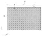
도 2는 광 차폐층(80)이 형성되지 않은 하나의 디스플레이 모듈(21)을 나타낸 정면도이고, 도 3은 디스플레이 모듈(21)의 동작을 나타낸 블록도이다.FIG. 2 is a front view showing one
이하에서는 복수의 디스플레이 모듈(20) 중 하나인 제1 디스플레이 모듈(21)을 기준으로 설명하였으나, 복수의 디스플레이 모듈(20) 중 다른 디스플레이 모듈들(22, 23)은 제1 디스플레이 모듈(21)과 동일한 구조로 구성될 수 있다.Below, the description is based on the
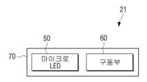
제1 디스플레이 모듈(21)은 마이크로 LED(50) 및 마이크로 LED(50)가 격자 형태로 배치되는 기판(70), 각각의 마이크로 LED(50)를 구동시키는 구동부(60)를 포함할 수 있다.The
마이크로 LED(50)는 가로, 세로 및 높이가 100μm이하인 크기의 무기 발광물질로 이루어 지고, 기판(70) 상에 배치되어 스스로 광을 조사할 수 있다.The
마이크로 LED(50)는 하나의 픽셀(50`, pixel)로 구성될 수 있으며, 하나의 픽셀(pixel) 내에는 서브 픽셀(sub-pixel)인 적색광을 방출하는 적색 마이크로 LED(51), 녹색광을 방출하는 녹색 마이크로 LED(52), 청색광을 방출하는 청색 마이크로 LED(53)이 배치될 수 있다.The
서브 픽셀(51, 52, 53)은 하나의 픽셀(50`) 내에서 매트릭스 형태로 배열되거나, 순차적으로 배열될 수 있다. 다만, 이러한 서브 픽셀(51, 52, 53)의 배치 형태는 일 예이며, 서브 픽셀(51, 52, 53)은 각 단일 픽셀(50`) 내에서 다양한 형태로 배치될 수 있다.The
본 개시에서는 서브 픽셀(sub-pixel)과 도시된 마이크로 LED(50)가 동일한 구성으로 취급한다.In the present disclosure, the sub-pixel and the illustrated
다만, 후술하는 마이크로 LED(50)는 서브 픽셀(sub-pixel) 단위에 한정되는 것이 아니라, 하나의 픽셀(pixel) 단위를 의미할 수 있다.However, the
즉, 후술하는 광 차폐층(80)의 개구(S)는 각 서브 픽셀(sub-pixel) 상에 대응되는 위치에 형성되는 경우뿐만 아니라, 하나의 픽셀(pixel) 상에 대응되는 위치에 형성될 수 있다.That is, the opening S of the
마이크로 LED(50)는 빠른 반응속도, 낮은 전력, 높은 휘도를 가지고 있어 차세대 디스플레이의 발광 소자로서 각광받고 있다. 구체적으로, 마이크로 LED(50)는 기존 LCD 또는 OLED에 비해 전기를 광자로 변환시키는 효율이 더 높다.Micro LED (50) has a fast response speed, low power, and high brightness, and is attracting attention as a light-emitting device for next-generation displays. Specifically, the
즉, 기존 LCD 또는 OLED 디스플레이에 비해 “와트 당 밝기”가 더 높다. 이로 인해 마이크로 LED(50)가 기존 LED 또는 OLED에 비해 약 절반 정도의 에너지로도 동일한 밝기를 낼 수 있게 된다.That is, it has higher “brightness per watt” compared to traditional LCD or OLED displays. As a result, the
이외에도 마이크로 LED(50)는 높은 해상도, 우수한 색상, 명암 및 밝기 구현이 가능하여, 넓은 범위의 색상을 정확하게 표현할 수 있으며, 햇빛이 밝은 야외에서도 선명한 화면을 구현할 수 있다. 그리고, 마이크로 LED(50)는 번인(burn in) 현상에 강하고 발열이 적어 변형 없이 긴 수명이 보장된다.In addition, the micro LED (50) is capable of realizing high resolution, excellent color, contrast, and brightness, so it can accurately express a wide range of colors and produce a clear screen even outdoors in bright sunlight. In addition, the
기판(70)은 기판(70) 상에 매트릭스 형태로 실장된 마이크로 LED(50)와 각각 전기적으로 연결되어, 구동부(60)의 구동 신호를 통해 마이크로 LED(50)를 제어할 수 있다.The
기판(70)은 통상적인 TFT(Thin film transistor) 기판으로 지칭될 수 있으나, 명칭은 이에 제한되지 않는다.The
기판(70)은 연성 가능한 재질, 글래스 또는 플라스틱 등 다양한 재질로 구성될 수 있다.The
구동부(60)는 각각의 마이크로 LED(50)를 제어하며, 기판(70)의 가장자리 영역 또는 기판(70)의 후면에 COG(Chip on Class) 본딩 또는 FOG(Film on Glass) 본딩 방식으로 기판(70)과 연결될 수 있다.The
다만, 구동부(60)가 기판(70)에 배치되는 위치 및 결합 방식은 이에 제한되지 않고 다양할 수 있다.However, the location and coupling method of the
이하에서는 도 4 및 도 5를 참조하여, 본 개시의 일 실시에에 따른 광 차폐층(80)의 구체적인 구조에 대해 설명한다.Hereinafter, with reference to FIGS. 4 and 5 , a detailed structure of the
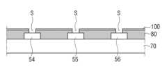
도 4는 본 개시의 일 실시예에 따른 광 차폐층(80)이 형성된 제1 디스플레이 모듈(21)을 나타낸 정면도이고, 도 5는 도 4의 A-A선을 따라 나타낸 단면도이다.FIG. 4 is a front view showing the
광 차폐층(80)은 복수의 마이크로 LED(54, 55, 56)를 커버하고, 복수의 마이크로 LED(54, 55, 56) 사이의 간격을 채울 수 있다. The
여기서, 복수의 마이크로 LED(54, 55, 56)는 적색광을 방출하는 제1 마이크로 LED(54), 녹색광을 방출하는 제2 마이크로 LED(55), 청색광을 방출하는 제3 마이크로 LED(56)를 포함하며, 제1 내지 제3 마이크로 LED(54, 55, 56)는 하나의 픽셀을 구성할 수 있다.Here, the plurality of
아울러, 제1 내지 제3 마이크로 LED(54, 55, 56)는 기판(70) 상에 순차적으로 배치될 수 있다.In addition, the first to third
광 차폐층(80)은 복수의 마이크로 LED(54, 55, 56)가 격자 형태로 배열된 기판(70) 상에 코팅되어 형성될 수 있다.The
또한, 광 차폐층(80)은 바인더 수지, 광중합 개시제, 블랙 안료 및 용제를 포함하는 액정 디스플레이용 블랙 매트릭스(Black matrix) 감광성 수지 조성물 또는 차폐용 블랙 안료를 포함하는 수지 조성물로 구성될 수 있다.Additionally, the
아울러, 블랙 안료를 포함하는 수지 조성물은 액상인 상태에서 디스펜서(110, 도 10a 참조)를 통해 기판(70) 상에 도포되어 광 차폐층(80)을 형성할 수 있다.In addition, the resin composition containing the black pigment can be applied on the
광 차폐층(80)은 각각 별개의 색상의 광을 방출하는 제1 내지 제3 마이크로 LED(54, 55, 56) 간의 간격을 나누어 각 색상이 혼합되는 것을 방지하며, 외광을 흡수하여 콘트라스트 비(contrast ratio)을 향상시킬 수 있다.The
아울러, 광 차폐층(80)의 상면(82)은 평편하게 형성될 수 있다. 이에 따라, 광 차폐층(80)은 각각의 마이크로 LED(54, 55, 56)에서 방출되는 광의 측광을 흡수하거나 가리지 않아 디스플레이 화면의 휘도를 높힐 수 있다.In addition, the
또한, 광 차폐층(80)의 높이(h1)는 마이크로 LED(54, 55, 56)의 높이(h2)보다 크게 형성될 수 있다. 이에 따라, 광 차폐층(80)은 마이크로 LED(54, 55, 56)의 측면뿐만 아니라 상면을 포함하여 마이크로 LED(54, 55, 56)를 전체적으로 커버할 수 있다.Additionally, the height h1 of the
아울러, 광 차폐층(80)은 복수의 마이크로 LED(54, 55, 56) 각각의 상면이 노출되도록 형성된 복수의 개구(S)를 포함할 수 있다.In addition, the
이에 따라, 복수의 마이크로 LED(54, 55, 56)의 상면에서 방출되는 광은 복수의 개구(S)를 통과하여 복수의 마이크로 LED(54, 55, 56)의 상부를 향해 방출될 수 있다.Accordingly, light emitted from the upper surface of the plurality of
여기서, 복수의 마이크로 LED(54, 55, 56) 각각의 상면이 노출되는 정도는 복수의 개구의 크기에 따라 다양하게 달라질 수 있다.Here, the extent to which the upper surface of each of the plurality of
또한, 복수의 개구(S)는 복수의 마이크로 LED(54, 55, 56) 각각의 상부(Y축 방향)에 기 설정된 간격(P)으로 형성될 수 있다.Additionally, a plurality of openings (S) may be formed at a preset interval (P) on the upper portion (Y-axis direction) of each of the plurality of micro LEDs (54, 55, and 56).
여기서 기 설정된 간격(P)은 일정할 수 있으며, 이에 따라 복수의 마이크로 LED(54, 55, 56)에서 방출되는 광은 기 설정된 간격(P)으로 형성된 복구의 개구(S)를 통해 디스플레이 화면 상에 균일한 휘도로 구현될 수 있다.Here, the preset interval (P) may be constant, and accordingly, the light emitted from the plurality of micro LEDs (54, 55, 56) is projected onto the display screen through the recovery opening (S) formed at the preset interval (P). It can be implemented with uniform luminance.
구체적으로, 제1 마이크로 LED(54)와 제2 마이크로 LED(55)는 제1 간격(D1)으로 배치되며, 제2 마이크로 LED(55)와 제3 마이크로 LED(56)는 제1 간격(D1)과 상이한 제2 간격(D2)으로 기판(70) 상에 배치될 수 있다.Specifically, the first
이때, 제2 간격(D2)의 배치 오차로 인해, 제2 마이크로 LED(55)와 제3 마이크로 LED(56) 사이의 제2 간격(D2)이 제1 간격(D1)과 달라질 수 있다.At this time, due to a placement error in the second gap D2, the second gap D2 between the second
이에 따라, 제1 내지 제3 마이크로 LED(54, 55, 56)에서 방출되는 광들 간의 거리가 일정하지 않게 되고, 이에 따라 디스플레이 화면의 휘도가 균일하지 않을 수 있다.Accordingly, the distance between the lights emitted from the first to third
이러한 경우, 제1 내지 제3 마이크로 LED(54, 55, 56) 상의 형성되는 광 차폐층(80)은 일정한 간격으로 형성된 복수의 개구(S)를 포함할 수 있으며, 복수의 개구(S) 각각과 대응되는 제1 내지 제3 마이크로 LED(54, 55, 56)는 복수의 개구(S)를 통해 광들 간의 일정한 간격으로 유지한 채 광을 방출할 수 있다.In this case, the
참고로, 복수의 개구(S)간의 간격은 하나의 개구의 중심부로부터 가장 가까운 하나의 개구의 중심부까지의 거리를 의미할 수 있다. 또한, 마이크로 LED 사이의 간격은 하나의 마이크로 LED의 중심부로부터 가장 가까운 하나의 마이크로 LED의 중심부까지의 거리를 의미할 수 있다.For reference, the interval between the plurality of openings (S) may mean the distance from the center of one opening to the center of the closest opening. Additionally, the spacing between micro LEDs may mean the distance from the center of one micro LED to the center of the closest micro LED.
구체적으로, 제2 마이크로 LED(55)의 중심축과 제2 마이크로 LED(55)의 상부에 형성된 하나의 개구(S)의 중심축이 일치하는 경우, 제2 마이크로 LED(55)와 제3 마이크로 LED(56) 사이의 간격인 제2 간격과 제2 마이크로 LED(55)의 상부에 형성된 개구(S)와 제3 마이크로 LED(56)의 상부에 형성된 개구(S) 사이의 간격(P)의 차이 값(e, 즉, 배치 오차)은 마이크로 LED의 측 방향으로의 길이(L)의 절반보다 작을 수 있다.Specifically, when the central axis of the second
이에 따라, 하나의 개구(S)는 하나의 마이크로 LED 상에 일대일로 대응되어 형성될 수 있으며, 복수의 개구(S)는 각각의 마이크로 LED(54, 55, 56)에서 방출하는 광을 제1 디스플레이 모듈(21)의 상부로 조사하도록 할 수 있다.Accordingly, one opening S may be formed in a one-to-one correspondence on one micro LED, and the plurality of openings S may direct the light emitted from each
아울러, 복수의 개구(S)는 격자 형태로 형성되며, 복수의 개구 각각은 복수의 마이크로 LED(54, 55, 56) 각각에 대응되는 위치에 형성될 수 있다.In addition, the plurality of openings S are formed in a grid shape, and each of the plurality of openings may be formed at a position corresponding to each of the plurality of
예를 들어, 제1 마이크로 LED(54)의 상부에는 하나의 개구(S)가 형성되며, 제2 마이크로 LED(55)의 상부에도 하나의 개구(S)가 형성될 수 있다.For example, one opening S may be formed at the top of the first
또한, 복수의 개구(S)의 단면은 직경이 일정한 원형일 수 있다. 구체적으로, 복수의 개구(S)는 각각의 마이크로 LED(54, 55, 56)의 상면에 대해 대략 수직하게 형성된 측면(81)을 포함할 수 있다.Additionally, the cross-section of the plurality of openings S may be circular with a constant diameter. Specifically, the plurality of openings S may include side surfaces 81 formed approximately perpendicular to the top surface of each
이에 따라, 하나의 마이크로 LED에서 방출되는 광은 방사상으로 균일하게 방출되며, 디스플레이 화면의 균일한 휘도를 구현할 수 있다.Accordingly, the light emitted from one micro LED is uniformly emitted radially, and uniform luminance of the display screen can be realized.
아울러, 복수의 개구(S)의 각각의 단면적은 복수의 마이크로 LED(54, 55, 56)의 상면의 단면적 보다 작을 수 있다.In addition, the cross-sectional area of each of the plurality of openings S may be smaller than the cross-sectional area of the upper surface of the plurality of
이에 따라, 복수의 개구(S)는 복수의 마이크로 LED(54, 55, 56)의 상면에 형성되더라도, 마이크로 LED(54, 55, 56)의 상면 내에 복수의 개구(S)가 위치할 수 있다.Accordingly, even if the plurality of openings S are formed on the upper surface of the plurality of
이하에서는 도 6을 참조하여, 제1 디스플레이 모듈(21`)의 변형 실시예의 구조에 대해서 설명한다.Hereinafter, the structure of a modified embodiment of the first display module 21' will be described with reference to FIG. 6.
도 6은 제1 디스플레이 모듈(21`)의 변형 실시예를 나타낸 단면도이다.Figure 6 is a cross-sectional view showing a modified embodiment of the first display module 21'.
도 6에 도시된 복수의 마이크로 LED(54, 55, 56), 기판(70) 및 광 차폐층(80)은 이전과 동일한 구성이므로 전술한 바와 동일하다.The plurality of
복수의 개구(S) 각각은 복수의 개구(S) 각각의 가장자리를 따라 마이크로 LED(54, 55, 56)의 상면에 대해 일정 각도 기울어져 형성된 광 확산면(83)을 포함할 수 있다.Each of the plurality of openings S may include a
광 확산면(83)은 광 차폐층(80)이 형성된 이후에 추가적인 공정을 통해 형성되거나, 광 차폐층(80)의 개구(S)가 형성될 때에 동시에 형성될 수도 있다.The
광 확산면(83)은 복수의 마이크로 LED(54, 55, 56)의 상면에서 방출되는 광이 확산될 때에 있어서, 측광을 가리지 않을 수 있다. 이에 따라, 광 확산면(83)은 디스플레이 화면의 휘도를 향상시킬 수 있다.The
이하에서는 도 7을 참조하여, 제1 디스플레이 모듈(21``)의 다른 변형 실시예의 구조에 대해 설명한다.Hereinafter, with reference to FIG. 7, the structure of another modified embodiment of the
도 7은 제1 디스플레이 모듈(21``)의 다른 변형 실시예를 나타낸 단면도이다.Figure 7 is a cross-sectional view showing another modified example of the
도 7에 도시된 복수의 마이크로 LED(54, 55, 56), 기판(70) 및 광 차폐층(80)은 이전과 동일한 구성이므로 전술한 바와 동일하다.The plurality of
제1 디스플레이 모듈(21``)은 기판(70) 및 기판(70) 상에 배치된 복수의 마이크로 LED(54, 55, 56)의 상부에 형성되는 보호층(90)을 더 포함할 수 있다.The
보호층(90)은 광 차폐층(80)에 복수의 개구(S)가 형성된 과정에서 마이크로 LED(54, 55, 56)가 손상되는 것을 방지할 수 있다.The
보호층(90)은 마이크로 LED(54, 55, 56)에서 방출되는 광이 투과될 수 있도록 일정 이상의 투과율을 가지는 재질로 구성될 수 있다.The
또한, 보호층(90)은 마이크로 LED(54, 55, 56)가 배치된 기판(70) 상에 일체로 도포되어 형성되기 때문에, 기판(70) 상의 마이크로 LED(54, 55, 56)의 위치를 안정적으로 고정시킬 수 있다.In addition, since the
이하에서는, 도 8a 내지 도 8c를 참조하여, 복수의 디스플레이 모듈(21, 22)이 배치된 경우의 광 차폐층(80)의 구조에 대해서 설명한다.Below, with reference to FIGS. 8A to 8C, the structure of the
도 8a은 복수의 디스플레이 모듈(21, 22)가 배치된 상태를 나타낸 정면도이고, 도 8b는 본 개시의 일 실시예에 따른 광 차폐층(80)이 형성된 복수의 디스플레이 모듈(21, 22)을 나타낸 정면도이며, 도 8c는 도 8b의 B-B선을 따라 나타낸 단면도이다.FIG. 8A is a front view showing a state in which a plurality of
도 8a에 도시된 바와 같이, 제1 및 제2 디스플레이 모듈(21, 22)는 일정한 크기를 가지는 모듈 형태로 제조될 수 있으며, 제1 및 제2 디스플레이 모듈(21, 22)을 배열 플레이트(30) 상에 배치되어 다양한 크기 및 형태의 디스플레이 화면을 구현할 수 있다.As shown in FIG. 8A, the first and
이후, 도 8b 에 도시된 바와 같이, 배열 플레이트(30) 상에 배치된 제1 및 제2 디스플레이 모듈(21, 22) 및 배열 플레이트(30)의 상면에 하나의 광 차폐층(80)이 형성될 수 있다.Thereafter, as shown in FIG. 8B, one
구체적으로, 제1 및 제2 디스플레이 모듈(21, 22)은 제1 및 제2 디스플레이 모듈(21, 22)간의 접촉으로 인한 손상을 방지하기 위해 마이크로 단위의 간격(D5)을 두고 배열 플레이트(30) 상에 배치될 수 있다.Specifically, the first and
이때, 광 차폐층(80)은 제1 및 제2 디스플레이 모듈(21, 22) 사이의 간격(D5)을 채우도록, 배열 플레이트(30) 및 배열 플레이트(30) 상에 배치된 제1 및 제2 디스플레이 모듈(21, 22)의 상부에 일체로 형성될 수 있다.At this time, the
즉, 복수의 디스플레이 모듈(21, 22) 각각의 상부에 형성되는 광 차폐층(80)은 일체로 형성될 수 있다.That is, the
이에 따라, 제1 및 제2 디스플레이 모듈(21, 22) 사이의 간격(D5)으로 인해 디스플레이 화면에 보일 수 있는 심(seam)에 대응하는 부분을 광 차폐층(80)이 채우거나 커버함으로써, 디스플레이 화면에 심(seam)을 커버하여 심 리스(seamless)를 구현할 수 있다.Accordingly, the
아울러, 광 차폐층(80)은 각각의 디스플레이 모듈(21, 22) 상에 배치된 마이크로 LED가 위치한 곳과 대응하여 기 설정된 간격으로 복수의 개구(S)가 형성될 수 있다.In addition, the
이때, 제1 디스플레이 모듈(21)의 가장자리에 위치한 제4 마이크로 LED(57)와 제2 디스플레이 모듈(22)의 가장자리에 위치한 제5 마이크로 LED(58) 사이의 간격은, 제1 디스플레이 모듈(21)의 측면(21a)과 제4 마이크로 LED(57)과의 거리인 제3 간격(D3), 제2 디스플레이 모듈(22)의 측면(22a)과 제5 마이크로 LED(58)과의 거리인 제4 간격(D4) 및 복수의 디스플레이 모듈(21, 22) 사이의 간격(D5)의 합일 수 있다.At this time, the gap between the fourth
이에 따라, 제4 및 제5 마이크로 LED(57, 58) 사이의 간격은 복수의 디스플레이 모듈(21, 22) 사이의 간격(D5)만큼 더 이격 될 수 밖에 없는 구조이나, 광 차폐층(80)은 복수의 개구(S) 간의 일정한 간격(P)으로 형성될 수 있으므로 복수의 디스플레이 모듈(21, 22) 사이의 간격(D5)에 제한되지 않고 일정한 간격으로 광을 방출하여 디스플레이 화면의 휘도를 균일하게 구현할 수 있다.Accordingly, the distance between the fourth and fifth
이하에서는 도 9 내지 도 14를 참조하여, 하나의 디스플레이 모듈(20)이 형성되는 과정을 구체적으로 설명한다.Hereinafter, the process of forming one
도 9는 기판(70) 상에 복수의 마이크로 LED(54, 55, 56)가 배치되는 과정을 나타낸 개략 단면도이고, 도 10a는 디스펜서를 이용하여 광 차폐층을 도포하는 과정을 나타낸 개략 단면도이며, 도 10b는 복수의 마이크로 LED(54, 55, 56) 및 기판(70) 상에 광 차폐층(80)이 형성된 것을 나타낸 개략 단면도이고, 도 11은 광 차폐층(80)의 상면에 포토 레지스트 층(100)이 형성된 것을 나타낸 개략 단면도이며, 도 12는 광 차폐층(80)에 복수의 개구(S)를 형성하는 과정을 나타낸 개략 단면도이고, 도 13은 포토 레지스트 층(100) 및 광 차폐층(80)에 복수의 개구(S)가 형성된 것을 나타낸 개략 단면도이며, 도 14는 복수의 개구(S)가 형성된 디스플레이 모듈(20)을 나타낸 단면도이다.FIG. 9 is a schematic cross-sectional view showing the process of placing a plurality of
먼저, 기판(70) 상에 제1 내지 제3 마이크로 LED(54, 55, 56)이 기 설정된 간격으로 배치된다.First, the first to third
이때, 제1 내지 제3 마이크로 LED(54, 55, 56)는 각각 적색, 녹색, 청색의 광을 방출하는 서브 픽셀에 해당하는 것으로 도시하였으나, 이에 제한되지 않고, 적색, 녹색, 청색의 광을 방출하는 서브 픽셀이 포함된 하나의 픽셀(50`)일 수 있다.At this time, the first to third
이후, 도 10a에 도시된 바와 같이, 블랙 안료를 포함하는 액상 상태의 수지 조성물(M)은 디스펜서(110)를 통해 기판(70)상에 도포될 수 있다.Thereafter, as shown in FIG. 10A, the liquid resin composition (M) containing the black pigment may be applied on the
구체적으로, 블랙 안료를 포함하는 액상 상태의 수지 조성물(M)을 포함하는 디스펜서(110)는 구현하고자 하는 광 차폐층의 높이(h1)로 도포하면서 기판(70)상의 기 설정된 방향(C)으로 이동할 수 있다.Specifically, the
다음으로, 액상 상태로 기판(70)상에 도포된 블랙 안료를 포함하는 액상 상태의 수지 조성물(M)을 응고시켜 고형화된 광 차폐층(80)을 형성할 수 있다.Next, the solidified
이에 따라, 도 10b에 도시된 바와 같이, 배치된 복수의 마이크로 LED(54, 55, 56) 및 복수의 마이크로 LED(54, 55, 56)가 배치된 기판(70) 상에 광 차폐층(80)이 도포될 수 있다.Accordingly, as shown in FIG. 10b, a
이때, 광 차폐층(80)의 높이(h1)는 복수의 마이크로 LED(54, 55, 56)을 커버할 수 있도록, 복수의 마이크로 LED(54, 55, 56)의 높이(h2)보다 클 수 있다.At this time, the height (h1) of the
아울러, 광 차폐층(80)의 상면(82)은 평편하게 형성되며, 광 차폐층(80)을 평편하게 하는 별도의 공정이 포함될 수 있다.In addition, the
또한, 광 차폐층(80)이 도포되기 이전에, 복수의 마이크로 LED(54, 55, 56)의 상면에 보호층(90, 도 7 참조)이 형성될 수 있다.Additionally, before the
다음으로, 도 11에 도시된 바와 같이, 도포된 광 차폐층(80)의 상면에 포토 레지스트 층(100)이 도포될 수 있다.Next, as shown in FIG. 11, a
포토 레지스트 층(100, Photo resist layer)은 빛을 조사하면 화학 변화를 일으키는 재료 물질로 구성된다.The photo resist layer (100) is composed of materials that cause chemical changes when irradiated with light.
이후, 도 12에 도시된 바와 같이, 격자 형태로 통과구(T)가 형성된 마스크(110)를 포토 레지스트 층(100)의 상부에 위치시키고, 마스크(110)의 상부에 빛(U)을 노출시킬 수 있다.Thereafter, as shown in FIG. 12, a
이때, 통과구(T)는 광 차폐층(80)에 형성하고자 하는 개구(S)의 형상에 따라서 다양하게 형성될 수 있으며, 형성하고자 하는 복수의 개구(S) 간의 간격 및 패턴에 따라서 마스크(110)에 복수의 통과구(T) 간의 간격 및 패턴이 달라질 수 있다.At this time, the passage hole T can be formed in various ways depending on the shape of the opening S to be formed in the
아울러, 빛(U)은 자외선(ultraviolet rays)일 수 있다.Additionally, light (U) may be ultraviolet rays.
이에 따라, 빛(U)에 노출된 포토 레지스트 층(100)의 부분은 화학 변화를 통해 특성이 변화하게 된다.Accordingly, the properties of the portion of the
이후, 복수의 개구(S)가 형성될 영역을 식각하여, 도 13과 같이 복수의 마이크로 LED(54, 55, 56) 상에 복수의 개구(S)를 형성할 수 있다.Thereafter, the area where the plurality of openings S will be formed may be etched to form the plurality of openings S on the plurality of
이때, 복수의 개구(S)를 식각하는 방법은 건식, 습식에 한정되지 않고 다양한 방법으로 행할 수 있다.At this time, the method of etching the plurality of openings S is not limited to dry or wet, and can be performed using various methods.
마지막으로, 광 차폐층(80)의 상부에 남아있는 포토 레지스트 층(100)을 제거함으로써, 도 14에 도시된 바와 같은 디스플레이 모듈(20)을 제조할 수 있다.Finally, by removing the
또한, 복수의 디스플레이 모듈(20)이 디스플레이 화면을 구성할 경우에는, 복수의 디스플레이 모듈(20)을 배열 플레이트(30) 상에 배치하는 단계를 더 포함할 수 있다.Additionally, when a plurality of
이때, 복수의 디스플레이 모듈(20) 간의 높이 차가 발생하지 않도록 복수의 디스플레이 모듈(20)은 상호간 동일 평면상에 평행하게 배치될 수 있다.At this time, the plurality of
이후, 복수의 디스플레이 모듈(20)이 배열 플레이트(30)상에 배치된 상태에서 광 차폐층(80)이 복수의 디스플레이 모듈(20)과 배열 플레이트(30) 상에 도포될 수 있다.Thereafter, with the plurality of
이에 따라, 광 차폐층(80)은 복수의 디스플레이 모듈(20)의 상면을 커버할 수 있는 뿐만 아니라, 복수의 디스플레이 모듈(20) 사이의 간격(D5)을 채울 수 있다.Accordingly, the
따라서, 광 차폐층(80)은 복수의 디스플레이 모듈(20) 사이의 간격(D5)으로 인해 발생하는 심(seam)을 제거하여, 심 리스(seamless)를 구현할 수 있을 뿐만 아니라, 복수의 디스플레이 모듈(20)을 배열 플레이트(30) 상에 안정적으로 고정시킬 수 있다.Accordingly, the
이상에서는 본 개시의 다양한 실시예를 각각 개별적으로 설명하였으나, 각 실시예들은 반드시 단독으로 구현되어야만 하는 것은 아니며, 각 실시예들의 구성 및 동작은 적어도 하나의 다른 실시예들과 조합되어 구현될 수도 있다.In the above, various embodiments of the present disclosure have been described individually, but each embodiment does not necessarily have to be implemented alone, and the configuration and operation of each embodiment may be implemented in combination with at least one other embodiment. .
또한, 이상에서는 본 개시의 바람직한 실시예에 대하여 도시하고 설명하였지만, 본 개시는 상술한 특정의 실시예에 한정되지 아니하며, 청구범위상에서 청구하는 본 개시의 요지를 벗어남이 없이 당해 발명이 속하는 기술분야에서 통상의 지식을 가진 자에 의해 다양한 변형실시가 가능한 것은 물론이고, 이러한 변형실시들은 본 개시의 기술적 사상이나 전망으로부터 개별적으로 이해되어서는 안될 것이다.In addition, although the preferred embodiments of the present disclosure have been shown and described above, the present disclosure is not limited to the specific embodiments described above, and the technical field to which the invention pertains without departing from the gist of the present disclosure as claimed in the claims. Of course, various modifications can be made by those skilled in the art, and these modifications should not be understood individually from the technical idea or perspective of the present disclosure.
1:디스플레이 장치10: 보호 플레이트
20: 디스플레이 모듈30: 배열 플레이트
40: 하우징50: 마이크로 LED
60: 구동부70: 기판
80: 광 차폐층90: 보호층1: Display device 10: Protective plate
20: display module 30: array plate
40: Housing 50: Micro LED
60: driving unit 70: substrate
80: light shielding layer 90: protective layer
Claims (15)
Translated fromKorean상기 기판 상에 배치되고 광을 조사하는 복수의 마이크로 LED; 및
상기 복수의 마이크로 LED를 커버하고, 상기 복수의 마이크로 LED 사이의 간격을 채우는 광 차폐층(light blocking layer);을 포함하고,
상기 복수의 마이크로 LED는 제1 마이크로 LED, 제2 마이크로 LED, 및 제3 마이크로 LED를 포함하고,
상기 광 차폐층은 상기 복수의 마이크로 LED 각각의 상면이 노출되도록 상기 복수의 마이크로 LED에 대응하는 복수의 개구를 포함하고,
상기 제2 마이크로 LED는 상기 제1 마이크로 LED와 상기 제3 마이크로 LED 사이에 인접하게 배치되고,
상기 복수의 개구의 서로 인접한 개구들의 중심 사이는 거리는 제1 간격이고, 상기 제1 간격은 상기 제1 마이크로 LED의 중심과 상기 제2 마이크로 LED의 중심 사이의 거리는 제2 간격과 동일하고, 상기 제2 간격은 상기 제2 마이크로 LED의 중심과 상기 제3 마이크로 LED의 중심 사이의 거리는 제3 간격과 상이하며,
상기 제1 마이크로 LED의 중심과 상기 제2 마이크로 LED의 중심은 각각 대응하는 개구들의 중심에 위치하고, 상기 제3 마이크로 LED의 중심은 대응하는 개구의 중심에서 벗어나는 디스플레이 모듈.Board;
a plurality of micro LEDs disposed on the substrate and emitting light; and
A light blocking layer covers the plurality of micro LEDs and fills the gap between the plurality of micro LEDs,
The plurality of micro LEDs include a first micro LED, a second micro LED, and a third micro LED,
The light shielding layer includes a plurality of openings corresponding to the plurality of micro LEDs so that the upper surface of each of the plurality of micro LEDs is exposed,
The second micro LED is disposed adjacent to the first micro LED and the third micro LED,
The distance between the centers of adjacent openings of the plurality of openings is a first interval, the first interval is equal to the second interval, and the distance between the center of the first micro LED and the center of the second micro LED is the same as the second interval. 2 Interval is the distance between the center of the second micro LED and the center of the third micro LED is different from the third interval,
A display module wherein the center of the first micro LED and the center of the second micro LED are located at the center of the corresponding openings, and the center of the third micro LED deviates from the center of the corresponding opening.
상기 복수의 개구의 각각의 단면적은 상기 복수의 마이크로 LED의 상면의 단면적 보다 작은 디스플레이 모듈.According to paragraph 1,
A display module wherein the cross-sectional area of each of the plurality of openings is smaller than the cross-sectional area of the upper surface of the plurality of micro LEDs.
상기 복수의 개구의 단면은 직경이 일정한 원형인 디스플레이 모듈.According to paragraph 2,
A display module wherein the cross-section of the plurality of openings is circular with a constant diameter.
상기 복수의 개구 각각은 상기 복수의 개구 각각의 가장자리를 따라 상기 마이크로 LED의 상면에 대해 일정 각도 기울어져 형성된 광 확산면을 포함하는 디스플레이 모듈.According to paragraph 1,
Each of the plurality of openings includes a light diffusion surface formed along an edge of each of the plurality of openings and inclined at a predetermined angle with respect to the upper surface of the micro LED.
상기 제1 마이크로 LED는 적색광을 방출하고,
상기 제2 마이크로 LED는 녹색광을 방출하고,
상기 제3 마이크로 LED는 청색광을 방출하며,
상기 제1 내지 제3 마이크로 LED는 하나의 픽셀을 구성하는 디스플레이 모듈.According to paragraph 1,
The first micro LED emits red light,
The second micro LED emits green light,
The third micro LED emits blue light,
A display module in which the first to third micro LEDs constitute one pixel.
상기 제1 내지 제3 마이크로 LED는 상기 기판 상에 순차적으로 배치되는 디스플레이 모듈.According to clause 5,
A display module wherein the first to third micro LEDs are sequentially arranged on the substrate.
상기 광 차폐층은 상기 기판 상에 형성되며,
상기 광 차폐층의 높이는 상기 복수의 마이크로 LED의 높이보다 큰 디스플레이 모듈.According to paragraph 1,
The light shielding layer is formed on the substrate,
A display module in which the height of the light shielding layer is greater than the height of the plurality of micro LEDs.
상기 복수의 디스플레이 모듈이 동일 평면상에 평행하게 배치되도록 지지하는 배열 플레이트;
상기 복수의 디스플레이 모듈 및 상기 배열 플레이트를 고정하는 하우징;을 포함하고,
상기 복수의 디스플레이 모듈 각각은,
기판;
상기 기판 상에 배치되고 광을 조사하는 복수의 마이크로 LED; 및
상기 복수의 마이크로 LED를 커버하고, 상기 복수의 마이크로 LED 사이의 간격을 채우는 광 차폐층(light blocking layer);을 포함하고,
상기 복수의 마이크로 LED는 제1 마이크로 LED, 제2 마이크로 LED, 및 제3 마이크로 LED를 포함하고,
상기 광 차폐층은 상기 복수의 마이크로 LED 각각의 상면이 노출되도록 상기 복수의 마이크로 LED에 대응하는 복수의 개구를 포함하고,
상기 제2 마이크로 LED는 상기 제1 마이크로 LED와 상기 제3 마이크로 LED 사이에 인접하게 배치되고,
상기 복수의 개구의 서로 인접한 개구들의 중심 사이는 거리는 제1 간격이고, 상기 제1 간격은 상기 제1 마이크로 LED의 중심과 상기 제2 마이크로 LED의 중심 사이의 거리는 제2 간격과 동일하고, 상기 제2 간격은 상기 제2 마이크로 LED의 중심과 상기 제3 마이크로 LED의 중심 사이의 거리는 제3 간격과 상이하며,
상기 제1 마이크로 LED의 중심과 상기 제2 마이크로 LED의 중심은 각각 대응하는 개구들의 중심에 위치하고, 상기 제3 마이크로 LED의 중심은 대응하는 개구의 중심에서 벗어나는 디스플레이 장치.A plurality of display modules;
an array plate supporting the plurality of display modules to be arranged in parallel on the same plane;
It includes a housing that fixes the plurality of display modules and the array plate,
Each of the plurality of display modules,
Board;
a plurality of micro LEDs disposed on the substrate and emitting light; and
A light blocking layer covers the plurality of micro LEDs and fills the gap between the plurality of micro LEDs,
The plurality of micro LEDs include a first micro LED, a second micro LED, and a third micro LED,
The light shielding layer includes a plurality of openings corresponding to the plurality of micro LEDs so that the upper surface of each of the plurality of micro LEDs is exposed,
The second micro LED is disposed adjacent to the first micro LED and the third micro LED,
The distance between the centers of adjacent openings of the plurality of openings is a first interval, the first interval is equal to the second interval, and the distance between the center of the first micro LED and the center of the second micro LED is the same as the second interval. 2 Interval is the distance between the center of the second micro LED and the center of the third micro LED is different from the third interval,
The center of the first micro LED and the center of the second micro LED are located at the center of the corresponding openings, and the center of the third micro LED deviates from the center of the corresponding opening.
상기 광 차폐층은 상기 복수의 디스플레이 모듈 사이의 간격을 채우는 디스플레이 장치.According to clause 8,
A display device wherein the light shielding layer fills the gap between the plurality of display modules.
상기 복수의 디스플레이 모듈 각각의 상부에 형성되는 광 차폐층은 일체로 형성되는 디스플레이 장치.According to clause 9,
A display device wherein the light shielding layer formed on top of each of the plurality of display modules is formed integrally.
상기 복수의 개구의 단면은 직경이 일정한 원형이고,
상기 복수의 개구 간의 간격은 동일한 디스플레이 장치.According to clause 8,
The cross-section of the plurality of openings is circular with a constant diameter,
A display device wherein the spacing between the plurality of openings is the same.
배치된 상기 복수의 마이크로 LED 상에 광 차폐층을 도포하는 단계; 및
상기 복수의 마이크로 LED 각각의 상면이 노출되도록 상기 복수의 마이크로 LED에 대응하는 복수의 개구를 형성하는 단계;를 포함하고,
상기 복수의 마이크로 LED는 제1 마이크로 LED, 제2 마이크로 LED, 및 제3 마이크로 LED를 포함하고,
상기 제2 마이크로 LED는 상기 제1 마이크로 LED와 상기 제3 마이크로 LED 사이에 인접하게 배치되고,
상기 복수의 개구의 서로 인접한 개구들의 중심 사이는 거리는 제1 간격이고, 상기 제1 간격은 상기 제1 마이크로 LED의 중심과 상기 제2 마이크로 LED의 중심 사이의 거리는 제2 간격과 동일하고, 상기 제2 간격은 상기 제2 마이크로 LED의 중심과 상기 제3 마이크로 LED의 중심 사이의 거리는 제3 간격과 상이하며,
상기 제1 마이크로 LED의 중심과 상기 제2 마이크로 LED의 중심은 각각 대응하는 개구들의 중심에 위치하고, 상기 제3 마이크로 LED의 중심은 대응하는 개구의 중심에서 벗어나는 디스플레이 모듈 제조방법.Arranging a plurality of micro LEDs on a substrate;
Applying a light shielding layer on the plurality of arranged micro LEDs; and
Comprising: forming a plurality of openings corresponding to the plurality of micro LEDs so that the upper surface of each of the plurality of micro LEDs is exposed,
The plurality of micro LEDs include a first micro LED, a second micro LED, and a third micro LED,
The second micro LED is disposed adjacent to the first micro LED and the third micro LED,
The distance between the centers of adjacent openings of the plurality of openings is a first interval, the first interval is equal to the second interval, and the distance between the center of the first micro LED and the center of the second micro LED is the same as the second interval. 2 Interval is the distance between the center of the second micro LED and the center of the third micro LED is different from the third interval,
A display module manufacturing method wherein the center of the first micro LED and the center of the second micro LED are located at the center of the corresponding openings, and the center of the third micro LED deviates from the center of the corresponding opening.
상기 복수의 개구를 형성하는 단계는,
도포된 상기 광 차폐층의 상면에 포토 레지스트 층(Photo Resist layer)을 도포하는 단계;
격자 형태로 통과구가 형성된 마스크를 상기 포토 레지스트 층의 상부에 위치시키는 단계;
상기 마스크의 상부에 빛을 노출시키는 단계;
상기 복수의 개구가 형성될 영역을 식각하는 단계; 및
상기 포토 레지스트 층을 제거하는 단계;를 더 포함하는 디스플레이 모듈 제조방법.According to clause 12,
The step of forming the plurality of openings includes:
Applying a photo resist layer on the upper surface of the applied light shielding layer;
Positioning a mask with passage holes formed in a grid shape on top of the photoresist layer;
exposing the top of the mask to light;
etching the area where the plurality of openings will be formed; and
A display module manufacturing method further comprising: removing the photoresist layer.
상기 광 차폐층을 도포하기 전에 상기 복수의 마이크로 LED의 상면에 보호층을 도포하는 단계;를 더 포함하는 디스플레이 모듈 제조방법.According to clause 12,
A display module manufacturing method further comprising: applying a protective layer to the upper surface of the plurality of micro LEDs before applying the light shielding layer.
상기 광 차폐층을 도포하는 단계는,
상기 광 차폐층을 구성하며 블랙 안료를 포함하는 수지 조성물을 디스펜서를 이용하여 도포하는 디스플레이 모듈 제조방법.According to clause 12,
The step of applying the light shielding layer is,
A display module manufacturing method in which a resin composition constituting the light-shielding layer and containing a black pigment is applied using a dispenser.
Priority Applications (3)
| Application Number | Priority Date | Filing Date | Title |
|---|---|---|---|
| KR1020180106790AKR102590433B1 (en) | 2018-09-07 | 2018-09-07 | Display module, display apparatus including the same and method of manufacturing display module |
| US16/561,161US11404472B2 (en) | 2018-09-07 | 2019-09-05 | Display module and display apparatus including light blocking layer with openings having regular intervals therebetween |
| TW108132196ATW202016622A (en) | 2018-09-07 | 2019-09-06 | Display module, display device including the same, and method of manufacturing display module |
Applications Claiming Priority (1)
| Application Number | Priority Date | Filing Date | Title |
|---|---|---|---|
| KR1020180106790AKR102590433B1 (en) | 2018-09-07 | 2018-09-07 | Display module, display apparatus including the same and method of manufacturing display module |
Publications (2)
| Publication Number | Publication Date |
|---|---|
| KR20200028574A KR20200028574A (en) | 2020-03-17 |
| KR102590433B1true KR102590433B1 (en) | 2023-10-18 |
Family
ID=69719653
Family Applications (1)
| Application Number | Title | Priority Date | Filing Date |
|---|---|---|---|
| KR1020180106790AActiveKR102590433B1 (en) | 2018-09-07 | 2018-09-07 | Display module, display apparatus including the same and method of manufacturing display module |
Country Status (3)
| Country | Link |
|---|---|
| US (1) | US11404472B2 (en) |
| KR (1) | KR102590433B1 (en) |
| TW (1) | TW202016622A (en) |
Families Citing this family (11)
| Publication number | Priority date | Publication date | Assignee | Title |
|---|---|---|---|---|
| KR20200088950A (en)* | 2019-01-15 | 2020-07-24 | 삼성디스플레이 주식회사 | Display device and method of fabricating the same |
| KR102796530B1 (en)* | 2020-02-19 | 2025-04-17 | 삼성디스플레이 주식회사 | Electronic device |
| KR102765516B1 (en)* | 2020-05-14 | 2025-02-12 | 삼성전자주식회사 | Display module and mathod of manufaturing the same |
| KR102851079B1 (en)* | 2020-06-25 | 2025-08-28 | 삼성전자주식회사 | Thin film transistor and display module having the same |
| WO2021261807A1 (en)* | 2020-06-25 | 2021-12-30 | 삼성전자주식회사 | Thin film transistor substrate and display module comprising same |
| US11887842B2 (en)* | 2020-08-24 | 2024-01-30 | PlayNitride Display Co., Ltd. | Spliced micro light-emitting-diode display panel |
| CN114335046A (en)* | 2020-09-29 | 2022-04-12 | 成都辰显光电有限公司 | Display panel and method for manufacturing the same |
| CN112349710A (en)* | 2020-11-27 | 2021-02-09 | 深圳市鼎华芯泰科技有限公司 | RGB-LED packaging structure and packaging method |
| CN112436049B (en)* | 2020-12-09 | 2024-02-23 | 维信诺科技股份有限公司 | Display panel preparation method and display panel |
| US20250212587A1 (en)* | 2023-12-21 | 2025-06-26 | Seoul Viosys Co., Ltd. | Light emitting module and display apparatus having the same |
| JP2025114143A (en)* | 2024-01-24 | 2025-08-05 | 三星電子株式会社 | Display device and display system |
Citations (3)
| Publication number | Priority date | Publication date | Assignee | Title |
|---|---|---|---|---|
| US20170345867A1 (en)* | 2015-01-23 | 2017-11-30 | Vuereal Inc. | Micro device integration into system substrate |
| JP2018014320A (en)* | 2016-07-08 | 2018-01-25 | 株式会社半導体エネルギー研究所 | Display apparatus |
| US20180102350A1 (en)* | 2016-10-11 | 2018-04-12 | Lumens Co., Ltd. | Led display modules and methods for making the same |
Family Cites Families (11)
| Publication number | Priority date | Publication date | Assignee | Title |
|---|---|---|---|---|
| KR101063561B1 (en)* | 2005-08-02 | 2011-09-07 | 엘지이노텍 주식회사 | Method of manufacturing gallium nitride-based light emitting diode |
| US9041202B2 (en)* | 2008-05-16 | 2015-05-26 | Semiconductor Energy Laboratory Co., Ltd. | Semiconductor device and manufacturing method of the same |
| JP5263788B2 (en) | 2009-10-22 | 2013-08-14 | シャープ株式会社 | Display device |
| JP6091189B2 (en) | 2012-11-29 | 2017-03-08 | 三菱電機株式会社 | Display device |
| KR20150081089A (en)* | 2014-01-03 | 2015-07-13 | 삼성디스플레이 주식회사 | Light emitting diode package |
| US9557954B2 (en) | 2014-12-23 | 2017-01-31 | X Development Llc | Display panel using direct emission pixel arrays |
| KR102427644B1 (en) | 2015-11-16 | 2022-08-02 | 삼성전자주식회사 | Light source, method of manufacturing the same, and display apparatus having the same |
| KR102673721B1 (en) | 2016-11-07 | 2024-06-11 | 삼성전자주식회사 | Light emitting diode panel and manufacturing method |
| WO2019014036A1 (en)* | 2017-07-11 | 2019-01-17 | Corning Incorporated | Tiled displays and methods of manufacturing the same |
| KR102650950B1 (en)* | 2017-09-29 | 2024-03-26 | 서울반도체 주식회사 | Light emitting device for display and display apparatus having the same |
| JP2019087659A (en)* | 2017-11-08 | 2019-06-06 | ソニーセミコンダクタソリューションズ株式会社 | Imaging element and method of manufacturing the same, and electronic equipment |
- 2018
- 2018-09-07KRKR1020180106790Apatent/KR102590433B1/enactiveActive
- 2019
- 2019-09-05USUS16/561,161patent/US11404472B2/enactiveActive
- 2019-09-06TWTW108132196Apatent/TW202016622A/enunknown
Patent Citations (3)
| Publication number | Priority date | Publication date | Assignee | Title |
|---|---|---|---|---|
| US20170345867A1 (en)* | 2015-01-23 | 2017-11-30 | Vuereal Inc. | Micro device integration into system substrate |
| JP2018014320A (en)* | 2016-07-08 | 2018-01-25 | 株式会社半導体エネルギー研究所 | Display apparatus |
| US20180102350A1 (en)* | 2016-10-11 | 2018-04-12 | Lumens Co., Ltd. | Led display modules and methods for making the same |
Also Published As
| Publication number | Publication date |
|---|---|
| US11404472B2 (en) | 2022-08-02 |
| US20200083283A1 (en) | 2020-03-12 |
| TW202016622A (en) | 2020-05-01 |
| KR20200028574A (en) | 2020-03-17 |
Similar Documents
| Publication | Publication Date | Title |
|---|---|---|
| KR102590433B1 (en) | Display module, display apparatus including the same and method of manufacturing display module | |
| KR102090036B1 (en) | Backlight assembly and display divece having the same | |
| KR102660614B1 (en) | Display apparatus and manufacturing method thereof | |
| EP2558905B1 (en) | Backlight unit and display apparatus comprising the same | |
| KR101969462B1 (en) | Photoluminescent display device and method for manufacturing the same | |
| US8870401B2 (en) | Lighting device, display device and television receiver | |
| US20170077436A1 (en) | Display panel, display apparatus and method of manufacturing display panel | |
| KR101818252B1 (en) | Backlight Unit And Liquid Crystal Display Comprising The Same | |
| US9612474B2 (en) | Backlight assembly and display device including the same | |
| JP6439255B2 (en) | Organic electroluminescence display device and manufacturing method thereof | |
| JP2023013880A (en) | Light-curing 3d printer optical machine, printer and 3d printing method | |
| JP6752948B2 (en) | Print head | |
| KR20200057202A (en) | Display module, display apparatus and manufacturing method of display apparatus | |
| KR102737986B1 (en) | Display apparatus and method of manufacturing display apparatus | |
| KR101315467B1 (en) | Backlight unit and display apparatus comprising the same | |
| US9176370B1 (en) | High contrast rear projection screen | |
| JP2015022016A (en) | Color filter for organic electroluminescence display device, organic electroluminescence display device and manufacturing method of color filter for organic electroluminescence display device | |
| US20210041745A1 (en) | Backlight and liquid crystal display device | |
| US10978430B2 (en) | Display apparatus and manufacturing method thereof | |
| JP2019059090A (en) | Print head | |
| KR102709667B1 (en) | Display apparatus | |
| KR102102703B1 (en) | LED package, method of fabricating the same, and backlight unit and liquid crystal display device including the LED package | |
| KR101372961B1 (en) | Backlight Unit Having Grid Serration Pattern And Liquid Crystal Display Device Including The Same | |
| KR101739586B1 (en) | Backlight unit and Liquid Crystal Display device having the same | |
| KR101681781B1 (en) | Liquid crystal display device |
Legal Events
| Date | Code | Title | Description |
|---|---|---|---|
| PA0109 | Patent application | St.27 status event code:A-0-1-A10-A12-nap-PA0109 | |
| PG1501 | Laying open of application | St.27 status event code:A-1-1-Q10-Q12-nap-PG1501 | |
| A201 | Request for examination | ||
| PA0201 | Request for examination | St.27 status event code:A-1-2-D10-D11-exm-PA0201 | |
| D13-X000 | Search requested | St.27 status event code:A-1-2-D10-D13-srh-X000 | |
| D14-X000 | Search report completed | St.27 status event code:A-1-2-D10-D14-srh-X000 | |
| E902 | Notification of reason for refusal | ||
| PE0902 | Notice of grounds for rejection | St.27 status event code:A-1-2-D10-D21-exm-PE0902 | |
| P11-X000 | Amendment of application requested | St.27 status event code:A-2-2-P10-P11-nap-X000 | |
| P13-X000 | Application amended | St.27 status event code:A-2-2-P10-P13-nap-X000 | |
| E701 | Decision to grant or registration of patent right | ||
| PE0701 | Decision of registration | St.27 status event code:A-1-2-D10-D22-exm-PE0701 | |
| PR0701 | Registration of establishment | St.27 status event code:A-2-4-F10-F11-exm-PR0701 | |
| PR1002 | Payment of registration fee | St.27 status event code:A-2-2-U10-U11-oth-PR1002 Fee payment year number:1 | |
| PG1601 | Publication of registration | St.27 status event code:A-4-4-Q10-Q13-nap-PG1601 | |
| P22-X000 | Classification modified | St.27 status event code:A-4-4-P10-P22-nap-X000 |