KR102589972B1 - Plasma module with slotted ground plate - Google Patents
Plasma module with slotted ground plateDownload PDFInfo
- Publication number
- KR102589972B1 KR102589972B1KR1020187010290AKR20187010290AKR102589972B1KR 102589972 B1KR102589972 B1KR 102589972B1KR 1020187010290 AKR1020187010290 AKR 1020187010290AKR 20187010290 AKR20187010290 AKR 20187010290AKR 102589972 B1KR102589972 B1KR 102589972B1
- Authority
- KR
- South Korea
- Prior art keywords
- elongated slot
- breaker plate
- slot
- gas
- plasma source
- Prior art date
- Legal status (The legal status is an assumption and is not a legal conclusion. Google has not performed a legal analysis and makes no representation as to the accuracy of the status listed.)
- Active
Links
Images


Classifications
- H—ELECTRICITY
- H01—ELECTRIC ELEMENTS
- H01J—ELECTRIC DISCHARGE TUBES OR DISCHARGE LAMPS
- H01J37/00—Discharge tubes with provision for introducing objects or material to be exposed to the discharge, e.g. for the purpose of examination or processing thereof
- H01J37/32—Gas-filled discharge tubes
- H01J37/32009—Arrangements for generation of plasma specially adapted for examination or treatment of objects, e.g. plasma sources
- H01J37/32357—Generation remote from the workpiece, e.g. down-stream
- H—ELECTRICITY
- H01—ELECTRIC ELEMENTS
- H01J—ELECTRIC DISCHARGE TUBES OR DISCHARGE LAMPS
- H01J37/00—Discharge tubes with provision for introducing objects or material to be exposed to the discharge, e.g. for the purpose of examination or processing thereof
- H01J37/32—Gas-filled discharge tubes
- H01J37/32431—Constructional details of the reactor
- H01J37/32623—Mechanical discharge control means
- H—ELECTRICITY
- H01—ELECTRIC ELEMENTS
- H01J—ELECTRIC DISCHARGE TUBES OR DISCHARGE LAMPS
- H01J37/00—Discharge tubes with provision for introducing objects or material to be exposed to the discharge, e.g. for the purpose of examination or processing thereof
- H01J37/32—Gas-filled discharge tubes
- H01J37/32431—Constructional details of the reactor
- H01J37/3244—Gas supply means
- C—CHEMISTRY; METALLURGY
- C23—COATING METALLIC MATERIAL; COATING MATERIAL WITH METALLIC MATERIAL; CHEMICAL SURFACE TREATMENT; DIFFUSION TREATMENT OF METALLIC MATERIAL; COATING BY VACUUM EVAPORATION, BY SPUTTERING, BY ION IMPLANTATION OR BY CHEMICAL VAPOUR DEPOSITION, IN GENERAL; INHIBITING CORROSION OF METALLIC MATERIAL OR INCRUSTATION IN GENERAL
- C23C—COATING METALLIC MATERIAL; COATING MATERIAL WITH METALLIC MATERIAL; SURFACE TREATMENT OF METALLIC MATERIAL BY DIFFUSION INTO THE SURFACE, BY CHEMICAL CONVERSION OR SUBSTITUTION; COATING BY VACUUM EVAPORATION, BY SPUTTERING, BY ION IMPLANTATION OR BY CHEMICAL VAPOUR DEPOSITION, IN GENERAL
- C23C16/00—Chemical coating by decomposition of gaseous compounds, without leaving reaction products of surface material in the coating, i.e. chemical vapour deposition [CVD] processes
- C23C16/44—Chemical coating by decomposition of gaseous compounds, without leaving reaction products of surface material in the coating, i.e. chemical vapour deposition [CVD] processes characterised by the method of coating
- C23C16/4401—Means for minimising impurities, e.g. dust, moisture or residual gas, in the reaction chamber
- C23C16/4405—Cleaning of reactor or parts inside the reactor by using reactive gases
- C—CHEMISTRY; METALLURGY
- C23—COATING METALLIC MATERIAL; COATING MATERIAL WITH METALLIC MATERIAL; CHEMICAL SURFACE TREATMENT; DIFFUSION TREATMENT OF METALLIC MATERIAL; COATING BY VACUUM EVAPORATION, BY SPUTTERING, BY ION IMPLANTATION OR BY CHEMICAL VAPOUR DEPOSITION, IN GENERAL; INHIBITING CORROSION OF METALLIC MATERIAL OR INCRUSTATION IN GENERAL
- C23C—COATING METALLIC MATERIAL; COATING MATERIAL WITH METALLIC MATERIAL; SURFACE TREATMENT OF METALLIC MATERIAL BY DIFFUSION INTO THE SURFACE, BY CHEMICAL CONVERSION OR SUBSTITUTION; COATING BY VACUUM EVAPORATION, BY SPUTTERING, BY ION IMPLANTATION OR BY CHEMICAL VAPOUR DEPOSITION, IN GENERAL
- C23C16/00—Chemical coating by decomposition of gaseous compounds, without leaving reaction products of surface material in the coating, i.e. chemical vapour deposition [CVD] processes
- C23C16/44—Chemical coating by decomposition of gaseous compounds, without leaving reaction products of surface material in the coating, i.e. chemical vapour deposition [CVD] processes characterised by the method of coating
- C23C16/455—Chemical coating by decomposition of gaseous compounds, without leaving reaction products of surface material in the coating, i.e. chemical vapour deposition [CVD] processes characterised by the method of coating characterised by the method used for introducing gases into reaction chamber or for modifying gas flows in reaction chamber
- C23C16/45523—Pulsed gas flow or change of composition over time
- C23C16/45525—Atomic layer deposition [ALD]
- C23C16/45527—Atomic layer deposition [ALD] characterized by the ALD cycle, e.g. different flows or temperatures during half-reactions, unusual pulsing sequence, use of precursor mixtures or auxiliary reactants or activations
- C23C16/45536—Use of plasma, radiation or electromagnetic fields
- C—CHEMISTRY; METALLURGY
- C23—COATING METALLIC MATERIAL; COATING MATERIAL WITH METALLIC MATERIAL; CHEMICAL SURFACE TREATMENT; DIFFUSION TREATMENT OF METALLIC MATERIAL; COATING BY VACUUM EVAPORATION, BY SPUTTERING, BY ION IMPLANTATION OR BY CHEMICAL VAPOUR DEPOSITION, IN GENERAL; INHIBITING CORROSION OF METALLIC MATERIAL OR INCRUSTATION IN GENERAL
- C23C—COATING METALLIC MATERIAL; COATING MATERIAL WITH METALLIC MATERIAL; SURFACE TREATMENT OF METALLIC MATERIAL BY DIFFUSION INTO THE SURFACE, BY CHEMICAL CONVERSION OR SUBSTITUTION; COATING BY VACUUM EVAPORATION, BY SPUTTERING, BY ION IMPLANTATION OR BY CHEMICAL VAPOUR DEPOSITION, IN GENERAL
- C23C16/00—Chemical coating by decomposition of gaseous compounds, without leaving reaction products of surface material in the coating, i.e. chemical vapour deposition [CVD] processes
- C23C16/44—Chemical coating by decomposition of gaseous compounds, without leaving reaction products of surface material in the coating, i.e. chemical vapour deposition [CVD] processes characterised by the method of coating
- C23C16/455—Chemical coating by decomposition of gaseous compounds, without leaving reaction products of surface material in the coating, i.e. chemical vapour deposition [CVD] processes characterised by the method of coating characterised by the method used for introducing gases into reaction chamber or for modifying gas flows in reaction chamber
- C23C16/45523—Pulsed gas flow or change of composition over time
- C23C16/45525—Atomic layer deposition [ALD]
- C23C16/45544—Atomic layer deposition [ALD] characterized by the apparatus
- C23C16/45548—Atomic layer deposition [ALD] characterized by the apparatus having arrangements for gas injection at different locations of the reactor for each ALD half-reaction
- C23C16/45551—Atomic layer deposition [ALD] characterized by the apparatus having arrangements for gas injection at different locations of the reactor for each ALD half-reaction for relative movement of the substrate and the gas injectors or half-reaction reactor compartments
- C—CHEMISTRY; METALLURGY
- C23—COATING METALLIC MATERIAL; COATING MATERIAL WITH METALLIC MATERIAL; CHEMICAL SURFACE TREATMENT; DIFFUSION TREATMENT OF METALLIC MATERIAL; COATING BY VACUUM EVAPORATION, BY SPUTTERING, BY ION IMPLANTATION OR BY CHEMICAL VAPOUR DEPOSITION, IN GENERAL; INHIBITING CORROSION OF METALLIC MATERIAL OR INCRUSTATION IN GENERAL
- C23C—COATING METALLIC MATERIAL; COATING MATERIAL WITH METALLIC MATERIAL; SURFACE TREATMENT OF METALLIC MATERIAL BY DIFFUSION INTO THE SURFACE, BY CHEMICAL CONVERSION OR SUBSTITUTION; COATING BY VACUUM EVAPORATION, BY SPUTTERING, BY ION IMPLANTATION OR BY CHEMICAL VAPOUR DEPOSITION, IN GENERAL
- C23C16/00—Chemical coating by decomposition of gaseous compounds, without leaving reaction products of surface material in the coating, i.e. chemical vapour deposition [CVD] processes
- C23C16/44—Chemical coating by decomposition of gaseous compounds, without leaving reaction products of surface material in the coating, i.e. chemical vapour deposition [CVD] processes characterised by the method of coating
- C23C16/458—Chemical coating by decomposition of gaseous compounds, without leaving reaction products of surface material in the coating, i.e. chemical vapour deposition [CVD] processes characterised by the method of coating characterised by the method used for supporting substrates in the reaction chamber
- C23C16/4582—Rigid and flat substrates, e.g. plates or discs
- C23C16/4583—Rigid and flat substrates, e.g. plates or discs the substrate being supported substantially horizontally
- C23C16/4584—Rigid and flat substrates, e.g. plates or discs the substrate being supported substantially horizontally the substrate being rotated
- H—ELECTRICITY
- H01—ELECTRIC ELEMENTS
- H01J—ELECTRIC DISCHARGE TUBES OR DISCHARGE LAMPS
- H01J37/00—Discharge tubes with provision for introducing objects or material to be exposed to the discharge, e.g. for the purpose of examination or processing thereof
- H01J37/32—Gas-filled discharge tubes
- H01J37/32009—Arrangements for generation of plasma specially adapted for examination or treatment of objects, e.g. plasma sources
- H01J37/32082—Radio frequency generated discharge
- H—ELECTRICITY
- H01—ELECTRIC ELEMENTS
- H01J—ELECTRIC DISCHARGE TUBES OR DISCHARGE LAMPS
- H01J37/00—Discharge tubes with provision for introducing objects or material to be exposed to the discharge, e.g. for the purpose of examination or processing thereof
- H01J37/32—Gas-filled discharge tubes
- H01J37/32431—Constructional details of the reactor
- H01J37/32532—Electrodes
- H—ELECTRICITY
- H01—ELECTRIC ELEMENTS
- H01J—ELECTRIC DISCHARGE TUBES OR DISCHARGE LAMPS
- H01J37/00—Discharge tubes with provision for introducing objects or material to be exposed to the discharge, e.g. for the purpose of examination or processing thereof
- H01J37/32—Gas-filled discharge tubes
- H01J37/32431—Constructional details of the reactor
- H01J37/32623—Mechanical discharge control means
- H01J37/32651—Shields, e.g. dark space shields, Faraday shields
- H—ELECTRICITY
- H01—ELECTRIC ELEMENTS
- H01J—ELECTRIC DISCHARGE TUBES OR DISCHARGE LAMPS
- H01J37/00—Discharge tubes with provision for introducing objects or material to be exposed to the discharge, e.g. for the purpose of examination or processing thereof
- H01J37/32—Gas-filled discharge tubes
- H01J37/32431—Constructional details of the reactor
- H01J37/32733—Means for moving the material to be treated
- H01J37/32752—Means for moving the material to be treated for moving the material across the discharge
Landscapes
- Chemical & Material Sciences (AREA)
- Engineering & Computer Science (AREA)
- Physics & Mathematics (AREA)
- Plasma & Fusion (AREA)
- Analytical Chemistry (AREA)
- Chemical Kinetics & Catalysis (AREA)
- General Chemical & Material Sciences (AREA)
- Materials Engineering (AREA)
- Mechanical Engineering (AREA)
- Metallurgy (AREA)
- Organic Chemistry (AREA)
- Electromagnetism (AREA)
- Power Engineering (AREA)
- Chemical Vapour Deposition (AREA)
- Plasma Technology (AREA)
Abstract
Translated fromKoreanDescription
Translated fromKorean[0001]본 개시내용의 실시예들은 일반적으로, 기판들을 프로세싱하기 위한 장치에 관한 것이다. 더 구체적으로, 본 개시내용의 실시예들은, 배치(batch) 프로세서들과 같은 프로세싱 챔버들과 함께 사용하기 위한 모듈형 용량 결합(capacitively coupled) 플라즈마 소스들에 관한 것이다.[0001] Embodiments of the present disclosure generally relate to apparatus for processing substrates. More specifically, embodiments of the present disclosure relate to modular capacitively coupled plasma sources for use with processing chambers, such as batch processors.
[0002]반도체 디바이스 형성은 일반적으로, 다수의 챔버들을 포함하는 기판 프로세싱 플랫폼들에서 실행된다. 일부 예들에서, 다중-챔버 프로세싱 플랫폼 또는 클러스터 툴의 목적은, 제어된 환경에서, 둘 또는 그 초과의 프로세스들을 기판에 대해 순차적으로 수행하는 것이다. 그러나, 다른 예들에서, 다중 챔버 프로세싱 플랫폼은 오직 단일 프로세싱 단계만을 기판들에 대해 수행할 수 있다; 부가적인 챔버들은, 기판들이 플랫폼에 의해 프로세싱되는 레이트(rate)를 최대화하도록 의도된다. 후자의 경우에, 기판들에 대해 수행되는 프로세스는 전형적으로 배치 프로세스이고, 여기서, 비교적 다수의, 예컨대, 25개 또는 50개의 기판들이, 주어진 챔버에서 동시적으로 프로세싱된다. 배치 프로세싱은, 경제적으로 실행 가능한 방식으로 개별 기판들에 대해 수행되기에는 지나치게 시간-소모적인 프로세스들, 예컨대, ALD(atomic layer deposition) 프로세스들 및 일부 CVD(chemical vapor deposition) 프로세스들에 대해 특히 유익하다.[0002] Semiconductor device formation is typically performed on substrate processing platforms that include multiple chambers. In some examples, the purpose of a multi-chamber processing platform or cluster tool is to perform two or more processes sequentially on a substrate in a controlled environment. However, in other examples, a multi-chamber processing platform may perform only a single processing step on substrates; The additional chambers are intended to maximize the rate at which substrates are processed by the platform. In the latter case, the process performed on the substrates is typically a batch process, in which a relatively large number of substrates, for example 25 or 50, are processed simultaneously in a given chamber. Batch processing is particularly beneficial for processes that are too time-consuming to be performed on individual substrates in an economically viable manner, such as atomic layer deposition (ALD) processes and some chemical vapor deposition (CVD) processes. do.
[0003]일부 ALD 시스템들, 특히, 회전식(rotating) 기판 플래튼들(platens)을 갖춘 공간적(spatial) ALD 시스템들은 모듈형 플라즈마 소스, 즉, 시스템 내에 쉽게 삽입될 수 있는 소스로부터 이익을 얻는다. 플라즈마 소스는, 플라즈마가 발생되는 용적, 및 작업물을 활성 화학 라디칼 종(active chemical radical species) 및 대전된 입자들의 플럭스(flux)에 노출시키는 수단(way)으로 구성된다.[0003] Some ALD systems, particularly spatial ALD systems with rotating substrate platens, benefit from a modular plasma source, ie, a source that can be easily inserted into the system. A plasma source consists of a volume in which a plasma is generated and a means for exposing the workpiece to a flux of active chemical radical species and charged particles.
[0004]CCP(capacitively coupled plasma) 소스들은, ALD 애플리케이션들에서 일반적으로 사용되는 압력 범위(1-50Torr)에서 CCP로 플라즈마를 발생시키는 것이 쉽기 때문에, 일반적으로 사용된다. 웨이퍼를 플라즈마의 활성 종에 노출시키기 위해, 보통, 홀들의 어레이가 사용된다. 그러나, 활성 종의 상대 밀도가 홀들의 전체 어레이에 걸쳐 균일하지 않음이 밝혀졌다.[0004] Capacitively coupled plasma (CCP) sources are commonly used because it is easy to generate plasma with CCP in the pressure range (1-50 Torr) commonly used in ALD applications. To expose the wafer to the active species of the plasma, an array of holes is usually used. However, it was found that the relative density of active species is not uniform across the entire array of holes.
[0005]그러므로, 당업계에는, 증가된 활성 종 밀도 균일성을 제공하는 용량 결합 플라즈마 소스들에 대한 필요가 존재한다.[0005] Therefore, there is a need in the art for capacitively coupled plasma sources that provide increased active species density uniformity.
[0006]본 개시내용의 하나 또는 그 초과의 실시예들은 하우징, 차단기 플레이트(blocker plate), 및 RF 핫 전극(hot electrode)을 포함하는 플라즈마 소스 조립체들에 관한 것이다. 차단기 플레이트는 하우징과 전기 연통(electrical communication)한다. 차단기 플레이트는, 필드(field)를 정의하는, 내측 둘레 에지(peripheral edge), 외측 둘레 에지, 제1 측 및 제2 측을 갖는다. 세장형(elongate) 슬롯은 필드 내에 있고, 차단기 플레이트를 통해 연장된다. 세장형 슬롯은 길이 및 폭을 갖는다. RF 핫 전극은 하우징 내에 있고, 전면 및 후면, 내측 둘레 단부 및 외측 둘레 단부를 갖는다. RF 핫 전극의 전면은 차단기 플레이트로부터 이격되어 갭(gap)을 정의한다.[0006] One or more embodiments of the present disclosure relate to plasma source assemblies including a housing, a blocker plate, and an RF hot electrode. The breaker plate is in electrical communication with the housing. The breaker plate has an inner peripheral edge, an outer peripheral edge, a first side and a second side, which define a field. An elongate slot is in the field and extends through the breaker plate. The elongated slot has a length and a width. The RF hot electrode is within the housing and has a front and back, an inner circumferential end and an outer circumferential end. The front of the RF hot electrode is spaced apart from the breaker plate to define a gap.
[0007]본 개시내용의 부가적인 실시예들은, 내측 둘레 단부, 외측 둘레, 제1 측 및 제2 측을 갖는 웨지-형상(wedge-shaped) 하우징을 포함하는 플라즈마 소스 조립체들에 관한 것이다. 웨지-형상 차단기 플레이트는 하우징과 전기 연통한다. 차단기 플레이트는, 필드를 정의하는, 내측 둘레 에지, 외측 둘레 에지, 제1 측 및 제2 측을 갖는다. 필드는, 차단기 플레이트의 제1 측에 대해 실질적으로 평행한 제1 세장형 슬롯, 차단기 플레이트를 통해 연장되고 차단기 플레이트의 제2 측에 대해 실질적으로 평행한 제2 세장형 슬롯, 및 제1 세장형 슬롯과 제2 세장형 슬롯 사이의 제3 세장형 슬롯을 포함한다. 제3 세장형 슬롯은 제2 세장형 슬롯의 길이의 약 20% 내지 약 80%의 범위의 길이를 갖는다. 제2 세장형 슬롯은 제1 세장형 슬롯의 길이의 약 20% 내지 약 80%의 범위의 길이를 갖는다. 웨지-형상 RF 핫 전극은 하우징 내에 있고, 전면 및 후면, 내측 둘레 단부 및 외측 둘레 단부를 가지며, RF 핫 전극의 전면은 차단기 플레이트로부터 이격되어 갭을 정의한다.[0007] Additional embodiments of the present disclosure relate to plasma source assemblies including a wedge-shaped housing having an inner perimeter end, an outer perimeter, a first side, and a second side. The wedge-shaped breaker plate is in electrical communication with the housing. The breaker plate has an inner peripheral edge, an outer peripheral edge, a first side, and a second side, which define a field. The field includes a first elongated slot substantially parallel to the first side of the breaker plate, a second elongated slot extending through the breaker plate and substantially parallel to the second side of the breaker plate, and a first elongated slot and a third elongated slot between the slot and the second elongated slot. The third elongated slot has a length ranging from about 20% to about 80% of the length of the second elongated slot. The second elongated slot has a length ranging from about 20% to about 80% of the length of the first elongated slot. The wedge-shaped RF hot electrode is within the housing and has front and back sides, an inner circumferential end and an outer circumferential end, with the front of the RF hot electrode spaced from the breaker plate to define a gap.
[0008]본 개시내용의 추가적인 실시예들은 프로세싱 챔버들에 관한 것이다. 서셉터(susceptor) 조립체는 프로세싱 챔버 내에 있다. 서셉터 조립체는 중심축을 중심으로 복수의 기판들을 지지하고 회전시키기 위한 정상부 표면을 갖는다. 가스 분배 조립체는 프로세싱 챔버 내에 있고, 가스들의 유동을 서셉터 조립체의 정상부 표면을 향해 지향시키기 위해, 서셉터 조립체의 정상부 표면을 대면하는(facing) 전면 표면을 갖는다. 가스 분배 조립체는, 내측 둘레 단부, 외측 둘레, 제1 측 및 제2 측을 갖는 웨지-형상 하우징을 포함하는 플라즈마 소스 조립체를 포함한다. 웨지-형상 차단기 플레이트는 하우징과 전기 연통한다. 차단기 플레이트는, 필드를 정의하는, 내측 둘레 에지, 외측 둘레 에지, 제1 측 및 제2 측을 갖는다. 필드는, 차단기 플레이트의 제1 측에 대해 실질적으로 평행한 제1 세장형 슬롯, 차단기 플레이트를 통해 연장되고 차단기 플레이트의 제2 측에 대해 실질적으로 평행한 제2 세장형 슬롯, 및 제1 세장형 슬롯과 제2 세장형 슬롯 사이의 제3 세장형 슬롯을 포함한다. 제3 세장형 슬롯은 제2 세장형 슬롯의 길이의 약 20% 내지 약 80%의 범위의 길이를 갖고, 제2 세장형 슬롯은 제1 세장형 슬롯의 길이의 약 20% 내지 약 80%의 범위의 길이를 갖는다. 웨지-형상 RF 핫 전극은 하우징 내에 있다. RF 핫 전극은 전면 및 후면, 내측 둘레 단부 및 외측 둘레 단부를 갖는다. RF 핫 전극의 전면은 차단기 플레이트로부터 이격되어 갭(gap)을 정의한다. 차단기 플레이트의 내측 둘레 단부는, 차단기 플레이트의 외측 둘레 단부보다, 서셉터 조립체의 정상부 표면으로부터 더 멀리 이격된다.[0008] Additional embodiments of the present disclosure relate to processing chambers. A susceptor assembly is within the processing chamber. The susceptor assembly has a top surface for supporting and rotating a plurality of substrates about a central axis. The gas distribution assembly is within the processing chamber and has a front surface facing the top surface of the susceptor assembly to direct the flow of gases toward the top surface of the susceptor assembly. The gas distribution assembly includes a plasma source assembly including a wedge-shaped housing having an inner peripheral end, an outer perimeter, a first side, and a second side. The wedge-shaped breaker plate is in electrical communication with the housing. The breaker plate has an inner peripheral edge, an outer peripheral edge, a first side, and a second side, which define a field. The field includes a first elongated slot substantially parallel to the first side of the breaker plate, a second elongated slot extending through the breaker plate and substantially parallel to the second side of the breaker plate, and a first elongated slot and a third elongated slot between the slot and the second elongated slot. The third elongated slot has a length ranging from about 20% to about 80% of the length of the second elongated slot, and the second elongated slot has a length ranging from about 20% to about 80% of the length of the first elongated slot. It has the length of the range. A wedge-shaped RF hot electrode is within the housing. The RF hot electrode has a front and back, an inner circumferential end and an outer circumferential end. The front of the RF hot electrode is spaced apart from the breaker plate to define a gap. The inner peripheral end of the breaker plate is spaced further from the top surface of the susceptor assembly than the outer peripheral end of the breaker plate.
[0009]본 개시내용의 실시예들의 상기 열거된 특징들이 상세히 이해될 수 있는 방식으로, 앞서 간략히 요약된, 본 개시내용의 실시예들의 보다 구체적인 설명이 실시예들을 참조로 하여 이루어질 수 있는데, 이러한 실시예들의 일부는 첨부된 도면들에 예시되어 있다. 그러나, 첨부된 도면들은 본 개시내용의 단지 전형적인 실시예들을 예시하는 것이므로 본 개시내용의 범위를 제한하는 것으로 간주되지 않아야 한다는 것이 주목되어야 하는데, 이는 본 개시내용이, 다른 균등하게 유효한 실시예들을 허용할 수 있기 때문이다.
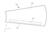
[0010]도 1은, 본 개시내용의 하나 또는 그 초과의 실시예들에 따른 기판 프로세싱 시스템의 개략적인 단면도를 도시하고;
[0011]도 2는, 본 개시내용의 하나 또는 그 초과의 실시예에 따른 기판 프로세싱 시스템의 사시도를 도시하며;
[0012]도 3은, 본 개시내용의 하나 또는 그 초과의 실시예에 따른 기판 프로세싱 시스템의 개략도를 도시하고;
[0013]도 4는, 본 개시내용의 하나 또는 그 초과의 실시예에 따른 가스 분배 조립체의 전면의 개략도를 도시하며;
[0014]도 5는, 본 개시내용의 하나 또는 그 초과의 실시예에 따른 프로세싱 챔버의 개략도를 도시하고;
[0015]도 6은, 본 개시내용의 하나 또는 그 초과의 실시예들에 따른 플라즈마 소스 조립체의 개략적인 단면도를 도시하며;
[0016]도 7은, 본 개시내용의 하나 또는 그 초과의 실시예들에 따른 차단기 플레이트의 사시도를 도시하고;
[0017]도 8은, 본 개시내용의 하나 또는 그 초과의 실시예들에 따른 차단기 플레이트의 개략적인 정면도를 도시하며;
[0018]도 9는, 본 개시내용의 하나 또는 그 초과의 실시예들에 따른 차단기 플레이트의 개략적인 정면도를 도시하고;
[0019]도 10은, 본 개시내용의 하나 또는 그 초과의 실시예들에 따른 차단기 플레이트의 개략적인 정면도를 도시하며;
[0020]도 11은, 본 개시내용의 하나 또는 그 초과의 실시예들에 따른 차단기 플레이트의 개략적인 정면도를 도시하고;
[0021]도 12는, 본 개시내용의 하나 또는 그 초과의 실시예들에 따른 차단기 플레이트의 개략적인 정면도를 도시하며;
[0022]도 13은, 본 개시내용의 하나 또는 그 초과의 실시예에 따른 틸팅식(tilted) 차단기 플레이트를 갖춘 플라즈마 소스 조립체의 개략적인 단면도를 도시하고;
[0023]도 14는, 본 개시내용의 하나 또는 그 초과의 실시예들에 따른 차단기 플레이트의 개략적인 단면도를 도시하며;
[0024]도 15는 슬롯 폭의 함수로써 플라즈마의 이온 플럭스의 그래프를 도시하고; 그리고
[0025]도 16은 슬롯 폭에 따른 플라즈마의 이온 플럭스의 그래프를 도시한다.[0009] A more specific description of the embodiments of the disclosure, briefly summarized above, may be made with reference to the embodiments in such a way that the above-enumerated features of the embodiments of the disclosure may be understood in detail, such as Some of the embodiments are illustrated in the accompanying drawings. However, it should be noted that the accompanying drawings illustrate only exemplary embodiments of the disclosure and should not be considered limiting the scope of the disclosure, as the disclosure allows for other equally effective embodiments. Because you can.
1 shows a schematic cross-sectional view of a substrate processing system according to one or more embodiments of the present disclosure;
[0011] Figure 2 shows a perspective view of a substrate processing system according to one or more embodiments of the present disclosure;
[0012] Figure 3 shows a schematic diagram of a substrate processing system according to one or more embodiments of the present disclosure;
[0013] Figure 4 shows a schematic diagram of the front of a gas distribution assembly according to one or more embodiments of the present disclosure;
[0014] Figure 5 shows a schematic diagram of a processing chamber according to one or more embodiments of the present disclosure;
[0015] Figure 6 shows a schematic cross-sectional view of a plasma source assembly according to one or more embodiments of the present disclosure;
[0016] Figure 7 shows a perspective view of a breaker plate according to one or more embodiments of the present disclosure;
[0017] Figure 8 shows a schematic front view of a breaker plate according to one or more embodiments of the present disclosure;
[0018] Figure 9 shows a schematic front view of a breaker plate according to one or more embodiments of the present disclosure;
[0019] Figure 10 shows a schematic front view of a breaker plate according to one or more embodiments of the present disclosure;
[0020] Figure 11 shows a schematic front view of a breaker plate according to one or more embodiments of the present disclosure;
[0021] Figure 12 shows a schematic front view of a breaker plate according to one or more embodiments of the present disclosure;
[0022] Figure 13 shows a schematic cross-sectional view of a plasma source assembly with a tilted blocker plate according to one or more embodiments of the present disclosure;
[0023] Figure 14 shows a schematic cross-sectional view of a breaker plate according to one or more embodiments of the present disclosure;
[0024] Figure 15 shows a graph of ion flux in the plasma as a function of slot width; and
[0025] Figure 16 shows a graph of ion flux in the plasma as a function of slot width.
[0026]본 개시내용의 실시예들은, 처리량을 최대화하고 프로세싱 효율을 개선하기 위해 연속적인 기판 증착을 위한 기판 프로세싱 시스템을 제공한다. 기판 프로세싱 시스템은 또한, 증착-전(pre-deposition) 및 증착-후(post-deposition) 플라즈마 처리들을 위해 사용될 수 있다.[0026] Embodiments of the present disclosure provide a substrate processing system for continuous substrate deposition to maximize throughput and improve processing efficiency. The substrate processing system can also be used for pre-deposition and post-deposition plasma treatments.
[0027]본 명세서 및 첨부된 청구항들에서 사용되는 바와 같이, "기판" 및 "웨이퍼"라는 용어는 상호 교환 가능하게 사용되고, 이 둘 모두는, 프로세스가 상부에서 작용하는 표면 또는 표면의 일 부분을 지칭한다. 문맥이 달리 명시적으로 표시하지 않는 한, 기판에 대한 언급은 또한, 기판의 오직 일 부분만을 지칭할 수 있다는 것이 또한, 당업자에게 이해될 것이다. 부가적으로, 기판 상에의 증착에 대한 언급은, 베어(bare) 기판 및 하나 또는 그 초과의 필름들 또는 피처들이 상부에 증착되거나 형성된 기판 둘 모두를 의미할 수 있다.[0027] As used in this specification and the appended claims, the terms “substrate” and “wafer” are used interchangeably, and both refer to a surface or portion of a surface on which a process operates. refers to It will also be understood by those skilled in the art that, unless the context clearly indicates otherwise, reference to a substrate may also refer to only a portion of the substrate. Additionally, reference to deposition on a substrate can mean both a bare substrate and a substrate on which one or more films or features have been deposited or formed.
[0028]본 명세서 및 첨부된 청구항들에서 사용되는 바와 같이, "반응성 가스", "전구체", "반응물", 등의 용어들은, 기판 표면과 반응하는 종을 포함하는 가스를 의미하기 위해 상호 교환 가능하게 사용된다. 예컨대, 제1 "반응성 가스"는 단순히 기판의 표면 상에 흡착될 수 있고, 제2 반응성 가스와의 추가적인 화학적 반응에 이용 가능할 수 있다.[0028] As used in this specification and the appended claims, the terms “reactive gas,” “precursor,” “reactant,” etc. are used interchangeably to mean a gas containing a species that reacts with the surface of a substrate. Possibly used. For example, the first “reactive gas” may simply be adsorbed on the surface of the substrate and available for further chemical reaction with the second reactive gas.
[0029]본 명세서 및 첨부된 청구항들에서 사용되는 바와 같이, "감소된 압력"이라는 용어는 약 100Torr 미만, 또는 약 75Torr 미만, 또는 약 50Torr 미만, 또는 약 25Torr 미만의 압력을 의미한다. 예컨대, 약 1Torr 내지 약 25Torr의 범위에 있는 것으로 정의된 "중간 압력"은 감소된 압력이다.[0029] As used in this specification and the appended claims, the term "reduced pressure" means a pressure of less than about 100 Torr, or less than about 75 Torr, or less than about 50 Torr, or less than about 25 Torr. For example, “medium pressure,” defined as ranging from about 1 Torr to about 25 Torr, is a reduced pressure.
[0030]회전식 플래튼 챔버들은 많은 애플리케이션들에 대해 고려되고 있다. 그러한 챔버에서, 하나 또는 그 초과의 웨이퍼들은 회전식 홀더("플래튼") 상에 배치된다. 플래튼이 회전할 때, 웨이퍼들은 다양한 프로세싱 지역들 사이에서 이동한다. 예컨대, ALD에서, 프로세싱 지역들은 웨이퍼를 전구체들 및 반응물들에 노출시킬 것이다. 부가적으로, 플라즈마 노출은 반응물로서 사용될 수 있거나, 강화된 필름 성장을 위해 기판 표면 또는 필름을 처리하는 데에 사용될 수 있거나, 필름 특성들을 수정하기 위해 사용될 수 있다. 본 개시내용의 일부 실시예들은, 회전식 플래튼 ALD 챔버를 사용하는 경우, ALD 필름들의 균일한 증착 및 후-처리(예컨대, 조밀화(densification))를 제공한다.[0030] Rotating platen chambers are being considered for many applications. In such a chamber, one or more wafers are placed on a rotating holder (“platen”). As the platen rotates, wafers move between various processing areas. For example, in ALD, processing regions will expose the wafer to precursors and reactants. Additionally, plasma exposure can be used as a reactant, to treat the substrate surface or film for enhanced film growth, or to modify film properties. Some embodiments of the present disclosure provide for uniform deposition and post-processing (e.g., densification) of ALD films when using a rotating platen ALD chamber.
[0031]회전식 플래튼 ALD 챔버들은, 전체 웨이퍼가 제1 가스에 노출되고, 퍼징되고(purged), 그리고 그런 다음에 제2 가스에 노출되는 전통적인 시간-영역(domain) 프로세스들에 의해, 또는 웨이퍼의 부분들이 제1 가스에 노출되고 이 부분들이 제2 가스에 노출되며 이러한 가스 스트림들을 통한 웨이퍼의 이동이 층을 증착시키는 공간적 ALD에 의해 필름들을 증착시킬 수 있다.[0031] Rotating platen ALD chambers are operated by traditional time-domain processes in which the entire wafer is exposed to a first gas, purged, and then exposed to a second gas, or the wafer Films can be deposited by spatial ALD in which portions of the wafer are exposed to a first gas and these portions are exposed to a second gas and movement of the wafer through these gas streams deposits the layer.
[0032]본 명세서 및 첨부된 청구항들에서 사용되는 바와 같이, "파이(pie)-형상" 및 "웨지-형상"이라는 용어들은, 대체로 부채꼴인 본체를 설명하는 데에 상호 교환 가능하게 사용된다. 예컨대, 웨지-형상 세그먼트는 원 또는 디스크-형상 구조의 부분일 수 있다. 파이-형상 세그먼트의 내측 에지는 한 지점이 될 수 있거나, 평평한 에지 또는 둥근 형태로 절단될 수 있다. 기판들의 경로는 가스 포트들에 대해 수직일 수 있다. 몇몇 실시예들에서, 가스 주입기 조립체들 각각은, 기판에 의해 횡단되는 경로에 대해 실질적으로 수직인 방향으로 연장되는 복수의 세장형 가스 포트들을 포함하고, 여기서, 가스 포트들의 전면 에지는 플래튼에 대해 실질적으로 평행하다. 본 명세서 및 첨부된 청구항들에서 사용되는 바와 같이, "실질적으로 수직"이라는 용어는, 기판들의 이동의 대체적인 방향이, 가스 포트들의 축에 대해 대략 수직(예컨대, 약 45° 내지 90°)인 평면을 따른다는 것을 의미한다. 웨지-형상 가스 포트의 경우, 가스 포트의 축은, 포트의 폭의 중간-지점으로서 정의되는, 포트의 길이를 따라 연장되는 선인 것으로 고려될 수 있다.[0032] As used in this specification and the appended claims, the terms “pie-shaped” and “wedge-shaped” are used interchangeably to describe a generally sector-shaped body. For example, a wedge-shaped segment may be part of a circular or disk-shaped structure. The inner edge of the pie-shaped segment can be a single point, or can be cut into a flat edge or rounded shape. The path of the substrates may be perpendicular to the gas ports. In some embodiments, each of the gas injector assemblies includes a plurality of elongated gas ports extending in a direction substantially perpendicular to the path traversed by the substrate, wherein the front edge of the gas ports extends in a direction substantially perpendicular to the path traversed by the substrate. is substantially parallel to As used in this specification and the appended claims, the term “substantially vertical” means that the general direction of movement of the substrates is approximately perpendicular to the axis of the gas ports (e.g., about 45° to 90°). It means following a plane. For a wedge-shaped gas port, the axis of the gas port can be considered to be a line extending along the length of the port, defined as the mid-point of the width of the port.
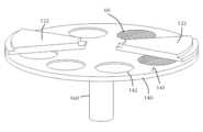
[0033]도 1은, 가스 분배 조립체(120) ― 이는 또한, 주입기들 또는 주입기 조립체로 지칭됨 ― 및 서셉터 조립체(140)를 포함하는 프로세싱 챔버(100)의 단면을 도시한다. 가스 분배 조립체(120)는 프로세싱 챔버에서 사용되는 임의의 유형의 가스 전달 디바이스이다. 가스 분배 조립체(120)는, 서셉터 조립체(140)를 대면하는 전면 표면(121)을 포함한다. 전면 표면(121)은 가스들의 유동을 서셉터 조립체(140)를 향하여 전달하기 위해 임의의 개수 또는 다양한 개구들을 가질 수 있다. 가스 분배 조립체(120)는 또한, 도시된 실시예들에서 실질적으로 둥근 외측 둘레 에지(124)를 포함한다.[0033] Figure 1 shows a cross-section of a
[0034]사용된 특정 유형의 가스 분배 조립체(120)는, 사용되는 특정 프로세스에 따라 변할 수 있다. 본 개시내용의 실시예들은 서셉터와 가스 분배 조립체 사이의 갭이 제어되는 임의의 유형의 프로세싱 시스템과 함께 사용될 수 있다. 다양한 유형들의 가스 분배 조립체들(예컨대, 샤워헤드들)이 채용될 수 있지만, 본 개시내용의 실시예들은, 복수의 실질적으로 평행한 가스 채널들을 갖는 공간적 ALD 가스 분배 조립체들에 특히 유용할 수 있다. 본 명세서 및 첨부된 청구항들에서 사용되는 바와 같이, "실질적으로 평행"이라는 용어는, 가스 채널들의 세장형 축이, 동일한 대체적인 방향으로 연장되는 것을 의미한다. 가스 채널들의 평행성에는 약간의 불완전성들이 존재할 수 있다. 복수의 실질적으로 평행한 가스 채널들은 적어도 하나의 제1 반응성 가스(A) 채널, 적어도 하나의 제2 반응성 가스(B) 채널, 적어도 하나의 퍼지 가스(P) 채널, 및/또는 적어도 하나의 진공(V) 채널을 포함할 수 있다. 제1 반응성 가스(A) 채널(들), 제2 반응성 가스(B) 채널(들), 및 퍼지 가스(P) 채널(들)로부터 유동하는 가스들은 웨이퍼의 정상부 표면을 향하여 지향된다. 가스 유동의 일부는 웨이퍼의 표면에 걸쳐 수평으로 그리고 퍼지 가스(P) 채널(들)을 통해 프로세싱 영역 밖으로 이동한다. 가스 분배 조립체의 일 단부로부터 다른 단부로 이동하는 기판은 프로세스 가스들 각각에 차례대로 노출되어, 기판 표면 상에 층을 형성할 것이다.[0034] The particular type of
[0035]몇몇 실시예들에서, 가스 분배 조립체(120)는 단일 주입기 유닛으로 만들어진 고정 강체(rigid stationary body)이다. 하나 또는 그 초과의 실시예들에서, 가스 분배 조립체(120)는, 도 2에 도시된 바와 같이, 복수의 개별 섹터들(예컨대, 주입기 유닛들(122))로 구성된다. 일체형 본체 또는 다중-섹터 본체는 설명되는 본 개시내용의 다양한 실시예들과 함께 사용될 수 있다.[0035] In some embodiments,
[0036]서셉터 조립체(140)는 가스 분배 조립체(120) 아래에 포지셔닝된다. 서셉터 조립체(140)는 정상부 표면(141), 및 정상부 표면(141)의 적어도 하나의 리세스(recess; 142)를 포함한다. 서셉터 조립체(140)는 또한, 바닥부 표면(143) 및 에지(144)를 갖는다. 리세스(142)는, 프로세싱되는 기판들(60)의 형상 및 크기에 따라 임의의 적합한 형상 및 크기일 수 있다. 도 1에 도시된 실시예에서, 리세스(142)는 웨이퍼의 바닥부를 지지하기 위해 평평한 바닥부를 갖는다; 그러나, 리세스의 바닥부는 변할 수 있다. 몇몇 실시예들에서, 리세스는, 리세스의 외측 둘레 에지 주위에, 웨이퍼의 외측 둘레 에지를 지지하도록 크기가 정해진 단차(step) 영역들을 갖는다. 단차들에 의해 지지되는 웨이퍼의 외측 둘레 에지의 양은, 예컨대, 웨이퍼의 두께 및 웨이퍼의 후면 상에 이미 존재하는 피처들의 존재에 따라 변할 수 있다.[0036] The
[0037]몇몇 실시예들에서, 도 1에 도시된 바와 같이, 서셉터 조립체(140)의 정상부 표면(141)의 리세스(142)는, 리세스(142)에서 지지되는 기판(60)이 서셉터(140)의 정상부 표면(141)과 실질적으로 동일 평면 상에 있는 정상부 표면(61)을 갖도록, 크기가 정해진다. 본 명세서 및 첨부된 청구항들에서 사용되는 바와 같이, "실질적으로 동일 평면 상에 있는"이라는 용어는, 웨이퍼의 정상부 표면과 서셉터 조립체의 정상부 표면이 ±0.2mm 내에서 동일 평면 상에 있다는 것을 의미한다. 몇몇 실시예들에서, 정상부 표면들은 ± 0.15mm, ± 0.10mm 또는 ± 0.05mm 내에서 동일 평면 상에 있다.[0037] In some embodiments, as shown in FIG. 1, the
[0038]도 1의 서셉터 조립체(140)는, 서셉터 조립체(140)를 리프팅, 하강, 및 회전시킬 수 있는 지지 기둥(post)(160)을 포함한다. 서셉터 조립체는 지지 기둥(160)의 중앙 내에 가열기, 또는 가스 라인들, 또는 전기 컴포넌트들을 포함할 수 있다. 지지 기둥(160)은 서셉터 조립체(140)와 가스 분배 조립체(120) 사이의 갭을 증가시키거나 감소시키고 서셉터 조립체(140)를 적절한 포지션 내로 이동시키는 일차 수단일 수 있다. 서셉터 조립체(140)는 또한, 서셉터 조립체(140)와 가스 분배 조립체(120) 사이에 미리 결정된 갭(170)을 생성하기 위해 서셉터 조립체(140)에 마이크로-조정들을 만들 수 있는 미세 튜닝(fine tuning) 액츄에이터들(162)을 포함할 수 있다. 몇몇 실시예들에서, 갭(170) 거리는 약 0.1mm 내지 약 5.0mm의 범위, 또는 약 0.1mm 내지 약 3.0mm의 범위, 또는 약 0.1mm 내지 약 2.0mm의 범위, 또는 약 0.2mm 내지 약 1.8mm의 범위, 또는 약 0.3mm 내지 약 1.7mm의 범위, 또는 약 0.4mm 내지 약 1.6mm의 범위, 또는 약 0.5mm 내지 약 1.5mm의 범위, 또는 약 0.6mm 내지 약 1.4mm의 범위, 또는 약 0.7mm 내지 약 1.3mm의 범위, 또는 약 0.8mm 내지 약 1.2mm의 범위, 또는 약 0.9mm 내지 약 1.1mm의 범위, 또는 약 1mm일 수 있다.[0038] The
[0039]도면들에 도시된 프로세싱 챔버(100)는, 서셉터 조립체(140)가 복수의 기판들(60)을 유지할 수 있는 캐러셀(carousel)-유형 챔버이다. 도 2에 도시된 바와 같이, 가스 분배 조립체(120)는 복수의 별개의 주입기 유닛들(122)을 포함할 수 있고, 각각의 주입기 유닛(122)은, 웨이퍼가 주입기 유닛 아래에서 이동될 때, 웨이퍼 상에 필름을 증착시킬 수 있다. 2개의 파이-형상 주입기 유닛들(122)은, 서셉터 조립체(140) 위에 그리고 서셉터 조립체(140)의 대략 대향하는 측들 상에 포지셔닝되는 것으로 도시된다. 이러한 개수의 주입기 유닛들(122)은 오직 예시적인 목적들을 위해 도시된다. 더 많은 또는 더 적은 주입기 유닛들(122)이 포함될 수 있다는 것이 이해될 것이다. 몇몇 실시예들에서, 서셉터 조립체(140)의 형상에 부합하는 형상을 형성하기 위해, 충분한 개수의 파이-형상 주입기 유닛들(122)이 존재한다. 몇몇 실시예들에서, 개별 파이-형상 주입기 유닛들(122) 각각은 다른 주입기 유닛들(122) 중 임의의 것에 영향을 주지 않고 독립적으로 이동, 제거, 및/또는 교체될 수 있다. 예컨대, 하나의 세그먼트는, 기판들(60)을 로딩/언로딩하기 위해 로봇이 서셉터 조립체(140)와 가스 분배 조립체(120) 사이의 영역에 액세싱하는 것을 허용하도록 상승될 수 있다.[0039] The
[0040]다수의 가스 주입기들을 갖는 프로세싱 챔버들은, 웨이퍼들이, 동일한 프로세스 흐름을 겪도록, 다수의 웨이퍼들을 동시적으로 프로세싱하는 데에 사용될 수 있다. 예컨대, 도 3에 도시된 바와 같이, 프로세싱 챔버(100)는 4개의 가스 주입기 조립체들 및 4개의 기판들(60)을 갖는다. 프로세싱의 착수 시에, 기판들(60)은 주입기 조립체들(30) 사이에 포지셔닝될 수 있다. 서셉터 조립체(140)를 45° 만큼 회전시키는 것(17)은 가스 분배 조립체들(120) 사이에 있는 각각의 기판(60)이 필름 증착을 위해, 가스 분배 조립체들(120) 아래에 점선 원에 의해 예시된 바와 같이, 가스 분배 조립체(120)로 이동하는 것을 초래할 것이다. 부가적인 45° 회전은 기판들(60)을 주입기 조립체들(30)로부터 멀리 이동시킬 것이다. 공간적 ALD 주입기들의 경우, 필름은, 주입기 조립체에 대한 웨이퍼의 이동 동안, 웨이퍼 상에 증착된다. 몇몇 실시예들에서, 서셉터 조립체(140)는, 기판들(60)이 가스 분배 조립체들(120) 아래에서 정지하는 것을 방지하는 증분들(increments)로 회전된다. 기판들(60)의 개수와 가스 분배 조립체들(120)의 개수는 동일하거나 상이할 수 있다. 몇몇 실시예들에서, 가스 분배 조립체들이 존재하는 것과 동일한 개수의 프로세싱되는 웨이퍼들이 존재한다. 하나 또는 그 초과의 실시예들에서, 프로세싱되는 웨이퍼들의 개수는 가스 분배 조립체들의 개수의 정수배 또는 일부이다. 예컨대, 4개의 가스 분배 조립체들이 있다면, 4x개의 프로세싱되는 웨이퍼들이 존재하고, 여기서, x는 1과 동일하거나 그 초과의 정수 값이다.[0040] Processing chambers with multiple gas injectors can be used to process multiple wafers simultaneously such that the wafers undergo the same process flow. For example, as shown in FIG. 3 ,
[0041]도 3에 도시된 프로세싱 챔버(100)는 단지 하나의 가능한 구성을 대표하고, 본 개시내용의 범위를 제한하는 것으로 취해져서는 안된다. 여기서, 프로세싱 챔버(100)는 복수의 가스 분배 조립체들(120)을 포함한다. 도시된 실시예에서, 프로세싱 챔버(100) 주위에 균일하게 이격된 4개의 가스 분배 조립체들(또한 주입기 조립체들(30)로 불림)이 존재한다. 도시된 프로세싱 챔버(100)는 8각형이지만, 당업자는, 이것이 하나의 가능한 형상이고, 본 개시내용의 범위를 제한하는 것으로 취해져서는 안된다는 것을 이해할 것이다. 도시된 가스 분배 조립체들(120)은 사다리꼴이지만, 단일 원형 컴포넌트일 수 있거나, 도 2에 도시된 것과 같이 복수의 파이-형상 세그먼트들로 구성될 수 있다.[0041] The
[0042]도 3에 도시된 실시예는 로드 록(load lock) 챔버(180), 또는 버퍼 스테이션(buffer station)과 같은 보조 챔버를 포함한다. 이러한 챔버(180)는, 예컨대, 기판들(또한 기판들(60)로 지칭됨)이 프로세싱 챔버(100)로부터 로딩/언로딩되는 것을 허용하도록, 프로세싱 챔버(100)의 측에 연결된다. 웨이퍼 로봇은, 기판을 서셉터 상에 이동시키기 위해, 챔버(180)에 포지셔닝될 수 있다.[0042] The embodiment shown in FIG. 3 includes an auxiliary chamber, such as a
[0043]캐러셀(예컨대, 서셉터 조립체(140))의 회전은 연속적이거나 불연속적일 수 있다. 연속적 프로세싱에서, 웨이퍼들은, 웨이퍼들이 주입기들 각각에 순서대로 노출되도록, 일정하게 회전한다. 불연속적 프로세싱에서, 웨이퍼들은 주입기 영역으로 이동되고 정지될 수 있고, 그런 다음에 주입기들 사이의 영역(84)으로 이동되고 정지될 수 있다. 예컨대, 캐러셀은, 웨이퍼들이 주입기-간 영역으로부터 주입기를 가로질러(또는 주입기 근처에서 정지) 그리고, 캐러셀이 다시 중지할 수 있는 다음 주입기-간 영역 상으로 이동하도록, 회전할 수 있다. 주입기들 사이에서 중지하는 것은, 각각의 층 증착 사이의 부가적인 프로세싱 단계들(예컨대, 플라즈마의 노출)을 위한 시간을 제공할 수 있다.[0043] Rotation of the carousel (e.g., susceptor assembly 140) may be continuous or discontinuous. In continuous processing, the wafers are rotated constantly such that they are exposed to each of the injectors in sequence. In discontinuous processing, wafers may be moved to an injector area and stopped, and then moved to an
[0044]도 4는, 주입기 유닛(122)으로 지칭될 수 있는, 가스 분배 조립체(220)의 섹터 또는 부분을 도시한다. 주입기 유닛들(122)은 개별적으로 또는 다른 주입기 유닛들과 조합하여 사용될 수 있다. 예컨대, 도 5에 도시된 바와 같이, 도 4의 주입기 유닛들(122) 중 4개는 단일 가스 분배 조립체(220)를 형성하도록 결합된다. (4개의 주입기 유닛들을 구별하는 선들은 명료함을 위해 도시되지 않았다.) 도 4의 주입기 유닛(122)이, 퍼지 가스 포트들(155) 및 진공 포트들(145)에 부가하여, 제1 반응성 가스 포트(125) 및 제2 반응성 가스 포트(135) 둘 모두를 갖지만, 주입기 유닛(122)은 이러한 컴포넌트들 모두를 필요로 하지는 않는다.[0044] Figure 4 shows a sector or portion of gas distribution assembly 220, which may be referred to as
[0045]도 4 및 5 둘 모두를 참조하면, 하나 또는 그 초과의 실시예에 따른 가스 분배 조립체(220)는, 각각의 섹터가 동일하거나 상이한 복수의 섹터들(또는 주입기 유닛들(122))을 포함할 수 있다. 가스 분배 조립체(220)는 프로세싱 챔버 내에 포지셔닝되고, 가스 분배 조립체(220)의 전면 표면(121)에 복수의 세장형 가스 포트들(125, 135, 145)을 포함한다. 복수의 세장형 가스 포트들(125, 135, 145, 155)은 가스 분배 조립체(220)의 내측 둘레 에지(123)에 인접한 지역으로부터, 외측 둘레 에지(124)에 인접한 지역을 향하여 연장된다. 도시된 복수의 가스 포트들은 제1 반응성 가스 포트(125), 제2 반응성 가스 포트(135), 제1 반응성 가스 포트들 및 제2 반응성 가스 포트들 각각을 둘러싸는 진공 포트(145), 및 퍼지 가스 포트(155)를 포함한다.[0045] Referring to both FIGS. 4 and 5, a gas distribution assembly 220 according to one or more embodiments includes a plurality of sectors (or injector units 122), each sector being the same or different. may include. Gas distribution assembly 220 is positioned within the processing chamber and includes a plurality of
[0046]도 4 또는 5에 도시된 실시예들을 참조하면, 포트들이 적어도 내측 둘레 영역 주위로부터 적어도 외측 둘레 영역 주위로 연장된다고 명시하지만, 포트들은 내측 영역으로부터 외측 영역으로 단지 방사상으로 연장되는 것 이상으로 연장될 수 있다. 포트들은, 진공 포트(145)가 반응성 가스 포트(125) 및 반응성 가스 포트(135)를 둘러싸는 것처럼 접선 방향으로 연장될 수 있다. 도 4 및 5에 도시된 실시예에서, 웨지 형상 반응성 가스 포트들(125, 135)은, 내측 둘레 영역 및 외측 둘레 영역에 인접한 것을 포함하여, 모든 에지들이 진공 포트(145)에 의해 둘러싸인다.[0046] Referring to the embodiments shown in Figures 4 or 5, it is specified that the ports extend from at least about the inner perimeter area to at least about the outer perimeter area, but the ports extend more than just radially from the inner area to the outer area. can be extended to The ports may extend tangentially such that
[0047]도 4를 참조하면, 기판이 경로(127)를 따라 이동할 때, 기판 표면의 각각의 부분은 다양한 반응성 가스들에 노출된다. 경로(127)를 따라가기 위해, 기판은 퍼지 가스 포트(155), 진공 포트(145), 제1 반응성 가스 포트(125), 진공 포트(145), 퍼지 가스 포트(155), 진공 포트(145), 제2 반응성 가스 포트(135), 및 진공 포트(145)에 노출 또는 이들을 "만나게(see)" 될 것이다. 따라서, 도 4에 도시된 경로(127)의 끝에서, 기판은, 층을 형성하도록, 제1 반응성 가스 포트(125) 및 제2 반응성 가스 포트(135)로부터의 가스 스트림들에 노출되었다. 도시된 주입기 유닛(122)은 사분원을 만들지만 이는 더 크거나 더 작을 수 있다. 도 5에 도시된 가스 분배 조립체(220)는, 직렬로 연결되는, 도 4의 주입기 유닛들(122) 중 4개의 주입기 유닛들의 조합으로 간주될 수 있다.[0047] Referring to Figure 4, as the substrate moves along
[0048]도 4의 주입기 유닛(122)은, 반응성 가스들을 분리시키는 가스 커튼(150)을 보여준다. "가스 커튼"이라는 용어는, 반응성 가스들이 혼합되지 않게 분리시키는 진공 또는 가스 유동들의 임의의 조합을 설명하는 데에 사용된다. 도 4에 도시된 가스 커튼(150)은 제1 반응성 가스 포트(125) 옆의 진공 포트(145)의 부분, 중간에 퍼지 가스 포트(155), 및 제2 반응성 가스 포트(135) 옆의 진공 포트(145)의 부분을 포함한다. 가스 유동 및 진공의 이러한 조합은 제1 반응성 가스 및 제2 반응성 가스의 가스 상(phase) 반응들을 방지하거나 최소화하는 데에 사용될 수 있다.[0048] The
[0049]도 5를 참조하면, 가스 분배 조립체(220)로부터의 진공 및 가스 유동들의 조합은 복수의 프로세싱 영역들(250)로의 분리를 형성한다. 프로세싱 영역들은 개개의 반응성 가스 포트들(125, 135) 주위에 개략적으로 정의되고 영역들(250) 사이에 가스 커튼(150)이 있다. 도 5에 도시된 실시예는 8개의 별개의 프로세싱 영역들(250)을 구성하고, 영역들 사이에 8개의 별개의 가스 커튼들(150)이 있다. 프로세싱 챔버는 적어도 2개의 프로세싱 영역을 가질 수 있다. 몇몇 실시예들에서, 적어도 3, 4, 5, 6, 7, 8, 9, 10, 11, 또는 12개의 프로세싱 영역들이 존재한다.[0049] Referring to FIG. 5, the combination of vacuum and gas flows from the gas distribution assembly 220 forms a separation into a plurality of
[0050]프로세싱 동안, 기판은 임의의 주어진 시간에 하나 초과의 프로세싱 영역(250)에 노출될 수 있다. 그러나, 상이한 프로세싱 영역들에 노출되는 부분들은 그 둘을 분리시키는 가스 커튼을 가질 것이다. 예컨대, 기판의 선행(leading) 에지가, 제2 반응성 가스 포트(135)를 포함하는 프로세싱 영역에 진입하는 경우, 기판의 중간 부분은 가스 커튼(150) 하에 있을 것이고, 기판의 후행(trailing) 에지는, 제1 반응성 가스 포트(125)를 포함하는 프로세싱 영역에 있을 것이다.[0050] During processing, the substrate may be exposed to more than one
[0051]예컨대, 로드 록 챔버일 수 있는 팩토리 인터페이스(280)는 프로세싱 챔버(100)에 연결된 것으로 도시된다. 기판(60)은, 기준 프레임을 제공하기 위해, 가스 분배 조립체(220) 위에 겹쳐서 도시된다. 기판(60)은 보통, 가스 분배 조립체(120)(또한, 가스 분배 플레이트로 지칭됨)의 전면 표면(121) 근처에서 유지되기 위해, 서셉터 조립체 상에 놓일 수 있다. 기판(60)은 팩토리 인터페이스(280)를 통해 프로세싱 챔버(100) 내에 기판 지지부 또는 서셉터 조립체 상에 로딩된다(도 3 참고). 기판(60)은 프로세싱 영역 내에 포지셔닝된 것으로 도시될 수 있는데, 이는, 기판이 제1 반응성 가스 포트(125)에 인접하여 그리고 2개의 가스 커튼들(150a, 150b) 사이에 로케이팅되기 때문이다. 기판(60)을 경로(127)를 따라 회전시키는 것은, 기판을 프로세싱 챔버(100) 주위에서 반-시계 방향으로 이동시킬 것이다. 따라서, 기판(60)은, 사이의 모든 프로세싱 영역들을 포함하여, 제8 프로세싱 영역(250h)을 통해 제1 프로세싱 영역(250a)에 노출될 것이다. 프로세싱 챔버 주위에서 각각의 사이클(cycle)에 대해, 도시된 가스 분배 조립체를 사용하여, 기판(60)은 제1 반응성 가스 및 제2 반응성 가스의 4개의 ALD 사이클들에 노출될 것이다.[0051]
[0052]배치 프로세서에서의 종래의 ALD 시퀀스는, 도 5의 것과 같이, 사이에 펌프/퍼지 섹션이 있는 공간적으로 분리된 주입기들로부터 각각 화학물질(A 및 B) 유동을 유지한다. 종래의 ALD 시퀀스는, 증착되는 필름의 불-균일성을 초래할 수 있는 시작 및 종료 패턴을 갖는다. 본 발명자들은 놀랍게도, 공간적 ALD 배치 프로세싱 챔버에서 수행되는 시간 기반 ALD 프로세스가, 더 높은 균일성을 갖는 필름을 제공한다는 것을 발견했다. 가스(A), 반응성 가스 없음, 가스(B), 반응성 가스 없음에 대한 노출의 기본 프로세스는, 필름에 시작 및 종료 패턴 형태를 갖는 것을 피하기 위해, 표면을 각각 화학물질(A 및 B)로 포화시키도록 주입기들 하에서 기판을 스위핑(sweep)할 것이다. 본 발명자들은 놀랍게도, 시간 기반 접근법이, 타겟 필름 두께가 얇을 때(예컨대, 20 ALD 사이클들 미만) ― 여기서, 시작 및 종료 패턴이 웨이퍼 균일성 성능에 대해 상당한 영향을 가짐 ― 특히 유리하다는 것을 발견했다. 본 발명자들은 또한, 본원에서 설명되는 바와 같은, SiCN, SiCO 및 SiCON 필름들을 생성하기 위한 반응 프로세스가 시간-영역 프로세스에 의해 달성될 수 없음을 발견했다. 프로세싱 챔버를 퍼징하는 데에 사용되는 시간의 양은 기판 표면으로부터 재료의 스트리핑(stripping)을 초래한다. 이 스트리핑은 설명된 공간적 ALD 프로세스에서는 일어나지 않는데, 이는, 가스 커튼 하에서의 시간이 짧기 때문이다.[0052] A conventional ALD sequence in a batch processor maintains chemicals (A and B) flowing from spatially separated injectors, respectively, with a pump/purge section in between, such as that of Figure 5. Conventional ALD sequences have start and end patterns that can result in non-uniformity of the deposited film. The inventors have surprisingly discovered that a time-based ALD process performed in a spatial ALD batch processing chamber provides films with higher uniformity. The basic process of exposure to gas (A), no reactive gas, and gas (B), no reactive gas, is to saturate the surface with chemicals (A and B), respectively, to avoid having start and end pattern shapes on the film. The substrate will be swept under the injectors to allow The inventors have surprisingly found that the time-based approach is particularly advantageous when the target film thickness is thin (e.g., less than 20 ALD cycles) - where the start and end pattern has a significant impact on wafer uniformity performance. . The inventors have also discovered that the reaction process for producing SiCN, SiCO and SiCON films, as described herein, cannot be achieved by a time-domain process. The amount of time used to purge the processing chamber results in stripping of material from the substrate surface. This stripping does not occur in the described spatial ALD process because the time under the gas curtain is short.
[0053]이에 따라, 본 개시내용의 실시예들은, 각각의 프로세싱 영역이 가스 커튼(150)에 의해 인접한 영역으로부터 분리되는 복수의 프로세싱 영역들(250a-250h)을 갖춘 프로세싱 챔버(100)를 포함하는 프로세싱 방법들에 관한 것이다. 예컨대, 도 5에 도시된 프로세싱 챔버. 프로세싱 챔버 내의 프로세싱 영역들 및 가스 커튼들의 개수는 가스 유동들의 어레인지먼트에 따라 임의의 적합한 개수일 수 있다. 도 5에 도시된 실시예는 8개의 가스 커튼들(150) 및 8개의 프로세싱 영역들(250a-250h)을 갖는다. 가스 커튼들의 개수는 일반적으로, 프로세싱 영역들의 개수와 동일하거나 더 크다. 예컨대, 영역(250a)이 반응성 가스 유동을 갖지 않지만 단지 로딩 지역으로서 역할을 하는 경우, 프로세싱 챔버는 7개의 프로세싱 영역들 및 8개의 가스 커튼들을 가질 것이다.[0053] Accordingly, embodiments of the present disclosure include a
[0054]복수의 기판들(60)은 기판 지지부, 예컨대, 도 1 및 2에 도시된 서셉터 조립체(140) 상에 포지셔닝된다. 복수의 기판들(60)은 프로세싱을 위해 프로세싱 영역들 주위에서 회전된다. 일반적으로, 가스 커튼들(150)은, 반응성 가스가 챔버 내로 유동하지 않는 기간들을 포함하여, 프로세싱 전반에 걸쳐 사용된다(가스 유동 및 진공 상태 유지(vacuum on)).[0054] A plurality of
[0055]제1 반응성 가스(A)가 프로세싱 영역들(250) 중 하나 또는 그 초과 내로 유동되는 동안, 제1 반응성 가스(A)가 내부에 유입되지 않는 임의의 프로세싱 영역(250) 내에 불활성 가스가 유동된다. 예컨대, 제1 반응성 가스가 프로세싱 영역(250h)을 통해 프로세싱 영역들(250b)로 유동한다면, 불활성 가스는 프로세싱 영역(250a) 내로 유동할 것이다. 불활성 가스는 제1 반응성 가스 포트(125) 또는 제2 반응성 가스 포트(135)를 통해 유동될 수 있다.[0055] While the first reactive gas (A) flows into one or more of the processing regions (250), an inert gas is formed within any processing region (250) into which the first reactive gas (A) does not flow. is in flux. For example, if the first reactive gas flows through
[0056]프로세싱 영역들 내의 불활성 가스 유동은 일정하거나 변화될 수 있다. 몇몇 실시예들에서, 반응성 가스가 불활성 가스와 함께 유동된다. 불활성 가스는 캐리어 및 희석제로서 작용할 것이다. 캐리어 가스에 비해 반응성 가스의 양이 작기 때문에, 함께 유동하는 것은, 인접한 영역들 사이의 압력의 차이들을 감소시킴으로써, 프로세싱 영역들 간의 가스 압력들을 균형맞추는(balancing) 것을 더 쉽게 만들 수 있다.[0056] The inert gas flow within the processing regions may be constant or varied. In some embodiments, the reactive gas flows together with the inert gas. The inert gas will act as a carrier and diluent. Because the amount of reactive gas is small compared to the carrier gas, flowing together can make it easier to balance gas pressures between processing regions by reducing pressure differences between adjacent regions.
[0057]본 개시내용의 몇몇 실시예들은 주입기 모듈들에 관한 것이다. 주입기 모듈들이 공간적 ALD 프로세싱 챔버에 관하여 설명되지만, 당업자들은, 모듈들이 공간적 ALD 챔버들에 제한되지 않으며, 가스 유동 균일성을 증가시키는 것이 유용한 임의의 주입기 상황에 적용 가능할 수 있다는 것을 이해할 것이다.[0057] Some embodiments of the present disclosure relate to injector modules. Although the injector modules are described with respect to a spatial ALD processing chamber, those skilled in the art will understand that the modules are not limited to spatial ALD chambers and may be applicable to any injector situation where increasing gas flow uniformity is useful.
[0058]본 개시내용의 몇몇 실시예들은 유리하게, 모듈형 플라즈마 소스들, 즉, 쉽게 프로세싱 시스템 내에 삽입될 수 있고 그로부터 제거될 수 있는 소스를 제공한다. 그러한 소스는, 소스의 하드웨어의 전부 또는 대부분이, 원자 층 증착 프로세스와 동일한 압력 레벨, 전형적으로 1-50Torr에서 동작하게 할 수 있다. 본 개시내용의 몇몇 실시예들은, 웨이퍼 포면에 걸쳐 개선된 이온 플럭스를 갖는 플라즈마 소스들을 제공한다. 하나 또는 그 초과의 실시예들은 유리하게, 많은 개수의 작은 홀들 대신에 적은 개수의 세장형 슬롯형 개구들을 사용하고, 제조하기에 상대적으로 쉬운, 플라즈마 소스들을 위한 차단기 플레이트들을 제공한다. 몇몇 실시예들은 유리하게, 기판 표면까지의 가변 거리를 갖는 틸팅식 차단기 플레이트를 사용하여, 기판 표면 위의 플라즈마 밀도의 균일성을 개선한다. 본 개시내용의 하나 또는 그 초과의 실시예들은, 전도성 재료들을 직접 플라즈마 노출로부터 보호하기 위해 유전체 슬리브(sleeve)를 제공함으로써 개선된 금속 오염을 갖는 플라즈마 소스를 제공한다.[0058] Some embodiments of the present disclosure advantageously provide modular plasma sources, ie, a source that can be easily inserted into and removed from a processing system. Such a source may allow all or most of the source's hardware to operate at the same pressure level as the atomic layer deposition process, typically 1-50 Torr. Some embodiments of the present disclosure provide plasma sources with improved ion flux across the wafer surface. One or more embodiments advantageously provide isolator plates for plasma sources that use a small number of elongated slotted openings instead of a large number of small holes and are relatively easy to manufacture. Some embodiments advantageously use a tilting blocker plate with a variable distance to the substrate surface to improve the uniformity of plasma density over the substrate surface. One or more embodiments of the present disclosure provide a plasma source with improved metal contamination by providing a dielectric sleeve to protect conductive materials from direct plasma exposure.
[0059]RF 핫 전극은 핫 전극과 접지된 전극 사이의 8.5mm 갭(갭은 3mm 내지 25mm 범위일 수 있음)에서 플라즈마를 생성한다. 전극의 상부 부분은 두꺼운 유전체(예컨대, 세라믹)에 의해 커버될 수 있고, 이는 차례대로, 접지된 표면에 의해 커버될 수 있다. RF 핫 전극 및 접지된 구조는 양호한 전도체, 예컨대, 알루미늄으로 만들어진다. 열 팽창을 수용하기 위해, 유전체(예컨대, 세라믹)의 2개의 피스들(pieces)이 RF 핫 전극의 긴 단부들에 배치된다. 예컨대, 접지된 Al 피스들은, 사이에 갭 없이, 유전체에 인접하여 배치된다. 접지된 피스들은 구조 내부로 슬라이딩할 수 있고, 스프링들에 의해 세라믹에 대하여 유지될 수 있다. 스프링들은 접지된 Al/유전체의 전체 "샌드위치"를, 어떠한 갭들 없이, RF 핫 전극에 대해 압축하여, 스퓨리어스 플라즈마(spurious plasma)의 가능성을 제거하거나 최소화한다. 이는 부분들을 함께 유지하고, 갭들을 제거하지만, 여전히, 열 팽창에 기인한 일부 슬라이딩을 허용한다.[0059] The RF hot electrode generates plasma in an 8.5 mm gap between the hot electrode and the grounded electrode (the gap can range from 3 mm to 25 mm). The upper portion of the electrode may be covered by a thick dielectric (eg ceramic), which in turn may be covered by the grounded surface. The RF hot electrode and grounded structure are made of a good conductor, such as aluminum. To accommodate thermal expansion, two pieces of dielectric (eg, ceramic) are placed at the long ends of the RF hot electrode. For example, grounded Al pieces are placed adjacent to the dielectric, with no gap in between. The grounded pieces can slide inside the structure and be held against the ceramic by springs. The springs compress the entire “sandwich” of grounded Al/dielectric against the RF hot electrode, without any gaps, eliminating or minimizing the possibility of spurious plasma. This keeps the parts together and eliminates gaps, but still allows some sliding due to thermal expansion.
[0060]플라즈마에서 발생되는 활성 종에 대한 웨이퍼의 노출은 일반적으로, 플라즈마가 홀들의 어레이를 통해 유동하는 것을 허용함으로써 달성된다. 홀들의 치수들은 웨이퍼 표면에 도달하는 활성 종의 상대적 존재비들(abundances)을 결정한다. "런 핫(run hot)"하는 홀들, 예컨대, 이웃하는 홀들을 초과하여, 대전된 입자 플럭스를 제공하는 홀들은 프로세싱에서 불-균일성을 초래할 수 있고, 웨이퍼에 대하여 프로세스 유도된 손상을 초래할 수 있다.[0060] Exposure of the wafer to active species generated in the plasma is generally achieved by allowing the plasma to flow through an array of holes. The dimensions of the holes determine the relative abundances of active species reaching the wafer surface. Holes that “run hot,” e.g., providing a flux of charged particles in excess of neighboring holes, can result in non-uniformities in processing and can result in process-induced damage to the wafer. there is.
[0061]웨이퍼 표면은 차단기 플레이트(350)의 전면 표면으로부터 임의의 적합한 거리에 있을 수 있다. 몇몇 실시예들에서, 차단기 플레이트(350)의 전면과 웨이퍼 표면 사이의 거리는 약 2mm 내지 약 16mm의 범위, 또는 약 4mm 내지 약 15mm의 범위, 또는 약 6mm 내지 약 14mm의 범위, 또는 약 8mm 내지 약 13mm의 범위, 또는 약 10mm 내지 약 13mm의 범위, 또는 약 12mm이다.[0061] The wafer surface may be at any suitable distance from the front surface of the
[0062]도 6 내지 14를 참조하면, 본 개시내용의 하나 또는 그 초과의 실시예들은 모듈형 용량 결합 플라즈마 소스들(300)에 관한 것이다. 본 명세서 및 첨부된 청구항들에서 사용되는 바와 같이, "모듈형"이라는 용어는 플라즈마 소스(300)가 프로세싱 챔버에 부착되거나 그로부터 제거될 수 있다는 것을 의미한다. 모듈형 소스는 일반적으로, 단일 인원에 의해 이동되거나, 제거되거나, 부착될 수 있다.[0062] Referring to Figures 6-14, one or more embodiments of the present disclosure relate to modular capacitively coupled plasma sources 300. As used in this specification and the appended claims, the term “modular” means that the
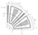
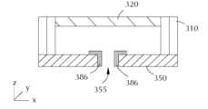
[0063]플라즈마 소스(300)는 차단기 플레이트(350) 및 가스 용적(313)을 갖춘 하우징(310)을 포함한다. 차단기 플레이트(350)는 전기적으로 접지되고, 핫 전극(320)과 함께 갭(316)에서 플라즈마를 형성한다. 차단기 플레이트(350)는 두께를 갖고, 세장형 슬롯(355)은, 갭(316)에서 점화된 플라즈마가 세장형 슬롯(355)을 통해, 갭(316)으로부터 차단기 플레이트(350)의 대향 측 상의 프로세싱 영역(314) 내로 전달되는 것을 허용하기 위해, 이 두께를 통해 연장된다. 차단기 플레이트(350)의 두께는 임의의 적합한 두께일 수 있다; 예컨대, 약 0.5mm 내지 약 10mm의 범위. 갭(316)은, 예컨대, 핫 전극(320)의 크기 또는 폭에 따라, 임의의 적합한 크기일 수 있다. 몇몇 실시예들에서, 갭(316)은 약 3mm 내지 약 25mm의 범위이다. 하나 또는 그 초과의 실시예들에서, 갭(316)은 약 4mm 내지 약 20mm의 범위, 또는 약 5mm 내지 약 15mm의 범위, 또는 약 6mm 내지 약 10mm의 범위, 또는 약 8mm 내지 약 9mm의 범위, 또는 약 8.5mm이다.[0063] The
[0064]하우징(310)은 둥근형, 사각형, 또는 세장형일 수 있고, 이는, 차단기 플레이트(350)의 면을 바라볼 때, 긴 축 및 짧은 축이 존재한다는 것을 의미한다. 예컨대, 2개의 긴 측들 및 2개의 짧은 측들을 갖는 직사각형은, 긴 측들 사이에 중간에서 연장되는 세장형 축을 갖는 세장형 형상을 생성할 것이다. 몇몇 실시예들에서, 하우징(310)은, 2개의 긴 측들, 짧은 단부, 및 긴 단부를 갖는 웨지 형상이다. 짧은 단부는 한 지점이 될 수 있고, 짧은 단부 및 긴 단부 중 어느 하나 또는 둘 모두는 직선이거나 만곡될 수 있다.[0064] The
[0065]차단기 플레이트(350)는 하우징(310)과 전기 연통한다. 도 7의 도면에 도시된 바와 같이, 몇몇 실시예들의 차단기 플레이트(350)는, 필드(356)를 정의하는, 내측 둘레 에지(351), 외측 둘레 에지(352), 제1 측(353), 및 제2 측(354)을 갖는다. 세장형 슬롯(355)은 필드(356) 내에 로케이팅되고, 차단기 플레이트(350)의 두께(357)를 통해 연장된다. 세장형 슬롯(355)은 길이(L) 및 폭(W)을 갖는다. 슬롯은 선형, 곡선형, 웨지-형상, 또는 타원 형상일 수 있다. 이와 관련하여 사용되는 바와 같이, 선형 슬롯은, 에지들 사이의 평균 거리에 대해 5% 초과만큼 변하지 않는 거리만큼 서로 이격되는 세장형 에지들을 갖는다. 슬롯이 만곡된 단부들을 갖는 경우, 슬롯의 에지들 사이의 거리는 슬롯 길이의 중간 90%에 기반하여 결정된다.[0065] The
[0066]세장형 슬롯(355)의 크기 및 형상은, 예컨대, 차단기 플레이트(350) 및/또는 하우징(310)의 크기 및 형상과 함께 변할 수 있다. 슬롯의 폭 및 길이는 플라즈마 밀도의 균일성에 영향을 줄 수 있다. 몇몇 실시예들에서, 세장형 슬롯(355)은 약 2mm 내지 약 20mm의 범위, 또는 약 3mm 내지 약 16mm의 범위, 또는 약 4mm 내지 약 12mm의 범위의 폭(W)을 갖는다. 본 발명자들은 놀랍게도, 세장형 슬롯의 측들에 인접한 플라즈마 밀도가, 슬롯의 중앙 부분의 플라즈마 밀도보다 더 크다는 것을 발견했다. 슬롯의 폭을 감소시키는 것은 플라즈마 밀도를 증가시킬 수 있다. 본 발명자들은 놀랍게도 또한, 슬롯 폭의 감소 및 플라즈마 밀도의 증가는 비-선형 관계라는 것을 발견했다.[0066] The size and shape of the
[0067]몇몇 실시예들의 세장형 슬롯(355)의 길이(L)는, 차단기 플레이트(350)의 외측 둘레 에지(352)와 내측 둘레 에지(351) 사이의 거리의 약 20% 내지 약 95%의 범위이다. 몇몇 실시예들에서, 세장형 슬롯(355)의 길이(L)는 차단기 플레이트(350)의 외측 둘레 에지(352)와 내측 둘레 에지(351) 사이의 거리의 약 30%, 40%, 50%, 60%, 70% 또는 80%보다 더 크다.[0067] The length (L) of the
[0068]차단기 플레이트(350)는, 예컨대, 차단기 플레이트(350)에 대해 기판들에 의해 이동되는 경로 및 하우징(310)의 형상에 따라, 임의의 적합한 형상일 수 있다. 몇몇 실시예들에서, 도 8에 도시된 바와 같이, 차단기 플레이트(350)는 외측 둘레 에지(352)에서보다 내측 둘레 에지(351)에서 더 협소한 폭을 갖는 웨지 형상이다. 몇몇 실시예들에서, 도 8에 도시된 바와 같이, 세장형 슬롯(355)은 차단기 플레이트(350)의 제1 측(353) 또는 제2 측(354) 중 하나에 대해 실질적으로 평행하고, 여기서는 제1 측(353)에 대해 평행한 것으로 도시된다. 본 명세서 및 첨부된 청구항들에서 사용되는 바와 같이, 이와 관련하여 사용되는 "실질적으로 평행"이라는 용어는, 언급된 측에 가장 근접한 세장형 슬롯(355)의 에지가, 언급된 측으로부터의 거리 ― 이 거리는, 슬롯과 측 사이의 평균 거리에 대해 약 20%, 15%, 10%, 또는 5%를 초과하지 않는 만큼 변함 ― 를 유지한다는 것을 의미한다. 차단기 플레이트(350)는 웨지-형상이고 세장형 슬롯(355)은 직사각형이기 때문에, 기하학적으로 슬롯은 하나 초과의 측에 대해 평행할 수 없다.[0068] The
[0069]몇몇 실시예들에서, 세장형 슬롯(355)의 길이(L)는 차단기 플레이트(350)의 제1 측(353) 및/또는 제2 측(354) 중 적어도 하나에 대해 실질적으로 평행하다. 도 9의 실시예는, 웨지-형상 차단기 플레이트(350)의 필드(356)의 중심축(357)을 따라 센터링된(centered) 웨지 형상 슬롯(355)을 도시한다. 이러한 실시예에서, 세장형 슬롯(355)의 양쪽 측들 모두는 제1 측(353) 또는 제2 측(354)에 대해 실질적으로 평행하다. 이러한 실시예의 웨지 형상 슬롯(355)은, 필드(356)의 외측 둘레 에지(352) 근처에서보다 필드(356)의 내측 둘레 에지(351) 근처에서 더 협소한 폭을 갖는다.[0069] In some embodiments, the length L of the
[0070]몇몇 실시예들에서, 세장형 슬롯의 어느 측도 차단기 플레이트의 제1 측 또는 제2 측에 대해 평행하지 않는다. 예컨대, 직사각형 세장형 슬롯을 갖는 직사각형 차단기 플레이트(350)는, 차단기 플레이트의 제1 측 및 제2 측 둘 모두에 대해 실질적으로 평행한 세장형 슬롯의 양쪽 측들 모두를 가질 수 있다. 유사하게, 직사각형 슬롯이 차단기 플레이트의 폭의 중심선으로부터 비뚤어지면, 세장형 슬롯은 차단기 플레이트의 어느 측에 대해서도 평행하지 않을 것이다.[0070] In some embodiments, neither side of the elongated slot is parallel to the first or second side of the breaker plate. For example, a
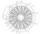
[0071]세장형 슬롯들(355)의 개수는 변할 수 있다. 몇몇 실시예들에서, 제1 세장형 슬롯(355)이 필드(356)에 존재하고, 제2 세장형 슬롯(365)이 필드(356)에 존재한다. 도 10에 도시된 실시예에서, 차단기 플레이트(350)는 제1 세장형 슬롯(355), 제2 세장형 슬롯(365), 및 제3 세장형 슬롯(375)을 포함하는 필드(356)를 갖는다. 세장형 슬롯들(355, 365, 375) 각각은 웨지 형상이지만, 웨지 형상이거나 직사각형일 수 있다.[0071] The number of
[0072]도 11은, 필드(356)가 제1 세장형 슬롯(355) 및 제2 세장형 슬롯(365)을 갖는 다른 실시예를 도시한다. 이러한 세장형 슬롯들 둘 모두는 직사각형이고, 각각은 차단기 플레이트의 상이한 측에 대해 실질적으로 평행하다. 이와 관련하여 사용되는 바와 같이, "직사각형"은 일반적으로 직사각형 형상을 의미하고, 직각들이 존재하지 않도록 단부들의 라운딩(rounding)을 허용한다. 제1 세장형 슬롯(355)은 차단기 플레이트(350)의 제1 측(353) 또는 제2 측(354) 중 하나에 대해 실질적으로 평행할 수 있고, 제2 세장형 슬롯(365)은 제1 측(353) 및 제2 측(354) 중 다른 하나에 대해 실질적으로 평행할 수 있다. 도시된 실시예에서, 제1 세장형 슬롯(355)은 제1 측(353)에 대해 실질적으로 평행하고, 제2 세장형 슬롯(365)은 제2 측(354)에 대해 실질적으로 평행하다.[0072] Figure 11 shows another embodiment where the
[0073]다수의 세장형 슬롯들이 차단기 플레이트(350)에 포함되는 경우, 슬롯들 각각의 길이들은 다른 슬롯들의 길이와 동일할 수 있거나 상이할 수 있다. 도 10의 실시예는 대략 동일한 길이의 3개의 세장형 슬롯들을 갖지만, 도 11은 제2 슬롯보다 더 긴 제1 슬롯을 도시한다. 몇몇 실시예들에서, 제2 세장형 슬롯은, 제1 세장형 슬롯과 상이한 길이인 경우, 제1 세장형 슬롯의 약 20% 내지 약 80%의 범위의 길이를 갖는다.[0073] If multiple elongated slots are included in the
[0074]도 12는 3개의 세장형 슬롯들이 있는 차단기 플레이트(350)의 또다른 실시예를 도시한다. 여기서, 제1 세장형 슬롯(355), 제2 세장형 슬롯(365), 및 제3 세장형 슬롯(375) 각각은 상이한 길이들을 갖는다. 몇몇 실시예들에서, 제1 세장형 슬롯(355)은 차단기 플레이트(350)의 제1 측(353)에 대해 실질적으로 평행하고 그에 인접한다. 제2 세장형 슬롯(365)은 차단기 플레이트(350)의 제2 측(354)에 대해 실질적으로 평행하고 그에 인접한다. 제2 세장형 슬롯(365)의 길이는 제1 세장형 슬롯(355)의 길이의 약 20% 내지 약 80%의 범위이다. 제3 세장형 슬롯(375)은 제1 세장형 슬롯(355)과 제2 세장형 슬롯(365) 사이에 있고, 제2 세장형 슬롯(365)의 길이의 약 20% 내지 약 80%의 범위의 길이를 갖는다. 제3 세장형 슬롯(375)은 제2 측(354)에 대해 실질적으로 평행한 것으로 도시되지만, 상이하게 배향될 수 있다.[0074] Figure 12 shows another embodiment of a
[0075]선형 슬롯은, 기판의 회전이 외측 에지 근처에서 짧은 노출을 초래하는 동안, 내측 둘레 에지에서 외측 둘레 에지 방향으로 더 균일한 플라즈마 밀도를 제공하는 것으로 관찰되었다. 웨지 형상 슬롯은, 외측 에지 근처에서 노출 시간을 증가시키는 것으로 밝혀졌지만, 길이에 따른 플라즈마 밀도에 더 많은 변화를 가질 수 있다. 다수의 선형 슬롯들을 갖는 것은, 외측 에지 근처에서 플라즈마 노출을 증가시키는 데에 사용될 수 있지만, 더 짧은 슬롯들이 시작되는 곳에서 플라즈마 밀도의 현저한 증가를 가질 수 있다. 선형 슬롯들에 대한 장점은, 필요하다면, 부가적인 슬롯들이 플라즈마 노출을 증가시키는 데에 사용될 수 있다는 점이다.[0075] The linear slot was observed to provide a more uniform plasma density from the inner circumferential edge to the outer circumferential edge, while rotation of the substrate resulted in a shorter exposure near the outer edge. Wedge shaped slots have been found to increase exposure time near the outer edges, but may have more variation in plasma density along their length. Having multiple linear slots can be used to increase plasma exposure near the outer edge, but can have a significant increase in plasma density where the shorter slots begin. The advantage over linear slots is that additional slots can be used to increase plasma exposure, if needed.
[0076]선형 슬롯들과 웨지 형상 슬롯들을 혼합하는 것은 플라즈마 밀도 및 균일성을 개선할 수 있다. 몇몇 실시예들에서, 제1 슬롯은 선형이고 제2 슬롯은 역전된 웨지 형상으로 더 짧다. 이와 관련하여 사용되는 바와 같이, 역전된 웨지 형상은 슬롯의 내측 단부가 슬롯의 외측 단부보다 더 넓다는 것을 의미한다. 이론에 구속됨 없이, 제2 슬롯의 시작에서의 플라즈마 밀도의 증가는, 이러한 포지션에서, 역전된 웨지 형상의 에지들이 서로 더 멀리 떨어져 있을 것이기 때문에, 선형 슬롯이 사용된 경우에 더 작을 것으로 여겨진다.[0076] Mixing linear slots and wedge-shaped slots can improve plasma density and uniformity. In some embodiments, the first slot is linear and the second slot is shorter with an inverted wedge shape. As used in this context, an inverted wedge shape means that the inner end of the slot is wider than the outer end of the slot. Without being bound by theory, it is believed that the increase in plasma density at the start of the second slot will be smaller if a linear slot is used because, in this position, the edges of the inverted wedge shape will be further apart from each other.
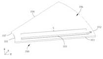
[0077]차단기 플레이트(350)는 서셉터 조립체(140)의 정상부 표면(141)에 대해 실질적으로 평행할 수 있거나, 틸팅될 수 있다. 도 13은, 차단기 플레이트(350)의 내측 둘레 단부(351)가 서셉터 조립체(140)의 정상부 표면(141)에 대해 차단기 플레이트(350)의 외측 둘레 단부(352)보다 더 높은 실시예를 도시한다. 차단기 플레이트(350)가 기판(60)에 인접하여 포지셔닝될 때, 내측 둘레 단부(351)는 기판(60)으로부터 외측 둘레 단부(352)보다 더 멀리에 있다. 이론에 구속됨 없이, 차단기 플레이트(350)를 웨이퍼 표면에 대해 틸팅하는 것은, 표면까지의 거리에 따라 웨이퍼 위의 플라즈마 밀도를 변화시키는 것으로 여겨진다. 내측 에지 근처에서보다 외측 에지 근처에서의 더 많은 이온들이 웨이퍼에 충돌할 수 있고, 내측 에지로부터 외측 에지까지 플라즈마에 대한 노출을 균일하게 하는 데에 사용될 수 있다.[0077] The
[0078]도 14를 참조하면, 몇몇 실시예들에서, 세장형 슬롯(355)은 유전체 재료(386)로 라이닝된다(lined). 이론에 구속됨 없이, 슬롯을 유전체로 라이닝하는 것은, 슬롯 주위의 금속이 플라즈마에 직접적으로 노출되는 것을 방지함으로써 금속 오염을 개선한다고 여겨진다. 이는, 슬롯(355)의 에지로부터 금속 차단기 플레이트(350)의 스퍼터링을 방지하거나 최소화하는 것을 도울 수 있고 금속 오염을 감소시킬 수 있다. 유전체 재료(386)는 차단기 플레이트의 전면 표면에 인접한 플라즈마 강도/밀도를 감소시키는 것으로 여겨진다. 유전체 재료는 프로세스 케미스트리(chemistry)와 양립 가능한 임의의 적합한 유전체 또는 낮은 스퍼터 재료일 수 있다.[0078] Referring to Figure 14, in some embodiments,
[0079]다시 도 6을 참조하면, 플라즈마 소스(300)는 RF 핫 전극(320)을 포함한다. 이러한 전극(320)은 또한 "핫 전극", "RF 핫", 등으로 지칭된다. 세장형 RF 핫 전극(320)은 전면(321), 후면(322), 및 세장형 측들(323)을 갖는다. 핫 전극(320)은 또한, 세장형 축을 정의하는, 제1 단부(324) 및 제2 단부(325)를 포함한다. 세장형 RF 핫 전극(320)은, 갭(316)이 차단기 플레이트(350)와 핫 전극(320)의 전면(321) 사이에 형성되도록, 차단기 플레이트(350)로부터 이격된다. 세장형 RF 핫 전극(320)은, 알루미늄을 포함하는(그러나 이에 제한되지 않음) 임의의 적합한 전도성 재료로 만들어질 수 있다.[0079] Referring again to FIG. 6, the
[0080]몇몇 실시예들은 RF 핫 전극(320)의 제1 단부(324) 및 제2 단부(325) 중 하나 또는 그 초과와 접촉하는 단부 유전체(330)를 포함한다. 단부 유전체(330)는, 핫 전극(320)을 전기 접지로부터 전기적으로 분리시키기 위해, 플라즈마 소스(300)의 측벽(311)과 RF 핫 전극(320) 사이에 포지셔닝된다. 하나 또는 그 초과의 실시예들에서, 단부 유전체(330)는 핫 전극(320)의 제1 단부(324) 및 제2 단부(325) 둘 모두와 접촉한다. 단부 유전체(330)는, 세라믹을 포함하는(그러나 이에 제한되지 않음) 임의의 적합한 유전체 재료로 만들어질 수 있다. 도면들에 도시된 단부 유전체(330)는 L-형상이지만, 임의의 적합한 형상이 사용될 수 있다.[0080] Some embodiments include an
[0081]슬라이딩 접지 연결부(340)는 측들 또는 RF 핫 전극(320)의 제1 단부(324) 및 제2 단부(325) 중 하나 또는 그 초과에 포지셔닝될 수 있다. 슬라이딩 접지 연결부(340)는 핫 전극(320)으로부터 단부 유전체(330)의 대향 측 상에 포지셔닝된다. 슬라이딩 접지 연결부(340)는 단부 유전체(330)에 의해 RF 핫 전극(320)과의 직접 접촉으로부터 분리된다. 슬라이딩 접지 연결부(340) 및 단부 유전체(330)는, 기밀 밀봉을 유지하고 그리고 전극의 측 주위에서 가스들의 누설을 허용하지 않으면서 핫 전극(320)이 팽창하는 것을 허용하도록 협동한다. 슬라이딩 접지 연결부(340)는 전도성 재료이고, 알루미늄을 포함하는(그러나 이에 제한되지 않음) 임의의 적합한 재료로 만들어질 수 있다. 슬라이딩 접지 연결부(340)는, 전기장이 존재하지 않는 것을 보장하여, 단부 유전체(330)의 측에 대한 누설 플라즈마의 가능성을 최소화하기 위해, 단부 유전체(330)의 측에 접지된 단자부를 제공한다.[0081] The sliding
[0082]밀봉 포일(foil)(342)이 단부 유전체(330)로부터 대향 측 상에서 슬라이딩 접지 연결부(340)에 포지셔닝될 수 있다. 밀봉 포일(342)은, 슬라이딩 접지 연결부(340)가 하우징(310)의 차단기 플레이트(350) 상에서 슬라이딩할 때, 차단기 플레이트(350)와 슬라이딩 접지 연결부(340) 사이에 전기 연결을 형성한다. 밀봉 포일(342)은, 알루미늄을 포함하는(그러나 이에 제한되지 않음) 임의의 적합한 전도성 재료로 만들어질 수 있다. 밀봉 포일(342)은, 슬라이딩 접지 연결부와 전면 사이의 전기 연결이 유지되는 한 핫 전극(320)의 팽창 및 수축을 통해 이동할 수 있는 얇은 가요성 재료일 수 있다.[0082] A sealing foil 342 may be positioned at the sliding
[0083]클램프 면 및 너트(344)가, 핫 전극(320)의 단부, 단부 유전체(330), 슬라이딩 접지 연결부(340), 및 밀봉 포일(342) 조합에 포지셔닝될 수 있다. 플라즈마 소스의 크기 및 형상에 따라, 다른 클램프 면들 및 너트들은 이러한 조합의 임의의 측에서 발견될 수 있고, 다수가 이러한 조합의 각각의 측을 따라서 발견될 수 있다. 클램프 면 및 너트는, 플라즈마 가스들이 핫 전극(320) 뒤에 도달하는 것을 허용할 수 있는, 슬라이딩 접지 연결부(340)와 단부 유전체(330) 사이에 기밀 밀봉을 형성하여 분리를 방지하기 위해, 내측으로 지향되는 압력을 컴포넌트들의 조합에 제공한다. 클램프 면 및 너트(344)는, 알루미늄 및 스테인리스 강을 포함하는(그러나 이에 제한되지 않음) 임의의 적합한 재료로 만들어질 수 있다.[0083] The clamp face and
[0084]몇몇 실시예들에서, 유전체 스페이서(370)가 세장형 RF 핫 전극(320)의 후면(322)에 인접하여 포지셔닝된다. 유전체 스페이서(370)는, 세라믹 재료들을 포함하는(그러나 이에 제한되지 않음) 임의의 적합한 유전체 재료로 만들어질 수 있다. 유전체 스페이서(370)는 RF 핫 전극(320)과 하우징(310)의 정상부 부분 사이에 비-전도성 분리기를 제공한다. 이러한 비-전도성 분리기가 없으면, RF 핫 전극(320)과 하우징(310) 사이의 용량 결합에 기인하여 플라즈마가 가스 용적(313)에 형성될 수 있는 가능성이 존재한다.[0084] In some embodiments, the
[0085]유전체 스페이서(370)는 임의의 적합한 두께일 수 있고, 임의의 개수의 개별 층들로 이루어질 수 있다. 도 6에 도시된 실시예에서, 유전체 스페이서(370)는 하나의 층으로 이루어지지만, 유전체 스페이서(370)의 총 두께를 구성하는 다수의 층들이 사용될 수 있다. 개별 서브(sub)-층들 각각은 동일한 두께일 수 있거나, 각각은 독립적으로 결정되는 두께를 가질 수 있다.[0085]
[0086]유전체 스페이서(370) 위에서는, 몇몇 실시예들에서, 접지된 플레이트(380)가 하우징(310) 내에 그리고 RF 핫 전극(320)으로부터 유전체 스페이서(370)의 대향 측 상에 포지셔닝된다. 접지된 플레이트(380)는, 알루미늄을 포함하는(그러나 이에 제한되지 않음) 임의의 적합한 전기 전도성 재료로 만들어지고, 전기 접지에 연결될 수 있다. 이러한 접지된 플레이트(380)는, 플라즈마가 형성되도록 의도되는 갭(316) 이외의 영역에서의 또는 가스 용적(313)에서의 플라즈마 형성을 방지하기 위해, RF 핫 전극(320)을 가스 용적(313)으로부터 추가적으로 분리시킨다.[0086] Above the
[0087]도면들은, 접지된 플레이트(380)가, 유전체 스페이서(370)와 대략 동일한 두께이거나 개별 유전체 스페이서 층들의 합인 것으로 도시하지만, 이는 단지 하나의 가능한 실시예일 뿐이다. 접지된 플레이트(380)의 두께는 플라즈마 소스의 특정 구성에 따라 임의의 적합한 두께일 수 있다. 몇몇 실시예들에서, 접지된 플레이트의 두께는, 예컨대, 가스 홀들의 드릴링을 더 쉽게 만들기에 충분히 얇지만, 언급된 다양한 스프링들의 힘들을 견디기에 충분히 두꺼운 것에 기반하여 선택된다. 부가적으로, 접지된 플레이트(380)의 두께는, 전형적으로 용접 연결인 동축 피드(coaxial feed)가 적절하게 부착되는 것을 보장하도록 튜닝될 수 있다.[0087] The figures show grounded
[0088]본 개시내용의 몇몇 실시예들은 복수의 압축 엘리먼트들(382)을 포함한다. 압축 엘리먼트들(382)은 힘을, 접지된 플레이트(380)의 후면 표면(381)에 대해 RF 핫 전극(320)의 방향으로 지향시킨다. 압축력은, 접지된 플레이트(380), 유전체 스페이서(370), 및 RF 핫 전극(320)이, 각각의 인접한 컴포넌트 사이의 임의의 간격을 최소화하거나 제거하기 위해, 함께 가압되게 한다. 압축력은, 가스들이, 가스들이 누설 플라즈마가 될 수 있는 RF 핫 전극인 공간 내로 유동하는 것을 방지하는 것을 돕는다. 적합한 압축 엘리먼트들(382)은, 접지된 플레이트(380)의 후면 표면(381)에 특정 힘을 제공하기 위해 조정되거나 튜닝될 수 있는 것들이고, 스프링들 및 스크류들을 포함하지만 이제 제한되지 않는다.[0088] Some embodiments of the present disclosure include a plurality of
[0089]동축 RF 피드 라인(360)은 세장형 하우징(310)을 통과하고, 갭(316)에서 플라즈마를 발생시키기 위해 전력을 RF 핫 전극(320)에 제공한다. 동축 RF 피드 라인(360)은, 절연체(366)에 의해 분리된 외측 전도체(362) 및 내측 전도체(364)를 포함한다. 외측 전도체(362)는 전기 접지와 전기 연통하고, 내측 전도체(364)는 세장형 RF 핫 전극(320)과 전기 연통한다. 본 명세서 및 첨부된 청구항들에서 사용되는 바와 같이, "전기 연통"이라는 용어는, 컴포넌트들이, 전기 저항이 거의 없도록, 중간 컴포넌트를 통해 또는 직접적으로 연결되는 것을 의미한다.[0089] A coaxial
[0090]동축 RF 피드는, 외측 전도체가 접지 플레이트 상에서 종결되도록 구성될 수 있다. 내측 전도체는 RF 핫 전극 상에서 종결될 수 있다. 피드가 대기압에 있는 경우, O-링들은, 소스 내부의 중간 압력을 가능하게 하기 위해, 피드 구조의 바닥부에 포지셔닝될 수 있다. 몇몇 실시예들에서, 가스는 동축 피드의 외부 둘레 주위의 소스로 피딩된다.[0090] A coaxial RF feed can be configured such that the outer conductor terminates on a ground plate. The inner conductor may terminate on an RF hot electrode. If the feed is at atmospheric pressure, O-rings can be positioned at the bottom of the feed structure to enable intermediate pressure inside the source. In some embodiments, gas is fed to a source around the outer perimeter of the coaxial feed.
[0091]가스가 플라즈마 용적에 도달하도록, 접지 플레이트, 두꺼운 세라믹, 및 RF 핫 전극이 스루 홀들로 천공될 수 있다. 홀들의 크기는 홀들 내부에서의 점화를 방지하기에 충분히 작을 수 있다. 접지 플레이트 및 RF 핫 전극의 경우, 몇몇 실시예들의 홀 직경은 <1mm, 예컨대, 약 0.5mm이다. 유전체 내부의 높은 전기장들은 홀들에서의 누설 플라즈마의 가능성을 제거하거나 최소화하는 것을 도울 수 있다.[0091] The ground plate, thick ceramic, and RF hot electrode can be drilled with through holes to allow the gas to reach the plasma volume. The size of the holes may be small enough to prevent ignition within the holes. For the ground plate and RF hot electrode, the hole diameter in some embodiments is <1 mm, such as about 0.5 mm. High electric fields within the dielectric can help eliminate or minimize the possibility of leakage plasma in the holes.
[0092]RF 피드는 동축 전달 라인의 형태일 수 있다. 외측 전도체는 접지된 플레이트에 연결되거나 그에서 종결될 수 있고, 내측 전도체는 RF 핫 전극에 연결되거나 그에서 종결될 수 있다. 접지된 플레이트는, 금속 가스켓을 포함하는(그러나 이에 제한되지 않음) 임의의 적합한 방법에 의해 금속 인클로저 또는 하우징에 연결될 수 있다. 이는, 복귀 전류들(return currents)의 대칭 기하학적 구조를 보장하는 것을 돕는다. 모든 복귀 전류들은 피드의 외측 도체 위로 흘러 RF 노이즈를 최소화한다.[0092] The RF feed may be in the form of a coaxial transmission line. The outer conductor may be connected to or terminated in a grounded plate, and the inner conductor may be connected to or terminated in an RF hot electrode. The grounded plate may be connected to the metal enclosure or housing by any suitable method, including but not limited to a metal gasket. This helps ensure a symmetrical geometry of the return currents. All return currents flow over the outer conductors of the feed to minimize RF noise.
[0093]몇몇 실시예들에서, RF 피드는 핫 플레이트에 대칭적 RF 피드 전류를, 그리고 대칭적 복귀 전류들을 제공하도록 설계된다. 모든 복귀 전류들은 외측 전도체 위로 흘러 RF 노이즈를 최소화하고, 동작시 소스 설치의 영향을 최소화한다.[0093] In some embodiments, the RF feed is designed to provide symmetrical RF feed currents and symmetrical return currents to the hot plate. All return currents flow over the outer conductors to minimize RF noise and minimize the effect of source installation on operation.
[0094]본 개시내용의 부가적인 실시예들은, 기판을 프로세싱 챔버에, 플라즈마 소스 조립체의 차단기 플레이트에 인접하여 포지셔닝하는 것을 포함하는 방법들에 관한 것이다. 차단기 플레이트는 본원에서 설명되는 다양한 실시예들 중 임의의 것이다. 그런 다음에, 플라즈마가 플라즈마 소스에서 발생되고, 차단기 플레이트의 슬롯(들)을 통해 기판을 향하여 유동하는 것이 허용된다.[0094] Additional embodiments of the present disclosure relate to methods that include positioning a substrate in a processing chamber adjacent a blocker plate of a plasma source assembly. The breaker plate is any of the various embodiments described herein. The plasma is then generated at the plasma source and allowed to flow through the slot(s) in the breaker plate toward the substrate.
[0095]예들[0095] Examples
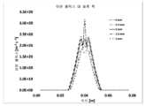
[0096]다양한 폭의 슬롯들을 갖춘 차단기 플레이트들을 사용하는 플라즈마 조립체들이 이온 플럭스 균일성에 대해 분석되었다. 도 15 및 16은 슬롯 폭에 따른 플라즈마의 이온 플럭스의 그래프들을 도시한다. 이러한 연구들을 위해 200W, 13.5MHz의 아르곤 플라즈마가 사용되었다. 19mm, 10mm, 6mm, 4mm, 3.5mm, 3mm, 2.5mm 및 2mm 의 슬롯 폭들을 갖는 차단기 플레이트들이 분석되었다. 넓은 슬롯들의 경우, 플라즈마 밀도는 슬롯의 에지들 근처에서 피크를 이룬다는 것이 밝혀졌다. 더 큰 슬롯 폭들에서, 도 15에서 보이는 바와 같이, 이온 플럭스에서 2개의 피크들이 관찰되었다. 슬롯 폭이 감소됨에 따라, 도 15의 2mm 슬롯에서 보이는 바와 같이, 슬롯 개구부 근처의 플라즈마 피크들이 병합될 때 플라즈마 밀도는 증가했다. 추가적인 연구들은, 도 16에 도시된 바와 같이, 슬롯이 약 3mm의 폭을 가졌을 때 이온 플럭스가 2개의 피크들로부터 단일 피크로 전이되었음을 나타내었다.[0096] Plasma assemblies using breaker plates with slots of various widths were analyzed for ion flux uniformity. Figures 15 and 16 show graphs of ion flux in the plasma as a function of slot width. For these studies, 200 W, 13.5 MHz argon plasma was used. Isolator plates with slot widths of 19 mm, 10 mm, 6 mm, 4 mm, 3.5 mm, 3 mm, 2.5 mm and 2 mm were analyzed. It has been found that for wide slots, the plasma density peaks near the edges of the slot. At larger slot widths, two peaks were observed in the ion flux, as shown in Figure 15. As the slot width decreased, the plasma density increased as the plasma peaks near the slot opening merged, as seen for the 2 mm slot in Figure 15. Additional studies showed that the ion flux transitioned from two peaks to a single peak when the slot had a width of about 3 mm, as shown in Figure 16.
[0097]본 개시내용의 몇몇 실시예들은, 프로세싱 챔버에서 아치형 경로를 따라 포지셔닝되는 적어도 하나의 용량 결합 웨지-형상 플라즈마 소스(100)를 포함하는 프로세싱 챔버들에 관한 것이다. 본 명세서 및 첨부된 청구항들에서 사용되는 바와 같이, "아치형 경로"라는 용어는, 원-형상 또는 타원-형상 경로의 적어도 부분을 이동하는 임의의 경로를 의미한다. 아치형 경로는, 적어도 약 5°, 10°, 15°, 20°의 경로의 부분을 따른 기판의 이동을 포함할 수 있다.[0097] Some embodiments of the present disclosure relate to processing chambers including at least one capacitively coupled wedge-shaped
[0098]본 개시내용의 부가적인 실시예들은 복수의 기판들을 프로세싱하는 방법들에 관한 것이다. 복수의 기판들은 프로세싱 챔버에서 기판 지지부 상에 로딩된다. 기판 지지부는, 기판 상에 필름을 증착시키기 위해 복수의 기판들 각각을 가스 분배 조립체를 가로질러 지나가게 하기 위해 회전된다. 기판 지지부는, 플라즈마 영역에서 실질적으로 균일한 플라즈마를 발생시키는 용량 결합 파이-형상 플라즈마 소스에 인접한 플라즈마 영역으로 기판들을 이동시키기 위해 회전된다. 이는, 미리 결정된 두께의 필름이 형성될 때까지 반복된다.[0098] Additional embodiments of the present disclosure relate to methods of processing multiple substrates. A plurality of substrates are loaded onto a substrate support in a processing chamber. The substrate support is rotated to pass each of the plurality of substrates across the gas distribution assembly to deposit a film on the substrate. The substrate support is rotated to move the substrates into the plasma region adjacent to a capacitively coupled pie-shaped plasma source that generates a substantially uniform plasma in the plasma region. This is repeated until a film of predetermined thickness is formed.
[0099]캐러셀의 회전은 연속적 또는 불연속적일 수 있다. 연속적 프로세싱에서, 웨이퍼들은, 웨이퍼들이 주입기들 각각에 대해 순서대로 노출되도록, 일정하게 회전한다. 불연속적 프로세싱에서, 웨이퍼들은 주입기 영역으로 이동되고 정지될 수 있고, 그런 다음에 주입기들 사이의 영역으로 이동되고 정지될 수 있다. 예컨대, 캐러셀은, 웨이퍼들이 주입기-간 영역으로부터 주입기를 가로질러(또는 주입기 근처에서 정지) 그리고, 캐러셀이 다시 중지할 수 있는 다음 주입기-간 영역 상으로 이동하도록, 회전할 수 있다. 주입기들 사이에서 중지하는 것은, 각각의 층 증착 사이의 부가적인 프로세싱(예컨대, 플라즈마에 대한 노출)을 위한 시간을 제공할 수 있다.[0099] Rotation of the carousel may be continuous or discontinuous. In continuous processing, the wafers are rotated constantly so that they are exposed to each of the implanters in sequence. In discontinuous processing, wafers can be moved to an injector area and stopped, and then moved to an area between the injectors and stopped. For example, the carousel can rotate so that wafers move from the inter-injector region, across the injector (or stop near the injector), and onto the next inter-injector region where the carousel can stop again. Pausing between injectors can provide time for additional processing (eg, exposure to plasma) between each layer deposition.
[0100]플라즈마의 주파수는 사용되는 특정 반응성 종에 따라 튜닝될 수 있다. 적합한 주파수들은 400kHz, 2MHz, 13.56MHz, 27MHz, 40MHz, 60MHz 및 100MHz를 포함하지만 이에 제한되지 않는다.[0100] The frequency of the plasma can be tuned depending on the specific reactive species used. Suitable frequencies include, but are not limited to, 400 kHz, 2 MHz, 13.56 MHz, 27 MHz, 40 MHz, 60 MHz, and 100 MHz.
[0101]하나 또는 그 초과의 실시예들에 따르면, 기판은 층을 형성하기 전에 그리고/또는 후에 프로세싱을 겪는다. 이러한 프로세싱은 동일한 챔버에서 또는 하나 또는 그 초과의 별개의 프로세싱 챔버들에서 수행될 수 있다. 몇몇 실시예들에서, 기판은 추가적인 프로세싱을 위해, 제1 챔버로부터 별개의 제2 챔버로 이동된다. 기판은 제 1 챔버로부터 별개의 프로세싱 챔버로 직접적으로 이동될 수 있거나, 또는 기판은 제 1 챔버로부터 하나 또는 그 초과의 이송 챔버들로 이동될 수 있고, 그런 다음에 별개의 프로세싱 챔버로 이동될 수 있다. 따라서, 프로세싱 장치는 이송 스테이션과 연통하는 다수의 챔버들을 포함할 수 있다. 이러한 종류의 장치는 "클러스터 툴" 또는 "클러스터링된 시스템", 등으로 지칭될 수 있다.[0101] According to one or more embodiments, the substrate undergoes processing before and/or after forming the layer. This processing may be performed in the same chamber or in one or more separate processing chambers. In some embodiments, the substrate is moved from the first chamber to a separate second chamber for further processing. The substrate may be moved directly from the first chamber to a separate processing chamber, or the substrate may be moved from the first chamber to one or more transfer chambers and then moved to the separate processing chamber. there is. Accordingly, the processing device may include multiple chambers in communication with the transfer station. This type of device may be referred to as a “cluster tool” or “clustered system”, etc.
[0102]일반적으로, 클러스터 툴은, 기판 중심-검색(center-finding) 및 배향, 탈기(degassing), 어닐링(annealing), 증착, 및/또는 에칭을 포함하는 다양한 기능들을 수행하는 다수의 챔버들을 포함하는 모듈형 시스템이다. 하나 또는 그 초과의 실시예들에 따르면, 클러스터 툴은 적어도 제1 챔버 및 중앙 이송 챔버를 포함한다. 중앙 이송 챔버는, 기판들을 프로세싱 챔버들과 로드 록 챔버들 사이에서 왕복시킬 수 있는 로봇을 수납할 수 있다. 이송 챔버는 전형적으로, 진공 조건에서 유지되며, 기판들을 하나의 챔버로부터 다른 챔버로 그리고/또는 클러스터 툴의 전면 단부에 포지셔닝된 로드 록 챔버로 왕복시키기 위한 중간 스테이지를 제공한다. 본 개시내용을 위해 이루어질 수 있는 2개의 잘-알려진 클러스터 툴들은 Centura® 및 Endura®이며, 양자 모두 캘리포니아주 산타 클라라의 Applied Materials, Inc.로부터 입수 가능하다. 그러나, 정확한 어레인지먼트 및 챔버들의 조합은, 본원에 설명되는 바와 같은 프로세스의 특정 단계들을 수행할 목적을 위해 변경될 수 있다. 사용될 수 있는 다른 프로세싱 챔버들은, CLD(cyclical layer deposition), ALD(atomic layer deposition), CVD(chemical vapor deposition), PVD(physical vapor deposition), 에칭, 사전-세정(pre-clean), 화학적 세정, RTP와 같은 열처리, 플라즈마 질화(nitridation), 탈기, 배향, 수산화, 및 다른 기판 프로세스들을 포함하지만, 이에 제한되지는 않는다. 프로세스들을 클러스터 툴 상의 챔버에서 수행함으로써, 대기 불순물들에 의한 기판의 표면 오염이, 후속 필름을 증착시키기 이전의 산화 없이, 회피될 수 있다.[0102] Typically, a cluster tool includes a number of chambers that perform various functions including substrate center-finding and orientation, degassing, annealing, deposition, and/or etching. It is a modular system that includes: According to one or more embodiments, the cluster tool includes at least a first chamber and a central transfer chamber. A central transfer chamber can house a robot that can shuttle substrates between the processing chambers and load lock chambers. The transfer chamber is typically maintained under vacuum conditions and provides an intermediate stage for shuttling substrates from one chamber to another and/or to a load lock chamber positioned at the front end of the cluster tool. Two well-known cluster tools with which this disclosure can be implemented are Centura® and Endura®, both available from Applied Materials, Inc., Santa Clara, California. However, the exact arrangement and combination of chambers may vary for the purpose of performing specific steps of the process as described herein. Other processing chambers that may be used include cyclical layer deposition (CLD), atomic layer deposition (ALD), chemical vapor deposition (CVD), physical vapor deposition (PVD), etching, pre-clean, chemical cleaning, Including, but not limited to, heat treatment such as RTP, plasma nitridation, degassing, orientation, hydration, and other substrate processes. By performing the processes in a chamber on a cluster tool, surface contamination of the substrate by atmospheric impurities can be avoided without oxidation prior to depositing the subsequent film.
[0103]하나 또는 그 초과의 실시예들에 따르면, 기판은 계속해서 진공 또는 "로드 록" 조건들 하에 있고, 하나의 챔버로부터 다음 챔버로 이동될 때 주변 공기에 노출되지 않는다. 따라서, 이송 챔버들은 진공 하에 있고, 진공 압력 하에서 "펌핑 다운"된다(pumped down). 불활성 가스들이 프로세싱 챔버들 또는 이송 챔버들에 존재할 수 있다. 몇몇 실시예들에서, 반응물들 중 일부 또는 전부를 제거하기 위해, 불활성 가스가 퍼지 가스로서 사용된다. 하나 또는 그 초과의 실시예들에 따르면, 퍼지 가스는, 반응물들이 증착 챔버로부터 이송 챔버로 그리고/또는 부가적인 프로세싱 챔버로 이동하는 것을 방지하기 위해, 증착 챔버의 출구에서 주입된다. 따라서, 불활성 가스의 유동은 챔버의 출구에 커튼을 형성한다.[0103] According to one or more embodiments, the substrate is continuously under vacuum or “load lock” conditions and is not exposed to ambient air when moved from one chamber to the next. Accordingly, the transfer chambers are under vacuum and are “pumped down” under vacuum pressure. Inert gases may be present in the processing chambers or transfer chambers. In some embodiments, an inert gas is used as a purge gas to remove some or all of the reactants. According to one or more embodiments, a purge gas is injected at the outlet of the deposition chamber to prevent reactants from migrating from the deposition chamber to the transfer chamber and/or to the additional processing chamber. Thus, the flow of inert gas forms a curtain at the outlet of the chamber.
[0104]프로세싱 동안 기판은 가열되거나 냉각될 수 있다. 그러한 가열 또는 냉각은, 기판 지지부(예컨대, 서셉터)의 온도를 바꾸는 것 및 가열된 또는 냉각된 가스들을 기판 표면에 유동시키는 것을 포함하는(그러나 이에 제한되지 않음) 임의의 적합한 수단에 의해 달성될 수 있다. 몇몇 실시예들에서, 기판 지지부는, 기판 온도를 전도적으로(conductively) 변화시키기 위해 제어될 수 있는 가열기/냉각기를 포함한다. 하나 또는 그 초과의 실시예들에서, 기판 온도를 국부적으로 변화시키기 위해, 채용되는 가스들(반응성 가스들 또는 불활성 가스들)이 가열되거나 냉각된다. 몇몇 실시예들에서, 기판 온도를 대류적으로(convectively) 변화시키기 위해, 가열기/냉각기는 챔버 내에서 기판 표면에 인접하여 포지셔닝된다.[0104] The substrate may be heated or cooled during processing. Such heating or cooling may be accomplished by any suitable means, including, but not limited to, changing the temperature of the substrate support (e.g., susceptor) and flowing heated or cooled gases to the substrate surface. You can. In some embodiments, the substrate support includes a heater/cooler that can be controlled to conductively change the substrate temperature. In one or more embodiments, the gases employed (reactive gases or inert gases) are heated or cooled to locally change the substrate temperature. In some embodiments, a heater/cooler is positioned within the chamber adjacent to the substrate surface to convectively vary the substrate temperature.
[0105]기판은 또한, 프로세싱 동안 고정적이거나 회전될 수 있다. 회전식 기판은 연속적으로 또는 불연속적인 단계들로 회전될 수 있다. 예컨대, 기판은 전체 프로세스 내내 회전될 수 있거나, 또는 기판은, 상이한 반응성 또는 퍼지 가스들에 대한 노출들 사이에서 작은 양만큼 회전될 수 있다. 프로세싱 동안 (연속적으로 또는 단계들로) 기판을 회전시키는 것은, 예컨대, 가스 유동 기하형상들(geometries)에서의 국부적인 변동성의 영향을 최소화하는 것에 의해, 더 균일한 증착 또는 에칭을 생성하는 것을 도울 수 있다.[0105] The substrate may also be stationary or rotated during processing. The rotating substrate can be rotated continuously or in discontinuous steps. For example, the substrate may be rotated throughout the entire process, or the substrate may be rotated by small amounts between exposures to different reactive or purge gases. Rotating the substrate (continuously or in steps) during processing can help create a more uniform deposition or etch, for example, by minimizing the effects of local variations in gas flow geometries. You can.
[0106]전술한 내용은 본 개시내용의 실시예들에 관한 것이지만, 본 개시내용의 다른 그리고 추가적인 실시예들이 본 개시내용의 기본적인 범위로부터 벗어나지 않고 안출될 수 있으며, 본 개시내용의 범위는 이하의 청구항들에 의해서 결정된다.[0106] Although the foregoing relates to embodiments of the disclosure, other and additional embodiments of the disclosure may be devised without departing from the basic scope of the disclosure, and the scope of the disclosure is defined below. It is decided by the claims.
Claims (15)
Translated fromKorean하우징(housing);
상기 하우징과 전기 연통(electrical communication)하는 차단기 플레이트(blocker plate) ― 상기 차단기 플레이트는, 필드(field)를 정의하는, 내측 둘레 에지(peripheral edge), 외측 둘레 에지, 제1 측, 및 제2 측을 갖고, 세장형 슬롯(elongate slot)은 상기 필드 내에 있으며 상기 차단기 플레이트를 통해 연장되고, 상기 세장형 슬롯은 길이 및 폭을 가짐 ―; 및
상기 하우징 내의 RF 핫 전극(hot electrode) ― 상기 RF 핫 전극은 전면 및 후면, 내측 둘레 단부 및 외측 둘레 단부를 가지며, 상기 RF 핫 전극의 전면은 상기 차단기 플레이트로부터 이격되어 갭(gap)을 정의함 ― 을 포함하고,
상기 차단기 플레이트는 상기 외측 둘레 에지에서보다 상기 내측 둘레 에지에서 더 협소한 폭을 갖는 웨지 형상이고(wedge shaped), 제1 세장형 슬롯이 상기 필드에 존재하고, 제2 세장형 슬롯이 상기 필드에 존재하는,
플라즈마 소스 조립체.A plasma source assembly, comprising:
housing;
A blocker plate in electrical communication with the housing, the blocker plate having an inner peripheral edge, an outer peripheral edge, a first side, and a second side, defining a field. wherein an elongate slot is within the field and extends through the breaker plate, the elongate slot having a length and a width; and
RF hot electrode within the housing - the RF hot electrode has a front and back, an inner circumferential end and an outer circumferential end, the front of the RF hot electrode being spaced from the breaker plate to define a gap. - Contains,
The breaker plate is wedge shaped with a narrower width at the inner peripheral edge than at the outer peripheral edge, with a first elongated slot present in the field and a second elongated slot present in the field. existing,
Plasma source assembly.
상기 세장형 슬롯의 길이는 상기 차단기 플레이트의 제1 측 및/또는 제2 측 중 적어도 하나에 대해 실질적으로 평행한,
플라즈마 소스 조립체.According to claim 1,
wherein the length of the elongated slot is substantially parallel to at least one of the first side and/or the second side of the breaker plate.
Plasma source assembly.
상기 세장형 슬롯은 2mm 내지 20mm의 범위의 폭을 갖는,
플라즈마 소스 조립체.According to claim 1,
The elongated slot has a width ranging from 2 mm to 20 mm,
Plasma source assembly.
상기 세장형 슬롯의 길이는, 상기 외측 둘레 에지와 상기 내측 둘레 에지 사이의 거리의 50% 내지 95%의 범위인,
플라즈마 소스 조립체.According to claim 1,
The length of the elongated slot ranges from 50% to 95% of the distance between the outer peripheral edge and the inner peripheral edge.
Plasma source assembly.
상기 세장형 슬롯은 상기 차단기 플레이트의 제1 측 또는 제2 측 중 하나에 대해 평행한,
플라즈마 소스 조립체.According to claim 1,
wherein the elongated slot is parallel to either the first side or the second side of the breaker plate.
Plasma source assembly.
상기 세장형 슬롯은 상기 필드의 중심축을 따라 센터링된(centered),
플라즈마 소스 조립체.According to claim 1,
the elongated slot is centered along the central axis of the field,
Plasma source assembly.
상기 슬롯은, 상기 필드의 상기 외측 둘레 에지 근처에서보다 상기 필드의 상기 내측 둘레 에지 근처에서 더 협소한 폭을 갖는 웨지 형상인,
플라즈마 소스 조립체.According to clause 6,
wherein the slot is wedge-shaped with a narrower width near the inner peripheral edge of the field than near the outer peripheral edge of the field.
Plasma source assembly.
상기 제1 세장형 슬롯은 상기 차단기 플레이트의 상기 제1 측 또는 상기 제2 측 중 하나에 대해 실질적으로 평행하고, 상기 제2 세장형 슬롯은 상기 제1 측 및 상기 제2 측 중 다른 하나에 대해 실질적으로 평행한,
플라즈마 소스 조립체.According to claim 1,
The first elongated slot is substantially parallel to either the first side or the second side of the breaker plate, and the second elongated slot is relative to the other of the first side and the second side. substantially parallel,
Plasma source assembly.
상기 제1 세장형 슬롯은 상기 제2 세장형 슬롯과 상이한 길이를 갖고, 상기 제1 세장형 슬롯은 상기 차단기 플레이트의 상기 제1 측에 대해 실질적으로 평행하며, 상기 제2 세장형 슬롯은, 상기 제1 세장형 슬롯보다 더 짧은 길이를 갖고 상기 차단기 플레이트의 상기 제2 측에 대해 실질적으로 평행한,
플라즈마 소스 조립체.According to claim 1,
The first elongated slot has a different length than the second elongated slot, the first elongated slot is substantially parallel to the first side of the breaker plate, and the second elongated slot is: having a length shorter than the first elongated slot and being substantially parallel to the second side of the breaker plate.
Plasma source assembly.
제1 세장형 슬롯이 상기 필드에 존재하고, 제2 세장형 슬롯이 상기 필드에 존재하며, 제3 세장형 슬롯이 상기 필드에 존재하는,
플라즈마 소스 조립체.According to claim 1,
a first elongate slot is present in the field, a second elongate slot is present in the field, and a third elongate slot is present in the field,
Plasma source assembly.
상기 제1 세장형 슬롯, 상기 제2 세장형 슬롯, 및 상기 제3 세장형 슬롯 각각은 상이한 길이들을 갖고, 상기 제1 세장형 슬롯은 상기 차단기 플레이트의 상기 제1 측에 대해 실질적으로 평행하고 상기 제1 측에 인접하며, 상기 제2 세장형 슬롯은 상기 차단기 플레이트의 상기 제2 측에 대해 실질적으로 평행하고 상기 제2 측에 인접하며 상기 제1 세장형 슬롯의 길이의 50% 내지 80%의 범위의 길이를 갖고, 상기 제3 세장형 슬롯은 상기 제1 세장형 슬롯과 상기 제2 세장형 슬롯 사이에 있고 상기 제2 세장형 슬롯의 길이의 50% 내지 80%의 범위의 길이를 갖는,
플라즈마 소스 조립체.According to claim 10,
The first elongate slot, the second elongate slot, and the third elongate slot each have different lengths, the first elongate slot being substantially parallel to the first side of the breaker plate and the adjacent the first side, wherein the second elongated slot is substantially parallel to the second side of the breaker plate and adjacent the second side and is between 50% and 80% of the length of the first elongated slot. having a length ranging from 50% to 80% of the length of the second elongated slot, wherein the third elongated slot is between the first elongated slot and the second elongated slot.
Plasma source assembly.
상기 차단기 플레이트의 내측 둘레 단부는, 기판에 인접하여 포지셔닝될 때, 상기 내측 둘레 단부가 외측 둘레 단부보다 상기 기판으로부터 더 멀리에 있도록, 상기 차단기 플레이트의 상기 외측 둘레 단부보다 더 높은,
플라즈마 소스 조립체.According to claim 1,
wherein the inner peripheral end of the breaker plate is higher than the outer peripheral end of the breaker plate such that when positioned adjacent a substrate, the inner peripheral end is further from the substrate than the outer peripheral end.
Plasma source assembly.
상기 세장형 슬롯은 유전체 재료로 라이닝되는(lined),
플라즈마 소스 조립체.According to claim 1,
the elongated slot is lined with a dielectric material,
Plasma source assembly.
Applications Claiming Priority (3)
| Application Number | Priority Date | Filing Date | Title |
|---|---|---|---|
| US201562217705P | 2015-09-11 | 2015-09-11 | |
| US62/217,705 | 2015-09-11 | ||
| PCT/US2016/050956WO2017044754A1 (en) | 2015-09-11 | 2016-09-09 | Plasma module with slotted ground plate |
Publications (2)
| Publication Number | Publication Date |
|---|---|
| KR20180040735A KR20180040735A (en) | 2018-04-20 |
| KR102589972B1true KR102589972B1 (en) | 2023-10-13 |
Family
ID=58240191
Family Applications (1)
| Application Number | Title | Priority Date | Filing Date |
|---|---|---|---|
| KR1020187010290AActiveKR102589972B1 (en) | 2015-09-11 | 2016-09-09 | Plasma module with slotted ground plate |
Country Status (6)
| Country | Link |
|---|---|
| US (1) | US20170076917A1 (en) |
| JP (1) | JP6892439B2 (en) |
| KR (1) | KR102589972B1 (en) |
| CN (1) | CN108028164B (en) |
| TW (1) | TWI719049B (en) |
| WO (1) | WO2017044754A1 (en) |
Families Citing this family (8)
| Publication number | Priority date | Publication date | Assignee | Title |
|---|---|---|---|---|
| US10273578B2 (en)* | 2014-10-03 | 2019-04-30 | Applied Materials, Inc. | Top lamp module for carousel deposition chamber |
| KR102662705B1 (en)* | 2016-01-24 | 2024-04-30 | 어플라이드 머티어리얼스, 인코포레이티드 | Symmetric plasma source to generate pie shaped treatment |
| TWI733021B (en) | 2017-05-15 | 2021-07-11 | 美商應用材料股份有限公司 | Plasma source assembly, processing chamber, and method of processing substrate |
| TWI794240B (en)* | 2017-06-22 | 2023-03-01 | 美商應用材料股份有限公司 | Processing tool for plasma process and plasma reactor |
| US11355321B2 (en) | 2017-06-22 | 2022-06-07 | Applied Materials, Inc. | Plasma reactor with electrode assembly for moving substrate |
| JP7069319B2 (en)* | 2017-12-15 | 2022-05-17 | アプライド マテリアルズ インコーポレイテッド | Electrodes shaped for improved plasma exposure from vertical plasma sources |
| JP7105649B2 (en)* | 2018-08-24 | 2022-07-25 | 株式会社Screenホールディングス | Substrate processing equipment |
| US11705312B2 (en) | 2020-12-26 | 2023-07-18 | Applied Materials, Inc. | Vertically adjustable plasma source |
Citations (4)
| Publication number | Priority date | Publication date | Assignee | Title |
|---|---|---|---|---|
| JP2000026975A (en)* | 1998-07-09 | 2000-01-25 | Komatsu Ltd | Surface treatment equipment |
| US20140023794A1 (en)* | 2012-07-23 | 2014-01-23 | Maitreyee Mahajani | Method And Apparatus For Low Temperature ALD Deposition |
| US20150147889A1 (en) | 2013-11-26 | 2015-05-28 | Applied Materials, Inc. | Tilted Plate For Batch Processing And Methods Of Use |
| WO2015103358A1 (en)* | 2014-01-05 | 2015-07-09 | Applied Materials, Inc. | Film deposition using spatial atomic layer deposition or pulsed chemical vapor deposition |
Family Cites Families (29)
| Publication number | Priority date | Publication date | Assignee | Title |
|---|---|---|---|---|
| US5015331A (en)* | 1988-08-30 | 1991-05-14 | Matrix Integrated Systems | Method of plasma etching with parallel plate reactor having a grid |
| JP3343629B2 (en)* | 1993-11-30 | 2002-11-11 | アネルバ株式会社 | Plasma processing equipment |
| WO2001043157A1 (en)* | 1999-12-13 | 2001-06-14 | Semequip, Inc. | Ion implantation ion source, system and method |
| JP2004519070A (en)* | 2000-11-30 | 2004-06-24 | セムエキップ インコーポレイテッド | Ion implantation system and control method |
| JP3924483B2 (en)* | 2001-03-19 | 2007-06-06 | アイピーエス リミテッド | Chemical vapor deposition equipment |
| US6753507B2 (en)* | 2001-04-27 | 2004-06-22 | Kyocera Corporation | Wafer heating apparatus |
| US6537928B1 (en)* | 2002-02-19 | 2003-03-25 | Asm Japan K.K. | Apparatus and method for forming low dielectric constant film |
| JP4077704B2 (en)* | 2001-09-27 | 2008-04-23 | 積水化学工業株式会社 | Plasma processing equipment |
| JP2005142486A (en)* | 2003-11-10 | 2005-06-02 | Pearl Kogyo Co Ltd | Matching circuit |
| WO2007013703A1 (en)* | 2005-07-26 | 2007-02-01 | Psm Inc. | Injection type plasma treatment apparatus and method |
| US8187679B2 (en)* | 2006-07-29 | 2012-05-29 | Lotus Applied Technology, Llc | Radical-enhanced atomic layer deposition system and method |
| US20080178805A1 (en)* | 2006-12-05 | 2008-07-31 | Applied Materials, Inc. | Mid-chamber gas distribution plate, tuned plasma flow control grid and electrode |
| KR101087445B1 (en)* | 2007-03-27 | 2011-11-25 | 세키스이가가쿠 고교가부시키가이샤 | Plasma processing equipment |
| KR100905278B1 (en)* | 2007-07-19 | 2009-06-29 | 주식회사 아이피에스 | Thin film deposition apparatus, thin film deposition method and gap-fill method of semiconductor device |
| DE102007037406A1 (en)* | 2007-08-08 | 2009-06-04 | Neoplas Gmbh | Method and device for plasma assisted surface treatment |
| JP5150217B2 (en)* | 2007-11-08 | 2013-02-20 | 東京エレクトロン株式会社 | Shower plate and substrate processing apparatus |
| JP5141607B2 (en)* | 2009-03-13 | 2013-02-13 | 東京エレクトロン株式会社 | Deposition equipment |
| US8272346B2 (en)* | 2009-04-10 | 2012-09-25 | Lam Research Corporation | Gasket with positioning feature for clamped monolithic showerhead electrode |
| US20110097494A1 (en)* | 2009-10-27 | 2011-04-28 | Kerr Roger S | Fluid conveyance system including flexible retaining mechanism |
| KR20110054840A (en)* | 2009-11-18 | 2011-05-25 | 주식회사 아토 | Shower head assembly and thin film deposition apparatus having same |
| JP5511536B2 (en)* | 2010-06-17 | 2014-06-04 | 株式会社日立国際電気 | Substrate processing apparatus and semiconductor device manufacturing method |
| US8485128B2 (en)* | 2010-06-30 | 2013-07-16 | Lam Research Corporation | Movable ground ring for a plasma processing chamber |
| US20120225207A1 (en)* | 2011-03-01 | 2012-09-06 | Applied Materials, Inc. | Apparatus and Process for Atomic Layer Deposition |
| US9082839B2 (en)* | 2011-03-14 | 2015-07-14 | Plasma-Therm Llc | Method and apparatus for plasma dicing a semi-conductor wafer |
| US9064815B2 (en)* | 2011-03-14 | 2015-06-23 | Applied Materials, Inc. | Methods for etch of metal and metal-oxide films |
| US9373517B2 (en)* | 2012-08-02 | 2016-06-21 | Applied Materials, Inc. | Semiconductor processing with DC assisted RF power for improved control |
| JP6066859B2 (en)* | 2013-08-02 | 2017-01-25 | 三菱電機株式会社 | Plasma processing apparatus, plasma processing method, and adhesion method |
| KR102176329B1 (en)* | 2013-08-16 | 2020-11-09 | 어플라이드 머티어리얼스, 인코포레이티드 | Elongated capacitively coupled plasma source for high temperature low pressure environments |
| JP5938491B1 (en)* | 2015-03-20 | 2016-06-22 | 株式会社日立国際電気 | Substrate processing apparatus, semiconductor device manufacturing method, program, and recording medium |
- 2016
- 2016-09-09KRKR1020187010290Apatent/KR102589972B1/enactiveActive
- 2016-09-09WOPCT/US2016/050956patent/WO2017044754A1/ennot_activeCeased
- 2016-09-09USUS15/260,876patent/US20170076917A1/ennot_activeAbandoned
- 2016-09-09CNCN201680052156.1Apatent/CN108028164B/enactiveActive
- 2016-09-09JPJP2018512362Apatent/JP6892439B2/enactiveActive
- 2016-09-10TWTW105129470Apatent/TWI719049B/enactive
Patent Citations (4)
| Publication number | Priority date | Publication date | Assignee | Title |
|---|---|---|---|---|
| JP2000026975A (en)* | 1998-07-09 | 2000-01-25 | Komatsu Ltd | Surface treatment equipment |
| US20140023794A1 (en)* | 2012-07-23 | 2014-01-23 | Maitreyee Mahajani | Method And Apparatus For Low Temperature ALD Deposition |
| US20150147889A1 (en) | 2013-11-26 | 2015-05-28 | Applied Materials, Inc. | Tilted Plate For Batch Processing And Methods Of Use |
| WO2015103358A1 (en)* | 2014-01-05 | 2015-07-09 | Applied Materials, Inc. | Film deposition using spatial atomic layer deposition or pulsed chemical vapor deposition |
Also Published As
| Publication number | Publication date |
|---|---|
| WO2017044754A1 (en) | 2017-03-16 |
| CN108028164A (en) | 2018-05-11 |
| JP2018534723A (en) | 2018-11-22 |
| TW201714493A (en) | 2017-04-16 |
| JP6892439B2 (en) | 2021-06-23 |
| TWI719049B (en) | 2021-02-21 |
| KR20180040735A (en) | 2018-04-20 |
| CN108028164B (en) | 2020-12-29 |
| US20170076917A1 (en) | 2017-03-16 |
Similar Documents
| Publication | Publication Date | Title |
|---|---|---|
| KR102434975B1 (en) | Hole pattern for uniform illumination of workpiece below a capacitively coupled plasma source | |
| KR102589972B1 (en) | Plasma module with slotted ground plate | |
| US9711330B2 (en) | RF multi-feed structure to improve plasma uniformity | |
| KR102176329B1 (en) | Elongated capacitively coupled plasma source for high temperature low pressure environments | |
| KR102656575B1 (en) | Lateral plasma/radical source | |
| KR102662705B1 (en) | Symmetric plasma source to generate pie shaped treatment | |
| US11315763B2 (en) | Shaped electrodes for improved plasma exposure from vertical plasma source | |
| KR102226827B1 (en) | Plasma source to rotate the susceptor | |
| WO2019118812A1 (en) | Geometrically selective deposition of dielectric films utilizing low frequency bias |
Legal Events
| Date | Code | Title | Description |
|---|---|---|---|
| P11-X000 | Amendment of application requested | St.27 status event code:A-2-2-P10-P11-nap-X000 | |
| P13-X000 | Application amended | St.27 status event code:A-2-2-P10-P13-nap-X000 | |
| PA0105 | International application | St.27 status event code:A-0-1-A10-A15-nap-PA0105 | |
| R15-X000 | Change to inventor requested | St.27 status event code:A-3-3-R10-R15-oth-X000 | |
| R16-X000 | Change to inventor recorded | St.27 status event code:A-3-3-R10-R16-oth-X000 | |
| PG1501 | Laying open of application | St.27 status event code:A-1-1-Q10-Q12-nap-PG1501 | |
| P11-X000 | Amendment of application requested | St.27 status event code:A-2-2-P10-P11-nap-X000 | |
| P13-X000 | Application amended | St.27 status event code:A-2-2-P10-P13-nap-X000 | |
| PA0201 | Request for examination | St.27 status event code:A-1-2-D10-D11-exm-PA0201 | |
| E902 | Notification of reason for refusal | ||
| PE0902 | Notice of grounds for rejection | St.27 status event code:A-1-2-D10-D21-exm-PE0902 | |
| E13-X000 | Pre-grant limitation requested | St.27 status event code:A-2-3-E10-E13-lim-X000 | |
| P11-X000 | Amendment of application requested | St.27 status event code:A-2-2-P10-P11-nap-X000 | |
| P13-X000 | Application amended | St.27 status event code:A-2-2-P10-P13-nap-X000 | |
| E701 | Decision to grant or registration of patent right | ||
| PE0701 | Decision of registration | St.27 status event code:A-1-2-D10-D22-exm-PE0701 | |
| GRNT | Written decision to grant | ||
| PR0701 | Registration of establishment | St.27 status event code:A-2-4-F10-F11-exm-PR0701 | |
| PR1002 | Payment of registration fee | St.27 status event code:A-2-2-U10-U12-oth-PR1002 Fee payment year number:1 | |
| PG1601 | Publication of registration | St.27 status event code:A-4-4-Q10-Q13-nap-PG1601 | |
| R17-X000 | Change to representative recorded | St.27 status event code:A-5-5-R10-R17-oth-X000 |