KR102589937B1 - Wave guide for radar - Google Patents
Wave guide for radarDownload PDFInfo
- Publication number
- KR102589937B1 KR102589937B1KR1020210042961AKR20210042961AKR102589937B1KR 102589937 B1KR102589937 B1KR 102589937B1KR 1020210042961 AKR1020210042961 AKR 1020210042961AKR 20210042961 AKR20210042961 AKR 20210042961AKR 102589937 B1KR102589937 B1KR 102589937B1
- Authority
- KR
- South Korea
- Prior art keywords
- radar
- waveguide
- passage
- cross
- wall
- Prior art date
- Legal status (The legal status is an assumption and is not a legal conclusion. Google has not performed a legal analysis and makes no representation as to the accuracy of the status listed.)
- Active
Links
- 239000004033plasticSubstances0.000claimsabstractdescription26
- 230000035699permeabilityEffects0.000claimsabstractdescription13
- 229920000049Carbon (fiber)Polymers0.000claimsdescription8
- 239000004917carbon fiberSubstances0.000claimsdescription8
- VNWKTOKETHGBQD-UHFFFAOYSA-NmethaneChemical compoundCVNWKTOKETHGBQD-UHFFFAOYSA-N0.000claimsdescription8
- 239000002041carbon nanotubeSubstances0.000claimsdescription7
- 238000005192partitionMethods0.000claimsdescription7
- OKTJSMMVPCPJKN-UHFFFAOYSA-NCarbonChemical compound[C]OKTJSMMVPCPJKN-UHFFFAOYSA-N0.000claimsdescription6
- 229920002302Nylon 6,6Polymers0.000claimsdescription6
- 229910021393carbon nanotubeInorganic materials0.000claimsdescription6
- 229920001707polybutylene terephthalatePolymers0.000claimsdescription6
- -1polybutylene terephthalatePolymers0.000claimsdescription3
- 238000010586diagramMethods0.000description8
- 239000000463materialSubstances0.000description7
- 238000001514detection methodMethods0.000description5
- 230000014509gene expressionEffects0.000description3
- 238000001746injection mouldingMethods0.000description3
- 238000004519manufacturing processMethods0.000description3
- 238000000034methodMethods0.000description3
- 230000008569processEffects0.000description3
- 229910001369BrassInorganic materials0.000description2
- 239000010951brassSubstances0.000description2
- 238000005516engineering processMethods0.000description2
- 239000000853adhesiveSubstances0.000description1
- 230000001070adhesive effectEffects0.000description1
- 229910052782aluminiumInorganic materials0.000description1
- XAGFODPZIPBFFR-UHFFFAOYSA-NaluminiumChemical compound[Al]XAGFODPZIPBFFR-UHFFFAOYSA-N0.000description1
- 230000008901benefitEffects0.000description1
- 230000005540biological transmissionEffects0.000description1
- 230000008859changeEffects0.000description1
- 230000004927fusionEffects0.000description1
- 238000002347injectionMethods0.000description1
- 239000007924injectionSubstances0.000description1
- 238000012423maintenanceMethods0.000description1
- 239000007769metal materialSubstances0.000description1
- 230000000149penetrating effectEffects0.000description1
- 238000007747platingMethods0.000description1
- 239000004065semiconductorSubstances0.000description1
- 239000013585weight reducing agentSubstances0.000description1
Images


Classifications
- H—ELECTRICITY
- H01—ELECTRIC ELEMENTS
- H01P—WAVEGUIDES; RESONATORS, LINES, OR OTHER DEVICES OF THE WAVEGUIDE TYPE
- H01P11/00—Apparatus or processes specially adapted for manufacturing waveguides or resonators, lines, or other devices of the waveguide type
- H01P11/001—Manufacturing waveguides or transmission lines of the waveguide type
- H01P11/002—Manufacturing hollow waveguides
- H—ELECTRICITY
- H01—ELECTRIC ELEMENTS
- H01P—WAVEGUIDES; RESONATORS, LINES, OR OTHER DEVICES OF THE WAVEGUIDE TYPE
- H01P3/00—Waveguides; Transmission lines of the waveguide type
- H01P3/12—Hollow waveguides
- H01P3/123—Hollow waveguides with a complex or stepped cross-section, e.g. ridged or grooved waveguides
- H—ELECTRICITY
- H01—ELECTRIC ELEMENTS
- H01P—WAVEGUIDES; RESONATORS, LINES, OR OTHER DEVICES OF THE WAVEGUIDE TYPE
- H01P3/00—Waveguides; Transmission lines of the waveguide type
- H01P3/12—Hollow waveguides
- G—PHYSICS
- G01—MEASURING; TESTING
- G01S—RADIO DIRECTION-FINDING; RADIO NAVIGATION; DETERMINING DISTANCE OR VELOCITY BY USE OF RADIO WAVES; LOCATING OR PRESENCE-DETECTING BY USE OF THE REFLECTION OR RERADIATION OF RADIO WAVES; ANALOGOUS ARRANGEMENTS USING OTHER WAVES
- G01S13/00—Systems using the reflection or reradiation of radio waves, e.g. radar systems; Analogous systems using reflection or reradiation of waves whose nature or wavelength is irrelevant or unspecified
- G01S13/88—Radar or analogous systems specially adapted for specific applications
- G01S13/93—Radar or analogous systems specially adapted for specific applications for anti-collision purposes
- G01S13/931—Radar or analogous systems specially adapted for specific applications for anti-collision purposes of land vehicles
- G—PHYSICS
- G01—MEASURING; TESTING
- G01S—RADIO DIRECTION-FINDING; RADIO NAVIGATION; DETERMINING DISTANCE OR VELOCITY BY USE OF RADIO WAVES; LOCATING OR PRESENCE-DETECTING BY USE OF THE REFLECTION OR RERADIATION OF RADIO WAVES; ANALOGOUS ARRANGEMENTS USING OTHER WAVES
- G01S7/00—Details of systems according to groups G01S13/00, G01S15/00, G01S17/00
- G01S7/02—Details of systems according to groups G01S13/00, G01S15/00, G01S17/00 of systems according to group G01S13/00
- G01S7/03—Details of HF subsystems specially adapted therefor, e.g. common to transmitter and receiver
- G01S7/032—Constructional details for solid-state radar subsystems
- H—ELECTRICITY
- H01—ELECTRIC ELEMENTS
- H01Q—ANTENNAS, i.e. RADIO AERIALS
- H01Q1/00—Details of, or arrangements associated with, antennas
- H01Q1/27—Adaptation for use in or on movable bodies
- H01Q1/32—Adaptation for use in or on road or rail vehicles
- H01Q1/3208—Adaptation for use in or on road or rail vehicles characterised by the application wherein the antenna is used
- H01Q1/3233—Adaptation for use in or on road or rail vehicles characterised by the application wherein the antenna is used particular used as part of a sensor or in a security system, e.g. for automotive radar, navigation systems
- H—ELECTRICITY
- H01—ELECTRIC ELEMENTS
- H01Q—ANTENNAS, i.e. RADIO AERIALS
- H01Q1/00—Details of, or arrangements associated with, antennas
- H01Q1/50—Structural association of antennas with earthing switches, lead-in devices or lightning protectors
- H—ELECTRICITY
- H01—ELECTRIC ELEMENTS
- H01Q—ANTENNAS, i.e. RADIO AERIALS
- H01Q13/00—Waveguide horns or mouths; Slot antennas; Leaky-waveguide antennas; Equivalent structures causing radiation along the transmission path of a guided wave
- H01Q13/06—Waveguide mouths
Landscapes
- Engineering & Computer Science (AREA)
- Radar, Positioning & Navigation (AREA)
- Remote Sensing (AREA)
- Physics & Mathematics (AREA)
- Computer Networks & Wireless Communication (AREA)
- General Physics & Mathematics (AREA)
- Electromagnetism (AREA)
- Computer Security & Cryptography (AREA)
- Manufacturing & Machinery (AREA)
- Radar Systems Or Details Thereof (AREA)
Abstract
Translated fromKoreanDescription
Translated fromKorean본 발명은 차량 등에 탑재될 수 있는 소형 레이더에 사용되는 웨이브가이드에 관한 기술이다.The present invention relates to a waveguide used in a small radar that can be mounted on a vehicle, etc.
최근 차량은 도로 상의 장애물을 미리 감지하여, 사용자가 보다 편리하고 안전하게 주행을 할 수 있도록 하고, 나아가 자율주행을 구현하기 위해, 장애물 탐지를 위한 레이더(RADAR: Radio Detecting And Ranging)를 탑재하는 경우가 증가하고 있다.Recently, vehicles are often equipped with radar (Radio Detecting And Ranging) to detect obstacles on the road in advance, allowing users to drive more conveniently and safely, and further implement autonomous driving. It is increasing.
레이더가 차량 등에 탑재되기 위해서는 가급적 소형, 경량이면서도, 충분한 장애물 감지 능력을 갖추어야 한다.In order for a radar to be mounted on a vehicle, it must be as small and light as possible, while also having sufficient obstacle detection capabilities.
상기 발명의 배경이 되는 기술로서 설명된 사항들은 본 발명의 배경에 대한 이해 증진을 위한 것일 뿐, 이 기술분야에서 통상의 지식을 가진 자에게 이미 알려진 종래기술에 해당함을 인정하는 것으로 받아들여져서는 안 될 것이다.The matters described as the background technology of the above invention are only for the purpose of improving the understanding of the background of the present invention, and should not be taken as recognition that they correspond to prior art already known to those skilled in the art. It will be.
본 발명은 차량 등에 탑재될 수 있는 초소형 레이더에 적용되어, 레이더 소자에서 방사되고, 감지 대상물로부터 반사되어 돌아오는 전자기파의 에너지 손실을 최소화하면서 효과적으로 가이드할 수 있도록 하여, 레이더의 감지성능을 충분히 확보할 수 있도록 하면서도, 제조 및 조립공정이 간단하며, 원가 및 중량을 저감할 수 있도록 한 레이더용 웨이브가이드를 제공함에 그 목적이 있다.The present invention is applied to ultra-small radars that can be mounted on vehicles, etc., to effectively guide the electromagnetic waves radiated from the radar element and reflected back from the detection object while minimizing energy loss, thereby sufficiently securing the detection performance of the radar. The purpose is to provide a waveguide for radar that allows for simple manufacturing and assembly processes while reducing cost and weight.
상기한 바와 같은 목적을 달성하기 위한 본 발명 레이더용 웨이브가이드는,The waveguide for radar of the present invention to achieve the above-mentioned purpose,
레이더소자가 송신 및 수신하는 전자기파를 가이드하도록 일정한 두께의 벽면을 포함하여 이루어진 통로를 형성하고;Forming a passage including walls of a certain thickness to guide electromagnetic waves transmitted and received by the radar element;
상기 벽면을 포함한 모든 부분이, 주파수 표면 저항이 1000Ω 이하이며, 투자율이 0.001H/m 이상인 전도성 플라스틱으로 이루어진 것All parts, including the wall, are made of conductive plastic with a frequency surface resistance of 1000Ω or less and a magnetic permeability of 0.001H/m or more.
을 특징으로 한다.It is characterized by .
상기 벽면의 두께는 3mm 이하로 구성될 수 있다.The thickness of the wall may be 3 mm or less.
상기 전도성 플라스틱은 탄소섬유 35~40%, 탄소나노튜브 2%를 포함하는 PA66(Polyamide 66)로 이루어질 수 있다.The conductive plastic may be made of PA66 (Polyamide 66) containing 35-40% carbon fiber and 2% carbon nanotubes.
상기 전도성 플라스틱은 탄소섬유 35~40%, 탄소나노튜브 2%를 포함하는 PBT(Polybutylene terephthalate)로 이루어질 수 있다.The conductive plastic may be made of PBT (polybutylene terephthalate) containing 35 to 40% carbon fiber and 2% carbon nanotubes.
상기 벽면은 상기 레이더소자로부터의 거리가 멀어짐에 따라 상기 통로의 단면적이 확대되도록 형성된 단면확대부를 포함하여 구성될 수 있다.The wall surface may be configured to include a cross-sectional enlargement portion formed so that the cross-sectional area of the passage increases as the distance from the radar element increases.
상기 통로를 형성하는 벽면의 양 단부 중, 상기 레이더소자가 장착된 회로기판을 향한 단부에는, 상기 회로기판을 관통한 후 열융착에 의해, 웨이브가이드가 상기 회로기판에 고정되도록 하는 다수의 조립돌기가 일체로 형성될 수 있다.Among both ends of the wall forming the passage, the end facing the circuit board on which the radar element is mounted is provided with a plurality of assembly protrusions that penetrate the circuit board and then are heat-sealed to secure the waveguide to the circuit board. can be formed integrally.
상기 벽면은 상기 통로 주변의 4방향에 서로 대칭되게 위치하여, 상기 벽면들이 형성하는 단면확대부는 상기 레이더소자로부터의 거리가 멀어짐에 따라 단면적이 점차 확대되는 사각 기둥 형태의 통로를 형성하도록 구성될 수 있다.The walls are positioned symmetrically in four directions around the passage, and the cross-sectional enlargement portion formed by the walls can be configured to form a passage in the shape of a square pillar whose cross-sectional area gradually expands as the distance from the radar element increases. there is.
상기 통로의 내부에는 서로 마주하는 두 벽면 사이를 연결하여, 상기 통로를 양분하는 격벽이 일체로 형성될 수 있다.Inside the passage, a partition may be integrally formed to connect two walls facing each other and bisect the passage.
상기 벽면들은 상기 단면확대부에 비해 상대적으로 상기 레이더소자에 인접한 부분에서는, 상기 레이더소자로부터의 거리와 무관하게 단면적이 일정한 사각 기둥 형태의 통로를 구성하는 단면유지부를 형성하도록 될 수 있다.The wall surfaces may be configured to form a cross-sectional holding portion constituting a passage in the form of a square pillar with a constant cross-sectional area regardless of the distance from the radar element, in a portion relatively adjacent to the radar element compared to the cross-sectional enlarged portion.
상기 다수의 조립돌기는 상기 단면유지부의 각 모서리 부분에 각각 돌출되어 형성된 것을 포함할 수 있다.The plurality of assembly protrusions may include those formed to protrude from each corner of the cross-section retaining portion.
본 발명은 차량 등에 탑재될 수 있는 초소형 레이더에 적용되어, 레이더 소자에서 방사되고, 감지 대상물로부터 반사되어 돌아오는 전자기파의 에너지 손실을 최소화하면서 효과적으로 가이드할 수 있도록 하여, 레이더의 감지성능을 충분히 확보할 수 있도록 하면서도, 레이더의 제조 및 조립공정이 간단하며, 원가 및 중량을 저감할 수 있도록 한다.The present invention is applied to ultra-small radars that can be mounted on vehicles, etc., to effectively guide the electromagnetic waves radiated from the radar element and reflected back from the detection object while minimizing energy loss, thereby sufficiently securing the detection performance of the radar. At the same time, the manufacturing and assembly process of the radar is simple and the cost and weight can be reduced.
도 1은 본 발명에 따른 웨이브가이드를 적용할 수 있는 레이더의 분해 사시도,
도 2는 본 발명에 따른 레이더용 웨이브가이드를 도시한 도면,
도 3은 도 2의 웨이브가이드의 측면도,
도 4는 전도성 플라스틱의 주파수 표면 저항과 투자율의 변화에 따른, 레이더 특성을 충족할 수 있는 벽면 두께의 도표,
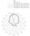
도 5는 전도성 플라스틱으로 제작된 웨이브가이드를 사용한 레이더의 수평 및 수직 빔패턴 성능을, 종래의 다른 소재로 제작된 웨이브가이드를 사용한 레이더의 경우와 비교하여 도시한 도표,
도 6은 본 발명의 함량에 따른 전도성 플라스틱으로 이루어진 웨이브가이드를 구비한 레이더의 수평 빔패턴 성능을, 다른 소재로 이루어진 웨이브가이드를 구비한 레이더의 경우와 비교하여 도시한 도면,
도 7은 본 발명의 함량에 따른 전도성 플라스틱으로 이루어진 웨이브가이드를 구비한 레이더의 수직 빔패턴 성능을, 다른 소재로 이루어진 웨이브가이드를 구비한 레이더의 경우와 비교하여 도시한 도면,
도 8은 웨이브가이드의 조립돌기가 회로기판을 관통하여 융착되는 것을 설명한 도면,
도 9는 웨이브가이드와 회로기판 사이의 간격 A를 설명한 도면,
도 10은 웨이브가이드와 회로기판 사이의 간격 A에 따른 레이더의 수평 빔패턴을 비교한 도면이다.1 is an exploded perspective view of a radar to which a waveguide according to the present invention can be applied;
Figure 2 is a diagram showing a waveguide for radar according to the present invention;
Figure 3 is a side view of the waveguide of Figure 2;
Figure 4 is a diagram of the wall thickness that can meet the radar characteristics according to the change in frequency surface resistance and permeability of the conductive plastic;
Figure 5 is a chart showing the horizontal and vertical beam pattern performance of a radar using a waveguide made of conductive plastic compared to that of a radar using a waveguide made of other conventional materials;
Figure 6 is a diagram showing the horizontal beam pattern performance of a radar equipped with a waveguide made of conductive plastic according to the content of the present invention compared with that of a radar equipped with a waveguide made of another material;
Figure 7 is a diagram showing the vertical beam pattern performance of a radar equipped with a waveguide made of conductive plastic according to the content of the present invention compared with that of a radar equipped with a waveguide made of another material;
Figure 8 is a diagram illustrating the assembly protrusions of the waveguide being fused through the circuit board;
Figure 9 is a diagram illustrating the gap A between the waveguide and the circuit board;
Figure 10 is a diagram comparing the horizontal beam pattern of the radar according to the gap A between the waveguide and the circuit board.
본 명세서 또는 출원에 개시되어 있는 본 발명의 실시 예들에 대해서 특정한 구조적 내지 기능적 설명들은 단지 본 발명에 따른 실시 예를 설명하기 위한 목적으로 예시된 것으로, 본 발명에 따른 실시 예들은 다양한 형태로 실시될 수 있으며 본 명세서 또는 출원에 설명된 실시 예들에 한정되는 것으로 해석되어서는 아니 된다.Specific structural and functional descriptions of the embodiments of the present invention disclosed in the present specification or application are merely illustrative for the purpose of explaining the embodiments according to the present invention, and the embodiments according to the present invention may be implemented in various forms. and should not be construed as limited to the embodiments described in this specification or application.
본 발명에 따른 실시 예는 다양한 변경을 가할 수 있고 여러가지 형태를 가질 수 있으므로 특정실시 예들을 도면에 예시하고 본 명세서 또는 출원에 상세하게 설명하고자 한다. 그러나, 이는 본 발명의 개념에 따른 실시 예를 특정한 개시 형태에 대해 한정하려는 것이 아니며, 본 발명의 사상 및 기술 범위에 포함되는 모든 변경, 균등물 내지 대체물을 포함하는 것으로 이해되어야 한다.Since the embodiments according to the present invention can make various changes and have various forms, specific embodiments will be illustrated in the drawings and described in detail in the specification or application. However, this is not intended to limit the embodiments according to the concept of the present invention to a specific disclosed form, and should be understood to include all changes, equivalents, and substitutes included in the spirit and technical scope of the present invention.
제1 및/또는 제2 등의 용어는 다양한 구성 요소들을 설명하는데 사용될 수 있지만, 상기 구성 요소들은 상기 용어들에 의해 한정되어서는 안된다. 상기 용어들은 하나의 구성 요소를 다른 구성 요소로부터 구별하는 목적으로만, 예컨대 본 발명의 개념에 따른 권리 범위로부터 이탈되지 않은 채, 제1 구성요소는 제2 구성요소로 명명될 수 있고, 유사하게 제2 구성요소는 제1 구성요소로도 명명될 수 있다.Terms such as first and/or second may be used to describe various components, but the components should not be limited by the terms. The above terms are used only for the purpose of distinguishing one component from another component, for example, without departing from the scope of rights according to the concept of the present invention, a first component may be named a second component, and similarly The second component may also be referred to as the first component.
어떤 구성요소가 다른 구성요소에 "연결되어" 있다거나 "접속되어" 있다고 언급된 때에는, 그 다른 구성요소에 직접적으로 연결되어 있거나 또는 접속되어 있을 수도 있지만, 중간에 다른 구성요소가 존재할 수도 있다고 이해되어야 할 것이다. 반면에, 어떤 구성요소가 다른 구성요소에 "직접 연결되어" 있다거나 "직접 접속되어" 있다고 언급된 때에는, 중간에 다른 구성요소가 존재하지 않는 것으로 이해되어야 할 것이다. 구성요소들 간의 관계를 설명하는 다른 표현들, 즉 "~사이에"와 "바로 ~사이에" 또는 "~에 이웃하는"과 "~에 직접 이웃하는" 등도 마찬가지로 해석되어야 한다.When a component is said to be "connected" or "connected" to another component, it is understood that it may be directly connected to or connected to the other component, but that other components may exist in between. It should be. On the other hand, when it is mentioned that a component is “directly connected” or “directly connected” to another component, it should be understood that there are no other components in between. Other expressions that describe the relationship between components, such as "between" and "immediately between" or "neighboring" and "directly adjacent to" should be interpreted similarly.
본 명세서에서 사용한 용어는 단지 특정한 실시 예를 설명하기 위해 사용된 것으로, 본 발명을 한정하려는 의도가 아니다. 단수의 표현은 문맥상 명백하게 다르게 뜻하지 않는 한, 복수의 표현을 포함한다. 본 명세서에서, "포함하다" 또는 "가지다" 등의 용어는 설시된 특징, 숫자, 단계, 동작, 구성요소, 부분품 또는 이들을 조합한 것이 존재함을 지정하려는 것이지, 하나 또는 그 이상의 다른 특징들이나 숫자, 단계, 동작, 구성요소, 부분품 또는 이들을 조합한 것들의 존재 또는 부가가능성을 미리 배제하지 않는 것으로 이해되어야 한다.The terms used in this specification are merely used to describe specific embodiments and are not intended to limit the present invention. Singular expressions include plural expressions unless the context clearly dictates otherwise. In this specification, terms such as “include” or “have” are intended to indicate the existence of a described feature, number, step, operation, component, part, or combination thereof, but are not intended to indicate the presence of one or more other features or numbers. It should be understood that this does not preclude the existence or addition of steps, operations, components, parts, or combinations thereof.
다르게 정의되지 않는 한, 기술적이거나 과학적인 용어를 포함해서 여기서 사용되는 모든 용어들은 본 발명이 속하는 기술 분야에서 통상의 지식을 가진 자에 의해 일반적으로 이해되는 것과 동일한 의미이다. 일반적으로 사용되는 사전에 정의되어 있는 것과 같은 용어들은 관련 기술의 문맥상 가지는 의미와 일치하는 의미인 것으로 해석되어야 하며, 본 명세서에서 명백하게 정의하지 않는 한, 이상적이거나 과도하게 형식적인 의미로 해석되지 않는다.Unless otherwise defined, all terms used herein, including technical or scientific terms, have the same meaning as commonly understood by a person of ordinary skill in the technical field to which the present invention pertains. Terms defined in commonly used dictionaries should be interpreted as having a meaning consistent with the meaning in the context of the related technology, and unless clearly defined in this specification, should not be interpreted as having an ideal or excessively formal meaning. .
이하, 첨부한 도면을 참조하여 본 발명의 바람직한 실시 예를 설명함으로써, 본 발명을 상세히 설명한다. 각 도면에 제시된 동일한 참조부호는 동일한 부재를 나타낸다.Hereinafter, the present invention will be described in detail by explaining preferred embodiments of the present invention with reference to the accompanying drawings. The same reference numerals in each drawing indicate the same member.
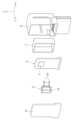
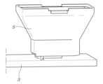
도 1을 참조하면, 본 발명 웨이브가이드(5)가 적용될 수 있는 레이더는, 전자기파를 송신 및 수신하는 반도체인 레이더소자(1), 상기 레이더소자(1)가 실장되고 이를 구동하는 회로가 구현된 회로기판(3), 상기 레이더소자(1)로부터 송신되고 상기 레이더소자(1)로 수신되는 전자기파를 가이드하도록 설치되는 웨이브가이드(5), 상기 레이더소자(1)가 실장된 회로기판(3)의 후방을 감싸는 쉴드캔(7), 상기 회로기판(3)과 웨이브가이드(5) 및 쉴드캔(7)을 감싸는 하우징(9); 상기 웨이브가이드(5)의 전방에서 상기 하우징(9)을 밀폐하도록 설치되는 레이돔(radom: 11)을 포함하여 구성된다.Referring to FIG. 1, the radar to which the
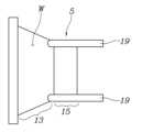
도 2와 도 3을 참조하면, 본 발명 레이더용 웨이브가이드(5)의 실시예는, 상기 레이더소자(1)가 송신 및 수신하는 전자기파를 가이드하도록 일정한 두께의 벽면(W)을 포함하여 이루어진 통로를 형성한다.Referring to FIGS. 2 and 3, the embodiment of the
상기 벽면(W)은 상기 레이더소자(1)로부터의 거리가 멀어짐에 따라 상기 통로의 단면적이 확대되도록 형성된 단면확대부(13)를 포함하여 구성된다.The wall surface (W) includes a cross-sectional enlargement portion (13) formed so that the cross-sectional area of the passage increases as the distance from the radar element (1) increases.
본 실시예에서, 상기 벽면(W)은 상기 통로 주변의 4방향에 서로 대칭되게 위치하여, 상기 벽면(W)들이 형성하는 단면확대부(13)는 상기 레이더소자(1)로부터의 거리가 멀어짐에 따라 단면적이 점차 확대되는 사각 기둥 형태의 통로를 형성하도록 구성된다.In this embodiment, the wall surfaces (W) are positioned symmetrically in four directions around the passage, so that the cross-sectional enlarged
또한, 상기 벽면(W)들은 상기 단면확대부(13)에 비해 상대적으로 상기 레이더소자(1)에 인접한 부분에서는, 상기 레이더소자(1)로부터의 거리와 무관하게 단면적이 일정한 사각 기둥 형태의 통로를 구성하는 단면유지부(15)를 형성한다.In addition, the wall surface (W) is a passage in the form of a square pillar with a constant cross-sectional area regardless of the distance from the
즉, 본 발명의 웨이브가이드(5)는 상기 전자기파의 통로를 형성하는 4개의 벽면(W)이 서로 연결되어, 상기 레이더소자(1)에 가까운 위치에 상기 단면유지부(15)를 구성하고, 상기 단면유지부(15)에 상기 단면확대부(13)가 일체로 연결되어 형성되며, 상기 단면확대부(13)는 상기 레이더소자(1)로부터의 거리가 멀어짐에 따라 점차 내부의 통로 단면이 확대되는 형상을 가지도록 한 것이다.That is, in the
본 실시예에서, 상기 벽면(W)은, 상기 웨이브가이드(5)를 이루는 부분들 중, 평면적으로 이루어져 있어서 표면으로부터 수직한 방향으로 측정한 두께가 대체로 일정한 수준을 유지할 수 있는 부분을, 상기 벽면(W)이 서로 연결되는 모서리 부분 등과 같이 일정한 두께를 표현하기 어려운 부분들과 구별하여 표현한 것이다.In this embodiment, the wall W is a part of the
따라서, 실질적으로 상기 웨이브가이드(5)는 상기와 같이 4개의 벽면(W)에 의한 사각통로 형상이 아니라 육각통로나 팔각통로 등을 이룰 수 있는 다수의 벽면(W)으로 구성될 수도 있을 것이며, 나아가 원기둥의 형태로 형성되는 것도 가능할 것이다.Therefore, in reality, the
한편, 본 발명의 웨이브가이드(5)는 도시된 바와 같이, 상기 통로의 내부에는 서로 마주하는 두 벽면(W) 사이를 연결하여, 상기 통로를 양분하는 격벽(17)이 일체로 형성된다.Meanwhile, as shown in the
따라서, 상기 레이더소자(1)의 송신영역과 수신영역을 상기 격벽(17)에 의해 구획된 두 통로로 각각 대응시켜, 보다 우수한 레이더 성능을 확보하도록 할 수 있다.Therefore, it is possible to secure better radar performance by making the transmission area and reception area of the
또한, 상기와 같은 격벽(17)은 상기 웨이브가이드(5)의 강성을 증대시키고 변형을 억제하는 데에도 기여하게 된다.In addition, the
상기 웨이브가이드(5)는 상기 벽면(W)을 포함한 모든 부분이, 주파수 표면 저항이 1000Ω 이하이며, 투자율이 0.001H/m 이상인 전도성 플라스틱으로 이루어진다.All parts of the
즉, 상기 웨이브가이드(5)는 사출 성형에 의해 모든 부분이 한꺼번에 형성되는 단일 사출물로 이루어질 수 있으며, 성형성 및 레이더의 소형 경량화를 위해서는 상기 벽면(W)의 두께는 3mm 이하인 것이 바람직하고, 이 경우 상기 웨이브가이드(5)의 사출 성형에 사용되는 상기 전도성 플라스틱은 상기와 같이 주파수 표면 저항이 1000Ω 이하이며, 투자율이 0.001H/m 이상인 전도성 플라스틱으로 이루어지는 것이 바람직한 것이다.In other words, the
즉, 상기 전도성 플라스틱으로 이루어진 웨이브가이드(5)의 벽면(W) 두께는 다음의 Skin Depth 수식을 통해 구할 수 있다.That is, the wall thickness (W) of the
벽면(W) 두께Wall (W) thickness
진공의 투자율: 4*10-7(H/m)Permeability of vacuum: 4 *10-7 (H/m)
비투자율=/Specific permeability= /
벽면(W) 소재의 투자율Permeability of wall (W) material
Cu(1.68*10-8Ω·m)에 대한 벽면(W) 소재의 비저항(Ω·m)Resistivity (Ω·m) of wall (W) material to Cu (1.68*10-8 Ω·m)
f: 레이더의 운용 주파수f: Radar operating frequency
상기 수식을 이용하여, 상기 웨이브가이드(5)에 사용될 수 있는 전도성 플라스틱의 주파수 표면 저항과 투자율을 변화시켜가면서, 상기 벽면(W) 두께를 산출해보면, 도 4와 같은 결과를 얻을 수 있다.If the thickness of the wall (W) is calculated while changing the frequency surface resistance and permeability of the conductive plastic that can be used in the
즉, 도 4에서 점선 부분으로 표현된, 벽면(W) 두께 3mm이하를 구현할 수 있는 전도성 플라스틱의 주파수 표면 저항과 투자율의 조합은, 주파수 표면 저항이 1000Ω 이하이며, 투자율이 0.001H/m 이상인 경우로 제한되는 것이다.That is, the combination of frequency surface resistance and permeability of the conductive plastic that can realize a wall (W) thickness of 3 mm or less, represented by the dotted line in Figure 4, is when the frequency surface resistance is 1000 Ω or less and the permeability is 0.001 H/m or more. It is limited to.
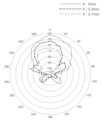
도 5는 상기한 바와 같은 전도성 플라스틱으로 제작된 웨이브가이드(5)를 사용한 레이더의 수평 및 수직 빔패턴 성능을, 종래의 다른 소재로 제작된 웨이브가이드를 사용한 레이더의 경우와 비교하여 도시한 것으로서, 본 발명에 따른 웨이브가이드(5)를 사용한 레이더가 종래 다른 소재의 웨이브가이드를 사용한 레이더와 거의 동일한 수준의 성능을 제공함을 확인할 수 있다.Figure 5 shows the horizontal and vertical beam pattern performance of a radar using the
즉, 본 발명의 전도성 플라스틱으로 제작된 웨이브가이드(5)는 종래 알루미늄이나 황동 등과 같은 금속재 또는 플라스틱으로 제작된 후 도금을 한 웨이브가이드 등에 비해, 동일한 성능을 확보할 수 있으면서도, 단일 사출물로 이루어져서, 그 제작 및 조립이 용이하고, 경량이며, 단가를 현저하게 저감시킬 수 있는 장점이 있는 것이다.In other words, the
여기서, 상기 전도성 플라스틱은 탄소섬유(CF: Carbon Fiber) 35~40%, 탄소나노튜브(CNT: Carbon Nano Tube) 2%를 포함하는 PA66(Polyamide 66)로 이루어지거나, 탄소섬유(CF) 35~40%, 탄소나노튜브(CNT) 2%를 포함하는 PBT(Polybutylene terephthalate)로 이루어질 수 있다.Here, the conductive plastic is made of PA66 (Polyamide 66) containing 35 to 40% carbon fiber (CF) and 2% carbon nanotube (CNT), or 35 to 40% carbon fiber (CF). It may be made of PBT (Polybutylene terephthalate) containing 40% and 2% carbon nanotubes (CNTs).
참고로, 도 6과 도 7은 상기한 바와 같은 함량의 전도성 플라스틱을 사용한 웨이브가이드(5)를 구비한 레이더의 수평 및 수직 빔패턴 성능을 각각 비교하여 표시한 도면으로서, 상기한 바와 같은 함량의 전도성 플라스틱을 사용하면, 종래 황동으로 제작되거나 플라스틱으로 제작되어 도금 공정을 거친 웨이브가이드를 사용하는 경우에 비교할 때 거의 동일한 성능을 제공할 수 있는 것을 확인할 수 있다.For reference, Figures 6 and 7 are diagrams comparing the horizontal and vertical beam pattern performance of a radar equipped with a
참고로, 도 5 내지 도 7에서 수평 빔패턴 성능은 도 1의 웨이브가이드(5)를 기준으로 상기 격벽(17)에 수직한 평면(YZ평면) 상의 빔패턴 성능을 의미하며, 수직 빔패턴 성능은 상기 격벽(17)과 평행한 평면(YX평면) 상의 빔패턴 성능을 의미한다.For reference, the horizontal beam pattern performance in FIGS. 5 to 7 refers to the beam pattern performance on the plane (YZ plane) perpendicular to the
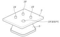
한편, 상기 웨이브가이드(5)의 통로를 형성하는 벽면(W)의 양 단부 중, 상기 레이더소자(1)가 장착된 회로기판(3)을 향한 단부에는, 상기 회로기판(3)을 관통한 후 열융착에 의해, 웨이브가이드(5)가 상기 회로기판(3)에 고정되도록 하는 다수의 조립돌기(19)가 일체로 형성된다.Meanwhile, among both ends of the wall surface (W) forming the passage of the waveguide (5), the end facing the circuit board (3) on which the radar element (1) is mounted has a hole penetrating the circuit board (3). After heat fusion, a plurality of
즉, 본 실시예에서, 상기 다수의 조립돌기(19)는 도 2와 도 3에 도시된 바와 같이 상기 단면유지부(15)의 각 모서리 부분에 각각 일체로 돌출되어 형성된 구성이다.That is, in this embodiment, the plurality of
상기 조립돌기(19)는 상기 웨이브가이드(5)의 일부로서 전도성 플라스틱으로 이루어져 있으므로, 도 8에 도시된 바와 같이 상기 회로기판(3)을 관통하여, 상기 회로기판(3)의 후방에서 열융착에 의해 자체적으로 변형됨에 의해 상기 웨이브가이드(5)를 상기 회로기판(3)에 견고하게 고정시킬 수 있다.Since the
특히, 상기 조립돌기(19)는 상기 웨이브가이드(5)를 상기 회로기판(3)에 완전히 밀착시킨 상태로 용이하게 고정할 수 있고, 그 고정상태를 영구적으로 유지할 수 있어서, 레이더의 성능을 최상의 상태로 확보하고 그 상태를 안정적으로 유지할 수 있도록 하는 것이다.In particular, the
도 9를 참조하면, 상기 웨이브가이드(5)가 회로기판(3)에서 약간 이격되어 간격(A)을 형성한 상태로 조립될 수 있음을 표현하고 있는데, 이러한 상태는 접착제 사용 등의 방법으로 상기 웨이브가이드(5)를 회로기판(3)에 고정시키는 경우에 발생할 수 있으며, 상기 간격(A)이 커질수록 레이더의 성능은 저하된다.Referring to FIG. 9, it is shown that the
도 10은 상기 간격(A)에 따른 레이더의 수평 빔패턴 성능을 비교한 것으로서, 상기 간격이 0인 경우의 빔패턴이 가장 우수하고, 간격이 커질수록 빔패턴 성능이 저하됨을 알 수 있는 것이다.Figure 10 compares the radar's horizontal beam pattern performance according to the spacing (A). It can be seen that the beam pattern when the spacing is 0 is the best, and as the spacing increases, the beam pattern performance deteriorates.
즉, 본 발명에서는 상기와 같이 상기 다수의 조립돌기(19)를 회로기판(3)을 관통하여 삽입된 상태로, 열에 의해 상기 조립돌기(19)가 상기 회로기판(3)에 융착되도록 함으로써, 상기 웨이브가이드(5)와 회로기판(3) 사이의 간격이 없이 밀착된 상태로 견고한 고정상태를 용이하게 확보할 수 있어서, 레이더의 성능 확보에 매우 유리한 것이다.That is, in the present invention, the plurality of
본 발명은 특정한 실시예에 관련하여 도시하고 설명하였지만, 이하의 특허청구범위에 의해 제공되는 본 발명의 기술적 사상을 벗어나지 않는 한도 내에서, 본 발명이 다양하게 개량 및 변화될 수 있다는 것은 당업계에서 통상의 지식을 가진 자에게 있어서 자명할 것이다.Although the present invention has been shown and described in relation to specific embodiments, it is known in the art that various improvements and changes can be made to the present invention without departing from the technical spirit of the invention as provided by the following claims. This will be self-evident to those with ordinary knowledge.
1; 레이더소자
3; 회로기판
5; 웨이브가이드
7; 쉴드캔
9; 하우징
11; 레이돔
W; 벽면
13; 단면확대부
15; 단면유지부
17; 격벽
19; 조립돌기
A; 간격One; Radar element
3; circuit board
5; wave guide
7; shield can
9; housing
11; Radome
W; wall
13; Section enlargement section
15; Section maintenance part
17; septum
19; assembly protrusion
A; interval
Claims (11)
Translated fromKorean상기 벽면을 포함한 모든 부분이, 주파수 표면 저항이 1000Ω 이하이며, 투자율이 0.001H/m 이상인 전도성 플라스틱으로 이루어지며;
상기 벽면의 두께는 3mm 이하이고;
상기 전도성 플라스틱은 탄소섬유 35~40%, 탄소나노튜브 2%를 포함하는 PA66(Polyamide 66)로 이루어진 것
을 특징으로 하는 레이더용 웨이브가이드.Forming a passage including walls of a certain thickness to guide electromagnetic waves transmitted and received by the radar element;
All parts, including the wall, are made of conductive plastic with a frequency surface resistance of 1000Ω or less and a magnetic permeability of 0.001H/m or more;
The thickness of the wall is 3 mm or less;
The conductive plastic is made of PA66 (Polyamide 66) containing 35-40% carbon fiber and 2% carbon nanotubes.
A waveguide for radar characterized by .
상기 벽면을 포함한 모든 부분이, 주파수 표면 저항이 1000Ω 이하이며, 투자율이 0.001H/m 이상인 전도성 플라스틱으로 이루어지며;
상기 벽면의 두께는 3mm 이하이고;
상기 전도성 플라스틱은 탄소섬유 35~40%, 탄소나노튜브 2%를 포함하는 PBT(Polybutylene terephthalate)로 이루어진 것
을 특징으로 하는 레이더용 웨이브가이드.Forming a passage including walls of a certain thickness to guide electromagnetic waves transmitted and received by the radar element;
All parts, including the wall, are made of conductive plastic with a frequency surface resistance of 1000Ω or less and a magnetic permeability of 0.001H/m or more;
The thickness of the wall is 3 mm or less;
The conductive plastic is made of PBT (polybutylene terephthalate) containing 35-40% carbon fiber and 2% carbon nanotubes.
A waveguide for radar characterized by .
상기 벽면은 상기 레이더소자로부터의 거리가 멀어짐에 따라 상기 통로의 단면적이 확대되도록 형성된 단면확대부를 포함하여 구성된 것
을 특징으로 하는 레이더용 웨이브가이드.In claim 1,
The wall is configured to include a cross-sectional enlargement portion formed so that the cross-sectional area of the passage increases as the distance from the radar element increases.
A waveguide for radar characterized by .
상기 통로를 형성하는 벽면의 양 단부 중, 상기 레이더소자가 장착된 회로기판을 향한 단부에는, 상기 회로기판을 관통한 후 열융착에 의해, 웨이브가이드가 상기 회로기판에 고정되도록 하는 다수의 조립돌기가 일체로 형성된 것
을 특징으로 하는 레이더용 웨이브가이드.In claim 5,
Among both ends of the wall forming the passage, the end facing the circuit board on which the radar element is mounted is provided with a plurality of assembly protrusions that penetrate the circuit board and then are heat-sealed to secure the waveguide to the circuit board. formed as a whole
A waveguide for radar characterized by .
상기 벽면은 상기 통로 주변의 4방향에 서로 대칭되게 위치하여, 상기 벽면들이 형성하는 단면확대부는 상기 레이더소자로부터의 거리가 멀어짐에 따라 단면적이 점차 확대되는 사각 기둥 형태의 통로를 형성하도록 구성된 것
을 특징으로 하는 레이더용 웨이브가이드.In claim 6,
The walls are positioned symmetrically in four directions around the passage, and the cross-sectional enlargement portion formed by the walls is configured to form a passage in the shape of a square pillar whose cross-sectional area gradually expands as the distance from the radar element increases.
A waveguide for radar characterized by .
상기 통로의 내부에는 서로 마주하는 두 벽면 사이를 연결하여, 상기 통로를 양분하는 격벽이 일체로 형성된 것
을 특징으로 하는 레이더용 웨이브가이드.In claim 7,
Inside the passage, a partition is integrally formed to connect the two opposing walls and bisect the passage.
A waveguide for radar characterized by .
상기 벽면들은 상기 단면확대부에 비해 상대적으로 상기 레이더소자에 인접한 부분에서는, 상기 레이더소자로부터의 거리와 무관하게 단면적이 일정한 사각 기둥 형태의 통로를 구성하는 단면유지부를 형성하도록 된 것
을 특징으로 하는 레이더용 웨이브가이드.In claim 7,
The wall surfaces are formed in a portion adjacent to the radar element relatively compared to the cross-sectional enlargement portion to form a cross-sectional retaining portion that constitutes a passage in the form of a square pillar with a constant cross-sectional area regardless of the distance from the radar device.
A waveguide for radar characterized by .
상기 다수의 조립돌기는 상기 단면유지부의 각 모서리 부분에 각각 돌출되어 형성된 것을 포함하는 것
을 특징으로 하는 레이더용 웨이브가이드.In claim 9,
The plurality of assembly protrusions include those formed to protrude from each corner of the cross-section retaining portion.
A waveguide for radar characterized by .
을 특징으로 하는 레이더.
Constructed including the waveguide of any one of claims 1 or 4 to 10
Radar featuring .
Priority Applications (4)
| Application Number | Priority Date | Filing Date | Title |
|---|---|---|---|
| KR1020210042961AKR102589937B1 (en) | 2021-04-01 | 2021-04-01 | Wave guide for radar |
| US17/339,871US20220320700A1 (en) | 2021-04-01 | 2021-06-04 | Waveguide for radar |
| DE102021117026.5ADE102021117026A1 (en) | 2021-04-01 | 2021-07-01 | WAVEGUIDE FOR A RADAR |
| CN202110752917.7ACN115189110B (en) | 2021-04-01 | 2021-07-02 | Waveguides for radar |
Applications Claiming Priority (1)
| Application Number | Priority Date | Filing Date | Title |
|---|---|---|---|
| KR1020210042961AKR102589937B1 (en) | 2021-04-01 | 2021-04-01 | Wave guide for radar |
Publications (2)
| Publication Number | Publication Date |
|---|---|
| KR20220136812A KR20220136812A (en) | 2022-10-11 |
| KR102589937B1true KR102589937B1 (en) | 2023-10-17 |
Family
ID=83282724
Family Applications (1)
| Application Number | Title | Priority Date | Filing Date |
|---|---|---|---|
| KR1020210042961AActiveKR102589937B1 (en) | 2021-04-01 | 2021-04-01 | Wave guide for radar |
Country Status (4)
| Country | Link |
|---|---|
| US (1) | US20220320700A1 (en) |
| KR (1) | KR102589937B1 (en) |
| CN (1) | CN115189110B (en) |
| DE (1) | DE102021117026A1 (en) |
Citations (1)
| Publication number | Priority date | Publication date | Assignee | Title |
|---|---|---|---|---|
| KR101751779B1 (en)* | 2016-05-27 | 2017-06-29 | 농업회사법인 에이앤피테크놀로지주식회사 | Horn antenna apparatus |
Family Cites Families (42)
| Publication number | Priority date | Publication date | Assignee | Title |
|---|---|---|---|---|
| US3320341A (en)* | 1960-02-24 | 1967-05-16 | William L Mackie | Method of manufacturing a lightweight microwave antenna |
| SE463339B (en) | 1989-03-14 | 1990-11-05 | Ericsson Telefon Ab L M | DEVICE FOR POWER SUPPLY OF A HAIR SPACE CONTROLLER INTENDED FOR ELECTROMAGNETIC MICROVAAGS |
| US5341678A (en)* | 1993-05-12 | 1994-08-30 | General Electric Company | Method for determining thickness of ferromagnetic material deposition on nuclear fuel rods |
| CA2134384C (en)* | 1993-11-18 | 1997-09-30 | Robert Lee Reynolds | Attenuation fin blanket for a feed horn |
| US5581217A (en) | 1995-09-21 | 1996-12-03 | Hughes Aircraft Company | Microwave shielding structures comprising parallel-plate waveguide |
| EP1247122A1 (en)* | 1999-12-23 | 2002-10-09 | Spectalis Corporation | Optical waveguide structures |
| DE10120248A1 (en)* | 2000-04-26 | 2002-03-28 | Kyocera Corp | Structure for connecting a non-radiating dielectric waveguide and a metal waveguide, transmitter / receiver module for millimeter waves and transmitter / receiver for millimeter waves |
| US6870516B2 (en)* | 2001-02-16 | 2005-03-22 | Integral Technologies, Inc. | Low cost antennas using conductive plastics or conductive composites |
| US6741221B2 (en)* | 2001-02-15 | 2004-05-25 | Integral Technologies, Inc. | Low cost antennas using conductive plastics or conductive composites |
| EP1331688A1 (en) | 2002-01-29 | 2003-07-30 | Era Patents Limited | Waveguide |
| JP3969650B2 (en)* | 2002-11-19 | 2007-09-05 | 日精樹脂工業株式会社 | Method for controlling skin layer thickness in composite resin molded products |
| EP1903328B1 (en)* | 2003-06-25 | 2011-12-21 | Canon Kabushiki Kaisha | High frequency electrical signal control device and sensing system |
| US20060202894A1 (en)* | 2005-03-09 | 2006-09-14 | Shary Nassimi | Conductive Plastic Antenna |
| JP4511406B2 (en)* | 2005-03-31 | 2010-07-28 | 株式会社デンソー | Antenna equipment |
| US20100214185A1 (en)* | 2006-11-01 | 2010-08-26 | The Regents Of The University Of California | Plastic waveguide-fed horn antenna |
| KR101001715B1 (en)* | 2008-07-23 | 2010-12-15 | 주식회사 극동통신 | Multimode Monopulse Feeder for Tracking Radar Monopulse Antenna |
| KR101644200B1 (en)* | 2008-07-30 | 2016-07-29 | 이 아이 듀폰 디 네모아 앤드 캄파니 | Heat Resistant Molded or Extruded Thermoplastic Articles |
| US9241433B2 (en)* | 2009-04-24 | 2016-01-19 | Applied Nanostructured Solutions, Llc | CNT-infused EMI shielding composite and coating |
| WO2012168536A1 (en)* | 2011-06-10 | 2012-12-13 | Amphenol Finland Oy | Two shot molding antenna with conductive plastic |
| PL2703436T3 (en)* | 2012-08-28 | 2017-07-31 | Ems-Patent Ag | Polyamide moulding material and its application |
| JP6259468B2 (en)* | 2013-01-22 | 2018-01-10 | ティーイー・コネクティビティ・コーポレイションTE Connectivity Corporation | Non-contact connector |
| US20140238736A1 (en)* | 2013-02-27 | 2014-08-28 | Cheil Industries Inc. | Thermoplastic Resin Composition with EMI Shielding Properties |
| US9515366B2 (en)* | 2013-03-19 | 2016-12-06 | Texas Instruments Incorporated | Printed circuit board dielectric waveguide core and metallic waveguide end |
| US12016168B2 (en)* | 2013-12-19 | 2024-06-18 | Hyundai Motor Company | Web for absorbing electromagnetic wave and housing of electronic parts using the same |
| US9525206B2 (en)* | 2014-02-13 | 2016-12-20 | Honda Elesys Co., Ltd. | Antenna unit, radar device, and composite sensor device |
| EP2947716B8 (en)* | 2014-05-23 | 2023-08-09 | Progress Rail Signaling S.p.A. | Radar obstacle detector for a railway crossing |
| EP3076482A1 (en)* | 2015-04-02 | 2016-10-05 | Progress Rail Inspection & Information Systems S.r.l. | Radar obstacle detector for a railway crossing |
| FR3041166B1 (en)* | 2015-09-11 | 2018-09-28 | Commissariat A L'energie Atomique Et Aux Energies Alternatives | RADOME EQUIPPED WITH A HEATING RESISTIVE SYSTEM STRUCTURE IN BANDS OF METAL NANO-ELEMENTS |
| DE102017109861A1 (en)* | 2016-05-18 | 2017-11-23 | Infineon Technologies Ag | Methods and devices for speed and / or position detection |
| US10582608B2 (en)* | 2016-07-20 | 2020-03-03 | Hcl Technologies Limited | Interconnection between printed circuit boards |
| US10539656B2 (en)* | 2016-07-21 | 2020-01-21 | Waymo Llc | Antenna and radar system that include a polarization-rotating layer |
| JP6399165B1 (en)* | 2016-07-22 | 2018-10-03 | 株式会社リコー | Three-dimensional modeling resin powder, three-dimensional model manufacturing apparatus, and three-dimensional model manufacturing method |
| US10224617B2 (en)* | 2016-07-26 | 2019-03-05 | Waymo Llc | Plated, injection molded, automotive radar waveguide antenna |
| EP3309897A1 (en)* | 2016-10-12 | 2018-04-18 | VEGA Grieshaber KG | Waveguide coupling for radar antenna |
| JP6838250B2 (en)* | 2017-06-05 | 2021-03-03 | 日立Astemo株式会社 | Antennas, array antennas, radar devices and in-vehicle systems |
| JP2019009765A (en)* | 2017-06-26 | 2019-01-17 | 日本電産株式会社 | Manufacturing method of hone antenna array and antenna array |
| US10547122B2 (en)* | 2017-06-26 | 2020-01-28 | Nidec Corporation | Method of producing a horn antenna array and antenna array |
| US10756417B2 (en)* | 2017-12-14 | 2020-08-25 | Waymo Llc | Adaptive polarimetric radar architecture for autonomous driving |
| CN109135277A (en)* | 2018-08-28 | 2019-01-04 | 安徽江淮汽车集团股份有限公司 | A kind of PA66 composite material and preparation method |
| CN111106450A (en)* | 2018-10-26 | 2020-05-05 | 西安美频电子科技有限公司 | A horn array antenna |
| EP3686567B1 (en)* | 2019-01-24 | 2023-09-06 | VEGA Grieshaber KG | Metallized dielectric waveguide |
| DE102019203842A1 (en)* | 2019-03-21 | 2020-09-24 | Zf Friedrichshafen Ag | Radar antenna structure and manufacturing method for manufacturing a radar antenna structure |
- 2021
- 2021-04-01KRKR1020210042961Apatent/KR102589937B1/enactiveActive
- 2021-06-04USUS17/339,871patent/US20220320700A1/ennot_activeAbandoned
- 2021-07-01DEDE102021117026.5Apatent/DE102021117026A1/enactivePending
- 2021-07-02CNCN202110752917.7Apatent/CN115189110B/enactiveActive
Patent Citations (1)
| Publication number | Priority date | Publication date | Assignee | Title |
|---|---|---|---|---|
| KR101751779B1 (en)* | 2016-05-27 | 2017-06-29 | 농업회사법인 에이앤피테크놀로지주식회사 | Horn antenna apparatus |
Also Published As
| Publication number | Publication date |
|---|---|
| DE102021117026A1 (en) | 2022-10-06 |
| CN115189110A (en) | 2022-10-14 |
| KR20220136812A (en) | 2022-10-11 |
| US20220320700A1 (en) | 2022-10-06 |
| CN115189110B (en) | 2024-05-07 |
Similar Documents
| Publication | Publication Date | Title |
|---|---|---|
| US10992053B2 (en) | Radar antenna array with parasitic elements excited by surface waves | |
| JP4065268B2 (en) | Automotive antenna | |
| KR20200086753A (en) | Multiple polarized radar units | |
| US7126525B2 (en) | Millimeter wave-radar and method for manufacturing the same | |
| US10826166B2 (en) | Plated, injection molded, automotive radar waveguide antenna | |
| US20180203110A1 (en) | Cover member of sensor configured to detect ambient situation of vehicle and sensor assembly | |
| US7038622B2 (en) | Slot antenna array using LTCC technology | |
| KR102177166B1 (en) | Iris Matched PCB to Waveguide Transition | |
| KR20190047739A (en) | Folded radiation slots for short wall waveguide radiation | |
| CN117296201A (en) | Antenna device for automotive radar applications | |
| CN114649661A (en) | Waveguide with radiating slot and parasitic elements for asymmetric coverage | |
| KR102589937B1 (en) | Wave guide for radar | |
| CN215894947U (en) | Vehicle radar sensor | |
| CN218099578U (en) | Radar system for vehicle and vehicle | |
| EP3340370A1 (en) | Millimeter wave antenna and connection arrangements | |
| US20190305434A1 (en) | Connection Arrangement | |
| KR102366273B1 (en) | Radar apparatus | |
| US12126080B2 (en) | Antenna module | |
| JP2011078020A (en) | Antenna for vehicle | |
| JP2017085311A (en) | Waveguide slot antenna | |
| JP2009088861A (en) | Horn array antenna and feeding path | |
| US20090121954A1 (en) | Device for Emitting and Receiving Electromagnetic Radiation | |
| CN113571866B (en) | Antenna, vehicle-mounted millimeter wave radar and automobile | |
| KR20210073394A (en) | Radar sensor module | |
| EP4391217A1 (en) | Waveguide antenna |
Legal Events
| Date | Code | Title | Description |
|---|---|---|---|
| PA0109 | Patent application | Patent event code:PA01091R01D Comment text:Patent Application Patent event date:20210401 | |
| PA0201 | Request for examination | ||
| PE0902 | Notice of grounds for rejection | Comment text:Notification of reason for refusal Patent event date:20220621 Patent event code:PE09021S01D | |
| PG1501 | Laying open of application | ||
| E90F | Notification of reason for final refusal | ||
| PE0902 | Notice of grounds for rejection | Comment text:Final Notice of Reason for Refusal Patent event date:20230222 Patent event code:PE09021S02D | |
| E701 | Decision to grant or registration of patent right | ||
| PE0701 | Decision of registration | Patent event code:PE07011S01D Comment text:Decision to Grant Registration Patent event date:20230818 | |
| GRNT | Written decision to grant | ||
| PR0701 | Registration of establishment | Comment text:Registration of Establishment Patent event date:20231011 Patent event code:PR07011E01D | |
| PR1002 | Payment of registration fee | Payment date:20231012 End annual number:3 Start annual number:1 | |
| PG1601 | Publication of registration |