KR102587895B1 - Image sensor in which pixel array and memory cell array are merged and electronic device including the same - Google Patents
Image sensor in which pixel array and memory cell array are merged and electronic device including the sameDownload PDFInfo
- Publication number
- KR102587895B1 KR102587895B1KR1020180109696AKR20180109696AKR102587895B1KR 102587895 B1KR102587895 B1KR 102587895B1KR 1020180109696 AKR1020180109696 AKR 1020180109696AKR 20180109696 AKR20180109696 AKR 20180109696AKR 102587895 B1KR102587895 B1KR 102587895B1
- Authority
- KR
- South Korea
- Prior art keywords
- semiconductor chip
- cell array
- memory cell
- area
- region
- Prior art date
- Legal status (The legal status is an assumption and is not a legal conclusion. Google has not performed a legal analysis and makes no representation as to the accuracy of the status listed.)
- Active
Links
- 230000015654memoryEffects0.000titleclaimsabstractdescription116
- 239000004065semiconductorSubstances0.000claimsabstractdescription240
- 238000000034methodMethods0.000claimsdescription11
- 230000008569processEffects0.000claimsdescription4
- 230000003213activating effectEffects0.000claims1
- 239000000758substrateSubstances0.000description51
- 239000010410layerSubstances0.000description43
- 230000000295complement effectEffects0.000description25
- 229910052751metalInorganic materials0.000description20
- 239000002184metalSubstances0.000description20
- 239000012535impuritySubstances0.000description19
- 238000009792diffusion processMethods0.000description17
- XUIMIQQOPSSXEZ-UHFFFAOYSA-NSiliconChemical compound[Si]XUIMIQQOPSSXEZ-UHFFFAOYSA-N0.000description11
- 229910052710siliconInorganic materials0.000description11
- 239000010703siliconSubstances0.000description11
- 238000006243chemical reactionMethods0.000description10
- 230000000875corresponding effectEffects0.000description10
- 239000003990capacitorSubstances0.000description9
- 238000007667floatingMethods0.000description9
- 230000004888barrier functionEffects0.000description7
- 230000001276controlling effectEffects0.000description7
- 238000003780insertionMethods0.000description7
- 230000037431insertionEffects0.000description7
- 229910052814silicon oxideInorganic materials0.000description7
- 229910052581Si3N4Inorganic materials0.000description6
- VYPSYNLAJGMNEJ-UHFFFAOYSA-NSilicium dioxideChemical compoundO=[Si]=OVYPSYNLAJGMNEJ-UHFFFAOYSA-N0.000description6
- 230000005540biological transmissionEffects0.000description6
- 238000010586diagramMethods0.000description6
- 239000000463materialSubstances0.000description6
- 150000004767nitridesChemical class0.000description6
- 238000002955isolationMethods0.000description5
- 208000017972multifocal atrial tachycardiaDiseases0.000description5
- 230000003287optical effectEffects0.000description5
- 238000012546transferMethods0.000description5
- 230000004913activationEffects0.000description4
- 238000004891communicationMethods0.000description4
- 150000001875compoundsChemical class0.000description4
- 239000011159matrix materialSubstances0.000description4
- 238000012545processingMethods0.000description4
- 238000005070samplingMethods0.000description4
- HQVNEWCFYHHQES-UHFFFAOYSA-Nsilicon nitrideChemical compoundN12[Si]34N5[Si]62N3[Si]51N64HQVNEWCFYHHQES-UHFFFAOYSA-N0.000description4
- 230000003936working memoryEffects0.000description4
- 239000004020conductorSubstances0.000description3
- 230000002596correlated effectEffects0.000description3
- 230000009977dual effectEffects0.000description3
- 229910052732germaniumInorganic materials0.000description3
- GNPVGFCGXDBREM-UHFFFAOYSA-Ngermanium atomChemical compound[Ge]GNPVGFCGXDBREM-UHFFFAOYSA-N0.000description3
- 229910052721tungstenInorganic materials0.000description3
- 239000010937tungstenSubstances0.000description3
- 229910000577Silicon-germaniumInorganic materials0.000description2
- GWEVSGVZZGPLCZ-UHFFFAOYSA-NTitan oxideChemical compoundO=[Ti]=OGWEVSGVZZGPLCZ-UHFFFAOYSA-N0.000description2
- NRTOMJZYCJJWKI-UHFFFAOYSA-NTitanium nitrideChemical compound[Ti]#NNRTOMJZYCJJWKI-UHFFFAOYSA-N0.000description2
- MCMNRKCIXSYSNV-UHFFFAOYSA-NZirconium dioxideChemical compoundO=[Zr]=OMCMNRKCIXSYSNV-UHFFFAOYSA-N0.000description2
- LEVVHYCKPQWKOP-UHFFFAOYSA-N[Si].[Ge]Chemical compound[Si].[Ge]LEVVHYCKPQWKOP-UHFFFAOYSA-N0.000description2
- 239000012790adhesive layerSubstances0.000description2
- 239000010949copperSubstances0.000description2
- 238000013461designMethods0.000description2
- 238000005516engineering processMethods0.000description2
- 230000004044responseEffects0.000description2
- 238000005096rolling processMethods0.000description2
- MZLGASXMSKOWSE-UHFFFAOYSA-Ntantalum nitrideChemical compound[Ta]#NMZLGASXMSKOWSE-UHFFFAOYSA-N0.000description2
- 230000007704transitionEffects0.000description2
- WFKWXMTUELFFGS-UHFFFAOYSA-NtungstenChemical compound[W]WFKWXMTUELFFGS-UHFFFAOYSA-N0.000description2
- 101100498818Arabidopsis thaliana DDR4 geneProteins0.000description1
- RYGMFSIKBFXOCR-UHFFFAOYSA-NCopperChemical compound[Cu]RYGMFSIKBFXOCR-UHFFFAOYSA-N0.000description1
- 239000004593EpoxySubstances0.000description1
- 229910004481Ta2O3Inorganic materials0.000description1
- RTAQQCXQSZGOHL-UHFFFAOYSA-NTitaniumChemical compound[Ti]RTAQQCXQSZGOHL-UHFFFAOYSA-N0.000description1
- UGACIEPFGXRWCH-UHFFFAOYSA-N[Si].[Ti]Chemical compound[Si].[Ti]UGACIEPFGXRWCH-UHFFFAOYSA-N0.000description1
- RVSGESPTHDDNTH-UHFFFAOYSA-Nalumane;tantalumChemical compound[AlH3].[Ta]RVSGESPTHDDNTH-UHFFFAOYSA-N0.000description1
- UQZIWOQVLUASCR-UHFFFAOYSA-Nalumane;titaniumChemical compound[AlH3].[Ti]UQZIWOQVLUASCR-UHFFFAOYSA-N0.000description1
- PNEYBMLMFCGWSK-UHFFFAOYSA-Naluminium oxideInorganic materials[O-2].[O-2].[O-2].[Al+3].[Al+3]PNEYBMLMFCGWSK-UHFFFAOYSA-N0.000description1
- 238000003491arrayMethods0.000description1
- 239000000919ceramicSubstances0.000description1
- 239000010941cobaltSubstances0.000description1
- 229910017052cobaltInorganic materials0.000description1
- GUTLYIVDDKVIGB-UHFFFAOYSA-Ncobalt atomChemical compound[Co]GUTLYIVDDKVIGB-UHFFFAOYSA-N0.000description1
- 229910052802copperInorganic materials0.000description1
- 229910052593corundumInorganic materials0.000description1
- 239000003989dielectric materialSubstances0.000description1
- 230000006870functionEffects0.000description1
- CJNBYAVZURUTKZ-UHFFFAOYSA-Nhafnium(IV) oxideInorganic materialsO=[Hf]=OCJNBYAVZURUTKZ-UHFFFAOYSA-N0.000description1
- MRELNEQAGSRDBK-UHFFFAOYSA-Nlanthanum oxideInorganic materials[O-2].[O-2].[O-2].[La+3].[La+3]MRELNEQAGSRDBK-UHFFFAOYSA-N0.000description1
- 229910044991metal oxideInorganic materials0.000description1
- 150000004706metal oxidesChemical class0.000description1
- 150000002739metalsChemical class0.000description1
- KTUFCUMIWABKDW-UHFFFAOYSA-Noxo(oxolanthaniooxy)lanthanumChemical compoundO=[La]O[La]=OKTUFCUMIWABKDW-UHFFFAOYSA-N0.000description1
- 230000002093peripheral effectEffects0.000description1
- 230000002265preventionEffects0.000description1
- 229910021332silicideInorganic materials0.000description1
- FVBUAEGBCNSCDD-UHFFFAOYSA-Nsilicide(4-)Chemical compound[Si-4]FVBUAEGBCNSCDD-UHFFFAOYSA-N0.000description1
- HWEYZGSCHQNNEH-UHFFFAOYSA-Nsilicon tantalumChemical compound[Si].[Ta]HWEYZGSCHQNNEH-UHFFFAOYSA-N0.000description1
- 230000003068static effectEffects0.000description1
- 230000001360synchronised effectEffects0.000description1
- 229910052715tantalumInorganic materials0.000description1
- GUVRBAGPIYLISA-UHFFFAOYSA-Ntantalum atomChemical compound[Ta]GUVRBAGPIYLISA-UHFFFAOYSA-N0.000description1
- 239000010936titaniumSubstances0.000description1
- 229910052719titaniumInorganic materials0.000description1
- 229910021341titanium silicideInorganic materials0.000description1
- 238000002834transmittanceMethods0.000description1
- WQJQOUPTWCFRMM-UHFFFAOYSA-Ntungsten disilicideChemical compound[Si]#[W]#[Si]WQJQOUPTWCFRMM-UHFFFAOYSA-N0.000description1
- -1tungsten nitrideChemical class0.000description1
- 229910021342tungsten silicideInorganic materials0.000description1
- 235000012773wafflesNutrition0.000description1
- 229910001845yogo sapphireInorganic materials0.000description1
Images


Classifications
- H—ELECTRICITY
- H04—ELECTRIC COMMUNICATION TECHNIQUE
- H04N—PICTORIAL COMMUNICATION, e.g. TELEVISION
- H04N25/00—Circuitry of solid-state image sensors [SSIS]; Control thereof
- H04N25/70—SSIS architectures; Circuits associated therewith
- H04N25/71—Charge-coupled device [CCD] sensors; Charge-transfer registers specially adapted for CCD sensors
- H04N25/75—Circuitry for providing, modifying or processing image signals from the pixel array
- H—ELECTRICITY
- H04—ELECTRIC COMMUNICATION TECHNIQUE
- H04N—PICTORIAL COMMUNICATION, e.g. TELEVISION
- H04N25/00—Circuitry of solid-state image sensors [SSIS]; Control thereof
- H04N25/70—SSIS architectures; Circuits associated therewith
- H04N25/79—Arrangements of circuitry being divided between different or multiple substrates, chips or circuit boards, e.g. stacked image sensors
- H—ELECTRICITY
- H04—ELECTRIC COMMUNICATION TECHNIQUE
- H04N—PICTORIAL COMMUNICATION, e.g. TELEVISION
- H04N25/00—Circuitry of solid-state image sensors [SSIS]; Control thereof
- H04N25/70—SSIS architectures; Circuits associated therewith
- G—PHYSICS
- G11—INFORMATION STORAGE
- G11C—STATIC STORES
- G11C11/00—Digital stores characterised by the use of particular electric or magnetic storage elements; Storage elements therefor
- G11C11/21—Digital stores characterised by the use of particular electric or magnetic storage elements; Storage elements therefor using electric elements
- G11C11/34—Digital stores characterised by the use of particular electric or magnetic storage elements; Storage elements therefor using electric elements using semiconductor devices
- G11C11/40—Digital stores characterised by the use of particular electric or magnetic storage elements; Storage elements therefor using electric elements using semiconductor devices using transistors
- G11C11/401—Digital stores characterised by the use of particular electric or magnetic storage elements; Storage elements therefor using electric elements using semiconductor devices using transistors forming cells needing refreshing or charge regeneration, i.e. dynamic cells
- G11C11/403—Digital stores characterised by the use of particular electric or magnetic storage elements; Storage elements therefor using electric elements using semiconductor devices using transistors forming cells needing refreshing or charge regeneration, i.e. dynamic cells with charge regeneration common to a multiplicity of memory cells, i.e. external refresh
- G—PHYSICS
- G11—INFORMATION STORAGE
- G11C—STATIC STORES
- G11C11/00—Digital stores characterised by the use of particular electric or magnetic storage elements; Storage elements therefor
- G11C11/21—Digital stores characterised by the use of particular electric or magnetic storage elements; Storage elements therefor using electric elements
- G11C11/34—Digital stores characterised by the use of particular electric or magnetic storage elements; Storage elements therefor using electric elements using semiconductor devices
- G11C11/40—Digital stores characterised by the use of particular electric or magnetic storage elements; Storage elements therefor using electric elements using semiconductor devices using transistors
- G11C11/401—Digital stores characterised by the use of particular electric or magnetic storage elements; Storage elements therefor using electric elements using semiconductor devices using transistors forming cells needing refreshing or charge regeneration, i.e. dynamic cells
- G11C11/4063—Auxiliary circuits, e.g. for addressing, decoding, driving, writing, sensing or timing
- G11C11/407—Auxiliary circuits, e.g. for addressing, decoding, driving, writing, sensing or timing for memory cells of the field-effect type
- G11C11/408—Address circuits
- G11C11/4087—Address decoders, e.g. bit - or word line decoders; Multiple line decoders
- G—PHYSICS
- G11—INFORMATION STORAGE
- G11C—STATIC STORES
- G11C7/00—Arrangements for writing information into, or reading information out from, a digital store
- G11C7/16—Storage of analogue signals in digital stores using an arrangement comprising analogue/digital [A/D] converters, digital memories and digital/analogue [D/A] converters
- H—ELECTRICITY
- H01—ELECTRIC ELEMENTS
- H01L—SEMICONDUCTOR DEVICES NOT COVERED BY CLASS H10
- H01L23/00—Details of semiconductor or other solid state devices
- H01L23/48—Arrangements for conducting electric current to or from the solid state body in operation, e.g. leads, terminal arrangements ; Selection of materials therefor
- H01L23/481—Internal lead connections, e.g. via connections, feedthrough structures
- H—ELECTRICITY
- H01—ELECTRIC ELEMENTS
- H01L—SEMICONDUCTOR DEVICES NOT COVERED BY CLASS H10
- H01L23/00—Details of semiconductor or other solid state devices
- H01L23/52—Arrangements for conducting electric current within the device in operation from one component to another, i.e. interconnections, e.g. wires, lead frames
- H01L23/522—Arrangements for conducting electric current within the device in operation from one component to another, i.e. interconnections, e.g. wires, lead frames including external interconnections consisting of a multilayer structure of conductive and insulating layers inseparably formed on the semiconductor body
- H01L23/528—Layout of the interconnection structure
- H01L27/14603—
- H—ELECTRICITY
- H04—ELECTRIC COMMUNICATION TECHNIQUE
- H04N—PICTORIAL COMMUNICATION, e.g. TELEVISION
- H04N25/00—Circuitry of solid-state image sensors [SSIS]; Control thereof
- H04N25/70—SSIS architectures; Circuits associated therewith
- H04N25/702—SSIS architectures characterised by non-identical, non-equidistant or non-planar pixel layout
- H—ELECTRICITY
- H04—ELECTRIC COMMUNICATION TECHNIQUE
- H04N—PICTORIAL COMMUNICATION, e.g. TELEVISION
- H04N25/00—Circuitry of solid-state image sensors [SSIS]; Control thereof
- H04N25/70—SSIS architectures; Circuits associated therewith
- H04N25/76—Addressed sensors, e.g. MOS or CMOS sensors
- H04N25/78—Readout circuits for addressed sensors, e.g. output amplifiers or A/D converters
- H—ELECTRICITY
- H10—SEMICONDUCTOR DEVICES; ELECTRIC SOLID-STATE DEVICES NOT OTHERWISE PROVIDED FOR
- H10B—ELECTRONIC MEMORY DEVICES
- H10B12/00—Dynamic random access memory [DRAM] devices
- H10B12/30—DRAM devices comprising one-transistor - one-capacitor [1T-1C] memory cells
- H10B12/31—DRAM devices comprising one-transistor - one-capacitor [1T-1C] memory cells having a storage electrode stacked over the transistor
- H10B12/315—DRAM devices comprising one-transistor - one-capacitor [1T-1C] memory cells having a storage electrode stacked over the transistor with the capacitor higher than a bit line
- H—ELECTRICITY
- H10—SEMICONDUCTOR DEVICES; ELECTRIC SOLID-STATE DEVICES NOT OTHERWISE PROVIDED FOR
- H10B—ELECTRONIC MEMORY DEVICES
- H10B12/00—Dynamic random access memory [DRAM] devices
- H10B12/50—Peripheral circuit region structures
- H—ELECTRICITY
- H10—SEMICONDUCTOR DEVICES; ELECTRIC SOLID-STATE DEVICES NOT OTHERWISE PROVIDED FOR
- H10F—INORGANIC SEMICONDUCTOR DEVICES SENSITIVE TO INFRARED RADIATION, LIGHT, ELECTROMAGNETIC RADIATION OF SHORTER WAVELENGTH OR CORPUSCULAR RADIATION
- H10F39/00—Integrated devices, or assemblies of multiple devices, comprising at least one element covered by group H10F30/00, e.g. radiation detectors comprising photodiode arrays
- H10F39/80—Constructional details of image sensors
- H10F39/802—Geometry or disposition of elements in pixels, e.g. address-lines or gate electrodes
- H—ELECTRICITY
- H10—SEMICONDUCTOR DEVICES; ELECTRIC SOLID-STATE DEVICES NOT OTHERWISE PROVIDED FOR
- H10F—INORGANIC SEMICONDUCTOR DEVICES SENSITIVE TO INFRARED RADIATION, LIGHT, ELECTROMAGNETIC RADIATION OF SHORTER WAVELENGTH OR CORPUSCULAR RADIATION
- H10F39/00—Integrated devices, or assemblies of multiple devices, comprising at least one element covered by group H10F30/00, e.g. radiation detectors comprising photodiode arrays
- H10F39/80—Constructional details of image sensors
- H10F39/809—Constructional details of image sensors of hybrid image sensors
- H—ELECTRICITY
- H10—SEMICONDUCTOR DEVICES; ELECTRIC SOLID-STATE DEVICES NOT OTHERWISE PROVIDED FOR
- H10F—INORGANIC SEMICONDUCTOR DEVICES SENSITIVE TO INFRARED RADIATION, LIGHT, ELECTROMAGNETIC RADIATION OF SHORTER WAVELENGTH OR CORPUSCULAR RADIATION
- H10F39/00—Integrated devices, or assemblies of multiple devices, comprising at least one element covered by group H10F30/00, e.g. radiation detectors comprising photodiode arrays
- H10F39/80—Constructional details of image sensors
- H10F39/811—Interconnections
- G—PHYSICS
- G11—INFORMATION STORAGE
- G11C—STATIC STORES
- G11C11/00—Digital stores characterised by the use of particular electric or magnetic storage elements; Storage elements therefor
- G11C11/21—Digital stores characterised by the use of particular electric or magnetic storage elements; Storage elements therefor using electric elements
- G11C11/34—Digital stores characterised by the use of particular electric or magnetic storage elements; Storage elements therefor using electric elements using semiconductor devices
- G11C11/40—Digital stores characterised by the use of particular electric or magnetic storage elements; Storage elements therefor using electric elements using semiconductor devices using transistors
- G11C11/401—Digital stores characterised by the use of particular electric or magnetic storage elements; Storage elements therefor using electric elements using semiconductor devices using transistors forming cells needing refreshing or charge regeneration, i.e. dynamic cells
- G11C11/4063—Auxiliary circuits, e.g. for addressing, decoding, driving, writing, sensing or timing
- G11C11/407—Auxiliary circuits, e.g. for addressing, decoding, driving, writing, sensing or timing for memory cells of the field-effect type
- G11C11/4074—Power supply or voltage generation circuits, e.g. bias voltage generators, substrate voltage generators, back-up power, power control circuits
- G—PHYSICS
- G11—INFORMATION STORAGE
- G11C—STATIC STORES
- G11C11/00—Digital stores characterised by the use of particular electric or magnetic storage elements; Storage elements therefor
- G11C11/21—Digital stores characterised by the use of particular electric or magnetic storage elements; Storage elements therefor using electric elements
- G11C11/34—Digital stores characterised by the use of particular electric or magnetic storage elements; Storage elements therefor using electric elements using semiconductor devices
- G11C11/40—Digital stores characterised by the use of particular electric or magnetic storage elements; Storage elements therefor using electric elements using semiconductor devices using transistors
- G11C11/401—Digital stores characterised by the use of particular electric or magnetic storage elements; Storage elements therefor using electric elements using semiconductor devices using transistors forming cells needing refreshing or charge regeneration, i.e. dynamic cells
- G11C11/4063—Auxiliary circuits, e.g. for addressing, decoding, driving, writing, sensing or timing
- G11C11/407—Auxiliary circuits, e.g. for addressing, decoding, driving, writing, sensing or timing for memory cells of the field-effect type
- G11C11/409—Read-write [R-W] circuits
- G11C11/4091—Sense or sense/refresh amplifiers, or associated sense circuitry, e.g. for coupled bit-line precharging, equalising or isolating
- G—PHYSICS
- G11—INFORMATION STORAGE
- G11C—STATIC STORES
- G11C11/00—Digital stores characterised by the use of particular electric or magnetic storage elements; Storage elements therefor
- G11C11/21—Digital stores characterised by the use of particular electric or magnetic storage elements; Storage elements therefor using electric elements
- G11C11/34—Digital stores characterised by the use of particular electric or magnetic storage elements; Storage elements therefor using electric elements using semiconductor devices
- G11C11/40—Digital stores characterised by the use of particular electric or magnetic storage elements; Storage elements therefor using electric elements using semiconductor devices using transistors
- G11C11/401—Digital stores characterised by the use of particular electric or magnetic storage elements; Storage elements therefor using electric elements using semiconductor devices using transistors forming cells needing refreshing or charge regeneration, i.e. dynamic cells
- G11C11/4063—Auxiliary circuits, e.g. for addressing, decoding, driving, writing, sensing or timing
- G11C11/407—Auxiliary circuits, e.g. for addressing, decoding, driving, writing, sensing or timing for memory cells of the field-effect type
- G11C11/409—Read-write [R-W] circuits
- G11C11/4093—Input/output [I/O] data interface arrangements, e.g. data buffers
- G—PHYSICS
- G11—INFORMATION STORAGE
- G11C—STATIC STORES
- G11C7/00—Arrangements for writing information into, or reading information out from, a digital store
- G11C7/10—Input/output [I/O] data interface arrangements, e.g. I/O data control circuits, I/O data buffers
- G11C7/1006—Data managing, e.g. manipulating data before writing or reading out, data bus switches or control circuits therefor
- H—ELECTRICITY
- H01—ELECTRIC ELEMENTS
- H01L—SEMICONDUCTOR DEVICES NOT COVERED BY CLASS H10
- H01L2224/00—Indexing scheme for arrangements for connecting or disconnecting semiconductor or solid-state bodies and methods related thereto as covered by H01L24/00
- H01L2224/01—Means for bonding being attached to, or being formed on, the surface to be connected, e.g. chip-to-package, die-attach, "first-level" interconnects; Manufacturing methods related thereto
- H01L2224/02—Bonding areas; Manufacturing methods related thereto
- H01L2224/07—Structure, shape, material or disposition of the bonding areas after the connecting process
- H01L2224/08—Structure, shape, material or disposition of the bonding areas after the connecting process of an individual bonding area
- H01L2224/081—Disposition
- H01L2224/0812—Disposition the bonding area connecting directly to another bonding area, i.e. connectorless bonding, e.g. bumpless bonding
- H01L2224/08135—Disposition the bonding area connecting directly to another bonding area, i.e. connectorless bonding, e.g. bumpless bonding the bonding area connecting between different semiconductor or solid-state bodies, i.e. chip-to-chip
- H01L2224/08145—Disposition the bonding area connecting directly to another bonding area, i.e. connectorless bonding, e.g. bumpless bonding the bonding area connecting between different semiconductor or solid-state bodies, i.e. chip-to-chip the bodies being stacked
- H—ELECTRICITY
- H01—ELECTRIC ELEMENTS
- H01L—SEMICONDUCTOR DEVICES NOT COVERED BY CLASS H10
- H01L2224/00—Indexing scheme for arrangements for connecting or disconnecting semiconductor or solid-state bodies and methods related thereto as covered by H01L24/00
- H01L2224/01—Means for bonding being attached to, or being formed on, the surface to be connected, e.g. chip-to-package, die-attach, "first-level" interconnects; Manufacturing methods related thereto
- H01L2224/26—Layer connectors, e.g. plate connectors, solder or adhesive layers; Manufacturing methods related thereto
- H01L2224/28—Structure, shape, material or disposition of the layer connectors prior to the connecting process
- H01L2224/29—Structure, shape, material or disposition of the layer connectors prior to the connecting process of an individual layer connector
- H01L2224/29001—Core members of the layer connector
- H01L2224/29099—Material
- H01L2224/2919—Material with a principal constituent of the material being a polymer, e.g. polyester, phenolic based polymer, epoxy
- H—ELECTRICITY
- H01—ELECTRIC ELEMENTS
- H01L—SEMICONDUCTOR DEVICES NOT COVERED BY CLASS H10
- H01L2224/00—Indexing scheme for arrangements for connecting or disconnecting semiconductor or solid-state bodies and methods related thereto as covered by H01L24/00
- H01L2224/01—Means for bonding being attached to, or being formed on, the surface to be connected, e.g. chip-to-package, die-attach, "first-level" interconnects; Manufacturing methods related thereto
- H01L2224/26—Layer connectors, e.g. plate connectors, solder or adhesive layers; Manufacturing methods related thereto
- H01L2224/31—Structure, shape, material or disposition of the layer connectors after the connecting process
- H01L2224/32—Structure, shape, material or disposition of the layer connectors after the connecting process of an individual layer connector
- H01L2224/321—Disposition
- H01L2224/32151—Disposition the layer connector connecting between a semiconductor or solid-state body and an item not being a semiconductor or solid-state body, e.g. chip-to-substrate, chip-to-passive
- H01L2224/32221—Disposition the layer connector connecting between a semiconductor or solid-state body and an item not being a semiconductor or solid-state body, e.g. chip-to-substrate, chip-to-passive the body and the item being stacked
- H01L2224/32225—Disposition the layer connector connecting between a semiconductor or solid-state body and an item not being a semiconductor or solid-state body, e.g. chip-to-substrate, chip-to-passive the body and the item being stacked the item being non-metallic, e.g. insulating substrate with or without metallisation
- H—ELECTRICITY
- H01—ELECTRIC ELEMENTS
- H01L—SEMICONDUCTOR DEVICES NOT COVERED BY CLASS H10
- H01L2224/00—Indexing scheme for arrangements for connecting or disconnecting semiconductor or solid-state bodies and methods related thereto as covered by H01L24/00
- H01L2224/01—Means for bonding being attached to, or being formed on, the surface to be connected, e.g. chip-to-package, die-attach, "first-level" interconnects; Manufacturing methods related thereto
- H01L2224/42—Wire connectors; Manufacturing methods related thereto
- H01L2224/47—Structure, shape, material or disposition of the wire connectors after the connecting process
- H01L2224/48—Structure, shape, material or disposition of the wire connectors after the connecting process of an individual wire connector
- H01L2224/481—Disposition
- H01L2224/48151—Connecting between a semiconductor or solid-state body and an item not being a semiconductor or solid-state body, e.g. chip-to-substrate, chip-to-passive
- H01L2224/48221—Connecting between a semiconductor or solid-state body and an item not being a semiconductor or solid-state body, e.g. chip-to-substrate, chip-to-passive the body and the item being stacked
- H01L2224/48225—Connecting between a semiconductor or solid-state body and an item not being a semiconductor or solid-state body, e.g. chip-to-substrate, chip-to-passive the body and the item being stacked the item being non-metallic, e.g. insulating substrate with or without metallisation
- H01L2224/48227—Connecting between a semiconductor or solid-state body and an item not being a semiconductor or solid-state body, e.g. chip-to-substrate, chip-to-passive the body and the item being stacked the item being non-metallic, e.g. insulating substrate with or without metallisation connecting the wire to a bond pad of the item
- H—ELECTRICITY
- H01—ELECTRIC ELEMENTS
- H01L—SEMICONDUCTOR DEVICES NOT COVERED BY CLASS H10
- H01L2224/00—Indexing scheme for arrangements for connecting or disconnecting semiconductor or solid-state bodies and methods related thereto as covered by H01L24/00
- H01L2224/73—Means for bonding being of different types provided for in two or more of groups H01L2224/10, H01L2224/18, H01L2224/26, H01L2224/34, H01L2224/42, H01L2224/50, H01L2224/63, H01L2224/71
- H01L2224/732—Location after the connecting process
- H01L2224/73251—Location after the connecting process on different surfaces
- H01L2224/73265—Layer and wire connectors
- H—ELECTRICITY
- H01—ELECTRIC ELEMENTS
- H01L—SEMICONDUCTOR DEVICES NOT COVERED BY CLASS H10
- H01L2225/00—Details relating to assemblies covered by the group H01L25/00 but not provided for in its subgroups
- H01L2225/03—All the devices being of a type provided for in the same main group of the same subclass of class H10, e.g. assemblies of rectifier diodes
- H01L2225/04—All the devices being of a type provided for in the same main group of the same subclass of class H10, e.g. assemblies of rectifier diodes the devices not having separate containers
- H01L2225/065—All the devices being of a type provided for in the same main group of the same subclass of class H10
- H01L2225/06503—Stacked arrangements of devices
- H01L2225/0651—Wire or wire-like electrical connections from device to substrate
- H—ELECTRICITY
- H01—ELECTRIC ELEMENTS
- H01L—SEMICONDUCTOR DEVICES NOT COVERED BY CLASS H10
- H01L2225/00—Details relating to assemblies covered by the group H01L25/00 but not provided for in its subgroups
- H01L2225/03—All the devices being of a type provided for in the same main group of the same subclass of class H10, e.g. assemblies of rectifier diodes
- H01L2225/04—All the devices being of a type provided for in the same main group of the same subclass of class H10, e.g. assemblies of rectifier diodes the devices not having separate containers
- H01L2225/065—All the devices being of a type provided for in the same main group of the same subclass of class H10
- H01L2225/06503—Stacked arrangements of devices
- H01L2225/06513—Bump or bump-like direct electrical connections between devices, e.g. flip-chip connection, solder bumps
- H—ELECTRICITY
- H01—ELECTRIC ELEMENTS
- H01L—SEMICONDUCTOR DEVICES NOT COVERED BY CLASS H10
- H01L2225/00—Details relating to assemblies covered by the group H01L25/00 but not provided for in its subgroups
- H01L2225/03—All the devices being of a type provided for in the same main group of the same subclass of class H10, e.g. assemblies of rectifier diodes
- H01L2225/04—All the devices being of a type provided for in the same main group of the same subclass of class H10, e.g. assemblies of rectifier diodes the devices not having separate containers
- H01L2225/065—All the devices being of a type provided for in the same main group of the same subclass of class H10
- H01L2225/06503—Stacked arrangements of devices
- H01L2225/06517—Bump or bump-like direct electrical connections from device to substrate
- H—ELECTRICITY
- H01—ELECTRIC ELEMENTS
- H01L—SEMICONDUCTOR DEVICES NOT COVERED BY CLASS H10
- H01L2225/00—Details relating to assemblies covered by the group H01L25/00 but not provided for in its subgroups
- H01L2225/03—All the devices being of a type provided for in the same main group of the same subclass of class H10, e.g. assemblies of rectifier diodes
- H01L2225/04—All the devices being of a type provided for in the same main group of the same subclass of class H10, e.g. assemblies of rectifier diodes the devices not having separate containers
- H01L2225/065—All the devices being of a type provided for in the same main group of the same subclass of class H10
- H01L2225/06503—Stacked arrangements of devices
- H01L2225/06541—Conductive via connections through the device, e.g. vertical interconnects, through silicon via [TSV]
- H—ELECTRICITY
- H01—ELECTRIC ELEMENTS
- H01L—SEMICONDUCTOR DEVICES NOT COVERED BY CLASS H10
- H01L24/00—Arrangements for connecting or disconnecting semiconductor or solid-state bodies; Methods or apparatus related thereto
- H01L24/01—Means for bonding being attached to, or being formed on, the surface to be connected, e.g. chip-to-package, die-attach, "first-level" interconnects; Manufacturing methods related thereto
- H01L24/26—Layer connectors, e.g. plate connectors, solder or adhesive layers; Manufacturing methods related thereto
- H01L24/28—Structure, shape, material or disposition of the layer connectors prior to the connecting process
- H01L24/29—Structure, shape, material or disposition of the layer connectors prior to the connecting process of an individual layer connector
- H—ELECTRICITY
- H01—ELECTRIC ELEMENTS
- H01L—SEMICONDUCTOR DEVICES NOT COVERED BY CLASS H10
- H01L24/00—Arrangements for connecting or disconnecting semiconductor or solid-state bodies; Methods or apparatus related thereto
- H01L24/01—Means for bonding being attached to, or being formed on, the surface to be connected, e.g. chip-to-package, die-attach, "first-level" interconnects; Manufacturing methods related thereto
- H01L24/26—Layer connectors, e.g. plate connectors, solder or adhesive layers; Manufacturing methods related thereto
- H01L24/31—Structure, shape, material or disposition of the layer connectors after the connecting process
- H01L24/32—Structure, shape, material or disposition of the layer connectors after the connecting process of an individual layer connector
- H—ELECTRICITY
- H01—ELECTRIC ELEMENTS
- H01L—SEMICONDUCTOR DEVICES NOT COVERED BY CLASS H10
- H01L24/00—Arrangements for connecting or disconnecting semiconductor or solid-state bodies; Methods or apparatus related thereto
- H01L24/01—Means for bonding being attached to, or being formed on, the surface to be connected, e.g. chip-to-package, die-attach, "first-level" interconnects; Manufacturing methods related thereto
- H01L24/42—Wire connectors; Manufacturing methods related thereto
- H01L24/47—Structure, shape, material or disposition of the wire connectors after the connecting process
- H01L24/48—Structure, shape, material or disposition of the wire connectors after the connecting process of an individual wire connector
- H—ELECTRICITY
- H01—ELECTRIC ELEMENTS
- H01L—SEMICONDUCTOR DEVICES NOT COVERED BY CLASS H10
- H01L24/00—Arrangements for connecting or disconnecting semiconductor or solid-state bodies; Methods or apparatus related thereto
- H01L24/73—Means for bonding being of different types provided for in two or more of groups H01L24/10, H01L24/18, H01L24/26, H01L24/34, H01L24/42, H01L24/50, H01L24/63, H01L24/71
- H—ELECTRICITY
- H01—ELECTRIC ELEMENTS
- H01L—SEMICONDUCTOR DEVICES NOT COVERED BY CLASS H10
- H01L24/00—Arrangements for connecting or disconnecting semiconductor or solid-state bodies; Methods or apparatus related thereto
- H01L24/80—Methods for connecting semiconductor or other solid state bodies using means for bonding being attached to, or being formed on, the surface to be connected
- H01L24/83—Methods for connecting semiconductor or other solid state bodies using means for bonding being attached to, or being formed on, the surface to be connected using a layer connector
- H—ELECTRICITY
- H01—ELECTRIC ELEMENTS
- H01L—SEMICONDUCTOR DEVICES NOT COVERED BY CLASS H10
- H01L25/00—Assemblies consisting of a plurality of semiconductor or other solid state devices
- H01L25/18—Assemblies consisting of a plurality of semiconductor or other solid state devices the devices being of the types provided for in two or more different main groups of the same subclass of H10B, H10D, H10F, H10H, H10K or H10N
- H—ELECTRICITY
- H01—ELECTRIC ELEMENTS
- H01L—SEMICONDUCTOR DEVICES NOT COVERED BY CLASS H10
- H01L2924/00—Indexing scheme for arrangements or methods for connecting or disconnecting semiconductor or solid-state bodies as covered by H01L24/00
- H01L2924/0001—Technical content checked by a classifier
- H01L2924/00014—Technical content checked by a classifier the subject-matter covered by the group, the symbol of which is combined with the symbol of this group, being disclosed without further technical details
- H—ELECTRICITY
- H01—ELECTRIC ELEMENTS
- H01L—SEMICONDUCTOR DEVICES NOT COVERED BY CLASS H10
- H01L2924/00—Indexing scheme for arrangements or methods for connecting or disconnecting semiconductor or solid-state bodies as covered by H01L24/00
- H01L2924/10—Details of semiconductor or other solid state devices to be connected
- H01L2924/11—Device type
- H01L2924/14—Integrated circuits
- H01L2924/143—Digital devices
- H01L2924/1431—Logic devices
- H—ELECTRICITY
- H01—ELECTRIC ELEMENTS
- H01L—SEMICONDUCTOR DEVICES NOT COVERED BY CLASS H10
- H01L2924/00—Indexing scheme for arrangements or methods for connecting or disconnecting semiconductor or solid-state bodies as covered by H01L24/00
- H01L2924/10—Details of semiconductor or other solid state devices to be connected
- H01L2924/11—Device type
- H01L2924/14—Integrated circuits
- H01L2924/143—Digital devices
- H01L2924/1434—Memory
- H—ELECTRICITY
- H01—ELECTRIC ELEMENTS
- H01L—SEMICONDUCTOR DEVICES NOT COVERED BY CLASS H10
- H01L2924/00—Indexing scheme for arrangements or methods for connecting or disconnecting semiconductor or solid-state bodies as covered by H01L24/00
- H01L2924/15—Details of package parts other than the semiconductor or other solid state devices to be connected
- H01L2924/151—Die mounting substrate
- H01L2924/153—Connection portion
- H01L2924/1531—Connection portion the connection portion being formed only on the surface of the substrate opposite to the die mounting surface
- H01L2924/15311—Connection portion the connection portion being formed only on the surface of the substrate opposite to the die mounting surface being a ball array, e.g. BGA
- H—ELECTRICITY
- H01—ELECTRIC ELEMENTS
- H01L—SEMICONDUCTOR DEVICES NOT COVERED BY CLASS H10
- H01L2924/00—Indexing scheme for arrangements or methods for connecting or disconnecting semiconductor or solid-state bodies as covered by H01L24/00
- H01L2924/15—Details of package parts other than the semiconductor or other solid state devices to be connected
- H01L2924/161—Cap
- H01L2924/1615—Shape
- H01L2924/16151—Cap comprising an aperture, e.g. for pressure control, encapsulation
- H—ELECTRICITY
- H01—ELECTRIC ELEMENTS
- H01L—SEMICONDUCTOR DEVICES NOT COVERED BY CLASS H10
- H01L2924/00—Indexing scheme for arrangements or methods for connecting or disconnecting semiconductor or solid-state bodies as covered by H01L24/00
- H01L2924/15—Details of package parts other than the semiconductor or other solid state devices to be connected
- H01L2924/161—Cap
- H01L2924/162—Disposition
- H01L2924/16251—Connecting to an item not being a semiconductor or solid-state body, e.g. cap-to-substrate
- H—ELECTRICITY
- H10—SEMICONDUCTOR DEVICES; ELECTRIC SOLID-STATE DEVICES NOT OTHERWISE PROVIDED FOR
- H10B—ELECTRONIC MEMORY DEVICES
- H10B12/00—Dynamic random access memory [DRAM] devices
- H10B12/30—DRAM devices comprising one-transistor - one-capacitor [1T-1C] memory cells
- H10B12/31—DRAM devices comprising one-transistor - one-capacitor [1T-1C] memory cells having a storage electrode stacked over the transistor
- H10B12/312—DRAM devices comprising one-transistor - one-capacitor [1T-1C] memory cells having a storage electrode stacked over the transistor with a bit line higher than the capacitor
- H—ELECTRICITY
- H10—SEMICONDUCTOR DEVICES; ELECTRIC SOLID-STATE DEVICES NOT OTHERWISE PROVIDED FOR
- H10D—INORGANIC ELECTRIC SEMICONDUCTOR DEVICES
- H10D88/00—Three-dimensional [3D] integrated devices
- H—ELECTRICITY
- H10—SEMICONDUCTOR DEVICES; ELECTRIC SOLID-STATE DEVICES NOT OTHERWISE PROVIDED FOR
- H10F—INORGANIC SEMICONDUCTOR DEVICES SENSITIVE TO INFRARED RADIATION, LIGHT, ELECTROMAGNETIC RADIATION OF SHORTER WAVELENGTH OR CORPUSCULAR RADIATION
- H10F39/00—Integrated devices, or assemblies of multiple devices, comprising at least one element covered by group H10F30/00, e.g. radiation detectors comprising photodiode arrays
- H10F39/10—Integrated devices
- H10F39/12—Image sensors
- H10F39/199—Back-illuminated image sensors
- H—ELECTRICITY
- H10—SEMICONDUCTOR DEVICES; ELECTRIC SOLID-STATE DEVICES NOT OTHERWISE PROVIDED FOR
- H10F—INORGANIC SEMICONDUCTOR DEVICES SENSITIVE TO INFRARED RADIATION, LIGHT, ELECTROMAGNETIC RADIATION OF SHORTER WAVELENGTH OR CORPUSCULAR RADIATION
- H10F39/00—Integrated devices, or assemblies of multiple devices, comprising at least one element covered by group H10F30/00, e.g. radiation detectors comprising photodiode arrays
- H10F39/80—Constructional details of image sensors
- H10F39/803—Pixels having integrated switching, control, storage or amplification elements
- H10F39/8037—Pixels having integrated switching, control, storage or amplification elements the integrated elements comprising a transistor
- H—ELECTRICITY
- H10—SEMICONDUCTOR DEVICES; ELECTRIC SOLID-STATE DEVICES NOT OTHERWISE PROVIDED FOR
- H10F—INORGANIC SEMICONDUCTOR DEVICES SENSITIVE TO INFRARED RADIATION, LIGHT, ELECTROMAGNETIC RADIATION OF SHORTER WAVELENGTH OR CORPUSCULAR RADIATION
- H10F39/00—Integrated devices, or assemblies of multiple devices, comprising at least one element covered by group H10F30/00, e.g. radiation detectors comprising photodiode arrays
- H10F39/80—Constructional details of image sensors
- H10F39/804—Containers or encapsulations
- H—ELECTRICITY
- H10—SEMICONDUCTOR DEVICES; ELECTRIC SOLID-STATE DEVICES NOT OTHERWISE PROVIDED FOR
- H10F—INORGANIC SEMICONDUCTOR DEVICES SENSITIVE TO INFRARED RADIATION, LIGHT, ELECTROMAGNETIC RADIATION OF SHORTER WAVELENGTH OR CORPUSCULAR RADIATION
- H10F39/00—Integrated devices, or assemblies of multiple devices, comprising at least one element covered by group H10F30/00, e.g. radiation detectors comprising photodiode arrays
- H10F39/80—Constructional details of image sensors
- H10F39/805—Coatings
- H10F39/8053—Colour filters
- H—ELECTRICITY
- H10—SEMICONDUCTOR DEVICES; ELECTRIC SOLID-STATE DEVICES NOT OTHERWISE PROVIDED FOR
- H10F—INORGANIC SEMICONDUCTOR DEVICES SENSITIVE TO INFRARED RADIATION, LIGHT, ELECTROMAGNETIC RADIATION OF SHORTER WAVELENGTH OR CORPUSCULAR RADIATION
- H10F39/00—Integrated devices, or assemblies of multiple devices, comprising at least one element covered by group H10F30/00, e.g. radiation detectors comprising photodiode arrays
- H10F39/80—Constructional details of image sensors
- H10F39/806—Optical elements or arrangements associated with the image sensors
- H10F39/8063—Microlenses
Landscapes
- Engineering & Computer Science (AREA)
- Microelectronics & Electronic Packaging (AREA)
- Computer Hardware Design (AREA)
- Multimedia (AREA)
- Signal Processing (AREA)
- Physics & Mathematics (AREA)
- Power Engineering (AREA)
- General Physics & Mathematics (AREA)
- Condensed Matter Physics & Semiconductors (AREA)
- Geometry (AREA)
- Dram (AREA)
- Transforming Light Signals Into Electric Signals (AREA)
- Semiconductor Memories (AREA)
Abstract
Translated fromKoreanDescription
Translated fromKorean본 발명은 이미지 센서 및 전자 장치에 관한 것으로, 좀 더 자세하게는, 픽셀 어레이와 메모리 셀 어레이가 병합된 이미지 센서 및 이를 포함하는 전자 장치에 관한 것이다.The present invention relates to an image sensor and an electronic device, and more specifically, to an image sensor in which a pixel array and a memory cell array are combined, and an electronic device including the same.
이미지 센서는 스마트폰, 태블릿, 디지털 카메라 등과 같은 모바일 장치 또는 다양한 전자 장치들에서 사용될 수 있다. 이미지 센서가 다양한 기능들을 지원하는 다양한 전자 장치들에서 사용됨에 따라, 이미지 센서를 소형화하고 촬영된 이미지를 내부에 저장하기 위한 기술이 필요하다.Image sensors may be used in mobile devices such as smartphones, tablets, digital cameras, etc. or in various electronic devices. As image sensors are used in various electronic devices that support various functions, technology is needed to miniaturize image sensors and store captured images internally.
최근, 적층된 반도체 칩들을 포함하는 이미지 센서가 개발되고 있다. 픽셀 어레이는 어느 하나의 반도체 칩에서 형성되고 로직 회로는 다른 반도체 칩에서 형성될 수 있다. 그리고, 이미지를 저장하기 위해 이미지 센서에 또 다른 반도체 칩이 사용될 수 있다. 그러나, 반도체 칩들 사이에서 이미지를 전송하기 위해 각각의 반도체 칩들이 반도체 칩들 사이의 통신을 지원해야 하므로, 상술한 방식으로 구현되는 이미지 센서는 소형화 및 저전력에 적합하지 않다.Recently, image sensors including stacked semiconductor chips have been developed. The pixel array may be formed on one semiconductor chip and the logic circuit may be formed on another semiconductor chip. Additionally, another semiconductor chip may be used in the image sensor to store images. However, since each semiconductor chip must support communication between semiconductor chips in order to transmit images between semiconductor chips, the image sensor implemented in the above-described manner is not suitable for miniaturization and low power consumption.
본 발명은 상술한 기술적 과제를 해결하기 위한 것으로, 본 발명은 픽셀 어레이와 메모리 셀 어레이가 병합된 이미지 센서 및 이를 포함하는 전자 장치를 제공할 수 있다.The present invention is intended to solve the above-described technical problem, and the present invention can provide an image sensor in which a pixel array and a memory cell array are combined, and an electronic device including the same.
본 발명의 실시 예에 따른, 픽셀 어레이와 메모리 셀 어레이가 병합된 이미지 센서 장치는, 픽셀 어레이 및 메모리 셀 어레이를 포함하는 제 1 반도체 칩, 및 평면적 관점에서 제 1 반도체 칩과 겹치도록 위치하는 제 2 반도체 칩을 포함하고, 제 2 반도체 칩은, 픽셀 어레이를 제어하는 제 1 로직 회로, 제 1 로직 회로의 제어에 따라, 픽셀 어레이로부터 출력되는 아날로그 신호를 디지털 신호로 변환하는 ADC, 및 디지털 신호에 기초하는 데이터를 제 1 반도체 칩의 메모리 셀 어레이에 저장하는 제 2 로직 회로를 포함한다.According to an embodiment of the present invention, an image sensor device combining a pixel array and a memory cell array includes a first semiconductor chip including a pixel array and a memory cell array, and a second semiconductor chip positioned to overlap the first semiconductor chip from a plan view. It includes two semiconductor chips, wherein the second semiconductor chip includes a first logic circuit that controls the pixel array, an ADC that converts an analog signal output from the pixel array into a digital signal under the control of the first logic circuit, and a digital signal. and a second logic circuit that stores data based on the memory cell array of the first semiconductor chip.
본 발명의 다른 실시 예에 따른 이미지 센서는, 픽셀 어레이 및 DRAM 셀 어레이가 배치되는 제 1 반도체 칩, 및 평면적 관점에서 제 1 반도체 칩과 겹치도록 위치하고 그리고 픽셀 어레이와 DRAM 셀 어레이를 제어하는 제 2 반도체 칩을 포함하고, 제 2 반도체 칩은, 픽셀 어레이로부터 출력되는 아날로그 신호를 제 1 반도체 칩과 제 2 반도체 칩 사이에서 형성되는 제 1 경로를 통해 수신하고, 아날로그 신호를 디지털 신호로 변환하고, 그리고 디지털 신호에 기초하는 데이터를 제 1 반도체 칩과 제 2 반도체 칩 사이에서 형성되는 제 2 경로를 통해 제 1 반도체 칩의 DRAM 셀 어레이로 전송한다.An image sensor according to another embodiment of the present invention includes a first semiconductor chip on which a pixel array and a DRAM cell array are disposed, and a second semiconductor chip positioned to overlap the first semiconductor chip in a plan view and controlling the pixel array and the DRAM cell array. It includes a semiconductor chip, wherein the second semiconductor chip receives an analog signal output from the pixel array through a first path formed between the first semiconductor chip and the second semiconductor chip, and converts the analog signal into a digital signal, Then, data based on the digital signal is transmitted to the DRAM cell array of the first semiconductor chip through a second path formed between the first semiconductor chip and the second semiconductor chip.
본 발명의 또 다른 실시 예에 따른 전자 장치는, 평면적 관점에서 서로 겹치도록 위치하는 제 1 반도체 칩 및 제 2 반도체 칩을 포함하는 이미지 센서, 및 이미지 센서 패키지로부터 출력되는 출력 데이터를 수신하고 처리하는 호스트를 포함하고, 제 1 반도체 칩은 픽셀 어레이 및 메모리 셀 어레이를 포함하고, 그리고 제 2 반도체 칩은 픽셀 어레이로부터 출력되는 아날로그 신호를 디지털 신호로 변환하고 그리고 디지털 신호에 기초하는 이미지 데이터를 제 1 반도체 칩의 메모리 셀 어레이에 저장한다.An electronic device according to another embodiment of the present invention includes an image sensor including a first semiconductor chip and a second semiconductor chip positioned to overlap each other in a planar view, and receiving and processing output data output from the image sensor package. It includes a host, a first semiconductor chip includes a pixel array and a memory cell array, and a second semiconductor chip converts an analog signal output from the pixel array into a digital signal and converts image data based on the digital signal to the first semiconductor chip. It is stored in the memory cell array of the semiconductor chip.
본 발명의 실시 예에 따르면, 이미지 센서의 픽셀 어레이와 메모리 셀 어레이가 하나의 이미지 센서 칩에 병합될 수 있다. 그리고 픽셀 어레이를 제어하기 위한 로직 회로 및 메모리 셀 어레이를 제어하기 위한 로직 회로가 하나의 로직 칩에 병합될 수 있다. 따라서, 하나의 로직 칩은 픽셀 어레이에 의해 생성된 데이터를 다른 메모리 칩 또는 로직 칩으로 전송하기 위한 경로들 및 회로들을 포함하지 않을 수 있다. 따라서, 이미지 센서의 면적 및 전력 소모가 개선될 수 있다.According to an embodiment of the present invention, the pixel array of the image sensor and the memory cell array may be merged into one image sensor chip. Additionally, the logic circuit for controlling the pixel array and the logic circuit for controlling the memory cell array may be merged into one logic chip. Accordingly, one logic chip may not include paths and circuits for transferring data generated by the pixel array to another memory chip or logic chip. Accordingly, the area and power consumption of the image sensor can be improved.
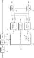
도 1은 본 발명의 실시 예에 따른 이미지 센서의 블록도를 예시적으로 도시한다.
도 2는 도 1의 픽셀 어레이, 제 1 로직 회로, 및 ADC를 좀 더 자세하게 도시한다.
도 3은 도 2의 픽셀 어레이에 배치되는 하나의 픽셀의 블록도를 예시적으로 도시한다.
도 4는 도 1의 메모리 셀 어레이 및 제 2 로직 회로를 좀 더 자세하게 도시한다.
도 5는 도 4의 메모리 셀 어레이를 좀 더 자세하게 도시한다.
도 6은 도 1의 이미지 센서가 실장된 패키지의 단면도를 예시적으로 도시한다.
도 7은 도 1의 이미지 센서의 픽셀 어레이, 메모리 셀 어레이, 제 1 로직 회로, ADC, 및 제 2 로직 회로가 배치되는 예시적인 위치들을 도시한다.
도 8은 도 7의 I-I' 선 및 II-II' 선에 따른 이미지 센서의 단면도를 예시적으로 도시한다.
도 9는 본 발명의 실시 예에 따른 이미지 센서를 포함하는 전자 장치의 구성 및 그것의 인터페이스들을 나타낸 블록도이다.
도 10은 본 발명의 실시 예에 따른 이미지 센서를 포함하는 전자 장치의 동작 방법을 도시하는 순서도이다.Figure 1 exemplarily shows a block diagram of an image sensor according to an embodiment of the present invention.
Figure 2 shows the pixel array, first logic circuit, and ADC of Figure 1 in more detail.
FIG. 3 exemplarily shows a block diagram of one pixel disposed in the pixel array of FIG. 2.
FIG. 4 shows the memory cell array and second logic circuit of FIG. 1 in more detail.
Figure 5 shows the memory cell array of Figure 4 in more detail.
FIG. 6 exemplarily illustrates a cross-sectional view of a package in which the image sensor of FIG. 1 is mounted.
FIG. 7 shows example locations where the pixel array, memory cell array, first logic circuit, ADC, and second logic circuit of the image sensor of FIG. 1 are placed.
FIG. 8 exemplarily shows a cross-sectional view of the image sensor taken along line II′ and line II-II′ in FIG. 7 .
Figure 9 is a block diagram showing the configuration of an electronic device including an image sensor and its interfaces according to an embodiment of the present invention.
10 is a flowchart illustrating a method of operating an electronic device including an image sensor according to an embodiment of the present invention.
아래에서는, 본 발명의 기술 분야에서 통상의 지식을 가진 자가 본 발명을 쉽게 실시할 수 있을 정도로, 본 발명의 실시 예들이 명확하고 상세하게 기재될 것이다. 본 발명은 픽셀 어레이와 메모리 셀 어레이가 병합된 이미지 센서에 관한 것이다. 이미지 센서는 전하 결합 소자(Charge Coupled Device; CCD)와 CMOS 이미지 센서(Complementary Metal-Oxide Semiconductor Image Sensor; CIS)로 구분될 수 있다. 이하, 이미지 센서는 CIS인 것으로 가정하되 본 발명의 범위는 이에 한정되지 않는다.Below, embodiments of the present invention will be described clearly and in detail so that a person skilled in the art can easily practice the present invention. The present invention relates to an image sensor in which a pixel array and a memory cell array are combined. Image sensors can be divided into charge coupled devices (CCD) and CMOS image sensors (Complementary Metal-Oxide Semiconductor Image Sensor (CIS)). Hereinafter, it is assumed that the image sensor is CIS, but the scope of the present invention is not limited thereto.
도 1은 본 발명의 실시 예에 따른 이미지 센서의 블록도를 예시적으로 도시한다. 이미지 센서(10)는 제 1 반도체 칩(110) 및 제 2 반도체 칩(120)을 포함할 수 있다. 제 1 반도체 칩(110) 및 제 2 반도체 칩(120)은 평면적 관점에서 서로 겹치도록 위치할 수 있다. 제 1 반도체 칩(110)은 제 2 반도체 칩(120) 상에 수직으로 적층될 수 있다. 제 1 반도체 칩(110)은 이미지 센서 칩으로 제 2 반도체 칩(120)은 로직 칩으로 지칭될 수 있다.Figure 1 exemplarily shows a block diagram of an image sensor according to an embodiment of the present invention. The
제 1 반도체 칩(110)은 픽셀 어레이(140) 및 메모리 셀 어레이(170)를 포함할 수 있다. 제 2 반도체 칩(120)은 제 1 로직 회로(150), ADC(analog digital converter, 152), 및 제 2 로직 회로(160)를 포함할 수 있다. 픽셀 어레이(140)는 제 1 로직 회로(150)의 제어에 따라 광학 이미지를 전기적 신호, 즉, 아날로그 신호로 변환하고 아날로그 신호를 ADC(152)로 출력할 수 있다. ADC(152)는 아날로그 신호를 디지털 신호로 변환하고 디지털 신호에 기초하는 데이터(픽셀 어레이(140)에 의해 생성되는 이미지)를 제 2 로직 회로(160)에 제공할 수 있다. 제 2 로직 회로(160)는 데이터를 메모리 셀 어레이(170)에 저장할 수 있다.The
데이터는 프레임 단위로 생성되는 이미지 데이터일 수 있다. 데이터의 비트들의 개수는 ADC(152)의 해상도(resolution)에 기초하여 결정될 수 있다. 데이터의 비트들의 개수는 이미지 센서(10)가 지원하는 HDR(high dynamic range)에 기초하여 결정될 수 있다. 또한, 데이터의 비트들은 데이터의 생성 위치, 데이터의 정보 등을 나타내는 적어도 하나의 확장 비트를 더 포함할 수도 있다.The data may be image data generated in units of frames. The number of bits of data may be determined based on the resolution of the
제 2 로직 회로(160) 및 메모리 셀 어레이(170)는 메모리 장치를 구성할 수 있다. 메모리 셀 어레이(170)의 메모리 셀의 종류에 따라 메모리 장치의 종류도 결정될 수 있다. 예를 들어, 메모리 장치는 DRAM(dynamic random access memory) 장치, SRAM(static random access memory) 장치, TRAM(thyristor random access memory) 장치, 플래시(flash) 메모리 장치, PRAM(phase-change random access memory) 장치, MRAM(magneto-resistive random access memory) 장치, ReRAM(Resistive random access memory) 장치, FRAM(ferro-electric random access memory) 장치 중 어느 하나일 수 있다. 이하, 제 2 로직 회로(160)는 데이터 입출력을 위한 DDR(double data rate) 인터페이스를 지원하고, 메모리 셀 어레이(170)는 DRAM 셀들을 포함하고, 그리고 제 2 로직 회로(160) 및 메모리 셀 어레이(170)는 DRAM 장치를 구성하는 것으로 가정한다.The
도 1을 참조하면, 픽셀 어레이(140)와 메모리 셀 어레이(170)는 제 1 반도체 칩(110)에 병합될 수 있다. 만약, 도 1의 도시와 달리, 데이터를 저장하기 위해 메모리 셀 어레이(170)가 제 1 반도체 칩(110)이 아닌 다른 반도체 칩(미도시)에서 구현되는 경우, 제 2 반도체 칩(120)은 다른 반도체 칩과 통신하기 위한 회로들을 더 포함해야 한다. 예를 들어, 다른 반도체 칩이 제 2 반도체 칩(120) 하부에 적층되는 경우(즉, 다른 반도체 칩 상에 제 2 반도체 칩(120)이 적층되는 경우), 제 2 반도체 칩(120)과 다른 반도체 칩 사이의 통신을 위한 경로들이 제 2 반도체 칩(120)에서 구현되어야 한다. 따라서, 제 2 반도체 칩(120)의 면적 및 전력 소모가 증가할 수 있다.Referring to FIG. 1 , the
상술한 경우와 달리, 본 발명에 의하면, 픽셀 어레이(140)와 메모리 셀 어레이(170)는 제 1 반도체 칩(110)에 병합되므로, 제 1 반도체 칩(110)과 제 2 반도체 칩(120) 사이의 통신을 위한 경로들은 제 2 반도체 칩(120)에서 형성되지만 제 2 반도체 칩(120)과 다른 반도체 칩 사이의 통신을 위한 경로들은 제 2 반도체 칩(120)에서 형성되지 않는다. 또한, 픽셀 어레이(140)를 제어하기 위한 제 1 로직 회로(150) 및 ADC(152)와 메모리 셀 어레이(170)를 제어하기 위한 제 2 로직 회로(160)가 모두 제 2 반도체 칩(120)에 병합된다. 따라서, ADC(152)로부터 출력된 데이터를 제 2 로직 회로(160)로 전송하기 위해, 칩들을 연결할 수 있는 TSV(through silicon via), BVS(back via stack), Cu-Cu(도전 패턴들의 접촉) 대신에, 제 2 반도체 칩(120) 내부의 배선 라인(wiring line)들이 사용될 수 있다. 또한, 제 1 로직 회로(150)와 제 2 로직 회로(160) 모두가 제 2 반도체 칩(120)에 병합되므로, 상술한 배선 라인들은 제 2 반도체 칩(120) 내에서 최적화될 수 있다. 본 발명에 의하면, 이미지 센서(10)는 3 스택(stack) 구조 대신에 제 1 반도체 칩(110) 및 제 2 반도체 칩(120)가 적층된 2 스택 구조를 가질 수 있다.Unlike the case described above, according to the present invention, the
실시 예에 있어서, 제 2 반도체 칩(120)은 픽셀 어레이(140)로부터 출력되는 데이터 또는 메모리 셀 어레이(170)로부터 출력되는 데이터를 처리하는 ISP(image signal processor), DSP(digital signal processor) 등과 같은 내장형 프로세서를 더 포함할 수 있다. 프로세서는 이미지 데이터의 노이즈를 개선하거나, 이미지를 보정하거나, 또는 픽셀 어레이(140)로부터 출력된 이미지와 관련된 후속 작업들을 수행할 수 있다.In an embodiment, the
도 2는 도 1의 픽셀 어레이, 제 1 로직 회로, 및 ADC를 좀 더 자세하게 도시한다. 전술한대로, 픽셀 어레이(140)는 제 1 반도체 칩(110)에서 구현될 수 있고 제 1 로직 회로(150, 도 1 참조)는 제 2 반도체 칩(120)에서 구현될 수 있다.Figure 2 shows the pixel array, first logic circuit, and ADC of Figure 1 in more detail. As described above, the
픽셀 어레이(140)는 입사광을 변환하고 전기적 신호를 생성할 수 있다. 픽셀 어레이(140)는 로우 방향과 컬럼 방향을 따라 매트릭스 형태로 배치되는 픽셀들을 포함할 수 있다. 픽셀 어레이(140)는 도 1의 제 1 로직 회로(150)의 제어에 따라 구동될 수 있다.The
제 1 로직 회로(150)는 픽셀 어레이(140)로부터 효율적으로 데이터를 수신하고 이미지 프레임을 생성할 수 있다. 예를 들어, 제 1 로직 회로(150)는 픽셀들 전체가 동시에 감지되는 글로벌 셔터 방식, 픽셀들 전체가 동시에 감지되되 노출 시간을 조절하는 플러터 셔터 방식, 행 단위로 픽셀들을 제어하는 롤링 셔터 방식 또는 코디드 롤링 셔터 방식 등을 이용할 수 있다. 제 1 로직 회로(150)는 로우 드라이버(151), ADC(152), 및 타이밍 컨트롤러(153)를 포함할 수 있다.The
로우 드라이버(151)는 타이밍 컨트롤러(153)의 제어에 따라 로우 단위로 픽셀 어레이(140)의 픽셀들을 제어할 수 있다. 로우 드라이버(151)는 로우 어드레스에 따라 픽셀 어레이(140)의 로우들 중 적어도 하나의 로우를 선택할 수 있다. 이를 위해, 로우 드라이버(151)는 로우 어드레스를 디코딩하고 선택 라인들(SEL), 리셋 라인들(RS), 및 전송 라인들(TG)을 활성화할 수 있다. 로우 드라이버(151)는 선택 라인들(SEL), 리셋 라인들(RS), 및 전송 라인들(TG)을 통해 픽셀 어레이(140)와 연결될 수 있다.The
ADC(152)는 컬럼 라인들(COL)을 통해 픽셀 어레이(140)와 연결될 수 있다. ADC(152)는 픽셀 어레이(140)로부터 컬럼 라인들(COL)을 통해 수신되는 아날로그 신호들을 디지털 신호들로 변환할 수 있다. ADC(152)의 개수는 하나의 로우를 따라 배치되는 픽셀들의 개수 및 컬럼 라인들(COL)의 개수에 기초하여 결정될 수 있고 ADC들(152)은 적어도 하나 이상일 수 있다.The
예를 들어, ADC(152)는 기준 신호 생성기(REF), 비교기(CMP), 카운터(CNT) 및 버퍼(BUF)를 포함할 수 있다. 기준 신호 생성기(REF)는 특정한 기울기를 갖는 램프 신호를 생성하고, 램프 신호를 비교기의 기준 신호로서 제공할 수 있다. 비교기(CMP)는 아날로그 신호와 기준 신호 생성기(REF)의 램프 신호를 비교하고 유효한 신호 성분에 따른 각각의 천이 시점들을 갖는 비교 신호들을 출력할 수 있다. 카운터(CNT)는 카운팅 동작을 수행하여 카운팅 신호를 생성하고, 카운팅 신호를 버퍼(BUF)에 제공할 수 있다. 버퍼(BUF)는 컬럼 라인들(COL)과 각각 연결된 래치(latch) 회로들을 포함하고, 비교 신호의 천이에 응답하여 카운터(CNT)로부터 출력되는 카운팅 신호를 각 컬럼마다 래치하여, 래치된 카운팅 신호를 데이터로서 출력할 수 있다.For example,
실시 예에 있어서, 제 1 로직 회로(150)는 픽셀들의 리셋 상태를 나타내는 기준 전압과 입사광에 상응하는 신호 성분을 나타내는 출력 전압의 차이를 구하여 상관 이중 샘플링을 수행하고 유효한 신호 성분에 상응하는 아날로그 샘플링 신호를 출력하는 상관 이중 샘플링(correlated double sampling; CDS, 미도시) 회로들을 더 포함할 수 있다. 상관 이중 샘플링 회로들은 컬럼 라인들(COL)과 연결될 수 있다.In an embodiment, the
타이밍 컨트롤러(153)는 로우 드라이버(151) 및 ADC(152)의 동작 타이밍을 제어할 수 있다. 타이밍 컨트롤러(153)는 로우 드라이버(151) 및 ADC(152)에 타이밍 신호 및 제어 신호를 제공할 수 있다. 좀 더 구체적으로, 타이밍 컨트롤러(153)는 ADC(152)를 제어할 수 있고 ADC(152)는 타이밍 컨트롤러(153)의 제어에 따라 데이터를 제 2 로직 회로(160)에 제공할 수 있다. 또한, 타이밍 컨트롤러(153)는 ADC(152)의 데이터가 메모리 셀 어레이(170)에 저장되도록 제 2 로직 회로(160)에 요청, 명령, 또는 어드레스를 제공하는 회로들(미도시)을 더 포함할 수 있다.The
도 3은 도 2의 픽셀 어레이에 배치되는 하나의 픽셀의 블록도를 예시적으로 도시한다. 픽셀(PX)은 픽셀 어레이(140)를 구성하는 단위 픽셀로 지칭될 수 있다. 픽셀(PX)은 수신되는 광에 기초하여 전기적 신호를 생성하고 그리고 전기적 신호를 컬럼 라인(COL)으로 출력할 수 있다. 픽셀(PX)은 광 감지 소자(photo sensitive device)로서 포토다이오드(PD)를 포함할 수 있다. 픽셀은 독출(readout) 회로이고 그리고 전송 트랜지스터(TX), 리셋 트랜지스터(RX), 드라이브 트랜지스터(DX), 및 선택 트랜지스터(SX)를 포함할 수 있다.FIG. 3 exemplarily shows a block diagram of one pixel disposed in the pixel array of FIG. 2. The pixel PX may be referred to as a unit pixel constituting the
포토다이오드(PD)는 외부로부터 광(예를 들어, 가시광선 또는 적외선)을 수신하고 수신된 광에 기초하여 광 전하(photo charge)를 생성할 수 있다. 다른 예에 있어서, 픽셀은 포토다이오드(PD)와 함께 또는 포토다이오드(PD)를 대신하여, 포토 트랜지스터, 포토 게이트, 또는 핀드(pinned) 포토다이오드를 포함할 수 있다. 포토다이오드(PD)에서 생성된 광 전하는 전송 트랜지스터(TX)를 통하여 플로팅 디퓨전 노드(floating diffusion node; FD)로 전송될 수 있다.A photodiode (PD) can receive light (for example, visible light or infrared light) from the outside and generate photo charges based on the received light. In another example, a pixel may include a phototransistor, a photogate, or a pinned photodiode, along with or instead of a photodiode (PD). Photo charges generated in the photodiode (PD) can be transferred to the floating diffusion node (FD) through the transfer transistor (TX).
전송 트랜지스터(TX)는 전송 라인(TG)의 신호의 논리 레벨에 따라 포토다이오드(PD)와 플로팅 디퓨전 노드(FD)를 전기적으로 연결할 수 있다. 예를 들어, 전송 라인(TG)의 신호가 임의의 논리 레벨(예를 들어, 하이 레벨)이고 전송 트랜지스터(TX)가 턴 온(turn-on)되면, 포토다이오드(PD)에서 생성된 광 전하는 전송 트랜지스터(TX)를 통해 플로팅 디퓨전 노드(FD)로 전송될 수 있다.The transmission transistor (TX) can electrically connect the photodiode (PD) and the floating diffusion node (FD) according to the logic level of the signal of the transmission line (TG). For example, when the signal of the transmission line (TG) is at any logic level (e.g., high level) and the transmission transistor (TX) is turned on, the photo charge generated in the photodiode (PD) is It can be transmitted to the floating diffusion node (FD) through a transfer transistor (TX).
리셋 트랜지스터(RX)는 리셋 라인(RS)의 신호의 논리 레벨에 따라 플로팅 디퓨전 노드(FD)를 리셋할 수 있다. 예를 들어, 리셋 트랜지스터(RX)는 주기적으로 혹은 비주기적으로 전원 전압(VDD)과 따라 플로팅 디퓨전 노드(FD)를 전기적으로 연결하고 플로팅 디퓨전 노드(FD)를 전원 전압(VDD)으로 충전시킬 수 있다.The reset transistor (RX) may reset the floating diffusion node (FD) according to the logic level of the signal of the reset line (RS). For example, the reset transistor (RX) can electrically connect the floating diffusion node (FD) according to the power supply voltage (VDD) periodically or aperiodically and charge the floating diffusion node (FD) with the power supply voltage (VDD). there is.
드라이브 트랜지스터(DX)는 플로팅 디퓨전 노드(FD)에 충전된 전하에 대응하는 신호(즉, 드라이브 트랜지스터(DX)의 게이트 단자의 전압)에 따라 소스 팔로워(source follower)와 유사하게 동작할 수 있다. 드라이브 트랜지스터(DX)는 플로팅 디퓨전 노드(FD)의 전압에 기초하여 결정되는 전압을 선택 트랜지스터(SX)에 제공할 수 있다. 드라이브 트랜지스터(DX)는 전원 전압(VDD)과 선택 트랜지스터(SX) 사이에 연결될 수 있다.The drive transistor DX may operate similarly to a source follower according to a signal corresponding to the charge charged in the floating diffusion node FD (i.e., the voltage of the gate terminal of the drive transistor DX). The drive transistor DX may provide a voltage determined based on the voltage of the floating diffusion node FD to the selection transistor SX. The drive transistor (DX) may be connected between the power supply voltage (VDD) and the selection transistor (SX).
선택 트랜지스터(SX)는 선택 라인(SEL)의 신호의 논리 레벨에 따라 드라이브 트랜지스터(DX)와 컬럼 라인(COL)을 전기적으로 연결할 수 있다. 선택 트랜지스터(SX)는 드라이브 트랜지스터(DX)로부터 제공되는 신호 또는 전압을 컬럼 라인(COL)에 제공할 수 있다.The selection transistor (SX) may electrically connect the drive transistor (DX) and the column line (COL) according to the logic level of the signal of the selection line (SEL). The selection transistor SX may provide a signal or voltage provided from the drive transistor DX to the column line COL.
도 4는 도 1의 메모리 셀 어레이 및 제 2 로직 회로를 좀 더 자세하게 도시한다. 메모리 셀 어레이(170)는 제 1 반도체 칩(110)에서 구현될 수 있다. 반면에, 제 2 로직 회로(160, 도 1 참조)의 모든 구성 요소들은 제 2 반도체 칩(120)에서 구현될 수 있다. 상술한 바와 달리, 제 2 로직 회로(160)의 일부 구성 요소들은 제 1 반도체 칩(110)에서 구현되거나 제 2 로직 회로(160)의 나머지 구성 요소들은 제 2 반도체 칩(120)에서 구현될 수도 있다. 제 2 로직 회로(160)의 구성 요소들은 제 1 반도체 칩(110) 및 제 2 반도체 칩(120)에 분산되어 배치될 수 있다. 즉, 제 2 로직 회로(160)는 제 1 반도체 칩(110) 또는 제 2 반도체 칩(120)에서 구현될 수 있다. 제 2 로직 회로(160)는 제 1 로직 회로(150)의 제어에 따라 픽셀 어레이(140)로부터 출력되는 아날로그 신호(들)에 기초하는 데이터를 메모리 셀 어레이(170)에 저장할 수 있다.FIG. 4 shows the memory cell array and second logic circuit of FIG. 1 in more detail. The
제 2 로직 회로(160)는 명령 디코더(161), 어드레스 버퍼(162), 로우 디코더(163), 컬럼 디코더(164), 입출력 드라이버(165), 입출력 센스 앰프(166), DQ 버퍼(167), 및 전압 생성기(168)를 포함할 수 있다. 상술한 구성 요소들(161, 162, 163, 164, 165, 166, 167, 168)의 개수들 각각은 하나인 것으로 도 4에서 도시되었으나 메모리 셀 어레이(170)의 용량, 동작 속도 등에 따라 개수들 각각은 하나 이상일 수도 있다.The
명령 디코더(161)는 명령(CMD)을 디코딩하고 어드레스 버퍼(162), 로우 디코더(163), 컬럼 디코더(164), 입출력 드라이버(165), 입출력 센스 앰프(166), DQ 버퍼(167), 및 전압 생성기(168)를 제어할 수 있다. 명령 디코더(161)는 제 2 반도체 칩(120)에서 구현되거나 배치될 수 있다. 명령(CMD)은 메모리 셀 어레이(170)와 관련된 활성화 명령, 프리차지 명령, 리프레쉬 명령, 쓰기 명령, 읽기 명령 등을 포함할 수 있다.The
예를 들어, 명령(CMD)은 제 1 로직 회로(150)로부터 제공될 수도 있다. 본 발명의 실시 예에 따라 제 1 로직 회로(150)와 제 2 로직 회로(160) 모두가 동일한 제 2 반도체 칩(120) 내부에서 구현되므로, 명령(CMD)은 제 2 반도체 칩(120)의 설계 방식에 따라 결정되고 JEDEC 표준에 정의되지 않을 수 있다. 또한, 명령(CMD)은 제 1 로직 회로(150)뿐만 아니라 이미지 센서(10)의 외부 장치(예를 들어, 호스트, 메모리 컨트롤러, 프로세서 등)로부터 제공될 수도 있다. 명령(CMD)은 DDR SDRAM(synchronous DRAM), DDR2 SDRAM, DDR3 SDRAM, DDR4 SDRAM, DDR5 SDRAM, LPDDR(low power double data rate) SDRAM, LPDD2 SDRAM, LPDDR3 SDRAM, LPDDR4 SDRAM, LPDDR5 SDRAM, HBM(high bandwidth memory), HBM2, HBM3 등과 같은 DRAM 장치들과 관련된 JEDEC 표준 또는 DDR 인터페이스에서 정의될 수 있다. 즉, 명령 디코더(161)는 제 2 반도체 칩(120) 내부적으로 생성되는 명령(CMD) 및 외부 장치로부터 제공되는 명령(CMD)을 모두 디코딩할 수 있다.For example, the command CMD may be provided from the
어드레스 버퍼(162)는 명령 디코더(161)의 제어에 따라 어드레스(ADD)를 수신할 수 있다. 어드레스 버퍼(162)는 제 2 반도체 칩(120)에서 구현되거나 배치될 수 있다. 예를 들어, 명령 디코더(161)가 활성화 명령을 수신하면, 어드레스 버퍼(162)는 수신된 어드레스(ADD)를 로우 어드레스(RADD)로서 로우 디코더(163)에 제공할 수 있다. 명령 디코더(161)가 쓰기 명령 또는 읽기 명령을 수신하면, 어드레스 버퍼(162)는 수신된 어드레스(ADD)를 컬럼 어드레스(CADD)로서 컬럼 디코더(164)에 제공할 수 있다. 명령(CMD)과 유사하게, 어드레스(ADD)는 외부 장치 또는 제 1 로직 회로(150)로부터 제공될 수 있다. 어드레스 버퍼(162)는 외부 장치 또는 제 1 로직 회로(150)로부터 로우 어드레스(RADD) 및 컬럼 어드레스(CADD)를 수신할 수도 있다. 어드레스(ADD)의 범위는 ADC(152)로부터 제공되는 데이터의 크기, 메모리 셀 어레이(170)의 용량, 메모리 셀 어레이(170)의 워드 라인들(WL)의 개수, 컬럼 선택 라인들(CSL)의 개수, 및 하나의 컬럼 선택 라인(CSL) 당 비트 라인들(BL)의 개수에 따라 결정될 수 있다.The
실시 예에 있어서, 어드레스(ADD)는 제 2 반도체 칩(120)에서 내부적으로 생성될 수도 있다. 전술한대로, 어드레스(ADD)는 명령(CMD)과 함께 제 1 로직 회로(150)에 의해 생성되고 제공될 수 있다. 다른 예를 들어, 제 1 로직 회로(150)는 명령(CMD)만 생성하고 어드레스(ADD)는 제 1 로직 회로(150)의 명령(CMD)에 기초하여 제 2 로직 회로(160)에 의해 생성될 수도 있다. 이 경우, 제 2 로직 회로(160)는 어드레스 버퍼(162) 대신에 어드레스 생성기, 로우 어드레스 생성기, 또는 컬럼 어드레스 생성기를 포함할 수 있다.In an embodiment, the address ADD may be generated internally in the
로우 디코더(163)는 명령 디코더(161)에 의해 생성되는 로우 제어 신호(R_CTRL)에 기초하여 로우 어드레스(RADD)를 디코딩할 수 있다. 명령 디코더(161)가 활성화 명령을 수신하면, 로우 디코더(163)는 로우 어드레스(RADD)의 디코딩 결과에 기초하여 메모리 셀 어레이(170)의 워드 라인들(WL) 중 적어도 하나를 선택하거나 활성화할 수 있다. 그 다음, 명령 디코더(161)가 프리차지 명령을 수신하면, 로우 디코더(163)는 로우 제어 신호(R_CTRL)에 기초하여 선택되거나 활성화된 워드 라인을 비선택하거나 비활성화할 수 있다.The
로우 디코더(163)는 주기적으로 메모리 셀 어레이(170)의 워드 라인들(WL) 중 적어도 하나를 활성화하고 메모리 셀 어레이(170)의 메모리 셀들을 리프레쉬할 수 있다. 예를 들어, 메모리 셀 어레이(170)의 리프레쉬를 위해, 제 1 로직 회로(150)는 명령 디코더(161)로 리프레쉬 명령을 제공할 수 있다. 이 경우, 제 2 로직 회로(160)는 상술한 리프레쉬 명령에 따라 로우 어드레스(RADD)를 생성하고 업데이트하는 어드레스 생성기를 더 포함할 수 있다. 다른 예를 들어, 제 2 로직 회로(160)는 제 1 로직 회로(150) 또는 외부 장치의 요청 없이도 리프레쉬 동작을 수행할 수 있다(즉, 셀프 리프레쉬). 이 경우, 제 2 로직 회로(160)는 리프레쉬 명령 및 로우 어드레스(RADD)를 주기적으로 생성하는 내부 회로들(타이머, 명령 생성기, 어드레스 생성기 등)을 포함할 수도 있다.The
로우 디코더(163)는 제 1 반도체 칩(110) 또는 제 2 반도체 칩(120)에 배치될 수 있다. 예를 들어, 로우 디코더(163)는 제 1 반도체 칩(110) 및 제 2 반도체 칩(120) 중 어느 하나에만 배치될 수도 있다. 다른 예를 들어, 로우 디코더(163)의 서브 회로들은 제 1 반도체 칩(110) 및 제 2 반도체 칩(120)에 분산되어 배치될 수 있다.The
컬럼 디코더(164)는 명령 디코더(161)에 의해 생성되는 컬럼 제어 신호(C_CTRL)에 기초하여 컬럼 어드레스(CADD)를 디코딩할 수 있다. 컬럼 디코더(164)는 컬럼 어드레스(CADD)의 디코딩 결과에 기초하여 메모리 셀 어레이(170)의 컬럼 선택 라인들(CSL) 중 적어도 하나를 선택하거나 활성화할 수 있다. 그 다음, 컬럼 디코더(164)는 컬럼 제어 신호(C_CTRL)에 기초하여 선택되거나 활성화된 컬럼 선택 라인을 비선택하거나 비활성화할 수 있다 컬럼 디코더(164)는 제 1 반도체 칩(110) 또는 제 2 반도체 칩(120)에 배치될 수 있다. 예를 들어, 컬럼 디코더(164)는 제 1 반도체 칩(110) 및 제 2 반도체 칩(120) 중 어느 하나에만 배치될 수도 있다. 다른 예를 들어, 컬럼 디코더(164)의 서브 회로들은 제 1 반도체 칩(110) 및 제 2 반도체 칩(120)에 분산되어 배치될 수 있다.The
입출력 드라이버(165)는 명령 디코더(161)의 제어에 따라 데이터를 메모리 셀 어레이(170)에 쓰거나 저장할 수 있다. 데이터는 ADC(152)로부터 제공될 수 있고 쓰기 데이터(WDATA)로 지칭될 수 있다. 입출력 드라이버(165)는 데이터를 입출력 라인(IO)을 통해 로우 디코더(163) 및 컬럼 디코더(164)에 의해 선택된 적어도 하나의 메모리 셀에 제공할 수 있다. 도 4에서, 입출력 라인(IO)만 도시되었으나, 입출력 드라이버(165)는 데이터를 입출력 라인(IO) 및 상보 입출력 라인(IOB)을 통해 선택된 적어도 하나의 메모리 셀에 제공할 수 있다. 입출력 드라이버(165)는 데이터의 논리 상태들에 기초하여 입출력 라인(IO) 및 상보 입출력 라인(IOB)을 차동 방식으로 구동할 수 있다. 입출력 드라이버(165)는 제 1 반도체 칩(110) 또는 제 2 반도체 칩(120)에 배치될 수 있다. 예를 들어, 입출력 드라이버(165)는 제 1 반도체 칩(110) 및 제 2 반도체 칩(120) 중 어느 하나에만 배치될 수도 있다. 다른 예를 들어, 입출력 드라이버(165)의 서브 회로들은 제 1 반도체 칩(110) 및 제 2 반도체 칩(120)에 분산되어 배치될 수 있다.The input/
입출력 센스 앰프(166)는 명령 디코더(161)의 제어에 따라 메모리 셀 어레이(170)에 저장된 데이터를 읽을 수 있다. 입출력 센스 앰프(166)에 의해 읽혀진 데이터는 읽기 데이터(RDATA)로 지칭될 수 있다. 입출력 센스 앰프(166)는 로우 디코더(163) 및 컬럼 디코더(164)에 의해 선택된 적어도 하나의 메모리 셀로부터 입출력 라인(IO) 및 상보 입출력 라인(IOB)을 통해 출력되는 데이터를 감지할 수 있다. 입출력 센스 앰프(166)는 차동 방식으로 입출력 라인(IO) 및 상보 입출력 라인(IOB)의 전압 레벨들을 감지하고 데이터의 논리 상태들을 판별할 수 있다. 입출력 센스 앰프(166)는 감지된 데이터를 DQ 버퍼(167)에 제공할 수 있다. 입출력 센스 앰프(166)는 제 1 반도체 칩(110) 또는 제 2 반도체 칩(120)에 배치될 수 있다. 예를 들어, 입출력 센스 앰프(166)는 제 1 반도체 칩(110) 및 제 2 반도체 칩(120) 중 어느 하나에만 배치될 수도 있다. 다른 예를 들어, 입출력 센스 앰프(166)의 서브 회로들은 제 1 반도체 칩(110) 및 제 2 반도체 칩(120)에 분산되어 배치될 수 있다.The input/
DQ 버퍼(167)는 명령 디코더(161)의 제어에 따라 입출력 센스 앰프(166)로부터 제공된 데이터를 수신하고 데이터를 읽기 데이터로서 외부 장치로 출력할 수 있다. DQ 버퍼(167)는 전술한 다양한 방식의 DDR 인터페이스에 기초하여 데이터를 외부 장치로 출력할 수 있다. 도 4에서 도시되진 않았지만, 제 2 로직 회로(160)는 데이터와 함께 데이터 스트로브(DQS)를 외부 장치로 더 출력할 수도 있다.The
전압 생성기(168)는 외부로부터 제공되는 전원 전압들(VDD, VSS)에 기초하여 메모리 셀 어레이(170)를 구동하기 위한 전압들을 생성할 수 있다. 예를 들어, 전압들은 전원 전압(VDD)보다 높은 고전압(VPP) 및 전원 전압(VSS)보다 낮은 저전압(VBB2)을 생성할 수 있다. 전압들(VPP, VBB2)은 워드 라인들을 선택하거나 비선택하는데 이용될 수 있다. 전압 생성기(168)는 메모리 셀 어레이(170)에 배치되는 다양한 라인들을 프리차지하기 위한 전압(VBLP)을 더 생성할 수 있다.The
메모리 셀 어레이(170)는 로우 방향과 컬럼 방향을 따라 매트릭스 형태로 배치되는 메모리 셀들을 포함할 수 있다. 메모리 셀 어레이(170)는 다수의 뱅크(bank)들로 나뉘어질 수 있다. 메모리 셀들 각각은 하나의 워드 라인(WL)과 하나의 비트 라인(BL)에 연결될 수 있다. 메모리 셀(MC)은 하나의 워드 라인(WL)과 하나의 비트 라인(BL)에 연결되는 하나의 트랜지스터 및 트랜지스터에 연결된 커패시터(capacitor)를 포함하는 DRAM 셀일 수 있다. 물론, 메모리 셀(MC)은 SRAM 셀, TRAM 셀, 플래시 메모리 셀, PRAM 셀, MRAM 셀, ReRAM 셀, FRAM 셀일 수도 있다. 전술한대로, 메모리 셀 어레이(170)는 제 1 반도체 칩(110)에서 구현되고 배치될 수 있다.The
도 5는 도 4의 메모리 셀 어레이를 좀 더 자세하게 도시한다. 메모리 셀 어레이(170)의 메모리 셀들(MC)은 다수의 매트들(MAT)로 나뉘어질 수 있다. 메모리 셀 어레이(170)에는 메모리 셀들(MC)과 연결되는 워드 라인들(WL) 및 비트 라인들(BL), 비트 라인들(BL)과 연결되는 컬럼 선택 라인들(CSL), 그리고 메모리 셀들(MC)에 데이터를 전달하거나 메모리 셀들(MC)로부터 데이터를 읽기 위한 입출력 라인들(IO) 및 상보 입출력 라인들(IOB)이 배치될 수 있다.Figure 5 shows the memory cell array of Figure 4 in more detail. The memory cells MC of the
매트들 각각에는 워드 라인(WL)과 비트 라인(BL)에 연결된 메모리 셀이 배치될 수 있다. 비트 라인(BL)이 배치되는 매트와 상보 비트 라인(BLB)이 배치되는 매트는 서로 다를 수 있다(즉, 오픈 비트 라인 구조). 매트들(MAT)은 워드 라인(WL)이 연장되는 방향(또는, 컬럼 선택 라인들(CSL)이 배치되는 방향, 즉, 로우 방향)을 따라 배치될 수 있다. 로우 방향을 따라 배치되는 매트들(MAT) 사이에는 서브 워드 라인 드라이버(SWD)가 배치될 수 있다. 서브 워드 라인 드라이버(SWD)는 인접하는 매트들(MAT)의 워드 라인(WL)을 구동할 수 있다. 매트들(MAT)은 비트 라인(BL), 상보 비트 라인(BLB), 또는 컬럼 선택 라인(CSL)이 연장되는 방향(또는, 워드 라인들(WL)이 배치되는 방향, 즉, 컬럼 방향)을 따라 배치될 수 있다. 컬럼 방향을 따라 배치되는 매트들(MAT) 사이에는 비트 라인 센스 앰프(BLSA) 및 스위치(SW)가 배치될 수 있다.Memory cells connected to the word line (WL) and the bit line (BL) may be disposed on each of the mats. The mat on which the bit line (BL) is placed and the mat on which the complementary bit line (BLB) is placed may be different from each other (i.e., open bit line structure). The mats MAT may be arranged along the direction in which the word line WL extends (or the direction in which the column select lines CSL are arranged, that is, the row direction). A sub word line driver (SWD) may be placed between the MATs arranged along the row direction. The sub word line driver (SWD) can drive the word lines (WL) of adjacent mats (MAT). The mats (MAT) extend in the direction in which the bit line (BL), complementary bit line (BLB), or column select line (CSL) extends (or the direction in which the word lines (WL) are arranged, that is, the column direction). It can be arranged accordingly. A bit line sense amplifier (BLSA) and a switch (SW) may be disposed between the mats (MAT) arranged along the column direction.
활성화 명령 또는 리프레쉬 명령에 기초하는 로우 디코더(163)의 제어에 따라, 비트 라인 센스 앰프(BLSA)는 비트 라인(BL)의 전압과 상보 비트 라인(BLB)의 전압 사이의 차이를 감지하고 증폭할 수 있다. 그 다음, 읽기 명령 또는 쓰기 명령에 기초하여 컬럼 디코더(164)가 컬럼 선택 라인(CSL)을 선택하면, 컬럼 선택 라인(CSL)의 신호에 따라 스위치들(SW)이 턴 온되거나 턴 오프될 수 있다. 컬럼 어드레스(CADD)에 대응하는 스위치들(SW)이 턴 온되면, 입출력 라인(IO)과 비트 라인(BL)이 전기적으로 연결되고 상보 입출력 라인(IOB)과 상보 비트 라인(BLB)이 전기적으로 연결될 수 있다. 물론, 데이터 스크램블에 따라, 비트 라인(BL)이 상보 입출력 라인(IOB)과 그리고 상보 비트 라인(BLB)이 입출력 라인(IO)과 전기적으로 연결될 수도 있다.Under the control of the
쓰기 동작에서, 입출력 드라이버(165)는 입출력 라인(IO), 상보 입출력 라인(IOB), 비트 라인(BL), 및 상보 비트 라인(BLB)을 통해 메모리 셀(MC)에 데이터를 쓸 수 있다. ADC(152)로부터 출력되는 데이터의 어느 한 비트는 입출력 라인(IO) 및 상보 입출력 라인(IOB)을 통해 메모리 셀 어레이(170)에 저장될 수 있다. 읽기 동작에서, 입출력 센스 앰프(166)는 비트 라인(BL), 상보 비트 라인(BLB), 입출력 라인(IO), 및 상보 입출력 라인(IOB)을 통해 출력되는 데이터를 읽을 수 있다. 예를 들어, 컬럼 방향을 따라 배치되는 매트들(MAT) 사이에는 비트 라인 센스 앰프(BLSA)에 의해 증폭된 전압 차이에 기초하여 입출력 라인(IO) 및 상보 입출력 라인(IOB)을 구동하는 로컬 센스 앰프(LSA)가 더 배치될 수도 있다. 입출력 라인(IO) 및 상보 입출력 라인(IOB)은 컬럼 방향을 따라 배치되는 매트들(MAT)과 관련된 데이터 입출력을 위해 사용될 수 있고 상술한 매트들(MAT)에 의해 공유될 수 있다.In a write operation, the input/
실시 예에 있어서, 메모리 셀들(MC)의 개수, 비트 라인 센스 앰프들(BLSA)의 개수, 스위치들(SW)의 개수, 비트 라인들(BL)의 개수, 상보 비트 라인들(BLB)의 개수, 컬럼 선택 라인들(CSL)의 개수, 입출력 라인들(IO)의 개수, 및 상보 입출력 라인들(IOB)의 개수는 도 5에서 도시된 것으로 한정되지 않는다. 또한, 하나의 컬럼 선택 라인(CSL)에 의해 선택되는 비트 라인(BL, 혹은 상보 비트 라인(BLB))의 개수는 적어도 하나 이상(예를 들어, 4, 8 등)일 수 있다. 하나의 컬럼 선택 라인(CSL)에 의해 선택될 수 있는 비트 라인들의 개수에 따라 컬럼 방향으로 배치되는 매트들(MAT)에 대응하는 입출력 라인들(IO, 혹은 상보 입출력 라인들(IOB))의 개수도 결정될 수 있다.In an embodiment, the number of memory cells (MC), the number of bit line sense amplifiers (BLSA), the number of switches (SW), the number of bit lines (BL), and the number of complementary bit lines (BLB) , the number of column selection lines (CSL), the number of input/output lines (IO), and the number of complementary input/output lines (IOB) are not limited to those shown in FIG. 5. Additionally, the number of bit lines (BL, or complementary bit lines (BLB)) selected by one column select line (CSL) may be at least one (eg, 4, 8, etc.). The number of input/output lines (IO, or complementary input/output lines (IOB)) corresponding to MATs arranged in the column direction according to the number of bit lines that can be selected by one column select line (CSL). can also be determined.
실시 예에 있어서, 메모리 셀들(MC)의 개수는 제 1 반도체 칩(110)의 면적, 픽셀 어레이(140)의 면적, 외부 장치와 사전에 정의된 규약 등에 기초하여 결정될 수 있다. 메모리 셀들(MC)의 개수에 기초하여 로우 어드레스(RADD)의 범위 및 컬럼 어드레스(CADD)의 범위가 결정될 수 있다. 예를 들어, 하나의 워드 라인(WL)에 연결되는 메모리 셀들(MC)의 개수(즉, 페이지 크기)는 컬럼 어드레스(CADD)의 범위에 따라 결정될 수 있다.In an embodiment, the number of memory cells MC may be determined based on the area of the
실시 예에 있어서, 매트들(MAT)의 개수는 도 5에서 도시된 것으로 한정되지 않는다. 예를 들어, 하나의 프레임 단위에 대응하는 데이터는 도 5에서 도시된 메모리 셀 어레이(170)에 저장될 수 있다. 또한, 메모리 셀 어레이(170)에 다른 매트들이 더 배치되고 메모리 셀 어레이(170)가 로우 방향 또는 컬럼 방향으로 확장될 수 있다. 확장된 메모리 셀 어레이에 하나의 프레임 단위에 대응하는 다른 데이터가 더 저장될 수 있다. 명령 디코더(161), 어드레스 버퍼(162), 로우 디코더(163), 또는 컬럼 디코더(164)는 로우 어드레스 범위 또는 컬럼 어드레스 범위가 확장된 어드레스 범위에 기초하여 메모리 셀 어레이(170)와 확장된 메모리 셀 어레이를 제어할 수 있고 메모리 셀 어레이(170) 또는 확장된 메모리 셀 어레이에 데이터를 저장할 수 있다.In the embodiment, the number of mats MAT is not limited to that shown in FIG. 5 . For example, data corresponding to one frame unit may be stored in the
실시 예에 있어서, ADC(152)의 해상도, ADC(152)로부터 출력되는 데이터의 비트들의 개수, 이미지 센서(10)가 지원하는 HDR에 기초하여 입출력 드라이버들(165)의 개수, 입출력 센스 앰프들(166)의 개수, 그리고 입출력 라인(IO) 및 상보 입출력 라인(IOB) 쌍들의 개수가 결정될 수 있고 그리고 상술한 개수들은 적어도 하나 이상일 수 있다. 컬럼 디코더(164)는 ADC(152)의 해상도, ADC(152)로부터 출력되는 데이터의 비트들의 개수, 이미지 센서(10)가 지원하는 HDR에 기초하여 적어도 두 개의 컬럼 선택 라인들(CSL)을 병렬로 또는 동시에 활성화할 수 있다. 적어도 두 개의 컬럼 선택 라인들(CSL)이 활성화되면, 적어도 두 개의 입출력 드라이버들(165) 또는 적어도 두 개의 입출력 센스 앰프들(166)이 병렬로 또는 동시에 동작할 수 있다.In an embodiment, the resolution of the
도 6은 도 1의 이미지 센서가 실장된 패키지의 단면도를 예시적으로 도시한다. 이미지 센서(10)는 접착층(12)을 이용하여 패키지 기판(11) 상에 실장될 수 있다. 예를 들어, 패키지 기판(11)은 인쇄회로기판(PCB)일 수 있다. 접착층(12)은 에폭시, 실리콘 재질의 절연성 막, 또는 테이프일 수 있다. 패키지 기판(11)은 윗면 및 아랫면에 각각 도전성 패턴들(미도시)을 포함할 수 있다. 도전성 패턴들의 일부는 패키지 기판(11)의 아랫면에 제공되는 패드들(13)과 연결될 수 있다. 외부 장치와의 전기적 연결을 위한 외부 단자들(14)이 패드들(13)에 부착될 수 있다. 또한, 도전성 패턴들의 일부는 패키지 기판(11)의 윗면에 제공되는 패드들(미도시)과 연결될 수 있다.FIG. 6 exemplarily illustrates a cross-sectional view of a package in which the image sensor of FIG. 1 is mounted. The
예를 들어, 외부 장치는 외부 단자들(14), 패드들(13), 패키지 기판(11)을 통해 제 1 반도체 칩(110) 및 제 2 반도체 칩(120)과 통신할 수 있다. 패키지 기판(11)은 TSV, BVS, 도전 패턴들의 접촉, 와이어 본딩(bonding)과 같은 연결을 통해 제 1 반도체 칩(110) 및 제 2 반도체 칩(120)과 전기적으로 연결될 수 있다.For example, an external device may communicate with the
이미지 센서(10)는 패키지 기판(11)과 마주보는 제 1 면(10a) 및 제 1 면(10a)과 대향하는 제 2 면(10b)을 가질 수 있다. 이미지 센서(10)는 패키지 기판(11) 상에 수직으로 적층된 제 2 반도체 칩(120) 및 제 2 반도체 칩(120) 상에 수직으로 적층된 제 1 반도체 칩(110)을 포함할 수 있다. 예를 들어, 제 1 반도체 칩(110)과 제 2 반도체 칩(120)은 웨이퍼 레벨에서 서로 물리적으로 그리고 전기적으로 결합될 수 있다.The
이미지 센서(10)의 제 2 면(10b) 상에 마이크로 렌즈들(ML)이 배치될 수 있다. 예를 들어, 마이크로 렌즈들(ML)은 평면적 관점에서 픽셀 어레이(140)와 겹치도록 배치될 수 있으나 메모리 셀 어레이(170)와는 겹치지 않도록 배치될 수 있다. 다른 예를 들어, 마이크로 렌즈들(ML)은 평면적 관점에서 메모리 셀 어레이(170)와 겹치도록 배치될 수도 있다.Micro lenses ML may be disposed on the
홀더(18)는 패키지 기판(11) 상에 제공되고 이미지 센서(10)를 둘러쌓을 수 있다. 투명 기판(19)은 홀더(18) 상에 제공될 수 있다. 투명 기판(19)은 이미지 센서(10)와 수직적으로 이격될 수 있다. 예를 들어, 제 1 반도체 칩(110)은 패키지 기판(11)보다 투명 기판(19)에 더 가깝게 배치되고 제 2 반도체 칩(120)은 투명 기판(19)보다 패키지 기판(11)에 더 가깝게 배치될 수 있다.The
실시 예에 있어서, 이미지 센서(10)는 다양한 종류의 반도체 패키지들을 이용하여 실장될 수 있다. 예를 들어, 이미지 센서(10)는 PoP(package on package), BGAs(ball grid arrays), CSPs(chip scale packages), PLCC(plastic leaded chip carrier), PDIP(plastic dual in-line package), Die in waffle pack, Die in wafer form, COB(chip on board), CERDIP(ceramic dual in-line package), MQFP(metric quad flat pack), TQFP(thin quad flat pack), SOIC(small outline integrated circuit), SSOP(shrink small outline package), TSOP(thin small outline package), SIP(system in package), MCP(multi chip package), WFP(wafer-level fabricated package), WSP(wafer-level processed stack package) 등과 같은 패키지를 이용하여 실장될 수 있다.In some embodiments, the
도 7은 도 1의 이미지 센서의 픽셀 어레이, 메모리 셀 어레이, 제 1 로직 회로, ADC, 및 제 2 로직 회로가 배치되는 예시적인 위치들을 도시한다. 이미지 센서(10)의 제 1 반도체 칩(110)과 제 2 반도체 칩(120)은 서로 수직하게 적층될 수 있다. 도 7에서, 제 1 반도체 칩(110)의 크기와 제 2 반도체 칩(120)의 크기는 서로 동일한 것으로 도시되었으나, 서로 상이할 수도 있다. 전술한대로, 픽셀 어레이(140) 및 메모리 셀 어레이(170)는 제 1 반도체 칩(110)에 배치될 수 있다. 제 1 로직 회로(150), ADC(152), 및 제 2 로직 회로(160)는 제 2 반도체 칩(120)에 배치될 수 있다. 물론, 제 2 로직 회로(160)의 일부 구성 요소들은 제 1 반도체 칩(110)에 배치될 수도 있다.FIG. 7 shows example locations where the pixel array, memory cell array, first logic circuit, ADC, and second logic circuit of the image sensor of FIG. 1 are placed. The
픽셀 어레이(140)는 제 1 반도체 칩(110)의 제 1 영역에 배치될 수 있다. 메모리 셀 어레이(170)는 제 1 영역과 분리된 제 2 영역에 배치될 수 있다. 제 1 영역과 제 2 영역은 서로 다를 수 있다. 제 1 영역은 제 2 영역보다 클 수 있다. 제 1 영역 및 제 2 영역과 분리된 제 3 영역에는 제 2 로직 회로(160)의 일부 구성 요소들 또는 제 1 반도체 칩(110)과 제 2 반도체 칩(120)을 전기적으로 연결하는 경로들이 배치될 수 있다. 제 3 영역은 제 2 영역보다 작을 수 있다. 제 1 반도체 칩(110)과 제 2 반도체 칩(120)을 전기적으로 연결하는 경로들은 제 1 반도체 칩(110)의 제 3 영역 및 평면적 관점에서 제 3 영역과 겹치는 제 2 반도체 칩(120)의 영역 사이에서 형성될 수 있다. 예를 들어, 제 2 로직 회로(160)가 메모리 셀 어레이(170)를 제어하기 위한 신호(들) 또는 ADC(152)로부터 출력된 데이터는, 상술한 경로들을 통해 제 2 반도체 칩(120)에서 제 1 반도체 칩(110)으로 전송될 수 있다.The
실시 예에 있어서, 제 1 반도체 칩(110)의 가장자리에는 패드들(미도시)이 더 배치될 수 있다. 가장자리에 배치된 패드들이 위치하는 영역 및 평면적 관점에서 상술한 영역과 겹치는 제 2 반도체 칩(120)의 영역 사이에서, 제 1 반도체 칩(110)과 제 2 반도체 칩(120)을 전기적으로 연결하는 경로들이 더 배치될 수도 있다.In an embodiment, pads (not shown) may be further disposed at the edge of the
제 1 로직 회로(150), ADC(152), 및 제 2 로직 회로(160)는 제 2 반도체 칩(120)의 제 4 영역에 배치될 수 있다. 제 4 영역은 제 2 반도체 칩(120)의 모든 영역을 나타낼 수 있다. 예를 들어, 제 1 로직 회로(150) 및 ADC(152)는, 제 4 영역 중 평면적 관점에서 제 1 반도체 칩(110)의 제 1 영역과 겹치는 영역에 배치될 수 있다. 제 2 로직 회로(160)는, 제 4 영역 중 평면적 관점에서 제 1 반도체 칩(110)의 제 2 영역 및 제 3 영역과 겹치는 영역에 배치될 수 있다. 물론, 제 1 로직 회로(150) 및 ADC(152) 일부 구성 요소들은, 제 4 영역 중 평면적 관점에서 제 1 반도체 칩(110)의 제 2 영역 및 제 3 영역과 겹치는 영역에 배치될 수도 있다. 제 2 로직 회로(160)의 일부 구성 요소들은, 제 4 영역 중 평면적 관점에서 제 1 반도체 칩(110)의 제 1 영역과 겹치는 영역에 배치될 수도 있다.The
도 8은 도 7의 I-I' 선 및 II-II' 선에 따른 이미지 센서의 단면도를 예시적으로 도시한다. 이미지 센서(10)는 제 1 반도체 칩(110), 제 2 반도체 칩(120), 및 삽입층(130)을 포함할 수 있다. 제 1 반도체 칩(110)은 삽입층(130)을 이용하여 제 2 반도체 칩(120) 상에 수직으로 적층될 수 있다. 삽입층(130)은 제 1 반도체 칩(110)과 제 2 반도체 칩(120) 사이에 위치할 수 있다.FIG. 8 exemplarily shows a cross-sectional view of the image sensor taken along lines II-I' and II-II' of FIG. 7 . The
제 1 반도체 칩(110)은 서로 분리된 제 1 영역과 제 2 영역을 포함할 수 있다. 픽셀들을 포함하는 픽셀 어레이(140)는 제 1 영역에 배치될 수 있다. 메모리 셀들(예를 들어, DRAM 셀들)을 포함하는 메모리 셀 어레이(170)는 제 2 영역에 배치될 수 있다. 먼저, 제 1 반도체 칩(110)의 제 1 영역이 설명될 것이다.The
제 1 반도체 칩(110)은 제 1 기판(111), 제 1 기판(111)에 형성된 광전 변환 소자들(PCD), 플로팅 디퓨전 영역들(FDA), 및 독출 회로 소자들(RCX)을 포함할 수 있다. 제 1 기판(111)은 불순물들이 도핑된 p형 반도체 기판(예를 들어, 실리콘 기판, 게르마늄 기판 또는 실리콘-게르마늄 기판)일 수 있다. 제 1 기판(111)은 서로 대향하는 제 1 면(111a) 및 제 2 면(111b)을 포함할 수 있다. 제 2 면(111b)은 도 6에서 전술한 제 2 면(10b)일 수 있다.The
독출 회로 소자들(RCX)은 기판(111)의 제 1 면(111a) 상에 배치될 수 있다. 독출 회로 소자들(RCX)은, 입사광에 상응하는 전기 신호(예를 들어, 광전하)를 전송하거나 증폭하는 트랜지스터들(예를 들어, 도 3의 전송 트랜지스터(TX), 리셋 트랜지스터(RX), 드라이브 트랜지스터(DX), 및 선택 트랜지스터(SX))을 포함할 수 있다.The read circuit elements RCX may be disposed on the
광전 변환 소자들(PCD) 각각은 포토다이오드를 포함할 수 있다. 광전 변환 소자들(PCD)은 제 1 기판(111) 내에 배치될 수 있다. 광전 변환 소자들(PCD)은 입사광에 상응하는 광전하들을 발생시킬 수 있다. 예를 들어, 광전 변환 소자들(PCD) 각각에서 입사광에 기초하는 전자-정공 쌍(electron-hole pair)이 생성될 수 있다. 광전 변환 소자들(PCD)은 제 1 기판(111)과 다른 도전형(예를 들면, n형)을 갖도록 불순물로 도핑될 수 있다.Each photoelectric conversion device (PCD) may include a photodiode. Photoelectric conversion devices (PCD) may be disposed in the
입사광을 광전 변환 소자들(PCD)에 제공하기 위한 컬러 필터들(CF) 및 마이크로 렌즈들(ML)이 제 1 기판(111)의 제 2 면(111b) 상에 배치될 수 있다. 컬러 필터들(CF)이 광전 변환 소자들(PCD) 상에 각각 배치될 수 있다. 컬러 필터들(CF)은 매트릭스 형태로 배열되어, 컬러 필터 어레이를 구성할 수 있다. 예를 들어, 컬러 필터 어레이는 레드 필터(red filter), 그린 필터(green filter), 및 블루 필터(blue filter)로 이루어진 베이어 패턴(Bayer pattern)을 포함할 수 있다. 컬러 필터들(CF) 각각은 레드 필터, 그린 필터, 및 블루 필터 중 하나일 수 있다. 다른 예를 들어, 컬러 필터 어레이는 옐로우 필터(yellow filter), 마젠타 필터(magenta filter), 및 시안 필터(cyan filter)로 이루어진 베이어 패턴을 포함할 수 있다. 컬러 필터들(CF) 각각은 옐로우 필터, 마젠타 필터 및 시안 필터 중 하나일 수 있다.Color filters (CF) and micro lenses (ML) for providing incident light to the photoelectric conversion devices (PCD) may be disposed on the
마이크로 렌즈들(ML)이 컬러 필터들(CF) 상에 각각 배치될 수 있다. 마이크로 렌즈들(ML) 각각은, 그에 입사되는 입사광이 그 아래의 광전 변환 소자(PCD)에 집광될 수 있도록 입사광의 경로를 조절할 수 있다. 마이크로 렌즈들(ML)은 매트릭스 형태로 배열되어, 마이크로 렌즈 어레이를 구성할 수 있다.Micro lenses ML may be respectively disposed on the color filters CF. Each of the microlenses ML can adjust the path of incident light so that the incident light incident thereon can be focused on the photoelectric conversion device (PCD) below it. The micro lenses ML may be arranged in a matrix form to form a micro lens array.
제 1 기판(111)의 제 2 면(111b)과 컬러 필터들(CF) 사이에 반사 방지층(112)이 제공될 수 있다. 반사 방지층(112)은 입사광이 제 1 기판(111)의 제 2 면(111b)에서 반사되는 것을 방지할 수 있다. 예를 들어, 반사 방지층(112)은 굴절률이 서로 다른 물질들이 교번적으로 적층된 다층 구조를 가질 수 있다. 굴절률이 서로 다른 물질들이 많이 적층될수록 반사 방지층(112)의 투과율이 향상될 수 있다.An
상부 절연막들(113, 116, 117, 118)이 제 1 기판(111)의 제 1 면(111a) 상에 적층될 수 있다. 상부 절연막들의 개수는 도 8에서 도시된 것으로 한정되지 않는다. 상부 절연막들(113, 116, 117, 118)은 실리콘 산화물을 포함할 수 있다. 상부 절연막들(113, 116, 117, 118) 내에 배선 라인들(IL) 및 비아들(VI)이 제공될 수 있다. 비아들(VI)은 배선 라인들(IL)을 수직으로 연결할 수 있다. 예를 들어, 제 1 반도체 칩(110)의 배선 라인들(IL)은 독출 회로 소자들(RCX)과 전기적으로 연결될 수 있다.Upper insulating
제 1 반도체 칩(110)의 광전 변환 소자들(PCD)은 제 1 기판(111)의 제 2 면(111b)을 통해 입사되는 입사광에 응답하여 광전하를 생성할 수 있다. 즉, 본 발명의 실시 예에 따른 이미지 센서(10)는 후면 수광 방식의 이미지 센서(backside illuminated image sensor; BIS)일 수 있다. 이하, 제 1 반도체 칩(110)의 제 2 영역이 설명될 것이다. 제 2 영역과 제 1 영역은 모두 동일한 제 1 기판(111)을 이용하여 형성될 수 있다.The photoelectric conversion devices (PCD) of the
제 1 반도체 칩(110)의 제 2 영역에 활성 영역들(ACT)을 정의하는 소자 분리막(ST)이 제공될 수 있다. 예를 들어, 소자 분리막(ST)은 실리콘 산화막, 실리콘 질화막, 또는 실리콘 산화질화막을 포함할 수 있다. 소자 분리막(ST)은 활성 영역들(ACT)을 분리할 수 있다. 또한, 소자 분리막(ST)은 제 1 영역과 제 2 영역 사이에 형성될 수 있고 제 1 영역과 제 2 영역을 분리할 수 있다.A device isolation layer (ST) defining active regions (ACT) may be provided in the second region of the
제 1 기판(111) 내에 활성 영역들(ACT)을 가로지르는 게이트 라인들(GL)이 제공될 수 있다. 게이트 라인들(GL)은 제 1 기판(111) 내에 매립될 수 있다. 게이트 라인들(GL)은 도전 물질을 포함할 수 있다. 예를 들어, 도전 물질은 도핑된 반도체 물질(도핑된 실리콘, 도핑된 게르마늄 등), 도전성 금속질화물(질화티타늄, 질화탄탈륨 등), 금속(텅스텐, 티타늄, 탄탈륨 등), 및 금속-반도체 화합물(텅스텐 실리사이드, 코발트 실리사이드, 티타늄 실리사이드 등) 중 어느 하나일 수 있다. 게이트 라인들(GL) 각각과 활성 영역(ACT) 사이에는 게이트 절연 패턴(GI)이 제공될 수 있다. 예를 들어, 게이트 절연 패턴(GI)은 실리콘 산화막, 실리콘 질화막, 또는 실리콘 산화질화막을 포함할 수 있다.Gate lines GL crossing the active areas ACT may be provided in the
게이트 라인들(GL) 각각의 상면 상에 제 1 캐핑 패턴(CP1)이 제공될 수 있다. 제 1 캐핑 패턴(CP1)의 상면은 제 1 기판(111)의 제 1 면(111a)과 실질적으로 동면을 이룰 수 있다. 예를 들어, 제 1 캐핑 패턴(CP1)은 실리콘 질화막 또는 실리콘 산화질화막을 포함할 수 있다.A first capping pattern CP1 may be provided on the top surface of each of the gate lines GL. The top surface of the first capping pattern CP1 may be substantially coplanar with the
활성 영역들(ACT) 각각에, 제 1 불순물 영역(SD1) 및 한 쌍의 제 2 불순물 영역들(SD2)이 제공될 수 있다. 한 쌍의 제 2 불순물 영역들(SD2)은 제 1 불순물 영역(SD1)을 기준으로 서로 이격될 수 있다. 제 1 불순물 영역(SD1)은 서로 이웃하는 한 쌍의 게이트 라인들(GL) 사이의 활성 영역(ACT) 내에 제공될 수 있다. 제 2 불순물 영역들(SD2)은 한 쌍의 게이트 라인들(GL)의 양 측의 활성 영역(ACT) 내에 배치될 수 있다. 제 2 불순물 영역들(SD2)은 한 쌍의 게이트 라인들(GL)을 기준으로 서로 이격될 수 있다. 제 1 불순물 영역(SD1)의 도전형은 제 2 불순물 영역(SD2)의 도전형과 실질적으로 동일할 수 있다.A first impurity region SD1 and a pair of second impurity regions SD2 may be provided in each of the active regions ACT. A pair of second impurity regions SD2 may be spaced apart from each other based on the first impurity region SD1. The first impurity region SD1 may be provided in the active region ACT between a pair of adjacent gate lines GL. The second impurity regions SD2 may be disposed in the active region ACT on both sides of the pair of gate lines GL. The second impurity regions SD2 may be spaced apart from each other based on the pair of gate lines GL. The conductivity type of the first impurity region SD1 may be substantially the same as the conductivity type of the second impurity region SD2.
제 1 기판(111)의 제 1 면(111a) 상에 활성 영역들(ACT)을 덮는 상부 절연막(114)이 제공될 수 있다. 상부 절연막(114)은 실리콘 산화막 또는 실리콘 산화질화막을 포함할 수 있다.An upper insulating
상부 절연막(114) 내에 비트 라인들(BL)이 제공될 수 있다. 비트 라인들(BL) 각각은 제 1 불순물 영역(SD1)과 전기적으로 연결될 수 있다. 예를 들어, 비트 라인들(BL)은 도핑된 반도체 물질, 도전성 금속질화물, 금속, 및 금속-반도체 화합물 중 어느 하나를 포함할 수 있다. 비트 라인들(BL) 각각의 상면 상에 제 2 캐핑 패턴(CP2)이 제공될 수 있다. 예를 들어, 제 2 캐핑 패턴(CP2)은 실리콘 질화막 또는 실리콘 산화질화막을 포함할 수 있다.Bit lines BL may be provided in the upper insulating
상부 절연막(114) 내에 제 1 컨택들(CT1) 및 랜딩 패드들(LP)이 제공될 수 있다. 랜딩 패드들(LP) 각각은 제 1 컨택(CT1) 상에 배치될 수 있다. 제 1 컨택들(CT1) 각각은 제 2 불순물 영역(SD2)과 전기적으로 연결될 수 있다. 제 1 컨택들(CT1) 및 랜딩 패드들(LP)은 도핑된 실리콘, 금속 등과 같은 도전 물질을 포함할 수 있다.First contacts CT1 and landing pads LP may be provided in the upper insulating
상부 절연막(114) 상에 적어도 하나의 커패시터(CAP)가 배치될 수 있다. 커패시터(CAP)는 제 1 전극(LEL1), 제 2 전극(LEL2), 및 제 1 전극(LEL1)과 제 2 전극(LEL2) 사이에 개재된 유전막(DIL)을 포함할 수 있다. 제 1 전극들(LEL1) 각각은 랜딩 패드(LP) 상에 배치될 수 있다. 제 1 전극들(LEL1) 각각은 랜딩 패드(LP) 및 제 1 컨택(CT1)을 통해 제 2 불순물 영역(SD2)과 전기적으로 연결될 수 있다. 평면적 관점에서, 제 1 전극들(LEL1)은 지그재그(zig zag) 형태로 또는 일렬로 배열될 수 있다.At least one capacitor (CAP) may be disposed on the upper insulating
제 1 전극들(LEL1) 각각은, 바닥부 및 바닥부로부터 수직으로 연장된 측벽부를 갖는 실린더 형태(또는 컵 형태)를 가질 수 있다. 제 1 전극들(LEL1) 각각의 바닥부 및 측벽부는 서로 실질적으로 동일한 두께를 가질 수 있다. 제 1 전극들(LEL1)의 평면적 직경들은 서로 실질적으로 동일할 수 있다.Each of the first electrodes LEL1 may have a cylindrical shape (or a cup shape) having a bottom and a side wall extending vertically from the bottom. The bottom and side walls of each of the first electrodes LEL1 may have substantially the same thickness. The planar diameters of the first electrodes LEL1 may be substantially equal to each other.
제 1 전극들(LEL1)은 도핑된 반도체 물질, 도전성 금속질화물, 금속, 및 금속-반도체 화합물 중 어느 하나를 포함할 수 있다. 예를 들어, 제 1 전극들(LEL1)은 티타늄 질화막(TiN), 티타늄 실리콘 질화막(TiSiN), 티타늄 알루미늄 질화막(TiAlN), 탄탈륨 질화막(TaN), 탄탈륨 실리콘 질화막(TaSiN), 탄탈륨 알루미늄 질화막(TaAlN), 및 텅스텐 질화막(WN)과 같은 금속 질화막을 포함할 수 있다.The first electrodes LEL1 may include any one of a doped semiconductor material, a conductive metal nitride, a metal, and a metal-semiconductor compound. For example, the first electrodes LEL1 include titanium nitride (TiN), titanium silicon nitride (TiSiN), titanium aluminum nitride (TiAlN), tantalum nitride (TaN), tantalum silicon nitride (TaSiN), and tantalum aluminum nitride (TaAlN). ), and a metal nitride film such as a tungsten nitride film (WN).
유전막(DIL)은 제 1 전극들(LEL1)의 표면들 상에 균일한 두께로 제공될 수 있다. 예를 들어, 유전막(DIL)은 HfO2, ZrO2, Al2O3, La2O3, Ta2O3 및 TiO2와 같은 고유전 물질을 포함할 수 있다.The dielectric layer DIL may be provided with a uniform thickness on the surfaces of the first electrodes LEL1. For example, the dielectric layer (DIL) may include a high dielectric material such as HfO2, ZrO2, Al2O3, La2O3, Ta2O3, and TiO2.
유전막(DIL) 상에 제 2 전극(LEL2)이 제공될 수 있다. 제 2 전극(LEL2)은, 유전막(DIL)을 사이에 두고 다수의 제 1 전극들(LEL1)을 덮을 수 있다. 제 2 전극(LEL2)의 일부는 실린더 형태(또는 컵 형태)의 제 1 전극(LEL1)의 내부를 채울 수 있다. 제 2 전극(LEL2)은 도핑된 반도체 물질, 도전성 금속질화물, 금속, 및 금속-반도체 화합물 중 어느 하나를 포함할 수 있다. 예를 들어, 제 2 전극(LEL2)은 금속 질화막과 반도체 막이 순차적으로 적층된 구조를 가질 수 있다.A second electrode LEL2 may be provided on the dielectric layer DIL. The second electrode LEL2 may cover the plurality of first electrodes LEL1 with the dielectric layer DIL interposed therebetween. A portion of the second electrode LEL2 may fill the inside of the first electrode LEL1 having a cylindrical (or cup-shaped) shape. The second electrode LEL2 may include any one of a doped semiconductor material, a conductive metal nitride, a metal, and a metal-semiconductor compound. For example, the second electrode LEL2 may have a structure in which a metal nitride layer and a semiconductor layer are sequentially stacked.
상부 절연막들(115, 116, 117, 118)이 커패시터(CAP) 상에 적층될 수 있다. 상부 절연막(115)을 관통하여 제 2 전극(LEL2)에 전기적으로 연결되는 적어도 하나의 제 2 컨택(CT2)이 제공될 수 있다. 상부 절연막들(116, 117, 118) 내에 배선 라인들(IL) 및 비아들(VI)이 제공될 수 있다. 비아들(VI)은 배선 라인들(IL)을 수직으로 연결할 수 있다. 예를 들어, 배선 라인들(IL)은 제 2 컨택(CT2)을 통해 커패시터(CAP)와 전기적으로 연결될 수 있다.Upper insulating
제 1 영역과 달리, 제 2 영역에 대응하는 제 1 기판(111)의 제 2 면(111b) 상에는 반사 방지층(112), 컬러 필터들(CF), 및 마이크로 렌즈들(ML)은 제공되지 않을 수 있다. 이하, 제 2 반도체 칩(120)이 설명될 것이다.Unlike the first area, the
제 2 반도체 칩(120)은 제 2 기판(121) 및 제 2 기판(121) 상에 형성된 트랜지스터들(TR)을 포함할 수 있다. 제 2 기판(121)은 불순물들이 도핑된 p형 반도체 기판(예를 들어, 실리콘 기판, 게르마늄 기판 또는 실리콘-게르마늄 기판)일 수 있다. 제 2 기판(121)은 서로 대향하는 제 1 면(121a) 및 제 2 면(121b)을 포함할 수 있다. 제 2 면(121b)은 도 6에서 전술한 제 1 면(10a)일 수 있다. 제 2 기판(121)의 제 1 면(121a)과 제 1 기판(111)의 제 1 면(111a)은 서로 대향할 수 있다.The
제 2 기판(121) 상에 형성된 트랜지스터들(TR, 또는 로직 셀들)은 전술한 제 1 로직 회로(150), ADC(152), 및 제 2 로직 회로(160)를 구성할 수 있다. 트랜지스터들(TR) 각각은 게이트 전극, 게이트 전극 양 측에 배치되는 불순물 영역들을 포함할 수 있다. 불순물 영역들은 제 2 기판(121) 내에 불순물로 도핑된 영역들일 수 있다. 트랜지스터들(TR)과 인접하게 소자 분리막들(ST)이 제공될 수 있다.Transistors (TR, or logic cells) formed on the
하부 절연막들(122, 123, 124, 125, 126, 127)이 제 2 기판(121)의 제 1 면(121a) 상에 적층될 수 있다. 하부 절연막들의 개수는 도 8에서 도시된 것으로 한정되지 않는다. 하부 절연막들(122, 123, 124, 125, 126, 127)은 실리콘 산화물을 포함할 수 있다. 하부 절연막(122)은 트랜지스터들(TR)을 덮을 수 있다. 적어도 하나의 제 3 컨택(CT3)이 하부 절연막(122)을 관통하여 트랜지스터들(TR)의 불순물 영역들 중 어느 하나와 연결될 수 있다. 하부 절연막들(122, 123, 124, 125, 126, 127) 내에 배선 라인들(IL) 및 비아들(VI)이 제공될 수 있다. 비아들(VI)은 배선 라인들(IL)을 수직으로 연결할 수 있다. 예를 들어, 제 2 반도체 칩(120)의 배선 라인들(IL)은 트랜지스터들(TR)과 전기적으로 연결될 수 있다.Lower insulating
삽입층(130)은 제 1 반도체 칩(110) 및 제 2 반도체 칩(120)을 물리적으로 그리고 전기적으로 연결할 수 있다. 삽입층(130)은 연결부(131)를 포함할 수 있다. 연결부(131)는 제 1 반도체 칩(110)의 배선 라인들(IL)과 제 2 반도체 칩(120)의 배선 라인들(IL)을 서로 전기적으로 연결할 수 있다. 연결부(131)는 구리 또는 텅스텐과 같은 도전 패턴들의 접촉, TSV, BVS 등을 이용하여 구현될 수 있다. 좀 더 구체적으로, 연결부(131)는 제 1 반도체 칩(110)의 적어도 하나의 배선 라인(IL)과 전기적으로 연결되는 제 1 도전 패턴(131a) 및 제 2 반도체 칩(120)의 적어도 하나의 배선 라인(IL)과 전기적으로 연결되는 제 2 도전 패턴(131b)을 포함할 수 있다. 제 1 도전 패턴(131a)과 제 2 도전 패턴(131b)은 서로 직접 접촉하여 전기적으로 연결될 수 있다.The
삽입층(130)은 제 1 절연막(132a) 및 제 2 절연막(132b)을 더 포함할 수 있다. 제 1 도전 패턴(131a)과 제 2 도전 패턴(131b)은 제 1 절연막(132a) 및 제 2 절연막(132b) 내에 각각 제공될 수 있다. 예를 들어, 제 1 절연막(132a) 및 제 2 절연막(132b)은 실리콘 산화막을 포함할 수 있다.The
삽입층(130)은 제 1 금속 확산 방지막(133a), 제 2 금속 확산 방지막(133b), 및 제 3 금속 확산 방지막(133c)을 더 포함할 수 있다. 제 1 금속 확산 방지막(133a)은 제 1 반도체 칩(110)과 제 1 절연막(132a) 사이에 개재될 수 있고, 제 2 금속 확산 방지막(133b)은 제 1 절연막(132a)과 제 2 절연막(132b) 사이에 개재될 수 있고, 그리고 제 3 금속 확산 방지막(133c)은 제 2 절연막(132b)과 제 2 반도체 칩(120) 사이에 개재될 수 있다. 제 1 내지 제 3 금속 확산 방지막들(133a, 133b, 133c)은 SiN, SiCN, SiOCN, SiON 또는 SiC를 포함할 수 있다. 제 1 내지 제 3 금속 확산 방지막들(133a, 133b, 133c)은 연결부(131)로부터 금속 성분이 확산되는 것을 방지할 수 있다.The
적어도 하나의 연결부(131)는 제 1 반도체 칩(110)과 제 2 반도체 칩(120)을 전기적으로 연결하는 적어도 하나의 경로에 대응할 수 있다. 예를 들어, 연결부(131)를 통해 픽셀 어레이(140)에서 생성된 아날로그 신호가 ADC(152)로 제공될 수 있다. 연결부(131)를 통해 데이터가 메모리 셀 어레이(170)로 제공될 수 있다. 또한, 연결부(131)를 통해 메모리 셀 어레이(170)를 제어하는 신호들 및 구동하는 전압들이 메모리 셀 어레이(170)로 제공될 수 있다. 상술한 경로들은 모두 분리되어 독립적으로 구현되거나 형성될 수 있다.At least one
도 9는 본 발명의 실시 예에 따른 이미지 센서를 포함하는 전자 장치의 구성 및 그것의 인터페이스들을 나타낸 블록도이다. 전자 장치(1000)는 MIPI(mobile industry processor interface) 연합(alliance)에 의해 제안된 인터페이스들을 이용하거나 지원할 수 있는 데이터 처리 장치로 구현될 수 있다. 예를 들어, 전자 장치(1000)는 모바일 장치, PDA(personal digital assistant), PMP(portable media player), 스마트폰, 웨어러블 장치 등일 수 있다.Figure 9 is a block diagram showing the configuration of an electronic device including an image sensor and its interfaces according to an embodiment of the present invention. The
전자 장치(1000)는 어플리케이션 프로세서(1100), 디스플레이(1220), 및 본 발명의 실시 예에 따른 이미지 센서(1230)를 포함할 수 있다. 어플리케이션 프로세서(1100)는 DigRF 마스터(1110), DSI(display serial interface) 호스트(1120), CSI(camera serial interface) 호스트(1130), 및 물리 계층(1140)을 포함할 수 있다.The
DSI 호스트(1120)는 DSI에 따라 디스플레이(1220)의 DSI 장치(1225)와 통신할 수 있다. 예를 들어, DSI 호스트(1120)에는 광 시리얼라이저(SER)가 구현될 수 있다. 예를 들어, DSI 장치(1225)에는 광 디시리얼라이저(DES)가 구현될 수 있다.
CSI 호스트(1130)는 CSI에 따라 본 발명의 실시 예에 따른 이미지 센서(1230)의 제 2 반도체 칩(1232)과 통신할 수 있다. 예를 들어, CSI 호스트(1130)에는 광 디시리얼라이저(DES)가 구현될 수 있다. 예를 들어, 제 2 반도체 칩(1232)에는 광 시리얼라이저(SER)가 구현될 수 있다. 또한, 전술한대로, 제 1 반도체 칩(1231)에는 픽셀 어레이(140)와 메모리 셀 어레이(170)가 구현될 수 있다. 제 1 반도체 칩(1231)에는 픽셀 어레이(140)와 메모리 셀 어레이(170)를 제어하기 위한 제 1 로직 회로(150), ADC(152), 및 제 2 로직 회로(160)가 구현될 수 있다. 어플리케이션 프로세서(1100)의 CSI 호스트(1130)는 이미지 센서(1230)로부터 출력되는 출력 데이터를 수신하고 처리할 수 있다.The
전자 장치(1000)는 어플리케이션 프로세서(1100)와 통신하는 RF(radio frequency) 칩(1240)을 더 포함할 수 있다. RF 칩(1240)은 물리 계층(1242), DigRF 슬레이브(1244), 및 안테나(1246)를 포함할 수 있다. 예를 들어, RF 칩(1240)의 물리 계층(1242)과 어플리케이션 프로세서(1100)의 물리 계층(1140)은 MIPI 연합에 의해 제안된 DigRF 인터페이스에 의해 서로 데이터를 교환할 수 있다.The
전자 장치(1000)는 워킹 메모리(1250) 및 임베디드/카드 스토리지(1255)를 더 포함할 수 있다. 워킹 메모리(1250) 및 임베디드/카드 스토리지(1255)는 어플리케이션 프로세서(1100)로부터 제공받은 데이터를 저장할 수 있다. 워킹 메모리(1250)는 어플리케이션 프로세서(1100)에 의해 처리된 또는 처리될 데이터를 일시적으로 저장할 수 있다. 임베디드/카드 스토리지(1255)는 전원 공급에 관계없이 데이터를 저장할 수 있다. 워킹 메모리(1250) 및 임베디드/카드 스토리지(1255)는 저장된 데이터를 어플리케이션 프로세서(1100)로 제공할 수 있다.The
전자 장치(1000)는 WiMax(1260), WLAN(Wireless Local Area Network; 1262), UWB(Ultra Wideband; 1264) 등을 통해 외부 시스템과 통신할 수 있다. 전자 장치(1000)는 음성 정보를 처리하기 위한 스피커(1270) 및 마이크(1275)를 더 포함할 수 있다. 전자 장치(1000)는 위치 정보를 처리하기 위한 GPS(global positioning system) 장치(1280)를 더 포함할 수 있다. 전자 장치(1000)는 주변 장치들과의 연결을 관리하기 위한 브릿지(bridge) 칩(1290)을 더 포함할 수 있다.The
도 10은 본 발명의 실시 예에 따른 이미지 센서를 포함하는 전자 장치의 동작 방법을 도시하는 순서도이다. 도 10은 도 9를 참조하여 설명될 것이다. 도 10을 참조하면, 전자 장치(1000)의 호스트(1100, 도 9의 어플리케이션 프로세서(1100) 또는 CSI 호스트(1130) 참조)와 제 1 반도체 칩(1231) 및 제 2 반도체 칩(1232)을 포함하는 이미지 센서(1230)가 예시적으로 도시되었다.10 is a flowchart illustrating a method of operating an electronic device including an image sensor according to an embodiment of the present invention. FIG. 10 will be explained with reference to FIG. 9 . Referring to FIG. 10, the
S110 단계에서, 호스트(1100)는 이미지 데이터를 이미지 센서(1230)의 제 2 반도체 칩(1232)에 요청할 수 있다. 호스트(1100)의 요청은 CSI 또는 DDR 인터페이스에 따라 정의된 쓰기 명령 또는 읽기 명령일 수 있다.In step S110, the
S120 단계에서, 제 2 반도체 칩(1232)의 제 1 로직 회로(전술한 150 참조)는 제 1 반도체 칩(1231)의 픽셀 어레이(전술한 140 참조)를 제어하거나 구동할 수 있다. S130 단계에서 제 1 반도체 칩(1231)의 픽셀 어레이로부터 출력되는 데이터(예를 들어, 아날로그 신호)가 제 2 반도체 칩(1232)의 ADC(전술한 152 참조)로 전송될 수 있다.In step S120, the first logic circuit of the second semiconductor chip 1232 (see 150 described above) may control or drive the pixel array (see 140 described above) of the
S140 단계에서, 제 2 반도체 칩(1232)의 제 1 로직 회로 및 ADC는 S130 단계에서 전송된 데이터를 처리할 수 있다. ADC는 아날로그 신호를 디지털 신호로 변환할 수 있다. 제 2 반도체 칩(1232)의 제 1 로직 회로 및 ADC는 처리된 데이터를 제 2 로직 회로(전술한 160 참조)에 제공할 수 있다. S150 단계에서, 제 2 로직 회로는 S140 단계에서 처리된 데이터를 제 1 반도체 칩(1231)의 메모리 셀 어레이(전술한 170 참조)로 전송할 수 있다. 또한, 도 10에서 도시되진 않았으나, 제 2 로직 회로는 S140 단계에서 처리된 데이터를 메모리 셀 어레이뿐만 아니라 호스트(1100)에도 전송하거나 제공할 수 있다.In step S140, the first logic circuit and the ADC of the
S160 단계에서, S150 단계에서 전송된 데이터가 메모리 셀 어레이에 저장될 수 있다. 예를 들어, S110 단계의 호스트 요청이 읽기 명령이면, S170 단계에서 메모리 셀 어레이에 저장된 데이터가 제 2 반도체 칩(1232)의 제 2 로직 회로로 전송될 수 있다. 다른 예를 들어, S110 단계의 호스트 요청이 쓰기 명령이고 S110 단계 이후에 읽기 명령이 호스트(1100)에 의해 발행되면, S170 단계에서 메모리 셀 어레이에 저장된 데이터가 제 2 반도체 칩(1232)의 제 2 로직 회로로 전송될 수 있다. S180 단계에서, 제 2 반도체 칩(1232)의 제 2 로직 회로는 S170 단계를 통해 전송된 데이터를 CSI 또는 DDR 인터페이스에 따라 호스트(1100)로 전송하거나 제공할 수 있다.In step S160, the data transmitted in step S150 may be stored in the memory cell array. For example, if the host request in step S110 is a read command, data stored in the memory cell array may be transmitted to the second logic circuit of the
실시 예에 있어서, S110 단계의 호스트 요청에 따라 제 1 반도체 칩(1231)의 픽셀 어레이에서 생성되는 데이터는 제 1 반도체 칩의 메모리 셀 어레이에 저장될 수 있다. 따라서, 메모리 셀 어레이는 호스트(1100)의 캐시 메모리 또는 버퍼 메모리로서 동작할 수 있다.In an embodiment, data generated in the pixel array of the
위에서 설명한 내용은 본 발명을 실시하기 위한 구체적인 예들이다. 본 발명에는 위에서 설명한 실시 예들뿐만 아니라, 단순하게 설계 변경하거나 쉽게 변경할 수 있는 실시 예들도 포함될 것이다. 또한, 본 발명에는 상술한 실시 예들을 이용하여 앞으로 쉽게 변형하여 실시할 수 있는 기술들도 포함될 것이다.The contents described above are specific examples for carrying out the present invention. The present invention will include not only the embodiments described above, but also embodiments that can be simply changed or easily changed in design. In addition, the present invention will also include technologies that can be easily modified and implemented in the future using the above-described embodiments.
Claims (10)
Translated fromKorean상기 픽셀 어레이가 배치된 제 1 영역, 상기 메모리 셀 어레이가 배치된 제 2 영역, 및 제 3 영역을 포함하는 제 1 반도체 칩;
평면적 관점에서 상기 제 1 반도체 칩과 겹치도록 위치하고, 상기 제 1 반도체 칩의 상기 제 3 영역과 상기 평면적 관점에서 겹치는 제 4 영역을 포함하는 제 2 반도체 칩; 및
상기 제 3 영역 및 상기 제 4 영역 사이에서 형성되고, 상기 제 1 반도체 칩 및 상기 제 2 반도체 칩을 전기적으로 연결하는 경로들을 포함하고,
상기 제 2 반도체 칩은:
상기 픽셀 어레이를 제어하는 제 1 로직 회로;
상기 제 1 로직 회로의 제어에 따라, 상기 픽셀 어레이로부터 출력되는 아날로그 신호를 디지털 신호로 변환하는 ADC(analog-to-digital converter); 및
상기 경로들을 통해 상기 디지털 신호에 기초하는 데이터를 상기 제 1 반도체 칩의 상기 메모리 셀 어레이에 저장하는 제 2 로직 회로를 포함하고,
상기 제 1 영역, 상기 제 2 영역, 및 상기 제 3 영역은 상기 평면적 관점에서 서로 분리되는 이미지 센서.In an image sensor that combines a pixel array and a memory cell array:
a first semiconductor chip including a first region where the pixel array is disposed, a second region where the memory cell array is disposed, and a third region;
a second semiconductor chip positioned to overlap the first semiconductor chip in plan view and including a fourth region overlapping in plan view with the third region of the first semiconductor chip; and
It is formed between the third region and the fourth region and includes paths that electrically connect the first semiconductor chip and the second semiconductor chip,
The second semiconductor chip is:
a first logic circuit controlling the pixel array;
an analog-to-digital converter (ADC) that converts an analog signal output from the pixel array into a digital signal under the control of the first logic circuit; and
a second logic circuit that stores data based on the digital signal in the memory cell array of the first semiconductor chip through the paths,
The image sensor wherein the first area, the second area, and the third area are separated from each other in the plan view.
상기 메모리 셀 어레이는 메모리 셀들을 포함하고, 그리고
상기 메모리 셀들과 연결되는 워드 라인들 및 비트 라인들, 상기 비트 라인들과 연결되는 컬럼 선택 라인들, 그리고 상기 메모리 셀들에 상기 데이터를 전달하기 위한 입출력 라인들은 상기 메모리 셀 어레이에 배치되는 이미지 센서.According to claim 1,
The memory cell array includes memory cells, and
Word lines and bit lines connected to the memory cells, column selection lines connected to the bit lines, and input/output lines for transmitting the data to the memory cells are arranged in the memory cell array.
상기 입출력 라인들의 개수는 상기 데이터의 비트들의 개수에 기초하여 결정되고, 그리고
상기 데이터의 상기 비트들은 HDR(high dynamic range)에 기초하여 결정되는 이미지 센서.According to claim 4,
The number of input/output lines is determined based on the number of bits of the data, and
An image sensor wherein the bits of the data are determined based on high dynamic range (HDR).
상기 데이터에 따라 상기 입출력 라인들을 구동하는 구동 회로들은 상기 제 1 반도체 칩 또는 상기 제 2 반도체 칩에 배치되는 이미지 센서.According to claim 4,
Driving circuits that drive the input/output lines according to the data are disposed on the first semiconductor chip or the second semiconductor chip.
상기 워드 라인들을 선택하는 로우 디코더; 및
상기 컬럼 선택 라인들을 선택하는 컬럼 디코더를 더 포함하되,
상기 로우 디코더 및 상기 컬럼 디코더는 상기 제 1 반도체 칩 또는 상기 제 2 반도체 칩에 배치되는 이미지 센서.According to claim 4,
a row decoder that selects the word lines; and
Further comprising a column decoder for selecting the column selection lines,
The row decoder and the column decoder are image sensors disposed on the first semiconductor chip or the second semiconductor chip.
상기 메모리 셀들 각각은 DRAM(dynamic random access memory) 셀이고, 그리고
상기 로우 디코더는 상기 워드 라인들을 활성화하여 상기 메모리 셀들을 리프레쉬하는 이미지 센서.According to claim 7,
Each of the memory cells is a dynamic random access memory (DRAM) cell, and
The row decoder refreshes the memory cells by activating the word lines.
평면적 관점에서 상기 제 1 반도체 칩과 겹치도록 위치하고, 상기 제 1 반도체 칩의 상기 제 3 영역과 상기 평면적 관점에서 겹치는 제 4 영역을 포함하고, 그리고 상기 픽셀 어레이와 상기 DRAM 셀 어레이를 제어하는 제 2 반도체 칩을 포함하되,
상기 제 2 반도체 칩은:
상기 픽셀 어레이로부터 출력되는 아날로그 신호를 상기 제 1 반도체 칩과 상기 제 2 반도체 칩 사이에서 형성되는 제 1 경로를 통해 수신하고,
상기 아날로그 신호를 디지털 신호로 변환하고, 그리고
상기 디지털 신호에 기초하는 데이터를 상기 제 1 반도체 칩과 상기 제 2 반도체 칩 사이에서 형성되는 제 2 경로를 통해 상기 제 1 반도체 칩의 상기 DRAM 셀 어레이로 전송하고,
상기 제 1 영역, 상기 제 2 영역, 및 상기 제 3 영역은 상기 평면적 관점에서 서로 분리되고,
상기 제 2 경로는 상기 제 3 영역 및 상기 제 4 영역 사이에서 형성되고, 상기 제 1 반도체 칩 및 상기 제 2 반도체 칩을 전기적으로 연결하는 이미지 센서.A first semiconductor chip including a first area where a pixel array is placed, a second area where a dynamic random access memory (DRAM) cell array is placed, and a third area; and
a second region positioned to overlap the first semiconductor chip in plan view, including a fourth region overlapping in plan view with the third region of the first semiconductor chip, and controlling the pixel array and the DRAM cell array Including semiconductor chips,
The second semiconductor chip is:
Receiving an analog signal output from the pixel array through a first path formed between the first semiconductor chip and the second semiconductor chip,
Convert the analog signal to a digital signal, and
Transmitting data based on the digital signal to the DRAM cell array of the first semiconductor chip through a second path formed between the first semiconductor chip and the second semiconductor chip,
the first area, the second area, and the third area are separated from each other in the plan view,
The second path is formed between the third area and the fourth area, and electrically connects the first semiconductor chip and the second semiconductor chip.
상기 이미지 센서로부터 출력되는 출력 데이터를 수신하고 처리하는 호스트를 포함하고,
상기 제 1 반도체 칩은 픽셀 어레이가 배치된 제 1 영역, 메모리 셀 어레이가 배치된 제 2 영역, 및 제 3 영역을 포함하고,
상기 제 2 반도체 칩은 상기 제 1 반도체 칩의 상기 제 3 영역과 상기 평면적 관점에서 겹치는 제 4 영역을 포함하고, 상기 픽셀 어레이로부터 출력되는 아날로그 신호를 디지털 신호로 변환하고, 그리고 상기 디지털 신호에 기초하는 이미지 데이터를 상기 제 1 반도체 칩의 상기 메모리 셀 어레이에 저장하고,
상기 제 1 영역, 상기 제 2 영역, 및 상기 제 3 영역은 상기 평면적 관점에서 서로 분리되고, 그리고
상기 이미지 데이터가 전송되는 경로는 상기 제 3 영역 및 상기 제 4 영역 사이에서 형성되고, 상기 제 1 반도체 칩 및 상기 제 2 반도체 칩을 전기적으로 연결하는 전자 장치.An image sensor including a first semiconductor chip and a second semiconductor chip positioned to overlap each other in a plan view; and
Includes a host that receives and processes output data output from the image sensor,
The first semiconductor chip includes a first area where a pixel array is placed, a second area where a memory cell array is placed, and a third area,
The second semiconductor chip includes a fourth region that overlaps the third region of the first semiconductor chip in the plan view, converts the analog signal output from the pixel array into a digital signal, and generates a signal based on the digital signal. Store image data in the memory cell array of the first semiconductor chip,
the first region, the second region, and the third region are separated from each other in the plan view, and
The path through which the image data is transmitted is formed between the third area and the fourth area, and electrically connects the first semiconductor chip and the second semiconductor chip.
Priority Applications (3)
| Application Number | Priority Date | Filing Date | Title |
|---|---|---|---|
| KR1020180109696AKR102587895B1 (en) | 2018-09-13 | 2018-09-13 | Image sensor in which pixel array and memory cell array are merged and electronic device including the same |
| US16/394,541US10841527B2 (en) | 2018-09-13 | 2019-04-25 | Image sensors in which pixel array and memory cell array are merged and electronic devices including the same |
| CN201910806744.5ACN110896456B (en) | 2018-09-13 | 2019-08-29 | Image sensor and electronic device including the same |
Applications Claiming Priority (1)
| Application Number | Priority Date | Filing Date | Title |
|---|---|---|---|
| KR1020180109696AKR102587895B1 (en) | 2018-09-13 | 2018-09-13 | Image sensor in which pixel array and memory cell array are merged and electronic device including the same |
Publications (2)
| Publication Number | Publication Date |
|---|---|
| KR20200031203A KR20200031203A (en) | 2020-03-24 |
| KR102587895B1true KR102587895B1 (en) | 2023-10-12 |
Family
ID=69772345
Family Applications (1)
| Application Number | Title | Priority Date | Filing Date |
|---|---|---|---|
| KR1020180109696AActiveKR102587895B1 (en) | 2018-09-13 | 2018-09-13 | Image sensor in which pixel array and memory cell array are merged and electronic device including the same |
Country Status (3)
| Country | Link |
|---|---|
| US (1) | US10841527B2 (en) |
| KR (1) | KR102587895B1 (en) |
| CN (1) | CN110896456B (en) |
Families Citing this family (15)
| Publication number | Priority date | Publication date | Assignee | Title |
|---|---|---|---|---|
| JP2018190766A (en)* | 2017-04-28 | 2018-11-29 | ソニーセミコンダクタソリューションズ株式会社 | Semiconductor device, manufacturing method, imaging element, and electronic equipment |
| JP6986046B2 (en)* | 2019-05-30 | 2021-12-22 | キヤノン株式会社 | Photoelectric converters and equipment |
| CN110476209B (en) | 2019-06-28 | 2020-11-17 | 长江存储科技有限责任公司 | In-memory computation in three-dimensional memory devices |
| WO2020258209A1 (en) | 2019-06-28 | 2020-12-30 | Yangtze Memory Technologies Co., Ltd. | Computation-in-memory in three-dimensional memory device |
| KR102634614B1 (en)* | 2019-07-12 | 2024-02-08 | 에스케이하이닉스 주식회사 | Vertical memory device |
| KR102757528B1 (en) | 2019-10-28 | 2025-01-22 | 삼성전자주식회사 | Semiconductor memory device |
| US11404316B2 (en)* | 2019-12-27 | 2022-08-02 | Taiwan Semiconductor Manufacturing Co., Ltd. | System, device and methods of manufacture |
| CN113053802A (en) | 2019-12-27 | 2021-06-29 | 台湾积体电路制造股份有限公司 | Method for forming semiconductor device |
| JP7562306B2 (en)* | 2020-06-23 | 2024-10-07 | キヤノン株式会社 | Photoelectric conversion device, photoelectric conversion system, and mobile body |
| US11945714B2 (en)* | 2020-07-30 | 2024-04-02 | Stmicroelectronics S.R.L. | Electronic device and corresponding method |
| KR102856772B1 (en) | 2020-09-28 | 2025-09-09 | 삼성전자주식회사 | Semiconductor memory device |
| US20230307437A1 (en)* | 2022-03-22 | 2023-09-28 | Taiwan Semiconductor Manufacturing Company, Ltd. | Novel Protection Diode Structure For Stacked Image Sensor Devices |
| CN119054081A (en)* | 2022-04-28 | 2024-11-29 | 索尼半导体解决方案公司 | Solid-state imaging device |
| US12413876B2 (en)* | 2022-12-21 | 2025-09-09 | Meta Platforms Technologies, Llc | Multi-mode sensor assembly for light detection |
| CN119183034B (en)* | 2024-09-10 | 2025-09-16 | 维沃移动通信有限公司 | Image sensor, control method, device, electronic device, and storage medium thereof |
Citations (1)
| Publication number | Priority date | Publication date | Assignee | Title |
|---|---|---|---|---|
| WO2018096813A1 (en)* | 2016-11-24 | 2018-05-31 | ソニーセミコンダクタソリューションズ株式会社 | Solid-state image capturing element, solid-state image capturing device, and solid-state image capturing element control method |
Family Cites Families (14)
| Publication number | Priority date | Publication date | Assignee | Title |
|---|---|---|---|---|
| KR100464955B1 (en) | 1998-06-29 | 2005-04-06 | 매그나칩 반도체 유한회사 | CMOS image sensor integrated with memory device |
| US6809769B1 (en)* | 2000-06-22 | 2004-10-26 | Pixim, Inc. | Designs of digital pixel sensors |
| TWI429066B (en)* | 2005-06-02 | 2014-03-01 | Sony Corp | Semiconductor image sensor module and manufacturing method thereof |
| US9118850B2 (en)* | 2007-11-27 | 2015-08-25 | Capso Vision, Inc. | Camera system with multiple pixel arrays on a chip |
| JP5682327B2 (en) | 2011-01-25 | 2015-03-11 | ソニー株式会社 | Solid-state imaging device, manufacturing method of solid-state imaging device, and electronic apparatus |
| US8773562B1 (en)* | 2013-01-31 | 2014-07-08 | Apple Inc. | Vertically stacked image sensor |
| JP2015119154A (en) | 2013-12-20 | 2015-06-25 | ソニー株式会社 | Solid state image pickup element, solid state image pickup element manufacturing method and electronic apparatus |
| US9521348B2 (en) | 2015-04-24 | 2016-12-13 | Omnivision Technologies, Inc. | Readout circuitry for image sensor |
| US9564464B2 (en) | 2015-06-03 | 2017-02-07 | Semiconductor Components Industries, Llc | Monolithically stacked image sensors |
| KR102440362B1 (en)* | 2015-09-25 | 2022-09-05 | 삼성전자주식회사 | Image sensor, stacked image sensor, image proceesing apparatus and method of fabricating image sensor chip package |
| US9866770B2 (en)* | 2015-10-21 | 2018-01-09 | Massachusetts Institute Of Technology | Methods and apparatus for true high dynamic range (THDR) time-delay-and-integrate (TDI) imaging |
| KR102502955B1 (en) | 2016-04-12 | 2023-02-27 | 에스케이하이닉스 주식회사 | Unit Pixel Apparatus and Operation Method Thereof, and CMOS Image Sensor Using That |
| US9899443B2 (en) | 2016-07-22 | 2018-02-20 | Taiwan Semiconductor Manufacturing Co., Ltd. | Complementary metal-oxide-semiconductor (CMOS) image sensor (CIS) package with an image buffer |
| JP6808420B2 (en)* | 2016-09-27 | 2021-01-06 | キヤノン株式会社 | Image sensor and image sensor |
- 2018
- 2018-09-13KRKR1020180109696Apatent/KR102587895B1/enactiveActive
- 2019
- 2019-04-25USUS16/394,541patent/US10841527B2/enactiveActive
- 2019-08-29CNCN201910806744.5Apatent/CN110896456B/enactiveActive
Patent Citations (1)
| Publication number | Priority date | Publication date | Assignee | Title |
|---|---|---|---|---|
| WO2018096813A1 (en)* | 2016-11-24 | 2018-05-31 | ソニーセミコンダクタソリューションズ株式会社 | Solid-state image capturing element, solid-state image capturing device, and solid-state image capturing element control method |
Also Published As
| Publication number | Publication date |
|---|---|
| CN110896456B (en) | 2022-03-18 |
| CN110896456A (en) | 2020-03-20 |
| KR20200031203A (en) | 2020-03-24 |
| US10841527B2 (en) | 2020-11-17 |
| US20200092506A1 (en) | 2020-03-19 |
Similar Documents
| Publication | Publication Date | Title |
|---|---|---|
| KR102587895B1 (en) | Image sensor in which pixel array and memory cell array are merged and electronic device including the same | |
| US11665452B2 (en) | Image sensor | |
| KR102421726B1 (en) | Image sensor | |
| US10199355B2 (en) | Semiconductor devices including stacked semiconductor chips | |
| JP7403972B2 (en) | image sensor | |
| JP7080913B2 (en) | Image sensor containing digital pixels | |
| US20200286938A1 (en) | Image sensor | |
| US11049814B2 (en) | Semiconductor device including a through contact extending between sub-chips and method of fabricating the same | |
| KR20200097841A (en) | Image sensor device | |
| CN112637524B (en) | Image sensor equipment | |
| US11652130B2 (en) | Image sensor and manufacturing method of the same | |
| CN106129072B (en) | Stacked Die Shared Pixel Architecture | |
| US20240072092A1 (en) | Image sensor | |
| US12364047B2 (en) | Image sensor and method of manufacturing the same | |
| US11606523B2 (en) | Image sensor having reduced parasitic capacitance | |
| US20160323523A1 (en) | Multiple Image Sensing Pixel Arrays with Sharing Common Control Circuits | |
| US20240234467A1 (en) | Image sensors | |
| US20220238570A1 (en) | Semiconductor device and image sensor including the same | |
| HK1227170B (en) | Stacked chip shared pixel architecture |
Legal Events
| Date | Code | Title | Description |
|---|---|---|---|
| PA0109 | Patent application | Patent event code:PA01091R01D Comment text:Patent Application Patent event date:20180913 | |
| PG1501 | Laying open of application | ||
| A201 | Request for examination | ||
| PA0201 | Request for examination | Patent event code:PA02012R01D Patent event date:20210818 Comment text:Request for Examination of Application Patent event code:PA02011R01I Patent event date:20180913 Comment text:Patent Application | |
| E902 | Notification of reason for refusal | ||
| PE0902 | Notice of grounds for rejection | Comment text:Notification of reason for refusal Patent event date:20230125 Patent event code:PE09021S01D | |
| E701 | Decision to grant or registration of patent right | ||
| PE0701 | Decision of registration | Patent event code:PE07011S01D Comment text:Decision to Grant Registration Patent event date:20230711 | |
| GRNT | Written decision to grant | ||
| PR0701 | Registration of establishment | Comment text:Registration of Establishment Patent event date:20231005 Patent event code:PR07011E01D | |
| PR1002 | Payment of registration fee | Payment date:20231006 End annual number:3 Start annual number:1 | |
| PG1601 | Publication of registration |