KR102587105B1 - Apparatus and method for receiving power and information in a wireless communication system - Google Patents
Apparatus and method for receiving power and information in a wireless communication systemDownload PDFInfo
- Publication number
- KR102587105B1 KR102587105B1KR1020210095620AKR20210095620AKR102587105B1KR 102587105 B1KR102587105 B1KR 102587105B1KR 1020210095620 AKR1020210095620 AKR 1020210095620AKR 20210095620 AKR20210095620 AKR 20210095620AKR 102587105 B1KR102587105 B1KR 102587105B1
- Authority
- KR
- South Korea
- Prior art keywords
- port
- signal
- power
- unit
- line
- Prior art date
- Legal status (The legal status is an assumption and is not a legal conclusion. Google has not performed a legal analysis and makes no representation as to the accuracy of the status listed.)
- Active
Links
- 238000004891communicationMethods0.000titleclaimsabstractdescription45
- 238000000034methodMethods0.000titledescription39
- 239000003990capacitorSubstances0.000claimsdescription8
- 230000000903blocking effectEffects0.000claims3
- 238000010586diagramMethods0.000description28
- 230000006870functionEffects0.000description19
- 238000005516engineering processMethods0.000description13
- 238000006243chemical reactionMethods0.000description7
- 230000015654memoryEffects0.000description6
- 230000008569processEffects0.000description5
- 230000005540biological transmissionEffects0.000description4
- 230000014509gene expressionEffects0.000description4
- 238000003780insertionMethods0.000description4
- 230000037431insertionEffects0.000description4
- 238000012545processingMethods0.000description4
- 238000012546transferMethods0.000description4
- 238000001914filtrationMethods0.000description3
- 238000013459approachMethods0.000description2
- 230000008901benefitEffects0.000description2
- 238000013461designMethods0.000description2
- 230000000694effectsEffects0.000description2
- 230000010354integrationEffects0.000description2
- 239000000203mixtureSubstances0.000description2
- 230000004044responseEffects0.000description2
- 230000001419dependent effectEffects0.000description1
- 238000011161developmentMethods0.000description1
- 238000012986modificationMethods0.000description1
- 230000004048modificationEffects0.000description1
- 230000003287optical effectEffects0.000description1
- 230000001151other effectEffects0.000description1
- 230000008054signal transmissionEffects0.000description1
- 238000004088simulationMethods0.000description1
Images


Classifications
- H—ELECTRICITY
- H02—GENERATION; CONVERSION OR DISTRIBUTION OF ELECTRIC POWER
- H02J—CIRCUIT ARRANGEMENTS OR SYSTEMS FOR SUPPLYING OR DISTRIBUTING ELECTRIC POWER; SYSTEMS FOR STORING ELECTRIC ENERGY
- H02J50/00—Circuit arrangements or systems for wireless supply or distribution of electric power
- H02J50/20—Circuit arrangements or systems for wireless supply or distribution of electric power using microwaves or radio frequency waves
- H02J50/27—Circuit arrangements or systems for wireless supply or distribution of electric power using microwaves or radio frequency waves characterised by the type of receiving antennas, e.g. rectennas
- H—ELECTRICITY
- H02—GENERATION; CONVERSION OR DISTRIBUTION OF ELECTRIC POWER
- H02J—CIRCUIT ARRANGEMENTS OR SYSTEMS FOR SUPPLYING OR DISTRIBUTING ELECTRIC POWER; SYSTEMS FOR STORING ELECTRIC ENERGY
- H02J50/00—Circuit arrangements or systems for wireless supply or distribution of electric power
- H02J50/80—Circuit arrangements or systems for wireless supply or distribution of electric power involving the exchange of data, concerning supply or distribution of electric power, between transmitting devices and receiving devices
- H—ELECTRICITY
- H03—ELECTRONIC CIRCUITRY
- H03H—IMPEDANCE NETWORKS, e.g. RESONANT CIRCUITS; RESONATORS
- H03H7/00—Multiple-port networks comprising only passive electrical elements as network components
- H03H7/38—Impedance-matching networks
- H—ELECTRICITY
- H04—ELECTRIC COMMUNICATION TECHNIQUE
- H04B—TRANSMISSION
- H04B1/00—Details of transmission systems, not covered by a single one of groups H04B3/00 - H04B13/00; Details of transmission systems not characterised by the medium used for transmission
- H04B1/06—Receivers
- H04B1/16—Circuits
- H04B1/18—Input circuits, e.g. for coupling to an antenna or a transmission line
Landscapes
- Engineering & Computer Science (AREA)
- Computer Networks & Wireless Communication (AREA)
- Power Engineering (AREA)
- Signal Processing (AREA)
- Transmitters (AREA)
Abstract
Translated fromKoreanDescription
Translated fromKorean본 개시(disclosure)는 일반적으로 무선 통신 시스템에서 전력 신호와 정보 신호를 수신하기 위한 방법에 관한 것으로, 보다 구체적으로 무선 통신 시스템에서 전력 신호와 정보 신호가 동시에 전달되는 경우 전력 신호와 정보 신호를 분배하기 위한 장치 및 방법에 관한 것이다.This disclosure generally relates to a method for receiving power signals and information signals in a wireless communication system, and more specifically, to distributing power signals and information signals when the power signals and information signals are transmitted simultaneously in a wireless communication system. It relates to a device and method for doing so.
SWIPT(simultaneous wireless information and power transfer)는 RF(radio frequency) 무선 전력 전송을 확장시킨 기술로서, 전력 신호와 정보 신호를 하나의 신호로 동시에 전송을 하는 기술을 지시한다. SWIPT를 이용하면 간단한 통신과 함께 전력의 전송이 가능하고, 특히 전력 신호와 정보 신호가 동일 범위 내의 주파수로 전송되어 보다 적은 대역폭이 사용되기 때문에 다른 통신 시스템과의 간섭이 적다는 장점이 있다. 뿐만 아니라, SWIPT를 이용하면 자유로운 위치에서 시간과 장소에 구애 받지 않는 무선 충전이 적용 가능하고, 다양한 무선 IoT(internet of things) 기기에 SWIPT가 이용되어 IoT 기기의 기술 고도화와 사용 편의성이 향상될 수 있다.SWIPT (simultaneous wireless information and power transfer) is a technology that expands RF (radio frequency) wireless power transmission and refers to a technology that simultaneously transmits a power signal and an information signal as one signal. Using SWIPT, power can be transmitted along with simple communication. In particular, power signals and information signals are transmitted at frequencies within the same range, so less bandwidth is used, so there is less interference with other communication systems. In addition, by using SWIPT, wireless charging can be applied in any location regardless of time and place, and by using SWIPT in various wireless IoT (internet of things) devices, the technology of IoT devices can be improved and the convenience of use can be improved. there is.
종래의 SWIPT 기술은 전력 신호와 정보 신호의 송수신에 있어 다양한 방식으로 구현될 수 있었다. 일 예에 따르면, SWIPT 기술로 주파수 분할 방식이 이용될 수 있고, 주파수 분할 방식에 따르면, 송신부는 변조된 저전력 정보 신호와 변조되지 않은 고출력 전력 신호를 혼합하여 송신하고 수신부는 정보 신호와 전력 신호를 필터 및 분배기를 이용하여 분리하여 정보를 복원하고 배터리에 전력을 저장한다. 이러한 주파수 분할 방식을 이용하는 경우, 송신부가 높은 선형성이 요구되지 않을 뿐만 아니라 수신부의 정류기가 넓은 대역폭 특성을 가질 필요가 없다는 장점이 있었다.Conventional SWIPT technology could be implemented in various ways in transmitting and receiving power signals and information signals. According to one example, a frequency division method can be used with SWIPT technology, and according to the frequency division method, the transmitter transmits a mixture of a modulated low-power information signal and an unmodulated high-output power signal, and the receiver transmits the information signal and the power signal. It is separated using filters and splitters to restore information and store power in the battery. When using this frequency division method, there was an advantage that not only did the transmitter not require high linearity, but the rectifier of the receiver did not need to have wide bandwidth characteristics.
그러나, 종래의 SWIPT 기술에 따르면, 수신부에서 입력되는 신호의 전력 세기나 주파수가 달라지면 정류기의 효율이 달라진다는 문제가 있었다. 구체적으로, 수신부에 큰 전력 신호와 정보 신호가 혼합되어 입력되면, 전력 신호를 필터링 하더라도 정보 신호 품질이 저하되었다. 또한 전력 신호와 정보 신호를 분리하기 위한 전력 분배기가 반드시 요구되는데, 전력 분배기의 삽입 손실에 따라서 정류기의 전력 변환 효율(power conversion efficiency, PCE)이 감소되는 문제가 있었다. 이에 대응하여 현재 전력 분배기의 변환 효율을 향상시키기 위한 기술 개발이 요구되고 있다.However, according to the conventional SWIPT technology, there was a problem that the efficiency of the rectifier changed when the power intensity or frequency of the signal input from the receiver changed. Specifically, when a large power signal and an information signal are mixed and input to the receiver, the quality of the information signal deteriorates even if the power signal is filtered. In addition, a power divider is required to separate the power signal and the information signal, but there is a problem that the power conversion efficiency (PCE) of the rectifier is reduced depending on the insertion loss of the power divider. In response to this, the development of technology to improve the conversion efficiency of current power distributors is required.
상술한 바와 같은 논의를 바탕으로, 본 개시(disclosure)는 무선 통신 시스템에서 전력 신호와 정보 신호를 수신하기 위한 장치 및 방법을 제공한다.Based on the above discussion, the present disclosure provides an apparatus and method for receiving power signals and information signals in a wireless communication system.
또한, 본 개시는 무선 통신 시스템에서 전력 신호와 정보 신호가 동시에 전달되는 경우 전력 신호와 정보 신호를 분배하기 위한 장치 및 방법을 제공한다.Additionally, the present disclosure provides an apparatus and method for distributing power signals and information signals when the power signals and information signals are transmitted simultaneously in a wireless communication system.
또한, 본 개시는 무선 통신 시스템에서 전력 신호와 정보 신호가 전달되는 경우, 전력 분배기의 재사용 방식을 이용하여 전력 분배기의 효율을 향상시키기 위한 장치 및 방법을 제공한다.Additionally, the present disclosure provides an apparatus and method for improving the efficiency of a power divider by using a reuse method of the power divider when power signals and information signals are transmitted in a wireless communication system.
본 개시의 다양한 실시 예들에 따르면, 무선 통신 시스템에서 수신 장치는 제1 주파수를 가지는 전력 신호와, 상기 제1 주파수를 중심 주파수로 하는 변조된 정보 신호가 결합된 RF(radio frequency) 신호를 수신하는 RF 안테나, 임피던스(impedance) 부정합에 의한 신호의 반사에 기반하여, 상기 RF 신호를 분배 전력 신호와 분배 정보 신호로 분배하는 전력 분배부, 상기 분배 전력 신호를 정류하여 상기 전력 신호를 획득하는 전력 신호 획득부, 상기 분배 정보 신호에 상기 제1 주파수에 관련된 대역 저지 필터를 적용하여 상기 정보 신호를 획득하는 정보 신호 획득부, 및 상기 전력 분배부와 상기 전력 신호 획득부 사이의 임피던스를 조정하는 임피던스 정합부를 포함할 수 있다.According to various embodiments of the present disclosure, in a wireless communication system, a receiving device receives an RF (radio frequency) signal combining a power signal having a first frequency and a modulated information signal with the first frequency as a center frequency. RF antenna, a power distribution unit that distributes the RF signal into a distribution power signal and a distribution information signal based on reflection of the signal due to impedance mismatch, and a power signal that rectifies the distribution power signal to obtain the power signal An acquisition unit, an information signal acquisition unit that obtains the information signal by applying a band-stop filter related to the first frequency to the distribution information signal, and an impedance matching that adjusts the impedance between the power distribution unit and the power signal acquisition unit. May include wealth.
다른 일 실시 예에 따르면, 상기 전력 분배부는 상기 RF 신호를 전달 받기 위하여, 상기 RF 안테나와 연결되는 제1 포트, 제1 분배 전력 신호를 출력하기 위하여, 상기 임피던스 정합부의 제1 정합부와 연결되는 제2 포트, 제2 분배 전력 신호를 출력하기 위하여, 상기 임피던스 정합부의 제2 정합부와 연결되는 제3 포트, 및 상기 분배 정보 신호를 출력하기 위하여, 상기 정보 신호 획득부와 연결되는 제4 포트를 포함할 수 있다.According to another embodiment, the power distribution unit has a first port connected to the RF antenna to receive the RF signal, and a first port connected to the first matching part of the impedance matching unit to output a first distributed power signal. A second port, a third port connected to the second matching part of the impedance matching unit to output a second distribution power signal, and a fourth port connected to the information signal acquisition unit to output the distribution information signal. may include.
다른 일 실시 예에 따르면, 상기 전력 분배부는 상기 제1 포트를 이용하여 상기 전력 신호를 입력 받고, 상기 전력 신호를 상기 제2 포트, 상기 제3 포트 중 적어도 하나로 전달하고, 상기 제2 포트와 상기 제3 포트에서 임피던스 부정합에 의하여 반사된 반사 전력 신호를 상기 제1 포트, 상기 제4 포트 중 적어도 하나로 전달하고, 상기 제4 포트로 전달된 반사 전력 신호를 상기 제2 포트와 상기 제3 포트로 전달할 수 있다.According to another embodiment, the power distribution unit receives the power signal using the first port, transfers the power signal to at least one of the second port and the third port, and transmits the power signal to at least one of the second port and the third port. The reflected power signal reflected by impedance mismatch at the third port is transmitted to at least one of the first port and the fourth port, and the reflected power signal transmitted to the fourth port is transmitted to the second port and the third port. It can be delivered.
다른 일 실시 예에 따르면, 상기 전력 분배부는 상기 제1 포트를 이용하여 상기 정보 신호를 입력 받고, 상기 정보 신호를 상기 제2 포트, 상기 제3 포트, 상기 제4 포트 중 적어도 하나로 전달하고, 상기 제2 포트와 상기 제3 포트에서 임피던스 부정합에 의하여 반사된 제1 반사 정보 신호를 상기 제1 포트, 상기 제4 포트 중 적어도 하나로 전달하고, 상기 제4 포트로 전달된 제1 반사 정보 신호의 적어도 일부를 상기 제2 포트, 상기 제3 포트 중 적어도 하나로 전달하고, 상기 제2 포트와 상기 제3 포트로 전달된 신호가 임피던스 부정합에 의하여 반사된 제2 반사 정보 신호를 상기 제1 포트, 상기 제4 포트 중 적어도 하나로 전달할 수 있다.According to another embodiment, the power distribution unit receives the information signal using the first port, transmits the information signal to at least one of the second port, the third port, and the fourth port, and A first reflection information signal reflected by impedance mismatch in the second port and the third port is transmitted to at least one of the first port and the fourth port, and at least one of the first reflection information signal transmitted to the fourth port is transmitted. A portion is transmitted to at least one of the second port and the third port, and a second reflection information signal reflected by the impedance mismatch of the signal transmitted to the second port and the third port is transmitted to the first port and the third port. It can be forwarded to at least one of the four ports.
다른 일 실시 예에 따르면, 상기 전력 분배부는 상기 제1 포트와 상기 제2 포트 사이에 제1 특성 임피던스를 가지는 제1 선로가 연결되고, 상기 제3 포트와 상기 제4 포트 사이에 상기 제1 특성 임피던스를 가지는 제2 선로가 연결되고, 상기 제1 포트와 상기 제4 포트 사이에 제2 특성 임피던스를 가지는 제3 선로가 연결되고, 상기 제2 포트와 상기 제3 포트 사이에 상기 제2 특성 임피던스를 가지는 제4 선로가 연결되도록 구성될 수 있다.According to another embodiment, the power distribution unit is connected to a first line having a first characteristic impedance between the first port and the second port, and the first line having the first characteristic impedance is connected between the third port and the fourth port. A second line having an impedance is connected, a third line having a second characteristic impedance is connected between the first port and the fourth port, and the second characteristic impedance is connected between the second port and the third port. The fourth line having can be configured to be connected.
다른 일 실시 예에 따르면, 상기 전력 분배부는 상기 제1 포트와 상기 제2 포트 사이에 제1 특성 임피던스를 가지는 제1 선로와 제2 선로가 연결되고, 상기 제3 포트와 상기 제4 포트 사이에 상기 제1 특성 임피던스를 가지는 제3 선로와 제4 선로가 연결되고, 상기 제1 포트와 상기 제4 포트 사이에 제2 특성 임피던스를 가지는 제5 선로가 연결되고, 상기 제2 포트와 상기 제3 포트 사이에 상기 제2 특성 임피던스를 가지는 제6 선로가 연결되고, 상기 제1 선로와 제2 선로 사이의 제1 노드와, 상기 제3 선로와 상기 제4 선로 사이의 제2 노드 사이에, 상기 제2 특성 임피던스를 가지는 제7 선로가 연결되도록 구성될 수 있다.According to another embodiment, the power distribution unit is connected between a first line and a second line having a first characteristic impedance between the first port and the second port, and between the third port and the fourth port. A third line and a fourth line having the first characteristic impedance are connected, a fifth line having a second characteristic impedance is connected between the first port and the fourth port, and the second port and the third A sixth line having the second characteristic impedance is connected between ports, between a first node between the first line and the second line, and a second node between the third line and the fourth line, A seventh line having a second characteristic impedance may be configured to be connected.
다른 일 실시 예에 따르면, 상기 전력 분배부는 상기 제1 포트와 상기 제2 포트 사이에, 제1 특성 임피던스를 가지는 제1 선로와 제2 선로가 연결되고, 상기 제3 포트와 상기 제4 포트 사이에, 상기 제1 특성 임피던스를 가지는 제3 선로와 제4 선로가 연결되고, 상기 제1 선로와 제2 선로 사이의 제1 노드와, 상기 제3 선로와 상기 제4 선로 사이의 제2 노드 사이에, 제2 특성 임피던스를 가지는 제5 선로가 연결되고, 상기 제1 포트와 상기 제4 포트 사이에 제1 인덕터가 직렬로 연결되고, 상기 제1 인덕터의 양단과 접지 단자 사이에 커패시터들이 병렬로 연결되고, 상기 제2 포트와 상기 제3 포트 사이에 제2 인덕터가 직렬로 연결되고, 상기 제2 인덕터의 양단과 접지 단자 사이에 커패시터들이 병렬로 연결되도록 구성될 수 있다.According to another embodiment, the power distribution unit is connected between the first port and the second port, a first line and a second line having a first characteristic impedance, and between the third port and the fourth port. In, a third line and a fourth line having the first characteristic impedance are connected, a first node between the first line and the second line, and a second node between the third line and the fourth line. A fifth line having a second characteristic impedance is connected, a first inductor is connected in series between the first port and the fourth port, and capacitors are connected in parallel between both ends of the first inductor and the ground terminal. connected, a second inductor may be connected in series between the second port and the third port, and capacitors may be connected in parallel between both ends of the second inductor and a ground terminal.
본 개시의 일 실시 예에 따르면, 무선 통신 시스템에서 수신 장치는 제1 주파수를 가지는 전력 신호와, 상기 제1 주파수를 중심 주파수로 하는 변조된 정보 신호가 결합된 RF(radio frequency) 신호를 수신하는 RF 안테나, 임피던스 정합을 위한 선로를 포함하고, 임피던스(impedance) 부정합에 의한 신호의 반사에 기반하여 상기 RF 신호를 분배 전력 신호와 분배 정보 신호로 분배하는 통합 전력 분배부, 상기 분배 전력 신호를 정류하여 상기 전력 신호를 획득하는 전력 신호 획득부, 및 상기 분배 정보 신호에 상기 제1 주파수에 관련된 대역 저지 필터를 적용하여 상기 정보 신호를 획득하는 정보 신호 획득부를 포함할 수 있다.According to an embodiment of the present disclosure, in a wireless communication system, a receiving device receives a radio frequency (RF) signal in which a power signal having a first frequency and a modulated information signal with the first frequency as a center frequency are combined. An integrated power distribution unit that includes an RF antenna and a line for impedance matching and distributes the RF signal into a distribution power signal and a distribution information signal based on reflection of the signal due to impedance mismatch, and rectifies the distribution power signal. It may include a power signal acquisition unit that acquires the power signal, and an information signal acquisition unit that obtains the information signal by applying a band-stop filter related to the first frequency to the distribution information signal.
본 개시의 일 실시 예에 따르면, 무선 통신 시스템에서 수신 장치의 동작 방법은 제1 주파수를 가지는 전력 신호와, 상기 제1 주파수를 중심 주파수로 하는 변조된 정보 신호가 결합된 RF(radio frequency) 신호를 수신하는 단계, 네 개의 포트를 포함하는 전력 분배기를 이용하고, 임피던스(impedance) 부정합에 의한 신호의 반사에 기반하여, 상기 RF 신호를 분배 전력 신호와 분배 정보 신호로 분배하는 단계, 상기 분배 전력 신호를 정류하여 상기 전력 신호를 획득하는 단계, 및 상기 분배 정보 신호에 상기 제1 주파수에 관련된 대역 저지 필터를 적용하여 상기 정보 신호를 획득하는 단계를 포함할 수 있다.According to an embodiment of the present disclosure, a method of operating a receiving device in a wireless communication system includes a radio frequency (RF) signal in which a power signal having a first frequency and a modulated information signal with the first frequency as a center frequency are combined. Receiving, using a power divider including four ports, distributing the RF signal into a distribution power signal and a distribution information signal based on reflection of the signal due to impedance mismatch, the distribution power It may include rectifying a signal to obtain the power signal, and applying a band-stop filter related to the first frequency to the distribution information signal to obtain the information signal.
다른 일 실시 예에 따르면, 상기 RF 신호를 분배 전력 신호와 분배 정보 신호로 분배하는 단계는 제1 포트를 이용하여 상기 전력 신호를 입력 받는 단계, 상기 전력 신호를 제2 포트, 제3 포트 중 적어도 하나로 전달하는 단계, 상기 제2 포트와 상기 제3 포트에서 임피던스 부정합에 의하여 반사된 반사 전력 신호를 상기 제1 포트, 제4 포트 중 적어도 하나로 전달하는 단계, 및 상기 제4 포트로 전달된 반사 전력 신호를 상기 제2 포트와 상기 제3 포트로 전달하는 단계를 포함할 수 있다.According to another embodiment, the step of distributing the RF signal into a distribution power signal and a distribution information signal includes receiving the power signal using a first port, and receiving the power signal through at least a second port or a third port. transmitting the reflected power signal reflected by impedance mismatch in the second port and the third port to at least one of the first port and the fourth port, and transmitting the reflected power signal transmitted to the fourth port It may include transmitting a signal to the second port and the third port.
다른 일 실시 예에 따르면, 상기 RF 신호를 분배 전력 신호와 분배 정보 신호로 분배하는 단계는 제1 포트를 이용하여 상기 정보 신호를 입력 받는 단계, 상기 정보 신호를 제2 포트, 제3 포트, 제4 포트 중 적어도 하나로 전달하는 단계, 상기 제2 포트와 상기 제3 포트에서 임피던스 부정합에 의하여 반사된 제1 반사 정보 신호를 상기 제1 포트, 상기 제4 포트 중 적어도 하나로 전달하는 단계, 상기 제4 포트로 전달된 제1 반사 정보 신호의 적어도 일부를 상기 제2 포트, 상기 제3 포트 중 적어도 하나로 전달하는 단계, 및 상기 제2 포트와 상기 제3 포트로 전달된 신호가 임피던스 부정합에 의하여 반사된 제2 반사 정보 신호를 상기 제1 포트, 상기 제4 포트 중 적어도 하나로 전달하는 단계를 포함할 수 있다.According to another embodiment, the step of distributing the RF signal into a distributed power signal and a distributed information signal includes receiving the information signal using a first port, and transmitting the information signal to a second port, a third port, and a third port. Transmitting a first reflection information signal reflected by impedance mismatch in the second port and the third port to at least one of the first port and the fourth port, transmitting the first reflection information signal to at least one of the first port and the fourth port, the fourth transmitting at least a portion of the first reflected information signal transmitted to the port to at least one of the second port and the third port, and the signal transmitted to the second port and the third port is reflected due to impedance mismatch. It may include transmitting a second reflection information signal to at least one of the first port and the fourth port.
본 발명의 다양한 각각의 측면들 및 특징들은 첨부된 청구항들에서 정의된다. 종속 청구항들의 특징들의 조합들(combinations)은, 단지 청구항들에서 명시적으로 제시되는 것뿐만 아니라, 적절하게 독립항들의 특징들과 조합될 수 있다.Various respective aspects and features of the invention are defined in the appended claims. Combinations of the features of the dependent claims may be combined with the features of the independent claims as appropriate, not just those explicitly set out in the claims.
또한, 본 개시에 기술된 임의의 하나의 실시 예(any one embodiment) 중 선택된 하나 이상의 특징들은 본 개시에 기술된 임의의 다른 실시 예 중 선택된 하나 이상의 특징들과 조합될 수 있으며, 이러한 특징들의 대안적인 조합이 본 개시에 논의된 하나 이상의 기술적 문제를 적어도 부분적으로 경감시키거나, 본 개시로부터 통상의 기술자에 의해 식별될 수 있는(discernable) 기술적 문제를 적어도 부분적으로 경감시키고, 나아가 실시 예의 특징들(embodiment features)의 이렇게 형성된 특정한 조합(combination) 또는 순열(permutation)이 통상의 기술자에 의해 양립 불가능한(incompatible) 것으로 이해되지만 않는다면, 그 조합은 가능하다.Additionally, one or more features selected from any one embodiment described in this disclosure may be combined with one or more features selected from any other embodiments described in this disclosure, and alternatives to these features may be used. A combination of the above may at least partially alleviate one or more technical problems discussed in this disclosure, or at least partially alleviate technical problems that can be discerned by a person skilled in the art from this disclosure, and further provide the features of the embodiments ( Unless such a particular combination or permutation of embodiment features is understood by those skilled in the art to be incompatible, the combination is possible.
본 개시에 기술된 임의의 예시 구현(any described example implementation)에 있어서 둘 이상의 물리적으로 별개의 구성 요소들은 대안적으로, 그 통합이 가능하다면 단일 구성 요소로 통합될 수도 있으며, 그렇게 형성된 단일한 구성 요소에 의해 동일한 기능이 수행된다면, 그 통합은 가능하다. 반대로, 본 개시에 기술된 임의의 실시 예(any embodiment)의 단일한 구성 요소는 대안적으로, 적절한 경우, 동일한 기능을 달성하는 둘 이상의 별개의 구성 요소들로 구현될 수도 있다.In any described example implementation of this disclosure, two or more physically distinct components may alternatively be integrated into a single component if such integration is possible, so forming a single component. If the same function is performed by , integration is possible. Conversely, a single component of any embodiment described in this disclosure may alternatively, where appropriate, be implemented as two or more separate components that achieve the same functionality.
본 발명의 특정 실시 예들(certain embodiments)의 목적은 종래 기술과 관련된 문제점 및/또는 단점들 중 적어도 하나를, 적어도 부분적으로, 해결, 완화 또는 제거하는 것에 있다. 특정 실시 예들(certain embodiments)은 후술하는 장점들 중 적어도 하나를 제공하는 것을 목적으로 한다.It is an object of certain embodiments of the present invention to solve, alleviate or eliminate, at least in part, at least one of the problems and/or disadvantages associated with the prior art. Certain embodiments aim to provide at least one of the advantages described below.
본 개시의 다양한 실시 예들에 따른 장치 및 방법은 전력 신호와 정보 신호를 동시에 수신함으로써, 수신 장치가 전력 신호와 정보 신호를 이용할 수 있게 한다.Devices and methods according to various embodiments of the present disclosure simultaneously receive power signals and information signals, thereby enabling the receiving device to use the power signals and information signals.
또한, 본 개시의 다양한 실시 예들에 따른 장치 및 방법은 전력 신호와 정보 신호가 전달되는 경우, 수신 장치가 전력 신호와 정보 신호를 분배할 수 있게 한다.Additionally, the apparatus and method according to various embodiments of the present disclosure enable a receiving device to distribute the power signal and the information signal when the power signal and the information signal are transmitted.
또한, 본 개시의 다양한 실시 예들에 따른 장치 및 방법은 전력 신호와 정보 신호가 전달되는 경우, 전력 재사용 방식을 이용함으로써 수신 장치의 전력 분배 효율을 향상시킬 수 있게 한다.Additionally, the apparatus and method according to various embodiments of the present disclosure can improve the power distribution efficiency of the receiving device by using a power reuse method when power signals and information signals are transmitted.
또한, 본 개시의 다양한 실시 예들에 따른 장치 및 방법은 전력 분배기의 전력 재사용 방식을 이용함으로써, 수신 장치가 넓은 입력 전력 및 주파수 범위를 가지는 정보 및 전력의 혼합 신호를 수신하여 이용할 수 있게 한다.In addition, devices and methods according to various embodiments of the present disclosure use a power reuse method of a power divider to enable a receiving device to receive and use a mixed signal of information and power having a wide input power and frequency range.
본 개시에서 얻을 수 있는 효과는 이상에서 언급한 효과들로 제한되지 않으며, 언급하지 않은 또 다른 효과들은 아래의 기재로부터 본 개시가 속하는 기술 분야에서 통상의 지식을 가진 자에게 명확하게 이해될 수 있을 것이다.The effects that can be obtained from the present disclosure are not limited to the effects mentioned above, and other effects not mentioned can be clearly understood by those skilled in the art from the description below. will be.
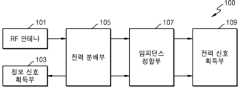
도 1은 본 개시의 다양한 실시 예들에 따른 무선 통신 시스템에서, 수신 장치의 구성을 도시한다.
도 2는 본 개시의 다양한 실시 예들에 따른 무선 통신 시스템에서, 수신 장치의 기능에 관한 블록도의 일 예를 도시한다.
도 3은 본 개시의 다양한 실시 예들에 따른 무선 통신 시스템에서, 전력 분배부의 입출력 신호에 관한 모식도를 도시한다.
도 4는 본 개시의 다양한 실시 예들에 따른 무선 통신 시스템에서, 전력 분배부가 전력 신호를 분배하는 방법에 관한 모식도를 도시한다.
도 5는 본 개시의 다양한 실시 예들에 따른 무선 통신 시스템에서, 전력 분배부가 정보 신호를 분배하는 방법에 관한 모식도를 도시한다.
도 6은 본 개시의 다양한 실시 예들에 따른 무선 통신 시스템에서, 전력 분배부의 회로도에 관한 일 예를 도시한다.
도 7은 본 개시의 다양한 실시 예들에 따른 무선 통신 시스템에서, 전력 분배부의 회로도에 관한 다른 일 예를 도시한다.
도 8은 본 개시의 다양한 실시 예들에 따른 무선 통신 시스템에서, 수신 장치의 구성의 일 예를 도시한다.
도 9는 본 개시의 다양한 실시 예들에 따른 무선 통신 시스템에서, 수신 장치의 회로도에 관한 일 예를 도시한다.
도 10은 본 개시의 다양한 실시 예들에 따른 무선 통신 시스템에서, 수신 장치의 동작 방법에 관한 흐름도를 도시한다.
도 11은 본 개시의 다양한 실시 예들에 따른 무선 통신 시스템에서, 수신 장치의 전력 변환 효율에 관한 그래프를 도시한다.
도 12는 본 개시의 다양한 실시 예들에 따른 무선 통신 시스템에서, 수신 장치의 S-파라미터 특성에 관한 그래프를 도시한다.1 illustrates the configuration of a receiving device in a wireless communication system according to various embodiments of the present disclosure.
FIG. 2 shows an example of a block diagram of the function of a receiving device in a wireless communication system according to various embodiments of the present disclosure.
Figure 3 shows a schematic diagram of input and output signals of a power distribution unit in a wireless communication system according to various embodiments of the present disclosure.
FIG. 4 illustrates a schematic diagram of a method by which a power distribution unit distributes a power signal in a wireless communication system according to various embodiments of the present disclosure.
FIG. 5 illustrates a schematic diagram of a method by which a power distribution unit distributes information signals in a wireless communication system according to various embodiments of the present disclosure.
FIG. 6 shows an example of a circuit diagram of a power distribution unit in a wireless communication system according to various embodiments of the present disclosure.
FIG. 7 shows another example of a circuit diagram of a power distribution unit in a wireless communication system according to various embodiments of the present disclosure.
FIG. 8 illustrates an example of the configuration of a receiving device in a wireless communication system according to various embodiments of the present disclosure.
FIG. 9 shows an example of a circuit diagram of a receiving device in a wireless communication system according to various embodiments of the present disclosure.
FIG. 10 illustrates a flowchart of a method of operating a receiving device in a wireless communication system according to various embodiments of the present disclosure.
FIG. 11 shows a graph regarding power conversion efficiency of a receiving device in a wireless communication system according to various embodiments of the present disclosure.
FIG. 12 shows a graph regarding S-parameter characteristics of a receiving device in a wireless communication system according to various embodiments of the present disclosure.
본 개시에서 사용되는 용어들은 단지 특정한 실시 예를 설명하기 위해 사용된 것으로, 다른 실시 예의 범위를 한정하려는 의도가 아닐 수 있다. 단수의 표현은 문맥상 명백하게 다르게 뜻하지 않는 한, 복수의 표현을 포함할 수 있다. 기술적이거나 과학적인 용어를 포함해서 여기서 사용되는 용어들은 본 개시에 기재된 기술 분야에서 통상의 지식을 가진 자에 의해 일반적으로 이해되는 것과 동일한 의미를 가질 수 있다. 본 개시에 사용된 용어들 중 일반적인 사전에 정의된 용어들은, 관련 기술의 문맥상 가지는 의미와 동일 또는 유사한 의미로 해석될 수 있으며, 본 개시에서 명백하게 정의되지 않는 한, 이상적이거나 과도하게 형식적인 의미로 해석되지 않는다. 경우에 따라서, 본 개시에서 정의된 용어일지라도 본 개시의 실시 예들을 배제하도록 해석될 수 없다.Terms used in the present disclosure are merely used to describe specific embodiments and may not be intended to limit the scope of other embodiments. Singular expressions may include plural expressions, unless the context clearly indicates otherwise. Terms used herein, including technical or scientific terms, may have the same meaning as generally understood by a person of ordinary skill in the technical field described in this disclosure. Among the terms used in this disclosure, terms defined in general dictionaries may be interpreted to have the same or similar meaning as the meaning they have in the context of related technology, and unless clearly defined in this disclosure, have an ideal or excessively formal meaning. It is not interpreted as In some cases, even terms defined in the present disclosure cannot be interpreted to exclude embodiments of the present disclosure.
이하에서 설명되는 본 개시의 다양한 실시 예들에서는 하드웨어적인 접근 방법을 예시로서 설명한다. 하지만, 본 개시의 다양한 실시 예들에서는 하드웨어와 소프트웨어를 모두 사용하는 기술을 포함하고 있으므로, 본 개시의 다양한 실시 예들이 소프트웨어 기반의 접근 방법을 제외하는 것은 아니다.In various embodiments of the present disclosure described below, a hardware approach method is explained as an example. However, since various embodiments of the present disclosure include technology using both hardware and software, the various embodiments of the present disclosure do not exclude software-based approaches.
이하 본 개시는 무선 통신 시스템에서 전력 신호와 정보 신호를 수신하기 위한 장치 및 방법에 관한 것이다. 구체적으로, 본 개시는 무선 통신 시스템에서 전력 신호와 정보 신호가 동시에 전달되는 경우 전력 신호와 정보 신호를 분배하기 위한 기술을 설명한다.Hereinafter, the present disclosure relates to an apparatus and method for receiving power signals and information signals in a wireless communication system. Specifically, the present disclosure describes a technique for distributing power signals and information signals when the power signals and information signals are transmitted simultaneously in a wireless communication system.
아래에서는 첨부한 도면을 참조하여 본 개시가 속하는 기술 분야에서 통상의 지식을 가진 자가 용이하게 실시할 수 있도록 다양한 실시예들을 상세히 설명한다. 그러나 본 개시의 기술적 사상은 다양한 형태로 변형되어 구현될 수 있으므로 본 명세서에서 설명하는 실시예들로 제한되지 않는다. 본 명세서에 개시된 실시예들을 설명함에 있어서 관련된 공지 기술을 구체적으로 설명하는 것이 본 개시의 기술적 사상의 요지를 흐릴 수 있다고 판단되는 경우 그 공지 기술에 대한 구체적인 설명을 생략한다. 동일하거나 유사한 구성요소는 동일한 참조 번호를 부여하고 이에 대한 중복되는 설명은 생략하기로 한다.Below, various embodiments will be described in detail with reference to the attached drawings so that those skilled in the art can easily implement them. However, since the technical idea of the present disclosure can be modified and implemented in various forms, it is not limited to the embodiments described in this specification. In describing the embodiments disclosed in this specification, if it is determined that detailed description of related known technologies may obscure the gist of the technical idea of the present disclosure, detailed descriptions of the known technologies will be omitted. Identical or similar components will be assigned the same reference number and duplicate descriptions thereof will be omitted.
본 명세서에서 어떤 요소가 다른 요소와 "연결"되어 있다고 기술될 때, 이는 "직접적으로 연결"되어 있는 경우뿐 아니라 그 중간에 다른 요소를 사이에 두고 "간접적으로 연결"되어 있는 경우도 포함한다. 어떤 요소가 다른 요소를 "포함"한다고 할 때, 이는 특별히 반대되는 기재가 없는 한 다른 요소 외에 또 다른 요소를 배제하는 것이 아니라 또 다른 요소를 더 포함할 수 있는 것을 의미한다.In this specification, when an element is described as being "connected" to another element, this includes not only the case of being "directly connected" but also the case of being "indirectly connected" with another element in between. When an element is said to “include” another element, this means that it does not exclude another element in addition to the other element, but may further include another element, unless specifically stated to the contrary.
일부 실시예들은 기능적인 블록 구성들 및 다양한 처리 단계들로 설명될 수 있다. 이러한 기능 블록들의 일부 또는 전부는 특정 기능을 실행하는 다양한 개수의 하드웨어 및/또는 소프트웨어 구성들로 구현될 수 있다. 예를 들어, 본 개시의 기능 블록들은 하나 이상의 마이크로프로세서들에 의해 구현되거나, 소정의 기능을 위한 회로 구성들에 의해 구현될 수 있다. 본 개시의 기능 블록들은 다양한 프로그래밍 또는 스크립팅 언어로 구현될 수 있다. 본 개시의 기능 블록들은 하나 이상의 프로세서들에서 실행되는 알고리즘으로 구현될 수 있다. 본 개시의 기능 블록이 수행하는 기능은 복수의 기능 블록에 의해 수행되거나, 본 개시에서 복수의 기능 블록이 수행하는 기능들은 하나의 기능 블록에 의해 수행될 수도 있다. 또한, 본 개시는 전자적인 환경 설정, 신호 처리, 및/또는 데이터 처리 등을 위하여 종래 기술을 채용할 수 있다.Some embodiments may be described in terms of functional block configurations and various processing steps. Some or all of these functional blocks may be implemented as any number of hardware and/or software configurations that perform specific functions. For example, the functional blocks of the present disclosure may be implemented by one or more microprocessors, or may be implemented by circuit configurations for certain functions. Functional blocks of the present disclosure may be implemented in various programming or scripting languages. The functional blocks of this disclosure may be implemented as algorithms running on one or more processors. Functions performed by a functional block in the present disclosure may be performed by a plurality of functional blocks, or functions performed by a plurality of functional blocks in the present disclosure may be performed by a single functional block. Additionally, the present disclosure may employ conventional technologies for electronic environment setup, signal processing, and/or data processing.
또한, 본 개시에서, 특정 조건의 만족(satisfied), 충족(fulfilled) 여부를 판단하기 위해, 초과 또는 미만의 표현이 사용되었으나, 이는 일 예를 표현하기 위한 기재일 뿐 이상 또는 이하의 기재를 배제하는 것이 아니다. '이상'으로 기재된 조건은 '초과', '이하'로 기재된 조건은 '미만', '이상 및 미만'으로 기재된 조건은 '초과 및 이하'로 대체될 수 있다.In addition, in the present disclosure, the expressions greater than or less than are used to determine whether a specific condition is satisfied or fulfilled, but this is only a description for expressing an example and excludes descriptions of more or less. It's not about doing it. Conditions written as ‘more than’ can be replaced with ‘more than’, conditions written as ‘less than’ can be replaced with ‘less than’, and conditions written as ‘more than and less than’ can be replaced with ‘greater than and less than’.
또한, 이하 사용되는 '…부', '…기' 등의 용어는 적어도 하나의 기능이나 동작을 처리하는 단위를 의미하며, 이는 하드웨어나 소프트웨어, 또는, 하드웨어 및 소프트웨어의 결합으로 구현될 수 있다. 수신 장치는 통신부, 저장부, 제어부를 포함할 수 있고, 제어부는 적어도 하나는 적어도 하나의 프로세서에 기능적으로 결합되어 동작할 수 있다.Additionally, hereinafter used ‘…’ wealth', '… Terms such as 'unit' refer to a unit that processes at least one function or operation, and may be implemented as hardware, software, or a combination of hardware and software. The receiving device may include a communication unit, a storage unit, and a control unit, and at least one control unit may operate while being functionally coupled to at least one processor.
도 1은 본 개시의 다양한 실시 예들에 따른 무선 통신 시스템에서, 수신 장치(100)의 구성을 도시한다.FIG. 1 illustrates the configuration of a receiving
SWIPT(simultaneous wireless information and power transfer) 기술이 적용되는 무선 통신 시스템에서 수신 장치(100)는 전력 신호와 정보 신호를 동시에 수신할 수 있다. 구체적으로, 수신 장치(100)는 전력 신호와 정보 신호가 결합된 RF(radio frequency) 신호를 수신할 수 있다. 수신 장치(100)는 수신한 RF 신호를 전력 신호와 정보 신호로 분류하여 이용할 수 있다. 도 1을 참고하면, 수신 장치(100)는 RF 안테나(101), 정보 신호 획득부(103), 전력 분배부(105), 임피던스 정합부(107), 및 전력 신호 획득부(109)를 포함할 수 있다.In a wireless communication system to which simultaneous wireless information and power transfer (SWIPT) technology is applied, the receiving
RF 안테나(101)는 무선 채널을 통해 RF 신호를 송수신하기 위한 기능을 수행한다. RF 안테나(101)의 전부 또는 일부는 송신부, 수신부, 송수신부로 지칭될 수 있다. 본 개시의 일 실시 예에 따르면, RF 안테나는 비변조된 전력 신호와 변조된 정보 신호가 결합된 RF 신호를 수신할 수 있다. 변조된 정보 신호는 f0를 중심 주파수로 하는 변조 신호를 포함하고, 비변조 전력 신호는 f0의 주파수를 가지는 신호를 포함할 수 있다. RF 안테나(101)는 수신한 RF 신호를 전력 분배부로 출력할 수 있다.The
정보 신호 획득부(103)는 전력 분배부(105)에서 분배된 분배 정보 신호로부터 정보 신호를 획득하는 기능을 수행한다. 정보 신호 획득부(103)는 전력 신호 분배부로부터 입력 받은 분배 정보 신호를 필터링(filtering) 하여 변조 정보 신호를 획득할 수 있다. 본 개시의 일 실시 예에 따르면, 정보 신호 획득부(103)는 f0주 파수를 포함하는 주파수 대역 신호의 통과를 저지하는 대역 저지 필터(band stop filter)를 포함할 수 있다.The information
전력 분배부(105)는 입력 받은 RF 신호를 분배 전력 신호와 분배 정보 신호로 분배하는 기능을 수행한다. 전력 분배부(105)는 RF 안테나(101)로부터 RF 신호를 전달 받고, 임피던스(impedance) 부정합에 의한 반사 신호에 기반하여 RF 신호를 분배 전력 신호와 분배 정보 신호로 분배할 수 있다. 본 개시의 일 실시 예에 따르면, 전력 분배부(105)는 정보 신호 획득부(103)에 분배 정보 신호를 출력하고, 임피던스 정합부(107)를 통해 전력 신호 획득부(109)에 분배 전력 신호를 출력할 수 있다.The
본 개시의 일 실시 예에 따르면, 전력 분배부(105)는 네 개의 포트를 가지는 4-포트 전력 분배부를 포함할 수 있다. 전력 분배부는 RF 안테나(101)와 연결되는 제1 포트, 임피던스 정합부(107)와 연결되는 제2 포트와 제3 포트, 정보 신호 획득부와 연결되는 제4 포트를 포함할 수 있다. 구체적인 전력 분배부(105)의 구성과 동작은 도 3 내지 도 9에 상세히 도시된다.According to an embodiment of the present disclosure, the
임피던스 정합부(107)는 수신 신호의 임피던스를 매칭(matching)하는 기능을 수행한다. 임피던스 정합부(107)는 전력 분배부(105)와 전력 신호 획득부(109)의 정류부 사이의 임피던스를 조정하는 기능을 수행할 수 있다. 본 개시의 일 실시 예에 따르면, 임피던스 정합부(107)는 수신된 RF 신호의 전력 신호가 RF 안테나(101)에서 전력 신호 획득부(109)까지 이동할 때, 신호가 최대 효율로 전송될 수 있도록 전력 분배부(105)와 전력 신호 획득부(109) 사이의 임피던스를 조정할 수 있다. 임피던스 정합이 수행 되지 않은 경우 수신된 신호는 반사될 수 있고, 반사된 신호는 전력 분배부(105)의 회로 내부로 입력될 수 있다.The
전력 신호 획득부(109)는 임피던스 정합부를 거쳐 분배된 분배 전력 신호로부터 전력 신호를 획득하는 기능을 수행한다. 전력 신호 획득부(109)는 분배 전력 신호를 정류하고, 필터링 하여 수신한 비변조 전력 신호를 획득할 수 있다. 본 개시의 일 실시 예에 따르면, 전력 신호 획득부(109)는 전력 신호를 정류하기 위한 적어도 하나의 정류부, 정류된 신호를 필터링 하기 위한 DC(direct current) 필터부를 포함할 수 있다.The power
도 1을 참고하면, RF 안테나(101)를 통하여 수신된 RF 신호는 전력 분배부(105)에 기반하여 분배 전력 신호와 분배 정보 신호로 분배될 수 있다. 이후, 분배 전력 신호가 전력 분배부(105)의 제2 포트와 제3 포트를 통해 전력 신호 획득부(109)로 전달되어 전력 신호가 획득될 수 있고, 분배 정보 신호가 전력 분배부(105)의 제4 포트를 통해 정보 신호 획득부(103)로 전달되어 정보 신호가 획득될 수 있다. 본 개시의 일 실시 예에 따르면, 수신 장치(100)는 전력 신호와 정보 신호가 혼합 되어있는 RF 신호에 관하여 변조된 정보 신호의 신호 처리와 동시에 전력 신호를 정류하여 배터리부에 전달할 수 있다.Referring to FIG. 1, the RF signal received through the
도 2는 본 개시의 다양한 실시 예들에 따른 무선 통신 시스템에서, 수신 장치의 기능에 관한 블록도(200)의 일 예를 도시한다. 도 2는 도 1의 수신 장치(100)의 구성을 예시한다.FIG. 2 shows an example of a block diagram 200 regarding the function of a receiving device in a wireless communication system according to various embodiments of the present disclosure. FIG. 2 illustrates the configuration of the receiving
도 2를 참고하면, 수신 장치는 RF 안테나(101), 정보 신호 획득부(103), 전력 분배부(105), 임피던스 정합부(107), 및 전력 신호 획득부(109)를 포함한다. 도 2에 도시된 수신 장치의 구성들 각각은 도 1의 수신 장치의 대응되는 구성들 각각과 동일한 기능을 수행할 수 있다.Referring to FIG. 2, the receiving device includes an
도 2를 참고하면, 전력 신호와 정보 신호가 결합된 RF 신호는 RF 안테나(101)를 통하여 전력 분배부(105)로 입력될 수 있다. 본 개시의 일 실시 예에 따르면, f0의 주파수를 가지는 비변조 전력 신호와 f0를 중심 주파수로 하는 변조된 정보 신호가 결합된 RF 신호는 RF 안테나(101)를 통하여 수신 장치에 입력될 수 있고, 입력된 RF 신호는 전력 분배부(105)로 전달될 수 있다.Referring to FIG. 2, an RF signal combining a power signal and an information signal may be input to the
전력 분배부(105)는 네 개의 포트를 포함하는 4-포트 전력 분배부로 구성될 수 있고, RF 신호는 전력 분배부(105)의 제1 포트를 통해 입력될 수 있다. 이후, RF 신호는 제1 포트 내지 제4 포트 사이에서 전달되면서 분배 전력 신호와 분배 정보 신호로 분류될 수 있다. 본 개시의 일 실시 예에 따르면, 전력 분배부(105)는 임피던스 부정합에 따라 RF 신호가 반사되는 성질을 이용하여 RF 신호를 분배할 수 있다. 분배 정보 신호는 전력 분배부(105)의 제4 포트를 통하여 정보 신호 획득부(103)으로 출력될 수 있고, 분배 전력 신호는 전력 분배부(105)의 제2 포트와 제3 포트를 통해 임피던스 정합부(107)로 출력될 수 있다.The
제2 포트로 출력된 분배 전력 신호는 임피던스 정합부(107)의 제1 정합부(217-1)로 입력될 수 있고, 제3 포트로 출력된 분배 전력 신호는 임피던스 정합부(107)의 제2 정합부(217-2)로 입력될 수 있다. 제1 정합부 내지 제2 정합부(217-1 내지 217-2) 각각은 전력 분배부(105)와 전력 신호 획득부(109)의 정류부 사이의 임피던스를 정합하고, 전력 신호 획득부(109)의 제1 정류부 내지 제2 정류부(219-1 내지 219-2)로 출력한다. 이후, 제1 정류부 내지 제2 정류부(219-1 내지 219-2)로 출력된 신호는 정류되어 DC 필터부(221)로 전달된다. DC 필터부(221)는 제1 정류부 내지 제2 정류부(219-1 내지 219-2)에서 출력된 정류 신호들을 합하고, 정류되지 않은 신호를 필터링 함으로써, 전력 신호를 획득할 수 있다.The distributed power signal output to the second port may be input to the first matching unit 217-1 of the
제4 포트로 출력된 분배 정보 신호는 f0주파수를 포함하는 주파수 대역 신호의 통과를 저지하는 대역 저지 필터가 적용될 수 있다. 정보 신호 획득부(103)는 대역 저지 필터를 이용하여 변조된 정보 신호를 획득할 수 있다.The distribution information signal output to the fourth port may be subject to a band-stop filter that blocks passage of a frequency band signal including the f0 frequency. The information
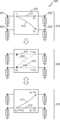
도 3은 본 개시의 다양한 실시 예들에 따른 무선 통신 시스템에서, 전력 분배부의 입출력 신호에 관한 모식도(300)를 도시한다.FIG. 3 shows a schematic diagram 300 of input and output signals of a power distribution unit in a wireless communication system according to various embodiments of the present disclosure.
도 3은 도 1의 전력 분배부(105)의 제1 포트 내지 제4 포트에 입력 또는 출력되는 신호를 예시한다. 여기서, 전력 분배부(105)에 입력 되거나 출력 되는 신호에 관한 제1 그래프 내지 제3 그래프(311, 313, 315)에서 가로 축은 주파수를 지시하고, 세로 축은 신호의 전력 세기를 지시한다.FIG. 3 illustrates signals input or output from the first to fourth ports of the
도 3을 참고하면, 제1 그래프(311)는 전력 분배부(105)의 제1 포트에 입력되는 신호 특성 그래프, 제2 그래프(313)는 전력 분배부(105)의 제2 포트 또는 제3 포트를 통해 출력되는 신호 특성 그래프, 제3 그래프(315)는 전력 분배부(105)의 제4 포트를 통해 출력되는 신호 특성 그래프를 예시한다.Referring to FIG. 3, the
RF 안테나(101)는 RF 신호를 수신하고, 전력 분배부(105)는 제1 포트를 이용하여 RF 신호를 입력 받는다. 제1 그래프(311)를 참고하면, RF 신호는 f0 주파수를 가지는 비변조 전력 신호(321)와 f0를 중심 주파수로 하는 변조된 정보 신호를 혼합하여 사용하는 주파수 분할 신호를 포함할 수 있다.The
혼합된 RF 신호는 주파수에 따라서 분배 전력 신호와 분배 정보 신호로 분배될 수 있다. 즉, 분배 전력 신호와 분배 정보 신호는 서로 상이한 포트를 통하여 출력될 수 있다. 대부분의 f0의 주파수를 가지는 비변조 전력 신호는 제2 포트, 제3 포트 중 적어도 하나로 출력되고, 대부분의 정보 신호는 제4 포트로 출력될 수 있다.The mixed RF signal can be distributed into a distributed power signal and a distributed information signal according to frequency. That is, the distribution power signal and the distribution information signal may be output through different ports. Most of the unmodulated power signal having a frequency of f0 may be output to at least one of the second port and the third port, and most of the information signals may be output to the fourth port.
제2 그래프(313)와 제3 그래프(315)를 참고하면, 상대적으로 높은 세기의 전력 신호(325)와 낮은 세기의 정보 신호(327)가 혼합된 신호가 제2 포트와 제3 포트를 통해 출력될 수 있다. 출력된 신호는 전력 신호 획득부(109)로 전달될 수 있다. 반대로, 상대적으로 낮은 세기의 전력 신호(329)와 높은 세기의 정보 신호(331)가 혼합된 신호가 제4 포트를 통해 출력될 수 있다. 출력된 신호는 정보 신호 획득부로 전달될 수 있다.Referring to the
즉, 전력 분배부(105)는 4-포트 전력 분배를 통해 입력 받은 RF 신호를 분배 전력 신호와 분배 정보 신호로 분배할 수 있다. 전력 분배부(105)의 전력 분배 방법은 도 4 내지 도 5에 상세히 설명된다.That is, the
도 4는 본 개시의 다양한 실시 예들에 따른 무선 통신 시스템에서, 전력 분배부가 전력 신호를 분배하는 방법에 관한 모식도(400)를 도시한다. 도 4는 도 1의 전력 분배부(105)의 동작 방법을 예시한다. 즉, 도 4는 f0의 주파수의 비변조 신호를 지시하는 전력 신호의 전달 과정을 예시한다.FIG. 4 shows a schematic diagram 400 of a method for a power distribution unit to distribute power signals in a wireless communication system according to various embodiments of the present disclosure. FIG. 4 illustrates a method of operating the
도 4를 참고하면, 전력 분배부(105)는 제1 포트(401), 제2 포트(402), 제3 포트(403), 및 제4 포트(404)를 포함하는 4-포트 전력 분배부로 구성될 수 있다.Referring to FIG. 4, the
첫 번째 단계(410)에서, 전력 신호는 제1 포트(401)를 통해 입력되어 제2 포트(402), 제3 포트(403) 중 적어도 하나의 포트로 전달될 수 있다. 제4 포트는 f0 주파수에서 정보 신호 획득부에 포함된 대역 저지 필터에 기반하여, f0 주파수에서 0 옴을 가지는 고립 포트가 되므로, 최초 제1 포트로 입력된 신호가 제4 포트로 전달되지 않을 수 있다.In the
본 개시의 일 실시 예에 따르면, 전력 신호는 제2 포트(402)로 전달되는 b2신호(411), 제3 포트(403)로 전달되는 b3 신호(413)로 분배될 수 있다. 이하의 단계에서, 제1 포트 내지 제4 포트는 첫 번째 단계에서 제1 포트 내지 제4 포트(401 내지 404)에 대응되는 포트를 지시할 수 있다.According to an embodiment of the present disclosure, the power signal may be distributed into a b2 signal 411 transmitted to the
두 번째 단계(440)에서, 제2 포트(402)와 제3 포트(403)로 전달된 신호 각각은 임피던스 부정합에 기반하여 신호의 적어도 일부가 반사될 수 있다. RF 신호의 입력 전력에 따라서 전력 신호 획득부(109)에 포함된 정류부의 최적 임피던스 Ropt가 상이할 수 있고, 그에 대응하여 제2 포트(402), 제3 포트(403)와 정류부 사이의 임피던스 부정합이 발생할 수 있다. 임피던스 부정합에 따라 제2 포트(402), 제3 포트(403)로 전달된 신호는 제1 포트(401), 제4 포트(404) 중 적어도 하나로 반사될 수 있다.In the
본 개시의 일 실시 예에 따르면, b2 신호(411)의 적어도 일부가 반사될 수 있고, 이에 대응하여 반사되는 Γ*b2신호는 제1 포트(401)로 전달되는 신호(441)와 제4 포트(404)로 전달되는 신호(442)로 분배될 수 있다. 동일한 방법으로, b3 신호(413)의 적어도 일부가 반사될 수 있고, 이에 대응하여 반사되는 Γ*b3신호는 제1 포트(401)로 전달되는 신호(443)와 제4 포트(404)로 전달되는 신호(444)로 분배될 수 있다. 여기서, 제4 포트(404)로 전달되는 신호는 b4로 지시될 수 있다.According to an embodiment of the present disclosure, at least a portion of the
세 번째 단계(470)에서, 제4 포트(404)로 전달된 신호는 제2 포트(402), 제3 포트(403) 중 적어도 하나로 전달될 수 있다. 즉, 제4 포트(404)로 전달된 a4 신호가 다시 제2 포트(402), 제3 포트(403)으로 전달되어 전력이 재사용 될 수 있다.In the
본 개시의 일 실시 예에 따르면, 제4 포트(404)로 전달된 신호는 f0 주파수에서 0 옴을 가지므로 입력된 신호가 그대로 제2 포트(402), 제3 포트(403) 중 적어도 하나로 재사용된다. 여기서 제1 포트(401)로 전달된 신호는, 제1 포트(401)가 RF 안테나와 연결되어 안테나와 정합되어 있음에 따라 신호가 반사되지 않는다.According to an embodiment of the present disclosure, the signal transmitted to the
본 개시의 일 실시 예에 따르면, 제4 포트(404)로 전달된 신호 a4 중 적어도 일부는 제2 포트(402), 제3 포트(403) 중 적어도 하나로 전달되어 재사용 될 수 있다. a4 신호는 제2 포트(402)로 전달되는 a4*b2 신호(471)와 제3 포트(403)로 전달되는 a4*b3 신호(473)로 분배될 수 있다. 재사용된 신호의 대부분은 전력 신호 획득부(109)의 정류부로 전달될 수 있고, 일부는 전력 분배부(105) 내에서 반사된다. 전력 분배부(105)는 두 번째 단계(440)와 세 번째 단계(470)에 따른 전력 신호의 반사 과정들을 반복하여, RF 신호를 분배 전력 신호와 분배 정보 신호로 분배할 수 있다.According to an embodiment of the present disclosure, at least a portion of the signal a4 transmitted to the
본 개시의 일 실시 예에 따르면, 전력 분배부(105)는 제1 포트(401)로 재입력되는 신호를 제외하고, 전력 신호를 제2 포트(402)와 제3 포트(403)를 통해 출력하도록 하여, 전력을 모두 재사용할 수 있다. 그에 따라, 본 개시에 따른 전력 분배부(105)는 입력 전력의 크기에 따라서 부정합이 발생하면서 생기는 반사 손실을 감소시킬 수 있고, 변조 정보 신호와 비변조 전력 신호의 분배 성능을 향상시킬 수 있다.According to an embodiment of the present disclosure, the
도 5는 본 개시의 다양한 실시 예들에 따른 무선 통신 시스템에서, 전력 분배부가 정보 신호를 분배하는 방법에 관한 모식도(500)를 도시한다. 도 5는 도 1의 전력 분배부(105)의 동작 방법을 예시한다. 즉, 도 5는 f0가 중심 주파수인 변조 신호를 지시하는 정보 신호의 전달 과정을 예시한다.FIG. 5 shows a schematic diagram 500 of a method for a power distribution unit to distribute information signals in a wireless communication system according to various embodiments of the present disclosure. FIG. 5 illustrates a method of operating the
도 5를 참고하면, 전력 분배부(105)는 제1 포트(501), 제2 포트(502), 제3 포트(503), 및 제4 포트(504)를 포함하는 4-포트 전력 분배부로 구성될 수 있다.Referring to FIG. 5, the
첫 번째 단계(510)에서, 정보 신호는 제1 포트(501)를 통해 입력되어 제2 포트(502), 제3 포트(503), 제4 포트(505) 중 적어도 하나의 포트로 전달될 수 있다. 본 개시의 일 실시 예에 따르면, 정보 신호는 제2 포트(502)와 제3 포트(503)에 일정한 비율로 분배되어 전달될 수 있다.In the first step 510, the information signal may be input through the
본 개시의 일 실시 예에 따르면, 정보 신호는 제2 포트(502)로 전달되는 b2신호(511), 제3 포트(503)로 전달되는 b3 신호(513), 제4 포트(504)로 전달되는 b4신호로 분배될 수 있다. 이하의 단계에서, 제1 포트 내지 제4 포트는 첫 번째 단계에서 제1 포트 내지 제4 포트(501 내지 504)에 대응되는 포트를 지시할 수 있다.According to an embodiment of the present disclosure, the information signal is the b2 signal 511 transmitted to the
두 번째 단계(540)에서, 제2 포트(502)와 제3 포트(503)로 전달된 신호 각각은 제1 포트(501), 제4 포트(504) 중 적어도 하나의 포트로 반사될 수 있다. 전력 신호 획득부의 정합부는 f0 주파수에서 대하여만 정합 되어 있으므로, 제2 포트(502), 제3 포트(503)로 전달된 f0 주파수 이외의 변조 신호는 반사되어 제1 포트(501)와 제4 포트(504) 중 적어도 하나로 전달될 수 있다.In the
본 개시의 일 실시 예에 따르면, b2 신호(511)의 적어도 일부가 반사될 수 있고, 이에 대응하여 반사되는 Γ*b2신호는 제1 포트(401)로 전달되는 신호(541)와 제4 포트(504)로 전달되는 신호(542)로 분배될 수 있다. 동일한 방법으로, b3 신호(513)의 적어도 일부가 반사될 수 있고, 이에 대응하여 반사되는 Γ*b3신호는 제1 포트(501)로 전달되는 신호(543)와 제4 포트(504)로 전달되는 신호(544)로 분배될 수 있다.According to an embodiment of the present disclosure, at least a portion of the
세 번째 단계(570)에서, 제4 포트(504)로 전달된 신호는 제2 포트(502), 제3 포트(503) 중 적어도 하나로 전달될 수 있다. 제2 포트(502), 제3 포트(503)로부터 반사된 신호의 대부분은 제4 포트(504)를 통해 출력되고, 적어도 일부는 반사되어 제2 포트(502)와 제3 포트(503)로 반사된다.In the
본 개시의 일 실시 예에 따르면, 제4 포트(504)로 전달된 신호 a4 중 일부는 제2 포트(502), 제3 포트(503) 중 적어도 하나로 전달될 수 있다. a4 신호는 제2 포트(502)로 전달되는 a4*b2 신호(571)와 제3 포트(503)로 전달되는 a4*b3 신호(573)로 구분될 수 있다. 이에 다시 제2 포트(502), 제3 포트(503)의 신호가 부정합에 의해서 반사되고, 반사된 신호가 제1 포트(501)와 제4 포트(504)로 입력되어 재사용되는 과정을 거치면서 변조된 정보 신호의 대부분이 제4 포트(504)로 인가될 수 있다. 즉, 전력 분배부(105)는 두 번째 단계(540)와 세 번째 단계(570)에 따른 전력 신호의 반사 과정들을 반복하여, RF 신호를 분배 전력 신호와 분배 정보 신호로 분배할 수 있다.According to an embodiment of the present disclosure, some of the signal a4 transmitted to the
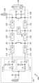
도 6은 본 개시의 다양한 실시 예들에 따른 무선 통신 시스템에서, 전력 분배부의 회로도에 관한 일 예(600)를 도시한다. 도 6은 도 1의 전력 분배부(105)의 회로도를 예시한다.FIG. 6 illustrates an example 600 of a circuit diagram of a power distribution unit in a wireless communication system according to various embodiments of the present disclosure. FIG. 6 illustrates a circuit diagram of the
도 6을 참고하면, 전력 분배부(105)는 네 가지 포트를 가지는 4-포트 전력 분배부로 구성될 수 있다. 이에 대응하여, 전력 분배부(105)는 RF 안테나와 연결되는 제1 포트(601), 임피던스 정합부의 제1 정합부(217-1)와 연결되는 제2 포트(602), 임피던스 정합부의 제2 정합부(217-2)와 연결되는 제3 포트(603), 정보 신호 획득부(103)와 연결되는 제4 포트(604)를 포함할 수 있다.Referring to FIG. 6, the
전력 분배부(105)는 분기선 결합기를 이용하여 구성될 수 있다. 구체적으로, 전력 분배부(105)의 제1 포트 내지 제4 포트(601 내지 604) 사이에 특성 임피던스를 가지는 선로가 배치될 수 있다. 특성 임피던스는 같은 위상 속도로 진행하는 전류파 및 전압파의 관계를 지시하는 것으로서, Z0-- 단위로 결정될 수 있고, Z0 값은 설계자의 설계에 따라 자유롭게 결정될 수 있다. 본 개시의 일 실시 예에 따르면, Z0는 50 옴을 포함할 수 있다. 또한 선로는 λ/4 선로를 이용할 수 있다.The
본 개시의 일 실시 예에 따르면, 제1 포트(601)와 제2 포트(602) 사이에 제1 특성 임피던스를 가지는 제1 선로(610)가 연결되고, 제3 포트(603)와 제4 포트(604) 사이에 제1 특성 임피던스를 가지는 제2 선로(620)가 연결될 수 있다. 또한, 제1 포트(601)와 제4 포트(604) 사이에 제2 특성 임피던스를 가지는 제3 선로(630)가 연결되고, 제2 포트(602)와 제3 포트(603) 사이에 제2 특성 임피던스를 가지는 제4 선로(640)가 연결될 수 있다.According to an embodiment of the present disclosure, a
도 7은 본 개시의 다양한 실시 예들에 따른 무선 통신 시스템에서, 전력 분배부의 회로도에 관한 다른 일 예(700)를 도시한다. 도 7은 도 1의 전력 분배부(105)의 회로도를 예시한다.FIG. 7 shows another example 700 of a circuit diagram of a power distribution unit in a wireless communication system according to various embodiments of the present disclosure. FIG. 7 illustrates a circuit diagram of the
도 7을 참고하면, 전력 분배부(105)는 2분할 분기선 결합기를 이용한 제1 회로도(710) 또는 제2 회로도(760)로 구성될 수 있다. 제1 회로도(710)를 참고하면, 전력 분배부(105)는 네 가지 포트를 가지는 4-포트 전력 분배부로 구성될 수 있다. 이에 대응하여, 전력 분배부(105)는 RF 안테나와 연결되는 제1 포트(701), 임피던스 정합부의 제1 정합부(217-1)와 연결되는 제2 포트(702), 임피던스 정합부의 제2 정합부(217-2)와 연결되는 제3 포트(703), 정보 신호 획득부(103)와 연결되는 제4 포트(704)를 포함할 수 있고, 제1 포트와 제2 포트 사이에 제1 노드(N1), 제3 포트와 제4 포트 사이에 제2 노드(N2)가 배치될 수 있다.Referring to FIG. 7, the
전력 분배부(105)의 제1 포트 내지 제4 포트(601 내지 604) 사이에 특성 임피던스를 가지는 선로가 배치될 수 있다. 특성 임피던스는 같은 위상 속도로 진행하는 전류파 및 전압파의 관계를 지시하는 것으로서, Z0-- 단위로 결정될 수 있고, Z0 값은 설계자의 설계에 따라 자유롭게 결정될 수 있다. 본 개시의 일 실시 예에 따르면, Z0는 50 옴을 포함할 수 있다. 또한 선로는 λ/4 선로를 이용할 수 있다.A line having a characteristic impedance may be disposed between the first to
제1 회로도(710)를 참고하면, 제1 포트(701)와 제2 포트(702) 사이에 제1 특성 임피던스를 가지는 제1 선로(711)와 제2 선로(713)가 연결되고, 제3 포트(703)와 제4 포트(704) 사이에 제1 특성 임피던스를 가지는 제3 선로(715)와 제4 선로(717)가 연결될 수 있다. 또한, 제1 포트(701)와 제4 포트(704) 사이에 제2 특성 임피던스를 가지는 제5 선로(719)가 연결되고, 제2 포트(702)와 제3 포트(703) 사이에 제2 특성 임피던스를 가지는 제6 선로(721)가 연결될 수 있다. 또한, 제1 노드(N1)와 제2 노드(N2) 사이에 제2 특성 임피던스를 가지는 제7 선로(723)가 연결될 수 있다. 제1 회로도(710)의 경우 도 6의 회로도를 이용하는 경우 대비 대역폭을 향상시킬 수 있다.Referring to the first circuit diagram 710, a
제2 회로도(760)를 참고하면, 제1 포트(701)와 제2 포트(702) 사이에 제1 특성 임피던스를 가지는 제1 선로(761)와 제2 선로(763)가 연결되고, 제3 포트(703)와 제4 포트(704) 사이에 제1 특성 임피던스를 가지는 제3 선로(765)와 제4 선로(767)가 연결될 수 있다. 또한, 제1 노드(N1)와 제2 노드(N2) 사이에 제2 특성 임피던스를 가지는 제5 선로(769)가 연결될 수 있다. 또한, 제1 포트(701)와 제4 포트(704) 사이에 CLC 회로(771)가 연결될 수 있고, 제2 포트(702)와 제3 포트(703) 사이에 CLC 회로(773)가 연결될 수 있다. 여기서, CLC 회로는 인덕터가 제1 포트(701)와 제4 포트(704) 및 제2 포트(702)와 제3 포트(703)에 직렬로 연결되고, 인덕터의 양단과 접지 단자 사이에 커패시터들이 병렬로 연결되는 회로 구조를 포함할 수 있다. 제2 회로도(760)의 경우 제1 회로도(710)를 이용하는 경우 대비, 회로의 크기가 감소될 수 있다. 즉, 제2 회로도(760)를 이용하는 경우, 집중 소자를 이용하여 넓은 대역폭을 가지면서 공간 절약도가 향상될 수 있다.Referring to the second circuit diagram 760, a
도 8은 본 개시의 다양한 실시 예들에 따른 무선 통신 시스템에서, 수신 장치(800)의 구성의 일 예를 도시한다. 도 8은 전력 분배부와 임피던스 정합부가 통합된 수신 장치의 기능에 관한 블록도를 예시한다.FIG. 8 illustrates an example of the configuration of a receiving
도 8을 참고하면, SWIPT 시스템에서 수신 장치(800)는 RF 안테나(801), 정보 신호 획득부(803), 통합 전력 분배부(805), 전력 신호 획득부(807)를 포함할 수 있다.Referring to FIG. 8, in the SWIPT system, the receiving
RF 안테나(801)는 RF 안테나는 비변조된 전력 신호와 변조된 정보 신호가 결합된 RF 신호를 수신할 수 있다. 변조된 정보 신호는 f0를 중심 주파수로 하는 변조 신호를 포함하고, 비변조 전력 신호는 f0의 주파수를 가지는 신호를 포함할 수 있다. RF 안테나(801)는 수신한 RF 신호를 통합 전력 분배부(805)로 출력할 수 있다.The
정보 신호 획득부(803)는 전력 분배부에서 분배된 분배 정보 신호로부터 정보 신호를 획득하는 기능을 수행한다. 본 개시의 일 실시 예에 따르면, 정보 신호 획득부(803)는 f0주파수를 포함하는 주파수 대역 신호의 통과를 저지하는 대역 저지 필터를 포함할 수 있다.The information
통합 전력 분배부(805)는 입력 받은 RF 신호를 분배 전력 신호와 분배 정보 신호로 분배하고, 임피던스를 정합하는 기능을 수행한다. 통합 전력 분배부(805)는 RF 안테나(801)로부터 RF 신호를 전달 받고, 임피던스(impedance) 부정합에 의한 반사 신호에 기반하여 RF 신호를 분배 전력 신호와 분배 정보 신호로 분배할 수 있다. 여기서, 통합 전력 분배부(805)는 임피던스 정합을 위한 추가 회로를 포함할 수 있다. 통합 전력 분배부(805)는 정보 신호 획득부(803)에 분배 정보 신호를 출력하고, 전력 신호 획득부(807)에 분배 전력 신호를 출력할 수 있다.The integrated
본 개시의 일 실시 예에 따르면, 통합 전력 분배부(805)는 네 개의 포트를 가지는 4-포트 전력 분배부를 포함할 수 있다. 통합 전력 분배부(805)는 RF 안테나(801)와 연결되는 제1 포트, 전력 신호 획득부(807)와 연결되는 제2 포트와 제3 포트, 정보 신호 획득부(803)와 연결되는 제4 포트를 포함할 수 있다. 여기서, 통합 전력 분배부(805)의 제2 포트와 제3 포트는 정류부로 보이는 최적 임피던스 Ropt를 기준으로 컨쥬게이트(conjugate) 정합이 되도록 구성될 수 있다.According to an embodiment of the present disclosure, the integrated
전력 신호 획득부(807)는 분배 전력 신호로부터 전력 신호를 획득하는 기능을 수행한다. 전력 신호 획득부(109)는 분배 전력 신호를 정류하고, 필터링 하여 수신한 비변조 전력 신호를 획득할 수 있다. 본 개시의 일 실시 예에 따르면, 전력 신호 획득부(807)는 분배 전력 신호를 정류하기 위한 제1 정류부 내지 제2 정류부(807-1 내지 807-2), 정류된 신호를 필터링 하기 위한 DC 필터부(809)를 포함할 수 있다. 통합 전력 분배부를 이용한 수신 장치의 구성과 동작은 도 9에 상세히 설명된다.The power
도 9는 본 개시의 다양한 실시 예들에 따른 무선 통신 시스템에서, 수신 장치의 회로도에 관한 일 예(900)를 도시한다. 도 9는 도 8의 수신 장치(800)의 구성을 예시한다.FIG. 9 illustrates an example 900 of a circuit diagram of a receiving device in a wireless communication system according to various embodiments of the present disclosure. FIG. 9 illustrates the configuration of the receiving
도 9를 참고하면, 수신 장치(800)는 RF 안테나(901), 정보 신호 획득부(903), 통합 전력 분배부(905), 및 전력 신호 획득부(907)를 포함할 수 있다. 전력 신호 획득부는 분배 전력 신호를 정류하기 위한 제1 정류부 내지 제2 정류부(919-1 내지 919-2), DC 필터부를 포함할 수 있다.Referring to FIG. 9, the receiving
도 9를 참고하면, 전력 신호와 정보 신호가 결합된 RF 신호는 RF 안테나(901)를 통하여 통합 전력 분배부(905)로 입력될 수 있다. 통합 전력 분배부(905)는 네 개의 포트를 포함하는 4-포트 전력 분배부로 구성될 수 있고, RF 신호는 전력 분배부(905)의 제1 포트(911)를 통해 입력될 수 있다. 이후, RF 신호는 제1 포트 내지 제4 포트(911 내지 914) 사이에서 전달되면서 분배 전력 신호와 분배 정보 신호로 분류될 수 있다. 본 개시의 일 실시 예에 따르면, 전력 분배부(205)는 임피던스 부정합에 따라 RF 신호가 반사되는 성질을 이용하여 RF 신호를 분배할 수 있다. 분배 정보 신호는 통합 전력 분배부(905)의 제4 포트(914)를 통하여 정보 신호 획득부(903)으로 출력될 수 있고, 분배 전력 신호는 통합 전력 분배부(905)의 제2 포트(912)와 제3 포트(913)를 통해 전력 신호 획득부(907)로 출력될 수 있다.Referring to FIG. 9, an RF signal combining a power signal and an information signal may be input to the integrated
여기서, 통합 전력 분배부(905)를 참고하면, 제1 포트(911)와 제4 노드(N4) 사이에, 제1 특성 임피던스를 가지는 제1 선로(921)와 제2 선로(922)가 연결되고, 제3 포트(913)와 제6 노드(N6) 사이에, 제1 특성 임피던스를 가지는 제3 선로(923)와 제4 선로(924)가 연결될 수 있다.Here, referring to the integrated
또한, 제3 노드(N3)와 제5 노드(N5) 사이에 제2 특성 임피던스를 가지는 제5 선로(925)가 연결될 수 있다. 또한, 제1 포트(911)와 제4 포트(914) 사이에 CLC 회로가 연결될 수 있고, 제4 노드(N4)와 제6 노드(N6) 사이에 인덕터(L1)가 연결될 수 있다. 여기서, CLC 회로는 인덕터가 제1 포트(911)와 제2 포트(914)에 직렬로 연결되고, 인덕터의 양단과 접지 단자 사이에 커패시터들이 병렬로 연결되는 회로 구조를 포함할 수 있다. 또한, 제4 노드(N4)와 제2 포트(912) 사이에 제3 특성 임피던스를 가지는 제6 선로(926)가 연결될 수 있고, 제6 노드(N6)와 제3 포트(913) 사이에 제3 특성 임피던스를 가지는 제7 선로(927)가 연결될 수 있다. 여기서, 특성 임피던스는 Z0-- 단위로 결정될 수 있고, 제1 특성 임피던스 내지 제3 특성 임피던스의 임피던스 값들은 서로 상이할 수 있다. 또한 선로는 λ/4 선로를 이용할 수 있다. 특성 임피던스에 대응되도록 선로의 두께(W)와 길이(L)가 결정될 수 있다.Additionally, a
도 7의 전력 분배부(105)의 제2 회로도(760)를 이용하는 경우 CLC 회로들(771, 773)이 필요하지만, 도 9의 통합 전력 분배부(905)를 이용하는 경우 하나의 CLC 회로를 제거할 수 있고, 특성 임피던스 선로를 추가함으로써 회로의 전력 분배 효율을 향상시킬 수 있다.When using the second circuit diagram 760 of the
이후 통합 전력 분배부(905)는 전력 신호 획득부(907)의 제1 정류부 내지 제2 정류부(919-1 내지 919-2)로 분배 전력 신호를 출력한다. 제1 정류부 내지 제2 정류부(919-1 내지 919-2)는 전달받은 분배 전력 신호를 정류하고, 이에 대응하여 전력 신호 획득부(907)는 정류 신호를 필터링 함으로써, 전력 신호를 획득할 수 있다.Thereafter, the integrated
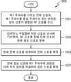
도 10은 본 개시의 다양한 실시 예들에 따른 무선 통신 시스템에서, 수신 장치의 동작 방법에 관한 흐름도(1000)를 도시한다. 도 10은 도 1의 수신 장치(100)의 동작 방법을 예시한다.FIG. 10 illustrates a
도 10을 참고하면 단계(1001)에서, 수신 장치(100)는 제1 주파수를 가지는 전력 신호와, 제1 주파수를 중심 주파수로 하는 변조된 정보 신호가 결합된 RF 신호를 수신한다. 본 개시의 일 실시 예에 따르면, 변조된 정보 신호는 f0를 중심 주파수로 하는 변조 신호를 포함하고, 비변조 전력 신호는 f0의 주파수를 가지는 신호를 포함할 수 있다.Referring to FIG. 10, in
단계(1003)에서, 수신 장치(100)는 임피던스 부정합에 의한 신호의 반사에 기반하여, RF 신호를 분배 전력 신호와 분배 정보 신호로 분배한다. 본 개시의 일 실시 예에 따르면, 수신 장치(100)는 전력 분배부를 이용하여 전력 신호와 정보 신호가 전달되는 경우, 전력 재사용 방식을 이용하여 전력 신호와 정보 신호를 분배할 수 있다.In
본 개시의 일 실시 예에 따르면, 전력 분배부는 RF 신호를 전달 받기 위하여, RF 안테나와 연결되는 제1 포트, 제1 분배 전력 신호를 출력하기 위하여, 임피던스 정합부의 제1 정합부와 연결되는 제2 포트, 제2 분배 전력 신호를 출력하기 위하여, 임피던스 정합부의 제2 정합부와 연결되는 제3 포트, 분배 정보 신호를 출력하기 위하여, 정보 신호 획득부와 연결되는 제4 포트를 포함하는 4포트 전력 분배부를 포함할 수 있다.According to an embodiment of the present disclosure, the power distribution unit includes a first port connected to an RF antenna to receive an RF signal, and a second port connected to the first matching unit of the impedance matching unit to output the first distribution power signal. 4-port power including a port, a third port connected to the second matching part of the impedance matching unit to output a second distribution power signal, and a fourth port connected to the information signal acquisition unit to output a distribution information signal. It may include a distribution unit.
본 개시의 일 실시 예에 따르면, 수신 장치(100)는 전력 분배부를 이용하여 제1 포트를 이용하여 전력 신호를 입력 받고, 전력 신호를 제2 포트, 제3 포트 중 적어도 하나로 전달하고, 제2 포트와 제3 포트에서 임피던스 부정합에 의하여 반사된 반사 전력 신호를 제1 포트, 제4 포트 중 적어도 하나로 전달하고, 제4 포트로 전달된 반사 전력 신호를 제2 포트와 제3 포트로 전달할 수 있다.According to an embodiment of the present disclosure, the receiving
본 개시의 일 실시 예에 따르면, 수신 장치(100)는 전력 분배부를 이용하여 제1 포트를 이용하여 정보 신호를 입력 받고, 정보 신호를 제2 포트, 제3 포트, 제4 포트 중 적어도 하나로 전달하고, 제2 포트와 제3 포트에서 임피던스 부정합에 의하여 반사된 제1 반사 정보 신호를 제1 포트, 제4 포트 중 적어도 하나로 전달하고, 제4 포트로 전달된 제1 반사 정보 신호의 적어도 일부를 제2 포트, 제3 포트 중 적어도 하나로 전달하고, 제2 포트와 제3 포트로 전달된 신호가 임피던스 부정합에 의하여 반사된 제2 반사 정보 신호를 제1 포트, 제4 포트 중 적어도 하나로 전달할 수 있다.According to an embodiment of the present disclosure, the receiving
본 개시의 일 실시 예에 따르면, 전력 분배부는 분기선 결합기를 이용하여 구성될 수 있다. 전력 분배부는 제1 포트와 제2 포트 사이에 제1 특성 임피던스를 가지는 제1 선로가 연결되고, 제3 포트와 제4 포트 사이에 제1 특성 임피던스를 가지는 제2 선로가 연결되고, 제1 포트와 제4 포트 사이에 제2 특성 임피던스를 가지는 제3 선로가 연결되고, 제2 포트와 제3 포트 사이에 제2 특성 임피던스를 가지는 제4 선로가 연결되도록 구성될 수 있다.According to an embodiment of the present disclosure, the power distribution unit may be configured using a branch line coupler. The power distribution unit has a first line having a first characteristic impedance connected between the first port and the second port, a second line having a first characteristic impedance connected between the third port and the fourth port, and a first port A third line having a second characteristic impedance may be connected between the and the fourth port, and a fourth line having a second characteristic impedance may be connected between the second port and the third port.
본 개시의 일 실시 예에 따르면, 전력 분배부는 제1 포트와 제2 포트 사이에 제1 특성 임피던스를 가지는 제1 선로와 제2 선로가 연결되고, 제3 포트와 제4 포트 사이에 제1 특성 임피던스를 가지는 제3 선로와 제4 선로가 연결되고, 제1 포트와 제4 포트 사이에 제2 특성 임피던스를 가지는 제5 선로가 연결되고, 제2 포트와 제3 포트 사이에 제2 특성 임피던스를 가지는 제6 선로가 연결되고, 제1 선로와 제2 선로 사이의 제1 노드와, 제3 선로와 제4 선로 사이의 제2 노드 사이에, 제2 특성 임피던스를 가지는 제7 선로가 연결되도록 구성될 수 있다.According to an embodiment of the present disclosure, the power distribution unit is connected to a first line and a second line having a first characteristic impedance between the first port and the second port, and a first line having a first characteristic impedance between the third port and the fourth port. A third line and a fourth line having an impedance are connected, a fifth line having a second characteristic impedance is connected between the first port and the fourth port, and a second characteristic impedance is connected between the second port and the third port. A sixth line is connected to each branch, and a seventh line having a second characteristic impedance is connected between the first node between the first line and the second line and the second node between the third line and the fourth line. It can be.
본 개시의 일 실시 예에 따르면, 전력 분배부는 제1 포트와 제2 포트 사이에, 제1 특성 임피던스를 가지는 제1 선로와 제2 선로가 연결되고, 제3 포트와 제4 포트 사이에, 제1 특성 임피던스를 가지는 제3 선로와 제4 선로가 연결되고, 제1 선로와 제2 선로 사이의 제1 노드와, 제3 선로와 제4 선로 사이의 제2 노드 사이에, 제2 특성 임피던스를 가지는 제5 선로가 연결되고, 제1 포트와 제4 포트 사이에 제1 인덕터가 직렬로 연결되고, 제1 인덕터의 양단과 접지 단자 사이에 커패시터들이 병렬로 연결되고, 제2 포트와 제3 포트 사이에 제2 인덕터가 직렬로 연결되고, 제2 인덕터의 양단과 접지 단자 사이에 커패시터들이 병렬로 연결도록 구성될 수 있다.According to an embodiment of the present disclosure, the power distribution unit has a first line and a second line having a first characteristic impedance connected between the first port and the second port, and a second line between the third port and the fourth port. A third line and a fourth line having a characteristic impedance of 1 are connected, and a second characteristic impedance is formed between the first node between the first line and the second line and the second node between the third line and the fourth line. A fifth line is connected to each branch, a first inductor is connected in series between the first port and the fourth port, capacitors are connected in parallel between both ends of the first inductor and the ground terminal, and the second and third ports are connected in parallel. A second inductor may be connected in series, and capacitors may be connected in parallel between both ends of the second inductor and the ground terminal.
단계(1005)에서, 수신 장치(100)는 분배 전력 신호를 정류하여 전력 신호를 획득한다. 본 개시의 일 실시 예에 따르면, 수신 장치는 분배 전력 신호를 정류하고 DC 필터를 적용하여 전력 신호를 획득할 수 있다. 이 때, 수신 장치는 전력 분배부의 출력과 전력 신호 획득부의 입력 사이의 임피던스를 조정하기 위한 임피던스 정합부를 포함할 수 있다.In
단계(1007)에서, 수신 장치(100)는 분배 정보 신호에 제1 주파수에 관련된 대역 저지 필터를 적용하여 정보 신호를 획득한다. 본 개시의 일 실시 예에 따르면, 수신 장치(100)는 분배 정보 신호에 대역 저지 필터를 적용하여 정보 신호를 획득할 수 있다.In
도 11은 본 개시의 다양한 실시 예들에 따른 무선 통신 시스템에서, 수신 장치의 전력 변환 효율에 관한 그래프(1100)를 도시한다.FIG. 11 shows a
도 11을 참고하면, 가로 축은 입력 전력의 크기를 지시하고, 세로 축은 전력 변환 효율(power conversion efficiency, PCE)을 지시한다. 도 11은 수신 장치가 2.45GHz 주파수를 가지는 비변조 전력 신호와 2.45GHz 중심 주파수를 가지는 변조 정보 신호가 포함된 RF 신호를 수신한 경우를 예시한다.Referring to FIG. 11, the horizontal axis indicates the size of input power, and the vertical axis indicates power conversion efficiency (PCE). Figure 11 illustrates a case where a receiving device receives an RF signal including an unmodulated power signal with a frequency of 2.45 GHz and a modulated information signal with a center frequency of 2.45 GHz.
도 11에서, 입력 전력의 범위가 약 17.5 dB 부터 33 dB인 경우, 전력 변환 효율이 50% 이상이 되는 것을 확인할 수 있다. 즉, 본 개시에 따른 수신 장치를 이용하는 경우, 입력 전력의 범위가 약 15.5 dB가 되므로 수신 장치의 입력 전력 범위가 보다 넓게 설계될 수 있다.In FIG. 11, it can be seen that when the input power ranges from about 17.5 dB to 33 dB, the power conversion efficiency is more than 50%. That is, when using the receiving device according to the present disclosure, the input power range is about 15.5 dB, so the input power range of the receiving device can be designed to be wider.
도 12는 본 개시의 다양한 실시 예들에 따른 무선 통신 시스템에서, 수신 장치의 S-파라미터 특성에 관한 그래프(1200)를 도시한다. 도 12를 참고하면, 가로 축은 RF 신호의 주파수를 지시하고, 세로 축은 S파라미터의 크기를 지시한다.FIG. 12 illustrates a
도 12는 수신 장치가 2.45GHz 주파수를 가지는 비변조 전력 신호와 2.45GHz의 중심 주파수를 가지는 변조 정보 신호가 포함된 RF 신호를 수신한 경우를 예시한다.Figure 12 illustrates a case where a receiving device receives an RF signal including an unmodulated power signal with a frequency of 2.45 GHz and a modulated information signal with a center frequency of 2.45 GHz.
도 12를 참고하면, 설계된 회로에서 RF 안테나에서 정보 신호 획득부나 전력 신호 획득부를 통해 정보를 획득하기 까지의 삽입 손실을 나타낸 시뮬레이션 결과가 예시된다. 비변조 전력 신호 주파수인 2.45GHz에서 -36 dB 정도의 큰 손실이 발생하였으나, 그 외의 주파수 대역에서 -5 dB 정도의 작은 삽입 손실이 발생한 것이 확인된다.Referring to FIG. 12, a simulation result showing the insertion loss from the RF antenna to acquiring information through the information signal acquisition unit or the power signal acquisition unit in the designed circuit is illustrated. A large loss of about -36 dB occurred at 2.45 GHz, the unmodulated power signal frequency, but it was confirmed that a small insertion loss of about -5 dB occurred in other frequency bands.
일반적으로 다양한 위치로부터 전달되는 전력 신호는 수신 장치까지의 거리에 따라서 입력 전력의 크기가 상이하고, 입력 전력의 크기에 따라서 정류기의 전력 변환 효율이 큰 폭으로 변동될 수 있다. 본 개시와 같이 정보 신호와 전력 신호를 동시에 전송 가능한 수신 장치에 전력 재사용 방식을 적용하면, 넓은 입력 전력 범위에서 높은 효율이 얻어질 수 있다. 다양한 위치에서 전력 신호가 송신됨에 따라 전력 신호의 크기의 변화한 경우라도, 효율이 일정한 수준으로 유지될 수 있고, 추가적인 전력 분배기에 따른 삽입 손실 없이 정보 신호와 전력 신호의 분배가 수행될 수 있다.In general, power signals transmitted from various locations have different input power sizes depending on the distance to the receiving device, and the power conversion efficiency of the rectifier may vary significantly depending on the size of the input power. By applying the power reuse method to a receiving device capable of simultaneously transmitting information signals and power signals, as in the present disclosure, high efficiency can be obtained in a wide input power range. Even when the size of the power signal changes as the power signal is transmitted from various locations, efficiency can be maintained at a constant level, and distribution of the information signal and the power signal can be performed without insertion loss due to an additional power divider.
본 개시에 따르면, 넓은 입력 전력 범위에서 정류부와 전력 분배부 사이의 정합이 유지 되므로, 정보 신호 전달 관점에서 변조 신호 처리부의 입력과 전력 분배부 사이의 정합 또한 넓은 입력 전력 범위에서 유지가 될 수 있기 때문에 변조 신호 처리부에 정보 신호의 전달이 가능하다. 이에 대응하여, 산업 및 경제적 측면에서 무선으로 자유로운 위치에 있는 전자기기에 안정적인 정보 전달과 전력 저장이 가능하기 때문에 동시 정보 및 전력 전송 시스템의 적용 범위가 확장될 수 있다.According to the present disclosure, since the matching between the rectifier and the power distribution unit is maintained over a wide input power range, the matching between the input of the modulation signal processor and the power distribution unit can also be maintained over a wide input power range from the perspective of information signal transmission. Therefore, it is possible to transmit information signals to the modulation signal processing unit. Correspondingly, from an industrial and economic perspective, the scope of application of simultaneous information and power transmission systems can be expanded because reliable information transmission and power storage are possible wirelessly in freely located electronic devices.
본 개시에 따르면, 다양한 전자기기 사용이 필요한 공간에서 효과적으로 전자기기들 사이에 유기적인 정보 전달이 가능하고, 또한 개별 전자기기의 독립적이고 자유로운 충전이 가능하다. 그에 따라, 본 개시에 따른 수신 장치는 스마트 홈, 스마트 오피스, 스마트 팩토리 서비스에 활용될 수 있다.According to the present disclosure, it is possible to effectively transmit information organically between electronic devices in a space where the use of various electronic devices is required, and independent and free charging of individual electronic devices is also possible. Accordingly, the receiving device according to the present disclosure can be used for smart home, smart office, and smart factory services.
본 개시의 청구항 또는 명세서에 기재된 실시 예들에 따른 방법들은 하드웨어, 소프트웨어, 또는 하드웨어와 소프트웨어의 조합의 형태로 구현될(implemented) 수 있다.Methods according to embodiments described in the claims or specification of the present disclosure may be implemented in the form of hardware, software, or a combination of hardware and software.
소프트웨어로 구현하는 경우, 하나 이상의 프로그램(소프트웨어 모듈)을 저장하는 컴퓨터 판독 가능 저장 매체가 제공될 수 있다. 컴퓨터 판독 가능 저장 매체에 저장되는 하나 이상의 프로그램은, 전자 장치(device) 내의 하나 이상의 프로세서에 의해 실행 가능하도록 구성된다(configured for execution). 하나 이상의 프로그램은, 전자 장치로 하여금 본 개시의 청구항 또는 명세서에 기재된 실시 예들에 따른 방법들을 실행하게 하는 명령어(instructions)를 포함한다.When implemented as software, a computer-readable storage medium that stores one or more programs (software modules) may be provided. One or more programs stored in a computer-readable storage medium are configured to be executable by one or more processors in an electronic device (configured for execution). One or more programs include instructions that cause the electronic device to execute methods according to embodiments described in the claims or specification of the present disclosure.
이러한 프로그램(소프트웨어 모듈, 소프트웨어)은 랜덤 액세스 메모리 (random access memory), 플래시(flash) 메모리를 포함하는 불휘발성(non-volatile) 메모리, 롬(read only memory, ROM), 전기적 삭제가능 프로그램가능 롬(electrically erasable programmable read only memory, EEPROM), 자기 디스크 저장 장치(magnetic disc storage device), 컴팩트 디스크 롬(compact disc-ROM, CD-ROM), 디지털 다목적 디스크(digital versatile discs, DVDs) 또는 다른 형태의 광학 저장 장치, 마그네틱 카세트(magnetic cassette)에 저장될 수 있다. 또는, 이들의 일부 또는 전부의 조합으로 구성된 메모리에 저장될 수 있다. 또한, 각각의 구성 메모리는 다수 개 포함될 수도 있다.These programs (software modules, software) may include random access memory, non-volatile memory, including flash memory, read only memory (ROM), and electrically erasable programmable ROM. (electrically erasable programmable read only memory, EEPROM), magnetic disc storage device, compact disc-ROM (CD-ROM), digital versatile discs (DVDs), or other types of disk storage. It can be stored in an optical storage device or magnetic cassette. Alternatively, it may be stored in a memory consisting of a combination of some or all of these. Additionally, multiple configuration memories may be included.
또한, 프로그램은 인터넷(Internet), 인트라넷(Intranet), LAN(local area network), WAN(wide area network), 또는 SAN(storage area network)과 같은 통신 네트워크, 또는 이들의 조합으로 구성된 통신 네트워크를 통하여 접근(access)할 수 있는 부착 가능한(attachable) 저장 장치(storage device)에 저장될 수 있다. 이러한 저장 장치는 외부 포트를 통하여 본 개시의 실시 예를 수행하는 장치에 접속할 수 있다. 또한, 통신 네트워크상의 별도의 저장장치가 본 개시의 실시 예를 수행하는 장치에 접속할 수도 있다.In addition, the program may be distributed through a communication network such as the Internet, an intranet, a local area network (LAN), a wide area network (WAN), or a storage area network (SAN), or a combination thereof. It may be stored on an attachable storage device that is accessible. This storage device can be connected to a device performing an embodiment of the present disclosure through an external port. Additionally, a separate storage device on a communication network may be connected to the device performing an embodiment of the present disclosure.
상술한 본 개시의 구체적인 실시 예들에서, 개시에 포함되는 구성 요소는 제시된 구체적인 실시 예에 따라 단수 또는 복수로 표현되었다. 그러나, 단수 또는 복수의 표현은 설명의 편의를 위해 제시한 상황에 적합하게 선택된 것으로서, 본 개시가 단수 또는 복수의 구성 요소에 제한되는 것은 아니며, 복수로 표현된 구성 요소라 하더라도 단수로 구성되거나, 단수로 표현된 구성 요소라 하더라도 복수로 구성될 수 있다.In the specific embodiments of the present disclosure described above, elements included in the disclosure are expressed in singular or plural numbers depending on the specific embodiment presented. However, singular or plural expressions are selected to suit the presented situation for convenience of explanation, and the present disclosure is not limited to singular or plural components, and even components expressed in plural may be composed of singular or singular. Even expressed components may be composed of plural elements.
한편 본 개시의 상세한 설명에서는 구체적인 실시 예에 관해 설명하였으나, 본 개시의 범위에서 벗어나지 않는 한도 내에서 여러 가지 변형이 가능함은 물론이다. 그러므로 본 개시의 범위는 설명된 실시 예에 국한되어 정해져서는 아니 되며 후술하는 특허청구의 범위뿐만 아니라 이 특허청구의 범위와 균등한 것들에 의해 정해져야 한다.Meanwhile, in the detailed description of the present disclosure, specific embodiments have been described, but of course, various modifications are possible without departing from the scope of the present disclosure. Therefore, the scope of the present disclosure should not be limited to the described embodiments, but should be determined not only by the scope of the patent claims described later, but also by the scope of this patent claim and equivalents.
101RF 안테나103정보 신호 획득부
105전력 분배부107임피던스 정합부
109전력 신호 획득부221DC 필터부
219-1 내지 219-2 제1 정류부 내지 제2 정류부
601제1 포트602제2 포트
603제3 포트604제4 포트
801RF 안테나803정보 신호 획득부
805통합 전력 분배부807전력 신호 획득부101
105
109 Power
219-1 to 219-2 first rectification unit to second rectification unit
601
603
801
805 Integrated
Claims (11)
Translated fromKorean제1 주파수를 가지는 전력 신호와 상기 제1 주파수를 중심 주파수로 하는 변조된 정보 신호가 결합된 RF(radio frequency) 신호를 수신하는 RF 안테나;
상기 RF 신호를 분배 전력 신호와 분배 정보 신호로 분배하기 위하여, 상기 RF 안테나에 연결되어 상기 RF 신호를 수신하는 제1 포트, 상기 분배 전력 신호를 출력하는 제2 포트 및 제3 포트, 및 상기 분배 정보 신호를 출력하는 제4 포트를 갖는 4-포트 전력 분배부;
상기 분배 전력 신호를 정류하는 정류부;
상기 4-포트 전력 분배부의 상기 제2 포트 및 상기 제3 포트와 상기 정류부 사이에 연결되고, 상기 제1 주파수에서 상기 4-포트 전력 분배부와 상기 정류부의 임피던스를 정합하는 임피던스 정합부;
상기 4-포트 전력 분배부의 상기 제4 포트에 연결되고, 상기 제1 주파수의 신호를 차단하는 대역 저지 필터; 및
상기 대역 저지 필터를 통해 상기 분배 정보 신호를 수신하는 정보 신호 획득부를 포함하는 수신 장치.In a receiving device in a wireless communication system,
An RF antenna that receives a radio frequency (RF) signal combining a power signal with a first frequency and a modulated information signal with the first frequency as a center frequency;
To distribute the RF signal into a distributed power signal and a distributed information signal, a first port connected to the RF antenna to receive the RF signal, a second port and a third port to output the distributed power signal, and the distribution a 4-port power distribution unit having a fourth port that outputs an information signal;
a rectifier that rectifies the distributed power signal;
an impedance matching unit connected between the second and third ports of the 4-port power distribution unit and the rectifier, and matching impedances of the 4-port power distribution unit and the rectification unit at the first frequency;
a band-stop filter connected to the fourth port of the 4-port power distribution unit and blocking the signal of the first frequency; and
A receiving device comprising an information signal acquisition unit that receives the distribution information signal through the band stop filter.
상기 임피던스 정합부는 상기 제2 포트에 연결되는 제1 정합부, 및 상기 제3 포트에 연결되는 제2 정합부를 포함하고,
상기 정류부는,
상기 제1 정합부를 통해 출력되는 신호를 정류하여 제1 정류 신호를 출력하는 제1 정류부;
상기 제2 정합부를 통해 출력되는 신호를 정류하여 제2 정류 신호를 출력하는 제2 정류부; 및
상기 제1 정류 신호와 상기 제2 정류 신호를 수신하고 비정류 신호를 필터링하는 DC 필터부를 포함하는 수신 장치.In claim 1,
The impedance matching part includes a first matching part connected to the second port, and a second matching part connected to the third port,
The rectifier unit,
a first rectifying unit that rectifies the signal output through the first matching unit and outputs a first rectified signal;
a second rectifying unit that rectifies the signal output through the second matching unit and outputs a second rectified signal; and
A receiving device comprising a DC filter unit that receives the first rectified signal and the second rectified signal and filters a non-rectified signal.
상기 4-포트 전력 분배부는,
상기 제1 포트를 이용하여 상기 전력 신호를 입력 받고, 상기 전력 신호를 상기 제2 포트, 상기 제3 포트 중 적어도 하나로 전달하고,
상기 제2 포트와 상기 제3 포트에서 임피던스 부정합에 의하여 반사된 반사 전력 신호를 상기 제1 포트, 상기 제4 포트 중 적어도 하나로 전달하고,
상기 제4 포트로 전달된 반사 전력 신호를 상기 제2 포트와 상기 제3 포트로 전달하는 수신 장치.In claim 1,
The 4-port power distribution unit,
Receiving the power signal using the first port, and transmitting the power signal to at least one of the second port and the third port,
transmitting the reflected power signal reflected by impedance mismatch in the second port and the third port to at least one of the first port and the fourth port,
A receiving device that transmits the reflected power signal transmitted to the fourth port to the second port and the third port.
상기 4-포트 전력 분배부는,
상기 제1 포트를 이용하여 상기 정보 신호를 입력 받고, 상기 정보 신호를 상기 제2 포트, 상기 제3 포트, 상기 제4 포트 중 적어도 하나로 전달하고,
상기 제2 포트와 상기 제3 포트에서 임피던스 부정합에 의하여 반사된 제1 반사 정보 신호를 상기 제1 포트, 상기 제4 포트 중 적어도 하나로 전달하고,
상기 제4 포트로 전달된 제1 반사 정보 신호의 적어도 일부를 상기 제2 포트, 상기 제3 포트 중 적어도 하나로 전달하고,
상기 제2 포트와 상기 제3 포트로 전달된 신호가 임피던스 부정합에 의하여 반사된 제2 반사 정보 신호를 상기 제1 포트, 상기 제4 포트 중 적어도 하나로 전달하는 수신 장치.In claim 1,
The 4-port power distribution unit,
Receiving the information signal using the first port, and transmitting the information signal to at least one of the second port, the third port, and the fourth port,
transmitting the first reflection information signal reflected by impedance mismatch in the second port and the third port to at least one of the first port and the fourth port,
Passing at least a portion of the first reflection information signal transmitted to the fourth port to at least one of the second port and the third port,
A receiving device that transmits a second reflection information signal, in which signals transmitted to the second port and the third port are reflected due to impedance mismatch, to at least one of the first port and the fourth port.
상기 4-포트 전력 분배부는,
상기 제1 포트와 상기 제2 포트 사이에 제1 특성 임피던스를 가지는 제1 선로가 연결되고,
상기 제3 포트와 상기 제4 포트 사이에 상기 제1 특성 임피던스를 가지는 제2 선로가 연결되고,
상기 제1 포트와 상기 제4 포트 사이에 제2 특성 임피던스를 가지는 제3 선로가 연결되고,
상기 제2 포트와 상기 제3 포트 사이에 상기 제2 특성 임피던스를 가지는 제4 선로가 연결되도록 구성되는 수신 장치.In claim 1,
The 4-port power distribution unit,
A first line having a first characteristic impedance is connected between the first port and the second port,
A second line having the first characteristic impedance is connected between the third port and the fourth port,
A third line having a second characteristic impedance is connected between the first port and the fourth port,
A receiving device configured to connect a fourth line having the second characteristic impedance between the second port and the third port.
상기 4-포트 전력 분배부는,
상기 제1 포트와 상기 제2 포트 사이에 제1 특성 임피던스를 가지는 제1 선로와 제2 선로가 연결되고,
상기 제3 포트와 상기 제4 포트 사이에 상기 제1 특성 임피던스를 가지는 제3 선로와 제4 선로가 연결되고,
상기 제1 포트와 상기 제4 포트 사이에 제2 특성 임피던스를 가지는 제5 선로가 연결되고,
상기 제2 포트와 상기 제3 포트 사이에 상기 제2 특성 임피던스를 가지는 제6 선로가 연결되고,
상기 제1 선로와 제2 선로 사이의 제1 노드와, 상기 제3 선로와 상기 제4 선로 사이의 제2 노드 사이에, 상기 제2 특성 임피던스를 가지는 제7 선로가 연결되도록 구성되는 수신 장치.In claim 1,
The 4-port power distribution unit,
A first line and a second line having a first characteristic impedance are connected between the first port and the second port,
A third line and a fourth line having the first characteristic impedance are connected between the third port and the fourth port,
A fifth line having a second characteristic impedance is connected between the first port and the fourth port,
A sixth line having the second characteristic impedance is connected between the second port and the third port,
A receiving device configured to connect a seventh line having the second characteristic impedance between a first node between the first line and the second line and a second node between the third line and the fourth line.
상기 4-포트 전력 분배부는,
상기 제1 포트와 상기 제2 포트 사이에, 제1 특성 임피던스를 가지는 제1 선로와 제2 선로가 연결되고,
상기 제3 포트와 상기 제4 포트 사이에, 상기 제1 특성 임피던스를 가지는 제3 선로와 제4 선로가 연결되고,
상기 제1 선로와 제2 선로 사이의 제1 노드와, 상기 제3 선로와 상기 제4 선로 사이의 제2 노드 사이에, 제2 특성 임피던스를 가지는 제5 선로가 연결되고,
상기 제1 포트와 상기 제4 포트 사이에 제1 인덕터가 직렬로 연결되고, 상기 제1 인덕터의 양단과 접지 단자 사이에 커패시터들이 병렬로 연결되고,
상기 제2 포트와 상기 제3 포트 사이에 제2 인덕터가 직렬로 연결되고, 상기 제2 인덕터의 양단과 접지 단자 사이에 커패시터들이 병렬로 연결되도록 구성되는 수신 장치.In claim 1,
The 4-port power distribution unit,
Between the first port and the second port, a first line and a second line having a first characteristic impedance are connected,
Between the third port and the fourth port, a third line and a fourth line having the first characteristic impedance are connected,
A fifth line having a second characteristic impedance is connected between a first node between the first line and the second line and a second node between the third line and the fourth line,
A first inductor is connected in series between the first port and the fourth port, and capacitors are connected in parallel between both ends of the first inductor and a ground terminal,
A receiving device configured such that a second inductor is connected in series between the second port and the third port, and capacitors are connected in parallel between both ends of the second inductor and a ground terminal.
상기 임피던스 정합부는 상기 임피던스 정합부와 상기 정류부 사이에서 상기 정류부로 바라본 상기 제1 주파수에서의 임피던스와 상기 임피던스 정합부로 바라본 상기 제1 주파수에서의 임피던스가 컨쥬게이트(conjugate) 정합을 이루도록 구성되는 수신 장치.In claim 1,
The impedance matching unit is a receiving device configured between the impedance matching unit and the rectifying unit to form conjugate matching between the impedance at the first frequency viewed from the rectifying unit and the impedance at the first frequency viewed from the impedance matching unit. .
상기 4-포트 전력 분배부의 상기 제4 포트에서 상기 대역 저지 필터로 바라본 상기 제1 주파수에서의 임피던스가 0 옴(ohm)인 수신 장치.In claim 1,
A receiving device wherein the impedance at the first frequency viewed from the fourth port of the 4-port power distribution unit through the band stop filter is 0 ohm.
제1 주파수를 가지는 전력 신호와 상기 제1 주파수를 중심 주파수로 하는 변조된 정보 신호가 결합된 RF(radio frequency) 신호를 수신하는 RF 안테나;
상기 RF 안테나에 연결되어 상기 RF 신호를 수신하는 제1 포트, 분배 전력 신호를 출력하는 제2 포트 및 제3 포트, 및 분배 정보 신호를 출력하는 제4 포트를 갖는 통합 전력 분배부;
상기 분배 전력 신호를 정류하는 정류부;
상기 통합 전력 분배부의 상기 제4 포트에 연결되고, 상기 제1 주파수의 신호를 차단하는 대역 저지 필터; 및
상기 대역 저지 필터를 통해 상기 분배 정보 신호를 수신하는 정보 신호 획득부를 포함하고,
상기 통합 전력 분배부는 4-포트 회로망, 제1 및 제2 노드, 및 제1 및 제2 임피던스 정합 선로를 갖고,
상기 제1 및 제2 임피던스 정합 선로는 각각 상기 제1 및 제2 노드를 통해 상기 4-포트 회로망에 연결되고, 상기 제1 주파수에서 상기 4-포트 회로망과 상기 정류부의 임피던스를 정합하는 수신 장치.In a receiving device in a wireless communication system,
An RF antenna that receives a radio frequency (RF) signal combining a power signal with a first frequency and a modulated information signal with the first frequency as a center frequency;
an integrated power distribution unit connected to the RF antenna and having a first port for receiving the RF signal, a second port and a third port for outputting a distribution power signal, and a fourth port for outputting a distribution information signal;
a rectifier that rectifies the distributed power signal;
a band stop filter connected to the fourth port of the integrated power distribution unit and blocking the signal of the first frequency; and
An information signal acquisition unit that receives the distribution information signal through the band stop filter,
The integrated power distribution unit has a 4-port circuit, first and second nodes, and first and second impedance matching lines,
The first and second impedance matching lines are connected to the 4-port network through the first and second nodes, respectively, and match the impedance of the 4-port network and the rectifier at the first frequency.
제1 주파수를 가지는 전력 신호와 상기 제1 주파수를 중심 주파수로 하는 변조된 정보 신호가 결합된 RF 신호를 수신하는 RF 안테나;
상기 RF 신호를 분배 전력 신호와 분배 정보 신호로 분배하기 위하여, 상기 RF 안테나에 연결되어 상기 RF 신호를 수신하는 신호 수신 포트, 상기 분배 전력 신호를 출력하는 전력 출력 포트, 및 상기 분배 정보 신호를 출력하는 정보 출력 포트를 갖는 전력 분배부;
상기 분배 전력 신호를 정류하는 정류부;
상기 전력 분배부의 상기 전력 출력 포트와 상기 정류부 사이에 연결되고, 상기 제1 주파수에서 상기 전력 분배부와 상기 정류부의 임피던스를 정합하는 임피던스 정합부;
상기 전력 분배부의 상기 정보 출력 포트에 연결되고, 상기 제1 주파수의 신호를 차단하는 대역 저지 필터; 및
상기 대역 저지 필터를 통해 상기 분배 정보 신호를 수신하는 정보 신호 획득부를 포함하는 수신 장치.
In a receiving device in a wireless communication system,
an RF antenna that receives an RF signal combining a power signal with a first frequency and a modulated information signal with the first frequency as a center frequency;
In order to distribute the RF signal into a distribution power signal and a distribution information signal, a signal reception port connected to the RF antenna to receive the RF signal, a power output port to output the distribution power signal, and output the distribution information signal a power distribution unit having an information output port;
a rectifier that rectifies the distributed power signal;
an impedance matching unit connected between the power output port of the power distribution unit and the rectification unit, and matching impedances of the power distribution unit and the rectification unit at the first frequency;
a band stop filter connected to the information output port of the power distribution unit and blocking the signal of the first frequency; and
A receiving device comprising an information signal acquisition unit that receives the distribution information signal through the band stop filter.
Priority Applications (1)
| Application Number | Priority Date | Filing Date | Title |
|---|---|---|---|
| KR1020210095620AKR102587105B1 (en) | 2021-07-21 | 2021-07-21 | Apparatus and method for receiving power and information in a wireless communication system |
Applications Claiming Priority (1)
| Application Number | Priority Date | Filing Date | Title |
|---|---|---|---|
| KR1020210095620AKR102587105B1 (en) | 2021-07-21 | 2021-07-21 | Apparatus and method for receiving power and information in a wireless communication system |
Publications (2)
| Publication Number | Publication Date |
|---|---|
| KR20230014369A KR20230014369A (en) | 2023-01-30 |
| KR102587105B1true KR102587105B1 (en) | 2023-10-10 |
Family
ID=85106206
Family Applications (1)
| Application Number | Title | Priority Date | Filing Date |
|---|---|---|---|
| KR1020210095620AActiveKR102587105B1 (en) | 2021-07-21 | 2021-07-21 | Apparatus and method for receiving power and information in a wireless communication system |
Country Status (1)
| Country | Link |
|---|---|
| KR (1) | KR102587105B1 (en) |
Citations (1)
| Publication number | Priority date | Publication date | Assignee | Title |
|---|---|---|---|---|
| US20090253385A1 (en) | 2008-04-08 | 2009-10-08 | Paul Wilkinson Dent | System and Method for Adaptive Antenna Impedance Matching |
Family Cites Families (4)
| Publication number | Priority date | Publication date | Assignee | Title |
|---|---|---|---|---|
| US8682261B2 (en)* | 2009-02-13 | 2014-03-25 | Qualcomm Incorporated | Antenna sharing for wirelessly powered devices |
| KR101222749B1 (en)* | 2010-12-14 | 2013-01-16 | 삼성전기주식회사 | Wireless power transmission apparatus and transmission method thereof |
| US9997963B2 (en)* | 2015-06-08 | 2018-06-12 | Ossia Inc. | Techniques for scheduling delivery of wireless power in wireless power delivery environments |
| US11251762B2 (en)* | 2018-01-22 | 2022-02-15 | Mitsubishi Electric Corporation | Amplifier |
- 2021
- 2021-07-21KRKR1020210095620Apatent/KR102587105B1/enactiveActive
Patent Citations (1)
| Publication number | Priority date | Publication date | Assignee | Title |
|---|---|---|---|---|
| US20090253385A1 (en) | 2008-04-08 | 2009-10-08 | Paul Wilkinson Dent | System and Method for Adaptive Antenna Impedance Matching |
Also Published As
| Publication number | Publication date |
|---|---|
| KR20230014369A (en) | 2023-01-30 |
Similar Documents
| Publication | Publication Date | Title |
|---|---|---|
| US10720956B2 (en) | Low loss transmitter receiver switch with transformer matching network | |
| US9635619B2 (en) | Wireless network device and wireless network control method | |
| US9391666B1 (en) | Multiplexer device with first and second filtering devices connected to common port | |
| US20170070368A1 (en) | Reflection coefficient reader | |
| US10200091B2 (en) | RF front end module and near field communication device | |
| DE112018007769T5 (en) | BROADBAND RECONFIGURABLE IMPEDANCE ADAPTATION NETWORK | |
| US20100244981A1 (en) | Radio frequency power divider and combiner circuit | |
| US10283864B2 (en) | Antenna and terminal | |
| DE102015108406A1 (en) | ANTENNA CONFIGURATION WITH A COUPLER ELEMENT FOR WIRELESS COMMUNICATION | |
| US9373879B2 (en) | Compact power divider/combiner with flexible output spacing | |
| US9653771B2 (en) | Directional coupler | |
| CN105428808A (en) | Antenna and terminal for transmitting and/or receiving multi-frequency-range wireless signals | |
| US20150263768A1 (en) | Transmitter | |
| US10797760B2 (en) | Shared-antenna interface apparatus for simultaneous transmit and receive | |
| CN105428807B (en) | A kind of multimode slot antenna and mobile terminal | |
| US10742314B2 (en) | System and methods for enabling simultaneous transmit and receive in the same wifi band within a device | |
| WO2017197807A1 (en) | Circuit and method for adjusting frequency band of antenna, and electronic device | |
| KR102587105B1 (en) | Apparatus and method for receiving power and information in a wireless communication system | |
| CN108199141B (en) | Antenna system and mobile terminal | |
| US10348251B2 (en) | Power supply circuit | |
| JP7734135B2 (en) | Radio frequency (RF) amplifier circuit for an antenna system having a modal antenna - Patents.com | |
| WO2018064981A1 (en) | Radio frequency apparatus and method with dual variable impedance components | |
| US12009566B2 (en) | Four-way power divider and combiner for phased array system | |
| KR102200380B1 (en) | Compact low loss millimeter-wave power divider and combiner device | |
| US11870484B2 (en) | Wireless communication system having dual-band coexistence architecture |
Legal Events
| Date | Code | Title | Description |
|---|---|---|---|
| PA0109 | Patent application | Patent event code:PA01091R01D Comment text:Patent Application Patent event date:20210721 | |
| PA0201 | Request for examination | ||
| PG1501 | Laying open of application | ||
| E902 | Notification of reason for refusal | ||
| PE0902 | Notice of grounds for rejection | Comment text:Notification of reason for refusal Patent event date:20230307 Patent event code:PE09021S01D | |
| E701 | Decision to grant or registration of patent right | ||
| PE0701 | Decision of registration | Patent event code:PE07011S01D Comment text:Decision to Grant Registration Patent event date:20230925 | |
| GRNT | Written decision to grant | ||
| PR0701 | Registration of establishment | Comment text:Registration of Establishment Patent event date:20231004 Patent event code:PR07011E01D | |
| PR1002 | Payment of registration fee | Payment date:20231005 End annual number:3 Start annual number:1 | |
| PG1601 | Publication of registration |