KR102584437B1 - Display device - Google Patents
Display deviceDownload PDFInfo
- Publication number
- KR102584437B1 KR102584437B1KR1020180085839AKR20180085839AKR102584437B1KR 102584437 B1KR102584437 B1KR 102584437B1KR 1020180085839 AKR1020180085839 AKR 1020180085839AKR 20180085839 AKR20180085839 AKR 20180085839AKR 102584437 B1KR102584437 B1KR 102584437B1
- Authority
- KR
- South Korea
- Prior art keywords
- sensor
- pixel
- wire
- sensing
- gate
- Prior art date
- Legal status (The legal status is an assumption and is not a legal conclusion. Google has not performed a legal analysis and makes no representation as to the accuracy of the status listed.)
- Active
Links
Images


Classifications
- G—PHYSICS
- G06—COMPUTING OR CALCULATING; COUNTING
- G06F—ELECTRIC DIGITAL DATA PROCESSING
- G06F3/00—Input arrangements for transferring data to be processed into a form capable of being handled by the computer; Output arrangements for transferring data from processing unit to output unit, e.g. interface arrangements
- G06F3/01—Input arrangements or combined input and output arrangements for interaction between user and computer
- G06F3/03—Arrangements for converting the position or the displacement of a member into a coded form
- G06F3/041—Digitisers, e.g. for touch screens or touch pads, characterised by the transducing means
- G06F3/042—Digitisers, e.g. for touch screens or touch pads, characterised by the transducing means by opto-electronic means
- G06F3/0421—Digitisers, e.g. for touch screens or touch pads, characterised by the transducing means by opto-electronic means by interrupting or reflecting a light beam, e.g. optical touch-screen
- G—PHYSICS
- G02—OPTICS
- G02F—OPTICAL DEVICES OR ARRANGEMENTS FOR THE CONTROL OF LIGHT BY MODIFICATION OF THE OPTICAL PROPERTIES OF THE MEDIA OF THE ELEMENTS INVOLVED THEREIN; NON-LINEAR OPTICS; FREQUENCY-CHANGING OF LIGHT; OPTICAL LOGIC ELEMENTS; OPTICAL ANALOGUE/DIGITAL CONVERTERS
- G02F1/00—Devices or arrangements for the control of the intensity, colour, phase, polarisation or direction of light arriving from an independent light source, e.g. switching, gating or modulating; Non-linear optics
- G02F1/01—Devices or arrangements for the control of the intensity, colour, phase, polarisation or direction of light arriving from an independent light source, e.g. switching, gating or modulating; Non-linear optics for the control of the intensity, phase, polarisation or colour
- G02F1/13—Devices or arrangements for the control of the intensity, colour, phase, polarisation or direction of light arriving from an independent light source, e.g. switching, gating or modulating; Non-linear optics for the control of the intensity, phase, polarisation or colour based on liquid crystals, e.g. single liquid crystal display cells
- G02F1/133—Constructional arrangements; Operation of liquid crystal cells; Circuit arrangements
- G—PHYSICS
- G06—COMPUTING OR CALCULATING; COUNTING
- G06F—ELECTRIC DIGITAL DATA PROCESSING
- G06F3/00—Input arrangements for transferring data to be processed into a form capable of being handled by the computer; Output arrangements for transferring data from processing unit to output unit, e.g. interface arrangements
- G06F3/01—Input arrangements or combined input and output arrangements for interaction between user and computer
- G06F3/03—Arrangements for converting the position or the displacement of a member into a coded form
- G06F3/041—Digitisers, e.g. for touch screens or touch pads, characterised by the transducing means
- G06F3/0412—Digitisers structurally integrated in a display
- G—PHYSICS
- G02—OPTICS
- G02F—OPTICAL DEVICES OR ARRANGEMENTS FOR THE CONTROL OF LIGHT BY MODIFICATION OF THE OPTICAL PROPERTIES OF THE MEDIA OF THE ELEMENTS INVOLVED THEREIN; NON-LINEAR OPTICS; FREQUENCY-CHANGING OF LIGHT; OPTICAL LOGIC ELEMENTS; OPTICAL ANALOGUE/DIGITAL CONVERTERS
- G02F1/00—Devices or arrangements for the control of the intensity, colour, phase, polarisation or direction of light arriving from an independent light source, e.g. switching, gating or modulating; Non-linear optics
- G02F1/01—Devices or arrangements for the control of the intensity, colour, phase, polarisation or direction of light arriving from an independent light source, e.g. switching, gating or modulating; Non-linear optics for the control of the intensity, phase, polarisation or colour
- G02F1/13—Devices or arrangements for the control of the intensity, colour, phase, polarisation or direction of light arriving from an independent light source, e.g. switching, gating or modulating; Non-linear optics for the control of the intensity, phase, polarisation or colour based on liquid crystals, e.g. single liquid crystal display cells
- G02F1/133—Constructional arrangements; Operation of liquid crystal cells; Circuit arrangements
- G02F1/13306—Circuit arrangements or driving methods for the control of single liquid crystal cells
- G02F1/13318—Circuits comprising a photodetector
- G—PHYSICS
- G02—OPTICS
- G02F—OPTICAL DEVICES OR ARRANGEMENTS FOR THE CONTROL OF LIGHT BY MODIFICATION OF THE OPTICAL PROPERTIES OF THE MEDIA OF THE ELEMENTS INVOLVED THEREIN; NON-LINEAR OPTICS; FREQUENCY-CHANGING OF LIGHT; OPTICAL LOGIC ELEMENTS; OPTICAL ANALOGUE/DIGITAL CONVERTERS
- G02F1/00—Devices or arrangements for the control of the intensity, colour, phase, polarisation or direction of light arriving from an independent light source, e.g. switching, gating or modulating; Non-linear optics
- G02F1/01—Devices or arrangements for the control of the intensity, colour, phase, polarisation or direction of light arriving from an independent light source, e.g. switching, gating or modulating; Non-linear optics for the control of the intensity, phase, polarisation or colour
- G02F1/13—Devices or arrangements for the control of the intensity, colour, phase, polarisation or direction of light arriving from an independent light source, e.g. switching, gating or modulating; Non-linear optics for the control of the intensity, phase, polarisation or colour based on liquid crystals, e.g. single liquid crystal display cells
- G02F1/133—Constructional arrangements; Operation of liquid crystal cells; Circuit arrangements
- G02F1/1333—Constructional arrangements; Manufacturing methods
- G02F1/13338—Input devices, e.g. touch panels
- G—PHYSICS
- G02—OPTICS
- G02F—OPTICAL DEVICES OR ARRANGEMENTS FOR THE CONTROL OF LIGHT BY MODIFICATION OF THE OPTICAL PROPERTIES OF THE MEDIA OF THE ELEMENTS INVOLVED THEREIN; NON-LINEAR OPTICS; FREQUENCY-CHANGING OF LIGHT; OPTICAL LOGIC ELEMENTS; OPTICAL ANALOGUE/DIGITAL CONVERTERS
- G02F1/00—Devices or arrangements for the control of the intensity, colour, phase, polarisation or direction of light arriving from an independent light source, e.g. switching, gating or modulating; Non-linear optics
- G02F1/01—Devices or arrangements for the control of the intensity, colour, phase, polarisation or direction of light arriving from an independent light source, e.g. switching, gating or modulating; Non-linear optics for the control of the intensity, phase, polarisation or colour
- G02F1/13—Devices or arrangements for the control of the intensity, colour, phase, polarisation or direction of light arriving from an independent light source, e.g. switching, gating or modulating; Non-linear optics for the control of the intensity, phase, polarisation or colour based on liquid crystals, e.g. single liquid crystal display cells
- G02F1/133—Constructional arrangements; Operation of liquid crystal cells; Circuit arrangements
- G02F1/1333—Constructional arrangements; Manufacturing methods
- G02F1/1343—Electrodes
- G02F1/134309—Electrodes characterised by their geometrical arrangement
- G—PHYSICS
- G02—OPTICS
- G02F—OPTICAL DEVICES OR ARRANGEMENTS FOR THE CONTROL OF LIGHT BY MODIFICATION OF THE OPTICAL PROPERTIES OF THE MEDIA OF THE ELEMENTS INVOLVED THEREIN; NON-LINEAR OPTICS; FREQUENCY-CHANGING OF LIGHT; OPTICAL LOGIC ELEMENTS; OPTICAL ANALOGUE/DIGITAL CONVERTERS
- G02F1/00—Devices or arrangements for the control of the intensity, colour, phase, polarisation or direction of light arriving from an independent light source, e.g. switching, gating or modulating; Non-linear optics
- G02F1/01—Devices or arrangements for the control of the intensity, colour, phase, polarisation or direction of light arriving from an independent light source, e.g. switching, gating or modulating; Non-linear optics for the control of the intensity, phase, polarisation or colour
- G02F1/13—Devices or arrangements for the control of the intensity, colour, phase, polarisation or direction of light arriving from an independent light source, e.g. switching, gating or modulating; Non-linear optics for the control of the intensity, phase, polarisation or colour based on liquid crystals, e.g. single liquid crystal display cells
- G02F1/133—Constructional arrangements; Operation of liquid crystal cells; Circuit arrangements
- G02F1/136—Liquid crystal cells structurally associated with a semi-conducting layer or substrate, e.g. cells forming part of an integrated circuit
- G02F1/1362—Active matrix addressed cells
- G02F1/1368—Active matrix addressed cells in which the switching element is a three-electrode device
- G—PHYSICS
- G06—COMPUTING OR CALCULATING; COUNTING
- G06F—ELECTRIC DIGITAL DATA PROCESSING
- G06F3/00—Input arrangements for transferring data to be processed into a form capable of being handled by the computer; Output arrangements for transferring data from processing unit to output unit, e.g. interface arrangements
- G06F3/01—Input arrangements or combined input and output arrangements for interaction between user and computer
- G06F3/03—Arrangements for converting the position or the displacement of a member into a coded form
- G06F3/041—Digitisers, e.g. for touch screens or touch pads, characterised by the transducing means
- G06F3/0416—Control or interface arrangements specially adapted for digitisers
- G06F3/0418—Control or interface arrangements specially adapted for digitisers for error correction or compensation, e.g. based on parallax, calibration or alignment
- G06F3/04182—Filtering of noise external to the device and not generated by digitiser components
- G—PHYSICS
- G06—COMPUTING OR CALCULATING; COUNTING
- G06F—ELECTRIC DIGITAL DATA PROCESSING
- G06F3/00—Input arrangements for transferring data to be processed into a form capable of being handled by the computer; Output arrangements for transferring data from processing unit to output unit, e.g. interface arrangements
- G06F3/01—Input arrangements or combined input and output arrangements for interaction between user and computer
- G06F3/03—Arrangements for converting the position or the displacement of a member into a coded form
- G06F3/041—Digitisers, e.g. for touch screens or touch pads, characterised by the transducing means
- G06F3/042—Digitisers, e.g. for touch screens or touch pads, characterised by the transducing means by opto-electronic means
- G—PHYSICS
- G09—EDUCATION; CRYPTOGRAPHY; DISPLAY; ADVERTISING; SEALS
- G09G—ARRANGEMENTS OR CIRCUITS FOR CONTROL OF INDICATING DEVICES USING STATIC MEANS TO PRESENT VARIABLE INFORMATION
- G09G3/00—Control arrangements or circuits, of interest only in connection with visual indicators other than cathode-ray tubes
- G09G3/20—Control arrangements or circuits, of interest only in connection with visual indicators other than cathode-ray tubes for presentation of an assembly of a number of characters, e.g. a page, by composing the assembly by combination of individual elements arranged in a matrix no fixed position being assigned to or needed to be assigned to the individual characters or partial characters
- G09G3/34—Control arrangements or circuits, of interest only in connection with visual indicators other than cathode-ray tubes for presentation of an assembly of a number of characters, e.g. a page, by composing the assembly by combination of individual elements arranged in a matrix no fixed position being assigned to or needed to be assigned to the individual characters or partial characters by control of light from an independent source
- G09G3/36—Control arrangements or circuits, of interest only in connection with visual indicators other than cathode-ray tubes for presentation of an assembly of a number of characters, e.g. a page, by composing the assembly by combination of individual elements arranged in a matrix no fixed position being assigned to or needed to be assigned to the individual characters or partial characters by control of light from an independent source using liquid crystals
- G09G3/3611—Control of matrices with row and column drivers
- G09G3/3648—Control of matrices with row and column drivers using an active matrix
- H—ELECTRICITY
- H10—SEMICONDUCTOR DEVICES; ELECTRIC SOLID-STATE DEVICES NOT OTHERWISE PROVIDED FOR
- H10F—INORGANIC SEMICONDUCTOR DEVICES SENSITIVE TO INFRARED RADIATION, LIGHT, ELECTROMAGNETIC RADIATION OF SHORTER WAVELENGTH OR CORPUSCULAR RADIATION
- H10F39/00—Integrated devices, or assemblies of multiple devices, comprising at least one element covered by group H10F30/00, e.g. radiation detectors comprising photodiode arrays
- H10F39/10—Integrated devices
- H10F39/103—Integrated devices the at least one element covered by H10F30/00 having potential barriers, e.g. integrated devices comprising photodiodes or phototransistors
- G—PHYSICS
- G02—OPTICS
- G02F—OPTICAL DEVICES OR ARRANGEMENTS FOR THE CONTROL OF LIGHT BY MODIFICATION OF THE OPTICAL PROPERTIES OF THE MEDIA OF THE ELEMENTS INVOLVED THEREIN; NON-LINEAR OPTICS; FREQUENCY-CHANGING OF LIGHT; OPTICAL LOGIC ELEMENTS; OPTICAL ANALOGUE/DIGITAL CONVERTERS
- G02F1/00—Devices or arrangements for the control of the intensity, colour, phase, polarisation or direction of light arriving from an independent light source, e.g. switching, gating or modulating; Non-linear optics
- G02F1/01—Devices or arrangements for the control of the intensity, colour, phase, polarisation or direction of light arriving from an independent light source, e.g. switching, gating or modulating; Non-linear optics for the control of the intensity, phase, polarisation or colour
- G02F1/13—Devices or arrangements for the control of the intensity, colour, phase, polarisation or direction of light arriving from an independent light source, e.g. switching, gating or modulating; Non-linear optics for the control of the intensity, phase, polarisation or colour based on liquid crystals, e.g. single liquid crystal display cells
- G02F1/133—Constructional arrangements; Operation of liquid crystal cells; Circuit arrangements
- G02F1/136—Liquid crystal cells structurally associated with a semi-conducting layer or substrate, e.g. cells forming part of an integrated circuit
- G02F1/1362—Active matrix addressed cells
- G02F1/136222—Colour filters incorporated in the active matrix substrate
- G—PHYSICS
- G02—OPTICS
- G02F—OPTICAL DEVICES OR ARRANGEMENTS FOR THE CONTROL OF LIGHT BY MODIFICATION OF THE OPTICAL PROPERTIES OF THE MEDIA OF THE ELEMENTS INVOLVED THEREIN; NON-LINEAR OPTICS; FREQUENCY-CHANGING OF LIGHT; OPTICAL LOGIC ELEMENTS; OPTICAL ANALOGUE/DIGITAL CONVERTERS
- G02F2201/00—Constructional arrangements not provided for in groups G02F1/00 - G02F7/00
- G02F2201/12—Constructional arrangements not provided for in groups G02F1/00 - G02F7/00 electrode
- G02F2201/121—Constructional arrangements not provided for in groups G02F1/00 - G02F7/00 electrode common or background
- G—PHYSICS
- G02—OPTICS
- G02F—OPTICAL DEVICES OR ARRANGEMENTS FOR THE CONTROL OF LIGHT BY MODIFICATION OF THE OPTICAL PROPERTIES OF THE MEDIA OF THE ELEMENTS INVOLVED THEREIN; NON-LINEAR OPTICS; FREQUENCY-CHANGING OF LIGHT; OPTICAL LOGIC ELEMENTS; OPTICAL ANALOGUE/DIGITAL CONVERTERS
- G02F2201/00—Constructional arrangements not provided for in groups G02F1/00 - G02F7/00
- G02F2201/12—Constructional arrangements not provided for in groups G02F1/00 - G02F7/00 electrode
- G02F2201/123—Constructional arrangements not provided for in groups G02F1/00 - G02F7/00 electrode pixel
- G—PHYSICS
- G09—EDUCATION; CRYPTOGRAPHY; DISPLAY; ADVERTISING; SEALS
- G09G—ARRANGEMENTS OR CIRCUITS FOR CONTROL OF INDICATING DEVICES USING STATIC MEANS TO PRESENT VARIABLE INFORMATION
- G09G2310/00—Command of the display device
- G09G2310/02—Addressing, scanning or driving the display screen or processing steps related thereto
- G09G2310/0264—Details of driving circuits
Landscapes
- Physics & Mathematics (AREA)
- Engineering & Computer Science (AREA)
- Theoretical Computer Science (AREA)
- General Engineering & Computer Science (AREA)
- General Physics & Mathematics (AREA)
- Nonlinear Science (AREA)
- Chemical & Material Sciences (AREA)
- Crystallography & Structural Chemistry (AREA)
- Human Computer Interaction (AREA)
- Mathematical Physics (AREA)
- Optics & Photonics (AREA)
- Liquid Crystal (AREA)
- Geometry (AREA)
- Microelectronics & Electronic Packaging (AREA)
- Computer Hardware Design (AREA)
- Devices For Indicating Variable Information By Combining Individual Elements (AREA)
Abstract
Translated fromKorean
Description
Translated fromKorean본 발명은 표시장치에 관한 것으로서, 보다 상세하게는 포토 터치 센서가 배치된 표시장치에 관한 것이다.The present invention relates to a display device, and more specifically, to a display device in which a photo touch sensor is disposed.
정보화 시대로 접어듦에 따라 전기적 정보신호를 시각적으로 표현하는 디스플레이(display) 분야가 급속도로 발전해 왔고, 이에 부응하여 박형화, 경량화, 저소비 전력화의 우수한 성능을 지닌 여러 가지 표시장치가 개발되고 있다.As we enter the information age, the field of displays that visually express electrical information signals has developed rapidly, and in response to this, various display devices with excellent performance such as thinner, lighter, and lower power consumption are being developed.
이러한 표시장치의 예로는 액정표시장치(Liquid Crystal Display device: LCD), 유기발광 표시장치(Organic Light Emitting Display device: OLED) 등을 들 수 있다.Examples of such display devices include Liquid Crystal Display devices (LCD) and Organic Light Emitting Display devices (OLED).
최근 표시장치는 버튼, 키보드, 마우스 등의 통상적인 입력 방식에서 탈피하여 사용자가 손쉽게 정보 혹은 명령을 직관적이고 편리하게 입력할 수 있도록 하는 터치 스크린(touch screen)을 구비하고 있다.Recently, display devices are equipped with touch screens that break away from typical input methods such as buttons, keyboards, and mice, allowing users to easily and intuitively and conveniently input information or commands.
터치 스크린은, 표시장치에 설치되어 사용자가 표시장치를 보면서 터치 스크린 내의 터치 센서를 가압하여 미리 정해진 정보를 입력하는 입력장치의 한 종류이다.A touch screen is a type of input device that is installed on a display device and allows a user to input predetermined information by pressing a touch sensor in the touch screen while looking at the display device.
터치 스크린은, 그 구조에 따라 부착형(add-on type), 상판형(on-cell type) 및 일체형(in-cell type)으로 나눌 수 있는데, 이 중 표시장치의 박형화 및 내구성 향상이 가능하다는 점에서 터치 스크린 일체형 표시장치가 많이 이용되고 있다.Touch screens can be divided into add-on type, on-cell type, and in-cell type depending on their structure. Among these, it is possible to thin the display device and improve durability. In this respect, touch screen integrated display devices are widely used.
터치 스크린 일체형 표시장치는, 터치 센서로 광 세기에 따라 터치를 인식하는 포토 터치 센서(photo touch sensor)와 커패시턴스 가변에 따라 터치를 인식하는 커패시턴스 터치 센서(capacitance touch sensor)가 주로 이용된다.For display devices integrated with a touch screen, a photo touch sensor, which recognizes a touch according to light intensity, and a capacitance touch sensor, which recognizes a touch according to a variable capacitance, are mainly used as touch sensors.
특히, 포토 터치 센서는 터치 물체에 의한 입사광 또는 반사광으로부터 발생되는 포토 트랜지스터의 광 누설 전류를 통해 터치를 인식한다. 이 경우 시분할 방식이 아닌, 디스플레이와 터치 구동을 동시에 진행함에 따라 데이터 신호의 변화(transition)에 의한 공통 전압의 변동(ripple)이 리드아웃(read out) 배선에 전달되어 노이즈가 발생하게 된다.In particular, a photo touch sensor recognizes a touch through light leakage current of a photo transistor generated from incident light or reflected light by a touch object. In this case, as display and touch driving are performed simultaneously rather than using a time division method, ripples in the common voltage due to changes in the data signal are transmitted to the read out wiring, resulting in noise.
노이즈의 세기는 리드아웃 배선에 걸리는 기생 커패시턴스에 비례하는데, 인치(inch) 및 해상도 증가에 따라 기생 커패시턴스가 기하급수적으로 증가되어 센싱에 문제가 되고 있다.The intensity of noise is proportional to the parasitic capacitance applied to the readout wiring, and as inches and resolution increase, the parasitic capacitance increases exponentially, causing problems in sensing.
본 발명이 해결하고자 하는 과제는, 센싱과 디스플레이 타이밍이 동시에 진행되는 포토 센서 방식의 표시장치에 있어, 데이터 신호의 변화(transition)에 의한 노이즈 영향을 최소화한 표시장치를 제공하려는 것이다.The problem to be solved by the present invention is to provide a display device that minimizes the noise effect caused by transitions in data signals in a photo sensor display device in which sensing and display timing occur simultaneously.
본 발명의 과제들은 이상에서 언급한 과제들로 제한되지 않으며, 언급되지 않은 또 다른 과제들은 아래의 기재로부터 당업자에게 명확하게 이해될 수 있을 것이다.The problems of the present invention are not limited to the problems mentioned above, and other problems not mentioned will be clearly understood by those skilled in the art from the description below.
전술한 바와 같은 과제를 해결하기 위하여 본 발명의 일 실시예에 따른 표시장치는, 제1 방향으로 배치되는 다수개의 게이트 배선, 상기 제1 방향과 상이한 제2 방향으로 배치되어, 상기 다수개의 게이트 배선과 함께 다수개의 화소를 정의하는 다수개의 데이터 배선, 상기 다수개의 화소로 이루어진 센서 화소 유닛, 상기 센서 화소 유닛에 배치된 포토 터치 센서, 상기 데이터 배선 사이에 상기 제2 방향으로 배열되고, 상기 포토 터치 센서에 의한 터치 감지 신호를 전달하는 제1 리드아웃 배선과 노이즈를 검출하기 위한 제2 리드아웃 배선, 상기 제2 방향으로 배열되고, 상기 포토 터치 센서에 센서 데이터 신호를 인가하는 센싱 데이터 배선 및 상기 제1 방향으로 배열되고, 상기 포토 터치 센서에 센서 게이트 신호를 인가하는 센싱 디스플레이 게이트 배선을 포함할 수 있다.In order to solve the above-described problem, a display device according to an embodiment of the present invention includes a plurality of gate wires arranged in a first direction, a plurality of gate wires arranged in a second direction different from the first direction, and the plurality of gate wires arranged in a second direction. together with a plurality of data wires defining a plurality of pixels, a sensor pixel unit composed of the plurality of pixels, a photo touch sensor disposed on the sensor pixel unit, arranged in the second direction between the data wires, and the photo touch A first lead-out wire for transmitting a touch detection signal by a sensor and a second lead-out wire for detecting noise, a sensing data wire arranged in the second direction and applying a sensor data signal to the photo touch sensor, and It may include a sensing display gate wire that is arranged in a first direction and applies a sensor gate signal to the photo touch sensor.
기타 실시예의 구체적인 사항들은 상세한 설명 및 도면들에 포함되어 있다.Specific details of other embodiments are included in the detailed description and drawings.
본 발명은 포토 센서 방식을 적용하여 시분할 구동 없이 표시패널을 구동 함으로써 충전(charging) 특성 확보에 유리하고, 터치 회로 구조가 단순하여 원가 절감에 유리하다.The present invention applies a photo sensor method to drive the display panel without time division driving, which is advantageous in securing charging characteristics, and has a simple touch circuit structure, which is advantageous in cost reduction.
본 발명은 포토 센서 방식의 표시장치에 있어, 데이터 신호의 변화에 의한 노이즈 영향을 최소화함으로써 인치 및 해상도 증가에 유리하며, DRD 구조에 적용이 가능하여 투과율 감소를 최소화할 수 있다.The present invention is advantageous in increasing the size and resolution of a photo sensor display device by minimizing the noise effect caused by changes in data signals, and can be applied to a DRD structure to minimize a decrease in transmittance.
본 발명에 따른 효과는 이상에서 예시된 내용에 의해 제한되지 않으며, 더욱 다양한 효과들이 본 명세서 내에 포함되어 있다.The effects according to the present invention are not limited to the contents exemplified above, and further various effects are included in the present specification.
도 1은 본 발명의 일 실시예에 따른 표시장치를 예시적으로 보여주는 블록도이다.
도 2는 본 발명의 일 실시예에 따른 표시패널에 배치된 어느 하나의 센서 화소 유닛의 일 예를 보여주는 등가회로도이다.
도 3은 본 발명의 일 실시예에 따른 리드아웃 배선 및 연산 증폭기의 일 예를 보여주는 등가회로도이다.
도 4는 센서 화소 유닛의 일 예를 보여주는 평면도이다.
도 5는 도 4에 도시된 센서 화소 유닛의 A-A'선에 따른 단면도이다.
도 6은 도 4에 도시된 센서 화소 유닛의 B-B'선에 따른 단면도이다.
도 7은 도 4에 도시된 센서 화소 유닛의 C-C'선에 따른 단면도이다.1 is a block diagram illustrating a display device according to an embodiment of the present invention.
Figure 2 is an equivalent circuit diagram showing an example of one sensor pixel unit disposed on a display panel according to an embodiment of the present invention.
Figure 3 is an equivalent circuit diagram showing an example of readout wiring and an operational amplifier according to an embodiment of the present invention.
Figure 4 is a plan view showing an example of a sensor pixel unit.
FIG. 5 is a cross-sectional view taken along line A-A' of the sensor pixel unit shown in FIG. 4.
FIG. 6 is a cross-sectional view taken along line B-B' of the sensor pixel unit shown in FIG. 4.
FIG. 7 is a cross-sectional view taken along line C-C' of the sensor pixel unit shown in FIG. 4.
본 발명의 이점 및 특징, 그리고 그것들을 달성하는 방법은 첨부되는 도면과 함께 상세하게 후술되어 있는 실시예들을 참조하면 명확해질 것이다. 그러나, 본 발명은 이하에서 개시되는 실시예들에 한정되는 것이 아니라 서로 다른 다양한 형태로 구현될 것이며, 단지 본 실시예들은 본 발명의 개시가 완전하도록 하며, 본 발명이 속하는 기술분야에서 통상의 지식을 가진 자에게 발명의 범주를 완전하게 알려주기 위해 제공되는 것이며, 본 발명은 청구항의 범주에 의해 정의될 뿐이다.The advantages and features of the present invention and methods for achieving them will become clear by referring to the embodiments described in detail below along with the accompanying drawings. However, the present invention is not limited to the embodiments disclosed below and will be implemented in various different forms, but the present embodiments only serve to ensure that the disclosure of the present invention is complete and are within the scope of common knowledge in the technical field to which the present invention pertains. It is provided to fully inform those who have the scope of the invention, and the present invention is only defined by the scope of the claims.
본 발명의 실시예를 설명하기 위한 도면에 개시된 형상, 크기, 비율, 각도, 개수 등은 예시적인 것이므로 본 발명이 도시된 사항에 한정되는 것은 아니다. 또한, 본 발명을 설명함에 있어서, 관련된 공지 기술에 대한 구체적인 설명이 본 발명의 요지를 불필요하게 흐리게 할 수 있다고 판단되는 경우 그 상세한 설명은 생략한다. 본 명세서 상에서 '포함한다', '갖는다', '이루어진다' 등이 사용되는 경우 '~만'이 사용되지 않는 이상 다른 부분이 추가될 수 있다. 구성요소를 단수로 표현한 경우에 특별히 명시적인 기재 사항이 없는 한 복수를 포함하는 경우를 포함한다.The shapes, sizes, proportions, angles, numbers, etc. disclosed in the drawings for explaining embodiments of the present invention are illustrative, and the present invention is not limited to the matters shown. Additionally, in describing the present invention, if it is determined that a detailed description of related known technologies may unnecessarily obscure the gist of the present invention, the detailed description will be omitted. When 'includes', 'has', 'consists of', etc. are used in this specification, other parts may be added unless 'only' is used. In cases where a component is expressed in the singular, the plural is included unless specifically stated otherwise.
구성요소를 해석함에 있어서, 별도의 명시적 기재가 없더라도 오차 범위를 포함하는 것으로 해석한다.When interpreting components, it is interpreted to include the margin of error even if there is no separate explicit description.
위치 관계에 대한 설명일 경우, 예를 들어 '~상에', '~상부에', '~하부에', '~옆에' 등으로 두 부분의 위치 관계가 설명되는 경우, '바로' 또는 '직접'이 사용되지 않는 이상 두 부분 사이에 하나 이상의 다른 부분이 위치할 수도 있다.In the case of a description of a positional relationship, for example, if the positional relationship between two parts is described as 'on top', 'on top', 'on the bottom', 'next to', etc., 'right away' or Unless 'directly' is used, there may be one or more other parts placed between the two parts.
소자 또는 층이 다른 소자 또는 층 위(on)로 지칭되는 것은 다른 소자 바로 위에 또는 중간에 다른 층 또는 다른 소자를 개재한 경우를 모두 포함한다.The fact that an element or layer is referred to as being on another element or layer includes all cases where another layer or other element is interposed directly on or in the middle of another element.
비록 제1, 제2 등이 다양한 구성요소들을 서술하기 위해서 사용되나, 이들 구성요소들은 이들 용어에 의해 제한되지 않는다. 이들 용어들은 단지 하나의 구성요소를 다른 구성요소와 구별하기 위하여 사용하는 것이다. 따라서, 이하에서 언급되는 제1 구성요소는 본 발명의 기술적 사상 내에서 제2 구성요소일 수도 있다.Although first, second, etc. are used to describe various elements, these elements are not limited by these terms. These terms are merely used to distinguish one component from another. Accordingly, the first component mentioned below may also be the second component within the technical spirit of the present invention.
명세서 전체에 걸쳐 동일 참조 부호는 동일 구성 요소를 지칭한다.Like reference numerals refer to like elements throughout the specification.
도면에서 나타난 각 구성의 크기 및 두께는 설명의 편의를 위해 도시된 것이며, 본 발명이 도시된 구성의 크기 및 두께에 반드시 한정되는 것은 아니다.The size and thickness of each component shown in the drawings are shown for convenience of explanation, and the present invention is not necessarily limited to the size and thickness of the components shown.
본 발명의 여러 실시예들의 각각 특징들이 부분적으로 또는 전체적으로 서로 결합 또는 조합 가능하며, 당업자가 충분히 이해할 수 있듯이 기술적으로 다양한 연동 및 구동이 가능하며, 각 실시예들이 서로에 대하여 독립적으로 실시 가능할 수도 있고 연관 관계로 함께 실시 가능할 수도 있다.Each feature of the various embodiments of the present invention can be partially or fully combined or combined with each other, and as can be fully understood by those skilled in the art, various technical interconnections and operations are possible, and each embodiment may be implemented independently of each other. It may be possible to conduct them together due to a related relationship.
이하, 첨부된 도면을 참조하여 본 발명의 다양한 실시예들을 상세히 설명한다.Hereinafter, various embodiments of the present invention will be described in detail with reference to the attached drawings.
도 1은 본 발명의 일 실시예에 따른 표시장치를 예시적으로 보여주는 블록도이다.1 is a block diagram exemplarily showing a display device according to an embodiment of the present invention.
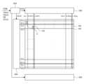
도 1을 참조하면, 본 발명의 일 실시예에 따른 표시장치는, 표시패널(100), 게이트 구동회로(drive circuit)(200), 데이터 구동회로(300), 타이밍 컨트롤러(timing controller)(400) 및 터치 구동회로(500)를 포함하여 구성될 수 있다.Referring to FIG. 1, a display device according to an embodiment of the present invention includes a
표시패널(100)에는 제1 방향으로 게이트 배선(GL1, GL2, …, GLn-1, GLn)과 공통 배선(CL1, …, CLo)이 배치되고, 제1 방향과 다른 방향인 제2 방향으로 데이터 배선(DL1, … DLm)이 배치될 수 있다.In the
또한, 표시패널(100)에는 데이터 배선(DL1, … DLm) 사이에 제2 방향으로 한 쌍의 리드아웃 배선(R-RO1,L-RO1, …R-ROq,L-ROq)이 배치될 수 있다. 또한, 게이트 배선(GL1, GL2, …GLn-1, GLn) 사이에는 제1 방향으로 센싱 스토리지 배선(VST1, …, VSTp)이 배치될 수 있다.Additionally, a pair of leadout wires (R-RO1, L-RO1, ...R-ROq, L-ROq) may be disposed in the second direction between the data wires (DL1, ... DLm) in the
일 예로, 다수개의 게이트 배선(GL1, GL2, …GLn-1, GLn)과 다수개의 데이터 배선(DL1, … DLm)이 교차하여 다수개의 화소(P)를 정의할 수 있다.As an example, a plurality of gate wires (GL1, GL2, ... GLn-1, GLn) and a plurality of data wires (DL1, ... DLm) may intersect to define a plurality of pixels (P).
다수개의 화소(P)는 게이트 배선(GL1, GL2, …GLn-1, GLn), 데이터 배선(DL1, … DLm) 및 공통 배선(CL1, …CLo)과 전기적으로 연결되고, 게이트 배선(GL1, GL2, …GLn-1, GLn), 데이터 배선(DL1, … DLm) 및 공통 배선(CL1, …CLo)을 통해 인가된 화소 구동 신호 또는 화소 구동 전압에 의해 화상을 표시할 수 있다.A plurality of pixels (P) are electrically connected to gate wires (GL1, GL2, ...GLn-1, GLn), data wires (DL1, ...DLm), and common wires (CL1, ...CLo), and gate wires (GL1, ...CLo) An image can be displayed by a pixel driving signal or pixel driving voltage applied through GL2,...GLn-1, GLn), data lines (DL1,...DLm), and common lines (CL1,...CLo).
본 발명의 일 실시예에 따른 표시패널(100)은, 인접하게 배치된 한 쌍의 화소(P)가 하나의 데이터 배선(DL1, … DLm)에 공통으로 접속되는 DRD(Double Rate Driving) 구조로 구성될 수 있다. 다만, 본 발명이 이에 한정되는 것은 아니다. DRD 구조란 일반적인 표시패널에 비해 게이트 배선의 수는 2배로 늘리는 대신 데이터 배선의 개수를 1/2배로 줄여, 데이터 구동회로를 이루는 데이터 집적회로(Integrated Circuit; IC)의 수를 줄이면서 동일한 해상도를 구현하기 위한 방식이다.The
이와 같이 본 발명의 일 실시예에 따른 표시패널(100)은, DRD 구조를 가짐으로써 기존의 데이터 배선이 배치된 영역을 이용하여 센싱 데이터 배선을 배치할 수 있으며, 두 개의 게이트 배선이 인접하게 배치된 영역에 포토 터치 센서(PS)를 배치함으로써 일반적인 표시장치와 비교하여 개구율 감소없이 터치를 감지하기 위한 포토 터치 센서(PS)를 구비할 수 있다.As such, the
표시패널(100)은 다수개의 화소(P)를 포함하고, 각각의 화소(P)가 표시하는 계조를 기반으로 화상을 표시할 수 있다. 다수개의 화소(P) 각각은 게이트 배선(GL1, GL2, …GLn-1, GLn)과 데이터 배선(DL1, … DLm)을 통해 인가된 신호에 의해 구동되는 화소 전극 및 공통 배선(CL1, …CLo)을 통해 구동되는 공통 전극을 포함할 수 있다. 다수개의 화소(P) 각각은 화소 전극과 공통 전극의 전압 차에 의해 액정이 틸트(tilt)되어 영상을 표시할 수 있다.The
도 1에 도시된 다수개의 화소(P)는 서로 다른 색을 표시하는 서브-화소일 수 있고, 다수개의 서브-화소가 단위를 이뤄 하나의 화소를 구성할 수 있다. 예를 들어, 서브-화소는 적색, 녹색 및 청색, 또는 적색, 녹색, 청색 및 백색을 표시할 수 있다.The plurality of pixels P shown in FIG. 1 may be sub-pixels that display different colors, and the plurality of sub-pixels may form a unit to form one pixel. For example, sub-pixels may display red, green, and blue, or red, green, blue, and white.
표시패널(100)에는 다수개의 센서 화소 유닛(150)이 정의될 수 있다.A plurality of
센서 화소 유닛(150)은 다수개의 화소로 이루어질 수 있다.The
센서 화소 유닛(150)은 광 세기에 따라 변하는 센서 박막 트랜지스터의 오프 커런트(off current)의 변화에 따라 터치를 인식하는 포토 터치 센서(PS)를 포함할 수 있다. 보다 구체적으로, 포토 터치 센서(PS)는 센서 박막 트랜지스터와 센서 스토리지 커패시터를 포함하고, 광 세기에 따라 센서 박막 트랜지스터가 턴-온되어 센서 스토리지 커패시터에 전압이 충전된다. 그리고, 충전된 전압이 미리 설정된 타이밍에 리드아웃 배선(R-RO1,L-RO1, …R-ROq,L-ROq)으로 출력되어 터치를 인식할 수 있다. 이러한 다수개의 센서 화소 유닛(150)의 구조는 후술할 도면들을 참조하여 보다 상세히 살펴보기로 한다.The
게이트 구동회로(200)는 타이밍 컨트롤러(400)로부터 전송된 게이트 구동 제어 신호(GCS)에 따라 순차적으로 표시패널(100)의 게이트 배선(GL1, GL2, …GLn-1, GLn)들에 게이트 신호를 공급할 수 있다. 게이트 구동회로(200)는 시프트 레지스터 및 레벨 시프터 등을 포함할 수 있다.The
게이트 구동회로(200)는 표시패널(100)과 독립되어 배치될 수도 있고, 표시패널(100)의 기판 제조 시 박막 형태로 표시패널(100)의 화소(P)가 배치되지 않는 비표시 영역 상에 게이트-인-패널(Gate In Panel; GIP) 방식으로 내장될 수도 있다.The
데이터 구동회로(300)는 타이밍 컨트롤러(400)로부터 전송된 데이터 구동 제어 신호(DCS)에 의해 샘플링 신호를 생성하고, 타이밍 컨트롤러(400)로부터 입력되는 영상 데이터를 샘플링 신호에 따라 래치하여 데이터 신호로 변경한 후, 소스 출력 인에이블(Source Output Enable; SOE) 신호에 응답하여 데이터 신호를 데이터 배선(DL1, … DLm)들에 공급할 수 있다.The
데이터 구동회로(300)는 칩-온-글래스(Chip On Glass; COG) 방식으로 표시패널(100)의 본딩 패드에 연결되거나, 표시패널(100)에 직접 배치될 수도 있으며, 경우에 따라 표시패널(100)에 집적화되어 배치될 수도 있다. 또한, 데이터 구동회로(300)는 칩-온-필름(Chip On Film; COF) 방식으로 배치될 수 있다.The
타이밍 컨트롤러(400)는 호스트 시스템(미도시)으로부터 수신된 입력 영상신호(RGB)를 데이터 구동회로(300)로 전송할 수 있다.The
또한, 타이밍 컨트롤러(400)는 입력 영상신호(RGB)와 함께 수신되는 클럭신호(DCLK), 수평동기신호(Hsync), 수직동기신호(Vsync) 및 데이터 인에이블 신호(DE) 등의 타이밍 신호를 이용하여 게이트 구동회로(200)와 데이터 구동회로(300)의 동작 타이밍을 제어하기 위한 타이밍 제어 신호를 생성할 수 있다. 타이밍 컨트롤러(400)는 타이밍 신호에 동기하여 게이트 구동회로(200)의 제어신호(GCS) 및 데이터 구동회로(300)의 제어신호(DCS)를 생성할 수 있다.In addition, the
또한, 타이밍 컨트롤러(400)는 포토 터치 센서(PS)의 구동을 위한 터치 구동 신호를 생성하여 터치 구동회로(500)에 전송할 수 있다. 또한, 타이밍 컨트롤러(400)는 터치 구동회로(500)로부터 터치 감지 신호를 입력받아 터치 정보를 산출할 수 있다.Additionally, the
터치 구동회로(500)는 타이밍 컨트롤러(400)로부터 전송된 터치 구동 신호를 포토 터치 터치 센서(PS)에 인가할 수 있다. 터치 구동회로(500)는 포토 터치 센서(PS)에서 전송된 터치 감지 신호를 입력받아 터치 여부를 판단할 수 있다.The
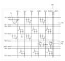
도 2는 본 발명의 일 실시예에 따른 표시패널에 배치된 어느 하나의 센서 화소 유닛의 일 예를 보여주는 등가회로도이다.Figure 2 is an equivalent circuit diagram showing an example of one sensor pixel unit disposed on a display panel according to an embodiment of the present invention.
도 3은 본 발명의 일 실시예에 따른 리드아웃 배선 및 연산 증폭기의 일 예를 보여주는 등가회로도이다.Figure 3 is an equivalent circuit diagram showing an example of readout wiring and an operational amplifier according to an embodiment of the present invention.
도 4는 센서 화소 유닛의 일 예를 보여주는 평면도이다.Figure 4 is a plan view showing an example of a sensor pixel unit.
먼저, 도 2를 참조하면, 본 발명의 일 실시예에 따른 표시패널의 센서 화소 유닛(150)은, 다수개의 화소(P1, P2)가 배치되어 화상을 표시하는 화소 영역(PA)과 적어도 하나의 포토 터치 센서(PS)가 배치되어 입사된 광을 감지하여 터치를 인식하는 센서 영역(SA)을 포함할 수 있다.First, referring to FIG. 2, the
화소 영역(PA)은 다수개의 화소(P1, P2)가 배치되고, 다수개의 화소(P1, P2)는 각각 적색, 녹색 및 청색의 서브-화소일 수 있다.The pixel area PA includes a plurality of pixels P1 and P2, and the plurality of pixels P1 and P2 may be red, green, and blue sub-pixels, respectively.
다수개의 화소(P1, P2)는 DRD 방식으로 배치될 수 있다. 보다 상세하게, 다수개의 화소(P1, P2) 중 인접하게 배치된 화소들, 예를 들어 제1 화소(P1)와 제2 화소(P2)는 동일한 데이터 배선인 제1 데이터 배선(DL1)과 전기적으로 연결되고, 서로 다른 게이트 배선, 예를 들어 각각 제1 게이트 배선(GL1)과 제2 게이트 배선(GL2)에 연결될 수 있다.A plurality of pixels (P1, P2) may be arranged in a DRD method. In more detail, among the plurality of pixels P1 and P2, pixels arranged adjacently, for example, the first pixel P1 and the second pixel P2, are electrically connected to the first data line DL1, which is the same data line. and may be connected to different gate wires, for example, the first gate wire GL1 and the second gate wire GL2, respectively.
화소 영역(PA)에는 제1 방향으로 배치된 제1 공통 배선(CL1) 및 제2 공통 배선(CL2), 제1 공통 배선(CL1)과 제2 공통 배선(CL2) 사이에 배치된 제1 게이트 배선(GL1) 및 제2 게이트 배선(GL2), 제1 방향과 상이한 제2 방향으로 배치된 제1 데이터 배선 내지 제3 데이터 배선(DL1~DL3)이 구비될 수 있다. 또한, 화소 영역(PA)에는, 제2 방향으로 배치되고 제1 데이터 배선(DL1) 및 제2 데이터 배선(DL2) 사이에 배치된 보조 배선(AL1), 제2 데이터 배선(DL2) 및 제3 데이터 배선(DL3) 사이에 배치된 센싱 데이터 배선(VDR1) 및 제3 데이터 배선(DL3)과 인접하게 배치된 제1, 제2 리드아웃 배선(R-RO1, L-RO1)이 구비될 수 있다.In the pixel area PA, a first common interconnection CL1 and a second common interconnection CL2 are arranged in the first direction, and a first gate is disposed between the first common interconnection CL1 and the second common interconnection CL2. A wiring GL1, a second gate wiring GL2, and first to third data lines DL1 to DL3 arranged in a second direction different from the first direction may be provided. Additionally, in the pixel area PA, an auxiliary line AL1, a second data line DL2, and a third line are disposed in the second direction and are disposed between the first data line DL1 and the second data line DL2. A sensing data line (VDR1) disposed between the data lines (DL3) and first and second leadout lines (R-RO1, L-RO1) disposed adjacent to the third data line (DL3) may be provided. .
제2 방향으로 배열된 배선들은 센서 영역(SA)까지 연장되어 배치될 수 있다. 센싱 데이터 배선(VDR1)은 센서 영역(PA)에 배치된 포토 터치 센서(PS)에 센서 데이터 신호, 즉 포토 터치 센서 구동 신호를 전달하는 배선이다.Wires arranged in the second direction may be arranged to extend to the sensor area SA. The sensing data wire (VDR1) is a wire that transmits a sensor data signal, that is, a photo touch sensor driving signal, to the photo touch sensor (PS) disposed in the sensor area (PA).
다수개의 화소(P1, P2) 각각은 화소 박막 트랜지스터(TPx), 화소 박막 트랜지스터(TPx)와 병렬 접속된 화소 커패시터(PClc) 및 화소 스토리지 커패시터(PCst)를 포함할 수 있다.Each of the plurality of pixels (P1, P2) may include a pixel thin film transistor (TPx), a pixel capacitor (PClc) and a pixel storage capacitor (PCst) connected in parallel with the pixel thin film transistor (TPx).
도시하지 않았지만, 각각의 화소(P1, P2)는 화소 박막 트랜지스터(TPx)와 접속된 화소 전극, 공통 전압을 공급하는 공통 전극 및 화소 전극과 공통 전극에 의해 수직 전계 또는 수평 전계에 의해 틸트되는 액정들이 배치된 액정층으로 구성될 수 있다.Although not shown, each pixel (P1, P2) includes a pixel electrode connected to the pixel thin film transistor (TPx), a common electrode that supplies a common voltage, and a liquid crystal that is tilted by a vertical or horizontal electric field by the pixel electrode and the common electrode. It may be composed of a liquid crystal layer in which these are disposed.
도 2를 참조하면, 화소 박막 트랜지스터(TPx)는 해당 게이트 배선(GL1, GL2, GL3, GL4)으로부터 인가되는 게이트 신호에 응답하여 데이터 배선(DL1, DL2, DL3)으로부터 인가되는 데이터 신호를 화소 커패시터(PClc) 및 화소 스토리지 커패시터(PCst)에 저장할 수 있다.Referring to FIG. 2, the pixel thin film transistor TPx transmits the data signal applied from the data lines DL1, DL2, and DL3 in response to the gate signal applied from the corresponding gate line GL1, GL2, GL3, and GL4 through the pixel capacitor. (PClc) and pixel storage capacitor (PCst).
이렇게 화소 커패시터(PClc)에 저장된 데이터 신호에 따라 액정이 구동되고, 화소 스토리지 커패시터(PCst)는 화소 커패시터(PClc)의 데이터 신호를 안정적으로 유지시킬 수 있다.In this way, the liquid crystal is driven according to the data signal stored in the pixel capacitor (PClc), and the pixel storage capacitor (PCst) can stably maintain the data signal of the pixel capacitor (PClc).
도 2에서는 본 발명의 일 실시예에 따른 표시패널(100)이 액정패널인 경우를 예시로 하여 설명하였으나, 본 발명이 이에 한정되는 것은 아니다. 예를 들어, 본 발명의 일 실시예에 따른 표시패널(100)은 유기발광 표시패널일 수 있고, 유기발광 표시패널인 경우 화소 박막 트랜지스터(Px)와 접속된 애노드, 유기물로 이루어진 발광층 및 캐소드를 포함할 수 있다.In FIG. 2 , the
전술한 바와 같이 본 발명의 일 실시예는, 센싱과 디스플레이 타이밍이 동시에 진행되는 포토 센서(photo sensor) 방식의 표시장치에 있어, 센싱을 위한 제1 리드아웃 배선(R-RO1)과 노이즈를 검출하기 위한 제2 리드아웃 배선(L-RO1)을 이웃하도록 배치하는 것을 특징으로 한다.As described above, in an embodiment of the present invention, in a photo sensor type display device in which sensing and display timing are performed simultaneously, a first leadout wire (R-RO1) for sensing and noise detection are provided. The second lead-out wiring (L-RO1) for this purpose is arranged adjacent to each other.
제1, 제2 리드아웃 배선(R-RO1, L-RO1)은 데이터 배선(DL3, DL4) 사이에 제2 방향으로 배열되고, 제1 리드아웃 배선(R-RO1)은 포토 터치 센서(PS)에 의한 터치 감지 신호를 전달할 수 있다. 또한, 제2 리드아웃 배선(L-RO1)은 노이즈를 검출하기 위해 제1 리드아웃 배선(R-RO1)의 인접하게 배치될 수 있다.The first and second leadout wires (R-RO1, L-RO1) are arranged in the second direction between the data wires (DL3, DL4), and the first leadout wire (R-RO1) is connected to the photo touch sensor (PS). ) can transmit a touch detection signal. Additionally, the second lead-out wire (L-RO1) may be disposed adjacent to the first lead-out wire (R-RO1) to detect noise.
이어서, 도 3을 참조하면, 제1, 제2 리드아웃 배선(R-RO1, L-RO1)에 각각 연결된 제1, 제2 연산 증폭기(operating amplifier)(OP1, OP2)를 통하여 출력 전압을 검출하고, 이를 제3 연산 증폭기(OP3)를 통해 비교해 노이즈 값을 제거함으로써 데이터 신호의 변화(transition)에 의한 노이즈 영향을 최소화할 수 있다. 일 예로, 제1 연산 증폭기(OP1)를 통해 검출된 출력 전압에서 제2 연산 증폭기(OP2)를 통해 검출된 출력 전압을 뺄 경우, 제1, 제2 연산 증폭기(OP1, OP2)를 통해 검출된 출력 전압에 공통되는 노이즈 값이 제거됨에 따라, 노이즈에 영향을 받지 않고 센싱 전압을 정확하게 검출할 수 있다.Next, referring to FIG. 3, the output voltage is detected through the first and second operating amplifiers (OP1, OP2) connected to the first and second readout wires (R-RO1, L-RO1), respectively. And, by comparing this through the third operational amplifier (OP3) and removing the noise value, the noise effect due to the transition of the data signal can be minimized. For example, when subtracting the output voltage detected through the second operational amplifier (OP2) from the output voltage detected through the first operational amplifier (OP1), the output voltage detected through the first and second operational amplifiers (OP1, OP2) is As noise values common to the output voltage are removed, the sensing voltage can be accurately detected without being affected by noise.
참고로, 통상 연산 증폭기는 아날로그 컴퓨터용의 고이득 증폭기를 의미하며, 아날로그 컴퓨터에서는 그 이득이 귀환회로에 쓰이는 수동소자의 특성만으로 결정될 수 있도록 하기 위해, 큰 이득을 가지며, 입력 임피던스가 높고, 출력 임피던스가 낮은 증폭기가 필요하게 되었다. 이 증폭기는 그 후 아날로그 증폭기의 표준 집적회로(IC)로서 널리 사용되도록 되어 있다. 표준 IC로서의 연산증폭기는 차동입력형으로서, 이득은 30~100dB이며, 여기에 음귀환을 걸어서 적절한 이득의 증폭회로를 얻는다. 연산증폭기의 입력에 접속한 임피던스와 귀환회로에 접속한 임피던스의 비로서, 회로의 입출력 특성이 결정되도록 되어 있다.For reference, an operational amplifier usually refers to a high-gain amplifier for analog computers. In analog computers, it has a large gain, high input impedance, and output so that the gain can be determined only by the characteristics of the passive elements used in the feedback circuit. An amplifier with low impedance was needed. This amplifier has since become widely used as a standard integrated circuit (IC) for analog amplifiers. The operational amplifier as a standard IC is a differential input type, with a gain of 30 to 100 dB, and negative feedback is applied to obtain an amplification circuit with an appropriate gain. The input/output characteristics of the circuit are determined by the ratio of the impedance connected to the input of the operational amplifier and the impedance connected to the feedback circuit.
제1, 제2, 제3 연산 증폭기(OP1, OP2, OP3)는 데이터 구동회로(300)나 터치 구동회로(500)의 터치 컨트롤 IC에 배치될 수 있다.The first, second, and third operational amplifiers OP1, OP2, and OP3 may be disposed in the touch control IC of the
도 3에는 소정 전압을 출력하는 제1, 제2 리드아웃 배선(R-RO1, L-RO1)에 기생 커패시터 용량(Cp)이 도시되어 있다.FIG. 3 shows the parasitic capacitor capacity (Cp) of the first and second leadout wires (R-RO1 and L-RO1) that output a predetermined voltage.
터치 컨트롤 IC는, 제1, 제2 리드아웃 배선(R-RO1, L-RO1)를 통해 센싱된 전류를 제1, 제2 연산 증폭기(OP1, OP2)에 의해 증폭하여 검출하는 것으로, 각각 (-) 입력 단자에 제1, 제2 리드아웃 배선(R-RO1, L-RO1)이 연결되고, (+) 입력 단자에 기준 전압(Vref)이 인가될 수 있다. 또한, 출력 단자에서 출력된 전압은 센싱된 전압 값의 증폭한 값이다. 여기서, (-) 입력 단자와 출력 단자 사이에는 제1, 제2 피드백 커패시터(Cfb1, Cfb2)가 형성될 수 있다. 다만, 본 발명이 이에 한정되는 것은 아니다.The touch control IC amplifies and detects the current sensed through the first and second readout wires (R-RO1, L-RO1) by the first and second operational amplifiers (OP1, OP2), respectively ( -) The first and second readout wires (R-RO1, L-RO1) may be connected to the input terminal, and a reference voltage (Vref) may be applied to the (+) input terminal. Additionally, the voltage output from the output terminal is an amplified value of the sensed voltage value. Here, first and second feedback capacitors Cfb1 and Cfb2 may be formed between the (-) input terminal and the output terminal. However, the present invention is not limited to this.
제1 피드백 커패시터(Cfb1)와 제2 피드백 커패시터(Cfb2)는 동일한 값으로 설정할 수 있다.The first feedback capacitor (Cfb1) and the second feedback capacitor (Cfb2) may be set to the same value.
기존은 데이터 신호의 변화(transition)에 의한 공통 전압의 변동(ripple)이 기생 커패시터 용량에 의하여 리드아웃 배선에 전압 변동을 유발하여 노이즈를 발생시킬 수 있다. 이는 터치 센서 특성의 저하를 가져오고, 터치 센서를 위한 전압 레벨의 마진이 줄어들게 된다. 즉, 일 예로 노이즈 값이 터치 감지 신호에 비해 큰 값을 가질 경우, 연산 증폭기를 통해 검출된 출력 전압이 노이즈 값인지 센싱 전압인지 구분할 수 없어 센싱의 정확도가 떨어지게 된다.Conventionally, a ripple in common voltage due to a change (transition) in a data signal may cause a voltage change in the readout wiring due to parasitic capacitor capacity, thereby generating noise. This results in a deterioration of the touch sensor characteristics, and the margin of voltage level for the touch sensor is reduced. That is, for example, if the noise value has a larger value than the touch detection signal, it is not possible to distinguish whether the output voltage detected through the operational amplifier is the noise value or the sensing voltage, thereby reducing the accuracy of sensing.
이를 개선하기 위해 본 발명은, 센싱을 위한 제1 리드아웃 배선(R-RO1)과 노이즈(noise)를 검출하기 위한 제2 리드아웃 배선(L-RO1)을 이웃하도록 배치하고, 제1 리드아웃 배선(R-RO1)과 제2 리드아웃 배선(L-RO1) 기생 커패시터 용량(Cp)을 맞추기 위하여 스토리지 커패시터를 서로 단락(short)시켜 제1, 제2 리드아웃 배선(R-RO1, L-RO1)에 각각 연결하게 된다.In order to improve this, the present invention arranges the first leadout wire (R-RO1) for sensing and the second leadout wire (L-RO1) for detecting noise to be adjacent to each other, and the first leadout wire (R-RO1) is arranged to be adjacent to each other. In order to match the parasitic capacitance (Cp) of the wire (R-RO1) and the second leadout wire (L-RO1), the storage capacitors are shorted together to form the first and second leadout wires (R-RO1, L-RO1). Each is connected to RO1).
이때, 외부 센싱이 없을 경우, 제1 리드아웃 배선(R-RO1)에 연결된 제1 연산 증폭기(OP1)와 제2 리드아웃 배선(L-RO1)에 연결된 제2 연산 증폭기(OP2)의 전압을 제3 연산 증폭기(OP3)를 통해 비교하여 노이즈 값을 제거한다. 일 예로, 제1 연산 증폭기(OP1)를 통해 검출된 출력 전압(즉, 노이즈 값)에서 제2 연산 증폭기(OP2)를 통해 검출된 출력 전압(즉, 노이즈 값)을 뺄 경우, 그 값이 0이 될 수 있다. 즉, 이 경우에는 외부 센싱이 없다는 것으로 인식할 수 있다.At this time, if there is no external sensing, the voltage of the first operational amplifier (OP1) connected to the first readout wire (R-RO1) and the second operational amplifier (OP2) connected to the second readout wire (L-RO1) are The noise value is removed by comparison through the third operational amplifier (OP3). For example, when the output voltage (i.e., noise value) detected through the second operational amplifier (OP2) is subtracted from the output voltage (i.e., noise value) detected through the first operational amplifier (OP1), the value is 0. This can be. In other words, in this case, it can be recognized that there is no external sensing.
반면, 센싱 신호가 발생할 경우, 제1 리드아웃 배선(R-RO1)에 연결된 제1 연산 증폭기(OP1)와 제2 리드아웃 배선(L-RO1)에 연결된 제2 연산 증폭기(OP2)의 전압을 비교하여 노이즈 값을 제거함으로써 센싱 민감도를 올리면서 센싱 전압을 검출할 수 있다. 일 예로, 제1 연산 증폭기(OP1)를 통해 검출된 출력 전압(즉, 노이즈 값 + 센싱 전압)에서 제2 연산 증폭기(OP2)를 통해 검출된 출력 전압(즉, 노이즈 값)을 뺄 경우, 센싱 전압을 얻을 수 있다. 즉, 제1, 제2 연산 증폭기(OP1, OP2)를 통해 검출된 출력 전압에 공통되는 노이즈 값이 제거됨에 따라, 노이즈에 영향을 받지 않고 센싱 전압을 정확하게 검출할 수 있게 된다.On the other hand, when a sensing signal occurs, the voltage of the first operational amplifier (OP1) connected to the first readout wire (R-RO1) and the second operational amplifier (OP2) connected to the second readout wire (L-RO1) By comparing and removing the noise value, the sensing voltage can be detected while increasing the sensing sensitivity. As an example, when subtracting the output voltage (i.e., noise value) detected through the second operational amplifier (OP2) from the output voltage (i.e., noise value + sensing voltage) detected through the first operational amplifier (OP1), the sensing voltage can be obtained. That is, as the noise value common to the output voltage detected through the first and second operational amplifiers OP1 and OP2 is removed, the sensing voltage can be accurately detected without being affected by noise.
본 발명은, 데이터 신호의 변화에 의한 노이즈 영향을 최소화함으로써 인치 및 해상도 증가에 유리하다.The present invention is advantageous in increasing inches and resolution by minimizing the noise effect caused by changes in data signals.
이어서, 도 4를 참조하면, 각 화소는 화소 전극(118)과 공통 전극(108)에 의해 화상이 표시되도록 하는 개구 영역 및 화상이 표시되지 않고 개구 영역의 화소 전극(118)과 공통 전극(108)의 구동을 위한 구동 소자, 예를 들어 화소 박막 트랜지스터(TPx) 등이 배치된 비개구 영역을 포함할 수 있다.Next, referring to FIG. 4, each pixel has an opening area in which an image is displayed by the
개구 영역에는 화소 전극(118)과 공통 전극(108)이 배치될 수 있다.A
화소 전극(118)은 공통 전극(108)과 함께 전계를 형성하고, 이렇게 형성된 전계에 의해 액정층의 액정 분자들이 틸트(tilt)되어 영상을 표시하도록 할 수 있다. 화소 전극(118)은 동일한 간격으로 나란히 배치될 수 있으며, 다수개의 화소 전극(118)의 일단은 제1 방향으로 배치된 화소라인(118a)에 연결될 수 있다. 화소 전극(118)은 개구 영역에만 배치되는 것이 아니라 비개구 영역에도 확장되어 배치될 수 있다.The
공통 전극(108)은 동일한 간격으로 나란하게 배치될 수 있으며, 다수개의 공통 전극(108)의 일단은 제1 방향으로 배치된 공통라인(108a)에 연결될 수 있다. 공통 전극(108)은 개구 영역 내에 화소 전극(118)과 번갈아 배치될 수 있다.The
그리고, 공통 전극(108)은 데이터 배선(DL3, DL4), 센싱 데이터 배선(VDR1), 제1, 제2 리드아웃 배선(R-RO1, L-RO1) 및 보조 배선(AL2) 위에 데이터 배선(DL3, DL4), 센싱 데이터 배선(VDR1), 제1, 제2 리드아웃 배선(R-RO1, L-RO1) 및 보조 배선(AL2)을 덮도록 배치될 수 있다.And, the
한편, 비개구 영역에는 다수개의 게이트 배선(GL3, GL4), 다수개의 데이터 배선(DL3, DL4), 보조 배선(AL2), 센싱 데이터 배선(VDR1), 제1, 제2 리드아웃 배선(R-RO1, L-RO1), 화소 박막 트랜지스터(TPx), 센싱 스토리지 배선(VST1), 센싱 게이트 배선(GL4), 센서 박막 트랜지스터(Tss), 센서 스위치 박막 트랜지스터(Tsw) 및 제1, 제2 센서 스토리지 커패시터(SCst1, SCst2)가 배치될 수 있다. 여기서, 센싱 게이트 배선(GL4)은 기존의 게이트 배선(GL4)으로 구성된 경우를 예로 들고 있으나, 본 발명이 이에 한정되는 것은 아니며, 기존의 게이트 배선과는 다른 배선으로 구성될 수도 있다. 다만, 기존의 게이트 배선과는 다른 배선으로 센싱 게이트 배선(GL4)을 구성하는 경우 개구율 손실이 발생할 수 있다. 이에 따라, 표시장치의 제1 방향으로의 개구율의 감소를 최소화하기 위해, 센싱 게이트 배선(GL4)은 기존의 게이트 배선(GL4)으로 구성할 수 있다.Meanwhile, in the non-opening area, there are a plurality of gate wires (GL3, GL4), a plurality of data wires (DL3, DL4), an auxiliary wire (AL2), a sensing data wire (VDR1), and first and second leadout wires (R- RO1, L-RO1), pixel thin film transistor (TPx), sensing storage wiring (VST1), sensing gate wiring (GL4), sensor thin film transistor (Tss), sensor switch thin film transistor (Tsw), and first and second sensor storage. Capacitors (SCst1, SCst2) may be disposed. Here, the sensing gate wire GL4 is made of the existing gate wire GL4 as an example, but the present invention is not limited to this and may be made of a wire different from the existing gate wire. However, if the sensing gate wiring (GL4) is configured with a different wiring from the existing gate wiring, aperture ratio loss may occur. Accordingly, in order to minimize a decrease in the aperture ratio in the first direction of the display device, the sensing gate wire GL4 may be configured with the existing gate wire GL4.
이때, 센싱 스토리지 배선(VST1), 센싱 게이트 배선(GL4), 센서 박막 트랜지스터(Tss), 센서 스위치 박막 트랜지스터(Tsw) 및 제1, 제2 센서 스토리지 커패시터(SCst1, SCst2)는 센서 영역(SA)에만 배치되는 구성으로, 이하에서 상세히 설명하도록 한다. 여기서, 제2 방향으로 배치된 보조 배선(AL2), 제3 데이터 배선(DL3), 제4 데이터 배선(DL4) 및 센싱 데이터 배선(VDR1)에는 광을 차폐하는 차폐 배선(111)이 각 배선을 감싸도록 배치될 수 있다. 다만, 본 발명이 이에 한정되는 것은 아니며, 제1, 제2 리드아웃 배선(R-RO1, L-RO1)에도 제1, 제2 리드아웃 배선(R-RO1, L-RO1)을 감싸도록 차폐 배선이 배치될 수 있다.At this time, the sensing storage wiring (VST1), the sensing gate wiring (GL4), the sensor thin film transistor (Tss), the sensor switch thin film transistor (Tsw), and the first and second sensor storage capacitors (SCst1, SCst2) are connected to the sensor area (SA). It is a configuration that is deployed only, and will be described in detail below. Here, a
이와 같이 제2 방향으로 배치된 보조 배선(AL2), 센싱 데이터 배선(VDR1) 및 제1, 제2 리드아웃 배선(R-RO1, L-RO1)은, 별도의 영역에 배선을 배치하는 것이 아니라, (DRD 방식이 아닌) 일반적인 표시장치에서 데이터 배선이 배치되는 영역에 배치될 수 있기 때문에 본 발명의 일 실시예에 따른 표시패널(100)은 포토 터치 센서(PS)를 배치하기 위해 별도의 배선 영역을 설계할 필요가 없다. 따라서, 개구율이 감소되는 것을 최소화할 수 있다.In this way, the auxiliary wiring (AL2), the sensing data wiring (VDR1), and the first and second leadout wiring (R-RO1, L-RO1) arranged in the second direction are not arranged in separate areas, but are instead arranged in separate areas. , Since it can be placed in the area where data wires are placed in a general display device (rather than the DRD method), the
즉, 본 발명의 일 실시예에 따른 표시장치(100)는 DRD 방식으로 화소들이 구성되기 때문에 별도의 보조 배선(AL2), 센싱 데이터 배선(VDR1) 및 제1, 제2 리드아웃 배선(R-RO1, L-RO1)을 배치할 영역을 마련할 필요가 없어, (DRD 방식이 아닌) 일반적인 표시장치에 포토 터치 센서를 구비하는 경우에 비해 제2 방향으로의 개구율 감소를 최소화시킬 수 있다.That is, since the
화소 박막 트랜지스터(TPx)는, 게이트 전극 역할을 제3 게이트 배선(GL3), 제3 데이터 배선(DL3) 및 제3 데이터 배선(DL3)으로부터 분기된 소스 전극과 소스 전극과 이격되어 배치된 드레인 전극을 포함하여 구성될 수 있다.The pixel thin film transistor TPx has a third gate wire GL3, a third data wire DL3, and a source electrode branched from the third data wire DL3, which serves as a gate electrode, and a drain electrode disposed to be spaced apart from the source electrode. It may be configured to include.
센싱 데이터 배선(VDR1)은 제2 데이터 배선과 제3 데이터 배선(DL3) 사이에 배치될 수 있고, 센서 박막 트랜지스터(Tss)와 연결되어 센서 박막 트랜지스터(Tss)에 센서 구동 신호 또는 센서 구동 전압을 인가할 수 있다. 센서 박막 트랜지스터(Tss)에 인가되는 센서 구동 전압은 터치 구동회로(500)로부터 인가되거나 타이밍 컨트롤러(200)로부터 인가될 수 있다.The sensing data wire (VDR1) may be disposed between the second data wire and the third data wire (DL3) and is connected to the sensor thin film transistor (Tss) to provide a sensor driving signal or sensor driving voltage to the sensor thin film transistor (Tss). It can be approved. The sensor driving voltage applied to the sensor thin film transistor (Tss) may be applied from the
제1 리드아웃 배선(R-RO1)은 포토 터치 센서(PS)의 센서 스위치 박막 트랜지스터(Tsw)와 전기적으로 연결될 수 있다. 이에 따라 제1 리드아웃 배선(R-RO1)은 포토 터치 센서(PS)에 의한 터치 감지 신호를 터치 구동회로(500)에 전달할 수 있다. 제1, 제2 리드아웃 배선(R-RO1, L-RO1)은 센서 화소 유닛(150)과 1:1로 대응되도록 배치될 수 있다.The first leadout wire (R-RO1) may be electrically connected to the sensor switch thin film transistor (Tsw) of the photo touch sensor (PS). Accordingly, the first leadout wire (R-RO1) can transmit a touch detection signal by the photo touch sensor (PS) to the
센서 박막 트랜지스터(Tss)는, 제1 게이트 전극(121a), 센싱 데이터 배선(VDR1) 및 센싱 데이터 배선(VDR1)으로부터 분기된 제1 소스 전극(122a)과 제1 소스 전극(122a)과 이격되어 배치된 제1 드레인 전극(123a)을 포함하여 구성될 수 있다.The sensor thin film transistor Tss is spaced apart from the
제1 드레인 전극(123a)은 일 방향으로 연장되어 그 하부의 센싱 스토리지 배선(VST1)과 함께 제1 센서 스토리지 커패시터(SCst1)를 구성할 수 있다.The
센서 스위치 박막 트랜지스터(Tsw)는, 제2 게이트 전극(121b), 제1 리드아웃 배선(R-RO1) 및 제1 리드아웃 배선(R-RO1)으로부터 분기된 제2 드레인 전극(123b)과 제2 드레인 전극(123b)과 이격되어 배치된 제2 소스 전극(122b)을 포함하여 구성될 수 있다.The sensor switch thin film transistor (Tsw) includes a second gate electrode (121b), a first lead-out wire (R-RO1), a second drain electrode (123b) branched from the first lead-out wire (R-RO1), and a second gate electrode (121b). 2 It may be configured to include a second source electrode (122b) disposed to be spaced apart from the drain electrode (123b).
제2 소스 전극(122b)은 일 방향으로 연장되어 그 하부의 센싱 스토리지 배선(VST1)과 함께 제2 센서 스토리지 커패시터(SCst2)를 구성할 수 있다.The
제1 센서 스토리지 커패시터(SCst1)의 상부, 즉 제1 드레인 전극(123a)은 제1 컨택홀(140a)을 통해 외부로 노출되며, 제2 센서 스토리지 커패시터(SCst2)의 상부, 즉 제2 소스 전극(122b)은 제2 컨택홀(140b)을 통해 외부로 노출될 수 있다.The top of the first sensor storage capacitor (SCst1), that is, the
제1 드레인 전극(123a)은 제1 컨택홀(140a)을 통해 연결전극(130)과 전기적으로 접속하는 동시에 제2 소스 전극(122b)은 제2 컨택홀(140b)을 통해 연결전극(130)과 전기적으로 접속함에 따라 제1 드레인 전극(123a)과 제2 소스 전극(122b)이 서로 연결될 수 있다.The
일 예로, 도 1 내지 도 4를 참조하면, 센서 화소 유닛(150)은, 제1 화소(P1) 및 제1 화소(P1)와 인접한 제2 화소(P2)를 포함할 수 있다. 이때, 제1 화소(P1)와 제2 화소(P2)는 제1 데이터 배선(DL1)에 연결되며, 제1 화소(P1)와 제2 화소(P2)는 제1 게이트 배선(GL1)과 제2 게이트 배선(GL2)에 각각 연결될 수 있다.As an example, referring to FIGS. 1 to 4 , the
또한, 센서 화소 유닛(150)은, 제2 화소(P2)와 인접한 제3 화소 및 제3 화소와 인접한 제4 화소를 더 포함할 수 있다. 이때, 제3 화소와 제4 화소는 제1 데이터 배선(DL1)과 인접한 제2 데이터 배선(DL2)과 연결될 수 있고, 제1 데이터 배선(DL1)과 제2 데이터 배선(DL2) 사이에 배치되는 보조 배선(AL1)을 추가로 포함할 수 있다.Additionally, the
또한, 센서 화소 유닛(150)은, 제4 화소와 인접한 제5 화소 및 제5 화소와 인접한 제6 화소를 더 포함할 수 있다. 이때, 제5 화소와 제6 화소는 제2 데이터 배선(DL2)과 인접한 제3 데이터 배선(DL3)과 연결되며, 센싱 데이터 배선(VDR1)은, 제2 데이터 배선(DL2)과 제3 데이터 배선(DL3) 사이에 배치될 수 있다.Additionally, the
전술한 센서 화소 유닛(150)에 이웃하는 센서 화소 유닛은, 제6 화소와 인접한 제7 화소 및 제7 화소와 인접한 제8 화소를 포함할 수 있다. 이때, 제7 화소와 제8 화소는 제3 데이터 배선(DL3)과 인접한 제4 데이터 배선(DL4)과 연결되며, 제1, 제2 리드아웃 배선(R-RO1, L-RO1)은, 제3 데이터 배선(DL3)과 제4 데이터 배선(DL4) 사이에 배치될 수 있다.The sensor pixel unit adjacent to the above-described
센서 화소 유닛(150)은, 제5 화소에 배치되며, 센싱 데이터 배선(VDR1)과 연결되어 광에 응답하여 출력 신호를 발생시키는 센서 박막 트랜지스터(Tss) 및 센서 박막 트랜지스터(Tss)에서 출력된 출력 신호를 저장하는 제1 센서 스토리지 커패시터(SCst1)를 포함할 수 있다. 또한, 센서 화소 유닛(150)은, 제6 화소에 배치되며, 제1 센서 스토리지 커패시터(SCst1)에 연결된 제2 센서 스토리지 커패시터(SCst2) 및 센서 게이트 신호에 응답하여 제1, 제2 센서 스토리지 커패시터(SCst1, SCst2)에 저장된 출력 신호를 제1 리드아웃 배선(R-RO1)으로 출력하는 센서 스위치 박막 트랜지스터(Tsw)를 추가로 포함할 수 있다.The
센서 화소 유닛(150)에 이웃하는 센서 화소 유닛은, 제7, 제8 화소에 배치되며, 제1, 제2 센싱 스토리지 커패시터(SCst1, SCst2)에 대응하는 스토리지 용량을 가지는 제1, 제2 보조 스토리지 커패시터를 추가로 포함할 수 있다.Sensor pixel units adjacent to the
제7, 제8 화소는, 제1, 제2 리드아웃 배선(R-RO1, L-RO1)을 중심으로 제5, 제6 화소와 거울 대칭 구조를 가지며, 센서 박막 트랜지스터(Tss)와 센서 스위치 박막 트랜지스터(Tsw)를 제외하고 실질적으로 제5, 제6 화소와 동일한 구성을 가지도록 구성될 수 있다.The 7th and 8th pixels have a mirror symmetrical structure with the 5th and 6th pixels centered on the first and second leadout wires (R-RO1, L-RO1), and include a sensor thin film transistor (Tss) and a sensor switch. It may be configured to have substantially the same configuration as the fifth and sixth pixels except for the thin film transistor (Tsw).
이와 같이 구성되는 표시패널의 개구 영역의 단면 구조를 보다 상세히 설명한다.The cross-sectional structure of the opening area of the display panel configured in this way will be described in more detail.
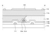
도 5는 도 4에 도시된 센서 화소 유닛의 A-A'선에 따른 단면도이다.FIG. 5 is a cross-sectional view taken along line A-A' of the sensor pixel unit shown in FIG. 4.
도 6은 도 4에 도시된 센서 화소 유닛의 B-B'선에 따른 단면도이다. 도 5 및 도 6은 센서 화소 유닛의 개구 영역의 단면 일부를 예로 들어 보여주고 있다.FIG. 6 is a cross-sectional view taken along line B-B' of the sensor pixel unit shown in FIG. 4. Figures 5 and 6 show a portion of the cross section of the opening area of the sensor pixel unit as an example.
도 5 및 도 6을 참조하면, 기판(110) 위에는 차폐 배선(111)이 배치될 수 있다.Referring to FIGS. 5 and 6 , a
차폐 배선(111)은, 예를 들어 보조 배선(AL2), 제3 데이터 배선(DL3), 제4 데이터 배선(DL4) 및 센싱 데이터 배선(VDR1)을 감싸도록 배치될 수 있다. 다만, 본 발명이 이에 한정되는 것은 아니다.The
차폐 배선(111)은, 예를 들어 몰리브덴(Mo), 알루미늄(Al), 크롬(Cr), 금(Au), 티타늄(Ti), 니켈(Ni), 네오디뮴(Nd) 및 구리(Cu)로 이루어진 군에서 선택된 어느 하나 또는 이들의 합금으로 이루어질 수 있다,The shielding
차폐 배선(111) 위에는 게이트 절연막(115a)이 배치될 수 있다. 게이트 절연막(115a)은, 예를 들어 실리콘 산화막(SiOx), 실리콘 질화막(SiNx) 또는 이들의 다층 구조로 이루어질 수 있다.A
게이트 절연막(115a) 위에는 반도체층(124c)이 배치될 수 있다.A
반도체층(124c)은, 일 예로 비정질 실리콘, 다결정 실리콘, 저온 폴리실리콘 및 산화물 반도체와 같은 반도체 물질 중 어느 하나의 반도체 물질로 이루어질 수 있다.The
반도체층(124c) 위에는 보조 배선(AL2), 제3 데이터 배선(DL3), 제4 데이터 배선(DL4), 센싱 데이터 배선(VDR1) 및 제1, 제2 리드아웃 배선(R-RO1, L-RO1)이 배치될 수 있다.On the
보조 배선(AL2), 제3 데이터 배선(DL3), 제4 데이터 배선(DL4), 센싱 데이터 배선(VDR1) 및 제1, 제2 리드아웃 배선(R-RO1, L-RO1)은, 예를 들어 몰리브덴(Mo), 알루미늄(Al), 크롬(Cr), 금(Au), 티타늄(Ti), 니켈(Ni), 네오디뮴(Nd) 및 구리(Cu)로 이루어진 군에서 선택된 어느 하나 또는 이들의 합금으로 이루어질 수 있다.The auxiliary wire (AL2), the third data wire (DL3), the fourth data wire (DL4), the sensing data wire (VDR1), and the first and second leadout wires (R-RO1, L-RO1) are, for example, For example, any one selected from the group consisting of molybdenum (Mo), aluminum (Al), chromium (Cr), gold (Au), titanium (Ti), nickel (Ni), neodymium (Nd), and copper (Cu). It may be made of alloy.
보조 배선(AL2), 제3 데이터 배선(DL3), 제4 데이터 배선(DL4), 센싱 데이터 배선(VDR1) 및 제1, 제2 리드아웃 배선(R-RO1, L-RO1) 위에는 층간절연막(115b)이 배치될 수 있다.An interlayer insulating film ( 115b) can be arranged.
층간절연막(115b)은 보조 배선(AL2), 제3 데이터 배선(DL3), 제4 데이터 배선(DL4), 센싱 데이터 배선(VDR1) 및 제1, 제2 리드아웃 배선(R-RO1, L-RO1)과 상부 층의 구성들을 절연하기 위한 것으로, 예를 들어 실리콘 산화막(SiOx), 실리콘 질화막(SiNx) 또는 이들의 다층으로 이루어질 수 있다.The
층간절연막(115b) 위에는 적색, 녹색 및 청색 중 어느 하나의 컬러필터로 이루어지거나 2개 이상의 컬러필터가 적층된 형태의 컬러필터층(106)이 배치될 수 있다.A
컬러필터층(106) 위에는 평탄화층(115c)이 배치될 수 있다.A
평탄화층(115c)은 하부의 단차를 평탄화하기 위한 것으로, 예를 들어 포토아크릴(photo acryl), 폴리이미드(polyimide), 벤조사이클로부틴계 수지(benzocyclobutene resin), 아크릴레이트계 수지(acrylate resin) 등의 유기물로 이루어질 수 있다.The
평탄화층(115c) 위에 화소 전극(118)과 공통 전극(108)이 배치될 수 있다.A
화소 전극(118)은 공통 전극(108)과 함께 전계를 형성하고, 이렇게 형성된 전계에 의해 액정층의 액정 분자들이 틸트(tilt)되어 영상을 표시하도록 할 수 있다. 화소 전극(118)은 동일한 간격으로 나란히 배치될 수 있으며, 다수개의 화소 전극(118)의 일단은 제1 방향으로 배치된 화소라인(118a)에 연결될 수 있다. 화소 전극(118)은 개구 영역에만 배치되는 것이 아니라 비개구 영역에도 확장되어 배치될 수 있다The
공통 전극(108)은 동일한 간격으로 나란하게 배치될 수 있으며, 다수개의 공통 전극(108)의 일단은 제1 방향으로 배치된 공통라인(108a)에 연결될 수 있다. 공통 전극(108)은 개구 영역 내에 화소 전극(118)과 번갈아 배치될 수 있다.The
공통 전극(108)과 화소 전극(118)은 투명 도전막으로 이루어질 수 있다. 투명 도전막은, 예를 들어 ITO(Indium Tin Oxide) 또는 IZO(Indium Zinc Oxide)와 같이 투명하면서도 도전성을 가진 재료일 수 있다. 도 4 및 도 5에서는 공통 전극(108)과 화소 전극(118)이 동일한 층에 배치된 것으로 도시하였으나, 발명이 이에 한정되는 것은 아니다. 공통 전극(108)과 화소 전극(118)은 서로 다른 층에 배치될 수 있고, 서로 다른 층에 배치되는 경우, 예를 들어 공통 전극(108)이 평탄화층(115c) 위에 배치되면 공통 전극(108) 위에 제2 절연막이 배치되고 제2 절연막 위에 화소 전극(118)이 배치될 수 있다.The
다음으로 센서 영역(SA)에 대해 보다 상세하게 살펴보기로 한다.Next, we will look at the sensor area (SA) in more detail.
다시 도 2 내지 도 4를 참조하면, 본 발명의 일 실시예에 따른 센서 영역(SA)은 제3 게이트 배선(GL3), 센싱 스토리지 배선(VST1) 및 센싱 디스플레이 게이트 배선(GL4)이 제1 방향으로 배치되고, 센싱 데이터 배선(VDR1)과 제1, 제2 리드아웃 배선(R-RO1, L-RO1)이 제1 방향과 다른 제2 방향으로 배치될 수 있다.Referring again to FIGS. 2 to 4, in the sensor area SA according to an embodiment of the present invention, the third gate wire GL3, the sensing storage wire VST1, and the sensing display gate wire GL4 are oriented in the first direction. , and the sensing data wire (VDR1) and the first and second leadout wires (R-RO1 and L-RO1) may be arranged in a second direction different from the first direction.
센싱 스토리지 배선(VST1)은 센서 스토리지 커패시터(SCst)의 배치로 인해 배치된 배선이다.The sensing storage wire (VST1) is a wire placed due to the placement of the sensor storage capacitor (SCst).
센싱 디스플레이 게이트 배선(GL4)은 화소 영역(PA)에 배치된 화소들에 게이트 신호를 전달함과 동시에 센서 영역(SA)에 배치된 포토 터치 센서(SP)에 센서 게이트 신호를 전달할 수 있다. 즉, 센싱 디스플레이 게이트 배선(GL4)은 기존의 센싱 게이트 배선과 제4 게이트 배선을 병합하여 배치된 배선이다. 이에 따라, 본 발명의 일 실시예에 따른 표시패널의 센서 영역(SA)은 기존보다 작은 면적을 가질 수 있어 포토 터치 센서(PS) 배치로 인한 개구율 감소를 최소화시킬 수 있다. 다만, 본 발명이 이에 한정되는 것은 아니다.The sensing display gate wire GL4 can transmit a gate signal to the pixels disposed in the pixel area PA and at the same time transmit a sensor gate signal to the photo touch sensor SP disposed in the sensor area SA. That is, the sensing display gate wiring GL4 is a wiring arranged by merging the existing sensing gate wiring and the fourth gate wiring. Accordingly, the sensor area (SA) of the display panel according to an embodiment of the present invention can have a smaller area than before, thereby minimizing the reduction in aperture ratio due to the arrangement of the photo touch sensor (PS). However, the present invention is not limited to this.
전술한 바와 같이, 본 발명의 일 실시예에 따른 포토 터치 센서(PS)는 센서 박막 트랜지스터(Tss), 센서 스토리지 커패시터(SCst) 및 센서 스위치 박막 트랜지스터(Tsw)를 포함할 수 있다.As described above, the photo touch sensor (PS) according to an embodiment of the present invention may include a sensor thin film transistor (Tss), a sensor storage capacitor (SCst), and a sensor switch thin film transistor (Tsw).
센서 박막 트랜지스터(Tss)는, 입사 광 또는 반사광의 광 세기에 응답하여 광 누설 전류를 발생시키고, 광 누설 전류를 센서 스토리지 커패시터(SCst)에 저장할 수 있다.The sensor thin film transistor (Tss) may generate light leakage current in response to the light intensity of incident light or reflected light, and store the light leakage current in the sensor storage capacitor (SCst).
센서 박막 트랜지스터(Tss)의 제1게이트 전극(121a)은 센싱 스토리지 배선(VST1)에 연결되고, 제1 소스 전극(122a)은 센싱 데이터 배선(VDR1)에 연결되며, 제1 드레인 전극(123a)은 제1 센서 스토리지 커패시터(SCst1)에 연결될 수 있다.The
제1 센서 스토리지 커패시터(SCst1)는 센서 박막 트랜지스터(Tss)의 출력 신호를 저장할 수 있다.The first sensor storage capacitor (SCst1) can store the output signal of the sensor thin film transistor (Tss).
그리고, 센서 스위치 박막 트랜지스터(Tsw)는, 센싱 디스플레이 게이트 배선(G4)으로부터 인가된 센서 게이트 신호에 응답하여 제1, 제2 센서 스토리지 커패시터(SCst1, SCst2)에 저장된 터치 감지 신호를 제1 리드아웃 배선(R-RO1)으로 출력할 수 있다.In addition, the sensor switch thin film transistor (Tsw) first reads out the touch detection signal stored in the first and second sensor storage capacitors (SCst1 and SCst2) in response to the sensor gate signal applied from the sensing display gate wire (G4). It can be output via wiring (R-RO1).
센서 스위치 박막 트랜지스터(Tsw)의 제2 게이트 전극(121b)은 센싱 디스플레이 게이트 배선(VST1)에 연결되고, 제2 소스 전극(122b) 및 제2 드레인 전극(123b) 각각은 제2 센서 스토리지 커패시터(SCst2)와 제1 리드아웃 배선(R-RO1)에 연결될 수 있다.The
이와 같이 구성되는 비개구 영역의 단면 구조를 보다 상세히 살펴보기로 한다.Let's look at the cross-sectional structure of the non-opening area configured in this way in more detail.
도 7은 도 4에 도시된 센서 화소 유닛의 C-C'선에 따른 단면도이다. 도 7은 센서 화소 유닛의 비개구 영역의 단면 일부를 예로 들어 보여주고 있다.FIG. 7 is a cross-sectional view taken along line C-C' of the sensor pixel unit shown in FIG. 4. Figure 7 shows a portion of the cross section of the non-aperture area of the sensor pixel unit as an example.
도 7을 참조하면, 기판(110) 위에는 제1 게이트 전극(121a)과 제2 게이트 전극(121b) 및 센싱 스토리지 배선(VST1)이 배치될 수 있다.Referring to FIG. 7 , a
이때, 제1 게이트 전극(121a)과 제2 게이트 전극(121b)은 센싱 스토리지 배선(VST1)의 일부로 구성될 수 있다.At this time, the
제1 게이트 전극(121a)과 제2 게이트 전극(121b) 및 센싱 스토리지 배선(VST1)은 동일한 금속물질로 이루어질 수 있고, 예를 들어 몰리브덴(Mo), 알루미늄(Al), 크롬(Cr), 금(Au), 티타늄(Ti), 니켈(Ni), 네오디뮴(Nd) 및 구리(Cu)로 이루어진 군에서 선택된 어느 하나 또는 이들의 합금으로 이루어질 수 있다.The
제1 게이트 전극(121a)과 제2 게이트 전극(121b) 및 센싱 스토리지 배선(VST1) 위에는 게이트 절연막(115a)이 배치될 수 있다. 게이트 절연막(115a)은, 예를 들어 실리콘 산화막(SiOx), 실리콘 질화막(SiNx) 또는 이들의 다층으로 이루어질 수 있다.A
게이트 절연막(115a) 위에는 제1 액티브층(124a), 제2 액티브층(124b) 및 반도체층(124c)이 배치될 수 있다.A first
제1 액티브층(124a), 제2 액티브층(124b) 및 반도체층(124c)은, 예를 들어 비정질 실리콘, 다결정 실리콘, 저온 폴리실리콘 및 산화물 반도체 등과 같은 반도체 물질 중 어느 하나의 반도체 물질로 이루어질 수 있다.The first
제1, 제2 액티브층(124a, 124b) 위에는 센싱 데이터 배선(VDR1)에서 분기된 제1 소스 전극(122a), 제1 소스 전극(122a)으로부터 이격된 제1 드레인 전극(123a), 제2 소스 전극(122b) 및 제1 리드아웃 배선(R-RO1)으로부터 분기되어 배치된 제2 드레인 전극(123b)이 배치될 수 있다.On the first and second
또한, 반도체층(124c) 위에는 데이터 배선(DL3) 및 제1, 제2 리드아웃 배선(R-RO1, L-RO1)이 배치될 수 있다.Additionally, a data line DL3 and first and second leadout lines R-RO1 and L-RO1 may be disposed on the
제1 리드아웃 배선(R-RO1)과 제2 리드아웃 배선(L-RO1)은 일정 간격을 두고 인접하여 배치될 수 있다.The first lead-out wire (R-RO1) and the second lead-out wire (L-RO1) may be arranged adjacent to each other at regular intervals.
이때, 제1 게이트 전극(121a), 제1 소스 전극(122a)과 제1 드레인 전극(123a) 및 제1 액티브층(124a)은 센서 박막 트랜지스터(Tss)를 구성할 수 있다. 즉, 제1 소스 전극(122a)이 센서 박막 트랜지스터(Tss)의 제1 전극이 되고, 제1 드레인 전극(123a)이 센서 박막 트랜지스터(Tss)의 제2 전극이 될 수 있다.At this time, the
또한, 제2 게이트 전극(121b), 제2 소스 전극(122b)과 제2 드레인 전극(123b) 및 제2 액티브층(124b)은 센서 스위치 박막 트랜지스터(Tsw)를 구성할 수 있다. 이 경우, 제2 소스 전극(122b)이 센서 스위치 박막 트랜지스터(Tsw)의 제2 전극이 되고, 제2 드레인 전극(123b)이 센서 스위치 박막 트랜지스터(Tsw)의 제1 전극이 될 수 있다. 또한, 제2 드레인 전극(123b)은 제1 리드아웃 배선(R-RO1)이 될 수도 있다.Additionally, the
제1 소스 전극(122a), 제1 드레인 전극(123a), 제2 소스 전극(122b) 및 제2 드레인 전극(123b)은, 예를 들어 몰리브덴(Mo), 알루미늄(Al), 크롬(Cr), 금(Au), 티타늄(Ti), 니켈(Ni), 네오디뮴(Nd) 및 구리(Cu)로 이루어진 군에서 선택된 어느 하나 또는 이들의 합금으로 이루어질 수 있다.The
전술한 바와 같이, 제1 드레인 전극(123a)은 일 방향으로 연장되어 그 하부의 센싱 스토리지 배선(VST1)과 함께 제1 센서 스토리지 커패시터(SCst1)를 구성할 수 있다.As described above, the
또한, 제2 드레인 전극(123b)은 일 방향으로 연장되어 그 하부의 센싱 스토리지 배선(VST1)과 함께 제2 센서 스토리지 커패시터(SCst2)를 구성할 수 있다.Additionally, the
제1 소스 전극(122a), 제1 드레인 전극(123a), 제2 소스 전극(122b), 제2 드레인 전극(123b), 데이터 배선(DL3) 및 제1, 제2 리드아웃 배선(R-RO1, L-RO1) 위에는 층간절연막(115b)이 배치될 수 있다.The
이때, 층간절연막(115b)은 제1 소스 전극(122a), 제1 드레인 전극(123a), 제2 소스 전극(122b), 제2 드레인 전극(123b), 데이터 배선(DL3) 및 제1, 제2 리드아웃 배선(R-RO1, L-RO1)과 상부 층의 구성들을 절연하기 위한 것으로, 예를 들어 실리콘 산화막(SiOx), 실리콘 질화막(SiNx) 또는 이들의 다층으로 이루어질 수 있다.At this time, the
층간절연막(115b) 위에는 적색, 녹색 및 청색 중 어느 하나의 컬러필터로 이루어지거나 2개 이상의 컬러필터가 적층된 형태의 컬러필터층(106)이 배치될 수 있다.A
컬러필터층(106) 위에는 평탄화층(115c)이 배치될 수 있다.A
평탄화층(115c)은 하부의 단차를 평탄화하기 위한 것으로, 예를 들어 포토아크릴(photo acryl), 폴리이미드(polyimide), 벤조사이클로부틴계 수지(benzocyclobutene resin), 아크릴레이트계 수지(acrylate resin) 등의 유기물로 이루어질 수 있다.The
평탄화층(115c) 위에 화소 전극(118)과 공통 전극(108)이 배치될 수 있다.A
또한, 평탄화층(115c) 위에는 연결전극(130)이 배치될 수 있다.Additionally, a
제1 센서 스토리지 커패시터(SCst1)의 상부, 즉 제1 드레인 전극(123a)은 제1 컨택홀(140a)을 통해 외부로 노출되며, 제2 센서 스토리지 커패시터(SCst2)의 상부, 즉 제2 드레인 전극(123b)은 제2 컨택홀(140b)을 통해 외부로 노출될 수 있다.The top of the first sensor storage capacitor (SCst1), that is, the
이에, 제1 드레인 전극(123a)은 제1 컨택홀(140a)을 통해 연결전극(130)과 전기적으로 접속하는 동시에 제2 드레인 전극(123b)은 제2 컨택홀(140b)을 통해 연결전극(130)과 전기적으로 접속함에 따라 제1 드레인 전극(123a)과 제2 드레인 전극(123b)이 서로 연결될 수 있다.Accordingly, the
공통 전극(108)과 화소 전극(118) 및 연결전극(130)은 투명 도전막으로 이루어질 수 있다. 투명 도전막은, 예를 들어 ITO(Indium Tin Oxide) 또는 IZO(Indium Zinc Oxide)와 같이 투명하면서도 도전성을 가진 재료일 수 있다.The
이와 같이, 본 발명의 일 실시예에 따른 표시장치는 포토 터치 센서(PS)에 센서 게이트 신호를 전달하는 배선과 해당 화소에 게이트 신호를 인가하는 게이트 배선을 통합하여 배치함으로써 포토 터치 센서(PS)의 배치에도 불구하고 개구율 감소를 최소화시킬 수 있다. 다만, 본 발명이 이에 한정되는 것은 아니다.As such, the display device according to an embodiment of the present invention integrates and arranges a wire for transmitting a sensor gate signal to the photo touch sensor (PS) and a gate wire for applying the gate signal to the corresponding pixel, thereby forming a photo touch sensor (PS). Despite the arrangement, the reduction in aperture ratio can be minimized. However, the present invention is not limited to this.
본 발명의 예시적인 실시예는 다음과 같이 설명될 수 있다.Exemplary embodiments of the present invention may be described as follows.
전술한 바와 같은 과제를 해결하기 위하여 본 발명의 일 실시예에 따른 표시장치는, 제1 방향으로 배치되는 다수개의 게이트 배선, 상기 제1 방향과 상이한 제2 방향으로 배치되어, 상기 다수개의 게이트 배선과 함께 다수개의 화소를 정의하는 다수개의 데이터 배선, 상기 다수개의 화소로 이루어진 센서 화소 유닛, 상기 센서 화소 유닛에 배치된 포토 터치 센서, 상기 데이터 배선 사이에 상기 제2 방향으로 배열되고, 상기 포토 터치 센서에 의한 터치 감지 신호를 전달하는 제1 리드아웃 배선과 노이즈를 검출하기 위한 제2 리드아웃 배선, 상기 제2 방향으로 배열되고, 상기 포토 터치 센서에 센서 데이터 신호를 인가하는 센싱 데이터 배선 및 상기 제1 방향으로 배열되고, 상기 포토 터치 센서에 센서 게이트 신호를 인가하는 센싱 디스플레이 게이트 배선을 포함할 수 있다.In order to solve the above-described problem, a display device according to an embodiment of the present invention includes a plurality of gate wires arranged in a first direction, a plurality of gate wires arranged in a second direction different from the first direction, and the plurality of gate wires arranged in a second direction. together with a plurality of data wires defining a plurality of pixels, a sensor pixel unit composed of the plurality of pixels, a photo touch sensor disposed on the sensor pixel unit, arranged in the second direction between the data wires, and the photo touch A first lead-out wire for transmitting a touch detection signal by a sensor and a second lead-out wire for detecting noise, a sensing data wire arranged in the second direction and applying a sensor data signal to the photo touch sensor, and It may include a sensing display gate wire that is arranged in a first direction and applies a sensor gate signal to the photo touch sensor.
본 발명의 다른 특징에 따르면, 상기 센싱 디스플레이 게이트 배선은, 상기 포토 터치 센서에 상기 센서 게이트 신호를 인가하면서 상기 화소에 게이트 신호를 인가할 수 있다.According to another feature of the present invention, the sensing display gate wiring may apply a gate signal to the pixel while applying the sensor gate signal to the photo touch sensor.
본 발명의 또 다른 특징에 따르면, 상기 포토 터치 센서는, 상기 센싱 데이터 배선과 연결되고, 입사 광 또는 반사 광에 응답하여 출력 신호를 발생시키는 센서 박막 트랜지스터, 상기 센서 박막 트랜지스터에서 출력된 상기 출력 신호를 저장하는 센서 스토리지 커패시터 및 상기 센서 게이트 신호에 응답하여 상기 센서 스토리지 커패시터에 저장된 상기 출력 신호를 상기 제1 리드아웃 배선으로 출력하는 센서 스위치 박막 트랜지스터를 포함할 수 있다.According to another feature of the present invention, the photo touch sensor includes a sensor thin film transistor that is connected to the sensing data wire and generates an output signal in response to incident light or reflected light, and the output signal output from the sensor thin film transistor. It may include a sensor storage capacitor that stores and a sensor switch thin film transistor that outputs the output signal stored in the sensor storage capacitor to the first readout wire in response to the sensor gate signal.
본 발명의 또 다른 특징에 따르면, 상기 센서 화소 유닛은, 제1 화소 및 상기 제1 화소와 인접한 제2 화소를 포함하고, 상기 제1 화소와 상기 제2 화소는 제1 데이터 배선에 연결되며, 상기 제1 화소와 상기 제2 화소는 제1 게이트 배선과 제2 게이트 배선에 각각 연결될 수 있다.According to another feature of the present invention, the sensor pixel unit includes a first pixel and a second pixel adjacent to the first pixel, and the first pixel and the second pixel are connected to a first data line, The first pixel and the second pixel may be connected to a first gate wire and a second gate wire, respectively.
본 발명의 또 다른 특징에 따르면, 상기 센서 화소 유닛은, 상기 제2 화소와 인접한 제3 화소 및 상기 제3 화소와 인접한 제4 화소를 더 포함하고, 상기 제3 화소와 상기 제4 화소는 상기 제1 데이터 배선과 인접한 제2 데이터 배선과 연결되며, 상기 제1 데이터 배선과 상기 제2 데이터 배선 사이에 배치되는 보조 배선을 추가로 포함할 수 있다.According to another feature of the present invention, the sensor pixel unit further includes a third pixel adjacent to the second pixel and a fourth pixel adjacent to the third pixel, and the third pixel and the fourth pixel are It is connected to a second data wire adjacent to the first data wire, and may further include an auxiliary wire disposed between the first data wire and the second data wire.
본 발명의 또 다른 특징에 따르면, 상기 센서 화소 유닛은, 상기 제4 화소와 인접한 제5 화소 및 상기 제5 화소와 인접한 제6 화소를 더 포함하고, 상기 제5 화소와 상기 제6 화소는 상기 제2 데이터 배선과 인접한 제3 데이터 배선과 연결되며, 상기 센싱 데이터 배선은, 상기 제2 데이터 배선과 상기 제3 데이터 배선 사이에 배치될 수 있다.According to another feature of the present invention, the sensor pixel unit further includes a fifth pixel adjacent to the fourth pixel and a sixth pixel adjacent to the fifth pixel, and the fifth pixel and the sixth pixel are It is connected to a third data wire adjacent to the second data wire, and the sensing data wire may be disposed between the second data wire and the third data wire.
본 발명의 또 다른 특징에 따르면, 표시장치는, 상기 제6 화소와 인접한 제7 화소 및 상기 제7 화소와 인접한 제8 화소를 더 포함하고, 상기 제7 화소와 상기 제8 화소는 상기 제3 데이터 배선과 인접한 제4 데이터 배선과 연결되며, 상기 제1, 제2 리드아웃 배선은, 상기 제3 데이터 배선과 상기 제4 데이터 배선 사이에 배치될 수 있다.According to another feature of the present invention, the display device further includes a seventh pixel adjacent to the sixth pixel and an eighth pixel adjacent to the seventh pixel, wherein the seventh pixel and the eighth pixel are the third pixel. It is connected to a fourth data wire adjacent to the data wire, and the first and second lead-out wires may be disposed between the third data wire and the fourth data wire.
본 발명의 또 다른 특징에 따르면, 표시장치는, 상기 제5 화소에 배치되며, 상기 센싱 데이터 배선과 연결되어 광에 응답하여 출력 신호를 발생시키는 센서 박막 트랜지스터 및 상기 센서 박막 트랜지스터에서 출력된 출력 신호를 저장하는 제1 센서 스토리지 커패시터 및 상기 제6 화소에 배치되며, 상기 제1 센서 스토리지 커패시터에 연결된 제2 센서 스토리지 커패시터 및 상기 센서 게이트 신호에 응답하여 상기 제1, 제2 센서 스토리지 커패시터에 저장된 출력 신호를 상기 제1 리드아웃 배선으로 출력하는 센서 스위치 박막 트랜지스터를 추가로 포함할 수 있다.According to another feature of the present invention, the display device includes a sensor thin film transistor disposed in the fifth pixel and connected to the sensing data wire to generate an output signal in response to light, and an output signal output from the sensor thin film transistor. A first sensor storage capacitor that stores and a second sensor storage capacitor disposed in the sixth pixel and connected to the first sensor storage capacitor, and outputs stored in the first and second sensor storage capacitors in response to the sensor gate signal. It may further include a sensor switch thin film transistor that outputs a signal to the first lead-out wire.
본 발명의 또 다른 특징에 따르면, 표시장치는, 상기 제7, 제8 화소에 배치되며, 상기 제1, 제2 센서 스토리지 커패시터에 대응하는 스토리지 용량을 가지는 제1, 제2 보조 스토리지 커패시터를 추가로 포함할 수 있다.According to another feature of the present invention, the display device is disposed in the seventh and eighth pixels and adds first and second auxiliary storage capacitors having storage capacities corresponding to the first and second sensor storage capacitors. It can be included as .
본 발명의 또 다른 특징에 따르면, 상기 제7, 제8 화소는, 상기 제1, 제2 리드아웃 배선을 중심으로 상기 제5, 제6 화소와 거울 대칭 구조를 가지며, 상기 센서 박막 트랜지스터와 상기 센서 스위치 박막 트랜지스터를 제외하고 상기 제5, 제6 화소와 동일한 구성을 가질 수 있다.According to another feature of the present invention, the seventh and eighth pixels have a mirror symmetrical structure with the fifth and sixth pixels around the first and second leadout wirings, and the sensor thin film transistor and the It may have the same configuration as the fifth and sixth pixels except for the sensor switch thin film transistor.
본 발명의 또 다른 특징에 따르면, 표시장치는, 상기 센서 박막 트랜지스터, 상기 제1, 제2 센서 스토리지 커패시터, 및 상기 센서 스위치 박막 트랜지스터 위에 배치된 층간절연막, 상기 층간절연막 위에 배치된 컬러필터층 및 상기 컬러필터층 위에 배치된 평탄화층을 추가로 포함할 수 있다.According to another feature of the present invention, the display device includes an interlayer insulating film disposed on the sensor thin film transistor, the first and second sensor storage capacitors, and the sensor switch thin film transistor, a color filter layer disposed on the interlayer insulating film, and the It may additionally include a planarization layer disposed on the color filter layer.
본 발명의 또 다른 특징에 따르면, 표시장치는, 상기 층간절연막과 상기 컬러필터층 및 상기 평탄화층의 일부가 제거되어 상기 제1, 제2 센서 스토리지 커패시터의 상부를 노출시키는 제1, 제2 컨택홀을 추가로 포함할 수 있다.According to another feature of the present invention, the display device includes first and second contact holes through which portions of the interlayer insulating film, the color filter layer, and the planarization layer are removed to expose the upper portions of the first and second sensor storage capacitors. may additionally be included.
본 발명의 또 다른 특징에 따르면, 표시장치는, 상기 평탄화층 위에 배치되며, 상기 제1, 제2 컨택홀을 통해 상기 제1, 제2 센서 스토리지 커패시터를 연결하는 연결전극을 추가로 포함할 수 있다.According to another feature of the present invention, the display device may further include a connection electrode disposed on the planarization layer and connecting the first and second sensor storage capacitors through the first and second contact holes. there is.
본 발명의 또 다른 특징에 따르면, 표시장치는, 상기 제1 리드아웃 배선에 연결된 제1 연산 증폭기, 상기 제2 리드아웃 배선에 연결된 제2 연산 증폭기 및 상기 제1 연산 증폭기와 상기 제2 연산 증폭기에서 출력되는 출력 전압을 비교하는 제3 연산 증폭기를 추가로 포함할 수 있다.According to another feature of the present invention, the display device includes a first operational amplifier connected to the first lead-out wire, a second operational amplifier connected to the second lead-out wire, and the first operational amplifier and the second operational amplifier. It may additionally include a third operational amplifier that compares the output voltage output from .
본 발명의 또 다른 특징에 따르면, 외부 센싱이 없을 경우, 상기 제3 연산 증폭기는, 상기 제1 연산 증폭기의 출력 전압에서 상기 제2 연산 증폭기의 출력 전압을 빼서 노이즈 값을 제거할 수 있다.According to another feature of the present invention, when there is no external sensing, the third operational amplifier may remove the noise value by subtracting the output voltage of the second operational amplifier from the output voltage of the first operational amplifier.
본 발명의 또 다른 특징에 따르면, 상기 제1 연산 증폭기를 통해 검출된 출력 전압에서 상기 제2 연산 증폭기를 통해 검출된 출력 전압을 빼서, 그 값이 0이 될 경우 외부 센싱이 없다는 것으로 인식할 수 있다.According to another feature of the present invention, the output voltage detected through the second operational amplifier can be subtracted from the output voltage detected through the first operational amplifier, and when the value becomes 0, it can be recognized that there is no external sensing. there is.
본 발명의 또 다른 특징에 따르면, 상기 제1 연산 증폭기를 통해 검출된 출력 전압에서 상기 제2 연산 증폭기를 통해 검출된 출력 전압을 빼서, 그 값이 0이 아닐 경우 센싱 신호가 발생한 것으로 인식할 수 있다.According to another feature of the present invention, the output voltage detected through the second operational amplifier can be subtracted from the output voltage detected through the first operational amplifier, and if the value is not 0, it can be recognized that a sensing signal has occurred. there is.
본 발명의 또 다른 특징에 따르면, 센싱 신호가 발생할 경우, 상기 제1 연산 증폭기의 출력 전압에서 상기 제2 연산 증폭기의 출력 전압을 빼서 노이즈 값을 제거함으로써 센싱 전압을 검출할 수 있다.According to another feature of the present invention, when a sensing signal is generated, the sensing voltage can be detected by removing the noise value by subtracting the output voltage of the second operational amplifier from the output voltage of the first operational amplifier.
본 발명의 또 다른 특징에 따르면, 상기 센서 화소 유닛과 상기 제1, 제2 리드아웃 배선은 1:1 대응되도록 배치될 수 있다.According to another feature of the present invention, the sensor pixel unit and the first and second leadout wires may be arranged in a 1:1 correspondence.
이상 첨부된 도면을 참조하여 본 발명의 실시예들을 더욱 상세하게 설명하였으나, 본 발명은 반드시 이러한 실시예로 국한되는 것은 아니고, 본 발명의 기술사상을 벗어나지 않는 범위 내에서 다양하게 변형 실시될 수 있다. 따라서, 본 발명에 개시된 실시예들은 본 발명의 기술 사상을 한정하기 위한 것이 아니라 설명하기 위한 것이고, 이러한 실시예에 의하여 본 발명의 기술 사상의 범위가 한정되는 것은 아니다. 그러므로, 이상에서 기술한 실시예들은 모든 면에서 예시적인 것이며 한정적이 아닌 것으로 이해해야만 한다. 본 발명의 보호 범위는 아래의 청구범위에 의하여 해석되어야 하며, 그와 동등한 범위 내에 있는 모든 기술 사상은 본 발명의 권리범위에 포함되는 것으로 해석되어야 할 것이다.Although embodiments of the present invention have been described in more detail with reference to the accompanying drawings, the present invention is not necessarily limited to these embodiments, and various modifications may be made without departing from the technical spirit of the present invention. . Accordingly, the embodiments disclosed in the present invention are not intended to limit the technical idea of the present invention, but are for illustrative purposes, and the scope of the technical idea of the present invention is not limited by these embodiments. Therefore, the embodiments described above should be understood in all respects as illustrative and not restrictive. The scope of protection of the present invention should be interpreted in accordance with the claims below, and all technical ideas within the equivalent scope should be construed as being included in the scope of rights of the present invention.
100: 표시패널
200: 게이트 구동회로
300: 데이터 구동회로
400: 타이밍 컨트롤러
500: 터치 구동회로
CL: 공통 배선
GL: 게이트 배선
DL: 데이터 배선
RL: 리드아웃배선
PS: 포토 터치 센서
Tss: 센서 박막 트랜지스터
SCst: 센서 스토리지 커패시터
Tsw: 센서 스위치 박막 트랜지스터
SSL: 센싱 스토리지 배선
SDL: 센싱 데이터 배선
SGL: 센싱 게이트 배선
SDGL: 센싱 디스플레이 게이트 배선100: display panel
200: Gate driving circuit
300: data driving circuit
400: Timing controller
500: Touch driving circuit
CL: Common wiring
GL: Gate wiring
DL: data wiring
RL: Leadout wiring
PS: Photo touch sensor
Tss: sensor thin film transistor
SCst: Sensor storage capacitor
Tsw: sensor switch thin film transistor
SSL: Sensing Storage Cabling
SDL: Sensing data wiring
SGL: Sensing Gate Wiring
SDGL: Sensing Display Gate Wiring
Claims (19)
Translated fromKorean상기 제1 방향과 상이한 제2 방향으로 배치되어, 상기 다수개의 게이트 배선과 함께 다수개의 화소를 정의하는 다수개의 데이터 배선;
상기 다수개의 화소로 이루어진 센서 화소 유닛;
상기 센서 화소 유닛에 배치된 포토 터치 센서;
상기 데이터 배선 사이에 상기 제2 방향으로 배열되고, 상기 포토 터치 센서에 의한 터치 감지 신호를 전달하는 제1 리드아웃 배선과 노이즈를 검출하기 위한 제2 리드아웃 배선;
상기 제1 리드아웃 배선에 연결된 제1 연산 증폭기;
상기 제2 리드아웃 배선에 연결된 제2 연산 증폭기;
상기 제1 연산 증폭기와 상기 제2 연산 증폭기에서 출력되는 출력 전압을 비교하는 제3 연산 증폭기;
상기 제2 방향으로 배열되고, 상기 포토 터치 센서에 센서 데이터 신호를 인가하는 센싱 데이터 배선; 및
상기 제1 방향으로 배열되고, 상기 포토 터치 센서에 센서 게이트 신호를 인가하는 센싱 디스플레이 게이트 배선을 포함하며,
상기 센서 화소 유닛은, 제1 화소 및 상기 제1 화소와 인접한 제2 화소, 상기 제2 화소와 인접한 제3 화소 및 상기 제3 화소와 인접한 제4 화소, 상기 제4 화소와 인접한 제5 화소 및 상기 제5 화소와 인접한 제6 화소, 상기 제6 화소와 인접한 제7 화소 및 상기 제7 화소와 인접한 제8 화소를 포함하며,
상기 제1 화소와 상기 제2 화소는 제1 데이터 배선에 연결되고,
상기 제3 화소와 상기 제4 화소는 상기 제1 데이터 배선과 인접한 제2 데이터 배선과 연결되고,
상기 제5 화소와 상기 제6 화소는 상기 제2 데이터 배선과 인접한 제3 데이터 배선과 연결되고,
상기 제7 화소와 상기 제8 화소는 상기 제3 데이터 배선과 인접한 제4 데이터 배선과 연결되며,
상기 제1 화소와 상기 제2 화소는 제1 게이트 배선과 제2 게이트 배선에 각각 연결되며,
상기 센싱 데이터 배선은, 상기 제2 데이터 배선과 상기 제3 데이터 배선 사이에 배치되고,
상기 제1, 제2 리드아웃 배선은, 상기 제3 데이터 배선과 상기 제4 데이터 배선 사이에 배치되는, 표시장치.a plurality of gate wires arranged in a first direction;
a plurality of data wires arranged in a second direction different from the first direction and defining a plurality of pixels together with the plurality of gate wires;
a sensor pixel unit consisting of the plurality of pixels;
a photo touch sensor disposed in the sensor pixel unit;
a first lead-out wire arranged in the second direction between the data wires and transmitting a touch detection signal by the photo touch sensor and a second lead-out wire for detecting noise;
a first operational amplifier connected to the first leadout wire;
a second operational amplifier connected to the second leadout wire;
a third operational amplifier that compares output voltages output from the first operational amplifier and the second operational amplifier;
a sensing data wire arranged in the second direction and applying a sensor data signal to the photo touch sensor; and
A sensing display gate wire arranged in the first direction and applying a sensor gate signal to the photo touch sensor,
The sensor pixel unit includes a first pixel, a second pixel adjacent to the first pixel, a third pixel adjacent to the second pixel, a fourth pixel adjacent to the third pixel, a fifth pixel adjacent to the fourth pixel, and It includes a sixth pixel adjacent to the fifth pixel, a seventh pixel adjacent to the sixth pixel, and an eighth pixel adjacent to the seventh pixel,
The first pixel and the second pixel are connected to a first data line,
The third pixel and the fourth pixel are connected to a second data line adjacent to the first data line,
The fifth pixel and the sixth pixel are connected to a third data line adjacent to the second data line,
The seventh and eighth pixels are connected to a fourth data line adjacent to the third data line,
The first pixel and the second pixel are connected to a first gate wire and a second gate wire, respectively,
The sensing data wire is disposed between the second data wire and the third data wire,
The first and second leadout wires are disposed between the third data wire and the fourth data wire.
상기 센싱 디스플레이 게이트 배선은, 상기 포토 터치 센서에 상기 센서 게이트 신호를 인가하면서 상기 화소에 게이트 신호를 인가하는, 표시장치.According to claim 1,
The sensing display gate wiring is configured to apply a gate signal to the pixel while applying the sensor gate signal to the photo touch sensor.
상기 포토 터치 센서는,
상기 센싱 데이터 배선과 연결되고, 입사 광 또는 반사 광에 응답하여 출력 신호를 발생시키는 센서 박막 트랜지스터;
상기 센서 박막 트랜지스터에서 출력된 상기 출력 신호를 저장하는 센서 스토리지 커패시터; 및
상기 센서 게이트 신호에 응답하여 상기 센서 스토리지 커패시터에 저장된 상기 출력 신호를 상기 제1 리드아웃 배선으로 출력하는 센서 스위치 박막 트랜지스터를 포함하는, 표시장치.According to claim 1,
The photo touch sensor is,
a sensor thin film transistor connected to the sensing data wire and generating an output signal in response to incident light or reflected light;
a sensor storage capacitor that stores the output signal output from the sensor thin film transistor; and
A display device comprising a sensor switch thin film transistor that outputs the output signal stored in the sensor storage capacitor to the first readout wire in response to the sensor gate signal.
상기 제1 데이터 배선과 상기 제2 데이터 배선 사이에 배치되는 보조 배선을 추가로 포함하는, 표시장치.According to claim 1,
A display device further comprising an auxiliary wire disposed between the first data wire and the second data wire.
상기 제5 화소에 배치되며, 상기 센싱 데이터 배선과 연결되어 광에 응답하여 출력 신호를 발생시키는 센서 박막 트랜지스터 및 상기 센서 박막 트랜지스터에서 출력된 출력 신호를 저장하는 제1 센서 스토리지 커패시터; 및
상기 제6 화소에 배치되며, 상기 제1 센서 스토리지 커패시터에 연결된 제2 센서 스토리지 커패시터 및 상기 센서 게이트 신호에 응답하여 상기 제1, 제2 센서 스토리지 커패시터에 저장된 출력 신호를 상기 제1 리드아웃 배선으로 출력하는 센서 스위치 박막 트랜지스터를 추가로 포함하는, 표시장치.According to claim 1,
a sensor thin film transistor disposed in the fifth pixel, connected to the sensing data line to generate an output signal in response to light, and a first sensor storage capacitor to store the output signal output from the sensor thin film transistor; and
A second sensor storage capacitor is disposed in the sixth pixel and connected to the first sensor storage capacitor, and output signals stored in the first and second sensor storage capacitors in response to the sensor gate signal are connected to the first readout wire. A display device further comprising a sensor switch thin film transistor that outputs.
상기 제7, 제8 화소에 배치되며, 상기 제1, 제2 센서 스토리지 커패시터에 대응하는 스토리지 용량을 가지는 제1, 제2 보조 스토리지 커패시터를 추가로 포함하는, 표시장치.According to claim 8,
The display device is disposed in the seventh and eighth pixels and further includes first and second auxiliary storage capacitors having storage capacities corresponding to the first and second sensor storage capacitors.
상기 제7, 제8 화소는, 상기 제1, 제2 리드아웃 배선을 중심으로 상기 제5, 제6 화소와 거울 대칭 구조를 가지며, 상기 센서 박막 트랜지스터와 상기 센서 스위치 박막 트랜지스터를 제외하고 상기 제5, 제6 화소와 동일한 구성을 가지는, 표시장치.According to clause 9,
The seventh and eighth pixels have a mirror symmetrical structure with the fifth and sixth pixels around the first and second leadout wirings, and the pixels have a mirror symmetrical structure except for the sensor thin film transistor and the sensor switch thin film transistor. A display device having the same configuration as the 5th and 6th pixels.
상기 센서 박막 트랜지스터, 상기 제1, 제2 센서 스토리지 커패시터, 및 상기 센서 스위치 박막 트랜지스터 위에 배치된 층간절연막;
상기 층간절연막 위에 배치된 컬러필터층; 및
상기 컬러필터층 위에 배치된 평탄화층을 추가로 포함하는, 표시장치.According to claim 8,
an interlayer insulating film disposed on the sensor thin film transistor, the first and second sensor storage capacitors, and the sensor switch thin film transistor;
a color filter layer disposed on the interlayer insulating film; and
A display device further comprising a planarization layer disposed on the color filter layer.
상기 층간절연막과 상기 컬러필터층 및 상기 평탄화층의 일부가 제거되어 상기 제1, 제2 센서 스토리지 커패시터의 상부를 노출시키는 제1, 제2 컨택홀을 추가로 포함하는, 표시장치.According to claim 11,
The display device further includes first and second contact holes through which portions of the interlayer insulating film, the color filter layer, and the planarization layer are removed to expose upper portions of the first and second sensor storage capacitors.
상기 평탄화층 위에 배치되며, 상기 제1, 제2 컨택홀을 통해 상기 제1, 제2 센서 스토리지 커패시터를 연결하는 연결전극을 추가로 포함하는, 표시장치.According to claim 12,
The display device is disposed on the planarization layer and further includes a connection electrode connecting the first and second sensor storage capacitors through the first and second contact holes.
외부 센싱이 없을 경우, 상기 제3 연산 증폭기는, 상기 제1 연산 증폭기의 출력 전압에서 상기 제2 연산 증폭기의 출력 전압을 빼서 노이즈 값을 제거하는, 표시장치.According to claim 1,
When there is no external sensing, the third operational amplifier removes a noise value by subtracting the output voltage of the second operational amplifier from the output voltage of the first operational amplifier.
상기 제1 연산 증폭기를 통해 검출된 출력 전압에서 상기 제2 연산 증폭기를 통해 검출된 출력 전압을 빼서, 그 값이 0이 될 경우 외부 센싱이 없다는 것으로 인식하는, 표시장치.According to claim 1,
A display device that subtracts the output voltage detected through the second operational amplifier from the output voltage detected through the first operational amplifier and recognizes that there is no external sensing when the value becomes 0.
상기 제1 연산 증폭기를 통해 검출된 출력 전압에서 상기 제2 연산 증폭기를 통해 검출된 출력 전압을 빼서, 그 값이 0이 아닐 경우 센싱 신호가 발생한 것으로 인식하는, 표시장치.According to claim 1,
A display device that subtracts the output voltage detected through the second operational amplifier from the output voltage detected through the first operational amplifier, and recognizes that a sensing signal has occurred if the value is not 0.
센싱 신호가 발생할 경우, 상기 제1 연산 증폭기의 출력 전압에서 상기 제2 연산 증폭기의 출력 전압을 빼서 노이즈 값을 제거함으로써 센싱 전압을 검출하는, 표시장치.According to claim 17,
A display device that detects a sensing voltage by removing a noise value by subtracting the output voltage of the second operational amplifier from the output voltage of the first operational amplifier when a sensing signal is generated.
상기 센서 화소 유닛과 상기 제1, 제2 리드아웃 배선은 1:1 대응되도록 배치되는, 표시장치.According to claim 1,
The display device wherein the sensor pixel unit and the first and second readout wires are arranged in a 1:1 correspondence.
Priority Applications (2)
| Application Number | Priority Date | Filing Date | Title |
|---|---|---|---|
| KR1020180085839AKR102584437B1 (en) | 2018-07-24 | 2018-07-24 | Display device |
| US16/519,137US10976869B2 (en) | 2018-07-24 | 2019-07-23 | Display device |
Applications Claiming Priority (1)
| Application Number | Priority Date | Filing Date | Title |
|---|---|---|---|
| KR1020180085839AKR102584437B1 (en) | 2018-07-24 | 2018-07-24 | Display device |
Publications (2)
| Publication Number | Publication Date |
|---|---|
| KR20200011129A KR20200011129A (en) | 2020-02-03 |
| KR102584437B1true KR102584437B1 (en) | 2023-09-27 |
Family
ID=69177369
Family Applications (1)
| Application Number | Title | Priority Date | Filing Date |
|---|---|---|---|
| KR1020180085839AActiveKR102584437B1 (en) | 2018-07-24 | 2018-07-24 | Display device |
Country Status (2)
| Country | Link |
|---|---|
| US (1) | US10976869B2 (en) |
| KR (1) | KR102584437B1 (en) |
Families Citing this family (5)
| Publication number | Priority date | Publication date | Assignee | Title |
|---|---|---|---|---|
| TWI726564B (en)* | 2019-12-31 | 2021-05-01 | 財團法人工業技術研究院 | Pixel array with gate driver and matrix sensor array |
| TWI735184B (en)* | 2020-03-17 | 2021-08-01 | 友達光電股份有限公司 | Display driver circuit and display device having the same |
| US11500237B2 (en)* | 2020-11-09 | 2022-11-15 | Sharp Kabushiki Kaisha | Array substrate and display device |
| CN114371564B (en)* | 2021-04-02 | 2023-10-31 | 深圳市华星光电半导体显示技术有限公司 | Display panel and display device |
| JP2023064256A (en)* | 2021-10-26 | 2023-05-11 | シャープディスプレイテクノロジー株式会社 | Active matrix substrate and display device |
Citations (1)
| Publication number | Priority date | Publication date | Assignee | Title |
|---|---|---|---|---|
| US20130176233A1 (en)* | 2012-01-10 | 2013-07-11 | Yu-Ting Lin | Touch panel, anti-noise unit and method for processing a noise |
Family Cites Families (11)
| Publication number | Priority date | Publication date | Assignee | Title |
|---|---|---|---|---|
| JP2714993B2 (en)* | 1989-12-15 | 1998-02-16 | セイコーエプソン株式会社 | Liquid crystal display |
| JP3504496B2 (en)* | 1998-05-11 | 2004-03-08 | アルプス電気株式会社 | Driving method and driving circuit for liquid crystal display device |
| KR101297387B1 (en)* | 2006-11-09 | 2013-08-19 | 삼성디스플레이 주식회사 | Liquid crystal display associated with touch panel |
| JP4932526B2 (en)* | 2007-02-20 | 2012-05-16 | 株式会社 日立ディスプレイズ | Image display device with screen input function |
| KR101243822B1 (en)* | 2008-05-27 | 2013-03-18 | 엘지디스플레이 주식회사 | Liquid crystal display |
| KR101000714B1 (en) | 2008-10-01 | 2010-12-10 | 하이디스 테크놀로지 주식회사 | Optical sensor module |
| KR101521096B1 (en)* | 2008-12-19 | 2015-05-18 | 삼성디스플레이 주식회사 | Display device |
| KR101735386B1 (en)* | 2010-06-25 | 2017-05-30 | 엘지디스플레이 주식회사 | Liquid crystal display device having touch sensor embedded therein, method for driving the same and method for fabricating the same |
| KR101285647B1 (en) | 2012-02-29 | 2013-07-12 | 주식회사 티엘아이 | Data read out circuit with compensating noise in sensing line and data detection system |
| TWI460841B (en)* | 2012-07-13 | 2014-11-11 | Au Optronics Corp | Photo sensor type touch display panel |
| KR102448611B1 (en)* | 2015-10-30 | 2022-09-27 | 엘지디스플레이 주식회사 | organic light emitting diode display |
- 2018
- 2018-07-24KRKR1020180085839Apatent/KR102584437B1/enactiveActive
- 2019
- 2019-07-23USUS16/519,137patent/US10976869B2/enactiveActive
Patent Citations (1)
| Publication number | Priority date | Publication date | Assignee | Title |
|---|---|---|---|---|
| US20130176233A1 (en)* | 2012-01-10 | 2013-07-11 | Yu-Ting Lin | Touch panel, anti-noise unit and method for processing a noise |
Also Published As
| Publication number | Publication date |
|---|---|
| US20200033994A1 (en) | 2020-01-30 |
| US10976869B2 (en) | 2021-04-13 |
| KR20200011129A (en) | 2020-02-03 |
Similar Documents
| Publication | Publication Date | Title |
|---|---|---|
| KR102584437B1 (en) | Display device | |
| KR101243822B1 (en) | Liquid crystal display | |
| KR101286550B1 (en) | Liquid Crystal Display Device | |
| KR101255283B1 (en) | Liquid Crystal Display Device | |
| KR101349096B1 (en) | Display device | |
| US9195331B2 (en) | Common electrode connections in integrated touch screens | |
| KR101297387B1 (en) | Liquid crystal display associated with touch panel | |
| JP6695385B2 (en) | Touch display device and touch panel | |
| US8743063B2 (en) | Liquid crystal display with integrated touch screen panel | |
| JP5066335B2 (en) | Display device with built-in sensing element | |
| EP2758855B1 (en) | Multi-mode voltages for touchscreens | |
| JP2019049693A (en) | Display with auxiliary load structure | |
| US20100013789A1 (en) | Touch control liquid crystal display array substrate and a liquid crystal display | |
| US11112911B2 (en) | Display device | |
| JP2007199718A (en) | Display device, liquid crystal display panel assembly, and display device inspection method | |
| CN101251780A (en) | Image display device with screen input function | |
| US20130141348A1 (en) | Common electrode connections in integrated touch screens | |
| KR20210005437A (en) | Sensor module and display device comprising the same | |
| TW201931090A (en) | Display device | |
| US20170315395A1 (en) | Capacitive touch display panel | |
| KR20210050252A (en) | Touch display device | |
| US20210333910A1 (en) | Touch Display Substrate, Touch Display Method and Touch Display Device | |
| CN112748818A (en) | Touch display device and display panel | |
| JP6564896B2 (en) | Display device | |
| US11669208B2 (en) | Touch display device and display panel |
Legal Events
| Date | Code | Title | Description |
|---|---|---|---|
| PA0109 | Patent application | Patent event code:PA01091R01D Comment text:Patent Application Patent event date:20180724 | |
| PG1501 | Laying open of application | ||
| A201 | Request for examination | ||
| PA0201 | Request for examination | Patent event code:PA02012R01D Patent event date:20210628 Comment text:Request for Examination of Application Patent event code:PA02011R01I Patent event date:20180724 Comment text:Patent Application | |
| PE0902 | Notice of grounds for rejection | Comment text:Notification of reason for refusal Patent event date:20220921 Patent event code:PE09021S01D | |
| E902 | Notification of reason for refusal | ||
| PE0902 | Notice of grounds for rejection | Comment text:Notification of reason for refusal Patent event date:20230518 Patent event code:PE09021S01D | |
| E701 | Decision to grant or registration of patent right | ||
| PE0701 | Decision of registration | Patent event code:PE07011S01D Comment text:Decision to Grant Registration Patent event date:20230921 | |
| GRNT | Written decision to grant | ||
| PR0701 | Registration of establishment | Comment text:Registration of Establishment Patent event date:20230925 Patent event code:PR07011E01D | |
| PR1002 | Payment of registration fee | Payment date:20230925 End annual number:3 Start annual number:1 | |
| PG1601 | Publication of registration |