KR102580699B1 - An electronic device including flexible printed circuit board laminated wireless charging coil and near field communication antenna pattern - Google Patents
An electronic device including flexible printed circuit board laminated wireless charging coil and near field communication antenna patternDownload PDFInfo
- Publication number
- KR102580699B1 KR102580699B1KR1020190020152AKR20190020152AKR102580699B1KR 102580699 B1KR102580699 B1KR 102580699B1KR 1020190020152 AKR1020190020152 AKR 1020190020152AKR 20190020152 AKR20190020152 AKR 20190020152AKR 102580699 B1KR102580699 B1KR 102580699B1
- Authority
- KR
- South Korea
- Prior art keywords
- wireless charging
- magnetic material
- charging coil
- coil
- disposed
- Prior art date
- Legal status (The legal status is an assumption and is not a legal conclusion. Google has not performed a legal analysis and makes no representation as to the accuracy of the status listed.)
- Active
Links
Images


Classifications
- G—PHYSICS
- G06—COMPUTING OR CALCULATING; COUNTING
- G06K—GRAPHICAL DATA READING; PRESENTATION OF DATA; RECORD CARRIERS; HANDLING RECORD CARRIERS
- G06K19/00—Record carriers for use with machines and with at least a part designed to carry digital markings
- G06K19/06—Record carriers for use with machines and with at least a part designed to carry digital markings characterised by the kind of the digital marking, e.g. shape, nature, code
- G06K19/067—Record carriers with conductive marks, printed circuits or semiconductor circuit elements, e.g. credit or identity cards also with resonating or responding marks without active components
- G06K19/07—Record carriers with conductive marks, printed circuits or semiconductor circuit elements, e.g. credit or identity cards also with resonating or responding marks without active components with integrated circuit chips
- G06K19/077—Constructional details, e.g. mounting of circuits in the carrier
- G06K19/0772—Physical layout of the record carrier
- H—ELECTRICITY
- H04—ELECTRIC COMMUNICATION TECHNIQUE
- H04M—TELEPHONIC COMMUNICATION
- H04M1/00—Substation equipment, e.g. for use by subscribers
- H04M1/02—Constructional features of telephone sets
- H04M1/0202—Portable telephone sets, e.g. cordless phones, mobile phones or bar type handsets
- H04M1/026—Details of the structure or mounting of specific components
- H—ELECTRICITY
- H05—ELECTRIC TECHNIQUES NOT OTHERWISE PROVIDED FOR
- H05K—PRINTED CIRCUITS; CASINGS OR CONSTRUCTIONAL DETAILS OF ELECTRIC APPARATUS; MANUFACTURE OF ASSEMBLAGES OF ELECTRICAL COMPONENTS
- H05K1/00—Printed circuits
- H05K1/02—Details
- H05K1/0277—Bendability or stretchability details
- G—PHYSICS
- G06—COMPUTING OR CALCULATING; COUNTING
- G06K—GRAPHICAL DATA READING; PRESENTATION OF DATA; RECORD CARRIERS; HANDLING RECORD CARRIERS
- G06K19/00—Record carriers for use with machines and with at least a part designed to carry digital markings
- G06K19/06—Record carriers for use with machines and with at least a part designed to carry digital markings characterised by the kind of the digital marking, e.g. shape, nature, code
- G06K19/067—Record carriers with conductive marks, printed circuits or semiconductor circuit elements, e.g. credit or identity cards also with resonating or responding marks without active components
- G06K19/07—Record carriers with conductive marks, printed circuits or semiconductor circuit elements, e.g. credit or identity cards also with resonating or responding marks without active components with integrated circuit chips
- G06K19/0701—Record carriers with conductive marks, printed circuits or semiconductor circuit elements, e.g. credit or identity cards also with resonating or responding marks without active components with integrated circuit chips at least one of the integrated circuit chips comprising an arrangement for power management
- G06K19/0707—Record carriers with conductive marks, printed circuits or semiconductor circuit elements, e.g. credit or identity cards also with resonating or responding marks without active components with integrated circuit chips at least one of the integrated circuit chips comprising an arrangement for power management the arrangement being capable of collecting energy from external energy sources, e.g. thermocouples, vibration, electromagnetic radiation
- H—ELECTRICITY
- H01—ELECTRIC ELEMENTS
- H01F—MAGNETS; INDUCTANCES; TRANSFORMERS; SELECTION OF MATERIALS FOR THEIR MAGNETIC PROPERTIES
- H01F27/00—Details of transformers or inductances, in general
- H01F27/28—Coils; Windings; Conductive connections
- H01F27/2804—Printed windings
- H—ELECTRICITY
- H01—ELECTRIC ELEMENTS
- H01F—MAGNETS; INDUCTANCES; TRANSFORMERS; SELECTION OF MATERIALS FOR THEIR MAGNETIC PROPERTIES
- H01F27/00—Details of transformers or inductances, in general
- H01F27/28—Coils; Windings; Conductive connections
- H01F27/2876—Cooling
- H—ELECTRICITY
- H01—ELECTRIC ELEMENTS
- H01F—MAGNETS; INDUCTANCES; TRANSFORMERS; SELECTION OF MATERIALS FOR THEIR MAGNETIC PROPERTIES
- H01F27/00—Details of transformers or inductances, in general
- H01F27/34—Special means for preventing or reducing unwanted electric or magnetic effects, e.g. no-load losses, reactive currents, harmonics, oscillations, leakage fields
- H01F27/36—Electric or magnetic shields or screens
- H01F27/366—Electric or magnetic shields or screens made of ferromagnetic material
- H—ELECTRICITY
- H01—ELECTRIC ELEMENTS
- H01F—MAGNETS; INDUCTANCES; TRANSFORMERS; SELECTION OF MATERIALS FOR THEIR MAGNETIC PROPERTIES
- H01F38/00—Adaptations of transformers or inductances for specific applications or functions
- H01F38/14—Inductive couplings
- H—ELECTRICITY
- H01—ELECTRIC ELEMENTS
- H01Q—ANTENNAS, i.e. RADIO AERIALS
- H01Q1/00—Details of, or arrangements associated with, antennas
- H01Q1/12—Supports; Mounting means
- H01Q1/22—Supports; Mounting means by structural association with other equipment or articles
- H01Q1/24—Supports; Mounting means by structural association with other equipment or articles with receiving set
- H01Q1/241—Supports; Mounting means by structural association with other equipment or articles with receiving set used in mobile communications, e.g. GSM
- H01Q1/242—Supports; Mounting means by structural association with other equipment or articles with receiving set used in mobile communications, e.g. GSM specially adapted for hand-held use
- H01Q1/243—Supports; Mounting means by structural association with other equipment or articles with receiving set used in mobile communications, e.g. GSM specially adapted for hand-held use with built-in antennas
- H—ELECTRICITY
- H01—ELECTRIC ELEMENTS
- H01Q—ANTENNAS, i.e. RADIO AERIALS
- H01Q1/00—Details of, or arrangements associated with, antennas
- H01Q1/42—Housings not intimately mechanically associated with radiating elements, e.g. radome
- H—ELECTRICITY
- H02—GENERATION; CONVERSION OR DISTRIBUTION OF ELECTRIC POWER
- H02J—CIRCUIT ARRANGEMENTS OR SYSTEMS FOR SUPPLYING OR DISTRIBUTING ELECTRIC POWER; SYSTEMS FOR STORING ELECTRIC ENERGY
- H02J50/00—Circuit arrangements or systems for wireless supply or distribution of electric power
- H02J50/10—Circuit arrangements or systems for wireless supply or distribution of electric power using inductive coupling
- H—ELECTRICITY
- H02—GENERATION; CONVERSION OR DISTRIBUTION OF ELECTRIC POWER
- H02J—CIRCUIT ARRANGEMENTS OR SYSTEMS FOR SUPPLYING OR DISTRIBUTING ELECTRIC POWER; SYSTEMS FOR STORING ELECTRIC ENERGY
- H02J7/00—Circuit arrangements for charging or depolarising batteries or for supplying loads from batteries
- H02J7/0042—Circuit arrangements for charging or depolarising batteries or for supplying loads from batteries characterised by the mechanical construction
- H—ELECTRICITY
- H04—ELECTRIC COMMUNICATION TECHNIQUE
- H04B—TRANSMISSION
- H04B5/00—Near-field transmission systems, e.g. inductive or capacitive transmission systems
- H04B5/20—Near-field transmission systems, e.g. inductive or capacitive transmission systems characterised by the transmission technique; characterised by the transmission medium
- H04B5/24—Inductive coupling
- H04B5/26—Inductive coupling using coils
- H—ELECTRICITY
- H04—ELECTRIC COMMUNICATION TECHNIQUE
- H04B—TRANSMISSION
- H04B5/00—Near-field transmission systems, e.g. inductive or capacitive transmission systems
- H04B5/40—Near-field transmission systems, e.g. inductive or capacitive transmission systems characterised by components specially adapted for near-field transmission
- H04B5/43—Antennas
- H—ELECTRICITY
- H05—ELECTRIC TECHNIQUES NOT OTHERWISE PROVIDED FOR
- H05K—PRINTED CIRCUITS; CASINGS OR CONSTRUCTIONAL DETAILS OF ELECTRIC APPARATUS; MANUFACTURE OF ASSEMBLAGES OF ELECTRICAL COMPONENTS
- H05K1/00—Printed circuits
- H05K1/02—Details
- H05K1/0201—Thermal arrangements, e.g. for cooling, heating or preventing overheating
- H05K1/0203—Cooling of mounted components
- H—ELECTRICITY
- H05—ELECTRIC TECHNIQUES NOT OTHERWISE PROVIDED FOR
- H05K—PRINTED CIRCUITS; CASINGS OR CONSTRUCTIONAL DETAILS OF ELECTRIC APPARATUS; MANUFACTURE OF ASSEMBLAGES OF ELECTRICAL COMPONENTS
- H05K1/00—Printed circuits
- H05K1/02—Details
- H05K1/0213—Electrical arrangements not otherwise provided for
- H05K1/0237—High frequency adaptations
- H05K1/0243—Printed circuits associated with mounted high frequency components
- H—ELECTRICITY
- H05—ELECTRIC TECHNIQUES NOT OTHERWISE PROVIDED FOR
- H05K—PRINTED CIRCUITS; CASINGS OR CONSTRUCTIONAL DETAILS OF ELECTRIC APPARATUS; MANUFACTURE OF ASSEMBLAGES OF ELECTRICAL COMPONENTS
- H05K5/00—Casings, cabinets or drawers for electric apparatus
- H05K5/0086—Casings, cabinets or drawers for electric apparatus portable, e.g. battery operated apparatus
- H—ELECTRICITY
- H02—GENERATION; CONVERSION OR DISTRIBUTION OF ELECTRIC POWER
- H02J—CIRCUIT ARRANGEMENTS OR SYSTEMS FOR SUPPLYING OR DISTRIBUTING ELECTRIC POWER; SYSTEMS FOR STORING ELECTRIC ENERGY
- H02J7/00—Circuit arrangements for charging or depolarising batteries or for supplying loads from batteries
- H02J7/00032—Circuit arrangements for charging or depolarising batteries or for supplying loads from batteries characterised by data exchange
- H02J7/00034—Charger exchanging data with an electronic device, i.e. telephone, whose internal battery is under charge
- H—ELECTRICITY
- H02—GENERATION; CONVERSION OR DISTRIBUTION OF ELECTRIC POWER
- H02J—CIRCUIT ARRANGEMENTS OR SYSTEMS FOR SUPPLYING OR DISTRIBUTING ELECTRIC POWER; SYSTEMS FOR STORING ELECTRIC ENERGY
- H02J7/00—Circuit arrangements for charging or depolarising batteries or for supplying loads from batteries
- H02J7/02—Circuit arrangements for charging or depolarising batteries or for supplying loads from batteries for charging batteries from AC mains by converters
- H—ELECTRICITY
- H04—ELECTRIC COMMUNICATION TECHNIQUE
- H04B—TRANSMISSION
- H04B5/00—Near-field transmission systems, e.g. inductive or capacitive transmission systems
- H04B5/70—Near-field transmission systems, e.g. inductive or capacitive transmission systems specially adapted for specific purposes
- H—ELECTRICITY
- H04—ELECTRIC COMMUNICATION TECHNIQUE
- H04M—TELEPHONIC COMMUNICATION
- H04M2250/00—Details of telephonic subscriber devices
- H04M2250/04—Details of telephonic subscriber devices including near field communication means, e.g. RFID
Landscapes
- Engineering & Computer Science (AREA)
- Power Engineering (AREA)
- Computer Networks & Wireless Communication (AREA)
- Microelectronics & Electronic Packaging (AREA)
- Signal Processing (AREA)
- Physics & Mathematics (AREA)
- Computer Hardware Design (AREA)
- General Physics & Mathematics (AREA)
- Theoretical Computer Science (AREA)
- Electromagnetism (AREA)
- Charge And Discharge Circuits For Batteries Or The Like (AREA)
- Telephone Set Structure (AREA)
Abstract
Translated fromKorean
Description
Translated fromKorean본 발명의 다양한 실시예는 무선충전 및 NFC 안테나를 포함하는 FPCB가 실장된 전자 장치 관한 것이다.Various embodiments of the present invention relate to an electronic device equipped with an FPCB including a wireless charging and NFC antenna.
전자 통신 기술이 발전하면서 다양한 기능을 갖는 전자 장치들이 등장하고 있다. 이러한 전자 장치들은 하나 또는 그 이상의 기능을 복합적으로 수행하는 컨버젼스 기능을 포함할 수 있다. 전자 장치는 내부에 다양한 전자 부품이 포함되고, 전자 부품과 인쇄회로기판을 연결하기 위한 연성인쇄회로기판 또는 연성케이블을 이용할 수 있다.As electronic communication technology develops, electronic devices with various functions are appearing. These electronic devices may include a convergence function that performs one or more functions in combination. Electronic devices include various electronic components inside, and may use a flexible printed circuit board or flexible cable to connect the electronic components and the printed circuit board.
전자 장치는 각 제조사마다 기능적 격차가 현저히 줄어듦에 따라 소비자의 구매 욕구를 충족시키기 위하여 디자인적 측면을 강화시킴과 동시에 점차 컴팩트한 사이즈를 가지도록 요청될 수 있다.As the functional gap between each manufacturer is significantly reduced, electronic devices may be required to have increasingly compact sizes while strengthening design aspects to meet consumers' purchasing needs.
휴대의 용이성과 심미감을 높이기 위하여, 전자 장치의 소형화, 박형화가 요구되고 있다. 전자 장치의 내부에는 다양한 전자 부품들과 다양한 부품들을 전기적으로 연결시키는 연성 인쇄회로기판(FPCB, flexible printed circuit board) 또는 케이블이 포함될 수 있고, 전자 장치의 내부 공간의 효율성을 높일 수 있는 방안이 요구된다.In order to improve portability and aesthetics, miniaturization and thinning of electronic devices are required. The interior of an electronic device may include various electronic components and a flexible printed circuit board (FPCB) or cable that electrically connects the various components, and a method to increase the efficiency of the internal space of the electronic device is required. do.
내부 공간 효율을 높이기 위해, 무선 충전 코일 및 NFC 코일을 포함하는 FPCB 안테나 구조의 효율을 유지하면서, 실장 공간의 효율을 높일 수 있는 방안이 요구된다.In order to increase internal space efficiency, a method is required to increase the efficiency of mounting space while maintaining the efficiency of the FPCB antenna structure including the wireless charging coil and NFC coil.
본 발명이 이루고자 하는 기술적 과제들은 이상에서 언급한 기술적 과제로 제한되지 않으며, 언급되지 않은 또 다른 기술적 과제들은 아래의 기재로부터 본 발명이 속하는 기술분야에서 통상의 지식을 가진 자에게 명확하게 이해될 수 있을 것이다.The technical problems to be achieved by the present invention are not limited to the technical problems mentioned above, and other technical problems not mentioned can be clearly understood by those skilled in the art from the description below. There will be.
다양한 실시예들에 따른 전자 장치는, 제1 면 및 상기 제1 면에 대향되도록 배치되어 내부 공간을 형성하는 제2 면을 포함하는 하우징과, 상기 하우징의 제2 면에 인접하게 배치되는 배터리와, 상기 배터리 상에 상기 제1 면을 바라보도록 배치된 안테나 모듈을 포함할 수 있고, 상기 안테나 모듈은, 베이스와, 상기 베이스의 일면에 배치되는 제1 무선 충전 코일과, 상기 베이스의 일면에 상기 제1 무선 충전 코일과 이격되어 상기 제1 무선 충전 코일을 외곽에 배치되는 제1 NFC 코일과, 상기 베이스의 타면에 상기 제1 무선 충전 코일에 대응되는 위치에 배치되는 제2 무선 충전 코일과, 상기 베이스의 타면에 상기 제1 NFC 코일에 대응되는 위치에 배치되고, 상기 제2 무선 충전 코일의 일부 영역을 감싸는 제2 NFC 코일과, 상기 제2 무선충전 코일 및 상기 제2 NFC 코일의 하부에 배치되는 차폐시트를 포함할 수 있고, 상기 안테나 모듈은 상기 제2 NFC 코일 및 제2 무선 충전 코일이 배치되는 제1 영역과 나머지 영역에 대응되는 제2 영역으로 형성되고, 상기 차폐시트는 상기 제1 영역과 상기 제2 영역에서의 두께는 상이하게 형성될 수 있다.An electronic device according to various embodiments includes a housing including a first side and a second side disposed to face the first side to form an internal space, a battery disposed adjacent to the second side of the housing, and , It may include an antenna module disposed on the battery to face the first side, wherein the antenna module includes a base, a first wireless charging coil disposed on one side of the base, and the first wireless charging coil on one side of the base. A first NFC coil spaced apart from the first wireless charging coil and disposed outside the first wireless charging coil, a second wireless charging coil disposed on the other side of the base at a position corresponding to the first wireless charging coil, A second NFC coil disposed on the other side of the base at a position corresponding to the first NFC coil and surrounding a partial area of the second wireless charging coil, and at a lower part of the second wireless charging coil and the second NFC coil. It may include a shielding sheet disposed, and the antenna module is formed of a first region where the second NFC coil and the second wireless charging coil are disposed and a second region corresponding to the remaining region, and the shielding sheet is formed of the first region where the second NFC coil and the second wireless charging coil are disposed. The thicknesses of the first region and the second region may be formed differently.
다양한 실시예들에 따른 전자 장치는, 내부공간을 포함하는 하우징; 상기 하우징의 내부에 배치되는 배터리; 및 상기 배터리상에 배치되고, 베이스, 안테나 모듈;을 포함하고, 상기 안테나 모듈은 중심부를 포함하는 제1 영역 및 상기 안테나 모듈의 가장자리에 대응되는 제2 영역을 포함하며, 상기 제1 영역과 상기 제2 영역은 상기 배터리를 기준으로 상이한 높이로 형성되고, 상기 안테나 모듈은, 상기 제1 영역에서 상기 안테나 모듈을 구성하는 베이스의 일면에 배치되는 제1 무선 충전 코일, 타면에 배치되는 제2 무선 충전코일, 및 상기 제2 영역에서 상기 베이스의 일면에 상기 제1 무선 충전 코일의 외부에 배치되는 제1 NFC 코일을 포함하며, 상기 안테나 모듈은 상기 제1 영역에서 상기 제2 무선 충전 코일에 접하는 제1 차폐층 및 상기 제1 차폐층에 접하는 제2 차폐층을 포함하고, 상기 제1 차폐층과 상기 제2 차폐층은 적어도 두 개로 형성되며, 상기 안테나 모듈은 상기 제1 영역과 상기 제2 영역을 구별하는 제1 경계 및 상기 제1 경계를 마주보는 제2 경계를 포함하고,상기 제1 차폐층은 상기 제1 경계에서 연장되는 제1 연장부 및 상기 제2 경계에서 연장되는 제2 연장부를 포함하며, 상기 제2 차폐층은 상기 제2 경계에서만 연장되는 제3 연장부를 포함할 수 있다.An electronic device according to various embodiments includes a housing including an internal space; a battery disposed inside the housing; and disposed on the battery, including a base and an antenna module, wherein the antenna module includes a first area including a center and a second area corresponding to an edge of the antenna module, wherein the first area and the The second area is formed at a different height relative to the battery, and the antenna module includes a first wireless charging coil disposed on one side of the base constituting the antenna module in the first area, and a second wireless charging coil disposed on the other side. A charging coil, and a first NFC coil disposed outside the first wireless charging coil on one surface of the base in the second area, wherein the antenna module is in contact with the second wireless charging coil in the first area. It includes a first shielding layer and a second shielding layer in contact with the first shielding layer, wherein the first shielding layer and the second shielding layer are formed in at least two pieces, and the antenna module is formed in the first area and the second shielding layer. It includes a first boundary defining an area and a second boundary facing the first boundary, wherein the first shielding layer has a first extension extending from the first boundary and a second extension extending from the second boundary. The second shielding layer may include a third extension portion extending only from the second boundary.
삭제delete
다양한 실시예에 따른 전자 장치는, 본 발명의 다양한 실시예에 따른 전자 장치는 무선 충전 코일 및 NFC 코일을 포함하는 연성 인쇄회로기판(FPCB, flexible printed circuit board)으로 형성되는 NFC/무선 충전 안테나의 일부 영역을 제거하여 단차를 형성하여, 추가 FPCB 또는 케이블이 실장될 수 있는 공간을 확보할 수 있다.Electronic devices according to various embodiments of the present invention include an NFC/wireless charging antenna formed of a flexible printed circuit board (FPCB) including a wireless charging coil and an NFC coil. By removing some areas to form a step, space can be secured where additional FPCBs or cables can be mounted.
NFC/무선 충전 안테나의 삭제 공간에 추가 FPCB 또는 케이블을 실장하여, 배터리의 용량을 증가시키거나, 전자 장치 내부공간의 활용성을 높일 수 있다.By mounting additional FPCBs or cables in the space removed from the NFC/wireless charging antenna, the capacity of the battery can be increased or the usability of the space inside the electronic device can be improved.
도 1은 일 실시예들에 따른 네트워크 환경 내의 전자 장치의 블럭도이다.
도 2a는 본 문서에 개시된 다양한 실시예 중 하나에 따른 전자 장치(200)를 나타내는 사시도이다.
도 2b는 도 2a의 전자 장치(200)를 후면에서 바라본 모습을 나타내는 사시도이다.
도 3은, 도 2a의 전자 장치의 전개 사시도이다.
도 4a는, 다양한 실시예에 따른 NFC/무선충전 안테나가 실장된 전자 장치를 도시한 도면이다.
도 4b는, 도 4a의 NFC/무선충전 안테나를 포함하는 전자 장치의 단면도이다.
도 5는, 다양한 실시예에 따른 NFC/무선충전 안테나의 단면도이다.
도 6은, 도 5의 NFC/무선충전 안테나의 평면도이다.
도 7은, 다양한 실시예에 따른 투자율이 다른 자성체를 포함하는 NFC/무선충전 안테나의 단면도이다.
도 8a 및 도 8b는, 다양한 실시예에 따른 상이한 두께의 무선 충전 코일을 포함하는 NFC/무선충전 안테나의 단면도이다.
도 9는, 다양한 실시예에 따른 안테나 모듈에서 NFC 코일은 일면에만 배치되고, 무선 충전 코일의 너비는 상이하게 형성된 NFC/무선충전 안테나의 단면도이다.
도 10a 및 10b는, 다양한 실시예에 따른 안테나 모듈에서 NFC 코일은 일면에만 배치되는 NFC/무선충전 안테나의 단면도이다.
도 11은 도 10b에 도시된 NFC/무선충전 안테나의 자성체의 특성이 상이한 NFC/무선충전 안테나의 단면도이다.
도 12는 도 10a 또는 10b에 도시된 NFC/무선충전 안테나의 자성체의 변형예이다.
도 13은 NFC 코일 아래에 배치된 자성체, 방열체를 제거한 NFC/무선충전 안테나의 단면도이다.
도 14는 무선충전 코일 또는 NFC 코일을 일면만 배치한 NFC/무선충전 안테나의 단면도이다.1 is a block diagram of an electronic device in a network environment according to one embodiment.
FIG. 2A is a perspective view of an
FIG. 2B is a perspective view showing the
FIG. 3 is an exploded perspective view of the electronic device of FIG. 2A.
FIG. 4A is a diagram illustrating an electronic device equipped with an NFC/wireless charging antenna according to various embodiments.
FIG. 4B is a cross-sectional view of an electronic device including the NFC/wireless charging antenna of FIG. 4A.
Figure 5 is a cross-sectional view of an NFC/wireless charging antenna according to various embodiments.
Figure 6 is a plan view of the NFC/wireless charging antenna of Figure 5.
Figure 7 is a cross-sectional view of an NFC/wireless charging antenna including magnetic materials with different permeability according to various embodiments.
8A and 8B are cross-sectional views of NFC/wireless charging antennas including wireless charging coils of different thicknesses according to various embodiments.
Figure 9 is a cross-sectional view of an NFC/wireless charging antenna in which the NFC coil is disposed on only one side and the width of the wireless charging coil is formed differently in the antenna module according to various embodiments.
10A and 10B are cross-sectional views of an NFC/wireless charging antenna in which the NFC coil is disposed on only one side of the antenna module according to various embodiments.
Figure 11 is a cross-sectional view of the NFC/wireless charging antenna shown in Figure 10b, where the magnetic material characteristics of the NFC/wireless charging antenna are different.
Figure 12 is a modified example of the magnetic material of the NFC/wireless charging antenna shown in Figure 10a or 10b.
Figure 13 is a cross-sectional view of the NFC/wireless charging antenna with the magnetic material and heat sink disposed under the NFC coil removed.
Figure 14 is a cross-sectional view of an NFC/wireless charging antenna with a wireless charging coil or NFC coil placed on only one side.
이하, 본 문서의 다양한 실시예들이 첨부된 도면을 참조하여 기재된다.Hereinafter, various embodiments of this document are described with reference to the attached drawings.
도 1은, 다양한 실시예들에 따른, 네트워크 환경(100) 내의 전자 장치(101)의 블럭도이다. 도 1을 참조하면, 네트워크 환경(100)에서 전자 장치(101)는 제 1 네트워크(198)(예: 근거리 무선 통신 네트워크)를 통하여 전자 장치(102)와 통신하거나, 또는 제 2 네트워크(199)(예: 원거리 무선 통신 네트워크)를 통하여 전자 장치(104) 또는 서버(108)와 통신할 수 있다. 일 실시예에 따르면, 전자 장치(101)는 서버(108)를 통하여 전자 장치(104)와 통신할 수 있다. 일 실시예에 따르면, 전자 장치(101)는 프로세서(120), 메모리(130), 입력 장치(150), 음향 출력 장치(155), 표시 장치(160), 오디오 모듈(170), 센서 모듈(176), 인터페이스(177), 햅틱 모듈(179), 카메라 모듈(180), 전력 관리 모듈(188), 배터리(189), 통신 모듈(190), 가입자 식별 모듈(196), 또는 안테나 모듈(197)을 포함할 수 있다. 어떤 실시예에서는, 전자 장치(101)에는, 이 구성 요소들 중 적어도 하나(예: 표시 장치(160) 또는 카메라 모듈(180))가 생략되거나, 하나 이상의 다른 구성 요소가 추가될 수 있다. 어떤 실시예에서는, 이 구성 요소들 중 일부들은 하나의 통합된 회로로 구현될 수 있다. 예를 들면, 센서 모듈(176)(예: 지문 센서, 홍채 센서, 또는 조도 센서)은 표시 장치(160)(예: 디스플레이)에 임베디드된 채 구현될 수 있다1 is a block diagram of an electronic device 101 in a
프로세서(120)는, 예를 들면, 소프트웨어(예: 프로그램(140))를 실행하여 프로세서(120)에 연결된 전자 장치(101)의 적어도 하나의 다른 구성 요소(예: 하드웨어 또는 소프트웨어 구성 요소)을 제어할 수 있고, 다양한 데이터 처리 또는 연산을 수행할 수 있다. 일 실시예에 따르면, 데이터 처리 또는 연산의 적어도 일부로서, 프로세서(120)는 다른 구성 요소(예: 센서 모듈(176) 또는 통신 모듈(190))로부터 수신된 명령 또는 데이터를 휘발성 메모리(132)에 로드하고, 휘발성 메모리(132)에 저장된 명령 또는 데이터를 처리하고, 결과 데이터를 비휘발성 메모리(134)에 저장할 수 있다. 일 실시예에 따르면, 프로세서(120)는 메인 프로세서(121)(예: 중앙 처리 장치 또는 어플리케이션 프로세서), 및 이와는 독립적으로 또는 함께 운영 가능한 보조 프로세서(123)(예: 그래픽 처리 장치, 이미지 시그널 프로세서, 센서 허브 프로세서, 또는 커뮤니케이션 프로세서)를 포함할 수 있다. 추가적으로 또는 대체적으로, 보조 프로세서(123)는 메인 프로세서(121)보다 저전력을 사용하거나, 또는 지정된 기능에 특화되도록 설정될 수 있다. 보조 프로세서(123)는 메인 프로세서(121)와 별개로, 또는 그 일부로서 구현될 수 있다.
보조 프로세서(123)는, 예를 들면, 메인 프로세서(121)가 인액티브(예: 슬립) 상태에 있는 동안 메인 프로세서(121)를 대신하여, 또는 메인 프로세서(121)가 액티브(예: 어플리케이션 실행) 상태에 있는 동안 메인 프로세서(121)와 함께, 전자 장치(101)의 구성 요소들 중 적어도 하나의 구성 요소(예: 표시 장치(160), 센서 모듈(176), 또는 통신 모듈(190))와 관련된 기능 또는 상태들의 적어도 일부를 제어할 수 있다. 일 실시예에 따르면, 보조 프로세서(123)(예: 이미지 시그널 프로세서 또는 커뮤니케이션 프로세서)는 기능적으로 관련 있는 다른 구성 요소(예: 카메라 모듈(180) 또는 통신 모듈(190))의 일부로서 구현될 수 있다.The auxiliary processor 123 may, for example, act on behalf of the
메모리(130)는, 전자 장치(101)의 적어도 하나의 구성 요소(예: 프로세서(120) 또는 센서 모듈(176))에 의해 사용되는 다양한 데이터를 저장할 수 있다. 데이터는, 예를 들어, 소프트웨어(예: 프로그램(140)) 및, 이와 관련된 명령에 대한 입력 데이터 또는 출력 데이터를 포함할 수 있다. 메모리(130)는, 휘발성 메모리(132) 또는 비휘발성 메모리(134)를 포함할 수 있다.The memory 130 may store various data used by at least one component (eg, the
프로그램(140)은 메모리(130)에 소프트웨어로서 저장될 수 있으며, 예를 들면, 운영 체제(142), 미들 웨어(144) 또는 어플리케이션(146)을 포함할 수 있다.The program 140 may be stored as software in the memory 130 and may include, for example, an operating system 142, middleware 144, or
입력 장치(150)는, 전자 장치(101)의 구성 요소(예: 프로세서(120))에 사용될 명령 또는 데이터를 전자 장치(101)의 외부(예: 사용자)로부터 수신할 수 있다. 입력 장치(150)는, 예를 들면, 마이크, 마우스, 또는 키보드를 포함할 수 있다.The
음향 출력 장치(155)는 음향 신호를 전자 장치(101)의 외부로 출력할 수 있다. 음향 출력 장치(155)는, 예를 들면, 스피커 또는 리시버를 포함할 수 있다. 스피커는 멀티미디어 재생 또는 녹음 재생과 같이 일반적인 용도로 사용될 수 있고, 리시버는 착신 전화를 수신하기 위해 사용될 수 있다. 일 실시예에 따르면, 리시버는 스피커와 별개로, 또는 그 일부로서 구현될 수 있다.The
표시 장치(160)는 전자 장치(101)의 외부(예: 사용자)로 정보를 시각적으로 제공할 수 있다. 표시 장치(160)는, 예를 들면, 디스플레이, 홀로그램 장치, 또는 프로젝터 및 해당 장치를 제어하기 위한 제어 회로를 포함할 수 있다. 일 실시예에 따르면, 표시 장치(160)는 터치를 감지하도록 설정된 터치 회로(touch circuitry), 또는 상기 터치에 의해 발생되는 힘의 세기를 측정하도록 설정된 센서 회로(예: 압력 센서)를 포함할 수 있다.The display device 160 can visually provide information to the outside of the electronic device 101 (eg, a user). The display device 160 may include, for example, a display, a hologram device, or a projector, and a control circuit for controlling the device. According to one embodiment, the display device 160 may include touch circuitry configured to detect a touch, or a sensor circuit configured to measure the intensity of force generated by the touch (e.g., a pressure sensor). there is.
오디오 모듈(170)은 소리를 전기 신호로 변환시키거나, 반대로 전기 신호를 소리로 변환시킬 수 있다. 일 실시예에 따르면, 오디오 모듈(170)은, 입력 장치(150)를 통해 소리를 획득하거나, 음향 출력 장치(155), 또는 전자 장치(101)와 직접 또는 무선으로 연결된 외부 전자 장치(예: 전자 장치(102)) (예: 스피커 또는 헤드폰))를 통해 소리를 출력할 수 있다.The audio module 170 can convert sound into an electrical signal or, conversely, convert an electrical signal into sound. According to one embodiment, the audio module 170 acquires sound through the
전자 장치(101)는 음성 인식 모듈(미도시)을 더 포함할 수 있다. 음성 인식 모듈은, 예를 들어, 입력 장치(150)에 포함된 마이크로폰 또는 센서 모듈(176)에 포함된 소리 센서를 통해 얻은 음향학적 신호(acoustic speech signal)을 단어나 문장으로 변화시킬 수 있다. 음성 인식 모듈은 음향 신호를 추출한 후 잡음을 제거하는 작업을 하게 되며, 이후 음성 신호의 특징을 추출하여 음성 모델 데이터 베이스(DB)와 비교하는 방식으로 음성 인식을 할 수 있다. 일 실시예에 따르면, 음성 모델 데이터 베이스는 외부 전자 장치(예: 서버(108))에서 저장 및 관리될 수 있고, 음성 인식 모듈은 통신 모듈(190)을 통해 외부 전자 장치에 접근할 수 있다.The electronic device 101 may further include a voice recognition module (not shown). For example, the speech recognition module may convert an acoustic speech signal obtained through a microphone included in the
센서 모듈(176)은 전자 장치(101)의 작동 상태(예: 전력 또는 온도), 또는 외부의 환경 상태(예: 사용자 상태)를 감지하고, 감지된 상태에 대응하는 전기 신호 또는 데이터 값을 생성할 수 있다. 일 실시예에 따르면, 센서 모듈(176)은, 예를 들면, 제스처 센서, 자이로 센서, 기압 센서, 마그네틱 센서, 가속도 센서, 그립 센서, 근접 센서, 컬러 센서, IR(infrared) 센서, 생체 센서, 온도 센서, 습도 센서, 또는 조도 센서를 포함할 수 있다.The
인터페이스(177)는, 전자 장치(101)가 외부 전자 장치(예: 전자 장치(102))와 직접 또는 무선으로 연결되기 위해 사용될 수 있는 하나 이상의 지정된 프로토콜들을 지원할 수 있다. 일 실시예에 따르면, 인터페이스(177)는, 예를 들면, HDMI(high definition multimedia interface), USB(universal serial bus) 인터페이스, SD카드 인터페이스, 또는 오디오 인터페이스를 포함할 수 있다.The
연결 단자(178)는, 그를 통해서 전자 장치(101)가 외부 전자 장치(예: 전자 장치(102))와 물리적으로 연결될 수 있는 커넥터를 포함할 수 있다. 일 실시예에 따르면, 연결 단자(178)는, 예를 들면, HDMI 커넥터, USB 커넥터, SD 카드 커넥터, 또는 오디오 커넥터(예: 헤드폰 커넥터)를 포함할 수 있다.The connection terminal 178 may include a connector through which the electronic device 101 can be physically connected to an external electronic device (eg, the electronic device 102). According to one embodiment, the connection terminal 178 may include, for example, an HDMI connector, a USB connector, an SD card connector, or an audio connector (eg, a headphone connector).
햅틱 모듈(179)은 전기적 신호를 사용자가 촉각 또는 운동 감각을 통해서 인지할 수 있는 기계적인 자극(예: 진동 또는 움직임) 또는 전기적인 자극으로 변환할 수 있다. 일 실시예에 따르면, 햅틱 모듈(179)은, 예를 들면, 모터, 압전 소자, 또는 전기 자극 장치를 포함할 수 있다.The haptic module 179 can convert electrical signals into mechanical stimulation (e.g., vibration or movement) or electrical stimulation that the user can perceive through tactile or kinesthetic senses. According to one embodiment, the haptic module 179 may include, for example, a motor, a piezoelectric element, or an electrical stimulation device.
카메라 모듈(180)은 정지 영상 및 동영상을 촬영할 수 있다. 일 실시예에 따르면, 카메라 모듈(180)은 하나 이상의 렌즈들, 이미지 센서들, 이미지 시그널 프로세서들, 또는 플래시들을 포함할 수 있다.The
전력 관리 모듈(188)은 전자 장치(101)에 공급되는 전력을 관리할 수 있다. 일 실시예에 따르면, 전력 관리 모듈(188)은, 예를 들면, PMIC(power management integrated circuit)의 적어도 일부로서 구현될 수 있다.The power management module 188 can manage power supplied to the electronic device 101. According to one embodiment, the power management module 188 may be implemented as at least a part of, for example, a power management integrated circuit (PMIC).
배터리(189)는 전자 장치(101)의 적어도 하나의 구성 요소에 전력을 공급할 수 있다. 일 실시예에 따르면, 배터리(189)는, 예를 들면, 재충전 불가능한 1차 전지, 재충전 가능한 2차 전지 또는 연료 전지를 포함할 수 있다.The
통신 모듈(190)은 전자 장치(101)와 외부 전자 장치(예: 전자 장치(102), 전자 장치(104), 또는 서버(108))간의 직접(예: 유선) 통신 채널 또는 무선 통신 채널의 수립, 및 수립된 통신 채널을 통한 통신 수행을 지원할 수 있다. 통신 모듈(190)은 프로세서(120)(예: 어플리케이션 프로세서)와 독립적으로 운영되고, 직접(예: 유선) 통신 또는 무선 통신을 지원하는 하나 이상의 커뮤니케이션 프로세서를 포함할 수 있다. 일 실시예에 따르면, 통신 모듈(190)은 무선 통신 모듈(192)(예: 셀룰러 통신 모듈, 근거리 무선 통신 모듈, 또는 GNSS(global navigation satellite system) 통신 모듈) 또는 유선 통신 모듈(194)(예: LAN(local area network) 통신 모듈, 또는 전력선 통신 모듈)을 포함할 수 있다. 이들 통신 모듈 중 해당하는 통신 모듈은 제 1 네트워크(198)(예: 블루투스, WiFi direct 또는 IrDA(infrared data association) 같은 근거리 통신 네트워크) 또는 제 2 네트워크(199)(예: 셀룰러 네트워크, 인터넷, 또는 컴퓨터 네트워크(예: LAN 또는 WAN)와 같은 원거리 통신 네트워크)를 통하여 외부 전자 장치와 통신할 수 있다. 이런 여러 종류의 통신 모듈들은 하나의 구성 요소(예: 단일 칩)로 통합되거나, 또는 서로 별도의 복수의 구성 요소들(예: 복수 칩들)로 구현될 수 있다. 무선 통신 모듈(192)은 가입자 식별 모듈(196)에 저장된 가입자 정보(예: 국제 모바일 가입자 식별자(IMSI))를 이용하여 제 1 네트워크(198) 또는 제 2 네트워크(199)와 같은 통신 네트워크 내에서 전자 장치(101)를 확인 및 인증할 수 있다.The communication module 190 provides a direct (e.g., wired) communication channel or a wireless communication channel between the electronic device 101 and an external electronic device (e.g., the
안테나 모듈(197)은 신호 또는 전력을 외부(예: 외부 전자 장치)로 송신하거나 외부로부터 수신할 수 있다. 안테나 모듈은, 일 실시예에 따르면, 도전체 또는 도전성 패턴으로 형성될 수 있고, 어떤 실시예에 따르면, 도전체 또는 도전성 패턴 이외에 추가적으로 다른 부품(예: RFIC)을 더 포함할 수 있다. 일 실시예에 따르면, 안테나 모듈(197)은 하나 이상의 안테나들을 포함할 수 있고, 이로부터, 제 1 네트워크(198) 또는 제 2 네트워크(199)와 같은 통신 네트워크에서 사용되는 통신 방식에 적합한 적어도 하나의 안테나가, 예를 들면, 통신 모듈(190)에 의하여 선택될 수 있다. 신호 또는 전력은 상기 선택된 적어도 하나의 안테나를 통하여 통신 모듈(190)과 외부 전자 장치 간에 송신되거나 수신될 수 있다.The
상기 구성 요소들 중 적어도 일부는 주변 기기들간 통신 방식(예: 버스, GPIO(general purpose input and output), SPI(serial peripheral interface), 또는 MIPI(mobile industry processor interface))를 통해 서로 연결되고 신호(예: 명령 또는 데이터)를 상호간에 교환할 수 있다.At least some of the components are connected to each other through a communication method between peripheral devices (e.g., bus, general purpose input and output (GPIO), serial peripheral interface (SPI), or mobile industry processor interface (MIPI)) and signal ( (e.g. commands or data) can be exchanged with each other.
일 실시예에 따르면, 명령 또는 데이터는 제 2 네트워크(199)에 연결된 서버(108)를 통해서 전자 장치(101)와 외부의 전자 장치(104)간에 송신 또는 수신될 수 있다. 전자 장치들(102, 104) 각각은 전자 장치(101)와 동일한 또는 다른 종류의 장치일 수 있다. 일 실시예에 따르면, 전자 장치(101)에서 실행되는 동작들의 전부 또는 일부는 외부 전자 장치들(102, 104, or 108) 중 하나 이상의 외부 장치들에서 실행될 수 있다. 예를 들면, 전자 장치(101)가 어떤 기능이나 서비스를 자동으로, 또는 사용자 또는 다른 장치로부터의 요청에 반응하여 수행해야 할 경우에, 전자 장치(101)는 기능 또는 서비스를 자체적으로 실행시키는 대신에 또는 추가적으로, 하나 이상의 외부 전자 장치들에게 그 기능 또는 그 서비스의 적어도 일부를 수행하라고 요청할 수 있다. 상기 요청을 수신한 하나 이상의 외부 전자 장치들은 요청된 기능 또는 서비스의 적어도 일부, 또는 상기 요청과 관련된 추가 기능 또는 서비스를 실행하고, 그 실행의 결과를 전자 장치(101)로 전달할 수 있다. 전자 장치(101)는 상기 결과를, 그대로 또는 추가적으로 처리하여, 상기 요청에 대한 응답의 적어도 일부로서 제공할 수 있다. 이를 위하여, 예를 들면, 클라우드 컴퓨팅, 분산 컴퓨팅, 또는 클라이언트-서버 컴퓨팅 기술이 이용될 수 있다.According to one embodiment, commands or data may be transmitted or received between the electronic device 101 and the external
본 문서에 개시된 다양한 실시예들에 따른 전자 장치는 다양한 형태의 장치가 될 수 있다. 전자 장치는, 예를 들면, 휴대용 통신 장치 (예: 스마트폰), 컴퓨터 장치, 휴대용 멀티미디어 장치, 휴대용 의료 기기, 카메라, 웨어러블 장치, 또는 가전 장치를 포함할 수 있다. 본 문서의 실시예에 따른 전자 장치는 전술한 기기들에 한정되지 않는다.Electronic devices according to various embodiments disclosed in this document may be of various types. Electronic devices may include, for example, portable communication devices (e.g., smartphones), computer devices, portable multimedia devices, portable medical devices, cameras, wearable devices, or home appliances. Electronic devices according to embodiments of this document are not limited to the above-described devices.
일 실시예에 따르면, 전자 장치(101)는 이동 로봇을 포함할 수 있다. 예를 들어, 센서 모듈(176)(예: 근접 센서)은 외부 사물을 감지할 수 있다. 카메라 모듈(180)(예: 뎁스 카메라(depth camera) 및/또는 RGB 카메라)는 시각 정보(vision information)를 지속적으로 획득할 수 있다. 마이크로폰은 이동 로봇의 구동에 관한 음성 정보를 획득할 수 있다. 프로세서(120)는 이동 로봇의 구동 및 서비스 제공을 위한 명령 처리를 하기 AP(application processor), GP(graphic processor), ISP(image signal processor) 또는 코덱 DSP(digital signal processor) 중 적어도 하나를 포함할 수 있다. 메모리(130)는 감지된 사물 정보와 비교할 수 있는 사물 데이터를 포함할 수 있다. 다양한 실시예에 따르면, 메모리(130)는 자율 주행에 관한 맵 정보를 저장할 수 있다.According to one embodiment, the electronic device 101 may include a mobile robot. For example, sensor module 176 (e.g., proximity sensor) can detect external objects. The camera module 180 (eg, depth camera and/or RGB camera) may continuously acquire vision information. The microphone can acquire voice information regarding the operation of the mobile robot. The
일 실시예에 따르면, 전자 장치(101), 이동 로봇으로서, 구동부를 포함할 수 있다. 예를 들어, 구동부는 이동 로봇의 이동 및 다른 구성 요소들 기구적으로 변경하기 위하여 사용될 수 있다. 구동부의 형태는 적어도 하나의 축을 중심으로 하여 상하좌우 또는 회전의 움직임이 가능한 형태일 수 있으며, 그 형태는 구동 모터를 조합하여 다양하게 구현될 수 있다.According to one embodiment, the electronic device 101 is a mobile robot and may include a driving unit. For example, the drive unit can be used to mechanically change the movement and other components of the mobile robot. The form of the driving unit may be capable of moving up, down, left, right, or rotationally around at least one axis, and the form may be implemented in various ways by combining drive motors.
본 문서의 다양한 실시예들 및 이에 사용된 용어들은 본 문서에 기재된 기술적 특징들을 특정한 실시예들로 한정하려는 것이 아니며, 해당 실시예의 다양한 변경, 균등물, 또는 대체물을 포함하는 것으로 이해되어야 한다. 도면의 설명과 관련하여, 유사한 또는 관련된 구성 요소에 대해서는 유사한 참조 부호가 사용될 수 있다. 아이템에 대응하는 명사의 단수 형은 관련된 문맥상 명백하게 다르게 지시하지 않는 한, 상기 아이템 한 개 또는 복수 개를 포함할 수 있다. 본 문서에서, "A 또는 B", "A 및 B 중 적어도 하나","A 또는 B 중 적어도 하나,""A, B 또는 C," "A, B 및 C 중 적어도 하나,"및 "A, B, 또는 C 중 적어도 하나"와 같은 문구들 각각은 그 문구들 중 해당하는 문구에 함께 나열된 항목들 중 어느 하나, 또는 그들의 모든 가능한 조합을 포함할 수 있다. "제 1", "제 2", 또는 "첫째" 또는 "둘째"와 같은 용어들은 단순히 해당 구성 요소를 다른 해당 구성 요소와 구분하기 위해 사용될 수 있으며, 해당 구성 요소들을 다른 측면(예: 중요성 또는 순서)에서 한정하지 않는다. 어떤(예: 제 1) 구성 요소가 다른(예: 제 2) 구성 요소에, "기능적으로" 또는 "통신적으로"라는 용어와 함께 또는 이런 용어 없이, "커플드" 또는 "커넥티드"라고 언급된 경우, 그것은 상기 어떤 구성 요소가 상기 다른 구성 요소에 직접적으로(예: 유선으로), 무선으로, 또는 제 3 구성 요소를 통하여 연결될 수 있다는 것을 의미한다.The various embodiments of this document and the terms used herein are not intended to limit the technical features described in this document to specific embodiments, and should be understood to include various changes, equivalents, or replacements of the embodiments. In connection with the description of the drawings, similar reference numbers may be used for similar or related elements. The singular form of a noun corresponding to an item may include one or more of the above items, unless the relevant context clearly indicates otherwise. In this document, “A or B,” “at least one of A and B,” “at least one of A or B,” “A, B, or C,” “at least one of A, B, and C,” and “A. Each of phrases such as “at least one of , B, or C” may include any one of the items listed together in the corresponding phrase, or any possible combination thereof. Terms such as "first", "second", or "first" or "second" may be used simply to distinguish one component from another, and to refer to that component in other respects (e.g., importance or order) is not limited. One (e.g. first) component is said to be “coupled” or “connected” to another (e.g. second) component, with or without the terms “functionally” or “communicatively”. Where mentioned, it means that any of the components can be connected to the other components directly (e.g. wired), wirelessly, or through a third component.
본 문서에서 사용된 용어 "모듈"은 하드웨어, 소프트웨어 또는 펌웨어로 구현된 유닛을 포함할 수 있으며, 예를 들면, 로직, 논리 블록, 부품, 또는 회로 등의 용어와 상호 호환적으로 사용될 수 있다. 모듈은, 일체로 구성된 부품 또는 하나 또는 그 이상의 기능을 수행하는, 상기 부품의 최소 단위 또는 그 일부가 될 수 있다. 예를 들면, 일 실시예에 따르면, 모듈은 ASIC(application-specific integrated circuit)의 형태로 구현될 수 있다.The term “module” used in this document may include a unit implemented in hardware, software, or firmware, and may be used interchangeably with terms such as logic, logic block, component, or circuit, for example. A module may be an integrated part or a minimum unit of the parts or a part thereof that performs one or more functions. For example, according to one embodiment, the module may be implemented in the form of an application-specific integrated circuit (ASIC).
본 문서의 다양한 실시예들은 기기(machine)(예: 전자 장치(101)) 의해 읽을 수 있는 저장 매체(storage medium)(예: 내장 메모리(136) 또는 외장 메모리(138))에 저장된 하나 이상의 명령어들을 포함하는 소프트웨어(예: 프로그램(140))로서 구현될 수 있다. 예를 들면, 기기(예: 전자 장치(101))의 프로세서(예: 프로세서(120))는, 저장 매체로부터 저장된 하나 이상의 명령어들 중 적어도 하나의 명령을 호출하고, 그것을 실행할 수 있다. 이것은 기기가 상기 호출된 적어도 하나의 명령어에 따라 적어도 하나의 기능을 수행하도록 운영되는 것을 가능하게 한다. 상기 하나 이상의 명령어들은 컴파일러에 의해 생성된 코드 또는 인터프리터에 의해 실행될 수 있는 코드를 포함할 수 있다. 기기로 읽을 수 있는 저장 매체는, 비일시적(non-transitory) 저장 매체의 형태로 제공될 수 있다. 여기서, ‘비일시적’은 저장 매체가 실재(tangible)하는 장치이고, 신호(signal)(예: 전자기파)를 포함하지 않는다는 것을 의미할 뿐이며, 이 용어는 데이터가 저장 매체에 반영구적으로 저장되는 경우와 임시적으로 저장되는 경우를 구분하지 않는다.Various embodiments of the present document are one or more instructions stored in a storage medium (e.g., built-in memory 136 or external memory 138) that can be read by a machine (e.g., electronic device 101). It may be implemented as software (e.g., program 140) including these. For example, a processor (e.g., processor 120) of a device (e.g., electronic device 101) may call at least one command among one or more commands stored from a storage medium and execute it. This allows the device to be operated to perform at least one function according to the at least one instruction called. The one or more instructions may include code generated by a compiler or code that can be executed by an interpreter. A storage medium that can be read by a device may be provided in the form of a non-transitory storage medium. Here, 'non-transitory' only means that the storage medium is a tangible device and does not contain signals (e.g. electromagnetic waves), and this term refers to cases where data is semi-permanently stored in the storage medium. There is no distinction between temporary storage cases.
일 실시예에 따르면, 본 문서에 개시된 다양한 실시예들에 따른 방법은 컴퓨터 프로그램 제품(computer program product)에 포함되어 제공될 수 있다. 컴퓨터 프로그램 제품은 상품으로서 판매자 및 구매자 간에 거래될 수 있다. 컴퓨터 프로그램 제품은 기기로 읽을 수 있는 저장 매체(예: compact disc read only memory (CD-ROM))의 형태로 배포되거나, 또는 어플리케이션 스토어(예: 플레이 스토어TM)를 통해 또는 두 개의 사용자 장치들 간에 직접, 온라인으로 배포(예: 다운로드 또는 업로드)될 수 있다. 온라인 배포의 경우에, 컴퓨터 프로그램 제품의 적어도 일부는 제조사의 서버, 어플리케이션 스토어의 서버, 또는 중계 서버의 메모리와 같은 기기로 읽을 수 있는 저장 매체에 적어도 일시 저장되거나, 임시적으로 생성될 수 있다.According to one embodiment, methods according to various embodiments disclosed in this document may be provided and included in a computer program product. Computer program products are commodities and can be traded between sellers and buyers. The computer program product may be distributed in the form of a machine-readable storage medium (e.g. compact disc read only memory (CD-ROM)) or through an application store (e.g. Play StoreTM) or between two user devices. It may be distributed in person or online (e.g., downloaded or uploaded). In the case of online distribution, at least a portion of the computer program product may be at least temporarily stored or temporarily created in a machine-readable storage medium, such as the memory of a manufacturer's server, an application store's server, or a relay server.
다양한 실시예들에 따르면, 상기 기술한 구성 요소들의 각각의 구성 요소(예: 모듈 또는 프로그램)는 단수 또는 복수의 개체를 포함할 수 있다. 다양한 실시예들에 따르면, 전술한 해당 구성 요소들 중 하나 이상의 구성 요소들 또는 동작들이 생략되거나, 또는 하나 이상의 다른 구성 요소들 또는 동작들이 추가될 수 있다. 대체적으로 또는 추가적으로, 복수의 구성 요소들(예: 모듈 또는 프로그램)은 하나의 구성 요소로 통합될 수 있다. 이런 경우, 통합된 구성 요소는 상기 복수의 구성 요소들 각각의 구성 요소의 하나 이상의 기능들을 상기 통합 이전에 상기 복수의 구성 요소들 중 해당 구성 요소에 의해 수행되는 것과 동일 또는 유사하게 수행할 수 있다. 다양한 실시예들에 따르면, 모듈, 프로그램 또는 다른 구성 요소에 의해 수행되는 동작들은 순차적으로, 병렬적으로, 반복적으로, 또는 휴리스틱하게 실행되거나, 상기 동작들 중 하나 이상이 다른 순서로 실행되거나, 생략되거나, 또는 하나 이상의 다른 동작들이 추가될 수 있다.According to various embodiments, each component (eg, module or program) of the above-described components may include a single entity or a plurality of entities. According to various embodiments, one or more of the above-described corresponding components or operations may be omitted, or one or more other components or operations may be added. Alternatively or additionally, multiple components (eg, modules or programs) may be integrated into a single component. In this case, the integrated component may perform one or more functions of each component of the plurality of components identically or similarly to those performed by the corresponding component of the plurality of components prior to the integration. . According to various embodiments, operations performed by a module, program, or other component may be executed sequentially, in parallel, iteratively, or heuristically, or one or more of the operations may be executed in a different order, or omitted. Alternatively, one or more other operations may be added.
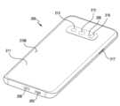
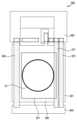
도 2a는 본 문서에 개시된 다양한 실시예 중 하나에 따른 전자 장치(200)를 나타내는 사시도이다. 도 2b는 도 2a의 전자 장치(200)를 후면에서 바라본 모습을 나타내는 사시도이다.FIG. 2A is a perspective view of an
도 1 및 2를 참조하면, 일 실시예에 따른 전자 장치(200)는, 제1 면(또는 전면)(210A), 제2 면(또는 후면)(210B), 및 제1 면(210A)과 제2 면(210B) 사이의 공간을 둘러싸는 측면(또는 측벽)(210C)을 포함하는 하우징(210)을 포함할 수 있다. 다른 실시예(미도시)에서는, 하우징은, 도 1의 제1 면(210A), 제2 면(210B) 및 측면(210C)들 중 일부를 형성하는 구조를 지칭할 수도 있다.Referring to FIGS. 1 and 2, the
일 실시예에 따르면, 제1 면(210A)은 적어도 일부분이 실질적으로 투명한 전면 플레이트(202)(예: 다양한 코팅 레이어들을 포함하는 글라스 플레이트, 또는 폴리머 플레이트)에 의하여 형성될 수 있다. 실시예에 따라, 전면 플레이트(202)는, 적어도 일측 단부(side edge portion)에서 제1 면(210A)으로부터 후면 플레이트(211) 쪽으로 휘어져 심리스하게(seamless) 연장된 곡면 부분을 포함할 수 있다.According to one embodiment, the
다양한 실시예에 따르면, 제2 면(210B)은 실질적으로 불투명한 후면 플레이트(211)에 의하여 형성될 수 있다. 상기 후면 플레이트(211)는, 예를 들어, 코팅 또는 착색된 유리, 세라믹, 폴리머, 금속(예: 알루미늄, 스테인레스 스틸(STS), 또는 마그네슘), 또는 상기 물질들 중 적어도 둘의 조합에 의하여 형성될 수 있다. 실시예에 따라, 후면 플레이트(211)는, 적어도 일측 단부에서 제2 면(210B)으로부터 전면 플레이트(202) 쪽으로 휘어져 심리스하게 연장된 곡면 부분을 포함할 수 있다.According to various embodiments, the
다양한 실시예에 따르면, 상기 측면(210C)은, 전면 플레이트(202) 및 후면 플레이트(211)와 결합하며, 금속 및/또는 폴리머를 포함하는 측면 베젤 구조 (또는 "측면 부재 또는 측벽")(218)에 의하여 형성될 수 있다. 어떤 실시예에서는, 후면 플레이트(211) 및 측면 베젤 구조(218)는 일체로 형성되고 동일한 물질(예: 알루미늄과 같은 금속 물질)을 포함할 수 있다.According to various embodiments, the
일 실시예에 따르면, 전자 장치(200)는, 디스플레이(201), 오디오 모듈(203, 214), 센서 모듈, 카메라 모듈(205), 키 입력 장치(217) 및 커넥터 홀(208) 중 적어도 하나 이상을 포함할 수 있다. 어떤 실시예에서는, 전자 장치(200)는, 구성요소들 중 적어도 하나(예: 키 입력 장치(217))를 생략하거나 다른 구성요소를 추가적으로 포함할 수 있다. 예를 들어, 전자 장치(200)는 도시되지 않은 센서 모듈을 포함할 수 있다. 예컨대, 전면 플레이트(202)가 제공하는 영역 내에는 근접 센서 또는 조도 센서와 같은 센서가 디스플레이(201)에 통합되거나, 디스플레이(201)와 인접한 위치에 배치될 수 있다. 어떤 실시예에서, 전자 장치(200)는 발광 소자를 더 포함할 수 있으며, 발광 소자는 전면 플레이트(202)가 제공하는 영역 내에서 디스플레이(201)와 인접한 위치에 배치될 수 있다. 발광 소자는, 예를 들어, 전자 장치(200)의 상태 정보를 광 형태로 제공할 수 있다. 다른 실시예에서는, 발광 소자는, 예를 들어, 카메라 모듈(205)의 동작과 연동되는 광원을 제공할 수 있다. 발광 소자는, 예를 들어, LED, IR LED 및 제논 램프를 포함할 수 있다.According to one embodiment, the
디스플레이(201)는, 예를 들어, 전면 플레이트(202)의 상당 부분을 통하여 노출될 수 있다. 어떤 실시예에서는, 디스플레이(201)의 모서리를 상기 전면 플레이트(202)의 인접한 외곽 형상(예: 곡면)과 대체로 동일하게 형성할 수 있다. 다른 실시예(미도시)에서는, 디스플레이(201)가 노출되는 면적을 확장하기 위하여, 디스플레이(201)의 외곽과 전면 플레이트(202)의 외곽간의 간격이 대체로 동일하게 형성될 수 있다. 다른 실시예(미도시)에서는, 디스플레이(201)의 화면 표시 영역의 일부에 리세스 또는 개구부(opening)을 형성하고, 상기 리세스 또는 상기 개구부(opening)와 정렬되는 다른 전자 부품, 예를 들어, 카메라 모듈(205), 도시되지 않은 근접 센서 또는 조도 센서를 포함할 수 있다.
다른 실시예(미도시)에서는, 디스플레이(201)의 화면 표시 영역의 배면에, 카메라 모듈(212, 213), 지문 센서(216), 및 플래시(206) 중 적어도 하나 이상을 포함할 수 있다. 다른 실시예(미도시)에서는, 디스플레이(201)는, 터치 감지 회로, 터치의 세기(압력)를 측정할 수 있는 압력 센서, 및/또는 자기장 방식의 스타일러스 펜을 검출하는 디지타이저와 결합되거나 인접하여 배치될 수 있다.In another embodiment (not shown), at least one of a
오디오 모듈(203, 214)은, 마이크 홀 및 스피커 홀을 포함할 수 있다. 마이크 홀은 외부의 소리를 획득하기 위한 마이크가 내부에 배치될 수 있고, 어떤 실시예에서는 소리의 방향을 감지할 수 있도록 복수개의 마이크가 배치될 수 있다. 어떤 실시예에서는 스피커 홀과 마이크 홀이 하나의 홀(203)로 구현 되거나, 스피커 홀 없이 스피커가 포함될 수 있다(예: 피에조 스피커). 스피커 홀은, 외부 스피커 홀 및 통화용 리시버 홀(214)을 포함할 수 있다.The
전자 장치(200)는 도시되지 않은 센서 모듈을 포함함으로써, 내부의 작동 상태, 또는 외부의 환경 상태에 대응하는 전기 신호 또는 데이터 값을 생성할 수 있다. 센서 모듈은, 예를 들어, 하우징(210)의 제1 면(210A)에 배치된 근접 센서, 디스플레이(201)에 통합된 또는 인접하게 배치된 지문 센서, 및/또는 상기 하우징(210)의 제2 면(210B)에 배치된 생체 센서(예: HRM 센서)를 더 포함할 수 있다. 전자 장치(200)는, 도시되지 않은 센서 모듈, 예를 들어, 제스처 센서, 자이로 센서, 기압 센서, 마그네틱 센서, 가속도 센서, 그립 센서, 컬러 센서, IR(infrared) 센서, 생체 센서, 온도 센서, 습도 센서, 또는 조도 센서 중 적어도 하나를 더 포함할 수 있다.The
카메라 모듈(205, 212, 213, 206)은, 전자 장치(200)의 제1 면(210A)에 배치된 제1 카메라 장치(205), 및 제2 면(210B)에 배치된 제2 카메라 장치(212, 213), 및/또는 플래시(206)를 포함할 수 있다. 상기 카메라 장치들(205, 212, 213)은, 하나 또는 복수의 렌즈들, 이미지 센서, 및/또는 이미지 시그널 프로세서를 포함할 수 있다. 플래시(206)는, 예를 들어, 발광 다이오드 또는 제논 램프(xenon lamp)를 포함할 수 있다. 어떤 실시예에서는, 2개 이상의 렌즈들(적외선 카메라, 광각 및 망원 렌즈) 및 이미지 센서들이 전자 장치(200)의 한 면에 배치될 수 있다.The
키 입력 장치(217)는, 하우징(210)의 측면(210C)에 배치될 수 있다. 다른 실시예에서는, 전자 장치(200)는 상기 언급된 키 입력 장치(217) 중 일부 또는 전부를 포함하지 않을 수 있고 포함되지 않은 키 입력 장치(217)는 디스플레이(201) 상에 소프트 키 등 다른 형태로 구현될 수 있다. 어떤 실시예에서, 키 입력 장치는 하우징(210)의 제2면(210B)에 배치된 지문 센서(216)의 적어도 일부를 포함할 수 있다.The
커넥터 홀(208)은, 외부 전자 장치와 전력 및/또는 데이터를 송수신하기 위한 커넥터, 및/또는 외부 전자 장치와 오디오 신호를 송수신하기 위한 커넥터를 수용할 수 있다. 예를 들어, 커넥터 홀(208)은 USB 커넥터 또는 이어폰 잭을 포함할 수 있다.The
도 3은, 도 2a의 전자 장치의 전개 사시도이다.FIG. 3 is an exploded perspective view of the electronic device of FIG. 2A.
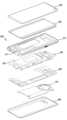
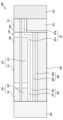
도 3을 참조하면, 전자 장치(300)는, 측면 베젤 구조(310), 제 1 지지부재(311)(예 : 브라켓), 전면 플레이트(320), 디스플레이(330), 인쇄 회로 기판(340), 배터리(350), 제 2 지지부재(360)(예 : 리어 케이스), 안테나(370), 및 후면 플레이트(380)를 포함할 수 있다. 어떤 실시예에서는, 전자 장치(300)는, 구성요소들 중 적어도 하나(예: 제 1 지지부재(311), 또는 제 2 지지부재(360))를 생략하거나 다른 구성요소를 추가적으로 포함할 수 있다. 전자 장치(300)의 구성요소들 중 적어도 하나는, 도 1, 또는 도 2의 전자 장치(200)의 구성요소들 중 적어도 하나와 동일, 또는 유사할 수 있으며, 중복되는 설명은 이하 생략한다.Referring to FIG. 3, the
제 1 지지부재(311)는, 전자 장치(300) 내부에 배치되어 측면 베젤 구조(310)와 연결될 수 있거나, 측면 베젤 구조(310)와 일체로 형성될 수 있다. 제 1 지지부재(311)는, 예를 들어, 금속 재질 및/또는 비금속 (예: 폴리머) 재질로 형성될 수 있다. 제 1 지지부재(311)는, 일면에 디스플레이(330)가 결합되고 타면에 인쇄 회로 기판(340)이 결합될 수 있다. 인쇄 회로 기판(340)에는, 프로세서, 메모리, 및/또는 인터페이스가 장착될 수 있다. 프로세서는, 예를 들어, 중앙처리장치, 어플리케이션 프로세서, 그래픽 처리 장치, 이미지 시그널 프로세서, 센서 허브 프로세서, 또는 커뮤니케이션 프로세서 중 하나 또는 그 이상을 포함할 수 있다.The
메모리는, 예를 들어, 휘발성 메모리 또는 비휘발성 메모리를 포함할 수 있다.Memory may include, for example, volatile memory or non-volatile memory.
인터페이스는, 예를 들어, HDMI(high definition multimedia interface), USB(universal serial bus) 인터페이스, SD카드 인터페이스, 및/또는 오디오 인터페이스를 포함할 수 있다. 인터페이스는, 예를 들어, 전자 장치(300)를 외부 전자 장치와 전기적 또는 물리적으로 연결시킬 수 있으며, USB 커넥터, SD 카드/MMC 커넥터, 또는 오디오 커넥터를 포함할 수 있다.The interface may include, for example, a high definition multimedia interface (HDMI), a universal serial bus (USB) interface, an SD card interface, and/or an audio interface. For example, the interface may electrically or physically connect the
배터리(350)는 전자 장치(300)의 적어도 하나의 구성 요소에 전력을 공급하기 위한 장치로서, 예를 들면, 재충전 불가능한 1차 전지, 또는 재충전 가능한 2차 전지, 또는 연료 전지를 포함할 수 있다. 배터리(350)의 적어도 일부는, 예를 들어, 인쇄 회로 기판(340)과 실질적으로 동일 평면 상에 배치될 수 있다. 배터리(350)는 전자 장치(300) 내부에 일체로 배치될 수 있고, 전자 장치(300)와 탈부착 가능하게 배치될 수도 있다.The
안테나(370)는, 후면 플레이트(380)와 배터리(350) 사이에 배치될 수 있다. 안테나(370)는, 예를 들어, NFC(near field communication) 안테나, 무선 충전 안테나, 및/또는 MST(magnetic secure transmission) 안테나를 포함할 수 있다. 안테나(370)는, 예를 들어, 외부 장치와 근거리 통신을 하거나, 충전에 필요한 전력을 무선으로 송수신 할 수 있다. 다른 실시예에서는, 측면 베젤 구조(310) 및/또는 상기 제 1 지지부재(311)의 일부 또는 그 조합에 의하여 안테나 구조가 형성될 수 있다.The
도 4a는, 다양한 실시예에 따른 안테나 모듈의 실장된 전자 장치를 도시한 도면이고, 도 4b는, 도 4a의 안테나 모듈을 포함하는 전자 장치의 단면도이다FIG. 4A is a diagram illustrating an electronic device mounted on an antenna module according to various embodiments, and FIG. 4B is a cross-sectional view of an electronic device including the antenna module of FIG. 4A.
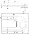
도 4a 및 도 4b를 참조하면, 전자 장치(300)는 안테나 모듈(370)(예: 도 3의 안테나(370)), 배터리(350), 및 후면 플레이트(380) 및 전면 플레이트(320)를 포함할 수 있다. 전면 플레이트(320)(예: 도 3의 전면 플레이트(320)), 후면 플레이트(380)(예: 도 3의 후면 플레이트(380)), 및 측면 부재(310)(예: 도 3의 측면 부재(310))는 하우징을 형성할 수 있다. 전면 플레이트(320)는 일면에 디스플레이(320)가 부착될 수 있다. 측면 부재(310)는 하우징의 내부로 연장되는 제1 지지 부재(311)를 포함할 수 있다. 제1 지지 부재(311)는 배터리(350)를 지지할 수 있고, 배터리(350)의 일 면에는 안테나 모듈(370)이 배치될 수 있다.4A and 4B, the
다양한 실시예에 따르면, 안테나 모듈(370)은 무선 충전 코일(410) 및 NFC 코일(420)을 포함할 수 있다. 안테나 모듈(370)은 무선 충전 코일(410) 및 NFC 코일(420)이 배치되는 제1 영역(401), 제1 영역(401)에 연장되고, 제2 지지부재(360)(예: 도 3의 제2 지지 부재(360)(예: 리어 케이스))에 부착되는 제2 영역(420), 및 제1 영역(401)을 사이에 두고, 제2 영역(402)을 마주보며 제1 영역(401)으로부터 연장되고, 제2 지지부재(360)의 일부에 부착될 수 있다.According to various embodiments, the
제1 영역(401)은 내부에 무선 충전 코일(410) 및/또는 NFC 코일(420)을 포함할 수 있고, 제1 영역(401)의 일부는 홈을 가질 수 있고, 제1 연성 인쇄회로기판(460), 제2 연성인쇄회로기판(471), 또는 제3 연성 인쇄회로기판(472) 중 적어도 하나는 제1 영역(401)에 형성된 홈에 배치될 수 있다. 다양한 실시예에 따르면, 안테나 모듈(370)의 제2 영역(402) 및 제3 영역(403)은 제1 영역(401)에 부착되는 방열부재와 일체로 형성될 수 있다. 다양한 실시예에 따르면, 안테나 모듈(370)의 제1 영역(401)은 하우징의 후면 플레이트(380)에 부착되고, 제3 영역(403)은 스피커 하우징에 부착될 수 있다.The first area 401 may include a wireless charging coil 410 and/or an NFC coil 420 therein, a portion of the first area 401 may have a groove, and a first flexible printed circuit board. At least one of 460 , the second flexible printed
다양한 실시예에 따르면, 배터리(예: 도 3의 배터리(350))는 제1 연성 인쇄회로기판(460), 제2 연성 인쇄회로기판(471), 또는 제3 연성 인쇄회로기판(472)과 제1 지지부재(311) 사이에 형성되는 공간에 배치될 수 있다. 배터리(350)는 제1 연성 인쇄회로기판(460), 제2 연성 인쇄회로기판(471), 또는 제3 연성 인쇄회로기판(472) 중 적어도 하나와 중첩될 수 있다. 예를 들면, 배터리(350)는 제1 연성 인쇄회로기판(460), 제2 연성 인쇄회로기판(471), 및 제3 연성 인쇄회로기판(472)가 형성하는 면과 제1 지지부재(311) 사이에 배치될 수 있다. 다른 예를 들면, 배터리(350)는 제1 연성 인쇄회로기판(460) 및 제2 연성 인쇄회로기판(471)이 형성하는 면과 제1 지지부재(311) 사이에 배치될 수 있다. 또 다른 예를 들면, 배터리(350)는 제1 연성 인쇄회로기판(460), 제2 연성 인쇄회로기판(471), 또는 제3 연성 인쇄회로기판(472) 중 어느 하나가 형성하는 면과 제1 지지부재(311) 사이에 배치될 수 있다.According to various embodiments, a battery (e.g.,
도 5는, 다양한 실시예에 따른 안테나 모듈의 단면도이다.Figure 5 is a cross-sectional view of an antenna module according to various embodiments.
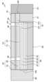
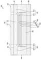
도 5를 참조하면, 전자 장치(500)는 안테나 모듈(501), 안테나 모듈(501)에 인접하게 배치되는 복수의 제1 연성 인쇄회로기판(560), 제2 연성 인쇄회로기판(571), 및 제3 연성 인쇄회로기판(572)을 포함할 수 있다.Referring to FIG. 5, the
안테나 모듈(501)은 무선충전 코일(510) 및 NFC 코일(520)의 패턴이 적층되는 베이스(505)와, 베이스(505)의 하부에 배치되어 무선충전 코일(510) 및 NFC 코일(520)에 흐르는 전류에 의해 발생하는 자기장이 전자 장치에 실장되는 전자 부품에 의해서 상쇄되는 것을 방지하는 자성체(530)와, 자성체(530)의 하부에 배치되어 열을 발산시키는 방열부재(550)와, 방열부재(550)의 하측에 배치되는 배터리(예: 도 3의 배터리(350))가 배치될 수 있다. NFC 코일(520)과 무선충전 코일(510)은 각각 서로 다른 주파수 대역의 신호를 송수신할 수 있다.The
일 실시예에 따르면, 베이스(505)는 플레이트 형상으로 형성되어, 외면에 무선충전 코일(510)과 NFC 코일(520)이 패터닝 될 수 있다. 베이스(505)는 연성 재질의 기판으로 형성될 수 있다. 예를 들면, 베이스(505)는 연성 인쇄회로기판의 기재로 사용되는 폴리이미드(PI, polyimide)를 포함할 수 있다. 자성체(530)는 무선충전 코일(510) 및 NFC 코일(520)에 흐르는 전류에 의해 발생하는 자기장이 코일 후면에 위치하는 다양한 전자 부품에 의한 영향을 최소화할 수 있다. 예를 들면, 자성체(530)는 자성체가 위치하는 면에 배치되는 배터리, 인쇄회로기판 또는 지지 부재가 무선충전 코일(510) 또는 NFC 코일(520)에서 발생하는 자기장을 상쇄시키는 것을 방지할 수 있다. 무선 충전 코일(510) 및 NFC 코일(520)에 의해 발생하는 자기장은 자성체(530)의 반대방향으로 집중될 수 있다. 자성체(530)는 무선충전 코일(510)에서 발생하는 자기장을 하우징의 후면 플레이트(예: 도 3의 후면 플레이트(380))가 배치되는 면으로 집중시킬 수 있어, 배터리의 충전효율을 높일 수 있다. NFC 코일(520)은 자성체(530)에 의해 자기장이 후면 플레이트로 집중될 수 있어, 외부 전자 장치(예: 도 1의 전자 장치(102))와 근거리 통신(NFC: near field communication)할 수 있다. NFC 코일(520)은 외부 장치와 통신을 하고, 전자 장치는 근거리에서 외부 장치와 데이터를 교환할 수 있다.According to one embodiment, the
일 실시예에 따르면, 무선충전 코일(510)은 베이스(505)의 상, 하면에 권선되는 제1 무선충전 코일(511) 및/또는 제2 무선충전 코일(512)를 포함할 수 있다. 무선충전 코일(510)은 도전성을 가지는 재질을 포함할 수 있다. 예를 들면, 무선충전 코일(510)은 구리(Cu)를 포함할 수 있다. 무선충전 코일(510)은 베이스(505)의 상, 하면에 병렬로 권선되도록 베이스(505)의 양면에 패터닝 될 수 있다. 무선충전 코일(510)은 베이스(505) 상부에 배치되는 제1 무선 충전 코일(511)과, 베이스(505)의 하부에 배치되는 제2 무선충전 코일(512)을 포함할 수 있다. 제1 무선 충전 코일(511)과 제2 무선 충전 코일(512)의 두께는 실질적으로 동일할 수 있으나, 이에 한정되지 않는다. 후술할 도 8a, 8b, 11, 12 및 13의 실시예에서는 제1 무선 충전 코일(511)과 제2 무선 충전 코일(512)의 두께는 상이할 수 있다. 제1 무선 충전 코일(511)과 제2 무선 충전 코일(512)은 베이스(505)에 형성된 비아(via)를 홀(미도시)에 배치되는 도전성 비아를 통하여 전기적으로 연결될 수 있다. 도전성 비아를 통하여, 무선 충전 코일(510)은 제1 무선 충전 코일(511)과 제2 무선 충전 코일(512)을 하나의 연결된 코일일 수 있다.According to one embodiment, the
일 실시예에 따르면, NFC 코일(520)은 베이스(505)의 상면에 패터닝 되는 제1 NFC 코일(521) 또는 베이스(505)의 하면에 패터닝 되는 제2 NFC 코일(522)을 포함할 수 있다. 제1 NFC 코일(521)은 베이스(505)의 상면 중 제1 무선 충전 코일(511)의 외측에 배치될 수 있다. 베이스(505)의 상면에서 제1 무선충전 코일(511)은 제1 NFC 코일(521)의 내측에 배치될 수 있다. 제1 NFC 코일(521)과 제1 무선충전 코일(511)은 상호 이격되게 배치될 수 있다. 예를 들면, 제1 NFC 코일(521)은 제1 무선충전 코일(511)을 감싸도록 베이스(505)의 상면에 배치될 수 있다.According to one embodiment, the
제2 NFC 코일(522)은 베이스(505)의 하면 중 제2 무선 충전 코일(512)의 외측에 배치될 수 있다. 베이스(505)의 하면에서 제2 무선충전 코일(512)은 제2 NFC 코일(522)의 내측에 배치될 수 있다. 제2 NFC 코일(522)과 제2 무선충전 코일(512)은 상호 이격되게 배치될 수 있다. 예를 들면, 제2 NFC 코일(522)은 제2 무선충전 코일(512)을 감싸도록 베이스(505)의 하면에 배치될 수 있다.The
다양한 실시예에 따르면, 제1 NFC 코일(521) 및 제2 NFC 코일(522)는 베이스(505)의 비아 홀에 형성되는 도전성 비아에 의해 전기적으로 연결될 수 있다. 도전성 비아를 통하여, NFC 코일(520)은 제1 NFC 코일(521) 및 제2 NFC 코일(522)를 하나의 연결될 코일일 수 있다.According to various embodiments, the
안테나 모듈(501)은 무선 충전 코일 및 NFC 코일(520)이 상면과 하면에 모두 배치되는 제1 영역(502) 및 베이스의 하면에 배치되는 제2 NFC 코일(522)의 적어도 일부가 제거된 제2 영역(503)으로 구별될 수 있다.The
다양한 실시예에 따르면, 제2 영역(503)에서 NFC 코일(520)은 제1 NFC 코일(521)을 포함하고, 제2 NFC 코일(522)은 제거된 형태일 수 있다. 제2 NFC 코일(522)은 제1 영역(502)에서 제2 무선충전 코일(512)의 일부를 감싸도록 형성되고, 제2 영역(503)에는 제거되거나 패터닝 되지 않을 수 있다. 제2 영역(503)은 제2 무선충전 코일(512)이 배치되지 않으므로, 제1 영역(502)과 제2 영역(503)은 배터리를 기준으로 높이가 상이할 수 있다. 제2 영역(503)에서는 제2 무선 충전 코일(512)의 두께만큼의 공간이 확보될 수 있어, 안테나 모듈(501)과 배터리 사이의 공간에는 제2 연성 인쇄회로기판(571)이 배치될 수 있다.According to various embodiments, in the
자성체(530)는 제1 영역에서 무선충전 코일(510)의 하부에 배치될 수 있고, 제2 영역에서 베이스(505)의 하부에 배치될 수 있다. 자성체(530)는 배치될 수 있다. 자성체(530)는 무선충전 코일(510) 또는 NFC 코일(520)에서 방출되는 자기장을 자성체의 반대 방향으로 진행하도록 할 수 있다. 자성체(530)는 복수로 구비되어 층을 이루도록 배치될 수 있다. 자성체(530)의 두께는 배치되는 위치에 따라 상이할 수 있고, 배치 형태도 상이할 수 있다.The
일 실시예에 따르면, 자성체(530)는 제1 영역과 제2 영역에서 위치하는 제1자성체(531), 제1자성체(531)의 하부에 배치되는 제2자성체(532)를 포함할 수 있다. 자성체(530)는 제1 영역(503)에서 제2자성체(532)의 하부에 배치되는 제3자성체(533)와, 제3자성체(533)의 하부에 배치되는 제4자성체(534)를 포함할 수 있다. 자성체(530)는 제2 NFC 코일(522)이 제거된 제2 영역(503)에서는 제1 자성체(531) 및 제2 자성체(532)만 포함할 수 있고, 제2 무선충전 코일(512) 및 제2 NFC 코일(522)이 제거되지 않은 제1 영역(502)에서는 제1 자성체(531), 제2 자성체(532), 제3 자성체(533) 및 제4 자성체(534)를 포함할 수 있다. 자성체는 제1 영역(502)에 배치되는 자성체(530a) 및 제2 영역에 배치되는 자성체(530b)로 구분할 수 있다. 제1 영역(502)에 배치되는 자성체(530a) 부분은 제2 영역(503)에 배치되는 자성체(530b) 부분보다 두꺼울 수 있다.According to one embodiment, the
제1자성체(531)와 제2자성체(532)는 NFC 코일(520) 및 무선충전 코일(510)에서 방출되는 자기장을 상쇄하는 전자 부품의 영향을 차단할 수 있다. 제3자성체(533)와 제4자성체(534)는 무선충전 코일(510)에서 방출되는 자기장을 상쇄할 수 있다. 제1 자성체(531), 제2 자성체(532), 제3 자성체(533), 및 제4 자성체(534)는 NFC 코일(520) 및 무선충전 코일(510)에서 발생하는 자기장을 집중시켜, 무선충전 효율 및 NFC 안테나 성능을 향상시킬 수 있다.The first
일 실시예에 따르면, 제1 자성체(531), 제2 자성체(532), 제3 자성체(533) 및 제4 자성체(534)는 서로 동일한 재질로 형성될 수 있다. 제1 자성체(531), 제2 자성체(532), 제3 자성체(533) 및 제4 자성체(534)는 실질적으로 동일한 두께를 포함하는 층으로 형성될 수 있다. 제1 자성체(531), 제2 자성체(532), 제3 자성체(533) 및 제4 자성체(534)는 NFC 코일(520)과 무선충전 코일(510)의 대역에서 높은 투자율과 낮은 손실 탄젠트(loss tangent)를 포함하는 재질로 형성될 수 있다. 제1 자성체(531), 제2 자성체(532), 제3 자성체(533) 및 제4 자성체(534)는 미세결정질로 형성된 재질을 포함할 수 있고, 대략 10Khz 내지 15Mhz의 무선충전 코일(510) 대역 및 NFC 코일(520) 대역에서 높은 투자율과 낮은 손실 탄젠트를 가질 수 있다. 자성체(530)는 약 10Khz 내지 15Mhz의 무선 충전 코일(510) 대역 및 NFC 코일(520)대역에서 강자성체로 사용될 수 있어, NFC/무선충전 안테나 모듈(501) 주위에 배치되는 전자부품들에 의한 영향을 최소화할 수 있어 무선 충전 코일(510) 및 NFC 코일(520)의 성능을 향상시킬 수 있다.According to one embodiment, the first
일 실시예에 따르면, 제1 자성체(531)는 제1 영역(502)에 배치되는 제1 부분(531a)과, 제2 영역(503)에서 제1 부분(531a)에 배치되는 제2 부분(531b)을 포함할 수 있다. 제1 부분(531a)과 제2 부분(531b)실질적으로 평행하게 배치될 수 있다. 제1 자성체(530)의 제1 부분(531a)과 제2 부분(531b)은 배터리(550)를 기준으로 높이가 상이할 수 있다. 자성체(530)는 제1 부분(531a)와 제2 부분(531b)에서 연결되어 형성될 수 있다. 예를 들면, 도 5와 같이 제1 부분(531a)와 제2 부분(531b)는 연결될 수 있고, 경계는 도 5와 같은 절곡되는 형태 대신에 부드럽게 연결될 수 있다. 제1 영역(502)에서, 제1 자성체(531)의 제1 부분(531a)은 제2 NFC 코일(522)과 제2 무선충전 코일(512)에 접하여 배치될 수 있다. 제1 자성체(531)의 제2 부분(531b)은 베이스(505)에 접하도록 형성될 수 있다. 제1 부분(531a)은 제1 부분(531a)와 제2 부분(531b) 사이(예를 들면, 제1 영역(502)와 제2 영역(503) 경계 주위)에서 절곡되어 제2 무선충전 코일(512)의 측면을 따라 연장될 수 있다. 제1 자성체(531)는 적어도 2회 이상 절곡될 수 있다.According to one embodiment, the first
다양한 실시예에 따르면, 제2 자성체(532)는 제1 영역(502)과 제2 영역(503)사이에서, 제1 자성체(531)와 동일한 형상을 가질 수 있다. 다양한 실시예에 따르면, 제2 자성체(532)는 제1 영역(502)과 제2 영역 사이에서 부드럽게 연결될 수 있다. 제2 자성체(532)는 제1 자성체(531)를 사이에 두고 베이스(505)와 마주보게 배치될 수 있다.According to various embodiments, the second
일 실시예에 따르면, 제3자성체(533)와 제4자성체(534)는 제2자성체(532)의 하부에 배치될 수 있다. 제3자성체(533) 및 제4 자성체는 제1 자성체(531)의 제1 부분(531a)에 대응되는 위치에 배치될 수 있다. 제3 자성체(533) 및 제4 자성체(534)는 NFC 코일(520)의 일부 및 무선충전 코일(510)이 위치하는 영역에 배치될 수 있다. 예를 들면, 제3 자성체(533) 및 제4 자성체(534)는 무선 충전 코일(510) 및 제2 NFC 코일(522)가 배치되는 제1 영역(502)에서 제2 자성체의 하부에 배치될 수 있다.제3 자성체(533) 및 제4자성체(534)는 NFC 코일(520)의 적어도 일부 및 무선충전 코일(510)과 중첩될 수 있다.According to one embodiment, the third
일 실시예에 따르면, 자성체(530)의 하부에는 방열체(550)가 배치될 수 있다. 방열체(550)는 하나의 층으로 형성될 수 도 있지만, 이에 한정되지 않고, 방열체(550)는 복수의 층으로 형성될 수 있다. 방열체(550)를 형성하는 복수의 층들은 각각의 층은 동일한 두께로 형성될 수 있고, 복수의 층들 중 적어도 하나의 층은 상이한 두께로 형성될 수 있다. 방열체(550)는 금속 재질일 수 있다. 방열체(550)는 무선충전 코일(510) 또는 NFC 코일(520)에서 발생하여 자성체(530) 또는 베이스(505)를 통하여 전달되는 열을 외부로 방출시킬 수 있다. 방열체(550)의 두께는 무선충전 코일(510)의 발열을 충분히 방열할 수 있을 정도의 두께로 형성될 수 있다. 방열체(550)는 제3자성체(533) 또는 제4자성체(534)와 중첩되도록 배치될 수 있다. 방열체(550)는 무선충전 코일(510)의 적어도 일부와 중첩되도록 배치될 수 있다. 방열체(550)는 무선충전 코일(510)또는 배터리에서 발생하는 발열을 줄이기 위하여, 방열성능이 뛰어난 그래파이트(graphite)를 포함할 수 있으며, 히트싱크나 히트파이프를 포함하는 방열 플레이트 일 수 있다.According to one embodiment, a
제1 연성인쇄회로기판(560)(예: 도 4a의 제1연성 인쇄회로기판(460))은 방열체(550), 제1 자성체(531), 제2 자성체(532), 제3자성체(533), 제4자성체(534), 제1 NFC 코일(521) 및 제2 NFC 코일(522)이 형성하는 일측에 배치될 수 있다. 예를 들면, 제1 연성 인쇄회로기판(560)은 안테나 모듈(501)의 제1 영역(502)의 측면에 접할 수 있다. 다른 예를 들면, 베이스(505)의 양면에 제1 NFC 코일(521) 및 제2 NFC 코일(522)이 형성된 영역은 하부에 자성체(530) 및 방열체(550)이 적층되어 있어, 제1 연성 인쇄회로기판(560)은 NFC/무선 충전 안테나(501)의 측면에 배치될 수 있다. The first flexible printed circuit board 560 (e.g., the first flexible printed
일 실시예에 따르면, 제2 연성 인쇄회로기판(571)은제2 NFC 코일(522)이 제거된 안테나 모듈(501)의 제2 영역(503)에서 제2 자성체(532)의 하부에 배치될 수 있다. 안테나 모듈(501)의 제2 영역(503)은 제1 영역(502)에 비하여 얇은 두께를 가질 수 있다. 예를 들면, 안테나 모듈(501)의 제2 영역(503)은 제2 NFC 코일(522)의 두께만큼 얇게 형성되어 제2 NFC 코일(522)이 제거된 공간을 가질 수 있다. NFC/무선충전 안테나(501)의 제2 영역(503)은 제2 NFC 코일(522)만큼 베이스(505)를 향하여 공간이 형성되고, 제3 자성체(533) 및 제4 자성체(534)도 제거되어 제2연성 인쇄회로기판(571)(예: 도4a의 제2연성 인쇄회로기판(471)이 배치되는 공간을 확보할 수 있다. 제2 연성 인쇄회로기판(571)은 제3자성체(533), 제4자성체(534) 및 방열체(550)가 형성하는 측면에 접하여 안테나 모듈(501)의 제2 영역에 배치될 수 있다. 제2 연성 인쇄회로기판(571)은 제2 영역에 배치되는 제2 자성체(332)의 하부에 배치될 수 있고, 제2 영역(503)에 배치되는 제1 NFC 코일(521)에 중첩되도록 배치될 수 있다.According to one embodiment, the second flexible printed
도 6은 다양한 실시예에 따른 전자 장치에 포함된 코일을 포함한 기판의 평면도이다.Figure 6 is a plan view of a substrate including a coil included in an electronic device according to various embodiments.
도 6을 참조하면, 전자 장치의 내부에는 제1인쇄회로기판(602)과, 제2인쇄회로기판(603), 배터리(590) 및 하나 이상의 연성 인쇄회로기판(FPCB : flexible printed circuit board)(560, 571, 572)을 포함할 수 있다.Referring to FIG. 6, the inside of the electronic device includes a first printed
제1인쇄회로기판(602)은 메인 인쇄회로기판일 수 있다. 제1인쇄회로기판(602)에는 하나 이상의 전자부품이 실장될 수 있다. 예를 들면, 제1인쇄회로기판(602)에는 프로세서(예: 도 1 의 프로세서(120)) 및 메모리(예: 도 1의 메모리(130) 등이 실장될 수 있다. 제1인쇄회로기판(602)에 배치되는 전자부품들은 구동을 통해 전자 장치의 동작을 제어할 수 있다.The first printed
제2인쇄회로기판(603)은 보조 인쇄회로기판일 수 있다. 제2인쇄회로기판(603)은 제1인쇄회로기판(602)과 전기적으로 연결될 수 있다. 제2인쇄회로기판(603)에는 하나 이상의 전자부품이 실장될 수 있다. 예를 들면, 제2 인쇄회로기판(603)은 통신 모듈(예: 도 1의 통신 모듈(190))을 통하여 안테나로 급접하는 컨택 또는 스위치, 음향 출력 장치, 입력 장치 또는 다양한 연결단자(예: 도 1의 연결단자(178))를 포함할 수 있다. 예를 들면, 연결단자는 헤드폰, 전원 공급 장치, 또는 저장 장치와 같은 외부 장치(예: 도 1의 전자 장치(102))와 연결될 수 있다. 제2인쇄회로기판(603)은 제1인쇄회로기판(602)에 이격되게 배치될 수 있다. 제2인쇄회로기판(602)은 제1인쇄회로기판(601)과 더불어 전자 장치의 동작을 제어할 수 있다.The second printed
배터리(590)는 제1인쇄회로기판(602)과 제2인쇄회로기판(603) 사이에 배치될 수 있다. 배터리(590)는 전자 장치 내 전자 부품들로 전원을 제공할 수 있다. 배터리(590)는 제1인쇄회로기판(602) 또는 제2인쇄회로기판(603)으로 전원을 제공할 수 있다. 배터리(590)는 제1인쇄회로기판(602) 또는 제2인쇄회로기판(603)과 이격되게 배치될 수 있다. 변형예로,The battery 590 may be disposed between the first printed
연성 인쇄회로기판(560, 571, 572)은, 배터리(590)의 일면에 배치될 수 있다. 연성 인쇄회로기판(560, 571, 572)은 플렉서블(Flexible) 재질로 형성될 수 있다. 예를 들면, 연성 인쇄회로기판(560, 571, 572)은 폴리이미드(PI, polyimide)를 포함할 수 있다. The flexible printed
제1 연성 인쇄회로기판(560)은 제1 인쇄회로기판(602)과 제2 인쇄회로기판(603)을 전기적으로 연결하는 기판일 수 있다. 제1 연성 인쇄회로기판(560)은 복수의 신호선 및 전원선이 포함될 수 있다. 예를 들면, 제1 연성 인쇄회로기판(560)은 외부 장치와 연결을 통하여 데이터를 교환하는 신호선로, 또는 스피커, 마이크 또는 연결단자를 통하여 연결되는 각종 음향 장치의 신호를 프로세서로 전달하는 음향선로를 포함할 수 있다. 제1 연성인쇄회로기판(560)은 외부 전원 장치로부터 공급 받은 전원을 전자 장치의 각 부품으로 공급하는 전력라인을 포함할 수 있다.The first flexible printed
제2 연성 인쇄회로기판(571) 및/또는 제3 연성 인쇄회로기판(572)은, RF 통신 신호를 송, 수신하기 위한 RF 전송 선로일 수 있다. 제2 연성 인쇄회로기판(571) 및/또는 제3 연성 인쇄회로기판(572)은 제1연성 인쇄회로기판(560) 보다 상대적으로 높은 주파수의 전파를 송, 수신할 수 있다. 제2 연성 인쇄회로기판(571) 및/또는 제3 연성 인쇄회로기판(572)은 제1 인쇄회로기판(602)과 제2 인쇄회로기판(603)을 전기적으로 연결시킬 수 있다. 제2 연성 인쇄회로기판(571) 및/또는 제3 연성 인쇄회로기판(572)은 제1 인쇄회로기판(602)과 제2 인쇄회로기판(603) 사이에서 전자 장치의 제어 명령을 송, 수신시킬 수 있다. 571) 제2 연성 인쇄회로기판(571) 및/또는 제3 연성 인쇄회로기판(572) 각각은 상호 이격되거나, 적어도 일부분이 중첩되게 배치될 수 있다.The second flexible printed
다양한 실시예에 따르면, 안테나 모듈(501)은 무선 충전 코일(511) 및 NFC 코일(521)을 포함할 수 있다. 안테나 모듈(501)은 제1 연성 인쇄회로기판(560) 제2 연성 인쇄회로기판(571) 또는 제3 연성 인쇄회로기판(572)과 중첩되도록 형성될 수 있다. 안테나 모듈(501)은 제1 연성 인쇄회로기판(560) 또는 제2 연성 인쇄회로기판(571)의 배치를 위한 실장공간을 포함할 수 있다.According to various embodiments, the
다양한 실시예에 무선 충전 코일(511) 및 NFC 코일(521)은 두개의 층으로 형성될 수 있다. 각각의 층에 형성된 무선 충전 코일(511) 각각은 동일한 형상으로 형성될 수 있고, 각각의 층에 형성된 NFC 코일(521) 각각은 동일한 형상으로 형성될 수 있다. NFC 코일(521)은 각각의 층에서 동일한 형상으로 형성되는 경우, 제1 연성 인쇄회로기판(560), 제2연성 인쇄회로기판(571) 또는 제3연성 인쇄회로기판(572)이 실장되는 공간을 확보하기 위해, 제1 연성 인쇄회로기판(560), 제2연성 인쇄회로기판(571) 또는 제3 연성 인쇄회로기판(572)이 실장되는 영역에서는 NFC 코일(521)은 일면에만 형성될 수 있고, 타면에서는 NFC 코일(521)은 제거될 수 있다.In various embodiments, the
도 7을 참조하면, 도 5의 안테나 모듈에서 제3 자성체(5831) 및 제4 자성체(5841)의 재질이 변형된 예이다. 전자 장치(500)는 안테나 모듈(501)의 제1 자성체(531), 제1 자성체와 동일한 특성을 가지는 제2 자성체(532), 제1 자성체(531)과 제2 자성체와 다른 특성을 가지는 제3 자성체(5831), 및 제3 자성체(5831)과 동일한 특성을 가지는 제4 자성체(5841)을 포함할 수 있다. 도 7의 전자 장치(500)는 제3 자성체(5831) 및 제4 자성체(5841)외에는 도 5의 전자 장치와 동일 유사할 수 있고, 중복되는 설명은 생략한다. Referring to FIG. 7, this is an example in which the materials of the third
일 실시예에 따르면, 자성체(530)는 베이스(505)의 하부에 배치될 수 있다. 자성체(530)는 무선충전 코일(510)의 하부에 배치될 수 있다. 자성체(530)는 무선충전 코일(510) 또는 NFC 코일(520)에서 형성되는 자기장의 진행 방향을 집중시킬 수 있다. 자성체(530)는 복수의 층으로 적층될 수 있다. 자성체(530)는 전자 장치(500) 내부의 전자 부품에 의해 무선충전 코일(510) 및 NFC 코일(520)에서 형성되는 자기장을 상쇄하는 것을 방지할 수 있다.According to one embodiment, the
일 실시예에 따르면, 자성체(530)는 제1자성체(531)와, 제1자성체(531)의 하부에 배치되는 제2자성체(532)와, 제2자성체(532)의 하부에 배치되는 제3자성체(5831)와, 제3자성체(5831)의 하부에 배치되는 제4자성체(5842)를 포함할 수 있다. 제1자성체(531)와 제2자성체(532)는 NFC 코일(520) 및 무선충전 코일(510)의 자기장의 방향을 전자 장치의 후면으로 집중시킬 수 있다. 제3자성체(5831)와 제4자성체(5841)는 무선충전 코일(510) 및 NFC 코일(520)의 일부 자기장의 방향을 전자 장치의 후면으로 집중시킬 수 있다.According to one embodiment, the
일 실시예에 따르면, 제1자성체(531)와 제2자성체(532)는 무선충전 대역 및 NFC안테나 대역을 포함하는 100Khz ~ 15Mhz의 대역에서 높은 투자율과 낮은 손실 탄젠트(loss tangent)를 가지는 재질로 형성될 수 있다. 제3자성체(5831)와 제4자성체(8541)는 10Khz ~ 200Khz의 대역에서 높은 투자율과 낮은 손실 탄젠트를 가지는 재질로 형성될 수 있다. 예를 들어, 제1자성체(581)와 제2자성체(532)는 미세결정으로 형성된 자성체(530)을 포함할 수 있다. 제3자성체(5831)와 제4자성체(5841)는 결정이 비정질(Amorphous)로 형성된 자성체(580)를 포함할 수 있다. 제3자성체(5831)와 제4자성체(5841)는 동종의 재질로 형성되고, 제1자성체(581)와 제2자성체(582)는 동종의 재질로 형성될 수 있다. 제3자성체(5831)와 제4자성체(5841)의 재질은 제1자성체(531)와 제2자성체(532)의 재질 보다 투자율이 높을 수 있다.According to one embodiment, the first
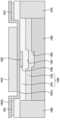
도 8a 및 도 8b는, 다양한 실시예에 따른 상이한 두께의 무선 충전 코일을 포함하는 NFC/무선충전 안테나의 단면도이다.8A and 8B are cross-sectional views of NFC/wireless charging antennas including wireless charging coils of different thicknesses according to various embodiments.
도 8a는 도 5의 안테나 모듈(501)의 무선충전 코일(510) 및 NFC 코일(520)의 두께를 변형한 예이고, 도 8b는 도 7의 안테나 모듈(501)의 무선충전 코일(510) 및 NFC 코일(520)의 두께를 변형한 예이다.FIG. 8A is an example of modifying the thickness of the
도 8a 및 도 8b를 참조하면, 안테나 모듈(501)은 무선충전 코일(510) 및 NFC 코일(520)의 패턴이 적층되는 베이스(505)와, 베이스(505)의 하부에 배치되어 무선충전 코일(510) 및 NFC 코일(520)에 흐르는 전류에 의해 발생하는 자기장이 전자 장치에 실장되는 전자 부품에 의해서 상쇄되는 것을 방지하는 자성체(530)와, 자성체(530)의 하부에 배치되어 열을 발산시키는 방열부재(550)와, 방열부재(550)의 하측에 배치되는 배터리(예: 도 3의 배터리(350))가 배치될 수 있다.Referring to FIGS. 8A and 8B, the
다양한 실시예에 따르면, 무선충전 코일(510)은 베이스(505)의 상, 하면에 권선되는 제1 무선충전 코일(5111) 및/또는 제2 무선충전 코일(5121)을 포함할 수 있다. 무선충전 코일(510)은 도전성을 가지는 재질을 포함할 수 있다. 예를 들면, 무선충전 코일(510)은 구리(Cu)를 포함할 수 있다. 무선충전 코일(510)은 베이스(505)의 상, 하면에 병렬로 권선되도록 베이스(505)의 양면에 패터닝 될 수 있다. 무선충전 코일(510)은 베이스(505) 상부에 배치되는 제1 무선 충전 코일(5111)과, 베이스(505)의 하부에 배치되는 제2 무선충전 코일(5121)을 포함할 수 있다. 제1 무선 충전 코일(5111)과 제2 무선 충전 코일(5121)의 두께는 상이할 수 있다.According to various embodiments, the
일 실시예에 따르면, NFC 코일(520)은 베이스(505)의 상면에 패터닝 되는 제1 NFC 코일(5211) 또는 베이스(505)의 하면에 패터닝 되는 제2 NFC 코일(5221)을 포함할 수 있다. 제1 NFC 코일(5211)은 베이스(505)의 상면 중 제1 무선 충전 코일(5111)의 외측에 배치될 수 있다. 베이스(505)의 상면에서 제1 무선충전 코일(5111)은 제1 NFC 코일(5211)의 내측에 배치될 수 있다. 제1 NFC 코일(521)과 제1 무선충전 코일(5111)은 상호 이격되게 배치될 수 있다. 예를 들면, 제1 NFC 코일(5211)은 제1 무선충전 코일(5111)을 감싸도록 베이스(505)의 상면에 배치될 수 있다.According to one embodiment, the
제2 NFC 코일(5221)은 베이스(505)의 하면 중 제2 무선 충전 코일(5121)의 외측에 배치될 수 있다. 베이스(505)의 하면에서 제2 무선충전 코일(5121)은 제2 NFC 코일(5221)의 내측에 배치될 수 있다. 제2 NFC 코일(5221)과 제2 무선충전 코일(5121)은 상호 이격되게 배치될 수 있다. 예를 들면, 제2 NFC 코일(5221)은 제2 무선충전 코일(5121)을 감싸도록 베이스(505)의 하면에 배치될 수 있다.The second NFC coil 5221 may be disposed outside the second
안테나 모듈(501)은 무선 충전 코일 및 NFC 코일(520)이 상면과 하면에 모두 배치되는 제1 영역(502) 및 베이스의 하면에 배치되는 제2 NFC 코일(522)의 적어도 일부가 제거된 제2 영역(503)으로 구별될 수 있다.The
제1 무선 충전 코일(5111) 및 제1 NFC 코일(5211)의 두께는 실질적으로 동일할 수 있다. 제2 무선 충전 코일(5121)과 제2 NFC 코일(5221)의 두께는 실질적으로 동일할 수 있다. 제1 무선 충전 코일(5111)과 제2 무선 충전 코일(5121)의 두께는 서로 상이할 수 있고, 제1 무선 충전 코일(5111)은 제2 무선 충전 코일(51210의 두께보다 얇게 형성될 수 있다. 제1 NFC 코일(5211)과 제2 NFC 코일(5221)의 두께는 서로 상이할 수 있고, 제1 NFC 코일(5211)은 제2 NFC 코일(5221)의 두께보다 얇게 형성될 수 있다.The thickness of the first
도 7의 무선 충전 코일(520)의 두께는 도 8a의 무선 충전 코일(5101)의 두께와 동일할 수 있다. 도 8a의 무선 충전 코일(5101)은 제1 무선 충전 코일(5111) 및 제2 무선 충전 코일(5121) 각각의 두께는 서로 상이할 수 있다. 제1 무선 충전 코일(5111)의 두께는 제2 무선 충전 코일(5121)의 두께보다 얇게 형성될 수 있다. 제2 무선 충전 코일(5121)과 제2 NFC 코일(522)의 두께는 서로 동일할 수 있고, 제거된 제2 NFC 코일(522)도 동일한 두께로 제거될 수 있다. 제거된 제2 NFC 코일(522)의 영역만큼 제2 연성 인쇄회로기판(571)이 배치될 수 있는 공간을 확보할 수 있다. 예를 들면, 도 7의 무선 충전 코일(510)의 두께는 110um이고, 제1 무선 충전 코일(511) 및 제2 무선 충전 코일(512)의 두께는 각각 55um일 수 있다. 이 경우, 제2 NFC 코일(522)를 제거하여 추가로 확보되는 두께는 55um일 수 있다. 도 8a의 무선 충전 코일(510)의 두께는 110um로 동일하고, 제1 무선 충전 코일(5111)은 30um이고, 제2 무선 충전 코일(5121)은 80um일 수 있다. 제2 NFC 코일(522)를 제거하여 추가 확보되는 두께는 80um일 수 있다.The thickness of the
제2 영역(503)에서는 제2 NFC 코일(5221)을 제거되므로, 제2 영역(503)의 하부의 실장 공간은 증가할 수 있어, 제2 연성 인쇄회로기판(571)이 배치될 수 있는 공간을 더확보할 수 있다.Since the second NFC coil 5221 is removed from the
도 8a의 제1 자성체(531), 제2 자성체(532), 제3 자성체(533), 제4 자성체(544)는 동일한 특성을 가지는 자성체로 형성될 수 있다. 제1 자성체(531), 제2 자성체(532), 제3 자성체(533) 및 제4 자성체(534)는 NFC 코일(520) 및 무선충전 코일(510)의 자기장의 방향을 전자 장치의 후면으로 집중시킬 수 있다. 제1 자성체(531), 제2 자성체(532), 제3 자성체(533) 및 제4 자성체(534)는 NFC 코일(520)과 무선충전 코일(510)의 대역에서 높은 투자율과 낮은 손실 탄젠트(loss tangent)를 포함하는 재질로 형성될 수 있다. 제1 자성체(531), 제2 자성체(532), 제3 자성체(533) 및 제4 자성체(534)는 미세결정질로 형성된 재질을 포함할 수 있고, 대략 10Khz 내지 15Mhz의 무선충전 코일(510) 대역 및 NFC 코일(520) 대역에서 높은 투자율과 낮은 손실 탄젠트를 가질 수 있다. 자성체(530)는 약 10Khz 내지 15Mhz의 무선 충전 코일(510) 대역 및 NFC 코일(520)대역에서 강자성체로 사용될 수 있어, 안테나 모듈(501) 주위에 배치되는 전자부품들에 의한 영향을 최소화할 수 있어 무선 충전 코일(510) 및 NFC 코일(520)의 성능을 향상시킬 수 있다.The first
도 8b의 제1 자성체(531), 제2 자성체(532)는 도 8a의 자성체(530)와 동일할 수 있다. 제3 자성체(5831), 제4 자성체(5841)는 제1 자성체(531) 및 제2 자성체(532)와는 서로 다른 특성을 가질 수 있다.The first
제1자성체(531)와 제2자성체(532)는 NFC 코일(520) 및 무선충전 코일(510)의 자기장의 방향을 전자 장치의 후면으로 집중시킬 수 있다. 제3자성체(5831)와 제4자성체(5841)는 무선충전 코일(510) 및 NFC 코일(520)의 일부 자기장의 방향을 전자 장치의 후면으로 집중시킬 수 있다.The first
일 실시예에 따르면, 제1자성체(531)와 제2자성체(532)는 무선충전 대역 및 NFC안테나 대역을 포함하는 100Khz ~ 15Mhz의 대역에서 높은 투자율과 낮은 손실 탄젠트(loss tangent)를 가지는 재질로 형성될 수 있다. 제3자성체(5831)와 제4자성체(8541)는 10Khz ~ 200Khz의 대역에서 높은 투자율과 낮은 손실 탄젠트를 가지는 재질로 형성될 수 있다. 예를 들어, 제1자성체(581)와 제2자성체(532)는 미세결정으로 형성된 자성체(530)을 포함할 수 있다. 제3자성체(5831)와 제4자성체(5841)는 결정이 비정질(Amorphous)로 형성된 자성체(580)를 포함할 수 있다. 제3자성체(5831)와 제4자성체(5841)는 동종의 재질로 형성되고, 제1자성체(581)와 제2자성체(582)는 동종의 재질로 형성될 수 있다. 제3자성체(5831)와 제4자성체(5841)의 재질은 제1자성체(531)와 제2자성체(532)의 재질 보다 투자율이 높을 수 있다.According to one embodiment, the first
상술한 다양한 실시예에 따르면, 도 5, 7, 8a, 및 8b에서, 안테나 모듈(500)은 일부를 제거하여, 제2 연성 인쇄회로기판(571)이 안테나 모듈(500)의 일부가 제거된 공간에 배치될 수 있다. 도 9 내지 도 14에서 후술할 다양한 실시예들은 안테나 모듈의 일부를 제거하여, 제1 연성 인쇄회로기판 및 제2 연성 인쇄회로기판이 안테나 모듈의 일부가 제거된 공간에 배치될 수 있다.According to the various embodiments described above, in FIGS. 5, 7, 8a, and 8b, part of the
도 9는, 다양한 실시예에 따른 안테나 모듈에서 NFC 코일은 일면에만 배치되고, 무선 충전 코일의 너비는 상이하게 형성된 NFC/무선충전 안테나의 단면도이고, 도 10a 및 10b는, 다양한 실시예에 따른 안테나 모듈에서 NFC 코일은 일면에만 배치되는 NFC/무선충전 안테나의 단면도이다.Figure 9 is a cross-sectional view of an NFC/wireless charging antenna in which the NFC coil is disposed on only one side of the antenna module according to various embodiments, and the width of the wireless charging coil is formed differently, and Figures 10a and 10b are antennas according to various embodiments. The NFC coil in the module is a cross-sectional view of the NFC/wireless charging antenna placed on only one side.
도 9, 및 10a를 참조하면,전자 장치(900)는 안테나 모듈(1000), 안테나 모듈(1000)에 인접하게 배치되는 복수의 제1 연성 인쇄회로기판(960), 제2 연성 인쇄회로기판(970)를 포함할 수 있다. 안테나 모듈(1000)는 무선충전 코일(910) 및 NFC 코일(920)의 패턴이 적층되는 베이스(901)와, 베이스(901)의 하부에 배치되어 무선충전 코일(910) 및 NFC 코일(920)에 흐르는 전류에 의해 발생하는 자기장이 전자 장치 내부에 실장되는 전자 부품에 의해서 상쇄되는 것을 방지하는 자성체(930)와, 자성체(930)의 하부에 배치되어 열을 발산시키는 방열부재(950)와, 방열부재(950)의 하측에 배치되는 배터리(990)(예: 도 4b의 배터리(350))가 배치될 수 있다.Referring to FIGS. 9 and 10A, the
일 실시예에 따르면, 베이스(901)는 플레이트 형상으로 형성되어, 외면에 무선충전 코일(910)과 NFC 코일(920)이 패터닝 될 수 있다. 베이스(901)는 연성 재질의 기판으로 형성될 수 있다. 예를 들면, 베이스(901_는 연성 인쇄회로기판의 기재로 사용되는 폴리이미드(PI, polyimide)를 포함할 수 있다. 자성체(930)는 무선충전 코일(910) 및 NFC 코일(920)에 흐르는 전류에 의해 발생하는 자기장이 코일 후면에 위치하는 다양한 전자 부품에 의한 영향을 최소화할 수 있다. 예를 들면, 자성체(930)는 자성체가 위치하는 면에 배치되는 배터리, 인쇄회로기판 또는 지지 부재가 무선충전 코일(910) 또는 NFC 코일(920)에서 발생하는 자기장을 상쇄시키는 것을 방지할 수 있다. 무선 충전 코일(910) 및 NFC 코일(920)에 의해 발생하는 자기장은 자성체(930)의 반대방향으로 집중될 수 있다. 자성체(930)는 무선충전 코일(910)에서 발생하는 자기장을 하우징의 후면 플레이트(예: 도 3의 후면 플레이트(380))가 배치되는 면으로 집중시킬 수 있어, 무선충전 코일(910)의 배터리(990) 충전효율을 높일 수 있다. NFC 코일(920)은 자성체(930)에 의해 자기장이 후면 플레이트로 집중될 수 있어, 외부 전자 장치(예: 도 1의 전자 장치(102))와 근거리 통신(NFC: near field communication) 통신할 수 있다. NFC 코일(920)과 자성체(930)의 상호 작용을 통해 외부 장치와 통신을 하고, 전자 장치는 근거리에서 외부 장치와 데이터를 교환할 수 있다.According to one embodiment, the
일 실시예에 따르면, 무선충전 코일(910)은 베이스(901)의 상, 하면에 패터닝 될 수 있다. 무선 충전 코일(910)은 도전성을 가지는 재질을 포함할 수 있다. 예를 들면, 무선충전 코일(910)은 구리(Cu)일 수 있다. 무선충전 코일(910)은 베이스(901)의 상, 하면에 병렬로 권선될 수 있다. 예를 들면, 무선충전 코일(910)은 베이스(901)의 상면에 패터닝 되는 제1 무선충전 코일(911) 및 베이스의 하면에 패터닝 되는 제2 무선충전 코일(912)를 포함할 수 있다. 베이스(901)의 상면에 배치된 제1 무선충전 코일(911)의 권선 영역은, 베이스(901)의 하면에 배치된 제2 무선충전 코일(912)의 권선 영역 보다 단면적이 크게 형성될 수 있다. 예를 들면, 제1 무선충전 코일(911)이 배치되는 영역이 제2 무선충전 코일(912)이 배치되는 영역보다 클 수 있다. 다른 예를 들면, 제1 무선충전 코일(911)이 베이스(901)와 접하는 면적이 제2 무선충전 코일(912)이 베이스(901)과 접하는 면적보다 클 수 있다. 제1 무선 충전 코일(911)과 제2 무선 충전 코일(912)의 두께는 실질적으로 동일할 수 있으나, 이에 한정되지 않는다. 후술할 도 8a, 8b, 11, 12 및 13의 실시예에서는 상면부(911)와 하면부(912)의 두께는 상이할 수 있다.According to one embodiment, the
일 실시예에 따르면, NFC 코일(920)은 베이스(901)의 상면에 권선될 수 있다. NFC 코일(920)은 베이스(901)의 상면 중 제1 무선충전 코일(911)의 외측에 배치될 수 있다. 베이스(901)의 상면에서 제1 무선충전 코일(911)은 NFC 코일(920)의 내측에 배치될 수 있다. NFC 코일(920)과 제1 무선충전 코일(911)은 상호 이격되게 배치될 수 있다.According to one embodiment, the
자성체(930)는 베이스(901)의 하부에 배치될 수 있다. 자성체(930)는 무선충전 코일(910)의 하부에 배치될 수 있다. 자성체(930)는 무선충전 코일(910) 또는 NFC 코일(920)에서 방출되는 자기장을 자성체의 반대 방향으로 진행하도록 할 수 있다. 자성체(930)는 복수로 구비되어 층을 이루도록 배치될 수 있다. 자성체(930)의 두께는 배치되는 위치에 따라 상이할 수 있고, 배치 형태도 상이할 수 있다. 자성체(930)는 제2 무선 충전 코일(912) 또는 NFC 코일(920)이 제거된 영역에서는 제1 자성체(931) 및 제2 자성체(932)만 포함할 수 있고, 제2 무선충전 코일(912)에 대응되는 영역에서는 제1 자성체(931), 제2 자성체(932), 제3 자성체(933) 및 제4 자성체(934)를 포함할 수 있다. 제2 무선 충전 코일(912) 또는 NFC 코일(920)이 제거된 영역에서의 자성체(930)의 두께는 제2 무선 충전 코일(912)에 대응되는 영역에서의 자성체(930)의 두께보다 얇을 수 있다.The
일 실시예에 따르면, 자성체(930)는 제1자성체(931)와, 제1자성체(931)의 하부에 배치되는 제2자성체(932)와, 제2자성체(932)의 하부에 배치되는 제3자성체(933)와, 제3자성체(933)의 하부에 배치되는 제4자성체(934)를 포함할 수 있다. 제1자성체(931)와 제2자성체(932)는 NFC 코일(920) 및 무선충전 코일(910)과 전자기적 상호 작용할 수 있다. 제3자성체(933)와 제4자성체(934)는 무선충전 코일(910)과 전자기적 상호 작용할 수 있다.According to one embodiment, the
일 실시예에 따르면, 제1 자성체(931), 제2 자성체(932), 제3 자성체(933) 및 제4 자성체(934)는 서로 동일한 재질로 형성될 수 있다. 제1 자성체(931), 제2 자성체(932), 제3 자성체(933) 및 제4 자성체(934)는 실질적으로 동일한 두께를 포함하는 층으로 형성될 수 있다. 제1 자성체(931), 제2 자성체(932), 제3 자성체(933) 및 제4 자성체(934)는 NFC 코일(920)과 무선충전 코일(910)의 대역에서 높은 투자율과 낮은 손실 탄젠트(loss tangent)를 포함하는 재질로 형성될 수 있다. 예를 들어, 제1 자성체(931), 제2 자성체(932), 제3 자성체(933) 및 제4 자성체(934)는 미세결정질로 형성된 재질을 포함할 수 있고, 약 10Khz 내지 약 15Mhz의 무선충전 코일(910) 대역 및 NFC 코일(920) 대역에서 대역에서 높은 투자율과 낮은 손실 탄젠트를 가질 수 있다.According to one embodiment, the first
일 실시예에 따르면, 제1 자성체(931)는 베이스(901)의 양면에 무선충전 코일(910)이 패터닝되는 제1 부분(931a)와, 제1 부분(931a)과 배터리를 기준으로 상이한 높이로 배치되고, 베이스(901)의 일면에만 무선충전 코일(910) 또는 NFC 코일이 패터닝 되는 제2 부분(931b)를 포함할 수 있다. 제2 부분(931b)은 제1 부분(931a)의 적어도 하나의 측면에 형성될 수 있다. 제1 부분(931a)의 일면과 제2 부분(931b)의 일면은 실질적으로 평행하게 배치될 수 있다. 제2 부분(931b)은 제1 부분(931a)의 양단부로부터 절곡된 절곡부의 일단에 내측 단부가 연결되도록 배치될 수 있다. 제2 부분(931b)는 절곡부의 일단으로부터 베이스(301)의 일면을 따라 연장될 수 있다.According to one embodiment, the first
다양한 실시예에 따르면, 제1 자성체(931)의 제1 부분(931a)이 배치되는 영역에서는 제2 무선충전 코일(912)가 존재하지만, 제1 자성체(931)의 제2 부분(931ㅠ)이 배치되는 영역에서는 제2 무선충전 코일(912) 또는 NFC 코일(920)이 제거될 수 있다. 제2 부분(931b)는 베이스(901)에서 제2 무선충전 코일(912) 또는 NFC 코일(920)의 제거 부분만큼 제1 부분(931a)과 부드럽게 연결될 수 있다. 제1 부분(931a)와 제2 부분(931b)의 높이 차이는 제2 무선 충전 코일(912)의 두께에 따라 결정될 수 있다. 제1자성체(331)는 적어도 2회 이상 절곡될 수 있다. 제2 부분(931b)은 NFC코일(920) 및 무선충전 코일(910)의 적어도 일부와 중첩될 수 있다. 제1 부분(931a)은 무선충전 코일(910)의 적어도 일부와 중첩될 수 있다.According to various embodiments, the second
일 실시예에 따르면, 제2 자성체(932)는 중앙부(932a)와, 제1 부분(932a)과 높이가 상이한제2 부분(932b)를 포함할 수 있다. 제1 부분(932a)의 일면과 제2 부분(932b)의 일면은 실질적으로 평행하게 배치될 수 있다. 제2 부분(932b)는 제1 부분(932a)의 양단부로부터 절곡된 절곡부의 일단에 내측 단부가 연결되도록 배치될 수 있다. 제2 부분(932b)는 절곡부의 일단으로부터 제1 자성체(931)의 제1 부분(931b)의 일면을 따라 연장될 수 있다. 제2 자성체(932)는 적어도 2회 이상 절곡될 수 있다. 제2 부분(932b)은 NFC 코일(920) 및 무선충전 코일(910)의 적어도 일부와 중첩될 수 있다. 제1 부분(932a)은 무선충전 코일(910)의 적어도 일부와 중첩될 수 있다. 제2 자성체(932)는 제1 자성체(911)과 형상은 유사하게 형성될 수 있고, 제1 자성체(911)가 배터리(990)를 향하는 면에 배치될 수 있다.According to one embodiment, the second
일 실시예에 따르면, 제3자성체(933)와 제4자성체(934)는 제2자성체(932)의 하부에 배치될 수 있다. 제3자성체(933) 및 제4 자성체(934)는 제1 자성체(931) 및 제2 자성체(932)의 제1 부분(931a, 932a)에 대응되는 위치에 배치될 수 있다.제3 자성체(933) 및 제4 자성체(934)는 무선 충전 코일(910)의 일부가 위치하는 영역에 배치될 수 있다. 예를 들면, 제3 자성체(933) 및 제4 자성체(934)는 제1 무선 충전 코일(911)의 일부에 중첩되는 제2 무선 충전 코일(912)에 대응되는 영역에 배치될 수 있다. 제3자성체(933)와 제4자성체(934)는 제1 및 2자성체(931, 932)보다 배터리(990)의 일면에 투영된 면적이 작을 수 있다. 제3자성체(933)와 제4자성체(934)는 무선충전 코일(910) 적어도 일부와 중첩될 수 있다.According to one embodiment, the third
일 실시예에 따르면, 자성체(930)의 하부에는 방열체(950)가 배치될 수 있다. 방열체(950)는 배터리(990)의 상부에 배치될 수 있다. 방열체(950)는 금속 재질일 수 있다. 방열체(950)는 자성체(930) 또는 베이스(901)로부터 발생되는 열을 외부로 방출시킬 수 있다. 방열체(950)의 두께는 무선충전 코일(910)의 발열을 충분히 방열할 수 있을 정도의 두께로 형성될 수 있다. 방열체(950)는 제3자성체(933) 또는 제4자성체(934)와 중첩되도록 배치될 수 있다. 방열체(950)는 무선충전 코일(910)의 적어도 일부와 상, 하 방향으로 중첩될 수 있다. 방열체(950)는 무선충전 코일(910)또는 배터리(990)에서 발생하는 발열을 줄이기 위하여, 방열성능이 뛰어난 그래파이트(graphite)를 포함할 수 있으며, 히트싱크나 히트파이프를 포함하는 방열 플레이트 일 수 있다.According to one embodiment, a
도 9의 제1 연성 인쇄회로기판(960)은 NFC 코일(920) 및 제2 무선충전 코일(912)의 일부가 제거되어 형성된 공간에 배치되고, 제2 연성 인쇄회로기판(970)은 NFC 코일(920)이 제거되어 형성된 공간에 배치될 수 있다. 제2 연성 인쇄회로기판(970)의 측면 중 자성체(1030, 1080)과 접하지 않는 측면에 인접하게 제3 연성 인쇄회로기판(미도시)이 배치될 수 있다. 제1 연성인쇄회로기판(960)(예: 도 4a의 제1연성 인쇄회로기판(460))은 방열체(350), 제3자성체(333) 및 제4자성체(334)가 형성하는 일측에 배치될 수 있다. 제1 연성인쇄회로기판(960)은 무선충전 코일(910)의 적어도 일부 및 NFC 코일(920)이 제거되어 확보된 공간에 배치될 수 있다. 제2 자성체(932)의 제2 부분(932b)의 일면에는 제1 연성 인쇄회로기판(960)이 배치될 수 있다. 배터리(90)의 상부에는 제1 연성 인쇄회로기판(960)이 배치될 수 있다. 예를 들어, 제1 연성 인쇄회로기판(360)이 배치되는 공간은 제2 자성체(932)의 제2 부분(932b), 제2 자성체(932)의 제1 부분(932a)와 제2 부분(932b)를 연결하는 연결부, 제3 자성체(933) 및 제4 자성체(934)의 일측면, 방열체(950)의 일측면 및 배터리(990)의 적어도 일부에 의해 감싸져 형성될 수 있다. 제1 연성 인쇄회로기판(960)이 배치되는 공간은 제2 무선충전 코일(912)의 일부와 NFC 코일의 일부가 제거되어 형성된 공간으로, 제2 무선충전 코일(912), 제3 자성체(933), 제4 자성체(934) 및 방열체(950)가 제거된 공간일 수 있다. 제1 연성 인쇄회로기판(960)은 NFC 코일(320) 무선충전 코일(910)의 적어도 일부와 중첩될 수 있다. 제1연성 인쇄회로기판(960)은 NFC 코일(920) 및 베이스(901)의 적어도 일 측과 일치할 수 있으며, NFC 코일(920)에 비해 상대적으로 베이스(901)의 중심으로 연장될 수 있다.The first flexible printed
도 10의 제1 연성 인쇄회로기판(960)은 NFC 코일(920)의 일부가 제거되어 형성된 공간에 배치되고, 제2 연성 인쇄회로기판(970)은 NFC 코일(920)의 일부가 제거되어 형성된 공간에 배치될 수 있고, 제2 연성 인쇄회로기판(970)은 NFC 코일(920)이 제거되어 형성된 공간에 배치될 수 있다. 제2 연성 인쇄회로기판(970)의 측면 중 자성체(1030, 1080)과 접하지 않는 측면에 인접하게 제3 연성 인쇄회로기판(미도시)이 배치될 수 있다. 제1 연성인쇄 연성인쇄회로기판(960)(예: 도 4a의 제1연성 인쇄회로기판(460))은 방열체(950), 제3자성체(933) 및 제4자성체(934)가 형성하는측면에 배치될 수 있다. 제1 연성인쇄회로기판(960)은 베이스(901)의 일면에 배치된 NFC 코일(920)이 제거되어 확보된 공간에 배치될 수 있다. 제2 자성체(932)의 제2 부분(932b)의 일면에는 제1 연성 인쇄회로기판(960)이 배치될 수 있다. 배터리(990)의 상부에는 제1 연성 인쇄회로기판(960)이 배치될 수 있다. 예를 들어, 제1 연성 인쇄회로기판(360)이 배치되는 공간은 제2 자성체(932)의 제2 부분(932b), 제2 자성체(932)의 연결부, 제3 자성체(933) 및 제4 자성체(934)의 일측면, 방열체(950)의 일측면 및 배터리(990)의 적어도 일부에 의해 감싸져 형성될 수 있다. 제1 연성 인쇄회로기판(960)이 배치되는 공간은 NFC 코일(920)의 일부가 제거되어 형성된 공간이고, 제2 무선충전 코일(912), 제3 자성체(933), 제4 자성체(934) 및 방열체(950)가 제거된 공간일 수 있다. 제1 연성 인쇄회로기판(960)은 NFC 코일(920)과 중첩될 수 있다. 제1연성 인쇄회로기판(960)은 NFC 코일(920) 및 베이스(901)의 일 측면은 적어도 일 측면과 동일 면 일 수 있다.The first flexible printed
일 실시예에 따르면, 도 9 및 도 10a의 방열체(950)의 타 측면에는 제2 연성 인쇄회로기판(970)(예: 도4a의 제2 연성 인쇄회로기판(471))이 배치될 수 있다.According to one embodiment, a second flexible printed circuit board 970 (e.g., the second flexible printed
제2연성 인쇄회로기판(970)은 제3자성체(933) 또는 제4자성체(934)를 기준으로 제1연성 인쇄회로기판(960)이 배치되는 일측에 대향하는 타측에 배치될 수 있다. 제2 자성체(932)의 제2 부분(932b)의 하부에는 제2연성 인쇄회로기판(970)이 배치될 수 있다. 배터리(990)의 상부에는 제2연성 인쇄회로기판(970)이 배치될 수 있다. 제2연성 인쇄회로기판(970)은 NFC 코일(920)의 일부와 중첩될 수 있다. 제2 연성 인쇄회로기판(970)은 NFC 코일(920)이 제거되어 확보된 공간에서 배치될 수 있다. 제2 연성 인쇄회로기판(970)이 배치되는 공간은 NFC 코일(920)의 일부가 제거되어 형성된 공간이고, 제3 자성체(933), 제4 자성체(934) 및 방열체(950)가 제거된 공간일 수 있다.The second flexible printed
도 10b를 참조하면, 도 10a의 NFC/무선충전 안테나에서, 제3 자성체(1081), 제4 자성체(1082)의 특성이 상이할 수 있다.도 10b의 제1 자성체(1031), 제2 자성체(1032)는 도 9의 자성체(930)와 동일할 수 있다. 제3 자성체(1081), 제4 자성체(1082)는 제1 자성체(1031) 및 제2 자성체(1032)와는 서로 다른 특성을 가질 수 있다.Referring to FIG. 10B, in the NFC/wireless charging antenna of FIG. 10A, the characteristics of the third
제1자성체(1031)와 제2자성체(1032)는 NFC 코일(920) 및 무선충전 코일(910)의 자기장의 방향을 전자 장치의 후면으로 집중시킬 수 있다. 제3자성체(1081)와 제4자성체(1082)는 무선충전 코일(910) 및 NFC 코일(920)의 일부 자기장의 방향을 전자 장치의 후면으로 집중시킬 수 있다.The first
일 실시예에 따르면, 제1자성체(1031)와 제2자성체(1032)는 무선충전 대역 및 NFC안테나 대역을 포함하는 100Khz ~ 15Mhz의 대역에서 높은 투자율과 낮은 손실 탄젠트(loss tangent)를 가지는 재질로 형성될 수 있다. 제3자성체(1081)와 제4자성체(1082)는 10Khz ~ 200Khz의 대역에서 높은 투자율과 낮은 손실 탄젠트를 가지는 재질로 형성될 수 있다. 예를 들어, 제1자성체(1031)와 제2자성체(1032)는 미세결정으로 형성된 자성체(1030)을 포함할 수 있다. 제3자성체(1081)와 제4자성체(1082)는 결정이 비정질(Amorphous)로 형성된 자성체(1080)를 포함할 수 있다. 제3자성체(1081)와 제4자성체(1082)는 동종의 재질로 형성되고, 제1자성체(1031)와 제2자성체(1032)는 동종의 재질로 형성될 수 있다. 제3자성체(1081)와 제4자성체(1082)의 재질은 제1자성체(1031)와 제2자성체(1032)의 재질보다 투자율이 높을 수 있다.According to one embodiment, the first
다른 실시예에 따르면, 제1 자성체(1031) 및 제2 자성체(1032)의 두께는 제3자성체(1081) 및 제4자성체(1082)의 두께보다 두꺼울 수 있다.According to another embodiment, the thickness of the first
도 11은 도 10b에 도시된 NFC/무선충전 안테나의 자성체의 특성이 상이한 NFC/무선충전 안테나의 단면도이다.Figure 11 is a cross-sectional view of the NFC/wireless charging antenna shown in Figure 10b, where the magnetic material characteristics of the NFC/wireless charging antenna are different.
도 11을 참조하면, 전자 장치(900)는 안테나 모듈(1000), 안테나 모듈(1000)에 인접하게 배치되는 복수의 제1 연성 인쇄회로기판(960), 제2 연성 인쇄회로기판(970)을 포함할 수 있다. 제2 연성 인쇄회로기판(970)은 NFC 코일(920)이 제거되어 형성된 공간에 배치될 수 있다. 제2 연성 인쇄회로기판(970)의 측면 중 자성체(1030, 1080)과 접하지 않는 측면에 인접하게 제3 연성 인쇄회로기판(미도시)이 배치될 수 있다. 안테나 모듈(1000)은 무선충전 코일(910) 및 NFC 코일(920)이 권선되는 베이스(901)와, 베이스(901)의 하부에 배치되어 무선충전 코일(910) 및 NFC 코일(920)에 흐르는 전류에 의해 발생하는 자기장이 전자 장치 내부에 실장되는 전자 부품에 의해서 상쇄되는 것을 자성체(930)와, 자성체(930)의 하부에 배치되어 열을 발산시키는 방열부재(950)와, 방열부재(950)의 하측에 배치되는 배터리(990)(예: 도 4b의 배터리(350))가 배치될 수 있다.Referring to FIG. 11, the
베이스(901)는 플레이트 형상으로 형성되어, 외면에 무선충전 코일(910)과 NFC 코일(920)이 패터닝될 수 있다. . 베이스(901)는 연성 재질의 기판으로 형성될 수 있다. 예를 들면, 베이스(901)는 연성 인쇄회로기판의 기재로 사용되는 폴리이미드(PI, polyimide)를 포함할 수 있다. 자성체(930)는 무선충전 코일(910) 및 NFC 코일(920)에 흐르는 전류에 의해 발생하는 자기장이 코일 후면에 위치하는 다양한 전자 부품에 의한 영향을 최소화할 수 있다. 예를 들면, 자성체(930)는 자성체가 위치하는 면에 배치되는 배터리, 인쇄회로기판 또는 지지 부재가 무선충전 코일(910) 또는 NFC 코일(920)에서 발생하는 자기장을 상쇄시키는 것을 방지할 수 있다. 무선 충전 코일(910) 및 NFC 코일(920)에 의해 발생하는 자기장은 자성체(930)의 반대방향으로 집중될 수 있다. 자성체(930)는 무선충전 코일(910)에서 발생하는 자기장을 하우징의 후면 플레이트(예: 도 3의 후면 플레이트(380))가 배치되는 면으로 집중시킬 수 있어, 무선충전 코일(910)의 배터리(990) 충전효율을 높일 수 있다. NFC 코일(920)은 자성체(930)에 의해 자기장이 후면 플레이트로 집중될 수 있어, 외부 전자 장치(예: 도 1의 전자 장치(102))와 근거리 통신(NFC: near field communication) 통신할 수 있다. NFC 코일(920)과 자성체(930)의 상호 작용을 통해 외부 장치와 통신을 하고, 전자 장치는 근거리에서 외부 장치와 데이터를 교환할 수 있다.The
일 실시예에 따르면, 무선충전 코일(1110)은 베이스(901)의 상, 하면에 권선될 수 있다. 무선충전 코일(1110)은 도전체로 형성될 수 있고, 예를 들면, 무선충전 코일(1110)은 구리(Cu)를 포함할 수 있다. 무선충전 코일(1110)은 베이스(1101)의 상, 하면에 병렬로 권선될 수 있다. 무선충전 코일(1110)은 베이스(901)의 상부에 배치되는 제1 무선 충전 코일(1111)와, 베이스(901)의 하부에 배치되는 제2 무선 충전 코일(1112)을 포함할 수 있다. 제1 무선 충전 코일(1111)와 제2 무선 충전 코일(1112)의 두께는 서로 상이할 수 있다.According to one embodiment, the
일 실시예에 따르며, NFC 코일(920)은 베이스(901)의 상면에 권선될 수 있다. NFC 코일(920)은 베이스(901)의 상면 중 무선충전 코일(1110)의 외측에 배치될 수 있다. 베이스(901)의 상면에서 무선충전 코일(1110)은 NFC 코일(920)의 내측에 배치될 수 있다. NFC 코일(920)과 무선충전 코일(1110)은 상호 이격되게 배치될 수 있다. NFC 코일(920)과 무선충전 코일(1110)은 서로 다른 대역의 주파수를 가질 수 있다. 자성체(930)는 무선충전 코일(910) 또는 NFC 코일(920)에서 방출되는 자기장을 자성체의 반대 방향으로 진행하도록 할 수 있다.According to one embodiment, the
일 실시예에 따르면, 자성체(430)는 베이스(401)의 하부에 배치될 수 있다. 자성체(400)는 무선충전 코일(410)의 하부에 배치될 수 있다. 자성체(400)는 무선충전 코일(410) 또는 NFC 코일(420)과 전자기적으로 상호 작용할 수 있다. 자성체(400)는 복수의 층으로 적층될 수 있다. 자성체(4300)는 의해 무선충전 코일(1110) 또는 NFC 코일(920)에서 발생하는 자기장이 전자 장치(900) 내부의 전자 부품들에 의한 자기장 상쇄를 방지하기에 충분한 두께로 형성될 수 있다. 자성체(1030, 1080)의 구조는 도 10b의 자성체의 구조와 동일 유사할 수 있고, 자성체(1030, 1080)의 구조에 관한 설명은 생략한다.According to one embodiment, the magnetic material 430 may be disposed below the base 401. The magnetic material 400 may be disposed below the wireless charging coil 410. The magnetic material 400 may electromagnetically interact with the wireless charging coil 410 or the NFC coil 420. The magnetic material 400 may be stacked in multiple layers. The magnetic material 4300 may be formed to a thickness sufficient to prevent the magnetic field generated from the
도 12는 도 10a 또는 10b에 도시된 안테나 모듈의 자성체의 변형예이다.FIG. 12 is a modified example of the magnetic material of the antenna module shown in FIG. 10A or 10B.
도 12 참조하면, 전자 장치 내에는 무선충전 코일(1210) 및 NFC 코일(1222)이 패터닝되는 베이스(1201)와, 베이스(1201)의 하부에 배치되어 무선충전 코일(1210)에서 방출되는 자기장의 상쇄를 방지하는 제1 자성체(1230)과 및 NFC 코일(1222)에서 방출되는 자기장의 상쇄를 방지하는 제2 자성체(1240)와, 제1 자성체(1230)의 하부에 배치되어 열을 발산시키는 방열부재(1250)와, 방열부재(1250)의 하측에 배치되는 배터리(1290)(예: 도 3b의 배터리(350))가 배치될 수 있다.Referring to FIG. 12, in the electronic device, there is a base 1201 on which the
일 실시예에 따르면, 베이스(1201)는 플레이트 형상으로 형성되어, 일면에 무선충전 코일(1210)과 NFC 코일(1222)이 권선될 수 있다. 제1 자성체(1230, )는 무선충전 코일로부터 발산되는 자기장을 전자 장치내의 전자 부품에 의한 상쇄하는 것을 방지할 수 있다. 무선 충전 코일(1210)은, 외부 코일과의 전자기 유도를 통해 배터리(1290)를 충전시킬 수 있다. NFC 코일(1222)은 제2 자성체(1280)에 의해 자기장의 방향을 일방향으로 집중시켜 NFC(Near Field Communication) 통신할 수 있다. NFC 코일(1222)은 외부 장치와 통신을 하여, 전자 장치는 근거리에서 외부 장치와 데이터를 교환할 수 있다.According to one embodiment, the
일 실시예에 따르면, 무선충전 코일(1210)은 베이스(1201)의 상, 하면에 권선될 수 있다. 무선충전 코일(1210)은 도전체일 수 있으며, 예를 들어, 구리(Cu)일 수 있다. 무선충전 코일(1210)은 베이스(1201)의 상, 하면에 병렬로 권선될 수 있다. 베이스(1201)의 상면에 배치된 무선충전 코일(1210)의 권선 영역은, 베이스(1201)의 하면에 배치된 무선충전 코일(1210)의 권선 영역은 상, 하 방향으로 중첩될 수 있다. 무선충전 코일(1210)은 베이스(1201)의 상부에 배치되는 제1 무선충전 코일(1211)와, 베이스(1201)의 하부에 배치되는 제2 무선충전 코일(1212)를 포함할 수 있다.According to one embodiment, the
일 실시예에 따르면, 제1 무선충전 코일(1211)의 두께는 제2 무선충전 코일(1212)의 두께 보다 얇게 형성될 수 있다. 제2 무선충전 코일(1212)의 두께는 제1 무선충전 코일(1211)의 두께 보다 두껍게 형성될 수 있다. 제1 무선충전 코일(1211)의 두께는 제2 무선충전 코일(1212)의 두께보다 얇을 수 있다.According to one embodiment, the thickness of the first
일 실시예에 따르면, 제1 무선 충전 코일(1211) 및 제2 무선 충전 코일(1212)의 두께는 서로 상이할 수 있다. 제1 무선충전 코일(1211)의 두께는 30μm일 수 있고, 제2 무선충전 코일(1212)의 두께는 80μm일 수 있다. 무선 충전 코일(1210)의 두께는 110μm로 동일하면서, 제1 무선충전 코일(1211)와 제2 무선충전 코일(1212)의 두께를 55μm로 동일한 경우보다, 제2 무선충전 코일(1212)의 두께는 25μm 두꺼워질 수 있다.제2 무선 충전 코일의 두께 만큼 제2 NFC 코일이 형성되지 않는 공간을 확보할 수 있으므로, 제2 무선 충전 코일의 두께가 80μm인 경우에 제1 연성 인쇄회로기판(1260) 또는 제2 연성 인쇄회로기판(1270)의 실장 공간을 확보할 수 있다. 다양한 실시예에 따르면, 제1 무선충전 코일(1211)과 제2 무선충전 코일(1212)의 두께는 동일할 수 있다.According to one embodiment, the thickness of the first
일 실시예에 따르면, NFC 코일(1222)은 제1 무선충전 코일(1211)의 둘레를 따라 배치될 수 있다. NFC코일(1222)은 무선충전 코일(1210)로부터 이격되어 무선충전 코일(1210)의 외측에 배치될 수 있다. NFC 코일(1222)은 무선충전 코일(1210)의 외측에 링(Ring) 형상으로 이루어질 수 있다. NFC 코일(1222)은 제2 자성체(1240)의 일부 영역과 중첩될 수 있다. NFC 코일(1222)은 제1 무선 충전 코일(1211)이 배치되는 베이스(1201)면에만 패터닝되고, 제2 무선 충전 코일(1212)이 배치되는 베이스(1201)면에는 제거되거나 패터닝 되지 않을 수 있다.According to one embodiment, the
일 실시예에 따르면, NFC 코일(622)과 무선충전 코일(610)은 서로 다른 대역의 주파수에서 동작할 수 있다. 자성체(1230, 1240)는 베이스(1201)의 하부에 배치될 수 있다. 자성체는 제1 자성체(1230) 및 제2 자성체(1240)을 포함할 수 있다. 제1 자성체(1230)는 무선충전 코일(1210)의 하부에 배치되고, 제2 자성체(1240)는 NFC 코일(1222)의 하부에 배치될 수 있다. 제1 자성체 및 제2 자성체(1230, 1240)는 무선충전 코일(1210) 또는 NFC 코일(1222)에서 방출되는 자기장이 상쇄되는 것을 방지할 수 있고, 자기장의 방향성을 형성할 수 있다.According to one embodiment, the NFC coil 622 and the wireless charging coil 610 may operate at frequencies in different bands. The
일 실시예에 따르면, 제1 자성체(1230)는 제2 무선충전 코일(1212)에 접하도록 배치될 수 있고, 제2 자성체(1240)은 NFC 코일(1222)가 배치되는 영역에서 베이스(1201)에 접하도록 배치될 수 있다.According to one embodiment, the first
일 실시예에 따르면, 제1자성체(1230)는 무선충전 코일(1210)의 주파수 대역에서 제2자성체(1240)는 NFC 코일(1222)의 주파수 대역에서 높읕 투자율과 낮은 손실 탄젠트를 포함하는 재질로 형성될 수 있다. 제1자성체(1230)는 각각 복수의 층을 형성할 수 있다. 예를 들어 제1자성체(1230)는 동종의 물질이 상, 하 방향으로 적층되는 4매의 층을 포함할 수 있다. 각각의 층은 서로 동일한 두께일 수 있고, 서로 상이한 두께로 형성될 수 있다.According to one embodiment, the first
일 실시예에 따르면, 제1자성체(1230)는 무선충전 대역을 포함하는 100Khz ~ 15Mhz의 대역에서 높은 투자율과 낮은 손실 탄젠트를 포함하는 재질로 형성될 수 있다 제2자성체(640)는 NFC 대역을 포함하는 10Mhz ~ 20Mhz의 대역에서 높읕 투자율과 낮은 손실 탄젠트를 포함하는 재질로 형성될 수 있다. 예를 들어, 제1자성체(630)는 미세결정으로 형성된 물질을 포함하는 재질일 수 있다. 제2자성체(640)는 결정이 페라이트(ferrite) 또는 비정질로 형성된 물질을 포함하는 재질 일 수 있다. 제2자성체(1240)의 하부에는 제1연성 인쇄회로기판(1260)과 제2연성 인쇄회로기판(1270)이 배치될 수 있다. 제2 연성 인쇄회로기판(1270)은 NFC 코일(1222)이 제거되어 형성된 공간에 배치될 수 있다. 제2 연성 인쇄회로기판(1270)의 측면 중 자성체(1230) 또는 방열체(1250)과 접하지 않는 측면에 인접하게 제3 연성 인쇄회로기판(미도시)이 배치될 수 있다.According to one embodiment, the first
일 실시예에 따르면, 제1 자성체(1230)의 하부에는 방열체(1250)가 배치될 수 있다. 예를 들면, 방열체(1250)은 무선충전 코일(1210) 및 제1 자성체(1230)과 중첩되도록 배치될 수 있다. 방열체(1250)는 배터리(1290)의 상부에 배치될 수 있다. 방열체(1250)는 열전도성이 좋은 금속 재질을 포함할 수 있고, 그래파이트를 포함할 수 있다. 방열체(1250)는 히트파이프나 히트싱크를 포함할 수 있다. 방열체(1250)는 무선충전 코일(1210)으로부터 발생하는 열이나 배터리(1290)로부터 발생하는 열을 외부로 방출할 수 있다. 방열체(1250)는 제1 자성체(1230) 또는 베이스(1201)로부터 발생되는 열을 외부로 방출시킬 수 있다. 방열체(1250)의 두께는 전자 장치(1200) 내부에 발생하는 열을 외부로 효과적으로 방출할 수 있는 두께로 형성될 수 있다. 방열체(1250)는 제1 자성체(1230)와 중첩될 수 있다. 방열체(1250)는 무선충전 코일(1210)과 중첩될 수 있다.According to one embodiment, a
일 실시예에 따르면, 방열체(1250)의 측면에는 제1 연성 인쇄회로기판(1260)(예: 도 4a의 제1연성 인쇄회로기판(460)) 및 제2 연성 인쇄회로기판(1270)(예: 도 4a의 제2 연성 인쇄회로기판(471))이 배치될 수 있다.According to one embodiment, a first flexible printed circuit board 1260 (e.g., the first flexible printed
다양한 실시예에 따르면, 제1 연성인쇄회로기판(1260)과 제2 연성인쇄회로기판(1270)은 NFC 코일(1222)와 제2 자성체(1240)에 중첩되도록 배치될 수 있다. NFC 코일(622)은 무선충전 코일(610)과 다르게 제2 무선충전 코일(1212)가 존재하지 않으므로, 제2 무선충전 코일(1212)의 두께만큼 제1 및 제2 연성인쇄회로기판(1260, 1270)을 배치할 수 있는 공간을 확보할 수 있다. 또한, 방열체(1250)는 무선충전코일(1210)에 중첩되는 영역에 배치되므로 NFC 코일(1222)에 중첩되는 영역에서는 방열체(1250)의 두께만큼 실장공간을 확보할 수 있다. 예를 들면, 제1 연성인쇄회로기판(1260) 및 제2 연성인쇄회로기판(1270)은 제2 자성체(1240), 제1 자성체(1230), 방열체(1250) 및 배터리(1290)에 의해 둘러 쌓은 영역에 배치될 수 있다. 다양한 실시예에 따르면, NFC 코일(1222) 하부에 배치되는 연성 인쇄회로기판의 두께에 따라, 제2 무선충전 코일(1212)의 두께가 결정될 수 있다.According to various embodiments, the first flexible printed
다양한 실시예에 따르면, 배터리(1290)는 베이스(1201)를 마주보고 배치되고, 방열체(1250)의 하부에 배치되면, 측면은 제1 연성인쇄회로기판(1260) 및 제2 연성인쇄회로기판(1270)의 측면에 일치하도록 배치될 수 있다.According to various embodiments, the
도 13은 NFC 코일 아래에 배치된 자성체, 방열체를 제거한 NFC/무선충전 안테나의 단면도이다.Figure 13 is a cross-sectional view of the NFC/wireless charging antenna with the magnetic material and heat sink disposed under the NFC coil removed.
도 13을 참조하면, 전자 장치(1300) 내에는 무선충전 코일(1310) 및 NFC 코일(1320)의 패턴이 적층되는 베이스(1301)와, 베이스(1301)의 하부에 배치되어 무선충전 코일(1310) 및 NFC 코일(1320)에서 방출되는 자기장의 상쇄를 방지하는 상부 자성체(1330)와 하부 자성체(1340), 하부 자성체(1340)의 하부에 배치되어 열을 발산시키는 방열부재(1350)및, 방열부재(1350)의 하측에 배치되는 배터리(1390)(예: 도 3의 배터리(350))가 배치될 수 있다.Referring to FIG. 13, the
일 실시예에 따르면, 베이스(1301)는 플레이트 형상으로 형성되어, 외면에 무선충전 코일(1310)과 NFC 코일(1320)이 권선될 수 있다. 무선충전 코일(1310)은 자성체(1330)와 전자기적으로 상호 작용하고, 상부 자성체(1330) 및 하부 자성체(1340)는 무선충전 코일(1310)로부터 발산되는 자기장을 전자 장치내의 전자 부품에 의한 상쇄하는 것을 방지할 수 있다 무선충전 코일(1310)은 외부 코일과의 전자기 유도를 통하여 배터리(1390)를 충전할 수 있고, 상부 자성체(1330) 및 하부 자성체(1340)에 의해 충전효율을 높일 수 있다. NFC 코일(1320)은 상부 자성체(1330)에 의해 자기장의 방향을 일방향으로 집중시켜 외부 전자 장치(예: 도 1의 전자 장치(102))와 근거리 통신(NFC: near field communication) 통신할 수 있다. NFC 코일(1320)은 근거리에 위치하는 외부 장치와 데이터를 교환할 수 있다. 자성체(1330)는 전자 장치(1300) 내부의 전자 부품에 의한 자기장의 영향을 줄 일 수 있다.According to one embodiment, the
일 실시예에 따르면, 무선충전 코일(1310)은 베이스(1301)의 상, 하면에 패터닝 될 수 있다. 무선충전 코일(1310)은 도전체일 수 있고, 예를 들면, 전도성이 좋은 구리(Cu)일 수 있다. 무선충전 코일(1310)은 베이스(1301)의 상, 하면에 병렬로 권선될 수 있다. 베이스(1301)의 상면에 배치된 제1 무선충전 코일(1311)의 권선 영역은, 베이스(1301)의 하면에 배치된 제2 무선충전 코일(1312)의 권선 영역 보다 단면적이 크게 형성될 수 있다. 무선충전 코일(1310)은 베이스(1301)의 상부에 배치되는 제1 무선충전 코일(1311)와, 베이스(1301)의 하부에 배치되는 제2 무선충전 코일(1312)을 포함할 수 있다. 제1 무선충전 코일(1311)와 제2 무선충전 코일(1312)의 두께는 서로 상이할 수 있다. 제1 무선충전 코일(1311)의 두께는 제2 무선충전 코일(1312)의 두께보다 얇을 수 있으며, 제2 무선충전 코일(1312)의 두께만큼 제1 연성 인쇄회로기판(1360) 및 제2 연성 인쇄회로기판(1370)의 실장공간을 확보할 수 있다. 제2 연성 인쇄회로기판(1370)은 NFC 코일(1320)이 제거되어 형성된 공간에 배치될 수 있다. 제2 연성 인쇄회로기판(1370)의 측면 중 자성체(1330) 또는 방열체(1350)과 접하지 않는 측면에 인접하게 제3 연성 인쇄회로기판(미도시)이 배치될 수 있다.According to one embodiment, the
일 실시예에 따르면, NFC 코일(1320)은 베이스(1301)의 상면에 권선될 수 있다. NFC 코일(1320)은 베이스(1301)의 상면 중 제1 무선충전 코일(1311)의 외측에 배치될 수 있다. 베이스(1301)의 상면에서 제1 무선충전 코일(1311)은 NFC 코일(1320)의 내측에 배치될 수 있다. NFC 코일(1320)과 제1 무선충전 코일(1311)은 상호 이격되게 배치될 수 있다. NFC 코일(1320)은 베이스(1301)의 상면에만 배치될 수 있고, 하면에서 제거되거나, 패터닝되지 않을 수 있다. 베이스(1301)에 NFC 코일(1320)이 배치되지 않은 일부 영역에는 상부 자성체(1330)가 배치될 수 있고, 나며지 영역에는 제1 연성 인쇄회로기판(1360)이 배치될 수 있다. 상부 자성체(1330)가 배치된 영역에는 NFC 코일(1320)과 상부 자성체(1330)의 중복되는 위치에서 제2 연성 인쇄회로기판이 배치될 수 있다.According to one embodiment, the
일 실시예에 따르면, 상부 자성체(1330) 및 하부 자성체(1340)는 베이스(1301)의 하부에 배치될 수 있다. 상부 자성체(1330)는 제2 무선충전 코일(1312)의 하부에 배치될 수 있다. 상부 자성체(1330)의 일부는 NFC 코일이 제거된 영역의 일부에 배치될 수 있다. 자성체(1330)는 무선충전 코일(1310) 또는 NFC 코일(1320)과 전자기적으로 상호 작용할 수 있다. 상부 및 하부 자성체(1330, 1340)는 복수의 층으로 적층될 수 있다. 상부 및 하부 자성체(1330, 1340)의 두께는 배치되는 위치에 따라 상이할 수 있고, 배치 형태도 상이할 수 있다.According to one embodiment, the upper
일 실시예에 따르면, 상부 자성체(1330)는 제1 상부 자성체(1331) 및 제2 상부 자성체(1332)를 포함할 수 있다. 제1 상부 자성체(1331)와 하부 자성체(1340)는 무선충전 코일(1310)에서 방출되는 자기장의 상쇄를 방지하고 제2 상부 자성체(1332)는 NFC 코일(1320) 에서 방출되는 자기장의 상쇄를 방지할 수 있다.According to one embodiment, the upper
일 실시예에 따르면, 일 실시예에 따르면, 제1 상부 자성체(1331) 및 제 2 상부 자성체(1332)는 서로 동일한 재질일 수 있고, 하부 자성체(1340)는 상부자성체(1330)과 상이한 재질일 수 있다.According to one embodiment, the first upper
예를 들어, 상부자성체(1330)는 미세결정질로 형성된 재질을 포함할 수 있고, 대략 100Khz 내지 15Mhz의 무선충전 코일(1310) 대역 및 NFC 코일(1320) 대역에서 우수한 투자율과 낮은 손실 탄젠트를 가질 수 있다. 하부자성체(1340)는 결정이 비정질(amorphous)로 형성된 재질을 포함할 수 있고, 10Khz 내지 200Khz의 무선충전 코일(1310)대역에서 우수한 투자율과 낮은 손실 탄젠트를가질 수 있다.For example, the upper
일 실시예에 따르면, 상부 자성체(1330)는 제1 상부 자성체(1331)과, 제1 상부 자성체(1331)와 높이가 다르게 배치되는 제2 상부 자성체(1332)를 포함할 수 있다. 제1 상부 자성체(1331)는 제2 상부 자성체(1332)로부터 부드럽게 연장될 수 있다. 제1 상부 자성체(1331)는 무선 충전 코일(1310)이 제거되지 않은 영역에 배치되어 제2 무선 충전 코일(1312)과 접할 수 있다. 제2 상부 자성체(1332)는 베이스(1301)의 제2 무선충전 코일(1310)이 배치된 면에 NFC 코일(1320)이 제거된 영역의 일부에 배치될 수 있다. 제1 상부 자성체(1331)는 베이스면으로부터 제2 무선 충전코일(1312)의 두께만큼 떨어지고, 제2 상부 자성체(1332)는 베이스(1301)에 배치되므로 높이차에 따른 연장부를 포함할 수 있다. 제1 상부 자성체(1331)의 일면과 제2 상부 자성체(1332)의 일면은 실질적으로 평행하게 배치될 수 있다. 제2 상부 자성체(1332)는 제1 상부 자성체(1331)의 양단부로부터 절곡된 절곡부의 일단에 내측 단부가 연결되도록 배치될 수 있다. 제2 상부 자성체(1332)는 절곡부의 일단으로부터 베이스(1301)의 일면을 따라 연장될 수 있다. 상부 자성체(1330)는 적어도 2회 이상 절곡될 수 있다. 제2 상부 자성체(732)는 NFC코일(1320)의 일부와 중첩될 수 있다. 제1 상부 자성체(1331)는 무선충전 코일(1310)의 적어도 일부와 중첩될 수 있다.According to one embodiment, the upper
NFC 코일(1320)의 일부영역에서 제1 자성체(1330)만 배치되고, 무선충전 코일에 대응되는 영역에서 제1 자성체(1330) 및 제2 자성체가 배치될 수 있다. NFC 코일(1320)의 일부 영역에 배치되는 자성체는 무선 충전 코일에 대응되는 영역에 배치되는 자성체보다 얇을 수 있다.Only the first
일 실시예에 따르면, 하부 자성체(1340)는 제1 상부 자성체(1331)의 하부에 배치될 수 있다. 하부 자성체(1340)는 무선충전 코일(1310) 적어도 일부와 상, 하 방향으로 중첩될 수 있다.According to one embodiment, the lower
일 실시예에 따르면, 하부 자성체(1340)의 하부에는 방열체(1350)가 배치될 수 있다. 방열체(1350)는 배터리(1390)의 상부에 배치될 수 있다. 방열체(1350)는 금속 재질일 수 있다. 방열체(1350)는 상부 및 하부 자성체(1330, 1340) 또는 베이스(1301)로부터 발생되는 열을 외부로 방출시킬 수 있다. 방열체(1350)의 두께는 무선충전 코일(1310)의 발열을 충분히 방열할 수 있을 정도의 두께로 형성될 수 있다. 방열체(1350)는 하부 자성체(1340) 및 무선충전 코일(1310)과 중첩되도록 배치될 수 있다. 방열체(1350)는 무선충전 코일(1310)또는 배터리(1390)에서 발생하는 발열을 줄이기 위하여, 방열성능이 뛰어난 그래파이트(graphite)를 포함할 수 있으며, 히트싱크나 히트파이프를 포함하는 방열 플레이트 일 수 있다.According to one embodiment, a
일 실시예에 따르면, 제1 연성인쇄회로기판(1360)은 상부 자성체(1330) 및 하부 자성체(1340)의 측면에 배치되어, 상부는 베이스(1301)에 직접 맞닿을 수 있다. 예를 들면, 제1 연성인쇄회로기판은 베이스(1301)의 하면, 상부 자성체(1330) 및 하부 자성체(1340)의 측면, 방열체(1350)의 측면, 및 배터리(1390)의 상면으로 형성된 공간에 배치될 수 있다. NFC 안테나(1320)의 일부에는 자성체(1330, 1340)와 중첩되지 않을 수 있다. 자성체(1330, 1340), 방열체(1350) 및 제거된 NFC 코일(1320)의 공간만큼 제1 연성인쇄회기판(1360)의 두께는 두꺼워질 수 있다.According to one embodiment, the first flexible printed
일 실시예에 따르면, 제2 연성인쇄회로기판(1370)은 상부 자성체(1330)의 하면 및 하부 자성체(1340)의 측면에 배치되어, 상부는 상부 자성체(1330)에 직접 맞닿을 수 있다. 예를 들면, 제1 연성인쇄회로기판(1320)은 상부 자성체(1330)의 하면, 하부 자성체(1340)의 측면, 방열체(1350)의 측면, 및 배터리(1390)의 상면으로 형성된 공간에 배치될 수 있다. NFC 코일(1320)의 하부에는 하부 자성체(1340)와 중첩되지 않으며, 하부 자성체(1340)와 제거된 NFC 코일(1320)의 공간 만큼 제2 연성인쇄회기판(1360)의 두께는 두꺼워 질 수 있다.According to one embodiment, the second flexible printed
도 14는 무선충전 코일 또는 NFC 코일을 일면만 배치한 NFC/무선충전 안테나의 단면도이다.Figure 14 is a cross-sectional view of an NFC/wireless charging antenna with a wireless charging coil or NFC coil placed on only one side.
도 14를 참조하면, 전자 장치는 홈 영역(1401a) 및 가장자리 영역(1401b)를 포함하는 베이스, 홈 영역(1401a) 상에 배치되는 무선충전 코일(1410), 가장자리 영역(1401b)에 접하는 NFC 코일(1421), 베이스(1401a, 1401b)의 아래에 배치되는 자성체(1430), 자성체(1430)의 아래에 배치되는 방열체(1450)을 가지는 NFC/무선 안테나를 포함할 수 있다.Referring to FIG. 14, the electronic device includes a base including a
베이스(1401a, 1401b)는 제1 무선 충전 코일(1410)이 배치될 수 있는 홈 영역(1401a)를 포함할 수 있고, NFC 코일(1421)이 배치될 수 있는 가장자리 영역(1401b)를 포함할 수 있다. 제1 무선충전 코일(1410)은 베이스의 일면 중 홈 영역(1401a)이 형성되어 만입된 부분에 배치될 수 있다. NFC 코일(1421)은 가장자리 영역(1401b)의 타면에 배치되어, 가장자리 영역(1401b)와 홈 영역(1401a)의 경계를 기준으로 제1 무선 충전 코일(1410)을 바라볼 수 있다. NFC 코일(1421)은 가장자리 영역(1401b)를 따라 배치되어, 무선 충전 코일(1410)을 감싸도록 배치될 수 있다.The
제2 무선 충전 코일(1422)은 제1 무선 충전 코일(1410)이 배치된 홈 영역(1401a)의 반대 면에 배치될 수 있다. 제2 무선 충전 코일(1422)은 제1 무선 충전 코일(1410)의 중심에 대응되는 위치에 배치될 수 있고, 베이스의 홈 영역(1401a)의 중심에 위치한 제1 무선 충전 코일(1422)에서 연장되어, 베이스(1401a)를 관통하는 도전성 비아를 통하여 제2 무선 충전 코일(1422)과 전기적으로 연결될 수 있다. 제2 무선 충전 코일(1422)의 형상은 도 12와 비교해 볼때, 축소된 형상일 수 있다. 예를 들면, 제2 무선 충전 코일(1422)은 제1 무선 충전 코일(1410)보다 작은 크기일 수 있다. 일 실시예에 따르면, NFC 코일(1421)이 위치하는 가장자리 영역(1401b)은 존재 하여야할 베이스(1401b)의 상부에 배치되는 코일의 두께에 해당하는 공간을 확보할 수 있다. 일 실시예에 따르면, 제1 연성 인쇄회로기판(1460) 및 제2 연성 인쇄회로기판(1470)는 NFC 코일(1421)이 위치하는 하부 영역에 배치될 수 있다. 제2 연성 인쇄회로기판(1470)은 NFC 코일(1421)이 제거되어 형성된 공간에 배치될 수 있다. 제2 연성 인쇄회로기판(1470)의 측면 중 자성체(1430) 또는 방열체(1450)과 접하지 않는 측면에 인접하게 제3 연성 인쇄회로기판(미도시)이 배치될 수 있다.The second
다양한 실시예에 따르면, 제2 무선 충전 코일(1422)이 배치되는 영역만큼 제1 자성체(1431)은 홈이 생길 수 있다. 제1 자성체(1431)의 두께는 일정하게 유지될 수 있다. 제1 자성체(1431)는 제1 무선 충전 코일(1410)이 배치되는 홈 영역(1401a)과 제1 NFC 코일이 배치되는 가장자리 영역(1401b)의 경계로부터 연장되는 연장부를 포함할 수 있다. 제1 자성체(1431)는 제2 무선 충전 코일(1422)에 대응되는 영역에서 제1 홈(1436)이 형성될 수 있고, 제2 무선 충전 코일(1422)은 제1 홈(1436)에 배치될 수 있고, 제1 홈(1436)이 형성되는 영역의 타면에서 홈(1436)에 대응되는 돌출부를 포함할 수 있다. 제2 자성체(1432)는 제1 무선 충전 코일(1411)이 배치되는 홈 영역(1401a)에 대응되는 영역에 배치될 수 있다. 제2 자성체(1432)는 제1 자성체(1431)의 돌출부에 대응되는 제2 홈(1436)을 포함할 수 있고, 제2 홈(1436)에 제1 자성체(1431)의 돌출부가 배치될 수 있다. 제2 자성체(1432)는 제2 홈(1437)이 형성되는 영역의 타면에서 제2 홈(1436)에 대응되는 돌출부를 포함할 수 있다.According to various embodiments, the first
다양한 실시예에 따르면, 제2 자성체(1432)의 하부에는 방열체(1450)가 배치될 수 있다. 방열체(1450)는 제2 자성체(1432)의 돌출부에 대응되는 제3 홈(1455)를 포함할 수 있고, 방열체는 홈 영역(1401a)에 대응되는 위치에 배치될 수 있다.According to various embodiments, a
제1 자성체(1431)는 제2 자성체(1432)와 다른 특성을 포함할 수 있다. 제1자성체(1431)는 제1 NFC 코일(1421), 제1 무선 충전 코일(1410) 및 제2 무선 충전 코일(1422) 의 자기장의 방향을 전자 장치의 후면으로 집중시킬 수 있다. 제2 자성체(1432)는 제1 무선 충전 코일(1410) 및 제2 무선 충전 코일(1422)의 일부에서 발생하는 자기장의 방향을 전자 장치의 후면으로 집중시킬 수 있다.The first
일 실시예에 따르면, 제1 자성체(1431) 는 무선충전 대역 및 NFC안테나 대역을 포함하는 100Khz ~ 15Mhz의 대역에서 높은 투자율과 낮은 손실 탄젠트(loss tangent)를 가지는 재질로 형성될 수 있다. 제2 자성체(1432)는 10Khz ~ 200Khz의 대역에서 높은 투자율과 낮은 손실 탄젠트를 가지는 재질로 형성될 수 있다. 예를 들어, 제1 자성체(1431)는 미세결정으로 형성된 자성체를 포함할 수 있다. 제2 자성체(1432)는 결정이 비정질(Amorphous)로 형성된 자성체를 포함할 수 있다. 제2자성체(1432)의 재질은 제1자성체(1431)의 재질보다 투자율이 높을 수 있다.According to one embodiment, the first
가장자리 영역(1401b)은 제1 자성체(1431)만 배치되고, 홈 영역(1401a)은 제1 자성체(1431) 및 제2 자성체(1432)가 배치되어, 제1 무선 충전 코일(1410)이 배치되는 영역에 배치되는 자성체(1430)는 제1 NFC 코일이 배치되는 영역에 배치되는 자성체(1430)보다 두꺼울 수 있다.In the
상술한 다양한 실시예에 따르면, 전자 장치는 배터리의 실장 공간확보를 위하여, 배터리 주위에 배치되는 적어도 하나의 연성 인쇄회로기판을 배터리와 제1 지지부재 사이에 배치시킬 수 있다. 안테나(예: 도 5의 안테나 모듈(501))를 형성하는 패턴의 하단부 일부를 삭제하거나(예를 들면, 제2 NFC 모듈(522)의 제거), 안테나 모듈 중 베이스를 기준으로 양면에 배치되는 안테나 모듈의 패턴의 두께를 상이하게 할 수 있다. 다양한 실시예에 따르면, 안테나 모듈의 패턴의 하부에 배치되는 자성체 또는 방열체의 일부를 삭제할 수 있다. 다양한 실시예에 따르면, 패턴 하단부에 배치되는 복수의 층으로 이루어진 자성체의 성질 또는 두께를 상이하게 할 수 있다.According to the various embodiments described above, the electronic device may arrange at least one flexible printed circuit board around the battery between the battery and the first support member to secure a mounting space for the battery. A portion of the lower part of the pattern forming the antenna (e.g., the
다양한 실시예에 따르면, 상술한 구조를 이용하여, 배터리 및 연성 인쇄회로기판의 실장 공간을 확보할 수 있다. 상술한 구조는 도면에서 설명한 실시예 뿐만 아니라, 서로 조합되어 형성될 수 있다. 예를 들면, 안테나(예: 도 5의 안테나 모듈(501))를 형성하는 패턴의 하단부 일부를 제거하고, 안테나 모듈 중 베이스를 기준으로 양면에 배치되는 안테나 모듈의 패턴의 두께를 상이하게 할 수 있다. 또한, 안테나를 형성하는 패턴의 하단부 일부를 제거하고, 안테나 모듈의 패턴의 하부에 배치되는 자성체 또는 방열체의 일부를 삭제할 수 있다. 상술한 구조들을 다양하게 조합하여 형성된 실시예로 형성될 수 있다.According to various embodiments, space for mounting a battery and a flexible printed circuit board can be secured using the above-described structure. The above-described structures can be formed not only in the embodiments described in the drawings but also in combination with each other. For example, a portion of the lower part of the pattern forming the antenna (e.g., the
상술한 바와 같은, 다양한 실시예들에 따른 전자 장치는, 제1 면 및 상기 제1 면에 대향되도록 배치되어 내부 공간을 형성하는 제2 면을 포함하는 하우징과, 상기 하우징의 제2 면에 인접하게 배치되는 배터리와, 상기 배터리 상에 상기 제1 면을 바라보도록 배치된 안테나 모듈을 포함할 수 있고, 상기 안테나 모듈은, 베이스와, 상기 베이스의 일면에 배치되는 제1 무선 충전 코일과, 상기 베이스의 일면에 상기 제1 무선 충전 코일과 이격되어 상기 제1 무선 충전 코일을 외곽에 배치되는 제1 NFC 코일과, 상기 베이스의 타면에 상기 제1 무선 충전 코일에 대응되는 위치에 배치되는 제2 무선 충전 코일과, 상기 베이스의 타면에 상기 제1 NFC 코일에 대응되는 위치에 배치되고, 상기 제2 무선 충전 코일의 일부 영역을 감싸는 제2 NFC 코일과, 상기 제2 무선충전 코일 및 상기 제2 NFC 코일의 하부에 배치되는 차폐시트를 포함할 수 있고, 상기 안테나 모듈은 상기 제2 NFC 코일 및 제2 무선 충전 코일이 배치되는 제1 영역과 나머지 영역에 대응되는 제2 영역으로 형성되고, 상기 차폐시트는 상기 제1 영역과 상기 제2 영역에서의 두께는 상이하게 형성될 수 있다.As described above, an electronic device according to various embodiments includes a housing including a first surface and a second surface disposed opposite the first surface to form an internal space, and adjacent to the second surface of the housing. It may include a battery disposed so as to face the first side of the battery, and an antenna module disposed on the battery to face the first side, wherein the antenna module includes a base, a first wireless charging coil disposed on one side of the base, and the A first NFC coil disposed on one side of the base, spaced apart from the first wireless charging coil and outside the first wireless charging coil, and a second NFC coil disposed on the other side of the base at a position corresponding to the first wireless charging coil. A wireless charging coil, a second NFC coil disposed on the other side of the base at a position corresponding to the first NFC coil and surrounding a partial area of the second wireless charging coil, the second wireless charging coil, and the second NFC coil It may include a shielding sheet disposed below the NFC coil, and the antenna module is formed of a first area where the second NFC coil and the second wireless charging coil are disposed and a second area corresponding to the remaining area, The shielding sheet may have different thicknesses in the first region and the second region.
다양한 실시예들에서, 상기 제2 영역은 연성 인쇄회로기판의 실장공간이 형성될 수 있다. 다양한 실시예들에서, 상기 제2 영역은 안테나 모듈의 적어도 일 가장자리에 대응될 수 있다.In various embodiments, the second area may be formed as a mounting space for a flexible printed circuit board. In various embodiments, the second area may correspond to at least one edge of the antenna module.
다양한 실시예들에서, 상기 배터리를 기준으로, 상기 제1 영역에 대응되는 상기 차폐시트의 높이는 상기 제2 영역에 대응되는 상기 차폐시트의 높이보다 높을 수 있다. 다양한 실시예들에서, 상기 차폐시트는 복수의 층으로 형성될 수 있다. 다양한 실시예들에서, 상기 차폐시트는 상기 제1 영역에서 상기 제2 영역보다 두꺼울 수 있다. 다양한 실시예들에서, 상기 차폐시트는 제1 영역과 제2 영역에 배치되는 제1 차폐층, 및 상기 제1 영역에서 상기 차폐층의 일면에 배치되는 제2 차폐층으로 형성되고, 상기 제1 차폐층 및 제2 차폐층은 적어도 둘이상의 층으로 형성될 수 있다. 다양한 실시예들에서, 상기 제1 차폐층은 상기 제1 영역의 적어도 일 가장자리에서 상기 베이스를 향하는 제1 절곡부, 및 상기 베이스와 상기 제1 절곡부와 접하는 지점에서 상기 베이스와 상기 연성회로기판의 경계를 따라 연장되는 제2 절곡부를 포함할 수 있다. 다양한 실시예들에서, 상기 제1 차폐층과 상기 제2 차폐층의 투자율은 서로 상이할 수 있다. 다양한 실시예들에서, 상기 제1 차폐층은 100Khz ~ 15Mhz의 대역에서 전자기적 작용을 할 수 있는 재질을 포함할 수 있고, 상기 제2 차폐층은 10Khz ~ 200Khz의 대역에서 전자기적 작용을 할 수 있는 재질을 포함할 수 있다. 다양한 실시예들에서, 상기 제1 차폐층은 상기 제2 차페층보다 두꺼울 수 있다.In various embodiments, the height of the shielding sheet corresponding to the first area may be higher than the height of the shielding sheet corresponding to the second area, based on the battery. In various embodiments, the shielding sheet may be formed of multiple layers. In various embodiments, the shielding sheet may be thicker in the first region than in the second region. In various embodiments, the shielding sheet is formed of a first shielding layer disposed in a first region and a second region, and a second shielding layer disposed on one surface of the shielding layer in the first region, and the first shielding layer is disposed on one surface of the shielding layer in the first region. The shielding layer and the second shielding layer may be formed of at least two or more layers. In various embodiments, the first shielding layer includes a first bent portion facing the base at at least one edge of the first area, and a contact between the base and the flexible printed circuit board at a point where the base and the first bent portion contact the base. It may include a second bent portion extending along the boundary. In various embodiments, permeability of the first shielding layer and the second shielding layer may be different from each other. In various embodiments, the first shielding layer may include a material capable of electromagnetic action in the band of 100Khz to 15Mhz, and the second shielding layer may include electromagnetic action in the band of 10Khz to 200Khz. It can include materials that are present. In various embodiments, the first shielding layer may be thicker than the second shielding layer.
다양한 실시예들에서, 상기 제1 무선충전 코일은 상기 제2 무선 충전 코일의 두께보다 얇게 형성될 수 있다.In various embodiments, the first wireless charging coil may be formed to be thinner than the thickness of the second wireless charging coil.
다양한 실시예들에서, 상기 전자 장치는 상기 제2 면을 향하여, 상기 제2 무선충전 코일에 대응되는 영역에 배치되는 방열부재를 더 포함할 수 있다.In various embodiments, the electronic device may further include a heat dissipation member disposed toward the second surface in an area corresponding to the second wireless charging coil.
상술한 바와 같은, 다양한 실시예들에 따른 전자 장치는, 내부공간을 포함하는 하우징과, 상기 하우징의 내부에 배치되는 배터리와, 상기 배터리상에 배치되고, 베이스, 안테나 모듈을 포함할 수 있고, 상기 안테나 모듈은 중심부를 포함하는 제1 영역 및 상기 안테나 모듈의 가장자리에 대응되는 제2 영역을 포함할 수 있고, 상기 제1 영역과 상기 제2 영역은 상기 배터리를 기준으로 상이한 높이로 형성될 수 있고, 상기 안테나 모듈은, 상기 제1 영역에서 상기 안테나 모듈을 구성하는 베이스의 일면에 배치되는 제1 무선 충전 코일, 타면에 배치되는 제2 무선 충전코일, 및 상기 제2 영역에서 상기 베이스의 일면에 상기 제1 무선 충전 코일의 외부에 배치되는 제1 NFC 코일을 포함할 수 있다.As described above, an electronic device according to various embodiments may include a housing including an internal space, a battery disposed inside the housing, a base disposed on the battery, and an antenna module, The antenna module may include a first area including a center and a second area corresponding to an edge of the antenna module, and the first area and the second area may be formed at different heights relative to the battery. The antenna module includes a first wireless charging coil disposed on one side of the base constituting the antenna module in the first area, a second wireless charging coil disposed on the other side, and one surface of the base in the second area. It may include a first NFC coil disposed outside the first wireless charging coil.
다양한 실시예들에서, 상기 안테나 모듈은 상기 제1 영역에서 상기 제2 무선 충전 코일에 접하는 제1 차폐층 및 상기 제1 차폐층에 접하는 제2 차폐층을 포함할 수 있고, 상기 제1 차폐층과 상기 제2 차폐층은 적어도 두 개로 형성될 수 있다. 다양한 실시예들에서, 상기 안테나 모듈은 상기 제1 영역과 상기 제2 영역을 구별하는 제1 경계 및 상기 제1 경계를 마주보는 제2 경계를 포함할 수 있고, 상기 제1 차폐층은 상기 제1 경계에서 연장되는 제1 연장부 및 상기 제2 경계에서 연장되는 제2 연장부를 포함할 수 있고, 상기 제2 차폐층은 상기 제2 경계에서만 연장되는 제3 연장부를 포함할 수 있다.In various embodiments, the antenna module may include a first shielding layer in contact with the second wireless charging coil in the first area and a second shielding layer in contact with the first shielding layer, and the first shielding layer and the second shielding layer may be formed of at least two. In various embodiments, the antenna module may include a first boundary distinguishing the first area from the second area and a second boundary facing the first boundary, and the first shielding layer may include the first boundary. It may include a first extension portion extending from the first boundary and a second extension portion extending from the second boundary, and the second shielding layer may include a third extension portion extending only from the second boundary.
다양한 실시예들에서, 상기 안테나 모듈은, 상기 제2 무선 충전 코일의 일부의 외측에 배치되고, 상기 제2 연장부와 상기 베이스 사이에만 배치되는 제2 NFC 코일을 포함할 수 있다.In various embodiments, the antenna module may include a second NFC coil disposed outside a portion of the second wireless charging coil and disposed only between the second extension and the base.
다양한 실시예들에서, 상기 제1무선 충전 코일의 넓이가 상기 제2 무선 충전 코일의 넓이보다 넓을 수 있다.In various embodiments, the area of the first wireless charging coil may be wider than the area of the second wireless charging coil.
다양한 실시예들에서, 상기 안테나는 상기 제2 영역에서 상기 베이스의 일면에 배치되는 NFC 코일 차폐시트를 포함할 수 있다.In various embodiments, the antenna may include an NFC coil shielding sheet disposed on one surface of the base in the second area.
다양한 실시예들에서, 상기 제1 차폐층은 100Khz ~ 15Mhz의 대역에서 전자기적 작용을 할 수 있는 재질을 포함할 수 있고, 상기 제2 차폐층은 10Khz ~ 200Khz의 대역에서 전자기적 작용을 할 수 있는 재질을 포함할 수 있다.In various embodiments, the first shielding layer may include a material capable of electromagnetic action in the band of 100Khz to 15Mhz, and the second shielding layer may include electromagnetic action in the band of 10Khz to 200Khz. It can include materials that are present.
본 명세서와 도면에 개시된 본 발명의 실시예들은 본 발명의 실시예에 따른 기술 내용을 쉽게 설명하고 본 발명의 실시예의 이해를 돕기 위해 특정 예를 제시한 것일 뿐이며, 본 발명의 실시예의 범위를 한정하고자 하는 것은 아니다. 따라서 본 발명의 다양한 실시예의 범위는 여기에 개시된 실시예들 이외에도 본 발명의 다양한 실시예의 기술적 사상을 바탕으로 도출되는 모든 변경 또는 변형된 형태가 본 발명의 다양한 실시예의 범위에 포함되는 것으로 해석되어야 한다.The embodiments of the present invention disclosed in the specification and drawings are merely presented as specific examples to easily explain the technical content according to the embodiments of the present invention and to aid understanding of the embodiments of the present invention, and do not limit the scope of the embodiments of the present invention. That's not what I want to do. Therefore, the scope of the various embodiments of the present invention should be interpreted as including all changes or modified forms derived based on the technical idea of the various embodiments of the present invention in addition to the embodiments disclosed herein. .
Claims (20)
Translated fromKorean제1 면 및 상기 제1 면에 대향되도록 배치되어 내부 공간을 형성하는 제2 면;을 포함하는 하우징;
상기 하우징의 제2 면에 인접하게 배치되는 배터리; 및상기 배터리 상에 상기 제1 면을 바라보도록 배치된 안테나 모듈;을 포함하고,
상기 안테나 모듈은,
베이스;
상기 베이스의 일면에 배치되는 제1 무선 충전 코일;
상기 베이스의 일면에 상기 제1 무선 충전 코일과 이격되어 상기 제1 무선 충전 코일을 외곽에 배치되는 제1 NFC 코일;
상기 베이스의 타면에 상기 제1 무선 충전 코일에 대응되는 위치에 배치되는 제2 무선 충전 코일;
상기 베이스의 타면에 상기 제1 NFC 코일에 대응되는 위치에 배치되고, 상기 제2 무선 충전 코일의 일부 영역을 감싸는 제2 NFC 코일; 및
상기 제2 무선충전 코일 및 상기 제2 NFC 코일의 하부에 배치되는 차폐시트;를 포함하고,
상기 안테나 모듈은 상기 제2 NFC 코일 및 제2 무선 충전 코일이 배치되는 제1 영역과 나머지 영역에 대응되는 제2 영역으로 형성되고,
상기 차폐시트는 상기 제1 영역과 상기 제2 영역에서의 두께는 상이하게 형성되는 전자 장치.
In electronic devices,
A housing including a first surface and a second surface disposed opposite the first surface to form an internal space;
a battery disposed adjacent to the second side of the housing; and an antenna module disposed on the battery to face the first side.
The antenna module is,
Base;
A first wireless charging coil disposed on one surface of the base;
A first NFC coil disposed on one surface of the base, spaced apart from the first wireless charging coil, and outside the first wireless charging coil;
a second wireless charging coil disposed on the other side of the base at a position corresponding to the first wireless charging coil;
a second NFC coil disposed on the other side of the base at a position corresponding to the first NFC coil and surrounding a partial area of the second wireless charging coil; and
It includes; a shielding sheet disposed below the second wireless charging coil and the second NFC coil,
The antenna module is formed of a first area where the second NFC coil and the second wireless charging coil are disposed, and a second area corresponding to the remaining area,
The shielding sheet is formed to have different thicknesses in the first area and the second area.
상기 제2 영역은 연성 인쇄회로기판의 실장공간이 형성되는 전자 장치.
According to paragraph 1,
The second area is an electronic device in which a mounting space for a flexible printed circuit board is formed.
상기 제2 영역은 안테나 모듈의 적어도 일 가장자리에 대응되는 전자 장치.
According to paragraph 2,
The second area corresponds to at least one edge of the antenna module.
상기 배터리를 기준으로, 상기 제1 영역에 대응되는 상기 차폐시트의 높이는 상기 제2 영역에 대응되는 상기 차폐시트의 높이보다 높은 전자 장치.
According to paragraph 1,
With respect to the battery, the height of the shielding sheet corresponding to the first area is higher than the height of the shielding sheet corresponding to the second area.
상기 차폐시트는 복수의 층으로 형성되는 전자 장치.
According to paragraph 4,
The shielding sheet is an electronic device formed of a plurality of layers.
상기 차폐시트는 상기 제1 영역에서 상기 제2 영역보다 두꺼운 전자 장치.
According to paragraph 4,
The shielding sheet is thicker in the first area than in the second area.
상기 차폐시트는 제1 영역과 제2 영역에 배치되는 제1 차폐층, 및 상기 제1 영역에서 상기 차폐층의 일면에 배치되는 제2 차폐층으로 형성되고,
상기 제1 차폐층 및 제2 차폐층은 적어도 둘이상의 층으로 형성되는 전자 장치.
According to clause 5,
The shielding sheet is formed of a first shielding layer disposed in a first region and a second region, and a second shielding layer disposed on one surface of the shielding layer in the first region,
The first shielding layer and the second shielding layer are formed of at least two layers.
The method of claim 7, wherein the first shielding layer includes a first bent portion facing the base at at least one edge of the first area, and a contact between the base and the flexible printed circuit board at a point where the base contacts the first bent portion. An electronic device comprising a second bent portion extending along the boundary of .
상기 제1 차폐층과 상기 제2 차폐층의 투자율은 서로 상이한 전자 장치.
According to clause 8,
An electronic device wherein the first shielding layer and the second shielding layer have different permeability.
상기 제1 차폐층은 100Khz ~ 15Mhz의 대역에서 전자기적으로 작용하는 재질을 포함하고, 상기 제2 차폐층은 10Khz ~ 200Khz의 대역에서 전자기적으로 작용하는 재질을 포함하는 전자 장치.
According to clause 9,
The first shielding layer includes a material that acts electromagnetically in the band of 100Khz to 15Mhz, and the second shielding layer includes a material that acts electromagnetically in the band of 10Khz to 200Khz.
상기 제1 차폐층은 상기 제2 차페층보다 두꺼운 전자 장치.
According to clause 9,
The first shielding layer is thicker than the second shielding layer.
상기 제1 무선충전 코일은 상기 제2 무선 충전 코일의 두께보다 얇게 형성되는 전자 장치.
According to paragraph 1,
The first wireless charging coil is an electronic device formed to be thinner than the thickness of the second wireless charging coil.
상기 제2 면을 향하여, 상기 제2 무선충전 코일에 대응되는 영역에 배치되는 방열부재를 더 포함하는 전자 장치.
According to paragraph 1,
The electronic device further includes a heat dissipation member disposed toward the second surface in an area corresponding to the second wireless charging coil.
상기 하우징의 내부에 배치되는 배터리; 및
상기 배터리상에 배치되고, 베이스, 안테나 모듈;을 포함하고,
상기 안테나 모듈은 중심부를 포함하는 제1 영역 및 상기 안테나 모듈의 가장자리에 대응되는 제2 영역을 포함하며,
상기 제1 영역과 상기 제2 영역은 상기 배터리를 기준으로 상이한 높이로 형성되고,
상기 안테나 모듈은, 상기 제1 영역에서 상기 안테나 모듈을 구성하는 베이스의 일면에 배치되는 제1 무선 충전 코일, 타면에 배치되는 제2 무선 충전코일, 및 상기 제2 영역에서 상기 베이스의 일면에 상기 제1 무선 충전 코일의 외부에 배치되는 제1 NFC 코일을 포함하며,
상기 안테나 모듈은 상기 제1 영역에서 상기 제2 무선 충전 코일에 접하는 제1 차폐층 및 상기 제1 차폐층에 접하는 제2 차폐층을 포함하고,
상기 제1 차폐층과 상기 제2 차폐층은 적어도 두 개로 형성되며,
상기 안테나 모듈은 상기 제1 영역과 상기 제2 영역을 구별하는 제1 경계 및 상기 제1 경계를 마주보는 제2 경계를 포함하고,
상기 제1 차폐층은 상기 제1 경계에서 연장되는 제1 연장부 및 상기 제2 경계에서 연장되는 제2 연장부를 포함하며,
상기 제2 차폐층은 상기 제2 경계에서만 연장되는 제3 연장부를 포함하는 전자 장치.
A housing including an interior space;
a battery disposed inside the housing; and
It is disposed on the battery and includes a base and an antenna module,
The antenna module includes a first area including a center and a second area corresponding to an edge of the antenna module,
The first area and the second area are formed at different heights relative to the battery,
The antenna module includes a first wireless charging coil disposed on one side of the base constituting the antenna module in the first region, a second wireless charging coil disposed on the other side, and the first wireless charging coil disposed on one side of the base in the second region. It includes a first NFC coil disposed outside the first wireless charging coil,
The antenna module includes a first shielding layer in contact with the second wireless charging coil in the first area and a second shielding layer in contact with the first shielding layer,
The first shielding layer and the second shielding layer are formed of at least two,
The antenna module includes a first boundary distinguishing the first area from the second area and a second boundary facing the first boundary,
The first shielding layer includes a first extension portion extending from the first boundary and a second extension portion extending from the second boundary,
The second shielding layer includes a third extension extending only from the second boundary.
상기 안테나 모듈은, 상기 제2 무선 충전 코일의 일부의 외측에 배치되고, 상기 제2 연장부와 상기 베이스 사이에만 배치되는 제2 NFC 코일을 포함하는 전자 장치.
According to clause 14,
The antenna module is disposed outside a portion of the second wireless charging coil and includes a second NFC coil disposed only between the second extension and the base.
상기 제1무선 충전 코일의 넓이가 상기 제2 무선 충전 코일의 넓이보다 넓은 전자 장치.
According to clause 14,
An electronic device in which the area of the first wireless charging coil is wider than the area of the second wireless charging coil.
상기 안테나는 상기 제2 영역에서 상기 베이스의 일면에 배치되는 NFC 코일 차폐시트를 포함하는 전자 장치.
According to clause 14,
The antenna is an electronic device including an NFC coil shielding sheet disposed on one surface of the base in the second area.
상기 제1 차폐층은 100Khz ~ 15Mhz의 대역에서 전자기적 작용을 할 수 있는 재질을 포함할 수 있고, 상기 제2 차폐층은 10Khz ~ 200Khz의 대역에서 전자기적 작용을 할 수 있는 재질을 포함하는 전자 장치.
According to clause 14,
The first shielding layer may include a material capable of electromagnetic action in the band of 100Khz to 15Mhz, and the second shielding layer may include a material capable of electromagnetic action in the band of 10Khz to 200Khz. Device.
Priority Applications (5)
| Application Number | Priority Date | Filing Date | Title |
|---|---|---|---|
| KR1020190020152AKR102580699B1 (en) | 2019-02-20 | 2019-02-20 | An electronic device including flexible printed circuit board laminated wireless charging coil and near field communication antenna pattern |
| US16/796,041US11665818B2 (en) | 2019-02-20 | 2020-02-20 | Electronic device including flexible printed circuit board laminated wireless charging coil and near field communication antenna pattern |
| CN202080015531.1ACN113454653B (en) | 2019-02-20 | 2020-02-20 | Electronic device including a flexible printed circuit board laminated with a wireless charging coil and a near field communication antenna pattern |
| EP20759355.9AEP3888009A4 (en) | 2019-02-20 | 2020-02-20 | Electronic device including flexible printed circuit board laminated wireless charging coil and near field communication antenna pattern |
| PCT/KR2020/002456WO2020171619A1 (en) | 2019-02-20 | 2020-02-20 | Electronic device including flexible printed circuit board laminated wireless charging coil and near field communication antenna pattern |
Applications Claiming Priority (1)
| Application Number | Priority Date | Filing Date | Title |
|---|---|---|---|
| KR1020190020152AKR102580699B1 (en) | 2019-02-20 | 2019-02-20 | An electronic device including flexible printed circuit board laminated wireless charging coil and near field communication antenna pattern |
Publications (2)
| Publication Number | Publication Date |
|---|---|
| KR20200101809A KR20200101809A (en) | 2020-08-28 |
| KR102580699B1true KR102580699B1 (en) | 2023-09-20 |
Family
ID=72042615
Family Applications (1)
| Application Number | Title | Priority Date | Filing Date |
|---|---|---|---|
| KR1020190020152AActiveKR102580699B1 (en) | 2019-02-20 | 2019-02-20 | An electronic device including flexible printed circuit board laminated wireless charging coil and near field communication antenna pattern |
Country Status (5)
| Country | Link |
|---|---|
| US (1) | US11665818B2 (en) |
| EP (1) | EP3888009A4 (en) |
| KR (1) | KR102580699B1 (en) |
| CN (1) | CN113454653B (en) |
| WO (1) | WO2020171619A1 (en) |
Families Citing this family (12)
| Publication number | Priority date | Publication date | Assignee | Title |
|---|---|---|---|---|
| CN116887593A (en)* | 2019-04-30 | 2023-10-13 | 北京小米移动软件有限公司 | Terminal equipment and protective cases |
| KR102640605B1 (en)* | 2019-06-26 | 2024-02-26 | 삼성전자 주식회사 | An electronic device having a plurality of coil antennas |
| EP4220862B1 (en)* | 2020-10-22 | 2025-01-08 | Samsung Electronics Co., Ltd. | Substrate on which conductive pattern is arranged, and electronic device comprising same |
| KR102847031B1 (en)* | 2020-12-21 | 2025-08-20 | 삼성전자주식회사 | Electronic device including coil antenna |
| KR20220134312A (en)* | 2021-03-26 | 2022-10-05 | 삼성전자주식회사 | An electronic device having a plurality of coil antennas |
| US20210367342A1 (en)* | 2021-08-06 | 2021-11-25 | Google Llc | Optimized Near-Field Communication Antenna Structure for Reduced Coupling |
| KR102743505B1 (en)* | 2021-12-01 | 2024-12-17 | 삼성전자주식회사 | Electronic device including antenna |
| CN114464092B (en)* | 2022-02-14 | 2023-12-05 | 京东方科技集团股份有限公司 | A display module and its preparation method and display device |
| CN114867203A (en)* | 2022-05-26 | 2022-08-05 | 深圳市金晟达电子技术有限公司 | Mixed circuit board of compatible millimeter wave and charging coil |
| WO2024019318A1 (en)* | 2022-07-19 | 2024-01-25 | 삼성전자주식회사 | Electronic device comprising flexible printed circuit boards overlapping each other |
| CN118300641B (en)* | 2022-12-30 | 2025-08-01 | 荣耀终端股份有限公司 | NFC equipment and control method |
| CN116741051A (en)* | 2023-06-27 | 2023-09-12 | 京东方科技集团股份有限公司 | Display module and display device |
Citations (3)
| Publication number | Priority date | Publication date | Assignee | Title |
|---|---|---|---|---|
| US20160126639A1 (en)* | 2014-10-14 | 2016-05-05 | Samsung Electro-Mechanics Co., Ltd. | Coil structure and wireless power receiving apparatus including the same |
| WO2018100975A1 (en)* | 2016-11-29 | 2018-06-07 | パナソニックIpマネジメント株式会社 | Combined coil module and magnetic sheet |
| US20180174747A1 (en)* | 2011-11-02 | 2018-06-21 | Panasonic Corporation | Electronic device including non-contact charging module and near field communication antenna |
Family Cites Families (9)
| Publication number | Priority date | Publication date | Assignee | Title |
|---|---|---|---|---|
| JP5342073B2 (en) | 2011-06-14 | 2013-11-13 | パナソニック株式会社 | Communication device |
| KR20130024757A (en)* | 2011-08-29 | 2013-03-08 | 주식회사 케이더파워 | The wireless charging system with the different charging ways |
| KR20130081620A (en) | 2012-01-09 | 2013-07-17 | 주식회사 케이더파워 | The reciving set for the wireless charging system |
| KR101508172B1 (en)* | 2012-11-05 | 2015-04-08 | 주식회사 아이엠텍 | Circuit Board for NFC Antenna with Wireless Charging |
| KR101852940B1 (en)* | 2013-06-20 | 2018-04-27 | 엘지이노텍 주식회사 | Receiving antennas and wireless power receiving apparatus comprising the same |
| WO2016117951A1 (en) | 2015-01-21 | 2016-07-28 | Samsung Electronics Co., Ltd. | Electronic device and transaction method using the same |
| KR20160129927A (en)* | 2015-04-30 | 2016-11-10 | 주식회사 아이엠텍 | Antenna for wireless communication |
| KR20170005670A (en)* | 2015-07-06 | 2017-01-16 | 엘지이노텍 주식회사 | Wiress antenna for wireless charging and nfc communication, and wireless device having the same |
| US10332663B2 (en)* | 2016-02-05 | 2019-06-25 | Samsung Electro-Mechanics Co., Ltd. | Coil module and wireless power receiver using the same |
- 2019
- 2019-02-20KRKR1020190020152Apatent/KR102580699B1/enactiveActive
- 2020
- 2020-02-20WOPCT/KR2020/002456patent/WO2020171619A1/ennot_activeCeased
- 2020-02-20EPEP20759355.9Apatent/EP3888009A4/enactivePending
- 2020-02-20CNCN202080015531.1Apatent/CN113454653B/enactiveActive
- 2020-02-20USUS16/796,041patent/US11665818B2/enactiveActive
Patent Citations (3)
| Publication number | Priority date | Publication date | Assignee | Title |
|---|---|---|---|---|
| US20180174747A1 (en)* | 2011-11-02 | 2018-06-21 | Panasonic Corporation | Electronic device including non-contact charging module and near field communication antenna |
| US20160126639A1 (en)* | 2014-10-14 | 2016-05-05 | Samsung Electro-Mechanics Co., Ltd. | Coil structure and wireless power receiving apparatus including the same |
| WO2018100975A1 (en)* | 2016-11-29 | 2018-06-07 | パナソニックIpマネジメント株式会社 | Combined coil module and magnetic sheet |
Also Published As
| Publication number | Publication date |
|---|---|
| US11665818B2 (en) | 2023-05-30 |
| CN113454653B (en) | 2024-06-11 |
| EP3888009A4 (en) | 2022-01-12 |
| EP3888009A1 (en) | 2021-10-06 |
| US20200267834A1 (en) | 2020-08-20 |
| CN113454653A (en) | 2021-09-28 |
| KR20200101809A (en) | 2020-08-28 |
| WO2020171619A1 (en) | 2020-08-27 |
Similar Documents
| Publication | Publication Date | Title |
|---|---|---|
| KR102580699B1 (en) | An electronic device including flexible printed circuit board laminated wireless charging coil and near field communication antenna pattern | |
| KR102651418B1 (en) | Electronic device including a shielding sheet and a heat radiation member | |
| KR102659482B1 (en) | Electronic device including interposer | |
| KR102706683B1 (en) | structure for shielding a magnetic force of speaker and electronic device including the same | |
| KR102660797B1 (en) | Electronic device including wireless recharge structure | |
| KR102554752B1 (en) | A flexible printed circuit board coupled with connector and an electronic device including the same | |
| KR102613670B1 (en) | An electronic device including an expanded flexible print circuit board antenna module | |
| KR102650861B1 (en) | Electronic device including spiral antenna | |
| US11366532B2 (en) | Electronic device including antenna structure | |
| KR102694244B1 (en) | Electronic device including a speaker module | |
| KR102752738B1 (en) | An electronic device comprising a housing | |
| KR102689873B1 (en) | Electronic device including acoustic waveguide | |
| KR102620179B1 (en) | Electronic device including heat radiating structure | |
| KR20210099264A (en) | Component stack mounting structure and electronic device with the same | |
| KR102622374B1 (en) | the Electronic Device including the Antenna | |
| KR102665774B1 (en) | Electronic device including shield can structure | |
| KR102822281B1 (en) | Electronic device including radiation structure | |
| US20240155274A1 (en) | Electronic device including insulating structure for speaker | |
| KR102815806B1 (en) | Electronic device including a plurality of electric objects | |
| KR20240067755A (en) | Electronic device including insulating structure for speaker | |
| KR20240062856A (en) | Electronic device including shield can | |
| KR20240115685A (en) | Electronic device including ground structure for flexible printed circuit board | |
| KR20240116322A (en) | Electronic device including structure for dissipating heat | |
| KR20230162495A (en) | Sealing module and electronic device including the same | |
| KR20240022942A (en) | Electronic device including speaker |
Legal Events
| Date | Code | Title | Description |
|---|---|---|---|
| PA0109 | Patent application | St.27 status event code:A-0-1-A10-A12-nap-PA0109 | |
| PG1501 | Laying open of application | St.27 status event code:A-1-1-Q10-Q12-nap-PG1501 | |
| A201 | Request for examination | ||
| PA0201 | Request for examination | St.27 status event code:A-1-2-D10-D11-exm-PA0201 | |
| D13-X000 | Search requested | St.27 status event code:A-1-2-D10-D13-srh-X000 | |
| D14-X000 | Search report completed | St.27 status event code:A-1-2-D10-D14-srh-X000 | |
| E902 | Notification of reason for refusal | ||
| PE0902 | Notice of grounds for rejection | St.27 status event code:A-1-2-D10-D21-exm-PE0902 | |
| E13-X000 | Pre-grant limitation requested | St.27 status event code:A-2-3-E10-E13-lim-X000 | |
| P11-X000 | Amendment of application requested | St.27 status event code:A-2-2-P10-P11-nap-X000 | |
| P13-X000 | Application amended | St.27 status event code:A-2-2-P10-P13-nap-X000 | |
| E701 | Decision to grant or registration of patent right | ||
| PE0701 | Decision of registration | St.27 status event code:A-1-2-D10-D22-exm-PE0701 | |
| PR0701 | Registration of establishment | St.27 status event code:A-2-4-F10-F11-exm-PR0701 | |
| PR1002 | Payment of registration fee | St.27 status event code:A-2-2-U10-U11-oth-PR1002 Fee payment year number:1 | |
| PG1601 | Publication of registration | St.27 status event code:A-4-4-Q10-Q13-nap-PG1601 |