KR102577408B1 - Display device including touch sensor - Google Patents
Display device including touch sensorDownload PDFInfo
- Publication number
- KR102577408B1 KR102577408B1KR1020180150111AKR20180150111AKR102577408B1KR 102577408 B1KR102577408 B1KR 102577408B1KR 1020180150111 AKR1020180150111 AKR 1020180150111AKR 20180150111 AKR20180150111 AKR 20180150111AKR 102577408 B1KR102577408 B1KR 102577408B1
- Authority
- KR
- South Korea
- Prior art keywords
- touch
- electrode
- signal
- selection signal
- load
- Prior art date
- Legal status (The legal status is an assumption and is not a legal conclusion. Google has not performed a legal analysis and makes no representation as to the accuracy of the status listed.)
- Active
Links
Images


Classifications
- G—PHYSICS
- G06—COMPUTING OR CALCULATING; COUNTING
- G06F—ELECTRIC DIGITAL DATA PROCESSING
- G06F3/00—Input arrangements for transferring data to be processed into a form capable of being handled by the computer; Output arrangements for transferring data from processing unit to output unit, e.g. interface arrangements
- G06F3/01—Input arrangements or combined input and output arrangements for interaction between user and computer
- G06F3/03—Arrangements for converting the position or the displacement of a member into a coded form
- G06F3/041—Digitisers, e.g. for touch screens or touch pads, characterised by the transducing means
- G06F3/0412—Digitisers structurally integrated in a display
- G—PHYSICS
- G06—COMPUTING OR CALCULATING; COUNTING
- G06F—ELECTRIC DIGITAL DATA PROCESSING
- G06F3/00—Input arrangements for transferring data to be processed into a form capable of being handled by the computer; Output arrangements for transferring data from processing unit to output unit, e.g. interface arrangements
- G06F3/01—Input arrangements or combined input and output arrangements for interaction between user and computer
- G06F3/03—Arrangements for converting the position or the displacement of a member into a coded form
- G06F3/041—Digitisers, e.g. for touch screens or touch pads, characterised by the transducing means
- G06F3/0416—Control or interface arrangements specially adapted for digitisers
- G06F3/04164—Connections between sensors and controllers, e.g. routing lines between electrodes and connection pads
- H—ELECTRICITY
- H10—SEMICONDUCTOR DEVICES; ELECTRIC SOLID-STATE DEVICES NOT OTHERWISE PROVIDED FOR
- H10K—ORGANIC ELECTRIC SOLID-STATE DEVICES
- H10K59/00—Integrated devices, or assemblies of multiple devices, comprising at least one organic light-emitting element covered by group H10K50/00
- H10K59/40—OLEDs integrated with touch screens
- G—PHYSICS
- G06—COMPUTING OR CALCULATING; COUNTING
- G06F—ELECTRIC DIGITAL DATA PROCESSING
- G06F2203/00—Indexing scheme relating to G06F3/00 - G06F3/048
- G06F2203/041—Indexing scheme relating to G06F3/041 - G06F3/045
- G06F2203/04106—Multi-sensing digitiser, i.e. digitiser using at least two different sensing technologies simultaneously or alternatively, e.g. for detecting pen and finger, for saving power or for improving position detection
Landscapes
- Engineering & Computer Science (AREA)
- General Engineering & Computer Science (AREA)
- Theoretical Computer Science (AREA)
- Human Computer Interaction (AREA)
- Physics & Mathematics (AREA)
- General Physics & Mathematics (AREA)
- Computer Networks & Wireless Communication (AREA)
- Control Of Indicators Other Than Cathode Ray Tubes (AREA)
Abstract
Translated fromKoreanDescription
Translated fromKorean본 발명의 실시예들은 터치 센서를 포함하는 표시장치에 관한 것이다.Embodiments of the present invention relate to a display device including a touch sensor.
정보화 사회가 발전함에 따라 화상을 표시하기 위한 표시장치에 대한 요구가 다양한 형태로 증가하고 있으며, 액정표시장치(LCD: Liquid Crystal Display Device), 플라즈마표시장치(Plasma Display Device), 유기발광표시장치(OLED: Organic Light Emitting Display Device) 등과 같은 여러 가지 타입의 표시장치가 활용되고 있다.As the information society develops, the demand for display devices for displaying images is increasing in various forms, including liquid crystal display devices (LCDs), plasma display devices, and organic light emitting display devices ( Various types of display devices such as OLED (Organic Light Emitting Display Device) are being used.
이러한 표시장치들은 버튼, 키보드, 마우스 등의 통상적인 입력방식에서 탈피하여, 사용자가 손쉽게 정보 혹은 명령을 직관적이고 편리하게 입력할 수 있도록 해주는 터치 기반의 입력방식을 제공한다. 터치 기반의 입력 방식을 제공하기 위해서는, 사용자의 터치 유무를 파악하고 터치 좌표를 정확하게 검출할 수 있어야 한다. 표시장치의 표시패널 상에 다수의 터치 전극(예: 가로 방향 전극, 세로 방향 전극)을 형성하고 터치전극 간의 정전용량또는 터치 전극과 손가락 등의 포인터 간의 정전용량의 변화를 토대로 터치 유무 및 터치 좌표 등을 검출하는 캐패시턴스 터치 방식이 많이 채용되고 있다.These display devices break away from typical input methods such as buttons, keyboards, and mice, and provide a touch-based input method that allows users to easily and intuitively and conveniently input information or commands. In order to provide a touch-based input method, it is necessary to determine the presence or absence of the user's touch and accurately detect the touch coordinates. A plurality of touch electrodes (e.g., horizontal electrodes, vertical electrodes) are formed on the display panel of the display device, and the presence or absence of touch and touch coordinates are based on the change in capacitance between the touch electrodes or the capacitance between the touch electrode and a pointer such as a finger. The capacitance touch method that detects etc. is widely used.
한편, 터치 구동 및 센싱 시, 복수의 터치구동신호라인을 통해 터치구동신호가 전달되게 된다. 표시장치는 화면의 면적이 증가함에 따라 배치되는 터치전극의 수도 증가하고 있어 터치전극에 터치구동신호를 공급하는 터치구동신호라인의 수가 증가하게 된다. 터치구동신호라인의 수가 증가하게 되면 터치구동신호를 출력하는 출력단의 수가 많은 터치드라이버 회로를 채용하거나 다수의 터치드라이버 회로를 채용하게 되어 표시장치의 제조비용이 증가하게 되는 문제점이 발생할 수 있다.Meanwhile, during touch driving and sensing, the touch driving signal is transmitted through a plurality of touch driving signal lines. As the screen area of a display device increases, the number of touch electrodes disposed increases, resulting in an increase in the number of touch drive signal lines that supply touch drive signals to the touch electrodes. If the number of touch drive signal lines increases, a problem may occur in which a touch driver circuit with a large number of output terminals that output a touch drive signal must be adopted or a plurality of touch driver circuits must be adopted, resulting in an increase in the manufacturing cost of the display device.
본 발명의 실시예들의 목적은 터치를 검출할 수 있는 터치센서를 포함하는 표시장치를 제공하는 것이다.The purpose of embodiments of the present invention is to provide a display device including a touch sensor capable of detecting touch.
또한, 본 발명의 실시예들의 다른 목적은 제조비용을 절감할 수 있는 터치센서를 포함하는 표시장치를 제공하는 것이다.Additionally, another object of the embodiments of the present invention is to provide a display device including a touch sensor that can reduce manufacturing costs.
일측면에서 본 발명의 실시예들은, 제1터치전극과 제2터치전극을 포함하는 터치센서, 제1전극에서 제2전극 간의 전압에 대응하여 영상을 표시하되, 제2전극은 제1터치전극과 제2터치전극을 포함하는 표시패널, 제1터치전극 또는 제2터치전극에 각각 터치구동신호와 로드프리신호를 공급하는 터치드라이버, 제1기간에 터치드라이버부터 전달받은 터치구동신호를 제1터치전극으로 공급하고 로드프리신호를 제2터치전극으로 공급하며, 제2기간에 터치드라이버로부터 전달받은 상기 터치구동신호를 제2터치전극으로 공급하고 로드프리신호를 제1터치전극으로 공급하는 먹스회로, 및 먹스회로를 제어하는 선택신호를 공급하되, 선택신호의 위상은 로드프리신호의 위상에 대응하도록 공급하는 터치제어부를 구비하는 터치센서를 구비하는 표시장치를 제공할 수 있다.In one aspect, embodiments of the present invention include a touch sensor including a first touch electrode and a second touch electrode, and displaying an image in response to a voltage between the first electrode and the second electrode, wherein the second electrode is the first touch electrode. and a display panel including a second touch electrode, a touch driver that supplies a touch drive signal and a load-free signal to the first touch electrode or the second touch electrode, respectively, and a touch drive signal received from the touch driver in the first period to the first touch A mux circuit that supplies the touch drive signal received from the touch driver in a second period to the second touch electrode and supplies the load-free signal to the first touch electrode, and supplies the load-free signal to the second touch electrode, and A display device including a touch sensor that supplies a selection signal for controlling a mux circuit and a touch control unit that supplies a selection signal whose phase corresponds to the phase of the load-free signal can be provided.
다른 일측면에서 본 발명의 실시예들은, 복수의 터치전극을 구비하는 터치센서와 복수의 화소를 포함하는 표시패널, 터치구동신호 및 로드프리신호를 공급하고, 터치센싱신호를 검출하는 터치드라이버, 선택신호에 대응하여 복수의 터치전극 중 터치구동신호를 전달받는 제1터치전극과 로드프리신호를 전달받는 제2터치전극을 선택하는 먹스회로 및 선택신호의 위상이 로드프리신호의 위상에 대응하도록 출력하는 터치제어부를 포함하는 터치센서를 포함하는 표시장치를 제공할 수 있다.In another aspect, embodiments of the present invention include a touch sensor having a plurality of touch electrodes, a display panel including a plurality of pixels, a touch driver that supplies a touch drive signal and a load-free signal, and detects a touch sensing signal, and a selector. A MUX circuit that selects the first touch electrode that receives the touch drive signal and the second touch electrode that receives the load-free signal among the plurality of touch electrodes in response to the signal, and a touch that outputs the phase of the selection signal so that it corresponds to the phase of the load-free signal. A display device including a touch sensor including a control unit can be provided.
본 발명의 실시예들에 의하면, 터치를 검출할 수 있는 터치센서를 포함하는 표시장치를 제공할 수 있다.According to embodiments of the present invention, a display device including a touch sensor capable of detecting a touch can be provided.
본 발명의 실시예들에 의하면, 제조비용을 절감할 수 있는 터치센서를 포함하는 표시장치를 제공할 수 있다.According to embodiments of the present invention, a display device including a touch sensor that can reduce manufacturing costs can be provided.
도 1은 본 발명의 실시예들에 의한 터치센서를 포함하는 표시장치를 나타내는 구조도이다.
도 2는 도 1에 도시된 표시패널의 일 실시예를 나타내는 평면도이다.
도 3은 도 1에 도시된 화소의 일 실시예를 나타내는 회로도이다.
도 4는 도 1에 도시된 터치센서의 일 실시예를 나타내는 평면도이다.
도 5는 터치전극과, 먹스회로와 터치전극라인의 관계를나타내는 회로도이다.
도 6은 본 발명의 실시예에 의한 타이밍도이다.
도 7은 터치구동신호와 로드프리신호의 파형을 나타내는 파형도이다.
도 8은 제1선택신호 내지 제4선택신호의 파형의 일실시예를 나타내는 파형도이다.
도 9는 제1선택신호 내지 제4선택신호의 파형의 다른 일 실시예를 나타내는 파형도이다.
도 10은 도 3에 도시된 표시패널의 A-A` 단면의 일 실시예를 나타내는 단면도이다.
도 11은 도 3에 도시된 표시패널의 B-B` 단면의 일 실시예 나타내는 단면도이다.
도 12는 도 6에 도시된 먹스회로의 일 실시예를 나타내는 평면도이다.
도 13은 도 12에 도시된 C-C`의 단면의 일 실시예를 나타내는 단면도이다.1 is a structural diagram showing a display device including a touch sensor according to embodiments of the present invention.
FIG. 2 is a plan view showing an embodiment of the display panel shown in FIG. 1 .
FIG. 3 is a circuit diagram showing an example of the pixel shown in FIG. 1.
FIG. 4 is a plan view showing an embodiment of the touch sensor shown in FIG. 1.
Figure 5 is a circuit diagram showing the relationship between the touch electrode, the mux circuit, and the touch electrode line.
Figure 6 is a timing diagram according to an embodiment of the present invention.
Figure 7 is a waveform diagram showing the waveforms of the touch drive signal and the load free signal.
Figure 8 is a waveform diagram showing an example of the waveforms of the first to fourth selection signals.
Figure 9 is a waveform diagram showing another embodiment of the waveforms of the first to fourth selection signals.
FIG. 10 is a cross-sectional view illustrating an embodiment of the AA′ cross-section of the display panel shown in FIG. 3 .
FIG. 11 is a cross-sectional view taken along line BB′ of the display panel shown in FIG. 3 according to one embodiment of the present invention.
FIG. 12 is a plan view showing an embodiment of the MUX circuit shown in FIG. 6.
FIG. 13 is a cross-sectional view showing an example of the cross section along line CC′ shown in FIG. 12.
본 발명의 이점 및 특징, 그리고 그것들을 달성하는 방법은 첨부되는 도면과 함께 상세하게 후술되어 있는 실시예들을 참조하면 명확해질 것이다. 그러나 본 발명은 이하에서 개시되는 실시예들에 한정되는 것이 아니라 서로 다른 다양한 형태로 구현될 것이며, 단지 본 실시예들은 본 발명의 개시가 완전하도록 하며, 본 발명이 속하는 기술분야에서 통상의 지식을 가진 자에게 발명의 범주를 완전하게 알려주기 위해 제공되는 것이며, 본 발명은 청구항의 범주에 의해 정의될 뿐이다.The advantages and features of the present invention and methods for achieving them will become clear by referring to the embodiments described in detail below along with the accompanying drawings. However, the present invention is not limited to the embodiments disclosed below and will be implemented in various different forms. The present embodiments only serve to ensure that the disclosure of the present invention is complete and that common knowledge in the technical field to which the present invention pertains is not limited. It is provided to fully inform those who have the scope of the invention, and the present invention is only defined by the scope of the claims.
또한, 본 발명의 실시예들을 설명하기 위한 도면에 개시된 형상, 크기, 비율, 각도, 개수 등은 예시적인 것이므로 본 발명이 도시된 사항에 한정되는 것은 아니다. 명세서 전체에 걸쳐 동일 참조 부호는 동일 구성 요소를 지칭한다. 또한, 본 발명을 설명함에 있어서, 관련된 공지 기술에 대한 구체적인 설명이 본 발명의 요지를 불필요하게 흐릴 수 있다고 판단되는 경우 그 상세한 설명은 생략한다. 본 명세서 상에서 언급된 '포함한다', '갖는다', '이루어진다' 등이 사용되는 경우 '~만'이 사용되지 않는 이상 다른 부분이 추가될 수 있다. 구성 요소를 단수로 표현한 경우에 특별히 명시적인 기재 사항이 없는 한 복수를 포함하는 경우를 포함할 수 있다.In addition, the shape, size, ratio, angle, number, etc. disclosed in the drawings for explaining embodiments of the present invention are illustrative, and the present invention is not limited to the matters shown. Like reference numerals refer to like elements throughout the specification. Additionally, in describing the present invention, if it is determined that a detailed description of related known technologies may unnecessarily obscure the gist of the present invention, the detailed description will be omitted. When 'includes', 'has', 'consists of', etc. mentioned in this specification are used, other parts may be added unless 'only' is used. When a component is expressed in the singular, it may also include the plural, unless specifically stated otherwise.
또한, 본 발명의 실시예들에서의 구성 요소들을 해석함에 있어서, 별도의 명시적 기재가 없더라도 오차 범위를 포함하는 것으로 해석되어야 할 것이다.Additionally, when interpreting the components in the embodiments of the present invention, it should be interpreted to include a margin of error even if there is no separate explicit description.
또한, 본 발명의 구성 요소를 설명하는 데 있어서, 제 1, 제 2, A, B, (a), (b) 등의 용어를 사용할 수 있다. 이러한 용어는 그 구성 요소를 다른 구성 요소와 구별하기 위한 것일 뿐, 그 용어에 의해 해당 구성 요소의 본질, 차례, 순서 또는 개수 등이 한정되지 않는다. 어떤 구성 요소가 다른 구성 요소에 "연결", "결합" 또는 "접속"된다고 기재된 경우, 그 구성 요소는 그 다른 구성 요소에 직접적으로 연결되거나 또는 접속될 수 있지만, 각 구성 요소 사이에 다른 구성 요소가 "개재"되거나, 각 구성 요소가 다른 구성 요소를 통해 "연결", "결합" 또는 "접속"될 수도 있다고 이해되어야 할 것이다. 위치 관계에 대한 설명일 경우, 예를 들어, '~상에', '~상부에', '~하부에', '~옆에' 등으로 두 부분의 위치 관계가 설명되는 경우, '바로' 또는 '직접'이 사용되지 않는 이상 두 부분 사이에 하나 이상의 다른 부분이 위치할 수도 있다.Additionally, when describing the components of the present invention, terms such as first, second, A, B, (a), and (b) may be used. These terms are only used to distinguish the component from other components, and the nature, sequence, order, or number of the components are not limited by the term. When a component is described as being “connected,” “coupled,” or “connected” to another component, that component may be directly connected or connected to that other component, but there are no other components between each component. It should be understood that may be “interposed” or that each component may be “connected,” “combined,” or “connected” through other components. In the case of a description of a positional relationship, for example, if the positional relationship of two parts is described as 'on top', 'on the top', 'on the bottom', 'next to', etc., 'immediately' Alternatively, there may be one or more other parts placed between the two parts, unless 'directly' is used.
또한, 본 발명의 실시예들에서의 구성 요소들은 이들 용어에 의해 제한되지 않는다. 이들 용어들은 단지 하나의 구성 요소를 다른 구성 요소와 구별하기 위하여 사용하는 것일 뿐이다. 따라서, 이하에서 언급되는 제1 구성 요소는 본 발명의 기술적 사상 내에서 제2 구성 요소일 수도 있다.Additionally, the components in the embodiments of the present invention are not limited by these terms. These terms are merely used to distinguish one component from another. Accordingly, the first component mentioned below may also be the second component within the technical spirit of the present invention.
또한, 본 발명의 실시예들에서의 특징들(구성들)이 부분적으로 또는 전체적으로 서로 결합 또는 조합 또는 분리 가능하고, 기술적으로 다양한 연동 및 구동이 가능하며, 각 실시예는 서로에 대하여 독립적으로 실시 가능할 수도 있고 연관 관계로 함께 실시 가능할 수도 있다.In addition, the features (configurations) in the embodiments of the present invention can be partially or fully combined, combined, or separated from each other, and various technological interconnections and drives are possible, and each embodiment is implemented independently of each other. It may be possible, or it may be possible to implement them together due to a related relationship.
이하에서는, 본 발명의 실시예들을 첨부된 도면을 참조하여 상세히 설명한다.Hereinafter, embodiments of the present invention will be described in detail with reference to the attached drawings.
도 1은 본 발명의 실시예들에 의한 표시장치를 나타내는 구조도이다.1 is a structural diagram showing a display device according to embodiments of the present invention.
도 1을 참조하면, 표시장치(100)는 표시패널(110), 터치센서(120), 데이터드라이버(130), 게이트드라이버(140), 제1제어부(150), 제2제어부(160) 및 터치드라이버(170)를 포함할 수 있다. 표시장치(100)은 액정표시장치 또는 유기발광표시장치일 수 있다. 하지만, 이에 한정되는 것은 아니다.Referring to FIG. 1, the
표시패널(110)은 제1방향으로 배치된 복수의 데이터라인(DL1,…,DLm)과 제2방향으로 배치된 복수의 게이트라인(GL1,…,GLn)을 포함할 수 있다. 복수의 데이터라인(DL1,…,DLm)과 복수의 게이트라인(GL1,…,GLn)은 직교하는 것으로 도시되어 있지만, 이에 한정되는 것은 아니다. 표시패널(110)은 복수의 게이트 라인(GL1,…,GLn)과 복수의 데이터라인(DL1,…,DLm)이 교차하는 영역에 대응하여 형성되는 복수의 화소(101)를 포함할 수 있다. 여기서, 표시패널(110)에 배치되는 배선은 복수의 데이터라인(DL1,…,DLm)과 복수의 게이트라인(GL1,…,GLn)에 한정되는 것은 아니다.The
표시패널(110)은 제1전극에서 제2전극 °의 전압에 대응하여 영상을 표시하되, 제2전극은 제1터치전극과 제2터치전극을 포함할 수 있다. 또한, 표시패널(110)은 화소회로와, 화소전극과, 공통전극을 포함하며, 화소회로로부터 화소전극에 인가되는 전압에 대응하여 영상이 표시될 수 있다. 화소전극에 인가되는 전압은 데이터신호에 대응할 수 있다. 화소전극은 각 화소별로 형성되고 공통전극은 적어도 2개의 화소에 대응하여 형성될 수 있다. 하지만, 이에 한정되는 것은 아니다. 또한, 화소(101)는 화소회로와 유기발광다이오드를 포함할 수 있다. 화소회로는 데이터신호에 대응하여 유기발광다이오드에 구동전류를 공급할 수 있고 유기발광다이오드는 애노드전극과, 캐소드전극과, 애노드전극과 캐소드전극 사이에 배치되는 유기발광층을 포함할 수 있다. 유기발광다이오드는 애노드전극에서 캐소드전극으로 흐르는 구동전류에 대응하여 유기발광층에서 빛을 발광할 수 있다.The
터치센서(120)는 표시패널(110)과 대응하는 위치에 배치될 수 있다. 터치센서(120)는 표시패널(110) 상의 터치지점을 검출할 수 있다. 터치센서(120)는 정전용량의 변화를 감지하여 터치지점을 검출할 수 있다. 화소(101)가 화소전극과 공통전극을 포함하는 경우 터치센서(120)는 공통전극을 포함할 수 있다. 또한, 화소(101)가 유기발광다이오드를 포함하는 경우 터치센서(120)은 캐소드전극을 포함할 수 있다.The
표시패널(110)는 디스플레이기간과 터치검출기간으로 구분하여 구동할 수 있다. 디스플레이기간은 영상신호가 화소에 기입되는 기간이고 터치검출기간은 터치구동신호가 전달되어 터치를 검출하는 기간이다. 표시패널(110)은 디스플레이기간과 터치검출기간에서 모두 영상을 표시할 수 있다. 하지만, 이에 한정되는 것은 아니다. 디스플레이기간에서는 공통전극 또는 캐소드전극에 저전원의 전압이 전달되고, 터치검출기간에는 공통전극 또는 캐소드전극에 터치구동신호가 전달될 수 있다. 또한, 터치검출기간에 공통전극 또는 캐소드전극에 로드프리신호가 전달될 수 있다. 터치전극은 공통전극 또는 캐소드전극을 포함하고 있기 때문에 특정 터치전극에만 터치구동신호가 전달되게 되면 특정 터치전극에 대응하는 화소(101)의 공통전극 또는 캐소드전극의 전압이 변경될 수 있다. 이로 인해 표시패널(110)의 공통전극 또는 캐소드전극간에 전압편차가 발생할 수 있다. 공통전극 또는 캐소드전극간에 전압편차가 발생하게 되면 표시패널(110)에 표시되는 영상이 왜곡되게 되는 문제가 발생하게 된다. 하지만, 로드프리신호를 터치구동신호를 전달받지 않는 다른 터치전극들에 전달하게 되면 공통전극 또는 캐소드전극들 간의 전압의 편차가 발생하지 않아 영상이 왜곡되는 문제를 해결할 수 있다.The
데이터드라이버(130)는 데이터신호를 복수의 데이터라인(DL1,…,DLm)에 인가할 수 있다. 데이터신호는 계조에 대응할 수 있고, 대응하는 계조에 따라 데이터신호의 전압레벨이 결정될 수 있다. 데이터신호의 전압을 데이터전압이라 칭할 수 있다. 여기서, 데이터드라이버(130)의 수는 한 개인 것으로 도시되어 있지만, 이에 한정되는 것은 아니며 표시패널(110)의 크기, 해상도에 대응하여 두개 이상일 수 있다. 또한, 데이터드라이버(130)는 집적회로(Integrated circuit)로 구현될 수 있다. 데이터드라이버(130)이 집적회로 형태로 구현된 것을 드라이브 IC라고 칭할 수 있다.The
게이트드라이버(140)는 게이트신호를 복수의 게이트라인(GL1,…,GLn)에 인가할 수 있다. 게이트신호가 인가된 복수의 게이트라인(GL1,…,GLn)에 대응하는 화소(101)는 데이터신호를 전달받을 수 있다. 또한, 게이트드라이버(140)는 센싱신호를 화소(101)로 전달할 수 있다. 게이트드라이버(140)에서 출력된 센싱신호를 전달받은 화소(101)는 데이터드라이버(130)에서 출력된 센싱전압을 전달받을 수 있다. 여기서, 게이트드라이버(140)의 수는 한 개인 것으로 도시되어 있지만, 이에 한정되는 것은 아니며, 적어도 두 개일 수 있다. 또한, 게이트드라이버(140)는 표시패널(110)의 양측에 배치되고 하나의 게이트드라이버(140)는 복수의 게이트라인(GL1,…,GLn) 중 홀수번째 게이트라인에 연결되고 다른 하나의 게이트드라이버(140)는 복수의 게이트라인(GL1,…,GLn) 중 짝수번째 게이트라인에 연결될 수 있다. 하지만, 이에 한정되는 것은 아니다. 게이트드라이버(140)는 집적회로로 구현될 수 있다.The
제1제어부(150)는 데이터드라이버(130)와 게이트드라이버(140)를 제어할 수 있다. 또한, 제1제어부(150)는 데이터신호에 대응하는 영상신호를 데이터드라이버(130)로 전달할 수 있다. 제1제어부(150)는 디스플레이제어부라고 칭할 수 있다. 영상신호는 디지털신호일 수 있다. 제1제어부(150)는 영상신호를 보정하여 데이터드라이버(130)에 전달할 수 있다. 제1제어부(150)는 디스플레이기간과 터치검출기간 중 디스플레이기간에 데이터드라이버(130)가 동작하도록 제어할 수 있다. 하지만, 이에 한정되는 것은 아니다. 제1제어부(150)는 타이밍컨트롤러일 수 있다.The
제2제어부(160)는 터치드라이버(170)로부터 전달받은 터치센싱신호를 이용하여 터치지점을 검출할 수 있다. 또한, 제2제어부(160)는 터치드라이버(170)를 제어할 수 있다. 제2제어부(160)는 터치제어부라고 칭할 수 있다. 제2제어부(160)는 디스플레이기간과 터치검출기간 중 터치검출기간에만 터치드라이버(170)가 터치구동신호를 출력하도록 제어할 수 있다. 하지만, 이에 한정되는 것은 아니다. 제2제어부(160)는 MCU(Micro controller unit)일 수 있다.The
터치드라이버(170)는 제2제어부(160)의 제어에 의해 터치구동신호를 특정 터치전극들에 전달할 수 있다. 또한, 터치드라이버(170)는 터치구동신호를 전달받은 특정 터치전극으로부터 터치센싱신호를 전달받을 수 있다. 터치드라이버(170)는 터치구동신호와 터치센싱신호를 비교하여 터치를 검출할 수 있다. 하지만, 이에 한정되는 것은 아니다. 또한, 터치드라이버(170)는 로드프리신호를 출력할 수 있다. 로드프리신호는 터치구동신호를 전달받지 않은 다른 터치전극에 전달될 수 있다.The
도 2는 도 1에 도시된 화소의 일 실시예를 나타내는 회로도이다.FIG. 2 is a circuit diagram showing an example of the pixel shown in FIG. 1.
도 2를 참조하면, 화소는 유기발광다이오드(OLED)와 유기발광다이오드(OLED)를 구동하는 화소회로를 포함할 수 있다. 화소회로는 제1트랜지스터(M1), 제2트랜지스터(M2) 및 캐패시터(Cst)를 포함할 수 있다. 하지만, 이에 한정되는 것은 아니다.Referring to FIG. 2, the pixel may include an organic light emitting diode (OLED) and a pixel circuit that drives the organic light emitting diode (OLED). The pixel circuit may include a first transistor (M1), a second transistor (M2), and a capacitor (Cst). However, it is not limited to this.
제1트랜지스터(M1)는 제1전원(EVDD)이 전달되는 전원라인(VL)에 제1전극이 연결되고 제1노드(N1)에 게이트전극이 연결되며 제2노드(N2)에 제2전극이 연결될 수 있다. 제1트랜지스터(M1)는 제1노드(N1)에 전달되는 전압에 대응하여 제2노드(N2)에 전류가 흐르도록 할 수 있다. 제1트랜지스터(M1)의 제1전극은 드레인전극이고, 제2전극은 소스전극일 수 있다. 하지만, 이에 한정되는 것은 아니다. 제1트랜지스터(M1)는 구동트랜지스터일 수 있다.The first transistor (M1) has a first electrode connected to the power line (VL) through which the first power (EVDD) is transmitted, a gate electrode connected to the first node (N1), and a second electrode to the second node (N2). This can be connected. The first transistor M1 may cause current to flow to the second node N2 in response to the voltage delivered to the first node N1. The first electrode of the first transistor M1 may be a drain electrode, and the second electrode may be a source electrode. However, it is not limited to this. The first transistor M1 may be a driving transistor.
제2노드(N2)로 흐르는 전류는 하기의 수학식 1에 대응할 수 있다.The current flowing to the second node (N2) may correspond to
여기서, Id는 제2노드(N2)에 흐르는 전류의 양을 의미하고, k는 트랜지스터의 전자이동도를 의미하며, VGS는 제1트랜지스터(M1)의 게이트전극과 소스전극의 전압차이를 의미하며, Vth는 제1트랜지스터(M1)의 문턱전압을 의미한다.Here, Id means the amount of current flowing in the second node (N2), k means the electron mobility of the transistor, and VGS means the voltage difference between the gate electrode and the source electrode of the first transistor (M1). And Vth means the threshold voltage of the first transistor (M1).
제2트랜지스터(M2)는 데이터라인(DL)에 제1전극이 연결되고 게이트라인(GL)에 게이트전극이 연결되며 제1노드(N1)에 제2전극이 연결될 수 있다. 따라서, 제2트랜지스터(M2)는 게이트라인(GL)을 통해 전달되는 게이트신호에 대응하여 제1노드(N1)에 데이터신호에 대응하는 데이터전압(Vdata)이 전달되게 할 수 있다. 제2트랜지스터(M2)의 제1전극은 드레인전극이고, 제2전극은 소스전극일 수 있다. 하지만, 이에 한정되는 것은 아니다.The second transistor M2 may have a first electrode connected to the data line DL, a gate electrode connected to the gate line GL, and a second electrode connected to the first node N1. Accordingly, the second transistor M2 can transmit the data voltage Vdata corresponding to the data signal to the first node N1 in response to the gate signal transmitted through the gate line GL. The first electrode of the second transistor M2 may be a drain electrode, and the second electrode may be a source electrode. However, it is not limited to this.
캐패시터(Cst)는 제1노드(N1)에 제1전극이 연결되고 제2노드(N2)에 제2전극이 연결될 수 있다. 캐패시터(Cst)는 제1트랜지스터(M1)의 게이트전극의 전압과 소스전극의 전압을 일정하게 유지할 수 있다.The capacitor Cst may have a first electrode connected to the first node N1 and a second electrode connected to the second node N2. The capacitor Cst can keep the voltage of the gate electrode and the source electrode of the first transistor M1 constant.
유기발광다이오드(OLED)는 애노드전극이 제2노드(N2)에 연결되고 캐소드전극이 제2전원(EVSS)에 연결될 수 있다. 여기서, 제2전원(EVSS)은 접지일 수 있다. 하지만, 이에 한정되는 것은 아니다. 제2전원(EVSS)은 저전원라인을 통해 공급받을 수 있다. 제2전원(EVSS)은 적어도 2개의 유기발광다이오드(OLED)에 공통으로 공급될 수 있다. 유기발광다이오드(OLED)는 애노드 전극에서 캐소드전극으로 전류가 흐르게 되면 전류의 양에 대응하여 빛을 발광할 수 있다. 유기발광다이오드(OLED)는 적색, 녹색, 청색, 백색 중 어느 하나의 색을 발광할 수 있다. 하지만, 이에 한정되는 것은 아니다.The organic light emitting diode (OLED) may have an anode connected to a second node (N2) and a cathode electrode connected to a second power source (EVSS). Here, the second power source (EVSS) may be ground. However, it is not limited to this. The second power source (EVSS) can be supplied through a low power line. The second power source (EVSS) may be commonly supplied to at least two organic light emitting diodes (OLEDs). Organic light-emitting diodes (OLEDs) can emit light in response to the amount of current when current flows from the anode electrode to the cathode electrode. Organic light-emitting diodes (OLEDs) can emit any one color among red, green, blue, and white. However, it is not limited to this.
도 3은 도 1에 도시된 표시패널의 일 실시예를 나타내는 평면도이다.FIG. 3 is a plan view showing an embodiment of the display panel shown in FIG. 1.
도 3을 참조하면, 표시패널(110)은 기판 상에 복수의 화소(101)가 배치되는 화소영역(110a)과, 화소영역(110a)에 공급되는 신호들을 전달하는 배선이 배치되는 링크영역(110b)과, 외부기기가 접속되어 신호를 링크영역(110b)에 배치되어 있는 신호들을 공급하는 패드가 배치되는 패드영역(110c)이 배치될 수 있다.Referring to FIG. 3, the
화소영역(110a)에는 도 1에 도시된 복수의 게이트 라인(GL1,…,GLn)과 복수의 데이터라인(DL1,…,DLm)이 교차하고, 교차된 영역에 도 2에 도시된 화소(101)들이 배치될 수 있다. 하지만, 이에 한정되는 것은 아니다. 또한, 화소영역(110a) 상에는 터치센서(120)가 배치될 수 있다.In the
링크영역(110b)에는 복수의 배선(WL)이 배치될 수 있다. 링크영역(110b)에 배치되는 배선들(WL)을 통해 전달되는 신호는 화소(101)에 공급되는 게이트신호, 데이터신호를 포함할 수 있다. 또한, 배선들(WL)을 통해 전달되는 신호는 터치센서(120)에 공급되는 터치구동신호와 터치센서(120)로부터 터치구동신호에 대응하는 터치센싱신호를 포함할 수 있다. 또한, 배선들(WL)을 통해 전달되는 신호는 구동전원을 포함할 수 있다. 배선들(WL)이 전달하는 신호는 이에 한정되는 것은 아니다. 또한, 링크영역(110b)에는 먹스회로부(111)가 배치될 수 있다. 먹스회로부(111)는 다수의 먹스회로(미도시)가 배치될 수 있다. 먹스회로는 하나의 입력단에 터치드라이버(170)의 하나의 출력단이 연결되고 적어도 두개의 출력단에 각각 터치신호라인이 연결될 수 있다. 먹스회로로 인해 하나의 터치드라이버(170)의 출력단에서 두개의 터치신호라인에 터치구동신호를 인가할 수 있어 먹스회로를 채용함으로써 터치드라이버(170)의 출력단의 수를 줄일 수 있다. 또한, 먹스회로로 인해 표시패널(110)의 화면이 커지더라도 터치드라이버(170)의 수가 증가되지 않게 할 수 있어 표시장치(100)의 제조비용을 절감할 수 있다. 또한, 먹스회로의 하나의 입력단에 데이터드라이버(130)의 하나의 출력단이 연결되고 먹스회로의 적어도 두개의 출력단에 각각 데이터라인이 연결될 수 있다. 이로 인해 데이터드라이버(130)의 출력단의 수를 줄일 수 있고 표시패널(110)의 화면이 커지더라도 데이터드라이버(130)의 수가 증가되지 않도록 할 수 있어 표시장치(100)의 제조비용을 절감할 수 있다. 링크영역(110b)에 배치되어 있는 배선들(WL) 중 터치신호를 전달하는 배선이 외곽 영역에 배치되고 데이터신호를 전달하는 배선이 중앙영역에 배치될 수 있다. 하지만, 이에 한정되는 것은 아니다A plurality of wires WL may be disposed in the
도 4는 도 1에 도시된 터치센서의 일 실시예를 나타내는 평면도이다.FIG. 4 is a plan view showing an embodiment of the touch sensor shown in FIG. 1.
도 4를 참조하면, 터치센서(120)는 복수의 터치전극(TE)이 매트릭스 형태로 배열되어 있다. 터치전극(TEa)이 도 1의 표시패널(110) 상에 배치될 수 있고, 각 터치전극(TE)에는 각각 하나의 터치신호라인(TEL)이 연결될 수 있다. 또한, 터치신호라인(TEL)의 일 부분은, 터치 전극들(TEs) 중 적어도 하나의 터치 전극(TE)의 적어도 일부와 중첩될 수 있다. 터치신호라인(TEL)은 순차적으로 터치구동신호와 터치센싱신호를 전송할 수 있다. 터치전극(TE)이 터치전극라인들(TEL)을 통해 터치구동신호를 공급받은 상태에서 손가락 또는 터치펜이 표시패널(110) 상의 한 지점을 터치하면 터치전극(TE)과 손가락 또는 터치펜 사이에 정전용량이 생성되고 생성된 정전용량을 감지한 터치센싱신호가 터치전극라인(TEL)으로 전달될 수 있다. 터치는 표시패널(110)에 손가락 또는 터치펜이 접촉하는 것과 일정한 거리로 접근하는 호버(hover)를 포함할 수 있다. 터치전극(TE)을 터치하는 객체는 이에 한정되는 것은 아니다.Referring to FIG. 4, the
도 5는 본 발명의 실시예들에 따른 표시장치의 동작을 나타내는 타이밍도이다.Figure 5 is a timing diagram showing the operation of a display device according to embodiments of the present invention.
도 5를 참조하면, 표시장치는 디스플레이기간(Ts)과 터치검출기간(Ts)으로 구분되어 동작할 수 있다. 디스플레이기간(Ts)에는 도 1의 표시패널(110)의 제2전극으로 일정한 크기의 직류전압(Vcom,EVSS)이 전달되고, 터치검출기간(Ts)에는 제2전극으로 터치구동신호(Tds)가 전달될 수 있다. 또한, 제2전극으로 터치구동신호(Tds)에 대응하는 로드프리신호(LFD)가 전달될 수 있다. 제2전극은 도 1에 도시된 표시장치(100)가 액정표시장치인 경우 공통전극일 수 있고 유기발광표시장치인 경우 캐소드전극일 수 있다. 디스플레이기간(Td)에는 공통전극에 공통전압(Vcom)이 전달되고 유기발광표시장친 경우 캐소드전극에 저전원(EVSS)가 전달될 수 있다. 공통전압(Vcom)과 저전원(EVSS)는 접지일 수 있다. 하지만, 이에 한정되는 것은 아니다.Referring to FIG. 5, the display device may operate divided into a display period (Ts) and a touch detection period (Ts). During the display period (Ts), a direct current voltage (Vcom, EVSS) of a certain magnitude is transmitted to the second electrode of the
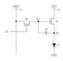
도 6은 터치전극에 연결된 먹스회로와 터치드라이버의 일 실시예를 나타내는 회로도이다.Figure 6 is a circuit diagram showing an embodiment of a mux circuit and a touch driver connected to a touch electrode.
도 6을 참조하면, 터치센서(120)는 제1터치전극(TEa)과 제2터치전극(TEb)을 포함할 수 있다. 제1터치전극(TEa)과 제2터치전극(TEb)은 도 4에 도시되어 있는 복수의 터치전극들 중 제1영역(A)에 배치되어 있는 터치전극일 수 있다. 제1영역(A) 영역에 배치되어 있는 제1터치전극(TEa)과 제2터치전극(TEb)은 동일한 열에 배치되어 있는 인접한 터치전극일 수 있다.Referring to FIG. 6, the
제1터치전극(TEa)과 제2터치전극(TEb)은 각각 제1터치신호라인(TEL1)과 제2터치신호라인(TEL2)이 연결될 수 있다. 또한, 제1터치신호라인(TEL1)과 제2터치신호라인(TEL2)은 먹스회로(111a)에 연결될 수 있다. 먹스회로(111a)는 도 3에 도시되어 있는 먹스회로부(111)에 포함되는 하나의 먹스회로일 수 있다.The first touch electrode (TEa) and the second touch electrode (TEb) may be connected to the first touch signal line (TEL1) and the second touch signal line (TEL2), respectively. Additionally, the first touch signal line (TEL1) and the second touch signal line (TEL2) may be connected to the
먹스회로(111a)는 도 3에 도시된 표시패널(11선택신호에 대응하여 복수의 터치전극 중 터치구동신호(Tds)를 전달받는 제1터치전극(TEa)과 로드프리신호(LFD)를 전달받는 제2터치전극(TEb)을 선택할 수 있다. 또한, 먹스회로(111a)는 선택신호에 대응하여 먹스회로(111a)는 선택신호에 대응하여 복수의 터치전극 중 터치구동신호(Tds)를 전달받는 제2터치전극(TEb)과 로드프리신호(LFD)를 전달받는 제1터치전극(TEa)을 선택할 수 있다. 먹스회로(111a)에 의해 복수의 터치전극 중 하나의 터치전극이 터치구동신호(Tds)를 전달받으면 나머지 다른 터치전극들은 로드프리신호(LFD)를 전달받을 수 있다.The
선택신호는 도 1에 도시된 제2제어부(160)에서 출력될 수 있다. 또한, 선택신호는 제1선택신호 내지 제4선택신호(ssl1 내지 ssl4)를 포함할 수 있다. 하지만, 이에 한정되는 것은 아니다.The selection signal may be output from the
터치드라이버(170)는 터치구동신호(Tds)를 출력하는 터치구동신호출력회로(170a)와, 로드프리신호(LFD)를 공급하는 로드프리신호출력회로(170b)를 포함할 수 있다. 또한, 터치구동신호출력회로(170a)는 터치구동신호(Tds)에 대응하는 터치센싱신호를 전달받을 수 있다. 터치구동신호출력회로(170a)는 적분기를 포함할 수 있다. 적분기는 앰프(171)와, 앰프(171)의 (-) 입력단과 출력단 사이에 배치되는 캐패시터(Cf)를 포함할 수 있다. 또한, 앰프(171)의 (+) 입력단에 터치구동신호(Tds)가 전달될 수 있다. 앰프(171)의 (-) 입력단은 터치신호라인(TEL1,TEL2)과 연결될 수 있다. 그리고, 앰프(171)의 (+) 입력단으로 전달되는 터치구동신호(Tds)는 터치신호라인(TEL1,TEL2)을 통해 제1터치전극(TEa) 또는 제2터치전극(TEb)으로 전달되고 제1터치전극(TEa) 또는 제2터치전극(TEb)은 터치구동신호(Tds)에 대응하여 터치센싱신호를 터치신호라인(TEL1,TEL2)을 통해 터치구동신호출력회로(170a)로 전달할 수 있다. 적분기는 앰프(171)의 (+) 입력단으로 전달되는 터치구동신호(Tds)와 (-) 입력단으로 전달되는 터치센싱신호의 차이에 대응하여 적분하여 터치를 검출하게 할 수 있다.The
먹스회로(111a)는 제1선택신호(ssl1)에 대응하여 동작하는 제1스위치(SW1), 제2선택신호(ssl2)에 대응하여 동작하는 제2스위치(SW2), 제3선택신호(ssl3)에 대응하여 동작하는 제3스위치(SW3) 및 제4선택신호(ssl4)에 대응하여 동작하는 제4스위치(SW4)를 포함할 수 있다.The
제1스위치(SW1)는 제1전극이 제1터치전극(TEa)에 연결되고 제2전극이 터치구동신호출력회로(170a)에 연결되고 게이트전극이 제1선택신호(ssl1)를 공급하는 제1선택신호선(SSL1)에 연결될 수 있다. 제2스위치(SW2)는 제1전극이 제1터치전극(TEa)에 연결되고 제2전극이 로드프리신호출력회로(170b)에 연결되고 게이트전극이 제2선택신호(ssl2)를 공급하는 제2선택신호선(SSL2)에 연결될 수 있다. 제3스위치(SW3)는 제1전극이 제2터치전극(TEb)에 연결되고 제2전극이 터치구동신호출력회로(170a)에 연결되고 게이트전극이 제3선택신호(ssl3)를 공급하는 제3선택신호선(SSL3)에 연결될 수 있다. 제4스위치(SW4)는 제1전극이 제2터치전극(TEb)에 연결되고 제2전극이 로드프리신호출력회로(170b)에 연결되고 게이트전극이 제4선택신호(ssl4)를 공급하는 제4선택신호선(SSL4)에 연결될 수 있다.The first switch (SW1) has a first electrode connected to the first touch electrode (TEa), a second electrode connected to the touch driving
선택신호에 대응하여 먹스회로(111a)는 제1기간에는 제1터치전극(TEa)으로 터치구동신호를 전달하고 제2기간에는 제2터치전극(TEb)으로 터치구동신호(Tds)를 전달할 수 있다. 또한, 먹스회로(111a)는 선택신호에 대응하여 제1기간에는 제2터치전극(TEb)으로 로드프리신호(LFD)를 전달하고 제2기간에는 제1터치전극(TEa)으로 터치구동신호를 전달할 수 있다.In response to the selection signal, the
제1터치전극(TEa)은 제1터치신호라인(TEL1)과 연결되고 제2터치전극(TEb)은 제2터치신호라인(TEL2)과 연결될 수 있다. 또한, 제1터치신호라인(TEL1)과 제2터치신호라인(TEL2)에는 먹스회로(111a)가 연결될 수 있다.The first touch electrode (TEa) may be connected to the first touch signal line (TEL1), and the second touch electrode (TEb) may be connected to the second touch signal line (TEL2). Additionally, a
제1선택신호선(SEL1)과 제1터치신호라인(TEL1)에는 제1기생패시터(CP1)이 형성되고 제3선택신호선(SEL3)과 제2터치신호라인(TEL2)에는 제2기생캐패시터(CP2)가 형성될 수 있다. 하지만, 기생캐패시터가 형성되는 위치는 이에 한정되는 것은 아니다.A first parasitic capacitor CP1 is formed in the first selection signal line SEL1 and the first touch signal line TEL1, and a second parasitic capacitor is formed in the third selection signal line SEL3 and the second touch signal line TEL2. CP2) may be formed. However, the location where the parasitic capacitor is formed is not limited to this.
또한, 제1 내지 제4스위치(SW1 내지 SW4)는 박막 트랜지스터일 수 있다. 또한, 제1내지 제4스위치(SW1 내지 SW4)는 산화물 반도체를 포함할 수 있다. 하지만, 이에 한정되는 것은 아니다. 제1내지 제4스위치(SW1 내지 SW4)가 산화물 반도체를 포함하는 경우, 도 2에 도시된 화소(101)의 제1트랜지스터(M1) 및 제2트랜지스터(M2) 역시 산화물 반도체를 포함할 수 있다. 하지만, 이에 한정되는 것은 아니다.Additionally, the first to fourth switches (SW1 to SW4) may be thin film transistors. Additionally, the first to fourth switches (SW1 to SW4) may include an oxide semiconductor. However, it is not limited to this. When the first to fourth switches (SW1 to SW4) include an oxide semiconductor, the first transistor (M1) and the second transistor (M2) of the
여기서는 하나의 먹스회로가 2개의 터치전극에 연결되어 있는 것으로 도시되어 있지만, 이에 한정되는 것은 아니며 하나의 먹스회로는 2개 이상의 터치전극과 연결되어 있을 수 있다. 하나의 먹스회로에 연결되어 있는 터치전극으 수가 증가할수록 선택신호의 수도 증가할 수 있다.Here, one MUX circuit is shown as being connected to two touch electrodes, but the present invention is not limited to this and one MUX circuit may be connected to two or more touch electrodes. As the number of touch electrodes connected to one MUX circuit increases, the number of selection signals may also increase.
도 7은 터치구동신호와 로드프리신호의 파형을 나타내는 파형도이고, 도 8은 제1선택신호 내지 제4선택신호의 파형의 일실시예를 나타내는 파형도이다. 또한, 도 9는 제1선택신호 내지 제4선택신호의 파형의 다른 일 실시예를 나타내는 파형도이다.FIG. 7 is a waveform diagram showing the waveforms of the touch drive signal and the load-free signal, and FIG. 8 is a waveform diagram showing an example of the waveforms of the first to fourth selection signals. Additionally, Figure 9 is a waveform diagram showing another example of the waveforms of the first to fourth selection signals.
도 7 내지 도 9를 참조하면, 터치드라이버(170)를 통해 전달되는 터치구동신호(Tds)는 일정한 주기를 갖는 복수의 구형파일 수 있다. 그리고, 로드프리신호(LFD)는 터치구동신호(Tds)에 대응할 수 있다. 로드프리신호(LFD)가 터치구동신호(Tds)에 대응하는 것은 로드프리신호(LFD)의 위상과 전압이 터치구동신호(Tds)의 위상과 전압이 동일한 것일 수 있다. 여기서, 동일은 완전동일만을 의미하는 것이 아니라 미차를 포함할 수 있다.Referring to FIGS. 7 to 9 , the touch drive signal Tds transmitted through the
제1기간(Ts1a)에서 제1선택신호(ssl1) 및 제4선택신호(ssl4)는 하이상태의 전압(VGH)이 될 수 있다. 그리고, 제2선택신호(ssl2) 및 제3선택신호(ssl3)는 로우상태의 전압(VGL)이 될 수 있다. 제1기간(Ts1a)에서 제1선택신호(ssl1)에 의해 제1터치전극(TEa)에 터치구동신호(Tds)가 전달될 수 있고 제4선택신호(ssl4)에 의해 로드프리신호(LFD)는 제2터치전극(TEb)에 전달될 수 있다. 로드프리신호(LFD)가 제2터치전극(TEb)에 전달되지 않게 되면, 제1터치전극(TEa)의 전압은 변화되지만 제2터치전극(TEb)의 전압은 일정하게 유지될 수 있다. 제1터치전극(TEa)과 제2터치전극(TEb)은 공통전극 또는 캐소드전극을 포함하고 있기 때문에 제1터치전극(TEa)의 전압이 변경되고 제2터치전극(TEb)이 일정하게 유지되면 표시패널(110)에서 표시되는 영상은 제1터치전극(TEa)과 제2터치전극(TEb)의 전압의 차이로 인해 왜곡될 수 있다. 하지만, 로드프리신호(LFD)를 인가하게 되면 제1터치전극(TEa)과 제2터치전극(TEb) 모두 동일하게 터치구동신호(Tds)에 대응하는 전압이 인가되게 되어 상기의 문제점을 해결할 수 있다.In the first period (Ts1a), the first selection signal (ssl1) and the fourth selection signal (ssl4) may be the high-state voltage (VGH). And, the second selection signal (ssl2) and the third selection signal (ssl3) may be the voltage (VGL) in a low state. In the first period (Ts1a), the touch drive signal (Tds) may be transmitted to the first touch electrode (TEa) by the first selection signal (ssl1), and the load free signal (LFD) may be transmitted by the fourth selection signal (ssl4). It may be transmitted to the second touch electrode (TEb). When the load free signal (LFD) is not transmitted to the second touch electrode (TEb), the voltage of the first touch electrode (TEa) changes, but the voltage of the second touch electrode (TEb) can be maintained constant. Since the first touch electrode (TEa) and the second touch electrode (TEb) include a common electrode or a cathode electrode, when the voltage of the first touch electrode (TEa) changes and the second touch electrode (TEb) remains constant, The image displayed on the
하지만, 도 8에 도시되어 있는 것과 같이, 제1선택신호(ssl1)는 제1기간(Ts1a)에서 일정한 크기를 갖는 하이상태의 전압이고 제2기간(Ts2a)에서 일정한 크기를 갖는 로우상태의 전압이다. 또한, 제3선택신호(ssl3)는 제1기간(Ts1a)에서 일정한 크기를 갖는 로우상태의 전압이고 제2기간(Ts2a)에서는 일정한 크기를 갖는 하이상태의 전압이다. 하지만, 제1터치신호라인(TEL1)과 제2터치신호라인(TEL2)에 전달되는 전압은 터치구동신호(Tds) 또는 로드프리신호(LFD)에 의해 제1기간(Ts1a)과 제2기간(Ts2a)에서 일정한 주기를 갖는 구형파의 형태로 전달된다. 제1스위치(SW1) 및 제3스위치(SW3) 각각의 게이트전극과 제1터치라인(TEL1)과 제2터치라인간(TEL2)에는 제1기생캐패시터(CP1) 및 제2기생캐패시터(CP2)가 형성되어 있어서 제1터치신호라인(TEL1)과 제2터치신호라인(TEL2)의 전압은 제1선택신호(ssl1)와 제3선택신호(ssl3)의 전압에 대응하게 된다. 이로 인해, 제1터치라인(TEL1) 또는 제2터치라인(TEL2)에 전달되는 터치구동신호(Tds) 또는 로드프리신호(LFD)는 왜곡되게 될 수 있다.However, as shown in FIG. 8, the first selection signal ssl1 is a high state voltage with a constant magnitude in the first period Ts1a and a low state voltage with a constant magnitude in the second period Ts2a. am. Additionally, the third selection signal ssl3 is a low-state voltage with a constant magnitude in the first period (Ts1a) and a high-state voltage with a constant magnitude in the second period (Ts2a). However, the voltage transmitted to the first touch signal line (TEL1) and the second touch signal line (TEL2) is divided into the first period (Ts1a) and the second period (Ts2a) by the touch drive signal (Tds) or the load free signal (LFD). ) is transmitted in the form of a square wave with a certain period. A first parasitic capacitor (CP1) and a second parasitic capacitor (CP2) are provided between the gate electrodes of each of the first switch (SW1) and the third switch (SW3) and the first touch line (TEL1) and the second touch line (TEL2). is formed, so that the voltages of the first touch signal line (TEL1) and the second touch signal line (TEL2) correspond to the voltages of the first selection signal (ssl1) and the third selection signal (ssl3). As a result, the touch drive signal (Tds) or load free signal (LFD) transmitted to the first touch line (TEL1) or the second touch line (TEL2) may be distorted.
하지만, 도 9에 도시되어 있는 것과 같이 제1선택신호(ssl1)와 제4선택신호(ssl4)는 제1기간(Ts1a)에서 하이상태(VGH)가 되고 제2선택신호(ssl2) 및 제3선택신호(ssl3)는 로우상태(VGL)가 될 수 있고, 제1선택신호(ssl1)와 제4선택신호(ssl4)는 제2기간(Ts1a)에서 로우상태(VGH)가 되고 제2선택신호(ssl2) 및 제3선택신호(ssl3)는 하이상태(VGL)가 될 수 있지만, 위상이 로드프리신호(LFD)와 동일하게 될 수 있다. 제1선택신호 내지 제4선택신호(ssl1 내지 ssl4)가 하이상태와 로우상태를 반복하게 되어 제1스위치 내지 제4스위치(SW1)은 스위칭동작을 수행하게 되지만, 위상이 로드프리신호(LFD)와 동일하게 됨으로써 제1기생캐패시터(CP1) 및 제2기생캐패시터(CP2)에 의한 제1기간(Ts1a) 및 제2기간(Ts1a)에서 로프르리신호(LFD)는 전압 변화가 발생하지 않게 될 수 있다.However, as shown in Figure 9, the first selection signal (ssl1) and the fourth selection signal (ssl4) are in the high state (VGH) in the first period (Ts1a), and the second selection signal (ssl2) and the third selection signal (ssl2) are in the high state (VGH). The selection signal (ssl3) may be in a low state (VGL), the first selection signal (ssl1) and the fourth selection signal (ssl4) may be in a low state (VGH) in the second period (Ts1a), and the second selection signal (ssl1) may be in a low state (VGH). (ssl2) and the third selection signal (ssl3) may be in a high state (VGL), but their phase may be the same as the load free signal (LFD). The first to fourth selection signals (ssl1 to ssl4) repeat high and low states, so that the first to fourth switches (SW1) perform a switching operation, but the phase is different from the load free signal (LFD). By being the same, the voltage change in the LFD signal may not occur in the first period (Ts1a) and the second period (Ts1a) due to the first parasitic capacitor (CP1) and the second parasitic capacitor (CP2). .
상기와 같은 이유로, 제1터치라인(TEL1) 또는 제2터치라인(TEL2)에 전달되는 터치구동신호(Tds) 또는 로드프리신호(LFD)가 왜곡되는 문제점을 해결할 수 있다.For the above reasons, it is possible to solve the problem that the touch drive signal (Tds) or load free signal (LFD) transmitted to the first touch line (TEL1) or the second touch line (TEL2) is distorted.
도 10은 도 3에 도시된 표시패널의 B-B` 단면의 일 실시예를 나타내는 단면도이다.FIG. 10 is a cross-sectional view of an embodiment of the display panel shown in FIG. 3 taken along line B-B′.
도 10을 참조하면, 표시패널(110)은 유기발광표시장치에 대응할 수 있다. 표시패널(110)은 기판(811) 상에 복수의 층이 증착될 수 있다. 기판(811) 상에 기판(811) 상에 멀티버퍼층(812)이 형성되고, 멀티버퍼층(812) 상에 액티브버퍼층(813)이 형성될 수 있다. 멀티버퍼층(812)과 액티브버퍼층(813)을 통칭해서 버퍼층이라고 칭할 수 있다. 기판(811)은 폴리아미드(polyamide: PI)를 포함할 수 있다. 기판(811)이 폴리아미드를 포함하는 경우 플렉서블 기판이라고 할 수 있다. 여기서, 플랙서블 기판은 기판(811)이 접히거나 휘어지는 것을 포함할 수 있다. 액티브버퍼층(813) 상에 액티브층(814)이 패터닝되어 배치될 수 있다. 멀티버퍼층(812)고 액티브버퍼층(813)은 기판에 존재하는 이물질이 액티브층(814)으로 침투하는 것을 방지할 수 있다. 멀티버퍼층(812)은 복수의 무기막을 포함하며, 각 무기막은 이산화규소(SiO2)와 질화규소(SiNx)를 포함할 수 있다. 그리고, 액티브버퍼층(813)은 무기막을 포함하며 무기막은 이산화규소(SiO2)를 포함할 수 있다.Referring to FIG. 10, the
액티브층(814) 상에 게이트절연막(815)이 배치될 수 있다. 그리고, 게이트절연막(815) 상에 게이트메탈이 패터딩되어 게이트전극(816)이 배치될 수 있다. 게이트절연막(815)은 이산화규소(SiO2)를 포함할 수 있다. 게이트전극(816) 상에는 제1층간절연막(817)과 제2층간절연막(818)이 배치될 수 있다. 제1층간절연막(817)은 이산화규소(SiO2)와 질화규소(SiNx)를 포함할 수 있고 제2층간절연막은 이산화규소(SiO2)와 질화규소(SiNx)를 포함할 수 있다. 제2층간절연막(818)의 상부에는 소스드레인메탈이 패터닝되어 소스전극(819a)과 드레인전극(919b)이 배치될 수 있다. 소스전극(819a)과 드레인전극(819b) 상에는 평탄화막(820)이 배치될 수 있다. 그리고, 평탄화막(820) 상에는 애노드전극(821)이 배치될 수 있다. 또한, 평탄화막(820)에는 컨텍홀이 형성되고 애노드전극(821)이 컨텍홀을 통해 드레인전극(919b)에 연결될 수 있다. 그리고, 평탄화막(820) 상에 뱅크(822)가 형성되고 뱅크(822)에는 캐버티가 형성되고 캐버티에 발광층(823)이 형성될 수 있다. 발광층(823)은 복수의 유기발광층을 포함할 수 있다. 발광층(823) 상에는 캐소드전극(824)이 형성될 수 있다. 캐소드전극(824)은 공통전극일 수 있다.A
캐소드전극(824) 상에는 실링기판(825,826,827)이 배치될 수 있다. 실링기판(825,826,827)은 제2무기막(825)과, 제3무기막(827)과, 제2무기막(825)과 제3무기막(827) 사이에 제1유기막(826)이 배치될 수 있다. 유기막(826)의 두께는 보다 두껍게 배치되어 이물이 실링기판(825,826,827)을 통과하여 발광층(823)에 침투하는 것을 방지할 수 있다. 그리고, 캐소드전극(824) 상에 제2무기막(825)이 배치되고, 제2무기막(825) 상에 제1유기막(826)이 배치되고, 제1유기막(826) 상에 제3무기막(827)을 배치할 수 있다. 제2무기막(825)은 제1유기막(826)이 외부로 배출되는 것을 방지하기 위해 2중의 댐이 형성될 수 있고, 제3무기막(827)은 일단이 제2무기막(825)과 댐에서 만날 수 있다.
그리고, 실링기판(825,826,827) 상에 터치센서부(829,830,831)가 배치될 수 있다. 터치센서부(829,830,831)는 제1터치전극(829)과 제2터치전극(831)이 패터닝될 수 있는데, 터치전극과 센싱전극을 패터닝할 때 실링기판에 데미지가 가해지는 것을 방지하기 위해 실링기판 상에 터치버퍼층(828)을 배치할 수 있다. 그리고, 터치버퍼층(828) 상에 제1도전층을 형성하고 패터닝하여 제1터치전극(829)을 배치할 수 있다. 그리고, 제1터치전극(829) 상에 터치절연막(830)이 형성되고 터치절연막(830) 상에 제2도전층이 형성되고 패터닝되어 제2터치전극(831)이 배치될 수 있다. 형성될 수 있다. 그리고, 제2터치전극(831) 상부에 패시베이션층(832)이 형성될 수 있다. 따라서, 터치센서부(829,830,831)는 표시패널에 실장될 수 있다.Additionally,
제1터치전극(829)은 도 4에 도시되어 있는 연결부(422) 중 하나일 수 있고 제2터치전극(831)은 도 4에 도시되어 있는 제1전극(TEa) 및 제2전극(TEb)일 수 있다. 또한, 제1터치전극(829)은 도 5에 도시되어 있는 터치전극(TE)이고 제2터치전극(831)은 터치배선(420)일 수 있다. 또한, 제1터치전극(829)은 도 6에 도시되어 있는 제1터치전극들(TEd1,TEd2,??TEdn-1,TEdn)일 수 있고 제2터치전극(831)은 제2터치전극들(TEs1,TEs2,??TEds-1,TEds)일 수 있다.The
도 11은 도 4에 도시된 표시패널의 C-C` 단면의 일 실시예 나타내는 단면도이다.FIG. 11 is a cross-sectional view showing one embodiment of the C-C' cross section of the display panel shown in FIG. 4.
도 11을 참조하면, 표시패널(110)은 기판(911) 상에 게이트메탈이 증착되고 패터닝되어 게이트전극(912)이 배치될 수 있다. 여기서, 기판(911)에 게이트전극(912)이 접촉되어 있는 것으로 도시되어 있지만, 이에 한정되는 것은 아니다. 기판(911) 상에 버퍼층(미도시)이 배치된 후 게이트전극(912)을 배치할 수 있다. 게이트전극(912)이 배치되어 있는 기판(911)의 상부에 게이트절연막(913)을 배치할 수 있다. 게이트절연막(913)의 복수의 액티브층(914a,914b,914c)을 배치할 수 있다. 여기서는 복수의 액티브층(914a,914b,914c)이 제1액티브층(914a) 내지 제3액티브층(914c)을 포함하는 것으로 도시되어 있지만 복수의 액티브층(914a,914b,914c)의 수는 이에 한정되는 것은 아니다. 그리고, 복수의 액티브층(914a,914b,914c) 상에 각각 소스드레인메탈(915a 내지 915d)이 배치될 수 있다. 제1액티브층(914a)에 배치된 소스드레인메탈은 제1소스드레인메탈(915a)이라고 칭하고, 제2액티브층(914b)에 배치된 두개의 소스드레인메탈을 각각 제2소스드레인메탈(915b)과 제3소스드레인메탈(915c)이라고 칭하고, 제3액티브층(914c)에 배치된 소스드레인메탈을 제4소스드레인메탈(915d)이라고 칭할 수 있다.Referring to FIG. 11 , the
소스드레인메탈들(915a 내지 915d)의 상부와 게이트절연막(913)의 상부에 절연막(916)을 배치할 수 있다. 절연막(916)에는 제3소스드레인메탈(915c)에 대응하는 컨텍홀(916h)을 형성하고 절연막(916) 상부에 화소전극(917)을 배치할 수 있다. 화소전극(917)은 컨텍홀(916h)을 통해 제3소스드레인메탈(915c)과 연결될 수 있다. 화소전극(917)은 도 1에 도시된 표시패널(110)의 제1전극에 대응할 수 있다. 표시패널(110)이 액정표시장치에 대응하는 경우 제1전극은 액정셀에 데이터신호에 대응하는 전압을 전달할 수 있다. 또한, 화소전극(917)은 도 1에 도시된 표시패널(110)이 유기발광표시장치인 경우 유기발광다이오드의 애노드전극일 수 있다. 화소전극(917)이 배치되어 있는 절연막(916)의 상부에 보호층(918)을 배치할 수 있다. 그리고, 보호층(918) 상에는 도전층을 증착하고 패터닝하여 전극(919)이 배치될 수 있다. 전극(919)는 도 1에 도시된 표시패널(110)의 제2전극(919)에 대응할 수 있다. 제2전극은 도 1에 도시된 표시패널(110)이 액정표시장치에 대응하는 경우 공통전압(Vcom)이 전달될 수 있다. 또한, 제2전극은 도 1에 도시된 표시패널(110)이 유기발광표시장치인 경우 유기발광다이오드의 캐소드전극일 수 있다. 하지만, 이에 한정되는 것은 아니다. 제2전극은 패터닝되어 배치될 수 있고 도 4에 도시된 터치전극(TE)으로 사용될 수 있다. 제2전극을 터치전극(TE)으로 사용되는 경우, 도 5에 도시된 것과 같이 디스플레이기간(Td)에서 제2전극에 공통전압(Vcom)이 전달될 수 있고 캐소드전극에 저전압이 전달될 수 있다. 그리고, 터치검출기간(Ts)에는 제2전극으로 터치구동신호(Tds)가 전달될 수 있다. 또한, 제2전극으로 터치구동신호(Tds)에 대응하는 로드프리신호(LFD)가 전달될 수 있다.An insulating
여기서, 게이트전극(912)은 액티브층(914a,914b,914c) 하부에 배치되어 있지만, 이에 한정되는 것은 아니며 게이트전극(912)이 액티브층(914a,914b,914c) 상부에 배치될 수 있다. 이 경우, 게이트절연막(912)은 액티브층(914a,914b,914c)과 게이트전극(912) 사이에 배치될 수 있다. 또한, 제2소스드레인메탈(915b) 및 제3소스드레인메탈(915c)은 컨텍홀(미도시)를 통해 제2액티브층(914b)과 접촉할 수 있다. 또한, 제1소스메탈(915a)과 제4소스메탈(915d)은 각각 상부에 대응하는 제2전극과 연결되어 터치신호를 제2전극에 전달할 수 있다. 그리고, 게이트전극(912), 제2액티브층(914b), 제2소스드레인메탈(915b) 및 제3소스드레인메탈(915c)은 게이트전극(912)에 전달되는 전압에 대응하여 데이터신호에 대응하는 데이터전압을 화소전극(917)에 전달할 수 있다.Here, the
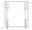
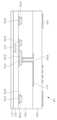
도 12는 도 6에 도시된 먹스회로의 일 실시예를 나타내는 평면도이고, 도 13은 도 12에 도시된 C-C`의 단면의 일 실시예를 나타내는 단면도이다.FIG. 12 is a plan view showing an embodiment of the mux circuit shown in FIG. 6, and FIG. 13 is a cross-sectional view showing an embodiment of the cross section taken along line C-C′ shown in FIG. 12.
도 12 및 도 13을 참조하면, 먹스회로는 도 3에 도시된 표시패널(110)의 링크영역(110b)상에 배치될 수 있다. 먹스회로는 도 3에 도시된 링크영역(110b) 상에 배치되어 있는 먹스회로부(111)에 대응할 수 있다. 먹스회로부는 다음과 같은 배치를 포함할 수 있다. 기판(1011) 상에 게이트메탈(1012)가 배치될 수 있다. 여기서, 기판(1011)에 게이트메탈(1012)이 접촉되어 있는 것으로 도시되어 있지만, 이에 한정되는 것은 아니다. 기판(1011) 상에 버퍼층(미도시)이 배치된 후 게이트메탈(1012)을 배치할 수 있다. 기판(1011) 상에는 제1게이트메탈 내지 제4게이트메탈(1012a 내지 1012d)를 포함할 수 있다. 각각 도 6에 도시되어 있는 먹스회로(111a)의 제1선택신호선(SSL1), 제2선택신호선(SSL2), 제3선택신호선(SSL3) 제4선택신호선(SSL4)에 대응할 수 있다. 그리고, 게이트메탈(1012)의 상부에 게이트절연막(1013)을 배치할 수 있다. 게이트절연막(1013)의 상부에는 제1액티브층 내지 제4액티브층(1014a 내지 1014e)이 배치될 수 있다. 네개의 제1게이트메탈 내지 제4게이트메탈(1012a 내지 1012d)이 각각 제1액티브층 내지 제4액티브층(1014a 내지 1014e)과 중첩되는 영역은 도 6에 도시되어 있는 제1스위치 내지 제4스위치(SW1 내지 SW4)의 게이트전극에 대응할 수 있다.Referring to Figures 12 and 13, the mux circuit may be placed on the
제1액티브층(1014a) 상에는 제1소스드레인메탈(1015a) 및 제2소스드레인메탈(1015b)이 배치되고, 제2액티브층(1014b) 상에는 제3소스드레인메탈(1015c)이 배치될 수 있다. 또한, 제3액티브층(1014b) 상에는 제4소스드레인메탈(1015c)이 배치되고 제4액티브층(1014c) 상에는 제5소스드레인메탈(1015d)이 배치될 수 있다. 제1액티브층(1014a)과 제1소스드레인메탈(1015a) 및 제2소스드레인메탈(1015b)은 도 6에 도시된 제1스위치(SW1)의 액티브층과 제1전극 및 제2전극에 대응하고, 제2액티브층(1014b)과 제3소스드레인메탈(1015c)은 제2스위치(SW2)의 액티브층과 제1전극에 대응하며, 제3액티브층(1014c)과 제4소스드레인메탈(1015d)은 제3스위치(SW3)의 액티브층과 제1전극에 대응하며, 제4액티브층(1014d)과 제 5소스드레인메탈(1015e)은 제4스위치(SW4)의 액티브층과 제1전극에 대응할 수 있다. A first
소스드레인메탈들(1015a 내지 1015e)의 상부와 게이트절연막(1013)의 상부에 절연막(1016)을 배치할 수 있다. 그리고, 절연막(1016)의 상부에 보호층(1017)을 배치할 수 있다.An insulating
여기서, 먹스회로는 2개의 터치전극에 터치구도신호(Tds) 또는 로드프리구동신호(LFD)를 전달하는 것으로 도시되어 있지만, 이에 한정되는 것은 아니며 먹스회로는 3개의 터치전극에 터치구동신호(Tds) 또는 로드프리구동신호(LFD)를 전달할 수 있다. 이 경우 게이트메탈의 수는 6개일 수 있다. 또한, 먹스회로(111a)는 6개의 스위치소자를 포함할 수 있고, 6개의 선택신호라인을 통해 전달되는 선택신호에 대응하여 3개의 스위치소자는 선택신호에 대응하여 터치구동신호를 스위칭하여 전달하고 나머지 3개의 스위치소자는 로드프리신호를 스위칭하여 전달할 수 있다.Here, the MUX circuit is shown as transmitting a touch composition signal (Tds) or a load-free driving signal (LFD) to two touch electrodes, but it is not limited to this, and the MUX circuit transmits a touch driving signal (Tds) to three touch electrodes. Alternatively, a load free driving signal (LFD) can be transmitted. In this case, the number of gate metals may be six. In addition, the
이상에서의 설명 및 첨부된 도면은 본 발명의 기술 사상을 예시적으로 나타낸 것에 불과한 것으로서, 본 발명이 속하는 기술 분야에서 통상의 지식을 가진 자라면 본 발명의 본질적인 특성에서 벗어나지 않는 범위에서 구성의 결합, 분리, 치환 및 변경 등의 다양한 수정 및 변형이 가능할 것이다. 따라서, 본 발명에 개시된 실시예들은 본 발명의 기술 사상을 한정하기 위한 것이 아니라 설명하기 위한 것이고, 이러한 실시예에 의하여 본 발명의 기술 사상의 범위가 한정되는 것은 아니다. 본 발명의 보호 범위는 아래의 청구범위에 의하여 해석되어야 하며, 그와 동등한 범위 내에 있는 모든 기술 사상은 본 발명의 권리범위에 포함되는 것으로 해석되어야 할 것이다.The above description and attached drawings are merely illustrative of the technical idea of the present invention, and those skilled in the art will be able to combine the components without departing from the essential characteristics of the present invention. , various modifications and transformations such as separation, substitution, and change will be possible. Accordingly, the embodiments disclosed in the present invention are not intended to limit the technical idea of the present invention, but are for illustrative purposes, and the scope of the technical idea of the present invention is not limited by these embodiments. The scope of protection of the present invention should be interpreted in accordance with the claims below, and all technical ideas within the equivalent scope should be construed as being included in the scope of rights of the present invention.
100: 표시장치
101: 화소
110: 표시패널
120: 터치센서
130: 데이터드라이버
140: 게이트드라이버
150: 제1제어부
160: 제2제어부
170: 터치드라이버100: display device
101: Pixel
110: display panel
120: Touch sensor
130: data driver
140: gate driver
150: first control unit
160: second control unit
170: Touch driver
Claims (19)
Translated fromKorean제1전극에서 제2전극 간의 전압에 대응하여 영상을 표시하되, 상기 제2전극은 상기 제1터치전극과 상기 제2터치전극에 포함되는 표시패널;
상기 제1터치전극 또는 상기 제2터치전극에 각각 터치구동신호와 로드프리신호를 공급하는 터치드라이버;
제1기간에 상기 터치드라이버부터 전달받은 상기 터치구동신호를 상기 제1터치전극으로 공급하고 상기 로드프리신호를 상기 제2터치전극으로 공급하며, 제2기간에 상기 터치드라이버로부터 전달받은 상기 터치구동신호를 상기 제2터치전극으로 공급하고 상기 로드프리신호를 상기 제1터치전극으로 공급하는 먹스회로; 및
상기 먹스회로를 제어하는 선택신호를 공급하되, 상기 선택신호의 위상은 상기 로드프리신호의 위상에 대응하도록 공급하는 터치제어부를 포함하며,
상기 먹스회로는 제1 내지 제4 스위치를 포함하고,
상기 선택신호는 제1 내지 제4 선택신호를 포함하며,
상기 제1스위치는 상기 제1터치전극과 제1터치구동신호라인을 통해 연결되고,
상기 제3스위치는 상기 제2터치전극과 제2터치구동신호라인을 통해 연결되며,
상기 제1스위치의 게이트 전극에는 상기 제1선택신호가 공급되고,
상기 제3스위치의 게이트 전극에는 상기 제3선택신호가 공급되며,
상기 제1스위치의 게이트 전극에 공급되는 상기 제1선택신호의 위상은 상기 로드프리신호의 위상에 대응되고, 상기 제3스위치의 게이트 전극에 공급되는 상기 제3선택신호의 위상은 상기 로드프리신호의 위상에 대응되는 표시장치.
A touch sensor including a first touch electrode and a second touch electrode;
A display panel that displays an image in response to a voltage between a first electrode and a second electrode, wherein the second electrode is included in the first touch electrode and the second touch electrode;
a touch driver that supplies a touch drive signal and a load-free signal to the first touch electrode or the second touch electrode, respectively;
The touch drive signal received from the touch driver in a first period is supplied to the first touch electrode, the load-free signal is supplied to the second touch electrode, and the touch drive signal received from the touch driver in a second period is supplied. a mux circuit that supplies the load-free signal to the first touch electrode and the second touch electrode; and
A touch control unit that supplies a selection signal for controlling the MUX circuit, wherein the phase of the selection signal corresponds to the phase of the load-free signal,
The mux circuit includes first to fourth switches,
The selection signal includes first to fourth selection signals,
The first switch is connected to the first touch electrode and a first touch driving signal line,
The third switch is connected to the second touch electrode and a second touch driving signal line,
The first selection signal is supplied to the gate electrode of the first switch,
The third selection signal is supplied to the gate electrode of the third switch,
The phase of the first selection signal supplied to the gate electrode of the first switch corresponds to the phase of the load-free signal, and the phase of the third selection signal supplied to the gate electrode of the third switch corresponds to the phase of the load-free signal. A display device corresponding to .
상기 로드프리신호는 상기 터치구동신호에 대응하는 표시장치.
According to paragraph 1,
The load-free signal corresponds to the touch drive signal.
상기 제1기간에서 상기 제1선택신호와 상기 제4선택신호는 하이상태의 신호이고 상기 제2선택신호 및 제3선택신호는 로우상태의 신호이며, 상기 제2기간에서 상기 제1선택신호와 상기 제4선택신호는 로우상태의 신호이고 상기 제2선택신호와 상기 제3선택신호는 하이상태의 신호로 공급하는 표시장치.
According to paragraph 1,
In the first period, the first selection signal and the fourth selection signal are high-state signals, and the second selection signal and the third selection signal are low-state signals, and in the second period, the first selection signal and A display device wherein the fourth selection signal is a low-state signal and the second selection signal and the third selection signal are supplied as high-state signals.
상기 먹스회로는,
상기 제2선택신호에 대응하여 동작하는 상기 제2스위치, 및 상기 제4선택신호에 대응하여 동작하는 상기 제4스위치를 구비하는 포함하는 표시장치.
According to paragraph 3,
The mux circuit is,
A display device comprising: the second switch operating in response to the second selection signal, and the fourth switch operating in response to the fourth selection signal.
상기 터치드라이버는 상기 터치구동신호를 출력하는 터치구동신호출력회로와, 상기 로드프리신호를 공급하는 로드프리신호출력회로를 포함하며,
상기 먹스회로는
제1전극이 상기 제1터치전극에 연결되고 제2전극이 상기 터치구동신호출력회로에 연결되고 게이트전극이 상기 제1선택신호를 공급하는 제1선택신호선에 연결되는 상기 제1스위치;
제1전극이 상기 제1터치전극에 연결되고 제2전극이 상기 로드프리신호출력회로에 연결되고 게이트전극이 상기 제2선택신호를 공급하는 제2선택신호선에 연결되는 상기 제2스위치;
제1전극이 상기 제2터치전극에 연결되고 제2전극이 상기 터치구동신호출력회로에 연결되고 게이트전극이 상기 제3선택신호를 공급하는 제3선택신호선에 연결되는 상기 제3스위치; 및
제1전극이 상기 제2터치전극에 연결되고 제2전극이 상기 로드프리신호출력회로에 연결되고 게이트전극이 상기 제4선택신호를 공급하는 제4선택신호선에 연결되는 상기 제4스위치를 포함하는 표시장치.
According to paragraph 3,
The touch driver includes a touch drive signal output circuit that outputs the touch drive signal, and a load-free signal output circuit that supplies the load-free signal,
The mux circuit is
the first switch having a first electrode connected to the first touch electrode, a second electrode connected to the touch driving signal output circuit, and a gate electrode connected to a first selection signal line supplying the first selection signal;
the second switch having a first electrode connected to the first touch electrode, a second electrode connected to the load-free signal output circuit, and a gate electrode connected to a second selection signal line supplying the second selection signal;
the third switch having a first electrode connected to the second touch electrode, a second electrode connected to the touch driving signal output circuit, and a gate electrode connected to a third selection signal line supplying the third selection signal; and
A display including the fourth switch in which a first electrode is connected to the second touch electrode, a second electrode is connected to the load-free signal output circuit, and a gate electrode is connected to a fourth selection signal line that supplies the fourth selection signal. Device.
상기 제1터치구동신호라인과 상기 제2터치구동신호라인은 각각 상기 터치구동신호와 상기 터치구동신호에 대응하는 터치센싱신호를 전송하는 표시장치.
According to paragraph 1,
The first touch driving signal line and the second touch driving signal line transmit the touch driving signal and a touch sensing signal corresponding to the touch driving signal, respectively.
상기 터치드라이버는 디스플레이기간과 터치센싱기간에 대응하여 동작하며, 상기 터치드라이버는 상기 터치구동신호를 상기 터치센싱기간에 공급하는 표시장치.
According to paragraph 1,
The touch driver operates in response to a display period and a touch sensing period, and the touch driver supplies the touch driving signal to the touch sensing period.
상기 표시패널은 복수의 화소가 배치되는 화소영역과, 상기 화소영역의 주변에 배치되고 상기 화소영역에 신호를 인가하는 링크영역이 배치되는 기판을 포함하되, 상기 먹스회로는 상기 링크영역에 배치되는 표시장치.
According to paragraph 1,
The display panel includes a pixel area on which a plurality of pixels are arranged, and a substrate on which a link area is arranged around the pixel area and applies a signal to the pixel area, and the mux circuit is arranged in the link area. Display device.
상기 제1스위치 내지 제4스위치는 산화물 반도체를 포함하는 트랜지스터인 표시장치.
According to paragraph 4,
The first to fourth switches are transistors including an oxide semiconductor.
터치구동신호 및 로드프리신호를 공급하고, 터치센싱신호를 검출하는 터치드라이버;
선택신호에 대응하여 상기 복수의 터치전극 중 상기 터치구동신호를 전달받는 제1터치전극과 상기 로드프리신호를 전달받는 제2터치전극을 선택하는 먹스회로; 및
상기 선택신호의 위상은 상기 로드프리신호의 위상에 대응하도록 출력하는 터치제어부를 포함하며,
상기 먹스회로는 제1 내지 제4 스위치를 포함하고,
상기 선택신호는 제1 내지 제4 선택신호를 포함하며,
상기 제1스위치는 상기 제1터치전극과 제1터치구동신호라인을 통해 연결되고,
상기 제3스위치는 상기 제2터치전극과 제2터치구동신호라인을 통해 연결되며,
상기 제1스위치의 게이트 전극에는 상기 제1선택신호가 공급되고,
상기 제3스위치의 게이트 전극에는 상기 제3선택신호가 공급되며,
상기 제1스위치의 게이트 전극에 공급되는 상기 제1선택신호의 위상은 상기 로드프리신호의 위상에 대응되고, 상기 제3스위치의 게이트 전극에 공급되는 상기 제3선택신호의 위상은 상기 로드프리신호의 위상에 대응되는 표시장치.
A display panel including a touch sensor including a plurality of touch electrodes and a plurality of pixels;
A touch driver that supplies a touch drive signal and a load-free signal and detects a touch sensing signal;
a mux circuit that selects a first touch electrode that receives the touch drive signal and a second touch electrode that receives the load-free signal among the plurality of touch electrodes in response to a selection signal; and
A touch control unit outputting the phase of the selection signal to correspond to the phase of the load-free signal,
The mux circuit includes first to fourth switches,
The selection signal includes first to fourth selection signals,
The first switch is connected to the first touch electrode and a first touch driving signal line,
The third switch is connected to the second touch electrode and a second touch driving signal line,
The first selection signal is supplied to the gate electrode of the first switch,
The third selection signal is supplied to the gate electrode of the third switch,
The phase of the first selection signal supplied to the gate electrode of the first switch corresponds to the phase of the load-free signal, and the phase of the third selection signal supplied to the gate electrode of the third switch corresponds to the phase of the load-free signal. A display device corresponding to .
상기 화소는
데이터신호에 대응하여 구동전류를 공급하는 제1트랜지스터;
상기 데이터신호를 상기 제1트랜지스터에 공급하는 제2트랜지스터;
상기 데이터신호를 유지하는 캐패시터; 및
상기 구동전류를 공급받아 빛을 발광하는 유기발광다이오드를 포함하되,
상기 터치전극은 상기 유기발광다이오드의 캐소드전극인 표시장치.
According to clause 10,
The pixel is
A first transistor that supplies driving current in response to the data signal;
a second transistor supplying the data signal to the first transistor;
a capacitor that maintains the data signal; and
Includes an organic light-emitting diode that receives the driving current and emits light,
A display device wherein the touch electrode is a cathode electrode of the organic light emitting diode.
상기 로드프리신호는 상기 터치구동신호에 대응하는 표시장치.
According to clause 10,
The load-free signal corresponds to the touch drive signal.
제1기간에서 상기 제1선택신호와 상기 제4선택신호는 하이상태의 신호이고 상기 제2선택신호 및 제3선택신호는 로우상태의 신호이며, 제2기간에서 상기 제1선택신호와 상기 제4선택신호는 로우상태의 신호이고 상기 제2선택신호와 상기 제3선택신호는 하이상태의 신호로 공급하는 표시장치.
According to clause 10,
In the first period, the first selection signal and the fourth selection signal are signals in a high state, and the second selection signal and the third selection signal are signals in a low state. In the second period, the first selection signal and the fourth selection signal are in a low state. 4. A display device in which the selection signal is a low-state signal and the second selection signal and the third selection signal are supplied as high-state signals.
상기 제1터치전극은 제1기간에 상기 터치구동신호를 공급받고 제2기간에 상기 로드프리신호를 공급받고, 상기 제2터치전극은 상기 제1기간에 상기 로드프리신호를 공급받고 상기 제2기간에 상기 터치구동신호를 공급받는 표시장치.
According to clause 10,
The first touch electrode receives the touch driving signal in a first period and the load-free signal in a second period, and the second touch electrode receives the load-free signal in the first period and receives the load-free signal in the second period. A display device that receives the touch driving signal.
상기 먹스회로는,
상기 제2선택신호에 대응하여 동작하는 상기 제2스위치, 및 상기 제4선택신호에 대응하여 동작하는 상기 제4스위치를 구비하는 포함하는 표시장치.
According to clause 13,
The mux circuit is,
A display device comprising: the second switch operating in response to the second selection signal, and the fourth switch operating in response to the fourth selection signal.
상기 터치드라이버는 상기 터치구동신호를 출력하는 터치구동신호출력회로와, 상기 로드프리신호를 공급하는 로드프리신호출력회로를 포함하며,
상기 먹스회로는
제1전극이 상기 제1터치전극에 연결되고 제2전극이 상기 터치구동신호출력회로에 연결되고 게이트전극이 상기 제1선택신호를 공급하는 제1선택신호선에 연결되는 상기 제1스위치;
제1전극이 상기 제1터치전극에 연결되고 제2전극이 상기 로드프리신호출력회로에 연결되고 게이트전극이 상기 제2선택신호를 공급하는 제2선택신호선에 연결되는 상기 제2스위치;
제1전극이 상기 제2터치전극에 연결되고 제2전극이 상기 터치구동신호출력회로에 연결되고 게이트전극이 상기 제3선택신호를 공급하는 제3선택신호선에 연결되는 상기 제3스위치; 및
제1전극이 상기 제2터치전극에 연결되고 제2전극이 상기 로드프리신호출력회로에 연결되고 게이트전극이 상기 제4선택신호를 공급하는 제4선택신호선에 연결되는 상기 제4스위치를 포함하는 표시장치.
According to clause 13,
The touch driver includes a touch drive signal output circuit that outputs the touch drive signal, and a load-free signal output circuit that supplies the load-free signal,
The mux circuit is
the first switch having a first electrode connected to the first touch electrode, a second electrode connected to the touch driving signal output circuit, and a gate electrode connected to a first selection signal line supplying the first selection signal;
the second switch having a first electrode connected to the first touch electrode, a second electrode connected to the load-free signal output circuit, and a gate electrode connected to a second selection signal line supplying the second selection signal;
the third switch having a first electrode connected to the second touch electrode, a second electrode connected to the touch driving signal output circuit, and a gate electrode connected to a third selection signal line supplying the third selection signal; and
A display including the fourth switch in which a first electrode is connected to the second touch electrode, a second electrode is connected to the load-free signal output circuit, and a gate electrode is connected to a fourth selection signal line that supplies the fourth selection signal. Device.
상기 터치드라이버는 디스플레이기간과 터치센싱기간에 대응하여 동작하며, 상기 터치드라이버는 상기 터치구동신호를 상기 터치센싱기간에 공급하는 표시장치.
According to clause 10,
The touch driver operates in response to a display period and a touch sensing period, and the touch driver supplies the touch driving signal to the touch sensing period.
상기 표시패널은 복수의 화소가 배치되는 화소영역과, 상기 화소영역의 주변에 배치되고 상기 화소영역에 신호를 인가하는 링크영역이 배치되는 기판을 포함하되, 상기 먹스회로는 상기 링크영역에 배치되는 표시장치.
According to clause 10,
The display panel includes a pixel area on which a plurality of pixels are arranged, and a substrate on which a link area is arranged around the pixel area and applies a signal to the pixel area, and the mux circuit is arranged in the link area. Display device.
상기 제1스위치 내지 제4스위치는 산화물 반도체를 포함하는 트랜지스터인 표시장치.According to clause 16,
The first to fourth switches are transistors including an oxide semiconductor.
Priority Applications (1)
| Application Number | Priority Date | Filing Date | Title |
|---|---|---|---|
| KR1020180150111AKR102577408B1 (en) | 2018-11-28 | 2018-11-28 | Display device including touch sensor |
Applications Claiming Priority (1)
| Application Number | Priority Date | Filing Date | Title |
|---|---|---|---|
| KR1020180150111AKR102577408B1 (en) | 2018-11-28 | 2018-11-28 | Display device including touch sensor |
Publications (2)
| Publication Number | Publication Date |
|---|---|
| KR20200063872A KR20200063872A (en) | 2020-06-05 |
| KR102577408B1true KR102577408B1 (en) | 2023-09-13 |
Family
ID=71088981
Family Applications (1)
| Application Number | Title | Priority Date | Filing Date |
|---|---|---|---|
| KR1020180150111AActiveKR102577408B1 (en) | 2018-11-28 | 2018-11-28 | Display device including touch sensor |
Country Status (1)
| Country | Link |
|---|---|
| KR (1) | KR102577408B1 (en) |
Families Citing this family (3)
| Publication number | Priority date | Publication date | Assignee | Title |
|---|---|---|---|---|
| CN113593457B (en)* | 2021-07-23 | 2024-04-26 | 昆山国显光电有限公司 | Display panel and testing method thereof |
| CN114816117B (en)* | 2022-04-20 | 2024-09-10 | 厦门天马微电子有限公司 | Touch display panel, driving method thereof and touch display device |
| CN117524150A (en)* | 2023-08-18 | 2024-02-06 | 武汉华星光电技术有限公司 | Touch display panel and display device |
Family Cites Families (2)
| Publication number | Priority date | Publication date | Assignee | Title |
|---|---|---|---|---|
| KR101648571B1 (en)* | 2014-07-16 | 2016-08-18 | 엘지디스플레이 주식회사 | In-cell touch type display device |
| CN104575355B (en)* | 2014-12-31 | 2017-02-01 | 深圳市华星光电技术有限公司 | Display panel and drive circuit thereof |
- 2018
- 2018-11-28KRKR1020180150111Apatent/KR102577408B1/enactiveActive
Also Published As
| Publication number | Publication date |
|---|---|
| KR20200063872A (en) | 2020-06-05 |
Similar Documents
| Publication | Publication Date | Title |
|---|---|---|
| KR102688299B1 (en) | Touch display | |
| US20210318772A1 (en) | Display device | |
| US10761632B2 (en) | Display device with touch sensor for suppressing deterioration of image quality caused by capacitor in touch sensor unit and method for manufacturing same | |
| US10540033B2 (en) | Display panel and touch display device | |
| US11327610B2 (en) | Display device with touch sensor and method of manufacturing same | |
| CN110045884B (en) | Display device with touch screen | |
| US20200026384A1 (en) | Display apparatus with touch sensor | |
| KR102577408B1 (en) | Display device including touch sensor | |
| US20210173245A1 (en) | Display apparatus | |
| KR102824767B1 (en) | Touch display device and the method of driving the same | |
| US11789574B2 (en) | Light emitting display apparatus | |
| KR20210071258A (en) | Touch display device and maunufacturing method for the same | |
| KR20240120095A (en) | Touch driving circuit and touch display device | |
| US11531423B2 (en) | Touch display device, driving circuit and driving method thereof | |
| KR20240094742A (en) | Display device and display panel | |
| KR20210085829A (en) | Display device | |
| US20240152228A1 (en) | Touch display device and touch sensing method | |
| CN116266453B (en) | Display device and driving method thereof | |
| US12382722B2 (en) | Display device | |
| US20250238101A1 (en) | Display device and driving method of the same | |
| KR20220001838A (en) | Display Apparatus | |
| KR20250098310A (en) | Display apparatus | |
| KR20250125645A (en) | Display apparatus and display panel | |
| KR20250131123A (en) | Display apparatus | |
| KR20240118475A (en) | Display apparatus |
Legal Events
| Date | Code | Title | Description |
|---|---|---|---|
| PA0109 | Patent application | St.27 status event code:A-0-1-A10-A12-nap-PA0109 | |
| PG1501 | Laying open of application | St.27 status event code:A-1-1-Q10-Q12-nap-PG1501 | |
| P22-X000 | Classification modified | St.27 status event code:A-2-2-P10-P22-nap-X000 | |
| PA0201 | Request for examination | St.27 status event code:A-1-2-D10-D11-exm-PA0201 | |
| D13-X000 | Search requested | St.27 status event code:A-1-2-D10-D13-srh-X000 | |
| D14-X000 | Search report completed | St.27 status event code:A-1-2-D10-D14-srh-X000 | |
| P22-X000 | Classification modified | St.27 status event code:A-2-2-P10-P22-nap-X000 | |
| P22-X000 | Classification modified | St.27 status event code:A-2-2-P10-P22-nap-X000 | |
| PE0902 | Notice of grounds for rejection | St.27 status event code:A-1-2-D10-D21-exm-PE0902 | |
| P11-X000 | Amendment of application requested | St.27 status event code:A-2-2-P10-P11-nap-X000 | |
| P13-X000 | Application amended | St.27 status event code:A-2-2-P10-P13-nap-X000 | |
| E701 | Decision to grant or registration of patent right | ||
| PE0701 | Decision of registration | St.27 status event code:A-1-2-D10-D22-exm-PE0701 | |
| PR0701 | Registration of establishment | St.27 status event code:A-2-4-F10-F11-exm-PR0701 | |
| PR1002 | Payment of registration fee | St.27 status event code:A-2-2-U10-U11-oth-PR1002 Fee payment year number:1 | |
| PG1601 | Publication of registration | St.27 status event code:A-4-4-Q10-Q13-nap-PG1601 |