KR102572718B1 - Color filter and display device including the same - Google Patents
Color filter and display device including the sameDownload PDFInfo
- Publication number
- KR102572718B1 KR102572718B1KR1020180110456AKR20180110456AKR102572718B1KR 102572718 B1KR102572718 B1KR 102572718B1KR 1020180110456 AKR1020180110456 AKR 1020180110456AKR 20180110456 AKR20180110456 AKR 20180110456AKR 102572718 B1KR102572718 B1KR 102572718B1
- Authority
- KR
- South Korea
- Prior art keywords
- color
- light
- layer
- color conversion
- conversion layer
- Prior art date
- Legal status (The legal status is an assumption and is not a legal conclusion. Google has not performed a legal analysis and makes no representation as to the accuracy of the status listed.)
- Active
Links
Images


Classifications
- G—PHYSICS
- G02—OPTICS
- G02F—OPTICAL DEVICES OR ARRANGEMENTS FOR THE CONTROL OF LIGHT BY MODIFICATION OF THE OPTICAL PROPERTIES OF THE MEDIA OF THE ELEMENTS INVOLVED THEREIN; NON-LINEAR OPTICS; FREQUENCY-CHANGING OF LIGHT; OPTICAL LOGIC ELEMENTS; OPTICAL ANALOGUE/DIGITAL CONVERTERS
- G02F1/00—Devices or arrangements for the control of the intensity, colour, phase, polarisation or direction of light arriving from an independent light source, e.g. switching, gating or modulating; Non-linear optics
- G02F1/01—Devices or arrangements for the control of the intensity, colour, phase, polarisation or direction of light arriving from an independent light source, e.g. switching, gating or modulating; Non-linear optics for the control of the intensity, phase, polarisation or colour
- G02F1/13—Devices or arrangements for the control of the intensity, colour, phase, polarisation or direction of light arriving from an independent light source, e.g. switching, gating or modulating; Non-linear optics for the control of the intensity, phase, polarisation or colour based on liquid crystals, e.g. single liquid crystal display cells
- G02F1/133—Constructional arrangements; Operation of liquid crystal cells; Circuit arrangements
- G02F1/1333—Constructional arrangements; Manufacturing methods
- G02F1/1335—Structural association of cells with optical devices, e.g. polarisers or reflectors
- G02F1/133509—Filters, e.g. light shielding masks
- G02F1/133514—Colour filters
- G—PHYSICS
- G02—OPTICS
- G02F—OPTICAL DEVICES OR ARRANGEMENTS FOR THE CONTROL OF LIGHT BY MODIFICATION OF THE OPTICAL PROPERTIES OF THE MEDIA OF THE ELEMENTS INVOLVED THEREIN; NON-LINEAR OPTICS; FREQUENCY-CHANGING OF LIGHT; OPTICAL LOGIC ELEMENTS; OPTICAL ANALOGUE/DIGITAL CONVERTERS
- G02F1/00—Devices or arrangements for the control of the intensity, colour, phase, polarisation or direction of light arriving from an independent light source, e.g. switching, gating or modulating; Non-linear optics
- G02F1/01—Devices or arrangements for the control of the intensity, colour, phase, polarisation or direction of light arriving from an independent light source, e.g. switching, gating or modulating; Non-linear optics for the control of the intensity, phase, polarisation or colour
- G02F1/13—Devices or arrangements for the control of the intensity, colour, phase, polarisation or direction of light arriving from an independent light source, e.g. switching, gating or modulating; Non-linear optics for the control of the intensity, phase, polarisation or colour based on liquid crystals, e.g. single liquid crystal display cells
- G02F1/133—Constructional arrangements; Operation of liquid crystal cells; Circuit arrangements
- G02F1/1333—Constructional arrangements; Manufacturing methods
- G02F1/1335—Structural association of cells with optical devices, e.g. polarisers or reflectors
- G02F1/133504—Diffusing, scattering, diffracting elements
- G—PHYSICS
- G02—OPTICS
- G02F—OPTICAL DEVICES OR ARRANGEMENTS FOR THE CONTROL OF LIGHT BY MODIFICATION OF THE OPTICAL PROPERTIES OF THE MEDIA OF THE ELEMENTS INVOLVED THEREIN; NON-LINEAR OPTICS; FREQUENCY-CHANGING OF LIGHT; OPTICAL LOGIC ELEMENTS; OPTICAL ANALOGUE/DIGITAL CONVERTERS
- G02F1/00—Devices or arrangements for the control of the intensity, colour, phase, polarisation or direction of light arriving from an independent light source, e.g. switching, gating or modulating; Non-linear optics
- G02F1/01—Devices or arrangements for the control of the intensity, colour, phase, polarisation or direction of light arriving from an independent light source, e.g. switching, gating or modulating; Non-linear optics for the control of the intensity, phase, polarisation or colour
- G02F1/13—Devices or arrangements for the control of the intensity, colour, phase, polarisation or direction of light arriving from an independent light source, e.g. switching, gating or modulating; Non-linear optics for the control of the intensity, phase, polarisation or colour based on liquid crystals, e.g. single liquid crystal display cells
- G02F1/133—Constructional arrangements; Operation of liquid crystal cells; Circuit arrangements
- G02F1/1333—Constructional arrangements; Manufacturing methods
- G02F1/1335—Structural association of cells with optical devices, e.g. polarisers or reflectors
- G—PHYSICS
- G02—OPTICS
- G02B—OPTICAL ELEMENTS, SYSTEMS OR APPARATUS
- G02B5/00—Optical elements other than lenses
- G02B5/20—Filters
- G—PHYSICS
- G02—OPTICS
- G02F—OPTICAL DEVICES OR ARRANGEMENTS FOR THE CONTROL OF LIGHT BY MODIFICATION OF THE OPTICAL PROPERTIES OF THE MEDIA OF THE ELEMENTS INVOLVED THEREIN; NON-LINEAR OPTICS; FREQUENCY-CHANGING OF LIGHT; OPTICAL LOGIC ELEMENTS; OPTICAL ANALOGUE/DIGITAL CONVERTERS
- G02F1/00—Devices or arrangements for the control of the intensity, colour, phase, polarisation or direction of light arriving from an independent light source, e.g. switching, gating or modulating; Non-linear optics
- G02F1/01—Devices or arrangements for the control of the intensity, colour, phase, polarisation or direction of light arriving from an independent light source, e.g. switching, gating or modulating; Non-linear optics for the control of the intensity, phase, polarisation or colour
- G02F1/13—Devices or arrangements for the control of the intensity, colour, phase, polarisation or direction of light arriving from an independent light source, e.g. switching, gating or modulating; Non-linear optics for the control of the intensity, phase, polarisation or colour based on liquid crystals, e.g. single liquid crystal display cells
- G02F1/133—Constructional arrangements; Operation of liquid crystal cells; Circuit arrangements
- G02F1/1333—Constructional arrangements; Manufacturing methods
- G02F1/1335—Structural association of cells with optical devices, e.g. polarisers or reflectors
- G02F1/133509—Filters, e.g. light shielding masks
- G02F1/133514—Colour filters
- G02F1/133516—Methods for their manufacture, e.g. printing, electro-deposition or photolithography
- G—PHYSICS
- G02—OPTICS
- G02F—OPTICAL DEVICES OR ARRANGEMENTS FOR THE CONTROL OF LIGHT BY MODIFICATION OF THE OPTICAL PROPERTIES OF THE MEDIA OF THE ELEMENTS INVOLVED THEREIN; NON-LINEAR OPTICS; FREQUENCY-CHANGING OF LIGHT; OPTICAL LOGIC ELEMENTS; OPTICAL ANALOGUE/DIGITAL CONVERTERS
- G02F1/00—Devices or arrangements for the control of the intensity, colour, phase, polarisation or direction of light arriving from an independent light source, e.g. switching, gating or modulating; Non-linear optics
- G02F1/01—Devices or arrangements for the control of the intensity, colour, phase, polarisation or direction of light arriving from an independent light source, e.g. switching, gating or modulating; Non-linear optics for the control of the intensity, phase, polarisation or colour
- G02F1/13—Devices or arrangements for the control of the intensity, colour, phase, polarisation or direction of light arriving from an independent light source, e.g. switching, gating or modulating; Non-linear optics for the control of the intensity, phase, polarisation or colour based on liquid crystals, e.g. single liquid crystal display cells
- G02F1/133—Constructional arrangements; Operation of liquid crystal cells; Circuit arrangements
- G02F1/1333—Constructional arrangements; Manufacturing methods
- G02F1/1335—Structural association of cells with optical devices, e.g. polarisers or reflectors
- G02F1/1336—Illuminating devices
- G02F1/133617—Illumination with ultraviolet light; Luminescent elements or materials associated to the cell
- H—ELECTRICITY
- H10—SEMICONDUCTOR DEVICES; ELECTRIC SOLID-STATE DEVICES NOT OTHERWISE PROVIDED FOR
- H10K—ORGANIC ELECTRIC SOLID-STATE DEVICES
- H10K59/00—Integrated devices, or assemblies of multiple devices, comprising at least one organic light-emitting element covered by group H10K50/00
- H10K59/30—Devices specially adapted for multicolour light emission
- H10K59/38—Devices specially adapted for multicolour light emission comprising colour filters or colour changing media [CCM]
- H—ELECTRICITY
- H10—SEMICONDUCTOR DEVICES; ELECTRIC SOLID-STATE DEVICES NOT OTHERWISE PROVIDED FOR
- H10K—ORGANIC ELECTRIC SOLID-STATE DEVICES
- H10K59/00—Integrated devices, or assemblies of multiple devices, comprising at least one organic light-emitting element covered by group H10K50/00
- H10K59/80—Constructional details
- H10K59/875—Arrangements for extracting light from the devices
- H10K59/877—Arrangements for extracting light from the devices comprising scattering means
- G—PHYSICS
- G02—OPTICS
- G02F—OPTICAL DEVICES OR ARRANGEMENTS FOR THE CONTROL OF LIGHT BY MODIFICATION OF THE OPTICAL PROPERTIES OF THE MEDIA OF THE ELEMENTS INVOLVED THEREIN; NON-LINEAR OPTICS; FREQUENCY-CHANGING OF LIGHT; OPTICAL LOGIC ELEMENTS; OPTICAL ANALOGUE/DIGITAL CONVERTERS
- G02F1/00—Devices or arrangements for the control of the intensity, colour, phase, polarisation or direction of light arriving from an independent light source, e.g. switching, gating or modulating; Non-linear optics
- G02F1/01—Devices or arrangements for the control of the intensity, colour, phase, polarisation or direction of light arriving from an independent light source, e.g. switching, gating or modulating; Non-linear optics for the control of the intensity, phase, polarisation or colour
- G02F1/015—Devices or arrangements for the control of the intensity, colour, phase, polarisation or direction of light arriving from an independent light source, e.g. switching, gating or modulating; Non-linear optics for the control of the intensity, phase, polarisation or colour based on semiconductor elements having potential barriers, e.g. having a PN or PIN junction
- G02F1/017—Structures with periodic or quasi periodic potential variation, e.g. superlattices, quantum wells
- G02F1/01791—Quantum boxes or quantum dots
- G—PHYSICS
- G02—OPTICS
- G02F—OPTICAL DEVICES OR ARRANGEMENTS FOR THE CONTROL OF LIGHT BY MODIFICATION OF THE OPTICAL PROPERTIES OF THE MEDIA OF THE ELEMENTS INVOLVED THEREIN; NON-LINEAR OPTICS; FREQUENCY-CHANGING OF LIGHT; OPTICAL LOGIC ELEMENTS; OPTICAL ANALOGUE/DIGITAL CONVERTERS
- G02F1/00—Devices or arrangements for the control of the intensity, colour, phase, polarisation or direction of light arriving from an independent light source, e.g. switching, gating or modulating; Non-linear optics
- G02F1/01—Devices or arrangements for the control of the intensity, colour, phase, polarisation or direction of light arriving from an independent light source, e.g. switching, gating or modulating; Non-linear optics for the control of the intensity, phase, polarisation or colour
- G02F1/13—Devices or arrangements for the control of the intensity, colour, phase, polarisation or direction of light arriving from an independent light source, e.g. switching, gating or modulating; Non-linear optics for the control of the intensity, phase, polarisation or colour based on liquid crystals, e.g. single liquid crystal display cells
- G02F1/133—Constructional arrangements; Operation of liquid crystal cells; Circuit arrangements
- G02F1/1333—Constructional arrangements; Manufacturing methods
- G02F1/133357—Planarisation layers
- G—PHYSICS
- G02—OPTICS
- G02F—OPTICAL DEVICES OR ARRANGEMENTS FOR THE CONTROL OF LIGHT BY MODIFICATION OF THE OPTICAL PROPERTIES OF THE MEDIA OF THE ELEMENTS INVOLVED THEREIN; NON-LINEAR OPTICS; FREQUENCY-CHANGING OF LIGHT; OPTICAL LOGIC ELEMENTS; OPTICAL ANALOGUE/DIGITAL CONVERTERS
- G02F1/00—Devices or arrangements for the control of the intensity, colour, phase, polarisation or direction of light arriving from an independent light source, e.g. switching, gating or modulating; Non-linear optics
- G02F1/01—Devices or arrangements for the control of the intensity, colour, phase, polarisation or direction of light arriving from an independent light source, e.g. switching, gating or modulating; Non-linear optics for the control of the intensity, phase, polarisation or colour
- G02F1/13—Devices or arrangements for the control of the intensity, colour, phase, polarisation or direction of light arriving from an independent light source, e.g. switching, gating or modulating; Non-linear optics for the control of the intensity, phase, polarisation or colour based on liquid crystals, e.g. single liquid crystal display cells
- G02F1/133—Constructional arrangements; Operation of liquid crystal cells; Circuit arrangements
- G02F1/1333—Constructional arrangements; Manufacturing methods
- G02F1/1335—Structural association of cells with optical devices, e.g. polarisers or reflectors
- G02F1/133509—Filters, e.g. light shielding masks
- G02F1/133512—Light shielding layers, e.g. black matrix
- G—PHYSICS
- G02—OPTICS
- G02F—OPTICAL DEVICES OR ARRANGEMENTS FOR THE CONTROL OF LIGHT BY MODIFICATION OF THE OPTICAL PROPERTIES OF THE MEDIA OF THE ELEMENTS INVOLVED THEREIN; NON-LINEAR OPTICS; FREQUENCY-CHANGING OF LIGHT; OPTICAL LOGIC ELEMENTS; OPTICAL ANALOGUE/DIGITAL CONVERTERS
- G02F2/00—Demodulating light; Transferring the modulation of modulated light; Frequency-changing of light
- G02F2/02—Frequency-changing of light, e.g. by quantum counters
- H—ELECTRICITY
- H05—ELECTRIC TECHNIQUES NOT OTHERWISE PROVIDED FOR
- H05B—ELECTRIC HEATING; ELECTRIC LIGHT SOURCES NOT OTHERWISE PROVIDED FOR; CIRCUIT ARRANGEMENTS FOR ELECTRIC LIGHT SOURCES, IN GENERAL
- H05B33/00—Electroluminescent light sources
- H05B33/12—Light sources with substantially two-dimensional radiating surfaces
- H05B33/14—Light sources with substantially two-dimensional radiating surfaces characterised by the chemical or physical composition or the arrangement of the electroluminescent material, or by the simultaneous addition of the electroluminescent material in or onto the light source
- H05B33/145—Arrangements of the electroluminescent material
- H—ELECTRICITY
- H10—SEMICONDUCTOR DEVICES; ELECTRIC SOLID-STATE DEVICES NOT OTHERWISE PROVIDED FOR
- H10H—INORGANIC LIGHT-EMITTING SEMICONDUCTOR DEVICES HAVING POTENTIAL BARRIERS
- H10H20/00—Individual inorganic light-emitting semiconductor devices having potential barriers, e.g. light-emitting diodes [LED]
- H10H20/80—Constructional details
- H10H20/85—Packages
- H10H20/851—Wavelength conversion means
- H10H20/8515—Wavelength conversion means not being in contact with the bodies
- H—ELECTRICITY
- H10—SEMICONDUCTOR DEVICES; ELECTRIC SOLID-STATE DEVICES NOT OTHERWISE PROVIDED FOR
- H10K—ORGANIC ELECTRIC SOLID-STATE DEVICES
- H10K2102/00—Constructional details relating to the organic devices covered by this subclass
- H10K2102/301—Details of OLEDs
- H10K2102/331—Nanoparticles used in non-emissive layers, e.g. in packaging layer
- H—ELECTRICITY
- H10—SEMICONDUCTOR DEVICES; ELECTRIC SOLID-STATE DEVICES NOT OTHERWISE PROVIDED FOR
- H10K—ORGANIC ELECTRIC SOLID-STATE DEVICES
- H10K59/00—Integrated devices, or assemblies of multiple devices, comprising at least one organic light-emitting element covered by group H10K50/00
- H10K59/80—Constructional details
- H10K59/8791—Arrangements for improving contrast, e.g. preventing reflection of ambient light
- H10K59/8792—Arrangements for improving contrast, e.g. preventing reflection of ambient light comprising light absorbing layers, e.g. black layers
Landscapes
- Physics & Mathematics (AREA)
- Nonlinear Science (AREA)
- General Physics & Mathematics (AREA)
- Optics & Photonics (AREA)
- Mathematical Physics (AREA)
- Chemical & Material Sciences (AREA)
- Crystallography & Structural Chemistry (AREA)
- Engineering & Computer Science (AREA)
- Manufacturing & Machinery (AREA)
- Optical Filters (AREA)
- Electroluminescent Light Sources (AREA)
Abstract
Translated fromKoreanDescription
Translated fromKorean본 발명은 컬러 필터 및 이를 포함하는 표시 장치에 관한 것이다.The present invention relates to a color filter and a display device including the same.
액정 표시 장치는 컬러를 형성하기 위해 컬러 필터를 사용하는데, 백라이트 광원으로부터 출사된 백색 광이 적색, 녹색 및 청색 컬러 필터들을 각각 통과할 때, 각각의 컬러 필터에 의해 광량이 대략 1/3로 감소되기 때문에 광효율이 낮다.The liquid crystal display device uses color filters to form colors. When white light emitted from a backlight source passes through red, green, and blue color filters, respectively, the amount of light is reduced to approximately 1/3 by each color filter. Because of this, the light efficiency is low.
이러한 광효율 저하를 보완하고 높은 색재현성을 위해 제안되는 포토루미네선트 액정 표시 장치(Photo-Luminescent Liquid Crystal Display Apparatus; PL-LCD)는 기존의 액정 표시 장치에 사용되는 컬러 필터를 양자점-색변환층(quantum dot color conversion layer; QD-CCL)로 대체한 액정 표시 장치이다. PL-LCD는 광원으로부터 발생되어 액정층에 의해 제어된 자외선 또는 청색광 등 저파장대역의 광이 색변환층(Color Conversion Layer; CCL)에 조사될 때 발생하는 가시광을 이용하여 컬러 영상을 표시한다.Photo-Luminescent Liquid Crystal Display Apparatus (PL-LCD), which is proposed to compensate for this decrease in light efficiency and to achieve high color reproducibility, is a quantum dot-color conversion layer using color filters used in existing liquid crystal displays. (quantum dot color conversion layer; QD-CCL). PL-LCD displays a color image using visible light generated when low-wavelength light, such as ultraviolet light or blue light generated from a light source and controlled by a liquid crystal layer, is irradiated onto a color conversion layer (CCL).
본 발명의 실시예들은 색재현성, 광효율이 개선된 표시 장치를 제공한다.Embodiments of the present invention provide a display device with improved color reproducibility and light efficiency.
본 발명이 이루고자 하는 기술적 과제들은 이상에서 언급한 기술적 과제들로 제한되지 않으며, 언급되지 않은 또 다른 기술적 과제들은 본 발명의 기재로부터 당해 분야에서 통상의 지식을 가진 자에게 명확하게 이해될 수 있을 것이다.The technical problems to be achieved by the present invention are not limited to the above-mentioned technical problems, and other technical problems not mentioned will be clearly understood by those skilled in the art from the description of the present invention. .
본 발명의 일 실시예에 따른 컬러필터는, 복수의 화소영역들과 상기 화소영역들을 둘러싸는 차광영역을 갖는 기판; 상기 화소영역들 중 제1 화소영역 상에 배치되고, 입사광을 제1 컬러의 광으로 변환하는 제1 색변환층; 상기 화소영역들 중 제2 화소영역 상에 배치되고, 상기 입사광을 제2 컬러의 광으로 변환하는 제2 색변환층; 및 상기 차광영역 상에 배치되고, 상기 제1 색변환층과 상기 제2 색변환층 사이에 위치하고, 산란 물질을 포함하는 격벽;을 포함한다.A color filter according to an embodiment of the present invention includes a substrate having a plurality of pixel regions and a light blocking region surrounding the pixel regions; a first color conversion layer disposed on a first pixel region among the pixel regions and converting incident light into light of a first color; a second color conversion layer disposed on a second pixel area among the pixel areas and converting the incident light into light of a second color; and a barrier rib disposed on the light blocking area, positioned between the first color conversion layer and the second color conversion layer, and including a scattering material.
상기 제1 색변환층은 상기 입사광에 의해 여기되어 상기 제1 컬러의 광을 방출하는 제1 양자점들을 포함하고, 상기 제2 색변환층은 상기 입사광에 의해 여기되어 상기 제2 컬러의 광을 방출하는 제2 양자점들을 포함할 수 있다.The first color conversion layer includes first quantum dots excited by the incident light to emit light of the first color, and the second color conversion layer is excited by the incident light to emit light of the second color. It may include second quantum dots that do.
상기 컬러필터는, 상기 기판과 상기 격벽 사이에 배치된 차광층; 상기 기판과 상기 제1 색변환층 사이에 배치되고, 상기 제1 색변환층으로부터 방출되는 상기 제1 컬러의 광을 선택적으로 투과하는 제1 컬러필터층; 및 상기 기판과 상기 제2 색변환층 사이에 배치되고, 상기 제2 색변환층으로부터 방출되는 상기 제2 컬러의 광을 선택적으로 투과하는 제2 컬러필터층;을 더 포함할 수 있다.The color filter may include a light blocking layer disposed between the substrate and the barrier rib; a first color filter layer disposed between the substrate and the first color conversion layer and selectively transmitting light of the first color emitted from the first color conversion layer; and a second color filter layer disposed between the substrate and the second color conversion layer and selectively transmitting the light of the second color emitted from the second color conversion layer.
상기 컬러필터는, 상기 화소영역들 중 상기 제1 화소영역 및 상기 제2 화소영역으로부터 이격된 제3 화소영역 상에 배치되고, 상기 입사광을 투과하는 투과층;을 더 포함할 수 있다.The color filter may further include a transmissive layer disposed on a third pixel area spaced apart from the first pixel area and the second pixel area among the pixel areas and transmitting the incident light.
상기 격벽은 상기 투과층과 상기 제1 색변환층, 및 상기 투과층과 상기 제2 색변환층 사이에 위치할 수 있다.The barrier rib may be positioned between the transmission layer and the first color conversion layer, and between the transmission layer and the second color conversion layer.
상기 컬러필터는, 상기 기판과 상기 격벽 사이에 배치된 차광층; 상기 기판과 상기 제1 색변환층 사이에 배치되고, 상기 제1 색변환층으로부터 방출되는 상기 제1 컬러의 광을 선택적으로 투과하는 제1 컬러필터층; 상기 기판과 상기 제2 색변환층 사이에 배치되고, 상기 제2 색변환층으로부터 방출되는 상기 제2 컬러의 광을 선택적으로 투과하는 제2 컬러필터층; 및 상기 기판과 상기 투과층 사이에 배치되고, 상기 투과층으로부터 방출되는 상기 입사광을 선택적으로 투과하는 제3 컬러필터층;을 더 포함할 수 있다.The color filter may include a light blocking layer disposed between the substrate and the barrier rib; a first color filter layer disposed between the substrate and the first color conversion layer and selectively transmitting light of the first color emitted from the first color conversion layer; a second color filter layer disposed between the substrate and the second color conversion layer and selectively transmitting light of the second color emitted from the second color conversion layer; and a third color filter layer disposed between the substrate and the transmission layer and selectively transmitting the incident light emitted from the transmission layer.
상기 입사광은 상기 제1 컬러 및 상기 제2 컬러의 파장보다 짧은 파장을 갖는 제3 컬러의 광일 수 있다.The incident light may be light of a third color having a shorter wavelength than the wavelengths of the first color and the second color.
상기 입사광은 청색광이고, 상기 제1 컬러와 상기 제2 컬러는 각각 적색과 녹색일 수 있다.The incident light may be blue light, and the first color and the second color may be red and green, respectively.
상기 격벽의 두께는 상기 제1 및 제2 색변환층들의 두께와 같거나 이보다 클 수 있다.A thickness of the barrier rib may be equal to or greater than that of the first and second color conversion layers.
본 발명의 일 실시예에 따른 표시장치는, 복수의 화소들이 배열되고, 상기 복수의 화소들 각각이 발광소자를 포함하는, 표시패널; 및 상기 복수의 화소들의 발광소자들로부터 방출되는 광의 파장을 변환시켜 컬러를 형성하는 컬러필터;를 포함하며, 상기 컬러필터는, 상기 화소들에 대응하는 복수의 화소영역들과 상기 화소영역들을 둘러싸는 차광영역을 갖는 제1 기판; 상기 화소영역들 중 제1 화소영역 상에 배치되고, 입사광을 제1 컬러의 광으로 변환하는 제1 색변환층; 상기 화소영역들 중 제2 화소영역 상에 배치되고, 상기 입사광을 제2 컬러의 광으로 변환하는 제2 색변환층; 및 상기 차광영역 상에 배치되고, 상기 제1 색변환층과 상기 제2 색변환층 사이에 위치하고, 산란 물질을 포함하는 제1 격벽;을 포함한다.A display device according to an exemplary embodiment of the present invention includes: a display panel in which a plurality of pixels are arranged, each of the plurality of pixels including a light emitting element; and a color filter configured to form a color by converting a wavelength of light emitted from light emitting elements of the plurality of pixels, wherein the color filter surrounds a plurality of pixel areas corresponding to the pixels and the pixel areas. Is a first substrate having a light blocking area; a first color conversion layer disposed on a first pixel region among the pixel regions and converting incident light into light of a first color; a second color conversion layer disposed on a second pixel area among the pixel areas and converting the incident light into light of a second color; and a first barrier rib disposed on the light-blocking area, positioned between the first color conversion layer and the second color conversion layer, and including a scattering material.
상기 제1 격벽의 두께는 상기 제1 및 제2 색변환층들의 두께와 같거나 이보다 클 수 있다.A thickness of the first barrier rib may be equal to or greater than a thickness of the first and second color conversion layers.
상기 표시패널은, 상기 복수의 화소들이 배치된 제2 기판; 및 상기 제2 기판 상의 박막봉지층;을 포함할 수 있다.The display panel may include a second substrate on which the plurality of pixels are disposed; and a thin film encapsulation layer on the second substrate.
상기 표시장치는, 상기 박막봉지층과 상기 컬러필터 사이의 충진층;을 더 포함할 수 있다.The display device may further include a filling layer between the thin film encapsulation layer and the color filter.
상기 제1 격벽의 두께는 상기 제1 및 제2 색변환층들의 두께와 상기 충진층의 두께의 합보다 크거나 작을 수 있다.A thickness of the first barrier rib may be greater than or less than the sum of the thicknesses of the first and second color conversion layers and the thickness of the filling layer.
상기 표시장치는, 상기 박막봉지층 상의 상기 차광영역에 대응하게 배치된 제2 격벽;을 더 포함할 수 있다.The display device may further include a second barrier rib disposed to correspond to the light blocking region on the thin film encapsulation layer.
상기 제1 격벽과 상기 제2 격벽은 컨택할 수 있다.The first barrier rib and the second barrier rib may contact each other.
본 발명의 일 실시예에 따른 표시장치는, 복수의 화소들을 포함하는 표시패널; 및 상기 복수의 화소들의 발광소자들로부터 입사되는 입사광의 파장을 변환시켜 컬러를 형성하는 컬러필터;를 포함하며, 상기 컬러필터는, 상기 화소들에 대응하는 복수의 화소영역들과 상기 화소영역들을 둘러싸는 차광영역을 갖는 제1 기판; 및 상기 화소영역들 상에 배치되고, 상기 입사광을 소정 컬러의 광으로 변환하는 복수의 색변환층들;을 포함하고, 상기 표시패널은, 상기 발광소자들이 상기 복수의 화소영역들에 대응하게 배치된 제2 기판; 및 상기 제2 기판 상의 박막봉지층;을 포함하고, 상기 표시장치는, 인접한 화소영역들의 색변환층들로부터 입사되는 광의 차단을 위한 제1 차단부재와, 상기 인접한 화소영역들의 상기 발광소자들로부터 입사되는 광의 차단을 위한 제2 차단부재 중 적어도 하나를 포함한다.A display device according to an exemplary embodiment of the present invention includes a display panel including a plurality of pixels; and a color filter configured to form a color by converting a wavelength of incident light incident from light emitting elements of the plurality of pixels, wherein the color filter comprises a plurality of pixel areas corresponding to the pixels and the pixel areas. a first substrate having a surrounding light blocking area; and a plurality of color conversion layers disposed on the pixel regions and converting the incident light into light of a predetermined color, wherein the light emitting elements are arranged to correspond to the plurality of pixel regions in the display panel. a second substrate; and a thin film encapsulation layer on the second substrate, wherein the display device includes: a first blocking member for blocking light incident from color conversion layers of adjacent pixel regions; and at least one of second blocking members for blocking incident light.
상기 제1 차단부재는, 상기 제1 기판의 차광영역 상에 배치되고, 상기 색변환층들 사이에 위치하고, 산란 물질을 포함하는 제1 격벽;일 수 있다.The first blocking member may be a first barrier rib disposed on the light blocking region of the first substrate, positioned between the color conversion layers, and including a scattering material.
상기 제2 차단부재는, 상기 박막봉지층 상의 상기 차광영역에 대응하게 배치된 제2 격벽;일 수 있다.The second blocking member may be a second barrier rib disposed to correspond to the light blocking region on the thin film encapsulation layer.
상기 제1 차단부재와 제2 차단부재는 컨택할 수 있다.The first blocking member and the second blocking member may contact each other.
본 발명의 다양한 실시예들에 따르면, 인접한 색변환층들 사이의 격벽 및/또는 박막봉지층 상부의 격벽에 의해 인접한 화소들 사이의 혼색이 방지되어, 간단하면서도 색 재현성이 개선된 표시 장치가 제공될 수 있다.According to various embodiments of the present invention, color mixing between adjacent pixels is prevented by barrier ribs between adjacent color conversion layers and/or barrier ribs on the upper portion of the thin film encapsulation layer, thereby providing a simple display device with improved color reproducibility. It can be.
도 1은 본 발명의 일 실시예에 따른 컬러필터의 개략적인 평면도이다.
도 2 및 도 3은 일 실시예에 따른 컬러필터의 개략적인 단면도로서, 도 1의 절취선(II-II')을 따라 절취한 단면을 도시한다.
도 4는 본 발명의 일 실시예에 따른 컬러필터의 제1 및 제2 색변환층들과 투과층을 확대한 단면도이다.
도 5a 내지 도 5d는 본 발명의 일 실시예에 따른 컬러필터를 제조하는 공정을 개략적으로 나타낸 단면도이다.
도 6 내지 도 10은 본 발명의 일 실시예에 따른 표시장치들의 개략적인 구조를 보이는 단면도들이다.1 is a schematic plan view of a color filter according to an embodiment of the present invention.
2 and 3 are schematic cross-sectional views of a color filter according to an exemplary embodiment, taken along the line II-II′ of FIG. 1 .
4 is an enlarged cross-sectional view of first and second color conversion layers and a transmission layer of a color filter according to an embodiment of the present invention.
5A to 5D are cross-sectional views schematically illustrating a process of manufacturing a color filter according to an embodiment of the present invention.
6 to 10 are cross-sectional views showing schematic structures of display devices according to an exemplary embodiment of the present invention.
본 발명은 다양하게 변형되고 여러 가지 실시예를 가질 수 있으므로, 특정 실시예들을 도면에 도시하고 상세한 설명을 통해 상세하게 설명하고자 한다. 본 발명의 특징, 및 효과, 그리고 그것들을 달성하는 방법은 도면과 함께 아래에서 상세하게 기술되어 있는 실시예들을 참조하면 명확해질 것이다. 그러나 본 발명은 아래에 개시되는 실시예들로 한정되지 않으며, 다양한 형태로 구현될 수 있다.Since the present invention may be variously modified and have various embodiments, specific embodiments are shown in the drawings and described in detail through detailed description. The features and effects of the present invention, and methods for achieving them will become clear with reference to the embodiments described in detail below together with the drawings. However, the present invention is not limited to the embodiments disclosed below and may be implemented in various forms.
이하, 첨부된 도면을 참조하여 본 발명의 실시예들이 상세히 설명된다. 본 발명을 명확하게 설명하기 위해서 설명과 관계없는 부분은 생략하였으며, 도면을 참조하여 설명할 때 동일하거나 대응하는 구성 요소는 동일한 도면부호를 부여하고 이에 대한 중복되는 설명은 생략하기로 한다.Hereinafter, embodiments of the present invention will be described in detail with reference to the accompanying drawings. In order to clearly describe the present invention, parts irrelevant to the description are omitted, and when describing with reference to the drawings, the same or corresponding components are given the same reference numerals, and overlapping descriptions thereof will be omitted.
이하의 실시예들에서, 막, 영역, 구성 요소 등의 부분이 다른 부분 위에 또는 상에 있다고 할 때, 다른 부분의 바로 위에 있는 경우뿐만 아니라, 그 중간에 다른 막, 영역, 구성 요소 등이 개재되어 있는 경우도 포함한다. 도면에서는 설명의 편의를 위하여 구성 요소들이 그 크기가 과장 또는 축소될 수 있다. 예컨대, 도면에 도시된 각 구성의 크기 및 두께는 설명의 편의를 위해 임의로 선택되었으므로, 본 발명이 반드시 도시된 형태로 한정되지 않는다.In the following embodiments, when a part such as a film, region, component, etc. is on or on another part, not only is it directly above the other part, but another film, region, component, etc. is interposed therebetween. Including cases where In the drawings, the size of components may be exaggerated or reduced for convenience of explanation. For example, since the size and thickness of each component shown in the drawings are arbitrarily selected for convenience of description, the present invention is not necessarily limited to the illustrated form.
이하의 실시예들에서, 막, 영역, 구성 요소 등이 연결되었다고 할 때, 막, 영역, 구성 요소들이 직접적으로 연결된 경우뿐만 아니라 막, 영역, 구성요소들 중간에 다른 막, 영역, 구성 요소들이 개재되어 간접적으로 연결된 경우도 포함한다. 예컨대, 본 명세서에서 막, 영역, 구성 요소 등이 전기적으로 연결되었다고 할 때, 막, 영역, 구성 요소 등이 직접 전기적으로 연결된 경우뿐만 아니라, 그 중간에 다른 막, 영역, 구성 요소 등이 개재되어 간접적으로 전기적 연결된 경우도 포함한다.In the following embodiments, when films, regions, components, etc. are connected, not only when the films, regions, and components are directly connected, but also when other films, regions, and components are interposed between the films, regions, and components. It also includes cases where it is intervened and connected indirectly. For example, when a film, region, component, etc. is electrically connected in this specification, not only is the film, region, component, etc. directly electrically connected, but another film, region, component, etc. is interposed therebetween. Including cases of indirect electrical connection.
어떤 실시예가 달리 구현 가능한 경우에 특정한 공정 순서는 설명되는 순서와 다르게 수행될 수도 있다. 예를 들어, 연속하여 설명되는 두 공정이 실질적으로 동시에 수행될 수도 있고, 설명되는 순서와 반대의 순서로 진행될 수 있다.When an embodiment is otherwise implementable, a specific process sequence may be performed differently from the described sequence. For example, two processes described in succession may be performed substantially simultaneously, or may be performed in an order reverse to the order described.
이하의 실시예들에서, 제1, 제2 등의 용어는 한정적인 의미가 아니라 하나의 구성 요소를 다른 구성 요소와 구별하는 목적으로 사용된다. 명세서 전체에서, 단수의 표현은 문맥상 명백하게 다르게 뜻하지 않는 한, 복수의 표현을 포함한다. 어떤 부분이 어떤 구성요소를 "포함"한다고 할 때, 이는 특별히 반대되는 기재가 없는 한 다른 구성요소를 제외하는 것이 아니라 다른 구성요소를 더 포함할 수 있는 것을 의미한다.In the following embodiments, terms such as first and second are used for the purpose of distinguishing one element from another element without limiting meaning. Throughout the specification, expressions in the singular number include plural expressions unless the context clearly dictates otherwise. When a certain component is said to "include", this means that it may further include other components, not excluding other components unless otherwise stated.
도 1은 본 발명의 일 실시예에 따른 컬러필터의 개략적인 평면도이다. 도 2 및 도 3은 일 실시예에 따른 컬러필터의 개략적인 단면도로서, 도 1의 절취선(II-II')을 따라 절취한 단면을 도시한다.1 is a schematic plan view of a color filter according to an embodiment of the present invention. 2 and 3 are schematic cross-sectional views of a color filter according to an exemplary embodiment, taken along the line II-II′ of FIG. 1 .
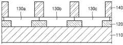
도 1 및 도 2를 참조하면, 컬러필터(100)는 기판(110), 차광층(120), 컬러필터층(130), 제1 격벽(140), 제1 색변환층(150) 및 제2 색변환층(160)을 포함할 수 있다.1 and 2, the
기판(110)은 서로 이격된 제1 화소영역(PA1)과 제2 화소영역(PA2), 및 제1 및 제2 화소영역들(PA1, PA2) 사이에 위치하는 차광영역(BA)을 가질 수 있다. 제1 색변환층(150)은 제1 화소영역(PA1) 상에 배치되고, 입사광(Lib)을 제1 컬러의 광(Lr)으로 변환한다. 제2 색변환층(160)은 제2 화소영역(PA2) 상에 배치되고, 입사광(Lib)을 제2 컬러의 광(Lg)으로 변환할 수 있다.The
컬러필터(100)는 투과층(170)을 더 포함할 수 있다. 기판(110)은 제1 및 제2 화소영역들(PA1, PA2)로부터 이격된 제3 화소영역(PA3)을 더 가질 수 있다. 투과층(170)은 제3 화소영역(PA3) 상에 배치되고 입사광(Lib)을 투과할 수 있다.The
컬러필터(100)는 입사광(Lib)을 수신하고 제1 내지 제3 컬러의 광(Lr, Lg, Lb)을 방출할 수 있다.The
도 1을 참조하면, 기판(110)에는 화소영역(PA)과 차광영역(BA)이 정의된다. 화소영역(PA)은 광이 방출되는 영역으로서, 차광영역(BA)에 의해 둘러싸여 있다. 화소영역(PA)은 방출되는 광의 컬러에 따라 제1 화소영역(PA1), 제2 화소영역(PA2) 및 제3 화소영역(PA3)으로 구분될 수 있다. 예를 들면, 제1 화소영역(PA1)은 제1 컬러의 광(Lr)이 방출되는 영역이고, 제2 화소영역(PA2)은 제2 컬러의 광(Lg)이 방출되는 영역이고, 제3 화소영역(PA3)은 제3 컬러의 광(Lb)이 방출되는 영역일 수 있다. 도 1에 도시된 각 화소영역들(PA1, PA2, PA3)의 배치는 예시적이며, 본 발명은 이에 한정되지 않는다. 제1 내지 제3 화소영역들(PA1, PA2, PA3)은 표시 장치의 화소들의 배열에 대응하여 다양한 형태로 배열될 수 있다.Referring to FIG. 1 , a pixel area PA and a light blocking area BA are defined on the
제1 컬러의 광(Lr)은 적색광이고, 제2 컬러의 광(Lg)은 녹색광이고, 제3 컬러의 광(Lb)은 청색광일 수 있다. 적색광이란 피크 파장이 580 nm 이상 750 nm미만의 광이다. 녹색광이란 피크 파장이 495nm 이상 580nm미만의 광이다. 청색광이란 피크 파장이 400nm 이상 495nm미만의 광이다. 입사광(Lib)은 제3 컬러의 광일 수 있다.The first color light Lr may be red light, the second color light Lg may be green light, and the third color light Lb may be blue light. Red light is light having a peak wavelength of 580 nm or more and less than 750 nm. The green light is light having a peak wavelength of 495 nm or more and less than 580 nm. Blue light is light having a peak wavelength of 400 nm or more and less than 495 nm. The incident light Lib may be light of a third color.
차광영역(BA)은 광이 방출되지 않는 영역으로서, 제1 내지 제3 화소영역들(PA1, PA2, PA3) 사이에 메쉬 형태로 배열될 수 있다.The blocking area BA is an area from which no light is emitted, and may be arranged in a mesh shape between the first to third pixel areas PA1 , PA2 , and PA3 .
기판(110)은 제1 및 제2 색변환층(150, 160)으로부터 방출되는 제1 및 제2 컬러의 광들(Lr, Lg)이 제1 및 제2 화소영역들(PA1, PA2)을 통해 방출될 수 있는 투명 기판이다. 기판(110)의 제3 화소영역(PA3)을 통해 제3 컬러의 광(Lb)이 방출될 수 있다.In the
기판(110)은 통상적으로 사용하는 것이라면 특별히 한정하지 않으나, 예를 들어, 유리, 플라스틱, 수정 등의 절연성 물질로 형성될 수 있다. 기판(110)은 예를 들어, 폴리카보네이트(PC), 폴리에틸렌테레프탈레이트(PET), 폴리에틸렌(PE), 폴리프로필렌(PP), 폴리술폰(PSF), 폴리메틸메타크릴레이트(PMMA), 트리아세틸셀룰로오스(TAC), 시클로올레핀 폴리머(COP), 시클로올레핀 코폴리머(COC) 등의 유기 고분자 물질로 형성될 수 있다. 기판(110)은 기계적 강도, 열적 안정성, 투명성, 표면 평활성, 취급 용이성, 방수성 등을 고려하여 선택될 수 있다.The
차광층(120)은 차광영역(BA) 상에 배치될 수 있다. 차광층(120)은 차광영역(BA) 상에 얇은 막으로 형성될 수 있다. 차광영역(BA)을 통해 광이 방출될 경우, 표시 장치에 빛샘이 발생할 수 있다. 차광층(120)은 차광영역(BA)을 통해 광이 외부로 방출되어 빛샘이 발생하는 것을 방지할 수 있다.The
차광층(120)은 흑색 또는 백색을 포함한 다양한 색상일 수 있다. 차광층(120)이 흑색인 경우, 차광층(120)은 블랙 매트릭스(black matrix)를 포함할 수 있다. 차광층(120)이 백색인 경우, 차광층(120)은 백색 수지 등의 유기 절연 물질을 포함할 수 있다. 차광층(120)은 CrOx 또는 MoOx 등의 불투명 무기 절연 물질이나 블랙 수지 등의 불투명 유기 절연 물질을 포함할 수 있다.The
컬러필터층(130)은 염료 또는 안료를 포함하는 유기물 패턴일 수 있다. 컬러필터층(130)은 제1 컬러필터층(130a), 제2 컬러필터층(130b) 및 제3 컬러필터층(130c)을 포함할 수 있다. 제1 컬러필터층(130a)은 적어도 제1 화소영역(PA1) 상에 배치되고, 제2 컬러필터층(130b)은 적어도 제2 화소영역(PA2) 상에 배치되고, 제3 컬러필터층(130c)은 적어도 제3 화소영역(PA3) 상에 배치될 수 있다. 제1 컬러필터층(130a)은 제1 컬러의 광만을 선택적으로 투과시키고, 제2 컬러필터층(130b)은 제2 컬러의 광만을 선택적으로 투과시키고, 제3 컬러필터층(130c)은 제3 컬러의 광만을 선택적으로 투과시킬 수 있다.The
제1 격벽(140)은 차광영역(BA) 상에 배치되고, 수평 방향으로 제1 색변환층(150), 제2 색변환층(160) 및 투과층(170) 사이에 위치할 수 있다. 제1 격벽(140)은 차광층(120)과 중첩하게 배치될 수 있다. 제1 격벽(140)의 높이(두께)( T1), 즉, 컬러필터층(130)의 상면으로부터 제1 격벽(140)의 상면까지의 거리는 제1 색변환층(150), 제2 색변환층(160) 및 투과층(170)의 높이(두께)(T1')와 같거나 더 클 수 있다. 제1 격벽(140)은 인접하는 제1 색변환층(150), 제2 색변환층(160) 및 투과층(170)의 측면과 컨택할 수 있다. 제1 격벽(140)은 제1 색변환층(150), 제2 색변환층(160) 및 투과층(170)과 컨택하는 계면의 광을 흡수할 수 있다.The
제1 격벽(140)은 제1 내지 제3 컬러의 광(Lr, Lg, Lb)을 산란 및/또는 반사하는 물질을 포함할 수 있다. 제1 격벽(140)은 제1 및 제2 색변환층들(140, 150) 및 투과층(170)으로부터 입사되는 광을 산란 및/또는 반사할 수 있다. 이에 따라 광 흡수 물질을 포함하는 격벽 대비 제1 격벽(140)은 광 흡수에 따른 광 손실을 줄일 수 있다.The
제1 격벽(140)은 제1 색변환층(150)에서 방출되는 제1 컬러의 광(Lr)이 제2 색변환층(160) 또는 투과층(170)으로 조사되거나, 제2 색변환층(160)에서 방출되는 제2 컬러의 광(Lg)이 제1 색변환층(150) 또는 투과층(170)으로 조사되거나, 투과층(170)에서 방출되는 제3 컬러의 광(Lb)이 제1 색변환층(150) 또는 제2 색변환층(160)으로 조사되는 것을 차단할 수 있다.The
제1 색변환층(150)으로부터 방출되어 제1 격벽(140)에서 산란 및/또는 반사된 제1 컬러의 광(Lr)의 대부분, 예를 들어, 절반 이상이 다시 제1 색변환층(150)에 입사될 수 있다. 제1 격벽(140)에서 반사된 제1 컬러의 광(Lr)의 일부가 제2 색변환층(160) 및/또는 투과층(170)에 입사되더라도, 제1 격벽(140)에서 산란 및/또는 반사된 제1 컬러의 광(Lr)의 절반 이상이 제1 색변환층(150)에 재입사된다면 본 실시예의 범위 내에 포함된다. 제2 색변환층(160)으로부터 방출되어 제1 격벽(140)에서 산란 및/또는 반사된 제2 컬러의 광(Lg)의 대부분, 예를 들어, 절반 이상은 다시 제2 색변환층(160)에 입사될 수 있다. 마찬가지로, 제1 격벽(140)에서 반사된 제2 컬러의 광(Lg)의 일부가 제1 색변환층(150) 및/또는 투과층(170)에 입사되더라도, 제1 격벽(140)에서 산란 및/또는 반사된 제2 컬러의 광(Lg)의 절반 이상이 제2 색변환층(160)에 재입사된다면 본 실시예의 범위 내에 포함된다.Most of, for example, half or more of the first color light Lr emitted from the first
제1 색변환층(150), 제2 색변환층(160) 및 투과층(170) 각각은 제1 격벽(140)에 의해 한정되는 오목한 공간 내에 잉크젯 방식으로 형성될 수 있다.Each of the first
제1 색변환층(150)은 제1 화소영역(PA1) 상에 제1 컬러필터층(130a)와 중첩하게 배치되고, 입사광(Lib)을 제1 컬러의 광(Lr)으로 변환하여 기판(110)을 향하여 방출한다. 제1 색변환층(150)은 입사광(Lib)에 의해 여기되어 입사광(Lib)의 파장보다 긴 파장을 갖는 제1 컬러의 광(Lr)을 방출하는 제1 양자점들을 포함할 수 있다.The first
제2 색변환층(160)은 제2 화소영역(PA2) 상에 제2 컬러필터층(130b)와 중첩하게 배치되고, 입사광(Lib)을 제2 컬러의 광(Lg)으로 변환하여 기판(110)을 향하여 방출한다. 제2 색변환층(160)은 입사광(Lib)에 의해 여기되어 입사광(Lib)의 파장보다 긴 파장을 갖는 제2 컬러의 광(Lg)을 방출하는 제2 양자점들을 포함할 수 있다.The second
투과층(170)은 제3 화소영역(PA3) 상에 제3 컬러필터층(130c)와 중첩하게 배치되고, 제3 컬러의 광(Lb)을 투과시켜 기판(110)을 향하여 방출한다.The
일 실시예에서, 도 3에 도시된 바와 같이, 컬러필터(100)는 제1 및 제2 색변환층들(150, 160) 및 투과층(170) 상에 배치되고 평탄한 상부 표면을 제공하는 평탄화층(190)을 더 포함할 수 있다.In one embodiment, as shown in FIG. 3 , the
평탄화층(190)은 제1 및 제2 색변환층(150, 160) 및 투과층(170)을 덮도록 기판(110) 상에 배치될 수 있다. 평탄화층(190)은 입사광(Lib)이 제1 및 제2 색변환층들(150, 160)과 투과층(170)에 조사될 수 있도록 투명할 수 있다. 평탄화층(190)은 폴리이미드 수지, 아크릴 수지, 레지스트 재료 등의 투명 유기 재료로 형성될 수 있다. 평탄화층(190)은 슬릿 코팅법, 스핀 코팅법 등의 습식 공정, 화학 기상 증착법, 진공 증착법 등의 건식 공정 등으로 형성될 수 있다. 본 실시예는 이들의 재료 및 형성 방법으로 한정되지 않는다. 평탄화층(190)은 도 2에 도시된 바와 같이 생략될 수 있음은 물론이다.The
도 4는 본 발명의 일 실시예에 따른 컬러필터의 제1 및 제2 색변환층들과 투과층을 확대한 단면도이다.4 is an enlarged cross-sectional view of first and second color conversion layers and a transmission layer of a color filter according to an embodiment of the present invention.
도 4를 참조하면, 제1 색변환층(150)은 청색 입사광(Lib)을 제1 컬러의 광(Lr)으로 변환한다. 제1 색변환층(150)은 제1 양자점들(152)과 제1 산란입자들(153)이 분산된 제1 감광성 폴리머(151)를 포함할 수 있다.Referring to FIG. 4 , the first
제1 양자점들(152)은 청색 입사광(Lib)에 의해 여기되어 청색광의 파장보다 긴 파장을 갖는 제1 컬러의 광(Lr)을 등방성으로 방출할 수 있다. 제1 감광성 폴리머(151)는 광 투과성을 갖는 유기 물질일 수 있다. 제1 산란입자들(153)은 제1 양자점들(152)에 흡수되지 못한 청색 입사광(Lib)을 산란시켜 더 많은 제1 양자점들(152)이 여기되도록 함으로써, 제1 색변환층(150)의 색변환율을 증가시킬 수 있다. 제1 산란입자들(153)은 예를 들어, 산화 티타늄(TiO2)이나 금속 입자 등일 수 있다. 제1 양자점들(152)은 II족-VI족 화합물, III족-V족 화합물, IV족-VI족 화합물, IV족 화합물, 또는 이들의 조합을 포함할 수 있다.The first
제2 색변환층(160)은 청색 입사광(Lib)을 제2 컬러의 광(Lg)으로 변환한다. 제2 색변환층(160)은 제2 양자점들(162)과 제2 산란입자들(163)이 분산된 제2 감광성 폴리머(161)를 포함할 수 있다.The second
제2 양자점들(162)은 청색 입사광(Lib)에 의해 여기되어 청색광의 파장보다 긴 파장을 갖는 제2 컬러의 광(Lg)을 등방성으로 방출할 수 있다. 제2 감광성 폴리머(161)는 광 투과성을 갖는 유기 물질로서, 제1 감광성 폴리머(151)와 동일한 물질일 수 있다. 제2 산란입자들(163)은 제2 양자점들(162)에 흡수되지 못한 청색 입사광(Lib)을 산란시켜 더 많은 제2 양자점들(162)이 여기되도록 함으로써, 제2 색변환층(160)의 색변환율을 증가시킬 수 있다. 제2 산란입자들(163)은, 예를 들어, 산화 티타늄(TiO2)이나 금속 입자 등일 수 있으며, 제1 산란입자들(153)과 동일한 물질일 수 있다. 제2 양자점들(162)은 II족-VI족 화합물, III족-V족 화합물, IV족-VI족 화합물, IV족 화합물, 또는 이들의 조합을 포함할 수 있다. 제2 양자점들(162)은 제1 양자점들(152)과 동일한 물질일 수 있으며, 이때, 제2 양자점들(162)의 크기는 제1 양자점들(152)의 크기보다 작을 수 있다.The second
투과층(170)은 청색 입사광(Lib)을 투과하여 기판(110) 방향으로 방출할 수 있다. 투과층(170)은 제3 산란입자들(173)이 분산된 제3 감광성 폴리머(171)를 포함할 수 있다. 제3 감광성 폴리머(171)는, 예를 들어, 실리콘 수지, 에폭시 수지 등의 광 투과성을 갖는 유기 물질일 수 있으며, 제1 및 제2 감광성 폴리머(151, 161)와 동일한 물질일 수 있다. 제3 산란입자들(173)은 청색 입사광(Lib)을 산란시켜 방출할 수 있으며, 제1 및 제2 산란입자들(153, 163)과 동일한 물질일 수 있다.The
도 5a 내지 도 5d는 본 발명의 일 실시예에 따른 컬러필터를 제조하는 공정을 개략적으로 나타낸 단면도이다.5A to 5D are cross-sectional views schematically illustrating a process of manufacturing a color filter according to an embodiment of the present invention.
도 5a를 참조하면, 기판(110) 상의 차광영역(BA)에 차광층(120)이 형성될 수 있다. 차광층(120)은 유기 잉크를 분사하여 형성하거나, 금속층을 사진 식각 공정을 통해 패터닝하여 형성할 수 있다. 이에 따라 차광영역(BA)에 개구(OP)가 형성될 수 있다.Referring to FIG. 5A , a
도 5b를 참조하면, 차광층(120) 형성된 기판(110) 상에 컬러필터층(130)이 형성될 수 있다. 컬러필터층(130)은 차광층(120)의 개구(OP) 내에 형성될 수 있다.Referring to FIG. 5B , a
컬러필터층(130)은 컬러 포토레지스트를 기판(110) 상에 도포한 후 선택적으로 패터닝하는 반복 과정에 의해 형성될 수 있다. 예를 들어, 제1 컬러 포토레지스트를 도포한 후 식각하여 제1 컬러필터층(130a)을 형성하고, 다음으로 제2 컬러 포토레지스트를 도포한 후 식각하여 제2 컬러필터층(130b)을 형성하고, 다음으로 제3 컬러 포토레지스트를 도포한 후 식각하여 제3 컬러필터층(130c)을 형성할 수 있다. 제1 내지 제3 컬러필터층(130a 내지 130c)을 형성하는 순서는 제한되지 않는다. 컬러 포토레지스트는 광중합 개시제, 모노머(monomer), 바인더(binder) 등의 광중합형 감광 조성물과, 색상을 구현하는 유기 안료를 포함할 수 있다. 제1 컬러필터층(130a), 제2 컬러필터층(130b), 및 제3 컬러필터층(130c)은 배열 방식에 따라, 예를 들어, 스트라이프형(stripe type), 모자이크형(mosaic type) 등으로 형성될 수 있다.The
도 5b에서 컬러필터층(130)은 차광층(120)의 높이(두께)보다 큰 높이(두께)를 갖게 형성되고 있으나, 본 발명의 실시예는 이에 한정되지 않으며, 예를 들어, 컬러필터층(130)은 차광층(120)의 높이(두께)와 동일하거나 더 낮은 높이(두께)를 갖도록 형성될 수 있다.In FIG. 5B , the
도 5c를 참조하면, 컬러필터층(130)이 형성된 기판(110) 상의 차광영역(BA)에 제1 격벽(140)이 형성될 수 있다. 제1 격벽(140)은 제1 격벽 형성 물질을 기판(110) 상에 도포한 후 패터닝하여 형성될 수 있다. 제1 격벽(140)은 제1 내지 제3 컬러의 광(Lr, Lg, Lb)을 산란 및/또는 반사하는 물질로 단층 또는 다층으로 형성될 수 있다. 제1 격벽(140)의 높이(두께), 및 산란 물질 및/또는 반사 물질의 농도는 적용되는 전자장치에 따라 다르게 설계될 수 있다.Referring to FIG. 5C , a
도 5d를 참조하면, 제1 격벽(140)에 의해 정의된 공간에 제1 색변환층(150), 제2 색변환층(160) 및 투과층(170)이 형성될 수 있다.Referring to FIG. 5D , a first
일 실시예에서, 제1 양자점-포토레지스트를 기판(110) 상에 도포한 후 패터닝하여 제1 화소영역(PA1)에 제1 색변환층(150)이 형성될 수 있다. 다음으로, 제2 양자점-포토레지스트를 기판(110) 상에 도포한 후 패터닝하여 제2 화소영역(PA2)에 제2 색변환층(160)이 형성될 수 있다. 다음으로, 제3 포토레지스트를 기판(110) 상에 도포한 후 패터닝하여 제3 화소영역(PA3)에 투과층(170)이 형성될 수 있다. 제1 및 제2 색변환층들(150, 160)과 투과층(170)을 형성하는 순서는 제한되지 않는다.In one embodiment, the first
다른 실시예에서, 제1 색변환층(150), 제2 색변환층(160) 및 투과층(170)은 잉크젯 도포법에 의해 형성될 수 있다. 제1 격벽(140)의 높이는 제1 색변환층(150), 제2 색변환층(160) 및 투과층(170)이 잉크젯 도포법에 의해 형성될 때 인접한 화소영역으로 넘치지 않도록 설계될 수 있다. 제1 색변환층(150), 제2 색변환층(160) 및 투과층(170)이 잉크젯 도포법에 의해 형성되기 때문에, 포토 공정이 추가되지 않을 수 있으며, 제조 비용이 감소되고, 공정이 단순화될 수 있다.In another embodiment, the first
도 6은 본 발명의 일 실시예에 따른 표시장치의 개략적인 구조를 보이는 단면도이다.6 is a cross-sectional view showing a schematic structure of a display device according to an exemplary embodiment of the present invention.
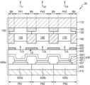
도 6을 참조하면, 표시장치(10)는 표시패널(400) 및 컬러필터(100)을 포함할 수 있다. 표시패널(400) 및 컬러필터(100) 사이에 충진층(500)이 더 구비될 수 있다. 충진층(500)은 투과성의 투명 물질을 포함하는 절연층 또는 에어층일 수 있다.Referring to FIG. 6 , the
표시패널(400)은 제1 및 제3 화소들(PX1, PX2, PX3)을 포함할 수 있다. 제1 화소(PX1)는 발광소자(430) 및 발광소자(430)를 제어하는 제1 화소회로(420a)를 포함하고, 제2 화소(PX2)는 발광소자(430) 및 발광소자(430)를 제어하는 제2 화소회로(420b)를 포함하고, 제3 화소(PX3)는 발광소자(430) 및 발광소자(430)를 제어하는 제3 화소회로(420c)를 포함할 수 있다.The
발광소자(430)는 유기발광소자(OLED)일 수 있다. 발광소자(430)는 제1 내지 제3 화소회로들(420a, 420b, 420c)에 의해 각각 제어되는 광량을 갖는 제3 컬러의 광, 예를 들어, 청색광(Lb)을 각각 방출할 수 있다. 발광소자(430)는 컬러필터(100)의 화소영역(PA)에 대응하여 배치될 수 있다. 제1 내지 제3 화소회로들(420a, 420b, 420c) 각각은 발광소자(430) 하부층인 화소회로층(420)에 배치되고, 발광소자(430)와 적어도 일부 중첩하거나 중첩하지 않을 수 있다.The
컬러필터(100)는 발광소자들(430)로부터 방출되는 제3 컬러의 광(Lb)의 일부를 색 변환시켜 제1 및 제2 컬러의 광들(Lr, Lg)을 외부로 방출하고, 제3 컬러의 광(Lb)의 일부를 색 변환 없이 외부로 방출할 수 있다.The
기판(410)은 유리, 금속 또는 유기물과 같은 물질로 형성될 수 있다.The
기판(410) 상에는 제1 내지 제3 화소들(PX1, PX2, PX3) 각각의 제1 내지 제3 화소회로들(420a, 420b, 420c)이 배치될 수 있다. 제1 내지 제3 화소회로들(420a, 420b, 420c) 각각은 복수의 박막 트랜지스터들과 적어도 하나의 커패시터를 포함할 수 있다. 화소회로층(420)에는 제1 내지 제3 화소회로들(420a, 420b, 420c) 외에 화소들(PX1, PX2, PX3)에 인가되는 신호들 및 구동 전압을 전달하기 위한 신호 라인들 및 전원 라인들이 배치될 수 있다. 제1 화소(PX1)의 발광소자(430)는 컬러필터(100)의 제1 화소영역(PA1)에 대응하게 배치될 수 있다. 제2 화소(PX2)의 발광소자(430)는 컬러필터(100)의 제2 화소영역(PA2)에 대응하게 배치될 수 있다. 제3 화소(PX3)의 발광소자(430)는 컬러필터(100)의 제3 화소영역(PA3)에 대응하게 배치될 수 있다.First to
박막 트랜지스터들은 반도체층, 게이트 전극, 소스 전극, 드레인 전극을 포함할 수 있다. 반도체층은 비정질 실리콘을 포함하거나, 다결정 실리콘을 포함할 수 있다. 반도체층은 산화물 반도체를 포함할 수 있다. 반도체층은 소스 영역, 드레인 영역 및 이들 사이의 채널 영역을 포함할 수 있다.Thin film transistors may include a semiconductor layer, a gate electrode, a source electrode, and a drain electrode. The semiconductor layer may include amorphous silicon or polycrystalline silicon. The semiconductor layer may include an oxide semiconductor. The semiconductor layer may include a source region, a drain region, and a channel region therebetween.
화소회로층(420) 상부에는 발광소자(430)가 구비될 수 있다. 발광소자(430)는 화소전극(431), 중간층(433) 및 대향전극(435)을 포함할 수 있다.A
화소전극(431)은 박막 트랜지스터의 소스 전극 또는 드레인 전극과 연결될 수 있다. 화소전극(431)은 화소 정의막(437)의 개구를 통해 노출되며, 화소전극(431)의 가장자리는 화소 정의막(437)에 의해 덮일 수 있다.The
화소 정의막(437)에 의해 노출된 화소전극들(431) 상에 중간층(433)이 배치될 수 있다. 중간층(433)은 유기 발광층을 포함하며, 유기 발광층은 저분자 유기물 또는 고분자 유기물일 수 있다. 중간층(433)은 유기 발광층 이외에 홀 수송층(HTL; hole transport layer), 홀 주입층(HIL; hole injection layer), 전자 수송층(ETL; electron transport layer) 및 전자 주입층(EIL; electron injection layer) 등과 같은 기능층을 선택적으로 더 포함할 수 있다.An
중간층(433)과 화소 정의막(437)을 덮도록 대향전극(435)이 배치될 수 있다. 대향전극(435)은 투명 또는 반투명 전극일 수 있다. 예를 들어, 대향전극(435)은 일함수가 작은 금속 박막으로 형성될 수 있다. 대향전극(435)은 투광성 도전층(TCO, transparent conductive oxide)을 포함할 수 있다.A
발광소자(430) 상부에는 박막봉지층(440)이 배치될 수 있다. 박막봉지층(440)은 대향전극(435)을 덮으며 기판(410) 전면에 배치될 수 있다. 박막봉지층(440)은 적어도 하나의 무기물로 구비된 무기봉지층 및 적어도 하나의 유기물로 구비된 유기봉지층을 포함할 수 있다. 일 실시예에서, 박막봉지층(440)은 제1무기봉지층/유기봉지층/제2무기봉지층이 적층된 구조로 구비될 수 있다.A thin
컬러필터(100)는 기판(110), 서로 다른 컬러를 형성하기 위한 제1 내지 제3 화소영역들(PA1, PA2, PA3)을 구획하는 차광층(120)과 제1 격벽(140), 및 서로 다른 컬러를 선택적으로 투과하는 제1 내지 제3 컬러필터층들(130a, 130b, 130c)을 포함할 수 있다.The
제1 화소영역(PA1)에는 청색광(Lb)을 적색광(Lr)으로 변환하는 제1 색변환층(150)이 배치되고, 제2 화소영역(PA2)에는 청색광(Lb)을 녹색광(Lg)으로 변환하는 제2 색변환층(160)이 배치되고, 제3 화소영역(C3)에는 청색광(Lb)을 그대로 통과시키는 투과층(170)이 배치될 수 있다.A first
제1 화소(PX1)의 제1 화소회로(420a)에 의해 제어되는 발광소자(430)로부터 방출되는 제3 컬러의 광(Lb)은 제1 색변환층(150)을 통해 제1 컬러의 광(Lr)으로 변환되어, 기판(110)을 통해 외부로 방출된다. 제2 화소(PX2)의 제2 화소회로(420b)에 의해 제어되는 발광소자(430)로부터 방출되는 제3 컬러의 광(Lb)은 제2 색변환층(160)을 통해 제2 컬러의 광(Lg)으로 변환되어, 기판(110)을 통해 외부로 방출된다. 제3 화소(PX3)의 제3 화소회로(420c)에 의해 제어되는 발광소자(430)로부터 방출되는 제3 컬러의 광(Lb)은 투과층(170)을 통해 색변환 없이 기판(110)을 통해 외부로 방출된다.The light Lb of the third color emitted from the
표시패널(400)로부터 방출된 청색광(Lb)의 영상은 컬러필터(100)에 입사되고, 적색광(Lr), 녹색광(Lg), 청색광(Lb)으로 변환됨에 따라 컬러 영상이 표시된다.An image of the blue light Lb emitted from the
본 발명의 실시예는 제1 격벽(140)에 의해 인접하는 색변환층들 및 투과층들 상호 간에 유입되는 광을 차단하여 혼색을 방지함으로써 색일치율 및 색재현성이 향상되고, 광효율이 개선되므로, 소비 전력이 감소될 수 있다.In the embodiment of the present invention, color matching rate and color reproducibility are improved and light efficiency is improved by preventing color mixing by blocking light introduced between adjacent color conversion layers and transmission layers by the
도 7은 본 발명의 다른 실시예에 따른 표시장치의 개략적인 구조를 보이는 단면도이다.7 is a cross-sectional view showing a schematic structure of a display device according to another exemplary embodiment of the present invention.
도 7을 참조하면, 표시장치(20)는 표시패널(400) 및 컬러필터(100a)를 포함할 수 있다. 도 7에 도시된 표시장치(20)는 제1 격벽(140a)이 충진층(500)을 가로질러 박막봉지층(440)의 상부까지 연장된 점에서, 도 6에 도시된 표시장치(10)와 차이가 있다. 이하에서는 도 6의 실시예와 동일한 구성에 대한 설명은 생략한다.Referring to FIG. 7 , the
제1 격벽(140a)의 높이(두께)(T2)는 제1 색변환층(150), 제2 색변환층(160) 및 투과층(170)의 높이(두께)(T21)와 충진층(500)의 두께(T22)의 합보다 크거나 작을 수 있다. 충진층(500)의 두께(T22)는 제1 색변환층(150), 제2 색변환층(160) 및 투과층(170)의 상면과 박막봉지층의 상면 간의 거리일 수 있다.The height (thickness) T2 of the first barrier rib 140a is the height (thickness) T21 of the first
제1 격벽(140a)은 색변환층들 및 투과층들 사이에 위치하여 인접하는 색변환층들 및 투과층들 상호 간에 유입되는 광을 차단할 수 있다. 또한, 제1 격벽(140a)은 충진층(500)에서 제1 내지 제3 화소영역(PA1, PA2, PA3)을 구획함으로써, 발광소자(430)로부터 방출되는 광의 일부(Lp)가 충진층(500)을 투과하여 인접하는 화소영역의 색변환층 또는 투과층으로 입사되는 것을 막을 수 있다. 따라서, 본 발명의 실시예는 화소영역들 간의 혼색이 방지되어 색일치율 및 색재현성이 향상되고, 광효율이 개선되므로, 소비 전력이 감소될 수 있다.The first barrier rib 140a may be positioned between the color conversion layers and the transmissive layers to block light introduced between the adjacent color conversion layers and the transmissive layers. In addition, the first barrier rib 140a partitions the first to third pixel areas PA1 , PA2 , and PA3 in the
도 8은 본 발명의 또 다른 실시예에 따른 표시장치의 개략적인 구조를 보이는 단면도이다.8 is a cross-sectional view showing a schematic structure of a display device according to another exemplary embodiment of the present invention.
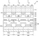
도 8을 참조하면, 표시장치(30)는 표시패널(400a) 및 컬러필터(100)를 포함할 수 있다. 도 8에 도시된 표시장치(20)는 제2 격벽(450)이 박막봉지층(440) 상부에 구비된 점에서, 도 6에 도시된 표시장치(10)와 차이가 있다. 이하에서는 도 6의 실시예와 동일한 구성에 대한 설명은 생략한다.Referring to FIG. 8 , the
표시장치(30)는 컬러필터(100)의 제1 격벽(140) 및 박막봉지층(440) 상부의 제2 격벽(450)을 포함할 수 있다. 제1 격벽(140) 및 제2 격벽(450)은 차광영역(BA)에 대응하게 위치할 수 있다.The
제1 격벽(140)은 색변환층들 및 투과층들 사이에 위치함으로써 색변환층들 및 투과층들 상호 간에 유입되는 광을 차단하여 혼색을 방지할 수 있다.The
제2 격벽(450)은 충진층(500)에서 제1 내지 제3 화소영역(PA1, PA2, PA3)을 구획함으로써, 발광소자(430)로부터 방출되는 광의 일부(Lp)가 박막봉지층(440) 및 충진층(500) 지나 인접하는 화소영역의 색변환층 또는 투과층으로 입사되는 것을 막을 수 있다. 발광소자가 방출하는 광 중 기판(410)의 상면으로부터 고각, 예를 들어, 대략 60 내지 80도 각도로 방출하는 광이 박막봉지층(440) 및 충진층(500)을 지나 인접하는 화소영역의 색변환층 및/또는 투과층으로 입사될 수 있다. 제2 격벽(450)은 발광소자의 고각 성분의 광을 흡수, 반사, 및/또는 산란시켜 인접하는 화소영역의 색변환층 및/또는 투과층으로 입사되는 것을 방지할 수 있다. 따라서, 본 발명의 실시예는 화소영역들 간의 혼색이 방지되어 색일치율 및 색재현성이 향상되고, 광효율이 개선되므로, 소비 전력이 감소될 수 있다.The
제2 격벽(450)은 광의 적어도 일부를 흡수하는 물질, 또는 광 반사 물질, 또는 광 산란 물질을 포함할 수 있다. 제2 격벽(450)은 블랙 매트릭스(black matrix)를 포함할 수 있다. 제2 격벽(450)은 CrOx 또는 MoOx 등의 불투명 무기 절연 물질이나 블랙 수지 등의 불투명 유기 절연 물질을 포함할 수 있다. 제2 격벽(450)은 광 반사율이 높은 예컨대 금속층을 포함할 수 있다. 금속층은 은(Ag), 마그네슘(Mg), 알루미늄(Al), 백금(Pt), 팔라듐(Pd), 금(Au), 니켈(Ni), 네오디뮴(Nd), 이리듐(Ir), 크롬(Cr) 및 이들의 합금 및 화합물으로 이루어진 층일 수 있다. 예컨대, 제2 격벽(450)은 은(Ag)으로 이루어진 층을 포함할 수 있다. 제2 격벽(450)은 복수의 층들이 연속적으로 적층되는 복층 구조를 가질 수 있다. 연속적으로 적층된 층들 중 적어도 하나는 금속층을 포함할 수 있다. 예컨대, 제2 격벽(450)은 ITO와 같은 투명 금속 산화물층과 은(Ag)층을 포함할 수 있다. 일 실시예에서, 제2 격벽(450)은 연속적으로 적층되는 제1 투명 금속 산화물층, 은(Ag)층, 제2 투명 금속 산화물층을 포함할 수 있다. 제2 격벽(450)은 격벽 형성용 물질을 박막봉지층(440) 상에 형성한 후 패터닝하여 형성될 수 있다.The
도 9는 본 발명의 또 다른 실시예에 따른 표시장치의 개략적인 구조를 보이는 단면도이다.9 is a cross-sectional view showing a schematic structure of a display device according to another exemplary embodiment of the present invention.
도 9를 참조하면, 표시장치(40)는 표시패널(400a) 및 컬러필터(100b)를 포함할 수 있다. 도 9에 도시된 표시장치(40)는 제1 격벽(140b)과 제2 격벽(450)이 서로 컨택하는 점에서, 도 8에 도시된 표시장치(30)와 차이가 있다. 이하에서는 도 6 및 도 8의 실시예와 동일한 구성에 대한 설명은 생략한다.Referring to FIG. 9 , the
표시장치(40)는 컬러필터(100b)의 제1 격벽(140b) 및 박막봉지층(440) 상부의 제2 격벽(450)을 포함할 수 있다. 제1 격벽(140b) 및 제2 격벽(450)은 차광영역(BA)에 대응하게 위치할 수 있다.The
제1 격벽(140b)은 박막봉지층(440)의 상부면에 구비된 제2 격벽(450)과 컨택하는 높이(두께)를 가질 수 있다. 제1 격벽(140b)의 높이(두께)는 제1 색변환층(150), 제2 색변환층(160) 및 투과층(170)의 높이(두께)와 충진층(500)의 두께(T22)의 합보다 작을 수 있다. 충진층(500)의 두께는 제1 색변환층(150), 제2 색변환층(160) 및 투과층(170)의 상면과 박막봉지층의 상면 간의 거리일 수 있다.The first barrier rib 140b may have a height (thickness) that contacts the
제1 격벽(140b)은 색변환층들 및 투과층들 사이에 위치함으로써 색변환층들 및 투과층들 상호 간에 유입되는 광을 차단하여 혼색을 방지할 수 있다. 또한, 제1 격벽(140b)은 제2 격벽(450)과 함께 충진층(500)에서 제1 내지 제3 화소영역(PA1, PA2, PA3)을 구획함으로써, 발광소자(430)로부터 방출되는 광의 일부(Lp)가 충진층을 투과하여 인접하는 화소영역의 색변환층 또는 투과층으로 입사되는 것을 막을 수 있다.The first barrier rib 140b is positioned between the color conversion layers and the transmission layers to prevent color mixing by blocking light introduced between the color conversion layers and the transmission layers. In addition, the first barrier rib 140b along with the
따라서, 본 발명의 실시예는 화소영역들 간의 혼색이 방지되어 색일치율 및 색재현성이 향상되고, 광효율이 개선되므로, 소비 전력이 감소될 수 있다.Therefore, in the embodiment of the present invention, color matching rate and color reproducibility are improved by preventing color mixing between pixel areas, and light efficiency is improved, so power consumption can be reduced.
도 10은 본 발명의 또 다른 실시예에 따른 표시장치의 개략적인 구조를 보이는 단면도이다.10 is a cross-sectional view showing a schematic structure of a display device according to another exemplary embodiment of the present invention.
도 10을 참조하면, 표시장치(50)는 표시패널(400a) 및 컬러필터(100c)를 포함할 수 있다. 도 10 도시된 표시장치(50)는 제2 격벽(450)만이 구비된 점에서 도 8에 도시된 표시장치(30)와 차이가 있다. 이하에서는 도 6 및 도 8의 실시예와 동일한 구성에 대한 설명은 생략한다.Referring to FIG. 10 , the
컬러필터(100c)는 기판(110), 서로 다른 컬러를 형성하기 위한 제1 내지 제3 화소영역들(PA1, PA2, PA3)을 구획하는 차광층(120) 및 서로 다른 컬러를 선택적으로 투과하는 제1 내지 제3 컬러필터층(130a, 130b, 130c)을 포함할 수 있다. 컬러필터(100c)는 도 6에 도시된 제1 격벽(140)이 생략된 예이다. 컬러필터(100c)는 제1 및 제2 색변환층들(150, 160) 및 투과층(170) 상에 배치되고 평탄한 상부 표면을 제공하는 평탄화층(190)을 더 포함할 수 있다.The color filter 100c includes the
표시장치(50)는 박막봉지층(440) 상부의 제2 격벽(450)을 포함할 수 있다. 제2 격벽(450)은 차광영역(BA)에 대응하게 위치할 수 있다. 제2 격벽(450)은 충진층(500)에서 제1 내지 제3 화소영역(PA1, PA2, PA3)을 구획함으로써, 발광소자(430)로부터 방출되는 광의 일부(Lp)가 충진층을 투과하여 인접하는 화소영역의 색변환층 또는 투과층으로 입사되는 것을 막을 수 있다. 따라서, 본 발명의 실시예는 화소영역들 간의 혼색이 방지되어 색일치율 및 색재현성이 향상되고, 광효율이 개선되므로, 소비 전력이 감소될 수 있다.The
색변환층은 컬러 필터와 같이 광원으로부터 출사된 광의 일부를 통과시키는 것이 아니라, 광원으로부터 출사된 광으로부터 다른 파장의 광을 생성하기 때문에, 색변환층에서 방출된 광은 다양한 방향으로 조사된다. 또한, 광원으로부터 출사된 광의 일부가 색변환층에서 변환되지 않고 그대로 통과할 수도 있다. 그에 따라, 어느 한 색변환층에서 방출된 제1 컬러의 광에 인접한 색변환층에서 방출된 제2 컬러의 광, 또는 광원으로부터 출사된 제3 컬러의 광이 혼합되어, 혼색이 발생하는 문제가 발생할 수 있다. 혼색으로 인해 색재현성이 오히려 감소하는 문제가 발생할 수 있다.Since the color conversion layer does not pass part of the light emitted from the light source like a color filter, but generates light of a different wavelength from the light emitted from the light source, the light emitted from the color conversion layer is irradiated in various directions. In addition, a part of the light emitted from the light source may pass as it is without being converted in the color conversion layer. Accordingly, there is a problem in that light of a first color emitted from any one color conversion layer is mixed with light of a second color emitted from an adjacent color conversion layer or light of a third color emitted from a light source, resulting in color mixing. can happen Color mixing may cause a problem of rather reducing color reproducibility.
본 발명의 실시예들에 따른 표시장치들은 컬러필터의 색변환층들 및 투과층들 사이의 차광영역에 구비되어 인접하는 화소영역들의 색변환층들 및 투과층들 간에 유입되는 광의 차단을 위한 제1 차단부재로서 제1 격벽을 포함할 수 있다. 본 발명의 실시예들에 따른 표시장치들은 차광영역에 대응하는 표시패널의 박막봉지층 상부에 구비되어 인접하는 화소영역들의 발광소자들로부터 유입되는 광의 차단을 위한 제2 차단부재로서 제2 격벽을 포함할 수 있다. 본 발명의 실시예들에 따른 표시장치들은 제1 격벽 및 제2 격벽 중 적어도 하나를 구비함으로써 인접하는 화소영역 간의 혼색을 방지할 수 있다. 제1 격벽의 두께, 및 산란 물질 및/또는 반사 물질의 농도 중 적어도 하나의 조절에 의해 표시장치를 통해 방출되는 광의 색일치율, 색재현율, 및 광효율이 제어될 수 있다.Display devices according to embodiments of the present invention are provided in a light blocking area between color conversion layers and transmission layers of a color filter to block light introduced between the color conversion layers and transmission layers of adjacent pixel areas. 1 may include a first barrier rib as a blocking member. Display devices according to embodiments of the present invention include a second barrier rib as a second blocking member provided on an upper portion of the thin film encapsulation layer of a display panel corresponding to a light blocking area to block light from light emitting elements of adjacent pixel areas. can include Display devices according to embodiments of the present invention include at least one of the first barrier rib and the second barrier rib, so that color mixing between adjacent pixel areas can be prevented. Color matching rate, color reproduction rate, and light efficiency of light emitted through the display device may be controlled by adjusting at least one of the thickness of the first barrier rib and the concentration of the scattering material and/or the reflective material.
본 발명은 도면에 도시된 실시 예를 참고로 설명되었으나 이는 예시적인 것에 불과하며, 당해 기술 분야에서 통상의 지식을 가진 자라면 이로부터 다양한 변형 및 균등한 다른 실시 예가 가능하다는 점을 이해할 것이다. 따라서, 본 발명의 진정한 기술적 보호 범위는 첨부된 특허청구범위의 기술적 사상에 의하여 정해져야 할 것이다.Although the present invention has been described with reference to the embodiments shown in the drawings, this is merely exemplary, and those skilled in the art will understand that various modifications and equivalent other embodiments are possible therefrom. Therefore, the true technical scope of protection of the present invention should be determined by the technical spirit of the appended claims.
Claims (20)
Translated fromKorean상기 복수의 화소들의 발광소자들로부터 방출되는 광의 파장을 변환시켜 컬러를 형성하는 컬러필터;를 포함하며,
상기 컬러필터는,
상기 화소들에 대응하는 복수의 화소영역들과 상기 화소영역들을 둘러싸는 차광영역을 갖는 제1 기판;
상기 화소영역들 중 제1 화소영역 상에 배치되고, 입사광을 제1 컬러의 광으로 변환하는 제1 색변환층;
상기 화소영역들 중 제2 화소영역 상에 배치되고, 상기 입사광을 제2 컬러의 광으로 변환하는 제2 색변환층; 및
상기 차광영역 상에 배치되고, 상기 제1 색변환층과 상기 제2 색변환층 사이에 위치하고, 산란 물질을 포함하는 제1 격벽;을 포함하고,
상기 표시패널은,
상기 복수의 화소들이 배치된 제2 기판;
상기 제2 기판 상의 박막봉지층; 및
상기 박막봉지층 상의 상기 차광영역에 대응하게 배치된 제2 격벽;을 포함하고,
상기 제1 격벽과 상기 제2 격벽이 컨택하는, 표시장치.a display panel in which a plurality of pixels are arranged, each of the plurality of pixels including a light emitting element; and
A color filter configured to form a color by converting a wavelength of light emitted from the light emitting elements of the plurality of pixels;
The color filter,
a first substrate having a plurality of pixel areas corresponding to the pixels and a light blocking area surrounding the pixel areas;
a first color conversion layer disposed on a first pixel region among the pixel regions and converting incident light into light of a first color;
a second color conversion layer disposed on a second pixel area among the pixel areas and converting the incident light into light of a second color; and
A first barrier rib disposed on the light-blocking area, positioned between the first color conversion layer and the second color conversion layer, and including a scattering material;
The display panel,
a second substrate on which the plurality of pixels are disposed;
a thin film encapsulation layer on the second substrate; and
And a second barrier rib disposed to correspond to the light-shielding region on the thin film encapsulation layer,
The display device, wherein the first barrier rib and the second barrier rib contact each other.
상기 제1 색변환층은 상기 입사광에 의해 여기되어 상기 제1 컬러의 광을 방출하는 제1 양자점들을 포함하고,
상기 제2 색변환층은 상기 입사광에 의해 여기되어 상기 제2 컬러의 광을 방출하는 제2 양자점들을 포함하는, 표시장치.According to claim 1,
The first color conversion layer includes first quantum dots excited by the incident light to emit light of the first color,
The second color conversion layer includes second quantum dots excited by the incident light to emit light of the second color.
상기 제1 기판과 상기 제1 격벽 사이에 배치된 차광층;
상기 제1 기판과 상기 제1 색변환층 사이에 배치되고, 상기 제1 색변환층으로부터 방출되는 상기 제1 컬러의 광을 선택적으로 투과하는 제1 컬러필터층; 및
상기 제1 기판과 상기 제2 색변환층 사이에 배치되고, 상기 제2 색변환층으로부터 방출되는 상기 제2 컬러의 광을 선택적으로 투과하는 제2 컬러필터층;을 더 포함하는 표시장치.According to claim 1,
a light blocking layer disposed between the first substrate and the first barrier rib;
a first color filter layer disposed between the first substrate and the first color conversion layer and selectively transmitting light of the first color emitted from the first color conversion layer; and
The display device further includes a second color filter layer disposed between the first substrate and the second color conversion layer and selectively transmitting the light of the second color emitted from the second color conversion layer.
상기 화소영역들 중 상기 제1 화소영역 및 상기 제2 화소영역으로부터 이격된 제3 화소영역 상에 배치되고, 상기 입사광을 투과하는 투과층;을 더 포함하는 표시장치.The method of claim 1, wherein the color filter,
The display device may further include a transmissive layer disposed on a third pixel area of the pixel areas and spaced apart from the first pixel area and the second pixel area and transmitting the incident light.
상기 제1 격벽은 상기 투과층과 상기 제1 색변환층, 및 상기 투과층과 상기 제2 색변환층 사이에 위치한, 표시장치.According to claim 4,
The first barrier rib is positioned between the transmission layer and the first color conversion layer, and between the transmission layer and the second color conversion layer.
상기 제1 기판과 상기 제1 격벽 사이에 배치된 차광층;
상기 제1 기판과 상기 제1 색변환층 사이에 배치되고, 상기 제1 색변환층으로부터 방출되는 상기 제1 컬러의 광을 선택적으로 투과하는 제1 컬러필터층;
상기 제1 기판과 상기 제2 색변환층 사이에 배치되고, 상기 제2 색변환층으로부터 방출되는 상기 제2 컬러의 광을 선택적으로 투과하는 제2 컬러필터층; 및
상기 제1 기판과 상기 투과층 사이에 배치되고, 상기 투과층으로부터 방출되는 상기 입사광을 선택적으로 투과하는 제3 컬러필터층;을 더 포함하는 표시장치.According to claim 4,
a light blocking layer disposed between the first substrate and the first barrier rib;
a first color filter layer disposed between the first substrate and the first color conversion layer and selectively transmitting light of the first color emitted from the first color conversion layer;
a second color filter layer disposed between the first substrate and the second color conversion layer and selectively transmitting light of the second color emitted from the second color conversion layer; and
and a third color filter layer disposed between the first substrate and the transmission layer and selectively transmitting the incident light emitted from the transmission layer.
상기 입사광은 상기 제1 컬러 및 상기 제2 컬러의 파장보다 짧은 파장을 갖는 제3 컬러의 광인, 표시장치.According to claim 1,
The incident light is light of a third color having a shorter wavelength than the wavelengths of the first color and the second color.
상기 입사광은 청색광이고, 상기 제1 컬러와 상기 제2 컬러는 각각 적색과 녹색인, 표시장치.According to claim 1,
The incident light is blue light, and the first color and the second color are red and green, respectively.
상기 제1 격벽의 두께는 상기 제1 및 제2 색변환층들의 두께보다 큰, 표시장치.According to claim 1,
The thickness of the first barrier rib is greater than the thicknesses of the first and second color conversion layers, the display device.
상기 박막봉지층과 상기 컬러필터 사이의 충진층;을 더 포함하는 표시장치.According to claim 1,
The display device further comprising a filling layer between the thin film encapsulation layer and the color filter.
상기 제1 격벽의 두께는 상기 제1 및 제2 색변환층들의 두께와 상기 충진층의 두께의 합보다 크거나 작은, 표시장치.According to claim 13,
A thickness of the first barrier rib is greater than or less than the sum of the thicknesses of the first and second color conversion layers and the thickness of the filling layer.
Priority Applications (3)
| Application Number | Priority Date | Filing Date | Title |
|---|---|---|---|
| KR1020180110456AKR102572718B1 (en) | 2018-09-14 | 2018-09-14 | Color filter and display device including the same |
| US16/276,675US11092841B2 (en) | 2018-09-14 | 2019-02-15 | Color filter and display apparatus including the same |
| CN201910525389.4ACN110908168B (en) | 2018-09-14 | 2019-06-18 | display screen |
Applications Claiming Priority (1)
| Application Number | Priority Date | Filing Date | Title |
|---|---|---|---|
| KR1020180110456AKR102572718B1 (en) | 2018-09-14 | 2018-09-14 | Color filter and display device including the same |
Publications (2)
| Publication Number | Publication Date |
|---|---|
| KR20200031750A KR20200031750A (en) | 2020-03-25 |
| KR102572718B1true KR102572718B1 (en) | 2023-08-31 |
Family
ID=69772904
Family Applications (1)
| Application Number | Title | Priority Date | Filing Date |
|---|---|---|---|
| KR1020180110456AActiveKR102572718B1 (en) | 2018-09-14 | 2018-09-14 | Color filter and display device including the same |
Country Status (3)
| Country | Link |
|---|---|
| US (1) | US11092841B2 (en) |
| KR (1) | KR102572718B1 (en) |
| CN (1) | CN110908168B (en) |
Families Citing this family (33)
| Publication number | Priority date | Publication date | Assignee | Title |
|---|---|---|---|---|
| KR20200124372A (en)* | 2019-04-23 | 2020-11-03 | 삼성디스플레이 주식회사 | Color control member and display device employing the same |
| CN111063708A (en)* | 2019-11-15 | 2020-04-24 | 深圳市华星光电半导体显示技术有限公司 | Color film substrate and preparation method thereof |
| CN111430425B (en)* | 2020-04-03 | 2023-04-18 | 京东方科技集团股份有限公司 | Display substrate, preparation method thereof and display device |
| KR102839242B1 (en)* | 2020-04-14 | 2025-07-28 | 삼성디스플레이 주식회사 | Display device |
| CN113540325B (en)* | 2020-04-22 | 2023-11-03 | 群创光电股份有限公司 | electronic device |
| KR102858644B1 (en)* | 2020-04-23 | 2025-09-12 | 삼성디스플레이 주식회사 | Display Apparatus |
| JP7369338B2 (en)* | 2020-04-28 | 2023-10-26 | Toppanホールディングス株式会社 | Black matrix substrate and display device equipped with the same |
| KR20210142031A (en)* | 2020-05-14 | 2021-11-24 | 삼성디스플레이 주식회사 | Display apparatus |
| KR102837274B1 (en) | 2020-05-18 | 2025-07-22 | 삼성디스플레이 주식회사 | Method for manufacturing display apparatus |
| KR20210152058A (en)* | 2020-06-04 | 2021-12-15 | 삼성디스플레이 주식회사 | Display device and method for manufacturing the same |
| KR20210153191A (en)* | 2020-06-09 | 2021-12-17 | 삼성디스플레이 주식회사 | Display apparatus |
| KR20210155443A (en)* | 2020-06-15 | 2021-12-23 | 삼성디스플레이 주식회사 | Display apparatus |
| CN111755490B (en)* | 2020-06-22 | 2022-07-29 | 武汉华星光电半导体显示技术有限公司 | Display panel |
| KR20220004872A (en)* | 2020-07-03 | 2022-01-12 | 삼성디스플레이 주식회사 | Display device |
| KR20220021978A (en) | 2020-08-14 | 2022-02-23 | 삼성디스플레이 주식회사 | Display device |
| CN112382733A (en)* | 2020-11-16 | 2021-02-19 | 京东方科技集团股份有限公司 | Flexible display panel, flexible display device and manufacturing method |
| JP7559523B2 (en) | 2020-11-24 | 2024-10-02 | Toppanホールディングス株式会社 | Display device |
| KR20220097772A (en)* | 2020-12-31 | 2022-07-08 | 삼성디스플레이 주식회사 | Display panel, display device including the same, and method for manufacturing the display panel |
| KR20220102680A (en) | 2021-01-13 | 2022-07-21 | 삼성디스플레이 주식회사 | Display panel |
| KR20220105210A (en) | 2021-01-18 | 2022-07-27 | 삼성디스플레이 주식회사 | Light emitting display device |
| KR20220105253A (en)* | 2021-01-19 | 2022-07-27 | 삼성디스플레이 주식회사 | Display apparatus |
| EP4206757A4 (en)* | 2021-03-08 | 2024-04-17 | Samsung Electronics Co., Ltd. | COLOR CONVERTER LAYER AND METHOD FOR MANUFACTURING SAME |
| KR20220125985A (en)* | 2021-03-08 | 2022-09-15 | 삼성전자주식회사 | Color converter layer and manufacturing method thereof |
| KR20220147771A (en)* | 2021-04-27 | 2022-11-04 | 삼성디스플레이 주식회사 | Display Device and Method of Repairing the same |
| EP4199098B1 (en)* | 2021-06-25 | 2024-10-09 | BOE Technology Group Co., Ltd. | Display substrate, display panel, and display apparatus |
| CN114035380B (en)* | 2021-11-01 | 2023-07-14 | 重庆康佳光电技术研究院有限公司 | Color film substrate, display panel and color film substrate preparation method |
| CN114156322B (en)* | 2021-11-29 | 2024-07-16 | 湖北长江新型显示产业创新中心有限公司 | Display panel, manufacturing method thereof and display device |
| KR102853016B1 (en) | 2021-12-28 | 2025-09-01 | 엘지디스플레이 주식회사 | Color conversion plate and display device |
| WO2023132620A1 (en)* | 2022-01-07 | 2023-07-13 | 삼성전자 주식회사 | Display comprising color conversion layer and manufacturing method therefor |
| EP4400904A4 (en)* | 2022-01-19 | 2025-02-19 | Samsung Electronics Co., Ltd. | Display panel and display device comprising same |
| CN115312571A (en)* | 2022-07-28 | 2022-11-08 | 上海天马微电子有限公司 | Display panel and display device |
| WO2024091432A1 (en)* | 2022-10-25 | 2024-05-02 | Applied Materials, Inc. | U-display structure with qd color conversion and methods of manufacture |
| CN120226480A (en)* | 2022-10-28 | 2025-06-27 | 应用材料公司 | Enhanced quantum dot color conversion layer fabrication and integration for micro LED back plates |
Citations (3)
| Publication number | Priority date | Publication date | Assignee | Title |
|---|---|---|---|---|
| JP2005123089A (en)* | 2003-10-17 | 2005-05-12 | Fuji Electric Holdings Co Ltd | Color organic EL display and manufacturing method thereof |
| JP2010146760A (en)* | 2008-12-16 | 2010-07-01 | Fuji Electric Holdings Co Ltd | Color conversion filter panel, panel type organic el emission portion, and color organic el display |
| JP2013254093A (en)* | 2012-06-07 | 2013-12-19 | Sharp Corp | Fluorescent material substrate, display apparatus, and illuminating apparatus |
Family Cites Families (13)
| Publication number | Priority date | Publication date | Assignee | Title |
|---|---|---|---|---|
| US20070077349A1 (en)* | 2005-09-30 | 2007-04-05 | Eastman Kodak Company | Patterning OLED device electrodes and optical material |
| US7791271B2 (en)* | 2006-02-24 | 2010-09-07 | Global Oled Technology Llc | Top-emitting OLED device with light-scattering layer and color-conversion |
| JPWO2013154133A1 (en)* | 2012-04-13 | 2015-12-17 | シャープ株式会社 | Light scatterer, light scatterer film, light scatterer substrate, light scatterer device, light emitting device, display device, and illumination device |
| TWI574055B (en)* | 2013-08-14 | 2017-03-11 | 鴻海精密工業股份有限公司 | Display panel |
| KR102119680B1 (en)* | 2014-02-11 | 2020-06-09 | 삼성디스플레이 주식회사 | Display apparatus and method for driving the same |
| KR102402195B1 (en) | 2015-06-30 | 2022-05-25 | 엘지디스플레이 주식회사 | Organic light emitting display device |
| KR102465382B1 (en)* | 2015-08-31 | 2022-11-10 | 삼성디스플레이 주식회사 | Diplay apparatus and manufacturing method for the same |
| KR20170099011A (en) | 2016-02-22 | 2017-08-31 | 희성전자 주식회사 | Liquid crystal display apparatus |
| KR102291493B1 (en) | 2016-08-11 | 2021-08-20 | 삼성디스플레이 주식회사 | Color filter and display device including the same |
| KR102608507B1 (en) | 2016-08-30 | 2023-12-01 | 삼성디스플레이 주식회사 | Display device and manufacturing method thereof |
| KR102651097B1 (en) | 2016-10-28 | 2024-03-22 | 엘지디스플레이 주식회사 | Light emitting diode display apparatus |
| KR102062587B1 (en)* | 2017-02-08 | 2020-01-13 | 삼성디스플레이 주식회사 | Display device |
| US10690954B2 (en)* | 2017-06-13 | 2020-06-23 | Shenzhen China Star Optoelectronics Technology Co., Ltd. | Liquid crystal display device having transparent stacked layer between quantum-dot color resist layer and encapsulation layer |
- 2018
- 2018-09-14KRKR1020180110456Apatent/KR102572718B1/enactiveActive
- 2019
- 2019-02-15USUS16/276,675patent/US11092841B2/enactiveActive
- 2019-06-18CNCN201910525389.4Apatent/CN110908168B/enactiveActive
Patent Citations (3)
| Publication number | Priority date | Publication date | Assignee | Title |
|---|---|---|---|---|
| JP2005123089A (en)* | 2003-10-17 | 2005-05-12 | Fuji Electric Holdings Co Ltd | Color organic EL display and manufacturing method thereof |
| JP2010146760A (en)* | 2008-12-16 | 2010-07-01 | Fuji Electric Holdings Co Ltd | Color conversion filter panel, panel type organic el emission portion, and color organic el display |
| JP2013254093A (en)* | 2012-06-07 | 2013-12-19 | Sharp Corp | Fluorescent material substrate, display apparatus, and illuminating apparatus |
Also Published As
| Publication number | Publication date |
|---|---|
| CN110908168A (en) | 2020-03-24 |
| US11092841B2 (en) | 2021-08-17 |
| US20200089047A1 (en) | 2020-03-19 |
| CN110908168B (en) | 2024-05-28 |
| KR20200031750A (en) | 2020-03-25 |
Similar Documents
| Publication | Publication Date | Title |
|---|---|---|
| KR102572718B1 (en) | Color filter and display device including the same | |
| KR102717106B1 (en) | Optical filter unit and display device including the same | |
| US20220262865A1 (en) | Display panel, display device and manufacturing method thereof | |
| US9966553B2 (en) | Display apparatus | |
| CN109445164B (en) | Display panel and display device | |
| KR102378879B1 (en) | Flexible color filter substrate and flexible light emitting display apparatus comprising the same | |
| US12032179B2 (en) | Color conversion component and display device | |
| CN112447931A (en) | Display panel and display device | |
| CN112397547A (en) | Display device | |
| KR102820736B1 (en) | Optical filter unit and display device including the same | |
| KR20190014140A (en) | Display device and manufacturing method of the same | |
| CN112614957A (en) | Display panel and display device | |
| CN111584541B (en) | Display device | |
| KR20170026959A (en) | Diplay apparatus and manufacturing method for the same | |
| US20220157891A1 (en) | Display panel, method of manufacturing display panel, and display device | |
| CN108628035B (en) | photoluminescent device | |
| CN110459567B (en) | light-emitting device | |
| CN113327968B (en) | Array substrate and display panel | |
| US20240397801A1 (en) | Display panel and display device | |
| KR20180078142A (en) | Low reflective display device | |
| KR20120021075A (en) | Electrowetting display device | |
| CN220326169U (en) | Display panel and display device | |
| KR20210059863A (en) | Optical filter unit and display device including the same | |
| KR20220126852A (en) | Display device | |
| US12302733B2 (en) | Color conversion substrate having side light blocking member and display device including the same |
Legal Events
| Date | Code | Title | Description |
|---|---|---|---|
| PA0109 | Patent application | St.27 status event code:A-0-1-A10-A12-nap-PA0109 | |
| R18-X000 | Changes to party contact information recorded | St.27 status event code:A-3-3-R10-R18-oth-X000 | |
| PG1501 | Laying open of application | St.27 status event code:A-1-1-Q10-Q12-nap-PG1501 | |
| A201 | Request for examination | ||
| PA0201 | Request for examination | St.27 status event code:A-1-2-D10-D11-exm-PA0201 | |
| D13-X000 | Search requested | St.27 status event code:A-1-2-D10-D13-srh-X000 | |
| D14-X000 | Search report completed | St.27 status event code:A-1-2-D10-D14-srh-X000 | |
| E902 | Notification of reason for refusal | ||
| PE0902 | Notice of grounds for rejection | St.27 status event code:A-1-2-D10-D21-exm-PE0902 | |
| E13-X000 | Pre-grant limitation requested | St.27 status event code:A-2-3-E10-E13-lim-X000 | |
| P11-X000 | Amendment of application requested | St.27 status event code:A-2-2-P10-P11-nap-X000 | |
| P13-X000 | Application amended | St.27 status event code:A-2-2-P10-P13-nap-X000 | |
| E701 | Decision to grant or registration of patent right | ||
| PE0701 | Decision of registration | St.27 status event code:A-1-2-D10-D22-exm-PE0701 | |
| PR0701 | Registration of establishment | St.27 status event code:A-2-4-F10-F11-exm-PR0701 | |
| PR1002 | Payment of registration fee | St.27 status event code:A-2-2-U10-U11-oth-PR1002 Fee payment year number:1 | |
| PG1601 | Publication of registration | St.27 status event code:A-4-4-Q10-Q13-nap-PG1601 |