KR102572514B1 - Semiconductor device and method for manufacturing the same - Google Patents
Semiconductor device and method for manufacturing the sameDownload PDFInfo
- Publication number
- KR102572514B1 KR102572514B1KR1020180044418AKR20180044418AKR102572514B1KR 102572514 B1KR102572514 B1KR 102572514B1KR 1020180044418 AKR1020180044418 AKR 1020180044418AKR 20180044418 AKR20180044418 AKR 20180044418AKR 102572514 B1KR102572514 B1KR 102572514B1
- Authority
- KR
- South Korea
- Prior art keywords
- layer
- mold
- forming
- pattern
- spacer
- Prior art date
- Legal status (The legal status is an assumption and is not a legal conclusion. Google has not performed a legal analysis and makes no representation as to the accuracy of the status listed.)
- Active
Links
Images


Classifications
- H—ELECTRICITY
- H01—ELECTRIC ELEMENTS
- H01L—SEMICONDUCTOR DEVICES NOT COVERED BY CLASS H10
- H01L21/00—Processes or apparatus adapted for the manufacture or treatment of semiconductor or solid state devices or of parts thereof
- H01L21/02—Manufacture or treatment of semiconductor devices or of parts thereof
- H01L21/027—Making masks on semiconductor bodies for further photolithographic processing not provided for in group H01L21/18 or H01L21/34
- H01L21/0271—Making masks on semiconductor bodies for further photolithographic processing not provided for in group H01L21/18 or H01L21/34 comprising organic layers
- H01L21/0273—Making masks on semiconductor bodies for further photolithographic processing not provided for in group H01L21/18 or H01L21/34 comprising organic layers characterised by the treatment of photoresist layers
- H01L21/0274—Photolithographic processes
- G—PHYSICS
- G03—PHOTOGRAPHY; CINEMATOGRAPHY; ANALOGOUS TECHNIQUES USING WAVES OTHER THAN OPTICAL WAVES; ELECTROGRAPHY; HOLOGRAPHY
- G03F—PHOTOMECHANICAL PRODUCTION OF TEXTURED OR PATTERNED SURFACES, e.g. FOR PRINTING, FOR PROCESSING OF SEMICONDUCTOR DEVICES; MATERIALS THEREFOR; ORIGINALS THEREFOR; APPARATUS SPECIALLY ADAPTED THEREFOR
- G03F7/00—Photomechanical, e.g. photolithographic, production of textured or patterned surfaces, e.g. printing surfaces; Materials therefor, e.g. comprising photoresists; Apparatus specially adapted therefor
- G03F7/0002—Lithographic processes using patterning methods other than those involving the exposure to radiation, e.g. by stamping
- H—ELECTRICITY
- H01—ELECTRIC ELEMENTS
- H01L—SEMICONDUCTOR DEVICES NOT COVERED BY CLASS H10
- H01L21/00—Processes or apparatus adapted for the manufacture or treatment of semiconductor or solid state devices or of parts thereof
- H01L21/02—Manufacture or treatment of semiconductor devices or of parts thereof
- H01L21/027—Making masks on semiconductor bodies for further photolithographic processing not provided for in group H01L21/18 or H01L21/34
- H01L21/033—Making masks on semiconductor bodies for further photolithographic processing not provided for in group H01L21/18 or H01L21/34 comprising inorganic layers
- H01L21/0334—Making masks on semiconductor bodies for further photolithographic processing not provided for in group H01L21/18 or H01L21/34 comprising inorganic layers characterised by their size, orientation, disposition, behaviour, shape, in horizontal or vertical plane
- H01L21/0337—Making masks on semiconductor bodies for further photolithographic processing not provided for in group H01L21/18 or H01L21/34 comprising inorganic layers characterised by their size, orientation, disposition, behaviour, shape, in horizontal or vertical plane characterised by the process involved to create the mask, e.g. lift-off masks, sidewalls, or to modify the mask, e.g. pre-treatment, post-treatment
- H—ELECTRICITY
- H01—ELECTRIC ELEMENTS
- H01L—SEMICONDUCTOR DEVICES NOT COVERED BY CLASS H10
- H01L21/00—Processes or apparatus adapted for the manufacture or treatment of semiconductor or solid state devices or of parts thereof
- H01L21/02—Manufacture or treatment of semiconductor devices or of parts thereof
- H01L21/04—Manufacture or treatment of semiconductor devices or of parts thereof the devices having potential barriers, e.g. a PN junction, depletion layer or carrier concentration layer
- H01L21/18—Manufacture or treatment of semiconductor devices or of parts thereof the devices having potential barriers, e.g. a PN junction, depletion layer or carrier concentration layer the devices having semiconductor bodies comprising elements of Group IV of the Periodic Table or AIIIBV compounds with or without impurities, e.g. doping materials
- H01L21/30—Treatment of semiconductor bodies using processes or apparatus not provided for in groups H01L21/20 - H01L21/26
- H01L21/302—Treatment of semiconductor bodies using processes or apparatus not provided for in groups H01L21/20 - H01L21/26 to change their surface-physical characteristics or shape, e.g. etching, polishing, cutting
- H01L21/306—Chemical or electrical treatment, e.g. electrolytic etching
- H01L21/30604—Chemical etching
- H01L21/30608—Anisotropic liquid etching
- H—ELECTRICITY
- H01—ELECTRIC ELEMENTS
- H01L—SEMICONDUCTOR DEVICES NOT COVERED BY CLASS H10
- H01L21/00—Processes or apparatus adapted for the manufacture or treatment of semiconductor or solid state devices or of parts thereof
- H01L21/02—Manufacture or treatment of semiconductor devices or of parts thereof
- H01L21/04—Manufacture or treatment of semiconductor devices or of parts thereof the devices having potential barriers, e.g. a PN junction, depletion layer or carrier concentration layer
- H01L21/18—Manufacture or treatment of semiconductor devices or of parts thereof the devices having potential barriers, e.g. a PN junction, depletion layer or carrier concentration layer the devices having semiconductor bodies comprising elements of Group IV of the Periodic Table or AIIIBV compounds with or without impurities, e.g. doping materials
- H01L21/30—Treatment of semiconductor bodies using processes or apparatus not provided for in groups H01L21/20 - H01L21/26
- H01L21/302—Treatment of semiconductor bodies using processes or apparatus not provided for in groups H01L21/20 - H01L21/26 to change their surface-physical characteristics or shape, e.g. etching, polishing, cutting
- H01L21/306—Chemical or electrical treatment, e.g. electrolytic etching
- H01L21/308—Chemical or electrical treatment, e.g. electrolytic etching using masks
- H01L21/3083—Chemical or electrical treatment, e.g. electrolytic etching using masks characterised by their size, orientation, disposition, behaviour, shape, in horizontal or vertical plane
- H01L21/3086—Chemical or electrical treatment, e.g. electrolytic etching using masks characterised by their size, orientation, disposition, behaviour, shape, in horizontal or vertical plane characterised by the process involved to create the mask, e.g. lift-off masks, sidewalls, or to modify the mask, e.g. pre-treatment, post-treatment
- H—ELECTRICITY
- H01—ELECTRIC ELEMENTS
- H01L—SEMICONDUCTOR DEVICES NOT COVERED BY CLASS H10
- H01L21/00—Processes or apparatus adapted for the manufacture or treatment of semiconductor or solid state devices or of parts thereof
- H01L21/02—Manufacture or treatment of semiconductor devices or of parts thereof
- H01L21/04—Manufacture or treatment of semiconductor devices or of parts thereof the devices having potential barriers, e.g. a PN junction, depletion layer or carrier concentration layer
- H01L21/18—Manufacture or treatment of semiconductor devices or of parts thereof the devices having potential barriers, e.g. a PN junction, depletion layer or carrier concentration layer the devices having semiconductor bodies comprising elements of Group IV of the Periodic Table or AIIIBV compounds with or without impurities, e.g. doping materials
- H01L21/30—Treatment of semiconductor bodies using processes or apparatus not provided for in groups H01L21/20 - H01L21/26
- H01L21/31—Treatment of semiconductor bodies using processes or apparatus not provided for in groups H01L21/20 - H01L21/26 to form insulating layers thereon, e.g. for masking or by using photolithographic techniques; After treatment of these layers; Selection of materials for these layers
- H01L21/3105—After-treatment
- H01L21/311—Etching the insulating layers by chemical or physical means
- H01L21/31144—Etching the insulating layers by chemical or physical means using masks
- H—ELECTRICITY
- H01—ELECTRIC ELEMENTS
- H01L—SEMICONDUCTOR DEVICES NOT COVERED BY CLASS H10
- H01L21/00—Processes or apparatus adapted for the manufacture or treatment of semiconductor or solid state devices or of parts thereof
- H01L21/02—Manufacture or treatment of semiconductor devices or of parts thereof
- H01L21/04—Manufacture or treatment of semiconductor devices or of parts thereof the devices having potential barriers, e.g. a PN junction, depletion layer or carrier concentration layer
- H01L21/18—Manufacture or treatment of semiconductor devices or of parts thereof the devices having potential barriers, e.g. a PN junction, depletion layer or carrier concentration layer the devices having semiconductor bodies comprising elements of Group IV of the Periodic Table or AIIIBV compounds with or without impurities, e.g. doping materials
- H01L21/30—Treatment of semiconductor bodies using processes or apparatus not provided for in groups H01L21/20 - H01L21/26
- H01L21/31—Treatment of semiconductor bodies using processes or apparatus not provided for in groups H01L21/20 - H01L21/26 to form insulating layers thereon, e.g. for masking or by using photolithographic techniques; After treatment of these layers; Selection of materials for these layers
- H01L21/3205—Deposition of non-insulating-, e.g. conductive- or resistive-, layers on insulating layers; After-treatment of these layers
- H01L21/321—After treatment
- H01L21/3213—Physical or chemical etching of the layers, e.g. to produce a patterned layer from a pre-deposited extensive layer
- H—ELECTRICITY
- H01—ELECTRIC ELEMENTS
- H01L—SEMICONDUCTOR DEVICES NOT COVERED BY CLASS H10
- H01L21/00—Processes or apparatus adapted for the manufacture or treatment of semiconductor or solid state devices or of parts thereof
- H01L21/02—Manufacture or treatment of semiconductor devices or of parts thereof
- H01L21/04—Manufacture or treatment of semiconductor devices or of parts thereof the devices having potential barriers, e.g. a PN junction, depletion layer or carrier concentration layer
- H01L21/50—Assembly of semiconductor devices using processes or apparatus not provided for in a single one of the groups H01L21/18 - H01L21/326 or H10D48/04 - H10D48/07 e.g. sealing of a cap to a base of a container
- H01L21/56—Encapsulations, e.g. encapsulation layers, coatings
- H01L21/565—Moulds
- H—ELECTRICITY
- H01—ELECTRIC ELEMENTS
- H01L—SEMICONDUCTOR DEVICES NOT COVERED BY CLASS H10
- H01L21/00—Processes or apparatus adapted for the manufacture or treatment of semiconductor or solid state devices or of parts thereof
- H01L21/70—Manufacture or treatment of devices consisting of a plurality of solid state components formed in or on a common substrate or of parts thereof; Manufacture of integrated circuit devices or of parts thereof
- H01L21/71—Manufacture of specific parts of devices defined in group H01L21/70
- H01L21/768—Applying interconnections to be used for carrying current between separate components within a device comprising conductors and dielectrics
- H01L21/76801—Applying interconnections to be used for carrying current between separate components within a device comprising conductors and dielectrics characterised by the formation and the after-treatment of the dielectrics, e.g. smoothing
- H01L21/76802—Applying interconnections to be used for carrying current between separate components within a device comprising conductors and dielectrics characterised by the formation and the after-treatment of the dielectrics, e.g. smoothing by forming openings in dielectrics
- H01L21/76816—Aspects relating to the layout of the pattern or to the size of vias or trenches
- H—ELECTRICITY
- H01—ELECTRIC ELEMENTS
- H01L—SEMICONDUCTOR DEVICES NOT COVERED BY CLASS H10
- H01L21/00—Processes or apparatus adapted for the manufacture or treatment of semiconductor or solid state devices or of parts thereof
- H01L21/70—Manufacture or treatment of devices consisting of a plurality of solid state components formed in or on a common substrate or of parts thereof; Manufacture of integrated circuit devices or of parts thereof
- H01L21/71—Manufacture of specific parts of devices defined in group H01L21/70
- H01L21/768—Applying interconnections to be used for carrying current between separate components within a device comprising conductors and dielectrics
- H01L21/76838—Applying interconnections to be used for carrying current between separate components within a device comprising conductors and dielectrics characterised by the formation and the after-treatment of the conductors
- H01L21/7684—Smoothing; Planarisation
- H—ELECTRICITY
- H01—ELECTRIC ELEMENTS
- H01L—SEMICONDUCTOR DEVICES NOT COVERED BY CLASS H10
- H01L21/00—Processes or apparatus adapted for the manufacture or treatment of semiconductor or solid state devices or of parts thereof
- H01L21/70—Manufacture or treatment of devices consisting of a plurality of solid state components formed in or on a common substrate or of parts thereof; Manufacture of integrated circuit devices or of parts thereof
- H01L21/71—Manufacture of specific parts of devices defined in group H01L21/70
- H01L21/768—Applying interconnections to be used for carrying current between separate components within a device comprising conductors and dielectrics
- H01L21/76838—Applying interconnections to be used for carrying current between separate components within a device comprising conductors and dielectrics characterised by the formation and the after-treatment of the conductors
- H01L21/76895—Local interconnects; Local pads, as exemplified by patent document EP0896365
- H—ELECTRICITY
- H10—SEMICONDUCTOR DEVICES; ELECTRIC SOLID-STATE DEVICES NOT OTHERWISE PROVIDED FOR
- H10D—INORGANIC ELECTRIC SEMICONDUCTOR DEVICES
- H10D84/00—Integrated devices formed in or on semiconductor substrates that comprise only semiconducting layers, e.g. on Si wafers or on GaAs-on-Si wafers
- H10D84/01—Manufacture or treatment
- H10D84/0123—Integrating together multiple components covered by H10D12/00 or H10D30/00, e.g. integrating multiple IGBTs
- H10D84/0126—Integrating together multiple components covered by H10D12/00 or H10D30/00, e.g. integrating multiple IGBTs the components including insulated gates, e.g. IGFETs
- H10D84/0165—Integrating together multiple components covered by H10D12/00 or H10D30/00, e.g. integrating multiple IGBTs the components including insulated gates, e.g. IGFETs the components including complementary IGFETs, e.g. CMOS devices
- H10D84/0184—Manufacturing their gate sidewall spacers
- H—ELECTRICITY
- H10—SEMICONDUCTOR DEVICES; ELECTRIC SOLID-STATE DEVICES NOT OTHERWISE PROVIDED FOR
- H10D—INORGANIC ELECTRIC SEMICONDUCTOR DEVICES
- H10D84/00—Integrated devices formed in or on semiconductor substrates that comprise only semiconducting layers, e.g. on Si wafers or on GaAs-on-Si wafers
- H10D84/01—Manufacture or treatment
- H10D84/0123—Integrating together multiple components covered by H10D12/00 or H10D30/00, e.g. integrating multiple IGBTs
- H10D84/0126—Integrating together multiple components covered by H10D12/00 or H10D30/00, e.g. integrating multiple IGBTs the components including insulated gates, e.g. IGFETs
- H10D84/0165—Integrating together multiple components covered by H10D12/00 or H10D30/00, e.g. integrating multiple IGBTs the components including insulated gates, e.g. IGFETs the components including complementary IGFETs, e.g. CMOS devices
- H10D84/0193—Integrating together multiple components covered by H10D12/00 or H10D30/00, e.g. integrating multiple IGBTs the components including insulated gates, e.g. IGFETs the components including complementary IGFETs, e.g. CMOS devices the components including FinFETs
- H—ELECTRICITY
- H10—SEMICONDUCTOR DEVICES; ELECTRIC SOLID-STATE DEVICES NOT OTHERWISE PROVIDED FOR
- H10D—INORGANIC ELECTRIC SEMICONDUCTOR DEVICES
- H10D84/00—Integrated devices formed in or on semiconductor substrates that comprise only semiconducting layers, e.g. on Si wafers or on GaAs-on-Si wafers
- H10D84/01—Manufacture or treatment
- H10D84/02—Manufacture or treatment characterised by using material-based technologies
- H10D84/03—Manufacture or treatment characterised by using material-based technologies using Group IV technology, e.g. silicon technology or silicon-carbide [SiC] technology
- H10D84/038—Manufacture or treatment characterised by using material-based technologies using Group IV technology, e.g. silicon technology or silicon-carbide [SiC] technology using silicon technology, e.g. SiGe
- H—ELECTRICITY
- H10—SEMICONDUCTOR DEVICES; ELECTRIC SOLID-STATE DEVICES NOT OTHERWISE PROVIDED FOR
- H10D—INORGANIC ELECTRIC SEMICONDUCTOR DEVICES
- H10D84/00—Integrated devices formed in or on semiconductor substrates that comprise only semiconducting layers, e.g. on Si wafers or on GaAs-on-Si wafers
- H10D84/80—Integrated devices formed in or on semiconductor substrates that comprise only semiconducting layers, e.g. on Si wafers or on GaAs-on-Si wafers characterised by the integration of at least one component covered by groups H10D12/00 or H10D30/00, e.g. integration of IGFETs
- H10D84/82—Integrated devices formed in or on semiconductor substrates that comprise only semiconducting layers, e.g. on Si wafers or on GaAs-on-Si wafers characterised by the integration of at least one component covered by groups H10D12/00 or H10D30/00, e.g. integration of IGFETs of only field-effect components
- H10D84/83—Integrated devices formed in or on semiconductor substrates that comprise only semiconducting layers, e.g. on Si wafers or on GaAs-on-Si wafers characterised by the integration of at least one component covered by groups H10D12/00 or H10D30/00, e.g. integration of IGFETs of only field-effect components of only insulated-gate FETs [IGFET]
- H10D84/85—Complementary IGFETs, e.g. CMOS
- H10D84/853—Complementary IGFETs, e.g. CMOS comprising FinFETs
- H—ELECTRICITY
- H10—SEMICONDUCTOR DEVICES; ELECTRIC SOLID-STATE DEVICES NOT OTHERWISE PROVIDED FOR
- H10D—INORGANIC ELECTRIC SEMICONDUCTOR DEVICES
- H10D89/00—Aspects of integrated devices not covered by groups H10D84/00 - H10D88/00
- H10D89/10—Integrated device layouts
Landscapes
- Engineering & Computer Science (AREA)
- General Physics & Mathematics (AREA)
- Physics & Mathematics (AREA)
- Microelectronics & Electronic Packaging (AREA)
- Manufacturing & Machinery (AREA)
- Computer Hardware Design (AREA)
- Condensed Matter Physics & Semiconductors (AREA)
- Power Engineering (AREA)
- Chemical & Material Sciences (AREA)
- Inorganic Chemistry (AREA)
- Chemical Kinetics & Catalysis (AREA)
- General Chemical & Material Sciences (AREA)
- Internal Circuitry In Semiconductor Integrated Circuit Devices (AREA)
Abstract
Translated fromKorean
Description
Translated fromKorean본 발명은 반도체 소자 및 이의 제조 방법에 관한 것으로, 보다 상세하게는 기판의 집적회로 상의 금속 패턴들을 포함하는 반도체 소자 및 이의 제조 방법에 관한 것이다.The present invention relates to a semiconductor device and a method for manufacturing the same, and more particularly, to a semiconductor device including metal patterns on an integrated circuit of a substrate and a method for manufacturing the same.
반도체 소자는 소형화, 다기능화 및/또는 낮은 제조 단가 등의 특성들로 인하여 많은 전자 산업에서 사용되고 있다. 반도체 소자는 데이터를 저장하는 기억 소자, 데이터를 연산처리 하는 논리 소자, 및 다양한 기능을 동시에 수행할 수 있는 하이브리드(hybrid) 소자 등을 포함할 수 있다.Semiconductor devices are used in many electronic industries due to characteristics such as miniaturization, multifunctionality, and/or low manufacturing cost. The semiconductor device may include a memory device for storing data, a logic device for calculating and processing data, and a hybrid device capable of simultaneously performing various functions.
전자 산업이 고도로 발전함에 따라, 반도체 소자의 고집적화에 대한 요구가 점점 심화되고 있다. 이에 따라, 미세한 패턴들을 정의하는 노광 공정의 공정 마진 감소 등의 여러 문제점들이 발생되어 반도체 소자의 구현이 점점 어려워지고 있다. 또한, 전자 산업의 발전에 의하여 반도체 소자의 고속화에 대한 요구도 점점 심화되고 있다. 이러한 반도체 소자의 고집적화 및/또는 고속화에 대한 요구들을 충족시키기 위하여 다양한 연구들이 수행되고 있다.As the electronic industry develops to a high degree, the demand for high integration of semiconductor devices is gradually intensifying. Accordingly, various problems, such as a decrease in process margin of an exposure process defining fine patterns, occur, making it increasingly difficult to implement a semiconductor device. In addition, with the development of the electronic industry, the demand for high-speed semiconductor devices is increasingly intensifying. Various studies are being conducted to meet the demands for high integration and/or high speed of such semiconductor devices.
본 발명이 해결하고자 하는 과제는, 고집적된 미세한 금속 패턴들을 공정 결함 없이 제조할 수 있는 반도체 소자의 제조 방법 및 이로 제조된 반도체 소자를 제공하는 것이다.An object to be solved by the present invention is to provide a method of manufacturing a semiconductor device capable of manufacturing highly integrated fine metal patterns without process defects and a semiconductor device manufactured therefrom.
본 발명의 개념에 따른, 반도체 소자의 제조 방법은, 기판 상에 하드 마스크막을 형성하는 것; 제1 포토리소그래피 공정을 수행하여, 상기 하드 마스크막 상에 제1 몰드 패턴을 형성하는 것; 상기 기판의 전면 상에 스페이서막을 콘포멀하게 형성하는 것; 제2 포토리소그래피 공정을 수행하여, 상기 스페이서막의 일부를 노출하는 제1 개구부를 갖는 제1 몰드막을 형성하는 것; 상기 제1 개구부에 의해 노출된 상기 스페이서막의 상기 일부를 상기 하드 마스크막의 상면의 일부가 노출될 때까지 이방성 식각하여, 스페이서 패턴을 형성하는 것; 및 상기 스페이서 패턴을 식각 마스크로 상기 하드 마스크막을 패터닝하는 것을 포함할 수 있다.According to the concept of the present invention, a method of manufacturing a semiconductor device includes forming a hard mask film on a substrate; forming a first mold pattern on the hard mask layer by performing a first photolithography process; conformally forming a spacer film on the entire surface of the substrate; forming a first mold layer having a first opening exposing a portion of the spacer layer by performing a second photolithography process; forming a spacer pattern by anisotropically etching the portion of the spacer layer exposed through the first opening until a portion of the upper surface of the hard mask layer is exposed; and patterning the hard mask layer using the spacer pattern as an etch mask.
본 발명의 다른 개념에 따른, 반도체 소자의 제조 방법은, 기판 상의 하드 마스크막 상에 제1 몰드 패턴을 형성하는 것; 상기 기판의 전면 상에 스페이서막을 형성하는 것, 상기 스페이서막은 상기 제1 몰드 패턴의 측벽을 덮는 제1 부분 및 상기 제1 부분으로부터 수평적으로 연장되어 상기 하드 마스크막의 상면을 덮는 제2 부분을 포함하고; 상기 스페이서막의 일부를 노출하는 것; 노출된 상기 일부의 상기 제2 부분을 제거하여 제1 개구부를 형성하는 것; 및 상기 제1 몰드 패턴을 제거하여 제2 개구부를 형성하는 것을 포함할 수 있다. 상기 제2 부분을 제거하는 것은, 상기 일부의 상기 제1 부분을 식각 마스크로 이방성 식각 공정을 수행하는 것을 포함할 수 있다.According to another concept of the present invention, a method of manufacturing a semiconductor device includes forming a first mold pattern on a hard mask film on a substrate; forming a spacer layer on the entire surface of the substrate, the spacer layer including a first portion covering sidewalls of the first mold pattern and a second portion extending horizontally from the first portion and covering an upper surface of the hard mask layer; do; exposing a portion of the spacer film; removing the second portion of the exposed portion to form a first opening; and forming a second opening by removing the first mold pattern. The removing of the second portion may include performing an anisotropic etching process using the first portion of the portion as an etch mask.
본 발명의 또 다른 개념에 따른, 반도체 소자는, 기판 상에서 제1 방향으로 서로 평행하게 연장되는 제1 도전 패턴 및 제2 도전 패턴을 포함할 수 있다. 상기 제1 및 제2 도전 패턴들은 상기 제1 방향과 교차하는 제2 방향으로 제1 거리만큼 서로 이격되고, 상기 제1 도전 패턴은 그의 일 단에 인접하는 제1 부분을 포함하고, 상기 제1 부분은 상기 제1 방향으로 갈수록 그의 폭이 감소하며, 상기 제2 도전 패턴은 상기 제1 부분에 인접하는 제2 부분을 포함하고, 상기 제2 부분은 상기 제1 방향으로 갈수록 그의 폭이 증가하며, 상기 제1 부분과 상기 제2 부분간의 제2 거리는 상기 제1 거리와 실질적으로 동일할 수 있다.According to another concept of the present invention, a semiconductor device may include a first conductive pattern and a second conductive pattern extending parallel to each other in a first direction on a substrate. The first and second conductive patterns are spaced apart from each other by a first distance in a second direction crossing the first direction, the first conductive pattern includes a first portion adjacent to one end thereof, The portion decreases in width in the first direction, the second conductive pattern includes a second portion adjacent to the first portion, and the second portion increases in width in the first direction; , The second distance between the first part and the second part may be substantially equal to the first distance.
본 발명에 따른 반도체 소자의 제조 방법은, 복수개의 포토마스크들을 이용해 기판 상에 고집적된 도전 패턴들을 형성할 수 있다. 나아가, 스페이서막을 도전 패턴들간의 이격 거리를 조절해주는 마스크로 사용함으로써, 도전 패턴들이 자기 정렬적으로 형성될 수 있다. 결과적으로 도전 패턴들간의 쇼트와 같은 공정 리스크를 방지할 수 있다.In the method of manufacturing a semiconductor device according to the present invention, highly integrated conductive patterns may be formed on a substrate using a plurality of photomasks. Furthermore, by using the spacer layer as a mask for adjusting the separation distance between the conductive patterns, the conductive patterns may be formed in a self-aligned manner. As a result, process risks such as short circuits between conductive patterns can be prevented.
도 1은 본 발명의 실시예들에 따른 반도체 소자의 제1 금속층을 정의하는 레이아웃을 나타낸 평면도이다.
도 2, 도 4, 도 6, 도 8, 도 10, 도 12, 도 14, 도 16, 도 18 및 도 20은 본 발명의 실시예들에 따른 반도체 소자를 제조하는 방법을 설명하기 위한 평면도들이다.
도 3a, 도 5a, 도 7a, 도 9a, 도 11a, 도 13a, 도 15a, 도 17a, 도 19a 및 도 21a는 각각 도 2, 도 4, 도 6, 도 8, 도 10, 도 12, 도 14, 도 16, 도 18 및 도 20의 I-I'선에 따른 단면도들이다.
도 3b, 도 5b, 도 7b, 도 9b, 도 11b, 도 13b, 도 15b, 도 17b, 도 19b 및 도 21b는 각각 도 2, 도 4, 도 6, 도 8, 도 10, 도 12, 도 14, 도 16, 도 18 및 도 20의 II- II'선에 따른 단면도들이다.
도 22은 본 발명의 실시예들에 따른 반도체 소자를 설명하기 위한 평면도이다.
도 23a 및 도 23b는 각각 도 22의 I-I'선 및 II-II'선에 따른 단면도들이다.1 is a plan view illustrating a layout defining a first metal layer of a semiconductor device according to example embodiments.
2, 4, 6, 8, 10, 12, 14, 16, 18, and 20 are plan views for explaining a method of manufacturing a semiconductor device according to example embodiments. .
3a, 5a, 7a, 9a, 11a, 13a, 15a, 17a, 19a and 21a are respectively shown in FIGS. 2, 4, 6, 8, 10, 12, and 21a. 14, FIGS. 16, 18 and 20 are cross-sectional views taken along line II'.
3b, 5b, 7b, 9b, 11b, 13b, 15b, 17b, 19b and 21b are shown in FIGS. 2, 4, 6, 8, 10, 12, and 21b, respectively. 14, FIGS. 16, 18 and 20 are cross-sectional views taken along line II- II'.
22 is a plan view for explaining a semiconductor device according to example embodiments.
23A and 23B are cross-sectional views taken along lines II' and II-II' of FIG. 22, respectively.
도 1은 본 발명의 실시예들에 따른 반도체 소자의 제1 금속층을 정의하는 레이아웃을 나타낸 평면도이다.1 is a plan view illustrating a layout defining a first metal layer of a semiconductor device according to example embodiments.
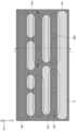
도 1을 참조하면, 제1 금속층을 정의하는 레이아웃(LAY)은 제1 내지 제6 레이아웃 패턴들(LP1-LP6)을 포함할 수 있다. 제1 내지 제6 레이아웃 패턴들(LP1-LP6)은 기판 상에 구현되는 제1 금속층의 도전 패턴들을 정의할 수 있다.Referring to FIG. 1 , the layout LAY defining the first metal layer may include first to sixth layout patterns LP1 to LP6. The first to sixth layout patterns LP1 to LP6 may define conductive patterns of the first metal layer implemented on the substrate.
제1 내지 제6 레이아웃 패턴들(LP1-LP6) 각각은 제2 방향(D2)으로 연장되는 라인 형태를 가질 수 있다. 제1 내지 제6 레이아웃 패턴들(LP1-LP6)은 제1 방향(D1)을 따라 배열될 수 있다. 제1 방향(D1)으로 서로 인접하는 제1 및 제2 레이아웃 패턴들(LP1, LP2) 사이에 제4 레이아웃 패턴(LP4)이 배치될 수 있다. 제1 방향(D1)으로 서로 인접하는 제2 및 제3 레이아웃 패턴들(LP2, LP3) 사이에 제5 레이아웃 패턴(LP5)이 배치될 수 있다. 제1 방향(D1)으로 서로 인접하는 제5 및 제6 레이아웃 패턴들(LP5, LP6) 사이에 제3 레이아웃 패턴(LP3)이 배치될 수 있다.Each of the first to sixth layout patterns LP1 to LP6 may have a line shape extending in the second direction D2 . The first to sixth layout patterns LP1 to LP6 may be arranged along the first direction D1. A fourth layout pattern LP4 may be disposed between first and second layout patterns LP1 and LP2 adjacent to each other in the first direction D1 . A fifth layout pattern LP5 may be disposed between second and third layout patterns LP2 and LP3 adjacent to each other in the first direction D1 . A third layout pattern LP3 may be disposed between fifth and sixth layout patterns LP5 and LP6 adjacent to each other in the first direction D1 .
제1 및 제6 레이아웃 패턴들(LP1, LP6) 사이에 제2 내지 제5 레이아웃 패턴들(LP2-LP5)이 배치될 수 있다. 제1 및 제6 레이아웃 패턴들(LP1, LP6) 각각의 폭은 서로 실질적으로 동일할 수 있다. 제2 내지 제5 레이아웃 패턴들(LP2-LP5) 각각의 폭은 서로 실질적으로 동일할 수 있다. 제1 및 제6 레이아웃 패턴들(LP1, LP6) 각각의 폭은, 제2 내지 제5 레이아웃 패턴들(LP2-LP5) 각각의 폭보다 더 클 수 있다.Second to fifth layout patterns LP2 to LP5 may be disposed between the first and sixth layout patterns LP1 and LP6. Widths of each of the first and sixth layout patterns LP1 and LP6 may be substantially equal to each other. Widths of the second to fifth layout patterns LP2 to LP5 may be substantially equal to each other. A width of each of the first and sixth layout patterns LP1 and LP6 may be greater than that of each of the second to fifth layout patterns LP2 to LP5 .
제2 내지 제5 레이아웃 패턴들(LP2-LP5)은 제1 방향(D1)으로 일정한 피치를 가지고 배열될 수 있다. 일 예로, 제1 방향(D1)으로 서로 인접하는 제2 및 제4 레이아웃 패턴들(LP2, LP4)간의 피치는 제1 피치(P1)일 수 있다. 제1 방향(D1)으로 서로 인접하는 제2 및 제5 레이아웃 패턴들(LP2, LP5)간의 피치는 제2 피치(P2)일 수 있다. 여기서, 제1 피치(P1)와 제2 피치(P2)는 서로 실질적으로 동일할 수 있다. 본 발명에서 사용되는 용어 "피치"는, 제1 패턴의 중심과 상기 제1 패턴에 인접하는 제2 패턴의 중심간의 거리를 의미할 수 있다.The second to fifth layout patterns LP2 - LP5 may be arranged at a constant pitch in the first direction D1 . For example, the pitch between the second and fourth layout patterns LP2 and LP4 adjacent to each other in the first direction D1 may be the first pitch P1. A pitch between the second and fifth layout patterns LP2 and LP5 adjacent to each other in the first direction D1 may be the second pitch P2. Here, the first pitch P1 and the second pitch P2 may be substantially the same. The term "pitch" used in the present invention may mean a distance between the center of a first pattern and the center of a second pattern adjacent to the first pattern.
제2 및 제3 레이아웃 패턴들(LP2, LP3) 상에 컷 패턴들(CUP)이 배치될 수 있다. 컷 패턴들(CUP) 각각은 기판 상에 도전 패턴들을 구현할 때 도전 물질이 채워지지 않는 영역을 정의할 수 있다. 다시 말하면, 컷 패턴들(CUP) 각각은 도전 패턴이 제거될 영역을 정의할 수 있다. 일 예로, 컷 패턴들(CUP)은 서로 실질적으로 동일한 제2 방향으로의 폭을 가질 수 있다.Cut patterns CUP may be disposed on the second and third layout patterns LP2 and LP3. Each of the cut patterns CUP may define a region not filled with a conductive material when implementing the conductive patterns on the substrate. In other words, each of the cut patterns CUP may define a region where the conductive pattern is to be removed. For example, the cut patterns CUP may have substantially the same width as each other in the second direction.
제1 내지 제3 레이아웃 패턴들(LP1, LP2, LP3)은 제1 그룹(CG1)을 구성할 수 있고, 제4 내지 제6 레이아웃 패턴들(LP4, LP5, LP6)은 제2 그룹(CG2)을 구성할 수 있다. 컷 패턴들(CUP)은 제3 그룹(CG3)을 구성할 수 있다.The first to third layout patterns LP1 , LP2 , and LP3 may constitute a first group CG1 , and the fourth to sixth layout patterns LP4 , LP5 , and LP6 may constitute a second group CG2 . can be configured. The cut patterns CUP may constitute a third group CG3.
레이아웃(LAY) 상에서, 제1 내지 제3 그룹들(CG1, CG2, CG3)은 서로 다른 색을 갖도록 표시될 수 있다. 제1 그룹(CG1)의 제1 내지 제3 레이아웃 패턴들(LP1, LP2, LP3)은 제1 색으로 표시될 수 있고, 제2 그룹(CG2)의 제4 내지 제6 레이아웃 패턴들(LP4, LP5, LP6)은 제2 색으로 표시될 수 있으며, 제3 그룹(CG3)의 컷 패턴들(CUP)은 제3 색으로 표시될 수 있다. 상기 제1 내지 제3 색들은 서로 다른 색일 수 있다.On the layout LAY, the first to third groups CG1 , CG2 , and CG3 may be displayed in different colors. The first to third layout patterns LP1 , LP2 , and LP3 of the first group CG1 may be displayed in a first color, and the fourth to sixth layout patterns LP4 of the second group CG2 may be displayed in a first color. LP5 and LP6) may be displayed in a second color, and the cut patterns CUP of the third group CG3 may be displayed in a third color. The first to third colors may be different colors.
제1 그룹(CG1)의 제1 내지 제3 레이아웃 패턴들(LP1, LP2, LP3)을 기초로 제1 포토마스크가 제작될 수 있다. 제2 그룹(CG2)의 제4 내지 제6 레이아웃 패턴들(LP4, LP5, LP6)을 기초로 제2 포토마스크가 제작될 수 있다. 제3 그룹(CG3)의 컷 패턴들(CUP)을 기초로 제3 포토마스크가 제작될 수 있다. 즉, 도 1에 나타난 레이아웃(LAY)을 통하여, 세 장의 포토마스크들이 각각 별개로 제작될 수 있다. 앞서 도 4를 참조하여 설명한 바와 같이, 제1 내지 제3 포토마스크들을 통해 기판 상에 패턴들이 각각 별도로 구현될 수 있다.A first photomask may be manufactured based on the first to third layout patterns LP1 , LP2 , and LP3 of the first group CG1 . A second photomask may be manufactured based on the fourth to sixth layout patterns LP4 , LP5 , and LP6 of the second group CG2 . A third photomask may be manufactured based on the cut patterns CUP of the third group CG3. That is, through the layout (LAY) shown in FIG. 1, three photomasks can be separately manufactured. As described above with reference to FIG. 4 , patterns may be separately implemented on the substrate through the first to third photomasks.
반도체 소자의 집적도가 높아짐에 따라, 기판 상에 구현되는 도전 패턴들 사이의 거리가 매우 가까워지고 있다. 이러한 근접성(Proximity) 때문에, 만약 도전 패턴들을 하나의 포토마스크로 구현할 경우, 기판 상에 원하는 레이아웃(LAY)과 다른 형태를 갖는 왜곡된 패턴들이 인쇄될 수 있다. 따라서 본 실시예에 나타난 바와 같이, 복수의 포토마스크들을 이용하여 도전 패턴들을 구현할 경우, 하나의 포토마스크에 배치되는 이미지 패턴들간의 간격을 넓힐 수 있다. 이로써, 기판 상에 왜곡된 패턴이 인쇄되는 것을 방지할 수 있다.As the degree of integration of semiconductor devices increases, the distance between conductive patterns implemented on a substrate is getting very close. Due to this proximity, if the conductive patterns are implemented with one photomask, distorted patterns having a shape different from a desired layout may be printed on the substrate. Therefore, as shown in the present embodiment, when conductive patterns are implemented using a plurality of photomasks, it is possible to widen the distance between image patterns disposed on one photomask. This can prevent a distorted pattern from being printed on the substrate.
도 2, 도 4, 도 6, 도 8, 도 10, 도 12, 도 14, 도 16, 도 18 및 도 20은 본 발명의 실시예들에 따른 반도체 소자를 제조하는 방법을 설명하기 위한 평면도들이다. 도 3a, 도 5a, 도 7a, 도 9a, 도 11a, 도 13a, 도 15a, 도 17a, 도 19a 및 도 21a는 각각 도 2, 도 4, 도 6, 도 8, 도 10, 도 12, 도 14, 도 16, 도 18 및 도 20의 I-I'선에 따른 단면도들이다. 도 3b, 도 5b, 도 7b, 도 9b, 도 11b, 도 13b, 도 15b, 도 17b, 도 19b 및 도 21b는 각각 도 2, 도 4, 도 6, 도 8, 도 10, 도 12, 도 14, 도 16, 도 18 및 도 20의 II- II'선에 따른 단면도들이다.2, 4, 6, 8, 10, 12, 14, 16, 18, and 20 are plan views for explaining a method of manufacturing a semiconductor device according to example embodiments. . 3a, 5a, 7a, 9a, 11a, 13a, 15a, 17a, 19a and 21a are respectively shown in FIGS. 2, 4, 6, 8, 10, 12, and 21a. 14, FIGS. 16, 18 and 20 are cross-sectional views taken along line II'. 3b, 5b, 7b, 9b, 11b, 13b, 15b, 17b, 19b and 21b are shown in FIGS. 2, 4, 6, 8, 10, 12, and 21b, respectively. 14, FIGS. 16, 18 and 20 are cross-sectional views taken along line II- II'.
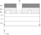
도 2, 도 3a 및 도 3b를 참조하면, 기판(100) 상에 상에 순차적으로 적층된 층간 절연막(IL), 하드 마스크막(HL), 제1 몰드막(ML1) 및 제2 몰드막(ML2)이 형성될 수 있다. 기판(100)은 실리콘 기판, 게르마늄 기판 또는 실리콘-게르마늄 기판일 수 있다. 도시되진 않았지만, 기판(100) 상에 집적회로를 구성하는 복수개의 트랜지스터들이 형성될 수 있다. 층간 절연막(IL)은 상기 복수개의 트랜지스터들을 덮을 수 있다.Referring to FIGS. 2, 3A, and 3B , an interlayer insulating layer (IL), a hard mask layer (HL), a first mold layer (ML1), and a second mold layer (which are sequentially stacked on a substrate 100) ML2) can be formed. The
하드 마스크막(HL)은 제1 몰드막(ML1) 및 층간 절연막(IL)과 식각 선택성을 가질 수 있다. 하드 마스크막(HL)은 유기막, 무기막 또는 이들이 적층된 다중막(multi layers)을 포함할 수 있다. 일 예로, 하드 마스크막(HL)은 실리콘 산화막, 실리콘 질화막 및 금속 질화막 중 적어도 하나를 포함할 수 있다.The hard mask layer HL may have etching selectivity with the first mold layer ML1 and the interlayer insulating layer IL. The hard mask layer HL may include an organic layer, an inorganic layer, or multi layers stacked thereon. For example, the hard mask layer HL may include at least one of a silicon oxide layer, a silicon nitride layer, and a metal nitride layer.
제1 몰드막(ML1)과 제2 몰드막(ML2)은 서로 다른 물질을 포함할 수 있다. 제1 몰드막(ML1) 및 제2 몰드막(ML2) 각각은, 비정질 실리콘막, 비정질 탄소막, SOH(Spin on hardmask) 막, 및 SOC(Spin-on Carbon) 막 중 적어도 하나를 포함할 수 있다.The first mold layer ML1 and the second mold layer ML2 may include different materials. Each of the first mold layer ML1 and the second mold layer ML2 may include at least one of an amorphous silicon layer, an amorphous carbon layer, a spin on hardmask (SOH) layer, and a spin on carbon (SOC) layer. .
제2 몰드막(ML2) 상에 제1 포토레지스트 패턴들(PR1)이 형성될 수 있다. 구체적으로, 제1 포토레지스트 패턴들(PR1)을 형성하는 것은, 제2 몰드막(ML2) 상에 제1 포토레지스트 막을 형성하는 것, 및 도 1을 참조하여 설명한 제1 포토마스크(즉, 제1 그룹(CG1))를 이용해 상기 제1 포토레지스트 막에 제1 포토리소그래피 공정을 수행하는 것을 포함할 수 있다. 상기 제1 포토리소그래피 공정은 노광 및 현상 공정을 수행하는 것을 포함할 수 있다. 일 예로, 상기 제1 포토리소그래피 공정의 노광 공정은 극자외선(EUV) 광원을 이용할 수 있다. 제1 포토레지스트 패턴들(PR1)은 도 1의 레이아웃(LAY)의 제1 내지 제3 레이아웃 패턴들(LP1, LP2, LP3)에 의해 구현된 것이다.First photoresist patterns PR1 may be formed on the second mold layer ML2 . Specifically, forming the first photoresist patterns PR1 includes forming a first photoresist layer on the second mold layer ML2 and using the first photomask (ie, the first photomask described with reference to FIG. 1 ). A first photolithography process may be performed on the first photoresist layer using one group (CG1). The first photolithography process may include performing exposure and development processes. For example, the exposure process of the first photolithography process may use an extreme ultraviolet (EUV) light source. The first photoresist patterns PR1 are implemented by the first to third layout patterns LP1 , LP2 , and LP3 of the layout LAY of FIG. 1 .
도 4, 도 5a 및 도 5b를 참조하면, 제1 포토레지스트 패턴들(PR1)을 식각 마스크로 제2 몰드막(ML2) 및 제1 몰드막(ML1)을 순차적으로 식각하여, 제1 몰드 패턴들(MP1)이 형성될 수 있다.Referring to FIGS. 4, 5A, and 5B , the second mold layer ML2 and the first mold layer ML1 are sequentially etched using the first photoresist patterns PR1 as an etch mask, and the first mold pattern s MP1 may be formed.
구체적으로, 제1 몰드 패턴들(MP1)을 형성하는 것은, 제1 포토레지스트 패턴들(PR1)을 식각 마스크로 제2 몰드막(ML2)을 패터닝하는 것, 패터닝된 제2 몰드막(ML2)을 식각 마스크로 제1 몰드막(ML1)을 패터닝하는 것, 및 잔류하는 제1 포토레지스트 패턴들(PR1) 및 패터닝된 제2 몰드막(ML2)을 제거하는 것을 포함할 수 있다. 도 4의 제1 몰드 패턴들(MP1)의 평면적 형상은, 도 2의 제1 포토레지스트 패턴들(PR1)의 평면적 형성과 실질적으로 동일할 수 있다.Specifically, forming the first mold patterns MP1 includes patterning the second mold layer ML2 using the first photoresist patterns PR1 as an etch mask, and forming the patterned second mold layer ML2. This may include patterning the first mold layer ML1 using the etch mask, and removing the remaining first photoresist patterns PR1 and the patterned second mold layer ML2. A planar shape of the first mold patterns MP1 of FIG. 4 may be substantially the same as that of the first photoresist patterns PR1 of FIG. 2 .
도 6, 도 7a 및 도 7b를 참조하면, 제1 몰드 패턴들(MP1)을 덮는 제3 몰드막(ML3)이 형성될 수 있다. 제3 몰드막(ML3)은, 앞서 제2 몰드막(ML2)의 물질과 동일한 물질을 이용하여 형성될 수 있다.Referring to FIGS. 6 , 7A and 7B , a third mold layer ML3 covering the first mold patterns MP1 may be formed. The third mold layer ML3 may be formed using the same material as the material of the second mold layer ML2 .
제3 몰드막(ML3) 상에 제1 개구부들(OP1)을 갖는 제2 포토레지스트 패턴(PR2)이 형성될 수 있다. 구체적으로, 제2 포토레지스트 패턴들(PR2)을 형성하는 것은, 제3 몰드막(ML3) 상에 제2 포토레지스트 막을 형성하는 것, 및 도 1을 참조하여 설명한 제3 포토마스크(즉, 제3 그룹(CG3))를 이용해 상기 제2 포토레지스트 막에 제2 포토리소그래피 공정을 수행하는 것을 포함할 수 있다. 일 예로, 상기 제2 포토리소그래피 공정의 노광 공정은 ArF 광원을 이용할 수 있다. 제2 포토레지스트 패턴(PR2)의 제1 개구부들(OP1)은 도 1의 레이아웃(LAY)의 컷 패턴들(CUP)에 의해 구현된 것이다.A second photoresist pattern PR2 having first openings OP1 may be formed on the third mold layer ML3 . Specifically, forming the second photoresist patterns PR2 includes forming a second photoresist layer on the third mold layer ML3 and the third photomask (ie, the third photomask described with reference to FIG. 1 ). A second photolithography process may be performed on the second photoresist layer using the group of three (CG3). For example, the exposure process of the second photolithography process may use an ArF light source. The first openings OP1 of the second photoresist pattern PR2 are implemented by the cut patterns CUP of the layout LAY of FIG. 1 .
제2 포토레지스트 패턴(PR2)을 마스크로 제3 몰드막(ML3)을 패터닝할 수 있다. 제1 개구부들(OP1)에 의해 제1 몰드 패턴들(MP1)의 일부들이 노출될 수 있다.The third mold layer ML3 may be patterned using the second photoresist pattern PR2 as a mask. Portions of the first mold patterns MP1 may be exposed through the first openings OP1 .
도 8, 도 9a 및 도 9b를 참조하면, 제1 개구부들(OP1)에 의해 노출된 제1 몰드 패턴들(MP1)의 일부들이 선택적으로 제거될 수 있다. 일 예로, 제1 몰드 패턴(MP1)의 일부가 제거되어, 제1 몰드 패턴(MP1)은 한 쌍의 제1 몰드 패턴들(MP1)로 나뉘어질 수 있다.Referring to FIGS. 8, 9A, and 9B , portions of the first mold patterns MP1 exposed by the first openings OP1 may be selectively removed. For example, by removing a portion of the first mold pattern MP1, the first mold pattern MP1 may be divided into a pair of first mold patterns MP1.
평면적 관점에서, 한 쌍의 제1 몰드 패턴들(MP1)은 서로 마주보는 라운드된 측벽들(RSW)을 포함할 수 있다. 라운드된 측벽들(RSW)은, 제1 몰드 패턴(MP1)의 식각 공정 동안 제1 몰드 패턴(MP1)의 중심부가 제1 몰드 패턴(MP1)의 가장자리부보다 더 식각됨으로써 형성될 수 있다.When viewed from a plan view, the pair of first mold patterns MP1 may include rounded sidewalls RSW facing each other. The rounded sidewalls RSW may be formed by etching the central portion of the first mold pattern MP1 more than the edge portion of the first mold pattern MP1 during the etching process of the first mold pattern MP1 .
상기 식각 공정 이후에 잔류하는 제2 포토레지스트 패턴들(PR2) 및 패터닝된 제3 몰드막(ML3)이 모두 제거될 수 있다.All of the second photoresist patterns PR2 and the patterned third mold layer ML3 remaining after the etching process may be removed.
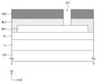
도 10, 도 11a 및 도 11b를 참조하면, 기판(100)의 전면 상에 스페이서막(SL)이 형성될 수 있다. 스페이서막(SL)은 노출된 하드 마스크막(HL)의 표면 및 노출된 제1 몰드 패턴들(MP1)의 표면들을 덮도록 콘포멀하게 형성될 수 있다. 스페이서막(SL)은, 서로 마주보는 라운드된 측벽들(RSW) 사이의 공간을 완전히 채울 수 있다. 일 예로, 스페이서막(SL)은 [TiO, SiCN, SiCON 및 SiN] 중 적어도 하나를 포함할 수 있다.Referring to FIGS. 10 , 11A and 11B , a spacer layer SL may be formed on the entire surface of the
스페이서막(SL)은 제1 몰드 패턴(MP1)의 측벽을 덮는 제1 부분(PA1) 및 제1 부분(PA1)으로부터 하드 마스크막(HL)의 상면 상으로 연장되는 제2 부분(PA2)을 포함할 수 있다. 제1 부분(PA1)은 수직적으로 제1 두께(T1)를 가질 수 있고, 제2 부분(PA2)은 수직적으로 제2 두께(T2)를 가질 수 있다. 제1 두께(T1)는 제2 두께(T2)보다 더 클 수 있다.The spacer layer SL includes a first portion PA1 covering the sidewall of the first mold pattern MP1 and a second portion PA2 extending from the first portion PA1 to the upper surface of the hard mask layer HL. can include The first portion PA1 may vertically have a first thickness T1 , and the second portion PA2 may vertically have a second thickness T2 . The first thickness T1 may be greater than the second thickness T2.
도 12, 도 13a 및 도 13b를 참조하면, 스페이서막(SL)을 덮는 제4 몰드막(ML4)이 형성될 수 있다. 제4 몰드막(ML4)은, 앞서 제2 몰드막(ML2)의 물질과 동일한 물질을 이용하여 형성될 수 있다.Referring to FIGS. 12, 13A, and 13B , a fourth mold layer ML4 covering the spacer layer SL may be formed. The fourth mold layer ML4 may be formed using the same material as the material of the second mold layer ML2 .
제4 몰드막(ML4) 상에 제2 개구부들(OP2)을 갖는 제3 포토레지스트 패턴(PR3)이 형성될 수 있다. 구체적으로, 제3 포토레지스트 패턴(PR3)을 형성하는 것은, 제4 몰드막(ML4) 상에 제3 포토레지스트 막을 형성하는 것, 및 도 1을 참조하여 설명한 제2 포토마스크(즉, 제2 그룹(CG2))를 이용해 상기 제3 포토레지스트 막에 제3 포토리소그래피 공정을 수행하는 것을 포함할 수 있다. 일 예로, 상기 제3 포토리소그래피 공정의 노광 공정은 극자외선(EUV) 광원을 이용할 수 있다. 제3 포토레지스트 패턴(PR3)의 제2 개구부들(OP2)은 도 1의 레이아웃(LAY)의 제4 내지 제6 레이아웃 패턴들(LP4, LP5, LP6)에 의해 구현된 것이다.A third photoresist pattern PR3 having second openings OP2 may be formed on the fourth mold layer ML4 . Specifically, forming the third photoresist pattern PR3 includes forming a third photoresist layer on the fourth mold layer ML4 , and the second photomask (ie, the second photomask described with reference to FIG. 1 ). A third photolithography process may be performed on the third photoresist layer using the group CG2). For example, the exposure process of the third photolithography process may use an extreme ultraviolet (EUV) light source. The second openings OP2 of the third photoresist pattern PR3 are implemented by the fourth to sixth layout patterns LP4 , LP5 , and LP6 of the layout LAY of FIG. 1 .
제3 포토레지스트 패턴(PR3)을 마스크로 제4 몰드막(ML4)을 패터닝할 수 있다. 제2 개구부들(OP2)에 의해 스페이서막(SL)의 일부들이 노출될 수 있다.The fourth mold layer ML4 may be patterned using the third photoresist pattern PR3 as a mask. Portions of the spacer layer SL may be exposed by the second openings OP2 .
도 14, 도 15a 및 도 15b를 참조하면, 제2 개구부들(OP2)에 의해 노출된 스페이서막(SL)을 이방성 식각하여, 제3 개구부들(OP3)을 포함하는 스페이서 패턴(SP)이 형성될 수 있다.14, 15A, and 15B, the spacer layer SL exposed by the second openings OP2 is anisotropically etched to form a spacer pattern SP including the third openings OP3. It can be.
구체적으로, 스페이서막(SL)은 제2 개구부들(OP2)에 의해 하드 마스크막(HL)의 상면이 노출될때까지 이방성 식각될 수 있다. 다시 말하면, 상기 이방성 식각 공정은 제2 개구부들(OP2)에 의해 노출된 스페이서막(SL)의 제2 부분(PA2)이 완전히 제거될 때까지 수행될 수 있다.Specifically, the spacer layer SL may be anisotropically etched until the upper surface of the hard mask layer HL is exposed by the second openings OP2 . In other words, the anisotropic etching process may be performed until the second portion PA2 of the spacer layer SL exposed through the second openings OP2 is completely removed.
상기 이방성 식각 공정 동안, 제2 개구부들(OP2)에 의해 노출된 스페이서막(SL)의 제1 부분(PA1)은 완전히 제거되지 않고 잔류할 수 있다. 잔류하는 제1 부분(PA1)은 수직적으로 제3 두께(T3)를 가질 수 있다. 제3 두께(T3)는 앞서 제1 두께(T1)에서 제2 두께(T2)를 뺀 값과 동일하거나 더 작을 수 있다.During the anisotropic etching process, the first portion PA1 of the spacer layer SL exposed by the second openings OP2 may remain without being completely removed. The remaining first portion PA1 may vertically have a third thickness T3. The third thickness T3 may be equal to or smaller than a value obtained by subtracting the second thickness T2 from the first thickness T1.
상기 이방성 식각 공정 동안, 제2 개구부들(OP2)에 의해 노출된 스페이서막(SL)의 제1 부분(PA1)은 마스크로 사용될 수 있다. 이로써, 제3 개구부들(OP3)은 스페이서막(SL)의 제1 부분(PA1)에 의해 자기 정렬적으로 형성될 수 있다. 제3 개구부들(OP3)은 스페이서막(SL)의 제1 부분(PA1)에 의해 자기 정렬적으로 형성되므로, 제3 개구부들(OP3)의 크기는 제3 포토레지스트 패턴(PR3)에서 정의된 제2 개구부들(OP2)의 크기보다 더 줄어들 수 있다.During the anisotropic etching process, the first portion PA1 of the spacer layer SL exposed by the second openings OP2 may be used as a mask. Thus, the third openings OP3 may be self-aligned by the first portion PA1 of the spacer layer SL. Since the third openings OP3 are self-aligned by the first portion PA1 of the spacer layer SL, the size of the third openings OP3 is defined by the third photoresist pattern PR3. It may be smaller than the size of the second openings OP2 .
도 16, 도 17a 및 도 17b를 참조하면, 스페이서 패턴(SP)을 덮는 제5 몰드막(ML5)이 형성될 수 있다. 제5 몰드막(ML5)은 제3 개구부들(OP3)을 채울 수 있다. 제5 몰드막(ML5)은 비정질 실리콘막 또는 SOH(Spin on hardmask) 막을 포함할 수 있다.Referring to FIGS. 16 , 17A and 17B , a fifth mold layer ML5 covering the spacer pattern SP may be formed. The fifth mold layer ML5 may fill the third openings OP3 . The fifth mold layer ML5 may include an amorphous silicon layer or a spin on hardmask (SOH) layer.
제5 몰드막(ML5)을 형성한 이후, 제1 몰드 패턴들(MP1)의 상면들이 노출될 때까지 평탄화 공정이 수행될 수 있다. 평탄화 공정은 화학 기계적 평탄화(CMP) 공정을 포함할 수 있다.After forming the fifth mold layer ML5 , a planarization process may be performed until upper surfaces of the first mold patterns MP1 are exposed. The planarization process may include a chemical mechanical planarization (CMP) process.
도 18, 도 19a 및 도 19b를 참조하면, 제1 몰드 패턴들(MP1) 및 제5 몰드막(ML5)이 함께 제거될 수 있다. 일 예로, 제1 몰드 패턴들(MP1) 및 제5 몰드막(ML5)은 암모니아수를 포함하는 식각액을 이용한 습식 식각 공정을 통해 동시에 제거될 수 있다. 결과적으로, 하드 마스크막(HL) 상에 스페이서 패턴(SP)만이 잔류할 수 있다.Referring to FIGS. 18 , 19A and 19B , the first mold patterns MP1 and the fifth mold layer ML5 may be removed together. For example, the first mold patterns MP1 and the fifth mold layer ML5 may be simultaneously removed through a wet etching process using an etchant containing ammonia water. As a result, only the spacer pattern SP may remain on the hard mask layer HL.
제1 몰드 패턴들(MP1)이 제거됨으로써, 제4 개구부들(OP4)이 형성될 수 있다. 스페이서 패턴(SP)은 제3 개구부들(OP3) 및 제4 개구부들(OP4)을 포함할 수 있다. 제3 및 제4 개구부들(OP3, OP4)은 하드 마스크막(HL)의 상면을 부분적으로 노출할 수 있다.As the first mold patterns MP1 are removed, fourth openings OP4 may be formed. The spacer pattern SP may include third openings OP3 and fourth openings OP4 . The third and fourth openings OP3 and OP4 may partially expose the upper surface of the hard mask layer HL.
도 20, 도 21a 및 도 21b를 참조하면, 스페이서 패턴(SP)을 식각 마스크로 하드 마스크막(HL)을 패터닝할 수 있다. 패터닝된 하드 마스크막(HL)을 식각 마스크로 층간 절연막(IL)의 상부를 패터닝하여, 층간 절연막(IL)의 상부에 리세스들(RS)이 형성될 수 있다. 스페이서 패턴(SP) 및 패터닝된 하드 마스크막(HL)은 제거될 수 있다.Referring to FIGS. 20 , 21A and 21B , the hard mask layer HL may be patterned using the spacer pattern SP as an etch mask. Recesses RS may be formed on the upper portion of the interlayer insulating layer IL by patterning the upper portion of the interlayer insulating layer IL using the patterned hard mask layer HL as an etch mask. The spacer pattern SP and the patterned hard mask layer HL may be removed.
층간 절연막(IL)의 각각의 리세스들(RS)을 채우는 도전 패턴(CP)이 형성될 수 있다. 도전 패턴(CP)을 형성하는 것은, 리세스들(RS)을 채우는 배리어 막(BL) 및 도전막(CL)을 순차적으로 형성하는 것을 포함할 수 있다. 배리어 막(BL) Ti, TiN, 또는 이들의 조합을 포함할 수 있고, 도전막(CL)은 구리(Cu) 또는 텅스텐(W)을 포함할 수 있다. 다시 말하면, 도전 패턴(CP)을 형성하는 것은 다마신 공정을 포함할 수 있다.A conductive pattern CP filling each of the recesses RS of the interlayer insulating layer IL may be formed. Forming the conductive pattern CP may include sequentially forming a barrier layer BL and a conductive layer CL filling the recesses RS. The barrier layer BL may include Ti, TiN, or a combination thereof, and the conductive layer CL may include copper (Cu) or tungsten (W). In other words, forming the conductive pattern CP may include a damascene process.
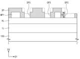
도 20, 도 21a 및 도 21b를 다시 참조하여, 본 발명의 실시예들에 따른 반도체 소자를 구체적으로 설명한다. 기판(100) 상에 층간 절연막(IL)이 제공될 수 있다. 층간 절연막(IL)의 상부에 도전 패턴들(CP)이 제공될 수 있다. 일 예로, 도전 패턴들(CP)은 반도체 소자의 제1 금속층을 구성할 수 있다.Referring back to FIGS. 20 , 21A and 21B , a semiconductor device according to example embodiments will be described in detail. An interlayer insulating layer IL may be provided on the
도전 패턴들(CP)은 제2 방향(D2)으로 서로 평행하게 연장될 수 있다. 도전 패턴들(CP)은 제1 방향(D1)으로 배열될 수 있다. 도전 패턴들(CP)은 제1 내지 제6 도전 패턴들(CP1-CP6)을 포함할 수 있다.The conductive patterns CP may extend parallel to each other in the second direction D2 . The conductive patterns CP may be arranged in the first direction D1. The conductive patterns CP may include first to sixth conductive patterns CP1 to CP6.
제2 방향(D2)으로 연장되는 제5 및 제6 도전 패턴들(CP5, CP6) 사이에 제1 내지 제4 도전 패턴들(CP1-CP4)이 배치될 수 있다. 제5 도전 패턴(CP5)은 접지 전압(VSS)이 인가되는 전원 배선일 수 있다. 제6 도전 패턴(CP6)은 전원 전압(VDD)이 인가되는 전원 배선일 수 있다.The first to fourth conductive patterns CP1 to CP4 may be disposed between the fifth and sixth conductive patterns CP5 and CP6 extending in the second direction D2 . The fifth conductive pattern CP5 may be a power line to which the ground voltage VSS is applied. The sixth conductive pattern CP6 may be a power line to which the power voltage VDD is applied.
제1 도전 패턴(CP1)은 제4 도전 패턴(CP4)과 제1 방향(D1)으로 서로 인접할 수 있다. 제2 도전 패턴(CP2)은 제1 도전 패턴(CP1)과 제1 방향(D1)으로 서로 인접할 수 있다. 제1 도전 패턴(CP1)과 제2 도전 패턴(CP2)은 제1 방향(D1)으로 제1 거리(L1)만큼 서로 이격될 수 있다. 제3 도전 패턴(CP3)은 제1 도전 패턴(CP1)과 제1 방향(D1)으로 서로 인접할 수 있다. 제3 도전 패턴(CP3)과 제2 도전 패턴(CP2)은 제2 방향(D2)을 따라 서로 나란히 배열될 수 있다.The first conductive pattern CP1 may be adjacent to the fourth conductive pattern CP4 in the first direction D1. The second conductive pattern CP2 may be adjacent to the first conductive pattern CP1 in the first direction D1. The first conductive pattern CP1 and the second conductive pattern CP2 may be spaced apart from each other by a first distance L1 in the first direction D1. The third conductive pattern CP3 may be adjacent to the first conductive pattern CP1 in the first direction D1. The third conductive pattern CP3 and the second conductive pattern CP2 may be arranged side by side with each other along the second direction D2.
제1 도전 패턴(CP1)은 그의 일 단에 인접하는 제1 부분(CP1a)을 포함할 수 있다. 제1 도전 패턴(CP1)의 제1 부분(CP1a)은, 제2 방향(D2)으로 갈수록 그의 폭(W1)이 증가할 수 있다. 제1 도전 패턴(CP1)의 제1 부분(CP1a)은 제1 측벽(SW1)을 포함할 수 있다. 평면적 관점에서, 제1 측벽(SW1)은 라운드된 형태를 가질 수 있다.The first conductive pattern CP1 may include a first portion CP1a adjacent to one end thereof. A width W1 of the first portion CP1a of the first conductive pattern CP1 may increase in the second direction D2 . The first portion CP1a of the first conductive pattern CP1 may include the first sidewall SW1. When viewed in plan, the first sidewall SW1 may have a rounded shape.
제2 도전 패턴(CP2)은 그의 일 단에 인접하는 제1 부분(CP2a)을 포함할 수 있다. 제2 도전 패턴(CP2)의 제1 부분(CP2a)은, 제2 방향(D2)으로 갈수록 그의 폭(W2)이 감소할 수 있다. 제2 도전 패턴(CP2)의 제1 부분(CP2a)은 제1 도전 패턴(CP1)의 제1 부분(CP1a)과 인접할 수 있다.The second conductive pattern CP2 may include a first portion CP2a adjacent to one end thereof. The width W2 of the first portion CP2a of the second conductive pattern CP2 may decrease toward the second direction D2. The first portion CP2a of the second conductive pattern CP2 may be adjacent to the first portion CP1a of the first conductive pattern CP1.
제2 도전 패턴(CP2)의 제1 부분(CP2a)은 제2 측벽(SW2)을 포함할 수 있다. 평면적 관점에서, 제2 측벽(SW2)은 라운드된 형태를 가질 수 있다. 제2 측벽(SW2)은 제1 측벽(SW1)을 마주볼 수 있다. 제1 측벽(SW1)과 제2 측벽(SW2)간의 최단 거리는 제2 거리(L2)일 수 있다. 제2 거리(L2)는 제1 거리(L1)와 실질적으로 동일할 수 있다.The first portion CP2a of the second conductive pattern CP2 may include the second sidewall SW2. When viewed from a plan view, the second sidewall SW2 may have a rounded shape. The second sidewall SW2 may face the first sidewall SW1. The shortest distance between the first sidewall SW1 and the second sidewall SW2 may be the second distance L2. The second distance L2 may be substantially equal to the first distance L1.
제2 도전 패턴(CP2)은 그의 타 단에 인접하는 제2 부분(CP2b)을 더 포함할 수 있다. 제2 부분(CP2b)은 제3 측벽(SW3)을 포함할 수 있다. 평면적 관점에서, 제3 측벽(SW3)은 라운드된 형태를 가질 수 있다. 제3 측벽(SW3)은 제2 도전 패턴(CP2)의 중심을 향해 함몰된 형태를 가질 수 있다. 제3 도전 패턴(CP3)은 제3 측벽(SW3)과 마주보는 제4 측벽(SW4)을 포함할 수 있다. 평면적 관점에서, 제4 측벽(SW4)은 라운드된 형태를 가질 수 있다. 제4 측벽(SW4)은 제3 도전 패턴(CP3)의 중심을 향해 함몰된 형태를 가질 수 있다.The second conductive pattern CP2 may further include a second portion CP2b adjacent to the other end thereof. The second portion CP2b may include the third sidewall SW3. When viewed from a plan view, the third sidewall SW3 may have a rounded shape. The third sidewall SW3 may have a shape depressed toward the center of the second conductive pattern CP2. The third conductive pattern CP3 may include a fourth sidewall SW4 facing the third sidewall SW3. When viewed from a plan view, the fourth sidewall SW4 may have a rounded shape. The fourth sidewall SW4 may have a shape depressed toward the center of the third conductive pattern CP3.
제1 내지 제4 도전 패턴들(CP1-CP4)은 일정한 피치를 가지고 제1 방향(D1)으로 배열될 수 있다. 다시 말하면, 제1 방향(D1)으로 서로 인접하는 제1 및 제4 도전 패턴들(CP1, CP4)간의 피치는 제3 피치(P3)일 수 있다. 제1 방향(D1)으로 서로 인접하는 제1 및 제3 도전 패턴들(CP1, CP3)간의 피치는 제4 피치(P4)일 수 있다. 여기서, 제3 피치(P3)와 제4 피치(P4)는 서로 실질적으로 동일할 수 있다.The first to fourth conductive patterns CP1 to CP4 may be arranged in the first direction D1 with a constant pitch. In other words, the pitch between the first and fourth conductive patterns CP1 and CP4 adjacent to each other in the first direction D1 may be the third pitch P3. A pitch between the first and third conductive patterns CP1 and CP3 adjacent to each other in the first direction D1 may be a fourth pitch P4. Here, the third pitch P3 and the fourth pitch P4 may be substantially equal to each other.
제1 내지 제4 도전 패턴들(CP1-CP4) 각각은 제2 방향(D2)으로 연장되는 중심 부분을 포함할 수 있다. 일 예로, 제1 내지 제4 도전 패턴들(CP1-CP4)의 중심 부분들은 서로 실질적으로 동일한 폭을 가질 수 있다. 제1 내지 제4 도전 패턴들(CP1-CP4)은 제1 방향(D1)으로 서로 동일한 거리만큼 이격될 수 있다. 일 예로, 제1 및 제4 도전 패턴들(CP1, CP4)은 제1 방향(D1)으로 제3 거리(L3)만큼 서로 이격될 수 있다. 여기서, 제3 거리(L3)는 제1 거리(L1)와 실질적으로 동일할 수 있다.Each of the first to fourth conductive patterns CP1 to CP4 may include a central portion extending in the second direction D2. For example, central portions of the first to fourth conductive patterns CP1 to CP4 may have substantially the same width as each other. The first to fourth conductive patterns CP1 to CP4 may be spaced apart from each other by the same distance in the first direction D1. For example, the first and fourth conductive patterns CP1 and CP4 may be spaced apart from each other by a third distance L3 in the first direction D1. Here, the third distance L3 may be substantially the same as the first distance L1.
도 22은 본 발명의 실시예들에 따른 반도체 소자를 설명하기 위한 평면도이다. 도 23a 및 도 23b는 각각 도 22의 I-I'선 및 II-II'선에 따른 단면도들이다. 본 실시예에서는, 앞서 도 20, 도 21a 및 도 21b를 참조하여 설명한 것과 중복되는 기술적 특징에 대한 상세한 설명은 생략하고, 차이점에 대해 상세히 설명한다.22 is a plan view for explaining a semiconductor device according to example embodiments. 23A and 23B are cross-sectional views taken along lines II' and II-II' of FIG. 22, respectively. In this embodiment, detailed descriptions of technical features overlapping with those previously described with reference to FIGS. 20, 21A, and 21B will be omitted, and differences will be described in detail.
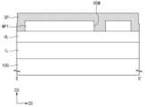
도 22, 도 23a 및 도 23b를 참조하면, 기판(100) 상에 로직 셀이 제공될 수 있다. 구체적으로, 기판(100) 상에 제1 활성 영역(PR) 및 제2 활성 영역(NR)을 정의하는 소자 분리막(ST)이 제공될 수 있다. 일 예로, 제1 활성 영역(PR)은 PMOSFET 영역일 수 있고, 제2 활성 영역(NR)은 NMOSFET 영역일 수 있다. 제1 활성 영역(PR) 및 제2 활성 영역(NR)은 기판(100) 상부의 제2 트렌치(TR2)에 의해 정의될 수 있고, 소자 분리막(ST)이 제2 트렌치(TR2)를 채울 수 있다. 일 예로, 소자 분리막(ST)은 실리콘 산화막을 포함할 수 있다.Referring to FIGS. 22 , 23A and 23B , logic cells may be provided on the
제1 활성 영역(PR) 및 제2 활성 영역(NR)은 소자 분리막(ST)을 사이에 두고 제1 방향(D1)으로 서로 이격될 수 있다. 제1 활성 영역(PR) 및 제2 활성 영역(NR)은 제2 방향(D2)으로 연장될 수 있다.The first active region PR and the second active region NR may be spaced apart from each other in the first direction D1 with the device isolation layer ST interposed therebetween. The first active region PR and the second active region NR may extend in the second direction D2 .
제1 활성 영역(PR) 상에 제2 방향(D2)으로 연장되는 복수의 제1 활성 패턴들(FN1)이 제공될 수 있다. 제2 활성 영역(NR) 상에 제2 방향(D2)으로 연장되는 복수의 제2 활성 패턴들(FN2)이 제공될 수 있다. 제1 및 제2 활성 패턴들(FN1, FN2)은 수직하게 돌출된 기판(100)의 부분들일 수 있다. 제1 및 제2 활성 패턴들(FN1, FN2)은 제1 방향(D1)을 따라 배열될 수 있다.A plurality of first active patterns FN1 extending in the second direction D2 may be provided on the first active region PR. A plurality of second active patterns FN2 extending in the second direction D2 may be provided on the second active region NR. The first and second active patterns FN1 and FN2 may be portions of the
일 예로, 제1 활성 영역(PR) 상에서 세 개의 제1 활성 패턴들(FN1)이 제2 방향(D2)을 따라 나란히 연장될 수 있다. 일 예로, 제2 활성 영역(NR) 상에서 세 개의 제2 활성 패턴들(FN2)이 제2 방향(D2)을 따라 나란히 연장될 수 있다. 그러나, 제1 활성 영역(PR) 상의 제1 활성 패턴들(FN1)의 개수와 형태 및 제2 활성 영역(NR) 상의 제2 활성 패턴들(FN2)의 개수와 형태는 예시적인 것이며, 도시된 형태에 제한되지 않는다.For example, three first active patterns FN1 may extend side by side along the second direction D2 on the first active region PR. For example, three second active patterns FN2 may extend side by side along the second direction D2 on the second active region NR. However, the number and shape of the first active patterns FN1 on the first active region PR and the number and shape of the second active patterns FN2 on the second active region NR are examples, and Not limited to form.
제1 방향(D1)으로 서로 인접하는 한 쌍의 활성 패턴들(FN1, FN2) 사이에 제1 트렌치(TR1)가 정의될 수 있다. 소자 분리막(ST)은 제1 트렌치들(TR1)을 더 채울 수 있다.A first trench TR1 may be defined between a pair of active patterns FN1 and FN2 adjacent to each other in the first direction D1 . The device isolation layer ST may further fill the first trenches TR1.
제1 및 제2 활성 패턴들(FN1, FN2)의 상부들은 소자 분리막(ST)의 상면보다 더 높이 위치할 수 있다. 제1 및 제2 활성 패턴들(FN1, FN2)의 상부들은 소자 분리막(ST)에 비해 수직하게 돌출될 수 있다. 제1 및 제2 활성 패턴들(FN1, FN2) 각각의 상부는 소자 분리막(ST)으로부터 돌출된 핀(fin) 형태를 가질 수 있다.Upper portions of the first and second active patterns FN1 and FN2 may be positioned higher than a top surface of the device isolation layer ST. Upper portions of the first and second active patterns FN1 and FN2 may protrude vertically compared to the device isolation layer ST. An upper portion of each of the first and second active patterns FN1 and FN2 may have a fin shape protruding from the isolation layer ST.
제1 활성 패턴들(FN1) 각각의 상부는 제1 채널 영역들(CH1) 및 제1 소스/드레인 영역들(SD1)을 포함할 수 있다. 제1 소스/드레인 영역들(SD1)은 p형의 불순물 영역들일 수 있다. 제1 채널 영역들(CH1) 각각은, 한 쌍의 제1 소스/드레인 영역들(SD1) 사이에 개재될 수 있다. 제2 활성 패턴들(FN2)의 각각의 상부는 제2 채널 영역들(CH2) 및 제2 소스/드레인 영역들(SD2)을 포함할 수 있다. 제2 소스/드레인 영역들(SD2)은 n형의 불순물 영역들일 수 있다. 제2 채널 영역들(CH2) 각각은 한 쌍의 제2 소스/드레인 영역들(SD2) 사이에 개재될 수 있다.An upper portion of each of the first active patterns FN1 may include first channel regions CH1 and first source/drain regions SD1. The first source/drain regions SD1 may be p-type impurity regions. Each of the first channel regions CH1 may be interposed between a pair of first source/drain regions SD1. An upper portion of each of the second active patterns FN2 may include second channel regions CH2 and second source/drain regions SD2. The second source/drain regions SD2 may be n-type impurity regions. Each of the second channel regions CH2 may be interposed between a pair of second source/drain regions SD2.
제1 및 제2 소스/드레인 영역들(SD1, SD2)은 선택적 에피택시얼 성장 공정으로 형성된 에피택시얼 패턴들일 수 있다. 제1 및 제2 소스/드레인 영역들(SD1, SD2)의 상면들은 제1 및 제2 채널 영역들(CH1, CH2)의 상면들보다 더 높을 수 있다.The first and second source/drain regions SD1 and SD2 may be epitaxial patterns formed through a selective epitaxial growth process. Top surfaces of the first and second source/drain regions SD1 and SD2 may be higher than top surfaces of the first and second channel regions CH1 and CH2 .
일 예로, 제1 소스/드레인 영역들(SD1)은 기판(100)의 반도체 원소의 격자 상수보다 큰 격자 상수를 갖는 반도체 원소를 포함할 수 있다. 이로써, 제1 소스/드레인 영역들(SD1)은 제1 채널 영역들(CH1)에 압축 응력(compressive stress)을 제공할 수 있다. 일 예로, 제2 소스/드레인 영역들(SD2)은 기판(100)의 반도체 원소와 동일한 반도체 원소를 포함할 수 있다. 예를 들어, 제1 소스/드레인 영역들(SD1)은 실리콘-게르마늄을 포함할 수 있고, 제2 소스/드레인 영역들(SD2)은 실리콘을 포함할 수 있다.For example, the first source/drain regions SD1 may include a semiconductor element having a greater lattice constant than the lattice constant of the semiconductor element of the
제1 및 제2 활성 패턴들(FN1, FN2)을 가로지르며 제1 방향(D1)으로 연장되는 게이트 전극들(GE)이 제공될 수 있다. 게이트 전극들(GE)은 제2 방향(D2)으로 서로 이격될 수 있다.Gate electrodes GE may be provided to cross the first and second active patterns FN1 and FN2 and extend in the first direction D1. The gate electrodes GE may be spaced apart from each other in the second direction D2.
게이트 전극들(GE)은 제1 및 제2 채널 영역들(CH1, CH2)과 수직적으로 중첩될 수 있다. 각각의 게이트 전극들(GE)은, 제1 및 제2 채널 영역들(CH1, CH2) 각각의 상면 및 양 측벽들 상에 제공될 수 있다 (도 23a 참조). 일 예로, 게이트 전극들(GE)은 도전성 금속 질화물(예를 들면, 티타늄 질화물 또는 탄탈늄 질화물) 및 금속 물질(예를 들면, 티타늄, 탄탈늄, 텅스텐, 구리 또는 알루미늄) 중 적어도 하나를 포함할 수 있다.The gate electrodes GE may vertically overlap the first and second channel regions CH1 and CH2. Each of the gate electrodes GE may be provided on a top surface and both sidewalls of each of the first and second channel regions CH1 and CH2 (see FIG. 23A ). For example, the gate electrodes GE may include at least one of a conductive metal nitride (eg, titanium nitride or tantalum nitride) and a metal material (eg, titanium, tantalum, tungsten, copper, or aluminum). can
게이트 전극들(GE) 각각의 양 측벽들 상에 한 쌍의 게이트 스페이서들(GS)이 배치될 수 있다. 게이트 스페이서들(GS)은 게이트 전극들(GE)을 따라 제1 방향(D1)으로 연장될 수 있다. 게이트 스페이서들(GS)의 상면들은 게이트 전극들(GE)의 상면들보다 높을 수 있다. 게이트 스페이서들(GS)의 상면들은 후술할 게이트 캐핑막(GP)의 상면과 공면을 이룰 수 있다. 일 예로, 게이트 스페이서들(GS)은 SiCN, SiCON 및 SiN 중 적어도 하나를 포함할 수 있다. 다른 예로, 게이트 스페이서들(GS)은 SiCN, SiCON 및 SiN 중 적어도 두 개로 이루어진 다중 막(multi-layer)을 포함할 수 있다.A pair of gate spacers GS may be disposed on both sidewalls of each of the gate electrodes GE. The gate spacers GS may extend in the first direction D1 along the gate electrodes GE. Top surfaces of the gate spacers GS may be higher than top surfaces of the gate electrodes GE. Top surfaces of the gate spacers GS may be coplanar with a top surface of a gate capping layer GP, which will be described later. For example, the gate spacers GS may include at least one of SiCN, SiCON, and SiN. As another example, the gate spacers GS may include a multi-layer made of at least two of SiCN, SiCON, and SiN.
게이트 전극들(GE)과 제1 및 제2 채널 영역들(CH1, CH2) 사이에 게이트 유전막들(GI)이 개재될 수 있다. 각각의 게이트 유전막들(GI)은 각각의 게이트 전극들(GE)의 바닥면을 따라 연장될 수 있다. 각각의 게이트 유전막들(GI)은 제1 및 제2 채널 영역들(CH1, CH2) 각각의 상면 및 양 측벽들을 덮을 수 있다. 게이트 유전막들(GI)은 실리콘 산화막보다 유전상수가 높은 고유전율 물질을 포함할 수 있다.Gate dielectric layers GI may be interposed between the gate electrodes GE and the first and second channel regions CH1 and CH2. Each of the gate dielectric layers GI may extend along the bottom surface of each of the gate electrodes GE. Each of the gate dielectric layers GI may cover top surfaces and both sidewalls of each of the first and second channel regions CH1 and CH2 . The gate dielectric layers GI may include a high-k material having a higher dielectric constant than a silicon oxide layer.
각각의 게이트 전극들(GE) 상에 게이트 캐핑막(GP)이 제공될 수 있다. 게이트 캐핑막들(GP)은 게이트 전극들(GE)을 따라 제1 방향(D1)으로 연장될 수 있다. 게이트 캐핑막들(GP)은 후술하는 제1 및 제2 층간 절연막들(IL1, IL2)에 대하여 식각 선택성이 있는 물질을 포함할 수 있다. 구체적으로, 게이트 캐핑막들(GP)은 SiON, SiCN, SiCON 및 SiN 중 적어도 하나를 포함할 수 있다.A gate capping layer GP may be provided on each of the gate electrodes GE. The gate capping layers GP may extend in the first direction D1 along the gate electrodes GE. The gate capping layers GP may include a material having etch selectivity with respect to the first and second interlayer insulating layers IL1 and IL2 described later. Specifically, the gate capping layers GP may include at least one of SiON, SiCN, SiCON, and SiN.
기판(100) 상에 순차적으로 적층된 제1 층간 절연막(IL1), 제2 층간 절연막(IL2) 및 제3 층간 절연막(IL3)이 제공될 수 있다. 제1 내지 제3 층간 절연막들(IL1, IL2, IL3) 각각은 실리콘 산화막 또는 실리콘 산화질화막을 포함할 수 있다.A first interlayer insulating layer IL1 , a second interlayer insulating layer IL2 , and a third interlayer insulating layer IL3 sequentially stacked on the
한 쌍의 게이트 전극들(GE) 사이에, 제1 및 제2 층간 절연막들(IL1, IL2)을 관통하여 제1 및 제2 소스/드레인 영역들(SD1, SD2)과 전기적으로 연결되는 적어도 하나의 활성 콘택(AC)이 제공될 수 있다. 적어도 하나의 게이트 전극(GE) 상에, 제2 층간 절연막(IL2) 및 게이트 캐핑막(GP)을 관통하여 적어도 하나의 게이트 전극(GE)과 전기적으로 연결되는 적어도 하나의 게이트 콘택(GC)이 제공될 수 있다.At least one electrically connected to the first and second source/drain regions SD1 and SD2 through the first and second interlayer insulating films IL1 and IL2 between the pair of gate electrodes GE. An active contact AC of may be provided. On the at least one gate electrode GE, at least one gate contact GC electrically connected to the at least one gate electrode GE through the second interlayer insulating layer IL2 and the gate capping layer GP is formed. can be provided.
활성 콘택들(AC) 및 게이트 콘택들(GC)은 서로 동일한 도전 물질을 포함할 수 있다. 활성 콘택들(AC) 및 게이트 콘택들(GC)은 금속 물질, 예를 들어 알루미늄, 구리, 텅스텐, 몰리브데늄 및 코발트 중 적어도 하나를 포함할 수 있다.Active contacts AC and gate contacts GC may include the same conductive material as each other. Active contacts AC and gate contacts GC may include at least one of a metal material, eg, aluminum, copper, tungsten, molybdenum, and cobalt.
제3 층간 절연막(IL3) 내에 도전 패턴들(CP)이 제공될 수 있다. 도전 패턴들(CP)은 본 실시예의 반도체 소자의 제1 금속층을 구성할 수 있다. 도전 패턴들(CP)에 관한 구체적인 설명은, 앞서 도 20, 도 21a 및 도 21b를 참조하여 설명한 도전 패턴들(CP)과 실질적으로 동일할 수 있다.Conductive patterns CP may be provided in the third interlayer insulating layer IL3 . The conductive patterns CP may form the first metal layer of the semiconductor device according to the present exemplary embodiment. A detailed description of the conductive patterns CP may be substantially the same as the conductive patterns CP previously described with reference to FIGS. 20 , 21A and 21B .
도전 패턴들(CP) 중 몇몇은 비아(VI)를 포함할 수 있다. 비아(VI)를 통하여, 도전 패턴(CP)이 활성 콘택(AC)과 전기적으로 연결될 수 있다. 비아(VI)를 통하여, 도전 패턴(CP)이 게이트 콘택(GC)과 전기적으로 연결될 수 있다.Some of the conductive patterns CP may include vias VI. The conductive pattern CP may be electrically connected to the active contact AC through the via VI. The conductive pattern CP may be electrically connected to the gate contact GC through the via VI.
도시되진 않았지만, 제1 금속층 상에 추가적인 금속층들이 제공될 수 있다. 제1 금속층 및 추가적인 금속층들을 통하여, 로직 셀이 다른 로직 셀들과 연결되어 설계된 회로를 구성할 수 있다.Although not shown, additional metal layers may be provided on the first metal layer. Through the first metal layer and the additional metal layers, a logic cell may be connected to other logic cells to form a designed circuit.
이상, 첨부된 도면들을 참조하여 본 발명의 실시 예들을 설명하였지만, 본 발명은 그 기술적 사상이나 필수적인 특징을 변경하지 않고서 다른 구체적인 형태로 실시될 수도 있다. 그러므로 이상에서 기술한 실시 예들에는 모든 면에서 예시적인 것이며 한정적이 아닌 것으로 이해해야 한다.Although the embodiments of the present invention have been described with reference to the accompanying drawings, the present invention may be implemented in other specific forms without changing its technical spirit or essential features. Therefore, it should be understood that the embodiments described above are illustrative in all respects and not restrictive.
Claims (10)
Translated fromKorean제1 포토리소그래피 공정을 수행하여, 상기 하드 마스크막 상에 제1 몰드 패턴을 형성하는 것;
상기 하드 마스크막의 노출된 표면 및 상기 제1 몰드 패턴의 노출된 표면 상에 스페이서막을 콘포멀하게 형성하는 것;
제2 포토리소그래피 공정을 수행하여, 상기 스페이서막의 일부를 노출하는 제1 개구부를 갖는 제1 몰드막을 형성하는 것;
상기 제1 개구부에 의해 노출된 상기 스페이서막의 상기 일부를 상기 하드 마스크막의 상면의 일부가 노출될 때까지 이방성 식각하여, 스페이서 패턴을 형성하는 것; 및
상기 스페이서 패턴을 식각 마스크로 상기 하드 마스크막을 패터닝하는 것을 포함하되,
상기 스페이서막은 상기 제1 몰드 패턴의 측벽을 덮는 제1 부분 및 상기 제1 부분으로부터 수평적으로 연장되는 제2 부분을 포함하고,
상기 제1 개구부는 상기 제1 부분의 적어도 일부와 수직적으로 중첩되며,
상기 스페이서 패턴을 형성하는 것은, 상기 제1 개구부에 의해 노출된 상기 제2 부분을 상기 이방성 식각으로 제거하는 것을 포함하고,
상기 제1 부분의 상기 적어도 일부는, 상기 제2 부분을 제거하는 동안 식각 마스크로 사용되는 반도체 소자의 제조 방법.
forming a hard mask film on the substrate;
forming a first mold pattern on the hard mask layer by performing a first photolithography process;
conformally forming a spacer layer on the exposed surface of the hard mask layer and the exposed surface of the first mold pattern;
forming a first mold layer having a first opening exposing a portion of the spacer layer by performing a second photolithography process;
forming a spacer pattern by anisotropically etching the portion of the spacer layer exposed through the first opening until a portion of the upper surface of the hard mask layer is exposed; and
Patterning the hard mask layer using the spacer pattern as an etch mask;
The spacer layer includes a first portion covering a sidewall of the first mold pattern and a second portion extending horizontally from the first portion;
The first opening vertically overlaps at least a portion of the first portion,
Forming the spacer pattern includes removing the second portion exposed by the first opening through the anisotropic etching;
The at least part of the first portion is used as an etching mask while removing the second portion.
상기 스페이서 패턴은 상기 제2 부분이 식각되어 형성된 제2 개구부를 갖고,
상기 제2 개구부는 상기 제1 부분에 의해 자기 정렬적으로 형성되며,
상기 제2 개구부는 상기 하드 마스크막의 상기 상면의 상기 일부를 노출하는 반도체 소자의 제조 방법.
According to claim 1,
The spacer pattern has a second opening formed by etching the second portion;
The second opening is formed in a self-aligning manner by the first part,
The second opening exposes the part of the upper surface of the hard mask layer.
상기 스페이서막을 형성하기 전에 제3 포토리소그래피 공정을 수행하여, 제1 몰드 패턴의 일부를 제거하는 것을 더 포함하되,
상기 스페이서막은 제1 몰드 패턴의 상기 일부가 제거된 공간을 완전히 채우는 반도체 소자의 제조 방법.
According to claim 1,
Further comprising removing a portion of the first mold pattern by performing a third photolithography process before forming the spacer layer,
The spacer film completely fills a space in which the part of the first mold pattern is removed.
상기 제1 몰드 패턴의 상기 일부가 제거되면서, 상기 제1 몰드 패턴은 한 쌍의 제1 몰드 패턴들로 나뉘어지고,
평면적 관점에서, 상기 한 쌍의 제1 몰드 패턴들은 서로 마주보는 라운드된 측벽들을 포함하는 반도체 소자의 제조 방법.
According to claim 5,
As the part of the first mold pattern is removed, the first mold pattern is divided into a pair of first mold patterns;
The method of claim 1 , wherein when viewed from a plan view, the pair of first mold patterns include rounded sidewalls facing each other.
상기 스페이서 패턴을 덮는 제2 몰드막을 형성하는 것;
상기 제1 몰드 패턴의 상면이 노출될 때까지 평탄화 공정을 수행하는 것; 및
노출된 상기 제1 몰드 패턴 및 상기 제2 몰드막을 동시에 제거하는 것을 더 포함하는 반도체 소자의 제조 방법.
According to claim 1,
forming a second mold layer covering the spacer pattern;
performing a planarization process until an upper surface of the first mold pattern is exposed; and
The method of manufacturing a semiconductor device further comprising simultaneously removing the exposed first mold pattern and the exposed second mold layer.
상기 기판 상에 층간 절연막을 형성하는 것, 상기 층간 절연막은 상기 기판과 상기 하드 마스크막 사이에 개재되고;
패터닝된 상기 하드 마스크막을 식각 마스크로 상기 층간 절연막을 패터닝하는 것; 및
패터닝된 상기 층간 절연막 상에 배리어 막 및 도전막을 순차적으로 형성하여, 상기 층간 절연막 내에 도전 패턴들을 형성하는 것을 더 포함하는 반도체 소자의 제조 방법.
According to claim 1,
forming an interlayer insulating film on the substrate, the interlayer insulating film being interposed between the substrate and the hard mask film;
patterning the interlayer insulating layer using the patterned hard mask layer as an etch mask; and
The method of manufacturing a semiconductor device further comprising forming conductive patterns in the interlayer insulating film by sequentially forming a barrier film and a conductive film on the patterned interlayer insulating film.
상기 제1 몰드 패턴을 형성하는 것은:
상기 하드 마스크막 상에 제2 몰드막을 형성하는 것;
상기 제1 포토리소그래피 공정을 수행하여, 상기 제2 몰드막 상에 제1 포토레지스트 패턴을 형성하는 것; 및
상기 제1 포토레지스트 패턴을 식각 마스크로 상기 제2 몰드막을 패터닝하는 것을 포함하는 반도체 소자의 제조 방법.
According to claim 1,
Forming the first mold pattern:
forming a second mold layer on the hard mask layer;
forming a first photoresist pattern on the second mold layer by performing the first photolithography process; and
and patterning the second mold layer using the first photoresist pattern as an etching mask.
상기 제1 개구부를 갖는 상기 제1 몰드막을 형성하는 것은:
상기 스페이서막 상에 상기 제1 몰드막을 형성하는 것;
상기 제2 포토리소그래피 공정을 수행하여, 상기 제1 몰드막 상에 제2 포토레지스트 패턴을 형성하는 것; 및
상기 제2 포토레지스트 패턴을 식각 마스크로 상기 제1 몰드막을 패터닝하여 상기 제1 개구부를 형성하는 것을 포함하는 반도체 소자의 제조 방법.According to claim 1,
Forming the first mold film having the first opening:
forming the first mold layer on the spacer layer;
forming a second photoresist pattern on the first mold layer by performing the second photolithography process; and
and forming the first opening by patterning the first mold layer using the second photoresist pattern as an etch mask.
Priority Applications (3)
| Application Number | Priority Date | Filing Date | Title |
|---|---|---|---|
| KR1020180044418AKR102572514B1 (en) | 2018-04-17 | 2018-04-17 | Semiconductor device and method for manufacturing the same |
| US16/358,810US10923402B2 (en) | 2018-04-17 | 2019-03-20 | Semiconductor device and method of manufacturing the same |
| CN201910289837.5ACN110391134B (en) | 2018-04-17 | 2019-04-11 | Semiconductor device and method for manufacturing the same |
Applications Claiming Priority (1)
| Application Number | Priority Date | Filing Date | Title |
|---|---|---|---|
| KR1020180044418AKR102572514B1 (en) | 2018-04-17 | 2018-04-17 | Semiconductor device and method for manufacturing the same |
Publications (2)
| Publication Number | Publication Date |
|---|---|
| KR20190120991A KR20190120991A (en) | 2019-10-25 |
| KR102572514B1true KR102572514B1 (en) | 2023-08-31 |
Family
ID=68162142
Family Applications (1)
| Application Number | Title | Priority Date | Filing Date |
|---|---|---|---|
| KR1020180044418AActiveKR102572514B1 (en) | 2018-04-17 | 2018-04-17 | Semiconductor device and method for manufacturing the same |
Country Status (3)
| Country | Link |
|---|---|
| US (1) | US10923402B2 (en) |
| KR (1) | KR102572514B1 (en) |
| CN (1) | CN110391134B (en) |
Families Citing this family (12)
| Publication number | Priority date | Publication date | Assignee | Title |
|---|---|---|---|---|
| US10727045B2 (en)* | 2017-09-29 | 2020-07-28 | Taiwan Semiconductor Manufacturing Company, Ltd. | Method for manufacturing a semiconductor device |
| KR102572514B1 (en)* | 2018-04-17 | 2023-08-31 | 삼성전자주식회사 | Semiconductor device and method for manufacturing the same |
| US11177160B2 (en)* | 2020-03-24 | 2021-11-16 | International Business Machines Corporation | Double patterned lithography using spacer assisted cuts for patterning steps |
| US11373880B2 (en) | 2020-09-22 | 2022-06-28 | International Business Machines Corporation | Creating different width lines and spaces in a metal layer |
| KR20220099616A (en)* | 2021-01-06 | 2022-07-14 | 삼성전자주식회사 | Semiconductor device and method for manufacturing the same |
| US12002865B2 (en)* | 2021-03-26 | 2024-06-04 | Taiwan Semiconductor Manufacturing Co., Ltd. | Interconnect features with sharp corners and method forming same |
| KR20220154518A (en) | 2021-05-13 | 2022-11-22 | 삼성전자주식회사 | Integrated circuit device and method of manufacturing the same |
| KR20230005003A (en)* | 2021-06-30 | 2023-01-09 | 삼성전자주식회사 | Semiconductor devices and method for manufacturing semiconductor devices |
| KR20230037103A (en) | 2021-09-08 | 2023-03-16 | 삼성전자주식회사 | Semiconductor device and method for manufacturing the same |
| US12020949B2 (en) | 2021-09-10 | 2024-06-25 | International Business Machines Corporation | Subtractive patterning of interconnect structures |
| US11682558B2 (en) | 2021-09-22 | 2023-06-20 | International Business Machines Corporation | Fabrication of back-end-of-line interconnects |
| US12183630B2 (en) | 2022-03-09 | 2024-12-31 | International Business Machines Corporation | Additive interconnect formation |
Citations (2)
| Publication number | Priority date | Publication date | Assignee | Title |
|---|---|---|---|---|
| US20080305635A1 (en) | 2007-06-07 | 2008-12-11 | Macronix International Co., Ltd. | Method for fabricating a pattern |
| US20180012761A1 (en)* | 2013-12-04 | 2018-01-11 | Taiwan Semiconductor Manufacturing Company, Ltd. | Lithography Using High Selectivity Spacers for Pitch Reduction |
Family Cites Families (24)
| Publication number | Priority date | Publication date | Assignee | Title |
|---|---|---|---|---|
| KR100499161B1 (en)* | 2003-03-31 | 2005-07-01 | 삼성전자주식회사 | Sidewall spacer structure for self-aligned contact and method for forming the same |
| US7910288B2 (en)* | 2004-09-01 | 2011-03-22 | Micron Technology, Inc. | Mask material conversion |
| KR100905827B1 (en)* | 2006-09-29 | 2009-07-02 | 주식회사 하이닉스반도체 | Method for forming hard mask pattern in semiconductor device |
| KR100752674B1 (en) | 2006-10-17 | 2007-08-29 | 삼성전자주식회사 | Hard mask pattern formation method of fine pitch and fine pattern formation method of semiconductor device using same |
| KR100842763B1 (en)* | 2007-03-19 | 2008-07-01 | 주식회사 하이닉스반도체 | Method of forming fine pattern of semiconductor device |
| KR100877111B1 (en)* | 2007-10-04 | 2009-01-07 | 주식회사 하이닉스반도체 | How to form a fine pattern |
| US9159627B2 (en)* | 2010-11-12 | 2015-10-13 | Tela Innovations, Inc. | Methods for linewidth modification and apparatus implementing the same |
| KR101093241B1 (en)* | 2010-12-15 | 2011-12-14 | 주식회사 하이닉스반도체 | Pattern formation method of semiconductor device |
| KR20130089120A (en)* | 2012-02-01 | 2013-08-09 | 에스케이하이닉스 주식회사 | Methods for fabricating semiconductor device with fine pattenrs |
| US8637982B2 (en) | 2012-04-18 | 2014-01-28 | Sandisk Technologies Inc. | Split loop cut pattern for spacer process |
| US8728332B2 (en)* | 2012-05-07 | 2014-05-20 | Taiwan Semiconductor Manufacturing Company, Ltd. | Methods of patterning small via pitch dimensions |
| US9069249B2 (en) | 2013-02-01 | 2015-06-30 | Taiwan Semiconductor Manufacturing Company, Ltd. | Self aligned patterning with multiple resist layers |
| US8835323B1 (en) | 2013-03-14 | 2014-09-16 | Taiwan Semiconductor Manufacturing Company, Ltd. | Method for integrated circuit patterning |
| US9230809B2 (en)* | 2013-10-17 | 2016-01-05 | Taiwan Semiconductor Manufacturing Company, Ltd. | Self-aligned double patterning |
| US9209076B2 (en) | 2013-11-22 | 2015-12-08 | Taiwan Semiconductor Manufacturing Company, Ltd. | Method of double patterning lithography process using plurality of mandrels for integrated circuit applications |
| US9425049B2 (en)* | 2014-01-14 | 2016-08-23 | Taiwan Semiconductor Manufacturing Co., Ltd. | Cut first self-aligned litho-etch patterning |
| KR102183038B1 (en)* | 2014-07-16 | 2020-11-26 | 삼성전자주식회사 | Method for manufacturing a semiconductor device |
| KR102192350B1 (en)* | 2014-08-05 | 2020-12-18 | 삼성전자주식회사 | Method for forming fine patterns of semiconductor devices and method for forming semiconductor devices using the same |
| KR102326120B1 (en)* | 2015-06-29 | 2021-11-15 | 삼성전자주식회사 | Wiring structrue and method of forming the same, and semiconductor device including the wiring structure |
| KR102280471B1 (en) | 2015-07-20 | 2021-07-22 | 삼성전자주식회사 | Method of forming active patterns, active pattern array, and method of manufacturing semiconductor device |
| US9536980B1 (en)* | 2015-07-28 | 2017-01-03 | Taiwan Semiconductor Manufacturing Company, Ltd. | Gate spacers and methods of forming same |
| US9373543B1 (en)* | 2015-10-06 | 2016-06-21 | Globalfoundries Inc. | Forming interconnect features with reduced sidewall tapering |
| US9852986B1 (en) | 2016-11-28 | 2017-12-26 | Globalfoundries Inc. | Method of patterning pillars to form variable continuity cuts in interconnection lines of an integrated circuit |
| KR102572514B1 (en)* | 2018-04-17 | 2023-08-31 | 삼성전자주식회사 | Semiconductor device and method for manufacturing the same |
- 2018
- 2018-04-17KRKR1020180044418Apatent/KR102572514B1/enactiveActive
- 2019
- 2019-03-20USUS16/358,810patent/US10923402B2/enactiveActive
- 2019-04-11CNCN201910289837.5Apatent/CN110391134B/enactiveActive
Patent Citations (2)
| Publication number | Priority date | Publication date | Assignee | Title |
|---|---|---|---|---|
| US20080305635A1 (en) | 2007-06-07 | 2008-12-11 | Macronix International Co., Ltd. | Method for fabricating a pattern |
| US20180012761A1 (en)* | 2013-12-04 | 2018-01-11 | Taiwan Semiconductor Manufacturing Company, Ltd. | Lithography Using High Selectivity Spacers for Pitch Reduction |
Also Published As
| Publication number | Publication date |
|---|---|
| KR20190120991A (en) | 2019-10-25 |
| CN110391134A (en) | 2019-10-29 |
| US10923402B2 (en) | 2021-02-16 |
| CN110391134B (en) | 2024-04-30 |
| US20190318968A1 (en) | 2019-10-17 |
Similar Documents
| Publication | Publication Date | Title |
|---|---|---|
| KR102572514B1 (en) | Semiconductor device and method for manufacturing the same | |
| US9305841B2 (en) | Method of patterning a feature of a semiconductor device | |
| US10553433B2 (en) | Method for preparing a semiconductor structure | |
| US11004740B2 (en) | Structure and method for interconnection with self-alignment | |
| US20120045901A1 (en) | Method of forming a pattern structure for a semiconductor device | |
| US20170256628A1 (en) | Methods of forming fine patterns | |
| US9893085B2 (en) | Integrated circuit (IC) with offset gate sidewall contacts and method of manufacture | |
| KR20170028817A (en) | Different height of dummy fin | |
| US9281193B2 (en) | Patterning method for semiconductor device fabrication | |
| US11688687B2 (en) | Semiconductor devices having landing pad patterns and methods of manufacturing the same | |
| KR102629208B1 (en) | Semiconductor device and method for manufacturing the same | |
| KR20180061478A (en) | Semiconductor device | |
| KR101095828B1 (en) | Method for forming semiconductor device | |
| US9564371B2 (en) | Method for forming semiconductor device | |
| CN111512439A (en) | Method for forming a contact structure in a three-dimensional memory device | |
| KR102541483B1 (en) | Semiconductor device and manufacturing method thereof | |
| CN109950160B (en) | Method for producing fine interconnection of semiconductor element | |
| CN108206217B (en) | Method for forming semiconductor device | |
| KR101269054B1 (en) | Method of forming fine patterns of semiconductor device | |
| CN118363257B (en) | Mask plate and correction method thereof | |
| KR20250108888A (en) | Semiconductor device | |
| KR100660339B1 (en) | Semiconductor element and manufacturing method thereof | |
| KR20100123446A (en) | Method of manufacturing semiconductor device |
Legal Events
| Date | Code | Title | Description |
|---|---|---|---|
| PA0109 | Patent application | St.27 status event code:A-0-1-A10-A12-nap-PA0109 | |
| PG1501 | Laying open of application | St.27 status event code:A-1-1-Q10-Q12-nap-PG1501 | |
| A201 | Request for examination | ||
| PA0201 | Request for examination | St.27 status event code:A-1-2-D10-D11-exm-PA0201 | |
| D18-X000 | Deferred examination requested | St.27 status event code:A-1-2-D10-D18-exm-X000 | |
| D19-X000 | Deferred examination accepted | St.27 status event code:A-1-2-D10-D19-exm-X000 | |
| D20-X000 | Deferred examination resumed | St.27 status event code:A-1-2-D10-D20-exm-X000 | |
| E902 | Notification of reason for refusal | ||
| PE0902 | Notice of grounds for rejection | St.27 status event code:A-1-2-D10-D21-exm-PE0902 | |
| E13-X000 | Pre-grant limitation requested | St.27 status event code:A-2-3-E10-E13-lim-X000 | |
| P11-X000 | Amendment of application requested | St.27 status event code:A-2-2-P10-P11-nap-X000 | |
| P13-X000 | Application amended | St.27 status event code:A-2-2-P10-P13-nap-X000 | |
| E701 | Decision to grant or registration of patent right | ||
| PE0701 | Decision of registration | St.27 status event code:A-1-2-D10-D22-exm-PE0701 | |
| PR0701 | Registration of establishment | St.27 status event code:A-2-4-F10-F11-exm-PR0701 | |
| PR1002 | Payment of registration fee | St.27 status event code:A-2-2-U10-U11-oth-PR1002 Fee payment year number:1 | |
| PG1601 | Publication of registration | St.27 status event code:A-4-4-Q10-Q13-nap-PG1601 |