KR102571555B1 - Variable resistance memory device - Google Patents
Variable resistance memory deviceDownload PDFInfo
- Publication number
- KR102571555B1 KR102571555B1KR1020180101455AKR20180101455AKR102571555B1KR 102571555 B1KR102571555 B1KR 102571555B1KR 1020180101455 AKR1020180101455 AKR 1020180101455AKR 20180101455 AKR20180101455 AKR 20180101455AKR 102571555 B1KR102571555 B1KR 102571555B1
- Authority
- KR
- South Korea
- Prior art keywords
- phase change
- pattern
- change pattern
- thickness
- lower electrode
- Prior art date
- Legal status (The legal status is an assumption and is not a legal conclusion. Google has not performed a legal analysis and makes no representation as to the accuracy of the status listed.)
- Active
Links
Images


Classifications
- H—ELECTRICITY
- H10—SEMICONDUCTOR DEVICES; ELECTRIC SOLID-STATE DEVICES NOT OTHERWISE PROVIDED FOR
- H10B—ELECTRONIC MEMORY DEVICES
- H10B63/00—Resistance change memory devices, e.g. resistive RAM [ReRAM] devices
- H10B63/80—Arrangements comprising multiple bistable or multi-stable switching components of the same type on a plane parallel to the substrate, e.g. cross-point arrays
- H—ELECTRICITY
- H10—SEMICONDUCTOR DEVICES; ELECTRIC SOLID-STATE DEVICES NOT OTHERWISE PROVIDED FOR
- H10N—ELECTRIC SOLID-STATE DEVICES NOT OTHERWISE PROVIDED FOR
- H10N70/00—Solid-state devices having no potential barriers, and specially adapted for rectifying, amplifying, oscillating or switching
- H10N70/801—Constructional details of multistable switching devices
- H10N70/821—Device geometry
- G—PHYSICS
- G11—INFORMATION STORAGE
- G11C—STATIC STORES
- G11C13/00—Digital stores characterised by the use of storage elements not covered by groups G11C11/00, G11C23/00, or G11C25/00
- G11C13/0002—Digital stores characterised by the use of storage elements not covered by groups G11C11/00, G11C23/00, or G11C25/00 using resistive RAM [RRAM] elements
- G11C13/0004—Digital stores characterised by the use of storage elements not covered by groups G11C11/00, G11C23/00, or G11C25/00 using resistive RAM [RRAM] elements comprising amorphous/crystalline phase transition cells
- G—PHYSICS
- G11—INFORMATION STORAGE
- G11C—STATIC STORES
- G11C13/00—Digital stores characterised by the use of storage elements not covered by groups G11C11/00, G11C23/00, or G11C25/00
- G11C13/0002—Digital stores characterised by the use of storage elements not covered by groups G11C11/00, G11C23/00, or G11C25/00 using resistive RAM [RRAM] elements
- G11C13/0021—Auxiliary circuits
- G11C13/0023—Address circuits or decoders
- G11C13/0026—Bit-line or column circuits
- G—PHYSICS
- G11—INFORMATION STORAGE
- G11C—STATIC STORES
- G11C13/00—Digital stores characterised by the use of storage elements not covered by groups G11C11/00, G11C23/00, or G11C25/00
- G11C13/0002—Digital stores characterised by the use of storage elements not covered by groups G11C11/00, G11C23/00, or G11C25/00 using resistive RAM [RRAM] elements
- G11C13/0021—Auxiliary circuits
- G11C13/0023—Address circuits or decoders
- G11C13/0028—Word-line or row circuits
- H—ELECTRICITY
- H10—SEMICONDUCTOR DEVICES; ELECTRIC SOLID-STATE DEVICES NOT OTHERWISE PROVIDED FOR
- H10B—ELECTRONIC MEMORY DEVICES
- H10B63/00—Resistance change memory devices, e.g. resistive RAM [ReRAM] devices
- H10B63/10—Phase change RAM [PCRAM, PRAM] devices
- H—ELECTRICITY
- H10—SEMICONDUCTOR DEVICES; ELECTRIC SOLID-STATE DEVICES NOT OTHERWISE PROVIDED FOR
- H10B—ELECTRONIC MEMORY DEVICES
- H10B63/00—Resistance change memory devices, e.g. resistive RAM [ReRAM] devices
- H10B63/20—Resistance change memory devices, e.g. resistive RAM [ReRAM] devices comprising selection components having two electrodes, e.g. diodes
- H10B63/24—Resistance change memory devices, e.g. resistive RAM [ReRAM] devices comprising selection components having two electrodes, e.g. diodes of the Ovonic threshold switching type
- H—ELECTRICITY
- H10—SEMICONDUCTOR DEVICES; ELECTRIC SOLID-STATE DEVICES NOT OTHERWISE PROVIDED FOR
- H10N—ELECTRIC SOLID-STATE DEVICES NOT OTHERWISE PROVIDED FOR
- H10N70/00—Solid-state devices having no potential barriers, and specially adapted for rectifying, amplifying, oscillating or switching
- H10N70/011—Manufacture or treatment of multistable switching devices
- H10N70/061—Shaping switching materials
- H10N70/066—Shaping switching materials by filling of openings, e.g. damascene method
- H—ELECTRICITY
- H10—SEMICONDUCTOR DEVICES; ELECTRIC SOLID-STATE DEVICES NOT OTHERWISE PROVIDED FOR
- H10N—ELECTRIC SOLID-STATE DEVICES NOT OTHERWISE PROVIDED FOR
- H10N70/00—Solid-state devices having no potential barriers, and specially adapted for rectifying, amplifying, oscillating or switching
- H10N70/20—Multistable switching devices, e.g. memristors
- H10N70/231—Multistable switching devices, e.g. memristors based on solid-state phase change, e.g. between amorphous and crystalline phases, Ovshinsky effect
- H—ELECTRICITY
- H10—SEMICONDUCTOR DEVICES; ELECTRIC SOLID-STATE DEVICES NOT OTHERWISE PROVIDED FOR
- H10N—ELECTRIC SOLID-STATE DEVICES NOT OTHERWISE PROVIDED FOR
- H10N70/00—Solid-state devices having no potential barriers, and specially adapted for rectifying, amplifying, oscillating or switching
- H10N70/801—Constructional details of multistable switching devices
- H10N70/821—Device geometry
- H10N70/826—Device geometry adapted for essentially vertical current flow, e.g. sandwich or pillar type devices
- H—ELECTRICITY
- H10—SEMICONDUCTOR DEVICES; ELECTRIC SOLID-STATE DEVICES NOT OTHERWISE PROVIDED FOR
- H10N—ELECTRIC SOLID-STATE DEVICES NOT OTHERWISE PROVIDED FOR
- H10N70/00—Solid-state devices having no potential barriers, and specially adapted for rectifying, amplifying, oscillating or switching
- H10N70/801—Constructional details of multistable switching devices
- H10N70/841—Electrodes
- H10N70/8413—Electrodes adapted for resistive heating
- H—ELECTRICITY
- H10—SEMICONDUCTOR DEVICES; ELECTRIC SOLID-STATE DEVICES NOT OTHERWISE PROVIDED FOR
- H10N—ELECTRIC SOLID-STATE DEVICES NOT OTHERWISE PROVIDED FOR
- H10N70/00—Solid-state devices having no potential barriers, and specially adapted for rectifying, amplifying, oscillating or switching
- H10N70/801—Constructional details of multistable switching devices
- H10N70/881—Switching materials
- H10N70/883—Oxides or nitrides
- G—PHYSICS
- G11—INFORMATION STORAGE
- G11C—STATIC STORES
- G11C2213/00—Indexing scheme relating to G11C13/00 for features not covered by this group
- G11C2213/50—Resistive cell structure aspects
- G11C2213/52—Structure characterized by the electrode material, shape, etc.
- H—ELECTRICITY
- H10—SEMICONDUCTOR DEVICES; ELECTRIC SOLID-STATE DEVICES NOT OTHERWISE PROVIDED FOR
- H10N—ELECTRIC SOLID-STATE DEVICES NOT OTHERWISE PROVIDED FOR
- H10N70/00—Solid-state devices having no potential barriers, and specially adapted for rectifying, amplifying, oscillating or switching
- H10N70/801—Constructional details of multistable switching devices
- H10N70/881—Switching materials
- H10N70/882—Compounds of sulfur, selenium or tellurium, e.g. chalcogenides
- H10N70/8825—Selenides, e.g. GeSe
- H—ELECTRICITY
- H10—SEMICONDUCTOR DEVICES; ELECTRIC SOLID-STATE DEVICES NOT OTHERWISE PROVIDED FOR
- H10N—ELECTRIC SOLID-STATE DEVICES NOT OTHERWISE PROVIDED FOR
- H10N70/00—Solid-state devices having no potential barriers, and specially adapted for rectifying, amplifying, oscillating or switching
- H10N70/801—Constructional details of multistable switching devices
- H10N70/881—Switching materials
- H10N70/882—Compounds of sulfur, selenium or tellurium, e.g. chalcogenides
- H10N70/8828—Tellurides, e.g. GeSbTe
Landscapes
- Chemical & Material Sciences (AREA)
- Crystallography & Structural Chemistry (AREA)
- Engineering & Computer Science (AREA)
- Manufacturing & Machinery (AREA)
- Semiconductor Memories (AREA)
Abstract
Translated fromKoreanDescription
Translated fromKorean본 발명은 가변 저장 메모리 소자에 관한 것으로, 더욱 상세하게는 신뢰성이 보다 개선된 가변 저항 메모리 소자에 관한 것이다.The present invention relates to a variable storage memory device, and more particularly, to a variable resistance memory device having improved reliability.
메모리 장치의 고용량화 및 저전력화의 요구에 따라 비휘발성인 동시에 리프레쉬가 필요 없는 차세대 메모리 소자들에 대한 연구가 진행되고 있다. 예를 들어, 차세대 메모리 소자는 PRAM(Phase change Random Access Memory), NFGM(Nano Floating Gate Memory), PoRAM(Polymer RAM), MRAM(Magnetic RAM), FeRAM(Ferroelectric RAM), 및 RRAM(Resistive RAM)의 소자를 포함할 수 있다.In accordance with demands for high-capacity and low-power memory devices, research is being conducted on next-generation memory devices that are non-volatile and do not require refresh. For example, next-generation memory devices include phase change random access memory (PRAM), nano floating gate memory (NFGM), polymer RAM (PoRAM), magnetic RAM (MRAM), ferroelectric RAM (FeRAM), and resistive RAM (RRAM). may contain elements.
본 발명의 해결 과제는 신뢰성을 향상시킬 수 있는 가변 저항 메모리 소자를 제공하는 데 있다.An object of the present invention is to provide a variable resistance memory device capable of improving reliability.
본 발명은 가변 저항 메모리 소자를 개시한다. 그의 소자는, 제 1 방향으로 연장하는 워드 라인; 상기 워드 라인 상에 배치되고 상기 제 1 방향과 교차하는 제 2 방향으로 연장하는 비트 라인; 상기 비트 라인과 상기 워드 라인 사이에 배치되는 스위칭 패턴; 상기 스위칭 패턴과 상기 워드 라인 사이에 배치되는 상변화 패턴; 및 상기 상변화 패턴과 상기 워드 라인 사이에 배치되는 하부 전극을 포함한다. 여기서, 상기 상변화 패턴은 상기 제 1 및 제 2 방향들로 정의되는 상기 하부 전극의 면적보다 넓은 면적을 갖고, 상기 제 1 및 제 2 방향들과 교차하는 제 3 방향으로 정의되는 상기 하부 전극의 두께보다 큰 두께를 가질 수 있다.The present invention discloses a variable resistance memory device. Its elements include a word line extending in a first direction; a bit line disposed on the word line and extending in a second direction crossing the first direction; a switching pattern disposed between the bit line and the word line; a phase change pattern disposed between the switching pattern and the word line; and a lower electrode disposed between the phase change pattern and the word line. Here, the phase change pattern has an area larger than that of the lower electrode defined by the first and second directions, and of the lower electrode defined by a third direction crossing the first and second directions. It may have a thickness greater than the thickness.
본 발명의 일 예에 따른 가변 저항 메모리 소자는, 기판 상에 제 1 방향으로 연장하는 워드 라인; 상기 워드 라인 상의 하부 전극; 상기 워드 라인 상에 배치되고, 상기 제 1 방향으로 상기 하부 전극의 양측들에 배치되는 절연 패턴들; 상기 절연 패턴들 사이의 상기 하부 전극 상에 배치되는 상변화 패턴; 상기 상변화 패턴 상의 중간 전극; 상기 중간 전극 상의 스위칭 패턴; 상기 스위칭 패턴 상의 상부 전극; 및 상기 상부 전극 상에 배치되고, 상기 제 1 방향과 교차하는 제 2 방향으로 연장하는 비트 라인을 포함한다. 여기서, 상기 상변화 패턴은 상기 제 1 및 제 2 방향들에서 상기 하부 전극보다 넓고, 상기 제 1 및 제 2 방향들과 교차하는 제 3 방향에서 상기 절연 패턴들보다 얇고, 상기 하부 전극보다 두꺼울 수 있다.A variable resistance memory device according to one embodiment of the present invention includes a word line extending in a first direction on a substrate; a lower electrode on the word line; insulating patterns disposed on the word line and disposed on both sides of the lower electrode in the first direction; a phase change pattern disposed on the lower electrode between the insulating patterns; an intermediate electrode on the phase change pattern; a switching pattern on the intermediate electrode; an upper electrode on the switching pattern; and a bit line disposed on the upper electrode and extending in a second direction crossing the first direction. Here, the phase change pattern may be wider than the lower electrode in the first and second directions, thinner than the insulating patterns in a third direction crossing the first and second directions, and thicker than the lower electrode. there is.
본 발명의 개념에 따른 가변 저항 메모리 소자는 하부 전극보다 두꺼운 상변화 패턴을 이용하여 상기 상변화 패턴 상의 스위칭 패턴의 문턱 전압 변화를 보상하여 신뢰성을 향상시킬 수 있다.The variable resistance memory device according to the concept of the present invention may improve reliability by using a phase change pattern thicker than a lower electrode to compensate for a threshold voltage change of a switching pattern on the phase change pattern.
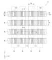
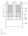
도 1은 본 발명의 개념에 따른 가변 저항 메모리 소자를 보여주는 평면도이다.
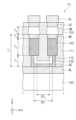
도 2a는 도 1의 Ⅰ-Ⅰ'선상을 절취하여 보여주는 단면도이다.
도 2b는 도 1의 Ⅱ-Ⅱ'선상을 절취하여 보여주는 단면도이다.
도 3은 도 2a 및 도 2b의 상변화 패턴의 최대 전압 차이를 보여주는 그래프이다.
도 4는 도 2의 상변화 패턴의 제 3 두께에 따른 최대 전압 차이를 보여주는 그래프이다.
도 5는 도 2a 및 도 2b의 하부 전극들의 제 1 두께에 대한 상변화 패턴의 제 3 두께의 비율에 따른 최대 전압 차이를 보여주는 그래프이다.
도 6은 도 1의 가변 저항 메모리 소자(10)의 제조방법을 보여주는 플로우 챠트이다.
도 7a 내지 도 17a는 도 1의 I-I' 선상을 절취하여 보여주는 공정 단면도들이다.
도 7b 내지 도 17b는 도 1의 II―II' 선상을 절취하여 보여주는 공정 단면도들이다.1 is a plan view showing a variable resistance memory device according to the concept of the present invention.
Figure 2a is a cross-sectional view taken along the line Ⅰ-Ⅰ′ of FIG.
FIG. 2B is a cross-sectional view taken along the line II-II′ of FIG. 1. Referring to FIG.
3 is a graph showing a maximum voltage difference between the phase change patterns of FIGS. 2A and 2B.
FIG. 4 is a graph showing a maximum voltage difference according to a third thickness of the phase change pattern of FIG. 2 .
5 is a graph showing a maximum voltage difference according to a ratio of a third thickness of a phase change pattern to a first thickness of lower electrodes of FIGS. 2A and 2B .
FIG. 6 is a flow chart showing a method of manufacturing the variable
7A to 17A are process cross-sectional views taken along line II′ of FIG. 1 .
7B to 17B are process cross-sectional views taken along line II-II' in FIG. 1 .
도 1은 본 발명의 개념에 따른 가변 저항 메모리 소자(10)를 보여준다. 도 2a는 도 1의 Ⅰ-Ⅰ'선상을 절취하여 보여주는 단면도이고, 도 2b는 도 1의 Ⅱ-Ⅱ'선상을 절취하여 보여주는 단면도이다.1 shows a variable
도 1, 도 2a 및 도 2b를 참조하면, 본 발명의 가변 저항 메모리 소자(10)는 크로스 포인트(cross-point) PRAM 소자일 수 있다. 일 예에 따르면, 가변 저항 메모리 소자(10)는 기판(100), 워드 라인(WL), 제 1 층간 절연막(105), 하부 전극(BE), 스페이서 패턴(120), 제 1 및 제 2 절연 패턴들(111, 112), 제 2 층간 절연막(130), 상변화 패턴(140), 중간 전극(ME), 스위칭 패턴(SW), 상부 전극(UE), 제 3 층간 절연막(150), 및 비트 라인(BL)을 포함할 수 있다.Referring to FIGS. 1, 2A and 2B, the variable
상기 기판(100)은 단결정 반도체 물질을 포함할 수 있다. 예를 들어, 상기 기판(100)은 실리콘 기판, 실리콘-온-인슐레이터(silicon on insulator: SOI) 기판, 게르마늄 기판, 게르마늄-온-인슐레이터(germanium on insulator: GOI) 기판, 및/또는 실리콘-게르마늄 기판일 수 있다.The
상기 워드 라인(WL)은 상기 기판(100) 상에 배치될 수 있다. 복수개의 워드 라인(WL)은 서로 평행하며 제 1 방향(X)으로 연장할 수 있다. 상기 워드 라인(WL)은 약 20nm의 제 2 방향(Y)으로의 제 1 폭(W1)과 약 10nm 이하의 두께를 가질 수 있다. 상기 워드 라인(WL)은 도전 물질을 포함할 수 있다. 예를 들어, 워드 라인(WL)은 구리, 알루미늄과 같은 금속 물질, 및 TiN, WN과 같은 도전성 금속 질화물 물질 중 적어도 하나를 포함할 수 있다.The word line WL may be disposed on the
상기 제 1 층간 절연막(105)은 상기 복수개의 워드 라인들(WL) 사이의 상기 기판(100) 상에 배치될 수 있다. 상기 제 1 층간 절연막(105)은 상기 워드 라인(WL)의 두께와 동일한 두께를 가질 수 있다. 예를 들어, 상기 제 1 층간 절연막(105)은 약 10nm이하의 두께를 가질 수 있다. 제 1 층간 절연막(105)은 실리콘 질화물 또는 실리콘 산화물을 포함할 수 있다.The first
상기 하부 전극(BE)은 상기 워드 라인(WL) 상에 배치될 수 있다. 복수개의 하부 전극(BE)은 상기 제 1 방향(X) 및 상기 제 2 방향(Y)으로 서로 이격 배치될 수 있다. 일 예로, 상기 하부 전극(BE)의 상기 제 2 방향(Y)으로의 폭은 상기 제 1 폭(W1)과 동일하고, 상기 제 1 방향(X)으로의 폭은 상기 비트 라인(BL)의 제 2 폭(W2)보다 작을 수 있다. 예를 들어, 상기 하부 전극(BE)은 상기 제 2 방향(Y) 방향으로 약 20nm의 폭을 갖고, 상기 제 1 방향(X)으로 약 10nm의 폭을 가질 수 있다. 나아가, 상기 하부 전극(BE)은 상기 워드 라인(WL)보다 두꺼울 수 있다. 상기 하부 전극(BE)은 제 3 방향(Z)으로 약 20nm 내지 약 60nm의 제 1 두께(T1)를 가질 수 있다. 상기 제 1 두께(T1)가 약 13nm이하일 경우, 상기 하부 전극(BE)은 열 손실 불량(heat loss fail)을 가질 수 있다. 일 예로, 상기 제 1 방향(X)으로 인접하는 한 쌍의 하부 전극들(BE)을 물리적으로 연결하는 제 1 연결부(CP1)가 제공될 수 있다. 상기 제 1 연결부(CP1)는 상기 한 쌍의 하부 전극(BE)의 하부들을 연결할 수 있다. 상기 제 1 연결부(CP1)는 제 1 두께(T1)보다 작은 두께를 가질 수 있다. 단면적 관점에서, 물리적으로 연결된 상기 한 쌍의 하부 전극들(BE)과 상기 제 1 연결부(CP1)는 U자 형상을 가질 수 있다. 다른 예로, 도면에 도시하지 않았지만, 상기 인접하는 한쌍의 하부 전극들(BE)은 상기 제 1 방향(X) 방향으로 분리될 수 있다. 상기 하부 전극(BE)은 상변화 패턴(140)을 가열하기 위한 히터(heater) 전극일 수 있다. 하부 전극(BE)은 W, Ti, Al, Cu, C, CN, TiN, TiAlN, TiSiN, TiCN, WN, CoSiN, WSiN, TaN, TaCN, TaSiN, 또는 TiO 중 적어도 하나를 포함할 수 있다.The lower electrode BE may be disposed on the word line WL. The plurality of lower electrodes BE may be spaced apart from each other in the first direction X and the second direction Y. For example, the width of the lower electrode BE in the second direction Y is the same as the first width W1 , and the width in the first direction X is equal to the bit line BL. It may be smaller than the second width (W2 ) of . For example, the lower electrode BE may have a width of about 20 nm in the second direction (Y) and a width of about 10 nm in the first direction (X). Furthermore, the lower electrode BE may be thicker than the word line WL. The lower electrode BE may have a first thickness T1 of about 20 nm to about 60 nm in the third direction Z. When the first thickness T1 is less than about 13 nm, the lower electrode BE may have a heat loss fail. For example, a first connection part CP1 physically connecting a pair of adjacent lower electrodes BE in the first direction X may be provided. The first connection part CP1 may connect lower portions of the pair of lower electrodes BE. The first connection portion CP1 may have a thickness smaller than the first thickness T1 . In terms of cross-sectional area, the pair of lower electrodes BE and the first connection part CP1 that are physically connected may have a U-shape. As another example, although not shown in the drawings, the pair of adjacent lower electrodes BE may be separated in the first direction X direction. The lower electrode BE may be a heater electrode for heating the
상기 스페이서 패턴(120)은 상기 하부 전극(BE)에 인접하여 배치될 수 있다. 상기 스페이서 패턴(120)은 상기 제 1 연결부(CP1) 상에 배치될 수 있다. 이와 달리, 상기 스페이서 패턴(120)은 상기 하부 전극(BE) 내에 배치될 수 있다. 상기 스페이서 패턴(120)은 상기 하부 전극(BE)의 상부 면과 동일한 높이(level)의 상부 면을 가질 수 있다. 상기 스페이서 패턴(120)은 상기 제 1 두께(T1)보다 작은 두께를 가질 수 있다. 일 예로, 상기 제 1 방향(X)으로 인접하는 상기 한 쌍의 스페이서 패턴들(120)을 물리적으로 연결하는 제 2 연결부(CP2)가 제공될 수 있다. 상기 스페이서 패턴(120)은 상기 하부 전극(BE)과 동일한 모양을 가질 수 있다. 단면적 관점에서, 물리적으로 연결된 상기 한 쌍의 스페이서 패턴들(120)과 상기 제 2 연결부(CP2)는 U자 모양을 가질 수 있다. 다른 예로, 도면에 도시하지 않았지만, 상기 인접하는 한쌍의 스페이서 패턴들(120)은 상기 제 1 방향(X) 방향으로 분리될 수 있다. 상기 스페이서 패턴(120)은 예를 들어, 실리콘 산화물 또는 폴리 실리콘을 포함할 수 있다.The
상기 제 1 및 제 2 절연 패턴들(111, 112)은 상기 워드 라인(WL) 상에 배치될 수 있다. 상기 제 1 절연 패턴(111)은 상기 한 쌍의 하부 전극(BE) 외곽에 배치될 수 있다. 상기 제 2 절연 패턴(112)은 상기 한 쌍의 상기 스페이서 패턴들(120) 사이에 배치될 수 있다. 즉, 상기 제 1 절연 패턴(111)은 상기 제 1 연결부(CP1)의 외곽에 배치되고, 상기 제 2 절연 패턴(112)은 상기 제 2 연결부(CP2) 상에 배치될 수 있다. 상기 제 1 절연 패턴(111)은 약 100nm 이하의 제 2 두께(T2)를 가질 수 있다. 상기 제 1 및 제 2 절연 패턴들(111, 112)은 실리콘 질화물을 포함할 수 있다.The first and second
상기 제 2 층간 절연막(130)은 복수개의 워드 라인들(WL) 사이의 상기 제 1 층간 절연막(105) 상에 배치될 수 있다. 상기 제 2 층간 절연막(130)의 상부 면은 상기 제 1 및 제 2 절연 패턴들(111, 112)의 상부 면들과 동일한 높이(level)를 가질 수 있다. 상기 제 2 층간 절연막(130)은 상기 제 2 두께(T2)와 동일한 두께를 가질 수 있다. 예를 들어, 상기 제 2 층간 절연막(130)은 약 100nm 이하의 두께를 가질 수 있다. 예를 들어, 상기 제 2 층간 절연막(130)은 실리콘 질화물 또는 실리콘 산화물을 포함할 수 있다.The second
상기 상변화 패턴(140)은 상기 하부 전극(BE) 및 상기 스페이서 패턴(120) 상에 배치될 수 있다. 상기 상변화 패턴(140)은 상기 제 1 및 제 2 방향들(X, Y)에 대해 상기 하부 전극(BE)보다 넓은 면적을 가질 수 있다. 복수개의 상변화 패턴들(140)은 제 1 방향(X) 및 제 2 방향(Y)으로 서로 이격 배치될 수 있다. 상기 상변화 패턴(140)은 상기 제 3 방향(Z)으로 상기 하부 전극(BE) 보다 두꺼울 수 있다. 예를 들어, 상기 상변화 패턴(140)은 약 40nm 내지 약 90nm의 제 3 두께(T3)를 가질 수 있다. 상기 제 3 두께(T3)가 약 10nm 이하일 경우, 상기 상변화 패턴(140)은 보이드 불량을 가질 수 있다. 상기 상변화 패턴(140)은 정보저장을 가능하게 하는 물성을 갖는 물질들 중 적어도 하나를 포함할 수 있다. 상변화 패턴(140)은 온도에 따라 결정질과 비정질 사이의 가역적 상변화가 가능한 물질을 포함할 수 있다. 일 예로, 상변화 패턴(140)은 칼코게나이드(chalcogenide)계 원소인 Te 및 Se 중의 적어도 하나와, Ge, Sb, Bi, Pb, Sn, Ag, As, S, Si, In, Ti, Ga, P, O 및 C 중에서 선택된 적어도 하나가 조합된 화합물로 형성될 수 있다. 예를 들어, 상기 상변화 패턴(140)은 GeSbTe, GeTeAs, SbTeSe, GeTe, SbTe, SeTeSn, GeTeSe, SbSeBi, GeBiTe, GeTeTi, InSe, GaTeSe, 및 InSbTe 중 적어도 하나를 포함할 수 있다. 다른 예로, 상기 상변화 패턴(140)은 페로브스카이트(perovskite) 화합물들 또는 도전성 금속 산화물들 중의 적어도 하나를 포함할 수 있다. 예를 들면, 상기 상변화 패턴(140)은 니오븀 산화물(niobium oxide), 티타늄 산화물(titanium oxide), 니켈 산화물(nikel oxide), 지르코늄 산화물(zirconium oxide), 바나듐 산화물(vanadium oxide), PCMO((Pr,Ca)MnO3), 스트론튬-티타늄 산화물(strontium-titanium oxide), 바륨-스트론튬-티타늄 산화물(barium-strontium-titanium oxide), 스트론튬-지르코늄 산화물(strontium-zirconium oxide), 바륨-지르코늄 산화물(barium-zirconium oxide), 또는 바륨-스트론튬-지르코늄 산화물(barium-strontium-zirconium oxide) 등에서 적어도 하나를 포함할 수 있다. 상변화 패턴(140)이 전이금속 산화물들을 포함하는 경우, 상변화 패턴(140)의 유전 상수는 실리콘 산화막의 유전 상수보다 클 수 있다. 다른 예로, 상변화 패턴(140)은 도전성 금속 산화물과 터널 절연막의 이중 구조이거나, 제 1 도전성 금속산화물, 터널 절연막, 및 제 2 도전성 금속 산화물의 삼중 구조일 수 있다. 터널 절연막은 알루미늄 산화물(aluminum oxide), 하프늄 산화물(hafnium oxide), 또는 실리콘 산화물(silicon oxide)을 포함할 수 있다.The
상기 중간 전극(ME)은 상기 상변화 패턴(140) 상에 배치될 수 있다. 일 예로, 상기 중간 전극(ME)은 상기 상변화 패턴(140)과 상기 스위칭 패턴(SW) 사이의 제 1 확산 방지막일 수 있다. 상기 중간 전극(ME)은 상기 제 1 및 제 2 방향들(X, Y)에 대해 상기 상변화 패턴(140)의 면적과 동일한 면적을 가질 수 있다. 상기 중간 전극(ME)의 상부 면은 상기 제 1 및 제 2 절연 패턴들(111, 112)과 상기 제 2 층간 절연막(130)의 상부 면들과 동일한 높이(level)를 가질 수 있다. 상기 중간 전극(ME)은 상기 제 3 방향(Z)으로 상기 상변화 패턴(140) 또는 상기 하부 전극(BE)보다 얇을 수 있다. 상기 중간 전극(ME)은 약 10nm 이하의 제 4 두께(T4)를 가질 수 있다. 예를 들어, 상기 중간 전극(ME)은 TiN를 포함할 수 있다.The intermediate electrode ME may be disposed on the
상기 스위칭 패턴(SW)은 상기 중간 전극(ME) 상에 배치될 수 있다. 상기 스위칭 패턴(SW)은 상기 상변화 패턴(140)보다 얇을 수 있다. 예를 들어, 상기 스위칭 패턴(SW)은 약 10nm 내지 약 15nm의 제 5 두께(T5)를 가질 수 있다. 상기 스위칭 패턴(SW)은 상기 비트 라인(BL)을 상기 워드 라인(WL)에 연결할 수 있다. 상기 워드 라인(WL)과, 상기 비트 라인(BL) 사이에 전압(ex, 라이팅(writing) 전압 및/또는 리딩(reading) 전압)이 인가되면, 상기 스위칭 패턴(SW)은 부도체에서 전도체 상태로 변할 수 있다. 상기 스위칭 패턴(SW)을 통해 흐른 전류는 하부 전극(BE)에 전달되어 하부 전극(BE)의 열 발생을 유도할 수 있다. 상기 스위칭 패턴(SW)은 양방향(bi-directional) 특성을 갖는 OTS(Ovonic Threshold Switch) 소자를 포함할 수 있다. 일 예로, 스위칭 패턴(SW)은 비선형적(일 예로, S자형) I-V 커브를 갖는 문턱(threshold) 스위칭 현상에 기초한 소자를 포함할 수 있다. 상기 스위칭 패턴(SW)은 약 3V 내지 약 4V의 문턱 전압(Vth)을 가질 수 있다. 상기 문턱 전압(Vth) 이상의 전압이 상기 워드 라인(WL)과 상기 비트 라인(BL) 사이에 인가되면, 상기 스위칭 패턴(SW)은 턴온될 수 있다. 또한, 상기 문턱 전압(Vth)은 상기 스위칭 패턴(SW)의 누적 사용 시간 및/또는 결함에 따라 변화할 수 있다. 즉, 상기 스위칭 패턴(SW)은 문턱 전압 변화(threshold voltage changing, △Vth)를 가질 수 있다. 일 예에 따르면, 상기 문턱 전압 변화(△Vth)는 상기 문턱 전압(Vth)의 전압 이동(voltage drift, 도 3의 14) 및/또는 누설 전류(leakage current)에 의한 전압 리크(voltage leak, 16)를 포함할 수 있다. 예를 들어, 약 1년 동안 사용된 상기 스위칭 패턴(SW)은 상기 문턱 전압(Vth)에 대해 약 1.7V의 상기 전압 이동(14)과 약 2.3V의 상기 전압 리크(16)를 가질 수 있다.The switching pattern SW may be disposed on the intermediate electrode ME. The switching pattern SW may be thinner than the
상기 스위칭 패턴(SW)은 상변화 패턴(140)의 상전이 온도보다 높은 상전이 온도를 가질 수 있다. 일 예로, 스위칭 패턴(SW)의 상전이 온도는 약 350℃내지 약 450℃일 수 있다. 따라서, 본 발명의 실시예들에 따른 가변 저항 메모리 소자의 동작 시, 상변화 패턴(140)은 동작 전압 하에서 결정질과 비정질 사이에서 가역적으로 상변화가 이루어지나, 스위칭 패턴(SW)은 동작 전압 하에서 상변화 없이 실질적으로 비정질 상태를 유지할 수 있다. 일 예로, 스위칭 패턴(SW)은 칼코게나이드(chalcogenide)계 원소인 Te 및 Se 중의 적어도 하나와, Ge, Sb, Bi, Al, Pb, Sn, Ag, As, S, Si, In, Ti, Ga 및 P 중에서 선택된 적어도 하나가 조합된 화합물로 형성될 수 있다. 스위칭 패턴(SW)은 상기 화합물에 추가하여 열적 안정화 원소를 더 포함할 수 있다. 열적 안정화 원소는 C, N, 및 O 중 적어도 하나일 수 있다. 예를 들어, 스위칭 패턴(SW)은 AsTe, AsSe, GeTe, SnTe, GeSe, SnTe, SnSe, ZnTe, AsTeSe, AsTeGe, AsSeGe, AsTeGeSe, AsSeGeSi, AsSeGeC, AsTeGeSi, AsTeGeS, AsTeGeSiIn, AsTeGeSiP, AsTeGeSiSbS, AsTeGeSiSbP, AsTeGeSeSb, AsTeGeSeSi, AsTeGeSiSeNS, SeTeGeSi, GeSbTeSe, GeBiTeSe, GeAsSbSe, GeAsBiTe, 및 GeAsBiSe 중 적어도 하나를 포함할 수 있다.The switching pattern SW may have a phase transition temperature higher than the phase transition temperature of the
상기 상부 전극(UE)은 상기 스위칭 패턴(SW) 상에 배치될 수 있다. 일 예로, 상기 상부 전극(UE)은 상기 스위칭 패턴(SW)과 상기 비트 라인(BL) 사이의 제 2 확산 방지막일 수 있다. 예를 들어, 상기 상부 전극(UE)은 W, Ti, Al, Cu, C, CN, TiN, TiAlN, TiSiN, TiCN, WN, CoSiN, WSiN, TaN, TaCN, TaSiN, 또는 TiO 중 적어도 하나를 포함할 수 있다.The upper electrode UE may be disposed on the switching pattern SW. For example, the upper electrode UE may be a second diffusion barrier between the switching pattern SW and the bit line BL. For example, the upper electrode UE includes at least one of W, Ti, Al, Cu, C, CN, TiN, TiAlN, TiSiN, TiCN, WN, CoSiN, WSiN, TaN, TaCN, TaSiN, or TiO. can do.
상기 제 3 층간 절연막(150)은 상기 제 2 층간 절연막(130), 제 1 절연 패턴(111) 및 제 2 상기 절연 패턴(112) 상에 배치될 수 있다. 상기 제 3 층간 절연막(150)은 복수개의 스위칭 패턴(SW) 사이에 배치될 수 있다. 또한, 상기 제 3 층간 절연막(150)은 복수개의 상부 전극(UE) 사이에 배치될 수 있다. 상기 제 3 층간 절연막(150)은 실리콘 질화물 또는 실리콘 산화물을 포함할 수 있다.The third
상기 비트 라인(BL)은 상기 상부 전극(UE) 및 상기 제 3 층간 절연막(150) 상에 배치될 수 있다. 복수개의 비트 라인들(BL)은 서로 평행하며 상기 제 2 방향(Y)으로 연장할 수 있다. 상기 비트 라인(BL)은 상기 제 1 방향(X)으로 약 20nm의 제 2 폭(W2)을 가질 수 있다. 상기 비트 라인(BL)은 도전 물질을 포함할 수 있다. 예를 들어, 비트 라인(BL)은 구리, 알루미늄과 같은 금속 물질, 및 TiN, WN과 같은 도전성 금속 질화물 물질 중 적어도 하나를 포함할 수 있다.The bit line BL may be disposed on the upper electrode UE and the third
한편, 본 발명의 가변 저항 메모리 소자(10)는 상변화 패턴(140)의 최대 전압 차이(clamping voltage difference, △VCMP)에 따라 신뢰성을 가질 수 있다. 상기 최대 전압 차이(△VCMP)가 증가하면, 신뢰성은 증가할 수 있다.Meanwhile, the variable
도 3은 도 2a 및 도 2b의 상변화 패턴(140)의 최대 전압 차이(△VCMP)를 보여준다.FIG. 3 shows the maximum voltage difference (ΔVCMP ) of the
도 3을 참조하면, 상기 상변화 패턴(140)은 최대 전압 차이(△VCMP)를 가질 수 있다. 예를 들어, 상기 최대 전압 차이(△VCMP)는 약 1.2V 이상일 수 있다. 일 예에 따르면, 상기 최대 전압 차이(△VCMP)는 상기 상변화 패턴(140)의 세트 전압(VCMP1)과 리세트 전압(VCMP2)의 피크들의 차이일 수 있다. 상기 세트 전압(VCMP1)은 상기 상변화 패턴(140)의 제 1 상태(ex, 결정 상태(crystalline state)에서의 제 1 최대 전압 강하에 대응될 수 있다. 예를 들어, 상기 세트 전압(VCMP1)은 약 0.3V의 피크를 가질 수 있다. 상기 세트 전압(VCMP1)은 약 0.6V 정도의 산포(dispersion and/or distribution)를 가질 수 있다. 상기 리세트 전압(VCMP2)은 상기 상변화 패턴(140)의 제 2 상태(ex, 아몰퍼스 상태)에서의 최대 전압 강하에 대응될 수 있다. 예를 들어, 상기 리세트 전압(VCMP2)은 약 1.5V 이상의 피크를 가질 수 있다. 상기 리세트 전압(VCMP2)은 약 0.6V 정도의 산포를 가질 수 있다.Referring to FIG. 3 , the
일 예로, 최대 전압 차이(△VCMP)는 상기 스위칭 패턴(SW)의 문턱 전압 변화(△Vth)의 제 1 및 제 2 보상 값들(22, 24)과, 상기 상변화 패턴(140)의 센싱 마진(26)을 가질 수 있다. 상기 제 1 및 제 2 보상 값들(22, 24)은 상기 스위칭 패턴(SW)의 문턱 전압 변화(△Vth)를 보상하여 가변 저항 메모리 소자(10)의 신뢰성을 증가시킬 수 있다. 상기 제 1 보상 값(22)은 상기 스위칭 패턴((SW)의 보증 사용 시간(ex, 1년) 내의 상기 전압 이동(14)에 따른 상기 문턱 전압 변화(△Vth)를 보상하는 값일 수 있다. 상기 제 1 보상 값(22)은 상기 전압 이동(14)에 의해 이동(drifted)된 세트 전압(34)의 최대 값과, 상기 세트 전압(VCMP1)의 최대 값의 차이로 정의될 수 있다. 예를 들어, 제 1 보상 값(22)은 약 0.17V일 수 있다. 상기 제 2 보상 값(24)은 상기 스위칭 패턴(SW)의 상기 전압 리크(16)에 따른 상기 문턱 전압 변화(△Vth)를 보상하는 값일 수 있다. 상기 제 2 보상 값(24)은 상기 전압 리크(16)에 의해 시프트된 세트 전압(36)의 최대 값과, 상기 이동된 세트 전압(34)의 최대 값의 차이로 정의될 수 있다. 예를 들어, 상기 제 2 보상 값(24)은 약 0.23V일 수 있다. 상기 센싱 마진(26)은 센싱 회로(미도시)에서 상기 세트 전압(VCMP1)과 상기 리세트 전압(VCMP2)을 구별하기 위한 최소한의 전압 차이일 수 있다. 상기 센싱 마진(26)은 상기 리세트 전압(VCMP2)의 최저 값과, 상기 시프트된 세트 전압(36)의 최대 값의 최대 값의 차이로 정의될 수 있다. 예를 들어, 상기 센싱 마진(26)은 약 0.2V일 수 있다.For example, the maximum voltage difference ΔVCMP is the first and second compensation values 22 and 24 of the threshold voltage change ΔVth of the switching pattern SW and the
상기 상변화 패턴(140)이 상기 스위칭 패턴(SW)의 상기 문턱 전압 변화(△Vth)를 제거하는 상기 제 1 및 제 2 보상 값들(22, 24)의 상기 최대 전압 차이(△VCMP)를 갖기 때문에 상기 스위칭 패턴(SW)의 신뢰성은 향상될 수 있다. 결과적으로 약 1.2V이상의 최대 전압 차이(△VCMP)를 갖는 상기 상변화 패턴(140)은 상기 가변 저항 메모리 소자(10)의 신뢰성을 향상시킬 수 있다.The maximum voltage difference ΔVCMP between the first and second compensation values 22 and 24 at which the
도 4는 도 2의 상변화 패턴(140)의 제 3 두께(T3)에 따른 최대 전압 차이(△VCMP)를 보여준다.FIG. 4 shows the maximum voltage difference (ΔVCMP ) according to the third thickness (T3 ) of the
도 3 및 도 4를 참조하면, 상기 상변화 패턴(140)의 상기 제 3 두께(T3)와 상기 최대 전압 차이(△VCMP)는 비례할 수 있다.Referring to FIGS. 3 and 4 , the third thickness T3 of the
상기 상변화 패턴(140)의 제 3 두께(T3)가 32nm이하일 경우, 상기 최대 전압 차이(△VCMP)는 약 1V보다 작을 수 있다. 상기 최대 전압 차이(△VCMP)가 1V보다 작아 상기 제 1 및 제 2 보상 값들(22, 24)을 포함하지 못할 경우, 상기 가변 저항 메모리 소자(10)의 신뢰성은 감소할 수 있다.When the third thickness T3 of the
상기 상변화 패턴(140)의 제 3 두께(T3)가 40nm이상일 경우, 상기 최대 전압 차이(△VCMP)는 약 1.2V이상일 수 있다. 약 1.2V 이상의 상기 최대 전압 차이(△VCMP)가 상기 제 1 및 제 2 보상 값들(22, 24)을 포함하기 때문에 상기 가변 저항 메모리 소자(10)의 신뢰성은 증가할 수 있다.When the third thickness T3 of the
다시 도 2a 및 도 2b를 참조하면, 상기 상변화 패턴(140)의 상기 제 3 두께(T3)는 상기 제 1 절연 패턴(111) 및 상기 제 2 층간 절연막(130)의 상기 제 2 두께(T2) 보다 작고, 상기 하부 전극(BE)의 상기 제 1 두께(T1)보다 클 수 있다. 상기 중간 전극(ME)이 없으면, 상기 제 2 두께(T2)는 상기 제 3 두께(T3)의 최대 한계일 수 있다. 상기 최대 한계 내에서, 상기 제 1 두께(T1)에 대한 상기 제 3 두께(T3)의 비율이 증가할수록 상기 가변 저항 메모리 소자(10)의 신뢰성은 증가할 수 있다.Referring back to FIGS. 2A and 2B , the third thickness T3 of the
도 5는 도 2a 및 도 2b의 제 1 두께(T1)에 대한 제 3 두께(T3)의 비율에 따른 최대 전압 차이(△VCMP)를 보여준다.FIG. 5 shows the maximum voltage difference (ΔVCMP ) according to the ratio of the third thickness (T3 ) to the first thickness (T1 ) of FIGS. 2A and 2B.
도 5를 참조하면, 상기 하부 전극(BE)의 제 1 두께(T1)에 대한 상기 상변화 패턴(140)의 제 3 두께(T3)의 비율과, 상기 최대 전압 차이(△VCMP)는 비례하여 증가할 수 있다. 일 예에 따르면, 상기 최대 전압 차이(△VCMP)가 약 1.2V이상일 경우, 상기 하부 전극(BE)에 대한 상변화 패턴(140)의 두께 비율은 약 1.5 내지 6.0일 수 있다. 즉, 상기 상변화 패턴(140)과 상기 하부 전극(BE)은 약 1.5: 1 내지 약 6:1의 두께 비율을 가질 수 있다. 상기 상변화 패턴(140)과 상기 하부 전극(BE)이 약 1.5: 1 내지 약 6:1의 두께 비율을 가질 경우, 상기 가변 저항 메모리 소자(10)의 신뢰성은 증가할 수 있다.Referring to FIG. 5 , the ratio of the
이와 같이 구성된 본 발명의 가변 저항 메모리 소자(10)의 제조방법을 설명하면 다음과 같다.A method of manufacturing the variable
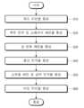
도 6은 도 1의 가변 저항 메모리 소자(10)의 제조방법을 보여준다.FIG. 6 shows a manufacturing method of the variable
도 6을 참조하면, 본 발명의 가변 저항 메모리 소자(10)의 제조방법은, 워드 라인(WL)을 형성하는 단계(S10), 하부 전극(BE) 및 스페이서 패턴(120)을 형성하는 단계(S20), 상변화 패턴(140)을 형성하는 단계(S30), 중간 전극(ME)을 형성하는 단계(S40), 스위칭 패턴(SW) 및 상부 전극(UE)을 형성하는 단계(S50), 및 비트 라인(BL)을 형성하는 단계(S60)를 포함할 수 있다.Referring to FIG. 6 , the manufacturing method of the variable
도 7a 내지 도 17a는 도 1의 I-I' 선상을 절취하여 보여주는 공정 단면도들이고, 도 7b 내지 도 17b는 도 1의 II―II' 선상을 절취하여 보여주는 공정 단면도들이다.7A to 17A are cross-sectional views taken along line II' of FIG. 1 , and FIGS. 7B to 17B are cross-sectional views taken along line II-II' in FIG. 1 .
도 6, 도 7a 및 도 7b를 참조하면, 상기 기판(100) 상에 상기 워드 라인(WL)을 형성한다(S10). 일 예로, 상기 워드 라인(WL)은 금속 증착 공정, 포토리소그래피 및 식각 공정을 통해 형성될 수 있다. 이후, 복수개의 워드 라인들(WL) 사이에 제 1 층간 절연막(105)이 형성될 수 있다. 다른 예로, 상기 워드 라인(WL)은 다마신 방법을 통해 형성될 수 있다. 예를 들어, 상기 기판(100) 상에 트렌치(미도시)를 갖는 제 1 층간 절연막(105)이 형성된 이후, 상기 워드 라인(WL)은 금속막의 박막 증착 공정 및 화학적 기계적 연마 공정으로 상기 트렌치 내에 형성될 수 있다.Referring to FIGS. 6, 7A and 7B , the word line WL is formed on the substrate 100 (S10). For example, the word line WL may be formed through a metal deposition process, a photolithography process, and an etching process. After that, a first
도 5, 도 8a 내지 도 12a 및 도 8b 내지 도 12b를 참조하면, 상기 워드 라인(WL) 상에 하부 전극(BE) 및 스페이서 패턴(120)을 형성한다(S20). 일 예로, 상기 하부 전극(BE) 및 상기 스페이서 패턴(120)은 제 1 절연막(107), 제 2 절연막(110) 및 제 2 층간 절연막(130)을 통해 형성될 수 있다.Referring to FIGS. 5, 8A to 12A, and 8B to 12B, a lower electrode BE and a
도 8a 및 도 8b를 참조하면, 상기 워드 라인(WL) 및 상기 제 1 층간 절연막(105) 상에 상기 제 1 절연막(107)을 형성한다. 예를 들어, 상기 제 1 절연막(107)은 화학기상증착방법으로 형성된 실리콘 질화물을 포함할 수 있다. 상기 제 1 절연막(107)은 약 200nm의 두께로 형성될 수 있다. 상기 제 1 절연막(107)은 포토리소그래피 공정 및 식각 공정으로 형성된 제 1 트렌치(106)를 가질 수 있다. 상기 제 1 트렌치(106)는 상기 워드 라인(WL)의 일부 및 상기 제 1 층간 절연막(105)의 일부를 노출시킬 수 있다. 상기 제 1 트렌치(106)는 약 200nm의 깊이와 약 40nm의 폭을 갖고, 상기 제 2 방향(Y) 방향으로 연장할 수 있다.Referring to FIGS. 8A and 8B , the first insulating
도 9a 및 도 9b를 참조하면, 상기 제 1 절연막(107)과, 상기 트렌치(106) 내의 상기 워드 라인(WL) 상에 예비 전극 층(108), 예비 스페이서 층(109) 및 제 2 절연막(110)을 형성한다. 상기 예비 전극 층(108)은 금속 층을 포함하고, 상기 예비 스페이서 층(109)은 실리콘 산화물 또는 실리콘 질화물의 유전체를 포함할 수 있다. 상기 예비 전극 층(108) 및 상기 예비 스페이서 층(109)은 상기 워드 라인(WL)과 상기 제 1 절연막(107) 상에 콘포말하게 형성되고, 상기 제 2 절연막(110)은 상기 예비 스페이서 층(109) 상에 형성될 수 있다. 상기 제 2 절연막(110)은 상기 제 1 트렌치(106) 내에 충진(filled)될 수 있다.9A and 9B , a
다음, 상기 예비 전극 층(108), 상기 예비 스페이서 층(109), 및 상기 제 2 절연막(110)을 화학적 기계적 연마 공정으로 평탄화한다. 상기 예비 전극 층(108), 상기 예비 스페이서 층(109), 및 상기 제 2 절연막(110)이 평탄화될 경우, 상기 제 1 절연막(107)의 두께는 감소할 수 있다. 예를 들어, 상기 제 1 절연막(107)의 두께는 약 20nm 정도 줄어들 수 있다.Next, the
그 다음, 상기 워드 라인(WL) 외곽의 상기 예비 전극 층(108), 상기 예비 스페이서 층(109), 상기 제 1 절연막(107) 및 상기 제 2 절연막(110)의 일부분들을 제거한다. 상기 예비 전극 층(108), 상기 예비 스페이서 층(109), 상기 제 1 절연막(107), 및 상기 제 2 절연막(110)은 상기 제 2 방향(Y)으로 분리될 수 있다. 상기 예비 전극 층(108), 상기 예비 스페이서 층(109), 상기 제 1 절연막(107), 및 상기 제 2 절연막(110)은 상기 워드 라인(WL) 상에 잔존(be)하도록 형성될 수 있다.Then, portions of the
도 10a 및 도 10b를 참조하면, 상기 제 1 층간 절연막(105) 상에 제 2 층간 절연막(130)을 형성한다. 상기 제 2 층간 절연막(130)은 유전체의 박막 증착 공정과 화학적 기계적 연마 공정으로 형성될 수 있다. 상기 제 2 층간 절연막(130)이 상기 화학적 기계적 연마 공정으로 평탄화될 경우, 상기 제 1 절연막(107)의 두께는 감소할 수 있다. 예를 들어, 상기 제 1 절연막(107)의 두께는 약 20nm 정도 줄어들 수 있다.Referring to FIGS. 10A and 10B , a second
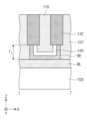
도 11a 및 도 11b를 참조하면, 상기 예비 전극 층(108) 및 상기 예비 스페이서 층(109)의 상부 부분들을 식각하여 제 2 트렌치(113)를 형성한다. 일 예로, 상기 예비 전극 층(108) 및 상기 예비 스페이서 층(109)의 상부 부분은 습식 식각 공정으로 제거될 수 있다. 상기 예비 전극 층(108) 및 상기 예비 스페이서 층(109)의 식각 용액은 상기 제 1 절연막(107), 상기 제 2 절연막(110) 및 상기 제 2 층간 절연막(130)에 대해 식각 선택비를 가질 수 있다. 그러나, 상기 제 1 절연막(107)의 일부는 상기 습식 식각 공정을 통헤 제거될 수 있다. 즉, 상기 제 1 절연막(107)의 두께는 상기 습식 식각 공정으로 감소할 수 있다. 예를 들어, 상기 제 1 절연막(107)의 두께는 약 20nm 정도 줄어들 수 있다.Referring to FIGS. 11A and 11B , upper portions of the
도 12a 및 도 12b를 참조하면, 상기 제 2 트렌치(113)를 확장(enlarge)시켜 상 상기 하부 전극(BE) 및 상기 스페이서 패턴(120)을 형성한다. 상기 제 2 트렌치(113)는 습식 식각 공정을 통해 제 1 내지 제 3 방향들(X, Y, Z)로 증가될 수 있다. 상기 제 2 트렌치(113)의 폭과 깊이는 증가될 수 있다. 상기 습식 식각 공정에 사용되는 식각 용액은 상기 제 1 절연막(107), 상기 제 2 절연막(110), 상기 제 2 층간 절연막(130), 상기 예비 전극 층(108), 및 상기 예비 스페이서 층(109) 중 적어도 어느 하나에 대한 식각 선택비를 갖지 않을 수 있다. 상기 제 1 절연막(107), 상기 제 2 절연막(110), 상기 제 2 층간 절연막(130), 상기 예비 전극 층(108), 및 상기 예비 스페이서 층(109)은 상기 습식 식각 공정을 통해 상기 제 3 방향(Z)으로 얇아질 수 있다. 예를 들어, 상기 제 1 절연막(107)의 두께는 약 10nm 내지 약 20nm정도 줄어들 수 있다. 상기 제 2 트렌치(113)의 제 1 깊이(D1)는 상기 하부 전극(BE)의 제 1 두께(T1)보다 클 수 있다. 예를 들어, 상기 제 1 깊이(D1)는 약 140nm 내지 약 120nm일 수 있다. 상기 하부 전극(BE)은 약 20 nm 내지 약 60nm의 상기 제 1 두께(T1)를 갖도록 형성될 수 있다.Referring to FIGS. 12A and 12B , the upper and lower electrodes BE and the
도 6, 도 13a 내지 도 14a 및 도 13b 내지 도 14b를 참조하면, 상기 제 2 트렌치(113) 내에 상기 상변화 패턴(140)을 형성한다(S30). 일 예로, 상기 상변화 패턴(140)은 다마신 방법으로 형성될 수 있다.Referring to FIGS. 6 , 13A to 14A and 13B to 14B , the
도 13a 및 도 13b를 참조하면, 상기 제 2 트렌치 (113) 내에 예비 상변화 패턴(142)을 형성한다. 상기 예비 상변화 패턴(142)은 칼코게나이드 원소와, Ge, Sb, Bi, Pb, Sn, Ag, As, S, Si, In, Ti, Ga, P, O 및 C 중에서 선택된 적어도 하나가 조합된 화합물을 포함할 수 있다. 상기 예비 상변화 패턴(142)은 금속막의 박막 증착 공정과, 화학적 기계적 연마 공정으로 형성될 수 있다. 상기 제 1 절연막(107)의 두께는 상기 화학적 기계적 연마 공정으로 감소할 수 있다. 예를 들어, 상기 제 1 절연막(107)의 두께는 약 20nm 정도 줄어들 수 있다.Referring to FIGS. 13A and 13B , a preliminary
도 14a 및 도 14b를 참조하면, 상기 예비 상변화 패턴(142)의 상부 부분을 제거하여 상기 상변화 패턴(140)을 형성한다. 상기 상변화 패턴(140) 상에 제 3 트렌치 (115)가 형성될 수 있다. 상기 상변화 패턴(140)은 약 40nm 내지 약 90nm의 제 3 두께(T3)를 갖도록 형성될 수 있다.Referring to FIGS. 14A and 14B , the
도 6, 도 15a 및 도 15b를 참조하면, 상기 제 3 트렌치(115) 내에 상기 중간 전극(ME)을 형성한다. 일 예로, 상기 중간 전극(ME)은 다마신 방법으로 형성될 수 있다. 예를 들어, 상기 중간 전극(ME)은 금속막의 증착 공정 및 화학적 기계적 연마 공정으로 형성될 수 있다. 상기 중간 전극(ME)은 약 10nm 이하의 제 4 두께(T4)를 갖도록 형성될 수 있다. 상기 제 1 절연막(107), 상기 제 2 절연막(110), 및 상기 제 2 층간 절연막(130)의 두께는 상기 화학적 기계적 연마 공정을 통해 감소할 수 있다. 예를 들어, 상기 제 1 절연막(107) 및 상기 제 2 층간 절연막(130)의 두께는 약 20nm 정도 줄어들 수 있다. 상기 제 1 절연막(107)은 그의 박막 증착 공정에서부터 상기 중간 전극(ME)의 형성까지, 약 100nm 이상의 두께가 감소할 수 있다. 상기 제 1 절연막(107) 및 상기 제 2 절연막(110)은 상기 제 1 절연 패턴(111)과 상기 제 2 절연 패턴(112)으로 형성될 수 있다. 상기 상변화 패턴(140)이 다마신 방법으로 약 20nm의 상기 제 1 및 제 2 폭들(W1, W2)로 형성될 경우, 상기 제 1 절연 패턴(111)과 상기 제 2 층간 절연막(130)은 약 100nm이하의 제 2 두께(T2)를 갖도록 형성될 수 있다.Referring to FIGS. 6 , 15A and 15B , the intermediate electrode ME is formed in the
도 6, 도 16a 및 도 16b를 참조하면, 상기 중간 전극(ME) 상에 상기 스위칭 패턴(SW)과 상기 상부 전극(UE)을 형성한다(S40). 일 예로, 상기 스위칭 패턴(SW)과 상기 상부 전극(UE)은 박막 증착 공정, 포토리소그래피 공정 및 건식 식각 공정을 통해 형성될 수 있다. 상기 건식 식각 공정은 반응성 이온 식각(Reactive Ion Etching: RIE) 공정을 포함할 수 있다. 상기 스위칭 패턴(SW)은 약 10nm 내지 약 15nm의 제 5 두께(T5)를 갖도록 형성될 수 있다.Referring to FIGS. 6, 16A and 16B , the switching pattern SW and the upper electrode UE are formed on the intermediate electrode ME (S40). For example, the switching pattern SW and the upper electrode UE may be formed through a thin film deposition process, a photolithography process, and a dry etching process. The dry etching process may include a reactive ion etching (RIE) process. The switching pattern SW may be formed to have a fifth thickness T5 of about 10 nm to about 15 nm.
도 6, 도 17a 및 도 17b를 참조하면, 복수개의 스위칭 패턴들(SW) 사이 및 복수개의 상부 전극들(UE) 사이에 제 3 층간 절연막(150)을 형성한다(S50). 상기 제 3 층간 절연막(150)은 유전체의 박막 증착 공정 및 화학적 기계적 연마 공정으로 형성될 수 있다. 상기 제 3 층간 절연막(150)은 실리콘 질화물 또는 실리콘 산화물을 포함할 수 있다.Referring to FIGS. 6, 17A and 17B , a third
도 2a, 도 2b 및 도 6을 참조하면, 상기 상부 전극(UE)과 상기 제 3 층간 절연막(150) 상에 비트 라인(BL)을 형성한다(S60). 상기 비트 라인(BL)은 금속막의 박막 증착 공정, 포토리소그래피 공정 및 식각 공정으로 형성될 수 있다.Referring to FIGS. 2A, 2B, and 6 , a bit line BL is formed on the upper electrode UE and the third interlayer insulating layer 150 (S60). The bit line BL may be formed through a metal film deposition process, a photolithography process, and an etching process.
이상, 첨부된 도면을 참조하여 본 발명의 실시예를 설명하였지만, 본 발명이 속하는 기술분야에서 통상의 지식을 가진 자는 본 발명이 그 기술적 사상이나 필수적인 특징을 변경하지 않고서 다른 구체적인 형태로 실시될 수 있다는 것을 이해할 수 있을 것이다. 그러므로 이상에서 기술한 실시예에는 모든 면에서 예시적인 것이며 한정적이 아닌 것으로 이해해야만 한다.Although the embodiments of the present invention have been described with reference to the accompanying drawings, those skilled in the art can implement the present invention in other specific forms without changing its technical spirit or essential features. You will understand that there is Therefore, it should be understood that the embodiments described above are illustrative in all respects and not restrictive.
Claims (10)
Translated fromKorean상기 워드 라인 상에 배치되고 상기 제 1 방향과 교차하는 제 2 방향으로 연장하는 비트 라인;
상기 비트 라인과 상기 워드 라인 사이에 배치되는 스위칭 패턴;
상기 스위칭 패턴과 상기 워드 라인 사이에 배치되는 상변화 패턴; 및
상기 상변화 패턴과 상기 워드 라인 사이에 배치되는 하부 전극을 포함하되,
상기 상변화 패턴은 상기 제 1 및 제 2 방향들로 정의되는 상기 하부 전극의 면적보다 넓은 면적을 갖고, 상기 제 1 및 제 2 방향들과 교차하는 제 3 방향으로 정의되는 상기 하부 전극의 두께보다 큰 두께를 갖되,
상기 스위칭 패턴은 상기 상변화 패턴의 면적과 동일한 면적을 갖고, 10nm 내지 15nm의 두께를 갖되,
상기 스위칭 패턴의 문턱 전압은 3V 내지 4V인 가변 저항 메모리 소자.
word lines extending in a first direction;
a bit line disposed on the word line and extending in a second direction crossing the first direction;
a switching pattern disposed between the bit line and the word line;
a phase change pattern disposed between the switching pattern and the word line; and
A lower electrode disposed between the phase change pattern and the word line,
The phase change pattern has an area larger than the area of the lower electrode defined by the first and second directions, and a thickness greater than that of the lower electrode defined by a third direction crossing the first and second directions. have great thickness
The switching pattern has an area equal to that of the phase change pattern and a thickness of 10 nm to 15 nm,
The variable resistance memory device of claim 1 , wherein the threshold voltage of the switching pattern is 3V to 4V.
상기 상변화 패턴과 상기 하부전 극은 1.5:1 내지 6:1의 두께 비율을 갖는 가변 저항 메모리 소자.
According to claim 1,
The variable resistance memory device of claim 1 , wherein the phase change pattern and the lower electrode have a thickness ratio of 1.5:1 to 6:1.
상기 상변화 패턴의 면적은 상기 하부 전극의 면적의 2배 이상인 가변 저항 메모리 소자.
According to claim 1,
The variable resistance memory device of claim 1 , wherein an area of the phase change pattern is twice or more than an area of the lower electrode.
상기 상변화 패턴은 40nm 내지 90nm의 두께를 갖는 가변 저항 메모리 소자.
According to claim 1,
The variable resistance memory device of claim 1, wherein the phase change pattern has a thickness of 40 nm to 90 nm.
상기 하부 전극은 20nm 내지 60nm의 두께를 갖는 가변 저항 메모리 소자.
According to claim 1,
The variable resistance memory device of claim 1, wherein the lower electrode has a thickness of 20 nm to 60 nm.
상기 상변화 패턴의 세트 전압과 리세트 전압의 피크들의 차이 값은 1.2V 이상인 가변 저항 메모리 소자.
According to claim 1,
The variable resistance memory device of claim 1 , wherein a difference between peaks of the set voltage and the reset voltage of the phase change pattern is 1.2V or more.
상기 스위칭 패턴과 상기 상변화 패턴 사이에 배치되는 중간 전극을 더 포함하되,
상기 중간 전극은 10nm 이하의 두께를 갖는 가변 저항 메모리 소자.
According to claim 1,
Further comprising an intermediate electrode disposed between the switching pattern and the phase change pattern,
The intermediate electrode has a thickness of 10 nm or less.
상기 상변화 패턴과 상기 하부 전극의 외곽에 배치되는 절연 패턴을 더 포함하되,
상기 절연 패턴은 100nm 이하의 두께를 갖는 가변 저항 메모리 소자.
According to claim 1,
Further comprising an insulating pattern disposed outside the phase change pattern and the lower electrode,
The variable resistance memory device of claim 1 , wherein the insulating pattern has a thickness of 100 nm or less.
상기 상변화 패턴은 복수개이되,
상기 복수개의 상변화 패턴들을 상기 제 1 방향으로 연결하는 제 1 연결부를 더 포함하는 가변 저항 메모리 소자.
According to claim 1,
The phase change pattern is plural,
The variable resistance memory device further includes a first connection portion connecting the plurality of phase change patterns in the first direction.
Priority Applications (3)
| Application Number | Priority Date | Filing Date | Title |
|---|---|---|---|
| KR1020180101455AKR102571555B1 (en) | 2018-08-28 | 2018-08-28 | Variable resistance memory device |
| US16/426,216US10923654B2 (en) | 2018-08-28 | 2019-05-30 | Variable resistance memory device |
| CN201910799037.8ACN110867463B (en) | 2018-08-28 | 2019-08-27 | Variable resistance memory device |
Applications Claiming Priority (1)
| Application Number | Priority Date | Filing Date | Title |
|---|---|---|---|
| KR1020180101455AKR102571555B1 (en) | 2018-08-28 | 2018-08-28 | Variable resistance memory device |
Publications (2)
| Publication Number | Publication Date |
|---|---|
| KR20200024589A KR20200024589A (en) | 2020-03-09 |
| KR102571555B1true KR102571555B1 (en) | 2023-08-29 |
Family
ID=69641661
Family Applications (1)
| Application Number | Title | Priority Date | Filing Date |
|---|---|---|---|
| KR1020180101455AActiveKR102571555B1 (en) | 2018-08-28 | 2018-08-28 | Variable resistance memory device |
Country Status (3)
| Country | Link |
|---|---|
| US (1) | US10923654B2 (en) |
| KR (1) | KR102571555B1 (en) |
| CN (1) | CN110867463B (en) |
Families Citing this family (6)
| Publication number | Priority date | Publication date | Assignee | Title |
|---|---|---|---|---|
| WO2021096288A1 (en)* | 2019-11-15 | 2021-05-20 | 김준성 | Composition for memory cell containing chalcogen compound, structure thereof, method for manufacturing same, and method for operating same |
| CN218004905U (en) | 2020-10-29 | 2022-12-09 | 意法半导体(克洛尔2)公司 | Electronic device and semiconductor structure |
| FR3115932A1 (en)* | 2020-10-29 | 2022-05-06 | Stmicroelectronics (Crolles 2) Sas | Phase change memory |
| FR3115931A1 (en) | 2020-10-29 | 2022-05-06 | Stmicroelectronics (Rousset) Sas | Phase change memory |
| US11348640B1 (en)* | 2021-04-05 | 2022-05-31 | Micron Technology, Inc. | Charge screening structure for spike current suppression in a memory array |
| US11514985B2 (en) | 2021-04-05 | 2022-11-29 | Micron Technology, Inc. | Spike current suppression in a memory array |
Citations (4)
| Publication number | Priority date | Publication date | Assignee | Title |
|---|---|---|---|---|
| US20090014704A1 (en) | 2007-07-11 | 2009-01-15 | International Business Machines Corporation | Current constricting phase change memory element structure |
| US20110240949A1 (en) | 2010-03-31 | 2011-10-06 | Yuichiro Mitani | Information recording device and method of manufacturing the same |
| US20120040508A1 (en)* | 2010-08-11 | 2012-02-16 | Samsung Electronics Co., Ltd. | Method of Forming Semiconductor Device Having Self-Aligned Plug |
| US20140124726A1 (en) | 2012-11-08 | 2014-05-08 | Samsung Electronics Co., Ltd. | Phase-change memory devices and methods of fabricating the same |
Family Cites Families (20)
| Publication number | Priority date | Publication date | Assignee | Title |
|---|---|---|---|---|
| US8426967B2 (en) | 2007-01-05 | 2013-04-23 | International Business Machines Corporation | Scaled-down phase change memory cell in recessed heater |
| KR100883412B1 (en)* | 2007-05-09 | 2009-02-11 | 삼성전자주식회사 | Method for manufacturing phase change memory device having self-aligned electrode, related device and electronic system |
| KR101000471B1 (en)* | 2008-04-28 | 2010-12-14 | 주식회사 하이닉스반도체 | Phase change memory device and manufacturing method thereof |
| US7973302B2 (en) | 2008-12-30 | 2011-07-05 | Stmicroelectronics S.R.L. | Forming phase change memory cells |
| US8693233B2 (en)* | 2010-06-18 | 2014-04-08 | Sandisk 3D Llc | Re-writable resistance-switching memory with balanced series stack |
| KR101071191B1 (en) | 2010-07-06 | 2011-10-10 | 주식회사 하이닉스반도체 | Phase change memory device and manufacturing method thereof |
| US8811061B2 (en)* | 2010-09-27 | 2014-08-19 | Panasonic Corporation | Memory device, semiconductor storage device, method for manufacturing memory device, and reading method for semiconductor storage device |
| CN102569647B (en)* | 2010-12-22 | 2014-02-05 | 中芯国际集成电路制造(上海)有限公司 | Manufacturing method for phase change memory |
| US20130058158A1 (en) | 2011-09-01 | 2013-03-07 | Micron Technology, Inc. | Method, system, and device for l-shaped memory component |
| KR20130092930A (en)* | 2012-02-13 | 2013-08-21 | 에스케이하이닉스 주식회사 | Variable resistive memory device, method of fabricating the same and method of driving the same |
| KR101900853B1 (en) | 2012-04-13 | 2018-09-20 | 삼성전자주식회사 | Variable Resistance memory device and method of forming the same |
| US8841649B2 (en) | 2012-08-31 | 2014-09-23 | Micron Technology, Inc. | Three dimensional memory array architecture |
| US9076962B2 (en) | 2013-03-15 | 2015-07-07 | Globalfoundries Singapore Pte. Ltd. | Nonvolative memory |
| US9425237B2 (en)* | 2014-03-11 | 2016-08-23 | Crossbar, Inc. | Selector device for two-terminal memory |
| US9406881B1 (en) | 2015-04-24 | 2016-08-02 | Micron Technology, Inc. | Memory cells having a heater electrode formed between a first storage material and a second storage material and methods of forming the same |
| US10424619B2 (en)* | 2016-01-13 | 2019-09-24 | Samsung Electronics Co., Ltd. | Variable resistance memory devices and methods of manufacturing the same |
| KR102465967B1 (en)* | 2016-02-22 | 2022-11-10 | 삼성전자주식회사 | Memory device and method for fabricating the same |
| KR101854023B1 (en) | 2016-02-23 | 2018-05-02 | 연세대학교 산학협력단 | Non-linear switching device, method of fabricating the same, and non-volatile memory device having the same |
| KR102527669B1 (en) | 2016-08-11 | 2023-05-02 | 삼성전자주식회사 | Variable resistance memory devices and methods of manufacturing the same |
| KR102714997B1 (en) | 2016-11-08 | 2024-10-10 | 에스케이하이닉스 주식회사 | Phase Change Memory Device Having Cross Point array structure |
- 2018
- 2018-08-28KRKR1020180101455Apatent/KR102571555B1/enactiveActive
- 2019
- 2019-05-30USUS16/426,216patent/US10923654B2/enactiveActive
- 2019-08-27CNCN201910799037.8Apatent/CN110867463B/enactiveActive
Patent Citations (4)
| Publication number | Priority date | Publication date | Assignee | Title |
|---|---|---|---|---|
| US20090014704A1 (en) | 2007-07-11 | 2009-01-15 | International Business Machines Corporation | Current constricting phase change memory element structure |
| US20110240949A1 (en) | 2010-03-31 | 2011-10-06 | Yuichiro Mitani | Information recording device and method of manufacturing the same |
| US20120040508A1 (en)* | 2010-08-11 | 2012-02-16 | Samsung Electronics Co., Ltd. | Method of Forming Semiconductor Device Having Self-Aligned Plug |
| US20140124726A1 (en) | 2012-11-08 | 2014-05-08 | Samsung Electronics Co., Ltd. | Phase-change memory devices and methods of fabricating the same |
Also Published As
| Publication number | Publication date |
|---|---|
| CN110867463B (en) | 2025-03-25 |
| US20200075854A1 (en) | 2020-03-05 |
| CN110867463A (en) | 2020-03-06 |
| US10923654B2 (en) | 2021-02-16 |
| KR20200024589A (en) | 2020-03-09 |
Similar Documents
| Publication | Publication Date | Title |
|---|---|---|
| KR102571555B1 (en) | Variable resistance memory device | |
| US11031435B2 (en) | Memory device containing ovonic threshold switch material thermal isolation and method of making the same | |
| CN106992196B (en) | Variable resistance memory device | |
| KR102578481B1 (en) | Semiconductor memory device and method of manufacturing the same | |
| US10777745B2 (en) | Switching element, variable resistance memory device, and method of manufacturing the switching element | |
| KR102557405B1 (en) | Variable resistance memory device and method of forming the same | |
| US10566386B2 (en) | Variable resistance memory device and method of manufacturing the same | |
| US20180019281A1 (en) | Variable resistance memory devices and methods of fabricating the same | |
| US11665914B2 (en) | Three dimensional semiconductor memory devices | |
| US11127900B2 (en) | Variable resistance memory devices, and methods of forming variable resistance memory devices | |
| KR20180066325A (en) | Variable resistance memory device | |
| US10923655B2 (en) | Variable resistance memory device and method of manufacturing the same | |
| KR20200028549A (en) | Variable resistance memory device and method of forming the same | |
| US10825862B2 (en) | Variable resistance memory device | |
| KR102675357B1 (en) | Variable resistance memory device and method of forming the same | |
| KR102792396B1 (en) | Resistance variable memory device and method for fabricating the same | |
| KR102778966B1 (en) | Resistance variable memory device and method for fabricating the same | |
| KR102666706B1 (en) | Resistance variable memory device and method for fabricating the same | |
| KR20250112593A (en) | Resistance variable memory device and method for fabricating the same | |
| KR20250112592A (en) | Resistance variable memory device and method for fabricating the same | |
| KR20250112591A (en) | Resistance variable memory device and method for fabricating the same | |
| KR20250112595A (en) | Resistance variable memory device and method for fabricating the same | |
| KR20250020085A (en) | Resistance variable memory device | |
| KR20230083098A (en) | Variable resistance memory device |
Legal Events
| Date | Code | Title | Description |
|---|---|---|---|
| PA0109 | Patent application | Patent event code:PA01091R01D Comment text:Patent Application Patent event date:20180828 | |
| PG1501 | Laying open of application | ||
| A201 | Request for examination | ||
| PA0201 | Request for examination | Patent event code:PA02012R01D Patent event date:20210714 Comment text:Request for Examination of Application Patent event code:PA02011R01I Patent event date:20180828 Comment text:Patent Application | |
| E902 | Notification of reason for refusal | ||
| PE0902 | Notice of grounds for rejection | Comment text:Notification of reason for refusal Patent event date:20221129 Patent event code:PE09021S01D | |
| E701 | Decision to grant or registration of patent right | ||
| PE0701 | Decision of registration | Patent event code:PE07011S01D Comment text:Decision to Grant Registration Patent event date:20230525 | |
| GRNT | Written decision to grant | ||
| PR0701 | Registration of establishment | Comment text:Registration of Establishment Patent event date:20230823 Patent event code:PR07011E01D | |
| PR1002 | Payment of registration fee | Payment date:20230824 End annual number:3 Start annual number:1 | |
| PG1601 | Publication of registration |