KR102568225B1 - Semiconductor device, semiconductor system and method for operating semiconductor device - Google Patents
Semiconductor device, semiconductor system and method for operating semiconductor deviceDownload PDFInfo
- Publication number
- KR102568225B1 KR102568225B1KR1020170000614AKR20170000614AKR102568225B1KR 102568225 B1KR102568225 B1KR 102568225B1KR 1020170000614 AKR1020170000614 AKR 1020170000614AKR 20170000614 AKR20170000614 AKR 20170000614AKR 102568225 B1KR102568225 B1KR 102568225B1
- Authority
- KR
- South Korea
- Prior art keywords
- clock
- signal
- request
- block
- circuit
- Prior art date
- Legal status (The legal status is an assumption and is not a legal conclusion. Google has not performed a legal analysis and makes no representation as to the accuracy of the status listed.)
- Active
Links
Images


Classifications
- G—PHYSICS
- G06—COMPUTING OR CALCULATING; COUNTING
- G06F—ELECTRIC DIGITAL DATA PROCESSING
- G06F1/00—Details not covered by groups G06F3/00 - G06F13/00 and G06F21/00
- G06F1/04—Generating or distributing clock signals or signals derived directly therefrom
- G06F1/06—Clock generators producing several clock signals
- G—PHYSICS
- G06—COMPUTING OR CALCULATING; COUNTING
- G06F—ELECTRIC DIGITAL DATA PROCESSING
- G06F1/00—Details not covered by groups G06F3/00 - G06F13/00 and G06F21/00
- G06F1/04—Generating or distributing clock signals or signals derived directly therefrom
- G06F1/08—Clock generators with changeable or programmable clock frequency
- G—PHYSICS
- G06—COMPUTING OR CALCULATING; COUNTING
- G06F—ELECTRIC DIGITAL DATA PROCESSING
- G06F1/00—Details not covered by groups G06F3/00 - G06F13/00 and G06F21/00
- G06F1/26—Power supply means, e.g. regulation thereof
- G06F1/32—Means for saving power
- G06F1/3203—Power management, i.e. event-based initiation of a power-saving mode
- G06F1/3206—Monitoring of events, devices or parameters that trigger a change in power modality
- G06F1/3228—Monitoring task completion, e.g. by use of idle timers, stop commands or wait commands
- G—PHYSICS
- G06—COMPUTING OR CALCULATING; COUNTING
- G06F—ELECTRIC DIGITAL DATA PROCESSING
- G06F1/00—Details not covered by groups G06F3/00 - G06F13/00 and G06F21/00
- G06F1/26—Power supply means, e.g. regulation thereof
- G06F1/32—Means for saving power
- G06F1/3203—Power management, i.e. event-based initiation of a power-saving mode
- G06F1/3234—Power saving characterised by the action undertaken
- G06F1/3237—Power saving characterised by the action undertaken by disabling clock generation or distribution
- Y—GENERAL TAGGING OF NEW TECHNOLOGICAL DEVELOPMENTS; GENERAL TAGGING OF CROSS-SECTIONAL TECHNOLOGIES SPANNING OVER SEVERAL SECTIONS OF THE IPC; TECHNICAL SUBJECTS COVERED BY FORMER USPC CROSS-REFERENCE ART COLLECTIONS [XRACs] AND DIGESTS
- Y02—TECHNOLOGIES OR APPLICATIONS FOR MITIGATION OR ADAPTATION AGAINST CLIMATE CHANGE
- Y02D—CLIMATE CHANGE MITIGATION TECHNOLOGIES IN INFORMATION AND COMMUNICATION TECHNOLOGIES [ICT], I.E. INFORMATION AND COMMUNICATION TECHNOLOGIES AIMING AT THE REDUCTION OF THEIR OWN ENERGY USE
- Y02D10/00—Energy efficient computing, e.g. low power processors, power management or thermal management
Landscapes
- Engineering & Computer Science (AREA)
- Theoretical Computer Science (AREA)
- Physics & Mathematics (AREA)
- General Engineering & Computer Science (AREA)
- General Physics & Mathematics (AREA)
- Semiconductor Integrated Circuits (AREA)
Abstract
Translated fromKorean
Description
Translated fromKorean본 발명은 반도체 장치, 반도체 시스템 및 반도체 장치의 동작 방법에 관한 것이다.The present invention relates to a semiconductor device, a semiconductor system, and a method of operating the semiconductor device.
SoC(Sytem-on-Chip)은 하나 이상의 IP 블록(Intellectual Property block), 클럭 관리 유닛(Clock Management Unit, CMU), 전력 관리 유닛(Power Management Unit, PMU) 등을 포함할 수 있다. 클럭 관리 유닛은 하나 이상의 IP 블록에 클럭 신호를 제공하는 한편, 실행 중이 아닌 IP 블록에 클럭 신호의 제공을 중지하여 SoC를 채용한 시스템에서의 불필요한 자원의 낭비를 줄일 수 있다.A system-on-chip (SoC) may include one or more intellectual property blocks (IP blocks), a clock management unit (CMU), a power management unit (PMU), and the like. The clock management unit provides clock signals to one or more IP blocks and stops providing clock signals to IP blocks that are not running, thereby reducing unnecessary waste of resources in a system employing an SoC.
이와 같이 클럭 신호의 제공을 조절하기 위해, 클럭 관리 유닛에 포함되는 다양한 클럭 소오스(clock source)들, 예컨대 다중화 회로(MUX circuit), 클럭 분주 회로(clock dividing circuit), 단기 정지 회로(short stop circuit) 및 클럭 게이팅 회로(clock gating circuit) 등은 SFR(Special Function Register)를 이용한 소프트웨어에 의해 제어될 수도 있지만, 소프트웨어에 의한 제어 속도는 하드웨어에 의한 제어 속도보다 느릴 수 있다. 따라서 클럭 관리 유닛의 다양한 클럭 소오스들을 하드웨어적으로 제어하는 방안이 요구된다.In this way, in order to control the provision of clock signals, various clock sources included in the clock management unit, such as a MUX circuit, a clock dividing circuit, and a short stop circuit ) and a clock gating circuit may be controlled by software using a special function register (SFR), but a control speed by software may be slower than a control speed by hardware. Therefore, a method of controlling various clock sources of the clock management unit in hardware is required.
본 발명이 해결하고자 하는 기술적 과제는 하드웨어에 의한 클럭 신호 제어가 구현된 시스템에서 단기 정지(short-stopped) 클럭 신호를 구현하기 위한 반도체 장치를 제공하는 것이다.A technical problem to be solved by the present invention is to provide a semiconductor device for realizing a short-stopped clock signal in a system in which clock signal control by hardware is implemented.
본 발명이 해결하고자 하는 다른 기술적 과제는 하드웨어에 의한 클럭 신호 제어가 구현된 시스템에서 단기 정지 클럭 신호를 구현하기 위한 반도체 시스템을 제공하는 것이다.Another technical problem to be solved by the present invention is to provide a semiconductor system for realizing a short-term stop clock signal in a system in which clock signal control by hardware is implemented.
본 발명이 해결하고자 하는 또 다른 기술적 과제는 하드웨어에 의한 클럭 신호 제어가 구현된 시스템에서 단기 정지 클럭 신호를 구현하기 위한 반도체 장치의 동작 방법을 제공하는 것이다.Another technical problem to be solved by the present invention is to provide a method of operating a semiconductor device for realizing a short-term stop clock signal in a system in which clock signal control by hardware is implemented.
본 발명이 해결하고자 하는 기술적 과제들은 이상에서 언급한 기술적 과제들로 제한되지 않으며, 언급되지 않은 또 다른 기술적 과제들은 아래의 기재로부터 해당 기술 분야의 통상의 기술자에게 명확하게 이해될 수 있을 것이다.The technical problems to be solved by the present invention are not limited to the technical problems mentioned above, and other technical problems not mentioned will be clearly understood by those skilled in the art from the description below.
상기 기술적 과제를 달성하기 위한 본 발명의 일 실시예에 따른 반도체 장치는, 제1 클럭 소오스(clock source)를 제어하는 제1 클럭 제어 회로(clock control circuit); IP 블록(Intellectual Property block)으로부터 수신된 IP 블록 클럭 요청에 대한 응답으로 제1 클럭 제어 회로에 제1 클럭 요청을 전송하고, 제1 클럭 소오스로부터 클럭 신호를 제공받는 제2 클럭 소오스를 제어하여, 미리 정해진 시간 동안 클럭 신호가 오프되는 단기 정지(short stopped) 클럭 신호를 생성하는 제2 클럭 제어 회로; 및 IP 블록을 제어하는 IP 블록 제어 신호를 입력받고, 제2 클럭 제어 회로로부터 단기 정지 클럭 신호가 IP 블록에 출력되는 동안 IP 블록 제어 신호를 IP 블록에 출력하는 구동 회로(driver)를 포함한다.A semiconductor device according to an embodiment of the present invention for achieving the above technical problem includes a first clock control circuit for controlling a first clock source; Transmitting a first clock request to a first clock control circuit in response to an IP block clock request received from an IP block (Intellectual Property block) and controlling a second clock source receiving a clock signal from the first clock source, a second clock control circuit that generates a short stopped clock signal in which the clock signal is turned off for a predetermined amount of time; and a driver receiving an IP block control signal for controlling the IP block and outputting the IP block control signal to the IP block while the short-term stop clock signal is output to the IP block from the second clock control circuit.
본 발명의 몇몇의 실시예에서, 상기 구동 회로는 상기 IP 블록 제어 신호의 입력을 검출한 경우 상기 제2 클럭 제어 회로에 제2 클럭 요청을 전송할 수 있다.In some embodiments of the present invention, the driving circuit may transmit a second clock request to the second clock control circuit when detecting the input of the IP block control signal.
본 발명의 몇몇의 실시예에서, 상기 구동 회로는 상기 제2 클럭 제어 회로로부터 상기 제2 클럭 요청에 대한 ACK를 수신할 수 있다.In some embodiments of the present invention, the driving circuit may receive an ACK for the second clock request from the second clock control circuit.
본 발명의 몇몇의 실시예에서, 상기 구동 회로는 상기 제2 클럭 제어 회로로부터 상기 제2 클럭 요청에 대한 ACK를 수신한 경우 상기 제2 클럭 소오스에 제3 클럭 요청을 전송할 수 있다.In some embodiments of the present invention, the driving circuit may transmit a third clock request to the second clock source when receiving an ACK for the second clock request from the second clock control circuit.
본 발명의 몇몇의 실시예에서, 상기 구동 회로는 상기 제2 클럭 소오스로부터 상기 제3 클럭 요청에 대한 ACK를 수신한 후 상기 IP 블록 제어 신호를 상기 IP 블록에 출력할 수 있다.In some embodiments of the present invention, the driving circuit may output the IP block control signal to the IP block after receiving an ACK for the third clock request from the second clock source.
본 발명의 몇몇의 실시예에서, 상기 IP 블록 제어 신호는 리셋(RESET) 신호, 격리(ISOLATION) 신호 및 메모리 장치용 EMA(Extra Magin Adjustment) 신호 중 적어도 하나를 포함할 수 있다.In some embodiments of the present invention, the IP block control signal may include at least one of a reset signal, an isolation signal, and an extra magnin adjustment (EMA) signal for a memory device.
본 발명의 몇몇의 실시예에서, 상기 제2 클럭 소오스는 클럭 게이팅 회로를 포함할 수 있다.In some embodiments of the invention, the second clock source may include a clock gating circuit.
본 발명의 몇몇의 실시예에서, 상기 제2 클럭 소오스는 상기 제2 클럭 제어 회로로부터 수신한 제1 인에이블 신호와, 상기 구동 회로로부터 수신한 제2 인에이블 신호에 대해 논리 연산을 하여 상기 클럭 게이팅 회로를 제어하는 신호를 출력하는 논리 게이트를 더 포함할 수 있다.In some embodiments of the present invention, the second clock source performs a logical operation on the first enable signal received from the second clock control circuit and the second enable signal received from the driving circuit to obtain the clock A logic gate outputting a signal for controlling the gating circuit may be further included.
본 발명의 몇몇의 실시예에서, 상기 클럭 게이팅 회로는 상기 논리 게이트의 출력 신호에 의해 인에이블 또는 디스에이블될 수 있다.In some embodiments of the present invention, the clock gating circuit may be enabled or disabled by an output signal of the logic gate.
본 발명의 몇몇의 실시예에서, 상기 구동 회로가 상기 제2 클럭 제어 회로로 클럭요청을 위한 REQ(SSCH_REQ[0])의 피드백으로써 ACK(SSCH_ACK[0])를 수신한 경우 상기 클럭 게이팅 회로로 클럭 디스에이블을 요청(SSCH_REQ[1])할수 있다..In some embodiments of the present invention, when the driving circuit receives an ACK (SSCH_ACK[0]) as feedback of the REQ (SSCH_REQ[0]) for clock request to the second clock control circuit, to the clock gating circuit Clock disable can be requested (SSCH_REQ[1]).
본 발명의 몇몇의 실시예에서, 상기 제2 클럭 제어 회로 또는 상기 제2 클럭 소오스는 상기 단기 정지 클럭 신호의 길이를 설정하기 위한 카운터를 더 포함할 수 있다.In some embodiments of the present invention, the second clock control circuit or the second clock source may further include a counter for setting the length of the short-term stop clock signal.
본 발명의 몇몇의 실시예에서, 상기 반도체 장치는, 상기 구동 회로의 입력단에 상기 IP 블록 제어 신호를 동기 신호로 변환하는 비동기 인터페이스를 더 포함할 수 있다.In some embodiments of the present invention, the semiconductor device may further include an asynchronous interface that converts the IP block control signal into a synchronization signal at an input terminal of the driving circuit.
본 발명의 몇몇의 실시예에서, 상기 반도체 장치는, 상기 IP 블록으로부터 수신된 상기 IP 블록 클럭 요청에 대한 응답으로 상기 제2 클럭 제어 회로에 제4 클럭 요청을 전송하는 채널 관리 회로(channel management circuit)를 더 포함할 수 있다.In some embodiments of the present disclosure, the semiconductor device may include a channel management circuit configured to transmit a fourth clock request to the second clock control circuit in response to the IP block clock request received from the IP block. ) may further include.
본 발명의 몇몇의 실시예에서, 상기 제1 클럭 소오스는 다중화 회로(MUX circuit), 클럭 분주 회로(clock dividing circuit), 단기 정지 회로(short stop circuit) 및 클럭 게이팅 회로(clock gating circuit) 중 적어도 하나를 포함할 수 있다.In some embodiments of the present invention, the first clock source is at least one of a multiplexing circuit (MUX circuit), a clock dividing circuit (clock dividing circuit), a short stop circuit (short stop circuit) and a clock gating circuit (clock gating circuit) may contain one.
본 발명의 몇몇의 실시예에서, 상기 제1 클럭 제어 회로 및 상기 제2 클럭 제어 회로는 상기 제1 클럭 소오스 및 상기 제2 클럭 소오스의 동작을 각각 제어하는 유한 상태 기계(Finite State Machine, FSM)를 포함할 수 있다.In some embodiments of the present invention, the first clock control circuit and the second clock control circuit are finite state machines (FSMs) that control operations of the first clock source and the second clock source, respectively. can include
상기 기술적 과제를 달성하기 위한 본 발명의 다른 실시예에 따른 반도체 장치는, 제1 클럭 소오스(clock source)를 제어하는 제1 클럭 제어 회로(clock control circuit); IP 블록(Intellectual Property block)으로부터 수신된 IP 블록 클럭 요청에 대한 응답으로 제1 클럭 제어 회로에 제1 클럭 요청을 전송하고, 제1 클럭 소오스로부터 클럭 신호를 제공받는 제2 클럭 소오스를 제어하여, 미리 정해진 시간 동안 클럭 신호가 오프되는 단기 정지(short stopped) 클럭 신호를 생성하는 제2 클럭 제어 회로; 및 IP 블록을 제어하는 IP 블록 제어 신호를 검출한 경우, 제2 클럭 제어 회로에 제2 클럭 요청을 전송하고 제2 클럭 소오스에 제3 클럭 요청을 전송하는 구동 회로(driver)를 포함한다.A semiconductor device according to another embodiment of the present invention for achieving the above technical problem includes a first clock control circuit for controlling a first clock source; Transmitting a first clock request to a first clock control circuit in response to an IP block clock request received from an IP block (Intellectual Property block) and controlling a second clock source receiving a clock signal from the first clock source, a second clock control circuit that generates a short stopped clock signal in which the clock signal is turned off for a predetermined amount of time; and a driver for transmitting a second clock request to a second clock control circuit and a third clock request to a second clock source when an IP block control signal for controlling the IP block is detected.
본 발명의 몇몇의 실시예에서, 상기 구동 회로는 상기 제2 클럭 제어 회로로부터 상기 제2 클럭 요청에 대한 ACK를 수신한 후 상기 제2 클럭 소오스에 상기 제3 클럭 요청을 전송할 수 있다.In some embodiments of the present invention, the driving circuit may transmit the third clock request to the second clock source after receiving an ACK for the second clock request from the second clock control circuit.
본 발명의 몇몇의 실시예에서, 상기 구동 회로는 상기 제2 클럭 소오스로부터 상기 제3 클럭 요청에 대한 ACK를 수신한 후 상기 IP 블록 제어 신호를 상기 IP 블록에 출력할 수 있다.In some embodiments of the present invention, the driving circuit may output the IP block control signal to the IP block after receiving an ACK for the third clock request from the second clock source.
본 발명의 몇몇의 실시예에서, 상기 IP 블록 제어 신호는 리셋(RESET) 신호, 격리(ISOLATION) 신호 및 메모리 장치용 EMA(Extra Magin Adjustment) 신호 중 적어도 하나를 포함할 수 있다.In some embodiments of the present invention, the IP block control signal may include at least one of a reset signal, an isolation signal, and an extra magnin adjustment (EMA) signal for a memory device.
본 발명의 몇몇의 실시예에서, 상기 제2 클럭 소오스는 클럭 게이팅 회로를 포함할 수 있다.In some embodiments of the invention, the second clock source may include a clock gating circuit.
본 발명의 몇몇의 실시예에서, 상기 제2 클럭 소오스는 상기 제2 클럭 제어 회로로부터 수신한 제1 인에이블 신호와, 상기 구동 회로로부터 수신한 제2 인에이블 신호에 대해 논리 연산을 하여 상기 클럭 게이팅 회로를 제어하는 신호를 출력하는 논리 게이트를 더 포함할 수 있다.In some embodiments of the present invention, the second clock source performs a logical operation on the first enable signal received from the second clock control circuit and the second enable signal received from the driving circuit to obtain the clock A logic gate outputting a signal for controlling the gating circuit may be further included.
본 발명의 몇몇의 실시예에서, 상기 클럭 게이팅 회로는 상기 논리 게이트의 출력 신호에 의해 인에이블 또는 디스에이블될 수 있다.In some embodiments of the present invention, the clock gating circuit may be enabled or disabled by an output signal of the logic gate.
본 발명의 몇몇의 실시예에서, 상기 제2 클럭 제어 회로 또는 상기 제2 클럭 소오스는 상기 단기 정지 클럭 신호의 길이를 설정하기 위한 카운터를 더 포함할 수 있다.In some embodiments of the present invention, the second clock control circuit or the second clock source may further include a counter for setting the length of the short-term stop clock signal.
본 발명의 몇몇의 실시예에서, 상기 반도체 장치는, 상기 구동 회로의 입력단에 상기 IP 블록 제어 신호를 동기 신호로 변환하는 비동기 인터페이스를 더 포함할 수 있다.In some embodiments of the present invention, the semiconductor device may further include an asynchronous interface that converts the IP block control signal into a synchronization signal at an input terminal of the driving circuit.
본 발명의 몇몇의 실시예에서, 상기 제1 클럭 소오스는 다중화 회로(MUX circuit), 클럭 분주 회로(clock dividing circuit), 단기 정지 회로(short stop circuit) 및 클럭 게이팅 회로(clock gating circuit) 중 적어도 하나를 포함할 수 있다.In some embodiments of the present invention, the first clock source is at least one of a multiplexing circuit (MUX circuit), a clock dividing circuit (clock dividing circuit), a short stop circuit (short stop circuit) and a clock gating circuit (clock gating circuit) may contain one.
상기 기술적 과제를 달성하기 위한 본 발명의 일 실시예에 따른 반도체 시스템은, 하나 이상의 IP 블록(Intellectual Property block) 및 IP 블록에 클럭 신호를 제공하는 클럭 관리 유닛(Clock Management Unit, CMU)을 포함하는 SoC(System-on-Chip); 및 SoC와 전기적으로 접속된 하나 이상의 외부 장치(external device)를 포함하고, 클럭 관리 유닛은, 제1 클럭 소오스(clock source)를 제어하는 제1 클럭 제어 회로(clock control circuit); IP 블록으로부터 수신된 IP 블록 클럭 요청에 대한 응답으로 제1 클럭 제어 회로에 제1 클럭 요청을 전송하고, 제1 클럭 소오스로부터 클럭 신호를 제공받는 제2 클럭 소오스를 제어하여, 미리 정해진 시간 동안 클럭 신호가 오프되는 단기 정지(short stopped) 클럭 신호를 생성하는 제2 클럭 제어 회로; 및 IP 블록을 제어하는 IP 블록 제어 신호를 입력받고, 제2 클럭 제어 회로로부터 단기 정지 클럭 신호가 IP 블록에 출력되는 동안 IP 블록 제어 신호를 IP 블록에 출력하는 구동 회로(driver)를 포함한다.A semiconductor system according to an embodiment of the present invention for achieving the above technical problem includes at least one intellectual property block (IP block) and a clock management unit (CMU) providing a clock signal to the IP block. System-on-Chip (SoC); and one or more external devices electrically connected to the SoC, wherein the clock management unit includes: a first clock control circuit for controlling a first clock source; In response to the IP block clock request received from the IP block, a first clock request is transmitted to the first clock control circuit, and a second clock source receiving a clock signal from the first clock source is controlled to clock the clock for a predetermined time. a second clock control circuit that generates a short stopped clock signal in which the signal is off; and a driver receiving an IP block control signal for controlling the IP block and outputting the IP block control signal to the IP block while the short-term stop clock signal is output to the IP block from the second clock control circuit.
본 발명의 몇몇의 실시예에서, 상기 구동 회로는 상기 IP 블록 제어 신호의 입력을 검출한 경우 상기 제2 클럭 제어 회로에 제2 클럭 요청을 전송할 수 있다.In some embodiments of the present invention, the driving circuit may transmit a second clock request to the second clock control circuit when detecting the input of the IP block control signal.
본 발명의 몇몇의 실시예에서, 상기 구동 회로는 상기 제2 클럭 제어 회로로부터 상기 제2 클럭 요청에 대한 ACK를 수신할 수 있다.In some embodiments of the present invention, the driving circuit may receive an ACK for the second clock request from the second clock control circuit.
본 발명의 몇몇의 실시예에서, 상기 구동 회로는 상기 제2 클럭 제어 회로로부터 상기 제2 클럭 요청에 대한 ACK를 수신한 경우 상기 제2 클럭 소오스에 제3 클럭 요청을 전송할 수 있다.In some embodiments of the present invention, the driving circuit may transmit a third clock request to the second clock source when receiving an ACK for the second clock request from the second clock control circuit.
본 발명의 몇몇의 실시예에서, 상기 구동 회로는 상기 제2 클럭 소오스로부터 상기 제3 클럭 요청에 대한 ACK를 수신한 후 상기 IP 블록 제어 신호를 상기 IP 블록에 출력할 수 있다.In some embodiments of the present invention, the driving circuit may output the IP block control signal to the IP block after receiving an ACK for the third clock request from the second clock source.
본 발명의 몇몇의 실시예에서, 상기 외부 장치는 메모리 장치, 디스플레이 장치, 네트워크 장치, 스토리지 장치 및 입출력 장치 중 적어도 하나를 포함하고, 상기 SoC는 상기 외부 장치를 제어할 수 있다.In some embodiments of the present disclosure, the external device includes at least one of a memory device, a display device, a network device, a storage device, and an input/output device, and the SoC may control the external device.
본 발명의 몇몇의 실시예에서, 상기 IP 블록은 상기 메모리 장치를 제어하는 메모리 컨트롤러, 상기 디스플레이 장치를 제어하는 디스플레이 컨트롤러, 상기 네크워크 장치를 제어하는 네트워크 컨트롤러, 상기 스토리지 장치를 제어하는 스토리지 컨트롤러 및 상기 입출력 장치를 제어하는 입출력 컨트롤러 중 적어도 하나를 포함할 수 있다.In some embodiments of the present invention, the IP block may include a memory controller for controlling the memory device, a display controller for controlling the display device, a network controller for controlling the network device, a storage controller for controlling the storage device, and the display controller for controlling the display device. It may include at least one of an input/output controller controlling an input/output device.
상기 기술적 과제를 달성하기 위한 본 발명의 일 실시예에 따른 반도체 장치의 동작 방법은, IP 블록(Intellectual Property block)을 제어하는 IP 블록 제어 신호를 입력받아 IP 블록에 출력하는 구동 회로로부터 제2 클럭 요청을 수신하고, 제2 클럭 요청에 대한 응답으로 부모 클럭 소오스(parent clock source)를 제어하는 부모 클럭 제어 회로(parent clock control circuit)에 제1 클럭 요청을 전송하고, 부모 클럭 제어 회로로부터 제1 클럭 요청에 대한 ACK를 수신한 후 구동 회로에 제2 클럭 요청에 대한 ACK를 전송하고, 구동 회로로부터 제3 클럭 요청을 수신하고, 제3 클럭 요청에 대한 응답으로 미리 정해진 시간 동안 클럭 신호가 오프되는 단기 정지(short stopped) 클럭 신호를 생성하고, 구동 회로에 제3 클럭 요청에 대한 ACK를 전송하는 것을 포함하는 반도체 장치의 동작 방법.In order to achieve the above technical problem, a method for operating a semiconductor device according to an embodiment of the present invention provides a second clock signal from a driving circuit that receives an IP block control signal for controlling an IP block (IP block) and outputs it to the IP block. Receives the request, sends a first clock request to a parent clock control circuit that controls a parent clock source in response to the second clock request, and sends a first clock request from the parent clock control circuit. After receiving the ACK for the clock request, transmits the ACK for the second clock request to the driving circuit, receives the third clock request from the driving circuit, and turns off the clock signal for a predetermined time in response to the third clock request. A method of operating a semiconductor device, comprising generating a short stopped clock signal and transmitting an ACK in response to a third clock request to a driving circuit.
본 발명의 몇몇의 실시예에서, 상기 단기 정지 클럭 신호를 생성하는 것은, 상기 구동 회로로부터 수신한 상기 제3 클럭 요청에 대한 응답으로, 상기 부모 클럭 소오스로부터 클럭 신호를 제공받는 클럭 게이팅 회로를 상기 미리 정해진 시간 동안 디스에이블하는 것을 포함할 수 있다.In some embodiments of the present invention, generating the short-term stop clock signal comprises a clock gating circuit receiving a clock signal from the parent clock source in response to the third clock request received from the driving circuit. It may include disabling for a predetermined amount of time.
본 발명의 몇몇의 실시예에서, 상기 방법은, 카운터를 이용하여 상기 단기 정지 클럭 신호의 길이를 설정하는 것을 더 포함할 수 있다.In some embodiments of the present invention, the method may further include setting a length of the short term stop clock signal using a counter.
본 발명의 몇몇의 실시예에서, 상기 구동 회로는 상기 단기 정지 클럭 신호가 상기 IP 블록에 입력되는 동안 상기 IP 블록 제어 신호를 상기 IP 블록에 출력할 수 있다.In some embodiments of the present invention, the driving circuit may output the IP block control signal to the IP block while the short-term stop clock signal is input to the IP block.
본 발명의 몇몇의 실시예에서, 상기 구동 회로는 상기 제3 클럭 요청에 대한 ACK를 수신한 후 상기 IP 블록 제어 신호를 상기 IP 블록에 출력할 수 있다.In some embodiments of the present invention, the driving circuit may output the IP block control signal to the IP block after receiving the ACK for the third clock request.
본 발명의 몇몇의 실시예에서, 상기 IP 블록 제어 신호는 리셋(RESET) 신호, 격리(ISOLATION) 신호 및 메모리 장치용 EMA(Extra Magin Adjustment) 신호 중 적어도 하나를 포함할 수 있다.In some embodiments of the present invention, the IP block control signal may include at least one of a reset signal, an isolation signal, and an extra magnin adjustment (EMA) signal for a memory device.
본 발명의 몇몇의 실시예에서, 상기 제1 클럭 소오스는 다중화 회로(MUX circuit), 클럭 분주 회로(clock dividing circuit), 단기 정지 회로(short stop circuit) 및 클럭 게이팅 회로(clock gating circuit) 중 적어도 하나를 포함할 수 있다.In some embodiments of the present invention, the first clock source is at least one of a multiplexing circuit (MUX circuit), a clock dividing circuit (clock dividing circuit), a short stop circuit (short stop circuit) and a clock gating circuit (clock gating circuit) may contain one.
기타 실시예들의 구체적인 사항들은 상세한 설명 및 도면들에 포함되어 있다.Details of other embodiments are included in the detailed description and drawings.
도 1은 본 발명의 일 실시예에 따른 반도체 장치를 설명하기 위한 개략도이다.
도 2는 본 발명의 일 실시예에 따른 반도체 장치를 설명하기 위한 개략도이다.
도 3은 본 발명의 다른 실시예에 따른 반도체 장치를 설명하기 위한 개략도이다.
도 4는 본 발명의 다른 실시예에 따른 반도체 장치의 동작을 설명하기 위한 타이밍도이다.
도 5은 본 발명의 또 다른 실시예에 따른 반도체 장치를 설명하기 위한 개략도이다.
도 6은 본 발명의 또 다른 실시예에 따른 반도체 장치를 설명하기 위한 개략도이다.
도 7은 본 발명의 또 다른 실시예에 따른 반도체 장치의 동작을 설명하기 위한 타이밍도이다.
도 8은 본 발명의 또 다른 실시예에 따른 반도체 장치를 설명하기 위한 개략도이다.
도 9는 본 발명의 또 다른 실시예에 따른 반도체 장치의 동작을 설명하기 위한 타이밍도이다.
도 10은 본 발명의 또 다른 실시예에 따른 반도체 장치를 설명하기 위한 개략도이다.
도 11은 본 발명의 또 다른 실시예에 따른 반도체 장치의 동작을 설명하기 위한 타이밍도이다.
도 12는 본 발명의 또 다른 실시예에 따른 반도체 장치를 설명하기 위한 개략도이다.
도 13은 본 발명의 또 다른 실시예에 따른 반도체 장치의 동작을 설명하기 위한 타이밍도이다.
도 14는 본 발명의 몇몇의 실시예에 따른 반도체 장치 및 반도체 장치의 동작 방법이 적용될 수 있는 반도체 시스템의 블록도이다.
도 15 내지 도 17은 본 발명의 몇몇의 실시예들에 따른 반도체 장치 및 반도체 장치의 동작 방법을 적용할 수 있는 예시적인 반도체 시스템들이다.1 is a schematic diagram illustrating a semiconductor device according to an exemplary embodiment of the present invention.
2 is a schematic diagram illustrating a semiconductor device according to an exemplary embodiment of the present invention.
3 is a schematic diagram for explaining a semiconductor device according to another exemplary embodiment of the present invention.
4 is a timing diagram illustrating an operation of a semiconductor device according to another exemplary embodiment of the present invention.
5 is a schematic diagram for explaining a semiconductor device according to still another embodiment of the present invention.
6 is a schematic diagram for explaining a semiconductor device according to still another embodiment of the present invention.
7 is a timing diagram illustrating an operation of a semiconductor device according to still another embodiment of the present invention.
8 is a schematic diagram for explaining a semiconductor device according to still another embodiment of the present invention.
9 is a timing diagram illustrating an operation of a semiconductor device according to still another embodiment of the present invention.
10 is a schematic diagram for explaining a semiconductor device according to still another embodiment of the present invention.
11 is a timing diagram illustrating an operation of a semiconductor device according to still another embodiment of the present invention.
12 is a schematic diagram for explaining a semiconductor device according to still another embodiment of the present invention.
13 is a timing diagram illustrating an operation of a semiconductor device according to still another embodiment of the present invention.
14 is a block diagram of a semiconductor system to which a semiconductor device and a method of operating the semiconductor device according to some embodiments of the present disclosure may be applied.
15 to 17 are exemplary semiconductor systems to which a semiconductor device and a method of operating the semiconductor device according to some embodiments of the present invention may be applied.
본 발명의 이점 및 특징, 그리고 그것들을 달성하는 방법은 첨부되는 도면과 함께 상세하게 후술되어 있는 실시예들을 참조하면 명확해질 것이다. 그러나 본 발명은 이하에서 개시되는 실시예들에 한정되는 것이 아니라 서로 다른 다양한 형태로 구현될 것이며, 단지 본 실시예들은 본 발명의 개시가 완전하도록 하며, 본 발명이 속하는 기술분야에서 통상의 지식을 가진 자에게 발명의 범주를 완전하게 알려주기 위해 제공되는 것이며, 본 발명은 청구항의 범주에 의해 정의될 뿐이다. 도면에서 층 및 영역들의 상대적인 크기는 설명의 명료성을 위해 과장된 것일 수 있다. 명세서 전체에 걸쳐 동일 참조 부호는 동일 구성 요소를 지칭한다.Advantages and features of the present invention, and methods of achieving them, will become clear with reference to the detailed description of the following embodiments taken in conjunction with the accompanying drawings. However, the present invention is not limited to the embodiments disclosed below, but will be implemented in various different forms, only these embodiments make the disclosure of the present invention complete, and common knowledge in the art to which the present invention belongs. It is provided to fully inform the holder of the scope of the invention, and the present invention is only defined by the scope of the claims. The relative sizes of layers and regions in the drawings may be exaggerated for clarity of explanation. Like reference numbers designate like elements throughout the specification.
하나의 소자(elements)가 다른 소자와 "접속된(connected to)" 또는 "커플링된(coupled to)" 이라고 지칭되는 것은, 다른 소자와 직접 연결 또는 커플링된 경우 또는 중간에 다른 소자를 개재한 경우를 모두 포함한다. 반면, 하나의 소자가 다른 소자와 "직접 접속된(directly connected to)" 또는 "직접 커플링된(directly coupled to)"으로 지칭되는 것은 중간에 다른 소자를 개재하지 않은 것을 나타낸다. 명세서 전체에 걸쳐 동일 참조 부호는 동일 구성 요소를 지칭한다. "및/또는"은 언급된 아이템들의 각각 및 하나 이상의 모든 조합을 포함한다.An element is said to be "connected to" or "coupled to" another element when it is directly connected or coupled to another element or intervening with another element. include all cases. On the other hand, when one element is referred to as “directly connected to” or “directly coupled to” another element, it indicates that another element is not intervened. Like reference numbers designate like elements throughout the specification. “And/or” includes each and every combination of one or more of the recited items.
비록 제1, 제2 등이 다양한 소자, 구성요소 및/또는 섹션들을 서술하기 위해서 사용되나, 이들 소자, 구성요소 및/또는 섹션들은 이들 용어에 의해 제한되지 않음은 물론이다. 이들 용어들은 단지 하나의 소자, 구성요소 또는 섹션들을 다른 소자, 구성요소 또는 섹션들과 구별하기 위하여 사용하는 것이다. 따라서, 이하에서 언급되는 제1 소자, 제1 구성요소 또는 제1 섹션은 본 발명의 기술적 사상 내에서 제2 소자, 제2 구성요소 또는 제2 섹션일 수도 있음은 물론이다.Although first, second, etc. are used to describe various elements, components and/or sections, it is needless to say that these elements, components and/or sections are not limited by these terms. These terms are only used to distinguish one element, component or section from another element, component or section. Accordingly, it goes without saying that the first element, first element, or first section referred to below may also be a second element, second element, or second section within the spirit of the present invention.
본 명세서에서 사용된 용어는 실시예들을 설명하기 위한 것이며 본 발명을 제한하고자 하는 것은 아니다. 본 명세서에서, 단수형은 문구에서 특별히 언급하지 않는 한 복수형도 포함한다. 명세서에서 사용되는 "포함한다(comprises)" 및/또는 "포함하는(comprising)"은 언급된 구성요소, 단계, 동작 및/또는 소자는 하나 이상의 다른 구성요소, 단계, 동작 및/또는 소자의 존재 또는 추가를 배제하지 않는다.Terminology used herein is for describing the embodiments and is not intended to limit the present invention. In this specification, singular forms also include plural forms unless specifically stated otherwise in a phrase. As used herein, "comprises" and/or "comprising" means that a stated component, step, operation, and/or element is present in the presence of one or more other components, steps, operations, and/or elements. or do not rule out additions.
다른 정의가 없다면, 본 명세서에서 사용되는 모든 용어(기술 및 과학적 용어를 포함)는 본 발명이 속하는 기술분야에서 통상의 지식을 가진 자에게 공통적으로 이해될 수 있는 의미로 사용될 수 있을 것이다. 또 일반적으로 사용되는 사전에 정의되어 있는 용어들은 명백하게 특별히 정의되어 있지 않는 한 이상적으로 또는 과도하게 해석되지 않는다.Unless otherwise defined, all terms (including technical and scientific terms) used in this specification may be used in a meaning commonly understood by those of ordinary skill in the art to which the present invention belongs. In addition, terms defined in commonly used dictionaries are not interpreted ideally or excessively unless explicitly specifically defined.
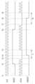
도 1은 본 발명의 일 실시예에 따른 반도체 장치를 설명하기 위한 개략도이다.1 is a schematic diagram illustrating a semiconductor device according to an exemplary embodiment of the present invention.
도 1을 참조하면, 본 발명의 일 실시예에 따른 반도체 장치(1)는 클럭 관리 유닛(Clock Management Unit, CMU)(100), IP 블록(Intellectual Property block)(200, 210) 및 전력 관리 유닛(Power Management Unit, PMU)(300)을 포함한다. 본 발명의 다양한 실시예에 따른 반도체 장치(1)는 SoC(System-on-Chip)으로 구현될 수 있으나, 본 발명의 범위가 이에 한정되는 것은 아니다.Referring to FIG. 1 , a
클럭 관리 유닛(100)은 IP 블록(200, 210)에 클럭 신호를 제공한다. 본 실시예에서, 클럭 관리 유닛(100)은 클럭 컴포넌트(120a, 120b, 120c, 120d, 120e, 120f, 120g), 채널 관리 회로(130, 132) 및 클럭 관리 유닛 컨트롤러(Clock Management Controller, CMU Controller)(110)를 포함한다. 클럭 컴포넌트(120a, 120b, 120c, 120d, 120e, 120f, 120g)는 IP 블록(200, 210)에 제공할 클럭 신호를 생성하고, 채널 관리 회로(130, 132)는 클럭 컴포넌트(120f, 120g)와 IP 블록(200, 210) 사이에 배치되어 클럭 관리 유닛(100)과 IP 블록(200, 210) 사이의 통신 채널(CH)을 제공한다. 그리고 클럭 관리 유닛 컨트롤러(110)는 클럭 컴포넌트(120a, 120b, 120c, 120d, 120e, 120f, 120g)를 이용하여 IP 블록(200, 210)에 클럭 신호를 제공한다.The
본 발명의 몇몇의 실시예에서, 채널 관리 회로(130, 132)가 제공하는 통신 채널(CH)은 ARM 사의 LPI(Low Power Interface), Q-채널 인터페이스(Q-Channel Interface) 또는 P-채널 인터페이스(P-Channel Interface)에 따르도록 구현될 수 있으나, 본 발명의 범위가 이에 제한되는 것은 아니고, 구현 목적에 따라 정해진 임의의 통신 프로토콜을 따르는 통신 채널(CH)로 구현될 수 있다.In some embodiments of the present invention, the communication channel (CH) provided by the
클럭 컴포넌트(120a, 120b, 120c, 120d, 120e, 120f, 120g)는 각각 클럭 소오스(124a, 124b, 124c, 124d, 124e, 124f, 124g)와, 클럭 소오스(124a, 124b, 124c, 124d, 124e, 124f, 124g)를 각각 제어하는 클럭 제어 회로(122a, 122b, 122c, 122d, 122e, 122f, 122g)를 포함한다. 클럭 소오스(124a, 124b, 124c, 124d, 124e, 124f, 124g)는, 예컨대, 다중화 회로(MUX circuit), 클럭 분주 회로(clock dividing circuit), 단기 정지 회로(short stop circuit), 클럭 게이팅 회로(clock gating circuit) 등을 포함할 수 있다.The
클럭 컴포넌트(120a, 120b, 120c, 120d, 120e, 120f, 120g)는 서로 간에 부모-자식 관계를 형성한다. 본 실시예에서 클럭 컴포넌트(120a)는 클럭 컴포넌트(120b)의 부모이고, 클럭 컴포넌트(120b)는 클럭 컴포넌트(120a)의 자식이자 클럭 컴포넌트(120c)의 부모이다. 또한 클럭 컴포넌트(120e)는 2 개의 클럭 컴포넌트(120f, 120g)의 부모이고, 클럭 컴포넌트(120f, 120g)는 클럭 컴포넌트(120e)의 자식이다. 한편, 본 실시예에서 PLL(Phase Locked Loop)에 가장 가깝도록 배치된 클럭 컴포넌트(120a)는 루트(root) 클럭 컴포넌트이고, IP 블록(200, 210)에 가장 가깝도록 배치된 클럭 컴포넌트(120f, 120g)는 리프(leaf) 클럭 컴포넌트이다. 이와 같은 부모-자식 관계는 클럭 컴포넌트(120a, 120b, 120c, 120d, 120e, 120f, 120g) 간의 부모-자식 관계에 따라 필연적으로 클럭 제어 회로(122a, 122b, 122c, 122d, 122e, 122f, 122g) 간, 그리고 클럭 소오스(124a, 124b, 124c, 124d, 124e, 124f, 124g) 간에도 형성된다.
클럭 제어 회로(122a, 122b, 122c, 122d, 122e, 122f, 122g)는 부모와 자식 간에 클럭 요청(REQ) 및 이에 대한 애크(acknowledgement)(ACK)를 주고 받으며, IP 블록(200, 210)에 클럭 신호를 제공한다.The
예를 들어, IP 블록(200)이 클럭 신호를 필요로 하지 않는 경우, 예컨대 IP 블록(200)이 슬립(sleep) 상태가 되어야 할 필요가 있는 경우, 클럭 관리 유닛(100)은 IP 블록(200)에 대한 클럭 신호의 제공을 중지한다.For example, when the
구체적으로, 채널 관리 회로(130)는, 클럭 관리 유닛(100) 또는 클럭 관리 유닛 컨트롤러(110)의 제어 하에, IP 블록(200)에 클럭 신호의 제공을 중지하겠다는 제1 신호를 전송한다. 제1 신호를 수신한 IP 블록(200)은 처리 중인 작업을 완료한 후 클럭 신호가 중지되어도 좋다는 제2 신호를 채널 관리 회로(130)에 전송한다. 채널 관리 회로(130)는 IP 블록(200)으로부터 제2 신호를 수신한 후, 자신의 부모에 해당하는 클럭 컴포넌트(120f)에 클럭 신호의 제공을 중지할 것을 요청한다.Specifically, the
일례로, 만일 채널 관리 회로(130)가 제공하는 통신 채널(CH)이 Q-채널 인터페이스를 따르는 경우라면, 채널 관리 회로(130)는 IP 블록(200)에 제1 논리 값(예컨대, 논리 로우(logic low), 이하 L로 표시)을 갖는 QREQn 신호를 제1 신호로서 전송한다. 이후 채널 관리 회로(130)는 IP 블록(200)으로부터, 예컨대 제1 논리 값을 갖는 QACCEPTn 신호를 제2 신호로서 수신한 후, 클럭 컴포넌트(120f)에, 예컨대 제1 논리 값을 갖는 클럭 요청(REQ)를 전송한다. 이 경우, 상기 제1 논리 값을 갖는 클럭 요청(REQ)은 "클럭 제공 중지 요청"을 말한다.For example, if the communication channel (CH) provided by the
채널 관리 회로(130)로부터 제1 논리 값을 갖는 클럭 요청(REQ), 즉 클럭 제공 중지 요청을 수신한 클럭 제어 회로(122f)는 클럭 소오스(124f)(예컨대, 클럭 게이팅 회로)를 디스에이블(disable)하여 클럭 신호의 제공을 중지하고, 이에 따라 IP 블록(200)은 슬립 모드로 진입할 수 있게 된다. 이 과정에서 클럭 제어 회로(122f)는 제1 논리 값을 갖는 애크(ACK)를 채널 관리 회로(130)에 제공할 수 있다. 유의할 점은 채널 관리 회로(130)가 제1 논리 값을 갖는 클럭 제공 중지 요청을 전송한 후 제1 논리 값을 갖는 애크(ACK)를 수신했다고 해서 클럭 소오스(124f)로부터의 클럭 제공의 중지가 보장되는 것은 아니다. 다만, 상기 애크(ACK)는, 채널 관리 회로(130)의 부모인 클럭 컴포넌트(120f)가 채널 관리 회로(130)에 더 이상 클럭 제공을 할 필요가 없다는 것을 클럭 제어 회로(122f)가 인지했다는 의미를 가질 뿐이다.The
한편, 클럭 컴포넌트(120f)의 클럭 제어 회로(122f)는 자신의 부모에 해당하는 클럭 컴포넌트(120e)의 클럭 제어 회로(122e)에 제1 논리 값을 갖는 클럭 요청(REQ)을 전송한다. 만일 IP 블록(210) 역시 클럭 신호를 필요로 하지 않는 경우, 예컨대 클럭 제어 회로(122e)가 클럭 제어 회로(122g)로부터 클럭 제공 중지 요청을 수신한 경우라면, 클럭 제어 회로(122e)는 클럭 소오스(124e)(예컨대, 클럭 분주 회로)를 디스에이블하여 클럭 신호의 제공을 중지한다. 이에 따라 IP 블록(200, 210)은 슬립 모드로 진입할 수 있게 된다.Meanwhile, the
이와 같은 동작은 다른 클럭 제어 회로(122a, 122b, 122c, 122d)에 대해서도 마찬가지로 수행될 수 있다.Such an operation may be similarly performed for other
이와 다르게, 클럭 컴포넌트(120f)의 클럭 제어 회로(122f)가 자신의 부모에 해당하는 클럭 컴포넌트(120e)의 클럭 제어 회로(122e)에 제1 논리 값을 갖는 클럭 요청(REQ)을 전송하였지만, IP 블록(210)이 실행(running) 상태에 있는 경우라면, 클럭 제어 회로(122e)는 클럭 소오스(124e)를 디스에이블할 수 없다. 이후 IP 블록(210)이 더 이상 클럭 신호를 필요로 하지 않는 경우가 되어서야 비로소 클럭 제어 회로(122e)는 클럭 소오스(124e)를 디스에이블하고 자신의 부모에 해당하는 클럭 제어 회로(120d)에 제1 논리 값을 갖는 클럭 요청(REQ)을 전송할 수 있다. 즉, 클럭 제어 회로(122e)는 자식에 해당하는 클럭 제어 회로(122f, 122g) 모두로부터 클럭 제공 중지 요청을 수신한 경우에만 클럭 소오스(124e)를 디스에이블할 수 있다.Unlike this, although the
한편, IP 블록(200, 210)이 슬립 상태에 있어서 클럭 소오스(124a, 124b, 124c, 124d, 124e, 124f)가 모두 디스에이블되었다가 IP 블록(200)이 실행 상태로 진입한 경우, 클럭 관리 유닛(100)은 IP 블록(200, 210)에 대한 클럭 신호의 제공을 재개한다.Meanwhile, when the IP blocks 200 and 210 are in the sleep state and the
채널 관리 회로(130)는 자신의 부모에 해당하는 클럭 컴포넌트(120f)의 클럭 제어 회로(122f)에 제2 논리 값(예컨대, 논리 하이(logic high), 이하 H로 표시)을 갖는 클럭 요청(REQ)을 전송하고, 클럭 제어 회로(122f)로부터의 애크(ACK)를 대기한다. 여기서 제2 논리 값을 갖는 클럭 요청(REQ)은 "클럭 제공 요청"을 말하고, 클럭 제공 요청에 대한 애크(ACK)는 클럭 소오스(124f)로부터 클럭 제공이 재개되었음을 의미한다. 클럭 제어 회로(122f)는 클럭 소오스(124f)(예컨대, 클럭 게이팅 회로)를 바로 인에이블(enable)하지 못하고, 부모로부터 클럭 신호가 제공되기를 대기한다.The
다음으로 클럭 제어 회로(122f)는 자신의 부모에 해당하는 클럭 제어회로(122e)에 제2 논리 값을 갖는 클럭 요청(REQ), 즉 클럭 제공 요청을 전송하고, 클럭 제어 회로(122e)로부터의 애크(ACK)를 대기한다. 이와 같은 동작은 클럭 제어 회로(122a, 122b, 122c, 122d)에 대해서도 마찬가지로 수행될 수 있다.Next, the
클럭 제어 회로(122b)로부터 제2 논리 값을 갖는 클럭 요청(REQ)를 수신한 루트 클럭 컴포넌트인 클럭 제어 회로(122a)는 클럭 소오스(124a)(예컨대, 다중화 회로)를 인에이블하고 애크(ACK)를 클럭 제어 회로(122b)에 전송한다. 이와 같은 방식으로 클럭 소오스(124b, 124c, 124d, 124d, 124e)가 순차적으로 인에이블되면 비로소 클럭 제어 회로(122e)는 클럭 제어 회로(122f)에 클럭 소오스(124e)로부터 클럭 제공이 재개되었음을 알리는 애크(ACK)를 전송한다. 애크(ACK)를 수신한 클럭 제어 회로(122f)는 비로소 클럭 소오스(124f)를 인에이블하여 클럭 신호를 IP 블록(200)에 제공하고, 채널 관리 회로(130)에 애크(ACK)를 제공한다.Upon receiving the clock request REQ having the second logic value from the
이와 같이 클럭 제어 회로(122a, 122b, 122c, 122d, 122e, 122f, 122g)는 부모와 자식 간에 클럭 요청(REQ) 및 이에 대한 애크 (ACK)를 주고 받는 풀 핸드셰이크(full handshake) 방식으로 동작한다. 이에 따라, 클럭 제어 회로(122a, 122b, 122c, 122d, 122e, 122f, 122g)는 하드웨어적으로 클럭 소오스(124a, 124b, 124c, 124d, 124e, 124f, 124g)를 제어하여 IP 블록(200, 210)에 제공되는 클럭 신호를 제어할 수 있다.In this way, the
이들 클럭 제어 회로(122a, 122b, 122c, 122d, 122e, 122f, 122g)는 자체적으로 동작하여 부모에게 클럭 요청(REQ)을 전송하거나 클럭 소오스(124a, 124b, 124c, 124d, 124e, 124f, 124g)를 제어할 수 있고, 클럭 관리 유닛 컨트롤러(110)의 제어 하에 동작할 수도 있다. 한편, 본 발명의 몇몇의 실시예에서, 클럭 제어 회로(122a, 122b, 122c, 122d, 122e, 122f, 122g)는 부모와 자식 간에 주고 받는 클럭 요청(REQ)에 따라 클럭 소오스(124a, 124b, 124c, 124d, 124e, 124f, 124g)를 각각 제어하는 유한 상태 기계(Finite State Machine, FSM)를 포함할 수 있다.These
도 2는 본 발명의 일 실시예에 따른 반도체 장치를 설명하기 위한 개략도이다.2 is a schematic diagram illustrating a semiconductor device according to an exemplary embodiment of the present invention.
도 2를 참조하면, 본 발명의 일 실시예에 따른 반도체 장치에서, 클럭 컴포넌트(120c)는 단기 정지 클럭 신호(SCLK)를 생성한다. 단기 정지 클럭 신호(SCLK)란 미리 정해진 시간 동안 클럭 신호를 오프시키되, 상기 미리 정해진 시간이 경과한 후에는 반드시 다시 클럭 신호가 온 됨이 보장되는 클럭 신호를 말한다. 단, 여기서 유의할 점은, 단기 정지 신호(SCLK)는 클럭 신호가 오프되는 시간의 길이와는 무관하다는 점이다. 즉, "단기 정지"의 의미는 일정 시간이 경과되기만 하면 특별한 다른 이벤트가 발생되지 않아도 오프되었던 클럭 신호가 반드시 온 된다는 의미이고, 구현 목적에 따라 클럭 신호가 오프되는 시간의 길이는 다양할 수 있다. 본 발명의 몇몇의 실시예에서, 상기 미리 정해진 시간의 길이는, 예컨대 소프트웨어에 의해 설정될 수 있다.Referring to FIG. 2 , in the semiconductor device according to an exemplary embodiment, a
단기 정지 클럭 신호(SCLK)는 예컨대 IP 블록(200)에 특정 신호(예컨대 비동기 또는 동기 리셋(asynchronous or synchronous reset) 신호)를 입력해야 하는 상황, 전파 지연 시간(propagation delay)이 길어 짧은 클럭 사이클(예컨대 1 클럭 사이클 또는 수 개의 클럭 사이클) 내에 타이밍을 맞추기 어려운 신호를 전송해야 하는 상황 등에서 필요할 수 있다. 또한, 단기 정지 클럭 신호(SCLK)는 글리치(glitch) 방지를 위해, 예컨대 IP 블록(200)의 아이들(idle) 상태가 보장된 상태에서 IP 블록(200)에 제어 신호를 제공하여야 하는 상황에서도 필요할 수 있다. 본 실시예에서, 클럭 컴포넌트(120c)는 클럭 제어 회로(122c) 및 클럭 제어 회로(122c)에 의해 제어되어 클럭 신호(CLK)를 입력 받고 정지 클럭 신호(SCLK)를 출력하는 클럭 소오스(124c)를 포함한다.The short-term stop clock signal (SCLK) is used in situations where a specific signal (eg, an asynchronous or synchronous reset signal) needs to be input to the
단기 정지 클럭 신호(SCLK)를 생성하는 클럭 컴포넌트(120c)는, 도 1과 관련하여 앞서 설명한 바와 같이, 다른 클럭 컴포넌트(120b, 120d)와 클럭 요청(REQ) 및 이에 대한 애크(ACK)를 주고 받으며, IP 블록(200)에 단기 정지 클럭 신호를 제공한다. 여기서 클럭 컴포넌트(120b, 120d)는 임의의 기능을 갖는 클럭 컴포넌트일 수 있다. 예를 들어, 클럭 컴포넌트(120b, 120d)는 클럭 신호를 분주하는 분주 회로를 포함할 수 있으나, 본 발명의 범위가 이에 제한되는 것은 아니다. 한편, 복수의 클럭 컴포넌트로 이루어지는 클럭 트리 상에서 단기 정지 클럭 신호(SCLK)를 생성하는 클럭 컴포넌트(120c)의 위치는 구현 목적에 따라 루트 클럭 컴포넌트(120a)를 제외한 임의의 위치로 정해질 수 있다.As described above with reference to FIG. 1, the
그런데, 예를 들어 IP 블록(200)에 특정 신호(예컨대 비동기 또는 동기 리셋(asynchronous or synchronous reset) 신호)를 입력해야 하는 상황에서, 클럭 컴포넌트(120c)가 적절한 시점에 단기 정지 클럭 신호(SCLK)를 생성하기 위해서는 어느 시점에 특정 신호의 값이 변경되었는지 인지해야 할 뿐 아니라, 어느 시점에 클럭 신호를 오프하고 다시 온 할 것인지 결정하는 것이 필요하다.However, for example, in a situation where a specific signal (eg, an asynchronous or synchronous reset signal) needs to be input to the
도 3은 본 발명의 다른 실시예에 따른 반도체 장치를 설명하기 위한 개략도이다.3 is a schematic diagram for explaining a semiconductor device according to another exemplary embodiment of the present invention.
도 3을 참조하면, 본 발명의 다른 실시예에 따른 반도체 장치는 구동 회로(128)를 더 포함한다.Referring to FIG. 3 , a semiconductor device according to another embodiment of the present invention further includes a
구동 회로(128)는 IP 블록(200)을 제어하는 IP 블록 제어 신호(OS)를 입력 받고, 클럭 제어 회로(122c)로부터 단기 정지 클럭 신호(SCLK)가 IP 블록(200)에 출력되는 동안, IP 블록 제어 신호(SS)를 IP 블록(200)에 출력한다. 즉, IP 블록 제어 신호(SS)는 IP 블록 제어 신호(OS)가 단기 정지 클럭 신호(SCLK)의 타이밍에 맞추어 IP 블록(200)으로 입력되는 신호이다. 본 발명의 몇몇의 실시예에서, IP 블록 제어 신호는 리셋(RESET) 신호, 격리(ISOLATION) 신호 및 메모리 장치용 EMA(Extra Magin Adjustment) 신호 등을 포함할 수 있으나, 본 발명의 범위가 이에 제한되는 것은 아니고, IP 블록(200)에 특정 신호(예컨대 비동기 또는 동기 리셋 신호)를 입력해야 하는 상황, 전파 지연 시간이 길어 짧은 클럭 사이클(예컨대 1 클럭 사이클 또는 수 개의 클럭 사이클) 내에 타이밍을 맞추기 어려운 신호를 전송해야 하는 상황, 글리치(glitch) 방지를 위해 예컨대 IP 블록(200)의 아이들(idle) 상태가 보장된 상태에서 IP 블록(200)에 제어 신호를 제공하여야 하는 상황 등에서 요구되는 임의의 신호를 포함한다.While the
구동 회로(128)는 IP 블록 제어 신호(OS)의 입력을 검출한 경우 클럭 제어 회로(122c)에 클럭 요청(410)을 전송한다. 여기서, 단기 정지 클럭 신호(SCLK)를 IP 블록(200)에 제공하기 위해서는, 먼저 클럭 제어 회로(122c)의 부모에 대한 클럭 신호(CLK)가 온 상태가 되어야 하므로, 클럭 제어 회로(122c)는 클럭 요청(410)을 수신한 후, 먼저 자신의 부모에 해당하는 클럭 제어 회로(122b)에 클럭 요청(REQ)을 전송하여, 클럭 소오스(124c)가 부모 클럭 소오스(124b)로부터 클럭 신호를 제공받도록 한다. 클럭 제어 회로(122c)는 클럭 제어 회로(122b)로부터 애크(ACK)를 수신한 후, 클럭 요청(410)에 대한 애크(412)를 구동 회로(128)에 전송한다. 여기서 클럭 요청(410)에 대한 애크(412)는, 클럭 제어 회로(122c)의 부모에 해당하는 클럭 제어 회로(122b)에 의해 제어되는 부모 클럭 소오스(124b)로부터 온 상태의 클럭 신호가 클럭 소오스(124c)에 제공됨을 의미할 수 있다.The driving
구동 회로(128)는 클럭 제어 회로(122c)로부터 클럭 요청(410)에 대한 애크(412)를 수신하여 부모 클럭 소오스(124b)로부터 제공되는 클럭 신호가 온 상태임이 보장된 후, 클럭 소오스(124c)에 클럭 요청(420)을 전송한다. 클럭 소오스(124)는 클럭 요청(420)을 수신한 후, 단기 정지 클럭 신호(SCLK)를 출력하면서 구동 회로(128)에 클럭 요청(420)에 대한 애크(422)를 전송한다.After the
이에 따라 구동 회로(128)는 클럭 소오스(124c)에 의해 생성된 단기 정지 클럭 신호(SCLK)의 타이밍에 맞추어 IP 블록 제어 신호(SS)를 IP 블록(200)에 출력한다. 한편, 구동 회로(128)는 IP 블록 제어 신호(SS)를 IP 블록(200)에 출력하다가 일정 시간이 지난 후 클럭 요청(420)을 해제하여 단기 정지 클럭 신호(SCLK)에 대한 클럭 게이팅을 중단할 수 있다.Accordingly, the driving
본 발명의 몇몇의 실시예에서, 구동 회로(128)는, 예컨대 IP 블록(200)과 마찬가지로 IP 블록으로서 구현될 수 있다. 이 경우, 구동 회로(128)는 자체적으로 동작하기 위한 클럭 신호에 해당하는 기준 클럭 신호(REF_CLK)에 의해 구동된다. 따라서, 구동 회로(128) 역시, 앞서 설명한 바와 같은 클럭 관리 유닛(100)에 대해 자체적으로 기준 클럭 신호(REF_CLK)의 제공 또는 중지를 요청할 수 있다. 즉, 구동 회로(128)에 공급되는 기준 클럭 신호(REF_CLK)와 IP 블록(200)에 공급되는 클럭 신호는 별개의 클럭 신호일 수 있다.In some embodiments of the invention,
이와 같이 구동 회로(128)를, 앞서 설명한 클럭 관리 유닛(100)의 요소들과 별개로 구현함에 따라, IP 블록 제어 신호(OS)의 입력을 검출하고 클럭 제어 회로(122c)를 제어하는 제1 경로와, 클럭 소오스(124b, 124c, 124d)를 거치게 되는 IP 블록(200)에 제공하기 위한 클럭 신호의 제2 경로를 분리함으로서, 클럭 신호의 지연 경로(propagation path)의 길이를 최소화할 수 있고, 나아가 지터 효과(jitter impact)를 감소시킬 수 있다.In this way, as the driving
도 4는 본 발명의 다른 실시예에 따른 반도체 장치의 동작을 설명하기 위한 타이밍도이다.4 is a timing diagram illustrating an operation of a semiconductor device according to another exemplary embodiment of the present invention.
도 4를 참조하면, T2에서 구동 회로(128)가 IP 블록 제어 신호(OS)의 입력을 검출한다. 이후 구동 회로(128)는 클럭 제어 회로(122c)에 클럭 요청(410)을 전송하여 클럭 소오스(124c)가 부모 클럭 소오스(124b)로부터 클럭 신호를 제공받는 것을 보장하고, 클럭 소오스(124c)에 클럭 요청(420)을 전송하여 클럭 소오스(124)가 단기 정지 클럭 신호(SCLK)를 생성하도록 한다(T3).Referring to FIG. 4 , at T2 , the driving
구동 회로(128)는 T3 내지 T5 구간(I 구간)을 갖는 단기 정지 클럭 신호(SCLK) 중에 IP 블록 제어 신호(SS)를 IP 블록(200)에 출력한다.The driving
T6에서 구동 회로(128)가 IP 블록 제어 신호(OS) 값의 변경을 검출하면, 구동 회로(128)는 클럭 제어 회로(122c)에 다시 클럭 요청(410)을 전송하여 클럭 소오스(124c)가 부모 클럭 소오스(124b)로부터 클럭 신호를 제공받는 것을 보장하고, 클럭 소오스(124c)에 다시 클럭 요청(420)을 전송하여 클럭 소오스(124)가 단기 정지 클럭 신호(SCLK)를 생성하도록 한다(T7).At T6, when the driving
구동 회로(128)는 T7 내지 T9 구간(II 구간)을 갖는 단기 정지 클럭 신호(SCLK) 중에 값이 변경된 IP 블록 제어 신호(SS)를 IP 블록(200)에 출력한다.The driving
도 5은 본 발명의 또 다른 실시예에 따른 반도체 장치를 설명하기 위한 개략도이다.5 is a schematic diagram for explaining a semiconductor device according to still another embodiment of the present invention.
도 5를 참조하면, 본 발명의 또 다른 실시예에 따른 반도체 장치에서, 클럭 소오스(124c)는 클럭 게이팅 회로(1244)를 포함할 수 있다. 클럭 게이팅 회로(1244)는 클럭 신호(CLK)를 입력 받고, 인에이블 신호에 따라 클럭 신호(CLK)를 게이팅하여 출력한다. 즉, 단기 정지 클럭 신호(SCLK)는 클럭 제어 회로(122c) 및 구동 회로(128)로부터 제공되는 인에이블 신호에 따라 클럭 게이팅 회로(1244)를 동작시킴으로서 생성될 수 있다.Referring to FIG. 5 , in a semiconductor device according to another embodiment of the present invention, a
클럭 소오스(124c)는 클럭 제어 회로(122c)로부터 수신한 제1 인에이블 신호(430)와, 구동 회로(128)로부터 수신한 제2 인에이블 신호(420)에 대해 논리 연산을 하여 클럭 게이팅 회로(1244)를 제어하는 신호를 출력하는 논리 게이트(1243)를 더 포함한다.The
본 실시예에서는, 본 발명의 개념에 대한 설명의 편의를 위해, 논리 게이트(1243)를 AND 논리 게이트로 도시하였으나, 본 발명의 범위가 이에 제한되는 것은 아니다. 즉, 논리 게이트(1243)는 제1 인에이블 신호(430) 및 제2 인에이블 신호(420)를 입력으로 받아 클럭 게이팅 회로(1244)를 제어하는 신호를 출력하는 임의의 논리 게이트로 구현될 수 있다.In this embodiment, for convenience of description of the concept of the present invention, the
구체적으로, 클럭 제어 회로(122c)로부터 수신한 제1 인에이블 신호(430)는 동기화 회로(1241)에 의해 클럭 신호(CLK)와 동기화되고, 구동 회로(128)로부터 수신한 제2 인에이블 신호(420)는 동기화 회로(1242)에 의해 클럭 신호(CLK)와 동기화된다. 이와 같이 클럭 신호(CLK)와 동기화된 제1 인에이블 신호(430) 및 제2 인에이블 신호(420)가 논리 게이트(1243)의 입력 신호가 된다. 동기화 회로(1241)는 제1 인에이블 신호(430)에 대한 애크(432)를 클럭 제어 회로(122c)에 전송하고, 동기화 회로(1242)는 제2 인에이블 신호(420)에 대한 애크(422)를 구동 회로(128)에 전송한다. 여기서 애크(432, 422)는 클럭 신호(CLK)의 상태(즉, 온/오프 상태)에 대한 정보를 클럭 제어 회로(122c) 및 구동 회로(128)에 제공할 수도 있다.Specifically, the first enable signal 430 received from the
클럭 게이팅 회로(1244)는 논리 게이트(1243)의 출력 신호에 의해 인에이블 또는 디스에이블되어 단기 정지 클럭 신호(SCLK)를 출력하게 된다. 다시 말해서 클럭 게이팅 회로(1244)는 구동 회로(128)가 클럭 제어 회로(122c)로부터 애크(412)를 수신한 후 디스에이블될 수 있다.The
도 6은 본 발명의 또 다른 실시예에 따른 반도체 장치를 설명하기 위한 개략도이다.6 is a schematic diagram for explaining a semiconductor device according to still another embodiment of the present invention.
도 6을 참조하면, 본 발명의 또 다른 실시예에 따른 반도체 장치는 비동기 인터페이스(129) 및 카운터를 더 포함할 수 있다.Referring to FIG. 6 , a semiconductor device according to another embodiment of the present invention may further include an
비동기 인터페이스(129)는 구동 회로(128)의 입력단에 배치되어. 입력 받은 비동기 IP 블록 제어 신호를 동기 신호로 변환하여 구동 회로(128)에 제공한다. 본 실시예에서, 비동기 인터페이스(129)는 비동기 제1 신호(SIGNAL 1) 및 비동기 제2 신호(SIGNAL 2)를 입력 받고, 이들을 동기 신호(SYNC_DATA)로 변환하여 구동 회로(128)에 제공한다. 동기 신호(SYNC_DATA)를 구동 회로(128)에 제공하기 위해, 비동기 인터페이스(129)와 구동 회로(128) 사이에는 요청(SYNC_REQ) 및 애크(SYNC_ACK) 신호가 전송될 수 있다.An
구동 회로(128)는 다중 비트의 제1 신호(SIGNAL 1) 및 제2 신호(SIGNAL 2)를 IP 블록(200)에 제공할 수 있다. 예를 들어, 제1 신호(SIGNAL 1)가 m 비트(여기서 m은 자연수) 데이터이고, 제2 신호(SIGNAL 2)가 n 비트(여기서 n은 자연수) 데이터인 경우, 구동 회로(128)는 m + n 비트의 제1 신호(SIGNAL 1) 및 제2 신호(SIGNAL 2)를 IP 블록(200)에 제공할 수 있다.The driving
한편, 본 실시예에서, 구동 회로(128)가 IP 블록 제어 신호(OS)의 입력을 검출한 후 클럭 제어 회로(122c)에 전송하는 클럭 요청(410) 및 클럭 요청(410)에 의해 부모로부터 클럭 신호를 제공받음을 보장한 후 클럭 소오스(124c)에 전송하는 클럭 요청(420)은 SSCH_REQ[1:0]의 2 비트 데이터로 구현될 수 있다. 또한 및 클럭 요청(410) 및 클럭 요청(420)에 대한 각각의 애크(412, 422)는 SSCH_ACK[1:0]의 2 비트 데이터로 구현될 수 있다.Meanwhile, in this embodiment, the
카운터는 단기 정지 클럭 신호(SCLK)의 길이를 설정하기 위해 이용될 수 있다. 즉, 단기 정지 클럭 신호(SCLK)의 타이밍에 전송되는 IP 블록 제어 신호가 트랜지션되는 시점의 앞 뒤로 몇 클럭 신호를 오프할 것인지 결정하기 위해 카운터가 이용될 수 있다.A counter may be used to set the length of the short-term stop clock signal SCLK. That is, the counter may be used to determine how many clock signals to turn off before and after the transition of the IP block control signal transmitted at the timing of the short-term stop clock signal SCLK.
도 7은 본 발명의 또 다른 실시예에 따른 반도체 장치의 동작을 설명하기 위한 타이밍도이다.7 is a timing diagram illustrating an operation of a semiconductor device according to still another embodiment of the present invention.
도 7을 참조하면, T2에서 구동 회로(128)는 비동기 인터페이스(129)로부터 제1 신호(SIGNAL 1) 및 제2 신호(SIGNAL 2)에 대한 동기 신호(SYNC_DATA)를 입력받는다. T1 내지 T3의 구간에서 구동 회로(128)은 유휴(idle) 상태인 제1 상태(S1)를 갖는다.Referring to FIG. 7 , at T2 , the driving
이후 T3에서 구동 회로(128)는 클럭 제어 회로(122c)에 클럭 요청 (SSCH_REQ[0])을 전송하여 부모로부터 클럭 신호를 제공받음을 보장받는다. 부모로부터의 클럭 신호가 클럭 소오스(124c)에 제공된 후, 구동 회로(128)는 T5에서 클럭 제어 회로(122c)로부터 애크(SSCH_ACK[0])를 수신한다. T3 내지 T6의 구간에서 구동 회로(128)는 부모로부터의 클럭 신호를 제공받기 위한 제2 상태(S2)를 갖는다.Then, at T3, the driving
이후 T5 내지 T7의 구간에서 구동 회로(128)는 제3 상태(S3)로 대기하다가, T7에서 구동 회로(128)는 클럭 소오스(124c)에 클럭 요청(SSCH_REQ[1])을 전송한다. 클럭 요청(SSCH_REQ[1])에 따라 클럭 소오스(124c)가 단기 정지 클럭 신호(SCLK)를 생성하기 시작하고, T8에서 구동 회로(128)는 클럭 소오스(124c)로부터 애크(SSCH_ACK[1])를 수신한다. T7 내지 T9에서 구동 회로(128)는 제4 상태로 단기 정지 클럭 신호(SCLK)를 생성을 제어한다.Thereafter, in the period from T5 to T7, the driving
이에 따라 생성된 단기 정지 클럭 신호(SCLK)는 T9 내지 T11(III 구간)에 걸쳐 출력되고, T10에 구동 회로(128)는 제1 신호(SIGNAL 1) 및 제2 신호(SIGNAL 2)의 변경된 값을 IP 블록(200)에 제공한다. 구동 회로(128)가 변경된 값을 제공하기 전의 T9 내지 T10 구간(A 구간)에서 구동 회로(128)는 클럭 신호를 1차 카운트하는 제5 상태(S5)를 갖는다. 또한 구동 회로(128)가 변경된 값을 제공한 후의 T10 내지 T11 구간(B 구간)에서 구동 회로(128)는 클럭 신호를 2차 카운트하는 제6 상태(S5)를 갖는다. 이와 같이 카운트를 이용하여 제1 신호(SIGNAL 1) 및 제2 신호(SIGNAL 2)의 전후로 충분한 클럭 오프 영역을 설정할 수 있다.Accordingly, the generated short-term stop clock signal SCLK is output from T9 to T11 (period III), and at T10, the driving
이후 T11에서 구동 회로(128)는 클럭 요청(SSCH_REQ[1])을 중단하고, 클럭 소오스(124c)는 단기 정지 클럭 신호(SCLK)의 생성을 종료된 후, 구동 회로(128)는 T12에서 애크(SSCH_ACK[1])를 수신한다. T11 내지 T13에서 구동 회로(128)는 단기 정지 클럭 신호(SCLK)의 생성을 종료시키는 제7 상태(S7)를 갖는다.Then, at T11, the driving
이후 T13에서 구동 회로(128)는 클럭 요청(SSCH_REQ[0])을 중단하고, 클럭 제어 회로(122c)의 부모에 대한 클럭 요청을 중단된 후, 구동 회로(128) T14에서 애크(SSCH_ACK[0])를 수신한다. T13 내지 T15에서 구동 회로(128)는 부모에 대한 클럭 요청을 종료시키는 제8 상태(S7)를 갖는다.Thereafter, at T13, the driving
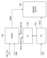
도 8은 본 발명의 또 다른 실시예에 따른 반도체 장치를 설명하기 위한 개략도이고, 도 9는 본 발명의 또 다른 실시예에 따른 반도체 장치의 동작을 설명하기 위한 타이밍도이다.8 is a schematic diagram for explaining a semiconductor device according to still another embodiment of the present invention, and FIG. 9 is a timing diagram for explaining an operation of the semiconductor device according to another embodiment of the present invention.
도 8 및 도 9를 함께 참조하면, 본 발명의 또 다른 실시예에 따른 반도체 장치에서, 구동 회로(128)는 IP 블록(200)을 제어하는 리셋(RESET) 신호를 입력 받고, 클럭 제어 회로(122c)로부터 단기 정지 클럭 신호(SCLK)가 IP 블록(200)에 출력되는 동안, IP 블록(200)을 재시작시키기 위한 리셋(RESET) 신호를 IP 블록(200)에 출력한다.8 and 9 together, in the semiconductor device according to another embodiment of the present invention, the driving
구체적으로, 구동 회로(128)는 리셋(RESET) 신호의 입력을 검출한 경우(T2, T6) 클럭 제어 회로(122c)에 클럭 요청(SSCH_REQ[0])을 전송한다. 클럭 제어 회로(122c)는 클럭 요청(SSCH_REQ[0])을 수신한 후, 자신의 부모에 해당하는 클럭 제어 회로에 클럭 요청(REQ)을 전송하여, 클럭 소오스(124c)가 부모 클럭 소오스로부터 클럭 신호를 제공받도록 한다. 클럭 제어 회로(122c)는 부모 클럭 제어 회로로부터 애크(ACK)를 수신한 후, 클럭 요청(SSCH_REQ[0])에 대한 애크(SSCH_ACK[0])를 구동 회로(128)에 전송한다.Specifically, the driving
구동 회로(128)는 클럭 제어 회로(122c)로부터 클럭 요청(SSCH_REQ[0])에 대한 애크(SSCH_ACK[0])를 수신한 후, 클럭 소오스(124c)에 클럭 요청(SSCH_REQ[1])을 전송한다. 클럭 소오스(124)는 클럭 요청(SSCH_REQ[1])을 수신한 후, T3 내지 T5(I 구간) 또는 T7 내지 T9 구간(II 구간)을 갖는 단기 정지 클럭 신호(SCLK)를 출력하면서 구동 회로(128)에 클럭 요청(SSCH_REQ[1])에 대한 애크(SSCH_ACK[1])를 전송한다.After receiving the ACK (SSCH_ACK[0]) for the clock request (SSCH_REQ[0]) from the
이에 따라 구동 회로(128)는 클럭 소오스(124c)에 의해 생성된 T3 내지 T5(I 구간) 또는 T7 내지 T9 구간(II 구간)을 갖는 단기 정지 클럭 신호(SCLK)의 타이밍에 맞추어 T4 또는 T8에서 리셋(RESET) 신호를 IP 블록(200)에 전송한다.Accordingly, the driving
도 10은 본 발명의 또 다른 실시예에 따른 반도체 장치를 설명하기 위한 개략도이고, 도 11은 본 발명의 또 다른 실시예에 따른 반도체 장치의 동작을 설명하기 위한 타이밍도이다.FIG. 10 is a schematic diagram illustrating a semiconductor device according to still another embodiment of the present invention, and FIG. 11 is a timing diagram illustrating an operation of the semiconductor device according to another embodiment of the present invention.
도 10 및 도 11을 함께 참조하면, 본 발명의 또 다른 실시예에 따른 반도체 장치에서, 구동 회로(128)는 IP 블록(200)을 제어하는 격리(ISOLATION) 신호를 입력 받고, 클럭 제어 회로(122c)로부터 단기 정지 클럭 신호(SCLK)가 IP 블록(200)에 출력되는 동안, IP 블록(200) 중 일부 영역을 격리시키기 위한 격리(ISOLATION) 신호를 격리 블록(220)에 출력한다.10 and 11 together, in the semiconductor device according to another embodiment of the present invention, the driving
구체적으로, 구동 회로(128)는 격리(ISOLATION) 신호의 입력을 검출한 경우(T2, T6) 클럭 제어 회로(122c)에 클럭 요청(SSCH_REQ[0])을 전송한다. 클럭 제어 회로(122c)는 클럭 요청(SSCH_REQ[0])을 수신한 후, 자신의 부모에 해당하는 클럭 제어 회로에 클럭 요청(REQ)을 전송하여, 클럭 소오스(124c)가 부모 클럭 소오스로부터 클럭 신호를 제공받도록 한다. 클럭 제어 회로(122c)는 부모 클럭 제어 회로로부터 애크(ACK)를 수신한 후, 클럭 요청(SSCH_REQ[0])에 대한 애크(SSCH_ACK[0])를 구동 회로(128)에 전송한다.Specifically, the driving
구동 회로(128)는 클럭 제어 회로(122c)로부터 클럭 요청(SSCH_REQ[0])에 대한 애크(SSCH_ACK[0])를 수신한 후, 클럭 소오스(124c)에 클럭 요청(SSCH_REQ[1])을 전송한다. 클럭 소오스(124)는 클럭 요청(SSCH_REQ[1])을 수신한 후, T3 내지 T5(I 구간) 또는 T7 내지 T9 구간(II 구간)을 갖는 단기 정지 클럭 신호(SCLK)를 출력하면서 구동 회로(128)에 클럭 요청(SSCH_REQ[1])에 대한 애크(SSCH_ACK[1])를 전송한다.After receiving the ACK (SSCH_ACK[0]) for the clock request (SSCH_REQ[0]) from the
이에 따라 구동 회로(128)는 클럭 소오스(124c)에 의해 생성된 T3 내지 T5(I 구간) 또는 T7 내지 T9 구간(II 구간)을 갖는 단기 정지 클럭 신호(SCLK)의 타이밍에 맞추어 T4 또는 T8에서 격리(ISOLATION) 신호를 격리 블록(220)에 전송한다.Accordingly, the driving
도 12는 본 발명의 또 다른 실시예에 따른 반도체 장치를 설명하기 위한 개략도이고, 도 13은 본 발명의 또 다른 실시예에 따른 반도체 장치의 동작을 설명하기 위한 타이밍도이다.FIG. 12 is a schematic diagram illustrating a semiconductor device according to another exemplary embodiment, and FIG. 13 is a timing diagram illustrating an operation of the semiconductor device according to another exemplary embodiment.
도 12 및 도 13을 함께 참조하면, 본 발명의 또 다른 실시예에 따른 반도체 장치에서, 구동 회로(128)는 메모리 블록인 IP 블록(240)을 제어하는 메모리 장치용 EMA 신호를 입력 받고, 클럭 제어 회로(122c)로부터 단기 정지 클럭 신호(SCLK)가 IP 블록(240)에 출력되는 동안, IP 블록(240)을 재설정하기 위한 EMA 신호를 IP 블록(240)에 출력한다.12 and 13 together, in the semiconductor device according to another embodiment of the present invention, the driving
구체적으로, 구동 회로(128)는 EMA 신호의 입력을 검출한 경우(T2, T6) 클럭 제어 회로(122c)에 클럭 요청(SSCH_REQ[0])을 전송한다. 클럭 제어 회로(122c)는 클럭 요청(SSCH_REQ[0])을 수신한 후, 자신의 부모에 해당하는 클럭 제어 회로에 클럭 요청(REQ)을 전송하여, 클럭 소오스(124c)가 부모 클럭 소오스로부터 클럭 신호를 제공받도록 한다. 클럭 제어 회로(122c)는 부모 클럭 제어 회로로부터 애크(ACK)를 수신한 후, 클럭 요청(SSCH_REQ[0])에 대한 애크(SSCH_ACK[0])를 구동 회로(128)에 전송한다.Specifically, the driving
구동 회로(128)는 클럭 제어 회로(122c)로부터 클럭 요청(SSCH_REQ[0])에 대한 애크(SSCH_ACK[0])를 수신한 후, 클럭 소오스(124c)에 클럭 요청(SSCH_REQ[1])을 전송한다. 클럭 소오스(124)는 클럭 요청(SSCH_REQ[1])을 수신한 후, T3 내지 T5(I 구간) 또는 T7 내지 T9 구간(II 구간)을 갖는 단기 정지 클럭 신호(SCLK)를 출력하면서 구동 회로(128)에 클럭 요청(SSCH_REQ[1])에 대한 애크(SSCH_ACK[1])를 전송한다.After receiving the ACK (SSCH_ACK[0]) for the clock request (SSCH_REQ[0]) from the
이에 따라 구동 회로(128)는 클럭 소오스(124c)에 의해 생성된 T3 내지 T5(I 구간) 또는 T7 내지 T9 구간(II 구간)을 갖는 단기 정지 클럭 신호(SCLK)의 타이밍에 맞추어 T4 또는 T8에서 EMA 신호를 IP 블록(240)에 전송한다.Accordingly, the driving
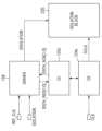
도 14는 본 발명의 몇몇의 실시예에 따른 반도체 장치 및 반도체 장치의 동작 방법이 적용될 수 있는 반도체 시스템의 블록도이다.14 is a block diagram of a semiconductor system to which a semiconductor device and a method of operating the semiconductor device according to some embodiments of the present disclosure may be applied.
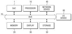
도 14를 참조하면, 본 발명의 몇몇의 실시예에 따른 반도체 장치 및 반도체 장치의 동작 방법이 적용될 수 있는 반도체 시스템은 앞서 설명한 바와 같은 특징들을 포함하는 반도체 장치(SoC)(1), 프로세서(10), 메모리 장치(20), 디스플레이 장치(30), 네트워크 장치(40), 스토리지 장치(50) 및 입출력 장치(60)를 포함할 수 있다. 반도체 장치(SoC)(1), 프로세서(10), 메모리 장치(20), 디스플레이 장치(30), 네트워크 장치(40), 스토리지 장치(50) 및 입출력 장치(60)는 버스(70)를 통해 서로 데이터를 주고 받을 수 있다.Referring to FIG. 14 , a semiconductor system to which a semiconductor device and a method of operating the semiconductor device according to some embodiments of the present disclosure may be applied include a semiconductor device (SoC) 1 including the features described above, and a processor 10 ), a
본 발명의 다양한 실시예에서 언급된 반도체 장치(SoC)(1) 내부의 IP 블록들은 메모리 장치(20)를 제어하는 메모리 컨트롤러, 디스플레이 장치(30)를 제어하는 디스플레이 컨트롤러, 네크워크 장치(40)를 제어하는 네트워크 컨트롤러, 스토리지 장치(50)를 제어하는 스토리지 컨트롤러 및 입출력 장치(60)를 제어하는 입출력 컨트롤러 중 적어도 하나를 포함할 수 있다. 또한 반도체 시스템은 이들 장치들을 제어하는 추가적인 프로세서(10)를 더 구비할 수도 있다.IP blocks inside the semiconductor device (SoC) 1 mentioned in various embodiments of the present invention include a memory controller for controlling the
도 15 내지 도 17는 본 발명의 몇몇의 실시예들에 따른 반도체 장치 및 반도체 장치의 동작 방법을 적용할 수 있는 예시적인 반도체 시스템들이다.15 to 17 are exemplary semiconductor systems to which a semiconductor device and a method of operating the semiconductor device according to some embodiments of the present invention may be applied.
도 15는 태블릿 PC(1200)를 도시한 도면이고, 도 16은 노트북(1300)을 도시한 도면이며, 도 17은 스마트폰(1400)을 도시한 것이다. 본 발명의 다양한 실시예들에 따른 반도체 장치는 이러한 태블릿 PC(1200), 노트북(1300), 스마트폰(1400) 등에 사용될 수 있다.FIG. 15 shows a tablet PC 1200, FIG. 16 shows a notebook 1300, and FIG. 17 shows a smart phone 1400. A semiconductor device according to various embodiments of the present disclosure may be used in such a tablet PC 1200, a notebook 1300, a smart phone 1400, and the like.
또한, 본 발명의 몇몇 실시예들에 따른 반도체 장치는, 예시하지 않는 다른 집적 회로 장치에도 적용될 수 있음은 해당 기술 분야의 통상의 기술자에게 자명하다.In addition, it is obvious to those skilled in the art that semiconductor devices according to some embodiments of the present invention can be applied to other integrated circuit devices not illustrated.
즉, 이상에서는 본 실시예에 따른 반도체 시스템의 예로, 태블릿 PC(1200), 노트북(1300), 및 스마트폰(1400)만을 들었으나, 본 실시예에 따른 반도체 시스템의 예가 이에 제한되는 것은 아니다.That is, in the foregoing, only the tablet PC 1200, the laptop computer 1300, and the smart phone 1400 have been described as examples of the semiconductor system according to the present embodiment, but the example of the semiconductor system according to the present embodiment is not limited thereto.
본 발명의 몇몇 실시예에서, 반도체 시스템은, 컴퓨터, UMPC (Ultra Mobile PC), 워크스테이션, 넷북(net-book), PDA (Personal Digital Assistants), 포터블(portable) 컴퓨터, 무선 전화기(wireless phone), 모바일 폰(mobile phone), e-북(e-book), PMP(portable multimedia player), 휴대용 게임기, 네비게이션(navigation) 장치, 블랙박스(black box), 디지털 카메라(digital camera), 3차원 수상기(3-dimensional television), 디지털 음성 녹음기(digital audio recorder), 디지털 음성 재생기(digital audio player), 디지털 영상 녹화기(digital picture recorder), 디지털 영상 재생기(digital picture player), 디지털 동영상 녹화기(digital video recorder), 디지털 동영상 재생기(digital video player) 등으로 구현될 수도 있다.In some embodiments of the present invention, the semiconductor system may be used in a computer, an ultra mobile PC (UMPC), a workstation, a net-book, a personal digital assistant (PDA), a portable computer, or a wireless phone. , mobile phone, e-book, portable multimedia player (PMP), portable game machine, navigation device, black box, digital camera, 3D receiver (3-dimensional television), digital audio recorder, digital audio player, digital picture recorder, digital picture player, digital video recorder ), a digital video player, and the like.
이상 첨부된 도면을 참조하여 본 발명의 실시예들을 설명하였으나, 본 발명은 상기 실시예들에 한정되는 것이 아니라 서로 다른 다양한 형태로 제조될 수 있으며, 본 발명이 속하는 기술분야에서 통상의 지식을 가진 자는 본 발명의 기술적 사상이나 필수적인 특징을 변경하지 않고서 다른 구체적인 형태로 실시될 수 있다는 것을 이해할 수 있을 것이다. 그러므로 이상에서 기술한 실시예들은 모든 면에서 예시적인 것이며 한정적이 아닌 것으로 이해해야만 한다.Although the embodiments of the present invention have been described with reference to the accompanying drawings, the present invention is not limited to the above embodiments and can be manufactured in a variety of different forms, and those skilled in the art in the art to which the present invention belongs A person will understand that the present invention may be embodied in other specific forms without changing the technical spirit or essential features. Therefore, the embodiments described above should be understood as illustrative in all respects and not limiting.
1: 반도체 장치100: 클럭 관리 유닛(CMU)
110: 클럭 관리 유닛 컨트롤러(CMU controller)
120: 클럭 컴포넌트122: 클럭 제어 회로
124: 클럭 소오스130, 132: 채널 관리 회로
200, 210: IP 블록300: 전력 관리 유닛(PMU)1: semiconductor device 100: clock management unit (CMU)
110: clock management unit controller (CMU controller)
120: clock component 122: clock control circuit
124:
200, 210: IP Block 300: Power Management Unit (PMU)
Claims (20)
Translated fromKorean제1 클럭 소오스(clock source)를 제어하는 제1 클럭 제어 회로(clock control circuit); 및
상기 구동 회로로부터 수신된 제2 클럭 요청에 대한 응답으로 상기 제1 클럭 제어 회로에 제1 클럭 요청을 전송하고, 상기 제1 클럭 제어 회로로부터의 상기 제1 클럭 요청의 ACK를 기초로 상기 제1 클럭 소오스로부터 클럭 신호를 제공받는 제2 클럭 소오스를 제어하여, 미리 정해진 시간 동안 상기 클럭 신호가 오프되는 정지(stopped) 클럭 신호를 생성하는 제2 클럭 제어 회로를 포함하되,
상기 구동 회로는 IP 블록 제어 신호를 입력받고, 상기 정지 클럭 신호가 IP 블록에 출력되는 동안 상기 IP 블록 제어 신호를 상기 IP 블록에 출력하는 반도체 장치.driving circuit;
a first clock control circuit for controlling a first clock source; and
Transmits a first clock request to the first clock control circuit in response to the second clock request received from the driving circuit, and based on an ACK of the first clock request from the first clock control circuit, the first clock request A second clock control circuit for controlling a second clock source receiving a clock signal from a clock source to generate a stopped clock signal in which the clock signal is turned off for a predetermined time,
The semiconductor device of claim 1 , wherein the driving circuit receives an IP block control signal and outputs the IP block control signal to the IP block while the stop clock signal is output to the IP block.
상기 구동 회로는 상기 IP 블록 제어 신호의 입력을 검출한 경우 상기 제2 클럭 제어 회로에 상기 제2 클럭 요청을 전송하는 반도체 장치.According to claim 1,
wherein the driving circuit transmits the second clock request to the second clock control circuit when the input of the IP block control signal is detected.
상기 구동 회로는 상기 제2 클럭 제어 회로로부터 상기 제2 클럭 요청에 대한 ACK를 수신하는 반도체 장치.According to claim 2,
The semiconductor device of claim 1 , wherein the driving circuit receives an ACK in response to the second clock request from the second clock control circuit.
상기 구동 회로는 상기 제2 클럭 제어 회로로부터 상기 제2 클럭 요청에 대한 ACK를 수신한 경우 상기 제2 클럭 소오스에 제3 클럭 요청을 전송하는 반도체 장치.According to claim 3,
wherein the driving circuit transmits a third clock request to the second clock source when an ACK for the second clock request is received from the second clock control circuit.
상기 구동 회로는 상기 제2 클럭 소오스로부터 상기 제3 클럭 요청에 대한 ACK를 수신한 후 상기 IP 블록 제어 신호를 상기 IP 블록에 출력하는 반도체 장치.According to claim 4,
The semiconductor device of claim 1 , wherein the driving circuit outputs the IP block control signal to the IP block after receiving an ACK for the third clock request from the second clock source.
상기 IP 블록 제어 신호는 리셋(RESET) 신호, 격리(ISOLATION) 신호 및 메모리 장치용 EMA(Extra Magin Adjustment) 신호 중 적어도 하나를 포함하는 반도체 장치.According to claim 1,
The IP block control signal includes at least one of a reset signal, an isolation signal, and an extra magnin adjustment (EMA) signal for a memory device.
상기 제2 클럭 소오스는 클럭 게이팅 회로를 포함하는 반도체 장치.According to claim 1,
The second clock source includes a clock gating circuit.
상기 제2 클럭 소오스는 상기 제2 클럭 제어 회로로부터 수신한 제1 인에이블 신호와, 상기 구동 회로로부터 수신한 제2 인에이블 신호에 대해 논리 연산을 하여 상기 클럭 게이팅 회로를 제어하는 신호를 출력하는 논리 게이트를 더 포함하는 반도체 장치.According to claim 7,
The second clock source outputs a signal for controlling the clock gating circuit by performing a logic operation on a first enable signal received from the second clock control circuit and a second enable signal received from the driving circuit. A semiconductor device further comprising a logic gate.
상기 제1 클럭 소오스는 다중화 회로(MUX circuit), 클럭 분주 회로(clock dividing circuit), 단기 정지 회로(short stop circuit) 및 클럭 게이팅 회로(clock gating circuit) 중 적어도 하나를 포함하는 반도체 장치.According to claim 1,
The semiconductor device of claim 1 , wherein the first clock source includes at least one of a MUX circuit, a clock dividing circuit, a short stop circuit, and a clock gating circuit.
제1 클럭 소오스(clock source)를 제어하는 제1 클럭 제어 회로(clock control circuit); 및
상기 구동 회로로부터 수신된 제2 클럭 요청에 응답하여 상기 제1 클럭 제어 회로에 제1 클럭 요청을 전송하고, 상기 제1 클럭 제어 회로로부터의 상기 제1 클럭 요청의 ACK를 기초로 상기 제1 클럭 소오스로부터 클럭 신호를 제공받는 제2 클럭 소오스를 제어하여, 미리 정해진 시간 동안 상기 클럭 신호가 오프되는 정지 클럭 신호를 생성하는 제2 클럭 제어 회로를 포함하되,
상기 구동 회로는 IP 블록 제어 신호에 응답하여, 상기 제2 클럭 제어 회로에 제2 클럭 요청을 전송하고 상기 제2 클럭 소오스에 제3 클럭 요청을 전송하고,
상기 구동 회로는 상기 정지 클럭 신호가 IP 블록에 출력되는 동안 상기 IP 블록 제어 신호를 상기 IP 블록에 출력하는 반도체 장치.driving circuit;
a first clock control circuit for controlling a first clock source; and
transmits a first clock request to the first clock control circuit in response to a second clock request received from the driving circuit, and transmits the first clock request to the first clock control circuit based on an ACK of the first clock request from the first clock control circuit; A second clock control circuit for controlling a second clock source receiving a clock signal from the source to generate a stop clock signal in which the clock signal is turned off for a predetermined time;
The driving circuit transmits a second clock request to the second clock control circuit and a third clock request to the second clock source in response to the IP block control signal;
wherein the driving circuit outputs the IP block control signal to the IP block while the stop clock signal is output to the IP block.
상기 IP 블록 제어 신호는 리셋(RESET) 신호, 격리(ISOLATION) 신호 및 메모리 장치용 EMA(Extra Magin Adjustment) 신호 중 적어도 하나를 포함하는 반도체 장치.According to claim 10,
The IP block control signal includes at least one of a reset signal, an isolation signal, and an extra magnin adjustment (EMA) signal for a memory device.
상기 구동 회로는 상기 제2 클럭 소오스로부터 상기 제3 클럭 요청에 대한 ACK를 수신한 후 상기 IP 블록 제어 신호를 상기 IP 블록에 출력하는 반도체 장치.According to claim 10,
The semiconductor device of claim 1 , wherein the driving circuit outputs the IP block control signal to the IP block after receiving an ACK for the third clock request from the second clock source.
상기 SoC와 전기적으로 접속된 하나 이상의 외부 장치(external device)를 포함하고,
상기 클럭 관리 유닛은,
클럭 제어 회로 및 클럭 소오스와,
제1 시간에 상기 클럭 제어 회로에 제1 클럭 요청을 전송하고, 제2 시간에 상기 제1 클럭 요청에 대한 ACK를 수신하고, 제3 시간에 상기 클럭 소오스에 제2 클럭 요청을 전송하고, 제4 시간에 상기 제2 클럭 요청에 대한 ACK를 수신하는 구동 회로를 포함하되,
상기 클럭 제어 회로는 상기 제1 클럭 요청을 수신한 것에 응답하여 상기 클럭 소오스에 인에이블 신호를 제공하고,
상기 클럭 제어 회로는 상기 클럭 소오스로부터의 인에이블 신호에 대한 ACK를 수신하는 것에 응답하여 상기 구동 회로에 상기 제1 클럭 요청에 대한 ACK를 제공하고,
상기 클럭 소오스는 상기 제2 클럭 요청에 응답하여 제1 클럭 신호를 생성하되, 상기 제1 클럭 신호는 하이(high) 상태와 로우(low) 상태 사이를 오실레이팅하지 않고,
상기 구동 회로는 제5 시간에 상기 제2 클럭 요청을 종료하고, 상기 제2 클럭 요청이 종료되는 것에 대응하여 상기 제1 클럭 신호는 디스에이블되고,
상기 구동 회로는, 상기 클럭 소오스로부터 오실레이팅하지 않는 상기 제1 클럭 신호가 출력되는 동안 제어 신호를 IP 블록에 출력하는 반도체 시스템.A System-on-Chip (SoC) including one or more Intellectual Property blocks (IP blocks) and a Clock Management Unit (CMU) providing clock signals to the IP blocks; and
Including one or more external devices electrically connected to the SoC,
The clock management unit,
a clock control circuit and a clock source;
send a first clock request to the clock control circuit at a first time, receive an ACK for the first clock request at a second time, send a second clock request to the clock source at a third time, and A driving circuit for receiving an ACK for the second clock request at time 4,
the clock control circuit provides an enable signal to the clock source in response to receiving the first clock request;
the clock control circuit provides an ACK for the first clock request to the driving circuit in response to receiving an ACK for an enable signal from the clock source;
the clock source generates a first clock signal in response to the second clock request, the first clock signal not oscillating between a high state and a low state;
the driving circuit terminates the second clock request at a fifth time, and the first clock signal is disabled in response to the termination of the second clock request;
wherein the driving circuit outputs a control signal to an IP block while the first clock signal, which does not oscillate, is output from the clock source.
상기 제1 클럭 신호가 디스에이블될 때, 하이(high) 상태와 로우(low) 상태 사이를 오실레이팅하는 제2 클럭 신호가 상기 클럭 소오스로부터 출력되는 반도체 시스템.According to claim 13,
and a second clock signal oscillating between a high state and a low state is output from the clock source when the first clock signal is disabled.
상기 외부 장치는 메모리 장치, 디스플레이 장치, 네트워크 장치, 스토리지 장치 및 입출력 장치 중 적어도 하나를 포함하고,
상기 SoC는 상기 외부 장치를 제어하는 반도체 시스템.According to claim 13,
The external device includes at least one of a memory device, a display device, a network device, a storage device, and an input/output device,
The SoC controls the external device.
상기 제2 클럭 요청에 대한 응답으로 부모 클럭 소오스(parent clock source)를 제어하는 부모 클럭 제어 회로(parent clock control circuit)에 제1 클럭 요청을 전송하고,
상기 부모 클럭 제어 회로로부터 상기 제1 클럭 요청에 대한 ACK를 수신한 후 상기 구동 회로에 상기 제2 클럭 요청에 대한 ACK를 전송하고,
상기 구동 회로로부터 제3 클럭 요청을 수신하고,
상기 제3 클럭 요청에 대한 응답으로 미리 정해진 시간 동안 상기 IP 블록에 제공되는 클럭 신호가 오프되는 정지(stopped) 클럭 신호를 생성하고,
상기 구동 회로에 상기 제3 클럭 요청에 대한 ACK를 전송하는 반도체 장치의 동작 방법.Receiving a second clock request from a driving circuit that receives an IP block control signal and outputs it to the IP block;
Sending a first clock request to a parent clock control circuit that controls a parent clock source in response to the second clock request;
After receiving an ACK for the first clock request from the parent clock control circuit, transmit an ACK for the second clock request to the driving circuit;
receive a third clock request from the driving circuit;
In response to the third clock request, a clock signal provided to the IP block is turned off for a predetermined time to generate a stopped clock signal;
A method of operating a semiconductor device comprising transmitting an ACK in response to the third clock request to the driving circuit.
상기 정지 클럭 신호를 생성하는 것은,
상기 구동 회로로부터 수신한 상기 제3 클럭 요청에 대한 응답으로, 상기 부모 클럭 소오스로부터 클럭 신호를 제공받는 클럭 게이팅 회로를 상기 미리 정해진 시간 동안 디스에이블하는 것을 포함하는 반도체 장치의 동작 방법.According to claim 16,
Generating the stop clock signal,
and disabling a clock gating circuit receiving a clock signal from the parent clock source for the predetermined time period in response to the third clock request received from the driving circuit.
카운터를 이용하여 상기 정지 클럭 신호의 길이를 설정하는 것을 더 포함하는 반도체 장치의 동작 방법.According to claim 16,
The method of operating the semiconductor device further comprising setting the length of the stop clock signal using a counter.
상기 구동 회로는 상기 정지 클럭 신호가 상기 IP 블록에 입력되는 동안 상기 IP 블록 제어 신호를 상기 IP 블록에 출력하는 반도체 장치의 동작 방법.According to claim 16,
wherein the driving circuit outputs the IP block control signal to the IP block while the stop clock signal is input to the IP block.
상기 구동 회로는 상기 제3 클럭 요청에 대한 ACK를 수신한 후 상기 IP 블록 제어 신호를 상기 IP 블록에 출력하는 반도체 장치의 동작 방법.According to claim 19,
wherein the driving circuit outputs the IP block control signal to the IP block after receiving an ACK for the third clock request.
Priority Applications (4)
| Application Number | Priority Date | Filing Date | Title |
|---|---|---|---|
| US15/415,020US10429881B2 (en) | 2016-01-25 | 2017-01-25 | Semiconductor device for stopping an oscillating clock signal from being provided to an IP block, a semiconductor system having the semiconductor device, and a method of operating the semiconductor device |
| DE102017110799.1ADE102017110799A1 (en) | 2016-01-25 | 2017-05-18 | A semiconductor device, a semiconductor system, and a method of operating the semiconductor device |
| CN201710611810.4ACN108268087B (en) | 2017-01-03 | 2017-07-25 | Semiconductor device, semiconductor system and method of operating semiconductor device |
| TW106124803ATWI727075B (en) | 2016-01-25 | 2017-07-25 | Semiconductor device |
Applications Claiming Priority (2)
| Application Number | Priority Date | Filing Date | Title |
|---|---|---|---|
| US201662286866P | 2016-01-25 | 2016-01-25 | |
| US62/286,866 | 2016-01-25 |
Publications (2)
| Publication Number | Publication Date |
|---|---|
| KR20170088751A KR20170088751A (en) | 2017-08-02 |
| KR102568225B1true KR102568225B1 (en) | 2023-08-17 |
Family
ID=59651742
Family Applications (1)
| Application Number | Title | Priority Date | Filing Date |
|---|---|---|---|
| KR1020170000614AActiveKR102568225B1 (en) | 2016-01-25 | 2017-01-03 | Semiconductor device, semiconductor system and method for operating semiconductor device |
Country Status (1)
| Country | Link |
|---|---|
| KR (1) | KR102568225B1 (en) |
Citations (7)
| Publication number | Priority date | Publication date | Assignee | Title |
|---|---|---|---|---|
| JP2002049437A (en) | 2000-08-01 | 2002-02-15 | Fujitsu Ltd | Electronic device and clock supply method |
| US20060161797A1 (en) | 2003-01-24 | 2006-07-20 | Eckhard Grass | Asynchronous wrapper for a globally asynchronous, locally synchronous (gals) circuit |
| US20060248367A1 (en) | 2005-04-29 | 2006-11-02 | Fischer Timothy C | Count calibration for synchronous data transfer between clock domains |
| KR100651888B1 (en) | 2005-10-11 | 2006-12-01 | 엘지전자 주식회사 | Asynchronous interface device and method |
| US20110202788A1 (en) | 2010-02-12 | 2011-08-18 | Blue Wonder Communications Gmbh | Method and device for clock gate controlling |
| US20140082396A1 (en) | 2012-09-14 | 2014-03-20 | Oracle International Corporation | Method and apparatus for distributed generation of multiple configurable ratioed clock domains within a high speed domain |
| US20160116934A1 (en) | 2014-10-23 | 2016-04-28 | Samsung Electronics Co., Ltd. | Clock circuit for generating clock signal and semiconductor integrated circuit device including the same |
Family Cites Families (1)
| Publication number | Priority date | Publication date | Assignee | Title |
|---|---|---|---|---|
| KR101790320B1 (en)* | 2010-04-09 | 2017-10-25 | 가부시키가이샤 한도오따이 에네루기 켄큐쇼 | Divider circuit |
- 2017
- 2017-01-03KRKR1020170000614Apatent/KR102568225B1/enactiveActive
Patent Citations (7)
| Publication number | Priority date | Publication date | Assignee | Title |
|---|---|---|---|---|
| JP2002049437A (en) | 2000-08-01 | 2002-02-15 | Fujitsu Ltd | Electronic device and clock supply method |
| US20060161797A1 (en) | 2003-01-24 | 2006-07-20 | Eckhard Grass | Asynchronous wrapper for a globally asynchronous, locally synchronous (gals) circuit |
| US20060248367A1 (en) | 2005-04-29 | 2006-11-02 | Fischer Timothy C | Count calibration for synchronous data transfer between clock domains |
| KR100651888B1 (en) | 2005-10-11 | 2006-12-01 | 엘지전자 주식회사 | Asynchronous interface device and method |
| US20110202788A1 (en) | 2010-02-12 | 2011-08-18 | Blue Wonder Communications Gmbh | Method and device for clock gate controlling |
| US20140082396A1 (en) | 2012-09-14 | 2014-03-20 | Oracle International Corporation | Method and apparatus for distributed generation of multiple configurable ratioed clock domains within a high speed domain |
| US20160116934A1 (en) | 2014-10-23 | 2016-04-28 | Samsung Electronics Co., Ltd. | Clock circuit for generating clock signal and semiconductor integrated circuit device including the same |
Also Published As
| Publication number | Publication date |
|---|---|
| KR20170088751A (en) | 2017-08-02 |
Similar Documents
| Publication | Publication Date | Title |
|---|---|---|
| US10853304B2 (en) | System on chip including clock management unit and method of operating the system on chip | |
| TWI727075B (en) | Semiconductor device | |
| US20180039598A1 (en) | Triple-data-rate technique for a synchronous link | |
| US8051320B2 (en) | Clock ratio controller for dynamic voltage and frequency scaled digital systems, and applications thereof | |
| US10928849B2 (en) | Semiconductor device, semiconductor system and method for operating semiconductor device | |
| US11275708B2 (en) | System on chip including clock management unit and method of operating the system on chip | |
| US10503674B2 (en) | Semiconductor device including a clock source for generating a clock signal and a clock control circuit for controlling the clock source in hardware, a semiconductor system including the semiconductor device, and a method of operating the semiconductor device | |
| KR20160143159A (en) | Power Gating Control Circuit For Controlling Stably Data Restoring | |
| US10209734B2 (en) | Semiconductor device, semiconductor system, and method of operating the semiconductor device | |
| JP2014206971A (en) | Method, apparatus, and system for hybrid lane stalling or no-lock bus architectures | |
| US10429881B2 (en) | Semiconductor device for stopping an oscillating clock signal from being provided to an IP block, a semiconductor system having the semiconductor device, and a method of operating the semiconductor device | |
| KR102568225B1 (en) | Semiconductor device, semiconductor system and method for operating semiconductor device | |
| KR102571154B1 (en) | Semiconductor device, semiconductor system and method for operating semiconductor device | |
| CN108268087B (en) | Semiconductor device, semiconductor system and method of operating semiconductor device | |
| KR102740417B1 (en) | Semiconductor device, semiconductor system and method for operating semiconductor device | |
| KR102712345B1 (en) | Semiconductor device, semiconductor system and method for operating semiconductor device | |
| CN108268117B (en) | Semiconductor device and semiconductor system | |
| KR102474620B1 (en) | Semiconductor device, semiconductor system and method for operating semiconductor device | |
| CN108268085B (en) | Semiconductor device | |
| TWI771301B (en) | Semiconductor device and semiconductor system | |
| CN108268086B (en) | Semiconductor device, semiconductor system, and method of operating semiconductor device |
Legal Events
| Date | Code | Title | Description |
|---|---|---|---|
| PA0109 | Patent application | Patent event code:PA01091R01D Comment text:Patent Application Patent event date:20170103 | |
| PG1501 | Laying open of application | ||
| PA0201 | Request for examination | Patent event code:PA02012R01D Patent event date:20211224 Comment text:Request for Examination of Application Patent event code:PA02011R01I Patent event date:20170103 Comment text:Patent Application | |
| E902 | Notification of reason for refusal | ||
| PE0902 | Notice of grounds for rejection | Comment text:Notification of reason for refusal Patent event date:20230224 Patent event code:PE09021S01D | |
| E701 | Decision to grant or registration of patent right | ||
| PE0701 | Decision of registration | Patent event code:PE07011S01D Comment text:Decision to Grant Registration Patent event date:20230522 | |
| GRNT | Written decision to grant | ||
| PR0701 | Registration of establishment | Comment text:Registration of Establishment Patent event date:20230814 Patent event code:PR07011E01D | |
| PR1002 | Payment of registration fee | Payment date:20230814 End annual number:3 Start annual number:1 | |
| PG1601 | Publication of registration |