KR102566655B1 - Display device - Google Patents
Display deviceDownload PDFInfo
- Publication number
- KR102566655B1 KR102566655B1KR1020160087588AKR20160087588AKR102566655B1KR 102566655 B1KR102566655 B1KR 102566655B1KR 1020160087588 AKR1020160087588 AKR 1020160087588AKR 20160087588 AKR20160087588 AKR 20160087588AKR 102566655 B1KR102566655 B1KR 102566655B1
- Authority
- KR
- South Korea
- Prior art keywords
- control signal
- voltage
- switch
- data
- overdriving
- Prior art date
- Legal status (The legal status is an assumption and is not a legal conclusion. Google has not performed a legal analysis and makes no representation as to the accuracy of the status listed.)
- Active
Links
- 239000003990capacitorSubstances0.000claimsabstractdescription74
- 230000000903blocking effectEffects0.000claimsdescription29
- 238000005070samplingMethods0.000claimsdescription26
- 238000000034methodMethods0.000claimsdescription9
- 230000000630rising effectEffects0.000claimsdescription9
- 238000010586diagramMethods0.000description28
- 239000000872bufferSubstances0.000description16
- 101100072644Saccharomyces cerevisiae (strain ATCC 204508 / S288c) INO2 geneProteins0.000description13
- 101100454372Saccharomyces cerevisiae (strain ATCC 204508 / S288c) LCB2 geneProteins0.000description13
- 101100489624Saccharomyces cerevisiae (strain ATCC 204508 / S288c) RTS1 geneProteins0.000description13
- 239000004973liquid crystal related substanceSubstances0.000description12
- 239000010409thin filmSubstances0.000description8
- 101100256290Saccharomyces cerevisiae (strain ATCC 204508 / S288c) SCS3 geneProteins0.000description7
- 101100256289Schizosaccharomyces pombe (strain 972 / ATCC 24843) fit1 geneProteins0.000description7
- 230000008859changeEffects0.000description7
- 239000000758substrateSubstances0.000description7
- 238000006243chemical reactionMethods0.000description5
- 239000011159matrix materialSubstances0.000description4
- 230000004044responseEffects0.000description3
- 239000010408filmSubstances0.000description2
- 230000015556catabolic processEffects0.000description1
- 239000003086colorantSubstances0.000description1
- 238000006731degradation reactionMethods0.000description1
- 230000000694effectsEffects0.000description1
- 230000004048modificationEffects0.000description1
- 238000012986modificationMethods0.000description1
- 230000008569processEffects0.000description1
- 230000011664signalingEffects0.000description1
- 238000006467substitution reactionMethods0.000description1
Images


Classifications
- G—PHYSICS
- G09—EDUCATION; CRYPTOGRAPHY; DISPLAY; ADVERTISING; SEALS
- G09G—ARRANGEMENTS OR CIRCUITS FOR CONTROL OF INDICATING DEVICES USING STATIC MEANS TO PRESENT VARIABLE INFORMATION
- G09G3/00—Control arrangements or circuits, of interest only in connection with visual indicators other than cathode-ray tubes
- G09G3/20—Control arrangements or circuits, of interest only in connection with visual indicators other than cathode-ray tubes for presentation of an assembly of a number of characters, e.g. a page, by composing the assembly by combination of individual elements arranged in a matrix no fixed position being assigned to or needed to be assigned to the individual characters or partial characters
- G09G3/34—Control arrangements or circuits, of interest only in connection with visual indicators other than cathode-ray tubes for presentation of an assembly of a number of characters, e.g. a page, by composing the assembly by combination of individual elements arranged in a matrix no fixed position being assigned to or needed to be assigned to the individual characters or partial characters by control of light from an independent source
- G09G3/36—Control arrangements or circuits, of interest only in connection with visual indicators other than cathode-ray tubes for presentation of an assembly of a number of characters, e.g. a page, by composing the assembly by combination of individual elements arranged in a matrix no fixed position being assigned to or needed to be assigned to the individual characters or partial characters by control of light from an independent source using liquid crystals
- G09G3/3611—Control of matrices with row and column drivers
- G09G3/3614—Control of polarity reversal in general
- G—PHYSICS
- G09—EDUCATION; CRYPTOGRAPHY; DISPLAY; ADVERTISING; SEALS
- G09G—ARRANGEMENTS OR CIRCUITS FOR CONTROL OF INDICATING DEVICES USING STATIC MEANS TO PRESENT VARIABLE INFORMATION
- G09G3/00—Control arrangements or circuits, of interest only in connection with visual indicators other than cathode-ray tubes
- G09G3/20—Control arrangements or circuits, of interest only in connection with visual indicators other than cathode-ray tubes for presentation of an assembly of a number of characters, e.g. a page, by composing the assembly by combination of individual elements arranged in a matrix no fixed position being assigned to or needed to be assigned to the individual characters or partial characters
- G09G3/2007—Display of intermediate tones
- G09G3/2011—Display of intermediate tones by amplitude modulation
- G—PHYSICS
- G09—EDUCATION; CRYPTOGRAPHY; DISPLAY; ADVERTISING; SEALS
- G09G—ARRANGEMENTS OR CIRCUITS FOR CONTROL OF INDICATING DEVICES USING STATIC MEANS TO PRESENT VARIABLE INFORMATION
- G09G3/00—Control arrangements or circuits, of interest only in connection with visual indicators other than cathode-ray tubes
- G09G3/20—Control arrangements or circuits, of interest only in connection with visual indicators other than cathode-ray tubes for presentation of an assembly of a number of characters, e.g. a page, by composing the assembly by combination of individual elements arranged in a matrix no fixed position being assigned to or needed to be assigned to the individual characters or partial characters
- G09G3/34—Control arrangements or circuits, of interest only in connection with visual indicators other than cathode-ray tubes for presentation of an assembly of a number of characters, e.g. a page, by composing the assembly by combination of individual elements arranged in a matrix no fixed position being assigned to or needed to be assigned to the individual characters or partial characters by control of light from an independent source
- G09G3/36—Control arrangements or circuits, of interest only in connection with visual indicators other than cathode-ray tubes for presentation of an assembly of a number of characters, e.g. a page, by composing the assembly by combination of individual elements arranged in a matrix no fixed position being assigned to or needed to be assigned to the individual characters or partial characters by control of light from an independent source using liquid crystals
- G09G3/3611—Control of matrices with row and column drivers
- G09G3/3648—Control of matrices with row and column drivers using an active matrix
- G—PHYSICS
- G09—EDUCATION; CRYPTOGRAPHY; DISPLAY; ADVERTISING; SEALS
- G09G—ARRANGEMENTS OR CIRCUITS FOR CONTROL OF INDICATING DEVICES USING STATIC MEANS TO PRESENT VARIABLE INFORMATION
- G09G3/00—Control arrangements or circuits, of interest only in connection with visual indicators other than cathode-ray tubes
- G09G3/20—Control arrangements or circuits, of interest only in connection with visual indicators other than cathode-ray tubes for presentation of an assembly of a number of characters, e.g. a page, by composing the assembly by combination of individual elements arranged in a matrix no fixed position being assigned to or needed to be assigned to the individual characters or partial characters
- G09G3/22—Control arrangements or circuits, of interest only in connection with visual indicators other than cathode-ray tubes for presentation of an assembly of a number of characters, e.g. a page, by composing the assembly by combination of individual elements arranged in a matrix no fixed position being assigned to or needed to be assigned to the individual characters or partial characters using controlled light sources
- G09G3/30—Control arrangements or circuits, of interest only in connection with visual indicators other than cathode-ray tubes for presentation of an assembly of a number of characters, e.g. a page, by composing the assembly by combination of individual elements arranged in a matrix no fixed position being assigned to or needed to be assigned to the individual characters or partial characters using controlled light sources using electroluminescent panels
- G09G3/32—Control arrangements or circuits, of interest only in connection with visual indicators other than cathode-ray tubes for presentation of an assembly of a number of characters, e.g. a page, by composing the assembly by combination of individual elements arranged in a matrix no fixed position being assigned to or needed to be assigned to the individual characters or partial characters using controlled light sources using electroluminescent panels semiconductive, e.g. using light-emitting diodes [LED]
- G09G3/3208—Control arrangements or circuits, of interest only in connection with visual indicators other than cathode-ray tubes for presentation of an assembly of a number of characters, e.g. a page, by composing the assembly by combination of individual elements arranged in a matrix no fixed position being assigned to or needed to be assigned to the individual characters or partial characters using controlled light sources using electroluminescent panels semiconductive, e.g. using light-emitting diodes [LED] organic, e.g. using organic light-emitting diodes [OLED]
- G09G3/3225—Control arrangements or circuits, of interest only in connection with visual indicators other than cathode-ray tubes for presentation of an assembly of a number of characters, e.g. a page, by composing the assembly by combination of individual elements arranged in a matrix no fixed position being assigned to or needed to be assigned to the individual characters or partial characters using controlled light sources using electroluminescent panels semiconductive, e.g. using light-emitting diodes [LED] organic, e.g. using organic light-emitting diodes [OLED] using an active matrix
- G—PHYSICS
- G09—EDUCATION; CRYPTOGRAPHY; DISPLAY; ADVERTISING; SEALS
- G09G—ARRANGEMENTS OR CIRCUITS FOR CONTROL OF INDICATING DEVICES USING STATIC MEANS TO PRESENT VARIABLE INFORMATION
- G09G3/00—Control arrangements or circuits, of interest only in connection with visual indicators other than cathode-ray tubes
- G09G3/20—Control arrangements or circuits, of interest only in connection with visual indicators other than cathode-ray tubes for presentation of an assembly of a number of characters, e.g. a page, by composing the assembly by combination of individual elements arranged in a matrix no fixed position being assigned to or needed to be assigned to the individual characters or partial characters
- G09G3/34—Control arrangements or circuits, of interest only in connection with visual indicators other than cathode-ray tubes for presentation of an assembly of a number of characters, e.g. a page, by composing the assembly by combination of individual elements arranged in a matrix no fixed position being assigned to or needed to be assigned to the individual characters or partial characters by control of light from an independent source
- G09G3/36—Control arrangements or circuits, of interest only in connection with visual indicators other than cathode-ray tubes for presentation of an assembly of a number of characters, e.g. a page, by composing the assembly by combination of individual elements arranged in a matrix no fixed position being assigned to or needed to be assigned to the individual characters or partial characters by control of light from an independent source using liquid crystals
- G09G3/3607—Control arrangements or circuits, of interest only in connection with visual indicators other than cathode-ray tubes for presentation of an assembly of a number of characters, e.g. a page, by composing the assembly by combination of individual elements arranged in a matrix no fixed position being assigned to or needed to be assigned to the individual characters or partial characters by control of light from an independent source using liquid crystals for displaying colours or for displaying grey scales with a specific pixel layout, e.g. using sub-pixels
- G—PHYSICS
- G09—EDUCATION; CRYPTOGRAPHY; DISPLAY; ADVERTISING; SEALS
- G09G—ARRANGEMENTS OR CIRCUITS FOR CONTROL OF INDICATING DEVICES USING STATIC MEANS TO PRESENT VARIABLE INFORMATION
- G09G3/00—Control arrangements or circuits, of interest only in connection with visual indicators other than cathode-ray tubes
- G09G3/20—Control arrangements or circuits, of interest only in connection with visual indicators other than cathode-ray tubes for presentation of an assembly of a number of characters, e.g. a page, by composing the assembly by combination of individual elements arranged in a matrix no fixed position being assigned to or needed to be assigned to the individual characters or partial characters
- G09G3/34—Control arrangements or circuits, of interest only in connection with visual indicators other than cathode-ray tubes for presentation of an assembly of a number of characters, e.g. a page, by composing the assembly by combination of individual elements arranged in a matrix no fixed position being assigned to or needed to be assigned to the individual characters or partial characters by control of light from an independent source
- G09G3/36—Control arrangements or circuits, of interest only in connection with visual indicators other than cathode-ray tubes for presentation of an assembly of a number of characters, e.g. a page, by composing the assembly by combination of individual elements arranged in a matrix no fixed position being assigned to or needed to be assigned to the individual characters or partial characters by control of light from an independent source using liquid crystals
- G09G3/3611—Control of matrices with row and column drivers
- G09G3/3685—Details of drivers for data electrodes
- G09G3/3688—Details of drivers for data electrodes suitable for active matrices only
- G—PHYSICS
- G09—EDUCATION; CRYPTOGRAPHY; DISPLAY; ADVERTISING; SEALS
- G09G—ARRANGEMENTS OR CIRCUITS FOR CONTROL OF INDICATING DEVICES USING STATIC MEANS TO PRESENT VARIABLE INFORMATION
- G09G2300/00—Aspects of the constitution of display devices
- G09G2300/04—Structural and physical details of display devices
- G09G2300/0439—Pixel structures
- G09G2300/0452—Details of colour pixel setup, e.g. pixel composed of a red, a blue and two green components
- G—PHYSICS
- G09—EDUCATION; CRYPTOGRAPHY; DISPLAY; ADVERTISING; SEALS
- G09G—ARRANGEMENTS OR CIRCUITS FOR CONTROL OF INDICATING DEVICES USING STATIC MEANS TO PRESENT VARIABLE INFORMATION
- G09G2300/00—Aspects of the constitution of display devices
- G09G2300/08—Active matrix structure, i.e. with use of active elements, inclusive of non-linear two terminal elements, in the pixels together with light emitting or modulating elements
- G09G2300/0809—Several active elements per pixel in active matrix panels
- G09G2300/0814—Several active elements per pixel in active matrix panels used for selection purposes, e.g. logical AND for partial update
- G—PHYSICS
- G09—EDUCATION; CRYPTOGRAPHY; DISPLAY; ADVERTISING; SEALS
- G09G—ARRANGEMENTS OR CIRCUITS FOR CONTROL OF INDICATING DEVICES USING STATIC MEANS TO PRESENT VARIABLE INFORMATION
- G09G2300/00—Aspects of the constitution of display devices
- G09G2300/08—Active matrix structure, i.e. with use of active elements, inclusive of non-linear two terminal elements, in the pixels together with light emitting or modulating elements
- G09G2300/0809—Several active elements per pixel in active matrix panels
- G09G2300/0828—Several active elements per pixel in active matrix panels forming a digital to analog [D/A] conversion circuit
- G—PHYSICS
- G09—EDUCATION; CRYPTOGRAPHY; DISPLAY; ADVERTISING; SEALS
- G09G—ARRANGEMENTS OR CIRCUITS FOR CONTROL OF INDICATING DEVICES USING STATIC MEANS TO PRESENT VARIABLE INFORMATION
- G09G2300/00—Aspects of the constitution of display devices
- G09G2300/08—Active matrix structure, i.e. with use of active elements, inclusive of non-linear two terminal elements, in the pixels together with light emitting or modulating elements
- G09G2300/0809—Several active elements per pixel in active matrix panels
- G09G2300/0842—Several active elements per pixel in active matrix panels forming a memory circuit, e.g. a dynamic memory with one capacitor
- G—PHYSICS
- G09—EDUCATION; CRYPTOGRAPHY; DISPLAY; ADVERTISING; SEALS
- G09G—ARRANGEMENTS OR CIRCUITS FOR CONTROL OF INDICATING DEVICES USING STATIC MEANS TO PRESENT VARIABLE INFORMATION
- G09G2310/00—Command of the display device
- G09G2310/02—Addressing, scanning or driving the display screen or processing steps related thereto
- G09G2310/0264—Details of driving circuits
- G09G2310/027—Details of drivers for data electrodes, the drivers handling digital grey scale data, e.g. use of D/A converters
- G—PHYSICS
- G09—EDUCATION; CRYPTOGRAPHY; DISPLAY; ADVERTISING; SEALS
- G09G—ARRANGEMENTS OR CIRCUITS FOR CONTROL OF INDICATING DEVICES USING STATIC MEANS TO PRESENT VARIABLE INFORMATION
- G09G2310/00—Command of the display device
- G09G2310/02—Addressing, scanning or driving the display screen or processing steps related thereto
- G09G2310/0264—Details of driving circuits
- G09G2310/0286—Details of a shift registers arranged for use in a driving circuit
- G—PHYSICS
- G09—EDUCATION; CRYPTOGRAPHY; DISPLAY; ADVERTISING; SEALS
- G09G—ARRANGEMENTS OR CIRCUITS FOR CONTROL OF INDICATING DEVICES USING STATIC MEANS TO PRESENT VARIABLE INFORMATION
- G09G2310/00—Command of the display device
- G09G2310/06—Details of flat display driving waveforms
- G09G2310/061—Details of flat display driving waveforms for resetting or blanking
- G—PHYSICS
- G09—EDUCATION; CRYPTOGRAPHY; DISPLAY; ADVERTISING; SEALS
- G09G—ARRANGEMENTS OR CIRCUITS FOR CONTROL OF INDICATING DEVICES USING STATIC MEANS TO PRESENT VARIABLE INFORMATION
- G09G2310/00—Command of the display device
- G09G2310/08—Details of timing specific for flat panels, other than clock recovery
- G—PHYSICS
- G09—EDUCATION; CRYPTOGRAPHY; DISPLAY; ADVERTISING; SEALS
- G09G—ARRANGEMENTS OR CIRCUITS FOR CONTROL OF INDICATING DEVICES USING STATIC MEANS TO PRESENT VARIABLE INFORMATION
- G09G2320/00—Control of display operating conditions
- G09G2320/02—Improving the quality of display appearance
- G09G2320/0242—Compensation of deficiencies in the appearance of colours
- G—PHYSICS
- G09—EDUCATION; CRYPTOGRAPHY; DISPLAY; ADVERTISING; SEALS
- G09G—ARRANGEMENTS OR CIRCUITS FOR CONTROL OF INDICATING DEVICES USING STATIC MEANS TO PRESENT VARIABLE INFORMATION
- G09G2320/00—Control of display operating conditions
- G09G2320/02—Improving the quality of display appearance
- G09G2320/0252—Improving the response speed
- G—PHYSICS
- G09—EDUCATION; CRYPTOGRAPHY; DISPLAY; ADVERTISING; SEALS
- G09G—ARRANGEMENTS OR CIRCUITS FOR CONTROL OF INDICATING DEVICES USING STATIC MEANS TO PRESENT VARIABLE INFORMATION
- G09G2320/00—Control of display operating conditions
- G09G2320/02—Improving the quality of display appearance
- G09G2320/0271—Adjustment of the gradation levels within the range of the gradation scale, e.g. by redistribution or clipping
- G09G2320/0276—Adjustment of the gradation levels within the range of the gradation scale, e.g. by redistribution or clipping for the purpose of adaptation to the characteristics of a display device, i.e. gamma correction
- G—PHYSICS
- G09—EDUCATION; CRYPTOGRAPHY; DISPLAY; ADVERTISING; SEALS
- G09G—ARRANGEMENTS OR CIRCUITS FOR CONTROL OF INDICATING DEVICES USING STATIC MEANS TO PRESENT VARIABLE INFORMATION
- G09G2320/00—Control of display operating conditions
- G09G2320/10—Special adaptations of display systems for operation with variable images
- G09G2320/103—Detection of image changes, e.g. determination of an index representative of the image change
- G—PHYSICS
- G09—EDUCATION; CRYPTOGRAPHY; DISPLAY; ADVERTISING; SEALS
- G09G—ARRANGEMENTS OR CIRCUITS FOR CONTROL OF INDICATING DEVICES USING STATIC MEANS TO PRESENT VARIABLE INFORMATION
- G09G2330/00—Aspects of power supply; Aspects of display protection and defect management
- G09G2330/06—Handling electromagnetic interferences [EMI], covering emitted as well as received electromagnetic radiation
- G—PHYSICS
- G09—EDUCATION; CRYPTOGRAPHY; DISPLAY; ADVERTISING; SEALS
- G09G—ARRANGEMENTS OR CIRCUITS FOR CONTROL OF INDICATING DEVICES USING STATIC MEANS TO PRESENT VARIABLE INFORMATION
- G09G2330/00—Aspects of power supply; Aspects of display protection and defect management
- G09G2330/12—Test circuits or failure detection circuits included in a display system, as permanent part thereof
Landscapes
- Engineering & Computer Science (AREA)
- Physics & Mathematics (AREA)
- Computer Hardware Design (AREA)
- General Physics & Mathematics (AREA)
- Theoretical Computer Science (AREA)
- Chemical & Material Sciences (AREA)
- Crystallography & Structural Chemistry (AREA)
- Control Of Indicators Other Than Cathode Ray Tubes (AREA)
Abstract
Translated fromKorean
Description
Translated fromKorean본 발명은 표시 장치에 관한 것으로, 특히 화질을 향상시킬 수 있는 표시 장치에 대한 것이다.The present invention relates to a display device, and more particularly, to a display device capable of improving image quality.
액정 표시 장치(liquid crystal display, LCD)는 현재 가장 널리 사용되고 있는 평판 표시 장치(flat panel display, FPD) 중 하나로서 전극이 형성되어 있는 2개의 기판과 그 사이에 삽입되어 있는 액정층을 포함한다.A liquid crystal display (LCD) is one of the most widely used flat panel displays (FPD) and includes two substrates on which electrodes are formed and a liquid crystal layer interposed therebetween.
액정 표시 장치는 두 전극에 전압을 인가하여 액정층의 액정 분자들을 재배열시킴으로써 투과되는 빛의 양을 조절하는 표시 장치이다.A liquid crystal display is a display device that controls the amount of transmitted light by rearranging liquid crystal molecules in a liquid crystal layer by applying a voltage to two electrodes.
본 발명은 화질을 향상시킬 수 있는 표시 장치를 제공하는데 그 목적이 있다.An object of the present invention is to provide a display device capable of improving picture quality.
상기와 같은 목적을 달성하기 위한 본 발명에 따른 표시 장치는, 시스템으로부터의 영상 데이터 신호들을 근거로 오버 드라이빙 제어 신호를 출력하는 타이밍 컨트롤러; 타이밍 컨트롤러로부터의 극성 제어 신호, 소스 출력 제어 신호, 수직 동기 신호 및 오버 드라이빙 제어 신호를 근거로 제 1 스위치 제어 신호 및 제 2 스위치 제어 신호를 출력하는 스위치 제어부; 커패시터; 스위치 제어부로부터의 제 1 스위치 제어 신호에 따라 제어되며, 커패시터의 일측 단자와 제 1 데이터 라인 사이에 접속된 제 1 스위치 소자; 스위치 제어부로부터의 제 2 스위치 제어 신호에 따라 제어되며, 커패시터의 타측 단자와 제 1 데이터 라인 사이에 접속된 제 2 스위치 소자; 타이밍 컨트롤러로부터의 제 1 이전 영상 데이터 신호 및 제 1 현재 영상 데이터 신호를 근거로 제 1 이전 데이터 전압 및 제 1 현재 데이터 전압을 생성하고, 제 1 출력 단자를 통해 제 1 이전 데이터 전압 및 제 1 현재 데이터 전압을 순차적으로 출력하는 데이터 드라이버; 및 타이밍 컨트롤러로부터의 제 3 스위치 제어 신호에 따라 제어되며, 제 1 출력 단자와 제 1 데이터 라인 사이에 접속된 제 3 스위치 소자를 포함한다.To achieve the above object, a display device according to the present invention includes a timing controller outputting an overdriving control signal based on image data signals from a system; a switch controller outputting a first switch control signal and a second switch control signal based on a polarity control signal, a source output control signal, a vertical synchronization signal, and an overdriving control signal from a timing controller; capacitor; a first switch element controlled according to a first switch control signal from a switch controller and connected between one terminal of the capacitor and the first data line; a second switch element controlled according to a second switch control signal from the switch controller and connected between the other terminal of the capacitor and the first data line; A first previous data voltage and a first current data voltage are generated based on the first previous image data signal and the first current image data signal from the timing controller, and the first previous data voltage and the first current data voltage are generated through a first output terminal. a data driver sequentially outputting data voltages; and a third switch element controlled according to a third switch control signal from the timing controller and connected between the first output terminal and the first data line.
시스템으로부터의 영상 데이터 신호들은 제 1 이전 영상 데이터 신호 및 제 1 현재 영상 데이터 신호를 포함한다.The image data signals from the system include a first previous image data signal and a first current image data signal.
표시 장치는 복수의 정극성 계조 전압들 및 복수의 부극성 계조 전압들을 생성하여 데이터 드라이버로 공급하는 계조 생성부를 더 포함한다.The display device further includes a grayscale generator generating a plurality of positive grayscale voltages and a plurality of negative grayscale voltages and supplying them to a data driver.
수직 동기 신호에 의해 정의된 수직 블랭크 기간의 전반부 동안, 스위치 제어부는, 극성 제어 신호의 레벨을 근거로 제 1 스위치 제어 신호 및 제 2 스위치 제어 신호 중 어느 하나를 액티브 레벨로 출력하고, 다른 하나를 비액티브 레벨로 출력하며; 타이밍 컨트롤러는 비액티브 레벨의 제 3 스위치 제어 신호를 출력한다.During the first half of the vertical blank period defined by the vertical synchronization signal, the switch control unit outputs one of the first switch control signal and the second switch control signal at an active level based on the level of the polarity control signal, and outputs the other one to an active level. output to an inactive level; The timing controller outputs the third switch control signal of an inactive level.
수직 블랭크 기간의 후반부 동안, 스위치 제어부는 비액티브 레벨의 제 1 스위치 제어 신호 및 비액티브 레벨의 제 2 스위치 제어 신호를 출력하며; 타이밍 컨트롤러는 액티브 레벨의 제 3 스위치 제어 신호를 출력하며; 데이터 드라이버는 제 1 출력 단자를 통해 초기화 전압을 출력한다.During the second half of the vertical blank period, the switch control section outputs the first switch control signal at an inactive level and the second switch control signal at an inactive level; the timing controller outputs an active level third switch control signal; The data driver outputs an initialization voltage through a first output terminal.
타이밍 컨트롤러에 입력된 영상 데이터 신호들은 이전 영상 데이터 신호들과 현재 영상 데이터 신호들을 포함하며; 이전 영상 데이터 신호들 각각이 제 1 기준값보다 크거나 같고, 현재 영상 데이터 신호들 각각이 제 2 기준값보다 작거나 같을 때, 타이밍 컨트롤러는 액티브 레벨의 오버 드라이빙 제어 신호를 출력한다.The video data signals input to the timing controller include previous video data signals and current video data signals; When each of the previous image data signals is greater than or equal to the first reference value and each of the current image data signals is less than or equal to the second reference value, the timing controller outputs an overdriving control signal having an active level.
제 1 기준값은 제 2 기준값보다 더 크다.The first reference value is greater than the second reference value.
제 1 기준값은 중간 계조 전압에 대응되는 디지털 값을 가지며, 제 2 기준값은 최저 계조 전압에 대응되는 디지털 값을 갖는다.The first reference value has a digital value corresponding to the middle grayscale voltage, and the second reference value has a digital value corresponding to the lowest grayscale voltage.
소스 출력 제어 신호에 의해 정의된 수평 블랭크 기간에, 타이밍 컨트롤러로부터 액티브 레벨의 오버 드라이빙 제어 신호가 출력될 때, 스위치 제어부는, 수평 블랭크 기간에, 극성 제어 신호의 레벨을 근거로 제 1 스위치 제어 신호 및 제 2 스위치 제어 신호 중 어느 하나를 액티브 레벨로 출력하고, 다른 하나를 비액티브 레벨로 출력하며; 타이밍 컨트롤러는, 수평 블랭크 기간에, 비액티브 레벨의 제 3 스위치 제어 신호를 출력한다.In the horizontal blank period defined by the source output control signal, when an active level overdriving control signal is output from the timing controller, the switch control unit generates a first switch control signal based on the level of the polarity control signal in the horizontal blank period. and outputting one of the second switch control signals as an active level and outputting the other as an inactive level; The timing controller outputs the third switch control signal at an inactive level during the horizontal blank period.
극성 제어 신호가 제 1 레벨을 가질 때, 스위치 제어부는 액티브 레벨의 제 1 스위치 제어 신호를 출력하고, 비액티브 레벨의 제 2 스위치 제어 신호를 출력하며; 극성 제어 신호가 제 2 레벨을 가질 때, 스위치 제어부는 비액티브 레벨의 제 1 스위치 제어 신호를 출력하고, 액티브 레벨의 제 2 스위치 제어 신호를 출력한다.When the polarity control signal has a first level, the switch control unit outputs the first switch control signal at an active level and outputs a second switch control signal at an inactive level; When the polarity control signal has the second level, the switch control unit outputs the first switch control signal of an inactive level and the second switch control signal of an active level.
제 1 이전 데이터 전압의 출력 기간과 제 1 현재 데이터 전압의 출력 기간 사이의 수평 블랭크 기간에, 스위치 제어부는 액티브 레벨의 제 1 스위치 제어 신호 및 비액티브 레벨의 제 2 스위치 제어 신호 중 하나를 출력한다.In a horizontal blank period between the output period of the first previous data voltage and the output period of the first current data voltage, the switch control unit outputs one of an active level first switch control signal and an inactive level second switch control signal. .
표시 장치는 소스 출력 제어 신호에 의해 정의된 수평 블랭크 기간에, 극성 제어 신호를 근거로 제 1 기준 전압 및 제 2 기준 전압 중 하나를 선택하는 선택부; 및 선택부로부터 선택된 기준 전압과 제 1 데이터 라인의 전압을 비교하여 비교 신호를 스위치 제어부로 공급하는 비교기를 더 포함한다.The display device includes a selection unit that selects one of a first reference voltage and a second reference voltage based on a polarity control signal in a horizontal blank period defined by the source output control signal; and a comparator comparing the voltage of the first data line with the reference voltage selected from the selection unit and supplying a comparison signal to the switch control unit.
비교기로부터 액티브 레벨의 비교 신호가 출력될 때, 스위치 제어부는 비액티브 레벨의 제 1 스위치 제어 신호 및 비액티브 레벨의 제 2 스위치 제어 신호를 출력한다.When an active level comparison signal is output from the comparator, the switch controller outputs a first switch control signal of an inactive level and a second switch control signal of an inactive level.
표시 장치는 커패시터의 일측 단자의 전압과 제 1 기준 전압을 비교하고, 그 비교 결과를 근거로 제 1 비교 신호를 출력하는 제 1 비교기; 커패시터의 타측 단자의 전압과 제 2 기준 전압을 비교하고, 그 비교 결과를 근거로 제 2 비교 신호를 출력하는 제 2 비교기; 및 제 1 및 제 2 비교기들로부터의 제 1 및 제 2 비교 신호들을 근거로 오버 드라이빙 차단 신호를 출력하여 스위치 제어부에 공급하는 오버 드라이빙 차단부를 더 포함한다.The display device includes a first comparator that compares a voltage of one terminal of a capacitor with a first reference voltage and outputs a first comparison signal based on the comparison result; a second comparator that compares the voltage of the other terminal of the capacitor with the second reference voltage and outputs a second comparison signal based on the comparison result; and an overdriving blocking unit outputting an overdriving blocking signal based on the first and second comparison signals from the first and second comparators and supplying the signal to the switch controller.
제 2 기준 전압은 부극성 최저 계조 전압과 동일한 크기를 가지며, 제 2 기준 전압은 정극성 최저 계조 전압과 동일한 크기를 갖는다.The second reference voltage has the same magnitude as the negative polarity lowest gradation voltage, and the second reference voltage has the same magnitude as the positive polarity lowest gradation voltage.
제 1 및 제 2 비교 신호들 중 적어도 하나가 액티브 레벨을 가질 때, 오버 드라이빙 차단부는 액티브 레벨의 오버 드라이빙 차단 신호를 출력하며; 스위치 제어부는 액티브 레벨의 오버 드라이빙 차단 신호에 따라 비액티브 레벨의 제 1 스위치 제어 신호 및 비액티브 레벨의 제 2 스위치 제어 신호를 출력한다.When at least one of the first and second comparison signals has an active level, the overdriving blocking unit outputs an active level overdriving blocking signal; The switch control unit outputs a first switch control signal of an inactive level and a second switch control signal of an inactive level according to the overdriving blocking signal of an active level.
표시 장치는 스위치 제어부로부터의 제 1 스위치 제어 신호에 따라 제어되며, 커패시터의 타측 단자와 제 2 데이터 라인 사이에 접속된 제 4 스위치 소자; 스위치 제어부로부터의 제 2 스위치 제어 신호에 따라 제어되며, 커패시터의 일측 단자와 제 2 데이터 라인 사이에 접속된 제 5 스위치 소자; 및 타이밍 컨트롤러로부터의 제 3 스위치 제어 신호에 따라 제어되며, 데이터 드라이버의 제 2 출력 단자와 제 2 데이터 라인 사이에 접속된 제 6 스위치 소자를 더 포함하며; 데이터 드라이버는, 타이밍 컨트롤러로부터의 제 2 이전 영상 데이터 신호 및 제 2 현재 영상 데이터 신호를 근거로 제 2 이전 데이터 전압 및 제 2 현재 데이터 전압을 생성하고, 제 2 출력 단자를 통해 제 2 이전 데이터 전압 및 제 2 현재 데이터 전압을 순차적으로 출력하며; 제 1 이전 데이터 전압은 제 2 이전 데이터 전압과 상반된 극성을 가지며, 제 1 현재 데이터 전압은 제 2 현재 데이터 전압과 상반된 극성을 갖는다.The display device includes a fourth switch element controlled according to a first switch control signal from a switch controller and connected between the other terminal of the capacitor and the second data line; a fifth switch element controlled according to a second switch control signal from the switch controller and connected between one terminal of the capacitor and the second data line; and a sixth switch element controlled according to a third switch control signal from the timing controller and connected between the second output terminal of the data driver and the second data line; The data driver generates a second previous data voltage and a second current data voltage based on the second previous image data signal and the second current image data signal from the timing controller, and generates the second previous data voltage through a second output terminal. and sequentially outputting the second current data voltage; The first previous data voltage has a polarity opposite to that of the second previous data voltage, and the first current data voltage has a polarity opposite to that of the second current data voltage.
수직 블랭크 기간의 전반부 동안, 스위치 제어부에 의해, 제 1 스위치 및 제 4 스위치가 턴-온되고, 제 2 스위치, 제 3 스위치 및 제 5 스위치가 턴-오프되며; 턴-온된 제 1 스위치를 통해 커패시터의 타측에 제 1 데이터 라인으로부터의 전압이 인가되고, 턴-온된 제 4 스위치를 통해 제 2 데이터 라인으로부터의 전압이 인가되며; 제 1 데이터 라인의 전압과 제 2 데이터 라인의 전압이 서로 상반된 극성을 갖는다.During the first half of the vertical blank period, by the switch control section, the first switch and the fourth switch are turned on, and the second switch, the third switch and the fifth switch are turned off; The voltage from the first data line is applied to the other side of the capacitor through the first switch turned on, and the voltage from the second data line is applied through the fourth switch turned on; A voltage of the first data line and a voltage of the second data line have opposite polarities.
또한, 상기와 같은 목적을 달성하기 위한 본 발명에 따른 다른 표시 장치는, 시스템으로부터의 영상 데이터 신호들을 공급받아 출력하는 타이밍 컨트롤러; 타이밍 컨트롤러로부터의 제 1 이전 영상 데이터 신호 및 제 1 현재 영상 데이터 신호를 근거로 제 1 이전 데이터 전압 및 제 1 현재 데이터 전압을 생성하고, 제 1 출력 단자를 통해 제 1 이전 데이터 전압 및 제 1 현재 데이터 전압을 순차적으로 출력하는 데이터 드라이버; 데이터 드라이버에 저장된 제 1 이전 영상 데이터 신호 및 제 1 현재 영상 데이터 신호를 근거로 오버 드라이빙 제어 신호를 출력하는 오버 드라이빙 판단부; 타이밍 컨트롤러로부터의 극성 제어 신호, 소스 출력 제어 신호 및 수직 동기 신호와 오버 드라이빙 판단부로부터의 오버 드라이빙 제어 신호를 근거로 제 1 스위치 제어 신호 및 제 2 스위치 제어 신호를 출력하는 스위치 제어부; 커패시터; 스위치 제어부로부터의 제 1 스위치 제어 신호에 따라 제어되며, 커패시터의 일측 단자와 제 1 데이터 라인 사이에 접속된 제 1 스위치 소자; 스위치 제어부로부터의 제 2 스위치 제어 신호에 따라 제어되며, 커패시터의 타측 단자와 제 1 데이터 라인 사이에 접속된 제 2 스위치 소자; 타이밍 컨트롤러로부터의 제 3 스위치 제어 신호에 따라 제어되며, 제 1 출력 단자와 제 1 데이터 라인 사이에 접속된 제 3 스위치 소자를 포함한다.In addition, another display device according to the present invention for achieving the above object includes a timing controller receiving and outputting image data signals from a system; A first previous data voltage and a first current data voltage are generated based on the first previous image data signal and the first current image data signal from the timing controller, and the first previous data voltage and the first current data voltage are generated through a first output terminal. a data driver sequentially outputting data voltages; an overdriving determining unit outputting an overdriving control signal based on the first previous image data signal and the first current image data signal stored in the data driver; a switch controller outputting a first switch control signal and a second switch control signal based on a polarity control signal, a source output control signal, and a vertical synchronization signal from a timing controller and an overdriving control signal from an overdriving determination unit; capacitor; a first switch element controlled according to a first switch control signal from a switch controller and connected between one terminal of the capacitor and the first data line; a second switch element controlled according to a second switch control signal from the switch controller and connected between the other terminal of the capacitor and the first data line; and a third switch element controlled according to a third switch control signal from a timing controller and connected between the first output terminal and the first data line.
오버 드라이빙 판단부는 데이터 드라이버의 홀딩 래치에 저장된 제 1 이전 영상 데이터 신호와 데이터 드라이버의 샘플링 래치에 저장된 제 1 현재 영상 데이터 신호를 근거로 오버 드라이빙 제어 신호를 출력한다.The overdriving determination unit outputs an overdriving control signal based on the first previous image data signal stored in the holding latch of the data driver and the first current image data signal stored in the sampling latch of the data driver.
소스 출력 제어 신호의 폴링 에지 시점에, 오버 드라이빙 판단부는 홀딩 래치의 제 1 이전 영상 데이터 신호와 샘플링 래치의 제 1 현재 영상 데이터를 비교한다.At the time of the falling edge of the source output control signal, the overdriving determining unit compares the first previous image data signal of the holding latch with the first current image data of the sampling latch.
소스 출력 제어 신호의 라이징 에지 시점에, 오버 드라이빙 판단부는 비교 결과를 근거로 오버 드라이빙 제어 신호를 출력한다.At the time of the rising edge of the source output control signal, the overdriving determining unit outputs an overdriving control signal based on the comparison result.
오버 드라이빙 판단부는 데이터 드라이버에 내장된다.The overdriving determining unit is built into the data driver.
본 발명에 따른 표시 장치는 다음과 같은 효과를 제공한다.The display device according to the present invention provides the following effects.
첫째, 커패시터에 저장된 정극성 계조 전압 및 부극성 계조 전압을 통해 데이터 전압이 오버 드라이빙 구동 되므로, 데이터 라인의 데이터 전압이 정해진 기간 안에 목표 전압에 도달할 수 있다. 이에 따라 0계조에서 높은 계조로 변화하는 데이터 전압에 대한 오버 드라이빙이 가능하다. 따라서, 하나의 데이터 라인에 연결되며 서로 다른 색상을 표시하는 화소들 간의 색 섞임 현상이 최소화된다. 따라서, 화상의 품질이 향상될 수 있다.First, since the data voltage is overdriving through the positive and negative gray-scale voltages stored in the capacitor, the data voltage of the data line can reach the target voltage within a predetermined period. Accordingly, overdriving of the data voltage changing from 0 grayscale to high grayscale is possible. Accordingly, a color mixing phenomenon between pixels connected to one data line and displaying different colors is minimized. Thus, the quality of images can be improved.
둘째, 비교기에 의해 데이터 라인의 전압이 감지되므로, 스위치의 저항 편차에 의한 오버 드라이빙 전압의 변동이 최소화될 수 있다.Second, since the voltage of the data line is sensed by the comparator, variations in the overdriving voltage due to variation in the resistance of the switch can be minimized.
셋째, 커패시터의 양단 전압이 미리 설정된 값으로부터 벗어날 경우 오버 드라이빙 동작이 차단되므로, 화질 저하가 방지된다.Third, when the voltage across the capacitor deviates from a preset value, the overdriving operation is blocked, thereby preventing image degradation.
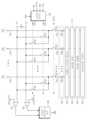
도 1은 본 발명의 한 실시예에 따른 표시 장치의 블록 구성도이고, 도 2는 도 1에 도시된 표시 패널의 상세 구성도이다.
도 3은 도 1의 데이터 드라이버에 대한 상세 블록 구성도이다.
도 4는 도 3의 데이터 드라이버 및 오버 드라이빙 구동을 위한 구성 요소들을 나타낸 도면이다.
도 5는 정극성 계조 전압들 및 부극성 계조 전압들의 크기 관계를 설명하기 위한 도면이다.
도 6은 도 1의 타이밍 컨트롤러가 오버 드라이빙 구동 여부를 판단하는 방법을 설명하기 위한 순서도이다.
도 7a 및 도 7b는 오버 드라이빙 구동 시 인접한 2개 채널들 각각에 포함된 제 1 내지 제 3 스위치들의 동작을 설명하기 위한 도면이다.
도 8a는 도 7a 및 도 7b에서의 오버 드라이빙 구동에 의한 제 1 데이터 라인의 전압 변화를 설명하기 위한 도면이다.
도 8b는 도 7a 및 도 7b에서의 오버 드라이빙 구동에 의한 제 2 데이터 라인의 전압 변화를 설명하기 위한 도면이다.
도 9a 및 도 9b는 수직 동기 신호의 수직 블랭크 기간에 본 발명의 표시 장치의 동작을 설명하기 위한 도면이다.
도 10은 도 3의 데이터 드라이버 및 오버 드라이빙 구동을 위한 다른 구성 요소들을 나타낸 도면이다.
도 11은 도 10의 오버 드라이빙 판단부가 오버 드라이빙 구동 여부를 판단하는 방법을 설명하기 위한 순서도이다.
도 12는 도 10의 오버 드라이빙 판단부의 영상 비교 시점 및 액티브 레벨의 오버 드라이빙 제어 신호의 출력 시점을 설명하기 위한 도면이다.
도 13은 도 3의 데이터 드라이버 및 오버 드라이빙 구동을 위한 또 다른 구성 요소들을 나타낸 도면이다.
도 14는 도 3에 도시된 표시 장치의 오버 드라이빙 구동을 위한 또 다른 구성 요소들을 나타낸 도면이다.
도 15는 도 3에 도시된 표시 장치의 오버 드라이빙 구동을 위한 또 다른 구성 요소들을 나타낸 도면이다.FIG. 1 is a block configuration diagram of a display device according to an exemplary embodiment, and FIG. 2 is a detailed configuration diagram of the display panel shown in FIG. 1 .
FIG. 3 is a detailed block configuration diagram of the data driver of FIG. 1 .
FIG. 4 is a diagram showing components for the data driver and overdriving of FIG. 3 .
5 is a diagram for explaining a relationship between magnitudes of positive gray-scale voltages and negative gray-scale voltages.
6 is a flowchart illustrating a method for determining whether the timing controller of FIG. 1 is overdriving.
7A and 7B are diagrams for explaining operations of first to third switches included in each of two adjacent channels during overdriving driving.
FIG. 8A is a diagram for explaining a change in voltage of the first data line due to overdriving in FIGS. 7A and 7B .
FIG. 8B is a diagram for explaining a change in voltage of the second data line due to overdriving in FIGS. 7A and 7B.
9A and 9B are diagrams for explaining the operation of the display device of the present invention in the vertical blank period of the vertical synchronization signal.
FIG. 10 is a diagram illustrating the data driver of FIG. 3 and other components for overdriving.
11 is a flowchart for explaining a method of determining whether an overdriving determination unit of FIG. 10 is driven.
FIG. 12 is a diagram for explaining the timing of comparing images of the overdriving determination unit of FIG. 10 and the timing of outputting an active level overdriving control signal.
FIG. 13 is a diagram illustrating other components for the data driver and overdriving of FIG. 3 .
FIG. 14 is a diagram illustrating other components for overdriving driving of the display device shown in FIG. 3 .
FIG. 15 is a diagram illustrating other components for overdriving the display device shown in FIG. 3 .
본 발명의 이점 및 특징, 그리고 그것들을 달성하는 방법은 첨부되는 도면과 함께 상세하게 후술되어 있는 실시예들을 참조하면 명확해질 것이다. 그러나 본 발명은 이하에서 개시되는 실시예들에 한정되는 것이 아니라 서로 다른 다양한 형태로 구현될 것이며, 단지 본 실시예들은 본 발명의 개시가 완전하도록 하며, 본 발명이 속하는 기술분야에서 통상의 지식을 가진 자에게 발명의 범주를 완전하게 알려주기 위해 제공되는 것이며, 본 발명은 청구항의 범주에 의해 정의될 뿐이다. 따라서, 몇몇 실시예에서, 잘 알려진 공정 단계들, 잘 알려진 소자 구조 및 잘 알려진 기술들은 본 발명이 모호하게 해석되는 것을 피하기 위하여 구체적으로 설명되지 않는다. 명세서 전체에 걸쳐 동일 참조 부호는 동일 구성 요소를 지칭한다.Advantages and features of the present invention, and methods of achieving them, will become clear with reference to the detailed description of the following embodiments taken in conjunction with the accompanying drawings. However, the present invention is not limited to the embodiments disclosed below, but will be implemented in various different forms, only these embodiments make the disclosure of the present invention complete, and common knowledge in the art to which the present invention belongs. It is provided to fully inform the holder of the scope of the invention, and the present invention is only defined by the scope of the claims. Thus, in some embodiments, well-known process steps, well-known device structures, and well-known techniques have not been described in detail in order to avoid obscuring the interpretation of the present invention. Like reference numbers designate like elements throughout the specification.
도면에서 여러 층 및 영역을 명확하게 표현하기 위하여 두께를 확대하여 나타내었다. 명세서 전체를 통하여 유사한 부분에 대해서는 동일한 도면 부호를 붙였다. 층, 막, 영역, 판 등의 부분이 다른 부분 "위에" 있다고 할 때, 이는 다른 부분 "바로 위에" 있는 경우뿐 아니라 그 중간에 또 다른 부분이 있는 경우도 포함한다. 반대로 어떤 부분이 다른 부분 "바로 위에" 있다고 할 때에는 중간에 다른 부분이 없는 것을 뜻한다. 또한, 층, 막, 영역, 판 등의 부분이 다른 부분 "아래에" 있다고 할 때, 이는 다른 부분 "바로 아래에" 있는 경우뿐 아니라 그 중간에 또 다른 부분이 있는 경우도 포함한다. 반대로 어떤 부분이 다른 부분 "바로 아래에" 있다고 할 때에는 중간에 다른 부분이 없는 것을 뜻한다.In the drawings, the thickness is shown enlarged to clearly express the various layers and regions. Like reference numerals have been assigned to like parts throughout the specification. When a part such as a layer, film, region, plate, etc. is said to be “on” another part, this includes not only the case where it is “directly on” the other part, but also the case where there is another part in between. Conversely, when a part is said to be "directly on" another part, it means that there is no other part in between. In addition, when a part such as a layer, film, region, plate, etc. is said to be "below" another part, this includes not only the case where it is "directly below" the other part, but also the case where another part is present in the middle. Conversely, when a part is said to be "directly below" another part, it means that there is no other part in between.
공간적으로 상대적인 용어인 "아래(below)", "아래(beneath)", "하부(lower)", "위(above)", "상부(upper)" 등은 도면에 도시되어 있는 바와 같이 하나의 소자 또는 구성 요소들과 다른 소자 또는 구성 요소들과의 상관관계를 용이하게 기술하기 위해 사용될 수 있다. 공간적으로 상대적인 용어는 도면에 도시되어 있는 방향에 더하여 사용시 또는 동작시 소자의 서로 다른 방향을 포함하는 용어로 이해되어야 한다. 예를 들면, 도면에 도시되어 있는 소자를 뒤집을 경우, 다른 소자의 "아래(below)"또는 "아래(beneath)"로 기술된 소자는 다른 소자의 "위(above)"에 놓여질 수 있다. 따라서, 예시적인 용어인 "아래"는 아래와 위의 방향을 모두 포함할 수 있다. 소자는 다른 방향으로도 배향될 수 있고, 이에 따라 공간적으로 상대적인 용어들은 배향에 따라 해석될 수 있다.The spatially relative terms "below", "beneath", "lower", "above", "upper", etc. It can be used to easily describe the correlation between elements or components and other elements or components. Spatially relative terms should be understood as encompassing different orientations of elements in use or operation in addition to the orientations shown in the figures. For example, when flipping elements shown in the figures, elements described as “below” or “beneath” other elements may be placed “above” the other elements. Thus, the exemplary term “below” may include directions of both below and above. Elements may also be oriented in other orientations, and thus spatially relative terms may be interpreted according to orientation.
본 명세서에서 어떤 부분이 다른 부분과 연결되어 있다고 할 때, 이는 직접적으로 연결되어있는 경우뿐 아니라, 그 중간에 다른 소자를 사이에 두고 전기적으로 연결되어 있는 경우도 포함한다. 또한, 어떤 부분이 어떤 구성 요소를 포함한다고 할 때, 이는 특별히 그에 반대되는 기재가 없는 한 다른 구성요소를 제외하는 것이 아니라 다른 구성요소를 더 포함할 수 있는 것을 의미한다.In this specification, when a part is said to be connected to another part, this includes not only the case where it is directly connected, but also the case where it is electrically connected with another element interposed therebetween. In addition, when a part includes a certain component, it means that it may further include other components without excluding other components unless otherwise specified.
본 명세서에서 제 1, 제 2, 제 3 등의 용어는 다양한 구성 요소들을 설명하는데 사용될 수 있지만, 이러한 구성 요소들은 상기 용어들에 의해 한정되는 것은 아니다. 상기 용어들은 하나의 구성 요소를 다른 구성 요소들로부터 구별하는 목적으로 사용된다. 예를 들어, 본 발명의 권리 범위로부터 벗어나지 않고, 제 1 구성 요소가 제 2 또는 제 3 구성 요소 등으로 명명될 수 있으며, 유사하게 제 2 또는 제 3 구성 요소도 교호적으로 명명될 수 있다.In this specification, terms such as first, second, and third may be used to describe various components, but these components are not limited by the terms. The terms are used for the purpose of distinguishing one component from other components. For example, a first component may be termed a second or third component, etc., and similarly, a second or third component may be termed interchangeably, without departing from the scope of the present invention.
다른 정의가 없다면, 본 명세서에서 사용되는 모든 용어(기술 및 과학적 용어를 포함)는 본 발명이 속하는 기술분야에서 통상의 지식을 가진 자에게 공통적으로 이해될 수 있는 의미로 사용될 수 있을 것이다. 또 일반적으로 사용되는 사전에 정의되어 있는 용어들은 명백하게 특별히 정의되어 있지 않은 한 이상적으로 또는 과도하게 해석되지 않는다.Unless otherwise defined, all terms (including technical and scientific terms) used in this specification may be used in a meaning commonly understood by those of ordinary skill in the art to which the present invention belongs. In addition, terms defined in commonly used dictionaries are not interpreted ideally or excessively unless explicitly specifically defined.
이하, 도 1 내지 도 15를 참조로 본 발명에 따른 표시 장치를 상세히 설명하면 다음과 같다.Hereinafter, a display device according to the present invention will be described in detail with reference to FIGS. 1 to 15 .
도 1은 본 발명의 한 실시예에 따른 표시 장치의 블록 구성도이고, 도 2는 도 1에 도시된 표시 패널의 상세 구성도이다.FIG. 1 is a block configuration diagram of a display device according to an exemplary embodiment, and FIG. 2 is a detailed configuration diagram of the display panel shown in FIG. 1 .
표시 장치는, 도 1에 도시된 바와 같이, 표시 패널(133), 타이밍 컨트롤러(101), 게이트 드라이버(112), 데이터 드라이버(111) 및 직류-직류 변환부(177)를 포함한다.As shown in FIG. 1 , the display device includes a
표시 패널(133)은 영상을 표시한다. 표시 패널(133)은 액정 패널 또는 유기 발광 다이오드 패널일 수 있다. 이하, 표시 패널(133)은 액정 패널인 것으로 예를 들어 설명한다.The
표시 패널(133)은, 도시되지 않았지만, 액정층과, 그리고 이 액정층을 사이에 두고 서로 마주보는 하부 기판과 상부 기판을 포함한다.Although not shown, the
하부 기판에 복수의 게이트 라인들(GL1 내지 GLi)과, 이 게이트 라인들(GL1 내지 GLi)과 교차되는 복수의 데이터 라인들(DL1 내지 DLj)과, 그리고 게이트 라인들(GL1 내지 GLi)과 데이터 라인들(DL1 내지 DLj)에 접속된 박막 트랜지스터(TFT)들이 배치된다.A plurality of gate lines GL1 to GLi on the lower substrate, a plurality of data lines DL1 to DLj crossing the gate lines GL1 to GLi, and the gate lines GL1 to GLi and data Thin film transistors TFTs connected to the lines DL1 to DLj are disposed.
도시되지 않았지만, 상부 기판에 블랙 매트릭스, 복수의 컬러필터들 및 공통 전극이 위치한다. 블랙 매트릭스는, 상부 기판 중 화소 영역들에 대응되는 부분들을 제외한 나머지 부분에 위치한다. 컬러필터들은 화소 영역에 위치한다. 컬러필터들은 적색 컬러필터, 녹색 컬러필터 및 청색 컬러필터를 포함한다.Although not shown, a black matrix, a plurality of color filters, and a common electrode are positioned on the upper substrate. The black matrix is located on the remaining portion of the upper substrate except for portions corresponding to the pixel areas. Color filters are located in the pixel area. The color filters include a red color filter, a green color filter and a blue color filter.
도 2에 도시된 바와 같이, 화소들(R, G, B)은 행렬 형태로 배열된다. 화소들(R, G, B)은 적색 컬러 필터에 대응하여 위치한 적색 화소(R)들, 녹색 컬러 필터에 대응하여 위치한 녹색 화소(G) 및 청색 컬러 필터에 대응하여 위치한 청색 화소(B)를 포함한다. 이때, 수직 방향으로 인접한 적색 화소(R), 녹색 화소(G) 및 청색 화소(B)는 하나의 단위 영상을 표시하기 위한 단위 화소를 이룬다.As shown in FIG. 2 , pixels R, G, and B are arranged in a matrix form. The pixels R, G, and B include red pixels R corresponding to the red color filter, green pixels G corresponding to the green color filter, and blue pixels B corresponding to the blue color filter. include In this case, the red pixel R, the green pixel G, and the blue pixel B that are vertically adjacent form a unit pixel for displaying one unit image.
제 n 수평 라인(n은 1 내지 i 중 어느 하나)을 따라 배열된 j개의 화소들(이하, 제 n 수평 라인 화소들)은 제 1 내지 제 j 데이터 라인들(DL1 내지 DLj) 각각에 개별적으로 접속된다. 아울러, 이 제 n 수평 라인 화소들은 제 n 게이트 라인에 공통으로 접속된다. 이에 따라, 제 n 수평 라인 화소들은 제 n 게이트 신호를 공통으로 공급받는다. 즉, 동일 수평 라인 상에 배열된 j개의 화소들은 모두 동일한 게이트 신호를 공급받지만, 서로 다른 수평라인 상에 위치한 화소들은 서로 다른 게이트 신호를 공급받는다. 예를 들어, 제 1 수평 라인(HL1)에 위치한 적색 화소(R)들은 모두 제 1 게이트 신호를 공급받는 반면, 제 2 수평라인(HL2)에 위치한 녹색 화소(G)들은 그 제 1 게이트 신호와 다른 타이밍을 갖는 제 2 게이트 신호를 공급받는다.The j pixels (hereinafter referred to as n-th horizontal line pixels) arranged along the n-th horizontal line (n is any one of 1 to i) are individually connected to the first to j-th data lines DL1 to DLj. connected In addition, the nth horizontal line pixels are commonly connected to the nth gate line. Accordingly, the nth horizontal line pixels are commonly supplied with the nth gate signal. That is, all j pixels arranged on the same horizontal line receive the same gate signal, but pixels positioned on different horizontal lines receive different gate signals. For example, all red pixels R located on the first horizontal line HL1 receive the first gate signal, while green pixels G located on the second horizontal line HL2 receive the first gate signal and A second gate signal having a different timing is supplied.
각 화소(R, G, B)는, 도 2에 도시된 바와 같이, 박막 트랜지스터(TFT), 액정용량 커패시터(Clc)및 보조용량 커패시터(Cst)를 포함한다.As shown in FIG. 2 , each of the pixels R, G, and B includes a thin film transistor TFT, a liquid crystal capacitance capacitor Clc, and an auxiliary capacitance capacitor Cst.
박막 트랜지스터(TFT)는 게이트 라인으로부터의 게이트 신호에 따라 턴-온된다. 턴-온된 박막 트랜지스터(TFT)는 데이터 라인으로부터 제공된 아날로그 영상 데이터 신호를 액정용량 커패시터(Clc)및 보조용량 커패시터(Cst)로 공급한다.The thin film transistor (TFT) is turned on according to a gate signal from a gate line. The turned-on thin film transistor TFT supplies the analog image data signal provided from the data line to the liquid crystal capacitance capacitor Clc and the auxiliary capacitance capacitor Cst.
액정용량 커패시터(Clc)는 서로 대향하여 위치한 화소 전극과 공통 전극을 포함한다.The liquid crystal capacitance capacitor Clc includes a pixel electrode and a common electrode positioned opposite to each other.
보조용량 커패시터(Cst)는 서로 대향하여 위치한 화소 전극과 대향 전극을 포함한다. 여기서, 대향 전극은 전단 게이트 라인 또는 공통 전압을 전송하는 공통 라인이 될 수 있다.The auxiliary capacitance capacitor Cst includes a pixel electrode and a counter electrode disposed to face each other. Here, the opposite electrode may be a previous gate line or a common line transmitting a common voltage.
한편, 화소(R, G, B)를 구성하는 구성 요소들 중 박막 트랜지스터(TFT)는 블랙 매트릭스에 의해 가려진다.Meanwhile, the thin film transistor (TFT) among components constituting the pixels R, G, and B is covered by the black matrix.
타이밍 컨트롤러(101)는 시스템에 구비된 그래픽 컨트롤러로부터 출력된 수직 동기 신호(Vsync), 수평 동기 신호(Hsync), 영상 데이터 신호(DATA) 및 기준 클럭 신호(DCLK)를 공급받는다. 타이밍 컨트롤러(101)와 시스템 사이에 인터페이스회로(도시되지 않음)가 구비되는 바, 시스템으로부터 출력된 위 신호들은 인터페이스회로를 통해 타이밍 컨트롤러(101)로 입력된다. 인터페이스회로는 타이밍 컨트롤러(101)에 내장될 수도 있다.The
도시되지 않았지만, 인터페이스회로는 LVDS(Low Voltage Differential Signaling) 수신부를 포함할 수 있다. 인터페이스회로는 시스템으로부터 출력된 수직동기신호(Vsync), 수평동기신호(Hsync), 영상 데이터 신호(DATA) 및 기준 클럭 신호(DCLK)의 전압 레벨을 낮추는 한편, 이들의 주파수를 높인다.Although not shown, the interface circuit may include a Low Voltage Differential Signaling (LVDS) receiver. The interface circuit lowers the voltage levels of the vertical sync signal (Vsync), the horizontal sync signal (Hsync), the image data signal (DATA), and the reference clock signal (DCLK) output from the system, while raising their frequencies.
한편, 인터페이스회로로부터 타이밍 컨트롤러(101)로 입력되는 신호의 높은 고주파 성분으로 인하여 이들 사이에 전자파장애(Electromagnetic interference)가 발생할 수 있는 바, 이를 방지하기 위해 인터페이스회로와 타이밍 컨트롤러(101) 사이에 EMI필터(도시되지 않음)가 더 구비될 수 있다.On the other hand, due to the high frequency component of the signal input from the interface circuit to the
타이밍 컨트롤러(101)는 수직 동기 신호(Hsync), 수평 동기 신호(Hsync) 및 기준 클럭 신호(DCLK)를 이용하여 게이트 드라이버(112)를 제어하기 위한 게이트 제어신호(GCS)와 데이터 드라이버(111)를 제어하기 위한 데이터 제어신호(DCS)를 발생한다.The
게이트 제어신호(GCS)는 게이트 스타트 펄스(Gate Start Pulse), 게이트 쉬프트 클럭(Gate Shift Clock), 게이트 출력 제어 신호(Gate Output Enable) 등을 포함한다. 데이터 제어신호(DCS)는 소스 스타트 펄스(Source Start Pulse), 소스 쉬프트 클럭(Source Shift Clock), 소스 출력 제어 신호(Source Output Enable), 극성 제어 신호(Polarity Signal) 등을 포함한다.The gate control signal GCS includes a gate start pulse, a gate shift clock, a gate output enable, and the like. The data control signal DCS includes a source start pulse, a source shift clock, a source output enable, a polarity signal, and the like.
또한, 타이밍 컨트롤러(101)는 시스템을 통해 입력되는 영상 데이터 신호들(DATA)을 재정렬하고, 그리고 이 재정렬된 영상 데이터 신호들(DATA`)을 데이터 드라이버(111)에 공급한다.Also, the
한편, 타이밍 컨트롤러(101)는 시스템에 구비된 전원부로부터 출력된 구동 전원(VCC)에 의해 동작하는 바, 특히 이 구동 전원(VCC)은 타이밍 컨트롤러(101) 내부에 설치된 위상고정루프회로(Phase Lock Loop: PLL)의 전원 전압으로서 사용된다. 위상고정루프회로(PLL)는 타이밍 컨트롤러(101)에 입력되는 기준 클럭 신호(DCLK)를 발진기로부터 발생되는 기준 주파수와 비교한다. 그리고, 그 비교 결과 이들 사이에 오차가 있는 것으로 확인되면, 위상고정루프회로는 그 오차만큼 기준 클럭 신호(DCLK)의 주파수를 조정하여 샘플링 클럭 신호를 발생한다. 이 샘플링 클럭 신호는 영상 데이터 신호들(DATA`)을 샘플링하기 위한 신호이다.Meanwhile, the
직류-직류 변환부(177)는 시스템을 통해 입력되는 구동 전원(VCC)을 승압 또는 감압하여 표시 패널(133)에 필요한 각종 전압들을 생성한다. 이를 위해, 직류-직류 변환부(177)는, 예를 들어, 이의 출력 단의 출력 전압을 스위칭하기 위한 출력 스위칭 소자와, 그 출력 스위칭 소자의 제어 단자에 인가되는 제어 신호의 듀티비(duty ratio)나 주파수를 제어하여 출력 전압을 승압하거나 감압시키기 위한 펄스폭 변조기(Pulse Width Modulator: PWM)를 포함할 수 있다. 여기서, 전술된 펄스폭 변조기 대신에 펄스주파수 변조기(Pulse Frequency Modulator: PFM)가 그 직류-직류 변환부(177)에 포함될 수 있다.The DC-
펄스폭 변조기는 전술된 제어 신호의 듀티비를 높여 직류-직류 변환부(177)의 출력 전압을 높이거나, 그 제어 신호의 듀티비를 낮추어 직류-직류 변환부(177)의 출력 전압을 낮춘다. 펄스주파수 변조기는 전술된 제어 신호의 주파수를 높여 직류-직류 변환부(177)의 출력 전압을 높이거나, 제어 신호의 주파수를 낮추어 직류-직류 변환부(177)의 출력 전압을 낮춘다. 직류-직류 변환부(177)의 출력 전압은 기준 전압(AVDD), 하프 기준 전압(HAVDD), 감마 기준 전압(GMA)들, 공통 전압(Vcom), 게이트 고전압 및 게이트 저전압(VGL)을 포함할 수 있다.The pulse width modulator increases the output voltage of the DC-
감마 기준 전압(GMA)들은 기준 전압의 분압에 의해 발생된 전압이다. 감마 기준 전압(GMA)들은 아날로그 전압으로서, 이들은 데이터 드라이버(111)에 공급된다. 공통 전압(Vcom)은 데이터 드라이버(111)를 경유하여 표시 패널(133)의 공통 전극에 공급된다. 게이트 고전압(VGH)은 박막 트랜지스터(TFT)의 문턱 전압 이상으로 설정된 게이트 신호의 하이논리전압이고, 그리고 게이트 저전압(VGL)은 박막 트랜지스터(TFT)의 오프 전압으로 설정된 게이트 신호의 로우논리전압으로서, 이들은 게이트 드라이버(112)에 공급된다.Gamma reference voltages (GMAs) are voltages generated by dividing the reference voltage. Gamma reference voltages (GMAs) are analog voltages, which are supplied to the
게이트 드라이버(112)는 타이밍 컨트롤러(101)로부터 제공된 게이트 제어신호(GCS)에 따라 게이트 신호들을 생성하고, 그 게이트 신호들을 복수의 게이트 라인들(GL1 내지 GLi)에 차례로 공급한다.The
게이트 드라이버(112)는, 예를 들어, 게이트 쉬프트 클럭에 따라 게이트 스타트 펄스를 쉬프트 시켜 게이트 신호들을 발생시키는 쉬프트 레지스터로 구성될 수 있다. 쉬프트 레지스터는 복수의 스위칭 소자들로 구성될 수 있다. 이 스위칭 소자들은 표시 영역의 박막 트랜지스터(TFT)와 동일한 공정으로 하부 기판 상에 형성될 수 있다.The
데이터 드라이버(111)는 타이밍 컨트롤러(101)로부터 영상 데이터 신호들(DATA') 및 데이터 제어신호(DCS)를 공급받는다. 데이터 드라이버(111)는 데이터 제어 신호(DCS)에 따라 영상 데이터 신호들(DATA')을 샘플링한 후에, 매 수평기간마다 한 수평 라인에 해당하는 샘플링 영상 데이터 신호들을 순차적으로 래치하고 그 래치된 영상 데이터 신호들을 데이터 라인들(DL1 내지 DLj)에 동시에 공급한다.The
즉, 데이터 드라이버(111)는 타이밍 컨트롤러(101)로부터의 영상 데이터 신호들(DATA')을, 직류-직류 변환부(177)로부터 입력되는 감마 기준 전압들(GMA)을 이용하여, 아날로그 영상 데이터 신호들로 변환하여 데이터 라인들(DL1 내지 DLj)로 공급한다. 예를 들어, 데이터 드라이버(111)는 계조 발생부(300)를 포함할 수 있는 바, 이 계조 발생부(도 3의 300)는 직류-직류 변환부(177)로부터 공급된 하프 기준 전압(HAVDD) 및 감마 기준 전압(GMA)들을 이용하여 복수의 계조 전압들(GV)을 생성한다. 복수의 계조 전압들(도 3의 GV)은 정극성 계조 전압들 및 이에 대응되는 복수의 부극성 계조 전압들을 생성한다. 복수의 정극성 계조 전압들은 하프 기준 전압(HVADD)보다 더 큰 전압값을 가지며, 복수의 부극성 계조 전압들은 하프 기준 전압(HAVDD)보다 더 작은 전압값을 갖는다. 데이터 드라이버(111)는 이들 정극성 계조 전압들 및 부극성 계조 전압들을 이용하여 타이밍 컨트롤러(101)로부터의 영상 데이터 신호들을 아날로그 신호로 변환한다.That is, the
한편, 계조 발생부(300)는 데이터 드라이버(111)의 내부 또는 외부에 위치할 수 있다.Meanwhile, the
도 3은 도 1의 데이터 드라이버(111)에 대한 상세 블록 구성도이다.FIG. 3 is a detailed block diagram of the
데이터 드라이버(111)는, 도 3에 도시된 바와 같이, 쉬프트 레지스터부(310), 샘플링 래치부(320), 홀딩 래치부(330), 계조 발생부(300), 디지털-아날로그 변환부(340) 및 버퍼부(350)를 포함한다.As shown in FIG. 3 , the
쉬프트 레지스터부(310)는 타이밍 컨트롤러(101)로부터 소스 쉬프트 클럭(SSC) 및 소스 스타트 펄스(SSP)를 공급받고, 소스 쉬프트 클럭(SSC)의 1주기 마다 소스 스타트 펄스(SSP)를 쉬프트 시키면서 순차적으로 j개의 샘플링 신호들을 생성한다. 이를 위해, 쉬프트 레지스터부(310)는 j개의 쉬프트 레지스터(31)들을 구비한다.The
샘플링 래치부(320)는 쉬프트 레지스터부(310)로부터 순차적으로 공급되는 샘플링 신호들에 응답하여 디지털 영상 데이터 신호들을 순차적으로 저장한다. 여기서, 샘플링 래치부(320)는 j개의 디지털 영상 데이터 신호들을 저장하기 위한 j개의 샘플링 래치(32)들을 포함한다. 그리고, 각각의 샘플링 래치(32)는 영상 데이터 신호의 비트수에 대응되는 저장 용량을 갖는다. 예를 들어, 영상 데이터 신호들 각각이 k비트(k는 자연수)로 구성되는 경우 샘플링 래치(32)들 각각은 k비트의 크기로 설정된 저장 용량을 갖는다.The
홀딩 래치부(330)는, 소스 출력 제어 신호(SOE; Source Output Enable)에 응답하여, 샘플링 래치부(320)로부터의 영상 데이터 신호들을 동시에 입력받아 저장함과 아울러, 이전 기간에 저장되었던 샘플링된 영상 데이터 신호들을 동시에 출력한다. 홀딩 래치부(330)로부터 출력된 영상 데이터 신호들은 디지털-아날로그 변환부(340)로 동시에 공급된다. 홀딩 래치부(330)는 j개의 영상 데이터 신호들을 저장하기 위한 j개의 홀딩 래치(33)들을 포함한다. 또한, 각각의 홀딩 래치(33)는 영상 데이터 신호의 비트수에 대응되는 저장 용량을 갖는다. 예를 들어, 영상 데이터 신호들 각각이 위와 같이 k비트로 구성되는 경우 홀딩 래치(33)들 각각은 k비트의 크기로 설정된 저장 용량을 갖는다.The holding
계조 발생부(300)는 직류-직류 변환부(177)로부터의 하프 기준 전압(HAVDD) 및 감마 기준 전압(GMA)들을 분압하여 복수의 정극성 계조 전압들 및 복수의 부극성 계조 전압들을 생성한다.The
디지털-아날로그 변환부(340)는 홀딩 래치부(340)로부터 공급된 영상 데이터 신호의 비트 값에 대응하는 아날로그 영상 데이터 신호를 생성한다. 구체적으로, 디지털-아날로그 변환부(340)는 홀딩 래치부(330)로부터의 디지털 영상 데이터 신호의 비트 값에 대응하는 계조 전압을 계조 발생부(300)에서 선택하고, 그 선택된 계조 전압을 아날로그 영상 데이터 신호로서 출력한다. 디지털-아날로그 변환부(340)는 j개의 디지털 영상 데이터 신호들을 아날로그 영상 데이터 신호들로 변환하기 위한 j개의 디지털-아날로그 변환기(34)들을 포함한다.The digital-to-
버퍼부(350)는 디지털-아날로그 변환부(340)로부터 아날로그 영상 데이터 신호들을 공급받고, 이 아날로그 영상 데이터 신호들을 증폭하여 표시 패널(133)의 데이터 라인(DL1 내지 DLj)들로 출력한다. 버퍼부(350)는 j개의 아날로그 영상 데이터 신호들을 증폭하기 위한 j개의 버퍼(35)들을 포함한다.The
본 발명은 오버 드라이빙 구동을 위해 커패시터, 복수의 스위치들, 스위치 제어부 등을 더 포함할 수 있는 바, 이를 도 4를 참조로 하여 구체적으로 설명한다.The present invention may further include a capacitor, a plurality of switches, a switch controller, etc. for overdriving driving, which will be described in detail with reference to FIG. 4 .
한편, 후술할 각종 신호들은 액티브 레벨 또는 비액티브 레벨을 가질 수 있다. 어떤 신호가 액티브 레벨을 가질 때, 그 액티브 레벨의 신호를 공급받는 구동부가 특정 동작(예를 들어, 오버 드라이빙 동작)을 수행할 수 있다. 이와 반대로, 어떤 신호가 비액티브 레벨을 가질 때, 그 비액티브 레벨의 신호를 공급받는 구동부는 그 특정 동작(예를 들어, 오버 드라이빙 동작)을 취소하거나 그 특정 동작을 수행하지 않는다.Meanwhile, various signals to be described later may have an active level or an inactive level. When a certain signal has an active level, a driving unit receiving the signal of the active level may perform a specific operation (eg, an overdriving operation). Conversely, when a certain signal has an inactive level, the driving unit supplied with the signal of the inactive level cancels the specific operation (eg, overdriving operation) or does not perform the specific operation.
또한, 어떤 신호가 액티브 레벨을 가질 때, 그 액티브 레벨의 신호를 공급받는 스위치는 턴-온될 수 있다. 이와 반대로, 어떤 신호가 비액티브 레벨을 가질 때, 그 액티브 레벨의 신호를 공급받는 스위치는 턴-오프될 수 있다.Also, when a certain signal has an active level, a switch receiving the signal of the active level may be turned on. Conversely, when a signal has an inactive level, a switch receiving the active level signal may be turned off.
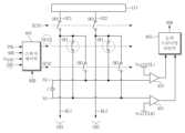
도 4는 도 3의 데이터 드라이버 및 오버 드라이빙 구동을 위한 구성 요소들을 나타낸 도면이고, 도 5는 정극성 계조 전압들 및 부극성 계조 전압들의 크기 관계를 설명하기 위한 도면이다.FIG. 4 is a diagram showing components for the data driver and overdriving driving of FIG. 3 , and FIG. 5 is a diagram for explaining a relationship between magnitudes of positive and negative gray-scale voltages.
본 발명의 표시 장치는, 도 4에 도시된 바와 같이, 커패시터(C), 복수의 스위치들(SW1, SW2, SW3), 스위치 제어부(401), 오버 드라이빙 차단부(402), 제 1 비교기(451) 및 제 2 비교기(452)를 더 포함할 수 있다.As shown in FIG. 4, the display device of the present invention includes a capacitor C, a plurality of switches SW1, SW2, and SW3, a
데이터 드라이버(111)는 데이터 라인들(DL1 내지 DLj)에 대응되는 복수의 출력 단자들(OT1 내지 OTj)을 포함하는 바, 이 데이터 드라이버(111)의 각 출력 단자(OT1 내지 OTj)는 각 버퍼(BF1 내지 BFj)의 출력 단자(OT1 내지 OTj)이다.The
스위치 제어부(401)는 타이밍 컨트롤러(101)로부터의 극성 제어 신호(POL), 소스 출력 제어 신호(SOE), 수직 동기 신호(Vsync) 및 오버 드라이빙 제어 신호(OD)를 근거로 제 1 스위치 제어 신호(SCS1) 및 제 2 스위치 제어 신호(SCS2)를 출력한다.The
커패시터(C)는 오버 드라이빙 구동에 필요한 오버 드라이빙 전압을 저장한다. 예를 들어, 이 커패시터(C)에 의해 이 커패시터(C)의 일측 단자(N1)는 부극성 오버 드라이빙 전압으로 유지될 수 있으며, 이 커패시터(C)의 타측 단자(N2)는 정극성 오버 드라이빙 전압으로 유지될 수 있다.Capacitor C stores the overdriving voltage required for overdriving operation. For example, by this capacitor (C), one side terminal (N1) of this capacitor (C) can be maintained at a negative overdriving voltage, and the other side terminal (N2) of this capacitor (C) can be maintained at a positive overdriving voltage. voltage can be maintained.
정극성 오버 드라이빙 전압은 전술된 정극성 계조 전압들 중 어느 하나의 전압과 동일할 수 있다. 부극성 오버 드라이빙 전압은 전술된 부극성 계조 전압들 중 어느 하나의 전압과 동일할 수 있다.The positive polarity overdriving voltage may be the same as any one of the positive polarity grayscale voltages described above. The negative overdriving voltage may be the same as any one of the negative grayscale voltages described above.
도 5에 도시된 바와 같이, 정극성 계조 전압들은 하프 기준 전압(HAVDD)보다 더 큰 계조 전압들이다. 여기서, 정극성 계조 전압들 중 하프 기준 전압(HAVDD)과 가장 큰 차이를 갖는 정극성 계조 전압을 정극성 최고 계조 전압(UH)으로 정의하고, 그 정극성 계조 전압들 중 하프 기준 전압(HAVDD)과 가장 작은 차이를 갖는 정극성 계조 전압을 정극성 최저 계조 전압(UL)으로 정의하자.As shown in FIG. 5 , the positive polarity grayscale voltages are grayscale voltages greater than the half reference voltage HAVDD. Here, among the positive grayscale voltages, the positive grayscale voltage having the greatest difference from the half reference voltage HAVDD is defined as the highest positive grayscale voltage UH, and among the positive grayscale voltages, the half reference voltage HAVDD Define a positive polarity grayscale voltage having the smallest difference with the positive polarity minimum grayscale voltage (UL).
정극성 최고 계조 전압(UH)은 정극성 계조 전압들 중 가장 큰 값을 가지며, 정극성 최저 계조 전압(UL)은 그 정극성 계조 전압들 중 가장 작은 값을 갖는다.The highest positive grayscale voltage UH has the largest value among the positive grayscale voltages, and the lowest positive grayscale voltage UL has the smallest value among the positive grayscale voltages.
정극성 계조 전압들이 서로 다른 크기를 갖는 256개의 정극성 계조 전압들을 포함한다고 할 때, 전술된 정극성 최고 계조 전압(UH)은 256번째 계조 전압(255계조 전압)에 해당하며, 정극성 최저 계조 전압(UL)은 첫 번째 계조 전압(0계조 전압)에 해당한다. 정극성 최고 계조 전압(UH)은 풀 화이트(full white) 레벨에 대응되는 전압이고, 정극성 최저 계조 전압(UL)은 풀 블랙(full black) 레벨에 대응되는 전압일 수 있다.Assuming that the positive gradation voltages include 256 positive gradation voltages having different magnitudes, the above-described highest positive gradation voltage (UH) corresponds to the 256th gradation voltage (255th gradation voltage), and the lowest positive gradation voltage The voltage UL corresponds to the first gradation voltage (0 gradation voltage). The highest positive grayscale voltage UH may be a voltage corresponding to a full white level, and the lowest positive grayscale voltage UL may be a voltage corresponding to a full black level.
도 5에 도시된 바와 같이, 부극성 계조 전압들은 하프 기준 전압(HAVDD)보다 더 작은 계조 전압들이다. 여기서, 부극성 계조 전압들 중 하프 기준 전압(HAVDD)과 가장 큰 차이를 갖는 부극성 계조 전압을 부극성 최고 계조 전압(LL)으로 정의하고, 그 부극성 계조 전압들 중 하프 기준 전압(HAVDD)과 가장 작은 차이를 갖는 부극성 계조 전압을 부극성 최저 계조 전압(LH)으로 정의하자.As shown in FIG. 5 , negative polarity grayscale voltages are grayscale voltages smaller than the half reference voltage HAVDD. Here, the negative grayscale voltage having the largest difference from the half reference voltage HAVDD among the negative grayscale voltages is defined as the highest negative grayscale voltage LL, and the half reference voltage HAVDD among the negative grayscale voltages Define a negative polarity grayscale voltage having the smallest difference with the negative polarity lowest grayscale voltage (LH).
부극성 최고 계조 전압(LL)은 부극성 계조 전압들 중 가장 작은 값을 가지며, 부극성 최저 계조 전압(LH)은 그 부극성 계조 전압들 중 가장 큰 값을 갖는다.The highest negative grayscale voltage LL has the smallest value among the negative grayscale voltages, and the lowest negative grayscale voltage LH has the largest value among the negative grayscale voltages.
부극성 계조 전압들이 서로 다른 크기를 갖는 256개의 부극성 계조 전압들을 포함한다고 할 때, 전술된 부극성 최고 계조 전압(LL)은 그 256개의 부극성 계조 전압들 중 256번째 계조 전압(255계조 전압)에 해당하며, 부극성 최저 계조 전압(LH)은 그 256개의 부극성 계조 전압들 중 첫 번째 계조 전압(0계조 전압)에 해당한다. 부극성 최고 계조 전압(LL)은 풀 화이트(full white) 레벨에 대응되는 전압이고, 부극성 최저 계조 전압(LH)은 풀 블랙(full black) 레벨에 대응되는 전압일 수 있다.Assuming that the negative grayscale voltages include 256 negative grayscale voltages having different magnitudes, the above-described negative highest grayscale voltage LL is the 256th grayscale voltage (255th grayscale voltage) among the 256 negative grayscale voltages. ), and the lowest negative grayscale voltage (LH) corresponds to the first grayscale voltage (0 grayscale voltage) among the 256 negative grayscale voltages. The negative highest grayscale voltage LL may be a voltage corresponding to a full white level, and the negative lowest grayscale voltage LH may be a voltage corresponding to a full black level.
하나의 예로서, 하프 기준 전압(HAVDD)은 7.5[V]의 직류 전압이고, 정극성 최고 계조 전압(UH)은 14[V]의 직류 전압이고, 정극성 최저 계조 전압(UL)은 8[V]의 직류 전압이고, 부극성 최고 계조 전압(LL)은 1[V]이고, 부극성 최저 계조 전압(LH)은 7[V]의 직류 전압일 수 있다.As an example, the half reference voltage HAVDD is a DC voltage of 7.5 [V], the positive highest gradation voltage UH is a DC voltage of 14 [V], and the lowest positive gradation voltage UL is 8 [V]. V], the highest negative gradation voltage LL is 1 [V], and the lowest negative gradation voltage LH is a DC voltage of 7 [V].
정극성 오버 드라이빙 전압은 전술된 부극성 최저 계조 전압(LH) 또는 하프 기준 전압(HAVDD) 보다 더 클 수 있다. 예를 들어, 정극성 오버 드라이빙 전압은 전술된 정극성 계조 전압들 중 어느 하나의 전압과 동일할 수 있다.The positive overdriving voltage may be greater than the negative lowest grayscale voltage LH or the half reference voltage HAVDD. For example, the positive polarity overdriving voltage may be the same as any one of the above-described positive polarity grayscale voltages.
부극성 오버 드라이빙 전압은 전술된 정극성 최저 계조 전압(UL) 또는 하프 기준 전압(HAVDD) 보다 더 작을 수 있다. 예를 들어, 부극성 오버 드라이빙 전압은 전술된 부극성 계조 전압들 중 어느 하나의 전압과 동일할 수 있다.The negative overdriving voltage may be smaller than the aforementioned positive polarity lowest grayscale voltage UL or half reference voltage HAVDD. For example, the negative overdriving voltage may be the same as any one of the negative grayscale voltages described above.
복수의 스위치들(SW1 내지 SW3)은 복수의 제 1 스위치(SW1)들, 복수의 제 2 스위치(SW2)들 및 복수의 제 3 스위치(SW3)들을 포함한다. 제 1 스위치(SW1)들은 스위치 제어부(401)로부터의 제 1 스위치 제어 신호(SCS1)에 의해 공통으로 제어되며, 제 2 스위치(SW2)들은 스위치 제어부(401)로부터의 제 2 스위치 제어 신호(SCS2)에 의해 공통으로 제어된다. 한편, 제 3 스위치(SW3)들은 타이밍 컨트롤러(101)로부터의 제 3 스위치 제어 신호(SCS3)에 따라 제어된다.The plurality of switches SW1 to SW3 include a plurality of first switches SW1 , a plurality of second switches SW2 , and a plurality of third switches SW3 . The first switches SW1 are commonly controlled by the first switch control signal SCS1 from the
서로 대응되는 출력 단자와 데이터 라인, 그리고 그 출력 단자 및 데이터 라인에 연결된 제 1 스위치(SW1), 제 2 스위치(SW2) 및 제 3 스위치(SW3)는 하나의 채널(channel)에 포함된다.Output terminals and data lines corresponding to each other, and the first switch SW1 , the second switch SW2 , and the third switch SW3 connected to the output terminals and data lines are included in one channel.
예를 들어, 데이터 드라이버(111)의 제 1 출력 단자(OT1), 제 1 데이터 라인(DL1), 그리고 그 제 1 출력 단자(OT1)과 제 1 데이터 라인(DL1)에 연결된 제 1 내지 제 3 스위치들(SW1 내지 SW3)은 제 1 채널(CH1)에 포함된다.For example, the first output terminal OT1 of the
제 1 채널(CH1)의 제 1 스위치(SW1)는 스위치 제어부(401)로부터의 제 1 스위치 제어 신호(SCS1)에 따라 제어되며, 제 1 데이터 라인(DL1)과 커패시터(C)의 일측 단자(N1) 사이에 접속된다.The first switch SW1 of the first channel CH1 is controlled according to the first switch control signal SCS1 from the
제 1 채널(CH1)의 제 2 스위치(SW2)는 스위치 제어부(401)로부터의 제 2 스위치 제어 신호(SCS2)에 따라 제어되며, 제 1 데이터 라인(DL1)과 커패시터(C)의 타측 단자(N2) 사이에 접속된다.The second switch SW2 of the first channel CH1 is controlled according to the second switch control signal SCS2 from the
제 1 채널(CH1)의 제 3 스위치(SW3)는 타이밍 컨트롤러(101)로부터의 제 3 스위치 제어 신호(SCS3)에 따라 제어되며, 제 1 데이터 라인(DL1)과 제 1 출력 단자(OT1) 사이에 접속된다.The third switch SW3 of the first channel CH1 is controlled according to the third switch control signal SCS3 from the
다른 채널도 전술된 제 1 채널(CH1)과 동일한 구성을 갖는다. 단, 홀수 번째 채널과 짝수 번째 채널은 서로 다른 구성을 갖는다. 예를 들어, 제 2 채널(CH2)의 제 1 스위치(SW1)는 커패시터(C)의 일측 단자(N1)가 아닌 타측 단자(N2)에 연결되며, 그 제 2 채널(CH2)의 제 2 스위치(SW2)는 커패시터(C)의 타측 단자(N2)가 아닌 일측 단자(N1)에 연결된다.Other channels have the same configuration as the first channel CH1 described above. However, odd-numbered channels and even-numbered channels have different configurations. For example, the first switch SW1 of the second channel CH2 is connected to the other terminal N2 of the capacitor C, not to the one terminal N1, and the second switch SW1 of the second channel CH2 (SW2) is connected to one terminal (N1) of the capacitor (C), not to the other terminal (N2).
홀수 번째 채널은 전술된 제 1 채널(CH1)과 동일한 구성을 가지며, 짝수 번째 채널은 전술된 제 2 채널(CH2)과 동일한 구성을 가질 수 있다. 한편, 이와 반대로, 홀수 번째 채널은 전술된 제 2 채널(CH2)과 동일한 구성을 가지며, 짝수 번째 채널은 전술된 제 1 채널(CH1)과 동일한 구성을 가질 수 있다.An odd-numbered channel may have the same configuration as the aforementioned first channel CH1, and an even-numbered channel may have the same configuration as the aforementioned second channel CH2. Meanwhile, on the other hand, odd-numbered channels may have the same configuration as the aforementioned second channel CH2, and even-numbered channels may have the same configuration as the aforementioned first channel CH1.
제 1 비교기(451)는 커패시터(C)의 일측 단자(N1)의 전압과 제 1 기준 전압(Vref1)을 비교하고, 그 비교 결과를 근거로 제 1 비교 신호를 출력한다.The
제 1 비교기(451)는 커패시터(C)의 일측 단자(N1)의 전압이 제 1 기준 전압(Vref1)보다 더 높으면 액티브 레벨의 제 1 비교 신호를 출력한다. 반면, 제 1 비교기(451)는 커패시터(C)의 일측 단자(N1)의 전압이 제 1 기준 전압(Vref1)과 동일하거나 이보다 더 낮으면 비액티브 레벨의 제 1 비교 신호를 출력한다.The
제 2 비교기(452)는 커패시터(C)의 타측 단자(N2)의 전압과 제 2 기준 전압(Vref2)을 비교하고, 그 비교 결과를 근거로 제 2 비교 신호를 출력한다.The
제 2 비교기(452)는 커패시터(C)의 타측 단자(N2)의 전압이 제 2 기준 전압(Vref2)보다 더 낮으면 액티브 레벨의 제 2 비교 신호를 출력한다. 반면, 제 2 비교기(452)는 커패시터(C)의 타측 단자(N2)의 전압이 제 2 기준 전압(Vref2)과 동일하거나 이보다 더 높으면 비액티브 레벨의 제 2 비교 신호를 출력한다.The
제 2 기준 전압(Vref2)은 제 1 기준 전압(Vref1)보다 더 클 수 있다. 예를 들어, 제 1 기준 전압(Vref1)은 부극성 최저 계조 전압(LH)과 동일한 값을 가질 수 있으며, 제 2 기준 전압(Vref2)은 정극성 최저 계조 전압(UL)과 동일한 값을 가질 수 있다.The second reference voltage Vref2 may be greater than the first reference voltage Vref1. For example, the first reference voltage Vref1 may have the same value as the negative lowest grayscale voltage LH, and the second reference voltage Vref2 may have the same value as the positive lowest grayscale voltage UL. there is.
원활한 오버 드라이빙 구동을 위해서는 커패시터(C)의 일측 단자(N1)의 전압이 적어도 부극성 최저 전압(LH)으로 유지되고, 커패시터(C)의 타측 단자(N2)의 전압이 적어도 정극성 최저 계조 전압(UL)으로 유지되어야 하는 바, 전술된 제 1 및 제 2 비교기(451, 452)는 그 커패시터(C)의 양측 단자(N1, N2)의 전압들이 오버 드라이빙 구동에 적절한 전압을 갖는지를 판단한다.For smooth overdriving operation, the voltage of one terminal N1 of the capacitor C is maintained at least at the lowest negative voltage (LH), and the voltage at the other terminal N2 of the capacitor C is maintained at least at the lowest gray level voltage of the positive polarity. (UL), the above-described first and
제 1 비교기(451)로부터의 제 1 비교 신호 및 제 2 비교기(452)로부터의 제 2 비교 신호는 각각 오버 드라이빙 차단부(402)로 공급된다.The first comparison signal from the
오버 드라이빙 차단부(402)는 제 1 및 제 2 비교기들(451, 452)로부터의 제 1 및 제 2 비교 신호들을 근거로 오버 드라이빙 차단 신호(NOD)를 출력한다. 예를 들어, 제 1 비교 신호 및 제 2 비교 신호들 중 적어도 하나가 액티브 레벨을 가질 때, 오버 드라이빙 차단부(402)는 액티브 레벨의 오버 드라이빙 차단 신호(NOD)를 출력한다. 즉, 오버 드라이빙 차단부(402)는 커패시터(C)의 일측 단자(N1) 및 타측 단자(N2) 중 적어도 하나가 오버 드라이빙 전압(정극성 오버 드라이빙 전압 또는 부극성 오버 드라이빙 전압)으로 유지되지 않을 때 액티브 레벨의 오버 드라이빙 차단 신호(NOD)를 출력한다. 오버 드라이빙 차단 신호(NOD)는 스위치 제어부(401)로 인가된다.The
액티브 레벨의 오버 드라이빙 차단 신호(NOD)를 공급받은 스위치 제어부(401)는 오버 드라이빙 동작을 수행하지 않는다. 다시 말하여, 액티브 레벨의 오버 드라이빙 차단 신호(NOD)에 응답하여, 스위치 제어부(401)는 오버 드라이빙 동작 대신 정상 동작을 수행한다. 예를 들어, 액티브 레벨의 오버 드라이빙 차단 신호(NOD)가 스위치 제어부(401)에 입력되면, 스위치 제어부(401)는 비액티브 레벨의 제 1 스위치 제어 신호(SCS1) 및 비액티브 레벨의 제 2 스위치 제어 신호(SCS2)를 출력한다. 이에 따라, 제 1 및 제 2 스위치들(SW1, SW2)은 턴-오프(개방)된다.The
도 6은 도 1의 타이밍 컨트롤러가 오버 드라이빙 구동 여부를 판단하는 방법을 설명하기 위한 순서도이다.6 is a flowchart illustrating a method for determining whether the timing controller of FIG. 1 is overdriving.
타이밍 컨트롤러(101)는 시스템으로부터의 영상 데이터 신호들을 근거로 오버 드라이빙 제어 신호(OD)를 출력한다. 예를 들어, 타이밍 컨트롤러(101)는 그 영상 데이터들 중 이전 수평 라인의 영상 데이터 신호들 각각과 제 1 기준값을 개별적으로 비교하고, 현재 수평 라인의 영상 데이터 신호들 각각과 제 2 기준값을 개별적으로 비교한다.The
이전 수평 라인의 영상 데이터 신호들 각각이 제 1 기준값보다 더 크거나 같고, 현재 수평 라인의 영상 데이터 신호들 각각이 제 2 기준값보다 더 작거나 같은 조건을 만족할 경우, 타이밍 컨트롤러(101)는 액티브 레벨의 오버 드라이빙 제어 신호(OD)를 출력한다. 반면, 위 조건이 만족되지 않을 경우, 타이밍 컨트롤러(101)는 비액티브 레벨의 오버 드라이빙 제어 신호(OD)를 출력한다.When each of the image data signals of the previous horizontal line is greater than or equal to the first reference value and each of the image data signals of the current horizontal line is less than or equal to the second reference value, the
하나의 예로서, 제 1 기준값은 제 2 기준값보다 더 클 수 있다. 이때, 제 1 기준값은 중간 계조 전압(예를 들어, 128계조 전압)에 대응되는 디지털 값을 가질 수 있으며, 제 2 기준값은 최저 계조 전압(예를 들어, 0계조 전압)에 대응되는 디지털 값을 가질 수 있다.As an example, the first reference value may be greater than the second reference value. In this case, the first reference value may have a digital value corresponding to the middle gradation voltage (eg, 128 gradation voltage), and the second reference value may have a digital value corresponding to the lowest gradation voltage (eg, 0 gradation voltage). can have
다른 실시예로서, 제 1 기준값과 제 2 기준값은 동일할 수도 있고, 이와 달리 제 2 기준값이 제 1 기준값보다 더 클 수도 있다.As another embodiment, the first reference value and the second reference value may be the same or, in contrast, the second reference value may be greater than the first reference value.
타이밍 컨트롤러(101)로부터 액티브 레벨의 오버 드라이빙 제어 신호(OD)가 출력되면, 현재 수평 라인의 영상 데이터 신호들에 대한 오버 드라이빙 구동이 수행된다. 반면, 타이밍 컨트롤러(101)로부터 비액티브 레벨의 오버 드라이빙 제어 신호(OD)가 출력되면, 현재 수평 라인의 영상 데이터 신호들에 대한 오버 드라이빙 구동이 수행되지 않는다.When the overdriving control signal OD of the active level is output from the
도 7a 및 도 7b는 오버 드라이빙 구동 시 인접한 2개 채널들 각각에 포함된 제 1 내지 제 3 스위치들의 동작을 설명하기 위한 도면이다. 도 7a 및 도 7b에서 원형 점선으로 둘러싸인 신호는 액티브 레벨을 갖는 신호를 의미하며, 원형 점선으로 둘러싸인 스위치는 턴-온된 스위치를 의미한다.7A and 7B are diagrams for explaining operations of first to third switches included in each of two adjacent channels during overdriving driving. In FIGS. 7A and 7B , a signal surrounded by a circular dotted line means a signal having an active level, and a switch surrounded by a circular dotted line means a turned-on switch.
도 8a는 도 7a 및 도 7b에서의 오버 드라이빙 구동에 의한 제 1 데이터 라인의 전압 변화를 설명하기 위한 도면이며, 도 8b는 도 7a 및 도 7b에서의 오버 드라이빙 구동에 의한 제 2 데이터 라인의 전압 변화를 설명하기 위한 도면이다.8A is a diagram for explaining a voltage change of a first data line by overdriving driving in FIGS. 7A and 7B , and FIG. 8B is a diagram for explaining a voltage change of a second data line by overdriving driving in FIGS. 7A and 7B . It is a drawing to explain the change.
도 8a에서의 도번 Data1은 제 1 데이터 라인(DL1)에 대응되는 시간 별 영상 데이터 신호(디지털 신호)들을 의미한다. 그리고, 동 도면의 도번 Vdata1은 그 Data1에 대응되는 데이터 전압(아날로그 신호, 즉 계조 전압)을 의미하는 것으로 이는 제 1 데이터 라인(DL1)의 전압을 나타낸다. Vdata1은 후술할 제 1 이전 데이터 전압(VP_n-1) 및 제 1 현재 데이터 전압(VP_n)을 포함한다.Data1 in FIG. 8A denotes image data signals (digital signals) for each time corresponding to the first data line DL1. Also, reference number Vdata1 in the same figure means a data voltage (analog signal, that is, a gradation voltage) corresponding to Data1, which indicates the voltage of the first data line DL1. Vdata1 includes a first previous data voltage VP_n−1 and a first current data voltage VP_n, which will be described later.
도 8b에서의 도번 Data2는 제 2 데이터 라인(DL2)에 대응되는 시간 별 영상 데이터 신호(디지털 신호)들을 의미한다. 그리고, 동 도면의 Vdata2는 그 Data2에 대응되는 데이터 전압(아날로그 신호, 즉 계조 전압)을 의미하는 것으로, 이는 제 2 데이터 라인(DL2)의 전압을 나타낸다. Vdata2는 후술할 제 2 이전 데이터 전압(VN_n-1) 및 제 2 현재 데이터 전압(VN_n)을 포함한다.Data2 in FIG. 8B means image data signals (digital signals) for each time corresponding to the second data line DL2. And, Vdata2 in the figure means a data voltage (analog signal, that is, grayscale voltage) corresponding to Data2, which indicates the voltage of the second data line DL2. Vdata2 includes a second previous data voltage VN_n−1 and a second current data voltage VN_n, which will be described later.
도 7a 및 도 7b와 관련된 동작을 설명하기에 앞서 이전 소스 출력 기간의 동작을 먼저 설명한다.Prior to explaining operations related to FIGS. 7A and 7B , the operation of the previous source output period will be first described.
소스 출력 제어 신호(SOE)는 소스 출력 기간 및 수평 블랭크 기간을 정의한다. 소스 출력 제어 신호가 로우 레벨로 유지되는 기간(예를 들어, ① 또는 ②)이 전술된 소스 출력 기간에 해당하며, 소스 출력 제어 신호가 하이 레벨로 유지되는 기간(예를 들어, ②)이 전술된 수평 블랭크 기간에 해당한다.The source output control signal (SOE) defines a source output period and a horizontal blank period. The period during which the source output control signal is maintained at the low level (eg, ① or ②) corresponds to the aforementioned source output period, and the period during which the source output control signal is maintained at the high level (eg, ②) corresponds to the above-mentioned source output control signal. corresponds to the horizontal blank period.
데이터 드라이버(111)는 소스 출력 제어 신호(SOE)의 소스 출력 기간에 제 1 수평 라인의 데이터 전압들을 동시에 출력한다. 예를 들어, 데이터 드라이버(111)는 소스 출력 제어 신호(SOE)의 제 1 소스 출력 기간(①) 동안 제 1 수평 라인의 데이터 전압들을 동시에 출력한다. 이후, 데이터 드라이버(111)는 수평 블랭크 기간(②) 이후의 제 2 소스 출력 기간(③) 동안 제 2 수평 라인의 데이터 전압들을 동시에 출력한다.The
여기서, 제 1 소스 출력 기간(①)을 이전 소스 출력 기간으로, 제 2 소스 출력 기간(③)을 현재 소스 출력 기간으로 정의한다. 그리고, 제 1 수평 라인의 데이터 전압을 이전 데이터 전압으로 정의하고, 제 2 수평 라인의 데이터 전압을 현재 데이터 전압으로 정의한다. 또한, 제 1 수평 라인의 데이터 전압에 대응되는 디지털 영상 데이터 신호를 이전 영상 데이터 신호로 정의하고, 제 2 수평 라인의 데이터 전압에 대응되는 디지털 영상 데이터 신호를 현재 영상 데이터 신호로 정의한다.Here, the first
이전 소스 출력 기간(①)에 제 1 및 제 2 데이터 라인(DL1, DL2)을 포함한 모든 데이터 라인들(DL1 내지 DLj)은 이전 소스 출력 기간(①) 동안 데이터 드라이버(111)로부터 출력된 이전 데이터 전압들을 공급받는다. 예를 들어, 제 1 데이터 라인(DL1)은 제 1 이전 데이터 전압을 공급받으며, 제 2 데이터 라인(DL2)은 제 2 이전 데이터 전압을 공급받는다.All data lines DL1 to DLj including the first and second data lines DL1 and DL2 in the previous
홀수 번째 데이터 라인(DL1, DL3, ..., DLj-1)에 대응되는 데이터 전압과 짝수 번째 데이터 라인(DL2, DL4, ..., DLj)에 대응되는 데이터 전압은 서로 상반된 극성을 갖는다. 예를 들어, 제 1 데이터 라인(DL1)에 대응되는 데이터 전압(이전 데이터 전압 또는 현재 데이터 전압)이 정극성을 갖는다면, 제 2 데이터 라인(DL2)에 대응되는 전압(이전 데이터 전압 또는 현재 데이터 전압)은 부극성을 가질 수 있다.Data voltages corresponding to odd-numbered data lines DL1, DL3, ..., DLj-1 and data voltages corresponding to even-numbered data lines DL2, DL4, ..., DLj have opposite polarities. For example, if the data voltage (previous data voltage or current data voltage) corresponding to the first data line DL1 has a positive polarity, the voltage corresponding to the second data line DL2 (previous data voltage or current data voltage) voltage) may have a negative polarity.
데이터 전압의 극성은 극성 제어 신호(POL)에 의해 결정된다. 극성 제어 신호(POL)는 서로 다른 2개의 레벨을 갖는 바, 한 프레임 기간 단위로 이의 레벨이 변경될 수 있다. 예를 들어, 극성 제어 신호(POL)가 제 1 레벨일 때, 홀수 번째 데이터 라인(DL1, DL3, ..., DLj-1)에 대응되는 데이터 전압은 정극성을 갖는 반면, 짝수 번째 데이터 라인(DL2, DL4, ..., DLj)에 대응되는 데이터 전압은 부극성을 갖는다. 한편, 극성 제어 신호(POL)가 제 2 레벨일 때, 홀수 번째 데이터 라인(DL1, DL3, ..., DLj-1)에 대응되는 데이터 전압은 부극성을 갖는 반면, 짝수 번째 데이터 라인(DL2, DL4, ..., DLj)에 대응되는 데이터 전압은 정극성을 갖는다.The polarity of the data voltage is determined by the polarity control signal POL. Since the polarity control signal POL has two different levels, its level may be changed in units of one frame period. For example, when the polarity control signal POL is at the first level, the data voltages corresponding to the odd-numbered data lines DL1, DL3, ..., DLj-1 have a positive polarity, while the even-numbered data lines The data voltages corresponding to (DL2, DL4, ..., DLj) have a negative polarity. Meanwhile, when the polarity control signal POL is at the second level, the data voltages corresponding to the odd-numbered data lines DL1, DL3, ..., DLj-1 have a negative polarity, while the even-numbered data lines DL2 , DL4, ..., DLj) have a positive polarity.
타이밍 컨트롤러(101)는, 이 이전 소스 출력 기간(①)을 정의하는 인접 펄스들 중 앞선 펄스의 폴링 에지(falling edge) 시점에, 이전 영상 데이터 신호들 및 현재 영상 데이터 신호들을 근거로 오버 드라이빙 여부를 판단한다. 이후, 타이밍 컨트롤러(101)는 그 인접 펄스들 중 시간적으로 후에 위치하는 펄스의 라이징 에지(rising edge) 시점에, 오버 드라이빙 제어 신호(OD)를 출력한다. 즉, 이 라이징 에지 시점에 비액티브 레벨의 오버 드라이빙 제어 신호(OD) 또는 액티브 레벨의 오버 드라이빙 제어 신호(OD)가 출력될 수 있다. 여기서, 영상 데이터 신호들이 도 6에서 설명된 조건을 만족하여 타이밍 컨트롤러(101)가 오버 드라이빙 구동을 수행하기로 결정하였다고 가정하자.The
그러면, 수평 블랭크 기간(②)에, 스위치들(SW1 내지 SW3)은 도 7a에 도시된 바와 같이 동작한다. 이하, 도 7a를 참조로 수평 블랭크 기간(②)에서의 표시 장치의 동작을 상세히 설명하면 다음과 같다.Then, in the horizontal
먼저, 전술된 바와 같이, 이전 소스 출력 기간(①)에 제 1 데이터 라인(DL1)에는 정극성의 제 1 이전 데이터 전압(VP_n-1)이 인가되었었으며, 제 2 데이터 라인(DL2)에는 부극성의 제 2 이전 데이터 전압(VN_n-1)이 인가되었다.First, as described above, in the previous
이후, 도 7a에 도시된 바와 같은 수평 블랭크 기간(②)에, 타이밍 컨트롤러(101)로부터 액티브 레벨의 오버 드라이빙 제어 신호(OD)가 출력된다.Then, in the horizontal blank period (②) as shown in FIG. 7A, the overdriving control signal (OD) of the active level is output from the
스위치 제어부(401)는 자신에게 입력된 극성 제어 신호(POL)의 레벨을 근거로 제 1 스위치(SW1)들 및 제 2 스위치(SW2)들 중 어느 한 종의 스위치들을 선택하여 턴-온시킨다. 예를 들어, 극성 제어 신호(POL)가 제 1 레벨을 갖는다면, 스위치 제어부(401)는 제 1 스위치(SW1)들을 모두 턴-온시키고, 제 2 스위치(SW2)들을 모두 턴-오프시킨다. 한편, 이 수평 블랭크 기간(②)에 타이밍 컨트롤러(101)는 제 3 스위치(SW3)들을 모두 턴-오프시킨다.The
이를 위해, 스위치 제어부(401)는 액티브 레벨의 제 1 스위치 제어 신호(SCS1)를 제 1 스위치(SW1)들의 각 게이트 전극으로 공급하고, 비액티브 레벨의 제 2 스위치 제어 신호(SCS2)를 제 2 스위치(SW2)들의 각 게이트 전극으로 공급한다. 그리고, 타이밍 컨트롤러(101)는 비액티브 레벨의 제 3 스위치 제어 신호(SCS3)를 제 3 스위치(SW3)들의 각 게이트 전극으로 공급한다.To this end, the
액티브 레벨의 제 1 스위치 신호(SCS1)는, 액티브 레벨의 오버 드라이빙 제어 신호(OD)와 소스 출력 제어 신호(SOE)의 수평 블랭크 기간(②)을 정의하는 펄스가 중첩되는 기간 동안, 그 액티브 레벨로 유지된다.The active level first switch signal SCS1 has its active level during a period in which the active level overdriving control signal OD and the pulse defining the horizontal
제 3 스위치 제어 신호(SCS3)는 소스 출력 제어 신호(SOE)의 매 수평 블랭크 기간 마다 액티브 레벨을 가지며, 소스 출력 제어 신호(SOE)의 매 소스 출력 기간 마다 비액티브 레벨을 갖는다.The third switch control signal SCS3 has an active level for every horizontal blank period of the source output control signal SOE and an inactive level for every source output period of the source output control signal SOE.
이에 따라, 수평 블랭크 기간(②) 동안, 제 1 스위치(SW1)들이 모두 턴-온되고, 제 2 스위치(SW2)들은 모두 턴-오프되며, 제 3 스위치(SW3)들은 모두 턴-오프된다.Accordingly, during the horizontal
그러면, 예를 들어, 제 1 채널(CH1)의 턴-온된 제 1 스위치(SW1)에 의해 제 1 데이터 라인(DL1)과 커패시터(C)의 일측 단자(N1)가 서로 연결된다. 이에 따라, 커패시터(C)의 일측 단자(N1)의 전압, 즉 부극성 오버 드라이빙 전압(QL)이 제 1 데이터 라인(DL1)에 인가된다. 따라서, 제 1 데이터 라인(DL1)의 전압(VP_n-1)이 빠르게 감소할 수 있다.Then, for example, the first data line DL1 and one terminal N1 of the capacitor C are connected to each other by the first switch SW1 of the first channel CH1 turned on. Accordingly, the voltage of the one terminal N1 of the capacitor C, that is, the negative overdriving voltage QL is applied to the first data line DL1. Accordingly, the voltage VP_n-1 of the first data line DL1 may rapidly decrease.
이와 동시에, 제 2 채널(CH2)의 턴-온된 제 1 스위치(SW1)에 의해 제 2 데이터 라인(DL2)과 커패시터(C)의 타측 단자(N2)가 서로 연결된다. 이에 따라, 커패시터(C)의 타측 단자(N2)의 전압, 즉 정극성 오버 드라이빙 전압(QH)이 제 2 데이터 라인(DL2)에 인가된다. 따라서, 제 2 데이터 라인(DL2)의 전압(VN_n-1)이 빠르게 증가할 수 있다.At the same time, the second data line DL2 and the other terminal N2 of the capacitor C are connected to each other by the turned-on first switch SW1 of the second channel CH2. Accordingly, the voltage of the other terminal N2 of the capacitor C, that is, the positive overdriving voltage QH is applied to the second data line DL2. Accordingly, the voltage VN_n−1 of the second data line DL2 may rapidly increase.
이어서, 7b를 참조로 현재 소스 출력 기간에서의 표시 장치의 동작을 상세히 설명하면 다음과 같다.Next, with reference to 7b, the operation of the display device in the current source output period will be described in detail.
현재 소스 출력 기간(③) 동안, 도 7b에 도시된 바와 같이, 데이터 드라이버(111)는 제 1 현재 데이터 전압(VP_n) 및 제 2 현재 데이터 전압(VN_n)을 포함한 현재 수평 라인의 데이터 전압들을 출력한다. 제 1 현재 데이터 전압(VP_n)은 데이터 드라이버(111)의 제 1 출력 단자(OT1)를 통해 출력되며, 제 2 현재 데이터 전압(VN_n)은 제 2 출력 단자(OT2)를 통해 출력된다. 제 1 현재 데이터 전압(VP_n)은 정극성을 가지며, 제 2 현재 데이터 전압(VN_n)은 부극성을 갖는다.During the current
이 현재 소스 출력 기간(③) 동안, 스위치 제어부(401)는 제 1 스위치(SW1)들 및 제 2 스위치(SW2)들을 모두 턴-오프시킨다. 그리고 타이밍 컨트롤러(101)는 제 3 스위치(SW3)들을 모두 턴-온시킨다.During this current
이를 위해, 스위치 제어부(401)는 비액티브 레벨의 제 1 스위치 제어 신호(SCS1)를 제 1 스위치(SW1)들의 각 게이트 전극으로 공급하고, 비액티브 레벨의 제 2 스위치 제어 신호(SCS2)를 제 2 스위치(SW2)들의 각 게이트 전극으로 공급한다. 그리고, 타이밍 컨트롤러(101)는 액티브 레벨의 제 3 스위치 제어 신호(SCS3)를 제 3 스위치(SW3)들의 각 게이트 전극으로 공급한다.To this end, the
그러면, 예를 들어, 제 1 채널(CH1)의 턴-온된 제 3 스위치(SW3)에 의해 제 1 출력 단자(OT1)와 제 1 데이터 라인(DL1)이 서로 연결되고, 제 2 채널(CH2)의 턴-온된 제 3 스위치(SW3)에 의해 제 2 출력 단자(OT2)와 제 2 데이터 라인(DL2)이 서로 연결된다. 이에 따라, 데이터 드라이버(111)로부터의 제 1 현재 데이터 전압(VP_n)은 제 1 데이터 라인(DL1)으로 공급되며, 데이터 드라이버(111)로부터의 제 2 현재 데이터 전압(VN_n)은 제 2 데이터 라인(DL2)으로 공급된다.Then, for example, the first output terminal OT1 and the first data line DL1 are connected to each other by the turned-on third switch SW3 of the first channel CH1, and the second channel CH2 The second output terminal OT2 and the second data line DL2 are connected to each other by the turned-on third switch SW3 of . Accordingly, the first current data voltage VP_n from the
전술된 수평 블랭크 기간(②)에 제 1 데이터 라인(DL1)의 전압이 부극성 오버 드라이빙 전압(QL)에 의해 충분히 감소된 상태이므로, 제 1 현재 데이터 전압은 그 현재 소스 출력 기간(③) 동안 충분히 목표 전압에 도달할 수 있다. 예를 들어, 정극성의 제 1 이전 데이터 전압(VP_n-1)이 풀 화이트의 영상 데이터 신호(FFh)에 해당하는 정극성 최고 계조 전압(UH)이고, 제 1 현재 데이터 전압(VP_n)이 풀 블랙의 영상 데이터 신호(00h)에 해당하는 정극성 최저 계조 전압(UL)이라면, 현재 소스 출력 기간(③) 동안 제 1 데이터 라인(DL1)의 전압은 정극성 최저 계조 전압(UL)의 레벨에 도달할 수 있다.Since the voltage of the first data line DL1 is sufficiently reduced by the negative overdriving voltage QL in the above-described horizontal
또한, 전술된 수평 블랭크 기간(②)에 제 2 데이터 라인(DL2)의 전압이 정극성 오버 드라이빙 전압(QH)에 의해 충분히 상승된 상태이므로, 제 2 현재 데이터 전압(VN_n)은 그 현재 소스 출력 기간(③) 동안 충분히 목표 전압에 도달할 수 있다. 예를 들어, 부극성의 제 2 이전 데이터 전압(VN_n-1)이 풀 화이트의 영상 데이터 신호(FFh)에 해당하는 부극성 최고 계조 전압(LL)이고, 제 2 현재 데이터 전압(VN_n)이 풀 블랙의 영상 데이터 신호(00h)에 해당하는 부극성 최저 계조 전압(LH)이라면, 현재 소스 출력 기간(③) 동안 제 2 데이터 라인(DL2)의 전압은 부극성 최저 계조 전압(LH)의 레벨에 도달할 수 있다.In addition, since the voltage of the second data line DL2 is sufficiently increased by the positive overdriving voltage QH in the aforementioned horizontal
한편, 도시되지 않았지만, 오버 드라이빙이 아닌 정상 구동시에, 스위치 제어부(401)는 전술된 수평 블랭크 기간(②)에 제 1 스위치(SW1)들 및 제 2 스위치(SW2)들을 모두 턴-오프시키고, 타이밍 컨트롤러(101)는 그 수평 블랭크 기간(②)에 제 3 스위치(SW3)들을 모두 턴-오프시킨다.Meanwhile, although not shown, during normal driving rather than overdriving, the
도 9a 및 도 9b는 수직 동기 신호의 수직 블랭크 기간에 본 발명의 표시 장치의 동작을 설명하기 위한 도면이다.9A and 9B are diagrams for explaining the operation of the display device of the present invention in the vertical blank period of the vertical synchronization signal.
수직 동기 신호(Vsync)는 수직 블랭크 기간을 정의한다. 수직 블랭크 기간은 인접한 프레임 기간들 사이에 위치한다.The vertical synchronization signal Vsync defines a vertical blank period. Vertical blank periods are located between adjacent frame periods.
수직 블랭크 기간의 전반부 동안, 도 9a에 도시된 바와 같이, 스위칭 제어부(401)는 극성 제어 신호(POL)의 레벨을 근거로, 제 1 스위치(SW1)들 및 제 2 스위치(SW2)들 중 어느 한 종의 스위치들을 선택하여 턴-온시킨다. 예를 들어, 극성 제어 신호(POL)가 제 1 레벨을 갖는다면, 스위치 제어부(401)는 제 2 스위치(SW2)들을 모두 턴-온시키고, 제 1 스위치(SW1)들을 모두 턴-오프시킨다. 한편, 이 수직 블랭크 기간의 전반부 동안 타이밍 컨트롤러(101)는 제 3 스위치(SW3)들을 모두 턴-오프시킨다.During the first half of the vertical blank period, as shown in FIG. 9A , the switching
이를 위해, 스위치 제어부(401)는 비액티브 레벨의 제 1 스위치 제어 신호(SCS1)를 제 1 스위치(SW1)들의 각 게이트 전극으로 공급하고, 액티브 레벨의 제 2 스위치 제어 신호(SCS2)를 제 2 스위치(SW2)들의 각 게이트 전극으로 공급한다. 그리고, 타이밍 컨트롤러(101)는 비액티브 레벨의 제 3 스위치 제어 신호(SCS3)를 제 3 스위치(SW3)들의 각 게이트 전극으로 공급한다.To this end, the
이에 따라, 수직 블랭크 기간의 전반부 동안, 제 2 스위치(SW2)들이 모두 턴-온되고, 제 1 스위치(SW1)들은 모두 턴-오프되며, 제 3 스위치(SW3)들은 모두 턴-오프된다.Accordingly, during the first half of the vertical blank period, all of the second switches SW2 are turned on, all of the first switches SW1 are turned off, and all of the third switches SW3 are turned off.
그러면, 제 1 채널(CH1)의 턴-온된 제 2 스위치(SW2)에 의해 제 1 데이터 라인(DL1)과 커패시터(C)의 타측 단자(N2)가 서로 연결된다. 이에 따라, 커패시터(C)의 타측 단자(N2)에 제 1 데이터 라인(DL1)의 전압이 인가된다. 전술된 도 7b에 도시된 바와 같이 제 1 데이터 라인(DL1)에 정극성의 제 1 현재 데이터 전압(VP_n)이 인가된 경우, 커패시터(C)의 일측 단자(N1)는 그 정극성의 전압으로 유지된다.Then, the first data line DL1 and the other terminal N2 of the capacitor C are connected to each other by the turned-on second switch SW2 of the first channel CH1. Accordingly, the voltage of the first data line DL1 is applied to the other terminal N2 of the capacitor C. As shown in FIG. 7B described above, when the first current data voltage VP_n of positive polarity is applied to the first data line DL1, one terminal N1 of the capacitor C is maintained at the positive polarity voltage. .
이와 동시에, 제 2 채널(CH2)의 턴-온된 제 2 스위치(SW2)에 의해 제 2 데이터 라인(DL2)과 커패시터(C)의 일측 단자(N1)가 서로 연결된다. 이에 따라, 커패시터(C)의 일측 단자(N1)에 제 2 데이터 라인(DL2)의 전압이 인가된다. 전술된 도 7b에 도시된 바와 같이 제 2 데이터 라인(DL2)에 부극성의 제 2 현재 데이터 전압(VN_n)이 인가된 경우, 커패시터(C)의 일측 단자(N1)는 그 부극성의 전압으로 유지된다.At the same time, the second data line DL2 and one terminal N1 of the capacitor C are connected to each other by the turned-on second switch SW2 of the second channel CH2. Accordingly, the voltage of the second data line DL2 is applied to one terminal N1 of the capacitor C. As shown in FIG. 7B described above, when the second current data voltage VN_n of negative polarity is applied to the second data line DL2, one terminal N1 of the capacitor C is supplied with the negative voltage. maintain.
이와 같이 수직 블랭크 기간의 전반부 동안, 커패시터(C)는 데이터 라인들(DL1 내지 DLj)의 전압에 의해 충전된다. 즉, 수직 블랭크 기간의 전반부 동안, 홀수 번째 데이터 라인들(DL1, DL3, ..., DLj-1)은 커패시터(C)의 타측 단자(N2)에 공통으로 연결되며, 짝수 번째 데이터 라인들(DL2, DL4, ..., DLj)은 커패시터(C)의 일측 단자(N1)에 공통으로 연결되는 바, 이에 따라 커패시터(C)의 타측 단자(N2)는 홀수 번째 데이터 라인들(DL1, DL3, ..., DLj-1)로부터의 정극성 전압들에 의해 충전되고, 커패시터(C)의 일측 단자(N1)는 짝수 번째 데이터 라인들(DL2, DL4, ..., DLj)로부터의 부극성 전압들에 의해 충전된다.During the first half of the vertical blank period, the capacitor C is charged by the voltages of the data lines DL1 to DLj. That is, during the first half of the vertical blank period, the odd-numbered data lines DL1, DL3, ..., DLj-1 are connected in common to the other terminal N2 of the capacitor C, and the even-numbered data lines ( DL2, DL4, ..., DLj) are commonly connected to one terminal N1 of the capacitor C, and accordingly, the other terminal N2 of the capacitor C is connected to the odd-numbered data lines DL1 and DL3. , ..., DLj-1), and one side terminal N1 of the capacitor C is negative from the even-numbered data lines DL2, DL4, ..., DLj. Charged by polarity voltages.
따라서, 커패시터(C)는 수직 블랭크 기간의 전반부마다 주기적으로 충전될 수 있다.Accordingly, the capacitor C may be periodically charged in the first half of the vertical blank period.
수직 블랭크 기간의 후반부 동안, 도 9b에 도시된 바와 같이, 스위 제어부(401)는 제 1 스위치(SW1)들 및 제 2 스위치(SW2)들을 모두 턴-오프시킨다. 그리고, 타이밍 컨트롤러(101)는 제 3 스위치(SW3)들을 모두 턴-온시킨다.During the second half of the vertical blank period, as shown in FIG. 9B , the
이를 위해, 스위치 제어부(401)는 비액티브 레벨의 제 1 스위치 제어 신호(SCS1)를 제 1 스위치(SW1)들의 각 게이트 전극으로 공급하고, 비액티브 레벨의 제 2 스위치 제어 신호(SCS2)를 제 2 스위치(SW2)들의 각 게이트 전극으로 공급한다. 그리고, 타이밍 컨트롤러(101)는 액티브 레벨의 제 3 스위치 제어 신호(SCS3)를 제 3 스위치(SW3)들의 각 게이트 전극으로 공급한다.To this end, the
이에 따라, 수직 블랭크 기간의 후반부 동안, 제 1 스위치(SW1)들 및 제 2 스위치(SW2)들이 모두 턴-오프되고, 제 3 스위치(SW3)들은 모두 턴-온된다.Accordingly, during the second half of the vertical blank period, the first switches SW1 and the second switches SW2 are all turned off, and the third switches SW3 are all turned on.
그러면, 예를 들어, 제 1 채널(CH1)의 턴-온된 제 3 스위치(SW3)에 의해 제 1 출력 단자(OT1)와 제 1 데이터 라인(DL1)이 서로 연결되고, 제 2 채널(CH2)의 턴-온된 제 3 스위치(SW3)에 의해 제 2 출력 단자(OT2)와 제 2 데이터 라인(DL2)이 서로 연결된다.Then, for example, the first output terminal OT1 and the first data line DL1 are connected to each other by the turned-on third switch SW3 of the first channel CH1, and the second channel CH2 The second output terminal OT2 and the second data line DL2 are connected to each other by the turned-on third switch SW3 of .
한편, 이 수직 블랭크 기간의 후반부 동안, 데이터 드라이버(111)는 각 출력 단자(OT1 내지 OTj)를 통해 초기화 전압을 출력한다. 그러면, 이 초기화 전압은 각 출력 단자(OT1 내지 OTj)를 통해 각 데이터 라인(DL1 내지 DLj)으로 공급된다. 이에 따라, 수직 블랭크 기간의 후반부 동안, 데이터 라인들(DL1 내지 DLj)이 초기화 전압으로 초기화될 수 있다. 이 초기화 전압은 전술된 하프 기준 전압(HAVDD)일 수 있다.Meanwhile, during the second half of the vertical blank period, the
도 10은 도 3의 데이터 드라이버 및 오버 드라이빙 구동을 위한 다른 구성 요소들을 나타낸 도면이다.FIG. 10 is a diagram illustrating the data driver of FIG. 3 and other components for overdriving.
본 발명의 표시 장치는, 도 10에 도시된 바와 같이, 커패시터(C), 복수의 스위치들(SW1, SW2, SW3), 오버 드라이빙 판단부(600), 복수의 스위치 제어부(500)들, 오버 드라이빙 차단부(402), 제 1 비교기(451) 및 제 2 비교기(452)를 더 포함할 수 있다.As shown in FIG. 10, the display device of the present invention includes a capacitor C, a plurality of switches SW1, SW2, and SW3, an overdriving
오버 드라이빙 판단부(600)는 홀딩 래치부(330)에 저장된 이전 영상 데이터 신호들 및 샘플링 래치부(320)에 저장된 현재 영상 데이터 신호들을 근거로 복수의 오버 드라이빙 제어 신호(OD1 내지 ODj)들을 출력한다. 다시 말하여, 오버 드라이빙 판단부(600)는 복수의 이전 영상 데이터들과 복수의 현재 영상 데이터 신호들을 대응되는 것들끼리 비교하고, 각 비교 결과를 근거로 각 오버 드라이빙 제어 신호(OD1 내지 ODj)의 레벨을 선택한다. 이에 따라, 각 오버 드라이빙 제어 신호(OD1 내지 ODj)는 서로 다른 레벨을 가질 수 있다. 예를 들어, 제 1 채널(CH1)에 대응되는 제 1 오버 드라이빙 제어 신호(OD1)는 액티브 레벨을 갖는 반면, 제 2 채널(CH2)에 대응되는 제 2 오버 드라이빙 제어 신호(OD2)는 비액티브 레벨을 가질 수 있다.The overdriving
오버 드라이빙 판단부(600)는 데이터 드라이버(111)에 내장될 수 있다. 이와 같은 경우, 데이터 드라이버(111)는 자체적으로 오버 드라이빙 제어 신호를 생성할 수 있다.The
한편, 본 발명의 표시 장치가 도 10과 같은 구성을 포함할 경우, 그 표시 장치의 타이밍 컨트롤러(101)는 오버 드라이빙 제어 신호(OD)를 생성하지 않는다. 다시 말하여, 도 10과 같은 구성을 포함하는 표시 장치에서, 데이터 드라이버(111)는 타이밍 컨트롤러(101)의 도움 없이 자체적으로 오버 드라이빙 동작 여부를 판단할 수 있다.Meanwhile, when the display device of the present invention includes the configuration shown in FIG. 10 , the
각 스위치 제어부(500)는 오버 드라이빙 판단부(600)로부터의 각 오버 드라이빙 제어 신호(OD1 내지 ODj)를 공급받는다. 각 스위치 제어부(500)의 동작은 전술된 도 4의 스위치 제어부(401)와 동일하다. 단, 각 스위치 제어부(500)는 각 채널별로 구비된다.Each
각 스위치 제어부(500)는 해당 채널의 제 1 스위치(SW1) 및 제 2 스위치(SW2)를 제어한다. 예를 들어, 제 1 채널(CH1)의 스위치 제어부(500)는 제 1 채널(CH1)의 제 1 스위치(SW1) 및 제 제 1 채널(CH1)의 제 2 스위치(SW2)를 각각 제어하며, 제 2 채널(CH2)의 스위치 제어부(500)는 제 2 채널(CH2)의 제 1 스위치(SW1) 및 제 2 채널(CH2)의 제 2 스위치(SW2)를 각각 제어한다.Each
각 스위치 제어부(500)는 전술된 극성 제어 신호(POL), 소스 출력 제어 신호(SOE) 및 수직 동기 신호(Vsync)를 공급받는다.Each
한편, 각 채널의 제 3 스위치(SW3)는, 전술된 바와 같은 타이밍 컨트롤러(101)의 제 3 스위치 제어 신호(SW3)에 따라 공통으로 제어된다.Meanwhile, the third switch SW3 of each channel is commonly controlled according to the third switch control signal SW3 of the
도 10의 오버 드라이빙 차단부(402)로부터 출력된 오버 드라이빙 차단 신호(NOD)는 오버 드라이빙 판단부(600)로 공급된다. 오버 드라이빙 차단부(402)로부터의 액티브 레벨의 오버 드라이빙 차단 신호(NOD)가 오버 드라이빙 판단부(600)에 공급되면, 오버 드라이빙 판단부(600)는 모든 스위치 제어부(500)들로 비액티브 레벨의 오버 드라이빙 신호들(OD1 내지 ODj)을 공급한다.The overdriving blocking signal NOD output from the
도 11은 도 10의 오버 드라이빙 판단부가 오버 드라이빙 구동 여부를 판단하는 방법을 설명하기 위한 순서도이다.11 is a flowchart for explaining a method of determining whether an overdriving determination unit of FIG. 10 is driven.
오버 드라이빙 판단부(600)는 데이터 드라이버(111)에 저장된 영상 데이터 신호들을 근거로 오버 드라이빙 제어 신호들(OD1 내지 ODj)을 출력한다. 다시 말하여, 오버 드라이빙 판단부(600)는 데이터 드라이버(111)의 샘플링 래치부(320) 및 홀딩 래치부(330) 저장된 영상 데이터 신호들을 근거로 오버 드라이빙 제어 신호들(OD1 내지 ODj)을 출력한다. 예를 들어, 오버 드라이빙 판단부(600)는 그 영상 데이터 신호들 중 하나의 홀딩 래치에 저장된 이전 영상 데이터 신호와 제 1 기준값을 비교하고, 그에 대응되는 하나의 샘플링 래치에 저장된 현재 영상 데이터 신호와 제 2 기준값을 개별적으로 비교한다.The
홀딩 래치의 이전 영상 데이터 신호가 제 1 기준값보다 더 크거나 같고, 샘플링 래치의 현재 영상 데이터 신호가 제 2 기준값보다 더 작거나 같은 조건을 만족할 경우, 오버 드라이빙 판단부(600)는 액티브 레벨의 오버 드라이빙 제어 신호를 출력한다. 반면, 위 조건이 만족되지 않을 경우, 오버 드라이빙 판단부는 비액티브 레벨의 오버 드라이빙 제어 신호를 출력한다.When the previous video data signal of the holding latch is greater than or equal to the first reference value and the current video data signal of the sampling latch is less than or equal to the second reference value, the overdriving
오버 드라이빙 판단부(600)로부터 액티브 레벨의 오버 드라이빙 제어 신호를 공급받은 스위치 제어부(500)는 수평 블랭크 기간에 해당 채널의 제 1 스위치(SW1) 및 제 2 스위치(SW2) 중 하나를 선택하여 턴-온시킨다. 이때, 스위치 제어부(500)는 전술된 바와 같이 그 수평 블랭크 기간이 포함된 현재 프레임 기간에서의 극성 제어 신호(POL)의 레벨을 근거로 하나의 스위치를 선택한다.The
반면, 오버 드라이빙 판단부(600)로부터 비액티브 레벨의 오버 드라이빙 제어 신호를 공급받은 스위치 제어부(500)는 수평 블랭크 기간에 해당 채널의 제 1 스위치(SW1) 및 제 2 스위치(SW2)를 턴-오프시킨다.On the other hand, the
도 12는 도 10의 오버 드라이빙 판단부의 영상 비교 시점 및 액티브 레벨의 오버 드라이빙 제어 신호의 출력 시점을 설명하기 위한 도면이다. 도 12에서의 화살표는 샘플링 래치의 디지털 영상 데이터 신호가 홀딩 래치로 출력되는 것을 의미한다. 홀딩 래치는 소스 출력 제어 신호(SOE)의 라이징 에지 시점에 맞춰 샘플링 래치로부터의 디지털 영상 데이터를 공급받고 이에 대한 데이터 전압을 출력한다. 한편, 도 12에서의 극성 제어 신호는 제 1 레벨을 갖는다.FIG. 12 is a diagram for explaining the timing of comparing images of the overdriving determination unit of FIG. 10 and the timing of outputting an active level overdriving control signal. An arrow in FIG. 12 means that the digital image data signal of the sampling latch is output to the holding latch. The holding latch receives digital image data from the sampling latch in time of the rising edge of the source output control signal (SOE) and outputs a corresponding data voltage. Meanwhile, the polarity control signal in FIG. 12 has a first level.
오버 드라이빙 판단부(600)는, 소스 출력 제어 신호(SOE)의 폴링 에지 시점에 홀딩 래치의 이전 영상 데이터 신호와 제 1 기준값을 비교하고, 그 폴링 에지 시점에 샘플링 래치의 현재 영상 데이터 신호와 제 2 기준값을 비교한다. 그리고, 그 비교 결과를 근거로 오버 드라이빙 여부를 판단한다.The overdriving
예를 들어, 도 12에 도시된 바와 같이, 오버 드라이빙 판단부(600)는 이전 소스 출력 기간(①)을 정의하는 인접 펄스들 중 앞선 펄스의 폴링 에지 시점(T_F)에, 홀딩 래치의 이전 영상 데이터 신호(128gray, 즉 128계조에 대응되는 디지털 영상 데이터 신호) 및 샘플링 래치의 현재 영상 데이터 신호(0gray, 즉 0계조에 대응되는 디지털 영상 데이터 신호)를 근거로 오버 드라이빙 여부를 판단한다.For example, as shown in FIG. 12 , the overdriving
이후, 오버 드라이빙 판단부(600)는 그 인접 펄스들 중 시간적으로 뒤에 위치하는 펄스의 라이징 에지 시점(T_R)에, 오버 드라이빙 제어 신호(OD)를 출력한다. 즉, 이 라이징 에지 시점(T_R)에 비액티브 레벨의 오버 드라이빙 제어 신호(OD) 또는 액티브 레벨의 오버 드라이빙 제어 신호(OD)가 출력될 수 있다.Thereafter, the
도 12에는, 그 라이징 에지 시점(T_R)부터 액티브 레벨을 갖는 오버 드라이빙 제어 신호(OD)가 출력되는 예가 도시되어 있다. 이 오버 드라이빙 제어 신호(OD)는 다음 펄스의 라이징 에지 시점 전까지 액티브 레벨을 유지한다. 다시 말하여, 이 오버 드라이빙 제어 신호(OD)는 현재 소스 출력 기간(③) 내에서 액티브 레벨로 유지된다. 이 액티브 레벨의 오버 드라이빙 제어 신호에 의해, 수평 블랭크 기간(②)에 제 1 데이터 라인(DL1)의 전압(VPn-1; 128계조의 제 1 이전 데이터 전압)이 급격하게 하강한다. 따라서, 현재 소스 출력 기간(③) 동안 제 1 데이터 라인(DL1)의 전압(VPn-1; 128계조의 제 1 이전 데이터 전압)이 목표 전압(VP_n; 0계조의 제 1 현재 데이터 전압)에 도달할 수 있다.12 shows an example in which the overdriving control signal OD having an active level is output from the rising edge time point T_R. The overdriving control signal OD maintains an active level until the rising edge of the next pulse. In other words, this overdriving control signal OD is maintained at an active level within the current
도 13은 도 3의 데이터 드라이버 및 오버 드라이빙 구동을 위한 또 다른 구성 요소들을 나타낸 도면이다.FIG. 13 is a diagram illustrating other components for the data driver and overdriving of FIG. 3 .
본 발명의 표시 장치는, 도 13에 도시된 바와 같이, 커패시터(C), 복수의 스위치들(SW1, SW2, SW3), 오버 드라이빙 판단부(600), 복수의 스위치 제어부(500)들, 오버 드라이빙 차단부(402), 제 1 비교기(451), 제 2 비교기(452), 복수의 선택부(700)들 및 복수의 비교기(733)들을 더 포함할 수 있다.As shown in FIG. 13, the display device of the present invention includes a capacitor C, a plurality of switches SW1, SW2, and SW3, an overdriving
제 1 채널(CH1)의 선택부(700)는 극성 제어 신호(POL)의 레벨을 근거로 제 1 기준 전압(Vref11) 및 제 2 기준 전압(Vref22) 중 어느 하나를 선택한다. 예를 들어, 극성 제어 신호(POL)가 제 1 레벨을 갖는다면, 제 1 채널(CH1)의 선택부(700)는 제 1 기준 전압(Vref11)을 선택하고, 극성 제어 신호(POL)가 제 2 레벨을 갖는다면 제 1 채널(CH1)의 선택부(700)는 제 2 기준 전압(Vref22)을 선택할 수 있다.The
제 2 기준 전압(Vref22)은 제 1 기준 전압(Vref11)보다 더 클 수 있다. 예를 들어, 제 1 기준 전압(Vref11)은 부극성 최저 계조 전압(LH)과 동일한 값을 가질 수 있으며, 제 2 기준 전압(Vref22)은 정극성 최저 계조 전압(UL)과 동일한 값을 가질 수 있다.The second reference voltage Vref22 may be greater than the first reference voltage Vref11. For example, the first reference voltage Vref11 may have the same value as the negative lowest grayscale voltage LH, and the second reference voltage Vref22 may have the same value as the positive lowest grayscale voltage UL. there is.
제 1 채널(CH1)의 비교기(733)는 제 1 채널(CH1)의 선택부(700)로부터 선택된 기준 전압과 제 1 데이터 라인(DL1)의 전압을 비교하고, 그 비교를 근거로 비교 신호를 출력한다. 제 1 채널(CH1)의 비교기(733)로부터 출력된 비교 신호는 제 1 채널(CH1)의 스위치 제어부(500)로 공급된다.The
제 1 채널(CH1)의 비교기(733)에 제 1 기준 전압(Vref11)이 인가될 때, 제 1 데이터 라인(DL1)의 전압이 제 1 기준 전압(Vref11)보다 작거나 같으면 제 1 채널(CH1)의 비교기(733)는 액티브 레벨의 비교 신호를 출력한다. 제 1 채널(CH1)의 비교기(733)에 제 2 기준 전압(Vref22)이 인가될 때, 제 1 데이터 라인(DL1)의 전압이 제 2 기준 전압(Vref22)보다 크거나 같으면 제 1 채널(CH1)의 비교기(733)는 액티브 레벨의 비교 신호를 출력한다.When the first reference voltage Vref11 is applied to the
제 1 채널(CH1)의 비교기(733)로부터 액티브 레벨의 비교 신호를 공급받은 제 1 채널(CH1)의 스위치 제어부(500)는 제 1 채널(CH1)의 제 1 스위치(SW1) 및 제 1 채널(CH1)의 제 2 스위치(SW2)를 턴-오프시킨다. 이를 위해, 제 1 채널(CH1)의 스위치 제어부(500)는 비액티브 레벨의 제 1 스위치 제어 신호(SCS1) 및 비액티브 레벨의 제 2 스위치 제어 신호(SCS2)를 출력한다.The
제 1 채널(CH1)의 선택부(700) 및 제 1 채널(CH1)의 비교기(733)는, 오버 드라이빙 동작에 의해 제 1 데이터 라인(DL1)의 전압이 제 1 기준 전압(Vref11; 부극성 최저 계조 전압) 또는 제 2 기준 전압(Vref22; 정극성 최저 계조 전압)에 도달할 경우, 제 1 채널(CH1)의 스위치 제어부(500)의 오버 드라이빙 동작을 중지시킨다. 즉, 제 1 스위치(SW1) 및 제 2 스위치(SW2)의 저항 크기에 따라 오버 드라이빙 전압이 제 1 데이터 라인(DL1)에 의도한 것보다 더 크게 또는 더 작게 인가될 수 있는 바, 제 1 채널(CH1)의 선택부(700) 및 제 1 채널(CH1)의 비교기(733)는 그러한 스위치의 저항 편차에 의한 오버 드라이빙 전압의 변동을 최소화할 수 있다.The
한편, 제 2 채널(CH2)의 선택부(700)는 극성 제어 신호(POL)의 레벨을 근거로 제 1 기준 전압(Vref11) 및 제 2 기준 전압(Vref22) 중 어느 하나를 선택한다. 단, 제 2 채널(CH2)의 선택부(700)는 전술된 제 1 채널(CH1)의 선택부(700)와 다른 기준 전압을 선택한다. 예를 들어, 극성 제어 신호(POL)가 제 1 레벨을 갖는다면, 제 2 채널(CH2)의 선택부(700)는 제 2 기준 전압(Vref22)을 선택하고, 극성 제어 신호(POL)가 제 2 레벨을 갖는다면 제 2 채널(CH2)의 선택부(700)는 제 1 기준 전압(Vref11)을 선택할 수 있다.Meanwhile, the
제 2 채널(CH2)의 비교기(733)는 제 2 채널(CH2)의 선택부(700)로부터 선택된 기준 전압과 제 2 데이터 라인(DL2)의 전압을 비교하고, 그 비교를 근거로 비교 신호를 출력한다. 제 2 채널(CH2)의 비교기(733)로부터 출력된 비교 신호는 제 2 채널(CH2)의 스위치 제어부(500)로 공급된다.The
제 2 채널(CH2)의 비교기(733)에 제 1 기준 전압(Vref11)이 인가될 때, 제 2 데이터 라인(DL2)의 전압이 제 1 기준 전압(Vref11)보다 작거나 같으면 제 2 채널(CH2)의 비교기(733)는 액티브 레벨의 비교 신호를 출력한다. 제 2 채널(CH2)의 비교기(733)에 제 2 기준 전압(Vref22)이 인가될 때, 제 2 데이터 라인(DL2)의 전압이 제 2 기준 전압(Vref22)보다 크거나 같으면 제 2 채널(CH2)의 비교기(733)는 액티브 레벨의 비교 신호를 출력한다.When the first reference voltage Vref11 is applied to the
제 2 채널(CH2)의 비교기(733)로부터 액티브 레벨의 비교 신호를 공급받은 제 2 채널(CH2)의 스위치 제어부(500)는 제 2 채널(CH2)의 제 1 스위치(SW1) 및 제 2 채널(CH2)의 제 2 스위치(SW2)를 턴-오프시킨다. 이를 위해, 제 2 채널(CH2)의 스위치 제어부(500)는 비액티브 레벨의 제 1 스위치 제어 신호(SCS1) 및 비액티브 레벨의 제 2 스위치 제어 신호(SCS2)를 출력한다.The
제 2 채널(CH2)의 선택부(700) 및 제 2 채널(CH2)의 비교기(733)는, 오버 드라이빙 동작에 의해 제 2 데이터 라인(DL2)의 전압이 제 1 기준 전압(Vref11; 부극성 최저 계조 전압) 또는 제 2 기준 전압(Vref22; 정극성 최저 계조 전압)에 도달할 경우, 제 2 채널(CH2)의 스위치 제어부(500)의 오버 드라이빙 동작을 중지시킨다.The
홀수 번째 채널의 선택부(700) 및 비교기(733)는 전술된 제 1 채널(CH1)의 선택부(700) 및 비교기(733)와 동일하게 동작하며, 짝수 번째 채널의 선택부(700) 및 비교기(733)는 전술된 제 2 채널(CH2)의 선택부(700) 및 비교기(733)와 동일하게 동작한다.The odd-numbered
한편, 전술된 각 채널의 선택부(700) 및 비교기(733)의 동작은 전술된 수평 블랭크 기간에 수행된다. 예를 들어, 제 1 및 제 2 스위치 제어 신호들(SCS1, SCS2) 중 어느 하나가 액티브 레벨을 갖고, 제 3 스위치 제어 신호(SCS)가 비액티브 레벨을 가질 때, 각 선택부는 그 수평 블랭크 기간을 포함한 이전 소스 출력 기간에서의 극성 제어 신호의 레벨을 근거로 하나의 기준 전압(Vref11 또는 Vref22)을 선택한다. 그리고, 제 1 및 제 2 스위치 제어 신호들(SCS1, SCS2) 중 어느 하나가 액티브 레벨을 갖고, 제 3 스위치 제어 신호(SCS)가 비액티브 레벨을 가질 때, 비교기는 그 선택된 기준 전압과 데이터 라인의 전압 간의 비교를 근거로 비교 신호를 출력한다.Meanwhile, the operations of the
도 14는 도 3에 도시된 표시 장치의 오버 드라이빙 구동을 위한 또 다른 구성 요소들을 나타낸 도면이다.FIG. 14 is a diagram illustrating other components for overdriving driving of the display device shown in FIG. 3 .
도 14에 도시된 바와 같이, 버퍼부(350)는 오버 드라이빙 제어 신호(OD)를 공급받을 수 있다. 이 오버 드라이빙 제어 신호(OD)는 전술된 타이밍 컨트롤러(101) 또는 오버 드라이빙 판단부(600)로부터 제공될 수 있다.As shown in FIG. 14 , the
타이밍 컨트롤러(101)로부터 액티브 레벨의 오버 드라이빙 제어 신호(OD)를 공급받은 버퍼부(350)는, 수평 블랭크 기간(②) 동안, 하프 기준 전압(HVADD)을 각각 출력한다. 이 하프 기준 전압(HVADD)은, 수평 블랭크 기간(②) 동안, 모든 데이터 라인들(DL1 내지 DLj)로 공급된다.The
오버 드라이빙 제어 신호(OD)가 타이밍 컨트롤러(101)로부터 공급될 경우, 모든 버퍼들(BF1 내지 BFj)은 동시에 오버 드라이빙 동작을 수행하거나 하지 않는다. 반면, 서로 다른 레벨을 갖는 복수의 오버 드라이빙 제어 신호들(OD1 내지 ODj)이 오버 드라이빙 판단부(600)로부터 제공될 경우, 각 버퍼(BF1 내지 BFj)는 자신에게 공급된 오버 드라이빙 제어 신호의 레벨에 따라 개별적으로 위와 같은 오버 드라이빙 동작을 수행하거나 수행하지 않는다.When the overdriving control signal OD is supplied from the
도 15는 도 3에 도시된 표시 장치의 오버 드라이빙 구동을 위한 또 다른 구성 요소들을 나타낸 도면이다.FIG. 15 is a diagram illustrating other components for overdriving the display device shown in FIG. 3 .
도 15에 도시된 바와 같이, 버퍼부(350)는 오버 드라이빙 제어 신호(OD)를 공급받을 수 있다. 이 오버 드라이빙 제어 신호(OD)는 전술된 타이밍 컨트롤러(101) 또는 오버 드라이빙 판단부(600)로부터 제공될 수 있다.As shown in FIG. 15 , the
액티브 레벨의 오버 드라이빙 제어 신호(OD)를 공급받은 버퍼부(BF1 내지 BFj)는, 수평 블랭크 기간(②) 동안, 그 수평 블랭크 기간(②)의 바로 이전의 소스 출력 기간에 데이터 라인에 인가된 데이터 전압과 반대의 극성을 갖는 데이터 전압을 출력한다. 예를 들어, 이전 소스 출력 기간(①)에 제 1 채널(CH1)의 제 1 데이터 라인(DL1)에 정극성의 데이터 전압이 인가되었다면, 제 1 채널(CH1)의 제 1 버퍼(BF1)는 수평 블랭크 기간(②) 동안 부극성의 데이터 전압을 그 제 1 데이터 라인(DL1)에 공급한다. 정극성의 데이터 전압은 정극성의 계조 전압들(pGV) 중 어느 하나이고, 부극성의 데이터 전압은 부극성의 계조 전압들(nGV) 중 어느 하나일 수 있다.The buffer units (BF1 to BFj) receiving the overdriving control signal (OD) of the active level are applied to the data lines during the horizontal blank period (②) and in the source output period immediately preceding the horizontal blank period (②). It outputs a data voltage having a polarity opposite to that of the data voltage. For example, if a positive data voltage is applied to the first data line DL1 of the first channel CH1 in the previous
오버 드라이빙 제어 신호(OD)가 타이밍 컨트롤러(101)로부터 공급될 경우, 모든 버퍼들(BF1 내지 BFj)은 동시에 오버 드라이빙 동작을 수행하거나 하지 않는다. 반면, 서로 다른 레벨을 갖는 복수의 오버 드라이빙 제어 신호들(OD1 내지 ODj)이 오버 드라이빙 판단부(600)로부터 제공될 경우, 각 버퍼(BF1 내지 BFj)는 자신에게 공급된 오버 드라이빙 제어 신호의 레벨에 따라 개별적으로 위와 같은 오버 드라이빙 동작을 수행하거나 수행하지 않는다.When the overdriving control signal OD is supplied from the
이상에서 설명한 본 발명은 상술한 실시예 및 첨부된 도면에 한정되는 것이 아니고, 본 발명의 기술적 사상을 벗어나지 않는 범위 내에서 여러 가지 치환, 변형 및 변경이 가능하다는 것이 본 발명이 속하는 기술 분야에서 통상의 지식을 가진 자에게 있어 명백할 것이다.The present invention described above is not limited to the above-described embodiments and the accompanying drawings, and it is common in the technical field to which the present invention belongs that various substitutions, modifications, and changes are possible within a range that does not deviate from the technical spirit of the present invention. It will be clear to those who have knowledge of
111: 데이터 드라이버320: 쉬프트 레지스터부
320: 샘플링 래치부330: 홀딩 래치부
340: 디지털-아날로그 변환부350: 버퍼부
BF1-j: 제 1 내지 제 j 버퍼
OT1-j: 제 1 내지 제 j 출력 단자
DL1-j: 제 1 내지 제 j 데이터 라인
SW1-3: 제 1 내지 제 3 스위치
SCS1-3: 제 1 내지 제 3 스위치 제어신호
Vref1-2: 제 1 및 제 2 기준 전압
C: 커패시터401: 스위치 제어부
402: 오버 드라이빙 차단부POL: 극성 제어 신호
SOE: 소스 출력 제어 신호Vsync: 수직 동기 신호
OD: 오버 드라이빙 제어 신호NOD: 오버 드라이빙 차단 신호
451: 제 1 비교기452: 제 2 비교기
UL: 정극성 최저 계조 전압LH: 부극성 최저 계조 전압
N1: 커패시터의 일측 단자N2: 커패시터의 타측 단자111: data driver 320: shift register unit
320: sampling latch unit 330: holding latch unit
340: digital-analog conversion unit 350: buffer unit
BF1-j: first to j buffers
OT1-j: first to j output terminals
DL1-j: 1st to jth data lines
SW1-3: first to third switches
SCS1-3: 1st to 3rd switch control signals
Vref1-2: first and second reference voltages
C: capacitor 401: switch control
402: overdriving blocking POL: polarity control signal
SOE: source output control signal Vsync: vertical synchronization signal
OD: Overdriving control signal NOD: Overdriving blocking signal
451: first comparator 452: second comparator
UL: positive polarity lowest gradation voltage LH: negative polarity lowest gradation voltage
N1: one terminal of the capacitor N2: the other terminal of the capacitor
Claims (20)
Translated fromKorean상기 타이밍 컨트롤러로부터의 극성 제어 신호, 소스 출력 제어 신호, 수직 동기 신호 및 오버 드라이빙 제어 신호를 근거로 제 1 스위치 제어 신호 및 제 2 스위치 제어 신호를 출력하는 스위치 제어부;
커패시터;
상기 스위치 제어부로부터의 제 1 스위치 제어 신호에 따라 제어되며, 상기 커패시터의 일측 단자와 제 1 데이터 라인 사이에 접속된 제 1 스위치 소자;
상기 스위치 제어부로부터의 제 2 스위치 제어 신호에 따라 제어되며, 상기 커패시터의 타측 단자와 상기 제 1 데이터 라인 사이에 접속된 제 2 스위치 소자;
상기 타이밍 컨트롤러로부터의 제 1 이전 영상 데이터 신호 및 제 1 현재 영상 데이터 신호를 근거로 제 1 이전 데이터 전압 및 제 1 현재 데이터 전압을 생성하고, 제 1 출력 단자를 통해 상기 제 1 이전 데이터 전압 및 상기 제 1 현재 데이터 전압을 순차적으로 출력하는 데이터 드라이버; 및
상기 타이밍 컨트롤러로부터의 제 3 스위치 제어 신호에 따라 제어되며, 상기 제 1 출력 단자와 상기 제 1 데이터 라인 사이에 접속된 제 3 스위치 소자를 포함하고,
상기 타이밍 컨트롤러에 입력된 영상 데이터 신호들은 이전 영상 데이터 신호들과 현재 영상 데이터 신호들을 포함하며;
상기 이전 영상 데이터 신호들 각각이 제 1 기준값보다 크거나 같고, 상기 현재 영상 데이터 신호들 각각이 제 2 기준값보다 작거나 같을 때, 상기 타이밍 컨트롤러는 액티브 레벨의 오버 드라이빙 제어 신호를 출력하는 표시 장치.a timing controller outputting an overdriving control signal based on video data signals from the system;
a switch controller outputting a first switch control signal and a second switch control signal based on a polarity control signal, a source output control signal, a vertical synchronization signal, and an overdriving control signal from the timing controller;
capacitor;
a first switch element controlled according to a first switch control signal from the switch controller and connected between one terminal of the capacitor and a first data line;
a second switch element controlled according to a second switch control signal from the switch controller and connected between the other terminal of the capacitor and the first data line;
A first previous data voltage and a first current data voltage are generated based on the first previous image data signal and the first current image data signal from the timing controller, and the first previous data voltage and the first current data voltage are generated through a first output terminal. a data driver sequentially outputting a first current data voltage; and
a third switch element controlled according to a third switch control signal from the timing controller and connected between the first output terminal and the first data line;
The video data signals input to the timing controller include previous video data signals and current video data signals;
wherein the timing controller outputs an active level overdriving control signal when each of the previous image data signals is greater than or equal to a first reference value and each of the current image data signals is less than or equal to a second reference value.
복수의 정극성 계조 전압들 및 복수의 부극성 계조 전압들을 생성하여 상기 데이터 드라이버로 공급하는 계조 생성부를 더 포함하는 표시 장치.According to claim 1,
The display device further includes a grayscale generator configured to generate a plurality of positive grayscale voltages and a plurality of negative grayscale voltages and supply the generated grayscale voltages to the data driver.
상기 수직 동기 신호에 의해 정의된 수직 블랭크 기간의 전반부 동안,
상기 스위치 제어부는, 상기 극성 제어 신호의 레벨을 근거로 제 1 스위치 제어 신호 및 제 2 스위치 제어 신호 중 어느 하나를 액티브 레벨로 출력하고, 다른 하나를 비액티브 레벨로 출력하며;
상기 타이밍 컨트롤러는 비액티브 레벨의 제 3 스위치 제어 신호를 출력하는 표시 장치.According to claim 2,
During the first half of the vertical blank period defined by the vertical synchronization signal,
The switch control unit outputs one of the first switch control signal and the second switch control signal as an active level and outputs the other as an inactive level based on the level of the polarity control signal;
The timing controller outputs a third switch control signal having an inactive level.
상기 수직 동기 신호에 의해 정의된 수직 블랭크 기간의 후반부 동안,
상기 스위치 제어부는 비액티브 레벨의 제 1 스위치 제어 신호 및 비액티브 레벨의 제 2 스위치 제어 신호를 출력하며;
상기 타이밍 컨트롤러는 액티브 레벨의 제 3 스위치 제어 신호를 출력하며;
상기 데이터 드라이버는 상기 제 1 출력 단자를 통해 초기화 전압을 출력하는 표시 장치.According to claim 2,
During the second half of the vertical blank period defined by the vertical synchronization signal,
the switch controller outputs a first switch control signal of an inactive level and a second switch control signal of an inactive level;
the timing controller outputs an active level third switch control signal;
The data driver outputs an initialization voltage through the first output terminal.
상기 제 1 기준값은 중간 계조 전압에 대응되는 디지털 값을 가지며, 제 2 기준값은 최저 계조 전압에 대응되는 디지털 값을 갖는 표시 장치.According to claim 1,
The first reference value has a digital value corresponding to a middle gray voltage, and the second reference value has a digital value corresponding to a lowest gray voltage.
상기 소스 출력 제어 신호에 의해 정의된 수평 블랭크 기간에, 상기 타이밍 컨트롤러로부터 액티브 레벨의 오버 드라이빙 제어 신호가 출력될 때,
상기 스위치 제어부는, 상기 수평 블랭크 기간에, 상기 극성 제어 신호의 레벨을 근거로 제 1 스위치 제어 신호 및 제 2 스위치 제어 신호 중 어느 하나를 액티브 레벨로 출력하고, 다른 하나를 비액티브 레벨로 출력하며;
상기 타이밍 컨트롤러는, 상기 수평 블랭크 기간에, 비액티브 레벨의 제 3 스위치 제어 신호를 출력하는 표시 장치.According to claim 1,
When an active level overdriving control signal is output from the timing controller in the horizontal blank period defined by the source output control signal,
The switch controller outputs one of the first switch control signal and the second switch control signal at an active level and the other at an inactive level based on the level of the polarity control signal during the horizontal blank period, ;
The timing controller outputs a third switch control signal having an inactive level during the horizontal blank period.
상기 극성 제어 신호가 제 1 레벨을 가질 때, 상기 스위치 제어부는 액티브 레벨의 제 1 스위치 제어 신호를 출력하고, 비액티브 레벨의 제 2 스위치 제어 신호를 출력하며;
상기 극성 제어 신호가 제 2 레벨을 가질 때, 상기 스위치 제어부는 비액티브 레벨의 제 1 스위치 제어 신호를 출력하고, 액티브 레벨의 제 2 스위치 제어 신호를 출력하는 표시 장치.According to claim 7,
When the polarity control signal has a first level, the switch controller outputs a first switch control signal of an active level and outputs a second switch control signal of an inactive level;
When the polarity control signal has a second level, the switch controller outputs a first switch control signal of an inactive level and outputs a second switch control signal of an active level.
제 1 이전 데이터 전압의 출력 기간과 상기 제 1 현재 데이터 전압의 출력 기간 사이의 수평 블랭크 기간에, 상기 스위치 제어부는 상기 액티브 레벨의 제 1 스위치 제어 신호 및 비액티브 레벨의 제 2 스위치 제어 신호 중 하나를 출력하는 표시 장치.According to claim 7,
In a horizontal blank period between the output period of the first previous data voltage and the output period of the first current data voltage, the switch control unit outputs one of the active level first switch control signal and the inactive level second switch control signal. A display device that outputs
상기 소스 출력 제어 신호에 의해 정의된 수평 블랭크 기간에,
상기 극성 제어 신호를 근거로 제 1 기준 전압 및 제 2 기준 전압 중 하나를 선택하는 선택부; 및
상기 선택부로부터 선택된 기준 전압과 상기 제 1 데이터 라인의 전압을 비교하여 비교 신호를 상기 스위치 제어부로 공급하는 비교기를 더 포함하는 표시 장치.According to claim 1,
In the horizontal blank period defined by the source output control signal,
a selection unit that selects one of a first reference voltage and a second reference voltage based on the polarity control signal; and
and a comparator configured to compare the reference voltage selected by the selector with the voltage of the first data line and supply a comparison signal to the switch control unit.
상기 비교기로부터 액티브 레벨의 비교 신호가 출력될 때, 상기 스위치 제어부는 비액티브 레벨의 제 1 스위치 제어 신호 및 비액티브 레벨의 제 2 스위치 제어 신호를 출력하는 표시 장치.According to claim 10,
When a comparison signal of an active level is output from the comparator, the switch controller outputs a first switch control signal of an inactive level and a second switch control signal of an inactive level.
상기 커패시터의 일측 단자의 전압과 제 1 기준 전압을 비교하고, 그 비교 결과를 근거로 제 1 비교 신호를 출력하는 제 1 비교기;
상기 커패시터의 타측 단자의 전압과 제 2 기준 전압을 비교하고, 그 비교 결과를 근거로 제 2 비교 신호를 출력하는 제 2 비교기; 및
상기 제 1 및 제 2 비교기들로부터의 제 1 및 제 2 비교 신호들을 근거로 오버 드라이빙 차단 신호를 출력하여 상기 스위치 제어부에 공급하는 오버 드라이빙 차단부를 더 포함하는 표시 장치.According to claim 2,
a first comparator that compares a voltage of one terminal of the capacitor with a first reference voltage and outputs a first comparison signal based on the comparison result;
a second comparator that compares the voltage of the other terminal of the capacitor with a second reference voltage and outputs a second comparison signal based on the comparison result; and
and an overdriving blocking unit outputting an overdriving blocking signal based on the first and second comparison signals from the first and second comparators and supplying the signal to the switch controller.
제 2 기준 전압은 부극성 최저 계조 전압과 동일한 크기를 가지며, 제 2 기준 전압은 정극성 최저 계조 전압과 동일한 크기를 갖는 표시 장치.According to claim 12,
The display device of claim 1 , wherein the second reference voltage has the same magnitude as the negative minimum gradation voltage, and the second reference voltage has the same magnitude as the positive lowest gradation voltage.
상기 제 1 및 제 2 비교 신호들 중 적어도 하나가 액티브 레벨을 가질 때, 오버 드라이빙 차단부는 액티브 레벨의 오버 드라이빙 차단 신호를 출력하며;
상기 스위치 제어부는 상기 액티브 레벨의 오버 드라이빙 차단 신호에 따라 비액티브 레벨의 제 1 스위치 제어 신호 및 비액티브 레벨의 제 2 스위치 제어 신호를 출력하는 표시 장치.According to claim 12,
when at least one of the first and second comparison signals has an active level, the overdriving blocking unit outputs an active level overdriving blocking signal;
The switch control unit outputs a first switch control signal of an inactive level and a second switch control signal of an inactive level according to the overdriving blocking signal of the active level.
상기 스위치 제어부로부터의 제 1 스위치 제어 신호에 따라 제어되며, 상기 커패시터의 타측 단자와 제 2 데이터 라인 사이에 접속된 제 4 스위치 소자;
상기 스위치 제어부로부터의 제 2 스위치 제어 신호에 따라 제어되며, 상기 커패시터의 일측 단자와 상기 제 2 데이터 라인 사이에 접속된 제 5 스위치 소자; 및
상기 타이밍 컨트롤러로부터의 제 3 스위치 제어 신호에 따라 제어되며, 상기 데이터 드라이버의 제 2 출력 단자와 상기 제 2 데이터 라인 사이에 접속된 제 6 스위치 소자를 더 포함하며;
상기 데이터 드라이버는, 상기 타이밍 컨트롤러로부터의 제 2 이전 영상 데이터 신호 및 제 2 현재 영상 데이터 신호를 근거로 제 2 이전 데이터 전압 및 제 2 현재 데이터 전압을 생성하고, 상기 제 2 출력 단자를 통해 상기 제 2 이전 데이터 전압 및 상기 제 2 현재 데이터 전압을 순차적으로 출력하며;
상기 제 1 이전 데이터 전압은 상기 제 2 이전 데이터 전압과 상반된 극성을 가지며, 상기 제 1 현재 데이터 전압은 상기 제 2 현재 데이터 전압과 상반된 극성을 갖는 표시 장치.According to claim 3,
a fourth switch element controlled according to a first switch control signal from the switch controller and connected between the other terminal of the capacitor and a second data line;
a fifth switch element controlled according to a second switch control signal from the switch controller and connected between one terminal of the capacitor and the second data line; and
a sixth switch element controlled according to a third switch control signal from the timing controller and connected between the second output terminal of the data driver and the second data line;
The data driver generates a second previous data voltage and a second current data voltage based on the second previous image data signal and the second current image data signal from the timing controller, and generates the second current data voltage through the second output terminal. sequentially outputting 2 previous data voltages and the second current data voltage;
The first previous data voltage has a polarity opposite to that of the second previous data voltage, and the first current data voltage has a polarity opposite to that of the second current data voltage.
상기 수직 블랭크 기간의 전반부 동안,
상기 스위치 제어부에 의해, 상기 제 1 스위치 및 상기 제 4 스위치가 턴-온되고, 상기 제 2 스위치, 상기 제 3 스위치 및 상기 제 5 스위치가 턴-오프되며;
상기 턴-온된 제 1 스위치를 통해 상기 커패시터의 타측에 제 1 데이터 라인으로부터의 전압이 인가되고, 상기 턴-온된 제 4 스위치를 통해 제 2 데이터 라인으로부터의 전압이 인가되며;
상기 제 1 데이터 라인의 전압과 상기 제 2 데이터 라인의 전압이 서로 상반된 극성을 갖는 표시 장치.According to claim 15,
During the first half of the vertical blank period,
by the switch controller, the first switch and the fourth switch are turned on, and the second switch, the third switch and the fifth switch are turned off;
a voltage from a first data line is applied to the other side of the capacitor through the turned-on first switch, and a voltage from a second data line is applied through the turned-on fourth switch;
The display device of claim 1 , wherein a voltage of the first data line and a voltage of the second data line have polarities opposite to each other.
상기 타이밍 컨트롤러로부터의 제 1 이전 영상 데이터 신호 및 제 1 현재 영상 데이터 신호를 근거로 제 1 이전 데이터 전압 및 제 1 현재 데이터 전압을 생성하고, 제 1 출력 단자를 통해 상기 제 1 이전 데이터 전압 및 상기 제 1 현재 데이터 전압을 순차적으로 출력하는 데이터 드라이버;
상기 데이터 드라이버에 저장된 제 1 이전 영상 데이터 신호 및 제 1 현재 영상 데이터 신호를 근거로 오버 드라이빙 제어 신호를 출력하는 오버 드라이빙 판단부;
상기 타이밍 컨트롤러로부터의 극성 제어 신호, 소스 출력 제어 신호 및 수직 동기 신호와 상기 오버 드라이빙 판단부로부터의 오버 드라이빙 제어 신호를 근거로 제 1 스위치 제어 신호 및 제 2 스위치 제어 신호를 출력하는 스위치 제어부;
커패시터;
상기 스위치 제어부로부터의 제 1 스위치 제어 신호에 따라 제어되며, 상기 커패시터의 일측 단자와 제 1 데이터 라인 사이에 접속된 제 1 스위치 소자;
상기 스위치 제어부로부터의 제 2 스위치 제어 신호에 따라 제어되며, 상기 커패시터의 타측 단자와 상기 제 1 데이터 라인 사이에 접속된 제 2 스위치 소자;
상기 타이밍 컨트롤러로부터의 제 3 스위치 제어 신호에 따라 제어되며, 상기 제 1 출력 단자와 상기 제 1 데이터 라인 사이에 접속된 제 3 스위치 소자를 포함하는 표시 장치.a timing controller receiving and outputting video data signals from the system;
A first previous data voltage and a first current data voltage are generated based on the first previous image data signal and the first current image data signal from the timing controller, and the first previous data voltage and the first current data voltage are generated through a first output terminal. a data driver sequentially outputting a first current data voltage;
an overdriving determining unit outputting an overdriving control signal based on a first previous image data signal and a first current image data signal stored in the data driver;
a switch controller outputting a first switch control signal and a second switch control signal based on a polarity control signal, a source output control signal, and a vertical synchronization signal from the timing controller and an overdriving control signal from the overdriving determining unit;
capacitor;
a first switch element controlled according to a first switch control signal from the switch controller and connected between one terminal of the capacitor and a first data line;
a second switch element controlled according to a second switch control signal from the switch controller and connected between the other terminal of the capacitor and the first data line;
and a third switch element controlled according to a third switch control signal from the timing controller and connected between the first output terminal and the first data line.
상기 오버 드라이빙 판단부는 상기 데이터 드라이버의 홀딩 래치에 저장된 제 1 이전 영상 데이터 신호와 상기 데이터 드라이버의 샘플링 래치에 저장된 제 1 현재 영상 데이터 신호를 근거로 상기 오버 드라이빙 제어 신호를 출력하는 표시 장치.18. The method of claim 17,
wherein the overdriving determining unit outputs the overdriving control signal based on a first previous image data signal stored in a holding latch of the data driver and a first current image data signal stored in a sampling latch of the data driver.
상기 소스 출력 제어 신호의 폴링 에지 시점에, 상기 오버 드라이빙 판단부는 상기 홀딩 래치의 제 1 이전 영상 데이터 신호와 상기 샘플링 래치의 제 1 현재 영상 데이터를 비교하는 표시 장치.According to claim 18,
The overdriving determination unit compares the first previous image data signal of the holding latch with the first current image data of the sampling latch at the time of the falling edge of the source output control signal.
상기 소스 출력 제어 신호의 라이징 에지 시점에, 상기 오버 드라이빙 판단부는 상기 비교 결과를 근거로 상기 오버 드라이빙 제어 신호를 출력하는 표시 장치.
According to claim 19,
At the time of the rising edge of the source output control signal, the overdriving determining unit outputs the overdriving control signal based on the comparison result.
Priority Applications (4)
| Application Number | Priority Date | Filing Date | Title |
|---|---|---|---|
| KR1020160087588AKR102566655B1 (en) | 2016-07-11 | 2016-07-11 | Display device |
| CN201710560499.5ACN107610657B (en) | 2016-07-11 | 2017-07-11 | Display device |
| US15/646,536US11017736B2 (en) | 2016-07-11 | 2017-07-11 | Display device |
| US17/307,550US11482183B2 (en) | 2016-07-11 | 2021-05-04 | Display device |
Applications Claiming Priority (1)
| Application Number | Priority Date | Filing Date | Title |
|---|---|---|---|
| KR1020160087588AKR102566655B1 (en) | 2016-07-11 | 2016-07-11 | Display device |
Publications (2)
| Publication Number | Publication Date |
|---|---|
| KR20180007038A KR20180007038A (en) | 2018-01-22 |
| KR102566655B1true KR102566655B1 (en) | 2023-08-14 |
Family
ID=60911119
Family Applications (1)
| Application Number | Title | Priority Date | Filing Date |
|---|---|---|---|
| KR1020160087588AActiveKR102566655B1 (en) | 2016-07-11 | 2016-07-11 | Display device |
Country Status (3)
| Country | Link |
|---|---|
| US (2) | US11017736B2 (en) |
| KR (1) | KR102566655B1 (en) |
| CN (1) | CN107610657B (en) |
Families Citing this family (21)
| Publication number | Priority date | Publication date | Assignee | Title |
|---|---|---|---|---|
| KR102566655B1 (en) | 2016-07-11 | 2023-08-14 | 삼성디스플레이 주식회사 | Display device |
| US10636355B2 (en)* | 2017-03-17 | 2020-04-28 | Apple Inc. | Early pixel reset systems and methods |
| KR102565299B1 (en)* | 2018-05-04 | 2023-08-09 | 엘지디스플레이 주식회사 | Data driving circuit, display panel and display device |
| KR102525974B1 (en) | 2018-06-12 | 2023-04-27 | 삼성디스플레이 주식회사 | Display device and method of driving the same |
| KR102583783B1 (en)* | 2018-08-29 | 2023-10-04 | 엘지디스플레이 주식회사 | Light Emitting Display and Driving Method Thereof |
| CN109410815B (en)* | 2018-11-01 | 2021-06-01 | 惠科股份有限公司 | Display panel, method for generating gray scale voltage of display panel and computer readable storage medium |
| KR102614690B1 (en)* | 2018-12-26 | 2023-12-19 | 삼성디스플레이 주식회사 | Display device |
| CN109697949A (en)* | 2019-01-29 | 2019-04-30 | 合肥京东方显示技术有限公司 | Display device and its display control method and display control unit |
| US10978011B2 (en)* | 2019-02-20 | 2021-04-13 | Sakai Display Products Corporation | Liquid-crystal display apparatus and method for correcting image signal |
| US10957236B2 (en)* | 2019-04-26 | 2021-03-23 | Novatek Microelectronics Corp. | Driving method for source driver and related display system |
| CN111862893B (en)* | 2019-04-29 | 2022-02-22 | 奇景光电股份有限公司 | Source driver |
| KR102736610B1 (en)* | 2019-07-23 | 2024-12-03 | 삼성디스플레이 주식회사 | Method of obtaining overdriving data of a display device, method of operating a display device, and display device |
| KR102716379B1 (en)* | 2019-12-20 | 2024-10-14 | 엘지디스플레이 주식회사 | Display device |
| KR102649600B1 (en)* | 2020-01-17 | 2024-03-22 | 삼성디스플레이 주식회사 | Clock generator and display device including the same |
| KR102673056B1 (en) | 2020-03-10 | 2024-06-10 | 주식회사 엘엑스세미콘 | Data processing device for compensating data and display device |
| TWI749628B (en)* | 2020-07-09 | 2021-12-11 | 瑞昱半導體股份有限公司 | Scalar, display device and associated data processing method |
| KR102791317B1 (en) | 2020-12-22 | 2025-04-08 | 주식회사 엘엑스세미콘 | Data driving device and display device including the same |
| KR20230112178A (en)* | 2022-01-19 | 2023-07-27 | 삼성디스플레이 주식회사 | Reference voltage generator, display device including the same, and method of driving display device |
| US11750205B1 (en)* | 2022-04-11 | 2023-09-05 | Nxp B.V. | Current digital-to-analog converter with distributed reconstruction filtering |
| CN115171582A (en)* | 2022-06-29 | 2022-10-11 | 长沙惠科光电有限公司 | Display panel driving device and method and display panel |
| CN118629331B (en)* | 2024-08-09 | 2024-10-25 | 惠科股份有限公司 | Detection circuit, detection method and display device |
Family Cites Families (24)
| Publication number | Priority date | Publication date | Assignee | Title |
|---|---|---|---|---|
| JP3684699B2 (en)* | 1996-02-09 | 2005-08-17 | セイコーエプソン株式会社 | D / A converter, liquid crystal panel substrate and liquid crystal display device |
| KR100692289B1 (en)* | 2000-02-10 | 2007-03-09 | 가부시키가이샤 히타치세이사쿠쇼 | Image display device |
| TWI288912B (en)* | 2004-04-01 | 2007-10-21 | Hannstar Display Corp | Driving method for a liquid crystal display |
| JP4846217B2 (en)* | 2004-09-17 | 2011-12-28 | 東芝モバイルディスプレイ株式会社 | Liquid crystal display |
| CN100511399C (en)* | 2005-04-18 | 2009-07-08 | 恩益禧电子股份有限公司 | LCD and drive circuit thereof |
| US8866717B2 (en)* | 2005-08-18 | 2014-10-21 | Japan Display, Inc. | Display device and drive method providing improved signal linearity |
| KR20070109297A (en)* | 2006-05-10 | 2007-11-15 | 엘지.필립스 엘시디 주식회사 | LCD and its driving method |
| JP4241781B2 (en)* | 2006-08-10 | 2009-03-18 | エプソンイメージングデバイス株式会社 | Electro-optical device, drive circuit, and electronic device |
| JP5177999B2 (en)* | 2006-12-05 | 2013-04-10 | 株式会社半導体エネルギー研究所 | Liquid crystal display |
| KR101342979B1 (en) | 2006-12-27 | 2013-12-18 | 삼성디스플레이 주식회사 | Liquid crystal display apparatus and method for driving the same |
| KR101332062B1 (en) | 2006-12-29 | 2013-11-22 | 엘지디스플레이 주식회사 | Liquid Crystal Display Device |
| JP4375463B2 (en)* | 2007-08-31 | 2009-12-02 | ソニー株式会社 | Display device and display method |
| CN101878502B (en) | 2007-11-29 | 2013-04-10 | 株式会社半导体能源研究所 | Liquid crystal display device and electronic device |
| KR20090099836A (en)* | 2008-03-18 | 2009-09-23 | 엘지디스플레이 주식회사 | Liquid crystal display device and driving method thereof |
| KR101570245B1 (en) | 2009-05-13 | 2015-11-19 | 엘지디스플레이 주식회사 | Liquid crystal display |
| KR101102358B1 (en)* | 2009-11-30 | 2012-01-05 | 주식회사 실리콘웍스 | Display panel drive circuit and driving method thereof |
| US9881587B2 (en)* | 2011-05-28 | 2018-01-30 | Ignis Innovation Inc. | Systems and methods for operating pixels in a display to mitigate image flicker |
| WO2013021419A1 (en)* | 2011-08-09 | 2013-02-14 | パナソニック株式会社 | Image display device |
| KR102034061B1 (en) | 2013-06-29 | 2019-11-08 | 엘지디스플레이 주식회사 | Liquid crystal display device |
| CN103400547B (en)* | 2013-07-30 | 2015-07-01 | 上海交通大学 | AMOLED direct electric signal mixing feedback circuit and driving method thereof |
| TWI534791B (en)* | 2014-10-31 | 2016-05-21 | 友達光電股份有限公司 | Clock generation circuit of liquid crystal display device and corresponding operation method |
| KR101588983B1 (en)* | 2014-12-24 | 2016-01-27 | 엘지디스플레이 주식회사 | Display device and driving device thereof |
| KR102566655B1 (en) | 2016-07-11 | 2023-08-14 | 삼성디스플레이 주식회사 | Display device |
| KR102604368B1 (en)* | 2016-07-28 | 2023-11-22 | 엘지디스플레이 주식회사 | Organic light emitting display panel, organic light emitting display device, driving circuit, controller, and driving method |
- 2016
- 2016-07-11KRKR1020160087588Apatent/KR102566655B1/enactiveActive
- 2017
- 2017-07-11USUS15/646,536patent/US11017736B2/enactiveActive
- 2017-07-11CNCN201710560499.5Apatent/CN107610657B/enactiveActive
- 2021
- 2021-05-04USUS17/307,550patent/US11482183B2/enactiveActive
Also Published As
| Publication number | Publication date |
|---|---|
| US20180012553A1 (en) | 2018-01-11 |
| US20210256923A1 (en) | 2021-08-19 |
| US11017736B2 (en) | 2021-05-25 |
| KR20180007038A (en) | 2018-01-22 |
| CN107610657A (en) | 2018-01-19 |
| CN107610657B (en) | 2021-08-27 |
| US11482183B2 (en) | 2022-10-25 |
Similar Documents
| Publication | Publication Date | Title |
|---|---|---|
| KR102566655B1 (en) | Display device | |
| KR102756873B1 (en) | Display Device and Driving Method Thereof | |
| US10204547B2 (en) | Display device and method for driving the same | |
| KR102081131B1 (en) | Display Device Being Capable Of Driving In Low-Speed | |
| KR101354233B1 (en) | Liquid crystal display device | |
| CN106097988B (en) | Display device | |
| US8188963B2 (en) | Driving circuit for liquid crystal display device and method of driving the same | |
| KR101322002B1 (en) | Liquid Crystal Display | |
| US20060256065A1 (en) | Data driver and liquid crystal display using the same | |
| KR102544321B1 (en) | Liquid crystal display | |
| KR102622306B1 (en) | Display device and driving method thereof | |
| KR20160081424A (en) | Display Device and Driving Method for the Same | |
| KR102278743B1 (en) | Liquid Crystal Display and Driving Method thereof | |
| KR20170105176A (en) | Liquid crystal display device and driving method thereof | |
| KR101192759B1 (en) | Apparatus and method for driving liquid crystal display device | |
| KR102526019B1 (en) | Display device | |
| KR100998119B1 (en) | LCD Display | |
| KR20130104733A (en) | Liquid crystal display device and its driving method | |
| KR101467213B1 (en) | A driving device of a 2 dot inversion liquid crystal display device | |
| KR101994777B1 (en) | Liquid crystal display and driving method thereof | |
| KR20170065091A (en) | Display device, and the method for driving therof | |
| KR101354352B1 (en) | Liquid crystal display and method for driving the same | |
| KR20170075578A (en) | Liquid crystal display device |
Legal Events
| Date | Code | Title | Description |
|---|---|---|---|
| PA0109 | Patent application | Patent event code:PA01091R01D Comment text:Patent Application Patent event date:20160711 | |
| PG1501 | Laying open of application | ||
| A201 | Request for examination | ||
| PA0201 | Request for examination | Patent event code:PA02012R01D Patent event date:20210707 Comment text:Request for Examination of Application Patent event code:PA02011R01I Patent event date:20160711 Comment text:Patent Application | |
| E902 | Notification of reason for refusal | ||
| PE0902 | Notice of grounds for rejection | Comment text:Notification of reason for refusal Patent event date:20230118 Patent event code:PE09021S01D | |
| E701 | Decision to grant or registration of patent right | ||
| PE0701 | Decision of registration | Patent event code:PE07011S01D Comment text:Decision to Grant Registration Patent event date:20230509 | |
| GRNT | Written decision to grant | ||
| PR0701 | Registration of establishment | Comment text:Registration of Establishment Patent event date:20230809 Patent event code:PR07011E01D | |
| PR1002 | Payment of registration fee | Payment date:20230809 End annual number:3 Start annual number:1 | |
| PG1601 | Publication of registration |