KR102556605B1 - Duplexer device - Google Patents
Duplexer deviceDownload PDFInfo
- Publication number
- KR102556605B1 KR102556605B1KR1020150173324AKR20150173324AKR102556605B1KR 102556605 B1KR102556605 B1KR 102556605B1KR 1020150173324 AKR1020150173324 AKR 1020150173324AKR 20150173324 AKR20150173324 AKR 20150173324AKR 102556605 B1KR102556605 B1KR 102556605B1
- Authority
- KR
- South Korea
- Prior art keywords
- band
- duplexer
- transmission
- reception
- terminal
- Prior art date
- Legal status (The legal status is an assumption and is not a legal conclusion. Google has not performed a legal analysis and makes no representation as to the accuracy of the status listed.)
- Active
Links
- 230000005540biological transmissionEffects0.000claimsabstractdescription78
- 230000008030eliminationEffects0.000claimsabstractdescription34
- 238000003379elimination reactionMethods0.000claimsabstractdescription34
- 238000010897surface acoustic wave methodMethods0.000claimsdescription44
- 239000000758substrateSubstances0.000claimsdescription5
- 238000006243chemical reactionMethods0.000claimsdescription3
- 230000008878couplingEffects0.000claimsdescription3
- 238000010168coupling processMethods0.000claimsdescription3
- 238000005859coupling reactionMethods0.000claimsdescription3
- 238000004891communicationMethods0.000abstractdescription27
- 238000010586diagramMethods0.000description15
- 230000000903blocking effectEffects0.000description6
- ORQBXQOJMQIAOY-UHFFFAOYSA-NnobeliumChemical compound[No]ORQBXQOJMQIAOY-UHFFFAOYSA-N0.000description6
- 238000003780insertionMethods0.000description5
- 230000037431insertionEffects0.000description5
- VYPSYNLAJGMNEJ-UHFFFAOYSA-NSilicium dioxideChemical compoundO=[Si]=OVYPSYNLAJGMNEJ-UHFFFAOYSA-N0.000description4
- 238000001514detection methodMethods0.000description3
- 230000002238attenuated effectEffects0.000description2
- 229910013641LiNbO 3Inorganic materials0.000description1
- 229910004298SiO 2Inorganic materials0.000description1
- GQYHUHYESMUTHG-UHFFFAOYSA-Nlithium niobateChemical compound[Li+].[O-][Nb](=O)=OGQYHUHYESMUTHG-UHFFFAOYSA-N0.000description1
- 238000000034methodMethods0.000description1
- 235000012239silicon dioxideNutrition0.000description1
- 239000000377silicon dioxideSubstances0.000description1
- 239000010409thin filmSubstances0.000description1
Images


Classifications
- H—ELECTRICITY
- H03—ELECTRONIC CIRCUITRY
- H03H—IMPEDANCE NETWORKS, e.g. RESONANT CIRCUITS; RESONATORS
- H03H9/00—Networks comprising electromechanical or electro-acoustic elements; Electromechanical resonators
- H03H9/70—Multiple-port networks for connecting several sources or loads, working on different frequencies or frequency bands, to a common load or source
- H03H9/72—Networks using surface acoustic waves
- H03H9/725—Duplexers
- H—ELECTRICITY
- H01—ELECTRIC ELEMENTS
- H01P—WAVEGUIDES; RESONATORS, LINES, OR OTHER DEVICES OF THE WAVEGUIDE TYPE
- H01P1/00—Auxiliary devices
- H01P1/20—Frequency-selective devices, e.g. filters
- H01P1/2002—Dielectric waveguide filters
- H—ELECTRICITY
- H03—ELECTRONIC CIRCUITRY
- H03H—IMPEDANCE NETWORKS, e.g. RESONANT CIRCUITS; RESONATORS
- H03H9/00—Networks comprising electromechanical or electro-acoustic elements; Electromechanical resonators
- H03H9/02—Details
- H03H9/02535—Details of surface acoustic wave devices
- H03H9/02543—Characteristics of substrate, e.g. cutting angles
- H03H9/02559—Characteristics of substrate, e.g. cutting angles of lithium niobate or lithium-tantalate substrates
- H—ELECTRICITY
- H03—ELECTRONIC CIRCUITRY
- H03H—IMPEDANCE NETWORKS, e.g. RESONANT CIRCUITS; RESONATORS
- H03H9/00—Networks comprising electromechanical or electro-acoustic elements; Electromechanical resonators
- H03H9/02—Details
- H03H9/05—Holders or supports
- H03H9/0538—Constructional combinations of supports or holders with electromechanical or other electronic elements
- H03H9/0566—Constructional combinations of supports or holders with electromechanical or other electronic elements for duplexers
- H03H9/0576—Constructional combinations of supports or holders with electromechanical or other electronic elements for duplexers including surface acoustic wave [SAW] devices
- H—ELECTRICITY
- H03—ELECTRONIC CIRCUITRY
- H03H—IMPEDANCE NETWORKS, e.g. RESONANT CIRCUITS; RESONATORS
- H03H9/00—Networks comprising electromechanical or electro-acoustic elements; Electromechanical resonators
- H03H9/46—Filters
- H03H9/64—Filters using surface acoustic waves
- H03H9/6406—Filters characterised by a particular frequency characteristic
- H03H9/6409—SAW notch filters
- H—ELECTRICITY
- H03—ELECTRONIC CIRCUITRY
- H03H—IMPEDANCE NETWORKS, e.g. RESONANT CIRCUITS; RESONATORS
- H03H9/00—Networks comprising electromechanical or electro-acoustic elements; Electromechanical resonators
- H03H9/46—Filters
- H03H9/64—Filters using surface acoustic waves
- H03H9/6423—Means for obtaining a particular transfer characteristic
- H—ELECTRICITY
- H04—ELECTRIC COMMUNICATION TECHNIQUE
- H04B—TRANSMISSION
- H04B1/00—Details of transmission systems, not covered by a single one of groups H04B3/00 - H04B13/00; Details of transmission systems not characterised by the medium used for transmission
- H04B1/06—Receivers
- H04B1/10—Means associated with receiver for limiting or suppressing noise or interference
- H04B1/1027—Means associated with receiver for limiting or suppressing noise or interference assessing signal quality or detecting noise/interference for the received signal
- H04B1/1036—Means associated with receiver for limiting or suppressing noise or interference assessing signal quality or detecting noise/interference for the received signal with automatic suppression of narrow band noise or interference, e.g. by using tuneable notch filters
- H—ELECTRICITY
- H04—ELECTRIC COMMUNICATION TECHNIQUE
- H04L—TRANSMISSION OF DIGITAL INFORMATION, e.g. TELEGRAPHIC COMMUNICATION
- H04L5/00—Arrangements affording multiple use of the transmission path
- H04L5/14—Two-way operation using the same type of signal, i.e. duplex
- H—ELECTRICITY
- H01—ELECTRIC ELEMENTS
- H01P—WAVEGUIDES; RESONATORS, LINES, OR OTHER DEVICES OF THE WAVEGUIDE TYPE
- H01P5/00—Coupling devices of the waveguide type
- H01P5/12—Coupling devices having more than two ports
- H01P5/16—Conjugate devices, i.e. devices having at least one port decoupled from one other port
- H01P5/19—Conjugate devices, i.e. devices having at least one port decoupled from one other port of the junction type
Landscapes
- Physics & Mathematics (AREA)
- Acoustics & Sound (AREA)
- Engineering & Computer Science (AREA)
- Signal Processing (AREA)
- Computer Networks & Wireless Communication (AREA)
- Chemical & Material Sciences (AREA)
- Materials Engineering (AREA)
- Transceivers (AREA)
Abstract
Translated fromKoreanDescription
Translated fromKorean본 발명은 듀플렉서 디바이스에 관한 것이다.The present invention relates to a duplexer device.
휴대 단말 등의 통신 디바이스에는, 안테나의 송신 경로와 수신 경로를 전기적으로 분리하기 위하여, 탄성 표면파(SAW: Surface Acoustic Wave) 장치에 의해서 구성되는 듀플렉서가 탑재되어 있다.A communication device such as a portable terminal is equipped with a duplexer composed of a surface acoustic wave (SAW) device to electrically separate a transmission path and a reception path of an antenna.
통신 디바이스에는, 지역, 나라 등에 따라서 다른 주파수 대역의 밴드가 할당되어 있으므로, 여러 지역, 나라에서 동일한 통신 디바이스를 사용하기 위해서는 많은 밴드에 대응한 다수의 듀플렉서를 탑재할 필요가 있다. 또, 최근에는, 통신에 사용되는 밴드 수의 증가에 따라, 듀플렉서의 통과 대역이, 텔레비전 신호 등, 그 외의 통신 시스템에서 사용하는 밴드의 주파수 대역과 부분적으로 겹치는 나라도 있다. 듀플렉서의 통과 대역과, 그 외의 통신 시스템에 있어서의 주파수 대역이 부분적으로 겹치는 경우에 대하여 도 7을 참조하여 보다 구체적으로 설명한다.Since bands of different frequency bands are assigned to communication devices according to regions, countries, etc., it is necessary to mount a plurality of duplexers corresponding to many bands in order to use the same communication device in various regions and countries. Moreover, in recent years, with the increase in the number of bands used for communication, in some countries the pass band of a duplexer partially overlaps the frequency band of a band used in other communication systems such as television signals. The case where the passband of the duplexer and the frequency band in other communication systems partially overlap will be described in more detail with reference to FIG. 7 .
도 7에서는, 듀플렉서의 송신 대역(61) 및 수신 대역(62)이 나타나 있고, 송신 대역(61)의 저주파측의 대역이 그 외의 통신 시스템, 예를 들면 텔레비전 시스템의 타 대역(63)과 부분적으로 겹쳐 있다. 도 7에 나타낸 모식도에 있어서, 횡축은 주파수(㎒)이고, 종축은 삽입 손실(dB)이다.In FIG. 7, the
도시된 송신 대역(61)은, 타 대역(63)과 겹치는 주파수 대역을 포함하는 블록-A와, 타 대역(63)과 겹치지 않는 주파수 대역을 포함하는 블록-B로 나뉘어지고, 블록-A 및 블록-B가 중복하는 대역을 실제의 송신 대역(실(實) 송신 대역)으로 하고 있다. 마찬가지로, 수신 대역(62)도 송신 대역(61)에 대응한 블록-A, 및 블록-B로 나뉘어지고, 블록-A 및 블록-B가 중복하는 대역을 실제의 수신 대역(실 수신 대역)으로 하고 있다.The illustrated
도시한 바와 같이, 송신 대역(61)의 일부가 타 대역(63)과 겹치고, 또한 타 대역(63)이 사용되게 되면, 실 송신 대역의 저주파 영역에 있는 블록-A에는 저지 대역(64)이 형성되어야 한다. 한편, 송신 대역(61)의 일부가 타 대역(63)과 겹쳐 있더라도, 타 대역(63)이 사용되지 않는 경우에도 대처할 필요가 있다.As shown, when a part of the
이 때문에, 저지 영역을 저지하도록 설계되어, 실 송신 대역 및 실 수신 대역을 통과시키는 듀플렉서와, 저지 영역을 통과시키고, 또한 실 송신 대역 및 실 수신 대역을 통과시키도록 설계된 듀플렉서를 준비할 필요가 있다. 그러나, 필터 특성이 다른 복수의 듀플렉서를 설치하는 것은, 휴대 단말을 소형화하기 위한 장애가 된다. 2개의 듀플렉서를 전환하는 스위치도 필요하게 되므로, 크로스 배선도 복잡화된다.For this reason, it is necessary to prepare a duplexer designed to block the blocking region and passing the real transmission band and real reception band, and a duplexer designed to pass the blocking region and also to pass the real transmission band and real reception band. . However, providing a plurality of duplexers having different filter characteristics becomes an obstacle to downsizing the portable terminal. Since a switch for switching between the two duplexers is also required, cross wiring is also complicated.
본 발명의 목적은, 듀플렉서의 통과 대역의 일부가 그 외의 통신 시스템에서 사용되고 있는 밴드의 주파수와 겹치는 경우이더라도, 통과 대역 내의 신호를 용이하게 억압할 수 있는 듀플렉서 디바이스를 제공하는 데에 있다.An object of the present invention is to provide a duplexer device capable of easily suppressing signals within a passband even when a part of the duplexer's passband overlaps a frequency of a band used in other communication systems.
본 발명의 일 태양(態樣)의 듀플렉서 디바이스는, 안테나 단자, 송신 단자 및 수신 단자를 갖고, 소정의 송신 대역 및 수신 대역을 구비한 듀플렉서와, 상기 안테나 단자, 상기 송신 단자 및 상기 수신 단자 중 적어도 1개에 스위치를 개재하여 접속되고, 상기 스위치의 전환에 의해서 상기 소정의 송신 대역 및 수신 대역 중 적어도 일방(一方)의 대역의 일부를 억압하는 대역 저지 필터를 구비한다.A duplexer device according to one aspect of the present invention includes a duplexer having an antenna terminal, a transmission terminal, and a reception terminal, and having a predetermined transmission band and a reception band, among the antenna terminal, the transmission terminal, and the reception terminal. and a band elimination filter that is connected to at least one through a switch and suppresses a part of at least one of the predetermined transmission band and reception band by switching the switch.
본 발명에 의하면, 듀플렉서의 통과 대역의 일부가 그 외의 통신 시스템에서 사용되고 있는 밴드의 주파수와 겹치는 경우이더라도, 통과 대역 내의 신호를 용이하게 억압할 수 있다.According to the present invention, even when a part of the duplexer's passband overlaps the frequency of a band used in other communication systems, signals within the passband can be easily suppressed.
도 1은 본 발명의 제 1 실시 형태에 관련된 듀플렉서 디바이스의 구성을 나타낸 블럭도이다.
도 2는 본 발명에 관련된 듀플렉서의 일례를 나타낸 블럭도이다.
도 3은 송신 대역, 수신 대역 및 저지 대역의 관계를 나타낸 모식도이다.
도 4는 송신 특성, 수신 특성 및 저지 특성의 관계를 나타낸 모식도이다.
도 5는 본 발명의 제 2 실시 형태에 관련된 듀플렉서 디바이스의 구성을 나타낸 블럭도이다.
도 6은 본 발명의 제 2 실시 형태에 관련된 제어부의 동작의 흐름을 나타낸 플로우차트이다.
도 7은 송신 대역 및 수신 대역과 그 외의 통신 시스템의 주파수 대역이 부분적으로 겹치는 경우를 설명하기 위한 모식도이다.1 is a block diagram showing the configuration of a duplexer device according to a first embodiment of the present invention.
2 is a block diagram showing an example of a duplexer related to the present invention.
3 is a schematic diagram showing the relationship among a transmission band, a reception band, and a stop band.
4 is a schematic diagram showing the relationship among transmission characteristics, reception characteristics, and blocking characteristics.
Fig. 5 is a block diagram showing the configuration of a duplexer device according to a second embodiment of the present invention.
Fig. 6 is a flowchart showing the flow of the operation of the control unit according to the second embodiment of the present invention.
7 is a schematic diagram for explaining a case where transmission bands and reception bands partially overlap each other in frequency bands of communication systems.
이하에서, 도면을 참조하면서, 본 발명의 실시 형태에 대하여 상세하게 설명한다. 또한, 반복해서 설명하는 것에 따른 번잡함을 피하기 위하여, 각 도면에 있어서 동일 또는 상당하는 부분에는 동일한 부호를 붙이고 설명은 적당히 생략한다.EMBODIMENT OF THE INVENTION Below, embodiment of this invention is described in detail, referring drawings. In order to avoid complexity due to repeated explanation, the same reference numerals are given to the same or equivalent parts in each drawing, and explanations are appropriately omitted.
[제 1 실시 형태][First Embodiment]
도 1은 본 발명에 관련된 듀플렉서 디바이스의 구성을 나타낸 블럭도이다. 도 2는 본 발명에 관련된 듀플렉서의 구체적 구성의 일례를 나타낸 블럭도이다.1 is a block diagram showing the configuration of a duplexer device related to the present invention. Fig. 2 is a block diagram showing an example of a specific configuration of a duplexer related to the present invention.
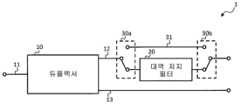
도 1을 참조하면, 듀플렉서 디바이스(1)는, 듀플렉서(10)와 대역 저지 필터(20)와 스위치(30a)와 스위치(30b)를 구비한다. 여기서는, 듀플렉서 디바이스(1)는 압전 소자 상에 탑재된 SAW 장치에 의해서 구성되어 있는 것으로 한다.Referring to FIG. 1 , a
도시된 듀플렉서(10)는, 안테나 단자(11)와 송신 단자(12)와 수신 단자(13)를 구비하고 있다. 안테나 단자(11)는, 듀플렉서(10)가 탑재되어 있는 통신 디바이스 등의 안테나와 접속되어 있는 단자이다. 송신 단자(12)는, 듀플렉서(10)가 탑재되어 있는 통신 디바이스 등의 송신 회로 등과 접속되어 있는 단자이다. 수신 단자(13)는, 듀플렉서(10)가 탑재되어 있는 통신 디바이스 등의 수신 회로 등과 접속되어 있는 단자이다.The illustrated
본 발명에 있어서, 듀플렉서(10)는, 여러 주파수 대역의 밴드에 대응하기 위하여 광대역의 송신 대역, 및 수신 대역을 갖는 풀 밴드 대응의 듀플렉서인 것이 바람직하다. 이와 같은 듀플렉서(10)는, 예를 들면 전기 기계 결합 상수(k2)가 11% 이상인 압전 기판으로 구성할 수 있다. 전기 기계 결합 상수 11% 이상인 압전 기판은, 예를 들면 LiNbO3(니오브산 리튬)으로부터 생성한 기판에, SiO2(이산화규소)의 박막을 조합함으로써 구성할 수 있다.In the present invention, the
도 2는 본 발명에 있어서 사용할 수 있는 듀플렉서의 구성의 일례를 나타낸 모식도이다. 도 2에 나타낸 바와 같이, 듀플렉서(10)는, 송신 필터(100)와 수신 필터(200)를 구비하고 있다. 또한, 도 2에 나타난 듀플렉서는 본 발명자들에 의해서 먼저 출원된 한국특허출원번호 제10-2015-0078784호에 기재된 듀플렉서와 동일한 구성을 구비하고 있고, 본 명세서에서는 전술한 명세서의 내용을 편입시키는 것으로 한다.2 is a schematic diagram showing an example of the configuration of a duplexer that can be used in the present invention. As shown in FIG. 2 , the
송신 필터(100)는, 제 1 탄성 표면파 소자(101)와 제 2 탄성 표면파 소자(102)를 구비하고 있다.The
제 1 탄성 표면파 소자(101) 및 제 2 탄성 표면파 소자(102)는, 각각, 특정 주파수 대역의 신호만을 통과시키는 통상의 밴드패스 필터에 의해서 구성되고, 입력 단자 및 출력 단자가 공통적으로 접속되어 있다. 또, 제 1 탄성 표면파 소자(101)는, 제 2 탄성 표면파 소자(102)와 비교하여 저주파 대역에 통과 대역을 갖고 있다. 또한, 제 1 탄성 표면파 소자(101) 및 제 2 탄성 표면파 소자(102)는, 각각 실질적으로 동일한 폭의 통과 대역을 갖고 있고, 통과 대역의 저주파측 및 고주파측에 있어서, 급준(急峻)한 감쇠 특성을 갖고 있다.The first surface
이 때, 제 1 탄성 표면파 소자(101)의 반사 계수의 실부를 a1, 허부를 b1이라고 하고, 제 2 탄성 표면파 소자(102)의 반사 계수의 실부를 a2, 허부를 b2라고 하였을 경우에, 입력 단자 및 출력 단자에 있어서 a1 ≥ a2, 또한 b1 > b2의 관계가 성립하고 있다. 또한, 제 1 탄성 표면파 소자(101) 및 제 2 탄성 표면파 장치(102)의 통과 대역은, 각각의 중심 주파수의 삽입 손실의 값으로부터 약 3 dB 감쇠하는 영역에서 교차하고 있다. 또한, 제 1 탄성 표면파 소자(101) 및 제 2 탄성 표면파 소자(102)의 구성은, 특별히 한정되지 않고, 더블 모드형 및 래더형 등의 탄성 표면파 소자로 구성할 수 있다.In this case, if the real part of the reflection coefficient of the first surface
수신 필터(200)는 제 3 탄성 표면파 소자(201)와 제 4 탄성 표면파 소자(202)를 구비하고 있다. 제 3 탄성 표면파 소자(201) 및 제 4 탄성 표면파 소자(202)는, 각각, 특정 주파수 대역의 신호만을 통과시키는 통상의 밴드패스 필터에 의해서 구성되고, 입력 단자 및 출력 단자가 공통적으로 접속되어 있다. 또, 제 3 탄성 표면파 소자(201)는, 제 4 탄성 표면파 소자(202)와 비교하여 저주파 대역에 통과 대역을 갖고 있다. 또한, 제 3 탄성 표면파 소자(201) 및 제 4 탄성 표면파 소자(202)는, 각각 실질적으로 동일한 폭의 통과 대역을 갖고 있고, 통과 대역의 저주파측 및 고주파측에 있어서, 급준한 감쇠 특성을 갖고 있다.The
이 때, 제 3 탄성 표면파 소자(201)의 반사 계수의 실부를 a3, 허부를 b3이라고 하고, 제 4 탄성 표면파 소자(202)의 반사 계수의 실부를 a4, 허부를 b4라고 하였을 경우에, 입력 단자 및 출력 단자에 있어서 a3 ≥ a4, 또한 b3 > b4의 관계가 성립하고 있다. 또, 제 3 탄성 표면파 소자(201) 및 제 4 탄성 표면파 장치(202)의 통과 대역은, 각각의 중심 주파수의 삽입 손실의 값으로부터 약 3 dB 감쇠하는 영역에서 교차하고 있다. 또한, 제 3 탄성 표면파 소자(201) 및 제 4 탄성 표면파 소자(202)의 구성은, 특별히 한정되지 않고, 더블 모드형 및 래더형 등의 탄성 표면파 소자로 구성할 수 있다.In this case, if the real part of the reflection coefficient of the third surface
도 1로 되돌아가면, 듀플렉서(10)에 접속되는 대역 저지 필터(20)는, 특정 주파수 대역의 신호만을 억압할 수 있는 필터이다. 구체적으로는, 대역 저지 필터(20)는, 듀플렉서(10)의 송신 대역 및 수신 대역에 그 외의 통신 시스템 등에서 사용하는 타 대역이 겹쳐 있는 경우에, 겹쳐 있는 범위의 주파수 대역의 신호를 억압할 수 있다. 이와 같은 대역 저지 필터(20)는, 예를 들면 SAW 필터 및 유전체 필터 등으로 구성할 수 있지만, 듀플렉서(10)와 동일한 기판을 이용한 SAW 필터인 것이 바람직하다. SAW 필터에 의해서 대역 저지 필터(20)를 구성하는 경우, 복수의 공진기를 다단 접속함으로써 구성할 수 있고, 15∼20 dB의 감쇠 특성을 갖게 하면 된다.Returning to Fig. 1, the
또, 대역 저지 필터(20)는, 스위치(30a) 및 스위치(30b)를 개재하여 듀플렉서(10)와 접속되어 있다.Also, the
듀플렉서 디바이스(1)에 있어서, 스위치(30a) 및 스위치(30b)를 전환함으로써, 듀플렉서(10)는 대역 저지 필터(20) 또는 송신 배선(31)과 접속시킨다.In the
여기서, 스위치(30a, 30b)는, 로밍 동작시에 생성되는 주파수 전환 신호에 응답하여 전환되도록 구성할 수 있다. 듀플렉서(10)가 대역 저지 필터(20)와 접속되어 있는 경우에는 소정의 주파수 대역(예를 들면, 도 7의 저지 대역)의 신호가 억압된다. 다른 한편, 듀플렉서(10)가 송신 배선(31)과 접속되어 있는 경우에는 통신 디바이스 등의 송신 회로로부터 출력된 신호는, 대역 저지 필터(20)를 개재하지 않고 듀플렉서(10)의 출력이 그대로 외부 회로(예를 들면, 송신 회로)에 출력된다.Here, the
따라서, 듀플렉서(10)의 송신 대역 및 수신 대역에 그 외의 통신 시스템 등에서 사용하는 신호가 겹치고 있음을 미리 알고 있는 경우에는, 당해 통신 시스템에 따른 주파수 전환 신호를 듀플렉서(10)에 출력하고, 듀플렉서(10)를 대역 저지 필터(20)와 접속시키면 된다. 한편, 듀플렉서(10)의 송신 대역 및 수신 대역에 그 외의 통신 시스템 등에서 사용하는 신호가 존재하지 않음을 미리 알고 있는 경우에는, 듀플렉서(10)를 송신 배선(31)과 접속시키면 된다.Therefore, when it is known in advance that the transmission band and the reception band of the
도 3은 본 발명에 관련된 듀플렉서(10)의 송신 대역, 수신 대역 및 저지 대역의 관계를 나타낸 모식도이다. 도 3을 참조하면, 송신 대역(41), 수신 대역(42), 타 대역(43) 및 저지 대역(44)이 나타나 있다. 도 3에 나타낸 모식도에 있어서, 횡축은 주파수(㎒)이고, 종축은 삽입 손실(dB)이다.Fig. 3 is a schematic diagram showing the relationship among the transmission band, reception band and stop band of the
송신 대역(41) 및 수신 대역(42)은, 각각, 듀플렉서(10)의 송신 대역과 수신 대역을 나타내고 있다. 또한, 본 발명에 있어서, 송신 대역(41) 및 수신 대역(42)의 주파수 대역은, 특별히 한정되지 않고, 여러 주파수 대역으로 설정할 수 있다.The
타 대역(43)은, 예를 들면, 듀플렉서(10)가 탑재되어 있는 통신 디바이스와는 다른 통신 시스템에서 사용되고 있는 밴드의 주파수 대역을 나타내고 있다.The
저지 대역(44)은, 송신 대역(41)과, 타 대역(43)이 겹쳐 있는 주파수 대역을 나타내고 있다. 그 때문에, 타 대역(43)이 사용되는 경우에, 저지 대역(44)은, 송신 대역(41)에 포함되는 대역이지만, 그 외의 통신 시스템과의 간섭 등을 피하기 위하여 억압하는 것이 필요하다.The
도 4는 본 발명에 관련된 듀플렉서(10)의 송신 특성 및 수신 특성과, 대역 저지 필터(20)의 저지 특성을 나타낸 모식도이다. 도 4에 나타낸 모식도에 있어서, 횡축은 주파수(㎒)이고, 종축은 삽입 손실(dB)이다.4 is a schematic diagram showing transmission characteristics and reception characteristics of the
송신 특성(51)은, 듀플렉서(10)의 송신측의 주파수 특성을 나타내고 있다. 수신 특성(52)은, 듀플렉서(10)의 수신측의 주파수 특성을 나타내고 있다. 저지 특성(53)은, 대역 저지 필터(20)의 주파수 특성을 나타내고 있다.The
도 4에 나타낸 바와 같이, 저지 특성(53)은, 송신 대역(41)과 타 대역(43)이 겹치는 주파수 대역인 저지 대역(44)에 있어서, 급준한 감쇠 특성을 갖고 있다. 즉, 저지 특성(53)을 나타낸 바와 같은 대역 저지 필터(20)를 듀플렉서(10)의 송신 단자(12)에 접속함으로써, 송신 대역(41)에 포함되는 저지 대역(44)을 억압할 수 있다.As shown in Fig. 4, the blocking characteristic 53 has a steep attenuation characteristic in the blocking
구체적으로는, 대역 저지 필터(20)는, 스위치(30a) 및 스위치(30b)를 개재하여 듀플렉서(10)의 송신 단자(12)에 접속되어 있다. 이 경우, 통신 디바이스 등의 송신 회로로부터 출력된 신호는, 듀플렉서(10)에 부여된 후, 대역 저지 필터(20)를 개재하여 외부 회로에 출력된다. 그 때문에, 대역 저지 필터(20)는, 듀플렉서(10)의 송신 대역(41)에 포함되는 저지 대역(44)을 억압할 수 있다. 또, 상술한 바와 같이 듀플렉서(10)는, 송신 대역(41)과 수신 대역(42)을 합친 주파수 대역인 원하는 통신 시스템 대역에 대응하고 있는 풀 밴드 대응의 듀플렉서인 것이 바람직하다.Specifically, the
또한, 도 4에 있어서, 저지 대역(44)은 1개만 존재하고 있지만, 이것은 예시이며, 저지 대역(44)은 복수 존재하고 있어도 된다. 이 경우, 저지 대역(44)에 대응하는 대역 저지 필터(20)를 복수 준비하고, 복수의 대역 저지 필터(20)를 듀플렉서(10)의 송신 단자(12)에 접속함으로써, 복수의 저지 대역(44)을 각각 억압할 수 있다.In Fig. 4, only one
또, 대역 저지 필터(20)는, 듀플렉서(10)의 송신 단자(12)에 접속되어 있는 경우를 설명하였다. 그러나, 대역 저지 필터(20)는, 송신 단자(12)가 아니라 듀플렉서(10)의 안테나 단자(11) 및 수신 단자(13)에 접속되어 있어도 된다.In addition, the case where the
대역 저지 필터(20)가 듀플렉서(10)의 안테나 단자(11)에 접속되어 있는 경우에는, 안테나로부터 신호가 직접, 대역 저지 필터(20)에 부여되어, 대역 저지 필터(20)에 의해 저지 대역의 신호를 억제한 신호가 듀플렉서(10)에 공급된다. 이 경우, 대역 저지 필터(20)는, 듀플렉서(10)의 송신 대역(41) 및 수신 대역(42)에 저지 대역(44)이 포함되는 경우에, 저지 대역(44)을 억압할 수 있다.When the
또, 대역 저지 필터(20)가 듀플렉서(10)의 수신 단자(13)에 접속되어 있는 경우에는, 듀플렉서(10)가 받은 신호는, 대역 저지 필터(20)를 개재하여, 통신 디바이스 등의 수신 회로에 공급된다. 이 경우, 대역 저지 필터(20)는, 듀플렉서(10)의 수신 대역(42)에 저지 대역(44)이 포함되는 경우에, 저지 대역(44)을 억압할 수 있다.In the case where the
즉, 대역 저지 필터(20)는, 저지 대역(44)의 주파수 대역에 따라서 안테나 단자(11), 송신 단자(12) 및 수신 단자(13)에 선택적으로 접속함으로써, 저지 대역(44)을 억압할 수 있다.That is, the band reject
[제 2 실시 형태][Second Embodiment]
도 5는 본 발명의 제 2 실시 형태에 관련된 듀플렉서 디바이스(1A)의 구성을 나타낸 블럭도이다. 도시된 듀플렉서 디바이스(1A)는, 스위치(30a 및 30b)를 자유롭게 전환할 수 있는 것으로 한다.Fig. 5 is a block diagram showing the configuration of a
듀플렉서 디바이스(1A)는, 듀플렉서(10)와 대역 저지 필터(20)와 스위치(30a)와 스위치(30b)와 제어부(40)를 구비한다.The
제어부(40)는, 스위치(30a) 및 스위치(30b)와 전기적으로 접속되어 있다. 또, 제어부(40)는, 도시하지 않은 주파수 검지 회로 등에 접속되고, 당해 주파수 검지 회로로부터의 출력에 의해서 스위치(30a, 30b)에 전환 신호를 출력한다. 이에 의해서, 도시된 듀플렉서(10)는, 검지된 주파수 대역에 따라서 스위치(30a) 및 스위치(30b)를 전환할 수 있다. 구체적으로는, 제어부(40)는, 듀플렉서(10)의 송신 대역 및 수신 대역과 겹치는 주파수 대역에 타 대역의 존재 유무를 검지하고, 타 대역이 존재하는 경우, 제어부(40)로부터의 전환 신호에 의해서 스위치(30a) 및 스위치(30b)를 전환하고, 듀플렉서(10)와 대역 저지 필터(20)를 접속시킨다. 한편, 타 대역이 존재하지 않는 경우에는, 제어부(40)는 스위치(30a) 및 스위치(30b)를 제어하여, 대역 저지 필터(20)를 접속하지 않고, 듀플렉서(10)와 송신 배선(31)을 직접 접속시킨다. 이 경우, 제어부(40)는, 예를 들면, 로밍하는 회로와 일체화함으로써 대응하는 주파수 대역을 검지하도록 구성해도 된다.
도 6은 도 5에 나타난 제어부(40)가 통신 디바이스에서 이용하는 밴드를 검지하고, 스위치(30a) 및 스위치(30b)를 전환하는 동작의 흐름을 나타낸 플로우차트이다.FIG. 6 is a flowchart showing the flow of an operation in which the
먼저, 제어부(40)는, 통신 디바이스에서 사용하는 듀플렉서(10)의 송신 대역과, 타 대역의 주파수 대역을 검지한다(단계 S101).First, the
이어서, 제어부(40)는, 듀플렉서(10)의 송신 대역에 겹치는 주파수 대역에 타 대역이 존재한다고 검지한 경우(단계 S102에 있어서 「YES」), 스위치(30a) 및 스위치(30b)를 전환하여, 듀플렉서(10)와 대역 저지 필터(20)를 접속시킨다(단계 S103). 이에 의해, 듀플렉서(10)의 송신 대역과 타 대역이 겹치는 주파수 대역을 억압할 수 있다.Next, when the
한편, 제어부(40)는, 검지 결과, 송신 대역에 겹치는 주파수 대역에 타 대역이 존재하지 않았을 경우(단계 S102에 있어서 「NO」), 스위치(30a) 및 스위치(30b)를 전환하여, 듀플렉서(10)와 송신 배선(31)을 접속시킨다(단계 S104).On the other hand, if, as a result of the detection, no other band exists in the frequency band overlapping the transmission band ("NO" in step S102),
또한, 제어부(40)가, 대역 저지 필터(20)가 듀플렉서(10)의 송신 단자(11)에 접속되어 있는 경우에 스위치(30a) 및 스위치(30b)를 제어하는 방법에 대하여 설명하였지만, 이것은 예시이며, 본 발명을 한정하는 것은 아니다. 제어부(40)는, 대역 저지 필터(20)가 듀플렉서(10)의 안테나 단자(11) 및 수신 단자(12)에 접속되어 있는 경우이더라도 동일하게 제어하는 것이 가능하다. 또, 제어부(40)는, 듀플렉서(10)의 안테나 단자(11), 송신 단자(12) 및 수신 단자(13)에 복수의 대역 저지 필터(20)가 접속되어 있는 경우이더라도, 동일하게 제어할 수 있다.Further, the method for controlling the
1, 1A: 듀플렉서 디바이스
10: 듀플렉서
20: 대역 저지 필터
30a, 30b: 스위치
31: 송신 배선
40: 제어부
41, 61: 송신 대역
42, 62: 수신 대역
43, 63: 타 대역
51: 송신 특성
52: 수신 특성
53: 저지 특성1, 1A: duplexer device
10: duplexer
20: band stop filter
30a, 30b: switch
31: transmission wiring
40: control unit
41, 61: transmission band
42, 62: reception band
43, 63: other bands
51: transmission characteristics
52: reception characteristics
53: Jersey characteristics
Claims (9)
Translated fromKorean상기 안테나 단자, 상기 송신 단자 및 상기 수신 단자 중 적어도 1개에 스위치를 개재하여 접속되고, 상기 스위치의 전환에 의해서 상기 소정의 송신 대역 및 수신 대역 중 적어도 일방의 대역의 일부를 억압하는 대역 저지 필터; 및
상기 스위치의 전환을 제어하는 제어부;
를 포함하고,
상기 듀플렉서는,
제 1 탄성 표면파 장치 및 제 2 탄성 표면파 장치를 포함하며,
상기 제 1 탄성 표면파 장치 및 제 2 탄성 표면파 장치의 입력 단자 및 출력 단자는 공통적이고,
상기 제 1 탄성 표면파 장치의 통과 대역은, 상기 제 2 탄성 표면파 장치보다 낮고,
또한 상기 제 1 탄성 표면파 장치의 통과 대역의 고주파측의 주파수가, 상기 제 2 탄성 표면파 장치의 통과 대역의 저주파측의 주파수와 부분적으로 겹치는, 듀플렉서 디바이스.a duplexer having an antenna terminal, a transmission terminal, and a reception terminal, and having predetermined transmission bands and reception bands;
A band elimination filter connected to at least one of the antenna terminal, the transmission terminal, and the reception terminal via a switch, and suppressing part of at least one of the predetermined transmission band and reception band by switching the switch. ; and
a control unit controlling conversion of the switch;
including,
The duplexer,
a first surface acoustic wave device and a second surface acoustic wave device;
an input terminal and an output terminal of the first surface acoustic wave device and the second surface acoustic wave device are common;
a pass band of the first surface acoustic wave device is lower than that of the second surface acoustic wave device;
Further, the duplexer device wherein a frequency on the high frequency side of the pass band of the first surface acoustic wave device partially overlaps a frequency on the low frequency side of the pass band of the second surface acoustic wave device.
상기 대역 저지 필터는, 상기 송신 대역 및 상기 수신 대역 중 적어도 일방과 부분적으로 겹치는 타 대역이 존재하는 경우에, 상기 송신 대역 및 상기 수신 대역 중 적어도 일방과 상기 타 대역과 겹치는 주파수 대역을 부분적으로 억압하는, 듀플렉서 디바이스.According to claim 1,
The band elimination filter partially suppresses a frequency band overlapping at least one of the transmission band and the reception band and the other band when another band partially overlaps with at least one of the transmission band and the reception band. , a duplexer device.
상기 제어부는, 상기 송신 대역 및 상기 수신 대역 중 적어도 일방의 상기 타 대역에 따라서 상기 스위치를 전환하는, 듀플렉서 디바이스.According to claim 2,
The control unit switches the switch according to the other band of at least one of the transmission band and the reception band.
상기 듀플렉서는, 전기 기계 결합 상수가 11% 이상인 압전 기판으로 구성되어 있는, 듀플렉서 디바이스.According to claim 1,
The duplexer device, wherein the duplexer is composed of a piezoelectric substrate having an electromechanical coupling constant of 11% or more.
Priority Applications (3)
| Application Number | Priority Date | Filing Date | Title |
|---|---|---|---|
| KR1020150173324AKR102556605B1 (en) | 2015-12-07 | 2015-12-07 | Duplexer device |
| US15/364,406US10236862B2 (en) | 2015-12-07 | 2016-11-30 | Duplexer device |
| CN201611089178.3ACN107040238A (en) | 2015-12-07 | 2016-12-01 | Diplexer device |
Applications Claiming Priority (1)
| Application Number | Priority Date | Filing Date | Title |
|---|---|---|---|
| KR1020150173324AKR102556605B1 (en) | 2015-12-07 | 2015-12-07 | Duplexer device |
Publications (2)
| Publication Number | Publication Date |
|---|---|
| KR20170066997A KR20170066997A (en) | 2017-06-15 |
| KR102556605B1true KR102556605B1 (en) | 2023-07-17 |
Family
ID=58799325
Family Applications (1)
| Application Number | Title | Priority Date | Filing Date |
|---|---|---|---|
| KR1020150173324AActiveKR102556605B1 (en) | 2015-12-07 | 2015-12-07 | Duplexer device |
Country Status (3)
| Country | Link |
|---|---|
| US (1) | US10236862B2 (en) |
| KR (1) | KR102556605B1 (en) |
| CN (1) | CN107040238A (en) |
Families Citing this family (1)
| Publication number | Priority date | Publication date | Assignee | Title |
|---|---|---|---|---|
| WO2023282330A1 (en)* | 2021-07-08 | 2023-01-12 | 株式会社村田製作所 | Elastic wave element, elastic wave filter device, and multiplexer |
Citations (1)
| Publication number | Priority date | Publication date | Assignee | Title |
|---|---|---|---|---|
| US20150236798A1 (en)* | 2013-03-14 | 2015-08-20 | Peregrine Semiconductor Corporation | Methods for Increasing RF Throughput Via Usage of Tunable Filters |
Family Cites Families (19)
| Publication number | Priority date | Publication date | Assignee | Title |
|---|---|---|---|---|
| SU1111256A1 (en)* | 1983-06-29 | 1984-08-30 | Предприятие П/Я В-2203 | Device for suppressing narrow-band interference |
| JPH01200726A (en)* | 1988-02-04 | 1989-08-11 | Matsushita Electric Ind Co Ltd | Antenna multicoupler |
| FI88565C (en)* | 1990-07-06 | 1993-05-25 | Lk Products Oy | Method for improving the barrier attenuation of a radio frequency filter |
| JPH09121138A (en)* | 1995-08-24 | 1997-05-06 | Fujitsu Ltd | Filter device and wireless device using the same |
| JP3739858B2 (en)* | 1996-06-14 | 2006-01-25 | 松下電器産業株式会社 | High frequency filter |
| JP2002171315A (en)* | 2000-12-01 | 2002-06-14 | Toshiba Corp | In-vehicle compatible mobile terminal device |
| EP1508974B1 (en)* | 2001-02-27 | 2007-09-19 | Matsushita Electric Industrial Co., Ltd. | Antenna duplexer and mobile communication device using the same |
| US6809611B2 (en)* | 2001-10-01 | 2004-10-26 | Matsushita Electric Industrial Co., Ltd. | Composite filter, antenna duplexer, and communication apparatus |
| US6833774B2 (en)* | 2002-06-25 | 2004-12-21 | Sawtek, Inc. | Surface acoustic wave filter |
| DE10352642B4 (en)* | 2003-11-11 | 2018-11-29 | Snaptrack, Inc. | Circuit with reduced insertion loss and device with the circuit |
| US8270927B2 (en)* | 2004-03-29 | 2012-09-18 | Qualcom, Incorporated | Adaptive interference filtering |
| US7298231B2 (en)* | 2004-05-27 | 2007-11-20 | Kyocera Corporation | Surface acoustic wave device and communication apparatus |
| CN100576760C (en)* | 2004-08-06 | 2009-12-30 | 株式会社村田制作所 | High frequency composite component |
| JP4267579B2 (en)* | 2005-01-31 | 2009-05-27 | パナソニック株式会社 | Multi-mode communication device |
| JP2010136298A (en)* | 2008-12-08 | 2010-06-17 | Sony Ericsson Mobilecommunications Japan Inc | Mobile wireless terminal |
| JP5075188B2 (en)* | 2009-12-03 | 2012-11-14 | 株式会社エヌ・ティ・ティ・ドコモ | Wireless communication terminal |
| JP5603209B2 (en)* | 2010-11-10 | 2014-10-08 | 太陽誘電株式会社 | Demultiplexer and electronic device having the same |
| US8711993B2 (en)* | 2010-12-10 | 2014-04-29 | Honeywell International Inc. | Wideband multi-channel receiver with fixed-frequency notch filter for interference rejection |
| US9673155B2 (en)* | 2014-02-14 | 2017-06-06 | Peregrine Semiconductor Corporation | Integrated tunable filter architecture |
- 2015
- 2015-12-07KRKR1020150173324Apatent/KR102556605B1/enactiveActive
- 2016
- 2016-11-30USUS15/364,406patent/US10236862B2/enactiveActive
- 2016-12-01CNCN201611089178.3Apatent/CN107040238A/enactivePending
Patent Citations (1)
| Publication number | Priority date | Publication date | Assignee | Title |
|---|---|---|---|---|
| US20150236798A1 (en)* | 2013-03-14 | 2015-08-20 | Peregrine Semiconductor Corporation | Methods for Increasing RF Throughput Via Usage of Tunable Filters |
Also Published As
| Publication number | Publication date |
|---|---|
| US20170163244A1 (en) | 2017-06-08 |
| CN107040238A (en) | 2017-08-11 |
| US10236862B2 (en) | 2019-03-19 |
| KR20170066997A (en) | 2017-06-15 |
Similar Documents
| Publication | Publication Date | Title |
|---|---|---|
| US10644673B2 (en) | Radio frequency filter circuit, duplexer, radio frequency front end circuit, and communication apparatus | |
| US10243538B2 (en) | High-frequency filter, multiplexer, high-frequency front-end circuit, and communication device | |
| JP6116648B2 (en) | Filter module | |
| US10727805B2 (en) | Multiplexer including filters with resonators and parallel inductor | |
| CN108023570B (en) | Multiplexer | |
| US9520857B2 (en) | Electronic device including filter | |
| US10148297B2 (en) | Splitter | |
| KR101850228B1 (en) | Branching device | |
| JP6365776B2 (en) | High frequency front end circuit | |
| US11336252B2 (en) | Radio frequency filter, multiplexer, radio frequency front end circuit, and communication apparatus | |
| KR20170048570A (en) | Demultiplexing device | |
| JP6798456B2 (en) | High frequency front end circuit and communication equipment | |
| JP2017208656A (en) | Switch module and high frequency module | |
| JP2018078542A (en) | Filter device, multiplexer, high frequency front end circuit and communication apparatus | |
| JP2017506860A (en) | Tunable electroacoustic HF filter with improved electrical characteristics and method of operating such a filter | |
| JPWO2019131501A1 (en) | Multiplexer | |
| US20180138890A1 (en) | Multiplexer | |
| JP6673467B2 (en) | Frequency variable filter, RF front-end circuit, and communication terminal | |
| US20170324393A1 (en) | Radio Frequency Duplexer | |
| KR20210023725A (en) | Multiplexer | |
| KR102556605B1 (en) | Duplexer device | |
| US8837336B2 (en) | Antenna arrangement | |
| US9294068B2 (en) | Filter circuit and module | |
| CN108631813B (en) | Front end module | |
| US9654150B2 (en) | Module with duplexers coupled to diplexer |
Legal Events
| Date | Code | Title | Description |
|---|---|---|---|
| PA0109 | Patent application | Patent event code:PA01091R01D Comment text:Patent Application Patent event date:20151207 | |
| PG1501 | Laying open of application | ||
| N231 | Notification of change of applicant | ||
| PN2301 | Change of applicant | Patent event date:20170908 Comment text:Notification of Change of Applicant Patent event code:PN23011R01D | |
| A201 | Request for examination | ||
| PA0201 | Request for examination | Patent event code:PA02012R01D Patent event date:20201202 Comment text:Request for Examination of Application Patent event code:PA02011R01I Patent event date:20151207 Comment text:Patent Application | |
| E902 | Notification of reason for refusal | ||
| PE0902 | Notice of grounds for rejection | Comment text:Notification of reason for refusal Patent event date:20230118 Patent event code:PE09021S01D | |
| E701 | Decision to grant or registration of patent right | ||
| PE0701 | Decision of registration | Patent event code:PE07011S01D Comment text:Decision to Grant Registration Patent event date:20230711 | |
| GRNT | Written decision to grant | ||
| PR0701 | Registration of establishment | Comment text:Registration of Establishment Patent event date:20230713 Patent event code:PR07011E01D | |
| PR1002 | Payment of registration fee | Payment date:20230713 End annual number:3 Start annual number:1 | |
| PG1601 | Publication of registration |