KR102555577B1 - Electronic module including camera module - Google Patents
Electronic module including camera moduleDownload PDFInfo
- Publication number
- KR102555577B1 KR102555577B1KR1020190010657AKR20190010657AKR102555577B1KR 102555577 B1KR102555577 B1KR 102555577B1KR 1020190010657 AKR1020190010657 AKR 1020190010657AKR 20190010657 AKR20190010657 AKR 20190010657AKR 102555577 B1KR102555577 B1KR 102555577B1
- Authority
- KR
- South Korea
- Prior art keywords
- recess
- plate
- electronic device
- filling member
- transparent member
- Prior art date
- Legal status (The legal status is an assumption and is not a legal conclusion. Google has not performed a legal analysis and makes no representation as to the accuracy of the status listed.)
- Active
Links
Images


Classifications
- G—PHYSICS
- G06—COMPUTING OR CALCULATING; COUNTING
- G06F—ELECTRIC DIGITAL DATA PROCESSING
- G06F1/00—Details not covered by groups G06F3/00 - G06F13/00 and G06F21/00
- G06F1/16—Constructional details or arrangements
- G06F1/1613—Constructional details or arrangements for portable computers
- G06F1/1633—Constructional details or arrangements of portable computers not specific to the type of enclosures covered by groups G06F1/1615 - G06F1/1626
- G06F1/1656—Details related to functional adaptations of the enclosure, e.g. to provide protection against EMI, shock, water, or to host detachable peripherals like a mouse or removable expansions units like PCMCIA cards, or to provide access to internal components for maintenance or to removable storage supports like CDs or DVDs, or to mechanically mount accessories
- H—ELECTRICITY
- H04—ELECTRIC COMMUNICATION TECHNIQUE
- H04M—TELEPHONIC COMMUNICATION
- H04M1/00—Substation equipment, e.g. for use by subscribers
- H04M1/02—Constructional features of telephone sets
- H04M1/0202—Portable telephone sets, e.g. cordless phones, mobile phones or bar type handsets
- H04M1/026—Details of the structure or mounting of specific components
- G—PHYSICS
- G02—OPTICS
- G02B—OPTICAL ELEMENTS, SYSTEMS OR APPARATUS
- G02B1/00—Optical elements characterised by the material of which they are made; Optical coatings for optical elements
- G02B1/10—Optical coatings produced by application to, or surface treatment of, optical elements
- G02B1/14—Protective coatings, e.g. hard coatings
- G—PHYSICS
- G02—OPTICS
- G02B—OPTICAL ELEMENTS, SYSTEMS OR APPARATUS
- G02B27/00—Optical systems or apparatus not provided for by any of the groups G02B1/00 - G02B26/00, G02B30/00
- G02B27/0006—Optical systems or apparatus not provided for by any of the groups G02B1/00 - G02B26/00, G02B30/00 with means to keep optical surfaces clean, e.g. by preventing or removing dirt, stains, contamination, condensation
- G—PHYSICS
- G02—OPTICS
- G02B—OPTICAL ELEMENTS, SYSTEMS OR APPARATUS
- G02B7/00—Mountings, adjusting means, or light-tight connections, for optical elements
- G02B7/02—Mountings, adjusting means, or light-tight connections, for optical elements for lenses
- G02B7/021—Mountings, adjusting means, or light-tight connections, for optical elements for lenses for more than one lens
- G—PHYSICS
- G06—COMPUTING OR CALCULATING; COUNTING
- G06F—ELECTRIC DIGITAL DATA PROCESSING
- G06F1/00—Details not covered by groups G06F3/00 - G06F13/00 and G06F21/00
- G06F1/16—Constructional details or arrangements
- G06F1/1613—Constructional details or arrangements for portable computers
- G06F1/1633—Constructional details or arrangements of portable computers not specific to the type of enclosures covered by groups G06F1/1615 - G06F1/1626
- G06F1/1684—Constructional details or arrangements related to integrated I/O peripherals not covered by groups G06F1/1635 - G06F1/1675
- G06F1/1686—Constructional details or arrangements related to integrated I/O peripherals not covered by groups G06F1/1635 - G06F1/1675 the I/O peripheral being an integrated camera
- H—ELECTRICITY
- H04—ELECTRIC COMMUNICATION TECHNIQUE
- H04M—TELEPHONIC COMMUNICATION
- H04M1/00—Substation equipment, e.g. for use by subscribers
- H04M1/02—Constructional features of telephone sets
- H04M1/0202—Portable telephone sets, e.g. cordless phones, mobile phones or bar type handsets
- H04M1/026—Details of the structure or mounting of specific components
- H04M1/0264—Details of the structure or mounting of specific components for a camera module assembly
- H—ELECTRICITY
- H04—ELECTRIC COMMUNICATION TECHNIQUE
- H04N—PICTORIAL COMMUNICATION, e.g. TELEVISION
- H04N23/00—Cameras or camera modules comprising electronic image sensors; Control thereof
- H04N23/50—Constructional details
- H04N23/51—Housings
- H—ELECTRICITY
- H04—ELECTRIC COMMUNICATION TECHNIQUE
- H04N—PICTORIAL COMMUNICATION, e.g. TELEVISION
- H04N23/00—Cameras or camera modules comprising electronic image sensors; Control thereof
- H04N23/50—Constructional details
- H04N23/55—Optical parts specially adapted for electronic image sensors; Mounting thereof
- H—ELECTRICITY
- H04—ELECTRIC COMMUNICATION TECHNIQUE
- H04N—PICTORIAL COMMUNICATION, e.g. TELEVISION
- H04N23/00—Cameras or camera modules comprising electronic image sensors; Control thereof
- H04N23/57—Mechanical or electrical details of cameras or camera modules specially adapted for being embedded in other devices
Landscapes
- Engineering & Computer Science (AREA)
- Physics & Mathematics (AREA)
- Signal Processing (AREA)
- Computer Hardware Design (AREA)
- General Physics & Mathematics (AREA)
- Theoretical Computer Science (AREA)
- Multimedia (AREA)
- General Engineering & Computer Science (AREA)
- Optics & Photonics (AREA)
- Human Computer Interaction (AREA)
- Telephone Set Structure (AREA)
- Devices For Indicating Variable Information By Combining Individual Elements (AREA)
Abstract
Translated fromKoreanDescription
Translated fromKorean본 문서에 개시된 다양한 실시예들은 카메라 모듈을 포함하는 전자 장치에 관한 것이다.Various embodiments disclosed in this document relate to an electronic device including a camera module.
통상적으로 전자 장치라 함은, 가전제품으로부터, 전자 수첩, 휴대용 멀티미디어 재생기, 이동통신 단말기, 태블릿 PC, 영상/음향 장치, 데스크톱/랩톱 컴퓨터, 차량용 내비게이션 등, 탑재된 프로그램에 따라 특정 기능을 수행하는 장치를 의미한다. 예를 들면, 이러한 전자 장치들은 저장된 정보를 음향이나 영상으로 출력할 수 있다. 전자 장치의 집적도가 높아지고, 초고속, 대용량 무선통신이 보편화되면서, 최근에는, 이동통신 단말기 하나에 다양한 기능이 탑재되고 있다. 예를 들면, 통신 기능뿐만 아니라, 게임과 같은 엔터테인먼트 기능, 음악/동영상 재생과 같은 멀티미디어 기능, 모바일 뱅킹 등을 위한 통신 및 보안 기능, 일정 관리나 전자 지갑 등의 기능이 하나의 전자 장치에 집약되고 있는 것이다. 또한, 전자 장치에는 하나 이상의 카메라 모듈이 구비될 수 있으며, 전자 장치는 상기 카메라 모듈을 통해 외부 이미지나 영상을 직접 기록하고 저장할 수 있다.In general, electronic devices include home appliances, electronic notebooks, portable multimedia players, mobile communication terminals, tablet PCs, video/audio devices, desktop/laptop computers, car navigation systems, etc., that perform specific functions according to loaded programs. means device. For example, these electronic devices may output stored information as sound or image. As the degree of integration of electronic devices increases and ultra-high-speed, high-capacity wireless communication becomes common, recently, a single mobile communication terminal is equipped with various functions. For example, not only communication functions, but also entertainment functions such as games, multimedia functions such as music/video playback, communication and security functions for mobile banking, and functions such as schedule management and electronic wallets are integrated into one electronic device. There is. Also, the electronic device may include one or more camera modules, and the electronic device may directly record and store external images or videos through the camera module.
휴대용 컴퓨터 및 모바일 폰과 같은 전자 장치에는 일반적으로 디스플레이가 포함된다. 상기 디스플레이를 손상으로부터 보호하기 위해, 많은 전자 장치들은 커버 글래스(이하, '윈도우'라 함)를 포함할 수 있다. 윈도우는 상기 윈도우 하부에 장착되는 상기 디스플레이를 긁힘 및 기타 손상으로부터 보호하는 역할을 할 수 있다. 여기서, 상기 윈도우의 상기 배면 상에는 전자 장치의 내부 구성 요소들을 감추기 위한 불투명한 경계 영역을 형성하기 위해 블랙 마스킹 층이 형성될 수 있다. 그리고 상기 마스킹 층에는, 상기 전자 장치에 내장되는 상기 카메라 모듈의 렌즈에 대응하는 구멍들이 형성될 수 있다.Electronic devices such as portable computers and mobile phones commonly include displays. In order to protect the display from damage, many electronic devices may include a cover glass (hereinafter referred to as 'window'). The window may serve to protect the display mounted under the window from scratches and other damage. Here, a black masking layer may be formed on the rear surface of the window to form an opaque boundary area for hiding internal components of the electronic device. Further, holes corresponding to lenses of the camera module embedded in the electronic device may be formed in the masking layer.
상기 윈도우의 편평하지 않은 표면에 의해 카메라 모듈의 성능이 저하될 수 있다.Performance of the camera module may be degraded by the non-flat surface of the window.
예를 들면, 윈도우는 그 제작과정에서 금형 틀의 미세한 자국으로 인해 표면이 고르거나 편평하지 않을 수 있다. 근래 광학 성능(예: 분해능)이 좋은 광학 모듈이 점차 보급됨에 따라, 광학 모듈에 의해 획득되는 이미지나 영상에 상기 금형 틀의 미세한 자국이 시인되어 품질이 저하될 수 있다.For example, the surface of the window may be uneven or uneven due to minute marks of the mold frame during the manufacturing process. Recently, as optical modules having good optical performance (eg, resolution) are increasingly popular, minute marks of the mold frame may be recognized in images or videos obtained by the optical module, and thus quality may deteriorate.
윈도우의 편평하지 않은 표면을 보완하기 위하여, 마스킹 층에 형성된 구멍에 폴리머(polymer)를 채워 넣을 수 있다. 그런데, 마스킹 층에 형성된 구멍에 폴리머를 채워 넣는 경우, 구멍의 내벽 부근의 폴리머는 표면 장력(surface tension) 효과에 의해 굴곡진 상태로 고착될 수 있다. 예를 들면, 마스킹 층에 형성된 구멍에 폴리머를 가득 채워 넣으면 폴리머는 구멍의 중심부에서 볼록한 형상으로 고착되고, 마스킹 층에 형성된 구멍에 폴리머를 적게 채워 넣으면 폴리머는 구멍의 중심부에서 오목한 형상으로 고착된다. 이와 같이 구멍의 내벽 부근에서는 폴리머가 굴곡진 형상으로 형성되고 이 부분을 통과하는 광의 진행 방향이 꺾여 이미지나 영상이 왜곡될 수 있다. 따라서, 광학 모듈의 F.O.V.(field of view)를 고려할 때, 폴리머의 편평한 부분을 통해 광이 입사 되도록 하여야 이미지나 영상이 왜곡되는 것을 방지할 수 있다.To compensate for the non-flat surface of the window, a polymer may be filled in the hole formed in the masking layer. However, when the polymer is filled into the hole formed in the masking layer, the polymer near the inner wall of the hole may be fixed in a curved state due to surface tension effect. For example, when the hole formed in the masking layer is filled with a polymer, the polymer is fixed in a convex shape at the center of the hole, and when a small amount of polymer is filled in the hole formed in the masking layer, the polymer is fixed in a concave shape at the center of the hole. In this way, near the inner wall of the hole, the polymer is formed in a curved shape, and the traveling direction of the light passing through this part is bent, so that the image or video may be distorted. Therefore, when considering the F.O.V. (field of view) of the optical module, light must be incident through the flat portion of the polymer to prevent image or video from being distorted.
어떤 실시예에 따르면, 전자 장치에 커브드(curved) 부분을 포함하는 윈도우를 장착할 수 있다. 윈도우의 커브드 부분의 표면을 통해 사용자 입력을 수행하거나 화면 표시 기능을 제공할 수 있으며, 전자 장치의 미관을 보다 유려하게 할 수 있다. 그런데, 커브드(curved) 부분을 포함하는 윈도우가 장착된 전자 장치에서는 상기 폴리머의 편평한 부분을 확보하기 어려워, 편평한 윈도우가 장착된 전자 장치에 비해 광학 모듈의 F.O.V.를 확보하기가 어려울 수 있다. 아울러, 상기 커브드 부분을 만들기 위한 열성형 과정에서, 윈도우의 표면에 남은 금형 틀의 자국이 이미지나 영상에 시인되는 문제가 발생할 수 있다.According to some embodiments, a window including a curved portion may be mounted on an electronic device. A user input may be performed or a screen display function may be provided through the surface of the curved portion of the window, and the aesthetics of the electronic device may be improved. However, in an electronic device equipped with a window including a curved portion, it is difficult to secure a flat portion of the polymer, so it may be difficult to secure F.O.V. of an optical module compared to an electronic device equipped with a flat window. In addition, in the process of thermoforming to make the curved part, the mark of the mold mold left on the surface of the window may be visually recognized in an image or video.
본 개시에서의 다양한 실시예들에서는 커브드(curved) 부분을 포함하는 윈도우를 적용하더라도, 광학모듈의 F.O.V.를 충분하게 확보할 수 있는 전자 장치를 제공하고자 한다.In various embodiments of the present disclosure, it is intended to provide an electronic device capable of sufficiently securing the F.O.V. of an optical module even when a window including a curved portion is applied.
본 문서에 개시된 다양한 실시예들에 따르면, 제 1 플레이트 및 상기 제 1 플레이트의 측방 또는 후방에 배치된 제 2 플레이트를 포함하는 하우징; 및 상기 제 1 플레이트의 적어도 일부를 통과한 광에 기반하여 외부 정보를 획득하는 카메라 모듈;을 포함하고, 상기 제 1 플레이트는, 적어도 일부분이 실질적으로 투명한 투명 부재; 상기 투명 부재의 배면에 배치되고, 상기 투명 부재의 상기 투명한 영역 주위에 불투명한 영역을 형성하는 마스킹 층; 상기 마스킹 층에 형성 형성되고, 상기 제 1 플레이트의 적어도 일부를 통과한 광이 상기 카메라 모듈을 향하도록 가이드하는 리세스; 및 상기 리세스에 충진된 충진 부재를 포함하는 전자 장치를 제공할 수 있다.According to various embodiments disclosed herein, a housing including a first plate and a second plate disposed on the side or rear side of the first plate; and a camera module configured to acquire external information based on light passing through at least a portion of the first plate, wherein the first plate includes: a transparent member in which at least a portion is substantially transparent; a masking layer disposed on a rear surface of the transparent member and forming an opaque region around the transparent region of the transparent member; a recess formed in the masking layer and guiding light passing through at least a portion of the first plate toward the camera module; and a filling member filled in the recess.
본 문서에 개시된 다양한 실시예들에 따르면, 제 1 플레이트 및 상기 제 1 플레이트의 측방 또는 후방에 배치된 제 2 플레이트를 포함하는 하우징; 상기 제 1 플레이트 및 상기 제 2 플레이트 사이에 배치되고, 상기 제 1 플레이트의 적어도 일부를 통해 화면을 표시하는 디스플레이; 및 상기 제 1 플레이트의 적어도 일부를 통과한 광에 기반하여 외부 정보를 획득하는 카메라 모듈;을 포함하고, 상기 제 1 플레이트는, 상기 디스플레이의 화면을 표시하기 위한 투명한 영역을 포함하는 투명 부재; 상기 투명 부재의 배면에 배치되고, 상기 투명 부재의 상기 투명한 영역 주위에 불투명한 영역을 형성하는 마스킹 층; 상기 마스킹 층에 형성 형성되고, 상기 제 1 플레이트의 적어도 일부를 통과한 광이 상기 카메라 모듈을 향하도록 형성된, 계단 구조의 리세스; 및 상기 계단 구조의 리세스에 충진된 충진 부재를 포함하는 전자 장치를 제공할 수 있다.According to various embodiments disclosed herein, a housing including a first plate and a second plate disposed on the side or rear side of the first plate; a display disposed between the first plate and the second plate and displaying a screen through at least a portion of the first plate; and a camera module configured to acquire external information based on light passing through at least a portion of the first plate, wherein the first plate includes: a transparent member including a transparent area for displaying an image of the display; a masking layer disposed on a rear surface of the transparent member and forming an opaque region around the transparent region of the transparent member; a stepped recess formed in the masking layer to direct light passing through at least a portion of the first plate toward the camera module; and a filling member filled in the recess of the stair structure.
본 문서에 개시된 다양한 실시예들에 따르면, 투명 부재;상기 투명 부재의 적어도 일부를 통해 화면을 표시하는 디스플레이; 상기 디스플레이의 배면을 지지하는 지지부재; 및 상기 투명 부재의 적어도 일부를 통과한 광에 기반하여 외부 정보를 획득하는 카메라 모듈;을 포함하고, 상기 디스플레이 및 상기 지지부재에 각각 형성되고, 상기 투명 부재의 적어도 일부를 통과한 광이 상기 카메라 모듈을 향하도록 형성된 리세스;를 포함하며, 상기 디스플레이에 형성된 리세스의 폭 보다 상기 지지부재에 형성된 리세스의 폭이 더 크게 형성되며, 상기 디스플레이 및 상기 지지부재에 형성된 리세스에 충진 부재가 충진되는 전자 장치를 제공할 수 있다.According to various embodiments disclosed herein, a transparent member; a display displaying a screen through at least a portion of the transparent member; a support member supporting the rear surface of the display; and a camera module configured to obtain external information based on light passing through at least a portion of the transparent member, wherein the light passing through at least a portion of the transparent member is formed on the display and the support member, respectively. A recess formed to face the module, wherein a width of the recess formed in the support member is larger than a width of the recess formed in the display, and a filling member is formed in the recess formed in the display and the support member. A filled electronic device may be provided.
본 문서에 개시된 다양한 실시예들에 따른 전자 장치는, 전면 플레이트(이하 '제 1 플레이트'라 함)의 불투명한 영역을 형성하는 마스킹 층에 리세스를 형성함에 있어서, 상기 리세스에 충진 부재를 충진함으로써 제 1 플레이트의 고르지 못한 표면에 의해 카메라 모듈의 분해능이 저하되는 것을 방지할 수 있다.In an electronic device according to various embodiments disclosed in this document, when forming a recess in a masking layer forming an opaque region of a front plate (hereinafter referred to as a 'first plate'), a filling member is provided in the recess. It is possible to prevent deterioration of the resolution of the camera module due to the uneven surface of the first plate by filling it.
본 문서에 개시된 일실시예에 따른 전자 장치는, 계단 구조의 리세스를 형성함으로써 상기 리세스에 충진 부재를 충진 시킬 때 F.O.V.(field of view) 확보를 용이하게 할 수도 있다.An electronic device according to an embodiment disclosed in this document may facilitate securing a field of view (F.O.V.) when a filling member is filled in the recess by forming a stepped recess.
본 문서에 개시된 일실시예에 따른 전자 장치는, 상기 리세스에 2중의 충진 부재를 충진시킴으로써 F.O.V.(field of view) 확보를 용이하게 할 수도 있다.The electronic device according to an embodiment disclosed in this document may facilitate securing a field of view (F.O.V.) by filling the recess with double filling members.
본 문서에 개시된 일실시예에 따른 전자 장치는, 상기 리세스에 충진 부재를 충진시키고, 또한, 상기 충진 부재 상부에 제 2 투명 부재를 배치함으로써 F.O.V.(field of view) 확보를 용이하게 할 수도 있다.The electronic device according to an embodiment disclosed in this document may facilitate securing a field of view (F.O.V.) by filling the recess with a filling member and disposing a second transparent member on top of the filling member. .
도 1은, 다양한 실시예들에 따른, 네트워크 환경 내의 전자 장치의 블럭도이다.
도 2는, 일 실시예에 따른, 모바일 전자 장치의 전면의 사시도이다.
도 3은, 일 실시예에 따른, 도 2의 전자 장치의 후면의 사시도이다.
도 4는, 일 실시예에 따른, 도 2의 전자 장치의 전개 사시도이다.
도 5는, 일실시예에 따른, 전자 장치의 제 1 플레이트를 나타내는 사시도이다.
도 6a는, 일실시예에 따른, 전자 장치의 제 1 플레이트를 나타내는 정면도이다.
도 6b는, 일실시예에 따른, 전자 장치의 제 1 플레이트의 측단면을 도면이다.
도 6c는, 다른 실시예에 따른, 전자 장치 제 1 플레이트의 측단면을 나타내는 도면이다.
도 7은, 일 실시예에 따른, 전자 장치의 다양한 구성들을 나타내는 분리 측면도 나타낸다.
도 8은, 도 7에 도시된 실시예에 따른 전자 장치의 분리 사시도를 나타낸다.
도 9는, 어떤 실시예에 따른, 전자 장치의 리세스 내에 충진 부재가 충진된 상태를 나타내는 도면이다.
도 10은, 일 실시예에 따른, 본 문서에 개시된 일실시예에 따른, 계단 구조(step structure)의 리세스 내에 충진 부재가 충진된 상태를 나타내는 도면이다.
도 11은, 도 10에 도시된 계단 구조의 리세스가 투명 부재의 평면부의 배면에 형성된 모습을 나타낸 도면이다.
도 12는, 본 문서에 개시된 일실시예에 따른, 리세스 내에 충진 부재가 2중으로 충진된 상태를 나타내는 도면이다.
도 13은, 일 실시예에 따른, 도 12에 도시된 리세스가 투명 부재의 평면부의 배면에 형성된 모습을 나타낸 도면이다.
도 14는, 본 문서에 개시된 일실시예에 따른, 계단 구조(step structure)의 리세스 내에 충진 부재가 2중으로 충진된 상태를 나타내는 도면이다.
도 15는, 일 실시예에 따른, 도 14에 도시된 리세스가 투명 부재의 평면부의 배면에 형성된 모습을 나타낸 도면이다.
도 16은, 본 문서에 개시된 일실시예에 따른, 리세스 내에 충진 부재가 충진되고, 제 2 투명 부재가 배치된 상태를 나타내는 도면이다.
도 17은, 도 16에 도시된 리세스가 투명 부재의 평면부의 배면에 형성된 모습을 나타낸 도면이다.
도 18은, 상기 도 10 내지 도 17에 도시된 실시예들에 따른, 제 1 플레이트를 제조하는 방법을 나타내는 도면이다.
도 19는, 어떤 실시예에 따른, 리세스 및 충진부재가 투명 부재의 평면부 및 곡면부의 배면에 형성된 모습을 나타낸 도면이다.
도 20은, 본 문서에 개시된 다른 실시예에 따른, 계단 구조(step structure)의 리세스가 투명 부재의 평면부 및 곡면부의 배면에 형성된 모습을 나타낸 도면이다.
도 21은, 본 문서에 개시된 다른 실시예에 따른, 리세스 및 상기 리세스에 2중으로 충진된 충진 부재가, 투명 부재의 평면부 및 곡면부의 배면에 형성된 모습을 나타낸 도면이다.
도 22는, 본 문서에 개시된 다른 실시예에 따른, 계단 구조(step structure)의 리세스 및 상기 리세스에 2중으로 충진된 충진 부재가, 투명 부재의 평면부 및 곡면부의 배면에 형성된 모습을 나타낸 도면이다.
도 23은, 본 문서에 개시된 다른 실시예에 따른, 리세스, 상기 리세스에 충진된 충진 부재 및 제 2 투명 부재가 투명 부재의 평면부 및 곡면부의 배면에 형성된 모습을 나타낸 도면이다.
도 24는, 어떤 실시예에 따른, 리세스 및 충진부재가 투명 부재의 곡면부의 배면에 형성된 모습을 나타낸 도면이다.
도 25는, 본 문서에 개시된 또 다른 실시예에 따른, 계단 구조(step structure)의 리세스가 투명 부재의 곡면부의 배면에 형성된 모습을 나타낸 도면이다.
도 26은, 본 문서에 개시된 또 다른 실시예에 따른, 리세스 및 상기 리세스에 2중으로 충진된 충진 부재가, 투명 부재의 곡면부의 배면에 형성된 모습을 나타낸 도면이다.
도 27은, 본 문서에 개시된 또 다른 실시예에 따른, 계단 구조(step structure)의 리세스 및 상기 리세스에 2중으로 충진된 충진 부재가, 투명 부재의 곡면부의 배면에 형성된 모습을 나타낸 도면이다.
도 28은, 본 문서에 개시된 또 다른 실시예에 따른, 리세스, 상기 리세스에 충진된 충진 부재 및 제 2 투명 부재가 투명 부재의 곡면부의 배면에 형성된 모습을 나타낸 도면이다.
도 29는, 본 문서에 개시된 다양한 실시예들에 따른 전자 장치에 있어서, 디스플레이 및 디스플레이를 지지하는 지지부재에 리세스가 형성된 것을 나타내는 도면이다.
도 30은, 본 문서에 개시된 다양한 실시예들에 따른 전자 장치에 있어서, 리세스가 계단 구조(step structure)의 형상을 가지며, 상기 리세스 내에 충진 부재가 충진된 상태를 나타내는 도면이다.
도 31은, 도 30과 다른 실시예들에 따른 전자 장치에 있어서, 리세스가 계단 구조(step structure)의 형상을 가지며, 상기 리세스 내에 충진 부재가 충진된 상태를 나타내는 도면이다.
도면의 설명과 관련하여, 동일 또는 유사한 구성요소에 대해서는 동일 또는 유사한 참조 부호가 사용될 수 있다.1 is a block diagram of an electronic device in a network environment, according to various embodiments.
2 is a perspective view of the front of a mobile electronic device, according to one embodiment.
3 is a perspective view of the back of the electronic device of FIG. 2 according to one embodiment.
4 is an exploded perspective view of the electronic device of FIG. 2 according to an embodiment.
5 is a perspective view illustrating a first plate of an electronic device according to an exemplary embodiment.
6A is a front view illustrating a first plate of an electronic device according to an exemplary embodiment.
6B is a cross-sectional side view of a first plate of an electronic device according to an embodiment.
6C is a side cross-sectional view of a first plate of an electronic device according to another embodiment.
7 also shows an isolated side view showing various configurations of an electronic device, according to an embodiment.
FIG. 8 is an exploded perspective view of the electronic device according to the embodiment shown in FIG. 7 .
9 is a diagram illustrating a state in which a filling member is filled in a recess of an electronic device according to an embodiment.
10 is a view showing a state in which a filling member is filled in a recess of a step structure according to an embodiment disclosed herein, according to an embodiment.
FIG. 11 is a view showing a state in which the stepped recesses shown in FIG. 10 are formed on the rear surface of the planar portion of the transparent member.
12 is a view illustrating a state in which a filling member is double filled in a recess according to an embodiment disclosed in this document.
FIG. 13 is a view illustrating a state in which the recess illustrated in FIG. 12 is formed on a rear surface of a planar portion of a transparent member according to an exemplary embodiment.
14 is a view illustrating a state in which a filling member is double filled in a recess of a step structure according to an embodiment disclosed in this document.
FIG. 15 is a view illustrating a state in which the recess illustrated in FIG. 14 is formed on a rear surface of a planar portion of a transparent member according to an exemplary embodiment.
16 is a view illustrating a state in which a filling member is filled in a recess and a second transparent member is disposed, according to an exemplary embodiment disclosed in the present document.
17 is a view showing a state in which the recess shown in FIG. 16 is formed on the rear surface of the planar portion of the transparent member.
18 is a view illustrating a method of manufacturing a first plate according to the embodiments shown in FIGS. 10 to 17 .
19 is a view showing a state in which a recess and a filling member are formed on the back surface of a flat part and a curved part of a transparent member according to an embodiment.
20 is a view showing a state in which recesses of a step structure are formed on the rear surfaces of the flat and curved portions of the transparent member according to another embodiment disclosed in this document.
FIG. 21 is a view illustrating a state in which a recess and a filling member doubly filled in the recess are formed on rear surfaces of a flat portion and a curved portion of a transparent member according to another embodiment disclosed in this document.
22 illustrates a state in which a recess of a step structure and a filling member double filled in the recess are formed on the rear surface of a flat part and a curved part of a transparent member according to another embodiment disclosed in this document. it is a drawing
FIG. 23 is a view illustrating a state in which a recess, a filling member filled in the recess, and a second transparent member are formed on rear surfaces of a flat part and a curved part of the transparent member according to another embodiment disclosed in this document.
24 is a view showing a state in which a recess and a filling member are formed on a rear surface of a curved portion of a transparent member according to an embodiment.
FIG. 25 is a view illustrating a state in which a recess of a step structure is formed on a rear surface of a curved portion of a transparent member according to another embodiment disclosed in this document.
FIG. 26 is a view illustrating a state in which a recess and a filling member doubly filled in the recess are formed on a rear surface of a curved portion of a transparent member according to another embodiment disclosed in this document.
27 is a view showing a state in which a recess of a step structure and a filling member double-filled in the recess are formed on the rear surface of a curved portion of a transparent member according to another embodiment disclosed in this document. .
28 is a view showing a state in which a recess, a filling member filled in the recess, and a second transparent member are formed on the rear surface of the curved portion of the transparent member according to another embodiment disclosed in this document.
FIG. 29 is a diagram showing that a recess is formed in a display and a support member supporting the display in an electronic device according to various embodiments disclosed herein.
30 is a view illustrating a state in which a recess has a step structure shape and a filling member is filled in the recess in the electronic device according to various embodiments disclosed herein.
FIG. 31 is a diagram showing a state in which a recess has a step structure shape and a filling member is filled in the recess in an electronic device according to embodiments different from that of FIG. 30 .
In connection with the description of the drawings, the same or similar reference numerals may be used for the same or similar elements.
도 1은, 다양한 실시예들에 따른, 네트워크 환경(100) 내의 전자 장치(101)의 블럭도이다.1 is a block diagram of an electronic device 101 within a
도 1을 참조하면, 네트워크 환경(100)에서 전자 장치(101)는 제 1 네트워크(198)(예: 근거리 무선 통신 네트워크)를 통하여 전자 장치(102)와 통신하거나, 또는 제 2 네트워크(199)(예: 원거리 무선 통신 네트워크)를 통하여 전자 장치(104) 또는 서버(108)와 통신할 수 있다. 일실시예에 따르면, 전자 장치(101)는 서버(108)를 통하여 전자 장치(104)와 통신할 수 있다. 일실시예에 따르면, 전자 장치(101)는 프로세서(120), 메모리(130), 입력 장치(150), 음향 출력 장치(155), 표시 장치(160), 오디오 모듈(170), 센서 모듈(176), 인터페이스(177), 햅틱 모듈(179), 카메라 모듈(180), 전력 관리 모듈(188), 배터리(189), 통신 모듈(190), 가입자 식별 모듈(196), 또는 안테나 모듈(197)을 포함할 수 있다. 어떤 실시예에서는, 전자 장치(101)에는, 이 구성요소들 중 적어도 하나(예: 표시 장치(160) 또는 카메라 모듈(180))가 생략되거나, 하나 이상의 다른 구성 요소가 추가될 수 있다. 어떤 실시예에서는, 이 구성요소들 중 일부들은 하나의 통합된 회로로 구현될 수 있다. 예를 들면, 센서 모듈(176)(예: 지문 센서, 홍채 센서, 또는 조도 센서)은 표시 장치(160)(예: 디스플레이)에 임베디드된 채 구현될 수 있다.Referring to FIG. 1 , in a
프로세서(120)는, 예를 들면, 소프트웨어(예: 프로그램(140))를 실행하여 프로세서(120)에 연결된 전자 장치(101)의 적어도 하나의 다른 구성요소(예: 하드웨어 또는 소프트웨어 구성요소)을 제어할 수 있고, 다양한 데이터 처리 또는 연산을 수행할 수 있다. 일실시예에 따르면, 데이터 처리 또는 연산의 적어도 일부로서, 프로세서(120)는 다른 구성요소(예: 센서 모듈(176) 또는 통신 모듈(190))로부터 수신된 명령 또는 데이터를 휘발성 메모리(132)에 로드하고, 휘발성 메모리(132)에 저장된 명령 또는 데이터를 처리하고, 결과 데이터를 비휘발성 메모리(134)에 저장할 수 있다. 일실시예에 따르면, 프로세서(120)는 메인 프로세서(121)(예: 중앙 처리 장치 또는 어플리케이션 프로세서), 및 이와는 독립적으로 또는 함께 운영 가능한 보조 프로세서(123)(예: 그래픽 처리 장치, 이미지 시그널 프로세서, 센서 허브 프로세서, 또는 커뮤니케이션 프로세서)를 포함할 수 있다. 추가적으로 또는 대체적으로, 보조 프로세서(123)는 메인 프로세서(121)보다 저전력을 사용하거나, 또는 지정된 기능에 특화되도록 설정될 수 있다. 보조 프로세서(123)는 메인 프로세서(121)와 별개로, 또는 그 일부로서 구현될 수 있다.The
보조 프로세서(123)는, 예를 들면, 메인 프로세서(121)가 인액티브(예: 슬립) 상태에 있는 동안 메인 프로세서(121)를 대신하여, 또는 메인 프로세서(121)가 액티브(예: 어플리케이션 실행) 상태에 있는 동안 메인 프로세서(121)와 함께, 전자 장치(101)의 구성요소들 중 적어도 하나의 구성요소(예: 표시 장치(160), 센서 모듈(176), 또는 통신 모듈(190))와 관련된 기능 또는 상태들의 적어도 일부를 제어할 수 있다. 일실시예에 따르면, 보조 프로세서(123)(예: 이미지 시그널 프로세서 또는 커뮤니케이션 프로세서)는 기능적으로 관련 있는 다른 구성 요소(예: 카메라 모듈(180) 또는 통신 모듈(190))의 일부로서 구현될 수 있다.The
메모리(130)는, 전자 장치(101)의 적어도 하나의 구성요소(예: 프로세서(120) 또는 센서모듈(176))에 의해 사용되는 다양한 데이터를 저장할 수 있다. 데이터는, 예를 들어, 소프트웨어(예: 프로그램(140)) 및, 이와 관련된 명령에 대한 입력 데이터 또는 출력 데이터를 포함할 수 있다. 메모리(130)는, 휘발성 메모리(132) 또는 비휘발성 메모리(134)를 포함할 수 있다.The
프로그램(140)은 메모리(130)에 소프트웨어로서 저장될 수 있으며, 예를 들면, 운영 체제(142), 미들 웨어(144) 또는 어플리케이션(146)을 포함할 수 있다.The
입력 장치(150)는, 전자 장치(101)의 구성요소(예: 프로세서(120))에 사용될 명령 또는 데이터를 전자 장치(101)의 외부(예: 사용자)로부터 수신할 수 있다. 입력 장치(150)는, 예를 들면, 마이크, 마우스, 키보드, 또는 디지털 펜(예: 스타일러스 펜)을 포함할 수 있다.The
음향 출력 장치(155)는 음향 신호를 전자 장치(101)의 외부로 출력할 수 있다. 음향 출력 장치(155)는, 예를 들면, 스피커 또는 리시버를 포함할 수 있다. 스피커는 멀티미디어 재생 또는 녹음 재생과 같이 일반적인 용도로 사용될 수 있고, 리시버는 착신 전화를 수신하기 위해 사용될 수 있다. 일실시예에 따르면, 리시버는 스피커와 별개로, 또는 그 일부로서 구현될 수 있다.The
표시 장치(160)는 전자 장치(101)의 외부(예: 사용자)로 정보를 시각적으로 제공할 수 있다. 표시 장치(160)은, 예를 들면, 디스플레이, 홀로그램 장치, 또는 프로젝터 및 해당 장치를 제어하기 위한 제어 회로를 포함할 수 있다. 일실시예에 따르면, 표시 장치(160)는 터치를 감지하도록 설정된 터치 회로(touch circuitry), 또는 상기 터치에 의해 발생되는 힘의 세기를 측정하도록 설정된 센서 회로(예: 압력 센서)를 포함할 수 있다.The
오디오 모듈(170)은 소리를 전기 신호로 변환시키거나, 반대로 전기 신호를 소리로 변환시킬 수 있다. 일실시예에 따르면, 오디오 모듈(170)은, 입력 장치(150)를 통해 소리를 획득하거나, 음향 출력 장치(155), 또는 전자 장치(101)와 직접 또는 무선으로 연결된 외부 전자 장치(예: 전자 장치(102)) (예: 스피커 또는 헤드폰))를 통해 소리를 출력할 수 있다.The
센서 모듈(176)은 전자 장치(101)의 작동 상태(예: 전력 또는 온도), 또는 외부의 환경 상태(예: 사용자 상태)를 감지하고, 감지된 상태에 대응하는 전기 신호 또는 데이터 값을 생성할 수 있다. 일실시예에 따르면, 센서 모듈(176)은, 예를 들면, 제스처 센서, 자이로 센서, 기압 센서, 마그네틱 센서, 가속도 센서, 그립 센서, 근접 센서, 컬러 센서, IR(infrared) 센서, 생체 센서, 온도 센서, 습도 센서, 또는 조도 센서를 포함할 수 있다.The
인터페이스(177)는 전자 장치(101)가 외부 전자 장치(예: 전자 장치(102))와 직접 또는 무선으로 연결되기 위해 사용될 수 있는 하나 이상의 지정된 프로토콜들을 지원할 수 있다. 일실시예에 따르면, 인터페이스(177)는, 예를 들면, HDMI(high definition multimedia interface), USB(universal serial bus) 인터페이스, SD카드 인터페이스, 또는 오디오 인터페이스를 포함할 수 있다.The
연결 단자(178)는, 그를 통해서 전자 장치(101)가 외부 전자 장치(예: 전자 장치(102))와 물리적으로 연결될 수 있는 커넥터를 포함할 수 있다. 일실시예에 따르면, 연결 단자(178)은, 예를 들면, HDMI 커넥터, USB 커넥터, SD 카드 커넥터, 또는 오디오 커넥터(예: 헤드폰 커넥터)를 포함할 수 있다.The
햅틱 모듈(179)은 전기적 신호를 사용자가 촉각 또는 운동 감각을 통해서 인지할 수 있는 기계적인 자극(예: 진동 또는 움직임) 또는 전기적인 자극으로 변환할 수 있다. 일실시예에 따르면, 햅틱 모듈(179)은, 예를 들면, 모터, 압전 소자, 또는 전기 자극 장치를 포함할 수 있다.The
카메라 모듈(180)은 정지 영상 및 동영상을 촬영할 수 있다. 일실시예에 따르면, 카메라 모듈(180)은 하나 이상의 렌즈들, 이미지 센서들, 이미지 시그널 프로세서들, 또는 플래시들을 포함할 수 있다.The
전력 관리 모듈(188)은 전자 장치(101)에 공급되는 전력을 관리할 수 있다. 일실시예에 따르면, 전력 관리 모듈(388)은, 예를 들면, PMIC(power management integrated circuit)의 적어도 일부로서 구현될 수 있다.The
배터리(189)는 전자 장치(101)의 적어도 하나의 구성 요소에 전력을 공급할 수 있다. 일실시예에 따르면, 배터리(189)는, 예를 들면, 재충전 불가능한 1차 전지, 재충전 가능한 2차 전지 또는 연료 전지를 포함할 수 있다.The
통신 모듈(190)은 전자 장치(101)와 외부 전자 장치(예: 전자 장치(102), 전자 장치(104), 또는 서버(108))간의 직접(예: 유선) 통신 채널 또는 무선 통신 채널의 수립, 및 수립된 통신 채널을 통한 통신 수행을 지원할 수 있다. 통신 모듈(190)은 프로세서(120)(예: 어플리케이션 프로세서)와 독립적으로 운영되고, 직접(예: 유선) 통신 또는 무선 통신을 지원하는 하나 이상의 커뮤니케이션 프로세서를 포함할 수 있다. 일실시예에 따르면, 통신 모듈(190)은 무선 통신 모듈(192)(예: 셀룰러 통신 모듈, 근거리 무선 통신 모듈, 또는 GNSS(global navigation satellite system) 통신 모듈) 또는 유선 통신 모듈(194)(예: LAN(local area network) 통신 모듈, 또는 전력선 통신 모듈)을 포함할 수 있다. 이들 통신 모듈 중 해당하는 통신 모듈은 제 1 네트워크(198)(예: 블루투스, WiFi direct 또는 IrDA(infrared data association) 같은 근거리 통신 네트워크) 또는 제 2 네트워크(199)(예: 셀룰러 네트워크, 인터넷, 또는 컴퓨터 네트워크(예: LAN 또는 WAN)와 같은 원거리 통신 네트워크)를 통하여 외부 전자 장치와 통신할 수 있다. 이런 여러 종류의 통신 모듈들은 하나의 구성 요소(예: 단일 칩)으로 통합되거나, 또는 서로 별도의 복수의 구성 요소들(예: 복수 칩들)로 구현될 수 있다. 무선 통신 모듈(192)은 가입자 식별 모듈(196)에 저장된 가입자 정보(예: 국제 모바일 가입자 식별자(IMSI))를 이용하여 제 1 네트워크(198) 또는 제 2 네트워크(199)와 같은 통신 네트워크 내에서 전자 장치(101)를 확인 및 인증할 수 있다.The
안테나 모듈(197)은 신호 또는 전력을 외부(예: 외부 전자 장치)로 송신하거나 외부로부터 수신할 수 있다. 일실시예에 따르면, 안테나 모듈은 서브스트레이트(예: PCB) 위에 형성된 도전체 또는 도전성 패턴으로 이루어진 방사체를 포함하는 하나의 안테나를 포함할 수 있다. 일실시예에 따르면, 안테나 모듈(197)은 복수의 안테나들을 포함할 수 있다. 이런 경우, 제 1 네트워크(198) 또는 제 2 네트워크(199)와 같은 통신 네트워크에서 사용되는 통신 방식에 적합한 적어도 하나의 안테나가, 예를 들면, 통신 모듈(190)에 의하여 상기 복수의 안테나들로부터 선택될 수 있다. 신호 또는 전력은 상기 선택된 적어도 하나의 안테나를 통하여 통신 모듈(190)과 외부 전자 장치 간에 송신되거나 수신될 수 있다. 어떤 실시예에 따르면, 방사체 이외에 다른 부품(예: RFIC)이 추가로 안테나 모듈(197)의 일부로 형성될 수 있다.The
상기 구성요소들 중 적어도 일부는 주변 기기들간 통신 방식(예: 버스, GPIO(general purpose input and output), SPI(serial peripheral interface), 또는 MIPI(mobile industry processor interface))를 통해 서로 연결되고 신호(예: 명령 또는 데이터)를 상호간에 교환할 수 있다.At least some of the components are connected to each other through a communication method between peripheral devices (eg, a bus, general purpose input and output (GPIO), serial peripheral interface (SPI), or mobile industry processor interface (MIPI)) and signal ( e.g. commands or data) can be exchanged with each other.
일실시예에 따르면, 명령 또는 데이터는 제 2 네트워크(199)에 연결된 서버(108)를 통해서 전자 장치(101)와 외부의 전자 장치(104)간에 송신 또는 수신될 수 있다. 전자 장치(102, 104) 각각은 전자 장치(101)와 동일한 또는 다른 종류의 장치일 수 있다. 일실시예에 따르면, 전자 장치(101)에서 실행되는 동작들의 전부 또는 일부는 외부 전자 장치들(102, 104, or 108) 중 하나 이상의 외부 장치들에서 실행될 수 있다. 예를 들면, 전자 장치(101)가 어떤 기능이나 서비스를 자동으로, 또는 사용자 또는 다른 장치로부터의 요청에 반응하여 수행해야 할 경우에, 전자 장치(101)는 기능 또는 서비스를 자체적으로 실행시키는 대신에 또는 추가적으로, 하나 이상의 외부 전자 장치들에게 그 기능 또는 그 서비스의 적어도 일부를 수행하라고 요청할 수 있다. 상기 요청을 수신한 하나 이상의 외부 전자 장치들은 요청된 기능 또는 서비스의 적어도 일부, 또는 상기 요청과 관련된 추가 기능 또는 서비스를 실행하고, 그 실행의 결과를 전자 장치(101)로 전달할 수 있다. 전자 장치(101)는 상기 결과를, 그대로 또는 추가적으로 처리하여, 상기 요청에 대한 응답의 적어도 일부로서 제공할 수 있다. 이를 위하여, 예를 들면, 클라우드 컴퓨팅, 분산 컴퓨팅, 또는 클라이언트-서버 컴퓨팅 기술이 이용될 수 있다.According to an embodiment, commands or data may be transmitted or received between the electronic device 101 and the external
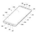
도 2는, 일실시예에 따른 모바일 전자 장치(200)(예: 도 1의 101)의 전면의 사시도이다. 도 3은, 일 실시예에 따른, 도 2의 전자 장치(200)(예: 도 1의 101)의 후면의 사시도이다.2 is a perspective view of the front of the mobile electronic device 200 (eg, 101 in FIG. 1 ) according to an embodiment. FIG. 3 is a perspective view of the back of the
도 2 및 3을 참조하면, 일실시예에 따른 전자 장치(200)(예: 도 1의 101)는, 제 1 면(또는 전면)(210A), 제 2 면(또는 후면)(210B), 및 제 1 면(210A) 및 제 2 면(210B) 사이의 공간을 둘러싸는 측면(210C)을 포함하는 하우징(210)을 포함할 수 있다. 다른 실시예(미도시)에서는, 하우징은, 도 2의 제 1 면(210A), 제 2 면(210B) 및 측면(210C)들 중 일부를 형성하는 구조를 지칭할 수도 있다. 일실시예에 따르면, 제 1 면(210A)은 적어도 일부분이 실질적으로 투명한 전면 플레이트(202)(예: 다양한 코팅 레이어들을 포함하는 글라스 플레이트, 또는 폴리머 플레이트)에 의하여 형성될 수 있다. 제 2 면(210B)은 실질적으로 불투명한 후면 플레이트(211)에 의하여 형성될 수 있다. 상기 후면 플레이트(211)는, 예를 들어, 코팅 또는 착색된 유리, 세라믹, 폴리머, 금속(예: 알루미늄, 스테인레스 스틸(STS), 또는 마그네슘), 또는 상기 물질들 중 적어도 둘의 조합에 의하여 형성될 수 있다. 상기 측면(210C)은, 전면 플레이트(202) 및 후면 플레이트(211)와 결합하며, 금속 및/또는 폴리머를 포함하는 측면 베젤 구조 (또는 "측면 부재")(218)에 의하여 형성될 수 있다. 어떤 실시예에서는, 후면 플레이트(211) 및 측면 베젤 구조(218)는 일체로 형성되고 동일한 물질(예: 알루미늄과 같은 금속 물질)을 포함할 수 있다.Referring to FIGS. 2 and 3 , an electronic device 200 (eg, 101 of FIG. 1 ) according to an embodiment includes a first side (or front side) 210A, a second side (or back side) 210B, and a
도시된 실시예에서는, 상기 전면 플레이트(202)는, 상기 제 1 면(210A)으로부터 상기 후면 플레이트(211) 쪽으로 휘어져 심리스하게(seamless) 연장된 2개의 제 1 영역(210D)들을, 상기 전면 플레이트(202)의 긴 엣지(long edge) 양단에 포함할 수 있다. 도시된 실시예(도 3 참조)에서, 상기 후면 플레이트(211)는, 상기 제 2 면(210B)으로부터 상기 전면 플레이트(202) 쪽으로 휘어져 심리스하게 연장된 2개의 제 2 영역(210E)들을 긴 엣지 양단에 포함할 수 있다. 어떤 실시예에서는, 상기 전면 플레이트(202)(또는 상기 후면 플레이트(211))가 상기 제 1 영역(210D)들(또는 상기 제 2 영역(210E)들) 중 하나 만을 포함할 수 있다. 다른 실시예에서는, 상기 제 1 영역(210D)들 또는 제 2 영역(210E)들 중 일부가 포함되지 않을 수 있다. 상기 실시예들에서, 상기 전자 장치(200)의 측면에서 볼 때, 측면 베젤 구조(218)는, 상기와 같은 제 1 영역(210D)들 또는 제 2 영역(210E)들이 포함되지 않는 측면 쪽에서는 제 1 두께(또는 폭)을 가지고, 상기 제 1 영역(210D)들 또는 제 2 영역(210E)들을 포함한 측면 쪽에서는 상기 제 1 두께보다 얇은 제 2 두께를 가질 수 있다.In the illustrated embodiment, the
일실시예에 따르면, 전자 장치(200)는, 디스플레이(201), 오디오 모듈(203, 207, 214), 센서 모듈(204, 216, 219), 카메라 모듈(205, 212, 213), 키 입력 장치(217), 발광 소자(206), 및 커넥터 홀(208, 209) 중 적어도 하나 이상을 포함할 수 있다. 어떤 실시예에서는, 전자 장치(200)는, 구성요소들 중 적어도 하나(예: 키 입력 장치(217), 또는 발광 소자(206))를 생략하거나 다른 구성요소를 추가적으로 포함할 수 있다.According to an embodiment, the
디스플레이(201)는, 예를 들어, 전면 플레이트(202)의 상당 부분을 통하여 노출될 수 있다. 어떤 실시예에서는, 상기 제 1 면(210A), 및 상기 측면(210C)의 제 1 영역(210D)들을 형성하는 전면 플레이트(202)를 통하여 상기 디스플레이(201)의 적어도 일부가 노출될 수 있다. 어떤 실시예에서는, 디스플레이(201)의 모서리를 상기 전면 플레이트(202)의 인접한 외곽 형상과 대체로 동일하게 형성할 수 있다. 다른 실시예(미도시)에서는, 디스플레이(201)가 노출되는 면적을 확장하기 위하여, 디스플레이(201)의 외곽과 전면 플레이트(202)의 외곽간의 간격이 대체로 동일하게 형성될 수 있다.The
다른 실시예(미도시)에서는, 디스플레이(201)의 화면 표시 영역의 일부에 리세스(또는 개구부(opening))를 형성하고, 상기 리세스(또는 상기 개구부(opening))와 정렬되는 오디오 모듈(214), 센서 모듈(204), 카메라 모듈(205), 및 발광 소자(206) 중 적어도 하나 이상을 포함할 수 있다. 다른 실시예(미도시)에서는, 디스플레이(201)의 화면 표시 영역의 배면에, 오디오 모듈(214), 센서 모듈(204), 카메라 모듈(205), 지문 센서(216), 및 발광 소자(206) 중 적어도 하나 이상을 포함할 수 있다. 다른 실시예(미도시)에서는, 디스플레이(201)는, 터치 감지 회로, 터치의 세기(압력)를 측정할 수 있는 압력 센서, 및/또는 자기장 방식의 스타일러스 펜을 검출하는 디지타이저와 결합되거나 인접하여 배치될 수 있다. 어떤 실시예에서는, 상기 센서 모듈(204, 219)의 적어도 일부, 및/또는 키 입력 장치(217)의 적어도 일부가, 상기 제 1 영역(210D)들, 및/또는 상기 제 2 영역(210E)들에 배치될 수 있다.In another embodiment (not shown), a recess (or opening) is formed in a part of the screen display area of the
오디오 모듈(203, 207, 214)은, 마이크 홀(203) 및 스피커 홀(207, 214)을 포함할 수 있다. 마이크 홀(203)은 외부의 소리를 획득하기 위한 마이크가 내부에 배치될 수 있고, 어떤 실시예에서는 소리의 방향을 감지할 수 있도록 복수개의 마이크가 배치될 수 있다. 스피커 홀(207, 214)은, 외부 스피커 홀(207) 및 통화용 리시버 홀(214)을 포함할 수 있다. 어떤 실시예에서는 스피커 홀(207, 214)과 마이크 홀(203)이 하나의 홀로 구현되거나, 스피커 홀(207, 214) 없이 스피커가 포함될 수 있다(예: 피에조 스피커).The
센서 모듈(204, 216, 219)은, 전자 장치(200)의 내부의 작동 상태, 또는 외부의 환경 상태에 대응하는 전기 신호 또는 데이터 값을 생성할 수 있다. 센서 모듈(204, 216, 219)은, 예를 들어, 하우징(210)의 제 1 면(210A)에 배치된 제 1 센서 모듈(204)(예: 근접 센서) 및/또는 제 2 센서 모듈(미도시)(예: 지문 센서), 및/또는 상기 하우징(210)의 제 2 면(210B)에 배치된 제 3 센서 모듈(219)(예: HRM 센서) 및/또는 제 4 센서 모듈(216) (예: 지문 센서)을 포함할 수 있다. 상기 지문 센서는 하우징(210)의 제 1면(210A)(예: 디스플레이(201)뿐만 아니라 제 2면(210B)에 배치될 수 있다. 전자 장치(200)는, 도시되지 않은 센서 모듈, 예를 들어, 제스처 센서, 자이로 센서, 기압 센서, 마그네틱 센서, 가속도 센서, 그립 센서, 컬러 센서, IR(infrared) 센서, 생체 센서, 온도 센서, 습도 센서, 또는 조도 센서(204) 중 적어도 하나를 더 포함할 수 있다.The
카메라 모듈(205, 212, 213)은, 전자 장치(200)의 제 1 면(210A)에 배치된 제 1 카메라 장치(205), 및 제 2 면(210B)에 배치된 제 2 카메라 장치(212), 및/또는 플래시(213)를 포함할 수 있다. 상기 카메라 장치들(205, 212)은, 하나 또는 복수의 렌즈들, 이미지 센서, 및/또는 이미지 시그널 프로세서를 포함할 수 있다. 플래시(213)는, 예를 들어, 발광 다이오드 또는 제논 램프(xenon lamp)를 포함할 수 있다. 어떤 실시예에서는, 2개 이상의 렌즈들(적외선 카메라, 광각 및 망원 렌즈) 및 이미지 센서들이 전자 장치(200)의 한 면에 배치될 수 있다.The
키 입력 장치(217)는, 하우징(210)의 측면(210C)에 배치될 수 있다. 다른 실시예에서는, 전자 장치(200)는 상기 언급된 키 입력 장치(217) 중 일부 또는 전부를 포함하지 않을 수 있고 포함되지 않은 키 입력 장치(217)는 디스플레이(201) 상에 소프트 키 등 다른 형태로 구현될 수 있다. 어떤 실시예에서, 키 입력 장치는 하우징(210)의 제 2면(210B)에 배치된 센서 모듈(216)을 포함할 수 있다.The
발광 소자(206)는, 예를 들어, 하우징(210)의 제 1 면(210A)에 배치될 수 있다. 발광 소자(206)는, 예를 들어, 전자 장치(200)의 상태 정보를 광 형태로 제공할 수 있다. 다른 실시예에서는, 발광 소자(206)는, 예를 들어, 카메라 모듈(205)의 동작과 연동되는 광원을 제공할 수 있다. 발광 소자(206)는, 예를 들어, LED, IR LED 및 제논 램프를 포함할 수 있다.The
커넥터 홀(208, 209)은, 외부 전자 장치와 전력 및/또는 데이터를 송수신하기 위한 커넥터(예를 들어, USB 커넥터)를 수용할 수 있는 제 1 커넥터 홀(208), 및/또는 외부 전자 장치와 오디오 신호를 송수신하기 위한 커넥터를 수용할 수 있는 제 2 커넥터 홀(예를 들어, 이어폰 잭)(209)을 포함할 수 있다.The connector holes 208 and 209 include a
도 4는, 일 실시예에 따른, 도 2의 전자 장치(300)(예: 도 1의 101)의 전개 사시도이다.4 is an exploded perspective view of the
도 4를 참조하면, 전자 장치(300)(예: 도 1의 101)는, 측면 베젤 구조(310), 제 1 지지부재(311)(예: 브라켓), 전면 플레이트(320), 디스플레이(330), 인쇄 회로 기판(340), 배터리(350), 제 2 지지부재(360)(예: 리어 케이스), 안테나(370), 및 후면 플레이트(380)를 포함할 수 있다. 어떤 실시예에서는, 전자 장치(300)는, 구성요소들 중 적어도 하나(예: 제 1 지지부재(311), 또는 제 2 지지부재(360))를 생략하거나 다른 구성요소를 추가적으로 포함할 수 있다. 전자 장치(300)의 구성요소들 중 적어도 하나는, 도 2, 또는 도 3의 전자 장치(200)의 구성요소들 중 적어도 하나와 동일, 또는 유사할 수 있으며, 중복되는 설명은 이하 생략한다.Referring to FIG. 4 , the electronic device 300 (eg, 101 of FIG. 1 ) includes a
제 1 지지부재(311)는, 전자 장치(300) 내부에 배치되어 측면 베젤 구조(310)와 연결될 수 있거나, 측면 베젤 구조(310)와 일체로 형성될 수 있다. 제 1 지지부재(311)는, 예를 들어, 금속 재질 및/또는 비금속 (예: 폴리머) 재질로 형성될 수 있다. 제 1 지지부재(311)는, 일면에 디스플레이(330)가 결합되고 타면에 인쇄 회로 기판(340)이 결합될 수 있다. 인쇄 회로 기판(340)에는, 프로세서, 메모리, 및/또는 인터페이스가 장착될 수 있다. 프로세서는, 예를 들어, 중앙처리장치, 어플리케이션 프로세서, 그래픽 처리 장치, 이미지 시그널 프로세서, 센서 허브 프로세서, 또는 커뮤니케이션 프로세서 중 하나 또는 그 이상을 포함할 수 있다.The
메모리는, 예를 들어, 휘발성 메모리 또는 비휘발성 메모리를 포함할 수 있다.Memory may include, for example, volatile memory or non-volatile memory.
인터페이스는, 예를 들어, HDMI(high definition multimedia interface), USB(universal serial bus) 인터페이스, SD카드 인터페이스, 및/또는 오디오 인터페이스를 포함할 수 있다. 인터페이스는, 예를 들어, 전자 장치(300)를 외부 전자 장치와 전기적 또는 물리적으로 연결시킬 수 있으며, USB 커넥터, SD 카드/MMC 커넥터, 또는 오디오 커넥터를 포함할 수 있다.The interface may include, for example, a high definition multimedia interface (HDMI), a universal serial bus (USB) interface, an SD card interface, and/or an audio interface. The interface may electrically or physically connect the
배터리(350)는 전자 장치(300)의 적어도 하나의 구성 요소에 전력을 공급하기 위한 장치로서, 예를 들면, 재충전 불가능한 1차 전지, 또는 재충전 가능한 2차 전지, 또는 연료 전지를 포함할 수 있다. 배터리(350)의 적어도 일부는, 예를 들어, 인쇄 회로 기판(340)과 실질적으로 동일 평면 상에 배치될 수 있다. 배터리(350)는 전자 장치(300) 내부에 일체로 배치될 수 있고, 전자 장치(300)와 탈부착 가능하게 배치될 수도 있다.The
안테나(370)는, 후면 플레이트(380)와 배터리(350) 사이에 배치될 수 있다. 안테나(370)는, 예를 들어, NFC(near field communication) 안테나, 무선 충전 안테나, 및/또는 MST(magnetic secure transmission) 안테나를 포함할 수 있다. 안테나(370)는, 예를 들어, 외부 장치와 근거리 통신을 하거나, 충전에 필요한 전력을 무선으로 송수신 할 수 있다. 다른 실시예에서는, 측면 베젤 구조(310) 및/또는 상기 제 1 지지부재(311)의 일부 또는 그 조합에 의하여 안테나 구조가 형성될 수 있다.The
도 5는, 일실시예에 따른, 전자 장치(예: 도 1의 101)의 제 1 플레이트(502)(예: 도 2의 전면 플레이트(202))를 나타내는 사시도이다. 도 6a는, 일실시예에 따른, 전자 장치(예: 도 1의 101)의 제 1 플레이트(502)를 나타내는 정면도이다. 도 6b는, 일실시예에 따른, 전자 장치(예: 도 1의 101) 제 1 플레이트(502)의 측단면을 도시한 도면이다. 도 6c는, 다른 실시예에 따른, 전자 장치(예: 도 1의 101) 제 1 플레이트(502)의 측단면을 나타내는 도면이다.FIG. 5 is a perspective view illustrating a first plate 502 (eg, the
도 5를 참조하면, 전자 장치(예: 도 1의 101)는 제 1 플레이트(502), 제 2 플레이트(예: 후면 플레이트(예: 도 3의 211) 및/또는 측면 베젤 구조(예: 도 2의 218))를 포함할 수 있다. 도 5 내지 도 6b에 별도로 도시되진 않았으나, 제 2 플레이트(예: 후면 플레이트 및/또는 측면 베젤 구조)는 상기 제 1 플레이트(502)와 함께 결합되어 전자 장치 내부의 전자 부품들을 보호하기 위한 하우징(예: 도 2의 210)을 구성할 수 있다. 상기 하우징(예: 도 2의 210)은 소재로서 적어도 부분적으로 메탈 및/또는 절연 물질을 포함할 수 있으며, 내부에 브라켓 및/또는 전자 부품들(예: 디스플레이, 카메라 모듈, 센서 모듈, 배터리)을 수용하기 위한 공간을 제공할 수 있다.Referring to FIG. 5 , an electronic device (eg, 101 in FIG. 1 ) includes a
제 1 플레이트(502)는, 전자 장치 내부의 전자 부품(예: 디스플레이(501))에서 표시되는 시각적 정보를 외부(예: 사용자)에 제공하기 위한 윈도우(window)에 해당될 수 있다. 이를 위해 제 1 플레이트(502)(예: 도 2의 202)는 적어도 일부분이 실질적으로 투명하게 형성될 수 있다. 그리고 제 1 플레이트(502)에서 실질적으로 투명한 영역이 아닌 다른 부분은 불투명하게 형성될 수 있다.The
일실시예에 따르면, 실질적으로 투명한 영역은 제 1 면(510A)(예: 도 2의 202) 및 제 1 영역(510D)(예: 도 2의 210D)에 형성될 수 있다. 실질적으로 불투명하게 형성되는 부분은, 상기 제 1 면(510A)에 인접하고 상기 제 1 플레이트(502)의 짧은 엣지(short edge) 중 어느 한쪽의 단부(또는 양단부)에 형성된 제 3 영역(510F)에 형성될 수 있다. 또한, 상기 불투명하게 형성되는 부분은 상기 제 3 영역(510F)의 적어도 일부분을 둘러싸도록 형성된 제 4 영역(510G)에 형성될 수도 있다. 어떤 실시예에 따르면, 상기 제 4 영역(510G)은 제 3 영역(510F) 주위뿐만 아니라, 2 개의 제 1 영역(510D)들의 주위에 배치되고, 제 2 플레이트(예:후면 플레이트(예: 도 2의 211) 및/또는 측면 베젤 구조(예: 도 2의 218)) 쪽으로 휘어지는 부분을 포함할 수 있다.According to an embodiment, the substantially transparent region may be formed on the
다양한 실시예들에 따르면, 실질적으로 투명한 영역이 제 1 플레이트(502)의 제 1 면(510A)(예: 도 2의 202), 제 1 영역(510D)(예: 도 2의 210D) 및 제 3 영역(510F)에 형성되고, 불투명하게 형성된 부분이 제 1 플레이트(502)의 제 4 영역(510G)에 형성될 수도 있다.According to various embodiments, the substantially transparent region may include a
이하 본 문서에서는 제 3 영역(510F) 및 제 4 영역(510G)이 실질적으로 불투명한 영역으로 형성되는 것을 중심으로 설명하나, 이 밖에도 다양한 실시예들이 적용될 수 있음을 유의해야 한다.Hereinafter, in this document, the
다양한 실시예들에 따르면, 상기 제 3 영역(510F)은 제 1 면(510A)으로부터 그 주위로 편평하게 연장된 부분일 수 있고, 또는 이와 달리 제 3 영역(510F)은 제 1 영역(510D)처럼 상기 후면 플레이트(211) 쪽으로 휘어져 심리스하게(seamless) 연장된 부분일 수도 있다. 일실시예에 따르면 제 3 영역(510F)은, 도 5에 도시된 실시예처럼, 제 1 플레이트(502)의 상단부뿐만 아니라 하단부에도 형성될 수 있다.According to various embodiments, the
전술한 바와 같이, 전자 장치(예: 도 1의 101)는 다양한 부품들(센서 모듈(예: 도2의 204), 카메라 모듈(예: 도 2의 205), 발광 소자(예: 도 2의 206), 및 오디오 모듈(예: 도 2의 214))을 포함할 수 있다. 그리고 도 6a를 참조하면, 제 1 플레이트(502)에는 상기 다양한 부품들이 배치된 위치에 정렬되어 복수의 리세스(또는 개구부(opening))(504, 505, 506, 514)가 형성될 수 있다.As described above, the electronic device (eg, 101 in FIG. 1) includes various components (sensor module (eg, 204 in FIG. 2), a camera module (eg, 205 in FIG. 2), and a light emitting element (eg, 204 in FIG. 2). 206), and an audio module (eg, 214 in FIG. 2). Referring to FIG. 6A , a plurality of recesses (or openings) 504 , 505 , 506 , and 514 may be formed in the
도 6a에는 상기 리세스가 제 1 플레이트(502)의 제 3 영역(510F)에 형성된 것이 도시된다. 다른 실시예에 따르면, 상기 리세스는 제 1 영역(예: 도 2의 210D) 및/또는 제 2 영역(예: 도 3의 210E)에 형성될 수도 있다. 이 밖에도, 상기 리세스는 제 4 영역(510G) 또는 제 3 영역(510F)와 제 4 영역(510G)의 경계 상에 형성될 수도 있다.6A shows that the recess is formed in the
일실시예에 따르면, 제 1 플레이트(502)(예: 도 2의 전면 플레이트(202))는, 투명 부재(521)를 포함할 수 있다. 예를 들면, 투명 부재(521)는 실질적으로 투명한 글래스 플레이트(또는 아크릴 플레이트, 또는 사파이어 플레이트, 또는 세라믹 플레이트, 또는 폴리머 플레이트)가 해당될 수 있다. 투명 부재(521)는, 예컨대 전자 장치(예: 도 2의 200)의 금속 및/또는 폴리머를 포함하는 측면 베젤 구조(예: 도 2의 218)와 결합될 수 있으며, 전자 장치 내부의 다양한 부품들을 외부의 충격으로부터 보호하는 한편, 실질적으로 투명한 재질을 통해 디스플레이(501)에 표시된 화면을 외부에 노출하는 구성일 수 있다.According to one embodiment, the first plate 502 (eg, the
도 6b와 도 6c에는, 도 6a를 A-A 방향으로 잘랐을 때의 투명 부재(521)의 단면도가 도시된다. 본 문서에 개시된 다양한 실시예들에 따른, 투명 부재(521)는 평면부(521a)와 곡면부(521b)를 포함할 수 있다. 도 6b에 도시된 실시예에 따르면, 투명 부재(521)의 평면부(521a)는 전자 장치의 외부인 제 1 방향(예: 방향성분 z와 평행한 방향)을 향하는 제 1 면(510A)과, 제 1 면(510A)에 인접한 제 3 영역(510F)으로 구분될 수 있다. 여기서 제 1 면(510A)은 전자 장치를 외부에서 보았을 때 실질적으로 투명하게 보이는 영역에 해당되고, 제 3 영역(510F)은 전자 장치를 외부에서 보았을 때 실질적으로 불투명하게 보이는 영역에 해당될 수 있다. 투명 부재(521)에서 실질적으로 불투명하게 보이는 영역(예: 제 3 영역(510F))은 후술하는 마스킹 층(예: 도 7의 722)이 상기 투명 부재(521)의 배면에 배치됨으로써 형성될 수 있다.6B and 6C show cross-sectional views of the
다양한 실시예들에 따르면, 투명 부재(521)의 평면부(521a)는 상기 제 1 방향과 반대인 방향을 향하는 제 1 배면(510A')을 포함하고, 제 1 배면(510A')에서 연장되는 제 2 배면(510F')을 포함할 수 있다. 여기서 제 2 배면(510F')은 투명 부재(521)에서 제 3 영역(510F)의 반대 측에 위치하는 표면에 해당될 수 있다. 도 6b에 도시된 실시예에 따르면, 투명 부재(521)의 곡면부(521b)는 제 1 플레이트(502)의 상기 상기 제 4 영역(510G)을 형성하는 부분을 포함할 수 있다. 제 4 영역(510G)을 형성하는 부분은 제 2 배면(510F')에서 연장되는 제 3 배면(510G')을 형성할 수 있다.According to various embodiments, the
도 6c에는, 도 6b와 다른 실시예에 따른 투명 부재(521)의 단면도가 도시된다. 도 6c에 도시된 실시예에 따르면, 투명 부재(521)는 평면부(521a)와 곡면부(521b)를 포함할 수 있고, 평면부(521a)와 곡면부(521b) 사이에 중간부(middle portion)(521c)를 포함할 수 있다. 도 6c의 실시예에 따르면, 중간부(521c)는 제 3 영역(510F)를 형성하고, 제 3 영역(510F)의 반대 측에 제 2 배면(510F')을 형성할 수 있다. 도 6c에 도시된 실시예는 도 6b에 도시된 실시예와 달리, 실질적으로 불투명한 영역인 제 3 영역(510F)이 적어도 일 부분은 평면으로 형성되고, 다른 부분은 곡면으로 형성될 수 있다.6C is a cross-sectional view of a
상기한 바와 같이, 투명 부재(521)의 실시예들은 다양할 수 있으며, 도 6c에 도시된 바와 같이 투명 부재(521)에서 제 3 영역(510F)의 적어도 일부분은 곡면을 포함할 수도 있다. 일실시예에 따르면, 제 3 영역(510F)을 형성하는 부분과 제 4 영역(510G)을 형성하는 부분은 경계 부근에서 단턱 없이 매끄럽게 이어지도록 서로 유사한 곡률 반지름을 가질 수 있다. 다른 실시예에 따르면 투명 부재(521)의 제 3 영역(510F)을 형성하는 부분과 제 4 영역(510G)을 형성하는 부분은 그 경계 부근에서의 곡률이 점차 커지거나 작아질 수도 있다. 예를 들면, 투명 부재(521)의 제 3 영역(510F)을 형성하는 부분과 제 4 영역(510G)을 형성하는 부분은 그 경계 부근에서 곡률이 투명부재(521)의 가장자리로 갈수록 점차 커질 수 있다.As described above, embodiments of the
이하에서는 본 문서에 개시된 발명의 주된 기술적 사상을 설명함에 있어서, 도 6b에 도시된 실시예를 참조하여 제 3 영역(510F)이 평면부(521a)에 속하는 투명 부재(521)의 구성요소를 중심으로 설명하지만, 반드시 이에 한정되는 것이 아님을 유의해야 한다.Hereinafter, in describing the main technical idea of the invention disclosed in this document, with reference to the embodiment shown in FIG. 6B, the
도 7은, 본 문서에 개시된 일 실시예에 따른, 전자 장치(700)의 다양한 구성들을 나타내는 분리 측면도 나타낸다. 도 8은, 도 7에 도시된 실시예에 따른 전자 장치(700)의 분리 사시도를 나타낸다.7 also shows an isolated side view showing various components of an
도 7을 참조하면, 전자 장치(700)는 외부(예: 사용자)로 텍스트, 이미지, 비디오, 아이콘, 심볼과 같은 다양한 유형의 정보를 시각적으로 제공하는 디스플레이(701)(예: 도 1의 표시장치(160)), 상기 디스플레이(701) 및 전자 장치(700)에 내장된 전자 부품들을 외부의 충격으로부터 보호하는 제 1 플레이트(702), 상기 제 1 플레이트(702)의 후방 및 상기 디스플레이(701)의 장착면을 제공하는 측면 베젤 구조(718)를 포함할 수 있다. 그리고 전자 장치(701)는 이미지나 영상 촬영 화상 통화와 같은 기능을 수행하기 위한 카메라 모듈(705)을 포함할 수 있다. 일실시예에 따른 전자 장치(700)는, 제 2 플레이트의 일 실시예로서 측면 베젤 구조(718)를 도시하나 반드시 이에 한정되는 것은 아니다. 다른 실시예에 따르면, 측면 베젤 구조(718)에 대체적으로 또는 추가적으로 후면 플레이트(예: 도 3의 211)을 포함할 수도 있다.Referring to FIG. 7 , the
제 1 플레이트(702)는, 마스킹 층( masking layer)(722)을 더 포함할 수 있다. 일실시예에 따르면, 마스킹 층(722)은 불투명(opaque) 마스킹 층일 수 있다. 제 1 플레이트(702)의 실질적으로 불투명한 영역은, 마스킹 층(722)에 의해 형성된 부분일 수 있다. 마스킹 층(722)은 상기 제 1 플레이트(702)의 배면에 장착되는 전자 부품들을 가리기 위하여 투명 부재(721)의 배면에 배치될 수 있다.The
다양한 실시예들에 따르면, 마스킹 층(722)은, 적어도 둘 이상의 마스킹 층을 포함할 수 있다. 예를 들면, 마스킹 층(722)은, 도 7 및 도 8에 도시된 바와 같이 세 개의 마스킹 층으로 형성될 수 있다.According to various embodiments, the
다양한 실시예들에 따르면, 마스킹 층(722)은 세 개의 마스킹 층으로서, 상기 투명 부재(721)의 배면 상에 인접하여 배치된 제 1 레이어(722a), 상기 제 1 레이어(722a) 배면에 배치된 제 2 레이어(722b), 상기 제 2 레이어(722b) 배면에 배치된 제 3 레이어(722c)를 포함할 수 있다. 상기 제 1 레이어(722a), 제 2 레이어(722b), 제 3 레이어(722c)는 순차적으로 적층될 수 있다.According to various embodiments, the
제 1 레이어(722a)는 투명 부재(721)의 배면 중 제 2 배면(예: 도 6b의 510F') 및 제 3 배면(예: 도 6b의 510G') 상에 인접 배치될 수 있다. 제 1 레이어(722a)가 제 2 배면(예: 도 6b의 510F') 및 제 3 배면(예: 도 6b의 510G')에 인접 배치된다는 것은, 제 1 레이어(722a)가 증착(evaporation), 접합(adhesion), 본딩(bonding), 인쇄(printing)와 같이 다양한 방법에 의해 제 2 배면(예: 도 6b의 510F') 및 제 3 배면(예: 도 6b의 510G')과 떨어지지 않도록 형성되는 것일 수 있다.The
제 1 레이어(722a)는 투명 부재(721)의 가장자리(edge)를 따라 형성될 수 있다. 일실시예에 따르면, 제 1 플레이트(702)에서 화면 표시 영역에 대응하여 디스플레이가 배치되고, 상기 화면 표시 영역을 둘러싼 주위 영역을 따라 제 1 레이어(722a)가 형성되며, 여기서 제 1 레이어(722a)가 형성된 영역은 비 화면 표시 영역이 될 수 있다. 도 7 및 도 8을 함께 참조하면, 제 1 레이어(722a)는 투명 부재(721)의 가장자리 형상에 대응되는 형상을 가질 수 있으며, 투명 부재(721)의 가장자리를 따라 길게 연장되는 부분을 가질 수도 있다.The
제 1 레이어(722a)는 적어도 하나의 컬러(color)를 포함하는 컬러 층(color layer)일 수 있다. 상기 제 1 레이어(722a)를 이용하여 제 1 플레이트(702)의 메인 컬러(main color)를 형성할 수 있다. 예를 들면, 제 1 레이어(722a)는 black, blue, grey, pupple, copper중에 어느 하나 또는 이들 중의 조합으로 이루어지거나, 상기 색상들 이외의 다양한 컬러들의 조합으로 형성될 수 있다. 상기 제 1 레이어(722a)에 의해 사용자에게 보여지는 전자 장치(700)의 외관 색상이 결정될 수 있다.The
제 2 레이어(722b)는 전자 장치(700)가 조립된 후, 디스플레이(701)로부터 발광된 빛이 제 1 플레이트(702)의 제 1 면(예: 도 6a의 510a)이 아닌 주변부로 새어나오는 것을 방지하기 위하여 구비될 수 있다. 이를 위해 제 2 레이어(722b)는 제 1 레이어(722a)의 하부에 배치되고, 제 2 레이어(722b)는 그 크기 및 형상이 제 1 레이어(722a)의 크기 및 형상과 유사하게 형성되어, 제 1 레이어(722a)의 적어도 일부를 덮도록 구성될 수 있다. 제 2 레이어(722b) 또한 제 1 레이어(722a)처럼, 투명 부재(721)의 가장자리 형상에 대응되는 형상을 가질 수 있으며, 투명 부재(721)의 가장자리를 따라 길게 연장되는 부분을 가질 수도 있다.After the
일실시예에 따르면, 제 2 레이어(722b)를 이용하여 메인 컬러를 형성하는 제 1 레이어(722b)의 색을 보완 또는 강화시킬 수도 있다.According to an embodiment, the color of the
제 3 레이어(722c)는 제 1 레이어(722a) 및 제 2 레이어(722b)를 보호하는 역할을 할 수 있다. 제 1 레이어(722a) 및 제 2 레이어(722b)가 마스킹 층(722)에서 어떤 색상을 발현하거나, 강화하거나 및/또는 빛샘을 방지하기 위한 구성인 반면, 제 3 레이어(722c)는 마스킹 층(722)을 외부 충격으로부터 보호하기 위한 구성일 수 있다. 일실시예에 따르면, 제 3 레이어(722c)는 충격 완화 재질 및/또는 탄성 재질을 포함할 수 있다. 다른 실시예에 따르면, 제 3 레이어(722c)는 디스플레이(701)와 측면 베젤 구조(718) 간의 접착력을 증가시키기 위하여, 접착 테이프(예: 후술하는 도 11의 1040)를 부착할 수 있는 표면을 제공하는 역할을 할 수도 있다.The
제 3 레이어(722c)의 크기 및 형상은 제 2 레이어(722c)와 유사하게 형성될 수 있다. 제 3 레이어(722c) 또한, 투명 부재(721)의 가장자리 형상에 대응되는 형상을 가질 수 있다. 도 7 및 도 8에는 투명 부재(721)의 짧은 엣지 측의 단부에 제 3 레이어(722c)이 구비되는 것이 도시된다. 단, 이에 한정되는 것은 아니며 제 3 레이어(722c) 또한 투명 부재(721)의 가장자리를 따라 길게 연장되는 부분을 가질 수도 있다.The size and shape of the
제 2 레이어(722b)는 증착(evaporation), 접합(adhesion), 본딩(bonding), 인쇄(printing)와 같이 다양한 방법에 의해 제 1 레이어(722a)의 하부에 배치될 수 있다. 제 3 레이어(722c) 또한 증착(evaporation), 접합(adhesion), 본딩(bonding), 인쇄(printing)와 같은 다양한 방법에 의해 제 2 레이어(722b)의 하부에 배치될 수 있다.The
도 7 및 도 8에 도시된, 전자 장치(700)의 각 구성요소가 분리된 모습을 참조하면, 투명 부재(721)의 배면에 마스킹 층(722)이 배치되고, 투명 부재(721) 및 마스킹 층(722)의 배면에 디스플레이(701)가 배치될 수 있다. 그리고 디스플레이(701)의 배면에는 측면 베젤 구조(718)가 배치되며, 측면 베젤 구조(718)가 디스플레이(701)의 후방 및 좌우 측면을 둘러싸는 형태를 가질 수 있다. 그리고, 전자 장치(700)의 일 측에 카메라 모듈(705)이 배치될 수 있다.Referring to FIGS. 7 and 8 in which each component of the
카메라 모듈(705)은 전자 장치(700)의 조립체(투명 부재(721), 마스킹 층(722), 디스플레이(701) 및 측면 베젤 구조(718)가 조립된 구조체)에서, 하우징(701)의 일 측, 예를 들면 마스킹 층(722)의 배면에 배치될 수 있다. 후술하겠지만(예: 도 11), 카메라 모듈(705)은 상기 디스플레이(701)와 함께 투명 부재(721)의 표면과 나란히 배치될 수 있다. 예를 들어, 카메라 모듈(705)은 투명 부재(721)로부터 수평 방향(예: x축과 평행한 방향)으로 소정거리 이격된 위치에 배치될 수 있다.The
도 7에서 카메라 모듈(705)이 측면 베젤 구조(718)의 전면 측에 위치한 도면이 도시되나, 카메라 모듈(705)의 배치 구조는 반드시 이에 한정되지 않는다. 일실시예에 따르면 카메라 모듈(705)은 측면 베젤 구조(718)의 전면 또는 후면에 배치될 수도 있다. 또 다른 실시예에 따르면, 카메라 모듈(705)은 후면 플레이트(예: 도 3의 211)의 내측 표면에 실장될 수도 있다.7 shows a view in which the
제 1 플레이트(702)의 일 부분에는 상기 리세스(또는 개구부)가 형성될 수 있다. 예를 들어, 제 3 영역(510F)에 상기 리세스(730)가 형성될 수 있다.The recess (or opening) may be formed in a portion of the
리세스(730)는 투명 부재(721)의 배면의 일 부분(731), 마스킹 층(722)에 형성된 복수 개의 개구들(732a, 732b, 732c)에 의해 형성될 수 있다. 일실시예에 따르면, 상기 투명 부재(721)의 배면의 일 부분(731)은 제 2 배면(예: 도 6b의 510F')의 일 부분에 해당될 수 있다. 일실시예들에 따르면, 복수 개의 개구들(732a, 732b, 732c)은 전자 장치(700)에 내장된 다양한 전자 부품들에 대응하여 다양한 형상과 크기로 형성될 수 있다. 예를 들어 복수 개의 개구들(732a, 732b, 732c)은 도 8에 도시된 바와 같이 둥근 형상을 가질 수 있으며, 렌즈부(L)에 대응되는 크기를 가질 수 있다. 일실시예에 따르면, 복수 개의 개구들(732a, 732b, 732c)은 카메라 모듈(705)의 기 지정된 F.O.V.(field of view)를 만족하기 위한 크기를 가질 수 있다.The
투명 부재(721)의 배면의 일 부분(731) 및 마스킹 층(722)에 형성된 복수 개의 개구들(732a, 732b, 732c)은, 카메라 모듈(705)의 렌즈부(L)와 광 정렬 구조(optical alignment structure)를 형성할 수 있다. 도 7 및 도 8에는 상기 투명 부재(721)의 배면 중 일 부분(731), 마스킹 층(722)에 형성된 복수 개의 개구들(732a, 732b, 732c), 및 카메라 모듈(705)의 렌즈부(L)가 가상의 라인(A.L.)을 따라 정렬된 것이 도시된다.The plurality of
본 문서에 개시된 다양한 실시예들에 따르면, 리세스(730)를 통해 전자 장치(700)의 외부에서 입사된 광은 카메라 모듈(705)의 렌즈부(L)에 수광될 수 있다. 리세스(730)를 형성하는 부분들(731, 732a, 732b, 732c)의 표면은 배경기술에서 전술한 바와 같이 가공 과정에서 편평한 면을 형성하지 않을 수 있다. 일실시예에 따르면, 리세스(730)를 형성하는 투명 부재(721)의 배면의 일 부분(731)은 제작 과정에서 주름지거나 울퉁불퉁한 표면을 가질 수 있다. 예를 들어, 투명 부재(721)의 배면의 일 부분(731)은 제작 과정 중 금형과 접촉된 면에서 자국이 남아 있을 수 있으며, 이러한 자국은 오히려 카메라 모듈(705)의 성능이 향상될수록 더욱 잘 시인될 수 있다. 다양한 실시예들에 따르면, 마스킹 층들(722a, 722b, 722c)은 서로 다른 재질로 형성될 수 있으며, 리세스(730)를 형성하는 복수 개의 개구들(732a, 732b, 732c)의 표면은 울퉁불퉁한 표면을 가질 수 있다. 상기 투명 부재(721)의 배면의 일 부분(731)에 형성된 자국 또는, 복수 개의 개구들(732a, 732b, 732c)의 고르지 못한 표면은 카메라 모듈(705)의 성능(예: 화질)에 영향을 끼칠 수 있다.According to various embodiments disclosed herein, light incident from the outside of the
제 1 플레이트(702)는, 리세스(730)를 채우는 충진 부재(filling member)(723)를 포함할 수 있다. 충진 부재(723)를 포함함으로써 상기 리세스(730)의 자국 및 고르지 못한 표면에 의한 카메라 모듈(705)의 성능(예: 화질)이 저하되는 문제를 보완할 수 있다. 일실시예에 따르면, 충진 부재(723)는 실질적으로 투명한 물질로 이루어질 수 있다. 다양한 실시예들에 따르면, 충진 부재의 재질은 OCA(optical clear adhesive material) 또는 폴리머(polymer) 재질을 포함할 수 있다. 이 밖에도, 충진 부재의 재질은 90% 이상의 광 투과율(transmittance)을 가지는 물질, 예를 들면 95% 내지 100%의 광 투과율을 가지는 물질을 포함할 수 있다. 다른 실시예에 따르면, 충진 부재의 재질은 대략 90% (또는 이보다 낮거나 높을 수는 있지만) 상회하는 광 투과율을 가지고, 대략 투명 부재(1221)에 대하여 1.5의 굴절력을 가지는 물질을 포함할 수 있다.The
일실시예에 따르면, 충진 부재(723)는 액형상태의 OCA인 LOCA(liquid optically clear adhesive material)를 이용하여 형성할 수 있다. LOCA를 이용한 충진 부재(723)는 도포 후 경화되는 과정에서 투명 부재(721)의 배면의 일 부분(731)을 덮고, 상기 마스킹 층(722)에 형성된 복수 개의 개구들(732a, 732b, 732c)의 내측 표면을 덮은 상태에서 고착될 수 있다. LOCA를 이용하면, 작은 폭으로 형성된 리세스를 가진 투명 부재의 표면에 OCA를 첨가하기 용이하고, 투명 부재의 평탄하지 않은 표면에 보다 잘 대응할 수 있다. LOCA의 도포 후에는, 제조사의 사양에 따라 자외선(UV), 열, 습도, 또는 이 밖에 다양한 환경을 제공하여 경화 정도를 조절하기에도 용이하다. 또한, LOCA의 표면 장력을 이용하여 카메라 모듈(705)에 대향하는 부분을 편평하게 형성할 수도 있다. 이 밖에도, 충진 부재(723)의 투명도를 비롯한 충진 부재(723)의 재질은 실시예에 따라 다양하게 설계될 수 있다.According to one embodiment, the filling
일실시예에 따르면, 충진 부재(723)는 광학 필름(optical film) 형태로 구비될 수 있다. 광학 필름 형태의 충진 부재(723)는 투명 부재(721)의 표면과 접착되는 접착층(adhesive layer)과, 상기 접착층의 상면에 적층되고 카메라 모듈(705)과 대향하는 부분인 비접착층(non-adhesive layer)을 포함할 수 있다.According to one embodiment, the filling
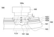
도 9는, 어떤 실시예에 따른, 전자 장치(900)의 리세스(930) 내에 충진 부재(923)가 충진된 상태를 나타내는 도면이다.9 is a diagram illustrating a state in which the filling
도 9를 참조하면, 리세스(930)는 투명 부재(921)의 배면의 일 부분(931)과 복수의 마스킹 층(922a, 922b, 922c)에 형성된 복수 개의 개구들(예: 도 7의 732a, 732b, 732c)에 의해 형성될 수 있다. 어떤 실시예에 따르면, 리세스(930) 내에는 충진 부재(923)이 충진되고 고착화될 수 있다. 이 상태에서 리세스(930)에 대응되는 위치에는 카메라 모듈(905)이 배치되고, 전자 장치(900)의 외부에서 입사된 광은 렌즈부(L)의 촬상면(905a)을 통해 카메라 모듈(905)에 입력된다. 전자 장치(900)에 장착된 카메라 모듈(905)의 성능 지표는 촬상 소자 고유의 성능(예: 분해능), 렌즈의 수차 및/또는 렌즈의 화각(angle of view)(또는 F.O.V.)과 같은 다양한 요인에 의해 결정될 수 있다. 본 문서에 개시된 다양한 실시예들에 따르면, 리세스(930) 내에 충진 부재(923)가 충진되므로 카메라 모듈(905)의 상기 F.O.V.(field of view)는, 촬상면(905a)과 투명 부재(921) 사이의 거리(a), 촬상면(905a)과 충진 부재(923) 사이의 거리(b), 충진 부재(923)의 굴절률을 고려하여 설정할 수 있다.Referring to FIG. 9 , the
충진 부재(923)가, 리세스(930)에 상기 LOCA가 충진된 상태에서 굳어진 것이라면, 충진 부재(923)는 중앙부에 편평한 부분(a flatting part)을 형성하고, 리세스(930)의 측벽에 인접한 부분(가장자리)에는 표면 장력 효과에 의해 굴곡진 부분(또는 편평하지 않은 부분(un-flatting part))이 형성될 수 있다. 제 1 플레이트(902)에 입사된 광이 상기 굴곡진 부분을 통과한 후 촬상면(905a)에 입력되면, 이를 통해 획득되는 이미지나 영상이 현저히 왜곡될 수 있으므로, 카메라 모듈(905)의 상기 F.O.V.는 충진 부재(923)의 편평한 부분과 굴곡진 부분의 경계점(c)을 고려하여 설정되어야 한다.If the filling
어떤 실시예에 따르면, 리세스(930)의 폭을 키워 F.O.V.를 늘릴 수 있으나, 이 경우 리세스(930)가 과도히 넓어질 수 있다. 리세스(930)가 과도히 넓어지면, 상기 리세스(930)를 통해 전자 장치 내부의 부품들이 외부에 시인되어 전자 장치(900)의 미관을 저하시킬 수 있다.According to some embodiments, F.O.V. may be increased by increasing the width of the
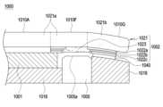
도 10은, 본 문서에 개시된 일실시예에 따른, 계단 구조(step structure)의 리세스(1030) 내에 충진 부재(1023)가 충진된 상태를 나타내는 도면이다. 도 11은, 일 실시예에 따른, 도 10에 도시된 계단 구조의 리세스(1030)가 투명 부재(1021)의 평면부(1021a)의 배면에 형성된 모습을 나타낸 도면이다.10 is a view showing a state in which the filling
본 문서에 개시된 일실시예에 따르면, 전자 장치(1000)는 디스플레이(1001)(예: 도 7의 701), 제 1 플레이트(1002)(예: 도 7의 702), 측면 베젤 구조(1018)(예: 도 7의 718), 카메라 모듈(1005)(예: 도 7의 705)을 포함할 수 있다.According to an embodiment disclosed in this document, the
일실시예에 따르면, 제 1 플레이트(1002)는 계단 구조(step structure)의 리세스(1030)를 포함할 수 있다. 계단 구조(step structure)의 리세스(1030)는 투명 부재(1021) 제 3 영역(1010F)의 배면의 일 부분(1031), 제 1 레이어(1022a), 제 2 레이어(1022b), 및 제 3 레이어(1022c)에 의해 형성될 수 있다. 여기서 제 1 레이어(1022a)에 형성된 개구는 제 1 폭(w1)을 가지고, 제 2 레이어(1022b)에 형성된 개구는 제 2 폭(w2)을 가지며, 제 3 레이어(1022c)에 형성된 개구는 제 3 폭(w3)을 가질 수 있다.According to one embodiment, the
계단 구조의 리세스(1030)에 일정량의 충진 부재(1023)가 충진되면, 충진 부재(1023)는 리세스(1030)를 형성하는 내벽과 만나는 가장자리 지점에서 표면 장력 효과에 따라 굴곡지게 형성될 수 있다. 예를 들면, 도 10에 도시된 실시예와 같이, 충진 부재(1023)의 표면 중 카메라 모듈(1005)의 렌즈부(L)와 대면하는 중앙 부분은 대체로 편평하게 형성되지만, 충진 부재(1023)의 가장자리 부분은 제 3 레이어(1022c)의 개구의 사면을 타고 굴곡지게 형성될 수 있다.When a predetermined amount of the filling
도 10에 도시된 실시예를, 도 9에 도시된 실시예와 비교할 수 있다. 충진 부재(1023)의 충진량, 렌즈부(L)의 촬상면(1005a)으로부터 투명 부재의 배면 사이의 거리(예: 도 9의 a), 촬상면(1005a)으로부터 충진 부재(1023) 사이의 거리(예: 도9의 b), 충진 부재(1023)의 굴절률 등이 각각 동일하다고 가정한 상태에서 양 자의 F.O.V.를 비교할 수 있다.The embodiment shown in FIG. 10 can be compared with the embodiment shown in FIG. 9 . The filling amount of the filling
도 10을 참조하면, 상기 제 3 폭(w3)은 제 1 폭(w1) 보다 크게 형성된 계단 구조를 형성할 수 있다. 상기 제 1 폭(w1)은 전자 장치(1000)의 미관을 고려하여, 전자 장치(1000) 내부의 구성요소들을 가리기에 충분한 정도의 폭을 가질 수 있다. 그리고, 제 3 폭(w3)을 제 1 폭(w1) 보다 크게 형성할 수 있다. 일실시예에 따르면, 이에 추가적으로, 상기 제 2 폭(w2)은 제 1 폭(w1) 보다 크고, 제 3 폭(w3)은 제 2 폭(w2) 보다 크게 설정되어 투명 부재(1021)의 배면으로부터 적층되어 갈수록 개구의 폭이 넓어지는 계단 구조를 형성할 수 있다. 이러한 계단 구조의 리세스(1030) 내부에 충진 부재(1023)가 충진될 수 있다.Referring to FIG. 10 , a stair structure may be formed in which the third width w3 is larger than the first width w1. The first width w1 may have a width sufficient to cover internal components of the
도 10에 도시된 실시예에 따르면, 계단 구조의 리세스(1030)에 충진 부재(1023)가 채워지고, 앞서 살펴본 도 9에 도시된 실시예에 따르면, 깊이 방향으로 대략 일정한 폭을 가진 리세스(930)에 충진 부재(923)가 채워질 수 있다. 도 10에 도시된 실시예에 따른 리세스(1030)의 폭은 도 9에 도시된 실시예에 따른 리세스(930)의 평균 폭과 동일하게 설정될 수 있다. 도 10의 실시예에 따른 충진 부재(1023)의 편평한 부분과 굴곡진 부분의 경계점(c')은, 도 9의 실시예에 따른 충진 부재(923)의 편평한 부분과 굴곡진 부분의 경계점(c)에 비해 정렬 라인(예: 도 7의 A.L.)으로부터 더 먼 곳에 형성될 수 있다. 따라서, 도 10에 도시된 실시예에 따른 전자 장치(1000)가 확보할 수 있는 최대 F.O.V.는 도 9에 도시된 실시예에 따른 전자 장치(900)가 확보할 수 있는 최대 F.O.V.에 비해 확장될 수 있다.According to the embodiment shown in FIG. 10, the filling
다른 실시예에 따르면, 도 10에 도시된 실시예에 따른 전자 장치(1000)의 최대 F.O.V.와 도 9에 도시된 실시예에 따른 전자 장치(900)의 최대 F.O.V를 동일하게 설정한 상태에서, 도 10에 도시된 실시예에 따른 전자 장치(1000)의 리세스의 크기(예: 제 1 폭(w1))를 도 9에 도시된 실시예에 따른 전자 장치(900)의 리세스의 크기보다 축소시킬 수 있다. 즉, 도 10의 계단 구조의 리세스(1030)를 포함하는 제 1 플레이트(1002)를 이용하면, 계단 구조의 리세스를 포함하지 않는 제 1 플레이트의 실시예에 비해 외부로 노출되는 리세스의 크기(예: 제 1 폭(w1))를 최소화할 수 있다.According to another embodiment, in a state in which the maximum F.O.V. of the
도 11에는 계단 구조의 리세스(1030)가 형성된 제 1 플레이트(1002)를 포함하는 전자 장치의 내부 구성도가 개략적으로 도시된다. 도 11에 도시된 바와 같이, 투명 부재(1021)의 배면에는 복수의 마스킹 층들(1022a, 1022b, 1022c)이 형성되고, 마스킹 층들(1022a, 1022b, 1022c)에 형성된 개구 내부에 충진 부재(1023)가 충진될 수 있다.FIG. 11 schematically shows an internal configuration of an electronic device including a
일실시예에 따르면, 디스플레이(1001)는 복수의 마스킹 층들(1022a, 1022b, 1022c) 중 제 3 레이어(1022c)의 배면의 적어도 일부분에 밀착될 수 있다. 그리고 전술한 바와 같이, 제 1 레이어(1022a)을 통해 제 1 플레이트(1002)의 불투명한 영역과 투명한 영역의 경계가 설정될 수 있다. 사용자는 제 1 플레이트(1002)의 투명한 영역을 통해 텍스트, 이미지, 비디오, 아이콘, 심볼 등과 같은 시각적 정보를 제공받을 수 있다. 디스플레이(1001)에서 출력된 화면은 제 1 플레이트(1002)의 제 1 면(1010A)을 통해 외부로 표시되는데, 제 2 레이어(1022b)이 구비됨으로써 디스플레이(1001)의 전면을 통해 출력된 빛이 전자 장치(1000)의 측면으로 새는 것이 방지될 수 있다.According to an embodiment, the
카메라 모듈(1005)은, 촬상면(1005a)이 충진 부재(1023)를 대향하며, 촬상면(1005a)이 충진 부재(1023)로부터 소정 거리만큼 이격된 곳에 배치될 수 있다. 촬상면(1005a)이 충진 부재(1023)로부터 직접 맞닿게 하지 않고 이격 시킴에 따라 카메라 모듈(1005)에 구비된 렌즈부(L)를 파손의 위험으로부터 보호할 수 있다. 또한, 카메라 모듈(1005)은 상기 전자 장치(1000)의 내부에 디스플레이(1001)와 함께 투명 부재(1021)의 면과 나란한 수평 방향으로 나란히 배치될 수 있다. 그리고 카메라 모듈(1005)과 디스플레이(1001) 사이에는 광의 이동 경로를 차단하는 마스킹 층(1022a, 1022b, 1022c)이 구비됨에 따라, 디스플레이(1001)는 상기 리세스(1030)를 통해 입사된 광에 의해 노출되지 않을 수 있다.The
측면 베젤 구조(1018)는 디스플레이(1001)와 카메라 모듈(1005)의 장착 공간을 제공할 수 있다. 측면 베젤 구조(1018)에는 상기 카메라 모듈(1005) 외에도 센서 모듈(예: 도 1의 176), 배터리(예: 도 1의 189) 및/또는 인쇄 회로 기판(예: 도 4의 340)를 포함한 다양한 전자 부품들이 추가로 장착될 수 있으나 본 실시예의 설명에서는 편의상 이를 생략하도록 한다.The
다양한 실시예들에 따른, 전자 장치(1000)는 적어도 하나의 접착층(1040)을 포함할 수 있다. 도 11에 도시된 실시예들에 따른 접착층(1040)은 제 1 플레이트(1002)와 측면 베젤 구조(1018) 사이에 배치될 수 있다. 보다 구체적으로는, 제 3 레이어(1022c)와 측면 베젤 구조(1018) 사이에 배치될 수 있다. 전자 장치(1000)는 충격 흡수, 및/또는 방수/ 방진 기능 구현을 위해 상기 접착층(1040)을 포함할 수 있다. 접착층(1040)은 그 예시로서, 본드와 같은 액체형 접착 물질, 또는 양면 테이프와 같은 접착 물질이 사용될 수 있다.According to various embodiments, the
다양한 실시예들에 따르면, 접착층(1040)은 이에 추가로 또는 대체적으로, 전자 장치(1000) 내의 다른 위치, 예를 들면, 디스플레이(1001)와 투명 부재(1021), 또는 디스플레이(1001)와 배터리(예: 도 4의 350), 디스플레이(1001)와 하우징(예: 도 3의 310)의 다른 부분 사이에 게재될 수도 있다. 이밖에도 접착층(1040)은 다양한 위치에 형성될 수 있다.According to various embodiments, the
본 문서에 개시된 다양한 실시예들에서 복수의 마스킹 층들(1022a, 1022b, 1022c)은 적어도 일부는 투명 부재(1021)의 곡면부(1021b)의 배면에 형성될 수 있다. 예를 들어, 도 11을 참조하면, 복수의 마스킹 층들(1022a, 1022b, 1022c)의 일부는 투명 부재(1021)의 평면부(1021a)의 배면에 형성되고, 다른 일부는 투명 부재(1021)의 곡면부(1021b)의 배면에 형성될 수 있다. 어떤 실시예에 따르면, 마스킹 층의 적어도 일부가 굴곡진 표면 상에 형성됨에 따라, 투명 부재(1021)의 배면에서 리세스(1030)가 형성되는 영역이 주름지고, 울퉁불퉁할 확률이 높아질 수 있다. 이는 카메라 모듈(1005)의 분해능을 저하시킬 수 있다. 본 문서에 개시된 다양한 실시예들에 따르면, 상기 리세스(1030)에 충진 부재(1023)를 충진함으로써 카메라 모듈(1005)의 분해능이 저하되는 것을 방지할 수 있다. 나아가, 도 10 및 도 11에 도시된 실시예와 같이, 계단 구조의 리세스(1030)에 충진 부재(1023)가 충진되도록 함으로써, 충진 부재(1023)가 상기 카메라 모듈(1005)을 대향하여 노출되는 표면에서 평탄한 부분의 면적을 확장시킬 수 있게 되어, F.O.V.를 향상시킬 수 있다.In various embodiments disclosed in this document, at least some of the plurality of masking
도 10 및 도 11에 도시된 실시예에 따르면, 리세스(1030)와 대향하는 전자 부품으로서, 카메라 모듈을 그 예시로 들었으나, 반드시 이에 한정되는 것은 아니고 리시버(또는 스피커) 모듈, 센서 모듈(예: IR 센서 모듈)을 비롯한 다양한 모듈이 추가 또는 대체될 수 있음을 유의해야 한다.According to the embodiment shown in FIGS. 10 and 11, as an electronic component facing the
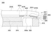
도 12는, 본 문서에 개시된 일실시예에 따른, 리세스(1230) 내에 충진 부재(1223a, 1223b)가 2중으로 충진된 상태를 나타내는 도면이다. 도 13은, 일 실시예에 따른, 도 12에 도시된 리세스(1230)가 투명 부재(1221)의 평면부(1221a)의 배면에 형성된 모습을 나타낸 도면이다.12 is a view illustrating a state in which the
이하, 본 문서에 개시된 다양한 실시예들을 설명함에 있어서, 전술한 실시예들과 중복되는 범위에서는 설명을 생략할 수 있다.Hereinafter, in describing various embodiments disclosed in this document, description may be omitted in the range overlapping with the above-described embodiments.
본 문서에 개시된 일실시예에 따르면, 전자 장치(1200)는 디스플레이(1201)(예: 도 7의 701), 제 1 플레이트(1202)(예: 도 7의 702), 측면 베젤 구조(1218)(예: 도 7의 718), 카메라 모듈(1205)(예: 도 7의 705)을 포함할 수 있다.According to an embodiment disclosed in this document, the
도 12 및 도 13을 함께 참조하면, 제 1 플레이트(1202)는 리세스(1230) 내에 2중으로 충진된 충진 부재를 포함할 수 있다. 충진 부재 전체의 평탄도(flatness)를 강화하고, 광의 투과도(transmittance)를 증가시키기 위해, 도 12 및 도 13에 도시된 실시예에 따른 전자 장치(1200)는, 리세스(1230) 내에 충진되는 두 개의 서로 다른 충진 부재(1223a, 1223b)를 포함할 수 있다. 제 1 충진 부재(1223a)는 제 2 충진 부재(1223b)와 서로 다른 물질로 형성될 수 있다. 예를 들면, 제 1 충진 부재(1223a)은 친수성(hydrophilic) 물질이고, 제 2 충진 부재(1223b)은 소수성(hydrophobic) 물질로 형성될 수 있다.Referring to FIGS. 12 and 13 together, the
본 실시예에 따르면, 제 1 충진 부재(1223a)는 리세스(1230) 내의 투명 부재(1231)의 비정질 표면과 맞닿고, 제 2 충진 부재(1223b)는 제 1 충진 부재(1223a)의 위에 적층되고, 상기 카메라 모듈(1205)에 대향할 수 있다.According to this embodiment, the
제 1 충진 부재(1223a)가 친수성 물질로 형성되면, 리세스(1230) 내의 투명 부재(1231)의 비정질 표면과 맞닿을 때, 제 1 충진 부재(1223a)가 비정질 표면의 틈새로 인입되어 부착될 수 있다.If the
제 2 충진 부재(1223b)는 제 1 충진 부재(1223a) 상면의 공간을 채울 수 있다. 제 2 충진 부재(1223b)가 제 1 충진 부재(1223a)에 적층되면, 제 2 충진 부재(1223b)의 일 면은 투명 부재(1221)를 대향하고, 제 2 충진 부재(1223b)의 타 면은 카메라 모듈(1205)의 촬상면(1205a)을 대향할 수 있다. 여기서 제 2 충진 부재(1223b)는 리세스(1230) 내의 불투명한 마스킹 층들과 접촉되도록 형성될 수도 또는 접촉하지 않도록 형성될 수도 있다.The
일실시예에 따르면, 제 2 충진 부재(1223b)은 제 1 충진 부재(1223a)와 동일한 광학 특성을 가질 수 있다. 일실시예에 따르면, 제 2 충진 부재(1223b)는 제 1 충진 부재(1223a)에 대하여 추가적으로 구비되어 제 1 충진 부재(1223a)와 조합된 구성이므로 제 1 충진 부재(1223a)만 구비되는 실시예에 비해 적어도 광학 특성을 개선시킬 수 있다.According to an embodiment, the
도 12 및 도 13에 도시된 실시예에 따르면, 제 1 충진 부재(1223a)과 다른 제 2 충진 부재(1223b)를 더 포함하고, 이를 이용하여 리세스(1230)를 충진시킴으로써 제 1 충진 부재(1223a) 상면의 오목한 부분을 보다 평탄하게 만들 수 있다. 본 실시예에 따르면, 리세스(1230)의 폭을 증가시키지 않고도 F.O.V.를 증가시킬 수 있다.According to the embodiment shown in FIGS. 12 and 13 , a
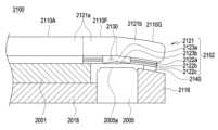
도 14는, 본 문서에 개시된 일실시예에 따른, 계단 구조(step structure)의 리세스(1430) 내에 충진 부재(1423a, 1423b)가 2중으로 충진된 상태를 나타내는 도면이다. 도 15는, 일 실시예에 따른, 도 14에 도시된 리세스(1430)가 투명 부재(1421)의 평면부(1421a)의 배면에 형성된 모습을 나타낸 도면이다.FIG. 14 is a view showing a state in which the
도 10 및 도 11에서는, 계단 구조(step structure)의 리세스(1030) 내에 1 종의 충진 부재(1023)를 충진한 상태에 대한 실시예를 설명하였고, 도 12 및 도 13에서는, 리세스(1230) 내에 2 종의 충진 부재(1223a, 1223b)를 충진한 상태에 대한 실시예를 설명하였다.In FIGS. 10 and 11, an embodiment of a state in which one type of filling
이와 달리, 도 14 및 도 15에서는, 상기 도 10 내지 도 13의 실시예를 조합하여, 계단 구조(step structure)의 리세스(1430) 내에 충진 부재(1423a, 1423b)를 2중으로 충진한 전자 장치(1400)에 대한 실시예를 개시한다.Unlike this, in FIGS. 14 and 15, the electronic device in which the
도 14 및 도 15에 따르면, 계단 구조의 리세스(1430)에 충진 부재(1423)가 충진됨에 따라, 충진 부재(1423)가 상기 카메라 모듈(1405)을 대향하여 노출되는 표면에서 평탄한 부분의 면적을 충분히 확보함으로써 F.O.V.를 향상시킬 수 있고, 제 1 충진 부재(1423a)과 다른 제 2 충진 부재(1423b)를 더 포함하고, 이를 이용하여 리세스(1430)를 충진시킴으로써 제 1 충진 부재(1423a) 상면의 오목한 부분을 보다 평탄하게 만들 수 있다. 본 실시예에 따르면, 리세스(1430)의 폭을 증가시키지 않고도 F.O.V.를 증가시킬 수 있다.14 and 15, as the filling member 1423 is filled in the stepped
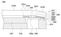
도 16은, 본 문서에 개시된 일실시예에 따른, 리세스(1630) 내에 충진 부재(1623)가 충진되고, 제 2 투명 부재(1624)가 배치된 상태를 나타내는 도면이다. 도 17은, 도 16에 도시된 리세스(1630)가 투명 부재(1621)의 평면부(1621a)의 배면에 형성된 모습을 나타낸 도면이다.FIG. 16 is a view showing a state in which the filling
본 문서에 개시된 일실시예에 따르면, 전자 장치(1600)는 디스플레이(1601)(예: 도 7의 701), 제 1 플레이트(1602)(예: 도 7의 702), 측면 베젤 구조(1618)(예: 도 7의 718), 카메라 모듈(1605)(예: 도 7의 705)을 포함할 수 있다.According to an embodiment disclosed in this document, the
도 16 및 도 17을 함께 참조하면, 제 1 플레이트(1602)는 리세스(1630) 내에 충진된 충진 부재(1623)를 포함하고, 이에 더하여 제 2 투명 부재(1624)를 포함할 수 있다.Referring to FIGS. 16 and 17 together, the
어떤 실시예에 따르면, 충진 부재(1623)의 두께가 매우 얇을 수 있다. 이와 같은 경우에는 제 2 투명 부재(1624)를 추가로 포함함으로써 F.O.V.를 증가시키는 방안을 고려할 수 있다.According to some embodiments, the thickness of the filling
일실시예에 따르면, 제 2 투명 부재(1624)는 제 1 투명 부재(1621)와 실질적으로 동일한 구성으로 형성될 수 있다. 제 2 투명 부재(1624)의 두께는 카메라 모듈의 촬상면(1605a)와 충진 부재(1623) 사이의 거리보다 작도록 형성될 수 있다. 예를 들면, 제 2 투명 부재(1624)의 두께는 50 ㎛ 로 설정되며, 제 1 투명 부재(1621)에 비해 매우 얇게 형성될 수 있다. 예를 들어, 제 2 투명 부재(1624)는 필름(film) 형태로 구비될 수 있다.According to an embodiment, the second
일실시예에 따르면, 충전 부재(1623)가 LOCA로 이루어지기 때문에, 그 표면이 고르지 못할 수 있는데, 제 2 투명 부재(1624)를 상기 충전 부재(1623)의 상면에 부착시킴으로써, 충전 부재(1623)의 표면을 균질화하고, 편평하게 하는 효과를 가질 수 있다. 이로 인해, F.O.V.를 증가시키는 효과를 얻을 수 있다.According to one embodiment, since the filling
도 18은, 상기 도 10 내지 도 17에 도시된 실시예(또는 제 1 실시예)들에 따른, 제 1 플레이트(1002, 1202, 1402, 1602)를 제조하는 방법을 나타내는 도면이다. 도 18을 참조하면, 편평한 투명 부재(예: 2D GLASS)를 고온의 열 성형 장치에 투입하여 굴곡진 부분을 포함하는 투명 부재(예: 3D GLASS)를 제조하는 방법이 도시될 수 있다.FIG. 18 is a diagram illustrating a method of manufacturing the
먼저, 편평한 투명 부재(예: 2D GLASS)가 마련될 수 있다(동작 1801).First, a flat transparent member (eg, 2D GLASS) may be provided (operation 1801).
편평한 투명 부재(예: 2D GLASS)를 성형하여 굴곡진 부분을 포함하는 투명 부재(예: 3D GLASS)로 만들기 위하여, 편평한 투명 부재(예: 2D GLASS)를 열 성형(heat forming) 시킬 수 있다(동작 1802). 열 성형 동작에서 투명 부재(예: 2D GLASS)의 표면은 고온 고압 하에서 금형과 직접 접촉하게 되고, 이에 따라 표면이 마모될 수 있으며, 부분적으로는 금형과 접촉에 의한 불규칙한 자국이 남을 수 있다. 특히 편평한 부분(이하 ' 평면부'라 함)을 굴곡진 부분(이하 '곡면부'라 함)으로 만드는 과정에서 자국이 많이 남을 수 있다. 곡면부를 통해 입사된 조명은 상기 자국에 의해 과도히 굴절되거나 반사될 수 있으며, 이로 인해 카메라 구멍을 통해 카메라 모듈의 카메라 센서로 입력된 시각적 정보(예: 이미지 또는 영상)는 왜곡될 수 있다.In order to mold a flat transparent member (eg 2D GLASS) into a transparent member (eg 3D GLASS) including a curved part, a flat transparent member (eg 2D GLASS) may be heat formed ( action 1802). In a thermoforming operation, the surface of a transparent member (eg, 2D glass) comes into direct contact with a mold under high temperature and high pressure, and as a result, the surface may be worn, and irregular marks may be partially left due to contact with the mold. In particular, many marks may be left in the process of making a flat part (hereinafter referred to as 'flat part') into a curved part (hereinafter referred to as 'curved part'). Illumination incident through the curved portion may be excessively refracted or reflected by the mark, and as a result, visual information (eg, image or video) input through the camera hole to the camera sensor of the camera module may be distorted.
열 성형 공정(동작 1802) 후, 곡면부를 포함한 투명 부재의 표면을 연마 공정(polishing)(동작 1803)을 통해 매끄럽게 할 수 있다.After the thermoforming process (operation 1802), the surface of the transparent member including the curved portion may be smoothed through a polishing process (operation 1803).
또한, 투명 부재를 더욱 단단하게 만들기 위해 표면을 강화시키는 공정(동작 1804)을 수행할 수 있다. 이 때 적어도 하나 이상의 화학물질을 사용하여 투명 부재의 표면을 강화시킬 수 있다. 실시예에 따라서, 상기 연마 공정 및 강화 공정은 어느 하나의 공정을 선택적으로 수행할 수 있고, 모두 생략할 수도 있다.In addition, a surface hardening process (operation 1804) may be performed to make the transparent member more rigid. At this time, the surface of the transparent member may be strengthened using at least one chemical substance. Depending on the embodiment, either of the polishing process and the strengthening process may be selectively performed, or both may be omitted.
불투명 마스킹 영역을 형성하기 위해 패드 인쇄 공정(동작 1805)을 수행할 수 있다. 일 실시예에 따르면, 제1 내지 제3 마스킹 층 형성을 위해 3 가지 종류의 잉크를 차례로 인쇄할 수 있다. 이와 함께 특정 종류의 잉크를 사용하여 SVC 리드, 센서 구멍 위치를 덮는 IR 인쇄 공정과, 투명 부재 표면에 지문이 찍히는 것을 방지하기 위해 투명 부재 외부를 코팅하는 AF 코팅 공정을 수행할 수 있다.A pad printing process (act 1805) may be performed to form an opaque masking region. According to an embodiment, three types of ink may be sequentially printed to form the first to third masking layers. In addition, an IR printing process of covering the SVC lead and sensor hole positions using a specific type of ink, and an AF coating process of coating the outside of the transparent member to prevent fingerprints from being left on the surface of the transparent member may be performed.
불투명 마스킹 영역을 형성할 때, 카메라 모듈의 촬상면이 향하는 방향을 고려하여 리세스를 형성할 수 있다. 리세스를 형성하면, 이곳에 충진 부재(예: OCA)를 충진할 수 있다.When forming the opaque masking region, the recess may be formed in consideration of the direction in which the imaging surface of the camera module faces. When the recess is formed, a filling member (eg, OCA) may be filled therein.
다양한 실시예들에 따르면, 상기한 공정들(예: 동작 1801 내지 1806)을 수행한 투명 부재에 대하여 다양한 테스트 공정(1807)을 수행할 수 있다. 여기서 테스트는 예컨대 SFR test, Vinyl, QR code 검사 중 적어도 하나의 테스트 공정을 포함할 수 있다.According to various embodiments, various test processes 1807 may be performed on the transparent member having performed the above processes (eg,
앞서 설명한, 도 10 내지 도 17에 도시된 실시예들을 통해, 투명 부재(1021, 1221, 1421, 1621)의 평면부(1021a, 1221a, 1421a, 1621a) 중 제 3 영역(1010F, 1210F, 1410F, 1610F)의 배면에 리세스(1030, 1230, 1430, 1630)가 형성된 전자 장치(1000, 1200, 1400, 1600)에 대해서 설명하였다.Through the above-described embodiments shown in FIGS. 10 to 17, the
이하, 도 19 내지 도 23을 참조하여, 도 10 내지 도 17에서 상술한 실시예와 다른 실시예들에 따른, 제 1 플레이트(1902, 2002, 2102, 2202, 2302)에 대해서 설명하기로 한다.Hereinafter, with reference to FIGS. 19 to 23 ,
도 19는, 어떤 실시예에 따른, 리세스(1930) 및 충진부재(1923)가 투명 부재(1921)의 평면부(1921a) 및 곡면부(1921b)의 배면에 형성된 모습을 나타낸 도면이다.FIG. 19 is a view illustrating a state in which a
본 문서에 개시된 다양한 실시예들에서 복수의 마스킹 층들(예: 1922a, 1922b, 1922c)은 적어도 일부는 투명 부재(예: 1921)의 곡면부(예: 1921b)의 배면에 형성될 수 있다. 이에 따라, 리세스(예: 1930)의 적어도 일부분이 곡면부(예: 1921b) 상에 형성될 수 있다.In various embodiments disclosed in this document, at least some of the plurality of masking layers (eg, 1922a, 1922b, and 1922c) may be formed on the rear surface of the curved portion (eg, 1921b) of the transparent member (eg, 1921). Accordingly, at least a portion of the recess (eg, 1930) may be formed on the curved portion (eg, 1921b).
도 19를 참조하면, 복수의 마스킹 층들(1922a, 1922b, 1922c)의 일부는 투명 부재(1921)의 평면부(1921a)의 배면에 형성되고, 다른 일부는 투명 부재(1921)의 곡면부(1921b)의 배면에 형성될 수 있다. 어떤 실시예에 따르면, 마스킹 층의 적어도 일부가 굴곡진 표면 상에 형성됨에 따라, 투명 부재(1921)의 배면에서 리세스(1930)가 형성되는 영역이 주름지고, 울퉁불퉁할 확률이 높아질 수 있다. 이는 카메라 모듈(1905)의 분해능을 저하시킬 수 있다. 본 문서에 개시된 다양한 실시예들에 따르면, 상기 리세스(1930)에 충진 부재(1923)를 충진함으로써 카메라 모듈(1905)의 분해능이 저하되는 것을 방지할 수 있다. 그런데, 도 19에 도시된 실시예는 리세스(1930)가 형성된 영역이 평면부(1921a) 및 곡면부(1921b)의 경계에 존재하게 되므로, 예컨대, 리세스(1930)가 형성된 영역이 평면부의 배면에만 형성된 실시예(예: 도 11, 도 13, 도 15, 도 17의 실시예)에 비해 투명 부재(1921)의 하부 표면 상태가 더욱 고르지 못할 수 있다.Referring to FIG. 19, some of the plurality of masking
도 20은, 본 문서에 개시된 다른 실시예에 따른, 계단 구조(step structure)의 리세스(2030)가 투명 부재(2021)의 평면부(2021a) 및 곡면부(2021b)의 배면에 형성된 모습을 나타낸 도면이다.20 shows a state in which recesses 2030 of a step structure are formed on the rear surfaces of the
도 20을 참조하면, 계단 구조의 리세스(2030)에 충진 부재(2023)가 충진되도록 함으로써, 충진 부재(2023)가 상기 카메라 모듈(2005)을 대향하여 노출되는 표면에서 평탄한 부분의 면적을 확장시킬 수 있게 되어, F.O.V.를 향상시킬 수 있다.Referring to FIG. 20 , the filling
도 21은, 본 문서에 개시된 다른 실시예에 따른, 리세스(2130) 및 상기 리세스(2130)에 2중으로 충진된 충진 부재(2130)가, 투명 부재(2121)의 평면부(2121a) 및 곡면부(2121b)의 배면에 형성된 모습을 나타낸 도면이다.21 shows a
도 21을 참조하면, 제 1 충진 부재(2123a)과 다른 제 2 충진 부재(2123b)를 더 포함하고, 이를 이용하여 리세스(2130)를 충진시킴으로써 제 1 충진 부재(2123a) 상면의 오목한 부분을 보다 평탄하게 만들 수 있다. 본 실시예에 따르면, 리세스(2130)의 폭을 증가시키지 않고도 F.O.V.를 증가시킬 수 있다.Referring to FIG. 21 , a
도 22는, 본 문서에 개시된 다른 실시예에 따른, 계단 구조(step structure)의 리세스(2230) 및 상기 리세스(2230)에 2중으로 충진된 충진 부재(2230)가, 투명 부재(2221)의 평면부(2221a) 및 곡면부(2221b)의 배면에 형성된 모습을 나타낸 도면이다.22 shows a
도 22를 참조하면, 계단 구조의 리세스(2230)에 충진 부재가 충진됨에 따라, 충진 부재가 상기 카메라 모듈(2205)을 대향하여 노출되는 표면에서 평탄한 부분의 면적을 충분히 확보함으로써 F.O.V.를 향상시킬 수 있다. 또한 상기 충진 부재로서, 제 1 충진 부재(2223a) 및 상기 제 1 충진 부재(2223a)과 다른 제 2 충진 부재(2223b)를 더 포함하고, 이를 이용하여 리세스(2230)를 충진시킴으로써 제 1 충진 부재(2223a) 상면의 오목한 부분을 보다 평탄하게 만들 수 있다. 본 실시예에 따르면, 리세스(2230)의 폭을 증가시키지 않고도 F.O.V.를 증가시킬 수 있다.Referring to FIG. 22, as the filling member fills the stepped
도 23은, 본 문서에 개시된 다른 실시예에 따른, 리세스(2330), 상기 리세스(2330)에 충진된 충진 부재(2323) 및 제 2 투명 부재(2324)가 투명 부재(2321)의 평면부(2321a) 및 곡면부(2321b)의 배면에 형성된 모습을 나타낸 도면이다.23 is a plane surface of a
도 23을 참조하면, 충전 부재(2323)가 LOCA로 이루어지기 때문에, 그 표면이 고르지 못할 수 있는데, 제 2 투명 부재(2324)를 상기 충전 부재(2323)의 상면에 부착시킴으로써, 충전 부재(2323)의 표면을 균질화하고, 편평하게 할 수 있다. 이로 인해, F.O.V.를 증가시킬 수 있다.Referring to FIG. 23 , since the filling
본 문서의 다양한 실시예들에 따르면, 상기 계단 구조의 리세스(2030)(2230), 2중 충진 부재(2123a, 2123b)(2223a, 2223b), 제 2 투명 부재(2324)의 실시예들을 개시하며, 제한된 조건에서 F.O.V.를 증가시키기 위한 다양한 방법을 제공할 수 있다.According to various embodiments of the present disclosure, embodiments of the stepped
이하, 도 24 내지 도 28을 참조하여, 도 10 내지 도 17에서 상술한 실시예와 또 다른 실시예들에 따른, 제 1 플레이트(2402, 2502, 2602, 2702, 2802)에 대해서 설명하기로 한다.Hereinafter, with reference to FIGS. 24 to 28,
도 24는, 어떤 실시예에 따른, 리세스(2430) 및 충진부재(2423)가 투명 부재(2421)의 곡면부(2421b)의 배면에 형성된 모습을 나타낸 도면이다.FIG. 24 is a view illustrating a state in which a
본 문서에 개시된 다양한 실시예들에서 복수의 마스킹 층들(예: 2422a, 2422b, 2422c)은 적어도 일부는 투명 부재(예: 2421)의 곡면부(예: 12921b)의 배면에 형성될 수 있다. 일실시예에 따르면, 리세스(예: 2430) 전체가 곡면부(예: 2421b) 상에 형성될 수 있다.In various embodiments disclosed herein, at least some of the plurality of masking layers (eg, 2422a, 2422b, and 2422c) may be formed on the rear surface of the curved portion (eg, 12921b) of the transparent member (eg, 2421). According to one embodiment, the entire recess (eg, 2430) may be formed on the curved portion (eg, 2421b).
도 24를 참조하면, 복수의 마스킹 층들(2422a, 2422b, 2422c)의 일부는 투명 부재(2421)의 평면부(2421a)의 배면에 형성되고, 다른 일부는 투명 부재(2421)의 곡면부(2421b)의 배면에 형성될 수 있다. 어떤 실시예에 따르면, 마스킹 층의 적어도 일부가 굴곡진 표면 상에 형성됨에 따라, 투명 부재(2421)의 배면에서 리세스(2430)가 형성되는 영역이 주름지고, 울퉁불퉁하게될 확률이 높아질 수 있다. 이는 카메라 모듈(2405)의 분해능을 저하시킬 수 있다. 본 문서에 개시된 다양한 실시예들에 따르면, 상기 리세스(2430)에 충진 부재(2423)를 충진함으로써 카메라 모듈(2405)의 분해능이 저하되는 것을 방지할 수 있다. 그런데, 도 24에 도시된 실시예는 리세스(2430)가 형성된 영역이 곡면부(2421b) 상에 존재하게 되므로, 예컨대, 리세스(2430)가 형성된 영역이 평면부의 배면에만 형성된 실시예(예: 도 11, 도 13, 도 15, 도 17의 실시예)에 비해 투명 부재(2421)의 하부 표면 상태가 더욱 고르지 못할 수 있다. 도 24의 실시예에 따른 투명 부재(2421)의 하부 표면 상태는, 도 19의 실시예에 따른 투명 부재(1921)의 하부 표면 상태에 비해서도 더욱 고르지 못할 수 있다.Referring to FIG. 24, some of the plurality of masking
도 25는, 본 문서에 개시된 또 다른 실시예에 따른, 계단 구조(step structure)의 리세스(2530)가 투명 부재(2521)의 곡면부(2521b)의 배면에 형성된 모습을 나타낸 도면이다.FIG. 25 is a view illustrating a state in which a
도 25를 참조하면, 계단 구조의 리세스(2530)에 충진 부재(2523)가 충진되도록 함으로써, 충진 부재(2523)가 상기 카메라 모듈(2505)을 대향하여 노출되는 표면에서 평탄한 부분의 면적을 확장시킬 수 있게 되어, F.O.V.를 향상시킬 수 있다.Referring to FIG. 25 , the filling
도 26은, 본 문서에 개시된 또 다른 실시예에 따른, 리세스(2630) 및 상기 리세스(2630)에 2중으로 충진된 충진 부재(2630)가, 투명 부재(2621)의 곡면부(2621b)의 배면에 형성된 모습을 나타낸 도면이다.FIG. 26 shows a
도 26을 참조하면, 제 1 충진 부재(2623a)과 다른 제 2 충진 부재(2623b)를 더 포함하고, 이를 이용하여 리세스(2630)를 충진시킴으로써 제 1 충진 부재(2623a) 상면의 오목한 부분을 보다 평탄하게 만들 수 있다. 본 실시예에 따르면, 리세스(2630)의 폭을 증가시키지 않고도 F.O.V.를 증가시킬 수 있다.Referring to FIG. 26 , a
도 27은, 본 문서에 개시된 또 다른 실시예에 따른, 계단 구조(step structure)의 리세스(2730) 및 상기 리세스(2730)에 2중으로 충진된 충진 부재(2730)가, 투명 부재(2721)의 곡면부(2721b)의 배면에 형성된 모습을 나타낸 도면이다.27 shows a
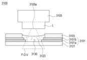
도 27을 참조하면, 계단 구조의 리세스(2730)에 충진 부재가 충진됨에 따라, 충진 부재가 상기 카메라 모듈(2705)을 대향하여 노출되는 표면에서 평탄한 부분의 면적을 충분히 확보함으로써 F.O.V.를 향상시킬 수 있다. 또한 상기 충진 부재로서, 제 1 충진 부재(2723a) 및 상기 제 1 충진 부재(2723a)과 다른 제 2 충진 부재(2723b)를 더 포함하고, 이를 이용하여 리세스(2730)를 충진시킴으로써 제 1 충진 부재(2723a) 상면의 오목한 부분을 보다 평탄하게 만들 수 있다. 본 실시예에 따르면, 리세스(2730)의 폭을 증가시키지 않고도 F.O.V.를 증가시킬 수 있다.Referring to FIG. 27, as the filling member fills the stepped
도 28은, 본 문서에 개시된 또 다른 실시예에 따른, 리세스(2830), 상기 리세스(2830)에 충진된 충진 부재(2823) 및 제 2 투명 부재(2824)가 투명 부재(2821)의 곡면부(2821b)의 배면에 형성된 모습을 나타낸 도면이다.28 is a diagram of a
도 28을 참조하면, 충전 부재(2823)가 LOCA로 이루어지기 때문에, 그 표면이 고르지 못할 수 있는데, 제 2 투명 부재(2824)를 상기 충전 부재(2823)의 상면에 부착시킴으로써, 충전 부재(2823)의 표면을 균질화하고, 편평하게 할 수 있다. 이로 인해, F.O.V.를 증가시킬 수 있다.Referring to FIG. 28, since the filling
본 문서의 다양한 실시예들에 따르면, 상기 계단 구조의 리세스(2030)(2230), 2중 충진 부재(2123a, 2123b)(2223a, 2223b), 제 2 투명 부재(2324)의 실시예들을 개시하며, 제한된 조건에서 F.O.V.를 증가시키기 위한 다양한 방법을 제공할 수 있다.According to various embodiments of the present disclosure, embodiments of the stepped
도 29는, 본 문서에 개시된 다양한 실시예들에 따른 전자 장치(2900)에 있어서, 디스플레이 및 디스플레이를 지지하는 지지부재에 리세스가 형성된 것을 나타내는 도면이다. 도 30은, 본 문서에 개시된 다양한 실시예들에 따른 전자 장치(3000)에 있어서, 리세스가 계단 구조(step structure)의 형상을 가지며, 상기 리세스 내에 충진 부재가 충진된 상태를 나타내는 도면이다. 도 31은, 도 30과 다른 실시예들에 따른 전자 장치에 있어서, 리세스가 계단 구조(step structure)의 형상을 가지며, 상기 리세스 내에 충진 부재가 충진된 상태를 나타내는 도면이다.FIG. 29 is a diagram showing that a recess is formed in a display and a support member supporting the display in the
도 29를 참조하면, 전자 장치(2900)는 리세스(2930)를 포함하되, 상기 리세스(2930)는 마스킹 층(예: 도 7의 722)이 아닌, 디스플레이(2901)에 형성될 수 있다. 이와 같은 실시예는 카메라 모듈(2905)가 디스플레이(2901)의 배면에 실장되는 경우에 적용될 수 있다.Referring to FIG. 29 , the
일실시예에 따르면, 전자 장치(2900)는 디스플레이(2901)의 배면을 지지하는 지지부재(2903)를 더 포함할 수 있다. 지지부재(2903)는 예를 들면, 브라켓, 후면 플레이트 또는 측면 베젤 구조와 같이, 디스플레이(2901)를 지지할 수 있는 구성이면 어떤 것이라도 해당될 수 있다.According to an embodiment, the
상기 지지 부재(2903)는, 예를 들면, 디스플레이의 기능을 개선하기 위한 디지타이저, 쿠션 층, 블랙 마스킹 층, 방열 시트(예: Cu)등의 구성일 수 있다.The
도 29에 도시된 실시예에 따르면, 디스플레이(2901)는 투명 부재(2921)의 배면에 배치되고, 상기 투명 부재(2921)의 적어도 일부를 통해 화면을 표시할 수 있다. 투명 부재(2921)의 적어도 일부(예: 투명한 영역)를 통과한 광은 상기 카메라 모듈을 향할 수 있으며, 리세스(2930)는 이를 가이드할 수 있다. 다만, 투명 부재(2921)의 표면은 제조 과정에서 고르지 못하게 형성될 수 있으므로, 리세스(2930) 내에 충진 부재(2923)를 충진하여 이를 보완할 수 있다.According to the embodiment shown in FIG. 29 , the
도 30에 도시된 실시예에 따르면, 디스플레이(3001)는 복수 개의 기재 층(substrate layer)(30011, 30012)으로 구성될 수 있다. 그리고 상기 복수 개의 기재 층(30011, 30012)은 적층 구조를 형성될 수 있으며, 이러한 적층 구조에는 계단식 리세스(3030)가 형성될 수 있다. 상기 리세스(3030)에 충진 부재(3023)가 충진됨으로써, F.O.V.의 확보를 용이하게 할 수 있다.According to the embodiment shown in FIG. 30 , the
도 31에 도시된 실시예에 따르면, 전자 장치(3100)는 적어도 두 개의 서브 디스플레이(3101a, 3101b)를 포함하여 디스플레이(3101)를 구성할 수 있다. 서브 디스플레이(3100a, 3100b)의 적층 구조는 적어도 하나의 픽셀들이 적층된 것일 수 있다. 다양한 실시예들에 따르면, 적어도 둘의 서브 디스플레이(3101a, 3101b)를 포함한 디스플레이(3101)의 적층 구조에는 계단식 리세스(3130)가 형성될 수 있으며, 이러한 형태의 리세스(3130)에도 충진 부재(3123)가 충진됨으로써, F.O.V.의 확보를 용이하게 할 수 있다.According to the embodiment shown in FIG. 31 , the
도 29 내지 도 31에 도시된 실시예에서, 상술한 설명을 제외한 다른 실시예들은, 도 1 내지 도 28을 통해 전술한 설명들을 준용할 수 있다.In the embodiments shown in FIGS. 29 to 31 , the descriptions described above with reference to FIGS. 1 to 28 may apply mutatis mutandis to other embodiments other than the above description.
본 문서에 개시된 다양한 실시예들에 따른 전자 장치(예: 도 1의 101)는 다양한 형태의 장치가 될 수 있다. 전자 장치(예: 도 1의 101)는, 예를 들면, 휴대용 통신 장치 (예: 스마트폰), 컴퓨터 장치, 휴대용 멀티미디어 장치, 휴대용 의료 기기, 카메라, 웨어러블 장치, 또는 가전 장치를 포함할 수 있다. 본 문서의 실시예에 따른 전자 장치는 전술한 기기들에 한정되지 않는다.An electronic device (eg, 101 of FIG. 1 ) according to various embodiments disclosed in this document may be various types of devices. The electronic device (eg, 101 of FIG. 1 ) may include, for example, a portable communication device (eg, a smartphone), a computer device, a portable multimedia device, a portable medical device, a camera, a wearable device, or a home appliance. . An electronic device according to an embodiment of the present document is not limited to the aforementioned devices.
본 문서의 다양한 실시예들 및 이에 사용된 용어들은 본 문서에 기재된 기술적 특징들을 특정한 실시예들로 한정하려는 것이 아니며, 해당 실시예의 다양한 변경, 균등물, 또는 대체물을 포함하는 것으로 이해되어야 한다. 도면의 설명과 관련하여, 유사한 또는 관련된 구성요소에 대해서는 유사한 참조 부호가 사용될 수 있다. 아이템에 대응하는 명사의 단수 형은 관련된 문맥상 명백하게 다르게 지시하지 않는 한, 상기 아이템 한 개 또는 복수 개를 포함할 수 있다. 본 문서에서, "A 또는 B", "A 및 B 중 적어도 하나","A 또는 B 중 적어도 하나,""A, B 또는 C," "A, B 및 C 중 적어도 하나,"및 "A, B, 또는 C 중 적어도 하나"와 같은 문구들 각각은 그 문구들 중 해당하는 문구에 함께 나열된 항목들 중 어느 하나, 또는 그들의 모든 가능한 조합을 포함할 수 있다. "제 1", "제 2", 또는 "첫째" 또는 "둘째"와 같은 용어들은 단순히 해당 구성요소를 다른 해당 구성요소와 구분하기 위해 사용될 수 있으며, 해당 구성요소들을 다른 측면(예: 중요성 또는 순서)에서 한정하지 않는다. 어떤(예: 제 1) 구성요소가 다른(예: 제 2) 구성요소에, "기능적으로" 또는 "통신적으로"라는 용어와 함께 또는 이런 용어 없이, "커플드" 또는 "커넥티드"라고 언급된 경우, 그것은 상기 어떤 구성요소가 상기 다른 구성요소에 직접적으로(예: 유선으로), 무선으로, 또는 제 3 구성요소를 통하여 연결될 수 있다는 것을 의미한다.Various embodiments of this document and terms used therein are not intended to limit the technical features described in this document to specific embodiments, but should be understood to include various modifications, equivalents, or substitutes of the embodiments. In connection with the description of the drawings, like reference numbers may be used for like or related elements. The singular form of a noun corresponding to an item may include one item or a plurality of items, unless the relevant context clearly dictates otherwise. In this document, "A or B", "at least one of A and B", "at least one of A or B," "A, B or C," "at least one of A, B and C," and "A Each of the phrases such as "at least one of , B, or C" may include any one of the items listed together in that phrase, or all possible combinations thereof. Terms such as "first", "second", or "first" or "secondary" may simply be used to distinguish a given component from other corresponding components, and may be used to refer to a given component in another aspect (eg, importance or order) is not limited. A (e.g., first) component is said to be "coupled" or "connected" to another (e.g., second) component, with or without the terms "functionally" or "communicatively." When mentioned, it means that the certain component may be connected to the other component directly (eg by wire), wirelessly, or through a third component.
본 문서에서 사용된 용어 "모듈"은 하드웨어, 소프트웨어 또는 펌웨어로 구현된 유닛을 포함할 수 있으며, 예를 들면, 로직, 논리 블록, 부품, 또는 회로 등의 용어와 상호 호환적으로 사용될 수 있다. 모듈은, 일체로 구성된 부품 또는 하나 또는 그 이상의 기능을 수행하는, 상기 부품의 최소 단위 또는 그 일부가 될 수 있다. 예를 들면, 일실시예에 따르면, 모듈은 ASIC(application-specific integrated circuit)의 형태로 구현될 수 있다.The term "module" used in this document may include a unit implemented by hardware, software, or firmware, and may be used interchangeably with terms such as logic, logic block, component, or circuit, for example. A module may be an integrally constructed component or a minimal unit of components or a portion thereof that performs one or more functions. For example, according to one embodiment, the module may be implemented in the form of an application-specific integrated circuit (ASIC).
본 문서의 다양한 실시예들은 기기(machine)(예: 전자 장치(101)) 의해 읽을 수 있는 저장 매체(storage medium)(예: 내장 메모리(136) 또는 외장 메모리(138))에 저장된 하나 이상의 명령어들을 포함하는 소프트웨어(예: 프로그램(140))로서 구현될 수 있다. 예를 들면, 기기(예: 전자 장치(101))의 프로세서(예: 프로세서(120))는, 저장 매체로부터 저장된 하나 이상의 명령어들 중 적어도 하나의 명령을 호출하고, 그것을 실행할 수 있다. 이것은 기기가 상기 호출된 적어도 하나의 명령어에 따라 적어도 하나의 기능을 수행하도록 운영되는 것을 가능하게 한다. 상기 하나 이상의 명령어들은 컴파일러에 의해 생성된 코드 또는 인터프리터에 의해 실행될 수 있는 코드를 포함할 수 있다. 기기로 읽을 수 있는 저장매체 는, 비일시적(non-transitory) 저장매체의 형태로 제공될 수 있다. 여기서, ‘비일시적’은 저장매체가 실재(tangible)하는 장치이고, 신호(signal)(예: 전자기파)를 포함하지 않는다는 것을 의미할 뿐이며, 이 용어는 데이터가 저장매체에 반영구적으로 저장되는 경우와 임시적으로 저장되는 경우를 구분하지 않는다.Various embodiments of this document provide one or more instructions stored in a storage medium (eg,
일실시예에 따르면, 본 문서에 개시된 다양한 실시예들에 따른 방법은 컴퓨터 프로그램 제품(computer program product)에 포함되어 제공될 수 있다. 컴퓨터 프로그램 제품은 상품으로서 판매자 및 구매자 간에 거래될 수 있다. 컴퓨터 프로그램 제품은 기기로 읽을 수 있는 저장 매체(예: compact disc read only memory (CD-ROM))의 형태로 배포되거나, 또는 어플리케이션 스토어(예: 플레이 스토어TM)를 통해 또는 두개의 사용자 장치들(예: 스마트폰들) 간에 직접, 온라인으로 배포(예: 다운로드 또는 업로드)될 수 있다. 온라인 배포의 경우에, 컴퓨터 프로그램 제품의 적어도 일부는 제조사의 서버, 어플리케이션 스토어의 서버, 또는 중계 서버의 메모리와 같은 기기로 읽을 수 있는 저장 매체에 적어도 일시 저장되거나, 임시적으로 생성될 수 있다.According to one embodiment, the method according to various embodiments disclosed in this document may be included and provided in a computer program product. Computer program products may be traded between sellers and buyers as commodities. A computer program product is distributed in the form of a device-readable storage medium (eg compact disc read only memory (CD-ROM)), or through an application store (eg Play StoreTM ) or between two user devices ( It can be distributed (eg downloaded or uploaded) online, directly between smartphones. In the case of online distribution, at least part of the computer program product may be temporarily stored or temporarily created in a device-readable storage medium such as a manufacturer's server, an application store server, or a relay server's memory.
다양한 실시예들에 따르면, 상기 기술한 구성요소들의 각각의 구성요소(예: 모듈 또는 프로그램)는 단수 또는 복수의 개체를 포함할 수 있다. 다양한 실시예들에 따르면, 전술한 해당 구성요소들 중 하나 이상의 구성요소들 또는 동작들이 생략되거나, 또는 하나 이상의 다른 구성요소들 또는 동작들이 추가될 수 있다. 대체적으로 또는 추가적으로, 복수의 구성요소들(예: 모듈 또는 프로그램)은 하나의 구성요소로 통합될 수 있다. 이런 경우, 통합된 구성요소는 상기 복수의 구성요소들 각각의 구성요소의 하나 이상의 기능들을 상기 통합 이전에 상기 복수의 구성요소들 중 해당 구성요소에 의해 수행되는 것과 동일 또는 유사하게 수행할 수 있다. 다양한 실시예들에 따르면, 모듈, 프로그램 또는 다른 구성요소에 의해 수행되는 동작들은 순차적으로, 병렬적으로, 반복적으로, 또는 휴리스틱하게 실행되거나, 상기 동작들 중 하나 이상이 다른 순서로 실행되거나, 생략되거나, 또는 하나 이상의 다른 동작들이 추가될 수 있다.According to various embodiments, each component (eg, module or program) of the components described above may include a singular entity or a plurality of entities. According to various embodiments, one or more components or operations among the aforementioned corresponding components may be omitted, or one or more other components or operations may be added. Alternatively or additionally, a plurality of components (eg modules or programs) may be integrated into a single component. In this case, the integrated component may perform one or more functions of each of the plurality of components identically or similarly to those performed by a corresponding component of the plurality of components prior to the integration. . According to various embodiments, the actions performed by a module, program, or other component are executed sequentially, in parallel, iteratively, or heuristically, or one or more of the actions are executed in a different order, or omitted. or one or more other actions may be added.
본 문서에 개시된 다양한 실시예들에 따르면, 전자 장치(예: 도 7의 700)에 있어서, 제 1 플레이트(예: 도 7의 702) 및 상기 제 1 플레이트의 측방 또는 후방에 배치된 제 2 플레이트(예: 도 7의 718)를 포함하는 하우징; 및 상기 제 1 플레이트의 적어도 일부를 통과한 광에 기반하여 외부 정보를 획득하는 카메라 모듈(예: 도 7의 705);을 포함하고, 상기 제 1 플레이트는, 적어도 일분이 실질적으로 투명한 영역을 포함하는 투명 부재(예: 도 7의 721); 상기 투명 부재의 배면에 배치되고, 상기 투명 부재의 상기 투명한 영역 주위에 불투명한 영역을 형성하는 마스킹 층(예: 도7의 722); 상기 마스킹 층에 형성 형성되고, 상기 제 1 플레이트의 적어도 일부를 통과한 광이 상기 카메라 모듈을 향하도록 형성된 리세스(예: 도 8의 730); 및 상기 리세스에 충진된 충진 부재(예: 도 7의 723)를 포함하는, 전자 장치를 제공할 수 있다.According to various embodiments disclosed in this document, in an electronic device (eg, 700 of FIG. 7 ), a first plate (eg, 702 of FIG. 7 ) and a second plate disposed on the side or rear of the first plate a housing including (eg, 718 in FIG. 7 ); and a camera module (eg, 705 in FIG. 7 ) that obtains external information based on light passing through at least a portion of the first plate, wherein the first plate includes a region that is substantially transparent for at least one minute. a transparent member (eg, 721 in FIG. 7 ); a masking layer disposed on a rear surface of the transparent member and forming an opaque region around the transparent region of the transparent member (eg, 722 in FIG. 7); a recess (eg, 730 in FIG. 8 ) formed in the masking layer and configured to direct light passing through at least a portion of the first plate toward the camera module; and a filling member (eg, 723 of FIG. 7 ) filled in the recess.
다양한 실시예들에 따르면, 상기 충진 부재는 액형으로서 상기 리세스에 충진된 후 고형화되고, 상기 리세스 내에서 고형화된 충진 부재의 중앙부는 편평하며 가장자리는 굴곡지게 형성될 수 있다.According to various embodiments, the filling member is solidified after being filled in the recess in the form of a liquid, and the filling member solidified in the recess may have a flat central portion and a curved edge.
다양한 실시예들에 따르면, 상기 리세스는 상기 투명 부재의 표면으로부터 멀어질수록 폭이 넓어지는 형태의 리세스일 수 있다.According to various embodiments, the recess may have a shape in which a width increases as the distance from the surface of the transparent member increases.
다양한 실시예들에 따르면, 상기 리세스는 계단 구조(step structure)의 리세스(예: 도 10의 1030)일 수 있다.According to various embodiments, the recess may be a step structure recess (eg, 1030 in FIG. 10 ).
다양한 실시예들에 따르면, 상기 충진 부재는 상기 투명 부재와 맞닿는 제 1 충진 부재(예: 도 12의 1223a); 및 상기 제 1 충진 부재와 다른 재질로 형성되고, 상기 제 1 충진 부재 상부에 적층된 제 2 충진 부재(예: 도 12의 1223b);를 포함할 수 있다.According to various embodiments, the filling member may include a first filling member (eg, 1223a in FIG. 12 ) that comes into contact with the transparent member; and a second filling member (eg, 1223b in FIG. 12 ) formed of a material different from that of the first filling member and stacked on top of the first filling member.
다양한 실시예들에 따르면, 상기 충진 부재의 상부에 배치되며, 적어도 일부분이 상기 리세스 내에 배치된 제 2 투명 부재(예: 도 16의 1624)를 더 포함할 수 있다.According to various embodiments, a second transparent member (eg, 1624 of FIG. 16 ) disposed above the filling member and having at least a portion disposed within the recess may be further included.
다양한 실시예들에 따르면, 상기 마스킹 층은, 상기 투명 부재의 배면에 배치되고, 컬러를 포함하는 제 1 레이어(예: 도 7의 721a); 상기 제 1 레이어의 배면에 배치되고, 빛샘 방지를 위한 제 2 레이어(예: 도 7의 721b); 및 상기 제 2 레이어의 배면에 배치되고, 제 1 레이어 및 제 2 레이어를 보호하기 위한 제 3 레이어(예: 도 7의 721c)을 포함할 수 있다.According to various embodiments, the masking layer may include a first layer disposed on a rear surface of the transparent member and including a color (eg, 721a of FIG. 7 ); a second layer (eg, 721b in FIG. 7 ) disposed on a rear surface of the first layer and preventing light leakage; and a third layer (eg, 721c of FIG. 7 ) disposed on the rear surface of the second layer and protecting the first layer and the second layer.
다양한 실시예들에 따르면, 상기 투명 부재는, 평면부(예: 도 11의 1021a)와 상기 평면부 주위에 형성된 굴곡부(예: 도 11의 1021b)를 포함할 수 있다.According to various embodiments, the transparent member may include a flat portion (eg, 1021a of FIG. 11 ) and a curved portion formed around the flat portion (eg, 1021b of FIG. 11 ).
다양한 실시예들에 따르면, 상기 리세스는 상기 평면부의 배면에 형성될 수 있다.According to various embodiments, the recess may be formed on a rear surface of the planar portion.
다양한 실시예들에 따르면, 상기 리세스는 상기 평면부 및 상기 굴곡부의 배면에 걸쳐 형성될 수 있다.According to various embodiments, the recess may be formed across rear surfaces of the flat portion and the curved portion.
다양한 실시예들에 따르면, 상기 리세스는 상기 굴곡부의 배면에 걸쳐 형성될 수 있다.According to various embodiments, the recess may be formed across the rear surface of the curved portion.
다양한 실시예들에 따르면, 상기 마스킹 층의 일 부분은 상기 평면부의 배면에 배치되고, 상기 마스킹 층의 다른 부분은 상기 굴곡부의 배면에 배치될 수 있다.According to various embodiments, a portion of the masking layer may be disposed on a rear surface of the flat portion, and another portion of the masking layer may be disposed on a rear surface of the bent portion.
다양한 실시예들에 따르면, 상기 마스킹 층과 상기 하우징 사이에 배치된 접착층(예: 도 7의1040)을 더 포함할 수 있다.According to various embodiments, an adhesive layer (eg, 1040 of FIG. 7 ) disposed between the masking layer and the housing may be further included.
다양한 실시예들에 따르면, 상기 카메라 모듈은 렌즈부(예: 도 10의 L)를 포함하고, 상기 렌즈부의 일단에 형성된 촬상면(예: 도 10의 1005a)은, 상기 충진 부재에 대향하며 상기 충진 부재로부터 소정 거리 이격되도록 형성될 수 있다.According to various embodiments, the camera module includes a lens unit (eg, L in FIG. 10 ), and an imaging surface (eg, 1005a in FIG. 10 ) formed on one end of the lens unit faces the filling member and It may be formed to be spaced apart from the member by a predetermined distance.
다양한 실시예들에 따르면, 상기 제 1 플레이트 및 상기 제 2 플레이트 사이에 배치되고, 상기 제 1 플레이트의 적어도 일부를 통해 화면을 표시하는 디스플레이(예: 도 7의 701)를 더 포함하고, 상기 투명 부재의 투명한 영역을 통해 상기 디스플레이의 화면을 표시할 수 있다.According to various embodiments, a display (eg, 701 of FIG. 7 ) disposed between the first plate and the second plate and displaying a screen through at least a portion of the first plate may be further included, and the transparent The screen of the display may be displayed through the transparent region of the member.
본 문서에 개시된 다양한 실시예들에 따르면, 전자 장치에 있어서, 제 1 플레이트(예: 도 11의 1002) 및 상기 제 1 플레이트의 측방 또는 후방에 배치된 제 2 플레이트(예: 도 11의 1018)를 포함하는 하우징; 상기 제 1 플레이트 및 상기 제 2 플레이트 사이에 배치되고, 상기 제 1 플레이트의 적어도 일부를 통해 화면을 표시하는 디스플레이(예: 도 11의 1001); 및 상기 제 1 플레이트의 적어도 일부를 통과한 광에 기반하여 외부 정보를 획득하는 카메라 모듈(예: 도 11의 1005);을 포함하고, 상기 제 1 플레이트는, 상기 디스플레이의 화면을 표시하기 위한 투명한 영역을 포함하는 투명 부재(예: 도 11의 1021); 상기 투명 부재의 배면에 배치되고, 상기 투명 부재의 상기 투명한 영역 주위에 불투명한 영역을 형성하는 마스킹 층; 상기 마스킹 층에 형성 형성되고, 상기 제 1 플레이트의 적어도 일부를 통과한 광이 상기 카메라 모듈을 향하도록 형성된 계단 구조의 리세스(예: 도 10의 1030); 및 상기 계단 구조의 리세스에 충진된 충진 부재(예: 도 11의 1023)를 포함하는, 전자 장치를 제공할 수 있다.According to various embodiments disclosed in this document, in an electronic device, a first plate (eg, 1002 of FIG. 11 ) and a second plate (eg, 1018 of FIG. 11 ) disposed on the side or rear of the first plate A housing comprising a; a display disposed between the first plate and the second plate and displaying a screen through at least a portion of the first plate (eg, 1001 in FIG. 11 ); and a camera module (eg, 1005 in FIG. 11 ) that obtains external information based on light passing through at least a portion of the first plate, wherein the first plate is transparent for displaying the screen of the display. a transparent member including a region (eg, 1021 in FIG. 11 ); a masking layer disposed on a rear surface of the transparent member and forming an opaque region around the transparent region of the transparent member; a recess formed in the masking layer and having a stepped structure (for example, 1030 in FIG. 10 ) formed to direct light passing through at least a part of the first plate toward the camera module; and a filling member (eg, 1023 of FIG. 11 ) filled in the recess of the stair structure.
다양한 실시예들에 따르면, 상기 충진 부재(예: 도 11의 1023)는 상기 투명 부재와 맞닿는 제 1 충진 부재(예: 도 15의 1423a); 및 상기 제 1 충진 부재와 다른 재질로 형성되고, 상기 제 1 충진 부재 상부에 적층된 제 2 충진 부재(예: 도 15의 1423b);를 포함할 수 있다.According to various embodiments, the filling member (eg, 1023 of FIG. 11 ) may include a first filling member (eg, 1423a of FIG. 15 ) that comes into contact with the transparent member; and a second filling member (eg, 1423b in FIG. 15 ) formed of a material different from that of the first filling member and stacked on top of the first filling member.
다양한 실시예들에 따르면, 상기 마스킹 층은, 상기 투명 부재의 배면에 배치되고, 컬러를 포함하는 제 1 레이어(예:도 11의 1022a); 상기 제 1 레이어의 배면에 배치되고, 빛샘 방지를 위한 제 2 레이어(예: 도 11의 1022b);및 상기 제 2 레이어의 배면에 배치되고, 제 1 레이어 및 제 2 레이어를 보호하기 위한 제 3 레이어(예: 도 11의 1022c)을 포함할 수 있다.According to various embodiments, the masking layer may include a first layer disposed on a rear surface of the transparent member and including a color (eg, 1022a in FIG. 11 ); A second layer (eg, 1022b in FIG. 11) disposed on the rear surface of the first layer to prevent light leakage; and a third layer disposed on the rear surface of the second layer to protect the first layer and the second layer. A layer (eg, 1022c in FIG. 11) may be included.
본 문서에 개시된 다양한 실시예들에 따르면, 전자 장치에 있어서, 투명 부재(예: 도 29의 2921); 상기 투명 부재의 적어도 일부를 통해 화면을 표시하는 디스플레이(예: 도 29의 2901); 상기 디스플레이의 배면을 지지하는 지지부재(예: 도 29의 2903); 및 상기 투명 부재의 적어도 일부를 통과한 광에 기반하여 외부 정보를 획득하는 카메라 모듈(예: 도 29의 2905);을 포함하고, 상기 디스플레이 및 상기 지지부재에 각각 형성되고, 상기 투명 부재의 적어도 일부를 통과한 광이 상기 카메라 모듈을 향하도록 형성된 리세스(예: 도 29의 2930);를 포함하며, 상기 디스플레이에 형성된 리세스의 폭 보다 상기 지지부재에 형성된 리세스의 폭이 더 크게 형성되며, 상기 디스플레이 및 상기 지지부재에 형성된 리세스에 충진 부재(예: 도29의 2923)가 충진되는, 전자 장치를 제공할 수 있다.According to various embodiments disclosed in this document, in an electronic device, a transparent member (eg, 2921 of FIG. 29 ); a display (eg, 2901 in FIG. 29 ) displaying a screen through at least a portion of the transparent member; a support member (for example, 2903 in FIG. 29) supporting the rear surface of the display; and a camera module (eg, 2905 in FIG. 29 ) that obtains external information based on light passing through at least a portion of the transparent member, and is formed on the display and the support member, respectively, and includes at least one of the transparent member. and a recess (for example, 2930 in FIG. 29 ) formed so that the light passing through the part is directed toward the camera module, and the width of the recess formed in the support member is larger than that of the recess formed in the display. And, it is possible to provide an electronic device in which a filling member (eg, 2923 in FIG. 29 ) is filled in the recesses formed in the display and the support member.
다양한 실시예들에 따르면, 상기 충진 부재는 상기 투명 부재와 맞닿는 제 1 충진 부재(예: 도 15의 1423a); 및 상기 제 1 충진 부재와 다른 재질로 형성되고, 상기 제 1 충진 부재 상부에 적층된 제 2 충진 부재(예: 도 15의 1423b);를 포함할 수 있다.According to various embodiments, the filling member may include a first filling member (eg, 1423a in FIG. 15 ) in contact with the transparent member; and a second filling member (eg, 1423b in FIG. 15 ) formed of a material different from that of the first filling member and stacked on top of the first filling member.
이상에서 설명한 본 발명의 다양한 실시 예의 회전 가능한 부재의 유동 제한 구조 및 전자장치는 전술한 실시 예 및 도면에 의해 한정되는 것은 아니고, 본 발명의 기술적 범위 내에서 여러 가지 치환, 변형 및 변경이 가능함은 본 발명이 속하는 기술분야에서 통상의 지식을 가진 자에게 있어 명백할 것이다.The flow limiting structure and electronic device of the rotatable member of various embodiments of the present invention described above are not limited to the above-described embodiments and drawings, and various substitutions, modifications, and changes are possible within the technical scope of the present invention. It will be clear to those skilled in the art to which the present invention pertains.
전자 장치 : 700
디스플레이 : 701
제 1 플레이트 : 702
카메라 모듈 : 705
제 3 영역 : 710F
제 4 영역 : 710G
측면 베젤 구조: 718
투명 부재 : 721
마스킹 층 : 722
충진 부재 : 730Electronics: 700
Display: 701
1st plate: 702
Camera module: 705
Zone 3: 710F
4th area: 710G
Side Bezel Structure: 718
Transparent member: 721
Masking Layer: 722
Filling member: 730
Claims (20)
Translated fromKorean제 1 플레이트 및 상기 제 1 플레이트의 측방 또는 후방에 배치된 제 2 플레이트를 포함하는 하우징; 및
상기 제 1 플레이트의 적어도 일부를 통과한 광에 기반하여 외부 정보를 획득하는 카메라 모듈;을 포함하고,
상기 제 1 플레이트는,
적어도 일부분이 실질적으로 투명한 영역을 포함하는 투명 부재; 및
상기 투명 부재의 배면에 배치되고, 상기 투명 부재의 상기 투명한 영역 주위에 불투명한 영역을 형성하는 마스킹 층 ― 상기 마스킹 층에는 상기 제 1 플레이트의 적어도 일부를 통과한 광이 상기 카메라 모듈을 향하도록 리세스가 형성됨 ―; 및
상기 리세스에 충진된 충진 부재를 포함하고,
상기 리세스의 폭은 상기 투명 부재의 표면으로부터 멀어질수록 커지는,
전자 장치.
In electronic devices,
a housing including a first plate and a second plate disposed on the side or rear side of the first plate; and
A camera module for acquiring external information based on light passing through at least a portion of the first plate;
The first plate,
a transparent member comprising a region at least partially transparent; and
A masking layer disposed on a rear surface of the transparent member and forming an opaque region around the transparent region of the transparent member - the masking layer is provided so that light passing through at least a portion of the first plate is directed toward the camera module. seth is formed; and
Including a filling member filled in the recess,
The width of the recess increases as the distance from the surface of the transparent member increases.
electronic device.
상기 충진 부재는 액형으로서 상기 리세스에 충진된 후 고형화되고, 상기 리세스 내에서 고형화된 충진 부재의 중앙부는 편평하며 가장자리는 굴곡지게 형성된 전자 장치.
According to claim 1,
The electronic device of claim 1 , wherein the filling member is in the form of a liquid, which is solidified after being filled in the recess, and has a flat central portion and curved edges of the solidified filling member in the recess.
상기 리세스는 계단 구조(step structure)의 리세스인 전자 장치.
According to claim 1,
The electronic device of claim 1 , wherein the recess is a recess of a step structure.
상기 충진 부재는,
상기 투명 부재와 맞닿는 제 1 충진 부재; 및
상기 제 1 충진 부재와 다른 재질로 형성되고, 상기 제 1 충진 부재 상부에 적층된 제 2 충진 부재;를 포함하는 전자 장치.
According to claim 1,
The filling member,
a first filling member in contact with the transparent member; and
and a second filling member made of a material different from that of the first filling member and stacked on top of the first filling member.
상기 충진 부재의 상부에 배치되며, 적어도 일부분이 상기 리세스 내에 배치된 제 2 투명 부재를 더 포함하는 전자 장치.
According to claim 1,
The electronic device further includes a second transparent member disposed above the filling member and having at least a portion disposed within the recess.
상기 마스킹 층은,
상기 투명 부재의 배면에 배치되고, 컬러를 포함하는 제 1 레이어;
상기 제 1 레이어의 배면에 배치되고, 빛샘 방지를 위한 제 2 레이어; 및
상기 제 2 레이어의 배면에 배치되고, 제 1 레이어 및 제 2 레이어를 보호하기 위한 제 3 레이어를 포함하는 전자 장치.
According to claim 1,
The masking layer,
a first layer disposed on a rear surface of the transparent member and including a color;
a second layer disposed on a rear surface of the first layer to prevent light leakage; and
and a third layer disposed on a rear surface of the second layer and protecting the first layer and the second layer.
상기 투명 부재는,
평면부와 상기 평면부 주위에 형성된 굴곡부를 포함하는 전자 장치.
According to claim 1,
The transparent member,
An electronic device comprising a flat portion and a bent portion formed around the flat portion.
상기 리세스는 상기 평면부의 배면에 형성된 전자 장치.
According to claim 8,
The recess is formed on a rear surface of the planar part.
상기 리세스는 상기 평면부 및 상기 굴곡부의 배면에 걸쳐 형성된 전자 장치.
According to claim 8,
The recess is formed across rear surfaces of the flat portion and the curved portion.
상기 리세스는 상기 굴곡부의 배면에 걸쳐 형성된 전자 장치.
According to claim 8,
The recess is formed across the rear surface of the bent part.
상기 마스킹 층의 일 부분은 상기 평면부의 배면에 배치되고, 상기 마스킹 층의 다른 부분은 상기 굴곡부의 배면에 배치된 전자 장치.
According to claim 8,
A portion of the masking layer is disposed on a rear surface of the flat portion, and another portion of the masking layer is disposed on a rear surface of the bent portion.
상기 마스킹 층과 상기 하우징 사이에 배치된 접착층을 더 포함하는 전자 장치.
According to claim 1,
The electronic device further comprises an adhesive layer disposed between the masking layer and the housing.
상기 카메라 모듈은 렌즈부를 포함하고,
상기 렌즈부의 일단에 형성된 촬상면은, 상기 충진 부재에 대향하며 상기충진 부재로부터 소정 거리 이격되도록 형성된 전자 장치.
According to claim 1,
The camera module includes a lens unit,
The electronic device of claim 1 , wherein an imaging surface formed at one end of the lens unit faces the filling member and is spaced apart from the filling member by a predetermined distance.
상기 제 1 플레이트 및 상기 제 2 플레이트 사이에 배치되고, 상기 제 1 플레이트의 적어도 일부를 통해 화면을 표시하는 디스플레이를 더 포함하고,
상기 투명 부재의 투명한 영역을 통해 상기 디스플레이의 화면을 표시하는 전자 장치.
According to claim 1,
Further comprising a display disposed between the first plate and the second plate and displaying a screen through at least a portion of the first plate,
An electronic device displaying a screen of the display through a transparent region of the transparent member.
제 1 플레이트 및 상기 제 1 플레이트의 측방 또는 후방에 배치된 제 2 플레이트를 포함하는 하우징;
상기 제 1 플레이트 및 상기 제 2 플레이트 사이에 배치되고, 상기 제 1 플레이트의 적어도 일부를 통해 화면을 표시하는 디스플레이; 및
상기 제 1 플레이트의 적어도 일부를 통과한 광에 기반하여 외부 정보를 획득하는 카메라 모듈;을 포함하고,
상기 제 1 플레이트는,
상기 디스플레이의 화면을 표시하기 위한 투명한 영역을 포함하는 투명 부재;
상기 투명 부재의 배면에 배치되고, 상기 투명 부재의 상기 투명한 영역 주위에 불투명한 영역을 형성하는 마스킹 층 ― 상기 마스킹 층에는 상기 제 1 플레이트의 적어도 일부를 통과한 광이 상기 카메라 모듈을 향하도록 하는 계단 구조의 리세스가 형성됨 ―; 및
상기 계단 구조의 리세스에 충진된 충진 부재를 포함하고,
상기 리세스의 폭은 상기 투명 부재의 표면으로부터 멀어질수록 커지는,
전자 장치.
In electronic devices,
a housing including a first plate and a second plate disposed on the side or rear side of the first plate;
a display disposed between the first plate and the second plate and displaying a screen through at least a portion of the first plate; and
A camera module for acquiring external information based on light passing through at least a portion of the first plate;
The first plate,
a transparent member including a transparent area for displaying the screen of the display;
a masking layer disposed on a rear surface of the transparent member and forming an opaque region around the transparent region of the transparent member, wherein the masking layer directs light passing through at least a portion of the first plate toward the camera module; A stepped recess is formed; and
Including a filling member filled in the recess of the stair structure,
The width of the recess increases as the distance from the surface of the transparent member increases.
electronic device.
상기 충진 부재는,
상기 투명 부재와 맞닿는 제 1 충진 부재; 및
상기 제 1 충진 부재와 다른 재질로 형성되고, 상기 제 1 충진 부재 상부에 적층된 제 2 충진 부재;를 포함하는 전자 장치.
17. The method of claim 16,
The filling member,
a first filling member in contact with the transparent member; and
and a second filling member made of a material different from that of the first filling member and stacked on top of the first filling member.
상기 마스킹 층은,
상기 투명 부재의 배면에 배치되고, 컬러를 포함하는 제 1 레이어;
상기 제 1 레이어의 배면에 배치되고, 빛샘 방지를 위한 제 2 레이어;및
상기 제 2 레이어의 배면에 배치되고, 제 1 레이어 및 제 2 레이어를 보호하기 위한 제 3 레이어를 포함하는 전자 장치.
17. The method of claim 16,
The masking layer,
a first layer disposed on a rear surface of the transparent member and including a color;
a second layer disposed on a rear surface of the first layer and preventing light leakage; and
and a third layer disposed on a rear surface of the second layer and protecting the first layer and the second layer.
투명 부재;
상기 투명 부재의 적어도 일부를 통해 화면을 표시하는 디스플레이;
상기 디스플레이의 배면을 지지하는 지지부재; 및
상기 투명 부재의 적어도 일부를 통과한 광에 기반하여 외부 정보를 획득하는 카메라 모듈을 포함하고,
상기 디스플레이 및 상기 지지부재 각각에는 상기 투명 부재의 적어도 일부를 통과한 광이 상기 카메라 모듈을 향하도록 하기 위한 리세스가 형성되고,
상기 디스플레이에 형성된 리세스의 폭 보다 상기 지지부재에 형성된 리세스의 폭이 더 크며,
상기 디스플레이 및 상기 지지부재에 형성된 리세스에 충진 부재가 충진되는 전자 장치.
In electronic devices,
transparent member;
a display displaying a screen through at least a portion of the transparent member;
a support member supporting the rear surface of the display; and
A camera module for acquiring external information based on light passing through at least a portion of the transparent member;
A recess is formed in each of the display and the support member to direct light passing through at least a portion of the transparent member toward the camera module;
The width of the recess formed in the support member is greater than the width of the recess formed in the display,
An electronic device in which a filling member is filled in recesses formed in the display and the support member.
상기 충진 부재는,
상기 투명 부재와 맞닿는 제 1 충진 부재; 및
상기 제 1 충진 부재와 다른 재질로 형성되고, 상기 제 1 충진 부재 상부에 적층된 제 2 충진 부재;를 포함하는 전자 장치.According to claim 19,
The filling member,
a first filling member in contact with the transparent member; and
and a second filling member made of a material different from that of the first filling member and stacked on top of the first filling member.
Priority Applications (5)
| Application Number | Priority Date | Filing Date | Title |
|---|---|---|---|
| KR1020190010657AKR102555577B1 (en) | 2019-01-28 | 2019-01-28 | Electronic module including camera module |
| US17/312,275US12147270B2 (en) | 2019-01-28 | 2020-01-21 | Electronic device comprising camera module |
| PCT/KR2020/001041WO2020159141A1 (en) | 2019-01-28 | 2020-01-21 | Electronic device comprising camera module |
| EP20749473.3AEP3883223B1 (en) | 2019-01-28 | 2020-01-21 | Electronic device comprising camera module |
| CN202080011402.5ACN113383535B (en) | 2019-01-28 | 2020-01-21 | Electronic device including camera module |
Applications Claiming Priority (1)
| Application Number | Priority Date | Filing Date | Title |
|---|---|---|---|
| KR1020190010657AKR102555577B1 (en) | 2019-01-28 | 2019-01-28 | Electronic module including camera module |
Publications (2)
| Publication Number | Publication Date |
|---|---|
| KR20200093736A KR20200093736A (en) | 2020-08-06 |
| KR102555577B1true KR102555577B1 (en) | 2023-07-18 |
Family
ID=71842168
Family Applications (1)
| Application Number | Title | Priority Date | Filing Date |
|---|---|---|---|
| KR1020190010657AActiveKR102555577B1 (en) | 2019-01-28 | 2019-01-28 | Electronic module including camera module |
Country Status (5)
| Country | Link |
|---|---|
| US (1) | US12147270B2 (en) |
| EP (1) | EP3883223B1 (en) |
| KR (1) | KR102555577B1 (en) |
| CN (1) | CN113383535B (en) |
| WO (1) | WO2020159141A1 (en) |
Families Citing this family (3)
| Publication number | Priority date | Publication date | Assignee | Title |
|---|---|---|---|---|
| US11687126B2 (en)* | 2020-02-18 | 2023-06-27 | Google Llc | Reducing hole bezel region in displays |
| KR102752738B1 (en)* | 2020-11-11 | 2025-01-10 | 삼성전자주식회사 | An electronic device comprising a housing |
| TWI808413B (en)* | 2021-04-29 | 2023-07-11 | 位元奈米科技股份有限公司 | Transparent conductive substrate structure formed by hot pressing |
Family Cites Families (25)
| Publication number | Priority date | Publication date | Assignee | Title |
|---|---|---|---|---|
| WO2008011003A2 (en)* | 2006-07-17 | 2008-01-24 | Tessera North America, Inc. | Camera system and associated methods |
| KR101701368B1 (en)* | 2010-06-25 | 2017-02-01 | 엘지이노텍 주식회사 | Liquid crystal display panel with embedded camera module and method for manufacturing the same |
| US8750949B2 (en) | 2011-01-11 | 2014-06-10 | Apple Inc. | Engagement features and adjustment structures for electronic devices with integral antennas |
| DE102011089443B4 (en)* | 2011-02-14 | 2016-12-01 | Lg Display Co., Ltd. | display device |
| NL2006373C2 (en)* | 2011-03-11 | 2012-09-17 | Anteryon Internat B V | OPTICAL UNIT. |
| US8723824B2 (en) | 2011-09-27 | 2014-05-13 | Apple Inc. | Electronic devices with sidewall displays |
| US8684613B2 (en) | 2012-01-10 | 2014-04-01 | Apple Inc. | Integrated camera window |
| KR102031654B1 (en)* | 2012-05-23 | 2019-10-15 | 삼성디스플레이 주식회사 | Window structure, method of manufacturing the same, electronic device equipped with a camera including a window structure and method of manufacturing the same |
| TWI584101B (en)* | 2013-04-19 | 2017-05-21 | 富智康〈香港〉有限公司 | Shading assembly and electronic device having the same |
| JP6237070B2 (en) | 2013-10-01 | 2017-11-29 | セイコーエプソン株式会社 | Microlens array substrate, electro-optical device, and electronic device |
| KR102145191B1 (en) | 2014-01-24 | 2020-08-19 | 엘지전자 주식회사 | Mobile terminal |
| US9787345B2 (en) | 2014-03-31 | 2017-10-10 | Apple Inc. | Laser welding of transparent and opaque materials |
| KR102514770B1 (en)* | 2015-10-02 | 2023-03-29 | 삼성전자주식회사 | Electronic device including waterproof structure |
| KR20170111827A (en) | 2016-03-29 | 2017-10-12 | 삼성전자주식회사 | Electronic device including display and camera |
| US10075636B2 (en) | 2016-04-26 | 2018-09-11 | Omnivision Technologies, Inc. | Ultra-small camera module with wide field of view, and associate lens systems and methods |
| KR102592053B1 (en) | 2016-07-04 | 2023-10-23 | 삼성전자주식회사 | User interface providing method and electronic device supporting the same |
| US10204947B2 (en) | 2016-09-09 | 2019-02-12 | Omnivision Technologies, Inc. | Cover-glass-free array camera with individually light-shielded cameras |
| KR102625247B1 (en) | 2016-11-11 | 2024-01-16 | 삼성전자주식회사 | Electronic device including camera and acoustic component |
| KR102567809B1 (en)* | 2017-01-02 | 2023-08-18 | 삼성전자주식회사 | electronic device including light-transmissive film and method for manufacturing the same |
| KR102702929B1 (en)* | 2017-01-09 | 2024-09-05 | 엘지이노텍 주식회사 | Liquid Lens, Camera Module, And Optical Device |
| WO2018128508A1 (en) | 2017-01-09 | 2018-07-12 | 엘지이노텍(주) | Liquid lens |
| CN107547708B (en) | 2017-09-26 | 2020-01-14 | Oppo广东移动通信有限公司 | Cover plate assembly, shell assembly and mobile terminal |
| CN107465863B (en) | 2017-09-26 | 2021-04-06 | Oppo广东移动通信有限公司 | Composite cover, camera module and mobile terminal |
| CN108200237B (en) | 2017-12-26 | 2020-08-07 | Oppo广东移动通信有限公司 | Electronic device |
| CN112041734A (en)* | 2018-06-13 | 2020-12-04 | Oppo广东移动通信有限公司 | Display module for electronic device, and method for manufacturing display module |
- 2019
- 2019-01-28KRKR1020190010657Apatent/KR102555577B1/enactiveActive
- 2020
- 2020-01-21WOPCT/KR2020/001041patent/WO2020159141A1/ennot_activeCeased
- 2020-01-21CNCN202080011402.5Apatent/CN113383535B/enactiveActive
- 2020-01-21EPEP20749473.3Apatent/EP3883223B1/enactiveActive
- 2020-01-21USUS17/312,275patent/US12147270B2/enactiveActive
Also Published As
| Publication number | Publication date |
|---|---|
| CN113383535B (en) | 2024-01-23 |
| EP3883223A1 (en) | 2021-09-22 |
| US12147270B2 (en) | 2024-11-19 |
| US20220107668A1 (en) | 2022-04-07 |
| WO2020159141A1 (en) | 2020-08-06 |
| CN113383535A (en) | 2021-09-10 |
| EP3883223A4 (en) | 2022-02-23 |
| KR20200093736A (en) | 2020-08-06 |
| EP3883223B1 (en) | 2024-05-01 |
Similar Documents
| Publication | Publication Date | Title |
|---|---|---|
| JP7527706B2 (en) | Electronic devices, including coatings for window protection | |
| KR102763576B1 (en) | Electronic device incluidng optical sensor module | |
| US10819381B2 (en) | Electronic device including glass plate | |
| US11331878B2 (en) | Decoration film and electronic device including the same | |
| US11648747B2 (en) | Plate including fine pattern, and electronic device including same | |
| KR20210101462A (en) | Electronic device including a microphone module | |
| KR102600941B1 (en) | Electronic device including display | |
| KR102779004B1 (en) | Electronic device comprising coating for protection of window | |
| US20220075225A1 (en) | Hole display and electronic device comprising same | |
| EP4181499A1 (en) | Electronic device comprising camera module | |
| EP3582064B1 (en) | Display device and electronic device including the same | |
| KR20190117133A (en) | electronic device including bendable display | |
| KR102555577B1 (en) | Electronic module including camera module | |
| US12364097B2 (en) | Electronic device comprising optical sensor and encapsulation layers | |
| US12058829B2 (en) | Electronic device comprising glass plate | |
| US11595586B2 (en) | Electronic device including camera module shooting through at least one portion of display device | |
| US11553605B2 (en) | Electronic device including housing | |
| EP3933546B1 (en) | Electronic device comprising support member | |
| KR20210100836A (en) | Electronic device including printing film | |
| KR102750053B1 (en) | Electronic device incuding glass plate | |
| KR20230008440A (en) | Electronic device including window glass and manufacturing method thereof |
Legal Events
| Date | Code | Title | Description |
|---|---|---|---|
| PA0109 | Patent application | Patent event code:PA01091R01D Comment text:Patent Application Patent event date:20190128 | |
| PG1501 | Laying open of application | ||
| A201 | Request for examination | ||
| PA0201 | Request for examination | Patent event code:PA02012R01D Patent event date:20211215 Comment text:Request for Examination of Application Patent event code:PA02011R01I Patent event date:20190128 Comment text:Patent Application | |
| E902 | Notification of reason for refusal | ||
| PE0902 | Notice of grounds for rejection | Comment text:Notification of reason for refusal Patent event date:20230213 Patent event code:PE09021S01D | |
| E701 | Decision to grant or registration of patent right | ||
| PE0701 | Decision of registration | Patent event code:PE07011S01D Comment text:Decision to Grant Registration Patent event date:20230703 | |
| GRNT | Written decision to grant | ||
| PR0701 | Registration of establishment | Comment text:Registration of Establishment Patent event date:20230711 Patent event code:PR07011E01D | |
| PR1002 | Payment of registration fee | Payment date:20230712 End annual number:3 Start annual number:1 | |
| PG1601 | Publication of registration |