KR102553265B1 - Light emitting diode(led) device, and light source modulehaving the same - Google Patents
Light emitting diode(led) device, and light source modulehaving the sameDownload PDFInfo
- Publication number
- KR102553265B1 KR102553265B1KR1020180079576AKR20180079576AKR102553265B1KR 102553265 B1KR102553265 B1KR 102553265B1KR 1020180079576 AKR1020180079576 AKR 1020180079576AKR 20180079576 AKR20180079576 AKR 20180079576AKR 102553265 B1KR102553265 B1KR 102553265B1
- Authority
- KR
- South Korea
- Prior art keywords
- light emitting
- sub
- arrays
- pads
- array
- Prior art date
- Legal status (The legal status is an assumption and is not a legal conclusion. Google has not performed a legal analysis and makes no representation as to the accuracy of the status listed.)
- Active
Links
Images


Classifications
- H—ELECTRICITY
- H01—ELECTRIC ELEMENTS
- H01L—SEMICONDUCTOR DEVICES NOT COVERED BY CLASS H10
- H01L25/00—Assemblies consisting of a plurality of semiconductor or other solid state devices
- H01L25/03—Assemblies consisting of a plurality of semiconductor or other solid state devices all the devices being of a type provided for in a single subclass of subclasses H10B, H10D, H10F, H10H, H10K or H10N, e.g. assemblies of rectifier diodes
- H01L25/04—Assemblies consisting of a plurality of semiconductor or other solid state devices all the devices being of a type provided for in a single subclass of subclasses H10B, H10D, H10F, H10H, H10K or H10N, e.g. assemblies of rectifier diodes the devices not having separate containers
- H01L25/075—Assemblies consisting of a plurality of semiconductor or other solid state devices all the devices being of a type provided for in a single subclass of subclasses H10B, H10D, H10F, H10H, H10K or H10N, e.g. assemblies of rectifier diodes the devices not having separate containers the devices being of a type provided for in group H10H20/00
- H01L25/0753—Assemblies consisting of a plurality of semiconductor or other solid state devices all the devices being of a type provided for in a single subclass of subclasses H10B, H10D, H10F, H10H, H10K or H10N, e.g. assemblies of rectifier diodes the devices not having separate containers the devices being of a type provided for in group H10H20/00 the devices being arranged next to each other
- H—ELECTRICITY
- H10—SEMICONDUCTOR DEVICES; ELECTRIC SOLID-STATE DEVICES NOT OTHERWISE PROVIDED FOR
- H10H—INORGANIC LIGHT-EMITTING SEMICONDUCTOR DEVICES HAVING POTENTIAL BARRIERS
- H10H29/00—Integrated devices, or assemblies of multiple devices, comprising at least one light-emitting semiconductor element covered by group H10H20/00
- H10H29/10—Integrated devices comprising at least one light-emitting semiconductor component covered by group H10H20/00
- H10H29/14—Integrated devices comprising at least one light-emitting semiconductor component covered by group H10H20/00 comprising multiple light-emitting semiconductor components
- F—MECHANICAL ENGINEERING; LIGHTING; HEATING; WEAPONS; BLASTING
- F21—LIGHTING
- F21V—FUNCTIONAL FEATURES OR DETAILS OF LIGHTING DEVICES OR SYSTEMS THEREOF; STRUCTURAL COMBINATIONS OF LIGHTING DEVICES WITH OTHER ARTICLES, NOT OTHERWISE PROVIDED FOR
- F21V23/00—Arrangement of electric circuit elements in or on lighting devices
- F21V23/003—Arrangement of electric circuit elements in or on lighting devices the elements being electronics drivers or controllers for operating the light source, e.g. for a LED array
- F21V23/004—Arrangement of electric circuit elements in or on lighting devices the elements being electronics drivers or controllers for operating the light source, e.g. for a LED array arranged on a substrate, e.g. a printed circuit board
- F21V23/005—Arrangement of electric circuit elements in or on lighting devices the elements being electronics drivers or controllers for operating the light source, e.g. for a LED array arranged on a substrate, e.g. a printed circuit board the substrate is supporting also the light source
- H—ELECTRICITY
- H01—ELECTRIC ELEMENTS
- H01L—SEMICONDUCTOR DEVICES NOT COVERED BY CLASS H10
- H01L25/00—Assemblies consisting of a plurality of semiconductor or other solid state devices
- H01L25/03—Assemblies consisting of a plurality of semiconductor or other solid state devices all the devices being of a type provided for in a single subclass of subclasses H10B, H10D, H10F, H10H, H10K or H10N, e.g. assemblies of rectifier diodes
- H01L25/04—Assemblies consisting of a plurality of semiconductor or other solid state devices all the devices being of a type provided for in a single subclass of subclasses H10B, H10D, H10F, H10H, H10K or H10N, e.g. assemblies of rectifier diodes the devices not having separate containers
- H01L25/075—Assemblies consisting of a plurality of semiconductor or other solid state devices all the devices being of a type provided for in a single subclass of subclasses H10B, H10D, H10F, H10H, H10K or H10N, e.g. assemblies of rectifier diodes the devices not having separate containers the devices being of a type provided for in group H10H20/00
- H—ELECTRICITY
- H01—ELECTRIC ELEMENTS
- H01L—SEMICONDUCTOR DEVICES NOT COVERED BY CLASS H10
- H01L25/00—Assemblies consisting of a plurality of semiconductor or other solid state devices
- H01L25/16—Assemblies consisting of a plurality of semiconductor or other solid state devices the devices being of types provided for in two or more different subclasses of H10B, H10D, H10F, H10H, H10K or H10N, e.g. forming hybrid circuits
- H01L25/167—Assemblies consisting of a plurality of semiconductor or other solid state devices the devices being of types provided for in two or more different subclasses of H10B, H10D, H10F, H10H, H10K or H10N, e.g. forming hybrid circuits comprising optoelectronic devices, e.g. LED, photodiodes
- H01L33/36—
- H01L33/62—
- H—ELECTRICITY
- H05—ELECTRIC TECHNIQUES NOT OTHERWISE PROVIDED FOR
- H05K—PRINTED CIRCUITS; CASINGS OR CONSTRUCTIONAL DETAILS OF ELECTRIC APPARATUS; MANUFACTURE OF ASSEMBLAGES OF ELECTRICAL COMPONENTS
- H05K1/00—Printed circuits
- H05K1/18—Printed circuits structurally associated with non-printed electric components
- H—ELECTRICITY
- H10—SEMICONDUCTOR DEVICES; ELECTRIC SOLID-STATE DEVICES NOT OTHERWISE PROVIDED FOR
- H10H—INORGANIC LIGHT-EMITTING SEMICONDUCTOR DEVICES HAVING POTENTIAL BARRIERS
- H10H20/00—Individual inorganic light-emitting semiconductor devices having potential barriers, e.g. light-emitting diodes [LED]
- H10H20/01—Manufacture or treatment
- H—ELECTRICITY
- H10—SEMICONDUCTOR DEVICES; ELECTRIC SOLID-STATE DEVICES NOT OTHERWISE PROVIDED FOR
- H10H—INORGANIC LIGHT-EMITTING SEMICONDUCTOR DEVICES HAVING POTENTIAL BARRIERS
- H10H20/00—Individual inorganic light-emitting semiconductor devices having potential barriers, e.g. light-emitting diodes [LED]
- H10H20/80—Constructional details
- H10H20/83—Electrodes
- H10H20/831—Electrodes characterised by their shape
- H—ELECTRICITY
- H10—SEMICONDUCTOR DEVICES; ELECTRIC SOLID-STATE DEVICES NOT OTHERWISE PROVIDED FOR
- H10H—INORGANIC LIGHT-EMITTING SEMICONDUCTOR DEVICES HAVING POTENTIAL BARRIERS
- H10H20/00—Individual inorganic light-emitting semiconductor devices having potential barriers, e.g. light-emitting diodes [LED]
- H10H20/80—Constructional details
- H10H20/85—Packages
- H10H20/857—Interconnections, e.g. lead-frames, bond wires or solder balls
- F—MECHANICAL ENGINEERING; LIGHTING; HEATING; WEAPONS; BLASTING
- F21—LIGHTING
- F21K—NON-ELECTRIC LIGHT SOURCES USING LUMINESCENCE; LIGHT SOURCES USING ELECTROCHEMILUMINESCENCE; LIGHT SOURCES USING CHARGES OF COMBUSTIBLE MATERIAL; LIGHT SOURCES USING SEMICONDUCTOR DEVICES AS LIGHT-GENERATING ELEMENTS; LIGHT SOURCES NOT OTHERWISE PROVIDED FOR
- F21K9/00—Light sources using semiconductor devices as light-generating elements, e.g. using light-emitting diodes [LED] or lasers
- F21K9/20—Light sources comprising attachment means
- F21K9/23—Retrofit light sources for lighting devices with a single fitting for each light source, e.g. for substitution of incandescent lamps with bayonet or threaded fittings
- F21K9/233—Retrofit light sources for lighting devices with a single fitting for each light source, e.g. for substitution of incandescent lamps with bayonet or threaded fittings specially adapted for generating a spot light distribution, e.g. for substitution of reflector lamps
- F—MECHANICAL ENGINEERING; LIGHTING; HEATING; WEAPONS; BLASTING
- F21—LIGHTING
- F21K—NON-ELECTRIC LIGHT SOURCES USING LUMINESCENCE; LIGHT SOURCES USING ELECTROCHEMILUMINESCENCE; LIGHT SOURCES USING CHARGES OF COMBUSTIBLE MATERIAL; LIGHT SOURCES USING SEMICONDUCTOR DEVICES AS LIGHT-GENERATING ELEMENTS; LIGHT SOURCES NOT OTHERWISE PROVIDED FOR
- F21K9/00—Light sources using semiconductor devices as light-generating elements, e.g. using light-emitting diodes [LED] or lasers
- F21K9/20—Light sources comprising attachment means
- F21K9/27—Retrofit light sources for lighting devices with two fittings for each light source, e.g. for substitution of fluorescent tubes
- F—MECHANICAL ENGINEERING; LIGHTING; HEATING; WEAPONS; BLASTING
- F21—LIGHTING
- F21V—FUNCTIONAL FEATURES OR DETAILS OF LIGHTING DEVICES OR SYSTEMS THEREOF; STRUCTURAL COMBINATIONS OF LIGHTING DEVICES WITH OTHER ARTICLES, NOT OTHERWISE PROVIDED FOR
- F21V23/00—Arrangement of electric circuit elements in or on lighting devices
- F21V23/04—Arrangement of electric circuit elements in or on lighting devices the elements being switches
- F21V23/0435—Arrangement of electric circuit elements in or on lighting devices the elements being switches activated by remote control means
- F—MECHANICAL ENGINEERING; LIGHTING; HEATING; WEAPONS; BLASTING
- F21—LIGHTING
- F21V—FUNCTIONAL FEATURES OR DETAILS OF LIGHTING DEVICES OR SYSTEMS THEREOF; STRUCTURAL COMBINATIONS OF LIGHTING DEVICES WITH OTHER ARTICLES, NOT OTHERWISE PROVIDED FOR
- F21V33/00—Structural combinations of lighting devices with other articles, not otherwise provided for
- F21V33/0004—Personal or domestic articles
- F21V33/0052—Audio or video equipment, e.g. televisions, telephones, cameras or computers; Remote control devices therefor
- F—MECHANICAL ENGINEERING; LIGHTING; HEATING; WEAPONS; BLASTING
- F21—LIGHTING
- F21Y—INDEXING SCHEME ASSOCIATED WITH SUBCLASSES F21K, F21L, F21S and F21V, RELATING TO THE FORM OR THE KIND OF THE LIGHT SOURCES OR OF THE COLOUR OF THE LIGHT EMITTED
- F21Y2115/00—Light-generating elements of semiconductor light sources
- F21Y2115/10—Light-emitting diodes [LED]
- H—ELECTRICITY
- H05—ELECTRIC TECHNIQUES NOT OTHERWISE PROVIDED FOR
- H05K—PRINTED CIRCUITS; CASINGS OR CONSTRUCTIONAL DETAILS OF ELECTRIC APPARATUS; MANUFACTURE OF ASSEMBLAGES OF ELECTRICAL COMPONENTS
- H05K2201/00—Indexing scheme relating to printed circuits covered by H05K1/00
- H05K2201/10—Details of components or other objects attached to or integrated in a printed circuit board
- H05K2201/10007—Types of components
- H05K2201/10106—Light emitting diode [LED]
Landscapes
- Engineering & Computer Science (AREA)
- Microelectronics & Electronic Packaging (AREA)
- Power Engineering (AREA)
- Physics & Mathematics (AREA)
- Condensed Matter Physics & Semiconductors (AREA)
- General Physics & Mathematics (AREA)
- Computer Hardware Design (AREA)
- General Engineering & Computer Science (AREA)
- Led Device Packages (AREA)
Abstract
Translated fromKoreanDescription
Translated fromKorean본 개시의 기술적 사상은 발광 소자 및 이를 포함하는 광원 모듈에 관한 것이다.The technical idea of the present disclosure relates to a light emitting device and a light source module including the same.
반도체 발광 소자는 발광 다이오드(Light Emitting Diode, LED) 등의 소자를 포함하며, 낮은 소비 전력, 높은 밝기, 긴 수명 등의 여러 장점을 가지고 있어 광원으로 그 사용 영역을 점점 넓혀가고 있다. 특히 최근에는 자동차용 헤드 램프나 테일 램프에 광원으로 쓰이던 기존의 할로겐 또는 제논 램프를 대체하는 수단으로 반도체 발광 소자가 각광을 받고 있다.Semiconductor light emitting devices include devices such as light emitting diodes (LEDs), and have various advantages such as low power consumption, high brightness, and long lifespan, and are gradually expanding their use as light sources. In particular, semiconductor light emitting devices have recently come into the limelight as a means to replace conventional halogen or xenon lamps used as light sources in automobile headlamps or tail lamps.
조명의 광원으로 반도체 발광 소자를 적용하는 경우, 반도체 발광 소자의 밝기, 광 지향각, 조사각 등을 원하는 수치로 조절할 필요가 있다. 특히 자동차용 헤드 램프 또는 테일 램프의 경우, 주변 상황에 따라 광의 밝기를 조절 조절할 수 있도록 제안되고 있다.When a semiconductor light emitting device is used as a light source for lighting, it is necessary to adjust the brightness, light directing angle, and irradiation angle of the semiconductor light emitting device to desired values. In particular, in the case of headlamps or taillamps for automobiles, it is proposed to adjust the brightness of light according to surrounding conditions.
본 개시의 기술적 사상이 해결하려는 과제는, 전체 밝기 조절이 용이하고, 발광 효율이 높은 발광 소자를 제공하는 데에 있다.An object to be solved by the technical idea of the present disclosure is to provide a light emitting device capable of easily controlling overall brightness and having high luminous efficiency.
본 개시의 기술적 사상이 해결하려는 과제는, 밝기 조절이 용이하고 발광 효율이 높은 발광 소자 및 구동 칩의 설계가 용이한 광원 모듈을 제공하는 데에 있다.An object to be solved by the technical idea of the present disclosure is to provide a light source module with easy brightness control and high luminous efficiency, and a light source module for easy design of a driving chip.
본 개시의 기술적 사상의 일측면에 따른 광원 모듈은, 인쇄회로기판, 인쇄회로기판에 실장되고, 복수의 발광 셀들을 각각 포함하는 복수의 서브 어레이들을 포함하는 발광 소자, 및 인쇄회로기판에 실장되고 발광 소자의 복수의 서브 어레이들 중 대응되는 서브 어레이를 각각 구동시키는 복수의 구동 칩들을 포함하고, 복수의 서브 어레이들은 서로 전기적으로 분리될 수 있다. 본 개시의 기술적 사상의 일측면에 따른 발광 소자는, 복수의 발광 셀들을 각각 포함하는 복수의 서브 어레이들, 및 외부 장치와 복수의 서브 어레이들의 전기적 연결을 제공하는 복수의 패드들을 포함하고, 복수의 서브 어레이들 각각은 서로 전기적으로 분리될 수 있다.A light source module according to one aspect of the technical idea of the present disclosure includes a printed circuit board, a light emitting element mounted on the printed circuit board and including a plurality of subarrays each including a plurality of light emitting cells, and mounted on the printed circuit board. It includes a plurality of driving chips that respectively drive corresponding sub-arrays among a plurality of sub-arrays of light emitting devices, and the plurality of sub-arrays may be electrically separated from each other. A light emitting device according to one aspect of the technical idea of the present disclosure includes a plurality of subarrays each including a plurality of light emitting cells, and a plurality of pads providing an electrical connection between the plurality of subarrays and an external device. Each of the subarrays of may be electrically isolated from each other.
본 개시의 기술적 사상의 일측면에 따른 광원 모듈은, 인쇄회로기판, 인쇄회로기판에 실장되고 복수의 발광 셀들을 각각 포함하는 제1 서브 어레이 및 제2 서브 어레이를 포함하는 발광 소자, 인쇄회로기판에 실장되고 제1 서브 어레이를 구동시키는 제1 구동 칩, 및 인쇄회로기판에 실장되고 제2 서브 어레이를 구동시키는 제2 구동 칩을 포함하고, 제1 서브 어레이 및 제2 서브 어레이는 서로 전기적으로 분리되고, 제1 서브 어레이 및 제2 서브 어레이는 인쇄회로기판의 주면과 평행한 제1 방향으로 순서대로 배치되고, 제1 구동 칩 및 상기 제2 구동 칩은 제1 방향으로 순서대로 배치될 수 있다.A light source module according to one aspect of the technical idea of the present disclosure includes a printed circuit board, a light emitting device including a first subarray and a second subarray mounted on the printed circuit board and including a plurality of light emitting cells, respectively, and a printed circuit board a first driving chip mounted on the circuit board and driving the first sub-array; and a second driving chip mounted on the printed circuit board and driving the second sub-array, wherein the first sub-array and the second sub-array are electrically connected to each other. The first sub-array and the second sub-array may be sequentially disposed in a first direction parallel to the main surface of the printed circuit board, and the first driving chip and the second driving chip may be sequentially disposed in the first direction. there is.
본 개시의 기술적 사상에 따른 발광 소자는, 중심 영역에 배치된 복수의 발광 셀들 및 주변 영역에 배치된 복수의 패드들을 포함함으로써, 외부의 구동 칩들과 복수의 패드들을 전기적으로 연결하는 것이 유리하다.A light emitting device according to the technical concept of the present disclosure includes a plurality of light emitting cells disposed in a central region and a plurality of pads disposed in a peripheral region, and thus it is advantageous to electrically connect external driving chips and the plurality of pads.
본 개시의 기술적 사상에 따른 발광 소자는, 서로 절연되는 복수의 서브 어레이들을 포함하고, 각각의 서브 어레이들이 서로 다른 구동 칩들에 의해 구동되므로, 각각의 서브 어레이들의 동작을 개별적으로 제어하는 것이 용이하다.Since the light emitting device according to the technical idea of the present disclosure includes a plurality of subarrays insulated from each other, and each subarray is driven by different driving chips, it is easy to individually control the operation of each subarray. .
또한, 본 개시의 기술적 사상에 따른 광원 모듈은, 하나의 LED 칩으로 구현되는 복수의 발광 셀들을 포함하는 발광 소자 및 발광 소자의 복수의 발광 셀들을 제어하는 구동 칩을 따로 포함함으로써, 광원 모듈 및 광원 모듈로부터 출력되는 빛이 중심으로 집중될 수 있고, 구동 칩의 설계가 용이하다.In addition, the light source module according to the technical idea of the present disclosure includes a light emitting device including a plurality of light emitting cells implemented as one LED chip and a driving chip for controlling the plurality of light emitting cells of the light emitting device, thereby providing a light source module and Light output from the light source module can be concentrated to the center, and the design of the driving chip is easy.
도 1은 본 개시의 예시적 실시예에 따른 광원 모듈의 구성을 나타내는 블록도이다.
도 2는 본 개시의 예시적 실시예에 따른 광원 모듈의 구성을 나타내는 사시도이다.
도 3은 도 2의 I-I'선을 따라 자른 단면도이다.
도 4는 본 개시의 예시적 실시예에 따른 발광 소자의 구성을 나타내는 사시도이다.
도 5는 도 4의 III-III' 선을 따라 자른 단면도이다.
도 6a는 본 개시에 따른 예시적 실시예의 발광 소자를 나타내는 단면도이고, 도 6b는 도 6a의 CX3 부분의 확대 단면도이다.
도 7은 본 개시의 예시적 실시예에 따른 발광 소자에 포함된 서브 어레이들 및 패드들의 연결 관계를 설명하기 위한 회로도이다.
도 8은 본 개시의 예시적 실시예에 따른 발광 소자에 포함된 서브 어레이들 및 패드들의 연결 관계를 설명하기 위한 회로도이다.
도 9a 내지 도 9l은 본 개시의 예시적 실시예에 따른 발광 소자의 제조 방법을 공정 순서에 따라 나타내는 단면도들이다.
도 10은 본 개시의 예시적 실시예에 따른 조명 장치를 개략적으로 나타내는 사시도이다.
도 11은 본 개시의 예시적 실시예에 의한 평판 조명 장치를 간략하게 나타내는 사시도이다.
도 12는 본 개시의 예시적 실시예에 의한 조명 장치를 간략하게 나타내는 분해 사시도이다.
도 13는 본 개시의 예시적 실시예에 따른 바(bar) 타입의 조명 장치를 개략적으로 나타내는 분해 사시도이다.
도 14는 본 개시의 예시적 실시예에 따른 조명 장치를 개략적으로 나타내는 분해 사시도이다.
도 15는 본 개시의 예시적 실시예에 의한 조명 장치를 구비하는 실내용 조명 제어 네트워크 시스템을 설명하기 위한 개략도이다.
도 16은 본 개시의 예시적 실시예에 의한 조명 장치를 구비하는 네트워크 시스템을 설명하기 위한 개략도이다.1 is a block diagram showing the configuration of a light source module according to an exemplary embodiment of the present disclosure.
2 is a perspective view showing the configuration of a light source module according to an exemplary embodiment of the present disclosure.
FIG. 3 is a cross-sectional view taken along line II′ of FIG. 2 .
4 is a perspective view showing a configuration of a light emitting device according to an exemplary embodiment of the present disclosure.
5 is a cross-sectional view taken along line III-III' of FIG. 4 .
6A is a cross-sectional view illustrating a light emitting device of an exemplary embodiment according to the present disclosure, and FIG. 6B is an enlarged cross-sectional view of a portion CX3 of FIG. 6A.
7 is a circuit diagram illustrating a connection relationship between sub arrays and pads included in a light emitting device according to an exemplary embodiment of the present disclosure.
8 is a circuit diagram illustrating a connection relationship between sub arrays and pads included in a light emitting device according to an exemplary embodiment of the present disclosure.
9A to 9L are cross-sectional views illustrating a method of manufacturing a light emitting device according to an exemplary embodiment of the present disclosure according to a process sequence.
10 is a perspective view schematically illustrating a lighting device according to an exemplary embodiment of the present disclosure.
11 is a perspective view schematically illustrating a flat lighting device according to an exemplary embodiment of the present disclosure.
12 is an exploded perspective view schematically illustrating a lighting device according to an exemplary embodiment of the present disclosure.
13 is an exploded perspective view schematically illustrating a bar-type lighting device according to an exemplary embodiment of the present disclosure.
14 is an exploded perspective view schematically illustrating a lighting device according to an exemplary embodiment of the present disclosure.
15 is a schematic diagram illustrating an indoor lighting control network system including a lighting device according to an exemplary embodiment of the present disclosure.
16 is a schematic diagram illustrating a network system including a lighting device according to an exemplary embodiment of the present disclosure.
이하, 첨부한 도면을 참조하여 본 발명의 실시예에 대해 상세히 설명한다.Hereinafter, embodiments of the present invention will be described in detail with reference to the accompanying drawings.
도 1은 본 개시의 예시적 실시예에 따른 광원 모듈의 구성을 나타내는 블록도이다.1 is a block diagram showing the configuration of a light source module according to an exemplary embodiment of the present disclosure.
도 1을 참조하면, 광원 모듈(10)은 광원(100) 및 LED 구동부(200)를 포함할 수 있다.Referring to FIG. 1 , the
광원(100)은 복수의 발광 셀들을 포함하는 LED 어레이를 포함할 수 있다. 일 실시예에서, 광원(100)을 구성하는 LED 어레이는 복수의 서브 어레이들(110)을 포함할 수 있다. 서로 다른 서브 어레이에 포함된 발광 셀들간에는 전기적으로 분리될 수 있다.The
LED 구동부(200)는 전원부와 연결될 수 있고, 전원부는 광원(100)이 동작하는 데에 필요한 입력 전압을 생성하여 광원(100)으로 제공할 수 있다. 일 실시예에서, 광원 모듈(10)이 자동차용 헤드 램프인 경우, 전원부는 자동차에 탑재된 배터리일 수 있다. 일 실시예에서, 광원 모듈(10)이 가정용, 사업용 조명기구인 경우, 광원 모듈(10)은 교류 전압을 생성하는 교류 전원 및 교류 전압을 정류하여 직류 전압을 생성하는 정류회로와 전압 레귤레이터 회로 등을 더 포함할 수 있다.The
LED 구동부(200)는 복수의 구동 칩들(210)을 포함할 수 있다. 복수의 구동 칩들(210) 각각은 집적 회로 칩(Integrated Circuit, IC)으로 구현될 수 있다.The
복수의 구동 칩들(210)은 광원(100)에 포함되는 LED 어레이를 구동시킬 수 있다. 일 실시예에서, 복수의 구동 칩들(210) 각각은, 복수의 서브 어레이들(110) 중 대응되는 서브 어레이와 전기적으로 연결될 수 있고, 대응되는 서브 어레이에 포함된 발광 셀들이 동작할 수 있도록 제어할 수 있다. 일 실시예에서, 복수의 구동 칩들(210)의 수는 광원(100)에 포함되는 복수의 서브 어레이들(110)의 수와 동일할 수 있으나, 이에 한정되는 것은 아니며, 복수의 구동 칩들(210)의 수와 복수의 서브 어레이들(110)의 수는 서로 상이할 수도 있다.The plurality of
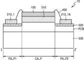
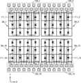
도 2는 본 개시의 예시적 실시예에 따른 광원 모듈의 구성을 나타내는 사시도이다. 도 3은 도 2의 I-I'선을 따라 자른 단면도이다. 도 2의 발광 소자(100)는 도 1의 광원(100)에 대응될 수 있다.2 is a perspective view showing the configuration of a light source module according to an exemplary embodiment of the present disclosure. FIG. 3 is a cross-sectional view taken along line II′ of FIG. 2 . The
도 2를 참조하면, 광원 모듈(10)은 기판(PCB)상에 실장되는 발광 소자(100) 및 복수의 구동 칩들(210_1~210_16)을 포함할 수 있다. 일 실시예에서, 발광 소자(100)는 하나의 칩으로 구현될 수 있고, 광원 모듈(10)은 하나의 칩으로 구성된 발광 소자(100)를 포함할 수 있다.Referring to FIG. 2 , the
발광 소자(100)는 복수의 발광 셀들이 배치되는 LED 어레이를 포함할 수 있다. LED 어레이는 복수의 서브 어레이들(SA1~SA16)로 구분될 수 있다. 도 2에서는 16개의 서브 어레이들(SA1~SA16)이 도시되어 있으나, 본 개시에 따른 광원 모듈(10)은 이에 한정되지 않으며, 서브 어레이의 수는 달라질 수 있으며, 서브 어레이들(SA1~SA16)의 배치도 달라질 수 있다.The
복수의 서브 어레이들(110) 각각은 서로 전기적으로 분리될 수 있다. 즉, 서로 다른 어레이들에 포함된 발광 셀들은 서로 전기적으로 절연될 수 있다.Each of the plurality of
발광 소자(100)는 제1 방향(X)보다 제2 방향(Y)이 짧은 직사각형의 형상을 가질 수 있다. 이 때, 제1 방향(X) 및 제2 방향(Y)은 기판(PCB)의 주면과 평행하고 서로 수직할 수 있다. 일 실시예에서, 발광 소자(100)에서 복수의 서브 어레이들(SA1~SA16)은 2열로 배열될 수 있다. 예를 들어, 제1 내지 제8 서브 어레이(SA1~SA8)는 제1 방향(X)으로 순서대로 배치될 수 있고, 제9 내지 제16 서브 어레이(SA9~SA16)는 제1 방향의 역방향(-X)으로 순서대로 배치될 수 있다. 제16 서브 어레이(SA16) 및 제1 서브 어레이(SA1)는 제2 방향(Y)으로 나란히 배치될 수 있다. 복수의 서브 어레이들(SA1~SA16)은 2열로 배열됨에 따라서, 발광 소자(100)와 복수의 구동 칩들(210_1~210_16)을 연결하기 위한 복수의 패드들을 형성하는 것이 구조적으로 용이할 수 있다. 복수의 패드들의 배치에 대해서는 도 4에서 후술하겠다.The
복수의 구동 칩들(210_1~210_16) 각각은 대응되는 서브 어레이에 포함된 발광 셀들이 동작할 수 있도록 제어할 수 있다. 예를 들어, 제1 구동 칩(210_1)은 제1 서브 어레이(SA1)와 전기적으로 연결될 수 있고, 제1 서브 어레이(SA1)의 동작을 제어할 수 있다. 제2 구동 칩(210_2)은 제2 서브 어레이(SA2)와 전기적으로 연결될 수 있고, 제2 서브 어레이(SA2)의 동작을 제어할 수 있다. 제3 내지 제16 구동 칩들(210_3~210_16)에도 제1 구동 칩(210_1) 및 제2 구동 칩(210_2)에 대한 설명이 동일하게 적용될 수 있다.Each of the plurality of driving chips 210_1 to 210_16 may control the light emitting cells included in the corresponding sub array to operate. For example, the first driving chip 210_1 can be electrically connected to the first sub-array SA1 and can control the operation of the first sub-array SA1. The second driving chip 210_2 can be electrically connected to the second sub-array SA2 and can control the operation of the second sub-array SA2. The description of the first driving chip 210_1 and the second driving chip 210_2 may be equally applied to the third to sixteenth driving chips 210_3 to 210_16.
광원 모듈(10)은 외부로부터 광원 모듈(10)이 동작하기 위해 필요한 신호들이 수신되는 입력부(300)를 더 포함할 수 있다. 복수의 구동 칩들(210_1~210_16)은 입력부(300)로부터 수신된 제어 신호(CS)를 수신할 수 있고, 제어 신호(CS)에 기초하여, 복수의 구동 칩들(210_1~210_16)의 동작이 제어될 수 있다. 예를 들어, 복수의 서브 어레이들(SA1~SA16) 중 중앙부에 배치된 제4, 제5, 제12, 및 제13 서브 어레이(SA4, SA5, SA12, SA13)만 발광하도록 하는 제어 신호(CS)가 입력부(300)로부터 수신되면, 제4, 제5, 제12, 및 제13 구동 칩들(210_4, 210_5, 210_12, 210_13)은 각각 제4, 제5, 제12, 및 제13 서브 어레이(SA4, SA5, SA12, SA13)으로 전압을 인가할 수 있다. 또한, 복수의 구동 칩들(210_1~210_16)은 입력부(300)로부터 구동 전력을 수신할 수 있다.The
복수의 구동 칩들(210_1~210_16) 중 적어도 일부는 대응되는 서브 어레이가 배치되는 순서대로 배치될 수 있다. 예를 들어, 발광 소자(100)에서 제1 내지 제8 서브 어레이(SA1~SA8)는 제1 방향(X)으로 순서대로 배치되고, 제1 내지 제8 서브 어레이(SA1~SA8)에 대응되는 제1 내지 제8 구동 칩(210_1~210_8)도 제1 방향(X)으로 순서대로 배치될 수 있다. 또는, 발광 소자(100)에서 제9 내지 제16 서브 어레이(SA9~SA16)는 제1 방향의 역방향(-X)으로 순서대로 배치되고, 제9 내지 제16 서브 어레이(SA9~SA16)에 대응되는 제9 내지 제16 구동 칩(210_9~210_16)도 제1 방향의 역방향(-X)으로 순서대로 배치될 수 있다. 다만, 복수의 구동 칩들(210_1~210_16)의 배치는 이에 한정되지 않으며, 제1 내지 제8 구동 칩(210_1~210_8) 중 일부만이 제1 방향(X)으로 순서대로 배치될 수도 있다. 따라서, 복수의 구동 칩들(210_1~210_16)이 배치되는 순서와 복수의 서브 어레이들(SA1~SA16)이 배치되는 순서가 서로 대응되도록, 복수의 구동 칩들(210_1~210_16) 및 복수의 서브 어레이들(SA1~SA16)이 배치되므로, 복수의 구동 칩들(210_1~210_16)과 복수의 서브 어레이들(SA1~SA16)을 전기적으로 연결하기 위한 배선의 형성 또는 와이어의 형성이 용이해질 수 있다.At least some of the plurality of driving chips 210_1 to 210_16 may be arranged in the order in which corresponding sub-arrays are arranged. For example, in the
일 실시예에서, 복수의 구동 칩들(210_1~210_16)의 수는 복수의 서브 어레이들(SA1~SA16)의 수와 동일할 수 있다. 다만, 본 개시에 따른 광원 모듈(10)은 이에 한정되지 않으며, 서로 다른 구동 칩들이 하나의 서브 어레이와 연결되어 하나의 서브 어레이를 제어할 수도 있고, 하나의 구동 칩이 서로 다른 서브 어레이들을 제어할 수도 있다.In one embodiment, the number of the plurality of driving chips 210_1 to 210_16 may be the same as the number of the plurality of sub arrays SA1 to SA16. However, the
일 실시예에서, 복수의 구동 칩들(210_1~210_16)은 연이어서 전기적으로 연결될 수 있다. 예를 들어, 제1 구동 칩(210_1)은 제2 구동 칩(210_2)과 전기적으로 연결되고, 제2 구동 칩(210_2)은 제1 구동 칩(210_1) 및 제3 구동 칩(210_3)과 전기적으로 연결되고, 제3 구동 칩(210_3)은 제2 구동 칩(210_2) 및 제4 구동 칩(210_4)과 전기적으로 연결될 수 있다. 제1 구동 칩(210_1)은 입력부(300)로부터 제어 신호(CS)를 수신하여, 제2 구동 칩(210_2)으로 전송할 수 있고, 제2 구동 칩(210_2)은 제1 구동 칩(210_1)로부터 제어 신호(CS)를 수신하여, 제3 구동 칩(210_3)으로 전송할 수 있다. 제3 내지 제16 구동 칩들(210_3~210_16)에도 제1 구동 칩(210_1) 및 제2 구동 칩(210_2)에 대한 설명이 동일하게 적용될 수 있다.In one embodiment, the plurality of driving chips 210_1 to 210_16 may be electrically connected in succession. For example, the first driving chip 210_1 is electrically connected to the second driving chip 210_2, and the second driving chip 210_2 is electrically connected to the first driving chip 210_1 and the third driving chip 210_3. , and the third driving chip 210_3 may be electrically connected to the second driving chip 210_2 and the fourth driving chip 210_4. The first driving chip 210_1 may receive the control signal CS from the
발광 소자(100)는 기판(PCB)의 중심 영역(CA_P)에 실장될 수 있고, 복수의 구동 칩들(210_1~210_16)은 발광 소자(100)를 둘러싸도록 기판(PCB)의 주변 영역(PA_P1, PA_P2)에 배치될 수 있다. 예를 들어, 제1 내지 제8 구동 칩(210_1~210_8)은 제1 주변 영역(PA_P1)에 배치될 수 있고, 제9 내지 제16 구동 칩(210_9~210_16)은 제2 주변 영역(PA_P2)에 배치될 수 있다. 복수의 구동 칩들(210_1~210_16)은 발광 소자(100)를 둘러싸도록 기판(PCB)의 주변 영역(PA_P1, PA_P2)에 배치됨에 따라서, 복수의 구동 칩들(210_1~210_16)과 복수의 서브 어레이들(SA1~SA16)을 전기적으로 연결하기 위한 배선의 형성 또는 와이어의 형성이 용이해질 수 있다.The
일 실시예에서, 제2 주변 영역(PA_P2), 중심 영역(CA_P) 및 제1 주변 영역(PA_P1)은 제2 방향(Y)으로 순서대로 배치될 수 있다. 일 실시예에서, 발광 소자(100) 및 복수의 구동 칩들(210_1~210_16)은, 기판(PCB)의 주면과 평행한 방향(예를 들어, 제1 방향(X) 또는 제2 방향(Y))으로 서로 오버랩되도록 배치될 수 있다.In an embodiment, the second peripheral area PA_P2, the central area CA_P, and the first peripheral area PA_P1 may be sequentially arranged in the second direction Y. In one embodiment, the
본 개시에 따른 광원 모듈(10)은 빛을 방출하는 발광 셀들을 포함하는 하나의 발광 소자(100)가 광원 모듈(10)의 중심 영역(CA_P)에 배치되고, 상기 발광 소자(100)를 구동시키는 복수의 구동 칩들(210_1~210_16)을 별도로 주변 영역(PA_P1, PA_P2)에 배치될 수 있다. 복수의 발광 셀들을 포함하는 발광 소자(100)와 복수의 구동 칩들(210_1~210_16)이 별도의 칩으로 구현됨에 따라, 복수의 구동 칩들(210_1~210_16)을 설계하는 데에 복수의 발광 셀들의 구조에 영향을 받지 않을 수 있어, 복수의 구동 칩들(210_1~210_16)의 설계 효율이 증가될 수 있다.In the
또한, 발광 소자(100)가 하나의 LED 칩으로 구현되고, 광원 모듈(10)의 중심 영역(CA_P)에 배치됨에 따라 광원 모듈(10)이 방출하는 빛이 중심 영역(CA_P)에 집중될 수 있다. 방출되는 빛이 중심 영역(CA_P)에 집중됨으로써, 방출되는 빛을 집광하기 위한 별도의 구성(예를 들어, 렌즈)의 수가 감소될 수 있다. 예를 들어, 본 개시에 따른 광원 모듈(10)은 렌즈를 포함하지 않을 수 있다. 광원 모듈(10)이 포함하는 렌즈의 수가 증가될수록 렌즈로 인해 손실되는 광량이 증가되므로, 본 개시에 따른 광원 모듈(10)은 발광 효율이 증가될 수 있다.In addition, as the
도 2 및 도 3을 참조하면, 발광 소자(100) 및 복수의 구동 칩들(210)은 기판 예를 들어 인쇄회로기판(Printed Circuit Board, PCB) 상에 실장될 수 있다. 일 실시예에서, 기판(PCB)은 금속 및 금속화합물을 소재로 하여 형성될 수 있으며, 예를 들어, 기판(PCB)은 MCPCB(Metal-Core Printed Circuit Board)일 수 있고, 예를 들어, 구리(Cu)를 포함할 수 있다.Referring to FIGS. 2 and 3 , the
일 실시예에서, 기판(PCB)은 자유롭게 휘어지며 다양한 모양으로 변형이 용이한 연성회로기판(FPCB)일 있다. 이 외에도 일반적인 FR4 타입의 인쇄회로기판일 수 있고, 에폭시, 트리아진, 실리콘, 및 폴리이미드 등을 함유하는 수지 소재로 형성되거나, 실리콘 나이트라이드, AlN, Al2O3 등의 세라믹 소재로 형성될 수도 있다.In one embodiment, the board (PCB) may be a flexible printed circuit board (FPCB) that is freely bent and easily deformed into various shapes. In addition, it may be a general FR4 type printed circuit board, and may be formed of a resin material containing epoxy, triazine, silicon, and polyimide, or a ceramic material such as silicon nitride, AlN, and Al2O3.
기판(PCB)의 하부(-Z방향)에는 방열 부재(530)가 배치될 수 있다. 방열 부재(530) 는 히트 싱크의 일종으로 기판(PCB)을 지지하는 한편, 발광 소자(100)에서 발생된 열을 외부로 방출할 수 있다. 방열 부재(530)는 방열 효율의 향상을 위해 열전도율이 우수한 재질로 이루어질 수 있으며, 예를 들어, 금속 재질로 이루어질 수 있으나 이에 한정하는 것은 아니다.A
방열 부재(530)는 다양한 형상을 가질 수 있다. 예를 들어, 기판(PCB)의 하부(-Z방향)으로 돌출되는 돌출부를 복수개 포함하는 형상을 가짐으로써 열 방출 효율을 증가시킬 수 있으나, 본 개시는 이에 한정되지는 않는다.The
기판(PCB)의 일부 영역 상에, 예를 들어, 중심 영역(CA_P)에는 인터포저(510)가 배치될 수 있고, 인터포저(510) 상에 발광 소자(100)가 실장될 수 있다. 인터포저(510)로 인하여, 발광 소자(100)와 복수의 구동 칩들(210_1~210_16)들 전기적으로 연결하기 위한 구성인 복수의 패드들을 복수의 서브 어레이들(SA1~SA16)을 둘러싸는 주변 영역에 형성할 수 있다. 인터포저(510)는 복수의 서브 어레이들(SA1~SA16)에 포함된 상기 복수의 발광 셀들 중 적어도 일부와 상기 복수의 패드들 중 적어도 일부 사이의 전기적 연결을 제공할 수 있다. 패드가 형성되는 주변 영역에 대해서는 도 4에서 후술하겠다.An
일 실시예에서, 기판(PCB)은 MCPCB일 수 있고, 인터포저(510) 및 발광 소자(100)가 실장되는 영역에는 기판(PCB) 상에 절연층이 형성되지 않고, 도금층으로 이루어진 인터포저 접합층이 형성될 수 있다. 인터포저(510) 및 발광 소자(100)는 상기 인터포저 접합층에 유테틱 본딩(Eutectic Bonding) 또는 솔더링(Soldering) 방식으로 실장됨으로써 열저항이 감소되어, 발광 소자(100)에서 발생된 열이 쉽게 외부로 방출될 수 있다.In one embodiment, the substrate (PCB) may be MCPCB, and an interposer junction made of a plating layer is not formed on the substrate (PCB) in a region where the
기판(PCB)의 다른 일부 영역 상에 예를 들어, 주변 영역(PA_P1, PA_P2) 상에는 절연층(520)이 적층되고, 절연층(520) 상에 복수의 구동 칩들(210_1~210_16)이 실장될 수 있다. 일 실시예에서, 복수의 구동 칩들(210_1~210_16)이 실장되는 절연층(520)은 기판(PCB) 상에 1μm 이상 30 μm이하의 두께로 형성될 수 있으나, 본 개시는 이에 한정되지는 않는다.An insulating
발광 소자(100)가 발광하는 발광면(예를 들어, 제3 방향(Z)으로 형성된 면) 상에 발광 소자(100)와 복수의 구동 칩들(210_1~210_16)을 연결하는 패드들이 형성될 수 있다. 상기 패드들과 연결되는 본딩 와이어(400)를 통해 복수의 구동 칩들(210_1~210_16) 각각은 발광 소자(100)에 전기적으로 연결될 수 있다.Pads connecting the
다만, 본 개시에 따른 광원 모듈(10)은 이에 한정되지 않고, 발광 소자(100)에 포함된 발광 셀들의 전극들 중 일부가 발광면의 반대면(예를 들어, 제3 방향의 역방향(-Z)으로 형성된 면)에 형성될 수도 있다. 이에 따라 발광 소자(100)에 포함된 발광 셀들의 전극들과 복수의 구동 칩들(210_1~210_16)을 연결하는 복수의 패드들 중 일부의 패드는, 인터포저(510)의 하부에 형성되어 기판(PCB)과 인터포저(510)를 전기적으로 연결하는 기능을 수행할 수 있다. 이 때, 기판(PCB)과 인터포저(510) 사이에는 절연층이 개재될 수 있고, 상기 절연층이 일부 제거되어 기판(PCB)이 노출된 영역에 상기 일부의 패드가 배치되어, 기판(PCB)과 인터포저(510)를 부착하는 부착 패드로서의 기능을 수행할 수 있다.However, the
도 4는 본 개시의 예시적 실시예에 따른 발광 소자의 구성을 나타내는 사시도이다.4 is a perspective view showing a configuration of a light emitting device according to an exemplary embodiment of the present disclosure.
도 4를 참조하면, 발광 소자(100)은 복수의 발광 셀들이 형성되는 발광 셀 영역(CA_L) 및 복수의 패드들(120)이 형성되는 제1 및 제2 패드 영역(PA_L1, PA_L2)을 포함할 수 있다. 발광 셀 영역(CA_L)은 발광 소자(100)의 중심 영역에 배치되고, 제1 및 제2 패드 영역(PA_L1, PA_L2)은 중심 영역을 둘러싼 외곽 영역에 배치될 수 있다. 예를 들어, 제2 패드 영역(PA_L2), 발광 셀 영역(CA_L) 및 제1 패드 영역(PA_L1)이 제2 방향(Y)으로 순서대로 배치될 수 있다.Referring to FIG. 4 , the
복수의 발광 셀들은 복수의 서브 어레이들(SA1~SA16)로 구분될 수 있다. 도 4에서는 총 16개의 서브 어레이들(SA1~SA16)이 도시되어 있으나, 본 개시에 따른 발광 소자(100)은 이에 한정되지 않으며, 서브 어레이의 수는 달라질 수 있고, 서브 어레이들(SA1~SA16)의 배치도 달라질 수 있다. 이 때, 복수의 서브 어레이들(SA1~SA16)은 각각 서로 전기적으로 분리될 수 있다.A plurality of light emitting cells may be divided into a plurality of sub arrays SA1 to SA16. Although a total of 16 sub-arrays SA1 to SA16 are shown in FIG. 4, the
일 실시예에서, 복수의 서브 어레이들(SA1~SA16)은 제1 방향(X)의 길이(a)가 제2 방향(Y)의 길이(b)보다 길도록 직사각형 형태로 배치될 수 있다. 예를 들어, 복수의 서브 어레이들(SA1~SA16)은 제1 열 및 제2 열의 총 2열로 배열될 수 있다. 제1 내지 제8 서브 어레이(SA1~SA8)는 제1 방향(X)으로 순서대로 제1 열에 배치될 수 있고, 제9 내지 제16 서브 어레이(SA9~SA16)는 제1 방향의 역방향(-X)으로 순서대로 제2 열에 배치될 수 있다. 다만 도 4에서는 제2 방향으로 2개의 서브 어레이가 배치되는 것으로 도시되었으나 이에 한정되지 않으며, 3개 이상의 서브 어레이가 배치될 수도 있다.In one embodiment, the plurality of sub arrays SA1 to SA16 may be arranged in a rectangular shape such that a length a in the first direction X is longer than a length b in the second direction Y. For example, the plurality of sub arrays SA1 to SA16 may be arranged in two columns, a first column and a second column. The first to eighth subarrays SA1 to SA8 may be sequentially arranged in the first column in the first direction (X), and the ninth to sixteenth subarrays SA9 to SA16 may be arranged in a direction opposite to the first direction (- X) may be arranged in the second column in order. However, although it is shown that two sub-arrays are disposed in the second direction in FIG. 4, it is not limited thereto, and three or more sub-arrays may be disposed.
제1 열에 배치되는 제1 내지 제8 서브 어레이(SA1~SA8)는 제1 패드 영역(PA_L1)에 배치된 복수의 패드들(120)을 통해 구동 칩들(예를 들어, 도 2의 210_1~210~8)과 전기적으로 연결될 수 있다. 제2 열에 배치되는 제9 내지 제16 서브 어레이(SA9~SA16)는 제2 패드 영역(PA_L2)에 배치된 복수의 패드들(120)을 통해 구동 칩들(예를 들어, 도 2의 210_9~210~16)과 전기적으로 연결될 수 있다.The first to eighth subarrays SA1 to SA8 disposed in the first column are connected to the driving chips (eg, 210_1 to 210 of FIG. 2 ) through the plurality of pads 120 disposed in the first pad area PA_L1. ~8) can be electrically connected. The ninth to sixteenth sub-arrays SA9 to SA16 disposed in the second column are driven chips (eg, 210_9 to 210 in FIG. 2 ) through the plurality of pads 120 disposed in the second pad area PA_L2 . ~16) and can be electrically connected.
본 개시에 따른 발광 소자(100)은 복수의 발광 셀들을 포함하는 발광 셀 영역(CA_L) 상에 제1 및 제2 패드 영역(PA_L1, PA_L2)이 배치되지 않고, 제2 방향(Y)으로 나란하게 배치될 수 있다. 즉, 복수의 패드들(120)이 배치되는 영역(PA_L1, PA_L2) 및 발광 셀 영역(CA_L)은 기판의 주면에 수직인 제3 방향(Z)으로 오버랩되지 않도록 배치될 수 있다. 발광 소자(100)은 제1 및 제2 패드 영역(PA_L1, PA_L2)을 발광 셀 영역(CA_L)과 별도로 구비함으로써, 발광 셀 영역(CA_L) 내부의 복수의 발광 셀들의 밀도가 높아질 수 있다. 또한, 발광 소자(100)의 외곽 영역에 복수의 패드들(120)이 배치됨으로써, 구동 칩들과 복수의 패드들(120)을 연결하기 위한 구성(예를 들어, 도 3의 본딩 와이어(400))을 형성하는 데에 용이할 수 있다.In the
일 실시예들에서, 평면도에서 발광 셀 영역(CA_L)은 발광 소자(100)의 전체 면적의 약 50 내지 90%에 해당하는 면적을 가질 수 있고, 제1 및 제2 패드 영역(PA_L1, PA_L2)은 발광 소자(100)의 전체 면적의 약 10 내지 50%에 해당하는 면적을 가질 수 있으나, 이에 한정되는 것은 아니다.In one embodiment, in a plan view, the light emitting cell area CA_L may have an area corresponding to about 50 to 90% of the total area of the
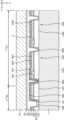
도 5는 도 4의 III-III' 선을 따라 자른 단면도이다. 도 5에서는 발광 소자(100)의 일부 구성요소들만이 도시되었다.5 is a cross-sectional view taken along line III-III' of FIG. 4 . In FIG. 5 , only some components of the
도 5를 참조하면, 발광 소자(100)는 발광 셀 영역(CA_L) 및 제1 패드 영역(PA_L1)을 포함할 수 있다. 발광 셀 영역(CA_L) 상에는 매트릭스 형태로 배열되는 복수의 발광 셀들(PX)이 배치될 수 있다. 복수의 발광 셀들(PX)은 도 4에 도시된 바와 같이, 복수의 서브 어레이들(SA1~SA16)로 구분될 수 있다. 복수의 발광 셀들(PX) 각각은, 예를 들어, 10 ㎛ 내지 수 mm의 제1 방향(X)의 폭 또는 제2 방향(Y)의 폭을 가질 수 있으나, 이에 한정되는 것은 아니다.Referring to FIG. 5 , the
제1 패드 영역(PA_L1) 상에는 복수의 발광 소자 구조물(20U)에 전기적으로 연결되는 제1 패드(48A)가 배치될 수 있다. 도 5에서는 하나의 패드만이 도시되었으나, 발광 소자(100)는 복수의 발광 소자 구조물(20U)과 연결되는 다른 패드들도 더 포함할 수 있다.A
발광 셀 영역(CA_L)에서 각각의 발광 셀들(PX) 내에 복수의 발광 소자 구조물(20U)이 배치될 수 있다. 또한 격벽 구조물(60)은 복수의 발광 소자 구조물(20U) 상에 배치되며, 평면도에서 격벽 구조물(60)이 복수의 발광 소자 구조물(20U) 각각을 둘러싸도록 배치될 수 있다. 제1 패드 영역(PA_L1)에서, 발광 적층체(20)가 격벽 구조물(60)의 외부에 배치되며 복수의 발광 소자 구조물(20U)을 둘러쌀 수 있다.A plurality of light emitting
격벽 구조물(60)은 발광 셀 영역(CA_L) 내부에서 인접한 발광 셀(PX) 사이에 배치되는 제1 격벽층(62)과 발광 셀 영역(CA_L)의 외주(periphery)에 형성되는 제2 격벽층(64)을 포함할 수 있고, 평면도에서 제2 격벽층(64)이 제1 격벽층(62)을 둘러싸도록 배치될 수 있다. 제1 격벽층(62)의 수평 방향(예를 들어, 제2 방향(Y))의 폭은, 제2 격벽층(64)의 수평 방향(Y)의 폭보다 더 작을 수 있다. 예를 들어, 제1 격벽층(62)은 10 ㎛ 내지 100 ㎛ 범위의 폭을 가질 수 있고, 제2 격벽층(64)은 10 ㎛ 내지 1 mm 범위의 폭을 가질 수 있다. 이에 따라 발광 소자(100)의 구조적 안정성이 향상될 수 있다. 예를 들어 발광 소자(100)가 차량용 헤드 램프로 사용되는 경우에 반복적인 진동 및 충격이 가해지더라도, 격벽 구조물(60) 내부에 배치되는 형광층(74)과 격벽 구조물(60) 사이의 우수한 구조적 안정성에 의해 발광 소자(100)의 신뢰성이 향상될 수 있다.The barrier structure 60 includes a
발광 적층체(20)는 제1 도전형 반도체층(22), 활성층(24), 및 제2 도전형 반도체층(26)을 포함할 수 있다. 발광 셀 영역(CA_L)에서 복수의 발광 소자 구조물(20U)은 소자 분리 개구부(IAH)에 의해 서로 분리되어 배치될 수 있다. 예시적인 공정에서, 발광 적층체(20)의 일부분을 제거하여 소자 분리 개구부(IAH)를 형성함에 의해 발광 셀 영역(CA_L) 상에 복수의 발광 소자 구조물(20U)이 형성되고, 평면도에서 복수의 발광 소자 구조물(20U)을 둘러싸는 발광 적층체(20)의 일부분이 제1 패드 영역(PA_L1)에 잔류할 수 있다.The
복수의 발광 소자 구조물(20U)은 제1 도전형 반도체층(22), 활성층(24), 및 제2 도전형 반도체층(26)을 포함할 수 있고, 복수의 발광 소자 구조물(20U) 상에 제1 절연층(32), 제1 전극(42A), 제2 전극(42B), 제1 연결 전극(44A), 및 제2 연결 전극(44B)이 더 배치될 수 있다.The plurality of light emitting
제1 도전형 반도체층(22)은 n형 InxAlyGa(1-x-y)N (0≤x<1, 0≤y<1, 0≤x+y<1)의 조성을 갖는 질화물 반도체일 수 있으며, 예를 들어 n형 불순물은 실리콘(Si)일 수 있다. 예를 들어, 제1 도전형 반도체층(22)은 n형 불순물이 포함된 GaN을 포함할 수 있다.The first conductivity-
일 실시예에서, 제1 도전형 반도체층(22)은 제1 도전형 반도체 콘택층과 전류 확산층을 포함할 수 있다. 상기 제1 도전형 반도체 콘택층의 불순물 농도는 2×10¹⁸ ㎝-3 내지 9×10¹⁹ ㎝-3 범위일 수 있다. 상기 제1 도전형 반도체 콘택층의 두께는 1 ㎛ 내지 5 ㎛일 수 있다. 상기 전류 확산층은 서로 다른 조성을 갖거나, 서로 다른 불순물 함량을 갖는 복수의 InxAlyGa(1-x-y)N (0≤x, y≤1, 0≤x+y≤1)층이 교대로 적층되는 구조일 수 있다. 예를 들어, 상기 전류 확산층은 각각이 1 nm 내지 500 nm의 두께를 갖는 n형 GaN층 및/또는 AlxInyGazN 층(0≤x,y,z≤1, x+y+z≠0)이 교대로 적층되는 n형 초격자 구조를 가질 수 있다. 상기 전류 확산층의 불순물 농도는 2 ×10¹⁸ ㎝-3 내지 9×10¹⁹ ㎝-3 일 수 있다.In one embodiment, the first conductivity
활성층(24)은 제1 도전형 반도체층(22) 및 제2 도전형 반도체층(26) 사이에 배치되고, 전자와 정공의 재결합에 의해 소정의 에너지를 갖는 광을 배출할 수 있다. 활성층(24)은 양자 우물층과 양자 장벽층이 서로 교대로 적층된 다중 양자 우물(MQW) 구조일 수 있다. 예를 들어, 상기 양자 우물층과 양자 장벽층은 서로 다른 조성을 갖는 InxAlyGa(1-x-y)N (0≤x, y≤1, 0≤x+y≤1)을 포함할 수 있다. 예를 들어, 상기 양자 우물층은 InxGa1-xN (0≤x≤1)을 포함하고, 상기 양자 장벽층은 GaN 또는 AlGaN일 수 있다. 양자 우물층과 양자 장벽층의 두께는 각각 1 nm ~ 50 nm 범위일 수 있다. 활성층(24)은 다중 양자 우물 구조에 한정되지 않고, 단일 양자 우물 구조일 수 있다.The
제2 도전형 반도체층(26)은 p형 InxAlyGa(1-x-y)N (0≤x<1, 0≤y<1, 0≤x+y<1)의 조성을 갖는 질화물 반도체층일 수 있으며, 예를 들어 p형 불순물은 마그네슘(Mg)일 수 있다.The second conductivity-
일 실시예에서, 제2 도전형 반도체층(26)은 전자 차단층, 저농도 p형 GaN층과 콘택층으로 제공되는 고농도 p형 GaN층을 포함할 수 있다. 예를 들어, 상기 전자 차단층은 각각이 5 nm 내지 100 nm의 두께를 갖는 서로 다른 조성을 갖거나, 서로 다른 불순물 함량을 갖는 복수의 InxAlyGa(1-x-y)N (0≤x, y≤1, 0≤x+y≤1)층이 교대로 적층되는 구조이거나, AlyGa(1-y)N (0<y≤1)으로 구성된 단일층일 수 있다. 상기 전자 차단층의 에너지 밴드갭은 활성층(24)으로부터 멀어질수록 감소할 수 있다. 예를 들어, 상기 전자 차단층의 Al 조성은 활성층(24)으로부터 멀어질수록 감소할 수 있다.In one embodiment, the second conductivity-
제1 도전형 반도체층(22), 활성층(24) 및 제2 도전형 반도체층(26)은 수직 방향으로 순차적으로 적층될 수 있고, 여기서 제1 도전형 반도체층(22)의 상면을 복수의 발광 소자 구조물(20U)의 제1 면(20F1)으로 지칭하고, 제2 도전형 반도체층(26)의 바닥면을 복수의 발광 소자 구조물(20U)의 제2 면(20F2)으로 지칭한다.The first conductivity-
제1 전극(42A)은 활성층(24) 및 제2 도전형 반도체층(26)을 관통하는 개구부(E) 내에서 제1 도전형 반도체층(22)과 연결되도록 배치될 수 있다. 제2 전극(42B)은 제2 도전형 반도체층(26)의 바닥면(즉, 제2 면(20F2)) 상에 배치될 수 있다. 제1 절연층(32)은 개구부(E) 내벽 상에 배치되어 제1 전극(42A)을 활성층(24) 및 제2 도전형 반도체층(26)으로부터 전기적으로 절연시킬 수 있다. 제1 절연층(32)은 제2 도전형 반도체층(26)의 바닥면 상에서 제1 전극(42A)과 제2 전극(42B) 사이에 배치될 수 있고, 제1 전극(42A)을 제2 전극(42B)으로부터 전기적으로 절연시킬 수 있다. 제1 전극(42A) 및 제2 전극(42B)은 Ag, Al, Ni, Cr, Au, Pt, Pd, Sn, W, Rh, Ir, Ru, Mg, Zn, 및 이들의 조합을 포함할 수 있다. 제1 전극(42A) 및 제2 전극(42B)은 반사도가 높은 금속 물질을 포함할 수 있다.The
제1 전극(42A) 및 제1 절연층(32) 상에는 제1 연결 전극(44A)이 배치될 수 있고, 제2 전극(42B) 및 제1 절연층(32) 상에는 제2 연결 전극(44B)이 배치될 수 있다. 제1 연결 전극(44A)과 제2 연결 전극(44B)은 각각 제1 전극(42A)과 제2 전극(42B)에 전기적으로 연결될 수 있다. 제1 연결 전극(44A)과 제2 연결 전극(44B)은 Ag, Al, Ni, Cr, Au, Pt, Pd, Sn, W, Rh, Ir, Ru, Mg, Zn, 및 이들의 조합을 포함할 수 있다.A
복수의 발광 소자 구조물(20U) 각각은 이에 인접한 발광 소자 구조물로부터 소자 분리 개구부(IAH)를 사이에 두고 이격되어 배치될 수 있다. 예를 들어 소자 분리 개구부(IAH)는 복수의 발광 소자 구조물(20U)의 제1 면(20F1)에 대하여 약 60 내지 90도의 경사각으로 기울어진 측벽을 포함할 수 있다.Each of the plurality of light emitting
절연 라이너(34)는 소자 분리 개구부(IAH)의 내벽 상에, 및 복수의 발광 소자 구조물(20U) 각각의 측면 및 제2 면(20F2) 상에서 제1 연결 전극(44A) 및 제2 연결 전극(44B)을 커버하도록 콘포말하게 배치될 수 있다. 절연 라이너(34)의 상면은 복수의 발광 소자 구조물(20U)의 제1 면(20F1)과 동일 레벨 상에 위치할 수 있다. 예시적인 실시예들에서, 절연 라이너(34)는 실리콘 산화물 또는 실리콘 질화물을 포함할 수 있다.The insulating
제1 패드 영역(PA_L1) 상에는 발광 적층체(20)를 관통하는 패드 개구부(PH)가 배치될 수 있고, 패드 개구부(PH) 내에 제1 패드(48A) 및 제2 패드(148B)가 배치될 수 있다. 제1 패드(48A)는 제1 배선 패턴(46A)을 통해 제1 연결 전극(44A)에 전기적으로 연결될 수 있다. 제2 연결 전극(44B)은 다른 배선 패턴을 통해 다른 패드와 연결될 수 있다.A pad opening PH penetrating the
일부의 발광 셀(PX) 내의 제1 배선 패턴(46A)은 소자 분리 개구부(IAH)를 통과하여 인접한 발광 셀(PX)(즉, 최외곽에 배치되는 발광 셀(PX))까지 연장될 수 있고, 제1 패드 영역(PA_L1) 상의 제1 패드(48A)에 연결될 수 있다. 이에 따라 소자 분리 개구부(IAH) 내에서 절연 라이너(34) 상에 제1 배선 패턴(46A)이 콘포말하게 배치될 수 있다The
절연 라이너(34), 제1 배선 패턴(46A) 상에는 매립 절연층(36)이 배치될 수 있다. 매립 절연층(36)은 소자 분리 개구부(IAH) 내부에서 절연 라이너(34), 제1 배선 패턴(46A)과 접촉하며 소자 분리 개구부(IAH)의 잔류 공간을 채울 수 있다. 매립 절연층(36)은 실리콘 수지, 에폭시 수지, 또는 아크릴 수지를 이용하여 형성될 수 있다.A filling insulating
매립 절연층(36) 상에는 접착층(52)을 사이에 두고 지지 기판(54)이 배치될 수 있다. 일 실시예에서, 접착층(52)은 전기 절연성 물질, 예를 들어 실리콘 산화물, 실리콘 질화물, UV 경화성 물질과 같은 폴리머 물질, 또는 수지류를 포함할 수 있다. 일부 실시예들에서, 접착층(52)과 매립 절연층(36)은 동일한 물질로 형성될 수 있고, 접착층(52)과 매립 절연층(36) 사이의 경계가 육안으로 식별가능하지 않을 수 있다. 일 실시예에서, 접착층(52)은 AuSn 또는 NiSi 등의 공융(eutectic) 접착 물질을 포함할 수 있다. 지지 기판(54)은 사파이어 기판, 유리 기판, 투명 전도성 기판, 실리콘 기판, 실리콘 카바이드 기판 등을 포함할 수 있으나, 이에 한정되지 않는다.A
전술한 바와 같이, 복수의 발광 소자 구조물(20U)의 제1 면(20F1) 상에는 격벽 구조물(60)이 배치될 수 있다. 격벽 구조물(60)은 실리콘(Si), 실리콘 카바이드(SiC), 사파이어(sapphire), 갈륨 질화물(GaN)을 포함할 수 있다.As described above, the barrier rib structure 60 may be disposed on the first surface 20F1 of the plurality of light emitting
격벽 구조물(60)은 평면도에서 매트릭스 형태로 배열될 수 있고, 격벽 구조물(60)에 의해 복수의 픽셀 공간(PXU)이 정의될 수 있다. 격벽 구조물(60)은 소자 분리 개구부(IAH)와 수직 오버랩되도록 배치될 수 있고, 격벽 구조물(60)의 바닥면은 절연 라이너(34)의 상면과 접촉할 수 있다. 이에 따라 복수의 픽셀 공간(PXU)의 바닥부에 복수의 발광 소자 구조물(20U)의 제1 면(20F1)이 노출될 수 있다.The barrier rib structure 60 may be arranged in a matrix form in a plan view, and a plurality of pixel spaces PXU may be defined by the barrier rib structure 60 . The barrier rib structure 60 may be disposed to vertically overlap the device isolation opening IAH, and a bottom surface of the barrier rib structure 60 may contact an upper surface of the insulating
격벽 구조물(60)의 측벽 상에는 반사층(72)이 배치될 수 있다. 반사층(72)은 복수의 발광 소자 구조물(20U)에서 방출되는 광을 반사시키는 역할을 수행할 수 있다. 제1 격벽층(62)의 측벽 상에는 반사층(72)이 형성되어 복수의 픽셀 공간(PXU)의 측벽이 반사층(72)으로 커버될 수 있다. 한편, 제2 격벽층(64)의 제1 패드 영역(PA_L1)을 대면하는 측벽 상에는 반사층(72)이 형성되지 않을 수 있다.A
예시적인 실시예들에서, 반사층(72)은 Ag, Al, Ni, Cr, Au, Pt, Pd, Sn, W, Rh, Ir, Ru, Mg, Zn, 및 이들의 조합을 포함하는 금속층일 수 있다. 다른 실시예들에서, 반사층(72)은 티타늄 산화물 또는 알루미늄 산화물 등의 금속 산화물이 함유된 PPA(polyphthalamide)와 같은 수지층일 수 있다. 다른 실시예들에서, 반사층(72)은 분산 브래그 반사층(distributed Bragg reflector layer)일 수 있다. 예를 들어, 상기 분산 브래그 반사층은 굴절율이 다른 복수의 절연막이 수 내지 수백 회 반복하여 적층된 구조를 가질 수 있다. 상기 분산 브래그 반사층 내에 포함되는 상기 절연막은 각각 SiO2, SiN, SiOxNy, TiO2, Si3N4, Al2O3, TiN, AlN, ZrO2, TiAlN, TiSiN 등의 산화물 또는 질화물 및 그 조합을 포함할 수 있다.In example embodiments, the
복수의 발광 소자 구조물(20U)의 제1 면(20F1) 상에서 복수의 픽셀 공간(PXU) 내부에는 형광층(74)이 배치될 수 있다. 도 5에 예시적으로 도시된 바와 같이, 형광층(74)은 복수의 픽셀 공간(PXU)의 실질적으로 전체 공간을 채우며, 형광층(74)의 상면 레벨은 격벽 구조물(60)의 상면 레벨(LV2)과 동일할 수 있다. 형광층(74)은 실질적으로 평탄한 상면을 가질 수 있다.A
형광층(74)은 복수의 발광 소자 구조물(20U)로부터 방출되는 빛을 원하는 색으로 변환시킬 수 있는 단일한 종류의 물질일 수 있고, 즉 복수의 픽셀 공간(PXU) 내부에 동일한 색상과 관련된 형광층(74)이 배치될 수 있다. 그러나 본 발명의 기술적 사상이 이에 한정되는 것은 아니다. 복수의 픽셀 공간(PXU) 중 일부의 픽셀 공간(PXU) 내에 배치되는 형광층(74)의 색상이 나머지 픽셀 공간(PXU) 내에 배치되는 형광층(74)의 색상과 다를 수도 있다.The
형광층(74)은 형광체가 분산된 수지 또는 형광체를 함유하는 필름을 포함할 수 있다. 예를 들어, 형광층(74)은 형광체 입자들이 소정의 농도로 균일하게 분산된 형광체 필름을 포함할 수 있다. 상기 형광체 입자들은 복수의 발광 소자 구조물(20U)로부터 방출되는 광의 파장을 변환시키는 파장 변환 물질일 수 있다. 형광체 입자의 밀도 향상 및 색 균일도 개선을 위하여 형광층(74)은 서로 다른 사이즈 분포를 갖는 2종 이상의 형광체 입자들을 포함할 수 있다.The
일 실시예에 있어서, 형광체는 산화물계, 실리케이트계, 질화물계, 플루오라이트계 등 다양한 조성 및 컬러를 가질 수 있다. 예를 들어, 상기 형광체로서 β-SiAlON:Eu2+(녹색), (Ca,Sr)AlSiN3:Eu2+(적색), La3Si6N11:Ce3+(황색), K2SiF6:Mn4+(적색), SrLiAl3N4:Eu(적색), Ln4-x(EuzM1-z)xSi12-yAlyO3+x+yN18-x-y (0.5≤x≤3, 0<z<0.3, 0<y≤4)(적색), K2TiF6:Mn4+(적색), NaYF4:Mn4+(적색), NaGdF4:Mn4+(적색) 등이 사용될 수 있다. 그러나, 상기 형광체의 종류가 전술한 바에 한정되는 것은 아니다.In one embodiment, the phosphor may have various compositions and colors such as oxide-based, silicate-based, nitride-based, and fluorite-based. For example, as the phosphor, β-SiAlON:Eu2+ (green), (Ca,Sr)AlSiN3:Eu2+ (red), La3Si6N11:Ce3+ (yellow), K2SiF6:Mn4+ (red), SrLiAl3N4:Eu (red), Ln4 -x(EuzM1-z)xSi12-yAlyO3+x+yN18-x-y (0.5≤x≤3, 0<z<0.3, 0<y≤4) (red), K2TiF6:Mn4+ (red), NaYF4:Mn4+( red), NaGdF4:Mn4+ (red), etc. may be used. However, the type of the phosphor is not limited to the above.
일 실시예에 있어서, 형광층(74) 상부에 양자점(quantum dot)과 같은 파장 변환 물질이 더 배치될 수 있다. 상기 양자점은 III-V 또는 II-VI 화합물 반도체를 이용하여 코어(Core)-쉘(Shell) 구조를 가질 수 있고, 예를 들어, CdSe, InP 등과 같은 코어(core)와 ZnS, ZnSe과 같은 쉘(shell)을 가질 수 있다. 또한, 상기 양자점은 코어 및 쉘의 안정화를 위한 리간드(ligand)를 포함할 수 있다.In one embodiment, a wavelength conversion material such as a quantum dot may be further disposed on the
도 5에 도시된 것과는 달리, 격벽 구조물(60)의 측벽 상에 반사층(72)이 형성되지 않을 수도 있다. 이러한 경우에, 제1 격벽층(62)의 측벽 및 제2 격벽층(64)의 측벽이 형광층(74)과 직접 접촉할 수 있다.Unlike that shown in FIG. 5 , the
제1 패드 영역(PA_L1)에서 제1 패드(48A)의 상면 레벨(LV1)은 복수의 발광 소자 구조물(20U)의 제1 면(20F1)의 레벨과 실질적으로 동일할 수 있다. 제1 패드 영역(PA_L1)에서 제1 패드(48A) 상에 구동 칩(예를 들어, 도 2의 제1 구동 칩(210_1))과의 전기적 연결을 위한 본딩 와이어(400) 등의 연결 부재가 배치될 수 있다. 한편, 제1 패드 영역(PA_L1)과 발광 셀 영역(CA_L)의 경계에서 격벽 구조물(60)의 상면 레벨(LV2)은 제1 및 제2 패드(48A, 148B)의 상면 레벨(LV1)보다 더 높을 수 있다.In the first pad region PA_L1, the level LV1 of the top surface of the
일반적으로, 차량용 헤드 램프 등의 지능형 조명 시스템을 위하여 복수의 발광 소자 칩을 포함하는 광원 모듈을 사용하며, 각각의 발광 소자 칩을 개별적으로 제어하여 주변 상황에 따라 다양한 조명 모드를 구현할 수 있다. 매트릭스 형태로 배열된 복수의 발광 소자를 사용하는 경우, 복수의 발광 소자 각각으로부터 방출되는 빛이 인접한 발광 소자에 혼입되거나 침투되는 현상이 발생할 수 있다. 따라서 광원 모듈의 콘트라스트 특성이 우수하지 못할 수 있다.In general, a light source module including a plurality of light emitting device chips is used for an intelligent lighting system such as a headlamp for a vehicle, and various lighting modes can be implemented according to surrounding conditions by individually controlling each light emitting device chip. In the case of using a plurality of light emitting elements arranged in a matrix form, a phenomenon in which light emitted from each of the plurality of light emitting elements is mixed with or penetrates adjacent light emitting elements may occur. Therefore, the contrast characteristics of the light source module may not be excellent.
그러나, 본 개시에 따른 일 실시예에 따르면, 격벽 구조물(60)은 하나의 발광 셀(PX)에서 방출되는 빛이 인접한 발광 셀(PX)로 혼입되거나 침투되는 것을 방지할 수 있고, 이에 따라 발광 소자(100)의 콘트라스트 특성이 우수할 수 있다. 또한 복수의 발광 소자 구조물(20U)은 소자 분리 개구부(IAH)에 의해 서로 완전히 분리됨에 따라, 복수의 발광 소자 구조물(20U)에서 방출되는 빛이 인접한 발광 소자 구조(20U)로 혼입되거나 침투되는 것이 방지될 수 있고 발광 소자(100)의 콘트라스트 특성이 우수할 수 있다.However, according to one embodiment according to the present disclosure, the barrier rib structure 60 can prevent light emitted from one light emitting cell PX from being mixed or penetrated into an adjacent light emitting cell PX, and thus light emitted. The contrast characteristics of the
도 6a는 본 개시에 따른 예시적 실시예의 발광 소자를 나타내는 단면도이고, 도 6b는 도 6a의 CX3 부분의 확대 단면도이다.6A is a cross-sectional view illustrating a light emitting device of an exemplary embodiment according to the present disclosure, and FIG. 6B is an enlarged cross-sectional view of a portion CX3 of FIG. 6A.
도 6a 및 도 6b를 참조하면, 격벽 구조물(60A)은 경사 측벽을 갖는 제1 격벽층(62A)과 경사 측벽을 갖는 제2 격벽층(64A)을 포함할 수 있다. 제1 격벽층(62A)의 수평 방향(예를 들어, 제2 방향(Y))의 폭, 및 제2 격벽층(62B)의 수평 방향(Y)의 폭은, 제3 방향(Z)으로부터 멀어지는 방향으로 점진적으로 감소할 수 있다. 복수의 픽셀 공간(PXU) 각각의 수평 방향의 폭은 발광 소자 구조물(20U)의 제1 면(20F1)으로부터 멀어지는 방향으로 점진적으로 증가할 수 있고, 이에 따라 발광 소자 구조물(20U)로부터의 광 추출 효율이 향상될 수 있다.Referring to FIGS. 6A and 6B , the
도 6b에 예시적으로 도시된 바와 같이, 복수의 발광 소자 구조물(20U)의 제1 면(20F1)에는 요철 구조(20SP)가 형성되어 발광 소자 구조물(20U)로부터의 광 추출 효율이 향상될 수 있다.As exemplarily shown in FIG. 6B , a concavo-convex structure 20SP is formed on the first surface 20F1 of the plurality of light emitting
일 실시예에서, 제2 도전형 반도체층(26) 상에 제2 전극(42B1)이 배치될 수 있고, 제2 도전형 반도체층(26)과 제2 전극(42B1) 사이에 제2 콘택층(42B2)이 더 형성될 수 있다. 또한 절연 라이너(34A)는 소자 분리 개구부(IAH)의 내벽 및 복수의 발광 소자 구조물(20U)의 제2 면(20F2) 상에 콘포말하게 형성되며, 제1 전극(42A) 및 제2 전극(42B1)을 둘러쌀 수 있다. 도 6a 및 6b에서 절연 라이너(34A)는 단일층으로 도시되었으나, 이와는 달리 절연 라이너(34A)는 복수의 절연층들로 구성되는 다층 구조를 가질 수도 있다. 제1 연결 전극(44A1) 및 제2 연결 전극(44B1)은 절연 라이너(34A) 상에 배치되며 제1 전극(42A) 및 제2 전극(42B1)과 각각 전기적으로 연결될 수 있다.In one embodiment, the second electrode 42B1 may be disposed on the second conductivity
제1 패드들(48A1, 48B1)은 패드 개구부(PH) 내벽 상에 콘포말하게 배치될 수 있고, 제1 패드들(48A1, 48B1)와 발광 적층체(20)와의 사이에 절연 라이너(34A)가 배치될 수 있다. 제1 패드들(48A1, 48B1)은 각각 제1 배선 패턴(46A1) 및 제2 배선 패턴(46B1)을 통해 제1 연결 전극(44A1) 및 제2 연결 전극(44B1)에 전기적으로 연결될 수 있다.The first pads 48A1 and 48B1 may be conformally disposed on the inner wall of the pad opening PH, and an insulating
제1 연결 전극(44A1), 제2 연결 전극(44B1), 및 제1 배선 패턴(46A1) 상에는 중간 절연층(56)이 배치될 수 있고, 제2 배선 패턴(46B1)은 중간 절연층(56) 상에 배치되며 중간 절연층(56)을 관통하여 제1 패드들 중 하나의 패드(48B1)와 연결될 수 있다. 제1 배선 패턴(46A1)과 제2 배선 패턴(46B1) 사이에 중간 절연층(56)이 배치됨에 따라, 제1 배선 패턴(46A1)과 제2 배선 패턴(46B1)이 수직 방향(Z)을 따라 이격되도록 배치될 수 있다. 그러나 제1 및 제2 배선 패턴(46A1, 46B1)의 배치가 이에 한정되는 것은 아니다.An intermediate insulating
제1 패드 영역(PA_L1)에서 제1 패드들(48A1, 48B1) 상에는 구동 칩(예를 들어, 도 2의 제1 구동 칩(210_1))과의 전기적 연결을 위한 본딩 와이어(400_1, 400_2) 등의 연결 부재가 각각 배치될 수 있다.Bonding wires 400_1 and 400_2 for electrical connection to the driving chip (eg, the first driving chip 210_1 of FIG. 2 ) are formed on the first pads 48A1 and 48B1 in the first pad area PA_L1 . Connecting members of may be disposed respectively.
전술한 발광 소자에 따르면, 격벽 구조물(60A)은 하나의 픽셀(PX)에서 방출되는 빛이 인접한 픽셀(PX)로 혼입되거나 침투되는 것을 방지할 수 있고, 이에 따라 발광 소자의 콘트라스트 특성이 우수할 수 있다. 또한 격벽 구조물(60A)이 경사 측벽을 가짐에 따라 발광 소자 구조물(20U)로부터의 광 추출 효율이 향상될 수 있다.According to the light emitting device described above, the
도 7은 본 개시의 예시적 실시예에 따른 발광 소자에 포함된 서브 어레이들 및 패드들의 연결 관계를 설명하기 위한 회로도이다. 도 7은 도 4의 제1, 제2, 제15 및 제16 서브 어레이(SA1, SA2, SA15, SA16) 및 상기 서브 어레이들과 연결되는 복수의 패드들을 도시한 등가 회로도이다. 도 7에서는 하나의 발광 셀이 하나의 다이오드에 대응될 수 있다.7 is a circuit diagram illustrating a connection relationship between sub arrays and pads included in a light emitting device according to an exemplary embodiment of the present disclosure. FIG. 7 is an equivalent circuit diagram illustrating the first, second, fifteenth, and sixteenth subarrays SA1, SA2, SA15, and SA16 of FIG. 4 and a plurality of pads connected to the subarrays. In FIG. 7 , one light emitting cell may correspond to one diode.
도 4 및 도 7을 참조하면, 제1, 제2, 제15 및 제16 서브 어레이(SA1, SA2, SA15, SA16)는 각각 LED로 구현된 복수의 발광 셀들을 포함할 수 있다. 도 7에서는 제1, 제2, 제15 및 제16 서브 어레이(SA1, SA2, SA15, SA16)가 각각 12개씩의 발광 셀들을 포함하는 것으로 도시되어 있으나, 본 개시의 발광 소자는 이에 한정되지 않으며, 하나의 서브 어레이에 포함된 발광 셀의 수는 달라질 수 있다. 도 7에서는 제1, 제2, 제15 및 제16 서브 어레이(SA1, SA2, SA15, SA16)만이 도시되어 있으나, 도 4에 도시된 다른 서브 어레이에도 동일한 설명이 적용될 수 있다.Referring to FIGS. 4 and 7 , each of the first, second, fifteenth, and sixteenth subarrays SA1 , SA2 , SA15 , and SA16 may include a plurality of light emitting cells implemented as LEDs. In FIG. 7 , the first, second, fifteenth, and sixteenth subarrays SA1 , SA2 , SA15 , and SA16 are illustrated as including 12 light emitting cells, but the light emitting device of the present disclosure is not limited thereto. , the number of light-emitting cells included in one sub-array may vary. Although only the first, second, fifteenth, and sixteenth subarrays SA1 , SA2 , SA15 , and SA16 are shown in FIG. 7 , the same description may be applied to other subarrays shown in FIG. 4 .
제1, 제2, 제15 및 제16 서브 어레이(SA1, SA2, SA15, SA16)를 포함한 복수의 서브 어레이들(SA1~SA16)은 서로 전기적으로 절연될 수 있고, 복수의 서브 어레이들(SA1~SA16) 각각은 서로 다른 구동 칩에 의해 동작이 제어될 수 있다. 본 개시에 따른 발광 소자(100)는, LED 어레이를 구성하는 복수의 발광 셀들을 복수의 서브 어레이들(SA1~SA16)로 세분화하고, 각각 서로 다른 구동 칩에 의해 동작이 제어되도록 함으로써, 발광 소자의 동작의 제어가 용이할 수 있다. 예를 들어, 발광 소자의 밝기 조절이 세분화될 수 있고, 밝기 조절 속도가 증가될 수 있다.The plurality of subarrays SA1 to SA16 including the first, second, fifteenth, and sixteenth subarrays SA1, SA2, SA15, and SA16 may be electrically insulated from each other, and the plurality of subarrays SA1 ~SA16) Each operation can be controlled by different driving chips. The
각각의 서브 어레이에 포함된 발광 셀들, 예를 들어, 제1 서브 어레이(SA1)에 포함된 복수의 제1 발광 셀들(111_1)은 음극(cathode) 또는 양극(anode) 중 하나가 서로 전기적으로 연결될 수 있다. 하나의 서브 어레이에 포함된 복수의 발광 셀들은 각각을 온(on) 또는 오프(off) 상태로 구동시키는 구동 칩과 연결될 수 있고, 상기 구동 칩은 펄스 폭 변조(Pulse Width Modulation, PWM) 방식을 통해 복수의 발광 셀들 각각의 밝기를 조절할 수 있다. 예를 들어, 복수의 제1 발광 셀들(111_1)은 제1 발광 칩과 연결될 수 있고, 제1 발광 칩은 펄스 폭 변조를 통해 복수의 제1 발광 셀들(111_1) 각각의 밝기를 조절할 수 있다.제1 서브 어레이(SA1)에 포함되는 복수의 제1 발광 셀들(111_1)은 서로 직렬로 연결될 수 있고, 복수의 제1 발광 셀들(111_1)의 양 끝단은 각각 서로 다른 패드들과 연결될 수 있다. 복수의 제1 발광 셀들(111_1)이 서로 직렬로 연결되므로 복수의 제1 발광 셀들(111_1)이 서로 연결되는 노드들에 인가되는 전압을 제어하면, 복수의 제1 발광 셀들(111_1)의 동작을 제어할 수 있다. 따라서, 복수의 제1 발광 셀들(111_1)과 연결되는 복수의 제1 패드들(120_1)의 수는 복수의 제1 발광 셀들(111_1)의 수의 2배보다 적을 수 있다. 제1 구동 칩(예를 들어, 도 2의 210_1)은 복수의 제1 패드들(120_1)과 전기적으로 연결될 수 있다. 제1 구동 칩은 복수의 제1 패드들(120_1)중에서 서로 다른 2개의 패드에 인가되는 전압을 조절함으로써, 상기 2개의 패드들 각각이 음극 및 양극에 연결되는 하나의 발광 셀을 구동시킬 수 있다. 즉, 제1 구동 칩은 복수의 제1 패드들(120_1)에 전압을 인가하여 복수의 제1 발광 셀들(111_1) 중 적어도 하나를 구동시킴으로써, 복수의 제1 발광 셀들(111_1)에서 방출되는 빛의 밝기를 조절할 수 있다.The light-emitting cells included in each sub-array, for example, the plurality of first light-emitting cells 111_1 included in the first sub-array SA1 may have either a cathode or an anode electrically connected to each other. can A plurality of light emitting cells included in one subarray may be connected to a driving chip that drives each of them in an on or off state, and the driving chip uses a Pulse Width Modulation (PWM) method. Through this, the brightness of each of the plurality of light emitting cells can be adjusted. For example, the plurality of first light emitting cells 111_1 may be connected to a first light emitting chip, and the first light emitting chip may adjust the brightness of each of the plurality of first light emitting cells 111_1 through pulse width modulation. The plurality of first light-emitting cells 111_1 included in the first sub-array SA1 may be connected in series to each other, and both ends of the plurality of first light-emitting cells 111_1 may be connected to different pads, respectively. Since the plurality of first light emitting cells 111_1 are connected in series to each other, controlling the voltage applied to the nodes to which the plurality of first light emitting cells 111_1 are connected allows the operation of the plurality of first light emitting cells 111_1 to be controlled. You can control it. Accordingly, the number of the plurality of first pads 120_1 connected to the plurality of first light emitting cells 111_1 may be less than twice the number of the plurality of first light emitting cells 111_1. The first driving chip (eg, 210_1 in FIG. 2 ) may be electrically connected to the plurality of first pads 120_1 . The first driving chip can drive one light emitting cell in which the two pads are connected to the cathode and anode, respectively, by adjusting the voltage applied to two different pads among the plurality of first pads 120_1. . That is, the first driving chip drives at least one of the plurality of first light emitting cells 111_1 by applying a voltage to the plurality of first pads 120_1, thereby emitting light from the plurality of first light emitting cells 111_1. brightness can be adjusted.
제2 서브 어레이(SA2)에 포함되는 복수의 제2 발광 셀들(111_2)은 서로 직렬로 연결될 수 있고, 복수의 제2 발광 셀들(111_2)의 양 끝단은 각각 서로 다른 패드들과 연결될 수 있다. 복수의 제2 발광 셀들(111_2)이 서로 직렬로 연결되므로 복수의 제2 발광 셀들(111_2)이 서로 연결되는 노드들에 인가되는 전압을 제어하면, 복수의 제2 발광 셀들(111_2)의 동작을 제어할 수 있다. 따라서, 복수의 제2 발광 셀들(111_2)과 연결되는 복수의 제2 패드들(120_2)의 수는 복수의 제2 발광 셀들(111_2)의 수의 2배보다 적을 수 있다.The plurality of second light-emitting cells 111_2 included in the second sub-array SA2 may be connected in series to each other, and both ends of the plurality of second light-emitting cells 111_2 may be connected to different pads, respectively. Since the plurality of second light emitting cells 111_2 are connected in series to each other, the operation of the plurality of second light emitting cells 111_2 is controlled by controlling the voltage applied to the nodes to which the plurality of second light emitting cells 111_2 are connected. You can control it. Accordingly, the number of the plurality of second pads 120_2 connected to the plurality of second light emitting cells 111_2 may be less than twice the number of the plurality of second light emitting cells 111_2.
제2 구동 칩(예를 들어, 도 2의 210_2)은 복수의 제2 패드들(120_2)과 전기적으로 연결될 수 있다. 제2 구동 칩은 복수의 제2 패드들(120_2)중에서 서로 다른 2개의 패드에 인가되는 전압을 조절함으로써, 상기 2개의 패드 각각이 음극 및 양극에 연결되는 하나의 발광 셀을 구동시킬 수 있다.The second driving chip (eg, 210_2 in FIG. 2 ) may be electrically connected to the plurality of second pads 120_2 . The second driving chip can drive one light emitting cell in which the two pads are connected to the cathode and anode, respectively, by adjusting the voltage applied to two different pads among the plurality of second pads 120_2 .
따라서, 제1 서브 어레이(SA1) 및 제2 서브 어레이(SA2)가 배치된 순서에 따라, 상기 제1 서브 어레이(SA1) 및 제2 서브 어레이(SA2)에 각각 대응되는 복수의 제1 패드들(120_1) 및 복수의 제2 패드들(120_2)이 순서대로 배치될 수 있다. 나아가, 복수의 서브 어레이들(SA1-SA16)이 배치된 순서에 따라, 상기 복수의 서브 어레이들(SA1-SA16)에 각각 대응되는 복수의 패드들이 순서대로 배치될 수 있다.Therefore, according to the order in which the first sub-array SA1 and the second sub-array SA2 are arranged, the plurality of first pads respectively correspond to the first sub-array SA1 and the second sub-array SA2. (120_1) and a plurality of second pads 120_2 may be sequentially disposed. Furthermore, according to the order in which the plurality of sub arrays SA1 to SA16 are arranged, a plurality of pads respectively corresponding to the plurality of sub arrays SA1 to SA16 may be arranged in order.
일 실시예에서, 제16 서브 어레이(SA16) 및 제1 서브 어레이(SA1)는 제1 방향(X)과 평행한 축으로 서로 대칭적으로 형성될 수 있다. 제16 서브 어레이(SA16)와 연결되는 복수의 제16 패드들(120_16), 및 제1 서브 어레이(SA1)와 연결되는 복수의 제1 패드들(120_1)은, 제1 방향(X)과 평행한 축으로 서로 대칭적으로 형성될 수 있다.In one embodiment, the sixteenth sub-array SA16 and the first sub-array SA1 may be symmetrically formed with an axis parallel to the first direction X. The plurality of 16th pads 120_16 connected to the 16th sub-array SA16 and the plurality of first pads 120_1 connected to the 1st sub-array SA1 are parallel to the first direction X. They may be formed symmetrically to each other in one axis.
일 실시예에서, 제15 서브 어레이(SA15) 및 제2 서브 어레이(SA2)는 제1 방향(X)과 평행한 축으로 서로 대칭적으로 형성될 수 있다. 제15 서브 어레이(SA15)와 연결되는 복수의 제15 패드들(120_15), 및 제2 서브 어레이(SA2)와 연결되는 복수의 제2 패드들(120_2)은, 제1 방향(X)과 평행한 축으로 서로 대칭적으로 형성될 수 있다.In one embodiment, the fifteenth sub-array SA15 and the second sub-array SA2 may be symmetrically formed with an axis parallel to the first direction X. The plurality of fifteenth pads 120_15 connected to the fifteenth sub array SA15 and the plurality of second pads 120_2 connected to the second sub array SA2 are parallel to the first direction X. They may be formed symmetrically to each other in one axis.
도 2 및 도 3를 다시 참조하면, 복수의 구동 칩들(210_1~210_16)이 연이어서 전기적으로 연결됨에 따라, 제1 구동 칩(210_1)과 제16 구동 칩(210_16)이 제어 신호(CS)를 수신하는 방향이 서로 반대가 될 수 있다. 예를 들어, 제1 구동 칩(210_1)은 입력부(300)로부터 제1 방향의 역방향(-X)에서 제어 신호(CS)가 수신될 수 있고, 제16 구동 칩(210_16)은 제15 구동 칩(210_15)로부터 제1 방향(X)에서 제어 신호(CS)가 수신될 수 있다. 제16 서브 어레이(SA16)를 제1 서브 어레이(SA1)와 제1 방향(X)과 평행한 축으로 대칭하게 형성하고, 복수의 제16 패드들(120_16)을 복수의 제1 패드들(120_1)과 제1 방향(X)과 평행한 축으로 대칭하게 형성함으로써, 제1 구동 칩(210_1)과 제1 서브 어레이(SA1)를 전기적으로 연결하는 방식, 및 제16 구동 칩(210_16)과 제16 서브 어레이(SA16)를 전기적으로 연결하는 방식이 서로 유사해질 수 있다. 따라서, 제1 구동 칩(210_1)과 복수의 제1 패드들(120_1)을 전기적으로 연결하는 본딩 와이어(400) 및 제16 구동 칩(210_16)과 복수의 제16 패드들(120_16)을 전기적으로 연결하는 본딩 와이어(400)를 형성하는 것이 용이해질 수 있다. 상기 설명은 다른 서브 어레이들 및 패드들에도 적용될 수 있다. 즉, 제2 방향(Y)으로 나란하게 배치되는 서브 어레이들 중 적어도 2개의 서브 어레이들은 제1 방향(X)과 평행한 축으로 서로 대칭적으로 형성될 수 있고, 상기 2개의 서브 어레이들과 각각 연결되는 패드들은, 제1 방향(X)과 평행한 축으로 서로 대칭적으로 형성될 수 있다.Referring back to FIGS. 2 and 3 , as the plurality of driving chips 210_1 to 210_16 are electrically connected in succession, the first driving chip 210_1 and the sixteenth driving chip 210_16 transmit the control signal CS. Receiving directions may be opposite to each other. For example, the first driving chip 210_1 may receive the control signal CS from the
도 8은 본 개시의 예시적 실시예에 따른 발광 소자에 포함된 서브 어레이들 및 패드들의 연결 관계를 설명하기 위한 회로도이다. 도 8은 도 4의 제1, 제2, 제15 및 제16 서브 어레이(SA1, SA2, SA15, SA16) 및 상기 서브 어레이들과 연결되는 복수의 패드들을 도시한 등가 회로도이다. 도 8에서는 하나의 발광 셀이 하나의 다이오드에 대응될 수 있다.8 is a circuit diagram illustrating a connection relationship between sub arrays and pads included in a light emitting device according to an exemplary embodiment of the present disclosure. FIG. 8 is an equivalent circuit diagram showing the first, second, fifteenth, and sixteenth subarrays SA1, SA2, SA15, and SA16 of FIG. 4 and a plurality of pads connected to the subarrays. In FIG. 8 , one light emitting cell may correspond to one diode.
도 8을 참조하면, 제1, 제2, 제15 및 제16 서브 어레이(SA1', SA2', SA15', SA16')는 각각 LED로 구현된 복수의 발광 셀들을 포함할 수 있다. 도 8에서는 제1, 제2, 제15 및 제16 서브 어레이(SA1', SA2', SA15', SA16')가 각각 12개씩의 발광 셀들을 포함하는 것으로 도시되어 있으나, 본 개시의 발광 소자는 이에 한정되지 않으며, 하나의 서브 어레이에 포함된 발광 셀의 수는 달라질 수 있다. 도 8에서는 제1, 제2, 제15 및 제16 서브 어레이(SA1', SA2', SA15', SA16')만이 도시되어 있으나, 도 4에 도시된 다른 서브 어레이에도 동일한 설명이 적용될 수 있다.Referring to FIG. 8 , each of the first, second, fifteenth, and sixteenth subarrays SA1', SA2', SA15', and SA16' may include a plurality of light emitting cells implemented as LEDs. In FIG. 8 , the first, second, fifteenth, and sixteenth sub-arrays SA1', SA2', SA15', and SA16' are illustrated as including 12 light-emitting cells each, but the light-emitting device of the present disclosure It is not limited thereto, and the number of light-emitting cells included in one sub-array may vary. In FIG. 8 , only the first, second, fifteenth, and sixteenth subarrays SA1', SA2', SA15', and SA16' are shown, but the same description may be applied to other subarrays shown in FIG. 4 .
제1 서브 어레이(SA1')에 포함되는 복수의 제1 발광 셀들(111_1')은 서로 병렬로 연결될 수 있고, 복수의 제1 발광 셀들(111_1')의 양 끝단은 각각 서로 다른 패드들과 연결될 수 있다. 일 실시예에서, 복수의 제1 발광 셀들(111_1')의 양극이 서로 연결될 수 있으나, 본 개시에 따른 발광 소자는 이에 한정되는 것은 아니다. 복수의 제1 발광 셀들(111_1')의 음극들이 서로 연결될 수도 있다.The plurality of first light-emitting cells 111_1' included in the first sub-array SA1' may be connected in parallel to each other, and both ends of the plurality of first light-emitting cells 111_1' may be connected to different pads, respectively. can In one embodiment, the anodes of the plurality of first light emitting cells 111_1' may be connected to each other, but the light emitting device according to the present disclosure is not limited thereto. The cathodes of the plurality of first light emitting cells 111_1' may be connected to each other.
복수의 제1 패드들(120_1')은 복수의 제1 발광 셀들(111_1')의 양극들이 서로 연결되는 하나의 노드와 연결되고, 복수의 제1 발광 셀들(111_1') 각각의 음극들과 연결되므로, 복수의 제1 패드들(120_1')의 수는 복수의 제1 발광 셀들(111_1')의 수의 2배보다 적을 수 있다.The plurality of first pads 120_1' are connected to one node where the anodes of the plurality of first light emitting cells 111_1' are connected to each other, and are connected to respective cathodes of the plurality of first light emitting cells 111_1'. Therefore, the number of the plurality of first pads 120_1' may be less than twice the number of the plurality of first light emitting cells 111_1'.
일 실시예에서, 제1 구동 칩(예를 들어, 도 2의 210_1)은 복수의 제1 패드들(120_1')과 전기적으로 연결될 수 있다. 제1 구동 칩은 복수의 제1 패드들(120_1')중에서 서로 다른 2개의 패드에 인가되는 전압을 조절함으로써, 상기 2개의 패드와 전기적으로 음극과 양극이 연결되는 하나의 발광 셀의 구동을 제어할 수 있다.In an embodiment, the first driving chip (eg, 210_1 of FIG. 2 ) may be electrically connected to the plurality of first pads 120_1'. The first driving chip controls the driving of one light emitting cell whose cathode and anode are electrically connected to the two pads by adjusting the voltage applied to two different pads among the plurality of first pads 120_1'. can do.
제2 서브 어레이(SA2')에 포함되는 복수의 제2 발광 셀들(111_2')은 서로 병렬로 연결될 수 있고, 복수의 제2 발광 셀들(111_2')의 양 끝단은 각각 서로 다른 패드들과 연결될 수 있다. 일 실시예에서, 복수의 제2 발광 셀들(111_2')의 양극이 서로 연결될 수 있으나, 본 개시에 따른 발광 소자는 이에 한정되는 것은 아니다. 복수의 제2 발광 셀들(111_2')의 음극들이 서로 연결될 수도 있다.The plurality of second light-emitting cells 111_2' included in the second sub-array SA2' may be connected in parallel to each other, and both ends of the plurality of second light-emitting cells 111_2' may be connected to different pads, respectively. can In one embodiment, the anodes of the plurality of second light emitting cells 111_2' may be connected to each other, but the light emitting device according to the present disclosure is not limited thereto. The cathodes of the plurality of second light emitting cells 111_2' may be connected to each other.
복수의 제2 패드들(120_2')은 복수의 제2 발광 셀들(111_2')의 양극들이 서로 연결되는 하나의 노드와 연결되고, 복수의 제2 발광 셀들(111_2') 각각의 음극들과 연결되므로, 복수의 제2 패드들(120_2')의 수는 복수의 제2 발광 셀들(111_2')의 수의 2배보다 적을 수 있다.The plurality of second pads 120_2' are connected to one node where the anodes of the plurality of second light emitting cells 111_2' are connected to each other, and are connected to respective cathodes of the plurality of second light emitting cells 111_2'. Therefore, the number of the plurality of second pads 120_2' may be less than twice the number of the plurality of second light emitting cells 111_2'.
일 실시예에서, 제2 구동 칩(예를 들어, 도 2의 210_2)은 복수의 제2 패드들(120_2)과 전기적으로 연결될 수 있다. 제2 구동 칩은 복수의 제2 패드들(120_2')중에서 서로 다른 2개의 패드에 인가되는 전압을 조절함으로써, 상기 2개의 패드와 전기적으로 음극과 양극이 연결되는 하나의 발광 셀의 구동을 제어할 수 있다.In one embodiment, the second driving chip (eg, 210_2 of FIG. 2 ) may be electrically connected to the plurality of second pads 120_2 . The second driving chip controls the driving of one light emitting cell whose cathode and anode are electrically connected to the two pads by adjusting the voltage applied to two different pads among the plurality of second pads 120_2'. can do.
일 실시예에서, 제16 서브 어레이(SA16') 및 제1 서브 어레이(SA1')는 제1 방향(X)과 평행한 축으로 서로 대칭적으로 형성될 수 있다. 제16 서브 어레이(SA16')와 연결되는 복수의 제16 패드들(120_16'), 및 제1 서브 어레이(SA1')와 연결되는 복수의 제1 패드들(120_1')은, 제1 방향(X)과 평행한 축으로 서로 대칭적으로 형성될 수 있다.In one embodiment, the sixteenth sub-array SA16' and the first sub-array SA1' may be symmetrically formed with an axis parallel to the first direction X. The plurality of sixteenth pads 120_16' connected to the sixteenth sub array SA16' and the plurality of first pads 120_1' connected to the first sub array SA1' are in the first direction ( X) and may be formed symmetrically with each other with an axis parallel to each other.
일 실시예에서, 제15 서브 어레이(SA15') 및 제2 서브 어레이(SA2')는 제1 방향(X)과 평행한 축으로 서로 대칭적으로 형성될 수 있다. 제15 서브 어레이(SA15')와 연결되는 복수의 제15 패드들(120_15'), 및 제2 서브 어레이(SA2')와 연결되는 복수의 제2 패드들(120_2')은, 제1 방향(X)과 평행한 축으로 서로 대칭적으로 형성될 수 있다. 즉, 제2 방향(Y)으로 나란하게 배치되는 서브 어레이들 중 적어도 2개의 서브 어레이들은 제1 방향(X)과 평행한 축으로 서로 대칭적으로 형성될 수 있고, 상기 2개의 서브 어레이들과 각각 연결되는 패드들은, 제1 방향(X)과 평행한 축으로 서로 대칭적으로 형성될 수 있다.In one embodiment, the fifteenth sub-array SA15' and the second sub-array SA2' may be symmetrically formed with an axis parallel to the first direction X. The plurality of fifteenth pads 120_15' connected to the fifteenth sub array SA15' and the plurality of second pads 120_2' connected to the second sub array SA2' are in the first direction ( X) and may be formed symmetrically with each other with an axis parallel to each other. That is, at least two subarrays among the subarrays disposed side by side in the second direction (Y) may be formed symmetrically with each other with an axis parallel to the first direction (X), and the two subarrays The pads connected to each other may be formed symmetrically with each other with an axis parallel to the first direction (X).
도 7 및 도 8을 참조하면, 하나의 서브 어레이에 포함되는 복수의 발광 셀들이 서로 직렬로 연결되거나, 서로 병렬로 연결되는 경우에 대해 각각 도시하였다. 다만, 본 개시에 따른 발광 소자는 이에 한정되지 않으며, 발광 소자에 포함되는 복수의 서브 어레이들 중 일부는 발광 셀들이 서로 직렬로 연결되고, 복수의 서브 어레이들 중 다른 일부는 발광 셀들이 서로 병렬로 연결되도록 구성될 수도 있다. 또는, 복수의 서브 어레이들 중 적어도 하나의 서브 어레이는, 포함된 발광 셀들 중 일부가 서로 직렬 연결되고, 다른 일부는 서로 병렬 연결되도록 구성될 수도 있다. 예를 들어, 복수의 제1 발광 셀들(111_1') 중 6개씩 서로 직렬로 연결되고, 직렬 연결된 6개의 제1 발광 셀들을 포함한 셀 그룹끼리 병렬 연결되도록 구성될 수 있다.Referring to FIGS. 7 and 8 , a case in which a plurality of light emitting cells included in one subarray are connected in series or parallel to each other is illustrated. However, the light emitting device according to the present disclosure is not limited thereto, and in some of a plurality of subarrays included in the light emitting device, light emitting cells are connected to each other in series, and in other parts of a plurality of subarrays, light emitting cells are parallel to each other. It may also be configured to be connected to. Alternatively, at least one subarray among a plurality of subarrays may be configured such that some of the included light emitting cells are connected in series to each other and other portions are connected to each other in parallel. For example, six of the plurality of first light emitting cells 111_1' may be connected in series to each other, and cell groups including the six first light emitting cells connected in series may be connected in parallel.
도 9a 내지 도 9l은 본 개시의 예시적 실시예에 따른 발광 소자의 제조 방법을 공정 순서에 따라 나타내는 단면도들이다. 도 9a 내지 도 9l는 도 4의 III-III' 선을 따라 자른 단면에 대응하는 단면도들이다.9A to 9L are cross-sectional views illustrating a method of manufacturing a light emitting device according to an exemplary embodiment of the present disclosure according to a process sequence. 9A to 9L are cross-sectional views corresponding to the cross-section taken along the line III-III' of FIG. 4 .
도 9a을 참조하면, 기판(1) 상에 발광 적층체(20)가 형성될 수 있다.Referring to FIG. 9A , a
일 실시예에서, 기판(1)은 실리콘(Si) 기판, 실리콘 카바이드(SiC) 기판, 사파이어 기판, 갈륨 질화물(GaN) 기판 등을 포함할 수 있다. 기판(1)은 발광 셀 영역(CA_L)과 제1 패드 영역(PA_L1)을 포함할 수 있고, 평면도에서 발광 셀 영역(CA_L)은 발광 소자의 중심 영역에 배치되고, 제1 패드 영역(PA_L1)은 주변 영역에 배치될 수 있다.In one embodiment, the
발광 적층체(20)는 기판(1)의 제1 면(10F1) 상에 순차적으로 형성되는 제1 도전형 반도체층(22), 활성층(24), 및 제2 도전형 반도체층(26)을 포함할 수 있다.The
도 9b를 참조하면, 발광 적층체(20) 상에 마스크 패턴이 형성되고, 상기 마스크 패턴이 식각 마스크로 사용되어 발광 적층체(20)의 일부분이 제거되고 개구부(E)가 형성될 수 있다. 개구부(E)는 제1 도전형 반도체층(22)의 상면을 노출할 수 있다. 개구부(E)는 기판(1)의 제1 패드 영역(PA_L1) 상에는 형성되지 않을 수 있다.Referring to FIG. 9B , a mask pattern may be formed on the
도 9c를 참조하면, 발광 적층체(20) 상에 개구부(E)를 콘포말하게 덮는 제1 절연층(32)이 형성될 수 있다. 제1 절연층(32)은 발광 셀 영역(CA_L)과 제1 패드 영역(PA_L1) 모두 상에 형성될 수 있다.Referring to FIG. 9C , a first insulating
이후, 개구부(E) 내에서 제1 절연층(32)의 일부분을 제거하고, 제2 도전형 반도체층(26) 상에서 제1 절연층(32)의 일부분을 제거하여 각각 제1 도전형 반도체층(22)과 제2 도전형 반도체층(26)의 상면이 노출될 수 있다.Thereafter, a portion of the first insulating
제1 도전형 반도체층(22)과 제2 도전형 반도체층(26)의 노출된 상면에 각각 제1 전극(42A)과 제2 전극(42B)이 형성될 수 있다. 한편, 제1 전극(42A)과 제1 도전형 반도체층(22) 사이에는 도전성 오믹 물질로 형성되는 제1 콘택층이 더 형성되고, 제2 전극(42B)과 제2 도전형 반도체층(26) 사이에는 도전성 오믹 물질로 형성되는 제2 콘택층이 더 형성될 수 있다.A
도 9d을 참조하면, 제1 절연층(32) 상에 제1 전극(42A) 및 제2 전극(42B)과 각각 전기적으로 연결되는 제1 연결 전극(44A) 및 제2 연결 전극(44B)이 형성될 수 있다. 일 실시예에서, 제1 전극(42A), 제2 전극(42B), 및 제1 절연층(32) 상에 도전층을 형성하고, 상기 도전층을 패터닝하여 각각 제1 전극(42A) 및 제2 전극(42B)에 연결되는 제1 연결 전극(44A) 및 제2 연결 전극(44B)이 형성될 수 있다. 일 실시예에서, 제1 연결 전극(44A) 및 제2 연결 전극(44B)은 도금 공정에 의해 형성될 수 있다.Referring to FIG. 9D , a
도 9e을 참조하면, 발광 적층체(20)의 일부분을 제거하여 발광 셀 영역(CA_L) 및 제1 패드 영역(PA_L1)에서 발광 적층체(20)에 각각 소자 분리 개구부(IAH)와 패드 개구부(PH)가 형성될 수 있다. 소자 분리 개구부(IAH)와 패드 개구부(PH)는 발광 적층체(20)가 완전히 관통되어, 소자 분리 개구부(IAH)의 바닥부와 패드 개구부(PH)의 바닥부에 기판(1)의 제1 면(10F1)이 노출될 수 있다.Referring to FIG. 9E , a portion of the
발광 셀 영역(CA_L)에서 소자 분리 개구부(IAH)에 의해 발광 적층체(20)가 복수의 발광 소자 구조물(20U)로 분리될 수 있다. 일 실시예에서, 소자 분리 개구부(IAH)를 형성하는 공정은 블레이드에 의해 수행될 수 있으나, 이에 한정되는 것은 아니다. 도 9e에 도시된 바와 같이, 소자 분리 개구부(IAH)의 형성 공정에 의해 얻어지는 복수의 발광 소자 구조물(20U)의 측단면 형상은 상부가 하부보다 짧은 사다리꼴 형상일 수 있으나, 본 발명의 기술적 사상이 이에 한정되는 것은 아니다.The
이후, 복수의 발광 소자 구조물(20U) 및 발광 적층체(20)의 상면 및 측벽 상에 절연 라이너(34)를 형성할 수 있다. 절연 라이너(34)는 소자 분리 개구부(IAH)의 내벽과 패드 개구부(PH)의 내벽 상에 콘포말하게 형성될 수 있고, 소자 분리 개구부(IAH)의 바닥부와 패드 개구부(PH)의 바닥부에 노출되는 기판(1)의 제1 면(10F1)과 접촉할 수 있다.After that, an insulating
소자 분리 개구부(IAH)와 절연 라이너(34)에 의해 하나의 발광 소자 구조물(20U)이 이에 인접한 발광 소자 구조물(20U)과 물리적으로 및 전기적으로 분리됨에 따라, 하나의 발광 소자 구조물(20U)에서 방출되는 빛이 인접한 발광 소자 구조물(20U) 내부로 흡수되거나 침투하지 않을 수 있고, 이에 따라 발광 소자(00)의 콘트라스트 특성이 향상될 수 있다.As one light emitting
도 9f를 참조하면, 절연 라이너(34)의 일부분이 제거되어 제1 연결 전극(44A) 및 제2 연결 전극(44B)의 상면이 노출될 수 있다. 또한 패드 개구부(PH)의 바닥부에 배치되는 절연 라이너(34)의 일부분이 함께 제거되어 기판(1)의 제1 면(10F1)이 노출될 수 있다.Referring to FIG. 9F , a portion of the insulating
이후, 절연 라이너(34) 상에 제1 연결 전극(44A) 및 제2 연결 전극(44B)과 전기적으로 연결되는 제1 배선 패턴(46A)이 형성될 수 있다.After that, a
또한, 패드 개구부(PH) 내에 제1 연결 전극(44A)과 제2 연결 전극(44B)과 전기적으로 연결되는 제1 패드(48A)가 형성될 수 있다. 일 실시예에서, 제1 배선 패턴(46A)이 형성된 이후에, 제1 패드(48A)가 형성될 수 있다. 또는, 일 실시예에서, 제1 배선 패턴(46A) 및 제1 패드(48A)가 동시에 형성될 수도 있다.Also, a
도 9g를 참조하면, 절연 라이너(34)와 배선 패턴(46A), 패드(48A) 상에 매립 절연층(36)이 형성될 수 있다. 매립 절연층(36)은 소자 분리 개구부(IAH) 및 패드 개구부(PH)의 잔류 공간을 채울 수 있다.Referring to FIG. 9G , a filling insulating
도 9g에 예시적으로 도시된 바와 같이, 제1 배선 패턴(46A)은 소자 분리 개구부(IAH)의 내부에서 절연 라이너(34) 상에 배치되는 일부분들을 포함할 수 있고, 매립 절연층(36)이 소자 분리 개구부(IAH)의 내부에서 제1 배선 패턴(46A)과 접촉할 수 있다. 예를 들어, 복수의 발광 소자 구조물(20U)이 매트릭스 형태로 배치되고 복수의 발광 소자 구조물(20U)에 대한 제1 배선 패턴(46A)이 제1 패드 영역(PA_L1)에 배치되는 제1 패드(48A)까지 연결되기 때문에, 제1 배선 패턴(46A)은 절연 라이너(34)와 매립 절연층(36) 사이에서 소자 분리 개구부(IAH) 내부를 통과할 수 있다. 그러나, 본 발명의 기술적 사상이 이에 한정되는 것은 아니다. 다른 실시예들에 따르면, 절연 라이너 상에서 소자 분리 개구부(IAH)의 잔류 공간을 매립하는 매립 절연층이 형성될 수 있고, 상기 매립 절연층 상에 제1 배선 패턴이 형성될 수도 있다. 즉, 소자 분리 개구부(IAH) 내부에서 절연 라이너와 제1 배선 패턴 사이에 매립 절연층이 더 배치될 수도 있다.As exemplarily shown in FIG. 9G , the
이후, 매립 절연층(36) 상에 접착층(52)이 형성되고, 접착층(52) 상에 지지 기판(54)이 부착될 수 있다.Thereafter, an
도 9h를 참조하면, 기판(1)의 제1 면(10F1)과 반대되는 제2 면(10F2)이 위를 향하도록 지지 기판(54)과 부착된 발광 적층체(20)를 뒤집을 수 있다. 이후, 그라인딩 공정에 의해 기판(1)의 제2 면(10F2)으로부터 기판(1) 상부를 제거하여, 기판(1)의 제2 면(10F2)의 레벨이 낮아질 수 있다.Referring to FIG. 9H , the
도 9i을 참조하면, 기판(1)의 제2 면(10F2) 상에 마스크 패턴이 형성되고, 상기 마스크 패턴을 식각 마스크로 사용하여 기판(1)의 일부분을 제거함으로써 기판(1)의 발광 셀 영역(CA_L) 상에 복수의 픽셀 공간(PXU)이 형성될 수 있다. 발광 셀 영역(CA_L)에서 복수의 픽셀 공간(PXU) 사이에 배치되는 기판(1)의 일부분은 제1 격벽층(62)으로 지칭할 수 있다.Referring to FIG. 9I, a mask pattern is formed on the second surface 10F2 of the
제1 격벽층(62)은 소자 분리 개구부(IAH)와 수직 오버랩되도록 배치될 수 있고, 복수의 픽셀 공간(PXU) 각각 내에 복수의 발광 소자 구조물(20U)이 배치될 수 있다. 복수의 픽셀 공간(PXU) 바닥부에는 제1 도전형 반도체층(22)의 상면, 즉 복수의 발광 소자 구조물(20U)의 제1 면(20F1)이 노출될 수 있다.The
한편, 도 9i을 참조한 공정에서, 복수의 픽셀 공간(PXU) 바닥부에 노출되는 제1 도전형 반도체층(22)에 식각 공정이 수행되어 요철 구조(20SP)가 더 형성될 수 있고, 이러한 경우에 도 6a 및 도 6b를 참조로 설명한 발광 소자가 형성될 수 있다.Meanwhile, in the process with reference to FIG. 9I , an etching process may be performed on the first conductivity-
도 9j를 참조하면, 기판(1)의 상면 및 복수의 픽셀 공간(PXU) 내벽 상에 도전층이 형성되고, 상기 도전층에 이방성 식각 공정을 수행하여 복수의 픽셀 공간(PXU)의 측벽(또는 제1 격벽층(62)의 측벽) 상에 반사층(72)이 형성될 수 있다.Referring to FIG. 9J , a conductive layer is formed on the upper surface of the
도 9k를 참조하면, 복수의 픽셀 공간(PXU) 내부를 채우는 형광층(74)이 형성될 수 있다. 일 실시예에서, 형광층(74)은 복수의 픽셀 공간(PXU) 내부에 형광체 입자들이 분산된 수지를 도포하거나 디스펜싱함에 의해 형성될 수 있다. 복수의 픽셀 공간(PXU) 각각 내에 형광체 입자가 균일하게 분산될 수 있도록 형광층(74)은 서로 다른 사이즈 분포를 갖는 2종 이상의 형광체 입자들을 포함할 수 있다.Referring to FIG. 9K , a
도 9l을 참조하면, 발광 셀 영역(CA_L)에서 형광층(74) 및 제1 격벽층(62)을 커버하는 마스크 패턴(M11)이 형성되고, 마스크 패턴(M11)을 식각 마스크로 사용하여 기판(1)의 일부분이 제거됨으로써 제2 격벽층(64)이 형성될 수 있다.Referring to FIG. 9L, a mask pattern M11 covering the
평면도에서 제2 격벽층(64)은 복수의 발광 소자 구조물(20U)과 제1 패드 영역(PA_L1) 사이에 배치될 수 있고, 제2 격벽층(64)이 제1 격벽층(62)을 둘러싸도록 배치될 수 있다. 이에 의해 제1 격벽층(62)과 제2 격벽층(64)을 포함하는 격벽 구조물(60)이 형성될 수 있다.In a plan view, the
제1 패드 영역(PA_L1)을 커버하던 기판(1)의 일부분이 제거됨에 의해 제1 패드 영역(PA_L1)에서 발광 적층체(20)의 상면, 제1 패드(48A)의 상면이 노출될 수 있다. 제1 패드(48A)의 상기 상면은 복수의 발광 소자 구조물(20U)의 제1 면(20F1)과 동일 평면에 위치할 수 있다.The top surface of the
이후, 마스크 패턴(M11)이 제거될 수 있다.After that, the mask pattern M11 may be removed.
전술한 공정에 의해, 발광 소자(100)가 완성될 수 있다.Through the above process, the
일 실시예에서, 복수의 발광 소자 구조물(20U)이 소자 분리 개구부(IAH) 내의 절연 라이너(34)에 의해 서로 물리적으로 분리되기 때문에 복수의 발광 소자 구조물(20U) 각각으로부터 방출되는 빛이 인접한 발광 소자 구조물(20U) 내로 확산되거나 침투하는 것이 방지될 수 있다. 또한 격벽 구조물(60)이 소자 분리 개구부(IAH)와 수직 오버랩되도록 배치되어, 복수의 발광 소자 구조물(20U) 각각으로부터 방출되는 빛이 인접한 발광 소자 구조물(20U)으로부터 방출되는 빛과 혼합되는 것이 방지될 수 있다. 따라서, 매트릭스 형태로 배열되는 복수의 발광 소자 구조물(20U)의 콘트라스트 특성이 향상될 수 있다.In one embodiment, since the plurality of light emitting
또한 제2 격벽층(64)의 폭이 제1 격벽층(62)의 폭보다 크게 형성되므로, 형광층(74)의 형성을 위한 형광 물질의 제조 공정에서, 또는 발광 소자(00)의 사용 환경에서 구조적 안정성이 확보될 수 있다.In addition, since the width of the
도 10은 본 개시의 예시적 실시예에 따른 조명 장치를 개략적으로 나타내는 사시도이다.10 is a perspective view schematically illustrating a lighting device according to an exemplary embodiment of the present disclosure.
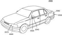
도 10을 참조하면, 자동차의 헤드 램프부(2010) 내에 헤드 램프 모듈(2020)이 설치될 수 있고, 외부 사이드 미러부(2030) 내에 사이드 미러 램프 모듈(2040)이 설치될 수 있으며, 테일 램프부(2050) 내에 테일 램프 모듈(2060)이 설치될 수 있다. 헤드 램프 모듈(2020), 사이드 미러 램프 모듈(2040), 테일 램프 모듈(2060) 중 적어도 하나는 앞서 설명한 광원 모듈(10) 중 하나로 구현될 수 있다.Referring to FIG. 10 , a
도 11은 본 개시의 예시적 실시예에 의한 평판 조명 장치를 간략하게 나타내는 사시도이다.11 is a perspective view schematically illustrating a flat lighting device according to an exemplary embodiment of the present disclosure.
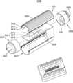
구체적으로, 평판 조명 장치(2100)는 광원 모듈(2110), 전원공급장치(2120) 및 하우징(2030)을 포함할 수 있다. 본 개시의 일 실시예에 따라, 광원 모듈(2110)은 발광 셀 어레이를 광원으로 포함할 수 있다. 광원 모듈(2110)은 앞서 설명한 본 개시의 일 실시예들에 따른 광원 모듈(10)로 구현될 수 있다. 광원 모듈(2110)은 발광 셀 어레이를 포함하는 발광 소자 및 구동 칩들을 포함할 수 있고, 전체적으로 평면 현상을 이루도록 형성될 수 있다.Specifically, the
전원 공급 장치(2120)는 광원 모듈(2110)에 전원을 공급하도록 구성될 수 있다. 하우징(2130)은 광원 모듈(2110) 및 전원 공급 장치(2120)가 내부에 수용되도록 수용 공간이 형성될 수 있고, 일 측면에 개방된 육면체 형상으로 형성되나 이에 한정되는 것은 아니다. 광원 모듈(2110)은 하우징(2130)의 개방된 일 측면으로 빛을 발광하도록 배치될 수 있다.The power supply 2120 may be configured to supply power to the
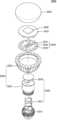
도 12는 본 개시의 예시적 실시예에 의한 조명 장치를 간략하게 나타내는 분해 사시도이다.12 is an exploded perspective view schematically illustrating a lighting device according to an exemplary embodiment of the present disclosure.
구체적으로, 조명 장치(2200)는 소켓(2210), 전원부(2220), 방열부(2230), 광원 모듈(2240) 및 광학부(2250)를 포함할 수 있다.In detail, the
소켓(2210)은 기존의 조명 장치와 대체 가능하도록 구성될 수 있다. 조명 장치(2200)에 공급되는 전력은 소켓(2210)을 통해서 인가될 수 있다. 도시된 바와 같이, 전원부(2220)는 제1 전원부(2221) 및 제2 전원부(2222)로 분리되어 조립될 수 있다. 방열부(2230)는 내부 방열부(2231) 및 외부 방열부(2232)를 포함할 수 있고, 내부 방열부(2231)는 광원모듈(2240) 및/또는 전원부(2220)와 직접 연결될 수 있고, 이를 통해 외부 방열부(2232)로 열이 전달되게 할 수 있다. 광학부(2250)는 내부 광학부 및 외부 광학부를 포함할 수 있고, 광원모듈(2240)이 방출하는 빛을 고르게 분산시키도록 구성될 수 있다.The
광원 모듈(2240)은 전원부(2220)로부터 전력을 공급받아 광학부(2250)로 빛을 방출할 수 있다. 광원 모듈(2110)은 앞서 설명한 본 개시의 일 실시예들에 따른 광원 모듈(10)로 구현될 수 있다.The
광원 모듈(2110)은 복수의 발광 셀들을 포함하는 발광 소자(2241), 회로 기판(2242) 및 복수의 구동 칩들(2243)을 포함할 수 있고, 복수의 구동 칩들에는 발광 소자(2241)의 구동 정보가 저장될 수 있다.The
도 13는 본 개시의 예시적 실시예에 따른 바(bar) 타입의 조명 장치를 개략적으로 나타내는 분해 사시도이다.13 is an exploded perspective view schematically illustrating a bar-type lighting device according to an exemplary embodiment of the present disclosure.
구체적으로, 조명 장치(2400)는 방열 부재(2401), 커버(2427), 광원 모듈(2421), 제1 소켓(2405) 및 제2 소켓(2423)을 포함한다. 방열 부재(2401)의 내부 또는/및 외부 표면에 다수개의 방열 핀(2500, 4409)이 요철 형태로 형성될 수 있으며, 방열 핀(2500, 4409)은 다양한 형상 및 간격을 갖도록 설계될 수 있다. 방열 부재(2401)의 내측에는 돌출 형태의 지지대(2413)가 형성되어 있다. 지지대(2413)에는 광원 모듈(2421)이 고정될 수 있다. 방열 부재(2401)의 양 끝단에는 걸림 턱(2411)이 형성될 수 있다.Specifically, the
커버(2427)에는 걸림 홈(2429)이 형성되어 있으며, 걸림 홈(2429)에는 방열 부재(2401)의 걸림 턱(2411)이 후크 결합 구조로 결합될 수 있다. 걸림 홈(2429)과 걸림 턱(2411)이 형성되는 위치는 서로 바뀔 수도 있다.A locking
광원 모듈(2421)은 앞서 설명한 본 개시의 일 실시예들에 따른 광원 모듈(10)로 구현될 수 있다.The
광원 모듈(2421)은 발광 셀 어레이를 포함할 수 있다. 광원 모듈(2421)은 인쇄회로기판(2419), 광원(2417) 및 컨트롤러(2415)를 포함할 수 있다. 컨트롤러(2415)는 앞서 설명한 본 개시의 일 실시예에 따른 구동 칩으로 구현될 수 있고, 광원(2417)의 구동 정보가 저장될 수 있으며, 광원(2417)을 구동시킬 수 있다. 인쇄회로기판(2419)에는 광원(2417)을 동작시키기 위한 회로 배선들이 형성되어 있다. 또한, 광원(2417)을 동작시키기 위한 구성 요소들이 포함될 수도 있다. 광원(2417)은 앞서 설명한 본 개시의 일 실시예들에 따른 발광 소자(100)로 구현될 수 있다. 따라서, 광원(2417)은 복수의 서브 어레이들로 구성될 수 있고, 복수의 서브 어레이들은 서로 전기적으로 절연될 수 있다.The
제1, 2 소켓(2405, 4423)은 한 쌍의 소켓으로서 방열 부재(2401) 및 커버(2427)로 구성된 원통형 커버 유닛의 양단에 결합되는 구조를 갖는다. 예를 들어, 제1 소켓(2405)은 전극 단자(2403) 및 전원 장치(2407)를 포함할 수 있고, 제2 소켓(2423)에는 더미 단자(2425)가 배치될 수 있다. 또한, 제1 소켓(2405) 또는 제2 소켓(2423) 중의 어느 하나의 소켓에 광센서 및/또는 통신 모듈이 내장될 수 있다. 예를 들어, 더미 단자(2425)가 배치된 제2 소켓(2423)에 광센서 및/또는 통신 모듈이 내장될 수 있다. 다른 예로서, 전극 단자(2403)가 배치된 제1 소켓(2405)에 광센서 및/또는 통신 모듈이 내장될 수도 있다.The first and
도 14는 본 개시의 예시적 실시예에 따른 조명 장치를 개략적으로 나타내는 분해 사시도이다.14 is an exploded perspective view schematically illustrating a lighting device according to an exemplary embodiment of the present disclosure.
구체적으로, 본 실시예에 따른 조명 장치(2500)와 앞서 도 2의 조명 장치(2200)와의 차이점은 광원 모듈(2240)의 상부에 반사판(2310) 및 통신 모듈(2320)이 포함되어 있다. 반사판(2310)은 광원으로부터의 빛을 측면 및 후방으로 고르게 퍼지게 하여 눈부심을 줄일 수 있다.Specifically, the difference between the
반사판(2310)의 상부에는 통신 모듈(2320)이 장착될 수 있으며 상기 통신 모듈(2320)을 통하여 홈-네트워크(home-network) 통신을 구현할 수 있다. 예를 들어, 통신 모듈(2320)은 지그비(Zigbee), 와이파이(WiFi) 또는 라이파이(LiFi)를 이용한 무선 통신 모듈일 수 있으며, 스마트폰 또는 무선 컨트롤러를 통하여 조명 장치의 온(on)/오프(off), 밝기 조절 등과 같은 가정 내외에 설치되어 있는 조명을 컨트롤 할 수 있다. 또한 상기 가정 내외에 설치되어 있는 조명 장치의 가시광 파장을 이용한 라이파이 통신 모듈을 이용하여 TV, 냉장고, 에어컨, 도어락, 자동차 등 가정 내외에 있는 전자 제품 및 자동차 시스템의 컨트롤을 할 수 있다. 상기 반사판(2310)과 통신 모듈(2320)은 커버부(2330)에 의해 커버될 수 있다.A
도 15는 본 개시의 예시적 실시예에 의한 조명 장치를 구비하는 실내용 조명 제어 네트워크 시스템을 설명하기 위한 개략도이다.15 is a schematic diagram illustrating an indoor lighting control network system including a lighting device according to an exemplary embodiment of the present disclosure.
구체적으로, 네트워크 시스템(3000)은 LED 등의 발광 소자를 이용하는 조명 기술과 사물인터넷(IoT) 기술, 무선 통신 기술 등이 융합된 복합적인 스마트 조명-네트워크 시스템일 수 있다. 네트워크 시스템(3000)은, 다양한 조명 장치 및 유무선 통신 장치를 이용하여 구현될 수 있으며, 센서, 컨트롤러, 통신수단, 네트워크 제어 및 유지 관리 등을 위한 소프트웨어 등에 의해 구현될 수 있다.Specifically, the
네트워크 시스템(3000)은 가정이나 사무실 같이 건물 내에 정의되는 폐쇄적인 공간은 물론, 공원, 거리 등과 같이 개방된 공간 등에도 적용될 수 있다. 네트워크 시스템(3000)은, 다양한 정보를 수집/가공하여 사용자에게 제공할 수 있도록, 사물인터넷 환경에 기초하여 구현될 수 있다.The
네트워크 시스템(3000)에 포함되는 LED 램프(3200)는, 주변 환경에 대한 정보를 게이트웨이(3100)로부터 수신하여 LED 램프(3200) 자체의 조명을 제어하는 것은 물론, LED 램프(3200)의 가시광 통신 등의 기능에 기초하여 사물인터넷 환경에 포함되는 다른 장치들(3300~3800)의 동작 상태 확인 및 제어 등과 같은 역할을 수행할 수도 있다. LED 램프(3200)는 앞서 설명한 본 개시의 일 실시예들에 따른 조명 장치(10)를 구성하는 발광 소자(100) 및 구동 칩들(210)로 구현될 수 있다.The
네트워크 시스템(3000)은, 서로 다른 통신 프로토콜에 따라 송수신되는 데이터를 처리하기 위한 게이트웨이(3100), 게이트웨이(3100)와 통신 가능하도록 연결되며 LED 발광소자를 포함하는 LED 램프(3200), 및 다양한 무선 통신 방식에 따라 게이트웨이(3100)와 통신 가능하도록 연결되는 복수의 장치(3300~3800)를 포함할 수 있다. 사물인터넷 환경에 기초하여 네트워크 시스템(3000)을 구현하기 위해, LED 램프(3200)를 비롯한 각 장치(3300~3800)들은 적어도 하나의 통신 모듈을 포함할 수 있다. 일 실시예로, LED 램프(3200)는 WiFi, 지그비(Zigbee), LiFi 등의 무선 통신 프로토콜에 의해 게이트 웨이(3100)와 통신 가능하도록 연결될 수 있으며, 이를 위해 적어도 하나의 램프용 통신 모듈(3210)을 가질 수 있다.The
네트워크 시스템(3000)은 가정이나 사무실 같이 폐쇄적인 공간은 물론 거리나 공원 같은 개방적인 공간에도 적용될 수 있다. 네트워크 시스템(3000)이 가정에 적용되는 경우, 네트워크 시스템(3000)에 포함되며 사물인터넷 기술에 기초하여 게이트 웨이(3100)와 통신 가능하도록 연결되는 복수의 장치(3300~3800)는 가전 제품(3300), 디지털 도어록(3400), 차고 도어록(3500), 벽 등에 설치되는 조명용 스위치(3600), 무선 통신망 중계를 위한 라우터(3700) 및 스마트폰, 태블릿, 랩톱 컴퓨터 등의 모바일 기기(3800) 등을 포함할 수 있다.The
네트워크 시스템(3000)에서, LED 램프(3200)는 가정 내에 설치된 무선 통신 네트워크(Zigbee, WiFi, LiFi 등)를 이용하여 다양한 장치(3300~3800)의 동작 상태를 확인하거나, 주위 환경/상황에 따라 LED 램프(3200) 자체의 조도를 자동으로 조절할 수 있다. 또한 LED 램프(3200)에서 방출되는 가시광선을 이용한 LiFi 통신을 이용하여 네트워크 시스템(3000)에 포함되는 장치들(3300~3800)을 컨트롤 할 수도 있다.In the
우선, LED 램프(3200)는 램프용 통신 모듈(3210)을 통해 게이트 웨이(3100)로부터 전달되는 주변 환경, 또는 LED 램프(3200)에 장착된 센서로부터 수집되는 주변 환경 정보에 기초하여 LED 램프(3200)의 조도를 자동으로 조절할 수 있다. 예를 들면, 텔레비젼(3310)에서 방송되고 있는 프로그램의 종류 또는 화면의 밝기에 따라 LED 램프(3200)의 조명 밝기가 자동으로 조절될 수 있다. 이를 위해, LED 램프(3200)는 게이트 웨이(3100)와 연결된 램프용 통신 모듈(3210)로부터 텔레비전(3310)의 동작 정보를 수신할 수 있다. 램프용 통신 모듈(3210)은 LED 램프(3200)에 포함되는 센서 및/또는 컨트롤러와 일체형으로 모듈화될 수 있다.First, the
예를 들어, TV프로그램에서 방영되는 프로그램 값이 휴먼드라마일 경우, 미리 셋팅된 설정 값에 따라 조명도 거기에 맞게 12000K 이하의 색 온도, 예를 들면 5000K로 낮아지고 색감이 조절되어 아늑한 분위기를 연출할 수 있다. 반대로 프로그램 값이 개그프로그램인 경우, 조명도 셋팅 값에 따라 색 온도가 5000K 이상으로 높아지고 푸른색 계열의 백색조명으로 조절되도록 네트워크 시스템(3000)이 구성될 수 있다.For example, if the value of a program aired in a TV program is a human drama, the lighting is also lowered to a color temperature of 12000K or less, for example 5000K, according to the preset setting value, and the color is adjusted to create a cozy atmosphere. can Conversely, when the program value is a gag program, the
또한, 가정 내에 사람이 없는 상태에서 디지털 도어록(3400)이 잠긴 후 일정 시간이 경과하면, 턴-온된 LED 램프(3200)를 모두 턴-오프시켜 전기 낭비를 방지할 수 있다. 또는, 모바일 기기(3800) 등을 통해 보안 모드가 설정된 경우, 가정 내에 사람이 없는 상태에서 디지털 도어록(3400)이 잠기면, LED 램프(3200)를 턴-온 상태로 유지시킬 수도 있다.In addition, when a predetermined time elapses after the
LED 램프(3200)의 동작은, 네트워크 시스템(3000)과 연결되는 다양한 센서를 통해 수집되는 주변 환경에 따라서 제어될 수도 있다. 예를 들어 네트워크 시스템(3000)이 건물 내에 구현되는 경우, 빌딩 내에서 조명과 위치센서와 통신모듈을 결합, 건물 내 사람들의 위치정보를 수집하여 조명을 턴-온 또는 턴-오프하거나 수집한 정보를 실시간으로 제공하여 시설관리나 유휴공간의 효율적 활용을 가능케 한다. 일반적으로 LED 램프(3200)와 같은 조명 장치는, 건물 내 각 층의 거의 모든 공간에 배치되므로, LED 램프(3200)와 일체로 제공되는 센서를 통해 건물 내의 각종 정보를 수집하고 이를 시설관리, 유휴공간의 활용 등에 이용할 수 있다.The operation of the
한편, LED 램프(3200)와 이미지센서, 저장장치, 램프용 통신 모듈(3210) 등을 결합함으로써, 건물 보안을 유지하거나 긴급상황을 감지하고 대응할 수 있는 장치로 활용할 수 있다. 예를 들어 LED 램프(3200)에 연기 또는 온도 감지 센서 등이 부착된 경우, 화재 발생 여부 등을 신속하게 감지함으로써 피해를 최소화할 수 있다. 또한 외부의 날씨나 일조량 등을 고려하여 조명의 밝기를 조절, 에너지를 절약하고 쾌적한 조명환경을 제공할 수도 있다.Meanwhile, by combining the
앞서 설명한 바와 같이, 네트워크 시스템(3000)은 가정, 오피스 또는 건물 등과 같이 폐쇄적인 공간은 물론, 거리나 공원 등의 개방적인 공간에도 적용될 수 있다. 물리적 한계가 없는 개방적인 공간에 네트워크 시스템(3000)을 적용하고자 하는 경우, 무선 통신의 거리 한계 및 각종 장애물에 따른 통신 간섭 등에 따라 네트워크 시스템(3000)을 구현하기가 상대적으로 어려울 수 있다. 각 조명 기구에 센서와 통신 모듈 등을 장착하고, 각 조명 기구를 정보 수집 수단 및 통신 중개 수단으로 사용함으로써, 상기와 같은 개방적인 환경에서 네트워크 시스템(3000)을 좀 더 효율적으로 구현할 수 있다.As described above, the
도 16은 본 개시의 예시적 실시예에 의한 조명 장치를 구비하는 네트워크 시스템을 설명하기 위한 개략도이다.16 is a schematic diagram illustrating a network system including a lighting device according to an exemplary embodiment of the present disclosure.
구체적으로, 도면은 개방적인 공간에 적용된 네트워크 시스템(4000)의 일 실시예를 나타낸 것이다. 네트워크 시스템(4000)은 통신 연결 장치(4100), 소정의 간격마다 설치되어 통신 연결 장치(4100)와 통신 가능하도록 연결되는 복수의 조명 기구(4120, 4150), 서버(4160), 서버(4160)를 관리하기 위한 컴퓨터(4170), 통신 기지국(4180), 통신 가능한 장비들을 연결하는 통신망(4190), 및 모바일 기기(4200) 등을 포함할 수 있다.Specifically, the drawing shows an embodiment of a
거리 또는 공원 등의 개방적인 외부 공간에 설치되는 복수의 조명 기구(4120, 4150) 각각은 스마트 엔진(4130, 4140)을 포함할 수 있다. 스마트 엔진(4130, 4140)은 빛을 내기 위한 발광소자, 발광소자를 구동하기 위한 구동 드라이버 외에 주변 환경의 정보를 수집하는 센서, 및 통신 모듈 등을 포함할 수 있다. 스마트 엔진은 본 개시에 따른 조명 장치(10)로 구현될 수 있다.Each of the plurality of
상기 통신 모듈에 의해 스마트 엔진(4130, 4140)은 WiFi, Zigbee, LiFi 등의 통신 프로토콜에 따라 주변의 다른 장비들과 통신할 수 있다.With the communication module, the
일례로, 하나의 스마트 엔진(4130)은 다른 스마트 엔진(4140)과 통신 가능하도록 연결될 수 있다. 이때, 스마트 엔진(4130, 6140) 상호 간의 통신에는 WiFi 확장 기술(WiFi Mesh)이 적용될 수 있다. 적어도 하나의 스마트 엔진(4130)은 통신망(4190)에 연결되는 통신 연결 장치(4100)와 유/무선 통신에 의해 연결될 수 있다. 통신의 효율을 높이기 위해, 몇 개의 스마트 엔진(4130, 4140)을 하나의 그룹으로 묶어 하나의 통신 연결 장치(4100)와 연결할 수 있다.For example, one
통신 연결 장치(4100)는 유/무선 통신이 가능한 액세스 포인트(access point, AP)로서, 통신망(4190)과 다른 장비 사이의 통신을 중개할 수 있다. 통신 연결 장치(4100)는 유/무선 방식 중 적어도 하나에 의해 통신망(4190)과 연결될 수 있으며, 일례로 조명 기구(4120, 4150) 중 어느 하나의 내부에 기구적으로 수납될 수 있다.The
통신 연결 장치(4100)는 WiFi 등의 통신 프로토콜을 통해 모바일 기기(4200)와 연결될 수 있다. 모바일 기기(4200)의 사용자는 인접한 주변의 조명 기구(4120)의 스마트 엔진(4130)과 연결된 통신 연결 장치(4100)를 통해, 복수의 스마트 엔진(4130, 4140)이 수집한 주변 환경 정보를 수신할 수 있다. 상기 주변 환경 정보는 주변 교통 정보, 날씨 정보 등을 포함할 수 있다. 모바일 기기(4200)는 통신 기지국(4180)을 통해 3G 또는 4G 등의 무선 셀룰러 통신 방식으로 통신망(4190)에 연결될 수도 있다.The
한편, 통신망(4190)에 연결되는 서버(4160)는, 각 조명 기구(4120, 4150)에 장착된 스마트 엔진(4130, 4140)이 수집하는 정보를 수신함과 동시에, 각 조명 기구(4120,4150)의 동작 상태 등을 모니터링할 수 있다. 각 조명 기구(4120, 4150)의 동작 상태의 모니터링 결과에 기초하여 각 조명 기구(4120, 4150)를 관리하기 위해, 서버(4160)는 관리 시스템을 제공하는 컴퓨터(4170)와 연결될 수 있다. 컴퓨터(4170)는 각 조명 기구(4120, 4150), 특히 스마트 엔진(4130, 4140)의 동작 상태를 모니터링하고 관리할 수 있는 소프트웨어 등을 실행할 수 있다.On the other hand, the
이상에서와 같이 도면과 명세서에서 예시적인 실시예들이 개시되었다. 본 명세서에서 특정한 용어를 사용하여 실시예들을 설명되었으나, 이는 단지 본 개시의 기술적 사상을 설명하기 위한 목적에서 사용된 것이지 의미 한정이나 특허청구범위에 기재된 본 개시의 범위를 제한하기 위하여 사용된 것은 아니다. 그러므로 본 기술분야의 통상의 지식을 가진 자라면 이로부터 다양한 변형 및 균등한 타 실시예가 가능하다는 점을 이해할 것이다. 따라서, 본 개시의 진정한 기술적 보호범위는 첨부된 특허청구범위의 기술적 사상에 의해 정해져야 할 것이다.As above, exemplary embodiments have been disclosed in the drawings and specifications. Although the embodiments have been described using specific terms in this specification, they are only used for the purpose of explaining the technical idea of the present disclosure, and are not used to limit the scope of the present disclosure described in the claims. . Therefore, those of ordinary skill in the art will understand that various modifications and equivalent other embodiments are possible therefrom. Therefore, the true technical scope of protection of the present disclosure should be determined by the technical spirit of the appended claims.
10: 광원 모듈, 100: 발광 소자
110: 복수의 서브 어레이들
120: 복수의 패드들
200: LED 구동부, 210: 구동 칩들
300: 입력부, 400: 본딩 와이어10: light source module, 100: light emitting element
110: a plurality of sub arrays
120: a plurality of pads
200: LED driving unit, 210: driving chips
300: input unit, 400: bonding wire
Claims (20)
Translated fromKorean상기 인쇄회로기판에 실장되고, 복수의 서브 어레이들을 포함하는 발광 소자; 및
상기 인쇄회로기판에 실장되고, 상기 발광 소자의 복수의 서브 어레이들 중 대응되는 서브 어레이를 각각 구동시키는 복수의 구동 칩들을 포함하고,
상기 복수의 서브 어레이들 각각은, 복수의 열들 및 복수의 행들에 배치되고, 격벽 구조물에 의해 물리적으로 서로 분리되고, 전기적으로 서로 연결되는 복수의 발광 셀들을 포함하고,
상기 복수의 서브 어레이들은 서로 전기적으로 분리되고,
상기 복수의 서브 어레이들 각각은 상기 복수의 구동 칩들 중 서로 다른 구동 칩에 의해, 포함된 복수의 발광 셀들 각각이 개별적으로 구동되고,
상기 발광 소자는 상기 인쇄회로기판의 중심 영역에 배치되고,
상기 복수의 구동 칩들은 상기 중심 영역의 측면인 상기 인쇄회로기판의 주변 영역에 배치되는 것을 특징으로 하는 광원 모듈.printed circuit board;
a light emitting element mounted on the printed circuit board and including a plurality of sub arrays; and
a plurality of driving chips mounted on the printed circuit board and driving corresponding sub-arrays among the plurality of sub-arrays of the light-emitting elements;
Each of the plurality of subarrays includes a plurality of light emitting cells disposed in a plurality of columns and a plurality of rows, physically separated from each other by a barrier rib structure, and electrically connected to each other;
The plurality of sub arrays are electrically isolated from each other,
Each of the plurality of light emitting cells included in each of the plurality of sub arrays is individually driven by a different driving chip among the plurality of driving chips,
The light emitting element is disposed in a central region of the printed circuit board,
The plurality of driving chips are disposed in a peripheral area of the printed circuit board, which is a side surface of the central area.
외부로부터 제어 신호를 수신하는 입력부를 더 포함하고,
상기 복수의 구동 칩들은 서로 연이어서 전기적으로 연결되며,
상기 복수의 구동 칩들 중 하나의 구동 칩이 상기 입력부로부터 상기 제어 신호를 수신하여, 상기 복수의 구동 칩들 중 다른 하나의 구동 칩으로 전송하는 것을 특징으로 하는 광원 모듈.According to claim 1,
Further comprising an input unit for receiving a control signal from the outside,
The plurality of driving chips are successively electrically connected to each other,
A light source module, wherein one of the plurality of driving chips receives the control signal from the input unit and transmits the control signal to another one of the plurality of driving chips.
상기 발광 소자는 하나의 LED(Light Emitting Diode) 칩인 것을 특징으로 하는 광원 모듈.According to claim 1,
The light emitting device is a light source module, characterized in that one LED (Light Emitting Diode) chip.
상기 복수의 서브 어레이들이 배치된 순서에 따라, 상기 복수의 서브 어레이들에 각각 대응되는 복수의 구동 칩들이 순서대로 배치되는 것을 특징으로 하는 광원 모듈.According to claim 1,
The light source module, characterized in that, according to the order in which the plurality of sub-arrays are arranged, a plurality of driving chips respectively corresponding to the plurality of sub-arrays are arranged in order.
상기 복수의 서브 어레이들 중 동일한 서브 어레이에 포함되는 복수의 발광 셀들 중 적어도 일부는 서로 직렬 연결되는 것을 특징으로 하는 광원 모듈.According to claim 1,
A light source module, characterized in that at least some of a plurality of light emitting cells included in the same subarray among the plurality of subarrays are serially connected to each other.
상기 복수의 서브 어레이들 중 동일한 서브 어레이에 포함되는 복수의 발광 셀들 중 적어도 일부는 서로 병렬 연결되는 것을 특징으로 하는 광원 모듈.According to claim 1,
A light source module, characterized in that at least some of a plurality of light-emitting cells included in the same sub-array among the plurality of sub-arrays are connected in parallel to each other.
상기 인쇄회로기판과 상기 발광 소자 사이에 배치되는 인터포저를 더 포함하는 것을 특징으로 하는 광원 모듈.According to claim 1,
The light source module further comprising an interposer disposed between the printed circuit board and the light emitting element.
상기 발광 소자는, 상기 복수의 구동 칩들과 상기 서브 어레이들 간의 전기적 연결을 제공하여 상기 복수의 발광 셀들을 개별적으로 구동시키는 복수의 패드들을 더 포함하고,
상기 복수의 서브 어레이들은 상기 발광 소자의 중심 영역에 배치되고,
상기 복수의 패드들은 상기 중심 영역을 둘러싸는 주변 영역에 배치되는 것을 특징으로 하는 광원 모듈.According to claim 1,
The light emitting element further includes a plurality of pads that individually drive the plurality of light emitting cells by providing an electrical connection between the plurality of driving chips and the sub arrays;
The plurality of sub-arrays are disposed in a central region of the light emitting device,
The plurality of pads are disposed in a peripheral area surrounding the central area.
상기 발광 소자 및 상기 복수의 구동 칩들은, 상기 인쇄회로기판의 주면과 평행한 방향으로 서로 오버랩되도록 배치되는 것을 특징으로 하는 광원 모듈.According to claim 1,
The light source module, characterized in that the light emitting element and the plurality of driving chips are arranged to overlap each other in a direction parallel to the main surface of the printed circuit board.
외부 장치와 상기 복수의 서브 어레이들의 전기적 연결을 제공하여, 상기 복수의 발광 셀들을 개별적으로 구동시키는 복수의 패드들을 포함하고,
상기 복수의 서브 어레이들 각각은 서로 전기적으로 분리되고,
상기 복수의 서브 어레이들은 중심 영역에 배치되고,
상기 복수의 패드들은 상기 중심 영역을 둘러싸는 주변 영역에 배치되는 것을 특징으로 하는 발광 소자.a plurality of sub-arrays each including a plurality of light emitting cells disposed in a plurality of columns and a plurality of rows, physically separated from each other by barrier rib structures, and electrically connected to each other; and
a plurality of pads that individually drive the plurality of light-emitting cells by providing an electrical connection between an external device and the plurality of sub-arrays;
Each of the plurality of sub arrays is electrically isolated from each other,
The plurality of sub arrays are disposed in a central region,
The light emitting device, characterized in that the plurality of pads are disposed in a peripheral area surrounding the central area.
상기 복수의 서브 어레이들 각각에 포함된 복수의 발광 셀들 중 적어도 일부의 발광 셀들은 서로 직렬 연결되는 것을 특징으로 하는 발광 소자.According to claim 10,
A light emitting device characterized in that at least some light emitting cells among a plurality of light emitting cells included in each of the plurality of sub arrays are connected in series with each other.
상기 복수의 서브 어레이들 각각에 포함된 복수의 발광 셀들 중 적어도 일부의 발광 셀들은 서로 병렬 연결되는 것을 특징으로 하는 발광 소자.According to claim 10,
A light emitting device characterized in that at least some light emitting cells among a plurality of light emitting cells included in each of the plurality of sub arrays are connected in parallel with each other.
상기 복수의 서브 어레이들은, 제1 방향 및 상기 제1 방향과 수직한 제2 방향으로 배치되고,
상기 복수의 서브 어레이들은, 상기 제2 방향보다 상기 제1 방향으로 길게 배치되는 것을 특징으로 하는 발광 소자.According to claim 10,
The plurality of sub arrays are arranged in a first direction and a second direction perpendicular to the first direction;
The plurality of sub arrays are arranged longer in the first direction than in the second direction.
상기 제2 방향으로 나란하게 배치되는 서브 어레이들 중 적어도 2개의 서브 어레이들은 제1 방향(X)과 평행한 축으로 서로 대칭적으로 형성되는 것을 특징으로 하는 발광 소자.According to claim 13,
At least two sub-arrays among the sub-arrays arranged side by side in the second direction are formed symmetrically with each other with an axis parallel to the first direction (X).
상기 복수의 서브 어레이들이 배치된 순서에 따라, 상기 복수의 서브 어레이들에 각각 대응되는 복수의 패드들이 순서대로 배치되는 것을 특징으로 하는 발광 소자.According to claim 10,
A light emitting device characterized in that according to the order in which the plurality of sub arrays are arranged, a plurality of pads respectively corresponding to the plurality of sub arrays are arranged in order.
상기 복수의 패드들 상에는 각각 본딩 와이어들이 배치되는 것을 특징으로 하는 발광 소자.According to claim 10,
A light emitting device, characterized in that bonding wires are disposed on each of the plurality of pads.
상기 복수의 패드들 중 하나의 패드는 적어도 2개의 발광 셀들에 연결되는 것을 특징으로 하는 발광 소자.According to claim 10,
A light emitting device, wherein one of the plurality of pads is connected to at least two light emitting cells.
상기 인쇄회로기판에 실장되고, 제1 서브 어레이 및 제2 서브 어레이를 포함하는 발광 소자;
상기 인쇄회로기판에 실장되고, 상기 제1 서브 어레이를 구동시키는 제1 구동 칩; 및
상기 인쇄회로기판에 실장되고, 상기 제1 구동 칩과 상이하고, 상기 제2 서브 어레이를 구동시키는 제2 구동 칩을 포함하고,
상기 제1 서브 어레이 및 상기 제2 서브 어레이 각각은, 복수의 열들 및 복수의 행들에 배치되고, 격벽 구조물에 의해 물리적으로 서로 분리되고, 전기적으로 서로 연결되는 복수의 발광 셀들을 포함하고,
상기 제1 서브 어레이의 복수의 발광 셀들 각각은, 상기 제1 구동 칩에 의해 개별적으로 구동되고,
상기 제2 서브 어레이의 복수의 발광 셀들 각각은, 상기 제2 구동 칩에 의해 개별적으로 구동되고,
상기 제1 서브 어레이 및 상기 제2 서브 어레이는 서로 전기적으로 분리되고,
상기 제1 서브 어레이 및 상기 제2 서브 어레이는 상기 인쇄회로기판의 주면과 평행한 제1 방향으로 순서대로 배치되고,
상기 제1 구동 칩 및 상기 제2 구동 칩은 상기 제1 방향으로 순서대로 배치되는 것을 특징으로 하는 광원 모듈.printed circuit board;
a light emitting element mounted on the printed circuit board and including a first sub array and a second sub array;
a first driving chip mounted on the printed circuit board and driving the first sub array; and
a second driving chip mounted on the printed circuit board, different from the first driving chip, and driving the second sub array;
Each of the first sub-array and the second sub-array includes a plurality of light emitting cells disposed in a plurality of columns and a plurality of rows, physically separated from each other by a barrier structure, and electrically connected to each other;
Each of the plurality of light-emitting cells of the first sub-array is individually driven by the first driving chip;
Each of the plurality of light-emitting cells of the second sub-array is individually driven by the second driving chip;
The first sub-array and the second sub-array are electrically isolated from each other;
The first sub-array and the second sub-array are sequentially arranged in a first direction parallel to a main surface of the printed circuit board;
The first driving chip and the second driving chip are sequentially arranged in the first direction.
상기 발광 소자는 하나의 LED 칩인 것을 특징으로 하는 광원 모듈.According to claim 18,
The light source module, characterized in that the light emitting element is one LED chip.
상기 발광 소자는, 상기 제1 구동 칩과 상기 제1 서브 어레이 간의 전기적 연결을 제공하는 복수의 제1 패드들, 및 상기 제2 구동 칩과 상기 제2 서브 어레이 간의 전기적 연결을 제공하는 복수의 제2 패드들을 더 포함하고,
상기 복수의 제1 패드들 및 상기 복수의 제2 패드들은 상기 제1 방향으로 차례로 배치되고,
상기 복수의 제1 패드들은, 상기 서브 어레이로부터, 상기 인쇄회로기판의 주면과 평행하고 상기 제1 방향과 수직인 제2 방향에 배치되는 것을 특징으로 하는 광원 모듈.According to claim 18,
The light emitting element includes a plurality of first pads providing electrical connection between the first driving chip and the first sub-array, and a plurality of first pads providing electrical connection between the second driving chip and the second sub-array. 2 more pads,
The plurality of first pads and the plurality of second pads are sequentially disposed in the first direction;
The plurality of first pads are disposed in a second direction parallel to the main surface of the printed circuit board and perpendicular to the first direction, from the sub array.
Priority Applications (4)
| Application Number | Priority Date | Filing Date | Title |
|---|---|---|---|
| KR1020180079576AKR102553265B1 (en) | 2018-07-09 | 2018-07-09 | Light emitting diode(led) device, and light source modulehaving the same |
| US16/504,983US11306908B2 (en) | 2018-07-09 | 2019-07-08 | Light emitting device and a light source module including the same |
| CN201910613252.4ACN110707118B (en) | 2018-07-09 | 2019-07-09 | Light emitting device and light source module including the same |
| US17/721,632US11573006B2 (en) | 2018-07-09 | 2022-04-15 | Light emitting device and a light source module including the same |
Applications Claiming Priority (1)
| Application Number | Priority Date | Filing Date | Title |
|---|---|---|---|
| KR1020180079576AKR102553265B1 (en) | 2018-07-09 | 2018-07-09 | Light emitting diode(led) device, and light source modulehaving the same |
Publications (2)
| Publication Number | Publication Date |
|---|---|
| KR20200005942A KR20200005942A (en) | 2020-01-17 |
| KR102553265B1true KR102553265B1 (en) | 2023-07-07 |
Family
ID=69101967
Family Applications (1)
| Application Number | Title | Priority Date | Filing Date |
|---|---|---|---|
| KR1020180079576AActiveKR102553265B1 (en) | 2018-07-09 | 2018-07-09 | Light emitting diode(led) device, and light source modulehaving the same |
Country Status (3)
| Country | Link |
|---|---|
| US (2) | US11306908B2 (en) |
| KR (1) | KR102553265B1 (en) |
| CN (1) | CN110707118B (en) |
Families Citing this family (12)
| Publication number | Priority date | Publication date | Assignee | Title |
|---|---|---|---|---|
| KR102551354B1 (en)* | 2018-04-20 | 2023-07-04 | 삼성전자 주식회사 | Semiconductor light emitting devices and methods of manufacturing the same |
| KR102553265B1 (en) | 2018-07-09 | 2023-07-07 | 삼성전자 주식회사 | Light emitting diode(led) device, and light source modulehaving the same |
| KR102682009B1 (en) | 2018-11-13 | 2024-07-08 | 삼성전자주식회사 | Light emitting module and light apparatus for car including the same |
| JP7114854B2 (en)* | 2020-04-28 | 2022-08-09 | 日亜化学工業株式会社 | light emitting device |
| EP3905326B1 (en)* | 2020-04-28 | 2023-01-04 | Nichia Corporation | Light-emitting device |
| KR102851496B1 (en)* | 2020-05-13 | 2025-08-28 | 삼성디스플레이 주식회사 | Display device |
| KR102822349B1 (en)* | 2020-05-22 | 2025-06-18 | 삼성전자주식회사 | Semiconductor light emitting devices and methods of manufacturing the same |
| US11811008B2 (en) | 2020-05-25 | 2023-11-07 | Samsung Electronics Co., Ltd. | Light source module including light-emitting diode |
| KR102858234B1 (en) | 2020-05-26 | 2025-09-09 | 삼성전자주식회사 | Light emitting device and Light source module including the same |
| WO2022010007A1 (en)* | 2020-07-08 | 2022-01-13 | 엘지전자 주식회사 | Display apparatus using semiconductor light-emitting device |
| US12205316B2 (en)* | 2021-04-29 | 2025-01-21 | Microsoft Technology Licensing, Llc | Ambient illuminance sensor system |
| US11499681B1 (en)* | 2021-11-19 | 2022-11-15 | Putco, Inc. | Replacement vehicle lighting apparatus |
Citations (2)
| Publication number | Priority date | Publication date | Assignee | Title |
|---|---|---|---|---|
| CN104637932A (en)* | 2014-12-17 | 2015-05-20 | 东莞市欧思科光电科技有限公司 | Package structure of LED driver IC with light emitting function |
| US20170367158A1 (en)* | 2016-06-02 | 2017-12-21 | Elemental LED, Inc. | Linear Lighting with Distributed Onboard Power Conversion and Filtering |
Family Cites Families (49)
| Publication number | Priority date | Publication date | Assignee | Title |
|---|---|---|---|---|
| CN1143394C (en) | 1996-08-27 | 2004-03-24 | 精工爱普生株式会社 | Peeling method, thin film device transfer method and thin film device |
| USRE38466E1 (en) | 1996-11-12 | 2004-03-16 | Seiko Epson Corporation | Manufacturing method of active matrix substrate, active matrix substrate and liquid crystal display device |
| US7208725B2 (en) | 1998-11-25 | 2007-04-24 | Rohm And Haas Electronic Materials Llc | Optoelectronic component with encapsulant |
| TWI252592B (en)* | 2000-01-17 | 2006-04-01 | Semiconductor Energy Lab | EL display device |
| JP3906654B2 (en) | 2000-07-18 | 2007-04-18 | ソニー株式会社 | Semiconductor light emitting device and semiconductor light emitting device |
| US6818465B2 (en) | 2001-08-22 | 2004-11-16 | Sony Corporation | Nitride semiconductor element and production method for nitride semiconductor element |
| JP2003218034A (en) | 2002-01-17 | 2003-07-31 | Sony Corp | Selective growth method, semiconductor light emitting device and method of manufacturing the same |
| JP3815335B2 (en) | 2002-01-18 | 2006-08-30 | ソニー株式会社 | Semiconductor light emitting device and manufacturing method thereof |
| KR100499129B1 (en) | 2002-09-02 | 2005-07-04 | 삼성전기주식회사 | Light emitting laser diode and fabricatin method thereof |
| US7002182B2 (en) | 2002-09-06 | 2006-02-21 | Sony Corporation | Semiconductor light emitting device integral type semiconductor light emitting unit image display unit and illuminating unit |
| KR100714639B1 (en) | 2003-10-21 | 2007-05-07 | 삼성전기주식회사 | Light emitting element |
| KR100506740B1 (en) | 2003-12-23 | 2005-08-08 | 삼성전기주식회사 | Nitride semiconductor light emitting device and method of manufacturing the same |
| KR100664985B1 (en) | 2004-10-26 | 2007-01-09 | 삼성전기주식회사 | Nitride-based semiconductor device |
| US7336195B2 (en)* | 2005-04-07 | 2008-02-26 | Lighthouse Technologies Ltd. | Light emitting array apparatus and method of manufacture |
| KR100691191B1 (en)* | 2005-07-15 | 2007-03-09 | 삼성전기주식회사 | Surface light source using LED and LCD backlight unit having same |
| KR100665222B1 (en) | 2005-07-26 | 2007-01-09 | 삼성전기주식회사 | LED package using diffusion material and manufacturing method thereof |
| KR100661614B1 (en) | 2005-10-07 | 2006-12-26 | 삼성전기주식회사 | Nitride-based semiconductor light emitting device and its manufacturing method |
| KR100765385B1 (en)* | 2005-12-16 | 2007-10-10 | 서울옵토디바이스주식회사 | Light emitting device in which a plurality of light emitting cells are arranged |
| KR100723247B1 (en) | 2006-01-10 | 2007-05-29 | 삼성전기주식회사 | Chip coated LED package and manufacturing method thereof |
| KR100735325B1 (en) | 2006-04-17 | 2007-07-04 | 삼성전기주식회사 | Light emitting diode package and its manufacturing method |
| KR100769106B1 (en) | 2006-09-08 | 2007-10-22 | (주)에니원 | Block scan type LED screen drive device |
| KR100930171B1 (en) | 2006-12-05 | 2009-12-07 | 삼성전기주식회사 | White light emitting device and white light source module using same |
| KR100855065B1 (en) | 2007-04-24 | 2008-08-29 | 삼성전기주식회사 | Light emitting diode package |
| KR100982980B1 (en) | 2007-05-15 | 2010-09-17 | 삼성엘이디 주식회사 | Surface light source device and LCD backlight unit having same |
| KR101164026B1 (en) | 2007-07-12 | 2012-07-18 | 삼성전자주식회사 | Nitride semiconductor light emitting device and fabrication method thereof |
| US7839295B2 (en) | 2007-10-09 | 2010-11-23 | Abl Ip Holding Llc | Extended life LED fixture |
| KR100891761B1 (en) | 2007-10-19 | 2009-04-07 | 삼성전기주식회사 | Semiconductor light emitting device, manufacturing method thereof and semiconductor light emitting device package using same |
| DE102008049777A1 (en)* | 2008-05-23 | 2009-11-26 | Osram Opto Semiconductors Gmbh | Optoelectronic module |
| KR101332794B1 (en) | 2008-08-05 | 2013-11-25 | 삼성전자주식회사 | Light emitting device, light emitting system comprising the same, and fabricating method of the light emitting device and the light emitting system |
| KR20100030470A (en) | 2008-09-10 | 2010-03-18 | 삼성전자주식회사 | Light emitting device and system providing white light with various color temperatures |
| KR101530876B1 (en) | 2008-09-16 | 2015-06-23 | 삼성전자 주식회사 | Light emitting device with increased light emitting amount, light emitting device including same, method of manufacturing light emitting device and light emitting device |
| US8008683B2 (en) | 2008-10-22 | 2011-08-30 | Samsung Led Co., Ltd. | Semiconductor light emitting device |
| FR2949278B1 (en)* | 2009-08-18 | 2012-11-02 | Commissariat Energie Atomique | METHOD FOR MANUFACTURING A LIGHT EMITTING DEVICE BASED ON LIGHT EMITTING DIODES |
| JP2012015148A (en) | 2010-06-29 | 2012-01-19 | Rohm Co Ltd | Led module and led lighting system |
| KR101122166B1 (en) | 2010-10-27 | 2012-03-19 | 한성엘컴텍 주식회사 | Smart converter that have led module realization function |
| KR20120124840A (en) | 2011-05-04 | 2012-11-14 | 삼성전자주식회사 | Light emitting diode driving apparatus and method for driving the same |
| KR101201294B1 (en) | 2011-08-16 | 2012-11-14 | 국민대학교산학협력단 | An information display system with a led panel |
| KR101310741B1 (en) | 2012-05-25 | 2013-09-25 | 국민대학교산학협력단 | Led electronic signboard and drive chip embedded therein |
| KR101372861B1 (en) | 2012-07-17 | 2014-03-10 | 주식회사 래도 | Led electronic single pannel sign board with both directions |
| KR102003001B1 (en)* | 2013-03-13 | 2019-07-23 | 엘지이노텍 주식회사 | Light emitting module |
| KR101344447B1 (en) | 2013-06-07 | 2013-12-23 | 새빛테크 주식회사 | Led illumination device including led driving chip |
| KR102206282B1 (en) | 2014-09-05 | 2021-01-22 | 서울반도체 주식회사 | Led driving circuit and lighting device |
| DE102015107739A1 (en) | 2015-05-18 | 2016-11-24 | Osram Opto Semiconductors Gmbh | Light source with multiple semiconductor components |
| KR102374267B1 (en)* | 2015-06-26 | 2022-03-15 | 삼성전자주식회사 | Led driving apparatus and lighting apparatus including the same |
| KR102453820B1 (en) | 2015-08-21 | 2022-10-17 | 서울반도체 주식회사 | Driving circuit and lighting apparatus for light emitting diode |
| KR102427644B1 (en)* | 2015-11-16 | 2022-08-02 | 삼성전자주식회사 | Light source, method of manufacturing the same, and display apparatus having the same |
| CN108475712B (en)* | 2015-12-01 | 2021-11-09 | 夏普株式会社 | image forming element |
| US10306731B2 (en) | 2016-05-06 | 2019-05-28 | Texas Instruments Incorporated | Configurable switch array |
| KR102553265B1 (en) | 2018-07-09 | 2023-07-07 | 삼성전자 주식회사 | Light emitting diode(led) device, and light source modulehaving the same |
- 2018
- 2018-07-09KRKR1020180079576Apatent/KR102553265B1/enactiveActive
- 2019
- 2019-07-08USUS16/504,983patent/US11306908B2/enactiveActive
- 2019-07-09CNCN201910613252.4Apatent/CN110707118B/enactiveActive
- 2022
- 2022-04-15USUS17/721,632patent/US11573006B2/enactiveActive
Patent Citations (2)
| Publication number | Priority date | Publication date | Assignee | Title |
|---|---|---|---|---|
| CN104637932A (en)* | 2014-12-17 | 2015-05-20 | 东莞市欧思科光电科技有限公司 | Package structure of LED driver IC with light emitting function |
| US20170367158A1 (en)* | 2016-06-02 | 2017-12-21 | Elemental LED, Inc. | Linear Lighting with Distributed Onboard Power Conversion and Filtering |
Also Published As
| Publication number | Publication date |
|---|---|
| US20220243906A1 (en) | 2022-08-04 |
| CN110707118B (en) | 2025-05-09 |
| US20200011518A1 (en) | 2020-01-09 |
| US11306908B2 (en) | 2022-04-19 |
| KR20200005942A (en) | 2020-01-17 |
| US11573006B2 (en) | 2023-02-07 |
| CN110707118A (en) | 2020-01-17 |
Similar Documents
| Publication | Publication Date | Title |
|---|---|---|
| KR102553265B1 (en) | Light emitting diode(led) device, and light source modulehaving the same | |
| KR102551354B1 (en) | Semiconductor light emitting devices and methods of manufacturing the same | |
| KR102611980B1 (en) | Light emitting diode(LED) device for implementing multi-colors | |
| KR102476137B1 (en) | Method of manufacturing light emitting device package | |
| KR102263041B1 (en) | Light emitting diode(LED) device for implementing multi-colors | |
| KR102374268B1 (en) | Light emitting device package | |
| KR102427641B1 (en) | Semiconductor light emitting device | |
| US10008640B2 (en) | Semiconductor light emitting apparatus and method of manufacturing same | |
| KR102530759B1 (en) | Light emitting device package and method of manufacturing the same | |
| US9887332B2 (en) | Semiconductor light-emitting device package | |
| US20160351755A1 (en) | Light emitting device package and method of manufacturing the same | |
| KR102518368B1 (en) | Lighting apparatus | |
| KR20170014558A (en) | Light emitting diode(LED) package | |
| KR20170075897A (en) | Light emitting diode package | |
| KR20170054054A (en) | Light emitting package, semiconductor light emitting device, light emitting module, and fabrication method of light emitting package | |
| KR20170057512A (en) | Light source, method of manufacturing the same, and display apparatus having the same | |
| KR20170104031A (en) | Package substrate and semiconductor light emitting device package | |
| KR102503215B1 (en) | Light emitting device package | |
| KR20210144483A (en) | Light emitting device and head lamp for vehicle comprising the same | |
| KR20230128829A (en) | Light emitting device and method for manufacturing the same | |
| KR102858234B1 (en) | Light emitting device and Light source module including the same | |
| KR102858233B1 (en) | Semiconductor light emitting device comprising buffer structure | |
| US20240128402A1 (en) | Light-emitting device and light-emitting device array including the same |
Legal Events
| Date | Code | Title | Description |
|---|---|---|---|
| PA0109 | Patent application | Patent event code:PA01091R01D Comment text:Patent Application Patent event date:20180709 | |
| PG1501 | Laying open of application | ||
| A201 | Request for examination | ||
| PA0201 | Request for examination | Patent event code:PA02012R01D Patent event date:20210520 Comment text:Request for Examination of Application Patent event code:PA02011R01I Patent event date:20180709 Comment text:Patent Application | |
| E902 | Notification of reason for refusal | ||
| PE0902 | Notice of grounds for rejection | Comment text:Notification of reason for refusal Patent event date:20221012 Patent event code:PE09021S01D | |
| E701 | Decision to grant or registration of patent right | ||
| PE0701 | Decision of registration | Patent event code:PE07011S01D Comment text:Decision to Grant Registration Patent event date:20230427 | |
| GRNT | Written decision to grant | ||
| PR0701 | Registration of establishment | Comment text:Registration of Establishment Patent event date:20230704 Patent event code:PR07011E01D | |
| PR1002 | Payment of registration fee | Payment date:20230705 End annual number:3 Start annual number:1 | |
| PG1601 | Publication of registration |