KR102553104B1 - Display device - Google Patents
Display deviceDownload PDFInfo
- Publication number
- KR102553104B1 KR102553104B1KR1020180089754AKR20180089754AKR102553104B1KR 102553104 B1KR102553104 B1KR 102553104B1KR 1020180089754 AKR1020180089754 AKR 1020180089754AKR 20180089754 AKR20180089754 AKR 20180089754AKR 102553104 B1KR102553104 B1KR 102553104B1
- Authority
- KR
- South Korea
- Prior art keywords
- generating device
- vibration generating
- blocking member
- display panel
- disposed
- Prior art date
- Legal status (The legal status is an assumption and is not a legal conclusion. Google has not performed a legal analysis and makes no representation as to the accuracy of the status listed.)
- Active
Links
Images


Classifications
- G—PHYSICS
- G06—COMPUTING OR CALCULATING; COUNTING
- G06F—ELECTRIC DIGITAL DATA PROCESSING
- G06F3/00—Input arrangements for transferring data to be processed into a form capable of being handled by the computer; Output arrangements for transferring data from processing unit to output unit, e.g. interface arrangements
- G06F3/01—Input arrangements or combined input and output arrangements for interaction between user and computer
- G06F3/03—Arrangements for converting the position or the displacement of a member into a coded form
- G06F3/041—Digitisers, e.g. for touch screens or touch pads, characterised by the transducing means
- G06F3/0414—Digitisers, e.g. for touch screens or touch pads, characterised by the transducing means using force sensing means to determine a position
- G—PHYSICS
- G06—COMPUTING OR CALCULATING; COUNTING
- G06F—ELECTRIC DIGITAL DATA PROCESSING
- G06F3/00—Input arrangements for transferring data to be processed into a form capable of being handled by the computer; Output arrangements for transferring data from processing unit to output unit, e.g. interface arrangements
- G06F3/01—Input arrangements or combined input and output arrangements for interaction between user and computer
- G06F3/048—Interaction techniques based on graphical user interfaces [GUI]
- G06F3/0487—Interaction techniques based on graphical user interfaces [GUI] using specific features provided by the input device, e.g. functions controlled by the rotation of a mouse with dual sensing arrangements, or of the nature of the input device, e.g. tap gestures based on pressure sensed by a digitiser
- G06F3/0488—Interaction techniques based on graphical user interfaces [GUI] using specific features provided by the input device, e.g. functions controlled by the rotation of a mouse with dual sensing arrangements, or of the nature of the input device, e.g. tap gestures based on pressure sensed by a digitiser using a touch-screen or digitiser, e.g. input of commands through traced gestures
- G06F3/04883—Interaction techniques based on graphical user interfaces [GUI] using specific features provided by the input device, e.g. functions controlled by the rotation of a mouse with dual sensing arrangements, or of the nature of the input device, e.g. tap gestures based on pressure sensed by a digitiser using a touch-screen or digitiser, e.g. input of commands through traced gestures for inputting data by handwriting, e.g. gesture or text
- G—PHYSICS
- G06—COMPUTING OR CALCULATING; COUNTING
- G06F—ELECTRIC DIGITAL DATA PROCESSING
- G06F1/00—Details not covered by groups G06F3/00 - G06F13/00 and G06F21/00
- G06F1/16—Constructional details or arrangements
- G06F1/1613—Constructional details or arrangements for portable computers
- G06F1/1626—Constructional details or arrangements for portable computers with a single-body enclosure integrating a flat display, e.g. Personal Digital Assistants [PDAs]
- G—PHYSICS
- G06—COMPUTING OR CALCULATING; COUNTING
- G06F—ELECTRIC DIGITAL DATA PROCESSING
- G06F1/00—Details not covered by groups G06F3/00 - G06F13/00 and G06F21/00
- G06F1/16—Constructional details or arrangements
- G06F1/1613—Constructional details or arrangements for portable computers
- G06F1/1633—Constructional details or arrangements of portable computers not specific to the type of enclosures covered by groups G06F1/1615 - G06F1/1626
- G06F1/1637—Details related to the display arrangement, including those related to the mounting of the display in the housing
- G06F1/1643—Details related to the display arrangement, including those related to the mounting of the display in the housing the display being associated to a digitizer, e.g. laptops that can be used as penpads
- G—PHYSICS
- G06—COMPUTING OR CALCULATING; COUNTING
- G06F—ELECTRIC DIGITAL DATA PROCESSING
- G06F1/00—Details not covered by groups G06F3/00 - G06F13/00 and G06F21/00
- G06F1/16—Constructional details or arrangements
- G06F1/1613—Constructional details or arrangements for portable computers
- G06F1/1633—Constructional details or arrangements of portable computers not specific to the type of enclosures covered by groups G06F1/1615 - G06F1/1626
- G06F1/1637—Details related to the display arrangement, including those related to the mounting of the display in the housing
- G06F1/1652—Details related to the display arrangement, including those related to the mounting of the display in the housing the display being flexible, e.g. mimicking a sheet of paper, or rollable
- G—PHYSICS
- G06—COMPUTING OR CALCULATING; COUNTING
- G06F—ELECTRIC DIGITAL DATA PROCESSING
- G06F1/00—Details not covered by groups G06F3/00 - G06F13/00 and G06F21/00
- G06F1/16—Constructional details or arrangements
- G06F1/1613—Constructional details or arrangements for portable computers
- G06F1/1633—Constructional details or arrangements of portable computers not specific to the type of enclosures covered by groups G06F1/1615 - G06F1/1626
- G06F1/1656—Details related to functional adaptations of the enclosure, e.g. to provide protection against EMI, shock, water, or to host detachable peripherals like a mouse or removable expansions units like PCMCIA cards, or to provide access to internal components for maintenance or to removable storage supports like CDs or DVDs, or to mechanically mount accessories
- G—PHYSICS
- G06—COMPUTING OR CALCULATING; COUNTING
- G06F—ELECTRIC DIGITAL DATA PROCESSING
- G06F1/00—Details not covered by groups G06F3/00 - G06F13/00 and G06F21/00
- G06F1/16—Constructional details or arrangements
- G06F1/1613—Constructional details or arrangements for portable computers
- G06F1/1633—Constructional details or arrangements of portable computers not specific to the type of enclosures covered by groups G06F1/1615 - G06F1/1626
- G06F1/1684—Constructional details or arrangements related to integrated I/O peripherals not covered by groups G06F1/1635 - G06F1/1675
- G06F1/1694—Constructional details or arrangements related to integrated I/O peripherals not covered by groups G06F1/1635 - G06F1/1675 the I/O peripheral being a single or a set of motion sensors for pointer control or gesture input obtained by sensing movements of the portable computer
- G—PHYSICS
- G06—COMPUTING OR CALCULATING; COUNTING
- G06F—ELECTRIC DIGITAL DATA PROCESSING
- G06F3/00—Input arrangements for transferring data to be processed into a form capable of being handled by the computer; Output arrangements for transferring data from processing unit to output unit, e.g. interface arrangements
- G06F3/01—Input arrangements or combined input and output arrangements for interaction between user and computer
- G06F3/016—Input arrangements with force or tactile feedback as computer generated output to the user
- G—PHYSICS
- G06—COMPUTING OR CALCULATING; COUNTING
- G06F—ELECTRIC DIGITAL DATA PROCESSING
- G06F3/00—Input arrangements for transferring data to be processed into a form capable of being handled by the computer; Output arrangements for transferring data from processing unit to output unit, e.g. interface arrangements
- G06F3/01—Input arrangements or combined input and output arrangements for interaction between user and computer
- G06F3/017—Gesture based interaction, e.g. based on a set of recognized hand gestures
- G—PHYSICS
- G06—COMPUTING OR CALCULATING; COUNTING
- G06F—ELECTRIC DIGITAL DATA PROCESSING
- G06F3/00—Input arrangements for transferring data to be processed into a form capable of being handled by the computer; Output arrangements for transferring data from processing unit to output unit, e.g. interface arrangements
- G06F3/01—Input arrangements or combined input and output arrangements for interaction between user and computer
- G06F3/03—Arrangements for converting the position or the displacement of a member into a coded form
- G06F3/041—Digitisers, e.g. for touch screens or touch pads, characterised by the transducing means
- G06F3/0412—Digitisers structurally integrated in a display
- H—ELECTRICITY
- H01—ELECTRIC ELEMENTS
- H01L—SEMICONDUCTOR DEVICES NOT COVERED BY CLASS H10
- H01L25/00—Assemblies consisting of a plurality of semiconductor or other solid state devices
- H01L25/03—Assemblies consisting of a plurality of semiconductor or other solid state devices all the devices being of a type provided for in a single subclass of subclasses H10B, H10D, H10F, H10H, H10K or H10N, e.g. assemblies of rectifier diodes
- H01L25/04—Assemblies consisting of a plurality of semiconductor or other solid state devices all the devices being of a type provided for in a single subclass of subclasses H10B, H10D, H10F, H10H, H10K or H10N, e.g. assemblies of rectifier diodes the devices not having separate containers
- H01L25/075—Assemblies consisting of a plurality of semiconductor or other solid state devices all the devices being of a type provided for in a single subclass of subclasses H10B, H10D, H10F, H10H, H10K or H10N, e.g. assemblies of rectifier diodes the devices not having separate containers the devices being of a type provided for in group H10H20/00
- H01L25/0753—Assemblies consisting of a plurality of semiconductor or other solid state devices all the devices being of a type provided for in a single subclass of subclasses H10B, H10D, H10F, H10H, H10K or H10N, e.g. assemblies of rectifier diodes the devices not having separate containers the devices being of a type provided for in group H10H20/00 the devices being arranged next to each other
- H—ELECTRICITY
- H10—SEMICONDUCTOR DEVICES; ELECTRIC SOLID-STATE DEVICES NOT OTHERWISE PROVIDED FOR
- H10D—INORGANIC ELECTRIC SEMICONDUCTOR DEVICES
- H10D86/00—Integrated devices formed in or on insulating or conducting substrates, e.g. formed in silicon-on-insulator [SOI] substrates or on stainless steel or glass substrates
- H10D86/40—Integrated devices formed in or on insulating or conducting substrates, e.g. formed in silicon-on-insulator [SOI] substrates or on stainless steel or glass substrates characterised by multiple TFTs
- H10D86/60—Integrated devices formed in or on insulating or conducting substrates, e.g. formed in silicon-on-insulator [SOI] substrates or on stainless steel or glass substrates characterised by multiple TFTs wherein the TFTs are in active matrices
- H—ELECTRICITY
- H10—SEMICONDUCTOR DEVICES; ELECTRIC SOLID-STATE DEVICES NOT OTHERWISE PROVIDED FOR
- H10H—INORGANIC LIGHT-EMITTING SEMICONDUCTOR DEVICES HAVING POTENTIAL BARRIERS
- H10H20/00—Individual inorganic light-emitting semiconductor devices having potential barriers, e.g. light-emitting diodes [LED]
- H10H20/80—Constructional details
- H10H20/85—Packages
- H10H20/851—Wavelength conversion means
- H10H20/8511—Wavelength conversion means characterised by their material, e.g. binder
- H10H20/8512—Wavelength conversion materials
- H—ELECTRICITY
- H10—SEMICONDUCTOR DEVICES; ELECTRIC SOLID-STATE DEVICES NOT OTHERWISE PROVIDED FOR
- H10H—INORGANIC LIGHT-EMITTING SEMICONDUCTOR DEVICES HAVING POTENTIAL BARRIERS
- H10H20/00—Individual inorganic light-emitting semiconductor devices having potential barriers, e.g. light-emitting diodes [LED]
- H10H20/80—Constructional details
- H10H20/85—Packages
- H10H20/851—Wavelength conversion means
- H10H20/8514—Wavelength conversion means characterised by their shape, e.g. plate or foil
- H—ELECTRICITY
- H10—SEMICONDUCTOR DEVICES; ELECTRIC SOLID-STATE DEVICES NOT OTHERWISE PROVIDED FOR
- H10H—INORGANIC LIGHT-EMITTING SEMICONDUCTOR DEVICES HAVING POTENTIAL BARRIERS
- H10H20/00—Individual inorganic light-emitting semiconductor devices having potential barriers, e.g. light-emitting diodes [LED]
- H10H20/80—Constructional details
- H10H20/85—Packages
- H10H20/855—Optical field-shaping means, e.g. lenses
- H—ELECTRICITY
- H10—SEMICONDUCTOR DEVICES; ELECTRIC SOLID-STATE DEVICES NOT OTHERWISE PROVIDED FOR
- H10H—INORGANIC LIGHT-EMITTING SEMICONDUCTOR DEVICES HAVING POTENTIAL BARRIERS
- H10H20/00—Individual inorganic light-emitting semiconductor devices having potential barriers, e.g. light-emitting diodes [LED]
- H10H20/80—Constructional details
- H10H20/85—Packages
- H10H20/857—Interconnections, e.g. lead-frames, bond wires or solder balls
- B—PERFORMING OPERATIONS; TRANSPORTING
- B82—NANOTECHNOLOGY
- B82Y—SPECIFIC USES OR APPLICATIONS OF NANOSTRUCTURES; MEASUREMENT OR ANALYSIS OF NANOSTRUCTURES; MANUFACTURE OR TREATMENT OF NANOSTRUCTURES
- B82Y20/00—Nanooptics, e.g. quantum optics or photonic crystals
- G—PHYSICS
- G06—COMPUTING OR CALCULATING; COUNTING
- G06F—ELECTRIC DIGITAL DATA PROCESSING
- G06F2203/00—Indexing scheme relating to G06F3/00 - G06F3/048
- G06F2203/01—Indexing scheme relating to G06F3/01
- G06F2203/014—Force feedback applied to GUI
- G—PHYSICS
- G06—COMPUTING OR CALCULATING; COUNTING
- G06F—ELECTRIC DIGITAL DATA PROCESSING
- G06F2203/00—Indexing scheme relating to G06F3/00 - G06F3/048
- G06F2203/041—Indexing scheme relating to G06F3/041 - G06F3/045
- G06F2203/04105—Pressure sensors for measuring the pressure or force exerted on the touch surface without providing the touch position
- G—PHYSICS
- G06—COMPUTING OR CALCULATING; COUNTING
- G06F—ELECTRIC DIGITAL DATA PROCESSING
- G06F2203/00—Indexing scheme relating to G06F3/00 - G06F3/048
- G06F2203/041—Indexing scheme relating to G06F3/041 - G06F3/045
- G06F2203/04107—Shielding in digitiser, i.e. guard or shielding arrangements, mostly for capacitive touchscreens, e.g. driven shields, driven grounds
- H—ELECTRICITY
- H10—SEMICONDUCTOR DEVICES; ELECTRIC SOLID-STATE DEVICES NOT OTHERWISE PROVIDED FOR
- H10H—INORGANIC LIGHT-EMITTING SEMICONDUCTOR DEVICES HAVING POTENTIAL BARRIERS
- H10H20/00—Individual inorganic light-emitting semiconductor devices having potential barriers, e.g. light-emitting diodes [LED]
- H10H20/01—Manufacture or treatment
- H10H20/036—Manufacture or treatment of packages
- H10H20/0364—Manufacture or treatment of packages of interconnections
Landscapes
- Engineering & Computer Science (AREA)
- Theoretical Computer Science (AREA)
- General Engineering & Computer Science (AREA)
- Physics & Mathematics (AREA)
- General Physics & Mathematics (AREA)
- Human Computer Interaction (AREA)
- Computer Hardware Design (AREA)
- Power Engineering (AREA)
- Microelectronics & Electronic Packaging (AREA)
- Condensed Matter Physics & Semiconductors (AREA)
- Devices For Indicating Variable Information By Combining Individual Elements (AREA)
- Electroluminescent Light Sources (AREA)
Abstract
Translated fromKoreanDescription
Translated fromKorean본 발명은 표시 장치에 관한 것이다.The present invention relates to a display device.
사용자에게 영상을 제공하는 스마트 폰, 태블릿 PC, 디지털 카메라, 노트북 컴퓨터, 네비게이션, 및 스마트 텔레비전 등의 전자기기는 영상을 표시하기 위한 표시 장치를 포함한다. 표시 장치는 영상을 생성하여 표시하는 표시 패널 및 다양한 입력 장치를 포함한다.Electronic devices such as smart phones, tablet PCs, digital cameras, notebook computers, navigation devices, and smart televisions that provide images to users include display devices for displaying images. The display device includes a display panel for generating and displaying images and various input devices.
최근에는 스마트 폰이나 태블릿 PC를 중심으로 터치 입력을 인식하는 터치 패널이 표시 장치에 많이 적용되고 있다. 터치 방식의 편리함으로 기존의 물리적인 입력 장치인 키 패드(key pad) 등을 대체하는 추세이다. 또한, 터치 패널에서 더 나아가 압력 센서를 표시 장치에 장착하여 다양한 입력을 구현하려고 시도하고 있다. 나아가, 햅틱(haptic)을 구현하기 위해 진동 발생 장치가 표시 장치에 적용되고 있으며, 진동 발생 장치를 터치 패널 또는 압력 센서와 연계하여 햅틱을 구현하려는 연구가 이루어지고 있다.Recently, a touch panel recognizing a touch input has been widely applied to a display device centered on a smart phone or a tablet PC. With the convenience of a touch method, there is a trend to replace a key pad, which is an existing physical input device. In addition, an attempt is being made to implement various inputs by mounting a pressure sensor on a display device beyond a touch panel. Furthermore, a vibration generating device is applied to a display device to implement haptic, and research is being conducted to implement haptic by linking the vibration generating device with a touch panel or a pressure sensor.
본 발명이 해결하고자 하는 과제는 사용자의 터치 위치 또는 압력 위치에 따라 국부적으로 진동을 발생하여 햅틱을 구현할 수 있는 표시 장치를 제공하고자 하는 것이다.An object of the present invention is to provide a display device capable of implementing haptics by locally generating vibration according to a user's touch position or pressure position.
본 발명의 과제들은 이상에서 언급한 과제로 제한되지 않으며, 언급되지 않은 또 다른 기술적 과제들은 아래의 기재로부터 당업자에게 명확하게 이해될 수 있을 것이다.The tasks of the present invention are not limited to the tasks mentioned above, and other technical tasks not mentioned will be clearly understood by those skilled in the art from the following description.
상기 과제를 해결하기 위한 일 실시예에 따른 표시 장치는 표시 패널, 상기 표시 패널의 하부에 배치되는 제1 압력 센서, 상기 표시 패널의 하부에 배치되며, 상기 제1 압력 센서에 인접하는 제1 진동 발생 장치, 및 상기 제1 진동 발생 장치의 복수의 측면들을 둘러싸는 제1 전파 차단 부재를 구비한다.A display device according to an exemplary embodiment for solving the above problems includes a display panel, a first pressure sensor disposed below the display panel, and a first vibration disposed below the display panel and adjacent to the first pressure sensor. A generating device and a first electromagnetic wave blocking member surrounding a plurality of side surfaces of the first vibration generating device.
상기 제1 전파 차단 부재의 높이는 상기 제1 진동 발생 장치의 높이보다 높다.A height of the first radio wave blocking member is higher than a height of the first vibration generating device.
상기 표시 패널의 하부에 배치되는 미들 프레임을 더 구비한다.A middle frame disposed below the display panel is further included.
상기 제1 전파 차단 부재는 상기 표시 패널의 하면과 상기 미들 프레임의 상면에 접착된다.The first radio wave blocking member is bonded to a lower surface of the display panel and an upper surface of the middle frame.
상기 제1 전파 차단 부재와 상기 표시 패널의 하면에 부착되는 제1 접착층, 및 상기 제1 전파 차단 부재와 상기 미들 프레임의 상면에 부착되는 제2 접착층을 더 구비한다.A first adhesive layer attached to lower surfaces of the first radio wave blocking member and the display panel, and a second adhesive layer attached to upper surfaces of the first radio wave blocking member and the middle frame are further included.
상기 제1 전파 차단 부재는 상기 미들 프레임의 상면으로부터 돌출되고, 상기 제1 전파 차단 부재와 상기 표시 패널의 하면에 부착되는 제3 접착층을 더 구비한다.The first radio wave blocking member protrudes from the upper surface of the middle frame and further includes a third adhesive layer attached to the first radio wave blocking member and a lower surface of the display panel.
상기 제1 진동 발생 장치와 상기 제1 전파 차단 부재는 상기 미들 프레임의 상면에 마련된 제1 수납 홀에 수납된다.The first vibration generating device and the first radio wave blocking member are accommodated in a first accommodating hole provided on an upper surface of the middle frame.
상기 제1 전파 차단 부재는 상기 표시 패널의 하면과 상기 제1 수납 홀의 바닥면에 접착된다.The first radio wave blocking member is bonded to a bottom surface of the display panel and a bottom surface of the first accommodating hole.
상기 제1 전파 차단 부재와 상기 표시 패널의 하면에 부착되는 제1 접착층, 및 상기 제1 전파 차단 부재와 상기 제1 수납 홀의 바닥면에 부착되는 제2 접착층을 더 구비한다.A first adhesive layer attached to a lower surface of the first radio wave blocking member and the display panel, and a second adhesive layer attached to a bottom surface of the first radio wave blocking member and the first accommodating hole are further included.
상기 제1 전파 차단 부재는 상기 제1 수납 홀의 바닥면으로부터 돌출된다.The first radio wave blocking member protrudes from a bottom surface of the first accommodating hole.
상기 제1 진동 발생 장치의 제1 패드 전극, 및 제2 패드 전극에 연결된 회로 보드를 더 구비하고, 상기 제1 전파 차단 부재는 상기 회로 보드 상에 배치된다.and a circuit board connected to the first pad electrode and the second pad electrode of the first vibration generating device, wherein the first electromagnetic wave blocking member is disposed on the circuit board.
상기 제1 진동 발생 장치는 상기 제1 압력 센서로부터 압력이 감지되는 경우 진동한다.The first vibration generating device vibrates when pressure is sensed from the first pressure sensor.
상기 표시 패널의 하부에 배치되는 제2 압력 센서, 상기 표시 패널의 하부에 배치되며, 상기 제2 압력 센서에 인접하는 제2 진동 발생 장치, 및 상기 제2 진동 발생 장치의 복수의 측면들을 둘러싸는 제2 전파 차단 부재를 더 구비한다.a second pressure sensor disposed under the display panel, a second vibration generating device disposed under the display panel and adjacent to the second pressure sensor, and surrounding a plurality of side surfaces of the second vibration generating device; A second radio wave blocking member is further provided.
상기 제1 압력 센서는 상기 제1 진동 발생 장치보다 상기 표시 패널의 제1 측 끝단에 배치되고, 상기 제2 압력 센서는 상기 제2 진동 발생 장치보다 상기 표시 패널의 제2 측 끝단에 배치된다.The first pressure sensor is disposed at a first-side end of the display panel relative to the first vibration generating device, and the second pressure sensor is disposed at a second-side end of the display panel relative to the second vibration generating device.
상기 제1 진동 발생 장치는 상기 제1 압력 센서로부터 압력이 감지되는 경우 진동하고, 상기 제2 진동 발생 장치는 상기 제2 압력 센서로부터 상기 압력이 감지되는 경우 진동한다.The first vibration generating device vibrates when pressure is sensed from the first pressure sensor, and the second vibration generating device vibrates when the pressure is sensed from the second pressure sensor.
상기 제1 진동 발생 장치의 높이 또는 폭은 상기 제2 진동 발생 장치의 높이 또는 폭과 상이하다.A height or width of the first vibration generating device is different from a height or width of the second vibration generating device.
상기 표시 패널의 하부에 배치되며, 상기 제1 압력 센서에 인접하는 제3 진동 발생 장치, 및 상기 제3 진동 발생 장치의 복수의 측면들을 둘러싸는 제3 전파 차단 부재를 더 구비한다.The display panel may further include a third vibration generating device disposed below the display panel and adjacent to the first pressure sensor, and a third radio wave blocking member surrounding a plurality of side surfaces of the third vibration generating device.
상기 제1 압력 센서는 복수의 압력 감지 셀들을 포함하고, 상기 제1 진동 발생 장치는 상기 복수의 압력 감지 셀들 중 어느 하나에 인접하게 배치되고, 상기 제3 진동 발생 장치는 상기 복수의 압력 감지 셀들 중 또 다른 하나에 인접하게 배치된다.The first pressure sensor includes a plurality of pressure sensing cells, the first vibration generating device is disposed adjacent to any one of the plurality of pressure sensing cells, and the third vibration generating device includes the plurality of pressure sensing cells. placed adjacent to another one of them.
상기 제1 진동 발생 장치는 상기 복수의 압력 감지 셀들 중 어느 하나로부터 압력이 감지되는 경우 진동하고, 상기 제3 진동 발생 장치는 상기 복수의 압력 감지 셀들 중 또 다른 하나로부터 압력이 감지되는 경우 진동한다.The first vibration generating device vibrates when pressure is sensed from one of the plurality of pressure sensing cells, and the third vibration generating device vibrates when pressure is sensed from another one of the plurality of pressure sensing cells. .
상기 제1 압력 센서의 하부에 배치된 제1 방수 부재를 더 구비한다.A first waterproof member disposed under the first pressure sensor is further included.
상기 제1 방수 부재는 상기 제1 전파 차단 부재의 일 측면과 마주보도록 배치된다.The first waterproof member is disposed to face one side surface of the first radio wave blocking member.
상기 제1 전파 차단 부재는 상기 제1 진동 발생 장치의 일 측면을 제외한 나머지 측면들 중 복수의 측면들에 배치된다.The first radio wave blocking member is disposed on a plurality of side surfaces of the side surfaces other than one side surface of the first vibration generating device.
상기 과제를 해결하기 위한 다른 실시예에 따른 표시 장치는 사용자의 입력을 감지하는 입력 감지 장치, 영상을 표시하는 표시 패널, 상기 표시 패널의 하부에 배치되는 제1 진동 발생 장치, 및 상기 제1 진동 발생 장치의 복수의 측면들을 둘러싸는 제1 전파 차단 부재를 구비하고, 상기 제1 진동 발생 장치는 상기 입력 감지 장치를 통해 사용자의 입력이 감지되는 경우 진동한다.A display device according to another embodiment for solving the above problems includes an input detection device for sensing a user's input, a display panel for displaying an image, a first vibration generating device disposed under the display panel, and the first vibration. A first radio wave blocking member surrounding a plurality of side surfaces of the generating device is provided, and the first vibration generating device vibrates when a user's input is detected through the input sensing device.
기타 실시예의 구체적인 사항들은 상세한 설명 및 도면들에 포함되어 있다.Other embodiment specifics are included in the detailed description and drawings.
일 실시예에 따른 표시 장치에 의하면, 진동 발생 장치에 의한 진동이 전파 차단 부재에 의해 차단되므로, 사용자는 진동 발생 장치가 배치된 위치에서 국부적으로 진동을 느낄 수 있다.According to the display device according to an exemplary embodiment, since the vibration generated by the vibration generating device is blocked by the electromagnetic wave blocking member, the user may locally feel the vibration at a location where the vibration generating device is disposed.
일 실시예에 따른 표시 장치에 의하면, 입력 감지 장치를 통해 사용자의 입력이 있는 경우, 복수의 진동 발생 장치들 중에서 입력 감지 장치에 인접한 진동 발생 장치를 진동함으로써, 국부적으로 진동을 발생하여 햅틱을 구현할 수 있다.According to the display device according to an embodiment, when there is a user's input through the input sensing device, a vibration generating device adjacent to the input sensing device among a plurality of vibration generating devices is vibrated to locally generate vibration to implement haptics. can
일 실시예에 따른 표시 장치에 의하면, 진동 발생 장치를 표시 패널의 하부에 배치된 미들 프레임의 상면에 부착하고 회로 보드를 통해 표시 회로 보드에 연결하므로, 진동 발생 장치, 회로 보드, 및 미들 프레임을 표시 패널과 하나로 모듈화할 수 있다.According to the display device according to an exemplary embodiment, since the vibration generating device is attached to the upper surface of the middle frame disposed below the display panel and connected to the display circuit board through a circuit board, the vibration generating device, the circuit board, and the middle frame are It can be modularized into one with the display panel.
일 실시예에 따른 표시 장치에 의하면, 제1 구동 전압과 제2 구동 전압을 높이지 않더라도, 진동 발생 장치의 높이와 폭을 크게 함으로써, 진동 발생 장치의 진동 세기를 조정할 수 있다.According to the display device according to an exemplary embodiment, the intensity of vibration of the vibration generating device may be adjusted by increasing the height and width of the vibration generating device even without increasing the first driving voltage and the second driving voltage.
일 실시예에 따른 표시 장치에 의하면, 복수의 방수 부재들에 의해 표시 패널의 하면의 가장자리들과 미들 프레임의 상면의 가장자리들을 부착하므로, 표시 패널과 미들 프레임 사이로 수분이나 분진이 침투하는 것을 방지할 수 있다. 즉, 방수 및 방진이 가능한 표시 장치가 제공될 수 있다.According to the display device according to an exemplary embodiment, since the edges of the lower surface of the display panel and the edges of the upper surface of the middle frame are attached by a plurality of waterproof members, penetration of moisture or dust between the display panel and the middle frame can be prevented. can That is, a display device capable of being waterproof and dustproof may be provided.
일 실시예에 따른 표시 장치에 의하면, 미들 프레임의 케이블 홀을 덮지 않도록 방수 부재와 압력 센서에는 노치(notch) 형태의 오목부가 형성된다. 이로 인해, 표시 회로 보드에 연결된 연결 케이블이 케이블 홀을 통해 미들 프레임의 배면으로 연장되어, 메인 회로 보드의 메인 커넥터에 연결될 수 있다. 따라서, 표시 회로 보드와 메인 회로 보드는 안정적으로 연결될 수 있다.According to the display device according to an exemplary embodiment, a notch-shaped concave portion is formed in the waterproof member and the pressure sensor so as not to cover the cable hole of the middle frame. Accordingly, a connection cable connected to the display circuit board may be extended to the rear surface of the middle frame through the cable hole and connected to the main connector of the main circuit board. Thus, the display circuit board and the main circuit board can be stably connected.
실시예들에 따른 효과는 이상에서 예시된 내용에 의해 제한되지 않으며, 더욱 다양한 효과들이 본 명세서 내에 포함되어 있다.Effects according to the embodiments are not limited by the contents exemplified above, and more various effects are included in this specification.
도 1은 일 실시예에 따른 표시 장치의 사시도이다.
도 2는 일 실시예에 따른 표시 장치의 분해 사시도이다.
도 3은 일 실시예에 따른 커버 윈도우에 부착된 표시 패널의 저면도이다.
도 4는 일 실시예에 따른 미들 프레임을 보여주는 평면도이다.
도 5는 일 실시예에 따른 미들 프레임과 메인 회로 보드의 저면도이다.
도 6은 일 실시예에 따른 제1 압력 센서와 제1 범프, 및 제1 방수 부재를 보여주는 평면도이다.
도 7은 일 실시예에 따른 제2 압력 센서와 제2 범프, 및 제2 방수 부재를 보여주는 평면도이다.
도 8은 도 7의 A 영역을 상세히 보여주는 평면도이다.
도 9는 도 8의 Ⅲ-Ⅲ’의 일 예를 보여주는 단면도이다.
도 10은 제1 진동 발생 장치를 보여주는 평면도이다.
도 11은 도 10의 Ⅳ-Ⅳ’의 일 예를 보여주는 단면도이다.
도 12는 제1 진동 발생 장치의 진동을 설명하기 위한 일 예시도면이다.
도 13은 도 3과 도 4의 Ⅰ-Ⅰ’과 Ⅱ-Ⅱ’의 일 예를 보여주는 단면도이다.
도 14a는 전파 차단 부재를 포함하지 않는 경우 진동 발생 장치의 진동을 보여주는 진동 측정 이미지와 그래프이다.
도 14b는 전파 차단 부재를 포함하는 경우 진동 발생 장치의 진동을 보여주는 진동 측정 이미지와 그래프이다.
도 15a 및 도 15b는 일 실시예에 따른 압력 센서들을 물리 버튼으로 활용하고, 진동 발생 장치들을 압력 센서들 또는 터치 감지 장치와 연계하여 국부적으로 진동을 발생시키는 표시 장치를 보여주는 예시도면들이다.
도 16은 도 3과 도 4의 Ⅰ-Ⅰ’과 Ⅱ-Ⅱ’의 또 다른 예를 보여주는 단면도이다.
도 17은 도 3과 도 4의 Ⅰ-Ⅰ’과 Ⅱ-Ⅱ’의 또 다른 예를 보여주는 단면도이다.
도 18은 도 3과 도 4의 Ⅰ-Ⅰ’과 Ⅱ-Ⅱ’의 또 다른 예를 보여주는 단면도이다.
도 19는 도 3과 도 4의 Ⅰ-Ⅰ’과 Ⅱ-Ⅱ’의 또 다른 예를 보여주는 단면도이다.
도 20은 또 다른 실시예에 따른 미들 프레임을 보여주는 평면도이다.
도 21은 도 3과 도 20의 Ⅰ-Ⅰ’과 Ⅱ-Ⅱ’의 일 예를 보여주는 단면도이다.
도 22는 도 3과 도 22의 Ⅰ-Ⅰ’과 Ⅱ-Ⅱ’의 또 다른 예를 보여주는 단면도이다.
도 23은 또 다른 실시예에 따른 미들 프레임을 보여주는 평면도이다.
도 24는 또 다른 실시예에 따른 미들 프레임을 보여주는 평면도이다.1 is a perspective view of a display device according to an exemplary embodiment.
2 is an exploded perspective view of a display device according to an exemplary embodiment.
3 is a bottom view of a display panel attached to a cover window according to an exemplary embodiment.
4 is a plan view showing a middle frame according to an exemplary embodiment.
5 is a bottom view of a middle frame and a main circuit board according to an embodiment.
6 is a plan view illustrating a first pressure sensor, a first bump, and a first waterproof member according to an exemplary embodiment.
7 is a plan view illustrating a second pressure sensor, a second bump, and a second waterproof member according to an exemplary embodiment.
FIG. 8 is a plan view showing area A of FIG. 7 in detail.
9 is a cross-sectional view showing an example of line Ⅲ-Ⅲ′ of FIG. 8 .
10 is a plan view showing the first vibration generating device.
FIG. 11 is a cross-sectional view showing an example at line IV-IV' of FIG. 10 .
12 is an exemplary diagram for explaining vibration of the first vibration generating device.
13 is a cross-sectional view showing an example of lines Ⅰ-Ⅰ′ and Ⅱ-Ⅱ′ of FIGS. 3 and 4 .
14A is a vibration measurement image and a graph showing vibration of a vibration generating device when a radio wave blocking member is not included.
14B is a vibration measurement image and a graph showing vibration of a vibration generating device when a radio wave blocking member is included.
15A and 15B are exemplary views illustrating a display device that locally generates vibration by using pressure sensors as physical buttons and linking vibration generating devices with pressure sensors or a touch sensing device, according to an exemplary embodiment.
16 is a cross-sectional view showing another example of lines Ⅰ-Ⅰ′ and Ⅱ-Ⅱ′ of FIGS. 3 and 4 .
17 is a cross-sectional view showing another example of lines Ⅰ-Ⅰ′ and Ⅱ-Ⅱ′ of FIGS. 3 and 4 .
18 is a cross-sectional view showing another example of lines Ⅰ-Ⅰ′ and Ⅱ-Ⅱ′ of FIGS. 3 and 4 .
19 is a cross-sectional view showing another example of lines Ⅰ-Ⅰ′ and Ⅱ-Ⅱ′ of FIGS. 3 and 4 .
20 is a plan view showing a middle frame according to another embodiment.
21 is a cross-sectional view showing an example of lines Ⅰ-Ⅰ′ and Ⅱ-Ⅱ′ of FIGS. 3 and 20 .
FIG. 22 is a cross-sectional view showing another example of lines Ⅰ-Ⅰ′ and Ⅱ-Ⅱ′ of FIGS. 3 and 22 .
23 is a plan view showing a middle frame according to another embodiment.
24 is a plan view showing a middle frame according to another embodiment.
본 발명의 이점 및 특징, 그리고 그것들을 달성하는 방법은 첨부되는 도면과 함께 상세하게 후술되어 있는 실시예들을 참조하면 명확해질 것이다. 그러나 본 발명은 이하에서 개시되는 실시예들에 한정되는 것이 아니라 서로 다른 다양한 형태로 구현될 것이며, 단지 본 실시예들은 본 발명의 개시가 완전하도록 하며, 본 발명이 속하는 기술분야에서 통상의 지식을 가진 자에게 발명의 범주를 완전하게 알려주기 위해 제공되는 것이며, 본 발명은 청구항의 범주에 의해 정의될 뿐이다.Advantages and features of the present invention, and methods of achieving them, will become clear with reference to the detailed description of the following embodiments taken in conjunction with the accompanying drawings. However, the present invention is not limited to the embodiments disclosed below, but will be implemented in various different forms, only these embodiments make the disclosure of the present invention complete, and common knowledge in the art to which the present invention belongs. It is provided to fully inform the holder of the scope of the invention, and the present invention is only defined by the scope of the claims.
소자(elements) 또는 층이 다른 소자 또는 층의 "상(on)"으로 지칭되는 것은 다른 소자 바로 위에 또는 중간에 다른 층 또는 다른 소자를 개재한 경우를 모두 포함한다. 명세서 전체에 걸쳐 동일 참조 부호는 동일 구성 요소를 지칭한다. 실시예들을 설명하기 위한 도면에 개시된 형상, 크기, 비율, 각도, 개수 등은 예시적인 것이므로 본 발명이 도시된 사항에 한정되는 것은 아니다.When an element or layer is referred to as being "on" another element or layer, it includes all cases where another element or layer is directly on top of another element or another layer or other element intervenes therebetween. Like reference numbers designate like elements throughout the specification. The shapes, sizes, ratios, angles, numbers, etc. disclosed in the drawings for explaining the embodiments are illustrative, and the present invention is not limited thereto.
비록 제1, 제2 등이 다양한 구성요소들을 서술하기 위해서 사용되나, 이들 구성요소들은 이들 용어에 의해 제한되지 않음은 물론이다. 이들 용어들은 단지 하나의 구성요소를 다른 구성요소와 구별하기 위하여 사용하는 것이다. 따라서, 이하에서 언급되는 제1 구성요소는 본 발명의 기술적 사상 내에서 제2 구성요소일 수도 있음은 물론이다.Although first, second, etc. are used to describe various components, these components are not limited by these terms, of course. These terms are only used to distinguish one component from another. Accordingly, it goes without saying that the first element mentioned below may also be the second element within the technical spirit of the present invention.
본 발명의 여러 실시예들의 각각 특징들이 부분적으로 또는 전체적으로 서로 결합 또는 조합 가능하고, 기술적으로 다양한 연동 및 구동이 가능하며, 각 실시예들이 서로에 대하여 독립적으로 실시 가능할 수도 있고 연관 관계로 함께 실시할 수도 있다.Each feature of the various embodiments of the present invention can be partially or entirely combined or combined with each other, technically various interlocking and driving are possible, and each embodiment can be implemented independently of each other or can be implemented together in a related relationship. may be
이하 첨부된 도면을 참조하여 구체적인 실시예들에 대해 설명한다.Hereinafter, specific embodiments will be described with reference to the accompanying drawings.
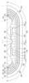
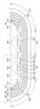
도 1은 일 실시예에 따른 표시 장치의 사시도이다. 도 2는 일 실시예에 따른 표시 장치의 분해 사시도이다.1 is a perspective view of a display device according to an exemplary embodiment. 2 is an exploded perspective view of a display device according to an exemplary embodiment.
도 1 및 도 2를 참조하면, 일 실시예에 따른 표시 장치(10)는 커버 윈도우(100), 터치 감지 장치(200), 터치 회로 보드(210), 터치 구동부(220), 표시 패널(300), 표시 회로 보드(310), 표시 구동부(320), 제1 방수 부재(410), 제2 방수 부재(420), 제3 방수 부재(430), 제4 방수 부재(440), 제1 전파 차단 부재(450), 제2 전파 차단 부재(460), 제3 전파 차단 부재(470), 제4 전파 차단 부재(480), 제1 압력 센서(510), 제2 압력 센서(520), 미들 프레임(600), 메인 회로 보드(700), 제1 진동 발생 장치(810), 제2 진동 발생 장치(820), 제3 진동 발생 장치(830), 제4 진동 발생 장치(840), 및 하부 커버(900)를 포함한다.1 and 2 , the
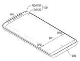
본 명세서에서, “상부”, “탑”, “상면”은 표시 패널(300)을 기준으로 윈도우(100)가 배치되는 방향, 즉 Z축 방향을 가리키고, “하부”, “바텀”, “하면”은 표시 패널(300)을 기준으로 미들 프레임(600)이 배치되는 방향, 즉 Z축 방향의 반대 방향을 가리킨다. 또한, “좌”, “우”, “상”, “하”는 표시 패널(300)을 평면에서 바라보았을 때의 방향을 가리킨다. 예를 들어, “좌”는 X축 방향의 반대 방향, “우”는 X축 방향, “상”은 Y축 방향, “하”는 Y축 방향의 반대 방향을 가리킨다.In this specification, "upper", "top", and "upper surface" refer to the direction in which the
표시 장치(10)는 평면 상 직사각형 형태로 이루어질 수 있다. 예를 들어, 표시 장치(10)는 도 1 및 도 2와 같이 제1 방향(X축 방향)의 단변과 제2 방향(Y축 방향)의 장변을 갖는 직사각형의 평면 형태를 가질 수 있다. 제1 방향(X축 방향)의 단변과 제2 방향(Y축 방향)의 장변이 만나는 모서리는 소정의 곡률을 갖도록 둥글게 형성되거나 직각으로 형성될 수 있다. 표시 장치(10)의 평면 형태는 직사각형에 한정되지 않고, 다른 다각형, 원형 또는 타원형으로 형성될 수 있다.The
표시 장치(10)는 평탄하게 형성된 제1 영역(DR1)과 제1 영역(DR1)의 좌우 측들로부터 연장된 제2 영역(DR2)을 포함할 수 있다. 제2 영역(DR2)은 평탄하게 형성되거나 곡면으로 형성될 수 있다. 제2 영역(DR2)이 평탄하게 형성되는 경우, 제1 영역(DR1)과 제2 영역(DR2)이 이루는 각도는 둔각일 수 있다. 제2 영역(DR2)이 곡면으로 형성되는 경우, 일정한 곡률을 갖거나 변화하는 곡률을 가질 수 있다.The
도 1에서는 제2 영역(DR2)이 제1 영역(DR1)의 좌우 측들 각각에서 연장된 것을 예시하였으나, 이에 한정되지 않는다. 즉, 제2 영역(DR2)은 제1 영역(DR1)의 좌우 측들 중 어느 한 측에서만 연장될 수 있다. 또는, 제2 영역(DR2)은 제1 영역(DR1)의 좌우 측들뿐만 아니라 상하 측들 중 적어도 어느 하나에서도 연장될 수 있다. 이하에서는, 제2 영역(DR2)이 표시 장치(10)의 좌우 측 가장자리에 배치된 것을 중심으로 설명한다.1 illustrates that the second region DR2 extends from each of the left and right sides of the first region DR1, but is not limited thereto. That is, the second region DR2 may extend only on one of the left and right sides of the first region DR1. Alternatively, the second region DR2 may extend on at least one of the upper and lower sides as well as the left and right sides of the first region DR1. Hereinafter, the second region DR2 disposed at the left and right edges of the
커버 윈도우(100)는 표시 패널(300)의 상면을 커버하도록 표시 패널(300)의 상부에 배치될 수 있다. 이로 인해, 커버 윈도우(100)는 표시 패널(300)의 상면을 보호하는 기능을 할 수 있다. 커버 윈도우(100)는 도 15와 같이 제1 접착 부재(910)를 통해 터치 감지 장치(200)에 부착될 수 있다. 제1 접착 부재(910)는 투명 접착 필름(optically cleared adhesive film, OCA) 또는 투명 접착 레진(optically cleared resin, OCR)일 수 있다.The
커버 윈도우(100)는 표시 패널(300)에 대응하는 투과부(DA100)와 표시 패널(300) 이외의 영역에 대응하는 차광부(NDA100)를 포함할 수 있다. 커버 윈도우(100)는 제1 영역(DR1)과 제2 영역(DR2)들에 배치될 수 있으며, 투과부(DA100)는 제1 영역(DR1)의 일부와 제2 영역(DR2)들의 일부에 배치될 수 있다. 차광부(NDA100)는 불투명하게 형성될 수 있다. 또는, 차광부(NDA100)는 화상을 표시하지 않는 경우에 사용자에게 보여줄 수 있는 패턴이 형성된 데코층으로 형성될 수 있다. 예를 들어, 차광부(NDA100)에는 “SAMSUNG”과 같이 회사의 로고 또는 다양한 문자가 패턴될 수 있다.The
커버 윈도우(100)의 차광부(NDA100)에는 전면 카메라, 전면 스피커, 적외선 센서, 초음파 센서, 조도 센서 등을 노출하기 위한 홀들(HH)이 형성될 수 있으나, 이에 한정되지 않는다. 예를 들어, 전면 카메라, 전면 스피커, 적외선 센서, 초음파 센서, 조도 센서 중 일부 또는 전부가 표시 패널(300)에 내장될 수 있으며, 이 경우 홀들(HH)의 일부 또는 전부가 삭제될 수 있다.Holes HH for exposing a front camera, a front speaker, an infrared sensor, an ultrasonic sensor, an illuminance sensor, and the like may be formed in the light blocking portion NDA100 of the
커버 윈도우(100)는 유리, 사파이어, 및/또는 플라스틱으로 이루어질 수 있다. 커버 윈도우(100)는 리지드(rigid)하거나 플렉시블(flexible)하게 형성될 수 있다.The
터치 감지 장치(200)는 커버 윈도우(100)와 표시 패널(300) 사이에 배치될 수 있다. 터치 감지 장치(200)는 제1 영역(DR1)과 제2 영역(DR2)들에 배치될 수 있다. 이로 인해, 제1 영역(DR1)뿐만 아니라 제2 영역(DR2)들에서도 사용자의 터치를 감지할 수 있다.The
터치 감지 장치(200)는 제1 접착 부재(910)를 통해 커버 윈도우(100)의 하면에 부착될 수 있다. 터치 감지 장치(200) 상에 외부 광 반사로 인한 시인성 저하를 방지하기 위해 편광 필름이 추가될 수 있다. 이 경우, 편광 필름이 제1 접착 부재(910)를 통해 커버 윈도우(100)의 하면에 부착될 수 있다.The
터치 감지 장치(200)는 사용자의 터치 위치를 감지하기 위한 장치로서, 자기 용량(self-capacitance) 방식 또는 상호 용량(mutual capacitance) 방식과 같이 정전 용량 방식으로 구현될 수 있다. 터치 감지 장치(200)가 자기 용량 방식으로 구현되는 경우 터치 구동 전극들만 포함하는 반면에, 상호 용량 방식으로 구현되는 경우 터치 구동 전극들과 터치 감지 전극들을 포함할 수 있다. 이하에서는, 터치 감지 장치가 상호 용량 방식으로 구현되는 것을 중심으로 설명한다.The
터치 감지 장치(200)는 패널 형태 또는 필름 형태로 형성될 수 있다. 이 경우, 터치 감지 장치(200)는 도 15와 같이 제2 접착 부재(920)를 통해 표시 패널(300)의 박막 봉지막 상에 부착될 수 있다. 제2 접착 부재(920)는 투명 접착 필름(OCA) 또는 투명 접착 레진(OCR)일 수 있다.The
또는, 터치 감지 장치(200)는 표시 패널(300)과 일체로 형성될 수 있다. 이 경우, 터치 감지 장치(200)의 터치 구동 전극들과 터치 감지 전극들은 표시 패널(300)의 박막 봉지막 상에 형성될 수 있다.Alternatively, the
터치 감지 장치(200)의 일 측에는 터치 회로 보드(210)가 부착될 수 있다. 구체적으로, 터치 회로 보드(210)는 이방성 도전 필름(anisotropic conductive film)을 이용하여 터치 감지 장치(200)의 일 측에 마련된 패드들 상에 부착될 수 있다. 또한, 터치 회로 보드(210)의 일 측 끝단에는 터치 접속부가 마련될 수 있으며, 터치 접속부는 표시 회로 보드(310)의 커넥터에 연결될 수 있다. 터치 회로 보드는 연성 인쇄 회로 기판(flexible printed circuit board)일 수 있다.A
터치 구동부(220)는 터치 감지 장치(200)의 터치 구동 전극들에 터치 구동 신호들을 인가하고, 터치 감지 장치(200)의 터치 감지 전극들로부터 감지 신호들을 감지하며, 감지 신호들을 분석하여 사용자의 터치 위치를 산출할 수 있다. 터치 구동부(220)는 집적회로(integrated circuit)로 형성되어 터치 회로 보드(210) 상에 장착될 수 있다.The
표시 패널(300)은 터치 감지 장치(200)의 하부에 배치될 수 있다. 표시 패널(300)은 커버 윈도우(100)의 투과부(100DA)에 중첩되게 배치될 수 있다. 표시 패널(300)은 제1 영역(DR1)과 제2 영역(DR2)들에 배치될 수 있다. 이로 인해, 제1 영역(DR1)뿐만 아니라 제2 영역(DR2)들에서도 표시 패널(300)의 영상이 보일 수 있다.The
표시 패널(300)은 발광 소자(light emitting element)를 포함하는 발광 표시 패널일 수 있다. 예를 들어, 표시 패널(300)은 유기 발광 다이오드(organic light emitting diode)를 이용하는 유기 발광 표시 패널, 및 초소형 발광 다이오드(micro LED)를 이용하는 초소형 발광 다이오드 표시 패널, 및 양자점 발광 소자(Quantum dot Light Emitting Diode)를 포함하는 양자점 발광 표시 패널일 수 있다.The
표시 패널(300)은 기판, 기판 상에 배치된 박막 트랜지스터층, 발광 소자층, 및 박막 봉지층(thin film encapsulation layer)을 포함할 수 있다.The
표시 패널(300)은 유연하게 구현되므로, 플라스틱으로 형성될 수 있다. 이 경우, 기판은 유연한 기판과 지지 기판을 포함할 수 있다. 지지 기판은 유연한 기판을 지지하기 위한 것이므로, 유연한 기판 대비 유연성이 적을 수 있다. 유연한 기판과 지지 기판 각각은 유연성을 갖는 고분자 물질을 포함할 수 있다. 예를 들어, 유연한 기판과 지지 기판 각각은 폴리에테르술폰(polyethersulphone: PES), 폴리아크릴레이트(polyacrylate: PA), 폴리아릴레이트(polyarylate: PAR), 폴리에테르이미드(polyetherimide: PEI), 폴리에틸렌나프탈레이트(polyethylenenapthalate: PEN), 폴리에틸렌 테레프탈레이드(polyethyleneterepthalate: PET), 폴리페닐렌설파이드 (polyphenylenesulfide: PPS), 폴리알릴레이트(polyallylate), 폴리이미드(polyimide: PI), 폴리카보네이트(polycarbonate: PC), 셀룰로오스 트리아세테이트(cellulosetriacetate: CAT), 셀룰로오스 아세테이트 프로피오네이트(cellulose acetate propionate: CAP) 또는 이들의 조합일 수 있다.Since the
기판 상에는 박막 트랜지스터층이 배치된다. 박막 트랜지스터층은 스캔 라인들, 데이터 라인들, 및 박막 트랜지스터들을 포함할 수 있다. 박막 트랜지스터들 각각은 게이트 전극, 반도체층, 소스 및 드레인 전극들을 포함한다. 스캔 구동부가 기판 상에 직접 형성되는 경우, 박막 트랜지스터층과 함께 형성될 수 있다.A thin film transistor layer is disposed on the substrate. The thin film transistor layer may include scan lines, data lines, and thin film transistors. Each of the thin film transistors includes a gate electrode, a semiconductor layer, and source and drain electrodes. When the scan driver is directly formed on the substrate, it may be formed together with the thin film transistor layer.
박막 트랜지스터층 상에는 발광 소자층이 배치된다. 발광 소자층은 애노드 전극들, 발광층, 캐소드 전극, 및 뱅크들을 포함한다. 발광층은 유기 물질을 포함하는 유기 발광층을 포함할 수 있다. 예를 들어, 발광층은 정공 주입층(hole injection layer), 정공 수송층(hole transporting layer), 유기 발광층(organic light emitting layer), 전자 수송층(electron transporting layer), 및 전자 주입층(electron injection layer)을 포함할 수 있다. 정공 주입층 및 전자 주입층은 생략될 수 있다. 애노드 전극과 캐소드 전극에 전압이 인가되면 정공과 전자가 각각 정공 수송층과 전자 수송층을 통해 유기 발광층으로 이동되며, 유기 발광층에서 서로 결합하여 발광하게 된다. 발광 소자층은 화소들이 형성되는 화소 어레이층일 수 있으며, 이로 인해 발광 소자층이 형성된 영역은 이미지를 표시하는 표시영역으로 정의될 수 있다. 표시영역의 주변 영역은 비표시영역으로 정의될 수 있다.A light emitting element layer is disposed on the thin film transistor layer. The light emitting element layer includes anode electrodes, a light emitting layer, a cathode electrode, and banks. The light emitting layer may include an organic light emitting layer including an organic material. For example, the light emitting layer includes a hole injection layer, a hole transporting layer, an organic light emitting layer, an electron transporting layer, and an electron injection layer. can include The hole injection layer and the electron injection layer may be omitted. When voltage is applied to the anode electrode and the cathode electrode, holes and electrons move to the organic light emitting layer through the hole transport layer and the electron transport layer, respectively, and combine with each other in the organic light emitting layer to emit light. The light emitting element layer may be a pixel array layer in which pixels are formed, and thus, an area in which the light emitting element layer is formed may be defined as a display area for displaying an image. An area around the display area may be defined as a non-display area.
발광 소자층 상에는 봉지층이 배치된다. 봉지층은 발광 소자층에 산소 또는 수분이 침투되는 것을 방지하는 역할을 한다. 봉지층은 적어도 하나의 무기막과 적어도 하나의 유기막을 포함할 수 있다.An encapsulation layer is disposed on the light emitting element layer. The encapsulation layer serves to prevent penetration of oxygen or moisture into the light emitting element layer. The encapsulation layer may include at least one inorganic layer and at least one organic layer.
표시 패널(300)의 일 측에는 표시 회로 보드(310)가 부착될 수 있다. 구체적으로, 표시 회로 보드(310)는 이방성 도전 필름을 이용하여 표시 패널(300)의 일 측에 마련된 패드들 상에 부착될 수 있다. 터치 회로 보드(210) 역시 표시 패널(300)의 하면으로 구부러질 수 있으며, 터치 회로 보드(210)의 일 측 끝단에 배치된 터치 접속부는 표시 회로 보드(310)의 커넥터에 연결될 수 있다. 표시 회로 보드(310)에 대한 자세한 설명은 도 3 및 도 4를 결부하여 후술한다.A
표시 구동부(320)는 표시 회로 보드(310)를 통해 표시 패널(300)을 구동하기 위한 신호들과 전압들을 출력한다. 표시 구동부(320)는 집적회로로 형성되어 표시 회로 보드(310) 상에 장착될 수 있으나, 이에 한정되지 않는다. 예를 들어, 표시 구동부(320)는 표시 패널(300)의 기판의 상면 또는 하면의 일 측에 부착될 수 있다.The
표시 패널(300)의 하부에는 도 15와 같이 패널 하부 부재(390)가 배치될 수 있다. 패널 하부 부재(390)는 제3 접착 부재(930)를 통해 표시 패널(300)의 하면에 부착될 수 있다. 제3 접착 부재(930)는 투명 접착 필름(OCA) 또는 투명 접착 레진(OCR)일 수 있다.A panel
패널 하부 부재(390)는 외부로부터 입사되는 광을 흡수하기 위한 광 흡수 부재, 외부로부터의 충격을 흡수하기 위한 완충 부재, 표시 패널(300)의 열을 효율적으로 방출하기 위한 방열 부재, 및 외부로부터 입사되는 광을 차단하기 위한 차광층 중 적어도 하나를 포함할 수 있다.The
광 흡수 부재는 표시 패널(300)의 하부에 배치될 수 있다. 광 흡수 부재는 광의 투과를 저지하여 광 흡수 부재의 하부에 배치된 구성들, 즉 제1 방수 부재(410), 제1 압력 센서(510), 제2 방수 부재(420), 제2 압력 센서(520), 및 표시 회로 보드(310)가 표시 패널(300)의 상부에서 시인되는 것을 방지한다. 광 흡수 부재는 블랙 안료나 염료 등과 같은 광 흡수 물질을 포함할 수 있다.The light absorbing member may be disposed below the
완충 부재는 광 흡수 부재의 하부에 배치될 수 있다. 완충 부재는 외부 충격을 흡수하여 표시 패널(300)이 파손되는 것을 방지한다. 완충 부재는 단일층 또는 복수층으로 이루어질 수 있다. 예를 들어, 완충 부재는 폴리우레탄(polyurethane), 폴리카보네이트(polycarbonate), 폴리프로필렌(polypropylene), 폴리에틸렌(polyethylene)등과 같은 고분자 수지로 형성되거나, 고무, 우레탄 계열 물질, 또는 아크릴 계열 물질을 발포 성형한 스폰지 등 탄성을 갖는 물질을 포함하여 이루어질 수 있다. 완충 부재는 쿠션층일 수 있다.The buffer member may be disposed below the light absorbing member. The buffer member absorbs an external shock and prevents the
방열 부재는 완충 부재의 하부에 배치될 수 있다. 방열 부재는 그라파이트나 탄소 나노 튜브 등을 포함하는 제1 방열층과 전자기파를 차폐할 수 있고 열전도성이 우수한 구리, 니켈, 페라이트, 은과 같은 금속 박막으로 형성된 제2 방열층을 포함할 수 있다.The heat dissipation member may be disposed below the buffer member. The heat dissipation member may include a first heat dissipation layer including graphite or carbon nanotubes, and a second heat dissipation layer formed of a metal thin film such as copper, nickel, ferrite, or silver that can shield electromagnetic waves and has excellent thermal conductivity.
제1 방수 부재(410), 제2 방수 부재(420), 제1 압력 센서(510), 및 제2 압력 센서(520)는 제2 영역(DR2)에 배치될 수 있다. 즉, 제1 방수 부재(410)와 제1 압력 센서(510)는 표시 패널(300)의 우측 가장자리에서 표시 패널(300)의 하부에 배치될 수 있다. 제2 방수 부재(420)와 제2 압력 센서(520)는 표시 패널(300)의 좌측 가장자리에서 표시 패널(300)의 하부에 배치될 수 있다. 제1 압력 센서(510)와 제2 압력 센서(520)는 서로 마주보도록 배치되고, 제1 방수 부재(410)와 제2 방수 부재(420)는 서로 마주보도록 배치될 수 있다.The first
제1 압력 센서(510)는 패널 하부 부재(390)의 하면에 부착될 수 있다. 제1 방수 부재(410)는 제1 압력 센서(510)의 하면에 부착될 수 있다. 추가로, 표시 패널(300)과 제1 압력 센서(510) 사이로 수분이나 분진이 침투하는 것을 방지하기 위해, 제1 방수 부재(410)는 제1 압력 센서(510)의 적어도 일 측면에 부착될 수 있다. 제1 압력 센서의 적어도 일 측면은 표시 패널(300)의 우측 가장자리에 인접한 측면일 수 있다.The
제2 압력 센서(520)는 패널 하부 부재(390)의 하면에 부착될 수 있다. 제2 방수 부재(420)는 제2 압력 센서(520)의 하면에 부착될 수 있다. 추가로, 표시 패널(300)과 제2 압력 센서(520) 사이로 수분이나 분진이 침투하는 것을 방지하기 위해, 제1 방수 부재(420)는 제1 압력 센서(520)의 적어도 일 측면에 부착될 수 있다. 제2 압력 센서의 적어도 일 측면은 표시 패널(300)의 좌측 가장자리에 인접한 측면일 수 있다.The
또한, 제3 방수 부재(430)는 표시 패널(300)의 상측 가장자리에서 표시 패널(300)의 하부에 배치되고, 제4 방수 부재(440)는 표시 패널(300)의 하측 가장자리에서 표시 패널(300)의 하부에 배치될 수 있다. 제3 방수 부재(430)와 제4 방수 부재(440)는 서로 마주보도록 배치될 수 있다.In addition, the third
한편, 표시 패널(300)과 미들 프레임(600) 사이의 갭이 상측 가장자리와 하측 가장자리보다 좌측 가장자리와 우측 가장자리에서 더 크기 때문에, 제1 방수 부재(410)의 높이와 제2 방수 부재(420)의 높이는 제3 방수 부재(430)의 높이 또는 제4 방수 부재(440)의 높이보다 높게 형성될 수 있다.Meanwhile, since the gap between the
한편, 수분이나 분진이 침투하는 것을 방지하기 위해, 제1 방수 부재(410)와 제3 방수 부재(430)의 사이, 제1 방수 부재(420)와 제4 방수 부재(440)의 사이, 제2 방수 부재(420)와 제3 방수 부재(430)의 사이, 및 제2 방수 부재(420)와 제4 방수 부재(440)의 사이에 방수 레진층이 형성될 수 있다.On the other hand, in order to prevent penetration of moisture or dust, between the first
제1 방수 부재(410), 제2 방수 부재(420), 제3 방수 부재(430), 및 제4 방수 부재(440) 각각은 베이스 필름과 베이스 필름의 일 면 상에 배치되는 제1 점착막, 및 베이스 필름의 타면 상에 배치되는 제2 점착막을 포함할 수 있다. 베이스 필름은 폴리에틸렌 테레프탈레이드(polyethyleneterepthalate: PET), 폴리에틸렌 테레프탈레이드(polyethyleneterepthalate: PET)와 쿠션층, 또는 폴리에틸렌 폼(PE-foam)일 수 있다. 제1 점착막과 제2 점착막은 압력 민감 점착제(pressure sensitive adhesive, PSA)일 수 있다.The first
도 1 및 도 2에 도시된 실시예에 의하면, 제1 방수 부재(410), 제2 방수 부재(420), 제3 방수 부재(430), 및 제4 방수 부재(440)에 의해 표시 패널(300)의 하면의 가장자리들과 미들 프레임(600)의 상면의 가장자리들을 부착하므로, 표시 패널(300)과 미들 프레임(600) 사이로 수분이나 분진이 침투하는 것을 방지할 수 있다. 즉, 방수 및 방진이 가능한 표시 장치(10)가 제공될 수 있다.According to the exemplary embodiment shown in FIGS. 1 and 2 , the display panel ( Since the edges of the lower surface of the
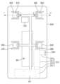
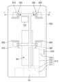
제1 압력 센서(510)와 제2 압력 센서(520)는 제3 회로 보드(550)를 통해 표시 회로 보드(310)에 연결될 수 있다. 도 3에서는 제1 압력 센서(510)와 제2 압력 센서(520)가 하나의 제3 회로 보드(550)에 연결된 것을 예시하였으나, 이에 한정되지 않는다. 즉, 표시 장치(10)는 복수의 제3 회로 보드(550)들을 포함할 수 있으며, 제1 압력 센서(510)가 하나의 제3 회로 보드(550)를 통해 표시 회로 보드(310)에 연결되고, 제2 압력 센서(520)가 다른 제3 회로 보드(550)를 통해 표시 회로 보드(310)에 연결될 수 있다.The
도 2와 도 3과 같이 표시 회로 보드(310) 상에는 제1 압력 센서(510)와 제2 압력 센서(520)를 구동하여 압력을 감지하기 위한 압력 감지부(330)가 장착될 수 있다. 이 경우, 압력 감지부(330)는 집적회로로 형성될 수 있다. 압력 감지부(330)는 표시 구동부(320)에 통합되어 하나의 집적회로로 형성될 수 있다.As shown in FIGS. 2 and 3 , a
또는, 제3 회로 보드(550)는 표시 회로 보드(310)가 아닌 터치 회로 보드(210)에 연결될 수 있다. 이 경우, 압력 감지부(330)는 터치 회로 보드(210) 상에 장착될 수 있다. 압력 감지부(330)는 터치 구동부(220)에 통합되어 하나의 집적회로로 형성될 수 있다.Alternatively, the
패널 하부 부재(390)의 하부에는 미들 프레임(600)이 배치될 수 있다. 미들 프레임(600)은 합성 수지, 금속, 또는 합성 수지와 금속을 모두 포함할 수 있다.A
미들 프레임(600)에는 카메라 장치(720)가 삽입되는 제1 카메라 홀(CMH1), 배터리의 발열을 해소하기 위한 배터리 홀(BH), 및 표시 회로 보드(310)에 접속된 제2 연결 케이블(314)이 통과하는 케이블 홀(FH)이 형성될 수 있다. 케이블 홀(FH)은 제2 영역(DR2)에 배치될 수 있다. 구체적으로, 케이블 홀(FH)은 미들 프레임(600)의 우측 가장자리에 배치될 수 있으며, 이 경우 표시 패널(300)의 우측 가장자리에서 표시 패널(300)의 하부에 배치되는 제1 방수 부재(410)와 제1 압력 센서(510)에 의해 가려질 수 있다. 따라서, 제1 방수 부재(410)와 제1 압력 센서(510)는 도 2와 같이 케이블 홀(FH)을 가리지 않고 노출하기 위해 노치(notch) 형태로 오목하게 형성된 오목부(NTH)를 포함할 수 있다.In the
또한, 미들 프레임(600)은 표시 패널(300)의 패널 하부 부재(390), 제1 방수 부재(410), 제2 방수 부재(420), 제3 방수 부재(430), 제4 방수 부재(440), 제1 압력 센서(510), 및 제2 압력 센서(520)의 하부에 배치된다. 이로 인해, 미들 프레임(600)은 제1 압력 센서(510)와 제2 압력 센서(520)에 압력이 인가되는 경우, 제1 압력 센서(510)와 제2 압력 센서(520)를 지지할 수 있다. 따라서, 제1 압력 센서(510)와 제2 압력 센서(520)는 인가된 압력을 감지할 수 있다.In addition, the
복수의 진동 발생 장치들은 미들 프레임(600)의 상부에 배치될 수 있으며, 복수의 진동 발생 장치들 각각의 복수의 측면들은 전파 차단 부재에 의해 둘러싸일 수 있다. 이하에서는, 설명의 편의를 위해, 4 개의 진동 발생 장치들이 미들 프레임(600)의 상부에 배치되는 것을 중심으로 설명한다.A plurality of vibration generating devices may be disposed above the
제1 진동 발생 장치(810), 제2 진동 발생 장치(820), 제3 진동 발생 장치(830), 및 제4 진동 발생 장치(840)는 미들 프레임(600)의 상부에 배치되며, 구체적으로 미들 프레임(600)의 상면에 부착될 수 있다. 제1 진동 발생 장치(810)와 제3 진동 발생 장치(830)는 제1 압력 센서(510)에 인접하게 배치되고, 제2 진동 발생 장치(820)와 제4 진동 발생 장치(840)는 제2 압력 센서(520)에 인접하게 배치될 수 있다.The first
제1 압력 센서(510)는 제1 진동 발생 장치(810)와 제3 진동 발생 장치(830)에 비해 표시 패널(300) 또는 미들 프레임(600)의 제1 측 끝단에 가까이 배치될 수 있다. 제2 압력 센서(520)는 제2 진동 발생 장치(820)와 제4 진동 발생 장치(840)에 비해 표시 패널(300) 또는 미들 프레임(600)의 제2 측 끝단에 가까이 배치될 수 있다. 도 2와 같이 표시 패널(300) 또는 미들 프레임(600)의 제1 측은 우측이고, 제2 측은 좌측일 수 있다.The
제1 진동 발생 장치(810)는 제3 진동 발생 장치(830)에 비해 상측에 인접하게 배치되고, 제2 진동 발생 장치(820)는 제4 진동 발생 장치(840)에 비해 상측에 인접하게 배치될 수 있다.The first
제1 진동 발생 장치(810), 제2 진동 발생 장치(820), 제3 진동 발생 장치(830), 및 제4 진동 발생 장치(840)는 제4 회로 보드(890)를 통해 표시 회로 보드(310)의 진동 구동부(340)에 연결될 수 있다. 도 4에서는 제1 진동 발생 장치(810), 제2 진동 발생 장치(820), 제3 진동 발생 장치(830), 및 제4 진동 발생 장치(840)가 하나의 제4 회로 보드(890)에 연결된 것을 예시하였으나, 이에 한정되지 않는다. 즉, 표시 장치(10)는 복수의 제4 회로 보드(890)들을 포함할 수 있으며, 제1 진동 발생 장치(810), 제2 진동 발생 장치(820), 제3 진동 발생 장치(830), 및 제4 진동 발생 장치(840)가 서로 다른 제4 회로 보드(890)들을 통해 표시 회로 보드(310)에 연결될 수 있다. 또는, 제1 진동 발생 장치(810), 제2 진동 발생 장치(820), 제3 진동 발생 장치(830), 및 제4 진동 발생 장치(840) 중 어느 두 개가 하나의 제4 회로 보드(890)를 통해 표시 회로 보드(310)에 연결되고, 다른 두 개가 다른 제4 회로 보드(890)를 통해 표시 회로 보드(310)에 연결될 수 있다.The first
도 2와 도 3과 같이 표시 회로 보드(310) 상에는 제1 진동 발생 장치(810), 제2 진동 발생 장치(820), 제3 진동 발생 장치(830), 및 제4 진동 발생 장치(840)를 구동하기 위한 진동 구동부(340)가 장착될 수 있다. 이 경우, 진동 구동부(340)는 집적회로로 형성될 수 있다. 또는, 진동 구동부(340)는 제4 회로 보드(890) 상에 장착될 수 있다.2 and 3, on the
진동 구동부(340)는 메인 프로세서(710)로부터 입력되는 진동 데이터에 응답하여 제1 진동 발생 장치(810), 제2 진동 발생 장치(820), 제3 진동 발생 장치(830), 및 제4 진동 발생 장치(840) 각각을 구동하기 위한 제1 구동 전압들과 제2 구동 전압들을 생성할 수 있다. 메인 프로세서(710)의 진동 데이터는 메인 회로 보드(700)와 표시 회로 보드(310)의 제2 연결 케이블(314), 제2 회로 보드(312), 제1 연결 케이블(313), 및 제1 회로 보드(311)를 경유하여 진동 구동부(340)에 제공될 수 있다. 진동 구동부(340)의 제1 구동 전압들과 제2 구동 전압들은 표시 회로 보드(310)의 제1 회로 보드(311)와 제4 회로 보드(890)를 경유하여 제1 진동 발생 장치(810), 제2 진동 발생 장치(820), 제3 진동 발생 장치(830), 및 제4 진동 발생 장치(840)에 제공될 수 있다.The
진동 구동부(340)는 디지털 신호인 진동 데이터를 처리하는 디지털 신호 처리부(digital signal processer, DSP), 디지털 신호 처리부에서 처리된 디지털 신호인 진동 데이터를 아날로그 신호인 제1 구동 전압들과 제2 구동 전압들로 변환하는 디지털 아날로그 변환부(digital analog converter, DAC), 디지털 아날로그 변환부에서 변환된 아날로그 신호인 제1 구동 전압들과 제2 구동 전압들을 증폭하여 출력하는 증폭기(amplifier, AMP) 등을 포함할 수 있다.The
메인 프로세서(710)는 제1 내지 제4 진동 발생 장치들(810, 820, 830, 840)의 진동 세기 및/또는 진동 주기가 서로 다르게 진동하도록 제어할 수 있다. 예를 들어, 제1 진동 발생 장치(810)가 가장 세게 진동하고, 제2 진동 발생 장치(820)가 두 번째로 세게 진동하며, 제3 진동 발생 장치(830)가 세 번째로 세게 진동하고, 제4 진동 발생 장치(840)가 가장 약하게 진동할 수 있다. 또는, 제1 진동 발생 장치(810)가 가장 높은 주기로 진동하고, 제2 진동 발생 장치(820)가 두 번째로 높은 주기로 진동하며, 제3 진동 발생 장치(830)가 세 번째로 높은 주기로 진동하고, 제4 진동 발생 장치(840)가 가장 낮은 주기로 진동할 수 있다.The
또한, 제1 진동 발생 장치(810), 제2 진동 발생 장치(820), 제3 진동 발생 장치(830), 및 제4 진동 발생 장치(840) 각각은 진동을 발생하여 음향을 출력할 수 있는 음향 발생 장치로 구현될 수도 있다. 제1 진동 발생 장치(810), 제2 진동 발생 장치(820), 제3 진동 발생 장치(830), 및 제4 진동 발생 장치(840)에 대한 자세한 설명은 도 10 내지 도 12를 결부하여 후술한다.In addition, each of the first
제1 전파 차단 부재(450)는 제1 진동 발생 장치(810)에 의해 발생되는 진동이 전파되는 것을 차단하기 위해, 제1 진동 발생 장치(810)의 복수의 측면들을 둘러싸도록 배치될 수 있다. 제2 전파 차단 부재(460)는 제2 진동 발생 장치(820)에 의해 발생되는 진동이 전파되는 것을 차단하기 위해, 제2 진동 발생 장치(820)의 복수의 측면들을 둘러싸도록 배치될 수 있다. 제3 전파 차단 부재(470)는 제3 진동 발생 장치(830)에 의해 발생되는 진동이 전파되는 것을 차단하기 위해, 제3 진동 발생 장치(830)의 복수의 측면들을 둘러싸도록 배치될 수 있다. 제4 전파 차단 부재(480)는 제4 진동 발생 장치(840)에 의해 발생되는 진동이 전파되는 것을 차단하기 위해, 제4 진동 발생 장치(840)의 복수의 측면들을 둘러싸도록 배치될 수 있다.The first electromagnetic
도 2 및 도 3에서는 제1 진동 발생 장치(810)가 사각형의 평면 형태를 가지며, 제1 전파 차단 부재(450)가 제1 진동 발생 장치(810)의 모든 측면들을 둘러싸는 것을 예시하였으나, 이에 한정되지 않는다. 제1 진동 발생 장치(810)가 미들 프레임(600)의 모서리에 배치되는 경우, 제1 전파 차단 부재(450)는 제1 진동 발생 장치(810)의 두 개의 측면들을 둘러싸도록 배치될 수 있다. 또한, 제1 진동 발생 장치(810)가 미들 프레임(600)의 좌측, 우측, 상측 또는 하측 가장자리에 배치되는 경우, 제1 전파 차단 부재(450)는 제1 진동 발생 장치(810)의 세 개의 측면들을 둘러싸도록 배치될 수 있다. 제2 전파 차단 부재(460), 제3 전파 차단 부재(470), 및 제4 전파 차단 부재(480) 각각 역시 그의 배치 위치에 따라 제1 진동 발생 장치(810)와 실질적으로 동일하게 두 개의 측면들, 세 개의 측면들, 또는 모든 측면들을 둘러싸도록 배치될 수 있다.2 and 3 illustrate that the first
도 1 및 도 2에 도시된 실시예에 의하면, 제1 진동 발생 장치(810)에 의한 진동은 제1 전파 차단 부재(450 )에 의해 차단되므로, 사용자는 제1 진동 발생 장치(810)가 진동하는 경우, 제1 진동 발생 장치(810)가 배치된 위치에서 국부적으로 진동을 느낄 수 있다. 또한, 사용자는 제2 진동 발생 장치(820)에 의한 진동, 제3 진동 발생 장치(830)에 의한 진동, 및 제4 진동 발생 장치(840)에 의한 진동 역시 마찬가지로 국부적으로 느낄 수 있다.According to the embodiment shown in FIGS. 1 and 2 , since the vibration by the first
미들 프레임(600)의 하부에는 메인 회로 보드(700)가 배치될 수 있다. 메인 회로 보드(700)는 인쇄 회로 기판(printed circuit board) 또는 연성 인쇄 회로 기판일 수 있다.A
메인 회로 보드(700)는 메인 프로세서(710), 카메라 장치(720), 메인 커넥터(730), 제5 진동 발생 장치(740), 및 제5 전파 차단 부재(750)를 포함할 수 있다.The
메인 프로세서(710)는 미들 프레임(600)과 마주보는 메인 회로 보드(700)의 일 면 상에 배치되는 반면에, 메인 커넥터(730)는 하부 커버(900)와 마주보는 메인 회로 보드(700)의 타 면 상에 배치될 수 있다. 또한, 카메라 장치(720)는 메인 회로 보드(700)의 일면과 타면 모두에 배치될 수 있다. 이 경우, 카메라 장치(720)의 상면은 메인 회로 보드(700)의 타면에 배치되고, 하면은 메인 회로 보드(700)의 일면에 배치될 수 있다.The
메인 프로세서(710)는 표시 장치(10)의 모든 기능을 제어할 수 있다. 예를 들어, 메인 프로세서(710)는 표시 패널(300)이 영상을 표시하도록 영상 데이터를 표시 회로 보드(310)의 표시 구동부(320)로 출력할 수 있다. 또한, 메인 프로세서(710)는 터치 구동부(220)로부터 터치 데이터를 입력 받고 사용자의 터치 위치를 판단한 후, 사용자의 터치 위치에 표시된 아이콘이 지시하는 어플리케이션을 실행할 수 있다. 또한, 메인 프로세서(710)는 터치 구동부(220) 또는 표시 구동부(320)로부터 압력 감지 데이터를 입력 받고, 압력 감지 데이터에 따라 홈 화면을 출력하거나 표시 장치(10)의 음향 크기를 제어하거나 햅틱(haptic)을 구현하도록 제어할 수 있다. 나아가, 메인 프로세서(710)는 제1 진동 발생 장치(810), 제2 진동 발생 장치(820), 제3 진동 발생 장치(830), 및 제4 진동 발생 장치(840)를 진동하기 위한 진동 데이터를 진동 구동부(340)로 출력하고, 제5 진동 발생 장치(740)를 진동하기 위한 진동 신호를 제5 진동 발생 장치(740)로 출력할 수 있다.The
메인 프로세서(710)는 집적회로로 이루어진 어플리케이션 프로세서(application processor), 중앙 처리 장치(central processing unit), 또는 시스템 칩(system chip)일 수 있다.The
카메라 장치(720)는 카메라 모드에서 이미지 센서에 의해 얻어지는 정지 영상 또는 동영상 등의 화상 프레임을 처리하여 메인 프로세서(710)로 출력한다.The
미들 프레임(600)의 커넥터 홀(FH)을 통과한 제2 연결 케이블(314)은 미들 프레임(600)과 메인 회로 보드(700)의 간극(GAP)을 통해 메인 회로 보드(700)의 하면에 배치된 메인 커넥터(730)에 연결될 수 있다. 이로 인해, 메인 회로 보드(700)는 표시 회로 보드(310)와 터치 회로 보드(210)에 전기적으로 연결될 수 있다.The
제5 진동 발생 장치(740)는 편심 모터(eccentric rotating mass, ERM), 선형 공진 액츄에이터(linear resonant actuator, LRA), 또는 피에조 액츄에이터(piezo actuator)와 같은 진동 발생 장치일 수 있다. 제5 진동 발생 장치(740)는 메인 프로세서(710)로부터 입력되는 진동 신호에 따라 진동을 발생할 수 있다. 도 2에서는 제5 진동 발생 장치(740)가 메인 회로 보드(700)의 상측 가장자리에 배치된 것을 예시하였으나, 이에 한정되지 않는다.The fifth
제5 전파 차단 부재(750)는 제5 진동 발생 장치(740)에 의해 발생되는 진동이 전파되는 것을 차단하기 위해, 제5 진동 발생 장치(740)의 복수의 측면들을 둘러싸도록 배치될 수 있다. 도 2에서는 제5 전파 차단 부재(750)가 제5 진동 발생 장치(740)의 모든 측면들을 둘러싸는 것을 예시하였으나, 이에 한정되지 않는다. 제5 진동 발생 장치(740)가 메인 회로 보드(700)의 모서리에 배치되는 경우, 제5 전파 차단 부재(750)는 제5 진동 발생 장치(740)의 두 개의 측면들을 둘러싸도록 배치될 수 있다. 또한, 제5 진동 발생 장치(740)가 미들 프레임(600)의 좌측, 우측, 상측 또는 하측 가장자리에 배치되는 경우, 제5 전파 차단 부재(750)는 제5 진동 발생 장치(740)의 세 개의 측면들을 둘러싸도록 배치될 수 있다.The fifth electromagnetic
제5 전파 차단 부재(750)는 플라스틱, 스틸(steel) 또는 방수 테이프와 같은 방수 부재로 이루어질 수 있다. 제5 전파 차단 부재(750)에 의해 제5 진동 발생 장치(740)의 진동을 효과적으로 차단하기 위해서는, 제5 전파 차단 부재(750)가 메인 회로 보드(700)의 상면과 미들 프레임(600)의 하면에 부착되는 것이 바람직하다.The fifth radio
이외, 메인 회로 보드(700)에는 이동 통신망 상에서 기지국, 외부의 단말, 서버 중 적어도 하나와 무선 신호를 송수신할 수 있는 이동 통신 모듈이 더 장착될 수 있다. 무선 신호는 음성 신호, 화상 통화 신호, 또는 문자/멀티미디어 메시지 송수신에 따른 다양한 형태의 데이터를 포함할 수 있다. 또한, 메인 회로 보드(700)에는 음향을 출력할 수 있는 음향 출력 장치, 햅틱 구현을 위해 진동을 발생할 수 있는 진동 발생 장치가 더 장착될 수 있다.In addition, a mobile communication module capable of transmitting and receiving radio signals with at least one of a base station, an external terminal, and a server on a mobile communication network may be further mounted on the
하부 커버(900)는 미들 프레임(600)과 메인 회로 보드(700)의 하부에 배치될 수 있다. 하부 커버(900)는 미들 프레임(600)과 체결되어 고정될 수 있다. 하부 커버(900)는 표시 장치(1)의 하면 외관을 형성할 수 있다. 하부 커버(900)는 플라스틱, 및/또는 금속을 포함할 수 있다. 하부 커버(900)에는 카메라 장치(720)가 삽입되어 외부로 돌출되는 제2 카메라 홀(CMH2)이 형성될 수 있다.The
한편 , 카메라 장치(720)의 위치와 카메라 장치(720)에 대응되는 제1 및 제2 카메라 홀들(CMH1, CMH2)의 위치는 도 1, 도 2, 도 4, 및 도 5에 도시된 실시예에 한정되지 않는다.Meanwhile, the location of the
도 3은 일 실시예에 따른 표시 패널의 일 예를 보여주는 저면도이다. 도 4는 일 실시예에 따른 미들 프레임의 일 예를 보여주는 평면도이다. 도 5는 일 실시예에 따른 미들 프레임과 메인 회로 보드의 저면도이다.3 is a bottom view illustrating an example of a display panel according to an exemplary embodiment. 4 is a plan view showing an example of a middle frame according to an embodiment. 5 is a bottom view of a middle frame and a main circuit board according to an embodiment.
이하에서는, 도 3 내지 도 5를 참조하여, 표시 회로 보드(310)와 제3 회로 보드(550)의 연결과 제2 연결 케이블(314)과 메인 회로 보드(700)의 메인 커넥터(730)의 연결에 대하여 상세히 설명한다. 한편, 도 4는 평면도인 반면에 도 3과 도 5는 저면도이므로, 도 3과 도 5에서는 도 4에서의 표시 장치(10)의 좌우가 반대로 도시되어 있음에 주의하여야 한다. 설명의 편의를 위해, 도 4에서는 표시 회로 보드(310)를 일점 쇄선으로 도시하였으며, 도 5에서는 제2 연결 케이블(314)을 일점 쇄선으로 도시하였다.Hereinafter, referring to FIGS. 3 to 5 , the
도 3 내지 도 5를 참조하면, 표시 회로 보드(310)는 제1 회로 보드(311), 제2 회로 보드(312), 및 제1 연결 케이블(313)을 포함할 수 있다.Referring to FIGS. 3 to 5 , the
제1 회로 보드(311)는 표시 패널(300)의 기판의 상면 또는 하면의 일 측에 부착되며, 표시 패널(300)의 기판의 하면으로 구부러질 수 있다. 제1 회로 보드(311)는 고정 부재들에 의해 도 4와 같이 미들 프레임(600)에 형성된 고정 홀(FH)들에 고정될 수 있다.The
제1 회로 보드(311)는 표시 구동부(320), 압력 감지부(330), 제1 커넥터(311a), 제2 커넥터(311b), 및 제3 커넥터(311c)를 포함할 수 있다. 표시 구동부(320), 압력 감지부(330), 제1 커넥터(311a), 제2 커넥터(311b), 및 제3 커넥터(311c)는 제1 회로 보드(311)의 일면 상에 배치될 수 있다.The
제1 커넥터(311a)는 제2 회로 보드(312)에 연결된 제1 연결 케이블(313)의 일 단에 연결될 수 있다. 이로 인해, 제1 회로 보드(311)에 장착된 표시 구동부(320)와 압력 감지부(330)는 제1 연결 케이블(313)을 통해 제2 회로 보드(312)에 전기적으로 연결될 수 있다.The
제2 커넥터(311b)는 제1 압력 센서(510)와 제2 압력 센서(520)에 연결된 제3 회로 보드(550)의 일 단에 연결될 수 있다. 이로 인해, 제1 압력 센서(510)와 제2 압력 센서(520)는 압력 감지부(330)에 전기적으로 연결될 수 있다.The
제3 커넥터(311c)는 제1 진동 발생 장치(810), 제2 진동 발생 장치(820), 제3 진동 발생 장치(830), 및 제4 진동 발생 장치(840)에 연결된 제4 회로 보드(890)의 일 단에 연결될 수 있다. 이로 인해, 제1 진동 발생 장치(810), 제2 진동 발생 장치(820), 제3 진동 발생 장치(830), 및 제4 진동 발생 장치(840) 각각은 표시 회로 보드(310)의 진동 구동부(340)에 전기적으로 연결될 수 있다. 나아가, 표시 회로 보드(310)가 제2 연결 케이블(314)을 통해 메인 회로 보드(700)에 전기적으로 연결되므로, 제1 진동 발생 장치(810), 제2 진동 발생 장치(820), 제3 진동 발생 장치(830), 및 제4 진동 발생 장치(840) 각각은 메인 회로 보드(700)의 메인 프로세서(710)에 전기적으로 연결될 수 있다.The
제2 회로 보드(312)는 터치 커넥터(312a), 제1 연결 커넥터(312b), 및 제2 연결 커넥터(312c)를 포함할 수 있다. 제1 연결 커넥터(312b)와 제2 연결 커넥터(312c)는 제2 회로 보드(312)의 일면 상에 배치되고, 터치 커넥터(312a)는 제2 회로 보드(312)의 타면 상에 배치될 수 있다.The
터치 커넥터(312a)는 터치 회로 보드(210)의 일 단에 연결될 수 있다. 이로 인해, 터치 구동부(220)는 제2 회로 보드(312)에 전기적으로 연결될 수 있다.The
제1 연결 커넥터(312b)는 제1 회로 보드(311)에 연결된 제1 연결 케이블(313)의 타 단에 연결될 수 있다. 이로 인해, 제1 회로 보드(311)에 장착된 표시 구동부(320)와 압력 감지부(330)는 제1 연결 케이블(313)을 통해 제2 회로 보드(312)에 전기적으로 연결될 수 있다.The
제2 연결 커넥터(312c)는 메인 회로 보드(700)의 메인 커넥터(730)에 연결되는 제2 연결 케이블(314)의 일 단에 연결될 수 있다. 이로 인해, 제2 회로 보드(312)는 제2 연결 케이블(314)을 통해 제2 회로 보드(312)에 전기적으로 연결될 수 있다.The
제2 연결 케이블(314)의 타 단에는 커넥터 접속부(315)가 형성될 수 있다. 제2 연결 케이블(314)의 커넥터 접속부(315)는 도 3 및 도 4와 같이 미들 프레임(600)의 케이블 홀(CAH)을 통과하여 미들 프레임(600)의 하면으로 연장될 수 있다. 제1 방수 부재(410)와 제1 압력 센서(510) 각각에는 미들 프레임(600)의 케이블 홀(CAH)에 대응되는 영역에 노치(notch) 형태의 오목부(NTH)가 형성되므로, 미들 프레임(600)의 케이블 홀(CAH)은 제1 방수 부재(410)와 제1 압력 센서(510)에 의해 덮이지 않고 노출될 수 있다.A
또한, 도 5와 같이 미들 프레임(600)과 메인 회로 보드(700) 사이의 간극(GAP)이 미들 프레임(600)의 케이블 홀(CAH)에 대응되는 영역에 형성되므로, 케이블 홀(CAH)을 통과한 제2 연결 케이블(314)의 커넥터 접속부(315)는 미들 프레임(600)과 메인 회로 보드(700) 사이의 간극(GAP)으로 빠져나와 메인 회로 보드(700)의 하면으로 연장될 수 있다. 최종적으로, 제2 연결 케이블(314)의 커넥터 접속부(315)는 메인 회로 보드(700)의 하면에 배치된 메인 커넥터(730)에 연결될 수 있다.5, since the gap (GAP) between the
도 3 내지 도 5에 도시된 실시예에 의하면, 미들 프레임(600)의 케이블 홀(CAH)을 덮지 않도록 제1 방수 부재(410)와 제1 압력 센서(510)에는 노치(notch) 형태의 오목부(NTH)가 형성된다. 이로 인해, 표시 회로 보드(310)에 연결된 제2 연결 케이블(314)이 케이블 홀(CAH)을 통해 미들 프레임(600)의 배면으로 연장되어, 메인 회로 보드(700)의 메인 커넥터(730)에 연결될 수 있다. 따라서, 표시 회로 보드(310)와 메인 회로 보드(700)는 안정적으로 연결될 수 있다.According to the embodiment shown in FIGS. 3 to 5, the first
도 6은 일 실시예에 따른 제1 압력 센서와 제1 범프, 및 제1 방수 부재를 보여주는 평면도이다.6 is a plan view illustrating a first pressure sensor, a first bump, and a first waterproof member according to an exemplary embodiment.
도 6을 참조하면, 제1 압력 센서(510)는 제1 방향(X축 방향)의 단변과 제2 방향(Y축 방향)의 장변을 갖는 직사각형의 평면 형태를 가질 수 있다. 하지만, 제1 압력 센서(510)의 평면 형태는 이에 한정되지 않으며, 적용되는 위치에 따라 달라질 수 있다.Referring to FIG. 6 , the
제1 압력 센서(510)는 복수의 압력 감지셀들(CE1~CE8)을 포함한다. 도 6에서는 제1 압력 센서(510)가 8 개의 압력 감지셀들(CE1~CE8)을 포함하는 것을 예시하였으나, 압력 감지 셀들(CE1~CE8)의 개수는 이에 한정되지 않는다.The
압력 감지 셀들(CE1~CE8) 각각은 독립적으로 해당 위치의 압력을 감지할 수 있다. 도 6에서는 압력 감지 셀들(CE1~CE8)이 1열로 배열된 것을 예시하였지만, 이에 한정되지 않는다. 압력 감지 셀들(CE1~CE8)은 필요에 따라 복수의 열로 배열될 수 있다. 또한, 압력 감지 셀들(CE1~CE8) 각각은 도 6과 같이 소정의 간격으로 떨어져 배치되거나, 연속적으로 배치될 수 있다.Each of the pressure sensing cells CE1 to CE8 may independently sense the pressure at a corresponding position. Although FIG. 6 illustrates that the pressure sensing cells CE1 to CE8 are arranged in one row, it is not limited thereto. The pressure sensing cells CE1 to CE8 may be arranged in a plurality of rows as needed. In addition, each of the pressure sensing cells CE1 to CE8 may be spaced apart from each other as shown in FIG. 6 or may be continuously arranged.
압력 감지 셀들(CE1~CE8)은 용도에 따라 다른 면적을 가질 수 있다. 예를 들어, 도 10a와 같이 제1 내지 제7 압력 감지 셀들(CE1~CE7)은 표시 장치(10)의 측면에 배치된 볼륨 제어 버튼(VB+, VB-) 또는 전원 버튼(PB)과 같이 물리 버튼으로 사용될 수 있다. 또는, 도 10b과 같이 제8 압력 감지 셀(CE8)은 사용자의 스퀴징(squeezing) 압력을 감지하기 위한 버튼(SQB)으로 사용될 수 있다. 이 경우, 제8 압력 감지 셀(CE8)은 제1 내지 제7 압력 감지 셀들(CE1~CE7)보다 넓은 면적으로 형성될 수 있다. 제8 압력 감지 셀(CE8)은 제1 압력 센서(510)의 길이 방향(Y축 방향)에서 제1 내지 제7 압력 감지 셀들(CE1~CE7)보다 길게 형성될 수 있다.The pressure sensing cells CE1 to CE8 may have different areas depending on the purpose. For example, as shown in FIG. 10A , the first to seventh pressure sensing cells CE1 to CE7 are physically disposed like volume control buttons VB+ and VB- or power button PB disposed on the side of the
또한, 도 6에서는 물리 버튼으로 사용되는 제1 내지 제7 압력 감지 셀들(CE1~CE7)이 동일한 면적으로 형성되는 것을 예시하였으나, 이에 한정되지 않는다. 즉, 제1 내지 제7 압력 감지 셀들(CE1~CE7)의 면적은 서로 다를 수 있다. 또는, 제1 내지 제7 압력 감지 셀들(CE1~CE7) 중 일부 압력 감지 셀들의 면적은 서로 동일하고, 나머지 압력 감지 셀들의 면적은 서로 동일하나, 일부 압력 감지 셀들 각각의 면적과 나머지 압력 감지 셀들 각각의 면적은 서로 다를 수 있다.In addition, although FIG. 6 illustrates that the first to seventh pressure sensing cells CE1 to CE7 used as physical buttons are formed in the same area, it is not limited thereto. That is, the areas of the first to seventh pressure sensing cells CE1 to CE7 may be different from each other. Alternatively, the areas of some of the pressure sensing cells among the first to seventh pressure sensing cells CE1 to CE7 are the same and the areas of the other pressure sensing cells are the same, but the area of each of the pressure sensing cells and the area of the remaining pressure sensing cells are the same. Each area may be different from each other.
제1 범프(530)들은 제1 내지 제8 압력 감지 셀들(CE1~CE8)에 중첩되도록 제1 내지 제8 압력 감지 셀들(CE1~CE8) 상에 배치될 수 있다. 제1 범프(530)들은 사용자의 압력이 가해지는 경우, 사용자의 압력에 따라 제1 내지 제8 압력 감지 셀들(CE1~CE8)을 가압하는 역할을 한다. 제1 범프(530)들 각각은 제1 내지 제8 압력 감지 셀들(CE1~CE8) 각각에 비해 작은 면적으로 형성될 수 있다.The
제1 범프(530)의 면적은 압력 감지 셀의 면적에 비례할 수 있다. 예를 들어, 도 6과 같이 제8 압력 감지 셀(CE8)의 면적이 제1 내지 제7 압력 감지 셀들(CE1~CE7) 각각의 면적에 비해 넓은 경우, 제8 압력 감지 셀(CE8)에 중첩되는 제1 범프(530)의 면적은 제1 내지 제7 압력 감지 셀들(CE1~CE7)에 중첩되는 제1 범프(530)들 각각의 면적보다 넓을 수 있다.The area of the
표시 패널(300)과 제1 압력 센서(510) 사이로 수분이나 분진이 침투하는 것을 방지하기 위해, 제1 방수 부재(410)는 제1 압력 센서(510)의 하면과 일 측면에 부착될 수 있으며, 이 경우 제1 방수 부재(410)의 폭 방향(X축 방향)의 너비(W2)는 제1 압력 센서(510)의 폭 방향(X축 방향)의 너비(W1)보다 넓게 형성될 수 있다. 이로 인해, 제1 방수 부재(410)의 면적은 제1 압력 센서(510)의 면적보다 넓을 수 있다.In order to prevent penetration of moisture or dust between the
또한, 미들 프레임(600)의 케이블 홀(CAH)을 덮지 않도록 하기 위해, 제1 방수 부재(410)에서 미들 프레임(600)의 케이블 홀(CAH)에 대응하는 영역에 노치(notch) 형태의 제1 오목부(NTH1)가 형성되고, 제1 압력 센서(510)에는 노치(notch) 형태의 제2 오목부(NTH2)가 형성될 수 있다. 이때, 제1 오목부(NTH1)가 제2 오목부(NTH2)를 덮지 않아야 하므로, 공정 오차를 고려할 때, 제1 오목부(NTH1)의 너비(W3)가 제2 오목부(NTH2)의 너비(W4)보다 넓게 형성되는 것이 바람직하다.In addition, in order not to cover the cable hole (CAH) of the
한편, 도 7에 도시된 제2 압력 센서(520), 제2 범프(540), 및 제2 방수 부재(420)는 오목부(NTH)가 형성되지 않는 것에서 도 6에 도시된 제1 압력 센서(510), 제1 범프(530), 및 제1 방수 부재(410)와 차이가 있다. 따라서, 도 7에 도시된 제2 압력 센서(520), 제2 범프(540), 및 제2 방수 부재(420)에 대한 자세한 설명은 생략한다.Meanwhile, since the
도 8은 도 7의 A 영역을 상세히 보여주는 평면도이다. 도 9는 도 8의 Ⅲ-Ⅲ’의 일 예를 보여주는 단면도이다.FIG. 8 is a plan view showing area A of FIG. 7 in detail. 9 is a cross-sectional view showing an example of Ⅲ-Ⅲ′ of FIG. 8 .
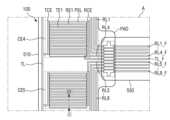
도 8 및 도 9를 참조하면, 제1 압력 센서(510)는 제1 기판(SUB1), 제2 기판(SUB2), 구동 라인(TL), 제1 내지 제8 감지 라인들(RL1~RL8, p는 2 이상의 정수), 구동 패드(TP), 제1 내지 제8 감지 패드들(RP1~RP8), 및 제1 내지 제8 압력 감지 셀들(CE1~CE8)을 포함한다.8 and 9 , the
도 8에서는 설명의 편의를 위해 제4 압력 감지 셀(CE4), 제5 압력 감지 셀(CE5), 및 패드 영역(PAD)만을 도시하였다. 또한, 도 8에서는 설명의 편의를 위해 제2 기판(SUB2)을 생략하였다.In FIG. 8 , only the fourth pressure sensing cell CE4 , the fifth pressure sensing cell CE5 , and the pad area PAD are illustrated for convenience of description. In addition, in FIG. 8 , the second substrate SUB2 is omitted for convenience of description.
제1 기판(SUB1)과 제2 기판(SUB2)은 서로 마주보도록 배치된다. 제1 기판(SUB1)과 제2 기판(SUB2)은 각각 폴리에틸렌(poly ethylene), 폴리이미드(poly imide), 폴리카보네이트(poly carbonate), 폴리술폰(polysulfone), 폴리아크릴레이트(poly acrylate), 폴리스티렌(polystyrene), 폴리비닐클로라이드(poly vinyl chloride), 폴리비닐알코올(poly vinyl alcohol), 폴리노르보넨(poly norbornene), 폴리에스테르(poly ester) 계열의 물질을 포함할 수 있다. 일 실시예에서, 제1 기판(SUB1)과 제2 기판(SUB2)은 폴레에틸렌 테레프탈레이트(polyethylene terephthalate, PET) 필름 또는 폴리이미드 필름으로 이루어질 수 있다.The first substrate SUB1 and the second substrate SUB2 are disposed to face each other. The first substrate SUB1 and the second substrate SUB2 are each made of polyethylene, poly imide, poly carbonate, polysulfone, poly acrylate, or polystyrene. (polystyrene), polyvinyl chloride, polyvinyl alcohol, polynorbornene, and polyester-based materials. In one embodiment, the first substrate SUB1 and the second substrate SUB2 may be formed of a polyethylene terephthalate (PET) film or a polyimide film.
제1 기판(SUB1)과 제2 기판(SUB2) 사이에는 압력 감지 셀들(CE1~CE8)이 배치된다. 제2 기판(SUB2)과 마주보는 제1 기판(SUB1)의 일면 상에는 구동 라인(TL), 감지 라인들(RL1~RL8), 구동 패드(TP), 감지 패드들(RP1~RP8)이 배치된다. 제1 기판(SUB1)과 제2 기판(SUB2) 사이에는 압력 감지 셀들(CE1~CE8)이 배치된다.Pressure sensing cells CE1 to CE8 are disposed between the first substrate SUB1 and the second substrate SUB2. A driving line TL, sensing lines RL1 to RL8, a driving pad TP, and sensing pads RP1 to RP8 are disposed on one surface of the first substrate SUB1 facing the second substrate SUB2. . Pressure sensing cells CE1 to CE8 are disposed between the first substrate SUB1 and the second substrate SUB2.
압력 감지 셀들(CE1~CE8) 각각은 적어도 하나의 구동 라인과 적어도 하나의 감지 라인에 연결될 수 있다. 예를 들어, 압력 감지 셀들(CE1~CE8)은 하나의 구동 라인(TL)에 공통적으로 연결되는데 비해, 감지 라인들(RL1~RL8)에는 일대일로 접속될 수 있다. 도 8과 같이, 제4 압력 감지 셀(CE4)은 구동 라인(TL)과 제4 감지 라인(RL4)에 접속되고, 제5 압력 감지 셀(CE5)은 구동 라인(TL)과 제5 감지 라인(RL5)에 접속될 수 있다.Each of the pressure sensing cells CE1 to CE8 may be connected to at least one driving line and at least one sensing line. For example, the pressure sensing cells CE1 to CE8 are commonly connected to one driving line TL, but may be connected to the sensing lines RL1 to RL8 one-to-one. 8 , the fourth pressure sensing cell CE4 is connected to the driving line TL and the fourth sensing line RL4, and the fifth pressure sensing cell CE5 is connected to the driving line TL and the fifth sensing line. (RL5).
구동 라인(TL)은 구동 패드(TP)에 접속되고, 감지 라인들(RL1~RL8)은 감지 패드들(RP1~RP8)에 일대일로 접속될 수 있다. 제1 감지 라인(RL1)은 제1 감지 패드(RP1)에 접속되고, 제2 감지 라인(RL2)은 제2 감지 패드(RP2)에 접속되며, 제3 감지 라인(RL3)은 제3 감지 패드(RP3)에 접속되고, 제4 감지 라인(RL4)은 제4 감지 패드(RP4)에 접속될 수 있다. 제5 감지 라인(RL5)은 제5 감지 패드(RP5)에 접속되고, 제6 감지 라인(RL6)은 제6 감지 패드(RP6)에 접속되며, 제7 감지 라인(RL7)은 제7 감지 패드(RP7)에 접속되고, 제8 감지 라인(RL8)은 제8 감지 패드(RP8)에 접속될 수 있다.The driving line TL may be connected to the driving pad TP, and the sensing lines RL1 to RL8 may be connected to the sensing pads RP1 to RP8 one-to-one. The first sense line RL1 is connected to the first sense pad RP1, the second sense line RL2 is connected to the second sense pad RP2, and the third sense line RL3 is connected to the third sense pad. RP3, and the fourth sense line RL4 may be connected to the fourth sense pad RP4. The fifth sense line RL5 is connected to the fifth sense pad RP5, the sixth sense line RL6 is connected to the sixth sense pad RP6, and the seventh sense line RL7 is connected to the seventh sense pad. RP7, and the eighth sense line RL8 may be connected to the eighth sense pad RP8.
패드 영역(PAD)은 제1 기판(SUB1)의 일 측으로부터 돌출되어 형성될 수 있다. 제1 기판(SUB1)의 일 측은 제1 압력 센서(510)의 장변일 수 있다. 도 8에서는 패드 영역(PAD)이 제1 기판(SUB1)의 장변의 중앙에서 돌출된 것을 예시하였으나, 이에 한정되지 않는다. 즉, 제1 기판(SUB1)의 장변의 일 단 또는 타단에서 돌출될 수 있다.The pad area PAD may protrude from one side of the first substrate SUB1. One side of the first substrate SUB1 may be a long side of the
패드 영역(PAD)에는 구동 패드(TP)와 감지 패드들(RP1~RP8)이 배치될 수 있다. 구동 패드(TP)와 감지 패드들(RP1~RP8)은 이방성 도전 필름을 통해 제3 회로 보드(550)의 구동 리드 라인(TL_F)과 감지 리드 라인들(RL1_F~RL8_F)에 일대일로 연결될 수 있다. 구동 패드(TP)는 구동 리드 라인(TL_F)에 접속되고, 제1 감지 패드(RP1)는 제1 감지 리드 라인(RL1_F)에 접속되며, 제2 감지 패드(RP2)는 제2 감지 리드 라인(RL2_F)에 접속되고, 제3 감지 패드(RP3)는 제3 감지 리드 라인(RL3_F)에 접속되며, 제4 감지 패드(RP4)는 제4 감지 리드 라인(RL4_F)에 접속될 수 있다. 또한, 제5 감지 패드(RP5)는 제5 감지 리드 라인(RL5_F)에 접속되며, 제6 감지 패드(RP6)는 제6 감지 리드 라인(RL6_F)에 접속되고, 제7 감지 패드(RP7)는 제7 감지 리드 라인(RL7_F)에 접속되며, 제8 감지 패드(RP8)는 제8 감지 리드 라인(RL8_F)에 접속될 수 있다.A driving pad TP and sensing pads RP1 to RP8 may be disposed in the pad area PAD. The driving pad TP and the sensing pads RP1 to RP8 may be connected one-to-one to the driving lead line TL_F and the sensing lead lines RL1_F to RL8_F of the
도 8과 같이 제3 회로 보드(550)는 표시 회로 보드(310)에 연결되므로, 표시 회로 보드(310)에 장착된 압력 감지부(330)와 전기적으로 연결될 수 있다. 압력 감지부(330)는 제3 회로 보드(550)의 구동 리드 라인(TL_F)과 제1 압력 센서(510)의 구동 패드(TP)를 통해 구동 라인(TL)에 구동 전압을 인가하고, 제1 압력 센서(510)의 감지 패드들(RP1~RPp)에 접속된 감지 리드 라인들(RL1_F~RL8_F)을 통해 감지 라인들(RL1~RL8)로부터 전류 값들 또는 전압 값들을 감지함으로써, 압력 감지 셀들(CE1~CE8)들에 가해진 압력을 감지할 수 있다.As shown in FIG. 8 , since the
제1 압력 센서(510)는 제1 기판(SUB1)과 제2 기판(SUB2) 사이에 배치되어 이들을 결합하는 결합층을 더 포함할 수 있다. 결합층은 감압 점착층이나 접착층으로 이루어질 수 있다. 결합층은 제1 기판(SUB1)과 제2 기판(SUB2)의 주변부를 따라 배치될 수 있다. 일 실시예에서, 결합층은 제1 기판(SUB1)과 제2 기판(SUB2)의 가장자리를 완전히 둘러싸 제1 압력 센서(510)의 내부를 밀봉하는 역할을 할 수 있다. 아울러, 결합층은 제1 기판(SUB1)과 제2 기판(SUB2) 사이의 간격을 일정하게 유지하는 스페이서의 역할을 할 수 있다. 결합층은 구동 라인(TL), 감지 라인들(RL1~RLp), 압력 감지 셀들(CE1~CEp), 구동 패드(TP), 및 감지 패드들(RP1~RPp)과 중첩되지 않을 수 있다.The
결합층은 제1 기판(SUB1)의 일면 또는 제2 기판(SUB2)의 일면에 먼저 부착된 후 제1 기판(SUB1)과 제2 기판(SUB2)의 합착 과정에서 다른 기판의 일면에 부착될 수 있다. 다른 예로, 제1 기판(SUB1)의 일면과 제2 기판(SUB2)의 일면에 각각 결합층이 마련되고, 제1 기판(SUB1)과 제2 기판(SUB2)의 합착 과정에서 제1 기판(SUB1)의 결합층과 제2 기판(SUB2)의 결합층이 상호 부착될 수도 있다.The bonding layer may be first attached to one surface of the first substrate SUB1 or one surface of the second substrate SUB2 and then attached to one surface of another substrate during the bonding process of the first substrate SUB1 and the second substrate SUB2. there is. As another example, bonding layers are provided on one surface of the first substrate SUB1 and one surface of the second substrate SUB2, respectively, and in the process of bonding the first substrate SUB1 and the second substrate SUB2, the first substrate SUB1 ) and the bonding layer of the second substrate SUB2 may be attached to each other.
압력 감지 셀들(CE1~CE8) 각각은 도 9와 같이 구동 연결 전극(TCE), 감지 연결 전극(RCE), 구동 전극(TE1)들, 감지 전극(RE1)들, 및 압력 감지층(PSL)을 포함한다.As shown in FIG. 9 , each of the pressure sensing cells CE1 to CE8 includes a driving connection electrode TCE, a sensing connection electrode RCE, driving electrodes TE1 , sensing electrodes RE1 , and a pressure sensing layer PSL. include
구동 연결 전극(TCE), 감지 연결 전극(RCE), 구동 전극(TE1)들, 및 감지 전극(RE1)들은 제2 기판(SUB2)과 마주보는 제1 기판(SUB1) 상에 배치된다.The driving connection electrode TCE, the sensing connection electrode RCE, the driving electrodes TE1, and the sensing electrode RE1 are disposed on the first substrate SUB1 facing the second substrate SUB2.
구동 연결 전극(TCE)은 구동 라인(TL)과 구동 전극(TE1)들에 접속된다. 구체적으로, 구동 연결 전극(TCE)은 길이 방향(Y축 방향)으로 일 끝단에서 구동 라인(TL)에 연결된다. 구동 전극(TE1)들은 구동 연결 전극(TCE)의 폭 방향(X축 방향)으로 분지될 수 있다.The driving connection electrode TCE is connected to the driving line TL and the driving electrodes TE1. Specifically, the driving connection electrode TCE is connected to the driving line TL at one end in the longitudinal direction (Y-axis direction). The driving electrodes TE1 may be branched in the width direction (X-axis direction) of the driving connection electrode TCE.
감지 연결 전극(RCE)은 감지 라인들(RL1~RL8) 중 어느 하나와 감지 전극(RE1)들에 접속된다. 구체적으로, 감지 연결 전극(TCE)은 길이 방향(Y축 방향)으로 일 끝단에서 감지 라인들(RL1~RL8) 중 어느 하나에 연결된다. 감지 전극(RE1)들은 감지 연결 전극(RCE)의 폭 방향(X축 방향)으로 분지될 수 있다.The sensing connection electrode RCE is connected to one of the sensing lines RL1 to RL8 and the sensing electrodes RE1. Specifically, the sensing connection electrode TCE is connected to one of the sensing lines RL1 to RL8 at one end in the length direction (Y-axis direction). The sensing electrodes RE1 may be branched in the width direction (X-axis direction) of the sensing connection electrode RCE.
구동 전극(TE1)들과 감지 전극(RE1)들은 동일층에 배치될 수 있다. 구동 전극(TE1)들과 감지 전극(RE1)들은 동일 물질로 이루어질 수 있다. 예를 들어, 구동 전극(TE1)들과 감지 전극(RE1)들은 은(Ag), 구리(Cu) 등의 도전성 물질을 포함할 수 있다. 구동 전극(TE1)들과 감지 전극(RE1)들은 제1 기판(SUB1) 상에 스크린 인쇄 방식으로 형성될 수 있다.The driving electrode TE1 and the sensing electrode RE1 may be disposed on the same layer. The driving electrodes TE1 and the sensing electrodes RE1 may be made of the same material. For example, the driving electrode TE1 and the sensing electrode RE1 may include a conductive material such as silver (Ag) or copper (Cu). The driving electrodes TE1 and the sensing electrodes RE1 may be formed on the first substrate SUB1 by a screen printing method.
구동 전극(TE1)들과 감지 전극(RE1)들은 인접하여 배치되나, 서로 연결되지 않는다. 구동 전극(TE1)들과 감지 전극(RE1)들은 서로 나란하게 배치될 수 있다. 구동 전극(TE1)들과 감지 전극(RE1)들은 구동 연결 전극(TCE)과 감지 연결 전극(RCE)의 길이 방향(Y축 방향)으로 교대로 배치될 있다. 즉, 구동 연결 전극(TCE)과 감지 연결 전극(RCE)의 길이 방향(Y축 방향)으로 구동 전극(TE1), 감지 전극(RE1), 구동 전극(TE1), 감지 전극(RE1)의 순서로 반복적으로 배치될 수 있다.The driving electrodes TE1 and the sensing electrode RE1 are disposed adjacent to each other, but are not connected to each other. The driving electrodes TE1 and the sensing electrodes RE1 may be disposed parallel to each other. The driving electrodes TE1 and the sensing electrodes RE1 may be alternately disposed in the longitudinal direction (Y-axis direction) of the driving connection electrode TCE and the sensing connection electrode RCE. That is, in the longitudinal direction (Y-axis direction) of the driving connection electrode TCE and the sensing connection electrode RCE, the driving electrode TE1, the sensing electrode RE1, the driving electrode TE1, and the sensing electrode RE1 are sequentially arranged. Can be placed repeatedly.
압력 감지층(PSL)은 제1 기판(SUB1)과 마주보는 제2 기판(SUB2)의 일면 상에 배치된다. 압력 감지층(PSL)은 구동 전극(TE1)들과 감지 전극(RE1)들에 중첩되게 배치될 수 있다.The pressure sensing layer PSL is disposed on one surface of the second substrate SUB2 facing the first substrate SUB1. The pressure sensing layer PSL may be disposed to overlap the driving electrodes TE1 and the sensing electrodes RE1.
압력 감지층(PSL)은 압력 민감 물질 및 압력 민감 물질이 배치되는 고분자 수지(polymer)를 포함할 수 있다. 압력 민감 물질은 니켈, 알루미늄, 티타늄, 주석, 구리 등의 금속 미세 입자들(또는 금속 나노 입자들)일 수 있다. 예를 들어, 압력 감지층(PSL)은 QTC(Quantum Tunneling Composite)일 수 있다.The pressure sensing layer PSL may include a pressure sensitive material and a polymer resin on which the pressure sensitive material is disposed. The pressure-sensitive material may be metal microparticles (or metal nanoparticles) of nickel, aluminum, titanium, tin, copper, or the like. For example, the pressure sensing layer PSL may be Quantum Tunneling Composite (QTC).
제1 압력 센서(510)의 높이 방향(Z축 방향)에서 압력이 제2 기판(SUB2)으로 가해지지 않는 경우, 도 9와 같이 압력 감지층(PSL)과 구동 전극(TE1)들 사이와 압력 감지층(PSL)과 감지 전극(RE1)들 사이에는 갭이 존재한다. 즉, 압력이 제2 기판(SUB2)으로 가해지지 않는 경우, 압력 감지층(PSL)은 구동 전극(TE1)들 및 감지 전극(RE1)들과 이격되어 있다.When pressure is not applied to the second substrate SUB2 in the height direction (Z-axis direction) of the
제1 압력 센서(510)의 높이 방향(Z축 방향)에서 압력이 제2 기판(SUB2)으로 가해지는 경우, 압력 감지층(PSL)이 구동 전극(TE1)들과 감지 전극(RE1)들에 접촉할 수 있다. 이 경우, 구동 전극(TE1)들 중 적어도 어느 하나와 감지 전극(RE1)들 중 적어도 어느 하나는 압력 감지층(PSL)을 통해 물리적으로 연결될 수 있으며, 압력 감지층(PSL)은 전기적인 저항으로 작용할 수 있다.When pressure is applied to the second substrate SUB2 in the height direction (Z-axis direction) of the
따라서, 도 8 및 도 9에 도시된 실시예에 의하면, 제1 압력 센서(510)는 가해지는 압력에 따라 압력 감지층(PSL)이 구동 전극(TE1)들과 감지 전극(RE1)들에 접촉하는 면적이 달라지므로, 감지 전극(RE1)들에 전기적으로 연결된 감지 라인의 저항 값이 변화될 수 있다. 압력 감지부(330)는 감지 라인들(RL1~RL8)로부터 전류 값 또는 전압 값 변화를 감지함으로써, 사용자가 손으로 누르는 압력을 감지할 수 있다.Therefore, according to the embodiment shown in FIGS. 8 and 9 , in the
한편, 제2 압력 센서(520)는 도 8 및 도 9에 도시된 제1 압력 센서(510)와 실질적으로 동일하므로, 제2 압력 센서(520)에 대한 자세한 설명은 생략한다.Meanwhile, since the
도 10은 제1 진동 발생 장치를 보여주는 평면도이다. 도 11은 도 10의 Ⅳ-Ⅳ’의 일 예를 보여주는 단면도이다.10 is a plan view showing the first vibration generating device. 11 is a cross-sectional view showing an example of line IV-IV′ of FIG. 10 .
도 10 및 도 11을 참조하면, 제1 진동 발생 장치(810)는 제1 전극(811), 제2 전극(812), 진동층(813), 제1 베이스 기판(814), 제2 베이스 기판(815), 제1 패드 전극(816), 및 제2 패드 전극(817)을 포함할 수 있다.10 and 11, the first
제1 전극(811)은 제1 베이스 기판(814)의 제1 면 상에 배치되고, 제1 전극(811) 상에는 진동층(813)이 배치될 수 있다. 진동층(813) 상에는 제2 전극(812)이 배치되며, 제2 전극(812) 상에는 제2 베이스 기판(815)이 배치될 수 있다. 제1 패드 전극(816)과 제2 패드 전극(817)은 제1 베이스 기판(814)의 제2 면 상에 배치될 수 있다.The
제1 전극(811)과 제2 전극(812)은 도전성 물질로 형성될 수 있다. 예를 들어, 도전성 물질은 ITO(indium Tin Oxide) 및 IZO(indium Zinc Oxide)와 같은 투명 도전성 물질(transparent conductive material), 불투명한 금속 물질, 도전성 폴리머, 탄소 나노 튜브(CNT) 등일 수 있다.The
제1 전극(811)은 제1 베이스 기판(814)을 관통하는 제1 콘택홀(CH1)을 통해 제1 패드 전극(816)과 접속될 수 있으며, 이로 인해 제1 패드 전극(816)을 통해 제4 회로 보드(890)에 연결될 수 있다. 또한, 제2 전극(812)은 진동층(813)과 제1 베이스 기판(814)을 관통하는 제2 콘택홀(CH2)을 통해 제2 패드 전극(817)과 접속될 수 있으며, 이로 인해 제1 패드 전극(817)을 통해 제4 회로 보드(890)에 연결될 수 있다. 결국, 제1 전극(811)과 제2 전극(812)은 제4 회로 보드(890)를 통해 표시 회로 보드(310)의 진동 구동부(340)에 전기적으로 연결될 수 있으므로, 진동 구동부(340)로부터 제1 구동 전압과 제2 구동 전압을 인가받을 수 있다.The
진동층(813)은 제1 전극(811)에 인가된 전압과 제2 전극(812)에 인가된 전압 차에 따라 도 12와 같이 변형되는 피에조 액츄에이터(piezo actuator)일 수 있다. 이 경우, 진동층(813)은 PVDF(Poly Vinylidene Fluoride) 필름이나 PZT(Plumbum Ziconate Titanate(티탄산지르콘납) ) 등의 압전체, 전기 활성 고분자(Electro Active Polymer) 중 적어도 어느 하나일 수 있다.The vibrating
이 경우, 진동층(813)은 제1 전극(811)에 인가되는 제1 구동 전압과 제2 전극(812)에 인가되는 제2 구동 전압 간의 차이에 따라 제1 힘(F1)에 따라 수축하거나 제2 힘(F2)에 따라 이완 또는 팽창하게 된다. 구체적으로, 도 12와 같이, 제1 전극(811)에 인접한 진동층(813)이 정극성의 특성을 가지며, 제2 전극(812)에 인접한 진동층(813)이 부극성의 특성을 갖는 경우, 제1 전극(811)에 정극성의 제1 구동 전압이 인가되며, 제2 전극(812)에 부극성의 제2 구동 전압이 인가되면, 진동층(813)은 제1 힘(F1)에 따라 수축할 수 있다. 또한, 제1 전극(811)에 인접한 진동층(813)이 정극성의 특성을 가지며, 제2 전극(812)에 인접한 진동층(813)이 부극성의 특성을 갖는 경우, 제1 전극(811)에 부극성의 제1 구동 전압이 인가되며, 제2 전극(812)에 정극성의 제2 구동 전압이 인가되면, 진동층(813)은 제2 힘(F2)에 따라 수축할 수 있다. 제1 전극(811)에 인가되는 제1 구동 전압과 제2 전극(812)에 인가되는 제2 구동 전압이 정극성과 부극성으로 교대로 반복되는 경우, 진동층(813)은 수축과 이완을 반복하게 된다. 이로 인해, 제1 진동 발생 장치(810)는 진동하게 된다.In this case, the vibrating
또한, 제1 진동 발생 장치(810)는 표시 패널(300)을 진동하여 제1 음향을 출력할 수도 있다. 이 경우, 표시 장치(10)는 외부로 드러나지 않은 음향 발생 장치에 의해 음향을 출력할 수 있으므로, 표시 장치(10)의 전면(前面)에 배치되는 음향 발생 장치가 삭제될 수 있으므로, 윈도우(100)의 투과부(DA100)가 넓어질 수 있다. 즉, 표시 장치(10)의 표시 영역이 넓어질 수 있다.Also, the first
제1 베이스 기판(814)과 제2 베이스 기판(815)은 절연성 물질로 이루어질 수 있다. 예를 들어, 제1 베이스 기판(814)과 제2 베이스 기판(815)은 폴리에테르술폰(polyethersulphone: PES), 폴리아크릴레이트(polyacrylate: PA), 폴리아릴레이트(polyarylate: PAR), 폴리에테르이미드(polyetherimide: PEI), 폴리에틸렌나프탈레이트(polyethylenenapthalate: PEN), 폴리에틸렌 테레프탈레이드(polyethyleneterepthalate: PET), 폴리페닐렌설파이드 (polyphenylenesulfide: PPS), 폴리알릴레이트(polyallylate), 폴리이미드(polyimide: PI), 폴리카보네이트(polycarbonate: PC), 셀룰로오스 트리아세테이트(cellulosetriacetate: CAT), 셀룰로오스 아세테이트 프로피오네이트(cellulose acetate propionate: CAP) 또는 이들의 조합이며, 예를 들어 플라스틱으로 형성될 수 있다.The
제1 패드 전극(816)과 제2 패드 전극(817)은 도전성 물질로 형성될 수 있다. 제1 패드 전극(816)과 제2 패드 전극(817)은 이방성 도전 필름을 이용하여 제4 회로 보드(890)와 연결될 수 있다.The
제2 진동 발생 장치(820), 제3 진동 발생 장치(830), 및 제4 진동 발생 장치(840) 각각은 도 10 내지 도 12를 결부하여 설명한 제1 진동 발생 장치(810)와 실질적으로 동일하므로, 이들에 대한 자세한 설명은 생략한다.Each of the second
도 10 내지 도 12에 도시된 실시예에 의하면, 제1 진동 발생 장치(810), 제2 진동 발생 장치(820), 제3 진동 발생 장치(830), 및 제4 진동 발생 장치(840)를 표시 패널(300)의 하부에 배치된 미들 프레임(600)의 상면에 부착하고, 제4 회로 보드(890)를 통해 표시 회로 보드(310)에 연결한다. 따라서, 제1 진동 발생 장치(810), 제2 진동 발생 장치(820), 제3 진동 발생 장치(830), 제4 진동 발생 장치(840), 제4 회로 보드(890), 및 미들 프레임(600)을 표시 패널(300)과 하나로 모듈화할 수 있다.10 to 12, the first
도 13은 도 3과 도 4의 Ⅰ-Ⅰ’과 Ⅱ-Ⅱ’의 일 예를 보여주는 단면도이다.13 is a cross-sectional view showing an example of lines Ⅰ-Ⅰ′ and Ⅱ-Ⅱ′ of FIGS. 3 and 4 .
도 13을 참조하면, 제1 압력 센서(510)는 표시 장치(10)의 곡면부에 해당하는 제2 영역(DR2)에 배치될 수 있다. 제1 압력 센서(510)의 상면에는 제1 범프(530)들이 배치되며, 제1 범프(530)들 각각은 제4 접착 부재(940)를 통해 표시 패널(300)의 하면의 패널 하부 부재(390)의 하면에 부착될 수 있으나, 이에 한정되지 않는다. 예를 들어, 제1 범프(530)들 각각은 제1 압력 센서(510)의 하면에 배치될 수 있으며, 이 경우 제1 압력 센서(510)의 상면은 제4 접착 부재(940)를 통해 표시 패널(300)의 하면의 패널 하부 부재(390)의 하면에 부착될 수 있다. 제4 접착 부재(940)는 투명 접착 필름(optically cleared adhesive film, OCA) 또는 투명 접착 레진(optically cleared resin, OCR)일 수 있다.Referring to FIG. 13 , the
제1 방수 부재(410)는 제1 압력 센서(510)의 하면에 배치될 수 있다. 즉, 제1 방수 부재(410)는 제1 압력 센서(510)의 하면과 미들 프레임(600)의 상면에 부착될 수 있다.The first
또한, 표시 패널(300)과 제1 압력 센서(510) 사이로 수분이나 분진이 침투하는 것을 방지하기 위해, 제1 방수 부재(410)는 제1 압력 센서(510)의 일 측면에 추가로 부착될 수 있다. 구체적으로, 도 13과 같이 제1 압력 센서(510)의 일 측면에 부착된 제1 방수 부재(410)의 상면은 표시 패널(300)의 패널 하부 부재(390)의 하면에 부착될 수 있다. 이 경우, 제4 접착 부재(940)는 생략될 수도 있다. 제1 압력 센서(510)는 표시 패널(300)의 우측 가장자리에 배치되므로, 제1 압력 센서(510)의 일 측면은 제1 압력 센서(510)의 우측 측면일 수 있다.In addition, in order to prevent penetration of moisture or dust between the
도 13에 도시된 실시예에 의하면, 제1 방수 부재(410)가 제1 압력 센서(510)의 하면과 우측면에 부착되므로, 제1 압력 센서(510)를 패널 하부 부재(400)의 하면의 우측 가장자리에 배치하더라도, 제1 방수 부재(410)에 의해 표시 패널(300)과 미들 프레임(600) 사이로 수분이나 분진이 침투하는 것을 방지할 수 있다. 즉, 방수 및 방진이 가능한 표시 장치(10)가 제공될 수 있다.According to the embodiment shown in FIG. 13 , since the first
제1 진동 발생 장치(810)는 표시 장치(10)의 평탄부에 해당하는 제1 영역(DR1)에 배치될 수 있다. 제1 진동 발생 장치(810)는 제1 압력 센서(510)에 인접하여 배치될 수 있다.The first
제1 진동 발생 장치(810)는 제5 접착 부재(950)를 통해 미들 프레임(600)의 상면에 부착될 수 있다. 제5 접착 부재(950)는 투명 접착 필름(optically cleared adhesive film, OCA) 또는 투명 접착 레진(optically cleared resin, OCR)일 수 있다.The first
제4 회로 보드(890)는 제1 진동 발생 장치(810)에 부착될 수 있다. 제4 회로 보드(890)는 제1 진동 발생 장치(810)의 상면에 배치된 제1 패드 전극(816)과 제2 패드 전극(817)에 부착될 수 있다.The
제1 전파 차단 부재(450)는 제1 진동 발생 장치(810)의 복수의 측면들을 둘러싸도록 배치될 수 있다. 도 4에서는 제1 전파 차단 부재(450)가 제1 진동 발생 장치(810)의 모든 측면들을 둘러싸는 것을 예시하였으나, 이에 한정되지 않는다. 제1 진동 발생 장치(810)가 미들 프레임(600)의 모서리에 배치되는 경우, 제1 전파 차단 부재(450)는 제1 진동 발생 장치(810)의 두 개의 측면들을 둘러싸도록 배치될 수 있다. 또한, 제1 진동 발생 장치(810)가 미들 프레임(600)의 좌측, 우측, 상측 또는 하측 가장자리에 배치되는 경우, 제1 전파 차단 부재(450)는 제1 진동 발생 장치(810)의 세 개의 측면들을 둘러싸도록 배치될 수 있다.The first electromagnetic
제1 진동 차단 부재(450)는 제1 방수 부재(410)와 실질적으로 동일한 방수 부재로 형성될 수 있다. 즉, 제1 진동 차단 부재(450)는 베이스 필름과 베이스 필름의 일 면 상에 배치되는 제1 점착막, 및 베이스 필름의 타면 상에 배치되는 제2 점착막을 포함할 수 있다. 베이스 필름은 폴리에틸렌 테레프탈레이드(polyethyleneterepthalate: PET), 폴리에틸렌 테레프탈레이드(polyethyleneterepthalate: PET)와 쿠션층, 또는 폴리에틸렌 폼(PE-foam)일 수 있다. 제1 점착막과 제2 점착막은 압력 민감 점착제(pressure sensitive adhesive, PSA)일 수 있다.The first
제1 진동 발생 장치(810)에 의해 발생한 진동이 주변으로 전파되는 것을 효과적으로 차단하기 위해, 제1 전파 차단 부재(450)의 높이는 제1 진동 발생 장치(810)의 높이보다 높을 수 있다. 이로 인해, 제1 전파 차단 부재(450)는 표시 패널(300)의 패널 하부 부재(390)의 하면과 미들 프레임(600)의 상면에 부착될 수 있다. 제1 진동 발생 장치(810)의 일 측면에 제4 회로 보드(890)가 배치되는 경우, 제1 전파 차단 부재(450)는 패널 하부 부재(390)의 하면과 제4 회로 보드(890)에 부착될 수 있다. 도 13에 도시된 실시예에 의하면, 제1 진동 발생 장치(810)는 표시 패널(300)의 패널 하부 부재(390), 미들 프레임(600), 및 제1 전파 차단 부재(450)에 의해 상면, 하면, 및 측면들이 둘러싸이므로, 제1 진동 발생 장치(810)에 의해 발생한 진동이 제1 전파 차단 부재(450)에 의해 주변으로 전파되는 것을 방지할 수 있다.In order to effectively block propagation of vibration generated by the first
도 14a는 전파 차단 부재를 포함하지 않는 경우 진동 발생 장치의 진동을 보여주는 진동 측정 이미지와 그래프이다. 도 14b는 전파 차단 부재를 포함하는 경우 진동 발생 장치의 진동을 보여주는 진동 측정 이미지와 그래프이다.14A is a vibration measurement image and a graph showing vibration of a vibration generating device when a radio wave blocking member is not included. 14B is a vibration measurement image and a graph showing vibration of a vibration generating device when a radio wave blocking member is included.
도 14a 및 도 14b의 이미지에서 X축은 제1 진동 발생 장치(810)의 가로 방향 위치를 나타내고, Y축은 제1 진동 발생 장치(810)의 세로 방향 위치를 나타내며, 빨간색, 노란색, 초록색, 하늘색으로 갈수록 진동 변위가 낮은 것을 나타낸다. 도 14a 및 도 14b의 그래프에서 X축은 제1 진동 발생 장치(810)의 가로 방향 위치를 나타내고, Y축은 진동 변위를 나타낸다.In the images of FIGS. 14A and 14B , the X axis represents the horizontal position of the first
도 14a와 같이 제1 전파 차단 부재(450)를 포함하지 않는 경우, 제1 진동 발생 장치(810) 에 의해 발생된 진동은 주변으로 전파된다. 하지만, 도 14b와 같이 제1 전파 차단 부재(450)를 포함하는 경우, 제1 진동 발생 장치(810)의 진동은 제1 전파 차단 부재(450)를 통과하지 못한다. 따라서, 도 14b와 같이 제1 전파 차단 부재(450)를 포함하는 경우, 제1 진동 발생 장치(810) 에 의해 발생된 진동 제1 전파 차단 부재(450)에 의해 둘러싸인 영역 내에서만 발생한다. 즉, 제1 진동 발생 장치(810)에 의해 발생된 진동은 제1 전파 차단 부재(450)에 의해 차단될 수 있다.When the first
도 13에 도시된 실시예는 제1 진동 발생 장치(810)에 의한 진동은 제1 전파 차단 부재(450 )에 의해 차단되므로, 사용자는 제1 진동 발생 장치(810)가 진동하는 경우, 제1 진동 발생 장치(810)가 배치된 위치에서 국부적으로 진동을 느낄 수 있다.In the embodiment shown in FIG. 13 , since vibrations by the first
도 13에 도시된 도 3과 도 4의 Ⅱ-Ⅱ’의 단면도는 제2 방수 부재(420), 제2 범프(540), 제2 압력 센서(520), 제2 진동 발생 장치(820), 제2 전파 차단 부재(460), 및 제4 회로 보드(890)가 표시 패널(300)의 패널 하부 부재(390)의 하면의 좌측 가장자리에 배치되는 것에서 차이가 있을 뿐이며, 도 13에 도시된 도 3과 도 4의 Ⅰ-Ⅰ’의 단면도와 실질적으로 동일하다. 따라서, 도 13에 도시된 도 3과 도 4의 Ⅱ-Ⅱ’의 단면도에 대한 자세한 설명은 생략한다.3 and 4 shown in FIG. 13 are cross-sectional views of the second
또한, 제3 진동 발생 장치(830), 제3 전파 차단 부재(470), 제4 진동 발생 장치(840), 및 제4 전파 차단 부재(480)의 단면은 도 13에 도시된 제1 진동 발생 장치(810)와 제2 진동 발생 장치(820)와 실질적으로 동일할 수 있다. 따라서, 제3 진동 발생 장치(830), 제3 전파 차단 부재(470), 제4 진동 발생 장치(840), 및 제4 전파 차단 부재(480)의 단면에 대한 자세한 설명은 생략한다.In addition, cross-sections of the third
도 15a 및 도 15b는 일 실시예에 따른 압력 센서들을 물리 버튼으로 활용하고, 진동 발생 장치들을 압력 센서들 또는 터치 감지 장치와 연계하여 국부적으로 진동을 발생시키는 표시 장치를 보여주는 예시도면들이다.15A and 15B are exemplary views illustrating a display device that locally generates vibration by using pressure sensors as physical buttons and linking vibration generating devices with pressure sensors or a touch sensing device, according to an exemplary embodiment.
도 15a 및 도 15b에는 표시 장치(10)의 제2 영역(DR2)들에 배치된 제1 압력 센서(510)와 제2 압력 센서(520)의 제1 내지 제8 압력 감지 셀들(CE1~CE8)이 나타나 있다. 제1 진동 발생 장치(810)는 표시 장치(10)의 우측 곡면부에 배치된 제1 압력 센서(510)의 제1 내지 제4 압력 감지 셀들(CE1, CE2, CE3, CE4)에 인접하게 배치되고, 제3 진동 발생 장치(830)는 제5 내지 제8 압력 감지 셀들(CE5, CE6, CE7, CE8)에 인접하게 배치될 수 있다. 또한, 제2 진동 발생 장치(820)는 표시 장치(10)의 좌측 곡면부에 배치된 제2 압력 센서(520)의 제1 내지 제4 압력 감지 셀들(CE1, CE2, CE3, CE4)에 인접하게 배치되고, 제4 진동 발생 장치(840)는 제5 내지 제8 압력 감지 셀들(CE5, CE6, CE7, CE8)에 인접하게 배치될 수 있다.15A and 15B show the first to eighth pressure sensing cells CE1 to CE8 of the
도 15a에는 사용자가 표시 장치(10)를 손으로 잡은 상태에서 검지 손가락으로 표시 장치(10)의 제2 영역(DR2)에 해당하는 좌측 곡면부의 제5 압력 감지 셀(CE5)을 누르는 것이 도시되어 있다. 도 15b에는 사용자가 표시 장치(10)를 손으로 잡은 상태에서 중지, 약지 및 새끼 손가락으로 표시 장치(10)의 제2 영역(DR2)에 해당하는 좌측 곡면부의 제8 압력 감지 셀(CE8)을 스퀴징(squeezing)하고, 손바닥으로 표시 장치(10)의 제2 영역(DR2)에 해당하는 우측 곡면부의 제8 압력 감지 셀(CE8)을 스퀴징(squeezing)하는 것이 도시되어 있다.FIG. 15A shows a user pressing the fifth pressure sensing cell CE5 of the left curved portion corresponding to the second region DR2 of the
도 15a 및 도 15b를 참조하면, 제1 압력 센서(510)와 제2 압력 센서(520)는 표시 장치(10)의 물리 버튼 대용으로 활용될 수 있다. 구체적으로, 표시 장치(10)의 우측 곡면부에 형성된 제1 압력 센서(510)의 제1 내지 제8 압력 감지 셀들(CE1~CE8)과 표시 장치(10)의 좌측 곡면부에 형성된 제2 압력 센서(520)의 제1 내지 제8 압력 감지 셀들(CE1~CE8)에 압력이 인가되는 경우, 미리 정해진 어플리케이션 또는 동작이 실행될 수 있다.Referring to FIGS. 15A and 15B , the
또한, 제1 압력 센서(510)에 압력이 인가되는 경우, 제1 압력 센서(510)에 인접한 제1 진동 발생 장치(810) 또는 제3 진동 발생 장치(830)가 진동할 수 있다. 제2 압력 센서(520)에 압력이 인가되는 경우, 제2 압력 센서(520)에 인접한 제2 진동 발생 장치(820) 또는 제4 진동 발생 장치(840)가 진동할 수 있다. 또는, 사용자의 터치 위치와 가장 인접한 진동 발생 장치가 진동할 수 있다.Also, when pressure is applied to the
예를 들어, 표시 장치(10)의 우측 곡면부에 형성된 제1 압력 센서(510)의 제1 내지 제8 압력 감지 셀들(CE1~CE8) 중에서 제1 압력 감지 셀(CE1)과 제2 압력 감지 셀(CE2)은 사용자가 표시 장치(10)의 음향을 높이기 위해 누르는 음향 상향 버튼(VB+)으로 활용되고, 제3 압력 감지 셀(CE3)과 제4 압력 감지 셀(CE4)은 사용자가 표시 장치(10)의 음향을 낮추기 위해 누르는 음향 하향 버튼(VB-)으로 활용되며, 제5 압력 감지 셀(CE5), 제6 압력 감지 셀(CE6), 및 제7 압력 감지 셀(CE7)은 사용자가 전원을 오프(off)하기 위해 누르는 전원 버튼(PWB)으로 활용될 수 있다.For example, among the first to eighth pressure sensing cells CE1 to CE8 of the
메인 프로세서(710)는 표시 장치(10)의 우측 곡면부에 형성된 제1 압력 감지 셀(CE1)과 제2 압력 감지 셀(CE2)로부터 압력이 감지되면, 표시 장치(10)의 스피커의 음향을 높이도록 제어할 수 있다. 또한, 메인 프로세서(710)는 표시 장치(10)의 우측 곡면부에 형성된 제3 압력 감지 셀(CE3)과 제4 압력 감지 셀(CE4)로부터 압력이 감지되면, 표시 장치(10)의 스피커의 음향을 높이도록 제어할 수 있다. 이 경우, 메인 프로세서(710)는 표시 장치(10)의 우측 곡면부에 형성된 제1 내지 제4 압력 감지 셀들(CE1, CE2, CE3, CE4)에 인접한 제1 진동 발생 장치(810)가 진동하도록 제1 진동 발생 장치(810)에 진동 데이터를 출력할 수 있다. 또는, 메인 프로세서(710)는 터치 구동부(220)로부터 입력된 터치 데이터에 따라 사용자의 터치 위치와 가장 인접한 제1 진동 발생 장치(810)가 진동하도록 제1 진동 발생 장치(810)에 진동 데이터를 출력할 수 있다.When pressure is sensed from the first pressure sensing cell CE1 and the second pressure sensing cell CE2 formed on the right curved portion of the
또한, 메인 프로세서(710)는 표시 장치(10)의 우측 곡면부에 형성된 제5 압력 감지 셀(CE5), 제6 압력 감지 셀(CE6), 및 제7 압력 감지 셀(CE7)로부터 압력이 감지되면, 표시 장치(10)의 화면을 끄거나, 표시 장치(10)의 전원 오프를 선택할 수 있는 화면을 출력할 수 있다. 이 경우, 메인 프로세서(710)는 표시 장치(10)의 우측 곡면부에 형성된 제5 내지 제7 압력 감지 셀들(CE5, CE6, CE7)에 인접한 제3 진동 발생 장치(830)가 진동하도록 제3 진동 발생 장치(830)에 진동 데이터를 출력할 수 있다. 또는, 메인 프로세서(710)는 터치 구동부(220)로부터 입력된 터치 데이터에 따라 사용자의 터치 위치와 가장 인접한 제3 진동 발생 장치(830)가 진동하도록 제3 진동 발생 장치(830)에 진동 데이터를 출력할 수 있다.Also, the
또한, 표시 장치(10)의 좌측 곡면부에 형성된 제1 내지 제8 압력 감지 셀들(CE1~CE8) 중에서 제1 압력 감지 셀(CE1)과 제2 압력 감지 셀(CE2)은 사용자가 통화 어플리케이션을 실행하기 위해 누르는 통화 버튼(CB)으로 활용되고, 제3 압력 감지 셀(CE3)과 제4 압력 감지 셀(CE4)은 사용자가 카메라 어플리케이션을 실행하기 위해 누르는 카메라 버튼(CMB)으로 활용되며, 제5 압력 감지 셀(CE5), 제6 압력 감지 셀(CE6), 및 제7 압력 감지 셀(CE7)은 사용자가 인터넷 어플리케이션을 실행하기 위해 누르는 인터넷 버튼(IB)으로 활용될 수 있다.In addition, the first pressure sensing cell CE1 and the second pressure sensing cell CE2 among the first to eighth pressure sensing cells CE1 to CE8 formed on the left curved portion of the
이 경우, 메인 프로세서(710)는 표시 장치(10)의 좌측 곡면부에 형성된 제1 압력 감지 셀(CE1)과 제2 압력 감지 셀(CE2)로부터 압력이 감지되면, 통화 어플리케이션을 실행하도록 제어할 수 있다. 또한, 메인 프로세서(710)는 표시 장치(10)의 우측 곡면부에 형성된 제3 압력 감지 셀(CE3)과 제4 압력 감지 셀(CE4)로부터 압력이 감지되면, 카메라 어플리케이션을 실행하도록 제어할 수 있다. 이 경우, 메인 프로세서(710)는 표시 장치(10)의 좌측 곡면부에 형성된 제1 내지 제4 압력 감지 셀들(CE1, CE2, CE3, CE4)에 인접한 제2 진동 발생 장치(820)가 진동하도록 제2 진동 발생 장치(820)에 진동 데이터를 출력할 수 있다. 또는, 메인 프로세서(710)는 터치 구동부(220)로부터 입력된 터치 데이터에 따라 사용자의 터치 위치와 가장 인접한 제2 진동 발생 장치(820)가 진동하도록 제2 진동 발생 장치(820)에 진동 데이터를 출력할 수 있다.In this case, the
또한, 메인 프로세서(710)는 표시 장치(10)의 우측 곡면부에 형성된 제5 압력 감지 셀(CE5), 제6 압력 감지 셀(CE6), 및 제7 압력 감지 셀(CE7)로부터 압력이 감지되면, 인터넷 어플리케이션을 실행하도록 제어할 수 있다. 이 경우, 메인 프로세서(710)는 표시 장치(10)의 좌측 곡면부에 형성된 제5 내지 제7 압력 감지 셀들(CE5, CE6, CE7)에 인접한 제4 진동 발생 장치(840)가 진동하도록 제4 진동 발생 장치(840)에 진동 데이터를 출력할 수 있다. 또는, 메인 프로세서(710)는 터치 구동부(220)로부터 입력된 터치 데이터에 따라 사용자의 터치 위치와 가장 인접한 제4 진동 발생 장치(840)가 진동하도록 제4 진동 발생 장치(840)에 진동 데이터를 출력할 수 있다.Also, the
한편, 도 15a에 도시된 실시예는 하나의 예에 불과하므로, 이에 한정되지 않는다. 즉, 표시 장치(10)의 우측 곡면부에 위치한 제1 압력 센서(510)의 제1 내지 제7 압력 감지 셀들(CE1~CE7)과 표시 장치(10)의 좌측 곡면부에 위치한 제2 압력 센서(520)의 제1 내지 제7 압력 감지 셀들(CE1~CE7)에 압력 인가에 따라, 상기 기능들을 포함하거나 제외한 다양한 기능들이 실행될 수 있다. 또한, 표시 장치(10)의 우측 곡면부에 위치한 제1 압력 센서(510)의 제1 내지 제7 압력 감지 셀들(CE1~CE7)과 표시 장치(10)의 좌측 곡면부에 위치한 제2 압력 센서(520)의 제1 내지 제7 압력 감지 셀들(CE1~CE7)마다 서로 다른 동작이 실행되도록 프로그래밍될 수 있다.Meanwhile, since the embodiment shown in FIG. 15A is only one example, it is not limited thereto. That is, the first to seventh pressure sensing cells CE1 to CE7 of the
또한, 표시 장치(10)의 좌측 곡면부와 우측 곡면부 각각에 형성된 제8 압력 감지 셀(CE8)은 스퀴징 감지 버튼(SB)으로 활용될 수 있다. 제8 압력 감지 셀(CE8)에 가해지는 스퀴징 압력은 제1 내지 제7 압력 감지 셀들(CE1~CE7)에 가해지는 압력에 비해 더 높고 큰 압력일 수 있다. 메인 프로세서(710)는 좌측 곡면부와 우측 곡면부 각각에 형성된 제8 압력 감지 셀(CE8)로부터 스퀴징 압력이 감지되면, 미리 정해진 어플리케이션 또는 동작을 실행하도록 제어할 수 있다.In addition, the eighth pressure sensing cell CE8 formed on each of the left curved portion and the right curved portion of the
예를 들어, 메인 프로세서(710)는 좌측 곡면부와 우측 곡면부 각각에 형성된 제8 압력 감지 셀(CE8)로부터 스퀴징 압력이 감지되면, 표시 장치(10)를 슬립 모드에서 온(on)시키도록 제어할 수 있다. 이 경우, 메인 프로세서(710)는 우측 곡면부에 형성된 제8 압력 감지 셀(CE8)과 인접한 제3 진동 발생 장치(830)가 진동하도록 제3 진동 발생 장치(830)에 진동 데이터를 출력할 수 있다. 또한, 메인 프로세서(710)는 좌측 곡면부에 형성된 제8 압력 감지 셀(CE8)과 인접한 제4 진동 발생 장치(840)가 진동하도록 제4 진동 발생 장치(840)에 진동 데이터를 출력할 수 있다.For example, the
도 15a 및 도 15b에 도시된 실시예에 의하면, 제1 압력 센서(510)와 제2 압력 센서(520)가 표시 장치(10)의 곡면부에 해당하는 제2 영역(DR2)들에 배치됨으로써, 음향 조절 버튼, 전원 버튼, 통화 버튼, 카메라 버튼, 인터넷 버튼, 및 스퀴징 감지 버튼 등의 물리 버튼 대용으로 활용될 수 있다.15A and 15B , the
또한, 도 15a 및 도 15b에 도시된 실시예에 의하면, 입력 감지 장치를 통해 사용자의 입력이 있는 경우, 제1 진동 발생 장치(810), 제2 진동 발생 장치(820), 제3 진동 발생 장치(830), 및 제4 진동 발생 장치(840) 중에서 입력 감지 장치에 인접한 진동 발생 장치를 진동함으로써, 국부적으로 진동을 발생하여 햅틱을 구현할 수 있다. 도 15a 및 도 15b에서는 입력 감지 장치로서, 압력 센서들(510, 520)과 터치 감지 장치(200)를 예시하였으나, 이에 한정되지 않는다. 즉, 입력 감지 장치로서 지문 인식 센서 또는 카메라 장치(720)가 이용될 수 있다. 예를 들어, 지문 인식 센서를 통한 사용자의 지문 인식이 있는 경우, 제1 진동 발생 장치(810), 제2 진동 발생 장치(820), 제3 진동 발생 장치(830), 및 제4 진동 발생 장치(840) 중 지문 인식 센서와 가장 인접한 진동 발생 장치가 진동함으로써, 햅틱을 구현할 수 있다. 또는, 카메라 장치(720)를 통해 사용자의 홍채 인식이 있는 경우, 제1 진동 발생 장치(810), 제2 진동 발생 장치(820), 제3 진동 발생 장치(830), 및 제4 진동 발생 장치(840) 중 어느 하나가 진동함으로써, 햅틱을 구현할 수 있다.In addition, according to the embodiment shown in FIGS. 15A and 15B , when there is a user's input through the input sensing device, the first
도 16은 도 3의 Ⅰ-Ⅰ’과 Ⅱ-Ⅱ’의 또 다른 예를 보여주는 단면도이다.16 is a cross-sectional view showing another example of lines Ⅰ-Ⅰ′ and Ⅱ-Ⅱ′ of FIG. 3 .
도 16에 도시된 실시예는 제1 진동 발생 장치(810)의 높이(H1)와 폭(W1)이 제2 진동 발생 장치(820)의 높이(H2)와 폭(W2)과 상이한 것에서 도 13에 도시된 실시예와 차이가 있다. 도 16에서는 도 13에 도시된 실시예와 중복된 설명은 생략한다.In the embodiment shown in FIG. 16, the height H1 and width W1 of the first
도 16을 참조하면, 제1 진동 발생 장치(810)의 높이(H1)는 제2 진동 발생 장치(820)의 높이(H2)보다 높게 형성되고, 제1 진동 발생 장치(810)의 폭(W1)은 제2 진동 발생 장치(820)의 폭(W2)보다 넓게 형성될 수 있다. 이로 인해, 제1 진동 발생 장치(810)의 부피 제2 진동 발생 장치(820)의 부피보다 클 수 있다. 따라서, 제1 진동 발생 장치(810)와 제2 진동 발생 장치(820)에 동일한 제1 구동 전압과 제2 구동 전압이 인가되더라도, 제1 진동 발생 장치(810)에 의해 발생되는 진동의 세기는 제2 진동 발생 장치(820)에 의해 발생되는 진동의 세기보다 클 수 있다.Referring to FIG. 16, the height H1 of the first
도 16에 도시된 실시예에 의하면, 제1 구동 전압과 제2 구동 전압을 높이지 않더라도, 진동 발생 장치의 높이와 폭을 크게 함으로써, 진동 발생 장치의 진동 세기를 조정할 수 있다.According to the embodiment illustrated in FIG. 16 , the intensity of vibration of the vibration generating device may be adjusted by increasing the height and width of the vibration generating device even without increasing the first driving voltage and the second driving voltage.
도 17은 도 3의 Ⅰ-Ⅰ’과 Ⅱ-Ⅱ’의 또 다른 예를 보여주는 단면도이다.17 is a cross-sectional view showing another example of lines Ⅰ-Ⅰ′ and Ⅱ-Ⅱ′ of FIG. 3 .
도 17에 도시된 실시예는 제1 전파 차단 부재(450)와 제2 전파 차단 부재(460)가 방수 부재가 아닌 스틸(steel)로 형성되는 것에서 도 13에 도시된 실시예와 차이가 있다. 도 17에서는 도 13에 도시된 실시예와 중복된 설명은 생략한다.The embodiment shown in FIG. 17 is different from the embodiment shown in FIG. 13 in that the first radio
도 17을 참조하면, 제1 전파 차단 부재(450)가 스틸(steel)로 형성되는 경우, 방수 부재로 형성될 때에 비해 제1 진동 발생 장치(810)의 진동과 제2 진동 발생 장치(820)의 진동의 차단 효과를 높일 수 있다. 또한, 제1 진동 발생 장치(810)에 의해 발생한 진동이 주변으로 전파되는 것을 효과적으로 차단하기 위해, 제1 전파 차단 부재(450)의 높이는 제1 진동 발생 장치(810)의 높이보다 높을 수 있다.Referring to FIG. 17 , when the first radio
제1 전파 차단 부재(450)가 스틸(steel)로 형성되는 경우, 미들 프레임(600)의 상면과 패널 하부 부재(390)의 하면에 부착하기 위해서는 제1 접착층(960)과 제2 접착층(970)이 필요하다. 제1 접착층(960)과 제2 접착층(970) 각각은 투명 접착 필름(optically cleared adhesive film, OCA) 또는 투명 접착 레진(optically cleared resin, OCR)일 수 있다.When the first radio
제1 전파 차단 부재(450)는 제1 접착층(960)을 통해 패널 하부 부재(390)의 하면에 부착되고, 제2 접착층(970)을 통해 미들 프레임(600)의 상면에 부착될 수 있다. 제1 진동 발생 장치(810)의 일 측면에 제4 회로 보드(890)가 배치되는 경우, 제1 전파 차단 부재(450)는 제2 접착층(970)을 통해 제4 회로 보드(890)의 상면에 부착될 수 있다.The first radio
도 17에 도시된 실시예에 의하면, 제1 진동 발생 장치(810)는 패널 하부 부재(390), 미들 프레임(600), 및 제1 전파 차단 부재(450)에 의해 상면, 하면, 및 측면들이 둘러싸이므로, 제1 진동 발생 장치(810)에 의해 발생한 진동이 제1 전파 차단 부재(450)에 의해 주변으로 전파되는 것을 방지할 수 있다.According to the embodiment shown in FIG. 17, the first
한편, 제2 전파 차단 부재(460)는 패널 하부 부재(390)의 하면의 좌측 가장자리에 배치되는 것에서 차이가 있을 뿐, 제1 전파 차단 부재(450)와 실질적으로 동일하므로, 이에 대한 자세한 설명은 생략한다.Meanwhile, the second radio
도 18은 도 3의 Ⅰ-Ⅰ’과 Ⅱ-Ⅱ’의 또 다른 예를 보여주는 단면도이다.18 is a cross-sectional view showing another example of lines Ⅰ-Ⅰ′ and Ⅱ-Ⅱ′ of FIG. 3 .
도 18에 도시된 실시예는 제1 진동 발생 장치(810)와 제1 전파 차단 부재(450)가 미들 프레임(600)의 상면에 형성된 제1 수납 홀(AH1)에 배치되고, 제2 진동 발생 장치(820)와 제2 전파 차단 부재(460)가 미들 프레임(600)의 상면에 형성된 제2 수납 홀(AH2)에 배치되는 것에서 도 13에 도시된 실시예와 차이가 있다. 도 18에서는 도 13에 도시된 실시예와 중복된 설명은 생략한다.In the embodiment shown in FIG. 18, the first
도 18을 참조하면, 미들 프레임(600)의 상면에는 미들 프레임(600)의 상면이 오목하게 파인 제1 수납 홀(AH1)과 제2 수납 홀(AH2)이 형성될 수 있다. 미들 프레임(600)은 평탄하게 형성된 제1 영역(DR1)과 곡면으로 형성된 제2 영역(DR2)을 포함할 수 있으며, 제1 수납 홀(AH1)과 제2 수납 홀(AH2)은 제1 영역(DR1)에 형성될 수 있다.Referring to FIG. 18 , a first accommodating hole AH1 and a second accommodating hole AH2 in which the upper surface of the
제1 진동 발생 장치(810)와 제1 전파 차단 부재(450)는 제1 수납 홀(AH1)에 배치될 수 있다. 제1 진동 발생 장치(810)는 제5 접착 부재(950)를 통해 제1 수납 홀(AH1)의 바닥면(FS)에 부착될 수 있다.The first
제1 전파 차단 부재(450)는 제1 방수 부재(410)와 실질적으로 동일한 방수 부재로 형성될 수 있다. 제1 진동 발생 장치(810)에 의해 발생한 진동이 주변으로 전파되는 것을 효과적으로 차단하기 위해, 제1 전파 차단 부재(450)의 높이는 제1 진동 발생 장치(810)의 높이보다 높을 수 있다. 이로 인해, 제1 전파 차단 부재(450)는 제1 수납 홀(AH1)의 바닥면과 패널 하부 부재(390)의 하면에 부착될 수 있다. 제1 진동 발생 장치(810)의 일 측면에 제4 회로 보드(890)가 배치되는 경우, 제1 전파 차단 부재(450)는 패널 하부 부재(390)의 하면과 제4 회로 보드(890)에 부착될 수 있다.The first radio
도 18에 도시된 실시예에 의하면, 제1 진동 발생 장치(810)는 패널 하부 부재(390), 미들 프레임(600), 및 제1 전파 차단 부재(450)에 의해 상면, 하면, 및 측면들이 둘러싸이므로, 제1 진동 발생 장치(810)에 의해 발생한 진동이 제1 전파 차단 부재(450)에 의해 주변으로 전파되는 것을 방지할 수 있다.According to the embodiment shown in FIG. 18 , the first
한편, 제2 진동 발생 장치(820) 및 제2 전파 차단 부재(460)는 제2 수납 홀(AH2)에 배치되는 것에서 차이가 있을 뿐, 제1 진동 발생 장치(810) 및 제1 전파 차단 부재(450)와 실질적으로 동일하므로, 이에 대한 자세한 설명은 생략한다.Meanwhile, the second
도 19는 도 3의 Ⅰ-Ⅰ’과 Ⅱ-Ⅱ’의 또 다른 예를 보여주는 단면도이다.19 is a cross-sectional view showing another example of lines Ⅰ-Ⅰ′ and Ⅱ-Ⅱ′ of FIG. 3 .
도 19에 도시된 실시예는 제1 진동 발생 장치(810)와 제1 전파 차단 부재(450)가 미들 프레임(600)의 상면에 형성된 제1 수납 홀(AH1)에 배치되고, 제2 진동 발생 장치(820)와 제2 전파 차단 부재(460)가 미들 프레임(600)의 상면에 형성된 제2 수납 홀(AH2)에 배치되는 것에서 도 18에 도시된 실시예와 차이가 있다. 도 19에서는 도 18에 도시된 실시예와 중복된 설명은 생략한다.In the embodiment shown in FIG. 19, the first
도 19를 참조하면, 미들 프레임(600)의 상면에는 미들 프레임(600)의 상면이 오목하게 파인 제1 수납 홀(AH1)과 제2 수납 홀(AH2)이 형성될 수 있다.Referring to FIG. 19 , a first accommodating hole AH1 and a second accommodating hole AH2 in which the upper surface of the
제1 진동 발생 장치(810)와 제1 전파 차단 부재(450)는 제1 수납 홀(AH1)에 배치될 수 있다. 제1 진동 발생 장치(810)는 제5 접착 부재(950)를 통해 제1 수납 홀(AH1)의 바닥면(FS)에 부착될 수 있다.The first
제1 전파 차단 부재(450)는 스틸(steel)로 형성되며, 이 경우 방수 부재로 형성될 때에 비해 제1 진동 발생 장치(810)의 진동과 제2 진동 발생 장치(820)의 진동의 차단 효과를 높일 수 있다. 또한, 제1 진동 발생 장치(810)에 의해 발생한 진동이 주변으로 전파되는 것을 효과적으로 차단하기 위해, 제1 전파 차단 부재(450)의 높이는 제1 진동 발생 장치(810)의 높이보다 높을 수 있다.The first radio
제1 전파 차단 부재(450)가 스틸(steel)로 형성되는 경우, 미들 프레임(600)의 상면과 패널 하부 부재(390)의 하면에 부착하기 위해서는 제1 접착층(960)과 제2 접착층(970)이 필요하다. 제1 접착층(960)과 제2 접착층(970) 각각은 투명 접착 필름(optically cleared adhesive film, OCA) 또는 투명 접착 레진(optically cleared resin, OCR)일 수 있다.When the first radio
제1 전파 차단 부재(450)는 제1 접착층(960)을 통해 패널 하부 부재(390)의 하면에 부착되고, 제2 접착층(970)을 통해 제1 수납 홀(AH1)의 바닥면에 부착될 수 있다. 제1 진동 발생 장치(810)의 일 측면에 제4 회로 보드(890)가 배치되는 경우, 제1 전파 차단 부재(450)는 제2 접착층(970)을 통해 제4 회로 보드(890)에 부착될 수 있다.The first radio
도 19에 도시된 실시예에 의하면, 제1 진동 발생 장치(810)는 패널 하부 부재(390), 미들 프레임(600), 및 제1 전파 차단 부재(450)에 의해 상면, 하면, 및 측면들이 둘러싸이므로, 제1 진동 발생 장치(810)에 의해 발생한 진동이 제1 전파 차단 부재(450)에 의해 주변으로 전파되는 것을 방지할 수 있다.According to the embodiment shown in FIG. 19 , the first
한편, 제2 전파 차단 부재(460)는 제2 수납 홀(AH2)에 배치되는 것에서 차이가 있을 뿐, 제1 전파 차단 부재(450)와 실질적으로 동일하므로, 이에 대한 자세한 설명은 생략한다.Meanwhile, the second radio
도 20은 또 다른 실시예에 따른 미들 프레임을 보여주는 평면도이다. 도 21은 도 3과 도 20의 Ⅰ-Ⅰ’과 Ⅱ-Ⅱ’의 또 다른 예를 보여주는 단면도이다.20 is a plan view showing a middle frame according to another embodiment. 21 is a cross-sectional view showing another example of Ⅰ-Ⅰ′ and Ⅱ-Ⅱ′ of FIGS. 3 and 20 .
도 20 및 도 21에 도시된 실시예는 제1 전파 차단 부재(450)와 제2 전파 차단 부재(460)가 미들 프레임(600)의 상면으로부터 돌출되어 형성되는 것에서 도 13에 도시된 실시예와 차이가 있다. 도 20 및 도 21에서는 도 13에 도시된 실시예와 중복된 설명은 생략한다.The embodiment shown in FIGS. 20 and 21 is similar to the embodiment shown in FIG. 13 in that the first radio
도 20 및 도 21을 참조하면, 제1 전파 차단 부재(450)는 미들 프레임(600)의 상면으로부터 돌출되어 형성될 수 있다. 제1 진동 발생 장치(810)에 의해 발생한 진동이 주변으로 전파되는 것을 효과적으로 차단하기 위해, 제1 전파 차단 부재(450)의 높이는 제1 진동 발생 장치(810)의 높이보다 높을 수 있다.Referring to FIGS. 20 and 21 , the first radio
제1 전파 차단 부재(450)는 제3 접착층(980)을 통해 패널 하부 부재(390)의 하면에 부착될 수 있다. 제3 접착층(980)은 투명 접착 필름(optically cleared adhesive film, OCA) 또는 투명 접착 레진(optically cleared resin, OCR)일 수 있다.The first radio
이때, 제4 회로 보드(890)는 제1 진동 발생 장치(810)의 일 측면에 배치된 제1 전파 차단 부재(450)의 상면에 배치될 수 있다. 이 경우, 제3 접착층(980)은 패널 하부 부재(390)의 하면과 제4 회로 보드(890)에 부착될 수 있다.In this case, the
도 20 및 도 21에 도시된 실시예에 의하면, 제1 진동 발생 장치(810)는 표시 패널(300)의 패널 하부 부재(390), 미들 프레임(600), 및 제1 전파 차단 부재(450)에 의해 상면, 하면, 및 측면들이 둘러싸이므로, 제1 진동 발생 장치(810)에 의해 발생한 진동이 제1 전파 차단 부재(450)에 의해 주변으로 전파되는 것을 방지할 수 있다.20 and 21 , the first
도 20 및 도 21과 같이, 제2 전파 차단 부재(460), 제3 전파 차단 부재(470), 및 제4 전파 차단 부재(480) 역시 제1 전파 차단 부재(450)와 실질적으로 동일하게 미들 프레임(600)의 상면으로부터 돌출되어 형성될 수 있으므로, 이들에 대한 자세한 설명은 생략한다.20 and 21, the second radio
도 22는 도 3과 도 20의 Ⅰ-Ⅰ’과 Ⅱ-Ⅱ’의 또 다른 예를 보여주는 단면도이다.22 is a cross-sectional view showing another example of Ⅰ-Ⅰ′ and Ⅱ-Ⅱ′ of FIGS. 3 and 20 .
도 22에 도시된 실시예는 제1 전파 차단 부재(450)와 제2 전파 차단 부재(460)가 미들 프레임(600)의 제1 수납 홀(AH1)의 바닥면(FS)과 제2 수납 홀(AH2)의 바닥면(FS)으로부터 각각 돌출되어 형성되는 것에서 도 19에 도시된 실시예와 차이가 있다. 도 22에서는 도 19에 도시된 실시예와 중복된 설명은 생략한다.In the embodiment shown in FIG. 22 , the first radio
도 22를 참조하면, 제1 전파 차단 부재(450)는 미들 프레임(600)의 제1 수용 홀(AH1)의 바닥면(FS)으로부터 돌출되어 형성될 수 있다. 제1 진동 발생 장치(810)에 의해 발생한 진동이 주변으로 전파되는 것을 효과적으로 차단하기 위해, 제1 전파 차단 부재(450)의 높이는 제1 진동 발생 장치(810)의 높이보다 높을 수 있다.Referring to FIG. 22 , the first radio
제1 전파 차단 부재(450)는 제3 접착층(980)을 통해 패널 하부 부재(390)의 하면에 부착될 수 있다. 제3 접착층(980)은 투명 접착 필름(optically cleared adhesive film, OCA) 또는 투명 접착 레진(optically cleared resin, OCR)일 수 있다.The first radio
이때, 제4 회로 보드(890)는 제1 진동 발생 장치(810)의 일 측면에 배치된 제1 전파 차단 부재(450)의 상면에 배치될 수 있다. 이 경우, 제3 접착층(980)은 패널 하부 부재(390)의 하면과 제4 회로 보드(890)에 부착될 수 있다.In this case, the
도 22에 도시된 실시예에 의하면, 제1 진동 발생 장치(810)는 표시 패널(300)의 패널 하부 부재(390), 미들 프레임(600), 및 제1 전파 차단 부재(450)에 의해 상면, 하면, 및 측면들이 둘러싸이므로, 제1 진동 발생 장치(810)에 의해 발생한 진동이 제1 전파 차단 부재(450)에 의해 주변으로 전파되는 것을 방지할 수 있다.According to the embodiment shown in FIG. 22 , the first
도 22와 같이, 제2 전파 차단 부재(460), 제3 전파 차단 부재(470), 및 제4 전파 차단 부재(480) 각각은 제1 전파 차단 부재(450)와 실질적으로 동일하게 미들 프레임(600)의 수납 홀의 바닥면으로부터 돌출되어 형성될 수 있으므로, 이들에 대한 자세한 설명은 생략한다.22 , each of the second radio
도 23은 도 3과 도 20의 Ⅰ-Ⅰ’과 Ⅱ-Ⅱ’의 또 다른 예를 보여주는 단면도이다.23 is a cross-sectional view showing another example of Ⅰ-Ⅰ′ and Ⅱ-Ⅱ′ of FIGS. 3 and 20 .
도 23에 도시된 실시예는 제4 회로 보드(890)가 배치된 영역에서 제1 전파 차단 부재(450)와 제2 전파 차단 부재(460)가 삭제된 것에서 도 13에 도시된 실시예와 차이가 있다. 도 23에서는 도 13에 도시된 실시예와 중복된 설명은 생략한다.The embodiment shown in FIG. 23 differs from the embodiment shown in FIG. 13 in that the first radio
도 23을 참조하면, 제4 회로 보드(890)가 제1 진동 발생 장치(810)의 일 측면과 상면 일부에 배치된다. 이로 인해, 제4 회로 보드(890)의 배치를 위해, 제1 진동 발생 장치(810)의 일 측면과 마주보는 제1 전파 차단 부재(450)의 일부가 제거될 수 있다.Referring to FIG. 23 , a
도 23과 같이, 제4 회로 보드(890)의 배치를 위해, 제1 전파 차단 부재(450)뿐만 아니라, 제2 전파 차단 부재(460), 제3 전파 차단 부재(470), 및 제4 전파 차단 부재(480)의 일부 역시 제거될 수 있다.As shown in FIG. 23 , for the arrangement of the
도 24는 또 다른 실시예에 따른 미들 프레임을 보여주는 평면도이다.24 is a plan view showing a middle frame according to another embodiment.
도 24에 도시된 실시예는 제1 전파 차단 부재(450)가 제1 진동 발생 장치(810)의 세 측면들을 둘러싸고, 제2 전파 차단 부재(460)가 제2 진동 발생 장치(820)의 세 측면들을 둘러싸며, 제3 전파 차단 부재(470)가 제3 진동 발생 장치(830)의 세 측면들을 둘러싸고, 제4 전파 차단 부재(480)가 제4 진동 발생 장치(840)의 세 측면들을 둘러싸는 것에서 도 4에 도시된 실시예와 차이가 있다. 도 24에서는 도 4와 중복된 설명은 생략한다.In the embodiment shown in FIG. 24 , the first radio
도 24를 참조하면, 제1 전파 차단 부재(450)는 제1 방수 부재(410)와 마주보는 제1 진동 발생 장치(810)의 우 측면을 제외한 나머지 측면들을 둘러싸도록 배치된다. 이로 인해, 제1 진동 발생 장치(810)의 진동은 우 측면 방향에서 차단되지 않고 미들 프레임(600)의 우측 끝단까지 전파될 수 있다. 이 경우, 제1 진동 발생 장치(810)가 미들 프레임(600)의 우 측에 배치되므로, 제1 진동 발생 장치(810)로부터 미들 프레임(600)의 우측 끝단까지의 영역에서 국부적으로 진동이 발생할 수 있다.Referring to FIG. 24 , the first radio
제2 전파 차단 부재(460)는 제2 방수 부재(420)와 마주보는 제2 진동 발생 장치(820)의 좌 측면을 제외한 나머지 측면들을 둘러싸도록 배치된다. 이로 인해, 제2 진동 발생 장치(820)의 진동은 좌 측면에서 차단되지 않고 미들 프레임(600)의 좌측 끝단까지 전파될 수 있다. 이 경우, 제2 진동 발생 장치(820)가 미들 프레임(600)의 좌 측에 배치되므로, 제2 진동 발생 장치(820)로부터 미들 프레임(600)의 좌측 끝단까지의 영역에서 국부적으로 진동이 발생할 수 있다.The second radio
제3 전파 차단 부재(470)는 제3 방수 부재(430)와 마주보는 제1 진동 발생 장치(810)의 우 측면을 제외한 나머지 측면들을 둘러싸도록 배치된다. 이로 인해, 제3 진동 발생 장치(830)의 진동은 우 측면 방향에서 차단되지 않고 미들 프레임(600)의 우측 끝단까지 전파될 수 있다. 이 경우, 제3 진동 발생 장치(830)가 미들 프레임(600)의 우 측에 배치되므로, 제3 진동 발생 장치(830)로부터 미들 프레임(600)의 우측 끝단까지의 영역에서 국부적으로 진동이 발생할 수 있다.The third electromagnetic
제4 전파 차단 부재(480)는 제4 방수 부재(440)와 마주보는 제4 진동 발생 장치(840)의 좌 측면을 제외한 나머지 측면들을 둘러싸도록 배치된다. 이로 인해, 제4 진동 발생 장치(840)의 진동은 좌 측면에서 차단되지 않고 미들 프레임(600)의 좌측 끝단까지 전파될 수 있다. 이 경우, 제4 진동 발생 장치(840)가 미들 프레임(600)의 좌 측에 배치되므로, 제4 진동 발생 장치(840)로부터 미들 프레임(600)의 좌측 끝단까지의 영역에서 국부적으로 진동이 발생할 수 있다.The fourth radio
도 24에 도시된 실시예에 의하면, 전파 차단 부재가 진동 발생 장치가 미들 프레임의 측부에 배치되는 경우, 미들 프레임의 측부 끝단과 마주보는 전파 차단 부재의 일 측면을 제외한 나머지 측면들을 둘러싸도록 배치하더라도, 국부적으로 진동을 발생할 수 있다.According to the embodiment shown in FIG. 24, when the vibration generating device is disposed on the side of the middle frame, even when the radio wave blocking member is disposed to surround the other sides except for one side of the radio wave blocking member facing the side end of the middle frame. , may generate local vibrations.
도 25는 또 다른 실시예에 따른 미들 프레임을 보여주는 평면도이다.25 is a plan view showing a middle frame according to another embodiment.
도 25에 도시된 실시예는 제1 전파 차단 부재(450)가 제1 진동 발생 장치(810)의 두 측면들을 둘러싸고, 제2 전파 차단 부재(460)가 제2 진동 발생 장치(820)의 두 측면들을 둘러싸는 것에서 도 24에 도시된 실시예와 차이가 있다. 도 25에서는 도 24와 중복된 설명은 생략한다.25, the first electromagnetic
도 25를 참조하면, 제1 전파 차단 부재(450)는 미들 프레임(600)의 우 측 끝단 및 상 측 끝단과 마주보는 제1 진동 발생 장치(810)의 우 측면과 상 측면을 제외한 나머지 측면들을 둘러싸도록 배치된다. 이로 인해, 제1 진동 발생 장치(810)의 진동은 우 측면 방향과 상 측면 방향에서 차단되지 않으며, 따라서 미들 프레임(600)의 우측 끝단과 상측 끝단까지 전파될 수 있다. 제1 진동 발생 장치(810)가 미들 프레임(600)의 우상측 모서리에 인접하게 배치되므로, 제1 진동 발생 장치(810)로부터 미들 프레임(600)의 우측 끝단과 상측 끝단까지의 영역에서 국부적으로 진동이 발생할 수 있다.Referring to FIG. 25 , the first electromagnetic
또한, 제2 전파 차단 부재(460)는 미들 프레임(600)의 좌 측 끝단 및 상 측 끝단과 마주보는 제2 진동 발생 장치(820)의 좌 측면과 상 측면을 제외한 나머지 측면들을 둘러싸도록 배치된다. 이로 인해, 제2 진동 발생 장치(820)의 진동은 좌 측면 방향과 상 측면 방향에서 차단되지 않으며, 따라서 미들 프레임(600)의 좌측 끝단과 상측 끝단까지 전파될 수 있다. 제2 진동 발생 장치(820)가 미들 프레임(600)의 좌상측 모서리에 인접하게 배치되므로, 제2 진동 발생 장치(820)로부터 미들 프레임(600)의 좌측 끝단과 상측 끝단까지의 영역에서 국부적으로 진동이 발생할 수 있다.In addition, the second radio
도 26은 또 다른 실시예에 따른 미들 프레임을 보여주는 평면도이다.26 is a plan view showing a middle frame according to another embodiment.
도 26에 도시된 실시예는 제3 전파 차단 부재(470)가 제3 진동 발생 장치(830)의 두 측면들을 둘러싸고, 제4 전파 차단 부재(480)가 제4 진동 발생 장치(840)의 두 측면들을 둘러싸는 것에서 도 25에 도시된 실시예와 차이가 있다. 도 26에서는 도 25와 중복된 설명은 생략한다.In the embodiment shown in FIG. 26, the third radio
도 26을 참조하면, 제3 전파 차단 부재(470)는 미들 프레임(600)의 우 측 끝단 및 하 측 끝단과 마주보는 제3 진동 발생 장치(830)의 우 측면과 하 측면을 제외한 나머지 측면들을 둘러싸도록 배치된다. 이로 인해, 제3 진동 발생 장치(830)의 진동은 우 측면 방향과 하 측면 방향에서 차단되지 않으며, 따라서 미들 프레임(600)의 우측 끝단과 하측 끝단까지 전파될 수 있다. 이로 인해, 제3 진동 발생 장치(830)로부터 미들 프레임(600)의 우측 끝단과 하측 끝단까지의 영역에서 국부적으로 진동이 발생할 수 있다.Referring to FIG. 26, the third radio
또한, 제4 전파 차단 부재(480)는 미들 프레임(600)의 좌 측 끝단 및 하 측 끝단과 마주보는 제4 진동 발생 장치(840)의 좌 측면과 하 측면을 제외한 나머지 측면들을 둘러싸도록 배치된다. 이로 인해, 제4 진동 발생 장치(840)의 진동은 좌 측면 방향과 하 측면 방향에서 차단되지 않으며, 따라서 미들 프레임(600)의 좌측 끝단과 하측 끝단까지 전파될 수 있다. 이로 인해, 제4 진동 발생 장치(840)로부터 미들 프레임(600)의 좌측 끝단과 하측 끝단까지의 영역에서 국부적으로 진동이 발생할 수 있다.In addition, the fourth radio
이상 첨부된 도면을 참조하여 본 발명의 실시예들을 설명하였지만, 본 발명이 속하는 기술분야에서 통상의 지식을 가진 자는 본 발명의 그 기술적 사상이나 필수적인 특징을 변경하지 않고서 다른 구체적인 형태로 실시될 수 있다는 것을 이해할 수 있을 것이다. 그러므로 이상에서 기술한 실시예들은 모든 면에서 예시적인 것이며 한정적이 아닌 것으로 이해해야만 한다.Although the embodiments of the present invention have been described with reference to the accompanying drawings, those skilled in the art to which the present invention pertains can be implemented in other specific forms without changing the technical spirit or essential features of the present invention. you will be able to understand Therefore, the embodiments described above should be understood as illustrative in all respects and not limiting.
10: 표시 장치100: 커버 윈도우
200: 터치 감지 장치210: 터치 회로 보드
220: 터치 구동부300: 표시 패널
310: 표시 회로 보드311: 제1 회로 보드
312: 제2 회로 보드313: 제1 연결 케이블
314: 제2 연결 케이블320: 표시 구동부
410: 제1 방수 부재420: 제2 방수 부재
430: 제3 방수 부재440: 제4 방수 부재
450: 제1 전파 차단 부재460: 제2 전파 차단 부재
470: 제3 전파 차단 부재480: 제4 전파 차단 부재
510: 제1 압력 센서520: 제2 압력 센서
530: 제1 범프540: 제2 범프
550: 제3 회로 보드600: 미들 프레임
700: 메인 회로 보드710: 메인 프로세서
720: 카메라 장치730: 메인 커넥터
740: 제5 진동 발생 장치750: 제5 전파 차단 부재
810: 제1 진동 발생 장치820: 제2 진동 발생 장치
830: 제3 진동 발생 장치840: 제4 진동 발생 장치
900: 하부 커버10: display device 100: cover window
200: touch sensing device 210: touch circuit board
220: touch driver 300: display panel
310: display circuit board 311: first circuit board
312: second circuit board 313: first connection cable
314: second connection cable 320: display driving unit
410: first waterproofing member 420: second waterproofing member
430: third waterproofing member 440: fourth waterproofing member
450: first radio wave blocking member 460: second radio wave blocking member
470: third radio wave blocking member 480: fourth radio wave blocking member
510: first pressure sensor 520: second pressure sensor
530: first bump 540: second bump
550: third circuit board 600: middle frame
700
720: camera device 730: main connector
740: fifth vibration generating device 750: fifth electromagnetic wave blocking member
810: first vibration generating device 820: second vibration generating device
830: third vibration generating device 840: fourth vibration generating device
900: lower cover
Claims (23)
Translated fromKorean상기 표시 패널의 하부에 배치되는 미들 프레임;
상기 표시 패널과 상기 미들 프레임 사이에 배치되는 제1 압력 센서;
상기 표시 패널과 상기 미들 프레임 사이에 배치되며, 상기 제1 압력 센서에 인접하는 제1 진동 발생 장치; 및
상기 표시 패널과 상기 미들 프레임 사이에 배치되며, 상기 제1 진동 발생 장치의 복수의 측면들을 둘러싸는 제1 전파 차단 부재를 구비하는 표시 장치.display panel;
a middle frame disposed below the display panel;
a first pressure sensor disposed between the display panel and the middle frame;
a first vibration generating device disposed between the display panel and the middle frame and adjacent to the first pressure sensor; and
A display device comprising a first electromagnetic wave blocking member disposed between the display panel and the middle frame and surrounding a plurality of side surfaces of the first vibration generating device.
상기 제1 전파 차단 부재의 높이는 상기 제1 진동 발생 장치의 높이보다 높은 표시 장치.According to claim 1,
The display device of claim 1 , wherein a height of the first electromagnetic wave blocking member is greater than a height of the first vibration generating device.
상기 제1 전파 차단 부재는 상기 표시 패널의 하면과 상기 미들 프레임의 상면에 접착된 표시 장치.According to claim 1,
The first radio wave blocking member is bonded to a lower surface of the display panel and an upper surface of the middle frame.
상기 제1 전파 차단 부재와 상기 표시 패널의 하면에 부착되는 제1 접착층; 및
상기 제1 전파 차단 부재와 상기 미들 프레임의 상면에 부착되는 제2 접착층을 더 구비하는 표시 장치.According to claim 1,
a first adhesive layer attached to the first radio wave blocking member and lower surfaces of the display panel; and
The display device further includes a second adhesive layer attached to upper surfaces of the first radio wave blocking member and the middle frame.
상기 제1 전파 차단 부재는 상기 미들 프레임의 상면으로부터 돌출되고,
상기 제1 전파 차단 부재와 상기 표시 패널의 하면에 부착되는 제3 접착층을 더 구비하는 표시 장치.According to claim 1,
The first radio wave blocking member protrudes from the upper surface of the middle frame,
The display device further includes a third adhesive layer attached to lower surfaces of the first radio wave blocking member and the display panel.
상기 제1 진동 발생 장치와 상기 제1 전파 차단 부재는 상기 미들 프레임의 상면에 마련된 제1 수납 홀에 수납되는 표시 장치.According to claim 1,
The display device wherein the first vibration generating device and the first electromagnetic wave blocking member are accommodated in a first accommodating hole provided on an upper surface of the middle frame.
상기 제1 전파 차단 부재는 상기 표시 패널의 하면과 상기 제1 수납 홀의 바닥면에 접착된 표시 장치.According to claim 7,
The first radio wave blocking member is bonded to a lower surface of the display panel and a bottom surface of the first accommodating hole.
상기 제1 전파 차단 부재와 상기 표시 패널의 하면에 부착되는 제1 접착층; 및
상기 제1 전파 차단 부재와 상기 제1 수납 홀의 바닥면에 부착되는 제2 접착층을 더 구비하는 표시 장치.According to claim 7,
a first adhesive layer attached to the first radio wave blocking member and lower surfaces of the display panel; and
The display device further includes a second adhesive layer attached to the first radio wave blocking member and a bottom surface of the first accommodation hole.
상기 제1 전파 차단 부재는 상기 제1 수납 홀의 바닥면으로부터 돌출되는 표시 장치.According to claim 7,
The first radio wave blocking member protrudes from a bottom surface of the first accommodating hole.
상기 표시 패널의 하부에 배치되는 미들 프레임;
상기 표시 패널의 하부에 배치되는 제1 압력 센서;
상기 표시 패널의 하부에 배치되며, 상기 제1 압력 센서에 인접하는 제1 진동 발생 장치;
상기 제1 진동 발생 장치의 복수의 측면들을 둘러싸는 제1 전파 차단 부재; 및
상기 제1 진동 발생 장치의 제1 패드 전극과 제2 패드 전극에 연결된 회로 보드를 구비하고,
상기 압력 센서, 상기 진동 발생 장치, 및 상기 회로 보드는 상기 표시 패널과 상기 미들 프레임 사이에 배치되고,
상기 제1 전파 차단 부재는 상기 회로 보드와 상기 표시 패널 사이에 배치되는 표시 장치.display panel;
a middle frame disposed under the display panel;
a first pressure sensor disposed under the display panel;
a first vibration generating device disposed under the display panel and adjacent to the first pressure sensor;
a first electromagnetic wave blocking member surrounding a plurality of side surfaces of the first vibration generating device; and
a circuit board connected to a first pad electrode and a second pad electrode of the first vibration generating device;
the pressure sensor, the vibration generating device, and the circuit board are disposed between the display panel and the middle frame;
The first radio wave blocking member is disposed between the circuit board and the display panel.
상기 제1 진동 발생 장치는 상기 제1 압력 센서로부터 압력이 감지되는 경우 진동하는 표시 장치.According to claim 1,
The first vibration generating device vibrates when pressure is sensed from the first pressure sensor.
상기 표시 패널의 하부에 배치되는 제2 압력 센서;
상기 표시 패널의 하부에 배치되며, 상기 제2 압력 센서에 인접하는 제2 진동 발생 장치; 및
상기 제2 진동 발생 장치의 복수의 측면들을 둘러싸는 제2 전파 차단 부재를 더 구비하는 표시 장치.According to claim 1,
a second pressure sensor disposed under the display panel;
a second vibration generating device disposed under the display panel and adjacent to the second pressure sensor; and
The display device further comprises a second electromagnetic wave blocking member surrounding a plurality of side surfaces of the second vibration generating device.
상기 제1 압력 센서는 상기 제1 진동 발생 장치보다 상기 표시 패널의 제1 측 끝단에 배치되고, 상기 제2 압력 센서는 상기 제2 진동 발생 장치보다 상기 표시 패널의 제2 측 끝단에 배치되는 표시 장치.According to claim 13,
The first pressure sensor is disposed at a first-side end of the display panel relative to the first vibration generating device, and the second pressure sensor is disposed at a second-side end of the display panel relative to the second vibration generating device. Device.
상기 제1 진동 발생 장치는 상기 제1 압력 센서로부터 압력이 감지되는 경우 진동하고, 상기 제2 진동 발생 장치는 상기 제2 압력 센서로부터 상기 압력이 감지되는 경우 진동하는 표시 장치.According to claim 13,
The display device of claim 1 , wherein the first vibration generating device vibrates when pressure is sensed from the first pressure sensor, and the second vibration generating device vibrates when pressure is sensed from the second pressure sensor.
상기 제1 진동 발생 장치의 높이 또는 폭은 상기 제2 진동 발생 장치의 높이 또는 폭과 상이한 표시 장치.According to claim 13,
A height or width of the first vibration generating device is different from a height or width of the second vibration generating device.
상기 표시 패널의 하부에 배치되며, 상기 제1 압력 센서에 인접하는 제3 진동 발생 장치; 및
상기 제3 진동 발생 장치의 복수의 측면들을 둘러싸는 제3 전파 차단 부재를 더 구비하는 표시 장치.According to claim 1,
a third vibration generator disposed under the display panel and adjacent to the first pressure sensor; and
The display device further includes a third electromagnetic wave blocking member surrounding a plurality of side surfaces of the third vibration generating device.
상기 제1 압력 센서는 복수의 압력 감지 셀들을 포함하고,
상기 제1 진동 발생 장치는 상기 복수의 압력 감지 셀들 중 어느 하나에 인접하게 배치되고, 상기 제3 진동 발생 장치는 상기 복수의 압력 감지 셀들 중 또 다른 하나에 인접하게 배치되는 표시 장치.18. The method of claim 17,
The first pressure sensor includes a plurality of pressure sensing cells,
The first vibration generating device is disposed adjacent to one of the plurality of pressure sensing cells, and the third vibration generating device is disposed adjacent to another one of the plurality of pressure sensing cells.
상기 제1 진동 발생 장치는 상기 복수의 압력 감지 셀들 중 어느 하나로부터 압력이 감지되는 경우 진동하고, 상기 제3 진동 발생 장치는 상기 복수의 압력 감지 셀들 중 또 다른 하나로부터 압력이 감지되는 경우 진동하는 표시 장치.According to claim 18,
The first vibration generating device vibrates when pressure is sensed from any one of the plurality of pressure sensing cells, and the third vibration generating device vibrates when pressure is sensed from another one of the plurality of pressure sensing cells. display device.
상기 제1 압력 센서의 하부에 배치된 제1 방수 부재를 더 구비하는 표시 장치.According to claim 1,
The display device further comprises a first waterproof member disposed under the first pressure sensor.
상기 제1 방수 부재는 상기 제1 전파 차단 부재의 일 측면과 마주보도록 배치된 표시 장치.21. The method of claim 20,
The first waterproof member is disposed to face one side of the first electromagnetic wave blocking member.
상기 제1 전파 차단 부재는 상기 제1 진동 발생 장치의 일 측면을 제외한 나머지 측면들 중 복수의 측면들에 배치된 표시 장치.21. The method of claim 20,
The first electromagnetic wave blocking member is disposed on a plurality of side surfaces of the side surfaces other than one side surface of the first vibration generating device.
영상을 표시하는 표시 패널;
상기 표시 패널의 하부에 배치되는 미들 프레임;
상기 표시 패널의 하부에 배치되는 제1 진동 발생 장치; 및
상기 제1 진동 발생 장치의 복수의 측면들을 둘러싸는 제1 전파 차단 부재를 구비하고,
상기 제1 진동 발생 장치는 상기 입력 감지 장치를 통해 사용자의 입력이 감지되는 경우 진동하며,
상기 입력 감지 장치, 상기 제1 진동 발생 장치, 및 상기 제1 전파 차단 부재는 상기 표시 패널과 상기 미들 프레임 사이에 배치되는 표시 장치.an input detection device that detects a user's input;
a display panel displaying an image;
a middle frame disposed below the display panel;
a first vibration generating device disposed under the display panel; and
A first electromagnetic wave blocking member surrounding a plurality of side surfaces of the first vibration generating device,
The first vibration generating device vibrates when a user's input is detected through the input detection device,
The input sensing device, the first vibration generating device, and the first electromagnetic wave blocking member are disposed between the display panel and the middle frame.
Priority Applications (10)
| Application Number | Priority Date | Filing Date | Title |
|---|---|---|---|
| KR1020180089754AKR102553104B1 (en) | 2018-08-01 | 2018-08-01 | Display device |
| PCT/KR2018/011307WO2020027369A1 (en) | 2018-08-01 | 2018-09-21 | Display apparatus |
| EP18928326.0AEP3832442B1 (en) | 2018-08-01 | 2018-09-21 | Display apparatus |
| CN201880096221.XACN112513793B (en) | 2018-08-01 | 2018-09-28 | Display apparatus |
| EP18928706.3AEP3832443B1 (en) | 2018-08-01 | 2018-09-28 | Display apparatus |
| PCT/KR2018/011384WO2020027371A1 (en) | 2018-08-01 | 2018-09-28 | Display apparatus |
| US16/360,771US10845912B2 (en) | 2018-08-01 | 2019-03-21 | Display device including force sensor and vibration generator |
| US17/101,652US11573654B2 (en) | 2018-08-01 | 2020-11-23 | Display device including force sensor and vibration generator |
| US18/105,177US12135844B2 (en) | 2018-08-01 | 2023-02-02 | Display device including force sensor and vibration generator |
| KR1020230086338AKR102654691B1 (en) | 2018-08-01 | 2023-07-04 | Display device |
Applications Claiming Priority (1)
| Application Number | Priority Date | Filing Date | Title |
|---|---|---|---|
| KR1020180089754AKR102553104B1 (en) | 2018-08-01 | 2018-08-01 | Display device |
Related Child Applications (1)
| Application Number | Title | Priority Date | Filing Date |
|---|---|---|---|
| KR1020230086338ADivisionKR102654691B1 (en) | 2018-08-01 | 2023-07-04 | Display device |
Publications (2)
| Publication Number | Publication Date |
|---|---|
| KR20200014952A KR20200014952A (en) | 2020-02-12 |
| KR102553104B1true KR102553104B1 (en) | 2023-07-07 |
Family
ID=69228599
Family Applications (2)
| Application Number | Title | Priority Date | Filing Date |
|---|---|---|---|
| KR1020180089754AActiveKR102553104B1 (en) | 2018-08-01 | 2018-08-01 | Display device |
| KR1020230086338AActiveKR102654691B1 (en) | 2018-08-01 | 2023-07-04 | Display device |
Family Applications After (1)
| Application Number | Title | Priority Date | Filing Date |
|---|---|---|---|
| KR1020230086338AActiveKR102654691B1 (en) | 2018-08-01 | 2023-07-04 | Display device |
Country Status (5)
| Country | Link |
|---|---|
| US (3) | US10845912B2 (en) |
| EP (2) | EP3832442B1 (en) |
| KR (2) | KR102553104B1 (en) |
| CN (1) | CN112513793B (en) |
| WO (2) | WO2020027369A1 (en) |
Families Citing this family (17)
| Publication number | Priority date | Publication date | Assignee | Title |
|---|---|---|---|---|
| KR102553104B1 (en)* | 2018-08-01 | 2023-07-07 | 삼성디스플레이 주식회사 | Display device |
| CN109194820A (en)* | 2018-08-04 | 2019-01-11 | 瑞声科技(新加坡)有限公司 | A kind of image pickup method and mobile terminal |
| KR102589832B1 (en) | 2018-08-17 | 2023-10-16 | 삼성디스플레이 주식회사 | Display device |
| KR102582316B1 (en)* | 2018-08-20 | 2023-09-25 | 삼성디스플레이 주식회사 | Display device |
| JP7138024B2 (en)* | 2018-11-28 | 2022-09-15 | 京セラ株式会社 | Electronics |
| KR102771506B1 (en)* | 2019-04-12 | 2025-02-21 | 삼성디스플레이 주식회사 | Display device |
| KR102733336B1 (en)* | 2019-06-19 | 2024-11-22 | 삼성디스플레이 주식회사 | Display device and method for driving the same |
| US11861087B2 (en)* | 2020-03-24 | 2024-01-02 | Lepton Computing Llc | Flexible display devices with a fold over camera window |
| US11556149B2 (en)* | 2020-07-13 | 2023-01-17 | Dell Products, Lp | Systems and methods of forming a video display |
| US11967172B2 (en)* | 2020-11-20 | 2024-04-23 | Image Match Design Inc. | Biometric sensor device with in-glass fingerprint sensor |
| US12136610B2 (en)* | 2020-11-30 | 2024-11-05 | Seoul Viosys Co., Ltd. | Unit pixel and displaying apparatus including the unit pixel |
| KR20220094672A (en)* | 2020-12-29 | 2022-07-06 | 엘지디스플레이 주식회사 | Display Device |
| KR20220136577A (en)* | 2021-03-31 | 2022-10-11 | 삼성디스플레이 주식회사 | Display device and method for fabricating the same |
| US12287252B2 (en) | 2021-04-06 | 2025-04-29 | Hexagon Technology As | Multi-element sensor for monitoring composite structure |
| US11619353B2 (en) | 2021-04-06 | 2023-04-04 | Hexagon Technology As | Composite cylinder monitoring system |
| CN217192489U (en)* | 2021-09-28 | 2022-08-16 | 荣耀终端有限公司 | Middle frame of electronic equipment, middle frame assembly and electronic equipment |
| KR20230136788A (en)* | 2022-03-17 | 2023-09-27 | 삼성디스플레이 주식회사 | Display device |
Citations (1)
| Publication number | Priority date | Publication date | Assignee | Title |
|---|---|---|---|---|
| US20120068957A1 (en)* | 2010-09-21 | 2012-03-22 | Apple Inc. | Touch-based user interface with haptic feedback |
Family Cites Families (32)
| Publication number | Priority date | Publication date | Assignee | Title |
|---|---|---|---|---|
| JP3949912B2 (en)* | 2000-08-08 | 2007-07-25 | 株式会社エヌ・ティ・ティ・ドコモ | Portable electronic device, electronic device, vibration generator, notification method by vibration and notification control method |
| US8686952B2 (en) | 2008-12-23 | 2014-04-01 | Apple Inc. | Multi touch with multi haptics |
| US8654524B2 (en) | 2009-08-17 | 2014-02-18 | Apple Inc. | Housing as an I/O device |
| KR101187980B1 (en)* | 2010-08-13 | 2012-10-05 | 삼성전기주식회사 | Haptic feedback device and electronic device including the same |
| US20120250320A1 (en)* | 2011-03-31 | 2012-10-04 | Xicato, Inc. | Color conversion cavities for led-based illumination modules |
| US8564187B2 (en)* | 2011-06-20 | 2013-10-22 | Emagin Corporation | Color organic light-emitting diode display device |
| KR20130063831A (en)* | 2011-12-07 | 2013-06-17 | 삼성전자주식회사 | Portable terminal |
| US9886116B2 (en) | 2012-07-26 | 2018-02-06 | Apple Inc. | Gesture and touch input detection through force sensing |
| KR102145191B1 (en) | 2014-01-24 | 2020-08-19 | 엘지전자 주식회사 | Mobile terminal |
| US10149044B2 (en)* | 2014-07-21 | 2018-12-04 | Nokia Technologies Oy | Vibration damping structure for audio device |
| KR20170022780A (en)* | 2015-08-21 | 2017-03-02 | 엘지전자 주식회사 | Mobile terminal and method for manufacturing the same |
| US9947882B2 (en)* | 2015-09-25 | 2018-04-17 | Apple Inc. | Electronic devices with robust flexible displays |
| CN108139666B (en)* | 2015-09-29 | 2021-09-07 | 默克专利有限公司 | Photosensitive compositions and color conversion films |
| KR101880670B1 (en)* | 2015-11-06 | 2018-08-16 | 주식회사 모다이노칩 | Electronic device having a pressure Sensor |
| KR102524805B1 (en)* | 2016-02-12 | 2023-04-25 | 삼성전자주식회사 | Lighting source module, display panel and display apparatus |
| US10142739B2 (en)* | 2016-03-28 | 2018-11-27 | Lg Display Co., Ltd. | Panel vibration type display device for generating sound |
| KR101704517B1 (en)* | 2016-03-28 | 2017-02-09 | 엘지디스플레이 주식회사 | Display device for generating sound by panel vibration type |
| KR20170111827A (en)* | 2016-03-29 | 2017-10-12 | 삼성전자주식회사 | Electronic device including display and camera |
| WO2017173386A1 (en)* | 2016-03-31 | 2017-10-05 | Sensel Inc. | Human-computer interface system |
| US20170357325A1 (en)* | 2016-06-14 | 2017-12-14 | Apple Inc. | Localized Deflection Using a Bending Haptic Actuator |
| KR102558476B1 (en)* | 2016-07-21 | 2023-07-25 | 삼성전자 주식회사 | Electronic device with pressure sensor |
| KR102291493B1 (en)* | 2016-08-11 | 2021-08-20 | 삼성디스플레이 주식회사 | Color filter and display device including the same |
| KR102494541B1 (en)* | 2016-10-14 | 2023-02-01 | 삼성디스플레이 주식회사 | Display device and method for manufacturing the same |
| KR102771227B1 (en)* | 2016-10-21 | 2025-02-25 | 삼성전자주식회사 | Display panner and display apparatus having the same |
| KR102655324B1 (en)* | 2016-12-09 | 2024-04-04 | 엘지디스플레이 주식회사 | Displya device |
| KR102639555B1 (en)* | 2017-01-13 | 2024-02-23 | 삼성전자주식회사 | EMI shielding structure having heat dissipation unit and manufacturing method the same |
| KR102522593B1 (en)* | 2017-01-19 | 2023-04-17 | 삼성디스플레이 주식회사 | Color conversion panel and display device including the same |
| KR102384033B1 (en)* | 2017-03-20 | 2022-04-06 | 엘지전자 주식회사 | Display Apparatus |
| EP4589618A3 (en)* | 2017-03-29 | 2025-10-15 | Apple Inc. | Device having integrated interface system |
| US20190087004A1 (en)* | 2017-09-15 | 2019-03-21 | Innolux Corporation | Display device |
| KR102455501B1 (en)* | 2017-12-20 | 2022-10-14 | 엘지디스플레이 주식회사 | Display apparatus |
| KR102553104B1 (en)* | 2018-08-01 | 2023-07-07 | 삼성디스플레이 주식회사 | Display device |
- 2018
- 2018-08-01KRKR1020180089754Apatent/KR102553104B1/enactiveActive
- 2018-09-21EPEP18928326.0Apatent/EP3832442B1/enactiveActive
- 2018-09-21WOPCT/KR2018/011307patent/WO2020027369A1/ennot_activeCeased
- 2018-09-28WOPCT/KR2018/011384patent/WO2020027371A1/ennot_activeCeased
- 2018-09-28EPEP18928706.3Apatent/EP3832443B1/enactiveActive
- 2018-09-28CNCN201880096221.XApatent/CN112513793B/enactiveActive
- 2019
- 2019-03-21USUS16/360,771patent/US10845912B2/enactiveActive
- 2020
- 2020-11-23USUS17/101,652patent/US11573654B2/enactiveActive
- 2023
- 2023-02-02USUS18/105,177patent/US12135844B2/enactiveActive
- 2023-07-04KRKR1020230086338Apatent/KR102654691B1/enactiveActive
Patent Citations (1)
| Publication number | Priority date | Publication date | Assignee | Title |
|---|---|---|---|---|
| US20120068957A1 (en)* | 2010-09-21 | 2012-03-22 | Apple Inc. | Touch-based user interface with haptic feedback |
Also Published As
| Publication number | Publication date |
|---|---|
| KR20200014952A (en) | 2020-02-12 |
| KR20230106140A (en) | 2023-07-12 |
| WO2020027369A1 (en) | 2020-02-06 |
| EP3832443A4 (en) | 2022-05-18 |
| EP3832442A4 (en) | 2022-07-13 |
| WO2020027371A1 (en) | 2020-02-06 |
| US20230251733A1 (en) | 2023-08-10 |
| EP3832443B1 (en) | 2025-06-18 |
| CN112513793B (en) | 2024-06-28 |
| US10845912B2 (en) | 2020-11-24 |
| US12135844B2 (en) | 2024-11-05 |
| EP3832442A1 (en) | 2021-06-09 |
| EP3832442B1 (en) | 2024-03-20 |
| CN112513793A (en) | 2021-03-16 |
| US20200042133A1 (en) | 2020-02-06 |
| KR102654691B1 (en) | 2024-04-04 |
| US11573654B2 (en) | 2023-02-07 |
| EP3832443A1 (en) | 2021-06-09 |
| US20210103353A1 (en) | 2021-04-08 |
Similar Documents
| Publication | Publication Date | Title |
|---|---|---|
| KR102553104B1 (en) | Display device | |
| KR102699192B1 (en) | Display device | |
| KR102589832B1 (en) | Display device | |
| KR102636883B1 (en) | Display device | |
| KR102748120B1 (en) | Display device | |
| KR102636887B1 (en) | Display device | |
| KR102811520B1 (en) | Force sensor and display device including the same | |
| KR102582263B1 (en) | Display device and method for manufacturing the same | |
| KR102644091B1 (en) | Display device |
Legal Events
| Date | Code | Title | Description |
|---|---|---|---|
| PA0109 | Patent application | Patent event code:PA01091R01D Comment text:Patent Application Patent event date:20180801 | |
| PG1501 | Laying open of application | ||
| A201 | Request for examination | ||
| PA0201 | Request for examination | Patent event code:PA02012R01D Patent event date:20210629 Comment text:Request for Examination of Application Patent event code:PA02011R01I Patent event date:20180801 Comment text:Patent Application | |
| E902 | Notification of reason for refusal | ||
| PE0902 | Notice of grounds for rejection | Comment text:Notification of reason for refusal Patent event date:20221123 Patent event code:PE09021S01D | |
| E701 | Decision to grant or registration of patent right | ||
| PE0701 | Decision of registration | Patent event code:PE07011S01D Comment text:Decision to Grant Registration Patent event date:20230405 | |
| A107 | Divisional application of patent | ||
| GRNT | Written decision to grant | ||
| PA0107 | Divisional application | Comment text:Divisional Application of Patent Patent event date:20230704 Patent event code:PA01071R01D | |
| PR0701 | Registration of establishment | Comment text:Registration of Establishment Patent event date:20230704 Patent event code:PR07011E01D | |
| PR1002 | Payment of registration fee | Payment date:20230704 End annual number:3 Start annual number:1 | |
| PG1601 | Publication of registration |