KR102552355B1 - Display apparatus - Google Patents
Display apparatusDownload PDFInfo
- Publication number
- KR102552355B1 KR102552355B1KR1020170170692AKR20170170692AKR102552355B1KR 102552355 B1KR102552355 B1KR 102552355B1KR 1020170170692 AKR1020170170692 AKR 1020170170692AKR 20170170692 AKR20170170692 AKR 20170170692AKR 102552355 B1KR102552355 B1KR 102552355B1
- Authority
- KR
- South Korea
- Prior art keywords
- touch
- pen
- group
- sensing
- uplink signal
- Prior art date
- Legal status (The legal status is an assumption and is not a legal conclusion. Google has not performed a legal analysis and makes no representation as to the accuracy of the status listed.)
- Active
Links
Images


Classifications
- G—PHYSICS
- G06—COMPUTING OR CALCULATING; COUNTING
- G06F—ELECTRIC DIGITAL DATA PROCESSING
- G06F3/00—Input arrangements for transferring data to be processed into a form capable of being handled by the computer; Output arrangements for transferring data from processing unit to output unit, e.g. interface arrangements
- G06F3/01—Input arrangements or combined input and output arrangements for interaction between user and computer
- G06F3/03—Arrangements for converting the position or the displacement of a member into a coded form
- G06F3/041—Digitisers, e.g. for touch screens or touch pads, characterised by the transducing means
- G06F3/0416—Control or interface arrangements specially adapted for digitisers
- G06F3/04164—Connections between sensors and controllers, e.g. routing lines between electrodes and connection pads
- G—PHYSICS
- G06—COMPUTING OR CALCULATING; COUNTING
- G06F—ELECTRIC DIGITAL DATA PROCESSING
- G06F3/00—Input arrangements for transferring data to be processed into a form capable of being handled by the computer; Output arrangements for transferring data from processing unit to output unit, e.g. interface arrangements
- G06F3/01—Input arrangements or combined input and output arrangements for interaction between user and computer
- G06F3/03—Arrangements for converting the position or the displacement of a member into a coded form
- G06F3/041—Digitisers, e.g. for touch screens or touch pads, characterised by the transducing means
- G06F3/0416—Control or interface arrangements specially adapted for digitisers
- G—PHYSICS
- G06—COMPUTING OR CALCULATING; COUNTING
- G06F—ELECTRIC DIGITAL DATA PROCESSING
- G06F3/00—Input arrangements for transferring data to be processed into a form capable of being handled by the computer; Output arrangements for transferring data from processing unit to output unit, e.g. interface arrangements
- G06F3/01—Input arrangements or combined input and output arrangements for interaction between user and computer
- G06F3/03—Arrangements for converting the position or the displacement of a member into a coded form
- G06F3/033—Pointing devices displaced or positioned by the user, e.g. mice, trackballs, pens or joysticks; Accessories therefor
- G06F3/0354—Pointing devices displaced or positioned by the user, e.g. mice, trackballs, pens or joysticks; Accessories therefor with detection of 2D relative movements between the device, or an operating part thereof, and a plane or surface, e.g. 2D mice, trackballs, pens or pucks
- G06F3/03545—Pens or stylus
- G—PHYSICS
- G06—COMPUTING OR CALCULATING; COUNTING
- G06F—ELECTRIC DIGITAL DATA PROCESSING
- G06F3/00—Input arrangements for transferring data to be processed into a form capable of being handled by the computer; Output arrangements for transferring data from processing unit to output unit, e.g. interface arrangements
- G06F3/01—Input arrangements or combined input and output arrangements for interaction between user and computer
- G06F3/03—Arrangements for converting the position or the displacement of a member into a coded form
- G06F3/033—Pointing devices displaced or positioned by the user, e.g. mice, trackballs, pens or joysticks; Accessories therefor
- G06F3/038—Control and interface arrangements therefor, e.g. drivers or device-embedded control circuitry
- G06F3/0383—Signal control means within the pointing device
- G—PHYSICS
- G06—COMPUTING OR CALCULATING; COUNTING
- G06F—ELECTRIC DIGITAL DATA PROCESSING
- G06F3/00—Input arrangements for transferring data to be processed into a form capable of being handled by the computer; Output arrangements for transferring data from processing unit to output unit, e.g. interface arrangements
- G06F3/01—Input arrangements or combined input and output arrangements for interaction between user and computer
- G06F3/03—Arrangements for converting the position or the displacement of a member into a coded form
- G06F3/041—Digitisers, e.g. for touch screens or touch pads, characterised by the transducing means
- G06F3/0412—Digitisers structurally integrated in a display
- G—PHYSICS
- G06—COMPUTING OR CALCULATING; COUNTING
- G06F—ELECTRIC DIGITAL DATA PROCESSING
- G06F3/00—Input arrangements for transferring data to be processed into a form capable of being handled by the computer; Output arrangements for transferring data from processing unit to output unit, e.g. interface arrangements
- G06F3/01—Input arrangements or combined input and output arrangements for interaction between user and computer
- G06F3/03—Arrangements for converting the position or the displacement of a member into a coded form
- G06F3/041—Digitisers, e.g. for touch screens or touch pads, characterised by the transducing means
- G06F3/0416—Control or interface arrangements specially adapted for digitisers
- G06F3/04166—Details of scanning methods, e.g. sampling time, grouping of sub areas or time sharing with display driving
- G06F3/041661—Details of scanning methods, e.g. sampling time, grouping of sub areas or time sharing with display driving using detection at multiple resolutions, e.g. coarse and fine scanning; using detection within a limited area, e.g. object tracking window
- G—PHYSICS
- G06—COMPUTING OR CALCULATING; COUNTING
- G06F—ELECTRIC DIGITAL DATA PROCESSING
- G06F3/00—Input arrangements for transferring data to be processed into a form capable of being handled by the computer; Output arrangements for transferring data from processing unit to output unit, e.g. interface arrangements
- G06F3/01—Input arrangements or combined input and output arrangements for interaction between user and computer
- G06F3/03—Arrangements for converting the position or the displacement of a member into a coded form
- G06F3/041—Digitisers, e.g. for touch screens or touch pads, characterised by the transducing means
- G06F3/0416—Control or interface arrangements specially adapted for digitisers
- G06F3/0418—Control or interface arrangements specially adapted for digitisers for error correction or compensation, e.g. based on parallax, calibration or alignment
- G06F3/04186—Touch location disambiguation
- G—PHYSICS
- G06—COMPUTING OR CALCULATING; COUNTING
- G06F—ELECTRIC DIGITAL DATA PROCESSING
- G06F3/00—Input arrangements for transferring data to be processed into a form capable of being handled by the computer; Output arrangements for transferring data from processing unit to output unit, e.g. interface arrangements
- G06F3/01—Input arrangements or combined input and output arrangements for interaction between user and computer
- G06F3/03—Arrangements for converting the position or the displacement of a member into a coded form
- G06F3/041—Digitisers, e.g. for touch screens or touch pads, characterised by the transducing means
- G06F3/044—Digitisers, e.g. for touch screens or touch pads, characterised by the transducing means by capacitive means
- G06F3/0442—Digitisers, e.g. for touch screens or touch pads, characterised by the transducing means by capacitive means using active external devices, e.g. active pens, for transmitting changes in electrical potential to be received by the digitiser
- G—PHYSICS
- G06—COMPUTING OR CALCULATING; COUNTING
- G06F—ELECTRIC DIGITAL DATA PROCESSING
- G06F3/00—Input arrangements for transferring data to be processed into a form capable of being handled by the computer; Output arrangements for transferring data from processing unit to output unit, e.g. interface arrangements
- G06F3/01—Input arrangements or combined input and output arrangements for interaction between user and computer
- G06F3/03—Arrangements for converting the position or the displacement of a member into a coded form
- G06F3/041—Digitisers, e.g. for touch screens or touch pads, characterised by the transducing means
- G06F3/044—Digitisers, e.g. for touch screens or touch pads, characterised by the transducing means by capacitive means
- G06F3/0443—Digitisers, e.g. for touch screens or touch pads, characterised by the transducing means by capacitive means using a single layer of sensing electrodes
- G—PHYSICS
- G06—COMPUTING OR CALCULATING; COUNTING
- G06F—ELECTRIC DIGITAL DATA PROCESSING
- G06F2203/00—Indexing scheme relating to G06F3/00 - G06F3/048
- G06F2203/041—Indexing scheme relating to G06F3/041 - G06F3/045
- G06F2203/04106—Multi-sensing digitiser, i.e. digitiser using at least two different sensing technologies simultaneously or alternatively, e.g. for detecting pen and finger, for saving power or for improving position detection
- G—PHYSICS
- G06—COMPUTING OR CALCULATING; COUNTING
- G06F—ELECTRIC DIGITAL DATA PROCESSING
- G06F2203/00—Indexing scheme relating to G06F3/00 - G06F3/048
- G06F2203/041—Indexing scheme relating to G06F3/041 - G06F3/045
- G06F2203/04114—Touch screens adapted for alternating or simultaneous interaction with active pens and passive pointing devices like fingers or passive pens
Landscapes
- Engineering & Computer Science (AREA)
- General Engineering & Computer Science (AREA)
- Theoretical Computer Science (AREA)
- Human Computer Interaction (AREA)
- Physics & Mathematics (AREA)
- General Physics & Mathematics (AREA)
- Computer Networks & Wireless Communication (AREA)
- Position Input By Displaying (AREA)
Abstract
Translated fromKoreanDescription
Translated fromKorean본 출원은 디스플레이 장치에 관한 것이다.This application relates to a display device.
정보화 사회가 발전함에 따라 영상을 표시하기 위한 디스플레이 장치에 대한 요구가 다양한 형태로 증가하고 있다.As the information society develops, demands for display devices for displaying images are increasing in various forms.
디스플레이 장치를 표시 화면으로 사용하는 전자 기기는 사용자 입력 편의를 위해 터치 스크린 방식의 유저 인터페이스를 제공하고 있다. 이러한 터치 인터페이스 처리가 가능한 디스플레이 장치는 더 많은 다양한 기능을 제공 할 수 있도록 발전되고 있다.Electronic devices using a display device as a display screen provide a touch screen user interface for user input convenience. Display devices capable of processing such a touch interface are being developed to provide more and more diverse functions.
최근에는, 손가락을 통한 핑거 터치 센싱뿐만 아니라 터치 펜(또는 스타일러스 펜(Stylus Pen))을 통한 펜 조작 센싱이 가능한 터치 패널이 부가된 디스플레이 장치 또는 터치 스크린 일체형 디스플레이 장치가 널리 사용되고 있다. 이러한 디스플레이 장치는 모바일 폰, 스마트 폰(smart phone), 스마트 와치(smart watch), 태블릿 PC(Personal Computer), 또는 와치 폰(watch phone) 등과 같은 모바일 전자 기기, 및 스마트 텔레비전, 노트북, 모니터, 또는 냉장고 등의 중대형 전자 기기의 표시 화면으로 사용될 수 있다.Recently, a display device with a touch panel capable of not only sensing a finger touch through a finger but also sensing a pen operation through a touch pen (or a stylus pen) or a display device integrated with a touch screen has been widely used. Such display devices include mobile electronic devices such as mobile phones, smart phones, smart watches, tablet PCs (Personal Computers), or watch phones, and smart televisions, laptops, monitors, or It can be used as a display screen for mid- to large-sized electronic devices such as refrigerators.
터치 펜을 이용한 터치 입력 방식은 손가락에 의한 입력에 비해 더 세밀한 입력이 가능하므로 필기, 스케치, 및 세밀한 그림 그리기 등의 터치 드로잉(touch drawing)(또는 그래픽 작업)을 수행하는데 적합하다.Since a touch input method using a touch pen enables more detailed input than input using a finger, it is suitable for performing touch drawing (or graphic work) such as handwriting, sketching, and detailed drawing.
그러나, 터치 펜을 이용한 터치 입력 방식은 사용자의 손이나 손바닥이 디스플레이 패널에 접촉될 경우, 사용자의 인체가 커패시터 및 저항으로 작용하여 디스플레이 패널로부터 터치 펜으로 전송되는 터치 구동 신호가 감쇄하게 되고, 이에 따른 터치 펜의 오동작으로 인하여 펜 센싱이 실패하게 되고, 펜 센싱 실패에 따라 터치 드로잉의 끊김 현상이 발생하는 문제점이 있다.However, in the touch input method using a touch pen, when the user's hand or palm touches the display panel, the user's body acts as a capacitor and resistance, and the touch driving signal transmitted from the display panel to the touch pen is attenuated. There is a problem in that the pen sensing fails due to a malfunction of the touch pen according to the above, and the touch drawing is disconnected according to the pen sensing failure.
본 출원은 사용자의 손이나 손바닥과 디스플레이 장치 간의 접촉시에도 오동작 없이 펜 터치를 센싱할 수 있는 디스플레이 장치를 제공하는 것을 기술적 과제로 한다.A technical problem of the present application is to provide a display device capable of sensing a pen touch without malfunction even when a user's hand or palm touches a display device.
본 출원에 따른 디스플레이 장치는 디스플레이 패널에 배치된 복수의 터치 전극을 복수의 터치 그룹으로 분할하고 복수의 디스플레이 구간마다 복수의 터치 전극에 공통 전압을 공급하며 복수의 펜 센싱 구간마다 복수의 터치 전극의 일부를 통해 터치 펜의 위치를 센싱하는 터치 구동 회로를 포함하며, 터치 구동 회로는 복수의 펜 센싱 구간 중 적어도 하나의 펜 위치 센싱 구간마다 복수의 터치 그룹 중 일부의 터치 그룹에 업 링크 신호를 공급하고, 업 링크 신호가 공급된 터치 그룹을 통해 터치 펜으로부터 전송된 다운 링크 신호를 센싱하여 펜 터치 로우 데이터를 생성할 수 있다.A display device according to the present application divides a plurality of touch electrodes disposed on a display panel into a plurality of touch groups, supplies a common voltage to a plurality of touch electrodes in each of a plurality of display sections, and supplies a common voltage to a plurality of touch electrodes in each of a plurality of pen sensing sections. and a touch driving circuit that senses the position of the touch pen through a part thereof, and the touch driving circuit supplies an uplink signal to some of the touch groups among the plurality of touch groups for each pen position sensing period of at least one of the plurality of pen sensing periods. And, pen touch raw data may be generated by sensing the downlink signal transmitted from the touch pen through the touch group to which the uplink signal is supplied.
본 출원에 따른 디스플레이 장치는 디스플레이 패널에 배치된 복수의 터치 전극과 복수의 데이터 라인에 연결되고, 복수의 터치 전극을 복수의 터치 그룹으로 분할하고 복수의 디스플레이 구간마다 복수의 터치 전극에 공통 전압을 공급하며 복수의 펜 센싱 구간마다 복수의 터치 전극의 일부를 통해 터치 펜의 위치를 센싱하는 데이터/터치 구동부를 포함하며, 데이터/터치 구동부는 복수의 펜 센싱 구간 중 적어도 하나의 펜 위치 센싱 구간마다 복수의 터치 그룹 중 일부의 터치 그룹에 업 링크 신호를 공급하고, 업 링크 신호가 공급된 터치 그룹을 통해 업 링크 신호의 응답으로 터치 펜으로부터 전송된 다운 링크 신호를 센싱하여 펜 터치 로우 데이터를 생성할 수 있다.A display device according to the present application is connected to a plurality of touch electrodes and a plurality of data lines disposed on a display panel, divides the plurality of touch electrodes into a plurality of touch groups, and supplies a common voltage to the plurality of touch electrodes for each of a plurality of display sections. and a data/touch driver that senses the position of the touch pen through a part of a plurality of touch electrodes in each of a plurality of pen sensing intervals, wherein the data/touch driver is configured for each pen position sensing interval of at least one of the plurality of pen sensing intervals. Pen touch raw data is generated by supplying an uplink signal to some of the touch groups among a plurality of touch groups and sensing a downlink signal transmitted from the touch pen in response to the uplink signal through the touch groups to which the uplink signal is supplied. can do.
본 출원에 따른 디스플레이 장치는 디스플레이 패널에 접촉된 사용자의 손이나 손바닥에 의한 업 링크 신호의 감쇄를 최소화할 수 있고, 이를 통해 사용자의 손이나 손바닥과 디스플레이 패널 간의 접촉시에도 디스플레이 패널 상에 위치한 터치 펜의 위치를 센싱할 수 있으며, 터치 펜의 위치를 기반으로 터치 펜의 위치를 트래킹하면서 펜 터치를 센싱하여 터치 드로잉을 끊김 없이 센싱할 수 있다.The display device according to the present application can minimize the attenuation of an uplink signal caused by a user's hand or palm in contact with the display panel, and through this, even when the user's hand or palm contacts the display panel, a touch located on the display panel can be minimized. The position of the pen can be sensed, and the touch drawing can be seamlessly sensed by sensing the pen touch while tracking the position of the touch pen based on the position of the touch pen.
위에서 언급된 본 출원의 효과 외에도, 본 출원의 다른 특징 및 이점들이 이하에서 기술되거나, 그러한 기술 및 설명으로부터 본 출원이 속하는 기술분야에서 통상의 지식을 가진 자에게 명확하게 이해될 수 있을 것이다.In addition to the effects of the present application mentioned above, other features and advantages of the present application will be described below, or will be clearly understood by those skilled in the art from such description and description.
도 1은 본 출원의 일 예에 따른 디스플레이 장치의 펜 센싱을 개략적으로 나타내는 도면이다.
도 2는 본 출원의 다른 예에 따른 디스플레이 장치의 펜 센싱을 개략적으로 나타내는 도면이다.
도 3은 본 출원의 일 예에 따른 디스플레이 장치를 설명하기 위한 도면이다.
도 4는 도 3에 도시된 표시 영역을 설명하기 위한 도면이다.
도 5는 도 3에 도시된 터치 동기 신호를 나타내는 파형도이다.
도 6은 본 출원의 일 예에 따른 터치 구동 회로를 설명하기 위한 도면이다.
도 7은 본 출원의 일 예에 따른 펜 터치의 센싱을 나타내는 도면이다.
도 8은 도 7에 도시된 펜 터치에 따른 디스플레이 장치의 동작 타이밍을 설명하기 위한 파형도이다.
도 9 및 도 10은 본 출원의 다른 예에 따른 디스플레이 장치의 동작 타이밍을 설명하기 위한 파형도이다.
도 11은 본 출원의 또 다른 예에 따른 펜 터치의 센싱을 나타내는 도면이다.
도 12는 도 11에 도시된 펜 터치에 따른 디스플레이 장치의 동작 타이밍을 설명하기 위한 파형도이다.
도 13 및 도 14는 본 출원의 또 다른 예에 따른 펜 터치의 센싱을 나타내는 도면이다.
도 15는 본 출원의 또 다른 예에 따른 디스플레이 장치를 설명하기 위한 도면이다.
도 16 및 도 17은 도 15에 도시된 데이터/터치 구동부를 이용한 펜 터치의 센싱을 나타내는 도면이다.
도 18은 본 출원의 예에 따른 디스플레이 장치와 비교 예에 따른 디스플레이 장치에 있어서, 디스플레이 패널에 대한 손바닥의 접촉 면적에 대한 터치 펜 내의 출력 전압을 나타내는 그래프이다.1 is a diagram schematically illustrating pen sensing of a display device according to an example of the present application.
2 is a diagram schematically illustrating pen sensing of a display device according to another example of the present application.
3 is a diagram for explaining a display device according to an example of the present application.
FIG. 4 is a diagram for explaining the display area shown in FIG. 3 .
FIG. 5 is a waveform diagram illustrating the touch synchronization signal shown in FIG. 3 .
6 is a diagram for explaining a touch driving circuit according to an example of the present application.
7 is a diagram illustrating sensing of a pen touch according to an example of the present application.
FIG. 8 is a waveform diagram for explaining the operation timing of the display device according to the pen touch shown in FIG. 7 .
9 and 10 are waveform diagrams for explaining operation timing of a display device according to another example of the present application.
11 is a diagram illustrating sensing of a pen touch according to another example of the present application.
FIG. 12 is a waveform diagram for explaining the operation timing of the display device according to the pen touch shown in FIG. 11 .
13 and 14 are diagrams illustrating sensing of a pen touch according to another example of the present application.
15 is a diagram for explaining a display device according to another example of the present application.
16 and 17 are views illustrating sensing of a pen touch using the data/touch driver shown in FIG. 15 .
18 is a graph showing an output voltage within a touch pen with respect to a contact area of a palm with respect to a display panel in a display device according to an example of the present application and a display device according to a comparative example.
본 출원의 이점 및 특징, 그리고 그것들을 달성하는 방법은 첨부되는 도면과 함께 상세하게 후술되어 있는 일 예들을 참조하면 명확해질 것이다. 그러나 본 출원은 이하에서 개시되는 일 예들에 한정되는 것이 아니라 서로 다른 다양한 형태로 구현될 것이며, 단지 본 출원의 일 예들은 본 출원의 개시가 완전하도록 하며, 본 출원의 발명이 속하는 기술분야에서 통상의 지식을 가진 자에게 발명의 범주를 완전하게 알려주기 위해 제공되는 것이며, 본 출원의 발명은 청구항의 범주에 의해 정의될 뿐이다.Advantages and features of the present application, and methods of achieving them, will become clear with reference to examples described below in detail in conjunction with the accompanying drawings. However, the present application is not limited to the examples disclosed below and will be implemented in a variety of different forms, and only the examples of the present application make the disclosure of the present application complete, and common in the technical field to which the invention of the present application belongs. It is provided to completely inform those who have knowledge of the scope of the invention, and the invention of this application is only defined by the scope of the claims.
본 출원의 일 예를 설명하기 위한 도면에 개시된 형상, 크기, 비율, 각도, 개수 등은 예시적인 것이므로 본 출원이 도시된 사항에 한정되는 것은 아니다. 명세서 전체에 걸쳐 동일 참조 부호는 동일 구성 요소를 지칭한다. 또한, 본 출원의 예를 설명함에 있어서, 관련된 공지 기술에 대한 구체적인 설명이 본 출원의 요지를 불필요하게 흐릴 수 있다고 판단되는 경우 그 상세한 설명은 생략한다.Since the shape, size, ratio, angle, number, etc. disclosed in the drawings for explaining an example of the present application are exemplary, the present application is not limited to the matters shown. Like reference numbers designate like elements throughout the specification. In addition, in describing examples of the present application, if it is determined that a detailed description of related known technologies may unnecessarily obscure the subject matter of the present application, the detailed description will be omitted.
본 명세서에서 언급된 '포함한다', '갖는다', '이루어진다' 등이 사용되는 경우 '~만'이 사용되지 않는 이상 다른 부분이 추가될 수 있다. 구성 요소를 단수로 표현한 경우에 특별히 명시적인 기재 사항이 없는 한 복수를 포함하는 경우를 포함한다.When 'includes', 'has', 'consists', etc. mentioned in this specification is used, other parts may be added unless 'only' is used. In the case where a component is expressed in the singular, the case including the plural is included unless otherwise explicitly stated.
구성 요소를 해석함에 있어서, 별도의 명시적 기재가 없더라도 오차 범위를 포함하는 것으로 해석한다.In interpreting the components, even if there is no separate explicit description, it is interpreted as including the error range.
위치 관계에 대한 설명일 경우, 예를 들어, '~상에', '~상부에', '~하부에', '~옆에' 등으로 두 부분의 위치 관계가 설명되는 경우, '바로' 또는 '직접'이 사용되지 않는 이상 두 부분 사이에 하나 이상의 다른 부분이 위치할 수도 있다.In the case of a description of a positional relationship, for example, 'on top of', 'on top of', 'at the bottom of', 'next to', etc. Or, unless 'directly' is used, one or more other parts may be located between the two parts.
시간 관계에 대한 설명일 경우, 예를 들어, '~후에', '~에 이어서', '~다음에', '~전에' 등으로 시간적 선후 관계가 설명되는 경우, '바로' 또는 '직접'이 사용되지 않는 이상 연속적이지 않은 경우도 포함할 수 있다.In the case of a description of a temporal relationship, for example, 'immediately' or 'directly' when a temporal precedence relationship is described in terms of 'after', 'following', 'next to', 'before', etc. It can also include non-continuous cases unless is used.
제 1, 제 2 등이 다양한 구성요소들을 서술하기 위해서 사용되나, 이들 구성요소들은 이들 용어에 의해 제한되지 않는다. 이들 용어들은 단지 하나의 구성요소를 다른 구성요소와 구별하기 위하여 사용하는 것이다. 따라서, 이하에서 언급되는 제 1 구성요소는 본 출원의 기술적 사상 내에서 제 2 구성요소일 수도 있다.Although first, second, etc. are used to describe various components, these components are not limited by these terms. These terms are only used to distinguish one component from another. Therefore, the first component mentioned below may be the second component within the technical spirit of the present application.
"적어도 하나"의 용어는 하나 이상의 관련 항목으로부터 제시 가능한 모든 조합을 포함하는 것으로 이해되어야 한다. 예를 들어, "제 1 항목, 제 2 항목 및 제 3 항목 중에서 적어도 하나"의 의미는 제 1 항목, 제 2 항목 또는 제 3 항목 각각 뿐만 아니라 제 1 항목, 제 2 항목 및 제 3 항목 중에서 2개 이상으로부터 제시될 수 있는 모든 항목의 조합을 의미할 수 있다.The term “at least one” should be understood to include all possible combinations from one or more related items. For example, "at least one of the first item, the second item, and the third item" means not only the first item, the second item, or the third item, respectively, but also two of the first item, the second item, and the third item. It may mean a combination of all items that can be presented from one or more.
본 출원의 여러 예들의 각각 특징들이 부분적으로 또는 전체적으로 서로 결합 또는 조합 가능하고, 기술적으로 다양한 연동 및 구동이 가능하며, 각 예들이 서로에 대하여 독립적으로 실시 가능할 수도 있고 연관 관계로 함께 실시할 수도 있다.Each feature of the various examples of the present application can be partially or entirely combined or combined with each other, technically various interlocking and driving are possible, and each example can be implemented independently of each other or can be implemented together in a related relationship. .
이하에서는 본 출원에 따른 디스플레이 장치의 예를 첨부된 도면을 참조하여 상세히 설명한다. 각 도면의 구성요소들에 참조부호를 부가함에 있어서, 동일한 구성요소들에 대해서는 비록 다른 도면상에 표시되더라도 가능한 한 동일한 부호를 가질 수 있다. 또한, 본 출원의 예를 설명함에 있어, 관련된 공지 구성 또는 기능에 대한 구체적인 설명이 본 출원의 요지를 흐릴 수 있다고 판단되는 경우에는 그 상세한 설명은 생략할 수 있다.Hereinafter, an example of a display device according to the present application will be described in detail with reference to the accompanying drawings. In adding reference numerals to components of each drawing, the same components may have the same numerals as much as possible even if they are displayed on different drawings. In addition, in describing examples of the present application, if it is determined that a detailed description of a related known configuration or function may obscure the gist of the present application, the detailed description may be omitted.
도 1은 본 출원의 일 예에 따른 디스플레이 장치의 펜 센싱을 개략적으로 나타내는 도면이다.1 is a diagram schematically illustrating pen sensing of a display device according to an example of the present application.
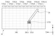
도 1을 참조하면, 본 출원의 일 예에 따른 디스플레이 장치(10)는 디스플레이 패널(100)을 복수의 수평 터치 그룹(HTG1 ~ HTG8)으로 분할하고, 복수의 수평 터치 그룹(HTG1 ~ HTG8)의 순차 구동 또는 수평 분할 구동을 통해 업 링크 신호(uplink signal)(ULS)를 터치 펜(20)에 전송하고 업 링크 신호(ULS)를 전송한 수평 터치 그룹(HTG6)을 통하여 업 링크 신호(ULS)에 동기되어 터치 펜(20)으로부터 전송되는 다운 링크 신호(downlink signal)(DLS)를 수신하여 터치 펜(20)의 위치를 센싱한 다음, 터치 펜(20)의 위치를 기반으로 터치 펜(20)이 위치한 수평 터치 그룹(HTG6)을 통해 업 링크 신호(ULS)를 전송하고 터치 펜(20)으로부터 전송되는 다운 링크 신호(DLS)를 수신하는 펜 트래킹(pen tracking) 방식으로 펜 터치를 센싱할 수 있다. 이때, 복수의 수평 터치 그룹(HTG1 ~ HTG8) 중 업 링크 신호(ULS)를 터치 펜(20)으로 전송하지 않는 수평 터치 그룹에는 직류 전압(또는 공통 전압)이 공급된다. 여기서, 업 링크 신호는 적어도 하나의 펄스를 갖는 구형파일 수 있으나, 반드시 이에 한정되지 않는다.Referring to FIG. 1 , the
상기 터치 펜(20)의 위치를 기반으로 하는 펜 트래킹 방식은 터치 펜(20)이 위치한 수평 터치 그룹(HTG6)을 펜 중첩 수평 터치 그룹으로 설정하거나 터치 펜(20)이 위치한 수평 터치 그룹(HTG6)과 그 주변의 수평 터치 그룹(HTG4, HTG6)을 펜 중첩 수평 터치 그룹으로 설정하고, 설정된 펜 중첩 수평 터치 그룹을 트래킹하면서 펜 터치를 센싱할 수 있다.In the pen tracking method based on the position of the
상기 터치 펜(20)은 금속 등과 같은 도전성 재질로 이루어진 전도성 팁을 포함할 수 있다. 전도성 팁은 디스플레이 패널(100)로부터 송신되는 펜 설정 신호 또는 펜 구동 신호(또는 펜 동기 신호)를 포함하는 업 링크 신호(ULS)를 수신하는 수신 전극의 역할을 하거나 펜 위치 데이터 신호 또는 펜 조작 데이터 신호를 포함하는 다운 링크 신호(DLS)를 디스플레이 패널(100)로 송신하는 송신 전극의 역할을 한다. 예를 들어, 전도성 팁은 디스플레이 패널(100)과 접촉하고, 그 접촉 위치의 디스플레이 패널(100)에 마련된 터치 전극과 커플링됨으로써 커플링된 터치 전극에 공급되는 업 링크 신호(ULS)를 수신한다. 그리고, 전도성 팁은 수신된 업 링크 신호(ULS)에 동기되는 다운 링크 신호(DLS)를 커플링된 터치 전극에 송신한다.The
이와 같은, 본 출원의 일 예에 따른 디스플레이 장치(10)는 복수의 수평 터치 그룹(HTG1 ~ HTG8)의 순차 구동 또는 수평 분할 구동을 통해 업 링크 신호(ULS)를 터치 펜(20)에 전송함으로써 디스플레이 패널(100)에 접촉된 사용자의 손이나 손바닥에 의한 업 링크 신호(ULS)의 감쇄를 최소화할 수 있고, 이를 통해 사용자의 손이나 손바닥과 디스플레이 패널(100) 간의 접촉시에도 디스플레이 패널(100) 상에 위치한 터치 펜(20)의 위치를 센싱할 수 있으며, 터치 펜(20)의 위치를 기반으로 터치 펜(20)의 위치를 트래킹하면서 펜 터치를 센싱하여 터치 드로잉을 끊김 없이 센싱할 수 있다.As described above, the
도 2는 본 출원의 다른 예에 따른 디스플레이 장치의 펜 센싱을 개략적으로 나타내는 도면이다.2 is a diagram schematically illustrating pen sensing of a display device according to another example of the present application.
도 2를 참조하면, 본 출원의 다른 예에 따른 디스플레이 장치(10)는 디스플레이 패널(100)을 복수의 수직 터치 그룹(VTG1 ~ VTG12)으로 분할하고, 복수의 수직 터치 그룹(VTG1 ~ VTG12)의 순차 구동 또는 수직 분할 구동을 통해 업 링크 신호(ULS)를 터치 펜(20)에 전송하고 업 링크 신호(ULS)를 전송한 수직 터치 그룹(VTG1 ~ VTG12)을 통하여 업 링크 신호(ULS)에 동기되어 터치 펜(20)으로부터 전송되는 다운 링크 신호(DLS)를 수신하여 터치 펜(20)의 위치를 센싱한 다음, 터치 펜(20)의 위치를 기반으로 터치 펜(20)이 위치한 로컬 터치 그룹(LTG)을 통해 업 링크 신호(ULS)를 전송하고 터치 펜(20)으로부터 전송되는 다운 링크 신호(DLS)를 수신하는 펜 트래킹 방식으로 펜 터치를 센싱한다. 이때, 복수의 수직 터치 그룹(VTG1 ~ VTG12) 중 업 링크 신호(ULS)를 터치 펜(20)으로 전송하지 않는 수직 터치 그룹에는 직류 전압(또는 공통 전압)이 공급된다.Referring to FIG. 2 , the
상기 터치 펜(20)의 위치를 기반으로 하는 펜 트래킹 방식은 터치 펜(20)이 위치한 수직 터치 그룹(VTG7)을 로컬 터치 그룹(LTG)으로 설정하거나 터치 펜(20)이 위치한 수직 터치 그룹(VTG7)과 그 주변의 수직 터치 그룹(LTG6, LTG8)을 로컬 터치 그룹(LTG)으로 설정하고 설정되는 로컬 터치 그룹(LTG)을 트래킹하면서 펜 터치를 센싱할 수 있다.In the pen tracking method based on the location of the
본 출원의 다른 예에 따른 디스플레이 장치(10)는 복수의 수직 터치 그룹(VTG1 ~ VTG12)의 순차 구동 또는 수직 분할 구동을 통해 업 링크 신호(ULS)를 터치 펜(20)에 전송함으로써 디스플레이 패널(100)에 접촉된 사용자의 손이나 손바닥에 의한 업 링크 신호(ULS)의 감쇄를 최소화할 수 있고, 이를 통해 사용자의 손이나 손바닥과 디스플레이 패널(100) 간의 접촉시에도 디스플레이 패널(100) 상에 위치한 터치 펜(20)의 위치를 센싱할 수 있으며, 터치 펜(20)의 위치를 기반으로 터치 펜(20)의 위치를 트래킹하면서 펜 터치를 센싱하여 터치 드로잉을 끊김 없이 센싱할 수 있다. 본 출원의 다른 예에 따른 디스플레이 장치(10)는 터치 펜(20)이 위치한 로컬 터치 그룹(LTG)을 통해 터치 펜(20) 간의 신호를 송수신함으로써 소비 전력이 감소될 수 있다.The
도 3은 본 출원의 일 예에 따른 디스플레이 장치를 설명하기 위한 도면이고, 도 4는 도 3에 도시된 표시 영역을 설명하기 위한 도면이며, 도 5는 도 3에 도시된 터치 동기 신호를 나타내는 파형도이다.3 is a diagram for explaining a display device according to an example of the present application, FIG. 4 is a diagram for explaining a display area shown in FIG. 3, and FIG. 5 is a waveform representing a touch sync signal shown in FIG. 3 It is also
도 3 내지 도 5를 참조하면, 본 출원의 일 예에 따른 디스플레이 장치는 디스플레이 패널(100), 디스플레이 구동 회로부, 터치 구동 회로(700), 및 호스트 제어부(800)를 포함할 수 있다.3 to 5 , a display device according to an example of the present application may include a
상기 디스플레이 패널(100)은 정전 용량 방식을 이용한 인셀 터치 타입의 구조를 갖는 액정 디스플레이 패널일 수 있다. 일 예에 따른 디스플레이 패널(100)은 자기(self) 정전 용량 방식을 이용한 인셀 터치 타입의 구조를 가질 수 있다. 이러한 디스플레이 패널(100)은 디스플레이 모드와 터치 센싱 모드로 동작할 수 있다. 예를 들어, 디스플레이 패널(100)은 디스플레이 모드 동안 백라이트 유닛으로부터 조사되는 광을 이용하여 영상을 표시하고, 터치 센싱 모드 동안 터치 센싱을 위한 터치 패널의 역할을 한다. 디스플레이 모드는 한 프레임 내에 설정된 복수의 디스플레이 구간마다 수행될 수 있고, 터치 센싱 모드는 한 프레임 내에 복수의 디스플레이 구간 사이에 설정된 복수의 터치 센싱 구간마다 수행될 수 있다. 여기서, 복수의 터치 센싱 구간 각각은 복수의 디스플레이 구간 각각의 직전에 설정될 수도 있다.The
일 예에 따른 디스플레이 패널(100)은 기판 상에 마련된 표시 영역(101), 및 표시 영역(101)을 둘러싸도록 기판의 가장자리에 마련된 비표시 영역(102)을 포함한다.The
상기 표시 영역(101)은 복수의 데이터 라인(DL), 복수의 게이트 라인(GL), 복수의 부화소(SP), 복수의 터치 전극(TE), 및 복수의 터치 라우팅 라인(TL)을 포함한다.The
상기 복수의 데이터 라인(DL) 각각은 디스플레이 모드시 데이터 신호를 입력 받는다. 상기 복수의 게이트 라인(GL) 각각은 디스플레이 모드시 스캔 펄스를 입력 받는다. 이러한 복수의 데이터 라인(DL)과 복수의 게이트 라인(GL) 각각은 기판 상에 서로 교차하도록 마련되어 복수의 부화소 영역을 정의한다.Each of the plurality of data lines DL receives a data signal in a display mode. Each of the plurality of gate lines GL receives a scan pulse in a display mode. Each of the plurality of data lines DL and the plurality of gate lines GL is provided to cross each other on the substrate to define a plurality of subpixel areas.
상기 복수의 부화소(SP) 각각은 인접한 게이트 라인(GL)과 데이터 라인(DL)에 연결된 박막 트랜지스터, 박막 트랜지스터에 연결된 화소 전극, 및 화소 전극에 연결된 스토리지 커패시터를 포함할 수 있다.Each of the plurality of subpixels SP may include a thin film transistor connected to an adjacent gate line GL and a data line DL, a pixel electrode connected to the thin film transistor, and a storage capacitor connected to the pixel electrode.
상기 박막 트랜지스터는 게이트 단자, 반도체층, 제 1 단자, 및 제 2 단자를 포함할 수 있다. 박막 트랜지스터의 제 1 단자와 제 2 단자는 전류 방향에 따라 소스 단자 또는 드레인 단자로 정의될 수 있다. 박막 트랜지스터는 게이트 단자가 반도체층 아래에 위치하는 바텀 게이트(bottom gate) 구조 및/또는 게이트 단자가 반도체층 위에 위치하는 탑 게이트(top gate) 구조로 가질 수 있다. 이러한 박막 트랜지스터는 보호층(또는 평탄화층)에 의해 덮인다.The thin film transistor may include a gate terminal, a semiconductor layer, a first terminal, and a second terminal. The first terminal and the second terminal of the thin film transistor may be defined as a source terminal or a drain terminal according to a current direction. The thin film transistor may have a bottom gate structure in which a gate terminal is positioned below the semiconductor layer and/or a top gate structure in which the gate terminal is positioned above the semiconductor layer. These thin film transistors are covered by a protective layer (or planarization layer).
상기 화소 전극은 부화소 영역 내의 보호층 상에 투명 전도성 물질로 형성되고 보호층에 마련된 비아홀을 통해 박막 트랜지스터의 제 2 단자와 연결될 수 있다.The pixel electrode may be formed of a transparent conductive material on the passivation layer in the subpixel area and connected to the second terminal of the thin film transistor through a via hole provided in the passivation layer.
상기 스토리지 커패시터는 박막 트랜지스터의 제 2 단자와 터치 전극(TE) 사이에 형성되거나 화소 전극과 터치 전극(TE) 사이에 형성될 수 있다. 이러한 스토리지 커패시터는 박막 트랜지스터를 통하여 공급되는 데이터 신호를 충전하고, 박막 트랜지스터가 턴-오프되면 충전 전압을 이용하여 화소 전극과 터치 전극(TE) 사이에 형성되는 전계를 유지시킨다.The storage capacitor may be formed between the second terminal of the thin film transistor and the touch electrode TE or may be formed between the pixel electrode and the touch electrode TE. The storage capacitor charges the data signal supplied through the thin film transistor and maintains an electric field formed between the pixel electrode and the touch electrode TE using the charging voltage when the thin film transistor is turned off.
상기 복수의 터치 전극(TE) 각각은 터치 객체에 의한 터치를 센싱하기 위한 터치 센서의 역할을 하거나 화소 전극과 함께 전계를 형성시켜 액정을 구동시키는 공통 전극의 역할을 한다. 즉, 복수의 터치 전극(TE) 각각은 터치 센싱 모드시 터치 센서로 사용되고, 디스플레이 모드시 공통 전극으로 사용된다. 이러한 복수의 터치 전극(TE) 각각은 액정 구동을 위한 공통 전극으로도 사용되기 때문에 투명 전도성 물질을 포함하여 이루어질 수 있다. 터치 객체는 사용자 손가락이거나 액티브 스타일러스 펜 등과 같은 터치 펜으로 정의될 수 있다.Each of the plurality of touch electrodes TE serves as a touch sensor for sensing a touch by a touch object or serves as a common electrode for driving liquid crystal by forming an electric field together with a pixel electrode. That is, each of the plurality of touch electrodes TE is used as a touch sensor in the touch sensing mode and used as a common electrode in the display mode. Since each of the plurality of touch electrodes TE is also used as a common electrode for driving the liquid crystal, it may include a transparent conductive material. The touch object may be defined as a user's finger or a touch pen such as an active stylus pen.
상기 복수의 터치 전극(TE) 각각은 터치 센싱 모드시 자기 정전 용량 방식의 터치 센서로 사용되기 때문에 터치 객체와 디스플레이 패널(100) 간의 최소 접촉 크기보다 큰 크기를 가져야만 한다. 이에 따라, 복수의 터치 전극(TE) 각각은 하나 이상의 부화소(SP)와 대응되는 크기를 가질 수 있다. 일 예에 따른 복수의 터치 전극(TE)은 복수의 수평 라인과 복수의 수직 라인을 따라 일정한 간격으로 배치될 수 있다. 예를 들어, 하나의 수평 라인은 일정한 간격으로 배치된 84개의 터치 전극(TE)을 포함할 수 있으며, 하나의 수직 라인은 일정한 간격으로 배치된 48개의 터치 전극(TE)을 포함할 수 있다.Since each of the plurality of touch electrodes TE is used as a self-capacitance type touch sensor in a touch sensing mode, it must have a size greater than the minimum contact size between a touch object and the
상기 복수의 터치 라우팅 라인(TL) 각각은 복수의 터치 전극(TE) 각각에 개별적으로 연결된다. 복수의 터치 라우팅 라인(TL) 각각은 디스플레이 모드시 해당하는 터치 전극(TE)에 공통 전압(Vcom)을 공급하고, 터치 센싱 모드시 해당하는 터치 전극(TE)에 터치 구동 펄스를 공급한 후, 해당하는 터치 전극(TE)의 정전 용량 변화를 터치 구동 회로(700)에 제공한다.Each of the plurality of touch routing lines TL is individually connected to each of a plurality of touch electrodes TE. Each of the plurality of touch routing lines TL supplies a common voltage Vcom to the corresponding touch electrode TE in the display mode and supplies a touch driving pulse to the corresponding touch electrode TE in the touch sensing mode, The capacitance change of the corresponding touch electrode TE is provided to the
이와 같은, 표시 영역(101)은 n(n은 2 이상의 자연수)개의 수평 블록(HB1~HBn)으로 분할되어 시분할 구동에 따라 수평 블록 단위로 영상이 표시되거나 터치 센싱이 수행된다. 일 예에 따른 n개의 수평 블록(HB1~HBn) 각각은 m(m은 자연수)개의 게이트 라인(GL)(또는 수평 라인)을 포함할 수 있으며, m개의 게이트 라인(GL)은 하나의 터치 전극(TE)과 중첩될 수 있다. 예를 들어, 제 1 수평 블록(HB1)은 제 1 내지 제 m 게이트 라인을 포함할 수 있고, 제 2 수평 블록(HB2)은 제 m+1 내지 제 2m 게이트 라인을 포함할 수 있다.As such, the
상기 디스플레이 구동부는 디스플레이 패널(100)의 표시 영역(101)을 n개의 수평 블록(HB1~HBn)으로 시분할하고, 터치 동기 신호(Tsync)의 디스플레이 구간(DP)마다 수평 블록 단위로 부화소들(SP)에 데이터 신호를 공급한다. 일 예에 따른 디스플레이 구동 회로부는 데이터 구동 회로(200), 게이트 구동 회로(300), 타이밍 제어 회로(400), 구동 전원 공급부(500), 및 터치 구동 신호 공급부(600)를 포함할 수 있다.The display driver time-divides the
상기 데이터 구동 회로(200)는 디스플레이 모드시, 데이터 제어 신호(DCS)를 기반으로 화소 데이터(R/G/B)를 아날로그 형태의 데이터 신호로 변환하여 복수의 데이터 라인(DL)에 공급한다.The
일 예에 따른 데이터 구동 회로(200)는 터치 동기 신호(Tsync)의 디스플레이 구간(DP)마다 복수의 데이터 라인(DL)을 통해 해당하는 수평 블록의 부화소들(SP)에 데이터 신호를 공급한다.The
다른 예에 따른 데이터 구동 회로(200)는 터치 동기 신호(Tsync)의 디스플레이 구간(DP)마다 복수의 데이터 라인(DL)을 통해 해당하는 수평 블록의 부화소들(SP)에 데이터 신호를 공급한다. 그리고, 데이터 구동 회로(200)는 터치 동기 신호(Tsync)의 터치 센싱 구간(TP)마다 터치 구동 신호 또는 업 링크 신호가 인가되는 터치 전극(TE)과 중첩되는 복수의 데이터 라인(DL) 각각에 데이터 로드 프리 신호(data load free signal)를 공급한다. 여기서, 데이터 로드 프리 신호는 터치 센싱 모드시, 터치 전극(TE)에 인가되는 터치 구동 신호 또는 업 링크 신호와 동일한 위상을 가짐으로써 터치 전극(TE)과 데이터 라인(DL) 사이의 기생 커패시턴스에 따른 터치 전극들(TE)의 로드를 감소시킴으로써 터치 감도를 향상시킬 수 있다.The
상기 게이트 구동 회로(300)는 부화소(SP)에 박막 트랜지스터를 마련하는 박막 트랜지스터 제조 공정과 함께 디스플레이 패널(100)의 일측 비표시 영역에 내장(또는 집적)되고, 복수의 게이트 라인(GL)과 일대일로 연결된다. 이러한 게이트 구동 회로(300)는 게이트 제어 신호(GCS)를 기반으로 정해진 순서에 따라 스캔 펄스를 생성하여 정해진 순서에 해당하는 게이트 라인(GL)에 공급한다. 게이트 라인에 공급되는 스캔 펄스는 데이터 라인에 공급되는 데이터 신호와 동기된다.The
일 예에 따른 게이트 구동 회로(300)는 터치 동기 신호(Tsync)의 디스플레이 구간(DP)마다 수평 블록 단위로 수평 블록 그룹에 포함된 i개의 게이트 라인에 스캔 펄스를 순차적으로 공급한다. 예를 들어, 게이트 구동 회로(300)는 i개의 게이트 라인에 스캔 펄스를 순차적으로 공급하는 i개의 구동 스테이지를 갖는 n개의 구동 스테이지 그룹, 및 n개의 구동 스테이지 그룹 사이에 배치되어 전단 구동 스테이지 그룹의 출력 신호를 터치 동기 신호(Tsync)의 터치 센싱 구간(TP) 동안 홀딩시킨 후 후단 구동 스테이지 그룹의 스타트 신호로 제공하는 n-1개의 홀딩 스테이지 그룹을 포함할 수 있다.The
다른 예에 따른 게이트 구동 회로(300)는 터치 동기 신호(Tsync)의 디스플레이 구간(DP)마다 수평 블록 단위로 수평 블록 그룹에 포함된 i개의 게이트 라인에 스캔 펄스를 순차적으로 공급한다. 그리고, 게이트 구동 회로(300)는 터치 동기 신호(Tsync)의 터치 센싱 구간(TP)마다 터치 구동 신호 또는 업 링크 신호가 인가되는 터치 전극(TE)과 중첩되는 복수의 게이트 라인(GL) 각각에 게이트 로드 프리 신호(gate load free signal)를 공급한다. 여기서, 게이트 로드 프리 신호는 터치 센싱 모드시, 터치 전극(TE)에 인가되는 터치 구동 신호 또는 업 링크 신호와 동일한 위상을 가짐으로써 터치 전극(TE)과 게이트 라인(GL) 사이의 기생 커패시턴스에 따른 터치 전극들(TE)의 로드를 감소시킴으로써 터치 감도를 향상시킬 수 있다.The
상기 타이밍 제어 회로(400)는 디스플레이 구동 시스템(또는 호스트 시스템)으로부터 공급되는 데이터 인에이블 신호, 기준 클럭 신호, 수직 동기 신호(Vsync), 및 수평 동기 신호 등의 타이밍 동기 신호(TSS)를 수신하고, 수신된 수직 동기 신호(Vsync)를 호스트 제어부(800)에 제공한다. 타이밍 제어 회로(400)는 호스트 제어부(800)로부터 터치 동기 신호(Tsync)를 수신하고, 터치 동기 신호(Tsync)를 기반으로 디스플레이 패널(100)의 한 프레임(1 Frame)을 복수의 디스플레이 구간(DP)과 복수의 터치 센싱 구간(TP)으로 시분할 구동한다.The
상기 타이밍 제어 회로(400)는 디스플레이 구동 시스템으로부터 제공되는 입력 데이터(Idata)를 수신하고, 복수의 디스플레이 구간(DP) 각각마다 입력 데이터(Idata)를 디스플레이 패널(100)의 구동에 알맞도록 화소 데이터(R/G/B)로 정렬하여 데이터 구동 회로(200)에 제공한다.The
상기 타이밍 제어 회로(400)는 타이밍 동기 신호(TSS)와 터치 동기 신호(Tsync)를 기반으로, 데이터 제어 신호(DCS)와 게이트 제어 신호(GCS)를 생성하여 출력한다. 여기서, 데이터 제어 신호(DCS)는 소스 스타트 신호, 소스 쉬프트 신호, 소스 인에이블 신호, 및 극성 제어 신호 등을 포함할 수 있다. 그리고, 게이트 제어 신호(GCS)는 적어도 하나의 게이트 스타트 신호 및 복수의 게이트 쉬프트 클럭 등을 포함할 수 있다.The
상기 구동 전원 공급부(500)는 외부로부터의 입력 전원(Vin)을 이용하여 디스플레이 장치의 구동에 필요한 구동 전원을 생성한다. 특히, 구동 전원 공급부(500)는 로직 구동 전압, 기준 공통 전압, 로드 프리 로우 전압(load free low voltage), 및 로드 프리 하이 전압(load free high voltage)을 포함하는 구동 전압(Vpower)을 생성하여 터치 구동 신호 공급부(700)에 제공할 수 있다. 이러한 구동 전원 공급부(500)는 디스플레이 장치의 데이터 인쇄 회로 기판, 제어 모드, 또는 전원 공급 보드에 실장되는 전원 관리 집적 회로(power management integrated circuit)일 수 있다.The driving
상기 터치 구동 신호 공급부(600)는 구동 전원 공급부(500)로부터 제공되는 구동 전압(Vpower)을 기반으로 터치 펄스 제어 신호(TPCS)에 따라 기준 공통 전압을 기준으로 하이 전압과 로우 전압 사이에서 스윙되는 복수의 구동 펄스를 갖는 터치 전극 구동 신호(TDS)를 생성하여 터치 구동 회로(700)에 제공한다. 여기서, 터치 전극 구동 신호(TDS)는 하이 전압과 로우 전압 각각의 펄스 폭이 터치 펄스 제어 신호(TPCS)에 따라 변조됨으로써 터치 센싱 구간에 터치 전극(TE)에 공급되는 업 링크 신호, 예를 들어 터치 구동 신호, 펜 구동 신호, 또는 펜 설정 신호로 사용된다. 그리고, 상기 터치 구동 신호 공급부(600)는 구동 전원 공급부(500)로부터 제공되는 로드 프리 로우 전압(Vlfd1)과 로드 프리 하이 전압(Vlfd2)을 터치 구동 회로(700)에 제공한다. 로드 프리 로우 전압(Vlfd1)은 디스플레이 구간(DP) 동안 터치 전극(TE)에 공급되는 공통 전압(Vcom) 또는 업 링크 신호가 공급되지 않는 터치 전극(TE)에 공급되는 직류 전압으로 사용될 수 있다. 이러한 터치 구동 신호 공급부(600)는 디스플레이 장치의 데이터 인쇄 회로 기판, 제어 모드, 또는 전원 공급 보드에 실장되는 터치 파워 집적 회로(touch power integrated circuit)일 수 있다.The touch driving
상기 터치 구동 회로(700)는 디스플레이 패널(100)에 마련된 복수의 터치 라우팅 라인(TL)을 통해 복수의 터치 전극(TE)과 일대일로 연결된다. 터치 구동 회로(700)는 호스트 제어부(800)의 채널 제어 및 센싱 타이밍 제어에 응답하여 터치 동기 신호(Tsync)의 디스플레이 구간(DP) 동안 복수의 터치 라우팅 라인(TL) 각각을 통해서 복수의 터치 전극(TE) 각각에 공통 전압(Vcom)을 공급하며, 터치 동기 신호(Tsync)의 터치 센싱 구간(TP) 동안 복수의 터치 전극(TE)의 일부 또는 전체를 통해 터치 객체에 의한 터치를 센싱한다.The
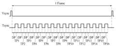
상기 터치 동기 신호(Tsync)의 터치 센싱 구간(TP)에 따른 터치 센싱 모드에 있어서, 일 예에 따른 터치 구동 회로(700)는 한 프레임(1 Frame) 내에 설정된 복수의 터치 센싱 구간(TP) 중 펜 조작 센싱 구간마다 펜 터치를 센싱하고, 복수의 터치 센싱 구간(TP) 중 핑거 터치 센싱 구간마다 핑거 터치를 센싱할 수 있다. 예를 들어, 한 프레임(1 Frame)이 제 1 내지 제 16 터치 센싱 구간(TP1 ~ TP16)을 포함할 경우, 제 1 터치 센싱 구간(TP1)은 펜 설정 구간으로 설정되고, 제 2-4, 제 6-8, 제 10-12, 제 14 및 제 15 터치 센싱 구간(TP2~TP4, TP6~TP8, TP10~TP12, TP14, TP15) 각각은 펜 센싱 구간으로 설정되며, 제 5, 제 9, 제 13, 및 제 16 터치 센싱 구간(TP5, TP9, TP13, TP16) 각각은 핑거 센싱 구간으로 설정될 수 있다. 그리고, 펜 센싱 구간으로 설정되는 터치 센싱 구간(TP2~TP4, TP6~TP8, TP10~TP12, TP14, TP15) 중 제 2, 제 6, 제 10, 및 제 14 터치 센싱 구간(TP2, TP6, TP10, TP14) 각각은 펜 위치 센싱 구간으로 설정되고, 제 3, 제 4, 제 7, 제 8, 제 11, 제 12, 및 제 15 터치 센싱 구간(TP3, TP4, TP7, TP8, TP11, TP12, TP15) 각각은 펜 조작 센싱 구간으로 설정될 수 있다. 제 2 내지 제 16 터치 센싱 구간(TP2 ~ TP16) 각각은 터치 전극(TE)을 구동하기 위한 제 1 기간, 및 터치 전극의 정전 용량 변화량을 센싱하기 위한 제 2 기간을 포함할 수 있다.In the touch sensing mode according to the touch sensing period (TP) of the touch synchronization signal (Tsync), the
일 예에 따른 터치 구동 회로(700)는 복수의 터치 전극(TE)을 복수의 터치 그룹으로 분할하고, 복수의 핑거 센싱 구간마다 복수의 터치 그룹 중 일부의 터치 그룹 또는 전체 터치 그룹의 터치 전극들 각각에 터치 구동 신호를 공급한 후, 복수의 터치 라우팅 라인(TL) 각각을 통해서 해당하는 터치 전극(TE)의 정전 용량 변화를 센싱해 핑거 터치 로우 데이터(finger touch raw data)를 생성하고, 생성된 핑거 터치 로우 데이터를 호스트 제어부(800)에 제공한다.The
일 예에 따른 터치 구동 회로(700)는 복수의 터치 전극(TE)을 복수의 터치 그룹으로 분할하고, 복수의 펜 위치 센싱 구간(TP2, TP6, TP10, TP14)의 제 1 구간마다 복수의 터치 그룹 중 일부의 터치 그룹에 업 링크 신호(즉, 펜 구동 신호)를 공급하고, 복수의 펜 위치 센싱 구간의 제 2 구간마다 펜 구동 신호가 공급된 터치 그룹을 통해 터치 펜으로부터 전송된 다운 링크 신호(즉, 펜 위치 데이터 신호)를 제 1 펜 터치 로우 데이터로 변환하여 호스트 제어부(800)에 제공한다. 이와 동시에, 일 예에 따른 터치 구동 회로(700)는 복수의 펜 위치 센싱 구간의 제 1 구간마다 복수의 터치 그룹 중 일부의 터치 그룹을 제외한 나머지 터치 그룹에 직류 전압(또는 공통 전압(Vcom))을 공급함으로써 복수의 터치 그룹 중 일부의 터치 그룹을 제외한 나머지 터치 그룹의 터치 전극들(TE)과 중첩되는 부화소들에 마련된 스토리지 커패시터의 전압이 펜 조작 센싱 구간 동안 터치 전극(TE)에 공급되는 업 링크 신호에 따라 변화되지 않고 유지되도록 한다.The
일 예에 따른 터치 구동 회로(700)는 복수의 펜 조작 센싱 구간의 제 1 구간마다 복수의 터치 그룹 중 호스트 제어부(800)로부터 제공되는 펜 트래킹 채널 정보에 해당하는 펜 중첩 터치 그룹에 펜 구동 신호를 공급하며, 복수의 펜 조작 센싱 구간의 제 2 구간마다 펜 중첩 터치 그룹을 통해 터치 펜으로부터 전송된 펜 조작 데이터 신호를 제 2 펜 터치 로우 데이터로 변환하여 호스트 제어부(800)에 제공한다. 이와 동시에, 일 예에 따른 터치 구동 회로(700)는 복수의 펜 조작 센싱 구간의 제 1 구간마다 복수의 터치 그룹 중 펜 중첩 터치 그룹을 제외한 나머지 펜 비중첩 터치 그룹에 직류 전압(또는 공통 전압(Vcom))을 공급함으로써 펜 비중첩 터치 그룹의 터치 전극들(TE)과 중첩되는 부화소들에 마련된 스토리지 커패시터의 전압이 펜 조작 센싱 구간 동안 터치 전극(TE)에 공급되는 업 링크 신호에 따라 변화되지 않고 유지되도록 한다.The
일 예에 따른 터치 구동 회로(700)는 복수의 터치 위치 센싱 구간의 제 1 구간마다 복수의 터치 그룹에 업 링크 신호(즉, 펜 구동 신호)를 순차적으로 공급하여 터치 펜의 위치를 센싱할 수 있다. 이때, 복수의 터치 그룹 각각은 적어도 하나의 수평 라인 또는 적어도 하나의 수직 라인에 배치된 터치 전극을 포함한다.The
다른 예에 따른 터치 구동 회로(700)는 복수의 터치 전극(TE)을 제 1 터치 그룹과 제 2 터치 그룹으로 분할하고, 프레임 단위 또는 복수의 터치 센싱 구간 각각의 제 1 구간 단위로 제 1 터치 그룹과 제 2 터치 그룹에 업 링크 신호(즉, 펜 구동 신호)를 교번적으로 공급하여 터치 펜의 위치를 센싱할 수 있다. 일 예로서, 제 1 터치 그룹은 복수의 수평 라인 중 홀수번째 수평 라인들에 배치된 터치 전극들을 포함하며, 제 2 터치 그룹은 복수의 수평 라인 중 짝수번째 수평 라인들에 배치된 터치 전극들을 포함할 수 있다. 다른 예로서, 제 1 터치 그룹은 복수의 수직 라인 중 홀수번째 수직 라인들에 배치된 터치 전극들을 포함하며, 제 2 터치 그룹은 복수의 수직 라인 중 짝수번째 수직 라인들에 배치된 터치 전극들을 포함할 수 있다.The
상기 호스트 제어부(800)는 MCU(Micro Controller Unit) 또는 어플리케이션 프로세서(application processor)일 수 있다.The
상기 호스트 제어부(800)는 타이밍 제어 회로(400)로부터 제공되는 수직 동기 신호(Vsync)에 기초하여 디스플레이 패널(100)을 수평 블록 단위로 시분할 구동하기 위한 터치 동기 신호(Tsync)와 터치 펄스 제어 신호(TPCS)를 각각 생성한다.The
일 예에 따른 터치 동기 신호(Tsync)는 타이밍 동기 신호(TSS)의 수직 동기 신호(Vsync)에 따른 한 프레임 동안 2회 이상의 디스플레이 구간(DP)과 2회 이상의 터치 센싱 구간(TP)을 포함할 수 있다. 터치 동기 신호(Tsync)는 터치 센싱 구간(TP)이 디스플레이 구간(DP)보다 먼저 시작되도록 생성될 수 있다. 여기서, 터치 동기 신호(Tsync)의 디스플레이 구간(DP)은 디스플레이 패널(100)의 디스플레이 모드로 정의될 수 있고, 터치 동기 신호(Tsync)의 터치 센싱 구간(TP)은 디스플레이 패널(100)의 터치 센싱 모드로 정의될 수 있다.The touch synchronization signal Tsync according to an example may include two or more display periods DP and two or more touch sensing periods TP during one frame according to the vertical synchronization signal Vsync of the timing synchronization signal TSS. can The touch synchronization signal Tsync may be generated such that the touch sensing period TP starts before the display period DP. Here, the display period DP of the touch sync signal Tsync may be defined as the display mode of the
상기 터치 펄스 제어 신호(TPCS)는 터치 구동 회로(700)로부터 터치 전극(TE)에 공급되는 업 링크 신호, 즉, 핑거 터치의 센싱을 위한 터치 구동 신호 및 펜 터치의 센싱을 위한 펜 설정 신호 및 펜 구동 신호 각각의 출력 주기를 제어하기 위한 신호로 정의될 수 있다. 예를 들어, 터치 펄스 제어 신호(TPCS)는 펄스 폭 변조 신호일 수 있다.The touch pulse control signal TPCS is an uplink signal supplied from the
일 예에 따른 호스트 제어부(800)는 SPI(Serial Peripheral Interface)를 통해 터치 구동 회로(700)와 연결된다. 호스트 제어부(800)는 채널 셋팅 정보, 센싱 블록 정보, 샘플링 개시 신호, 및 디지털 변환 설정 파라미터 등을 포함하는 터치 제어 데이터를 생성하여 SPI 방식을 통해 터치 구동 회로(700)에 제공함으로써 터치 구동 회로(700)의 구동 타이밍을 제어한다. 특히, 호스트 제어부(800)는 복수의 터치 전극을 복수의 터치 그룹으로 분할하여 터치 그룹 단위의 순차 구동 또는 터치 그룹 단위의 분할 구동을 위한 채널 그룹 셋팅 정보를 생성하여 터치 구동 회로(700)에 제공함으로써 디스플레이 패널(100)에 접촉된 사용자의 손이나 손바닥에 의해 터치 펜으로 송신되는 업 링크 신호의 감쇄를 최소화하고, 이를 통해 사용자의 손이나 손바닥과 디스플레이 패널(100) 간의 접촉시에도 터치 구동 회로(700)에서 펜 터치의 센싱을 가능하게 한다.The
일 예에 따른 호스트 제어부(800)는 SPI 방식을 통해 터치 구동 회로(700)로부터 제공되는 터치 로우 데이터를 수신하고, 수신된 핑거 터치 로우 데이터에 대해 미리 설정된 터치 센싱 알고리즘을 실행하여 터치 좌표 정보를 산출하고, 산출된 터치 좌표 정보에 해당되는 어플리케이션을 실행할 수 있다.The
일 예에 따른 호스트 제어부(800)는 SPI 방식을 통해 터치 구동 회로(700)로부터 제공되는 제 1 펜 터치 로우 데이터를 수신하고, 수신된 제 1 펜 터치 로우 데이터에 대해 미리 설정된 펜 터치 센싱 알고리즘을 실행하여 펜 위치 정보를 산출하고, 복수의 터치 그룹 중 산출된 펜 위치 정보에 해당하는 터치 그룹에 대한 펜 트래킹 채널 정보로 이루어지는 채널 셋팅 정보를 생성하여 터치 구동 회로(700)에 제공한다. 이에 따라, 터치 구동 회로(700)는 복수의 펜 조작 센싱 구간의 제 1 구간마다 펜 트래킹 채널 정보에 해당하는 펜 중첩 터치 그룹에 업 링크 신호를 공급하며, 복수의 펜 조작 센싱 구간의 제 2 구간마다 펜 중첩 터치 그룹을 통해 터치 펜으로부터 전송된 다운 링크 신호를 제 2 펜 터치 로우 데이터로 변환하여 호스트 제어부(800)에 제공한다. 여기서, 펜 중첩 터치 그룹은 복수의 터치 그룹의 배치 구조에 따라 적어도 하나의 수평 라인에 배치된 터치 전극들을 갖는 수평 터치 그룹이거나 적어도 하나의 수직 라인에 배치된 터치 전극들을 갖는 수직 터치 그룹 내의 로컬 터치 그룹일 수 있다. 호스트 제어부(800)는 SPI 방식을 통해 터치 구동 회로(700)로부터 제공되는 제 2 펜 터치 로우 데이터를 수신하고, 수신된 제 2 펜 터치 로우 데이터에 대해 미리 설정된 펜 조작 센싱 알고리즘을 실행하여 펜 조작 정보를 산출하고, 산출된 펜 위치 정보와 펜 조작 정보에 해당하는 어플리케이션을 실행할 수 있다. 여기서, 펜 조작 정보는 필압 정보 또는 버튼 조작 정보 등이 될 수 있다.The
선택적으로, 호스트 제어부(800)는 타이밍 제어 회로(400) 또는 터치 구동 회로(700)에 내장될 수도 있으며, 이 경우, 본 출원은 디스플레이 장치의 부품 수 및 구성요소 간의 연결 구조가 간소화될 수 있다. 그리고, 터치 동기 신호(Tsync)와 터치 펄스 제어 신호(TPCS)는 호스트 제어부(800)에서 생성되지 않고 타이밍 제어 회로(400)에서 생성될 수도 있다.Optionally, the
도 6은 본 출원의 일 예에 따른 터치 구동 회로를 설명하기 위한 도면이다.6 is a diagram for explaining a touch driving circuit according to an example of the present application.
도 6을 참조하면, 본 출원의 일 예에 따른 터치 구동 회로(700)는 채널 선택부(CSP), 전압 선택부(VSP), 센싱 유닛(SU), 멀티플렉서(MUX), 아날로그-디지털 변환기(ADC), 및 터치 제어 회로(CTR)를 포함할 수 있다.Referring to FIG. 6 , the
상기 채널 선택부(CSP)는 복수의 터치 라우팅 라인(TL)을 통해 복수의 터치 전극(TE)에 일대일로 연결된다. 이러한 채널 선택부(CSP)는 복수의 펜 센싱 구간의 제 1 구간마다 채널 선택 신호(CSS)에 해당하는 터치 그룹에 업 링크 신호와 로드 프리 로우 전압(Vlfd1)을 선택적으로 공급한다. 그리고, 채널 선택부(CSP)는 복수의 펜 센싱 구간의 제 2 구간마다 채널 선택 신호에 해당하는 터치 그룹을 선택한다. 즉, 채널 선택부(CSP)는 채널 선택 신호(CSS)에 해당하는 터치 라우팅 라인(TL)을 해당하는 센싱 회로(AFE)에 연결한다. 일 예에 따른 채널 선택부(CSS)는 터치 동기 신호(Tsync)와 채널 선택 신호(CSS)에 따라서 스위칭되는 복수의 멀티플렉서를 포함할 수 있다.The channel selector CSP is connected one-to-one to the plurality of touch electrodes TE through a plurality of touch routing lines TL. The channel selection unit CSP selectively supplies an uplink signal and a load pre-low voltage Vlfd1 to a touch group corresponding to the channel selection signal CSS in each first section of a plurality of pen sensing sections. Also, the channel selection unit CSP selects a touch group corresponding to the channel selection signal in each second section of the plurality of pen sensing sections. That is, the channel selector CSP connects the touch routing line TL corresponding to the channel select signal CSS to the corresponding sensing circuit AFE. The channel selection unit CSS according to an example may include a plurality of multiplexers that are switched according to the touch synchronization signal Tsync and the channel selection signal CSS.
상기 전압 선택부(VSP)는 터치 구동 신호 공급부(600)로부터 공급되는 터치 전극 구동 신호(TDS)(또는 업 링크 신호)와 로드 프리 로우 전압(Vlfd1)을 터치 제어 회로(CTR)로부터 공급되는 전압 선택 신호(VSS)에 따라 선택적으로 채널 선택부(CSP)에 공급한다. 예를 들어, 전압 선택부(VSP)는 터치 동기 신호(Tsync)의 디스플레이 구간마다 공통 전압으로 사용되는 로드 프리 로우 전압(Vlfd1)을 채널 선택부(CSP)에 공급한다. 그리고, 전압 선택부(VSP)는 터치 동기 신호(Tsync)의 터치 센싱 구간마다 터치 전극 구동 신호(TDS)에 따른 업 링크 신호가 복수의 터치 그룹 중 일부의 터치 그룹의 터치 전극에 공급되고, 로드 프리 로우 전압(Vlfd1)에 따른 직류 전압이 복수의 터치 그룹 중 일부의 터치 그룹을 제외한 나머지 터치 그룹의 터치 전극에 공급될 수 있도록 터치 전극 구동 신호(TDS)와 로드 프리 로우 전압(Vlfd1)을 선택적으로 채널 선택부(CSP)에 공급한다.The voltage selector VSP converts the touch electrode driving signal TDS (or uplink signal) supplied from the touch driving
상기 센싱 유닛(SU)은 채널 선택부(CSP)를 통해 디스플레이 패널(100)에 마련된 복수의 터치 전극(TE)과 선택적으로 연결되고, 복수의 터치 전극(TE)에 터치 구동 신호, 펜 설정 신호, 또는 펜 구동 신호를 포함하는 업 링크 신호를 공급함과 아울러 터치 펜으로부터 전송되는 펜 위치 데이터 신호 또는 펜 데이터 신호를 포함하는 다운 링크 신호를 센싱한다. 일 예에 따른 센싱 유닛(SU)은 복수의 센싱 회로(AFE)를 포함할 수 있다.The sensing unit SU is selectively connected to a plurality of touch electrodes TE provided on the
상기 복수의 센싱 회로(AFE) 각각은 터치 라우팅 라인(TL)과 채널 선택부(CSP)를 통해 입력되는 터치 전극(TE)의 정전 용량 변화량을 센싱하여 터치 센싱 신호(Tsen)를 출력한다. 복수의 센싱 회로(AFE) 각각은 전압 선택부(VSP)로부터 출력되는 터치 전극 구동 신호(TDS) 또는 로드 프리 로우 전압(Vlfd1)를 기준 신호로 하여 터치 전극(TE)의 정전 용량 변화량을 센싱하여 터치 센싱 신호(Tsen)를 출력한다. 예를 들어, 복수의 센싱 회로(AFE)는 복수의 터치 센싱 구간(TP) 중 펜 위치 센싱 구간 내에서 복수의 터치 그룹 중 일부의 터치 그룹의 터치 전극을 통해 펜 위치 데이터 신호에 의한 정전 용량 변화량을 센싱하여 터치 센싱 신호(Tsen)를 출력하고, 복수의 터치 센싱 구간(TP) 중 펜 조작 센싱 구간 내에서 복수의 터치 그룹 중 일부의 터치 그룹의 터치 전극을 통해 펜 조작 데이터 신호에 의한 정전 용량 변화량을 센싱하여 터치 센싱 신호(Tsen)를 출력하며, 복수의 터치 센싱 구간(TP) 중 핑거 센싱 구간 내에서 복수의 터치 그룹 중 일부의 터치 그룹의 터치 전극을 통해 핑거 터치에 의한 정전 용량 변화량을 센싱하여 터치 센싱 신호(Tsen)를 출력한다.Each of the plurality of sensing circuits AFE senses a change in capacitance of the touch electrode TE inputted through the touch routing line TL and the channel selector CSP and outputs a touch sensing signal Tsen. Each of the plurality of sensing circuits AFE senses the capacitance change of the touch electrode TE using the touch electrode driving signal TDS or the load free low voltage Vlfd1 output from the voltage selector VSP as a reference signal. It outputs the touch sensing signal Tsen. For example, the plurality of sensing circuits (AFE) may change capacitance by the pen position data signal through touch electrodes of some of the plurality of touch groups within a pen position sensing period among a plurality of touch sensing periods (TP). is sensed to output the touch sensing signal Tsen, and the capacitance by the pen manipulation data signal is output through the touch electrodes of some of the touch groups among the plurality of touch groups within the pen manipulation sensing section among the plurality of touch sensing sections TP. The amount of change is sensed and the touch sensing signal Tsen is output, and the amount of capacitance change due to a finger touch is measured through the touch electrodes of some of the touch groups among the plurality of touch groups within the finger sensing period among the plurality of touch sensing periods TP. and outputs a touch sensing signal Tsen.
선택적으로, 복수의 센싱 회로(AFE) 각각은 전압 선택부(VSP)로부터 출력되는 터치 전극 구동 신호(TDS) 또는 로드 프리 하이 전압(Vlfd2)을 기준 신호로 하여 터치 전극(TE)의 정전 용량 변화량을 센싱하여 터치 센싱 신호(Tsen)를 출력할 수도 있다.Optionally, each of the plurality of sensing circuits (AFE) uses the touch electrode driving signal (TDS) or the load free high voltage (Vlfd2) output from the voltage selector (VSP) as a reference signal to determine the change in capacitance of the touch electrode (TE). may be sensed to output the touch sensing signal Tsen.
상기 멀티플렉서(MUX)는 터치 제어 회로(CTR)로부터 공급되는 터치 동기 신호(Tsync)에 따라 복수의 터치 센싱 구간(TP)별로 복수의 센싱 회로(AFE)를 선택적으로 하나씩 아날로그-디지털 변환기(ADC)에 연결한다.The multiplexer (MUX) selectively converts a plurality of sensing circuits (AFE) one by one for each of a plurality of touch sensing intervals (TP) according to the touch synchronization signal (Tsync) supplied from the touch control circuit (CTR) to analog-to-digital converter (ADC). connect to
상기 아날로그-디지털 변환기(ADC)는 터치 제어 회로(CTR)의 제어에 따라 복수의 센싱 회로(AFE) 중 어느 하나로부터 공급되는 터치 센싱 신호(Tsen)를 아날로그-디지털 변환하여 터치 로우 데이터(Tdata)를 생성한다.The analog-to-digital converter ADC converts the touch sensing signal Tsen supplied from one of the plurality of sensing circuits AFE into analog-to-digital conversion to generate touch raw data Tdata under the control of the touch control circuit CTR. generate
상기 터치 제어 회로(CTR)는 터치 동기 신호(Tsync)를 생성하여 디스플레이 구동 회로부에 제공하면서 멀티플렉서(MUX)에 제공한다. 또한, 터치 제어 회로(CTR)은 SPI 방식을 통해 호스트 제어부(800)로부터 제공되는 터치 제어 데이터를 기반으로 터치 그룹 단위의 순차 구동 또는 터치 그룹 단위의 분할 구동에 대응되는 채널 선택 신호(CSS)를 생성하여 채널 선택부(CSP)에 제공한다. 그리고, 터치 제어 회로(CTR)는 복수의 터치 센싱 구간(TP)의 제 1 구간 동안 해당하는 터치 전극에 업 링크 신호를 공급함과 동시에 해당하는 터치 전극에 공통 전압(또는 직류 전압)을 공급하며, 복수의 터치 센싱 구간(TP)의 제 2 구간 동안 공통 전압(또는 직류 전압)을 해당하는 터치 전극에 공급하기 위한 전압 선택 신호(VSS)를 생성하여 전압 선택부(VSP)에 제공한다. 그리고, 터치 제어 회로(CTR)는 아날로그-디지털 변환기(ADC)로부터의 터치 로우 데이터를 메모리에 임시 저장하고, 저장된 터치 로우 데이터를 SPI 방식을 통해 호스트 제어부(800)에 제공한다.The touch control circuit (CTR) generates a touch sync signal (Tsync) and provides it to the multiplexer (MUX) while providing it to the display driving circuit. In addition, the touch control circuit (CTR) transmits channel selection signals (CSS) corresponding to sequential driving in units of touch groups or divisional driving in units of touch groups based on touch control data provided from the
선택적으로, 본 예에 따른 터치 구동 회로(700)에서, 전압 선택부(VSP)는 타이밍 제어 회로 및 호스트 제어부(800)가 실장된 인쇄 회로 기판에 실장되어 전압 선택 신호(VSS)에 따라 터치 전극 구동 신호(TDS)와 로드 프리 로우 전압(Vlfd1)을 터치 구동 회로(700)의 채널 선택부(CSP)에 공급할 수도 있다. 즉, 전압 선택부(VSP)는 터치 구동 회로(700)에 내장되지 않고, 터치 구동 회로(700)의 외부에 배치될 수 있다. 이 경우, 본 출원은 전압 선택부(VSP)를 포함하는 터치 구동 회로(700)를 별도로 제작하지 않고, 전압 선택부(VSP)를 포함하지 않는 범용(또는 공용)의 터치 구동 회로에 사용할 수 있는 장점이 있다.Optionally, in the
도 7은 본 출원의 일 예에 따른 펜 터치의 센싱을 나타내는 도면이며, 도 8은 도 7에 도시된 펜 터치에 따른 디스플레이 장치의 동작 타이밍을 설명하기 위한 파형도이다.FIG. 7 is a diagram illustrating sensing of a pen touch according to an example of the present application, and FIG. 8 is a waveform diagram for explaining an operation timing of a display device according to a pen touch shown in FIG. 7 .
도 7 및 도 8을 도 6과 결부하여, 본 출원의 일 예에 따른 디스플레이 장치의 펜 위치 센싱 방법을 설명하면 다음과 같다.A pen position sensing method of a display device according to an example of the present application will be described in connection with FIGS. 7 and 8 with FIG. 6 .
먼저, 터치 구동 회로(700)는 디스플레이 패널(100)에 마련된 복수의 터치 전극을 제 1 내지 제 8 수평 터치 그룹(HTG1 ~ HTG8)으로 분할하고, 제 1 내지 제 8 수평 터치 그룹(HTG1 ~ HTG8)에 순차적으로 업 링크 신호(ULS)를 공급하여 펜 터치를 센싱한다. 이때, 터치 구동 회로(700)는 업 링크 신호(ULS)를 터치 펜으로 송신하는 수평 터치 그룹을 제외한 나머지 수평 터치 그룹의 터치 전극에 공통 전압 또는 직류 전압을 공급한다.First, the
구체적으로, 터치 구동 회로(700)는 제 N 프레임의 제 1 터치 센싱 구간(TP1) 동안, 디스플레이 패널(100)의 제 1 수평 터치 그룹(HTG1)의 터치 전극들에 업 링크 신호(ULS), 즉 펜 설정 신호(PSS)를 공급한다. 여기서, 펜 설정 신호(PSS)는 펜 주파수, 펜 구동 방식(콘택, 호버링), 패널의 구동 상태(기본 구동, 저전력 구동) 등을 터치 펜에 알려주기 위한 신호로 정의될 수 있다. 이어서, 터치 구동 회로(700)는 제 N 프레임의 제 2 내지 제 8 터치 센싱 구간(TP2 ~ TP8) 각각의 제 1 구간(P1)마다 제 2 내지 제 8 수평 터치 그룹(HTG2 ~ HTG8)의 터치 전극들에 다시 업 링크 신호(ULS), 즉 펜 구동 신호(PDS)(또는 펜 동기 신호)를 순차적으로 공급하고, 제 2 내지 제 8 터치 센싱 구간(TP2 ~ TP8) 각각의 제 2 구간(P2)마다 해당하는 수평 터치 그룹의 터치 전극들의 정전 용량 변화량을 통해 펜 터치를 순차적으로 센싱한다. 이어서, 터치 구동 회로(700)는 제 N 프레임의 제 9 내지 제 16 터치 센싱 구간(TP9 ~ TP16) 각각의 제 1 구간(P1)마다 제 1 내지 제 8 수평 터치 그룹(HTG1 ~ HTG8)의 터치 전극들에 다시 업 링크 신호(ULS), 즉 펜 구동 신호(PDS)를 순차적으로 공급하고, 제 9 내지 제 16 터치 센싱 구간(TP9 ~ TP16) 각각의 제 2 구간(P2)마다 해당하는 수평 터치 그룹의 터치 전극들의 정전 용량 변화량을 통해 펜 터치를 순차적으로 센싱한다. 이러한 터치 구동 회로(700)는 제 N 프레임의 제 5, 제 9, 제 13, 및 제 16 터치 센싱 구간(TP5, TP9, TP13, TP16) 각각의 제 1 구간(P1)마다 해당하는 수평 터치 그룹의 터치 전극들의 터치 구동 신호를 순차적으로 공급한 후, 제 5, 제 9, 제 13, 및 제 16 터치 센싱 구간(TP5, TP9, TP13, TP16) 각각의 제 2 구간(P2)마다 해당하는 수평 터치 그룹의 터치 전극들의 정전 용량 변화량을 통해 사용자의 핑거 터치를 순차적으로 센싱할 수 있다.Specifically, the
그런 다음, 터치 구동 회로(700)는 제 N+1 프레임의 제 1 터치 센싱 구간(TP1) 동안, 디스플레이 패널(100)의 제 1 수평 터치 그룹(HTG1)의 터치 전극들에 업 링크 신호(ULS), 즉 펜 설정 신호(PSS)를 공급한다. 이에 따라, 디스플레이 패널(100) 상에 위치하는 터치 펜(20)은 디스플레이 패널(100)의 제 1 수평 터치 그룹(HTG1)의 터치 전극들로부터 송신되는 펜 설정 신호(PSS)를 수신하고, 수신된 펜 설정 신호(PSS)에 따라 펜 구동 주파수 및 펜 구동 방식(콘택, 호버링)을 설정한다.Then, the
이어서, 터치 구동 회로(700)는 제 N+1 프레임의 제 2 터치 센싱 구간(TP2)의 제 1 구간(P1) 동안 제 2 수평 터치 그룹(HTG2)의 터치 전극들에 업 링크 신호(ULS), 즉 펜 구동 신호(PDS)를 공급한다. 이에 따라, 터치 펜(20)은 디스플레이 패널(100)의 제 2 수평 터치 그룹(HTG2)의 터치 전극들로부터 송신되는 펜 구동 신호(PDS)를 수신하고, 수신된 펜 구동 신호(PDS)에 동기되는 다운 링크 신호(DLS), 즉 펜 위치 신호(PPS)를 전도성 팁을 통해 디스플레이 패널(100)의 제 2 수평 터치 그룹(HTG2)의 터치 전극들로 송신한다. 이와 동시에, 터치 구동 회로(700)는 센싱 유닛(SU)을 통해 제 2 터치 센싱 구간(TP2)의 제 2 구간(P2) 동안 제 2 수평 터치 그룹(HTG2)의 터치 전극들의 정전 용량 변화량을 센싱하여 터치 센싱 신호(Tsen)를 터치 제어 회로(CTR)에 제공하고, 터치 제어 회로(CTR)는 터치 센싱 신호(Tsen)를 기반으로 제 1 펜 터치 로우 데이터를 생성해 호스트 제어부(800)에 제공한다. 호스트 제어부(800)는 제 1 펜 터치 로우 데이터를 기반으로 펜 위치 정보를 산출하고, 산출된 펜 위치 정보에 해당하는 어플리케이션을 실행하면서 산출된 펜 위치 정보에 해당하는 수평 터치 그룹(HTG)에 대응되는 펜 트래킹 채널 정보를 포함하는 채널 셋팅 정보를 생성하여 터치 구동 회로(700)에 제공한다.Subsequently, the
이어서, 터치 구동 회로(700)는 호스트 제어부(800)로부터 제공되는 채널 셋팅 정보의 펜 트래킹 채널 정보에 따라 제 N+1 프레임의 제 3 터치 센싱 구간(TP3)의 제 1 구간(P1) 동안 제 2 수평 터치 그룹(HTG2)의 터치 전극들에 업 링크 신호(ULS), 즉 펜 구동 신호(PDS)를 공급한다. 이에 따라, 터치 펜(20)은 디스플레이 패널(100)의 제 2 수평 터치 그룹(HTG2)의 터치 전극들로부터 송신되는 펜 구동 신호(PDS)를 수신하고, 수신된 펜 구동 신호(PDS)에 동기되는 다운 링크 신호(DLS), 즉 펜 조작 데이터 신호(PMS)를 전도성 팁을 통해 디스플레이 패널(100)의 제 2 수평 터치 그룹(HTG2)의 터치 전극들로 송신한다. 이와 동시에, 터치 구동 회로(700)는 센싱 유닛(SU)을 통해 제 3 터치 센싱 구간(TP3)의 제 2 구간(P2) 동안 제 2 수평 터치 그룹(HTG2)의 터치 전극들의 정전 용량 변화량을 센싱하여 터치 센싱 신호(Tsen)를 터치 제어 회로(CTR)에 제공하고, 터치 제어 회로(CTR)는 터치 센싱 신호(Tsen)를 기반으로 제 2 펜 터치 로우 데이터를 생성해 호스트 제어부(800)에 제공한다. 호스트 제어부(800)는 제 2 펜 터치 로우 데이터를 기반으로 펜 조작 정보를 산출하고, 산출된 펜 조작 정보에 해당하는 어플리케이션을 실행하면서 터치 펜(20)의 위치에 따른 펜 트래킹 채널 정보로 이루어지는 채널 셋팅 정보를 생성하여 터치 구동 회로(700)에 제공한다.Subsequently, the
이어서, 터치 구동 회로(700)은 호스트 제어부(800)로부터 제공되는 채널 셋팅 정보의 펜 트래킹 채널 정보에 따라 제 N+1 프레임의 제 4 내지 제 16 터치 센싱 구간(TP4 ~ TP16)의 제 1 구간(P1)마다 해당하는 수평 터치 그룹의 터치 전극들에 업 링크 신호(ULS), 즉 펜 구동 신호(PDS)를 공급한다. 이에 따라, 터치 펜(20)은 디스플레이 패널(100)의 해당하는 수평 터치 그룹의 터치 전극들로부터 송신되는 펜 구동 신호(PDS)를 수신하고, 수신된 펜 구동 신호(PDS)에 동기되는 다운 링크 신호(DLS)를 전도성 팁을 통해 디스플레이 패널(100)의 해당하는 수평 터치 그룹의 터치 전극들로 송신한다. 이와 동시에, 터치 구동 회로(700)는 센싱 유닛(SU)을 통해 해당하는 터치 센싱 구간(TP4 ~ TP16)의 제 2 구간(P2)마다 해당하는 수평 터치 그룹의 터치 전극들의 정전 용량 변화량을 센싱하여 터치 센싱 신호(Tsen)를 터치 제어 회로(CTR)에 제공하고, 터치 제어 회로(CTR)는 터치 센싱 신호(Tsen)를 기반으로 펜 터치 로우 데이터를 생성해 호스트 제어부(800)에 제공한다. 호스트 제어부(800)는 펜 터치 로우 데이터를 기반으로 펜 위치 정보 또는 펜 조작 정보를 산출하고, 산출된 펜 위치 정보 또는 펜 조작 정보에 해당하는 어플리케이션을 실행하면서 터치 펜(20)의 위치에 따른 펜 트래킹 채널 정보로 이루어지는 채널 셋팅 정보를 생성하여 터치 구동 회로(700)에 제공한다. 이러한 터치 구동 회로(700)는 제 N+1 프레임의 제 5, 제 9, 제 13, 및 제 16 터치 센싱 구간(TP5, TP9, TP13, TP16) 각각의 제 1 구간(P1)마다 해당하는 수평 터치 그룹의 터치 전극들의 터치 구동 신호를 공급한 후, 제 5, 제 9, 제 13, 및 제 16 터치 센싱 구간(TP5, TP9, TP13, TP16) 각각의 제 2 구간(P2)마다 해당하는 수평 터치 그룹의 터치 전극들의 정전 용량 변화량을 통해 사용자의 핑거 터치를 센싱할 수 있다.Subsequently, the
이와 같은, 본 출원의 일 예에 따른 디스플레이 장치는 디스플레이 패널(100)에 정의된 제 1 내지 제 8 수평 터치 그룹(HTG1 ~ HTG8)에 순차적으로 업 링크 신호(ULS)를 공급하여 펜 터치를 센싱함으로써 사용자의 손이나 손바닥과 디스플레이 패널(100) 간의 접촉시에도 디스플레이 패널(100) 상에 위치한 터치 펜(20)의 위치를 센싱할 수 있으며, 터치 펜(20)의 위치를 기반으로 터치 펜(20)의 위치를 트래킹하면서 펜 터치를 센싱하여 터치 드로잉을 끊김 없이 센싱할 수 있다.As such, the display device according to an example of the present application senses a pen touch by sequentially supplying an uplink signal (ULS) to the first to eighth horizontal touch groups (HTG1 to HTG8) defined in the
도 9는 본 출원의 다른 예에 따른 디스플레이 장치의 동작 타이밍을 설명하기 위한 파형도으로서, 이는 디스플레이 패널 상에 위치한 터치 펜의 위치를 센싱하기 위한 동작만을 나타낸 것이다.9 is a waveform diagram for explaining an operation timing of a display device according to another example of the present application, which shows only an operation for sensing a position of a touch pen located on a display panel.
도 9를 도 6과 결부하여, 본 출원의 다른 예에 따른 디스플레이 장치의 펜 위치 센싱 방법을 설명하면 다음과 같다.Referring to FIG. 9 with FIG. 6 , a pen position sensing method of a display device according to another example of the present application will be described.
먼저, 터치 구동 회로(700)는 디스플레이 패널(100)에 마련된 복수의 터치 전극을 제 1 터치 그룹(TG1)과 제 2 터치 그룹(TG2)으로 분할하고, 제 1 터치 그룹(TG1)과 제 2 터치 그룹(TG2)에 업 링크 신호(ULS), 즉 펜 구동 신호를 교번적으로 공급할 수 있다. 일 에에 따른 제 1 터치 그룹(TG1)은 복수의 수평 라인 중 홀수번째 수평 라인들에 배치된 터치 전극들을 포함하고, 제 2 터치 그룹(TG2)은 복수의 수평 라인 중 짝수번째 수평 라인들에 배치된 터치 전극들을 포함할 수 있다.First, the
구체적으로, 터치 구동 회로(700)는 제 N 프레임의 제 1 터치 센싱 구간(TP1) 동안, 제 1 터치 그룹(TG1)의 터치 전극들에 업 링크 신호(ULS), 즉 펜 설정 신호(PSS)를 공급하고, 제 2 터치 그룹(TG2)의 터치 전극들에 공통 전압(또는 직류 전압)을 공급한다. 이어서, 터치 구동 회로(700)는 제 N 프레임의 제 2 내지 제 16 터치 센싱 구간(TP2 ~ TP16) 각각의 제 1 구간(P1)마다 제 1 터치 그룹(TG1)의 터치 전극들에 다시 업 링크 신호(ULS), 즉 펜 구동 신호(PDS)(또는 펜 동기 신호)를 공급함과 동시에 제 2 터치 그룹(TG2)의 터치 전극들에 공통 전압(또는 직류 전압)을 공급하고 제 2 내지 제 16 터치 센싱 구간(TP2 ~ TP16) 각각의 제 2 구간(P2)마다 제 1 터치 그룹의 터치 전극들의 정전 용량 변화량을 통해 펜 터치를 센싱한다. 이러한 터치 구동 회로(700)는 제 N 프레임의 제 5, 제 9, 제 13, 및 제 16 터치 센싱 구간(TP5, TP9, TP13, TP16) 각각의 제 1 구간(P1)마다 해당하는 수평 터치 그룹의 터치 전극들의 터치 구동 신호를 공급한 후, 제 5, 제 9, 제 13, 및 제 16 터치 센싱 구간(TP5, TP9, TP13, TP16) 각각의 제 2 구간(P2)마다 해당하는 수평 터치 그룹의 터치 전극들의 정전 용량 변화량을 통해 사용자의 핑거 터치를 센싱할 수 있다.Specifically, the
그런 다음, 터치 구동 회로(700)는 제 N+1 프레임의 제 1 터치 센싱 구간(TP1) 동안, 제 2 터치 그룹(TG2)의 터치 전극들에 업 링크 신호(ULS), 즉 펜 설정 신호(PSS)를 공급하고, 제 1 터치 그룹(TG1)의 터치 전극들에 공통 전압(또는 직류 전압)을 공급한다. 이어서, 터치 구동 회로(700)는 제 N+1 프레임의 제 2 내지 제 16 터치 센싱 구간(TP2 ~ TP16) 각각의 제 1 구간(P1)마다 제 2 터치 그룹(TG2)의 터치 전극들에 다시 업 링크 신호(ULS), 즉 펜 구동 신호(PDS)(또는 펜 동기 신호)를 공급함과 동시에 제 1 터치 그룹(TG1)의 터치 전극들에 공통 전압(또는 직류 전압)을 공급하고 제 2 내지 제 16 터치 센싱 구간(TP2 ~ TP16) 각각의 제 2 구간(P2)마다 제 2 터치 그룹의 터치 전극들의 정전 용량 변화량을 통해 펜 터치를 센싱한다. 이러한 터치 구동 회로(700)는 제 N 프레임의 제 5, 제 9, 제 13, 및 제 16 터치 센싱 구간(TP5, TP9, TP13, TP16) 각각의 제 1 구간(P1)마다 해당하는 수평 터치 그룹의 터치 전극들의 터치 구동 신호를 공급한 후, 제 5, 제 9, 제 13, 및 제 16 터치 센싱 구간(TP5, TP9, TP13, TP16) 각각의 제 2 구간(P2)마다 해당하는 수평 터치 그룹의 터치 전극들의 정전 용량 변화량을 통해 사용자의 핑거 터치를 센싱할 수 있다.Then, during the first touch sensing period TP1 of the N+1th frame, the
이와 같은, 본 출원의 다른 예에 따른 디스플레이 장치는 프레임 단위로 디스플레이 패널(100)에 정의된 제 1 및 제 2 터치 그룹(TG1, TG2)에 업 링크 신호(ULS)를 교번적으로 공급하여 펜 위치를 센싱함으로써 사용자의 손이나 손바닥과 디스플레이 패널(100) 간의 접촉시에도 디스플레이 패널(100) 상에 위치한 터치 펜(20)의 위치를 센싱할 수 있으며, 터치 펜(20)의 위치를 기반으로 터치 펜(20)의 위치를 트래킹하면서 펜 터치를 센싱하여 터치 드로잉을 끊김 없이 센싱할 수 있다.As described above, the display device according to another example of the present application alternately supplies the uplink signal ULS to the first and second touch groups TG1 and TG2 defined in the
선택적으로, 본 출원의 다른 예에 따른 디스플레이 장치의 터치 구동 회로(700)는, 도 10에 도시된 바와 같이, 각 프레임의 제 1 터치 센싱 구간(TP1) 동안, 제 1 터치 그룹(TG1) 또는 제 2 터치 그룹(TG2)의 터치 전극들에 펜 설정 신호(PSS)를 공급한 후, 제 2 내지 제 16 터치 센싱 구간(TP2 ~ TP16) 동안 터치 센싱 구간 단위로 제 1 및 제 2 터치 그룹(TG1, TG2)에 업 링크 신호(ULS)를 교번적으로 공급하여 펜 위치를 센싱할 수도 있으며, 이 경우, 보다 신속하게 터치 펜의 위치를 센싱할 수 있다.Optionally, the
도 11은 본 출원의 또 다른 예에 따른 펜 터치의 센싱을 나타내는 도면이며, 도 12는 도 11에 도시된 펜 터치에 따른 디스플레이 장치의 동작 타이밍을 설명하기 위한 파형도이다.FIG. 11 is a diagram illustrating sensing of a pen touch according to another example of the present application, and FIG. 12 is a waveform diagram for explaining operation timing of a display device according to a pen touch shown in FIG. 11 .
도 11 및 도 12를 도 6과 결부하여, 본 출원의 또 다른 예에 따른 디스플레이 장치의 펜 위치 센싱 방법을 설명하면 다음과 같다.A pen position sensing method of a display device according to another example of the present application will be described in connection with FIGS. 11 and 12 with FIG. 6 .
먼저, 터치 구동 회로(700)는 디스플레이 패널(100)에 마련된 복수의 터치 전극을 제 1 내지 제 6 수직 터치 그룹(VTG1 ~ VTG6)으로 분할하고, 제 1 내지 제 6 수직 터치 그룹(VTG1 ~ VTG6)에 순차적으로 업 링크 신호(ULS)를 공급하여 펜 터치를 센싱한다. 이때, 터치 구동 회로(700)는 업 링크 신호(ULS)를 터치 펜으로 송신하는 수직 터치 그룹을 제외한 나머지 수직 터치 그룹의 터치 전극에 공통 전압 또는 직류 전압을 공급한다.First, the
구체적으로, 터치 구동 회로(700)는 제 N 프레임의 제 1 터치 센싱 구간(TP1) 동안, 디스플레이 패널(100)의 제 1 수직 터치 그룹(VTG1)의 터치 전극들에 업 링크 신호(ULS), 즉 펜 설정 신호(PSS)를 공급한다. 이어서, 터치 구동 회로(700)는 제 N 프레임의 제 2 내지 제 6 터치 센싱 구간(TP2 ~ TP6) 각각의 제 1 구간(P1)마다 제 2 내지 제 6 수직 터치 그룹(VTG2 ~ VTG6)의 터치 전극들에 다시 업 링크 신호(ULS), 즉 펜 구동 신호(PDS)(또는 펜 동기 신호)를 순차적으로 공급하고, 제 2 내지 제 6 터치 센싱 구간(TP2 ~ TP6) 각각의 제 2 구간(P2)마다 해당하는 수직 터치 그룹의 터치 전극들의 정전 용량 변화량을 통해 펜 터치를 순차적으로 센싱한다. 이어서, 터치 구동 회로(700)는 제 N 프레임의 제 7 내지 제 16 터치 센싱 구간(TP7 ~ TP16) 각각의 제 1 구간(P1)마다 제 1 내지 제 6 수직 터치 그룹(VTG1 ~ VTG6)의 터치 전극들에 다시 업 링크 신호(ULS), 즉 펜 구동 신호(PDS)를 순차적으로 공급하고, 제 7 내지 제 16 터치 센싱 구간(TP7 ~ TP16) 각각의 제 2 구간(P2)마다 해당하는 수직 터치 그룹의 터치 전극들의 정전 용량 변화량을 통해 펜 터치를 순차적으로 센싱한다. 이러한 터치 구동 회로(700)는 제 N 프레임의 제 5, 제 9, 제 13, 및 제 16 터치 센싱 구간(TP5, TP9, TP13, TP16) 각각의 제 1 구간(P1)마다 해당하는 수평 터치 그룹의 터치 전극들의 터치 구동 신호를 공급한 후, 제 5, 제 9, 제 13, 및 제 16 터치 센싱 구간(TP5, TP9, TP13, TP16) 각각의 제 2 구간(P2)마다 해당하는 수평 터치 그룹의 터치 전극들의 정전 용량 변화량을 통해 사용자의 핑거 터치를 센싱할 수 있다.Specifically, the
그런 다음, 터치 구동 회로(700)는 제 N+1 프레임의 제 1 터치 센싱 구간(TP1) 동안, 디스플레이 패널(100)의 제 1 수직 터치 그룹(VTG1)의 터치 전극들에 업 링크 신호(ULS), 즉 펜 설정 신호(PSS)를 공급한다. 이에 따라, 디스플레이 패널(100) 상에 위치하는 터치 펜(20)은 디스플레이 패널(100)의 제 1 수직 터치 그룹(VTG1)의 터치 전극들로부터 송신되는 펜 설정 신호(PSS)를 수신하고, 수신된 펜 설정 신호(PSS)에 따라 펜 구동 주파수 및 펜 구동 방식(콘택, 호버링)을 설정한다.Then, the
이어서, 터치 구동 회로(700)는 제 N+1 프레임의 제 2 터치 센싱 구간(TP2)의 제 1 구간(P1) 동안 제 2 수직 터치 그룹(VTG2)의 터치 전극들에 업 링크 신호(ULS), 즉 펜 구동 신호(PDS)를 공급한다. 이에 따라, 터치 펜(20)은 디스플레이 패널(100)의 제 2 수직 터치 그룹(VTG2)의 터치 전극들로부터 송신되는 펜 구동 신호(PDS)를 수신하고, 수신된 펜 구동 신호(PDS)에 동기되는 다운 링크 신호(DLS), 즉 펜 위치 신호(PPS)를 전도성 팁을 통해 디스플레이 패널(100)의 제 2 수직 터치 그룹(VTG2)의 터치 전극들로 송신한다. 이와 동시에, 터치 구동 회로(700)는 센싱 유닛(SU)을 통해 제 2 터치 센싱 구간(TP2)의 제 2 구간(P2) 동안 제 2 수직 터치 그룹(VTG2)의 터치 전극들의 정전 용량 변화량을 센싱하여 터치 센싱 신호(Tsen)를 터치 제어 회로(CTR)에 제공하고, 터치 제어 회로(CTR)는 터치 센싱 신호(Tsen)를 기반으로 제 1 펜 터치 로우 데이터를 생성해 호스트 제어부(800)에 제공한다. 호스트 제어부(800)는 제 1 펜 터치 로우 데이터를 기반으로 펜 위치 정보를 산출하고, 산출된 펜 위치 정보에 해당하는 어플리케이션을 실행하면서 산출된 펜 위치 정보에 해당하는 로컬 터치 그룹(LTG)에 대응되는 펜 트래킹 채널 정보를 포함하는 채널 셋팅 정보를 생성하여 터치 구동 회로(700)에 제공한다.Subsequently, the
이어서, 터치 구동 회로(700)는 호스트 제어부(800)로부터 제공되는 채널 셋팅 정보의 펜 트래킹 채널 정보에 따라 제 N+1 프레임의 제 3 터치 센싱 구간(TP3)의 제 1 구간(P1) 동안 제 2 수직 터치 그룹(VTG2) 내의 로컬 터치 그룹(LTG)의 터치 전극들에 업 링크 신호(ULS), 즉 펜 구동 신호(PDS)를 공급한다. 이에 따라, 터치 펜(20)은 디스플레이 패널(100)의 로컬 터치 그룹(LTG)의 터치 전극들로부터 송신되는 펜 구동 신호(PDS)를 수신하고, 수신된 펜 구동 신호(PDS)에 동기되는 다운 링크 신호(DLS), 즉 펜 조작 데이터 신호(PMS)를 전도성 팁을 통해 디스플레이 패널(100)의 로컬 터치 그룹(LTG)의 터치 전극들로 송신한다. 이와 동시에, 터치 구동 회로(700)는 센싱 유닛(SU)을 통해 제 3 터치 센싱 구간(TP3)의 제 2 구간(P2) 동안 로컬 터치 그룹(LTG)의 터치 전극들의 정전 용량 변화량을 센싱하여 터치 센싱 신호(Tsen)를 터치 제어 회로(CTR)에 제공하고, 터치 제어 회로(CTR)는 터치 센싱 신호(Tsen)를 기반으로 제 2 펜 터치 로우 데이터를 생성해 호스트 제어부(800)에 제공한다. 호스트 제어부(800)는 제 2 펜 터치 로우 데이터를 기반으로 펜 조작 정보를 산출하고, 산출된 펜 조작 정보에 해당하는 어플리케이션을 실행하면서 터치 펜(20)의 위치에 따른 펜 트래킹 채널 정보로 이루어지는 채널 셋팅 정보를 생성하여 터치 구동 회로(700)에 제공한다.Subsequently, the
이어서, 터치 구동 회로(700)은 호스트 제어부(800)로부터 제공되는 채널 셋팅 정보의 펜 트래킹 채널 정보에 따라 제 N+1 프레임의 제 4 내지 제 16 터치 센싱 구간(TP4 ~ TP16)의 제 1 구간(P1)마다 해당하는 수직 터치 그룹 내의 로컬 터치 그룹(LTG)의 터치 전극들에 업 링크 신호(ULS), 즉 펜 구동 신호(PDS)를 공급한다. 이에 따라, 터치 펜(20)은 디스플레이 패널(100)의 해당하는 수직 터치 그룹 내의 로컬 터치 그룹(LTG)의 터치 전극들로부터 송신되는 펜 구동 신호(PDS)를 수신하고, 수신된 펜 구동 신호(PDS)에 동기되는 다운 링크 신호(DLS)를 전도성 팁을 통해 디스플레이 패널(100)의 해당하는 수직 터치 그룹 내의 로컬 터치 그룹(LTG)의 터치 전극들로 송신한다. 이와 동시에, 터치 구동 회로(700)는 센싱 유닛(SU)을 통해 해당하는 터치 센싱 구간(TP4 ~ TP16)의 제 2 구간(P2)마다 해당하는 수직 터치 그룹 내의 로컬 터치 그룹(LTG)의 터치 전극들의 정전 용량 변화량을 센싱하여 터치 센싱 신호(Tsen)를 터치 제어 회로(CTR)에 제공하고, 터치 제어 회로(CTR)는 터치 센싱 신호(Tsen)를 기반으로 펜 터치 로우 데이터를 생성해 호스트 제어부(800)에 제공한다. 호스트 제어부(800)는 펜 터치 로우 데이터를 기반으로 펜 위치 정보 또는 펜 조작 정보를 산출하고, 산출된 펜 위치 정보 또는 펜 조작 정보에 해당하는 어플리케이션을 실행하면서 터치 펜(20)의 위치에 따른 펜 트래킹 채널 정보로 이루어지는 채널 셋팅 정보를 생성하여 터치 구동 회로(700)에 제공한다. 이러한 터치 구동 회로(700)는 제 N+1 프레임의 제 5, 제 9, 제 13, 및 제 16 터치 센싱 구간(TP5, TP9, TP13, TP16) 각각의 제 1 구간(P1)마다 해당하는 수직 터치 그룹 내의 로컬 터치 그룹(LTG)의 터치 전극들의 터치 구동 신호를 공급한 후, 제 5, 제 9, 제 13, 및 제 16 터치 센싱 구간(TP5, TP9, TP13, TP16) 각각의 제 2 구간(P2)마다 해당하는 수직 터치 그룹 내의 로컬 터치 그룹(LTG)의 터치 전극들의 정전 용량 변화량을 통해 사용자의 핑거 터치를 센싱할 수 있다.Subsequently, the
이와 같은, 본 출원의 또 다른 예에 따른 디스플레이 장치는 디스플레이 패널(100)에 정의된 제 1 내지 제 6 수직 터치 그룹(VTG1 ~ VTG6)에 순차적으로 업 링크 신호(ULS)를 공급하여 펜 터치를 센싱함으로써 사용자의 손이나 손바닥과 디스플레이 패널(100) 간의 접촉시에도 디스플레이 패널(100) 상에 위치한 터치 펜(20)의 위치를 센싱할 수 있으며, 터치 펜(20)의 위치를 기반으로 터치 펜(20)의 위치를 트래킹하면서 펜 터치를 센싱하여 터치 드로잉을 끊김 없이 센싱할 수 있다. 또한, 본 출원의 또 다른 예에 따른 디스플레이 장치는 터치 펜(20)이 위치하는 제 1 내지 제 6 수직 터치 그룹(VTG1 ~ VTG6) 내의 로컬 터치 그룹(LTG)만을 통해 펜 터치를 센싱함으로써 소비전력이 감소될 수 있다. 예를 들어, 소비 전력에 대한 시뮬레이션 결과에 따르면, 터치 펜(20)이 위치하는 하나의 로컬 터치 그룹(LTG)만을 통해 펜 터치를 센싱할 경우에는 전체 터치 전극들을 통해 펜 터치를 센싱하는 비교 예와 대비하여 83%의 소비 전력이 감소하는 것을 확인할 수 있었고, 터치 펜(20)이 위치하는 하나의 로컬 터치 그룹(LTG)과 그 주변에 위치한 하나의 로컬 터치 그룹을 포함하는 2개의 로컬 터치 그룹을 통해 펜 터치를 센싱할 경우에는 비교 예와 대비하여 67%의 소비 전력이 감소하는 것을 확인할 수 있었다.As such, the display device according to another example of the present application sequentially supplies the uplink signal ULS to the first to sixth vertical touch groups VTG1 to VTG6 defined in the
도 13은 본 출원의 또 다른 예에 따른 펜 터치의 센싱을 나타내는 도면으로서, 이는 디스플레이 패널 상에 위치한 터치 펜의 위치를 센싱하기 위한 동작만을 나타낸 것이다.13 is a diagram illustrating pen touch sensing according to another example of the present application, which shows only an operation for sensing a position of a touch pen located on a display panel.
도 13을 도 6 및 도 9와 결부하여, 본 출원의 또 다른 예에 따른 디스플레이 장치의 펜 위치 센싱 방법을 설명하면 다음과 같다.Referring to FIG. 13 in association with FIGS. 6 and 9 , a pen position sensing method of a display device according to another example of the present application will be described.
먼저, 터치 구동 회로(700)는 디스플레이 패널(100)에 마련된 복수의 터치 전극을 제 1 터치 그룹(TG1)과 제 2 터치 그룹(TG2)을 분할하고, 프레임 단위로 제 1 터치 그룹(TG1)과 제 2 터치 그룹(TG2)에 업 링크 신호(ULS), 즉 펜 구동 신호를 교번적으로 공급할 수 있다. 일 에에 따른 제 1 터치 그룹(TG1)은 복수의 수직 라인 중 홀수번째 수직 라인들에 배치된 터치 전극들을 포함하고, 제 2 터치 그룹(TG2)은 복수의 수직 라인 중 짝수번째 수직 라인들에 배치된 터치 전극들을 포함할 수 있다.First, the
구체적으로, 터치 구동 회로(700)는 제 N 프레임 또는 제 N+2 프레임의 제 1 터치 센싱 구간(TP1) 동안, 제 1 터치 그룹(TG1)의 터치 전극들에 업 링크 신호(ULS), 즉 펜 설정 신호(PSS)를 공급하고, 제 2 터치 그룹(TG2)의 터치 전극들에 공통 전압(또는 직류 전압)을 공급한다. 이어서, 터치 구동 회로(700)는 제 N 프레임 또는 제 N+2 프레임의 제 2 내지 제 16 터치 센싱 구간(TP2 ~ TP16) 각각의 제 1 구간(P1)마다 제 1 터치 그룹(TG1)의 터치 전극들에 다시 업 링크 신호(ULS), 즉 펜 구동 신호(PDS)(또는 펜 동기 신호)를 공급함과 동시에 제 2 터치 그룹(TG2)의 터치 전극들에 공통 전압(또는 직류 전압)을 공급하고 제 2 내지 제 16 터치 센싱 구간(TP2 ~ TP16) 각각의 제 2 구간(P2)마다 제 1 터치 그룹의 터치 전극들의 정전 용량 변화량을 통해 펜 터치를 센싱한다. 이러한 터치 구동 회로(700)는 제 N 프레임 또는 제 N+2 프레임의 제 5, 제 9, 제 13, 및 제 16 터치 센싱 구간(TP5, TP9, TP13, TP16) 각각의 제 1 구간(P1)마다 해당하는 수직 터치 그룹의 터치 전극들의 터치 구동 신호를 공급한 후, 제 5, 제 9, 제 13, 및 제 16 터치 센싱 구간(TP5, TP9, TP13, TP16) 각각의 제 2 구간(P2)마다 해당하는 수직 터치 그룹의 터치 전극들의 정전 용량 변화량을 통해 사용자의 핑거 터치를 센싱할 수 있다.Specifically, the
그런 다음, 터치 구동 회로(700)는 제 N+1 프레임 또는 제 N+3 프레임의 제 1 터치 센싱 구간(TP1) 동안, 제 2 터치 그룹(TG2)의 터치 전극들에 업 링크 신호(ULS), 즉 펜 설정 신호(PSS)를 공급하고, 제 1 터치 그룹(TG1)의 터치 전극들에 공통 전압(또는 직류 전압)을 공급한다. 이어서, 터치 구동 회로(700)는 제 N+1 프레임 또는 제 N+3 프레임의 제 2 내지 제 16 터치 센싱 구간(TP2 ~ TP16) 각각의 제 1 구간(P1)마다 제 2 터치 그룹(TG2)의 터치 전극들에 다시 업 링크 신호(ULS), 즉 펜 구동 신호(PDS)(또는 펜 동기 신호)를 공급함과 동시에 제 1 터치 그룹(TG1)의 터치 전극들에 공통 전압(또는 직류 전압)을 공급하고 제 2 내지 제 16 터치 센싱 구간(TP2 ~ TP16) 각각의 제 2 구간(P2)마다 제 2 터치 그룹의 터치 전극들의 정전 용량 변화량을 통해 펜 터치를 센싱한다. 이러한 터치 구동 회로(700)는 제 N+1 프레임 또는 제 N+3 프레임의 제 5, 제 9, 제 13, 및 제 16 터치 센싱 구간(TP5, TP9, TP13, TP16) 각각의 제 1 구간(P1)마다 해당하는 수직 터치 그룹의 터치 전극들의 터치 구동 신호를 공급한 후, 제 5, 제 9, 제 13, 및 제 16 터치 센싱 구간(TP5, TP9, TP13, TP16) 각각의 제 2 구간(P2)마다 해당하는 수직 터치 그룹의 터치 전극들의 정전 용량 변화량을 통해 사용자의 핑거 터치를 센싱할 수 있다.Then, the
이와 같은, 본 출원의 또 다른 예에 따른 디스플레이 장치는 프레임 단위로 디스플레이 패널(100)에 정의된 제 1 및 제 2 터치 그룹(TG1, TG2)에 업 링크 신호(ULS)를 교번적으로 공급하여 펜 위치를 센싱함으로써 사용자의 손이나 손바닥과 디스플레이 패널(100) 간의 접촉시에도 디스플레이 패널(100) 상에 위치한 터치 펜(20)의 위치를 센싱할 수 있으며, 터치 펜(20)의 위치를 기반으로 터치 펜(20)의 위치를 트래킹하면서 펜 터치를 센싱하여 터치 드로잉을 끊김 없이 센싱할 수 있다.As described above, the display device according to another example of the present application alternately supplies the uplink signal ULS to the first and second touch groups TG1 and TG2 defined in the
선택적으로, 본 출원의 또 다른 예에 따른 디스플레이 장치의 터치 구동 회로(700)는, 도 14에 도시된 바와 같이, 각 프레임의 제 1 터치 센싱 구간(TP1) 동안, 제 1 터치 그룹(TG1) 또는 제 2 터치 그룹(TG2)의 터치 전극들에 펜 설정 신호(PSS)를 공급한 후, 제 2 내지 제 16 터치 센싱 구간(TP2 ~ TP16) 동안 터치 센싱 구간 단위로 제 1 및 제 2 터치 그룹(TG1, TG2)에 업 링크 신호(ULS)를 교번적으로 공급하여 펜 위치를 센싱할 수도 있으며, 이 경우, 보다 신속하게 터치 펜의 위치를 센싱할 수 있다. 일 예로, 터치 구동 회로(700)는 제 1 내지 제 16 터치 센싱 구간(TP1 ~ TP16) 중 홀수번째 터치 센싱 구간(TP_odd) 동안 제 1 터치 그룹(TG1)에 업 링크 신호를 공급하고, 짝수번째 터치 센싱 구간(TP_even) 동안 제 2 터치 그룹(TG2)에 업 링크 신호를 공급할 수 있다. 다른 예로, 터치 구동 회로(700)는 홀수번째 프레임에서, 제 1 내지 제 16 터치 센싱 구간(TP1 ~ TP16) 중 홀수번째 터치 센싱 구간(TP_odd) 동안 제 1 터치 그룹(TG1)에 업 링크 신호를 공급하고, 짝수번째 터치 센싱 구간(TP_even) 동안 제 2 터치 그룹(TG2)에 업 링크 신호를 공급할 수 있으며, 짝수번째 프레임에서, 제 1 내지 제 16 터치 센싱 구간(TP1 ~ TP16) 중 홀수번째 터치 센싱 구간(TP_odd) 동안 제 2 터치 그룹(TG2)에 업 링크 신호를 공급하고, 짝수번째 터치 센싱 구간(TP_even) 동안 제 1 터치 그룹(TG1)에 업 링크 신호를 공급할 수 있다.Optionally, the
도 15는 본 출원의 또 다른 예에 따른 디스플레이 장치를 설명하기 위한 도면으로서, 이는 도 3에 도시된 데이터 구동 회로와 터치 구동 회로를 변경하여 구성한 것이다. 이에 따라, 이하의 설명에서는 데이터 구동 회로와 터치 구동 회로 및 이와 관련된 구성들에 대해서만 설명하고 나머지 동일한 구성에 대한 중복 설명은 생략하기로 한다.FIG. 15 is a diagram for explaining a display device according to another example of the present application, which is configured by changing the data driving circuit and the touch driving circuit shown in FIG. 3 . Accordingly, in the following description, only the data driving circuit and the touch driving circuit and components related thereto will be described, and redundant description of the same components will be omitted.
도 15를 참조하면, 본 출원의 또 다른 예에 따른 디스플레이 장치에서, 데이터 구동 회로와 터치 구동 회로는 데이터/터치 구동부(900)로 구성될 수 있다.Referring to FIG. 15 , in the display device according to another example of the present application, the data driving circuit and the touch driving circuit may include a data/
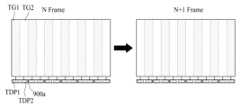
상기 데이터/터치 구동부(900)는 복수의 터치 전극(TE)과 복수의 데이터 라인에 연결되고, 복수의 터치 전극(TE)을 복수의 터치 그룹으로 분할하고 복수의 디스플레이 구간마다 복수의 터치 전극(TE)에 공통 전압을 공급하며 복수의 펜 센싱 구간마다 복수의 터치 전극(TE)의 일부를 통해 터치 펜의 위치를 센싱한다. 즉, 데이터/터치 구동부(900)는 복수의 펜 센싱 구간 중 적어도 하나의 펜 위치 센싱 구간마다 복수의 터치 그룹 중 일부의 터치 그룹에 업 링크 신호를 공급하고, 업 링크 신호가 공급된 터치 그룹을 통해 터치 펜으로부터 전송된 다운 링크 신호를 센싱하여 펜 터치 로우 데이터를 생성할 수 있다. 그리고, 데이터/터치 구동부(900)는 SPI 방식을 통해 호스트 제어부로부터 제공되는 펜 트래킹 채널 정보를 갖는 채널 셋팅 정보를 포함하는 터치 제어 데이터를 기반으로, 펜 위치 센싱 구간마다 펜 트래킹 채널 정보에 해당하는 펜 중첩 터치 그룹에 업 링크 신호를 공급하고 펜 중첩 터치 그룹을 통해 터치 펜으로부터 전송된 다운 링크 신호를 센싱하여 터치 센싱 신호를 생성하며, 생성된 터치 센싱 신호를 펜 터치 로우 데이터로 변환하여 호스트 제어부에 제공한다.The data/
일 예에 따른 데이터/터치 구동부(900)는 복수의 통합 구동 집적 회로(900a ~ 900n)를 포함할 수 있다. 여기서, 복수의 통합 구동 집적 회로(900a ~ 900n) 각각은 SRIC(source readout integrated circuit) 또는 ROIC(readout integrated circuit)로 표현될 수도 있다.The data/
상기 복수의 통합 구동 집적 회로(900a ~ 900n) 각각은 복수의 제 1 터치 채널(Tch1), 복수의 제 2 터치 채널(Tch2), 및 복수의 데이터 채널(Dch), 제 1 터치 구동부(TDP1), 제 2 터치 구동부(DDP), 및 데이터 구동부(DDP)를 포함할 수 있다.Each of the plurality of integrated driving
상기 복수의 제 1 터치 채널(Tch1)은 디스플레이 패널(100)의 정의된 복수의 수직 라인 중 i(i는 2 이상의 자연수)개의 수직 라인에 배치된 터치 전극들(TE)에 일대일로 연결된다. 본 예에 대한 설명에서는 복수의 제 1 터치 채널(Tch1)가 7개의 수직 라인에 배치된 터치 전극들(TE)과 일대일로 연결되는 것으로 가정하기로 한다. 예를 들어, 제 1 통합 구동 집적 회로(900a)에 마련된 복수의 제 1 터치 채널(Tch1)은 제 1 내지 제 7 수직 라인에 마련된 터치 전극들(TE)에 일대일로 연결될 수 있다.The plurality of first touch channels Tch1 are connected one-to-one to touch electrodes TE disposed on i (i is a natural number of 2 or more) vertical lines among a plurality of defined vertical lines of the
상기 복수의 제 2 터치 채널(Tch2)은 디스플레이 패널(100)의 정의된 복수의 수직 라인 중 복수의 제 1 터치 채널(Tch1)에 연결된 i개의 수직 라인에 인접한 i개의 수직 라인에 배치된 터치 전극들과 일대일로 연결된다. 본 예에 대한 설명에서는 복수의 제 2 터치 채널(Tch2)가 7개의 수직 라인에 배치된 터치 전극들(TE)과 일대일로 연결되는 것으로 가정하기로 한다. 예를 들어, 제 1 통합 구동 집적 회로(900a)에 마련된 복수의 제 2 터치 채널(Tch2)은 제 8 내지 제 14 수직 라인에 마련된 터치 전극들(TE)에 일대일로 연결될 수 있다.The plurality of second touch channels Tch2 are touch electrodes disposed on i vertical lines adjacent to i vertical lines connected to the plurality of first touch channels Tch1 among the plurality of defined vertical lines of the
상기 복수의 데이터 채널(Dch)은 복수의 제 1 터치 채널(Tch1)과 복수의 제 2 터치 채널(Tch2) 사이에 배치되고, 2i개의 수직 라인에 배치된 터치 전극들(TE)과 중첩되는 복수의 데이터 라인과 일대일로 연결된다.The plurality of data channels Dch are disposed between the plurality of first touch channels Tch1 and the plurality of second touch channels Tch2 and overlap the plurality of touch electrodes TE disposed in 2i vertical lines. It is connected one-to-one with the data line of
상기 제 1 터치 구동부(TDP1)는 디스플레이 패널(100)의 마련된 복수의 터치 전극(TE) 중 i개의 수직 라인에 배치된 터치 전극들(TE)에 일대일로 연결된다. 즉, 제 1 터치 구동부(TDP1)는 복수의 제 1 터치 채널(Tch1)을 통해서 i개의 수직 라인에 배치된 터치 전극들(TE)에 일대일로 연결될 수 있다.The first touch driver TDP1 is connected to the touch electrodes TE disposed on i vertical lines among the plurality of touch electrodes TE of the
상기 제 2 터치 구동부(TDP2)는 복수의 수직 라인 중 제 1 터치 구동부(TDP1)에 연결된 i개의 수직 라인에 인접한 i개의 수직 라인에 배치된 터치 전극들(TE)과 일대일로 연결된다. 즉, 제 2 터치 구동부(TDP2)는 복수의 제 2 터치 채널(Tch2)을 통해서 i개의 수직 라인에 배치된 터치 전극들(TE)에 일대일로 연결될 수 있다.The second touch driver TDP2 is connected one-to-one with the touch electrodes TE disposed on i vertical lines adjacent to i vertical lines connected to the first touch driver TDP1 among the plurality of vertical lines. That is, the second touch driver TDP2 may be connected one-to-one to the touch electrodes TE disposed in i vertical lines through the plurality of second touch channels Tch2.
상기 제 1 및 제 2 터치 구동부(TDP1, TDP2) 각각은 i개의 수직 라인에 배치된 터치 전극들(TE)에 일대일로 연결되는 것을 제외하고는 도 3 및 도 6에 도시된 터치 구동 회로(700)와 동일한 구성을 가지므로, 이에 대한 설명은 생략하기로 한다. 이때, 제 1 및 제 2 터치 구동부(TDP1, TDP2) 각각에 구성된 전압 선택부는 통합 구동 집적 회로(900a ~ 900n)의 외부, 예를 들어 타이밍 제어 회로 및 호스트 제어부가 실장된 인쇄 회로 기판에 실장되어 전압 선택 신호에 따라 터치 전극 구동 신호와 로드 프리 로우 전압을 해당하는 터치 구동부의 채널 선택부에 공급할 수 있다.The
상기 데이터 구동부(DDP)는 제 1 터치 구동부(TDP1)와 제 2 터치 구동부(TDP2) 사이에 배치되어 2i개의 수직 라인에 배치된 터치 전극들(TE)과 중첩되는 복수의 데이터 라인과 일대일로 연결된다. 즉, 데이터 구동부(DDP)는 복수의 데이터 채널(Dch)을 통해서 2i개의 수직 라인에 배치된 터치 전극들(TE)과 중첩되는 복수의 데이터 라인과 일대일로 연결될 수 있다. 예를 들어, 데이터 구동부(DDP)는 하나의 수평 라인에 배치된 14개의 터치 전극들(TE)과 중첩되는 복수의 데이터 라인과 일대일로 연결될 수 있다. 이러한 14개의 터치 전극들(TE)과 중첩되는 복수의 데이터 라인과 일대일로 연결되는 것을 제외하고는 도 3에 도시된 데이터 구동 회로(200)와 동일하므로, 이에 대한 설명은 생략하기로 한다.The data driver DDP is disposed between the first touch driver TDP1 and the second touch driver TDP2 and is connected one to one with a plurality of data lines overlapping the touch electrodes TE disposed in 2i vertical lines. do. That is, the data driver DDP may be connected one-to-one to a plurality of data lines overlapping the touch electrodes TE disposed on 2i vertical lines through a plurality of data channels Dch. For example, the data driver DDP may be connected one-to-one with a plurality of data lines overlapping the 14 touch electrodes TE disposed on one horizontal line. Since it is the same as the
일 예에 따른 복수의 통합 구동 집적 회로(900a ~ 900n) 각각은 칩 실장 공정에 의해 디스플레이 패널(100)의 패드부에 실장될 수 있다.Each of the plurality of integrated driving
다른 예에 따른 복수의 통합 구동 집적 회로(900a ~ 900n) 각각은 칩 실장 공정에 의해 플렉서블 회로 필름에 실장될 수 있다. 플렉서블 회로 필름은 필름 부착 공정에 의해 디스플레이 패널(100)의 패드부에 부착될 수 있다.Each of the plurality of integrated driving
일 예에 따른 복수의 통합 구동 집적 회로(900a ~ 900n) 각각에서, 제 1 및 제 2 터치 구동부(TDP1, TDP2) 각각은 복수의 펜 센싱 구간 중 적어도 하나의 펜 위치 센싱 구간마다 복수의 터치 그룹 중 일부의 터치 그룹에 업 링크 신호를 공급하고, 업 링크 신호가 공급된 터치 그룹을 통해 터치 펜으로부터 전송된 다운 링크 신호를 센싱하여 펜 터치 로우 데이터를 생성한다. 이때, 제 1 및 제 2 터치 구동부(TDP1, TDP2) 각각은 펜 위치 센싱 구간마다 복수의 터치 그룹 중 일부의 터치 그룹을 제외한 나머지 터치 그룹에 직류 전압(또는 공통 전압)을 공급한다.In each of the plurality of integrated driving
본 예에서, 일 예에 따른 복수의 터치 그룹 각각은 적어도 하나의 수평 라인에 배치된 터치 전극들을 포함할 수 있다. 이 경우, 일 예에 따른 제 1 및 제 2 터치 구동부(TDP1, TDP2) 각각은, 도 7에 도시된 제 N 프레임에서와 같이, 터치 센싱 구간(TP), 즉 펜 위치 센싱 구간 단위로 복수의 터치 그룹에 업 링크 신호를 순차적으로 공급할 수 있다.In this example, each of the plurality of touch groups according to an example may include touch electrodes disposed on at least one horizontal line. In this case, each of the first and second touch drivers TDP1 and TDP2 according to an exemplary embodiment, as in the Nth frame shown in FIG. Uplink signals may be sequentially supplied to the touch groups.
본 예에서, 다른 예에 따른 복수의 터치 그룹 각각은 복수의 통합 구동 집적 회로 각각의 제 1 및 제 2 터치 구동부(TDP1, TDP2) 각각에 연결된 터치 전극들을 갖는 수직 터치 그룹일 수 있다. 이 경우, 다른 예에 따른 제 1 및 제 2 터치 구동부(TDP1, TDP2) 각각은, 도 11에 도시된 제 N 프레임에서와 같이, 터치 센싱 구간(TP), 즉 펜 위치 센싱 구간 단위로 복수의 터치 그룹(VTG)에 업 링크 신호를 순차적으로 공급할 수 있다.In this example, each of the plurality of touch groups according to another example may be a vertical touch group having touch electrodes connected to each of the first and second touch drivers TDP1 and TDP2 of each of the plurality of integrated driving integrated circuits. In this case, each of the first and second touch drivers TDP1 and TDP2 according to another example, as in the Nth frame shown in FIG. Uplink signals may be sequentially supplied to the touch group VTG.
본 예에서, 또 다른 예에 따른 제 1 및 제 2 터치 구동부(TDP1, TDP2) 각각에 연결된 터치 전극들(TE)은 제 1 터치 그룹과 제 2 터치 그룹으로 분할될 수 있다. 일 예에 따른 제 1 터치 그룹은 제 1 및 제 2 터치 구동부(TDP1, TDP2) 각각에 연결된 복수의 수직 라인 중 홀수번째 수직 라인들에 배치된 터치 전극들을 포함하며, 제 2 터치 그룹은 제 1 및 제 2 터치 구동부(TDP1, TDP2) 각각에 연결된 복수의 수직 라인 중 짝수번째 수직 라인들에 배치된 터치 전극들을 포함할 수 있다. 이에 따라, 또 다른 예에 따른 제 1 및 제 2 터치 구동부(TDP1, TDP2) 각각은, 도 13에 도시된 바와 같이, 프레임 단위로 제 1 터치 그룹(TG1)과 제 2 터치 그룹(TG2)에 업 링크 신호를 교번적으로 공급할 수 있다. 또는, 제 1 및 제 2 터치 구동부(TDP1, TDP2) 각각은, 도 13에 도시된 바와 같이, 터치 센싱 구간(TP), 즉 펜 위치 센싱 구간 단위로 제 1 터치 그룹(TG1)과 제 2 터치 그룹(TG2)에 업 링크 신호를 교번적으로 공급할 수 있다. 선택적으로, 제 1 및 제 2 터치 구동부(TDP1, TDP2) 각각은, 도 13에 도시된 바와 같이, 프레임과 펜 위치 센싱 구간 단위로 제 1 터치 그룹(TG1)과 제 2 터치 그룹(TG2)에 업 링크 신호를 교번적으로 공급할 수도 있다.In this example, the touch electrodes TE connected to each of the first and second touch drivers TDP1 and TDP2 according to another example may be divided into a first touch group and a second touch group. The first touch group according to an example includes touch electrodes disposed on odd-numbered vertical lines among a plurality of vertical lines connected to the first and second touch drivers TDP1 and TDP2, respectively. and touch electrodes disposed on even-numbered vertical lines among a plurality of vertical lines connected to each of the second touch drivers TDP1 and TDP2. Accordingly, as shown in FIG. 13 , each of the first and second touch drivers TDP1 and TDP2 according to another example is applied to the first touch group TG1 and the second touch group TG2 in frame units. Uplink signals can be supplied alternately. Alternatively, as shown in FIG. 13 , each of the first and second touch drivers TDP1 and TDP2 performs a first touch group TG1 and a second touch in units of touch sensing intervals TP, that is, pen position sensing intervals. An uplink signal can be alternately supplied to the group TG2. Optionally, as shown in FIG. 13 , each of the first and second touch drivers TDP1 and TDP2 is applied to the first touch group TG1 and the second touch group TG2 in units of frame and pen position sensing intervals. An uplink signal may be alternately supplied.
선택적으로, 제 1 터치 그룹은 제 1 및 제 2 터치 구동부(TDP1, TDP2) 각각에 연결된 복수의 수평 라인 중 홀수번째 수평 라인들에 배치된 터치 전극들을 포함하며, 제 2 터치 그룹은 제 1 및 제 2 터치 구동부(TDP1, TDP2) 각각에 연결된 복수의 수평 라인 중 짝수번째 수평 라인들에 배치된 터치 전극들을 포함할 수 있다. 이 경우에도, 다른 예에 따른 제 1 및 제 2 터치 구동부(TDP1, TDP2) 각각은 프레임 단위, 펜 위치 센싱 구간 단위, 또는 프레임과 펜 위치 센싱 구간 단위로 제 1 터치 그룹(TG1)과 제 2 터치 그룹(TG2)에 업 링크 신호를 교번적으로 공급할 수도 있다.Optionally, the first touch group includes touch electrodes disposed on odd-numbered horizontal lines among a plurality of horizontal lines connected to the first and second touch drivers TDP1 and TDP2, respectively. It may include touch electrodes disposed on even-numbered horizontal lines among a plurality of horizontal lines connected to each of the second touch drivers TDP1 and TDP2. In this case as well, each of the first and second touch drivers TDP1 and TDP2 according to another example may perform the first touch group TG1 and the second touch group TG1 and the second touch group TG1 in units of frames, units of pen position sensing intervals, or units of frame and pen position sensing intervals. An uplink signal may be alternately supplied to the touch group TG2.
본 예에서, 디스플레이 패널(100)에 마련된 복수의 터치 전극(TE)은, 도 16에 도시된 바와 같이, 제 1 터치 구동부(TDP1)에 연결된 제 1 터치 그룹(TG1) 및 제 2 터치 구동부(TFP2)에 연결된 제 2 터치 그룹(TG2)으로 분할될 수 있다. 이 경우, 또 다른 예에 따른 제 1 및 제 2 터치 구동부(TDP1, TDP2) 각각은 터치 센싱 구간(TP), 즉 펜 위치 센싱 구간 단위 또는 프레임 단위로 제 1 터치 그룹(TG1)과 제 2 터치 그룹(GT2)에 업 링크 신호를 교번적으로 공급할 수 있다.In this example, the plurality of touch electrodes TE provided on the
일 예로서, 제 N 프레임 동안 제 1 터치 구동부(TDP1)는 제 1 터치 그룹(TG1)에 업 링크 신호를 공급하고, 제 2 터치 구동부(TDP2)는 제 2 터치 그룹(TG2)에 직류 전압(또는 공통 전압)을 공급할 수 있다. 그리고, 제 N+1 프레임 동안 제 1 터치 구동부(TDP1)는 제 1 터치 그룹(TG1)에 직류 전압(또는 공통 전압)을 공급하고, 제 2 터치 구동부(TDP2)는 제 2 터치 그룹(TG2)에 업 링크 신호를 공급할 수 있다. 여기서, 제 N 프레임은 홀수번째 프레임일 수 있다.For example, during the Nth frame, the first touch driver TDP1 supplies an uplink signal to the first touch group TG1, and the second touch driver TDP2 supplies a DC voltage (DC voltage) to the second touch group TG2. Or common voltage) can be supplied. Also, during the N+1th frame, the first touch driver TDP1 supplies DC voltage (or common voltage) to the first touch group TG1, and the second touch driver TDP2 supplies the DC voltage (or common voltage) to the second touch group TG2. An uplink signal can be supplied to Here, the N-th frame may be an odd-numbered frame.
다른 예로서, 도 17에 도시된 바와 같이, 터치 센싱 구간(TP) 중 홀수번째 터치 센싱 구간 동안 제 1 터치 구동부(TDP1)는 제 1 터치 그룹(TG1)에 업 링크 신호를 공급하고, 제 2 터치 구동부(TDP2)는 제 2 터치 그룹(TG2)에 직류 전압(또는 공통 전압)을 공급할 수 있다. 그리고, 터치 센싱 구간(TP) 중 짝수번째 터치 센싱 구간 동안 제 1 터치 구동부(TDP1)는 제 1 터치 그룹(TG1)에 직류 전압(또는 공통 전압)을 공급하고, 제 2 터치 구동부(TDP2)는 제 2 터치 그룹(TG2)에 업 링크 신호를 공급할 수 있다.As another example, as shown in FIG. 17 , the first touch driver TDP1 supplies an uplink signal to the first touch group TG1 during an odd-numbered touch sensing period of the touch sensing period TP, and The touch driver TDP2 may supply DC voltage (or common voltage) to the second touch group TG2. Also, during the even-numbered touch sensing period of the touch sensing period TP, the first touch driver TDP1 supplies DC voltage (or common voltage) to the first touch group TG1, and the second touch driver TDP2 supplies a DC voltage (or common voltage) to the first touch group TG1. An uplink signal may be supplied to the second touch group TG2.
또 다른 예로서, 제 N 프레임의 홀수번째 터치 센싱 구간 동안 제 1 터치 구동부(TDP1)는 제 1 터치 그룹(TG1)에 업 링크 신호를 공급하고, 제 2 터치 구동부(TDP2)는 제 2 터치 그룹(TG2)에 직류 전압(또는 공통 전압)을 공급할 수 있다. 제 N 프레임의 짝수번째 터치 센싱 구간 동안 제 1 터치 구동부(TDP1)는 제 1 터치 그룹(TG1)에 직류 전압(또는 공통 전압)을 공급하고, 제 2 터치 구동부(TDP2)는 제 2 터치 그룹(TG2)에 업 링크 신호를 공급할 수 있다. 제 N+1 프레임의 홀수번째 터치 센싱 구간 동안 제 1 터치 구동부(TDP1)는 제 1 터치 그룹(TG1)에 직류 전압(또는 공통 전압)을 공급하고, 제 2 터치 구동부(TDP2)는 제 2 터치 그룹(TG2)에 업 링크 신호를 공급할 수 있다. 그리고, 제 N+1 프레임의 짝수번째 터치 센싱 구간 동안 제 1 터치 구동부(TDP1)는 제 1 터치 그룹(TG1)에 업 링크 신호를 공급하고, 제 2 터치 구동부(TDP2)는 제 2 터치 그룹(TG2)에 직류 전압(또는 공통 전압)을 공급할 수 있다. 여기서, 제 N 프레임은 홀수번째 프레임일 수 있다.As another example, during the odd-numbered touch sensing period of the Nth frame, the first touch driver TDP1 supplies an uplink signal to the first touch group TG1, and the second touch driver TDP2 supplies the uplink signal to the second touch group TG1. DC voltage (or common voltage) can be supplied to (TG2). During the even-numbered touch sensing period of the Nth frame, the first touch driver TDP1 supplies DC voltage (or common voltage) to the first touch group TG1, and the second touch driver TDP2 supplies DC voltage (or common voltage) to the second touch group (TDP2). TG2) can be supplied with an uplink signal. During the odd-numbered touch sensing period of the N+1th frame, the first touch driver TDP1 supplies DC voltage (or common voltage) to the first touch group TG1, and the second touch driver TDP2 supplies a DC voltage (or common voltage) to the first touch group TG1. An uplink signal can be supplied to the group TG2. Also, during the even-numbered touch sensing period of the N+1th frame, the first touch driver TDP1 supplies an uplink signal to the first touch group TG1, and the second touch driver TDP2 supplies an uplink signal to the second touch group ( TG2) can be supplied with DC voltage (or common voltage). Here, the N-th frame may be an odd-numbered frame.
본 출원의 또 다른 예에 따른 디스플레이 장치는 복수의 통합 구동 집적 회로(900a ~ 900n) 각각에 마련된 제 1 및 제 2 터치 구동부(TDP1, TDP2) 각각은 호스트 제어부로부터 제공되는 펜 트래킹 채널 정보를 갖는 채널 셋팅 정보를 포함하는 터치 제어 데이터를 기반으로, 펜 위치 센싱 구간마다 펜 트래킹 채널 정보에 해당하는 펜 중첩 터치 그룹, 즉 로컬 터치 그룹에만 업 링크 신호를 공급하고 펜 중첩 터치 그룹을 통해 터치 펜으로부터 전송된 다운 링크 신호를 센싱하여 터치 센싱 신호를 생성할 수 있다. 이 경우, 본 예는 복수의 통합 구동 집적 회로(900a ~ 900n) 각각에 마련된 제 1 및 제 2 터치 구동부(TDP1, TDP2) 중 로컬 터치 그룹에 연결된 터치 구동부의 센싱 유닛만을 통해 펜 터치를 센싱하고, 나머지 터치 구동부들의 센싱 유닛들이 동작하지 않음으로써 디스플레이 장치의 소비 전력을 감소시킬 수 있다. 예를 들어, 데이터/터치 구동부(900)가 6개의 통합 구동 집적 회로로 구성된 경우, 본 예는 총 12의 터치 구동부 중 로컬 터치 그룹에 연결된 하나의 터치 구동부의 센싱 유닛을 인에이블시키는 반면에 나머지 11개의 터치 구동부들의 센싱 유닛들을 디스에이블시킴으로써 디스플레이 장치의 소비 전력을 감소시킬 수 있다.In a display device according to another example of the present application, each of the first and second touch drivers TDP1 and TDP2 provided in each of the plurality of integrated driving
이와 같은, 본 출원의 또 다른 예에 따른 디스플레이 장치는 복수의 터치 전극을 복수의 터치 그룹으로 분할하고 복수의 통합 구동 집적 회로(900a ~ 900n) 각각에 마련된 제 1 및 제 2 터치 구동부(TDP1, TDP2)를 통해 복수의 터치 그룹 중 일부의 터치 그룹에 업 링크 신호를 공급하여 펜 터치를 센싱함으로써 디스플레이 패널에 접촉된 사용자의 손이나 손바닥에 의해 터치 펜으로 송신되는 업 링크 신호의 감쇄가 최소화됨에 따라 사용자의 손이나 손바닥과 디스플레이 패널 간의 접촉시에도 펜 터치의 센싱이 가능하다.As described above, the display device according to another example of the present application divides a plurality of touch electrodes into a plurality of touch groups, and first and second touch drivers (TDP1, By supplying an uplink signal to some of the touch groups of a plurality of touch groups through TDP2) to sense the pen touch, attenuation of the uplink signal transmitted to the touch pen by the user's hand or palm in contact with the display panel is minimized. Accordingly, the pen touch can be sensed even when the user's hand or palm touches the display panel.
도 18은 본 출원의 예에 따른 디스플레이 장치와 비교 예에 따른 디스플레이 장치에 있어서, 디스플레이 패널에 대한 손바닥의 접촉 면적에 대한 터치 펜 내의 출력 전압을 나타내는 그래프이다. 도 18에서, 가로 축은 디스플레이 패널에 대한 손바닥의 접촉 면적을 나타내고, 세로 축은 터치 펜에 내장된 수신부(이하, ‘펜 수신부’라 함)의 출력 전압을 나타낸다. 도 18에서, 제 1 그래프(G1)(가는 실선)는 비교 예로서, 복수의 터치 전극 모두에 업 링크 신호를 공급하고 디스플레이 패널의 에지부에 터치 펜을 위치시켜 측정한 펜 수신부의 출력 전압, 제 2 그래프(G1) (가는 점선)는 비교 예로서, 복수의 터치 전극 모두에 업 링크 신호를 공급하고 디스플레이 패널의 중앙부에 터치 펜을 위치시켜 측정한 펜 수신부의 출력 전압, 제 3 그래프(G3)(굵은 실선)는 본 출원의 예로서, 복수의 터치 전극 중 일부의 터치 그룹에 포함된 터치 전극들에만 업 링크 신호를 공급하고 디스플레이 패널의 에지부에 터치 펜을 위치시켜 측정한 펜 수신부의 출력 전압, 및 제 4 그래프(G4) (굵은 점선)는 본 출원의 예로서, 복수의 터치 전극 중 일부의 터치 그룹에 포함된 터치 전극들에만 업 링크 신호를 공급하고 디스플레이 패널의 중앙부에 터치 펜을 위치시켜 측정한 펜 수신부의 출력 전압을 각각 나타낸다.18 is a graph showing an output voltage within a touch pen with respect to a contact area of a palm with respect to a display panel in a display device according to an example of the present application and a display device according to a comparative example. In FIG. 18 , the horizontal axis represents the contact area of the palm with respect to the display panel, and the vertical axis represents the output voltage of the receiver built into the touch pen (hereinafter referred to as the 'pen receiver'). In FIG. 18 , a first graph G1 (thin solid line) is a comparison example, in which an uplink signal is supplied to all of a plurality of touch electrodes and the output voltage of the pen receiver measured by placing the touch pen on the edge of the display panel; As a comparative example, the second graph G1 (thin dotted line) shows the output voltage of the pen receiver measured by supplying uplink signals to all of the plurality of touch electrodes and placing the touch pen in the center of the display panel, and the third graph (G3 ) (thick solid line) is an example of the present application, supplying an uplink signal only to touch electrodes included in some touch groups among a plurality of touch electrodes, and measuring the pen receiving unit by placing the touch pen on the edge of the display panel. The output voltage and the fourth graph (G4) (thick dotted line) are examples of the present application, supplying an uplink signal only to touch electrodes included in some touch groups among a plurality of touch electrodes, and a touch pen in the center of the display panel. indicates the output voltage of the pen receiver measured by placing
도 18의 제 1 및 제 2 그래프(G1, G2) 각각에서 알 수 있듯이, 비교 예는 디스플레이 패널에 대한 손바닥 면적이 증가할수록 수신부의 출력 전압이 감소하는 것을 알 수 있으며, 특히, 디스플레이 패널에 대한 손바닥 면적이 4500mm2 이상일 경우, 손바닥을 통한 업 링크 신호의 감쇄로 인하여 터치 펜에서 업 링크 신호를 인식할 수 없을 수 있다.As can be seen from each of the first and second graphs G1 and G2 of FIG. 18, in the comparative example, it can be seen that the output voltage of the receiver decreases as the palm area with respect to the display panel increases. In particular, with respect to the display panel When the area of the palm is 4500 mm2 or more, the touch pen may not be able to recognize the uplink signal due to attenuation of the uplink signal through the palm.
반면에, 도 18의 제 3 및 제 4 그래프(G3, G4) 각각에서 알 수 있듯이, 본 출원의 예는 디스플레이 패널에 대한 손바닥 면적이 증가하더라도 손바닥을 통한 업 링크 신호의 감쇄 비율이 비교 예 대비 2배 이상 감소하는 것을 확인할 수 있다.On the other hand, as can be seen from the third and fourth graphs G3 and G4 of FIG. 18, the example of the present application shows an attenuation ratio of the uplink signal through the palm compared to the comparative example even if the area of the palm with respect to the display panel increases. A more than two-fold decrease can be seen.
따라서, 본 출원은 복수의 터치 전극을 복수의 터치 그룹의 분할하고, 복수의 터치 그룹의 순차 구동 또는 분할 구동을 통해 업 링크 신호를 터치 펜에 전송함으로써 디스플레이 패널에 접촉된 사용자의 손이나 손바닥에 의한 업 링크 신호의 감쇄를 최소화할 수 있고, 이를 통해 사용자의 손이나 손바닥과 디스플레이 패널 간의 접촉시에도 디스플레이 패널 상에 위치한 터치 펜의 위치를 센싱할 수 있으며, 터치 펜의 위치를 기반으로 터치 펜의 위치를 트래킹하면서 펜 터치를 센싱하여 터치 드로잉을 끊김 없이 센싱할 수 있다.Therefore, the present application divides a plurality of touch electrodes into a plurality of touch groups and transmits an uplink signal to a touch pen through sequential driving or divisional driving of the plurality of touch groups, so that the user's hand or palm in contact with the display panel It is possible to minimize the attenuation of the uplink signal by the user's hand or palm and through this, the position of the touch pen located on the display panel can be sensed even when the user's hand or palm touches the display panel, and based on the position of the touch pen By tracking the position of the pen and sensing the pen touch, the touch drawing can be sensed seamlessly.
본 출원에 따른 디스플레이 장치는 스마트 폰(smart phone), 이동 통신 단말기, 모바일 폰, 태블릿 PC(personal computer), 스마트 와치(smart watch), 와치 폰(watch phone), 웨어러블 기기(wearable device), 전자 수첩, 전자 책, PMP(portable multimedia player), 네비게이션, 텔레비전, 노트북, 모니터, 카메라, 캠코더, 또는 가전 기기 등의 표시 화면으로 사용될 수 있다.The display device according to the present application is a smart phone, a mobile communication terminal, a mobile phone, a tablet PC (personal computer), a smart watch, a watch phone, a wearable device, an electronic It can be used as a display screen of a notebook, electronic book, portable multimedia player (PMP), navigation, television, laptop computer, monitor, camera, camcorder, or home appliance.
상술한 본 출원의 예에 설명된 특징, 구조, 효과 등은 본 출원의 적어도 하나의 예에 포함되며, 반드시 하나의 예에만 한정되는 것은 아니다. 나아가, 본 출원의 적어도 하나의 예에서 예시된 특징, 구조, 효과 등은 본 출원이 속하는 분야의 통상의 지식을 가지는 자에 의하여 다른 예들에 대해서도 조합 또는 변형되어 실시 가능하다. 따라서 이러한 조합과 변형에 관계된 내용들은 본 출원의 범위에 포함되는 것으로 해석되어야 할 것이다.The features, structures, effects, etc. described in the above examples of the present application are included in at least one example of the present application, and are not necessarily limited to only one example. Furthermore, the features, structures, effects, etc. exemplified in at least one example of this application can be combined or modified with respect to other examples by those skilled in the art to which this application belongs. Therefore, contents related to these combinations and variations should be construed as being included in the scope of the present application.
이상에서 설명한 본 출원은 전술한 실시 예 및 첨부된 도면에 한정되는 것이 아니고, 본 출원의 기술적 사항을 벗어나지 않는 범위 내에서 여러 가지 치환, 변형 및 변경이 가능하다는 것이 본 출원이 속하는 기술 분야에서 통상의 지식을 가진 자에게 있어 명백할 것이다. 그러므로, 본 출원의 범위는 후술하는 특허청구범위에 의하여 나타내어지며, 특허청구범위의 의미 및 범위 그리고 그 등가 개념으로부터 도출되는 모든 변경 또는 변형된 형태가 본 출원의 범위에 포함되는 것으로 해석되어야 한다.The present application described above is not limited to the above-described embodiments and the accompanying drawings, and it is common in the technical field to which this application belongs that various substitutions, modifications, and changes are possible without departing from the technical details of the present application. It will be clear to those who have knowledge of Therefore, the scope of the present application is indicated by the following claims, and all changes or modifications derived from the meaning and scope of the claims and equivalent concepts should be interpreted as being included in the scope of the present application.
10: 디스플레이 장치 20: 터치 펜
100: 디스플레이 패널 200: 데이터 구동 회로
300: 게이트 구동 회로 400: 타이밍 제어 회로
500: 구동 전원 공급부 600: 터치 구동 신호 공급부
700: 터치 구동 회로 800: 호스트 제어부10: display device 20: touch pen
100: display panel 200: data driving circuit
300: gate driving circuit 400: timing control circuit
500: driving power supply unit 600: touch driving signal supply unit
700: touch driving circuit 800: host control unit
Claims (21)
Translated fromKorean상기 복수의 터치 전극을 복수의 터치 그룹으로 분할하고 복수의 디스플레이 구간마다 상기 복수의 터치 전극에 공통 전압을 공급하며 복수의 펜 센싱 구간마다 상기 복수의 터치 전극의 일부를 통해 터치 펜의 위치를 센싱하는 터치 구동 회로; 및
상기 터치 구동 회로로부터 제공되는 펜 터치 로우 데이터를 기반으로 펜 위치 정보를 산출하고, 상기 복수의 터치 그룹 중 상기 펜 위치 정보에 해당하는 터치 그룹에 대한 펜 트래킹 채널 정보를 상기 터치 구동 회로에 제공하는 호스트 제어부를 포함하며,
상기 터치 구동 회로는 상기 복수의 펜 센싱 구간 중 적어도 하나의 펜 위치 센싱 구간마다 상기 복수의 터치 그룹 중 일부의 터치 그룹에 업 링크 신호를 공급하고, 상기 업 링크 신호가 공급된 터치 그룹을 통해 상기 업 링크 신호의 응답으로 터치 펜으로부터 전송된 다운 링크 신호를 센싱하여 상기 펜 터치 로우 데이터를 생성하는, 디스플레이 장치.a display panel including a plurality of touch electrodes disposed at regular intervals along a plurality of horizontal lines and a plurality of vertical lines;
The plurality of touch electrodes are divided into a plurality of touch groups, a common voltage is supplied to the plurality of touch electrodes in each of a plurality of display sections, and the position of the touch pen is sensed through a part of the plurality of touch electrodes in each of a plurality of pen sensing sections. a touch driving circuit; and
Calculating pen position information based on pen touch raw data provided from the touch driving circuit, and providing pen tracking channel information for a touch group corresponding to the pen position information among the plurality of touch groups to the touch driving circuit It includes a host control unit;
The touch driving circuit supplies an uplink signal to some of the touch groups among the plurality of touch groups in at least one pen position sensing period among the plurality of pen sensing periods, and the touch group to which the uplink signal is supplied provides the uplink signal. A display device generating the pen touch raw data by sensing a downlink signal transmitted from a touch pen in response to an uplink signal.
상기 터치 구동 회로는 상기 펜 위치 센싱 구간마다 상기 복수의 터치 그룹 중 일부의 터치 그룹을 제외한 나머지 터치 그룹에 직류 전압을 공급하는, 디스플레이 장치.According to claim 1,
The touch driving circuit supplies a DC voltage to touch groups other than some of the plurality of touch groups in each pen position sensing period.
상기 복수의 터치 전극을 복수의 터치 그룹으로 분할하고 복수의 디스플레이 구간마다 상기 복수의 터치 전극에 공통 전압을 공급하며 복수의 펜 센싱 구간마다 상기 복수의 터치 전극의 일부를 통해 터치 펜의 위치를 센싱하는 터치 구동 회로를 포함하고,
상기 터치 구동 회로는 상기 복수의 펜 센싱 구간 중 적어도 하나의 펜 위치 센싱 구간마다 상기 복수의 터치 그룹 중 일부의 터치 그룹에 업 링크 신호를 공급하고, 상기 업 링크 신호가 공급된 터치 그룹을 통해 상기 업 링크 신호의 응답으로 터치 펜으로부터 전송된 다운 링크 신호를 센싱하여 펜 터치 로우 데이터를 생성하고,
상기 복수의 터치 그룹 각각은 상기 복수의 수평 라인 중 적어도 하나의 수평 라인 또는 상기 복수의 수직 라인 중 적어도 하나의 수직 라인에 배치된 터치 전극들을 포함하며,
상기 업 링크 신호는 상기 펜 위치 센싱 구간 단위로 상기 복수의 터치 그룹에 순차적으로 공급되는, 디스플레이 장치.a display panel including a plurality of touch electrodes disposed at regular intervals along a plurality of horizontal lines and a plurality of vertical lines; and
The plurality of touch electrodes are divided into a plurality of touch groups, a common voltage is supplied to the plurality of touch electrodes in each of a plurality of display sections, and the position of the touch pen is sensed through a part of the plurality of touch electrodes in each of a plurality of pen sensing sections. Including a touch drive circuit that
The touch driving circuit supplies an uplink signal to some of the touch groups among the plurality of touch groups in at least one pen position sensing period among the plurality of pen sensing periods, and the touch group to which the uplink signal is supplied provides the uplink signal. Sensing the downlink signal transmitted from the touch pen in response to the uplink signal to generate pen touch raw data;
Each of the plurality of touch groups includes touch electrodes disposed on at least one horizontal line among the plurality of horizontal lines or at least one vertical line among the plurality of vertical lines,
Wherein the uplink signal is sequentially supplied to the plurality of touch groups in units of the pen position sensing period.
상기 복수의 터치 전극을 복수의 터치 그룹으로 분할하고 복수의 디스플레이 구간마다 상기 복수의 터치 전극에 공통 전압을 공급하며 복수의 펜 센싱 구간마다 상기 복수의 터치 전극의 일부를 통해 터치 펜의 위치를 센싱하는 터치 구동 회로를 포함하고,
상기 터치 구동 회로는 상기 복수의 펜 센싱 구간 중 적어도 하나의 펜 위치 센싱 구간마다 상기 복수의 터치 그룹 중 일부의 터치 그룹에 업 링크 신호를 공급하고, 상기 업 링크 신호가 공급된 터치 그룹을 통해 상기 업 링크 신호의 응답으로 터치 펜으로부터 전송된 다운 링크 신호를 센싱하여 펜 터치 로우 데이터를 생성하고,
상기 터치 구동 회로는 상기 복수의 터치 전극을 제 1 터치 그룹과 제 2 터치 그룹으로 분할하고, 프레임 단위 또는 상기 펜 위치 센싱 구간 단위로 상기 제 1 터치 그룹과 상기 제 2 터치 그룹에 상기 업 링크 신호를 교번적으로 공급하는, 디스플레이 장치.a display panel including a plurality of touch electrodes disposed at regular intervals along a plurality of horizontal lines and a plurality of vertical lines; and
The plurality of touch electrodes are divided into a plurality of touch groups, a common voltage is supplied to the plurality of touch electrodes in each of a plurality of display sections, and the position of the touch pen is sensed through a part of the plurality of touch electrodes in each of a plurality of pen sensing sections. Including a touch drive circuit that
The touch driving circuit supplies an uplink signal to some of the touch groups among the plurality of touch groups in at least one pen position sensing period among the plurality of pen sensing periods, and the touch group to which the uplink signal is supplied provides the uplink signal. Sensing the downlink signal transmitted from the touch pen in response to the uplink signal to generate pen touch raw data;
The touch driving circuit divides the plurality of touch electrodes into a first touch group and a second touch group, and transmits the uplink signal to the first touch group and the second touch group in units of frames or units of the pen position sensing section. A display device that alternately supplies.
상기 제 1 터치 그룹은 상기 복수의 수평 라인 중 홀수번째 수평 라인들에 배치된 터치 전극들을 포함하며,
상기 제 2 터치 그룹은 상기 복수의 수평 라인 중 짝수번째 수평 라인들에 배치된 터치 전극들을 포함하는, 디스플레이 장치.According to claim 4,
The first touch group includes touch electrodes disposed on odd-numbered horizontal lines among the plurality of horizontal lines;
The second touch group includes touch electrodes disposed on even-numbered horizontal lines among the plurality of horizontal lines.
상기 제 1 터치 그룹은 상기 복수의 수직 라인 중 홀수번째 수직 라인들에 배치된 터치 전극들을 포함하며,
상기 제 2 터치 그룹은 상기 복수의 수직 라인 중 짝수번째 수직 라인들에 배치된 터치 전극들을 포함하는, 디스플레이 장치.According to claim 4,
The first touch group includes touch electrodes disposed on odd-numbered vertical lines among the plurality of vertical lines,
The second touch group includes touch electrodes disposed on even-numbered vertical lines among the plurality of vertical lines.
상기 터치 구동 회로는 상기 펜 위치 센싱 구간마다 상기 펜 트래킹 채널 정보에 해당하는 펜 중첩 터치 그룹에 업 링크 신호를 공급하고 상기 펜 중첩 터치 그룹을 통해 상기 터치 펜으로부터 전송된 다운 링크 신호를 센싱하여 터치 센싱 신호를 생성하며, 생성된 터치 센싱 신호를 상기 펜 터치 로우 데이터로 변환하여 상기 호스트 제어부에 제공하는, 디스플레이 장치.According to claim 1,
The touch driving circuit supplies an uplink signal to a pen overlapping touch group corresponding to the pen tracking channel information for each pen position sensing period, senses a downlink signal transmitted from the touch pen through the pen overlapping touch group, and touches A display device that generates a sensing signal, converts the generated touch sensing signal into raw pen touch data, and provides the converted pen touch raw data to the host controller.
상기 펜 중첩 터치 그룹은 적어도 하나의 수평 라인에 배치된 터치 전극들을 갖는 수평 터치 그룹이거나 적어도 하나의 수직 라인에 배치된 터치 전극들을 갖는 수직 터치 그룹 내의 로컬 터치 그룹인, 디스플레이 장치.According to claim 7,
The pen overlapping touch group is a horizontal touch group having touch electrodes disposed on at least one horizontal line or a local touch group in a vertical touch group having touch electrodes disposed on at least one vertical line.
인쇄 회로 기판에 실장되고 상기 업 링크 신호와 상기 직류 전압을 상기 터치 구동 회로에 선택적으로 공급하는 전압 선택부를 더 포함하는, 디스플레이 장치.According to claim 2,
and a voltage selection unit mounted on a printed circuit board and selectively supplying the uplink signal and the DC voltage to the touch driving circuit.
상기 복수의 터치 전극과 상기 복수의 데이터 라인에 연결되고, 상기 복수의 터치 전극을 복수의 터치 그룹으로 분할하고 복수의 디스플레이 구간마다 상기 복수의 터치 전극에 공통 전압을 공급하며 복수의 펜 센싱 구간마다 상기 복수의 터치 전극의 일부를 통해 터치 펜의 위치를 센싱하는 데이터/터치 구동부; 및
상기 데이터/터치 구동부로부터 제공되는 펜 터치 로우 데이터를 기반으로 펜 위치 정보를 산출하고, 상기 복수의 터치 그룹 중 상기 펜 위치 정보에 해당하는 터치 그룹에 대한 펜 트래킹 채널 정보를 상기 데이터/터치 구동부에 제공하는 호스트 제어부를 포함하며,
상기 데이터/터치 구동부는 상기 복수의 펜 센싱 구간 중 적어도 하나의 펜 위치 센싱 구간마다 상기 복수의 터치 그룹 중 일부의 터치 그룹에 업 링크 신호를 공급하고, 상기 업 링크 신호가 공급된 터치 그룹을 통해 상기 업 링크 신호의 응답으로 터치 펜으로부터 전송된 다운 링크 신호를 센싱하여 상기 펜 터치 로우 데이터를 생성하는, 디스플레이 장치.A display including a plurality of touch electrodes disposed at regular intervals along a plurality of horizontal lines and a plurality of vertical lines, a plurality of gate lines overlapping the plurality of touch electrodes, and a plurality of data lines crossing the plurality of gate lines panel;
connected to the plurality of touch electrodes and the plurality of data lines, divides the plurality of touch electrodes into a plurality of touch groups, supplies a common voltage to the plurality of touch electrodes in each of a plurality of display sections, and supplies a common voltage to each of a plurality of pen sensing sections a data/touch driver that senses a position of a touch pen through some of the plurality of touch electrodes; and
Pen position information is calculated based on raw pen touch data provided from the data/touch driver, and pen tracking channel information for a touch group corresponding to the pen position information among the plurality of touch groups is transmitted to the data/touch driver. It includes a host control unit that provides,
The data/touch driver supplies an uplink signal to some of the touch groups among the plurality of touch groups in at least one pen position sensing period among the plurality of pen sensing periods, and through the touch group to which the uplink signal is supplied. and generating the pen touch raw data by sensing a downlink signal transmitted from a touch pen in response to the uplink signal.
상기 복수의 터치 전극과 상기 복수의 데이터 라인에 연결되고, 상기 복수의 터치 전극을 복수의 터치 그룹으로 분할하고 복수의 디스플레이 구간마다 상기 복수의 터치 전극에 공통 전압을 공급하며 복수의 펜 센싱 구간마다 상기 복수의 터치 전극의 일부를 통해 터치 펜의 위치를 센싱하는 데이터/터치 구동부를 포함하고,
상기 데이터/터치 구동부는 상기 복수의 펜 센싱 구간 중 적어도 하나의 펜 위치 센싱 구간마다 상기 복수의 터치 그룹 중 일부의 터치 그룹에 업 링크 신호를 공급하고, 상기 업 링크 신호가 공급된 터치 그룹을 통해 상기 업 링크 신호의 응답으로 터치 펜으로부터 전송된 다운 링크 신호를 센싱하여 펜 터치 로우 데이터를 생성하고,
상기 데이터/터치 구동부는 복수의 통합 구동 집적 회로를 포함하며,
상기 복수의 통합 구동 집적 회로 각각은,
상기 복수의 수직 라인 중 i(i는 2이상의 자연수)개의 수직 라인에 배치된 터치 전극들과 일대일로 연결된 제 1 터치 구동부;
상기 복수의 수직 라인 중 상기 제 1 터치 구동부에 연결된 i개의 수직 라인에 인접한 i개의 수직 라인에 배치된 터치 전극들과 일대일로 연결된 제 2 터치 구동부; 및
상기 2i개의 수직 라인에 배치된 터치 전극들과 중첩되는 데이터 라인들과 일대일로 연결된 데이터 구동부를 포함하며,
상기 제 1 및 제 2 터치 구동부 각각은 상기 복수의 펜 센싱 구간 중 적어도 하나의 펜 위치 센싱 구간마다 상기 복수의 터치 그룹 중 일부의 터치 그룹에 업 링크 신호를 공급하고, 상기 업 링크 신호가 공급된 터치 그룹을 통해 터치 펜으로부터 전송된 다운 링크 신호를 센싱하여 상기 펜 터치 로우 데이터를 생성하는, 디스플레이 장치.A display including a plurality of touch electrodes disposed at regular intervals along a plurality of horizontal lines and a plurality of vertical lines, a plurality of gate lines overlapping the plurality of touch electrodes, and a plurality of data lines crossing the plurality of gate lines panel; and
connected to the plurality of touch electrodes and the plurality of data lines, divides the plurality of touch electrodes into a plurality of touch groups, supplies a common voltage to the plurality of touch electrodes in each of a plurality of display sections, and supplies a common voltage to each of a plurality of pen sensing sections A data/touch driver for sensing a position of a touch pen through some of the plurality of touch electrodes;
The data/touch driver supplies an uplink signal to some of the touch groups among the plurality of touch groups in at least one pen position sensing period among the plurality of pen sensing periods, and through the touch group to which the uplink signal is supplied. Sensing a downlink signal transmitted from a touch pen in response to the uplink signal to generate pen touch raw data;
The data/touch driver includes a plurality of integrated driving integrated circuits;
Each of the plurality of integrated driving integrated circuits,
a first touch driver connected one-to-one with touch electrodes disposed on i (i is a natural number of 2 or more) vertical lines among the plurality of vertical lines;
a second touch driver connected one-to-one with touch electrodes disposed on i vertical lines adjacent to i vertical lines connected to the first touch driver among the plurality of vertical lines; and
a data driver connected one-to-one with data lines overlapping the touch electrodes disposed on the 2i vertical lines;
Each of the first and second touch drivers supplies an uplink signal to some touch groups among the plurality of touch groups in each pen position sensing period of at least one of the plurality of pen sensing periods, and when the uplink signal is supplied, A display device generating the pen touch raw data by sensing a downlink signal transmitted from a touch pen through a touch group.
상기 제 1 및 제 2 터치 구동부 각각은 상기 펜 위치 센싱 구간마다 상기 복수의 터치 그룹 중 일부의 터치 그룹을 제외한 나머지 터치 그룹에 직류 전압을 공급하는, 디스플레이 장치.According to claim 11,
wherein each of the first and second touch drivers supplies a DC voltage to touch groups other than some of the plurality of touch groups in each pen position sensing period.
상기 복수의 터치 그룹 각각은 적어도 하나의 수평 라인에 배치된 터치 전극들을 포함하며,
상기 제 1 및 제 2 터치 구동부 각각은 상기 펜 위치 센싱 구간 단위로 상기 복수의 터치 그룹에 상기 업 링크 신호를 순차적으로 공급하는, 디스플레이 장치.According to claim 12,
Each of the plurality of touch groups includes touch electrodes disposed on at least one horizontal line,
Wherein each of the first and second touch drivers sequentially supplies the uplink signal to the plurality of touch groups in units of the pen position sensing period.
상기 제 1 및 제 2 터치 구동부 각각에 연결된 터치 전극들은 제 1 터치 그룹과 제 2 터치 그룹으로 분할되고,
상기 제 1 및 제 2 터치 구동부 각각은 프레임 단위 또는 상기 펜 위치 센싱 구간 단위로 상기 제 1 터치 그룹과 상기 제 2 터치 그룹에 상기 업 링크 신호를 교번적으로 공급하는, 디스플레이 장치.According to claim 12,
Touch electrodes connected to each of the first and second touch drivers are divided into a first touch group and a second touch group;
Wherein each of the first and second touch drivers alternately supplies the uplink signal to the first touch group and the second touch group in units of frames or units of the pen position sensing period.
상기 제 1 터치 그룹은 상기 제 1 및 제 2 터치 구동부 각각에 연결된 복수의 수평 라인 중 홀수번째 수평 라인들에 배치된 터치 전극들을 포함하며,
상기 제 2 터치 그룹은 상기 제 1 및 제 2 터치 구동부 각각에 연결된 복수의 수평 라인 중 짝수번째 수평 라인들에 배치된 터치 전극들을 포함하는, 디스플레이 장치.15. The method of claim 14,
The first touch group includes touch electrodes disposed on odd-numbered horizontal lines among a plurality of horizontal lines connected to each of the first and second touch drivers,
The second touch group includes touch electrodes disposed on even-numbered horizontal lines among a plurality of horizontal lines connected to each of the first and second touch drivers.
상기 제 1 터치 그룹은 상기 제 1 및 제 2 터치 구동부 각각에 연결된 복수의 수직 라인 중 홀수번째 수직 라인들에 배치된 터치 전극들을 포함하며,
상기 제 2 터치 그룹은 상기 제 1 및 제 2 터치 구동부 각각에 연결된 복수의 수직 라인 중 짝수번째 수직 라인들에 배치된 터치 전극들을 포함하는, 디스플레이 장치.15. The method of claim 14,
The first touch group includes touch electrodes disposed on odd-numbered vertical lines among a plurality of vertical lines connected to each of the first and second touch drivers,
The second touch group includes touch electrodes disposed on even-numbered vertical lines among a plurality of vertical lines connected to each of the first and second touch drivers.
상기 복수의 터치 그룹 각각은 상기 복수의 통합 구동 집적 회로 각각의 상기 제 1 및 제 2 터치 구동부 각각에 연결된 터치 전극들을 가지며,
상기 업 링크 신호는 상기 펜 위치 센싱 구간 단위로 상기 복수의 터치 그룹에 순차적으로 공급되는, 디스플레이 장치.According to claim 11,
Each of the plurality of touch groups has touch electrodes connected to each of the first and second touch drivers of each of the plurality of integrated driving integrated circuits;
Wherein the uplink signal is sequentially supplied to the plurality of touch groups in units of the pen position sensing period.
상기 복수의 터치 전극은 상기 제 1 터치 구동부에 연결된 제 1 터치 그룹 및 상기 제 2 터치 구동부에 연결된 제 2 터치 그룹으로 분할되고,
상기 제 1 및 제 2 터치 구동부 각각은 프레임 단위 또는 상기 펜 위치 센싱 구간 단위로 상기 제 1 터치 그룹과 상기 제 2 터치 그룹에 상기 업 링크 신호를 교번적으로 공급하는, 디스플레이 장치.According to claim 11,
The plurality of touch electrodes are divided into a first touch group connected to the first touch driver and a second touch group connected to the second touch driver;
Wherein each of the first and second touch drivers alternately supplies the uplink signal to the first touch group and the second touch group in units of frames or units of the pen position sensing period.
상기 데이터/터치 구동부는 상기 펜 위치 센싱 구간마다 상기 펜 트래킹 채널 정보에 해당하는 펜 중첩 터치 그룹에 업 링크 신호를 공급하고 상기 펜 중첩 터치 그룹을 통해 상기 터치 펜으로부터 전송된 다운 링크 신호를 센싱하여 터치 센싱 신호를 생성하며, 생성된 터치 센싱 신호를 상기 펜 터치 로우 데이터로 변환하여 상기 호스트 제어부에 제공하는, 디스플레이 장치.According to claim 10,
The data/touch driver supplies an uplink signal to a pen overlapping touch group corresponding to the pen tracking channel information for each pen position sensing period and senses a downlink signal transmitted from the touch pen through the pen overlapping touch group. A display device that generates a touch sensing signal, converts the generated touch sensing signal into the pen touch raw data, and provides the converted pen touch raw data to the host controller.
상기 펜 중첩 터치 그룹은 적어도 하나의 수평 라인에 배치된 터치 전극들을 갖는 수평 터치 그룹이거나 적어도 하나의 수직 라인에 배치된 터치 전극들을 갖는 수직 터치 그룹 내의 로컬 터치 그룹인, 디스플레이 장치.According to claim 19,
The pen overlapping touch group is a horizontal touch group having touch electrodes disposed on at least one horizontal line or a local touch group in a vertical touch group having touch electrodes disposed on at least one vertical line.
인쇄 회로 기판에 실장되고 상기 업 링크 신호와 상기 직류 전압을 상기 복수의 통합 구동 집적 회로 각각의 제 1 및 제 2 터치 구동부 각각에 선택적으로 공급하는 전압 선택부를 더 포함하는, 디스플레이 장치.
According to any one of claims 12 to 16,
and a voltage selector mounted on a printed circuit board and selectively supplying the uplink signal and the DC voltage to each of the first and second touch drivers of the plurality of integrated driving integrated circuits.
Priority Applications (3)
| Application Number | Priority Date | Filing Date | Title |
|---|---|---|---|
| KR1020170170692AKR102552355B1 (en) | 2017-12-12 | 2017-12-12 | Display apparatus |
| CN201811450530.0ACN110032288B (en) | 2017-12-12 | 2018-11-30 | display screen |
| US16/212,124US11175766B2 (en) | 2017-12-12 | 2018-12-06 | Display apparatus |
Applications Claiming Priority (1)
| Application Number | Priority Date | Filing Date | Title |
|---|---|---|---|
| KR1020170170692AKR102552355B1 (en) | 2017-12-12 | 2017-12-12 | Display apparatus |
Publications (2)
| Publication Number | Publication Date |
|---|---|
| KR20190070149A KR20190070149A (en) | 2019-06-20 |
| KR102552355B1true KR102552355B1 (en) | 2023-07-05 |
Family
ID=66696097
Family Applications (1)
| Application Number | Title | Priority Date | Filing Date |
|---|---|---|---|
| KR1020170170692AActiveKR102552355B1 (en) | 2017-12-12 | 2017-12-12 | Display apparatus |
Country Status (3)
| Country | Link |
|---|---|
| US (1) | US11175766B2 (en) |
| KR (1) | KR102552355B1 (en) |
| CN (1) | CN110032288B (en) |
Families Citing this family (26)
| Publication number | Priority date | Publication date | Assignee | Title |
|---|---|---|---|---|
| KR102522290B1 (en)* | 2018-04-05 | 2023-04-19 | 삼성디스플레이 주식회사 | Display device |
| KR102460552B1 (en)* | 2018-06-28 | 2022-10-27 | 엘지디스플레이 주식회사 | Touch display device, display controller, driving circuit, and driving method |
| KR102644692B1 (en)* | 2018-12-20 | 2024-03-07 | 주식회사 엘엑스세미콘 | Touch Sensing Device for Implementing High Resolution and Display Device Including That Touch Sensing Device |
| US11294497B2 (en) | 2019-06-18 | 2022-04-05 | Himan Technologies Limited | Touch-and-display device and sensing system with peripheral electrode for transmitting uplink signal |
| CN112099660A (en)* | 2019-06-18 | 2020-12-18 | 奇景光电股份有限公司 | Touch display device and sensing system |
| US10963094B2 (en)* | 2019-06-18 | 2021-03-30 | Himax Technologies Limited | Touch-and-display device and sensing system |
| US11003288B2 (en)* | 2019-06-21 | 2021-05-11 | Synaptics Incorporated | Active input sensing using regional scanning |
| KR102623176B1 (en)* | 2019-10-28 | 2024-01-09 | 엘지디스플레이 주식회사 | Touch display device and touch circuit |
| KR20210076232A (en)* | 2019-12-13 | 2021-06-24 | 삼성디스플레이 주식회사 | Touch sensor, display device, and method of driving a touch sensor |
| DE112020003811T5 (en) | 2019-12-19 | 2022-04-28 | Wacom Co., Ltd. | sensor system |
| KR102714317B1 (en) | 2019-12-24 | 2024-10-10 | 주식회사 엘엑스세미콘 | Touch sensing device for display device including |
| KR102717782B1 (en)* | 2020-02-07 | 2024-10-16 | 삼성전자주식회사 | Electronic device comprising touch sensor ic and method for operating thereof |
| KR102727759B1 (en)* | 2020-02-21 | 2024-11-08 | 주식회사 엘엑스세미콘 | Touch sensing device and display device including the same |
| CN116909416A (en)* | 2020-03-10 | 2023-10-20 | 华为技术有限公司 | Active pen touch position detection method and electronic terminal |
| US11977702B2 (en)* | 2020-03-25 | 2024-05-07 | Microsoft Technology Licensing, Llc. | Uplink channel compensation for touchscreen devices |
| JP7475950B2 (en)* | 2020-04-27 | 2024-04-30 | 株式会社ワコム | Uplink signal transmission/reception system and sensor control circuit |
| KR102770414B1 (en)* | 2020-08-19 | 2025-02-21 | 엘지디스플레이 주식회사 | Touch circuit, touch display device, and touch driving method thereof |
| US11435859B2 (en)* | 2020-11-02 | 2022-09-06 | Microsoft Technology Licensing, Llc | Driving signals for capacitive touch-sensitive surface |
| KR102613313B1 (en)* | 2020-12-02 | 2023-12-12 | 엘지디스플레이 주식회사 | Touch display device and touch sensing method |
| KR20220094296A (en)* | 2020-12-28 | 2022-07-06 | 삼성디스플레이 주식회사 | Display device and driving method thereof |
| US12346507B2 (en)* | 2022-01-27 | 2025-07-01 | Novatek Microelectronics Corp. | Stylus control circuit and stylus |
| CN117093087A (en)* | 2022-05-13 | 2023-11-21 | 华为技术有限公司 | Control method of electronic equipment and electronic equipment |
| KR20240117756A (en)* | 2023-01-26 | 2024-08-02 | 엘지디스플레이 주식회사 | Touch sensing system and driving method of the same |
| KR20240160712A (en)* | 2023-05-02 | 2024-11-12 | 삼성디스플레이 주식회사 | Touch device, touch system including the same, and driving method thereof |
| KR20250035080A (en)* | 2023-09-04 | 2025-03-12 | 삼성디스플레이 주식회사 | Touch module and electronic device including the same |
| KR20250109264A (en)* | 2024-01-09 | 2025-07-17 | 삼성디스플레이 주식회사 | Display device and driving method of the same |
Citations (1)
| Publication number | Priority date | Publication date | Assignee | Title |
|---|---|---|---|---|
| KR101602842B1 (en)* | 2015-03-05 | 2016-03-11 | 주식회사 지2터치 | Capacitive type touch signal detection apparatus and mentod |
Family Cites Families (26)
| Publication number | Priority date | Publication date | Assignee | Title |
|---|---|---|---|---|
| KR101136550B1 (en) | 2009-11-24 | 2012-04-17 | 주식회사 윈터치 | Tablet having improved configration of antena |
| CN103534670B (en) | 2010-10-28 | 2017-02-08 | 谱瑞科技股份有限公司 | Synchronizing a stylus with a capacitive sense array |
| KR101158650B1 (en) | 2011-01-07 | 2012-06-26 | 한양대학교 산학협력단 | Methods of detecting touch position of touch screen and touch screen using the same |
| KR101330320B1 (en)* | 2012-02-20 | 2013-11-14 | 엘지디스플레이 주식회사 | Display device with integrated touch screen and method for driving the same |
| KR101441957B1 (en)* | 2012-05-24 | 2014-09-18 | 엘지디스플레이 주식회사 | In-cell touch type liquid crystal display device and method for driving thereof |
| KR101315227B1 (en)* | 2012-05-30 | 2013-10-07 | 엘지디스플레이 주식회사 | Display device with integrated touch screen and method for driving the same |
| KR101428568B1 (en)* | 2012-08-08 | 2014-08-12 | 엘지디스플레이 주식회사 | Display device with touch screen and method for driving the same |
| KR101404960B1 (en)* | 2012-08-30 | 2014-06-12 | 엘지디스플레이 주식회사 | Display device with integrated touch screen and method for driving the same |
| KR102112528B1 (en)* | 2013-12-10 | 2020-05-19 | 엘지디스플레이 주식회사 | Display device and method of driving the same |
| KR102149841B1 (en)* | 2013-12-10 | 2020-09-01 | 엘지디스플레이 주식회사 | Display device and method of driving the same |
| KR102177651B1 (en)* | 2014-04-28 | 2020-11-12 | 엘지디스플레이 주식회사 | Display device and method of driving the same |
| US9904404B2 (en)* | 2014-10-06 | 2018-02-27 | Lg Display Co., Ltd. | Electronic device having touch sensor and driving method thereof |
| JP6082172B1 (en)* | 2015-04-09 | 2017-02-15 | 株式会社ワコム | Method, system, sensor controller, and active stylus using active stylus and sensor controller |
| KR102534115B1 (en)* | 2015-04-20 | 2023-05-26 | 가부시키가이샤 와코무 | Method using active stylus and sensor controller, sensor controller, and active stylus |
| US9785262B2 (en)* | 2015-04-20 | 2017-10-10 | Wacom Co., Ltd. | System and method for bidirectional communication between stylus and stylus sensor controller |
| KR101727589B1 (en)* | 2015-08-20 | 2017-05-02 | 주식회사 센트론 | Method and device of controlling touch sensing display |
| CN106569627B (en)* | 2015-10-13 | 2020-05-19 | 乐金显示有限公司 | Touch sensitive display device and operation method, driving circuit and control circuit thereof |
| JP6518576B2 (en)* | 2015-11-27 | 2019-05-22 | 株式会社ジャパンディスプレイ | Display device and touch detection method for display device |
| KR102456350B1 (en)* | 2016-01-28 | 2022-10-20 | 엘지디스플레이 주식회사 | Active stylus pen and touch sensing system and driving method of the same |
| US10540043B2 (en)* | 2016-03-02 | 2020-01-21 | Synaptics Incorporated | Hybrid in-cell sensor topology |
| US10514803B2 (en)* | 2016-03-06 | 2019-12-24 | Microsoft Technology Licensing, Llc | Pen in field force sensing calibration |
| US10203778B2 (en)* | 2016-11-04 | 2019-02-12 | Microsoft Technology Licensing, Llc | Active stylus motion vector |
| US10788935B2 (en)* | 2017-03-13 | 2020-09-29 | Microsoft Technology Licensing, Llc | Multiplexing capacitance sensing and display functionality |
| US10282021B2 (en)* | 2017-06-16 | 2019-05-07 | Synaptics Incorporated | Input object based increase in ground mass state |
| US10216333B2 (en)* | 2017-06-30 | 2019-02-26 | Microsoft Technology Licensing, Llc | Phase error compensation in single correlator systems |
| US10534464B2 (en)* | 2017-10-03 | 2020-01-14 | Microsoft Technology Licensing, Llc | Selective scanning for touch-sensitive display device |
- 2017
- 2017-12-12KRKR1020170170692Apatent/KR102552355B1/enactiveActive
- 2018
- 2018-11-30CNCN201811450530.0Apatent/CN110032288B/enactiveActive
- 2018-12-06USUS16/212,124patent/US11175766B2/enactiveActive
Patent Citations (1)
| Publication number | Priority date | Publication date | Assignee | Title |
|---|---|---|---|---|
| KR101602842B1 (en)* | 2015-03-05 | 2016-03-11 | 주식회사 지2터치 | Capacitive type touch signal detection apparatus and mentod |
Also Published As
| Publication number | Publication date |
|---|---|
| CN110032288B (en) | 2022-08-12 |
| US20190179475A1 (en) | 2019-06-13 |
| US11175766B2 (en) | 2021-11-16 |
| CN110032288A (en) | 2019-07-19 |
| KR20190070149A (en) | 2019-06-20 |
Similar Documents
| Publication | Publication Date | Title |
|---|---|---|
| KR102552355B1 (en) | Display apparatus | |
| KR102207193B1 (en) | Touch sensing system | |
| US9189097B2 (en) | Display device with integrated in-cell touch screen and method of driving the same | |
| KR101404960B1 (en) | Display device with integrated touch screen and method for driving the same | |
| KR101570455B1 (en) | Display device with integrated touch screen and method for driving the same | |
| KR101480314B1 (en) | Display device with integrated touch screen and method for driving the same | |
| US9182847B2 (en) | Display device with integrated touch screen and method of driving the same | |
| KR102020935B1 (en) | Display device having touch sensors and control method of gate driving circuit thereof | |
| KR102020282B1 (en) | Display device with integrated touch screen and method for driving the same | |
| CN113970986B (en) | Touch display device, touch circuit and touch driving method thereof | |
| US10466824B2 (en) | Display panel having overlapping electrode lines and display device including the same | |
| JP2015127946A (en) | Display device and driving method thereof | |
| KR20130095461A (en) | Display device with integrated touch screen and method for driving the same | |
| JP2018504685A (en) | Time division of display and sensing data | |
| US10824271B2 (en) | Display device having touch sensor and driving method thereof | |
| KR101674880B1 (en) | Liquid Crystal Display Device With Interred Touch Screen And Method For Driving The Same | |
| KR20150067432A (en) | Display device and method of driving the same | |
| KR102235497B1 (en) | Display device | |
| KR20190067087A (en) | Drive integrated circuit and display device using the same | |
| KR101984189B1 (en) | Liquid Crystal Display Device With Interred Touch Screen And Method For Driving The Same | |
| US10345971B2 (en) | Display device | |
| CN116382508A (en) | Touch display device | |
| KR102043823B1 (en) | Touch sensing system and enhancement method of touch report rate thereof | |
| KR101795998B1 (en) | Display device with integrated touch screen and method for driving the same | |
| KR102722455B1 (en) | Touch Display Device and Method for driving the same |
Legal Events
| Date | Code | Title | Description |
|---|---|---|---|
| PA0109 | Patent application | Patent event code:PA01091R01D Comment text:Patent Application Patent event date:20171212 | |
| PG1501 | Laying open of application | ||
| A201 | Request for examination | ||
| PA0201 | Request for examination | Patent event code:PA02012R01D Patent event date:20201211 Comment text:Request for Examination of Application Patent event code:PA02011R01I Patent event date:20171212 Comment text:Patent Application | |
| E902 | Notification of reason for refusal | ||
| PE0902 | Notice of grounds for rejection | Comment text:Notification of reason for refusal Patent event date:20220620 Patent event code:PE09021S01D | |
| E90F | Notification of reason for final refusal | ||
| PE0902 | Notice of grounds for rejection | Comment text:Final Notice of Reason for Refusal Patent event date:20221114 Patent event code:PE09021S02D | |
| E701 | Decision to grant or registration of patent right | ||
| PE0701 | Decision of registration | Patent event code:PE07011S01D Comment text:Decision to Grant Registration Patent event date:20230418 | |
| GRNT | Written decision to grant | ||
| PR0701 | Registration of establishment | Comment text:Registration of Establishment Patent event date:20230703 Patent event code:PR07011E01D | |
| PR1002 | Payment of registration fee | Payment date:20230703 End annual number:3 Start annual number:1 | |
| PG1601 | Publication of registration |