KR102550322B1 - Display device and manufacturing method thereof - Google Patents
Display device and manufacturing method thereofDownload PDFInfo
- Publication number
- KR102550322B1 KR102550322B1KR1020160034130AKR20160034130AKR102550322B1KR 102550322 B1KR102550322 B1KR 102550322B1KR 1020160034130 AKR1020160034130 AKR 1020160034130AKR 20160034130 AKR20160034130 AKR 20160034130AKR 102550322 B1KR102550322 B1KR 102550322B1
- Authority
- KR
- South Korea
- Prior art keywords
- layer
- metal pattern
- pattern layer
- metal
- pad
- Prior art date
- Legal status (The legal status is an assumption and is not a legal conclusion. Google has not performed a legal analysis and makes no representation as to the accuracy of the status listed.)
- Active
Links
Images


Classifications
- H—ELECTRICITY
- H10—SEMICONDUCTOR DEVICES; ELECTRIC SOLID-STATE DEVICES NOT OTHERWISE PROVIDED FOR
- H10K—ORGANIC ELECTRIC SOLID-STATE DEVICES
- H10K50/00—Organic light-emitting devices
- H10K50/80—Constructional details
- H10K50/84—Passivation; Containers; Encapsulations
- C—CHEMISTRY; METALLURGY
- C08—ORGANIC MACROMOLECULAR COMPOUNDS; THEIR PREPARATION OR CHEMICAL WORKING-UP; COMPOSITIONS BASED THEREON
- C08J—WORKING-UP; GENERAL PROCESSES OF COMPOUNDING; AFTER-TREATMENT NOT COVERED BY SUBCLASSES C08B, C08C, C08F, C08G or C08H
- C08J5/00—Manufacture of articles or shaped materials containing macromolecular substances
- C08J5/20—Manufacture of shaped structures of ion-exchange resins
- C08J5/22—Films, membranes or diaphragms
- C08J5/2206—Films, membranes or diaphragms based on organic and/or inorganic macromolecular compounds
- C08J5/2218—Synthetic macromolecular compounds
- C08J5/2225—Synthetic macromolecular compounds containing fluorine
- C—CHEMISTRY; METALLURGY
- C08—ORGANIC MACROMOLECULAR COMPOUNDS; THEIR PREPARATION OR CHEMICAL WORKING-UP; COMPOSITIONS BASED THEREON
- C08J—WORKING-UP; GENERAL PROCESSES OF COMPOUNDING; AFTER-TREATMENT NOT COVERED BY SUBCLASSES C08B, C08C, C08F, C08G or C08H
- C08J5/00—Manufacture of articles or shaped materials containing macromolecular substances
- C08J5/20—Manufacture of shaped structures of ion-exchange resins
- C08J5/22—Films, membranes or diaphragms
- C08J5/2206—Films, membranes or diaphragms based on organic and/or inorganic macromolecular compounds
- C08J5/2218—Synthetic macromolecular compounds
- C08J5/2231—Synthetic macromolecular compounds based on macromolecular compounds obtained by reactions involving unsaturated carbon-to-carbon bonds
- H—ELECTRICITY
- H01—ELECTRIC ELEMENTS
- H01L—SEMICONDUCTOR DEVICES NOT COVERED BY CLASS H10
- H01L21/00—Processes or apparatus adapted for the manufacture or treatment of semiconductor or solid state devices or of parts thereof
- H01L21/02—Manufacture or treatment of semiconductor devices or of parts thereof
- H01L21/027—Making masks on semiconductor bodies for further photolithographic processing not provided for in group H01L21/18 or H01L21/34
- H01L21/0271—Making masks on semiconductor bodies for further photolithographic processing not provided for in group H01L21/18 or H01L21/34 comprising organic layers
- H01L21/0273—Making masks on semiconductor bodies for further photolithographic processing not provided for in group H01L21/18 or H01L21/34 comprising organic layers characterised by the treatment of photoresist layers
- H—ELECTRICITY
- H10—SEMICONDUCTOR DEVICES; ELECTRIC SOLID-STATE DEVICES NOT OTHERWISE PROVIDED FOR
- H10D—INORGANIC ELECTRIC SEMICONDUCTOR DEVICES
- H10D86/00—Integrated devices formed in or on insulating or conducting substrates, e.g. formed in silicon-on-insulator [SOI] substrates or on stainless steel or glass substrates
- H10D86/01—Manufacture or treatment
- H10D86/021—Manufacture or treatment of multiple TFTs
- H10D86/0231—Manufacture or treatment of multiple TFTs using masks, e.g. half-tone masks
- H—ELECTRICITY
- H10—SEMICONDUCTOR DEVICES; ELECTRIC SOLID-STATE DEVICES NOT OTHERWISE PROVIDED FOR
- H10D—INORGANIC ELECTRIC SEMICONDUCTOR DEVICES
- H10D86/00—Integrated devices formed in or on insulating or conducting substrates, e.g. formed in silicon-on-insulator [SOI] substrates or on stainless steel or glass substrates
- H10D86/40—Integrated devices formed in or on insulating or conducting substrates, e.g. formed in silicon-on-insulator [SOI] substrates or on stainless steel or glass substrates characterised by multiple TFTs
- H10D86/441—Interconnections, e.g. scanning lines
- H—ELECTRICITY
- H10—SEMICONDUCTOR DEVICES; ELECTRIC SOLID-STATE DEVICES NOT OTHERWISE PROVIDED FOR
- H10D—INORGANIC ELECTRIC SEMICONDUCTOR DEVICES
- H10D86/00—Integrated devices formed in or on insulating or conducting substrates, e.g. formed in silicon-on-insulator [SOI] substrates or on stainless steel or glass substrates
- H10D86/40—Integrated devices formed in or on insulating or conducting substrates, e.g. formed in silicon-on-insulator [SOI] substrates or on stainless steel or glass substrates characterised by multiple TFTs
- H10D86/451—Integrated devices formed in or on insulating or conducting substrates, e.g. formed in silicon-on-insulator [SOI] substrates or on stainless steel or glass substrates characterised by multiple TFTs characterised by the compositions or shapes of the interlayer dielectrics
- H—ELECTRICITY
- H10—SEMICONDUCTOR DEVICES; ELECTRIC SOLID-STATE DEVICES NOT OTHERWISE PROVIDED FOR
- H10D—INORGANIC ELECTRIC SEMICONDUCTOR DEVICES
- H10D86/00—Integrated devices formed in or on insulating or conducting substrates, e.g. formed in silicon-on-insulator [SOI] substrates or on stainless steel or glass substrates
- H10D86/40—Integrated devices formed in or on insulating or conducting substrates, e.g. formed in silicon-on-insulator [SOI] substrates or on stainless steel or glass substrates characterised by multiple TFTs
- H10D86/60—Integrated devices formed in or on insulating or conducting substrates, e.g. formed in silicon-on-insulator [SOI] substrates or on stainless steel or glass substrates characterised by multiple TFTs wherein the TFTs are in active matrices
- H—ELECTRICITY
- H10—SEMICONDUCTOR DEVICES; ELECTRIC SOLID-STATE DEVICES NOT OTHERWISE PROVIDED FOR
- H10K—ORGANIC ELECTRIC SOLID-STATE DEVICES
- H10K50/00—Organic light-emitting devices
- H10K50/80—Constructional details
- H10K50/84—Passivation; Containers; Encapsulations
- H10K50/844—Encapsulations
- H—ELECTRICITY
- H10—SEMICONDUCTOR DEVICES; ELECTRIC SOLID-STATE DEVICES NOT OTHERWISE PROVIDED FOR
- H10K—ORGANIC ELECTRIC SOLID-STATE DEVICES
- H10K59/00—Integrated devices, or assemblies of multiple devices, comprising at least one organic light-emitting element covered by group H10K50/00
- H10K59/10—OLED displays
- H10K59/12—Active-matrix OLED [AMOLED] displays
- H10K59/121—Active-matrix OLED [AMOLED] displays characterised by the geometry or disposition of pixel elements
- H—ELECTRICITY
- H10—SEMICONDUCTOR DEVICES; ELECTRIC SOLID-STATE DEVICES NOT OTHERWISE PROVIDED FOR
- H10K—ORGANIC ELECTRIC SOLID-STATE DEVICES
- H10K59/00—Integrated devices, or assemblies of multiple devices, comprising at least one organic light-emitting element covered by group H10K50/00
- H10K59/10—OLED displays
- H10K59/12—Active-matrix OLED [AMOLED] displays
- H10K59/124—Insulating layers formed between TFT elements and OLED elements
- H—ELECTRICITY
- H10—SEMICONDUCTOR DEVICES; ELECTRIC SOLID-STATE DEVICES NOT OTHERWISE PROVIDED FOR
- H10K—ORGANIC ELECTRIC SOLID-STATE DEVICES
- H10K71/00—Manufacture or treatment specially adapted for the organic devices covered by this subclass
Landscapes
- Chemical & Material Sciences (AREA)
- Engineering & Computer Science (AREA)
- Manufacturing & Machinery (AREA)
- Physics & Mathematics (AREA)
- Health & Medical Sciences (AREA)
- Microelectronics & Electronic Packaging (AREA)
- Chemical Kinetics & Catalysis (AREA)
- Medicinal Chemistry (AREA)
- Polymers & Plastics (AREA)
- Organic Chemistry (AREA)
- Inorganic Chemistry (AREA)
- Devices For Indicating Variable Information By Combining Individual Elements (AREA)
- Materials Engineering (AREA)
- Electroluminescent Light Sources (AREA)
- Computer Hardware Design (AREA)
- General Physics & Mathematics (AREA)
- Power Engineering (AREA)
- Condensed Matter Physics & Semiconductors (AREA)
- Optics & Photonics (AREA)
- Geometry (AREA)
Abstract
Translated fromKoreanDescription
Translated fromKorean본 발명은 표시 장치 및 그 제조 방법에 관한 것이다.The present invention relates to a display device and a manufacturing method thereof.
유기 발광 표시 장치(organic light emitting diode display, OLED), 액정 표시 장치(liquid crystal display, LCD) 등의 표시 장치는 표시 영역과 패드 영역을 포함한다. 표시 영역에는 유기 발광층, 액정층 등의 전기 광학 활성층(electro-optical active layer)이 위치하며, 패드 영역에는 구동 칩 등의 외부 회로와 접촉하기 위한 연결 패드, 아일랜드 패드들이 위치한다.A display device such as an organic light emitting diode display (OLED) or a liquid crystal display (LCD) includes a display area and a pad area. An electro-optical active layer such as an organic light emitting layer and a liquid crystal layer is positioned in the display area, and connection pads and island pads for contacting external circuits such as a driving chip are positioned in the pad area.
표시 장치의 기판에 데이터선, 보호층 및 애노드 전극을 형성할 때, 표시 영역의 경우 보호층이 데이터선과 애노드 전극 사이에 존재하는 반면, 패드 영역의 경우 각 패드의 데이터선이 외부의 구동 칩 등과 접촉하기 위해 노출되어야 하기 때문에 보호층이 제거된다.When forming the data line, the protective layer and the anode electrode on the substrate of the display device, in the case of the display area, the protective layer exists between the data line and the anode electrode, whereas in the case of the pad area, the data line of each pad is connected to an external driving chip or the like. The protective layer is removed because it must be exposed to contact.
따라서, 패드 영역의 데이터선은 애노드 전극을 포함하는 금속층과 직접 접촉하게 되며, 애노드 전극을 제거하는 습식 식각 진행 시 애노드 전극에 포함된 금속의 이온이 데이터선에 포함된 금속과의 갈바닉(Galvanic) 반응을 통해 환원됨으로써 금속 입자(particle)를 형성할 수 있다는 문제점이 발생한다. 갈바닉 반응을 일으킬 수 있는 물질로서, 데이터선에는 알루미늄(Al)이 포함될 수 있고, 애노드 전극에는 은(Ag)이 포함될 수 있다.Therefore, the data line of the pad area comes into direct contact with the metal layer including the anode electrode, and when wet etching is performed to remove the anode electrode, ions of the metal included in the anode electrode are galvanic with the metal included in the data line. A problem arises in that metal particles can be formed by being reduced through the reaction. As a material capable of causing a galvanic reaction, aluminum (Al) may be included in the data line, and silver (Ag) may be included in the anode electrode.
또한, 구동 전원에 의해 각 패드들 사이에 전기장(electric field)이 발생함에 따라 패드의 데이터선 측면에 형성된 금속 입자가 이상 성장함으로써 패드를 단락 시킬 수 있는데, 이는 표시 장치의 정상적인 구동을 방해하는 주요 원인으로 작용한다.In addition, as an electric field is generated between each pad by the driving power supply, metal particles formed on the side of the data line of the pad grow abnormally, thereby shorting the pad. act as a cause
본 발명이 해결하고자 하는 과제는 패드 영역에 패시베이션막이 형성된 표시 장치를 제공하는 것이다.An object to be solved by the present invention is to provide a display device in which a passivation film is formed in a pad region.
본 발명이 해결하고자 하는 다른 과제는 패드 영역에 패시베이션막이 형성되는 표시 장치의 제조 방법을 제공하는 것이다.Another problem to be solved by the present invention is to provide a manufacturing method of a display device in which a passivation film is formed in a pad region.
본 발명의 과제들은 이상에서 언급한 기술적 과제로 제한되지 않으며, 언급되지 않은 또 다른 기술적 과제들은 아래의 기재로부터 당업자에게 명확하게 이해될 수 있을 것이다.The tasks of the present invention are not limited to the technical tasks mentioned above, and other technical tasks not mentioned will be clearly understood by those skilled in the art from the following description.
상기 과제를 해결하기 위한 본 발명의 일 실시예에 따른 표시 장치는 기판, 상기 기판 상에 배치된 활성 패턴층, 상기 활성 패턴층 상에 배치된 게이트 절연층, 상기 게이트 절연층 상에 배치된 제1 금속 패턴층, 상기 제1 금속 패턴층 상에 배치된 층간 절연층, 상기 층간 절연층 상에 배치된 제2 금속 패턴층 및 상기 제2 금속 패턴층의 측벽 상에 배치된 패시베이션막을 포함한다.A display device according to an exemplary embodiment of the present invention for solving the above problems is a substrate, an active pattern layer disposed on the substrate, a gate insulating layer disposed on the active pattern layer, and a first layer disposed on the gate insulating layer. It includes a first metal pattern layer, an interlayer insulating layer disposed on the first metal pattern layer, a second metal pattern layer disposed on the interlayer insulating layer, and a passivation film disposed on sidewalls of the second metal pattern layer.
또한, 상기 표시 장치는 평면상 구분되는 화소 영역과 패드 영역을 포함하고, 상기 패시베이션막은 상기 화소 영역의 제2 금속 패턴층 측벽 상에 배치될 수 있다.The display device may include a pixel region and a pad region that are divided on a plane, and the passivation layer may be disposed on a sidewall of the second metal pattern layer of the pixel region.
상기 패시베이션막은 불소계 고분자를 포함할 수 있다.The passivation layer may include a fluorine-based polymer.
또한, 상기 불소계 고분자는 플루오로카본(CxFy) 또는 플루오로하이드로카본(CxHyFz) 그룹을 포함할 수 있다.In addition, the fluorine-based polymer may include a fluorocarbon (Cx Fy ) or fluorohydrocarbon (Cx Hy Fz ) group.
상기 제2 금속 패턴층 상에 배치된 보호층 및 상기 보호층 상에 배치되며 상기 제2 금속 패턴층과 환원 전위가 상이한 물질을 포함하는 제3 금속 패턴층을 더 포함할 수 있다.A protective layer disposed on the second metal pattern layer and a third metal pattern layer disposed on the protective layer and including a material having a different reduction potential from that of the second metal pattern layer may be further included.
또한, 상기 제2 금속 패턴층은 상기 제3 금속 패턴층과 환원 전위가 상이한 물질을 포함하는 주 금속층, 상기 주 금속층의 하부에 위치하는 하부 보조 금속층 및 상기 주 금속층의 상부에 위치하는 상부 보조 금속층을 포함할 수 있다.In addition, the second metal pattern layer includes a main metal layer including a material having a different reduction potential from the third metal pattern layer, a lower auxiliary metal layer positioned below the main metal layer, and an upper auxiliary metal layer positioned above the main metal layer. can include
상기 주 금속층은 알루미늄(Al)을 포함하고, 상기 제3 금속 패턴층은 은(Ag)을 포함할 수 있다.The main metal layer may include aluminum (Al), and the third metal pattern layer may include silver (Ag).
상기 과제를 해결하기 위한 본 발명의 다른 실시예에 따른 표시 장치는 기판, 상기 기판 상에 배치된 금속 패턴층 및 상기 금속 패턴층의 측벽 상에 배치되고, 상기 금속 패턴층의 상면을 적어도 부분적으로 노출하는 불소계 고분자를 포함하는 패시베이션막을 포함하는 표시 장치를 제공한다.A display device according to another embodiment of the present invention for solving the above problems is disposed on a substrate, a metal pattern layer disposed on the substrate, and sidewalls of the metal pattern layer, and at least partially covers an upper surface of the metal pattern layer. A display device including a passivation film containing a fluorine-based polymer to be exposed is provided.
또한, 상기 표시 장치는 평면상 구분되는 화소 영역과 패드 영역을 포함하고, 상기 패시베이션막은 상기 화소 영역의 금속 패턴층 측벽 상에 배치될 수 있다.The display device may include a pixel region and a pad region that are divided on a plane, and the passivation layer may be disposed on a sidewall of the metal pattern layer of the pixel region.
상기 불소계 고분자는 플루오로카본(CxFy) 또는 플루오로하이드로카본(CxHyFz) 그룹을 포함할 수 있다.The fluorine-based polymer may include a fluorocarbon (Cx Fy ) or fluorohydrocarbon (Cx Hy Fz ) group.
또한, 상기 패시베이션막의 상부가 상기 금속 패턴층보다 높게 돌출되도록 형성된 돌출부를 포함할 수 있다.In addition, an upper portion of the passivation layer may include a protruding portion formed to protrude higher than the metal pattern layer.
또한, 상기 패시베이션막의 두께는 하부가 상부보다 얇을 수 있다.In addition, the lower portion of the passivation layer may be thinner than the upper portion.
상기 다른 과제를 해결하기 위한 본 발명의 일 실시예에 따른 표시 장치의 제조 방법은 평면상 구분되는 화소 영역과 패드 영역을 포함하는 표시 장치를 제조하는 방법으로서, 상기 화소 영역의 기판 상에 활성 패턴층을 형성하는 단계, 상기 활성 패턴층 및 상기 패드 영역의 기판 상에 게이트 절연층을 형성하는 단계, 상기 게이트 절연층 상에 제1 금속 패턴층을 형성하는 단계, 상기 제1 금속 패턴층 상에 층간 절연층을 형성하는 단계, 상기 층간 절연층 상에 제2 금속 패턴층을 형성하는 단계 및 상기 제2 금속 패턴층의 측벽 상에 불소계 가스를 이용하여 패시베이션막을 형성하는 단계를 포함한다.In order to solve the other problem, a method of manufacturing a display device according to an exemplary embodiment of the present invention includes a pixel region and a pad region that are divided on a plane, and includes an active pattern on a substrate of the pixel region. Forming a layer, forming a gate insulating layer on the active pattern layer and the substrate of the pad region, forming a first metal pattern layer on the gate insulating layer, forming a first metal pattern layer on the first metal pattern layer Forming an interlayer insulating layer, forming a second metal pattern layer on the interlayer insulating layer, and forming a passivation film on a sidewall of the second metal pattern layer using a fluorine-based gas.
또한, 상기 제2 금속 패턴층을 형성하는 단계 및 패시베이션막을 형성하는 단계는, 상기 층간 절연층 상에 제2 금속층을 형성하는 단계, 상기 제2 금속층 상에 포토레지스트층을 형성하고 포토레지스트 패턴을 형성하는 단계, 상기 포토레지스트 패턴을 식각 마스크로 이용하여 식각 가스로 상기 제2 금속층을 식각하여 제2 금속 패턴층을 형성하는 단계, 상기 제2 금속 패턴층 상에 잔존하는 포토레지스트를 제거하는 단계, 상기 화소 영역 및 패드 영역의 제2 금속 패턴층 상에 불소계 가스를 이용하여 패시베이션층을 형성하는 단계 및 상기 패시베이션층을 식각하여 상기 화소 영역 및 패드 영역의 제2 금속 패턴층 측벽 상에 패시베이션막을 형성하는 단계를 포함할 수 있다.In addition, the forming of the second metal pattern layer and the forming of the passivation film may include forming a second metal layer on the interlayer insulating layer, forming a photoresist layer on the second metal layer, and forming a photoresist pattern. Forming a second metal pattern layer by etching the second metal layer with an etching gas using the photoresist pattern as an etching mask, removing the remaining photoresist on the second metal pattern layer Forming a passivation layer using a fluorine-based gas on the second metal pattern layer of the pixel region and the pad region, and etching the passivation layer to form a passivation film on the sidewall of the second metal pattern layer of the pixel region and the pad region. Formation may be included.
또한, 상기 제2 금속 패턴층을 형성하는 단계 및 패시베이션막을 형성하는 단계는, 상기 층간 절연층 상에 제2 금속층을 형성하는 단계, 상기 제2 금속층 상에 포토레지스트층을 형성하고 포토레지스트 패턴을 형성하는 단계 및 상기 포토레지스트 패턴을 식각 마스크로 이용하여 불소계 가스를 포함하는 식각 가스로 상기 제2 금속층을 제2 금속 패턴층으로 식각하는 동시에, 상기 화소 영역 및 패드 영역의 제2 금속 패턴층의 측벽 상에 패시베이션막을 형성하는 단계를 포함할 수 있다.In addition, the forming of the second metal pattern layer and the forming of the passivation film may include forming a second metal layer on the interlayer insulating layer, forming a photoresist layer on the second metal layer, and forming a photoresist pattern. Forming and etching the second metal layer into a second metal pattern layer with an etching gas containing a fluorine-based gas using the photoresist pattern as an etching mask, and at the same time, the second metal pattern layer of the pixel area and the pad area A step of forming a passivation film on the sidewall may be included.
또한, 상기 패시베이션막을 형성하는 단계는, 상기 제2 금속 패턴층 상에 보호층을 형성하는 단계, 상기 패드 영역의 제2 금속 패턴층이 노출되도록 상기 보호층을 식각하는 단계 및 불소계 가스를 이용하여 상기 패드 영역의 제2 금속 패턴층 측벽 상에 패시베이션막을 형성하는 단계를 포함할 수 있다.In addition, the forming of the passivation film may include forming a protective layer on the second metal pattern layer, etching the protective layer to expose the second metal pattern layer in the pad region, and using a fluorine-based gas. A step of forming a passivation film on a sidewall of the second metal pattern layer in the pad region may be included.
상기 불소계 가스는 플루오로카본(CxFy) 또는 플루오로하이드로카본(CxHyFz)을 포함할 수 있다.The fluorine-based gas may include fluorocarbon (Cx Fy ) or fluorohydrocarbon (Cx Hy Fz ).
상기 불소계 가스는 CF4, C3F6, C4F8, C5F8, CHF3, CH2F2, C2HF5 및 CH3F으로 이루어진 군으로부터 선택되는 하나 이상을 포함할 수 있다.The fluorine-based gas may include one or more selected from the group consisting of CF4 , C3 F6 , C4 F8 , C5 F8 , CHF3 , CH2 F2 , C2 HF5 and CH3 F there is.
또한, 상기 제2 금속 패턴층 상에 보호층을 형성하는 단계, 상기 패드 영역의 제2 금속 패턴층이 노출되도록 상기 보호층을 식각하는 단계 및 상기 보호층 상에 상기 제2 금속 패턴층과 환원 전위가 상이한 물질을 포함하는 제3 금속 패턴층을 형성하는 단계를 더 포함할 수 있다.In addition, forming a protective layer on the second metal pattern layer, etching the protective layer to expose the second metal pattern layer in the pad region, and reducing the second metal pattern layer and the protective layer on the protective layer. The method may further include forming a third metal pattern layer including materials having different potentials.
또한, 상기 제2 금속 패턴층은, 상기 제3 금속 패턴층과 환원 전위가 상이한 물질을 포함하는 주 금속층, 상기 주 금속층의 하부에 위치하는 하부 보조 금속층 및 상기 주 금속층의 상부에 위치하는 상부 보조 금속층을 포함할 수 있다.In addition, the second metal pattern layer, the third metal pattern layer and a primary metal layer containing a material having a different reduction potential, a lower auxiliary metal layer positioned below the main metal layer, and an upper auxiliary metal layer positioned on top of the main metal layer A metal layer may be included.
기타 실시예의 구체적인 사항들은 상세한 설명 및 도면들에 포함되어 있다.Other embodiment specifics are included in the detailed description and drawings.
본 발명의 실시예들에 의하면 적어도 다음과 같은 효과가 있다.According to embodiments of the present invention, at least the following effects are provided.
표시 장치의 패드 영역에 패시베이션막이 형성되어 데이터선을 포함하는 금속층의 갈바닉 반응을 방지할 수 있다.A passivation layer may be formed in the pad region of the display device to prevent a galvanic reaction of the metal layer including the data line.
나아가, 추가적인 공정 없이 패시베이션막을 형성할 수 있어 공정의 효율성을 확보할 수 있다.Furthermore, since a passivation film can be formed without an additional process, process efficiency can be secured.
본 발명의 실시예들에 따른 효과는 이상에서 예시된 내용에 의해 제한되지 않으며, 더욱 다양한 효과들이 본 명세서 내에 포함되어 있다.Effects according to the embodiments of the present invention are not limited by the contents exemplified above, and more diverse effects are included in the present specification.
도 1은 본 발명의 일 실시예에 따른 표시 장치의 배치도이다.
도 2는 도 1의 화소에 대한 등가 회로도이다.
도 3은 도 1의 일 화소의 레이아웃도이다.
도 4는 도 3의 Ⅳ-Ⅳ' 선을 따라 자른 단면도이다.
도 5는 도 1의 Ⅴ-Ⅴ' 선을 따라 자른 단면도이다.
도 6 내지 8는 본 발명의 다양한 실시예들에 따른 제2 금속 패턴층 및 그 측벽을 덮는 패시베이션막의 단면도들이다.
도 9 내지 도 19는 본 발명의 실시예에 따른 표시 장치의 제조 방법의 공정 단계별 단면도들이다.
도 20 및 도 21은 본 발명의 실시예에 따른 표시 장치의 제2 금속 패턴층의 단면을 나타낸 이미지이다.
도 22는 본 발명의 실시예에 따른 표시 장치를 X선 광전자 분광법(X-ray photoelectron spectroscopy, XPS)으로 분석한 결과를 나타낸 것이다.1 is a layout view of a display device according to an exemplary embodiment of the present invention.
FIG. 2 is an equivalent circuit diagram of the pixel of FIG. 1 .
FIG. 3 is a layout diagram of one pixel of FIG. 1 .
FIG. 4 is a cross-sectional view taken along line IV-IV' of FIG. 3 .
FIG. 5 is a cross-sectional view taken along line V-V' in FIG. 1 .
6 to 8 are cross-sectional views of a second metal pattern layer and a passivation film covering sidewalls thereof according to various embodiments of the present disclosure.
9 to 19 are cross-sectional views of step-by-step processes of a method of manufacturing a display device according to an embodiment of the present invention.
20 and 21 are cross-sectional images of the second metal pattern layer of the display device according to the exemplary embodiment of the present invention.
22 shows a result of analyzing the display device according to the embodiment of the present invention by X-ray photoelectron spectroscopy (XPS).
본 발명의 이점 및 특징, 그리고 그것들을 달성하는 방법은 첨부되는 도면과 함께 상세하게 후술되어 있는 실시예들을 참조하면 명확해질 것이다. 그러나 본 발명은 이하에서 개시되는 실시예들에 한정되는 것이 아니라 서로 다른 다양한 형태로 구현될 것이며, 단지 본 실시예들은 본 발명의 개시가 완전하도록 하며, 본 발명이 속하는 기술분야에서 통상의 지식을 가진 자에게 발명의 범주를 완전하게 알려주기 위해 제공되는 것이며, 본 발명은 청구항의 범주에 의해 정의될 뿐이다.Advantages and features of the present invention, and methods of achieving them, will become clear with reference to the detailed description of the following embodiments taken in conjunction with the accompanying drawings. However, the present invention is not limited to the embodiments disclosed below, but will be implemented in various different forms, only these embodiments make the disclosure of the present invention complete, and common knowledge in the art to which the present invention belongs. It is provided to fully inform the holder of the scope of the invention, and the present invention is only defined by the scope of the claims.
어떤 부분이 어떤 구성요소를 "포함"한다고 할 때, 이는 특별히 반대되는 기재가 없는 한 다른 구성요소를 제외하는 것이 아니라 다른 구성 요소를 더 포함할 수 있는 것을 의미한다.When a part is said to "include" a certain component, it means that it may further include other components without excluding other components unless otherwise stated.
소자(elements) 또는 층이 다른 소자 또는 층의 "위(on)" 또는 "상(on)"으로 지칭되는 것은 다른 소자 바로 위에 또는 중간에 다른 층 또는 다른 소자를 개재한 경우를 모두 포함한다. 명세서 전체에 걸쳐 동일 참조 부호는 동일 구성 요소를 지칭한다.When an element or layer is referred to as being “on” or “on” another element or layer, it includes all cases where another element or layer is directly on or intervening with another element or layer. Like reference numbers designate like elements throughout the specification.
비록 제1, 제2 등이 다양한 구성요소들을 서술하기 위해서 사용되나, 이들 구성요소들은 이들 용어에 의해 제한되지 않음은 물론이다. 이들 용어들은 단지 하나의 구성요소를 다른 구성요소와 구별하기 위하여 사용하는 것이다. 따라서, 이하에서 언급되는 제1 구성요소는 본 발명의 기술적 사상 내에서 제2 구성요소일 수도 있음은 물론이다.Although first, second, etc. are used to describe various components, these components are not limited by these terms, of course. These terms are only used to distinguish one component from another. Accordingly, it goes without saying that the first element mentioned below may also be the second element within the technical spirit of the present invention.
이하, 첨부된 도면을 참고로 하여 본 발명의 실시예들에 대해 설명한다.Hereinafter, embodiments of the present invention will be described with reference to the accompanying drawings.
도 1은 본 발명의 일 실시예에 따른 표시 장치의 배치도이다.1 is a layout view of a display device according to an exemplary embodiment of the present invention.
도 1을 참조하면, 표시 장치는 기판(100), 기판(100) 위에 배치되며 제1 방향(D1)으로 연장된 복수의 게이트선(GL), 기판(100) 위에 각 게이트선(GL)과 절연되도록 배치되며, 상기 제1 방향(D1)에 교차하는 제2 방향(D2)으로 연장된 복수의 데이터선(DL) 및 구동 전압선(ELVDD)을 포함한다.Referring to FIG. 1 , the display device includes a
표시 장치는 평면상 표시 영역 및 표시 영역 주변의 비표시 영역을 포함한다. 상술한 게이트선(GL), 데이터선(DL) 및 구동 전압선(ELVDD)은 비표시 영역 및 표시 영역에 걸쳐 배치된다.The display device includes a flat display area and a non-display area around the display area. The aforementioned gate line GL, data line DL, and driving voltage line ELVDD are disposed across the non-display area and the display area.
표시 장치의 표시 영역은 복수의 화소(P)를 포함한다. 각 화소(P)는 게이트선(GL)과 데이터선(DL)이 교차하는 영역에 배치될 수 있다.The display area of the display device includes a plurality of pixels P. Each pixel P may be disposed in an area where the gate line GL and the data line DL intersect.
비표시 영역은 표시 영역의 적어도 일측 주변에 배치된다. 예를 들어, 표시 영역은 도 1에 도시된 바와 같이 직사각형 형상으로 형성되고, 비표시 영역은 표시 영역을 둘러싸도록 배치될 수 있다. 그러나, 이에 제한되는 것은 아니며, 비표시 영역이 표시 영역의 일 장변과 일 단변에 인접하도록 배치될 수도 있다.The non-display area is disposed around at least one side of the display area. For example, the display area may be formed in a rectangular shape as shown in FIG. 1 , and the non-display area may be arranged to surround the display area. However, it is not limited thereto, and the non-display area may be disposed adjacent to one long side and one short side of the display area.
비표시 영역에는 게이트 패드(GP), 데이터 패드(DP) 및 구동 전압 패드(EP)가 배치되는 패드 영역(PA)이 포함될 수 있다. 게이트 패드(GP), 데이터 패드(DP) 및 구동 전압 패드(EP)는 각각 구동 칩 등의 외부 회로와 접촉할 수 있다.The non-display area may include a pad area PA in which a gate pad GP, a data pad DP, and a driving voltage pad EP are disposed. The gate pad GP, data pad DP, and driving voltage pad EP may each contact an external circuit such as a driving chip.
데이터 패드(DP)와 구동 전압 패드(EP)는 각각 표시 영역의 일 장변 및 타 장변에 인접한 비표시 영역에 배치될 수 있다. 데이터 패드(DP)는 데이터선(DL)에 연결되고 구동 전압 패드(EP)는 구동 전압선(ELVDD)에 연결된다.The data pad DP and the driving voltage pad EP may be disposed in the non-display area adjacent to one long side and the other long side of the display area, respectively. The data pad DP is connected to the data line DL, and the driving voltage pad EP is connected to the driving voltage line ELVDD.
게이트 패드(GP)는 표시 영역의 일 단변에 인접한 비표시 영역에 배치될 수 있다. 게이트 패드(GP)는 게이트선(GL)에 연결된다.The gate pad GP may be disposed in a non-display area adjacent to one side of the display area. The gate pad GP is connected to the gate line GL.
이하의 명세서에서 데이터 패드(DP)가 위치하는 비표시 영역은 데이터 패드 영역(DPA)으로, 구동 전압 패드(EP)가 위치하는 비표시 영역은 구동 전압 패드 영역(EPA)으로, 게이트 패드(GP)가 위치하는 비표시 영역은 게이트 패드 영역(GPA)으로 지칭된다.In the following specification, the non-display area where the data pad DP is located is the data pad area DPA, the non-display area where the driving voltage pad EP is located is the driving voltage pad area EPA, and the gate pad GP ) is located is referred to as a gate pad area GPA.
데이터 패드(DP)는 화소 영역(DA)으로부터 연장된 데이터선(DL)의 단부와 연결될 수 있다. 데이터 패드(DP)는 데이터선(DL) 보다 폭이 확장된 형태로 형성될 수 있고, 제2 방향(D2)으로 장변을 갖는 직사각형 형태를 취할 수 있다.The data pad DP may be connected to an end of the data line DL extending from the pixel area DA. The data pad DP may be formed to have a width wider than that of the data line DL, and may have a rectangular shape with a long side in the second direction D2.
구동 전압 패드(EP)는 화소 영역(DA)으로부터 연장된 구동 전압선(ELVDD)의 단부와 연결될 수 있다. 마찬가지로, 구동 전압 패드(EP)는 구동 전압선(ELVDD) 보다 폭이 확장된 형태로 형성될 수 있고, 제2 방향(D2)으로 장변을 갖는 직사각형 형태를 취할 수 있다.The driving voltage pad EP may be connected to an end of the driving voltage line ELVDD extending from the pixel area DA. Similarly, the driving voltage pad EP may be formed to have a width wider than that of the driving voltage line ELVDD, and may have a rectangular shape having a long side in the second direction D2.
게이트 패드(GP)는 화소 영역(DA)으로부터 연장된 게이트선(GL)의 단부와 연결될 수 있다. 게이트 패드(GP)는 게이트선(GL)보다 폭이 확장된 형태로 형성될 수 있고, 제1 방향(D1)으로 장변을 갖는 직사각형 형태를 취할 수 있다.The gate pad GP may be connected to an end of a gate line GL extending from the pixel area DA. The gate pad GP may be formed to have a width wider than that of the gate line GL, and may have a rectangular shape having a long side in the first direction D1.
화소 영역(DA)의 데이터선(DL) 및 구동 전압선(ELVDD) 위에는 보호층(180), 발광 소자(LD), 화소 정의막(200) 등이 위치할 수 있으나, 데이터 패드(DP) 및 구동 전압 패드(EP) 위에는 상기와 같은 구조물들의 전부 또는 일부가 존재하지 않아, 데이터 패드(DP) 및 구동 전압 패드(EP)를 형성하는 데이터선(DL) 및 구동 전압선(ELVDD)의 일부 또는 전부가 외부로 노출될 수 있다.The
화소 영역(DA)의 게이트선(GL) 위에는 층간 절연층(160), 데이터선(DL), 구동 전압선(ELVDD), 보호층(180), 발광 소자(LD), 화소 정의막(200) 등이 위치할 수 있으나, 게이트 패드(GP) 위에는 상기와 같은 구조물들의 전부 또는 일부가 존재하지 않아, 게이트 패드(GP)를 형성하는 게이트선(GL)의 일부 또는 전부가 외부로 노출될 수 있다.An interlayer insulating
구동 전압선(ELVDD)은 데이터선(DL)과 동일한 재질로 형성될 수 있으며, 구동 전압 패드(EP)는 데이터 패드(DP)와 동일한 재질로 형성될 수 있다.The driving voltage line ELVDD may be formed of the same material as the data line DL, and the driving voltage pad EP may be formed of the same material as the data pad DP.
도 2는 도 1의 화소에 대한 등가 회로도이다.FIG. 2 is an equivalent circuit diagram of the pixel of FIG. 1 .
도 2를 참조하면, 각 화소는 스위칭 박막 트랜지스터(Qs), 구동 박막 트랜지스터(Qd), 축전기(Cst) 및 발광 소자(LD)를 포함할 수 있다.Referring to FIG. 2 , each pixel may include a switching thin film transistor Qs, a driving thin film transistor Qd, a capacitor Cst, and a light emitting element LD.
스위칭 박막 트랜지스터(Qs)는 제어 단자, 입력 단자 및 출력 단자를 포함한다. 제어 단자는 게이트선(GL)에 연결되고, 입력 단자는 데이터선(DL)에 연결되며, 출력 단자는 구동 박막 트랜지스터(Qd)의 제어 단자에 연결된다. 스위칭 박막 트랜지스터(Qs)는 게이트선(GL)에 인가되는 게이트 신호에 응답하여 데이터선(DL)에 인가되는 데이터 신호를 구동 박막 트랜지스터(Qd)의 제어 단자에 전달한다.The switching thin film transistor Qs includes a control terminal, an input terminal and an output terminal. The control terminal is connected to the gate line GL, the input terminal is connected to the data line DL, and the output terminal is connected to the control terminal of the driving thin film transistor Qd. The switching thin film transistor Qs transmits the data signal applied to the data line DL to the control terminal of the driving thin film transistor Qd in response to the gate signal applied to the gate line GL.
구동 박막 트랜지스터(Qd)도 제어 단자, 입력 단자 및 출력 단자를 포함한다. 구동 박막 트랜지스터(Qd)의 제어 단자는 스위칭 박막 트랜지스터(Qs)의 출력 단자에 연결되고, 입력 단자는 구동 전압선(ELVDD)에 연결되며, 출력 단자는 발광 소자(LD)에 연결된다. 구동 박막 트랜지스터(Qd)는 제어 단자와 입력 단자 사이에 걸리는 전압에 따라 크기가 달라지는 출력 전류(ID)를 발광 소자(LD)로 전달한다.The driving thin film transistor Qd also includes a control terminal, an input terminal, and an output terminal. The control terminal of the driving thin film transistor Qd is connected to the output terminal of the switching thin film transistor Qs, the input terminal is connected to the driving voltage line ELVDD, and the output terminal is connected to the light emitting element LD. The driving thin film transistor Qd transfers the output current ID whose magnitude varies according to the voltage applied between the control terminal and the input terminal to the light emitting element LD.
축전기(Cst)는 구동 박막 트랜지스터(Qd)의 제어 단자(동시에, 스위칭 박막 트랜지스터(Qs)의 출력 단자)와 입력 단자 사이에 연결된다. 축전기(Cst)는 스위칭 박막 트랜지스터(Qs)로부터 제공된 데이터 신호를 충전하고, 스위칭 박막 트랜지스터(Qs)가 턴오프(turn-off)된 후에도 이를 유지한다.The capacitor Cst is connected between the control terminal of the driving thin film transistor Qd (and at the same time, the output terminal of the switching thin film transistor Qs) and the input terminal. The capacitor Cst charges the data signal provided from the switching thin film transistor Qs and maintains it even after the switching thin film transistor Qs is turned off.
발광 소자(LD)는 유기 발광 소자(LD)일 수 있다. 발광 소자(LD)는 애노드 전극(191a), 발광층(201) 및 캐소드 전극(210)을 포함한다. 발광 소자(LD)의 애노드 전극(191a)은 화소 전극이고, 캐소드 전극(210)은 공통 전극일 수 있다. 발광 소자(LD)의 애노드 전극(191a)은 구동 박막 트랜지스터(Qd)의 출력 단자에 연결되고, 캐소드 전극(210)은 공통 전압에 연결된다. 발광층(201)은 구동 박막 트랜지스터(Qd)의 출력 전류(ID)에 따라 세기를 달리하여 발광함으로써 영상을 표시한다.The light emitting device LD may be an organic light emitting device LD. The light emitting element LD includes an
스위칭 박막 트랜지스터(Qs), 구동 박막 트랜지스터(Qd), 축전기(Cst) 및 발광 소자(LD)의 연결 관계는 필요에 따라 변경될 수 있다.A connection relationship between the switching thin film transistor Qs, the driving thin film transistor Qd, the capacitor Cst, and the light emitting element LD may be changed as needed.
이하, 상술한 표시 장치의 구조에 대해 더욱 상세히 설명한다.Hereinafter, the structure of the above-described display device will be described in more detail.
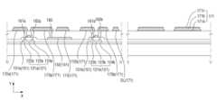
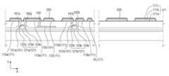
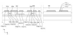
도 3은 도 1의 일 화소의 레이아웃도이고, 도 4는 도 3의 Ⅳ-Ⅳ' 선을 따라 자른 단면도이며, 도 5는 도 1의 Ⅴ-Ⅴ' 선을 따라 자른 단면도이다.FIG. 3 is a layout diagram of one pixel of FIG. 1 , FIG. 4 is a cross-sectional view taken along line IV-IV' in FIG. 3 , and FIG. 5 is a cross-sectional view taken along line V-V' in FIG. 1 .
도 1 및 도 3 내지 도 5를 참조하면, 표시 장치는 기판(100), 버퍼층(110), 활성 패턴층(121), 게이트 절연층(140), 제1 금속 패턴층(151), 층간 절연층(160), 제2 금속 패턴층(171), 보호층(180), 제3 금속 패턴층(191), 화소 정의막(200), 발광층(201) 및 캐소드 전극(210)을 포함한다.1 and 3 to 5 , the display device includes a
기판(100)은 투명한 유리 또는 플라스틱을 포함할 수 있다.The
버퍼층(110)은 화소 영역(DA) 및 패드 영역(PA)의 기판(100) 상에 위치할 수 있다. 버퍼층(110)은 질화규소(SiNx), 산화규소(SiOx), 산질화규소(SiOxNy) 등을 포함할 수 있고, 단층 또는 다층으로 형성될 수 있다. 버퍼층(110)은 반도체의 특성을 열화(degradation)시키는 불순물 또는 수분이나 외기의 침투를 방지하고, 표면을 평탄화시키는 역할을 수행한다. 버퍼층(110)은 생략될 수 있다.The
활성 패턴층(121)은 화소 영역(DA)의 버퍼층(110) 상에 위치할 수 있다. 활성 패턴층(121)은 스위칭 반도체(121a) 및 구동 반도체(121b)를 포함할 수 있으며, 다결정 실리콘(polysilicon)으로 이루어질 수 있다.The
스위칭 반도체(121a) 및 구동 반도체(121b)는 채널 영역(123a, 123b)과 상기 채널 영역(123a, 123b)의 양 옆에 위치하는 소스 영역(122a, 122b) 및 드레인 영역(124a, 124b)을 포함할 수 있다. 채널 영역(123a, 123b)은 불순물이 도핑되지 않은 다결정 실리콘인 진성 반도체(intrinsic semiconductor)일 수 있고, 소스 영역(122a, 122b) 및 드레인 영역(124a, 124b)은 도전성 불순물이 도핑된 다결정 실리콘인 불순물 반도체(impurity semiconductor)일 수 있다.The switching
게이트 절연층(140)은 화소 영역(DA)의 활성 패턴층(121) 및 패드 영역(PA)의 버퍼층(110) 위에 위치할 수 있다. 게이트 절연층(140)은 질화규소, 산화규소, 산질화규소 등을 포함할 수 있고, 단층 또는 다층으로 형성될 수 있다.The
제1 금속 패턴층(151)은 화소 영역(DA) 및 패드 영역(PA)의 게이트 절연층(140) 상에 위치할 수 있다. 제1 금속 패턴층(151)은 알루미늄(Al), 몰리브덴(Mo), 구리(Cu) 등 또는 이들의 합금을 포함할 수 있고, 다중층 구조를 가질 수도 있다.The first
제1 금속 패턴층(151)은 화소 영역(DA)에서 게이트선(GL), 게이트선(GL)으로부터 분지된 복수의 스위칭 게이트 전극(151a), 제1 축전판(152) 및 제1 축전판(152)과 연결된 구동 게이트 전극(151b)을 포함할 수 있다.The first
게이트선(GL)은 제1 방향(D1)으로 연장되어 화소의 일 측면에 위치할 수 있다. 게이트선(GL)은 게이트 신호를 전달한다.The gate line GL may extend in the first direction D1 and be positioned on one side of the pixel. The gate line GL transmits a gate signal.
스위칭 게이트 전극(151a)은 게이트선(GL)으로부터 스위칭 반도체(121a) 측으로 돌출된다.The switching
구동 게이트 전극(151b)은 게이트선(GL) 및 스위칭 게이트 전극(151a)과 이격되어 배치된다. 스위칭 게이트 전극(151a) 및 구동 게이트 전극(151b)은 각각 스위칭 반도체(121a)와 구동 반도체(121b)의 채널 영역(123a, 123b)에 중첩된다.The driving
제1 축전판(152)은 구동 게이트 전극(151b)과 연결된다. 제1 축전판(152)은 제1 접촉 구멍(163)을 통해 스위칭 드레인 전극(173a)과 연결된다.The
제1 금속 패턴층(151)은 패드 영역(PA)에서 게이트 패드(GP)를 포함한다. 게이트 패드(GP)는 게이트선(GL)의 단부와 연결된다.The first
층간 절연층(160)은 화소 영역(DA) 및 패드 영역(PA)의 제1 금속 패턴층(151) 상에 위치한다. 층간 절연층(160)은 질화규소, 산화규소, 산질화규소 등을 포함할 수 있고, 단층 또는 다층으로 형성될 수 있다.The interlayer insulating
게이트 절연층(140) 및 층간 절연층(160)에는 스위칭 반도체(121a)의 소스 영역(122a)과 드레인 영역(124a)이 각각 노출되도록 하는 스위칭 소스 접촉 구멍(161a)과 스위칭 드레인 접촉 구멍(162a)이 게이트 절연층(140) 및 층간 절연층(160)을 관통하여 형성될 수 있다. 마찬가지로, 구동 반도체(121b)의 소스 영역(122b)과 드레인 영역(124b)이 각각 노출되도록 하는 구동 소스 접촉 구멍(161b)과 구동 드레인 접촉 구멍(162b)이 게이트 절연층(140) 및 층간 절연층(160)을 관통하여 형성될 수 있다.The
제2 금속 패턴층(171)은 화소 영역(DA) 및 패드 영역(PA)의 층간 절연층(160) 상에 위치할 수 있다. 제2 금속 패턴층(171)은 알루미늄(Al), 몰리브덴(Mo), 크롬(Cr), 탄탈륨(Ta), 티타늄(Ti) 및 기타 내화성 금속(refractory metal) 또는 이들의 합금을 포함할 수 있으며, 다중층 구조를 가질 수도 있다.The second
예를 들어, 제2 금속 패턴층(171)은 최하부에 위치하는 하부 보조 금속층(171a), 그 위에 위치하는 주 금속층(171b) 및 그 위에 위치하는 상부 보조 금속층(171c)으로 구성된 삼중층 구조를 가질 수 있다. 주 금속층(171b)은 알루미늄을 포함할 수 있으며, 하부 및 상부 보조 금속층(171a, 171c)은 티타늄을 포함할 수 있다.For example, the second
제2 금속 패턴층(171)은 화소 영역(DA)에서 데이터선(DL), 구동 전압선(ELVDD), 스위칭 드레인 전극(173a) 및 구동 드레인 전극(173b)을 포함할 수 있다.The second
데이터선(DL)은 게이트선(GL)과 교차하는 제2 방향(D2)으로 연장되어 데이터 신호를 전달한다. 스위칭 소스 전극(172a)은 데이터선(DL)으로부터 스위칭 반도체(121a) 측으로 돌출된다.The data line DL extends in the second direction D2 crossing the gate line GL to transfer the data signal. The switching
구동 전압선(ELVDD)은 데이터선(DL)과 분리되어 있으며, 데이터선(DL)과 동일한 방향으로 연장되어 구동 신호를 전달할 수 있다. 데이터선(DL) 및 구동 전압선(ELVDD)은 서로 구분되어 화소의 양 측면에 위치할 수 있다.The driving voltage line ELVDD is separated from the data line DL and extends in the same direction as the data line DL to transmit a driving signal. The data line DL and the driving voltage line ELVDD may be separated from each other and positioned on both sides of the pixel.
제2 금속 패턴층(171)은 구동 전압선(ELVDD)으로부터 구동 반도체(121b)로 돌출된 구동 소스 전극(172b) 및 구동 전압선(ELVDD)으로부터 돌출되어 제1 축전판(152)과 중첩되는 제2 축전판(173)을 포함할 수 있다. 제1 축전판(152)과 제2 축전판(173)은 층간 절연층(160)을 유전체로 하여 축전기(Cst)를 구성할 수 있다.The second
스위칭 드레인 전극(173a)은 스위칭 소스 전극(172a)과 마주하고, 구동 드레인 전극(173b)은 구동 소스 전극(172b)과 마주할 수 있다.The switching
스위칭 드레인 전극(173a)과 스위칭 소스 전극(172a)은 각각 스위칭 드레인 접촉 구멍(162a)과 스위칭 소스 접촉 구멍(161a)을 통해 스위칭 반도체(121a)의 드레인 영역(124a)과 소스 영역(122a)에 연결될 수 있다. 구동 드레인 전극(173b)과 구동 소스 전극(172b)은 각각 구동 드레인 접촉 구멍(162b)과 구동 소스 접촉 구멍(161b)을 통해 구동 반도체(121b)의 드레인 영역(124b)과 소스 영역(122b)에 연결될 수 있다.The switching
스위칭 드레인 전극(173a)은 또한, 층간 절연층(160)을 관통하여 형성된 제1 접촉 구멍(163)을 통해 제1 축전판(152) 및 구동 게이트 전극(151b)과 전기적으로 연결될 수 있다.The switching
스위칭 반도체(121a), 스위칭 게이트 전극(151a), 스위칭 소스 전극(172a) 및 스위칭 드레인 전극(173a)은 스위칭 박막 트랜지스터(Qs)를 이루고, 구동 반도체(121b), 구동 게이트 전극(151b), 구동 소스 전극(172b) 및 구동 드레인 전극(173b)은 구동 박막 트랜지스터(Qd)를 이룰 수 있다.The switching
제2 금속 패턴층(171)은 패드 영역(PA)에서 데이터 패드(DP) 및 구동 전압 패드(EP)를 포함할 수 있다. 데이터 패드(DP) 및 구동 전압 패드(EP)는 각각 화소 영역(DA)으로부터 연장된 데이터선(DL) 및 구동 전압선(ELVDD)의 단부와 연결된다. 데이터 패드(DP) 및 구동 전압 패드(EP)의 측벽은 적어도 부분적으로 보호층(180)에 덮이지 않고 노출될 수 있다.The second
패드 영역(PA)의 제2 금속 패턴층(171), 즉 데이터 패드(DP) 및 구동 전압 패드(EP)의 측벽에는 패시베이션막(221)이 배치될 수 있다. 패시베이션막(221)은 제2 금속 패턴층(171)에 포함된 금속과 환원 전위(potential)가 상이하여 갈바닉 반응을 일으킬 수 있는 금속이 환원되어 패드를 단락시키는 것을 방지할 수 있다.A
패시베이션막(221)은 불소(F)계 고분자를 포함할 수 있다. 상기 불소계 고분자는 플루오로카본(Fluorocarbon, CxFy) 또는 플루오로하이드로카본(Fluorohydrocarbon, CxHyFz) 그룹을 포함할 수 있다. 플루오로카본 또는 플루오로하이드로카본 그룹의 예로서, -CF3, -CF2-, -CHF- 그룹 등을 들 수 있다.The
패시베이션막(221)은 제2 금속 패턴층(171)의 모든 측벽 상에 해당 측벽을 덮도록 형성될 수 있으며, 상기 측벽의 배치 방향에 한정되지 않는다.The
패시베이션막(221)은 제2 금속 패턴층(171)의 측벽에만 형성되고, 제2 금속 패턴층(171)의 상면은 전부 노출할 수 있다. 그러나 이에 제한되는 것은 아니며, 패시베이션막(221)은 제2 금속 패턴층(171)의 상면의 일부 또는 전부까지 덮도록 형성될 수도 있고, 제2 금속 패턴층(171)의 측벽의 일부가 노출되도록 형성될 수도 있다.The
제2 금속 패턴층(171)이 다중층 구조를 취할 경우, 패시베이션막(221)은 제2 금속 패턴층(171)에 포함된 모든 층의 측벽 상에 형성될 수 있으나, 제2 금속 패턴층(171)에 포함된 일부 층의 측벽 상에만 형성될 수도 있다.When the second
예를 들어, 상술한 바와 같이 제2 금속 패턴층(171)이 주 금속층(171b) 및 주 금속층(171b)의 상하부에 위치하는 상부/하부 보조 금속층(171a, 171c)을 포함하는 경우, 패시베이션막(221)은 주 금속층(171b) 및 상부/하부 보조 금속층(171a, 171c)의 측벽에 형성될 수 있다. 이에 한정되지 않고, 패시베이션막(221)은 주 금속층(171b)이나 상부/하부 보조 금속층(171a, 171c)의 측벽에만 형성될 수도 있고, 주 금속층(171b)과 상부 또는 하부 보조 금속층(171a, 171c)의 측벽에만 형성될 수도 있다.For example, as described above, when the second
패시베이션막(221)은 두께가 10~150nm의 범위로 형성될 수 있다. 균일한 두께로 형성될 수 있고, 두께가 균일하지 않거나 상하부의 두께가 상이하도록 형성될 수도 있다.The
도면으로 도시하지는 않았지만, 패시베이션막(221)은 패드 영역(PA)의 제2 금속 패턴층(171) 측벽뿐만 아니라, 패드 영역(PA)을 제외한 주변 영역(SA)의 제2 금속 패턴층(171) 측벽에도 형성될 수 있다. 나아가, 패시베이션막(221)은 화소 영역(DA)의 제2 금속 패턴층(171) 측벽에도 형성될 수 있다.Although not shown in the drawing, the
보호층(180)은 화소 영역(DA) 및 패드 영역(PA)의 제2 금속 패턴층(171) 상에 위치할 수 있다. 보호층(180)은 질화규소, 산화규소, 산질화규소, 유전상수가 작은 아크릴(acryl)계 유기화합물, BCB(Benzocyclobutane) 또는 PFCB(Perfluorocyclobutane) 등을 포함할 수 있다.The
보호층(180)은 제2 금속 패턴층(171)을 보호하는 역할을 수행하며, 그 상면을 평탄화시키는 평탄화막의 역할을 수행할 수도 있다. 보호층(180)에는 구동 박막 트랜지스터(Qd)의 구동 드레인 전극(173b)이 노출되도록 하는 제2 접촉 구멍(181)이 보호층(180)을 관통하여 형성될 수 있다.The
제3 금속 패턴층(191)은 화소 영역(DA)의 보호층(180) 상에 위치하며, 애노드 전극(191a)을 포함할 수 있다. 애노드 전극(191a)은 보호층(180)에 형성된 제2 접촉 구멍(181)을 통해 구동 박막 트랜지스터(Qd)의 구동 드레인 전극(173b)과 전기적으로 연결될 수 있으며, 발광 소자(LD)의 화소 전극이 될 수 있다.The third
제3 금속 패턴층(191)은 ITO, IZO, ZnO, In2O3 등의 일함수가 높은 물질층을 포함할 수 있다. 더 나아가, 제3 금속 패턴층(191)은 상술한 일함수가 높은 물질층과 리튬(Li), 칼슘(Ca), 플루오르화리튬/칼슘(LiF/Ca), 플루오르화리튬/알루미늄(LiF/Al), 알루미늄(Al), 은(Ag), 마그네슘(Mg), 금(Au) 등의 반사성 금속층의 적층막으로 이루어질 수 있다.The third
제2 금속 패턴층(171)과 제3 금속 패턴층(191)은 환원 전위(potential) 차에 의해 서로 갈바닉 반응을 일으킬 수 있는 물질을 포함할 수 있다. 다중층 구조인 경우, 제2 금속 패턴층(171)의 주 금속층(171b)과 제3 금속 패턴층(191)이 갈바닉 반응을 일으킬 수 있는 물질을 포함할 수 있다. 예를 들어, 제2 금속 패턴층(171)의 주 금속층(171b)은 알루미늄(Al)을 포함할 수 있고, 제3 금속 패턴층(191)은 은(Ag)을 포함할 수 있다.The second
화소 정의막(200)은 제3 금속 패턴층(191) 상에 위치하며, 폴리아크릴계(polyacrylates) 또는 폴리이미드계(polyimides) 등의 수지를 포함할 수 있다. 화소 정의막(200)은 애노드 전극(191a)이 노출되도록 하는 개구부를 포함할 수 있다.The
발광층(201)은 화소 정의막(200)의 개구부를 통해 노출되는 애노드 전극(191a) 상에 위치할 수 있다. 유기 발광 소자(LD)의 경우, 발광층(201)은 정공 주입층(HIL), 정공 수송층(HTL), 전자 수송층(ETL) 및 전자 주입층(EIL) 중 하나 이상과 유기 발광층(EML)을 포함하는 다중층으로 형성될 수 있다.The
캐소드 전극(210)은 화소 정의막(200) 및 발광층(201) 위에 위치할 수 있다. 캐소드 전극(210)은 Li, Ca, LiF/Ca, LiF/Al, Al, Mg, Ag, Pt, Pd, Ni, Au Nd, Ir, Cr, BaF, Ba 또는 이들의 화합물이나 혼합물(예를 들어, Ag와 Mg의 혼합물 등)을 포함할 수 있다. 캐소드 전극(210)은 보조 전극을 더 포함할 수 있다. 상기 보조 전극은 상기 물질이 증착되어 형성된 막 및 상기 막 상에 투명 금속 산화물, 예를 들어, 인듐-주석-산화물(Indium-Tin-Oxide: ITO), 인듐-아연-산화물(Indium-Zinc-Oxide: IZO), 산화아연(Zinc Oxide: ZnO), 인듐-주석-아연-산화물 (Indium-Tin-Zinc-Oxide) 등을 포함할 수 있다. 캐소드 전극(210)은 발광 소자(LD)의 공통 전극일 수 있다.The
한편, 도 5에 도시된 바와 같이, 패드 영역(PA)에서는 화소 영역(DA)과 달리 제2 금속 패턴층(171) 상의 보호층(180) 및 제3 금속 패턴층(191) 등의 일부 또는 전부가 제거된다. 따라서, 제2 금속 패턴층(171)은 노출되어 구동 칩 등의 외부 회로와 접촉할 수 있다.Meanwhile, as shown in FIG. 5 , unlike the pixel area DA, in the pad area PA, a part of the
이하, 본 발명의 다른 실시예에 대해 설명한다.Hereinafter, other embodiments of the present invention will be described.
도 6 내지 8는 본 발명의 다양한 실시예들에 따른 제2 금속 패턴층 및 그 측벽을 덮는 패시베이션막의 단면도들이다.6 to 8 are cross-sectional views of a second metal pattern layer and a passivation film covering sidewalls thereof according to various embodiments of the present disclosure.
도 6은 패시베이션막(221_1)의 상부가 제2 금속 패턴층(171) 보다 약 50~250nm 높게 돌출되도록 형성된 돌출부(222)를 더 포함할 수 있음을 예시한다.6 illustrates that the upper part of the passivation film 221_1 may further include a
도 7은 패시베이션막(221_2)의 두께가 불균일한 경우를 예시한다. 예를 들어, 패시베이션막(221_2)은 도 7에 도시된 바와 같이 하부의 두께(d2)가 상부의 두께(d1)보다 얇을 수 있다. 구체적으로, 패시베이션막(221_2)의 상부에서 하부로 갈수록 두께가 점점 얇아지거나, 패시베이션막(221_2) 높이의 중간 지점을 기준으로 하부의 평균 두께가 상부의 평균 두께보다 얇을 수 있다.7 illustrates a case where the thickness of the passivation film 221_2 is non-uniform. For example, as shown in FIG. 7 , the lower portion of the passivation layer 221_2 may have a thickness (d2 ) smaller than the upper thickness (d1 ). Specifically, the thickness of the passivation layer 221_2 may gradually decrease from the top to the bottom, or the average thickness of the lower portion may be thinner than the average thickness of the upper portion based on the middle point of the passivation layer 221_2 height.
이에 따라, 패시베이션막(221_2)의 외면이 지면과 이루는 각(θ)은 직각에 가까운 범위, 예를 들어 80~90° 범위 내의 값을 이룰 수 있으나, 이에 한정되는 것은 아니다.Accordingly, the angle θ between the outer surface of the passivation layer 221_2 and the ground may be close to a right angle, for example, within a range of 80° to 90°, but is not limited thereto.
도 8의 패시베이션막(221_3)은 하부의 두께가 상부보다 얇은 동시에, 돌출부(222)를 더 포함하는 경우를 예시한다.The passivation film 221_3 of FIG. 8 illustrates a case in which the lower portion is thinner than the upper portion and further includes the
이하, 상술한 표시 장치의 제조 방법에 대해 설명한다.Hereinafter, a method of manufacturing the display device described above will be described.
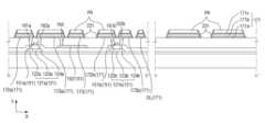
도 9 내지 도 15는 본 발명의 일 실시예에 따른 표시 장치의 제조 방법의 공정 단계별 단면도들이다.9 to 15 are cross-sectional views of step-by-step processes of a method of manufacturing a display device according to an embodiment of the present invention.
도 9를 참조하면, 기판(100) 상에 버퍼층(110), 스위칭 반도체(121a) 및 구동 반도체(121b)를 포함하는 활성 패턴층(121), 게이트 절연층(140), 게이트선(GL)을 포함하는 제1 금속 패턴층(151) 및 층간 절연층(160)을 형성한다. 상기 구조들을 형성하는 구체적인 방법들은 당업계에 공지되어 있으므로 본 발명이 모호해지는 것을 회피하기 위해 구체적인 설명은 생략한다.Referring to FIG. 9 , a
이어, 층간 절연층(160)을 패터닝하여 스위칭 반도체(121a)의 소스 영역(122a)과 드레인 영역(124a)이 각각 노출되도록 하는 스위칭 소스 접촉 구멍(161a)과 스위칭 드레인 접촉 구멍(162a), 구동 반도체(121b)의 소스 영역(122b)과 드레인 영역(124b)이 각각 노출되도록 하는 구동 소스 접촉 구멍(161b)과 구동 드레인 접촉 구멍(162b) 및 제1 축전판(152)이 노출되도록 하는 제1 접촉 구멍(163)을 형성한다.Subsequently, the
이어, 도 10을 참조하면, 화소 영역(DA) 및 패드 영역(PA)의 층간 절연층(160) 상에 제2 금속층(170)을 형성한다.Next, referring to FIG. 10 , a
도 11을 참조하면, 화소 영역(DA) 및 패드 영역(PA)의 제2 금속층(170) 상에 포토레지스트층(PRL)을 형성한다.Referring to FIG. 11 , a photoresist layer PRL is formed on the
도 12를 참조하면, 이어, 포토레지스트층(PRL)을 마스크(Mask)를 정렬하여 노광하고 현상액으로 현상(develop)하여 포토레지스트(PR) 패턴을 형성한다. 이어, 포토레지스트(PR) 패턴을 식각 마스크로 이용하여 하부의 제2 금속층(170)을 식각하여 제2 금속 패턴층(171)을 형성한다.Referring to FIG. 12 , the photoresist layer PRL is then exposed to light by aligning a mask, and developed with a developer to form a photoresist pattern. Subsequently, the second
구체적으로, 패터닝된 포토레지스트층(PRL)의 패턴을 따라 제2 금속층(170)을 식각함으로써, 데이터선(DL), 구동 전압선(ELVDD), 스위칭 드레인 전극(173a) 및 구동 드레인 전극(173b)을 포함하는 제2 금속 패턴층(171)을 형성할 수 있다. 식각되지 않은 제2 금속 패턴층(171)의 위에는 포토레지스트(PR)가 잔존할 수 있다.Specifically, the data line DL, the driving voltage line ELVDD, the switching
제2 금속층(170)은 식각 가스를 사용하는 건식 식각(dry etching)을 통해 식각할 수 있으며, 식각 가스는 BCl3, BCl3/Cl2, BCl3/Cl2/Ar 등의 염소(Cl)계 가스를 포함할 수 있다.The
도 13을 참조하면, 이어, 화소 영역(DA) 및 패드 영역(PA)의 제2 금속 패턴층(171) 상에 잔존하는 포토레지스트(PR)를 제거(stripping)한다. 포토레지스트(PR)는 제거 용액(stripper)을 사용하여 제거할 수 있고, 리프트오프(lift off) 또는 에싱(ashing) 등의 방식으로 제거할 수 있다.Referring to FIG. 13 , the photoresist PR remaining on the second
도 14를 참조하면, 화소 영역(DA) 및 패드 영역(PA)의 제2 금속 패턴층(171) 상에 패시베이션층(220)을 형성할 수 있다. 패시베이션층(220)은 화학기상증착(chemical vapor deposition, CVD), 물리기상증착(physical vapor deposition, PVD), 원자층증착(atomic layer deposition, ALD) 등의 방식으로 형성할 수 있으며, 특히 불소(F)계 가스를 공급하여 제2 금속 패턴층(171) 위에 증착함으로써 형성할 수 있다.Referring to FIG. 14 , a
불소계 가스는 플루오로카본(Fluorocarbon, CxFy) 또는 플루오로하이드로카본(Fluorohydrocarbon, CxHyFz)을 포함할 수 있다. 플루오로카본 또는 플루오로하이드로카본의 예로서, CF4, C3F6, C4F8, C5F8, CHF3, CH2F2, C2HF5, CH3F 등을 들 수 있다.The fluorine-based gas may include fluorocarbon (Cx Fy ) or fluorohydrocarbon (Cx Hy Fz ). Examples of fluorocarbons or fluorohydrocarbons include CF4 , C3 F6 , C4 F8 , C5 F8 , CHF3 , CH2 F2 , C2 HF5 , CH3 F and the like. there is.
도 15를 참조하면, 패시베이션층(220)을 식각하여 화소 영역(DA) 및 패드 영역(PA)의 제2 금속 패턴층(171) 측벽 상에 패시베이션막(221)을 형성할 수 있다. 패시베이션층(220)을 수직 방향(y)에 대한 이방성(anisotropic) 식각을 통해 식각하면, 제2 금속 패턴층(171)의 측벽에 존재하는 패시베이션층(220)(동시에, 패시베이션막)을 제외한 층간 절연층(160)의 상면 및 제2 금속 패턴층(171)의 상면에 존재하는 패시베이션층(220)을 제거할 수 있다.Referring to FIG. 15 , the
패시베이션막(221)은 불소(F)계 고분자를 포함할 수 있다. 상기 불소계 고분자는 플루오로카본(Fluorocarbon, CxFy) 또는 플루오로하이드로카본(Fluorohydrocarbon, CxHyFz) 그룹을 포함할 수 있다. 플루오로카본 또는 플루오로하이드로카본 그룹의 예로서, -CF3, -CF2-, -CHF- 그룹 등을 들 수 있다.The
패시베이션막(221)의 두께는 도 7과 같이 하부가 상부보다 얇을 수 있다. 이와 같은 두께 차이는 식각 가스가 수직 방향(y)으로의 이방성 식각을 수행하는 한편, 제2 금속 패턴층(171)은 상부로 갈수록 층의 단면이 좁아지는 각뿔대의 형태를 취하기 때문에 발생할 수 있다.As shown in FIG. 7 , the lower portion of the
이와 같은 과정에 따르면, 패시베이션막(221)을 패드 영역(PA)뿐 아니라, 패드 영역(PA)을 제외한 주변 영역(SA) 및 화소 영역(DA)에도 형성할 수 있다.According to this process, the
도 9 내지 도 11 및 도 16은 본 발명의 다른 실시예에 따른 표시 장치의 제조 방법의 공정 단계별 단면도들이다.9 to 11 and 16 are cross-sectional views of process steps of a method of manufacturing a display device according to another exemplary embodiment of the present invention.
도 16을 참조하면, 도 9 내지 도 11까지의 과정 후, 제2 금속층(170)을 제2 금속 패턴층(171)으로 식각하는 동시에, 화소 영역(DA) 및 패드 영역(PA)의 제2 금속 패턴층(171) 측벽에 패시베이션막(221)을 형성한다.Referring to FIG. 16 , after the processes of FIGS. 9 to 11 , the
구체적으로, 불소계 가스를 포함하는 식각 가스를 공급하고 공정 조건을 조절하여 제2 금속층(170)을 건식 식각 및 이방성 식각하면, 식각 가스가 포토레지스트(PR) 패턴을 따라 제2 금속층(170)을 수직 방향(y)으로 식각하는 동시에, 불소계 가스가 패시베이션층(220)을 형성한다. 이때, 식각 가스가 패시베이션층(220) 또한 수직 방향(y)으로 식각하기 때문에, 수평 방향(x)으로 형성된 제2 금속 패턴층(171) 측벽 상의 패시베이션막(221)만 남을 수 있다.Specifically, when the
식각 가스는 BCl3, BCl3/Cl2, BCl3/Cl2/Ar 등의 염소(Cl)계 가스를 포함할 수 있다.The etching gas may include a chlorine (Cl)-based gas such as BCl3 , BCl3 /Cl2 , BCl3 /Cl2 /Ar.
불소계 가스는 플루오로카본(Fluorocarbon, CxFy) 또는 플루오로하이드로카본(Fluorohydrocarbon, CxHyFz)을 포함할 수 있다.The fluorine-based gas may include fluorocarbon (Cx Fy ) or fluorohydrocarbon (Cx Hy Fz ).
또한, 도 15와 같이 제2 금속 패턴층(171) 위에 잔존하는 포토레지스트(PR)를 제거(stripping)할 수 있다.Also, as shown in FIG. 15 , the photoresist PR remaining on the second
패시베이션막(221)은 제2 금속 패턴층(171) 위에 잔존하는 포토레지스트(PR)의 측벽에도 형성될 수 있는데, 포토레지스트(PR)를 제거 용액으로 제거할 때 포토레지스트(PR)의 측면에 형성된 패시베이션막(221)이 불완전하게 제거되며 도 6과 같은 돌출부(222)를 형성할 수 있다.The
이와 같은 과정에 따르면, 패시베이션층(220)을 형성 및 식각하는 과정이 별도로 필요하지 않기 때문에, 추가적인 공정 없이 패시베이션막(221)을 형성할 수 있다. 또한, 패시베이션막(221)을 패드 영역(PA)뿐 아니라, 패드 영역(PA)을 제외한 주변 영역(SA) 및 화소 영역(DA)에도 형성할 수 있다.According to this process, since a separate process of forming and etching the
도 9 내지 도 13 및 도 17 내지 도 19는 본 발명의 다른 실시예에 따른 표시 장치의 제조 방법의 공정 단계별 단면도들이다.9 to 13 and FIGS. 17 to 19 are process-step cross-sectional views of a manufacturing method of a display device according to another exemplary embodiment of the present invention.
도 17을 참조하면, 도 9 내지 도 13까지의 과정 후, 화소 영역(DA) 및 패드 영역(PA)의 제2 금속 패턴층(171) 상에 보호층(180)을 형성한다.Referring to FIG. 17 , after the processes of FIGS. 9 to 13 , a
도 18을 참조하면, 패드 영역(PA)의 제2 금속 패턴층(171)이 노출되도록 보호층(180)을 식각하며, 구동 박막 트랜지스터(Qd)의 구동 드레인 전극(173b)이 노출되도록 하는 제2 접촉 구멍(181)은 보호층(180)을 관통하여 형성한다.Referring to FIG. 18 , the
도 19를 참조하면, 패드 영역(PA)의 제2 금속 패턴층(171) 측벽 상에 패시베이션막(221)을 형성한다. 구체적으로, 도 14 및 도 15와 같이 제2 금속 패턴층(171) 위에 패시베이션층(220)을 형성하고 패시베이션층(220)을 식각하여 제2 금속 패턴층(171) 측면에 패시베이션막(221)을 형성할 수 있다.Referring to FIG. 19 , a
도면에는 도시하지 않았지만, 보호층(180)의 측면에도 패시베이션막이 형성될 수 있다.Although not shown in the drawings, a passivation film may also be formed on the side surface of the
이와 같은 과정에 따르면, 패시베이션막(221)을 패드 영역(PA)에만 형성할 수 있다.According to this process, the
한편, 화소 영역(DA)의 보호층(180) 상에 애노드 전극(191a)을 포함하는 제3 금속 패턴층(191)을 형성할 수 있다. 제2 금속 패턴층(171)과 제3 금속 패턴층(191)은 환원 전위(potential) 차에 의해 서로 갈바닉 반응을 일으킬 수 있는 물질을 포함할 수 있다.Meanwhile, a third
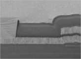
도 20 및 도 21은 본 발명의 실시예에 따른 표시 장치의 제2 금속 패턴층의 단면을 나타낸 이미지이다. 도 20은 포토레지스트(PR)가 제거되지 않은 제2 금속 패턴층(171)을 나타낸 것이며, 도 21은 포토레지스트(PR)가 제거된 제2 금속 패턴층(171)의 단면을 나타낸 것이다.20 and 21 are cross-sectional images of the second metal pattern layer of the display device according to the exemplary embodiment of the present invention. FIG. 20 shows the second
도 20 및 도 21을 참조하면, 제2 금속 패턴층(171)의 측면에 패시베이션막(221)이 형성될 수 있으며, 패시베이션막(221)은 도 21에 나타난 것과 같이 상부가 제2 금속 패턴층(171)보다 높게 돌출되도록 형성되는 돌출부(222)를 포함할 수 있다.20 and 21, a
도 22는 본 발명의 실시예에 따른 표시 장치를 X선 광전자 분광법(X-ray photoelectron spectroscopy, XPS)으로 분석한 결과를 나타낸 것이다.22 shows a result of analyzing the display device according to the embodiment of the present invention by X-ray photoelectron spectroscopy (XPS).
도 22를 참조하면, 표시 장치를 제조할 때 불소계 고분자를 포함하는 패시베이션막(221)을 형성함에 따라, 표시 장치에서 -CF3-, -CF2-, -CHF- 그룹을 포함하는 고분자가 검출될 수 있다.Referring to FIG. 22 , when a display device is manufactured, as a
이상 첨부된 도면을 참조하여 본 발명의 실시예들을 설명하였지만, 본 발명이 속하는 기술분야에서 통상의 지식을 가진 자는 본 발명의 그 기술적 사상이나 필수적인 특징을 변경하지 않고서 다른 구체적인 형태로 실시될 수 있다는 것을 이해할 수 있을 것이다. 그러므로 이상에서 기술한 실시예들은 모든 면에서 예시적인 것이며 한정적이 아닌 것으로 이해해야만 한다.Although the embodiments of the present invention have been described with reference to the accompanying drawings, those skilled in the art to which the present invention pertains can be implemented in other specific forms without changing the technical spirit or essential features of the present invention. you will be able to understand Therefore, the embodiments described above should be understood as illustrative in all respects and not limiting.
100: 기판
110: 버퍼층
121: 활성 패턴층
140: 게이트 절연층
151: 제1 금속 패턴층
160: 층간 절연층
171: 제2 금속 패턴층
180: 보호층
191: 제3 금속 패턴층
200: 화소 정의막
221: 패시베이션막100: substrate
110: buffer layer
121: active pattern layer
140: gate insulating layer
151: first metal pattern layer
160: interlayer insulating layer
171: second metal pattern layer
180: protective layer
191: third metal pattern layer
200: pixel defining layer
221 passivation film
Claims (20)
Translated fromKorean상기 기판 상에 배치되고 상기 표시 영역에 위치하는 활성 패턴층;
상기 활성 패턴층 상에 배치된 게이트 절연층;
상기 게이트 절연층 상에 배치된 제1 금속 패턴층;
상기 제1 금속 패턴층 바로 위에 배치되고 상기 표시 영역 및 상기 패드 영역에 위치하는 층간 절연층;
상기 층간 절연층 상에 배치된 제2 금속 패턴층;
상기 제2 금속 패턴층의 측벽 상에 배치되고 상기 패드 영역에 위치하는 패시베이션막; 및
상기 제2 금속 패턴층 상에 위치하는 보호층; 을 포함하고,
상기 제1 금속 패턴층은 상기 표시 영역에 위치하고 상기 활성 패턴층과 중첩하는 게이트 전극을 포함하고,
상기 제2 금속 패턴층은 상기 표시 영역에 위치하는 소스 전극, 상기 표시 영역에 위치하는 드레인 전극 및 상기 패드 영역에 위치하는 데이터 패드를 포함하고,
상기 소스 전극, 상기 드레인 전극 및 상기 데이터 패드는 각각 상기 층간 절연층 바로 위에 위치하는 제1면, 상기 제1면의 반대면인 제2면 및 상기 제1면과 상기 제2면에 직접 연결된 측면을 포함하고,
상기 패시베이션막은 상기 데이터 패드의 상기 측면 바로 위에 위치하고,
상기 패시베이션막은 상기 데이터 패드의 상기 제2면과 비접촉하는 표시 장치.a substrate including a display area and a non-display area, wherein the non-display area includes a pad area;
an active pattern layer disposed on the substrate and located in the display area;
a gate insulating layer disposed on the active pattern layer;
a first metal pattern layer disposed on the gate insulating layer;
an interlayer insulating layer disposed directly on the first metal pattern layer and positioned in the display area and the pad area;
a second metal pattern layer disposed on the interlayer insulating layer;
a passivation layer disposed on a sidewall of the second metal pattern layer and positioned in the pad region; and
a protective layer positioned on the second metal pattern layer; including,
The first metal pattern layer includes a gate electrode positioned in the display area and overlapping the active pattern layer;
The second metal pattern layer includes a source electrode positioned in the display area, a drain electrode positioned in the display area, and a data pad positioned in the pad area;
The source electrode, the drain electrode, and the data pad each have a first surface positioned directly on the interlayer insulating layer, a second surface opposite to the first surface, and a side surface directly connected to the first surface and the second surface. including,
the passivation layer is located directly on the side surface of the data pad;
The passivation layer does not contact the second surface of the data pad.
상기 보호층은 상기 소스 전극의 상기 제2면, 상기 소스 전극의 상기 측면, 상기 드레인 전극의 상기 제2면 및 상기 드레인 전극의 상기 측면과 직접 접촉하고,
상기 보호층은 상기 데이터 패드와 비중첩하고,
상기 보호층은 상기 데이터 패드의 상기 제2면과 비접촉하는 표시 장치.According to claim 1,
the protective layer is in direct contact with the second surface of the source electrode, the side surface of the source electrode, the second surface of the drain electrode and the side surface of the drain electrode;
the protective layer does not overlap with the data pad;
The protective layer does not contact the second surface of the data pad.
상기 패시베이션막은 불소계 고분자를 포함하는 표시 장치.According to claim 1,
The display device of claim 1, wherein the passivation layer includes a fluorine-based polymer.
상기 불소계 고분자는 플루오로카본(CxFy) 또는 플루오로하이드로카본(CxHyFz) 그룹을 포함하는 표시 장치.According to claim 3,
The display device of claim 1 , wherein the fluorine-based polymer includes a fluorocarbon (Cx Fy ) or fluorohydrocarbon (Cx Hy Fz ) group.
상기 보호층 상에 배치되며 상기 제2 금속 패턴층과 환원 전위가 상이한 물질을 포함하는 제3 금속 패턴층을 더 포함하는 표시 장치.According to claim 1,
and a third metal pattern layer disposed on the passivation layer and including a material having a different reduction potential from the second metal pattern layer.
상기 제2 금속 패턴층은,
상기 제3 금속 패턴층과 환원 전위가 상이한 물질을 포함하는 주 금속층;
상기 주 금속층의 하부에 위치하는 하부 보조 금속층; 및
상기 주 금속층의 상부에 위치하는 상부 보조 금속층;을 포함하는 표시 장치.According to claim 5,
The second metal pattern layer,
a main metal layer including a material having a different reduction potential from that of the third metal pattern layer;
a lower auxiliary metal layer positioned below the main metal layer; and
A display device comprising: an upper auxiliary metal layer positioned on top of the main metal layer.
상기 주 금속층은 알루미늄(Al)을 포함하고, 상기 제3 금속 패턴층은 은(Ag)을 포함하는 표시 장치.According to claim 6,
The main metal layer includes aluminum (Al), and the third metal pattern layer includes silver (Ag).
Priority Applications (2)
| Application Number | Priority Date | Filing Date | Title |
|---|---|---|---|
| KR1020160034130AKR102550322B1 (en) | 2016-03-22 | 2016-03-22 | Display device and manufacturing method thereof |
| US15/465,154US10672799B2 (en) | 2016-03-22 | 2017-03-21 | Display device and manufacturing method thereof |
Applications Claiming Priority (1)
| Application Number | Priority Date | Filing Date | Title |
|---|---|---|---|
| KR1020160034130AKR102550322B1 (en) | 2016-03-22 | 2016-03-22 | Display device and manufacturing method thereof |
Publications (2)
| Publication Number | Publication Date |
|---|---|
| KR20170110217A KR20170110217A (en) | 2017-10-11 |
| KR102550322B1true KR102550322B1 (en) | 2023-07-03 |
Family
ID=59898236
Family Applications (1)
| Application Number | Title | Priority Date | Filing Date |
|---|---|---|---|
| KR1020160034130AActiveKR102550322B1 (en) | 2016-03-22 | 2016-03-22 | Display device and manufacturing method thereof |
Country Status (2)
| Country | Link |
|---|---|
| US (1) | US10672799B2 (en) |
| KR (1) | KR102550322B1 (en) |
Families Citing this family (8)
| Publication number | Priority date | Publication date | Assignee | Title |
|---|---|---|---|---|
| CN104658974A (en)* | 2015-03-12 | 2015-05-27 | 京东方科技集团股份有限公司 | Method for preparing film layer pattern, thin film transistor and array substrate |
| CN108735761A (en)* | 2017-04-20 | 2018-11-02 | 京东方科技集团股份有限公司 | Conductive pattern structure and preparation method thereof, array substrate and display device |
| KR102623838B1 (en) | 2018-08-20 | 2024-01-11 | 삼성디스플레이 주식회사 | Display device and manufacturing method therof |
| KR102608021B1 (en) | 2018-09-03 | 2023-12-01 | 삼성디스플레이 주식회사 | Electronic apparatus and method of manufacturing the same |
| KR102661283B1 (en)* | 2018-11-26 | 2024-05-02 | 삼성디스플레이 주식회사 | Display substrate, method of manufacturing the same, and display device including the same |
| KR102694186B1 (en) | 2019-06-21 | 2024-08-12 | 삼성디스플레이 주식회사 | Display device and method of manufacturing the same |
| KR102801928B1 (en) | 2020-07-13 | 2025-04-28 | 삼성전자주식회사 | Semiconductor device and method for fabricating thereof |
| CN113053811B (en)* | 2021-03-11 | 2024-07-30 | 深圳市华星光电半导体显示技术有限公司 | Array substrate and preparation method thereof |
Citations (3)
| Publication number | Priority date | Publication date | Assignee | Title |
|---|---|---|---|---|
| US4581267A (en) | 1982-09-09 | 1986-04-08 | Morgan Adhesives Company | Moisture and oxygen barrier laminate for photographic or printed articles |
| KR100647712B1 (en)* | 2005-11-09 | 2006-11-23 | 삼성에스디아이 주식회사 | Organic light emitting display |
| JP2013042149A (en) | 2004-10-29 | 2013-02-28 | Lam Research Corporation | Method for protecting silicon or silicon carbide electrode surface from morphological modification during plasma etch processing |
Family Cites Families (12)
| Publication number | Priority date | Publication date | Assignee | Title |
|---|---|---|---|---|
| US6771328B2 (en)* | 2001-07-25 | 2004-08-03 | Lg. Philips Lcd Co., Ltd. | Active matrix organic electroluminescent device simplifying a fabricating process and a fabricating method thereof |
| US7928654B2 (en)* | 2003-08-29 | 2011-04-19 | Semiconductor Energy Laboratory Co., Ltd. | Display device and method for manufacturing the same |
| GB0517195D0 (en) | 2005-08-23 | 2005-09-28 | Cambridge Display Tech Ltd | Molecular electronic device structures and fabrication methods |
| DE112006002220B4 (en) | 2005-08-23 | 2018-05-24 | Cambridge Display Technology Ltd. | Organic electronic device structures and manufacturing processes |
| KR100922802B1 (en)* | 2006-12-29 | 2009-10-21 | 엘지디스플레이 주식회사 | TFT array substrate and manufacturing method thereof |
| KR20080069745A (en) | 2007-01-24 | 2008-07-29 | 삼성전자주식회사 | Display device |
| US20080286698A1 (en)* | 2007-05-18 | 2008-11-20 | Haoren Zhuang | Semiconductor device manufacturing methods |
| KR101135540B1 (en)* | 2009-11-30 | 2012-04-13 | 삼성모바일디스플레이주식회사 | Organic Light Emitting Display Device |
| KR102192592B1 (en) | 2013-07-22 | 2020-12-18 | 삼성디스플레이 주식회사 | Organic light emitting diode display |
| KR102147849B1 (en)* | 2013-08-05 | 2020-08-25 | 삼성전자주식회사 | Thin film transistor and method for fabricating the same |
| KR20150044327A (en)* | 2013-10-16 | 2015-04-24 | 삼성디스플레이 주식회사 | Field relaxation thin film transistor, method of manufacturing the same and display apparatus including the same |
| KR102458866B1 (en)* | 2014-07-23 | 2022-10-27 | 엘지디스플레이 주식회사 | Organic light emitting diode display device and fabricating method of the same |
- 2016
- 2016-03-22KRKR1020160034130Apatent/KR102550322B1/enactiveActive
- 2017
- 2017-03-21USUS15/465,154patent/US10672799B2/enactiveActive
Patent Citations (3)
| Publication number | Priority date | Publication date | Assignee | Title |
|---|---|---|---|---|
| US4581267A (en) | 1982-09-09 | 1986-04-08 | Morgan Adhesives Company | Moisture and oxygen barrier laminate for photographic or printed articles |
| JP2013042149A (en) | 2004-10-29 | 2013-02-28 | Lam Research Corporation | Method for protecting silicon or silicon carbide electrode surface from morphological modification during plasma etch processing |
| KR100647712B1 (en)* | 2005-11-09 | 2006-11-23 | 삼성에스디아이 주식회사 | Organic light emitting display |
Also Published As
| Publication number | Publication date |
|---|---|
| US10672799B2 (en) | 2020-06-02 |
| KR20170110217A (en) | 2017-10-11 |
| US20170278867A1 (en) | 2017-09-28 |
Similar Documents
| Publication | Publication Date | Title |
|---|---|---|
| KR102550322B1 (en) | Display device and manufacturing method thereof | |
| CN108288621B (en) | Manufacturing method of array substrate, array substrate and display panel | |
| KR102706584B1 (en) | Backplane for display device and method of manufacturing the same | |
| KR101593443B1 (en) | Method of fabricating array substrate | |
| US9842934B2 (en) | Array substrate and method of fabricating the same | |
| US10825876B2 (en) | Display device and method of manufacturing the same | |
| US9245937B2 (en) | Thin film transistor substrates, display devices and methods of manufacturing display devices | |
| US9064750B2 (en) | Display substrate and method of manufacturing the same | |
| US20210098582A1 (en) | Tft substrate and manufacturing method thereof | |
| KR102553981B1 (en) | Backplane for display device and method of manufacturing the same | |
| US7923732B2 (en) | Thin film transistor and method for manufacturing a display panel | |
| KR102477608B1 (en) | Display substrate, method of manufacturing the same, and display device including the same | |
| US11894506B2 (en) | Display apparatus having a pad spaced away from an encapsulating element and a black matrix on the encapsulating element | |
| TW201526246A (en) | Thin film transistor and display substrate | |
| KR20210004795A (en) | Display apparatus having an oxide semiconductor pattern | |
| US20050285100A1 (en) | Organic light emitting display and method of fabricating the same | |
| CN111293125A (en) | Display device and method for manufacturing the same | |
| KR20110113040A (en) | Array board | |
| US20160197165A1 (en) | Manufacturing method of thin film transistor display panel | |
| KR20160053383A (en) | Thin Film Transistor Array Substrate and Organic Light Emitting Diode Display Device Having The Same | |
| KR102313004B1 (en) | Display device and method of manufacturing the same | |
| US11223030B2 (en) | Organic emitting display device having reflective metal layers on different levels above red, green and blue pixel regions and method of manufacturing same | |
| KR102035004B1 (en) | Array substrate for liquid crystal display device and method of fabricating the same | |
| KR102142476B1 (en) | Array substrate and method of fabricating the same | |
| KR101847063B1 (en) | Method of fabricating array substrate |
Legal Events
| Date | Code | Title | Description |
|---|---|---|---|
| PA0109 | Patent application | St.27 status event code:A-0-1-A10-A12-nap-PA0109 | |
| PG1501 | Laying open of application | St.27 status event code:A-1-1-Q10-Q12-nap-PG1501 | |
| R18-X000 | Changes to party contact information recorded | St.27 status event code:A-3-3-R10-R18-oth-X000 | |
| A201 | Request for examination | ||
| PA0201 | Request for examination | St.27 status event code:A-1-2-D10-D11-exm-PA0201 | |
| D13-X000 | Search requested | St.27 status event code:A-1-2-D10-D13-srh-X000 | |
| D14-X000 | Search report completed | St.27 status event code:A-1-2-D10-D14-srh-X000 | |
| E902 | Notification of reason for refusal | ||
| PE0902 | Notice of grounds for rejection | St.27 status event code:A-1-2-D10-D21-exm-PE0902 | |
| E13-X000 | Pre-grant limitation requested | St.27 status event code:A-2-3-E10-E13-lim-X000 | |
| P11-X000 | Amendment of application requested | St.27 status event code:A-2-2-P10-P11-nap-X000 | |
| P13-X000 | Application amended | St.27 status event code:A-2-2-P10-P13-nap-X000 | |
| P22-X000 | Classification modified | St.27 status event code:A-2-2-P10-P22-nap-X000 | |
| P22-X000 | Classification modified | St.27 status event code:A-2-2-P10-P22-nap-X000 | |
| E701 | Decision to grant or registration of patent right | ||
| PE0701 | Decision of registration | St.27 status event code:A-1-2-D10-D22-exm-PE0701 | |
| GRNT | Written decision to grant | ||
| PR0701 | Registration of establishment | St.27 status event code:A-2-4-F10-F11-exm-PR0701 | |
| PR1002 | Payment of registration fee | St.27 status event code:A-2-2-U10-U11-oth-PR1002 Fee payment year number:1 | |
| PG1601 | Publication of registration | St.27 status event code:A-4-4-Q10-Q13-nap-PG1601 | |
| P22-X000 | Classification modified | St.27 status event code:A-4-4-P10-P22-nap-X000 |