KR102549418B1 - Resonant circuit for aerosol-generating system - Google Patents
Resonant circuit for aerosol-generating systemDownload PDFInfo
- Publication number
- KR102549418B1 KR102549418B1KR1020217008825AKR20217008825AKR102549418B1KR 102549418 B1KR102549418 B1KR 102549418B1KR 1020217008825 AKR1020217008825 AKR 1020217008825AKR 20217008825 AKR20217008825 AKR 20217008825AKR 102549418 B1KR102549418 B1KR 102549418B1
- Authority
- KR
- South Korea
- Prior art keywords
- transistor
- voltage
- susceptor
- aerosol
- circuit
- Prior art date
- Legal status (The legal status is an assumption and is not a legal conclusion. Google has not performed a legal analysis and makes no representation as to the accuracy of the status listed.)
- Active
Links
- 230000001939inductive effectEffects0.000claimsabstractdescription112
- 239000000463materialSubstances0.000claimsabstractdescription54
- 238000010438heat treatmentMethods0.000claimsabstractdescription39
- 239000000443aerosolSubstances0.000claimsabstractdescription38
- 230000006698inductionEffects0.000claimsabstractdescription21
- 230000010355oscillationEffects0.000claimsabstractdescription17
- 230000004044responseEffects0.000claimsabstractdescription10
- 229910052782aluminiumInorganic materials0.000claimsdescription16
- XAGFODPZIPBFFR-UHFFFAOYSA-NaluminiumChemical compound[Al]XAGFODPZIPBFFR-UHFFFAOYSA-N0.000claimsdescription16
- 230000005669field effectEffects0.000claimsdescription15
- 230000008878couplingEffects0.000claimsdescription8
- 238000010168coupling processMethods0.000claimsdescription8
- 238000005859coupling reactionMethods0.000claimsdescription8
- 238000000034methodMethods0.000claimsdescription5
- 239000003990capacitorSubstances0.000description31
- 230000005291magnetic effectEffects0.000description21
- 241000208125NicotianaSpecies0.000description16
- 235000002637Nicotiana tabacumNutrition0.000description16
- 239000004065semiconductorSubstances0.000description15
- 230000008859changeEffects0.000description8
- 230000007423decreaseEffects0.000description8
- 230000035699permeabilityEffects0.000description6
- 230000000694effectsEffects0.000description5
- XEEYBQQBJWHFJM-UHFFFAOYSA-NIronChemical compound[Fe]XEEYBQQBJWHFJM-UHFFFAOYSA-N0.000description4
- PXHVJJICTQNCMI-UHFFFAOYSA-NNickelChemical compound[Ni]PXHVJJICTQNCMI-UHFFFAOYSA-N0.000description4
- 239000000969carrierSubstances0.000description4
- 229910052751metalInorganic materials0.000description4
- 239000002184metalSubstances0.000description4
- PEDCQBHIVMGVHV-UHFFFAOYSA-NGlycerineChemical compoundOCC(O)COPEDCQBHIVMGVHV-UHFFFAOYSA-N0.000description3
- DNIAPMSPPWPWGF-UHFFFAOYSA-NPropylene glycolChemical compoundCC(O)CODNIAPMSPPWPWGF-UHFFFAOYSA-N0.000description3
- XUIMIQQOPSSXEZ-UHFFFAOYSA-NSiliconChemical compound[Si]XUIMIQQOPSSXEZ-UHFFFAOYSA-N0.000description3
- 239000003302ferromagnetic materialSubstances0.000description3
- 238000010079rubber tappingMethods0.000description3
- 229910052710siliconInorganic materials0.000description3
- 239000010703siliconSubstances0.000description3
- SNICXCGAKADSCV-JTQLQIEISA-N(-)-NicotineChemical compoundCN1CCC[C@H]1C1=CC=CN=C1SNICXCGAKADSCV-JTQLQIEISA-N0.000description2
- RYGMFSIKBFXOCR-UHFFFAOYSA-NCopperChemical compound[Cu]RYGMFSIKBFXOCR-UHFFFAOYSA-N0.000description2
- CWYNVVGOOAEACU-UHFFFAOYSA-NFe2+Chemical compound[Fe+2]CWYNVVGOOAEACU-UHFFFAOYSA-N0.000description2
- VYPSYNLAJGMNEJ-UHFFFAOYSA-NSilicium dioxideChemical compoundO=[Si]=OVYPSYNLAJGMNEJ-UHFFFAOYSA-N0.000description2
- 229910000831SteelInorganic materials0.000description2
- 238000003491arrayMethods0.000description2
- 230000006399behaviorEffects0.000description2
- 229910017052cobaltInorganic materials0.000description2
- 239000010941cobaltSubstances0.000description2
- GUTLYIVDDKVIGB-UHFFFAOYSA-Ncobalt atomChemical compound[Co]GUTLYIVDDKVIGB-UHFFFAOYSA-N0.000description2
- 150000001875compoundsChemical class0.000description2
- 239000004020conductorSubstances0.000description2
- 238000010276constructionMethods0.000description2
- 229910052802copperInorganic materials0.000description2
- 239000010949copperSubstances0.000description2
- 238000007599dischargingMethods0.000description2
- 239000012535impuritySubstances0.000description2
- 229910052742ironInorganic materials0.000description2
- 230000005381magnetic domainEffects0.000description2
- 230000007246mechanismEffects0.000description2
- 229910052759nickelInorganic materials0.000description2
- 229960002715nicotineDrugs0.000description2
- SNICXCGAKADSCV-UHFFFAOYSA-NnicotineNatural productsCN1CCCC1C1=CC=CN=C1SNICXCGAKADSCV-UHFFFAOYSA-N0.000description2
- 230000009467reductionEffects0.000description2
- 239000010959steelSubstances0.000description2
- 235000019505tobacco productNutrition0.000description2
- ZOXJGFHDIHLPTG-UHFFFAOYSA-NBoronChemical compound[B]ZOXJGFHDIHLPTG-UHFFFAOYSA-N0.000description1
- OAICVXFJPJFONN-UHFFFAOYSA-NPhosphorusChemical compound[P]OAICVXFJPJFONN-UHFFFAOYSA-N0.000description1
- 238000010521absorption reactionMethods0.000description1
- 230000009471actionEffects0.000description1
- 230000009286beneficial effectEffects0.000description1
- 229910052796boronInorganic materials0.000description1
- 239000003985ceramic capacitorSubstances0.000description1
- 239000002800charge carrierSubstances0.000description1
- 235000019506cigarNutrition0.000description1
- 235000019504cigarettesNutrition0.000description1
- 230000001419dependent effectEffects0.000description1
- 239000003989dielectric materialSubstances0.000description1
- 230000005684electric fieldEffects0.000description1
- 230000005674electromagnetic inductionEffects0.000description1
- 239000000499gelSubstances0.000description1
- -1gelled sheetsSubstances0.000description1
- 239000003906humectantSubstances0.000description1
- WABPQHHGFIMREM-UHFFFAOYSA-Nlead(0)Chemical compound[Pb]WABPQHHGFIMREM-UHFFFAOYSA-N0.000description1
- 239000007788liquidSubstances0.000description1
- 239000000696magnetic materialSubstances0.000description1
- 230000005415magnetizationEffects0.000description1
- 238000004519manufacturing processMethods0.000description1
- 229910001092metal group alloyInorganic materials0.000description1
- 150000002739metalsChemical class0.000description1
- 230000004048modificationEffects0.000description1
- 238000012986modificationMethods0.000description1
- 238000012544monitoring processMethods0.000description1
- ORQBXQOJMQIAOY-UHFFFAOYSA-NnobeliumChemical compound[No]ORQBXQOJMQIAOY-UHFFFAOYSA-N0.000description1
- 229910052698phosphorusInorganic materials0.000description1
- 239000011574phosphorusSubstances0.000description1
- 230000000704physical effectEffects0.000description1
- 229910021420polycrystalline siliconInorganic materials0.000description1
- 229920005591polysiliconPolymers0.000description1
- 239000000843powderSubstances0.000description1
- 230000008569processEffects0.000description1
- 230000000717retained effectEffects0.000description1
- 235000012239silicon dioxideNutrition0.000description1
- 239000000377silicon dioxideSubstances0.000description1
- 239000000779smokeSubstances0.000description1
- 230000000391smoking effectEffects0.000description1
- 239000002699waste materialSubstances0.000description1
- 238000004804windingMethods0.000description1
Images


Classifications
- H—ELECTRICITY
- H05—ELECTRIC TECHNIQUES NOT OTHERWISE PROVIDED FOR
- H05B—ELECTRIC HEATING; ELECTRIC LIGHT SOURCES NOT OTHERWISE PROVIDED FOR; CIRCUIT ARRANGEMENTS FOR ELECTRIC LIGHT SOURCES, IN GENERAL
- H05B6/00—Heating by electric, magnetic or electromagnetic fields
- H05B6/02—Induction heating
- H05B6/10—Induction heating apparatus, other than furnaces, for specific applications
- H05B6/105—Induction heating apparatus, other than furnaces, for specific applications using a susceptor
- H05B6/108—Induction heating apparatus, other than furnaces, for specific applications using a susceptor for heating a fluid
- A—HUMAN NECESSITIES
- A24—TOBACCO; CIGARS; CIGARETTES; SIMULATED SMOKING DEVICES; SMOKERS' REQUISITES
- A24F—SMOKERS' REQUISITES; MATCH BOXES; SIMULATED SMOKING DEVICES
- A24F40/00—Electrically operated smoking devices; Component parts thereof; Manufacture thereof; Maintenance or testing thereof; Charging means specially adapted therefor
- A24F40/40—Constructional details, e.g. connection of cartridges and battery parts
- A24F40/46—Shape or structure of electric heating means
- A24F40/465—Shape or structure of electric heating means specially adapted for induction heating
- A—HUMAN NECESSITIES
- A24—TOBACCO; CIGARS; CIGARETTES; SIMULATED SMOKING DEVICES; SMOKERS' REQUISITES
- A24F—SMOKERS' REQUISITES; MATCH BOXES; SIMULATED SMOKING DEVICES
- A24F40/00—Electrically operated smoking devices; Component parts thereof; Manufacture thereof; Maintenance or testing thereof; Charging means specially adapted therefor
- A24F40/50—Control or monitoring
- A24F40/53—Monitoring, e.g. fault detection
- A—HUMAN NECESSITIES
- A24—TOBACCO; CIGARS; CIGARETTES; SIMULATED SMOKING DEVICES; SMOKERS' REQUISITES
- A24F—SMOKERS' REQUISITES; MATCH BOXES; SIMULATED SMOKING DEVICES
- A24F40/00—Electrically operated smoking devices; Component parts thereof; Manufacture thereof; Maintenance or testing thereof; Charging means specially adapted therefor
- A24F40/50—Control or monitoring
- A24F40/57—Temperature control
- H—ELECTRICITY
- H05—ELECTRIC TECHNIQUES NOT OTHERWISE PROVIDED FOR
- H05B—ELECTRIC HEATING; ELECTRIC LIGHT SOURCES NOT OTHERWISE PROVIDED FOR; CIRCUIT ARRANGEMENTS FOR ELECTRIC LIGHT SOURCES, IN GENERAL
- H05B1/00—Details of electric heating devices
- H05B1/02—Automatic switching arrangements specially adapted to apparatus ; Control of heating devices
- H05B1/0202—Switches
- H—ELECTRICITY
- H05—ELECTRIC TECHNIQUES NOT OTHERWISE PROVIDED FOR
- H05B—ELECTRIC HEATING; ELECTRIC LIGHT SOURCES NOT OTHERWISE PROVIDED FOR; CIRCUIT ARRANGEMENTS FOR ELECTRIC LIGHT SOURCES, IN GENERAL
- H05B6/00—Heating by electric, magnetic or electromagnetic fields
- H05B6/02—Induction heating
- H05B6/06—Control, e.g. of temperature, of power
- H—ELECTRICITY
- H05—ELECTRIC TECHNIQUES NOT OTHERWISE PROVIDED FOR
- H05B—ELECTRIC HEATING; ELECTRIC LIGHT SOURCES NOT OTHERWISE PROVIDED FOR; CIRCUIT ARRANGEMENTS FOR ELECTRIC LIGHT SOURCES, IN GENERAL
- H05B6/00—Heating by electric, magnetic or electromagnetic fields
- H05B6/02—Induction heating
- H05B6/10—Induction heating apparatus, other than furnaces, for specific applications
- H05B6/105—Induction heating apparatus, other than furnaces, for specific applications using a susceptor
- H—ELECTRICITY
- H05—ELECTRIC TECHNIQUES NOT OTHERWISE PROVIDED FOR
- H05B—ELECTRIC HEATING; ELECTRIC LIGHT SOURCES NOT OTHERWISE PROVIDED FOR; CIRCUIT ARRANGEMENTS FOR ELECTRIC LIGHT SOURCES, IN GENERAL
- H05B6/00—Heating by electric, magnetic or electromagnetic fields
- H05B6/02—Induction heating
- H05B6/36—Coil arrangements
- A—HUMAN NECESSITIES
- A24—TOBACCO; CIGARS; CIGARETTES; SIMULATED SMOKING DEVICES; SMOKERS' REQUISITES
- A24F—SMOKERS' REQUISITES; MATCH BOXES; SIMULATED SMOKING DEVICES
- A24F40/00—Electrically operated smoking devices; Component parts thereof; Manufacture thereof; Maintenance or testing thereof; Charging means specially adapted therefor
- A24F40/30—Devices using two or more structurally separated inhalable precursors, e.g. using two liquid precursors in two cartridges
Landscapes
- Physics & Mathematics (AREA)
- Electromagnetism (AREA)
- General Induction Heating (AREA)
- Dc-Dc Converters (AREA)
Abstract
Translated fromKoreanDescription
Translated fromKorean본 발명은 에어로졸 발생 시스템(aerosol generating system)을 위한 공진 회로(resonant circuit)에 관한 것이며, 더 구체적으로, 에어로졸을 발생시키기 위한 서셉터 배열체(susceptor arrangement)를 유도 가열하기 위한 공진 회로에 관한 것이다.The present invention relates to a resonant circuit for an aerosol generating system, and more particularly to a resonant circuit for inductively heating a susceptor arrangement for generating an aerosol. .
시가렛들(cigarettes), 시가들(cigars) 등과 같은 흡연 물품들은 사용 동안에 담배를 태워서 담배 연기를 생성한다. 연소시키지 않고 화합물들을 방출하는 제품들을 생성함으로써, 이들 물품들에 대한 대안들을 제공하려는 시도들이 있었다. 그러한 제품들의 예들은, 재료(material)를 가열하되 태우지 않음으로써 화합물들을 방출하는, 소위 "비연소식 가열(heat-not-burn)" 제품들 또는 담배 가열 장치들 또는 제품들이다. 재료는, 예컨대, 니코틴을 보유할 수 있거나 보유하지 않을 수 있는 담배 또는 다른 비-담배 제품들일 수 있다.BACKGROUND OF THE INVENTION Smoking articles such as cigarettes, cigars, and the like burn tobacco during use to produce tobacco smoke. Attempts have been made to provide alternatives to these articles by creating products that release compounds without burning. Examples of such products are so-called “heat-not-burn” products or tobacco heating devices or products that release compounds by heating the material but not burning it. The material may be, for example, tobacco or other non-tobacco products that may or may not contain nicotine.
본 발명의 제1 양상에 따라, 에어로졸 발생 시스템을 위한 공진 회로가 제공되고, 공진 회로는: 서셉터 배열체를 유도 가열하여 에어로졸 발생 재료를 가열하고 이로써 에어로졸을 발생시키기 위한 유도성 요소; 및 사용 시, 가변 전류가 DC 전압 공급 장치로부터 발생되고 유도성 요소를 통해 흐르게 하여 서셉터 배열체의 유도 가열을 발생시키기 위해 제1 상태와 제2 상태를 교번하는 스위칭 배열체를 포함하고, 스위칭 배열체는 공진 회로 내의 전압 발진들에 대한 응답으로 제1 상태와 제2 상태를 교번하도록 구성되고, 전압 발진들은 공진 회로의 공진 주파수로 동작하고, 이로써 가변 전류가 공진 회로의 공진 주파수로 유지된다.According to a first aspect of the present invention there is provided a resonant circuit for an aerosol-generating system comprising: an inductive element for inductively heating a susceptor arrangement to heat an aerosol-generating material and thereby generate an aerosol; and a switching arrangement which, in use, alternates between a first state and a second state to cause a variable current to be generated from the DC voltage supply and flow through the inductive element to generate induction heating of the susceptor arrangement; The arrangement is configured to alternate between a first state and a second state in response to voltage oscillations in the resonant circuit, the voltage oscillations operating at a resonant frequency of the resonant circuit, whereby a variable current is maintained at the resonant frequency of the resonant circuit. .
공진 회로는, 유도성 요소 및 용량성 요소를 포함하는 LC 회로일 수 있다.The resonant circuit may be an LC circuit including an inductive element and a capacitive element.
유도성 요소 및 용량성 요소는 병렬로 배열될 수 있고, 전압 발진들은 유도성 요소 및 용량성 요소에 걸친 전압 발진들일 수 있다.The inductive and capacitive elements may be arranged in parallel and the voltage oscillations may be voltage oscillations across the inductive and capacitive elements.
스위칭 배열체는, 스위칭 배열체가 제1 상태에 있을 때, 제1 트랜지스터가 오프(OFF)가 되고 제2 트랜지스터는 온(ON)이고, 그리고 스위칭 배열체가 제2 상태에 있을 때, 제1 트랜지스터는 온(ON)이고 제2 트랜지스터는 오프(OFF)가 되도록 배열된 제1 트랜지스터 및 제2 트랜지스터를 포함할 수 있다.The switching arrangement is such that when the switching arrangement is in a first state, the first transistor is OFF and the second transistor is ON, and when the switching arrangement is in the second state, the first transistor is It may include a first transistor and a second transistor arranged such that it is ON and the second transistor is OFF.
제1 트랜지스터 및 제2 트랜지스터 각각은 트랜지스터를 턴 온(ON) 및 오프(OFF)하기 위한 제1 단자, 제2 단자 및 제3 단자를 포함할 수 있고, 그리고 제2 트랜지스터의 제2 단자의 전압이 제1 트랜지스터의 스위칭 임계 전압 이하일 때, 스위칭 배열체는 제1 트랜지스터가 온(ON)에서 오프(OFF)로 스위칭하도록 구성되도록 구성될 수 있다.Each of the first transistor and the second transistor may include a first terminal, a second terminal, and a third terminal for turning the transistor on and off, and a voltage of the second terminal of the second transistor. When below the switching threshold voltage of the first transistor, the switching arrangement may be configured such that the first transistor is configured to switch from ON to OFF.
제1 트랜지스터 및 제2 트랜지스터 각각은 트랜지스터를 턴 온(ON) 및 오프(OFF)하기 위한 제1 단자, 제2 단자 및 제3 단자를 포함할 수 있고, 그리고 제1 트랜지스터의 제2 단자의 전압이 제2 트랜지스터의 스위칭 임계 전압 이하일 때, 스위칭 배열체는 제2 트랜지스터가 온(ON)에서 오프(OFF)로 스위칭하도록 구성되도록 구성될 수 있다.Each of the first transistor and the second transistor may include a first terminal, a second terminal, and a third terminal for turning the transistor on and off, and a voltage of the second terminal of the first transistor. When below the switching threshold voltage of the second transistor, the switching arrangement may be configured such that the second transistor is configured to switch from ON to OFF.
공진 회로는 제1 다이오드 및 제2 다이오드를 더 포함할 수 있고, 그리고 제1 트랜지스터의 제1 단자는 제1 다이오드를 통해 제2 트랜지스터의 제2 단자에 연결될 수 있고, 제2 트랜지스터의 제1 단자는 제2 다이오드를 통해 제1 트랜지스터의 제2 단자에 연결될 수 있고, 이로써 제2 트랜지스터가 온(ON)일 때, 제1 트랜지스터의 제1 단자가 저전압으로 클램핑되고, 제1 트랜지스터가 온(ON)일 때, 제2 트랜지스터의 제1 단자가 저전압으로 클램핑된다.The resonant circuit may further include a first diode and a second diode, and a first terminal of the first transistor may be connected to a second terminal of the second transistor through the first diode, and a first terminal of the second transistor. may be connected to the second terminal of the first transistor through a second diode, so that when the second transistor is on (ON), the first terminal of the first transistor is clamped to a low voltage, and the first transistor is on (ON ), the first terminal of the second transistor is clamped to a low voltage.
제1 다이오드 및/또는 제2 다이오드는 쇼트키(Schottky) 다이오드들일 수 있다.The first diode and/or the second diode may be Schottky diodes.
제2 트랜지스터의 제2 단자의 전압이 제1 트랜지스터의 스위칭 임계 전압 + 제1 다이오드의 바이어스 전압 이하일 때, 스위칭 배열체는 제1 트랜지스터가 온(ON)에서 오프(OFF)로 스위칭하도록 구성되도록 구성될 수 있다.The switching arrangement is configured to switch the first transistor from ON to OFF when the voltage at the second terminal of the second transistor is less than or equal to the switching threshold voltage of the first transistor plus the bias voltage of the first diode. It can be.
제1 트랜지스터의 제2 단자의 전압이 제2 트랜지스터의 스위칭 임계 전압 + 제2 다이오드의 바이어스 전압 이하일 때, 스위칭 배열체는 제2 트랜지스터가 온(ON)에서 오프(OFF)로 스위칭하도록 구성되도록 구성될 수 있다.The switching arrangement is configured to switch the second transistor from ON to OFF when the voltage at the second terminal of the first transistor is less than or equal to the switching threshold voltage of the second transistor plus the bias voltage of the second diode. It can be.
제1 트랜지스터 및 제2 트랜지스터 각각은 트랜지스터를 턴 온(ON) 및 오프(OFF)하기 위한 제1 단자, 제2 단자 및 제3 단자를 포함할 수 있고, 그리고 회로는 제3 트랜지스터 및 제4 트랜지스터를 더 포함할 수 있다. 제1 트랜지스터의 제1 단자는 제3 트랜지스터를 통해 제2 트랜지스터의 제2 단자에 연결될 수 있고, 제2 트랜지스터의 제1 단자는 제4 트랜지스터를 통해 제1 트랜지스터의 제2 단자에 연결될 수 있다. 제3 및 제4 트랜지스터들은 전계 효과 트랜지스터들일 수 있다.Each of the first transistor and the second transistor may include a first terminal, a second terminal, and a third terminal for turning the transistor on and off, and the circuit includes a third transistor and a fourth transistor. may further include. The first terminal of the first transistor may be connected to the second terminal of the second transistor through a third transistor, and the first terminal of the second transistor may be connected to the second terminal of the first transistor through a fourth transistor. The third and fourth transistors may be field effect transistors.
제3 트랜지스터 및 제4 트랜지스터 각각은 트랜지스터를 턴 온(ON) 및 오프(OFF)하기 위한 제1 단자를 가질 수 있고, 제3 트랜지스터 및 제4 트랜지스터 각각은, 임계 전압 이상의 전압이 트랜지스터의 개개의 제1 단자에 인가될 때, 스위칭 온(ON)되도록 구성될 수 있다.Each of the third transistor and the fourth transistor may have a first terminal for turning the transistor on and off, and each of the third transistor and the fourth transistor has a voltage equal to or higher than a threshold voltage of the transistor. When applied to the first terminal, it may be configured to be switched on.
공진 회로는 제3 트랜지스터 및 제4 트랜지스터 둘 모두의 제1 단자들에 임계 전압 이상의 전압을 인가함으로써 활성화되고, 이로써 제3 트랜지스터 및 제4 트랜지스터를 턴 온(ON)하도록 구성될 수 있다.The resonant circuit may be configured to be activated by applying a voltage equal to or greater than a threshold voltage to first terminals of both the third and fourth transistors, thereby turning on the third and fourth transistors.
일부 예들에서, 공진 회로는 스위칭 배열체를 작동시키도록 구성된 제어기를 포함하지 않는다.In some examples, the resonant circuit does not include a controller configured to operate the switching arrangement.
공진 회로의 공진 주파수는, 에너지가 유도성 요소로부터 서셉터 배열체로 전달되는 것에 대한 응답으로 변할 수 있다.The resonant frequency of the resonant circuit may change in response to energy being transferred from the inductive element to the susceptor array.
공진 회로는 제1 트랜지스터 및 제2 트랜지스터의 제1 단자들에 제어 전압을 공급하기 위한 트랜지스터 제어 전압을 포함할 수 있다.The resonance circuit may include a transistor control voltage for supplying the control voltage to first terminals of the first transistor and the second transistor.
공진 회로는, 제1 트랜지스터의 제1 단자와 트랜지스터 제어 전압 사이에 직렬로 연결된 제1 풀-업 저항기, 및 제2 트랜지스터의 제1 단자와 트랜지스터 제어 전압 사이에 직렬로 연결된 제2 풀-업 저항기를 포함할 수 있다.The resonance circuit includes a first pull-up resistor connected in series between the first terminal of the first transistor and the transistor control voltage, and a second pull-up resistor connected in series between the first terminal of the second transistor and the transistor control voltage. can include
제3 트랜지스터는 제어 전압과 제1 트랜지스터의 제1 단자 사이에 연결될 수 있고, 제4 트랜지스터는 제어 전압과 제2 트랜지스터 사이에 연결될 수 있다.The third transistor may be connected between the control voltage and the first terminal of the first transistor, and the fourth transistor may be connected between the control voltage and the second transistor.
제1 트랜지스터 및/또는 제2 트랜지스터는 전계 효과 트랜지스터들일 수 있다.The first transistor and/or the second transistor may be field effect transistors.
DC 전압 공급 장치의 제1 단자는 공진 회로의 제1 지점 및 제2 지점에 연결될 수 있고, 제1 지점 및 제2 지점은 유도성 요소의 양측에 전기적으로 위치될 수 있다.A first terminal of the DC voltage supply may be connected to a first point and a second point of the resonant circuit, and the first point and the second point may be electrically located on either side of the inductive element.
DC 전압 공급 장치의 제1 단자는 공진 회로의 제1 지점에 연결될 수 있고, 제1 지점은, 제1 지점으로부터 흐르는 전류가 유도성 요소의 제1 부분을 통해 제1 방향으로 그리고 유도성 요소의 제2 부분을 통해 제2 방향으로 흐를 수 있도록, 유도성 요소의 중심 지점에 전기적으로 연결될 수 있다.A first terminal of the DC voltage supply may be connected to a first point of the resonant circuit, the first point allowing a current flowing from the first point to pass through a first portion of the inductive element in a first direction and to the inductive element. It can be electrically connected to the central point of the inductive element so that it can flow in a second direction through the second part.
공진 회로는, DC 전압 공급 장치와 유도성 요소 사이에 위치결정된 적어도 하나의 초크 인덕터를 포함할 수 있다.The resonant circuit may include at least one choke inductor positioned between the DC voltage supply and the inductive element.
공진 회로는 제1 초크 인덕터 및 제2 초크 인덕터를 포함할 수 있고, 제1 초크 인덕터는 제1 지점과 유도성 요소 사이에 직렬로 연결되고, 제2 초크 인덕터는 제2 지점과 유도성 요소 사이에 직렬로 연결된다.The resonant circuit may include a first choke inductor and a second choke inductor, the first choke inductor connected in series between the first point and the inductive element, and the second choke inductor between the second point and the inductive element. connected in series to
공진 회로는 제1 초크 인덕터를 포함할 수 있고, 제1 초크 인덕터는 공진 회로의 제1 지점과 유도성 요소의 중심 지점 사이에 직렬로 연결된다.The resonant circuit may include a first choke inductor, the first choke inductor connected in series between a first point of the resonant circuit and a center point of the inductive element.
본 발명의 제2 양상에 따라, 제1 양상에 따른 공진 회로를 포함하는 에어로졸 발생 디바이스가 제공된다.According to a second aspect of the present invention there is provided an aerosol-generating device comprising the resonant circuit according to the first aspect.
에어로졸 발생 디바이스는 제1 서셉터 배열체를 갖는 제1 소모성 구성요소를 수용하도록 구성될 수 있고, 그리고 에어로졸 발생 디바이스는 제2 서셉터 배열체를 갖는 제2 소모성 구성요소를 수용하도록 구성될 수 있고, 가변 전류는, 제1 소모성 구성요소가 디바이스에 커플링될 때 공진 회로의 제1 공진 주파수로 유지되고, 제2 소모성 구성요소가 디바이스에 커플링될 때 공진 회로의 제2 공진 주파수로 유지된다.The aerosol-generating device may be configured to receive a first consumable component having a first susceptor arrangement, and the aerosol-generating device may be configured to receive a second consumable component having a second susceptor arrangement and , the variable current is maintained at the first resonant frequency of the resonant circuit when the first consumable component is coupled to the device, and is maintained at the second resonant frequency of the resonant circuit when the second consumable component is coupled to the device. .
에어로졸 발생 디바이스는 수용부를 포함할 수 있고, 수용부는, 제1 서셉터 배열체 또는 제2 서셉터 배열체가 유도성 요소에 근접하게 제공되도록 제1 소모성 구성요소 또는 제2 소모성 구성요소 중 어느 하나를 수용하도록 구성된다.The aerosol-generating device may comprise a receptacle, wherein the receptacle accommodates either the first consumable component or the second consumable component such that the first or second susceptor arrangement is provided proximate to the inductive element. configured to accept.
유도성 요소는 전기 전도성 코일일 수 있고, 디바이스는 코일 내의 제1 서셉터 배열체 또는 제2 서셉터 배열체 중 적어도 일부를 수용하도록 구성된다.The inductive element may be an electrically conductive coil, and the device is configured to receive at least a portion of the first susceptor arrangement or the second susceptor arrangement within the coil.
본 발명의 제3 양상에 따라, 제2 양상에 따른 에어로졸 발생 디바이스 및 서셉터 배열체를 포함하는 시스템이 제공된다.According to a third aspect of the present invention there is provided a system comprising an aerosol-generating device according to the second aspect and a susceptor arrangement.
서셉터 배열체는 알루미늄으로 형성될 수 있다.The susceptor array may be formed of aluminum.
서셉터 배열체는 서셉터 배열체 및 에어로졸 발생 재료를 포함하는 소모품에 배열될 수 있다.The susceptor array may be arranged in a consumable comprising the susceptor array and the aerosol-generating material.
본 발명의 제4 양상에 따라, 부품들의 키트가 제공되고, 키트는 제1 에어로졸 발생 재료 및 제1 서셉터 배열체를 포함하는 제1 소모성 구성요소, 및 제2 에어로졸 발생 재료 및 제2 서셉터 배열체를 포함하는 제2 소모성 구성요소를 포함하고, 제1 소모성 구성요소 및 제2 소모성 구성요소는 제2 양상에 따른 에어로졸 발생 디바이스와 함께 사용하도록 구성된다.According to a fourth aspect of the present invention there is provided a kit of parts, the kit comprising a first consumable component comprising a first aerosol-generating material and a first susceptor assembly, and a second aerosol-generating material and a second susceptor A second expendable component comprising an arrangement, the first expendable component and the second expendable component being configured for use with an aerosol-generating device according to the second aspect.
제1 소모성 구성요소는 제2 소모성 구성요소와 비교하여 상이한 형상을 가질 수 있다.The first consumable component may have a different shape compared to the second consumable component.
제1 서셉터 배열체는 제2 소모성 구성요소와 비교하여 상이한 형상을 갖거나 상이한 재료로 형성될 수 있다.The first susceptor arrangement may have a different shape or be formed of a different material compared to the second consumable component.
제1 및 제2 소모성 구성요소들은 스틱, 포드, 카토마이저 및 평평한 시트를 포함하는 그룹으로부터 선택될 수 있다.The first and second consumable components may be selected from a group comprising sticks, pods, cartomizers and flat sheets.
제1 서셉터 배열체 또는 제2 서셉터 배열체는 알루미늄으로 형성될 수 있다.The first susceptor array or the second susceptor array may be formed of aluminum.
도 1은 예에 따른 에어로졸 발생 디바이스를 개략적으로 예시한다.
도 2는 예에 따른 공진 회로를 개략적으로 예시한다.
도 3은 제2 예에 따른 공진 회로를 개략적으로 예시한다.
도 4는 제3 예에 따른 공진 회로를 개략적으로 예시한다.
도 5는 제4 예에 따른 공진 회로를 개략적으로 예시한다.1 schematically illustrates an aerosol-generating device according to an example.
2 schematically illustrates a resonant circuit according to an example.
3 schematically illustrates a resonant circuit according to a second example.
4 schematically illustrates a resonant circuit according to a third example.
5 schematically illustrates a resonant circuit according to a fourth example.
유도 가열은 전자기 유도에 의해 전기 전도성 물체(또는 서셉터)를 가열하는 프로세스이다. 유도 히터는 유도성 요소, 예컨대, 유도성 코일 및 유도성 요소를 통해 교류와 같은 가변 전류를 통과시키기 위한 디바이스를 포함할 수 있다. 유도성 요소의 가변 전류는 가변 자기장을 생성한다. 가변 자기장은 유도성 요소에 대해 적합하게 위치결정된(positioned) 서셉터를 관통하여, 서셉터 내부에 와전류를 발생시킨다. 서셉터는 와전류들에 대한 전기 저항을 갖고, 따라서 이 저항에 대한 와전류들의 흐름은, 서셉터가 줄 가열(Joule heating)에 의해 가열되게 한다. 서셉터가 철, 니켈 또는 코발트와 같은 강자성 재료를 포함하는 경우들에서, 서셉터의 자기 히스테리시스 손실들에 의해, 즉, 가변 자기장과의 자신들의 정렬의 결과로 자기 재료에서의 자기 쌍극자들의 가변 배향에 의해 열이 또한 발생될 수 있다.Induction heating is the process of heating an electrically conductive object (or susceptor) by electromagnetic induction. An induction heater may include an induction element, such as an induction coil and a device for passing a variable current, such as alternating current, through the induction element. A variable current in the inductive element creates a variable magnetic field. A variable magnetic field passes through the susceptor properly positioned relative to the inductive element, generating eddy currents inside the susceptor. The susceptor has an electrical resistance to eddy currents, so the flow of eddy currents across this resistance causes the susceptor to be heated by Joule heating. In cases where the susceptor comprises a ferromagnetic material such as iron, nickel or cobalt, the variable orientation of the magnetic dipoles in the magnetic material is caused by the magnetic hysteresis losses of the susceptor, i.e., as a result of their alignment with the variable magnetic field. Heat may also be generated by
유도 가열(inductive heating)에서, 전도에 의한 가열과 비교하여, 예컨대, 서셉터 내부에서 열이 발생되어, 급속 가열이 가능해진다. 또한, 유도 가열기와 서셉터 사이에 어떠한 물리적인 접촉도 필요하지 않아서, 구성 및 적용에서 개선된 자유도를 허용한다.In inductive heating, compared to heating by conduction, for example, heat is generated inside the susceptor, enabling rapid heating. Additionally, no physical contact is required between the induction heater and the susceptor, allowing improved degrees of freedom in construction and application.
유도 히터는 유도 요소, 예컨대, 서셉터를 유도 가열하도록 배열될 수 있는 전자석에 의해 제공되는 인덕턴스(L) 및 커패시터에 의해 제공되는 커패시턴스(C)를 갖는 LC 회로를 포함할 수 있다. 일부 경우들에서, 회로는 저항기(resistor)에 의해 제공되는 저항(R)을 포함하는 RLC 회로로 표현될 수 있다. 일부 경우들에서, 인덕터 및 커패시터를 연결하는 회로의 부분들의 옴 저항에 의해 저항이 제공되고, 따라서 회로는 그렇게 반드시 저항기를 포함할 필요가 없다. 그러한 회로는, 예컨대, LC 회로로 지칭될 수 있다. 그러한 회로들은 전기 공진을 나타낼 수 있으며, 이는 회로 요소들의 어드미턴스들(admittances) 또는 임피던스들의 허수 부분들이 서로 상쇄될 때 특정 공진 주파수에서 발생한다.The induction heater may include an LC circuit having an inductance (L) provided by an induction element, eg, an electromagnet that may be arranged to inductively heat a susceptor, and a capacitance (C) provided by a capacitor. In some cases, the circuit can be represented as an RLC circuit that includes a resistance R provided by a resistor. In some cases, the resistance is provided by the ohmic resistance of the parts of the circuit connecting the inductor and capacitor, so the circuit need not so necessarily include a resistor. Such a circuit may be referred to as an LC circuit, for example. Such circuits may exhibit electrical resonance, which occurs at a particular resonant frequency when the imaginary parts of the admittances or impedances of the circuit elements cancel each other out.
전기 공진을 나타내는 회로의 일 예는, 인덕터, 커패시터 및 선택적으로 저항기를 포함하는 LC 회로이다. LC 회로의 일 예는 인덕터 및 커패시터가 직렬로 연결된 직렬 회로이다. LC 회로의 다른 예는 인덕터 및 커패시터가 병렬로 연결된 병렬 LC 회로이다. 인덕터의 붕괴 자기장(collapsing magnetic field)은 커패시터를 충전하는 그것의 권선들에 전류를 발생시키는 반면, 방전 커패시터는 인덕터에 자기장을 구축하는 전류를 제공하기 때문에, LC 회로에서 공진이 발생한다. 본 개시내용은 병렬 LC 회로들에 초점을 맞춘다. 병렬 LC 회로가 공진 주파수에서 구동될 때, 회로의 동적 임피던스는 최대이고(인덕터의 리액턴스가 커패시터의 리액턴스와 동일하므로), 회로 전류는 최소이다. 그러나, 병렬 LC 회로의 경우, 병렬 인덕터 및 커패시터 루프는 전류 멀티플라이어(current multiplier)(루프 내의 전류를 효과적으로 곱하고, 따라서 전류가 인덕터를 통과함)로서 역할을 한다. 따라서, 공진 주파수 또는 그 근처에서 RLC 또는 LC 회로를 구동하는 것은 서셉터를 관통하는 자기장의 가장 큰 값을 제공함으로써 효과적이고 그리고/또는 효율적인 유도 가열을 제공할 수 있다.One example of a circuit that exhibits electrical resonance is an LC circuit that includes an inductor, a capacitor, and optionally a resistor. One example of an LC circuit is a series circuit in which an inductor and a capacitor are connected in series. Another example of an LC circuit is a parallel LC circuit in which an inductor and capacitor are connected in parallel. Resonance occurs in an LC circuit because the collapsing magnetic field of an inductor creates a current in its windings that charges the capacitor, while the discharging capacitor provides a current that builds a magnetic field in the inductor. This disclosure focuses on parallel LC circuits. When a parallel LC circuit is driven at its resonant frequency, the dynamic impedance of the circuit is maximum (since the reactance of an inductor is equal to that of a capacitor), and the circuit current is minimum. However, in the case of a parallel LC circuit, the parallel inductor and capacitor loop acts as a current multiplier (effectively multiplying the current in the loop, so the current passes through the inductor). Thus, driving the RLC or LC circuit at or near the resonant frequency can provide effective and/or efficient induction heating by providing the largest value of the magnetic field through the susceptor.
트랜지스터는 전자 신호들을 스위칭하기 위한 반도체 디바이스이다. 트랜지스터는 통상적으로, 전자 회로에 연결하기 위한 적어도 3개의 단자들을 포함한다. 일부 종래 기술의 예들에서, 트랜지스터로 하여금, 미리 결정된 주파수에서 예컨대, 회로의 공진 주파수에서 스위칭하게 하는 구동 신호를 공급함으로써 트랜지스터를 사용하는 회로에 교류가 공급될 수 있다.A transistor is a semiconductor device for switching electronic signals. A transistor typically includes at least three terminals for connection to electronic circuitry. In some prior art examples, an alternating current may be supplied to a circuit that uses a transistor by supplying a drive signal that causes the transistor to switch at a predetermined frequency, eg, at the resonant frequency of the circuit.
FET(field effect transistor)는 인가된 전계의 효과가 트랜지스터의 유효 컨덕턴스를 변화시키는 데 사용될 수 있는 트랜지스터이다. 전계 효과 트랜지스터는 본체(B), 소스 단자(S), 드레인 단자(D) 및 게이트 단자(G)를 포함할 수 있다. 전계 효과 트랜지스터는 반도체를 포함하는 활성 채널을 포함하며, 이를 통해 전하 캐리어들, 전자들 또는 홀들(hole)은 소스(S)와 드레인(D) 사이를 흐를 수 있다. 채널의 전도도, 즉, 드레인(D)과 소스(S) 단자들 사이의 전도도는, 예컨대, 게이트 단자(G)에 인가된 전위에 의해 발생된 게이트(G)와 소스(S) 단자들 사이의 전위차의 함수이다. 향상 모드 FET들에서, FET는, 실질적으로 0인 게이트(G)-소스(S) 전압이 존재할 때 오프(OFF)(즉, 실질적으로 전류가 통과하지 못하게 함)될 수 있으며, 실질적으로 0이 아닌 게이트(G)-소스(S) 전압이 존재할 때 턴 온(ON)(즉, 실질적으로 전류가 통과할 수 있게 함)될 수 있다.A field effect transistor (FET) is a transistor in which the effect of an applied electric field can be used to change the effective conductance of the transistor. The field effect transistor may include a body (B), a source terminal (S), a drain terminal (D) and a gate terminal (G). The field effect transistor includes an active channel comprising a semiconductor through which charge carriers, electrons or holes can flow between the source (S) and the drain (D). The conductivity of the channel, that is, the conductivity between the drain (D) and source (S) terminals is, for example, the conductivity between the gate (G) and source (S) terminals generated by a potential applied to the gate terminal (G). is a function of the potential difference. In enhancement mode FETs, the FET can be turned off (i.e., substantially permits no current to pass) in the presence of a gate (G)-source (S) voltage of substantially zero; It may be turned on (that is, substantially allow current to pass) when a gate (G)-source (S) voltage other than that exists.
n-채널(또는 n-형) 전계 효과 트랜지스터(n-FET)는 채널이 n-형 반도체를 포함하는 전계 효과 트랜지스터이며, 여기서 전자들은 다수의 캐리어들이고, 홀들은 소수의 캐리어들이다. 예컨대, n-형 반도체들은 (예컨대, 인(phosphorus)과 같은) 도너(donor) 불순물들로 도핑된 (예컨대, 실리콘(silicon)과 같은) 진성 반도체를 포함할 수 있다. n-채널 FET들에서, 드레인 단자(D)는 소스 단자(S)보다 높은 전위에 배치된다(즉, 양의 드레인-소스 전압 또는 다시 말해서, 음의 소스-드레인 전압이 존재함). n-채널 FET를 턴 "온"하기 위해(즉, 전류가 통과할 수 있게 하기 위해), 스위칭 전위가 소스 단자(S)의 전위보다 높은 게이트 단자(G)에 인가된다.An n-channel (or n-type) field effect transistor (n-FET) is a field effect transistor in which the channel comprises an n-type semiconductor, where electrons are the majority carriers and holes are the minority carriers. For example, n-type semiconductors may include an intrinsic semiconductor (eg, silicon) doped with donor impurities (eg, phosphorus). In n-channel FETs, the drain terminal (D) is placed at a higher potential than the source terminal (S) (ie, a positive drain-to-source voltage or, in other words, a negative source-to-drain voltage is present). To turn the n-channel FET “on” (ie, to allow current to pass), a switching potential is applied to the gate terminal (G) that is higher than the potential of the source terminal (S).
p-채널(또는 p-형) 전계 효과 트랜지스터(p-FET)는 채널이 p-형 반도체를 포함하는 전계 효과 트랜지스터이며, 여기서 홀들은 다수의 캐리어들이고, 전자들은 소수의 캐리어들이다. 예컨대, p-형 반도체들은 (예컨대, 붕소(boron)와 같은) 억셉터(acceptor) 불순물들로 도핑된 (예컨대, 실리콘과 같은) 진성 반도체를 포함할 수 있다. p-채널 FET들에서, 소스 단자(S)는 드레인 단자(D)보다 높은 전위에 배치된다(즉, 음의 드레인-소스 전압 또는 다시 말해서, 양의 소스-드레인 전압이 존재함). p-채널 FET를 턴 "온"하기 위해(즉, 전류가 통과할 수 있게 하기 위해), 스위칭 전위가 소스 단자(S)의 전위보다 낮은(그리고 예컨대, 드레인 단자(D)의 전위보다 높을 수 있는) 게이트 단자(G)에 인가된다.A p-channel (or p-type) field effect transistor (p-FET) is a field effect transistor in which the channel comprises a p-type semiconductor, where holes are the majority carriers and electrons are the minority carriers. For example, p-type semiconductors may include an intrinsic semiconductor (eg, silicon) doped with acceptor impurities (eg, boron). In p-channel FETs, the source terminal (S) is placed at a higher potential than the drain terminal (D) (ie, a negative drain-to-source voltage or, in other words, a positive source-to-drain voltage is present). To turn the p-channel FET “on” (i.e., allow current to pass), the switching potential may be lower than the potential of the source terminal S (and, for example, higher than the potential of the drain terminal D). is applied to the gate terminal (G).
MOSFET(metal-oxide-semiconductor field effect transistor)는 게이트 단자(G)가 절연 층에 의해 반도체 채널과 전기적으로 절연되는 전계 효과 트랜지스터이다. 일부 예들에서, 게이트 단자(G)는 금속일 수 있고, 절연층은 (예컨대, 실리콘 이산화물(silicon dioxide)과 같은) 산화물일 수 있으며, 따라서 "금속-산화물-반도체"일 수 있다. 그러나, 다른 예들에서, 게이트는 폴리실리콘(polysilicon)과 같은 금속 이외의 재료들로 제조될 수 있고, 그리고/또는 절연층은 다른 유전체 재료들과 같은 산화물 이외의 재료들로 제조될 수 있다. 그럼에도 불구하고, 그러한 디바이스들은 통상적으로 MOSFET(metal-oxide-semiconductor field effect transistor)들로 지칭되고, 본원에서 사용되는 바와 같이, 금속-산화물-반도체 전계 효과 트랜지스터들 또는 MOSFET들이라는 용어는 그러한 디바이스들을 포함하는 것으로 해석되어야 한다는 것이 이해되어야 한다.A metal-oxide-semiconductor field effect transistor (MOSFET) is a field effect transistor in which a gate terminal G is electrically insulated from a semiconductor channel by an insulating layer. In some examples, the gate terminal G may be a metal and the insulating layer may be an oxide (eg, silicon dioxide), thus a “metal-oxide-semiconductor”. However, in other examples, the gate may be made of materials other than metal, such as polysilicon, and/or the insulating layer may be made of materials other than oxide, such as other dielectric materials. Nevertheless, such devices are commonly referred to as metal-oxide-semiconductor field effect transistors (MOSFETs), and as used herein, the terms metal-oxide-semiconductor field effect transistors or MOSFETs refer to such devices. It should be understood that it should be construed as including.
MOSFET은 반도체가 n-형인 n-채널 (또는 n-형) MOSFET일 수 있다. n-채널 MOSFET(n-MOSFET)은 n-채널 FET에 대해 위에서 설명된 바와 동일한 방식으로 작동될 수 있다. 다른 예로서, MOSFET은 p-채널 (또는 p-형) MOSFET일 수 있으며, 여기서 반도체는 p-형이다. p-채널 MOSFET(p-MOSFET)은 p-채널 FET에 대해 위에서 설명된 바와 동일한 방식으로 작동될 수 있다. n-MOSFET은 통상적으로 p-MOSFET보다 낮은 소스-드레인 저항을 갖는다. 따라서, "온" 상태(즉, 전류가 통과하는 경우)에서, n-MOSFET은 p-MOSFET들과 비교하여 적은 열을 발생시키고, 따라서 p-MOSFET들보다 작동 시 적은 에너지를 낭비할 수 있다. 추가로, n-MOSFET들은 통상적으로 p-MOSFET들과 비교하여 더 짧은 스위칭 시간들(즉, 게이트 단자(G)에 제공되는 스위칭 전위를 MOSFET으로 변화시켜 전류가 통과하는지 여부를 변화시키는 특성 응답 시간)을 갖는다. 이것은 더 높은 스위칭 속도들 및 개선된 스위칭 제어를 가능하게 할 수 있다.The MOSFET may be an n-channel (or n-type) MOSFET in which the semiconductor is n-type. An n-channel MOSFET (n-MOSFET) can be operated in the same way as described above for an n-channel FET. As another example, the MOSFET can be a p-channel (or p-type) MOSFET, where the semiconductor is p-type. A p-channel MOSFET (p-MOSFET) can be operated in the same way as described above for a p-channel FET. n-MOSFETs typically have lower source-drain resistance than p-MOSFETs. Thus, in the "on" state (i.e., when current passes), n-MOSFETs generate less heat compared to p-MOSFETs, and thus can waste less energy when operating than p-MOSFETs. In addition, n-MOSFETs typically have shorter switching times compared to p-MOSFETs (i.e., the characteristic response time that changes the switching potential provided to the gate terminal (G) to the MOSFET to change whether or not current passes through it). ) has This may enable higher switching speeds and improved switching control.
도 1은 일 예에 따른 에어로졸 발생 디바이스(100)를 개략적으로 예시한다. 에어로졸 발생 디바이스(100)는 DC 전원(104)(이 예에서는, 배터리(104)), 유도성 요소(158)를 포함하는 회로(150), 서셉터 배열체(110) 및 에어로졸 발생 재료(116)를 포함한다.1 schematically illustrates an aerosol-generating
도 1의 예에서, 서셉터 배열체(110)는 에어로졸 발생 재료(116)와 함께 소모품(120) 내에 위치된다. DC 전원(104)은 회로(150)에 전기적으로 연결되고, 회로(150)에 DC 전력을 제공하도록 배열된다. 디바이스(100)는 또한 제어 회로(106)를 포함하고, 이 예에서, 회로(150)는 제어 회로(106)를 통해 배터리(104)에 연결된다.In the example of FIG. 1 , a
제어 회로(106)는, 예컨대, 사용자 입력에 대한 응답으로 디바이스(100)를 스위칭 온 및 오프하기 위한 수단을 포함할 수 있다. 제어 회로(106)는 그 자체로 알려져 있는 바와 같이, 예컨대, 퍼프 검출기(puff detector)(도시되지 않음)를 포함할 수 있고 그리고/또는 적어도 하나의 버튼 또는 터치 제어(도시되지 않음)를 통해 사용자 입력을 취할 수 있다. 제어 회로(106)는 디바이스(100)의 구성요소들 또는 디바이스에 삽입되는 소모품(120)의 구성요소들의 온도를 모니터링하기 위한 수단을 포함할 수 있다. 유도성 요소(158) 외에도, 회로(150)는 아래에서 설명되는 다른 구성요소들을 포함한다.The
유도성 요소(158)는, 예컨대, 코일일 수 있으며, 이는 예컨대, 평면일 수 있다. 유도성 요소(158)는 예컨대, (비교적 낮은 저항률을 갖는) 구리로 형성될 수 있다. 회로(150)는 DC 전원(104)으로부터의 입력 DC 전류를 유도성 요소(158)를 통해 가변 전류 예컨대, 교류로 변환하도록 배열된다. 회로(150)는 유도성 요소(158)를 통해 가변 전류를 구동하도록 배열된다.
서셉터 배열체(110)는 유도성 요소(158)로부터 서셉터 배열체(110)로의 유도성 에너지 전달을 위해 유도성 요소(158)에 대해 배열된다. 서셉터 배열체(110)는 유도 가열될 수 있는 임의의 적합한 재료, 예컨대, 금속 또는 금속 합금, 예컨대, 강철로 형성될 수 있다. 일부 구현들에서, 서셉터 배열체(110)는 철, 니켈 및 코발트와 같은 예시적 금속들 중 하나 또는 이들의 조합을 포함할 수 있는 강자성 재료로 완전히 형성될 수 있거나 또는 이를 포함할 수 있다. 일부 구현들에서, 서셉터 배열체(110)는 비-강자성 재료, 예컨대, 알루미늄으로 완전히 형성될 수 있거나 또는 이를 포함할 수 있다. 위에서 설명된 바와 같이, 유도성 요소(158)(이를 통해 구동되는 가변 전류를 가짐)는 줄 가열에 의해 그리고/또는 자기 히스테리시스 가열에 의해 서셉터 배열체(110)가 가열되게 한다. 서셉터 배열체(110)는 사용 시 에어로졸을 발생시키기 위해, 예컨대, 전도, 대류 및/또는 복사 가열에 의해 에어로졸 발생 재료(116)를 가열하도록 배열된다. 일부 예들에서, 서셉터 배열체(110) 및 에어로졸 발생 재료(116)는, 에어로졸 발생 디바이스(100)로부터 삽입 및/또는 제거될 수 있고 일회용일 수 있는 일체형 유닛을 형성한다. 일부 예들에서, 유도성 요소(158)는 예컨대, 교체를 위해 디바이스(100)로부터 제거 가능할 수 있다. 에어로졸 발생 디바이스(100)는 핸드-헬드형(hand-held)일 수 있다. 에어로졸 발생 디바이스(100)는 사용자가 흡입하기 위한 에어로졸을 발생시키기 위해 에어로졸 발생 재료(116)를 가열하도록 배열될 수 있다.
본원에서 사용되는 바와 같이, "에어로졸 발생 재료"라는 용어는 통상적으로 증기 또는 에어로졸의 형태로, 가열 시 휘발 성분들을 제공하는 재료들을 포함한다는 점이 주목된다. 에어로졸 발생 재료는 비-담배-보유 재료 또는 담배-보유 재료일 수 있다. 예컨대, 에어로졸 발생 재료는 담배일 수 있거나 또는 담배를 포함할 수 있다. 예컨대, 에어로졸 발생 재료는 담배 자체, 담배 파생품들(tobacco derivatives), 팽화 담배(expanded tobacco), 재생 담배(reconstituted tobacco), 담배 추출물(tobacco extract), 균질화 담배(homogenised tobacco) 또는 담배 대용품 중 하나 이상을 포함할 수 있다. 에어로졸 발생 재료는 분쇄 담배(ground tobacco), 컷 래그 담배(cut rag tobacco), 압출 담배(extruded tobacco), 재생 담배, 재생 재료, 액체, 겔, 겔화된 시트, 분말 또는 응집품들(agglomerates) 등의 형태일 수 있다. 에어로졸 발생 재료는 또한 제품에 따라 니코틴을 보유할 수 있거나 또는 보유하지 않을 수 있는 다른 비-담배 제품들을 포함할 수 있다. 에어로졸 발생 재료는 글리세롤 또는 프로필렌 글리콜과 같은 하나 이상의 보습제들(humectants)을 포함할 수 있다.It is noted that, as used herein, the term "aerosol-generating material" includes materials that provide volatile components when heated, usually in the form of a vapor or aerosol. The aerosol-generating material may be a non-tobacco-retaining material or a tobacco-retaining material. For example, the aerosol-generating material can be or include tobacco. For example, the aerosol-generating material is one of tobacco itself, tobacco derivatives, expanded tobacco, reconstituted tobacco, tobacco extract, homogenised tobacco, or a tobacco substitute. may contain more than Aerosol generating materials include ground tobacco, cut rag tobacco, extruded tobacco, reconstituted tobacco, reconstituted materials, liquids, gels, gelled sheets, powders or agglomerates, etc. may be in the form of Aerosol-generating materials may also include other non-tobacco products, which may or may not contain nicotine, depending on the product. The aerosol-generating material may include one or more humectants such as glycerol or propylene glycol.
도 1을 다시 참조하면, 에어로졸 발생 디바이스(100)는 DC 전력 공급 장치(104), 제어 회로(106) 및 유도성 요소(158)를 포함하는 회로(150)를 수납하는 외부 본체(112)를 포함한다. 이 예에서, 서셉터 배열체(110) 및 에어로졸 발생 재료(116)를 포함하는 소모품(120)은 또한 사용을 위해 디바이스(100)를 구성하기 위해 본체(112)에 삽입된다. 외부 본체(112)는 사용 시 발생되는 에어로졸이 디바이스(100)를 빠져나갈 수 있게 하기 위한 마우스피스(114)를 포함한다.Referring again to FIG. 1 , the aerosol-generating
사용 시, 사용자는 예컨대, 버튼(도시되지 않음) 또는 퍼프 검출기(도시되지 않음)를 통해, 회로(106)를 활성화시켜, 가변 전류, 예컨대, 교류가 유도성 요소(108)를 통해 구동되게 할 수 있어, 그에 의해 서셉터 배열체(110)를 유도 가열할 수 있으며, 이는 차례로, 에어로졸 발생 재료(116)를 가열하고, 그에 의해 에어로졸 발생 재료(116)가 에어로졸을 발생시키게 한다. 에어로졸은 공기 유입구(도시되지 않음)로부터 디바이스(100)로 흡인된 공기로 발생되고, 그에 의해 마우스피스(104)로 운반되며, 여기서 에어로졸은 사용자가 흡입하기 위해 디바이스(100)를 빠져나간다.In use, a user may activate
유도성 요소(158) 및 서셉터 배열체(110) 및/또는 디바이스(100)를 전체적으로 포함하는 회로(150)는, 에어로졸 발생 재료를 연소하지 않고 에어로졸 발생 재료(116)의 적어도 하나의 구성요소를 휘발시키기 위한 온도들의 범위로 에어로졸 발생 재료(116)를 가열하도록 배열될 수 있다. 예컨대, 온도 범위는 약 50℃ 내지 약 350℃, 이를테면, 약 50℃ 내지 약 300℃, 약 100℃ 내지 약 300℃, 약 150℃ 내지 약 300℃, 약 100℃ 내지 약 200℃, 약 200℃ 내지 약 300℃, 또는 약 150℃ 내지 약 250℃일 수 있다. 일부 예에서, 온도 범위는 약 170℃ 내지 약 250℃이다. 일부 예들에서, 온도 범위는 이 범위 이외의 범위일 수 있고, 온도 범위의 상한은 300℃보다 클 수 있다.The
예컨대, 서셉터 배열체(110)의 가열 동안, 예컨대, 가열 속도가 큰 경우, 서셉터 배열체(110)의 온도와 에어로졸 발생 재료(116)의 온도 사이에 차이가 존재할 수 있다는 것이 인식될 것이다. 따라서, 일부 예들에서 서셉터 배열체(110)가 가열되는 온도는 예컨대, 에어로졸 발생 재료(116)가 가열되는 것이 요구되는 온도보다 높을 수 있다는 것이 인식될 것이다.It will be appreciated that, for example, during heating of the
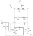
이제 도 2를 참조하면, 서셉터 배열체(110)의 유도 가열을 위한 공진 회로인 예시적 회로(150)가 예시되어 있다. 공진 회로(150)는 병렬로 연결된 유도성 요소(158) 및 커패시터(156)를 포함한다.Referring now to FIG. 2 , an
공진 회로(150)는 이 예에서, 제1 트랜지스터(M1) 및 제2 트랜지스터(M2)를 포함하는 스위칭 배열체(M1, M2)를 포함한다. 제1 트랜지스터(M1) 및 제2 트랜지스터(M2) 각각은 개개의 제1 단자(G1, G2), 제2 단자(D1, D2) 및 제3 단자(S1, S2)를 포함한다. 제1 트랜지스터(M1) 및 제2 트랜지스터(M2)의 제2 단자들(D1, D2)은 아래에서 더 상세하게 설명될 바와 같이, 병렬 유도 요소(158) 및 커패시터(156) 조합의 양 측에 연결된다. 제1 트랜지스터(M1) 및 제2 트랜지스터(M2)의 제3 단자들(S1, S2)은 각각 접지(151)에 연결된다. 도 2에 예시된 예에서, 제1 트랜지스터(M1) 및 제2 트랜지스터(M2) 둘 모두는 MOSFET들이고, 제1 단자들(G1, G2)은 게이트 단자들이고, 제2 단자들(D1, D2)은 드레인 단자들이고, 제3 단자들(S1, S2)은 소스 단자들이다.The
대안적 예들에서, 위에서 설명된 MOSFET들 대신에 다른 유형들의 트랜지스터들이 사용될 수 있다는 것이 인식될 것이다.In alternative examples, it will be appreciated that other types of transistors may be used in place of the MOSFETs described above.
공진 회로(150)는 인덕턴스(L) 및 커패시턴스(C)를 갖는다. 공진 회로(150)의 인덕턴스(L)는 유도성 요소(158)에 의해 제공되고, 또한 유도성 요소(158)에 의한 유도 가열을 위해 배열된 서셉터 배열체(110)의 인덕턴스에 의해 영향을 받을 수 있다. 서셉터 배열체(110)의 유도 가열은, 위에서 설명된 방식으로 서셉터 배열체(110)에서 줄 가열 및/또는 자기 히스테리시스 손실들을 유도하는 유도성 요소(158)에 의해 발생되는 가변 자기장을 통해 이루어진다. 공진 회로(150)의 인덕턴스(L)의 일부분은 서셉터 배열체(110)의 자기 투자율(magnetic permeability)에 기인할 수 있다. 유도성 요소(158)에 의해 발생되는 가변 자기장은 유도성 요소(158)를 통해 흐르는 가변 전류, 예컨대, 교류에 의해 발생된다.The
유도성 요소(158)는 예컨대, 코일형 전도성 요소의 형태일 수 있다. 예컨대, 유도성 요소(158)는 구리 코일일 수 있다. 유도성 요소(158)는 예컨대, 리츠 와이어(Litz wire)와 같은 다중-스트랜디드 와이어(multi-stranded wire), 예컨대, 함께 꼬인 다수의 개별적으로 절연된 와이어들을 포함하는 와이어를 포함할 수 있다. 다중-스트랜디드 와이어의 AC 저항은 주파수의 함수이고, 다중-스트랜디드 와이어는 구동 주파수에서 유도성 요소의 전력 흡수가 감소하도록 구성될 수 있다. 다른 예로서, 유도성 요소(158)는 예컨대, 인쇄 회로 기판 상의 코일형 트랙일 수 있다. 인쇄 회로 기판 상에 코일형 트랙을 사용하는 것은, 그것이 다중-스트랜디드 와이어(이는 고가일 수 있음)에 대한 임의의 요건을 제거하는 단면을 갖는 강성 및 자기-지지형 트랙을 제공하므로 유용할 수 있으며, 이는 저비용으로 높은 재현성으로 대량 생산될 수 있다. 하나의 유도성 요소(158)가 도시되어 있지만, 하나 이상의 서셉터 배열체들(110)의 유도 가열을 위해 배열된 하나 초과의 유도성 요소(158)가 존재할 수 있다는 것이 쉽게 인식될 것이다.
공진 회로(150)의 커패시턴스(C)는 커패시터(156)에 의해 제공된다. 커패시터(156)는 예컨대, 클래스 1 세라믹 커패시터, 예컨대, COG 유형 커패시터일 수 있다. 총 커패시턴스(C)는 또한 공진 회로(150)의 부유 커패시턴스를 포함할 수 있지만, 이것은 커패시터(156)에 의해 제공되는 커패시턴스와 비교하여 무시할 수 있거나 또는 무시될 수 있다.The capacitance C of
공진 회로(150)의 저항은 도 2에 도시되어 있지 않지만, 회로의 저항은 공진 회로(150)의 구성요소들을 연결하는 트랙 또는 와이어의 저항, 인덕터(158)의 저항 및/또는 인덕터(158)와의 에너지 전달을 위해 배열된 서셉터 배열체(110)에 의해 제공되는 공진 회로(150)를 통해 흐르는 전류에 대한 저항에 의해 제공될 수 있다는 것이 인식되어야 한다. 일부 예들에서, 하나 이상의 전용 저항기들(도시되지 않음)은 공진 회로(150)에 포함될 수 있다.Although the resistance of the
공진 회로(150)는 DC 전원(104)(도 1 참조)으로부터, 예컨대, 배터리로부터 제공되는 DC 공급 전압(V1)이 공급된다. DC 전압 공급 장치(V1)의 양극 단자는 제1 지점(159) 및 제2 지점(160)에서 공진 회로(150)에 연결된다. DC 전압 공급 장치(V1)의 음극 단자(도시되지 않음)는 접지(151)에 연결되고, 따라서, 이 예에서는, MOSFET들(M1 및 M2) 둘 모두의 소스 단자들(S)에 연결된다. 예들에서, DC 공급 전압(V1)은 배터리로부터 직접적으로 또는 중간 요소를 통해 공진 회로에 공급될 수 있다.The
따라서, 공진 회로(150)는 브리지의 2개의 아암들 사이에 병렬로 연결된 유도성 요소(158) 및 커패시터(156)와 함께 전기 브리지로서 연결되는 것으로 간주될 수 있다. 공진 회로(150)는 아래에 설명되는 스위칭 효과를 생성하도록 작용하며, 이는 가변, 예컨대, 교류가 유도성 요소(158)를 통해 인출되어(drawn), 따라서 교류 자기장을 생성하고 서셉터 배열체(110)를 가열하게 한다.Thus,
제1 지점(159)은 유도성 요소(158)와 커패시터(156)의 병렬 조합의 제1 측에 위치된 제1 노드(A)에 연결된다. 제2 지점(160)은 유도성 요소(158)와 커패시터(156)의 병렬 조합의 제2 측으로의 제2 노드(B)에 연결된다. 제1 초크 인덕터(161)는 제1 지점(159)과 제1 노드(A) 사이에 직렬로 연결되고, 제2 초크 인덕터(162)는 제2 지점(160)과 제2 노드(B) 사이에 직렬로 연결된다. 제1 및 제2 초크들(161 및 162)은 제1 지점(159) 및 제2 지점(160)으로부터 각각 회로에 들어가는 것으로부터 AC 주파수들을 필터링하지만 DC 전류가 인덕터(158)로 그리고 이를 통해 인출될 수 있게 하도록 작용한다. 초크들(161 및 162)은 A 및 B의 전압이 제1 지점(159) 또는 제2 지점(160)에서 가시적 효과들이 거의 없거나 또는 전혀 없이 발진(oscillate)할 수 있게 한다.
이 특정 예에서, 제1 MOSFET(M1) 및 제2 MOSFET(M2)은 n-채널 향상 모드 MOSFET들이다. 제1 MOSFET(M1)의 드레인 단자는 도선(conducting wire) 등을 통해 제1 노드(A)에 연결되지만, 제2 MOSFET(M2)의 드레인 단자는 도선 등을 통해 제2 노드(B)에 연결된다. 각각의 MOSFET(M1, M2)의 소스 단자는 접지(151)에 연결된다.In this particular example, the first MOSFET M1 and the second MOSFET M2 are n-channel enhancement mode MOSFETs. The drain terminal of the first MOSFET (M1) is connected to the first node (A) through a conducting wire or the like, but the drain terminal of the second MOSFET (M2) is connected to the second node (B) through a conducting wire or the like. do. The source terminal of each MOSFET (M1, M2) is connected to ground (151).
공진 회로(150)는, 게이트 전압 공급 장치(또는 때때로 본원에서 제어 전압으로 지칭됨)인 제2 전압원(V2)을 포함하며, 그것의 양극 단자는 제1 및 제2 MOSFET들(M1 및 M2)의 게이트 단자들(G1, G2)에 전압을 공급하기 위해 사용되는 제3 지점(165)에 연결된다. 이 예에서, 제3 지점(165)에 공급되는 제어 전압(V2)은 제1 및 제2 지점들(159, 160)에 공급되는 전압(V1)과는 무관하며, 이는 제어 전압(V2)에 영향을 주지 않고 전압(V1)의 변동을 가능하게 한다. 제1 풀-업 저항기(pull-up resistor)(163)는 제3 지점(165)과 제1 MOSFET(M1)의 게이트 단자(G1) 사이에 연결된다. 제2 풀-업 저항기(164)는 제3 지점(165)과 제2 MOSFET(M2)의 게이트 단자(G2) 사이에 연결된다.
다른 예들에서, 상이한 유형의 FET와 같은 상이한 유형의 트랜지스터가 사용될 수 있다. 아래에서 설명되는 스위칭 효과는 "온" 상태로부터 "오프" 상태로 스위칭할 수 있는 상이한 유형의 트랜지스터에 대해 동일하게 달성될 수 있다는 것이 인식될 것이다. 공급 전압들(V1 및 V2)의 값들 및 극성들은 사용되는 트랜지스터 및 회로의 다른 구성요소들의 특성들과 함께 선택될 수 있다. 예컨대, 공급 전압들은 n-채널 트랜지스터가 사용되는지 아니면 p-채널 트랜지스터가 사용되는지에 따라, 또는 트랜지스터가 연결된 구성에 따라, 또는 트랜지스터가 온 또는 오프 상태에 있게 하는 트랜지스터의 단자들에 걸쳐 인가된 전위차의 차이에 따라 선택될 수 있다.In other examples, different types of transistors may be used, such as different types of FETs. It will be appreciated that the switching effect described below can equally be achieved for different types of transistors capable of switching from an "on" state to an "off" state. The values and polarities of the supply voltages V1 and V2 may be chosen along with the characteristics of the transistor used and other components of the circuit. For example, the supply voltages depend on whether an n-channel transistor or a p-channel transistor is used, or the configuration in which the transistor is connected, or the difference in potential applied across the terminals of the transistor that causes the transistor to be in an on or off state. can be selected according to the difference in
공진 회로(150)는 제1 다이오드(d1) 및 제2 다이오드(d2)를 더 포함하는데, 이는 이 예에서는, 쇼트키 다이오드들(Schottky diodes)이지만, 다른 예들에서는 임의의 다른 적합한 유형의 다이오드가 사용될 수 있다. 제1 MOSFET(M1)의 게이트 단자(G1)는 제1 다이오드(d1)를 통해 제2 MOSFET(M2)의 드레인 단자(D2)에 연결되며, 제1 다이오드(d1)의 순방향은 제2 MOSFET(M2)의 드레인(D2)을 향한다.
제2 MOSFET(M2)의 게이트 단자(G2)는 제2 다이오드(d2)를 통해 제1의 제2 MOSFET(M1)의 드레인(D1)에 연결되며, 제2 다이오드(d2)의 순방향은 제1 MOSFET(M1)의 드레인(D1)을 향한다. 제1 및 제2 쇼트키 다이오드들(d1 및 d2)은 약 0.3V의 다이오드 임계 전압을 가질 수 있다. 다른 예들에서, 약 0.7V의 다이오드 임계 전압을 갖는 실리콘 다이오드들이 사용될 수 있다. 예들에서, 사용되는 다이오드의 유형은 MOSFET들(M1 및 M2)의 원하는 스위칭을 가능하게 하기 위해 게이트 임계 전압과 함께 선택된다. 다이오드 및 게이트 공급 전압(V2)의 유형은 또한 풀-업 저항기들(163 및 164)의 값들뿐만 아니라 공진 회로(150)의 다른 구성요소들과 함께 선택될 수 있다는 것이 인식될 것이다.The gate terminal (G2) of the second MOSFET (M2) is connected to the drain (D1) of the first second MOSFET (M1) through the second diode (d2), and the forward direction of the second diode (d2) is connected to the first It goes to the drain (D1) of MOSFET (M1). The first and second Schottky diodes d1 and d2 may have a diode threshold voltage of about 0.3V. In other examples, silicon diodes with a diode threshold voltage of about 0.7V may be used. In the examples, the type of diode used is selected along with the gate threshold voltage to enable the desired switching of MOSFETs M1 and M2. It will be appreciated that the type of diode and gate supply voltage V2 may also be selected along with the values of pull-up
공진 회로(150)는 제1 및 제2 MOSFET들(M1 및 M2)의 스위칭으로 인한 가변 전류인, 유도성 요소(158)를 통한 전류를 지원한다. 이 예에서, MOSFET들(M1 및 M2)은 향상 모드 MOSFET들이기 때문에, 제1 및 제2 MOSFET들 중 하나의 게이트 단자(G1, G2)에 인가된 전압이, 게이트-소스 전압이 그 MOSFET에 대해 미리 결정된 임계치보다 높도록 할 때, MOSFET은 온(ON) 상태로 턴된다. 그런 다음, 전류는 드레인 단자(D1, D2)로부터 접지(151)에 연결된 소스 단자(S1, S2)로 흐를 수 있다. 이 온(ON) 상태에서 MOSFET의 직렬 저항은 회로의 작동을 위해 무시할 수 있고, MOSFET이 온(ON) 상태에 있을 때 드레인 단자(D)는 접지 전위에 있는 것으로 간주될 수 있다. MOSFET에 대한 게이트-소스 임계치는 공진 회로(150)에 대한 임의의 적합한 값일 수 있으며, 전압(V2)의 크기 및 저항기들(164 및 163)의 저항들은 MOSFET들(M1 및 M2)의 게이트-소스 임계 전압에 따라 선택되어, 본질적으로 전압(V2)이 게이트 임계 전압(들)보다 크다는 것이 인식될 것이다.
유도성 요소(158)를 통해 흐르는 가변 전류를 초래하는 공진 회로(150)의 스위칭 절차는 이제, 제1 노드(A)의 전압이 높고 제2 노드(B)의 전압이 낮은 조건으로부터 시작하여 설명될 것이다.The switching procedure of
노드(A)의 전압이 높을 때, 제1 MOSFET(M1)의 드레인 단자(D1)가 이 예에서는 도선을 통해 노드(A)에 직접적으로 연결되기 때문에, M1의 드레인 단자(D1)의 전압이 또한 높다. 동시에, 노드(B)의 전압은 낮게 유지되고, 제2 MOSFET(M2)의 드레인 단자(D2)의 전압은 대응적으로 낮다(이 예에서는, M2의 드레인 단자가 도선을 통해 노드(B)에 직접적으로 연결됨).When the voltage at node A is high, since the drain terminal D1 of the first MOSFET M1 is directly connected to the node A through a conducting wire in this example, the voltage at the drain terminal D1 of M1 is Also high. At the same time, the voltage at node B is kept low, and the voltage at drain terminal D2 of second MOSFET M2 is correspondingly low (in this example, the drain terminal of M2 is connected to node B via a lead). directly linked).
따라서, 이때에, M1의 드레인 전압 값은 높고, M2의 게이트 전압보다 크다. 따라서, 이때에, 제2 다이오드(d2)는 역방향 바이어스된다(reverse-biased). 이때에, M2의 게이트 전압은 M2의 소스 단자 전압보다 크고, 전압(V2)은 M2의 게이트-소스 전압이 MOSFET(M2)에 대한 온(ON) 임계치보다 크도록 된다. 따라서, 이때에, M2는 온(ON)이다.Therefore, at this time, the value of the drain voltage of M1 is high and is greater than the gate voltage of M2. Accordingly, at this time, the second diode d2 is reverse-biased. At this time, the gate voltage of M2 is greater than the source terminal voltage of M2, and the voltage V2 is such that the gate-source voltage of M2 is greater than the ON threshold for MOSFET M2. Accordingly, at this time, M2 is ON.
동시에, M2의 드레인 전압은 낮고, 제1 다이오드(d1)는 M1의 게이트 단자에 대한 게이트 전압 공급 장치(V2)로 인해 순방향 바이어스된다(forward biased). 따라서, M1의 게이트 단자는 순방향 바이어스된 제1 다이오드(d1)를 통해 제2 MOSFET(M2)의 저전압 드레인 단자에 연결되고, 따라서, M1의 게이트 전압이 또한 낮다. 다시 말해서, M2가 온(on)되기 때문에, 그것은 접지 클램프로서 역할을 하고 있으며, 이는 제1 다이오드(d1)가 순방향 바이어스되게 하고, M1의 게이트 전압이 낮아지게 한다. 이로써, M1의 게이트-소스 전압은 온(ON) 임계치 미만이고, 제1 MOSFET(M1)는 오프(OFF)된다.At the same time, the drain voltage of M2 is low and the first diode d1 is forward biased due to the gate voltage supply V2 to the gate terminal of M1. Therefore, the gate terminal of M1 is connected to the low voltage drain terminal of the second MOSFET (M2) through the forward biased first diode (d1), and thus the gate voltage of M1 is also low. In other words, since M2 is on, it is acting as a ground clamp, which causes the first diode d1 to be forward biased and the gate voltage of M1 to go low. As a result, the gate-source voltage of M1 is less than the ON threshold, and the first MOSFET M1 is turned OFF.
요약하면, 이 지점에서, 회로(150)는 제1 상태에 있으며, 여기서:In summary, at this point,
노드(A)의 전압은 높고;The voltage at node A is high;
노드(B)의 전압은 낮고;The voltage at node B is low;
제1 다이오드(d1)는 순방향 바이어스되고;the first diode d1 is forward biased;
제2 MOSFET(M2)은 온(ON)이고;the second MOSFET (M2) is ON;
제2 다이오드(d2)는 역방향 바이어스되고; 그리고the second diode d2 is reverse biased; and
제1 MOSFET(M1)은 오프(OFF)이다.The first MOSFET (M1) is off (OFF).
이 지점으로부터, 제2 MOSFET(M2)이 온(ON) 상태에 있고, 제1 MOSFET(M1)이 오프(OFF) 상태에 있는 경우, 전류는 제1 초크(161)를 통해 그리고 유도성 요소(158)를 통해 공급 장치(V1)로부터 인출된다. 유도 초크(161)의 존재로 인해, 노드(A)의 전압은 자유롭게 발진한다. 유도성 요소(158)가 커패시터(156)와 병렬로 되어있기 때문에, 노드(A)에서 관측된 전압은 절반 정현파 전압 프로파일(half sinusoidal voltage profile)의 전압을 따른다. 노드(A)에서 관측된 전압의 주파수는 회로(150)의 공진 주파수(
노드(A)의 전압은 노드(A)에서의 에너지 감쇠의 결과로 그것의 최대 값으로부터 0을 향해 시간이 지남에 따라 정현파로 감소한다. 노드(B)의 전압은 낮게 유지되고(MOSFET(M2)가 온(on)되기 때문에) 인덕터(L)는 DC 공급 장치(V1)로부터 충전된다. MOSFET(M2)은 노드(A)의 전압이 M2의 게이트 임계 전압 + d2의 순방향 바이어스 전압 이하인 시점에 스위칭 오프된다. 노드(A)의 전압이 마침내 0에 도달할 때, MOSFET(M2)은 완전히 오프될 것이다.The voltage at node A decreases sinusoidally over time from its maximum value towards zero as a result of energy decay at node A. The voltage at node B is kept low (because MOSFET M2 is on) and inductor L is charged from DC supply V1. MOSFET M2 is switched off when the voltage at node A is less than the gate threshold voltage of M2 + the forward bias voltage of d2. When the voltage at node A finally reaches zero, MOSFET M2 will be completely off.
동시에 또는 직후에, 노드(B)의 전압이 높아진다. 이것은 유도성 요소(158)와 커패시터(156) 사이의 에너지의 공진 전달로 인해 발생한다. 이러한 에너지의 공진 전달로 인해 노드(B)의 전압이 높아질 때, 노드들(A 및 B)과 MOSFET들(M1 및 M2)에 대해 위에서 설명된 상황이 반전된다. 즉, A의 전압이 0을 향해 감소함에 따라, M1의 드레인 전압이 감소된다. M1의 드레인 전압은 제2 다이오드(d2)가 더 이상 역방향 바이어스되지 않고 순방향 바이어스되는 지점까지 감소된다. 유사하게, 노드(B)의 전압은 그것의 최대치로 상승하고, 제1 다이오드(d1)는 순방향 바이어스되는 것으로부터 역방향 바이어스되는 것으로 스위칭한다. 이것이 발생함에 따라, M1의 게이트 전압은 더 이상 M2의 드레인 전압에 커플링되지 않고, 따라서 M1의 게이트 전압은 게이트 공급 전압(V2)의 인가 하에서 높아진다. 따라서, 제1 MOSFET(M1)은, 그것의 게이트-소스 전압이 이제 스위치-온에 대한 임계치 초과이기 때문에, 온(ON) 상태로 스위칭된다. M2의 게이트 단자가 이제 순방향 바이어스된 제2 다이오드(d2)를 통해 M1의 저전압 드레인 단자에 연결되므로, M2의 게이트 전압은 낮다. 따라서, M2는 오프(OFF) 상태로 스위칭된다.At the same time or immediately after, the voltage at node B is raised. This occurs due to resonant transfer of energy between
요약하면, 이 지점에서, 회로(150)는 제2 상태에 있으며, 여기서:In summary, at this point,
노드(A)의 전압은 낮고;The voltage at node A is low;
노드(B)의 전압은 높고;The voltage at node B is high;
제1 다이오드(d1)는 역방향 바이어스되고;the first diode d1 is reverse biased;
제2 MOSFET(M2)은 오프(OFF)이고;the second MOSFET (M2) is OFF;
제2 다이오드(d2)는 순방향 바이어스되고; 그리고the second diode d2 is forward biased; and
제1 MOSFET(M1)은 온(ON)이다.The first MOSFET (M1) is on (ON).
이 지점에서, 전류는 제2 초크(162)를 통해 공급 전압(V1)으로부터 유도성 요소(158)를 통해 인출된다. 따라서, 전류의 방향은 공진 회로(150)의 스위칭 작동으로 인해 반전되었다. 공진 회로(150)는, 제1 MOSFET(M1)이 오프(OFF)되고 제2 MOSFET(M2)이 온(ON)되는 위에서 설명된 제1 상태와 제1 MOSFET(M1)이 온(ON)되고 제2 MOSFET(M2)이 오프(OFF)되는 위에서 설명된 제2 상태 사이를 계속 스위칭할 것이다.At this point, current is drawn through the
정상 작동 상태에서, 에너지는 정전 도메인(electrostatic domain)(즉, 커패시터(156)에서)과 자기 도메인(magnetic domain)(즉, 인덕터(158)) 사이에서 전달되며, 그 반대도 마찬가지이다.In normal operating conditions, energy is transferred between the electrostatic domain (ie, in capacitor 156) and the magnetic domain (ie, inductor 158) and vice versa.
순 스위칭 효과는 정전 도메인(즉, 커패시터(156)에서)과 자기 도메인(즉, 인덕터(158)) 사이에 에너지 전달이 있는 공진 회로(150)의 전압 발진들에 응답하여, 따라서 병렬 LC 회로의 시변 전류를 생성하며, 이는 공진 회로(150)의 공진 주파수에서 변한다. 이것은, 회로(150)가 그것의 최적의 효율 레벨에서 작동하고, 따라서 공진을 차단하는 회로와 비교하여 에어로졸 발생 재료(116)의 더 효율적 가열을 달성하기 때문에, 유도성 요소(158)와 서셉터 배열체(110) 사이의 에너지 전달에 유리하다. 설명된 스위칭 배열체는, 예컨대, 상이한 서셉터가 유도 요소에 커플링될 때, 회로(150)가 가변 로드 조건들 하에서 공진 주파수에서 스스로 구동할 수 있게 하므로 유리하다. 이것이 의미하는 것은, 회로(150)의 특성들이 변화하는 경우(예컨대, 서셉터(110)가 존재하거나 또는 존재하지 않는 경우, 또는 서셉터의 온도가 변화하거나 또는 심지어 서셉터 요소(110)의 물리적 움직임이 변화하는 경우), 회로(150)의 동적 특성이 최적의 방식으로 에너지를 전달하기 위해 그것의 공진 지점을 계속적으로 적응시키고, 따라서 회로(150)가 항상 공진 상태에서 구동된다는 것을 의미한다는 것이다. 더욱이, 회로(150)의 구성은 스위칭을 수행하기 위해 MOSFET들의 게이트들에 제어 전압 신호들을 인가하기 위해 외부 제어기 등이 요구되지 않도록 한다.The net switching effect is in response to voltage oscillations in the
위에서 설명된 예들에서, 도 2를 참조하면, 게이트 단자들(G1, G2)에는 소스 전압(V1)에 대한 전력 공급 장치와 상이한 제2 전력 공급 장치를 통해 게이트 전압이 공급된다. 그러나, 일부 예들에서, 게이트 단자들에는 소스 전압(V1)과 동일한 전압 공급 장치가 공급될 수 있다. 그러한 예들에서, 회로(150)의 제1 지점(159), 제2 지점(160) 및 제3 지점(165)은 예컨대, 동일한 파워 레일(power rail)에 연결될 수 있다. 그러한 예들에서, 회로의 구성요소들의 특성들은 설명된 스위칭 동작이 발생할 수 있게 하도록 선택되어야 한다는 것이 인식될 것이다. 예컨대, 게이트 공급 전압 및 다이오드 임계 전압들은 회로의 발진들이 적절한 레벨에서 MOSFET들의 스위칭을 트리거하도록 선택되어야 한다. 게이트 공급 전압(V2) 및 소스 전압(V1)에 대한 별개의 전압 값들의 제공은, 소스 전압(V1)이, 회로의 스위칭 기구(switching mechanism)의 작동에 영향을 미치지 않고 게이트 공급 전압(V2)과 무관하게 변할 수 있게 한다.In the examples described above, referring to FIG. 2 , the gate terminals G1 and G2 are supplied with a gate voltage through a second power supply different from the power supply for the source voltage V1. However, in some examples, a voltage supply equal to the source voltage V1 may be supplied to the gate terminals. In such examples,
회로(150)의 공진 주파수(


공진 회로(150)의 특성들은 주어진 서셉터 배열체(110)에 대한 다른 팩터들에 기반하여 선택될 수 있다는 것이 또한 인식될 것이다. 예컨대, 유도성 요소(158)로부터 서셉터 배열체(110)로의 에너지 전달을 개선하기 위해, 서셉터 배열체(110)의 재료 특성들에 기반하여 스킨 깊이(즉, 전류 밀도가, 적어도 주파수의 함수인 1/e 만큼 떨어지는 서셉터 배열체(110)의 표면으로부터의 깊이)를 선택하는 것이 유용할 수 있다. 스킨 깊이는 서셉터 배열체들(110)의 상이한 재료들에 대해 상이하며, 구동 주파수가 증가함에 따라 감소한다. 다른 한편으로, 예컨대, 전자장치 내에서 열로 손실되는 공진 회로(150) 및/또는 구동 요소(102)에 공급되는 전력의 비율을 감소시키기 위해, 상대적으로 더 낮은 주파수들에서 스스로 구동하는 회로를 갖는 것이 유익할 수 있다. 이 예에서는, 구동 주파수가 공진 주파수와 동일하기 때문에, 구동 주파수와 관련한 여기서의 고려사항들은 예컨대, 서셉터 배열체(110)를 설계하고 그리고/또는 특정 커패시턴스를 갖는 커패시터(156) 및 특정 인덕턴스를 갖는 유도성 요소(158)를 사용함으로써 적절한 공진 주파수를 획득하는 것과 관련하여 이루어진다. 따라서, 일부 예들에서, 이러한 팩터들 사이의 절충이 적절하게 그리고/또는 원하는 대로 선택될 수 있다.It will also be appreciated that the characteristics of the
도 2의 공진 회로(150)는 전류(I)가 최소화되고 동적 저항이 최대화되는 공진 주파수(
일부 예들에서, 공진 회로(150)에 의한 서셉터 배열체(110)의 유도 가열은 공진 회로(150)에 제공되는 공급 전압을 제어함으로써 제어될 수 있으며, 이는 차례로 공진 회로(150)에 흐르는 전류를 제어할 수 있고, 따라서 공진 회로(150)에 의해 서셉터 배열체(110)에 전달되는 에너지, 및 따라서 서셉터 배열체(110)가 가열되는 정도를 제어할 수 있다. 다른 예들에서, 서셉터 배열체(110)의 온도는 예컨대, 서셉터 배열체(110)가 더 큰 정도로 가열될 것인지 아니면 더 적은 정도로 가열될 것인지에 따라 유도성 요소(158)에 대한 전압 공급 장치를 변화시킴으로써(예컨대, 공급된 전압의 크기를 변화시킴으로써 또는 펄스 폭 변조 전압 신호의 듀티 사이클을 변화시킴으로써) 모니터링되고 제어될 수 있다는 것이 인식될 것이다.In some examples, inductive heating of
위에서 언급된 바와 같이, 공진 회로(150)의 인덕턴스(L)는 서셉터 배열체(110)의 유도 가열을 위해 배열된 유도성 요소(158)에 의해 제공된다. 공진 회로(150)의 인덕턴스(L)의 적어도 일부분은 서셉터 배열체(110)의 자기 투자율에 기인한다. 따라서, 공진 회로(150)의 인덕턴스(L) 및 따라서 공진 주파수(
도 3은 공진 회로(250)의 제2 예를 도시한다. 제2 공진 회로(250)는 공진 회로(150)와 동일한 구성요소들 중 많은 구성요소를 포함하고, 공진 회로들(150, 250) 각각의 동일한 구성요소들에는 동일한 참조 번호들이 제공되며, 다시 상세히 설명되지 않을 것이다.3 shows a second example of a
제2 회로(250)는, 제2 회로(250)가 다이오드들(d1, d2)을 포함하지 않는다는 점에서 제1 회로(150)와 상이하고, 다이오드들(d1, d2)을 통해 트랜지스터들(M1, M2) 각각의 게이트 단자들(G1, G2)이 트랜지스터들(M1, M2) 중 다른 것의 드레인 단자들(D1, D2)에 각각 연결된다. 제1 회로(150)에 포함되는 다이오드들(d1, d2) 대신에, 제2 회로(250)는 제3 MOSFET(M3) 및 제4 MOSFET(M4)을 포함한다.The
제2 회로(250)에서, 제1 MOSFET(M1)의 게이트(G1)는 제3 MOSFET(M3)을 통해 제2 MOSFET(M2)의 드레인(D2)에 연결된다. 제2 MOSFET(M2)의 게이트(G2)는 유사하게 제4 MOSFET(M4)을 통해 제1 MOSFET(M1)의 드레인(D1)에 연결된다. 제어 전압(V2)은 지점(165)으로부터 제3 MOSFET(M3) 및 제4 MOSFET(M4) 둘 모두의 게이트 단자들(G3, G4)에 공급된다. 도 3에 표현된 예와 같은 예에서, 제3 MOSFET(M3) 및 제4 MOSFET(M4)의 게이트 단자들(G3, G4)은 전기 전도체, 예컨대, 전기 트랙을 통해 서로 연결되고, 전압(V2)이 전기 전도체의 한 지점에 공급된다. 제3 MOSFET(M3) 및 제4 MOSFET(M4) 각각은, 게이트 임계 전압보다 큰 전압이 MOSFET의 게이트 단자들(G3, G4)에 인가될 때, 전류가 MOSFET의 드레인 단자로부터 MOSFET의 소스 단자로 흐를 수 있도록 개개의 MOSFET들(M3, M4)이 턴 오프되도록 하는 게이트 임계 전압을 갖는다는 것이 인지될 것이다. 예들에서, 전압(V2)은, 제어 전압(V2)을 인가하는 것이 제3 및 제4 MOSFET들(M3, M4)을 온(ON) 상태로 턴하도록 제3 및 제4 MOSFET들(M3, M4)의 임계 전압들보다 더 크다. 예에서, 제3 MOSFET(M3)의 임계 전압은 제4 MOSFET(M4)의 임계 전압과 동일하다. 일부 예들에서, 제2 회로(250)는, 제1 및 제2 MOSFET들(M1, M2)의 게이트들(G1, G2)과 접지 사이에 연결된 하나 이상의 풀-다운 저항기들(도 3에 도시되지 않음)을 포함할 수 있다.In the
제2 회로(250)는, 도 2를 참조로 제1 예시적인 회로(150)를 참조하여 설명된 방식으로 가변 전류가 유도성 요소(158)를 통해 흐르게 하는 자기-발진 회로(self-oscillating circuit)로서 동작한다. 다이오드들(d1, d2)보다는 MOSFET들(M3, M4)의 사용으로 인한 제1 예시적인 회로(150)의 거동과 제2 회로(250)의 거동의 차이들은 다음 설명으로부터 명백해질 것이다.The
유도성 요소(158)를 통해 흐르는 가변 전류를 발생시키는 제2 회로(250)의 스위칭 절차가 이제 설명될 것이다.The switching procedure of the
전압(V2)이 제3 및 제4 MOSFET들(M3, M4)의 게이트들(G3, G4)에 인가될 때, 제3 및 제4 MOSFET들이 턴 "온"된다. 이 지점에서, 그 전압(V1)을 제공하면, 제1, 제2, 제3 및 제4 MOSFET들(M1-M4) 각각은 온(ON) 상태에 있다. 이 지점에서, 노드들(A 및 B)의 전압들이 강하하기 시작한다. 회로(250)에서 특정 불균형들, 예컨대, MOSFET들(M1-M4) 사이의 저항의 차이들, 또는 회로에 존재하는 인덕터들의 값들의 특성들이 존재할 수 있다. 이러한 불균형들은, 노드들(A 또는 B) 중 하나의 전압이 이들 노드들(A, B) 중 다른 노드의 전압보다 더 빠르게 강하하기 시작하도록 작용한다. 전압이 가장 빠르게 강하하는 노드(A, B)에 대응하는 MOSFET들(M1, M2)은 온(ON) 상태로 유지될 것이다. 노드들(A, B) 중 다른 노드에 대응하는, MOSFET들(M1, M2) 중 다른 하나는 오프(OFF) 상태로 스위칭된다. 다음은, 노드(A)의 전압이 발진하기 시작하고 노드(B)의 전압이 0으로 유지되는 상황을 설명한다. 그러나, 동일하게, 노드(A)의 전압이 0V로 유지되는 동안, 발진을 시작하는 노드(B)의 전압이 이에 해당하는 경우일 수 있다.When voltage V2 is applied to the gates G3 and G4 of the third and fourth MOSFETs M3 and M4, the third and fourth MOSFETs are turned on. At this point, providing the voltage V1, each of the first, second, third and fourth MOSFETs M1-M4 is in an on state. At this point, the voltages of nodes A and B start to drop. There may be certain imbalances in
노드(A)의 전압이 상승할 때, 제1 MOSFET(M1)의 드레인 단자(D1)가 도선을 통해 노드(A)에 연결되기 때문에, 제1 MOSFET(M1)의 드레인 단자(D1)의 전압이 또한 상승한다. 동시에, 노드(B)의 전압은 낮게 유지되고, 제2 MOSFET(M2)의 드레인 단자(D2)의 전압은 대응적으로 낮다(이 예에서는, 제2 MOSFET(M2)의 드레인 단자(D2)가 도선을 통해 노드(B)에 직접적으로 연결됨).When the voltage of node A rises, since the drain terminal D1 of the first MOSFET M1 is connected to the node A through a wire, the voltage of the drain terminal D1 of the first MOSFET M1 this also rises At the same time, the voltage at node B remains low, and the voltage at the drain terminal D2 of the second MOSFET M2 is correspondingly low (in this example, the drain terminal D2 of the second MOSFET M2 is directly connected to node (B) via a lead wire).
제1 MOSFET(M1)의 노드(A) 및 드레인(D1)의 전압이 상승함에 따라, 제2 MOSFET(M2)의 게이트(G2)의 전압이 상승한다. 이는, 드레인(D1)이 제4 MOSFET(M4)을 통해 제2 MOSFET(M2)의 게이트(G2)에 연결되는 것 및 제4 MOSFET(M4)이 자신의 게이트 단자(G4)에 인가되는 전압(V2)으로 인해 "온"되기 때문이다.As the voltages of the node A and the drain D1 of the first MOSFET M1 increase, the voltage of the gate G2 of the second MOSFET M2 increases. This means that the drain D1 is connected to the gate G2 of the second MOSFET M2 through the fourth MOSFET M4 and the voltage applied to the gate terminal G4 of the fourth MOSFET M4 ( V2) because it is "on".
제1 MOSFET(M1)의 드레인(D1)의 전압이 상승함에 따라, 제2 MOSFET(M2)의 게이트(G2)의 전압은, 최대 전압 값(Vmax)에 도달할 때까지 계속 상승한다. 제2 MOSFET(M2)의 게이트(G2)에 도달한 최대 전압 값(Vmax)은 제어 전압(V2) 및 제4 MOSFET(M4)의 게이트-소스 전압(VgsM4)에 의존한다. 최대 값(Vmax)은 Vmax = V2-VgsM4로 표현될 수 있다.As the voltage of the drain (D1) of the first MOSFET (M1) rises, the voltage of the gate (G2) of the second MOSFET (M2) continues to rise until it reaches the maximum voltage value (Vmax ). The maximum voltage value (Vmax ) reached at the gate (G2) of the second MOSFET (M2) depends on the control voltage (V2) and the gate-source voltage (VgsM4 ) of the fourth MOSFET (M4). The maximum value (Vmax ) can be expressed as Vmax = V2-VgsM4 .
회로(250)의 공진 주파수에서 절반 사이클(half cycle)의 발진 후에, 제1 MOSFET(M1)의 드레인(D1)의 전압이 감소하기 시작한다. 제1 MOSFET(M1)의 드레인(D1)의 전압은 0V에 도달할 때까지 감소한다. 이 지점에서, 제1 MOSFET(M1)은 "오프"에서 "온"으로 턴하고, 제2 MOSFET(M2)은 "온"에서 "오프"로 턴한다.After a half cycle of oscillation at the resonant frequency of
그런 다음, 회로는, 노드(B)가 자유롭게 발진하는 동안 노드(A)가 0V로 유지되는 것을 제외하고는, 위에서 설명한 방식과 유사한 방식으로 계속 발진한다. 즉, 그럼 다음, 제2 MOSFET(M2)의 드레인(D2) 및 노드(B)의 전압이 상승하기 시작하는 반면에, 제1 MOSFET(M1)의 드레인(D1) 및 노드(A)의 전압은 0으로 유지된다.The circuit then continues to oscillate in a manner similar to that described above, except that node A is held at 0V while node B is free to oscillate. That is, then, the voltage at the drain (D2) and node (B) of the second MOSFET (M2) starts to rise, while the voltage at the drain (D1) and node (A) of the first MOSFET (M1) is kept at 0.
제2 MOSFET(M2)의 드레인(D2) 및 노드(B)의 전압이 상승함에 따라, 드레인(D2)이 제3 MOSFET(M3)을 통해 제1 MOSFET(M1)의 게이트(G1)에 연결되기 때문에, 제1 MOSFET(M1)의 게이트(G1)의 전압이 상승하고, 제3 MOSFET(M3)은 전압(V2)이 자신의 게이트 단자(G3)에 인가되기 때문에 "온"이다.As the voltage of the drain (D2) and node (B) of the second MOSFET (M2) rises, the drain (D2) is connected to the gate (G1) of the first MOSFET (M1) through the third MOSFET (M3). Therefore, the voltage of the gate (G1) of the first MOSFET (M1) rises, and the third MOSFET (M3) is "on" because the voltage (V2) is applied to its gate terminal (G3).
제2 MOSFET(M2)의 드레인(D2)의 전압이 상승함에 따라, 제1 MOSFET(M1)의 게이트(G1)의 전압은 최대 전압 값(Vmax)에 도달할 때까지 계속 상승한다. 게이트(G1)에 도달한 최대 전압 값(Vmax)은 제어 전압(V2) 및 제3 MOSFET(M3)의 게이트-소스 전압(VgsM3)에 의존한다. 최대 값(Vmax)은 Vmax = V2-VgsM3로 표현될 수 있다. 이 예에서, 제3 및 제4 MOSFET들(M3, M4)의 게이트-소스 전압들은 서로 동일하고, 즉 VgsM3 = VgsM4이다.As the voltage of the drain (D2) of the second MOSFET (M2) increases, the voltage of the gate (G1) of the first MOSFET (M1) continues to rise until it reaches the maximum voltage value (Vmax ). The maximum voltage value (Vmax ) reached at the gate (G1) depends on the control voltage (V2) and the gate-source voltage (VgsM3 ) of the third MOSFET (M3). The maximum value (Vmax ) can be expressed as Vmax = V2-VgsM3 . In this example, the gate-source voltages of the third and fourth MOSFETs M3 and M4 are equal to each other, that is, VgsM3 = VgsM4 .
제2 회로(250)의 공진 주파수에서 절반 사이클의 발진 후에, 제2 MOSFET(M2)의 드레인(D2)의 전압이 감소하기 시작한다. 제2 MOSFET(M2)의 드레인(D2)의 전압은 0V에 도달할 때까지 감소한다. 이 지점에서, 제2 MOSFET(M2)은 "오프"에서 "온"으로 턴하고, 제1 MOSFET(M1)은 "온"에서 "오프"로 턴한다.After half cycle of oscillation at the resonant frequency of the
제1 예시적인 회로(150)를 참조하여 설명된 방식으로, 제2 MOSFET(M2)이 온(ON) 상태에 있고 제1 MOSFET(M1)이 오프(OFF) 상태에 있을 때, 전류는 공급 장치(V1)로부터 제1 초크(161)를 통해 그리고 유도성 요소(158)를 통해 인출된다. 제1 MOSFET(M1)이 온(ON) 상태에 있고 제2 MOSFET(M2)이 오프(OFF) 상태에 있을 때, 전류는 제2 초크(162)를 통해 그리고 유도성 요소(158)를 통해 공급 장치(V1)로부터 인출된다. 따라서, 제2 예시적인 회로(250)는 도 2의 제1 예시적인 회로(150)에 대해 설명된 방식과 동일한 방식으로 발진하며, 전류의 방향은 회로(250)의 각각의 스위칭 동작에 따라 반전된다.In the manner described with reference to the first
일부 예들에서, 제3 및 제4 MOSFET들(M3, M4)의 사용은, 더 낮은 에너지 손실들을 허용할 수 있기 때문에 유리할 수 있다. 즉, 제1 예시적인 회로(150)는, 풀-업 저항기들(163, 164)을 통한 접지(151)로의 일부 전류 인출로 인해 저항성 손실들을 초래할 수 있다. 예컨대, 제1 MOSFET(M1)이 온(ON) 상태일 때, 제2 다이오드(d2)가 순방향 바이어스되고, 따라서 작은 전류가 제2 풀-업 저항기(164)를 통해 인출되어, 저항성 손실들을 초래한다. 마찬가지로, 제2 MOSFET(M2)이 온(ON) 상태일 때, 제1 풀-업 저항기(163)를 통해 인출되는 전류로 인해 저항성 손실들이 존재할 수 있다. 예들에서 제2 예시적인 회로는 저항기들(163, 164)을 생략할 수 있다. 제2 예시적인 회로(250)는, 풀-업 저항기들(163, 164) 및 다이오드들(d1, d2)을 제3 및 제4 MOSFET들(M3, M4)로 대체함으로써 이러한 손실들을 감소시킬 수 있다. 예컨대, 제2 예시적인 회로(250)에서, 제1 MOSFET(M1)이 오프(OFF) 상태에 있을 때, 제3 MOSFET(M3)을 통해 인출된 전류는 본질적으로 0일 수 있다. 유사하게, 제2 예시적인 회로(250)에서, 제2 MOSFET(M2)이 오프 상태에 있을 때, 제4 MOSFET(M4)을 통해 인출된 전류는 본질적으로 0일 수 있다. 따라서, 저항성 손실들은 제2 회로(250)에 도시된 배열체를 사용함으로써 감소될 수 있다. 또한, 제1 MOSFET(M1) 및 제2 MOSFET(M2)의 게이트들(G1, G2)을 충전 및 방전하기 위한 에너지가 요구될 수 있다. 제2 회로(250)는 노드들(A 및 B)로부터 효과적으로 제공될 이 에너지를 제공할 수 있다.In some examples, the use of third and fourth MOSFETs M3 and M4 may be advantageous as it may allow for lower energy losses. That is, the first
2개의 초크 인덕터들(161, 162)을 포함하는 위의 예시적인 회로들이 설명되었다. 다른 예에서, 예시적인 유도 가열 회로는 단지 하나의 초크 인덕터를 포함할 수 있다. 이러한 예시적인 회로에서, 인덕터 코일(158)은 "중심-탭핑"될 수 있다.The above example circuits including two
도 4는, 제1 예시적인 회로(150)의 변형이고 코일(158)이 중심-탭핑 코일이고 단일 초크 인덕터(461)가 제1 및 제2 초크 인덕터들(161, 162)을 대체하는 제3 예시적인 회로(350)를 도시한다. 서셉터(110)는 명확성을 위해 도 4에서 생략된다. 다시, 도 2에 예시된 회로(150)의 구성요소들과 동일한 구성요소들에는 도 1에서와 같이 도 4에서 동일한 참조 번호들이 제공된다.4 shows a third variation of the first
제3 회로(350)에서, 전압(V1)은, 제1 예시적인 회로(150)의 제1 및 제2 지점들(159, 160)에서와는 반대로, 단일 지점(459)에서 인덕터 코일(158)의 중심에 초크 인덕터(461)를 통해 인가된다. 제1 및 제2 예시적인 회로들(150, 250)에서와 같이, 회로의 공진 진동으로 인해 회로의 전류가 방향을 변경함에 따라, 제1 초크(161) 및 제2 초크(162)를 통해 전류가 교대로 인출되는 것보다는, 전류는 단일 초크 인덕터(461)를 통해 인출되고, MOSFET들(M1, M2)의 스위칭 동작으로 인해 회로(350)의 전류 발진들이 방향을 변경함에 따라, 인덕터(158)의 제1 부분(158a)을 통해 그리고 인덕터(158)의 제2 부분(158b)을 통해 교대로 인출된다. 제3 회로(350)는 다른 측면들에서 제1 회로(150)와 등가의 방식으로 동작한다.In
제4 예시적인 회로가 도 5에 도시된다. 다시, 도 2에 예시된 회로(150)의 구성요소들과 동일한 구성요소들에는 도 1에서와 같이 도 4에서 동일한 참조 번호들이 제공된다. 제4 회로(450)는, 제3 회로(350)의 단일 커패시터(156)를 포함하는 것보다는, 제1 커패시터(156a) 및 제2 커패시터(156b)가 제4 회로(450)에 제공된다는 점에서, 제3 회로(350)와 상이하다. 제3 회로(350)와 유사하게, 제4 회로(450)는, 제1 부분(158a) 및 제2 부분(158b)을 포함하는 인덕터와 함께 중심-탭핑 배열체를 포함한다. 전압(V1)은 (도 4의 배열체에서와 같이) 초크 인덕터(461)를 통해 인덕터 코일(158)의 중심에 인가되고, 또한, 인덕터 코일(158)의 중심은 제1 커패시터(156a)와 제2 커패시터(156b) 사이의 지점에 전기적으로 연결된다. 따라서, 2개의 인접한 회로 루프들이 제공되며, 하나는 제1 인덕터 부분(158a) 및 제1 커패시터(156a)를 포함하고, 다른 하나는 제2 인덕터 부분(158b) 및 제2 커패시터(156b)를 포함한다. 제4 회로(450)는 다른 측면들에서 제3 회로(350)와 등가의 방식으로 동작한다.A fourth exemplary circuit is shown in FIG. 5 . Again, components that are identical to those of the
도 4 및 도 5를 참조하여 설명된 중심-탭핑 배열체는, 도 3을 참조하여 설명된 방식으로, 다이오드들 대신에 제3 및 제4 MOSFET들을 사용하는 배열체에 동일하게 적용될 수 있다. 중심-탭핑 배열체의 사용은, 회로를 조립하는 데 필요한 부품들의 수가 감소될 수 있기 때문에 유리할 수 있다. 예컨대, 초크 인덕터들의 수는 2개에서 1개로 감소될 수 있다.The center-tapping arrangement described with reference to FIGS. 4 and 5 can equally be applied to an arrangement using third and fourth MOSFETs instead of diodes, in the manner described with reference to FIG. 3 . The use of a center-tapping arrangement can be advantageous because the number of parts needed to assemble a circuit can be reduced. For example, the number of choke inductors may be reduced from two to one.
본원에서 설명된 예들에서, 서셉터 배열체(110)는 소모품 내에 보유되어, 따라서 교체 가능하다. 예컨대, 서셉터 배열체(110)는 일회용일 수 있고, 예컨대, 가열되도록 배열된 에어로졸 발생 재료(116)와 통합될 수 있다. 공진 회로(150)는, 서셉터 배열체(110)가 교체될 시 그리고 교체될 때, 상이한 서셉터 배열체들(110) 사이의 구성 및/또는 재료 유형의 차이들 및/또는 유도성 요소(158)에 대한 서셉터 배열체들(110)의 배치의 차이들을 자동으로 고려하여, 회로가 공진 주파수에서 구동될 수 있게 한다. 게다가, 공진 회로는 특정 유도성 요소(158) 또는 실제로, 사용되는 공진 회로(150)의 임의의 다른 구성요소에 관계없이 공진 상태에서 스스로 구동하도록 구성된다. 이것은 서셉터 배열체(110)뿐만 아니라 회로(150)의 다른 구성요소들 둘 모두와 관련하여 제조의 변동들을 수용하는 데 특히 유용하다. 예컨대, 공진 회로(150)는, 상이한 인덕턴스 값들을 갖는 상이한 유도성 요소들(158)의 사용 및/또는 서셉터 배열체(110)에 대한 유도성 요소(158)의 배치의 차이들과 관계없이, 회로가 공진 주파수에서 스스로 계속 구동할 수 있게 한다. 회로(150)는 또한 소모성 구성요소들이 디바이스의 수명에 걸쳐 교체되더라도 공진 상태에서 스스로 구동할 수 있다.In the examples described herein, the
일부 예들에서, 에어로졸 발생 디바이스(100)는 복수의 상이한 유형들의 소모품들과 함께 사용 가능하도록 구성되고, 소모품들 각각은 다른 소모품들과 상이한 유형의 서셉터 배열체를 포함한다.In some examples, the aerosol-generating
상이한 서셉터 배열체들은, 예컨대, 상이한 재료들로 형성될 수 있거나 상이한 형상들 또는 상이한 크기들 또는 상이한 재료들 또는 형상들 또는 크기들의 상이한 조합들일 수 있다.Different susceptor arrangements may, for example, be formed of different materials or may be of different shapes or sizes or different materials or different combinations of shapes or sizes.
사용 시, 회로(150)의 공진 주파수는, 어떤 유형의 소모품이 디바이스(100)에 커플링, 예컨대, 디바이스(100) 내에 삽입되는지의 특정 서셉터 배열체에 의존한다. 그러나, 회로(150)의 자기-발진 배열체로 인해 공진 회로의 유도성 요소(158)를 통한 교류 주파수는, 유도성 요소에 대한 상이한 서셉터/소모품의 커플링에 의해 발생되는 공진 주파수의 변화들과 매칭하도록 자체-조정하도록 구성된다. 따라서, 회로는, 서셉터 배열체 또는 소모품의 특성들에 관계없이, 그 소모품이 디바이스(100)에 커플링될 때, 회로(150)의 공진 주파수에서 주어진 서셉터 배열체를 가열하도록 구성된다.In use, the resonant frequency of
일부 예들에서, 에어로졸 발생 디바이스(100)는 제1 서셉터 배열체를 갖는 제1 소모품을 수용하도록 구성되고, 디바이스는 또한 제1 서셉터 배열체와 상이한 제2 서셉터 배열체를 갖는 제2 소모품을 수용하도록 구성된다.In some examples, the aerosol-generating
예컨대, 디바이스(100)는 특정 크기의 알루미늄 서셉터를 포함하는 제1 소모품을 수용하도록 구성될 수 있으며, 또한, 알루미늄 서셉터와 상이한 형상 및/또는 크기일 수 있는 스틸 서셉터를 포함하는 제2 소모품을 수용하도록 구성될 수 있다.For example,
회로(150)의 가변 전류는, 제1 소모품이 디바이스에 커플링될 때 공진 회로(150)의 제1 공진 주파수로 유지되고, 제2 소모품이 디바이스(100)에 커플링될 때 공진 회로의 제2 공진 주파수로 유지된다.The variable current in the
예들에서, 에어로졸 발생 디바이스(100)는 소모품을 수용하기 위한 수용부를 포함한다. 수용부는 제1 소모품 또는 제2 소모품과 같은 복수의 유형들의 소모품들을 수용하도록 구성될 수 있다. 도 1은 소모품(120)을 수용한 에어로졸 발생 디바이스(100)를 도시하며, 이는 에어로졸 발생 디바이스(100)의 수용부(130)에 수용되는 것으로 개략적으로 도시된다. 수용부(130)는 디바이스의 본체(112) 내의 캐비티 또는 챔버일 수 있다. 소모품(120)이 수용부(130)에 있을 때, 소모품(120)의 서셉터 배열체(110)는 유도성 요소(158)에 의한 유도 커플링 및 가열을 위해 근접하게 배열된다.In examples, the aerosol-generating
디바이스(100)는 상이한 형상들의 복수의 상이한 소모품들을 수용하도록 구성될 수 있다.
예들에서, 위에서 언급된 바와 같이, 유도성 요소(158)는 전기 전도성 코일이다. 그러한 예들에서, 소모품의 서셉터 배열체의 적어도 일부는 코일 내에 수용되도록 구성될 수 있다. 이것은 서셉터 배열체와 유도성 요소 사이에 효율적인 유도 커플링을 제공하고, 이로써 서셉터 배열체의 효율적인 가열을 제공할 수 있다.In examples, as noted above,
공진 회로(150)를 포함하는 에어로졸 발생 디바이스(100)의 작동이 이제 일 예에 따라 설명될 것이다. 디바이스(100)가 턴 온되기 이전에, 디바이스(100)는 '오프' 상태에 있을 수 있는데, 즉, 공진 회로(150)에 전류가 흐르지 않을 수 있다. 디바이스(150)는, 예컨대, 사용자가 디바이스(100)를 턴 온시킴으로써 '온' 상태로 스위칭된다. 디바이스(100)의 스위칭 온 시, 공진 회로(150)는 전압 공급 장치(104)로부터 전류를 인출하기 시작하며, 유도성 요소(158)를 통한 전류는 공진 주파수(


본 개시내용은 주로 LC 병렬 회로 배열체를 설명한다. 위에서 언급된 바와 같이, 공진 상태의 LC 병렬 회로의 경우, 임피던스는 최대이고, 전류는 최소이다. 최소인 전류는 일반적으로 병렬 LC 루프 외부에서, 예컨대, 초크(161)의 좌측으로 또는 초크(162)의 우측으로 관측된 전류를 지칭한다는 점이 주목된다. 반대로, 직렬 LC 회로에서, 전류가 최대이고, 일반적으로 말하자면, 저항기는, 다른 방식으로 회로 내의 특정 전기 구성요소들을 손상시킬 수 있는 안전한 값으로 전류를 제한하기 위해 삽입되도록 요구된다. 이것은 일반적으로, 에너지가 저항기를 통해 손실되기 때문에 회로의 효율성을 감소시킨다. 공진 상태에서 작동하는 병렬 회로는 그러한 제약들을 요구하지 않는다.This disclosure primarily describes an LC parallel circuit arrangement. As mentioned above, for an LC parallel circuit in resonance, the impedance is maximum and the current is minimum. It is noted that the current that is minimum generally refers to the current observed outside the parallel LC loop, e.g., into the left side of
일부 예들에서, 서셉터 배열체(110)는 알루미늄을 포함하거나 또는 그로 구성된다. 알루미늄은 비철 재료(non-ferrous material)의 예이며, 이로써 1에 가까운 상대적 자기 투자율을 갖는다. 이것이 의미하는 것은, 알루미늄이 일반적으로, 인가된 자기장에 대한 응답으로 낮은 자화 정도를 갖는다는 것이다. 따라서, 일반적으로, 특히 에어로졸 제공 시스템들에 사용되는 것들과 같은 저전압들에서 알루미늄을 유도 가열하는 것이 어려운 것으로 간주되었다. 일반적으로, 공진 주파수에서 회로를 구동하는 것은, 이것이 유도성 요소(158)와 서셉터 배열체(110) 사이에 최적의 커플링을 제공하므로, 유리하다는 것이 또한 밝혀졌다. 알루미늄의 경우, 공진 주파수로부터의 약간의 편차가, 서셉터 배열체(110)와 유도성 요소(158) 사이의 유도 커플링의 두드러진 감소 및 따라서 가열 효율성의 두드러진 감소(일부 경우들에서는, 가열이 더 이상 관측되지 않는 정도)를 야기하는 것이 관측된다. 위에서 언급된 바와 같이, 서셉터 배열체(110)의 온도가 변화함에 따라, 회로(150)의 공진 주파수도 변화한다. 따라서, 서셉터 배열체(110)가 알루미늄과 같은 비철 서셉터를 포함하거나 또는 그로 구성되는 경우, 본 개시내용의 공진 회로(150)는 (임의의 외부 제어 기구와 무관하게) 회로가 항상 공진 주파수에서 구동된다는 점에서 유리하다. 이것은, 최대 유도 커플링 및 따라서 최대 가열 효율성이 항상 달성되어 알루미늄이 효율적으로 가열되는 것을 가능하게 한다는 것을 의미한다. 알루미늄 서셉터를 포함하는 소모품은, 소모품이, 폐쇄형 전기 회로를 형성하고 그리고/또는 50 마이크론 미만의 두께를 갖는 알루미늄 랩을 포함할 때 효율적으로 가열될 수 있는 것이 밝혀졌다.In some examples, the
서셉터 배열체(110)가 소모품의 일부를 형성하는 예들에서, 소모품은 PCT/EP2016/070178에서 설명된 형태를 취할 수 있으며, 그 전체는 인용에 의해 본원에 포함된다.In instances where the
위의 예들은 본 발명의 예시적 예들로서 이해되어야 한다. 임의의 하나의 예와 관련하여 설명된 임의의 특징은 단독으로 또는 설명된 다른 특징들과 조합하여 사용될 수 있고, 또한 예들 중 임의의 다른 예의 하나 이상의 특징들, 또는 다른 예들 중 임의의 다른 예의 임의의 조합과 조합하여 사용될 수 있다는 것을 이해해야 한다. 추가로, 첨부된 청구항들에 정의된 본 발명의 범위를 벗어나지 않으면서, 위에서 설명되지 않은 등가물들 및 수정들이 또한 사용될 수 있다.The above examples should be understood as illustrative examples of the present invention. Any feature described in connection with any one example can be used alone or in combination with other features described, and can also be used as one or more features of any other of the examples, or any of any other of the other examples. It should be understood that it can be used in combination with a combination of Additionally, equivalents and modifications not described above may also be used without departing from the scope of the invention as defined in the appended claims.
Claims (36)
Translated fromKorean상기 공진 회로는:
서셉터 배열체(susceptor arrangement)를 유도 가열하여 상기 에어로졸 발생 재료를 가열하고 이로써 에어로졸을 발생시키기 위한 유도성 요소(inductive element); 및
사용 시, 가변 전류(varying current)가 DC 전압 공급 장치로부터 발생되고 상기 유도성 요소를 통해 흐르게 하여 상기 서셉터 배열체의 유도 가열을 발생시키기 위해 제1 상태와 제2 상태를 교번(alternate)하는 스위칭 배열체(switching arrangement)를 포함하고,
상기 스위칭 배열체는, 상기 공진 회로 내의 전압 발진들(voltage oscillations)에 대한 응답으로, 상기 제1 상태와 상기 제2 상태를 교번하도록 구성되고, 상기 전압 발진들은 상기 공진 회로의 공진 주파수로 동작하고, 이로써 상기 가변 전류가 상기 공진 회로의 상기 공진 주파수로 유지되고,
상기 스위칭 배열체는 제1 트랜지스터 및 제2 트랜지스터를 포함하고, 상기 스위칭 배열체가 상기 제1 상태에 있을 때 상기 제1 트랜지스터는 오프(OFF)이고 상기 제2 트랜지스터는 온(ON)이며, 상기 스위칭 배열체가 상기 제2 상태에 있을 때 상기 제1 트랜지스터는 온(ON)이고 상기 제2 트랜지스터는 오프(OFF)이며, 그리고
상기 제1 트랜지스터 및 상기 제2 트랜지스터 각각은 상기 트랜지스터를 턴 온(ON) 및 오프(OFF)하기 위한 제1 단자, 제2 단자 및 제3 단자를 포함하고, 상기 회로는 제3 트랜지스터 및 제4 트랜지스터를 더 포함하고, 그리고 상기 제1 트랜지스터의 상기 제1 단자는 상기 제3 트랜지스터를 통해 상기 제2 트랜지스터의 상기 제2 단자에 연결되고, 상기 제2 트랜지스터의 상기 제1 단자는 상기 제4 트랜지스터를 통해 상기 제1 트랜지스터의 상기 제2 단자에 연결되는,
에어로졸 발생 디바이스.An aerosol generating device comprising a resonant circuit for heating an aerosol generating material,
The resonant circuit is:
an inductive element for inductively heating a susceptor arrangement to heat the aerosol-generating material and thereby generate an aerosol; and
In use, a varying current is generated from a DC voltage supply and caused to flow through the inductive element to alternate a first state and a second state to generate induction heating of the susceptor array. a switching arrangement;
wherein the switching arrangement is configured to alternate between the first state and the second state in response to voltage oscillations in the resonant circuit, the voltage oscillations operating at a resonant frequency of the resonant circuit; , whereby the variable current is maintained at the resonant frequency of the resonant circuit,
The switching arrangement includes a first transistor and a second transistor, wherein the first transistor is OFF and the second transistor is ON when the switching arrangement is in the first state, the switching arrangement is When the arrangement is in the second state, the first transistor is ON and the second transistor is OFF, and
Each of the first transistor and the second transistor includes a first terminal, a second terminal, and a third terminal for turning the transistor on and off, and the circuit includes a third transistor and a fourth terminal. and wherein the first terminal of the first transistor is connected to the second terminal of the second transistor through the third transistor, and the first terminal of the second transistor is connected to the fourth transistor. Connected to the second terminal of the first transistor through,
Aerosol generating device.
상기 공진 회로는, 상기 유도성 요소 및 용량성 요소(capacitive element)를 포함하는 LC 회로인,
에어로졸 발생 디바이스.According to claim 1,
The resonant circuit is an LC circuit including the inductive element and the capacitive element,
Aerosol generating device.
상기 유도성 요소 및 상기 용량성 요소는 병렬로 배열되고, 상기 전압 발진들은 상기 유도성 요소 및 상기 용량성 요소에 걸친 전압 발진들인,
에어로졸 발생 디바이스.According to claim 2,
wherein the inductive element and the capacitive element are arranged in parallel, and the voltage oscillations are voltage oscillations across the inductive element and the capacitive element.
Aerosol generating device.
상기 제2 트랜지스터의 상기 제2 단자의 전압이 상기 제1 트랜지스터의 스위칭 임계 전압 이하일 때, 상기 스위칭 배열체는 상기 제1 트랜지스터가 온(ON)에서 오프(OFF)로 스위칭하도록 구성되고, 그리고
상기 제1 트랜지스터의 상기 제2 단자의 전압이 상기 제2 트랜지스터의 스위칭 임계 전압 이하일때, 상기 스위칭 배열체는 상기 제2 트랜지스터가 온(ON)에서 오프(OFF)로 스위칭하도록 구성되는
에어로졸 발생 디바이스.According to claim 1,
the switching arrangement is configured to switch the first transistor from ON to OFF when a voltage at the second terminal of the second transistor is less than or equal to a switching threshold voltage of the first transistor; and
wherein the switching arrangement is configured to switch the second transistor from ON to OFF when the voltage at the second terminal of the first transistor is less than or equal to a switching threshold voltage of the second transistor.
Aerosol generating device.
상기 제3 트랜지스터 및 상기 제4 트랜지스터 각각은 상기 트랜지스터를 턴 온(ON) 및 오프(OFF)하기 위한 제1 단자를 갖고, 그리고
상기 제3 트랜지스터 및 상기 제4 트랜지스터 각각은, 임계 전압 이상의 전압이 상기 트랜지스터의 개개의 제1 단자에 인가될 때, 스위칭 온(ON)되도록 구성되고, 상기 제3 트랜지스터 및 상기 제4 트랜지스터는 전계 효과 트랜지스터들(field effect transistors)일 수 있는,
에어로졸 발생 디바이스.According to claim 1,
Each of the third transistor and the fourth transistor has a first terminal for turning the transistor on and off, and
Each of the third transistor and the fourth transistor is configured to be switched on when a voltage equal to or higher than a threshold voltage is applied to each first terminal of the transistor, and the third transistor and the fourth transistor are configured to be switched on. which may be field effect transistors,
Aerosol generating device.
상기 공진 회로는 상기 제3 트랜지스터 및 상기 제4 트랜지스터 둘 모두의 제1 단자들에 상기 임계 전압 이상의 전압을 인가함으로써 활성화되고, 이로써 상기 제3 트랜지스터 및 상기 제4 트랜지스터를 턴 온(ON)하도록 구성되는,
에어로졸 발생 디바이스.According to claim 12,
The resonant circuit is activated by applying a voltage equal to or greater than the threshold voltage to first terminals of both the third and fourth transistors, thereby turning on the third and fourth transistors. felled,
Aerosol generating device.
상기 공진 회로는 상기 스위칭 배열체를 작동시키도록 구성된 제어기를 포함하지 않는,
에어로졸 발생 디바이스.According to claim 1,
wherein the resonant circuit does not include a controller configured to operate the switching arrangement;
Aerosol generating device.
상기 공진 회로의 상기 공진 주파수는, 에너지가 상기 유도성 요소로부터 상기 서셉터 배열체로 전달되는 것에 대한 응답으로 변하는,
에어로졸 발생 디바이스.According to claim 1,
wherein the resonant frequency of the resonant circuit changes in response to energy being transferred from the inductive element to the susceptor array;
Aerosol generating device.
상기 제1 트랜지스터 및 상기 제2 트랜지스터의 제1 단자들에 제어 전압을 공급하기 위한 트랜지스터 제어 전압을 포함하는,
에어로졸 발생 디바이스.According to claim 1,
Including a transistor control voltage for supplying a control voltage to the first terminals of the first transistor and the second transistor,
Aerosol generating device.
상기 제1 트랜지스터의 상기 제1 단자와 상기 트랜지스터 제어 전압 사이에 직렬로 연결된 제1 풀-업 저항기(pull-up resistor), 및 상기 제2 트랜지스터의 상기 제1 단자와 상기 트랜지스터 제어 전압 사이에 직렬로 연결된 제2 풀-업 저항기를 포함하는,
에어로졸 발생 디바이스.According to claim 16,
A first pull-up resistor connected in series between the first terminal of the first transistor and the transistor control voltage, and in series between the first terminal of the second transistor and the transistor control voltage. Including a second pull-up resistor connected to,
Aerosol generating device.
상기 제3 트랜지스터는 상기 제어 전압과 상기 제1 트랜지스터의 상기 제1 단자 사이에 연결되고, 상기 제4 트랜지스터는 상기 제어 전압과 상기 제2 트랜지스터 사이에 연결되는,
에어로졸 발생 디바이스.According to claim 17,
The third transistor is connected between the control voltage and the first terminal of the first transistor, and the fourth transistor is connected between the control voltage and the second transistor.
Aerosol generating device.
상기 제1 트랜지스터 및/또는 상기 제2 트랜지스터는 전계 효과 트랜지스터들인,
에어로졸 발생 디바이스.According to claim 1,
wherein the first transistor and/or the second transistor are field effect transistors;
Aerosol generating device.
상기 DC 전압 공급 장치의 제1 단자는 상기 공진 회로의 제1 지점 및 제2 지점에 연결되고, 그리고
상기 제1 지점 및 상기 제2 지점은 상기 유도성 요소의 양측에 전기적으로 위치되는,
에어로졸 발생 디바이스.According to claim 1,
A first terminal of the DC voltage supply is connected to a first point and a second point of the resonant circuit, and
wherein the first point and the second point are electrically located on opposite sides of the inductive element.
Aerosol generating device.
상기 DC 전압 공급 장치의 제1 단자는 상기 공진 회로의 제1 지점에 연결되고, 그리고
상기 제1 지점은, 상기 제1 지점으로부터 흐르는 전류가 상기 유도성 요소의 제1 부분을 통해 제1 방향으로 그리고 상기 유도성 요소의 제2 부분을 통해 제2 방향으로 흐를 수 있도록, 상기 유도성 요소의 중심 지점에 전기적으로 연결되는,
에어로졸 발생 디바이스.According to claim 1,
A first terminal of the DC voltage supply is connected to a first point of the resonant circuit, and
The first point is such that a current flowing from the first point can flow in a first direction through a first portion of the inductive element and in a second direction through a second portion of the inductive element. electrically connected to the central point of the element,
Aerosol generating device.
상기 DC 전압 공급 장치와 상기 유도성 요소 사이에 위치하는 적어도 하나의 초크 인덕터를 포함하는,
에어로졸 발생 디바이스.According to claim 1,
at least one choke inductor positioned between the DC voltage supply and the inductive element;
Aerosol generating device.
상기 DC 전압 공급 장치 및 상기 유도성 요소 사이에 위치하는 제1 초크 인덕터(choke inductor) 및 제2 초크 인덕터를 포함하고,
상기 제1 초크 인덕터는 상기 제1 지점과 상기 유도성 요소 사이에 직렬로 연결되고, 상기 제2 초크 인덕터는 상기 제2 지점과 상기 유도성 요소 사이에 직렬로 연결되는,
에어로졸 발생 디바이스.According to claim 20,
a first choke inductor and a second choke inductor positioned between the DC voltage supply and the inductive element;
the first choke inductor is connected in series between the first point and the inductive element, and the second choke inductor is connected in series between the second point and the inductive element;
Aerosol generating device.
상기 DC 전압 공급 장치 및 상기 유도성 요소 사이에 위치하는 제1 초크 인덕터를 포함하고,
상기 제1 초크 인덕터는 상기 공진 회로의 상기 제1 지점과 상기 유도성 요소의 상기 중심 지점 사이에 직렬로 연결되는,
에어로졸 발생 디바이스.According to claim 21,
a first choke inductor positioned between the DC voltage supply and the inductive element;
wherein the first choke inductor is connected in series between the first point of the resonant circuit and the center point of the inductive element;
Aerosol generating device.
상기 에어로졸 발생 디바이스는 제1 서셉터 배열체를 갖는 제1 소모성 구성요소(consumable component)를 수용하도록 구성되고, 그리고
상기 에어로졸 발생 디바이스는 제2 서셉터 배열체를 갖는 제2 소모성 구성요소를 수용하도록 구성되고, 그리고
상기 가변 전류는, 상기 제1 소모성 구성요소가 상기 디바이스에 커플링될 때 상기 공진 회로의 제1 공진 주파수로 유지되고, 상기 제2 소모성 구성요소가 상기 디바이스에 커플링될 때 상기 공진 회로의 제2 공진 주파수로 유지되는,
에어로졸 발생 디바이스.According to claim 1,
the aerosol-generating device is configured to receive a first consumable component having a first susceptor arrangement; and
the aerosol-generating device is configured to receive a second consumable component having a second susceptor arrangement; and
The variable current is maintained at a first resonant frequency of the resonant circuit when the first dissipable component is coupled to the device and at a second resonant frequency of the resonant circuit when the second dissipable component is coupled to the device. 2 held at the resonant frequency,
Aerosol generating device.
상기 에어로졸 발생 디바이스는 수용부(receiving portion)를 포함하고, 상기 유도성 요소와 상기 제1 서셉터 배열체 또는 상기 제2 서셉터 배열체 사이에 유도성 커플링을 제공할 정도로 상기 제1 서셉터 배열체 또는 상기 제2 서셉터 배열체가 상기 유도성 요소에 근접하게 제공되도록, 상기 수용부는 상기 제1 소모성 구성요소 또는 상기 제2 소모성 구성요소 중 어느 하나를 수용하도록 구성되는,
에어로졸 발생 디바이스.According to claim 25,
The aerosol-generating device comprises a receiving portion and the first susceptor to such an extent as to provide an inductive coupling between the inductive element and the first or second susceptor array. wherein the receptacle is configured to receive either the first consumable component or the second consumable component, such that the arrangement or the second susceptor arrangement is provided proximate to the inductive element.
Aerosol generating device.
상기 유도성 요소는 전기 전도성 코일이고, 그리고
상기 디바이스는 상기 코일 내의 상기 제1 서셉터 배열체 또는 상기 제2 서셉터 배열체 중 적어도 일부를 수용하도록 구성되는,
에어로졸 발생 디바이스.The method of claim 26,
The inductive element is an electrically conducting coil, and
wherein the device is configured to receive at least a portion of the first susceptor arrangement or the second susceptor arrangement within the coil.
Aerosol generating device.
제1항 내지 제3항, 제5항, 및 제12항 내지 제27항 중 어느 한 항에 따른 에어로졸 발생 디바이스 및 서셉터 배열체를 포함하는,
시스템.As a system,
Comprising an aerosol-generating device and a susceptor arrangement according to any one of claims 1 to 3, 5, and 12 to 27,
system.
상기 서셉터 배열체는 알루미늄으로 형성되며, 그리고
상기 서셉터 배열체는 상기 서셉터 배열체 및 상기 에어로졸 발생 재료를 포함하는 소모품(consumable)에 배열되는,
시스템.According to claim 28,
The susceptor array is formed of aluminum, and
wherein the susceptor array is arranged in a consumable comprising the susceptor array and the aerosol-generating material;
system.
제1 에어로졸 발생 재료 및 제1 서셉터 배열체를 포함하는 제1 소모성 구성요소, 및 제2 에어로졸 발생 재료 및 제2 서셉터 배열체를 포함하는 제2 소모성 구성요소를 포함하고, 상기 제1 소모성 구성요소 및 상기 제2 소모성 구성요소는 제1항 내지 제3항, 제5항, 및 제12항 내지 제27항 중 어느 한 항에 따른 에어로졸 발생 디바이스와 함께 사용하도록 구성되는,
부품들의 키트.As a kit of parts,
a first consumable component comprising a first aerosol-generating material and a first susceptor arrangement, and a second consumable component comprising a second aerosol-generating material and a second susceptor arrangement, wherein the first consumable component comprises: The component and the second consumable component are configured for use with an aerosol-generating device according to any one of claims 1 to 3, 5, and 12 to 27,
kit of parts.
상기 제1 소모성 구성요소는 상기 제2 소모성 구성요소와 비교하여 상이한 형상을 갖고,
상기 제1 서셉터 배열체는 상기 제2 소모성 구성요소와 비교하여 상이한 형상을 가지거나 상이한 재료로 형성되고,
상기 제1 및 제2 소모성 구성요소들은 스틱, 포드(pod), 카토마이저(cartomiser), 및 평평한 시트를 포함하는 그룹으로부터 선택되고, 그리고,
상기 제1 서셉터 배열체 또는 상기 제2 서셉터 배열체는 알루미늄으로 형성되는,
부품들의 키트.31. The method of claim 30,
the first consumable component has a different shape compared to the second consumable component;
the first susceptor assembly has a different shape or is formed of a different material compared to the second consumable component;
the first and second consumable components are selected from the group comprising a stick, a pod, a cartomizer, and a flat sheet; and
The first susceptor array or the second susceptor array is formed of aluminum,
kit of parts.
Applications Claiming Priority (3)
| Application Number | Priority Date | Filing Date | Title |
|---|---|---|---|
| GB1814202.6 | 2018-08-31 | ||
| GBGB1814202.6AGB201814202D0 (en) | 2018-08-31 | 2018-08-31 | A resonant circuit for an aerosol generating system |
| PCT/US2019/049076WO2020047417A1 (en) | 2018-08-31 | 2019-08-30 | A resonant circuit for an aerosol generating system |
Publications (2)
| Publication Number | Publication Date |
|---|---|
| KR20210044878A KR20210044878A (en) | 2021-04-23 |
| KR102549418B1true KR102549418B1 (en) | 2023-06-28 |
Family
ID=63920922
Family Applications (1)
| Application Number | Title | Priority Date | Filing Date |
|---|---|---|---|
| KR1020217008825AActiveKR102549418B1 (en) | 2018-08-31 | 2019-08-30 | Resonant circuit for aerosol-generating system |
Country Status (19)
| Country | Link |
|---|---|
| US (1) | US12285050B2 (en) |
| EP (1) | EP3843566B1 (en) |
| JP (1) | JP7208358B2 (en) |
| KR (1) | KR102549418B1 (en) |
| CN (1) | CN112911955B (en) |
| AU (1) | AU2019328534B2 (en) |
| BR (1) | BR112021003926A2 (en) |
| CA (1) | CA3111072C (en) |
| ES (1) | ES2925262T3 (en) |
| GB (1) | GB201814202D0 (en) |
| HU (1) | HUE059989T2 (en) |
| IL (1) | IL281128A (en) |
| LT (1) | LT3843566T (en) |
| MY (1) | MY207250A (en) |
| PL (1) | PL3843566T3 (en) |
| PT (1) | PT3843566T (en) |
| RU (1) | RU2770618C1 (en) |
| UA (1) | UA129821C2 (en) |
| WO (1) | WO2020047417A1 (en) |
Families Citing this family (19)
| Publication number | Priority date | Publication date | Assignee | Title |
|---|---|---|---|---|
| US20140202476A1 (en) | 2011-09-06 | 2014-07-24 | British American Tobacco (Investments) Limited | Heating smokeable material |
| US20170055584A1 (en) | 2015-08-31 | 2017-03-02 | British American Tobacco (Investments) Limited | Article for use with apparatus for heating smokable material |
| US11924930B2 (en) | 2015-08-31 | 2024-03-05 | Nicoventures Trading Limited | Article for use with apparatus for heating smokable material |
| US20170119046A1 (en) | 2015-10-30 | 2017-05-04 | British American Tobacco (Investments) Limited | Apparatus for Heating Smokable Material |
| GB201705206D0 (en) | 2017-03-31 | 2017-05-17 | British American Tobacco Investments Ltd | Apparatus for a resonance circuit |
| GB201705259D0 (en) | 2017-03-31 | 2017-05-17 | British American Tobacco Investments Ltd | Induction coil arrangement |
| GB201721610D0 (en)* | 2017-12-21 | 2018-02-07 | British American Tobacco Investments Ltd | Circuitry for an induction element for an aerosol generating device |
| GB201721612D0 (en) | 2017-12-21 | 2018-02-07 | British American Tobacco Investments Ltd | Circuitry for a plurality of induction elements for an aerosol generating device |
| JP2023520148A (en)* | 2020-03-23 | 2023-05-16 | フィリップ・モーリス・プロダクツ・ソシエテ・アノニム | Aerosol generation system with resonant circuit for cartridge recognition |
| EP4233600A3 (en) | 2020-09-07 | 2023-09-06 | KT&G Corporation | Aerosol generating device |
| GB202112365D0 (en)* | 2021-08-31 | 2021-10-13 | Nicoventures Trading Ltd | Inductive heating |
| CN113925223A (en)* | 2021-09-06 | 2022-01-14 | 深圳麦时科技有限公司 | Aerosol generating device and control method thereof |
| CN114069806B (en)* | 2021-10-27 | 2025-08-22 | 深圳市吉迩科技有限公司 | Aerosol generating system, device, wireless charging circuit and charging method |
| KR102746867B1 (en)* | 2021-11-02 | 2024-12-27 | 주식회사 케이티앤지 | Granule with multiple susceptors for uniform heating and Aerosol generating article comprising thereof |
| KR102743412B1 (en)* | 2021-12-15 | 2024-12-17 | 주식회사 케이티앤지 | Method for controlling overheating and generating asrosol using ultrasonic vibrator and electronic device for performing the method |
| CN114766740A (en)* | 2022-04-28 | 2022-07-22 | 深圳麦时科技有限公司 | Temperature measuring device and method |
| CN119546200A (en)* | 2022-07-15 | 2025-02-28 | 韩国烟草人参公社 | Ultrasonic vibrator and field effect transistor protection circuit |
| CN117717195A (en)* | 2022-09-16 | 2024-03-19 | 深圳市合元科技有限公司 | Electronic atomizing device and control method thereof |
| CN120693080A (en)* | 2023-03-31 | 2025-09-23 | 韩国烟草人参公社 | Aerosol generating device |
Citations (2)
| Publication number | Priority date | Publication date | Assignee | Title |
|---|---|---|---|---|
| WO2016023711A1 (en)* | 2014-08-14 | 2016-02-18 | Philip Morris Products S.A. | Rechargeable device with short circuit prevention |
| WO2018073376A1 (en)* | 2016-10-19 | 2018-04-26 | British American Tobacco (Investments) Limited | Inductive heating arrangement |
Family Cites Families (17)
| Publication number | Priority date | Publication date | Assignee | Title |
|---|---|---|---|---|
| KR0179529B1 (en)* | 1995-12-27 | 1999-05-15 | 구자홍 | Dual half bridge type induction heating cooker |
| JP4528321B2 (en)* | 2007-09-26 | 2010-08-18 | シャープ株式会社 | Switching circuit, circuit, and circuit including switching circuit and drive pulse generation circuit |
| ITRM20120193A1 (en)* | 2012-05-04 | 2012-08-03 | Elton Prendi | INDUCTION BOILER |
| GB2504731B (en)* | 2012-08-08 | 2015-03-25 | Reckitt & Colman Overseas | Device for evaporating a volatile fluid |
| DE102012215257B4 (en)* | 2012-08-28 | 2022-10-06 | Vitesco Technologies GmbH | Circuit arrangement for inductive heating of at least one fuel injection valve and fuel injection valve arrangement with such a circuit arrangement and method for operating a circuit arrangement and a fuel injection valve arrangement |
| TWI661782B (en)* | 2014-05-21 | 2019-06-11 | 瑞士商菲利浦莫里斯製品股份有限公司 | Electrically heated aerosol-generating system,electrically heated aerosol-generating deviceand method of generating an aerosol |
| TWI692274B (en)* | 2014-05-21 | 2020-04-21 | 瑞士商菲利浦莫里斯製品股份有限公司 | Induction heating device for heating aerosol to form substrate and method for operating induction heating system |
| WO2017085242A1 (en)* | 2015-11-19 | 2017-05-26 | Philip Morris Products S.A. | Inductive heating device for heating an aerosol-forming substrate |
| US10104912B2 (en)* | 2016-01-20 | 2018-10-23 | Rai Strategic Holdings, Inc. | Control for an induction-based aerosol delivery device |
| US10758686B2 (en)* | 2017-01-31 | 2020-09-01 | Altria Client Services Llc | Aerosol-generating device and aerosol-generating system |
| US10806181B2 (en)* | 2017-12-08 | 2020-10-20 | Rai Strategic Holdings, Inc. | Quasi-resonant flyback converter for an induction-based aerosol delivery device |
| US10750787B2 (en)* | 2018-01-03 | 2020-08-25 | Cqens Technologies Inc. | Heat-not-burn device and method |
| US12102118B2 (en)* | 2018-03-09 | 2024-10-01 | Rai Strategic Holdings, Inc. | Electronically heated heat-not-burn smoking article |
| GB201909385D0 (en)* | 2019-06-28 | 2019-08-14 | Nicoventures Trading Ltd | Apparatus for an aerosol generating device |
| GB201918808D0 (en)* | 2019-12-19 | 2020-02-05 | Nicoventures Trading Ltd | Aerosol generating apparatus, a system for generating aerosol, an article and method of determining the prescence of an article |
| GB202014643D0 (en)* | 2020-09-17 | 2020-11-04 | Nicoventures Trading Ltd | Apparatus for an aerosol generating device |
| KR102758543B1 (en)* | 2022-03-29 | 2025-01-23 | 주식회사 실리콘마이터스 | Electromagnetic induction heating apparatus for heating an aerosol-forming article of an electronic cigarette |
- 2018
- 2018-08-31GBGBGB1814202.6Apatent/GB201814202D0/ennot_activeCeased
- 2019
- 2019-08-30UAUAA202101433Apatent/UA129821C2/enunknown
- 2019-08-30PTPT197693112Tpatent/PT3843566T/enunknown
- 2019-08-30EPEP19769311.2Apatent/EP3843566B1/enactiveActive
- 2019-08-30JPJP2021510723Apatent/JP7208358B2/enactiveActive
- 2019-08-30ESES19769311Tpatent/ES2925262T3/enactiveActive
- 2019-08-30CACA3111072Apatent/CA3111072C/enactiveActive
- 2019-08-30LTLTEPPCT/US2019/049076Tpatent/LT3843566T/enunknown
- 2019-08-30BRBR112021003926-0Apatent/BR112021003926A2/enactiveSearch and Examination
- 2019-08-30WOPCT/US2019/049076patent/WO2020047417A1/ennot_activeCeased
- 2019-08-30CNCN201980070906.1Apatent/CN112911955B/enactiveActive
- 2019-08-30USUS17/250,741patent/US12285050B2/enactiveActive
- 2019-08-30KRKR1020217008825Apatent/KR102549418B1/enactiveActive
- 2019-08-30RURU2021108651Apatent/RU2770618C1/enactive
- 2019-08-30HUHUE19769311Apatent/HUE059989T2/enunknown
- 2019-08-30MYMYPI2021001004Apatent/MY207250A/enunknown
- 2019-08-30PLPL19769311.2Tpatent/PL3843566T3/enunknown
- 2019-08-30AUAU2019328534Apatent/AU2019328534B2/enactiveActive
- 2021
- 2021-02-25ILIL281128Apatent/IL281128A/enunknown
Patent Citations (2)
| Publication number | Priority date | Publication date | Assignee | Title |
|---|---|---|---|---|
| WO2016023711A1 (en)* | 2014-08-14 | 2016-02-18 | Philip Morris Products S.A. | Rechargeable device with short circuit prevention |
| WO2018073376A1 (en)* | 2016-10-19 | 2018-04-26 | British American Tobacco (Investments) Limited | Inductive heating arrangement |
Also Published As
| Publication number | Publication date |
|---|---|
| GB201814202D0 (en) | 2018-10-17 |
| MY207250A (en) | 2025-02-10 |
| EP3843566A1 (en) | 2021-07-07 |
| CN112911955A (en) | 2021-06-04 |
| AU2019328534B2 (en) | 2022-09-15 |
| CN112911955B (en) | 2024-07-26 |
| US12285050B2 (en) | 2025-04-29 |
| CA3111072A1 (en) | 2020-03-05 |
| RU2770618C1 (en) | 2022-04-19 |
| KR20210044878A (en) | 2021-04-23 |
| AU2019328534A1 (en) | 2021-03-18 |
| WO2020047417A1 (en) | 2020-03-05 |
| EP3843566B1 (en) | 2022-07-13 |
| CA3111072C (en) | 2023-08-29 |
| HUE059989T2 (en) | 2023-01-28 |
| IL281128A (en) | 2021-04-29 |
| JP2021536238A (en) | 2021-12-27 |
| PL3843566T3 (en) | 2022-09-19 |
| JP7208358B2 (en) | 2023-01-18 |
| BR112021003926A2 (en) | 2021-05-18 |
| US20210186109A1 (en) | 2021-06-24 |
| ES2925262T3 (en) | 2022-10-14 |
| UA129821C2 (en) | 2025-08-13 |
| PT3843566T (en) | 2022-08-29 |
| LT3843566T (en) | 2022-10-10 |
Similar Documents
| Publication | Publication Date | Title |
|---|---|---|
| KR102549418B1 (en) | Resonant circuit for aerosol-generating system | |
| US12284743B2 (en) | Circuitry for a plurality of induction elements for an aerosol generating device | |
| KR102459824B1 (en) | Circuit for an inductive element for an aerosol-generating device and an aerosol-generating device | |
| KR102543579B1 (en) | Apparatus for aerosol-generating devices | |
| JP7520134B2 (en) | Apparatus for an aerosol generating device | |
| WO2024046909A1 (en) | Electronic circuit for an aerosol generator of an aerosol provision device |
Legal Events
| Date | Code | Title | Description |
|---|---|---|---|
| A201 | Request for examination | ||
| PA0105 | International application | Patent event date:20210324 Patent event code:PA01051R01D Comment text:International Patent Application | |
| PA0201 | Request for examination | Patent event code:PA02012R01D Patent event date:20210324 Comment text:Request for Examination of Application | |
| PG1501 | Laying open of application | ||
| E902 | Notification of reason for refusal | ||
| PE0902 | Notice of grounds for rejection | Comment text:Notification of reason for refusal Patent event date:20220902 Patent event code:PE09021S01D | |
| E701 | Decision to grant or registration of patent right | ||
| PE0701 | Decision of registration | Patent event code:PE07011S01D Comment text:Decision to Grant Registration Patent event date:20230418 | |
| GRNT | Written decision to grant | ||
| PR0701 | Registration of establishment | Comment text:Registration of Establishment Patent event date:20230626 Patent event code:PR07011E01D | |
| PR1002 | Payment of registration fee | Payment date:20230626 End annual number:3 Start annual number:1 | |
| PG1601 | Publication of registration |