KR102548574B1 - Nonvolatile memory module - Google Patents
Nonvolatile memory moduleDownload PDFInfo
- Publication number
- KR102548574B1 KR102548574B1KR1020150170119AKR20150170119AKR102548574B1KR 102548574 B1KR102548574 B1KR 102548574B1KR 1020150170119 AKR1020150170119 AKR 1020150170119AKR 20150170119 AKR20150170119 AKR 20150170119AKR 102548574 B1KR102548574 B1KR 102548574B1
- Authority
- KR
- South Korea
- Prior art keywords
- memory
- data
- module
- controller
- address
- Prior art date
- Legal status (The legal status is an assumption and is not a legal conclusion. Google has not performed a legal analysis and makes no representation as to the accuracy of the status listed.)
- Active
Links
Images


Classifications
- G—PHYSICS
- G06—COMPUTING OR CALCULATING; COUNTING
- G06F—ELECTRIC DIGITAL DATA PROCESSING
- G06F12/00—Accessing, addressing or allocating within memory systems or architectures
- G06F12/02—Addressing or allocation; Relocation
- G06F12/0223—User address space allocation, e.g. contiguous or non contiguous base addressing
- G06F12/023—Free address space management
- G06F12/0238—Memory management in non-volatile memory, e.g. resistive RAM or ferroelectric memory
- G06F12/0246—Memory management in non-volatile memory, e.g. resistive RAM or ferroelectric memory in block erasable memory, e.g. flash memory
- G—PHYSICS
- G06—COMPUTING OR CALCULATING; COUNTING
- G06F—ELECTRIC DIGITAL DATA PROCESSING
- G06F12/00—Accessing, addressing or allocating within memory systems or architectures
- G06F12/02—Addressing or allocation; Relocation
- G06F12/08—Addressing or allocation; Relocation in hierarchically structured memory systems, e.g. virtual memory systems
- G06F12/0802—Addressing of a memory level in which the access to the desired data or data block requires associative addressing means, e.g. caches
- G06F12/0806—Multiuser, multiprocessor or multiprocessing cache systems
- G06F12/0815—Cache consistency protocols
- G06F12/0831—Cache consistency protocols using a bus scheme, e.g. with bus monitoring or watching means
- G—PHYSICS
- G06—COMPUTING OR CALCULATING; COUNTING
- G06F—ELECTRIC DIGITAL DATA PROCESSING
- G06F12/00—Accessing, addressing or allocating within memory systems or architectures
- G06F12/02—Addressing or allocation; Relocation
- G06F12/08—Addressing or allocation; Relocation in hierarchically structured memory systems, e.g. virtual memory systems
- G06F12/0802—Addressing of a memory level in which the access to the desired data or data block requires associative addressing means, e.g. caches
- G06F12/0806—Multiuser, multiprocessor or multiprocessing cache systems
- G06F12/084—Multiuser, multiprocessor or multiprocessing cache systems with a shared cache
- G—PHYSICS
- G06—COMPUTING OR CALCULATING; COUNTING
- G06F—ELECTRIC DIGITAL DATA PROCESSING
- G06F13/00—Interconnection of, or transfer of information or other signals between, memories, input/output devices or central processing units
- G06F13/14—Handling requests for interconnection or transfer
- G06F13/16—Handling requests for interconnection or transfer for access to memory bus
- G06F13/1668—Details of memory controller
- G06F13/1694—Configuration of memory controller to different memory types
Landscapes
- Engineering & Computer Science (AREA)
- Theoretical Computer Science (AREA)
- Physics & Mathematics (AREA)
- General Engineering & Computer Science (AREA)
- General Physics & Mathematics (AREA)
- Memory System Of A Hierarchy Structure (AREA)
- Read Only Memory (AREA)
Abstract
Translated fromKorean
Description
Translated fromKorean본 발명은 반도체 메모리에 관한 것으로써 더욱 상세하게는 불휘발성 메모리 모듈에 관한 것이다.The present invention relates to semiconductor memories, and more particularly to nonvolatile memory modules.
반도체 메모리 장치(semiconductor memory device)는 실리콘(Si, silicon), 게르마늄(Ge, Germanium), 비화 갈륨(GaAs, gallium arsenide), 인화인듐(InP, indium phosphide) 등과 같은 반도체를 이용하여 구현되는 기억장치이다. 반도체 메모리 장치는 크게 휘발성 메모리 장치(Volatile memory device)와 불휘발성 메모리 장치(Nonvolatile memory device)로 구분된다.A semiconductor memory device is a memory device implemented using semiconductors such as silicon (Si, silicon), germanium (Ge, Germanium), gallium arsenide (GaAs), and indium phosphide (InP). am. Semiconductor memory devices are largely classified into volatile memory devices and nonvolatile memory devices.
휘발성 메모리 장치는 전원 공급이 차단되면 저장하고 있던 데이터가 소멸되는 메모리 장치이다. 휘발성 메모리 장치에는 SRAM (Static RAM), DRAM (Dynamic RAM), SDRAM (Synchronous DRAM) 등이 있다. 불휘발성 메모리 장치는 전원 공급이 차단되어도 저장하고 있던 데이터를 유지하는 메모리 장치이다. 불 휘발성 메모리 장치에는 ROM (Read Only Memory), PROM (Programmable ROM), EPROM (Electrically Programmable ROM), EEPROM (Electrically Erasable and Programmable ROM), 플래시 메모리 장치, PRAM (Phase-change RAM), MRAM (Magnetic RAM), RRAM (Resistive RAM), FRAM (Ferroelectric RAM) 등이 있다.A volatile memory device is a memory device in which stored data is lost when power supply is cut off. Volatile memory devices include static RAM (SRAM), dynamic RAM (DRAM), and synchronous DRAM (SDRAM). A nonvolatile memory device is a memory device that maintains stored data even when power supply is cut off. Non-volatile memory devices include Read Only Memory (ROM), Programmable ROM (PROM), Electrically Programmable ROM (EPROM), Electrically Erasable and Programmable ROM (EEPROM), Flash memory devices, Phase-change RAM (PRAM), Magnetic RAM (MRAM) ), Resistive RAM (RRAM), and Ferroelectric RAM (FRAM).
특히, DRAM은 빠른 응답 속도 및 빠른 동작 속도를 갖기 때문에, 시스템의 주 메모리(main memory)로써 널리 사용된다. 그러나, DRAM은 전원 공급이 차단되면 데이터가 소멸되는 휘발성 메모리이기 때문에, DRAM에 저장된 데이터를 보존하기 위해서는 별도의 장치가 요구된다. 또한, DRAM은 캐패시터를 사용하여 데이터를 저장하기 때문에, 단위 셀의 크기가 크고, 이로 인하여, 제한된 영역에 DRAM 용량을 증가시키는데 어려움이 있다.In particular, since DRAM has a fast response speed and a fast operating speed, it is widely used as a main memory of a system. However, since DRAM is a volatile memory in which data is lost when power is cut off, a separate device is required to preserve data stored in the DRAM. In addition, since DRAM uses a capacitor to store data, the size of a unit cell is large, and as a result, it is difficult to increase DRAM capacity in a limited area.
본 발명의 목적은 불휘발성 메모리 및 휘발성 메모리를 사용하여 대용량 및 고성능을 갖는 불휘발성 메모리 모듈을 제공하는데 있다.An object of the present invention is to provide a nonvolatile memory module having a large capacity and high performance by using a nonvolatile memory and a volatile memory.
본 발명의 실시 예에 따른 불휘발성 메모리 모듈은 제1 메모리, 상기 제1 메모리와 다른 제2 메모리, 상기 제1 메모리를 제어하도록 구성되는 제어기, 및 외부 장치로부터 커맨드 및 어드레스를 수신하고, 상기 수신된 커맨드 및 어드레스에 응답하여 제1 버스를 통해 제1 커맨드 및 어드레스를 상기 제1 메모리로 제공하고, 제2 버스를 통해 제2 커맨드 및 어드레스를 상기 제어기로 제공하는 모듈 컨트롤러를 포함한다.A nonvolatile memory module according to an embodiment of the present invention receives a command and an address from a first memory, a second memory different from the first memory, a controller configured to control the first memory, and an external device, and receives the received command and address. and a module controller providing a first command and an address to the first memory through a first bus in response to the received command and address, and providing a second command and address to the controller through a second bus.
실시 예로서, 상기 제1 메모리 및 상기 제어 장치는 데이터 라인을 공유하고, 상기 데이터 라인을 통해 데이터를 송수신하는 것을 특징으로 한다.As an embodiment, the first memory and the control device may share a data line and transmit/receive data through the data line.
실시 예로서, 상기 제1 메모리 및 상기 제어 장치는 상기 데이터 라인과 다른 데이터 채널을 통해 데이터를 교환하는 것을 특징으로 한다.As an embodiment, the first memory and the control device may exchange data through a data channel different from the data line.
실시 예로서, 상기 제1 메모리는 복수의 휘발성 메모리 칩들을 포함하고, 상기 제어기는 제1 및 제2 제어기들을 포함하고, 상기 복수의 휘발성 메모리 칩들 중 일부는 상기 제1 제어기와 데이터 라인을 공유하고, 상기 복수의 휘발성 메모리 칩들 중 나머지는 상기 제2 제어기와 데이터 라인을 공유하는 것을 특징으로 한다.As an embodiment, the first memory includes a plurality of volatile memory chips, the controller includes first and second controllers, and some of the plurality of volatile memory chips share a data line with the first controller, , The rest of the plurality of volatile memory chips may share a data line with the second controller.
실시 예로서, 상기 제1 메모리는 상기 제2 메모리의 캐시 메모리인 것을 특징으로 한다.As an embodiment, the first memory may be a cache memory of the second memory.
실시 예로서, 상기 제1 메모리에 저장된 데이터에 대한 태그 정보를 저장하는 태그 전용 메모리를 더 포함하는 것을 특징으로 한다.As an embodiment, it may further include a tag-only memory for storing tag information on data stored in the first memory.
본 발명의 실시 예에 따른 불휘발성 메모리 모듈은 이종 메모리 장치, 및 외부 장치로부터 커맨드 및 어드레스를 수신하고, 상기 수신된 커맨드 및 어드레스에 응답하여 제1 버스를 통해 제1 커맨드 및 어드레스를 상기 이종 메모리 장치로 제공하고, 제2 버스를 통해 제2 커맨드 및 어드레스를 상기 이종 메모리 장치로 제공하는 모듈 컨트롤러를 포함한다.A nonvolatile memory module according to an embodiment of the present invention receives a command and an address from a heterogeneous memory device and an external device, and transmits a first command and address to the heterogeneous memory through a first bus in response to the received command and address. and a module controller providing a second command and address to the heterogeneous memory device through a second bus.
본 발명의 일 실시 예에 따른 불휘발성 메모리 모듈은 복수의 휘발성 메모리들, 복수의 불휘발성 메모리들, 상기 복수의 불휘발성 메모리들을 제어하도록 구성되고, 상기 복수의 휘발성 메모리들과 복수의 메모리 데이터 라인을 공유하도록 구성되는 제어 장치, 및 외부 장치로부터 커맨드 및 어드레스를 수신하고, 상기 수신된 커맨드 및 어드레스에 응답하여 제1 버스를 통해 제1 커맨드 및 어드레스를 상기 복수의 휘발성 메모리들 각각으로 전송하고, 상기 제1 버스와 다른 제2 버스를 통해 제2 커맨드 및 어드레스를 상기 제어 장치로 전송하는 모듈 컨트롤러를 포함한다.A nonvolatile memory module according to an embodiment of the present invention is configured to control a plurality of volatile memories, a plurality of nonvolatile memories, the plurality of nonvolatile memories, the plurality of volatile memories and a plurality of memory data lines Receives a command and an address from a control device configured to share a and an external device, and transmits a first command and an address to each of the plurality of volatile memories through a first bus in response to the received command and address, and a module controller transmitting a second command and an address to the control device through a second bus different from the first bus.
본 발명의 일 실시 예에 따른 메모리 시스템은 제1 메모리, 상기 제1 메모리의 캐시 메모리인 제2 메모리, 상기 제1 메모리 및 상기 제2 메모리와 데이터 버스를 공유하고, 상기 데이터 버스를 통해 상기 제1 및 제2 메모리들과 데이터를 교환하도록 구성되는 메모리 컨트롤러를 포함하고, 상기 제2 메모리는 상기 메모리 컨트롤러의 제어에 따라 캐시 정보를 출력하도록 구성된다.A memory system according to an embodiment of the present invention shares a data bus with a first memory, a second memory that is a cache memory of the first memory, and the first memory and the second memory, and the first memory and the second memory through the data bus. and a memory controller configured to exchange data with first and second memories, wherein the second memory is configured to output cache information under control of the memory controller.
실시 예로서, 상기 메모리 컨트롤러는 상기 제2 메모리로부터의 상기 캐시 정보를 기반으로 상기 제1 및 제2 메모리들을 각각 제어하도록 구성되는 것을 특징으로 하는 메모리 시스템.As an embodiment, the memory system may be configured to control the first and second memories respectively based on the cache information from the second memory.
본 발명에 따르면, 불휘발성 메모리 및 휘발성 메모리를 사용하여 대용량 및 고성능을 갖는 불휘발성 메모리 모듈이 제공된다. 불휘발성 메모리 모듈은 시스템의 주 메모리로써 사용되며, 이로 인하여 항샹된 성능 및 감소된 비용을 갖는 불휘발성 메모리 모듈이 제공된다.According to the present invention, a nonvolatile memory module having a large capacity and high performance using a nonvolatile memory and a volatile memory is provided. A non-volatile memory module is used as the main memory of the system, thereby providing a non-volatile memory module with improved performance and reduced cost.
도 1은 본 발명의 실시 예에 따른 사용자 시스템을 예시적으로 보여주는 블록도이다.
도 2는 도 1의 불휘발성 메모리 모듈을 상세하게 보여주는 블록도이다.
도 3은 도 2의 불휘발성 메모리 모듈의 쓰기 동작을 보여주는 순서도이다.
도 4는 도 3의 동작 방법을 상세하게 설명하기 위한 타이밍도이다.
도 5는 도 2의 불휘발성 메모리 모듈의 읽기 동작을 보여주는 순서도이다.
도 6은 도 5의 읽기 동작을 상세하게 설명하기 위한 타이밍도이다.
도 7은 도 2의 불휘발성 메모리 모듈의 다른 읽기 동작을 보여주는 순서도이다.
도 8은 도 7의 읽기 동작을 상세하게 설명하기 위한 타이밍도이다.
도 9는 도 2의 불휘발성 메모리 모듈의 다른 예를 보여주는 블록도이다.
도 10은 도 2의 불휘발성 메모리 모듈의 다른 예를 보여주는 블록도이다.
도 11은 도 2의 불휘발성 메모리 모듈의 다른 예를 보여주는 블록도이다.
도 12는 도 2의 불휘발성 메모리 모듈의 다른 예를 보여주는 블록도이다.
도 13은 도 2의 불휘발성 메모리 모듈의 다른 예를 보여주는 블록도이다.
도 14는 도 2의 불휘발성 메모리 모듈의 다른 예를 보여주는 블록도이다.
도 15는 도 2의 불휘발성 메모리 모듈의 다른 예를 보여주는 블록도이다.
도 16은 도 2의 불휘발성 메모리 모듈의 다른 예를 보여주는 블록도이다.
도 17은 도 2의 불휘발성 메모리 모듈의 다른 예를 보여주는 블록도이다.
도 18은 본 발명에 따른 불휘발성 메모리 모듈에 포함된 불휘발성 메모리를 예시적으로 보여주는 블록도이다.
도 19는 본 발명에 따른 불휘발성 메모리 모듈의 불휘발성 메모리에 포함된 메모리 블록들 중 제1 메모리 블록을 예시적으로 보여주는 회로도이다.
도 20은 본 발명에 따른 불휘발성 메모리 모듈의 휘발성 메모리를 예시적으로 보여주는 블록도이다.
도 21은 본 발명에 따른 불휘발성 메모리 모듈이 적용된 서버 시스템을 예시적으로 보여주는 도면이다.
도 22는 본 발명에 따른 불휘발성 메모리 모듈이 적용된 사용자 시스템을 예시적으로 보여주는 블록도이다.1 is a block diagram exemplarily showing a user system according to an embodiment of the present invention.
FIG. 2 is a block diagram showing the nonvolatile memory module of FIG. 1 in detail.
FIG. 3 is a flowchart illustrating a write operation of the nonvolatile memory module of FIG. 2 .
4 is a timing diagram for explaining the operation method of FIG. 3 in detail.
FIG. 5 is a flowchart illustrating a read operation of the nonvolatile memory module of FIG. 2 .
6 is a timing diagram for explaining the read operation of FIG. 5 in detail.
7 is a flowchart illustrating another read operation of the nonvolatile memory module of FIG. 2 .
8 is a timing diagram for explaining the read operation of FIG. 7 in detail.
9 is a block diagram showing another example of the nonvolatile memory module of FIG. 2 .
FIG. 10 is a block diagram showing another example of the nonvolatile memory module of FIG. 2 .
11 is a block diagram showing another example of the nonvolatile memory module of FIG. 2 .
FIG. 12 is a block diagram showing another example of the nonvolatile memory module of FIG. 2 .
FIG. 13 is a block diagram showing another example of the nonvolatile memory module of FIG. 2 .
FIG. 14 is a block diagram showing another example of the nonvolatile memory module of FIG. 2 .
15 is a block diagram showing another example of the nonvolatile memory module of FIG. 2 .
16 is a block diagram showing another example of the nonvolatile memory module of FIG. 2 .
17 is a block diagram showing another example of the nonvolatile memory module of FIG. 2 .
18 is a block diagram exemplarily showing a nonvolatile memory included in a nonvolatile memory module according to the present invention.
19 is a circuit diagram exemplarily showing a first memory block among memory blocks included in a nonvolatile memory of a nonvolatile memory module according to the present invention.
20 is a block diagram exemplarily showing a volatile memory of a nonvolatile memory module according to the present invention.
21 is a diagram exemplarily showing a server system to which a nonvolatile memory module according to the present invention is applied.
22 is a block diagram exemplarily showing a user system to which a nonvolatile memory module according to the present invention is applied.
이하에서, 첨부된 도면들을 참조하여 본 발명의 실시 예들이 상세하게 설명된다. 이하의 설명에서, 상세한 구성들 및 구조들과 같은 세부적인 사항들은 단순히 본 발명의 실시 예들의 전반적인 이해를 돕기 위하여 제공된다. 그러므로 본 발명의 기술적 사상 및 범위로부터의 벗어남 없이 본문에 기재된 실시 예들의 변형들은 당업자에 의해 수행될 수 있다. 더욱이, 잘 알려진 기능들 및 구조들에 대한 설명들은 명확성 및 간결성을 위하여 생략된다. 본문에서 사용된 용어들은 본 발명의 기능들을 고려하여 정의된 용어들이며, 특정 기능에 한정되지 않는다. 용어들의 정의는 상세한 설명에 기재된 사항을 기반으로 결정될 수 있다.Hereinafter, embodiments of the present invention will be described in detail with reference to the accompanying drawings. In the following description, details such as detailed configurations and structures are provided merely to facilitate a general understanding of embodiments of the present invention. Therefore, modifications of the embodiments described herein may be made by those skilled in the art without departing from the spirit and scope of the present invention. Moreover, descriptions of well-known functions and structures are omitted for clarity and conciseness. The terms used in the text are terms defined in consideration of the functions of the present invention, and are not limited to specific functions. Definitions of terms may be determined based on the details described in the detailed description.
이하의 도면들 또는 상세한 설명에서의 모듈들은 도면에 도시되거나 또는 상세한 설명에 기재된 구성 요소 이외에 다른 것들과 연결될 수 있다. 모듈들 또는 구성 요소들 사이의 연결은 각각 직접적 또는 비직접적일 수 있다. 모듈들 또는 구성 요소들 사이의 연결은 각각 통신에 의한 연결이거나 또는 물리적인 접속일 수 있다.Modules in the following drawings or detailed description may be connected with other components other than those shown in the drawings or described in the detailed description. Connections between modules or components may be direct or non-direct, respectively. The connection between the modules or components may be a communication connection or a physical connection, respectively.
상세한 설명에서 사용되는 부 또는 유닛(unit), 모듈(module), 계층(layer) 등의 용어를 참조하여 설명되는 구성 요소들은 소프트웨어, 또는 하드웨어, 또는 그것들의 조합의 형태로 구현될 수 있다. 예시적으로, 소프트웨어는 기계 코드, 펌웨어, 임베디드 코드, 및 애플리케이션 소프트웨어일 수 있다. 예를 들어, 하드웨어는 전기 회로, 전자 회로, 프로세서, 컴퓨터, 집적 회로, 집적 회로 코어들, 압력 센서, 관성 센서, 멤즈(MEMS; microelectromechanical system), 수동 소자, 또는 그것들의 조합을 포함할 수 있다.Components described with reference to terms such as unit, unit, module, layer, etc. used in the detailed description may be implemented in software, hardware, or a combination thereof. Illustratively, the software may be machine code, firmware, embedded code, and application software. For example, the hardware may include an electrical circuit, an electronic circuit, a processor, a computer, an integrated circuit, integrated circuit cores, a pressure sensor, an inertial sensor, a microelectromechanical system (MEMS), a passive component, or a combination thereof. .
다르게 정의되지 않는 한, 본문에서 사용되는 기술적 또는 과학적인 의미를 포함하는 모든 용어들은 본 발명이 속하는 기술 분야에서의 당업자에 의해 이해될 수 있는 의미를 갖는다. 일반적으로 사전에서 정의된 용어들은 관련된 기술 분야에서의 맥락적 의미와 동등한 의미를 갖도록 해석되며, 본문에서 명확하게 정의되지 않는 한, 이상적 또는 과도하게 형식적인 의미를 갖도록 해석되지 않는다.Unless otherwise defined, all terms including technical or scientific meanings used in the text have meanings that can be understood by those skilled in the art to which the present invention belongs. In general, terms defined in dictionaries are interpreted to have meanings equivalent to contextual meanings in related technical fields, and unless clearly defined in the text, terms are not interpreted to have ideal or excessively formal meanings.
또한, 이하에서, 설명의 편의를 위하여 특정 실시 예들을 기반으로 본 발명이 설명되나, 본 발명의 범위가 이에 한정되는 것은 아니며, 다양한 실시 예들 각각이 구현되거나 또는 다양한 실시 예들의 조합이 구현될 수 있다.In addition, in the following, the present invention is described based on specific embodiments for convenience of explanation, but the scope of the present invention is not limited thereto, and each of various embodiments may be implemented or a combination of various embodiments may be implemented. there is.
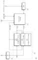
도 1은 본 발명의 실시 예에 따른 사용자 시스템을 예시적으로 보여주는 블록도이다. 도 1을 참조하면, 사용자 시스템(10)은 불휘발성 메모리 모듈들(100), 프로세서(101), 칩셋(102), 그래픽 처리 유닛(103), 입출력 장치(104), 스토리지 장치(105)를 포함한다. 예시적으로, 사용자 시스템(10)은 컴퓨터, 노트북, 서버, 워크 스테이션, 휴대용 통신 단말기, PDA(Personal Digital Assistant), PMP(Portable Media Player), 스마트폰, 또는 웨어러블(Wearable) 장치와 같은 컴퓨팅 시스템일 수 있다.1 is a block diagram exemplarily showing a user system according to an embodiment of the present invention. Referring to FIG. 1 , a
사용자 시스템(10)은 불휘발성 메모리 모듈(100), 프로세서(101), 칩셋(102), 그래픽 처리 유닛(103), 입출력 장치(104), 및 스토리지 장치(105)를 포함한다.The
프로세서(101)는 사용자 시스템(100)의 제반 동작을 제어할 수 있다. 프로세서(101)는 사용자 시스템(100)에서 수행되는 다양한 연산을 수행하고, 데이터를 처리할 수 있다.The
불휘발성 메모리 모듈(100)은 프로세서(101)와 직접적으로 연결될 수 있다. 예를 들어, 불휘발성 메모리 모듈(100)은 듀얼 인-라인 메모리 모듈(DIMM; Dual In-line Memory Module) 형태를 가질 수 있고, 불휘발성 메모리 모듈(100)은 프로세서(101)와 직접적으로 연결된 DIMM 소켓에 장착되어 프로세서(101)와 통신할 수 있다. 예시적으로, 불휘발성 메모리 모듈(100)은 NVDIMM 프로토콜을 기반으로 프로세서(101)와 통신할 수 있다.The
불휘발성 메모리 모듈(100)은 프로세서(101)의 주 메모리 또는 동작 메모리로써 사용될 수 있다. 불휘발성 메모리 모듈(100)은 불휘발성 메모리 및 휘발성 메모리를 포함할 수 있다. 불휘발성 메모리는 ROM (Read Only Memory), PROM (Programmable ROM), EPROM (Electrically Programmable ROM), EEPROM (Electrically Erasable and Programmable ROM), 플래시 메모리, PRAM (Phase-change RAM), MRAM (Magnetic RAM), RRAM (Resistive RAM), FRAM (Ferroelectric RAM) 등과 같이 전원 공급이 차단되어도 데이터가 소실되지 않는 메모리를 포함할 수 있다. 휘발성 메모리는 SRAM (Static RAM), DRAM (Dynamic RAM), SDRAM (Synchronous DRAM) 등과 같이 전원이 차단되면, 데이터가 소실되는 메모리를 포함할 수 있다.The
예시적으로, 불휘발성 메모리 모듈(100)의 불휘발성 메모리는 사용자 시스템(10) 또는 프로세서(101)의 주 메모리(main memory)로써 사용되고, 휘발성 메모리는 사용자 시스템(10), 프로세서(101), 또는 불휘발성 메모리 모듈(100)의 캐시 메모리(cache memory)로써 사용될 수 있다.Exemplarily, the nonvolatile memory of the
칩셋(102)은 프로세서(101)와 전기적으로 연결되고, 프로세서(101)의 제어에 따라 사용자 시스템(10)의 하드웨어를 제어할 수 있다. 예를 들어, 칩셋(102)은 주요 버스들을 통해 GPU(103), 입출력 장치(104), 및 스토리지 장치(105)와 각각 연결되고, 주요 버스들에 대한 브릿지 역할을 수행할 수 있다.The
GPU(103)는 사용자 시스템(10)의 영상 데이터를 출력하기 위한 일련의 연산 동작을 수행할 수 있다. 예시적으로, GPU(103)는 시스템-온-칩 형태로 프로세서(101) 내에 실장될 수 있다.The
입출력 장치(104)는 사용자 시스템(10)으로 데이터 또는 명령어를 입력하거나 또는 외부로 데이터를 출력하는 다양한 장치들을 포함한다. 예를 들어, 입출력 장치(104)는 키보드, 키패드, 버튼, 터치 패널, 터치 스크린, 터치 패드, 터치 볼, 카메라, 마이크, 자이로스코프 센서, 진동 센서, 압전 소자, 온도 센서, 생체 인식 센서 등과 같은 사용자 입력 장치들 및 LCD (Liquid Crystal Display), OLED (Organic Light Emitting Diode) 표시 장치, AMOLED (Active Matrix OLED) 표시 장치, LED, 스피커, 모터 등과 같은 사용자 출력 장치들을 포함할 수 있다.The input/
스토리지 장치(105)는 사용자 시스템(10)의 대용량 저장 매체로서 사용될 수 있다. 스토리지 장치(105)는 하드 디스크 드라이브, SSD, 메모리 카드, 메모리 스틱 등과 같은 대용량 저장 매체들을 포함할 수 있다.The
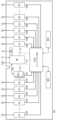
도 2는 도 1의 불휘발성 메모리 모듈을 상세하게 보여주는 블록도이다. 도 1 및 도 2를 참조하면, 불휘발성 메모리 모듈(100)은 모듈 컨트롤러(110), 이종 메모리 장치(120), 데이터 버퍼(130), 및 직렬 프레즌스 검출 칩(140)(SPD chip; Serial Presence Detect chip)을 포함한다.FIG. 2 is a block diagram showing the nonvolatile memory module of FIG. 1 in detail. 1 and 2, the
모듈 컨트롤러(110)는 프로세서(101)로부터 커맨드/어드레스(CA)를 수신하고, 수신된 커맨드/어드레스(CA)에 응답하여 이종 메모리 장치(120)를 제어할 수 있다. 예를 들어, 모듈 컨트롤러(110)는 프로세서(101)로부터의 커맨드/어드레스(CA)에 응답하여 커맨드/어드레스(CA_n) 및 커맨드/어드레스(CA_v)를 이종 메모리 장치(120)로 제공할 수 있다.The
예시적으로, 커맨드/어드레스(CA_n)는 이종 메모리 장치(120)에 포함된 불휘발성 메모리(123)를 제어하기 위한 커맨드/어드레스이고, 커맨드/어드레스(CA_v)는 이종 메모리 장치(120)에 포함된 휘발성 메모리(121)를 제어하기 위한 커맨드/어드레스일 수 있다.For example, the command/address CA_n is a command/address for controlling the
이하에서, 간결한 설명을 위하여, 프로세서(101)로부터 제공되는 커맨드/어드레스(CA)는 '모듈 커맨드/어드레스'라 칭하고, 모듈 컨트롤러(110)로부터 휘발성 메모리(121)로 제공되는 커맨드/어드레스(CA_v)는 'VM(Volatile Memory) 커맨드/어드레스'라 칭하고, 모듈 컨트롤러(110)로부터 NVM 제어기(122)로 제공되는 커맨드/어드레스(CA_n)는 'NVM(Nonvolatile Memory) 커맨드/어드레스'라 칭한다.Hereinafter, for concise description, the command/address CA provided from the
예시적으로, NVM 커맨드/어드레스(CA_n) 및 VM 커맨드/어드레스(CA_v)와 서로 다른 커맨드/어드레스 버스를 통해 제공될 수 있다.Illustratively, the NVM command/address CA_n and the VM command/address CA_v may be provided through a different command/address bus.
예시적으로, 모듈 컨트롤러는 RCD(Register Clock Driver)일 수 있다.Illustratively, the module controller may be a Register Clock Driver (RCD).
이종 메모리 장치(120)는 휘발성 메모리(121), NVM 제어기(122), 및 불휘발성 메모리(123)를 포함한다. 휘발성 메모리(121)는 모듈 컨트롤러(110)로부터의 VM 커맨드/어드레스(CA_v)에 응답하여 동작할 수 있다. 휘발성 메모리(121)는 VM 커맨드/어드레스(CA_v)에 응답하여 메모리 데이터 라인(MDQ) 및 태그 데이터 라인(TDQ)을 통해 데이터 및 태그(TAG)를 각각 출력할 수 있다. 휘발성 메모리(121)는 VM 커맨드/어드레스(CA_v)에 따라 메모리 데이터 라인(MDQ) 및 태그 데이터 라인(TDQ)을 통해 각각 수신된 데이터 및 태그를 기입할 수 있다.The
NVM 제어기(122)는 모듈 컨트롤러(110)로부터의 NVM 커맨드/어드레스(CA_n)에 응답하여 동작할 수 있다. 예를 들어, NVM 제어기(122)는 모듈 컨트롤러(110)로부터의 NVM 커맨드/어드레스(CA_n)에 따라, 메모리 데이터 라인(MDQ)을 통해 수신된 데이터를 불휘발성 메모리(123)에 프로그램하거나 또는 불휘발성 메모리(123)에 프로그램된 데이터를 메모리 데이터 라인(MDQ)을 통해 출력할 수 있다.The
NVM 제어기(122)는 불휘발성 메모리(123)를 제어하기 위한 다양한 동작을 수행할 수 있다. 예를 들어, NVM 제어기(122)는 불휘발성 메모리(123)를 효율적으로 사용하기 위하여 가비지 콜렉션, 웨어 레벨링, 어드레스 변환 등과 같은 동작을 수행할 수 있다. 예시적으로, NVM 제어기(122)는 에러 정정 회로, 랜더마이져 등과 같은 구성 요소들을 더 포함할 수 있다.The
예시적으로, 휘발성 메모리(121) 및 NVM 제어기(122)는 서로 동일한 메모리 데이터 라인(MDQ)을 공유할 수 있다.For example, the
예시적으로, 휘발성 메모리(121) 및 모듈 컨트롤러(110)는 태그 데이터 라인(TDQ)을 서로 공유할 수 있다. 또는 휘발성 메모리(121), NVM 제어기(122), 및 모듈 컨트롤러(110)는 태그 데이터 라인(TDQ)을 서로 공유할 수 있다. NVM 제어기(122)는 태그 데이터 라인(TDQ)을 통해 태그(TAG)를 출력할 수 있다.For example, the
데이터 버퍼(130)는 메모리 데이터 라인(MDQ)을 통해 데이터를 수신하고, 수신된 데이터를 데이터 라인(DQ)을 통해 프로세서(101)로 제공할 수 있다. 또는 데이터 버퍼(130)는 데이터 라인(DQ)을 통해 데이터를 수신하고, 수신된 데이터를 메모리 데이터 라인(MDQ)을 통해 출력할 수 있다. 예시적으로, 데이터 버퍼(130)는 모듈 컨트롤러(110)의 제어(예를 들어, 버퍼 커맨드(미도시))에 응답하여 동작할 수 있다. 예시적으로, 데이터 버퍼(130)는 메모리 데이터 라인(MDQ) 상의 신호 및 데이터 라인(DQ) 상의 신호를 구분하는 역할을 수행할 수 있다. 또는 데이터 버퍼(130)는 메모리 데이터 라인(MDQ) 및 데이터 라인(DQ) 사이의 신호를 차단하는 역할을 수행할 수 있다. 즉, 데이터 버퍼(130)에 의해 메모리 데이터 라인(MDQ)의 신호가 데이터 라인(DQ)에 영향을 미치지 않거나 또는 데이터 버퍼(130)에 의해 데이터 라인(DQ)의 신호가 메모리 데이터 라인(MDQ)의 신호에 영향을 미치지 않을 수 있다.The
예시적으로, 메모리 데이터 라인(MDQ)은 불휘발성 메모리 모듈(100)에 포함된 구성 요소들(예를 들어, 휘발성 메모리, 불휘발성 메모리, 데이터 버퍼 등) 사이의 데이터 전송 경로일 수 있고, 데이터 라인(DQ)은 불휘발성 메모리 모듈(100) 및 프로세서(101) 사이의 데이터 전송 경로일 수 있다. 태그 데이터 라인(TDQ)은 태그(TAG)를 송수신하기 위한 전송 경로일 수 있다.Illustratively, the memory data line MDQ may be a data transmission path between components included in the nonvolatile memory module 100 (eg, a volatile memory, a nonvolatile memory, a data buffer, etc.), and data The line DQ may be a data transmission path between the
예시적으로, 메모리 데이터 라인(MDQ), 데이터 라인(DQ), 및 태그 데이터 라인(TDQ) 각각은 복수의 배선들을 포함할 수 있다. 또한, 비록 도면에 도시되지는 않았으나, 메모리 데이터 라인(MDQ), 데이터 라인(DQ), 및 태그 데이터 라인(TDQ) 각각은 메모리 데이터 스트로브 라인(MDQS), 데이터 스트로브 라인(DQS), 및 태그 데이터 스트로브 라인(TDQS)을 포함할 수 있다. 이하에서, 도면의 간결성을 위하여, 데이터 스트로브 라인(MDQS), 데이터 스트로브 라인(DQS), 및 태그 데이터 스트로브 라인(TDQS)의 참조 번호 및 구성은 생략된다. 그러나, 본 발명의 범위가 이에 한정되는 것은 아니며, 메모리 데이터 라인(MDQ), 데이터 라인(DQ), 및 태그 데이터 라인(TDQ)과 연결된 구성 요소들은 데이터 스트로브 라인(MDQS), 데이터 스트로브 라인(DQS), 및 태그 데이터 스트로브 라인(TDQS)의 신호에 동기하여 데이터 또는 태그를 송수신할 수 있다.For example, each of the memory data line MDQ, data line DQ, and tag data line TDQ may include a plurality of wires. In addition, although not shown in the drawing, the memory data line MDQ, data line DQ, and tag data line TDQ include a memory data strobe line MDQS, a data strobe line DQS, and a tag data line, respectively. A strobe line (TDQS) may be included. Hereinafter, for brevity of the drawing, reference numbers and configurations of the data strobe line MDQS, the data strobe line DQS, and the tag data strobe line TDQS are omitted. However, the scope of the present invention is not limited thereto, and components connected to the memory data line (MDQ), data line (DQ), and tag data line (TDQ) include a data strobe line (MDQS) and a data strobe line (DQS). ), and data or tags can be transmitted/received in synchronization with signals of the tag data strobe line (TDQS).
SPD(140)는 프로그램 가능 읽기 전용 기억 장치(EEPROM; Electrically Erasable Programmable Read-Only Memory)일 수 있다. SPD(140)는 불휘발성 메모리 모듈(100)의 초기 정보 또는 장치 정보(DI)를 포함할 수 있다. 예시적으로, SPD(140)는 불휘발성 메모리 모듈(100)의 모듈 형태, 모듈 구성, 저장 용량, 모듈 종류, 실행 환경 등과 같은 장치 정보(DI)를 포함할 수 있다. 불휘발성 메모리 모듈(100)이 포함된 사용자 시스템(10)이 부팅될 때, 프로세서(101)는 SPD(140)로부터 장치 정보(DI)를 읽고, 이를 기반으로 불휘발성 메모리 모듈(100)을 인식할 수 있다. 프로세서(101)는 SPD(140)로부터 읽은 장치 정보(DI)를 기반으로, 불휘발성 메모리 모듈(100)을 제어할 수 있다.The
이하에서, 간결한 설명을 위하여, 휘발성 메모리(121)는 DRAM인 것으로 가정하고, 불휘발성 메모리(123)는 낸드 플래시 메모리인 것으로 가정한다. 그러나, 본 발명의 범위가 이에 한정되는 것은 아니며, 휘발성 메모리(121)는 다른 종류의 랜덤 액세스 메모리를 포함할 수 있고, 불휘발성 메모리(123)는 다른 종류의 불휘발성 메모리 장치들을 포함할 수 있다. 예시적으로, 불휘발성 메모리(123)는 상 변화 메모리를 포함할 수 있다.Hereinafter, for concise description, it is assumed that the
예시적으로, 휘발성 메모리(121)는 복수의 휘발성 메모리 칩들을 포함할 수 있고, 각 휘발성 메모리 칩들은 별도의 칩, 별도의 패키지 등으로 구현될 수 있다. 각 휘발성 메모리 칩들은 서로 다른 메모리 데이터 라인들 또는 태그 데이터 라인을 통해 모듈 컨트롤러(110) 또는 NVM 제어기(122)와 연결될 수 있다.For example, the
예시적으로, 프로세서(101)는 불휘발성 메모리 모듈(100)의 불휘발성 메모리(123)를 메인 메모리로써 사용할 수 있다. 즉, 프로세서(101)는 불휘발성 메모리(123)의 저장 공간을 메인 메모리 영역으로 인식할 수 있다. 휘발성 메모리(121)는 프로세서(101) 및 불휘발성 메모리(123)의 캐시 메모리로써 동작할 수 있다. 예시적으로, 휘발성 메모리(121)는 후 기입 캐시(write-back cache)로 사용될 수 있다. 즉, 프로세서(101)로부터의 모듈 커맨드/어드레스(CA)에 응답하여 모듈 컨트롤러(110)는 캐시 히트 또는 캐시 미스를 판별하고, 판별 결과에 따라 휘발성 메모리(121) 또는 불휘발성 메모리(123)를 제어할 수 있다.For example, the
예시적으로, 캐시 히트는 프로세서(101)로부터 수신된 모듈 커맨드/어드레스(CA)와 대응되는 데이터가 휘발성 메모리(121)에 저장되어 있는 경우를 가리킨다. 캐시 미스는 프로세서(101)로부터 수신된 모듈 커맨드/어드레스(CA)와 대응되는 데이터가 휘발성 메모리(121)에 저장되어 있지 않은 경우를 가리킨다. Exemplarily, a cache hit refers to a case in which data corresponding to a module command/address (CA) received from the
예시적으로, 모듈 컨트롤러(110)는 태그(TAG)를 기반으로 캐시 히트 또는 캐시 미스 여부를 판별할 수 있다. 모듈 컨트롤러(110)는 프로세서(101)로부터 수신된 모듈 커맨드/어드레스(CA) 및 태그(TAG)를 비교함으로써 캐시 히트 또는 캐시 미스 여부를 판별할 수 있다.Illustratively, the
예시적으로, 태그(TAG)는 휘발성 메모리(121)에 저장된 데이터와 대응되는 어드레스(address)의 일부를 포함할 수 있다. 예시적으로, 모듈 컨트롤러(110)는 태그 데이터 라인(TDQ)을 통해 휘발성 메모리(121)와 태그(TAG)를 주고 받을 수 있다. 예시적으로, 휘발성 메모리(121)에 데이터가 기입될 때, 모듈 컨트롤러(110)의 제어에 따라, 데이터와 대응되는 태그(TAG)가 휘발성 메모리(121)에 함께 기입될 수 있다.For example, the tag TAG may include a part of an address corresponding to data stored in the
예시적으로, 휘발성 메모리(121) 및 불휘발성 메모리(123)는 n:1(단, n은 자연수)의 직접 사상(direct mapping) 관계를 가질 수 있다. 즉, 휘발성 메모리(121)는 불휘발성 메모리(123)의 직접 사상 캐시(direct mapped cache)일 수 있다. 예를 들어, 휘발성 메모리(121)의 제1 휘발성 저장 영역은 불휘발성 메모리(123)의 제1 내지 제n 불휘발성 저장 영역들과 대응될 수 있다. 이 때, 제1 휘발성 저장 영역 및 제1 내지 제n 불휘발성 저장 영역들 각각은 서로 동일한 크기일 수 있다. 예시적으로, 제1 휘발성 저장 영역은 부가 정보(예를 들어, 태그, ECC, 더티 정보 등)를 저장하기 위한 영역을 더 포함할 수 있다.For example, the
비록 도면에 도시되지는 않았으나, 불휘발성 메모리 모듈(100)은 별도의 메모리(미도시)를 더 포함할 수 있다. 별도의 메모리(미도시)는 NVM 제어기(122)에서 사용되는 데이터, 프로그램, 소프트웨어 등과 같은 정보를 저장할 수 있다. 예를 들어, 별도의 메모리는 NVM 제어기(122)에 의해 관리되는 매핑 테이블, FTL 등과 같은 정보를 저장할 수 있다. 또는 별도의 메모리는 불휘발성 메모리(123)로부터 읽은 데이터 또는 불휘발성 메모리(123)에 저장될 데이터를 임시 저장하기 위한 버퍼 메모리일 수 있다.Although not shown in the drawing, the
이하에서, 도 3 내지 도 8을 참조하여, 불휘발성 메모리 모듈(100)의 쓰기 동작 및 읽기 동작이 상세하게 설명된다. 이하에서, 간결한 설명을 위하여, 휘발성 메모리(121)와 연관된 구성 요소들(예를 들어, 데이터, 태그, 커맨드/어드레스 등)은 '_v'의 참조 기호를 사용하여 표현된다. 예를 들어, 휘발성 메모리(121)를 제어하기 위하여 모듈 컨트롤러(110)로부터 출력되는 VM 커맨드/어드레스는 'CA_v'로 표현되고, 모듈 컨트롤러(110)의 제어에 따라 휘발성 메모리(121)로부터 출력되는 데이터는 'DT_v'로 표현된다. 좀 더 상세하게는, 휘발성 메모리(121)에 데이터를 기입하기 위한 VM 쓰기 커맨드는 'WR_v'로 표현되고, 휘발성 메모리(121)로부터 데이터를 읽기 위한 VM 읽기 커맨드는 'RD_v'로 표현된다.Hereinafter, a write operation and a read operation of the
마찬가지로, 불휘발성 메모리(123)와 연관된 구성 요소들(예를 들어, 데이터, 태그, 커맨드/어드레스 등)은 '_n'의 참조 기호를 사용하여 표현된다. 예를 들어, 불휘발성 메모리(123)를 제어하기 위하여 모듈 컨트롤러(110)로부터 출력되는 NVM 커맨드/어드레스는 'CA_n'로 표현되고, 모듈 컨트롤러(110)의 제어에 따라 불휘발성 메모리(121)로부터 출력되는 데이터는 'DT_n'로 표현된다. 좀 더 상세하게는, 불휘발성 메모리(123)에 데이터를 기입하기 위한 NVM 쓰기 커맨드는 'WR_n'으로 표현되고, 불휘발성 메모리(123)로부터 데이터를 읽기 위한 NVM 읽기 커맨드는 'RD_n'으로 표현된다.Similarly, components related to the nonvolatile memory 123 (eg, data, tags, commands/addresses, etc.) are expressed using a reference symbol of '_n'. For example, an NVM command/address output from the
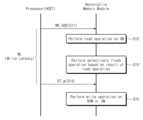
도 3은 도 2의 불휘발성 메모리 모듈의 쓰기 동작을 보여주는 순서도이다. 도 1 내지 도 3을 참조하면, S11 단계에서, 프로세서(101)는 불휘발성 메모리 모듈(100)로 모듈 쓰기 커맨드 및 어드레스(WR, ADD)를 전송한다. 예를 들어, 프로세서(101)는 불휘발성 메모리 모듈(100)에 쓰기 데이터(DT_w)를 기입하기 위하여 모듈 쓰기 커맨드 및 어드레스(WR, ADD)를 불휘발성 메모리 모듈(100)로 전송한다. 예시적으로, 모듈 쓰기 커맨드 및 어드레스(WR, ADD)는 쓰기 데이터(DT_w)에 대응하는 어드레스(ADD)를 포함할 수 있다. 쓰기 데이터에 대응하는 어드레스(ADD)는 불휘발성 메모리 모듈(100)의 저장 공간, 즉, 불휘발성 메모리(123)의 저장 공간 중 일부에 대응하는 논리적 어드레스, 메모리 어드레스일 수 있다.FIG. 3 is a flowchart illustrating a write operation of the nonvolatile memory module of FIG. 2 . Referring to FIGS. 1 to 3 , in step S11 , the
S12 단계에서, 불휘발성 메모리 모듈(100)은 수신된 모듈 쓰기 커맨드 및 어드레스(WR, ADD)에 응답하여 휘발성 메모리(121)에 대한 읽기 동작을 수행할 수 있다. 예를 들어, 불휘발성 메모리 모듈(100)은 휘발성 메모리(121)의 영역 중 수신된 어드레스(ADD) 또는 수신된 어드레스(ADD)의 일부와 대응되는 영역에서 데이터 및 태그(TAG)를 읽을 수 있다. 예시적으로, 불휘발성 메모리 모듈(100)은 읽은 태그(TAG) 및 어드레스(ADD)를 비교함으로써 캐시 히트 또는 캐시 미스 여부를 판별할 수 있다.In step S12 , the
S13 단계에서, 불휘발성 메모리 모듈(100)은 S12 단계의 읽기 동작의 결과를 기반으로 플러시 동작을 선택적으로 수행할 수 있다. 예를 들어, S12 단계의 읽기 동작의 결과가 캐시 미스를 가리키는 경우, 불휘발성 메모리 모듈(100)은 휘발성 메모리(121)로부터 읽은 데이터가 불휘발성 메모리(123)에 저장되도록 플러시 동작을 수행할 수 있다. 예시적으로, 도 2를 참조하여 설명된 바와 같이, 불휘발성 메모리(123)를 제어하는 NVM 제어기(122) 및 휘발성 메모리(121)는 메모리 데이터 라인(MDQ)을 공유한다. 즉, 휘발성 메모리(121)로부터 읽은 데이터에 의해 메모리 데이터 라인(MDQ)의 전압이 구동될 경우, 불휘발성 메모리(123)를 제어하는 NVM 제어기(122)는 메모리 데이터 라인(MDQ)을 통해 휘발성 메모리(121)로부터 읽은 데이터를 수신(또는 감지)할 수 있다. NVM 제어기(122)는 수신된 데이터를 불휘발성 메모리(123)에 프로그램할 수 있다.In step S13, the
예시적으로, S12 단계의 읽기 동작의 결과가 캐시 히트를 가리키는 경우, 불휘발성 메모리 모듈(100)은 플러시 동작을 수행하지 않을 수 있다. 또는 S12 단계의 읽기 동작의 결과가 캐시 히트를 가리키고, 읽은 데이터가 더티 데이터(dirty data)인 경우, 불휘발성 메모리 모듈(100)은 플러시 동작을 수행할 수 있다.For example, when the result of the read operation of step S12 indicates a cache hit, the
예시적으로, 불휘발성 메모리 모듈(100)의 플러시 동작, 캐시 히트 또는 캐시 미스 판별, 더티 데이터 판별과 같은 동작들은 NVM 제어기(122)에 의해 수행될 수 있다.Illustratively, operations such as a flush operation of the
S14 단계에서, 프로세서(101)는 불휘발성 메모리 모듈(100)로 쓰기 데이터(DT_w)를 전송할 수 있다. 예시적으로, S11 단계로부터 미리 정해진 시간이 경과한 이후에, S14 단계의 동작이 수행될 수 있다. 즉, 프로세서(101)는 모듈 쓰기 커맨드 및 어드레스(WR, ADD)를 전송하고, 미리 정해진 시간이 경과한 이후에, 불휘발성 메모리 모듈(100)로 쓰기 데이터(DT_w)를 전송할 수 있다. 이 때, 미리 정해진 시간은 쓰기 레이턴시(WL; Write Latency)일 수 있다. 예시적으로, 쓰기 레이턴시(WL)는 불휘발성 메모리 모듈(100)의 동작 특성에 따라 미리 정해진 시간 또는 클럭 주기일 수 있다. 쓰기 레이턴시(WL)에 대한 정보는 SPD(140)에 저장되고, 장치 정보(DI)로써 프로세서(101)로 제공될 수 있다. 프로세서(101)는 장치 정보(DI)를 기반으로 쓰기 데이터(DT_w)를 전송할 수 있다.In step S14 , the
S15 단계에서, 불휘발성 메모리 모듈(100)은 수신된 쓰기 데이터(DT_w)를 휘발성 메모리(121) 또는 불휘발성 메모리(133)에 기입 또는 프로그램할 수 있다.In step S15 , the
도 4는 도 3의 동작 방법을 상세하게 설명하기 위한 타이밍도이다. 예시적으로, 본 발명의 기술적 사상이 커맨드, 어드레스, 데이터, 태그 등의 크기 및 타이밍은 도 4에 도시된 타이밍도에 국한되는 것은 아니다.4 is a timing diagram for explaining the operation method of FIG. 3 in detail. By way of example, the size and timing of commands, addresses, data, tags, etc. of the technical concept of the present invention are not limited to the timing diagram shown in FIG. 4 .
도 1 내지 도 4를 참조하면, 불휘발성 메모리 모듈(100)은 프로세서(101)로부터 모듈 쓰기 커맨드 및 제1 어드레스(WR, ADD1)를 수신한다. 불휘발성 메모리 모듈(100)의 모듈 컨트롤러(110)는 수신된 모듈 쓰기 커맨드 및 제1 어드레스(WR, ADD1)에 응답하여, NVM 커맨드/어드레스(CA_n) 및 VM 메모리 커맨드/어드레스(CA_n)를 출력할 수 있다. 이 때, NVM 커맨드/어드레스(CA_n)는 NVM 쓰기 커맨드 및 제1 어드레스(WR_v, ADD1)를 포함하고, VM 커맨드/어드레스(CA_v)는 VM 읽기 커맨드 및 제1 어드레스(RD_v, ADD1) 및 VM 쓰기 커맨드, 제1 어드레스(WR_v, ADD1)를 포함할 수 있다.1 to 4 , the
불휘발성 메모리 모듈(100)의 휘발성 메모리(121)는 VM 읽기 커맨드(RD_v)에 응답하여 휘발성 메모리(121)의 영역 중 제1 어드레스(ADD1)와 대응되는 영역에 저장된 데이터(DT_v) 및 태그(TAG_v)를 출력할 수 있다. 예를 들어, 앞서 설명된 바와 같이, 휘발성 메모리(121)는 데이터(DT_v)를 기반으로 메모리 데이터 라인(MDQ)의 전압을 구동함으로써, 메모리 데이터 라인(MD 통해 데이터(DT_v)를 출력할 수 있다. 휘발성 메모리(121)는 태그(TAG)를 기반으로 태그 데이터 라인(TDQ)의 전압을 구동함으로써, 태그 데이터 라인(TDQ)을 통해 태그(TAG)를 출력할 수 있다.In response to the VM read command RD_v, the
프로세서(101)는 데이터 라인(DQ)을 통해 쓰기 데이터(DT_w)를 출력할 수 있다. 불휘발성 메모리 모듈(100)은 데이터 라인(DQ)을 통해 수신된 쓰기 데이터(DT_w)를 메모리 데이터 라인(MDQ)을 통해 휘발성 메모리(121) 또는 NVM 제어기(122)로 제공하고, 쓰기 데이터(DT_w)(또는 제1 어드레스(ADD1))와 대응되는 태그(TAG_w)를 태그 데이터 라인(TDQ)을 통해 휘발성 메모리(121)로 제공할 수 있다. 휘발성 메모리(121) 또는 NVM 제어기(122)는 수신된 신호들을 기반으로 쓰기 동작 또는 프로그램 동작을 수행할 수 있다.The
비록 도면에 도시되지는 않았으나, 휘발성 메모리(121)로부터 읽은 태그(TAG_v)에 따라 플러시 동작이 선택적으로 수행될 수 있다.Although not shown, a flush operation may be selectively performed according to the tag TAG_v read from the
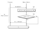
도 5는 도 2의 불휘발성 메모리 모듈(100)의 읽기 동작을 보여주는 순서도이다. 도 1, 도 2, 및 도 5를 참조하면, S21 단계에서, 프로세서(101)는 불휘발성 메모리 모듈(100)로 모듈 읽기 커맨드 및 어드레스(RD, ADD)를 전송한다.FIG. 5 is a flowchart illustrating a read operation of the
S21 단계에서, 불휘발성 메모리 모듈(100)은 모듈 읽기 커맨드 및 어드레스(RD, ADD)에 응답하여, 휘발성 메모리(121)에 대한 읽기 동작을 수행한다. 예를 들어, 모듈 읽기 커맨드 및 어드레스(RD, ADD)는 불휘발성 메모리 모듈(100)에 저장된 데이터를 읽기 위한 읽기 커맨드 및 읽기 데이터에 대응하는 읽기 어드레스를 포함할 수 있다. 불휘발성 메모리 모듈(100)은 휘발성 메모리(121)의 영역 중 읽기 어드레스와 대응하는 영역에 저장된 데이터 및 태그를 읽을 수 있다.In step S21 , the
S22 단계에서, 불휘발성 메모리 모듈(100)은 읽기 결과를 기반으로 캐시 히트 또는 캐시 미스를 판별할 수 있다. 앞서 설명된 바와 같이, 태그(TAG)는 어드레스의 일부 정보를 포함한다. 불휘발성 메모리 모듈(100)은 수신된 읽기 어드레스 및 태그(TAG)를 비교함으로써 캐시 히트 또는 캐시 미스를 판별할 수 있다. 수신된 어드레스의 일부와 태그(TAG)가 일치하는 경우, 불휘발성 메모리 모듈(100)은 캐시 히트로 판별하고, 수신된 어드레스의 일부와 태그(TAG)가 일치하지 않는 경우, 불휘발성 메모리 모듈(100)은 캐시 미스로 판별한다.In step S22, the
예시적으로, 캐시 미스로 판별된 경우의 읽기 동작은 도 7 및 도 8을 참조하여 설명된다.By way of example, a read operation when it is determined as a cache miss will be described with reference to FIGS. 7 and 8 .
캐시 히트로 판별된 경우, S24 단계에서, 불휘발성 메모리 모듈(100)은 휘발성 메모리(121)로부터 읽은 데이터 및 캐시 정보(INFO)를 프로세서(101)로 전송한다. 캐시 정보(INFO)는 출력되는 데이터가 캐시 히트인지 또는 캐시 미스인지에 대한 정보를 포함한다. 프로세서(101)는 캐시 정보(INFO)를 통해 수신된 데이터(DT_v)가 유효한 데이터인지 판별할 수 있다. 즉, 불휘발성 메모리 모듈(100)이 캐시 히트(H)에 대한 정보를 캐시 정보(INFO)로써 제공함으로써 프로세서(101)는 수신된 데이터가 유효한 데이터인 것을 인지할 수 있다.When it is determined as a cache hit, the
예시적으로, S21 단계로부터 미리 정해진 시간이 경과한 이후에 S24 단계의 동작이 수행될 수 있다. 즉, 프로세서(101)가 모듈 읽기 커맨드 및 어드레스(RD, ADD)를 전송하고, 미리 정해진 시간이 경과한 이후에, 불휘발성 메모리 모듈(100)로부터 읽기 데이터가 수신될 것이다. 이 때, 미리 정해진 시간은 읽기 레이턴시(RL; Read Latency)일 수 있다. 읽기 레이턴시(RL)는 불휘발성 메모리 모듈(100)의 동작 특성에 따라 미리 정해진 시간 또는 클럭 주기일 수 있다. 읽기 레이턴시(RL)에 대한 정보는 SPD(140)에 저장되고, 장치 정보(DI)로써 프로세서(101)로 제공될 수 있다. 프로세서(101)는 읽기 레이턴시(RL)를 기반으로 불휘발성 메모리 모듈을 제어할 수 잇다.Illustratively, the operation of step S24 may be performed after a predetermined time has elapsed from step S21. That is, read data may be received from the
도 6은 도 5의 읽기 동작을 상세하게 설명하기 위한 타이밍도이다. 도 1, 도 2, 도 5, 및 도 6을 참조하면, 불휘발성 메모리 모듈(100)은 프로세서(101)로부터 모듈 읽기 커맨드 및 제1 어드레스(RD, ADD1)를 수신하고, 수신된 신호에 응답하여 NVM 커맨드/어드레스(CA_n) 및 VM 커맨드/어드레스(CA_v)를 출력한다. 이 때, NVM 커맨드/어드레스(CA_n)는 불휘발성 메모리(123)에 저장된 데이터를 읽기 위한 NVM 읽기 커맨드 및 제1 어드레스(RD_n, ADD1)를 포함할 수 있다. VM 커맨드/어드레스(CA_v)는 휘발성 메모리(121)에 저장된 데이터를 읽기 위한 VM 읽기 커맨드 및 제1 어드레스(RD_v, ADD1)를 포함할 수 있다.6 is a timing diagram for explaining the read operation of FIG. 5 in detail. Referring to FIGS. 1, 2, 5, and 6 , the
휘발성 메모리(121)는 VM 읽기 커맨드 및 제1 어드레스(RD_v, ADD1)에 응답하여, 휘발성 메모리(121)의 영역 중 제1 어드레스(ADD1)와 대응되는 영역에 저장된 데이터(DT_v) 및 태그(TAG_v)를 출력할 수 있다. 예를 들어, 앞서 설명된 바와 같이, 휘발성 메모리(121)는 데이터(DT_v)를 기반으로 메모리 데이터 라인(MDQ)의 전압을 구동함으로써, 메모리 데이터 라인(MDQ)을 통해 데이터(DT_v)를 출력할 수 있다. 휘발성 메모리(121)는 태그(TAG_v)를 기반으로 태그 데이터 라인(TDQ)의 전압을 구동함으로써, 태그 데이터 라인(TDQ)을 통해 태그(TAG_v)를 출력할 수 있다.In response to the VM read command and the first addresses RD_v and ADD1, the
모듈 컨트롤러(110)는 태그 데이터 라인(TDQ)을 통해 태그(TAG_v)를 수신하고, 수신된 태그(TAG_v) 및 제1 어드레스(ADD1)를 비교함으로써 캐시 히트인지 또는 캐시 미스인지 판별할 수 있다.The
캐시 히트인 경우, 불휘발성 메모리 모듈(100)은 휘발성 메모리(131)로부터 읽은 데이터(DT_v)를 데이터 라인(DQ)을 통해 출력하고, 캐시 히트(H) 정보를 포함하는 캐시 정보(INFO)를 출력할 수 있다. 프로세서(101)는 캐시 히트(H) 정보를 포함하는 캐시 정보(INFO)를 수신함으로써, 데이터 라인(DQ)을 통해 수신된 데이터(DT_v)가 유효한 데이터임을 인지할 수 있다.In case of a cache hit, the
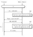
도 7은 도 2의 불휘발성 메모리 모듈(100)의 다른 읽기 동작을 보여주는 순서도이다. 예시적으로, 도 7을 참조하여, 캐시 미스인 경우의 읽기 동작이 설명된다.FIG. 7 is a flowchart illustrating another read operation of the
도 1, 도 2, 도 5, 및 도 7을 참조하면, S23 단계의 판별 결과가 캐시 미스인 것을 가리키는 경우, S25 단계의 동작이 수행된다. S25 단계에서, 불휘발성 메모리 모듈(100)은 휘발성 메모리(121)로부터 읽은 데이터(DT_v) 및 캐시 정보(INFO)를 프로세서(101)로 전송한다. 이 때, 캐시 정보(INFO)는 캐시 미스(M)에 대한 정보를 포함할 것이다.Referring to FIGS. 1, 2, 5, and 7 , when the determination result of step S23 indicates that there is a cache miss, the operation of step S25 is performed. In step S25 , the
예시적으로, 앞서 설명된 바와 같이, S25 단계의 동작 또한 모듈 읽기 커맨드 및 어드레스(RD, ADD)가 수신된 시점으로부터 읽기 레이턴시(RL) 이후에 수행될 수 있다.Illustratively, as described above, the operation of step S25 may also be performed after the read latency RL from the time when the module read command and the addresses RD and ADD are received.
S26 단계에서, 불휘발성 메모리 모듈(100)은 불휘발성 메모리(123)에 대한 선-읽기 동작을 수행할 수 있다. 예시적으로, 선-읽기 동작은 NVM 제어기(122)가 불휘발성 메모리(123)로부터 데이터를 읽고, 읽은 데이터를 NVM 제어기(122)에 포함된 데이터 버퍼(미도시)에 저장하는 동작을 가리킨다. 또는 선-읽기 동작은 프로세서(101)의 명령에 따라 NVM 제어기(122)가 읽기 레이턴시(RL) 이내에 불휘발성 메모리(123)로부터의 데이터를 출력할 수 있도록 읽기 데이터를 준비하는 동작을 가리킨다. 즉, 불휘발성 메모리(123)에 대한 선-읽기 동작이 완료된 경우, 프로세서(101)로부터의 명령에 응답하여 읽기 레이턴시(RL) 이내에 불휘발성 메모리(123)로부터의 데이터가 출력될 것이다.In step S26 , the
예시적으로, 선-읽기 동작은 S22 단계 내지 S25 단계의 동작들이 수행되는 동안 수행될 수 있다. 또는 선-읽기 동작은 캐시 미스로 판별된 경우, NVM 제어기(122)에 의해 수행될 수 있다. 예를 들어, NVM 제어기(122)는 모듈 컨트롤러(110)로부터 제1 어드레스(ADD1)를 수신하고, 태그 데이터 라인(TDQ)을 통해 태그(TAG)를 수신할 수 있다. NVM 제어기(122)는 수신된 제1 어드레스(ADD1) 및 태그(TAG)를 비교함으로써 캐시 히트인지 또는 캐시 미스인지 판별할 수 있다. 판별 결과에 따라, NVM 제어기(122)는 선-읽기 동작을 수행할 수 있다. 예시적으로, NVM 제어기(122)에 의한 캐시 히트 또는 캐시 미스에 대한 판별 동작은 휘발성 메모리(121)로부터 태그(TAG_v)가 출력된 이후에 수행될 수 있다.Illustratively, the pre-read operation may be performed while the operations of steps S22 to S25 are performed. Alternatively, the pre-read operation may be performed by the
선-읽기 동작이 완료된 이후에, S27 단계에서, 불휘발성 메모리 모듈(100)은 레디 신호(R)를 프로세서(101)로 제공한다. 예시적으로, 레디 신호(R)는 불휘발성 메모리 모듈(100)이 선-읽기 동작을 완료했음을 알리는 신호일 수 있다. 레디 신호(R)는 캐시 정보(INFO)가 전송되는 신호 라인을 통해 제공되거나 또는 별도의 신호 라인을 통해 제공될 수 있다.After the pre-read operation is completed, in step S27, the
S28 단계에서, 프로세서(101)는 레디 신호(R)에 응답하여 모듈 읽기 커맨드 및 어드레스(NRD, ADD)를 불휘발성 메모리 모듈(100)로 제공할 수 있다. 예시적으로, 모듈 읽기 커맨드는(NRD)는 S21 단계의 모듈 읽기 커맨드(RD)와 다를 수 있다. 모듈 읽기 커맨드(NRD)는 불휘발성 메모리(123)로부터의 데이터를 읽기 위한 커맨드/어드레스일 수 있다.In step S28 , the
S29 단계에서, 모듈 읽기 커맨드 및 어드레스(NRD, ADD)에 응답하여 불휘발성 메모리 모듈(100)은 불휘발성 메모리(123)에 대한 읽기 동작 및 휘발성 메모리(121)에 대한 쓰기 동작을 수행한다. 예를 들어, 불휘발성 메모리 모듈(100)의 NVM 제어기(122)는 선-읽기 동작에서 준비된 데이터를 기반으로 메모리 데이터 라인(MDQ)을 구동할 수 있다. 휘발성 메모리(121)는 메모리 데이터 라인(MDQ)을 통해 NVM 제어기(122)로부터 출력된 데이터(즉, 불휘발성 메모리(123)로부터 출력된 데이터)를 수신하고, 수신된 데이터를 기입할 수 있다. 이 때, 휘발성 메모리(121)의 쓰기 동작은 읽기 캐싱 동작일 수 있다.In step S29 , the
S2a 단계에서, 불휘발성 메모리 모듈(100)은 불휘발성 메모리(123)로부터의 데이터(DT_n)를 프로세서(101)로 전송할 수 있다. 예를 들어, 불휘발성 메모리 모듈(100)은 데이터 라인(DQ)을 통해 불휘발성 메모리(123)로부터의 데이터(DT_n)를 출력할 수 있다. 예시적으로, S2a 단계의 동작은 S28 단계의 동작으로부터 미리 정해진 시간 이후에 수행될 수 있다. 미리 정해진 시간은 읽기 레이턴시(RL')일 수 있다. 예시적으로, 도 7의 읽기 레이턴시(RL')는 도 5의 읽기 레이턴시(RL)와 다를 수 있으며, 이들에 대한 정보는 SPD(140)에 저장되고, 장치 정보(DI)로써 프로세서(101)로 제공될 수 있다.In step S2a, the
도 8은 도 7의 읽기 동작을 상세하게 설명하기 위한 타이밍도이다. 간결한 설명을 위하여, 앞서 설명된 구성과 중복되는 구성들에 대한 상세한 설명은 생략된다.8 is a timing diagram for explaining the read operation of FIG. 7 in detail. For concise description, detailed descriptions of components overlapping with those described above are omitted.
도 1, 도 2, 도 5, 도 7, 및 도 8을 참조하면, 불휘발성 메모리 모듈(100)은 프로세서(101)로부터 모듈 읽기 커맨드 및 제1 어드레스(RD, ADD1)를 수신한다. 불휘발성 메모리 모듈(100)의 모듈 컨트롤러(110)는 모듈 읽기 커맨드 및 제1 어드레스(RD, ADD1)에 응답하여 NVM 읽기 커맨드 및 제1 어드레스(RD_n, ADD1)를 NVM 제어기(122)로 제공하고, VM 읽기 커맨드 및 제1 어드레스(RD_v, ADD1)를 휘발성 메모리(121)로 제공한다.Referring to FIGS. 1 , 2 , 5 , 7 , and 8 , the
휘발성 메모리(121)는 VM 읽기 커맨드 및 제1 어드레스(RD_v, ADD1)에 응답하여, 휘발성 메모리(121)의 영역 중 제1 어드레스(ADD1)에 대응하는 영역의 데이터(DT_v) 및 태그(TAG_v)를 메모리 데이터 라인(MDQ)을 통해 출력할 수 있다. 즉, 휘발성 메모리(121)는 데이터(DT_v) 및 태그(TAG_v)를 기반으로 메모리 데이터 라인(MDQ) 및 태그 데이터 라인(TDQ)의 전압들을 각각 구동할 수 있다. 메모리 데이터 라인(MDQ) 상의 데이터(DT_v)는 모듈 컨트롤러(110) 및 데이터 버퍼(130)의 제어에 따라 데이터 라인(DQ)을 통해 출력된다.In response to the VM read command and the first addresses RD_v and ADD1, the
모듈 컨트롤러(110)는 휘발성 메모리(121)로부터 출력된 태그(TAG_v) 및 제1 어드레스(ADD1)를 비교함으로써, 캐시 히트 또는 캐시 미스 여부를 판별할 수 있다. 캐시 미스인 경우, 모듈 컨트롤러(110)는 캐시 미스(M)에 대한 캐시 정보(INFO)를 프로세서(101)로 전송할 수 있다. 이 때, 프로세서(101)는 데이터 라인(DQ)을 통해 수신된 데이터(DT_v)가 캐시 미스(M)임을 인지할 수 있다.The
불휘발성 메모리 모듈(100)은 선-읽기 동작을 수행할 수 있다. 예시적으로, NVM 제어기(122)는 모듈 컨트롤러(110)로부터의 불휘발성 메모리 읽기 커맨드 및 제1 어드레스(ADD1)에 응답하여 불휘발성 메모리(123)의 영역 중 제1 어드레스(ADD1)와 대응되는 영역의 데이터를 준비(또는 별도의 데이터 버퍼에 저장)할 수 있다. 선-읽기 동작이 완료된 경우, 모듈 컨트롤러(110)는 준비 신호(R)를 프로세서(101)로 전송할 수 있다. 예시적으로, 준비 신호(R)는 캐시 정보(INFO)와 동일한 라인, 또는 별도의 신호 라인, 또는 데이터 라인(DQ)을 통해 프로세서(101)로 제공될 수 있다.The
준비 신호(R)에 응답하여, 프로세서(101)는 모듈 읽기 커맨드 및 제1 어드레스(NRD, ADD1)를 불휘발성 메모리 모듈(100)로 전송한다. 모듈 읽기 커맨드 및 제1 어드레스(NRD, ADD1)에 응답하여, 불휘발성 메모리 모듈(100)은 NVM 읽기 커맨드 및 제1 어드레스(RD_n', ADD1)를 NVM 제어기(122)로 제공한다. 예시적으로, 모듈 읽기 커맨드(NRD)에 따른 NVM 읽기 커맨드 (RD_n)는 모듈 읽기 커맨드(RD)에 따른 NVM 읽기 커맨드(RD_n)와 다를 수 있다.In response to the preparation signal R, the
예시적으로, 모듈 읽기 커맨드들(NRD, RD) 각각은 프로세서(101) 및 불휘발성 메모리 모듈(100) 사이의 통신 규약에 의해 미리 정의된 커맨드일 수 있다.For example, each of the module read commands NRD and RD may be a command predefined by a communication protocol between the
NVM 제어기(122)는 NVM 읽기 커맨드 및 제1 어드레스(RD_n', ADD1)에 응답하여, 선-읽기 동작에서 준비된 데이터(DT_n)를 메모리 데이터 라인(MDQ)을 통해 출력할 수 있다. 예시적으로, NVM 제어기(122)는 데이터(DT_n)와 대응되는 태그(TAG_n)를 태그 데이터 라인(TDQ)을 통해 출력할 수 있다. 예시적으로, 데이터(DT_n)와 대응되는 태그(TAG_n)는 데이터(DT_n)와 대응되는 제1 어드레스(ADD1)의 일부를 포함할 수 있다. 메모리 데이터 라인(MDQ) 상의 데이터(DT_n)는 모듈 컨트롤러(110) 및 데이터 버퍼(130)의 제어에 따라 데이터 라인(DQ)으로 출력될 수 있다.The
예시적으로, 데이터(DT_n)가 출력되는 동안 불휘발성 메모리 모듈(100)은 읽기 캐싱(read caching)을 수행할 수 있다. 예를 들어, 모듈 컨트롤러(110)는 불휘발성 메모리 읽기 커맨드/어드레스(CA_NRD)에 응답하여 VM 쓰기 커맨드 및 제1 어드레스(WR_v, ADD1)를 휘발성 메모리(121)로 제공할 수 있다.For example, while the data DT_n is being output, the
예시적으로, VM 쓰기 커맨드 및 제1 어드레스(WR_v, ADD1)는 NVM 읽기 커맨드 및 제1 어드레스(RD_n', ADD1)와 소정의 시간을 가질 수 있다. 즉, NVM 제어기(122)가 NVM 읽기 커맨드 및 제1 어드레스(RD_n', ADD1)에 응답하여 메모리 데이터 라인(MDQ)을 통해 데이터(DT_n)를 출력하는 시점에 동기되어 VM 쓰기 커맨드 및 제1 어드레스(WR_v, ADD1)가 휘발성 메모리(121)로 제공될 수 있다.For example, the VM write command and the first addresses WR_v and ADD1 may have a predetermined time with the NVM read command and the first addresses RD_n' and ADD1. That is, the VM write command and the first address are synchronized when the
휘발성 메모리(121)는 휘발성 메모리 쓰기 커맨드 및 제1 어드레스(WR_v, ADD1)에 응답하여, 휘발성 메모리(121)의 영역 중 제1 어드레스(ADD1)와 대응되는 영역에 메모리 데이터 라인(MDQ) 상의 데이터(DT_n) 및 태그 데이터 라인(TDQ) 상의 태그(TAG_n)를 기입할 수 있다. 상술된 읽기 캐싱을 통해, 불휘발성 메모리 모듈(100)의 캐시 히트율이 증가할 수 있다.The
상술된 바와 같은 불휘발성 메모리 모듈(100)의 구조, 쓰기 동작, 또는 읽기 동작은 예시적인 것이며, 본 발명의 기술적 사상으로부터의 벗어남 없이 다양하게 변형될 수 있다.The structure, write operation, or read operation of the
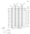
도 9는 도 2의 불휘발성 메모리 모듈의 다른 예를 보여주는 블록도이다. 도면의 간결성을 위하여, 이종 메모리 장치(220) 및 데이터 버퍼(230) 이외의 구성 요소들(모듈 컨트롤러 및 SPD)의 구성은 생략된다. 또한, 앞서 설명된 구성 요소들에 대한 상세한 설명은 생략된다. 도 9를 참조하면, 불휘발성 메모리 모듈(200)은 이종 메모리 장치(220) 및 데이터 버퍼(230)를 포함한다.9 is a block diagram showing another example of the nonvolatile memory module of FIG. 2 . For brevity of the drawing, configurations of components (module controller and SPD) other than the
도 2의 이종 메모리 장치(120)와 달리 도 9의 이종 메모리 장치(220)는 복수의 휘발성 메모리들(221), NVM 제어기(222), 및 복수의 불휘발성 메모리들(223)을 포함한다. 복수의 휘발성 메모리들(221), NVM 제어기(222), 및 복수의 불휘발성 메모리들(223) 각각은 별도의 다이, 별도의 칩, 또는 별도의 패키지로 구현될 수 있다. 이종 메모리 장치(220)의 복수의 휘발성 메모리들(221), NVM 제어기(222), 및 복수의 불휘발성 메모리들(223) 각각은 별도의 칩으로 구현되고, 멀티 칩 패키지(MCP)를 통해 하나의 패키지로 구현될 수 있다.Unlike the
복수의 휘발성 메모리들(221) 각각은 NVM 제어기(222)와 서로 다른 메모리 데이터 라인(MDQ)을 공유하도록 구성된다. 예를 들어, 제1 휘발성 메모리(VM1)는 제1 메모리 데이터 라인(MDQ1)을 NVM 제어기(222)와 공유할 수 있다. 제1 메모리 데이터 라인(MDQ1)은 데이터 버퍼(230)와 연결된다. 예시적으로, 제1 메모리 데이터 라인(MDQ1)은 x8 라인일 수 있다. 제n 휘발성 메모리(VMn)는 제n 메모리 데이터 라인(MDQn)을 NVM 제어기(222)와 공유할 수 있다. 제n 데이터 라인(MDQn)은 데이터 버퍼(230)와 연결된다. 예시적으로, 제n 메모리 데이터 라인(MDQn)은 x8 라인일 수 있다. 즉, 복수의 휘발성 메모리들(221) 각각은 하나의 NVM 제어기(222)와 복수의 메모리 데이터 라인들(MDQ1~MDQn)을 각각 공유하고, 복수의 메모리 데이터 라인들(MDQ1~MDQn)은 하나의 데이터 버퍼(230)와 연결될 수 있다.Each of the plurality of
데이터 버퍼(230)는 데이터 라인(DQ)을 통해 프로세서(101, 도 1 참조)와 연결된다. 이 때, 데이터 라인(DQ)의 개수는 복수의 메모리 데이터 라인들(MDQ1~MDQn)의 개수에 따라 결정될 수 있다.The
예시적으로, 도 9의 불휘발성 메모리 모듈(200)은 도 1 내지 도 8을 참조하여 설명된 동작 방법을 기반으로 동작할 수 있다.Illustratively, the
도 10은 도 2의 불휘발성 메모리 모듈의 다른 예를 보여주는 블록도이다. 간결한 설명을 위하여, 도 2 및 도 9를 참조하여 설명된 구성 요소들에 대한 설명은 생략된다. 도 10을 참조하면, 불휘발성 메모리 모듈(300)은 이종 메모리 장치(320) 및 데이터 버퍼(330)를 포함한다. 이종 메모리 장치(320)는 복수의 휘발성 메모리들(321), NVM 제어기(322), 및 복수의 불휘발성 메모리들(323)을 포함한다.FIG. 10 is a block diagram showing another example of the nonvolatile memory module of FIG. 2 . For concise description, descriptions of components described with reference to FIGS. 2 and 9 are omitted. Referring to FIG. 10 , a
도 9의 이종 메모리 장치(220)와 달리 도 10의 이종 메모리 장치(320)는 전용 플러시 채널(FC)을 포함한다. 전용 플러시 채널(FC)은 복수의 휘발성 메모리들(321) 각각 및 NVM 제어기(322) 사이의 데이터 전송 경로를 제공한다. 앞서 설명된 바와 같이, 불휘발성 메모리 모듈(300)은 플러시 동작을 수행할 수 있다. 불휘발성 메모리 모듈(300)은 전용 플러시 채널(FC)을 통해 복수의 휘발성 메모리들(321)로부터의 데이터가 NVM 제어기(322)로 전송되도록 이종 메모리 장치(320)를 제어할 수 있다.Unlike the
예시적으로, 도 10의 불휘발성 메모리 모듈(300)은 도 1 내지 도 8을 참조하여 설명된 동작 방법을 기반으로 동작할 수 있다.Illustratively, the
도 11은 도 2의 불휘발성 메모리 모듈의 다른 예를 보여주는 블록도이다. 도 11을 참조하면, 불휘발성 메모리 모듈(400)은 모듈 컨트롤러(MC; Module Controller), 복수의 이종 메모리 장치들(HM), 복수의 데이터 버퍼들(DB), SPD, 및 태그 전용 휘발성 메모리(TVM)를 포함한다. 예시적으로, 불휘발성 메모리 모듈(400)은 LRDIMM(Load Reduced Dual In-line Memory Module)의 형태를 가질 수 있다. 간결한 설명을 위하여, 앞서 설명된 구성 요소들과 중복되는 설명은 생략된다.11 is a block diagram showing another example of the nonvolatile memory module of FIG. 2 . Referring to FIG. 11 , the
앞서 설명된 바와 같이, 모듈 컨트롤러(MC)는 프로세서(101)(도 1 참조)로부터 모듈 커맨드/어드레스(CA)를 수신하고, 수신된 모듈 커맨드/어드레스(CA)에 응답하여 NVM 커맨드/어드레스(CA_n) 및 VM 커맨드/어드레스(CA_v)를 출력한다. NVM 커맨드/어드레스(CA_n) 및 VM 커맨드/어드레스(CA_v)는 서로 다른 버스를 통해 이종 메모리 장치(HMD)로 제공될 수 있다.As described above, the module controller MC receives the module command/address CA from the processor 101 (see FIG. 1), and in response to the received module command/address CA, the module controller MC receives the NVM command/address ( CA_n) and VM command/address (CA_v) are output. The NVM command/address CA_n and the VM command/address CA_v may be provided to the heterogeneous memory device HMD through different buses.
복수의 이종 메모리 장치들(HMD; Heterogeneous Memory Device) 각각은 별도의 패키지로 구현될 수 있으며, 복수의 이종 메모리 장치들(HMD) 각각은 도 1 내지 도 10을 참조하여 설명된 이종 메모리 장치들(120, 220, 320) 중 어느 하나일 수 있다. 앞서 설명된 바와 같이, 복수의 이종 메모리 장치들(HM) 각각은 모듈 컨트롤러(MC)로부터의 NVM 커맨드/어드레스(CA_v) 및 VM 커맨드/어드레스(CA_v)에 응답하여 동작할 수 있다. 예시적으로, NVM 커맨드/어드레스(CA_n)는 이종 메모리 장치(HMD)에 포함된 NVM 제어기로 제공되고, VM 커맨드/어드레스(CA_v)는 이종 메모리 장치(HMD)에 포함된 휘발성 메모리 및 NVM 제어기로 제공될 수 있다.Each of the plurality of heterogeneous memory devices (HMD) may be implemented as a separate package, and each of the plurality of heterogeneous memory devices (HMD) may be the same as the heterogeneous memory devices described with reference to FIGS. 1 to 10 ( 120, 220, 320) may be any one. As described above, each of the plurality of heterogeneous memory devices HM may operate in response to the NVM command/address CA_v and the VM command/address CA_v from the module controller MC. For example, the NVM command/address CA_n is provided to the NVM controller included in the heterogeneous memory device HMD, and the VM command/address CA_v is provided to the volatile memory and NVM controller included in the heterogeneous memory device HMD. can be provided.
SPD는 불휘발성 메모리 모듈(400)에 대한 장치 정보(DI)를 포함하고, 프로세서(101)(도 1 참조)로 장치 정보(DI)를 제공할 수 있다.The SPD may include device information DI about the
태그 전용 휘발성 메모리(TVM)는 모듈 컨트롤러(MC)로부터의 VM 커맨드/어드레스(CA_v)에 응답하여 동작할 수 있다. 태그 전용 휘발성 메모리(TVM)는 복수의 이종 메모리 장치들(HMD)의 휘발성 메모리에 저장된 데이터에 대한 태그(TAG)를 저장할 수 있다. 태그 전용 휘발성 메모리(TVM)는 태그 데이터 라인(TDQ)을 통해 태그(TAG)를 송수신할 수 있다. 예시적으로, 모듈 컨트롤러(MC), 복수의 이종 메모리 장치들(HM), 및 태그 전용 휘발성 메모리(TVM)는 태그 데이터 라인(TDQ)을 서로 공유할 수 있다.The tag-only volatile memory (TVM) may operate in response to a VM command/address (CA_v) from the module controller (MC). The tag-only volatile memory (TVM) may store a tag (TAG) for data stored in the volatile memories of the plurality of heterogeneous memory devices (HMD). The tag-only volatile memory (TVM) may transmit/receive a tag (TAG) through a tag data line (TDQ). For example, the module controller MC, the plurality of heterogeneous memory devices HM, and the tag-only volatile memory TVM may share the tag data line TDQ with each other.
비록 도면에 도시되지는 않았으나, 태그 전용 휘발성 메모리(TVM)는 이종 메모리 장치(HMD)와 유사하게 구성될 수 있다. 예를 들어, 복수의 이종 메모리 장치들(HMD) 중 적어도 하나에 포함된 휘발성 메모리는 태그 전용 휘발성 메모리(TVM)로써 사용될 수 있다.Although not shown in the drawings, the tag-only volatile memory (TVM) may be configured similarly to the heterogeneous memory device (HMD). For example, a volatile memory included in at least one of the plurality of heterogeneous memory devices (HMD) may be used as a tag-only volatile memory (TVM).
예시적으로, 도 11의 불휘발성 메모리 모듈(400)은 도 1 내지 도 8을 참조하여 설명된 동작 방법을 기반으로 동작할 수 있다.Illustratively, the
도 12는 도 2의 불휘발성 메모리 모듈의 다른 예를 보여주는 블록도이다. 간결한 설명을 위하여, 앞서 설명된 구성 요소들에 대한 설명은 생략된다. 도 12를 참조하면, 불휘발성 메모리 모듈(500)은 모듈 컨트롤러(MC), 복수의 휘발성 메모리들(VM11~VM1n, VM21~VM2m), 제1 및 제2 NVM 제어기들(522a, 522b), 복수의 불휘발성 메모리들(NVM11~NVM1k, NVM21~NVM2i), 태그 전용 휘발성 메모리(TVM), SPD, 및 복수의 데이터 버퍼들(DB)을 포함한다. 예시적으로, 도 12의 불휘발성 메모리 모듈(500)은 LRDIMM의 구조를 가질 수 있다.FIG. 12 is a block diagram showing another example of the nonvolatile memory module of FIG. 2 . For concise description, descriptions of the components described above are omitted. Referring to FIG. 12 , the
복수의 휘발성 메모리들(VM11~VM1n, VM21~VM2m) 중 일부 휘발성 메모리들(예를 들어, VM11~VM1n)은 제1 NVM 제어기(522a)와 메모리 데이터 라인(MDQ)을 각각 공유하도록 구성된다. 나머지 휘발성 메모리들(예를 들어, VM21~VM2m)은 제2 NVM 제어기(522b)와 메모리 데이터 라인(MDQ)을 각각 공유하도록 구성된다. 복수의 휘발성 메모리들(VM11~VM1n, VM21~VM2m) 각각은 복수의 데이터 버퍼들(DB) 각각과 메모리 데이터 라인(MDQ)을 공유하도록 구성된다.Some of the volatile memories (eg, VM11 to VM1n) among the plurality of volatile memories VM11 to VM1n and VM21 to VM2m are configured to share the
복수의 불휘발성 메모리들(NVM11~NVM1k, NVM21~NVM2i) 중 일부 불휘발성 메모리들(예를 들어, NVM11~NVM1k)은 제1 NVM 제어기(522a)의 제어에 따라 동작하도록 구성된다. 나머지 불휘발성 메모리들(예를 들어, NVM21~NVM2i)은 제2 NVM 제어기(522b)의 제어에 따라 동작하도록 구성된다.Some of the nonvolatile memories (eg, NVM11 to NVM1k) among the plurality of nonvolatile memories (NVM11 to NVM1k and NVM21 to NVM2i) are configured to operate under the control of the
태그 전용 휘발성 메모리(TVM; tag dedicated volatile memory)는 모듈 컨트롤러(MC), 제1 NVM 제어기(522a), 및 제2 NVM 제어기(522b)와 태그 데이터 라인(TDQ)을 공유하도록 구성된다.A tag dedicated volatile memory (TVM) is configured to share a tag data line (TDQ) with a module controller (MC), a
예시적으로, 도 12에 도시된 구성 요소들 각각은 복수의 반도체 칩들로 구현될 수 있고, 복수의 반도체 칩들 중 적어도 일부는 하나의 패키지로 구현될 수 있다. 예를 들어, 복수의 휘발성 메모리들(VM11~VM1n, VM21~VM2m), 복수의 불휘발성 메모리들(NVM11~NVM1k, NVM21~NVM2i), 제1 NVM 제어기(522a), 및 제2 NVM 제어기(522b) 각각은 별도의 반도체 칩들로 구현될 수 있다. 복수의 휘발성 메모리들(VM11~VM1n, VM21~VM2m), 복수의 불휘발성 메모리들(NVM11~NVM1k, NVM21~NVM2i), 제1 NVM 제어기(522a), 및 제2 NVM 제어기(522b) 중 일부 구성 요소들은 하나의 패키지로 구현될 수 있다.For example, each of the components shown in FIG. 12 may be implemented as a plurality of semiconductor chips, and at least some of the plurality of semiconductor chips may be implemented as one package. For example, a plurality of volatile memories (VM11 to VM1n, VM21 to VM2m), a plurality of nonvolatile memories (NVM11 to NVM1k, NVM21 to NVM2i), a
예를 들어, 복수의 휘발성 메모리들(VM11~VM1n, VM21~VM2m) 중 일부(예를 들어, VM11~VM1n)가 하나의 패키지로 구성되고, NVM 제어기(522a) 및 불휘발성 메모리 모듈들(NVM11~NVM1k, NVM21~NVM2i) 중 일부(NVM11~NVM1k)가 다른 하나의 패키지로 구현될 수 있다.For example, some of the plurality of volatile memories (VM11 to VM1n, VM21 to VM2m) (eg, VM11 to VM1n) are configured as one package, and the
예시적으로, 태그 전용 휘발성 메모리(TVM)는 복수의 반도체 칩들을 포함할 수 있다. 예를 들어, 태그 전용 휘발성 메모리(TVM)는 복수의 태그 전용 휘발성 메모리 칩들을 포함하고, 복수의 휘발성 메모리 칩들 각각은 서로 동일한 태그 정보, ECC 정보, 더티 정보 등을 저장할 수 있다. 이 경우, 어느 하나의 태그 전용 휘발성 메모리 칩의 정상 동작하지 않더라도, 다른 태그 전용 휘발성 메모리 칩을 통해 정상적으로 태그 정보, ECC 정보, 더티 정보 등을 기입 또는 출력할 수 있다. 예시적으로, 태그 전용 휘발성 메모리(TVM)는 다른 구성 요소들과 별도의 패키지로 구현될 수 있다. 또는 태그 전용 휘발성 메모리(TVM)는 다른 구성 요소들 중 적어도 일부와 함께 패키지로 구현될 수 있다.For example, a tag-only volatile memory (TVM) may include a plurality of semiconductor chips. For example, a tag-only volatile memory (TVM) includes a plurality of tag-only volatile memory chips, and each of the plurality of volatile memory chips may store the same tag information, ECC information, dirty information, and the like. In this case, even if one of the tag-only volatile memory chips does not normally operate, tag information, ECC information, dirty information, etc. may be normally written or output through the other tag-only volatile memory chips. For example, the tag-only volatile memory (TVM) may be implemented as a separate package from other components. Alternatively, the tag-only volatile memory (TVM) may be implemented as a package along with at least some of other components.
예시적으로, 도 12의 불휘발성 메모리 모듈(500)은 도 1 내지 도 8을 참조하여 설명된 동작 방법을 기반으로 동작할 수 있다.Illustratively, the
도 13은 도 2의 불휘발성 메모리 모듈의 다른 예를 보여주는 블록도이다. 도 13을 참조하면, 불휘발성 메모리 모듈(600)은 모듈 컨트롤러(MC), 복수의 휘발성 메모리들(VM), NVM 제어기(622), 불휘발성 메모리들(NVM), 태그 전용 휘발성 메모리(TVM), SPD, 및 복수의 데이터 버퍼들(DB)을 포함할 수 있다. 간결한 설명을 위하여, 앞서 설명된 구성 요소들에 대한 상세한 설명은 생략된다. 예시적으로, 도 13의 불휘발성 메모리 모듈(600)은 LRDIMM의 구조를 가질 수 있다.FIG. 13 is a block diagram showing another example of the nonvolatile memory module of FIG. 2 . Referring to FIG. 13, the
도 12의 불휘발성 메모리 모듈(500)과 달리 도 13의 불휘발성 메모리 모듈(600)은 하나의 NVM 제어기(622)의 통해 불휘발성 메모리들(NVM)을 제어할 수 있다. 즉, 복수의 휘발성 메모리들(VM) 각각은 NVM 제어기(622)와 메모리 데이터 라인(MDQ)을 공유하도록 구성된다.Unlike the
태그 휘발성 메모리(TVM)는 모듈 컨트롤러(MC) 및 NVM 제어기(622)와 태그 데이터 라인(TDQ)을 공유하도록 구성된다. 앞서 설명된 바와 같이 태그 휘발성 메모리(TVM)는 VM 커맨드/어드레스(CA_v)에 응답하여 태그(TAG)를 기입하거나 또는 저장된 태그(TAG)를 출력할 수 있다.The tag volatile memory (TVM) is configured to share the tag data line (TDQ) with the module controller (MC) and the
예시적으로, 도 13의 불휘발성 메모리 모듈(600)은 도 1 내지 도 8을 참조하여 설명된 동작 방법을 기반으로 동작할 수 있다.Illustratively, the
도 14는 도 2의 불휘발성 메모리 모듈의 다른 예를 보여주는 블록도이다. 도 14를 참조하면, 불휘발성 메모리 모듈(700)은 모듈 컨트롤러, 복수의 휘발성 메모리들(VM11~VM1n, VM21~VM2m), 제1 및 제2 NVM 제어기들(722a, 722b), 복수의 불휘발성 메모리들(NVM11~NVM1k, NVM21~NVM2i), 태그 전용 휘발성 메모리(TVM), SPD, 복수의 데이터 버퍼들(DB), 및 태그 제어 회로(TC; Tag Control circuit)를 포함한다. 간결한 설명을 위하여, 앞서 설명된 구성 요소들에 대한 설명은 생략된다. 예시적으로, 도 14의 불휘발성 메모리 모듈(700)은 LRDIMM의 구조를 가질 수 있다.FIG. 14 is a block diagram showing another example of the nonvolatile memory module of FIG. 2 . Referring to FIG. 14 , the
도 11 내지 도 13의 불휘발성 메모리 모듈들(400, 500, 600)과 달리, 도 14의 불휘발성 메모리 모듈(700)은 태그 제어 회로(TC)를 더 포함한다. 태그 제어 회로(TC)는 태그 전용 휘발성 메모리(TVM)와 태그 데이터 라인(TDQ)을 공유하도록 구성된다. 즉, 태그 제어 회로(TC)는 태그 데이터 라인(TDQ)을 통해 태그 전용 휘발성 메모리(TVM)로부터 태그(TAG)를 수신하거나 또는 태그 데이터 라인(TDQ)을 통해 태그(TAG)를 태그 전용 휘발성 메모리(TVM)로 전송할 수 있다.Unlike the
태그 제어 회로(TC)는 모듈 컨트롤러(MC)의 제어에 따라 캐시 히트 또는 캐시 미스 여부를 판별하고, 판별 결과를 캐시 정보(INFO)로써 출력할 수 있다. 예를 들어, 태그 제어 회로(TC)는 모듈 컨트롤러(MC)의 제어에 따라 태그 전용 휘발성 메모리(TVM)로부터 태그(TAG)를 수신할 수 있다. 태그 제어 회로(TC)는 모듈 컨트롤러(MC)로부터의 태그(TAG)(또는 어드레스(ADD)) 및 태그 전용 휘발성 메모리(TVM)로부터의 태그(TAG)를 비교함으로써 캐시 히트 또는 캐시 미스를 판별할 수 있다.The tag control circuit (TC) may determine whether a cache hit or a cache miss is determined under the control of the module controller (MC), and output the determination result as cache information (INFO). For example, the tag control circuit TC may receive the tag TAG from the tag-only volatile memory TVM under the control of the module controller MC. The tag control circuit (TC) determines a cache hit or cache miss by comparing the tag (TAG) (or address (ADD)) from the module controller (MC) and the tag (TAG) from the tag-only volatile memory (TVM). can
예시적으로, 태그 제어 회로(TC)는 소프트웨어 또는 하드웨어로 구현될 수 있으며, 태그 제어 회로(TC)는 모듈 컨트롤러(MC)에 포함되거나 또는 제1 및 제2 NVM 제어기들(722a, 722b)에 각각 포함될 수 있다.Illustratively, the tag control circuit (TC) may be implemented in software or hardware, and the tag control circuit (TC) is included in the module controller (MC) or in the first and second NVM controllers (722a, 722b). each can be included.
예시적으로, 도 14의 불휘발성 메모리 모듈(700)은 도 1 내지 도 8을 참조하여 설명된 동작 방법을 기반으로 동작할 수 있다.Illustratively, the
도 15는 도 2의 불휘발성 메모리 모듈의 다른 예를 보여주는 블록도이다. 도 15를 참조하면, 불휘발성 메모리 모듈(800)은 모듈 컨트롤러(MC), 복수의 이종 메모리들(HMD), 태그 전용 휘발성 메모리(TVM), 및 SPD를 포함한다. 간결한 설명을 위하여, 앞서 설명된 구성 요소들에 대한 상세한 설명은 생략된다.15 is a block diagram showing another example of the nonvolatile memory module of FIG. 2 . Referring to FIG. 15 , the
도 15의 불휘발성 메모리 모듈(800)은 도 11의 불휘발성 메모리 모듈(400)과 달리, 복수의 데이터 버퍼들(DB)을 포함하지 않는다. 즉, 불휘발성 메모리 모듈(800)은 RDIMM(Registered DIMM)의 구조를 가질 수 있다.Unlike the
복수의 이종 메모리들(HMD) 각각은 데이터 라인(DQ)과 직접 연결된다. 예시적으로, 복수의 이종 메모리들(HMD) 각각에 포함된 불휘발성 메모리를 제어하는 NVM 제어기 및 휘발성 메모리는 데이터 라인(DQ)을 공유하도록 구성될 수 있다.Each of the plurality of heterogeneous memories HMD is directly connected to the data line DQ. Exemplarily, the NVM controller controlling the nonvolatile memory included in each of the plurality of heterogeneous memories HMD and the volatile memory may be configured to share the data line DQ.
예시적으로, 프로세서(101)(도 1 참조)는 불휘발성 메모리 모듈(800)의 SPD로부터 장치 정보(DI)를 수신하고, 수신된 장치 정보(DI)를 기반으로 불휘발성 메모리 모듈(800)을 제어할 수 있다. 이 때, 장치 정보(DI)는 앞서 설명된 읽기 레이턴시(RL), 쓰기 레이턴시(WL) 등과 같은 불휘발성 메모리 모듈(800)의 동작 정보를 포함할 것이다. 즉, 복수의 이종 메모리 장치들(HMD) 각각에 포함된 휘발성 메모리 및 NVM 제어기가 서로 데이터 라인(DQ)을 공유하고, 데이터 라인(DQ)을 통해 프로세서(101)의 요청과 별개로 데이터를 서로 교환하더라도, 프로세서(101)는 장치 정보(DI)를 기반으로 불휘발성 메모리 모듈(800)을 제어하기 때문에, 불휘발성 메모리 모듈(800)에 대한 읽기 또는 쓰기 동작을 정상적으로 수행할 수 있다.Illustratively, the processor 101 (see FIG. 1 ) receives device information (DI) from the SPD of the
예시적으로, 도 15의 불휘발성 메모리 모듈(800)은 도 1 내지 도 8을 참조하여 설명된 동작 방법을 기반으로 동작할 수 있다.Illustratively, the
도 16은 도 2의 불휘발성 메모리 모듈의 다른 예를 보여주는 블록도이다. 도 16을 참조하면, 불휘발성 메모리 모듈(900)은 모듈 컨트롤러(MC), 복수의 휘발성 메모리들(VM11~VM1n, VM21~VM2m), 제1 및 제2 NVM 제어기들(922a, 922b), 복수의 불휘발성 메모리들(NVM11~NVM1k, NVM21~NVM2i), 태그 전용 휘발성 메모리(TVM), 및 SPD를 포함한다. 간결한 설명을 위하여, 앞서 설명된 구성 요소들에 대한 상세한 설명은 생략된다.16 is a block diagram showing another example of the nonvolatile memory module of FIG. 2 . Referring to FIG. 16 , the
도 16의 불휘발성 메모리 모듈(900)은 도 12의 불휘발성 메모리 모듈(500)과 달리, 복수의 데이터 버퍼(DB)를 포함하지 않는다. 즉, 불휘발성 메모리 모듈(900)은 RDIMM의 구조를 가질 수 있다. 이 때, 복수의 휘발성 메모리들(VM11~VM1n, VM21~VM2m) 중 일부(예를 들어, VM11~VM1n)는 제1 NVM 제어기(922a)와 데이터 라인(DQ)을 공유하고, 나머지 일부(예를 들어, VM21~VM2m)는 제2 NVM 제어기(922b)와 데이터 라인(DQ)을 공유하도록 구성된다.Unlike the
도 15를 참조하여 설명된 바와 유사하게, 도 16의 복수의 휘발성 메모리들(VM11~VM1n, VM21~VM2m), 제1 및 제2 NVM 제어기들(922a, 922b)이 서로 데이터 라인(DQ)을 공유하더라도, 프로세서(101)(도 1 참조)는 SPD로부터의 장치 정보(DI)를 기반으로 동작하기 때문에, 복수의 휘발성 메모리들(VM11~VM1n, VM21~VM2m), 제1 및 제2 NVM 제어기들(922a, 922b) 사이의 데이터 교환과 무관하게 정상적으로 불휘발성 메모리 모듈을 제어할 수 있다.Similar to the description with reference to FIG. 15 , the plurality of volatile memories VM11 to VM1n and VM21 to VM2m and the first and
예시적으로, 도 16의 불휘발성 메모리 모듈(900)은 도 1 내지 도 9를 참조하여 설명된 동작 방법을 기반으로 동작할 수 있다.Illustratively, the
도 17은 도 2의 불휘발성 메모리 모듈의 다른 예를 보여주는 블록도이다. 도 17을 참조하면, 불휘발성 메모리 모듈(A00)은 모듈 컨트롤러(MC), 복수의 휘발성 메모리들(VM), NVM 제어기(A22), 불휘발성 메모리들(NVM), 태그 전용 휘발성 메모리(TVM), 및 SPD를 포함한다. 간결한 설명을 위하여, 앞서 설명된 구성 요소들에 대한 상세한 설명은 생략된다.17 is a block diagram showing another example of the nonvolatile memory module of FIG. 2 . Referring to FIG. 17, the nonvolatile memory module A00 includes a module controller MC, a plurality of volatile memories VM, an NVM controller A22, nonvolatile memories NVM, and a tag-only volatile memory TVM. , and SPD. For concise description, detailed descriptions of the components described above are omitted.
도 17의 불휘발성 메모리 모듈(A00)은 도 13의 불휘발성 메모리 모듈(600)과 달리 복수의 데이터 버퍼(DB)를 포함하지 않는다. 즉, 불휘발성 메모리 모듈(A00)은 RDIMM의 구조를 가질 수 있다. 복수의 휘발성 메모리들(VM)은 하나의 NVM 제어기(A22)와 데이터 라인(DQ)을 서로 공유하도록 구성된다.Unlike the
앞서 설명된 바와 같이, 프로세서(101)(도 1 참조)는 SPD로부터의 장치 정보(DI)를 기반으로 동작하기 때문에, 복수의 휘발성 메모리들(VM) 및 NVM 제어기(A22) 사이의 데이터 교환과 무관하게 정상적으로 불휘발성 메모리 모듈을 제어할 수 있다.As described above, since the processor 101 (see FIG. 1) operates based on the device information (DI) from the SPD, data exchange between a plurality of volatile memories (VM) and the NVM controller (A22) and Regardless, the nonvolatile memory module can be normally controlled.
상술된 불휘발성 메모리 모듈들은 예시적인 것이며, 본 발명의 범위가 이에 한정되는 것은 아니다. 본 발명에 따른 불휘발성 메모리 모듈 상술된 실시 예들에서 서로 조합되거나 또는 변형될 수 있다.The aforementioned nonvolatile memory modules are exemplary, and the scope of the present invention is not limited thereto. The nonvolatile memory module according to the present invention may be combined with or modified from the above-described embodiments.
도 18은 본 발명에 따른 불휘발성 메모리 모듈에 포함된 불휘발성 메모리를 예시적으로 보여주는 블록도이다. 도 18을 참조하면, 불휘발성 메모리(1100)는 메모리 셀 어레이(1110), 어드레스 디코더(1120), 제어 로직 회로(1130), 페이지 버퍼(1140), 및 입출력 회로(1150)를 포함한다.18 is a block diagram exemplarily showing a nonvolatile memory included in a nonvolatile memory module according to the present invention. Referring to FIG. 18 , a
메모리 셀 어레이(1110)는 복수의 메모리 블록들을 포함하고, 복수의 메모리 블록들 각각은 복수의 메모리 셀들을 포함한다. 복수의 메모리 셀들 각각은 복수의 워드라인들(WL)과 각각 연결될 수 있다. 복수의 메모리 셀들 각각은 1-비트를 저장하는 싱글 레벨 셀(SLC)이거나 또는 적어도 2-비트를 저장하는 멀티 레벨 셀(MLC)일 수 있다.The
어드레스 디코더(1120)는 NVM 제어기(112)(도 2 참조)로부터 어드레스(ADDR)를 수신하고, 수신된 어드레스(ADDR)를 디코딩할 수 있다. 예시적으로, NVM 제어기(112)로부터 수신된 어드레스(ADDR)는 불휘발성 메모리(1100)의 저장 영역의 물리적 위치를 가리키는 물리적 어드레스(physical address)일 수 있다. 어드레스 디코더(1120)는 디코딩된 어드레스를 기반으로 복수의 워드라인들(WL) 중 적어도 하나의 워드라인을 선택하고, 선택된 워드라인의 전압을 구동할 수 있다.The
제어 로직 회로(1130)는 NVM 제어기(112)(도 2 참조)로부터 커맨드(CMD) 및 제어 신호(CTRL)를 수신하고, 수신된 신호들에 응답하여 어드레스 디코더(1120), 페이지 버퍼(1140), 및 입출력 회로(1150)를 제어할 수 있다.The
페이지 버퍼(1140)는 복수의 비트 라인들(BL)을 통해 메모리 셀 어레이(1110)와 연결되고, 복수의 데이터 라인들(DL)을 통해 입출력 회로(1150)와 연결된다. 페이지 버퍼(1140)는 복수의 비트 라인들(BL)의 전압을 감지하여 메모리 셀 어레이(1110)에 저장된 데이터를 읽을 수 있다. 또는 페이지 버퍼(1140)는 복수의 데이터 라인들(DL)을 통해 수신되는 데이터를 기반으로 복수의 비트 라인들(BL)의 전압을 제어할 수 있다.The
입출력 회로(1150)는 제어 로직 회로(1130)의 제어에 따라 NVM 제어기(112)(도 2 참조)로부터 데이터를 수신하고, 수신된 데이터를 페이지 버퍼(1140)로 전달할 수 있다. 또는 입출력 회로(1150)는 페이지 버퍼(1140)로부터 데이터를 수신하고, 수신된 데이터를 NVM 제어기(112)로 전달할 수 있다.The input/
예시적으로, NVM 제어기(122)는 모듈 컨트롤러(110)(도 2 참조)로부터의 NVM 커맨드/어드레스(CA_v)를 기반으로 어드레스(ADDR), 커맨드(CMD), 및 제어 신호(CTRL)를 생성할 수 있다.Illustratively, the
도 19는 본 발명에 따른 불휘발성 메모리 모듈의 불휘발성 메모리에 포함된 메모리 블록들 중 제1 메모리 블록을 예시적으로 보여주는 회로도이다. 예시적으로, 도 19를 참조하여 3차원 구조의 제1 메모리 블록(BLK1)이 설명된다. 그러나, 본 발명의 범위가 이에 한정되는 것은 아니며, 다른 메모리 블록들 또한 제1 메모리 블록(BLK1)과 유사한 구조를 가질 수 있다.19 is a circuit diagram exemplarily showing a first memory block among memory blocks included in a nonvolatile memory of a nonvolatile memory module according to the present invention. As an example, a first memory block BLK1 having a 3D structure will be described with reference to FIG. 19 . However, the scope of the present invention is not limited thereto, and other memory blocks may also have a structure similar to that of the first memory block BLK1.
도 19를 참조하면, 제1 메모리 블록(BLK1)은 복수의 셀 스트링들(CS11, CS12, CS21, CS22)을 포함한다. 복수의 셀 스트링들(CS11, CS12, CS21, CS22)은 행 방향(row direction) 및 열 방향(column direction)을 따라 배치되어 행들 및 열들을 형성할 수 있다.Referring to FIG. 19 , the first memory block BLK1 includes a plurality of cell strings CS11, CS12, CS21, and CS22. The plurality of cell strings CS11 , CS12 , CS21 , and CS22 may be disposed along a row direction and a column direction to form rows and columns.
복수의 셀 스트링들(CS11, CS12, CS21, CS22) 각각은 복수의 셀 트랜지스터들을 포함한다. 예를 들어, 복수의 셀 스트링들(CS11, CS12, CS21, CS22) 각각은 스트링 선택 트랜지스터들(SSTa, SSTb), 복수의 메모리 셀들(MC1~MC8), 접지 선택 트랜지스터들(GSTa, GSTb), 및 더미 메모리 셀들(DMC1, DMC2)을 포함할 수 있다. 예시적으로, 복수의 셀 스트링들(CS11, CS12, CS21, CS22)에 포함된 복수의 셀 트랜지스터들 각각은 전하 트랩형 플래시(CTF; charge trap flash) 메모리 셀일 수 있다.Each of the plurality of cell strings CS11 , CS12 , CS21 , and CS22 includes a plurality of cell transistors. For example, each of the plurality of cell strings CS11, CS12, CS21, and CS22 includes string select transistors SSTa and SSTb, a plurality of memory cells MC1 to MC8, ground select transistors GSTa and GSTb, and dummy memory cells DMC1 and DMC2. For example, each of the plurality of cell transistors included in the plurality of cell strings CS11 , CS12 , CS21 , and CS22 may be a charge trap flash (CTF) memory cell.
복수의 메모리 셀들(MC1~MC8)은 직렬 연결되며, 행 방향 및 열 방향에 의해 형성된 평면과 수직한 방향인 높이 방향(height direction)으로 적층된다. 스트링 선택 트랜지스터들(SSTa, SSTb)은 직렬 연결되고, 직렬 연결된 스트링 선택 트랜지스터들(SSTa, SSTb)은 복수의 메모리 셀들(MC1~MC8) 및 비트라인(BL) 사이에 제공된다. 접지 선택 트랜지스터들(GSTa, GSTb)은 직렬 연결되고, 직렬 연결된 접지 선택 트랜지스터들(GSTa, GSTb)은 복수의 메모리 셀들(MC1~MC8) 및 공통 소스 라인(CSL) 사이에 제공된다.The plurality of memory cells MC1 to MC8 are connected in series and stacked in a height direction that is perpendicular to a plane formed by row and column directions. The string select transistors SSTa and SSTb are connected in series, and the string select transistors SSTa and SSTb connected in series are provided between the plurality of memory cells MC1 to MC8 and the bit line BL. The ground select transistors GSTa and GSTb are serially connected, and the serially connected ground select transistors GSTa and GSTb are provided between the plurality of memory cells MC1 to MC8 and the common source line CSL.
예시적으로, 복수의 메모리 셀들(MC1~MC8) 및 접지 선택 트랜지스터들(GSTa, GSTb) 사이에 제1 더미 메모리 셀(DMC1)이 제공될 수 있다. 예시적으로, 복수의 메모리 셀들(MC1~MC8) 및 스트링 선택 트랜지스터들(SSTa, SSTb) 사이에 제2 더미 메모리 셀(DMC2)이 제공될 수 있다.For example, a first dummy memory cell DMC1 may be provided between the plurality of memory cells MC1 to MC8 and the ground select transistors GSTa and GSTb. For example, a second dummy memory cell DMC2 may be provided between the plurality of memory cells MC1 to MC8 and the string select transistors SSTa and SSTb.
셀 스트링들(CS11, CS12, CS21, CS22)의 접지 선택 트랜지스터들(GSTa, GSTb)은 접지 선택 라인(GSL)에 공통으로 연결될 수 있다. 예시적으로, 동일한 행의 접지 선택 트랜지스터들은 동일한 접지 선택 라인에 연결될 수 있고, 다른 행의 접지 선택 트랜지스터들은 다른 접지 선택 라인에 연결될 수 있다. 예를 들어, 제1 행의 셀 스트링들(CS11, CS12)의 제1 접지 선택 트랜지스터들(GSTa)은 제1 접지 선택 라인에 연결될 수 있고, 제2 행의 셀 스트링들(CS21, CS22)의 제1 접지 선택 트랜지스터들(GSTa)은 제2 접지 선택 라인에 연결될 수 있다.The ground select transistors GSTa and GSTb of the cell strings CS11 , CS12 , CS21 , and CS22 may be connected to the ground select line GSL in common. For example, ground select transistors in the same row may be connected to the same ground select line, and ground select transistors in different rows may be connected to different ground select lines. For example, the first ground select transistors GSTa of the cell strings CS11 and CS12 in the first row may be connected to the first ground select line, and the cell strings CS21 and CS22 in the second row may be connected to each other. The first ground select transistors GSTa may be connected to the second ground select line.
예시적으로, 도면에 도시되지는 않았으나, 기판(미도시)으로부터 동일한 높이에 제공되는 접지 선택 트랜지스터들은 동일한 접지 선택 라인에 연결될 수 있고, 다른 높이에 제공되는 접지 선택 트랜지스터들은 다른 접지 선택 라인에 연결될 수 있다. 예를 들어, 셀 스트링들(CS11, CS12, CS21, CS22)의 제1 접지 선택 트랜지스터들(GSTa)은 제1 접지 선택 라인에 연결되고, 제2 접지 선택 트랜지스터들(GSTb)은 제2 접지 선택 라인에 연결될 수 있다.For example, although not shown in the drawings, ground select transistors provided at the same height from a substrate (not shown) may be connected to the same ground select line, and ground select transistors provided at different heights may be connected to different ground select lines. can For example, the first ground select transistors GSTa of the cell strings CS11, CS12, CS21, and CS22 are connected to the first ground select line, and the second ground select transistors GSTb are connected to the second ground select line. can be connected to the line.
기판 또는 접지 선택 트랜지스터(GSTa, GSTb)으로부터 동일한 높이의 메모리 셀들은 동일한 워드라인에 공통으로 연결되고, 서로 다른 높이의 메모리 셀들은 서로 다른 워드라인에 연결된다. 예를 들어, 셀 스트링들(CS11, CS12, CS21, CS22)의 제1 내지 제8 메모리 셀들(MC8)은 제1 내지 제8 워드라인들(WL1~WL8)에 각각 공통으로 연결된다.Memory cells of the same height from the substrate or ground selection transistors GSTa and GSTb are commonly connected to the same word line, and memory cells of different heights are connected to different word lines. For example, the first to eighth memory cells MC8 of the cell strings CS11, CS12, CS21, and CS22 are commonly connected to the first to eighth word lines WL1 to WL8, respectively.
동일한 높이의 제1 스트링 선택 트랜지스터들(SSTa) 중 동일한 행의 스트링 선택 트랜지스터들은 동일한 스트링 선택 라인과 연결되고, 다른 행의 스트링 선택 트랜지스터들은 다른 스트링 선택 라인과 연결된다. 예를 들어, 제1 행의 셀 스트링들(CS11, CS12)의 제1 스트링 선택 트랜지스터들(SSTa)은 스트링 선택 라인(SSL1a)과 공통으로 연결되고, 제2 행의 셀 스트링들(CS21, CS22)의 제1 스트링 선택 트랜지스터들(SSTa)은 스트링 선택 라인(SSL1a)과 공통으로 연결된다.Among the first string select transistors SSTa having the same height, string select transistors in the same row are connected to the same string select line, and string select transistors in different rows are connected to different string select lines. For example, the first string select transistors SSTa of the cell strings CS11 and CS12 in the first row are connected in common with the string select line SSL1a, and the cell strings CS21 and CS22 in the second row are connected in common. The first string select transistors SSTa of ) are connected in common with the string select line SSL1a.
마찬가지로, 동일한 높이의 제2 스트링 선택 트랜지스터들(SSTb) 중 동일한 행의 스트링 선택 트랜지스터들은 동일한 스트링 선택 라인과 연결되고, 다른 행의 스트링 선택 트랜지스터들은 다른 스트링 선택 라인과 연결된다. 예를 들어, 제1 행의 셀 스트링들(CS11, CS12)의 제2 스트링 선택 트랜지스터들(SSTb)은 스트링 선택 라인(SSL1b)과 공통으로 연결되고, 제2 행의 셀 스트링들(CS21, CS22)의 제2 스트링 선택 트랜지스터들(SSTb)은 스트링 선택 라인(SSL2b)과 공통으로 연결된다.Similarly, among the second string select transistors SSTb having the same height, string select transistors of the same row are connected to the same string select line, and string select transistors of different rows are connected to other string select lines. For example, the second string select transistors SSTb of the cell strings CS11 and CS12 in the first row are connected in common with the string select line SSL1b, and the cell strings CS21 and CS22 in the second row are connected in common. The second string select transistors SSTb of ) are connected in common with the string select line SSL2b.
예시적으로, 동일한 높이의 더미 메모리 셀들은 동일한 더미 워드라인과 연결되고, 다른 높이의 더미 메모리 셀들은 다른 더미 워드라인과 연결된다. 예를 들어, 제1 더미 메모리 셀들(DMC1)은 제1 더미 워드라인(DWL1)과 연결되고, 제2 더미 메모리 셀들(DMC2)은 제2 더미 워드라인(DWL2)과 연결된다.For example, dummy memory cells of the same height are connected to the same dummy word line, and dummy memory cells of different heights are connected to different dummy word lines. For example, the first dummy memory cells DMC1 are connected to the first dummy word line DWL1, and the second dummy memory cells DMC2 are connected to the second dummy word line DWL2.
예시적으로, 도 19에 도시된 제1 메모리 블록(BLK1)은 예시적인 것이며, 셀 스트링들의 개수는 증가 또는 감소할 수 있으며, 셀 스트링들의 개수에 따라 셀 스트링들이 구성하는 행들 및 열들의 개수는 증가 또는 감소할 수 있다. 또한, 제1 메모리 블록(BLK1)의 셀 트랜지스터들(GST, MC, DMC, SST 등)의 개수들은 각각 증가 또는 감소될 수 있으며, 셀 트랜지스터들의 개수들에 따라 제1 메모리 블록(BLK1)의 높이가 증가 또는 감소할 수 있다. 또한, 셀 트랜지스터들의 개수들에 따라 셀 트랜지스터들과 연결된 라인들(GSL, WL, DWL, SSL 등)의 개수들이 증가 또는 감소될 수 있다.As an example, the first memory block BLK1 illustrated in FIG. 19 is exemplary, and the number of cell strings may increase or decrease, and the number of rows and columns of the cell strings may increase or decrease according to the number of cell strings. may increase or decrease. Also, the number of cell transistors (GST, MC, DMC, SST, etc.) of the first memory block BLK1 may be increased or decreased, respectively, and the height of the first memory block BLK1 depends on the number of cell transistors. may increase or decrease. Also, the number of lines (GSL, WL, DWL, SSL, etc.) connected to the cell transistors may increase or decrease according to the number of cell transistors.
예시적으로, 본 발명에 따른 불휘발성 메모리는 상술된 구성에 한정되지 않는다. 본 발명의 기술적 사상에 따른 예시적인 실시 예로서, 불휘발성 메모리는 3차원 메모리 어레이를 포함할 수 있다. 3차원 메모리 어레이는, 실리콘 기판 및 메모리 셀들의 동작에 연관된 회로의 위에 배치되는 활성 영역을 갖는 메모리 셀들의 어레이들의 하나 또는 그 이상의 물리 레벨들에 모놀리식으로(monolithically) 형성될 수 있다. 메모리 셀들의 동작에 연관된 회로는 기판 내에 또는 기판 위에 위치할 수 있다. 모놀리식(monolithically)이란 용어는, 3차원 어레이의 각 레벨의 층들이 3차원 어레이의 하위 레벨의 층들 위에 직접 증착됨을 의미한다.By way of example, the nonvolatile memory according to the present invention is not limited to the above-described configuration. As an exemplary embodiment according to the technical spirit of the inventive concept, the nonvolatile memory may include a 3D memory array. A three-dimensional memory array may be monolithically formed on one or more physical levels of arrays of memory cells having an active region disposed over a silicon substrate and circuitry associated with operation of the memory cells. Circuitry involved in the operation of the memory cells may be located in or on the substrate. The term monolithically means that the layers of each level of the three-dimensional array are deposited directly over the layers of lower levels of the three-dimensional array.
본 발명의 기술적 사상에 따른 예시적인 실시 예로서, 3차원 메모리 어레이는 수직의 방향성을 가지며, 적어도 하나의 메모리 셀이 다른 하나의 메모리 셀 위에 위치하는 수직 NAND 스트링들을 포함한다. 적어도 하나의 메모리 셀은 전하 트랩 층을 포함한다. 각각의 수직 NAND 스트링은 메모리 셀들 위에 위치하는 적어도 하나의 선택 트랜지스터를 포함할 수 있다. 적어도 하나의 선택 트랜지스터는 메모리 셀들과 동일한 구조를 갖고, 메모리 셀들과 함께 모놀리식으로 형성될 수 있다.As an exemplary embodiment according to the technical concept of the inventive concept, a 3D memory array includes vertical NAND strings having a vertical direction and at least one memory cell positioned above another memory cell. At least one memory cell includes a charge trap layer. Each vertical NAND string may include at least one select transistor located over the memory cells. At least one select transistor has the same structure as the memory cells and may be monolithically formed with the memory cells.
3차원 메모리 어레이가 복수의 레벨들로 구성되고, 레벨들 사이에 공유된 워드 라인들 또는 비트 라인들을 갖고, 3차원 메모리 어레이에 적합한 구성은 미국등록특허공보 제7,679,133호, 미국등록특허공보 제8,553,466호, 미국등록특허공보 제8,654,587호, 미국등록특허공보 제8,559,235호, 그리고 미국공개특허공보 제2011/0233648호에 개시되어 있으며, 본 발명의 레퍼런스로 포함된다.Configurations in which the three-dimensional memory array is composed of a plurality of levels, with word lines or bit lines shared between the levels, suitable for the three-dimensional memory array are disclosed in U.S. Patent No. 7,679,133 and U.S. Patent No. 8,553,466. , US Patent Publication No. 8,654,587, US Patent Publication No. 8,559,235, and US Patent Publication No. 2011/0233648, which are incorporated herein by reference.
도 20은 본 발명에 따른 불휘발성 메모리 모듈의 휘발성 메모리를 예시적으로 보여주는 블록도이다. 도 20을 참조하면, 휘발성 메모리(1200)는 메모리 셀 어레이(1210), 어드레스 버퍼(1220), X-디코더(1230), Y-디코더(1240), 감지 증폭기 및 쓰기 드라이버(1250), 및 입출력 회로(1260)를 포함할 수 있다.20 is a block diagram exemplarily showing a volatile memory of a nonvolatile memory module according to the present invention. Referring to FIG. 20 , a
메모리 셀 어레이(1210)는 복수의 메모리 셀들을 포함하고, 복수의 메모리 셀들 각각은 복수의 워드 라인들(WL) 및 복수의 비트 라인들(BL)과 연결된다. 복수의 메모리 셀들 각각은 워드라인 및 비트라인이 교차하는 지점에 위치할 수 있다. 예시적으로, 복수의 메모리 셀들 각각은 스토리지 캐패시터 및 엑세스 트랜지스터를 포함할 수 있다.The
어드레스 버퍼(1220)는 모듈 컨트롤러(110)(도 2 참조)로부터 어드레스(ADD)를 수신하고, 수신된 어드레스를 임시 저장할 수 있다. 예시적으로, 어드레스 버퍼(1220)는 수신된 어드레스(ADD) 중 행 어드레스(ADD_row)를 X-디코더(1230)로 제공하고, 열 어드레스(ADD_col)를 Y-디코더(1240)로 제공할 수 있다.The
X-디코더(1230)는 복수의 워드 라인들(WL)을 통해 메모리 셀 어레이(1210)와 연결된다. X-디코더(1230)는 모듈 컨트롤러(110)(도 2 참조)로부터의 행 어드레스 스트로브(RAS) 신호에 응답하여 행 어드레스(ADD_row)를 기반으로 복수의 워드 라인들(WL) 중 적어도 하나의 워드 라인을 활성화시킬 수 있다.The
Y-디코더(1240)는 어드레스 버퍼(1220)로부터 열 어드레스(ADD_col)를 수신할 수 있다. Y-디코더(1240)는 열 어드레스 스트로브(CAS) 신호에 응답하여 열 어드레스(ADD_col)를 기반으로 감지 증폭기 및 쓰기 드라이버(1250)를 제어할 수 있다.The Y-
감지 증폭기 및 쓰기 드라이버(1250)는 복수의 비트 라인들(BL)을 통해 메모리 셀 어레이(1210)와 연결된다. 감지 증폭기 및 쓰기 드라이버(1250)는 복수의 비트 라인들(BL)의 전압 변화를 감지할 수 있다. 또는 감지 증폭기 및 쓰기 드라이버(1250)는 입출력 회로(1260)로부터 수신된 데이터를 기반으로 복수의 비트 라인들(BL)의 전압을 제어할 수 있다.The sense amplifier and write
입출력 회로(1260)는 감지 증폭기 및 쓰기 드라이버(1250)로부터 데이터를 수신하고, 수신된 데이터를 메모리 데이터 라인(MDQ)(또는 데이터 라인(DQ))을 통해 출력할 수 있다. 또는 입출력 회로(1260)는 메모리 데이터 라인(MDQ)(또는 데이터 라인(DQ))을 통해 데이터를 수신하고, 수신된 데이터를 감지 증폭기 및 쓰기 드라이버(1250)에 전달할 수 있다.The input/
예시적으로, 어드레스(ADD)는 모듈 컨트롤러(110)(도 2 참조)로부터 제공되는 VM 커맨드/어드레스(CA_v)에 포함된 어드레스일 수 있다. 행 어드레스 스트로브(RAS) 및 열 어드레스 스트로브(CAS)는 모듈 컨트롤러(110)(도 2 참조)로부터 제공되는 VM 커맨드/어드레스(CA_v)에 포함된 신호들일 수 있다.For example, the address ADD may be an address included in the VM command/address CA_v provided from the module controller 110 (see FIG. 2 ). The row address strobe (RAS) and the column address strobe (CAS) may be signals included in the VM command/address CA_v provided from the module controller 110 (see FIG. 2 ).
도 21은 본 발명에 따른 불휘발성 메모리 모듈이 적용된 서버 시스템을 예시적으로 보여주는 도면이다. 도 21을 참조하면, 서버 시스템(2000)은 복수의 서버 랙들(2100)을 포함할 수 있다. 복수의 서버 랙들(2100) 각각은 복수의 불휘발성 메모리 모듈들(2200)을 포함할 수 있다. 복수의 불휘발성 메모리 모듈들(2200)은 복수의 서버 랙들(2100) 각각에 포함된 프로세서들과 직접적으로 연결될 수 있다. 예를 들어, 복수의 불휘발성 메모리 모듈들(2200) 듀얼 인-라인 메모리 모듈의 형태를 갖고, 프로세서와 전기적으로 연결된 DIMM 소켓에 장착되어 프로세서와 서로 통신할 수 있다. 예시적으로, 복수의 불휘발성 메모리 모듈들(2200)은 서버 시스템(2000)의 스토리지로서 사용될 수 있다. 예시적으로, 복수의 불휘발성 메모리 모듈들(2200)은 도 1 내지 도 20을 참조하여 설명된 불휘발성 메모리 모듈이거나 또는 동작 방법을 기반으로 동작할 수 있다.21 is a diagram exemplarily showing a server system to which a nonvolatile memory module according to the present invention is applied. Referring to FIG. 21 , a
도 22는 본 발명에 따른 불휘발성 메모리 모듈이 적용된 사용자 시스템을 예시적으로 보여주는 블록도이다. 도 22를 참조하면, 사용자 시스템(3000)은 프로세서(3001) 및 복수의 메모리들(3110~3140)을 포함할 수 있다.22 is a block diagram exemplarily showing a user system to which a nonvolatile memory module according to the present invention is applied. Referring to FIG. 22 , a
프로세서(3001)는 메모리 컨트롤러(3002)를 포함할 수 있다. 메모리 컨트롤러(3002)는 버스(3003)를 통해 복수의 메모리들(3110~3140)과 통신할 수 있다. 예시적으로, 버스(3003)는 복수의 메모리들(3110~3140) 각각과 연결된 전용 버스들 또는 복수의 메모리들(3110~3140)과 공유되는 공용 버스를 포함할 수 있다. 예시적으로, 버스(3003)는 도 1 내지 도 21을 참조하여 설명된, 데이터 라인(DQ), 메모리 데이터 라인(MDQ), 태그 데이터 라인(TDQ) 중 적어도 하나를 포함할 수 있다.The
예시적으로, 복수의 메모리들(3110~3140) 중 적어도 일부는 도 1 내지 도 21을 참조하여 설명된 불휘발성 메모리 모듈이거나 또는 도 1 내지 도 21을 참조하여 설명된 동작 방법을 기반으로 동작할 수 있다.Illustratively, at least some of the plurality of
또는, 복수의 메모리 모듈들(3110~3140) 중 적어도 일부는 불휘발성 메모리를 포함하고, 나머지 일부는 휘발성 메모리를 포함할 수 있다. 휘발성 메모리를 포함하는 메모리 모듈은 불휘발성 메모리를 포함하는 메모리 모듈의 캐시 메모리로서 사용될 수 있다. 즉, 도 1 내지 도 21을 참조하여 설명된 바와 같이, 복수의 메모리 모듈들(3110~3140) 중 일부는 사용자 시스템(3000)의 메인 메모리로써 사용되고, 나머지는 캐시 메모리로써 사용될 수 있다. 캐시 메모리로써 사용되는 메모리들은 도 1 내지 도 21을 참조하여 설명된 휘발성 메모리이거나 또는 도 1 내지 도 21을 참조하여 설명된 휘발성 메모리와 같이 동작할 수 있다.Alternatively, at least some of the plurality of
예시적으로, 메모리 컨트롤러(3002)는 도 1 내지 도 21을 참조하여 설명된 모듈 컨트롤러 또는 제어기이거나 또는, 도 1 내지 도 21을 참조하여 설명된 모듈 컨트롤러 또는 제어기와 같이 동작할 수 있다.For example, the memory controller 3002 may be the module controller or controller described with reference to FIGS. 1 to 21 , or may operate like the module controller or controller described with reference to FIGS. 1 to 21 .
본 발명의 상세한 설명에서는 구체적인 실시 예들에 관하여 설명하였으나, 본 발명의 범위에서 벗어나지 않는 한도 내에서 여러 가지 변형이 가능하다. 그러므로 본 발명의 범위는 상술된 실시 예들에 국한되어 정해져서는 안되며 후술하는 특허청구범위뿐만 아니라 이 발명의 특허청구범위와 균등한 것들에 의해 정해져야 할 것이다.In the detailed description of the present invention, specific embodiments have been described, but various modifications are possible without departing from the scope of the present invention. Therefore, the scope of the present invention should not be limited to the above-described embodiments and should be defined by the claims of the present invention and equivalents as well as the claims to be described later.
10 : 사용자 시스템
100 : 불휘발성 메모리 모듈
101 : 프로세서
110 : 모듈 컨트롤러
120 : 이종 메모리 장치
121 : 휘발성 메모리
122 : 제어기
123 : 불휘발성 메모리
130 : DB
140 : 직렬 프레즌스 검출 칩(SPD)
CA : 모듈 커맨드/어드레스
CA_v : VM 커맨드/어드레스
CA_n : NVM 커맨드/어드레스
TAG : 태그
DQ : 데이터 라인
TDQ : 태그 데이터 라인
MDQ : 메모리 데이터 라인10: User system
100: non-volatile memory module
101: processor
110: module controller
120: heterogeneous memory device
121: volatile memory
122: controller
123: non-volatile memory
130 DB
140: serial presence detection chip (SPD)
CA: module command/address
CA_v: VM command/address
CA_n: NVM command/address
TAG : tag
DQ: data line
TDQ: tag data line
MDQ: memory data line
Claims (20)
Translated fromKorean상기 제1 메모리와 다른 제2 메모리;
상기 제1 메모리를 제어하도록 구성되는 제어기; 및
외부 장치로부터 커맨드 및 어드레스를 수신하고, 상기 수신된 커맨드 및 어드레스에 응답하여 제1 버스를 통해 제1 커맨드 및 어드레스를 상기 제1 메모리로 제공하고, 제2 버스를 통해 제2 커맨드 및 어드레스를 상기 제어기로 제공하는 모듈 컨트롤러를 포함하고,
상기 제1 메모리 및 상기 제어기는 데이터 라인들을 공유하고, 상기 데이터 라인들을 통해 상기 외부 장치와 데이터를 송수신하는 것을 특징으로 하는 불휘발성 메모리 모듈.a first memory;
a second memory different from the first memory;
a controller configured to control the first memory; and
Receives a command and address from an external device, provides a first command and address to the first memory through a first bus in response to the received command and address, and provides a second command and address to the first memory through a second bus Including a module controller provided as a controller,
The first memory and the controller share data lines and transmit/receive data to/from the external device through the data lines.
상기 제1 메모리는 휘발성 메모리이고, 상기 제2 메모리는 불휘발성 메모리인 것으로 특징으로 하는 불휘발성 메모리 모듈.According to claim 1,
The nonvolatile memory module of claim 1, wherein the first memory is a volatile memory and the second memory is a nonvolatile memory.
상기 제1 메모리 및 상기 제어기는 상기 데이터 라인들과 다른 데이터 채널을 통해 데이터를 교환하는 것을 특징으로 하는 불휘발성 메모리 모듈.According to claim 1,
The first memory and the controller exchange data through a data channel different from the data lines.
상기 제1 메모리는 복수의 휘발성 메모리 칩들을 포함하고,
상기 제어기는 제1 및 제2 제어기들을 포함하고,
상기 복수의 휘발성 메모리 칩들 중 일부는 상기 제1 제어기와 상기 데이터 라인들 중 제1 데이터 라인들을 공유하고, 상기 복수의 휘발성 메모리 칩들 중 나머지는 상기 제2 제어기와 상기 데이터 라인들 중 제2 데이터 라인들을 공유하는 것을 특징으로 하는 불휘발성 메모리 모듈.According to claim 1,
The first memory includes a plurality of volatile memory chips;
The controller includes first and second controllers,
Some of the plurality of volatile memory chips share first data lines among the data lines with the first controller, and second data lines among the data lines with the rest of the plurality of volatile memory chips. Non-volatile memory module, characterized in that for sharing.
상기 제1 메모리는 상기 제2 메모리의 캐시 메모리인 것을 특징으로 하는 불휘발성 메모리 모듈.According to claim 1,
The nonvolatile memory module according to claim 1 , wherein the first memory is a cache memory of the second memory.
상기 제1 메모리에 저장된 데이터에 대한 태그 정보를 저장하는 태그 전용 메모리를 더 포함하는 것을 특징으로 하는 불휘발성 메모리 모듈.According to claim 1,
The nonvolatile memory module of claim 1, further comprising a tag-only memory for storing tag information on data stored in the first memory.
상기 태그 전용 메모리는 상기 제1 버스를 통해 상기 제1 커맨드 및 어드레스를 수신하고, 상기 수신된 제1 커맨드 및 어드레스에 응답하여 동작하는 것을 특징으로 하는 불휘발성 메모리 모듈.According to claim 7,
The nonvolatile memory module of claim 1 , wherein the tag-only memory receives the first command and address through the first bus and operates in response to the received first command and address.
상기 태그 전용 메모리, 상기 제어기, 및 상기 모듈 컨트롤러는 태그 데이터 라인을 서로 공유하고,
상기 태그 전용 메모리, 상기 제어기, 및 상기 모듈 컨트롤러 각각은 상기 태그 데이터 라인을 통해 상기 태그 정보를 송수신하고,
상기 모듈 컨트롤러는 상기 태그 정보를 기반으로 캐시 정보를 상기 외부 장치로 전송하는 것을 특징으로 하는 불휘발성 메모리 모듈.According to claim 7,
The tag dedicated memory, the controller, and the module controller share a tag data line with each other;
Each of the tag memory, the controller, and the module controller transmits and receives the tag information through the tag data line;
The module controller transmits cache information to the external device based on the tag information.
상기 제어기는 상기 제1 버스를 통해 상기 제1 커맨드 및 어드레스를 수신하는 것을 특징으로 하는 불휘발성 메모리 모듈.According to claim 1,
The nonvolatile memory module of claim 1 , wherein the controller receives the first command and address through the first bus.
상기 외부 장치와 데이터 라인을 통해 연결되고, 상기 제1 메모리 및 상기 제어기와 메모리 데이터 라인을 공유하도록 구성된 데이터 버퍼를 더 포함하는 불휘발성 메모리 모듈.According to claim 1,
and a data buffer connected to the external device through a data line and configured to share a memory data line with the first memory and the controller.
장치 정보를 포함하고, 상기 장치 정보를 상기 외부 장치로 제공하는 직렬 프레즌스 검출 칩을 더 포함하는 불휘발성 메모리 모듈.According to claim 1,
The nonvolatile memory module further comprising a serial presence detection chip including device information and providing the device information to the external device.
상기 제1 메모리는 동적 랜덤 액세스 메모리(DRAM; Dynamic Random Access Memory)이고, 상기 제2 메모리는 낸드 플래시 메모리인 것을 특징으로 하는 불휘발성 메모리 모듈.According to claim 1,
The nonvolatile memory module of claim 1 , wherein the first memory is a dynamic random access memory (DRAM), and the second memory is a NAND flash memory.
상기 제2 메모리는 3차원 메모리 어레이를 포함하는 불휘발성 메모리 모듈.According to claim 13,
The second memory includes a three-dimensional memory array.
외부 장치로부터 커맨드 및 어드레스를 수신하고, 상기 수신된 커맨드 및 어드레스에 응답하여 제1 버스를 통해 제1 커맨드 및 어드레스를 상기 이종 메모리 장치로 제공하고, 제2 버스를 통해 제2 커맨드 및 어드레스를 상기 이종 메모리 장치로 제공하는 모듈 컨트롤러를 포함하고,
상기 이종 메모리 장치는
상기 제1 버스를 통해 상기 제1 커맨드 및 어드레스를 수신하고, 상기 수신된 제1 커맨드 및 어드레스에 응답하여 동작하는 휘발성 메모리;
불휘발성 메모리; 및
상기 제2 버스를 통해 상기 제2 커맨드 및 어드레스를 수신하고, 상기 수신된 제2 커맨드 및 어드레스에 응답하여 상기 불휘발성 메모리를 제어하는 제어기를 포함하고,
상기 휘발성 메모리 및 상기 제어기는 데이터 라인들을 공유하고, 상기 공유된 데이터 라인들을 통해 상기 외부 장치와 데이터를 송수신하는 것을 특징으로 하는 불휘발성 메모리 모듈.heterogeneous memory device; and
Receives a command and address from an external device, provides a first command and address to the heterogeneous memory device through a first bus in response to the received command and address, and transmits a second command and address through a second bus to the heterogeneous memory device. It includes a module controller provided as a heterogeneous memory device,
The heterogeneous memory device
a volatile memory that receives the first command and address through the first bus and operates in response to the received first command and address;
non-volatile memory; and
a controller receiving the second command and address through the second bus and controlling the nonvolatile memory in response to the received second command and address;
The nonvolatile memory module of claim 1, wherein the volatile memory and the controller share data lines and transmit/receive data to/from the external device through the shared data lines.
상기 휘발성 메모리 및 상기 제어기는 상기 데이터 라인들과 다른 데이터 채널을 통해 데이터를 교환하는 것을 특징으로 하는 불휘발성 메모리 모듈.According to claim 15,
The volatile memory and the controller exchange data through a data channel different from the data lines.
상기 제1 메모리의 캐시 메모리인 제2 메모리; 및
상기 제1 메모리 및 상기 제2 메모리와 데이터 라인들을 포함하는 데이터 버스를 공유하고, 상기 데이터 버스를 통해 상기 제1 및 제2 메모리들과 데이터를 교환하도록 구성되는 메모리 컨트롤러를 포함하고,
상기 제2 메모리는 상기 메모리 컨트롤러의 제어에 따라 캐시 정보를 출력하도록 구성되는 메모리 시스템.a first memory;
a second memory that is a cache memory of the first memory; and
a memory controller configured to share a data bus including data lines with the first memory and the second memory and exchange data with the first and second memories through the data bus;
The second memory is configured to output cache information under control of the memory controller.
상기 메모리 컨트롤러는 상기 제2 메모리로부터의 상기 캐시 정보를 기반으로 상기 제1 및 제2 메모리들을 각각 제어하도록 구성되는 것을 특징으로 하는 메모리 시스템.
According to claim 19,
wherein the memory controller is configured to control the first and second memories respectively based on the cache information from the second memory.
Priority Applications (4)
| Application Number | Priority Date | Filing Date | Title |
|---|---|---|---|
| KR1020150170119AKR102548574B1 (en) | 2015-12-01 | 2015-12-01 | Nonvolatile memory module |
| US15/366,137US10303372B2 (en) | 2015-12-01 | 2016-12-01 | Nonvolatile memory device and operation method thereof |
| US16/414,893US11106363B2 (en) | 2015-12-01 | 2019-05-17 | Nonvolatile memory device and operation method thereof |
| US17/389,834US11614866B2 (en) | 2015-12-01 | 2021-07-30 | Nonvolatile memory device and operation method thereof |
Applications Claiming Priority (1)
| Application Number | Priority Date | Filing Date | Title |
|---|---|---|---|
| KR1020150170119AKR102548574B1 (en) | 2015-12-01 | 2015-12-01 | Nonvolatile memory module |
Publications (2)
| Publication Number | Publication Date |
|---|---|
| KR20170064627A KR20170064627A (en) | 2017-06-12 |
| KR102548574B1true KR102548574B1 (en) | 2023-06-29 |
Family
ID=59219345
Family Applications (1)
| Application Number | Title | Priority Date | Filing Date |
|---|---|---|---|
| KR1020150170119AActiveKR102548574B1 (en) | 2015-12-01 | 2015-12-01 | Nonvolatile memory module |
Country Status (1)
| Country | Link |
|---|---|
| KR (1) | KR102548574B1 (en) |
Families Citing this family (3)
| Publication number | Priority date | Publication date | Assignee | Title |
|---|---|---|---|---|
| KR102505913B1 (en)* | 2018-04-04 | 2023-03-07 | 삼성전자주식회사 | Memory module and memory system including memory module) |
| US10853168B2 (en)* | 2018-03-28 | 2020-12-01 | Samsung Electronics Co., Ltd. | Apparatus to insert error-correcting coding (ECC) information as data within dynamic random access memory (DRAM) |
| KR102709412B1 (en)* | 2019-01-24 | 2024-09-24 | 삼성전자주식회사 | A memory system comprising a plurality of controllers |
Citations (1)
| Publication number | Priority date | Publication date | Assignee | Title |
|---|---|---|---|---|
| US20080147902A1 (en)* | 2006-12-13 | 2008-06-19 | Fujitsu Limited | Monitoring device, semiconductor integrated circuit, and monitoring method |
Family Cites Families (1)
| Publication number | Priority date | Publication date | Assignee | Title |
|---|---|---|---|---|
| US8924661B1 (en)* | 2009-01-18 | 2014-12-30 | Apple Inc. | Memory system including a controller and processors associated with memory devices |
- 2015
- 2015-12-01KRKR1020150170119Apatent/KR102548574B1/enactiveActive
Patent Citations (1)
| Publication number | Priority date | Publication date | Assignee | Title |
|---|---|---|---|---|
| US20080147902A1 (en)* | 2006-12-13 | 2008-06-19 | Fujitsu Limited | Monitoring device, semiconductor integrated circuit, and monitoring method |
Also Published As
| Publication number | Publication date |
|---|---|
| KR20170064627A (en) | 2017-06-12 |
Similar Documents
| Publication | Publication Date | Title |
|---|---|---|
| US11614866B2 (en) | Nonvolatile memory device and operation method thereof | |
| KR102523141B1 (en) | Nonvolatile memory module comprising volatile memory device and nonvolatile memory device | |
| KR102430561B1 (en) | Nonvolatile memory module having dual port dram | |
| KR102274038B1 (en) | Nonvolatile memory module having back-up function | |
| KR102249810B1 (en) | Storage device and operating method of storage device | |
| US10175667B2 (en) | Storage devices including dynamic internal thermal throttling | |
| KR102358053B1 (en) | Storage device including a plurality of nonvolatile memory chips | |
| CN112687314B (en) | Memory device and method of operating a memory device | |
| CN112527189B (en) | Memory device and method of operating the same | |
| KR102408613B1 (en) | Operation mehtod of memory module, and operation mehtod of processor controlling memory module, and user system | |
| CN115495390A (en) | Computing system and method of operation thereof | |
| KR102513903B1 (en) | Nonvolatile memory module and memory system | |
| KR20160144577A (en) | Nonvolatile memory module and user device comprising the same | |
| KR102548574B1 (en) | Nonvolatile memory module | |
| KR102475547B1 (en) | Nonvolatile memory device and operation method thereof | |
| KR20220120016A (en) | Memory controller and operating method thereof | |
| KR20220050691A (en) | Memory device and operating method thereof | |
| CN107066392A (en) | For accessing the method for heterogeneous memory and memory module containing heterogeneous memory | |
| KR102538246B1 (en) | Nonvolatile memory moduel | |
| KR20240129456A (en) | Storage device and operating method thereof | |
| KR20170085923A (en) | Method for accessing heterogeneous memories and memory module including heterogeneous memories | |
| CN116246666A (en) | Memory controller and method of operating the same | |
| KR102513913B1 (en) | Nonvolatile memory module and memory system | |
| KR20220138288A (en) | Storage device and operating method thereof | |
| KR20160144574A (en) | Nonvolatile memory module and data write method thereof |
Legal Events
| Date | Code | Title | Description |
|---|---|---|---|
| PA0109 | Patent application | St.27 status event code:A-0-1-A10-A12-nap-PA0109 | |
| PG1501 | Laying open of application | St.27 status event code:A-1-1-Q10-Q12-nap-PG1501 | |
| P22-X000 | Classification modified | St.27 status event code:A-2-2-P10-P22-nap-X000 | |
| PA0201 | Request for examination | St.27 status event code:A-1-2-D10-D11-exm-PA0201 | |
| PE0902 | Notice of grounds for rejection | St.27 status event code:A-1-2-D10-D21-exm-PE0902 | |
| E13-X000 | Pre-grant limitation requested | St.27 status event code:A-2-3-E10-E13-lim-X000 | |
| P11-X000 | Amendment of application requested | St.27 status event code:A-2-2-P10-P11-nap-X000 | |
| P13-X000 | Application amended | St.27 status event code:A-2-2-P10-P13-nap-X000 | |
| E701 | Decision to grant or registration of patent right | ||
| PE0701 | Decision of registration | St.27 status event code:A-1-2-D10-D22-exm-PE0701 | |
| PR0701 | Registration of establishment | St.27 status event code:A-2-4-F10-F11-exm-PR0701 | |
| PR1002 | Payment of registration fee | St.27 status event code:A-2-2-U10-U11-oth-PR1002 Fee payment year number:1 | |
| PG1601 | Publication of registration | St.27 status event code:A-4-4-Q10-Q13-nap-PG1601 |