KR102547209B1 - Display device and method of manufacturing the same - Google Patents
Display device and method of manufacturing the sameDownload PDFInfo
- Publication number
- KR102547209B1 KR102547209B1KR1020180042172AKR20180042172AKR102547209B1KR 102547209 B1KR102547209 B1KR 102547209B1KR 1020180042172 AKR1020180042172 AKR 1020180042172AKR 20180042172 AKR20180042172 AKR 20180042172AKR 102547209 B1KR102547209 B1KR 102547209B1
- Authority
- KR
- South Korea
- Prior art keywords
- area
- bending
- protection layer
- display panel
- bending protection
- Prior art date
- Legal status (The legal status is an assumption and is not a legal conclusion. Google has not performed a legal analysis and makes no representation as to the accuracy of the status listed.)
- Active
Links
- 238000004519manufacturing processMethods0.000titleclaimsdescription21
- 238000005452bendingMethods0.000claimsabstractdescription328
- 239000010410layerSubstances0.000claimsdescription406
- 239000000463materialSubstances0.000claimsdescription51
- 239000011241protective layerSubstances0.000claimsdescription33
- 230000001681protective effectEffects0.000claimsdescription29
- 229920001187thermosetting polymerPolymers0.000claimsdescription15
- 239000011248coating agentSubstances0.000claimsdescription2
- 238000000576coating methodMethods0.000claimsdescription2
- 239000010408filmSubstances0.000description39
- 238000005538encapsulationMethods0.000description38
- 239000000758substrateSubstances0.000description20
- 238000000034methodMethods0.000description19
- 239000010409thin filmSubstances0.000description18
- 230000008569processEffects0.000description14
- 239000004065semiconductorSubstances0.000description10
- 239000000853adhesiveSubstances0.000description9
- 230000001070adhesive effectEffects0.000description9
- 238000001723curingMethods0.000description7
- UQEAIHBTYFGYIE-UHFFFAOYSA-NhexamethyldisiloxaneChemical compoundC[Si](C)(C)O[Si](C)(C)CUQEAIHBTYFGYIE-UHFFFAOYSA-N0.000description7
- -1polyethylene terephthalatePolymers0.000description7
- 229910052581Si3N4Inorganic materials0.000description6
- VYPSYNLAJGMNEJ-UHFFFAOYSA-NSilicium dioxideChemical compoundO=[Si]=OVYPSYNLAJGMNEJ-UHFFFAOYSA-N0.000description6
- XUIMIQQOPSSXEZ-UHFFFAOYSA-NSiliconChemical compound[Si]XUIMIQQOPSSXEZ-UHFFFAOYSA-N0.000description6
- 235000019589hardnessNutrition0.000description6
- 239000011229interlayerSubstances0.000description6
- 230000007935neutral effectEffects0.000description6
- 229910052710siliconInorganic materials0.000description6
- 239000010703siliconSubstances0.000description6
- HQVNEWCFYHHQES-UHFFFAOYSA-Nsilicon nitrideChemical compoundN12[Si]34N5[Si]62N3[Si]51N64HQVNEWCFYHHQES-UHFFFAOYSA-N0.000description6
- 229910052814silicon oxideInorganic materials0.000description6
- 229910010272inorganic materialInorganic materials0.000description5
- 239000011147inorganic materialSubstances0.000description5
- 239000002356single layerSubstances0.000description5
- 239000004642PolyimideSubstances0.000description4
- UMIVXZPTRXBADB-UHFFFAOYSA-NbenzocyclobuteneChemical compoundC1=CC=C2CCC2=C1UMIVXZPTRXBADB-UHFFFAOYSA-N0.000description4
- 239000010949copperSubstances0.000description4
- 125000000524functional groupChemical group0.000description4
- 229920000139polyethylene terephthalatePolymers0.000description4
- 239000005020polyethylene terephthalateSubstances0.000description4
- 229920001721polyimidePolymers0.000description4
- 239000010936titaniumSubstances0.000description4
- 229910052782aluminiumInorganic materials0.000description3
- XAGFODPZIPBFFR-UHFFFAOYSA-NaluminiumChemical compound[Al]XAGFODPZIPBFFR-UHFFFAOYSA-N0.000description3
- 239000004020conductorSubstances0.000description3
- 230000007547defectEffects0.000description3
- 230000005525hole transportEffects0.000description3
- 239000011368organic materialSubstances0.000description3
- 229920005989resinPolymers0.000description3
- 239000011347resinSubstances0.000description3
- 238000007665saggingMethods0.000description3
- 229920008347Cellulose acetate propionatePolymers0.000description2
- RYGMFSIKBFXOCR-UHFFFAOYSA-NCopperChemical compound[Cu]RYGMFSIKBFXOCR-UHFFFAOYSA-N0.000description2
- ZOKXTWBITQBERF-UHFFFAOYSA-NMolybdenumChemical compound[Mo]ZOKXTWBITQBERF-UHFFFAOYSA-N0.000description2
- 239000004697PolyetherimideSubstances0.000description2
- 239000004734Polyphenylene sulfideSubstances0.000description2
- 239000004820Pressure-sensitive adhesiveSubstances0.000description2
- RTAQQCXQSZGOHL-UHFFFAOYSA-NTitaniumChemical compound[Ti]RTAQQCXQSZGOHL-UHFFFAOYSA-N0.000description2
- 238000000231atomic layer depositionMethods0.000description2
- QVGXLLKOCUKJST-UHFFFAOYSA-Natomic oxygenChemical compound[O]QVGXLLKOCUKJST-UHFFFAOYSA-N0.000description2
- 230000004888barrier functionEffects0.000description2
- 238000005229chemical vapour depositionMethods0.000description2
- 229910052802copperInorganic materials0.000description2
- 230000000694effectsEffects0.000description2
- RBTKNAXYKSUFRK-UHFFFAOYSA-Nheliogen blueChemical compound[Cu].[N-]1C2=C(C=CC=C3)C3=C1N=C([N-]1)C3=CC=CC=C3C1=NC([N-]1)=C(C=CC=C3)C3=C1N=C([N-]1)C3=CC=CC=C3C1=N2RBTKNAXYKSUFRK-UHFFFAOYSA-N0.000description2
- 239000012535impuritySubstances0.000description2
- 238000002347injectionMethods0.000description2
- 239000007924injectionSubstances0.000description2
- 239000004973liquid crystal related substanceSubstances0.000description2
- 229910052750molybdenumInorganic materials0.000description2
- 239000011733molybdenumSubstances0.000description2
- 229910052760oxygenInorganic materials0.000description2
- 239000001301oxygenSubstances0.000description2
- 239000002245particleSubstances0.000description2
- 229920000058polyacrylatePolymers0.000description2
- 229920001230polyarylatePolymers0.000description2
- 239000004417polycarbonateSubstances0.000description2
- 229920000515polycarbonatePolymers0.000description2
- 229920001601polyetherimidePolymers0.000description2
- 239000011112polyethylene naphthalateSubstances0.000description2
- 239000002861polymer materialSubstances0.000description2
- 229920000069polyphenylene sulfidePolymers0.000description2
- 238000000926separation methodMethods0.000description2
- 229910052719titaniumInorganic materials0.000description2
- YOZHUJDVYMRYDM-UHFFFAOYSA-N4-(4-anilinophenyl)-3-naphthalen-1-yl-n-phenylanilineChemical compoundC=1C=C(C=2C(=CC(NC=3C=CC=CC=3)=CC=2)C=2C3=CC=CC=C3C=CC=2)C=CC=1NC1=CC=CC=C1YOZHUJDVYMRYDM-UHFFFAOYSA-N0.000description1
- 229930040373ParaformaldehydeNatural products0.000description1
- 229920001609Poly(3,4-ethylenedioxythiophene)Polymers0.000description1
- 229920012266Poly(ether sulfone) PESPolymers0.000description1
- 239000004698PolyethyleneSubstances0.000description1
- 208000006930Pseudomyxoma PeritoneiDiseases0.000description1
- NIXOWILDQLNWCW-UHFFFAOYSA-Nacrylic acid groupChemical groupC(C=C)(=O)ONIXOWILDQLNWCW-UHFFFAOYSA-N0.000description1
- 239000012790adhesive layerSubstances0.000description1
- 229910021417amorphous siliconInorganic materials0.000description1
- 230000015572biosynthetic processEffects0.000description1
- 230000008859changeEffects0.000description1
- 238000004891communicationMethods0.000description1
- 230000006835compressionEffects0.000description1
- 238000007906compressionMethods0.000description1
- XCJYREBRNVKWGJ-UHFFFAOYSA-Ncopper(II) phthalocyanineChemical compound[Cu+2].C12=CC=CC=C2C(N=C2[N-]C(C3=CC=CC=C32)=N2)=NC1=NC([C]1C=CC=CC1=1)=NC=1N=C1[C]3C=CC=CC3=C2[N-]1XCJYREBRNVKWGJ-UHFFFAOYSA-N0.000description1
- 230000008878couplingEffects0.000description1
- 238000010168coupling processMethods0.000description1
- 238000005859coupling reactionMethods0.000description1
- 230000001066destructive effectEffects0.000description1
- 238000005516engineering processMethods0.000description1
- 238000005530etchingMethods0.000description1
- 238000007641inkjet printingMethods0.000description1
- 238000009413insulationMethods0.000description1
- 239000007788liquidSubstances0.000description1
- 239000011159matrix materialSubstances0.000description1
- 239000007769metal materialSubstances0.000description1
- IBHBKWKFFTZAHE-UHFFFAOYSA-Nn-[4-[4-(n-naphthalen-1-ylanilino)phenyl]phenyl]-n-phenylnaphthalen-1-amineChemical compoundC1=CC=CC=C1N(C=1C2=CC=CC=C2C=CC=1)C1=CC=C(C=2C=CC(=CC=2)N(C=2C=CC=CC=2)C=2C3=CC=CC=C3C=CC=2)C=C1IBHBKWKFFTZAHE-UHFFFAOYSA-N0.000description1
- 230000000149penetrating effectEffects0.000description1
- 230000035515penetrationEffects0.000description1
- 239000012466permeateSubstances0.000description1
- 238000000016photochemical curingMethods0.000description1
- 230000010287polarizationEffects0.000description1
- 238000005498polishingMethods0.000description1
- 229920003207poly(ethylene-2,6-naphthalate)Polymers0.000description1
- 229910021420polycrystalline siliconInorganic materials0.000description1
- 229920001690polydopaminePolymers0.000description1
- 229920000573polyethylenePolymers0.000description1
- 229920002098polyfluorenePolymers0.000description1
- 239000002952polymeric resinSubstances0.000description1
- 229920000306polymethylpentenePolymers0.000description1
- 229920006324polyoxymethylenePolymers0.000description1
- 238000007639printingMethods0.000description1
- 230000004044responseEffects0.000description1
- 238000007650screen-printingMethods0.000description1
- 230000008054signal transmissionEffects0.000description1
- 239000000126substanceSubstances0.000description1
- BDHFUVZGWQCTTF-UHFFFAOYSA-MsulfonateChemical compound[O-]S(=O)=OBDHFUVZGWQCTTF-UHFFFAOYSA-M0.000description1
- 229920003002synthetic resinPolymers0.000description1
- 238000001931thermographyMethods0.000description1
- TVIVIEFSHFOWTE-UHFFFAOYSA-Ktri(quinolin-8-yloxy)alumaneChemical compound[Al+3].C1=CN=C2C([O-])=CC=CC2=C1.C1=CN=C2C([O-])=CC=CC2=C1.C1=CN=C2C([O-])=CC=CC2=C1TVIVIEFSHFOWTE-UHFFFAOYSA-K0.000description1
- 238000001771vacuum depositionMethods0.000description1
- 238000001291vacuum dryingMethods0.000description1
Images


Classifications
- H—ELECTRICITY
- H10—SEMICONDUCTOR DEVICES; ELECTRIC SOLID-STATE DEVICES NOT OTHERWISE PROVIDED FOR
- H10K—ORGANIC ELECTRIC SOLID-STATE DEVICES
- H10K77/00—Constructional details of devices covered by this subclass and not covered by groups H10K10/80, H10K30/80, H10K50/80 or H10K59/80
- H10K77/10—Substrates, e.g. flexible substrates
- H10K77/111—Flexible substrates
- G—PHYSICS
- G09—EDUCATION; CRYPTOGRAPHY; DISPLAY; ADVERTISING; SEALS
- G09G—ARRANGEMENTS OR CIRCUITS FOR CONTROL OF INDICATING DEVICES USING STATIC MEANS TO PRESENT VARIABLE INFORMATION
- G09G3/00—Control arrangements or circuits, of interest only in connection with visual indicators other than cathode-ray tubes
- G09G3/20—Control arrangements or circuits, of interest only in connection with visual indicators other than cathode-ray tubes for presentation of an assembly of a number of characters, e.g. a page, by composing the assembly by combination of individual elements arranged in a matrix no fixed position being assigned to or needed to be assigned to the individual characters or partial characters
- G—PHYSICS
- G02—OPTICS
- G02F—OPTICAL DEVICES OR ARRANGEMENTS FOR THE CONTROL OF LIGHT BY MODIFICATION OF THE OPTICAL PROPERTIES OF THE MEDIA OF THE ELEMENTS INVOLVED THEREIN; NON-LINEAR OPTICS; FREQUENCY-CHANGING OF LIGHT; OPTICAL LOGIC ELEMENTS; OPTICAL ANALOGUE/DIGITAL CONVERTERS
- G02F1/00—Devices or arrangements for the control of the intensity, colour, phase, polarisation or direction of light arriving from an independent light source, e.g. switching, gating or modulating; Non-linear optics
- G02F1/01—Devices or arrangements for the control of the intensity, colour, phase, polarisation or direction of light arriving from an independent light source, e.g. switching, gating or modulating; Non-linear optics for the control of the intensity, phase, polarisation or colour
- G02F1/13—Devices or arrangements for the control of the intensity, colour, phase, polarisation or direction of light arriving from an independent light source, e.g. switching, gating or modulating; Non-linear optics for the control of the intensity, phase, polarisation or colour based on liquid crystals, e.g. single liquid crystal display cells
- G02F1/133—Constructional arrangements; Operation of liquid crystal cells; Circuit arrangements
- G02F1/1333—Constructional arrangements; Manufacturing methods
- G02F1/133305—Flexible substrates, e.g. plastics, organic film
- G—PHYSICS
- G09—EDUCATION; CRYPTOGRAPHY; DISPLAY; ADVERTISING; SEALS
- G09G—ARRANGEMENTS OR CIRCUITS FOR CONTROL OF INDICATING DEVICES USING STATIC MEANS TO PRESENT VARIABLE INFORMATION
- G09G3/00—Control arrangements or circuits, of interest only in connection with visual indicators other than cathode-ray tubes
- G09G3/20—Control arrangements or circuits, of interest only in connection with visual indicators other than cathode-ray tubes for presentation of an assembly of a number of characters, e.g. a page, by composing the assembly by combination of individual elements arranged in a matrix no fixed position being assigned to or needed to be assigned to the individual characters or partial characters
- G09G3/22—Control arrangements or circuits, of interest only in connection with visual indicators other than cathode-ray tubes for presentation of an assembly of a number of characters, e.g. a page, by composing the assembly by combination of individual elements arranged in a matrix no fixed position being assigned to or needed to be assigned to the individual characters or partial characters using controlled light sources
- G09G3/30—Control arrangements or circuits, of interest only in connection with visual indicators other than cathode-ray tubes for presentation of an assembly of a number of characters, e.g. a page, by composing the assembly by combination of individual elements arranged in a matrix no fixed position being assigned to or needed to be assigned to the individual characters or partial characters using controlled light sources using electroluminescent panels
- G09G3/32—Control arrangements or circuits, of interest only in connection with visual indicators other than cathode-ray tubes for presentation of an assembly of a number of characters, e.g. a page, by composing the assembly by combination of individual elements arranged in a matrix no fixed position being assigned to or needed to be assigned to the individual characters or partial characters using controlled light sources using electroluminescent panels semiconductive, e.g. using light-emitting diodes [LED]
- G09G3/3208—Control arrangements or circuits, of interest only in connection with visual indicators other than cathode-ray tubes for presentation of an assembly of a number of characters, e.g. a page, by composing the assembly by combination of individual elements arranged in a matrix no fixed position being assigned to or needed to be assigned to the individual characters or partial characters using controlled light sources using electroluminescent panels semiconductive, e.g. using light-emitting diodes [LED] organic, e.g. using organic light-emitting diodes [OLED]
- G09G3/3225—Control arrangements or circuits, of interest only in connection with visual indicators other than cathode-ray tubes for presentation of an assembly of a number of characters, e.g. a page, by composing the assembly by combination of individual elements arranged in a matrix no fixed position being assigned to or needed to be assigned to the individual characters or partial characters using controlled light sources using electroluminescent panels semiconductive, e.g. using light-emitting diodes [LED] organic, e.g. using organic light-emitting diodes [OLED] using an active matrix
- H—ELECTRICITY
- H05—ELECTRIC TECHNIQUES NOT OTHERWISE PROVIDED FOR
- H05K—PRINTED CIRCUITS; CASINGS OR CONSTRUCTIONAL DETAILS OF ELECTRIC APPARATUS; MANUFACTURE OF ASSEMBLAGES OF ELECTRICAL COMPONENTS
- H05K1/00—Printed circuits
- H05K1/02—Details
- H05K1/0277—Bendability or stretchability details
- H05K1/028—Bending or folding regions of flexible printed circuits
- H05K1/0281—Reinforcement details thereof
- H—ELECTRICITY
- H05—ELECTRIC TECHNIQUES NOT OTHERWISE PROVIDED FOR
- H05K—PRINTED CIRCUITS; CASINGS OR CONSTRUCTIONAL DETAILS OF ELECTRIC APPARATUS; MANUFACTURE OF ASSEMBLAGES OF ELECTRICAL COMPONENTS
- H05K3/00—Apparatus or processes for manufacturing printed circuits
- H05K3/30—Assembling printed circuits with electric components, e.g. with resistor
- H05K3/32—Assembling printed circuits with electric components, e.g. with resistor electrically connecting electric components or wires to printed circuits
- H05K3/321—Assembling printed circuits with electric components, e.g. with resistor electrically connecting electric components or wires to printed circuits by conductive adhesives
- H05K3/323—Assembling printed circuits with electric components, e.g. with resistor electrically connecting electric components or wires to printed circuits by conductive adhesives by applying an anisotropic conductive adhesive layer over an array of pads
- H—ELECTRICITY
- H10—SEMICONDUCTOR DEVICES; ELECTRIC SOLID-STATE DEVICES NOT OTHERWISE PROVIDED FOR
- H10K—ORGANIC ELECTRIC SOLID-STATE DEVICES
- H10K50/00—Organic light-emitting devices
- H10K50/80—Constructional details
- H10K50/84—Passivation; Containers; Encapsulations
- H—ELECTRICITY
- H10—SEMICONDUCTOR DEVICES; ELECTRIC SOLID-STATE DEVICES NOT OTHERWISE PROVIDED FOR
- H10K—ORGANIC ELECTRIC SOLID-STATE DEVICES
- H10K59/00—Integrated devices, or assemblies of multiple devices, comprising at least one organic light-emitting element covered by group H10K50/00
- H10K59/10—OLED displays
- H10K59/12—Active-matrix OLED [AMOLED] displays
- H10K59/131—Interconnections, e.g. wiring lines or terminals
- H—ELECTRICITY
- H10—SEMICONDUCTOR DEVICES; ELECTRIC SOLID-STATE DEVICES NOT OTHERWISE PROVIDED FOR
- H10K—ORGANIC ELECTRIC SOLID-STATE DEVICES
- H10K59/00—Integrated devices, or assemblies of multiple devices, comprising at least one organic light-emitting element covered by group H10K50/00
- H10K59/80—Constructional details
- H10K59/87—Passivation; Containers; Encapsulations
- H10K59/873—Encapsulations
- G—PHYSICS
- G09—EDUCATION; CRYPTOGRAPHY; DISPLAY; ADVERTISING; SEALS
- G09G—ARRANGEMENTS OR CIRCUITS FOR CONTROL OF INDICATING DEVICES USING STATIC MEANS TO PRESENT VARIABLE INFORMATION
- G09G2300/00—Aspects of the constitution of display devices
- G09G2300/04—Structural and physical details of display devices
- G09G2300/0421—Structural details of the set of electrodes
- G09G2300/0426—Layout of electrodes and connections
- H—ELECTRICITY
- H05—ELECTRIC TECHNIQUES NOT OTHERWISE PROVIDED FOR
- H05K—PRINTED CIRCUITS; CASINGS OR CONSTRUCTIONAL DETAILS OF ELECTRIC APPARATUS; MANUFACTURE OF ASSEMBLAGES OF ELECTRICAL COMPONENTS
- H05K3/00—Apparatus or processes for manufacturing printed circuits
- H05K3/22—Secondary treatment of printed circuits
- H05K3/28—Applying non-metallic protective coatings
- H05K3/285—Permanent coating compositions
- H05K3/287—Photosensitive compositions
- H—ELECTRICITY
- H10—SEMICONDUCTOR DEVICES; ELECTRIC SOLID-STATE DEVICES NOT OTHERWISE PROVIDED FOR
- H10K—ORGANIC ELECTRIC SOLID-STATE DEVICES
- H10K2102/00—Constructional details relating to the organic devices covered by this subclass
- H10K2102/301—Details of OLEDs
- H10K2102/311—Flexible OLED
- H—ELECTRICITY
- H10—SEMICONDUCTOR DEVICES; ELECTRIC SOLID-STATE DEVICES NOT OTHERWISE PROVIDED FOR
- H10K—ORGANIC ELECTRIC SOLID-STATE DEVICES
- H10K59/00—Integrated devices, or assemblies of multiple devices, comprising at least one organic light-emitting element covered by group H10K50/00
- H10K59/10—OLED displays
- H10K59/12—Active-matrix OLED [AMOLED] displays
- Y—GENERAL TAGGING OF NEW TECHNOLOGICAL DEVELOPMENTS; GENERAL TAGGING OF CROSS-SECTIONAL TECHNOLOGIES SPANNING OVER SEVERAL SECTIONS OF THE IPC; TECHNICAL SUBJECTS COVERED BY FORMER USPC CROSS-REFERENCE ART COLLECTIONS [XRACs] AND DIGESTS
- Y02—TECHNOLOGIES OR APPLICATIONS FOR MITIGATION OR ADAPTATION AGAINST CLIMATE CHANGE
- Y02E—REDUCTION OF GREENHOUSE GAS [GHG] EMISSIONS, RELATED TO ENERGY GENERATION, TRANSMISSION OR DISTRIBUTION
- Y02E10/00—Energy generation through renewable energy sources
- Y02E10/50—Photovoltaic [PV] energy
- Y02E10/549—Organic PV cells
- Y—GENERAL TAGGING OF NEW TECHNOLOGICAL DEVELOPMENTS; GENERAL TAGGING OF CROSS-SECTIONAL TECHNOLOGIES SPANNING OVER SEVERAL SECTIONS OF THE IPC; TECHNICAL SUBJECTS COVERED BY FORMER USPC CROSS-REFERENCE ART COLLECTIONS [XRACs] AND DIGESTS
- Y02—TECHNOLOGIES OR APPLICATIONS FOR MITIGATION OR ADAPTATION AGAINST CLIMATE CHANGE
- Y02P—CLIMATE CHANGE MITIGATION TECHNOLOGIES IN THE PRODUCTION OR PROCESSING OF GOODS
- Y02P70/00—Climate change mitigation technologies in the production process for final industrial or consumer products
- Y02P70/50—Manufacturing or production processes characterised by the final manufactured product
Landscapes
- Engineering & Computer Science (AREA)
- Physics & Mathematics (AREA)
- Microelectronics & Electronic Packaging (AREA)
- General Physics & Mathematics (AREA)
- Computer Hardware Design (AREA)
- Theoretical Computer Science (AREA)
- Nonlinear Science (AREA)
- Optics & Photonics (AREA)
- Chemical & Material Sciences (AREA)
- Crystallography & Structural Chemistry (AREA)
- Mathematical Physics (AREA)
- Manufacturing & Machinery (AREA)
- Electroluminescent Light Sources (AREA)
- Devices For Indicating Variable Information By Combining Individual Elements (AREA)
Abstract
Translated fromKoreanDescription
Translated fromKorean본 발명은 표시 장치에 관한 것이다. 보다 상세하게는, 본 발명은 벤딩 영역을 포함하는 표시 장치 및 이러한 표시 장치의 제조 방법에 관한 것이다.The present invention relates to a display device. More specifically, the present invention relates to a display device including a bending area and a manufacturing method of the display device.
정보화 기술이 발달함에 따라 사용자와 정보 간의 연결 매체인 표시 장치의 시장이 커지고 있다. 이에 따라, 액정 표시 장치(liquid crystal display, LCD), 유기 발광 소자(organic light emitting diodes, OLED) 및 플라즈마 표시 패널(plasma display panel, PDP) 등과 같은 평판 표시 장치(flat panel display, FPD)의 사용이 증가하고 있다.As information technology develops, the market for display devices, which are communication media between users and information, is growing. Accordingly, the use of flat panel displays (FPDs) such as liquid crystal displays (LCDs), organic light emitting diodes (OLEDs) and plasma display panels (PDPs) this is increasing
한편, 표시 장치의 적어도 일부를 구부림으로써 다양한 각도에서의 시인성을 향상시키거나 비표시 영역의 면적을 감소시킬 수 있다. 이와 같은 적어도 일부가 구부러진 표시 장치를 제조하는 과정에서 불량을 최소화하고 공정 비용을 절감하는 방안이 모색되고 있다.Meanwhile, by bending at least a portion of the display device, visibility at various angles may be improved or the area of the non-display area may be reduced. In the process of manufacturing such a display device at least partially bent, a method of minimizing defects and reducing process costs has been sought.
본 발명의 일 목적은 구부리는 과정에서 구동회로칩 및 가요성 인쇄회로기판이 분리되는 것이 방지할 수 있는 표시 장치 및 이러한 표시 장치의 제조 방법을 제공하는 것이다.One object of the present invention is to provide a display device capable of preventing separation of a driving circuit chip and a flexible printed circuit board during a bending process, and a manufacturing method of the display device.
다만, 본 발명의 목적이 이와 같은 목적들에 한정되는 것은 아니며, 본 발명의 사상 및 영역으로부터 벗어나지 않는 범위에서 다양하게 확장될 수 있을 것이다.However, the object of the present invention is not limited to these objects, and may be expanded in various ways without departing from the spirit and scope of the present invention.
전술한 본 발명의 일 목적을 달성하기 위하여, 실시예들에 따른 표시 장치는 제1 영역, 상기 제1 영역과 이격되는 제2 영역 및 상기 제1 영역과 상기 제2 영역 사이에 위치하는 벤딩 영역을 가지는 표시 패널, 상기 표시 패널의 상기 제2 영역 상에 배치되는 구동회로칩, 상기 구동회로칩과 이격되어 상기 표시 패널의 상기 제2 영역 상에 배치되는 가요성 인쇄회로기판, 그리고 상기 가요성 인쇄회로기판의 일부를 덮는 제1 선벤딩보호층 및 상기 표시 패널의 상기 벤딩 영역을 덮는 제1 후벤딩보호층을 포함하는 벤딩보호층을 포함할 수 있다.In order to achieve one object of the present invention described above, a display device according to embodiments provides a first area, a second area spaced apart from the first area, and a bending area positioned between the first area and the second area. A display panel having a, a driving circuit chip disposed on the second area of the display panel, a flexible printed circuit board spaced apart from the driving circuit chip and disposed on the second area of the display panel, and the flexible printed circuit board. A bending protection layer including a first pre-bending protection layer covering a portion of the printed circuit board and a first post-bending protection layer covering the bending area of the display panel.
일 실시예에 있어서, 상기 제1 후벤딩보호층은 상기 제1 선벤딩보호층과 실질적으로 동일한 물질을 포함할 수 있다.In one embodiment, the first post-bending protection layer may include substantially the same material as the first pre-bending protection layer.
일 실시예에 있어서, 상기 제1 선벤딩보호층은 광경화성 물질을 포함하고, 상기 제1 후벤딩보호층은 열경화성 물질을 포함할 수 있다.In one embodiment, the first pre-bending protection layer may include a photocurable material, and the first post-bending protection layer may include a thermosetting material.
일 실시예에 있어서, 상기 제1 선벤딩보호층의 경도는 상기 제1 후벤딩보호층의 경도보다 클 수 있다.In one embodiment, the hardness of the first pre-bending protection layer may be greater than that of the first post-bending protection layer.
일 실시예에 있어서, 상기 제1 후벤딩보호층은 상기 구동회로칩을 덮을 수 있다.In one embodiment, the first post-bending protection layer may cover the driving circuit chip.
일 실시예에 있어서, 상기 제1 선벤딩보호층은 상기 구동회로칩과 비중첩할 수 있다.In one embodiment, the first pre-bending protection layer may not overlap the driving circuit chip.
일 실시예에 있어서, 상기 제1 선벤딩보호층은 상기 구동회로칩을 덮을 수 있다.In one embodiment, the first pre-bending protection layer may cover the driving circuit chip.
일 실시예에 있어서, 상기 벤딩보호층은 상기 표시 패널의 상기 제1 영역 상에 배치되는 제2 선벤딩보호층을 더 포함할 수 있다.In one embodiment, the bending protection layer may further include a second pre-bending protection layer disposed on the first region of the display panel.
일 실시예에 있어서, 상기 벤딩보호층은 상기 구동회로칩을 사이에 두고 상기 제1 선벤딩보호층과 이격되어 상기 표시 패널의 상기 제2 영역 상에 배치되는 제3 선벤딩보호층 및 상기 제1 선벤딩보호층과 상기 제3 선벤딩보호층 사이에 배치되어 상기 구동회로칩을 덮는 제2 후벤딩보호층을 더 포함할 수 있다.In an exemplary embodiment, the bending protection layer includes a third pre-bending protection layer disposed on the second region of the display panel and spaced apart from the first pre-bending protection layer with the driving circuit chip interposed therebetween and the first pre-bending protection layer. A second post-bending protection layer disposed between the first pre-bending protection layer and the third pre-bending protection layer to cover the driving circuit chip may be further included.
일 실시예에 있어서, 상기 제1 선벤딩보호층의 높이는 상기 제3 선벤딩보호층의 높이보다 낮을 수 있다.In one embodiment, the height of the first pre-bending protection layer may be lower than the height of the third pre-bending protection layer.
일 실시예에 있어서, 상기 제2 후벤딩보호층의 높이는 상기 제1 후벤딩보호층의 높이보다 낮을 수 있다.In one embodiment, the height of the second post-bending protection layer may be lower than the height of the first post-bending protection layer.
일 실시예에 있어서, 상기 표시 장치는 상기 표시 패널을 사이에 두고 상기 벤딩보호층에 대향하고, 상기 표시 패널의 상기 벤딩 영역에 대응되는 개구부를 가지는 보호 필름을 더 포함할 수 있다.In one embodiment, the display device may further include a protective film facing the bending protection layer with the display panel interposed therebetween and having an opening corresponding to the bending area of the display panel.
일 실시예에 있어서, 상기 제2 선벤딩보호층은 상기 개구부에 의해 노출되는 상기 보호 필름의 단부와 평면상 중첩할 수 있다.In one embodiment, the second pre-bending protective layer may overlap an end of the protective film exposed through the opening on a plane.
일 실시예에 있어서, 상기 제1 후벤딩보호층의 상면은 평탄할 수 있다.In one embodiment, a top surface of the first post-bending protection layer may be flat.
일 실시예에 있어서, 상기 제1 후벤딩보호층은 상기 표시 패널 상에 배치되는 제1 층 및 상기 제1 층 상에 배치되고 상기 제1 층과 다른 물질을 포함하는 제2 층을 포함할 수 있다.In one embodiment, the first post-bending protection layer may include a first layer disposed on the display panel and a second layer disposed on the first layer and including a material different from that of the first layer. there is.
일 실시예에 있어서, 상기 표시 장치는 상기 표시 패널의 상기 제1 영역 상에 배치되는 편광판을 더 포함하고, 상기 벤딩보호층은 상기 편광판과 접촉할 수 있다.In an exemplary embodiment, the display device may further include a polarizing plate disposed on the first region of the display panel, and the bending protection layer may contact the polarizing plate.
전술한 본 발명의 일 목적을 달성하기 위하여, 실시예들에 따른 표시 장치의 제조 방법은 제1 영역, 상기 제1 영역과 이격되는 제2 영역 및 상기 제1 영역과 상기 제2 영역 사이에 위치하는 벤딩 영역을 가지는 표시 패널을 형성하는 단계, 상기 표시 패널의 상기 제2 영역 상에 구동회로칩을 부착하는 단계, 상기 표시 패널의 상기 제2 영역 상에 상기 구동회로칩과 이격되는 가요성 인쇄회로기판을 부착하는 단계, 상기 가요성 인쇄회로기판의 일부를 덮는 선벤딩보호층을 형성하는 단계, 그리고 상기 표시 패널의 상기 벤딩 영역을 덮는 후벤딩보호층을 형성하는 단계를 포함할 수 있다.In order to achieve one object of the present invention described above, a method of manufacturing a display device according to embodiments provides a first area, a second area spaced apart from the first area, and a location between the first area and the second area. Forming a display panel having a bending area for bending, attaching a driving circuit chip on the second area of the display panel, flexible printing spaced apart from the driving circuit chip on the second area of the display panel The method may include attaching a circuit board, forming a pre-bending protection layer covering a portion of the flexible printed circuit board, and forming a post-bending protection layer covering the bending area of the display panel.
일 실시예에 있어서, 상기 선벤딩보호층을 형성하는 단계는 상기 표시 패널의 상기 제2 영역 및 상기 가요성 인쇄회로기판의 상기 일부 상에 광경화성 물질을 도포하는 단계 및 자외선으로 상기 광경화성 물질을 전경화(pre-curing)하는 단계를 포함할 수 있다.In an embodiment, the forming of the pre-bending protective layer may include applying a photocurable material on the second region of the display panel and the portion of the flexible printed circuit board, and applying the photocurable material to the UV light. It may include a step of foregrounding (pre-curing).
일 실시예에 있어서, 상기 후벤딩보호층을 형성하는 단계는 상기 표시 패널의 상기 벤딩 영역 상에 열경화성 물질을 도포하는 단계 및 열로 상기 열경화성 물질을 경화(curing)하는 단계를 포함할 수 있다.In one embodiment, forming the post-bending protection layer may include applying a thermosetting material on the bending area of the display panel and curing the thermosetting material with heat.
일 실시예에 있어서, 상기 후벤딩보호층을 형성하는 단계는 상기 선벤딩보호층을 형성하는 단계 이후에 수행될 수 있다.In one embodiment, the forming of the post-bending protection layer may be performed after the forming of the pre-bending protection layer.
본 발명의 실시예들에 따른 표시 장치의 벤딩보호층은 가요성 인쇄회로기판의 일부를 덮는 선벤딩보호층 및 표시 패널의 벤딩 영역 및 구동회로칩을 덮는 후벤딩보호층을 포함함으로써, 표시 장치를 구부리는 과정에서 구동회로칩 및 가요성 인쇄회로기판이 표시 패널로부터 분리되는 것을 방지할 수 있다.A bending protection layer of a display device according to embodiments of the present invention includes a pre-bending protection layer covering a portion of a flexible printed circuit board and a post-bending protection layer covering a bending area of a display panel and a driving circuit chip. It is possible to prevent the driving circuit chip and the flexible printed circuit board from being separated from the display panel during the bending process.
다만, 본 발명의 효과가 전술한 효과에 한정되는 것이 아니며, 본 발명의 사상 및 영역으로부터 벗어나지 않는 범위에서 다양하게 확장될 수 있을 것이다.However, the effects of the present invention are not limited to the above-described effects, and may be variously extended within a range that does not deviate from the spirit and scope of the present invention.
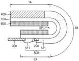
도 1은 본 발명의 일 실시예에 따른 표시 장치를 나타내는 평면도이다.
도 2 및 도 3은 본 발명의 일 실시예에 따른 표시 장치를 나타내는 단면도들이다.
도 4 및 도 5는 도 2의 표시 장치를 상세하게 나타내는 단면도들이다.
도 6은 본 발명의 일 실시예에 따른 표시 장치를 나타내는 단면도이다.
도 7은 도 6의 표시 장치의 제조 방법을 나타내는 단면도이다.
도 8은 본 발명의 일 실시예에 따른 표시 장치를 나타내는 단면도이다.
도 9는 본 발명의 일 실시예에 따른 표시 장치를 나타내는 단면도이다.
도 10은 본 발명의 일 실시예에 따른 표시 장치를 나타내는 단면도이다.
도 11은 도 10의 표시 장치의 제조 방법을 나타내는 단면도이다.
도 12는 본 발명의 일 실시예에 따른 표시 장치를 나타내는 단면도이다.
도 13은 도 12의 표시 장치의 제조 방법을 나타내는 단면도이다.1 is a plan view illustrating a display device according to an exemplary embodiment of the present invention.
2 and 3 are cross-sectional views illustrating a display device according to an exemplary embodiment of the present invention.
4 and 5 are cross-sectional views illustrating the display device of FIG. 2 in detail.
6 is a cross-sectional view illustrating a display device according to an exemplary embodiment of the present invention.
7 is a cross-sectional view illustrating a manufacturing method of the display device of FIG. 6 .
8 is a cross-sectional view illustrating a display device according to an exemplary embodiment of the present invention.
9 is a cross-sectional view illustrating a display device according to an exemplary embodiment of the present invention.
10 is a cross-sectional view illustrating a display device according to an exemplary embodiment.
11 is a cross-sectional view illustrating a manufacturing method of the display device of FIG. 10 .
12 is a cross-sectional view illustrating a display device according to an exemplary embodiment.
13 is a cross-sectional view illustrating a manufacturing method of the display device of FIG. 12 .
이하, 첨부한 도면들을 참조하여, 본 발명의 실시예들에 따른 표시 장치들 및 표시 장치들의 제조 방법들을 보다 상세하게 설명한다. 첨부된 도면들 상의 동일한 구성 요소들에 대해서는 동일하거나 유사한 참조 부호들을 사용한다.Hereinafter, display devices and methods of manufacturing the display devices according to embodiments of the present invention will be described in more detail with reference to the accompanying drawings. The same or similar reference numerals are used for like elements in the accompanying drawings.
도 1은 본 발명의 일 실시예에 따른 표시 장치를 나타내는 평면도이다. 도 2 및 도 3은 본 발명의 일 실시예에 따른 표시 장치를 나타내는 단면도들이다. 예를 들면, 도 3은 도 2의 표시 장치가 구부러진 상태를 나타낼 수 있다.1 is a plan view illustrating a display device according to an exemplary embodiment of the present invention. 2 and 3 are cross-sectional views illustrating a display device according to an exemplary embodiment of the present invention. For example, FIG. 3 may represent a bent state of the display device of FIG. 2 .
도 1, 도 2 및 도 3을 참조하면, 본 발명의 일 실시예에 따른 표시 장치는 표시 패널(100), 구동회로칩(200), 가요성 인쇄회로기판(flexible printed circuit board, FPCB)(300), 편광판(400), 벤딩보호층(500) 및 보호 필름(600)을 포함할 수 있다.1, 2, and 3 , a display device according to an embodiment of the present invention includes a
표시 장치는 화상을 표시하는 장치이다. 표시 장치는 액정 표시 장치(liquid crystal display), 전기영동 표시 장치(electrophoretic display), 유기 발광 표시 장치(organic light emitting display), 무기 EL 표시 장치(inorganic light emitting display), 전계 방출 표시 장치(field emission display), 표면 전도 전자 방출 표시 장치(surface-conduction electron-emitter display), 플라즈마 표시 장치(plasma display), 음극선관 표시 장치(cathode ray display) 등일 수 있다. 이하에서는, 본 발명의 일 실시예에 따른 표시 장치로써, 유기 발광 표시 장치를 예시적으로 설명하지만, 본 발명의 표시 장치는 이에 한정되지 아니하고, 다양한 방식의 표시 장치가 사용될 수 있다.A display device is a device that displays an image. Display devices include liquid crystal displays, electrophoretic displays, organic light emitting displays, inorganic light emitting displays, and field emission displays. display), a surface-conduction electron-emitter display, a plasma display, a cathode ray display, and the like. Hereinafter, an organic light emitting display device will be exemplarily described as a display device according to an exemplary embodiment of the present invention, but the display device of the present invention is not limited thereto and various types of display devices may be used.
표시 패널(100)은 제1 영역(1A), 제2 영역(2A) 및 벤딩 영역(BA)을 가질 수 있다. 제2 영역(2A)은 제1 영역(1A)과 이격되고, 벤딩 영역(BA)은 제1 영역(1A)과 제2 영역(2A) 사이에 위치할 수 있다. 벤딩 영역(BA)은 도 3에 도시된 바와 같이 벤딩축을 따라 구부러질 수 있다.The
구동회로칩(200) 및 가요성 인쇄회로기판(300)은 표시 패널(100)의 제2 영역(2A) 상에 배치될 수 있다. 구동회로칩(200)은 제2 영역(2A) 내에 배치되고, 가요성 인쇄회로기판(300)은 제2 영역(2A)의 단부에 배치될 수 있다. 구동회로칩(200)과 가요성 인쇄회로기판(300)은 서로 이격할 수 있다.The
구동회로칩(200) 및 가요성 인쇄회로기판(300)은 표시 패널(100)에 구동 신호를 제공할 수 있다. 상기 구동 신호는 구동 전압, 게이트 신호, 데이터 신호 등 표시 장치를 구동하는 다양한 신호를 의미할 수 있다. 도면에는 도시되지 않았으나, 가요성 인쇄회로기판(300)은 상기 구동 신호를 생성하는 인쇄회로기판에 연결될 수 있다.The driving
편광판(400)은 표시 패널(100)의 제1 영역(1A) 상에 배치될 수 있다. 편광판(400)은 외광 반사를 감소시키는 역할을 할 수 있다. 예를 들면, 외광이 편광판(400)을 통과하여 표시 패널(100)의 상부에서 반사된 후에 다시 편광판(400)을 통과하는 경우에, 편광판(400)을 2 회 통과함에 따라 상기 외광의 위상이 바뀔 수 있다. 그 결과, 반사광의 위상이 편광판(400)으로 진입하는 외광의 위상과 달라짐으로써 소멸간섭이 발생할 수 있고, 결과적으로 외광 반사가 감소됨으로써 표시 장치의 시인성이 향상될 수 있다.The
벤딩보호층(500)은 표시 패널(100)의 제2 영역(2A) 및 벤딩 영역(BA) 상에 배치될 수 있다. 어떤 적층체를 구부리는 경우에, 상기 적층체 내에는 스트레스 중성 평면(stress neutral plane)이 존재할 수 있다. 만일 벤딩보호층(500)이 존재하지 않으면, 표시 패널(100)을 구부림에 따라 벤딩 영역(BA) 내의 도전층에 과도한 인장 스트레스 등이 인가될 수 있다. 이는 상기 도전층의 위치가 스트레스 중성 평면에 대응하지 않을 수 있기 때문이다. 그러나, 벤딩보호층(500)을 벤딩 영역(BA) 상에 배치하고, 벤딩보호층(500)의 두께 및 모듈러스 등을 조절함으로써, 표시 패널(100), 벤딩보호층(500) 등을 포함하는 적층체에 있어서 스트레스 중성 평면의 위치를 조정할 수 있다. 따라서, 벤딩보호층(500)을 통해 스트레스 중성 평면이 상기 도전층의 근방에 위치하도록 함으로써, 상기 도전층에 인가되는 인장 스트레스를 최소화할 수 있다.The
벤딩보호층(500)은 제1 선벤딩보호층(511) 및 제1 후벤딩보호층(521)을 포함할 수 있다. 벤딩보호층(500)을 형성함에 있어서, 제1 선벤딩보호층(511)을 형성한 후에 제1 후벤딩보호층(521)을 형성할 수 있다.The
제1 선벤딩보호층(511)은 표시 패널(100)의 제2 영역(2A) 상에 배치될 수 있다. 제1 선벤딩보호층(511)은 가요성 인쇄회로기판(300)의 일부를 덮을 수 있다. 예를 들면, 제1 선벤딩보호층(511)은 제2 영역(2A)의 단부 상에 위치하는 가요성 인쇄회로기판(300)의 단부를 덮을 수 있다. 제1 선벤딩보호층(511)은 가요성 인쇄회로기판(300)이 표시 패널(100)로부터 분리되지 않도록 고정시키는 역할을 할 수 있다. 또한, 제1 선벤딩보호층(511)은 제1 후벤딩보호층(521)을 형성하는 과정에서 제1 후벤딩보호층(521)이 넘치는 것(overflow)을 방지할 수 있다.The first pre-bending
일 실시예에 있어서, 제1 선벤딩보호층(511)은 구동회로칩(200)과 평면상 비중첩할 수 있다. 다시 말해, 제1 선벤딩보호층(511)은 구동회로칩(200)을 덮지 않을 수 있다.In one embodiment, the first
제1 후벤딩보호층(521)은 표시 패널(100)의 벤딩 영역(BA) 상에 배치될 수 있다. 다시 말해, 제1 후벤딩보호층(521)은 표시 패널(100)의 벤딩 영역(BA)을 덮을 수 있다. 제1 후벤딩보호층(521)은 벤딩 영역(BA) 내의 스트레스 중성 평면의 위치를 조정하는 역할을 할 수 있다.The first
일 실시예에 있어서, 제1 후벤딩보호층(521)은 표시 패널(100)의 제2 영역(2A) 상에도 형성되어 구동회로칩(200)을 덮을 수 있다. 예를 들면, 제1 후벤딩보호층(521)은 제1 선벤딩보호층(511)과 접촉하며 구동회로칩(200)을 완전히 덮을 수 있다. 이 경우, 제1 후벤딩보호층(521)은 구동회로칩(200)이 표시 패널(100)로부터 분리되지 않도록 고정시키는 역할을 할 수 있다.In one embodiment, the first
일 실시예에 있어서, 제1 선벤딩보호층(511)의 경도는 제1 후벤딩보호층(521)의 경도보다 클 수 있다. 제1 선벤딩보호층(511)은 구부러지지 않는 제2 영역(2A) 상에 위치하고, 가요성 인쇄회로기판(300)의 일부를 덮어 가요성 인쇄회로기판(300)을 표시 패널(100)에 고정시킬 수 있다. 이에 따라, 제1 선벤딩보호층(511)은 상대적으로 높은 경도를 가질 수 있다. 표시 패널(100)의 벤딩 영역(BA)이 구부러지는 경우에, 벤딩 영역(BA)을 덮는 제1 후벤딩보호층(521)은 늘어나고, 인장 스트레스를 받을 수 있다. 이에 따라, 제1 후벤딩보호층(521)은 상대적으로 낮은 경도를 가질 수 있다.In one embodiment, the hardness of the first
일 실시예에 있어서, 벤딩보호층(500)은 편광판(400)과 접촉할 수 있다. 예를 들면, 표시 패널(100)의 제1 영역(1A) 상에 위치하는 제1 후벤딩보호층(521)의 단부가 편광판(400)의 단부와 접촉할 수 있다. 벤딩보호층(500)은 액상 또는 페이스트 형태의 물질을 도포하고 이를 경화시킴으로써 형성될 수 있다. 이 경우, 경화 과정에서 벤딩보호층(500)의 부피가 감소할 수 있다. 전술한 바와 같이, 벤딩보호층(500)의 상기 단부가 편광판(400)과 접촉하는 경우에, 벤딩보호층(500)의 상기 단부가 편광판(400)에 고정되기 때문에, 벤딩보호층(500)의 잔여 부분의 부피가 감소할 수 있다. 그 결과, 벤딩보호층(500)의 표시 패널(100)의 제1 영역(1A) 상에 위치하는 부분의 두께가 벤딩보호층(500)의 표시 패널(100)의 제2 영역(2A) 및 벤딩 영역(BA) 상에 위치하는 부분의 두께보다 두껍게 형성될 수 있다.In one embodiment, the
보호 필름(600)은 표시 패널(100)을 사이에 두고 편광판(400)과 벤딩보호층(500)에 대향하도록 배치될 수 있다. 예를 들면, 편광판(400) 및 벤딩보호층(500)은 표시 패널(100)의 상면에 형성되고, 보호 필름(600)은 표시 패널(100)의 상기 상면에 대향하는 하면에 형성될 수 있다.The
보호 필름(600)은 표시 패널(100)의 벤딩 영역(BA)에 대응되는 개구부(OP)를 가질 수 있다. 보호 필름(600)은 표시 패널(100)의 하면을 보호하는 역할을 할 수 있고, 이에 따라, 보호 필름(600)은 자체적인 강성을 가질 수 있다. 보호 필름(600)의 가요성이 낮은 경우에, 표시 패널(100)이 구부러짐에 따라 보호 필름(600)과 표시 패널(100) 사이에서 박리가 발생할 수도 있다. 그러나, 본 실시예에 따른 표시 장치의 보호 필름(600)은 벤딩 영역(BA)에 대응되는 개구부(OP)를 가짐으로써, 이러한 박리가 발생하는 것을 효과적으로 방지할 수 있다.The
일 실시예에 있어서, 개구부(OP)의 폭은 벤딩 영역(BA)의 폭보다 클 수 있다. 예를 들면, 벤딩 영역(BA)은 개구부(OP) 내에 위치할 수 있다. 이에 따라, 표시 패널(100)의 벤딩 영역(BA) 상에는 보호 필름(600)이 배치되지 않을 수 있다.In one embodiment, the width of the opening OP may be greater than that of the bending area BA. For example, the bending area BA may be positioned within the opening OP. Accordingly, the
도 4 및 도 5는 도 2의 표시 장치를 상세하게 나타내는 단면도들이다.4 and 5 are cross-sectional views illustrating the display device of FIG. 2 in detail.
도 4를 참조하면, 표시 패널(100)은 기판(110), 절연층들(121, 123, 125, 127, 129), 박막 트랜지스터(130), 유기 발광 소자(140), 봉지층(150) 등을 포함할 수 있다.Referring to FIG. 4 , the
표시 패널(100)의 제1 영역(1A)은 표시 영역(DA)을 포함할 수 있다. 제1 영역(1A)은 도 4에 도시된 바와 같이 표시 영역(DA) 외에도 표시 영역(DA) 외측의 비표시 영역의 일부를 포함할 수 있다. 제2 영역(2A) 및 벤딩 영역(BA)도 비표시 영역을 포함할 수 있다.The
표시 패널(100)의 표시 영역(DA)에는 복수의 화소들이 배치되어 화상을 표시할 수 있다. 표시 영역(DA)에는 박막 트랜지스터(130)와 같은 스위칭 소자, 유기 발광 소자(140)와 같은 표시 소자 등이 구비될 수 있다. 표시 영역(DA)에는 게이트 신호를 전달하는 게이트선과 데이터 신호를 전달하는 데이터선, 전원을 전달하는 구동 전원선, 공통 전원선 등의 신호 배선이 더 포함될 수 있으며, 상기 게이트선, 상기 데이터선, 상기 구동 전원선에 전기적으로 연결된 박막 트랜지스터(130), 상기 공통 전원선에 전기적으로 연결된 유기 발광 소자(140) 등의 전기적 결합에 의해 화소가 형성되어 화상을 표시할 수 있다. 화소는 화소로 공급되는 구동 전원 및 공통 전원에 따라 데이터 신호에 대응하여 유기 발광 소자(140)를 통과하는 구동 전류에 대응하는 휘도로 발광할 수 있다. 화소는 복수로 구성될 수 있으며, 복수의 화소들은 스트라이프 배열, 펜타일 배열 등 다양한 형태로 배치될 수 있다.A plurality of pixels may be arranged in the display area DA of the
기판(110)은 가요성을 갖는 다양한 물질을 포함할 수 있다. 예를 들면, 기판(110)은 폴리에테르술폰(polyethersulfone, PES), 폴리아크릴레이트(polyacrylate, PAR), 폴리에테르 이미드(polyetherimide, PEI), 폴리에틸렌 나프탈레이트(polyethylene naphthalate, PEN), 폴리에틸렌 테레프탈레이트(polyethylene terephthalate, PET), 폴리페닐렌 설파이드(polyphenylene sulfide, PPS), 폴리아릴레이트(polyarylate), 폴리이미드(polyimide, PI), 폴리카보네이트(polycarbonate, PC) 또는 셀룰로오스 아세테이트 프로피오네이트(cellulose acetate propionate, CAP)와 같은 고분자 수지를 포함할 수 있다. 기판(110)은 단일층 또는 다중층으로 구성될 수 있다. 일 실시예에 있어서, 기판(110)은 수지로 이루어진 수지층과 실리콘 산화물 또는 실리콘 질화물과 같은 무기물로 이루어진 배리어층이 교번하여 적층된 구조를 가질 수 있으며, 상기 수지층과 상기 배리어층 사이에 비정질 실리콘으로 이루어진 중간층이 더 포함되는 구조를 가질 수도 있다.The
박막 트랜지스터(130)는 비정질 실리콘, 다결정 실리콘, 산화물 반도체 또는 유기 반도체 물질을 포함하는 반도체층(131), 게이트 전극(133a), 소스 전극(135a) 및 드레인 전극(135b)을 포함할 수 있다.The
게이트 전극(133a)은 박막 트랜지스터(130)에 온/오프 신호를 인가하는 게이트 배선(미도시)과 연결될 수 있으며, 저저항 금속 물질로 이루어질 수 있다. 예를 들면, 게이트 전극(133a)은 몰리브덴(Mo), 알루미늄(Al), 구리(Cu), 티타늄(Ti) 등을 포함하는 도전 물질로 이루어진 단일막 또는 다층막일 수 있다.The
소스 전극(135a) 및 드레인 전극(135b)은 전도성이 좋은 도전 물질로 이루어진 단일막 또는 다층막일 수 있으며, 반도체층(131)의 소스 영역 및 드레인 영역과 각각 연결될 수 있다. 예를 들면, 각각의 소스 전극(135a) 및 드레인 전극(135b)은 알루미늄(Al), 구리(Cu), 티타늄(Ti) 등을 포함하는 도전 물질로 이루어진 단일막 또는 다층막일 수 있다.The
일 실시예에 따른 박막 트랜지스터(130)는 게이트 전극(133a)이 반도체층(131)의 상부에 배치되는 탑 게이트 타입(top gate type)이지만, 본 발명은 이에 한정되지 않으며, 다른 실시예에 따른 박막 트랜지스터는 게이트 전극이 반도체층의 하부에 배치되는 바텀 게이트 타입(bottom gate type)일 수 있다.The
반도체층(131)과 게이트 전극(133a)의 절연성을 확보하기 위하여, 실리콘 산화물, 실리콘 질화물, 실리콘 산질화물 등의 무기물을 포함하는 게이트 절연막(123)이 반도체층(131)과 게이트 전극(133a) 사이에 개재될 수 있다. 또한, 게이트 전극(133a)의 상부에는 실리콘 산화물, 실리콘 질화물, 실리콘 산질화물 등의 무기물을 포함하는 층간 절연막(125)이 배치될 수 있고, 소스 전극(135a) 및 드레인 전극(135b)은 층간 절연막(125) 상에 배치될 수 있다. 무기물을 포함하는 게이트 절연막(123) 및 층간 절연막(125)과 같은 절연막은 화학 기상 증착법(CVD), 원자층 증착법(ALD) 등을 통해 형성될 수 있다.In order to secure insulation between the
소스 전극(135a) 및 드레인 전극(135b)은 반도체층(131)과 접촉 구멍을 통해 연결될 수 있다. 상기 접촉 구멍은 게이트 절연막(123) 및 층간 절연막(125)을 동시에 식각하여 형성될 수 있다.The
박막 트랜지스터(130)와 기판(110) 사이에는 실리콘 산화물, 실리콘 질화물, 실리콘 산질화물 등과 같은 무기물을 포함하는 버퍼층(121)이 개재될 수 있다. 버퍼층(121)은 단일막 또는 다층막의 구조를 가질 수 있다. 버퍼층(121)은 기판(110)의 상면을 평탄하게 하거나 기판(110)을 통한 불순물이 박막 트랜지스터(130)의 반도체층(131)으로 침투하는 것을 방지하거나 최소화하는 역할을 할 수 있다.A
박막 트랜지스터(130) 상에는 평탄화층(127)이 배치될 수 있다. 예를 들면, 도 4에 도시된 바와 같이 박막 트랜지스터(130) 상부에 유기 발광 소자(140)가 배치되는 경우에, 평탄화층(127)은 박막 트랜지스터(130)의 상부를 대체로 평탄화하는 역할을 할 수 있다. 평탄화층(127)은 아크릴, BCB(benzocyclobutene), HMDSO(hexamethyldisiloxane) 등과 같은 유기물로 형성될 수 있다. 도 4에는 평탄화층(127)이 단층으로 도시되어 있으나, 다층으로 형성될 수도 있다. 또한, 도 4에 도시된 바와 같이 평탄화층(127)이 표시 영역(DA)의 외측에서 개구를 가짐으로써, 표시 영역(DA)의 평탄화층(127)의 부분과 벤딩 영역(BA)의 평탄화층(127)의 부분이 물리적으로 분리될 수도 있다. 이는 외부에서 침투한 불순물 등이 평탄화층(127)을 통해 표시 영역(DA) 내부에까지 도달하는 것을 방지하기 위함이다.A
표시 영역(DA) 내의 평탄화층(127) 상에는 화소 전극(141), 대향 전극(145) 및 그들 사이에 개재되며 발광층을 포함하는 중간층(143)을 포함하는 유기 발광 소자(140)가 배치될 수 있다. 화소 전극(141)은 평탄화층(127)에 형성된 개구부를 통해 소스 전극(135a) 및 드레인 전극(135b) 중 어느 하나와 접촉하여 박막 트랜지스터(130)와 전기적으로 연결될 수 있다.An organic
평탄화층(127) 상부에는 화소 정의막(129)이 배치될 수 있다. 화소 정의막(129)은 각 화소들에 대응하는 개구, 즉 적어도 화소 전극(141)의 중앙부가 노출되도록 하는 개구를 가짐으로써 화소를 정의하는 역할을 할 수 있다. 또한, 화소 정의막(129)은 화소 전극(141)의 가장자리와 화소 전극(141) 상부의 대향 전극(145) 사이의 거리를 증가시킴으로써 화소 전극(141)의 가장자리에서 아크 등이 발생하는 것을 방지하는 역할을 할 수 있다. 화소 정의막(129)은 폴리이미드 또는 HMDSO(hexamethyldisiloxane) 등과 같은 유기물로 형성될 수 있다.A
유기 발광 소자(140)의 중간층(143)은 저분자 물질 또는 고분자 물질을 포함할 수 있다. 중간층(143)이 저분자 물질을 포함하는 경우에, 정공 주입층(hole injection layer, HIL), 정공 수송층(hole transport layer, HTL), 발광층(emission layer, EML), 전자 수송층(electron transport layer, ETL), 전자 주입층(electron injection layer, EIL) 등이 단일한 또는 적층된 구조를 가질 수 있고, 구리 프탈로시아닌(CuPc: copper phthalocyanine), N,N-디(나프탈렌-1-일)-N,N'-디페닐-벤지딘 (N,N'-Di(naphthalene-1-yl)-N,N'-diphenyl-benzidine: NPB), 트리스-8-하이드록시퀴놀린 알루미늄(tris-8-hydroxyquinoline aluminum)(Alq3) 등과 같은 다양한 유기 물질을 포함할 수 있다. 상기 층들은 진공 증착법 등으로 형성될 수 있다.The
중간층(143)이 고분자 물질을 포함할 경우에는 대개 정공 수송층(HTL) 및 발광층(EML)을 포함하는 구조를 가질 수 있다. 이 경우, 상기 정공 수송층은 PEDOT을 포함하고, 상기 발광층은 PPV(poly-phenylenevinylene)계 및 폴리플루오렌(polyfluorene)계 등 고분자 물질을 포함할 수 있다. 중간층(143)은 스크린 인쇄법, 잉크젯 인쇄법, 레이저 열전사법(laser induced thermal imaging, LITI) 등으로 형성될 수 있다.When the
중간층(143)은 이에 한정되는 것은 아니고, 다양한 구조를 가질 수도 있다. 또한, 중간층(143)은 복수의 화소 전극들(141)에 걸쳐서 일체로 형성된 층을 포함할 수 있고, 복수의 화소 전극들(141) 각각에 대응하도록 패터닝된 층을 포함할 수도 있다.The
대향 전극(145)은 표시 영역(DA)의 상부에 배치되는데, 도 4에 도시된 바와 같이 표시 영역(DA)을 덮도록 배치될 수 있다. 다시 말해, 대향 전극(145)은 복수의 유기 발광 소자들(140)에 걸쳐서 일체로 형성되어 복수의 화소 전극들(141)에 대응할 수 있다.The
유기 발광 소자(140)는 외부로부터의 수분, 산소 등에 의해 쉽게 손상될 수 있기 때문에, 봉지층(150)은 유기 발광 소자(140)를 덮어 이를 보호할 수 있다. 봉지층(150)은 표시 영역(DA)을 덮으며 표시 영역(DA)의 외측까지 연장될 수 있다. 봉지층(150)은 제1 무기 봉지층(151), 유기 봉지층(153) 및 제2 무기 봉지층(155)을 포함할 수 있다.Since the organic
제1 무기 봉지층(151)은 대향 전극(145)을 덮으며, 실리콘 산화물, 실리콘 질화물, 실리콘 산질화물 등을 포함할 수 있다. 필요에 따라 제1 무기 봉지층(151)과 대향 전극(145) 사이에 캡핑층 등의 다른 층들이 개재될 수도 있다. 제1 무기 봉지층(151)은 그 하부의 구조물을 따라 형성되므로 그 상면이 평탄하지 않을 수 있다. 유기 봉지층(153)은 제1 무기 봉지층(151)을 덮으며, 제1 무기 봉지층(151)과 다르게 그 상면이 대략 평탄할 수 있다. 구체적으로, 유기 봉지층(153)은 표시 영역(DA)에 대응하는 부분에서는 상면이 대략 평탄하도록 형성될 수 있다. 예를 들면, 유기 봉지층(153)은 폴리에틸렌 테레프탈레이트, 폴리에틸렌 나프탈레이트, 폴리카보네이트, 폴리이미드, 폴리에틸렌설포네이트, 폴리옥시메틸렌, 폴리아릴레이트, 헥사메틸디실록산 등을 포함할 수 있다. 제2 무기 봉지층(155)은 유기 봉지층(153)을 덮으며, 실리콘 산화물, 실리콘 질화물, 실리콘 산질화물 등을 포함할 수 있다. 제2 무기 봉지층(155)은 표시 영역(DA) 외측에 위치한 그 가장자리에서 제1 무기 봉지층(151)과 접촉함으로써, 유기 봉지층(153)이 외부로 노출되지 않도록 할 수 있다.The first
이와 같이, 봉지층(150)이 제1 무기 봉지층(151), 유기 봉지층(153) 및 제2 무기 봉지층(155)을 포함함으로써, 봉지층(150) 내에 크랙이 발생하더라도, 제1 무기 봉지층(151)과 유기 봉지층(153) 사이 또는 유기 봉지층(153)과 제2 무기 봉지층(155) 사이에서 상기 크랙이 연결되지 않을 수 있다. 이에 따라, 외부로부터의 수분, 산소 등이 표시 영역(DA)으로 침투하는 경로가 형성되는 것을 방지하거나 최소화할 수 있다.As described above, since the
봉지층(150) 상에는 투광성 접착제(optically clear adhesive, OCA)(450)에 의해 편광판(400)이 위치할 수 있다. 투광성 접착제(450)와 편광판(400)은 평탄화층(127)의 상기 개구의 적어도 일부를 덮을 수 있다. 필요에 따라 편광판(400)을 생략할 수 있고, 다른 구성들로 대체할 수도 있다. 예를 들면, 편광판(400)을 생략하고 블랙 매트릭스와 컬러 필터를 이용하여 외광 반사를 감소시킬 수도 있다.A
일 실시예에 있어서, 도 4에 도시된 바와 같이 투광성 접착제(450)와 편광판(400)은 표시 영역(DA) 외측에 위치한 봉지층(150)의 단부를 완전히 덮을 수 있다. 이 경우, 편광판(400)에 인접하게 형성되는 벤딩보호층(500)이 봉지층(150)과 접촉하지 않을 수 있다. 다른 실시예에 있어서, 도 5에 도시된 바와 같이 투광성 접착제(450)와 편광판(400)은 표시 영역(DA) 외측에 위치한 봉지층(150)의 단부의 일부를 덮지 않을 수 있다. 다시 말해, 봉지층(150)의 상기 단부의 일부가 노출될 수 있다. 이 경우, 편광판(400)에 인접하게 형성되는 벤딩보호층(500)이 표시 영역(DA)의 외측에서 봉지층(150)과 접촉할 수 있다.In one embodiment, as shown in FIG. 4 , the light-
본 실시예에 따른 표시 장치는 버퍼층(121), 게이트 절연막(123) 및 층간 절연막(125)을 포함하는 무기 절연층 상에 배치되는 제1 도전층(135c)을 구비할 수 있다. 제1 도전층(135c)은 제1 영역(1A)에서 벤딩 영역(BA)을 거쳐 제2 영역(2A)으로 연장될 수 있다. 제1 도전층(135c)은 표시 영역(DA)에 전기적 신호를 전달하는 배선으로 기능할 수 있다. 제1 도전층(135c)은 소스 전극(135a) 또는 드레인 전극(135b)과 동일한 물질로 동시에 형성될 수 있다.The display device according to the present exemplary embodiment may include the first
본 실시예에 따른 표시 장치는 제1 도전층(135c) 외에 제2 도전층(133b, 133c) 및 제1 도전층(135c)과 동일한 층에 배치되는 제3 도전층(135d)을 구비할 수 있다. 제2 도전층(133b, 133c)은 제1 도전층(135c)이 위치한 층과 상이한 층에 위치하도록 제1 영역(1A) 또는 제2 영역(2A)에 배치되며, 제1 도전층(135c) 또는 제3 도전층(135d)에 전기적으로 연결될 수 있다. 도 4에는 제2 도전층(133b, 133c)이 박막 트랜지스터(130)의 게이트 전극(133a)과 동일한 물질로 동일한 층에 위치하는 것으로 예시되어 있다. 또한, 제1 도전층(135c)이 층간 절연막(125)에 형성된 접촉 구멍을 통해 제1 영역(1A)에 위치하는 제2 도전층(133b)에 접촉하는 것으로 예시되어 있다. 나아가, 제3 도전층(135d)은 제2 영역(2A)에 위치하는 제2 도전층(133c)에 접촉하는 것으로 예시되어 있다.In addition to the first
제1 영역(1A)에 위치하는 제2 도전층(133b)은 표시 영역(DA) 내의 박막 트랜지스터 등에 전기적으로 연결될 수 있고, 이에 따라, 제1 도전층(135c)이 제2 도전층(133b)을 통해 표시 영역(DA) 내의 박막 트랜지스터 등에 전기적으로 연결될 수 있다. 제2 영역(2A)에 위치하는 제2 도전층(133c)도 표시 영역(DA) 내의 박막 트랜지스터 등에 전기적으로 연결될 수 있다.The second
벤딩 영역(BA)을 가로지르는 제1 도전층(135c)이 연신율이 높은 물질을 포함하는 경우에, 제1 도전층(135c)에 크랙이 발생하거나 제1 도전층(135c)이 단선되는 등의 불량이 발생하지 않을 수 있다. 또한, 제1 영역(1A) 또는 제2 영역(2A)에는 제1 도전층(135c)보다는 연신율이 낮지만 제1 도전층(135c)과 상이한 전기적/물리적 특성을 갖는 물질로 제2 도전층(133b, 133c)을 형성함으로써, 표시 장치에 있어서 전기적 신호 전달의 효율성이 높아지거나 제조 과정에서의 불량 발생률이 낮아질 수 있다. 예를 들면, 제2 도전층(133b, 133c)은 몰리브덴을 포함할 수 있고, 제1 도전층(135c)은 알루미늄을 포함할 수 있다. 제1 도전층(135c) 또는 제2 도전층(133b, 133c)은 필요에 따라 다층구조를 가질 수 있다.When the first
일 실시예에 있어서, 제1 도전층(135c) 및 제3 도전층(135d)은 소스 전극(135a) 및 드레인 전극(135b)과 실질적으로 동시에 형성될 수 있고, 제2 도전층(133b, 133c)은 게이트 전극(133a)과 실질적으로 동시에 형성될 수 있다.In one embodiment, the first
구동회로칩(200) 및 가요성 인쇄회로기판(300)은 표시 패널(100)의 제2 영역(2A) 상에 배치될 수 있다. 구동회로칩(200)은 제2 영역(2A) 내에 배치되고, 가요성 인쇄회로기판(300)은 제2 영역(2A)의 단부에 배치될 수 있다.The driving
각각의 구동회로칩(200) 및 가요성 인쇄회로기판(300)은 제2 영역(2A) 상에 배치되는 제1 도전층(135c), 제2 도전층(133c), 제3 도전층(135d) 또는 이들로부터 전기적으로 연결되는 다른 도전층과 연결될 수 있다. 도 4에는 제1 도전층(135c)의 단부에 구동회로칩(200)이 배치되고, 제3 도전층(135d)의 단부에 가요성 인쇄회로기판(300)이 연결되는 것이 예시되어 있으나, 본 발명은 이에 한정되지 아니하고, 구동회로칩(200) 및 가요성 인쇄회로기판(300)은 제2 도전층(133c) 또는 다른 도전층과 연결될 수도 있다.Each of the driving
벤딩보호층(500)은 표시 패널(100)의 벤딩 영역(BA) 상에 배치되며, 구동회로칩(200) 및 가요성 인쇄회로기판(300)의 일부를 덮을 수 있다. 예를 들면, 도 4에 도시된 바와 같이 제1 선벤딩보호층(511)은 제2 영역(2A)의 단부 상에 위치하는 가요성 인쇄회로기판(300)의 단부 및 제3 도전층(135d)을 덮을 수 있다. 또한, 제1 후벤딩보호층(521)은 벤딩 영역(BA) 상에 위치하는 제1 도전층(135c) 및 제2 영역(2A) 상에 위치하는 구동회로칩(200)을 덮을 수 있다.The
도 4에는 제1 영역(1A) 상에 위치하는 벤딩보호층(500)의 단부가 편광판(400) 및 투광성 접착제(450)와 접촉하는 것이 예시되어 있으나, 본 발명은 이에 한정되지 아니하고, 벤딩보호층(500)의 상기 단부는 편광판(400) 및 투광성 접착제(450)와 이격될 수도 있다.4 illustrates that the end of the
벤딩보호층(500)은 평탄화층(127), 화소 정의막(129) 및 봉지층(150)의 유기 봉지층(153)과 실질적으로 동일한 물질로 형성될 수 있다. 예를 들면, 벤딩보호층(500)은 아크릴, BCB(benzocyclobutene), HMDSO(hexamethyldisiloxane) 등과 같은 유기물로 형성될 수 있다.The
일 실시예에 있어서, 제1 선벤딩보호층(511)과 제1 후벤딩보호층(521)은 실질적으로 동일한 물질을 포함할 수 있다. 이 경우, 동일한 물질로 제1 선벤딩보호층(511)과 제1 후벤딩보호층(521)을 형성함으로써, 제조 비용 및 제조 시간을 절감할 수 있다. 다른 실시예에 있어서, 제1 선벤딩보호층(511)과 제1 후벤딩보호층(521)은 서로 다른 물질을 포함할 수 있다. 예를 들면, 제1 선벤딩보호층(511)은 광경화성 물질을 포함하고, 제1 후벤딩보호층(521)은 열경화성 물질을 포함할 수 있다. 이 경우, 제1 선벤딩보호층(511)과 제1 후벤딩보호층(521)은 서로 다른 경화 과정을 거칠 수 있고, 제1 선벤딩보호층(511)의 경도와 제1 후벤딩보호층(521)의 경도가 서로 상이하게 형성될 수 있다.In one embodiment, the first
보호 필름(600)은 기판(110)의 하면에 배치될 수 있다. 보호 필름(600)은 표시 패널(100)의 벤딩 영역(BA)에 대응되는 개구부(OP)를 가질 수 있다. 도 4에는 도시되지 않았으나, 기판(110)과 보호 필름(600) 사이에는 보호 필름(600)을 기판(110)에 접착하기 위한 감압성 접착 물질(pressure sensitive adhesive, PSA) 등을 포함하는 점착층이 개재될 수 있다.The
도 6은 본 발명의 일 실시예에 따른 표시 장치를 나타내는 단면도이다.6 is a cross-sectional view illustrating a display device according to an exemplary embodiment of the present invention.
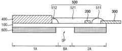
도 6을 참조하면, 본 발명의 일 실시예에 따른 표시 장치는 표시 패널(100), 구동회로칩(200), 가요성 인쇄회로기판(300), 편광판(400), 벤딩보호층(500) 및 보호 필름(600)을 포함할 수 있다. 도 6을 참조하여 설명하는 일 실시예에 따른 표시 장치에 있어서, 도 2를 참조하여 설명한 일 실시예에 따른 표시 장치의 구성들과 실질적으로 동일하거나 유사한 구성들에 대한 상세한 설명은 생략한다.Referring to FIG. 6 , a display device according to an exemplary embodiment of the present invention includes a
벤딩보호층(500)은 제1 선벤딩보호층(511), 제2 선벤딩보호층(512) 및 제1 후벤딩보호층(521)을 포함할 수 있다. 벤딩보호층(500)을 형성함에 있어서, 제1 선벤딩보호층(511) 및 제2 선벤딩보호층(512)을 형성한 후에 제1 후벤딩보호층(521)을 형성할 수 있다.The
제2 선벤딩보호층(512)은 표시 패널(100)의 제1 영역(1A) 상에 배치될 수 있다. 구체적으로, 제2 선벤딩보호층(512)은 편광판(400)에 인접하며, 제1 영역(1A)의 벤딩 영역(BA)에 인접한 부분 상에 배치될 수 있다. 제2 선벤딩보호층(512)은 제1 후벤딩보호층(521)을 형성하는 과정에서 제1 후벤딩보호층(521)이 넘치는 것(overflow)을 방지할 수 있다.The second
일 실시예에 있어서, 제2 선벤딩보호층(512)은 개구부(OP)에 의해 노출되는 보호 필름(600)의 단부와 평면상 중첩할 수 있다. 개구부(OP)의 폭은 벤딩 영역(BA)의 폭보다 클 수 있고, 제2 선벤딩보호층(512)의 가장자리는 제1 영역(1A)과 벤딩 영역(BA) 사이의 경계에 인접할 수 있다. 이에 따라, 제2 선벤딩보호층(512)은 개구부(OP)의 일부와 평면상 중첩할 수 있다.In one embodiment, the second pre-bending
도 7은 도 6의 표시 장치의 제조 방법을 나타내는 단면도이다.7 is a cross-sectional view illustrating a manufacturing method of the display device of FIG. 6 .
도 7을 참조하면, 본 발명의 일 실시예에 따른 표시 장치의 제조 방법에 있어서, 표시 패널(100)을 형성하고, 구동회로칩(200) 및 가요성 인쇄회로기판(300)을 부착하며, 선벤딩보호층(511, 512)을 형성할 수 있다.Referring to FIG. 7 , in a method of manufacturing a display device according to an embodiment of the present invention, a
먼저, 도 4를 참조하여 설명한 바와 같이 기판(110) 상에 박막 트랜지스터(130), 도전층들(133b, 133c, 135c, 135d), 유기 발광 소자(140) 및 봉지층(150)을 순차적으로 형성하여 표시 패널(100)을 형성할 수 있다. 또한, 투광성 접착제(450)를 이용하여 표시 패널(100)의 제1 영역(1A) 상에 편광층(400)을 형성할 수 있다. 나아가, 표시 패널(100)의 하면에 보호 필름(600) 및 지지 필름(650)을 부착할 수 있다. 보호 필름(600)은 표시 패널의 제1 영역(1A) 및 제2 영역(2A)에 대응하고, 지지 필름(650)은 표시 패널의 벤딩 영역(BA)에 대응할 수 있다.First, as described with reference to FIG. 4, the
그 다음, 표시 패널(100)의 제2 영역(2A) 상에 서로 이격하는 구동회로칩(200) 및 가요성 인쇄회로기판(300)을 부착할 수 있다. 구동회로칩(200)은 제2 영역(2A) 내에 부착되고, 가요성 인쇄회로기판(300)은 제2 영역(2A)의 단부에 부착될 수 있다.Then, the driving
일 실시예에 있어서, 구동회로칩(200) 및 가요성 인쇄회로기판(300)은 압착 본딩 장치에 의해 압력 및 열이 가해지면서 표시 패널(100) 상에 부착될 수 있고, 이 경우, 이방성 도전 필름(anisotropic conducting film, ACF)이 사용될 수 있다. 이방성 도전 필름은 열에 의해 경화되는 접착제와 그 내부에 미세한 도전 입자를 분산 혼합시킨 양면 테이프로 이루어질 수 있다. 이방성 도전 필름의 상부 및 하부에 압력이 가해지면, 상기 도전 입자가 터지면서 그 내부에 있던 접착제가 상기 양면 테이프 전체에 충진됨으로써, 전도성 및 접착성을 동시에 가질 수 있다.In one embodiment, the driving
지지 필름(650)은 구동회로칩(200) 및 가요성 인쇄회로기판(300)의 본딩 공정에서 기판(110)의 변형을 최소화할 수 있다. 상기 본딩 공정에서, 다량의 열이 발생할 수 있고, 이에 따라 기판(110)에도 상당한 열이 전달될 수 있다. 지지 필름(650)이 배치되지 않은 상태에서 기판(110)에 열이 전달되면, 기판(110)이 하부 방향으로 처질 수 있다. 기판(110)이 처진 상태에서 열이 방출되어 경화되면, 추후 벤딩 공정에서 곡률 반경이 균일하게 형성되지 않고, 벤딩 영역(BA)에서 크랙이 발생할 수 있다. 또한, 기판(110)이 처진 상태에서 후술하는 벤딩보호층(500)이 형성되는 경우에, 벤딩보호층(500)의 두께가 불균일하게 형성되어, 벤딩 시에 곡률 반경이 균일하게 형성되지 않고, 벤딩 영역(BA)에 크랙이 발생할 가능성이 있다. 본 실시예에 있어서, 표시 패널(100)의 벤딩 영역(BA)의 하면에 지지 필름(650)이 배치되므로, 공정 중에 발생할 수 있는 기판(110)의 처짐 현상을 방지하거나 최소화할 수 있다.The
그 다음, 표시 패널(100) 상에 선벤딩보호층(511, 512)을 형성할 수 있다. 제1 선벤딩보호층(511)은 표시 패널(100)의 제2 영역(2A) 상에 가요성 인쇄회로기판(300)을 덮도록 형성되고, 제2 선벤딩보호층(512)은 편광판(400)에 인접하며 표시 패널(100)의 제1 영역(1A) 상에 형성될 수 있다.Next, pre-bending protection layers 511 and 512 may be formed on the
일 실시예에 있어서, 먼저 가요성 인쇄회로기판(300)의 단부와 이에 인접하는 표시 패널(100)의 제2 영역(2A), 그리고 편광판(400)에 인접하는 표시 패널(100)의 제1 영역(1A)에 광경화성 물질을 도포할 수 있다. 예를 들면, 노즐 등을 이용하여 표시 패널(100) 상에 부분적으로 상기 광경화성 물질을 도포할 수 있다. 예를 들면, 상기 광경화성 물질은 광경화가 가능한 작용기를 가질 수 있다. 그 다음, 자외선으로 상기 광경화성 물질을 전경화(pre-curing)할 수 있다. 예를 들면, UV 레이저 소스 등과 같은 광원을 이용하여 상기 광경화성 물질이 도포된 부분에 자외선을 조사할 수 있다.In one embodiment, first, the end of the flexible printed
도 6을 참조하면, 본 발명의 일 실시예에 따른 표시 장치의 제조 방법에 있어서, 후벤딩보호층(521)을 형성할 수 있다. 후벤딩보호층(521)은 표시 패널(100)의 제2 영역(2A) 및 벤딩 영역(BA) 상에 구동회로칩(200)을 덮도록 형성될 수 있다.Referring to FIG. 6 , in the method of manufacturing a display device according to an exemplary embodiment, a
일 실시예에 있어서, 먼저 표시 패널(100) 상의 제1 선벤딩보호층(511)과 제2 선벤딩보호층(512) 사이에 열경화성 물질을 도포할 수 있다. 예를 들면, 노즐 등을 이용하여 표시 패널(100) 상의 제1 선벤딩보호층(511)과 제2 선벤딩보호층(512) 사이에 전체적으로 상기 열경화성 물질을 도포할 수 있다. 예를 들면, 상기 열경화성 물질은 열경화가 가능한 작용기를 가질 수 있다. 이 경우, 제1 선벤딩보호층(511)과 제2 선벤딩보호층(512)은 상기 열경화성 물질이 넘치는 것을 방지하는 역할을 할 수 있다. 그 다음, 열로 상기 열경화성 물질을 경화(curing)할 수 있다. 예를 들면, 레이저 열원, 적외선 열원, 진공 건조 열원 등과 같은 열원을 이용하여 상기 열경화성 물질이 도포된 부분에 열을 공급할 수 있다. 이 경우, 광경화 단계에서 전경화되었던 선벤딩보호층(511, 512)이 후벤딩보호층(521)과 함께 경화될 수 있다.In one embodiment, first, a thermosetting material may be applied between the first
본 실시예에서는 선벤딩보호층(511, 512)을 광경화성 물질로 형성하고, 후벤딩보호층(521)을 열경화성 물질로 형성하는 것을 예시적으로 설명하였으나 본 발명은 이에 한정되지 아니한다. 다른 실시예에서는 선벤딩보호층(511, 512)과 후벤딩보호층(521)을 광경화가 가능한 작용기 및 열경화가 가능한 작용기를 모두 포함하는 물질로 형성할 수 있고, 선벤딩보호층(511, 512)과 후벤딩보호층(521)을 동일한 물질로 형성할 수도 있다.In this embodiment, it has been exemplarily described that the pre-bending
그 다음, 표시 패널(100)의 하면에 부착된 지지 필름(650)을 제거할 수 있다. 이에 따라, 보호 필름(600)의 개구부(OP)가 형성될 수 있다.Next, the
도 8은 본 발명의 일 실시예에 따른 표시 장치를 나타내는 단면도이다.8 is a cross-sectional view illustrating a display device according to an exemplary embodiment of the present invention.
도 8을 참조하면, 일 실시예에 있어서, 제1 후벤딩보호층(521)의 상면은 실질적으로 평탄할 수 있다. 예를 들면, 후벤딩보호층 형성 물질을 평탄하게 도포한 후에 경화하여 평탄한 상면을 형성하거나, 이의 중앙부가 볼록한 제1 후벤딩보호층(521)을 형성한 후에 화학 기계 연마(chemical mechanical polishing, CMP) 등과 같은 연마법으로 볼록한 상면을 연마하여 평탄한 상면을 형성할 수도 있다.Referring to FIG. 8 , in one embodiment, a top surface of the first
도 9는 본 발명의 일 실시예에 따른 표시 장치를 나타내는 단면도이다.9 is a cross-sectional view illustrating a display device according to an exemplary embodiment of the present invention.
도 9를 참조하면, 일 실시예에 있어서, 제1 후벤딩보호층(521)은 표시 패널(100) 상에 배치되는 제1 층(521a) 및 제1 층(521a) 상에 배치되는 제2 층(521b)을 포함할 수 있다. 예를 들면, 제1 층(521a)과 제2 층(521b)은 서로 다른 물질로 형성될 수 있다.Referring to FIG. 9 , in an exemplary embodiment, the first
도 10은 본 발명의 일 실시예에 따른 표시 장치를 나타내는 단면도이다. 도 11은 도 10의 표시 장치의 제조 방법을 나타내는 단면도이다.10 is a cross-sectional view illustrating a display device according to an exemplary embodiment. 11 is a cross-sectional view illustrating a manufacturing method of the display device of FIG. 10 .
도 10을 참조하면, 본 발명의 일 실시예에 따른 표시 장치는 표시 패널(100), 구동회로칩(200), 가요성 인쇄회로기판(300), 편광판(400), 벤딩보호층(500) 및 보호 필름(600)을 포함할 수 있다. 도 10을 참조하여 설명하는 일 실시예에 따른 표시 장치에 있어서, 도 6을 참조하여 설명한 일 실시예에 따른 표시 장치의 구성들과 실질적으로 동일하거나 유사한 구성들에 대한 상세한 설명은 생략한다.Referring to FIG. 10 , a display device according to an exemplary embodiment of the present invention includes a
일 실시예에 있어서, 제1 선벤딩보호층(511)은 구동회로칩(200)을 덮을 수 있다. 구체적으로, 제1 선벤딩보호층(511)은 가요성 인쇄회로기판(300)의 단부와 함께 구동회로칩(200)을 전체적으로 덮을 수 있다. 제1 후벤딩보호층(521)은 제1 선벤딩보호층(511)과 제2 선벤딩보호층(512) 사이에 형성되고, 구동회로칩(200)을 직접 덮지 않을 수 있다.In one embodiment, the first
도 11을 참조하면, 선벤딩보호층 형성 물질을 가요성 인쇄회로기판(300)의 단부 및 구동회로칩(200)을 덮도록 도포하고, 이를 경화하여 제1 선벤딩보호층(511)을 형성할 수 있다. 제1 선벤딩보호층(511)이 구동회로칩(200)을 덮음에 따라, 후속하여 후벤딩보호층(521)을 형성하는 공정에서 구동회로칩(200)이 충격 등의 외부 요소로부터 영향을 받는 것을 방지할 수 있다.Referring to FIG. 11, a material for forming a pre-bending protective layer is applied to cover the end of the flexible printed
도 12는 본 발명의 일 실시예에 따른 표시 장치를 나타내는 단면도이다. 도 13은 도 12의 표시 장치의 제조 방법을 나타내는 단면도이다.12 is a cross-sectional view illustrating a display device according to an exemplary embodiment. 13 is a cross-sectional view illustrating a manufacturing method of the display device of FIG. 12 .
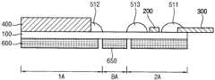
도 12를 참조하면, 본 발명의 일 실시예에 따른 표시 장치는 표시 패널(100), 구동회로칩(200), 가요성 인쇄회로기판(300), 편광판(400), 벤딩보호층(500) 및 보호 필름(600)을 포함할 수 있다. 도 12를 참조하여 설명하는 일 실시예에 따른 표시 장치에 있어서, 도 6을 참조하여 설명한 일 실시예에 따른 표시 장치의 구성들과 실질적으로 동일하거나 유사한 구성들에 대한 상세한 설명은 생략한다.Referring to FIG. 12 , a display device according to an exemplary embodiment of the present invention includes a
벤딩보호층(500)은 제1 선벤딩보호층(511), 제2 선벤딩보호층(512), 제3 선벤딩보호층(513), 제1 후벤딩보호층(521) 및 제2 후벤딩보호층(522)을 포함할 수 있다. 벤딩보호층(500)을 형성함에 있어서, 제1 선벤딩보호층(511), 제2 선벤딩보호층(512) 및 제3 선벤딩보호층(513)을 형성한 후에 제1 후벤딩보호층(521) 및 제2 후벤딩보호층(522)을 형성할 수 있다.The
제3 선벤딩보호층(513)은 구동회로칩(200)을 사이에 두고 제1 선벤딩보호층(511)과 이격되어 표시 패널(100)의 제2 영역(2A) 상에 배치될 수 있다. 다시 말해, 구동회로칩(200)은 제1 선벤딩보호층(511)과 제3 선벤딩보호층(513) 사이에 위치할 수 있다.The third
일 실시예에 있어서, 제3 선벤딩보호층(513)은 개구부(OP)에 의해 노출되는 보호 필름(600)의 단부와 평면상 중첩할 수 있다. 개구부(OP)의 폭은 벤딩 영역(BA)의 폭보다 클 수 있고, 제3 선벤딩보호층(513)의 가장자리는 제2 영역(2A)과 벤딩 영역(BA) 사이의 경계에 인접할 수 있다. 이에 따라, 제3 선벤딩보호층(513)은 개구부(OP)의 일부와 평면상 중첩할 수 있다.In one embodiment, the third pre-bending
제1 후벤딩보호층(521)은 제2 선벤딩보호층(512)과 제3 선벤딩보호층(513) 사이에 형성되어 표시 패널(100)의 벤딩 영역(BA)을 덮을 수 있다. 제1 후벤딩보호층(521)은 벤딩 영역(BA) 내의 스트레스 중성 평면의 위치를 조정하는 역할을 할 수 있다.The first
제2 후벤딩보호층(522)은 제1 선벤딩보호층(511)과 제3 선벤딩보호층(513) 사이에 형성되어 표시 패널(100)의 제2 영역(2A) 상에 배치된 구동회로칩(200)을 덮을 수 있다. 예를 들면, 제2 후벤딩보호층(522)은 제1 선벤딩보호층(511) 및 제3 선벤딩보호층(513)과 접촉하며 구동회로칩(200)을 완전히 덮을 수 있다. 이 경우, 제2 후벤딩보호층(522)은 구동회로칩(200)이 표시 패널(100)로부터 분리되지 않도록 고정시키는 역할을 할 수 있다.The second
일 실시예에 있어서, 제1 선벤딩보호층(511)의 높이는 제3 선벤딩보호층(513)의 높이보다 낮을 수 있다. 또한, 제2 후벤딩보호층(522)의 높이는 제1 후벤딩보호층(521)의 높이보다 낮을 수 있다.In one embodiment, the height of the first
도 13을 참조하면, 선벤딩보호층 형성 물질을 가요성 인쇄회로기판(300)이 배치된 제2 영역(2A)의 단부, 벤딩 영역(BA)에 인접한 제1 영역(1A) 및 벤딩 영역(BA)에 인접한 제2 영역(2A)에 도포하고, 이를 경화하여 제1 선벤딩보호층(511), 제2 선벤딩보호층(512) 및 제3 선벤딩보호층(513)을 형성할 수 있다. 여기서, 제1 선벤딩보호층(511)의 높이를 제3 선벤딩보호층(513)의 높이보다 낮게 형성하여 후속 공정에서 제1 후벤딩보호층(521)의 높이와 제2 후벤딩보호층(522)의 높이를 상이하게 형성할 수 있다.Referring to FIG. 13, a material for forming a pre-bending protective layer is applied to the end of the
그 다음, 도 14에 도시된 바와 같이 후벤딩보호층 형성 물질을 제2 선벤딩보호층(512)과 제3 선벤딩보호층(513) 사이 및 제1 선벤딩보호층(511)과 제3 선벤딩보호층(513) 사이에 도포하고, 이를 경화하여 제1 후벤딩보호층(521) 및 제2 후벤딩보호층(522)을 형성할 수 있다. 전술한 바와 같이 제1 선벤딩보호층(511)의 높이가 제3 선벤딩보호층(513)의 높이보다 낮게 형성됨에 따라, 제2 후벤딩보호층(522)의 높이가 제1 후벤딩보호층(521)의 높이보다 낮게 형성될 수 있다. 제2 후벤딩보호층(522)의 높이가 상대적으로 낮게 형성됨에 따라 제2 후벤딩보호층(522)의 부피가 상대적으로 작게 형성될 수 있고, 제2 후벤딩보호층(522)의 제조 시간 및 제조 비용이 절감될 수 있다.Then, as shown in FIG. 14, a post-bending protection layer-forming material is applied between the second
본 발명의 예시적인 실시예들에 따른 표시 장치는 컴퓨터, 노트북, 휴대폰, 스마트폰, 스마트패드, 피엠피(PMP), 피디에이(PDA), MP3 플레이어 등에 포함되는 표시 장치에 적용될 수 있다.Display devices according to exemplary embodiments of the present invention may be applied to display devices included in computers, laptop computers, mobile phones, smart phones, smart pads, PMPs, PDAs, MP3 players, and the like.
이상, 본 발명의 예시적인 실시예들에 따른 표시 장치들 및 표시 장치의 제조 방법들에 대하여 도면들을 참조하여 설명하였지만, 설시한 실시예들은 예시적인 것으로서 하기의 청구범위에 기재된 본 발명의 기술적 사상을 벗어나지 않는 범위에서 해당 기술 분야에서 통상의 지식을 가진 자에 의하여 수정 및 변경될 수 있을 것이다.Above, display devices and methods of manufacturing the display devices according to exemplary embodiments of the present invention have been described with reference to the drawings, but the described embodiments are illustrative and the technical spirit of the present invention described in the claims below is exemplary. It may be modified and changed by those skilled in the art to the extent that it does not deviate from the
100: 표시 패널200: 구동회로칩
300: 가요성 인쇄회로기판400: 편광판
500: 벤딩보호층511: 제1 선벤딩보호층
512: 제2 선벤딩보호층513: 제3 선벤딩보호층
521: 제1 후벤딩보호층522: 제2 후벤딩보호층
600: 보호 필름100: display panel 200: driving circuit chip
300: flexible printed circuit board 400: polarizer
500: bending protective layer 511: first pre-bending protective layer
512: second pre-bending protective layer 513: third pre-bending protective layer
521: first post-bending protective layer 522: second post-bending protective layer
600: protective film
Claims (20)
Translated fromKorean상기 표시 패널의 상기 제2 영역 상에 배치되는 구동회로칩;
상기 구동회로칩과 이격되어 상기 표시 패널의 상기 제2 영역 상에 배치되는 가요성 인쇄회로기판;
상기 가요성 인쇄회로기판의 일부를 덮는 제1 선벤딩보호층, 상기 표시 패널의 상기 벤딩 영역을 덮는 제1 후벤딩보호층, 및 상기 표시 패널의 상기 제1 영역 상에 배치되는 제2 선벤딩보호층을 포함하는 벤딩보호층; 및
상기 표시 패널을 사이에 두고 상기 벤딩보호층에 대향하고, 상기 표시 패널의 상기 벤딩 영역에 대응되는 개구부를 가지는 보호 필름을 포함하는, 표시 장치.a display panel having a first area, a second area spaced apart from the first area, and a bending area positioned between the first area and the second area;
a driving circuit chip disposed on the second area of the display panel;
a flexible printed circuit board spaced apart from the driving circuit chip and disposed on the second area of the display panel;
a first pre-bending protection layer covering a portion of the flexible printed circuit board, a first post-bending protection layer covering the bending area of the display panel, and a second pre-bending protection layer disposed on the first area of the display panel; a bending protection layer including a protection layer; and
and a protective film facing the bending protection layer with the display panel interposed therebetween and having an opening corresponding to the bending region of the display panel.
상기 제1 후벤딩보호층은 상기 제1 선벤딩보호층과 동일한 물질을 포함하는, 표시 장치.According to claim 1,
The first post-bending protection layer includes the same material as the first pre-bending protection layer.
상기 제1 선벤딩보호층은 광경화성 물질을 포함하고,
상기 제1 후벤딩보호층은 열경화성 물질을 포함하는, 표시 장치.According to claim 1,
The first pre-bending protective layer includes a photocurable material,
The first post-bending protection layer includes a thermosetting material.
상기 제1 선벤딩보호층의 경도는 상기 제1 후벤딩보호층의 경도보다 큰, 표시 장치.According to claim 1,
A hardness of the first pre-bending protection layer is greater than a hardness of the first post-bending protection layer.
상기 제1 후벤딩보호층은 상기 구동회로칩을 덮는, 표시 장치.According to claim 1,
The first post-bending protection layer covers the driving circuit chip.
상기 제1 선벤딩보호층은 상기 구동회로칩과 평면상 비중첩하는, 표시 장치.According to claim 5,
The first pre-bending protection layer does not overlap the driving circuit chip in a plan view.
상기 제1 선벤딩보호층은 상기 구동회로칩을 덮는, 표시 장치.According to claim 1,
The first pre-bending protective layer covers the driving circuit chip.
상기 표시 패널의 상기 제2 영역 상에 배치되는 구동회로칩;
상기 구동회로칩과 이격되어 상기 표시 패널의 상기 제2 영역 상에 배치되는 가요성 인쇄회로기판; 및
상기 가요성 인쇄회로기판의 일부를 덮는 제1 선벤딩보호층, 상기 표시 패널의 상기 벤딩 영역을 덮는 제1 후벤딩보호층, 상기 표시 패널의 상기 제1 영역 상에 배치되는 제2 선벤딩보호층, 상기 구동회로칩을 사이에 두고 상기 제1 선벤딩보호층과 이격되어 상기 표시 패널의 상기 제2 영역 상에 배치되는 제3 선벤딩보호층, 및 상기 제1 선벤딩보호층과 상기 제3 선벤딩보호층 사이에 배치되어 상기 구동회로칩을 덮는 제2 후벤딩보호층을 포함하는 벤딩보호층을 포함하는, 표시 장치.a display panel having a first area, a second area spaced apart from the first area, and a bending area positioned between the first area and the second area;
a driving circuit chip disposed on the second area of the display panel;
a flexible printed circuit board spaced apart from the driving circuit chip and disposed on the second area of the display panel; and
A first pre-bending protection layer covering a portion of the flexible printed circuit board, a first post-bending protection layer covering the bending area of the display panel, and a second pre-bending protection layer disposed on the first area of the display panel. a third pre-bending protection layer disposed on the second region of the display panel and spaced apart from the first pre-bending protection layer with the driving circuit chip interposed therebetween; 3 a bending protection layer including a second post-bending protection layer disposed between the pre-bending protection layers and covering the driving circuit chip;
상기 제1 선벤딩보호층의 높이는 상기 제3 선벤딩보호층의 높이보다 낮은, 표시 장치.According to claim 9,
A height of the first pre-bending protection layer is lower than a height of the third pre-bending protection layer.
상기 제2 후벤딩보호층의 높이는 상기 제1 후벤딩보호층의 높이보다 낮은, 표시 장치.According to claim 10,
A height of the second post-bending protection layer is lower than a height of the first post-bending protection layer.
상기 제2 선벤딩보호층은 상기 개구부에 의해 노출되는 상기 보호 필름의 단부와 평면상 중첩하는, 표시 장치.According to claim 1,
The second pre-bending protective layer overlaps in a plane with an end of the protective film exposed by the opening.
상기 제1 후벤딩보호층의 상면은 평탄한, 표시 장치.According to claim 1,
A top surface of the first post-bending protection layer is flat.
상기 표시 패널의 상기 제2 영역 상에 배치되는 구동회로칩;
상기 구동회로칩과 이격되어 상기 표시 패널의 상기 제2 영역 상에 배치되는 가요성 인쇄회로기판; 및
상기 가요성 인쇄회로기판의 일부를 덮는 제1 선벤딩보호층 및 상기 표시 패널의 상기 벤딩 영역을 덮는 제1 후벤딩보호층을 포함하는 벤딩보호층을 포함하고,
상기 제1 후벤딩보호층은:
상기 표시 패널 상에 배치되는 제1 층; 및
상기 제1 층 상에 배치되고 상기 제1 층과 다른 물질을 포함하는 제2 층을 포함하는, 표시 장치.a display panel having a first area, a second area spaced apart from the first area, and a bending area positioned between the first area and the second area;
a driving circuit chip disposed on the second area of the display panel;
a flexible printed circuit board spaced apart from the driving circuit chip and disposed on the second area of the display panel; and
a bending protection layer including a first pre-bending protection layer covering a portion of the flexible printed circuit board and a first post-bending protection layer covering the bending area of the display panel;
The first post-bending protection layer:
a first layer disposed on the display panel; and
and a second layer disposed on the first layer and including a material different from that of the first layer.
상기 표시 패널의 상기 제1 영역 상에 배치되는 편광판을 더 포함하고,
상기 벤딩보호층은 상기 편광판과 접촉하는, 표시 장치.According to claim 1,
a polarizer disposed on the first area of the display panel;
The bending protection layer is in contact with the polarizing plate, the display device.
상기 표시 패널의 상기 제2 영역 상에 구동회로칩을 부착하는 단계;
상기 표시 패널의 상기 제2 영역 상에 상기 구동회로칩과 이격되는 가요성 인쇄회로기판을 부착하는 단계;
상기 가요성 인쇄회로기판의 일부를 덮는 선벤딩보호층을 형성하는 단계;
상기 표시 패널의 상기 벤딩 영역을 덮는 후벤딩보호층을 형성하는 단계; 및
상기 표시 패널의 하면에 상기 표시 패널을 사이에 두고 상기 선벤딩보호층 및 상기 후벤딩보호층에 대향하고 상기 표시 패널의 상기 벤딩 영역에 대응되는 개구부를 가지는 보호 필름을 형성하는 단계를 포함하는, 표시 장치의 제조 방법.forming a display panel having a first area, a second area spaced apart from the first area, and a bending area positioned between the first area and the second area;
attaching a driving circuit chip on the second area of the display panel;
attaching a flexible printed circuit board spaced apart from the driving circuit chip on the second area of the display panel;
forming a pre-bending protective layer covering a portion of the flexible printed circuit board;
forming a post-bending protection layer covering the bending area of the display panel; and
forming a protective film on a lower surface of the display panel to face the pre-bending protective layer and the post-bending protective layer with the display panel interposed therebetween and having an opening corresponding to the bending region of the display panel; A method of manufacturing a display device.
상기 선벤딩보호층을 형성하는 단계는:
상기 표시 패널의 상기 제2 영역 및 상기 가요성 인쇄회로기판의 상기 일부 상에 광경화성 물질을 도포하는 단계; 및
자외선으로 상기 광경화성 물질을 전경화(pre-curing)하는 단계를 포함하는, 표시 장치의 제조 방법.According to claim 17,
The step of forming the pre-bending protective layer is:
coating a photocurable material on the second area of the display panel and the portion of the flexible printed circuit board; and
and pre-curing the photocurable material with ultraviolet light.
상기 후벤딩보호층을 형성하는 단계는:
상기 표시 패널의 상기 벤딩 영역 상에 열경화성 물질을 도포하는 단계; 및
열로 상기 열경화성 물질을 경화(curing)하는 단계를 포함하는, 표시 장치의 제조 방법.According to claim 18,
The step of forming the post-bending protection layer is:
applying a thermosetting material on the bending area of the display panel; and
and curing the thermosetting material with heat.
상기 후벤딩보호층을 형성하는 단계는 상기 선벤딩보호층을 형성하는 단계 이후에 수행되는, 표시 장치의 제조 방법.According to claim 17,
The forming of the post-bending protection layer is performed after the forming of the pre-bending protection layer.
Priority Applications (2)
| Application Number | Priority Date | Filing Date | Title |
|---|---|---|---|
| KR1020180042172AKR102547209B1 (en) | 2018-04-11 | 2018-04-11 | Display device and method of manufacturing the same |
| US16/377,690US11017716B2 (en) | 2018-04-11 | 2019-04-08 | Display device and method of manufacturing the same |
Applications Claiming Priority (1)
| Application Number | Priority Date | Filing Date | Title |
|---|---|---|---|
| KR1020180042172AKR102547209B1 (en) | 2018-04-11 | 2018-04-11 | Display device and method of manufacturing the same |
Publications (2)
| Publication Number | Publication Date |
|---|---|
| KR20190119244A KR20190119244A (en) | 2019-10-22 |
| KR102547209B1true KR102547209B1 (en) | 2023-06-26 |
Family
ID=68161835
Family Applications (1)
| Application Number | Title | Priority Date | Filing Date |
|---|---|---|---|
| KR1020180042172AActiveKR102547209B1 (en) | 2018-04-11 | 2018-04-11 | Display device and method of manufacturing the same |
Country Status (2)
| Country | Link |
|---|---|
| US (1) | US11017716B2 (en) |
| KR (1) | KR102547209B1 (en) |
Families Citing this family (29)
| Publication number | Priority date | Publication date | Assignee | Title |
|---|---|---|---|---|
| KR102706503B1 (en)* | 2018-10-08 | 2024-09-12 | 엘지디스플레이 주식회사 | Display Unit |
| KR102793085B1 (en)* | 2019-03-22 | 2025-04-08 | 삼성디스플레이 주식회사 | Touch sensing device and display device comprising the same |
| CN112447098A (en)* | 2019-09-03 | 2021-03-05 | 群创光电股份有限公司 | Scroll bar type display device and modulation method of scroll bar type display device |
| CN110930881B (en)* | 2019-11-28 | 2021-10-08 | 武汉华星光电半导体显示技术有限公司 | Flexible display module and flexible display device |
| CN111129340A (en)* | 2019-12-05 | 2020-05-08 | 武汉华星光电半导体显示技术有限公司 | Display panel and display device |
| KR102831568B1 (en) | 2019-12-19 | 2025-07-10 | 삼성디스플레이 주식회사 | Display module and method for manufacturing display device |
| KR20210122955A (en) | 2020-04-01 | 2021-10-13 | 삼성디스플레이 주식회사 | Display device |
| CN111524942B (en)* | 2020-04-27 | 2023-04-18 | 武汉华星光电半导体显示技术有限公司 | Display panel and display device |
| CN111415591B (en)* | 2020-04-29 | 2022-04-15 | 京东方科技集团股份有限公司 | Display panel, method for making the same, and display device |
| CN113835546B (en) | 2020-06-24 | 2023-08-29 | 京东方科技集团股份有限公司 | Bonding device and bonding method |
| KR20220009544A (en) | 2020-07-15 | 2022-01-25 | 삼성디스플레이 주식회사 | Flexible display apparatus |
| KR102743166B1 (en) | 2020-07-15 | 2024-12-18 | 삼성디스플레이 주식회사 | Electronic apparatus |
| CN112086493B (en)* | 2020-09-10 | 2023-04-18 | 武汉华星光电半导体显示技术有限公司 | Display device and method for manufacturing the same |
| KR20220052390A (en)* | 2020-10-20 | 2022-04-28 | 삼성디스플레이 주식회사 | Display device |
| CN112270890B (en)* | 2020-10-27 | 2022-09-06 | 合肥维信诺科技有限公司 | Flexible display panel and flexible display device |
| CN115244699A (en)* | 2020-12-23 | 2022-10-25 | 京东方科技集团股份有限公司 | Display panel and method of making the same |
| CN112750881B (en)* | 2020-12-23 | 2023-02-03 | 乐金显示光电科技(中国)有限公司 | OLED display panel, packaging method and display device |
| CN112909062B (en)* | 2021-02-03 | 2024-03-15 | 京东方科技集团股份有限公司 | A kind of preparation method of display module |
| CN113161371B (en)* | 2021-03-01 | 2023-05-09 | 武汉华星光电半导体显示技术有限公司 | display panel |
| CN113178137B (en) | 2021-04-07 | 2022-09-27 | Tcl华星光电技术有限公司 | Drive substrate and display panel |
| KR20220145982A (en)* | 2021-04-22 | 2022-11-01 | 삼성디스플레이 주식회사 | Display device and method of manufacturing the same |
| CN113314033A (en)* | 2021-05-20 | 2021-08-27 | 武汉华星光电半导体显示技术有限公司 | Display device |
| KR20230030719A (en) | 2021-08-25 | 2023-03-07 | 삼성디스플레이 주식회사 | Display module and manufacturing method of the same |
| US12342677B2 (en)* | 2021-09-06 | 2025-06-24 | Samsung Display Co., Ltd. | Display device and method for fabricating electronic device by using the same |
| CN113782694B (en)* | 2021-09-15 | 2023-03-21 | 京东方科技集团股份有限公司 | Display module and display device |
| CN114927071B (en)* | 2022-05-31 | 2023-06-27 | 武汉天马微电子有限公司 | Display module and display device |
| CN114980494B (en)* | 2022-07-12 | 2024-04-02 | Oppo广东移动通信有限公司 | Flexible circuit boards and foldable electronic devices |
| KR20240018739A (en)* | 2022-08-02 | 2024-02-14 | 삼성디스플레이 주식회사 | Apparatus and method for manufacturing display device |
| CN117456829A (en)* | 2023-05-12 | 2024-01-26 | 武汉华星光电半导体显示技术有限公司 | Display module |
Family Cites Families (5)
| Publication number | Priority date | Publication date | Assignee | Title |
|---|---|---|---|---|
| KR101416768B1 (en) | 2012-11-15 | 2014-07-09 | 안성룡 | The method for attaching the glass to display-panel |
| US9706607B2 (en) | 2014-12-10 | 2017-07-11 | Lg Display Co., Ltd. | Flexible display device with multiple types of micro-coating layers |
| US20160172428A1 (en)* | 2014-12-11 | 2016-06-16 | Lg Display Co., Ltd. | Flexible display device with corrosion resistant printed circuit film |
| US9535522B2 (en)* | 2014-12-22 | 2017-01-03 | Lg Display Co., Ltd. | Flexible organic light emitting diode display device |
| KR102572720B1 (en) | 2016-05-03 | 2023-08-31 | 삼성디스플레이 주식회사 | Display apparatus and method of manufacturing the same |
- 2018
- 2018-04-11KRKR1020180042172Apatent/KR102547209B1/enactiveActive
- 2019
- 2019-04-08USUS16/377,690patent/US11017716B2/enactiveActive
Also Published As
| Publication number | Publication date |
|---|---|
| KR20190119244A (en) | 2019-10-22 |
| US11017716B2 (en) | 2021-05-25 |
| US20190318689A1 (en) | 2019-10-17 |
Similar Documents
| Publication | Publication Date | Title |
|---|---|---|
| KR102547209B1 (en) | Display device and method of manufacturing the same | |
| US12010907B2 (en) | Display apparatus | |
| US12379620B2 (en) | Flexible display device | |
| US20210351375A1 (en) | Flexible display apparatus | |
| KR102572720B1 (en) | Display apparatus and method of manufacturing the same | |
| US10749140B2 (en) | Organic light-emitting display device | |
| US10153322B2 (en) | Organic light emitting display device | |
| KR102707494B1 (en) | Display device | |
| CN107275508A (en) | Display device | |
| KR20120035040A (en) | Organic light emitting diode display apparatus and manufacturing method thereof | |
| KR102651935B1 (en) | Display device and method of manufacturing the same | |
| CN116437722A (en) | display device | |
| US20250287826A1 (en) | Bonding apparatus for display apparatus | |
| KR20240144712A (en) | Display apparatus | |
| KR20230093720A (en) | Display apparatus | |
| KR20240144708A (en) | Protective layer and display apparatus including the same |
Legal Events
| Date | Code | Title | Description |
|---|---|---|---|
| PA0109 | Patent application | Patent event code:PA01091R01D Comment text:Patent Application Patent event date:20180411 | |
| PG1501 | Laying open of application | ||
| A201 | Request for examination | ||
| PA0201 | Request for examination | Patent event code:PA02012R01D Patent event date:20210406 Comment text:Request for Examination of Application Patent event code:PA02011R01I Patent event date:20180411 Comment text:Patent Application | |
| E902 | Notification of reason for refusal | ||
| PE0902 | Notice of grounds for rejection | Comment text:Notification of reason for refusal Patent event date:20221018 Patent event code:PE09021S01D | |
| E701 | Decision to grant or registration of patent right | ||
| PE0701 | Decision of registration | Patent event code:PE07011S01D Comment text:Decision to Grant Registration Patent event date:20230323 | |
| GRNT | Written decision to grant | ||
| PR0701 | Registration of establishment | Comment text:Registration of Establishment Patent event date:20230620 Patent event code:PR07011E01D | |
| PR1002 | Payment of registration fee | Payment date:20230621 End annual number:3 Start annual number:1 | |
| PG1601 | Publication of registration |