KR102546525B1 - Device and method for three-phase inverter dead time compensation considering single-shunt algorithm - Google Patents
Device and method for three-phase inverter dead time compensation considering single-shunt algorithmDownload PDFInfo
- Publication number
- KR102546525B1 KR102546525B1KR1020210087965AKR20210087965AKR102546525B1KR 102546525 B1KR102546525 B1KR 102546525B1KR 1020210087965 AKR1020210087965 AKR 1020210087965AKR 20210087965 AKR20210087965 AKR 20210087965AKR 102546525 B1KR102546525 B1KR 102546525B1
- Authority
- KR
- South Korea
- Prior art keywords
- current
- dead time
- shunt
- phase
- voltage command
- Prior art date
- Legal status (The legal status is an assumption and is not a legal conclusion. Google has not performed a legal analysis and makes no representation as to the accuracy of the status listed.)
- Active
Links
Images


Classifications
- H—ELECTRICITY
- H02—GENERATION; CONVERSION OR DISTRIBUTION OF ELECTRIC POWER
- H02M—APPARATUS FOR CONVERSION BETWEEN AC AND AC, BETWEEN AC AND DC, OR BETWEEN DC AND DC, AND FOR USE WITH MAINS OR SIMILAR POWER SUPPLY SYSTEMS; CONVERSION OF DC OR AC INPUT POWER INTO SURGE OUTPUT POWER; CONTROL OR REGULATION THEREOF
- H02M1/00—Details of apparatus for conversion
- H02M1/38—Means for preventing simultaneous conduction of switches
- G—PHYSICS
- G01—MEASURING; TESTING
- G01R—MEASURING ELECTRIC VARIABLES; MEASURING MAGNETIC VARIABLES
- G01R19/00—Arrangements for measuring currents or voltages or for indicating presence or sign thereof
- G01R19/14—Indicating direction of current; Indicating polarity of voltage
- G—PHYSICS
- G01—MEASURING; TESTING
- G01R—MEASURING ELECTRIC VARIABLES; MEASURING MAGNETIC VARIABLES
- G01R23/00—Arrangements for measuring frequencies; Arrangements for analysing frequency spectra
- G01R23/005—Circuits for comparing several input signals and for indicating the result of this comparison, e.g. equal, different, greater, smaller (comparing phase or frequency of 2 mutually independent oscillations in demodulators)
- H—ELECTRICITY
- H02—GENERATION; CONVERSION OR DISTRIBUTION OF ELECTRIC POWER
- H02M—APPARATUS FOR CONVERSION BETWEEN AC AND AC, BETWEEN AC AND DC, OR BETWEEN DC AND DC, AND FOR USE WITH MAINS OR SIMILAR POWER SUPPLY SYSTEMS; CONVERSION OF DC OR AC INPUT POWER INTO SURGE OUTPUT POWER; CONTROL OR REGULATION THEREOF
- H02M1/00—Details of apparatus for conversion
- H02M1/0003—Details of control, feedback or regulation circuits
- H02M1/0009—Devices or circuits for detecting current in a converter
- H—ELECTRICITY
- H02—GENERATION; CONVERSION OR DISTRIBUTION OF ELECTRIC POWER
- H02M—APPARATUS FOR CONVERSION BETWEEN AC AND AC, BETWEEN AC AND DC, OR BETWEEN DC AND DC, AND FOR USE WITH MAINS OR SIMILAR POWER SUPPLY SYSTEMS; CONVERSION OF DC OR AC INPUT POWER INTO SURGE OUTPUT POWER; CONTROL OR REGULATION THEREOF
- H02M1/00—Details of apparatus for conversion
- H02M1/08—Circuits specially adapted for the generation of control voltages for semiconductor devices incorporated in static converters
- H02M1/084—Circuits specially adapted for the generation of control voltages for semiconductor devices incorporated in static converters using a control circuit common to several phases of a multi-phase system
- H—ELECTRICITY
- H02—GENERATION; CONVERSION OR DISTRIBUTION OF ELECTRIC POWER
- H02M—APPARATUS FOR CONVERSION BETWEEN AC AND AC, BETWEEN AC AND DC, OR BETWEEN DC AND DC, AND FOR USE WITH MAINS OR SIMILAR POWER SUPPLY SYSTEMS; CONVERSION OF DC OR AC INPUT POWER INTO SURGE OUTPUT POWER; CONTROL OR REGULATION THEREOF
- H02M7/00—Conversion of AC power input into DC power output; Conversion of DC power input into AC power output
- H02M7/42—Conversion of DC power input into AC power output without possibility of reversal
- H02M7/44—Conversion of DC power input into AC power output without possibility of reversal by static converters
- H02M7/48—Conversion of DC power input into AC power output without possibility of reversal by static converters using discharge tubes with control electrode or semiconductor devices with control electrode
- H02M7/53—Conversion of DC power input into AC power output without possibility of reversal by static converters using discharge tubes with control electrode or semiconductor devices with control electrode using devices of a triode or transistor type requiring continuous application of a control signal
- H02M7/537—Conversion of DC power input into AC power output without possibility of reversal by static converters using discharge tubes with control electrode or semiconductor devices with control electrode using devices of a triode or transistor type requiring continuous application of a control signal using semiconductor devices only, e.g. single switched pulse inverters
- H02M7/5387—Conversion of DC power input into AC power output without possibility of reversal by static converters using discharge tubes with control electrode or semiconductor devices with control electrode using devices of a triode or transistor type requiring continuous application of a control signal using semiconductor devices only, e.g. single switched pulse inverters in a bridge configuration
Landscapes
- Engineering & Computer Science (AREA)
- Power Engineering (AREA)
- Physics & Mathematics (AREA)
- General Physics & Mathematics (AREA)
- Inverter Devices (AREA)
Abstract
Translated fromKoreanDescription
Translated fromKorean본 개시(disclosure)는 싱글-션트 알고리즘을 고려한 3상 인버터 데드 타임 보상 장치 및 방법에 관한 것이다.The present disclosure relates to a three-phase inverter dead time compensation apparatus and method considering a single-shunt algorithm.
SVPWM(Space Vector PWM) 방식은 영전압 스위칭 구간을 효율적으로 배치함으로써, PWM 방식에 비해 전류의 스위칭 노이즈를 억제할 수 있는 반면에 전력용 반도체 스위치의 단락 방지를 위해 삽입된 데드 타임에 의해 지령 전압과는 오차를 가지게 되고, 부하 전류의 방향에 따라서 데드 타임을 고려하지 않으면 출력 전압에 왜형과 실제 부하에 인가되는 출력전압에서 기본파 전압이 감소하는 문제가 발생한다. 따라서 이와 같은 문제점을 해결하고자 데드 타임의 영향을 보상하기 위한 다양한 보상 방식에 대한 연구가 활발히 진행되고 있다The SVPWM (Space Vector PWM) method efficiently arranges the zero voltage switching section, thereby suppressing the current switching noise compared to the PWM method. If the dead time is not considered according to the direction of the load current, distortion in the output voltage and a decrease in the fundamental voltage in the output voltage applied to the actual load occur. Therefore, in order to solve this problem, research on various compensation methods to compensate for the effect of dead time is being actively conducted.
이러한 발명의 배경이 되는 기술에 개시된 상술한 정보는 본 개시의 배경에 대한 이해도를 향상시키기 위한 것뿐이며, 따라서 종래 기술을 구성하지 않는 정보를 포함할 수도 있다.The above-described information disclosed in the background art of this invention is only for improving the understanding of the background of the present disclosure, and therefore may include information that does not constitute prior art.
본 개시에 따른 해결하고자 하는 과제는 싱글 션트 알고리즘에 적용 시 기존의 데드 타임 보상 기법에 비해 구현이 쉽고 높은 신뢰도를 갖는 싱글-션트 알고리즘을 고려한 3상 인버터 데드 타임 보상 장치 및 방법을 제공하는데 있다.An object to be solved according to the present disclosure is to provide an apparatus and method for compensating 3-phase inverter dead time considering a single-shunt algorithm that is easier to implement and has higher reliability than conventional dead-time compensation techniques when applied to a single-shunt algorithm.
본 개시에 따르면, 상단 및 하단이 반도체 스위치로 구성되고, 직류 버스에 하나의 션트 저항이 연결된 싱글-션트 알고리즘을 고려한 3상 인버터의 데드 타임 보상 장치에 있어서, 상기 션트 저항으로부터 전류를 측정하는 션트 저항 전류 측정부; 상기 션트 저항 전류 측정부에 연결되어, 상기 측정된 전류로부터 전류 극성이 양성인지 여부를 판단하는 전류 극성 판단부; 상기 전류 극성 판단부에 연결되어, 상기 전류 극성이 양성인 경우, 상기 반도체 스위치에 게이트 신호 인가를 위한 삼각파로부터 상기 삼각파가 라이징 슬로프인지 여부를 판단하는 삼각파 판단부; 및 상기 삼각파 판단부에 연결되어, 상기 삼각파가 라이징 슬로프인 경우, 상기 반도체 스위치에 게이트 신호 인가를 위한 전압 지령 신호를 조정하여 데드 타임 위치를 조정하는 전압 지령 조정부를 포함하고, 전압 지령 조정부는 데드 타임 위치를 조정하기 위해 전압 지령 신호의 레벨을 증가시키되, 삼각파의 레벨이 가장 낮은 전류 갱신 시점 이후에 전압 지령 신호를 조정할 수 있다.According to the present disclosure, in a device for compensating for dead time of a three-phase inverter considering a single-shunt algorithm in which upper and lower ends are composed of semiconductor switches and one shunt resistor is connected to a DC bus, a shunt for measuring current from the shunt resistor resistance current measuring unit; a current polarity determination unit connected to the shunt resistor current measuring unit and determining whether the current polarity is positive based on the measured current; a triangular wave determining unit connected to the current polarity determining unit and determining whether the triangular wave for applying a gate signal to the semiconductor switch is a rising slope when the current polarity is positive; and a voltage command adjusting unit that is connected to the triangle wave determination unit and adjusts a dead time position by adjusting a voltage command signal for applying a gate signal to the semiconductor switch when the triangle wave has a rising slope. In order to adjust the time position, the level of the voltage command signal may be increased, but the voltage command signal may be adjusted after the current update point in time at which the level of the triangular wave is the lowest.
삭제delete
삭제delete
본 개시에 따르면, 상단 및 하단이 반도체 스위치로 구성되고, 직류 버스에 하나의 션트 저항이 연결된 싱글-션트 알고리즘을 고려한 3상 인버터의 데드 타임 보상 방법에 있어서, 션트 저항으로부터 전류를 측정하는 션트 저항 전류 측정 단계; 측정된 전류로부터 전류 극성이 양성인지 여부를 판단하는 전류 극성 판단 단계; 반도체 스위치에 게이트 신호 인가를 위한 삼각파로부터 라이징 슬로프인지 여부를 판단하는 삼각파 판단 단계; 및 반도체 스위치에 게이트 신호 인가를 위한 전압 지령 신호를 조정하여 데드 타임 위치를 조정하는 전압 지령 조정 단계를 포함할 수 있다.According to the present disclosure, in a dead time compensation method for a three-phase inverter considering a single-shunt algorithm in which upper and lower ends are composed of semiconductor switches and one shunt resistor is connected to a DC bus, the shunt resistor measures the current from the shunt resistor. current measurement step; Current polarity determination step of determining whether the current polarity is positive from the measured current; a triangular wave determination step of determining whether or not a rising slope is obtained from a triangular wave for applying a gate signal to a semiconductor switch; and a voltage command adjusting step of adjusting a dead time position by adjusting a voltage command signal for applying a gate signal to the semiconductor switch.
전압 지령 조정 단계는 데드 타임 위치를 조정하기 위해 전압 지령 신호의 레벨을 증가시킬 수 있다.The step of adjusting the voltage command may increase the level of the voltage command signal to adjust the dead time position.
전압 지령 조정 단계는 삼각파의 레벨이 가장 낮은 전류 갱신 시점에서 전압 지령 신호를 조정할 수 있다.In the step of adjusting the voltage command, the voltage command signal may be adjusted at a current update point in time when the level of the triangular wave is the lowest.
본 개시는 싱글-션트 알고리즘이 적용된 인버터에 적용되기 쉬운 데드 타임 기법을 제공할 수 있다. 본 개시에 따른 데드 타임 보상 기법과 기존의 데드 타임 보상 기법의 목적은 데드 타임을 보상하는 것으로 동일하지만, 본 개시에 따른 데드 타임 보상 기법을 싱글 션트 알고리즘에 적용 시 기존의 데드 타임 보상 기법에 비해 구현이 쉽고 높은 신뢰도를 구현할 수 있다.The present disclosure may provide a dead time scheme that is easy to apply to an inverter to which a single-shunt algorithm is applied. The purpose of the dead time compensation scheme according to the present disclosure and the conventional dead time compensation scheme is the same as compensating for dead time, but when the dead time compensation scheme according to the present disclosure is applied to a single shunt algorithm, compared to the conventional dead time compensation scheme It is easy to implement and can achieve high reliability.
도 1은 통상의 3상 전압-공급 인버터(Conventional 3 Phase Voltage-fed Inverter)를 도시한 것이다.
도 2는 SVPWM의 극전압지령 파형과 삼각파(Carrier) 파형을 도시한 것이다.
도 3은 삼각파(Carrier) 한 주기에 대해 나타낸 파형이다.
도 4는 데드 타임(Dead Time)에서 전류 극성에 따른 바디 다이오드(Body Diode)의 도통 동작 회로를 도시한 것이다.
도 5는 상 전류 극성에 따른 게이트-소스 전압 파형(데드 타임 보상 전)이다.
도 6은 상 전류 극성에 따른 게이트-소스 전압 파형(데드 타임 보상 후)이다.
도 7은 3상 인버터를 활용한 상 전류 측정 방법을 도시한 것이다.
도 8은 스위칭 상태에 따른 싱글-션트(Single-Shunt) 전류 측정 원리를 도시한 것이다.
도 9는 공간 벡터 변조 방식(SVPWM) 의 백터도이다.
도 10은 데드 타임 보상 적용 시 전류의 극성에 따라 나타나는 게이트 파형이다.
도 11은 전류 업데이트 포인트(Update Point) 및 데드 타임 보상 영역을 도시한 것이다.
도 12는 본 개시에 따른 데드 타임 보상 적용 시 게이트 파형이다.
도 13은 전류 업데이트 포인트 및 데드 타임 보상 영역을 도시한 것이다.
도 14a 및 도 14b는 본 개시에 따른 싱글-션트 알고리즘을 고려한 3상 인버터 데드 타임 보상 장치의 구성을 도시한 블럭도 및 순서도이다.
도 15는 기존 및 본 개시에 따른 싱글-션트 알고리즘을 고려한 3상 인버터 데드 타임 보상 결과를 설명하는 도면이다.1 shows a conventional 3 Phase Voltage-fed Inverter.
2 shows an extreme voltage command waveform and a triangular wave (Carrier) waveform of SVPWM.
3 is a waveform shown for one cycle of a triangular wave (Carrier).
4 illustrates a conduction operation circuit of a body diode according to current polarity at a dead time.
5 is a gate-source voltage waveform (before dead time compensation) according to phase current polarity.
6 is a gate-source voltage waveform (after dead time compensation) according to phase current polarity.
7 illustrates a phase current measurement method using a three-phase inverter.
8 illustrates a single-shunt current measurement principle according to a switching state.
9 is a vector diagram of a space vector modulation scheme (SVPWM).
10 is a gate waveform appearing according to the polarity of current when dead time compensation is applied.
11 illustrates a current update point and a dead time compensation area.
12 is a gate waveform when dead time compensation is applied according to the present disclosure.
13 shows a current update point and dead time compensation area.
14A and 14B are block diagrams and flowcharts showing the configuration of a three-phase inverter dead time compensation device considering a single-shunt algorithm according to the present disclosure.
15 is a diagram explaining a result of dead time compensation of a 3-phase inverter considering existing and single-shunt algorithms according to the present disclosure.
이하, 첨부된 도면을 참조하여 본 개시의 바람직한 실시예를 상세히 설명하기로 한다.Hereinafter, preferred embodiments of the present disclosure will be described in detail with reference to the accompanying drawings.
본 개시는 당해 기술 분야에서 통상의 지식을 가진 자에게 본 개시을 더욱 완전하게 설명하기 위하여 제공되는 것이며, 하기 실시예는 여러 가지 다른 형태로 변형될 수 있으며, 본 개시의 범위가 하기 실시예에 한정되는 것은 아니다. 오히려, 이들 실시예는 본 개시를 더욱 충실하고 완전하게 하고, 당업자에게 본 개시의 사상을 완전하게 전달하기 위하여 제공되는 것이다.The present disclosure is provided to more completely explain the present disclosure to those skilled in the art, and the following examples may be modified in many different forms, and the scope of the present disclosure is limited to the following examples. it is not going to be Rather, these embodiments are provided so that this disclosure will be thorough and complete, and will fully convey the spirit of the disclosure to those skilled in the art.
또한, 본 명세서에서 사용된 바와 같이, 용어 "및/또는"은 해당 열거된 항목 중 어느 하나 및 하나 이상의 모든 조합을 포함한다. 또한, 본 명세서에서 "연결된다"라는 의미는 A 부재와 B 부재가 직접 연결되는 경우뿐만 아니라, A 부재와 B 부재의 사이에 C 부재가 개재되어 A 부재와 B 부재가 간접 연결되는 경우도 의미한다.Also, as used herein, the term "and/or" includes any one and all combinations of one or more of the listed items. In addition, the meaning of "connected" in the present specification means not only when member A and member B are directly connected, but also when member A and member B are indirectly connected by interposing member C between member A and member B. do.
본 명세서에서 사용된 용어는 특정 실시예를 설명하기 위하여 사용되며, 본 개시을 제한하기 위한 것이 아니다. 본 명세서에서 사용된 바와 같이, 단수 형태는 문맥상 다른 경우를 분명히 지적하는 것이 아니라면, 복수의 형태를 포함할 수 있다. 또한, 본 명세서에서 사용되는 경우 "포함한다(comprise, include)" 및/또는 "포함하는(comprising, including)"은 언급한 형상들, 숫자, 단계, 동작, 부재, 요소 및/또는 이들 그룹의 존재를 특정하는 것이며, 하나 이상의 다른 형상, 숫자, 동작, 부재, 요소 및 /또는 그룹들의 존재 또는 부가를 배제하는 것이 아니다.Terms used in this specification are used to describe specific embodiments and are not intended to limit the present disclosure. As used herein, the singular form may include the plural form unless the context clearly indicates otherwise. Also, when used herein, “comprise, include” and/or “comprising, including” refers to a referenced form, number, step, operation, member, element, and/or group thereof. presence, but does not preclude the presence or addition of one or more other shapes, numbers, operations, elements, elements and/or groups.
도 1은 통상의 3상 전압-공급 인버터(Conventional 3 Phase Voltage-fed Inverter)를 도시한 것이다. 통상의 3상 인버터는 구조가 간단하고, 제어가 쉬우며 높은 성능을 나타내므로 모터 구동을 위해 많이 사용되고 있다. 일반적으로 3상 인버터는 도 1에 도시된 바와 같이 6개의 스위치가 3개의 레그(Leg)로 구성되어 있고, 각 레그의 상/하단 스위치의 동작을 통해 모터에 전압과 전류를 인가하고 이로 인해 모터가 회전한다. 3상 인버터의 각 상의 상/하단 스위치는 상보동작(Complementary Switching)을 한다. 이 모드는 하단 및 상단 스위치의 온/오프(On/Off) 상태가 서로 다르고, 다음 동작에서 그 상태가 서로 바뀌는 것을 의미한다.1 shows a conventional 3 Phase Voltage-fed Inverter. Conventional three-phase inverters are widely used for driving motors because they have a simple structure, easy control, and high performance. In general, a 3-phase inverter is composed of 6 switches and 3 legs as shown in FIG. 1, and voltage and current are applied to the motor through the operation of the upper/lower switches of each leg, which causes the motor to rotates The upper/lower switches of each phase of the 3-phase inverter perform complementary switching. This mode means that the on/off states of the lower and upper switches are different from each other, and the states change each other in the next operation.
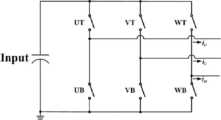
도 2는 SVPWM의 극전압지령 파형과 삼각파(Carrier) 파형을 도시한 것이다. 종래에 많이 사용되는 3상 교류 전동기를 구동하기 위해 사용되는 대표적인 PWM 기법은 Sinusoidal PWM(SPWM)과 Space Vector PWM(SVPWM)이 있다. SPWM과 SVPWM은 모터에 정현파의 상전압을 인가하기 위해 적용되는 방법으로써, 그 중 SVPWM은 SPWM 에 비해 전압 변조지수가 크고 노이즈 특성이 뛰어난 장점을 가지고 있다.2 shows an extreme voltage command waveform and a triangular wave (Carrier) waveform of SVPWM. Representative PWM techniques used to drive three-phase AC motors that are widely used in the prior art include Sinusoidal PWM (SPWM) and Space Vector PWM (SVPWM). SPWM and SVPWM are methods applied to apply a sinusoidal phase voltage to a motor. Among them, SVPWM has a larger voltage modulation index and superior noise characteristics compared to SPWM.
도 2의 (a)와(b)는 SVPWM 기법에서 나타나는 극전압지령과 삼각파(Carrier) 파형을 각각 나타낸다. 각 상의 상/하단 스위치의 게이트 신호(Gate Signal)는 비교기(Comparator)를 사용하여 생성한다. 비교기 입력단은 극전압지령과 삼각파를 입력신호로 사용하며, 그 출력은 상단 스위치의 게이트 신호로 사용한다. 그리고 하단 스위치의 게이트 신호는 상단 스위치의 게이트 신호를 반전하여 사용한다.(a) and (b) of FIG. 2 show an extreme voltage command and a triangular wave (Carrier) waveform appearing in the SVPWM technique, respectively. The gate signal of the upper/lower switch of each phase is generated using a comparator. The input stage of the comparator uses the extreme voltage command and triangular wave as input signals, and its output is used as the gate signal of the upper switch. The gate signal of the lower switch is used by inverting the gate signal of the upper switch.
도 3은 삼각파(Carrier)의 한 주기에 대해 나타낸 파형이다. 도 3에서, 삼각파의 한 주기에 대해 3상 전압지령(Uref, Vref, Wref)과 스위치의 게이트-소스(Gate-Source) 전압(U/V/W_Vgs(High/Low))이 도시되어 있다. 삼각파의 주파수는 전압지령의 주파수에 비해 상당히 크기 때문에 삼각파 한 주기에서 전압지령은 DC(Direct Current) 값으로 가정하여 해석할 수 있다. 3상 인버터의 상단 또는 하단 스위치가 모두 도통하는 시간은 T0 로 표시하였고, 입력단에서 모터로 전력이 공급되는 유효 벡터 시간은 T1, T2 로 표시하였다.3 is a waveform shown for one cycle of a triangular wave (Carrier). In FIG. 3, three-phase voltage references (Uref, Vref, and Wref) and gate-source voltages (U/V/W_Vgs (High/Low)) of a switch are shown for one cycle of a triangular wave. Since the frequency of the triangular wave is considerably larger than the frequency of the voltage command, the voltage command in one cycle of the triangular wave can be analyzed by assuming DC (Direct Current) value. The time when the top or bottom switches of the 3-phase inverter are all conducting is indicated by T0, and the effective vector time when power is supplied from the input terminal to the motor is indicated by T1 and T2.
도 4는 데드 타임(Dead Time)에서 전류 극성에 따른 바디 다이오드(Body Diode)의 도통 동작 회로를 도시한 것이다. 3상 인버터의 각 상의 상/하단 스위치는 상보동작을 한다. 동작 과정에서 상/하단 스위치가 모두 켜지는 암-쇼트(Arm-Short)가 발생할 경우, 스위치 소자의 손상 문제가 발생할 수 있다. 이러한 현상을 방지하기 상/하단 스위치의 동작이 변하는 구간에 데드 타임이 적용될 필요가 있다. 데드 타임이 적용될 경우 지령 전압과 실제 인가 전압 사이에 오차가 발생하게 된다. 이 오차는 모터를 정밀하게 제어하는데 있어 단점으로 작용한다.4 illustrates a conduction operation circuit of a body diode according to current polarity at a dead time. The upper/lower switches of each phase of the 3-phase inverter perform complementary operations. When an arm-short occurs in which both the upper and lower switches are turned on during operation, damage to the switch element may occur. To prevent this phenomenon, a dead time needs to be applied to a section in which an operation of an upper/lower switch changes. When the dead time is applied, an error occurs between the command voltage and the actual applied voltage. This error acts as a disadvantage in controlling the motor precisely.
도 4에 따르면, 데드 타임 구간에서 U상의 인버터 레그(Leg)가 나타나 있다. 모터에 흐르는 전류 극성에 따라 데드 타임일 때 바디 다이오드의 도통 경로는 달라진다. 도 4(a)는 U상 전류의 극성이 양수인 경우 데드 타임 구간에서 회로 동작을 나타낸다. 이 구간에서 하단 스위치의 바디 다이오드를 통해 전류가 흐르기 때문에 하단 스위치가 도통된 것과 같은 동작을 한다. 도 4(b)는 U상 전류의 극성이 음수인 경우 데드 타임 구간에서 회로 동작을 나타낸다. 이 구간에서 상단 스위치의 바디 다이오드를 통해 전류가 흐르기 때문에 상단 스위치가 도통된 것과 같은 동작을 한다.According to FIG. 4, the U-phase inverter leg is shown in the dead time period. Depending on the polarity of the current flowing in the motor, the conduction path of the body diode during dead time is different. Figure 4 (a) shows the circuit operation in the dead time section when the polarity of the U-phase current is positive. In this section, since the current flows through the body diode of the lower switch, it operates as if the lower switch is conducting. Figure 4 (b) shows the circuit operation in the dead time section when the polarity of the U-phase current is negative. In this section, since the current flows through the body diode of the top switch, it operates as if the top switch is conducting.
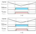
도 5는 상 전류 극성에 따른 게이트-소스 전압 파형(데드 타임 보상 전)이다. 도 5에 따르면, 상 전류 극성이 양수와 음수인 경우에 따른 데드 타임 보상 전 게이트 신호(Gate Signal)와 U 상의 극전압 파형이 도시되어 있다. 게이트 신호는 지령전압(Reference)과 삼각파(Carrier)를 비교하여 생성하게 되며, 생성된 게이트 신호에 데드 타임을 적용하여 게이트 신호를 인가하게 된다. Gate(High)의 하늘색 명암은 인가하고자 하는 지령을 나타낸다. 그리고 붉은색의 명암은 실제 U 상의 극전압 VU 를 나타낸다. 하늘색 명암과 붉은색 명암의 면적의 영역이 다르다는 것을 통해 인가하고자 하는 전압과 실제로 인가되는 전압에 오차가 발생하는 것을 알 수 있다.5 is a gate-source voltage waveform (before dead time compensation) according to phase current polarity. Referring to FIG. 5 , the gate signal before dead time compensation according to the case where the phase current polarity is positive and negative and the extreme voltage waveform of the U phase are shown. A gate signal is generated by comparing a reference voltage and a triangular wave (Carrier), and a dead time is applied to the generated gate signal to apply the gate signal. The sky blue contrast of Gate (High) indicates the command to be applied. And the contrast of red color represents the pole voltage VU of the actual U phase. It can be seen that an error occurs between the voltage to be applied and the voltage actually applied through the difference between the areas of the sky blue contrast and the red contrast.
도 6은 상 전류 극성에 따른 게이트-소스 전압 파형(데드 타임 보상 후)이다. 도 6에 따르면, 전류 극성이 양수와 음수인 경우 각각 데드 타임 보상이 적용된 게이트 신호와 그때의 극전압 파형이 도시되어 있다. 도 5와 비교하여 도 6 의 경우, 지령 신호를 나타내는 Gate(High)의 하늘색 명암 영역과 실제 인가 전압을 나타내는 VU 의 붉은색 명암 영역이 동일하다. 따라서 데드 타임 보상 기법은 전류의 극성에 따라 데드 타임 위치를 적절히 보상해줌으로써 지령 신호와 동일한 실제 전압 인가를 가능하도록 한다.6 is a gate-source voltage waveform (after dead time compensation) according to phase current polarity. Referring to FIG. 6 , when the current polarity is positive and negative, a gate signal to which dead time compensation is applied and an extreme voltage waveform at that time are shown. Compared to FIG. 5 , in the case of FIG. 6 , the sky blue contrast area of Gate (High) indicating the command signal and the red contrast area of VU indicating the actual applied voltage are the same. Therefore, the dead time compensation technique properly compensates for the dead time position according to the polarity of the current, so that the same actual voltage as that of the command signal can be applied.
다음으로,싱글-션트 알고리즘(Single-Shunt Algorithm)에 대해 설명한다. 3상 모터를 원하는 속도로 회전시키기 위해 3상 인버터가 사용된다. 3상 모터를 원하는 속도로 제어하기 위해 속도제어와 전류제어가 일반적으로 사용된다. 속도제어와 전류제어를 위해선 모터의 회전속도와 3상 전류정보가 필요하다. 모터의 속도는 엔코더와 같은 센서를 통해 읽어오거나, 속도센서를 사용하지 않는 센서리스(Sensorless) 기법을 통해 추정할 수 있다. 모터의 상전류는 전류 변성기(Current Transformer(CT)) 또는 션트 저항(Shunt Resistor)과 같은 측정 장비가 필요하며, 가격적으로 경쟁력있는 션트 저항이 많이 사용되고 있다.Next, the single-shunt algorithm will be described. A three-phase inverter is used to rotate the three-phase motor at a desired speed. Speed control and current control are commonly used to control a three-phase motor at a desired speed. For speed control and current control, motor rotation speed and three-phase current information are required. The speed of the motor can be read through a sensor such as an encoder or estimated through a sensorless technique that does not use a speed sensor. The phase current of the motor requires measurement equipment such as a current transformer (CT) or shunt resistor, and shunt resistors with competitive prices are widely used.
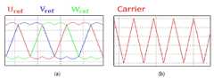
도 7은 3상 인버터를 활용한 상 전류 측정 방법을 도시한 것이다. 도 7에 따르면, 앞서 언급한 상전류 측정을 위해 사용되는 션트 저항의 위치를 나타낸다. 3 션트 알고리즘(Three Shunt Algorithm)은 3개의 션트 저항을 사용하여 상전류를 측정하는 알고리즘으로써, 각 상의 하단 스위치 아래 위치하게 된다. 2 션트 알고리즘(Two Shunt Algorithm)은 2개의 션트 저항을 사용하여 상전류를 측정하는 알고리즘으로, 임의의 2상의 하단 스위치 아래 션트 저항을 배치하여 2개의 전류 측정 후 남은 한상의 전류를 도출해내는 방법이 적용된다(Iu + Iv + Iw = 0). 싱글-션트 알고리즘(Single-Shunt Algorithm)은 DC 버스와 3상 인버터 간 흐르는 전류를 측정하는 방법으로, 한 주기 2번의 전류 측정 후 2개의 전류 정보를 통해 3상 전류를 복원해 내는 방법이 적용된다. 위에 언급되었듯, 션트 알고리즘은 션트 저항의 수에 따라 알고리즘이 분류되며, 싱글 션트 알고리즘의 가격이 저렴한 장점을 가지게 된다.7 illustrates a phase current measurement method using a three-phase inverter. 7 shows the position of the shunt resistor used for measuring the aforementioned phase current. The Three Shunt Algorithm is an algorithm that measures phase current using three shunt resistors, located below the lower switch of each phase. The Two Shunt Algorithm is an algorithm that measures the phase current using two shunt resistors. A method of deriving the current of the remaining one phase after measuring the two currents by placing the shunt resistor under the lower switch of any two phases is applied. (Iu + Iv + Iw = 0). The Single-Shunt Algorithm is a method of measuring the current flowing between the DC bus and the 3-phase inverter. A method of restoring the 3-phase current through two current information after measuring the current twice in one cycle is applied. . As mentioned above, the shunt algorithm is classified according to the number of shunt resistors, and the price of the single shunt algorithm is low.
도 8은 스위칭 상태에 따른 싱글-션트(Single-Shunt) 전류 측정 원리를 도시한 회로도이다. 싱글 션트 알고리즘의 전류 측정은 인버터 회로의 스위칭 상태와 관련이 있다. 측정 과정을 설명을 위해 인버터 스위칭 상태는 다음과 같이 정의한다. Su는 U 상의 스위치 상태를 나타내는 변수로, U 상의 상단 스위치가 온(On)일 경우 Su = 1, U 상의 하단 스위치가 온(On)일 경우 Su = 0으로 나타낸다. V 상과 W 상도 U 상과 동일한 표현 방식이 적용된다.8 is a circuit diagram illustrating a single-shunt current measurement principle according to a switching state. The current measurement of the single shunt algorithm is related to the switching state of the inverter circuit. To explain the measurement process, the inverter switching state is defined as follows. Su is a variable representing the state of the switch of phase U. When the upper switch of phase U is on, Su = 1, and when the lower switch of phase U is on, Su = 0. The same expression method as the U phase is applied to the V phase and the W phase.
도 8(a)는 Su = 1, Sv = 0, Sw = 0 이므로 U 상의 상단 스위치, 그리고 V 상과 W 상의 하단 스위치가 온(On)된 상태를 나타낸다. 이 스위칭 상태에서 U 상의 전류 정보가 측정된다. 도 8(b) 는 U 상과 V 상의 상단 스위치가, 그리고 W 상의 하단 스위치가 온(On)된 상태를 나타낸다. 이 스위칭 상태에서, 션트 저항에 흐르는 전류는 W 상의 전류와 같다.8(a) shows a state in which the upper switch of U phase and the lower switch of V phase and W phase are turned on since Su = 1, Sv = 0, and Sw = 0. In this switching state, current information on U is measured. 8(b) shows a state in which the upper switches of phase U and V and the lower switch of phase W are turned on. In this switching state, the current flowing through the shunt resistor is equal to the current of the W phase.
SVPWM 을 적용하게 될 경우, 서로 다른 스위칭 상태가 8가지로 나타나게 된다. 이 중 6가지의 스위칭 상태는 입력단에서 모터에 전력을 공급하기 때문에 유효벡터(Active Vector)라고 부른다. 그 외에 인버터의 모든 상단 스위치가 온(On) 상태인 Su = 1, Sv = 1, Sw = 1과 하단 스위치가 온(On) 상태인 Su = 0, Sv = 0, Sw = 0 인 2가지 스위칭 상태는 모터에 전력 전달이 이루어지지 않기에 영백터(Zero Vector)라고 부른다. 위에 언급된 8가지의 스위칭 상태에서 션트 저항에 흐르는 전류는 규칙적으로 나타나므로, 인버터 각극에서 모터로 들어가는 방향의 전류를 양수로 정의하였을 경우 표 1과 같이 정리할 수 있다. 표 1은 인버터 스위칭 상태에 따른 측정 전류를 나타낸다.When SVPWM is applied, 8 different switching states appear. Six of these switching states are called active vectors because they supply power to the motor at the input. In addition, there are two switching modes: Su = 1, Sv = 1, Sw = 1 with all top switches of the inverter on, and Su = 0, Sv = 0, Sw = 0 with bottom switches on. This state is called zero vector because no power is transmitted to the motor. Since the current flowing through the shunt resistor appears regularly in the eight switching states mentioned above, if the current in the direction entering the motor from each pole of the inverter is defined as a positive number, it can be summarized as shown in Table 1. Table 1 shows the measured current according to the inverter switching state.
[표 1][Table 1]

도 9는 공간 벡터 변조 방식(SVPWM)의 백터도이다. 도 9는 앞서 언급한 SVPWM의 인버터 스위칭 상태에 따른 벡터도를 나타낸 것이며, 표 1은 스위칭 상태에 따라 션트 저항에 흐르는 전류를 나타낸 표이다. 스위칭 상태를 나타내는 괄호( ) 안의 숫자는 순서대로 U, V, W 상의 스위칭 상태를 나타내며, 1인 경우 상단 스위치가 온(On), 0인 경우 하단 스위치가 온(On) 동작을 나타낸다. 총 8 가지의 스위치 동작 상태가 존재하며, 6개 벡터(V1 ~ V6 : 유효벡터)에서는 션트 저항에 모터의 상전류가 흐르게 되며, 남은 2개 벡터(V0 , V7 : 영벡터)에서는 션트 저항에 모터의 상전류가 흐르지 않는다.9 is a vector diagram of a space vector modulation scheme (SVPWM). 9 shows a vector diagram according to the above-mentioned inverter switching state of the SVPWM, and Table 1 is a table showing the current flowing through the shunt resistor according to the switching state. Numbers in parentheses ( ) indicating the switching state indicate the switching states of U, V, and W phases in order. If 1, the upper switch is On, and if 0, the lower switch is On. There are a total of 8 switch operation states. In 6 vectors (V1 ~ V6: effective vectors), the phase current of the motor flows through the shunt resistor, and in the remaining 2 vectors (V0, V7: zero vector), the motor flows through the shunt resistor. phase current does not flow.
SVPWM의 경우 한 주기동안 2개의 유효벡터가 나타나게 된다. 따라서 3상 전류정보를 모두 알기 위해 2개의 유효벡터가 나타나는 동안 전류를 각각 측정해야 한다.(Iu + Iv + Iw = 0)In the case of SVPWM, two valid vectors appear during one cycle. Therefore, in order to know all three-phase current information, each current must be measured while two effective vectors appear. (Iu + Iv + Iw = 0)
하지만, 유효벡터의 지속시간이 전류를 측정하기 위해 필요한 최소시간보다 짧게 나타날 경우, 션트 저항의 정보를 측정할 수 없는 문제가 나타난다. 이러한 상황이 발생하는 영역을 데드밴드 영역(Dead Band Area)라고 부르며, 모든 섹터(Sector)에 반드시 나타나는 문제가 있다. 전류제어를 위해 데드 밴드 영역에서도 전류측정이 이루어져야 한다. 전류측정을 위한 유효벡터의 인가시간을 늘리기 위해 게이트 신호 쉬프팅(Gate Signal Shifting) 기법이 적용될 수 있다. 게이트 신호 쉬프팅은 전류측정을 위한 최소시간보다 유효벡터의 인가시간이 짧은 경우 나타나게 되며, 이를 판단하는 기준은 3상 전압지령 중 인접한 2개의 전압지령 차이로 판단하게 된다. 삼각파는 일정한 주파수와 크기를 가지므로, 인접한 2개의 전압지령 차이는 시간정보를 포함하게 되므로, 인접한 2개의 전압지령의 차이가 게이트 신호 쉬프팅 판단 기준이 된다. 전압지령의 차이로 판단을 하기 때문에, 최소인가시간에 포함되는 정보는 데드 타임, 유효벡터에서 전류가 안정화되기까지의 시간인 셋틀링 타임(Settling Time), 그리고 션트 저항 정보를 디지털 값으로 읽어 들이는 A/D 컨버젼 딜레이 타임(Conversion Delay Time)이 포함된다. 하지만, 이때 기존의 데드 타임 보상 기법이 싱글 션트 알고리즘에 적용될 경우, 알고리즘이 복잡해지는 문제가 나타나게 된다.However, if the duration of the effective vector appears shorter than the minimum time required to measure the current, a problem of not being able to measure shunt resistance information appears. The area where this situation occurs is called a dead band area, and there is a problem that must appear in all sectors. For current control, current measurement must be performed even in the dead band area. In order to increase the application time of the effective vector for current measurement, a gate signal shifting technique may be applied. Gate signal shifting occurs when the effective vector application time is shorter than the minimum time for current measurement, and the criterion for determining this is the difference between two adjacent voltage commands among the three-phase voltage commands. Since the triangular wave has a constant frequency and magnitude, the difference between two adjacent voltage commands includes time information, and thus the difference between the two adjacent voltage commands becomes a criterion for determining gate signal shifting. Since the decision is made based on the difference in voltage command, the information included in the minimum applied time is the dead time, the settling time, which is the time until the current is stabilized in the effective vector, and the shunt resistance information is read as a digital value. includes the A/D conversion delay time. However, in this case, when the conventional dead time compensation technique is applied to the single shunt algorithm, a problem of complicating the algorithm appears.
도 10은 데드 타임 보상 적용 시 전류의 극성에 따라 나타나는 게이트 파형이다. 도 10에 따르면, 싱글 션트 알고리즘에서 기존의 데드 타임 보상 기법 적용시 나타나는 게이트 신호를 나타낸다. 전류 측정을 위한 최소 시간을 확보하기 위한 게이트 신호 쉬프팅은 인접한 두개의 전압지령 차이로 판단하게 된다. 도 10(a)는 U 상의 전류는 음수, V 상의 전류는 양수인 경우 데드 타임 보상이 적용된 게이트 파형을 나타낸다. 도 10(b)는 U 상과 V 상의 전류가 모두 음수인 경우를 나타낸다. 도 10(a)에 나타나듯, 인접한 두 전압지령의 차이(Vu - Vv)에 해당하는 주황색 영역에는 데드 타임이 두번 나타나며, 도 10(b)의 경우 파란색 영역에는 데드 타임이 한번 나타난다. 이는 V 상과 W 상의 경우에도 똑같이 발생할 수 있다. 위 두가지 경우를 구분하여 알고리즘을 구현하게 될 경우, 기존의 데드 타임 보상 기법 알고리즘보다 구현이 어려워지는 단점이 나타난다.10 is a gate waveform appearing according to the polarity of current when dead time compensation is applied. 10 shows a gate signal appearing when a conventional dead time compensation technique is applied in a single shunt algorithm. Gate signal shifting to secure the minimum time for current measurement is determined by the difference between two adjacent voltage commands. 10(a) shows gate waveforms to which dead time compensation is applied when the current of phase U is a negative number and the current of phase V is a positive number. 10(b) shows a case in which both U and V phase currents are negative. As shown in FIG. 10 (a), the dead time appears twice in the orange area corresponding to the difference (Vu - Vv) between two adjacent voltage commands, and in the case of FIG. 10 (b), the dead time appears once in the blue area. This may equally occur in the case of the V phase and the W phase. If the algorithm is implemented by distinguishing the above two cases, the disadvantage of implementation becomes more difficult than the existing dead time compensation algorithm.
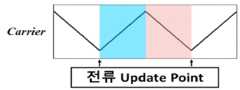
도 11은 전류 갱신 시점(Update Point) 및 데드 타임 보상 영역을 도시한 것이다. 도 11에 따르면, 삼각파에서 전류 갱신 시점 및 데드 타임 보상 영역을 나타낸다. 파란색과 붉은색 명암의 영역에서 모두 데드 타임 보상이 이루어진다. 하지만, 붉은색 명암의 영역은 전류 갱신 후 약간의 시간이 지난 후 데드 타임 보상이 이루어진다. 하지만, 데드 타임 보상의 경우 전류의 극성이 중요하므로 붉은색 영역에서의 데드 타임 보상은 신뢰도가 떨어지는 단점이 존재한다.11 illustrates a current update point and a dead time compensation area. 11 shows a current update point and a dead time compensation area in a triangular wave. Dead time compensation is made in both blue and red contrast areas. However, in the red contrast area, dead time compensation is performed after some time has elapsed after the current update. However, in the case of dead time compensation, since the polarity of the current is important, dead time compensation in the red region has a disadvantage in that reliability is low.
본 개시에서는 싱글 션트 알고리즘에서도 구현이 쉽고 높은 신뢰도를 나타내는 데드 타임 보상 기법을 제공하며, 이를 설명한다.In the present disclosure, a dead time compensation technique that is easy to implement even in a single shunt algorithm and exhibits high reliability is provided and described.
도 12는 본 개시에 따른 데드 타임 보상 적용 시 게이트 파형이다. 도 12(a)는 전류의 극성이 양수인 경우를 나타내며, 도 12(b)는 전류의 극성이 음수인 경우 데드 타임 보상이 적용되었을 때의 파형을 나타낸다. 기존의 방법과 본 개시에 따른 방법의 차이는 전류의 극성이 양수인 도 10(a)에서 확인할 수 있다. 본 개시에 따른 데드 타임 보상은 도 12에 나타나듯이 전류의 측정이 이루어지지 않는 삼각파(Carrier)의 라이징 슬로프(Rising Slope)에서만 이루어지며, 전류 갱신 시점에서 전압지령을 조정하여 데드 타임의 위치를 조정할 수 있다. 따라서 전류의 측정 시 필요한 최소 인가 시간 판단 기준인 전압 지령의 차이에는 데드 타임이 전압지령의 차이에서 한번 나타나기 때문에 알고리즘 구현이 간편해지게 된다.12 is a gate waveform when dead time compensation is applied according to the present disclosure. 12(a) shows a case where the current polarity is positive, and FIG. 12(b) shows a waveform when dead time compensation is applied when the current polarity is negative. The difference between the conventional method and the method according to the present disclosure can be seen in FIG. 10 (a) in which the polarity of the current is positive. As shown in FIG. 12, the dead time compensation according to the present disclosure is performed only on the rising slope of the carrier, where the current is not measured, and the dead time position can be adjusted by adjusting the voltage command at the time of current renewal. can Therefore, since the dead time appears once in the voltage command difference for the voltage command difference, which is the criterion for determining the minimum applied time required for current measurement, the implementation of the algorithm is simplified.
도 13은 전류 갱신 시점 및 데드 타임 보상 영역을 도시한 것이다. 도 13에서와 같이, 본 개시에 따른 데드 타임 보상 기법이 적용 되었을 때, 유효벡터에서 측정한 전류를 업데이트하는 시점과 데드 타임 보상 기법이 적용되는 영역이 도시되어 있다. 도 11에서와 동일하게 도 13에서도 삼각파(Carrier)가 가장 작은 값을 가질 때 전류가 업데이트되는 것을 나타낸다. 하지만, 도 13에서 데드 타임 보상이 나타나는 영역은 오직 하늘색 명암의 영역에서만 나타난다. 즉, 전류의 극성이 중요한 데드 타임 보상 기법에서, 전류가 업데이트된 직후에만 데드 타임 보상을 수행함을 나타낸다.13 illustrates a current update timing and a dead time compensation area. As shown in FIG. 13, when the dead time compensation technique according to the present disclosure is applied, the timing of updating the current measured from the effective vector and the area to which the dead time compensation technique is applied are shown. As in FIG. 11, FIG. 13 shows that the current is updated when the triangular wave (Carrier) has the smallest value. However, in FIG. 13 , the dead time compensation area appears only in the light blue area. That is, in the dead time compensation scheme in which the polarity of the current is important, dead time compensation is performed only immediately after the current is updated.
따라서, 기존의 데드 타임 보상 기법에 비해 높은 신뢰도를 가질 수 있다. 이와 같이 하여, 본 개시는 싱글 션트 알고리즘이 적용된 인버터에 적용되기 쉬운 데드 타임 기법을 제공한다. 본 개시에 따른 데드 타임 보상 기법과 기존의 데드 타임 보상 기법의 목적은 데드 타임을 보상하는 것으로 동일하지만, 본 개시에 따른 데드 타임 보상 기법을 싱글 션트 알고리즘에 적용 시 기존의 데드 타임 보상 기법에 비해 구현이 쉽고 높은 신뢰도를 가질 수 있다.Therefore, it can have higher reliability than the existing dead time compensation technique. In this way, the present disclosure provides a dead time scheme that is easy to apply to inverters to which a single shunt algorithm is applied. The purpose of the dead time compensation scheme according to the present disclosure and the conventional dead time compensation scheme is the same as compensating for dead time, but when the dead time compensation scheme according to the present disclosure is applied to a single shunt algorithm, compared to the conventional dead time compensation scheme It is easy to implement and can have high reliability.
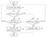
도 14a 및 도 14b는 본 개시에 따른 싱글-션트 알고리즘을 고려한 3상 인버터 데드 타임 보상 장치(100)의 구성을 도시한 블럭도 및 순서도이다.14A and 14B are block diagrams and flowcharts showing the configuration of a 3-phase inverter dead
일부 예들에서, 3상 인버터는 상술한 바와 같이 상단 및 하단이 반도체 스위치로 구성되고, 또한 직류 버스에 하나의 션트 저항이 연결된 구성을 포함할 수 있다. 여기서, 3상 인버터 데드 타임 보상 장치(100)는 도 14a에 도시된 바와 같이, 션트 저항 전류 측정부(110), 전류 극성 판단부(120), 삼각파 판단부(130), 및 전압 지령 조정부(140)를 포함할 수 있다.In some examples, the 3-phase inverter may include a configuration in which upper and lower ends are composed of semiconductor switches as described above, and one shunt resistor is connected to a DC bus. Here, as shown in FIG. 14A, the three-phase inverter dead
션트 저항 전류 측정부(110)는 직류 버스에 연결된 션트 저항으로부터 전류를 측정한다.(도 14b에서 단계 S1 참조)The shunt resistor
전류 극성 판단부(120)는 션트 저항 전류 측정부에서 측정된 전류로부터 전류 극성이 양성인지 여부를 판단한다. 일부 예들에서, 전류가 모터로 들어가면 양성(또는 양수)으로 판단하고 전류가 모터에서 나오면 음성(또는 음수)으로 판단한다.(도 14b에서 단계 S2 참조)The
삼각파 판단부(130)는 반도체 스위치에 게이트 신호 인가를 위한 삼각파로부터 라이징 슬로프인지 여부를 판단한다. 일부 예들에서, 삼각파 판단부(130)는 삼각파 제공부에서 출력되는 삼각파의 주파수를 이용하여, 삼각파가 라이징 슬로프인지 아닌지 판단할 수 있다. 일부 예들에서, 삼각파 판단부(130)는 삼각파 제공부에서 특정한 시간에 특정한 삼각파를 출력하는 정보를 미리 알고 있으므로, 이를 통해 삼각파의 라이징 슬로프 여부를 판단할 수 있다.(도 14b에서 단계 S3 참조)The triangle
전압 지령 조정부(140)는 반도체 스위치에 게이트 신호 인가를 위한 전압 지령 신호를 조정하여 데드 타임 위치가 조정되도록 한다. 일부 예들에서, 전압 지령 조정부(140)는 데드 타임 위치를 조정하기 위해 전압 지령 신호의 레벨을 증가시킬 수 있다. 증가시킬 전압 지령 신호의 레벨은 데드 타임 보상 위치에 따라 다양하게 조정될 수 있다. 일부 예들에서, 전압 지령 조정부(140)는 삼각파의 레벨이 가장 낮은 전류 갱신 시점에서 전압 지령 신호를 조정할 수 있다.(도 14b에서 단계 S4 참조)The voltage
한편, 전류가 모터로부터 나오면 음성(또는 음수)으로 판단하며(도 14b에서 단계 S5 참조), 이때에는 기존과 동일한 방식으로 데드타임 보상이 수행될 수 있다(도 14b에서 단계 S6 참조).On the other hand, if the current comes out of the motor, it is determined as negative (or negative) (see step S5 in FIG. 14b), and at this time, dead time compensation may be performed in the same manner as in the past (see step S6 in FIG. 14b).
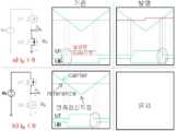
도 15는 기존 및 본 개시에 따른 싱글-션트 알고리즘을 고려한 3상 인버터 데드 타임 보상 결과를 설명하는 도면이다.15 is a diagram illustrating a result of compensating for a dead time of a three-phase inverter considering existing and single-shunt algorithms according to the present disclosure.
도 15에 도시된 바와 같이, 기존에는 상전류가 양수인 경우 전류 갱신 시점 이전에 데드 타임 위치가 조정되었으나, 본 개시에서는 상전류가 양수인 경우 전류 갱신 시점 이후에 데드 타임 위치가 조정된다. 즉, 본 개시에는 게이트 신호의 앞단이 원래대로 뒤쪽으로 밀리고, 게이트 신호의 후단이 전압 지령 조정에 의해(데드 타인 조정에 의해) 보상된다. 또한, 도 15에 도시된 바와 같이, 상전류가 음수인 경우에는 기존과 동일한 방식으로 게이트 신호가 보상된다.As shown in FIG. 15 , in the past, when the phase current is a positive number, the dead time position is adjusted before the current update time, but in the present disclosure, when the phase current is a positive number, the dead time position is adjusted after the current update time. That is, in the present disclosure, the front end of the gate signal is pushed backward as originally, and the rear end of the gate signal is compensated by voltage command adjustment (by dead tine adjustment). Also, as shown in FIG. 15, when the phase current is negative, the gate signal is compensated in the same manner as before.
이와 같이 하여, 본 개시는 데드 타임 보상 블록에서, 상전류가 양수인 경우 전류 갱신 후 곧바로 데드 타임을 보상할 수 있도록 위치를 변경한다. 따라서, 기존에 전류 극성의 신뢰도를 높이기 위해 사용하던 별도의 회로를 제거할 수 있고, 상전압 리플(ripple), 전력 손실, EMI 등을 저감하여 내구성 있는 모터 구동에 기여할 수 있다.In this way, in the present disclosure, when the phase current is a positive number in the dead time compensation block, the position is changed so that the dead time can be compensated immediately after updating the current. Accordingly, a separate circuit conventionally used to increase reliability of current polarity can be removed, and phase voltage ripple, power loss, EMI, and the like can be reduced, thereby contributing to durable motor driving.
이상에서 설명한 것은 본 개시에 따른 예시적 싱글-션트 알고리즘을 고려한 3상 인버터 데드 타임 보상 장치 및 방법을 실시하기 위한 하나의 실시예에 불과한 것으로서, 본 개시는 상기한 실시예에 한정되지 않고, 이하의 특허청구범위에서 청구하는 바와 같이 본 개시의 요지를 벗어남이 없이 당해 발명이 속하는 분야에서 통상의 지식을 가진 자라면 누구든지 다양한 변경 실시가 가능한 범위까지 본 개시의 기술적 정신이 있다고 할 것이다.What has been described above is only one embodiment for implementing a three-phase inverter dead time compensation apparatus and method considering an exemplary single-shunt algorithm according to the present disclosure, and the present disclosure is not limited to the above-described embodiment. As claimed in the claims of, anyone skilled in the art without departing from the gist of the present disclosure will say that the technical spirit of the present disclosure exists to the extent that various changes can be made.
Claims (6)
Translated fromKorean상기 션트 저항으로부터 전류를 측정하는 션트 저항 전류 측정부;
상기 션트 저항 전류 측정부에 연결되어, 상기 측정된 전류로부터 전류 극성이 양성인지 여부를 판단하는 전류 극성 판단부;
상기 전류 극성 판단부에 연결되어, 상기 전류 극성이 양성인 경우, 상기 반도체 스위치에 게이트 신호 인가를 위한 삼각파로부터 상기 삼각파가 라이징 슬로프인지 여부를 판단하는 삼각파 판단부; 및
상기 삼각파 판단부에 연결되어, 상기 삼각파가 라이징 슬로프인 경우, 상기 반도체 스위치에 게이트 신호 인가를 위한 전압 지령 신호를 조정하여 데드 타임 위치를 조정하는 전압 지령 조정부를 포함하고,
상기 전압 지령 조정부는 데드 타임 위치를 조정하기 위해 상기 전압 지령 신호의 레벨을 증가시키되, 상기 삼각파의 레벨이 가장 낮은 전류 갱신 시점 이후에 상기 전압 지령 신호를 조정하는, 3상 인버터 데드 타임 보상 장치.In the dead time compensation device of a three-phase inverter considering a single-shunt algorithm in which the upper and lower ends are composed of semiconductor switches and one shunt resistor is connected to a DC bus,
a shunt resistance current measurement unit measuring a current from the shunt resistance;
a current polarity determination unit connected to the shunt resistor current measuring unit and determining whether the current polarity is positive based on the measured current;
a triangular wave determining unit connected to the current polarity determining unit and determining whether the triangular wave for applying a gate signal to the semiconductor switch is a rising slope when the current polarity is positive; and
A voltage command adjustment unit connected to the triangle wave determination unit to adjust a dead time position by adjusting a voltage command signal for applying a gate signal to the semiconductor switch when the triangle wave has a rising slope;
The voltage command adjusting unit increases the level of the voltage command signal to adjust the dead time position, and adjusts the voltage command signal after a current update point in time when the level of the triangular wave is the lowest.
Priority Applications (1)
| Application Number | Priority Date | Filing Date | Title |
|---|---|---|---|
| KR1020210087965AKR102546525B1 (en) | 2021-07-05 | 2021-07-05 | Device and method for three-phase inverter dead time compensation considering single-shunt algorithm |
Applications Claiming Priority (1)
| Application Number | Priority Date | Filing Date | Title |
|---|---|---|---|
| KR1020210087965AKR102546525B1 (en) | 2021-07-05 | 2021-07-05 | Device and method for three-phase inverter dead time compensation considering single-shunt algorithm |
Publications (2)
| Publication Number | Publication Date |
|---|---|
| KR20230007116A KR20230007116A (en) | 2023-01-12 |
| KR102546525B1true KR102546525B1 (en) | 2023-06-23 |
Family
ID=84923671
Family Applications (1)
| Application Number | Title | Priority Date | Filing Date |
|---|---|---|---|
| KR1020210087965AActiveKR102546525B1 (en) | 2021-07-05 | 2021-07-05 | Device and method for three-phase inverter dead time compensation considering single-shunt algorithm |
Country Status (1)
| Country | Link |
|---|---|
| KR (1) | KR102546525B1 (en) |
Citations (2)
| Publication number | Priority date | Publication date | Assignee | Title |
|---|---|---|---|---|
| JP2014166081A (en)* | 2013-02-27 | 2014-09-08 | Hitachi Appliances Inc | Motor control device and air conditioner using the same |
| JP2015015885A (en) | 2013-07-02 | 2015-01-22 | エルエス産電株式会社Lsis Co., Ltd. | Apparatus for modifying voltage command for detecting output current in inverter |
Family Cites Families (2)
| Publication number | Priority date | Publication date | Assignee | Title |
|---|---|---|---|---|
| KR101268585B1 (en)* | 2011-10-05 | 2013-06-04 | 주식회사 오토파워 | Compensation method of dwad-time for three-phase inverter of SVPWM |
| JP6246756B2 (en)* | 2015-03-10 | 2017-12-13 | 株式会社東芝 | Motor control device, heat pump system and air conditioner |
- 2021
- 2021-07-05KRKR1020210087965Apatent/KR102546525B1/enactiveActive
Patent Citations (2)
| Publication number | Priority date | Publication date | Assignee | Title |
|---|---|---|---|---|
| JP2014166081A (en)* | 2013-02-27 | 2014-09-08 | Hitachi Appliances Inc | Motor control device and air conditioner using the same |
| JP2015015885A (en) | 2013-07-02 | 2015-01-22 | エルエス産電株式会社Lsis Co., Ltd. | Apparatus for modifying voltage command for detecting output current in inverter |
Also Published As
| Publication number | Publication date |
|---|---|
| KR20230007116A (en) | 2023-01-12 |
Similar Documents
| Publication | Publication Date | Title |
|---|---|---|
| US9584043B2 (en) | Inverter phase current reconstruction apparatus and methods | |
| US7239168B2 (en) | Current sensing in a two-phase motor | |
| CN110323991B (en) | Power module and method for providing multiphase current to multiphase load | |
| US7483279B2 (en) | Apparatus and method for detecting phase currents of inverter | |
| US4546422A (en) | Control system for a voltage-type inverter | |
| US6642690B2 (en) | Method for measuring phase current for inverter control apparatus using single current sensor and apparatus therefor | |
| CN112492892B (en) | Power conversion device | |
| KR102546525B1 (en) | Device and method for three-phase inverter dead time compensation considering single-shunt algorithm | |
| US7800333B2 (en) | Audible noise reduction for single current shunt platform | |
| JP3722561B2 (en) | Power supply device for magnetic resonance imaging apparatus | |
| JP2011193543A (en) | Gate voltage controller for voltage-type inverter, gate voltage control method, and intelligent power module | |
| CN104901528A (en) | Method and device for improving low-frequency wobble of motor | |
| KR102594764B1 (en) | Expansion method of current reconstruction areas for detecting phase currents by three-shunt resistors of three-leg two-phase inverters | |
| JP6016720B2 (en) | Power conversion device and power conversion method | |
| JP2012182874A (en) | Motor control device | |
| KR20230011861A (en) | Pwm driving method for an electric motor with zerocrossing compensation | |
| US10581366B2 (en) | Calculation apparatus and processing apparatus | |
| KR100610767B1 (en) | How to measure three-phase output current of inverter using one current sensor | |
| CN118435511A (en) | Control device and control method | |
| JPH0670549A (en) | Voltage type inverter device | |
| JP6575865B2 (en) | 3-level inverter control method and control apparatus | |
| WO2023190173A1 (en) | Motor control device, motor module, motor control program, and motor control method | |
| Wu et al. | A novel dead time compensation method for PWM inverter | |
| CN120077562A (en) | Motor control device, motor module, motor control program, and motor control method | |
| KR20200126814A (en) | Apparatus and method for controlling inverter of electric compressor |
Legal Events
| Date | Code | Title | Description |
|---|---|---|---|
| PA0109 | Patent application | Patent event code:PA01091R01D Comment text:Patent Application Patent event date:20210705 | |
| PA0201 | Request for examination | ||
| PE0902 | Notice of grounds for rejection | Comment text:Notification of reason for refusal Patent event date:20220914 Patent event code:PE09021S01D | |
| PG1501 | Laying open of application | ||
| E701 | Decision to grant or registration of patent right | ||
| PE0701 | Decision of registration | Patent event code:PE07011S01D Comment text:Decision to Grant Registration Patent event date:20230421 | |
| GRNT | Written decision to grant | ||
| PR0701 | Registration of establishment | Comment text:Registration of Establishment Patent event date:20230619 Patent event code:PR07011E01D | |
| PR1002 | Payment of registration fee | Payment date:20230620 End annual number:3 Start annual number:1 | |
| PG1601 | Publication of registration |