KR102543179B1 - Method of fabricating light emitting didoe module - Google Patents
Method of fabricating light emitting didoe moduleDownload PDFInfo
- Publication number
- KR102543179B1 KR102543179B1KR1020160106015AKR20160106015AKR102543179B1KR 102543179 B1KR102543179 B1KR 102543179B1KR 1020160106015 AKR1020160106015 AKR 1020160106015AKR 20160106015 AKR20160106015 AKR 20160106015AKR 102543179 B1KR102543179 B1KR 102543179B1
- Authority
- KR
- South Korea
- Prior art keywords
- hole
- metal plate
- reflective
- delete delete
- led module
- Prior art date
- Legal status (The legal status is an assumption and is not a legal conclusion. Google has not performed a legal analysis and makes no representation as to the accuracy of the status listed.)
- Active
Links
Images


Classifications
- H—ELECTRICITY
- H10—SEMICONDUCTOR DEVICES; ELECTRIC SOLID-STATE DEVICES NOT OTHERWISE PROVIDED FOR
- H10H—INORGANIC LIGHT-EMITTING SEMICONDUCTOR DEVICES HAVING POTENTIAL BARRIERS
- H10H20/00—Individual inorganic light-emitting semiconductor devices having potential barriers, e.g. light-emitting diodes [LED]
- H10H20/01—Manufacture or treatment
- H—ELECTRICITY
- H01—ELECTRIC ELEMENTS
- H01L—SEMICONDUCTOR DEVICES NOT COVERED BY CLASS H10
- H01L25/00—Assemblies consisting of a plurality of semiconductor or other solid state devices
- H01L25/03—Assemblies consisting of a plurality of semiconductor or other solid state devices all the devices being of a type provided for in a single subclass of subclasses H10B, H10D, H10F, H10H, H10K or H10N, e.g. assemblies of rectifier diodes
- H01L25/04—Assemblies consisting of a plurality of semiconductor or other solid state devices all the devices being of a type provided for in a single subclass of subclasses H10B, H10D, H10F, H10H, H10K or H10N, e.g. assemblies of rectifier diodes the devices not having separate containers
- H01L25/075—Assemblies consisting of a plurality of semiconductor or other solid state devices all the devices being of a type provided for in a single subclass of subclasses H10B, H10D, H10F, H10H, H10K or H10N, e.g. assemblies of rectifier diodes the devices not having separate containers the devices being of a type provided for in group H10H20/00
- H01L25/0753—Assemblies consisting of a plurality of semiconductor or other solid state devices all the devices being of a type provided for in a single subclass of subclasses H10B, H10D, H10F, H10H, H10K or H10N, e.g. assemblies of rectifier diodes the devices not having separate containers the devices being of a type provided for in group H10H20/00 the devices being arranged next to each other
- H01L33/005—
- H—ELECTRICITY
- H01—ELECTRIC ELEMENTS
- H01L—SEMICONDUCTOR DEVICES NOT COVERED BY CLASS H10
- H01L21/00—Processes or apparatus adapted for the manufacture or treatment of semiconductor or solid state devices or of parts thereof
- H01L21/02—Manufacture or treatment of semiconductor devices or of parts thereof
- H01L21/027—Making masks on semiconductor bodies for further photolithographic processing not provided for in group H01L21/18 or H01L21/34
- H01L21/033—Making masks on semiconductor bodies for further photolithographic processing not provided for in group H01L21/18 or H01L21/34 comprising inorganic layers
- H—ELECTRICITY
- H01—ELECTRIC ELEMENTS
- H01L—SEMICONDUCTOR DEVICES NOT COVERED BY CLASS H10
- H01L25/00—Assemblies consisting of a plurality of semiconductor or other solid state devices
- H01L25/50—Multistep manufacturing processes of assemblies consisting of devices, the devices being individual devices of subclass H10D or integrated devices of class H10
- H01L33/10—
- H01L33/36—
- H01L33/62—
- H—ELECTRICITY
- H10—SEMICONDUCTOR DEVICES; ELECTRIC SOLID-STATE DEVICES NOT OTHERWISE PROVIDED FOR
- H10H—INORGANIC LIGHT-EMITTING SEMICONDUCTOR DEVICES HAVING POTENTIAL BARRIERS
- H10H20/00—Individual inorganic light-emitting semiconductor devices having potential barriers, e.g. light-emitting diodes [LED]
- H10H20/01—Manufacture or treatment
- H10H20/032—Manufacture or treatment of electrodes
- H—ELECTRICITY
- H10—SEMICONDUCTOR DEVICES; ELECTRIC SOLID-STATE DEVICES NOT OTHERWISE PROVIDED FOR
- H10H—INORGANIC LIGHT-EMITTING SEMICONDUCTOR DEVICES HAVING POTENTIAL BARRIERS
- H10H20/00—Individual inorganic light-emitting semiconductor devices having potential barriers, e.g. light-emitting diodes [LED]
- H10H20/01—Manufacture or treatment
- H10H20/036—Manufacture or treatment of packages
- H10H20/0364—Manufacture or treatment of packages of interconnections
- H—ELECTRICITY
- H10—SEMICONDUCTOR DEVICES; ELECTRIC SOLID-STATE DEVICES NOT OTHERWISE PROVIDED FOR
- H10H—INORGANIC LIGHT-EMITTING SEMICONDUCTOR DEVICES HAVING POTENTIAL BARRIERS
- H10H20/00—Individual inorganic light-emitting semiconductor devices having potential barriers, e.g. light-emitting diodes [LED]
- H10H20/80—Constructional details
- H10H20/81—Bodies
- H10H20/814—Bodies having reflecting means, e.g. semiconductor Bragg reflectors
- H—ELECTRICITY
- H10—SEMICONDUCTOR DEVICES; ELECTRIC SOLID-STATE DEVICES NOT OTHERWISE PROVIDED FOR
- H10H—INORGANIC LIGHT-EMITTING SEMICONDUCTOR DEVICES HAVING POTENTIAL BARRIERS
- H10H20/00—Individual inorganic light-emitting semiconductor devices having potential barriers, e.g. light-emitting diodes [LED]
- H10H20/80—Constructional details
- H10H20/83—Electrodes
- H—ELECTRICITY
- H10—SEMICONDUCTOR DEVICES; ELECTRIC SOLID-STATE DEVICES NOT OTHERWISE PROVIDED FOR
- H10H—INORGANIC LIGHT-EMITTING SEMICONDUCTOR DEVICES HAVING POTENTIAL BARRIERS
- H10H20/00—Individual inorganic light-emitting semiconductor devices having potential barriers, e.g. light-emitting diodes [LED]
- H10H20/80—Constructional details
- H10H20/85—Packages
- H10H20/857—Interconnections, e.g. lead-frames, bond wires or solder balls
- H—ELECTRICITY
- H01—ELECTRIC ELEMENTS
- H01L—SEMICONDUCTOR DEVICES NOT COVERED BY CLASS H10
- H01L2224/00—Indexing scheme for arrangements for connecting or disconnecting semiconductor or solid-state bodies and methods related thereto as covered by H01L24/00
- H01L2224/01—Means for bonding being attached to, or being formed on, the surface to be connected, e.g. chip-to-package, die-attach, "first-level" interconnects; Manufacturing methods related thereto
- H01L2224/10—Bump connectors; Manufacturing methods related thereto
- H01L2224/15—Structure, shape, material or disposition of the bump connectors after the connecting process
- H01L2224/16—Structure, shape, material or disposition of the bump connectors after the connecting process of an individual bump connector
- H01L2224/161—Disposition
- H01L2224/16151—Disposition the bump connector connecting between a semiconductor or solid-state body and an item not being a semiconductor or solid-state body, e.g. chip-to-substrate, chip-to-passive
- H01L2224/16221—Disposition the bump connector connecting between a semiconductor or solid-state body and an item not being a semiconductor or solid-state body, e.g. chip-to-substrate, chip-to-passive the body and the item being stacked
- H01L2224/16225—Disposition the bump connector connecting between a semiconductor or solid-state body and an item not being a semiconductor or solid-state body, e.g. chip-to-substrate, chip-to-passive the body and the item being stacked the item being non-metallic, e.g. insulating substrate with or without metallisation
- H—ELECTRICITY
- H01—ELECTRIC ELEMENTS
- H01L—SEMICONDUCTOR DEVICES NOT COVERED BY CLASS H10
- H01L2924/00—Indexing scheme for arrangements or methods for connecting or disconnecting semiconductor or solid-state bodies as covered by H01L24/00
- H01L2924/10—Details of semiconductor or other solid state devices to be connected
- H01L2924/11—Device type
- H01L2924/12—Passive devices, e.g. 2 terminal devices
- H01L2924/1204—Optical Diode
- H01L2924/12041—LED
- H01L2933/0016—
- H01L2933/0066—
Landscapes
- Engineering & Computer Science (AREA)
- Microelectronics & Electronic Packaging (AREA)
- Power Engineering (AREA)
- Physics & Mathematics (AREA)
- Condensed Matter Physics & Semiconductors (AREA)
- General Physics & Mathematics (AREA)
- Computer Hardware Design (AREA)
- Manufacturing & Machinery (AREA)
- Chemical & Material Sciences (AREA)
- Inorganic Chemistry (AREA)
- Led Device Packages (AREA)
- General Engineering & Computer Science (AREA)
Abstract
Translated fromKoreanDescription
Translated fromKorean본 발명의 기술적 사상은 발광다이오드(LED) 모듈 제조방법에 관한 것이다.The technical idea of the present invention relates to a method for manufacturing a light emitting diode (LED) module.
반도체 발광다이오드(light emitting diode, LED)는 전기에너지를 이용하여 소자 내에 포함되어 있는 물질이 빛을 발광하는 소자로서, 접합된 반도체의 전자와 정공이 재결합하며 발생하는 에너지를 광으로 변환하여 방출한다. 이러한 발광다이오드는 조명장치 및 대형 액정디스플레이(Liquid Crystal Display, LCD)용 백라이트(backlight) 장치의 광원으로서 널리 이용되며 그 개발이 가속화되고 있는 추세이다.A semiconductor light emitting diode (LED) is a device that emits light by using electrical energy, and converts the energy generated by recombination of electrons and holes of bonded semiconductors into light and emits it. . These light emitting diodes are widely used as light sources for lighting devices and backlight devices for large liquid crystal displays (Liquid Crystal Displays, LCDs), and their development is accelerating.
일반적으로, 발광다이오드(LED) 모듈은 광추출 효율을 향상시키기 위해서 다양한 구조체를 추가로 도입할 수 있다. 이러한 구조체의 도입에 따라 발광 다이오드를 모듈화하는 과정이 복잡해지고 이로 인해 불량이 야기될 수 있다는 문제가 있다.In general, a light emitting diode (LED) module may additionally introduce various structures in order to improve light extraction efficiency. According to the introduction of such a structure, there is a problem in that a process of modularizing light emitting diodes becomes complicated, and thus defects may be caused.
본 발명의 해결하고자 하는 과제들 중 하나는, 솔더 인쇄 공정을 효율적으로 수행할 수 있는 발광다이오드(LED) 모듈 제조방법을 제공하는데 있다.
One of the problems to be solved by the present invention is to provide a method for manufacturing a light emitting diode (LED) module capable of efficiently performing a solder printing process.
본 발명의 일 실시예는, 칩 실장영역 주위에 배치된 반사성 적층체와 상기 칩 실장영역에 배치된 전극 패드를 갖는 회로 기판을 마련하는 단계와, 토출홀(discharge hole)이 형성된 돌출부를 갖는 마스크를 이용하여 상기 전극 패드 상에 솔더 페이스트를 적하시키는 단계 - 상기 돌출부는 상기 반사성 적층체에 의해 둘러싸인 공간에 삽입되도록 구성됨 - 와, 상기 솔더 페이스트를 이용하여 LED 칩의 전극을 상기 전극 패드에 접합시키는 단계를 포함하는 LED 모듈 제조방법를 제공한다.
An embodiment of the present invention provides a circuit board having a reflective laminate disposed around a chip mounting area and an electrode pad disposed on the chip mounting area, and a mask having a protruding portion having a discharge hole formed thereon. Dropping solder paste on the electrode pad by using - the protrusion is configured to be inserted into the space surrounded by the reflective laminate - and bonding the electrode of the LED chip to the electrode pad using the solder paste It provides an LED module manufacturing method comprising the steps.
본 발명의 일 실시예는, 칩 실장 공간을 정의하는 반사성 적층체와 상기 칩 실장 공간에 노출된 전극 패드를 갖는 회로 기판을 마련하는 단계와, 토출홀이 형성된 돌출부를 갖는 메탈 마스크를 마련하는 단계와, 상기 돌출부가 상기 칩 실장 공간에 삽입되도록 상기 메탈 마스크를 정렬하는 단계와, 상기 메탈 마스크가 정렬된 상태에서 상기 토출홀을 통해 상기 전극 패드 상에 솔더 페이스트를 적하시키는 단계와, 상기 솔더 페이스트를 이용하여 LED 칩의 전극을 상기 전극 패드에 접합시키는 단계를 포함하는 LED 모듈 제조방법을 제공한다.
An embodiment of the present invention provides a circuit board having a reflective laminate defining a chip mounting space and an electrode pad exposed to the chip mounting space, and preparing a metal mask having a protruding portion formed with a discharge hole. and aligning the metal mask so that the protrusion is inserted into the chip mounting space, dropping solder paste onto the electrode pad through the discharge hole in a state where the metal mask is aligned, and dropping the solder paste onto the electrode pad. It provides an LED module manufacturing method comprising the step of bonding the electrodes of the LED chip to the electrode pads by using.
본 발명의 일 실시예는, 제1 홀을 갖는 제1 금속 플레이트와, 상기 제1 금속 플레이트의 일부 영역에 적층되며 상기 제1 홀과 연결된 제2 홀을 갖는 적어도 하나의 제2 금속 플레이트와, 상기 제2 금속 플레이트 상에 적층되며 상기 제2 홀과 연결된 제3 홀을 갖는 제3 금속 플레이트를 포함하며, 상기 제2 및 제3 금속 플레이트는 상기 제1 금속 플레이트의 일면으로부터 볼록한 구조로 제공되는 메탈 마스크를 제공한다.
One embodiment of the present invention, a first metal plate having a first hole, at least one second metal plate laminated on a partial region of the first metal plate and having a second hole connected to the first hole, A third metal plate stacked on the second metal plate and having a third hole connected to the second hole, wherein the second and third metal plates are provided in a convex structure from one surface of the first metal plate A metal mask is provided.
회로 기판에 배치된 3차원 구조체로 인해 솔더 인쇄의 작업효율이 저하되지 않을 수 있는 방안을 제공한다. 돌출부를 갖는 메탈 마스크를 이용하여 효율적인 솔더 인쇄 공정을 수행할 수 있다.Provided is a method for not deteriorating work efficiency of solder printing due to a three-dimensional structure disposed on a circuit board. An efficient solder printing process may be performed using a metal mask having protrusions.
도1은 본 발명의 일 실시예에 따른 LED 모듈 제조에 사용되는 메탈 마스크와 회로 기판을 나타내는 개략 사시도이다.
도2a 및 도2b는 각각 도1에 도시된 메탈 마스크의 단면도 및 상부 평면도이다.
도3 내지 도6은 본 발명의 일 실시예에 따른 LED 모듈 제조방법을 설명하기 위한 주요 공정별 단면도이다.
도7은 도3에 도시된 회로 기판에 채용된 반사성 적층체를 나타내는 단면도이다.
도8 및 도9는 본 발명의 다양한 실시예에 채용 가능한 반사성 적층체의 예들을 나타내는 단면도이다.
도10 및 도11은 본 발명의 다양한 실시예에 채용 가능한 LED 칩의 예들을 나타내는 단면도이다.
도12 내지 도15는 본 발명의 다양한 실시예에 채용 가능한 메탈 마스크의 예들을 나타낸다.
도16 내지 도18은 본 발명의 실시예에 의해 제조가능한 LED 모듈의 예들을 나타낸다.1 is a schematic perspective view showing a metal mask and a circuit board used in manufacturing an LED module according to an embodiment of the present invention.
2A and 2B are cross-sectional and top plan views of the metal mask shown in FIG. 1, respectively.
3 to 6 are cross-sectional views of each main process for explaining a method of manufacturing an LED module according to an embodiment of the present invention.
Fig. 7 is a cross-sectional view showing a reflective laminate employed in the circuit board shown in Fig. 3;
8 and 9 are cross-sectional views showing examples of reflective laminates usable in various embodiments of the present invention.
10 and 11 are cross-sectional views showing examples of LED chips employable in various embodiments of the present invention.
12 to 15 show examples of metal masks employable in various embodiments of the present invention.
16 to 18 show examples of LED modules producible by the embodiment of the present invention.
이하, 첨부된 도면을 참조하여 본 발명의 다양한 실시예를 상세히 설명한다.
Hereinafter, various embodiments of the present invention will be described in detail with reference to the accompanying drawings.
도1은 본 발명의 일 실시예에 따른 LED 모듈 제조에 사용되는 메탈 마스크와 회로 기판을 나타내는 개략 사시도이다.1 is a schematic perspective view showing a metal mask and a circuit board used in manufacturing an LED module according to an embodiment of the present invention.
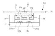
도1을 참조하면, 회로 기판(11)은 칩 실장 영역(M) 주위에 배치된 반사성 구조체(15)와 상기 칩 실장 영역(M)에 배치된 복수의 전극 패드(12a,12b)를 포함한다. 상기 복수의 전극 패드(12a,12b)는 상기 회로 기판(11)에 마련된 다른 회로 패턴들과 연결되도록 구성될 수 있다.Referring to FIG. 1 , a
메탈 마스크(30)는 베이스 플레이트(31)와 상기 베이스 플레이트(31) 하부에 위치한 돌출부(35)를 포함한다. 상기 돌출부(35)는 상기 반사성 적층체(15)에 의해 둘러싸인 공간에 삽입하도록 구성된다. 상기 돌출부(35)는 칩 실장 영역(M)의 폭(w1)보다 작은 폭(w2)을 가질 수 있다. 이에 한정되지는 않으나, 상기 돌출부(35)는 전극 패드(12a,12b)와 직접 접속되지 않도록 구성될 수 있다. 예를 들어, 상기 돌출부(35)는 반사 적층체(15)의 높이(h1)보다 낮은 높이(h2)를 가질 수 있다.The
도2a 및 도2b에 도시된 바와 같이, 상기 돌출부(35)는 아래 방향으로 개방된 토출홀(Ha,Hb)을 갖는다. 토출홀(Ha,Hb)은 솔더 페이스트가 토출되는 개구로서, 사이즈를 조절하여 전극 패드(12a,12b)에 배치될 솔더의 양과 크기를 제어할 수 있다. 본 실시예와 같이, 제1 및 제2 전극 패드(12a,12b)에 동시에 솔더 페이스트를 제공하는 경우에는, 상기 돌출부(35)는 제1 및 제2 전극패드(12a,12b)와 대응되는 위치에 토출홀(Ha,Hb)을 가질 수 있다.As shown in FIGS. 2A and 2B, the protruding
상기 메탈 마스크(30)는 상기 토출홀(Ha,Hb)에 연결되어 솔더 페이스트를 위한 수용 공간(S)을 가질 수 있다. 상기 수용 공간(S)은 상부로 개방된 개구를 갖는다. 상기 수용 공간(S)은 솔더 페이스트를 토출홀(Ha,Hb)을 통해서 원하는 사이즈로 공급하기 위해서 솔더 페이스트를 일시 수용하는 공간으로 사용된다.
The
도3 내지 도6은 본 발명의 일 실시예에 따른 LED 모듈 제조방법을 설명하기 위한 주요 공정별 단면도이다.3 to 6 are cross-sectional views of each main process for explaining a method of manufacturing an LED module according to an embodiment of the present invention.
도3을 참조하면, 반사성 적층체(15)와 제1 및 제2 전극 패드(12a,12nb를 갖는 회로 기판(11)을 마련한다.Referring to FIG. 3 , a
도3에 도시된 회로 기판(11)은 도1에 도시된 회로 기판을 I2-I2'로 절개한 단면으로 이해될 수 있다. 예를 들어, 상기 회로 기판(11)은 인쇄 회로 기판(PCB)일 수 있다. 칩 실장 영역(M)은 반도체 적층체(15)에 의해 정의되며, 상기 칩 실장 영역(M)에는 제1 및 제2 전극 패드(12a,12b)가 배치될 수 있다. 반사성 적층체(15)는 광추출 효율을 향상시키기 위한 구조체로 제공될 수 있으며, 반사성을 갖는 다수의 필름(15)을 충분한 두께(예, 0.2∼1.0㎜)로 적층시킨 구조를 갖는다.The
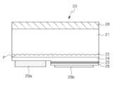
도7에는 반사성 적층체(15)의 단면 구조가 도시되어 있다. 도7에 도시된 부부분은 도3에서 "A"부분을 확대하여 나타낸 것으로 이해할 수 있다.7 shows a cross-sectional structure of the
도7에 도시된 바와 같이, 상기 반사성 적층체(15)는 반사성 분말(R)이 함유된 수지로 이루어진 복수의 반사 필름(15a)(본 명세서에서는 "제1 수지층"이라고도 함)과 복수의 접합층(15b)이 교대로 적층된 구조체일 수 있다. 접합층(15b)을 이용하여 다소 얇은 반사 필름(15a)을 복수 회(예, 5회)로 적층시킴으로써 원하는 두께의 반사성 적층체(15)를 제조할 수 있다.As shown in FIG. 7, the
반사 필름(15a)을 구성하는 수지는, 실리콘(silicone), 에폭시, 폴리아크릴레이트, 폴리이미드 및 우레탄 수지일 수 있다. 반사성 분말(R)은 백색 세라믹 분말 또는 금속 분말일 수 있다. 예를 들어, 상기 세라믹 분말은 TiO2, Al2O3, Nb2O5 및 ZnO로 구성된 그룹으로부터 선택된 적어도 하나일 수 있다. 상기 금속 분말은 Al 또는 Ag와 같은 물질일 수 있다. 접합층(15b)은 실리콘 수지 조성물, 에폭시 수지 조성물, 폴리이미드 조성물 및 그들의 변성 수지를 포함할 수 있다.The resin constituting the
본 실시예에 채용 가능한 반사성 적층체(15)는 다양한 형태로 변경되어 실시될 수 있다(도8 및 도9 참조).
The
도4를 참조하면, 메탈 마스크(30)를 이용하여 솔더 페이스트(25)를 제1 및 제2 전극 패드(12a,12b) 상에 적하시킬 수 있다.Referring to FIG. 4 , the
우선, 토출홀(Ha,Hb)이 형성된 돌출부(35)가 칩 실장 공간(M)에 위치하도록 메탈 마스크(30)를 정렬시킬 수 있다. 메탈 마스크(30)를 정렬한 후에, 메탈 마스크(30)의 수용부(S)에 솔더 페이스트(25)를 공급하고, 상기 토출홀(Ha,Hb)을 통해 상기 제1 및 제2 전극 패드(12a,12b) 상에 소정의 양의 솔더볼(25a,25b)을 적하시킬 수 있다. 예를 들어, 스퀴즈(squeeze) 공정과 유사하게, 개구를 통해서 솔더 페이스트(25)를 압착시켜 토출홀(Ha,Hb)로 원하는 양의 솔더볼(25a,25b)을 적하시킬 수 있다.First, the
칩 실장 공간(M) 내부에 돌출부(35)를 삽입시켜 솔더볼(25a,25b)을 제공함으로써 드랍되는 거리를 감소시킬 수 있으며, 그 결과 정확한 위치에 솔더볼(25a,25b)을 제공할 수 있다. 또한 낙하 충격을 감소됨으로써 솔더볼(25a,25b)이 무너지지 않도록(퍼지지 않도록) 형성할 수 있다.
By providing the
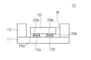
도5를 참조하면, LED 칩(20)을 솔더볼(25a,25b)이 배치된 제1 및 제2 전극 패드(12a,12b)에 탑재할 수 있다.Referring to FIG. 5 , the
본 실시예에 채용된 LED 칩(20)은 일면에 제1 및 제2 전극(29a,29b)을 배치된 플립칩 구조일 수 있다. 상기 제1 및 제2 전극(29a,29b)은 제1 및 제2 전극 패드(12a,12b) 상에 위치한 솔더볼(25a,25b) 상에 위치하도록 탑재될 수 있다. 본 실시예에 채용가능한 LED 칩(20,100)의 다양한 예는 도10 및 도11에서 상세히 설명하기로 한다.
The
도6을 참조하면, 솔더볼(25a,25b)을 이용하여 LED 칩(20)의 제1 및 제2 전극(29a,29b)을 각각 제1 및 제2 전극 패드(12a,12b)에 접합시킬 수 있다.Referring to FIG. 6, the first and
본 접합 공정은 솔더볼(25a,25b)을 가열하여 용융시킴으로써 구현될 수 있다. 용융된 솔더볼은 제1 및 제2 전극(29a,29b)과 제1 및 제2 전극 패드(12a,12b)을 서로 결합시킨 후에 응고될 수 있다. 이러한 가열과정은 회로 기판(11)의 일부 회로 패턴을 통해서 열을 제1 및 제2 전극 패드(12a,12b)에 전달시킴으로써 구현될 수 있다.
This bonding process may be implemented by heating and melting the
본 실시예에 사용 가능한 회로 기판은 도7에 도시된 반사성 적층체 외에도 다양한 다른 형태의 반사성 적층체를 사용할 수 있다. 도8 및 도9는 본 발명의 다양한 실시예에 채용 가능한 반사성 적층체의 예들을 나타내는 단면도이다.
In addition to the reflective laminate shown in FIG. 7, various other types of reflective laminates may be used as the circuit board usable in this embodiment. 8 and 9 are cross-sectional views showing examples of reflective laminates usable in various embodiments of the present invention.
도8을 참조하면, 본 실시예에 따른 반사성 적층체(15A)는, 제1 수지층(15a), 제2 수지층(15c) 및 접합층(15b)이 교대로 적층된 구조를 갖는다.Referring to FIG. 8 , the
상기 제1 수지층(15a)은 반사성 분말(R)이 함유된 수지로 이루어질 수 있다. 상기 제2 수지층(15c)은 반사성 분말이 함유되지 않은 수지층일 수 있다. 일부 실시예에서, 상기 제2 수지층(15c)은 상기 제1 수지층(15a)을 제조하기 위해서 사용된 베이스 필름일 수 있다. 따라서, 상기 제1 및 2 수지층(15a,15b)은 서로 접합된 상태에서 제공될 수 있다.The
본 실시예에서, 접합층(15b)은 제2 수지층(15c)의 하면에 제공되어 제1 수지층(15a)의 상면과 접합될 수 있다. 이와 같이, 접합층(15b)을 이용하여 제1 및 제2 수지층(15a,15b)의 결합체를 복수 회(예, 4회)로 적층시킴으로써 원하는 두께의 반사성 적층체(15A)를 제조할 수 있다. 예를 들어, 제1 및 제2 수지층(15a,15c)을 구성하는 수지는, 실리콘, 에폭시, 폴리아크릴레이트, 폴리이미드 및 우레탄 수지일 수 있다.
In this embodiment, the
도9을 참조하면, 본 실시예에 따른 반사성 적층체(15B)는 일정한 높이를 갖는 수지체(15')와 상기 수지체(15')의 표면에 코팅되며 반사성 분말(R)이 함유된 반사성 수지층(15a')을 포함할 수 있다.Referring to FIG. 9, the
상기 수지체(15')는 이에 한정되지 않으나, 회로 기판(11)을 구성하는 재질과 유사한 재질로 구성될 수 있다. 예를 들어, 상기 수지체(15')는 FR4과 같은 유리 강화 에폭시 필름(glass-reinforced epoxy film)일 수 있다. 상기 수지체(15')는 반사서 적층체의 두께를 확보하는 역할을 할 수 있다.The resin body 15' is not limited thereto, but may be made of a material similar to that of the
상기 반사성 수지층(15a')은 별도의 접합층에 의해 접합될 수 있으나, 반사성 액상 수지를 마련한 후에 도포한 후에 이를 경화시키는 방식으로 제공될 수 있다. 본 실시예에서, 반사성 수지층(15a')은 수지체(15')의 상면에만 코팅된 형태로 예시되어 있으나, 필요에 따라 다른 측면들에도 추가적으로 제공되어 반사효율을 향상시킬 수 있다.
The
도10 및 도11은 본 발명의 다양한 실시예에 채용 가능한 LED 칩의 예들을 나타내는 단면도이다.10 and 11 are cross-sectional views showing examples of LED chips employable in various embodiments of the present invention.
도10에 도시된 바와 같이, 본 실시예에 채용된 반도체 발광 다이오드 칩(20)은, 기판(21)과, 상기 기판(21) 상에 순차적으로 배치된 제1 도전형 반도체층(24), 활성층(25) 및 제2 도전형 반도체층(26)을 포함한다. 상기 기판(21)과 상기 제1 도전형 반도체층(24) 사이에 버퍼층(22)을 배치시킬 수 있다.As shown in FIG. 10, the semiconductor light emitting
상기 기판(21)은 사파이어와 같은 절연성 기판일 수 있다. 하지만, 이에 한정되지 않으며, 상기 기판(21)은 절연성 외에도 도전성 또는 반도체 기판일 수 있다. 예를 들어, 상기 기판(21)은 사파이어 외에도 SiC, Si, MgAl2O4, MgO, LiAlO2, LiGaO2, GaN일 수 있다. 상기 기판(21)의 상면에는 요철(P)이 형성될 수 있다. 상기 요철(P)은 광추출효율을 개선하면서 성장되는 단결정의 품질을 향상시킬 수 있다.The
상기 버퍼층(22)은 InxAlyGa1-x-yN (0≤x≤1, 0≤y≤1)일수 있다. 예를 들어, 상기 버퍼층(22)는 GaN, AlN, AlGaN, InGaN일 수 있다. 필요에 따라, 복수의 층을 조합하거나, 조성을 점진적으로 변화시켜 사용할 수도 있다.The
상기 제1 도전형 반도체층(24)은 n형 InxAlyGa1-x-yN (0≤x<1, 0≤y<1, 0≤x+y<1)을 만족하는 질화물 반도체일 수 있으며, n형 불순물은 Si일 수 있다. 예를 들어, 상기 제1 도전형 반도체층(24)은 n형 GaN을 포함할 수 있다. 상기 제2 도전형 반도체층(26)은 p형 InxAlyGa1-x-yN (0≤x<1, 0≤y<1, 0≤x+y<1)을 만족하는 질화물 반도체층일 수 있으며, p형 불순물은 Mg일 수 있다. 예를 들어, 상기 제2 도전형 반도체층(26)은 단층 구조로 구현될 수도 있으나, 본 실시예와 같이, 서로 다른 조성을 갖는 다층 구조를 가질 수 있다. 상기 활성층(25)은 양자우물층과 양자장벽층이 서로 교대로 적층된 다중 양자우물(MQW) 구조일 수 있다. 예를 들어, 상기 양자우물층과 양자장벽층은 서로 다른 조성을 갖는 InxAlyGa1-x-yN (0≤x≤1, 0≤y≤1, 0≤x+y≤1)일 수 있다. 특정 예에서, 상기 양자우물층은 InxGa1-xN (0<x≤1)이며, 상기 양자장벽층은 GaN 또는 AlGaN일 수 있다. 양자우물층과 양자장벽층의 두께는 각각 1㎚∼50㎚ 범위일 수 있다. 상기 활성층(25)은 다중양자우물구조에 한정되지 않고, 단일양자우물 구조일 수 있다.The first conductivity-
상기 제1 및 제2 전극(29a,29b)은, 동일한 면(제1 면)에 위치하도록, 상기 제1 도전형 반도체층(24)의 메사 에칭된 영역과 상기 제2 도전형 반도체층(26)에 각각 배치될 수 있다. 상기 제1 전극(29a)은 이에 한정되지 않지만, Ag, Ni, Al, Cr, Rh, Pd, Ir, Ru, Mg, Zn, Pt, Au 등의 물질을 포함할 수 있으며, 단일층 또는 2층 이상의 구조로 채용될 수 있다. 필요에 따라, 상기 제2 전극(29b)은 투명 전도성 산화물 또는 투명 전도성 질화물과 같은 투명 전극이거나, 그래핀(graphene)을 포함할 수도 있다. 상기 제2 전극(29b)은 Al, Au, Cr, Ni, Ti, Sn 중 적어도 하나를 포함할 수 있다.The first and
상기 반도체 발광다이오드 칩(20)의 상면(즉, 제2 면)에는 파장변환필름(28)이 배치될 수 있다. 상기 파장변환필름(28)은 상기 반도체 발광다이오드 칩(20)으로부터 방출된 광의 일부를 다른 파장을 변환하는 파장변환물질을 포함한다. 상기 파장변환필름(28)은 상기 파장변환물질이 분산된 수지층 또는 세라믹 형광체의 소결체로 이루어진 세라믹 필름일 수 있다. 상기 반도체 발광다이오드 칩(20)은 청색광을 방출하고, 상기 파장변환필름(28)은 상기 청색광의 일부를 황색 및/또는 적색 및 녹색으로 변환하여, 백색 광을 방출할 수 있다.
A
도8은 본 발명에 채용될 수 있는 반도체 발광다이오드의 일 예를 나타내는 측단면도이다.8 is a side cross-sectional view showing an example of a semiconductor light emitting diode that can be employed in the present invention.
도8을 참조하면, 반도체 발광다이오드 칩(100)은 기판(110) 상에 형성된 반도체 적층체(L)을 포함한다. 상기 반도체 적층체(L)는 제1 도전형 반도체층(114), 활성층(115) 및 제2 도전형 반도체층(116)을 포함할 수 있다.Referring to FIG. 8 , the semiconductor light emitting
상기 반도체 발광다이오드(100)는 상기 제1 및 제2 도전형 반도체층(114,116)에 각각 접속된 제1 및 제2 전극(122,124)을 포함한다. 상기 제1 전극(122)은 제2 도전형 반도체층(116) 및 활성층(115)을 관통하여 제1 도전형 반도체층(114)과 접속된 도전성 비아와 같은 연결 전극부(122a) 및 연결 전극부(122a)에 연결된 제1 전극 패드(122b)를 포함할 수 있다. 연결 전극부(122a)는 절연부(121)에 의하여 둘러싸여 활성층(115) 및 제2 도전형 반도체층(116)과 전기적으로 분리될 수 있다. 연결 전극부(122a)는 반도체 적층체(L)이 식각된 영역에 배치될 수 있다. 연결 전극부(122a)는 접촉 저항이 낮아지도록 개수, 형상, 피치 또는 제1 도전형 반도체층(114)과의 접촉 면적 등을 적절히 설계할 수 있다. 또한, 연결 전극부(122a)는 반도체 적층체(L) 상에 행과 열을 이루도록 배열됨으로써 전류 흐름을 개선시킬 수 있다. 상기 제2 전극(124)은 제2 도전형 반도체층(116) 상의 오믹 콘택층(124a) 및 제2 전극 패드(124b)를 포함할 수 있다.The semiconductor
상기 연결 전극부 및 오믹 콘택층(122a,124a)은 각각 제1 및 제2 도전형 반도체층(114, 116)과 오믹 특성을 갖는 도전성 물질이 1층 또는 다층 구조를 포함할 수 있다. 예를 들어, Ag, Al, Ni, Cr, 투명 도전성 산화물(TCO) 등의 물질 중 하나 이상을 증착하거나 스퍼터링하는 등의 공정으로 형성될 수 있다.The connection electrode portion and the
상기 제1 및 제2 전극 패드(122b,124b)는 각각 상기 연결 전극부(122a) 및 오믹 콘택층(124a)에 각각 접속되어 상기 반도체 발광다이오드(100)의 외부 단자로 기능할 수 있다. 예를 들어, 제1 및 제2 전극 패드(122b,124b)는 Au, Ag, Al, Ti, W, Cu, Sn, Ni, Pt, Cr, NiSn, TiW, AuSn 또는 이들의 공융 금속일 수 있다.The first and
상기 제1 및 제2 전극(122,124)은 서로 동일한 방향으로 배치될 수 있으며, 리드 프레임 등에 소위, 플립칩 형태로 실장될 수 있다.The first and
한편, 2개의 전극(122,124)는 절연부(121)에 의하여 서로 전기적으로 분리될 수 있다. 절연부(121)는 전기적으로 절연 특성을 갖는 물질이면 어느 것이나 사용할 수 있으며, 전기 절연성을 갖는 물체라면 어느 것이나 채용 가능하지만, 광흡수율이 낮은 물질을 사용할 수 있다. 예를 들어, SiO2, SiOxNy, SixNy 등의 실리콘 산화물, 실리콘 질화물을 이용할 수 있을 것이다. 필요에 따라, 광투과성 물질 내에 광 반사성 필러를 분산시켜 광반사 구조를 형성할 수 있다. 이와 달리, 상기 절연부(121)는 서로 다른 굴절률을 갖는 복수의 절연막들이 교대로 적층된 다층 반사구조일 수 있다. 예를 들어 이러한 다층 반사구조는 제1 굴절률을 갖는 제1 절연막과 제2 굴절률을 갖는 제2 절연막이 교대로 적층된 분산 브래그 반사기(DBR: Distributed Bragg Reflector)일 수 있다.Meanwhile, the two
상기 다층 반사 구조는 상기 굴절률이 서로 다른 복수의 절연막들이 2회 내지 100회 반복하여 적층될 수 있다. 예를 들어, 3회 내지 70회 반복하여 적층 될 수 있으며, 나아가 4회 내지 50회 반복하여 적층될 수 있다. 상기 다층 반사 구조의 복수의 절연막은 각각 SiO2, SiN, SiOxNy, TiO2, Si3N4, Al2O3, TiN, AlN, ZrO2, TiAlN, TiSiN 등의 산화물 또는 질화물 및 그 조합일 수 있다.In the multi-layer reflective structure, a plurality of insulating films having different refractive indices may be repeatedly stacked 2 to 100 times. For example, it may be repeatedly laminated 3 to 70 times, and may be repeatedly laminated 4 to 50 times. The plurality of insulating films of the multi-layer reflective structure are oxides or nitrides of SiO2 , SiN, SiOx Ny , TiO2 , Si3 N4 , Al2 O3 , TiN, AlN, ZrO2 , TiAlN, TiSiN, and the like, respectively. can be a combination.
예를 들어, 상기 활성층에서 생성되는 빛의 파장을 λ이라고 하고 n을 해당 층의 굴절률이라 할 때에, 상기 제1 절연막과 제2 절연막은, λ/4n의 두께를 갖도록 형성될 수 있으며, 대략 약 300Å 내지 900Å의 두께를 가질 수 있다. 이때, 상기 다층 반사구조는 상기 활성층(115)에서 생성된 빛의 파장에 대해서 높은 반사율(예, 95% 이상)을 갖도록 각 제1 절연막 및 제2 절연막의 굴절률과 두께가 선택되어 설계될 수 있다.For example, when the wavelength of light generated in the active layer is λ and n is the refractive index of the corresponding layer, the first insulating film and the second insulating film may be formed to have a thickness of λ/4n, approximately about It may have a thickness of 300 Å to 900 Å. At this time, the multi-layer reflective structure may be designed by selecting the refractive index and thickness of each of the first insulating film and the second insulating film to have a high reflectance (eg, 95% or more) with respect to the wavelength of light generated in the active layer 115. .
상기 제1 절연막 및 제2 절연막의 굴절률은 약 1.4 내지 약 2.5 범위에서 결정될 수 있으며, 상기 제1 도전형 반도체층(114)의 굴절률 및 기판의 굴절률보다 작은 값일 수 있으나, 상기 제1 도전형 반도체층(114)의 굴절률보다는 작되 기판(101)의 굴절률보다는 큰 값을 가질 수도 있다.
The refractive indices of the first insulating film and the second insulating film may be determined in the range of about 1.4 to about 2.5, and may be smaller than the refractive index of the first conductivity-
본 실시예에 따른 LED 모듈 제조방법에 사용되는 메탈 마스크는 다양한 구조의 메탈 마스크가 유익하게 사용될 수 있다. 도12 내지 도15는 메탈 마스크의 다양한 예들을 나타낸다.
As the metal mask used in the LED module manufacturing method according to the present embodiment, metal masks having various structures can be advantageously used. 12 to 15 show various examples of metal masks.
우선, 도12를 참조하면, 메탈 마스크(40)는, 플레이트(41)와 상기 플레이트(41) 하부에 위치한 돌출부(45)를 포함한다.First, referring to FIG. 12 , the
상기 메탈 마스크(40)는 도2a에 도시된 메탈 마스크(30)와 유사하게, 단일체를 가공하여 얻어진 구조일 수 있다. 예를 들어, 상기 메탈 마스크(40)는 SUS 재질의 직방형인 벌크를 화학적으로 에칭하거나 기계적으로 연삭공정으로 가공하여 제조될 수 있다.Similar to the
본 실시예에 채용된 돌출부(45)는 경사진 측면(SP)을 갖는다. 상기 돌출부(45)는 상단의 폭(Wb)보다 하단의 폭(Wa)이 작은 구조를 가질 수 있다. 이러한 돌출부(45)는 칩 실장 공간에 더욱 용이하게 삽입될 수 있다.The
상기 돌출부(45)는 아래 방향으로 개방된 하나의 토출홀(H)을 갖는다. 상기 메탈 마스크(40)는 상기 토출홀(H)에 연결되어 솔더 페이스트를 위한 수용부(S)를 가질 수 있다. 상기 수용부(S)는 상부로 개방된 개구를 갖는다.The
토출홀(H)의 개수 및 크기는 다양하게 변경될 수 있다. 일 실시예에서는, 하나의 LED 칩에 관련된 전극 패드들의 수와 위치에 대응되는 토출홀들을 가질 수 있다(도2a 참조). 다른 실시예에서는, 2 이상의 LED 칩의 전극패드들에 동시에 솔더 인쇄 가능하도록 복수의 토출홀의 배열이 제공될 수도 있다.
The number and size of the discharge holes H may be variously changed. In one embodiment, one LED chip may have discharge holes corresponding to the number and position of electrode pads (see FIG. 2A). In another embodiment, an arrangement of a plurality of discharge holes may be provided so that solder printing is possible on electrode pads of two or more LED chips at the same time.
본 실시예에 따른 메탈 마스크는 단일체로부터 가공되지 않고, 복수의 플레이트를 접합시키는 형태로 구현될 수 있다.The metal mask according to the present embodiment may be implemented in a form of bonding a plurality of plates without being processed from a single body.
도13a은 복수의 금속 플레이트가 적층된 메탈 마스크의 단면을 나타내며, 도13b는 도13a에 도시된 메탈 마스크의 분해 사시도이다.
13A is a cross-section of a metal mask in which a plurality of metal plates are stacked, and FIG. 13B is an exploded perspective view of the metal mask shown in FIG. 13A.
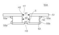
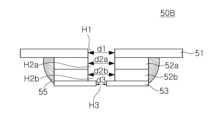
도13a 및 도13b를 참조하면, 본 실시예에 따른 메탈 마스크(50A)는, 제1 홀(H1)을 갖는 제1 금속 플레이트(51)와, 상기 제1 금속 플레이트(51)의 일부 영역에 순차적으로 적층된 제2 및 제3 금속 플레이트(52,53)를 포함한다. 상기 제2 및 제3 금속 플레이트(52,53)는 볼록한 구조(또는 돌출부라고도 함)를 제공할 수 있다.13A and 13B, the
상기 제1 내지 제3 금속 플레이트(51,52,53)는 이에 한정되지는 않으나, 외부 표면들이 용접됨으로써 서로 접합될 수 있다. 도13a에 도시된 바와 같이, 외부 표면들의 일부 영역에 인접한 플레이트들을 서로 연결하는 용접부들(55a,55b)에 의해 상기 금속 플레이트들(51,52과 52,53)은 접합될 수 있다.The first to
상기 제2 및 제3 금속 플레이트(52,53)는 각각 제2 및 제3 홀(H2,H3)을 갖는다. 상기 제2 및 제3 금속 플레이트(52,53)는 상기 제2 및 제3홀(H2,H3)이 상기 제1 홀(H1)과 연결되도록 상기 제1 금속 플레이트(51) 상에 배치될 수 있다.The second and
본 실시예에서, 상기 제1 홀(H1)의 크기(또는 직경)(d1)은 상기 제2 홀(H2)의 크기(d2)과 동일하거나 유사한 반면에, 상기 제3 홀(H3)은 상기 제1 및 제2 홀(H1,H2)의 크기(d1,d2)보다 작은 크기(d3)를 가질 수 있다. 상기 제1 및 제2 홀(H1,H2)은 솔더 페이스트를 위한 수용부(S)로 제공되며, 상기 제3 홀(H3)은 토출홀로 제공될 수 있다.In this embodiment, the size (or diameter) d1 of the first hole H1 is the same as or similar to the size d2 of the second hole H2, while the third hole H3 is The size d3 may be smaller than the sizes d1 and d2 of the first and second holes H1 and H2. The first and second holes H1 and H2 may be provided as receiving portions S for solder paste, and the third hole H3 may be provided as a discharge hole.
상기 제1 내지 제3 금속 플레이트(51,52,53)는 동일한 두께로 형성될 수 있으나, 필요에 따라 서로 다른 두께를 가질 수 있다. 예를 들어, 상기 제2 금속 플레이트(52)는 상기 제1 및 제3 금속 플레이트(51,53) 중 적어도 하나의 두께와 다른 두께를 가질 수 있다. 본 실시예에서는, 제2 금속 플레이트(52)의 두께(t2)는 상기 제1 및 제3 금속 플레이트(51,53)의 두께(t1,t3)보다 클 수 있다. 상기 제1 및 제3 금속 플레이트(51,53)의 두께(t1,t3)는 이에 한정되지는 않으나 서로 동일하거나 유사한 두께를 가질 수 있다.
The first to
도14를 참조하면, 메탈 마스크(50B)는 복수의 제2 금속 플레이트(52a,52b)를 갖는 점과 용접부(55) 형태가 상인 점을 제외하고는 도13a에 도시된 메탈 마스크(50A)와 유사한 것으로 이해할 수 있다.Referring to FIG. 14, the
본 실시예에 채용된 제2 금속 플레이트는 2개의 제2 금속 플레이트(52a,52b)를 포함할 수 있다. 2개의 제2 금속 플레이트(52a,52b)에 형성된 홀(H2a,H2b)은 서로 동일한 크기(d2a=d2b)를 가질 수 있다. 또한, 상기 홀(H2a,H2b)의 크기는 상기 제1 금속 플레이트(51)의 홀 크기(d1)에 대응되어 하나의 수용부를 제공할 수 있다. 상기 복수의 제2 금속 플레이트(52a,52b)와 상기 제1 및 제3 금속 플레이트(51,53)는 하나의 용접부(55)에 의해 서로 연결될 수 있다.
The second metal plate employed in this embodiment may include two
도15를 참조하면, 메탈 마스크(50C)는 홀(H1',H2',H3') 크기가 상이한 점과 용접부(55) 형태가 상이한 점을 제외하고는 도13a에 도시된 메탈 마스크와 유사한 것으로 이해할 수 있다. 상기 제1 내지 제3 금속 플레이트(51,52,53)는 도14에 도시된 예와 유사헤가 하나의 용접부(55)에 의해 서로 연결될 수 있다.Referring to FIG. 15, the
또한, 도15에 도시된 바와 같이, 상기 제2 홀(H2)의 크기(d2')은 상기 제2 홀(H3')의 크기(d3')과 동일하거나 유사한 반면에, 상기 제1 홀(H1)은 상기 제2 및 제3 홀(H2,H3)의 크기(d2,d3)보다 작은 크기(d1)를 가질 수 있다. 본 실시예에서는, 상기 제1 홀(H1)은 솔더볼의 양(또는 크기)를 결정하는 토출홀로 제공될 수 있다. 상기 제2 및 제3 홀(H2,H3)은 제1 홀(H1)을 통해 적하되는 솔더볼의 경로를 제공할 수 있다. 특정 예에서, 상기 제3 금속 플레이트(53')의 하면이 전극 패드 또는 칩 실장 영역의 표면에 밀착되어 원하지 않은 영역으로 솔더 페이스트가 튀거나 흐르는 것을 방지하는 역할을 할 수 있다.
In addition, as shown in FIG. 15, the size d2' of the second hole H2 is the same as or similar to the size d3' of the second hole H3', while the first hole ( H1) may have a size d1 smaller than the sizes d2 and d3 of the second and third holes H2 and H3. In this embodiment, the first hole H1 may serve as a discharge hole for determining the amount (or size) of solder balls. The second and third holes H2 and H3 may provide a path for solder balls dropped through the first hole H1. In a specific example, the lower surface of the third metal plate 53' may come into close contact with an electrode pad or a surface of a chip mounting area to prevent solder paste from splashing or flowing to an undesirable area.
본 발명의 실시예에 따른 제조방법은 다양한 형태의 LED 모듈를 제조하는 방법으로 사용될 수 있다. 도16 내지 도18은 본 발명의 실시예에 의해 제조가능한 LED 모듈의 다양한 예들을 나타내는 상부 평면도이다.The manufacturing method according to the embodiment of the present invention can be used as a method for manufacturing various types of LED modules. 16 to 18 are top plan views illustrating various examples of LED modules that can be manufactured according to embodiments of the present invention.
도16에 도시된 LED 모듈(10A)은 회로 기판(11)과, 칩 실장 영역(M) 주위에 배치된 반사성 구조체(65)와, 상기 칩 실장 영역(M)에 배치된 복수의 LED 칩(20)을 포함한다.The
상기 반사성 구조체(65)는 백색 분말과 같은 반사성 분말이 함유된 수지층일 수 있다. 예를 들어, 상기 반사성 구조체(65)는 도7 내지 도9에 예시된 적층 구조체들 중 어느 하나일 수 있다. 본 실시예에 채용된 반사성 구조체(65)는 앞선 실시예와 달리 칩 실장 영역(M)을 완전히 둘러싸지 않고, 양단부가 개방된 형태를 가질 수 있다. 이러한 구조의 LED 모듈(10A)은 다른 LED 모듈과 단부에서 연결될 수 있으며, 모듈 사이에 격벽이 존재하지 않은 하나의 LED 모듈과 같이 구성될 수 있다.The
복수의 LED 칩(20)은 일렬로 배열된 형태일 수 있다. 예를 들어, 상기 LED 모듈(10A)은 백라이트 유닛의 광원으로 사용될 수 있다. 상기 LED 칩(20)은 전극 패드(도1의 12a,12b 참조)에 본딩될 수 있다. 이러한 본딩 과정에서 도3 내지 도5에서 설명된 방식으로 돌출부를 갖는 메탈 마스크를 이용하여 인쇄된 솔더볼을 사용할 수 있다.
A plurality of
도17에 도시된 LED 모듈(10B)은 도16에 도시된 LED 모듈(10A)과 유사하게 회로 기판(11)과, 반사성 구조체(75)와, 복수의 LED 칩(20)을 포함한다.The
본 실시예에서 채용된 반사성 구조체(75)는 칩 실장 영역을 3개의 영역(Ma,Mb,Mc)으로 구분되도록 추가적인 격벽(75a)를 포함할 수 있다. 상기 격벽(75a,75b)은 LED 배열 방향을 가로질러 형성되며, 구획된 각 실장 영역(Ma,Mb,Mc)에는 동일한 수의 LED 칩(20)이 배열될 수 있다. 본 실시예에서는 반사성 구조체가 더욱 밀집되게 배치되므로, 돌출부를 갖는 메탈 마스크를 이용하여 솔더 인쇄 공정이 유익하게 사용할 수 있다.
The
도18에 도시된 LED 모듈(10C)은 도16에 도시된 LED 모듈(10A)과 유사하게 회로 기판(11')과, 반사성 구조체(85)와, 복수의 LED 칩(20)을 포함하되, 앞선 실시예들과 달리 정방형 구조를 가질 수 있다. 반사성 구조체(85)에 의해 정의된 칩 실장 영역(M)에는 2 X 2의 배열로 LED 칩이 배열될 수 있다. 이와 같이, LED 칩이 일렬로 배열된 모듈뿐만 아니라, LED 칩들이 복수의 열로 배열된 LED 모듈에서도 본 실시예에 따른 메탈 마스크를 이용한 솔더 인쇄공정이 유익하게 적용될 수 있다.
The LED module 10C shown in FIG. 18 includes a circuit board 11', a
본 발명은 상술한 실시형태 및 첨부된 도면에 의해 한정되는 것이 아니며, 첨부된 청구범위에 의해 한정하고자 한다. 따라서, 청구범위에 기재된 본 발명의 기술적 사상을 벗어나지 않는 범위 내에서 당 기술분야의 통상의 지식을 가진 자에 의해 다양한 형태의 치환, 변형 및 변경이 가능할 것이며, 이 또한 본 발명의 범위에 속한다고 할 것이다.
The present invention is not limited by the above-described embodiments and accompanying drawings, but is intended to be limited by the appended claims. Therefore, various forms of substitution, modification, and change will be possible by those skilled in the art within the scope of the technical spirit of the present invention described in the claims, which also falls within the scope of the present invention. something to do.
10,10A,10B,10C: LED 모듈
11: 회로 기판
12a,12b: 전극 패드
15: 반사성 구조체
30,40,50A,50B: 메탈 마스크
31: 베이스 플레이트
35: 돌출부10,10A,10B,10C: LED module
11: circuit board
12a, 12b: electrode pads
15: reflective structure
30,40,50A,50B: Metal mask
31: base plate
35: protrusion
Claims (20)
Translated fromKorean토출홀이 형성된 돌출부를 갖는 마스크를 이용하여 상기 전극 패드 상에 솔더 페이스트를 적하시키는 단계 - 상기 돌출부는 상기 반사성 적층체에 의해 둘러싸인 공간에 삽입되도록 구성됨 - ; 및
상기 솔더 페이스트를 이용하여 LED 칩의 전극을 상기 전극 패드에 접합시키는 단계를 포함하고,
상기 마스크는 상기 돌출부 내부에 상부로 개방되어 상기 솔더 페이스트를 수용하기 위한 수용부를 가지며,
상기 토출홀은 상기 수용부의 바닥에 형성되고, 상기 수용부의 폭보다 작은 폭을 갖는 LED 모듈 제조방법.
preparing a circuit board having a reflective laminate disposed around a chip mounting area and an electrode pad disposed in the chip mounting area;
dripping solder paste onto the electrode pad using a mask having a protrusion having a discharge hole formed therein, wherein the protrusion is configured to be inserted into a space surrounded by the reflective laminate; and
Bonding an electrode of an LED chip to the electrode pad using the solder paste;
The mask has a receiving portion inside the protruding portion that is open upward to accommodate the solder paste,
The discharge hole is formed at the bottom of the accommodating portion, LED module manufacturing method having a width smaller than the width of the accommodating portion.
상기 반사성 적층체는 반사성 분말이 함유된 복수의 제1 수지층과 복수의 접합층이 교대로 적층된 구조체인 LED 모듈 제조방법.
According to claim 1,
The reflective laminate is an LED module manufacturing method in which a plurality of first resin layers containing reflective powder and a plurality of bonding layers are alternately laminated.
상기 반사성 적층체는 일정한 높이를 갖는 수지체와 상기 수지체의 표면에 코팅되며 반사성 분말이 함유된 반사성 수지층을 포함하는 LED 모듈 제조방법.
According to claim 1,
The reflective laminate includes a resin body having a predetermined height and a reflective resin layer coated on a surface of the resin body and containing a reflective powder.
상기 돌출부는 상단의 폭보다 하단의 폭이 작은 구조를 갖는 LED 모듈 제조방법.
According to claim 1,
The LED module manufacturing method of the protrusion having a structure in which the width of the bottom is smaller than the width of the top.
상기 전극 패드는 제1 및 제2 전극 패드를 포함하며,
상기 마스크의 토출홀은 상기 수용부의 바닥에 상기 제1 및 제2 전극 패드에 각각 대응되도록 형성된 제1 및 제2 토출홀을 포함하는 LED 모듈 제조방법.
According to claim 1,
The electrode pad includes first and second electrode pads,
The discharge hole of the mask includes first and second discharge holes formed at the bottom of the accommodating portion to correspond to the first and second electrode pads, respectively.
상기 마스크는, 제1 홀을 갖는 제1 금속 플레이트와, 상기 제1 금속 플레이트의 일부 영역에 적층되며 상기 제1 홀과 연결된 제2 홀을 갖는 적어도 하나의 제2 금속 플레이트와, 상기 제2 금속 플레이트 상에 적층되며 상기 제2 홀과 연결된 제3 홀을 갖는 제3 금속 플레이트를 포함하며,
상기 적층된 제2 및 제3 금속 플레이트는 상기 돌출부로 제공되는 LED 모듈 제조방법.
According to claim 1,
The mask may include a first metal plate having a first hole, at least one second metal plate stacked on a partial region of the first metal plate and having a second hole connected to the first hole, and the second metal plate. A third metal plate stacked on the plate and having a third hole connected to the second hole,
The laminated second and third metal plates are provided as the protrusions LED module manufacturing method.
상기 제3 홀은 상기 제1 및 제2 홀의 크기보다 작은 크기를 가지며,
상기 제1 및 제2 홀은 상기 수용부로 제공되며, 상기 제3 홀은 상기 토출홀로 제공되는 LED 모듈 제조방법.
According to claim 6,
The third hole has a smaller size than the first and second holes,
The first and second holes are provided as the receiving portion, and the third hole is provided as the discharge hole.
상기 제1 홀은 상기 제2 및 제3 홀의 크기보다 작은 크기를 갖는 LED 모듈 제조방법.
According to claim 6,
The first hole has a size smaller than the size of the second and third holes LED module manufacturing method.
상기 반사성 적층체는 복수의 칩 실장 영역을 제공하도록 상기 복수의 칩 실장 영역 사이에 위치한 격벽 구조를 포함하는 LED 모듈 제조방법.
According to claim 1,
The reflective laminate includes a partition structure positioned between the plurality of chip mounting regions to provide a plurality of chip mounting regions.
상기 제1 금속 플레이트의 일부 영역에 적층되며 상기 제1 홀과 연결된 제2 홀을 갖는 적어도 하나의 제2 금속 플레이트; 및
상기 제2 금속 플레이트 상에 적층되며 상기 제2 홀과 연결된 제3 홀을 갖는 제3 금속 플레이트를 포함하며,
상기 제2 및 제3 금속 플레이트는 상기 제1 금속 플레이트의 일면으로부터 볼록한 구조로 제공되는 솔더 인쇄용 메탈 마스크.a first metal plate having a first hole;
at least one second metal plate stacked on a partial region of the first metal plate and having a second hole connected to the first hole; and
a third metal plate stacked on the second metal plate and having a third hole connected to the second hole;
The second and third metal plates are provided in a convex structure from one surface of the first metal plate.
Priority Applications (3)
| Application Number | Priority Date | Filing Date | Title |
|---|---|---|---|
| KR1020160106015AKR102543179B1 (en) | 2016-08-22 | 2016-08-22 | Method of fabricating light emitting didoe module |
| US15/478,541US10332865B2 (en) | 2016-08-22 | 2017-04-04 | Method of fabricating light emitting diode module |
| CN201710716307.5ACN107768499B (en) | 2016-08-22 | 2017-08-16 | Method of manufacturing a light emitting diode module |
Applications Claiming Priority (1)
| Application Number | Priority Date | Filing Date | Title |
|---|---|---|---|
| KR1020160106015AKR102543179B1 (en) | 2016-08-22 | 2016-08-22 | Method of fabricating light emitting didoe module |
Publications (2)
| Publication Number | Publication Date |
|---|---|
| KR20180021456A KR20180021456A (en) | 2018-03-05 |
| KR102543179B1true KR102543179B1 (en) | 2023-06-14 |
Family
ID=61192117
Family Applications (1)
| Application Number | Title | Priority Date | Filing Date |
|---|---|---|---|
| KR1020160106015AActiveKR102543179B1 (en) | 2016-08-22 | 2016-08-22 | Method of fabricating light emitting didoe module |
Country Status (3)
| Country | Link |
|---|---|
| US (1) | US10332865B2 (en) |
| KR (1) | KR102543179B1 (en) |
| CN (1) | CN107768499B (en) |
Families Citing this family (6)
| Publication number | Priority date | Publication date | Assignee | Title |
|---|---|---|---|---|
| CN110887006B (en)* | 2018-08-17 | 2021-12-03 | 丰鹏电子(珠海)有限公司 | LED car lamp module, manufacturing method thereof and circuit board for LED car lamp module |
| CN111192944B (en)* | 2018-11-15 | 2024-12-24 | 日亚化学工业株式会社 | Method for manufacturing a light emitting device |
| TWI881982B (en)* | 2019-06-11 | 2025-05-01 | 荷蘭商庫力克及索發荷蘭公司 | Discrete component assembly and method of assembling discrete components onto a substrate |
| TWI814434B (en)* | 2022-04-01 | 2023-09-01 | 友達光電股份有限公司 | Light emitting diode array substrate |
| CN114784613B (en)* | 2022-06-20 | 2022-11-11 | 深圳市埃尔法光电科技有限公司 | Laser chip with unitized dual-topology structure |
| CN114784612B (en)* | 2022-06-20 | 2022-11-11 | 深圳市埃尔法光电科技有限公司 | Wafer arrangement method of laser chips with topological structures |
Citations (1)
| Publication number | Priority date | Publication date | Assignee | Title |
|---|---|---|---|---|
| US20150221835A1 (en)* | 2014-02-05 | 2015-08-06 | Michael A. Tischler | Light-emitting dies incorporating wavelength-conversion materials and related methods |
Family Cites Families (44)
| Publication number | Priority date | Publication date | Assignee | Title |
|---|---|---|---|---|
| CN1143394C (en) | 1996-08-27 | 2004-03-24 | 精工爱普生株式会社 | Peeling method, thin film device transfer method and thin film device |
| USRE38466E1 (en) | 1996-11-12 | 2004-03-16 | Seiko Epson Corporation | Manufacturing method of active matrix substrate, active matrix substrate and liquid crystal display device |
| US7208725B2 (en) | 1998-11-25 | 2007-04-24 | Rohm And Haas Electronic Materials Llc | Optoelectronic component with encapsulant |
| JP3906654B2 (en) | 2000-07-18 | 2007-04-18 | ソニー株式会社 | Semiconductor light emitting device and semiconductor light emitting device |
| US6947748B2 (en)* | 2000-12-15 | 2005-09-20 | Adaptix, Inc. | OFDMA with adaptive subcarrier-cluster configuration and selective loading |
| US6818465B2 (en) | 2001-08-22 | 2004-11-16 | Sony Corporation | Nitride semiconductor element and production method for nitride semiconductor element |
| JP2003218034A (en) | 2002-01-17 | 2003-07-31 | Sony Corp | Selective growth method, semiconductor light emitting device and method of manufacturing the same |
| JP3815335B2 (en) | 2002-01-18 | 2006-08-30 | ソニー株式会社 | Semiconductor light emitting device and manufacturing method thereof |
| KR100861267B1 (en) | 2002-04-29 | 2008-10-01 | 엘지디스플레이 주식회사 | Metal mask |
| KR100499129B1 (en) | 2002-09-02 | 2005-07-04 | 삼성전기주식회사 | Light emitting laser diode and fabricatin method thereof |
| US7002182B2 (en) | 2002-09-06 | 2006-02-21 | Sony Corporation | Semiconductor light emitting device integral type semiconductor light emitting unit image display unit and illuminating unit |
| JP2004155004A (en) | 2002-11-06 | 2004-06-03 | Matsushita Electric Ind Co Ltd | Squeegee for cream solder printing and cream solder printing method |
| KR100714639B1 (en) | 2003-10-21 | 2007-05-07 | 삼성전기주식회사 | Light emitting element |
| KR100506740B1 (en) | 2003-12-23 | 2005-08-08 | 삼성전기주식회사 | Nitride semiconductor light emitting device and method of manufacturing the same |
| KR100664985B1 (en) | 2004-10-26 | 2007-01-09 | 삼성전기주식회사 | Nitride-based semiconductor device |
| KR100665222B1 (en) | 2005-07-26 | 2007-01-09 | 삼성전기주식회사 | LED package using diffusion material and manufacturing method thereof |
| KR100661614B1 (en) | 2005-10-07 | 2006-12-26 | 삼성전기주식회사 | Nitride-based semiconductor light emitting device and its manufacturing method |
| KR100723247B1 (en) | 2006-01-10 | 2007-05-29 | 삼성전기주식회사 | Chip coated LED package and manufacturing method thereof |
| KR100735325B1 (en) | 2006-04-17 | 2007-07-04 | 삼성전기주식회사 | Light emitting diode package and its manufacturing method |
| KR100930171B1 (en) | 2006-12-05 | 2009-12-07 | 삼성전기주식회사 | White light emitting device and white light source module using same |
| JP2008205149A (en)* | 2007-02-20 | 2008-09-04 | Towa Corp | Method for forming phosphor and mold |
| KR100855065B1 (en) | 2007-04-24 | 2008-08-29 | 삼성전기주식회사 | Light emitting diode package |
| KR100982980B1 (en) | 2007-05-15 | 2010-09-17 | 삼성엘이디 주식회사 | Surface light source device and LCD backlight unit having same |
| JP2008302567A (en) | 2007-06-07 | 2008-12-18 | Process Lab Micron:Kk | Metal mask for printing |
| KR101164026B1 (en) | 2007-07-12 | 2012-07-18 | 삼성전자주식회사 | Nitride semiconductor light emitting device and fabrication method thereof |
| KR100902838B1 (en)* | 2007-07-24 | 2009-06-25 | 주식회사 에프엔텍 | Solder cream coating method using silicon pad |
| KR100891761B1 (en) | 2007-10-19 | 2009-04-07 | 삼성전기주식회사 | Semiconductor light emitting device, manufacturing method thereof and semiconductor light emitting device package using same |
| KR101332794B1 (en) | 2008-08-05 | 2013-11-25 | 삼성전자주식회사 | Light emitting device, light emitting system comprising the same, and fabricating method of the light emitting device and the light emitting system |
| KR20100030470A (en) | 2008-09-10 | 2010-03-18 | 삼성전자주식회사 | Light emitting device and system providing white light with various color temperatures |
| KR101530876B1 (en) | 2008-09-16 | 2015-06-23 | 삼성전자 주식회사 | Light emitting device with increased light emitting amount, light emitting device including same, method of manufacturing light emitting device and light emitting device |
| US8008683B2 (en) | 2008-10-22 | 2011-08-30 | Samsung Led Co., Ltd. | Semiconductor light emitting device |
| EP2359172B1 (en)* | 2008-12-22 | 2015-02-25 | Panasonic Corporation | Method for forming mirror-reflecting film in optical wiring board |
| JP2011181663A (en) | 2010-03-01 | 2011-09-15 | Mitsubishi Electric Corp | Mask for solder printing |
| JP5519774B2 (en)* | 2010-03-23 | 2014-06-11 | 株式会社朝日ラバー | Silicone resin reflective substrate, method for producing the same, and raw material composition used for the reflective substrate |
| KR20120091839A (en)* | 2011-02-10 | 2012-08-20 | 삼성전자주식회사 | Flip chip light emitting device package and manufaturing method thereof |
| US9178093B2 (en)* | 2011-07-06 | 2015-11-03 | Flextronics Ap, Llc | Solar cell module on molded lead-frame and method of manufacture |
| JP2014184574A (en) | 2013-03-22 | 2014-10-02 | Stanley Electric Co Ltd | Mask-printing method |
| US9128638B2 (en)* | 2013-07-22 | 2015-09-08 | Progress Rail Services Corporation | Integrated time-stamped event recorder |
| KR20150053538A (en) | 2013-11-08 | 2015-05-18 | 삼성전기주식회사 | Pipe mask for solder paste printing |
| JP6155468B2 (en) | 2013-12-06 | 2017-07-05 | パナソニックIpマネジメント株式会社 | Electronic component mounting method and electronic component mounting system |
| CN103681990B (en)* | 2013-12-11 | 2017-09-01 | 深圳市华星光电技术有限公司 | LED package and manufacturing method thereof |
| CN103904172A (en)* | 2014-03-19 | 2014-07-02 | 浙江竞达齐泰科技有限公司 | Method for welding LED chip to ceramic body through ultrasonic waves at normal temperature |
| KR102252475B1 (en)* | 2014-06-02 | 2021-05-17 | 엘지이노텍 주식회사 | Light emitting device module |
| KR20160023329A (en)* | 2014-08-22 | 2016-03-03 | 엘지이노텍 주식회사 | Light emitting device package |
- 2016
- 2016-08-22KRKR1020160106015Apatent/KR102543179B1/enactiveActive
- 2017
- 2017-04-04USUS15/478,541patent/US10332865B2/enactiveActive
- 2017-08-16CNCN201710716307.5Apatent/CN107768499B/enactiveActive
Patent Citations (1)
| Publication number | Priority date | Publication date | Assignee | Title |
|---|---|---|---|---|
| US20150221835A1 (en)* | 2014-02-05 | 2015-08-06 | Michael A. Tischler | Light-emitting dies incorporating wavelength-conversion materials and related methods |
Also Published As
| Publication number | Publication date |
|---|---|
| CN107768499A (en) | 2018-03-06 |
| US20180053750A1 (en) | 2018-02-22 |
| US10332865B2 (en) | 2019-06-25 |
| KR20180021456A (en) | 2018-03-05 |
| CN107768499B (en) | 2020-05-01 |
Similar Documents
| Publication | Publication Date | Title |
|---|---|---|
| KR102543179B1 (en) | Method of fabricating light emitting didoe module | |
| US10998479B2 (en) | Light emitting diode | |
| US10270007B2 (en) | Light emitting diode, method for manufacturing the same, and light emitting device module having the same | |
| KR101546929B1 (en) | Light emitting diode and led module having the same | |
| JP7524209B2 (en) | Light emitting device package | |
| US10249798B2 (en) | Light emitting device | |
| JP5864514B2 (en) | Light emitting element | |
| JP5646254B2 (en) | Light emitting device and light emitting device package including the same | |
| US9224926B2 (en) | Light-emitting device and lighting system | |
| US8779446B2 (en) | Light emitting device package and light emitting system | |
| JP2011216891A (en) | Light-emitting device package and lighting system | |
| KR20160149827A (en) | Light emitting device including multiple wavelength conversion units and method of making the same | |
| KR102588170B1 (en) | Semiconductor light emitting device having a reflector layer of multilayer structure | |
| TW201511353A (en) | Light emitting device and method of manufacturing the same | |
| CN111192952A (en) | Light emitting diode module | |
| US8405093B2 (en) | Light emitting device | |
| KR20130088556A (en) | Light emitting device and light emitting device package | |
| KR20130014255A (en) | Light emitting device, method for fabricating the same and lighting system | |
| KR20230010139A (en) | Semiconductor light emitting diode pacakge | |
| KR102149911B1 (en) | Light emitting diode and led module having the same | |
| KR20120045637A (en) | Light emitting device package | |
| KR20230111840A (en) | Light emitting diode module | |
| KR20130060638A (en) | Light emitting device, package including the same, and lighting system including the same |
Legal Events
| Date | Code | Title | Description |
|---|---|---|---|
| PA0109 | Patent application | St.27 status event code:A-0-1-A10-A12-nap-PA0109 | |
| PG1501 | Laying open of application | St.27 status event code:A-1-1-Q10-Q12-nap-PG1501 | |
| A201 | Request for examination | ||
| E13-X000 | Pre-grant limitation requested | St.27 status event code:A-2-3-E10-E13-lim-X000 | |
| P11-X000 | Amendment of application requested | St.27 status event code:A-2-2-P10-P11-nap-X000 | |
| P13-X000 | Application amended | St.27 status event code:A-2-2-P10-P13-nap-X000 | |
| PA0201 | Request for examination | St.27 status event code:A-1-2-D10-D11-exm-PA0201 | |
| D13-X000 | Search requested | St.27 status event code:A-1-2-D10-D13-srh-X000 | |
| D14-X000 | Search report completed | St.27 status event code:A-1-2-D10-D14-srh-X000 | |
| E902 | Notification of reason for refusal | ||
| PE0902 | Notice of grounds for rejection | St.27 status event code:A-1-2-D10-D21-exm-PE0902 | |
| P11-X000 | Amendment of application requested | St.27 status event code:A-2-2-P10-P11-nap-X000 | |
| P13-X000 | Application amended | St.27 status event code:A-2-2-P10-P13-nap-X000 | |
| E701 | Decision to grant or registration of patent right | ||
| PE0701 | Decision of registration | St.27 status event code:A-1-2-D10-D22-exm-PE0701 | |
| PR0701 | Registration of establishment | St.27 status event code:A-2-4-F10-F11-exm-PR0701 | |
| PR1002 | Payment of registration fee | St.27 status event code:A-2-2-U10-U11-oth-PR1002 Fee payment year number:1 | |
| PG1601 | Publication of registration | St.27 status event code:A-4-4-Q10-Q13-nap-PG1601 | |
| P22-X000 | Classification modified | St.27 status event code:A-4-4-P10-P22-nap-X000 |