KR102542814B1 - The defect inspecti on apparatus on the transparent substrate and the method thereof - Google Patents
The defect inspecti on apparatus on the transparent substrate and the method thereofDownload PDFInfo
- Publication number
- KR102542814B1 KR102542814B1KR1020210008688AKR20210008688AKR102542814B1KR 102542814 B1KR102542814 B1KR 102542814B1KR 1020210008688 AKR1020210008688 AKR 1020210008688AKR 20210008688 AKR20210008688 AKR 20210008688AKR 102542814 B1KR102542814 B1KR 102542814B1
- Authority
- KR
- South Korea
- Prior art keywords
- defect
- light
- image
- imaging
- shadow
- Prior art date
- Legal status (The legal status is an assumption and is not a legal conclusion. Google has not performed a legal analysis and makes no representation as to the accuracy of the status listed.)
- Active
Links
Images


Classifications
- G—PHYSICS
- G01—MEASURING; TESTING
- G01N—INVESTIGATING OR ANALYSING MATERIALS BY DETERMINING THEIR CHEMICAL OR PHYSICAL PROPERTIES
- G01N21/00—Investigating or analysing materials by the use of optical means, i.e. using sub-millimetre waves, infrared, visible or ultraviolet light
- G01N21/84—Systems specially adapted for particular applications
- G01N21/88—Investigating the presence of flaws or contamination
- G01N21/8806—Specially adapted optical and illumination features
- G—PHYSICS
- G01—MEASURING; TESTING
- G01N—INVESTIGATING OR ANALYSING MATERIALS BY DETERMINING THEIR CHEMICAL OR PHYSICAL PROPERTIES
- G01N33/00—Investigating or analysing materials by specific methods not covered by groups G01N1/00 - G01N31/00
- G01N33/38—Concrete; Lime; Mortar; Gypsum; Bricks; Ceramics; Glass
- G01N33/388—Ceramics
- G—PHYSICS
- G01—MEASURING; TESTING
- G01N—INVESTIGATING OR ANALYSING MATERIALS BY DETERMINING THEIR CHEMICAL OR PHYSICAL PROPERTIES
- G01N21/00—Investigating or analysing materials by the use of optical means, i.e. using sub-millimetre waves, infrared, visible or ultraviolet light
- G01N21/17—Systems in which incident light is modified in accordance with the properties of the material investigated
- G01N21/41—Refractivity; Phase-affecting properties, e.g. optical path length
- G01N21/45—Refractivity; Phase-affecting properties, e.g. optical path length using interferometric methods; using Schlieren methods
- G01N2021/456—Moire deflectometry
- G—PHYSICS
- G01—MEASURING; TESTING
- G01N—INVESTIGATING OR ANALYSING MATERIALS BY DETERMINING THEIR CHEMICAL OR PHYSICAL PROPERTIES
- G01N21/00—Investigating or analysing materials by the use of optical means, i.e. using sub-millimetre waves, infrared, visible or ultraviolet light
- G01N21/84—Systems specially adapted for particular applications
- G01N21/88—Investigating the presence of flaws or contamination
- G01N21/8806—Specially adapted optical and illumination features
- G01N2021/8809—Adjustment for highlighting flaws
- G—PHYSICS
- G01—MEASURING; TESTING
- G01N—INVESTIGATING OR ANALYSING MATERIALS BY DETERMINING THEIR CHEMICAL OR PHYSICAL PROPERTIES
- G01N21/00—Investigating or analysing materials by the use of optical means, i.e. using sub-millimetre waves, infrared, visible or ultraviolet light
- G01N21/84—Systems specially adapted for particular applications
- G01N21/88—Investigating the presence of flaws or contamination
- G01N21/8851—Scan or image signal processing specially adapted therefor, e.g. for scan signal adjustment, for detecting different kinds of defects, for compensating for structures, markings, edges
- G01N2021/8887—Scan or image signal processing specially adapted therefor, e.g. for scan signal adjustment, for detecting different kinds of defects, for compensating for structures, markings, edges based on image processing techniques
Landscapes
- Chemical & Material Sciences (AREA)
- Engineering & Computer Science (AREA)
- Health & Medical Sciences (AREA)
- Life Sciences & Earth Sciences (AREA)
- Immunology (AREA)
- Biochemistry (AREA)
- General Health & Medical Sciences (AREA)
- General Physics & Mathematics (AREA)
- Physics & Mathematics (AREA)
- Pathology (AREA)
- Analytical Chemistry (AREA)
- Ceramic Engineering (AREA)
- Food Science & Technology (AREA)
- Medicinal Chemistry (AREA)
- Investigating Materials By The Use Of Optical Means Adapted For Particular Applications (AREA)
- Testing Or Measuring Of Semiconductors Or The Like (AREA)
Abstract
Translated fromKoreanDescription
Translated fromKorean본 발명은 투명 기판 검사 장치 및 투명기판 검사 방법에 관한 것으로, 보다 상세하게는 보다 정확도를 높여 미세 결함을 검출하고, 결함의 위치를 특정할 수 있는 투명 기판 검사 장치 및 투명기판 검사 방법에 관한 것이다.The present invention relates to a transparent substrate inspection apparatus and a transparent substrate inspection method, and more particularly, to a transparent substrate inspection apparatus and a transparent substrate inspection method capable of detecting micro-defects with increased accuracy and specifying the location of defects. .
종래부터, 투명 판상체의 결함 검사에 있어서는, 기포, 이물질 또는 흠집 등의 결함과 투명 판상체의 품질에 영향을 미치지 않는 먼지나 오염 등의 유사 결함을 구별하는 것이 요구된다. 또, 결함이 있는 투명 판상체의 부위 (촬영면, 내부 또는 촬영면의 반대 면 중 어느 하나), 및 내부에 있는 경우에 있어서의 결함의 깊이에 따라, 요구되는 품질 레벨이 상이한 경우가 있다. 이 때문에, 결함을 검출하는 것뿐만이 아니고, 투명 판상체의 두께 방향에 있어서의 결함의 위치를 특정하는 것도 요구된다.Conventionally, in defect inspection of a transparent plate-like object, it is required to distinguish between defects such as bubbles, foreign matter, or flaws, and similar defects such as dust and dirt that do not affect the quality of the transparent plate-like object. In addition, there are cases where the required quality level differs depending on the part of the transparent plate-like body with defects (either the imaging surface, the interior or the surface opposite to the imaging surface), and the depth of the defect in the case of being in the interior. For this reason, not only detecting a defect, but also specifying the position of a defect in the thickness direction of a transparent plate-like object is calculated|required.
투명 기판에 존재하는 결함은 투명 기판 상에 광을 조사하고, 투명 기판으로부터 반사 및 산란된 광을 검출하는 광학적 방법에 의해 수행될 수 있다. 이 때, 조사된 광은 투명 기판을 투과하므로, 광이 입사하는 투명 기판의 제1 면 상에 존재하는 결함뿐만이 아니라 투명 기판 내부 또는 투명 기판의 제1 면과 반대되는 제2 면 상에 존재하는 결함까지 함께 검출될 수 있다.Defects present in the transparent substrate can be performed by an optical method of irradiating light onto the transparent substrate and detecting light reflected and scattered from the transparent substrate. At this time, since the irradiated light transmits through the transparent substrate, not only defects present on the first surface of the transparent substrate through which light is incident, but also defects present in the transparent substrate or on the second surface opposite to the first surface of the transparent substrate Even defects can be detected together.
최근 최소의 표면 결함을 갖는 투명 기판이 요구되고 있으므로, 투명 기판의 제1 면에 존재하는 결함을 제1 면과 반대되는 제2 면에 존재하는 결함과 구별하여 신속하고 정확하게 검출하는 기술이 필요하다.Recently, since a transparent substrate having minimal surface defects is required, a technology for quickly and accurately detecting defects on the first surface of the transparent substrate from defects on the second surface opposite to the first surface is required. .
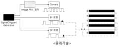
이에 따라, 종래의 기술에서는 촬상면에 브라이트 필드를 형성하는 BF 조명과, 다크 필드를 형성하는 DF 조명을 포함하여 브라이트 필드 및 다크 필드 이미지를 각각 취득하여 결함을 이중으로 조사하는 기술이 제시된 바 있다.Accordingly, in the prior art, a technique of double irradiating defects by acquiring bright field and dark field images, respectively, including BF illumination for forming a bright field and DF illumination for forming a dark field on an image pickup surface, has been proposed.
이러한 종래의 기술은 도 1에 도시된 바와 같이, 촬영면에 브라이트 필드를 형성하는 BF 조명과, 다크 필드를 형성하는 DF 조명을 시그널 제너레이터가 직접 디지털 신호를 전달하여 제어하고, 프레임 그래버가 시그널 제너레이터로부터 디지털 신호를 수신하여 카메라를 제어함으로써, 조명과 카메라가 서로 별도로 제어됨에 따라 신호 손상이 발생하는 현상이 발생하는 문제점이 있었다.As shown in FIG. 1, in this conventional technique, a signal generator directly transmits a digital signal to control BF lighting for forming a bright field and DF lighting for forming a dark field on a photographing surface, and the frame grabber controls the signal generator By receiving a digital signal from and controlling the camera, there is a problem in that signal damage occurs as the lighting and the camera are controlled separately from each other.
본 발명은 상기와 같은 문제점을 해결하기 위하여 안출된 것으로서 본 발명의 목적은, 하나의 촬상수단을 이용해 다수의 조명에 의한 화상을 촬상함으로써, 더 빠른 검사가 가능하고, 동일 영역을 거의 동시에 브라이트 필드 및 다크 필드 검사를 진행함으로써 검사 신뢰성을 향상 시킬 수 있으며, 촬상 수단의 개수를 줄일 수 있는 경제적 효과가 있는 투명 기판 검사 장치 및 투명기판 검사 방법을 제공함에 있다.The present invention has been made to solve the above problems, and an object of the present invention is to take an image by a plurality of illuminations using one imaging means, so that faster inspection is possible and the same area is almost simultaneously bright field And it is to provide a transparent substrate inspection apparatus and a transparent substrate inspection method capable of improving inspection reliability by performing a dark field inspection and having an economical effect of reducing the number of imaging means.
또한, 습득한 브라이트 필드 이미지와 다크 필드 이미지를 비교하여 결함의 위치, 즉 촬상면 상의 결함인지, 촬상면의 반대면 상의 결함인지 여부를 자동으로 판단할 수 있는 투명기판 검사 방법을 제공함에 있다.Another object of the present invention is to provide a transparent substrate inspection method capable of automatically determining the location of a defect, that is, whether the defect is on the imaging surface or on the opposite side of the imaging surface by comparing the obtained bright field image with the dark field image.
상기한 바와 같은 문제점을 해결하기 위한 본 발명의 투명 기판 검사 장치는투명 기판의 결함을 검사하는 투명 기판 검사 장치로서, 상기 투명 기판의 한 촬상면에 빛을 조사하는 제 1 조명 및 제 2 조명, 상기 촬상면을 한 라인씩 촬상하는 라인카메라를 포함하는 촬상 수단, 및 상기 제 1 조명 및 상기 제 2 조명 및 상기 촬상 수단을 제어하고, 상기 촬상 수단에 의해 촬상된 이미지에 기초하여 상기 투명 기판의 결함 여부를 판단하는 제어부,를 포함하고, 상기 제 1 조명은, 상기 제 1 조명의 브라이트 필드 영역이 상기 촬상 수단의 FOV(Field of view)에 대응되도록 상기 제 1 조명의 빛의 조사 방향과 상기 촬상면이 이루는 각도와 상기 촬상수단과 상기 촬상면이 이루는 각도가 동일한 위치에 설치되고, 상기 제 2 조명은, 상기 제 2 조명의 다크 필드 영역이 상기 촬상 수단의 FOV에 대응되도록 상기 제 2 조명의 빛의 조사 방향과 상기 촬상면이 이루는 각도와 상기 촬상수단과 상기 촬상면이 이루는 각도가 소정 수치만큼 차이가 있는 위치에 설치된 것을 특징으로 한다.A transparent substrate inspection apparatus of the present invention for solving the above problems is a transparent substrate inspection apparatus for inspecting defects of a transparent substrate, comprising: a first light and a second light for irradiating light to one imaging surface of the transparent substrate; Imaging means including a line camera for taking images of an imaged surface line by line, and controlling the first illumination and the second illumination and the imaging means, and determining whether or not the transparent substrate is defective based on an image captured by the imaging means Including a control unit for determining, wherein the first light is such that a bright field area of the first light corresponds to a field of view (FOV) of the imaging means, and the light irradiation direction of the first light and the imaging surface are The angle formed by the imaging means and the imaging surface are installed at the same position, and the second illumination is irradiated with light of the second illumination so that the dark field area of the second illumination corresponds to the FOV of the imaging means. It is characterized in that it is installed at a position where there is a difference between the direction and the angle formed by the imaging surface and the angle formed by the imaging means and the imaging surface by a predetermined value.
또한, 상기 제어부는, 상기 제 1 조명 및 상기 제 2 조명이 교번하여 빛을 조사하도록 상기 제 1 조명 및 상기 제 2 조명을 제어하고, 상기 촬상수단이 상기 제 1 조명과 상기 제 2 조명의 각각이 교번하여 빛을 조사하는 시점의 이미지를 순차적으로 촬상하도록 상기 촬상수단을 제어하는 것을 특징으로 한다.In addition, the controller controls the first light and the second light so that the first light and the second light alternately emit light, and the imaging unit controls each of the first light and the second light It is characterized in that the imaging means is controlled to sequentially capture images at the time of alternately irradiating the light.
또한, 상기 제어부는, 상기 촬상수단에서 촬상된 이미지들을 순차적으로 조합하여 소정 크기의 이미지인 통합 이미지를 생성하고, 상기 통합 이미지로부터, 상기 제 1 조명이 빛을 조사하는 순간에 촬상된 이미지들만을 추출하고, 조합하여 브라이트 필드 이미지를 생성하며, 상기 통합 이미지로부터, 상기 제 2 조명이 빛을 조사하는 순간에 촬상된 이미지들만을 추출하고, 조합하여 다크 필드 이미지를 생성하고, 상기 브라이트 필드 이미지 및 상기 다크 필드 이미지에 기초하여 상기 투명 기판의 결함 여부를 판단하는 것을 특징으로 한다.In addition, the control unit generates an integrated image of a predetermined size by sequentially combining the images captured by the imaging means, and from the integrated image, only the images captured at the moment when the first light emits light extracting and combining to generate a bright field image, extracting only images taken at the moment when the second light irradiates light from the integrated image, and combining to generate a dark field image, the bright field image and It is characterized in that determining whether the transparent substrate is defective based on the dark field image.
또한, 상기 제어부는, 상기 브라이트 필드 이미지에서 결함의 그림자가 촬상된 경우, 촬상면 상의 결함으로 판단하고, 상기 브라이트 필드 이미지에서 결함의 그림자가 촬상되지 않고, 상기 다크 필드 이미지에서 결함의 그림자가 촬상된 경우, 촬상면 상의 미세 결함으로 판단하며, 상기 브라이트 필드 이미지와 상기 다크 필드 이미지에서 모두 결함의 그림자가 촬상되지 않은 경우, 촬상면의 반대면 상의 결함으로 판단하는 것을 특징으로 한다.In addition, the control unit, when the shadow of the defect is captured in the bright field image, determines that it is a defect on the imaging surface, the shadow of the defect is not captured in the bright field image, and the shadow of the defect is captured in the dark field image In this case, it is determined as a micro defect on the imaging surface, and when the shadow of the defect is not captured in both the bright field image and the dark field image, it is characterized in that it is determined as a defect on the opposite side of the imaging surface.
또한, 본 발명의 투명 기판 검사 방법은 제 1 조명 및 제 2 조명, 촬상 수단, 및 상기 제 1 조명, 상기 제 2 조명 및 상기 촬상 수단을 제어하고, 상기 촬상 수단에서 촬상한 이미지에 기초하여 투명 기판의 결함 여부를 판단하는 제어부를 포함하는 투명 기판 검사 장치를 이용하고, 제어부가, 상기 촬상 수단으로부터 화상을 수신하여 이미지를 생성 및 취득하는 이미지 취득 단계, 상기 이미지 취득 단계에서 취득한 이미지를 분석하여 결함 유무를 판별하는 결함 유무 판별 단계, 상기 이미지 취득 단계에서 취득한 이미지를 출력하는 출력 단계, 상기 결함 유무 판별 단계에서, 결함이 발견된 경우, 상기 결함 유무 판별 단계와 상기 출력 단계의 사이에, 상기 결함의 위치 및 그림자를 분석하는 분석 단계, 및 상기 분석 단계에서 분석한 자료를 바탕으로 결함의 정확한 위치 및 크기를 판단하는 판단단계, 를 포함하는 것을 특징으로 한다.In addition, the transparent substrate inspection method of the present invention controls the first illumination and the second illumination, imaging means, and the first illumination, the second illumination, and the imaging means, and based on the image captured by the imaging means, transparent Using a transparent substrate inspection apparatus including a control unit for determining whether or not a substrate is defective, an image acquisition step in which the control unit receives an image from the imaging means to generate and acquire an image, and analyzes the image acquired in the image acquisition step. A defect determination step of determining whether there is a defect, an output step of outputting the image obtained in the image acquisition step, and in the case where a defect is found in the defect determination step, between the defect determination step and the output step, the It is characterized in that it includes an analysis step of analyzing the location and shadow of the defect, and a judgment step of determining the exact location and size of the defect based on the data analyzed in the analysis step.
또한, 상기 이미지 취득 단계는, 상기 촬상수단이 상기 제 1 조명과 상기 제 2 조명의 각각이 교번하여 빛을 조사하는 시점의 이미지를 순차적으로 촬상하도록 상기 촬상 수단과 상기 제 1 조명 및 상기 제 2 조명을 동시 제어하는 제어 신호를 발생시키는 신호 발생 단계, 상기 촬상 수단이 화상을 취득하는 촬상 단계, 상기 촬상수단에서 촬상된 이미지들을 순차적으로 조합하여 소정 크기의 이미지인 통합 이미지를 생성하는 통합 이미지 생성 단계 및 상기 통합 이미지로부터, 상기 제 1 조명이 빛을 조사하는 순간에 촬상된 이미지들만을 추출하고, 조합하여 브라이트 필드 이미지를 생성하며, 상기 제 2 조명이 빛을 조사하는 순간에 촬상된 이미지들만을 추출하고, 조합하여 다크 필드 이미지를 생성하는 이미지 분리 단계를 포함하는 것을 특징으로 한다.In addition, in the image acquisition step, the imaging means and the first light and the second light so that the imaging means sequentially captures an image at a time when each of the first light and the second light alternately irradiates light. A signal generating step of generating a control signal for simultaneously controlling lighting, an imaging step of acquiring an image by the imaging unit, and an integrated image generation of generating an integrated image of a predetermined size by sequentially combining images captured by the imaging unit. and extracting only images taken at the moment when the first light emits light from the combined image, combining them to generate a bright field image, and only images taken when the second light emits light. It is characterized in that it comprises an image separation step of extracting and combining to generate a dark field image.
또한, 상기 분석 단계는, 상기 제어부가, 브라이트 필드 이미지 상의 결함 위치와 다크 필드 이미지 상의 결함 위치를 비교하는 결함 위치 비교 단계, 결함 위치로부터 소정 범위 내에 추가 결함 유무를 탐색하는 그림자 탐색 단계, 상기 그림자 탐색 단계에서 상기 추가 결함이 발견된 경우, 상기 추가 결함이 기존 결함의 위치에서 소정 거리 만큼 이격된 위치에 위치하였을 때, 상기 추가 결함을 기존 결함의 그림자로 판단하는 그림자 판별 단계를 포함하는 것을 특징으로 한다.In addition, the analysis step may include a defect location comparison step in which the control unit compares a defect location on a bright field image with a defect location on a dark field image, a shadow search step in which the control unit searches for additional defects within a predetermined range from the defect location, and the shadow and a shadow discrimination step of determining the additional defect as a shadow of the existing defect when the additional defect is located at a location separated by a predetermined distance from the location of the existing defect when the additional defect is found in the search step. to be
또한, 상기 판단 단계는, 브라이트 필드 이미지에서 결함의 그림자가 촬상된 경우, 촬상면 상의 결함으로 판단하고, 브라이트 필드 이미지에서 결함의 그림자가 촬상되지 않고, 다크 필드 이미지에서 결함의 그림자가 촬상된 경우, 촬상면 상의 미세 결함으로 판단하며, 브라이트 필드 이미지와 다크 필드 이미지에서 모두 결함의 그림자가 촬상되지 않은 경우, 촬상면의 반대면 상의 결함으로 판단하는 것을 특징으로 한다.In addition, in the determining step, when the shadow of the defect is captured in the bright field image, it is determined that the defect is on the imaging surface, the shadow of the defect is not captured in the bright field image, and the shadow of the defect is captured in the dark field image. It is characterized in that it is determined as a micro defect on the imaging surface, and when the shadow of the defect is not captured in both the bright field image and the dark field image, it is determined as a defect on the surface opposite to the imaging surface.
상기와 같은 구성에 의한 본 발명의 투명 기판 검사 장치 및 투명기판 검사 방법은 하나의 촬상 수단을 이용해 다수의 조명에 의한 화상을 촬상함으로써, 더 빠른 검사가 가능하고, 동일 영역을 거의 동시에 브라이트 필드 및 다크 필드 검사를 진행함으로써 검사 신뢰성을 향상 시킬 수 있으며, 촬상 수단의 개수를 줄일 수 있는 경제적 효과가 있다.The transparent substrate inspection apparatus and transparent substrate inspection method of the present invention according to the configuration as described above enable faster inspection by capturing images with a plurality of illuminations using one imaging means, and can perform bright field and By performing the dark field inspection, inspection reliability can be improved, and there is an economical effect of reducing the number of imaging means.
또한, 습득한 브라이트 필드 이미지와 다크 필드 이미지를 비교하여 결함의 위치, 즉 촬상면 상의 결함인지, 촬상면의 반대면 상의 결함인지 여부를 자동으로 판단할 수 있는 효과가 있다.In addition, there is an effect of automatically determining the location of the defect, that is, whether the defect is on the imaging surface or on the opposite side of the imaging surface by comparing the acquired bright field image with the dark field image.
도 1은 종래 기술의 블록도이다.
도 2는 본 발명의 투명 기판 검사 장치의 구성을 도시한 블록도이다.
도 3은 본 발명의 투명 기판 검사 장치의 구성을 도시한 평면도이다.
도 4는 본 발명의 투명 기판 검사 방법의 순서도이다.
도 5는 이미지 취득 단계의 세부 단계를 도시한 순서도이다.
도 6은 분석 단계의 세부 단계를 도시한 순서도이다.
도 7은 결함이 촬상면 상에 존재하는 투명기판의 상면도 및 측면도이다.
도 8은 결함이 미세 결함인 경우의 실제 브라이트 필드 이미지와 다크 필드 이미지이다.
도 9는 결함이 촬상면의 반대 면에 존재하는 투명기판의 상면도 및 측면도이다.
도 10은 판단 단계 판단 알고리즘을 도시한 순서도이다.1 is a block diagram of the prior art.
2 is a block diagram showing the configuration of a transparent substrate inspection apparatus of the present invention.
3 is a plan view showing the configuration of the transparent substrate inspection apparatus of the present invention.
4 is a flow chart of a method for inspecting a transparent substrate according to the present invention.
5 is a flowchart illustrating detailed steps of an image acquisition step.
6 is a flowchart illustrating detailed steps of the analysis step.
Fig. 7 is a top view and a side view of a transparent substrate in which defects exist on the imaging surface.
8 is an actual bright field image and a dark field image when the defect is a micro defect.
9 is a top view and a side view of a transparent substrate in which a defect exists on the surface opposite to the imaging surface.
10 is a flowchart illustrating a decision step decision algorithm.
이하, 본 발명의 기술적 사상을 첨부된 도면을 사용하여 더욱 구체적으로 설명한다. 이에 앞서, 본 명세서 및 청구범위에 사용된 용어나 단어는 통상적이거나 사전적인 의미로 한정해서 해석되어서는 아니 되며, 발명자는 그 자신의 발명을 가장 최선의 방법으로 설명하기 위해 용어의 개념을 적절하게 정의할 수 있다는 원칙에 입각하여 본 발명의 기술적 사상에 부합하는 의미와 개념으로 해석되어야만 한다.Hereinafter, the technical idea of the present invention will be described in more detail using the accompanying drawings. Prior to this, the terms or words used in this specification and claims should not be construed as being limited to the usual or dictionary meaning, and the inventor appropriately uses the concept of the term in order to explain his/her invention in the best way. It should be interpreted as a meaning and concept consistent with the technical idea of the present invention based on the principle that it can be defined.
이하로, 도 2 내지 3을 참조하여 본 발명의 투명 기판 검사 장치(1000)의 구성 및 특징에 대해 설명한다.Hereinafter, the configuration and characteristics of the transparent
본 발명의 투명 기판 검사 장치(1000)는 도 2에 도시된 바와 같이 투명 기판(2000)의 하나의 촬상면에 빛을 조사하는 제 1 조명(100) 및 제 2 조명(200), 촬상면을 한 라인씩 촬상하는 라인 카메라를 포함하는 촬상 수단(300)을 포함할 수 있다. 이 때, 제 1 조명(100) 및 제 2 조명(200)은 서로 다른 각도로 투명 기판(2000)의 촬상면에 빛을 조사함으로써 촬상 수단(300)이 촬상하는 부분에 브라이트 필드 및 다크 필드를 형성할 수 있다. 보다 자세히, 제 1 조명(100)은 제 1 조명(100)의 브라이트 필드 영역이 상기 촬상 수단의 FOV(Field of view)에 대응되도록 하는 위치에 설치되고, 제 2 조명(200)은 제 2 조명(200)의 다크 필드 영역이 상기 촬상 수단의 FOV에 대응되도록 하는 위치에 설치된 것이 바람직하다.As shown in FIG. 2, the transparent
또한, 본 발명의 투명 기판 검사 장치(1000)는 도 3에 도시된 바와 같이 제 1 조명(100)과 제 2 조명(200) 및 촬상 수단(300)을 제어하는 제어부(400)를 포함할 수 있다. 제어부(400)는 촬상 수단(300)에서 촬상한 이미지에 기초하여 투명 기판(2000)의 결함 여부를 판단할 수 있다. 보다 자세히, 제어부(400)는 신호 발생부를 포함할 수 있고, 신호 발생부는 디지털 신호를 생성하여 제 1 조명(100)과 제 2 조명(200) 및 촬상 수단(300)에 전달할 수 있다. 신호 발생부는 촬상 수단(300)이 일정한 주기로 촬상면을 촬상하도록 디지털 신호를 생성할 수 있고, 제 1 조명(100) 및 제 2 조명(200)이 촬상 수단(300)의 화상 습득 시각과 동일한 시각에 빛을 조사하되, 제 1 조명(100)과 제 2 조명(200)이 이 서로 교번되어 빛을 조사하고, 촬상수단(300)이 제 1 조명(100)과 제 2 조명(200)의 각각이 교번하여 빛을 조사하는 시점의 이미지를 순차적으로 촬상하도록 촬상 수단(300)과 제 1 조명(100) 및 제 2 조명(200)에 모두 디지털 신호를 송신할 수 있다.In addition, the transparent
제 1 조명(100)과 제 2 조명(200)이 점등되는 시점은 서로 겹치지 않는 것이 바람직하며, 제 1 조명(100)이 한번 켜지고 꺼진 후에 제 2 조명(200)이 한번 켜지고 꺼지는 것이 반복되는 것이 바람직하다. 이에 따라 촬상 수단(300)은 특정한 촬상 위치에서 제 1 조명(100)이 형성한 브라이트 필드의 이미지와, 제 2 조명(200)이 형성한 다크 필드의 이미지를 함께 촬상할 수 있다. 이 때, 신호 발생부는 PC에 설치된 프레임 그래버(Frame grabber)일 수 있고, 촬상 수단(300)은 라인 카메라인 것이 바람직하다.It is preferable that the timing at which the
또한, 제 1 조명(100)의 빛의 조사 방향과 촬영면 즉, 투명기판(2000)이 이루는 각도는 촬상 수단(300)과 투명기판(2000)이 이루는 각도 θ1과 동일한 θ1인 것이 바람직하고, 제 2 조명(200)의 빛의 조사 방향과 투명기판(2000)이 이루는 각도는 촬상 수단(300)과 투명기판(2000)이 이루는 각도 θ1와 상이한 θ2인 것이 바람직하다. 이에 따라 제 1 조명(100)은 촬상 영역에 브라이트 필드를 형성할 수 있고, 제 2 조명(200)은 촬상 영역에 다크 필드를 형성할 수 있다.In addition, the angle formed by the light irradiation direction of the
상술한 구성으로 인하여 하나의 촬상 수단(300)을 이용해 제 1 조명(100) 및 제 2 조명(200)에 의한 영상을 촬상함으로써, 더 빠른 검사가 가능하고, 동일 영역을 거의 동시에 브라이트 필드 및 다크 필드 검사를 진행함으로써 검사 신뢰성을 향상 시킬 수 있으며, 촬상 수단(300)의 개수를 줄일 수 있는 경제적 효과를 기대할 수 있다.Due to the above-described configuration, by capturing images by the
또한, 촬상 수단(300)과 제 1 조명(100) 및 제 2 조명(200)이 전기적으로 병렬로 연결되어 촬상 수단(300)과 제 1 조명(100) 및 제 2 조명(200)을 함께 제어함에 따라 촬상 수단(300)과 제 1 조명(100) 및 제 2 조명(200) 신호 사이에 오차 발생율을 현저히 줄이고, 신호 손상이 발생하는 현상을 최소화 할 수 있다.In addition, the
또한, 본 발명의 투명 기판 검사 장치(1000)는 제 1 및 제 2 조명(200)과 라인 카메라를 진행방향으로 이동시키는 이동부를 더 포함할 수 있다. 제어부(400)는, 촬상 수단(300)이 특정한 위치에서 브라이트 필드와 다크 필드의 화상을 모두 촬상한 이후에 진행방향의 다음 위치로 제 1 및 제 2 조명(200)과 라인 카메라를 함께 이동시키도록 이동부를 제어하는 것이 바람직하다.In addition, the transparent
또한, 제어부(400)는 촬상 수단(300)으로부터 시간별 브라이트 필드의 화상과 다크 필드의 화상을 각각 수신하는 화상 수신부와, 신호 발생부가 생성한 디지털 신호 정보를 토대로 브라이트 필드의 화상과 다크 필드의 화상을 분리하는 화상 분리부를 포함하여, 브라이트 필드와 다크 필드의 개별 이미지를 생성할 수 있다.In addition, the
보다 자세히, 제어부(400)의 화상 수신부는 촬상수단(300)에서 촬상된 이미지들을 순차적으로 조합하여 소정 크기의 이미지인 통합 이미지를 생성하고, 통합 이미지로부터, 제 1 조명(100)이 빛을 조사하는 순간에 촬상된 이미지들만을 추출하고, 조합하여 브라이트 필드 이미지를 생성하며, 제 2 조명(200)이 빛을 조사하는 순간에 촬상된 이미지들만을 추출하고, 조합하여 다크 필드 이미지를 생성할 수 있고, 추후 제어부(400)는 상술한 브라이트 필드 이미지 및 다크 필드 이미지에 기초하여 투명 기판(2000)의 결함 여부를 판단할 수 있다.In more detail, the image receiving unit of the
제어부(400)는 촬상 면 상의 결함을 판단 할 시 하기와 같은 알고리즘으로 판단할 수 있다.The
(a) 결함이 촬상면 상에 위치하되, 결함의 크기가 큰 경우,(a) If the defect is located on the imaging surface, but the size of the defect is large,
결함이 촬상면 상에 위치한 경우, 결함으로 인해 그림자가 발생할 수 있고, 이에 따라 제 1 조명(100) 및 제 2 조명(200)의 위치를 고려하였을 시의 결함 그림자의 예상 위치 즉, 기존 결함과 소정 거리 L 만큼 이격된 위치에 그림자가 형성될 수 있다.(L 값은 제 1 조명의 조사 각도와 투명 기판 사이의 각도 및 거리에 따라 도출될 수 있다.) 이 때 형성된 그림자는 브라이트 필드의 이미지 및 다크 필드 이미지에 촬상될 수 있다. 이에 따라, 제어부(400)는 브라이트 필드 이미지에서 결함의 그림자가 촬상된 경우, 촬상면 상의 결함으로 판단하는 것이 바람직하다.When the defect is located on the imaging surface, a shadow may be generated due to the defect, and accordingly, the expected position of the shadow of the defect when considering the positions of the
(b) 결함이 촬상면 상에 위치하되, 결함의 크기가 작은 경우,(b) If the defect is located on the imaging surface, but the size of the defect is small,
결함이 촬상면 상에 위치한 경우, 케이스(a)에서 설명한 바와 같이, 브라이트 필드 이미지에 결함의 그림자가 촬상될 수 있다. 다만, 브라이트 필드 이미지의 경우 실제 결함의 크기보다 더 작게 결함이 측정되는 경향이 있으므로, 결함의 크기가 충분히 작으면 브라이트 필드 이미지에서 결함과 그 그림자의 이미지가 누락되거나 하여 결함과 그 그림자의 유무 식별이 어려울 수 있다. 이를 보완하기 위해, 제어부(400)는 다크 필드 이미지를 고려하여 결함의 그림자 유무를 확인할 수 있다. 다크 필드 이미지의 경우 실제 결함의 크기보다 더 크게 결함이 측정되므로 결함의 크기가 작더라도 포착이 용이할 수 있다.If the defect is located on the imaging surface, as described in case (a), the shadow of the defect may be captured in the bright field image. However, in the case of a bright field image, defects tend to be smaller than the size of the actual defect, so if the size of the defect is sufficiently small, the image of the defect and its shadow may be missing from the bright field image, thereby identifying the presence or absence of the defect and its shadow. this can be difficult In order to compensate for this, the
즉, 브라이트 필드 이미지에서 결함의 그림자가 포착되지 않았더라도 다크 필드 이미지에 결함의 그림자가 촬상되었다면, 제어부(400)는 촬상면 상에 결함이 존재하되, 존재하는 결함의 크기가 작은 미세 결함인 것으로 판단할 수 있다.That is, even if the shadow of the defect is not captured in the bright field image, if the shadow of the defect is captured in the dark field image, the
(c) 결함이 촬상면의 반대면에 위치하는 경우,(c) If the defect is located on the opposite side of the imaging plane,
결함이 촬상면의 반대 면에 위치한 경우, 도 8에 도시된 바와 같이, 결함에 그림자가 발생하지 않는다. 이에 따라 결함은 촬영이 되되, 브라이트 필드 이미지 와 다크 필드 이미지 모두에서 결함의 그림자는 촬영이 되지 않는다. 이에 따라, 제어부(400)는 브라이트 필드 이미지와 다크 필드 이미지 모두 에서 결함의 그림자가 촬상되지 않은 경우, 촬상면의 반대면 상의 결함으로 판단하는 것이 바람직하다.When the defect is located on the opposite side of the imaging plane, no shadow is generated on the defect, as shown in FIG. 8 . Accordingly, the defect is photographed, but the shadow of the defect is not photographed in both the bright field image and the dark field image. Accordingly, the
그리고, 제어부(400)는 취득한 이미지를 외부로 출력하는 출력부를 포함하고, 출력부는 브라이트 필드와 다크 필드의 개별 이미지를 외부로 출력하는 것이 바람직하다.Also, the
본 발명의 일 실시 예로, 제어부(400)의 신호 발생부는, 제 1 조명(100) 및 제 2 조명(200)이 교번하여 빛을 조사하도록 제 1 조명(100) 및 제 2 조명(200)을 제어하되, 제 1 조명(100) 및 제 2 조명(200)의 빛 조사 시작 시점 이후 소정의 대기 시간후에 촬상 수단(300)이 투명 기판(2000)의 적어도 일부를 촬상하도록 디지털 신호를 발생 시킬 수 있다.In one embodiment of the present invention, the signal generating unit of the
이 때, 대기 시간은 0.1μs 내지 0.1ms 일 수 있고, 촬상 수단(300)의 1회 촬상 시간의 0.1% 내지 1%일 수 있다. 이에 따라 조명의 노후화 및 긴 신호선에 의한 불균일한 시간 지연, 노이즈, 주변 장치와의 간섭에 의하여 촬용시점의 조명이 원하는 조명이 되지 못하여 오검출 하는 것을 억제할 수 있는 효과가 있다.At this time, the standby time may be 0.1 μs to 0.1 ms, and may be 0.1% to 1% of the imaging time of the
더 나아가, 본 발명의 또 다른 실시 예에서, 본 발명의 투명 기판 검사 장치(1000)는 제어부(400)와 제 1 조명(100)을 연결하는 제 1 와이어, 및 제어부(400)와 제 2 조명(200)을 연결하는 제 2 와이어, 를 포함할 수 있다. 이 때, 제 1 및 2 와이어의 길이의 차는 소정 기준치 이하인 것이 바람직하다. 이에 따라, 제어부(400)의 신호 발생부가 제 1 및 2 와이어를 통해 제 1 조명(100) 및 제 2 조명(200)을 제어할 시에, 와이어의 길이 차에 의해 발생하는 딜레이를 최소화 할 수 있고, 신호의 손상 및 결함이 발생하는 것을 방지할 수 있다.Furthermore, in another embodiment of the present invention, the transparent
또한, 본 발명의 투명 기판 검사 장치(1000)는 제어부(400)와 촬상 수단(300)을 연결하는 제 3 와이어를 더 포함할 수 있고, 제 3 와이어는 제 1, 2 와의 길이의 차가 소정 기준치 이하인 것이 바람직하다. 이에 따라, 제어부(400)의 신호 발생부가 제 1 내지 3 와이어를 통해 제 1 조명(100) 및 제 2 조명(200)과 촬상 수단(300)을 제어할 시에, 와이어의 길이 차에 의해 발생하는 딜레이를 최소화 할 수 있고, 제 1 조명(100) 및 제 2 조명(200)과 촬상 수단(300) 간의 시간차를 최소화 함에 따라 신호의 손상 및 결함이 발생하는 것을 방지할 수 있다.In addition, the transparent
촬상 수단(300)과 제 1 조명(100) 및 제 2 조명(200)는 매우 빠른 속도 및 주기로 촬상면을 촬상하고, 빛을 조사하므로, 미소한 시간 지연으로도 신호의 결손이 발생할 수 있다. 이에 따라 제 1 내지 3 와이어의 길이 차를 줄임으로써 신호 전달에 있어 발생하는 시간 지연을 줄이는 구성은 현저한 효과를 기대할 수 있다.Since the imaging means 300, the
이하로, 도 3 내지 5를 참조하여 본 발명의 투명 기판(2000) 검사 방법에 대해 설명한다.Hereinafter, a
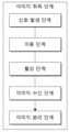
본 발명의 투명 기판(2000) 검사 방법은 제어부(400)에 의해 수행될 수 있다. 도 3에 도시된 바와 같이, 본 발명의 투명 기판(2000) 검사 방법은 촬상 수단(300)으로부터 시간별 화상을 수신하여 이미지를 생성하는 이미지 취득 단계와, 이미지 취득 단계에서 취득한 이미지를 분석하여 결함 유무를 판별하는 결함 유무 판별 단계와, 이미지 취득 단계에서 취득한 이미지를 출력하는 출력 단계를 포함할 수 있다.The
이 때, 결함 유무 판별 단계에서, 결함이 발견된 경우, 결함의 위치 및 그림자를 분석하는 분석 단계, 분석 단계에서 분석한 자료를 바탕으로 결함의 정확한 위치 및 크기를 판단하는 판단단계가 더 포함될 수 있다. 이에 따라 투명 기판(2000) 상의 결함 위치를 보다 자세히 파악할 수 있다.At this time, in the defect determination step, if a defect is found, an analysis step of analyzing the location and shadow of the defect, and a judgment step of determining the exact location and size of the defect based on the data analyzed in the analysis step may be further included. there is. Accordingly, the location of the defect on the
결함 유무 판별 단계에서 결함이 발견되지 않은 경우는 결함 유무 판별 단계가 완료된 이후에 바로 출력 단계가 수행되는 것이 바람직하다.When no defect is found in the defect determination step, the outputting step is preferably performed immediately after the defect determination step is completed.
도 4에 도시된 바와 같이 이미지 취득 단계는, 제어부(400)가 디지털 신호를 생성하고 촬상 수단(300)과 제 1 조명(100) 및 제 2 조명(200) 에 전달하여 촬상수단(300)이 제 1 조명(100)과 제 2 조명(200)의 각각이 교번하여 빛을 조사하는 시점의 이미지를 순차적으로 촬상하도록 촬상 수단(300)과 제 1 조명(100)과 제 2 조명(200)을 동시 제어하는 신호 발생 단계, 제어부(400)가 이동부를 제어하여 촬상 수단(300)과 조명를 촬상면의 목표 촬상 위치로 이동시키는 이동 단계, 촬상 수단(300)이 화상을 취득하는 촬상 단계, 촬상수단(300)에서 촬상된 이미지들을 순차적으로 조합하여 소정 크기의 이미지인 통합 이미지를 생성하는 통합 이미지 생성 단계 및 통합 이미지로부터, 제 1 조명(100)이 빛을 조사하는 순간에 촬상된 이미지들만을 추출하고, 조합하여 브라이트 필드 이미지를 생성하며, 제 2 조명(200)이 빛을 조사하는 순간에 촬상된 이미지들만을 추출하고, 조합하여 다크 필드 이미지를 생성하는 이미지 분리 단계를 포함하는 것이 바람직하다. 이 때, 이동 단계는 택일적으로 포함될 수 있다.As shown in FIG. 4, in the image acquisition step, the
이에 따라, 본 발명의 투명 기판(2000) 검사 방법은 하나의 촬상 수단(300)을 이용해 제 1 조명(100) 및 제 2 조명(200)에 의한 화상을 촬상함으로써, 더 빠른 검사가 가능하고, 동일 영역을 거의 동시에 브라이트 필드 및 다크 필드 검사를 진행함으로써 검사 신뢰성을 향상 시킬 수 있으며, 촬상 수단(300)의 개수를 줄일 수 있는 경제적 효과를 기대할 수 있다.Accordingly, the
또한, 촬상 수단(300)과 제 1 조명(100) 및 제 2 조명(200)이 병렬로 연결되어 촬상 수단(300)과 제 1 조명(100) 및 제 2 조명(200)을 함께 제어함에 따라 촬상 수단(300)과 제 1 조명(100) 및 제 2 조명(200) 신호 사이에 오차 발생율을 현저히 줄이고, 신호 손상이 발생하는 현상을 최소화 할 수 있다.In addition, as the imaging means 300, the
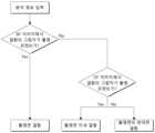
도 5에 도시된 바와 같이 분석 단계는, 제어부(400)가, 브라이트 필드 이미지 상의 결함 위치와 다크 필드 이미지 상의 결함 위치를 비교하는 결함 위치 비교 단계, 결함 위치로부터 소정 범위 내에 추가 결함이 촬상 되었는지 유무를 탐색하는 그림자 탐색 단계, 그림자 탐색 단계에서 추가 결함이 발견된 경우, 추가 결함의 위치가 기존 결함의 위치에서 소정 거리만큼 이격된 위치에 위치한 경우, 추가 결함을 기존 결함의 그림자로 판단하는 그림자 판별 단계를 포함할 수 있다.As shown in FIG. 5, the analysis step is a defect location comparison step in which the
보다 자세히, 그림자 탐색 단계에서 탐색하는 추가 결함의 기준은 기존에 탐색된 결함과 크기가 소정 오차범위 내로 동일한 크기를 가지는 것일 수 있다. 이는 추가로 탐색된 결함이 기존에 탐색된 결함의 그림자인지, 또는 기존에 탐색된 결함의 인근에 위치한 별도의 결함인지 유무를 판별할 수 있다. 이에 따라 그림자 탐색 단계에서는 기존에 탐색된 결함의 그림자를 탐색해 낼 수 있다.In more detail, the criterion for additional defects to be searched for in the shadow search step may be to have the same size as a previously detected defect within a predetermined error range. This may determine whether the additionally searched defect is a shadow of the previously searched defect or a separate defect located in the vicinity of the previously searched defect. Accordingly, in the shadow search step, the shadow of the previously searched defect can be searched.
또한, 그림자 판별 단계에서, 탐색된 추가 결함이 기존 결함과 소정 거리 만큼 이격되었는지, 더 나아가, 추가 결함이 기존 결함으로부터 어느 방향으로 이격되었는지 탐색하여 제 1 및 제 2 조명(200)의 위치를 고려 하였을 시, 그림자의 예상 위치와 비교 후, 탐색된 추가 결함이 기존 결함의 그림자인지 유무를 판별할 수 있다.In addition, in the shadow determination step, whether the additional defect found is spaced apart from the existing defect by a predetermined distance, and furthermore, the location of the first and
이하로, 도 6 내지 9를 참조하여 판단 단계의 결함 위치 판단 알고리즘에 대해 보다 자세히 설명한다.Hereinafter, the defect location determination algorithm in the determination step will be described in more detail with reference to FIGS. 6 to 9 .
상술한 분석 단계에서 기존 결함의 그림자가 발견된 경우에 판단 단계는 이를 기준으로 결함의 정확한 위치를 판별할 수 있다.If the shadow of the existing defect is found in the above analysis step, the determination step may determine the exact location of the defect based on this.
(a) 결함이 촬상면 상에 위치하되, 결함의 크기가 큰 경우,(a) If the defect is located on the imaging surface, but the size of the defect is large,
결함이 촬상면 상에 위치한 경우, 도 6에 도시된 바와 같이, 결함으로 인해 그림자가 발생할 수 있고, 이에 따라 제 1 및 제 2 조명(200)의 위치를 고려하였을 시의 결함 그림자의 예상 위치 즉, 기존 결함과 소정 거리 L 만큼 이격된 위치에 그림자가 형성될 수 있다.(L 값은 제 1 조명과 투명 기판 사이의 각도(θ1) 및 거리에 따라 도출될 수 있다.) 이 때 형성된 그림자는 브라이트 필드의 이미지 및 다크 필드 이미지에 촬상될 수 있다. 이에 따라, 제어부(400)는 브라이트 필드 이미지에서 결함의 그림자가 촬상된 경우, 촬상면 상의 결함으로 판단하는 것이 바람직하다.When the defect is located on the imaging surface, as shown in FIG. 6, the defect may cause a shadow, and accordingly, the expected position of the defect shadow when considering the positions of the first and
(b) 결함이 촬상면 상에 위치하되, 결함의 크기가 작은 경우,(b) If the defect is located on the imaging surface, but the size of the defect is small,
결함이 촬상면 상에 위치한 경우, 케이스(a)에서 설명한 바와 같이, 브라이트 필드 이미지에 결함의 그림자가 촬상될 수 있다. 다만, 브라이트 필드 이미지의 경우 실제 결함의 크기보다 더 작게 결함이 측정되는 경향이 있으므로, 결함의 크기가 충분히 작으면 브라이트 필드 이미지에서 결함과 그 그림자의 이미지가 누락되거나 하여 결함과 그 그림자의 유무 식별이 어려울 수 있다. 이를 보완하기 위해, 제어부(400)는 다크 필드 이미지를 고려하여 결함의 그림자 유무를 확인할 수 있다. 다크 필드 이미지의 경우 실제 결함의 크기보다 더 크게 결함이 측정되므로 결함의 크기가 작더라도 포착이 용이할 수 있다. 브라이트 필드 이미지와 다크 필드 이미지에서의 결함 크기 차이는 도 7에 도시된 비교 이미지를 통해 확인할 수 있다. 도 7에 도시된 브라이트 필드 이미지와 다크 필드 이미지는 동일한 촬상면을 촬상한 것이다.If the defect is located on the imaging surface, as described in case (a), the shadow of the defect may be captured in the bright field image. However, in the case of a bright field image, defects tend to be smaller than the size of the actual defect, so if the size of the defect is sufficiently small, the image of the defect and its shadow may be missing from the bright field image, thereby identifying the presence or absence of the defect and its shadow. this can be difficult In order to compensate for this, the
즉, 브라이트 필드 이미지에서 결함의 그림자가 포착되지 않았더라도 다크 필드 이미지에 결함의 그림자가 촬상되었다면, 제어부(400)는 촬상면 상에 결함이 존재하되, 존재하는 결함의 크기가 작은 미세 결함인 것으로 판단할 수 있다.That is, even if the shadow of the defect is not captured in the bright field image, if the shadow of the defect is captured in the dark field image, the
(c) 결함이 촬상면의 반대면에 위치하는 경우,(c) If the defect is located on the opposite side of the imaging plane,
결함이 촬상면의 반대 면에 위치한 경우, 도 8에 도시된 바와 같이, 결함에 그림자가 발생하지 않는다. 이에 따라 결함은 촬영이 되되, 브라이트 필드 이미지 와 다크 필드 이미지 모두에서 결함의 그림자는 촬영이 되지 않는다. 이에 따라, 제어부(400)는 브라이트 필드 이미지와 다크 필드 이미지 모두 에서 결함의 그림자가 촬상되지 않은 경우, 촬상면의 반대면 상의 결함으로 판단하는 것이 바람직하다.When the defect is located on the opposite side of the imaging plane, no shadow is generated on the defect, as shown in FIG. 8 . Accordingly, the defect is photographed, but the shadow of the defect is not photographed in both the bright field image and the dark field image. Accordingly, the
상술한 케이스 별 판단 지표에 따라 제어부(400)는 도 9에 도시된 그림자 위치 판단 알고리즘을 구축하여 수행할 수 있다. 도 9에 도시된 판단 단계는, 브라이트 필드 이미지에서 결함의 그림자가 촬상된 경우, 촬상면 상의 결함으로 판단하고, 브라이트 필드 이미지에서 결함의 그림자가 촬상되지 않고, 다크 필드 이미지에서 결함의 그림자가 촬상된 경우, 촬상면 상의 미세 결함으로 판단하며, 브라이트 필드 이미지와 다크 필드 이미지에서 모두 결함의 그림자가 촬상되지 않은 경우, 촬상면의 반대면 상의 결함으로 판단할 수 있다.According to the above-described determination index for each case, the
2000 : 투명 기판
1000 : 투명 기판 검사 장치
100 : 제 1 조명
200 : 제 2 조명
300 : 촬상 수단
400 : 제어부2000: transparent substrate
1000: transparent substrate inspection device
100: 1st light
200: second light
300: imaging means
400: control unit
Claims (8)
Translated fromKorean상기 투명 기판의한 촬상면에 빛을 조사하는 제 1 조명 및 제 2 조명;
상기 촬상면을 한 라인씩 촬상하는 라인카메라를 포함하는 촬상 수단; 및
상기 제 1 조명 및 상기 제 2 조명 및 상기 촬상 수단을 제어하고, 상기 촬상 수단에 의해 촬상된 이미지에 기초하여 상기 투명 기판의 결함 여부를 판단하는 제어부;를 포함하고,
상기 제 1 조명은, 상기 제 1 조명의 브라이트 필드 영역이 상기 촬상 수단의 FOV(Field of view)에 대응되도록 상기 제 1 조명의 빛의 조사 방향과 상기 촬상면이 이루는 각도와 상기 촬상수단과 상기 촬상면이 이루는 각도가 동일한 위치에 설치되고,
상기 제 2 조명은, 상기 제 2 조명의 다크 필드 영역이 상기 촬상 수단의 FOV에 대응되도록 상기 제 2 조명의 빛의 조사 방향과 상기 촬상면이 이루는 각도와 상기 촬상수단과 상기 촬상면이 이루는 각도가 소정 수치만큼 차이가 있는 위치에 설치되고,
상기 제어부는,
상기 촬상수단에서 촬상된 이미지들을 순차적으로 조합하여 소정 크기의 이미지인 통합 이미지를 생성하고,
상기 통합 이미지로부터, 상기 제 1 조명이 빛을 조사하는 순간에 촬상된 이미지들만을 추출하고, 조합하여 브라이트 필드 이미지를 생성하며,
상기 통합 이미지로부터, 상기 제 2 조명이 빛을 조사하는 순간에 촬상된 이미지들만을 추출하고, 조합하여 다크 필드 이미지를 생성하며,
상기 브라이트 필드 이미지에서 결함의 그림자가 촬상된 경우, 촬상면 상의 결함으로 판단하고,
상기 브라이트 필드 이미지에서 결함의 그림자가 촬상되지 않고 상기 다크 필드 이미지에서 결함의 그림자가 촬상된 경우, 촬상면 상의 미세 결함으로 판단하며,
상기 브라이트 필드 이미지와 상기 다크 필드 이미지에서 모두 결함의 그림자가 촬상되지 않은 경우, 촬상면의 반대면 상의 결함으로 판단하는 것을 특징으로 하는 투명 기판 검사 장치.
A transparent substrate inspection device for inspecting defects of a transparent substrate, comprising:
first illumination and second illumination for radiating light toone imaging surface of the transparent substrate;
imaging means including a line camera that captures images of the imaging surface line by line; and
A controller for controlling the first and second lights and the imaging unit, and determining whether the transparent substrate is defective based on an image captured by the imaging unit;
The first illumination includes an angle formed between the light irradiation direction of the first illumination and the imaging surface so that the bright field area of the first illumination corresponds to the field of view (FOV) of the imaging means, and the imaging means and the imaging surface. The angle formed by this is installed at the same position,
In the second illumination, the angle formed by the light irradiation direction of the second illumination and the imaging surface and the angle formed by the imaging means and the imaging surface are predetermined so that the dark field region of the second illumination corresponds to the FOV of the imaging means. It is installed in a location that differs by the number,
The control unit,
sequentially combining the images captured by the imaging means to generate an integrated image of a predetermined size;
From the integrated image, only images captured at the moment when the first light irradiates light are extracted and combined to generate a bright field image;
Extracting only images taken at the moment when the second light irradiates light from the integrated image and combining them to generate a dark field image;
When a shadow of a defect is captured in the bright field image, it is determined as a defect on the imaging surface;
If the shadow of the defect is not captured in the bright field image and the shadow of the defect is captured in the dark field image, it is determined as a micro defect on the imaging surface;
When the shadow of the defect is not captured in both the bright field image and the dark field image, it is determined as a defect on a surface opposite to the imaged surface.
상기 제어부는,
상기 제 1 조명 및 상기 제 2 조명이 교번하여 빛을 조사하도록 상기 제 1 조명 및 상기 제 2 조명을 제어하고,
상기 촬상수단이 상기 제 1 조명과 상기 제 2 조명의 각각이 교번하여 빛을 조사하는 시점의 이미지를 순차적으로 촬상하도록 상기 촬상수단을 제어하는 것
을 특징으로 하는 투명 기판 검사 장치.
According to claim 1,
The control unit,
Controlling the first light and the second light so that the first light and the second light alternately emit light;
Controlling the imaging means so that the imaging means sequentially captures images at the time when each of the first light and the second light alternately irradiates light.
Characterized in that the transparent substrate inspection device.
제어부가,
상기 촬상 수단으로부터 화상을 수신하여 이미지를 생성 및 취득하는 이미지 취득 단계;
상기 이미지 취득 단계에서 취득한 이미지를 분석하여 결함 유무를 판별하는 결함 유무 판별 단계;
상기 이미지 취득 단계에서 취득한 이미지를 출력하는 출력 단계;
상기 결함 유무 판별 단계에서, 결함이 발견된 경우, 상기 결함 유무 판별 단계와 상기 출력 단계의 사이에,
상기 결함의 위치 및 그림자를 분석하는 분석 단계; 및
상기 분석 단계에서 분석한 자료를 바탕으로 결함의 정확한 위치 및 크기를 판단하는 판단단계;
를 포함하고,
상기 판단 단계는,
브라이트 필드 이미지에서 결함의 그림자가 촬상된 경우, 촬상면 상의 결함으로 판단하고,
브라이트 필드 이미지에서 결함의 그림자가 촬상되지 않고,
다크 필드 이미지에서 결함의 그림자가 촬상된 경우, 촬상면 상의 미세 결함으로 판단하며,
브라이트 필드 이미지와 다크 필드 이미지에서 모두 결함의 그림자가 촬상되지 않은 경우, 촬상면의 반대면 상의 결함으로 판단하는 것을 특징으로 하는 투명 기판 검사 방법.
a first light and a second light; imaging means; and a control unit controlling the first light, the second light, and the imaging unit, and determining whether or not the transparent substrate has a defect based on an image captured by the imaging unit. in
control unit,
an image acquisition step of receiving an image from the imaging means to generate and acquire an image;
Defect determination step of analyzing the image obtained in the image acquisition step to determine whether there is a defect;
an output step of outputting the image acquired in the image acquisition step;
In the defect determination step, when a defect is found, between the defect determination step and the output step,
An analysis step of analyzing the location and shadow of the defect; and
A determination step of determining the exact location and size of the defect based on the data analyzed in the analysis step;
including,
The judgment step is
When a shadow of a defect is captured in the bright field image, it is determined as a defect on the imaging surface;
The shadow of the defect is not captured in the bright field image,
If the shadow of the defect is captured in the dark field image, it is determined as a micro defect on the imaging surface,
A method for inspecting a transparent substrate characterized in that when the shadow of the defect is not captured in both the bright field image and the dark field image, it isjudged as a defect on a surface opposite to the imaged surface.
상기 이미지 취득 단계는,
상기 촬상수단이 상기 제 1 조명과 상기 제 2 조명의 각각이 교번하여 빛을 조사하는 시점의 이미지를 순차적으로 촬상하도록 상기 촬상 수단과 상기 제 1 조명 및 상기 제 2 조명을 동시 제어하는 제어 신호를 발생시키는 신호 발생 단계,
상기 촬상 수단이 화상을 취득하는 촬상 단계,
상기 촬상수단에서 촬상된 이미지들을 순차적으로 조합하여 소정 크기의 이미지인 통합 이미지를 생성하는 통합 이미지 생성 단계 및
상기 통합 이미지로부터, 상기 제 1 조명이 빛을 조사하는 순간에 촬상된 이미지들만을 추출하고, 조합하여 브라이트 필드 이미지를 생성하며, 상기 제 2 조명이 빛을 조사하는 순간에 촬상된 이미지들만을 추출하고, 조합하여 다크 필드 이미지를 생성하는 이미지 분리 단계를 포함하는 것을 특징으로 하는 투명 기판 검사 방법.
According to claim 5,
The image acquisition step,
A control signal for simultaneously controlling the imaging means, the first light, and the second light so that the imaging means sequentially captures an image at a time when each of the first light and the second light alternately irradiates light. Signal generation step to generate,
an imaging step in which the imaging means acquires an image;
An integrated image generating step of sequentially combining the images captured by the imaging means to generate an integrated image of a predetermined size; and
From the integrated image, extract only images taken at the moment when the first light emits light, combine them to create a bright field image, and extract only images taken when the second light emits light. and an image separation step of generating a dark field image in combination.
상기 분석 단계는,
상기 제어부가,
브라이트 필드 이미지 상의 결함 위치와 다크 필드 이미지 상의 결함 위치를 비교하는 결함 위치 비교 단계,
결함 위치로부터 소정 범위 내에 추가 결함 유무를 탐색하는 그림자 탐색 단계,
상기 그림자 탐색 단계에서 상기 추가 결함이 발견된 경우,
상기 추가 결함이 기존 결함의 위치에서 소정 거리 만큼 이격된 위치에 위치하였을 때, 상기 추가 결함을 기존 결함의 그림자로 판단하는 그림자 판별 단계를 포함하는 것을 특징으로 하는 투명 기판 검사 방법.
According to claim 5,
The analysis step is
the control unit,
A defect location comparison step of comparing a defect location on a bright field image with a defect location on a dark field image;
A shadow search step of searching for additional defects within a predetermined range from the defect location;
If the additional defect is found in the shadow search step,
and a shadow determination step of judging the additional defect as a shadow of the existing defect when the additional defect is located at a location spaced apart from the location of the existing defect by a predetermined distance.
Priority Applications (1)
| Application Number | Priority Date | Filing Date | Title |
|---|---|---|---|
| KR1020210008688AKR102542814B1 (en) | 2021-01-21 | 2021-01-21 | The defect inspecti on apparatus on the transparent substrate and the method thereof |
Applications Claiming Priority (1)
| Application Number | Priority Date | Filing Date | Title |
|---|---|---|---|
| KR1020210008688AKR102542814B1 (en) | 2021-01-21 | 2021-01-21 | The defect inspecti on apparatus on the transparent substrate and the method thereof |
Publications (2)
| Publication Number | Publication Date |
|---|---|
| KR20220105838A KR20220105838A (en) | 2022-07-28 |
| KR102542814B1true KR102542814B1 (en) | 2023-06-14 |
Family
ID=82607652
Family Applications (1)
| Application Number | Title | Priority Date | Filing Date |
|---|---|---|---|
| KR1020210008688AActiveKR102542814B1 (en) | 2021-01-21 | 2021-01-21 | The defect inspecti on apparatus on the transparent substrate and the method thereof |
Country Status (1)
| Country | Link |
|---|---|
| KR (1) | KR102542814B1 (en) |
Families Citing this family (1)
| Publication number | Priority date | Publication date | Assignee | Title |
|---|---|---|---|---|
| CN115901776B (en)* | 2022-11-02 | 2024-10-01 | 富翔精密工业(昆山)有限公司 | Detection device and detection method |
Citations (4)
| Publication number | Priority date | Publication date | Assignee | Title |
|---|---|---|---|---|
| JP2007327896A (en)* | 2006-06-09 | 2007-12-20 | Canon Inc | Inspection device |
| JP2012237566A (en)* | 2011-05-10 | 2012-12-06 | Hitachi High-Technologies Corp | Defect observation method and apparatus for the same |
| KR101326455B1 (en)* | 2006-05-12 | 2013-11-20 | 코닝 인코포레이티드 | Apparatus and method for characterizing defects in a transparent substrate |
| KR101972517B1 (en)* | 2017-09-05 | 2019-05-02 | 주식회사 에이치비테크놀러지 | Dual line optics inspection system for surface inspection of flexible device |
Family Cites Families (2)
| Publication number | Priority date | Publication date | Assignee | Title |
|---|---|---|---|---|
| JPH11108637A (en)* | 1997-10-03 | 1999-04-23 | Dakku Engineering Kk | Quality inspection device |
| KR20030096780A (en) | 2002-06-17 | 2003-12-31 | 한국전기초자 주식회사 | Apparatus for inspecting defect of glass and control method thereof |
- 2021
- 2021-01-21KRKR1020210008688Apatent/KR102542814B1/enactiveActive
Patent Citations (4)
| Publication number | Priority date | Publication date | Assignee | Title |
|---|---|---|---|---|
| KR101326455B1 (en)* | 2006-05-12 | 2013-11-20 | 코닝 인코포레이티드 | Apparatus and method for characterizing defects in a transparent substrate |
| JP2007327896A (en)* | 2006-06-09 | 2007-12-20 | Canon Inc | Inspection device |
| JP2012237566A (en)* | 2011-05-10 | 2012-12-06 | Hitachi High-Technologies Corp | Defect observation method and apparatus for the same |
| KR101972517B1 (en)* | 2017-09-05 | 2019-05-02 | 주식회사 에이치비테크놀러지 | Dual line optics inspection system for surface inspection of flexible device |
Also Published As
| Publication number | Publication date |
|---|---|
| KR20220105838A (en) | 2022-07-28 |
Similar Documents
| Publication | Publication Date | Title |
|---|---|---|
| US6710868B2 (en) | Optical inspection system with dual detection heads | |
| US8854471B2 (en) | Infrared sensor and sensing method using the same | |
| CN101014850B (en) | System and method for inspecting electrical circuits utilizing reflective and fluorescent imagery | |
| JP2008020359A (en) | Surface inspection method and apparatus | |
| US9874436B2 (en) | Hole inspection method and apparatus | |
| JP5712079B2 (en) | Defect inspection apparatus and defect inspection method | |
| US20140347664A1 (en) | Apparatus and method for identifying defects within the volume of a transparent sheet and use of the apparatus | |
| JP2000241362A (en) | Surface quality inspecting apparatus and method | |
| KR101473569B1 (en) | Apparatus of defect detection using line scan camera and method thereof | |
| KR102542814B1 (en) | The defect inspecti on apparatus on the transparent substrate and the method thereof | |
| JP4986255B1 (en) | Container mouth inspection method and apparatus | |
| TW201411122A (en) | Surface foreign material detecting system and control method thereof | |
| TW202127012A (en) | Optical inspection apparatus and optical inspection method | |
| JP2008026149A (en) | Appearance inspection device | |
| TW201910755A (en) | Automatic optical inspection device and method comprising multiple detectors, multiple light sources and a synchronization controller connected to the detectors and the light sources | |
| JP2004132773A (en) | Vegetable gloss inspection device | |
| JP5430614B2 (en) | Optical device | |
| JP2016102776A (en) | Inspection device and method for inspection | |
| JPH0979990A (en) | Semiconductor device inspection apparatus and inspection method thereof | |
| JP2009164305A (en) | Foreign matter inspection method and foreign matter inspection apparatus for wafer peripheral edge | |
| KR101063542B1 (en) | Electronic component storage condition inspection method and system | |
| JPH10282014A (en) | Surface defect detector with polarizing plate | |
| JP3254873B2 (en) | Package visual inspection device and visual inspection method | |
| JPH07103905A (en) | Flaw inspecting equipment | |
| KR20200062081A (en) | How to inspect the optical display panel for damage |
Legal Events
| Date | Code | Title | Description |
|---|---|---|---|
| PA0109 | Patent application | St.27 status event code:A-0-1-A10-A12-nap-PA0109 | |
| PA0201 | Request for examination | St.27 status event code:A-1-2-D10-D11-exm-PA0201 | |
| D13-X000 | Search requested | St.27 status event code:A-1-2-D10-D13-srh-X000 | |
| D14-X000 | Search report completed | St.27 status event code:A-1-2-D10-D14-srh-X000 | |
| PG1501 | Laying open of application | St.27 status event code:A-1-1-Q10-Q12-nap-PG1501 | |
| E902 | Notification of reason for refusal | ||
| PE0902 | Notice of grounds for rejection | St.27 status event code:A-1-2-D10-D21-exm-PE0902 | |
| E13-X000 | Pre-grant limitation requested | St.27 status event code:A-2-3-E10-E13-lim-X000 | |
| P11-X000 | Amendment of application requested | St.27 status event code:A-2-2-P10-P11-nap-X000 | |
| P13-X000 | Application amended | St.27 status event code:A-2-2-P10-P13-nap-X000 | |
| E701 | Decision to grant or registration of patent right | ||
| PE0701 | Decision of registration | St.27 status event code:A-1-2-D10-D22-exm-PE0701 | |
| PR0701 | Registration of establishment | St.27 status event code:A-2-4-F10-F11-exm-PR0701 | |
| PR1002 | Payment of registration fee | St.27 status event code:A-2-2-U10-U11-oth-PR1002 Fee payment year number:1 | |
| PG1601 | Publication of registration | St.27 status event code:A-4-4-Q10-Q13-nap-PG1601 | |
| P14-X000 | Amendment of ip right document requested | St.27 status event code:A-5-5-P10-P14-nap-X000 | |
| R18-X000 | Changes to party contact information recorded | St.27 status event code:A-5-5-R10-R18-oth-X000 | |
| P14-X000 | Amendment of ip right document requested | St.27 status event code:A-5-5-P10-P14-nap-X000 | |
| P14-X000 | Amendment of ip right document requested | St.27 status event code:A-5-5-P10-P14-nap-X000 |