KR102541940B1 - Light valve panel and liquid crystal display device using the same - Google Patents
Light valve panel and liquid crystal display device using the sameDownload PDFInfo
- Publication number
- KR102541940B1 KR102541940B1KR1020160067778AKR20160067778AKR102541940B1KR 102541940 B1KR102541940 B1KR 102541940B1KR 1020160067778 AKR1020160067778 AKR 1020160067778AKR 20160067778 AKR20160067778 AKR 20160067778AKR 102541940 B1KR102541940 B1KR 102541940B1
- Authority
- KR
- South Korea
- Prior art keywords
- voltage
- light valve
- liquid crystal
- electrode
- panel
- Prior art date
- Legal status (The legal status is an assumption and is not a legal conclusion. Google has not performed a legal analysis and makes no representation as to the accuracy of the status listed.)
- Active
Links
Images


Classifications
- G—PHYSICS
- G02—OPTICS
- G02F—OPTICAL DEVICES OR ARRANGEMENTS FOR THE CONTROL OF LIGHT BY MODIFICATION OF THE OPTICAL PROPERTIES OF THE MEDIA OF THE ELEMENTS INVOLVED THEREIN; NON-LINEAR OPTICS; FREQUENCY-CHANGING OF LIGHT; OPTICAL LOGIC ELEMENTS; OPTICAL ANALOGUE/DIGITAL CONVERTERS
- G02F1/00—Devices or arrangements for the control of the intensity, colour, phase, polarisation or direction of light arriving from an independent light source, e.g. switching, gating or modulating; Non-linear optics
- G02F1/01—Devices or arrangements for the control of the intensity, colour, phase, polarisation or direction of light arriving from an independent light source, e.g. switching, gating or modulating; Non-linear optics for the control of the intensity, phase, polarisation or colour
- G02F1/13—Devices or arrangements for the control of the intensity, colour, phase, polarisation or direction of light arriving from an independent light source, e.g. switching, gating or modulating; Non-linear optics for the control of the intensity, phase, polarisation or colour based on liquid crystals, e.g. single liquid crystal display cells
- G02F1/137—Devices or arrangements for the control of the intensity, colour, phase, polarisation or direction of light arriving from an independent light source, e.g. switching, gating or modulating; Non-linear optics for the control of the intensity, phase, polarisation or colour based on liquid crystals, e.g. single liquid crystal display cells characterised by the electro-optical or magneto-optical effect, e.g. field-induced phase transition, orientation effect, guest-host interaction or dynamic scattering
- G—PHYSICS
- G09—EDUCATION; CRYPTOGRAPHY; DISPLAY; ADVERTISING; SEALS
- G09G—ARRANGEMENTS OR CIRCUITS FOR CONTROL OF INDICATING DEVICES USING STATIC MEANS TO PRESENT VARIABLE INFORMATION
- G09G3/00—Control arrangements or circuits, of interest only in connection with visual indicators other than cathode-ray tubes
- G09G3/20—Control arrangements or circuits, of interest only in connection with visual indicators other than cathode-ray tubes for presentation of an assembly of a number of characters, e.g. a page, by composing the assembly by combination of individual elements arranged in a matrix no fixed position being assigned to or needed to be assigned to the individual characters or partial characters
- G09G3/34—Control arrangements or circuits, of interest only in connection with visual indicators other than cathode-ray tubes for presentation of an assembly of a number of characters, e.g. a page, by composing the assembly by combination of individual elements arranged in a matrix no fixed position being assigned to or needed to be assigned to the individual characters or partial characters by control of light from an independent source
- G09G3/36—Control arrangements or circuits, of interest only in connection with visual indicators other than cathode-ray tubes for presentation of an assembly of a number of characters, e.g. a page, by composing the assembly by combination of individual elements arranged in a matrix no fixed position being assigned to or needed to be assigned to the individual characters or partial characters by control of light from an independent source using liquid crystals
- G—PHYSICS
- G02—OPTICS
- G02F—OPTICAL DEVICES OR ARRANGEMENTS FOR THE CONTROL OF LIGHT BY MODIFICATION OF THE OPTICAL PROPERTIES OF THE MEDIA OF THE ELEMENTS INVOLVED THEREIN; NON-LINEAR OPTICS; FREQUENCY-CHANGING OF LIGHT; OPTICAL LOGIC ELEMENTS; OPTICAL ANALOGUE/DIGITAL CONVERTERS
- G02F1/00—Devices or arrangements for the control of the intensity, colour, phase, polarisation or direction of light arriving from an independent light source, e.g. switching, gating or modulating; Non-linear optics
- G02F1/01—Devices or arrangements for the control of the intensity, colour, phase, polarisation or direction of light arriving from an independent light source, e.g. switching, gating or modulating; Non-linear optics for the control of the intensity, phase, polarisation or colour
- G02F1/13—Devices or arrangements for the control of the intensity, colour, phase, polarisation or direction of light arriving from an independent light source, e.g. switching, gating or modulating; Non-linear optics for the control of the intensity, phase, polarisation or colour based on liquid crystals, e.g. single liquid crystal display cells
- G02F1/1313—Devices or arrangements for the control of the intensity, colour, phase, polarisation or direction of light arriving from an independent light source, e.g. switching, gating or modulating; Non-linear optics for the control of the intensity, phase, polarisation or colour based on liquid crystals, e.g. single liquid crystal display cells specially adapted for a particular application
- G—PHYSICS
- G02—OPTICS
- G02F—OPTICAL DEVICES OR ARRANGEMENTS FOR THE CONTROL OF LIGHT BY MODIFICATION OF THE OPTICAL PROPERTIES OF THE MEDIA OF THE ELEMENTS INVOLVED THEREIN; NON-LINEAR OPTICS; FREQUENCY-CHANGING OF LIGHT; OPTICAL LOGIC ELEMENTS; OPTICAL ANALOGUE/DIGITAL CONVERTERS
- G02F1/00—Devices or arrangements for the control of the intensity, colour, phase, polarisation or direction of light arriving from an independent light source, e.g. switching, gating or modulating; Non-linear optics
- G02F1/01—Devices or arrangements for the control of the intensity, colour, phase, polarisation or direction of light arriving from an independent light source, e.g. switching, gating or modulating; Non-linear optics for the control of the intensity, phase, polarisation or colour
- G02F1/13—Devices or arrangements for the control of the intensity, colour, phase, polarisation or direction of light arriving from an independent light source, e.g. switching, gating or modulating; Non-linear optics for the control of the intensity, phase, polarisation or colour based on liquid crystals, e.g. single liquid crystal display cells
- G02F1/133—Constructional arrangements; Operation of liquid crystal cells; Circuit arrangements
- G02F1/1333—Constructional arrangements; Manufacturing methods
- G02F1/1335—Structural association of cells with optical devices, e.g. polarisers or reflectors
- G02F1/133509—Filters, e.g. light shielding masks
- G—PHYSICS
- G02—OPTICS
- G02F—OPTICAL DEVICES OR ARRANGEMENTS FOR THE CONTROL OF LIGHT BY MODIFICATION OF THE OPTICAL PROPERTIES OF THE MEDIA OF THE ELEMENTS INVOLVED THEREIN; NON-LINEAR OPTICS; FREQUENCY-CHANGING OF LIGHT; OPTICAL LOGIC ELEMENTS; OPTICAL ANALOGUE/DIGITAL CONVERTERS
- G02F1/00—Devices or arrangements for the control of the intensity, colour, phase, polarisation or direction of light arriving from an independent light source, e.g. switching, gating or modulating; Non-linear optics
- G02F1/01—Devices or arrangements for the control of the intensity, colour, phase, polarisation or direction of light arriving from an independent light source, e.g. switching, gating or modulating; Non-linear optics for the control of the intensity, phase, polarisation or colour
- G02F1/13—Devices or arrangements for the control of the intensity, colour, phase, polarisation or direction of light arriving from an independent light source, e.g. switching, gating or modulating; Non-linear optics for the control of the intensity, phase, polarisation or colour based on liquid crystals, e.g. single liquid crystal display cells
- G02F1/133—Constructional arrangements; Operation of liquid crystal cells; Circuit arrangements
- G02F1/1333—Constructional arrangements; Manufacturing methods
- G02F1/1343—Electrodes
- G02F1/134309—Electrodes characterised by their geometrical arrangement
- G—PHYSICS
- G02—OPTICS
- G02F—OPTICAL DEVICES OR ARRANGEMENTS FOR THE CONTROL OF LIGHT BY MODIFICATION OF THE OPTICAL PROPERTIES OF THE MEDIA OF THE ELEMENTS INVOLVED THEREIN; NON-LINEAR OPTICS; FREQUENCY-CHANGING OF LIGHT; OPTICAL LOGIC ELEMENTS; OPTICAL ANALOGUE/DIGITAL CONVERTERS
- G02F1/00—Devices or arrangements for the control of the intensity, colour, phase, polarisation or direction of light arriving from an independent light source, e.g. switching, gating or modulating; Non-linear optics
- G02F1/01—Devices or arrangements for the control of the intensity, colour, phase, polarisation or direction of light arriving from an independent light source, e.g. switching, gating or modulating; Non-linear optics for the control of the intensity, phase, polarisation or colour
- G02F1/13—Devices or arrangements for the control of the intensity, colour, phase, polarisation or direction of light arriving from an independent light source, e.g. switching, gating or modulating; Non-linear optics for the control of the intensity, phase, polarisation or colour based on liquid crystals, e.g. single liquid crystal display cells
- G02F1/133—Constructional arrangements; Operation of liquid crystal cells; Circuit arrangements
- G02F1/1333—Constructional arrangements; Manufacturing methods
- G02F1/1347—Arrangement of liquid crystal layers or cells in which the final condition of one light beam is achieved by the addition of the effects of two or more layers or cells
- G02F1/13471—Arrangement of liquid crystal layers or cells in which the final condition of one light beam is achieved by the addition of the effects of two or more layers or cells in which all the liquid crystal cells or layers remain transparent, e.g. FLC, ECB, DAP, HAN, TN, STN, SBE-LC cells
- G—PHYSICS
- G09—EDUCATION; CRYPTOGRAPHY; DISPLAY; ADVERTISING; SEALS
- G09G—ARRANGEMENTS OR CIRCUITS FOR CONTROL OF INDICATING DEVICES USING STATIC MEANS TO PRESENT VARIABLE INFORMATION
- G09G3/00—Control arrangements or circuits, of interest only in connection with visual indicators other than cathode-ray tubes
- G09G3/20—Control arrangements or circuits, of interest only in connection with visual indicators other than cathode-ray tubes for presentation of an assembly of a number of characters, e.g. a page, by composing the assembly by combination of individual elements arranged in a matrix no fixed position being assigned to or needed to be assigned to the individual characters or partial characters
- G09G3/2003—Display of colours
- G—PHYSICS
- G09—EDUCATION; CRYPTOGRAPHY; DISPLAY; ADVERTISING; SEALS
- G09G—ARRANGEMENTS OR CIRCUITS FOR CONTROL OF INDICATING DEVICES USING STATIC MEANS TO PRESENT VARIABLE INFORMATION
- G09G3/00—Control arrangements or circuits, of interest only in connection with visual indicators other than cathode-ray tubes
- G09G3/20—Control arrangements or circuits, of interest only in connection with visual indicators other than cathode-ray tubes for presentation of an assembly of a number of characters, e.g. a page, by composing the assembly by combination of individual elements arranged in a matrix no fixed position being assigned to or needed to be assigned to the individual characters or partial characters
- G09G3/2007—Display of intermediate tones
- G—PHYSICS
- G09—EDUCATION; CRYPTOGRAPHY; DISPLAY; ADVERTISING; SEALS
- G09G—ARRANGEMENTS OR CIRCUITS FOR CONTROL OF INDICATING DEVICES USING STATIC MEANS TO PRESENT VARIABLE INFORMATION
- G09G3/00—Control arrangements or circuits, of interest only in connection with visual indicators other than cathode-ray tubes
- G09G3/20—Control arrangements or circuits, of interest only in connection with visual indicators other than cathode-ray tubes for presentation of an assembly of a number of characters, e.g. a page, by composing the assembly by combination of individual elements arranged in a matrix no fixed position being assigned to or needed to be assigned to the individual characters or partial characters
- G09G3/34—Control arrangements or circuits, of interest only in connection with visual indicators other than cathode-ray tubes for presentation of an assembly of a number of characters, e.g. a page, by composing the assembly by combination of individual elements arranged in a matrix no fixed position being assigned to or needed to be assigned to the individual characters or partial characters by control of light from an independent source
- G09G3/3406—Control of illumination source
- G09G3/3413—Details of control of colour illumination sources
- G—PHYSICS
- G09—EDUCATION; CRYPTOGRAPHY; DISPLAY; ADVERTISING; SEALS
- G09G—ARRANGEMENTS OR CIRCUITS FOR CONTROL OF INDICATING DEVICES USING STATIC MEANS TO PRESENT VARIABLE INFORMATION
- G09G3/00—Control arrangements or circuits, of interest only in connection with visual indicators other than cathode-ray tubes
- G09G3/20—Control arrangements or circuits, of interest only in connection with visual indicators other than cathode-ray tubes for presentation of an assembly of a number of characters, e.g. a page, by composing the assembly by combination of individual elements arranged in a matrix no fixed position being assigned to or needed to be assigned to the individual characters or partial characters
- G09G3/34—Control arrangements or circuits, of interest only in connection with visual indicators other than cathode-ray tubes for presentation of an assembly of a number of characters, e.g. a page, by composing the assembly by combination of individual elements arranged in a matrix no fixed position being assigned to or needed to be assigned to the individual characters or partial characters by control of light from an independent source
- G09G3/36—Control arrangements or circuits, of interest only in connection with visual indicators other than cathode-ray tubes for presentation of an assembly of a number of characters, e.g. a page, by composing the assembly by combination of individual elements arranged in a matrix no fixed position being assigned to or needed to be assigned to the individual characters or partial characters by control of light from an independent source using liquid crystals
- G09G3/3611—Control of matrices with row and column drivers
- G09G3/3648—Control of matrices with row and column drivers using an active matrix
- G09G3/3655—Details of drivers for counter electrodes, e.g. common electrodes for pixel capacitors or supplementary storage capacitors
- G—PHYSICS
- G09—EDUCATION; CRYPTOGRAPHY; DISPLAY; ADVERTISING; SEALS
- G09G—ARRANGEMENTS OR CIRCUITS FOR CONTROL OF INDICATING DEVICES USING STATIC MEANS TO PRESENT VARIABLE INFORMATION
- G09G3/00—Control arrangements or circuits, of interest only in connection with visual indicators other than cathode-ray tubes
- G09G3/20—Control arrangements or circuits, of interest only in connection with visual indicators other than cathode-ray tubes for presentation of an assembly of a number of characters, e.g. a page, by composing the assembly by combination of individual elements arranged in a matrix no fixed position being assigned to or needed to be assigned to the individual characters or partial characters
- G09G3/34—Control arrangements or circuits, of interest only in connection with visual indicators other than cathode-ray tubes for presentation of an assembly of a number of characters, e.g. a page, by composing the assembly by combination of individual elements arranged in a matrix no fixed position being assigned to or needed to be assigned to the individual characters or partial characters by control of light from an independent source
- G09G3/36—Control arrangements or circuits, of interest only in connection with visual indicators other than cathode-ray tubes for presentation of an assembly of a number of characters, e.g. a page, by composing the assembly by combination of individual elements arranged in a matrix no fixed position being assigned to or needed to be assigned to the individual characters or partial characters by control of light from an independent source using liquid crystals
- G09G3/3611—Control of matrices with row and column drivers
- G09G3/3685—Details of drivers for data electrodes
- G09G3/3688—Details of drivers for data electrodes suitable for active matrices only
- G—PHYSICS
- G02—OPTICS
- G02F—OPTICAL DEVICES OR ARRANGEMENTS FOR THE CONTROL OF LIGHT BY MODIFICATION OF THE OPTICAL PROPERTIES OF THE MEDIA OF THE ELEMENTS INVOLVED THEREIN; NON-LINEAR OPTICS; FREQUENCY-CHANGING OF LIGHT; OPTICAL LOGIC ELEMENTS; OPTICAL ANALOGUE/DIGITAL CONVERTERS
- G02F1/00—Devices or arrangements for the control of the intensity, colour, phase, polarisation or direction of light arriving from an independent light source, e.g. switching, gating or modulating; Non-linear optics
- G02F1/01—Devices or arrangements for the control of the intensity, colour, phase, polarisation or direction of light arriving from an independent light source, e.g. switching, gating or modulating; Non-linear optics for the control of the intensity, phase, polarisation or colour
- G02F1/13—Devices or arrangements for the control of the intensity, colour, phase, polarisation or direction of light arriving from an independent light source, e.g. switching, gating or modulating; Non-linear optics for the control of the intensity, phase, polarisation or colour based on liquid crystals, e.g. single liquid crystal display cells
- G02F1/133—Constructional arrangements; Operation of liquid crystal cells; Circuit arrangements
- G02F1/1333—Constructional arrangements; Manufacturing methods
- G02F1/1335—Structural association of cells with optical devices, e.g. polarisers or reflectors
- G02F1/1336—Illuminating devices
- G02F1/133601—Illuminating devices for spatial active dimming
- G—PHYSICS
- G09—EDUCATION; CRYPTOGRAPHY; DISPLAY; ADVERTISING; SEALS
- G09G—ARRANGEMENTS OR CIRCUITS FOR CONTROL OF INDICATING DEVICES USING STATIC MEANS TO PRESENT VARIABLE INFORMATION
- G09G2300/00—Aspects of the constitution of display devices
- G09G2300/02—Composition of display devices
- G09G2300/023—Display panel composed of stacked panels
- G—PHYSICS
- G09—EDUCATION; CRYPTOGRAPHY; DISPLAY; ADVERTISING; SEALS
- G09G—ARRANGEMENTS OR CIRCUITS FOR CONTROL OF INDICATING DEVICES USING STATIC MEANS TO PRESENT VARIABLE INFORMATION
- G09G2300/00—Aspects of the constitution of display devices
- G09G2300/04—Structural and physical details of display devices
- G09G2300/0421—Structural details of the set of electrodes
- G09G2300/0426—Layout of electrodes and connections
- G—PHYSICS
- G09—EDUCATION; CRYPTOGRAPHY; DISPLAY; ADVERTISING; SEALS
- G09G—ARRANGEMENTS OR CIRCUITS FOR CONTROL OF INDICATING DEVICES USING STATIC MEANS TO PRESENT VARIABLE INFORMATION
- G09G2310/00—Command of the display device
- G09G2310/08—Details of timing specific for flat panels, other than clock recovery
- G—PHYSICS
- G09—EDUCATION; CRYPTOGRAPHY; DISPLAY; ADVERTISING; SEALS
- G09G—ARRANGEMENTS OR CIRCUITS FOR CONTROL OF INDICATING DEVICES USING STATIC MEANS TO PRESENT VARIABLE INFORMATION
- G09G2320/00—Control of display operating conditions
- G09G2320/02—Improving the quality of display appearance
- G09G2320/0238—Improving the black level
- G—PHYSICS
- G09—EDUCATION; CRYPTOGRAPHY; DISPLAY; ADVERTISING; SEALS
- G09G—ARRANGEMENTS OR CIRCUITS FOR CONTROL OF INDICATING DEVICES USING STATIC MEANS TO PRESENT VARIABLE INFORMATION
- G09G2320/00—Control of display operating conditions
- G09G2320/02—Improving the quality of display appearance
- G09G2320/0242—Compensation of deficiencies in the appearance of colours
- G—PHYSICS
- G09—EDUCATION; CRYPTOGRAPHY; DISPLAY; ADVERTISING; SEALS
- G09G—ARRANGEMENTS OR CIRCUITS FOR CONTROL OF INDICATING DEVICES USING STATIC MEANS TO PRESENT VARIABLE INFORMATION
- G09G2320/00—Control of display operating conditions
- G09G2320/02—Improving the quality of display appearance
- G09G2320/0271—Adjustment of the gradation levels within the range of the gradation scale, e.g. by redistribution or clipping
- G—PHYSICS
- G09—EDUCATION; CRYPTOGRAPHY; DISPLAY; ADVERTISING; SEALS
- G09G—ARRANGEMENTS OR CIRCUITS FOR CONTROL OF INDICATING DEVICES USING STATIC MEANS TO PRESENT VARIABLE INFORMATION
- G09G2320/00—Control of display operating conditions
- G09G2320/02—Improving the quality of display appearance
- G09G2320/028—Improving the quality of display appearance by changing the viewing angle properties, e.g. widening the viewing angle, adapting the viewing angle to the view direction
- G—PHYSICS
- G09—EDUCATION; CRYPTOGRAPHY; DISPLAY; ADVERTISING; SEALS
- G09G—ARRANGEMENTS OR CIRCUITS FOR CONTROL OF INDICATING DEVICES USING STATIC MEANS TO PRESENT VARIABLE INFORMATION
- G09G2320/00—Control of display operating conditions
- G09G2320/06—Adjustment of display parameters
- G09G2320/0626—Adjustment of display parameters for control of overall brightness
- G09G2320/0646—Modulation of illumination source brightness and image signal correlated to each other
- G—PHYSICS
- G09—EDUCATION; CRYPTOGRAPHY; DISPLAY; ADVERTISING; SEALS
- G09G—ARRANGEMENTS OR CIRCUITS FOR CONTROL OF INDICATING DEVICES USING STATIC MEANS TO PRESENT VARIABLE INFORMATION
- G09G2320/00—Control of display operating conditions
- G09G2320/06—Adjustment of display parameters
- G09G2320/066—Adjustment of display parameters for control of contrast
- G—PHYSICS
- G09—EDUCATION; CRYPTOGRAPHY; DISPLAY; ADVERTISING; SEALS
- G09G—ARRANGEMENTS OR CIRCUITS FOR CONTROL OF INDICATING DEVICES USING STATIC MEANS TO PRESENT VARIABLE INFORMATION
- G09G3/00—Control arrangements or circuits, of interest only in connection with visual indicators other than cathode-ray tubes
- G09G3/20—Control arrangements or circuits, of interest only in connection with visual indicators other than cathode-ray tubes for presentation of an assembly of a number of characters, e.g. a page, by composing the assembly by combination of individual elements arranged in a matrix no fixed position being assigned to or needed to be assigned to the individual characters or partial characters
- G09G3/34—Control arrangements or circuits, of interest only in connection with visual indicators other than cathode-ray tubes for presentation of an assembly of a number of characters, e.g. a page, by composing the assembly by combination of individual elements arranged in a matrix no fixed position being assigned to or needed to be assigned to the individual characters or partial characters by control of light from an independent source
- G09G3/3406—Control of illumination source
- G09G3/342—Control of illumination source using several illumination sources separately controlled corresponding to different display panel areas, e.g. along one dimension such as lines
- G09G3/3426—Control of illumination source using several illumination sources separately controlled corresponding to different display panel areas, e.g. along one dimension such as lines the different display panel areas being distributed in two dimensions, e.g. matrix
Landscapes
- Physics & Mathematics (AREA)
- Engineering & Computer Science (AREA)
- General Physics & Mathematics (AREA)
- Nonlinear Science (AREA)
- Chemical & Material Sciences (AREA)
- Crystallography & Structural Chemistry (AREA)
- Computer Hardware Design (AREA)
- Theoretical Computer Science (AREA)
- Optics & Photonics (AREA)
- Mathematical Physics (AREA)
- Power Engineering (AREA)
- Geometry (AREA)
- Control Of Indicators Other Than Cathode Ray Tubes (AREA)
- Liquid Crystal Display Device Control (AREA)
- Liquid Crystal (AREA)
Abstract
Translated fromKoreanDescription
Translated fromKorean본 발명은 입력 영상의 휘도 분포를 바탕으로 표시패널에 입사되는 광량을 조절하는 액정표시장치에 관한 것이다.The present invention relates to a liquid crystal display device that adjusts the amount of light incident on a display panel based on a luminance distribution of an input image.
액정표시장치(Liquid Crystal Display Device: LCD), 유기 발광 다이오드 표시장치(Organic Light Emitting Diode Display: OLED Display), 플라즈마 디스플레이 패널(Plasma Display Panel: PDP), 전기영동 표시장치(Electrophoretic Display Device: EPD) 등 각종 평판 표시장치가 개발되고 있다. 액정표시장치는 액정 분자에 인가되는 전계를 데이터 전압에 따라 제어하여 화상을 표시한다. 액티브 매트릭스(Active Matrix) 구동방식의 액정표시장치에는 픽셀 마다 박막트랜지스터(Thin Film Transistor: 이하 "TFT"라 함)가 형성되어 있다.Liquid Crystal Display Device (LCD), Organic Light Emitting Diode Display (OLED Display), Plasma Display Panel (PDP), Electrophoretic Display Device (EPD) Various flat panel display devices such as these are being developed. A liquid crystal display device displays an image by controlling an electric field applied to liquid crystal molecules according to a data voltage. A thin film transistor (hereinafter referred to as “TFT”) is formed for each pixel in an active matrix driving type liquid crystal display device.
액정표시장치는 액정층을 가진 표시패널, 표시패널에 빛을 조사하는 백라이트 유닛(Back Light Unit, BLU), 표시패널의 데이터라인들에 데이터전압을 공급하기 위한 소스 드라이브 집적회로(Integrated Circuit, 이하 "IC"라 함), 표시패널의 게이트라인들(또는 스캔라인들)에 게이트 펄스(또는 스캔 펄스)를 공급하기 위한 게이트 드라이브 IC, 및 상기 IC들을 제어하는 제어회로, 백라이트 유닛의 광원을 구동하기 위한 광원 구동회로 등을 구비한다.The liquid crystal display device includes a display panel with a liquid crystal layer, a back light unit (BLU) that irradiates light to the display panel, and a source drive integrated circuit (hereinafter referred to as Integrated Circuit) for supplying data voltage to the data lines of the display panel. "IC"), a gate drive IC for supplying gate pulses (or scan pulses) to the gate lines (or scan lines) of the display panel, and a control circuit for controlling the ICs, driving the light source of the backlight unit. A light source driving circuit and the like for doing so are provided.
표시패널의 액정층에 인가되는 데이터 전압으로 입력 영상의 계조가 표현된다. 액정표시장치는 백라이트로 인하여 어두운 영상의 재현성이 떨어진다. 이는 백라이트 유닛이 입력 영상의 휘도 분포에 관계 없이 표시패널의 화면 전체에 균일한 광량으로 빛을 조사하기 때문이다. 따라서, 액정표시장치의 명암비(contrast ratio)를 개선하는데에 한계가 있다.A gray level of an input image is expressed as a data voltage applied to a liquid crystal layer of a display panel. The liquid crystal display device has low reproducibility of dark images due to the backlight. This is because the backlight unit radiates light with a uniform amount of light to the entire screen of the display panel regardless of the luminance distribution of the input image. Therefore, there is a limit to improving the contrast ratio of the liquid crystal display device.
본 발명은 표시패널에 입사되는 광량을 입력 영상에 따라 조절하여 명암비를 향상시키도록 한 광 밸브 패널과 이를 이용한 액정표시장치에 관한 것이다.The present invention relates to a light valve panel in which the amount of light incident on a display panel is adjusted according to an input image to improve a contrast ratio and a liquid crystal display device using the same.
본 발명에 의한 광 밸브 패널은 액정층, 제1 전극 및 제2 전극을 포함한다. 제1 전극은 광 밸브 데이터라인을 통해 광 밸브 데이터전압을 인가받는다. 제2 전극은 액정층을 사이에 두고 제1 전극과 대면하고, 광 밸브 데이터전압에 동기되어 동일한 위상으로 스윙하는 공통전압을 인가받는다.A light valve panel according to the present invention includes a liquid crystal layer, a first electrode and a second electrode. The first electrode receives the light valve data voltage through the light valve data line. The second electrode faces the first electrode with the liquid crystal layer interposed therebetween, and receives a common voltage that swings in the same phase in synchronization with the light valve data voltage.
본 발명에 의한 액정표시장치는 표시패널, 백라이트 유닛, 광 밸브 패널을 포함한다. 표시패널은 입력 영상이 기입되는 픽셀들을 포함한다. 백라이트 유닛은 표시패널에 빛을 조사한다. 광 밸브 패널은 표시패널과 백라이트 유닛 사이에 배치되어 입력 영상에 따라 백라이트 유닛으로부터의 광량을 조절한다.A liquid crystal display device according to the present invention includes a display panel, a backlight unit, and a light valve panel. The display panel includes pixels on which an input image is written. The backlight unit radiates light to the display panel. A light valve panel is disposed between the display panel and the backlight unit to adjust the amount of light from the backlight unit according to an input image.
본 발명은 광 밸브 패널의 블록 내에서 휘도가 점진적으로 증가 또는 감소하도록 휘도를 그라데이션(gradation)으로 조절함으로써 측면 시야각에서의 휘도와 색 왜곡을 방지하고 휘선 현상을 방지할 수 있다.The present invention can prevent luminance and color distortion at a side viewing angle and prevent a bright line phenomenon by adjusting luminance in a gradation so that luminance gradually increases or decreases within a block of a light valve panel.
특히, 본 발명의 광 밸브 패널은 공통전압을 광 밸브 데이터전압과 동일한 위상으로 스윙하여, 화이트 마진을 확보할 수 있다. 그 결과 화이트 마진이 부족하여 화이트 영상을 표시하는 블록에서 화상 불량이 발생하는 것을 개선할 수 있다.In particular, the light valve panel according to the present invention may secure a white margin by swinging the common voltage in the same phase as the light valve data voltage. As a result, it is possible to improve the occurrence of image defects in a block displaying a white image due to insufficient white margin.
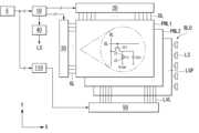
도 1은 본 발명의 실시예에 따른 액정표시장치를 보여 주는 블록도이다.
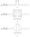
도 2는 도 1에 도시된 표시패널, 광 밸브 패널 및 백라이트 유닛의 적층 구조를 보여 주는 단면도이다.
도 3은 표시패널의 금속 배선들과 광 밸브 패널의 금속 배선들이 겹쳐질 때 초래되는 빛의 간섭으로 인하여 보이는 무아레를 보여 주는 도면이다.
도 4는 표시패널과 광 밸브 패널 간의 갭으로 인하여 발생하는 색(color) 왜곡을 보여 주는 도면이다.
도 5는 측면 시야각의 색 왜곡을 개선하기 위하여 광 밸브 패널에서 밝은 블록과 이웃하는 어두운 블록을 점등할 때 보이는 휘선 불량의 예를 보여 주는 도면이다.
도 6은 표시패널의 픽셀 데이터 변조 방법과 광 밸브 패널의 블록 휘도 제어 방법을 보여 주는 도면들이다.
도 7은 도 6에서 (C)의 제어 방법으로 표시패널의 데이터와 휘도를 제어할 때 측면 시야각에서 픽셀의 휘도를 보여 주는 도면이다.
도 8은 광 밸브 패널을 나타내는 단면도이다.
도 9는 본 발명의 패널 블록 분할을 나타내는 도면이다.
도 10은 본 발명에 의한 광 밸브 패널의 구동전압을 나타내는 도면이다.
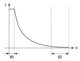
도 11은 광 밸브 패널 액정층의 V-T 특성 곡선을 나타내는 도면이다.
도 12 내지 도 14는 블록 영상 표시과정에서 하부전극의 전압 강하 현상을 설명하는 도면들이다.
도 15 내지 도 16은 본 발명의 공통전압에 의해서 화이트마진을 확보하는 과정을 설명하는 도면들이다.1 is a block diagram showing a liquid crystal display according to an embodiment of the present invention.
FIG. 2 is a cross-sectional view showing a stacked structure of a display panel, a light valve panel, and a backlight unit shown in FIG. 1 .
FIG. 3 is a view showing moire due to light interference caused when metal wires of a display panel and metal wires of a light valve panel overlap each other.
4 is a diagram illustrating color distortion caused by a gap between a display panel and a light valve panel.
5 is a view showing an example of a bright line defect seen when a bright block and a neighboring dark block are turned on in a light valve panel in order to improve color distortion at a side viewing angle.
6 are diagrams illustrating a method of modulating pixel data of a display panel and a method of controlling block luminance of a light valve panel.
FIG. 7 is a diagram showing luminance of a pixel at a side viewing angle when data and luminance of a display panel are controlled by the control method of (C) in FIG. 6 .
8 is a cross-sectional view showing a light valve panel.
9 is a diagram illustrating panel block division according to the present invention.
10 is a diagram showing the driving voltage of the light valve panel according to the present invention.
11 is a diagram showing a VT characteristic curve of a liquid crystal layer of a light valve panel.
12 to 14 are diagrams explaining a voltage drop phenomenon of a lower electrode in a block image display process.
15 to 16 are diagrams explaining a process of securing a white margin by using a common voltage according to the present invention.
이하 첨부된 도면을 참조하여 본 발명에 따른 바람직한 실시예들을 상세히 설명한다. 명세서 전체에 걸쳐서 동일한 참조번호들은 실질적으로 동일한 구성요소들을 의미한다. 이하의 설명에서, 본 발명과 관련된 공지 기능 혹은 구성에 대한 구체적인 설명이 본 발명의 요지를 불필요하게 흐릴 수 있다고 판단되는 경우, 그 상세한 설명을 생략한다.Hereinafter, preferred embodiments according to the present invention will be described in detail with reference to the accompanying drawings. Like reference numbers throughout the specification indicate substantially the same elements. In the following description, if it is determined that a detailed description of a known function or configuration related to the present invention may unnecessarily obscure the subject matter of the present invention, the detailed description will be omitted.
도 1 및 도 2를 참조하면, 본 발명의 액정표시장치는 픽셀 어레이가 형성된 표시패널(PNL1), 표시패널(PNL1)에 빛을 조사하는 백라이트 유닛(BLU), 표시패널(PNL1)과 백라이트 유닛(BLN) 사이에 배치된 광 밸브 패널(PNL2), 제1 패널 구동 회로(100, 20, 30, 100), 제2 패널 구동 회로(110, 50), 백라이트 구동 회로(40)를 포함한다.Referring to FIGS. 1 and 2 , the liquid crystal display of the present invention includes a display panel PNL1 having a pixel array, a backlight unit BLU irradiating light to the display panel PNL1, and the display panel PNL1 and the backlight unit. and a light valve panel PNL2 disposed between (BLN), first
표시패널(PNL1)은 액정층을 사이에 두고 대향하는 제1 상부기판(100) 및 제1 하부기판(110)을 포함한다.The display panel PNL1 includes a first
제1 상부기판(100)에는 블랙 매트릭스(Black matrix, BM)와 컬러 필터(Color filter, CF)를 포함한 컬러 필터 어레이가 형성된다.A color filter array including a black matrix (BM) and color filters (CF) is formed on the first
제1 하부기판(110)에는 데이터라인들(DL), 게이트라인들(GL), 공통 전극(12), TFT에 접속된 픽셀 전극(11), 및 픽셀 전극(11)에 접속된 스토리지 커패시터(Storage Capacitor, Cst) 등이 형성된다. TFT들은 서브 픽셀 마다 하나씩 형성되어 픽셀 전극(11)에 연결된다. TFT들은 비정질 실리콘(amorphose Si, a-Si) TFT, LTPS(Low Temperature Poly Silicon) TFT, 산화물 TFT(Oxide TFT) 등으로 구현될 수 있다. TFT들은 서브 픽셀들의 화소 전극에 1:1로 연결된다. 공통 전극(12)과 픽셀 전극(11)은 절연막을 사이에 두고 분리된다.The first
표시패널(PNL1)의 액정 모드는 TN(Twisted Nematic) 모드와 VA(Vertical Alignment) 모드, IPS(In Plane Switching) 모드, FFS(Fringe Field Switching) 모드 등 공지된 어떠한 액정 모드로도 적용될 수 있다.As the liquid crystal mode of the display panel PNL1, any known liquid crystal mode such as twisted nematic (TN) mode, vertical alignment (VA) mode, in-plane switching (IPS) mode, and fringe field switching (FFS) mode may be applied.
표시패널(PNL1)의 상판과 하판 각각에는 편광 필름(13, 14)이 접착되고, 액정의 선경사각(pretilt angle)을 설정하기 위한 배향막이 형성된다. 상판과 하판 사이에는 액정셀의 셀갭(Cell gap)을 유지하기 위한 스페이서(spacer)가 형성될 수 있다.Polarizing
광 밸브 패널(PNL2)은 표시패널(PNL1)과 백라이트 유닛(BLU) 사이에 배치된다. 광 밸브 패널(PNL2)은 제2 상부기판(200)과 제2 하부기판(210)에 인가되는 전압차에 따라 액정 분자들을 구동하여 표시패널(PNL1)에 조사되는 광량을 조절한다. 광 밸브 패널(PNL2)은 전기적으로 제어되는 액정 분자들을 이용하여 입력 영상에 동기하여 광량을 조절하는 액정 셔터(shutter)이다.The light valve panel PNL2 is disposed between the display panel PNL1 and the backlight unit BLU. The light valve panel PNL2 controls the amount of light irradiated to the display panel PNL1 by driving liquid crystal molecules according to a voltage difference applied to the second
광 밸브 패널(PNL2)의 액정은 TN 모드로 구동될 수 있다. TN 모드에서 액정셀(liquid crystal cell)의 휘도는 노말리 화이트(Normally White)의 투과율 대 전압 커브(transmittance-voltage curve, T-V curve)를 따라 조절된다. 노말리 화이트의 T-V 커브는 전압이 낮을수록 투과율이 높아져 액정셀의 휘도가 높아지고, 전압이 높을수록 투과율이 낮아져 액정셀의 휘도가 낮아진다. 광 밸브 패널(PNL2)의 구조 및 동작에 대한 자세한 설명은 후술하기로 한다.The liquid crystal of the light valve panel PNL2 can be driven in the TN mode. In the TN mode, the luminance of a liquid crystal cell is controlled according to a transmittance-voltage curve (T-V curve) of normally white. In the T-V curve of normal white, the lower the voltage, the higher the transmittance and thus the luminance of the liquid crystal cell, and the higher the voltage, the lower the transmittance and the lower the luminance of the liquid crystal cell. A detailed description of the structure and operation of the light valve panel PNL2 will be described later.
표시패널(PNL1)과 광 밸브 패널(PNL2)은 접착제(23) 예를 들어, OCA(Optical Clear Adhesive)로 접착될 수 있다.The display panel PNL1 and the light valve panel PNL2 may be bonded with an adhesive 23 , for example, optical clear adhesive (OCA).
제1 패널 구동 회로(100, 20, 30)는 입력 영상의 데이터를 픽셀들에 기입한다. 제1 패널 구동 회로(100, 20, 30)는 제1 타이밍 콘트롤러(100), 제1 데이터7 구동부(20) 및 게이트 구동부(30)를 포함한다. 제1 패널 구동 회로(100, 20, 30, 100)는 하나의 IC로 집적될 수 있다.The first
제1 타이밍 콘트롤러(100)는 호스트 시스템(200)으로부터 수신된 입력 영상의 디지털 비디오 데이터를 데이터 구동부(20)로 전송한다. 제1 타이밍 콘트롤러(100)는 입력 영상 데이터와 동기되는 타이밍 신호들을 호스트 시스템(200)으로부터 수신한다. 타이밍 신호들은 수직 동기신호(Vsync), 수평 동기신호(Hsync), 데이터 인에이블 신호(DE), 클럭(CLK) 등을 포함한다. 제1 타이밍 콘트롤러(100)는 입력 영상의 픽셀 데이터와 함께 수신되는 타이밍 신호들(Vsync, Hsync, DE, CLK)을 바탕으로 데이터 구동부(20)와 게이트 구동부(30)의 동작 타이밍을 제어한다. 제1 타이밍 콘트롤러(100)는 픽셀 어레이의 극성을 제어하기 위한 극성제어신호를 제1 데이터 구동부(20)의 소스 드라이브 IC들 각각에 전송할 수 있다.The
제1 데이터 구동부(20)의 출력 채널들은 픽셀 어레이의 데이터 라인들(DL)에 연결된다. 제1 데이터 구동부(20)는 제1 타이밍 콘트롤러(100)로부터 입력 영상의 디지털 비디오 데이터를 수신한다. 제1 데이터 구동부(20)은 제1 타이밍 콘트롤러(100)의 제어 하에 입력 영상의 디지털 비디오 데이터를 정극성/부극성 감마보상전압으로 변환하여 정극성/부극성 데이터전압을 출력한다. 제1 데이터 구동부(20)의 출력 전압은 데이터 라인들(DL)에 공급된다. 제1 데이터 구동부(20)는 타이밍 콘트롤러(100)의 제어 하에 픽셀들에 공급될 데이터 전압의 극성을 반전시킨다.Output channels of the
게이트 구동부(30)는 제1 타이밍 콘트롤러(100)의 제어 하에 게이트 라인들(GL)에 데이터 전압에 동기되는 게이트 펄스를 순차적으로 공급한다. 게이트 구동부(30)로부터 출력된 게이트 펄스는 데이터 라인들(DL)에 공급되는 데이터 전압에 동기된다.The
제2 패널 구동 회로(110, 50)는 입력 영상에 동기하여 광 밸브 패널(PNL2)을 투과하는 광량을 조절함으로써 표시패널(PNL1)에서 재현된 영상의 명암비를 향상시킨다. 제2 패널 구동 회로(110, 50)는 제2 타이밍 콘트롤러(110)와 제2 데이터 구동부(50)를 포함한다. 제2 패널 구동 회로(110, 50)는 하나의 IC로 집적될 수 있다.The second
제2 타이밍 콘트롤러(110)는 입력 영상의 데이터를 제2 데이터 구동부(50)로 전송한다. 제2 타이밍 콘트롤러(110)는 입력 영상 데이터와 동기되는 타이밍 신호들을 호스트 시스템(200)으로부터 수신한다. 타이밍 신호들은 수직 동기신호(Vsync), 수평 동기신호(Hsync), 데이터 인에이블 신호(DE), 클럭(CLK) 등을 포함한다. 제2 타이밍 콘트롤러(110)는 입력 영상의 픽셀 데이터와 함께 수신되는 타이밍 신호들(Vsync, Hsync, DE, CLK)을 바탕으로 데이터 구동부(50)의 동작 타이밍을 제어한다.The
제2 데이터 구동부(50)는 제2 타이밍 콘트롤러(110)로부터 입력 영상의 디지털 비디오 데이터를 입력 받는다. 제2 데이터 구동부(50)는 제2 타이밍 콘트롤러(100)의 제어 하에 입력 영상의 디지털 비디오 데이터를 정극성/부극성 감마보상전압으로 변환하여 정극성/부극성 데이터전압을 출력한다. 제2 데이터 구동부(50)는의 출력 전압은 데이터 라인들(LVL)에 공급된다. 제2 데이터 구동부(50)는 제2 타이밍 콘트롤러(100)의 제어 하에 픽셀들에 공급될 데이터 전압의 극성을 반전시킨다.The
제1 및 제2 패널 구동회로는 다양한 형태로 집적될 수 있다. 예를 들어, 제1 및 제2 타이밍 콘트롤러(100, 110)는 하나의 IC로 집적될 수 있다. 제1 및 제2 패널 구동회로는 하나의 IC 집적 회로로 집적될 수 있다.The first and second panel driving circuits may be integrated in various forms. For example, the first and
백라이트 유닛(BLU)은 직하형(direct type) 백라이트 유닛 또는, 에지형(edge type) 백라이트 유닛으로 구현될 수 있다. 백라이트 유닛은 광원(LS), 도광판(LGP), 광학 시트(OPT) 등을 포함한다. 광원(LS)은 LED(Light Emitting Diode)와 같은 점광원으로 구현될 수 있다. 광원들(LS)은 백라이트 구동부(40)로부터 공급되는 구동 전압에 따라 그 휘도가 독립적으로 조절된다. 광학 시트는 1 매 이상의 프리즘 시트와 1 매 이상의 확산 시트를 포함하여 도광판(LGP)으로부터 입사되는 빛을 확산하고 표시패널(PNL)의 광입사면에 대하여 실질적으로 수직인 각도로 빛의 진행경로를 굴절시킨다.The backlight unit BLU may be implemented as a direct type backlight unit or an edge type backlight unit. The backlight unit includes a light source LS, a light guide plate LGP, an optical sheet OPT, and the like. The light source LS may be implemented as a point light source such as a light emitting diode (LED). The luminance of the light sources LS is independently adjusted according to the driving voltage supplied from the
호스트 시스템(200)은 TV(Television) 시스템, 셋톱박스, 네비게이션 시스템, DVD 플레이어, 블루레이 플레이어, 개인용 컴퓨터(PC), 홈 시어터 시스템, 폰 시스템(Phone system) 중 어느 하나일 수 있다.The
본 발명의 액정표시장치는 도시하지 않은 전원부를 더 포함한다. 전원부는 직류-직류 변환기(DC-DC converter)를 이용하여 표시패널(PNL1)과 광 밸브 패널(PNL2)의 구동에 필요한 전압들을 발생한다. 이 전압들은 고전위 전원전압(VDD), 로직 전원전압(VCC), 감마기준전압, 게이트 하이 전압(VGH), 게이트 로우 전압(VGL), 공통전압(Vcom) 등을 포함한다. 고전위 전원전압(VDD)은 표시패널(PNL1)과 의 픽셀에 충전될 최대 데이터 전압이다. 로직 전원전압(VCC)은 제1 및 제2 패널 구동 회로의 IC 전원 전압이다. 게이트 하이전압(VGH)은 픽셀 어레이의 TFT들의 문턱 전압 이상으로 설정된 게이트 펄스의 하이 논리 전압이고, 게이트 로우전압(VGL)은 픽셀 어레이의 TFT들의 문턱 전압 보다 낮은 전압으로 설정된 게이트 펄스의 로우 논리 전압이다. 게이트 하이 전압(VGH)과 게이트 로우 전압(VGL)은 게이트 구동부(30)에 공급된다. 게이트 펄스는 게이트 하이 전압(VGH)과 게이트 로우 전압(VGL) 사이에서 스윙한다. 공통 전압(Vcom)은 액정셀들(Clc)의 공통전극(12)에 공급된다. 전원부는 고전위 전원전압(VDD)을 분압하여 감마기준전압을 발생한다. 감마기준전압은 데이터 구동부(20) 내의 분압 회로에서 분압되어 계조에 따라 정극성/부극성 감마보상전압으로 나뉘어 진다.The liquid crystal display device of the present invention further includes a power supply unit (not shown). The power supply generates voltages necessary for driving the display panel PNL1 and the light valve panel PNL2 using a DC-DC converter. These voltages include a high potential power supply voltage (VDD), a logic power supply voltage (VCC), a gamma reference voltage, a gate high voltage (VGH), a gate low voltage (VGL), a common voltage (Vcom), and the like. The high potential power supply voltage VDD is the maximum data voltage to be charged in the pixels of the display panel PNL1 and PNL1. The logic power supply voltage VCC is the IC power supply voltage of the first and second panel driving circuits. The gate high voltage VGH is a high logic voltage of a gate pulse set higher than the threshold voltage of TFTs of the pixel array, and the gate low voltage VGL is a low logic voltage of a gate pulse set to a voltage lower than the threshold voltage of TFTs of the pixel array. am. The gate high voltage VGH and the gate low voltage VGL are supplied to the
광 밸브 패널(PNL2)은 픽셀 어레이에 표시되는 입력 영상의 데이터에 동기되어 픽셀들 각각에 조사되는 광량을 정밀하게 제어하여 표시패널(PNL1)에서 재현되는 영상의 명암비를 극대화한다. 이를 도 3을 결부하여 설명하기로 한다.The light valve panel PNL2 maximizes the contrast ratio of the image reproduced on the display panel PNL1 by precisely controlling the amount of light irradiated to each pixel in synchronization with data of the input image displayed on the pixel array. This will be described with reference to FIG. 3 .
표시패널(PNL1)과 광 밸브 패널(PNL2) 각각에는 배선들이 형성되는데, 이러한 배선들이 투명하지 않고 반사율이 높은 금속 배선으로 형성될 수 있다. 금속 배선은 수직 방향의 데이터 라인들과, 수평 방향의 게이트 라인 및 공통 라인(Vcom line)을 포함한다. 공통 라인은 픽셀들의 공통 전극에 연결되어 공통 전압(Vcom)을 공통 전극에 공급한다. 반사율이 높은 금속 배선들은 외부 광을 반사시켜 명암비를 떨어 뜨리므로 그 금속 배선들과 TFT는 블랙 매트릭스 패턴에 의해 가려진다. 이 경우에, 표시패널(PNL1)의 배선들과 광 밸브 패널(PNL2)의 배선들이 겹쳐질 때 도 3과 같이 미스 얼라인(mis-align)되면 빛의 간섭으로 인하여 수직 및 수평 방향의 무아레(Moire) 현상이 발생한다. 이러한 무아레 현상을 감소시키기 위하여 표시패널(PNL1)과 광 밸브 패널(PNL2) 사이에 빛을 확산시키는 확산 시트(diffuser sheet)를 배치할 수 있다. 본 발명은 광 밸브 패널(PNL2)에서 수평 배선을 제거하고, 상하판 전극들과 배선을 투명 전극 물질로 형성함으로써 확산 시트 추가 없이 무아레 현상을 최소화한다.Wires are formed on each of the display panel PNL1 and the light valve panel PNL2, and these wires may be formed of non-transparent metal wires having high reflectivity. The metal wire includes data lines in a vertical direction, and a gate line and a common line (Vcom line) in a horizontal direction. The common line is connected to a common electrode of the pixels to supply a common voltage Vcom to the common electrode. Metal wires with high reflectivity reflect external light and lower the contrast ratio, so the metal wires and TFT are covered by the black matrix pattern. In this case, if the wires of the display panel PNL1 and the wires of the light valve panel PNL2 are misaligned as shown in FIG. 3 when they overlap, the vertical and horizontal moiré ( Moire) phenomenon occurs. In order to reduce the moiré phenomenon, a diffuser sheet for diffusing light may be disposed between the display panel PNL1 and the light valve panel PNL2. In the present invention, the moire phenomenon is minimized without adding a diffusion sheet by removing the horizontal wiring from the light valve panel PNL2 and forming the upper and lower electrodes and wiring with a transparent electrode material.
사용자가 액정표시장치를 정면 시야각에서 바라볼 때 원하는 휘도로 영상을 감상할 수 있지만, 그 액정표시장치를 측면 시야각에서 바라 보면 휘도와 색이 달라질 수 있다. 정면 시야각은 도 4의 중앙 도면과 같이 사용자가 표시패널(PNL1)의 표시면에 대하여 90° 각도에서 바라 볼 때의 각도이다. 측면 시야각은 표시패널(PNL1)의 표시면을 좌측 또는 우측으로 치우친 각도에서 바라볼 때의 시야각이다. 도 4의 예에서 좌측 도면은 좌측 45°시야각이고, 우측 도면은 우측 좌측 45°시야각이다. 특히, 표시패널(PNL1)과 광 밸브 패널(PNL2) 사이에는 소정의 갭(ΔG)이 존재할 수 밖에 없기 때문에 광 밸브 패널(PNL2)을 적용한 액정표시장치는 측면 시야각에서 컬러 왜곡이 더 잘 보일 수 있다. 도 4의 예는 광 밸브 패널(PNL2)에서 백색으로 표시된 픽셀들의 아래의 블록에서만 광이 투과되고 그 이외의 다른 블록들에서 광이 차단된다. 이 경우에, 측면 시야각에서 액정표시장치를 바라 보면 일부 컬러의 휘도가 낮어져 색 왜곡이 보이게 된다. 측면 시야각의 휘도를 개선하기 위하여, 도 5와 같은 방법으로 광 밸브 패널(PNL2)의 휘도를 조절하는 방법을 고려할 수 있다. 도 5는 종래 기술이 아니라는 것에 주의하여야 한다.When a user views the liquid crystal display from a front viewing angle, he or she can enjoy an image with a desired luminance, but when viewing the liquid crystal display from a side viewing angle, the luminance and color may be different. The front viewing angle is an angle when the user views the display surface of the display panel PNL1 at a 90° angle as shown in the central drawing of FIG. 4 . The side viewing angle is a viewing angle when viewing the display surface of the display panel PNL1 from an angle biased to the left or right. In the example of FIG. 4 , the left drawing shows a left 45° viewing angle, and the right drawing shows a right left 45° viewing angle. In particular, since a predetermined gap ΔG inevitably exists between the display panel PNL1 and the light valve panel PNL2, the liquid crystal display to which the light valve panel PNL2 is applied may show color distortion better at a side viewing angle. there is. In the example of FIG. 4 , light is transmitted only in blocks below the pixels displayed in white in the light valve panel PNL2 and light is blocked in other blocks. In this case, when looking at the liquid crystal display from the side viewing angle, the luminance of some colors is lowered, resulting in color distortion. In order to improve the luminance of the side viewing angle, a method of adjusting the luminance of the light valve panel PNL2 may be considered as shown in FIG. 5 . It should be noted that FIG. 5 is not prior art.
도 5는 측면 시야각의 색 왜곡을 개선하기 위하여 광 밸브 패널(PNL2)에서 밝은 블록과 이웃하는 어두운 블록을 점등할 때 보이는 휘선 불량의 예를 보여 주는 도면이다. 밝은 블록은 표시패널(PNL1)에서 밝은 픽셀(이하, "ON 픽셀"이라 함) 아래에 배치되어 그 ON 픽셀에 빛을 조사하는 광 밸브 패널(PNL2)의 블록(이하, "ON 블록"이라 함)을 의미한다. 밝은 픽셀은 화이트 계조와 같은 고계조 데이터가 기입되는 픽셀이다. 표시패널(PNL1)에서 ON 픽셀과 이웃하는 어두운 픽셀(이하, "OFF 픽셀"이라 함) 아래에 배치되는 광 밸브 패널의 블록(이하, "OFF 블록"이라 함)을 의미한다. 어두운 픽셀은 ON 픽셀 보다 낮은 계조 예컨대, 블랙 계조와 같은 저계조 데이터가 기입되는 픽셀이다. 도 5와 같이 ON 블록에 이웃한 OFF 블록들의 휘도를 높이면 측면 시야각에서 RGB 각각의 휘도를 원하는 휘도로 보이게 할 수 있기 때문에 측면 시야각에서 색 왜곡을 개선할 수 있다. OFF 블록들의 휘도를 높이면 OFF 픽셀들의 휘도가 상승하여 정면 시야각에서 OFF 픽셀들의 휘도가 상승할 수 있다. 이러한 정면 시야각에서의 화질 저하를 보상하기 위하여, ON 픽셀에 이웃하는 OFF 픽셀의 데이터 값을 낮추는 변조 방법을 이용하여 OFF 픽셀의 휘도를 낮출 수 있다. 그런데 이 방법은 데이터가 기입된 OFF 픽셀과 원 데이터(Original data)가 기입되는 OFF 픽셀 사이의 경계 부분이 밝게 보이는 휘선 현상이 발생될 수 있다.5 is a view showing an example of a bright line defect seen when a bright block and a neighboring dark block are turned on in the light valve panel PNL2 in order to improve color distortion in a side viewing angle. The bright block is a block (hereinafter referred to as an "ON block") of the light valve panel PNL2 disposed below a bright pixel (hereinafter referred to as an "ON pixel") in the display panel PNL1 and radiating light to the ON pixel. ) means. A bright pixel is a pixel into which high grayscale data such as white grayscale is written. A block of light valve panels (hereinafter referred to as an "OFF block") disposed under a dark pixel (hereinafter referred to as an "OFF pixel") adjacent to an ON pixel in the display panel PNL1. A dark pixel is a pixel to which low grayscale data such as a grayscale lower than that of an ON pixel, for example, a black grayscale, is written. As shown in FIG. 5, if the luminance of the OFF blocks adjacent to the ON block is increased, the luminance of each of the RGBs can be made to appear as a desired luminance at the side viewing angle, and thus color distortion can be improved at the side viewing angle. If the luminance of the OFF blocks is increased, the luminance of the OFF pixels is increased, so that the luminance of the OFF pixels may be increased at a front viewing angle. In order to compensate for the deterioration of the image quality at the front viewing angle, the luminance of the OFF pixel may be reduced by using a modulation method of lowering the data value of the OFF pixel adjacent to the ON pixel. However, this method may cause a bright line phenomenon in which a boundary portion between an OFF pixel in which data is written and an OFF pixel in which original data is written appears bright.
본 발명은 측면 시야각에서 휘도와 색 왜곡을 줄이고 휘선 현상을 방지하기 위하여, 광 밸브 패널(PNL2)에서 ON 블록과 이웃하는 OFF 블록에서 휘도가 점진적으로 변하도록 블록 내에서 전압을 분배함으로써 광 밸브 패널(PNL2)의 휘도를 그러데이션(Gradation) 방법으로 조절한다. 또한, 본 발명은 ON 픽셀과 이웃하는 OFF 픽셀의 계조값을 OFF 블록의 그라데이션 휘도 제어 방법과 반대로 제어할 수 있다.In order to reduce luminance and color distortion at a side viewing angle and prevent a luminance phenomenon, the present invention distributes voltage in a light valve panel PNL2 so that luminance gradually changes in an ON block and an OFF block adjacent thereto, thereby distributing voltage within the light valve panel PNL2. The luminance of (PNL2) is adjusted using a gradation method. In addition, according to the present invention, the gradation value of an OFF pixel adjacent to an ON pixel can be controlled opposite to the gradation luminance control method of the OFF block.
도 6은 표시패널의 픽셀 데이터 변조 방법과 광 밸브 패널의 블록 휘도 제어 방법을 보여 주는 도면들이다. 도 7은 도 6에서 (C)의 제어 방법으로 표시패널의 데이터와 휘도를 제어할 때 측면 시야각에서 픽셀의 휘도를 보여 주는 도면이다.6 are diagrams illustrating a method of modulating pixel data of a display panel and a method of controlling block luminance of a light valve panel. FIG. 7 is a diagram showing luminance of a pixel at a side viewing angle when data and luminance of a display panel are controlled by the control method of (C) in FIG. 6 .
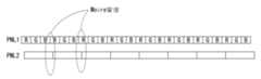
도 6을 참조하면, D1는 ON 픽셀과 그 아래의 ON 블록 위치를 나타낸다. D2 및 D3는 ON 픽셀과 이웃하는 OFF 픽셀과 그 아래의 OFF 블록 위치를 나타낸다.Referring to FIG. 6 , D1 denotes an ON pixel and an ON block position below it. D2 and D3 indicate positions of an OFF pixel adjacent to an ON pixel and an OFF block below it.
도 6의 (A)는 ON 픽셀에만 고계조의 데이터가 기입되고, ON 블록만 높은 휘도로 점등된 예이다. 도 6의 (B)는 측면 시야각을 개선하기 위하여 ON 블록과 이웃하는 OFF 블록의 휘도를 ON 블록만큼 높이고, ON 픽셀과 이웃하는 OFF 픽셀에 기입될 데이터의 계조 값을 낮추는 방법이다.6(A) is an example in which high-grayscale data is written only to ON pixels and only ON blocks are lit with high luminance. 6(B) is a method of increasing the luminance of an OFF block adjacent to an ON block by an amount of the ON block and lowering a gray level value of data to be written in an OFF pixel adjacent to an ON pixel in order to improve a side viewing angle.
도 6의 (C)와 도 7은 측면 시야각과 휘선 불량을 개선하기 위하여 ON 블록과 이웃하는 OFF 블록의 휘도를 ON 블록만큼 높이되, ON 블록으로부터 멀어질수록 점진적으로 낮추는 방법이다. 광 밸브 패널(PNL2)의 블록들 각각은 다수의 픽셀들 아래에 배치되어 그 픽셀들에 빛을 조사한다. 따라서, ON 블록과 이웃하는 OFF 블록 내에서 다수의 OFF 픽셀들이 존재하고, 그 픽셀들의 계조값은 도 6의 (C) 및 도 7과 같이 개별로 조절될 수 있다. 픽셀 데이터의 변조 방법은 도 6의 (C)와 같은 그라데이션 방법이 바람직하지만 이에 한정되지 않는다. 예를 들어, 광 밸브 패널(PNL2)의 휘도는 도 7의 (C)와 같은 그라데이션 방법을 적용하고, 픽셀 데이터의 변조 방법은 도 7의 (B) 또는 (C)와 같은 방법으로 적용될 수 있다.6(C) and 7 show a method in which the luminance of an OFF block adjacent to an ON block is increased by the amount of the ON block, but gradually lowered as the distance from the ON block increases, in order to improve side viewing angle and defective bright lines. Each of the blocks of the light valve panel PNL2 is disposed under a plurality of pixels to radiate light to the pixels. Accordingly, a plurality of OFF pixels exist in an OFF block adjacent to an ON block, and grayscale values of the pixels may be individually adjusted as shown in FIGS. 6(C) and 7 . The method of modulating pixel data is preferably a gradation method as shown in (C) of FIG. 6, but is not limited thereto. For example, a gradation method as shown in FIG. 7(C) may be applied to the luminance of the light valve panel PNL2, and a method as shown in FIG. 7(B) or (C) may be applied as a modulation method of pixel data. .
도 8은 광 밸브 패널의 단면을 나타내는 도면이다.8 is a cross-sectional view of the light valve panel.
도 8을 참조하면, 광 밸브 패널(PNL2)은 제2 상부기판(200) 및 제2 하부기판(210)을 포함한다.Referring to FIG. 8 , the light valve panel PNL2 includes a second
제2 상부기판(200)은 제1 베이스기판(201) 및 제2 전극(203)을 포함한다. 제2 전극(203)은 ITO와 같은 투명 전극 물질로 형성될 수 있다. 상판은 필요에 따라 블랙 매트릭스(BM)를 포함할 수 있다. 이하, 본 명세서에서 제2 전극(203)은 상부전극(203)으로 명칭하기로 한다.The second
제2 하부기판(210)은 제2 베이스기판(211), 광 밸브 데이터라인(LVDL) 및 제1 전극(215)을 포함한다. 이하, 본 명세서에서 제1 전극(215)은 하부전극(215)으로 명칭하기로 한다.The second
하부전극(215)은 ITO와 같은 투명 전극 물질로 형성될 수 있다. 하부전극(215)은 광 밸브 패널(PNL2)의 전면에 걸쳐서 배치된다. 광 밸브 데이터라인(LVDL)은 ITO(Indium-Tin Oxide), IZO(Indium Zinc Oxide)와 같은 투명 전극 물질로 형성된다. 데이터 라인은 무아레(Moire)를 방지하기 위하여 투명 전극으로 형성되는 것이 바람직하나 이에 한정되지 않는다. 데이터 라인은 투명 전극의 저항을 보상하기 위하여 저저항 금속으로 형성될 수도 있다.The
광 밸브 데이터라인(LVDL)들은 하부전극(215)에 연결되어 광 밸브 전압을 직접 공급한다. 따라서, 광 밸브 패널(PNL2)에는 TFT나 게이트 라인(또는 스캔 라인)이 필요 없다. 이로 인하여, 본 발명은 무아레 현상과 휘선을 방지할 수 있을 뿐 아니라 광 밸브 패널(PNL2)의 구조를 단순하게 하여 광 밸브 패널의 제조 공정수를 감소시켜 수율을 높이고 광 밸브 패널(PNL2)을 구동하기 위한 게이트 구동회로를 생략하여 염가의 광 밸브 패널(PNL2)을 구현할 수 있다.The light valve data lines (LVDL) are connected to the
광 밸브 패널(PNL2)의 하판에는 편광 필름(24)이 접착된다. 광 밸브 패널(PNL2)의 하판과 상판 각각에서 액정층과 접하는 면에 배향막이 형성된다. 상판과 하판 사이에는 액정셀의 셀갭(Cell gap)을 유지하기 위한 스페이서(spacer)가 형성될 수 있다.A
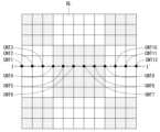
도 9는 본 발명에 의한 광 밸브 패널의 블록 분할을 나타내는 도면이다.9 is a block diagram illustrating block division of a light valve panel according to the present invention.
도 8 및 도 9를 참조하면, 광 밸브 패널(PNL2)의 하부전극은 액티브 영역(AA)과 베젤 영역(Bezel)을 포함하고, 액티브 영역(AA)에는 m
광 밸브 데이터라인들(LVDL)은 서로 평행하고, 액티브 영역(AA) 내에서 수직 방향(y축 방향)으로 배치된다. 각각의 광 밸브 데이터라인(LVDL)은 컨택홀(CNT)을 통해서 블록(BL)들에 연결된다. 컨택홀(CNT)을 통해서 하부 전극에 공급되는 광 밸브 전압은 블록(BL)의 영역으로 분배된다The light valve data lines LVDL are parallel to each other and are disposed in the vertical direction (y-axis direction) within the active area AA. Each light valve data line LVDL is connected to the blocks BL through a contact hole CNT. The light valve voltage supplied to the lower electrode through the contact hole CNT is distributed to the area of the block BL.
광 밸브 데이터 라인(LVDL)들은 픽셀(P)들의 열 방향(y축방향)과 평행하게 수직으로 배열될 수 있다.The light valve data lines LVDL may be vertically arranged parallel to the column direction (y-axis direction) of the pixels P.
도 10은 본 발명에 의한 광 밸브 패널의 구동전압을 나타내는 도면이다.10 is a diagram showing the driving voltage of the light valve panel according to the present invention.
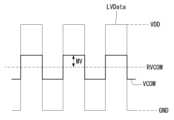
도 10을 참조하면, 광 밸브 데이터전압(LVData)은 일정 간격으로 극성이 반전된다. 이하, 본 명세서에서 광 밸브 데이터전압(LVData)의 극성은 기준공통전압(RVCOM) 보다 큰 전압을 정극성으로 정의하고, 기준공통전압(RVCOM) 보다 작은 전압을 부극성으로 정의한다. 광 밸브 데이터전압(LVData)의 극성이 반전되는 주기는 표시패널(PNL1)의 픽셀(P)에 공급되는 데이터전압의 극성반전 주기와 동기될 수 있다. 광 밸브 데이터전압(LVData)의 크기는 영상데이터를 바탕으로 결정되고, 저전위전압(GND)에서 고전위전압(VDD) 사이의 전압레벨으로 결정될 수 있다.Referring to FIG. 10, the polarity of the light valve data voltage LVData is reversed at regular intervals. Hereinafter, as for the polarity of the light valve data voltage LVData in this specification, a voltage greater than the reference common voltage RVCOM is defined as a positive polarity, and a voltage smaller than the reference common voltage RVCOM is defined as a negative polarity. The polarity inversion cycle of the light valve data voltage LVData may be synchronized with the polarity inversion cycle of the data voltage supplied to the pixel P of the display panel PNL1. The size of the light valve data voltage LVData is determined based on the image data and may be determined as a voltage level between the low potential voltage GND and the high potential voltage VDD.
기준공통전압은 광 밸브 데이터전압(LVData)의 저전위전압(GND)과 고전위전압(VDD)의 평균값을 지칭한다.The reference common voltage refers to an average value of the low potential voltage (GND) and the high potential voltage (VDD) of the light valve data voltage (LVData).
공통전압(VCOM)은 광 밸브 데이터전압(LVData)의 주기와 동기되고, 동일한 위상을 갖도록 스윙한다. 본 명세서에서 공통전압(VCOM)의 극성은 기준공통전압(RVCOM)보다 높은 전압을 정극성으로 정의하고, 기준공통전압(RVCOM)보다 낮은 전압을 부극성으로 정의한다. 공통전압(VCOM)은 기준공통전압(RVCOM)보다 변조전압(MV)만큼 큰 전압레벨을 갖는 정극성의 전압과 기준공통전압(RVCOM)보다 변조전압(MV)만큼 작은 전압레벨을 갖는 부극성의 전압 범위 내에서 스윙한다.The common voltage VCOM is synchronized with the period of the light valve data voltage LVData and swings to have the same phase. In this specification, the polarity of the common voltage VCOM is defined as a positive polarity higher than the reference common voltage RVCOM and a negative polarity lower than the reference common voltage RVCOM. The common voltage VCOM is a positive voltage having a higher voltage level than the reference common voltage RVCOM by the modulation voltage MV and a negative voltage having a lower voltage level than the reference common voltage RVCOM by the modulation voltage MV. Swing within range.
이와 같이, 상부전극(203)에 인가되는 공통전압(VCOM)은 하부전극(215)에 인가되는 광 밸브 데이터전압(LVData)과 동일한 극성으로 스윙됨으로써 화이트로 표현되는 영상 객체의 경계선에서 화상 불량이 발생하는 것을 개선할 수 있다.As such, the common voltage (VCOM) applied to the
본 발명의 실시 예를 정전압의 공통전압(VCOM)이 인가되는 비교예와 더불어 설명하면 다음과 같다.An embodiment of the present invention will be described together with a comparative example in which a common voltage (VCOM) of a constant voltage is applied.
도 11은 광 밸브 패널(PNL2)의 액정층(230)을 구동하는 TN 모드 특성을 나타내는 도면이다. 도 11은 상부전극(203)과 하부전극(215) 간의 차전압(V)에 따른 액정층(230)의 투과율(T)을 나타내고 있다.11 is a diagram showing TN mode characteristics for driving the
도 11을 참조하면, 노말리 화이트의 V-T 커브는 상부전극(203)과 하부전극(215) 간의 전압 차이가 작을수록 투과율이 높아져서 광 밸브 패널(PNL2)의 휘도가 높아지고, 상부전극(203)과 하부전극(215) 간의 전압 차이가 클수록 투과율이 작아져서 광 밸브 패널(PNL2)의 휘도가 낮아진다. 상부전극(203)과 하부전극(215) 간의 전압 차이가 화이트 마진(Ws)에 속할 경우에 광 밸브 패널(PNL2)은 화이트를 표현하고, 블랙 마진(Bs)에 속할 경우에는 광 밸브 패널(PNL2)은 블랙을 표현한다.Referring to FIG. 11, the normal white V-T curve shows that the smaller the voltage difference between the
도 12는 광 밸브 패널의 블록 영상의 일례를 나타내는 도면이다. 도 13은 비교 예에 의한 광 밸브 데이터전압 및 기준공통전압을 나타내는 도면이고, 도 14는 도 13에 도시된 광 밸브 데이터전압을 인가받은 하부전극 블록들의 전압 분포를 나타내는 도면이다. 도 13에 도시된 제1 내지 제12 광 밸브 데이터전압(LVData)은 각각 도 12에서 I-I'에 위치한 제1 내지 제12 컨택홀(CNT1~CNT12)에 인가되는 전압이다. 도 13에 도시된 비교 예에 의한 기준공통전압(RVCOM)은 일정한 정전압을 유지한다는 점에서 본 발명에 의한 공통전압(VCOM)과 차이점이 있다. 도 13은 광 밸브 데이터전압(LVData)의 전압레벨이 기준공통전압(RVCOM) 보다 큰 정극성이 광 밸브 데이터전압(LVData)을 도시하고 있다.12 is a diagram showing an example of a block image of a light valve panel. 13 is a diagram showing a light valve data voltage and a reference common voltage according to a comparative example, and FIG. 14 is a diagram showing a voltage distribution of lower electrode blocks to which the light valve data voltage shown in FIG. 13 is applied. The first to twelfth light valve data voltages LVData shown in FIG. 13 are voltages applied to the first to twelfth contact holes CNT1 to CNT12 located at positions II' in FIG. 12 , respectively. The reference common voltage RVCOM according to the comparative example shown in FIG. 13 is different from the common voltage VCOM according to the present invention in that it maintains a constant constant voltage. FIG. 13 shows the light valve data voltage LVData whose voltage level is greater than the reference common voltage RVCOM.
TN 모드로 동작하는 광 밸브 패널(PNL2)이 도 12와 같은 패턴 영상을 표현하는 과정에서 상부전극에 정전압이 인가되는 비교 예를 살펴보면 다음과 같다.A comparison example in which a constant voltage is applied to the upper electrode in the process of expressing a pattern image as shown in FIG. 12 of the light valve panel PNL2 operating in the TN mode will be described below.
도 12 및 도 13을 참조하면, 화이트를 표시하는 블록에 속한 제1 내지 제3 컨택홀(CNT1~CNT3)에는 기준공통전압(RVCOM)의 크기와 동일하거나 전압차이가 작은 전압이 인가된다. 블랙을 표시하는 블록에 속한 제5 내지 제8 컨택홀(CNT5~CON8)에는 고전위전압(VDD) 또는 이에 가까운 전압이 인가된다. 광 밸브 데이터라인(DLVL)을 통해서 인가되는 전압은 하부전극(215)의 블록(BL)들에 분배된다.Referring to FIGS. 12 and 13 , a voltage having the same magnitude as or a small voltage difference between the reference common voltage RVCOM is applied to the first to third contact holes CNT1 to CNT3 belonging to a block displaying white. A high potential voltage VDD or a voltage close thereto is applied to the fifth to eighth contact holes CNT5 to CON8 belonging to a block displaying black. A voltage applied through the light valve data line DLVL is distributed to the blocks BL of the
상부전극(203)에는 도 10에 도시된 정전압의 기준공통전압(RVCOM)이 인가된다.The reference common voltage RVCOM of the constant voltage shown in FIG. 10 is applied to the
도 13은 광 밸브 데이터라인(DLVL)에 인가되는 전압에 의해서 광 밸브 패널(PNL2)에서 I-I'에 위치한 하부전극(215)의 이상적인 전압분포를 의미한다. 하지만 컨택홀(CNT)들에 인가되는 전압은 하부전극(215)의 면저항으로 인해서 강하되고, 그 결과 I-I'에 위치한 하부전극(215)의 전압 분포는 도 14와 같이 나타난다. 그 결과, 도 14에서와 같이, 화이트를 표시하는 블록(BL)들은 중심영역으로 갈수록 컨택홀(CNT)에 인가되는 전압보다 높은 전압을 갖고, 블랙을 표시하는 블록(BL)들은 중심영역으로 갈수록 컨택홀(CNT)에 인가되는 전압보다 낮은 전압을 갖는다. 이처럼, 하부전극(215)의 전압 분포는 면저항을 배제한 이상적인 전압 분포에 대비하여 전압편차(ΔV1, ΔV2)를 갖는다.13 shows an ideal voltage distribution of the
전압편차(ΔV1, ΔV2)에 의해서 블록(BL)들은 다른 휘도를 표시하게 되지만, 전압편차(ΔV1, ΔV2)가 화이트 마진(Ws) 또는 블랙 마진(Bs)에 속할 때에는 원하는 휘도를 표시할 수 있다. 예컨대, 블랙 전압편차(ΔV2)가 도 11에 도시된 블랙 마진(Bs)에 속할 경우에는 블록(BL)들은 블랙 영상을 표현한다. 또한, 화이트 전압편차(ΔV1)가 도 11에 도시된 화이트 마진(Ws)에 속할 경우에는 블록(BL)들은 화이트 영상을 표현한다.The blocks BL display different luminance according to the voltage deviations ΔV1 and ΔV2, but when the voltage deviations ΔV1 and ΔV2 belong to the white margin (Ws) or the black margin (Bs), the desired luminance can be displayed. . For example, when the black voltage deviation ΔV2 belongs to the black margin Bs shown in FIG. 11, the blocks BL represent a black image. Also, when the white voltage deviation ΔV1 belongs to the white margin Ws shown in FIG. 11, the blocks BL represent a white image.
도 11에서와 같이, TN 모드의 V-T 커브는 블랙 마진(Bs)이 비교적 넓기 때문에 도 14에서와 같이 블랙 전압편차(ΔV2)가 발생하여도 영상의 왜곡이 발생하지 않고 블록(BL)들은 블랙을 표현할 수 있다.As shown in FIG. 11, since the black margin (Bs) of the V-T curve of the TN mode is relatively wide, even if a black voltage deviation (ΔV2) occurs as shown in FIG. 14, image distortion does not occur and the blocks BL are black. can express
하지만, 화이트 마진(Ws)은 블랙 마진(Bs)에 비해서 상당히 좁기 때문에, 화이트 전압편차(ΔV1)가 화이트 마진(Ws)을 벗어나는 경우가 발생한다. 특히, 도 12와 같이 화이트 영상과 블랙 영상의 경계 부분에 인접한 곳에서 화이트를 표시하는 블록(BL)들은 인접 블록(BL)에 인가되는 고전위전압(VDD)의 영향으로 전압 강하가 더 크게 발생한다. 그 결과, 화이트를 표현하여야 하는 블록(BL)들이 그레이(gray)를 표현하는 문제점이 발생한다.However, since the white margin Ws is considerably narrower than the black margin Bs, the white voltage deviation ΔV1 may exceed the white margin Ws. In particular, as shown in FIG. 12, the blocks BLs displaying white adjacent to the boundary between the white image and the black image have a larger voltage drop due to the high potential voltage VDD applied to the adjacent block BL. do. As a result, a problem arises in that blocks BLs that are supposed to express white express gray.
이러한 비교 예에 대비하여, 본 발명에 의한 광 밸브 패널이 화이트 마진을 확보하는 동작을 살펴보면 다음과 같다.In preparation for this comparative example, an operation of the light valve panel according to the present invention to secure a white margin is as follows.
도 15는 공통전압(VCOM)의 전압폭을 기준공통전압(RVCOM)에 대비하여 변조전압(MV)만큼 상승시켰을 경우, TN 모드의 V-T 특성 곡선을 나타내는 도면이다. 도 16은 본 발명에 의한 공통전압에 의해서 하부전극의 전압 강하가 보상되는 원리를 설명하는 모식도이다.15 is a diagram showing a V-T characteristic curve of the TN mode when the voltage width of the common voltage VCOM is increased by the modulation voltage MV compared to the reference common voltage RVCOM. 16 is a schematic diagram explaining the principle of compensating for the voltage drop of the lower electrode by the common voltage according to the present invention.
도 15 및 도 16을 참조하여 본 발명의 V-T 특성 곡선을 살펴보면 다음과 같다.Referring to FIGS. 15 and 16, the V-T characteristic curve of the present invention is as follows.
광 밸브 데이터전압(LVData)이 정극성일 때, 공통전압(VCOM)은 기준공통전압(RVCOM)보다 변조전압(MV)만큼 큰 값을 갖는다.When the light valve data voltage LVData has a positive polarity, the common voltage VCOM has a higher value than the reference common voltage RVCOM by the modulation voltage MV.
상부전극(203)의 전압이 높아지면, 하부전극(215)과 상부전극(203) 간의 전압 차이는 작아지면서, V-T 특성 곡선의 구간은 좌측 방향으로 쉬프트한다. 예컨대, 도 16에서와 같이, 기준공통전압(RVCOM)과의 차전압(V)이 'V1'인 블록(BL)의 전압레벨은 공통전압(VCOM)과의 차전압(V)은 'V2'가 된다. 이처럼, 공통전압(VCOM)이 변조전압(MV)만큼 상승하면, 기준공통전압(RVCOM)을 바탕으로 한 V-T 특성 곡선에서 차전압(V)이 변조전압(MV)의 크기보다 작은 제1 구간(A1)의 차전압(V)은 (-)전압이 된다. 결과적으로, 상부전극(203)의 전압이 변조전압(MV) 크기만큼 상승하면, 하부전극(215)에서 제1 구간(A1)에 속한 V-T 특성 곡선은 제2 구간(A2)에 속한 V-T 특성 곡선에 속한다. 즉, 차전압(V)이 'V1'일 경우에는 화이트 마진(Ws)을 벗어나서 화상 왜곡이 일어날 수 있지만, 본 발명에서와 같이 공통전압(VCOM)이 상승할 때에는 반대 극성 영역의 화이트 마진 범위에 속하기 때문에 화상 왜곡이 발생하지 않는다.When the voltage of the
상부전극(203)의 전압이 변조전압(MV) 크기만큼 상승하면, 하부전극(215)과 상부전극(203) 간의 차전압(V)의 최대값은 고전위전압(VDD)에서 변조전압(MV)을 뺀 값이 된다. 결국, 상부전극(203)의 전압이 변조전압(MV) 크기만큼 상승하면, 제3 구간의 V-T 특성 곡선은 배제된다.When the voltage of the
결과적으로, 상부전극(203)의 전압이 변조전압(MV) 크기만큼 상승할 때, 정극성의 광 밸브 데이터전압(VLData)에 대한 V-T 특성 곡선은 제4 구간에 속한다.As a result, when the voltage of the
광 밸브 데이터전압(LVData)이 부극성일 때, 공통전압(VCOM)은 기준공통전압(RVCOM) 보다 변조전압(MV)만큼 작은 전압을 갖는다.When the light valve data voltage LVData has a negative polarity, the common voltage VCOM has a voltage lower than the reference common voltage RVCOM by the modulation voltage MV.
상부전극(203)의 전압이 낮아지면, 하부전극(215)과 상부전극(203) 간의 전압 차이는 작아지면서, V-T 특성 곡선의 구간은 우측 방향으로 쉬프트한다. 특히, 공통전압(VCOM)이 변조전압(MV)만큼 낮아지면, 기준공통전압(RVCOM)을 바탕으로 한 V-T 특성 곡선에서 차전압(V)이 변조전압(MV)의 크기보다 작은 제2 구간(A2)의 차전압(V)은 (+)전압이 된다. 결과적으로, 상부전극(203)의 전압이 변조전압(MV) 크기만큼 낮아지면, 하부전극(215)에서 제2 구간(A2)에 속한 V-T 특성 곡선은 제1 구간(A1)에 속한 V-T 특성 곡선에 속한다.When the voltage of the
상부전극(203)의 전압이 변조전압(MV) 크기만큼 작은 값일 경우에는, 하부전극(215)과 상부전극(203) 간의 차전압(V)의 최대값은 저전위전압(GND)에서 변조전압(MV)을 더한 값이 된다. 결국, 상부전극(203)의 전압이 변조전압(MV) 크기만큼 상승하면, 제5 구간의 V-T 특성 곡선은 배제된다.When the voltage of the
그 결과, 상부전극(203)의 전압이 변조전압(MV) 크기만큼 상승할 때, 정극성의 광 밸브 데이터전압(LVData)에 대한 V-T 특성 곡선은 제4 구간에 속한다.As a result, when the voltage of the
결과적으로, 정극성의 광 밸브 데이터전압(LVData) 및 부극성의 광 밸브 데이터전압(LVData)에 의한 V-T 특성 곡선은 제4 구간(A4) 및 제6 구간(A6)에 속하게 된다. 그리고, 화이트 마진(Ws)은 기준공통전압(RVCOM)을 변조전압(MV)의 크기만큼 증가한다. 이처럼, 본 발명의 광 밸브 패널(PNL2)은 공통전압(VCOM)을 광 밸브 데이터전압(LVData)과 동일한 위상으로 스윙하여, 화이트 마진(Ws)을 확보할 수 있다. 그 결과 화이트 마진이 부족하여 화이트 영상을 표시하는 블록(BL)에서 화상 불량이 발생하는 것을 개선할 수 있다.As a result, the V-T characteristic curve by the light valve data voltage LVData of positive polarity and the light valve data voltage LVData of negative polarity belongs to the fourth section A4 and the sixth section A6. Also, the white margin Ws increases the reference common voltage RVCOM by the magnitude of the modulation voltage MV. As described above, the light valve panel PNL2 of the present invention swings the common voltage VCOM in the same phase as the light valve data voltage LVData to secure the white margin Ws. As a result, it is possible to improve the occurrence of image defects in the block BL displaying a white image due to insufficient white margin.
한편, 본 발명의 광 밸브 데이터전압(LVData)은 블랙 마진(Bs)이 줄어들지만, 블랙 마진(Bs)의 폭은 화이트 마진(Ws)의 폭에 대비하여 상당히 크기 때문에 블랙 마진(Bs)이 감소하여도 차전압(V)이 블랙 마진(Bs)을 벗어나는 경우가 드물다. 또한, 블랙 마진(Bs)을 벗어나서 블록(BL)이 표시하는 블랙 영상이 왜곡된다고 할지라도 시각적으로 인지되지 않는 수준이어서 화이트 마진(Ws)의 폭을 넓히기 위한 보상 조건으로서 무방하다.Meanwhile, the black margin (Bs) of the light valve data voltage (LVData) of the present invention is reduced, but the black margin (Bs) is reduced because the width of the black margin (Bs) is considerably larger than that of the white margin (Ws). Even so, the difference voltage (V) rarely exceeds the black margin (Bs). In addition, even if the black image displayed by the block BL is distorted beyond the black margin Bs, it is at a level that is not visually recognized, so it is free as a compensation condition for widening the width of the white margin Ws.
본 발명의 광 밸브 패널(PNL2)에서 화이트 마진(Ws)이 증가하는 정도는 공통전압(VCOM)의 변조전압(MV)에 비례한다. 변조전압(MV)의 크기는 기준공통전압(RVCOM)과의 차이와 동일하다. 변조전압(MV)의 크기는 화이트 영상 표시 구간에서 반전이 일어나지 않는 정도로 설정된다. 변조전압(MV)의 크기가 화이트 마진의 전압레벨 폭보다 커지면, V-T 특성 곡선에서 반대 극성 영역에서 화이트 마진을 벗어난다. 따라서, 변조전압(MV)의 크기는 기준공통전압(RVCOM)을 바탕으로 하는 V-T 특성 곡선에서 화이트 마진의 전압 폭 이하로 설정된다. 화이트 마진은 광 밸브 패널의 설계 과정에서 산출될 수 있고, 이를 바탕으로 변조전압(MV)의 크기가 결정될 수 있다.The degree of increase in the white margin (Ws) in the light valve panel (PNL2) of the present invention is proportional to the modulation voltage (MV) of the common voltage (VCOM). The magnitude of the modulation voltage (MV) is equal to the difference from the reference common voltage (RVCOM). The magnitude of the modulation voltage (MV) is set to such an extent that inversion does not occur in the white image display section. When the magnitude of the modulation voltage (MV) is larger than the voltage level width of the white margin, the white margin is out of the range of the opposite polarity in the V-T characteristic curve. Accordingly, the magnitude of the modulation voltage MV is set to be less than or equal to the voltage width of the white margin in the V-T characteristic curve based on the reference common voltage RVCOM. The white margin may be calculated in the process of designing the light valve panel, and based on this, the magnitude of the modulation voltage MV may be determined.
이상 설명한 내용을 통해 당업자라면 본 발명의 기술사상을 일탈하지 아니하는 범위에서 다양한 변경 및 수정이 가능함을 알 수 있을 것이다. 따라서, 본 발명의 기술적 범위는 명세서의 상세한 설명에 기재된 내용으로 한정되는 것이 아니라 특허 청구의 범위에 의해 정하여져야만 할 것이다.Through the above description, those skilled in the art will understand that various changes and modifications are possible without departing from the spirit of the present invention. Therefore, the technical scope of the present invention should not be limited to the contents described in the detailed description of the specification, but should be determined by the claims.
PNL1: 표시패널PNL2: 광 밸브 패널
BLU: 백라이트 유닛100: 제1 타이밍 콘트롤러
110: 제2 타이밍 콘트롤러20: 제1 데이터 구동부
30: 게이트 구동부50: 제2 데이터 구동부
CNT: 컨택홀LVDL: 광 밸브 데이터라인PNL1: Display panel PNL2: Light valve panel
BLU: backlight unit 100: first timing controller
110: second timing controller 20: first data driver
30: gate driver 50: second data driver
CNT: contact hole LVDL: light valve data line
Claims (8)
Translated fromKorean광 밸브 데이터라인을 통해 저전위전압과 고전위전압의 전압 범위 내에서 스윙하는 광 밸브 데이터전압을 인가받는 제1 전극; 및
상기 액정층을 사이에 두고 상기 제1 전극과 대향하고, 상기 광 밸브 데이터전압에 동기되어 동일한 위상으로 스윙하는 공통전압을 인가받는 제2 전극을 포함하고,
상기 공통전압은 상기 저전위전압과 고전위전압의 평균값인 기준공통전압을 기준으로, 상기 기준공통전압보다 소정의 변조전압만큼 큰 전압레벨과 상기 기준공통전압보다 상기 변조전압만큼 작은 전압레벨의 전압 범위 내에서 스윙하는 광 밸브 패널.liquid crystal layer;
a first electrode receiving a light valve data voltage swinging within a voltage range of a low potential voltage and a high potential voltage through a light valve data line; and
a second electrode facing the first electrode with the liquid crystal layer interposed therebetween and receiving a common voltage that swings in the same phase in synchronization with the light valve data voltage;
The common voltage is a voltage having a voltage level higher than the reference common voltage by a predetermined modulation voltage and a voltage level lower than the reference common voltage by the modulation voltage, based on the reference common voltage, which is an average value of the low potential voltage and the high potential voltage. A light valve panel that swings in range.
상기 광 밸브 데이터전압과 상기 공통전압은 상기 기준공통전압 보다 큰 전압레벨의 정극성 전압과 상기 기준공통전압 보다 작은 전압레벨의 부극성 전압 사이에서 스윙하는 광 밸브 패널.According to claim 1,
The light valve data voltage and the common voltage swing between a positive polarity voltage having a voltage level greater than the reference common voltage and a negative polarity voltage having a voltage level smaller than the reference common voltage.
상기 변조전압의 크기는
상기 액정층의 V-T 특성 곡선에서 화이트 마진 보다 크지 않은 광 밸브 패널.According to claim 2,
The magnitude of the modulation voltage is
A light valve panel not greater than a white margin in the VT characteristic curve of the liquid crystal layer.
상기 제2 전극은 단일 전극막으로 이루어지고, 상기 광 밸브 데이터라인을 통해 인가받는 상기 광 밸브 데이터전압을 그라데이션(Gradation)하게 분배하는 광 밸브 패널.According to claim 1,
The second electrode is formed of a single electrode film, and distributes the light valve data voltage applied through the light valve data line in a gradation.
상기 표시패널에 빛을 조사하는 백라이트 유닛; 및
상기 표시패널과 상기 백라이트 유닛 사이에 배치되어 입력 영상에 따라 상기 백라이트 유닛으로부터의 광량을 조절하는 광 밸브 패널을 포함하고,
상기 광 밸브 패널은,
액정층;
광 밸브 데이터라인을 통해 저전위전압과 고전위전압의 전압 범위 내에서 스윙하는 광 밸브 데이터전압을 인가받는 제1 전극; 및
상기 액정층을 사이에 두고 상기 제1 전극과 대향하고, 상기 광 밸브 데이터전압에 동기되어 동일한 위상으로 스윙하는 공통전압을 인가받는 제2 전극을 포함하고,
상기 공통전압은 상기 저전위전압과 고전위전압의 평균값인 기준공통전압을 기준으로, 상기 기준공통전압보다 소정의 변조전압만큼 큰 전압레벨과 상기 기준공통전압보다 상기 변조전압만큼 작은 전압레벨의 전압 범위 내에서 스윙하는 액정표시장치.a display panel on which pixels on which an input image is written are disposed;
a backlight unit irradiating light to the display panel; and
a light valve panel disposed between the display panel and the backlight unit to adjust the amount of light from the backlight unit according to an input image;
The light valve panel,
liquid crystal layer;
a first electrode receiving a light valve data voltage swinging within a voltage range of a low potential voltage and a high potential voltage through a light valve data line; and
a second electrode facing the first electrode with the liquid crystal layer interposed therebetween and receiving a common voltage that swings in the same phase in synchronization with the light valve data voltage;
The common voltage is a voltage having a voltage level higher than the reference common voltage by a predetermined modulation voltage and a voltage level lower than the reference common voltage by the modulation voltage, based on the reference common voltage, which is an average value of the low potential voltage and the high potential voltage. A liquid crystal display that swings within a range.
상기 광 밸브 데이터전압과 상기 공통전압은 상기 기준공통전압 보다 큰 전압레벨의 정극성 전압과 상기 기준공통전압 보다 작은 전압레벨의 부극성 전압 사이에서 스윙하는 액정표시장치.According to claim 5,
The light valve data voltage and the common voltage swing between a positive polarity voltage having a voltage level greater than the reference common voltage and a negative polarity voltage having a voltage level smaller than the reference common voltage.
상기 변조전압의 크기는
상기 액정층의 V-T 특성 곡선에서 화이트 마진 보다 크지 않은 액정표시장치.According to claim 6,
The magnitude of the modulation voltage is
A liquid crystal display device not greater than a white margin in the VT characteristic curve of the liquid crystal layer.
상기 제2 전극은 단일 전극막으로 이루어지고, 상기 광 밸브 데이터라인을 통해 인가받는 상기 광 밸브 데이터전압을 그라데이션(Gradation)하게 분배하는 액정표시장치.According to claim 5,
The second electrode is formed of a single electrode film, and distributes the light valve data voltage applied through the light valve data line in a gradation.
Priority Applications (4)
| Application Number | Priority Date | Filing Date | Title |
|---|---|---|---|
| KR1020160067778AKR102541940B1 (en) | 2016-05-31 | 2016-05-31 | Light valve panel and liquid crystal display device using the same |
| US15/604,929US10490138B2 (en) | 2016-05-31 | 2017-05-25 | Light valve panel and liquid crystal display using the same |
| CN201710391744.4ACN107450203B (en) | 2016-05-31 | 2017-05-27 | Light valve panel and liquid crystal display using the same |
| EP17173485.8AEP3252752B1 (en) | 2016-05-31 | 2017-05-30 | Light valve panel and liquid crystal display using the same |
Applications Claiming Priority (1)
| Application Number | Priority Date | Filing Date | Title |
|---|---|---|---|
| KR1020160067778AKR102541940B1 (en) | 2016-05-31 | 2016-05-31 | Light valve panel and liquid crystal display device using the same |
Publications (2)
| Publication Number | Publication Date |
|---|---|
| KR20170136151A KR20170136151A (en) | 2017-12-11 |
| KR102541940B1true KR102541940B1 (en) | 2023-06-12 |
Family
ID=58873684
Family Applications (1)
| Application Number | Title | Priority Date | Filing Date |
|---|---|---|---|
| KR1020160067778AActiveKR102541940B1 (en) | 2016-05-31 | 2016-05-31 | Light valve panel and liquid crystal display device using the same |
Country Status (4)
| Country | Link |
|---|---|
| US (1) | US10490138B2 (en) |
| EP (1) | EP3252752B1 (en) |
| KR (1) | KR102541940B1 (en) |
| CN (1) | CN107450203B (en) |
Families Citing this family (21)
| Publication number | Priority date | Publication date | Assignee | Title |
|---|---|---|---|---|
| JP6873785B2 (en)* | 2017-03-30 | 2021-05-19 | パナソニック液晶ディスプレイ株式会社 | Liquid crystal display device |
| CN107908042A (en)* | 2017-12-28 | 2018-04-13 | 惠州市华星光电技术有限公司 | Liquid crystal module and liquid crystal display device |
| CN108227320A (en)* | 2018-03-07 | 2018-06-29 | 京东方科技集团股份有限公司 | Display device |
| CN110320723B (en)* | 2018-03-28 | 2023-12-19 | 京东方科技集团股份有限公司 | Display device, display method and display device thereof |
| US11348545B2 (en) | 2018-05-22 | 2022-05-31 | Sony Corporation | Image processing device, display device, and image processing method |
| JP2020052363A (en)* | 2018-09-28 | 2020-04-02 | 株式会社ジャパンディスプレイ | Display device |
| JP2020056807A (en)* | 2018-09-28 | 2020-04-09 | 株式会社ジャパンディスプレイ | Display |
| KR102592143B1 (en)* | 2019-02-22 | 2023-10-23 | 삼성전자주식회사 | Display apparatus and method for driving thereof |
| CN109870859A (en)* | 2019-03-19 | 2019-06-11 | 京东方科技集团股份有限公司 | A display panel, its manufacturing method, and display device |
| CN111785222B (en)* | 2019-04-04 | 2021-05-28 | 海信视像科技股份有限公司 | Contrast lifting algorithm and double-panel display device |
| US11263987B2 (en) | 2019-04-04 | 2022-03-01 | Hisense Visual Technology Co., Ltd. | Method of enhancing contrast and a dual-cell display apparatus |
| US11004406B1 (en)* | 2020-01-05 | 2021-05-11 | Himax Technologies Limited | Dual liquid crystal display device |
| CN113936614B (en)* | 2020-06-29 | 2022-10-04 | 京东方科技集团股份有限公司 | Display panel driving method, driving device, display device and storage medium |
| TWI737420B (en) | 2020-07-27 | 2021-08-21 | 友達光電股份有限公司 | Display apparatus |
| CN114384729B (en) | 2020-10-19 | 2025-04-22 | 京东方科技集团股份有限公司 | Display module and manufacturing method thereof, and display device |
| CN114442385A (en)* | 2020-10-30 | 2022-05-06 | 京东方科技集团股份有限公司 | Display module, display device and control method of display device |
| US11721297B2 (en)* | 2020-11-12 | 2023-08-08 | Beijing Boe Display Technology Co., Ltd. | Display method, display device, and storage medium |
| JP7555303B2 (en)* | 2021-05-21 | 2024-09-24 | 株式会社ジャパンディスプレイ | Display device |
| JP2023000471A (en)* | 2021-06-18 | 2023-01-04 | シャープディスプレイテクノロジー株式会社 | Liquid crystal display device |
| JP7634459B2 (en)* | 2021-10-08 | 2025-02-21 | 株式会社ジャパンディスプレイ | Display device |
| CN115241351A (en)* | 2022-06-15 | 2022-10-25 | Tcl华星光电技术有限公司 | Display panel |
Citations (1)
| Publication number | Priority date | Publication date | Assignee | Title |
|---|---|---|---|---|
| JP2016071337A (en)* | 2014-09-29 | 2016-05-09 | 株式会社ジャパンディスプレイ | Display device |
Family Cites Families (19)
| Publication number | Priority date | Publication date | Assignee | Title |
|---|---|---|---|---|
| CN1220098C (en)* | 2000-04-28 | 2005-09-21 | 夏普株式会社 | Display device, display device driving method, and electronic equipment incorporating display device |
| KR100698048B1 (en)* | 2003-06-26 | 2007-03-23 | 엘지.필립스 엘시디 주식회사 | LCD Display |
| US7916223B2 (en)* | 2006-04-18 | 2011-03-29 | Nec Lcd Technologies, Ltd. | Dual panel liquid crystal display device |
| JP5176194B2 (en)* | 2006-04-18 | 2013-04-03 | Nltテクノロジー株式会社 | Liquid crystal display device and image display system |
| TWI339375B (en)* | 2007-01-29 | 2011-03-21 | Chimei Innolux Corp | Liquid crystal display device and driving method using the same |
| JP5235363B2 (en) | 2007-09-04 | 2013-07-10 | 株式会社ジャパンディスプレイイースト | Liquid crystal display |
| KR20090050857A (en) | 2007-11-16 | 2009-05-20 | 삼성모바일디스플레이주식회사 | LCD and its driving method |
| KR101508719B1 (en)* | 2008-10-06 | 2015-04-03 | 삼성디스플레이 주식회사 | Driving unit and display device having the same |
| US9864243B2 (en)* | 2010-05-14 | 2018-01-09 | Dolby Laboratories Licensing Corporation | High dynamic range displays using filterless LCD(s) for increasing contrast and resolution |
| TWI518652B (en)* | 2010-10-20 | 2016-01-21 | 達意科技股份有限公司 | Electro-phoretic display apparatus |
| JP2015049426A (en)* | 2013-09-03 | 2015-03-16 | パナソニック液晶ディスプレイ株式会社 | Liquid crystal display device |
| JP2016038567A (en) | 2014-08-08 | 2016-03-22 | キヤノン株式会社 | Display device and control method thereof |
| US9753596B2 (en)* | 2014-09-29 | 2017-09-05 | Japan Display Inc. | Display device with display of complementary portion between dark portion and bright portion |
| KR102440113B1 (en)* | 2015-01-02 | 2022-09-05 | 삼성디스플레이 주식회사 | Optical modulatoin device |
| CN105068695A (en)* | 2015-09-11 | 2015-11-18 | 京东方科技集团股份有限公司 | Touch display panel with pressure detection function, display device and driving method |
| KR20170049701A (en)* | 2015-10-27 | 2017-05-11 | 삼성디스플레이 주식회사 | Display apparatus and method of operating the same |
| CN105372884A (en)* | 2015-12-02 | 2016-03-02 | 武汉华星光电技术有限公司 | LCD panel and electronic device using same |
| JP6560610B2 (en)* | 2015-12-18 | 2019-08-14 | 株式会社ジャパンディスプレイ | Display device |
| JP2017167403A (en)* | 2016-03-17 | 2017-09-21 | 株式会社ジャパンディスプレイ | Display device |
- 2016
- 2016-05-31KRKR1020160067778Apatent/KR102541940B1/enactiveActive
- 2017
- 2017-05-25USUS15/604,929patent/US10490138B2/enactiveActive
- 2017-05-27CNCN201710391744.4Apatent/CN107450203B/enactiveActive
- 2017-05-30EPEP17173485.8Apatent/EP3252752B1/enactiveActive
Patent Citations (1)
| Publication number | Priority date | Publication date | Assignee | Title |
|---|---|---|---|---|
| JP2016071337A (en)* | 2014-09-29 | 2016-05-09 | 株式会社ジャパンディスプレイ | Display device |
Also Published As
| Publication number | Publication date |
|---|---|
| CN107450203B (en) | 2020-09-18 |
| EP3252752A3 (en) | 2018-03-21 |
| EP3252752B1 (en) | 2020-07-01 |
| KR20170136151A (en) | 2017-12-11 |
| US20170343839A1 (en) | 2017-11-30 |
| EP3252752A2 (en) | 2017-12-06 |
| CN107450203A (en) | 2017-12-08 |
| US10490138B2 (en) | 2019-11-26 |
Similar Documents
| Publication | Publication Date | Title |
|---|---|---|
| KR102541940B1 (en) | Light valve panel and liquid crystal display device using the same | |
| US10109241B2 (en) | Light valve panel and liquid crystal display using the same | |
| KR102463226B1 (en) | Light valve panel and liquid crystal display device using the same | |
| KR102538750B1 (en) | Liquid crystal display device | |
| CN102460556B (en) | Liquid crystal display device having a plurality of pixel electrodes | |
| KR20130062649A (en) | Liquid crystal display and driving method thereof | |
| CN107710320B (en) | Liquid crystal display device and method for driving liquid crystal display device | |
| US9406270B2 (en) | Liquid crystal display device and method of driving the same | |
| KR102145280B1 (en) | Display apparatus | |
| KR102564463B1 (en) | Light valve panel and liquid crystal display device using the same | |
| KR102270257B1 (en) | Display device and driving method for display device using the same | |
| KR102572965B1 (en) | Display device | |
| US8902143B2 (en) | Liquid crystal display for driving a pixel with a black state and a white state within one frame period, method of driving the same and electronic unit including the same | |
| KR20210026274A (en) | Backlight Unit and Liquid Crystal Display Device using the same | |
| KR102298850B1 (en) | Liquid crystal display device | |
| KR102633411B1 (en) | Back Light Unit and Liquid Crystal Display Device using the same | |
| KR102013378B1 (en) | Liquid crystal display | |
| KR20110036209A (en) | LCD and Local Dimming Control Method | |
| KR102279279B1 (en) | Liquid crystal display and driving method of thereof | |
| KR20170015819A (en) | Light valve panel and liquid crystal display device using the same | |
| KR20120002190A (en) | LCD and its driving method |
Legal Events
| Date | Code | Title | Description |
|---|---|---|---|
| PA0109 | Patent application | Patent event code:PA01091R01D Comment text:Patent Application Patent event date:20160531 | |
| PG1501 | Laying open of application | ||
| PA0201 | Request for examination | Patent event code:PA02012R01D Patent event date:20210413 Comment text:Request for Examination of Application Patent event code:PA02011R01I Patent event date:20160531 Comment text:Patent Application | |
| E902 | Notification of reason for refusal | ||
| PE0902 | Notice of grounds for rejection | Comment text:Notification of reason for refusal Patent event date:20221102 Patent event code:PE09021S01D | |
| E701 | Decision to grant or registration of patent right | ||
| PE0701 | Decision of registration | Patent event code:PE07011S01D Comment text:Decision to Grant Registration Patent event date:20230508 | |
| GRNT | Written decision to grant | ||
| PR0701 | Registration of establishment | Comment text:Registration of Establishment Patent event date:20230605 Patent event code:PR07011E01D | |
| PR1002 | Payment of registration fee | Payment date:20230607 End annual number:3 Start annual number:1 | |
| PG1601 | Publication of registration |