KR102541552B1 - Transistor substrate and organic light emitting display panel and organic light emitting display apparatus using the same - Google Patents
Transistor substrate and organic light emitting display panel and organic light emitting display apparatus using the sameDownload PDFInfo
- Publication number
- KR102541552B1 KR102541552B1KR1020160162108AKR20160162108AKR102541552B1KR 102541552 B1KR102541552 B1KR 102541552B1KR 1020160162108 AKR1020160162108 AKR 1020160162108AKR 20160162108 AKR20160162108 AKR 20160162108AKR 102541552 B1KR102541552 B1KR 102541552B1
- Authority
- KR
- South Korea
- Prior art keywords
- light emitting
- organic light
- gate
- channel
- switching
- Prior art date
- Legal status (The legal status is an assumption and is not a legal conclusion. Google has not performed a legal analysis and makes no representation as to the accuracy of the status listed.)
- Active
Links
Images


Classifications
- H—ELECTRICITY
- H10—SEMICONDUCTOR DEVICES; ELECTRIC SOLID-STATE DEVICES NOT OTHERWISE PROVIDED FOR
- H10D—INORGANIC ELECTRIC SEMICONDUCTOR DEVICES
- H10D86/00—Integrated devices formed in or on insulating or conducting substrates, e.g. formed in silicon-on-insulator [SOI] substrates or on stainless steel or glass substrates
- H10D86/40—Integrated devices formed in or on insulating or conducting substrates, e.g. formed in silicon-on-insulator [SOI] substrates or on stainless steel or glass substrates characterised by multiple TFTs
- H10D86/471—Integrated devices formed in or on insulating or conducting substrates, e.g. formed in silicon-on-insulator [SOI] substrates or on stainless steel or glass substrates characterised by multiple TFTs having different architectures, e.g. having both top-gate and bottom-gate TFTs
- G—PHYSICS
- G09—EDUCATION; CRYPTOGRAPHY; DISPLAY; ADVERTISING; SEALS
- G09F—DISPLAYING; ADVERTISING; SIGNS; LABELS OR NAME-PLATES; SEALS
- G09F9/00—Indicating arrangements for variable information in which the information is built-up on a support by selection or combination of individual elements
- G09F9/30—Indicating arrangements for variable information in which the information is built-up on a support by selection or combination of individual elements in which the desired character or characters are formed by combining individual elements
- G09F9/33—Indicating arrangements for variable information in which the information is built-up on a support by selection or combination of individual elements in which the desired character or characters are formed by combining individual elements being semiconductor devices, e.g. diodes
- H01L27/1251—
- G—PHYSICS
- G09—EDUCATION; CRYPTOGRAPHY; DISPLAY; ADVERTISING; SEALS
- G09G—ARRANGEMENTS OR CIRCUITS FOR CONTROL OF INDICATING DEVICES USING STATIC MEANS TO PRESENT VARIABLE INFORMATION
- G09G3/00—Control arrangements or circuits, of interest only in connection with visual indicators other than cathode-ray tubes
- G09G3/20—Control arrangements or circuits, of interest only in connection with visual indicators other than cathode-ray tubes for presentation of an assembly of a number of characters, e.g. a page, by composing the assembly by combination of individual elements arranged in a matrix no fixed position being assigned to or needed to be assigned to the individual characters or partial characters
- G09G3/22—Control arrangements or circuits, of interest only in connection with visual indicators other than cathode-ray tubes for presentation of an assembly of a number of characters, e.g. a page, by composing the assembly by combination of individual elements arranged in a matrix no fixed position being assigned to or needed to be assigned to the individual characters or partial characters using controlled light sources
- G09G3/30—Control arrangements or circuits, of interest only in connection with visual indicators other than cathode-ray tubes for presentation of an assembly of a number of characters, e.g. a page, by composing the assembly by combination of individual elements arranged in a matrix no fixed position being assigned to or needed to be assigned to the individual characters or partial characters using controlled light sources using electroluminescent panels
- G09G3/32—Control arrangements or circuits, of interest only in connection with visual indicators other than cathode-ray tubes for presentation of an assembly of a number of characters, e.g. a page, by composing the assembly by combination of individual elements arranged in a matrix no fixed position being assigned to or needed to be assigned to the individual characters or partial characters using controlled light sources using electroluminescent panels semiconductive, e.g. using light-emitting diodes [LED]
- G09G3/3208—Control arrangements or circuits, of interest only in connection with visual indicators other than cathode-ray tubes for presentation of an assembly of a number of characters, e.g. a page, by composing the assembly by combination of individual elements arranged in a matrix no fixed position being assigned to or needed to be assigned to the individual characters or partial characters using controlled light sources using electroluminescent panels semiconductive, e.g. using light-emitting diodes [LED] organic, e.g. using organic light-emitting diodes [OLED]
- G09G3/3225—Control arrangements or circuits, of interest only in connection with visual indicators other than cathode-ray tubes for presentation of an assembly of a number of characters, e.g. a page, by composing the assembly by combination of individual elements arranged in a matrix no fixed position being assigned to or needed to be assigned to the individual characters or partial characters using controlled light sources using electroluminescent panels semiconductive, e.g. using light-emitting diodes [LED] organic, e.g. using organic light-emitting diodes [OLED] using an active matrix
- G09G3/3233—Control arrangements or circuits, of interest only in connection with visual indicators other than cathode-ray tubes for presentation of an assembly of a number of characters, e.g. a page, by composing the assembly by combination of individual elements arranged in a matrix no fixed position being assigned to or needed to be assigned to the individual characters or partial characters using controlled light sources using electroluminescent panels semiconductive, e.g. using light-emitting diodes [LED] organic, e.g. using organic light-emitting diodes [OLED] using an active matrix with pixel circuitry controlling the current through the light-emitting element
- G09G3/3241—Control arrangements or circuits, of interest only in connection with visual indicators other than cathode-ray tubes for presentation of an assembly of a number of characters, e.g. a page, by composing the assembly by combination of individual elements arranged in a matrix no fixed position being assigned to or needed to be assigned to the individual characters or partial characters using controlled light sources using electroluminescent panels semiconductive, e.g. using light-emitting diodes [LED] organic, e.g. using organic light-emitting diodes [OLED] using an active matrix with pixel circuitry controlling the current through the light-emitting element the current through the light-emitting element being set using a data current provided by the data driver, e.g. by using a two-transistor current mirror
- G09G3/325—Control arrangements or circuits, of interest only in connection with visual indicators other than cathode-ray tubes for presentation of an assembly of a number of characters, e.g. a page, by composing the assembly by combination of individual elements arranged in a matrix no fixed position being assigned to or needed to be assigned to the individual characters or partial characters using controlled light sources using electroluminescent panels semiconductive, e.g. using light-emitting diodes [LED] organic, e.g. using organic light-emitting diodes [OLED] using an active matrix with pixel circuitry controlling the current through the light-emitting element the current through the light-emitting element being set using a data current provided by the data driver, e.g. by using a two-transistor current mirror the data current flowing through the driving transistor during a setting phase, e.g. by using a switch for connecting the driving transistor to the data driver
- H01L27/1255—
- H01L27/1262—
- H—ELECTRICITY
- H10—SEMICONDUCTOR DEVICES; ELECTRIC SOLID-STATE DEVICES NOT OTHERWISE PROVIDED FOR
- H10D—INORGANIC ELECTRIC SEMICONDUCTOR DEVICES
- H10D86/00—Integrated devices formed in or on insulating or conducting substrates, e.g. formed in silicon-on-insulator [SOI] substrates or on stainless steel or glass substrates
- H10D86/01—Manufacture or treatment
- H10D86/021—Manufacture or treatment of multiple TFTs
- H10D86/0212—Manufacture or treatment of multiple TFTs comprising manufacture, treatment or coating of substrates
- H—ELECTRICITY
- H10—SEMICONDUCTOR DEVICES; ELECTRIC SOLID-STATE DEVICES NOT OTHERWISE PROVIDED FOR
- H10D—INORGANIC ELECTRIC SEMICONDUCTOR DEVICES
- H10D86/00—Integrated devices formed in or on insulating or conducting substrates, e.g. formed in silicon-on-insulator [SOI] substrates or on stainless steel or glass substrates
- H10D86/40—Integrated devices formed in or on insulating or conducting substrates, e.g. formed in silicon-on-insulator [SOI] substrates or on stainless steel or glass substrates characterised by multiple TFTs
- H10D86/481—Integrated devices formed in or on insulating or conducting substrates, e.g. formed in silicon-on-insulator [SOI] substrates or on stainless steel or glass substrates characterised by multiple TFTs integrated with passive devices, e.g. auxiliary capacitors
- H—ELECTRICITY
- H10—SEMICONDUCTOR DEVICES; ELECTRIC SOLID-STATE DEVICES NOT OTHERWISE PROVIDED FOR
- H10D—INORGANIC ELECTRIC SEMICONDUCTOR DEVICES
- H10D86/00—Integrated devices formed in or on insulating or conducting substrates, e.g. formed in silicon-on-insulator [SOI] substrates or on stainless steel or glass substrates
- H10D86/40—Integrated devices formed in or on insulating or conducting substrates, e.g. formed in silicon-on-insulator [SOI] substrates or on stainless steel or glass substrates characterised by multiple TFTs
- H10D86/60—Integrated devices formed in or on insulating or conducting substrates, e.g. formed in silicon-on-insulator [SOI] substrates or on stainless steel or glass substrates characterised by multiple TFTs wherein the TFTs are in active matrices
- H—ELECTRICITY
- H10—SEMICONDUCTOR DEVICES; ELECTRIC SOLID-STATE DEVICES NOT OTHERWISE PROVIDED FOR
- H10K—ORGANIC ELECTRIC SOLID-STATE DEVICES
- H10K59/00—Integrated devices, or assemblies of multiple devices, comprising at least one organic light-emitting element covered by group H10K50/00
- H10K59/10—OLED displays
- H10K59/12—Active-matrix OLED [AMOLED] displays
- H10K59/121—Active-matrix OLED [AMOLED] displays characterised by the geometry or disposition of pixel elements
- H10K59/1213—Active-matrix OLED [AMOLED] displays characterised by the geometry or disposition of pixel elements the pixel elements being TFTs
- H—ELECTRICITY
- H10—SEMICONDUCTOR DEVICES; ELECTRIC SOLID-STATE DEVICES NOT OTHERWISE PROVIDED FOR
- H10K—ORGANIC ELECTRIC SOLID-STATE DEVICES
- H10K59/00—Integrated devices, or assemblies of multiple devices, comprising at least one organic light-emitting element covered by group H10K50/00
- H10K59/10—OLED displays
- H10K59/12—Active-matrix OLED [AMOLED] displays
- H10K59/121—Active-matrix OLED [AMOLED] displays characterised by the geometry or disposition of pixel elements
- H10K59/1216—Active-matrix OLED [AMOLED] displays characterised by the geometry or disposition of pixel elements the pixel elements being capacitors
- H—ELECTRICITY
- H10—SEMICONDUCTOR DEVICES; ELECTRIC SOLID-STATE DEVICES NOT OTHERWISE PROVIDED FOR
- H10K—ORGANIC ELECTRIC SOLID-STATE DEVICES
- H10K59/00—Integrated devices, or assemblies of multiple devices, comprising at least one organic light-emitting element covered by group H10K50/00
- H10K59/10—OLED displays
- H10K59/12—Active-matrix OLED [AMOLED] displays
- H10K59/123—Connection of the pixel electrodes to the thin film transistors [TFT]
- H—ELECTRICITY
- H10—SEMICONDUCTOR DEVICES; ELECTRIC SOLID-STATE DEVICES NOT OTHERWISE PROVIDED FOR
- H10K—ORGANIC ELECTRIC SOLID-STATE DEVICES
- H10K59/00—Integrated devices, or assemblies of multiple devices, comprising at least one organic light-emitting element covered by group H10K50/00
- H10K59/10—OLED displays
- H10K59/12—Active-matrix OLED [AMOLED] displays
- H10K59/124—Insulating layers formed between TFT elements and OLED elements
- H—ELECTRICITY
- H10—SEMICONDUCTOR DEVICES; ELECTRIC SOLID-STATE DEVICES NOT OTHERWISE PROVIDED FOR
- H10K—ORGANIC ELECTRIC SOLID-STATE DEVICES
- H10K59/00—Integrated devices, or assemblies of multiple devices, comprising at least one organic light-emitting element covered by group H10K50/00
- H10K59/10—OLED displays
- H10K59/12—Active-matrix OLED [AMOLED] displays
- H10K59/126—Shielding, e.g. light-blocking means over the TFTs
- H—ELECTRICITY
- H10—SEMICONDUCTOR DEVICES; ELECTRIC SOLID-STATE DEVICES NOT OTHERWISE PROVIDED FOR
- H10K—ORGANIC ELECTRIC SOLID-STATE DEVICES
- H10K59/00—Integrated devices, or assemblies of multiple devices, comprising at least one organic light-emitting element covered by group H10K50/00
- H10K59/10—OLED displays
- H10K59/12—Active-matrix OLED [AMOLED] displays
- H10K59/129—Chiplets
- H—ELECTRICITY
- H10—SEMICONDUCTOR DEVICES; ELECTRIC SOLID-STATE DEVICES NOT OTHERWISE PROVIDED FOR
- H10K—ORGANIC ELECTRIC SOLID-STATE DEVICES
- H10K59/00—Integrated devices, or assemblies of multiple devices, comprising at least one organic light-emitting element covered by group H10K50/00
- H10K59/10—OLED displays
- H10K59/12—Active-matrix OLED [AMOLED] displays
- H10K59/131—Interconnections, e.g. wiring lines or terminals
- G—PHYSICS
- G02—OPTICS
- G02F—OPTICAL DEVICES OR ARRANGEMENTS FOR THE CONTROL OF LIGHT BY MODIFICATION OF THE OPTICAL PROPERTIES OF THE MEDIA OF THE ELEMENTS INVOLVED THEREIN; NON-LINEAR OPTICS; FREQUENCY-CHANGING OF LIGHT; OPTICAL LOGIC ELEMENTS; OPTICAL ANALOGUE/DIGITAL CONVERTERS
- G02F1/00—Devices or arrangements for the control of the intensity, colour, phase, polarisation or direction of light arriving from an independent light source, e.g. switching, gating or modulating; Non-linear optics
- G02F1/01—Devices or arrangements for the control of the intensity, colour, phase, polarisation or direction of light arriving from an independent light source, e.g. switching, gating or modulating; Non-linear optics for the control of the intensity, phase, polarisation or colour
- G02F1/165—Devices or arrangements for the control of the intensity, colour, phase, polarisation or direction of light arriving from an independent light source, e.g. switching, gating or modulating; Non-linear optics for the control of the intensity, phase, polarisation or colour based on translational movement of particles in a fluid under the influence of an applied field
- G02F1/1675—Constructional details
- G02F1/1676—Electrodes
- G—PHYSICS
- G09—EDUCATION; CRYPTOGRAPHY; DISPLAY; ADVERTISING; SEALS
- G09G—ARRANGEMENTS OR CIRCUITS FOR CONTROL OF INDICATING DEVICES USING STATIC MEANS TO PRESENT VARIABLE INFORMATION
- G09G2300/00—Aspects of the constitution of display devices
- G09G2300/04—Structural and physical details of display devices
- G09G2300/0421—Structural details of the set of electrodes
- G09G2300/0426—Layout of electrodes and connections
- G—PHYSICS
- G09—EDUCATION; CRYPTOGRAPHY; DISPLAY; ADVERTISING; SEALS
- G09G—ARRANGEMENTS OR CIRCUITS FOR CONTROL OF INDICATING DEVICES USING STATIC MEANS TO PRESENT VARIABLE INFORMATION
- G09G2300/00—Aspects of the constitution of display devices
- G09G2300/08—Active matrix structure, i.e. with use of active elements, inclusive of non-linear two terminal elements, in the pixels together with light emitting or modulating elements
- G09G2300/0809—Several active elements per pixel in active matrix panels
- G09G2300/0814—Several active elements per pixel in active matrix panels used for selection purposes, e.g. logical AND for partial update
- G—PHYSICS
- G09—EDUCATION; CRYPTOGRAPHY; DISPLAY; ADVERTISING; SEALS
- G09G—ARRANGEMENTS OR CIRCUITS FOR CONTROL OF INDICATING DEVICES USING STATIC MEANS TO PRESENT VARIABLE INFORMATION
- G09G2300/00—Aspects of the constitution of display devices
- G09G2300/08—Active matrix structure, i.e. with use of active elements, inclusive of non-linear two terminal elements, in the pixels together with light emitting or modulating elements
- G09G2300/0809—Several active elements per pixel in active matrix panels
- G09G2300/0842—Several active elements per pixel in active matrix panels forming a memory circuit, e.g. a dynamic memory with one capacitor
- G09G2300/0852—Several active elements per pixel in active matrix panels forming a memory circuit, e.g. a dynamic memory with one capacitor being a dynamic memory with more than one capacitor
- G—PHYSICS
- G09—EDUCATION; CRYPTOGRAPHY; DISPLAY; ADVERTISING; SEALS
- G09G—ARRANGEMENTS OR CIRCUITS FOR CONTROL OF INDICATING DEVICES USING STATIC MEANS TO PRESENT VARIABLE INFORMATION
- G09G2310/00—Command of the display device
- G09G2310/02—Addressing, scanning or driving the display screen or processing steps related thereto
- G09G2310/0243—Details of the generation of driving signals
- G09G2310/0251—Precharge or discharge of pixel before applying new pixel voltage
- G—PHYSICS
- G09—EDUCATION; CRYPTOGRAPHY; DISPLAY; ADVERTISING; SEALS
- G09G—ARRANGEMENTS OR CIRCUITS FOR CONTROL OF INDICATING DEVICES USING STATIC MEANS TO PRESENT VARIABLE INFORMATION
- G09G2310/00—Command of the display device
- G09G2310/02—Addressing, scanning or driving the display screen or processing steps related thereto
- G09G2310/0262—The addressing of the pixel, in a display other than an active matrix LCD, involving the control of two or more scan electrodes or two or more data electrodes, e.g. pixel voltage dependent on signals of two data electrodes
Landscapes
- Engineering & Computer Science (AREA)
- Microelectronics & Electronic Packaging (AREA)
- Physics & Mathematics (AREA)
- General Physics & Mathematics (AREA)
- Theoretical Computer Science (AREA)
- Geometry (AREA)
- Computer Hardware Design (AREA)
- Electroluminescent Light Sources (AREA)
- Devices For Indicating Variable Information By Combining Individual Elements (AREA)
Abstract
Translated fromKoreanDescription
Translated fromKorean본 발명은 트랜지스터 기판 및 이를 이용한 유기발광표시패널과 유기발광표시장치에 관한 것이다.The present invention relates to a transistor substrate, an organic light emitting display panel using the same, and an organic light emitting display device.
휴대전화, 테블릿PC, 노트북 등을 포함한 다양한 종류의 전자제품에는 평판표시장치(FPD: Flat Panel Display)가 이용되고 있다. 평판표시장치에는, 액정표시장치(LCD: Liquid Crystal Display), 유기발광 표시장치(OLED: Organic Light Emitting Display Device) 등이 있으며, 최근에는 전기영동표시장치(EPD: ELECTROPHORETIC DISPLAY)도 널리 이용되고 있다.Flat Panel Displays (FPDs) are used in various types of electronic products, including mobile phones, tablet PCs, and laptop computers. Flat panel displays include Liquid Crystal Displays (LCDs), Organic Light Emitting Displays (OLEDs), and the like, and recently, Electrophoretic Displays (EPDs) are also widely used. .
평판표시장치(이하, 간단히 '표시장치'라 함)들 중에서, 유기발광 표시장치(Organic Light Emitting Display Device)는, 1ms 이하의 고속의 응답속도를 가지며, 소비 전력이 낮기 때문에, 차세대 표시장치로 주목 받고 있다.Among flat panel displays (hereinafter simply referred to as 'display devices'), organic light emitting display devices have a high-speed response speed of 1 ms or less and low power consumption, so they are considered as next-generation display devices. is getting attention
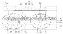
도 1은 종래의 유기발광표시패널의 단면을 나타낸 예시도이며, 도 2는 종래의 유기발광표시패널의 구동 트랜지스터의 게이트-소스 전압과 전류의 관계를 나타낸 그래프이다.1 is an exemplary view showing a cross section of a conventional organic light emitting display panel, and FIG. 2 is a graph showing a relationship between gate-source voltage and current of a driving transistor of a conventional organic light emitting display panel.
종래의 유기발광표시패널은, 도 1에 도시된 바와 같이, 게이트 라인 및 데이터 라인과 연결된 스위칭 트랜지스터(Tsw), 애노드(31)와 발광층(32)과 캐소드(33)로 구성된 유기발광다이오드(30) 및 상기 애노드(31)와 상기 스위칭 트랜지스터(Tsw)에 연결된 구동 트랜지스터(Tdr)를 포함한다. 상기 스위칭 트랜지스터(Tsw)의 제2 전극(16)은 데이터 라인과 연결되고, 제1 전극(16)은 상기 구동 트랜지스터(Tdr)의 게이트(21)와 연결되며, 상기 스위칭 트랜지스터(Tsw)의 게이트(15)는 게이트 라인과 연결된다.As shown in FIG. 1, a conventional organic light emitting display panel includes an organic
상기 구동 트랜지스터(Tdr)의 게이트(21)와 상기 애노드(31) 사이의 스토리지 캐패시턴스의 증가를 위해, 종래의 유기발광표시패널에서는, 게이트 절연막(14) 또는 절연막(19)의 두께가 작게 형성된다. 또한, 종래에는 상기 스토리지 캐패시턴스의 증가를 위해, 도 1에 도시된 바와 같이, 금속(51)이 이용되고 있다.In order to increase the storage capacitance between the
부연하여 설명하면, 상기 스위칭 트랜지스터(Tsw)의 제1 전극(17)과, 상기 애노드(31)와 연결되는 캐패시턴스 전극(41) 사이에는 제1 캐패시턴스(Ca)가 형성되며, 상기 제1 전극(17)과 상기 금속(51) 사이에는 제2 캐패시턴스(Cb)가 형성된다. 상기 제1 캐패시턴스(Ca)와 상기 제2 캐패시턴스(Cb)는, 상기 스토리지 캐패시턴스를 형성한다. 도 1에서, 도면부호 41로 표시되어 있는 두 개의 캐패시턴스 전극(41)은, 도면상에서는 서로 분리되어 있으나, 실질적으로는 전기적으로 연결되어 있다.More specifically, a first capacitance Ca is formed between the
상기 스위칭 트랜지스터(Tsw)의 특성을 향상시키기 위해서는, 상기 게이트 절연막(14)의 두께를 감소시키는 것이 바람직하다. 그러나, 상기 게이트 절연막(14)의 두께가 감소되면, 상기 구동 트랜지스터(Tdr)의 특성이 감소된다.In order to improve the characteristics of the switching transistor Tsw, it is preferable to reduce the thickness of the
예를 들어, 상기 스위칭 트랜지스터(Tsw)의 특성을 향상시키기 위해, 상기 게이트 절연막(14) 또는 상기 절연막(19)의 두께가 작게 형성되면, 도 2에 도시된 바와 같이, 상기 구동 트랜지스터(Tdr)가 턴온되어 전류가 상승하는 구간의 폭(△Vgs)이 매우 좁아진다.For example, if the thickness of the
상기 폭(△Vgs)이 좁아진다는 것은, 컬러의 계조를 표현하는 전압의 폭이 좁아진다는 것을 의미한다. 예를 들어, 상기 폭(△Vgs)에 대응되는 전압들이 256개로 나뉘어져야, 256개의 컬러가 표현될 수 있다.The narrowing of the width (ΔVgs) means that the width of the voltage representing the gradation of color is narrowing. For example, 256 colors can be expressed only when voltages corresponding to the width ΔVgs are divided into 256.
따라서, 상기 게이트 절연막(14)의 두께를 작게 형성하는 것에는 한계가 있다.Therefore, there is a limit to forming the
또한, 상기 스토리지 캐패시턴스의 증가를 위해, 도 1 에 도시된 바와 같이, 상기 캐패시턴스 전극(41) 및 상기 금속(51)이 이용되는 종래의 유기발광표시패널에서는, 상기 캐패시턴스 전극(41) 및 상기 금속(51)을 형성하기 위한 마스크가 추가적으로 요구된다. 또한, 컨택홀들에 의해 상기 캐패시턴스 전극(41)의 면적이 감소하여 스토리지 캐패시턴스의 크기가 감소될 수 있다.In addition, in order to increase the storage capacitance, as shown in FIG. 1 , in a conventional organic light emitting display panel in which the
상술한 문제점을 해결하기 위해 제안된 본 발명의 목적은, 스위칭 트랜지스터의 제1 전극이 구동 트랜지스터의 게이트로 이용되는, 트랜지스터 기판 및 이를 이용한 유기발광표시패널과 유기발광표시장치를 제공하는 것이다.An object of the present invention proposed to solve the above problems is to provide a transistor substrate in which a first electrode of a switching transistor is used as a gate of a driving transistor, an organic light emitting display panel and an organic light emitting display device using the same.
상기한 바와 같은 문제점을 해결하기 위한 본 발명에 따른 트랜지스터 기판은, 기판, 상기 기판에 구비되는 스위칭용 채널, 상기 스위칭용 채널을 구성하는 스위칭용 액티브와 중첩되도록 상기 스위칭용 채널 상에 구비되는 게이트 절연막, 상기 스위칭용 액티브와 중첩되도록 상기 게이트 절연막 상에 구비되는 스위칭용 게이트, 상기 스위칭용 채널과, 상기 게이트 절연막과, 상기 스위칭용 게이트를 커버하는 제1 절연막, 상기 제1 절연막 상에 구비되는 구동용 채널, 상기 구동용 채널 및 상기 제1 절연막을 커버하는 제2 절연막, 상기 스위칭용 채널을 구성하는 제1 도체부에 연결되며, 상기 제2 절연막 상에 구비되는 제1 전극 및 상기 스위칭용 채널을 구성하는 제2 도체부에 연결되며, 상기 제2 절연막 상에 구비되는 제2 전극을 포함한다. 여기서, 상기 스위칭용 채널을 구성하는 상기 제1 도체부는 상기 구동용 채널을 구성하는 구동용 액티브와 중첩되도록 배치된다.A transistor substrate according to the present invention to solve the above problems is a substrate, a switching channel provided on the substrate, and a gate provided on the switching channel so as to overlap with a switching active constituting the switching channel. An insulating film, a switching gate provided on the gate insulating film to overlap with the switching active, a first insulating film covering the switching channel, the gate insulating film, and the switching gate, provided on the first insulating film A driving channel, a second insulating film covering the driving channel and the first insulating film, a first electrode connected to a first conductor part constituting the switching channel, and provided on the second insulating film, and the switching It is connected to the second conductor constituting the channel and includes a second electrode provided on the second insulating film. Here, the first conductor part constituting the switching channel is disposed to overlap the driving active constituting the driving channel.
상기한 바와 같은 문제점을 해결하기 위한 본 발명에 따른 유기발광표시패널은, 상기 트랜지스터 기판, 상기 제1 전극과 상기 제2 전극 및 상기 제2 절연막을 커버하는 보호막 및 상기 보호막에 구비되는 유기발광다이오드를 포함한다.An organic light emitting display panel according to the present invention to solve the above problems is a passivation layer covering the transistor substrate, the first electrode, the second electrode, and the second insulating layer, and an organic light emitting diode provided on the passivation layer. includes
상기한 바와 같은 문제점을 해결하기 위한 본 발명에 따른 유기발광표시장치는, 상기 유기발광표시패널, 상기 유기발광표시패널에 구비된 게이트 라인들로 게이트 펄스를 공급하는 게이트 드라이버, 상기 유기발광표시패널에 구비된 데이터 라인들로 데이터 전압을 공급하는 데이터 드라이버 및 상기 게이트 드라이버와 상기 데이터 드라이버를 제어하는 제어부를 포함한다.An organic light emitting display device according to the present invention to solve the above problems is the organic light emitting display panel, a gate driver supplying gate pulses to gate lines provided in the organic light emitting display panel, and the organic light emitting display panel. and a data driver for supplying data voltages to data lines provided therein and a control unit for controlling the gate driver and the data driver.
본 발명에 의하면, 게이트 절연막의 두께를 감소시키지 않더라도 필요한 스토리지 캐패시턴스가 확보될 수 있다. 이에 따라, 구동 트랜지스터의 게이트-소스 전압(Vgs)과 전류(Ids) 사이의 특성이 향상될 수 있다.According to the present invention, required storage capacitance can be secured without reducing the thickness of the gate insulating layer. Accordingly, a characteristic between the gate-source voltage Vgs and the current Ids of the driving transistor may be improved.
본 발명에 의하면 스위칭 트랜지스터의 제1 전극이 구동 트랜지스터의 게이트로 이용되기 때문에, 대용량의 스토리지 캐패시턴스가 확보될 수 있다.According to the present invention, since the first electrode of the switching transistor is used as the gate of the driving transistor, a large storage capacitance can be secured.
본 발명에 의하면 스위칭 트랜지스터의 제1 전극이 구동 트랜지스터의 게이트로 이용되기 때문에, 컨택홀의 개수가 감소될 수 있으며, 따라서, 스토리지 캐패시턴스가 극대화될 수 있다.According to the present invention, since the first electrode of the switching transistor is used as the gate of the driving transistor, the number of contact holes can be reduced, and thus the storage capacitance can be maximized.
본 발명에 의하면 스위칭 트랜지스터는 탑게이트 방식으로 형성되고, 구동 트랜지스터는 바텀 게이트 방식으로 형성되기 때문에, 구동트랜지스터의 액티브와 게이트 사이의 두께 조절이 가능하며, 이에 따라, 구동 트랜지스터의 구동 전압 및 구동 범위가 증가될 수 있다.According to the present invention, since the switching transistor is formed in a top-gate method and the driving transistor is formed in a bottom-gate method, it is possible to adjust the thickness between the active and gate of the driving transistor, and accordingly, the driving voltage and driving range of the driving transistor. can be increased.
본 발명에 의하면 스위칭용 채널을 구성하는 상기 제1 도체부가, 상기 구동트랜지스터의 게이트, 즉, 구동용 게이트의 기능을 수행할 수 있기 때문에, 컨택홀의 개수가 감소될 수 있다.According to the present invention, since the first conductor part constituting the switching channel can function as a gate of the driving transistor, that is, a gate for driving, the number of contact holes can be reduced.
본 발명에 의하면, 스위칭 트랜지스터를 구성하는 게이트 절연막의 두께와, 구동 트랜지스터를 구성하는 게이트 절연막의 두께가 서로 다르게 형성될 수 있다. 특히, 상기 구동 트랜지스터를 구성하는 게이트 절연막의 두께는 상기 스위칭 트랜지스터를 구성하는 게이트 절연막의 두께보다 크게 형성될 수 있다. 이에 따라, 스위칭 트랜지스터를 구성하는 게이트 절연막의 두께를 감소시키는 것에 의해 스위칭 트랜지스터의 특성이 향상될 수 있으며, 구동 트랜지스터의 게이트 절연막의 두께를 증가시키는 것에 의해 구동 트랜지스터의 게이트-소스 전압(Vgs)과 전류(Ids) 사이의 특성이 향상될 수 있다.According to the present invention, the thickness of the gate insulating film constituting the switching transistor and the thickness of the gate insulating film constituting the driving transistor may be formed to be different from each other. In particular, the thickness of the gate insulating layer constituting the driving transistor may be greater than that of the gate insulating layer constituting the switching transistor. Accordingly, characteristics of the switching transistor may be improved by reducing the thickness of the gate insulating film constituting the switching transistor, and by increasing the thickness of the gate insulating film of the driving transistor, the gate-source voltage (Vgs) and A characteristic between the currents Ids may be improved.
도 1은 종래의 유기발광표시패널의 단면을 나타낸 예시도.
도 2는 종래의 유기발광표시패널의 구동 트랜지스터의 게이트-소스 전압과 전류의 관계를 나타낸 그래프.
도 3은 본 발명에 따른 유기발광표시장치의 구성을 나타낸 예시도.
도 4는 본 발명에 따른 유기발광표시패널에 구비되는 픽셀의 일실시예 구성도.
도 5는 본 발명에 따른 유기발광표시패널의 하나의 픽셀의 단면을 나타낸 예시도.
도 6 내지 도 11은 본 발명에 따른 유기발광표시패널을 제조하는 방법을 설명하기 위한 예시도들.1 is an exemplary view showing a cross section of a conventional organic light emitting display panel;
2 is a graph showing the relationship between gate-source voltage and current of a driving transistor of a conventional organic light emitting display panel;
3 is an exemplary diagram showing the configuration of an organic light emitting display device according to the present invention;
4 is a configuration diagram of an embodiment of a pixel included in an organic light emitting display panel according to the present invention.
5 is an exemplary view showing a cross-section of one pixel of an organic light emitting display panel according to the present invention;
6 to 11 are exemplary views for explaining a method of manufacturing an organic light emitting display panel according to the present invention.
본 발명의 이점 및 특징, 그리고 그것들을 달성하는 방법은 첨부되는 도면과 함께 상세하게 후술되어 있는 실시 예들을 참조하면 명확해질 것이다. 그러나 본 발명은 이하에서 개시되는 실시 예들에 한정되는 것이 아니라 서로 다른 다양한 형태로 구현될 것이며, 단지 본 실시 예들은 본 발명의 개시가 완전하도록 하며, 본 발명이 속하는 기술 분야에서 통상의 지식을 가진 자에게 발명의 범주를 완전하게 알려주기 위해 제공되는 것이며, 본 발명은 청구항의 범주에 의해 정의될 뿐이다.Advantages and features of the present invention, and methods for achieving them, will become clear with reference to the embodiments described below in detail in conjunction with the accompanying drawings. However, the present invention is not limited to the embodiments disclosed below, but will be implemented in a variety of different forms, only the present embodiments make the disclosure of the present invention complete, and those skilled in the art in the art to which the present invention belongs It is provided to fully inform the person of the scope of the invention, and the invention is only defined by the scope of the claims.
본 명세서에서 각 도면의 구성요소들에 참조번호를 부가함에 있어서 동일한 구성 요소들에 한해서는 비록 다른 도면상에 표시되더라도 가능한 한 동일한 번호를 가지도록 하고 있음에 유의하여야 한다.In this specification, it should be noted that in adding reference numerals to components of each drawing, the same components have the same numbers as much as possible, even if they are displayed on different drawings.
본 발명의 실시 예를 설명하기 위한 도면에 개시된 형상, 크기, 비율, 각도, 개수 등은 예시적인 것이므로 본 발명이 도시된 사항에 한정되는 것은 아니다. 명세서 전체에 걸쳐 동일 참조 부호는 동일 구성 요소를 지칭한다. 또한, 본 발명을 설명함에 있어서, 관련된 공지 기술에 대한 구체적인 설명이 본 발명의 요지를 불필요하게 흐릴 수 있다고 판단되는 경우 그 상세한 설명은 생략한다. 본 명세서 상에서 언급한 '포함한다', '갖는다', '이루어진다' 등이 사용되는 경우 '~만'이 사용되지 않는 이상 다른 부분이 추가될 수 있다. 구성 요소를 단수로 표현한 경우에 특별히 명시적인 기재 사항이 없는 한 복수를 포함하는 경우를 포함한다.Since the shape, size, ratio, angle, number, etc. disclosed in the drawings for explaining the embodiment of the present invention are exemplary, the present invention is not limited to the matters shown. Like reference numbers designate like elements throughout the specification. In addition, in describing the present invention, if it is determined that a detailed description of related known technologies may unnecessarily obscure the subject matter of the present invention, the detailed description will be omitted. When 'includes', 'has', 'consists of', etc. mentioned in this specification is used, other parts may be added unless 'only' is used. In the case where a component is expressed in the singular, the case including the plural is included unless otherwise explicitly stated.
구성 요소를 해석함에 있어서, 별도의 명시적 기재가 없더라도 오차 범위를 포함하는 것으로 해석한다.In interpreting the components, even if there is no separate explicit description, it is interpreted as including the error range.
위치 관계에 대한 설명일 경우, 예를 들어, '~상에', '~상부에', '~하부에', '~옆에' 등으로 두 부분의 위치 관계가 설명되는 경우, '바로' 또는 '직접'이 사용되지 않는 이상 두 부분 사이에 하나 이상의 다른 부분이 위치할 수도 있다.In the case of a description of a positional relationship, for example, 'on top of', 'on top of', 'at the bottom of', 'next to', etc. Or, unless 'directly' is used, one or more other parts may be located between the two parts.
시간 관계에 대한 설명일 경우, 예를 들어, '~후에', '~에 이어서', '~다음에', '~전에' 등으로 시간적 선후 관계가 설명되는 경우, '바로' 또는 '직접'이 사용되지 않는 이상 연속적이지 않은 경우도 포함할 수 있다.In the case of a description of a temporal relationship, for example, 'immediately' or 'directly' when a temporal precedence relationship is described in terms of 'after', 'following', 'next to', 'before', etc. It can also include non-continuous cases unless is used.
‘적어도 하나’의 용어는 하나 이상의 관련 항목으로부터 제시 가능한 모든 조합을 포함하는 것으로 이해되어야 한다. 예를 들어, ‘제1 항목, 제 2 항목 및 제 3 항목 중에서 적어도 하나’의 의미는 제1 항목, 제 2 항목 또는 제 3 항목 각각 뿐만 아니라 제1 항목, 제 2 항목 및 제 3 항목 중에서 2개 이상으로부터 제시될 수 있는 모든 항목의 조합을 의미한다.The term 'at least one' should be understood to include all conceivable combinations from one or more related items. For example, 'at least one of the first item, the second item, and the third item' means not only the first item, the second item, or the third item, but also two of the first item, the second item, and the third item. It means a combination of all items that can be presented from one or more.
제1, 제2 등이 다양한 구성요소들을 서술하기 위해서 사용되나, 이들 구성요소들은 이들 용어에 의해 제한되지 않는다. 이들 용어들은 단지 하나의 구성 요소를 다른 구성요소와 구별하기 위하여 사용하는 것이다. 따라서, 이하에서 언급되는 제1 구성요소는 본 발명의 기술적 사상 내에서 제2 구성요소일 수도 있다.Although first, second, etc. are used to describe various components, these components are not limited by these terms. These terms are only used to distinguish one component from another. Therefore, the first component mentioned below may also be the second component within the technical spirit of the present invention.
본 발명의 여러 실시 예들의 각각 특징들이 부분적으로 또는 전체적으로 서로 결합 또는 조합 가능하고, 기술적으로 다양한 연동 및 구동이 가능하며, 각 실시 예들이 서로에 대하여 독립적으로 실시 가능할 수도 있고 연관 관계로 함께 실시할 수도 있다.Each feature of the various embodiments of the present invention can be partially or entirely combined or combined with each other, technically various interlocking and driving are possible, and each embodiment can be implemented independently of each other or can be implemented together in an association relationship. may be
이하, 첨부된 도면을 참조하여 본 발명의 실시 예가 상세히 설명된다.Hereinafter, embodiments of the present invention will be described in detail with reference to the accompanying drawings.
도 3은 본 발명에 따른 유기발광표시장치의 구성을 나타낸 예시도이며, 도 4는 본 발명에 따른 유기발광표시패널에 구비되는 픽셀의 일실시예 구성도이다.3 is an exemplary diagram showing the configuration of an organic light emitting display device according to the present invention, and FIG. 4 is a configuration diagram of an embodiment of pixels included in the organic light emitting display panel according to the present invention.
본 발명에 따른 유기발광표시장치는, 도 3에 도시된 바와 같이, 게이트 라인들(GL1 to GLg)과 데이터 라인들(DL1 to DLd)에 의해 정의되는 픽셀(110)들이 형성되어 있으며 영상이 출력되는 본 발명에 따른 유기발광표시패널(100), 상기 유기발광표시패널(100)에 구비된 상기 게이트 라인들(GL1 to GLg)에 순차적으로 게이트 펄스를 공급하는 게이트 드라이버(200), 상기 유기발광표시패널(100)에 구비된 상기 데이터 라인들(DL1 to DLd)로 데이터 전압을 공급하는 데이터 드라이버(300) 및 상기 게이트 드라이버(200)와 상기 데이터 드라이버(300)를 제어하는 제어부(400)를 포함한다.As shown in FIG. 3 , the organic light emitting display device according to the present invention has
우선, 상기 유기발광표시패널(100)은 게이트 펄스가 공급되는 상기 게이트 라인들(GL1 to GLg), 데이터 전압이 공급되는 상기 데이터 라인들(DL1 to DLd) 및 상기 게이트 라인들(GL1 to GLg)과 상기 데이터 라인들(Dl1 to DLd)에 의해 정의되는 픽셀(110)들을 포함하며, 상기 픽셀들 각각에는 박막트랜지스터(이하, 간단히 트랜지스터라 함)가 적어도 하나 구비된다.First, the organic light emitting
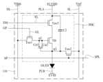
상기 유기발광표시패널(100)에 구비된 상기 픽셀(110)들 각각은, 도 4에 도시된 바와 같이, 광을 출력하는 유기발광다이오드(OLED) 및 상기 유기발광다이오드(OLED)를 구동하는 픽셀 구동부(PDC)를 포함한다. 상기 픽셀(110)들 각각에는, 상기 픽셀구동부(PDC)에 구동 신호를 공급하는 신호 라인들(DL, EL, GL, PLA, PLB, SL, SPL)이 형성되어 있다.As shown in FIG. 4 , each of the
상기 데이터 라인(DL)으로는 데이터 전압(Vdata)이 공급되고, 상기 게이트 라인(GL)으로는 게이트 펄스(GP)가 공급되고, 전원공급라인(PLA)으로는 제1 구동 전원(EVDD)이 공급되고, 구동전원라인(PLB)으로는 제2 구동 전원(EVSS)이 공급되고, 센싱 라인(SL)으로는 기준전압(Vref)이 공급되고, 센싱 펄스 라인(SPL)으로는 센싱 트랜지스터(Tsw2)를 턴온 또는 턴오프시키는 센싱 펄스(SP)가 공급되며, 에미션라인(EL)으로는 에미션 트랜지스터(Tsw3)를 구동시키기 위한 에미션 제어 신호(EM)가 공급된다.A data voltage Vdata is supplied to the data line DL, a gate pulse GP is supplied to the gate line GL, and a first driving voltage EVDD is supplied to the power supply line PLA. The second driving power supply EVSS is supplied to the driving power line PLB, the reference voltage Vref is supplied to the sensing line SL, and the sensing transistor Tsw2 is supplied to the sensing pulse line SPL. ) is supplied to turn on or off, and the emission control signal EM for driving the emission transistor Tsw3 is supplied to the emission line EL.
상기 픽셀구동부(PDC)는, 예를 들어, 도 4에 도시된 바와 같이, 게이트 라인(GL) 및 데이터 라인(DL)과 연결된 스위칭 트랜지스터(Tsw1), 상기 스위칭 트랜지스터(Tsw1)를 통해 전송된 데이터 전압(Vdata)에 따라, 상기 유기발광다이오드(OLED)로 출력되는 전류의 크기를 제어하는 구동 트랜지스터(Tdr), 상기 구동 트랜지스터(Tdr)의 특성을 감지하기 위한 상기 센싱 트랜지스터(Tsw2) 및 상기 구동 트랜지스터(Tdr)의 발광 시점을 제어하기 위한 상기 에미션 트랜지스터(Tsw3)를 포함할 수 있다.As shown in FIG. 4 , the pixel driver PDC includes, for example, a switching transistor Tsw1 connected to a gate line GL and a data line DL, and data transmitted through the switching transistor Tsw1. The driving transistor Tdr controls the amount of current output to the organic light emitting diode OLED according to the voltage Vdata, the sensing transistor Tsw2 detects the characteristic of the driving transistor Tdr, and the driving transistor Tsw2. The emission transistor Tsw3 for controlling the emission timing of the transistor Tdr may be included.
상기 구동 트랜지스터(Tdr)의 게이트와 상기 유기발광다이오드(OLED)의 애노드 사이에는 스토리지 캐패시턴스(Cst)가 형성된다. 상기 스토리지 캐패시턴스(Cst)는 제1 캐패시턴스라고 한다.A storage capacitance Cst is formed between the gate of the driving transistor Tdr and the anode of the organic light emitting diode OLED. The storage capacitance Cst is referred to as a first capacitance.
상기 에미션 트랜지스터의 단자들 중 상기 제1 구동전원이 공급되는 단자와, 상기 유기발광다이오드(OLED)의 애노드 사이에는 제2 캐패시턴스(C2)가 형성된다.A second capacitance C2 is formed between a terminal of the emission transistor to which the first driving power is supplied and an anode of the organic light emitting diode (OLED).
상기 스위칭 트랜지스터(Tsw1)는 상기 게이트 라인(GL)으로 공급되는 게이트 펄스에 의해 턴온되어, 상기 데이터 라인(DL)으로 공급되는 데이터 전압(Vdata)을 상기 구동 트랜지스터(Tdr)의 게이트로 전송한다.The switching transistor Tsw1 is turned on by a gate pulse supplied to the gate line GL, and transmits the data voltage Vdata supplied to the data line DL to the gate of the driving transistor Tdr.
상기 센싱 트랜지스터(Tsw2)는 상기 구동 트랜지스터(Tdr)와 상기 유기발광다이오드(OLED) 사이의 제1노드(n1) 및 상기 센싱 라인(SL)에 연결되어, 센싱 펄스(SP)에 의해 턴온 또는 턴오프되며, 센싱 기간에, 상기 구동 트랜지스터의 특성을 감지한다.The sensing transistor Tsw2 is connected to a first node n1 between the driving transistor Tdr and the organic light emitting diode OLED and to the sensing line SL, and is turned on or turned on by a sensing pulse SP. is turned off, and during the sensing period, the characteristics of the driving transistor are sensed.
상기 구동 트랜지스터(Tdr)의 게이트와 연결된 제2노드(n2)는 상기 스위칭 트랜지스터(Tsw1)와 연결된다. 상기 제2노드(n2)와 상기 제1노드(n1) 사이에는 스토리지 캐패시턴스(Cst)가 형성된다. 상기 스토리지 캐패시턴스(Cst)가 커질수록, 상기 구동 트랜지스터(Tdr)의 구동 특성이 향상될 수 있다.A second node n2 connected to the gate of the driving transistor Tdr is connected to the switching transistor Tsw1. A storage capacitance Cst is formed between the second node n2 and the first node n1. As the storage capacitance Cst increases, driving characteristics of the driving transistor Tdr may improve.
상기 에미션 트랜지스터(Tsw3)는 상기 에미젼 제어 신호(EM)에 따라, 상기 제1 구동 전원(EVDD)을 상기 구동 트랜지스터(Tdr)로 전달하거나, 상기 제1 구동 전원(EVDD)을 차단한다. 상기 에미션 트랜지스터(Tsw3)가 턴온될 때, 상기 구동 트랜지스터(Tdr)로 전류가 공급되어, 상기 유기발광다이오드로부터 광이 출력된다.The emission transistor Tsw3 transmits the first driving power source EVDD to the driving transistor Tdr or blocks the first driving power source EVDD according to the emission control signal EM. When the emission transistor Tsw3 is turned on, current is supplied to the driving transistor Tdr, and light is output from the organic light emitting diode.
상기 픽셀구동부(PDC)는, 도 4에 도시된 구조 이외에도, 다양한 구조로 형성될 수 있다.The pixel driver PDC may be formed in various structures other than the structure shown in FIG. 4 .
상기 픽셀 구동부(PDC)에 구비되는 상기 트랜지스터들은 산화물 박막트랜지스터들이될 수 있다.The transistors included in the pixel driver PDC may be oxide thin film transistors.
상기 트랜지스터는 상기 픽셀들이 구비되어 있는 표시영역의 외곽의 비표시영역에도 구비될 수 있다. 예를 들어, 상기 게이트 드라이버(200)가 상기 유기발광표시패널(100)의 상기 비표시영역에 내장되어 있는 경우, 상기 게이트 드라이버(200)를 구성하는 트랜지스터들 역시 상기 산화물 박막트랜지스터로 구성될 수 있다.The transistor may also be provided in a non-display area outside the display area where the pixels are provided. For example, when the
따라서, 상기 유기발광표시패널에 구비되는 모든 트랜지스터들이 동일한 공정을 통해 생성될 수 있다.Accordingly, all transistors included in the organic light emitting display panel may be produced through the same process.
다음, 상기 제어부(400)는 외부 시스템으로부터 공급되는 타이밍 신호, 예를 들어, 수직 동기신호, 수평 동기신호 및 클럭 등을 이용하여, 상기 게이트 드라이버(200)를 제어하기 위한 게이트 제어신호(GCS)와, 상기 데이터 드라이버(300)를 제어하기 위한 데이터 제어신호(DCS)를 출력한다. 상기 제어부(400)는 상기 외부 시스템으로부터 입력되는 입력영상데이터를 샘플링한 후에 이를 재정렬하여, 재정렬된 디지털 영상데이터(Data)를 상기 데이터 드라이버(300)에 공급한다.Next, the
다음, 상기 데이터 드라이버(300)는 상기 제어부(400)로부터 입력된 상기 영상데이터(Data)를 아날로그 데이터 전압으로 변환하여, 상기 게이트 라인(GL)에 상기 게이트 펄스(GP)가 공급되는 1수평기간마다 1수평라인분의 데이터 전압(Vdata)들을 상기 데이터 라인들(DL1 to DLd)로 전송한다.Next, the
마지막으로, 상기 게이트 드라이버(200)는 상기 제어부(400)로부터 입력되는 상기 게이트 제어신호에 응답하여 상기 유기발광표시패널(100)의 상기 게이트 라인들(GL1 to GLg)로 게이트 펄스를 순차적으로 공급한다. 이에 따라, 상기 게이트 펄스가 입력되는 각각의 픽셀에 형성되어 있는 트랜지스터들이 턴온되어, 각 픽셀(110)로 영상이 출력될 수 있다. 상기 게이트 드라이버(200)는, 상기 유기발광표시패널(100)과 독립되게 형성되어, 다양한 방식으로 상기 유기발광표시패널(100)과 전기적으로 연결될 수 있는 형태로 구성될 수 있으나, 상기 유기발광표시패널(100) 내에 실장되어 있는 게이트 인 패널(Gate In Panel : GIP) 방식으로 구성될 수도 있다.Finally, the
상기 설명에서는, 상기 데이터 드라이버(300), 상기 게이트 드라이버(200) 및 상기 제어부(400)가 독립적으로 구성된 것으로 설명되었으나, 상기 데이터 드라이버(300) 또는 상기 게이트 드라이버(200)들 중 적어도 어느 하나는 상기 제어부(400)와 일체로 구성될 수도 있다.In the above description, the
도 5는 본 발명에 따른 유기발광표시패널의 하나의 픽셀의 단면을 나타낸 예시도이다.5 is an exemplary view showing a cross-section of one pixel of the organic light emitting display panel according to the present invention.
본 발명에 따른 유기발광표시패널(100)은, 도 5에 도시된 바와 같이, 기판(101), 스위칭용 채널(119), 구동용 채널(129), 게이트 절연막(103), 스위칭용 게이트(114), 제1 절연막(104), 차단막(126), 제2 절연막(105), 제1 전극(141), 제2 전극(142), 제3 전극(143), 제4 전극(144), 보호막(106) 및 유기발광다이오드(OLED)를 포함한다. 이하에서 설명된 본 발명에 따른 유기발광표시패널 중, 상기 보호막(106)과 상기 유기발광다이오드(OLED)가 제외되면, 본 발명에 따른 트랜지스터 기판이 형성될 수 있다. 즉, 본 발명에 따른 트랜지스터 기판은, 도 5에 도시된 구성요소들 중, 상기 기판(101), 상기 스위칭용 채널(119), 상기 구동용 채널(129), 상기 게이트 절연막(103), 상기 스위칭용 게이트(114), 상기 제1 절연막(104), 상기 차단막(126), 상기 제2 절연막(105), 상기 제1 전극(141), 상기 제2 전극(142), 상기 제3 전극(143) 및 상기 제4 전극(144)을 포함한다. 따라서, 본 발명에 따른 트랜지스터 기판에 대해서는 별도로 설명되지 않는다.As shown in FIG. 5 , the organic light emitting
우선, 상기 기판(101)은 유리기판이 될 수도 있으며, 플라스틱기판이 될 수도 있다.First, the
다음, 상기 스위칭용 채널(119)이 구비되기 전에, 상기 기판(101)에는 버퍼(102)가 구비될 수 있다. 상기 버퍼(102)는 유기물 또는 무기물로 형성될 수 있다.Next, before the switching
다음, 상기 스위칭용 채널(119)은 상기 기판(101) 또는 상기 버퍼(102) 상에 구비될 수 있다. 상기 스위칭용 채널(119)은 산화물 반도체로 형성된 스위칭용 액티브(113), 상기 스위칭용 액티브(113)의 양측 끝단에 구비되는 제1 도체부(111) 및 제2 도체부(112)를 포함한다.Next, the switching
상기 스위칭용 채널(119)을 구성하는 상기 제1 도체부(111)는 상기 구동용 채널(129)을 구성하는 구동용 액티브(123)와 중첩되도록 배치된다. 따라서, 상기 스위칭용 채널(119)을 구성하는 상기 제1 도체부(111)는, 상기 구동트랜지스터(Tdr)의 게이트, 즉, 상기 구동용 게이트의 기능을 수행할 수 있다. 따라서, 본 발명에 의하면, 컨택홀의 개수가 감소될 수 있다.The
다음, 상기 게이트 절연막(103)은 상기 스위칭용 채널(119)을 구성하는 스위칭용 액티브(113)와 중첩되도록 상기 스위칭용 채널(119) 상에 구비된다. 상기 게이트 절연막(103)은 유기물 또는 무기물로 형성될 수 있다.Next, the
다음, 상기 스위칭용 게이트(114)는 상기 스위칭용 액티브(113)와 중첩되도록 상기 게이트 절연막(103) 상에 구비된다.Next, the switching
다음, 상기 스위칭용 채널(119)과, 상기 게이트 절연막(103)과, 상기 스위칭용 게이트(114)는 상기 제1 절연막(104)에 의해 커버된다.Next, the switching
상기 게이트 절연막(103)과, 상기 제1 절연막(104)의 두께는 서로 다르게 형성될 수 있다. 특히, 상기 구동 트랜지스터(Tdr)를 구성하는 상기 제1 절연막(104)의 두께는 상기 스위칭 트랜지스터(Tsw)를 구성하는 상기 게이트 절연막(103)의 두께보다 크게 형성될 수 있다. 이에 따라, 스위칭 트랜지스터(Tsw)를 구성하는 상기 게이트 절연막(103)의 두께를 감소시키는 것에 의해 상기 스위칭 트랜지스터(Tsw)의 특성이 향상될 수 있으며, 상기 구동 트랜지스터를 구성하는 상기 절연막(104)의 두께를 증가시키는 것에 의해 상기 구동 트랜지스터의 게이트-소스 전압(Vgs)과 전류(Ids) 사이의 특성이 향상될 수 있다.The
다음, 상기 구동용 채널(129)은 상기 제1 절연막(104)에 구비된다. 상기 구동용 채널(129)은 산화물 반도체로 형성된 구동용 액티브(123), 상기 구동용 액티브(123)의 양쪽 끝단에 구비되는 제3 도체부(121) 및 제4 도체부(122)를 포함한다. 상기 구동용 액티브(123)는 산화물 반도체로 구성된다.Next, the driving
상기 스위칭용 채널(119)을 구성하는 상기 제1 도체부(111)는 상기 구동용 채널(129)을 구성하는 제3 도체부(121)와도 중첩되도록 배치된다. 상기 제3 도체부(121)는 상기 유기발광다이오드(OLED)를 구성하는 애노드(131)와 연결된다.The
따라서, 상기 스위칭용 채널(119)을 구성하는 상기 제1 도체부(111)와, 상기 구동용 채널(129)을 구성하는 상기 제3 도체부(121) 사이에는 스토리지 캐패시턴스가 형성된다.Accordingly, a storage capacitance is formed between the
상기 스위칭용 채널(119)을 구성하는 상기 제1 도체부(111)와, 상기 구동용 채널(129)을 구성하는 상기 제3 도체부(121) 사이에 형성되는 스토리지 캐패시턴스는 제2 스토리지 캐패시턴스(Cst2)라 한다.The storage capacitance formed between the
다음, 상기 제2 절연막(105)은 상기 구동용 채널(129) 및 상기 제1 절연막(104)을 커버한다. 상기 제2 절연막(105)은 유기물 또는 무기물로 형성될 수 있다.Next, the second insulating
다음, 차단막(126)은 상기 구동용 채널(129)을 구성하는 상기 구동용 액티브(123)와 중첩되도록 상기 구동용 채널(129) 상에 구비될 수 있다. 상기 차단막(126)은 상기 구동용 액티브(123)의 형성에 이용될 수 있다.Next, a blocking
예를 들어, 상기 구동용 채널(129)을 구성하는 상기 제3 도체부(121)와 상기 제4 도체부(122)에 플라즈마를 이용하여 캐리어를 형성하는 공정이 진행될 때, 상기 차단막(126)은 상기 플라즈마를 차단하는 기능을 수행한다. 이에 따라, 상기 구동용 채널(129) 중, 상기 차단막(126)에 의해 커버되어 있지 않은 양쪽 끝단이 도체화되어, 상기 제3 도체부(121)와 상기 제4 도체부(122)가 형성될 수 있다.For example, when a process of forming a carrier by using plasma is performed in the
이를 위해, 상기 차단막(126)은 플라즈마를 차단시킬 수 있는 다양한 물질로 구성될 수 있다. 예를 들어, 상기 차단막(126)은 불투명한 금속으로 형성될 수도 있으며, 플라즈마를 차단하는 유기물 또는 무기물로 구성될 수 있다.To this end, the
상기 차단막(126)은 상기 제2 절연막(105)에 의해 커버된다.The
그러나, 상기 차단막(126)은 생략될 수도 있다.However, the
예를 들어, 상기 차단막(126) 대신 별도의 마스크를 이용하여, 상기 제3 도체부(121) 및 상기 제4 도체부(122)가 형성될 수 있다.For example, the
또한, 상기 차단막(126)은 상기 제3 도체부(121) 및 상기 제4 도체부(122)가 형성된 후, 제거될 수도 있다.In addition, the blocking
다음, 상기 제1 전극(141)은 상기 제2 절연막(105) 상에 구비된다. 상기 제1 전극(141)은 상기 스위칭용 채널(119)을 구성하는 제1 도체부(111)와 연결된다.Next, the
상기 제1 전극(141)은 다양한 종류의 금속으로 형성된다.The
상기 제1 전극(141)은 상기 구동용 채널(129)을 구성하는 상기 제3 도체부(121)와 중첩되도록 배치된다. 상기 구동용 채널(129)을 구성하는 상기 제3 도체부(121)는 상기 유기발광다이오드(OLED)를 구성하는 애노드(131)와 연결된다.The
따라서, 상기 구동용 채널(129)을 구성하는 상기 제3 도체부(121)와, 상기 제1 전극(141)에 의해 상기 스토리지 캐패시턴스가 형성될 수 있다.Accordingly, the storage capacitance may be formed by the
상기 구동용 채널(129)을 구성하는 상기 제3 도체부(121)와, 상기 제1 전극(141) 의해 형성되는 상기 스토리지 캐패시턴스는 제1 스토리지 캐패시턴스(Cst1)라 한다.The storage capacitance formed by the
상기 제1 스토리지 캐패시턴(Cst1)와 상기 제2 스토리지 캐패시턴스(Cst2)에 의해, 상기 스토리지 캐패시턴스(Cst)가 형성된다.The storage capacitance Cst is formed by the first storage capacitance Cst1 and the second storage capacitance Cst2.
부연하여 설명하면, 상기 제2노드(n2)와 상기 제1노드(n1) 사이에 형성되는 상기 스토리지 캐패시턴스(Cst)는 상기 제1 스토리지 캐패시턴스(Cst1) 및 상기 제2 스토리지 캐패시턴스(Cst2) 중 적어도 어느 하나에 의해 형성될 수 있다. 본 발명에서는, 상기 제1 스토리지 캐패시턴스(Cst1)와 상기 제2 스토리지 캐패시턴스(Cst2) 중 적어도 어느 하나에 의해, 상기 구동트랜지스터(Tdr)의 구동에 필요한 상기 스토리지 캐패시턴스(Cst)가 형성될 수 있다.More specifically, the storage capacitance Cst formed between the second node n2 and the first node n1 is at least one of the first storage capacitance Cst1 and the second storage capacitance Cst2. can be formed by either In the present invention, the storage capacitance Cst necessary for driving the driving transistor Tdr may be formed by at least one of the first storage capacitance Cst1 and the second storage capacitance Cst2.
다음, 상기 제2 전극(142)은 상기 제2 절연막(105) 상에 구비된다. 상기 제2 전극(142)은 상기 스위칭용 채널(119)을 구성하는 제2 도체부(112)에 연결된다.Next, the
다음, 상기 제3 전극(143)은 상기 제2 절연막(105) 상에 구비된다. 상기 제3 전극(143)은 상기 구동용 채널(129)을 구성하는 상기 제3 도체부(121)와 연결된다.Next, the
상기 제3 전극(143)은 상기 애노드(131)와 연결된다.The
다음, 상기 제4 전극(144)은 상기 제2 절연막(105) 상에 구비된다. 상기 제4 전극(144)은 상기 구동용 채널(129)을 구성하는 제4 도체부(122)에 연결된다.Next, the
다음, 상기 보호막(106)은 상기 제1 전극(141), 상기 제2 전극(142), 상기 제3 전극(143), 상기 제4 전극(144) 및 상기 제2 절연막(105)을 커버한다. 상기 보호막(106)은 유기물 또는 유기물로 형성된 적어도 하나의 막으로 형성될 수 있다. 상기 보호막(106)은 상기 제1 전극(141), 상기 제2 전극(142), 상기 제3 전극(143), 상기 제4 전극(144) 및 상기 제2 절연막(105) 상단을 평탄화시키는 기능을 수행할 수 있다.Next, the
마지막으로, 상기 유기발광다이오드(OLED)는 상기 보호막(106) 상에 구비된다. 상기 유기발광다이오드(OLED)는 애노드(131), 발광층(132) 및 캐소드(133)를 포함한다.Finally, the organic light emitting diode (OLED) is provided on the
상기 유기발광다이오드(OLED)를 구성하는 상기 애노드(131)는 상기 제3 전극(143)을 통해, 상기 구동용 채널(129)을 구성하는 제3 도체부(121)와 연결된다. 도 5에서, 상기 제3 전극(143)에 연결된 보조전극(Y)은 상기 구동용 채널(129)을 구성하는 상기 제3 도체부(121)와 분리되어 있다. 그러나, 실질적으로, 상기 보조전극(Y)은 상기 구동용 채널(129)을 구성하는 상기 제3 도체부(121)와 연결되어 있다. 따라서, 상기 보조전극(Y)과 상기 구동용 채널(129)을 구성하는 상기 제3 도체부(121)는 일체로 형성된다.The
상기 유기발광다이오드(OLED)는 뱅크(107)에 의해 둘러 쌓여져 있다. 상기 뱅크(107)에 의해 픽셀들 각각이 구분될 수 있다.The organic light emitting diode (OLED) is surrounded by a
도 6 내지 도 11은 본 발명에 따른 유기발광표시패널을 제조하는 방법을 설명하기 위한 예시도들이다. 도 6 내지 도 11 각각에서 (a)는 유기발광표시패널의 하나의 픽셀의 평면을 나타내며, (b)는 유기발광표시패널의 하나의 픽셀의 단면을 나타낸다. 이하의 설명 중, 도 3 내지 도 5를 참조하여 설명된 내용과 동일하거나 유사한 내용은 생략되거나 간단히 설명된다.6 to 11 are exemplary views for explaining a method of manufacturing an organic light emitting display panel according to the present invention. In each of FIGS. 6 to 11 , (a) represents a plane of one pixel of the organic light emitting display panel, and (b) represents a cross section of one pixel of the organic light emitting display panel. In the following description, the same or similar contents to those described with reference to FIGS. 3 to 5 are omitted or briefly described.
우선, 제1 마스크를 이용하여, 도 6에 도시된 바와 같이, 상기 기판(101) 또는 상기 버퍼(102)에 산화물 반도체로 형성된 상기 스위칭용 채널(119)이 형성된다. 도 6의 (a)에는 상기 스위칭용 채널(119) 및 상기 구동용 채널(129) 이외에도, 상기 픽셀에 구비되는 또 다른 트랜지스터들에 적용되는 채널들이 도시되어 있다. 이하에서 설명되는 도 7 내지 도 11에도 상기 또 다른 트랜지스터들에 적용되는 구성요소들이 도시되어 있다. 이하의 설명에서는 상기 스토리지 캐패시턴스(Cst)의 형성과정이 중점적으로 설명된다. 도 6의 (a)에서 C_st로 표시된 영역에는, 이하에서 설명되는 공정들을 통해 상기 스토리지키 캐패시턴스(Cst)가 형성되며, C_2로 표시된 영역에는, 상기 제2 캐패시턴스(C2)가 형성된다. 또한, 도 6의 (a)에서 T_1으로 표시된 영역에는, 이하에서 설명되는 공정들을 통해 상기 스위칭 트랜지스터(Tsw1)가 형성되고, T_2로 표시된 영역에는 상기 센싱 트랜지스터(Tsw2)가 형성되고, T_3로 표시된 영역에는 상기 에미션 트랜지스터(Tsw3)가 형성되며, T_4로 표시된 영역에는 상기 구동트랜지스터(Tdr)가 형성된다.First, the switching
다음, 상기 스위칭용 채널(119)은 상기 게이트 절연막(103)을 형성하기 위한 게이트 절연물질에 의해 커버된다.Next, the switching
다음, 제2 마스크를 이용하여, 도 7에 도시된 바와 같이, 상기 게이트 절연물질 상단에 스위칭용 게이트(114)가 형성된다.Next, using a second mask, as shown in FIG. 7 , a switching
다음, 드라이 에칭 공정에서, 상기 스위칭용 게이트(114)를 마스크로 하여, 상기 게이트 절연물질이 식각되어, 도 7에 도시된 바와 같이, 상기 게이트 절연막(103)이 형성된다.Next, in a dry etching process, the gate insulating material is etched using the
다음, 플라즈마가 상기 기판(101)에 조사된다. 이 경우, 상기 스위칭용 채널(119) 중, 상기 스위칭용 게이트(114) 및 상기 게이트 절연막(103)에 의해 커버되지 않은 영역에서는, 캐리어가 증가되며, 이에 따라, 상기 스위칭용 게이트(114) 및 상기 게이트 절연막(103)에 의해 커버되지 않은 영역은 도체로 변한다.Next, plasma is irradiated onto the
이에 따라, 도 7에 도시된 바와 같이, 상기 스위칭용 액티브(113), 상기 제1 도체부(111) 및 상기 제2 도체부(112)가 형성된다.Accordingly, as shown in FIG. 7 , the active 113 for switching, the
다음, 상기 스위칭용 채널(119)과, 상기 게이트 절연막(103)과, 상기 스위칭용 게이트(114)는 상기 제1 절연막(104)에 의해 커버된다.Next, the switching
다음, 제3 마스크를 이용하여, 도 8에 도시된 바와 같이, 상기 구동용 채널(129)이 상기 제1 절연막(104) 상에 구비된다.Next, using a third mask, as shown in FIG. 8 , the driving
다음, 제4 마스크를 이용하여 상기 차단막(126)이, 상기 구동용 채널(129)을 구성하는 상기 구동용 액티브(123)와 중첩되도록 상기 구동용 채널(129) 상에 구비된다.Next, the blocking
다음, 플라즈마가 상기 기판(101)에 조사된다. 이 경우, 상기 구동용 채널(129) 중, 상기 차단막(126)에 의해 커버되지 않은 영역에서는, 캐리어가 증가되며, 이에 따라, 상기 차단막(126)에 의해 커버되지 않은 영역은 도체로 변한다.Next, plasma is irradiated onto the
이에 따라, 도 9에 도시된 바와 같이, 상기 구동용 액티브(123), 상기 구동용 채널(129)을 구성하는 상기 제3 도체부(121) 및 상기 제4 도체부(122)가 형성된다.Accordingly, as shown in FIG. 9 , the
이 경우, 상기 차단막(126)이 형성되어 있지 않다면, 제4 마스크에 의해 상기 구동용 액티브(123), 상기 구동용 채널(129)을 구성하는 상기 제3 도체부(121) 및 상기 제4 도체부(122)가 형성될 수도 있다.In this case, if the blocking
다음, 상기 제2 절연막(105)에 의해 상기 구동용 채널(129) 및 상기 제1 절연막(104)이 커버된다.Next, the driving
다음, 제5 마스크를 이용하여, 도 10에 도시된 바와 같이, 컨텍홀들이 형성된다. 상기 컨택홀들 중에는 상기 스위칭용 채널(119)을 구성하는 상기 제1 도체부(111)를 노출시키는 제1 컨택홀(H1), 상기 스위칭용 채널(119)을 구성하는 상기 제2 도체부(112)를 노출시키는 제2 컨택홀(H2), 상기 구동용 채널(129)을 구성하는 상기 제3 도체부(121)를 노출시키는 제3 컨택홀(H3) 및 상기 구동용 채널(129)을 구성하는 상기 제4 도체부(122)를 노출시키는 제4 컨택홀(H4)이 포함된다.Next, contact holes are formed using a fifth mask, as shown in FIG. 10 . Among the contact holes, a first contact hole H1 exposing the
다음, 제6 마스크를 이용하여, 도 11에 도시된 바와 같이, 상기 제1 전극(141), 상기 제2 전극(142), 상기 제3 전극(143) 및 상기 제4 전극(144)이 형성된다.Next, using a sixth mask, as shown in FIG. 11 , the
이에 따라, 상기 스위칭 트랜지스터(Tsw1) 및 상기 구동트랜지스터(Tdr)가 형성된다.Accordingly, the switching transistor Tsw1 and the driving transistor Tdr are formed.
또한, 상기 구동용 채널(129)을 구성하는 상기 제3 도체부(121)와, 상기 제1 전극(141) 사이에는 상기 제1 스토리지 캐패시턴스(Cst1)가 형성되며, 상기 구동용 채널(129)을 구성하는 상기 제3 도체부(121)와, 상기 스위칭용 채널(119)을 구성하는 상기 제1 도체부(111) 사이에는 상기 제2 스토리지 캐패시턴스(Cst2)가 형성된다.In addition, the first storage capacitance Cst1 is formed between the
다음, 상기 제1 전극(141), 상기 제2 전극(142), 상기 제3 전극(143), 상기 제4 전극(144) 및 상기 제2 절연막(105)은 상기 보호막(106)에 의해 커버된다.Next, the
마지막으로, 상기 유기발광다이오드(OLED)가 상기 보호막(106) 상에 구비된다. 상기 애노드(131)는 상기 보호막(106)을 관통하는 컨택홀을 통해 상기 구동용 채널(129)을 구성하는 제3 도체부(121)와 연결된다.Finally, the organic light emitting diode (OLED) is provided on the
본 발명이 속하는 기술분야의 당업자는 본 발명이 그 기술적 사상이나 필수적 특징을 변경하지 않고서 다른 구체적인 형태로 실시될 수 있다는 것을 이해할 수 있을 것이다. 그러므로, 이상에서 기술한 실시 예들은 모든 면에서 예시적인 것이며 한정적인 것이 아닌 것으로 이해해야만 한다. 본 발명의 범위는 상기 상세한 설명보다는 후술하는 특허청구범위에 의하여 나타내어지며, 특허청구범위의 의미 및 범위 그리고 그 등가 개념으로부터 도출되는 모든 변경 또는 변형된 형태가 본 발명의 범위에 포함되는 것으로 해석되어야 한다.Those skilled in the art to which the present invention pertains will understand that the present invention may be embodied in other specific forms without changing its technical spirit or essential features. Therefore, it should be understood that the embodiments described above are illustrative in all respects and not limiting. The scope of the present invention is indicated by the following claims rather than the detailed description above, and all changes or modifications derived from the meaning and scope of the claims and equivalent concepts should be construed as being included in the scope of the present invention. do.
100: 패널 110: 픽셀
200: 게이트 드라이버 300: 데이터 드라이버
400: 제어부100: panel 110: pixel
200: gate driver 300: data driver
400: control unit
Claims (10)
Translated fromKorean상기 기판에 구비되는 스위칭용 채널;
상기 스위칭용 채널을 구성하는 스위칭용 액티브와 중첩되도록 상기 스위칭용 채널 상에 구비되는 게이트 절연막;
상기 스위칭용 액티브와 중첩되도록 상기 게이트 절연막 상에 구비되는 스위칭용 게이트;
상기 스위칭용 채널과, 상기 게이트 절연막과, 상기 스위칭용 게이트를 커버하는 제1 절연막;
상기 제1 절연막 상에 구비되는 구동용 채널;
상기 구동용 채널 및 상기 제1 절연막을 커버하는 제2 절연막;
상기 스위칭용 채널을 구성하는 제1 도체부에 연결되며, 상기 제2 절연막 상에 구비되는 제1 전극; 및
상기 스위칭용 채널을 구성하는 제2 도체부에 연결되며, 상기 제2 절연막 상에 구비되는 제2 전극을 포함하며,상기 스위칭용 채널을 구성하는 상기 제1 도체부는 상기 구동용 채널을 구성하는 구동용 액티브와 중첩되도록 배치되고,
상기 제1 도체부는 산화물 반도체로 이루어지고, 상기 게이트 절연막과 중첩되지 않는 트랜지스터 기판.Board;
a switching channel provided on the substrate;
a gate insulating layer provided on the switching channel so as to overlap the switching active constituting the switching channel;
a switching gate provided on the gate insulating layer to overlap the switching active;
a first insulating layer covering the switching channel, the gate insulating layer, and the switching gate;
a driving channel provided on the first insulating layer;
a second insulating layer covering the driving channel and the first insulating layer;
a first electrode connected to a first conductor constituting the switching channel and provided on the second insulating film; and
It is connected to a second conductor part constituting the switching channel and includes a second electrode provided on the second insulating film, and the first conductor part constituting the switching channel constitutes the driving channel. Arranged to overlap with the dragon active,
The transistor substrate of claim 1 , wherein the first conductor portion is made of an oxide semiconductor and does not overlap the gate insulating layer.
상기 스위칭용 채널을 구성하는 상기 제1 도체부는, 상기 제1 절연막과 상기 구동용 채널을 포함하는 구동 트랜지스터의 게이트로 이용되는 트랜지스터 기판.According to claim 1,
The first conductor part constituting the switching channel is used as a gate of a driving transistor including the first insulating film and the driving channel.
상기 구동용 채널을 구성하는 제3 도체부는 상기 스위칭용 채널을 구성하는 상기 제1 도체부와 중첩되도록 배치되는 트랜지스터 기판.According to claim 1,
The transistor substrate of claim 1 , wherein the third conductor part constituting the driving channel overlaps the first conductor part constituting the switching channel.
상기 제1 전극은 상기 구동용 채널을 구성하는 제3 도체부와 중첩되도록 배치되는 트랜지스터 기판.According to claim 1,
The transistor substrate of claim 1 , wherein the first electrode is disposed to overlap a third conductor portion constituting the driving channel.
상기 제1 전극은 상기 구동용 채널을 구성하는 제3 도체부와 중첩되도록 배치되고, 상기 제1 전극과 상기 제3 도체부 사이에는 제1 스토리지 캐패시턴스가 형성되며,
상기 구동용 채널을 구성하는 상기 제3 도체부는 상기 스위칭용 채널을 구성하는 상기 제1 도체부와 중첩되도록 배치되고, 상기 제1 도체부와 상기 제3 도체부 사이에는 제2 스토리지 캐패시턴스가 형성되는 트랜지스터 기판.According to claim 1,
The first electrode is disposed to overlap a third conductor portion constituting the driving channel, and a first storage capacitance is formed between the first electrode and the third conductor portion;
The third conductor part constituting the driving channel is disposed to overlap the first conductor part constituting the switching channel, and a second storage capacitance is formed between the first conductor part and the third conductor part. transistor board.
상기 구동용 채널을 구성하는 상기 구동용 액티브와 중첩되도록 상기 구동용 채널에 구비되는 차단막을 더 포함하며,
상기 차단막은 상기 제2 절연막에 의해 커버되는 트랜지스터 기판.According to claim 1,
Further comprising a blocking film provided on the driving channel to overlap with the driving active constituting the driving channel;
The transistor substrate of claim 1 , wherein the blocking film is covered by the second insulating film.
상기 절연막의 두께는 상기 게이트 절연막의 두께보다 큰 트랜지스터 기판.According to claim 1,
The thickness of the insulating film is greater than the thickness of the gate insulating film transistor substrate.
상기 제1 전극과 상기 제2 전극 및 상기 제2 절연막을 커버하는 보호막; 및
상기 보호막에 구비되는 유기발광다이오드를 포함하는 유기발광표시패널.A transistor substrate according to any one of claims 1 to 7;
a passivation layer covering the first electrode, the second electrode, and the second insulating layer; and
An organic light emitting display panel comprising an organic light emitting diode provided on the passivation layer.
상기 유기발광다이오드를 구성하는 애노드는 상기 구동용 채널을 구성하는 제3 도체부와 연결되는 유기발광표시패널.According to claim 8,
The organic light emitting display panel of claim 1 , wherein an anode constituting the organic light emitting diode is connected to a third conductor constituting the driving channel.
상기 유기발광표시패널에 구비된 게이트 라인들로 게이트 펄스를 공급하는 게이트 드라이버;
상기 유기발광표시패널에 구비된 데이터 라인들로 데이터 전압을 공급하는 데이터 드라이버; 및
상기 게이트 드라이버와 상기 데이터 드라이버를 제어하는 제어부를 포함하는 유기발광표시장치.an organic light emitting display panel according to claim 8;
a gate driver supplying gate pulses to gate lines provided in the organic light emitting display panel;
a data driver supplying data voltages to data lines provided in the organic light emitting display panel; and
An organic light emitting display device comprising a control unit controlling the gate driver and the data driver.
Priority Applications (4)
| Application Number | Priority Date | Filing Date | Title |
|---|---|---|---|
| KR1020160162108AKR102541552B1 (en) | 2016-11-30 | 2016-11-30 | Transistor substrate and organic light emitting display panel and organic light emitting display apparatus using the same |
| CN201711225647.4ACN108122500B (en) | 2016-11-30 | 2017-11-29 | Transistor substrate, organic light-emitting display panel and organic light-emitting display device |
| DE102017128454.0ADE102017128454A1 (en) | 2016-11-30 | 2017-11-30 | Transistor substrate and the same organic light emitting display panel and organic light emitting display device |
| US15/828,194US10741126B2 (en) | 2016-11-30 | 2017-11-30 | Transistor assembly, and organic light emitting display panel and organic light emitting display device including the same |
Applications Claiming Priority (1)
| Application Number | Priority Date | Filing Date | Title |
|---|---|---|---|
| KR1020160162108AKR102541552B1 (en) | 2016-11-30 | 2016-11-30 | Transistor substrate and organic light emitting display panel and organic light emitting display apparatus using the same |
Publications (2)
| Publication Number | Publication Date |
|---|---|
| KR20180062148A KR20180062148A (en) | 2018-06-08 |
| KR102541552B1true KR102541552B1 (en) | 2023-06-07 |
Family
ID=62117995
Family Applications (1)
| Application Number | Title | Priority Date | Filing Date |
|---|---|---|---|
| KR1020160162108AActiveKR102541552B1 (en) | 2016-11-30 | 2016-11-30 | Transistor substrate and organic light emitting display panel and organic light emitting display apparatus using the same |
Country Status (4)
| Country | Link |
|---|---|
| US (1) | US10741126B2 (en) |
| KR (1) | KR102541552B1 (en) |
| CN (1) | CN108122500B (en) |
| DE (1) | DE102017128454A1 (en) |
Families Citing this family (16)
| Publication number | Priority date | Publication date | Assignee | Title |
|---|---|---|---|---|
| US10825839B2 (en)* | 2016-12-02 | 2020-11-03 | Innolux Corporation | Touch display device |
| JP6935055B2 (en)* | 2017-07-21 | 2021-09-15 | 天馬微電子有限公司 | OLED display device, its circuit, and its manufacturing method |
| CN109427820B (en)* | 2017-08-31 | 2021-02-23 | 京东方科技集团股份有限公司 | Substrate for display device, preparation method of substrate and display panel |
| KR102584303B1 (en)* | 2018-06-25 | 2023-10-04 | 삼성디스플레이 주식회사 | Display device |
| KR20200039867A (en)* | 2018-10-05 | 2020-04-17 | 삼성디스플레이 주식회사 | Organic light emitting diode display device |
| KR102800154B1 (en)* | 2019-03-29 | 2025-04-29 | 삼성디스플레이 주식회사 | Display apparatus |
| KR102704437B1 (en) | 2019-06-13 | 2024-09-09 | 삼성디스플레이 주식회사 | Thin film transistor substrate and display apparatus comprising the same |
| CN110289269A (en)* | 2019-06-26 | 2019-09-27 | 上海天马微电子有限公司 | Array substrate, display panel and display device |
| CN110890387A (en)* | 2019-11-26 | 2020-03-17 | 京东方科技集团股份有限公司 | Display substrate, display panel and display device |
| CN210607259U (en) | 2019-12-13 | 2020-05-22 | 北京京东方技术开发有限公司 | Display substrate and display device |
| CN113053959B (en)* | 2019-12-27 | 2025-08-22 | 天马日本株式会社 | Thin film device |
| CN116058106A (en)* | 2021-04-30 | 2023-05-02 | 京东方科技集团股份有限公司 | Display substrate and display device |
| KR20230077268A (en)* | 2021-11-25 | 2023-06-01 | 엘지디스플레이 주식회사 | Organic Light Emitting Diode display apparatus |
| CN114927094A (en) | 2022-04-14 | 2022-08-19 | 武汉华星光电半导体显示技术有限公司 | OLED display panel |
| TWI814534B (en)* | 2022-08-12 | 2023-09-01 | 超炫科技股份有限公司 | Pixel layout structure and electroluminescence display |
| KR20250051367A (en)* | 2023-10-10 | 2025-04-17 | 삼성전자주식회사 | Display module |
Citations (1)
| Publication number | Priority date | Publication date | Assignee | Title |
|---|---|---|---|---|
| WO2016101389A1 (en)* | 2014-12-23 | 2016-06-30 | 深圳市华星光电技术有限公司 | Tft substrate structure |
Family Cites Families (34)
| Publication number | Priority date | Publication date | Assignee | Title |
|---|---|---|---|---|
| JP3716580B2 (en) | 1997-02-27 | 2005-11-16 | セイコーエプソン株式会社 | Liquid crystal device and manufacturing method thereof, and projection display device |
| KR20070076860A (en)* | 2006-01-20 | 2007-07-25 | 삼성전자주식회사 | Organic light emitting display and manufacturing method |
| EP1816681A3 (en)* | 2006-02-06 | 2012-05-30 | Samsung Electronics Co., Ltd. | Display device and manufacturing method of the same |
| KR101315375B1 (en) | 2006-11-08 | 2013-10-08 | 삼성디스플레이 주식회사 | Display device |
| CN102870220B (en)* | 2010-04-30 | 2014-05-07 | 夏普株式会社 | Circuit board and display device |
| JP5757083B2 (en) | 2010-12-01 | 2015-07-29 | セイコーエプソン株式会社 | Thin film transistor forming substrate, semiconductor device, electric device |
| SG2014013833A (en) | 2011-06-24 | 2014-10-30 | Sharp Kk | Display device and method for manufacturing same |
| US8987047B2 (en)* | 2012-04-02 | 2015-03-24 | Samsung Display Co., Ltd. | Thin film transistor, thin film transistor array panel including the same, and method of manufacturing the same |
| KR101985298B1 (en) | 2012-10-26 | 2019-06-04 | 삼성디스플레이 주식회사 | Organic light emitting diode display and manufacturing method thereof |
| KR102006352B1 (en) | 2012-11-20 | 2019-08-02 | 삼성디스플레이 주식회사 | Organic light emitting diode display and manufacturing method thereof |
| KR101994657B1 (en) | 2012-12-12 | 2019-07-02 | 삼성디스플레이 주식회사 | Organic electroluminescent display |
| KR102072215B1 (en) | 2013-05-09 | 2020-02-03 | 삼성디스플레이 주식회사 | Organic light emitting diode display |
| US9564478B2 (en) | 2013-08-26 | 2017-02-07 | Apple Inc. | Liquid crystal displays with oxide-based thin-film transistors |
| US9818765B2 (en) | 2013-08-26 | 2017-11-14 | Apple Inc. | Displays with silicon and semiconducting oxide thin-film transistors |
| KR102137392B1 (en)* | 2013-10-08 | 2020-07-24 | 엘지디스플레이 주식회사 | Display apparatus and method for manufacturing the same |
| KR102117109B1 (en)* | 2013-10-22 | 2020-06-01 | 삼성디스플레이 주식회사 | Organic light-emitting display apparatus |
| KR102227474B1 (en)* | 2013-11-05 | 2021-03-15 | 삼성디스플레이 주식회사 | Thin film transistor array substrate, organic light-emitting display apparatus and manufacturing of the thin film transistor array substrate |
| WO2015079360A1 (en)* | 2013-11-29 | 2015-06-04 | Semiconductor Energy Laboratory Co., Ltd. | Semiconductor device, method for manufacturing the same, and display device |
| KR102141557B1 (en) | 2013-12-26 | 2020-08-05 | 엘지디스플레이 주식회사 | Array substrate |
| TWI658597B (en) | 2014-02-07 | 2019-05-01 | 日商半導體能源研究所股份有限公司 | Semiconductor device |
| US9276050B2 (en)* | 2014-02-25 | 2016-03-01 | Lg Display Co., Ltd. | Organic light emitting display device |
| KR102257978B1 (en)* | 2014-03-17 | 2021-05-31 | 삼성디스플레이 주식회사 | Display divece and method for preparing the same |
| KR102205856B1 (en)* | 2014-06-11 | 2021-01-21 | 삼성디스플레이 주식회사 | Organic light emitting diode display device including sensors |
| KR102298336B1 (en) | 2014-06-20 | 2021-09-08 | 엘지디스플레이 주식회사 | Organic Light Emitting diode Display |
| EP2963687B1 (en) | 2014-07-03 | 2020-03-18 | LG Display Co., Ltd. | Organic electroluminescent device |
| KR102189223B1 (en) | 2014-07-10 | 2020-12-10 | 삼성디스플레이 주식회사 | Organic light emitting display, driving method thereof and manufacturing method thereof |
| CN104241298B (en) | 2014-09-02 | 2017-11-10 | 深圳市华星光电技术有限公司 | TFT backplate structure and preparation method thereof |
| KR20160055546A (en) | 2014-11-10 | 2016-05-18 | 삼성디스플레이 주식회사 | Organic light emitting diode display |
| KR102537989B1 (en) | 2015-04-30 | 2023-05-31 | 삼성디스플레이 주식회사 | Organic light emitting display device and method of manufacturing organic light emitting display device |
| KR102491873B1 (en)* | 2015-11-03 | 2023-01-27 | 삼성디스플레이 주식회사 | Thin film transistor, method for manufacturing the same, and organic light emitting display |
| KR102592564B1 (en)* | 2016-06-13 | 2023-10-23 | 삼성디스플레이 주식회사 | Transistor array panel |
| KR20180013577A (en)* | 2016-07-29 | 2018-02-07 | 엘지디스플레이 주식회사 | Transparent display device and method for manufacturing the same |
| KR101980781B1 (en) | 2016-10-31 | 2019-05-21 | 엘지디스플레이 주식회사 | Organic light emitting display device and method of manufacturing the same |
| CN107452757B (en)* | 2017-07-31 | 2019-10-22 | 上海天马微电子有限公司 | A display panel, its manufacturing method and display device |
- 2016
- 2016-11-30KRKR1020160162108Apatent/KR102541552B1/enactiveActive
- 2017
- 2017-11-29CNCN201711225647.4Apatent/CN108122500B/enactiveActive
- 2017-11-30USUS15/828,194patent/US10741126B2/enactiveActive
- 2017-11-30DEDE102017128454.0Apatent/DE102017128454A1/enactivePending
Patent Citations (1)
| Publication number | Priority date | Publication date | Assignee | Title |
|---|---|---|---|---|
| WO2016101389A1 (en)* | 2014-12-23 | 2016-06-30 | 深圳市华星光电技术有限公司 | Tft substrate structure |
Also Published As
| Publication number | Publication date |
|---|---|
| CN108122500B (en) | 2020-05-01 |
| DE102017128454A1 (en) | 2018-05-30 |
| CN108122500A (en) | 2018-06-05 |
| US10741126B2 (en) | 2020-08-11 |
| US20180151114A1 (en) | 2018-05-31 |
| KR20180062148A (en) | 2018-06-08 |
Similar Documents
| Publication | Publication Date | Title |
|---|---|---|
| KR102541552B1 (en) | Transistor substrate and organic light emitting display panel and organic light emitting display apparatus using the same | |
| KR102578996B1 (en) | Organic light emitting display panel and organic light emitting display apparatus using the same | |
| US11545088B2 (en) | Display panel and display device | |
| KR102799493B1 (en) | Thin film transistor and display device including the same | |
| KR102683938B1 (en) | Organic light emitting display panel and organic light emitting display apparatus using the same | |
| US10811484B2 (en) | Organic light emitting display panel and organic light emitting display apparatus using the same | |
| US9397124B2 (en) | Organic light-emitting diode display with double gate transistors | |
| US9336709B2 (en) | Displays with overlapping light-emitting diodes and gate drivers | |
| JP5686043B2 (en) | Electro-optical device and electronic apparatus | |
| EP3331015B1 (en) | Transistor substrate, organic light emitting display panel including the same, method of manufacturing the transistor substrate, and organic light emitting display device including the organic light emitting display panel | |
| KR102758332B1 (en) | Organic light emitting display device comprising multi-type thin film transistor and method of manufacturing the same | |
| KR20160053043A (en) | Organic Light Emitting Display Device and Manufacturing Method thereof | |
| KR102755727B1 (en) | Oxide tft, method of manufacturing the same, and display panel and display apparatus using the same | |
| US20240274078A1 (en) | Display device | |
| KR102632118B1 (en) | Display device having minimized bezel | |
| US11455955B2 (en) | Display device | |
| KR102412010B1 (en) | Organic light emitting device | |
| KR102715249B1 (en) | Display device | |
| KR102601136B1 (en) | Oxide tft, method of manufacturing the same, and display panel and display apparatus using the same | |
| KR20160042362A (en) | Organic light emitting diode display | |
| US20240274076A1 (en) | Pixel circuit and display device having the same | |
| JP5975120B2 (en) | Electro-optical device and electronic apparatus | |
| US20250089478A1 (en) | Display panel and display device | |
| KR20230034832A (en) | Display panel and electronic device including same | |
| KR20170081073A (en) | Display device and method for manufacturing the same |
Legal Events
| Date | Code | Title | Description |
|---|---|---|---|
| PA0109 | Patent application | Patent event code:PA01091R01D Comment text:Patent Application Patent event date:20161130 | |
| PG1501 | Laying open of application | ||
| A201 | Request for examination | ||
| PA0201 | Request for examination | Patent event code:PA02012R01D Patent event date:20211013 Comment text:Request for Examination of Application Patent event code:PA02011R01I Patent event date:20161130 Comment text:Patent Application | |
| E902 | Notification of reason for refusal | ||
| PE0902 | Notice of grounds for rejection | Comment text:Notification of reason for refusal Patent event date:20221125 Patent event code:PE09021S01D | |
| E701 | Decision to grant or registration of patent right | ||
| PE0701 | Decision of registration | Patent event code:PE07011S01D Comment text:Decision to Grant Registration Patent event date:20230306 | |
| GRNT | Written decision to grant | ||
| PR0701 | Registration of establishment | Comment text:Registration of Establishment Patent event date:20230602 Patent event code:PR07011E01D | |
| PR1002 | Payment of registration fee | Payment date:20230602 End annual number:3 Start annual number:1 | |
| PG1601 | Publication of registration |