KR102541545B1 - Electronic pen sensing device and display panel including the same - Google Patents
Electronic pen sensing device and display panel including the sameDownload PDFInfo
- Publication number
- KR102541545B1 KR102541545B1KR1020160006349AKR20160006349AKR102541545B1KR 102541545 B1KR102541545 B1KR 102541545B1KR 1020160006349 AKR1020160006349 AKR 1020160006349AKR 20160006349 AKR20160006349 AKR 20160006349AKR 102541545 B1KR102541545 B1KR 102541545B1
- Authority
- KR
- South Korea
- Prior art keywords
- sub
- pattern
- sensing
- node
- electronic pen
- Prior art date
- Legal status (The legal status is an assumption and is not a legal conclusion. Google has not performed a legal analysis and makes no representation as to the accuracy of the status listed.)
- Active
Links
Images


Classifications
- G—PHYSICS
- G06—COMPUTING OR CALCULATING; COUNTING
- G06F—ELECTRIC DIGITAL DATA PROCESSING
- G06F3/00—Input arrangements for transferring data to be processed into a form capable of being handled by the computer; Output arrangements for transferring data from processing unit to output unit, e.g. interface arrangements
- G06F3/01—Input arrangements or combined input and output arrangements for interaction between user and computer
- G06F3/03—Arrangements for converting the position or the displacement of a member into a coded form
- G06F3/041—Digitisers, e.g. for touch screens or touch pads, characterised by the transducing means
- G06F3/0412—Digitisers structurally integrated in a display
- G—PHYSICS
- G06—COMPUTING OR CALCULATING; COUNTING
- G06F—ELECTRIC DIGITAL DATA PROCESSING
- G06F3/00—Input arrangements for transferring data to be processed into a form capable of being handled by the computer; Output arrangements for transferring data from processing unit to output unit, e.g. interface arrangements
- G06F3/01—Input arrangements or combined input and output arrangements for interaction between user and computer
- G06F3/03—Arrangements for converting the position or the displacement of a member into a coded form
- G06F3/041—Digitisers, e.g. for touch screens or touch pads, characterised by the transducing means
- G06F3/046—Digitisers, e.g. for touch screens or touch pads, characterised by the transducing means by electromagnetic means
- G—PHYSICS
- G06—COMPUTING OR CALCULATING; COUNTING
- G06F—ELECTRIC DIGITAL DATA PROCESSING
- G06F3/00—Input arrangements for transferring data to be processed into a form capable of being handled by the computer; Output arrangements for transferring data from processing unit to output unit, e.g. interface arrangements
- G06F3/01—Input arrangements or combined input and output arrangements for interaction between user and computer
- G06F3/03—Arrangements for converting the position or the displacement of a member into a coded form
- G06F3/033—Pointing devices displaced or positioned by the user, e.g. mice, trackballs, pens or joysticks; Accessories therefor
- G06F3/0354—Pointing devices displaced or positioned by the user, e.g. mice, trackballs, pens or joysticks; Accessories therefor with detection of 2D relative movements between the device, or an operating part thereof, and a plane or surface, e.g. 2D mice, trackballs, pens or pucks
- G06F3/03545—Pens or stylus
- G—PHYSICS
- G06—COMPUTING OR CALCULATING; COUNTING
- G06F—ELECTRIC DIGITAL DATA PROCESSING
- G06F3/00—Input arrangements for transferring data to be processed into a form capable of being handled by the computer; Output arrangements for transferring data from processing unit to output unit, e.g. interface arrangements
- G06F3/01—Input arrangements or combined input and output arrangements for interaction between user and computer
- G06F3/03—Arrangements for converting the position or the displacement of a member into a coded form
- G06F3/041—Digitisers, e.g. for touch screens or touch pads, characterised by the transducing means
- G06F3/0416—Control or interface arrangements specially adapted for digitisers
- G—PHYSICS
- G06—COMPUTING OR CALCULATING; COUNTING
- G06F—ELECTRIC DIGITAL DATA PROCESSING
- G06F3/00—Input arrangements for transferring data to be processed into a form capable of being handled by the computer; Output arrangements for transferring data from processing unit to output unit, e.g. interface arrangements
- G06F3/01—Input arrangements or combined input and output arrangements for interaction between user and computer
- G06F3/03—Arrangements for converting the position or the displacement of a member into a coded form
- G06F3/041—Digitisers, e.g. for touch screens or touch pads, characterised by the transducing means
- G06F3/044—Digitisers, e.g. for touch screens or touch pads, characterised by the transducing means by capacitive means
- G06F3/0442—Digitisers, e.g. for touch screens or touch pads, characterised by the transducing means by capacitive means using active external devices, e.g. active pens, for transmitting changes in electrical potential to be received by the digitiser
Landscapes
- Engineering & Computer Science (AREA)
- General Engineering & Computer Science (AREA)
- Theoretical Computer Science (AREA)
- Physics & Mathematics (AREA)
- Human Computer Interaction (AREA)
- General Physics & Mathematics (AREA)
- Electromagnetism (AREA)
- Measurement Of Length, Angles, Or The Like Using Electric Or Magnetic Means (AREA)
- Position Input By Displaying (AREA)
Abstract
Translated fromKoreanDescription
Translated fromKorean본 발명은 표시 장치에 관한 것으로, 보다 상세하게는 전자기 유도 기술을 이용하는 전자펜 센싱 장치 및 상기 전자펜 센싱 장치를 포함하는 표시 장치에 관한 것이다.The present invention relates to a display device, and more particularly, to an electronic pen sensing device using electromagnetic induction technology and a display device including the electronic pen sensing device.
전자기 유도는 1차 코일에 전류를 공급하여 자기장을 형성하고, 자기장에 기초하여 제2 코일에 유도 기전력(또는, 유도 전류)을 발생시키는 기술이다. 최근, 전자기 유도는 무선 충전 장치, 디지타이저 등에 이용되고 있다.Electromagnetic induction is a technique of supplying current to a primary coil to form a magnetic field, and generating an induced electromotive force (or induced current) in a second coil based on the magnetic field. Recently, electromagnetic induction has been used in wireless charging devices, digitizers, and the like.
종래의 디지타이저는 타블릿과 전자펜을 포함한다. 타블릿은 판 형상을 가지고, 가장자리에 배열된 1차 코일을 포함하며, 1차 코일을 통해 1차 자기장을 생성한다. 전자펜은 자기장에 기초하여 생성된 유도 기전력을 저장하고, 유도 기전력에 기초하여 2차 자기장을 생성할 수 있다. 디지타이저는 2차 자기장에 기초하여 전자펜의 위치를 인식한다.A conventional digitizer includes a tablet and an electronic pen. The tablet has a plate shape, includes a primary coil arranged on an edge, and generates a primary magnetic field through the primary coil. The electronic pen may store induced electromotive force generated based on the magnetic field and generate a secondary magnetic field based on the induced electromotive force. The digitizer recognizes the position of the electronic pen based on the secondary magnetic field.
본 발명의 일 목적은 전자펜을 보다 정확하게 인식할 수 있는 전자펜 센싱 장치를 제공하는 것이다.One object of the present invention is to provide an electronic pen sensing device capable of more accurately recognizing an electronic pen.
본 발명의 일 목적은 전자펜을 이용한 입력 기능을 가지는 표시 장치를 제공하는 것이다.One object of the present invention is to provide a display device having an input function using an electronic pen.
본 발명의 일 목적을 달성하기 위하여, 본 발명의 실시예들에 따른 전자펜 센싱 장치는 센싱 영역 및 제1 방향으로 상기 센싱 영역의 폭보다 감소된 폭을 가지는 제1 서브 센싱 영역을 포함하는 기판, 제1 노드부터 제2 노드까지 제1 회전 방향을 따라 상기 센싱 영역의 외곽을 n회 일주하고, 상기 제2 노드부터 상기 제1 노드까지 상기 제1 회전 방향을 따라 상기 제1 서브 센싱 영역의 외곽을 m회 일주하는 제1 폐루프선(closed loop line)(단, n 및 m 각각은 양의 정수임), 및 상기 제1 노드를 통해 출력되는 제1 유도 전류에 기초하여 전자펜의 위치를 산출하는 제어부를 포함 할 수 있다.In order to achieve one object of the present invention, an electronic pen sensing device according to embodiments of the present invention includes a substrate including a sensing area and a first sub-sensing area having a width smaller than that of the sensing area in a first direction. , circumnavigates the perimeter of the sensing area n times along the first rotational direction from the first node to the second node, and the first sub-sensing area of the first sub-sensing area along the first rotational direction from the second node to the first node. The position of the electronic pen is determined based on a first closed loop line (where each of n and m is a positive integer) that circumnavigates the perimeter m times and the first induced current output through the first node. A control unit may be included.
일 실시예에 의하면, 상기 제1 폐루프선은, 상기 센싱 영역의 상기 외곽을 따라 배치된 주 패턴, 및 상기 제1 서브 센싱 영역의 상기 외곽을 따라 배치된 제1 서브 패턴을 포함 할 수 있다.According to an embodiment, the first closed loop line may include a main pattern disposed along the perimeter of the sensing area and a first sub pattern disposed along the perimeter of the first sub sensing area. .
일 실시예에 의하면, 상기 제1 유도 전류는, 상기 제1 패턴에 유도되는 제1 전류와 상기 제2 패턴에 유도되는 제2 전류간의 전류 차 일 수 있다.According to an embodiment, the first induced current may be a current difference between a first current induced in the first pattern and a second current induced in the second pattern.
일 실시예에 의하면, 상기 제어부는, 상기 제1 유도 전류를 증폭하여 센싱 신호를 출력하는 센싱 유닛, 및 상기 센싱 신호 및 상기 전자펜의 위치간의 상관관계를 포함하는 룩업 테이블을 이용하여 상기 전자펜의 위치를 산출하는 산출 유닛을 포함 할 수 있다.According to an embodiment, the control unit controls the electronic pen by using a sensing unit outputting a sensing signal by amplifying the first induced current and a lookup table including a correlation between the sensing signal and the position of the electronic pen. It may include a calculation unit that calculates the position of.
일 실시예에 의하면, 상기 센싱 영역은 상기 제1 방향으로 상기 제1 서브 센싱 영역의 상기 폭보다 감소된 폭을 가지는 제2 센싱 영역을 포함하고, 상기 제1 폐루프선은 상기 제2 서브 센싱 영역의 외곽을 따라 배치된 제2 서브 패턴을 더 포함 할 수 있다.According to an embodiment, the sensing area includes a second sensing area having a width smaller than the width of the first sub-sensing area in the first direction, and the first closed loop line is the second sub-sensing area. A second sub-pattern disposed along the periphery of the region may be further included.
일 실시예에 의하면, 상기 제어부는, 상기 제1 서브 패턴 및 상기 제2 서브 패턴 중 하나를 선택하여 상기 제1 노드에 연결하는 제1 스위칭 유닛, 및 상기 제1 서브 패턴 및 상기 제2 서브 패턴 중 상기 하나를 상기 제2 노드에 연결하는 제2 스위칭 유닛을 포함 할 수 있다.According to an embodiment, the control unit may include a first switching unit configured to select one of the first sub-pattern and the second sub-pattern and connect it to the first node; and the first sub-pattern and the second sub-pattern. It may include a second switching unit that connects the one of the second node to the second node.
일 실시예에 의하면, 상기 제어부는 제1 센싱 구간에서 상기 제1 서브 패턴을 상기 제1 노드 및 상기 제2 노드에 연결하고, 상기 제1 센싱 구간과 다른 제2 센싱 구간에서 상기 제2 서브 패턴을 상기 제1 노드 및 상기 제2 노드에 연결 할 수 있다.According to an embodiment, the controller connects the first sub-pattern to the first node and the second node in a first sensing period, and connects the second sub-pattern in a second sensing period different from the first sensing period. may be connected to the first node and the second node.
일 실시예에 의하면, 상기 제어부는, 상기 주 패턴 및 상기 제2 노드 사이에 연결되는 제1 가변 저항, 및 상기 제1 노드 및 상기 제1 스위칭 유닛 사이에 연결되는 제2 가변 저항을 더 포함 할 수 있다.According to an embodiment, the controller may further include a first variable resistor connected between the main pattern and the second node, and a second variable resistor connected between the first node and the first switching unit. can
일 실시예에 의하면, 상기 센싱 영역은 제3 서브 센싱 영역 및 제4 서브 센싱 영역을 더 포함하고, 상기 제1 폐루프선은, 상기 제3 서브 센싱 영역의 외곽을 따라 배치된 제3 서브 패턴, 및 상기 제4 서브 센싱 영역의 외곽을 따라 배치된 제4 서브 패턴을 더 포함하며, 상기 제3 서브 센싱 영역은 상기 제1 방향에 수직하는 제2 방향으로 상기 센싱 영역의 상기 폭보다 감소된 폭을 가지고, 상기 제4 서브 센싱 영역은 상기 제2 방향으로 상기 제3 서브 센싱 영역의 상기 폭보다 감소된 폭을 가질 수 있다.According to an exemplary embodiment, the sensing area further includes a third sub-sensing area and a fourth sub-sensing area, and the first closed loop line is a third sub-pattern disposed along the periphery of the third sub-sensing area. and a fourth sub-pattern disposed along the outer edge of the fourth sub-sensing area, wherein the third sub-sensing area has a width smaller than the width of the sensing area in a second direction perpendicular to the first direction. width, and the fourth sub-sensing region may have a width smaller than that of the third sub-sensing region in the second direction.
일 실시예에 의하면, 상기 제어부는, 상기 제1 서브 패턴 내지 상기 제4 서브 패턴 중 하나를 선택하여 상기 제1 노드에 연결하는 제1 스위칭 유닛, 및 상기 제1 서브 패턴 내지 상기 제4 서브 패턴 중 상기 하나를 상기 제2 노드에 연결하는 제2 스위칭 유닛을 포함 할 수 있다.According to an embodiment, the control unit may include: a first switching unit configured to select one of the first sub-pattern to the fourth sub-pattern and connect it to the first node; and the first sub-pattern to the fourth sub-pattern. It may include a second switching unit that connects the one of the second node to the second node.
일 실시예에 의하면, 상기 제어부는, 상기 제1 서브 패턴 및 상기 제2 서브 패턴 중 하나를 선택하여 상기 제1 노드에 연결하는 제1 스위칭 유닛, 상기 제1 서브 패턴 및 상기 제2 서브 패턴 중 상기 하나를 상기 제2 노드에 연결하는 제2 스위칭 유닛, 상기 제3 서브 패턴 및 상기 제4 서브 패턴 중 하나를 선택하여 제3 노드에 연결하는 제3 스위칭 유닛, 및 상기 제3 서브 패턴 및 상기 제4 서브 패턴 중 상기 하나를 제4 노드에 연결하는 제4 스위칭 유닛을 더 포함하고, 상기 제어부는 상기 제1 유도 전류에 기초하여 전자펜의 제1 방향 위치를 산출하고, 상기 제3 노드를 통해 출력되는 제2 유도 전류에 기초하여 전자펜의 제2 방향 위치를 산출 할 수 있다.According to an embodiment, the control unit selects one of the first sub-pattern and the second sub-pattern and connects the first switching unit to the first node, and among the first sub-pattern and the second sub-pattern. a second switching unit connecting the one to the second node, a third switching unit selecting one of the third sub-pattern and the fourth sub-pattern and connecting it to a third node, and the third sub-pattern and the A fourth switching unit for connecting the one of the fourth sub-patterns to a fourth node, wherein the control unit calculates a position of the electronic pen in the first direction based on the first induced current, and sets the third node to The position of the electronic pen in the second direction may be calculated based on the second induced current output through the electronic pen.
일 실시예에 의하면, 상기 제어부는 제1 센싱 구간에서 상기 제1 서브 패턴을 상기 제1 노드 및 상기 제2 노드에 연결하고, 상기 제1 센싱 구간과 다른 제2 센싱 구간에서 상기 제2 서브 패턴을 상기 제1 노드 및 상기 제2 노드에 연결하며, 상기 제1 센싱 구간에서 상기 제3 서브 패턴을 상기 제3 노드 및 상기 제4 노드에 연결하고, 상기 제2 센싱 구간에서 상기 제4 서브 패턴을 상기 제3 노드 및 상기 제4 노드에 연결 할 수 있다.According to an embodiment, the controller connects the first sub-pattern to the first node and the second node in a first sensing period, and connects the second sub-pattern in a second sensing period different from the first sensing period. connects to the first node and the second node, connects the third sub-pattern to the third node and the fourth node in the first sensing period, and connects the fourth sub-pattern in the second sensing period. may be connected to the third node and the fourth node.
일 실시예에 의하면, 상기 센싱 영역은 상기 제1 방향으로 상기 제1 서브 센싱 영역의 상기 폭보다 감소된 폭을 가지는 제2 센싱 영역을 포함하고, 상기 제1 폐루프선은 상기 제1 서브 센싱 영역 및 상기 제2 서브 센싱 영역간의 경계선을 따라 배치되고, 일단이 상기 제1 서브 패턴에 연결되는 제1 라인 패턴을 더 포함 할 수 있다.According to an embodiment, the sensing area includes a second sensing area having a width smaller than the width of the first sub-sensing area in the first direction, and the first closed loop line is used to detect the first sub-sensing area. It may further include a first line pattern disposed along a boundary between the first sub-sensing area and the second sub-sensing area, and having one end connected to the first sub-pattern.
일 실시예에 의하면, 상기 제어부는, 상기 제1 서브 패턴 및 상기 제1 라인 패턴 중 하나를 선택하여 상기 제1 노드에 연결하는 제1 스위칭 유닛, 및 상기 제1 서브 패턴 및 상기 제1 라인 패턴 중 상기 하나를 상기 제2 노드에 연결하는 제2 스위칭 유닛을 포함 할 수 있다.According to an embodiment, the control unit may include a first switching unit configured to select one of the first sub pattern and the first line pattern and connect it to the first node; and the first sub pattern and the first line pattern. It may include a second switching unit that connects the one of the second node to the second node.
일 실시예에 의하면, 상기 센싱 영역은 제3 서브 센싱 영역 및 제4 서브 센싱 영역을 더 포함하고, 상기 제1 폐루프선은, 상기 제3 서브 센싱 영역의 외곽을 따라 배치된 제3 서브 패턴, 및 상기 제3 서브 센싱 영역 및 상기 제4 서브 센싱 영역간의 경계선을 따라 배치되고, 일단이 상기 제3 서브 패턴에 연결되는 제2 라인 패턴을 더 포함하며, 상기 제3 서브 센싱 영역은 상기 제1 방향에 수직하는 제2 방향으로 상기 센싱 영역의 상기 폭보다 감소된 폭을 가지고, 상기 제4 서브 센싱 영역은 상기 제2 방향으로 상기 제3 서브 센싱 영역의 상기 폭보다 감소된 폭을 가질 수 있다.According to an exemplary embodiment, the sensing area further includes a third sub-sensing area and a fourth sub-sensing area, and the first closed loop line is a third sub-pattern disposed along the periphery of the third sub-sensing area. and a second line pattern disposed along a boundary between the third sub-sensing region and the fourth sub-sensing region, one end of which is connected to the third sub-pattern, wherein the third sub-sensing region comprises the first line pattern. A second direction perpendicular to the first direction may have a width smaller than that of the sensing region, and the fourth sub-sensing region may have a width smaller than that of the third sub-sensing region in the second direction. there is.
일 실시예에 의하면, 상기 제1 서브 패턴 및 상기 제2 서브 패턴은 정전식 터치 입력을 감지하는 터치 센싱 전극일 수 있다.According to an embodiment, the first sub-pattern and the second sub-pattern may be touch sensing electrodes for sensing a capacitive touch input.
본 발명의 일 목적을 달성하기 위하여, 본 발명의 실시예들에 따른 전자펜 센싱 장치는, 센싱 영역 및 상기 센싱 영역을 구획한 센싱 블록 영역들을 포함하는 기판, 제1 노드부터 제2 노드까지 제1 회전 방향을 따라 상기 센싱 영역의 외곽을 일주하는 주 패턴, 상기 제2 노드부터 상기 제1 노드까지 상기 제1 회전 방향을 따라 상기 센싱 블록 영역들 중 제1 센싱 블록 영역의 외곽을 따라 일주하는 제1 블록 패턴, 상기 제2 노드부터 상기 제1 노드까지 상기 제1 회전 방향을 따라 상기 센싱 블록 영역들 중 제2 센싱 블록 영역의 외곽을 따라 일주하는 제2 블록 패턴, 및 상기 제1 패턴 블록 및 상기 제2 패턴 블록 중 하나를 상기 제1 노드 및 상기 제2 노드에 연결하고, 상기 제1 노드를 통해 출력되는 제1 유도 전류에 기초하여 전자펜의 위치를 산출하는 제어부를 포함 할 수 있다.In order to achieve one object of the present invention, an electronic pen sensing device according to embodiments of the present invention includes a substrate including a sensing area and sensing block areas partitioning the sensing area, and a first node to a second node. A main pattern that goes around the perimeter of the sensing area along one rotational direction, and a main pattern that goes around the perimeter of the first sensing block area among the sensing block areas along the first rotational direction from the second node to the first node. A first block pattern, a second block pattern that travels around the perimeter of a second sensing block region among the sensing block regions along the first rotation direction from the second node to the first node, and the first pattern block and a controller that connects one of the second pattern blocks to the first node and the second node and calculates a position of the electronic pen based on a first induced current output through the first node. .
일 실시예에 의하면, 상기 제어부는, 상기 제1 블록 패턴 및 상기 제2 블록 패턴 중 하나를 선택하여 상기 제1 노드에 연결하는 제1 스위칭 유닛, 및 상기 제1 블록 패턴 및 상기 제2 블록 패턴 중 상기 하나를 상기 제2 노드에 연결하는 제2 스위칭 유닛을 포함 할 수 있다.According to an embodiment, the control unit may select one of the first block pattern and the second block pattern and connect the first switching unit to the first node, and the first block pattern and the second block pattern. It may include a second switching unit that connects the one of the second node to the second node.
일 실시예에 의하면, 상기 제1 블록 패턴 중 상기 제2 블록 패턴과 인접한 제1 부분 패턴은 상기 제2 블록 패턴과 중첩되고, 상기 제어부는 상기 제1 블록 패턴 중 상기 제1 부분 패턴을 상기 제1 노드 및 상기 제2 노드 중 하나에 연결하는 제5 스위칭 유닛을 포함 할 수 있다.According to an embodiment, a first partial pattern adjacent to the second block pattern among the first block patterns overlaps the second block pattern, and the control unit controls the first partial pattern among the first block patterns to the first block pattern. A fifth switching unit connected to one of node 1 and the second node may be included.
본 발명의 일 목적을 달성하기 위하여, 본 발명의 실시예들에 따른 표시 장치는, 전자기력을 발생시키는 전자펜, 상기 전자기력에 기초하여 유도 전류를 생성하고, 상기 유도 전류에 기초하여 상기 전자펜을 인식하는 전자펜 센싱 장치를 포함하고, 상기 전자펜 센싱 장치는, 센싱 영역 및 제1 방향으로 상기 센싱 영역의 폭보다 감소된 폭을 가지는 제1 서브 센싱 영역을 포함하는 기판, 제1 노드부터 제2 노드까지 제1 회전 방향을 따라 상기 센싱 영역의 외곽을 n회 일주하고, 상기 제2 노드부터 상기 제1 노드까지 상기 제1 회전 방향을 따라 상기 제1 서브 센싱 영역의 외곽을 m회 일주하는 제1 폐루프선(closed loop line)(단, n 및 m 각각은 양의 정수임), 및 상기 제1 노드를 통해 출력되는 상기 유도 전류에 기초하여 상기 전자펜의 위치를 산출하는 제어부를 포함 할 수 있다.In order to achieve one object of the present invention, a display device according to embodiments of the present invention includes an electronic pen generating electromagnetic force, generating an induced current based on the electromagnetic force, and generating the electronic pen based on the induced current. a substrate including a sensing area and a first sub-sensing area having a width smaller than that of the sensing area in a first direction; circumnavigates the outer perimeter of the sensing area n times along a first rotational direction up to node 2, and circumnavigates the outer perimeter of the first sub-sensing area m times along the first rotational direction from the second node to the first node; A control unit for calculating the position of the electronic pen based on a first closed loop line (where each of n and m is a positive integer) and the induced current output through the first node. can
본 발명의 실시예들에 따른 전자펜 센싱 장치는 폭의 크기가 상이한 패턴(또는, 코일)들을 이용하여 폐루프를 형성하고, 폐루프에 유도되는 유도 전류에 기초하여 전자펜을 감지할 수 있다. 또한, 전자펜 센싱 장치는 상기 패턴들의 연결 구성을 통해 폐루프의 레지스턴스를 감소시키고, 전자펜의 센싱 감도를 향상시킬 수 있다. 따라서, 전자펜 센싱 장치는 보다 정확하게 전자펜을 인식할 수 있다.The electronic pen sensing device according to embodiments of the present invention may form a closed loop using patterns (or coils) having different widths and sense the electronic pen based on an induced current induced in the closed loop. . In addition, the electronic pen sensing device may reduce closed-loop resistance and improve sensing sensitivity of the electronic pen through the connection configuration of the patterns. Accordingly, the electronic pen sensing device may more accurately recognize the electronic pen.
또한, 본 발명의 실시예들에 따른 전자펜 센싱 장치는 상기 패턴들의 상호 인접한 부분(즉, 부분 패턴)을 공통 배선으로 형성하므로, 배선 영역을 감소시키고, 전자펜 센싱 장치의 제조 비용을 절감할 수 있다.In addition, since the electronic pen sensing device according to embodiments of the present invention forms mutually adjacent portions (ie, partial patterns) of the patterns as a common wire, it is possible to reduce the wiring area and the manufacturing cost of the electronic pen sensing device. can
본 발명의 실시예들에 따른 표시 장치는 전자펜 센싱 장치를 포함하므로, 전자펜을 이용한 다양한 입력 기능을 제공할 수 있다.Since display devices according to embodiments of the present invention include an electronic pen sensing device, various input functions using an electronic pen can be provided.
다만, 본 발명의 효과는 상기 효과들로 한정되는 것이 아니며, 본 발명의 사상 및 영역으로부터 벗어나지 않는 범위에서 다양하게 확장될 수 있을 것이다.However, the effects of the present invention are not limited to the above effects, and may be expanded in various ways without departing from the spirit and scope of the present invention.
도 1은 본 발명의 실시예들에 따른 전자펜 센싱 장치를 나타내는 도면이다.
도 2a는 도 1의 전자펜 센싱 장치에 포함된 제어부의 일 예를 나타내는 도면이다.
도 2b는 도 2a의 제어부에서 생성되는 출력 신호의 일 예를 나타내는 도면이다.
도 3은 도 1의 전자펜 센싱 장치의 일 예를 나타내는 도면이다.
도 4는 도 1의 전자펜 센싱 장치의 다른 일 예를 나타내는 도면이다.
도 5a는 도 1의 전자펜 센싱 장치의 또 다른 일 예를 나타내는 도면이다.
도 5b는 도 5a의 전자펜 센싱 장치에 포함된 폐루프선의 일 예를 나타내는 도면이다.
도 5c는 도 5a의 전자펜 센싱 장치에 포함된 폐루프선의 다른 일 예를 나타내는 도면이다.
도 6a는 도 1의 전자펜 센싱 장치의 또 다른 일 예를 나타내는 도면이다.
도 6b는 도 6a의 전자펜 센싱 장치에 포함된 폐루프선의 일 예를 나타내는 도면이다.
도 7은 본 발명의 실시예들에 따른 표시 장치를 나타내는 도면이다.1 is a diagram illustrating an electronic pen sensing device according to embodiments of the present invention.
FIG. 2A is a diagram illustrating an example of a control unit included in the electronic pen sensing device of FIG. 1 .
2B is a diagram illustrating an example of an output signal generated by the control unit of FIG. 2A.
FIG. 3 is a diagram illustrating an example of the electronic pen sensing device of FIG. 1 .
4 is a diagram illustrating another example of the electronic pen sensing device of FIG. 1 .
5A is a diagram illustrating another example of the electronic pen sensing device of FIG. 1 .
5B is a diagram illustrating an example of a closed loop line included in the electronic pen sensing device of FIG. 5A.
5C is a diagram illustrating another example of a closed loop line included in the electronic pen sensing device of FIG. 5A.
6A is a diagram illustrating another example of the electronic pen sensing device of FIG. 1 .
6B is a diagram illustrating an example of a closed loop line included in the electronic pen sensing device of FIG. 6A.
7 is a diagram illustrating a display device according to example embodiments.
이하, 첨부한 도면들을 참조하여, 본 발명의 실시예들을 보다 상세하게 설명하고자 한다. 도면상의 동일한 구성 요소에 대해서는 동일하거나 유사한 참조 부호를 사용한다.Hereinafter, embodiments of the present invention will be described in more detail with reference to the accompanying drawings. The same or similar reference numerals are used for like elements in the drawings.
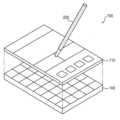
도 1은 본 발명의 실시예들에 따른 전자펜 센싱 장치를 나타내는 도면이다.1 is a diagram illustrating an electronic pen sensing device according to embodiments of the present invention.
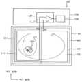
도 1을 참조하면, 전자펜 센싱 장치(100)는 기판(110), 제1 폐루프선(120), 제어부(130)를 포함할 수 있다. 전자펜 센싱 장치(100)는 전자펜(200)으로부터 생성된 전자기장에 기초하여 제1 유도 전류(I_I1)를 생성하고, 유도 전류(I_I1)에 기초하여 전자펜(200)의 위치를 인식할 수 있다.Referring to FIG. 1 , the electronic
기판(110)은 센싱 영역(SA0), 제1 서브 센싱 영역(SA1)을 포함할 수 있다. 여기서, 센싱 영역(SA0)은 전자펜 센싱 장치(100)가 전자펜(200)을 센싱할 수 있는 최대 영역이고, 제1 서브 센싱 영역(SA1)은 센싱 영역(SA0)에 포함된 영역일 수 있다. 예를 들어, 제1 서브 센싱 영역(SA1)은 제1 방향으로 센싱 영역의 폭(또는, 너비)보다 감소된 폭(또는, 너비)를 가질 수 있다. 한편, 도 1에서, 기판(110)(또는, 센싱 영역(SA0))은 제1 서브 센싱 영역(SA1)을 포함하는 것으로 도시되어 있으나, 기판(110)(또는, 센싱 영역(SA0))은 이에 국한되는 것은 아니다. 예를 들어, 기판(110)(또는, 센싱 영역(SA0))은 복수의 서브 센싱 영역들을 포함할 수 있다.The
제1 폐루프선(120)은 기판(110) 상에 배치되며, 제1 노드(N1)부터 제2 노드(N2)까지 제1 회전 방향을 따라 센싱 영역(SA0)의 외곽을 n회 일주하고, 제2 노드(N2)부터 제1 노드(N1)까지 제1 회전 방향을 따라 제1 서브 센싱 영역(SA1)의 외곽을 m회 일주할 수 있다(단, n 및 m은 각각 양의 정수임). 여기서, 제1 회전 방향은 반시계 방향 또는, 시계 방향일 수 있다.The first
실시예들에서, 제1 폐루프선(120)은 주 패턴(122) 및 제1 서브 패턴(121-1)을 포함할 수 있다. 주 패턴(122)은 센싱 영역(SA0)의 외곽을 따라 배치될 수 있다. 예를 들어, 주 패턴(122)은 제1 회전 방향(또는, 제1 권선 방향)으로 권선된 주 코일일 수 있다. 제1 서브 패턴(121-1)은 제1 서브 센싱 영역(SA1)의 외곽을 따라 배치될 수 있다. 예를 들어, 제1 서브 패턴(121-1)은 제1 회전 방향(또는, 제2 권선 방향)으로 권선된 제1 보조 코일일 수 있다. 도 1에 도시된 바와 같이, 제1 서브 패턴(121-1)은 주 패턴(122)에 엇갈려 연결될 수 있다. 즉, 제1 폐루프선(120)은 상호 상이한 폭(또는, 너비)을 가지는 패턴들(예를 들어, 주 패턴(122) 및 제1 서브 패턴(121-1))을 이용하여 폐루프 구조를 형성할 수 있다.In embodiments, the first
주 패턴(122)은 전자펜(200)의 전자기장에 기초하여 제1 전류(I1)를 생성할 수 있다. 예를 들어, 전자펜(200)이 전자기장을 생성한 경우, 전자기장에 기초하여 제1 전류(I1)가 주 패턴(122)에 유도될 수 있다. 여기서, 제1 전류(I1)는 제1 회전 방향으로 흐를 수 있다. 제1 서브 패턴(121-1)은 전자펜(200)의 전자기장에 기초하여 제2 전류(I2)를 생성할 수 있다. 예를 들어, 전자펜(200)이 전자기장을 생성한 경우, 전자기장에 의해 제2 전류(I2)가 제1 서브 패턴(121-1)에 유도될 수 있다. 이 경우, 제1 노드(N1)를 통해 제1 폐루프선(120)의 외부로 출력되는 제1 유도 전류(I_I1)는 제2 전류(I2) 및 제1 전류(I1)간의 전류 차일 수 있다(즉, I_I1 = I2 I1). 또한, 제1 유도 전류(I_I1)는 제2 노드(N2)를 통해 제1 폐루프선(120)으로 유입될 수 있다.The
제어부(130)는 제1 유도 전류(I_I1)에 기초하여 전자펜(200)의 위치를 산출할 수 있다.The
실시예들에서, 제어부(130)는 센싱 유닛(131) 및 산출 유닛(132)을 포함할 수 있다. 센싱 유닛(131)은 제1 유도 전류(I_I1)을 증폭하여 센싱 신호를 출력하고, 산출 유닛(132)은 센싱 신호에 기초하여 전자펜의 위치를 산출할 수 있다. 예를 들어, 산출 유닛(132)은 센싱 신호 및 전자펜(200)의 위치간의 상관관계를 포함(또는, 정의)하는 룩업 테이블을 포함하고, 센싱 신호에 매칭되는 전자펜(200)의 위치를 룩업 테이블로부터 획득할 수 있다. 제어부(130)의 구성에 대해서는 도 2a 및 도 2b를 참조하여 상세히 설명하기로 한다.In embodiments, the
상술한 바와 같이, 전자펜 센싱 장치(100)는 상호 엇갈려 연결되는 주 패턴(122) 및 제1 서브 패턴(121-1)을 포함하는 제1 폐루프선(120)을 이용하여 제1 유도 전류(I_I1)을 생성하고, 제1 유도 전류(I_I1)에 기초하여 전자펜(200)을 인식할 수 있다. 특히, 제어부(130)의 관점에서, 제1 서브 패턴(121-1)은 주 패턴(122)에 병렬 연결되므로, 제1 서브 패턴(121-1)의 레지스턴스가 감소함에 따라 제1 폐루프선(120)의 레지스턴스(또는, 주 패턴(122) 및 제1 서브 패턴(121-1)의 합성 저항)는 감소될 수 있다. 따라서, 전자펜 센싱 장치(100)는 제1 폐루프선(120)의 레지스턴스를 감소시킴으로써, 전자펜(200)을 센싱하는 센싱 감도를 향상시키고, 보다 정확하게 전자펜(200)(또는, 전자펜(200)의 위치)를 인식할 수 있다.As described above, the electronic
도 2a는 도 1의 전자펜 센싱 장치에 포함된 제어부의 일 예를 나타내는 도면이고, 도 2b는 도 2a의 제어부에서 생성되는 출력 신호의 일 예를 나타내는 도면이다.FIG. 2A is a diagram illustrating an example of a controller included in the electronic pen sensing device of FIG. 1 , and FIG. 2B is a diagram illustrating an example of an output signal generated by the controller of FIG. 2A .
도 1 및 도 2a를 참조하면, 제어부(130)는 센싱 유닛(131)을 포함하고, 센싱 유닛(131)은 증폭기(AMP) 및 저항(R_GAIN)을 포함할 수 있다. 증폭기(AMP)의 제1 입력 단자(-)는 제1 노드(N1)에 연결되고, 증폭기(AMP)의 제2 입력 단자(+)는 제2 노드(N2)에 연결되며, 기준 전압(예를 들어, 그라운드 전압, 또는 0 볼트(V))에 연결될 수 있다. 저항(R_GAIN)은 증폭기(AMP)의 제1 입력 단자(-) 및 증폭기(AMP)의 출력 단자 사이에 연결될 수 있다.Referring to FIGS. 1 and 2A , the
센싱 유닛(131)은 제1 유도 전류(I_I1)를 증폭하여 센싱 신호(VOUT)을 출력할 수 있다. 예를 들어, 센싱 유닛(131)은 제1 유도 전류(I_I1)를 반전 증폭하여 센싱 신호(VOUT)을 출력하고, 센싱 신호(VOUT)는 제1 유도 전류(I_I1) 및 저항(R_GAIN)의 곱과 같은 크기를 가질 수 있다(즉, VOUT = - I_I1 * R_GAIN).The
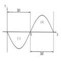
도 1, 도 2a 및 도 2b를 참조하면, 전자펜(200)의 위치에 따라 센싱 신호가 변할 수 있다. 도 2b에 도시된 그래프에서, X축(또는, 수평축)은 전자펜(200)의 위치를 나타내고, Y축(또는, 수직축)은 센싱 신호(VOUT)를 나타낼 수 있다. 예를 들어, X축은, 제1 방향과 제2 방향을 기준으로 하는 2차원 평면에서, 전자펜(200)의 제2 방향의 좌표를 나타낼 수 있다.Referring to FIGS. 1 , 2A and 2B , a sensing signal may change according to the position of the
도 2b에 도시된 바와 같이, 전자펜(200)이 제1 서브 센싱 영역(SA1)에 위치하는 경우, 센싱 신호(VOUT)는 음의 값을 가질 수 있다. 예를 들어, 전자펜(200)이 제1 서브 센싱 영역(SA1)에 위치하는 경우, 제2 전류(I2)는 제1 전류(I1)보다 클 수 있다. 이 경우, 제1 유도 전류(I_I1)는 양의 값을 가지고, 센싱 신호(VOUT)는 제1 유도 전류(I_I1)의 반전 증폭에 따라 음의 값을 가질 수 있다. 특히, 전자펜(200)이 제1 서브 센싱 영역(SA1)의 중앙에 위치하는 경우, 제2 전류(I2)는 가장 큰 값을 가지므로, 센싱 신호(VOUT)은 음의 최대 값을 가질 수 있다.As shown in FIG. 2B , when the
전자펜(200)이 센싱 영역(SA0) 및 제1 서브 센싱 영역(SA1) 간의 경계선에 위치하는 경우, 센싱 신호(VOUT)는 0의 값을 가질 수 있다. 예를 들어, 전자펜(200)이 제1 서브 센싱 영역(SA1)에 위치하는 경우, 제2 전류(I2)는 제1 전류(I1)와 동일한 값을 가질 수 있다.When the
한편, 전자펜(200)이 제1 서브 센싱 영역(SA1) 이외의 센싱 영역(SA0)에 위치하는 경우, 센싱 신호(VOUT)는 양의 값을 가질 수 있다. 예를 들어, 전자펜(200)이 센싱 영역(SA0)의 제2 방향에 위치하는 경우, 제2 전류(I2)는 제1 전류(I1)보다 작을 수 있다. 이 경우, 제1 유도 전류(I_I1)는 음의 값을 가지고, 센싱 신호(VOUT)는 증폭기(AMP)의 반전 증폭에 따라 양의 값을 가질 수 있다.Meanwhile, when the
도 2b에 도시된 바와 같이, 전자펜(200)의 위치에 따라 제어부(130)(또는, 센싱 유닛(131))를 통해 생성되는 센싱 신호(VOUT)는 달라지므로, 제어부(130)는 센싱 신호(VOUT)에 기초하여 전자펜(200)의 제2 방향의 위치(또는, 좌표)를 산출할 수 있다.As shown in FIG. 2B, since the sensing signal VOUT generated through the control unit 130 (or the sensing unit 131) varies according to the position of the
도 3은 도 1의 전자펜 센싱 장치의 일 예를 나타내는 도면이다.FIG. 3 is a diagram illustrating an example of the electronic pen sensing device of FIG. 1 .
도 1 및 도 3을 참조하면, 전자펜 센싱 장치(100)는 기판(100), 주 패턴(122), 제1 서브 패턴(121-1), 제2 서브 패턴(121-2) 및 제어부(130)를 포함할 수 있다. 도 3에 도시된 전자펜 센싱 장치(100)는 제1 서브 패턴(121-1) 및 제2 서브 패턴(121-2) 중 하나를 선택하고, 제1 서브 패턴(121-1) 및 제2 서브 패턴(121-2) 중 선택된 하나를 주 패턴(122)에 연결하여 폐루프를 형성할 수 있다.1 and 3, the electronic
기판(100)은 도 1을 참조하여 설명한 기판(100)과 실질적으로 동일하고, 주 패턴(122) 및 제1 서브 패턴(121-1)은 도 1을 참조하여 설명한 주 패턴(122) 및 제1 서브 패턴(121-1)과 각각 실질적으로 동일할 수 있다. 따라서, 중복되는 설명은 반복하지 않기로 한다.The
기판(100)(또는, 센싱 영역(SA0))는 제1 방향으로 제1 서브 센싱 영역(SA1)의 폭(또는, 너비)보다 감소된 폭(또는, 폭)을 가지는 제2 센싱 영역(SA2)을 포함할 수 있다.The substrate 100 (or the sensing area SA0) has a width (or width) smaller than that of the first sub-sensing area SA1 in the first direction, and the second sensing area SA2 has a smaller width (or width). ) may be included.
제2 서브 패턴(121-2)은 제2 서브 센싱 영역(SA2)의 외곽을 따라 기판(110) 상에 배치될 수 있다. 예를 들어, 제2 서브 패턴(121-2)은 제2 노드(N2)부터 제1 노드(N1)까지 제1 회전 방향을 따라 제2 서브 센싱 영역(SA2)의 외곽을 L회 일주할 수 있다(단, L은 양의 정수). 예를 들어, 제2 서브 패턴(121-2)은 제1 회전 방향(또는, 제1 권선 방향)으로 권선된 제2 보조 코일일 수 있다. 제2 서브 패턴(121-2)은 도 1을 참조하여 설명한 제1 폐루프선(120)에 포함될 수 있다.The second sub pattern 121 - 2 may be disposed on the
제어부(130)는 제1 스위칭 유닛(MUX1) 및 제2 스위칭 유닛(MUX2)를 포함할 수 있다. 제1 스위칭 유닛(MUX1)은 제1 서브 패턴(121-1) 및 제2 서브 패턴(121-2) 중 하나를 선택하고, 제1 서브 패턴(121-1) 및 제2 서브 패턴(121-2) 중 하나를 제1 노드(N1)에 연결할 수 있다. 한편, 제2 스위칭 유닛(MUX2)는 제1 서브 패턴(121-1) 및 제2 서브 패턴(121-2) 중 하나를 제2 노드(N2)에 연결할 수 있다. 즉, 제1 스위칭 유닛(MUX1) 및 제2 스위칭 유닛(MUX1)은 제1 서브 패턴(121-1) 및 제2 서브 패턴(121-2) 중 하나를 주 패턴(122)에 선택적으로 연결할 수 있다. 이 경우, 주 패턴(121)과, 제1 서브 패턴(121-1) 및 제2 서브 패턴(121-2) 중 하나는 폐루프를 형성할 수 있다.The
실시예들에서, 제어부(130)는 제1 센싱 구간에서 제1 서브 패턴(121-1)을 제1 노드(N1) 및 제2 노드(N2)에 연결하고, 제2 센싱 구간에서 제2 서브 패턴(121-2)을 제1 노드(N1) 및 제2 노드(N2)에 연결할 수 있다. 여기서, 제1 센싱 구간 및 제2 센싱 구간은 전자펜을 센싱하기 위해 기 설정된 시간이며, 제2 센싱 구간은 제1 센싱 구간과 다를 수 있다(즉, 제2 센싱 구간은 제1 센싱 구간과 중첩되지 않는 구간일 수 있다). 즉, 제어부(130)는 복수의 영역들로 분할된 센싱 영역(SA0)을 순차적으로 스캔할 수 있다. 이 경우, 제어부(130)는 스캔 결과에 기초하여 전자펜(200)을 위치를 산출할 수 있다.In embodiments, the
한편, 제어부(130)는 제1 센싱 구간에서의 센싱 신호(VOUT)의 값과, 제2 센싱 구간에서의 센싱 신호(VOUT)의 값을 조합하여, 전자펜(200)의 위치를 산출할 수 있다. 예를 들어, 전자펜(200)이 제2 서브 센싱 영역(SA2) 상에 위치하는 경우, 도 2b를 참조하여 설명한 센싱 신호(VOUT)는 제1 센싱 구간에서 음의 값을 가지고, 제2 센싱 구간에서 음의 값을 가질 수 있다. 예를 들어, 전자펜(200)이 제2 서브 센싱 영역(SA2)과 중첩되지 않는 제1 서브 센싱 영역(SA1)의 일부분 상에 위치하는 경우, 센싱 신호(VOUT)는 제1 센싱 구간에서 음의 값을 가지고, 제2 센싱 구간에서 양의 값을 가질 수 있다.Meanwhile, the
도 3에서, 제1 스위칭 유닛(MUX1) 및 제2 스위칭 유닛(MUX2)은 제어부(130)에 포함되는 것으로 도시되어 있으나, 제1 스위칭 유닛(MUX1) 및 제2 스위칭 유닛(MUX2)은 이에 국한되는 것은 아니다. 예를 들어, 제1 스위칭 유닛(MUX1) 및 제2 스위칭 유닛(MUX2)은 기판(110)에 포함되거나, 또는, 기판(110) 상에 배치될 수 있다.In FIG. 3 , the first switching unit MUX1 and the second switching unit MUX2 are shown as being included in the
또한, 도 3에서, 기판(110)(또는, 센싱 영역(SA0))은 2개의 서브 센싱 영역들(즉, 제1 서브 센싱 영역(121-1) 및 제2 서브 센싱 영역(121-2))를 포함하는 것으로 도시되어 있으나, 기판(100)(또는, 센싱 영역(SA0))은 이에 국한되는 것은 아니다. 예를 들어, 기판(110)은 x개의 서브 센싱 영역들을 포함할 수 있다(단, x는 3 이상의 정수). 이 경우, 전자펜 센싱 장치(100)는 x개의 서브 패턴들을 포함하고, 제y 서브 패턴은 제y-1 서브 패턴의 폭(또는, 너비)보다 감소된 폭(또는, 너비)를 가질 수 있다(단, y는 3보다 크고 x보다 작은 정수).In addition, in FIG. 3 , the substrate 110 (or the sensing area SA0) includes two sub-sensing areas (ie, a first sub-sensing area 121-1 and a second sub-sensing area 121-2). ), but the substrate 100 (or the sensing area SA0) is not limited thereto. For example, the
실시예들에서, 제어부(130)는 제1 가변 저항(R1) 및 제2 가변 저항(R2)을 포함할 수 있다. 예를 들어, 제1 가변 저항(R1)은 주 패턴(122) 및 제2 노드(N2) 사이에 연결되고, 제2 가변 저항(R2)은 제1 노드(N1) 및 제1 스위칭 유닛(MUX1) 사이에 연결될 수 있다. 예를 들어, 제1 가변 저항(R1)은 주 패턴(122) 및 제1 노드(N1) 사이에 연결되고, 제2 가변 저항(R2)은 제2 노드(N2) 및 제2 스위칭 유닛(MUX2) 사이에 연결될 수 있다.In some embodiments, the
참고로, 주 패턴(122), 제1 서브 패턴(121-1) 및 제2 서브 패턴(121-2)은 상호 다른 형태 및 상기 다른 길이를 가질 수 있다. 이 경우, 주 패턴(122)의 인덕턴스(또는 레지스턴스), 제1 서브 패턴(121-1)의 인덕턴스(또는 레지스턴스) 및 제2 서브 패턴(121-2)의 인덕턴스(또는 레지스턴스)는 상호 상이하므로, 제어부(130)는 도 2b에 도시된 센싱 출력(VOUT)을 획득하지 못할 수 있다(즉, 제어부(130)는 이상적인 센싱 출력(VOUT)과 다른 값을 획득할 수 있다). 따라서, 제어부(130)는 제1 가변 저항(R1) 및 제2 가변 저항(R2) 중 적어도 하나를 조절함으로써, 도 2b에 도시된 센싱 출력(VOUT)(또는, 이상적인 값)을 획득할 수 있다.For reference, the
제1 저항(R1)은 주 패턴(122)과 서브 패턴들(즉, 제1 서브 패턴(121-1) 및 제2 서브 패턴(121-2))간의 편차(예를 들어, 인덕턴스 편차, 또는 레지스턴스 편차)를 보상하는 데 이용될 수 있다. 제2 저항(R2)는 서브 패턴들(즉, 제1 서브 패턴(121-1) 및 제2 서브 패턴(121-2))간의 편차(예를 들어, 인덕턴스 편차, 또는 레지스턴스 편차)를 보상하는 데 이용될 수 있다.The first resistor R1 is a deviation (eg, inductance deviation, or resistance deviation) can be used to compensate. The second resistor R2 compensates for a deviation (eg, inductance deviation or resistance deviation) between the subpatterns (ie, the first subpattern 121-1 and the second subpattern 121-2). can be used to
상술한 바와 같이, 전자펜 센싱 장치(100)는 복수의 서브 센싱 영역들(예를 들어, 제1 서브 센싱 영역(SA1), 제2 서브 센싱 영역(SA2) 등)의 외곽을 따라 배치된 복수의 서브 패턴들(예를 들어, 제1 서브 패턴(121-1), 제2 서브 패턴(121-2), 등)를 포함하고, 복수의 서브 패턴들 중 하나를 선택적으로 주 패턴(122)에 연결하여 폐루프를 형성하며, 폐루프에 유도되는 제1 유도 전류(I_I1)에 기초하여 전파펜(200)의 위치를 산출할 수 있다. 또한, 전자펜 센싱 장치(100)는 주 패턴(122) 및 복수의 서브 패턴들(예를 들어, 제1 서브 패턴(121-1), 제2 서브 패턴(121-2), 등)을 연결하는 제1 가변 저항(R1) 및 제2 가변 저항(R2)을 포함할 수 있다. 따라서, 전자펜 센싱 장치(100)는 전자펜(200)의 센싱 정확도를 향상시킬 수 있다.As described above, the electronic
도 4는 도 1의 전자펜 센싱 장치의 다른 일 예를 나타내는 도면이다.4 is a diagram illustrating another example of the electronic pen sensing device of FIG. 1 .
도 1 및 도 4를 참조하면, 도 4에 도시된 전자펜 센싱 장치(100)는 도 1에 도시된 전자펜 센싱 장치(100)와 실질적으로 동일할 수 있다. 따라서, 중복되는 설명은 반복하지 않기로 한다.Referring to FIGS. 1 and 4 , the electronic
기판(420)(또는, 센싱 영역(SA0))은 제3 서브 센싱 영역(SA3)을 포함할 수 있다. 여기서, 센싱 영역(SA0)은 앞서 도 1을 참조하여 설명한 센싱 영역(SA0)과 실질적으로 동일할 수 있다. 제3 서브 센싱 영역(SA3)은 제2 방향으로 센싱 영역(SA0)의 폭(또는, 너비)보다 감소된 폭(또는, 너비)를 가지고, 제2 방향은 제1 방향에 수직할 수 있다.The substrate 420 (or the sensing area SA0) may include a third sub-sensing area SA3. Here, the sensing area SA0 may be substantially the same as the sensing area SA0 previously described with reference to FIG. 1 . The third sub-sensing area SA3 has a width (or width) smaller than that of the sensing area SA0 in the second direction, and the second direction may be perpendicular to the first direction.
제2 폐루프선(420)은 기판(410) 상에 배치되며, 제3 노드(N3)부터 제4 노드(N4)까지 제1 회전 방향을 따라 센싱 영역(SA0)의 외곽을 일주하고, 제4 노드(N4)부터 제3 노드(N3)까지 제1 회전 방향을 따라 제3 서브 센싱 영역(SA3)의 외곽을 일주할 수 있다(단, n 및 m은 각각 양의 정수임). 여기서, 제3 노드(N3)는 도 1에 도시된 제1 노드(N1)와 동일하고, 제4 노드(N4)는 도 1에 도시된 제2 노드(N2)와 동일할 수 있다.The second
제2 폐루프선(420)은 주 패턴(422) 및 제3 서브 패턴(421-3)을 포함할 수 있다. 주 패턴(422)은 센싱 영역(SA0)의 외곽을 따라 배치되고, 도 1을 참조하여 설명한 주 패턴(122)과 실질적으로 동일할 수 있다. 제3 서브 패턴(421-3)은 제3 서브 센싱 영역(SA3)의 외곽을 따라 기판(110) 상에 배치될 수 있다. 예를 들어, 제3 서브 패턴(421-3)은 제4 노드(N4)부터 제3 노드(N3)까지 제1 회전 방향을 따라 제3 서브 센싱 영역(SA3)의 외곽을 일주할 수 있다. 예를 들어, 제3 서브 패턴(421-3)은 제1 회전 방향(또는, 제1 권선 방향)으로 권선된 제3 보조 코일일 수 있다.The second
앞서 도 1을 참조하여 설명한 바와 같이, 주 패턴(422)은 전자펜(200)의 전자기장에 기초하여 제1 전류(I1)를 생성할 수 있다. 제3 서브 패턴(421-3)은 전자펜(200)의 전자기장에 기초하여 제3 전류(I3)를 생성할 수 있다. 즉, 전자펜(200)의 전자기장에 의해 제3 전류(I3)가 제3 서브 패턴(421-1)에 유도될 수 있다. 이 경우, 제3 노드(N3)를 통해 제2 폐루프선(420)의 외부로 출력되는 제2 유도 전류(I_I2)는 제3 전류(I3) 및 제1 전류(I1)간의 전류 차일 수 있다(즉, I3 I1).As described above with reference to FIG. 1 , the
제어부(130)는 제2 유도 전류(I_I2)에 기초하여 전자펜(200)의 위치를 산출할 수 있다. 도 1에 도시된 전자펜 센싱 장치(100)는, 도 2b를 참조하여 설명한 바와 같이, 전자펜(200)의 제1 방향의 위치를 산출하고, 도 4에 도시된 전자펜 센싱 장치(100)는 전자펜(200)의 제2 방향의 위치를 산출할 수 있다.The
도 5a는 도 1의 전자펜 센싱 장치의 일 예를 나타내는 도면이고, 도 5b는 도 5a의 전자펜 센싱 장치에 포함된 폐루프선의 일 예를 나타내는 도면이다.5A is a diagram illustrating an example of the electronic pen sensing device of FIG. 1 , and FIG. 5B is a diagram illustrating an example of a closed loop line included in the electronic pen sensing device of FIG. 5A .
도 3, 도 4, 도 5a 및 도 5b를 참조하면, 제3 폐루프선(520)은 주 패턴(522), 제1 서브 패턴(521-1), 제2 서브 패턴(521-2), 제3 서브 패턴(511-3) 및 제4 서브 패턴(511-4)를 포함할 수 있다.3, 4, 5A and 5B, the third
주 패턴(522), 제1 서브 패턴(521-1) 및 제2 서브 패턴(521-2)은 도 3을 참조하여 설명한 주 패턴(122), 제1 서브 패턴(121-1) 및 제2 서브 패턴(121-2)과 각각 동일할 수 있다. 또한, 제3 서브 패턴(511-3)은 도 4를 참조하여 설명한 제3 서브 패턴(421-3)과 동일할 수 있다. 따라서, 중복되는 설명은 반복하지 않기로 한다.The
제4 서브 패턴(511-4)는 제4 서브 센싱 영역(SA4)의 외곽을 따라 배치될 수 있다. 여기서, 제4 서브 센싱 영역(SA4)은 제2 방향으로 제3 서브 센싱 영역(SA3)의 폭(또는, 너비)보다 감소된 폭(또는, 너비)을 가질 수 있다. 예를 들어, 제4 서브 패턴(511-4)은 도 4에 도시된 제4 노드(N4)부터 도 4에 도시된 제3 노드(N3)까지 제1 회전 방향을 따라 제4 서브 센싱 영역(SA4)의 외곽을 L회 일주할 수 있다(단, L은 양의 정수). 예를 들어, 제4 서브 패턴(511-4)은 제1 회전 방향(또는, 제1 권선 방향)으로 권선된 제4 보조 코일일 수 있다.The fourth sub-pattern 511 - 4 may be disposed along the periphery of the fourth sub-sensing area SA4 . Here, the fourth sub-sensing area SA4 may have a width (or width) smaller than that of the third sub-sensing area SA3 in the second direction. For example, the fourth sub-pattern 511-4 is a fourth sub-sensing area (from the fourth node N4 shown in FIG. 4 to the third node N3 shown in FIG. 4 along the first rotation direction). SA4) can go around the perimeter L times (however, L is a positive integer). For example, the fourth sub-pattern 511-4 may be a fourth auxiliary coil wound in a first rotation direction (or first winding direction).
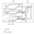
일 실시예에서, 제1 서브 패턴(521-1) 및 제2 서브 패턴(521-2)은 제1 레이어에 배치되고, 제3 서브 패턴(511-3) 및 제4 서브 패턴(511-4)은 제2 레이어에 배치될 수 있다. 여기서, 제2 레이어는 제1 레이어와 다른 레이어(layer) 일 수 있다. 이 경우, 주 패턴(522)은 제1 레이어 또는 제2 레이어에 배치되거나, 또는, 별도의 제3 레이어에 배치될 수 있다.In an embodiment, the first sub-pattern 521-1 and the second sub-pattern 521-2 are disposed on the first layer, and the third sub-pattern 511-3 and the fourth sub-pattern 511-4 ) may be disposed in the second layer. Here, the second layer may be a layer different from the first layer. In this case, the
다른 일 실시예에서, 주 패턴(522), 제1 서브 패턴(521-1), 제2 서브 패턴(521-2), 제3 서브 패턴(511-3) 및 제4 서브 패턴(511-4)은 하나의 레이어에 배치될 수 있다.In another embodiment, a
한편, 전자펜 센싱 장치(100)은 제1 서브 패턴(521-1) 및 제2 서브 패턴(521-2) 중 하나와, 주 패턴(522)을 이용하여 전자펜(200)의 제1 방향의 위치를 산출할 수 있다. 또한, 전자펜 센싱 장치(100)는 제3 서브 패턴(511-3) 및 제4 서브 패턴(511-4) 중 하나와, 주 패턴(522)을 이용하여 전자펜(200)의 제2 방향의 위치를 산출할 수 있다.Meanwhile, the electronic
실시예들에서, 전자펜 센싱 장치(100)은 제1 서브 패턴(521-1) 내지 제4 서브 패턴(511-4) 중 하나를 선택하고, 제1 서브 패턴(521-1) 내지 제4 서브 패턴(511-4) 중 선택된 하나를 제1 노드(N1)(또는, 제3 노드(N3))에 연결하고, 제1 서브 패턴(521-1) 내지 제4 서브 패턴(511-4) 중 선택된 하나를 제2 노드(N2)(또는, 제4 노드(N4))에 연결할 수 있다.In embodiments, the electronic
일 실시예에서, 전자펜 센싱 장치(100)는 제1 서브 패턴(521-1) 및 제2 서브 패턴(521-2) 중 하나를 선택하여 제1 노드(N1)에 연결하는 제1 스위칭 유닛(MUX1), 제1 서브 패턴(521-1) 및 제2 서브 패턴(521-2) 중 선택된 하나를 제2 노드(N2)에 연결하는 제2 스위칭 유닛(MUX2) 및 제3 서브 패턴(511-3) 및 제4 서브 패턴(511-4) 중 하나를 선택하여 제3 노드(N3)에 연결하는 제3 스위칭 유닛 및 제3 서브 패턴(511-3) 및 제4 서브 패턴(511-4) 중 선택된 하나를 제4 노드(N4)에 연결하는 제4 스위칭 유닛을 포함할 수 있다. 이 경우, 전자펜 센싱 장치(100)는 도 1에 도시된 제1 유도 전류(I_I1)에 기초하여 전자펜(200)의 제1 방향 위치를 산출하고, 도 3에 도시된 제2 유도 전류(I_I2)(즉, 제3 노드(N3)를 통해 출력되는 제2 유도 전류(I_I2))에 기초하여 전자펜(200)의 제2 방향 위치를 산출할 수 있다.In an embodiment, the electronic
일 실시예에서, 전자펜 센싱 장치(100)는 제1 방향으로 배열된 서브 센싱 영역들(예를 들어, 제1 서브 센싱 영역(SA1) 및 제2 서브 센싱 영역(SA2)) 및 제2 방향으로 배열된 서브 센싱 영역들(예를 들어, 제3 서브 센싱 영역(SA3) 및 제4 서브 센싱 영역(SA4))을 동시에(또는, 독립적으로) 스캔할 수 있다. 예를 들어, 전자펜 센싱 장치(200)는 제1 센싱 구간에서 제1 서브 패턴(521-1)을 제1 노드(N1) 및 제2 노드(N2)에 연결하고, 제1 센싱 구간과 다른 제2 센싱 구간에서 제2 서브 패턴(521-2)을 제1 노드(N1) 및 제2 노드(N2)에 연결하며, 제1 센싱 구간에서 제3 서브 패턴(511-3)을 제3 노드(N3) 및 제4 노드(N4)에 연결하고, 제2 센싱 구간에서 제4 서브 패턴(511-4)을 제3 노드(N3) 및 제4 노드(N4)에 연결할 수 있다. 즉, 전자펜 센싱 장치(100)는 전자펜(200)의 제1 방향 위치를 산출하는 구성에 독립하여, 전자펜(200)의 제2 방향 위치를 산출할 수 있다.In an embodiment, the electronic
일 실시예에서, 전자펜 센싱 장치(100)는 제1 서브 패턴(521-1) 내지 제4 서브 패턴(511-4) 중 하나를 선택하여 제1 노드(N1)(또는, 제3 노드(N3))에 연결하는 제1 스위칭 유닛(MUX1) 및 제1 서브 패턴(521-1) 내지 제4 서브 패턴(511-4) 중 선택된 하나를 제2 노드(N2)(또는, 제4 노드(N4))에 연결하는 제2 스위칭 유닛(MUX2)를 포함할 수 있다. 예를 들어, 제3 스위칭 유닛(MUX3)는 제1 스위칭 유닛(MUX1)에 포함되고, 제4 스위칭 유닛(MUX4)은 제2 스위칭 유닛(MUX2)에 포함될 수 있다. 이 경우, 전자펜 센싱 장치(100)는 제1 스위칭 유닛(MUX1) 및 제2 스위칭 유닛(MUX2)를 이용하여, 제1 서브 패턴(521-1) 내지 제4 서브 패턴(511-4) 중 선택된 하나를 제1 노드(N1) 및 제2 노드(N2) 사이에 연결할 수 있다.In an embodiment, the electronic
일 실시예에서, 전자펜 센싱 장치(100)는 제1 서브 센싱 영역(SA1) 내지 제4 서브 센싱 영역(SA4)를 순차적으로 스캔할 수 있다. 예를 들어, 전자펜 센싱 장치(100)는 제1 센싱 구간에서 제1 서브 패턴(521-1)을 제1 노드(N1) 및 제2 노드(N2)에 연결하고, 제2 센싱 구간에서 제2 서브 패턴(121-2)을 제1 노드(N1) 및 제2 노드(N2)에 연결하며, 제3 센싱 구간에서 제3 서브 패턴(511-3)을 제3 노드(N3)(또는, 제1 노드(N1)) 및 제4 노드(N4)(또는, 제2 노드(N2))에 연결하고, 제4 센싱 구간에서 제4 서브 패턴(511-4)를 제3 노드(N3)(또는, 제1 노드(N1)) 및 제4 노드(N4)(또는, 제2 노드(N2))에 연결할 수 있다. 여기서, 제1 내지 제4 센싱 구간들은 상호 다를 수 있다(즉, 상호 중첩되지 않을 수 있다).In one embodiment, the electronic
실시예들에서, 제1 서브 패턴(521-1) 내지 제4 서브 패턴(511-4)은 터치 센싱 전극일 수 있다. 여기서, 터치 센싱 전극은 정전 방식의 터치 입력을 감지하기 위한 전극일 수 있다. 예를 들어, 터치 센싱 구간에서, 전자펜 센싱 장치(100)는 제1 서브 패턴(521-1) 내지 제4 서브 패턴(511-4)에 센싱 신호(예를 들어, 교류 전압)을 공급하고, 터치 입력에 의한 제1 서브 패턴(521-1) 내지 제4 서브 패턴(511-4) 간의 정전 용량 변화에 기초하여 터치 입력을 감지할 수 있다. 예를 들어, 터치 센싱 구간과 다른 전자펜 센싱 구간에서, 전자펜 센싱 장치(100)는 전자펜(200)의 전자기장에 의해 유도되는 유도 전류(예를 들어, 제1 유도 전류(I_I1) 및/또는 제2 유도 전류(I_I2))에 기초하여 전자펜(200)을 감지할 수 있다.In embodiments, the first sub-pattern 521-1 to the fourth sub-pattern 511-4 may be touch sensing electrodes. Here, the touch sensing electrode may be an electrode for sensing a capacitive touch input. For example, in the touch sensing period, the electronic
상술한 바와 같이, 전자펜 센싱 장치(100)는 주 패턴(522), 제1 방향으로 배열된 서브 패턴들(예를 들어, 제1 서브 패턴(521-1) 및 제2 서브 패턴(521-2)) 및 제2 방향으로 배열된 서브 패턴들(예를 들어, 제3 서브 패턴(511-3) 및 제4 서브 패턴(511-4))을 포함하고, 주 패턴(522) 및 상기 서브 패턴들을 이용하여 전자펜(200)의 제1 방향 위치 및 제2 방향 위치를 산출할 수 있다.As described above, the electronic
도 5c는 도 5a의 전자펜 센싱 장치에 포함된 폐루프선의 다른 일 예를 나타내는 도면이다.5C is a diagram illustrating another example of a closed loop line included in the electronic pen sensing device of FIG. 5A.
도 5b 및 도 5c를 참조하면, 제3 폐루프선(520)은 주 패턴(532), 제1 서브 패턴(531), 제1 라인 패턴(531-1), 제3 서브 패턴(533) 및 제3 라인 패턴(533-1)을 포함할 수 있다. 여기서, 주 패턴(532), 제1 서브 패턴(531) 및 제2 서브 패턴(532)은 도 5b에 도시된 주 패턴(522), 제1 서브 패턴(521-1) 및 제3 서브 패턴(511-3)과 각각 동일할 수 있다. 따라서, 중복되는 설명은 반복하지 않기로 한다.5B and 5C, the third
제1 라인 패턴(521-1)은, 제1 서브 센싱 영역(SA1) 및 제2 서브 센싱 영역(SA2)간의 경계선을 따라 배치되고, 일단이 제1 서브 패턴(521)에 연결될 수 있다. 이 경우, 제1 라인 패턴(531-1)에 의해 형성되는 폐루프 구조는 도 5b에 도시된 제2 서브 패턴(521-2)에 의해 형성되는 폐루프 구조와 실질적으로 동일할 수 있다. 예를 들어, 전자펜 센싱 장치(100)가 제1 스위칭 유닛(MUX1)을 이용하여 제1 라인 패턴(531-1)을 제1 노드(N1)에 연결하고, 제2 스위칭 유닛(MUX2)를 이용하여 제1 서브 패턴(531)의 일단을 제2 노드(N2)에 연결한 경우, 제1 라인 패턴(531-1)에 의해 형성되는 폐루프 구조는 제2 서브 센싱 영역(SA2) 상에 형성될 수 있다.The first line pattern 521 - 1 may be disposed along a boundary line between the first sub-sensing area SA1 and the second sub-sensing area SA2 , and one end may be connected to the first sub-pattern 521 . In this case, the closed-loop structure formed by the first line pattern 531-1 may be substantially the same as the closed-loop structure formed by the second sub-pattern 521-2 shown in FIG. 5B. For example, the electronic
즉, 전자펜 센싱 장치(100)는 도 5b에 도시된 제1 서브 패턴(521-1)과 제2 서브 패턴(521-2)의 상호 인접한 부분을 공통 패턴으로 이용하여, 배선 영역을 감소시키고, 스위칭 유닛(예를 들어, 제2 스위칭 유닛(MUX2))의 입력 채널의 수를 감소시킬 수 있다. 따라서, 전자펜 센싱 장치(100)는 제1 라인 패턴(531-1)을 이용하여, 도 5b에 도시된 제2 서브 패턴(521-2)을 이용하는 경우보다, 제조 비용을 절감시킬 수 있다.That is, the electronic
제1 라인 패턴(531-1)과 유사하게, 제3 라인 패턴(533-1)은, 제3 서브 센싱 영역(SA3) 및 제4 서브 센싱 영역(SA4)간의 경계선을 따라 배치되고, 일단이 제3 서브 패턴(533)에 연결될 수 있다. 이 경우, 제3 라인 패턴(533-1)에 의해 형성되는 폐루프 구조는 도 5b에 도시된 제4 서브 패턴(511-4)에 의해 형성되는 폐루프 구조와 실질적으로 동일할 수 있다. 예를 들어, 전자펜 센싱 장치(100)가 제1 스위칭 유닛(MUX1)을 이용하여 제3 라인 패턴(533-1)을 제1 노드(N1)에 연결하고, 제2 스위칭 유닛(MUX2)를 이용하여 제3 서브 패턴(533)의 일단을 제2 노드(N2)에 연결한 경우, 제3 라인 패턴(533-1)에 의해 형성되는 폐루프 구조는 제4 서브 센싱 영역(SA4) 상에 형성될 수 있다.Similar to the first line pattern 531-1, the third line pattern 533-1 is disposed along the boundary between the third sub-sensing area SA3 and the fourth sub-sensing area SA4, and has one end. It may be connected to the
상술한 바와 같이, 전자펜 센싱 장치(100)는 서브 패턴들(예를 들어, 도 5b에 도시된 제1 서브 패턴(521-1)과 제2 서브 패턴(521-2))의 상호 인접한 부분을 공통 패턴으로 이용함으로써, 배선 영역을 감소시키고, 스위칭 유닛(예를 들어, 제2 스위칭 유닛(MUX2))의 입력 채널의 수를 감소시킬 수 있다. 따라서, 전자펜 센싱 장치(100)는 제조 비용을 절감시킬 수 있다.As described above, in the electronic
도 5c에서 제3 폐루프선(520)은 제1 방향으로 배열된 제1 라인 패턴(531-1)과 제2 방향으로 배열된 제3 라인 패턴(533-1)을 포함하는 것으로 도시되어 있으나, 제3 폐루프선(520)은 이에 국한되는 것은 아니다. 예를 들어, 제3 폐루프선(520)은 제1 방향을 따라 배열된 m개의 수직 라인 패턴들과 제2 방향을 따라 배열된 n개의 수평 라인 패턴들을 포함할 수 있다(단, m 및 n은 2 이상의 자연수).In FIG. 5C, the third
도 6a는 도 1의 전자펜 센싱 장치의 또 다른 일 예를 나타내는 도면이고, 도 6b는 도 6a의 전자펜 센싱 장치에 포함된 폐루프선의 일 예를 나타내는 도면이다.6A is a diagram illustrating another example of the electronic pen sensing device of FIG. 1 , and FIG. 6B is a diagram illustrating an example of a closed loop line included in the electronic pen sensing device of FIG. 6A .
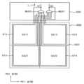
도 1 및 도 6a를 참조하면, 기판(610)은 센싱 영역(SA0)들을 구획한 센싱 블록 영역들을 포함할 수 있다. 예를 들어, 기판(610)은 제11 센싱 블록 영역(SA11), 제12 센싱 블록 영역(SA12), 제21 센싱 블록 영역(SA21) 및 제22 센싱 블록 영역(SA22)를 포함할 수 있다. 도 6에서 기판(610)은 4개의 센싱 블록 영역들을 포함하는 것으로 도시되어 있으나, 기판(610)은 이에 국한되는 것은 아니다. 예를 들어, 기판(610)은 M*N 개(M행 * N열)의 센싱 블록 영역들을 포함할 수 있다(단, M 및 N 각각은 3 이상의 정수). 여기서, 상기 센싱 블록 영역들은 상호 중첩되지 않을 수 있다.Referring to FIGS. 1 and 6A , the substrate 610 may include sensing block regions partitioning the sensing regions SA0. For example, the substrate 610 may include an 11th sensing block area SA11 , a 12th sensing block area SA12 , a 21st sensing block area SA21 , and a 22nd sensing block area SA22 . In FIG. 6 , the substrate 610 is illustrated as including four sensing block regions, but the substrate 610 is not limited thereto. For example, the substrate 610 may include M*N (M rows X N columns) sensing block regions (where M and N are each an integer greater than or equal to 3). Here, the sensing block regions may not overlap each other.
전자펜 센싱 장치(100)는 주 패턴(622), 제1 블록 패턴(611), 제2 블록 패턴(612), 제3 블록 패턴(613) 및 제4 블록 패턴(614)를 포함할 수 있다. 주 패턴(622)는 앞서 도 1을 참조하여 설명한 주 패턴(122)과 실질적으로 동일할 수 있다.The electronic
제1 블록 패턴(611)은 제11 센싱 블록 영역(SA11)의 외곽을 따라 배치될 수 있다. 예를 들어, 제1 블록 패턴(611)은 제2 노드(N2)부터 제1 노드(N1)까지 제11 센싱 블록 영역(SA11)의 외곽을 따라 배치되고, 제1 회전 방향을 따라 권선된 제11 보조 코일일 수 있다.The
제2 블록 패턴(612)은 제12 센싱 블록 영역(SA12)의 외곽을 따라 배치될 수 있다. 예를 들어, 제2 블록 패턴(612)은 제2 노드(N2)부터 제1 노드(N1)까지 제12 센싱 블록 영역(SA12)의 외곽을 따라 배치되고, 제1 회전 방향을 따라 권선된 제12 보조 코일일 수 있다.The
유사하게, 제3 블록 패턴(613)은 제21 센싱 블록 영역(SA21)의 외곽을 따라 배치되고, 제4 블록 패턴(614)은 제22 센싱 블록 영역(SA22)의 외곽을 따라 배치될 수 있다.Similarly, the
제어부(630)는 블록 패턴들(예를 들어, 제1 내지 제4 블록 패턴들(611 내지 614)) 중에서 하나를 선택하여, 제1 노드(N1) 및 제2 노드(N2) 사이에 연결하고, 제1 노드(N1)를 통해 출력되는 제1 유도 전류(I_I1)에 기초하여 전자펜의 위치를 산출할 수 있다.The
도 6a에 도시된 바와 같이, 제어부(630)는 제1 스위칭 유닛(MUX1) 및 제2 스위칭 유닛(MUX2)을 포함할 수 있다. 제1 스위칭 유닛(MUX1)은 제1 내지 제4 블록 패턴들(611 내지 614) 중에서 하나를 선택하여 제1 노드(N1)에 연결하고, 제2 스위칭 유닛(MUX2)은 제1 내지 제4 블록 패턴들(611 내지 614) 중에서 선택된 하나를 제2 노드(N2)에 연결할 수 있다. 즉, 제어부(630)는 제1 내지 제4 블록 패턴들(611 내지 614) 중에서 하나를 선택하고, 제1 내지 제4 블록 패턴들(611 내지 614) 중에서 선택된 하나와, 주 패턴(622)를 이용하여 폐루프 구조를 형성할 수 있다.As shown in FIG. 6A , the
제1 유도 전류(I_I1)에 기초하여 전자펜의 위치를 산출하는 구성은 도 1을 참조하여 설명한 전자펜의 위치 산출 구성과 실질적으로 동일할 수 있다. 따라서, 중복되는 설명은 반복하지 않기로 한다.A configuration for calculating the position of the electronic pen based on the first induced current I_I1 may be substantially the same as the configuration for calculating the position of the electronic pen described with reference to FIG. 1 . Therefore, duplicate descriptions will not be repeated.
실시예들에서, 블록 패턴들 중에서 상호 인접한 부분 패턴들은 중첩될 수 있다. 즉, 블록 패턴들 중에서 상호 인접한 부분들은 공통 패턴으로 구성될 수 있다.In embodiments, partial patterns adjacent to each other among block patterns may overlap each other. That is, mutually adjacent parts among the block patterns may be configured in a common pattern.
도 6a 및 도 6b를 참조하면, 도 6a에 도시된 제1 블록 패턴(611) 중 제3 블록 패턴(613)과 인접한 제1 부분 패턴(622-1)은 제3 블록 패턴(613)과 중첩될 수 있다. 즉, 제1 부분 패턴(622-1)은 제1 블록 패턴(611) 및 제3 블록 패턴(613)에 포함된 제1 공통 패턴일 수 있다. 유사하게, 도 6a에 도시된 제2 블록 패턴(612) 중 제4 블록 패턴(614)과 인접한 제2 부분 패턴(622-2)은 제4 블록 패턴(614)과 중첩될 수 있다. 즉, 제2 부분 패턴(622-2)은 제2 블록 패턴(612) 및 제4 블록 패턴(614)에 포함된 제2 공통 패턴일 수 있다. 또한, 제3 부분 패턴(622-3)은 제3 블록 패턴(613) 및 제4 블록 패턴(614)에 포함된 제3 공통 패턴일 수 있다.6A and 6B, among the
즉, 전자펜 센싱 장치(100)는 블록 패턴들(즉, 제1 내지 제4 블록 패턴들(611 내지 614))의 상호 인접한 부분을 공통 패턴으로 이용할 수 있다. 따라서, 전자펜 센싱 장치(100)는 배선 영역을 감소시키고, 스위칭 유닛(예를 들어, 제2 스위칭 유닛(MUX2))의 입력 채널의 수를 감소시킬 수 있다.That is, the electronic
한편, 제어부(630)는 부분 패턴(예를 들어, 제1 내지 제3 부분 패턴들(621-1 내지 621-3) 중 하나)를 제1 노드(N1) 및 제2 노드(N2)에 연결하는 제5 스위칭 유닛(MUX5)을 포함할 수 있다. 부분 패턴(예를 들어, 제1 내지 제3 부분 패턴들(621-1 내지 621-3) 중 하나)은 상호 인접한 블록 패턴들(예를 들어, 제1 내지 제4 블록 패턴들(611 내지 614) 중 선택된 2개)에 공통적으로 이용되므로, 부분 패턴(예를 들어, 제1 내지 제3 부분 패턴들(621-1 내지 621-3) 중 하나)은 제1 노드(N1) 또는 제2 노드(N2)에 선택적으로 연결될 수 있다. 따라서, 전자펜 센싱 장치(100)는 제5 스위칭 유닛(MUX5)을 이용하여 부분 패턴(예를 들어, 제1 내지 제3 부분 패턴들(621-1 내지 621-3) 중 하나)를 제1 노드(N1) 및 제2 노드(N2)에 선택적으로 연결할 수 있다.Meanwhile, the
도 6a 및 도 6b를 참조하여 설명한 바와 같이, 전자펜 센싱 장치(100)는 센싱 영역(SA0)을 구획한 센싱 블록 영역들(SA11 내지 SA22) 및 센싱 블록 영역들(SA11 내지 SA22)에 각각 배치된 블록 패턴들(611 내지 614)을 포함하며, 블록 패턴들(611 내지 614)을 이용하여 센싱 블록 영역들(SA11 내지 SA22)을 순차적으로 스캔할 수 있다. 또한, 전자펜 센싱 장치(100)는 블록 패턴들(611 내지 614)의 상호 인접한 부분을 공통 패턴으로 이용함으로써, 배선 영역을 감소시키고, 스위칭 유닛(예를 들어, 제5 스위칭 유닛(MUX5))의 입력 채널의 수를 감소시킬 수 있다.As described with reference to FIGS. 6A and 6B , the electronic
도 7은 본 발명의 실시예들에 따른 표시 장치를 나타내는 도면이다.7 is a diagram illustrating a display device according to example embodiments.
도 1 및 도 7을 참조하면, 표시 장치(700)는 표시 패널(710), 전자펜 센싱 장치(100) 및 전자펜(200)을 포함할 수 있다.Referring to FIGS. 1 and 7 , the
표시 패널(710)은 영상 데이터에 기초하여 영상을 표시할 수 있다. 예를 들어, 표시 패널(710)은 유기 발광 표시 패널일 수 있다. 도 7에 도시되지 않았으나, 표시 패널(710)은 화소들을 포함하고, 화소들 각각은 데이터 신호를 게이트 신호에 응답하여 일시적으로 저장하고, 저장된 데이터 신호에 기초하여 발광할 수 있다. 여기서, 데이터 신호는 표시 장치(700)에 구비된 데이터 구동 회로에서 공급되고, 게이트 신호는 표시 장치(700)에 구비된 게이트 구동 회로에서 공급될 수 있다.The
전자펜(200)은 전자기력을 발생시킬 수 있다. 예를 들어, 전자펜(200)은 외부 장치(예를 들어, 전자펜 센싱 장치(100))에 의해 형성된 외부 전자기력에 기초하여 전자펜 유도 전류(또는, 유도 기전력)를 생성하고, 전자펜 유도 전류에 기초하여 전자기력을 생성할 수 있다. 예를 들어, 전자펜(200)은 유도 코일 및 유도 코일에 병렬 연결된 커패시터를 포함하고, 유도 코일을 통해 외부 전자기력에 기초하여 유도된 유도 기전력을 커패시터에 저장하며, 특정 조건에서(예를 들어, 외부 전자기장이 소멸된 경우) 커패시터를 방전시킴으로써 유도 코일을 통해 전자기력을 생성할 수 있다.The
전자펜 센싱 장치(100)는 앞서 도 1을 참조하여 설명한 전자펜 센싱 장치(100)와 실질적으로 동일할 수 있다. 즉, 전자펜 센싱 장치(100)는 전자기력에 기초하여 전자펜(200)을 인식할 수 있다. 도 1에 도시된 바와 같이, 전자펜 센싱 장치(100)는 기판(110), 제1 폐루프선(120) 및 제어부(130)를 포함할 수 있다. 여기서, 기판(110)은 센싱 영역(SA0) 및 제1 방향으로 센싱 영역(SA0)의 폭보다 감소된 폭을 가지는 제1 서브 센싱 영역(SA1)을 포함할 수 있다. 제1 폐루프선(120)은 기판(110) 상에 배치되되, 제1 노드(N1)로부터 제2 노드(N2)까지 제1 회전 방향을 따라 센싱 영역(SA0)의 외곽을 일주하고, 제2 노드(N2)로부터 제1 노드(N1)까지 제1 회전 방향을 따라 제1 서브 센싱 영역(SA1)의 외곽을 일주할 수 있다. 제어부(130)는 제1 노드(N1)(및/또는 제2 노드(N2))를 통해 출력되는 유도 전류(즉, 제1 유도 전류(I_I1))에 기초하여 전자펜(200)의 위치를 산출할 수 있다.The electronic
일 실시예에서, 전자펜 센싱 장치(100)는 외부 전자기장(즉, 전자펜(200)의 구동을 위한 외부 전자기장)을 생성할 수 있다. 예를 들어, 전자펜 센싱 장치(100)는 센싱 영역(SA0)의 외곽을 따라 일주하는(또는, 배치되는) 전력 코일을 포함할 수 있다. 예를 들어, 전력 코일은 도 1에 도시된 주 패턴(122)과 실질적으로 동일할 수 있다. 이 경우, 전자펜 센싱 장치(100)는 전력 공급 구간에서 전력 코일(또는, 주 패턴(122))에 전류를 공급함으로써 외부 전자기장을 생성하고, 센싱 구간에서 폐루프선(120)(예를 들어, 주 패턴(122) 및 제1 서브 패턴(121-1)을 이용하여 형성된 폐루프 구조)을 이용하여 전자펜(200)을 감지할 수 있다.In one embodiment, the electronic
상술한 바와 같이, 표시 장치(700)는 전자펜(200) 및 전자펜 센싱 장치(100)를 포함하므로, 전자펜(200)을 이용한 다양한 입력 기능을 제공할 수 있다.As described above, since the
이상, 본 발명의 실시예들에 따른 전자펜 센싱 장치 및 이를 포함하는 표시 장치에 대하여 도면을 참조하여 설명하였지만, 상기 설명은 예시적인 것으로서 본 발명의 기술적 사상을 벗어나지 않는 범위에서 해당 기술 분야에서 통상의 지식을 가진 자에 의하여 수정 및 변경될 수 있을 것이다.In the above, the electronic pen sensing device according to the embodiments of the present invention and the display device including the same have been described with reference to the drawings, but the above description is exemplary and is common in the art within the scope of the technical idea of the present invention. It can be modified and changed by those with knowledge of.
본 발명의 실시예들에 따른 전자펜 센싱 장치 및 이를 포함하는 표시 장치는 다양한 디스플레이 시스템에 적용될 수 있다. 예를 들어, 전자펜 센싱 장치 및 이를 포함하는 표시 장치는 텔레비전, 컴퓨터 모니터, 랩탑, 디지털 카메라, 셀룰러 폰, 스마트 폰, PDA, PMP, MP3 플레이어, 네비게이션 시스템, 비디오 폰 등에 적용될 수 있다.An electronic pen sensing device and a display device including the electronic pen sensing device according to embodiments of the present invention may be applied to various display systems. For example, the electronic pen sensing device and the display device including the same may be applied to televisions, computer monitors, laptops, digital cameras, cellular phones, smart phones, PDAs, PMPs, MP3 players, navigation systems, video phones, and the like.
100: 전자펜 센싱 장치110: 기판
120: 제1 폐루프선121-1: 제1 서브 패턴
121-2: 제2 서브 패턴122: 주 패턴
130: 제어부131: 센싱 유닛
132: 산출 유닛200: 전자펜
410: 기판420: 제2 폐루프
421-3: 제3 서브 패턴422: 주 패턴
430: 제어부431: 센싱 유닛
432: 산출 유닛520: 제3 폐루프
530: 제어부511-3: 제3 서브 패턴
511-4: 제4 서브 패턴521-1: 제1 서브 패턴
521-2: 제2 서브 패턴522: 주 패턴
531: 제1 서브 패턴531-1: 제1 라인 패턴
533: 제2 서브 패턴533-1: 제2 라인 패턴
610: 기판611: 제1 블록 패턴
612: 제2 블록 패턴613: 제3 블록 패턴
614: 제4 블록 패턴622: 주 패턴
630: 제어부621-1: 제1 부분 패턴
621-2: 제2 부분 패턴621-3: 제3 부분 패턴
700: 표시 장치710: 표시 패널100: electronic pen sensing device 110: substrate
120: first closed loop line 121-1: first sub pattern
121-2: second sub pattern 122: main pattern
130: control unit 131: sensing unit
132: calculation unit 200: electronic pen
410: substrate 420: second closed loop
421-3: third sub pattern 422: main pattern
430: control unit 431: sensing unit
432: calculating unit 520: third closed loop
530: control unit 511-3: third sub pattern
511-4: 4th sub pattern 521-1: 1st sub pattern
521-2: second sub pattern 522: main pattern
531: first sub pattern 531-1: first line pattern
533: second sub pattern 533-1: second line pattern
610: substrate 611: first block pattern
612: second block pattern 613: third block pattern
614: fourth block pattern 622: main pattern
630: control unit 621-1: first partial pattern
621-2: second partial pattern 621-3: third partial pattern
700: display device 710: display panel
Claims (20)
Translated fromKorean제1 노드부터 제2 노드까지 제1 회전 방향을 따라 상기 센싱 영역의 외곽을 n회 일주하고, 상기 제2 노드부터 상기 제1 노드까지 상기 제1 회전 방향을 따라 상기 제1 서브 센싱 영역의 외곽을 m회 일주하는 제1 폐루프선(closed loop line)(단, n 및 m 각각은 양의 정수임); 및
상기 제1 노드를 통해 출력되는 제1 유도 전류에 기초하여 전자펜의 위치를 산출하는 제어부를 포함하고,
상기 제1 폐루프선은,
상기 센싱 영역의 상기 외곽을 따라 배치된 주 패턴; 및
상기 제1 서브 센싱 영역의 상기 외곽을 따라 배치된 제1 서브 패턴을 포함하며,
상기 주 패턴은 상기 제1 회전 방향으로 권선된 주 코일이고, 상기 제1 서브 패턴은 상기 제1 회전 방향으로 권선된 제1 보조 코일인 것을 특징으로 하는 전자펜 센싱 장치.a substrate including a sensing area and a first sub-sensing area having a width smaller than that of the sensing area in a first direction;
The outer periphery of the sensing area is circumnavigated n times along a first rotational direction from a first node to a second node, and the outer periphery of the first sub-sensing area is performed along the first rotational direction from the second node to the first node. a first closed loop line that circumnavigates m times (provided that each of n and m is a positive integer); and
A control unit calculating a position of an electronic pen based on a first induced current output through the first node;
The first closed loop line,
a main pattern disposed along the outer edge of the sensing area; and
a first sub-pattern disposed along the outer edge of the first sub-sensing area;
The electronic pen sensing device of claim 1 , wherein the main pattern is a main coil wound in the first rotational direction, and the first sub-pattern is a first auxiliary coil wound in the first rotational direction.
상기 제1 유도 전류를 증폭하여 센싱 신호를 출력하는 센싱 유닛: 및
상기 센싱 신호 및 상기 전자펜의 위치간의 상관관계를 포함하는 룩업 테이블을 이용하여 상기 전자펜의 위치를 산출하는 산출 유닛을 포함하는 것을 특징으로 하는 전자펜 센싱 장치.The method of claim 1, wherein the control unit,
A sensing unit configured to amplify the first induced current and output a sensing signal; and
and a calculating unit that calculates the position of the electronic pen using a look-up table including a correlation between the sensing signal and the position of the electronic pen.
상기 제1 폐루프선은 상기 제2 서브 센싱 영역의 외곽을 따라 배치된 제2 서브 패턴을 더 포함하는 것을 특징으로 하는 전자펜 센싱 장치.The method of claim 1 , wherein the sensing region includes a second sub-sensing region having a width smaller than the width of the first sub-sensing region in the first direction;
The electronic pen sensing device of claim 1 , wherein the first closed loop line further includes a second sub-pattern disposed along an outer edge of the second sub-sensing area.
상기 제1 서브 패턴 및 상기 제2 서브 패턴 중 하나를 선택하여 상기 제1 노드에 연결하는 제1 스위칭 유닛; 및
상기 제1 서브 패턴 및 상기 제2 서브 패턴 중 상기 하나를 상기 제2 노드에 연결하는 제2 스위칭 유닛을 포함하는 것을 특징으로 하는 전자펜 센싱 장치.The method of claim 5, wherein the control unit,
a first switching unit configured to select one of the first sub-pattern and the second sub-pattern and connect it to the first node; and
and a second switching unit configured to connect the one of the first sub-pattern and the second sub-pattern to the second node.
상기 주 패턴 및 상기 제2 노드 사이에 연결되는 제1 가변 저항; 및
상기 제1 노드 및 상기 제1 스위칭 유닛 사이에 연결되는 제2 가변 저항을 더 포함하는 것을 특징으로 하는 전자펜 센싱 장치.The method of claim 6, wherein the control unit,
a first variable resistor connected between the main pattern and the second node; and
The electronic pen sensing device further comprises a second variable resistor connected between the first node and the first switching unit.
상기 제1 폐루프선은,
상기 제3 서브 센싱 영역의 외곽을 따라 배치된 제3 서브 패턴; 및
상기 제4 서브 센싱 영역의 외곽을 따라 배치된 제4 서브 패턴을 더 포함하며,
상기 제3 서브 센싱 영역은 상기 제1 방향에 수직하는 제2 방향으로 상기 센싱 영역의 상기 폭보다 감소된 폭을 가지고,
상기 제4 서브 센싱 영역은 상기 제2 방향으로 상기 제3 서브 센싱 영역의 상기 폭보다 감소된 폭을 가지는 것을 특징으로 하는 전자펜 센싱 장치.The method of claim 5 , wherein the sensing region further comprises a third sub-sensing region and a fourth sub-sensing region,
The first closed loop line,
a third sub-pattern disposed along the periphery of the third sub-sensing area; and
a fourth sub-pattern disposed along the periphery of the fourth sub-sensing region;
the third sub-sensing region has a width smaller than the width of the sensing region in a second direction perpendicular to the first direction;
The electronic pen sensing device of claim 1 , wherein the fourth sub-sensing area has a width smaller than the width of the third sub-sensing area in the second direction.
상기 제1 서브 패턴 내지 상기 제4 서브 패턴 중 하나를 선택하여 상기 제1 노드에 연결하는 제1 스위칭 유닛; 및
상기 제1 서브 패턴 내지 상기 제4 서브 패턴 중 상기 하나를 상기 제2 노드에 연결하는 제2 스위칭 유닛을 포함하는 것을 특징으로 하는 전자펜 센싱 장치.The method of claim 9, wherein the control unit,
a first switching unit configured to select one of the first sub-pattern to the fourth sub-pattern and connect it to the first node; and
and a second switching unit configured to connect the one of the first sub-pattern to the fourth sub-pattern to the second node.
상기 제1 서브 패턴 및 상기 제2 서브 패턴 중 하나를 선택하여 상기 제1 노드에 연결하는 제1 스위칭 유닛;
상기 제1 서브 패턴 및 상기 제2 서브 패턴 중 상기 하나를 상기 제2 노드에 연결하는 제2 스위칭 유닛;
상기 제3 서브 패턴 및 상기 제4 서브 패턴 중 하나를 선택하여 제3 노드에 연결하는 제3 스위칭 유닛; 및
상기 제3 서브 패턴 및 상기 제4 서브 패턴 중 상기 하나를 제4 노드에 연결하는 제4 스위칭 유닛을 더 포함하고,
상기 제어부는 상기 제1 유도 전류에 기초하여 전자펜의 제1 방향 위치를 산출하고, 상기 제3 노드를 통해 출력되는 제2 유도 전류에 기초하여 전자펜의 제2 방향 위치를 산출하는 것을 특징으로 하는 전자펜 센싱 장치.The method of claim 9, wherein the control unit,
a first switching unit configured to select one of the first sub-pattern and the second sub-pattern and connect it to the first node;
a second switching unit connecting the one of the first sub-pattern and the second sub-pattern to the second node;
a third switching unit selecting one of the third sub-pattern and the fourth sub-pattern and connecting it to a third node; and
a fourth switching unit configured to connect the one of the third sub-pattern and the fourth sub-pattern to a fourth node;
The control unit calculates a position of the electronic pen in a first direction based on the first induced current, and calculates a position of the electronic pen in a second direction based on a second induced current output through the third node. Electronic pen sensing device that does.
상기 제1 폐루프선은 상기 제1 서브 센싱 영역 및 상기 제2 서브 센싱 영역간의 경계선을 따라 배치되고, 일단이 상기 제1 서브 패턴에 연결되는 제1 라인 패턴을 더 포함하는 것을 특징으로 하는 전자펜 센싱 장치.The method of claim 1 , wherein the sensing region includes a second sub-sensing region having a width smaller than the width of the first sub-sensing region in the first direction;
The first closed loop line may further include a first line pattern disposed along a boundary between the first sub-sensing area and the second sub-sensing area, and having one end connected to the first sub-pattern. Pen sensing device.
상기 제1 서브 패턴 및 상기 제1 라인 패턴 중 하나를 선택하여 상기 제1 노드에 연결하는 제1 스위칭 유닛; 및
상기 제1 서브 패턴 및 상기 제1 라인 패턴 중 상기 하나를 상기 제2 노드에 연결하는 제2 스위칭 유닛을 포함하는 것을 특징으로 하는 전자펜 센싱 장치.The method of claim 13, wherein the control unit,
a first switching unit configured to select one of the first sub-pattern and the first line pattern and connect it to the first node; and
and a second switching unit configured to connect the one of the first sub-pattern and the first line pattern to the second node.
상기 제1 폐루프선은,
상기 제3 서브 센싱 영역의 외곽을 따라 배치된 제3 서브 패턴; 및
상기 제3 서브 센싱 영역 및 상기 제4 서브 센싱 영역간의 경계선을 따라 배치되고, 일단이 상기 제3 서브 패턴에 연결되는 제2 라인 패턴을 더 포함하며,
상기 제3 서브 센싱 영역은 상기 제1 방향에 수직하는 제2 방향으로 상기 센싱 영역의 상기 폭보다 감소된 폭을 가지고,
상기 제4 서브 센싱 영역은 상기 제2 방향으로 상기 제3 서브 센싱 영역의 상기 폭보다 감소된 폭을 가지는 것을 특징으로 하는 전자펜 센싱 장치.14. The method of claim 13, wherein the sensing region further comprises a third sub-sensing region and a fourth sub-sensing region,
The first closed loop line,
a third sub-pattern disposed along the periphery of the third sub-sensing area; and
a second line pattern disposed along a boundary between the third sub-sensing area and the fourth sub-sensing area, and having one end connected to the third sub-pattern;
the third sub-sensing region has a width smaller than the width of the sensing region in a second direction perpendicular to the first direction;
The electronic pen sensing device of claim 1 , wherein the fourth sub-sensing area has a width smaller than the width of the third sub-sensing area in the second direction.
제1 노드부터 제2 노드까지 제1 회전 방향을 따라 상기 센싱 영역의 외곽을 일주하는 주 패턴;
상기 제2 노드부터 상기 제1 노드까지 상기 제1 회전 방향을 따라 상기 센싱 블록 영역들 중 제1 센싱 블록 영역의 외곽을 따라 일주하는 제1 블록 패턴;
상기 제2 노드부터 상기 제1 노드까지 상기 제1 회전 방향을 따라 상기 센싱 블록 영역들 중 제2 센싱 블록 영역의 외곽을 따라 일주하는 제2 블록 패턴; 및
상기 제1 블록 패턴 및 상기 제2 블록 패턴 중 하나를 상기 제1 노드 및 상기 제2 노드에 연결하고, 상기 제1 노드를 통해 출력되는 제1 유도 전류에 기초하여 전자펜의 위치를 산출하는 제어부를 포함하고,
상기 주 패턴은 상기 제1 회전 방향으로 권선된 주 코일이고, 상기 제1 블록 패턴은 상기 제1 회전 방향으로 권선된 제1 보조 코일이며, 상기 제2 블록 패턴은 상기 제1 회전 방향으로 권선된 제2 보조 코일인 것을 특징으로 하는 전자펜 센싱 장치.a substrate including a sensing area and sensing block areas partitioning the sensing area;
a main pattern circumnavigating the outer circumference of the sensing area along a first rotational direction from a first node to a second node;
a first block pattern that travels along the outer edge of a first sensing block region among the sensing block regions along the first rotation direction from the second node to the first node;
a second block pattern that travels along the outer edge of a second sensing block area among the sensing block areas along the first rotation direction from the second node to the first node; and
A controller that connects one of the first block pattern and the second block pattern to the first node and the second node, and calculates a position of the electronic pen based on a first induced current output through the first node. including,
The main pattern is a main coil wound in the first rotational direction, the first block pattern is a first auxiliary coil wound in the first rotational direction, and the second block pattern is a coil wound in the first rotational direction. Electronic pen sensing device, characterized in that the second auxiliary coil.
상기 제1 블록 패턴 및 상기 제2 블록 패턴 중 하나를 선택하여 상기 제1 노드에 연결하는 제1 스위칭 유닛; 및
상기 제1 블록 패턴 및 상기 제2 블록 패턴 중 상기 하나를 상기 제2 노드에 연결하는 제2 스위칭 유닛을 포함하는 것을 특징으로 하는 전자펜 센싱 장치.The method of claim 17, wherein the control unit,
a first switching unit configured to select one of the first block pattern and the second block pattern and connect it to the first node; and
and a second switching unit configured to connect the one of the first block pattern and the second block pattern to the second node.
상기 제어부는 상기 제1 블록 패턴 중 상기 제1 부분 패턴을 상기 제1 노드 및 상기 제2 노드 중 하나에 연결하는 제5 스위칭 유닛을 포함하는 것을 특징으로 하는 전자펜 센싱 장치.18. The method of claim 17, wherein a first partial pattern adjacent to the second block pattern among the first block patterns overlaps the second block pattern,
The controller may include a fifth switching unit configured to connect the first partial pattern of the first block pattern to one of the first node and the second node.
상기 전자기력에 기초하여 유도 전류를 생성하고, 상기 유도 전류에 기초하여 상기 전자펜을 인식하는 전자펜 센싱 장치를 포함하고,
상기 전자펜 센싱 장치는,
센싱 영역 및 제1 방향으로 상기 센싱 영역의 폭보다 감소된 폭을 가지는 제1 서브 센싱 영역을 포함하는 기판;
제1 노드부터 제2 노드까지 제1 회전 방향을 따라 상기 센싱 영역의 외곽을 n회 일주하고, 상기 제2 노드부터 상기 제1 노드까지 상기 제1 회전 방향을 따라 상기 제1 서브 센싱 영역의 외곽을 m회 일주하는 제1 폐루프선(closed loop line)(단, n 및 m 각각은 양의 정수임); 및
상기 제1 노드를 통해 출력되는 상기 유도 전류에 기초하여 상기 전자펜의 위치를 산출하는 제어부를 포함하며,
상기 제1 폐루프선은,
상기 센싱 영역의 상기 외곽을 따라 배치된 주 패턴; 및
상기 제1 서브 센싱 영역의 상기 외곽을 따라 배치된 제1 서브 패턴을 포함하고,
상기 주 패턴은 상기 제1 회전 방향으로 권선된 주 코일이고, 상기 제1 서브 패턴은 상기 제1 회전 방향으로 권선된 제1 보조 코일인 것을 특징으로 하는 표시 장치.An electronic pen that generates electromagnetic force;
An electronic pen sensing device that generates an induced current based on the electromagnetic force and recognizes the electronic pen based on the induced current;
The electronic pen sensing device,
a substrate including a sensing area and a first sub-sensing area having a width smaller than that of the sensing area in a first direction;
The outer periphery of the sensing area is circumnavigated n times along a first rotational direction from a first node to a second node, and the outer periphery of the first sub-sensing area is performed along the first rotational direction from the second node to the first node. a first closed loop line that circumnavigates m times (provided that each of n and m is a positive integer); and
And a control unit for calculating the position of the electronic pen based on the induced current output through the first node,
The first closed loop line,
a main pattern disposed along the outer edge of the sensing area; and
a first sub-pattern disposed along the outer edge of the first sub-sensing area;
The display device of claim 1 , wherein the main pattern is a main coil wound in the first rotational direction, and the first sub-pattern is a first auxiliary coil wound in the first rotational direction.
Priority Applications (4)
| Application Number | Priority Date | Filing Date | Title |
|---|---|---|---|
| KR1020160006349AKR102541545B1 (en) | 2016-01-19 | 2016-01-19 | Electronic pen sensing device and display panel including the same |
| US15/392,841US10139928B2 (en) | 2016-01-19 | 2016-12-28 | Electronic pen sensing panel, electronic pen sensing device, and display device including the same |
| EP17151780.8AEP3196742B1 (en) | 2016-01-19 | 2017-01-17 | Electronic pen sensing device and display device |
| CN201710044068.3ACN107015696B (en) | 2016-01-19 | 2017-01-19 | Electronic pen sensing panel, electronic pen sensing apparatus, and display apparatus including the same |
Applications Claiming Priority (1)
| Application Number | Priority Date | Filing Date | Title |
|---|---|---|---|
| KR1020160006349AKR102541545B1 (en) | 2016-01-19 | 2016-01-19 | Electronic pen sensing device and display panel including the same |
Publications (2)
| Publication Number | Publication Date |
|---|---|
| KR20170087094A KR20170087094A (en) | 2017-07-28 |
| KR102541545B1true KR102541545B1 (en) | 2023-06-09 |
Family
ID=57850916
Family Applications (1)
| Application Number | Title | Priority Date | Filing Date |
|---|---|---|---|
| KR1020160006349AActiveKR102541545B1 (en) | 2016-01-19 | 2016-01-19 | Electronic pen sensing device and display panel including the same |
Country Status (4)
| Country | Link |
|---|---|
| US (1) | US10139928B2 (en) |
| EP (1) | EP3196742B1 (en) |
| KR (1) | KR102541545B1 (en) |
| CN (1) | CN107015696B (en) |
Families Citing this family (5)
| Publication number | Priority date | Publication date | Assignee | Title |
|---|---|---|---|---|
| KR101819517B1 (en)* | 2016-08-17 | 2018-01-17 | 엘지전자 주식회사 | Input device and method for controlling the same |
| KR20180099230A (en)* | 2017-02-28 | 2018-09-05 | 동우 화인켐 주식회사 | Digitizer and Method of Preparing the Same |
| US10817083B2 (en)* | 2018-09-07 | 2020-10-27 | Microsoft Technology Licensing, Llc | Detection of pen location relative to an electronic device |
| TW202437081A (en)* | 2021-01-29 | 2024-09-16 | 南韓商希迪普公司 | Touch device, driving method the same and touch system |
| KR20250050990A (en)* | 2023-10-06 | 2025-04-16 | 삼성디스플레이 주식회사 | Display device |
Citations (2)
| Publication number | Priority date | Publication date | Assignee | Title |
|---|---|---|---|---|
| WO2008096484A1 (en) | 2007-02-08 | 2008-08-14 | Sharp Kabushiki Kaisha | Touch panel apparatus and method for manufacturing the same |
| KR100935340B1 (en) | 2009-07-13 | 2010-01-06 | 이성호 | Display device having built-in touch input means |
Family Cites Families (12)
| Publication number | Priority date | Publication date | Assignee | Title |
|---|---|---|---|---|
| US4423286A (en)* | 1982-07-21 | 1983-12-27 | Talos Systems, Inc. | Apparatus and method for determining the position of a driven coil within a grid of spaced conductors |
| EP1746488A2 (en) | 2005-07-21 | 2007-01-24 | TPO Displays Corp. | Electromagnetic digitizer sensor array structure |
| GB0613983D0 (en) | 2006-07-13 | 2006-08-23 | Synaptics Uk Ltd | Digitising System |
| CN202257539U (en)* | 2011-09-22 | 2012-05-30 | 福州锐达数码科技有限公司 | Electromagnetic induction type electronic whiteboard body |
| TW201317839A (en)* | 2011-10-25 | 2013-05-01 | Au Optronics Corp | Stylus, touch sensitive display system and touch sensitive display method |
| KR101355939B1 (en) | 2011-11-11 | 2014-01-28 | 주식회사 더한 | Tablet with improved antenna pattern structure |
| KR101309492B1 (en)* | 2012-02-20 | 2013-09-16 | 주식회사 윈터치 | Tablet having flexible and transparent sensing area |
| KR101975596B1 (en)* | 2012-08-29 | 2019-05-07 | 삼성전자주식회사 | Touch screen device for compensating distortion of input sensing signal |
| KR101516059B1 (en)* | 2012-12-26 | 2015-05-04 | 삼성전기주식회사 | Touch screen and method for driving the same |
| KR101487463B1 (en) | 2013-07-03 | 2015-01-28 | 주식회사 더한 | Tablet detecting induced electromagnetic field and capacitive touch |
| KR102202799B1 (en)* | 2013-12-26 | 2021-01-14 | 엘지디스플레이 주식회사 | Display device with integrated touch screen |
| KR101581672B1 (en)* | 2014-06-09 | 2015-12-31 | 주식회사 더한 | Multiple input pad and input system capable of detecting electrostatic touch and induced electromagnetic field |
- 2016
- 2016-01-19KRKR1020160006349Apatent/KR102541545B1/enactiveActive
- 2016-12-28USUS15/392,841patent/US10139928B2/enactiveActive
- 2017
- 2017-01-17EPEP17151780.8Apatent/EP3196742B1/enactiveActive
- 2017-01-19CNCN201710044068.3Apatent/CN107015696B/enactiveActive
Patent Citations (2)
| Publication number | Priority date | Publication date | Assignee | Title |
|---|---|---|---|---|
| WO2008096484A1 (en) | 2007-02-08 | 2008-08-14 | Sharp Kabushiki Kaisha | Touch panel apparatus and method for manufacturing the same |
| KR100935340B1 (en) | 2009-07-13 | 2010-01-06 | 이성호 | Display device having built-in touch input means |
Also Published As
| Publication number | Publication date |
|---|---|
| US10139928B2 (en) | 2018-11-27 |
| EP3196742A1 (en) | 2017-07-26 |
| EP3196742B1 (en) | 2022-04-13 |
| CN107015696A (en) | 2017-08-04 |
| CN107015696B (en) | 2022-04-08 |
| US20170205907A1 (en) | 2017-07-20 |
| KR20170087094A (en) | 2017-07-28 |
Similar Documents
| Publication | Publication Date | Title |
|---|---|---|
| KR102541545B1 (en) | Electronic pen sensing device and display panel including the same | |
| KR102267365B1 (en) | Multi-step incremental switching scheme | |
| TW201714060A (en) | Touch screen panel | |
| KR102751666B1 (en) | Touch Sensing Device of Current Driving Type and Method for Operating That Device | |
| US20100315363A1 (en) | Signal processing circuit for electrostatic capacity type touch sensor | |
| US11269450B2 (en) | Electrostatic capacitance sensor | |
| JPWO2016059967A1 (en) | Input device | |
| CN104603728A (en) | Capacitance measurement | |
| US11294501B2 (en) | Method for proximity sensing | |
| US8878812B2 (en) | Signal processing circuit for electrostatic capacity type touch sensor | |
| US8975962B2 (en) | Slew-enhanced operational transconductance amplifier | |
| CN113126808A (en) | Touch display device, touch driving circuit and touch driving method thereof | |
| KR101564069B1 (en) | Hovering Object Detection Method, Hovering Object Detection Apparatus using the Same, Switching Matrix and Compensation Capacitance Detection Apparatus | |
| KR102805608B1 (en) | Touch Sensing Device of Current Driving Type and Method for Operating That Device | |
| US9310817B2 (en) | Negative voltage feedback generator | |
| US10620762B2 (en) | Input device, control method for input device, and non-transitory computer readable storage medium storing input device control program | |
| KR20230099797A (en) | Touch control circuit and display device including the same | |
| US9146646B2 (en) | Apparatus for generating driving signal | |
| KR102869215B1 (en) | Haptic system, haptic driving method and display device | |
| US20240393894A1 (en) | Display device and method of driving the same | |
| JP2016177339A (en) | Input device | |
| KR102674309B1 (en) | Touch input device | |
| KR102817371B1 (en) | Touch Sensing Device of Current Driving Type and Method for Operating That Device |
Legal Events
| Date | Code | Title | Description |
|---|---|---|---|
| PA0109 | Patent application | St.27 status event code:A-0-1-A10-A12-nap-PA0109 | |
| PG1501 | Laying open of application | St.27 status event code:A-1-1-Q10-Q12-nap-PG1501 | |
| R18-X000 | Changes to party contact information recorded | St.27 status event code:A-3-3-R10-R18-oth-X000 | |
| A201 | Request for examination | ||
| PA0201 | Request for examination | St.27 status event code:A-1-2-D10-D11-exm-PA0201 | |
| P22-X000 | Classification modified | St.27 status event code:A-2-2-P10-P22-nap-X000 | |
| E902 | Notification of reason for refusal | ||
| PE0902 | Notice of grounds for rejection | St.27 status event code:A-1-2-D10-D21-exm-PE0902 | |
| E13-X000 | Pre-grant limitation requested | St.27 status event code:A-2-3-E10-E13-lim-X000 | |
| P11-X000 | Amendment of application requested | St.27 status event code:A-2-2-P10-P11-nap-X000 | |
| P13-X000 | Application amended | St.27 status event code:A-2-2-P10-P13-nap-X000 | |
| PE0701 | Decision of registration | St.27 status event code:A-1-2-D10-D22-exm-PE0701 | |
| PR0701 | Registration of establishment | St.27 status event code:A-2-4-F10-F11-exm-PR0701 | |
| PR1002 | Payment of registration fee | St.27 status event code:A-2-2-U10-U11-oth-PR1002 Fee payment year number:1 | |
| PG1601 | Publication of registration | St.27 status event code:A-4-4-Q10-Q13-nap-PG1601 |