KR102538701B1 - Ferroelectric Memory Device and Method of Operating Nonvolatile Memory Device - Google Patents
Ferroelectric Memory Device and Method of Operating Nonvolatile Memory DeviceDownload PDFInfo
- Publication number
- KR102538701B1 KR102538701B1KR1020180021272AKR20180021272AKR102538701B1KR 102538701 B1KR102538701 B1KR 102538701B1KR 1020180021272 AKR1020180021272 AKR 1020180021272AKR 20180021272 AKR20180021272 AKR 20180021272AKR 102538701 B1KR102538701 B1KR 102538701B1
- Authority
- KR
- South Korea
- Prior art keywords
- ferroelectric
- layer
- memory cell
- memory device
- ferroelectric memory
- Prior art date
- Legal status (The legal status is an assumption and is not a legal conclusion. Google has not performed a legal analysis and makes no representation as to the accuracy of the status listed.)
- Active
Links
Images


Classifications
- H—ELECTRICITY
- H10—SEMICONDUCTOR DEVICES; ELECTRIC SOLID-STATE DEVICES NOT OTHERWISE PROVIDED FOR
- H10B—ELECTRONIC MEMORY DEVICES
- H10B51/00—Ferroelectric RAM [FeRAM] devices comprising ferroelectric memory transistors
- H10B51/30—Ferroelectric RAM [FeRAM] devices comprising ferroelectric memory transistors characterised by the memory core region
- G—PHYSICS
- G11—INFORMATION STORAGE
- G11C—STATIC STORES
- G11C11/00—Digital stores characterised by the use of particular electric or magnetic storage elements; Storage elements therefor
- G11C11/21—Digital stores characterised by the use of particular electric or magnetic storage elements; Storage elements therefor using electric elements
- G11C11/22—Digital stores characterised by the use of particular electric or magnetic storage elements; Storage elements therefor using electric elements using ferroelectric elements
- G11C11/225—Auxiliary circuits
- G11C11/2259—Cell access
- H—ELECTRICITY
- H10—SEMICONDUCTOR DEVICES; ELECTRIC SOLID-STATE DEVICES NOT OTHERWISE PROVIDED FOR
- H10B—ELECTRONIC MEMORY DEVICES
- H10B53/00—Ferroelectric RAM [FeRAM] devices comprising ferroelectric memory capacitors
- G—PHYSICS
- G11—INFORMATION STORAGE
- G11C—STATIC STORES
- G11C11/00—Digital stores characterised by the use of particular electric or magnetic storage elements; Storage elements therefor
- G11C11/21—Digital stores characterised by the use of particular electric or magnetic storage elements; Storage elements therefor using electric elements
- G11C11/22—Digital stores characterised by the use of particular electric or magnetic storage elements; Storage elements therefor using electric elements using ferroelectric elements
- G11C11/221—Digital stores characterised by the use of particular electric or magnetic storage elements; Storage elements therefor using electric elements using ferroelectric elements using ferroelectric capacitors
- G—PHYSICS
- G11—INFORMATION STORAGE
- G11C—STATIC STORES
- G11C11/00—Digital stores characterised by the use of particular electric or magnetic storage elements; Storage elements therefor
- G11C11/21—Digital stores characterised by the use of particular electric or magnetic storage elements; Storage elements therefor using electric elements
- G11C11/22—Digital stores characterised by the use of particular electric or magnetic storage elements; Storage elements therefor using electric elements using ferroelectric elements
- G11C11/223—Digital stores characterised by the use of particular electric or magnetic storage elements; Storage elements therefor using electric elements using ferroelectric elements using MOS with ferroelectric gate insulating film
- G—PHYSICS
- G11—INFORMATION STORAGE
- G11C—STATIC STORES
- G11C11/00—Digital stores characterised by the use of particular electric or magnetic storage elements; Storage elements therefor
- G11C11/21—Digital stores characterised by the use of particular electric or magnetic storage elements; Storage elements therefor using electric elements
- G11C11/22—Digital stores characterised by the use of particular electric or magnetic storage elements; Storage elements therefor using electric elements using ferroelectric elements
- G11C11/225—Auxiliary circuits
- G11C11/2275—Writing or programming circuits or methods
- G—PHYSICS
- G11—INFORMATION STORAGE
- G11C—STATIC STORES
- G11C11/00—Digital stores characterised by the use of particular electric or magnetic storage elements; Storage elements therefor
- G11C11/56—Digital stores characterised by the use of particular electric or magnetic storage elements; Storage elements therefor using storage elements with more than two stable states represented by steps, e.g. of voltage, current, phase, frequency
- G11C11/5657—Digital stores characterised by the use of particular electric or magnetic storage elements; Storage elements therefor using storage elements with more than two stable states represented by steps, e.g. of voltage, current, phase, frequency using ferroelectric storage elements
- G—PHYSICS
- G11—INFORMATION STORAGE
- G11C—STATIC STORES
- G11C5/00—Details of stores covered by group G11C11/00
- G11C5/02—Disposition of storage elements, e.g. in the form of a matrix array
- G11C5/025—Geometric lay-out considerations of storage- and peripheral-blocks in a semiconductor storage device
- G—PHYSICS
- G11—INFORMATION STORAGE
- G11C—STATIC STORES
- G11C5/00—Details of stores covered by group G11C11/00
- G11C5/06—Arrangements for interconnecting storage elements electrically, e.g. by wiring
- G11C5/063—Voltage and signal distribution in integrated semi-conductor memory access lines, e.g. word-line, bit-line, cross-over resistance, propagation delay
- H01L29/40111—
- H01L29/516—
- H—ELECTRICITY
- H10—SEMICONDUCTOR DEVICES; ELECTRIC SOLID-STATE DEVICES NOT OTHERWISE PROVIDED FOR
- H10B—ELECTRONIC MEMORY DEVICES
- H10B51/00—Ferroelectric RAM [FeRAM] devices comprising ferroelectric memory transistors
- H10B51/10—Ferroelectric RAM [FeRAM] devices comprising ferroelectric memory transistors characterised by the top-view layout
- H—ELECTRICITY
- H10—SEMICONDUCTOR DEVICES; ELECTRIC SOLID-STATE DEVICES NOT OTHERWISE PROVIDED FOR
- H10B—ELECTRONIC MEMORY DEVICES
- H10B51/00—Ferroelectric RAM [FeRAM] devices comprising ferroelectric memory transistors
- H10B51/20—Ferroelectric RAM [FeRAM] devices comprising ferroelectric memory transistors characterised by the three-dimensional arrangements, e.g. with cells on different height levels
- H—ELECTRICITY
- H10—SEMICONDUCTOR DEVICES; ELECTRIC SOLID-STATE DEVICES NOT OTHERWISE PROVIDED FOR
- H10B—ELECTRONIC MEMORY DEVICES
- H10B51/00—Ferroelectric RAM [FeRAM] devices comprising ferroelectric memory transistors
- H10B51/40—Ferroelectric RAM [FeRAM] devices comprising ferroelectric memory transistors characterised by the peripheral circuit region
- H—ELECTRICITY
- H10—SEMICONDUCTOR DEVICES; ELECTRIC SOLID-STATE DEVICES NOT OTHERWISE PROVIDED FOR
- H10B—ELECTRONIC MEMORY DEVICES
- H10B51/00—Ferroelectric RAM [FeRAM] devices comprising ferroelectric memory transistors
- H10B51/50—Ferroelectric RAM [FeRAM] devices comprising ferroelectric memory transistors characterised by the boundary region between the core and peripheral circuit regions
- H—ELECTRICITY
- H10—SEMICONDUCTOR DEVICES; ELECTRIC SOLID-STATE DEVICES NOT OTHERWISE PROVIDED FOR
- H10B—ELECTRONIC MEMORY DEVICES
- H10B53/00—Ferroelectric RAM [FeRAM] devices comprising ferroelectric memory capacitors
- H10B53/10—Ferroelectric RAM [FeRAM] devices comprising ferroelectric memory capacitors characterised by the top-view layout
- H—ELECTRICITY
- H10—SEMICONDUCTOR DEVICES; ELECTRIC SOLID-STATE DEVICES NOT OTHERWISE PROVIDED FOR
- H10D—INORGANIC ELECTRIC SEMICONDUCTOR DEVICES
- H10D64/00—Electrodes of devices having potential barriers
- H10D64/01—Manufacture or treatment
- H10D64/031—Manufacture or treatment of data-storage electrodes
- H10D64/033—Manufacture or treatment of data-storage electrodes comprising ferroelectric layers
- H—ELECTRICITY
- H10—SEMICONDUCTOR DEVICES; ELECTRIC SOLID-STATE DEVICES NOT OTHERWISE PROVIDED FOR
- H10D—INORGANIC ELECTRIC SEMICONDUCTOR DEVICES
- H10D64/00—Electrodes of devices having potential barriers
- H10D64/60—Electrodes characterised by their materials
- H10D64/66—Electrodes having a conductor capacitively coupled to a semiconductor by an insulator, e.g. MIS electrodes
- H10D64/68—Electrodes having a conductor capacitively coupled to a semiconductor by an insulator, e.g. MIS electrodes characterised by the insulator, e.g. by the gate insulator
- H10D64/689—Electrodes having a conductor capacitively coupled to a semiconductor by an insulator, e.g. MIS electrodes characterised by the insulator, e.g. by the gate insulator having ferroelectric layers
- G—PHYSICS
- G11—INFORMATION STORAGE
- G11C—STATIC STORES
- G11C11/00—Digital stores characterised by the use of particular electric or magnetic storage elements; Storage elements therefor
- G11C11/21—Digital stores characterised by the use of particular electric or magnetic storage elements; Storage elements therefor using electric elements
- G11C11/22—Digital stores characterised by the use of particular electric or magnetic storage elements; Storage elements therefor using electric elements using ferroelectric elements
- G11C11/225—Auxiliary circuits
- G11C11/2273—Reading or sensing circuits or methods
- H—ELECTRICITY
- H01—ELECTRIC ELEMENTS
- H01L—SEMICONDUCTOR DEVICES NOT COVERED BY CLASS H10
- H01L2924/00—Indexing scheme for arrangements or methods for connecting or disconnecting semiconductor or solid-state bodies as covered by H01L24/00
- H01L2924/10—Details of semiconductor or other solid state devices to be connected
- H01L2924/11—Device type
- H01L2924/14—Integrated circuits
- H01L2924/143—Digital devices
- H01L2924/1434—Memory
- H01L2924/1435—Random access memory [RAM]
- H01L2924/1441—Ferroelectric RAM [FeRAM or FRAM]
- H—ELECTRICITY
- H10—SEMICONDUCTOR DEVICES; ELECTRIC SOLID-STATE DEVICES NOT OTHERWISE PROVIDED FOR
- H10D—INORGANIC ELECTRIC SEMICONDUCTOR DEVICES
- H10D30/00—Field-effect transistors [FET]
- H10D30/01—Manufacture or treatment
- H10D30/021—Manufacture or treatment of FETs having insulated gates [IGFET]
- H10D30/0415—Manufacture or treatment of FETs having insulated gates [IGFET] of FETs having ferroelectric gate insulators
Landscapes
- Engineering & Computer Science (AREA)
- Computer Hardware Design (AREA)
- Microelectronics & Electronic Packaging (AREA)
- Power Engineering (AREA)
- Semiconductor Memories (AREA)
- Non-Volatile Memory (AREA)
Abstract
Translated fromKoreanDescription
Translated fromKorean본 개시(disclosure)는 대체로(generally) 강유전성 메모리 장치 및 그 구동 방법에 관한 것이다.The disclosure generally relates to a ferroelectric memory device and a method of driving the same.
최근에 강유전층의 분극을 제어하여 신호 정보를 비휘발적으로 저장하는 트랜지스터 형태의 강유전성 메모리 장치가 연구되고 있다. 상기 분극은, 상기 강유전층에 인가되는 전압의 극성 또는 전압의 크기에 따라 변화할 수 있으며, 상기 전압이 제거된 후에는 잔류 분극의 형태로 상기 강유전층 내에 비휘발적으로 저장될 수 있다. 한편, 소정의 잔류 분극은 상기 강유전층과 인접하는 기판의 채널 영역에 전하를 유도하여, 트랜지스터의 채널 저항을 변경시킬 수 있다. 따라서, 상기 채널 저항을 측정함으로써, 상기 강유전층 내에 저장된 신호 정보인 상기 잔류 분극을 판독할 수 있다.Recently, a ferroelectric memory device in the form of a transistor that stores signal information in a non-volatile manner by controlling the polarization of a ferroelectric layer has been studied. The polarization may change according to the polarity or magnitude of the voltage applied to the ferroelectric layer, and after the voltage is removed, it may be stored non-volatilely in the ferroelectric layer in the form of remnant polarization. Meanwhile, a predetermined remnant polarization induces charges in a channel region of the substrate adjacent to the ferroelectric layer, and thus changes channel resistance of the transistor. Therefore, by measuring the channel resistance, the remnant polarization, which is signal information stored in the ferroelectric layer, can be read.
한편, 최근에는 디자인 룰(design rule)의 감소 및 집적도의 증가 추세에 따라, 구조적 안정성과 동작 신뢰성을 모두 담보할 수 있는 고집적 메모리 장치의 구조에 대한 연구가 계속되고 있다. 또한, 전자 장치의 고성능화에 따라, 메모리 장치의 정보 저장 능력을 향상시키는 시도가 진행되고 있는데, 일 예로서, 단일 셀 내에 멀티 레벨의 정보를 기록할 수 있는 메모리 셀 구조가 출현하고 있다.On the other hand, recently, according to the trend of decreasing design rules and increasing integration, research on the structure of a high-integration memory device capable of securing both structural stability and operational reliability has been continued. In addition, with the high performance of electronic devices, attempts are being made to improve the information storage capacity of memory devices. As an example, a memory cell structure capable of recording multi-level information in a single cell has emerged.
본 개시의 일 실시 예는, 구조적 집적도를 향상시키고 동작 신뢰성을 담보할 수 있는 강유전성 메모리 장치 및 그 구동 방법을 제공한다.An embodiment of the present disclosure provides a ferroelectric memory device and a driving method capable of improving structural integration and ensuring operational reliability.
본 개시의 일 실시 예는, 단일 메모리 셀 내에 멀티 레벨 정보를 신뢰성 있게 기록할 수 있는 강유전성 메모리 장치 및 그 구동 방법을 제공한다.One embodiment of the present disclosure provides a ferroelectric memory device capable of reliably recording multi-level information in a single memory cell and a method of driving the same.
본 개시의 일 측면에 따르는 강유전성 메모리 장치가 개시된다. 상기 강유전성 메모리 장치는 기판, 상기 기판 상에 배치되는 베이스 전도층, 상기 베이스 전도층 상에서 수직 방향으로 배열되는 채널층, 상기 기판 상에서 수직 방향으로 적층되는 복수의 강유전성 메모리 셀 트랜지스터, 상기 복수의 강유전성 메모리 셀 트랜지스터의 상부에 배치되는 제어 트랜지스터, 및 상기 제어 트랜지스터의 상부에 배치되는 비트 라인 패턴을 포함한다. 상기 복수의 강유전성 메모리 셀 트랜지스터는 상기 채널층에 인접하는 강유전층 및 메모리 게이트 전극층을 포함한다. 상기 제어 트랜지스터는 상기 채널층에 인접하는 제어 유전층 및 제어 게이트 전극층을 포함한다. 상기 비트 라인 패턴은 상기 채널층과 전기적으로 연결된다.A ferroelectric memory device according to one aspect of the present disclosure is disclosed. The ferroelectric memory device includes a substrate, a base conductive layer disposed on the substrate, a channel layer arranged in a vertical direction on the base conductive layer, a plurality of ferroelectric memory cell transistors vertically stacked on the substrate, and a plurality of ferroelectric memory cells. A control transistor disposed above the cell transistor, and a bit line pattern disposed above the control transistor. The plurality of ferroelectric memory cell transistors include a ferroelectric layer adjacent to the channel layer and a memory gate electrode layer. The control transistor includes a control dielectric layer and a control gate electrode layer adjacent to the channel layer. The bit line pattern is electrically connected to the channel layer.
본 개시의 다른 측면에 따르는 강유전성 메모리 장치의 구동 방법이 개시된다. 상기 구동 방법에 있어서, 기판 상의 베이스 전도층으로부터 수직으로 연장되는 채널층, 상기 채널층을 공유하는 복수의 강유전성 메모리 셀 트랜지스터 및 제어 트랜지스터, 및 상기 채널층과 전기적으로 연결되는 비트 라인 패턴을 구비하는 소자 구조물을 제공한다. 이때, 상기 복수의 강유전성 메모리 셀 트랜지스터는 강유전층 및 메모리 게이트 전극층을 포함하고 상기 제어 트랜지스터는 게이트 유전층 및 제어 게이트 전극층을 포함한다. 상기 제어 트랜지스터를 이용하여 상기 채널층을 따라 전도되는 분극 제어 전류를 결정한다. 상기 베이스 전도층과 상기 비트 라인 패턴 사이에서, 상기 채널층을 따라 상기 분극 제어 전류를 전도시킨다. 상기 복수의 강유전성 메모리 셀 트랜지스터 중 소정의 메모리 셀 트랜지스터의 메모리 게이트 전극층을 턴온시켜, 상기 분극 제어 전류가 상기 소정의 메모리 셀 트랜지스터의 강유전층 내에 분극을 기록하도록 한다.A method of driving a ferroelectric memory device according to another aspect of the present disclosure is disclosed. In the driving method, a channel layer extending vertically from a base conductive layer on a substrate, a plurality of ferroelectric memory cell transistors and control transistors sharing the channel layer, and a bit line pattern electrically connected to the channel layer A device structure is provided. In this case, the plurality of ferroelectric memory cell transistors include a ferroelectric layer and a memory gate electrode layer, and the control transistor includes a gate dielectric layer and a control gate electrode layer. A polarization control current conducted along the channel layer is determined using the control transistor. Between the base conductive layer and the bit line pattern, the polarization control current is conducted along the channel layer. A memory gate electrode layer of a predetermined memory cell transistor of the plurality of ferroelectric memory cell transistors is turned on so that the polarization control current writes a polarization in the ferroelectric layer of the predetermined memory cell transistor.
본 개시의 또다른 측면에 따르는 강유전성 메모리 장치가 개시된다. 상기 강유전성 메모리 장치는 기판, 상기 기판에 배치되는 베이스 전도층, 상기 베이스 전도층 상에서 수직 방향으로 연장되는 채널층, 상기 기판 상에서 수직 방향으로 적층되는 복수의 강유전성 메모리 셀 트랜지스터, 및 상기 복수의 강유전성 메모리 셀 트랜지스터의 상부에 배치되는 비트 라인 패턴을 포함한다. 상기 복수의 강유전성 메모리 셀 트랜지스터는 상기 채널층에 인접하는 강유전체 구조물 및 메모리 게이트 전극층을 각각 포함한다. 상기 비트 라인 패턴은 상기 채널층과 전기적으로 연결된다. 상기 강유전체 구조물은 서로 다른 항전계를 구비하는 복수의 강유전층을 구비한다.A ferroelectric memory device according to another aspect of the present disclosure is disclosed. The ferroelectric memory device includes a substrate, a base conductive layer disposed on the substrate, a channel layer extending in a vertical direction on the base conductive layer, a plurality of ferroelectric memory cell transistors vertically stacked on the substrate, and a plurality of ferroelectric memories. and a bit line pattern disposed over the cell transistor. The plurality of ferroelectric memory cell transistors each include a ferroelectric structure and a memory gate electrode layer adjacent to the channel layer. The bit line pattern is electrically connected to the channel layer. The ferroelectric structure includes a plurality of ferroelectric layers having different coercive fields.
본 개시의 일 실시 예에 따르는 강유전성 메모리 장치는, 수직 방향으로 연장되는 채널층을 공유하는 복수의 강유전성 메모리 셀 트랜지스터 및 제어 트랜지스터를 구비할 수 있다. 상기 강유전성 메모리 장치는, 상기 제어 트랜지스터에 의해 제어되는 채널 전류를 이용하여, 복수의 강유전성 메모리 셀 트랜지스터 중에서 선택되는 소정의 메모리 셀 내의 잔류 분극을 제어할 수 있다. 상기 채널 전류를 통해 강유전층 내부의 분극을 제어하는 방법을 채택함으로써, 분극 스위칭을 보다 정밀하게 제어할 수 있다. 이에 따라, 상기 분극 스위칭 정도(degree)에 따라, 상기 강유전층에 서로 다른 복수의 분극 상태를 구현할 수 있다. 그 결과, 본 개시의 실시 예에서, 단일 메모리 셀 내에 상기 복수의 분극 상태에 대응되는 멀티 레벨 신호 정보를 효과적으로 기록할 수 있다.A ferroelectric memory device according to an embodiment of the present disclosure may include a plurality of ferroelectric memory cell transistors and control transistors sharing a channel layer extending in a vertical direction. The ferroelectric memory device may control remnant polarization in a predetermined memory cell selected from among a plurality of ferroelectric memory cell transistors using a channel current controlled by the control transistor. By adopting a method of controlling polarization inside the ferroelectric layer through the channel current, polarization switching can be more precisely controlled. Accordingly, a plurality of different polarization states can be implemented in the ferroelectric layer according to the degree of polarization switching. As a result, in an embodiment of the present disclosure, multi-level signal information corresponding to the plurality of polarization states can be effectively written in a single memory cell.
본 개시의 다른 실시 예에 따르는 강유전성 메모리 장치는, 수직 방향으로 연장되는 채널층과 수평 방향으로 연장되는 메모리 게이트 전극층 사이에 배치되는 강유전체 구조물을 포함할 수 있다. 상기 강유전체 구조물은 서로 다른 항전계를 구비하는 복수의 강유전층을 포함할 수 있다. 상기 복수의 강유전층이 서로 다른 항전계를 가짐으로써, 상기 복수의 강유전층의 분극 스위칭은 상기 항전계에 각각 대응하는 서로 다른 인가 전압에서 발생할 수 있다. 이에 따라, 외부 인가 전압을 상기 항전계에 대응하도록 제어함으로써, 상기 강유전체 구조물 내에 복수의 분극 상태를 구현할 수 있다. 그 결과, 본 개시의 실시 예에서, 단일 메모리 셀 내에 상기 복수의 분극 상태에 대응되는 멀티 레벨 신호 정보를 효과적으로 기록할 수 있다.A ferroelectric memory device according to another embodiment of the present disclosure may include a ferroelectric structure disposed between a channel layer extending in a vertical direction and a memory gate electrode layer extending in a horizontal direction. The ferroelectric structure may include a plurality of ferroelectric layers having different coercive fields. Since the plurality of ferroelectric layers have different coercive fields, polarization switching of the plurality of ferroelectric layers can occur at different applied voltages respectively corresponding to the coercive fields. Accordingly, a plurality of polarization states may be implemented in the ferroelectric structure by controlling an externally applied voltage to correspond to the coercive field. As a result, in an embodiment of the present disclosure, multi-level signal information corresponding to the plurality of polarization states can be effectively written in a single memory cell.
도 1은 본 개시의 일 실시 예에 따르는 강유전성 메모리 장치를 개략적으로 나타내는 회로도이다.
도 2는 본 개시의 일 실시 예에 따르는 강유전성 메모리 장치를 개략적으로 나타내는 단면도이다.
도 3a는 도 2의 A 영역의 확대도이며, 도 3b는 도 2의 B 영역의 확대도이다.
도 4는 본 개시의 일 실시 예에 따르는 강유전층의 히스테리시스 그래프이다.
도 5a 및 도 5b는 강유전성 메모리 장치의 동작 원리를 개략적으로 설명하는 도면이다.
도 6a 내지 도 6c는 본 개시의 일 실시 예에 따르는 강유전성 메모리 장치의 동작 원리를 개략적으로 설명하는 도면이다.
도 7은 본 개시의 일 실시 예에 따르는 강유전성 메모리 장치의 구동 방법을 개략적으로 설명하는 순서도이다.
도 8 내지 도 10은 본 개시의 일 실시 예에 따르는 강유전성 메모리 장치의 구동 방법을 개략적으로 설명하는 모식도이다.
도 11은 본 개시의 다른 실시 예에 따르는 강유전성 메모리 장치를 개략적으로 나타내는 단면도이다.
도 12는 도 11의 C 영역의 확대도이다.
도 13은 본 개시의 일 실시 예에 따르는 강유전성 메모리 장치의 구동 방법을 개략적으로 설명하는 도면이다.1 is a circuit diagram schematically illustrating a ferroelectric memory device according to an exemplary embodiment of the present disclosure.
2 is a cross-sectional view schematically illustrating a ferroelectric memory device according to an exemplary embodiment of the present disclosure.
FIG. 3A is an enlarged view of region A of FIG. 2 , and FIG. 3B is an enlarged view of region B of FIG. 2 .
4 is a hysteresis graph of a ferroelectric layer according to an embodiment of the present disclosure.
5A and 5B are diagrams schematically illustrating the operating principle of the ferroelectric memory device.
6A to 6C are views schematically illustrating an operating principle of a ferroelectric memory device according to an exemplary embodiment of the present disclosure.
7 is a flowchart schematically illustrating a method of driving a ferroelectric memory device according to an exemplary embodiment of the present disclosure.
8 to 10 are schematic diagrams schematically illustrating a method of driving a ferroelectric memory device according to an exemplary embodiment of the present disclosure.
11 is a cross-sectional view schematically illustrating a ferroelectric memory device according to another exemplary embodiment of the present disclosure.
FIG. 12 is an enlarged view of area C of FIG. 11 .
13 is a diagram schematically illustrating a method of driving a ferroelectric memory device according to an exemplary embodiment of the present disclosure.
이하, 첨부한 도면들을 참조하여, 본 출원의 실시 예들을 보다 상세하게 설명하고자 한다. 도면에서는 각 장치의 구성요소를 명확하게 표현하기 위하여 상기 구성요소의 폭이나 두께 등의 크기를 다소 확대하여 나타내었다. 전체적으로 도면 설명시 관찰자 시점에서 설명하였고, 일 요소가 다른 요소 위에 위치하는 것으로 언급되는 경우, 이는 상기 일 요소가 다른 요소 위에 바로 위치하거나 또는 그들 요소들 사이에 추가적인 요소가 개재될 수 있다는 의미를 모두 포함한다. 복수의 도면들 상에서 동일 부호는 실질적으로 서로 동일한 요소를 지칭한다.Hereinafter, embodiments of the present application will be described in more detail with reference to the accompanying drawings. In the drawings, in order to clearly express the components of each device, the size of the components, such as width or thickness, is shown somewhat enlarged. In the description of the drawings as a whole, it has been described from the viewpoint of an observer, and when one element is referred to as being located on top of another element, this means that the one element is located directly on top of another element or that additional elements may be interposed between them. include In a plurality of drawings, like reference numerals denote substantially the same elements.
또한, 단수의 표현은 문맥상 명백하게 다르게 뜻하지 않는 한 복수의 표현을 포함하는 것으로 이해되어야 하고, '포함하다' 또는 '가지다' 등의 용어는 기술되는 특징, 숫자, 단계, 동작, 구성요소, 부분품 또는 이들을 조합한 것이 존재함을 지정하려는 것이지, 하나 또는 그 이상의 다른 특징들이나 숫자, 단계, 동작, 구성요소, 부분품 또는 이들을 조합한 것들의 존재 또는 부가 가능성을 미리 배제하지 않는 것으로 이해되어야 한다. 또한, 방법을 수행함에 있어서, 상기 방법을 이루는 각 과정들은 문맥상 명백하게 특정 순서를 기재하지 않은 이상 명기된 순서와 다르게 일어날 수 있다. 즉, 각 과정들은 명기된 순서와 동일하게 일어날 수도 있고 실질적으로 동시에 수행될 수도 있으며 반대의 순서대로 수행될 수도 있다.In addition, singular expressions should be understood to include plural expressions unless the context clearly indicates otherwise, and terms such as 'include' or 'have' refer to the described feature, number, step, operation, component, or part. Or, it is intended to indicate that a combination thereof exists, but it is to be understood that it does not preclude the possibility of existence or addition of one or more other features, numbers, steps, operations, components, parts, or combinations thereof. In addition, in performing the method, each process constituting the method may occur in a different order from the specified order unless a specific order is clearly described in context. That is, each process may occur in the same order as specified, may be performed substantially simultaneously, or may be performed in the reverse order.
본 개시의 실시 예는, 강유전성 메모리 셀 트랜지스터 및 제어 트랜지스터를 구비하는 강유전성 메모리 장치 및 그 구동 방법을 제공한다. 도 1은 본 개시의 일 실시 예에 따르는 강유전성 메모리 장치를 개략적으로 나타내는 회로도이다. 도 1을 참조하면, 강유전성 메모리 장치(1)는 복수의 스트링(100a, 100b)을 구비하는 셀의 어레이를 포함한다. 스트링(100a, 100b)의 일단은 공통 소스 라인(SL)에 연결되고, 스트링(100a, 100b)의 타단은 서로 다른 비트 라인(BL1, BL2)에 각각 연결된다. 도 1에서는, 설명의 편의상 스트링(100a, 100b)의 구성을 제1 스트링(100a) 및 제2 스트링(100b)로 도시하고 있지만, 반드시 이에 한정되는 것은 아니고, 상기 셀 어레이를 구성하는 스트링의 개수는 제한되지 않는다.An embodiment of the present disclosure provides a ferroelectric memory device including a ferroelectric memory cell transistor and a control transistor and a method for driving the same. 1 is a circuit diagram schematically illustrating a ferroelectric memory device according to an exemplary embodiment of the present disclosure. Referring to FIG. 1 , a
제1 스트링(100a)은 서로 직렬로 연결되는 제1 내지 제6 메모리 셀 트랜지스터(MC1, MC2, MC3, MC4, MC5, MC6) 및 제1 제어 트랜지스터(TR1)를 구비할 수 있다. 제1 제어 트랜지스터(TR1)은 제6 메모리 셀 트랜지스터(MC6)와 제1 비트 라인(BL1) 사이에 배치될 수 있다. 제2 스트링(110b)은 서로 직결로 연결되는 제7 내지 제12 메모리 셀 트랜지스터(MC7, MC8, MC9, MC10, MC11, MC12) 및 제2 제어 트랜지스터(TR2)를 구비할 수 있다. 제2 제어 트랜지스터(TR2)은 제12 메모리 셀 트랜지스터(MC12)와 제2 비트 라인(BL2) 사이에 배치될 수 있다.The
제1 내지 제12 메모리 셀 트랜지스터(MC1, MC2, MC3, MC4, MC5, MC6, MC7, MC8, MC9, MC10, MC11, MC12)은 각각 강유전층을 게이트 유전층으로서 구비할 수 있다. 이때, 상기 강유전층은 내부 분극을 비휘발적으로 저장함으로써, 메모리 기능을 수행할 수 있다. 제1 및 제2 제어 트랜지스터(TR1, TR2)는 각각 상기 유전체층을 게이트 유전층으로 구비할 수 있다. 제1 및 제2 제어 트랜지스터(TR1, TR2)는 제1 및 제2 비트 라인(BL1, BL2)과 소스 라인(SL) 사이의 전류 흐름을 각각 온-오프하는 스위칭 기능과 채널층(ch-t1, ch-t2)을 각각 통과하는 채널 전류의 크기를 각각 제어하는 기능을 수행할 수 있다. 상기 제어된 채널 전류는 제1 내지 제12 메모리 셀 트랜지스터(MC1, MC2, MC3, ??, MC10, MC11, MC12)의 제1 내지 제12 채널층(ch1, ch2, ch3,??, ch10, ch11, ch12)을 통과할 수 있다. 상기 채널 전류는, 제1 내지 제12 채널층(ch1, ch2, ch3, ?? ch9, ch10, ch11, ch12)을 통과하는 과정에서, 각각 대응하는 제1 내지 제12 메모리 셀 트랜지스터(MC1, MC2, MC3, ?? MC10, MC11, MC12)의 강유전층에 대한 분극 제어 전류로서 기능할 수 있다.The first to twelfth memory cell transistors MC1 , MC2 , MC3 , MC4 , MC5 , MC6 , MC7 , MC8 , MC9 , MC10 , MC11 , and MC12 each include a ferroelectric layer. It can be provided as a gate dielectric layer. In this case, the ferroelectric layer may perform a memory function by non-volatilely storing an internal polarization. Each of the first and second control transistors TR1 and TR2 may include the dielectric layer as a gate dielectric layer. The first and second control transistors TR1 and TR2 have a switching function of turning on and off the flow of current between the first and second bit lines BL1 and BL2 and the source line SL, respectively, and a channel layer (ch). -t1, ch-t2) can perform a function of respectively controlling the size of the channel current passing through each. The controlled channel current is applied to the first to twelfth channel layers(
도 1에서는 설명의 편의상 제1 및 제2 스트링(100a, 100b)이 각각 6개의 메모리 셀 트랜지스터를 구비하는 것으로 도시하고 있지만, 반드시 이에 한정되는 것은 아니고, 제1 및 제2 스트링(100a, 100b)을 구성하는 메모리 셀 트랜지스터의 개수는 제한되지 않는다. 또한, 몇몇 다른 실시예들에 있어서, 제1 제어 트랜지스터(TR1)는 도시된 것과 다르게, 소스 라인(SL)과 제1 메모리 셀 트랜지스터(MC1) 사이에 배치될 수 있다. 또한, 제2 제어 트랜지스터(TR2)는 도시된 것과 다르게, 소스 라인(SL)과 제7 메모리 셀 트랜지스터(MC7) 사이에 배치될 수 있다.In FIG. 1 , for convenience of description, the first and
제1 스트링(100a) 내의 제1 내지 제6 메모리 셀 트랜지스터(MC1, MC2, MC3, MC4, MC5, MC6)는 각각 서로 다른 제1 내지 제6 워드 라인(WL1, WL2, WL3, WL4, WL5, WL6)에 연결될 수 있다. 제1 제어 트랜지스터(TR1)는 제7 워드 라인(WL7)에 연결될 수 있다. 마찬가지로, 제2 스트링(100b) 내의 제7 내지 제12 메모리 셀 트랜지스터(MC7, MC8, MC9, MC10, MC11, MC12)는 각각 서로 다른 제1 내지 제6 워드 라인(WL1, WL2, WL3, WL4, WL5, WL6)에 연결될 수 있다. 제2 제어 트랜지스터(TR2)는 제7 워드 라인(WL7)에 연결될 수 있다.The first to sixth memory cell transistors MC1 , MC2 , MC3 , MC4 , MC5 , and MC6 in the
제1 내지 제6 워드 라인(WL1, WL2, WL3, WL4, WL5, WL6)은 제1 내지 제12 메모리 셀 트랜지스터(MC1, MC2, MC3, ??, MC10, MC11, MC12)의 메모리 게이트 전극층에 쓰기 전압을 제공할 수 있다. 상기 쓰기 전압은 일 예로서, 상기 강유전층의 항전계의 절대치에 대응되는 전압의 크기보다 작은 크기를 가지는 제1 쓰기 전압일 수 있다. 이때, 제1 쓰기 전압은 상기 강유전층에 대해 분극 스위칭을 발생시키지는 못하지만, 제1 및 제12 채널층(ch1, ch2, ch3, ?? ch10, ch11, ch12)에 캐리어가 이동할 수 있는 소정의 전도성을 부여할 수 있다. 다른 예로서, 상기 쓰기 전압은 상기 항전계의 절대치에 대응되는 전압의 크기보다 큰 크기를 가지는 제2 쓰기 전압일 수 있다. 이때, 상기 제2 쓰기 전압은 상기 강유전층의 분극 스위칭을 발생시키면서, 동시에 제1 및 제12 채널층(ch1, ch2, ch3, ?? ch10, ch11, ch12)에 캐리어가 이동할 수 있는 소정의 전도성을 부여할 수 있다.The first to sixth word lines WL1 , WL2 , WL3 , WL4 , WL5 , and WL6 include first to twelfth memory cell transistors MC1 , MC2 , MC3 , ??, MC10 , MC11 , and MC12 . ) may provide a write voltage to the memory gate electrode layer. For example, the write voltage may be a first write voltage having a magnitude smaller than that of a voltage corresponding to an absolute value of a coercive electric field of the ferroelectric layer. At this time, the first write voltage does not cause polarization switching in the ferroelectric layer, but the carriers in the first and twelfth channel layers (ch1 , ch2 , ch3 , ?? ch10 , ch11 , ch12 ) A predetermined conductivity that can move may be imparted. As another example, the write voltage may be a second write voltage having a magnitude greater than that of a voltage corresponding to an absolute value of the coercive electric field. At this time, the second write voltage causes polarization switching of the ferroelectric layer, and at the same time, carriers are generated in the first and twelfth channel layers (ch1 , ch2 , ch3 , ?? ch10 , ch11 , ch12 ) A predetermined conductivity that can move may be imparted.
제7 워드 라인(WL7)은 제1 및 제2 제어 트랜지스터(TR1, TR2)의 제어 게이트 전극층에 인가되는 제어 전압을 제공할 수 있다. 소스 라인(SL)과 제1 비트 라인(BL1) 또는 소스 라인(SL)과 제2 비트 라인(BL2) 사이에 소정의 전압이 인가된 상태에서, 상기 제어 전압의 크기를 변경함으로써, 제1 제어 채널층(ch-t1) 또는 제2 제어 채널층(ch-1)을 통과하는 전류의 크기를 조절할 수 있다. 일 예로서, 상기 제어 전압의 크기를 증가시키면, 제1 제어 채널층(ch-1) 또는 제2 제어 채널층(ch-t2)을 통과하는 전류가 소정의 포화 전류에 이르기까지 증가할 수 있다.The seventh word line WL7 may provide a control voltage applied to the control gate electrode layers of the first and second control transistors TR1 and TR2 . In a state where a predetermined voltage is applied between the source line SL and the first bit line BL1 or between the source line SL and the second bit line BL2, by changing the level of the control voltage, the first control The magnitude of the current passing through the channel layer ch-t1 or the second control channel layer ch-1 may be adjusted. For example, when the magnitude of the control voltage is increased, the current passing through the first control channel layer (ch-1) or the second control channel layer (ch-t2) may increase to a predetermined saturation current. .
일 실시 예에 있어서, 제1 내지 제6 메모리 셀 트랜지스터(MC1, MC2, MC3, MC4, MC5, MC6)의 메모리 게이트 전극층에 상기 제1 쓰기 전압을 각각 인가하고, 상기 제어 게이트 전극층에 소정의 상기 제어 전압을 인가할 때, 분극 제어 전류로서 기능하는 채널 전류가 제1 및 제6 채널층(ch1, ch2, ch3, ch4, ch5, ch6) 및 제1 제어 채널층(ch-t1)을 통하여 흐를 수 있다. 이때, 제1 내지 제6 메모리 셀 트랜지스터(MC1, MC2, MC3, MC4, MC5, MC6) 중 선택되는 적어도 하나의 메모리 셀 트랜지스터의 메모리 게이트 전극층에 상기 제2 쓰기 전압이 인가되면, 상기 분극 제어 전류는 상기 적어도 하나의 메모리 셀 트랜지스터의 강유전층에 전기적 쌍극자의 분극 스위칭을 발생시킬 수 있다. 상기 분극 스위칭을 통해, 상기 적어도 하나의 메모리 셀 트랜지스터에 대한 쓰기 동작이 진행될 수 있다.In an embodiment, the first write voltage is applied to memory gate electrode layers of the first to sixth memory cell transistors MC1 , MC2 , MC3 , MC4 , MC5 , and MC6 , respectively, and the control When the predetermined control voltage is applied to the gate electrode layer, a channel current functioning as a polarization control current is generated in the first and sixth channel layers (ch1 , ch2 , ch3 , ch4 , ch5 , ch6 ) and 1 can flow through the control channel layer (ch-t1). At this time, the second write voltage is applied to the memory gate electrode layer of at least one memory cell transistor selected from among the first to sixth memory cell transistors MC1 , MC2 , MC3 , MC4 , MC5 , and MC6 . Then, the polarization control current may cause polarization switching of an electrical dipole in the ferroelectric layer of the at least one memory cell transistor. A write operation may be performed on the at least one memory cell transistor through the polarization switching.
동일한 방식대로, 제7 워드 라인(WL7)이 제공하는 제어 전압이 제2 제어 트랜지스터(TR2)의 채널 전류를 제어할 수 있다. 분극 제어 전류로서 기능하는 상기 채널 전류는 상기 제7 내지 제12 메모리 셀 트랜지스터(MC7, MC8, MC9, MC10, MC11, MC12)의 제7 내지 제12 채널층(ch7, ch8, ch9, ch10, ch11, ch12)을 통해 흐를 수 있다. 제7 내지 제12 메모리 셀 트랜지스터(MC7, MC8, MC9, MC10, MC11, MC12) 중 선택되는 적어도 하나의 메모리 셀 트랜지스터의 메모리 게이트 전극층에 상기 제2 쓰기 전압이 인가되면, 상기 분극 제어 전류에 의해 적어도 하나의 메모리 셀 트랜지스터에 대해 쓰기 동작이 진행될 수 있다.In the same manner, the control voltage provided by the seventh word line WL7 may control the channel current of the second control transistor TR2 . The channel current functioningasa polarizationcontrol current is the 7th to12th channel layers(ch7 , ch8 , ch9 , ch10 , ch11 , ch12 ). When the second write voltage is applied to the memory gate electrode layer of at least one memory cell transistor selected from the seventh to twelfth memory cell transistors MC7 , MC8 , MC9 , MC10 , MC11 , and MC12 , A write operation may be performed on at least one memory cell transistor by the polarization control current.
한편, 상기 제2 쓰기 전압 및 상기 분극 제어 전류의 인가가 종료된 후에도, 상기 강유전층은 상기 스위칭된 분극 상태를 유지할 수 있다. 즉, 제1 내지 제12 메모리 셀 트랜지스터(MC1, MC2, ?? MC12)의 상기 강유전층 내에서 상기 스위칭된 분극 상태가 비휘발적으로 저장됨으로써, 제1 내지 제12 메모리 셀 트랜지스터(MC1, MC2, ?? MC12)의 메모리 동작이 수행될 수 있다.Meanwhile, even after the application of the second write voltage and the polarization control current is finished, the ferroelectric layer may maintain the switched polarization state. That is, the switched polarization state is non-volatilely stored in the ferroelectric layer of the first to twelfth memory cell transistors MC1 , MC2 , ?? MC12 , so that the first to twelfth memory cell transistors ( Memory operations of MC1 , MC2 , ??MC12 ) may be performed.
본 개시의 일 실시 예에 따르는 강유전성 메모리 장치의 구동 방식에 따르면, 메모리 셀 트랜지스터(MC1, MC2, ?? MC12)의 상기 강유전층 내에 각각 저장되는 분극 상태는, 상기 분극 제어 전류의 크기에 따라 서로 다른 복수의 상태를 가질 수 있다. 이에 따라, 단일 메모리 셀 트랜지스터에 대해 멀티 레벨의 신호 정보가 저장될 수 있다.According to a driving method of a ferroelectric memory device according to an exemplary embodiment of the present disclosure, the polarization state stored in the ferroelectric layer of each of the memory cell transistors MC1 , MC2 , ?? MC12 is the magnitude of the polarization control current. Depending on , it may have a plurality of different states. Accordingly, multi-level signal information may be stored for a single memory cell transistor.
한편, 강유전성 메모리 장치(1)의 읽기 동작 시에, 상기 강유전층 내에 비휘발적으로 기록된 분극 상태에 대응하여, 메모리 셀 트랜지스터(MC1, MC2, MC3,?? MC10, MC11, MC12)의 채널층(ch1, ch2, ch3, ?? ch10, ch11, ch12)이 서로 다른 전기적 저항을 가질 수 있다. 이때, 제1 스트링(100a)의 전체 채널 저항은 서로 직렬 연결된 메모리 셀 트랜지스터(MC1, MC2, MC3, MC4, MC5, MC6)의 채널 저항의 합으로 결정된다. 결과적으로, 메모리 셀 트랜지스터(MC1, MC2, MC3, MC4, MC5, MC6)의 강유전층에 기록된 분극 상태에 대응하여, 제1 스트링(100a)이 서로 다른 복수의 저항을 가질 수 있다. 따라서, 제1 스트링(100a)의 서로 다른 저항을 식별함으로써, 읽기 동작이 수행될 수 있다. 마찬가지의 방식에 따라, 메모리 셀 트랜지스터(MC7, MC8, MC9, MC10, MC11, MC12)의 강유전층에 기록된 분극 상태에 대응하여, 제2 스트링(100b)이 서로 다른 복수의 저항을 가질 수 있다. 제2 스트링(100b)의 서로 다른 저항을 식별함으로써 읽기 동작이 수행될 수 있다.Meanwhile, during a read operation of the
일 실시 예에 따르면, 상기 강유전성 메모리 장치는 이하에서 설명되는 바와 같이, 소스 라인 및 비트 라인 패턴 사이에서 복수의 메모리 셀 트랜지스터 및 제어 트랜지스터가 수직으로 적층되는 3차원 구조로 구현될 수 있다.According to an embodiment, the ferroelectric memory device may be implemented in a three-dimensional structure in which a plurality of memory cell transistors and control transistors are vertically stacked between source line and bit line patterns, as will be described below.
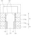
도 2는 본 개시의 일 실시 예에 따르는 강유전성 메모리 장치를 개략적으로 나타내는 단면도이다. 도 3a는 도 2의 A 영역의 확대도이며, 도 3b는 도 2의 B 영역의 확대도이다.2 is a cross-sectional view schematically illustrating a ferroelectric memory device according to an exemplary embodiment of the present disclosure. FIG. 3A is an enlarged view of region A of FIG. 2 , and FIG. 3B is an enlarged view of region B of FIG. 2 .
도 2, 도 3a 및 도 3b를 참조하면, 강유전성 메모리 장치(2)는 기판(101), 베이스 전도층(105), 채널층(150), 복수의 메모리 셀 트랜지스터(2a), 제어 트랜지스터(2b) 및 비트 라인 패턴(160)을 포함한다. 제어 트랜지스터(2b)는 복수의 메모리 셀 트랜지스터(2a)의 상부에 배치되며, 비트 라인 패턴(160)과 연결된다. 채널층(150)은 베이스 전도층(105)으로부터 수직 방향으로 연장될 수 있다. 복수의 메모리 셀 트랜지스터(2a) 및 제어 트랜지스터(2b)는 채널층(150)을 공유할 수 있다.Referring to FIGS. 2, 3A and 3B, the
기판(101)은 반도체 기판일 수 있다. 상기 반도체 기판은 일 예로서, 실리콘(Si) 기판, 갈륨비소(GaAs) 기판, 인듐인(InP, indium phosphide) 기판, 게르마늄(Ge) 기판, 또는 실리콘 게르마늄(SiGe) 기판일 수 있다. 상기 반도체 기판은 n형 또는 p형으로 도핑되어 전도성을 가질 수 있다. 다른 실시 예에서, 기판(101)은 실리콘-온-절연체(silicon-on-insulator) 기판과 같은 절연 기판일 수 있다. 도시되지는 않았지만, 기판(101)은 n형 또는 p형 도펀트가 도핑되어 형성되는 웰(well)을 포함할 수 있다. 기판(101)과 베이스 전도층(105) 사이에는 다양한 형태의 집적 회로가 배치될 수 있다.The
기판(101) 상에 베이스 전도층(105)이 배치된다. 일 실시 예에서, 베이스 전도층(105)은 일 예로서, 금속, 금속 질화물 또는 금속 실리사이드를 포함하는 도전성 박막일 수 있다. 다른 실시 예에서, 기판(101)이 반도체 기판일 때, 베이스 전도층(105)은 n형 또는 p형의 도펀트가 도핑된 기판(101)의 영역일 수 있다.A base
베이스 전도층(105) 상에 제1 내지 제8 층간 절연층(110a, 110b, 110c, 110d, 110e, 110f, 110g, 110h) 및 제1 내지 제7 게이트 전극층(210a, 210b, 210c, 210d, 210e, 210f, 210g)이 교대로 적층될 수 있다. 이때, 제1 층간 절연층(110a)은 베이스 전도층(105)과 접할 수 있다. 상기 복수의 강유전성 메모리 셀 트랜지스터(2a)는, 제1 내지 제6 게이트 전극층(210a, 210b, 210c, 210d, 210e, 210f)을 메모리 게이트 전극층으로서 구비할 수 있다. 제어 트랜지스터(2b)는 제7 게이트 전극층(210g)을 제어 게이트 전극층으로서 구비할 수 있다. 비록, 도 2에서는 설명의 편의상 제1 내지 제6 게이트 전극층(210a, 210b, 210c, 210d, 210e, 210f)에 각각 대응되는 6개의 메모리 셀 트랜지스터를 개시하고 있지만, 메모리 셀 트랜지스터의 개수는 한정되지 않을 수 있다. 즉, 다른 실시 예들에 있어서, 복수의 강유전성 메모리 셀 트랜지스터(2a)는 다양한 다른 개수의 메모리 셀 트랜지스터 및 상기 메모리 셀 트랜지스터에 대응되는 다른 개수의 층간 절연층을 구비할 수 있다.On the base
일 실시 예에 있어서, 제1 내지 제8 층간 절연층(110a, 110b, 110c, 110d, 110e, 110f, 110g, 110h)은 일 예로서, 절연성 산화물, 절연성 질화물, 절연성 산질화물 등을 포함할 수 있다. 제1 내지 제8 층간 절연층(110a, 110b, 110c, 110d, 110e, 110f, 110g, 110h)은 일 예로서 실리콘 산화물, 실리콘 질화물, 실리콘산질화물을 포함할 수 있다. 제1 내지 제7 게이트 전극층(210a, 210b, 210c, 210d, 210e, 210f, 210g)은 일 예로서, 금속, 전도성 금속 질화물, 전도성 금속 실리사이드, 전도성 금속 산화물, 전도성 금속카바이드 등을 포함할 수 있다. 제1 내지 제7 게이트 전극층(210a, 210b, 210c, 210d, 210e, 210f, 210g)은 일 예로서, 텅스텐, 티타늄, 구리, 루테늄, 텅스텐 질화물, 티타늄질화물, 탄탈륨질화물, 루테늄 산화물 텅스텐카바이드, 티타늄카바이드, 텅스텐실리사이드, 티타늄실리사이드, 탄탈륨실리사이드 또는 이들의 둘 이상의 조합을 포함할 수 있다.In one embodiment, the first to eighth
도 2를 다시 참조하면, 제1 내지 제8 층간 절연층(110a, 110b, 110c, 110d, 110e, 110f, 110g, 110h) 및 제1 내지 제7 게이트 전극층(210a, 210b, 210c, 210d, 210e, 210f, 210g)을 관통하여, 베이스 전도층(105)을 노출시키는 제1 트렌치(10)가 형성된다. 제1 트렌치(10)의 내부에는 베이스 전도층(105) 상에서 수직 방향으로 연장되는 채널층(150)이 배치될 수 있다. 채널층(150)은 도핑된 반도체 물질을 포함할 수 있다. 상기 도핑된 반도체 물질은 일 예로서, n형 또는 p형 도펀트를 구비하는 실리콘을 포함할 수 있다. 일 예로서, 채널층(150)은 n형의 도펀트가 약 1016/cm3 이상의 농도로 도핑된 실리콘층일 수 있다. 상기 n형 도펀트는 일 예로서, 인(P), 비소(As) 등을 포함할 수 있다.Referring back to FIG. 2 , the first to eighth
채널층(150)과 제1 내지 제8 층간 절연층(110a, 110b, 110c, 110d, 110e, 110f, 110g, 110h), 및 채널층(150)과 제1 내지 제7 게이트 전극층(210a, 210b, 210c, 210d, 210e, 210f, 210g) 사이에는 유전층이 배치될 수 있다. 도 2 및 도 3a를 참조하면, 일 실시 예에서, 채널층(150)와 제1 내지 제6 게이트 전극층(210a, 210b, 210c, 210d, 210e, 210f) 사이에는 상기 유전층으로서, 계면 절연층(141) 및 강유전층(142)이 배치될 수 있다. 마찬가지로, 채널층(150)과 제1 내지 제7 층간 절연층(110a, 110b, 110c, 110d, 110e, 110f, 110g) 사이에는 상기 유전층으로서, 계면 절연층(141) 및 강유전층(142)이 배치될 수 있다. 이때, 강유전층(142)은 대응되는 강유전성 메모리 셀 트랜지스터의 신호 정보를 저장할 수 있다. 제1 내지 제6 게이트 전극층(210a, 210b, 210c, 210d, 210e, 210f)은 복수의 강유전성 메모리 셀 트랜지스터(2a)의 메모리 게이트 전극층으로 각각 기능할 수 있다.The
계면 절연층(141)은 채널층(150)과 강유전층(142)이 직접 접하는 것을 방지하는 버퍼층의 역할을 수행할 수 있다. 채널층(150)과 강유전층(142)이 직접 접하는 경우, 접합 계면에서 결함 사이트가 생성되어 메모리 동작시 강유전층(142)의 전기적 보유 특성(retention)이 저하될 수 있기 때문이다. 계면 절연층(141)은 비정질 구조를 가질 수 있다. 계면 절연층(141)은 일 예로서, 실리콘 산화물, 실리콘 질화물, 알루미늄 산화물, 실리콘 산질화물 등을 포함할 수 있다.The interfacial
강유전층(142)은 강유전성 물질을 포함할 수 있다. 상기 강유전성 물질은 일 예로서, 하프늄 산화물, 지르코늄 산화물, 하프늄지르코늄 산화물 또는 이들의 둘 이상의 조합을 포함할 수 있다. 강유전층(142)은 상기 강유전성 물질에 주입되는 도펀트를 포함할 수 있다. 상기 도펀트는 일 예로서, 탄소, 실리콘, 마그네슘, 알루미늄, 이트륨, 질소, 게르마늄, 주석, 스트론튬, 납, 칼슘, 바륨, 티타늄, 지르코늄, 가돌리늄, 또는 이들의 둘 이상의 조합을 포함할 수 있다.The
일 실시 예에서, 채널층(150)와 제7 게이트 전극층(210g) 사이에는 상기 유전층으로서 제어 유전층(143)이 배치된다. 마찬가지로, 채널층(150)과 제8 층간 절연층(110h) 사이에는 상기 유전층으로서 제어 유전층(143)이 배치된다. 제어 유전층(143)은 상유전 특성을 가질 수 있다. 일 실시 예에서, 채널층(150)와 제7 게이트 전극층(210g) 사이에는 제어 유전층(143)을 제외한 다른 강유전층은 배치되지 않을 수 있다. 한편, 분극 스위칭이 완료된 후에, 스위칭된 분극 상태가 제어 유전층(143)의 내부에 저장되지 않음으로써, 제어 유전층(143)은 메모리 기능을 수행하지 않을 수 있다. 제어 유전층(143)은 일 예로서, 실리콘 산화물, 실리콘 질화물, 알루미늄 산화물, 실리콘 산질화물, 하프늄 산화물, 및 지르코늄 산화물 등과 같은 상유전 물질을 포함할 수 있다. 한편, 상기 하프늄 산화물 및 지르코늄 산화물의 경우, 화학양론비의 조절, 주입되는 도펀트의 조절 등을 통해, 제어 유전층(143)이 상유전성을 가지도록 제어될 수 있다.In an embodiment, a
제어 트랜지스터(2b)의 상부에는 채널층(150)과 전기적으로 연결되는 비트 라인 패턴(160)이 배치될 수 있다. 비트 라인 패턴(160)은 비트 라인의 일부분이거나, 상기 비트 라인과 전기적으로 연결되는 접속 패턴일 수 있다. 비트 라인 패턴(160)은 일 예로서, 금속, 전도성 금속 질화물, 전도성 금속 실리사이드 등을 포함할 수 있다.A
도 3b를 참조하면, 채널층(150)은 베이스 전도층(105)과 접할 수 있다. 이에 따라, 채널층(150)은 베이스 전도층(105)과 비트 라인 패턴(160) 사이에서 전하 전도의 경로로 기능할 수 있다. 베이스 전도층(105)의 바로 상부에 제1 층간 절연층(110a)이 배치됨으로써, 베이스 전도층(105)과 제1 게이트 전극층(210a) 사이의 통전을 방지할 수 있다.Referring to FIG. 3B , the
도 2를 다시 참조하면, 제1 내지 제8 층간 절연층(110a, 110b, 110c, 110d, 110e, 110f, 110g, 110h) 및 제1 내지 제7 게이트 전극층(210a, 210b, 210c, 210d, 210e, 210f, 210g)을 관통하여, 베이스 전도층(105)을 노출시키는 제2 트렌치(20)가 형성될 수 있다. 제2 트렌치(20)의 측벽에는 라이너 절연층(170)이 배치될 수 있다. 라이너 절연층(170)은 일 예로서, 절연성 산화물, 절연성 질화물, 절연성 산질화물을 포함할 수 있다.Referring back to FIG. 2 , the first to eighth
제2 트렌치(20)의 내부는 제1 소스 라인 접속 패턴(250)이 배치될 수 있다. 제2 트렌치(20)의 외부에 제1 소스 라인 접속 패턴(250)과 연결되는 제2 소스 라인 접속 패턴(260)이 배치될 수 있다. 제1 및 제2 소스 라인 접속 패턴(250, 260)은 베이스 전도층(105)을 소스 라인(미도시)과 전기적으로 연결시킬 수 있다. 제1 및 제2 소스 라인 접속 패턴(250, 260)은 금속, 전도성 금속 질화물, 전도성 금속 산화물, 전도성 금속 카바이드, 전도성 금속 실리사이드를 포함할 수 있다. 제1 및 제2 소스 라인 접속 패턴(250, 260)은 일 예로서, 텅스텐, 티타늄, 구리, 루테늄, 텅스텐 질화물, 티타늄질화물, 탄탈륨질화물, 루테늄 산화물 텅스텐카바이드, 티타늄카바이드, 텅스텐실리사이드, 티타늄실리사이드, 탄탈륨실리사이드 또는 이들의 둘 이상의 조합을 포함할 수 있다.A first source
상술한 바와 같이, 강유전성 메모리 장치(2)는 베이스 전도층(105) 상에서 수직으로 연장되는 채널층(150)을 구비할 수 있다. 복수의 강유전성 메모리 셀 트랜지스터(2a)와 제어 트랜지스터(2b)는 채널층(150)을 공유할 수 있다. 제어 트랜지스터(2b)의 제어 게이트 전극층인 제7 게이트 전극층(210g)에 인가되는 전압을 통해, 채널층(150)을 따라 베이스 전도층(105)과 비트 라인 패턴(160) 사이에서 전도되는 채널 전류를 제어할 수 있다. 상기 채널 전류는 상기 강유전층에 대한 분극 제어 전류로 기능할 수 있다.As described above, the
일 실시 예에 따르면, 복수의 강유전성 메모리 셀 트랜지스터(2a) 중 선택되는 적어도 하나의 메모리 셀 트랜지스터의 게이트 전극층에 상기 제2 쓰기 전압이 인가될 때, 상기 분극 제어 전류가 상기 적어도 하나의 메모리 셀 트랜지스터 내 강유전층의 분극을 스위칭시킬 수 있다. 상기 분극 스위칭 동작을 통해, 상기 적어도 하나의 메모리 셀 트랜지스터에 대한 쓰기 동작이 수행될 수 있다.According to an embodiment, when the second write voltage is applied to a gate electrode layer of at least one memory cell transistor selected from among the plurality of ferroelectric
도 4는 본 개시의 일 실시 예에 따르는 강유전층의 히스테리시스 그래프이다. 도 4의 그래프(400)를 참조하면, 본 개시의 일 실시 예에 따르는 강유전층은, 상기 강유전층의 양단에 인가되는 전계에 따라, 제1 및 제2 항전계(Ec, -Ec), 제1 및 제2 잔류 분극(Pr, -Pr)을 구비하는 히스테리시스 동작을 나타낼 수 있다. 먼저, 소정의 제2 잔류 분극(-Pr)을 구비하는 강유전층에 양의 방향의 전계를 인가하면, 전계가 증가할수록 음의 극성을 가지는 분극의 크기가 감소할 수 있다. 상기 인가 전계가 제1 항전계(Ec)보다 증가하면, 상기 강유전층 내부에서는 음의 값을 가지는 분극으로부터 양의 값을 가지는 분극으로, 분극 상태가 스위칭될 수 있다. 상기 전계가 제1 포화 전계(Es)에 도달하면, 상기 강유전층은 제1 포화 분극(Ps)을 가질 수 있다. 상기 인가 전계를 상기 제1 포화 전계(Es) 이하로 다시 감소시키면, 상기 분극의 크기가 감소할 수 있다. 상기 인가 전계를 제거하면, 상기 강유전층은 제1 잔류 분극(Pr)을 가질 수 있다.4 is a hysteresis graph of a ferroelectric layer according to an embodiment of the present disclosure. Referring to the
이어서, 상기 제1 잔류 분극(Pr)을 구비하는 강유전체에 음의 방향의 전계를 인가할 때, 상기 전계의 절대치가 증가할수록 양의 값을 가지는 분극의 크기가 감소할 수 있다. 상기 인가 전계의 절대치가 제2 항전계(-Ec)의 절대치보다 증가하면, 상기 강유전층 내부에서는 양의 값을 가지는 분극으로부터 음의 값을 가지는 분극으로, 분극 상태가 스위칭될 수 있다. 상기 전계가 제2 포화 전계(-Es)에 도달하면, 상기 강유전층은 제2 포화 분극(-Ps)을 가질 수 있다. 상기 인가 전계의 절대치를 상기 제2 포화 전계(-Es)의 절대치 이하로 다시 감소시키면, 음의 값을 가지는 분극의 크기가 감소할 수 있다. 상기 인가 전계를 제거하면, 상기 강유전층은 상기 제2 잔류 분극(-Pr)을 가질 수 있다.Subsequently, when a negative electric field is applied to the ferroelectric having the first remanent polarization Pr, the magnitude of the positive polarization may decrease as the absolute value of the electric field increases. When the absolute value of the applied electric field is greater than the absolute value of the second coercive electric field (-Ec), the polarization state may be switched from a positive polarization to a negative polarization inside the ferroelectric layer. When the electric field reaches the second saturation electric field (-Es), the ferroelectric layer may have a second saturation polarization (-Ps). When the absolute value of the applied electric field is reduced again to be less than or equal to the absolute value of the second saturation electric field (-Es), the polarization having a negative value may be reduced. When the applied electric field is removed, the ferroelectric layer may have the second remanent polarization (-Pr).
도 5a 및 도 5b는 강유전성 메모리 장치의 동작 원리를 개략적으로 설명하는 도면이다도 5a 및 도 5b를 참조하면, 강유전성 메모리 장치(500)는 기판(501), 강유전층(530), 및 게이트 전극층(540)을 구비한다. 게이트 전극층(540)의 양단의 기판(501) 영역에 소스 영역(510)과 드레인 영역(520)이 각각 배치될 수 있다. 기판(501)은 p형으로 도핑된 반도체 기판일 수 있으며, 소스 영역(510)과 드레인 영역(520)은 n형으로 도핑된 기판(501)의 영역일 수 있다.5A and 5B are views schematically illustrating the operating principle of the ferroelectric memory device. Referring to FIGS. 5A and 5B, the
도 5a를 참조하면, 강유전층(530)은 제1 분극 배향(Pdn)을 가지는 잔류 분극을 가질 수 있다. 일 예로서, 상기 잔류 분극은 도 4의 제1 잔류 분극(Pr)에 대응될 수 있다. 이때, 상기 제1 분극 배향(Pdn)은 게이트 전극층(540)으로부터 기판(501)으로의 방향일 수 있다. 즉, 기판(501)과 인접하는 강유전층(530)의 내부 영역에 양의 전하가 대전되며, 게이트 전극층(540)과 인접하는 강유전층(530)의 내부 영역에 음의 전하가 대전될 수 있다. 이때, 제1 분극 배향(Pdn)을 가지는 잔류 분극은 게이트 전극층(540) 하부에 위치하는 기판(501)의 채널 영역에 전자(501e)를 유도할 수 있다.Referring to FIG. 5A , the
도 5b를 참조하면, 도 5a의 강유전성 메모리 장치(500)의 게이트 전극층(540)과 기판(501) 사이에 전압을 인가한다. 일 예로서, 소정의 음의 극성을 가지는 게이트 전압(VG)을 게이트 전극층(540)에 인가하고, 기판(501)을 접지시킬 수 있다. 상기 인가되는 게이트 전압(VG)의 절대치가 강유전층(530)의 항전계의 절대치에 대응되는 전압보다 증가할 때, 강유전층(530) 내부에서 분극 스위칭이 발생한다. 일 예로서, 상기 게이트 전압(VG)의 절대치가 도 4의 제2 항전계(-Ec)의 절대치에 대응되는 전압보다 증가하면, 강유전층(530) 내부의 분극 배향이 제2 분극 배향(Pup)으로 스위칭될 수 있다. 이때, 기판(501)의 채널 영역에는 홀(501h)이 유도될 수 있다. 상기 게이트 전압(VG)의 절대치를 도 4의 제2 포화 전계(-Es)에 대응되는 전압 보다 증가시킨 후에 다시 제거하면, 강유전층(530)은 도 4의 제2 잔류 분극(-Pr)에 대응되는 잔류 분극을 구비할 수 있다. 도시되지는 않았지만, 도 5b의 강유전성 메모리 장치(500)의 게이트 전극층(540)에 대하여, 제1 항전계(Ec)에 대응되는 전압보다 큰 게이트 전압(VG)을 인가하면, 강유전층(530) 내부의 분극 배향이 제1 분극 배향(Pdn)으로 스위칭될 수 있다. 이때, 기판(501)의 채널 영역에는 전자(501e)가 다시 유도될 수 있다.Referring to FIG. 5B , a voltage is applied between the
도 6a 내지 도 6c는 본 개시의 일 실시 예에 따르는 강유전성 메모리 장치의 동작 원리를 개략적으로 설명하는 도면이다. 도 6a 내지 도 6c를 참조하면, 강유전성 메모리 장치(600)는 기판(601), 강유전층(630) 및 게이트 전극층(640)을 구비한다. 게이트 전극층(640)의 양단의 기판(601) 영역에 소스 영역(610)과 드레인 영역(620)이 각각 배치될 수 있다. 기판(601)은 p형으로 도핑된 반도체 기판일 수 있으며, 소스 영역(610)과 드레인 영역(620)은 n형으로 도핑된 기판(601)의 영역일 수 있다.6A to 6C are views schematically illustrating an operating principle of a ferroelectric memory device according to an exemplary embodiment of the present disclosure. Referring to FIGS. 6A to 6C , a
도 6a를 참조하면, 초기 상태로서, 강유전층(630)은 제2 분극 배향(Pup)을 가지는 소정의 잔류 분극(P0)을 구비할 수 있다. 일 예로서, 상기 잔류 분극(P0)은 도 4의 제2 잔류 분극(-Pr)에 대응될 수 있다.Referring to FIG. 6A , as an initial state, the
도 6b 및 도 6c를 참조하면, 드레인 영역(620)에 소정의 드레인 전압(VD)을 인가하고, 소스 영역(610)을 접지함으로써, 소스 영역(610)과 드레인 영역(620) 사이에 전위차를 발생시킬 수 있다. 일 예로서, 드레인 전압(VD)은 양의 극성을 가질 수 있다.6B and 6C, a potential difference between the
일 실시 예에서, 기판(601)을 접지한 상태에서, 게이트 전극층(640)에 0V 보다 크고 강유전층(630)의 항전계에 대응되는 전압보다 작은 게이트 전압(VG)을 인가할 수 있다. 이 경우, 상기 게이트 전압(VG)은 강유전층(630)의 분극 스위칭을 발생시키지 못하지만, 기판(601) 내 채널 영역의 저항을 감소시킬 수 있다. 그 결과, 소스 영역(610)과 드레인 영역(620) 사이에서 상기 채널 영역을 통과하는 제1 및 제2 전자 전도(Fe1, Fe2)를 발생시킬 수 있다. 이 때, 상기 제1 및 제2 전자 전도(Fe1, Fe2)가 진행되는 동안, 전자(601e)은 강유전층(630)과 인접하는 상기 채널 영역을 음의 전하로 대전시킬 수 있다.In an embodiment, a gate voltage (VG ) greater than 0V and less than a voltage corresponding to the coercive field of the
한편, 도 6b 및 도 6c에서와 같이, 기판(601)을 접지한 상태에서, 게이트 전극층(640)에 강유전층(630)의 항전계에 대응되는 전압보다 큰 게이트 전압(VG)을 인가할 수 있다. 이 경우, 상기 게이트 전압(VG)은 강유전층(630)의 분극 스위칭을 발생시킬 수 있으며, 상기 분극 스위칭 결과 강유전층(630)은 제1 분극 배향(Pdn)을 가지는 소정의 잔류 분극(P1)을 구비할 수 있다. 이 때, 상기 분극 스위칭의 정도(degree)는 상기 채널 영역을 통과하는 전자(601e)의 밀도에 따라 변화할 수 있다. 일 예로서, 도 6b 및 도 6c의 실시 예를 서로 비교하면, 동일한 크기의 게이트 전압(VG)이 인가될 때, 도 6b의 실시 예에 도시되는 제1 전자 전도(Fe1)의 전하량이 도 6c의 실시 예에 도시되는 제2 전자 전도(Fe2)의 전하량보다 크도록 제어될 수 있다. 즉, 도 6b의 실시 예에서 소스 영역(610) 및 드레인 영역(620) 사이에 전도하는 전류가 도 6c의 실시 예에서 소스 영역(610) 및 드레인 영역(620) 사이에 전도하는 전류보다 클 수 있다. 이에 따라, 도 6b의 실시 예에서, 상기 채널층을 점유하는 전하량이 도 6c의 실시 예의 전하량보다 상대적으로 많으므로, 상기 채널층에 인접하는 강유전층(630)의 내부 영역을 양의 전하로 대전시키는 구동력이 도 6b의 실시 예에서 상대적으로 클 수 있다. 이에 따라, 도 6b의 실시예에서는, 강유전층(630) 내에서 발생하는 분극 스위칭의 정도가 상대적으로 클 수 있다. 그 결과, 상기 분극 스위칭 후에 강유전층(630)은 제2 분극 배향(Pdn)을 가지는 잔류 분극(P1)을 가질 수 있다. 일 예로서, 상기 잔류 분극(P1)은 도 4의 제1 잔류 분극(Pr)에 대응될 수 있다.Meanwhile, as shown in FIGS. 6B and 6C, a gate voltage (VG ) greater than the voltage corresponding to the coercive field of the
반대로, 도 6c의 실시 예에서는, 상기 채널 영역을 점유하는 전하량이 상대적으로 적으므로, 상기 분극 스위칭의 구동력이 상대적으로 작을 수 있다. 그 결과, 도 6b의 실시 예에서와 같이, 분극 스위칭이 충분히 일어나지 않아서, 도 6a에 도시되는 초기 상태의 제2 분극 배향(Pup)을 유지하는 잔류 분극(P2)을 가질 수 있다. 또는, 도시되지는 않았지만, 제1 분극 배향(Pdn)으로의 분극 스위칭이 발생하더라도, 도 6b의 실시예의 잔류 분극(P1)보다는 작은 잔류 분극값을 가질 수 있다.Conversely, in the embodiment of FIG. 6C , since the amount of charge occupying the channel region is relatively small, the driving force of the polarization switching may be relatively small. As a result, as in the embodiment of FIG. 6B, polarization switching does not sufficiently occur, and thus, a residual polarization P2 maintaining the second polarization orientation Pup of the initial state shown in FIG. 6A may be obtained. Alternatively, although not shown, even if polarization switching to the first polarization orientation (Pdn ) occurs, the residual polarization value may be smaller than that of the residual polarization (P1 ) of the embodiment of FIG. 6B .
상술한 바와 같이, 본 개시의 실시 예에서는, 강유전성 메모리 장치의 게이트 전극층에 강유전층의 항전계에 대응되는 전압 보다 큰 쓰기 전압을 인가한 상태에서, 채널층을 통과하는 전류를 제어하여 상기 강유전층에 서로 다른 정도의 분극 스위칭을 발생시킬 수 있다. 상기 서로 다른 정도의 분극 스위칭 결과, 상기 강유전층 내에는 서로 다른 잔류 분극이 저장될 수 있다. 상기의 동작 원리를 이용하여, 강유전층 내에 멀티 레벨의 신호 정보를 비휘발적으로 저장할 수 있다. 상기 채널 영역을 통과하는 전류의 크기는, 후술하는 바와 같이 제어 트랜지스터에 의해 제어될 수 있다. As described above, in an embodiment of the present disclosure, in a state in which a write voltage higher than the voltage corresponding to the coercive field of the ferroelectric layer is applied to the gate electrode layer of the ferroelectric memory device, the current passing through the channel layer is controlled to control the ferroelectric layer. can generate different degrees of polarization switching. As a result of the polarization switching of different degrees, different remnant polarizations may be stored in the ferroelectric layer. Using the above operating principle, multi-level signal information can be stored in a non-volatile manner in the ferroelectric layer. The amount of current passing through the channel region may be controlled by a control transistor as will be described later.
도 7은 본 개시의 일 실시 예에 따르는 강유전성 메모리 장치의 구동 방법을 개략적으로 설명하는 순서도이다. 도 8 내지 도 10은 본 개시의 일 실시 예에 따르는 강유전성 메모리 장치의 구동 방법을 개략적으로 설명하는 모식도이다. 일 실시 예에서, 상기 강유전성 메모리 장치의 구동 방법은 도 1 및 도 2와 관련하여 상술한 강유전성 메모리 장치(1)를 이용하여 구현할 수 있다.7 is a flowchart schematically illustrating a method of driving a ferroelectric memory device according to an exemplary embodiment of the present disclosure. 8 to 10 are schematic diagrams schematically illustrating a method of driving a ferroelectric memory device according to an exemplary embodiment of the present disclosure. In an embodiment, the method of driving the ferroelectric memory device may be implemented using the
도 7의 S110을 참조하면, 기판(100) 상의 베이스 전도층(105)으로부터 수직으로 연장되는 채널층(150), 채널층(150)을 공유하는 복수의 강유전성 메모리 셀 트랜지스터(2a) 및 제어 트랜지스터(2b), 및 채널층(150)과 전기적으로 연결되는 비트 라인 패턴(160)을 구비하는 소자 구조물을 제공한다. 이때, 상기 복수의 강유전성 메모리 셀 트랜지스터(2a)는 강유전층(142) 및 메모리 게이트 전극층(210a, 210b, 210c, 210d, 210e, 210f)을 포함하고 제어 트랜지스터(2b)는 제어 유전층(143) 및 제어 게이트 전극층(210g)을 포함한다. 복수의 강유전성 메모리 셀 트랜지스터(2a)가 강유전층(142) 및 채널층(150)을 서로 공유하므로, 복수의 강유전성 메모리 셀 트랜지스터(2a)가 각각 제어하는 채널층(150)의 길이는 대응되는 메모리 게이트 전극층(210a, 210b, 210c, 210d, 210e, 120f)의 두께에 의해 각각 결정될 수 있다. 또한, 제어 트랜지스터(2b)가 제어하는 채널층(150)의 길이는 제어 게이트 전극층(210g)의 두께에 의해 결정될 수 있다. 상기 소자 구조물은 일 실시 예로서, 도 8에 도시되는 스트링(100a)으로 구현될 수 있다. 도 8에 도시되는 스트링(100a)은 도 1과 관련하여 상술한 복수의 스트링(100a, 100b) 중의 어느 하나일 수 있다.Referring to S110 of FIG. 7 , a
S120을 참조하면, 제어 트랜지스터(2b)를 이용하여 채널층(150)을 따라 전도되는 분극 제어 전류를 결정한다. 일 실시 예에 있어서, 상기 분극 제어 전류를 결정하는 단계는 다음과 같이 진행될 수 있다. 먼저, 소정의 메모리 셀의 강유전층(142)의 분극 스위칭에 요청되는 이동 전류(displacement current)를 결정한다. 상기 이동 전류는, 상기 소정의 메모리 셀의 강유전층(142)에 목적하는 분극을 기록하기 위해 채널층(150) 내에 분포하도록 요구되는 전하량에 의해 결정될 수 있다. 이어서, 상기 이동 전류에 대응되는 채널 전류가 채널층(150)을 통해 전도하도록, 제어 게이트 전극층(210g)에 인가되는 제어 전압의 크기를 결정할 수 있다. 일 실시 예에 있어서, 상기 채널 전류는 후술하는 바와 같이, 강유전층(150)에 기록되는 분극의 크기에 따라, 서로 다른 둘 이상의 값을 가질 수 있으며, 상기 채널 전류의 크기에 따라, 상기 제어 전압의 크기가 결정될 수 있다.Referring to S120 , the polarization control current conducted along the
S130을 참조하면, 베이스 전도층(105)과 비트 라인 패턴(160) 사이에서, 채널층(150)을 따라 상기 분극 제어 전류를 전도시킨다. 일 실시 예에 있어서, 상기 분극 제어 전류를 전도시키는 단계는 복수의 강유전성 메모리 셀 트랜지스터(2a)의 메모리 게이트 전극(210a, 210b, 210c, 210d, 210e, 210f)에 제1 쓰기 전압을 인가하여, 채널층(150)의 전기적 저항을 감소시키는 단계를 포함할 수 있다. 이때, 상기 제1 쓰기 전압은 강유전층(142)의 항전계의 절대치에 대응되는 전압의 크기보다 작을 수 있다. 즉, 상기 제1 쓰기 전압이 메모리 게이트 전극(210a, 210b, 210c, 210d, 210e, 210f)에 인가될 때, 상기 분극 제어 전류는 복수의 강유전성 메모리 셀 트랜지스터(2a)에 속하는 강유전층(142)에 대해 분극 스위칭을 발생시키지 못한다. 한편, 도 9를 참조하면, 제어 트랜지스터(2b)에 의해 제어되는 분극 제어 전류(Ip)가 제1 내지 제6 채널 저항(Rch1, Rch2, Rch3, Rch4, Rch5, Rch6, Rch-t1) 및 제1 제어 저항(Rch-t1)이 직렬로 연결된 회로를 통과하여 소스 라인(SL)과 비트 라인(BL1) 사이를 전도하는 현상이 도시되고 있다.Referring to S130 , the polarization control current is conducted along the
S140을 참조하면, 복수의 강유전성 메모리 셀 트랜지스터(2a) 중 소정의 메모리 셀 트랜지스터의 메모리 게이트 전극(210a, 210b, 210c, 210d, 210e, 210f)을 턴온시켜, 상기 분극 제어 전류가 상기 소정의 메모리 셀의 강유전층(142) 내에 분극을 기록하도록 할 수 있다. 일 실시 예에 있어서, 메모리 게이트 전극(210a, 210b, 210c, 210d, 210e, 210f)을 턴온시키는 단계는 메모리 게이트 전극(210a, 210b, 210c, 210d, 210e, 210f)에 제2 쓰기 전압을 인가하는 단계를 포함할 수 있다. 이때, 상기 제2 쓰기 전압의 크기는 강유전층(142)의 항전계의 절대치에 대응되는 전압의 크기보다 클 수 있다. 즉, 상기 제2 쓰기 전압이 메모리 게이트 전극층(210a, 210b, 210c, 210d, 210e, 210f)에 인가될 때, 상기 분극 제어 전류는 상기 소정의 메모리 셀 트랜지스터의 강유전층(142)에 대해 분극 스위칭을 발생시킬 수 있다. 한편, 도 10을 참조하면, 복수의 강유전성 메모리 셀 트랜지스터(2a) 중 제4 메모리 셀 트랜지스터(MC4)가 선택되는 경우, 분극 제어 전류(Ip)는 채널층(ch4)에 전하를 대전시킬 수 있다. 메모리 게이트 전극층(G4)에 상기 제2 쓰기 전압이 인가될 때, 상기 대전된 전하는 강유전층(F4) 내의 분극을 스위칭시킬 수 있다.Referring to step S140, by turning on the
상술한 바와 같이, 상기 소정의 메모리 셀 트랜지스터의 강유전층 내에 분극을 기록하는 단계는, 상기 분극 제어 전류의 크기를 변화시켜, 상기 강유전층 의 분극 배향을 다양한 정도(degree)로 스위칭시키는 단계를 포함할 수 있다. 이로써, 단일의 메모리 셀 트랜지스터의 상기 강유전층 내에 멀티 레벨 신호 정보를 저장할 수 있다.As described above, the step of writing the polarization into the ferroelectric layer of the given memory cell transistor includes the step of switching the polarization orientation of the ferroelectric layer to various degrees by changing the magnitude of the polarization control current. can do. Accordingly, multi-level signal information can be stored in the ferroelectric layer of a single memory cell transistor.
도 11은 본 개시의 다른 실시 예에 따르는 강유전성 메모리 장치를 개략적으로 나타내는 단면도이다. 도 12는 도 11의 C 영역의 확대도이다.11 is a cross-sectional view schematically illustrating a ferroelectric memory device according to another exemplary embodiment of the present disclosure. FIG. 12 is an enlarged view of area C of FIG. 11 .
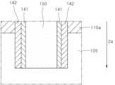
도 11 및 도 12를 참조하면, 강유전성 메모리 장치(3)는 기판(1101), 베이스 전도층(1105), 채널층(1500), 복수의 메모리 셀 트랜지스터(3a) 및 비트 라인 패턴(1600)을 포함한다. 채널층(1500)은 베이스 전도층(1105)으로부터 수직 방향으로 연장될 수 있다. 복수의 메모리 셀 트랜지스터(3a)는 채널층(1500)을 공유할 수 있다. 도 12에 도시되는 바와 같이, 복수의 메모리 셀 트랜지스터(3a)는 채널층(1500)에 인접하여 배치되는 강유전체 구조물(1400)을 포함할 수 있다.11 and 12, a
기판(1101)은 반도체 기판일 수 있다. 기판(1101)의 구성은 도 2와 관련하여 상술한 기판(101)의 구성과 실질적으로 동일할 수 있다. 기판(1101) 상에 베이스 전도층(1105)이 배치된다. 베이스 전도층(1105)의 구성은 도 2와 관련하여 상술한 베이스 전도층(105)의 구성과 실질적으로 동일할 수 있다.The
베이스 전도층(1105) 상에 제1 내지 제7 층간 절연층(1110a, 1110b, 1110c, 1110d, 1110e, 1110f, 1110g) 및 제1 내지 제6 게이트 전극층(1210a, 1210b, 1210c, 1210d, 1210e, 1210f)이 교대로 적층될 수 있다. 이때, 제1 층간 절연층(1110a)은 베이스 전도층(1105)과 접할 수 있다. 상기 복수의 강유전성 메모리 셀 트랜지스터(3a)는, 제1 내지 제6 게이트 전극층(1210a, 1210b, 1210c, 1210d, 1210e, 1210f)을 메모리 게이트 전극층으로서 구비할 수 있다. 비록, 도 11에서는 설명의 편의상 제1 내지 제6 게이트 전극층(1210a, 1210b, 1210c, 1210d, 1210e, 1210f)에 각각 대응되는 6개의 메모리 셀 트랜지스터를 개시하고 있지만, 메모리 셀 트랜지스터의 개수는 한정되지 않을 수 있다. 즉, 다른 실시 예들에 있어서, 복수의 강유전성 메모리 셀 트랜지스터(3a)는 다양한 다른 개수의 메모리 셀 트랜지스터 및 상기 메모리 셀 트랜지스터에 대응되는 다른 개수의 층간 절연층을 구비할 수 있다.The first to seventh
제1 내지 제7 층간 절연층(1110a, 1110b, 1110c, 1110d, 1110e, 1110f, 1110g) 및 제1 내지 제6 게이트 전극층(1210a, 1210b, 1210c, 1210d, 1210e, 1210f)의 구성은 도 2와 관련하여 상술한 제1 내지 제7 층간 절연층(110a, 110b, 110c, 110d, 110e, 110f, 110g) 및 제1 내지 제6 게이트 전극층(210a, 210b, 210c, 210d, 210e, 210f)의 구성과 실질적으로 동일할 수 있다.The configurations of the first to seventh
도 11을 다시 참조하면, 제1 내지 제7 층간 절연층(1110a, 1110b, 1110c, 1110d, 1110e, 1110f, 1110g) 및 제1 내지 제6 게이트 전극층(1210a, 1210b, 1210c, 1210d, 1210e, 1210f, 1210g)을 관통하여, 베이스 전도층(1105)을 노출시키는 제1 트렌치(1000)가 형성된다. 트렌치(1000)의 내부에는 베이스 전도층(1105) 상에서 수직 방향으로 연장되는 채널층(1500)이 배치될 수 있다. 트렌치(1000) 및 채널층(1500)의 구성은 도 2와 관련하여 상술한 트렌치(10) 및 채널층(150)의 구성과 실질적으로 동일할 수 있다.Referring back to FIG. 11 , the first to seventh
채널층(1500)과 제1 내지 제7 층간 절연층(1110a, 1110b, 1110c, 1110d, 1110e, 1110f, 1110g) 및 채널층(1500)과 제1 내지 제6 게이트 전극층(1210a, 1210b, 1210c, 1210d, 1210e, 1210f, 1210g) 사이에는 강유전체 구조물(1400)이 배치될 수 있다.The
강유전체 구조물(1400)은 서로 다른 항전계를 구비하는 복수의 강유전층을 포함할 수 있다. 일 실시 예로서, 도 11 및 도 12에서는 서로 다른 항전계를 구비하는 제1 내지 제3 강유전층(1420, 1430, 1440)이 개시된다. 하지만, 강유전체 구조물(1400)을 구성하는 강유전층의 개수는 한정되지 않을 수 있다. 즉, 강유전체 구조물(1400)은 다른 다양한 개수의 강유전층을 가질 수 있다.The
도 11 및 도 12를 참조하면, 강유전체 구조물(1400)은 채널층(1500)과 접합 하는 계면 절연층(1410)을 더 포함할 수 있다. 계면 절연층(1410)은 제1 강유전층(1420)과 채널층(1500)이 직접 접하는 것을 방지하는 버퍼층의 역할을 수행할 수 있다. 채널층(1500)과 제1 강유전층(1420)이 직접 접하는 경우, 접합 계면에서 결함 사이트가 생성되어 소자 동작시 강유전체 구조물(1400)의 전기적 보유 특성(retention)이 저하될 수 있기 때문이다.Referring to FIGS. 11 and 12 , the
일 실시 예에서, 제1 내지 제3 강유전층(1420, 1430, 1440)은 강유전성 물질을 포함할 수 있다. 상기 강유전성 물질은 일 예로서, 하프늄 산화물, 지르코늄 산화물, 하프늄지르코늄 산화물 또는 이들의 조합을 포함할 수 있다. 일 실시 예에서, 제1 내지 제3 강유전층(1420, 1430, 1440) 중 적어도 하나는 도펀트를 포함할 수 있다. 상기 도펀트는 일 예로서, 탄소, 실리콘, 마그네슘, 알루미늄, 이트륨, 질소, 게르마늄, 주석, 스트론튬, 납, 칼슘, 바륨, 티타늄, 지르코늄, 가돌리늄 또는 이들의 조합을 포함할 수 있다.In an embodiment, the first to third
제1 내지 제3 강유전층(1420, 1430, 1440)은 서로 다른 항전계를 가질 수 있다. 상기 항전계는 외부의 자극에 대항하여, 강유전층이 종래의 분극 배향을 유지하려는 저항력으로 해석될 수 있다. 일 실시 예에서, 상기 서로 다른 항전계는, 제1 내지 제3 강유전층(1420, 1430, 1440)에 대해 서로 다른 농도로 도펀트를 주입하여 강유전층 내부의 스트레인(strain)을 변경시킴으로써 구현될 수 있다. 다른 실시 예에서, 상기 서로 다른 항전계는, 제1 내지 제3 강유전층(1420, 1430, 1440)이 서로 다른 결정립 크기를 가지도록 제어하여 분극 도메인의 크기를 변경시킴으로써, 구현될 수 있다. 제1 내지 제3 강유전층(1420, 1430, 1440)가 서로 다른 항전계를 가짐으로써, 제1 내지 제3 강유전층(1420, 1430, 1440)의 분극 스위칭은 각각의 항전계 이상의 크기를 가지는 외부 전계가 인가될 때, 각각 발생할 수 있다.The first to third
채널층(1500)의 상부에는 채널층(1500)과 전기적으로 연결되는 비트 라인 패턴(1600)이 배치될 수 있다. 비트 라인 패턴(1600)은 비트 라인의 일부분이거나, 상기 비트 라인과 전기적으로 연결되는 접속 패턴일 수 있다. 비트 라인 패턴(1600)의 구성은 도 2와 관련하여 상술한 비트 라인 패턴(160)의 구성과 실질적으로 동일하다.A
도 11을 다시 참조하면 제1 내지 제7 층간 절연층(1110a, 1110b, 1110c, 1110d, 1110e, 1110f, 1110g) 및 제1 내지 제6 게이트 전극층(1210a, 1210b, 1210c, 1210d, 1210e, 1210f, 1210g)을 관통하여, 베이스 전도층(1105)을 노출시키는 제2 트렌치(2000)가 형성될 수 있다. 제2 트렌치(2000)의 측벽에는 라이너 절연층(1700)이 배치될 수 있다. 제2 트렌치(2000)의 내부는 제1 소스 라인 접속 패턴(2500)이 배치될 수 있다. 제2 트렌치(2000)의 외부에는 제1 소스 라인 접속 패턴(2500)과 연결되는 제2 소스 라인 접속 패턴(2600)이 배치될 수 있다. 제1 및 제2 소스 라인 접속 패턴(2500, 2600)은 베이스 전도층(1105)을 소스 라인(미도시)과 전기적으로 연결시킬 수 있다. 제2 트렌치(2000), 라이너 절연층(1700), 제1 및 제2 소스 라인 접속 패턴(2500, 2600)의 구성은 도 2와 관련하여 상술한 제2 트렌치(20), 라이너 절연층(170), 제1 및 제2 소스 라인 접속 패턴(250, 260)의 구성과 실질적으로 동일하다.Referring back to FIG. 11 , the first to seventh
상술한 바와 같이, 본 개시의 실시 예에 따르는 강유전성 메모리 장치는, 수직 방향으로 연장되는 채널층과 수평 방향으로 연장되는 메모리 게이트 전극층 사이에 배치되는 강유전체 구조물을 구비한다. 상기 강유전체 구조물은 서로 다른 항전계를 구비하는 복수의 강유전층을 포함할 수 있다. 상기 강유전체 구조물의 분극 상태가, 서로 다른 항전계를 가지는 복수의 강유전층에 의해 제어됨으로써, 소정의 강유전성 메모리 셀 트랜지스터 내에 복수의 신호 정보를 저장할 수 있다.As described above, a ferroelectric memory device according to an embodiment of the present disclosure includes a ferroelectric structure disposed between a channel layer extending in a vertical direction and a memory gate electrode layer extending in a horizontal direction. The ferroelectric structure may include a plurality of ferroelectric layers having different coercive fields. Since the polarization state of the ferroelectric structure is controlled by a plurality of ferroelectric layers having different coercive fields, a plurality of signal information can be stored in a predetermined ferroelectric memory cell transistor.
도 13은 본 개시의 일 실시 예에 따르는 강유전성 메모리 장치의 구동 방법을 개략적으로 설명하는 도면이다. 도 13의 구동 방법은 도 11 및 도 12와 관련하여 상술한 강유전성 메모리 장치(3)를 이용하여 구현할 수 있다. 구체적인 실시 예에서, 도 14와 관련하여 설명하는 강유전성 메모리 장치(3)의 쓰기 방법은 도 5a 및 도 5b와 관련하여 상술한 동작 원리를 적용할 수 있다. 즉, 강유전성 메모리 장치(3) 내 복수의 강유전성 메모리 셀 트랜지스터(3a) 중에서, 소정의 강유전성 메모리 셀 트랜지스터가 선택될 수 있다. 이어서, 선택된 강유전성 메모리 셀 트랜지스터의 메모리 게이트 전극층을 통하여, 복수의 강유전층(1420, 1430, 1440) 중 어느 하나의 항전계보다 큰 전계가 인가될 때, 강유전체 구조물(1400) 내부에서 분극 스위칭이 발생할 수 있다.13 is a diagram schematically illustrating a method of driving a ferroelectric memory device according to an exemplary embodiment of the present disclosure. The driving method of FIG. 13 can be implemented using the
도 13의 그래프(3000)는 강유전체 구조물(1400)에 인가되는 전계에 따라 변화하는 잔류 분극(Pr)을 도시하고 있다. 일 예로서, 강유전체 구조물(1400)은 제1 내지 제3 강유전층(1420, 1430, 1440)을 구비하며, 제1 내지 제3 강유전층(1420, 1430, 1440)은 각각 대응되는 제1 내지 제3 항전계(Ec1, Ec2, Ec3)를 구비할 수 있다. 이때, 상기 항전계는, 제3 항전계(Ec3), 제2 항전계(Ec2), 및 제1 항전계(Ec1) 순으로 큰 값을 가질 수 있다.A
일 실시 예에서, 강유전체 구조물(1400)에 제1 항전계(Ec1)의 절대치 보다 작은 크기의 외부 전계를 인가한다. 이 때, 강유전체 구조물(1400)에는 분극 스위칭이 발생하지 않는다. 상기 제1 항전계(Ec1)의 절대치 보다 작은 크기의 전계를 인가한 후에, 상기 전계를 제거하면, 강유전체 구조물(1400)은 종래의 분극 배향을 유지하면서, 제1 잔류 분극(Pr1)을 가질 수 있다.In an embodiment, an external electric field having a magnitude smaller than the absolute value of the first coercive electric field Ec1 is applied to the
다른 실시 예에서, 강유전체 구조물(1400)에 제1 항전계(Ec1)의 절대치 이상 제2 항전계(Ec2)의 절대치보다 작은 외부 전계를 인가한다. 이 때, 강유전체 구조물(1400) 내에서는, 상기 인가 전계에 대응하여 제1 강유전층(1420)에서 분극 스위칭이 발생할 수 있다. 다만, 제2 및 제3 강유전층(1430, 1440)에서는 분극 스위칭이 발생하지 않을 수 있다. 상기 제1 항전계(Ec1)의 절대치 이상 제2 항전계(Ec2)의 절대치보다 작은 전계를 인가한 후에, 상기 전계를 제거하면, 강유전체 구조물(1400)은 스위칭된 분극 배향을 유지하면서, 제2 잔류 분극(Pr2)을 가질 수 있다.In another embodiment, an external electric field equal to or greater than the absolute value of the first coercive electric field Ec1 and smaller than the absolute value of the second coercive electric field Ec2 is applied to the
또다른 실시예에서, 강유전체 구조물(1400)에 제2 항전계(Ec2)의 절대치 이상 제3 항전계(Ec3)의 절대치보다 작은 외부 전계를 인가한다. 이 때, 강유전체 구조물(1400) 내에서는, 상기 인가 전계에 대응하여 제1 및 제2 강유전층(1420, 1430)에서 분극 스위칭이 발생할 수 있다. 다만, 제3 강유전층(1440)에서는 분극 스위칭이 발생하지 않을 수 있다. 상기 제2 항전계(Ec2)의 절대치 이상 제3 항전계(Ec3)의 절대치보다 작은 전계를 인가한 후에, 상기 전계를 제거하면, 강유전체 구조물(1400)은 스위칭된 분극 배향을 유지하면서, 제3 잔류 분극(Pr3)을 가질 수 있다. 이때, 제3 잔류 분극(Pr3)의 절대치는 제2 잔류 분극(Pr2)의 절대치 보다 클 수 있다.In another embodiment, an external electric field that is greater than or equal to the absolute value of the second coercive electric field Ec2 and smaller than the absolute value of the third coercive electric field Ec3 is applied to the
또다른 실시예에서, 강유전체 구조물(1400)에 제3 항전계(Ec3)의 절대치 이상의 외부 전계를 인가한다. 이 때, 강유전체 구조물(1400) 내에서는, 상기 인가 전계에 대응하여 제1 내지 제3 강유전층(1420, 1430, 1440)에서 분극 스위칭이 각각 발생할 수 있다. 상기 제3 항전계(Ec3)의 절대치 이상의 전계를 인가한 후에, 상기 전계를 제거하면, 강유전체 구조물(1400)은 스위칭된 분극 배향을 유지하면서, 제4 잔류 분극(Pr4)을 가질 수 있다. 이때, 제4 잔류 분극(Pr4)의 절대치는 제3 잔류 분극(Pr2)의 절대치 보다 클 수 있다. 상술한 바와 같이, 인가되는 외부 전계에 반응하여, 서로 구분되도록 형성되는 복수의 잔류 분극(Pr1, Pr2, Pr3, Pr4)를 이용하여, 단일의 메모리 셀 트랜지스터 내에 멀티 레벨의 신호를 저장할 수 있다.In another embodiment, an external electric field equal to or greater than the absolute value of the third coercive electric field Ec3 is applied to the
한편, 도 14의 그래프(3000)에서는, 인가 전류가 0 보다 크고 제1 항전계(Ec1)보다 작은 제1 전계 구간에서 동일한 제1 잔류 분극(Pr1)을 구비하고, 인가 전류가 제1 항전계(Ec1) 이상 제2 항전계(Ec2)보다 작은 제2 전계 구간에서 동일한 제2 잔류 분극(Pr2)을 구비하고, 인가 전류가 제2 항전계(Ec2) 이상 제3 항전계(Ec3)보다 작은 제3 전계 구간에서 동일한 제3 잔류 분극(Pr3)을 구비하고 인가 전류가 제3 항전계(Ec3) 이상 제4 항전계(Ec2)보다 작은 제4 전계 구간에서 동일한 제4 잔류 분극(Pr2)을 구비하는 것으로 도시되고 있지만, 이와는 다른 변형예가 존재할 수 있다. 즉, 동일한 전계 구간 내에서도, 상기 인가 전계의 크기에 따라 잔류 분극의 크기가 서로 다를 수 있다. 다만, 이러한 동일 전계 구간 내에서의 잔류 분극의 크기 차이는, 서로 다른 전계 구간 사이에서 잔류 분극 차이에 비해 극히 작을 수 있다. 이에 따라, 서로 다른 전계 구간 사이에서 발생하는 잔류 분극의 차이를 이용하여, 멀티 레벨의 신호를 효과적으로 구현할 수 있다.Meanwhile, in the
도시되지는 않았지만, 몇몇 다른 실시예들에 있어서, 강유전성 메모리 장치(3)의 구동 방법은 도 6a 내지 도 6c의 분극 제어 전류를 이용하는 방법을 적용할 수 있다. 이 경우, 복수의 메모리 셀 트랜지스터(3a) 및 비트 라인 패턴(1600) 사이 또는 복수의 메모리 셀 트랜지스터(3a) 및 베이스 전도층(1105) 사이에, 제어 트랜지스터를 추가로 포함할 수 있다. 상기 제어 트랜지스터에 의해 제어되는 분극 제어 전류가, 복수의 메모리 셀 트랜지스터(3a) 내부의 분극 스위칭을 제어할 수 있다.Although not shown, in some other embodiments, the method of using the polarization control current of FIGS. 6A to 6C may be applied to the driving method of the
이상에서는 도면 및 실시 예를 참조하여 설명하였지만, 해당 기술 분야의 숙련된 당업자는 하기의 특허청구범위에 기재된 본 출원의 기술적 사상으로부터 벗어나지 않는 범위 내에서 본 출원에 개시된 실시예들을 다양하게 수정 및 변경시킬 수 있음을 이해할 수 있을 것이다.Although the above has been described with reference to drawings and embodiments, those skilled in the art will variously modify and change the embodiments disclosed in this application within the scope not departing from the technical spirit of the present application described in the claims below. You will understand that it can be done.
1 2 3 600 700: 강유전성 메모리 장치,
2a: 강유전성 메모리 셀 트랜지스터, 2b: 제어 트랜지스터,
10 20 1000 2000: 트렌치,
101 1101: 기판, 105 1105: 베이스 전도층,
110a 110b 110c 110d 110e 110f 110g 110h 1110a 1110b 1110c 1110d 1110e 1110f 1110g: 층간 절연층,
210a 210b 210c 210d 210e 210f 210g 1210a 1210b 1210c 1210d 1210e 1210f: 게이트 전극층,
141 1410: 계면 절연층, 142: 강유전층, 143: 제어 유전층,
150 1500: 채널층, 160 1600: 비트 라인 패턴, 170 1700: 라이너 절연층,
250 2500: 제1 소스 라인 접속 패턴, 260 2600: 제2 소스 라인 접속 패턴,
601 701: 기판, 601e 701e: 전자, 601h: 홀(양의 전하)
610 710: 소스 영역, 620 720: 드레인 영역,
630 730: 강유전체, 640 740: 게이트 전극층,
1400: 강유전체 구조물, 1420: 제1 강유전층, 1430: 제2 강유전층, 1440: 제3 강유전층.1 2 3 600 700: ferroelectric memory device,
2a: ferroelectric memory cell transistor, 2b: control transistor,
10 20 1000 2000: trench,
101 1101: substrate; 105 1105: base conductive layer;
141 1410: interfacial insulating layer, 142: ferroelectric layer, 143: control dielectric layer,
150 1500: channel layer, 160 1600: bit line pattern, 170 1700: liner insulating layer,
250 2500: first source line connection pattern, 260 2600: second source line connection pattern,
601 701: substrate, 601e 701e: electron, 601h: hole (positive charge)
610 710: source region, 620 720: drain region,
630 730: ferroelectric, 640 740: gate electrode layer,
1400: ferroelectric structure, 1420: first ferroelectric layer, 1430: second ferroelectric layer, 1440: third ferroelectric layer.
Claims (21)
Translated fromKorean상기 기판에 배치되는 베이스 전도층;
상기 베이스 전도층 상에서 수직 방향으로 연장되는 채널층;
상기 기판 상에서 수직 방향으로 적층되며, 상기 채널층에 인접하는 강유전층 및 메모리 게이트 전극층을 각각 포함하는 복수의 강유전성 메모리 셀 트랜지스터;
상기 복수의 강유전성 메모리 셀 트랜지스터의 상부에 배치되며, 상기 채널층에 인접하는 제어 유전층 및 제어 게이트 전극층을 포함하는 제어 트랜지스터; 및
상기 제어 트랜지스터의 상부에서, 상기 채널층과 전기적으로 연결되는 비트 라인 패턴을 포함하고,
상기 복수의 강유전성 메모리 셀 트랜지스터 및 상기 제어 트랜지스터는 상기 채널층을 공유하고,
상기 제어 트랜지스터는 상기 채널층을 따라 전도되는 분극 제어 전류를 제어하여, 상기 제어된 분극 제어 전류가 상기 복수의 강유전성 메모리 셀 트랜지스터의 상기 강유전층 내에 서로 다른 분극을 기록하도록 하는
강유전성 메모리 장치.
Board;
a base conductive layer disposed on the substrate;
a channel layer extending in a vertical direction on the base conductive layer;
a plurality of ferroelectric memory cell transistors stacked on the substrate in a vertical direction, each including a ferroelectric layer and a memory gate electrode layer adjacent to the channel layer;
a control transistor disposed over the plurality of ferroelectric memory cell transistors and including a control dielectric layer and a control gate electrode layer adjacent to the channel layer; and
A bit line pattern electrically connected to the channel layer on top of the control transistor;
the plurality of ferroelectric memory cell transistors and the control transistor share the channel layer;
the control transistor controls a polarization control current conducted along the channel layer so that the controlled polarization control current writes different polarizations in the ferroelectric layer of the plurality of ferroelectric memory cell transistors.
Ferroelectric memory device.
상기 복수의 강유전성 메모리 셀 트랜지스터 사이에 각각 배치되는 층간 절연층을 더 포함하되,
상기 층간 절연층은 상기 기판 상에서 수직 방향으로 상기 메모리 게이트 전극층과 교대로 적층되는
강유전성 메모리 장치.
According to claim 1,
Further comprising an interlayer insulating layer disposed between the plurality of ferroelectric memory cell transistors,
The interlayer insulating layer is alternately stacked with the memory gate electrode layer in a vertical direction on the substrate.
Ferroelectric memory device.
상기 채널층은 n형 또는 p형으로 도핑된 반도체 물질을 포함하는
강유전성 메모리 장치.
According to claim 1,
The channel layer comprises a semiconductor material doped with n-type or p-type
Ferroelectric memory device.
상기 강유전층은
하프늄 산화물, 지르코늄 산화물 및 하프늄지르코늄 산화물 중 적어도 하나를 포함하는
강유전성 메모리 장치.
According to claim 1,
The ferroelectric layer is
At least one of hafnium oxide, zirconium oxide and hafnium zirconium oxide
Ferroelectric memory device.
상기 강유전층은 도펀트로서, 탄소, 실리콘, 마그네슘, 알루미늄, 이트륨, 질소, 게르마늄, 주석, 스트론튬, 납, 칼슘, 바륨, 티타늄, 지르코늄 및 가돌리늄 중 적어도 하나를 포함하는
강유전성 메모리 장치.
According to claim 5,
The ferroelectric layer includes at least one of carbon, silicon, magnesium, aluminum, yttrium, nitrogen, germanium, tin, strontium, lead, calcium, barium, titanium, zirconium, and gadolinium as a dopant.
Ferroelectric memory device.
상기 제어 유전층은 상유전 물질을 포함하되,
상기 상유전 물질은
실리콘 산화물, 실리콘 질화물, 알루미늄 산화물, 실리콘 산질화물, 하프늄 산화물, 및 지르코늄 산화물 중 적어도 하나를 포함하는
강유전성 메모리 장치.
According to claim 1,
The control dielectric layer comprises a paraelectric material,
The paraelectric material is
containing at least one of silicon oxide, silicon nitride, aluminum oxide, silicon oxynitride, hafnium oxide, and zirconium oxide
Ferroelectric memory device.
상기 메모리 게이트 전극층 및 상기 제어 게이트 전극층은
텅스텐, 티타늄, 구리, 루테늄, 텅스텐 질화물, 티타늄질화물, 탄탈륨질화물, 루테늄 산화물 텅스텐카바이드, 티타늄카바이드, 텅스텐실리사이드, 티타늄실리사이드, 및 탄탈륨실리사이드 중 적어도 하나를 포함하는
강유전성 메모리 장치.
According to claim 1,
The memory gate electrode layer and the control gate electrode layer
At least one of tungsten, titanium, copper, ruthenium, tungsten nitride, titanium nitride, tantalum nitride, ruthenium oxide, tungsten carbide, titanium carbide, tungsten silicide, titanium silicide, and tantalum silicide
Ferroelectric memory device.
상기 제어 트랜지스터를 이용하여 상기 채널층을 따라 전도되는 분극 제어 전류를 결정하는 단계;
상기 베이스 전도층과 상기 비트 라인 패턴 사이에서, 상기 채널층을 따라 상기 분극 제어 전류를 전도시키는 단계;
상기 복수의 강유전성 메모리 셀 트랜지스터 중 소정의 메모리 셀 트랜지스터의 메모리 게이트 전극층을 턴온시켜, 상기 분극 제어 전류가 상기 소정의 메모리 셀 트랜지스터의 강유전층 내에 분극을 기록하도록 하는 단계를 포함하는
강유전성 메모리 장치의 구동 방법.
Provide a device structure including a channel layer extending vertically from a base conductive layer on a substrate, a plurality of ferroelectric memory cell transistors and control transistors sharing the channel layer, and a bit line pattern electrically connected to the channel layer, the plurality of ferroelectric memory cell transistors include a ferroelectric layer and a memory gate electrode layer and the control transistor includes a control dielectric layer and a control gate electrode layer;
determining a polarization control current conducted along the channel layer using the control transistor;
conducting the polarization control current along the channel layer between the base conductive layer and the bit line pattern;
turning on a memory gate electrode layer of a predetermined memory cell transistor of the plurality of ferroelectric memory cell transistors so that the polarization control current writes a polarization in the ferroelectric layer of the predetermined memory cell transistor;
A driving method of a ferroelectric memory device.
상기 제어 트랜지스터를 이용하여 상기 분극 제어 전류를 결정하는 단계는
상기 소정의 메모리 셀의 상기 강유전층의 분극 스위칭에 요청되는 이동 전류(displacement current)를 결정하는 단계; 및
상기 이동 전류에 대응되는 채널 전류가 상기 채널층을 통해 전도하도록, 상기 제어 게이트 전극층에 인가되는 제어 전압의 크기를 결정하는 단계를 포함하는
강유전성 메모리 장치의 구동 방법.
According to claim 9,
The step of determining the polarization control current using the control transistor
determining a displacement current required for polarization switching of the ferroelectric layer of the predetermined memory cell; and
Determining a magnitude of a control voltage applied to the control gate electrode layer so that a channel current corresponding to the movement current is conducted through the channel layer.
A driving method of a ferroelectric memory device.
상기 채널 전류는 상기 강유전층에 기록되는 분극의 크기에 근거하여, 서로 다른 둘 이상의 값을 가지는
강유전성 메모리 장치의 구동 방법.
According to claim 10,
The channel current has two or more different values based on the magnitude of polarization recorded in the ferroelectric layer.
A driving method of a ferroelectric memory device.
상기 채널층을 따라 상기 분극 제어 전류를 전도시키는 단계는
상기 복수의 강유전성 메모리 셀 트랜지스터의 상기 메모리 게이트 전극층에 제1 쓰기 전압을 인가하여, 상기 채널층의 전기적 저항을 감소시키는 단계를 포함하되,
상기 제1 쓰기 전압의 크기는 상기 강유전층의 항전계의 절대치에 대응되는 전압의 크기보다 작은
강유전성 메모리 장치의 구동 방법.
According to claim 10,
Conducting the polarization control current along the channel layer
reducing electrical resistance of the channel layer by applying a first write voltage to the memory gate electrode layers of the plurality of ferroelectric memory cell transistors;
The magnitude of the first write voltage is smaller than the magnitude of the voltage corresponding to the absolute value of the coercive field of the ferroelectric layer.
A driving method of a ferroelectric memory device.
상기 소정의 메모리 셀 트랜지스터의 메모리 게이트 전극층을 턴온시키는 단계는
제2 쓰기 전압을 상기 메모리 게이트 전극층에 인가하는 단계를 포함하되,
상기 제2 쓰기 전압의 크기는 상기 강유전층의 항전계의 절대치에 대응되는 전압의 크기보다 큰
강유전성 메모리 장치의 구동 방법.
According to claim 9,
The step of turning on the memory gate electrode layer of the predetermined memory cell transistor
Applying a second write voltage to the memory gate electrode layer,
The magnitude of the second write voltage is greater than the magnitude of the voltage corresponding to the absolute value of the coercive field of the ferroelectric layer.
A driving method of a ferroelectric memory device.
상기 소정의 메모리 셀의 강유전층 내에 분극을 기록하는 단계는
상기 분극 제어 전류의 크기를 변화시켜, 상기 강유전층 내에 서로 다른 분극을 기록하는 단계를 포함하는
강유전성 메모리 장치의 구동 방법.
According to claim 13,
The step of writing the polarization into the ferroelectric layer of the given memory cell is
Changing the magnitude of the polarization control current to record different polarizations in the ferroelectric layer.
A driving method of a ferroelectric memory device.
상기 기판에 배치되는 베이스 전도층;
상기 베이스 전도층 상에서 수직 방향으로 연장되는 채널층;
상기 기판 상에서 수직 방향으로 적층되며 상기 채널층에 인접하는 강유전체 구조물 및 메모리 게이트 전극층을 각각 포함하는 복수의 강유전성 메모리 셀 트랜지스터; 및
상기 복수의 강유전성 메모리 셀 트랜지스터의 상부에서, 상기 채널층과 전기적으로 연결되는 비트 라인 패턴을 포함하고,
상기 강유전체 구조물은 서로 다른 항전계를 구비하는 복수의 강유전층을 구비하는
강유전성 메모리 장치.
Board;
a base conductive layer disposed on the substrate;
a channel layer extending in a vertical direction on the base conductive layer;
a plurality of ferroelectric memory cell transistors stacked in a vertical direction on the substrate and each including a ferroelectric structure and a memory gate electrode layer adjacent to the channel layer; and
a bit line pattern electrically connected to the channel layer on top of the plurality of ferroelectric memory cell transistors;
The ferroelectric structure includes a plurality of ferroelectric layers having different coercive fields.
Ferroelectric memory device.
상기 강유전체 구조물은 상기 채널층과 계면을 이루는 계면 절연층을 더 포함하는
강유전성 메모리 장치.
According to claim 15,
The ferroelectric structure further comprises an interfacial insulating layer forming an interface with the channel layer.
Ferroelectric memory device.
상기 복수의 강유전층은 각각
하프늄 산화물, 지르코늄 산화물 및 하프늄지르코늄 산화물 중 적어도 하나를 포함하는
강유전성 메모리 장치.
According to claim 15,
The plurality of ferroelectric layers are each
At least one of hafnium oxide, zirconium oxide and hafnium zirconium oxide
Ferroelectric memory device.
상기 복수의 강유전층 중 적어도 하나는 도펀트를 구비하되,
상기 도펀트는 탄소, 실리콘, 마그네슘, 알루미늄, 이트륨, 질소, 게르마늄, 주석, 스트론튬, 납, 칼슘, 바륨, 티타늄, 지르코늄 및 가돌리늄 중 적어도 하나를 포함하는
강유전성 메모리 장치.
According to claim 17,
At least one of the plurality of ferroelectric layers includes a dopant,
The dopant includes at least one of carbon, silicon, magnesium, aluminum, yttrium, nitrogen, germanium, tin, strontium, lead, calcium, barium, titanium, zirconium and gadolinium.
Ferroelectric memory device.
상기 복수의 강유전층은 서로 다른 도펀트 농도를 가지는
강유전성 메모리 장치.
According to claim 15,
The plurality of ferroelectric layers have different dopant concentrations
Ferroelectric memory device.
상기 복수의 강유전층은 서로 다른 결정립 크기를 가지는
강유전성 메모리 장치.
According to claim 16,
The plurality of ferroelectric layers have different grain sizes
Ferroelectric memory device.
상기 강유전체 구조물은 상기 복수의 강유전층이 가지는 서로 다른 항전계에 근거하여, 복수의 잔류 분극을 가지는
강유전성 메모리 장치.According to claim 15,
The ferroelectric structure has a plurality of remanent polarizations based on different coercive electric fields of the plurality of ferroelectric layers.
Ferroelectric memory device.
Priority Applications (3)
| Application Number | Priority Date | Filing Date | Title |
|---|---|---|---|
| KR1020180021272AKR102538701B1 (en) | 2018-02-22 | 2018-02-22 | Ferroelectric Memory Device and Method of Operating Nonvolatile Memory Device |
| US16/162,043US10720437B2 (en) | 2018-02-22 | 2018-10-16 | Ferroelectric memory device having vertical channel between source line and bit line |
| CN201811365442.0ACN110190062B (en) | 2018-02-22 | 2018-11-16 | Ferroelectric memory device and method of operating the same |
Applications Claiming Priority (1)
| Application Number | Priority Date | Filing Date | Title |
|---|---|---|---|
| KR1020180021272AKR102538701B1 (en) | 2018-02-22 | 2018-02-22 | Ferroelectric Memory Device and Method of Operating Nonvolatile Memory Device |
Publications (2)
| Publication Number | Publication Date |
|---|---|
| KR20190105174A KR20190105174A (en) | 2019-09-16 |
| KR102538701B1true KR102538701B1 (en) | 2023-06-01 |
Family
ID=67618163
Family Applications (1)
| Application Number | Title | Priority Date | Filing Date |
|---|---|---|---|
| KR1020180021272AActiveKR102538701B1 (en) | 2018-02-22 | 2018-02-22 | Ferroelectric Memory Device and Method of Operating Nonvolatile Memory Device |
Country Status (3)
| Country | Link |
|---|---|
| US (1) | US10720437B2 (en) |
| KR (1) | KR102538701B1 (en) |
| CN (1) | CN110190062B (en) |
Families Citing this family (44)
| Publication number | Priority date | Publication date | Assignee | Title |
|---|---|---|---|---|
| US11120884B2 (en) | 2015-09-30 | 2021-09-14 | Sunrise Memory Corporation | Implementing logic function and generating analog signals using NOR memory strings |
| KR102151711B1 (en)* | 2018-09-04 | 2020-09-07 | 브이메모리 주식회사 | Controlling method for electric current path using electric field and electric circuit |
| US10700093B1 (en) | 2018-12-20 | 2020-06-30 | Sandisk Technologies Llc | Ferroelectric memory devices employing conductivity modulation of a thin semiconductor material or a two-dimensional charge carrier gas and methods of operating the same |
| US11177284B2 (en) | 2018-12-20 | 2021-11-16 | Sandisk Technologies Llc | Ferroelectric memory devices containing a two-dimensional charge carrier gas channel and methods of making the same |
| KR102702091B1 (en)* | 2018-12-21 | 2024-09-04 | 삼성전자주식회사 | Memory device |
| US10879269B1 (en) | 2019-06-27 | 2020-12-29 | Sandisk Technologies Llc | Ferroelectric memory device containing a series connected select gate transistor and method of forming the same |
| US10916287B2 (en) | 2019-06-27 | 2021-02-09 | Sandisk Technologies Llc | Ferroelectric memory device containing a series connected select gate transistor and method of forming the same |
| WO2020263340A1 (en)* | 2019-06-27 | 2020-12-30 | Sandisk Technologies Llc | Ferroelectric memory device containing a series connected select gate transistor and method of forming the same |
| KR102817641B1 (en)* | 2019-10-11 | 2025-06-10 | 에스케이하이닉스 주식회사 | Semiconductor memory device and operating method thereof |
| KR102840448B1 (en)* | 2019-12-18 | 2025-07-29 | 삼성전자주식회사 | Nonvolatile memory cell and nonvolatile memory device comprising the same |
| WO2021127218A1 (en) | 2019-12-19 | 2021-06-24 | Sunrise Memory Corporation | Process for preparing a channel region of a thin-film transistor |
| TWI767512B (en) | 2020-01-22 | 2022-06-11 | 美商森恩萊斯記憶體公司 | Cool electron erasing in thin-film storage transistors |
| US12256547B2 (en) | 2020-01-22 | 2025-03-18 | Sunrise Memory Corporation | Silicon oxide nitride tunnel dielectric for a storage transistor in a 3-dimensional NOR memory string array |
| TWI836184B (en) | 2020-02-07 | 2024-03-21 | 美商森恩萊斯記憶體公司 | High capacity memory circuit with low effective latency |
| KR102810484B1 (en)* | 2020-02-13 | 2025-05-21 | 에스케이하이닉스 주식회사 | non volatile memory device having 3-dimensional structure |
| US11107516B1 (en) | 2020-02-24 | 2021-08-31 | Sandisk Technologies Llc | Ferroelectric memory devices containing a two-dimensional charge carrier gas channel and methods of making the same |
| KR102817668B1 (en)* | 2020-04-27 | 2025-06-10 | 에스케이하이닉스 주식회사 | Semiconductor device and manufacturing method thereof |
| DE102020135119B4 (en)* | 2020-05-28 | 2024-08-08 | Taiwan Semiconductor Manufacturing Co. Ltd. | FERROELECTRIC STORAGE DEVICE AND METHOD FOR THE PRODUCTION THEREOF |
| DE102021105038A1 (en) | 2020-05-29 | 2021-12-02 | Taiwan Semiconductor Manufacturing Co., Ltd. | MULTI-BIT STORAGE DEVICE AND METHOD OF OPERATING THE SAME |
| US11695073B2 (en) | 2020-05-29 | 2023-07-04 | Taiwan Semiconductor Manufacturing Co., Ltd. | Memory array gate structures |
| DE102020127831A1 (en) | 2020-05-29 | 2021-12-02 | Taiwan Semiconductor Manufacturing Co., Ltd. | MEMORY ARRAY GATE STRUCTURES |
| DE102021101243A1 (en) | 2020-05-29 | 2021-12-02 | Taiwan Semiconductor Manufacturing Co., Ltd. | MEMORY BLOCK CHANNEL REGIONS |
| CN114930530A (en)* | 2020-05-29 | 2022-08-19 | 华为技术有限公司 | Three-dimensional ferroelectric memory, manufacturing method and electronic equipment |
| US11532746B2 (en) | 2020-05-29 | 2022-12-20 | Taiwan Semiconductor Manufacturing Company, Ltd. | Multi-bit memory storage device and method of operating same |
| US11696448B2 (en) | 2020-06-18 | 2023-07-04 | Taiwan Semiconductor Manufacturing Company, Ltd. | Memory device and method of forming the same |
| CN116390641A (en)* | 2020-06-18 | 2023-07-04 | 中国科学院微电子研究所 | HfO (HfO) 2 Preparation method of base ferroelectric capacitor |
| US11569250B2 (en)* | 2020-06-29 | 2023-01-31 | Taiwan Semiconductor Manufacturing Company Limited | Ferroelectric memory device using back-end-of-line (BEOL) thin film access transistors and methods for forming the same |
| US11729987B2 (en) | 2020-06-30 | 2023-08-15 | Taiwan Semiconductor Manufacturing Company, Ltd. | Memory array source/drain electrode structures |
| CN111799265B (en)* | 2020-06-30 | 2021-06-04 | 湘潭大学 | A three-dimensional NAND type ferroelectric field effect transistor memory and preparation method thereof |
| CN111799278B (en)* | 2020-06-30 | 2021-05-07 | 湘潭大学 | A kind of three-dimensional ferroelectric memory and preparation method thereof |
| KR102368866B1 (en)* | 2020-07-06 | 2022-03-04 | 인하대학교 산학협력단 | Ferroelectric memory device and method of fabricating the same |
| US11101291B2 (en)* | 2020-07-15 | 2021-08-24 | Ferroelectric Memory Gmbh | Memory cell arrangement and methods thereof |
| US11903214B2 (en)* | 2020-07-16 | 2024-02-13 | Taiwan Semiconductor Manufacturing Co., Ltd. | Three-dimensional ferroelectric random access memory devices and methods of forming |
| WO2022110009A1 (en)* | 2020-11-27 | 2022-06-02 | 华为技术有限公司 | Storage device and fabrication method therefor, and electronic device |
| CN116670764A (en)* | 2021-02-20 | 2023-08-29 | 华为技术有限公司 | A kind of memory and electronic equipment |
| KR20220144731A (en)* | 2021-04-20 | 2022-10-27 | 에스케이하이닉스 주식회사 | semiconductor device having resistance change layer including carbon nano structure |
| KR20230000055A (en) | 2021-06-24 | 2023-01-02 | 에스케이하이닉스 주식회사 | Resistive memory device and operating method thereof |
| TW202310429A (en) | 2021-07-16 | 2023-03-01 | 美商日升存儲公司 | 3-dimensional memory string array of thin-film ferroelectric transistors |
| US12402319B2 (en) | 2021-09-14 | 2025-08-26 | Sunrise Memory Corporation | Three-dimensional memory string array of thin-film ferroelectric transistors formed with an oxide semiconductor channel |
| KR20230085646A (en)* | 2021-12-07 | 2023-06-14 | 삼성전자주식회사 | Vertical non-volatile memory device and electronic apparatus including the same |
| US12289889B2 (en) | 2022-06-29 | 2025-04-29 | SanDisk Technologies, Inc. | Three-dimensional memory device containing templated crystalline ferroelectric memory elements and method of making thereof |
| US12150310B2 (en)* | 2022-08-16 | 2024-11-19 | International Business Machines Corporation | Ferroelectric random-access memory cell |
| JP2024044730A (en)* | 2022-09-21 | 2024-04-02 | キオクシア株式会社 | Non-volatile semiconductor memory and its manufacturing method |
| KR102753490B1 (en)* | 2022-12-12 | 2025-01-14 | 한양대학교 산학협력단 | 3d memory with structure that write metal line and read metal line separately |
Citations (3)
| Publication number | Priority date | Publication date | Assignee | Title |
|---|---|---|---|---|
| JP2010165982A (en) | 2009-01-19 | 2010-07-29 | Hitachi Ltd | Semiconductor storage device |
| US20140070290A1 (en)* | 2012-09-10 | 2014-03-13 | Kabushiki Kaisha Toshiba | Ferroelectric memory and manufacturing method of the same |
| US20150179657A1 (en) | 2013-12-24 | 2015-06-25 | Kabushiki Kaisha Toshiba | Semiconductor storage device |
Family Cites Families (18)
| Publication number | Priority date | Publication date | Assignee | Title |
|---|---|---|---|---|
| US1063933A (en)* | 1912-06-14 | 1913-06-03 | Peter Keller | Gas-regulating device. |
| US6091621A (en) | 1997-12-05 | 2000-07-18 | Motorola, Inc. | Non-volatile multistate memory cell using a ferroelectric gate fet |
| US6781184B2 (en)* | 2001-11-29 | 2004-08-24 | Symetrix Corporation | Barrier layers for protecting metal oxides from hydrogen degradation |
| JP2007157982A (en)* | 2005-12-05 | 2007-06-21 | Seiko Epson Corp | Transistor type ferroelectric memory and manufacturing method thereof |
| KR100687051B1 (en)* | 2006-02-15 | 2007-02-26 | 삼성전자주식회사 | Stacked ferroelectric memory device, manufacturing method thereof, ferroelectric memory circuit and driving method |
| KR100963132B1 (en) | 2008-04-03 | 2010-06-15 | 한양대학교 산학협력단 | Multi-Bit Ferroelectric Memory |
| KR101547328B1 (en) | 2009-09-25 | 2015-08-25 | 삼성전자주식회사 | Ferroelectric memory device and its operation method |
| KR101087800B1 (en)* | 2010-08-05 | 2011-11-30 | 주식회사 하이닉스반도체 | Nonvolatile Memory Device and Formation Method |
| JP5902111B2 (en) | 2013-03-06 | 2016-04-13 | 株式会社東芝 | Semiconductor memory device |
| US9337210B2 (en)* | 2013-08-12 | 2016-05-10 | Micron Technology, Inc. | Vertical ferroelectric field effect transistor constructions, constructions comprising a pair of vertical ferroelectric field effect transistors, vertical strings of ferroelectric field effect transistors, and vertical strings of laterally opposing pairs of vertical ferroelectric field effect transistors |
| KR102192539B1 (en)* | 2014-05-21 | 2020-12-18 | 삼성전자주식회사 | Semiconductor Device and program method of the same |
| US9818848B2 (en)* | 2015-04-29 | 2017-11-14 | Yale University | Three-dimensional ferroelectric FET-based structures |
| DE102015015854B4 (en)* | 2015-12-03 | 2021-01-28 | Namlab Ggmbh | Integrated circuit with a ferroelectric memory cell and use of the integrated circuit |
| KR102616129B1 (en)* | 2016-02-26 | 2023-12-21 | 에스케이하이닉스 주식회사 | Multi-level Ferroelectric Memory Device And Method of Manufacturing The Same |
| US10002872B2 (en)* | 2016-04-16 | 2018-06-19 | Chengdu Haicun Ip Technology Llc | Three-dimensional vertical one-time-programmable memory |
| TWI605575B (en)* | 2017-01-20 | 2017-11-11 | 群聯電子股份有限公司 | Three-dimensional non-volatile memory structure and manufacturing method thereof |
| US10685702B2 (en)* | 2017-08-28 | 2020-06-16 | Micron Technology, Inc. | Memory array reset read operation |
| JP2019114314A (en)* | 2017-12-25 | 2019-07-11 | 東芝メモリ株式会社 | Semiconductor storage device |
- 2018
- 2018-02-22KRKR1020180021272Apatent/KR102538701B1/enactiveActive
- 2018-10-16USUS16/162,043patent/US10720437B2/enactiveActive
- 2018-11-16CNCN201811365442.0Apatent/CN110190062B/enactiveActive
Patent Citations (3)
| Publication number | Priority date | Publication date | Assignee | Title |
|---|---|---|---|---|
| JP2010165982A (en) | 2009-01-19 | 2010-07-29 | Hitachi Ltd | Semiconductor storage device |
| US20140070290A1 (en)* | 2012-09-10 | 2014-03-13 | Kabushiki Kaisha Toshiba | Ferroelectric memory and manufacturing method of the same |
| US20150179657A1 (en) | 2013-12-24 | 2015-06-25 | Kabushiki Kaisha Toshiba | Semiconductor storage device |
Also Published As
| Publication number | Publication date |
|---|---|
| CN110190062A (en) | 2019-08-30 |
| CN110190062B (en) | 2024-01-09 |
| US10720437B2 (en) | 2020-07-21 |
| KR20190105174A (en) | 2019-09-16 |
| US20190259778A1 (en) | 2019-08-22 |
Similar Documents
| Publication | Publication Date | Title |
|---|---|---|
| KR102538701B1 (en) | Ferroelectric Memory Device and Method of Operating Nonvolatile Memory Device | |
| CN110896665B (en) | Three-dimensional memory device programming with reduced disturbance | |
| US7643346B2 (en) | NAND type nonvolatile semiconductor memory device having sideface electrode shared by memory cells | |
| US6421269B1 (en) | Low-leakage MOS planar capacitors for use within DRAM storage cells | |
| US7582926B2 (en) | Semiconductor storage device, its manufacturing method and operating method, and portable electronic apparatus | |
| US6819590B2 (en) | Semiconductor memory | |
| CN102386188B (en) | Three-dimensional array memory architecture with diodes in memory strings | |
| US5515311A (en) | Method of driving ferroelectric memory | |
| US8143667B2 (en) | Semiconductor device having non-volatile memory and method of fabricating the same | |
| KR100442959B1 (en) | Magnetic random access memory and method for forming the same | |
| US20030128580A1 (en) | High-density magnetic random access memory device and method of operating the same | |
| US7471563B2 (en) | Semiconductor memory device | |
| KR20220149304A (en) | Non-volatile content addressable memory device having simple cell configuration and method of operating the same | |
| US12266424B2 (en) | Memory circuit and method of operating same | |
| WO2022141618A1 (en) | Three-dimensional memory device programming with reduced disturbance | |
| JP2006024923A (en) | Memory array including multi-gate charge trapping non-volatile cells | |
| KR20190115521A (en) | Ferroelectric Memory Device | |
| US9196340B2 (en) | Magnetic random access memory having increased on/off ratio and methods of manufacturing and operating the same | |
| KR100354406B1 (en) | Flash memory devices, and methods of making and using the same | |
| KR100799040B1 (en) | Flash memory device | |
| US20070086230A1 (en) | Nonvolatile latch circuit and system on chip with the same | |
| US7476926B2 (en) | Eraseable nonvolatile memory with sidewall storage |
Legal Events
| Date | Code | Title | Description |
|---|---|---|---|
| PA0109 | Patent application | St.27 status event code:A-0-1-A10-A12-nap-PA0109 | |
| P22-X000 | Classification modified | St.27 status event code:A-2-2-P10-P22-nap-X000 | |
| PG1501 | Laying open of application | St.27 status event code:A-1-1-Q10-Q12-nap-PG1501 | |
| A201 | Request for examination | ||
| PA0201 | Request for examination | St.27 status event code:A-1-2-D10-D11-exm-PA0201 | |
| D13-X000 | Search requested | St.27 status event code:A-1-2-D10-D13-srh-X000 | |
| D14-X000 | Search report completed | St.27 status event code:A-1-2-D10-D14-srh-X000 | |
| E902 | Notification of reason for refusal | ||
| PE0902 | Notice of grounds for rejection | St.27 status event code:A-1-2-D10-D21-exm-PE0902 | |
| E13-X000 | Pre-grant limitation requested | St.27 status event code:A-2-3-E10-E13-lim-X000 | |
| P11-X000 | Amendment of application requested | St.27 status event code:A-2-2-P10-P11-nap-X000 | |
| P13-X000 | Application amended | St.27 status event code:A-2-2-P10-P13-nap-X000 | |
| P22-X000 | Classification modified | St.27 status event code:A-2-2-P10-P22-nap-X000 | |
| P22-X000 | Classification modified | St.27 status event code:A-2-2-P10-P22-nap-X000 | |
| E701 | Decision to grant or registration of patent right | ||
| PE0701 | Decision of registration | St.27 status event code:A-1-2-D10-D22-exm-PE0701 | |
| PR0701 | Registration of establishment | St.27 status event code:A-2-4-F10-F11-exm-PR0701 | |
| PR1002 | Payment of registration fee | St.27 status event code:A-2-2-U10-U11-oth-PR1002 Fee payment year number:1 | |
| PG1601 | Publication of registration | St.27 status event code:A-4-4-Q10-Q13-nap-PG1601 | |
| P22-X000 | Classification modified | St.27 status event code:A-4-4-P10-P22-nap-X000 |