KR102534265B1 - Capacitive type sensor - Google Patents
Capacitive type sensorDownload PDFInfo
- Publication number
- KR102534265B1 KR102534265B1KR1020210011262AKR20210011262AKR102534265B1KR 102534265 B1KR102534265 B1KR 102534265B1KR 1020210011262 AKR1020210011262 AKR 1020210011262AKR 20210011262 AKR20210011262 AKR 20210011262AKR 102534265 B1KR102534265 B1KR 102534265B1
- Authority
- KR
- South Korea
- Prior art keywords
- upper electrode
- gas
- electrode
- semiconductor layer
- capacitance
- Prior art date
- Legal status (The legal status is an assumption and is not a legal conclusion. Google has not performed a legal analysis and makes no representation as to the accuracy of the status listed.)
- Active
Links
- 239000004065semiconductorSubstances0.000claimsabstractdescription87
- 239000000463materialSubstances0.000claimsabstractdescription51
- 238000000034methodMethods0.000claimsdescription5
- 229910005191Ga 2 O 3Inorganic materials0.000claimsdescription2
- 229910052723transition metalInorganic materials0.000claimsdescription2
- 150000003624transition metalsChemical class0.000claimsdescription2
- 230000008859changeEffects0.000description27
- 238000001179sorption measurementMethods0.000description19
- 239000003990capacitorSubstances0.000description18
- 239000002245particleSubstances0.000description14
- 238000001514detection methodMethods0.000description6
- 238000011084recoveryMethods0.000description6
- 238000004630atomic force microscopyMethods0.000description5
- 239000000126substanceSubstances0.000description5
- 239000000758substrateSubstances0.000description5
- 230000008901benefitEffects0.000description4
- 239000013626chemical specieSubstances0.000description4
- 230000000694effectsEffects0.000description4
- 238000011156evaluationMethods0.000description4
- 229910052751metalInorganic materials0.000description4
- 239000002184metalSubstances0.000description4
- 230000004044responseEffects0.000description4
- 230000035945sensitivityEffects0.000description4
- OKTJSMMVPCPJKN-UHFFFAOYSA-NCarbonChemical compound[C]OKTJSMMVPCPJKN-UHFFFAOYSA-N0.000description3
- 238000001237Raman spectrumMethods0.000description3
- 229910004298SiO 2Inorganic materials0.000description3
- 229910021389grapheneInorganic materials0.000description3
- 238000000879optical micrographMethods0.000description3
- 239000000956alloySubstances0.000description2
- 229910045601alloyInorganic materials0.000description2
- 238000012986modificationMethods0.000description2
- 230000004048modificationEffects0.000description2
- 230000008569processEffects0.000description2
- 230000009257reactivityEffects0.000description2
- 238000001530Raman microscopyMethods0.000description1
- 239000002390adhesive tapeSubstances0.000description1
- 238000004458analytical methodMethods0.000description1
- 238000000137annealingMethods0.000description1
- 238000000089atomic force micrographMethods0.000description1
- 230000000903blocking effectEffects0.000description1
- 239000000356contaminantSubstances0.000description1
- 230000003247decreasing effectEffects0.000description1
- 238000011161developmentMethods0.000description1
- 238000010586diagramMethods0.000description1
- AJNVQOSZGJRYEI-UHFFFAOYSA-Ndigallium;oxygen(2-)Chemical compound[O-2].[O-2].[O-2].[Ga+3].[Ga+3]AJNVQOSZGJRYEI-UHFFFAOYSA-N0.000description1
- 230000005684electric fieldEffects0.000description1
- 238000005566electron beam evaporationMethods0.000description1
- 238000000313electron-beam-induced depositionMethods0.000description1
- 238000005516engineering processMethods0.000description1
- 230000005669field effectEffects0.000description1
- 229910001195gallium oxideInorganic materials0.000description1
- 108010025899gelatin filmProteins0.000description1
- 239000012212insulatorSubstances0.000description1
- 230000010354integrationEffects0.000description1
- 238000004519manufacturing processMethods0.000description1
- 238000005259measurementMethods0.000description1
- 150000002739metalsChemical class0.000description1
- CWQXQMHSOZUFJS-UHFFFAOYSA-Nmolybdenum disulfideChemical compoundS=[Mo]=SCWQXQMHSOZUFJS-UHFFFAOYSA-N0.000description1
- 229910052982molybdenum disulfideInorganic materials0.000description1
- 229910052763palladiumInorganic materials0.000description1
- 238000000206photolithographyMethods0.000description1
- 229910052697platinumInorganic materials0.000description1
- 229920006395saturated elastomerPolymers0.000description1
- 238000012546transferMethods0.000description1
Images


Classifications
- G—PHYSICS
- G01—MEASURING; TESTING
- G01N—INVESTIGATING OR ANALYSING MATERIALS BY DETERMINING THEIR CHEMICAL OR PHYSICAL PROPERTIES
- G01N27/00—Investigating or analysing materials by the use of electric, electrochemical, or magnetic means
- G01N27/02—Investigating or analysing materials by the use of electric, electrochemical, or magnetic means by investigating impedance
- G01N27/22—Investigating or analysing materials by the use of electric, electrochemical, or magnetic means by investigating impedance by investigating capacitance
- G01N27/227—Sensors changing capacitance upon adsorption or absorption of fluid components, e.g. electrolyte-insulator-semiconductor sensors, MOS capacitors
- G—PHYSICS
- G01—MEASURING; TESTING
- G01N—INVESTIGATING OR ANALYSING MATERIALS BY DETERMINING THEIR CHEMICAL OR PHYSICAL PROPERTIES
- G01N33/00—Investigating or analysing materials by specific methods not covered by groups G01N1/00 - G01N31/00
- G01N33/0004—Gaseous mixtures, e.g. polluted air
- G01N33/0009—General constructional details of gas analysers, e.g. portable test equipment
- G01N33/0022—General constructional details of gas analysers, e.g. portable test equipment using a number of analysing channels
- G—PHYSICS
- G01—MEASURING; TESTING
- G01N—INVESTIGATING OR ANALYSING MATERIALS BY DETERMINING THEIR CHEMICAL OR PHYSICAL PROPERTIES
- G01N27/00—Investigating or analysing materials by the use of electric, electrochemical, or magnetic means
- G01N27/02—Investigating or analysing materials by the use of electric, electrochemical, or magnetic means by investigating impedance
- G01N27/22—Investigating or analysing materials by the use of electric, electrochemical, or magnetic means by investigating impedance by investigating capacitance
- G01N27/221—Investigating or analysing materials by the use of electric, electrochemical, or magnetic means by investigating impedance by investigating capacitance by investigating the dielectric properties
- G01N2027/222—Investigating or analysing materials by the use of electric, electrochemical, or magnetic means by investigating impedance by investigating capacitance by investigating the dielectric properties for analysing gases
Landscapes
- Chemical & Material Sciences (AREA)
- Life Sciences & Earth Sciences (AREA)
- Engineering & Computer Science (AREA)
- Health & Medical Sciences (AREA)
- Analytical Chemistry (AREA)
- General Physics & Mathematics (AREA)
- Pathology (AREA)
- Physics & Mathematics (AREA)
- Immunology (AREA)
- Biochemistry (AREA)
- General Health & Medical Sciences (AREA)
- Combustion & Propulsion (AREA)
- Food Science & Technology (AREA)
- Medicinal Chemistry (AREA)
- Power Engineering (AREA)
- Chemical Kinetics & Catalysis (AREA)
- Electrochemistry (AREA)
- Investigating Or Analyzing Materials By The Use Of Electric Means (AREA)
Abstract
Translated fromKoreanDescription
Translated fromKorean본 발명은 정전용량형 센서에 관한 것으로, 보다 상세하게는 저차원 물질을 기반으로 광(빛) 또는 가스를 감지하는 정전용량형 센서에 관한 것이다.The present invention relates to a capacitive sensor, and more particularly, to a capacitive sensor that senses light (light) or gas based on a low-dimensional material.
최근 급격한 기술발전에 따라 반도체 소자의 집적도가 증가하며 그래핀, 이황화 몰리브덴, 산화갈륨 등의 저차원 물질에 대한 관심이 증대되고 있다. 저차원 물질은 높은 전하 이동도와 넓은 비표면적을 바탕으로 주변환경에 민감하게 반응하며 밴드갭이 존재할 경우 빛과 강하게 상호작용하기 때문에 센서의 신소재로서 큰 가능성을 보인다. 대부분의 저차원 물질 기반 센서는 저항형 방식(resistive type)으로 화학물질의 노출 또는 빛의 조사에 의한 감지층의 저항 변화를 인식한다. 하기 선행기술문헌의 특허문헌에 개시된 바와 같이 저항형 센서는 구조가 간단하기 때문에 낮은 공정 단가로 소형화가 가능하다는 장점이 존재한다. 그러나 화학종에 대한 낮은 선택성을 가지므로, 다양한 화학물질이 혼재하는 환경에서 유용하지 않고, 느린 회복속도의 한계를 가진다.Recently, as the degree of integration of semiconductor devices increases with rapid technological development, interest in low-dimensional materials such as graphene, molybdenum disulfide, and gallium oxide is increasing. Low-dimensional materials show great potential as new materials for sensors because they react sensitively to the surrounding environment based on their high charge mobility and wide specific surface area, and strongly interact with light when a band gap exists. Most of the low-dimensional material-based sensors recognize a change in resistance of the sensing layer due to chemical exposure or light irradiation in a resistive type. As disclosed in the patent documents of the prior art documents, the resistive sensor has a simple structure and thus has the advantage of being able to be miniaturized at a low process cost. However, since it has low selectivity for chemical species, it is not useful in an environment where various chemicals are mixed, and has a limitation of a slow recovery rate.
이에 종래 저차원 물질 기반 저항형 센서의 문제점을 해결하기 위한 방안이 절실히 요구되고 있다.Accordingly, there is an urgent need for a method for solving the problems of conventional low-dimensional material-based resistive sensors.
본 발명은 상술한 종래기술의 문제점을 해결하기 위한 것으로, 본 발명의 일측면은 광(빛) 또는 화학물질과 반응할 때에 전기적 특성이 변하는 전극 또는 이차원 반도체 물질을 기반으로 소자 전체의 정전변화를 측정하여 광 또는 가스를 감지하는 정전용량형 센서를 제공하는 데 있다.The present invention is to solve the problems of the prior art described above, and one aspect of the present invention is based on an electrode or a two-dimensional semiconductor material whose electrical characteristics change when reacting with light (light) or a chemical substance, the electrostatic change of the entire device It is an object of the present invention to provide a capacitive sensor that detects light or gas by measuring.
본 발명의 실시예에 따른 정전용량형 센서는 하부 전극; 상기 하부 전극과 마주보고, 상기 하부 전극과의 사이에 바이어스 전압이 인가되는 상부 전극; 및 이차원 반도체 물질을 포함하는 반도체층;을 포함하고, 광(빛) 또는 가스에 노출될 때에 정전용량이 변한다.A capacitive sensor according to an embodiment of the present invention includes a lower electrode; an upper electrode facing the lower electrode and to which a bias voltage is applied between the upper electrode and the lower electrode; and a semiconductor layer including a two-dimensional semiconductor material, and capacitance changes when exposed to light (light) or gas.
또한, 본 발명의 실시예에 따른 정전용량형 센서에 있어서, 상기 상부 전극과 상기 하부 전극 사이에 삽입 배치되는 절연층;을 더 포함하고, 상기 상부 전극은, 상기 하부 전극에 비해 면적이 작게 형성되며, 상기 절연층의 상부면 중 일영역에 접촉 배치되고, 상기 반도체층은, 상기 절연층의 상부면 중 상기 일영역을 제외한 타영역을 접촉 커버하면서, 상기 상부 전극과 연결되도록 배치될 수 있다.In addition, the capacitive sensor according to an embodiment of the present invention further includes an insulating layer interposed between the upper electrode and the lower electrode, wherein the upper electrode has a smaller area than the lower electrode. It is disposed in contact with one region of the upper surface of the insulating layer, and the semiconductor layer may be disposed to be connected to the upper electrode while contacting and covering another region of the upper surface of the insulating layer except for the one region. .
또한, 본 발명의 실시예에 따른 정전용량형 센서에 있어서, 상기 절연층의 상부면에, 상기 상부 전극과 이격 배치되는 전도판;을 더 포함하고, 상기 반도체층은, 상기 상부 전극과 상기 전도판을 연결할 수 있다.In addition, the capacitive sensor according to an embodiment of the present invention further includes a conduction plate spaced apart from the upper electrode on an upper surface of the insulating layer, wherein the semiconductor layer comprises the upper electrode and the conduction plate. Plates can be connected.
또한, 본 발명의 실시예에 따른 정전용량형 센서에 있어서, 상기 상부 전극과 상기 하부 전극 사이에 삽입 배치되는 절연층;을 더 포함하고, 상기 반도체층은, 상기 절연층의 상부면을 접촉 커버하도록 배치되며, 상기 상부 전극은, 상기 하부 전극에 비해 면적이 작게 형성되며, 상기 반도체층의 상부면 중 일영역에 접촉 배치될 수 있다.In addition, the capacitive sensor according to an embodiment of the present invention further includes an insulating layer interposed between the upper electrode and the lower electrode, wherein the semiconductor layer contacts and covers an upper surface of the insulating layer. The upper electrode is formed to have a smaller area than the lower electrode, and may be disposed in contact with one region of an upper surface of the semiconductor layer.
또한, 본 발명의 실시예에 따른 정전용량형 센서에 있어서, 상기 상부 전극은, 상기 가스의 흡착에 의해 일 함수가 변하는 전극이고, 상기 반도체층은, 상기 상부 전극과 상기 하부 전극 사이에 삽입 배치되며, 상기 가스를 감지할 수 있다.In addition, in the capacitive sensor according to an embodiment of the present invention, the upper electrode is an electrode whose work function is changed by adsorption of the gas, and the semiconductor layer is inserted between the upper electrode and the lower electrode. and can detect the gas.
또한, 본 발명의 실시예에 따른 정전용량형 센서에 있어서, 상기 반도체층과 상기 하부 전극 사이, 또는 상기 상부 전극과 상기 반도체층 사이에 삽입 배치되는 절연층;을 더 포함할 수 있다.In addition, the capacitive sensor according to an embodiment of the present invention may further include an insulating layer interposed between the semiconductor layer and the lower electrode or between the upper electrode and the semiconductor layer.
또한, 본 발명의 실시예에 따른 정전용량형 센서에 있어서, 상기 상부 전극은, 투명 전극이고, 상기 반도체층은, 상기 상부 전극과 상기 하부 전극 사이에 삽입 배치되며, 상기 광을 감지할 수 있다.In addition, in the capacitive sensor according to an embodiment of the present invention, the upper electrode is a transparent electrode, the semiconductor layer is interposed between the upper electrode and the lower electrode, and can sense the light. .
또한, 본 발명의 실시예에 따른 정전용량형 센서에 있어서, 상기 반도체층과 상기 하부 전극 사이, 또는 상기 상부 전극과 상기 반도체층 사이에 삽입 배치되는 절연층;을 더 포함할 수 있다.In addition, the capacitive sensor according to an embodiment of the present invention may further include an insulating layer interposed between the semiconductor layer and the lower electrode or between the upper electrode and the semiconductor layer.
본 발명의 특징 및 이점들은 첨부도면에 의거한 다음의 상세한 설명으로 더욱 명백해질 것이다.Features and advantages of the present invention will become more apparent from the following detailed description taken in conjunction with the accompanying drawings.
이에 앞서 본 명세서 및 청구범위에 사용된 용어나 단어는 통상적이고 사전적인 의미로 해석되어서는 아니 되며, 발명자가 그 자신의 발명을 가장 최선의 방법으로 설명하기 위해 용어의 개념을 적절하게 정의할 수 있다는 원칙에 입각하여 본 발명의 기술적 사상에 부합하는 의미와 개념으로 해석되어야만 한다.Prior to this, the terms or words used in this specification and claims should not be interpreted in a conventional and dictionary sense, and the inventor may appropriately define the concept of the term in order to explain his or her invention in the best way. It should be interpreted as a meaning and concept consistent with the technical idea of the present invention based on the principle that there is.
본 발명에 따르면, 이차원 반도체 물질을 도입하여 정전용량형 센서 구조를 구축하므로, 전력소모가 적고 회복속도가 빠르며, 화학종에 대해 높은 선택성을 가질 수 있다. 또한, 인가하는 교류전압의 주파수에 따라 외부환경에 의한 정전용량 변화가 달라지기 때문에 주파수 선택성을 더욱 높일 수 있다.According to the present invention, since a capacitive sensor structure is constructed by introducing a two-dimensional semiconductor material, power consumption is low, recovery speed is fast, and high selectivity to chemical species can be obtained. In addition, since the capacitance change due to the external environment varies according to the frequency of the applied AC voltage, frequency selectivity can be further increased.
나아가 감지 대상과 반응하는 이차원 반도체 물질 자체의 정전용량 변화만을 측정하는 것이 아니라, 이차원 반도체 물질의 전기적 특성 변화에서 기인한 소자 전체의 정전용량 변화를 측정하여 신호를 증폭시키므로, 수용기 부착 혹은 온도 증가 등의 화학적·물리적 처리 없이 고간도의 감지가 가능하다.Furthermore, since the signal is amplified by measuring the change in capacitance of the entire device resulting from the change in the electrical properties of the two-dimensional semiconductor material, rather than measuring only the change in capacitance of the two-dimensional semiconductor material itself that reacts with the sensing object, the sensor attachment or temperature increase High sensitivity detection is possible without chemical or physical treatment of
도 1 내지 도 6은 본 발명의 제1 내지 제6 실시예에 따른 정전용량형 센서의 단면도이다.
도 7은 실시예에서 제작된 2D WSe2 기반 캐패시터형 센서의 광학 현미경 이미지(a), 2D WSe2플레이크의 라만 스펙트럼(b), 원자력 현미경(AFM) 이미지(c), 및 WSe2 두께(d)를 나타낸다.
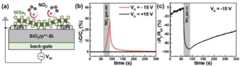
도 8은 실시예에서 제작된 2D WSe2 기반 캐패시터형 센서의 NO2 가스 감지를 위한 센서 구성도(a) 및 NO2 가스에 대한 반응 결과(b 및 c)를 나타내는 그래프이다.
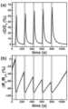
도 9는 도 8의 (a)에 도시된 가스 센서의 NO2 가스에 대한 반복 반응 결과를 나타내는 그래프이다.1 to 6 are cross-sectional views of capacitive sensors according to first to sixth embodiments of the present invention.
7 is an optical microscope image (a) of a 2D WSe2 -based capacitor-type sensor fabricated in Example, 2D WSe2A Raman spectrum (b), atomic force microscopy (AFM) image (c), and WSe2 thickness (d) of the flake are shown.
8 is a graph showing the configuration of a 2D WSe2 -based capacitor-type sensor for sensing NO2 gas (a) and reaction results (b and c) for NO2 gas produced in Example.
FIG. 9 is a graph showing repeated reaction results for NO2 gas of the gas sensor shown in (a) of FIG. 8 .
본 발명의 목적, 특정한 장점들 및 신규한 특징들은 첨부된 도면들과 연관되어지는 이하의 상세한 설명과 바람직한 실시예들로부터 더욱 명백해질 것이다. 본 명세서에서 각 도면의 구성요소들에 참조번호를 부가함에 있어서, 동일한 구성 요소들에 한해서는 비록 다른 도면상에 표시되더라도 가능한 한 동일한 번호를 가지도록 하고 있음에 유의하여야 한다. 또한, "제1", "제2" 등의 용어는 하나의 구성요소를 다른 구성요소로부터 구별하기 위해 사용되는 것으로, 구성요소가 상기 용어들에 의해 제한되는 것은 아니다. 이하, 본 발명을 설명함에 있어서, 본 발명의 요지를 불필요하게 흐릴 수 있는 관련된 공지 기술에 대한 상세한 설명은 생략한다.Objects, specific advantages and novel features of the present invention will become more apparent from the following detailed description and preferred embodiments taken in conjunction with the accompanying drawings. In adding reference numerals to components of each drawing in this specification, it should be noted that the same components have the same numbers as much as possible, even if they are displayed on different drawings. In addition, terms such as “first” and “second” are used to distinguish one component from another component, and the components are not limited by the terms. Hereinafter, in describing the present invention, detailed descriptions of related known technologies that may unnecessarily obscure the subject matter of the present invention will be omitted.
이하, 첨부된 도면을 참조하여 본 발명의 바람직한 실시형태를 상세히 설명하기로 한다.Hereinafter, preferred embodiments of the present invention will be described in detail with reference to the accompanying drawings.
도 1 내지 도 6은 본 발명의 제1 내지 제6 실시예에 따른 정전용량형 센서의 단면도이다.1 to 6 are cross-sectional views of capacitive sensors according to first to sixth embodiments of the present invention.
도 1 내지 도 6에 도시된 바와 같이, 본 발명에 따른 정전용량형 센서는 하부 전극(10), 하부 전극(10)과 마주보고, 하부 전극(10)과의 사이에 바이어스 전압이 인가되는 상부 전극(20), 및 이차원 반도체 물질을 포함하는 반도체층(30)을 포함하고, 광(빛) 또는 가스에 노출될 때에 정전용량이 변한다.As shown in FIGS. 1 to 6, the capacitive sensor according to the present invention has a
본 발명은 소자의 정전용량 변화를 기반으로 광(빛) 또는 가스를 감지하는 정전용량형 센서에 관한 것이다. 종래 저항형 센서는 구조가 간단하여 낮은 공정 단가로 소형화가 가능하다는 장점이 있으나, 전력소모가 많고 회복속도가 느리며, 화학종에 대한 선택성이 낮은 문제가 있는바, 이에 대한 해결방안으로서 본 발명이 안출되었다.The present invention relates to a capacitive sensor that detects light (light) or gas based on a change in capacitance of a device. The conventional resistive sensor has the advantage of being able to be miniaturized at a low process cost due to its simple structure, but has problems such as high power consumption, slow recovery speed, and low selectivity for chemical species. As a solution to this, the present invention is was devised
정전용량형 센서는 외부환경의 변화에 따른 절연체의 유전상수 혹은 전기장의 변화에서 기인한 소자의 정전용량의 차이를 감지한다. 정전용량형 센서는 저전력으로 구동이 가능하고, 비교적 우수한 안정성과 빠른 응답·회복속도를 보이며 높은 선택성을 가진다.A capacitive sensor detects a difference in capacitance of an element caused by a change in the dielectric constant of an insulator or an electric field according to a change in the external environment. Capacitive sensors can be driven with low power, have relatively excellent stability, fast response and recovery speed, and high selectivity.
구체적으로, 본 발명에 따른 정전용량형 센서는 하부 전극(10), 상부 전극(20), 및 반도체층(30)을 포함한다. 또한, 하부 전극(10)과 상부 전극(20) 사이에 삽입 배치되는 절연층(40)을 더 포함할 수 있다. 하부 전극(10), 상부 전극(20), 반도체층(30), 절연층(40)이 배치는 센서의 구조에 따라 달라지는데, 이에 대해서는 다양한 실시예에 따라 후술한다.Specifically, the capacitive sensor according to the present invention includes a
하부 전극(10)은 오믹(ohmic) 전극으로서, 전기전도성을 가지는 물질로 구현된다. 일례로, 단일 금속, 합금, 이종 금속이 적층된 다층 구조로 이루어질 수 있다.The
상부 전극(20)은 쇼트키(schottky) 또는 오믹(ohmic) 전극으로서, 하부 전극(10)과 마주보도록 배열된다. 일례로, 일례로, 단일 금속, 합금, 이종 금속이 적층된 다층 구조로 이루어질 수 있다. 또한, 가스 감지 센서 구조에서는, 가스 입자의 흡착에 의해 일 함수(work fuction)가 변하는 소재, 예를 들면 그래핀, Pt, Pd, 반도체 등을 사용할 수 있다. 한편, 광 감지 센서 구조에서는 투명 전극, 일례로 그래핀 전극을 사용할 수 있다.The
한편, 상부 전극(20)과 하부 전극(10) 사이에 바이어스 전압이 인가됨에 따라 센서의 정전용량 변화를 확인할 수 있다.Meanwhile, as a bias voltage is applied between the
반도체층(30)은 이차원 반도체 물질을 포함한다. 여기서, 이차원 반도체 물질은 가스 입자의 흡착에 의해 전기전도도가 변하는 성질을 가진다. 또한, 광이 조사되는 경우에 전자-정공 쌍이 발생하여 캐리어 농도가 증가하여, 전기전도도가 증가하는 성질도 가진다. 이러한 이차원 반도체 물질로는 WSe2, MoS2, WS2 등과 같은 TMDC(Transition metal dichalcogenide), BP, Ga2O3 등을 들 수 있는데, 나노 스케일 두께로 박리 가능하므로 소자 소형화가 가능하고, 전하 이동도가 높고 비표적이 넓어 외부 환경에 민감하게 반응하며, 밴드갭이 존재하여 빛과 강하게 상호작용을 하므로, 본 발명에 따른 고성능 정전용량형 센서에 적용된다.The
절연층(40)은 캐패시터에 사용되는 유전체(dielectric)를 포함한다. 이러한 절연층(40)은 하부 전극(10)과 상부 전극(20) 사이에 삽입 배치되는데, 센서의 구조에 따라서는 반도체층(30)과 접촉된다.The
이하에서는 다양한 실시예에 따른 센서 구조에 대해 설명한다.Hereinafter, a sensor structure according to various embodiments will be described.
도 1을 참고로, 본 발명의 제1 실시예에 따른 정전용량형 센서는 하부 전극(10)의 상부면에 절연층(40)이 적층되고, 절연층(40)의 상부면에 상부 전극(20)이 적층된다. 여기서, 상부 전극(20)은 하부 전극(10)에 비해 면적이 작게 형성되고, 절연층(40)의 전체 상부면 중 일영역에 접촉 배치된다. 반도체층(30)은 절연층(40)의 상부면 중 상부 전극(20)이 배치된 상기 일영역을 제외한 타영역에 접촉되어 그 타영역을 커버한다. 또한, 반도체층(30)은 상부 전극(20)과도 연결되므로, 절연층(40)의 상부면은 상부 전극(20)과 반도체층(30)에 의해 접촉 커버된다.Referring to FIG. 1 , in the capacitive sensor according to the first embodiment of the present invention, an
제1 실시예에 따른 센서 구조에서는 광 및 가스 감지가 가능하다. 반도체층(30)의 이차원 반도체 물질이 가스 입자를 흡착하게 되면, 이차원 반도체 물질의 전기전도도가 변하게 된다. 흡착되는 가스 종에 따라서, 이차원 반도체 물질의 전기전도도가 가스 흡착 전의 초기 전기전도도에 비해 높아지거나 낮아질 수 있다. 이때, 반도체층(30)과 상부 전극(20)이 전기적으로 서로 연결되기 때문에, 반도체층(30)에 의해 상부 전극(20)의 면적이 변하는 효과를 얻을 수 있다.In the sensor structure according to the first embodiment, light and gas detection is possible. When the two-dimensional semiconductor material of the
2개의 마주보는 평형판 사이에 유전체가 삽입되는 캐패시터에 있어서, 정전용량은 아래 식으로 표현된다.In a capacitor in which a dielectric is inserted between two opposing flat plates, the capacitance is expressed by the equation below.

(여기서, C는 정전용량, ε은 유전체의 유전상수, A는 평행판의 면적, d는 평행판 사이 거리임.)(Where C is the capacitance, ε is the dielectric constant of the dielectric, A is the area of parallel plates, and d is the distance between parallel plates.)
따라서, 가스 입자의 흡착을 통해 전기전도도가 증가한 이차원 반도체 물질에 의해 반도체층(30)과 상부 전극(20)이 전기적으로 연결되어, 가스 흡착 전 절연층(40)에 접촉되는 상부 전극(20)의 면적에 대응되는 캐패시터의 평행판 면적이 가스 흡착 후에 변하는 효과가 나타난다. 예를 들어, 이차원 반도체 물질의 초기 전기전도도가 낮을 경우, 캐패시터 평행판의 면적은 상부 전극(20)의 면적에 대응되지만, 가스 흡착에 의해 이차원 반도체 물질의 전기전도도가 향상되면, 그 캐패시터 평행판의 면적은 상부 전극(20), 및 반도체층(30)에 대응되도록 증가하게 된다. 다른 예로, 이차원 반도체 물질의 초기 전기전도도가 높을 경우에는, 캐패시터 평행판의 면적은 상부 전극(20), 및 반도체층(30)에 대응되지만, 가스 흡착에 의해 이차원 반도체 물질의 전기전도도가 감소되면, 그 캐패시터 평행판의 면적은 상부 전극(20)의 면적에 대응되도록 감소하게 된다. 결국, 제1 실시예에 따른 정전용량형 센서는 이차원 반도체 물질과 가스 흡착에 따라, 정전용량이 변하므로, 그 정전용량 변화에 기반하여 가스를 감지할 수 있다.Therefore, the
한편, 이차원 반도체 물질에 광이 조사되면, 이차원 반도체 물질에 전자-정공 쌍이 발행하여 캐리어 농도가 증가한다. 이로 인해 이차원 반도체 물질의 전기전도도가 증가하게 되므로, 전술한 바와 같이 상부 전극(20)의 면적이 넓어지는 효과가 발생하게 되고, 센서의 정전용량이 증가하게 되어 광을 감지할 수 있다.On the other hand, when light is irradiated on the two-dimensional semiconductor material, electron-hole pairs are issued to the two-dimensional semiconductor material to increase the carrier concentration. As a result, the electrical conductivity of the two-dimensional semiconductor material increases, and as described above, the area of the
도 2와 같이, 본 발명의 제2 실시예에 따른 정전용량형 센서는 전도판(50)을 더 포함할 수 있다. 여기서, 전도판(50)은 전기전도성을 가지는 부재로서, 절연층(40)의 상부면에 상부 전극(20)과 이격되어, 접촉 배치된다. 반도체층(30)은 상부 전극(20)과 전도판(50)을 연결하면서, 절연층(40)의 상부면 중 상부 전극(20)과 전도판(50) 사이의 영역을 접촉 커버한다. 한편, 절연층(40)의 상부면과 접촉되는 전도판(50)의 면적은 상부 전극(20)보다 넓게 형성될 수 있다.As shown in FIG. 2 , the capacitive sensor according to the second embodiment of the present invention may further include a
제2 실시예에 따른 센서 구조하에서도, 전술한 바와 같이 반도체층(30)의 이차원 반도체 물질이 가스 입자를 흡착하게 되면, 이차원 반도체 물질의 전기전도도가 변하므로, 캐패시터 평행판의 면적이 변하는 효과가 발생한다. 예를 들어, 이차원 반도체 물질의 초기 전기전도도가 낮을 경우, 캐패시터 평행판의 면적은 상부 전극(20)의 면적에 대응되지만, 가스 흡착에 의해 이차원 반도체 물질의 전기전도도가 향상되면, 그 캐패시터 평행판의 면적은 상부 전극(20), 반도체층(30), 및 전도판(50)에 대응되도록 증가하게 된다. 다른 예로, 이차원 반도체 물질의 초기 전기전도도가 높을 경우에는, 캐패시터 평행판의 면적은 상부 전극(20), 반도체층(30), 및 전도판(50)에 대응되지만, 가스 흡착에 의해 이차원 반도체 물질의 전기전도도가 감소되면, 그 캐패시터 평행판의 면적은 상부 전극(20)의 면적에 대응되도록 감소하게 된다. 결국, 이차원 반도체 물질의 가스 흡착에 의해 상부 전극(20)의 면적이 변하는 효과가 발생하는데, 전기전도성이 높은 전도판(50)에 의해, 제1 실시예의 경우와 비교할 때에 상부 전극(20)의 면적 변화 효과가 극대화된다.Even under the sensor structure according to the second embodiment, as described above, when the two-dimensional semiconductor material of the
또한, 제1 실시예와 마찬가지로, 이차원 반도체 물질에 광이 조사될 때에서, 상부 전극(20)의 면적이 증대되는 결과가 초래되므로, 광을 감지할 수 있다.In addition, as in the first embodiment, when light is irradiated to the two-dimensional semiconductor material, the area of the
도 3을 참고로, 본 발명의 제3 실시예에 따른 정전용량형 센서는 하부 전극(10) 상에, 절연층(40), 반도체층(30), 및 상부 전극(20)이 순차적으로 적층되는 구조로 이루어진다. 여기서, 상부 전극(20)은 하부 전극(10)에 비해 면적이 작게 형성된다.Referring to FIG. 3 , in the capacitive sensor according to the third embodiment of the present invention, an insulating
제3 실시예에 따른 정전용량형 센서 구조하에서도, 제1 실시예와 같이 가스 입자의 흡착 내지 광 조사에 대응하여 이차원 반도체 물질의 전기전도도가 변하므로, 센서 자체의 정전용량 변화에 기반하여 가스 또는 광을 감지할 수 있다.Even under the capacitive sensor structure according to the third embodiment, since the electrical conductivity of the two-dimensional semiconductor material changes in response to the adsorption of gas particles or light irradiation, as in the first embodiment, gas based on the change in capacitance of the sensor itself Or it can sense light.
도 4와 같이, 본 발명의 제4 실시예에 따른 정전용량형 센서는 하부 전극(10) 상에, 반도체층(30), 및 상부 전극(20)이 순차적으로 적층되는 소위 쇼트키 다이오드(schottky diode) 구조로 구현될 수 있다.As shown in FIG. 4 , the capacitive sensor according to the fourth embodiment of the present invention is a so-called Schottky diode in which a
가스 센서로 적용되기 위해서, 상부 전극(20)은 가스 입자 흡착에 의해 일 함수가 변하는 소재로 형성된다. 여기서, 가스 입자가 상부 전극(20)에 흡착됨에 따라, 상부 전극(20)의 일 함수가 변하므로, 상부 전극(20)과 반도체층(30) 사이에 접촉 저항이 변하게 된다. 이로써, 가스 입자 흡착 전후에 센서 자체의 정전용량이 변하고, 그 정전용량의 변화를 확인하여 가스를 감지할 수 있다.In order to be applied as a gas sensor, the
반면, 광을 감지하기 위해서, 상부 전극(20)은 투명 전극으로 구현된다. 여기서, 광이 조사되면, 상부 전극(20)을 투과한 광이 반도체층(30)의 이차원 반도체 물질에 입사되고, 이로 인해 이차원 반도체 물질에 전자-전공 쌍이 발생하여 캐리어 농도가 증가하여, 상부 전극(20)과 반도체층(30) 사이에 접촉 저항이 개선된다. 따라서, 광 조사 전후에 센서 자체의 정전용량이 변하고 이를 확인함으로써 광을 감지할 수 있다.On the other hand, in order to sense light, the
도 5를 참고로, 본 발명의 제5 실시예에 따른 정전용량형 센서는 하부 전극(10) 상에, 절연층(40), 반도체층(30), 및 상부 전극(20)이 순차적으로 적층되는 구조로 이루어질 수 있다.Referring to FIG. 5 , in the capacitive sensor according to the fifth embodiment of the present invention, an insulating
이러한 센서 구조하에서, 가스를 감지하기 위해서는, 가스 입자 흡착에 의해 일 함수가 변하는 소재로 상부 전극(20)이 형성된다. 여기서, 가스 입자가 상부 전극(20)에 흡착되면, 상부 전극(20)의 일 함수가 변하면서, 상부 전극(20)과 반도체층(30) 사이에 접촉 저항이 변하게 되므로, 센서 자체의 가스 입자 흡착 전후 정전용량 변화를 측정하여 가스를 감지할 수 있다.Under this sensor structure, in order to sense gas, the
반면, 광을 감지하기 위해서는, 상부 전극(20)이 투명 전극으로 구현된다. 따라서, 광이 상부 전극(20)을 투과하여 반도체층(30)의 이차원 반도체 물질에 입사되면서, 이차원 반도체 물질의 캐리어 농도가 증가하여, 상부 전극(20)과 반도체층(30) 사이에 접촉 저항이 개선시키므로, 광 조사 전후에 변하는 센서 자체의 정전용량을 확인함으로써 광을 감지할 수 있다.On the other hand, in order to sense light, the
도 6과 같이, 본 발명의 제6 실시예에 따른 정전용량형 센서는 하부 전극(10) 상에, 반도체층(30), 절연층(40), 및 상부 전극(20)이 순차적으로 적층된 구조로 이루어질 수 있다. 여기서, 상부 전극(20)은 가스 입자 흡착에 의해 일 함수가 변하는 소재로 이루어지므로, 전술한 바와 같이 가스 입자 흡착에 의해 센서 자체의 정전용량이 변하고, 이를 측정하여 가스를 감지할 수 있다.As shown in FIG. 6 , in the capacitive sensor according to the sixth embodiment of the present invention, a
종합적으로, 본 발명에 따르면, 이차원 반도체 물질을 도입하여 정전용량형 센서 구조를 구축하므로, 전력소모가 적고 회복속도가 빠르며, 화학종에 대해 높은 선택성을 가질 수 있다. 또한, 인가하는 교류전압의 주파수에 따라 외부환경에 의한 정전용량 변화가 달라지기 때문에 주파수 선택성을 더욱 높일 수 있다.Overall, according to the present invention, since a capacitive sensor structure is constructed by introducing a two-dimensional semiconductor material, power consumption is low, recovery speed is fast, and high selectivity for chemical species can be obtained. In addition, since the capacitance change due to the external environment varies according to the frequency of the applied AC voltage, frequency selectivity can be further increased.
나아가 감지 대상(광 또는 가스)과 반응하는 이차원 반도체 물질 자체의 정전용량 변화만을 측정하는 것이 아니라, 이차원 반도체 물질의 전기적 특성 변화에서 기인한 소자 전체의 정전용량 변화를 측정하여 신호를 증폭시키므로, 수용기 부착 혹은 온도 증가 등의 화학적·물리적 처리 없이 고간도의 감지가 가능하다.Furthermore, since the signal is amplified by measuring the change in capacitance of the entire device resulting from the change in electrical properties of the two-dimensional semiconductor material, rather than measuring only the change in capacitance of the two-dimensional semiconductor material reacting with the sensing object (light or gas), the receptor High sensitivity detection is possible without chemical or physical treatment such as adhesion or temperature increase.
이하에서는 구체적인 실시예 및 평가예를 들어 본 발명을 보다 상세하게 설명한다.Hereinafter, the present invention will be described in more detail with reference to specific examples and evaluation examples.
실시예: 2D WSe2 기반 캐패시터형 센서 제작Example: Fabrication of 2D WSe2 -based Capacitive Sensor
SiO2/p++-Si 기판을 준비하고, 그 기판의 하부에 전자빔 증착(electron-beam evaporation)을 통해 Ti/Au (50/150 nm) 백 게이트 전극(back-gate electrode)를 형성했다. 기판의 상부에는 포토리소그래피와 전자빔 증착을 이용해 2개의 Ti/Pt (5/45 nm) 전극을 서로 이격되게 배열했다. 접착 테이프를 통해 벌크 WSe2로부터 기계적으로 박리된 WSe2 플레이크 중 적절한 크기와 두께의 플레이크를 선별하고, 투명 겔 필름(gel film)을 이용해 2개의 상부 전극(Ti/Pt) 사이에 배치하였다. 다음, Ar 분위기에서 2시간 동안 200℃에서 열 어닐링을 수행하여, WSe2와 상부 전극 사이의 전기적 특성을 개선하였다.A SiO2 /p++ -Si substrate was prepared, and a Ti/Au (50/150 nm) back-gate electrode was formed on the bottom of the substrate by electron-beam evaporation. On the top of the substrate, two Ti/Pt (5/45 nm) electrodes were arranged spaced apart from each other using photolithography and electron beam deposition. Among WSe2 flakes mechanically exfoliated from bulk WSe2 through an adhesive tape, flakes of appropriate size and thickness were selected and placed between two upper electrodes (Ti/Pt) using a transparent gel film. Next, thermal annealing was performed at 200° C. for 2 hours in an Ar atmosphere to improve electrical properties between WSe2 and the upper electrode.
평가예 1: 2D WSe2 기반 캐패시터형 센서의 구조 분석Evaluation Example 1: Structure analysis of 2D WSe2 -based capacitive sensor
도 7은 실시예에서 제작된 2D WSe2 기반 캐패시터형 센서의 광학 현미경 이미지(a), 2D WSe2플레이크의 라만 스펙트럼(b), 원자력 현미경(AFM) 이미지(c), 및 WSe2 두께(d)를 나타낸다.7 is an optical microscope image (a) of a 2D WSe2 -based capacitor-type sensor fabricated in Example, 2D WSe2A Raman spectrum (b), atomic force microscopy (AFM) image (c), and WSe2 thickness (d) of the flake are shown.
도 7의 (a)는 실시예에서 제작된 2D WSe2 기반 캐패시터형 센서의 광학 현미경 이미지로서, 이를 참고로, 2D WSe2 기반 캐패시터형 센서는 하부에 백 게이트 전극이 형성된 SiO2/p++-Si 기판의 상부에 배열된 2개의 상부 전극 사이에 2D WSe2 플레이크가 배치되는 바닥 접촉 구조(bottom contact structure)를 가진다. 이러한 2D WSe2 기반 화학캐패시터(chemicapacitor) 구조는 WSe2 기반 전계효과트랜지스터(FET), 및 캐패시터에 적용 가능하다.7 (a) is an optical microscope image of the 2D WSe2 -based capacitor-type sensor fabricated in the example. Referring to this, the 2D WSe2 -based capacitor-type sensor has a SiO2 /p++ with a back gate electrode formed thereon. -Has a bottom contact structure in which 2D WSe2 flakes are disposed between two upper electrodes arranged on top of the Si substrate. This 2D WSe2 based chemical capacitor structure is applicable to WSe2 based field effect transistors (FETs) and capacitors.
마이크로 라만 분광기(Micro-Raman spectroscopy)를 이용하여, 실시예에서 제작된 2D WSe2 기반 캐패시터형 센서의 2D WSe2에 대한 구조적 특성을 분석하였다. 도 7의 (b)는 실시예에서 제작된 2D WSe2 기반 캐패시터형 센서의 2D WSe2플레이크의 라만 스펙트럼이다. 여기서, ~ 249 ㎝-1의 진동 주파수를 가지는 WSe2의 E12g 포논 피크(phonon peak)가 발견되었는데, 이는 이전 연구와 일치하는 결과이다.Using micro-Raman spectroscopy, the structural characteristics of the 2D WSe2 of the 2D WSe2 -based capacitor-type sensor fabricated in Example were analyzed. 7(b) shows the 2D WSe2 of the 2D WSe2 -based capacitor-type sensor fabricated in the example.This is the Raman spectrum of the flake. Here, an E12g phonon peak of WSe2 having a vibration frequency of ~ 249 cm−1 was found, which is consistent with previous studies.
원자력 현미경(atomic force microscope, AFM)을 이용하여, 실시예에서 제작된 2D WSe2 기반 캐패시터형 센서를 관찰하였다. 도 7의 (c)는 도 7의 (a)에 표시된 붉은색 점선 영역에 대한 원자력 현미경(AFM) 이미지이다. 도 7의 (a)와 도 7의 (c)를 통해, 깨끗한 표면 및 낮은 잔류 오염물을 가지는 WSe2 플레이크가 상부 전극과 SiO2 기판 상에 배치되었음을 알 수 있다. 도 7의 (d)는 실시예에서 제작된 2D WSe2 기반 캐패시터형 센서의 WSe2 두께를 나타내는데, 해당 WSe2 두께는 ~ 20.5 ㎚로 측정되었다.Using an atomic force microscope (AFM), the 2D WSe2 -based capacitor-type sensor fabricated in the example was observed. Figure 7(c) is an atomic force microscope (AFM) image of the red dotted line area indicated in Figure 7(a). 7(a) and 7(c), it can be seen that WSe2 flakes having clean surfaces and low residual contaminants were disposed on the upper electrode and the SiO2 substrate. 7(d) shows the WSe2 thickness of the 2D WSe2 -based capacitor-type sensor fabricated in the example, and the corresponding WSe2 thickness was measured to be ~ 20.5 nm.
평가예 2: 2D WSe2 기반 캐패시터형 센서의 성능 평가Evaluation Example 2: Performance Evaluation of 2D WSe2 -based Capacitive Sensor
실시예에서 제작된 2D WSe2 기반 캐패시터형 센서의 NO2 가스 감지 성능을 평가하였다. 도 8은 실시예에서 제작된 2D WSe2 기반 캐패시터형 센서의 NO2 가스 감지를 위한 센서 구성도(a) 및 NO2 가스에 대한 반응 결과(b 및 c)를 나타내는 그래프이다.The NO2 gas sensing performance of the 2D WSe2 -based capacitive sensor fabricated in Example was evaluated. 8 is a graph showing the configuration of a 2D WSe2 -based capacitor-type sensor for sensing NO2 gas (a) and reaction results (b and c) for NO2 gas produced in Example.
도 8의 (a)는 실시예에서 제작된 2D WSe2 기반 캐패시터형 센서의 NO2 가스 감지를 위한 센서 구성도로서, 2D WSe2 기반 캐패시터형 센서의 백 게이트 전극에 AC 게이트 바이어스(AC gate bias)를 인가하고, WSe2 플레이크과 접촉된 상부 전극을 접지하였다. NO2 가스에 노출되기 전, 센서의 정전용량은 약 1.54 pF로 측정되었다.8(a) is a sensor configuration diagram for detecting NO2 gas of a 2D WSe2 -based capacitor type sensor fabricated in an embodiment. An AC gate bias is applied to the back gate electrode of the 2D WSe2 -based capacitor type sensor. ) was applied, and the top electrode in contact with the WSe2 flake was grounded. Before exposure to NO2 gas, the capacitance of the sensor was measured to be approximately 1.54 pF.
도 8의 (b) 내지 도 8의 (c)는 도 8의 (a)에 도시된 가스 센서의 NO2 가스에 대한 반응 결과를 나타내는 그래프이다. 도 8의 (b)는 ΔC/C0(여기서, C0는 초기 정전용량(capacitance)이고, ΔC는 측정된 정전용량과 초기 정전용량 차(정전용량 변화량)를 각각 나타낸다)로서, 도 8의 (c)는 ΔR/R0(여기서, R0는 초기 병렬저항이고, ΔC는 측정된 병렬저항과 초기 병렬저항 차(병렬저항 변화량)를 각각 나타낸다)로서, 가스 센서의 반응도를 나타낸다.8(b) to 8(c) are graphs showing the reaction results of the gas sensor shown in FIG. 8(a) to NO2 gas. (b) of FIG. 8 is ΔC/C0 (where C0 is initial capacitance, and ΔC represents the difference between measured capacitance and initial capacitance (capacitance change amount), respectively), (c) is ΔR / R0 (where R0 is the initial parallel resistance, and ΔC represents the difference between the measured parallel resistance and the initial parallel resistance (parallel resistance change), respectively), and shows the reactivity of the gas sensor.
도 8의 (b)를 참고로, NO2에 대한 WSe2 기반 캐패시터형 센서의 반응은 2가지 AC 게이트 바이어스의 조건(VG < 0 (-15 V), VG > 0 (+15 V))에서 측정되었다. 그 결과, VG> 0 (검은색) 조건에서는 정전용량에 변화가 없었고, VG < 0 (빨간색) 조건에서 정전용량에 변화가 나타났다.Referring to (b) of FIG. 8, the response of the WSe2 -based capacitive sensor to NO2 is under two AC gate bias conditions (VG < 0 (-15 V), VG > 0 (+15 V) ) was measured. As a result, VGThere was no change in capacitance under the > 0 (black) condition, and there was a change in capacitance under the VG < 0 (red) condition.
WSe2 기반 캐패시터형 센서의 정전용량은 아래 식으로 표현된다.The capacitance of the WSe2 -based capacitive sensor is expressed by the formula below.

(여기서, C는 정전용량, ε은 유전상수, A는 평행판의 면적, d는 평행판 사이 거리임.)(Where C is the capacitance, ε is the dielectric constant, A is the area of parallel plates, and d is the distance between parallel plates.)
WSe2가 NO2가스에 노출되면, WSe2의전기전도도가 증가되고, 증가된 그 전기전도도는 정전용량를 변화시키게 된다. 즉, NO2가스에 노출됨에 따라 캐패시터의 평형판의 면적이 증가하여, 정전용량도 증가한다고 볼 수 있다.When WSe2 is exposed to NO2 gas,theThe electrical conductivity is increased, and the increased electrical conductivity changes the capacitance. That is, it can be seen that as the exposure to the NO2 gas increases, the area of the balanced plate of the capacitor increases, and thus the capacitance also increases.
VG> 0 조건에서는 WSe2 기반 캐패시터형 센서가 오프(off)되어, NO2가스에 노출되더라도 WSe2의전기전도도가 증가하지 않는다. 따라서, VG> 0 조건에서 정전용량도 변하지 않는다.VG> 0 condition, the WSe2 -based capacitor type sensor is turned off, and even when exposed to NO2 gas, the WSe2The electrical conductivity does not increase. Therefore, VG> 0 condition, the capacitance does not change either.
도 8의 (b) 및 도 8의 (c)를 참고로, NO2가스 노출에 따른 ΔC/C0및 ΔR/R0경향은 서로 다르게 나타난다. 30초 동안 NO2가스에 노출될 때에 ΔC/C0는 ~ 30%까지 거의 선형적으로 증가했고, NO2가스가 제거됨에 따라 빠르게 감소하였다. 반면, ΔR/R0는 ~ -94% 지점에서 빠르게 포화되었고, NO2가스의 공급이 중단된 후에는 매우 느린 회복 속도를 보였다.Referring to FIG. 8(b) and FIG. 8(c) , ΔC/C0 and ΔR/R0 trends according to NO2 gas exposure are different from each other. When exposed to NO2 gas for 30 seconds, ΔC/C0 increased almost linearly to ~30% and rapidly decreased as NO2 gas was removed. On the other hand, ΔR/R0 was quickly saturated at ~ -94%, and showed a very slow recovery rate after the supply of NO2 gas was stopped.
도 9는 도 8의 (a)에 도시된 가스 센서의 NO2 가스에 대한 반복 반응 결과를 나타내는 그래프이다. 도 9의 (a)는 ΔC/C0(여기서, C0는 초기 정전용량(capacitance)이고, ΔC는 측정된 정전용량과 초기 정전용량 차(정전용량 변화량)를 각각 나타낸다)로서, 도 9의 (b)는 ΔR/R0(여기서, R0는 초기 병렬저항이고, ΔC는 측정된 병렬저항과 초기 병렬저항 차(병렬저항 변화량)를 각각 나타낸다)로서, 가스 센서의 반응도를 나타낸다.FIG. 9 is a graph showing repeated reaction results for NO2 gas of the gas sensor shown in (a) of FIG. 8 . 9(a) shows ΔC/C0 (where C0 is an initial capacitance, and ΔC represents a difference between the measured capacitance and the initial capacitance (capacitance change amount), respectively), of FIG. 9 (b) is ΔR / R0 (where R0 is the initial parallel resistance, and ΔC represents the difference between the measured parallel resistance and the initial parallel resistance (parallel resistance change), respectively), indicating the reactivity of the gas sensor.
도 9를 참고로, NO2 가스의 공급 및 차단을 반복하면서 가스 감지 반응을 분석한 결과, ΔC/C0(최대값 ~ 65%)에 따른 감도와, ΔR/R0(최대값 ~ -90%)에 따른 감도 모두가 전술한 특성을 나타내며, 반복 측정에서 감지 응답을 유지하였다.Referring to FIG. 9, as a result of analyzing the gas detection reaction while repeating the supply and blocking of NO2 gas, the sensitivity according to ΔC / C0 (maximum value ~ 65%) and ΔR / R0 (maximum value ~ -90 All of the sensitivities according to %) exhibited the above-described characteristics, and the sensing response was maintained in repeated measurements.
이상 본 발명을 구체적인 실시예를 통하여 상세히 설명하였으나, 이는 본 발명을 구체적으로 설명하기 위한 것으로, 본 발명은 이에 한정되지 않으며, 본 발명의 기술적 사상 내에서 당 분야의 통상의 지식을 가진 자에 의해 그 변형이나 개량이 가능함이 명백하다.Although the present invention has been described in detail through specific examples, this is for explaining the present invention in detail, the present invention is not limited thereto, and within the technical spirit of the present invention, by those skilled in the art It is clear that modifications and improvements are possible.
본 발명의 단순한 변형 내지 변경은 모두 본 발명의 영역에 속한 것으로 본 발명의 구체적인 보호 범위는 첨부된 특허청구범위에 의하여 명확해질 것이다.All simple modifications or changes of the present invention belong to the scope of the present invention, and the specific protection scope of the present invention will be clarified by the appended claims.
10: 하부 전극 20: 상부 전극
30: 반도체층 40: 절연층
50: 전도판
10: lower electrode 20: upper electrode
30: semiconductor layer 40: insulating layer
50: conducting plate
Claims (8)
Translated fromKorean상기 하부 전극의 상부면에 배치되는 절연층;
상기 하부 전극의 면적보다 작게 형성되고, 상기 절연층의 상부면 중 일영역에 접촉 배치되며, 상기 하부 전극과의 사이에 바이어스 전압이 인가되는 상부 전극;
상기 절연층의 상부면 중 타영역에, 상기 상부 전극과 이격 배치되는 전도판; 및
이차원 반도체 물질을 포함하고, 상기 상부 전극과 상기 전도판을 연결하면서, 상기 절연층의 상부면 중 상기 일영역과 상기 타영역 사이의 중간영역을 접촉 커버하는 반도체층;을 포함하고,
상기 반도체층이 광(빛) 또는 가스에 노출될 때에 정전용량이 변하는 정전용량형 센서.
lower electrode;
an insulating layer disposed on an upper surface of the lower electrode;
an upper electrode formed smaller than the area of the lower electrode, disposed in contact with one of the upper surfaces of the insulating layer, and to which a bias voltage is applied between the upper electrode and the lower electrode;
a conductive plate spaced apart from the upper electrode on the other region of the upper surface of the insulating layer; and
A semiconductor layer comprising a two-dimensional semiconductor material, connecting the upper electrode and the conductive plate, and contactingly covering an intermediate region between the one region and the other region of the upper surface of the insulating layer;
A capacitive sensor in which capacitance changes when the semiconductor layer is exposed to light (light) or gas.
상기 이차원 반도체 물질은,
TMDC(Transition metal dichalcogenide), BP, 및 Ga2O3으로 구성된 군으로부터 선택되는 어느 하나 이상을 포함하는 정전용량형 센서.
The method of claim 1,
The two-dimensional semiconductor material,
A capacitive sensor comprising at least one selected from the group consisting of transition metal dichalcogenide (TMDC), BP, and Ga2 O3 .
상기 반도체층의 일단은 상기 상부 전극의 상부면에 접촉 배치되고, 상기 반도체층의 타단은 상기 전도판의 상부면에 접촉 배치되는 정전용량형 센서.
The method of claim 1,
One end of the semiconductor layer is disposed in contact with the upper surface of the upper electrode, and the other end of the semiconductor layer is disposed in contact with the upper surface of the conductive plate.
Priority Applications (1)
| Application Number | Priority Date | Filing Date | Title |
|---|---|---|---|
| KR1020210011262AKR102534265B1 (en) | 2021-01-27 | 2021-01-27 | Capacitive type sensor |
Applications Claiming Priority (1)
| Application Number | Priority Date | Filing Date | Title |
|---|---|---|---|
| KR1020210011262AKR102534265B1 (en) | 2021-01-27 | 2021-01-27 | Capacitive type sensor |
Publications (2)
| Publication Number | Publication Date |
|---|---|
| KR20220108350A KR20220108350A (en) | 2022-08-03 |
| KR102534265B1true KR102534265B1 (en) | 2023-05-17 |
Family
ID=82847169
Family Applications (1)
| Application Number | Title | Priority Date | Filing Date |
|---|---|---|---|
| KR1020210011262AActiveKR102534265B1 (en) | 2021-01-27 | 2021-01-27 | Capacitive type sensor |
Country Status (1)
| Country | Link |
|---|---|
| KR (1) | KR102534265B1 (en) |
Citations (2)
| Publication number | Priority date | Publication date | Assignee | Title |
|---|---|---|---|---|
| JP2017534169A (en) | 2014-07-07 | 2017-11-16 | ノキア テクノロジーズ オーユー | Detection device and manufacturing method thereof |
| KR102088244B1 (en) | 2018-02-05 | 2020-03-12 | 고려대학교 산학협력단 | Chemical detecting sensor of zero-power and sensing method using the same |
Family Cites Families (2)
| Publication number | Priority date | Publication date | Assignee | Title |
|---|---|---|---|---|
| CN104603729B (en)* | 2012-04-27 | 2018-02-02 | 阿尔申蒂斯有限责任公司 | Apparatus for determining touch input stimuli |
| KR101912900B1 (en) | 2017-01-17 | 2018-10-29 | 울산과학기술원 | Multi-channel resistance-type gas sensor system |
- 2021
- 2021-01-27KRKR1020210011262Apatent/KR102534265B1/enactiveActive
Patent Citations (2)
| Publication number | Priority date | Publication date | Assignee | Title |
|---|---|---|---|---|
| JP2017534169A (en) | 2014-07-07 | 2017-11-16 | ノキア テクノロジーズ オーユー | Detection device and manufacturing method thereof |
| KR102088244B1 (en) | 2018-02-05 | 2020-03-12 | 고려대학교 산학협력단 | Chemical detecting sensor of zero-power and sensing method using the same |
Non-Patent Citations (1)
| Title |
|---|
| Ying Wang, et al. Electrically Transduced Gas Sensors Based on Semiconducting Metal Oxide Nanowires. Sensors 2020, 20, 6781; doi:10.3390/s20236781.* |
Also Published As
| Publication number | Publication date |
|---|---|
| KR20220108350A (en) | 2022-08-03 |
Similar Documents
| Publication | Publication Date | Title |
|---|---|---|
| US10948447B2 (en) | Ultra-compact, passive, wireless sensor using quantum capacitance effect in graphene | |
| Newaz et al. | Probing charge scattering mechanisms in suspended graphene by varying its dielectric environment | |
| EP2623968B1 (en) | Gas sensor comprising a gate structure with capacitively coupled platinum crystal grains | |
| US10043990B2 (en) | Dual-gate chemical field effect transistor sensor | |
| JP6622166B2 (en) | Molecular detector, molecular detection method, molecular detector, and organic probe | |
| CN111307876A (en) | Gas sensor for detecting nitrogen dioxide and preparation method thereof | |
| Wang et al. | Effect of high-κ dielectric layer on 1/f noise behavior in graphene field-effect transistors | |
| CN105705942B (en) | Device and method for measuring small voltages and potentials at biological, chemical or other samples | |
| US10488287B2 (en) | Electric device for detecting pressure | |
| Wang et al. | High-performance graphene-based electrostatic field sensor | |
| KR102534265B1 (en) | Capacitive type sensor | |
| Chang et al. | Impedimetric phosphorene field-effect transistors for rapid detection of lead ions | |
| Kim et al. | Capacitive Chemical Sensors Based on Two-Dimensional WSe2 | |
| CN105301079B (en) | Semiconductor devices and its detection method for the detection of determinand ionic activity | |
| US8431001B2 (en) | Ion sensor for measuring ion concentration of a solution | |
| Noll et al. | Transfer-free in situ ccvd grown nanocrystalline graphene for sub-ppmv ammonia detection | |
| KR20120081093A (en) | Liquid organic semiconductor material | |
| CN110864805A (en) | Ultra-wideband spectrum detection device and method | |
| ÖZERLİ | Frequency and voltage dependent of electrical and dielectric properties of Ag/GO doped NiO/p-Si/Al MOS structures under darkness and light | |
| US9097741B2 (en) | Molecule sensing and identification | |
| JP2546340B2 (en) | Moisture sensitive element and its operating circuit | |
| Akram et al. | Organic–Inorganic Composite Poly-N-Epoxypropylcarbazole-Nickel Phthalocynine-Cu2O Based Humidity Sensor | |
| KR101698680B1 (en) | High selective and high seneitive gas sensor device | |
| Dockx et al. | Strong doping reduction on wafer-scale CVD graphene devices via Al2O3 ALD encapsulation | |
| CN111416035B (en) | Nonvolatile Hall sensor and manufacturing method and testing method thereof |
Legal Events
| Date | Code | Title | Description |
|---|---|---|---|
| PA0109 | Patent application | Patent event code:PA01091R01D Comment text:Patent Application Patent event date:20210127 | |
| PA0201 | Request for examination | ||
| PE0902 | Notice of grounds for rejection | Comment text:Notification of reason for refusal Patent event date:20220528 Patent event code:PE09021S01D | |
| PG1501 | Laying open of application | ||
| E701 | Decision to grant or registration of patent right | ||
| PE0701 | Decision of registration | Patent event code:PE07011S01D Comment text:Decision to Grant Registration Patent event date:20230508 | |
| GRNT | Written decision to grant | ||
| PR0701 | Registration of establishment | Comment text:Registration of Establishment Patent event date:20230515 Patent event code:PR07011E01D | |
| PR1002 | Payment of registration fee | Payment date:20230515 End annual number:3 Start annual number:1 | |
| PG1601 | Publication of registration |