KR102533197B1 - Semiconductor memory device and operating method thereof - Google Patents
Semiconductor memory device and operating method thereofDownload PDFInfo
- Publication number
- KR102533197B1 KR102533197B1KR1020160121655AKR20160121655AKR102533197B1KR 102533197 B1KR102533197 B1KR 102533197B1KR 1020160121655 AKR1020160121655 AKR 1020160121655AKR 20160121655 AKR20160121655 AKR 20160121655AKR 102533197 B1KR102533197 B1KR 102533197B1
- Authority
- KR
- South Korea
- Prior art keywords
- word line
- word lines
- select transistor
- memory device
- semiconductor memory
- Prior art date
- Legal status (The legal status is an assumption and is not a legal conclusion. Google has not performed a legal analysis and makes no representation as to the accuracy of the status listed.)
- Active
Links
Images


Classifications
- G—PHYSICS
- G11—INFORMATION STORAGE
- G11C—STATIC STORES
- G11C11/00—Digital stores characterised by the use of particular electric or magnetic storage elements; Storage elements therefor
- G11C11/21—Digital stores characterised by the use of particular electric or magnetic storage elements; Storage elements therefor using electric elements
- G11C11/34—Digital stores characterised by the use of particular electric or magnetic storage elements; Storage elements therefor using electric elements using semiconductor devices
- G11C11/40—Digital stores characterised by the use of particular electric or magnetic storage elements; Storage elements therefor using electric elements using semiconductor devices using transistors
- G11C11/401—Digital stores characterised by the use of particular electric or magnetic storage elements; Storage elements therefor using electric elements using semiconductor devices using transistors forming cells needing refreshing or charge regeneration, i.e. dynamic cells
- G11C11/4063—Auxiliary circuits, e.g. for addressing, decoding, driving, writing, sensing or timing
- G11C11/407—Auxiliary circuits, e.g. for addressing, decoding, driving, writing, sensing or timing for memory cells of the field-effect type
- G11C11/4074—Power supply or voltage generation circuits, e.g. bias voltage generators, substrate voltage generators, back-up power, power control circuits
- G—PHYSICS
- G11—INFORMATION STORAGE
- G11C—STATIC STORES
- G11C16/00—Erasable programmable read-only memories
- G11C16/02—Erasable programmable read-only memories electrically programmable
- G11C16/06—Auxiliary circuits, e.g. for writing into memory
- G11C16/34—Determination of programming status, e.g. threshold voltage, overprogramming or underprogramming, retention
- G11C16/3418—Disturbance prevention or evaluation; Refreshing of disturbed memory data
- G—PHYSICS
- G11—INFORMATION STORAGE
- G11C—STATIC STORES
- G11C16/00—Erasable programmable read-only memories
- G11C16/02—Erasable programmable read-only memories electrically programmable
- G11C16/04—Erasable programmable read-only memories electrically programmable using variable threshold transistors, e.g. FAMOS
- G11C16/0483—Erasable programmable read-only memories electrically programmable using variable threshold transistors, e.g. FAMOS comprising cells having several storage transistors connected in series
- G—PHYSICS
- G11—INFORMATION STORAGE
- G11C—STATIC STORES
- G11C16/00—Erasable programmable read-only memories
- G11C16/02—Erasable programmable read-only memories electrically programmable
- G11C16/06—Auxiliary circuits, e.g. for writing into memory
- G11C16/08—Address circuits; Decoders; Word-line control circuits
- G—PHYSICS
- G11—INFORMATION STORAGE
- G11C—STATIC STORES
- G11C16/00—Erasable programmable read-only memories
- G11C16/02—Erasable programmable read-only memories electrically programmable
- G11C16/06—Auxiliary circuits, e.g. for writing into memory
- G11C16/10—Programming or data input circuits
- G—PHYSICS
- G11—INFORMATION STORAGE
- G11C—STATIC STORES
- G11C16/00—Erasable programmable read-only memories
- G11C16/02—Erasable programmable read-only memories electrically programmable
- G11C16/06—Auxiliary circuits, e.g. for writing into memory
- G11C16/30—Power supply circuits
- G—PHYSICS
- G11—INFORMATION STORAGE
- G11C—STATIC STORES
- G11C29/00—Checking stores for correct operation ; Subsequent repair; Testing stores during standby or offline operation
- G11C29/04—Detection or location of defective memory elements, e.g. cell constructio details, timing of test signals
- G11C29/08—Functional testing, e.g. testing during refresh, power-on self testing [POST] or distributed testing
- G11C29/12—Built-in arrangements for testing, e.g. built-in self testing [BIST] or interconnection details
- G11C29/18—Address generation devices; Devices for accessing memories, e.g. details of addressing circuits
- G11C29/30—Accessing single arrays
- G11C29/34—Accessing multiple bits simultaneously
- G—PHYSICS
- G11—INFORMATION STORAGE
- G11C—STATIC STORES
- G11C7/00—Arrangements for writing information into, or reading information out from, a digital store
- G11C7/10—Input/output [I/O] data interface arrangements, e.g. I/O data control circuits, I/O data buffers
- G11C7/1051—Data output circuits, e.g. read-out amplifiers, data output buffers, data output registers, data output level conversion circuits
- H—ELECTRICITY
- H10—SEMICONDUCTOR DEVICES; ELECTRIC SOLID-STATE DEVICES NOT OTHERWISE PROVIDED FOR
- H10B—ELECTRONIC MEMORY DEVICES
- H10B41/00—Electrically erasable-and-programmable ROM [EEPROM] devices comprising floating gates
- H10B41/40—Electrically erasable-and-programmable ROM [EEPROM] devices comprising floating gates characterised by the peripheral circuit region
- H—ELECTRICITY
- H10—SEMICONDUCTOR DEVICES; ELECTRIC SOLID-STATE DEVICES NOT OTHERWISE PROVIDED FOR
- H10D—INORGANIC ELECTRIC SEMICONDUCTOR DEVICES
- H10D48/00—Individual devices not covered by groups H10D1/00 - H10D44/00
- H10D48/30—Devices controlled by electric currents or voltages
- H10D48/32—Devices controlled by only the electric current supplied, or only the electric potential applied, to an electrode which does not carry the current to be rectified, amplified or switched
- H10D48/36—Unipolar devices
- H—ELECTRICITY
- H10—SEMICONDUCTOR DEVICES; ELECTRIC SOLID-STATE DEVICES NOT OTHERWISE PROVIDED FOR
- H10D—INORGANIC ELECTRIC SEMICONDUCTOR DEVICES
- H10D88/00—Three-dimensional [3D] integrated devices
Landscapes
- Engineering & Computer Science (AREA)
- Microelectronics & Electronic Packaging (AREA)
- Computer Hardware Design (AREA)
- Read Only Memory (AREA)
Abstract
Translated fromKoreanDescription
Translated fromKorean본 발명은 전자 장치에 관한 것으로, 보다 구체적으로는 반도체 메모리 장치 및 그 동작 방법에 관한 것이다.The present invention relates to an electronic device, and more particularly, to a semiconductor memory device and an operating method thereof.
반도체 장치 중 특히 반도체 메모리 장치는 크게 휘발성 메모리 장치(Volatile memory device)와 불휘발성 메모리 장치(Nonvolatile memory device)로 구분된다.Among semiconductor devices, semiconductor memory devices are largely classified into volatile memory devices and nonvolatile memory devices.
불휘발성 메모리 장치는 쓰기 및 읽기 속도가 상대적으로 느리지만 전원 공급이 차단되더라도 저장 데이터를 유지한다. 따라서 전원 공급 여부와 관계없이 유지되어야 할 데이터를 저장하기 위해 불휘발성 메모리 장치가 사용된다. 불휘발성 메모리 장치에는 ROM(Read Only Memory), MROM(Mask ROM), PROM(Programmable ROM), EPROM(Erasable Programmable ROM), EEPROM(Electrically Erasable Programmable ROM), 플래시 메모리(Flash memory), PRAM(Phase change Random Access Memory), MRAM(Magnetic RAM), RRAM(Resistive RAM), FRAM(Ferroelectric RAM) 등이 있다. 플래시 메모리는 노어 타입과 낸드 타입으로 구분된다.Nonvolatile memory devices have relatively slow writing and reading speeds, but retain stored data even when power supply is cut off. Therefore, a nonvolatile memory device is used to store data to be maintained regardless of whether power is supplied or not. Non-volatile memory devices include Read Only Memory (ROM), Mask ROM (MROM), Programmable ROM (PROM), Erasable Programmable ROM (EPROM), Electrically Erasable Programmable ROM (EEPROM), Flash memory, and Phase change PRAM (PRAM). random access memory), magnetic RAM (MRAM), resistive RAM (RRAM), and ferroelectric RAM (FRAM). Flash memory is classified into a NOR type and a NAND type.
플래시 메모리 장치는 셀 스트링이 반도체 기판에 수평하게 형성된 2차원 반도체 메모리 장치와, 셀 스트링이 반도체 기판에 수직으로 형성된 3차원 반도체 메모리 장치로 구분될 수 있다. 3차원 반도체 메모리 장치는 2차원 반도체 메모리 장치의 집적도 한계를 해소하기 위하여 고안된 메모리 장치로써, 반도체 기판 상에 수직으로 형성된 다수의 셀 스트링들을 포함한다. 셀 스트링들은 비트 라인과 공통 소스 라인(SL) 사이에 직렬로 연결된 드레인 선택 트랜지스터, 메모리 셀들 및 소스 선택 트랜지스터를 포함한다.Flash memory devices may be divided into two-dimensional semiconductor memory devices in which cell strings are formed horizontally on a semiconductor substrate and three-dimensional semiconductor memory devices in which cell strings are formed vertically on a semiconductor substrate. A 3D semiconductor memory device is a memory device designed to solve the integration limit of a 2D semiconductor memory device, and includes a plurality of cell strings vertically formed on a semiconductor substrate. The cell strings include a drain select transistor, memory cells, and a source select transistor connected in series between the bit line and the common source line SL.
본 발명의 실시 예는 프로그램 디스터브 현상을 개선시킬 수 있는 반도체 메모리 장치 및 그 동작 방법을 제공한다.An embodiment of the present invention provides a semiconductor memory device capable of improving a program disturb phenomenon and an operating method thereof.
본 발명의 일 실시예에 따른 반도체 메모리 장치는 복수의 워드 라인들에 연결된 복수의 메모리 셀들을 포함하는 메모리 셀 어레이; 상기 복수의 워드 라인들 중에서 선택된 워드 라인에 프로그램 전압을 인가하도록 구성된 주변 회로; 및 상기 선택된 워드 라인에 상기 프로그램 전압이 인가되기 이전에, 상기 복수의 워드 라인들에 프리 바이어스 전압들이 인가되도록 상기 주변 회로를 제어하는 제어 로직을 포함하고, 상기 복수의 워드 라인들의 위치에 따라 상기 프리 바이어스 전압들의 레벨이 결정되고, 상기 복수의 워드 라인들은 복수의 워드 라인 그룹들로 그룹화되고, 상기 프리 바이어스 전압들 중 프로그램된 메모리 셀에 가까운 워드 라인 그룹에 인가되는 프리 바이어스 전압은 상대적으로 낮게 설정되는 것을 특징으로 한다.A semiconductor memory device according to an embodiment of the present invention includes a memory cell array including a plurality of memory cells connected to a plurality of word lines; a peripheral circuit configured to apply a program voltage to a word line selected from among the plurality of word lines; and a control logic for controlling the peripheral circuit to apply pre-bias voltages to the plurality of word lines before the program voltage is applied to the selected word line, Levels of pre-bias voltages are determined, the plurality of word lines are grouped into a plurality of word line groups, and among the pre-bias voltages, a pre-bias voltage applied to a word line group close to a programmed memory cell is relatively low. characterized in that it is set.
삭제delete
일 실시예에서, 상기 복수의 워드 라인들은 복수의 워드 라인 그룹들로 그룹화되고, 상기 복수의 메모리 셀들 중 소스 선택 트랜지스터에 인접한 메모리 셀부터 순차적으로 프로그램되며, 상기 프리 바이어스 전압들 중 드레인 선택 트랜지스터에 가까운 워드 라인 그룹에 인가되는 프리 바이어스 전압이 상대적으로 높게 설정될 수 있다.In one embodiment, the plurality of word lines are grouped into a plurality of word line groups, sequentially programmed from a memory cell adjacent to a source select transistor among the plurality of memory cells, and a drain select transistor among the pre-bias voltages. A pre-bias voltage applied to a nearby word line group may be set relatively high.
일 실시예에서, 상기 복수의 워드 라인 그룹들 각각은 서로 동일한 개수의 워드라인들을 포함할 수 있다.In one embodiment, each of the plurality of word line groups may include the same number of word lines.
일 실시예에서, 상기 복수의 워드 라인 그룹들 중에서, 소스 선택 트랜지스터에 가까운 워드 라인 그룹일수록 상대적으로 많은 개수의 워드 라인들을 포함할 수 있다.In one embodiment, among the plurality of word line groups, a word line group closer to the source select transistor may include a relatively larger number of word lines.
일 실시예에서, 상기 선택된 워드 라인이 속한 워드 라인 그룹과, 상기 프리 바이어스 전압들 중, 선택된 워드 라인이 속한 워드 라인 그룹과 소스 선택 트랜지스터 사이에 위치한 워드 라인들에 인가되는 프리 바이어스 전압은 디폴트 값을 가질 수 있다.In an embodiment, a pre-bias voltage applied to a word line group to which the selected word line belongs and word lines positioned between the word line group to which the selected word line belongs and a source select transistor among the pre-bias voltages has a default value. can have
일 실시예에서, 상기 제어 로직은 상기 선택된 워드 라인의 위치에 기초하여 공통 소스 라인에 인가되는 프리차지 전압을 결정할 수 있다.In an embodiment, the control logic may determine a precharge voltage applied to a common source line based on a position of the selected word line.
일 실시예에서, 상기 제어 로직은 상기 선택된 워드 라인이 상기 소스 선택 트랜지스터에 가까울수록 상기 프리 차지 전압이 높게 설정되도록 상기 주변 회로를 제어할 수 있다.In an embodiment, the control logic may control the peripheral circuit such that the precharge voltage is set higher as the selected word line is closer to the source select transistor.
일 실시예에서, 상기 복수의 워드 라인들은 복수의 워드 라인 그룹들로 그룹화되고, 상기 복수의 메모리 셀들은 드레인 선택 트랜지스터에 인접한 메모리 셀부터 순차적으로 프로그램되며, 상기 프리 바이어스 전압들 중, 소스 선택 트랜지스터에 가까운 워드 라인 그룹에 인가되는 프리 바이어스 전압이 상대적으로 높게 설정될 수 있다.In one embodiment, the plurality of word lines are grouped into a plurality of word line groups, the plurality of memory cells are sequentially programmed from a memory cell adjacent to a drain select transistor, and among the pre-bias voltages, the source select transistor A pre-bias voltage applied to a word line group close to may be set relatively high.
일 실시예에서, 상기 프리 바이어스 전압들 중, 상기 선택된 워드 라인이 속한 워드 라인 그룹과, 상기 선택된 워드 라인이 속한 워드 라인 그룹과 드레인 선택 트랜지스터 사이에 위치한 워드 라인 그룹들의 워드 라인들에 인가되는 프리 바이어스 전압은 디폴트 값을 가질 수 있다.In one embodiment, among the pre-bias voltages, pre-bias voltages are applied to word lines of a word line group to which the selected word line belongs, and word line groups located between the word line group to which the selected word line belongs and a drain select transistor. The bias voltage may have a default value.
일 실시예에서, 상기 제어 로직은 상기 선택된 워드 라인의 위치에 기초하여 공통 소스 라인에 인가되는 프리차지 전압을 결정하고, 상기 제어 로직은 상기 선택된 워드 라인이 상기 드레인 선택 트랜지스터에 가까울수록 상대적으로 높은 프리 차지 전압을 상기 공통 소스 라인에 인가되도록 상기 주변 회로를 제어할 수 있다.In one embodiment, the control logic determines a precharge voltage applied to a common source line based on the location of the selected word line, and the control logic determines a relatively high precharge voltage as the selected word line is closer to the drain select transistor. The peripheral circuit may be controlled to apply a pre-charge voltage to the common source line.
삭제delete
본 발명의 다른 실시예에 따른 반도체 메모리 장치의 동작 방법은, 복수의 워드 라인들 각각에 프리 바이어스 전압들을 인가하는 단계; 및 상기 프리 바이어스 전압들이 상기 복수의 워드 라인들에 인가된 후, 상기 복수의 워드 라인들 중 선택된 워드 라인에 프로그램 전압을 인가하는 단계를 포함하고, 상기 복수의 워드 라인들의 위치에 따라 상기 복수의 워드 라인들은 복수의 워드 라인 그룹들로 그룹화되고, 상기 프리 바이어스 전압들은 상기 복수의 워드 라인 그룹들에 따라 결정되고, 상기 프리 바이어스 전압들 중, 프로그램된 메모리 셀과 가까운 워드 라인 그룹에 인가되는 프리 바이어스 전압은 상대적으로 낮게 설정되는 것을 특징으로 한다.A method of operating a semiconductor memory device according to another embodiment of the present invention includes applying pre-bias voltages to each of a plurality of word lines; and applying a program voltage to a selected word line among the plurality of word lines after the pre-bias voltages are applied to the plurality of word lines, wherein the plurality of word lines are applied according to positions of the plurality of word lines. Word lines are grouped into a plurality of word line groups, the pre-bias voltages are determined according to the plurality of word line groups, and among the pre-bias voltages, pre-bias voltages are applied to a word line group close to a programmed memory cell. The bias voltage is characterized in that it is set relatively low.
삭제delete
일 실시예에서, 상기 복수의 워드 라인들에 연결된 메모리 셀들 중 소스 선택 트랜지스터에 가까운 메모리 셀부터 순차적으로 프로그램되고, 상기 프리 바이어스 전압들 중, 드레인 선택 트랜지스터에 가까운 워드 라인 그룹에 인가되는 프리 바이어스 전압은 상대적으로 높게 설정될 수 있다.In one embodiment, a pre-bias voltage is sequentially programmed from a memory cell close to a source select transistor among memory cells connected to the plurality of word lines and applied to a word line group close to a drain select transistor among the pre-bias voltages. can be set relatively high.
일 실시예에서, 상기 복수의 워드 라인 그룹들 각각이 서로 동일한 개수의 워드라인들을 포함할 수 있다.In one embodiment, each of the plurality of word line groups may include the same number of word lines.
일 실시예에서, 상기 복수의 워드 라인 그룹들 중에서, 소스 선택 트랜지스터에 가까운 워드 라인 그룹일수록 상대적으로 많은 개수의 워드 라인들을 포함할 수 있다.In one embodiment, among the plurality of word line groups, a word line group closer to the source select transistor may include a relatively larger number of word lines.
일 실시예에서, 상기 프리 바이어스 전압들 중, 상기 선택된 워드 라인이 프로그램 된 메모리 셀과 가까울수록 공통 소스 라인에 인가되는 프리 차지 전압은 상대적으로 높은 전압 값으로 결정될 수 있다.In one embodiment, among the pre-bias voltages, the pre-charge voltage applied to the common source line may be determined to be a relatively high voltage value as the selected word line is closer to the programmed memory cell.
일 실시예에서, 상기 복수의 워드 라인들에 연결된 메모리 셀 어레이 내 최초 프로그램 된 메모리 셀과 가까울수록 공통 소스 라인에 인가되는 프리 차지 전압을 상대적으로 높은 전압 값으로 결정하는 단계에서는, 상기 프로그램 셀이 상기 소스 선택 트랜지스터에 가까울수록 공통 소스 라인에 인가되는 프리 차지 전압을 상대적으로 높은 전압 값으로 결정할 수 있다.In one embodiment, in the step of determining a pre-charge voltage applied to a common source line as a relatively high voltage value closer to an initially programmed memory cell in the memory cell array connected to the plurality of word lines, the program cell may The pre-charge voltage applied to the common source line may be determined as a relatively high voltage value as it is closer to the source select transistor.
일 실시예에서, 상기 복수의 워드 라인들에 연결된 메모리 셀들은 드레인 선택 트랜지스터에 인접한 메모리 셀부터 순차적으로 프로그램되고, 상기 프리 바이어스 전압들 중, 소스 선택 트랜지스터에 가까운 워드 라인 그룹에 속한 워드 라인에 인가되는 프리 바이어스 전압은 상대적으로 높게 설정될 수 있다.In an exemplary embodiment, memory cells connected to the plurality of word lines are sequentially programmed from a memory cell adjacent to a drain select transistor, and among the pre-bias voltages, applied to a word line belonging to a word line group close to the source select transistor The pre-bias voltage to be can be set relatively high.
일 실시예에서, 상기 선택된 워드 라인이 상기 드레인 선택 트랜지스터에 가까울수록, 상기 프리 바이어스 전압들 중 공통 소스 라인에 인가되는 프리 차지 전압이 상대적으로 높은 전압 값으로 결정될 수 있다.In one embodiment, as the selected word line is closer to the drain select transistor, the pre-charge voltage applied to the common source line among the pre-bias voltages may be determined as a relatively high voltage value.
본 발명의 일 실시예에 따른 반도체 메모리 장치에 의하면, 프로그램 동작 시 인접 메모리 셀의 프로그램 디스터브 현상이 개선된다.According to the semiconductor memory device according to an exemplary embodiment of the present invention, a program disturb phenomenon of an adjacent memory cell during a program operation is improved.
본 발명의 다른 실시예에 따른 반도체 메모리 장치의 동작 방법에 의하면, 프로그램 동작 시 인접한 메모리 셀의 프로그램 디스터브 현상이 개선된다.According to the method of operating a semiconductor memory device according to another embodiment of the present invention, program disturb of adjacent memory cells during a program operation is improved.
도 1은 본 발명에 따른 반도체 메모리 장치를 설명하기 위한 블럭도이다.
도 2는 도 1의 메모리 셀 어레이의 실시 예를 설명하기 위한 블럭도이다.
도 3은 메모리 셀 어레이 내 셀 스트링들의 일부를 나타내는 회로도이다.
도 4a는 본 발명의 일 실시예에 따라, 복수의 워드 라인들을 그룹화하여 프리 바이어스 전압을 인가하는 방법을 설명하기 위한 도면이다.
도 4b는 본 발명의 다른 실시예에 따라, 복수의 워드 라인들을 그룹화하여 프리 바이어스 전압을 인가하는 방법을 설명하기 위한 도면이다.
도 4c는 본 발명의 다른 실시예에 따라, 복수의 워드 라인들을 그룹화하여 프리 바이어스 전압을 인가하는 방법을 설명하기 위한 도면이다.
도 5a는 본 발명의 다른 실시예에 따라, 복수의 워드 라인들을 그룹화하여 프리 바이어스 전압을 인가하는 방법을 설명하기 위한 도면이다.
도 5b는 본 발명의 다른 실시예에 따라, 복수의 워드 라인들을 그룹화하여 프리 바이어스 전압을 인가하는 방법을 설명하기 위한 도면이다.
도 6은 본 발명의 일 실시예에 따른 반도체 메모리 장치의 프로그램 방법을 나타내는 순서도이다.
도 7은 도 5에서 워드라인 그룹화 결과에 기초하여 프로그램 동작을 수행하는 단계를 보다 상세히 나타내는 예시적인 실시예이다.
도 8은 도 5에서 워드라인 그룹화 결과에 기초하여 프로그램 동작을 수행하는 단계를 보다 상세히 나타내는 또다른 예시적인 실시예이다.
도 9는 도 1의 반도체 메모리 장치를 포함하는 메모리 시스템의 실시 예를 설명하기 위한 블럭도이다.
도 10은 도 1의 반도체 메모리 장치를 포함하는 메모리 시스템의 다른 실시 예를 설명하기 위한 블럭도이다.
도 11은 도 10의 메모리 시스템을 포함하는 컴퓨팅 시스템을 설명하기 위한 블럭도이다.1 is a block diagram illustrating a semiconductor memory device according to the present invention.
FIG. 2 is a block diagram illustrating an exemplary embodiment of the memory cell array of FIG. 1 .
3 is a circuit diagram showing some of cell strings in a memory cell array.
4A is a diagram for explaining a method of applying a pre-bias voltage by grouping a plurality of word lines according to an embodiment of the present invention.
4B is a diagram for explaining a method of applying a pre-bias voltage by grouping a plurality of word lines according to another embodiment of the present invention.
4C is a diagram for explaining a method of applying a pre-bias voltage by grouping a plurality of word lines according to another embodiment of the present invention.
5A is a diagram for explaining a method of applying a pre-bias voltage by grouping a plurality of word lines according to another embodiment of the present invention.
5B is a diagram for explaining a method of applying a pre-bias voltage by grouping a plurality of word lines according to another embodiment of the present invention.
6 is a flowchart illustrating a method of programming a semiconductor memory device according to an exemplary embodiment of the present invention.
FIG. 7 is an exemplary embodiment illustrating in detail a step of performing a program operation based on a word line grouping result in FIG. 5 .
FIG. 8 is another exemplary embodiment illustrating in detail a step of performing a program operation based on a wordline grouping result in FIG. 5 .
FIG. 9 is a block diagram illustrating an example embodiment of a memory system including the semiconductor memory device of FIG. 1 .
FIG. 10 is a block diagram for explaining another embodiment of a memory system including the semiconductor memory device of FIG. 1 .
FIG. 11 is a block diagram illustrating a computing system including the memory system of FIG. 10 .
이하, 첨부된 도면을 참조하여 본 발명의 바람직한 실시 예들을 상세히 설명한다. 이 때, 첨부된 도면에서 동일한 구성 요소는 가능한 동일한 부호로 나타내고 있음에 유의해야 한다. 또한 본 발명의 요지를 흐리게 할 수 있는 공지 기능 및 구성에 대한 상세한 설명은 생략할 것이다.Hereinafter, preferred embodiments of the present invention will be described in detail with reference to the accompanying drawings. At this time, it should be noted that the same components in the accompanying drawings are indicated by the same reference numerals as much as possible. In addition, detailed descriptions of well-known functions and configurations that may obscure the subject matter of the present invention will be omitted.
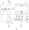
도 1은 본 발명에 따른 반도체 메모리 장치를 설명하기 위한 블럭도이다.1 is a block diagram illustrating a semiconductor memory device according to the present invention.
도 1을 참조하면, 반도체 메모리 장치(100)는 메모리 셀 어레이(110), 어드레스 디코더(120), 읽기 및 쓰기 회로(130), 제어 로직(140), 그리고 전압 생성부(150)를 포함한다.Referring to FIG. 1 , the
메모리 셀 어레이(110)는 다수의 메모리 블록들(BLK1~BLKz)을 포함한다. 다수의 메모리 블록들(BLK1~BLKz)은 워드 라인들(WL)을 통해 어드레스 디코더(120)에 연결된다. 다수의 메모리 블록들(BLK1~BLKz)은 비트 라인들(BL1내지 BLm)을 통해 읽기 및 쓰기 회로(130)에 연결된다. 다수의 메모리 블록들(BLK1~BLKz) 각각은 다수의 메모리 셀들을 포함한다. 실시 예로서, 다수의 메모리 셀들은 불휘발성 메모리 셀들이다. 하나의 워드 라인에 공통적으로 연결된 다수의 메모리 셀들은 하나의 페이지로 정의된다. 또한 하나의 메모리 블록은 다수의 페이지들을 포함한다. 다수의 페이지들에 포함된 다수의 메모리 셀들은 반도체 기판 상에 수직한 플러그를 따라 순차적으로 적층된다.The
반도체 메모리 장치(100)의 프로그램 동작은 페이지 단위로 수행된다. 메모리 셀 어레이(110)의 다수의 메모리 블록들(BLK1~BLKz) 각각은 다수의 셀 스트링들을 포함한다. 다수의 셀 스트링들 각각은 반도체 기판 상에 적층된 다수의 메모리 셀들을 포함한다. 다수의 셀 스트링들 각각은 비트 라인(BL)과 공통 소스 라인(SL) 사이에 연결된 드레인 선택 트랜지스터, 다수의 메모리 셀들 및 소스 선택 트랜지스터를 포함한다.A program operation of the
어드레스 디코더(120), 읽기 및 쓰기 회로(130), 및 전압 생성부(150)는 메모리 셀 어레이(110)를 구동하는 주변 회로들로서 동작한다.The
어드레스 디코더(120)는 워드 라인들(WL)을 통해 메모리 셀 어레이(110)에 연결된다. 어드레스 디코더(120)는 제어 로직(140)의 제어에 응답하여 동작하도록 구성된다. 어드레스 디코더(120)는 반도체 메모리 장치(100) 내부의 입출력 버퍼(미도시)를 통해 어드레스(ADDR)를 수신한다. 어드레스 디코더(120)는 수신된 어드레스(ADDR) 중 행 어드레스를 디코딩하도록 구성된다. 어드레스 디코더(120)는 프로그램 동작 시 전압 생성부(150)에서 생성된 프로그램 전압들(Vpgm), 패스 전압들(Vpass) 및 다수의 동작 전압들을 수신된 어드레스(ADDR) 중 디코딩된 행 어드레스에 따라 메모리 셀 어레이(110)의 다수의 메모리 셀들, 드레인 및 소스 선택 트랜지스터에 인가한다. 어드레스 디코더(120)는 수신된 어드레스(ADDR) 중 열 어드레스(Yi)를 디코딩하도록 구성된다. 어드레스 디코더(120)는 디코딩된 열 어드레스(Yi)를 읽기 및 쓰기 회로(130)에 전송한다.The
프로그램 동작 요청 시에 수신되는 어드레스(ADDR)는 블록 어드레스, 행 어드레스 및 열 어드레스(Yi)를 포함한다. 어드레스 디코더(120)는 블록 어드레스 및 행 어드레스에 따라 하나의 메모리 블록 및 하나의 워드 라인을 선택한다. 열 어드레스(Yi)는 어드레스 디코더(120)에 의해 디코딩되어 읽기 및 쓰기 회로(130)에 제공된다.The address ADDR received when requesting a program operation includes a block address, a row address, and a column address Yi. The
어드레스 디코더(120)는 블록 디코더, 행 디코더, 열 디코더 및 어드레스 버퍼 등을 포함할 수 있다.The
읽기 및 쓰기 회로(130)는 다수의 페이지 버퍼들(PB1~PBm)을 포함한다. 다수의 페이지 버퍼들(PB1~PBm)은 비트 라인들(BL1 내지 BLm)을 통해 메모리 셀 어레이(110)에 연결된다. 다수의 페이지 버퍼들(PB1~PBm) 각각은 프로그램 동작 시 프로그램 데이터(DATA)를 전송받아 임시 저장하고, 프로그램 데이터(DATA)에 따라 대응하는 비트 라인들(BL1 내지 BLm)중 어느 하나의 전위를 프로그램 허용 전압 또는 프로그램 금지 전압으로 제어한다. 또한 다수의 페이지 버퍼들(PB1~PBm) 각각은 프로그램 검증 동작 시 대응하는 메모리 셀의 프로그램 상태를 센싱하여 이를 프로그램 동작 시 임시 저장된 프로그램 데이터(DATA)와 비교하여 대응하는 메모리 셀이 프로그램 완료되었는지를 검증한다.The read and write
읽기 및 쓰기 회로(130)는 제어 로직(140)의 제어에 응답하여 동작한다. 예시적인 실시 예로서, 읽기 및 쓰기 회로(130)는 페이지 버퍼들(또는 페이지 레지스터들), 열 선택 회로 등을 포함할 수 있다.The read and write
제어 로직(140)은 어드레스 디코더(120), 읽기 및 쓰기 회로(130), 및 전압 생성부(150)에 연결된다. 제어 로직(140)은 반도체 메모리 장치(100)의 입출력 버퍼(미도시)를 통해 커맨드(CMD)를 수신한다. 제어 로직(140)은 커맨드(CMD)에 응답하여 반도체 메모리 장치(100)의 제반 동작을 제어하도록 구성된다.The
본 발명의 일 실시 예에 따른 제어 로직(140)은 프로그램 동작 시 복수의 워드 라인들에 프리 바이어스 전압을 인가할 수 있다. 이 때, 제어 로직(140)은 복수의 워드 라인들 각각의 위치에 따라 상이한 프리 바이어스 전압을 인가할 수 있다.The
전압 생성부(150)는 프로그램 동작 시 제어 로직(140)의 제어에 따라 프로그램 전압들(Vpgm), 패스 전압들(Vpass) 및 다수의 동작 전압들을 생성하여 출력한다. 다수의 동작 전압들에는 파이프 트랜지스터 동작 전압 등이 포함될 수 있다. 본 명세서에서, 메모리 셀 어레이(110) 및 제어 로직(140)을 제외한 구성 요소는 모두 주변 회로로서 통칭할 수 있다.During a program operation, the
도 2는 도 1의 메모리 셀 어레이의 실시 예를 설명하기 위한 블럭도이다.FIG. 2 is a block diagram illustrating an exemplary embodiment of the memory cell array of FIG. 1 .
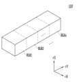
도 2를 참조하면, 메모리 셀 어레이(110)는 다수의 메모리 블록들(BLK1~BLKz)을 포함한다. 각 메모리 블록은 3차원 구조를 가질 수 있는다. 각 메모리 블록은 반도체 기판 상에 수직한 플러그를 따라 적층된 다수의 메모리 셀들을 포함한다. 이러한 다수의 메모리 셀들은 +X 방향, +Y 방향 및 +Z 방향을 따라 배열될 수 있다.Referring to FIG. 2 , the
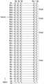
도 3은 메모리 셀 어레이 내 셀 스트링들의 일부를 나타내는 회로도이다. 도 3에는 메모리 셀 어레이의 복수의 블록들에 포함된 다수의 셀 스트링들 중에서, 두 개의 셀 스트링만이 도시되었다. 즉, 프로그램 동작의 대상이 되는 선택된 셀 스트링과, 프로그램 동작의 대상이 아닌 다수의 비선택 셀 스트링 중 선택된 셀 스트링에 인접하여 위치한 하나의 비선택 셀 스트링이 도시되었다. 선택된 셀 스트링은 비트 라인(BLk)에 연결되고, 비선택 셀 스트링은 비트 라인(BLk+1)과 연결된다.3 is a circuit diagram showing some of cell strings in a memory cell array. 3 shows only two cell strings among a plurality of cell strings included in a plurality of blocks of the memory cell array. That is, a selected cell string that is a target of a program operation and one unselected cell string located adjacent to a selected cell string among a plurality of unselected cell strings that are not subject to a program operation are shown. The selected cell string is connected to the bit line BLk, and the unselected cell string is connected to the bit
도 3을 참조하면, 선택된 셀 스트링은 공통 소스 라인(CSL)과 대응하는 비트 라인들(BLk) 사이에 연결되며, 소스 선택 트랜지스터(SST0), 메모리 셀들(MC00~MC0(n-1)) 및 드레인 선택 트랜지스터(DST0)를 포함한다. 소스 선택 트랜지스터(SST0) 및 드레인 선택 트랜지스터(DST0)는 각각 소스 선택 라인(SSL) 및 드레인 선택 라인(DSL)에 연결되고, 메모리 셀들(MC00~MC0(n-1))은 각각 워드 라인들(WL0~WLn-1)에 연결된다. 서로 다른 워드 라인들(WL0~WLn-1)에 연결된 메모리 셀들(MC00~MC0(n-1))은 서로 다른 페이지들에 포함된다. 또한, 비선택된 셀 스트링은 공통 소스 라인(CSL)과 대응하는 비트 라인들(BLk+1) 사이에 연결되며, 소스 선택 트랜지스터(SST1), 메모리 셀들(MC10~MC1(n-1)) 및 드레인 선택 트랜지스터(DST1)를 포함한다. 소스 선택 트랜지스터(SST1) 및 드레인 선택 트랜지스터(DST1)는 각각 소스 선택 라인(SSL) 및 드레인 선택 라인(DSL)에 연결되고, 메모리 셀들(MC10~MC1(n-1))은 각각 워드 라인들(WL0~WLn-1)에 연결된다. 서로 다른 워드 라인들(WL0~WLn-1)에 연결된 메모리 셀들(MC10~MC1(n-1))은 서로 다른 페이지들에 포함된다Referring to FIG. 3 , the selected cell string is connected between a common source line CSL and corresponding bit lines BLk, and includes a source selection transistor SST0, memory cells MC00 to MC0(n-1), and A drain select transistor DST0 is included. The source select transistor SST0 and the drain select transistor DST0 are connected to the source select line SSL and the drain select line DSL, respectively, and the memory cells MC00 to MC0(n-1) are respectively connected to word lines ( It is connected to WL0~WLn-1). Memory cells MC00 to MC0(n-1) connected to different word lines WL0 to WLn-1 are included in different pages. In addition, the non-selected cell string is connected between the common source line CSL and the corresponding bit
본 발명의 일 실시예에 따른 반도체 메모리 장치는, 메모리 블록 내 메모리 스트링에 연결된 워드 라인들을 그룹화 하고, 셀 스트링의 프리차지 동작 시 각 그룹별로 서로 다른 프리 바이어스 전압을 인가할 수 있다. 이에 따라, 전체 셀 스트링 내 균일한 프리차지 레벨을 달성할 수 있다.In the semiconductor memory device according to an exemplary embodiment of the present invention, word lines connected to memory strings in a memory block may be grouped, and different pre-bias voltages may be applied to each group during a pre-charging operation of a cell string. Accordingly, it is possible to achieve a uniform precharge level in the entire cell string.
본 발명의 일 실시예에 따라 프로그램 동작 시 프리차징 단계에서 워드 라인들에 서로 다른 프리 바이어스 전압을 인가하는 구체적인 내용에 대해서는 도 4a 내지 도 8을 참조하여 후술하기로 한다.Details of applying different pre-bias voltages to word lines in a pre-charging step during a program operation according to an embodiment of the present invention will be described later with reference to FIGS. 4A to 8 .
도 4a는 본 발명의 일 실시예에 따라, 복수의 워드 라인들을 그룹화하여 프리 바이어스 전압을 인가하는 방법을 설명하기 위한 도면이다.4A is a diagram for explaining a method of applying a pre-bias voltage by grouping a plurality of word lines according to an embodiment of the present invention.
도 4a를 참조하면, 본 발명의 일 실시예에 따른 반도체 메모리 장치의 제어 로직은 메모리 블록 내 워드 라인들을 그룹화할 수 있다. 도 4a에서 메모리 블록은 32개의 워드 라인들(WL0~WL31)을 포함한다. 한편, 도 4a에서 제어 로직은 32개의 워드 라인을 2개의 워드 라인 그룹으로 그룹화할 수 있다. 제 1 워드 라인 그룹(Group1) 및 제 2 워드 라인 그룹(Group2)은 각각 16개의 워드 라인들을 포함한다.Referring to FIG. 4A , the control logic of the semiconductor memory device according to an exemplary embodiment may group word lines in a memory block. In FIG. 4A, the memory block includes 32 word lines WL0 to WL31. Meanwhile, in FIG. 4A, the control logic may group 32 word lines into two word line groups. Each of the first word line group Group1 and the second word line group Group2 includes 16 word lines.
제어 로직은 그룹화 결과에 기초하여, 프로그램 대상인 메모리 셀과 연결된 워드 라인의 위치에 따라 각 워드 라인들(WL0~WL31)에 인가되는 프리 바이어스 전압을 결정할 수 있다. 상기 프리 바이어스 전압은 프로그램 셀의 프로그램 동작시, 프리차지 단계에서 각 워드 라인들(WL0~WL31)에 인가되는 전압이다.The control logic may determine a pre-bias voltage applied to each of the word lines WL0 to WL31 according to a position of a word line connected to a memory cell to be programmed based on a grouping result. The pre-bias voltage is a voltage applied to each of the word lines WL0 to WL31 in a pre-charge step during a program operation of a program cell.
도 4a에는 프로그램 대상이 되는 프로그램 셀이 제 1 워드 라인 그룹(Group1) 내에 속하는 제 10 워드 라인(WL10)과 연결된 경우를 도시하고 있다. 이는, 상대적으로 소스 선택 트랜지스터와 가까운 메모리 셀이 프로그램 되는 경우이다. 즉, 도 4a의 실시예에서, 프로그램 방향은 제 0 워드 라인(WL0)에서 제 31 워드 라인(WL31)으로 향하는 방향이다. 통상적인 프로그램 동작의 경우, 비 선택된 메모리 스트링의 프리차지 동작시 소스 선택 트랜지스터와 드레인 선택 트랜지스터 사이의 저항 성분으로 인해 메모리 셀의 문턱 전압이 상승한다. 이에 따라 소스 선택 트랜지스터 측의 채널 내 프리차지 레벨이 감소하여 채널 부스팅이 효과적으로 일어나지 않는다. 따라서 프로그램 디스터브가 발생한다. 본 발명의 실시예에 따른 반도체 메모리 장치의 경우, 프리차지 과정에서 드레인 선택 트랜지스터에 가까운 워드 라인 그룹에 속한 워드 라인일수록 상대적으로 높은 프리 바이어스 전압을 인가할 수 있다. 다르게 말하면, 본 발명의 실시예에 따른 반도체 메모리 장치의 경우, 프리차지 과정에서 최초 프로그램된 메모리 셀과 연결된 워드 라인(WL0)을 포함하는 워드 라인 그룹 또는 그에 가까운 워드 라인 그룹일수록 상대적으로 낮은 프리 바이어스 전압을 인가하고, 가장 나중에 프로그램될 메모리 셀과 연결된 워드 라인(WL31)을 포함하는 워드 라인 그룹 또는 그에 가까운 워드 라인 그룹일수록 상대적으로 높은 프리 바이어스 전압을 인가할 수 있다. 따라서 소스 선택 트랜지스터와 드레인 선택 트랜지스터 사이의 저항 성분에 따른 효과를 상쇄하여, 채널 내 프리차지 레벨을 균일하게 달성할 수 있다. 이에 따라 프로그램 디스터브 현상이 개선된다.4A shows a case in which a program cell to be programmed is connected to a tenth word line WL10 belonging to a first word line group Group1. This is a case where a memory cell relatively close to the source select transistor is programmed. That is, in the embodiment of FIG. 4A , the programming direction is from the 0 th word line WL0 to the 31 th word line WL31 . In the case of a normal program operation, a threshold voltage of a memory cell increases due to a resistive component between a source select transistor and a drain select transistor during a precharge operation of an unselected memory string. Accordingly, the precharge level in the channel of the source select transistor side is reduced, so that channel boosting does not effectively occur. Therefore, program disturb occurs. In the case of the semiconductor memory device according to an embodiment of the present invention, a relatively higher pre-bias voltage may be applied to word lines belonging to a word line group closer to the drain select transistor during the pre-charging process. In other words, in the case of a semiconductor memory device according to an embodiment of the present invention, a word line group including a word line WL0 connected to an initially programmed memory cell or a word line group close thereto has a relatively low pre-bias during a pre-charging process. A relatively high pre-bias voltage may be applied to a word line group including the word line WL31 connected to the memory cell to be programmed most recently or to a word line group close to the word line WL31. Therefore, it is possible to achieve a uniform precharge level in the channel by canceling the effect of the resistance component between the source select transistor and the drain select transistor. Accordingly, the program disturb phenomenon is improved.
도 4a를 다시 참조하면, 프로그램 셀과 연결된 워드 라인이 제 1 그룹(Group1)에 포함된 경우, 프리차지 동안 제 1 그룹(Group1)에 속하는 워드 라인들(WL0~WL15)에는 디폴트 값(default value)을 갖는 프리 바이어스 전압을 인가하고, 제 2 그룹(Group2)에 속하는 워드 라인들(WL16~WL31)에는 상기 디폴트 값보다 일정 크기만큼 큰 프리 바이어스 전압을 인가할 수 있다. 즉, 제 1 그룹(Group1)에 속하는 워드 라인들에 인가되는 프리 바이어스 전압보다 제 2 그룹(Group2)에 속하는 워드 라인들에 인가되는 프리 바이어스 전압이 크다.Referring back to FIG. 4A , when a word line connected to a program cell is included in the first group (Group1), the word lines (WL0 to WL15) belonging to the first group (Group1) have default values during precharging. ), and a pre-bias voltage higher than the default value by a certain amount may be applied to the word lines WL16 to WL31 belonging to the second group Group2. That is, the pre-bias voltage applied to the word lines belonging to the second group (Group2) is greater than the pre-bias voltage applied to the word lines belonging to the first group (Group1).
한편, 본 발명의 일 실시예에서는, 선택된 워드 라인의 위치에 따라 프리차지 동작시 공통 소스 라인에 인가되는 프리 차지 전압을 다르게 설정할 수 있다. 예를 들어, 프로그램 대상이 되는 프로그램 셀이 소스 선택 트랜지스터에 가까울수록 상대적으로 높은 프리차지 전압을 공통 소스 라인에 인가할 수 있다. 또한, 프로그램 대상이 되는 프로그램 셀이 드레인 선택 트랜지스터에 가까울수록 상대적으로 낮은 프리차지 전압을 공통 소스 라인에 인가할 수 있다.Meanwhile, in one embodiment of the present invention, the pre-charge voltage applied to the common source line may be differently set during the pre-charge operation according to the position of the selected word line. For example, a relatively high precharge voltage may be applied to the common source line as the program cell to be programmed is closer to the source select transistor. In addition, a relatively low precharge voltage may be applied to the common source line as the program cell to be programmed is closer to the drain select transistor.
프리 바이어스 전압을 각 워드 라인들에 인가하고 프리차지 동작이 완료된 이후에, 선택된 워드 라인(WL10)에는 프로그램 전압을 인가하고, 비선택된 워드 라인들(WL0~WL9, WL11~WL31)에는 패스 전압을 인가할 수 있다. 상기 동작을 메모리 셀의 프로그램 루프로서, 상기 프로그램 루프는 반복적으로 수행될 수 있다.After the pre-bias voltage is applied to each word line and the pre-charge operation is completed, the program voltage is applied to the selected word line (WL10) and the pass voltage is applied to the non-selected word lines (WL0 to WL9, WL11 to WL31). can be authorized. The above operation is a program loop of a memory cell, and the program loop may be repeatedly performed.
한편, 도 4a와 달리 프로그램 셀이 제 2 워드 라인 그룹(Group2)에 속하는 워드 라인과 연결된 경우 전체 워드 라인들(WL0~WL16)에 동일한 디폴트 값을 프리 바이어스 전압으로서 인가할 수 있다. 예를 들어, 프로그램 셀이 제 29 워드 라인(WL28)과 연결된 경우, 제 1 내지 제 28 워드 라인(WL0~WL27)과 연결된 메모리 셀들은 프로그램이 완료된 상태이다. 이 경우, 드레인 선택 트랜지스터에 상대적으로 가까운 워드 라인에 보다 높은 프리 바이어스 전압을 인가할 필요성이 낮다. 따라서, 이와 같은 경우에는 제 1 그룹 및 제 2 그룹(Group1, Group2)에 연결된 전체 워드 라인들(WL0~WL31)에 동일한 값의 프리 바이어스 전압을 인가할 수 있다.Meanwhile, unlike FIG. 4A , when a program cell is connected to a word line belonging to the second word line group Group2 , the same default value may be applied as a pre-bias voltage to all word lines WL0 to WL16 . For example, when the program cells are connected to the 29th word line WL28, the programming of the memory cells connected to the 1st to 28th word lines WL0 to WL27 is completed. In this case, there is less need to apply a higher pre-bias voltage to the word line relatively close to the drain select transistor. Accordingly, in this case, a pre-bias voltage of the same value may be applied to all word lines WL0 to WL31 connected to the first and second groups (Group1 and Group2).
도 4a에는 워드 라인들을 2개의 워드 라인 그룹으로 그룹화한 실시예를 도시하고 있다. 그러나 본 발명에 따른 반도체 메모리 장치의 워드 라인들은 3개 또는 그 이상의 워드 라인 그룹들로 그룹화될 수 있다.4A shows an example of grouping word lines into two word line groups. However, word lines of the semiconductor memory device according to the present invention may be grouped into three or more word line groups.
도 4b는 본 발명의 다른 실시예에 따라, 복수의 워드 라인들을 그룹화하여 프리 바이어스 전압을 인가하는 방법을 설명하기 위한 도면이다.4B is a diagram for explaining a method of applying a pre-bias voltage by grouping a plurality of word lines according to another embodiment of the present invention.
도 4b를 참조하면, 제어 로직은 32개의 워드 라인을 4개의 워드 라인 그룹으로 그룹화할 수 있다. 제 1 내지 제 4 워드 라인 그룹(Group1~Group4)은 각각 8개의 워드 라인들을 포함한다. 여기에서는 12번째 워드 라인(WL11)이 선택된 경우에 대해서 설명하기로 한다.Referring to FIG. 4B, the control logic may group the 32 word lines into groups of 4 word lines. Each of the first to fourth word line groups Group1 to Group4 includes 8 word lines. Here, a case in which the twelfth word line WL11 is selected will be described.
도 4a를 참조하여 설명한 바와 같이, 선택된 워드 라인이 속하는 그룹을 기준으로 하여, 드레인 선택 트랜지스터에 가까운 그룹일수록 워드 라인들에 상대적으로 높은 프리 바이어스 전압이 인가된다. 즉, 제 3 그룹(Group3)에 속하는 워드 라인들(WL16~WL23)에 인가되는 프리 바이어스 전압은 제 2 그룹(Group2)에 속하는 워드 라인들(WL8~WL15)에 인가되는 프리 바이어스 전압보다 더 클 수 있다. 또한, 제 4 그룹(Group4)에 속하는 워드 라인들(WL24~WL32)에 인가되는 프리 바이어스 전압은 제 3 그룹(Group3)에 속하는 워드 라인들(WL16~WL23)에 인가되는 프리 바이어스 전압보다 더 클 수 있다. 한편, 선택 트랜지스터와 연결된 워드 라인(WL11)이 속한 그룹(Group2)에 연결된 워드 라인들(WL8~WL15)에는 디폴트 값의 프리 바이어스 전압이 인가된다. 또한, 제 2 그룹보다 소스 선택 트랜지스터 측에 가까운 그룹(Group1)에 속하는 워드 라인들(WL0~WL7)에도 또한 디폴트 값의 프리 바이어스 전압이 인가된다.As described with reference to FIG. 4A , a relatively high pre-bias voltage is applied to word lines as the group is closer to the drain select transistor based on the group to which the selected word line belongs. That is, the pre-bias voltage applied to the word lines WL16 to WL23 belonging to the third group (Group3) is greater than the pre-bias voltage applied to the word lines WL8 to WL15 belonging to the second group (Group2). can In addition, the pre-bias voltage applied to the word lines WL24 to WL32 belonging to the fourth group (Group4) is greater than the pre-bias voltage applied to the word lines WL16 to WL23 belonging to the third group (Group3). can Meanwhile, a pre-bias voltage of a default value is applied to the word lines WL8 to WL15 connected to the group Group2 to which the word line WL11 connected to the selection transistor belongs. In addition, a pre-bias voltage of a default value is also applied to the word lines WL0 to WL7 belonging to the group Group1 closer to the source select transistor than the second group.
다른 예에서, 선택된 트랜지스터가 제 3 그룹(Group3)에 속하는 워드 라인과 연결된 경우, 제 1 내지 제 3 그룹(Group1~Group3)에 속한 워드 라인들(WL0~WL23)에는 디폴트 값의 프리 바이어스 전압이 인가되고, 제 4 그룹(Group4)에 속하는 워드 라인들(WL24~WL31)에는 상기 디폴트 값보다 큰 값의 프리 바이어스 전압이 인가될 수 있다.In another example, when the selected transistor is connected to a word line belonging to the third group (Group3), a pre-bias voltage of a default value is applied to the word lines (WL0 to WL23) belonging to the first to third groups (Group1 to Group3). A pre-bias voltage having a higher value than the default value may be applied to the word lines WL24 to WL31 belonging to the fourth group Group4.
도 4c는 본 발명의 다른 실시예에 따라, 복수의 워드 라인들을 그룹화하여 프리 바이어스 전압을 인가하는 방법을 설명하기 위한 도면이다.4C is a diagram for explaining a method of applying a pre-bias voltage by grouping a plurality of word lines according to another embodiment of the present invention.
도 4a 내지 도 4b에서는 각 워드 라인 그룹이 동일한 개수의 워드 라인들을 포함하는 실시예가 도시되어 있으나, 본 발명에 따른 반도체 메모리 장치 및 그 동작 방법에 의하면, 각 워드 라인 그룹은 서로 다른 개수의 워드 라인들을 포함할 수 있다. 예를 들어, 도 4c에 도시된 바와 같이, 드레인 선택 트랜지스터에 가까운 워드 라인 그룹일수록 더 적은 워드 라인들을 포함할 수 있다.4A and 4B show an embodiment in which each word line group includes the same number of word lines, but according to a semiconductor memory device and an operating method thereof according to the present invention, each word line group has a different number of word lines. may include For example, as shown in FIG. 4C , a word line group closer to the drain select transistor may include fewer word lines.
도 5a는 본 발명의 다른 실시예에 따라, 복수의 워드 라인들을 그룹화하여 프리 바이어스 전압을 인가하는 방법을 설명하기 위한 도면이다.5A is a diagram for explaining a method of applying a pre-bias voltage by grouping a plurality of word lines according to another embodiment of the present invention.
도 5a를 참조하면, 도 4a 내지 도 4c와는 달리 비트 라인들(BL0~BLk)에 가까운 메모리 셀들부터 프로그램되는 실시예가 도시되어 있다. 즉, 도 5a의 실시예에서, 프로그램 방향은 제 31 워드 라인(WL31)에서 제 0 워드 라인(WL0)으로 향하는 방향이다. 이를 위하여, 드레인 선택 라인(DSL)과 워드 라인들 사이에 추가적인 드레인 측 전원 워드 라인(DPWL)이 포함될 수 있고, 관련된 트랜지스터들 또한 구비될 수 있다. 또한, 소스 선택 라인(SSL)과 워드 라인들 사이에 추가적인 소스 측 전원 워드 라인(SPWL)이 포함될 수 있고, 관련된 트랜지스터들 또한 구비될 수 있다.Referring to FIG. 5A , unlike FIGS. 4A to 4C , an embodiment in which memory cells close to bit lines BL0 to BLk are programmed first is illustrated. That is, in the embodiment of FIG. 5A , the programming direction is from the 31st word line WL31 to the 0th word line WL0. To this end, an additional drain-side power supply word line DPWL may be included between the drain select line DSL and the word lines, and related transistors may also be provided. In addition, an additional source-side power supply word line SPWL may be included between the source select line SSL and the word lines, and related transistors may also be provided.
도 5a의 실시예에 의하면, 예를 들어 선택된 워드 라인(WL26)이 제 2 그룹(Group2)에 속하는 경우, 제 2 그룹(Group2)에 속하는 워드 라인들(WL16~WL31)에는 디폴트 값의 프리 바이어스 전압이 인가되고, 제 1 그룹(Group1)에 속하는 워드 라인들(WL0~WL15)에는 상기 디폴트 값보다 큰 값의 프리 바이어스 전압이 인가된다. 즉, 본 발명의 실시예에 따른 반도체 메모리 장치의 경우, 프로그램 동작이 드레인 선택 트랜지스터와 인접한 메모리 셀부터 수행되는 경우에, 소스 선택 트랜지스터에 가까운 워드 라인 그룹에 속한 워드 라인일수록 상대적으로 높은 프리 바이어스 전압이 인가될 수 있다. 다르게 말하면, 본 발명의 실시예에 따른 반도체 메모리 장치의 경우, 프리차지 과정에서 최초 프로그램된 메모리 셀과 연결된 워드 라인(WL31)을 포함하는 워드 라인 그룹 또는 그에 가까운 워드 라인 그룹일수록 상대적으로 낮은 프리 바이어스 전압을 인가하고, 가장 나중에 프로그램될 메모리 셀과 연결된 워드 라인(WL0)을 포함하는 워드 라인 그룹 또는 그에 가까운 워드 라인 그룹일수록 상대적으로 높은 프리 바이어스 전압을 인가할 수 있다.According to the embodiment of FIG. 5A , for example, when the selected word line WL26 belongs to the second group Group2, word lines WL16 to WL31 belonging to the second group Group2 are pre-biased with a default value. A voltage is applied, and a pre-bias voltage higher than the default value is applied to the word lines WL0 to WL15 belonging to the first group Group1. That is, in the case of the semiconductor memory device according to an embodiment of the present invention, when a program operation is performed from a memory cell adjacent to a drain select transistor, a relatively higher pre-bias voltage is associated with a word line belonging to a word line group closer to the source select transistor. this may be authorized. In other words, in the case of the semiconductor memory device according to an embodiment of the present invention, a word line group including the word line WL31 connected to the first programmed memory cell or a word line group close to the word line group has a relatively low pre-bias during the pre-charging process. A relatively high pre-bias voltage may be applied to a word line group including a word line WL0 connected to a memory cell to be programmed last or a word line group close thereto.
도 5b는 본 발명의 다른 실시예에 따라, 복수의 워드 라인들을 그룹화하여 프리 바이어스 전압을 인가하는 방법을 설명하기 위한 도면이다.5B is a diagram for explaining a method of applying a pre-bias voltage by grouping a plurality of word lines according to another embodiment of the present invention.
도 5b에서는 제 13 워드 라인(WL12)이 선택되었다. 따라서, 제 2 내지 제 4 그룹(Group2~Group4)에 속하는 워드 라인들(WL8~WL31)에는 디폴트 값의 프리 바이어스 전압이 인가되고, 제 1 그룹(Group1)에 속하는 워드 라인들(WL0~WL7)에는 상기 디폴트 값보다 큰 값의 프리 바이어스 전압이 인가된다.In FIG. 5B, the thirteenth word line WL12 is selected. Therefore, the pre-bias voltage of the default value is applied to the word lines WL8 to WL31 belonging to the second to fourth groups Group2 to Group4, and the word lines WL0 to WL7 belonging to the first group Group1 are applied. A pre-bias voltage greater than the default value is applied to .
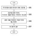
도 6은 본 발명의 일 실시예에 따른 반도체 메모리 장치의 프로그램 방법을 나타내는 순서도이다.6 is a flowchart illustrating a method of programming a semiconductor memory device according to an exemplary embodiment of the present invention.
도 6을 참조하면, 본 발명의 일 실시예에 따른 반도체 메모리 장치의 프로그램 방법은 메모리 셀들과 연결된 워드 라인들을 복수의 워드 라인 그룹으로 그룹화하는 단계(S101) 및 상기 워드 라인의 그룹화 결과에 기초하여, 프로그램 동작을 수행하는 단계(S103)를 포함한다. 단계(S101)에서는 그룹화 할 워드 라인 그룹의 개수 및 각 워드 라인 그룹이 포함하게 될 워드 라인들의 개수를 결정할 수 있다. 단계(S103)에서는 결정된 워드 라인 그룹화 결과에 기초하여, 선택된 워드 라인이 어느 워드 라인 그룹에 속하는지에 따라 각 그룹에 속하는 워드 라인들에 인가되는 프리 바이어스 전압을 결정하여 프로그램 동작을 수행할 수 있다.Referring to FIG. 6 , a method of programming a semiconductor memory device according to an embodiment of the present invention includes grouping word lines connected to memory cells into a plurality of word line groups (S101) and based on a result of grouping the word lines. , performing a program operation (S103). In step S101, the number of word line groups to be grouped and the number of word lines to be included in each word line group may be determined. In step S103, a program operation may be performed by determining a pre-bias voltage applied to word lines belonging to each group according to which word line group the selected word line belongs to based on the determined word line grouping result.
도 7은 도 6에서 워드라인 그룹화 결과에 기초하여 프로그램 동작을 수행하는 단계를 보다 상세히 나타내는 예시적인 실시예이다.FIG. 7 is an exemplary embodiment illustrating in detail a step of performing a program operation based on a word line grouping result in FIG. 6 .
도 7을 참조하면, 워드 라인의 그룹화 결과에 기초하여, 프로그램 동작을 수행하는 단계는, 프로그램 셀과 연결된 워드 라인이 포함된 워드 라인 그룹을 판별하는 단계(S201), 상기 그룹 판별 결과에 기초하여, 각 워드 라인 그룹들에 적용되는 프리 바이어스 전압을 결정하는 단계(S203), 결정된 프리 바이어스 전압에 기초하여 메모리 셀들의 채널 영역을 프리차지하는 단계(S205) 및 프로그램 루프를 실행하는 단계(S207)를 포함한다. 프로그램 셀과 연결된 워드 라인이 포함된 워드 라인 그룹을 판별하는 단계(S201)에서는, 프로그램 셀과 연결된 워드 라인이 복수의 워드 라인 그룹들 중 어느 워드 라인 그룹에 속하는지 판별한다. 상기 그룹 판별 결과에 기초하여, 각 워드 라인 그룹들에 적용되는 프리 바이어스 전압을 결정하는 단계(S203)에서는 각 워드 라인 그룹들에 속하는 워드 라인들에 인가될 프리 바이어스 전압을 결정한다. 도 4a 내지 도 4c를 참조하여 전술한 바와 같이, 드레인 선택 트랜지스터에 가까운 워드 라인 그룹일수록 높은 프리 바이어스 전압이 인가될 수 있다. 결정된 프리 바이어스 전압에 기초하여 메모리 셀들의 채널 영역을 프리차지하는 단계(S205)에서는 결정된 프리 바이어스 전압을 각 워드 라인에 인가하고 공통 소스 라인에 프리차지 전압을 인가한다. 프로그램 루프를 실행하는 단계(S207)에서는 선택된 워드 라인에 프로그램 전압을 인가하고, 비선택된 워드 라인에 패스 전압을 인가한다.Referring to FIG. 7 , performing a program operation based on a word line grouping result includes determining a word line group including a word line connected to a program cell (S201), and based on the group determination result , determining a pre-bias voltage applied to each word line group (S203), pre-charging a channel region of memory cells based on the determined pre-bias voltage (S205), and executing a program loop (S207). include In step S201 of determining the word line group including the word line connected to the program cell, it is determined which word line group among a plurality of word line groups the word line connected to the program cell belongs to. In step S203 of determining a pre-bias voltage applied to each word line group based on the group determination result, a pre-bias voltage to be applied to word lines belonging to each word line group is determined. As described above with reference to FIGS. 4A to 4C , a higher pre-bias voltage may be applied to a word line group closer to the drain select transistor. In step S205 of precharging the channel regions of the memory cells based on the determined pre-bias voltage, the determined pre-bias voltage is applied to each word line and the pre-charge voltage is applied to a common source line. In the step of executing the program loop (S207), the program voltage is applied to the selected word line and the pass voltage is applied to the non-selected word line.
도 8은 도 6에서 워드라인 그룹화 결과에 기초하여 프로그램 동작을 수행하는 단계를 보다 상세히 나타내는 또다른 예시적인 실시예이다.FIG. 8 is another exemplary embodiment illustrating in detail a step of performing a program operation based on a wordline grouping result in FIG. 6 .
도 8을 참조하면, 워드 라인의 그룹화 결과에 기초하여, 프로그램 동작을 수행하는 단계는, 프로그램 셀과 연결된 워드 라인이 포함된 워드 라인 그룹을 판별하는 단계(S301), 상기 그룹 판별 결과에 기초하여, 각 워드 라인 그룹들에 적용되는 프리 바이어스 전압을 결정하는 단계(S303a), 그룹 판별 결과에 기초하여 공통 소스 라인에 인가되는 프리차지 전압을 결정하는 단계(S303b), 결정된 프리차지 전압 및 프리 바이어스 전압에 기초하여 메모리 셀들의 채널 영역을 프리차지하는 단계(S305) 및 프로그램 루프를 실행하는 단계(S307)를 포함한다. 도 8의 실시예가 도 7의 실시예와 다른 점은, 단계(S301)에서 수행된 그룹 판별 결과에 기초하여, 공통 소스 라인에 인가되는 소스 전압을 결정하는 단계(S303b)가 더 포함된다는 것이다.Referring to FIG. 8 , performing a program operation based on a word line grouping result includes determining a word line group including a word line connected to a program cell (S301), and based on the group determination result , determining the pre-bias voltage applied to each word line group (S303a), determining the pre-charge voltage applied to the common source line based on the group discrimination result (S303b), the determined pre-charge voltage and pre-bias Precharging channel regions of memory cells based on the voltage (S305) and executing a program loop (S307). A difference between the embodiment of FIG. 8 and the embodiment of FIG. 7 is that a step of determining a source voltage applied to a common source line (S303b) is further included based on the group determination result performed in step S301.
단계(S303b)에서는, 프로그램 동작을 위해 선택된 메모리 셀에 연결된 워드라인이 최초 프로그램된 메모리 셀과 가까울수록 공통 소스 라인에 인가되는 프리차지 전압을 상승시킬 수 있다. 예를 들어 도 4b를 함께 참조하면, 프로그램 동작의 대상으로서 선택된 워드 라인이 제 2 그룹(Group2)에 속하는 경우 공통 소스 라인(CSL)에 인가되는 프리차지 전압은, 프로그램 동작의 대상으로 선택된 워드 라인이 제 1 그룹(Group1)에 속하는 경우 공통 소스 라인(CSL)에 인가되는 프리차지 전압보다 크다. 다른 예에서, 프로그램 동작의 대상으로서 선택된 워드 라인이 제 3 그룹(Group3)에 속하는 경우 공통 소스 라인(CSL)에 인가되는 프리차지 전압은, 프로그램 동작의 대상으로 선택된 워드 라인이 제 2 그룹(Group2)에 속하는 경우 공통 소스 라인(CSL)에 인가되는 프리차지 전압보다 크다. 또다른 예로서, 프로그램 동작의 대상으로서 선택된 워드 라인이 제 4 그룹(Group4)에 속하는 경우 공통 소스 라인(CSL)에 인가되는 프리차지 전압은, 프로그램 동작의 대상으로 선택된 워드 라인이 제 3 그룹(Group3)에 속하는 경우 공통 소스 라인(CSL)에 인가되는 프리차지 전압보다 크다.In step S303b, the precharge voltage applied to the common source line may be increased as the word line connected to the memory cell selected for the program operation is closer to the initially programmed memory cell. For example, referring to FIG. 4B together, when the word line selected as the target of the program operation belongs to the second group Group2, the precharge voltage applied to the common source line CSL is the word line selected as the target of the program operation. If it belongs to the first group (Group1), it is greater than the precharge voltage applied to the common source line (CSL). In another example, when the word line selected as the target of the program operation belongs to the third group (Group3), the precharge voltage applied to the common source line (CSL) is such that the word line selected as the target of the program operation belongs to the second group (Group2). ), it is greater than the precharge voltage applied to the common source line CSL. As another example, when the word line selected as the target of the program operation belongs to the fourth group Group4, the precharge voltage applied to the common source line CSL is such that the word line selected as the target of the program operation belongs to the third group (Group4). Group3) is greater than the precharge voltage applied to the common source line (CSL).
다른 실시예에서, 단계(S303b)에서는, 프로그램 동작을 위해 선택된 메모리 셀에 연결된 워드라인이 최초 프로그램된 메모리 셀과 가까울수록 공통 소스 라인에 인가되는 프리차지 전압을 하강시킬 수 있다. 예를 들어 도 4b를 함께 참조하면, 프로그램 동작의 대상으로서 선택된 워드 라인이 제 1 그룹(Group1)에 속하는 경우 공통 소스 라인(CSL)에 인가되는 프리차지 전압은, 프로그램 동작의 대상으로 선택된 워드 라인이 제 2 그룹(Group2)에 속하는 경우 공통 소스 라인(CSL)에 인가되는 프리차지 전압보다 크다. 다른 예에서, 프로그램 동작의 대상으로서 선택된 워드 라인이 제 2 그룹(Group2)에 속하는 경우 공통 소스 라인(CSL)에 인가되는 프리차지 전압은, 프로그램 동작의 대상으로 선택된 워드 라인이 제 3 그룹(Group3)에 속하는 경우 공통 소스 라인(CSL)에 인가되는 프리차지 전압보다 크다. 또다른 예로서, 프로그램 동작의 대상으로서 선택된 워드 라인이 제 3 그룹(Group3)에 속하는 경우 공통 소스 라인(CSL)에 인가되는 프리차지 전압은, 프로그램 동작의 대상으로 선택된 워드 라인이 제 4 그룹(Group4)에 속하는 경우 공통 소스 라인(CSL)에 인가되는 프리차지 전압보다 크다.In another embodiment, in step S303b, the precharge voltage applied to the common source line may decrease as the word line connected to the memory cell selected for the program operation is closer to the initially programmed memory cell. For example, referring to FIG. 4B together, when the word line selected as the target of the program operation belongs to the first group (Group1), the precharge voltage applied to the common source line CSL is the word line selected as the target of the program operation. If it belongs to the second group (Group2), it is greater than the precharge voltage applied to the common source line (CSL). In another example, when the word line selected as the target of the program operation belongs to the second group (Group2), the precharge voltage applied to the common source line (CSL) is such that the word line selected as the target of the program operation belongs to the third group (Group3). ), it is greater than the precharge voltage applied to the common source line CSL. As another example, when the word line selected as the target of the program operation belongs to the third group (Group3), the precharge voltage applied to the common source line (CSL) is such that the word line selected as the target of the program operation belongs to the fourth group ( Group 4) is greater than the precharge voltage applied to the common source line (CSL).
한편, 단계(S305)에서는 단계(S303a)에서 결정된 프리바이어스 전압과, 단계(S303b)에서 결정된 소스 전압에 기초하여 채널 프리차지를 수행할 수 있다(S305). Meanwhile, in step S305, channel precharging may be performed based on the prebias voltage determined in step S303a and the source voltage determined in step S303b (S305).
도 9는 도 1의 반도체 메모리 장치를 포함하는 메모리 시스템의 실시 예를 설명하기 위한 블럭도이다.FIG. 9 is a block diagram illustrating an example embodiment of a memory system including the semiconductor memory device of FIG. 1 .
도 9를 참조하면, 메모리 시스템(1000)은 반도체 메모리 장치(100) 및 컨트롤러(1100)를 포함한다.Referring to FIG. 9 , a
반도체 메모리 장치(100)는 도 1을 참조하여 설명된 바와 마찬가지로 구성되고, 동작할 수 있다. 이하, 중복되는 설명은 생략된다.The
컨트롤러(1100)는 호스트(Host) 및 반도체 메모리 장치(100)에 연결된다. 호스트(Host)로부터의 요청에 응답하여, 컨트롤러(1100)는 반도체 메모리 장치(100)를 액세스하도록 구성된다. 예를 들면, 컨트롤러(1100)는 반도체 메모리 장치(100)의 읽기, 쓰기, 소거, 그리고 배경(background) 동작을 제어하도록 구성된다. 컨트롤러(1100)는 반도체 메모리 장치(100) 및 호스트(Host) 사이에 인터페이스를 제공하도록 구성된다. 컨트롤러(1100)는 반도체 메모리 장치(100)를 제어하기 위한 펌웨어(firmware)를 구동하도록 구성된다.The
컨트롤러(1100)는 램(1110, Random Access Memory), 프로세싱 유닛(1120, processing unit), 호스트 인터페이스(1130, host interface), 메모리 인터페이스(1140, memory interface) 및 에러 정정 블록(1150)을 포함한다. 램(1110)은 프로세싱 유닛(1120)의 동작 메모리, 반도체 메모리 장치(100) 및 호스트(Host) 사이의 캐시 메모리, 그리고 반도체 메모리 장치(100) 및 호스트(Host) 사이의 버퍼 메모리 중 적어도 하나로서 이용된다. 프로세싱 유닛(1120)은 컨트롤러(1100)의 제반 동작을 제어한다. 또한 컨트롤러(1100)는 쓰기 동작시 호스트(Host)로부터 제공되는 프로그램 데이터를 임시 저장할 수 있다.The
호스트 인터페이스(1130)는 호스트(Host) 및 컨트롤러(1100) 사이의 데이터 교환을 수행하기 위한 프로토콜을 포함한다. 예시적인 실시 예로서, 컨트롤러(1200)는 USB (Universal Serial Bus) 프로토콜, MMC (multimedia card) 프로토콜, PCI (peripheral component interconnection) 프로토콜, PCI-E (PCI-express) 프로토콜, ATA (Advanced Technology Attachment) 프로토콜, Serial-ATA 프로토콜, Parallel-ATA 프로토콜, SCSI (small computer small interface) 프로토콜, ESDI (enhanced small disk interface) 프로토콜, 그리고 IDE (Integrated Drive Electronics) 프로토콜, 사유(private) 프로토콜 등과 같은 다양한 인터페이스 프로토콜들 중 적어도 하나를 통해 호스트(Host)와 통신하도록 구성된다.The
메모리 인터페이스(1140)는 반도체 메모리 장치(100)와 인터페이싱한다. 예를 들면, 메모리 인터페이스는 낸드 인터페이스 또는 노어 인터페이스를 포함한다.The
에러 정정 블록(1150)은 에러 정정 코드(ECC, Error Correcting Code)를 이용하여 반도체 메모리 장치(100)로부터 수신된 데이터의 에러를 검출하고, 정정하도록 구성된다. 프로세싱 유닛(1120)은 에러 정정 블록(1150)의 에러 검출 결과에 따라 읽기 전압을 조절하고, 재 읽기를 수행하도록 반도체 메모리 장치(100)를 제어할 것이다. 예시적인 실시 예로서, 에러 정정 블록은 컨트롤러(1100)의 구성 요소로서 제공될 수 있다.The
컨트롤러(1100) 및 반도체 메모리 장치(100)는 하나의 반도체 장치로 집적될 수 있다. 예시적인 실시 예로서, 컨트롤러(1100) 및 반도체 메모리 장치(100)는 하나의 반도체 장치로 집적되어, 메모리 카드를 구성할 수 있다. 예를 들면, 컨트롤러(1100) 및 반도체 메모리 장치(100)는 하나의 반도체 장치로 집적되어 PC 카드(PCMCIA, personal computer memory card international association), 컴팩트 플래시 카드(CF), 스마트 미디어 카드(SM, SMC), 메모리 스틱, 멀티미디어 카드(MMC, RS-MMC, MMCmicro), SD 카드(SD, miniSD, microSD, SDHC), 유니버설 플래시 기억장치(UFS) 등과 같은 메모리 카드를 구성할 것이다.The
컨트롤러(1100) 및 반도체 메모리 장치(100)는 하나의 반도체 장치로 집적되어 반도체 드라이브(SSD, Solid State Drive)를 구성할 수 있다. 반도체 드라이브(SSD)는 반도체 메모리에 데이터를 저장하도록 구성되는 저장 장치를 포함한다. 메모리 시스템(1000)이 반도체 드라이브(SSD)로 이용되는 경우, 메모리 시스템(2000)에 연결된 호스트(Host)의 동작 속도는 획기적으로 개선된다.The
다른 예로서, 메모리 시스템(1000)은 컴퓨터, UMPC (Ultra Mobile PC), 워크스테이션, 넷북(net-book), PDA (Personal Digital Assistants), 포터블(portable) 컴퓨터, 웹 타블렛(web tablet), 무선 전화기(wireless phone), 모바일 폰(mobile phone), 스마트폰(smart phone), e-북(e-book), PMP(portable multimedia player), 휴대용 게임기, 네비게이션(navigation) 장치, 블랙박스(black box), 디지털 카메라(digital camera), 3차원 수상기(3-dimensional television), 디지털 음성 녹음기(digital audio recorder), 디지털 음성 재생기(digital audio player), 디지털 영상 녹화기(digital picture recorder), 디지털 영상 재생기(digital picture player), 디지털 동영상 녹화기(digital video recorder), 디지털 동영상 재생기(digital video player), 정보를 무선 환경에서 송수신할 수 있는 장치, 홈 네트워크를 구성하는 다양한 전자 장치들 중 하나, 컴퓨터 네트워크를 구성하는 다양한 전자 장치들 중 하나, 텔레매틱스 네트워크를 구성하는 다양한 전자 장치들 중 하나, RFID 장치, 또는 컴퓨팅 시스템을 구성하는 다양한 구성 요소들 중 하나 등과 같은 전자 장치의 다양한 구성 요소들 중 하나로 제공된다.As another example, the
예시적인 실시 예로서, 반도체 메모리 장치(100) 또는 메모리 시스템(1000)은 다양한 형태들의 패키지로 실장될 수 있다. 예를 들면, 반도체 메모리 장치(100) 또는 메모리 시스템(2000)은 PoP(Package on Package), Ball grid arrays(BGAs), Chip scale packages(CSPs), Plastic Leaded Chip Carrier(PLCC), Plastic Dual In Line Package(PDIP), Die in Waffle Pack, Die in Wafer Form, Chip On Board(COB), Ceramic Dual In Line Package(CERDIP), Plastic Metric Quad Flat Pack(MQFP), Thin Quad Flatpack(TQFP), Small Outline(SOIC), Shrink Small Outline Package(SSOP), Thin Small Outline(TSOP), Thin Quad Flatpack(TQFP), System In Package(SIP), Multi-Chip Package(MCP), Wafer-level Fabricated Package(WFP), Wafer-Level Processed Stack Package(WSP) 등과 같은 방식으로 패키지화되어 실장될 수 있다.As an exemplary embodiment, the
도 10은 도 1의 반도체 메모리 장치를 포함하는 메모리 시스템의 다른 실시 예를 설명하기 위한 블럭도이다.FIG. 10 is a block diagram for explaining another embodiment of a memory system including the semiconductor memory device of FIG. 1 .
도 10을 참조하면, 메모리 시스템(2000)은 반도체 메모리 장치(2100) 및 컨트롤러(2200)를 포함한다. 반도체 메모리 장치(2100)는 다수의 반도체 메모리 칩들을 포함한다. 다수의 반도체 메모리 칩들은 다수의 그룹들로 분할된다.Referring to FIG. 10 , a
도 20에서, 다수의 그룹들은 각각 제 1 내지 제 k 채널들(CH1~CHk)을 통해 컨트롤러(2200)와 통신하는 것으로 도시되어 있다. 각 반도체 메모리 칩은 도 1을 참조하여 설명된 반도체 메모리 장치(100) 중 하나와 마찬가지로 구성되고, 동작할 것이다.In FIG. 20 , a plurality of groups are illustrated as communicating with the
각 그룹은 하나의 공통 채널을 통해 컨트롤러(2200)와 통신하도록 구성된다. 컨트롤러(2200)는 도 9를 참조하여 설명된 컨트롤러(1100)와 마찬가지로 구성되고, 다수의 채널들(CH1~CHk)을 통해 반도체 메모리 장치(2100)의 다수의 메모리 칩들을 제어하도록 구성된다.Each group is configured to communicate with the
도 11은 도 10의 메모리 시스템을 포함하는 컴퓨팅 시스템을 설명하기 위한 블럭도이다.FIG. 11 is a block diagram illustrating a computing system including the memory system of FIG. 10 .
도 11을 참조하면, 컴퓨팅 시스템(3000)은 중앙 처리 장치(3100), 램(3200, RAM, Random Access Memory), 사용자 인터페이스(3300), 전원(3400), 시스템 버스(3500), 그리고 메모리 시스템(2000)을 포함한다.Referring to FIG. 11 , a
메모리 시스템(2000)은 시스템 버스(3500)를 통해, 중앙처리장치(3100), 램(3200), 사용자 인터페이스(3300), 그리고 전원(3400)에 전기적으로 연결된다. 사용자 인터페이스(3300)를 통해 제공되거나, 중앙 처리 장치(3100)에 의해서 처리된 데이터는 메모리 시스템(2000)에 저장된다.The
도 11에서, 반도체 메모리 장치(2100)는 컨트롤러(2200)를 통해 시스템 버스(3500)에 연결되는 것으로 도시되어 있다. 그러나, 반도체 메모리 장치(2100)는 시스템 버스(3500)에 직접 연결되도록 구성될 수 있다. 이때, 컨트롤러(2200)의 기능은 중앙 처리 장치(3100) 및 램(3200)에 의해 수행될 것이다.In FIG. 11 , the
도 11에서, 도 10을 참조하여 설명된 메모리 시스템(2000)이 제공되는 것으로 도시되어 있다. 그러나, 메모리 시스템(2000)은 도 9를 참조하여 설명된 메모리 시스템(1000)으로 대체될 수 있다. 예시적인 실시 예로서, 컴퓨팅 시스템(3000)은 도 9 및 도 10을 참조하여 설명된 메모리 시스템들(1000, 2000)을 모두 포함하도록 구성될 수 있다.In FIG. 11 , the
본 발명의 상세한 설명에서는 구체적인 실시 예에 관하여 설명하였으나, 본 발명의 범위와 기술적 사상에서 벗어나지 않는 한도 내에서 다양한 변경이 가능하다. 그러므로 본 발명의 범위는 상술한 실시 예에 국한되어 정해져서는 안되며 후술하는 특허청구범위뿐만 아니라 이 발명의 특허청구범위와 균등한 것들에 의해 정해져야 한다.본 명세서와 도면에 개시된 본 발명의 실시예들은 본 발명의 기술 내용을 쉽게 설명하고 본 발명의 이해를 돕기 위해 특정 예를 제시한 것일 뿐이며, 본 발명의 범위를 한정하고자 하는 것은 아니다. 여기에 개시된 실시예들 이외에도 본 발명의 기술적 사상에 바탕을 둔 다른 변형 예들이 실시 가능하다는 것은 본 발명이 속하는 기술 분야에서 통상의 지식을 가진 자에게 자명한 것이다.Although specific embodiments have been described in the detailed description of the present invention, various changes are possible within the limits that do not deviate from the scope and spirit of the present invention. Therefore, the scope of the present invention should not be limited to the above-described embodiments and should be defined by not only the claims to be described later but also those equivalent to the claims of this invention. Embodiments of the present invention disclosed in this specification and drawings These are only presented as specific examples to easily explain the technical content of the present invention and help understanding of the present invention, and are not intended to limit the scope of the present invention. It is obvious to those skilled in the art that other modified examples based on the technical idea of the present invention can be implemented in addition to the embodiments disclosed herein.
100: 반도체 메모리 장치110: 메모리 셀 어레이
120: 어드레스 디코더130: 페이지 버퍼
140: 제어 로직150: 전압 생성부100: semiconductor memory device 110: memory cell array
120: address decoder 130: page buffer
140: control logic 150: voltage generator
Claims (20)
Translated fromKorean상기 복수의 워드 라인들 중에서 선택된 워드 라인에 프로그램 전압을 인가하도록 구성된 주변 회로; 및
상기 선택된 워드 라인에 상기 프로그램 전압이 인가되기 이전에, 상기 복수의 워드 라인들에 프리 바이어스 전압들이 인가되도록 상기 주변 회로를 제어하는 제어 로직을 포함하고,
상기 복수의 워드 라인들의 위치에 따라 상기 프리 바이어스 전압들의 레벨이 결정되고,
상기 복수의 워드 라인들은 복수의 워드 라인 그룹들로 그룹화되고,
상기 프리 바이어스 전압들 중 프로그램된 메모리 셀에 가까운 워드 라인 그룹에 인가되는 프리 바이어스 전압은 상대적으로 낮게 설정되는 것을 특징으로 하는, 반도체 메모리 장치.a memory cell array including a plurality of memory cells connected to a plurality of word lines;
a peripheral circuit configured to apply a program voltage to a word line selected from among the plurality of word lines; and
a control logic for controlling the peripheral circuit to apply pre-bias voltages to the plurality of word lines before the program voltage is applied to the selected word line;
levels of the pre-bias voltages are determined according to positions of the plurality of word lines;
the plurality of word lines are grouped into a plurality of word line groups;
The semiconductor memory device of claim 1 , wherein a pre-bias voltage applied to a word line group close to a programmed memory cell among the pre-bias voltages is set relatively low.
상기 복수의 워드 라인들은 복수의 워드 라인 그룹들로 그룹화되고,
상기 복수의 메모리 셀들 중 소스 선택 트랜지스터에 인접한 메모리 셀부터 순차적으로 프로그램되며,
상기 프리 바이어스 전압들 중 드레인 선택 트랜지스터에 가까운 워드 라인 그룹에 인가되는 프리 바이어스 전압이 상대적으로 높게 설정되는 것을 특징으로 하는, 반도체 메모리 장치.According to claim 1,
the plurality of word lines are grouped into a plurality of word line groups;
among the plurality of memory cells, sequentially programming is performed from a memory cell adjacent to a source select transistor;
The semiconductor memory device of claim 1 , wherein a pre-bias voltage applied to a word line group close to a drain select transistor among the pre-bias voltages is set relatively high.
상기 복수의 워드 라인 그룹들 각각은 서로 동일한 개수의 워드라인들을 포함하는 것을 특징으로 하는, 반도체 메모리 장치.According to claim 3,
The semiconductor memory device of claim 1 , wherein each of the plurality of word line groups includes the same number of word lines as each other.
상기 복수의 워드 라인 그룹들 중에서, 상기 소스 선택 트랜지스터에 가까운 워드 라인 그룹일수록 상대적으로 많은 개수의 워드 라인들을 포함하는 것을 특징으로 하는, 반도체 메모리 장치.According to claim 3,
The semiconductor memory device of claim 1 , wherein, among the plurality of word line groups, a word line group closer to the source select transistor includes a relatively larger number of word lines.
상기 선택된 워드 라인이 속한 워드 라인 그룹과,
상기 프리 바이어스 전압들 중, 선택된 워드 라인이 속한 워드 라인 그룹과 소스 선택 트랜지스터 사이에 위치한 워드 라인들에 인가되는 프리 바이어스 전압은 디폴트 값을 갖는 것을 특징으로 하는, 반도체 메모리 장치.According to claim 3,
a word line group to which the selected word line belongs;
Among the pre-bias voltages, a pre-bias voltage applied to word lines positioned between a word line group to which the selected word line belongs and a source select transistor has a default value.
상기 제어 로직은 상기 선택된 워드 라인의 위치에 기초하여 공통 소스 라인에 인가되는 프리차지 전압을 결정하는 것을 특징으로 하는, 반도체 메모리 장치.According to claim 3,
The semiconductor memory device of claim 1 , wherein the control logic determines a precharge voltage applied to a common source line based on a position of the selected word line.
상기 제어 로직은 상기 선택된 워드 라인이 상기 소스 선택 트랜지스터에 가까울수록 상기 프리 차지 전압이 높게 설정되도록 상기 주변 회로를 제어하는 것을 특징으로 하는, 반도체 메모리 장치.According to claim 7,
The semiconductor memory device of claim 1 , wherein the control logic controls the peripheral circuit such that the precharge voltage is set higher as the selected word line is closer to the source select transistor.
상기 복수의 워드 라인들은 복수의 워드 라인 그룹들로 그룹화되고,
상기 복수의 메모리 셀들은 드레인 선택 트랜지스터에 인접한 메모리 셀부터 순차적으로 프로그램되며,
상기 프리 바이어스 전압들 중, 소스 선택 트랜지스터에 가까운 워드 라인 그룹에 인가되는 프리 바이어스 전압이 상대적으로 높게 설정되는 것을 특징으로 하는, 반도체 메모리 장치.According to claim 1,
the plurality of word lines are grouped into a plurality of word line groups;
The plurality of memory cells are sequentially programmed from a memory cell adjacent to a drain select transistor,
Among the pre-bias voltages, a pre-bias voltage applied to a word line group close to a source select transistor is set relatively high.
상기 프리 바이어스 전압들 중, 상기 선택된 워드 라인이 속한 워드 라인 그룹과, 상기 선택된 워드 라인이 속한 워드 라인 그룹과 드레인 선택 트랜지스터 사이에 위치한 워드 라인 그룹들의 워드 라인들에 인가되는 프리 바이어스 전압은 디폴트 값을 갖는 것을 특징으로 하는, 반도체 메모리 장치.According to claim 9,
Among the pre-bias voltages, the pre-bias voltage applied to the word lines of the word line group to which the selected word line belongs and the word line groups located between the word line group to which the selected word line belongs and the drain select transistor has a default value. Characterized in that, a semiconductor memory device having a.
상기 제어 로직은 상기 선택된 워드 라인의 위치에 기초하여 공통 소스 라인에 인가되는 프리차지 전압을 결정하고,
상기 제어 로직은 상기 선택된 워드 라인이 상기 드레인 선택 트랜지스터에 가까울수록 상대적으로 높은 프리 차지 전압을 상기 공통 소스 라인에 인가되도록 상기 주변 회로를 제어하는 것을 특징으로 하는, 반도체 메모리 장치.According to claim 9,
The control logic determines a precharge voltage applied to a common source line based on the position of the selected word line;
The semiconductor memory device of claim 1 , wherein the control logic controls the peripheral circuit to apply a relatively high pre-charge voltage to the common source line as the selected word line is closer to the drain select transistor.
상기 프리 바이어스 전압들이 상기 복수의 워드 라인들에 인가된 후, 상기 복수의 워드 라인들 중 선택된 워드 라인에 프로그램 전압을 인가하는 단계를 포함하고,
상기 복수의 워드 라인들의 위치에 따라 상기 복수의 워드 라인들은 복수의 워드 라인 그룹들로 그룹화되고,
상기 프리 바이어스 전압들은 상기 복수의 워드 라인 그룹들에 따라 결정되고,
상기 프리 바이어스 전압들 중, 프로그램된 메모리 셀과 가까운 워드 라인 그룹에 인가되는 프리 바이어스 전압은 상대적으로 낮게 설정되는 것을 특징으로 하는 반도체 메모리 장치의 동작 방법.applying pre-bias voltages to each of a plurality of word lines; and
applying a program voltage to a selected word line among the plurality of word lines after the pre-bias voltages are applied to the plurality of word lines;
The plurality of word lines are grouped into a plurality of word line groups according to positions of the plurality of word lines;
The pre-bias voltages are determined according to the plurality of word line groups;
Of the pre-bias voltages, a pre-bias voltage applied to a word line group close to a programmed memory cell is set relatively low.
상기 복수의 워드 라인들에 연결된 메모리 셀들 중 소스 선택 트랜지스터에 가까운 메모리 셀부터 순차적으로 프로그램되고,
상기 프리 바이어스 전압들 중, 드레인 선택 트랜지스터에 가까운 워드 라인 그룹에 인가되는 프리 바이어스 전압은 상대적으로 높게 설정되는 것을 특징으로 하는 반도체 메모리 장치의 동작 방법.According to claim 13,
among memory cells connected to the plurality of word lines, a memory cell close to a source select transistor is sequentially programmed;
Of the pre-bias voltages, a pre-bias voltage applied to a word line group close to the drain select transistor is set relatively high.
상기 복수의 워드 라인 그룹들 각각이 서로 동일한 개수의 워드라인들을 포함하는 것을 특징으로 하는, 반도체 메모리 장치의 동작 방법.According to claim 15,
A method of operating a semiconductor memory device, wherein each of the plurality of word line groups includes the same number of word lines.
상기 복수의 워드 라인 그룹들 중에서, 소스 선택 트랜지스터에 가까운 워드 라인 그룹일수록 상대적으로 많은 개수의 워드 라인들을 포함하는 것을 특징으로 하는, 반도체 메모리 장치의 동작 방법.According to claim 15,
A method of operating a semiconductor memory device, wherein, among the plurality of word line groups, a word line group closer to a source select transistor includes a relatively larger number of word lines.
상기 프리 바이어스 전압들 중, 상기 선택된 워드 라인이 프로그램 된 메모리 셀과 가까울수록 공통 소스 라인에 인가되는 프리 차지 전압은 상대적으로 높은 전압 값으로 결정되는 것을 특징으로 하는, 반도체 메모리 장치의 동작 방법.According to claim 13,
Among the pre-bias voltages, a pre-charge voltage applied to a common source line is determined to be a relatively high voltage value as the selected word line is closer to the programmed memory cell.
상기 복수의 워드 라인들에 연결된 메모리 셀들은 드레인 선택 트랜지스터에 인접한 메모리 셀부터 순차적으로 프로그램되고,
상기 프리 바이어스 전압들 중, 소스 선택 트랜지스터에 가까운 워드 라인 그룹에 속한 워드 라인에 인가되는 프리 바이어스 전압은 상대적으로 높게 설정되는 것을 특징으로 하는 반도체 메모리 장치의 동작 방법.According to claim 13,
Memory cells connected to the plurality of word lines are sequentially programmed from a memory cell adjacent to a drain select transistor;
Of the pre-bias voltages, a pre-bias voltage applied to a word line belonging to a word line group close to the source select transistor is set relatively high.
상기 선택된 워드 라인이 상기 드레인 선택 트랜지스터에 가까울수록, 상기 프리 바이어스 전압들 중 공통 소스 라인에 인가되는 프리 차지 전압이 상대적으로 높은 전압 값으로 결정되는 것을 특징으로 하는, 반도체 메모리 장치의 동작 방법.According to claim 19,
The method of claim 1 , wherein a pre-charge voltage applied to a common source line among the pre-bias voltages is determined to be a relatively high voltage value as the selected word line is closer to the drain select transistor.
Priority Applications (4)
| Application Number | Priority Date | Filing Date | Title |
|---|---|---|---|
| KR1020160121655AKR102533197B1 (en) | 2016-09-22 | 2016-09-22 | Semiconductor memory device and operating method thereof |
| US15/633,417US10121529B2 (en) | 2016-09-22 | 2017-06-26 | Semiconductor memory device for applying different bias voltages and operating method thereof |
| US16/150,091US10388358B2 (en) | 2016-09-22 | 2018-10-02 | Semiconductor memory device and operating method thereof |
| US16/503,935US10790006B2 (en) | 2016-09-22 | 2019-07-05 | Semiconductor memory device and operating method thereof |
Applications Claiming Priority (1)
| Application Number | Priority Date | Filing Date | Title |
|---|---|---|---|
| KR1020160121655AKR102533197B1 (en) | 2016-09-22 | 2016-09-22 | Semiconductor memory device and operating method thereof |
Publications (2)
| Publication Number | Publication Date |
|---|---|
| KR20180032427A KR20180032427A (en) | 2018-03-30 |
| KR102533197B1true KR102533197B1 (en) | 2023-05-17 |
Family
ID=61620572
Family Applications (1)
| Application Number | Title | Priority Date | Filing Date |
|---|---|---|---|
| KR1020160121655AActiveKR102533197B1 (en) | 2016-09-22 | 2016-09-22 | Semiconductor memory device and operating method thereof |
Country Status (2)
| Country | Link |
|---|---|
| US (3) | US10121529B2 (en) |
| KR (1) | KR102533197B1 (en) |
Families Citing this family (10)
| Publication number | Priority date | Publication date | Assignee | Title |
|---|---|---|---|---|
| US11367493B2 (en) | 2019-07-18 | 2022-06-21 | Samsung Electronics Co., Ltd. | Non-volatile memory devices and program methods thereof |
| KR102772629B1 (en) | 2019-07-18 | 2025-02-26 | 삼성전자주식회사 | Non-volatile memory device and program method thereof |
| KR102745261B1 (en) | 2019-07-26 | 2024-12-23 | 에스케이하이닉스 주식회사 | Memory device and method of operating the same |
| EP4546343A3 (en)* | 2019-10-22 | 2025-09-17 | Yangtze Memory Technologies Co., Ltd. | Non-volatile memory device and control method |
| CN110945590B (en) | 2019-10-23 | 2021-04-23 | 长江存储科技有限责任公司 | Method for reading three-dimensional flash memory |
| KR20220028306A (en)* | 2020-08-28 | 2022-03-08 | 에스케이하이닉스 주식회사 | Memory device and operating method thereof |
| KR20220135022A (en)* | 2021-03-29 | 2022-10-06 | 에스케이하이닉스 주식회사 | Semiconductor memory device and operating method thereof |
| KR20230046834A (en)* | 2021-09-30 | 2023-04-06 | 에스케이하이닉스 주식회사 | Memory device and operation method of the memory device |
| US12125541B2 (en) | 2021-11-10 | 2024-10-22 | Samsung Electronics Co., Ltd. | Method of programming non-volatile memory device |
| KR20240171388A (en)* | 2023-05-30 | 2024-12-09 | 에스케이하이닉스 주식회사 | Memory device and operating method of the memory device |
Citations (3)
| Publication number | Priority date | Publication date | Assignee | Title |
|---|---|---|---|---|
| US20100142285A1 (en) | 2006-08-31 | 2010-06-10 | Micron Technology, Inc. | Reducing read failure in a memory device |
| US20130064029A1 (en) | 2011-09-08 | 2013-03-14 | SK Hynix Inc. | Semiconductor memory device and operating method thereof |
| US20150221380A1 (en) | 2014-02-03 | 2015-08-06 | SK Hynix Inc. | Semiconductor device |
Family Cites Families (11)
| Publication number | Priority date | Publication date | Assignee | Title |
|---|---|---|---|---|
| US7206224B1 (en)* | 2004-04-16 | 2007-04-17 | Spansion Llc | Methods and systems for high write performance in multi-bit flash memory devices |
| GB0705287D0 (en)* | 2007-03-20 | 2007-04-25 | Conductive Inkjet Tech Ltd | Electrical connection of components |
| KR101572830B1 (en)* | 2009-06-22 | 2015-11-30 | 삼성전자주식회사 | Method of programming non-volatile memory device, non-volatile memory device and non-volatile memory system |
| KR20110032797A (en)* | 2009-09-24 | 2011-03-30 | 주식회사 하이닉스반도체 | Program Method of Nonvolatile Memory Device |
| WO2013075067A1 (en)* | 2011-11-18 | 2013-05-23 | Aplus Flash Technology, Inc. | Low voltage page buffer for use in nonvolatile memory design |
| KR20150007397A (en) | 2013-07-10 | 2015-01-21 | 에스케이하이닉스 주식회사 | Semiconductor memory device and operating method thereof |
| TWI489095B (en)* | 2013-07-17 | 2015-06-21 | Wistron Corp | Force feedback mechanism and related electronic device and operation method |
| KR20150063848A (en)* | 2013-12-02 | 2015-06-10 | 에스케이하이닉스 주식회사 | Semiconductor memory device and operating method thereof |
| US9070470B1 (en)* | 2013-12-11 | 2015-06-30 | Micron Technology, Inc. | Sensing memory cells coupled to different access lines in different blocks of memory cells |
| KR102468995B1 (en) | 2016-03-29 | 2022-11-22 | 에스케이하이닉스 주식회사 | Semiconductor memory device and operating method thereof |
| KR102395727B1 (en) | 2016-04-25 | 2022-05-10 | 에스케이하이닉스 주식회사 | Semiconductor memory device and operating method thereof |
- 2016
- 2016-09-22KRKR1020160121655Apatent/KR102533197B1/enactiveActive
- 2017
- 2017-06-26USUS15/633,417patent/US10121529B2/enactiveActive
- 2018
- 2018-10-02USUS16/150,091patent/US10388358B2/enactiveActive
- 2019
- 2019-07-05USUS16/503,935patent/US10790006B2/enactiveActive
Patent Citations (3)
| Publication number | Priority date | Publication date | Assignee | Title |
|---|---|---|---|---|
| US20100142285A1 (en) | 2006-08-31 | 2010-06-10 | Micron Technology, Inc. | Reducing read failure in a memory device |
| US20130064029A1 (en) | 2011-09-08 | 2013-03-14 | SK Hynix Inc. | Semiconductor memory device and operating method thereof |
| US20150221380A1 (en) | 2014-02-03 | 2015-08-06 | SK Hynix Inc. | Semiconductor device |
Also Published As
| Publication number | Publication date |
|---|---|
| US10121529B2 (en) | 2018-11-06 |
| US20190325935A1 (en) | 2019-10-24 |
| US10790006B2 (en) | 2020-09-29 |
| KR20180032427A (en) | 2018-03-30 |
| US10388358B2 (en) | 2019-08-20 |
| US20180082731A1 (en) | 2018-03-22 |
| US20190035451A1 (en) | 2019-01-31 |
Similar Documents
| Publication | Publication Date | Title |
|---|---|---|
| KR102533197B1 (en) | Semiconductor memory device and operating method thereof | |
| US9558794B2 (en) | Semiconductor memory device including peripheral circuit for performing program and read opeartions and operating method thereof | |
| KR102611851B1 (en) | Semiconductor memory device and operating method thereof | |
| KR102137075B1 (en) | Semiconductor memory device and programming method thereof | |
| US9899093B2 (en) | Semiconductor memory device having memory strings coupled to bit lines and operating method thereof | |
| KR102469684B1 (en) | Method for programming semiconductor memory apparatus | |
| KR102452994B1 (en) | Semiconductor memory device and method for operating the same | |
| KR102669409B1 (en) | Semiconductor memory device and operating method thereof | |
| KR102468995B1 (en) | Semiconductor memory device and operating method thereof | |
| US9275743B1 (en) | Semiconductor memory device and operating method thereof | |
| KR102468994B1 (en) | Semiconductor memory device and operating method thereof | |
| US10770151B2 (en) | Semiconductor memory device and operating method thereof | |
| US9607711B1 (en) | Semiconductor memory device and operating method thereof | |
| US9466372B2 (en) | Semiconductor memory device improving threshold voltage of unselected memory block and operating method thereof | |
| US20140376315A1 (en) | Semiconductor device and method of operating the same | |
| US9396799B2 (en) | Semiconductor memory device improving threshold voltage of unselected memory block and method of operating the same | |
| KR102362858B1 (en) | Semiconductor memory device and method for operating the same | |
| US9236130B2 (en) | Semiconductor memory device being capable of reducing program disturbance and program method thereof | |
| US9620221B1 (en) | Semiconductor memory device and operating method thereof | |
| KR20160006343A (en) | Semiconductor memory device, memory system including the same and operating method thereof | |
| KR20190102596A (en) | Semiconductor memory device and methode for operating thereof | |
| US20200202951A1 (en) | Semiconductor memory device, controller, storage device having the same, and operating method thereof | |
| KR20180027035A (en) | Semiconductor memory device and operating method thereof | |
| KR102498248B1 (en) | Semiconductor memory device and operating method thereof |
Legal Events
| Date | Code | Title | Description |
|---|---|---|---|
| PA0109 | Patent application | St.27 status event code:A-0-1-A10-A12-nap-PA0109 | |
| PG1501 | Laying open of application | St.27 status event code:A-1-1-Q10-Q12-nap-PG1501 | |
| R17-X000 | Change to representative recorded | St.27 status event code:A-3-3-R10-R17-oth-X000 | |
| A201 | Request for examination | ||
| PA0201 | Request for examination | St.27 status event code:A-1-2-D10-D11-exm-PA0201 | |
| R17-X000 | Change to representative recorded | St.27 status event code:A-3-3-R10-R17-oth-X000 | |
| E902 | Notification of reason for refusal | ||
| PE0902 | Notice of grounds for rejection | St.27 status event code:A-1-2-D10-D21-exm-PE0902 | |
| E13-X000 | Pre-grant limitation requested | St.27 status event code:A-2-3-E10-E13-lim-X000 | |
| P11-X000 | Amendment of application requested | St.27 status event code:A-2-2-P10-P11-nap-X000 | |
| P13-X000 | Application amended | St.27 status event code:A-2-2-P10-P13-nap-X000 | |
| E701 | Decision to grant or registration of patent right | ||
| PE0701 | Decision of registration | St.27 status event code:A-1-2-D10-D22-exm-PE0701 | |
| PR0701 | Registration of establishment | St.27 status event code:A-2-4-F10-F11-exm-PR0701 | |
| PR1002 | Payment of registration fee | St.27 status event code:A-2-2-U10-U11-oth-PR1002 Fee payment year number:1 | |
| PG1601 | Publication of registration | St.27 status event code:A-4-4-Q10-Q13-nap-PG1601 |