KR102531995B1 - Semiconductor memory device, storage device having the same, and method for operating memory controller - Google Patents
Semiconductor memory device, storage device having the same, and method for operating memory controllerDownload PDFInfo
- Publication number
- KR102531995B1 KR102531995B1KR1020180036822AKR20180036822AKR102531995B1KR 102531995 B1KR102531995 B1KR 102531995B1KR 1020180036822 AKR1020180036822 AKR 1020180036822AKR 20180036822 AKR20180036822 AKR 20180036822AKR 102531995 B1KR102531995 B1KR 102531995B1
- Authority
- KR
- South Korea
- Prior art keywords
- command
- memory device
- semiconductor memory
- read
- discharge
- Prior art date
- Legal status (The legal status is an assumption and is not a legal conclusion. Google has not performed a legal analysis and makes no representation as to the accuracy of the status listed.)
- Active
Links
Images


Classifications
- G—PHYSICS
- G11—INFORMATION STORAGE
- G11C—STATIC STORES
- G11C16/00—Erasable programmable read-only memories
- G11C16/02—Erasable programmable read-only memories electrically programmable
- G11C16/06—Auxiliary circuits, e.g. for writing into memory
- G11C16/34—Determination of programming status, e.g. threshold voltage, overprogramming or underprogramming, retention
- G11C16/3436—Arrangements for verifying correct programming or erasure
- G11C16/3454—Arrangements for verifying correct programming or for detecting overprogrammed cells
- G—PHYSICS
- G06—COMPUTING OR CALCULATING; COUNTING
- G06F—ELECTRIC DIGITAL DATA PROCESSING
- G06F3/00—Input arrangements for transferring data to be processed into a form capable of being handled by the computer; Output arrangements for transferring data from processing unit to output unit, e.g. interface arrangements
- G06F3/06—Digital input from, or digital output to, record carriers, e.g. RAID, emulated record carriers or networked record carriers
- G06F3/0601—Interfaces specially adapted for storage systems
- G06F3/0628—Interfaces specially adapted for storage systems making use of a particular technique
- G06F3/0655—Vertical data movement, i.e. input-output transfer; data movement between one or more hosts and one or more storage devices
- G06F3/0658—Controller construction arrangements
- G—PHYSICS
- G06—COMPUTING OR CALCULATING; COUNTING
- G06F—ELECTRIC DIGITAL DATA PROCESSING
- G06F3/00—Input arrangements for transferring data to be processed into a form capable of being handled by the computer; Output arrangements for transferring data from processing unit to output unit, e.g. interface arrangements
- G06F3/06—Digital input from, or digital output to, record carriers, e.g. RAID, emulated record carriers or networked record carriers
- G06F3/0601—Interfaces specially adapted for storage systems
- G06F3/0602—Interfaces specially adapted for storage systems specifically adapted to achieve a particular effect
- G06F3/061—Improving I/O performance
- G06F3/0611—Improving I/O performance in relation to response time
- G—PHYSICS
- G06—COMPUTING OR CALCULATING; COUNTING
- G06F—ELECTRIC DIGITAL DATA PROCESSING
- G06F3/00—Input arrangements for transferring data to be processed into a form capable of being handled by the computer; Output arrangements for transferring data from processing unit to output unit, e.g. interface arrangements
- G06F3/06—Digital input from, or digital output to, record carriers, e.g. RAID, emulated record carriers or networked record carriers
- G06F3/0601—Interfaces specially adapted for storage systems
- G06F3/0668—Interfaces specially adapted for storage systems adopting a particular infrastructure
- G06F3/0671—In-line storage system
- G06F3/0683—Plurality of storage devices
- G—PHYSICS
- G11—INFORMATION STORAGE
- G11C—STATIC STORES
- G11C11/00—Digital stores characterised by the use of particular electric or magnetic storage elements; Storage elements therefor
- G11C11/56—Digital stores characterised by the use of particular electric or magnetic storage elements; Storage elements therefor using storage elements with more than two stable states represented by steps, e.g. of voltage, current, phase, frequency
- G11C11/5621—Digital stores characterised by the use of particular electric or magnetic storage elements; Storage elements therefor using storage elements with more than two stable states represented by steps, e.g. of voltage, current, phase, frequency using charge storage in a floating gate
- G11C11/5628—Programming or writing circuits; Data input circuits
- G—PHYSICS
- G11—INFORMATION STORAGE
- G11C—STATIC STORES
- G11C11/00—Digital stores characterised by the use of particular electric or magnetic storage elements; Storage elements therefor
- G11C11/56—Digital stores characterised by the use of particular electric or magnetic storage elements; Storage elements therefor using storage elements with more than two stable states represented by steps, e.g. of voltage, current, phase, frequency
- G11C11/5621—Digital stores characterised by the use of particular electric or magnetic storage elements; Storage elements therefor using storage elements with more than two stable states represented by steps, e.g. of voltage, current, phase, frequency using charge storage in a floating gate
- G11C11/5642—Sensing or reading circuits; Data output circuits
- G—PHYSICS
- G11—INFORMATION STORAGE
- G11C—STATIC STORES
- G11C16/00—Erasable programmable read-only memories
- G11C16/02—Erasable programmable read-only memories electrically programmable
- G11C16/06—Auxiliary circuits, e.g. for writing into memory
- G11C16/10—Programming or data input circuits
- G—PHYSICS
- G11—INFORMATION STORAGE
- G11C—STATIC STORES
- G11C16/00—Erasable programmable read-only memories
- G11C16/02—Erasable programmable read-only memories electrically programmable
- G11C16/06—Auxiliary circuits, e.g. for writing into memory
- G11C16/10—Programming or data input circuits
- G11C16/14—Circuits for erasing electrically, e.g. erase voltage switching circuits
- G—PHYSICS
- G11—INFORMATION STORAGE
- G11C—STATIC STORES
- G11C16/00—Erasable programmable read-only memories
- G11C16/02—Erasable programmable read-only memories electrically programmable
- G11C16/06—Auxiliary circuits, e.g. for writing into memory
- G11C16/24—Bit-line control circuits
- G—PHYSICS
- G11—INFORMATION STORAGE
- G11C—STATIC STORES
- G11C16/00—Erasable programmable read-only memories
- G11C16/02—Erasable programmable read-only memories electrically programmable
- G11C16/06—Auxiliary circuits, e.g. for writing into memory
- G11C16/26—Sensing or reading circuits; Data output circuits
- G—PHYSICS
- G11—INFORMATION STORAGE
- G11C—STATIC STORES
- G11C16/00—Erasable programmable read-only memories
- G11C16/02—Erasable programmable read-only memories electrically programmable
- G11C16/06—Auxiliary circuits, e.g. for writing into memory
- G11C16/30—Power supply circuits
- G—PHYSICS
- G11—INFORMATION STORAGE
- G11C—STATIC STORES
- G11C16/00—Erasable programmable read-only memories
- G11C16/02—Erasable programmable read-only memories electrically programmable
- G11C16/06—Auxiliary circuits, e.g. for writing into memory
- G11C16/32—Timing circuits
- G—PHYSICS
- G11—INFORMATION STORAGE
- G11C—STATIC STORES
- G11C16/00—Erasable programmable read-only memories
- G11C16/02—Erasable programmable read-only memories electrically programmable
- G11C16/04—Erasable programmable read-only memories electrically programmable using variable threshold transistors, e.g. FAMOS
- G11C16/0483—Erasable programmable read-only memories electrically programmable using variable threshold transistors, e.g. FAMOS comprising cells having several storage transistors connected in series
- G—PHYSICS
- G11—INFORMATION STORAGE
- G11C—STATIC STORES
- G11C5/00—Details of stores covered by group G11C11/00
- G11C5/14—Power supply arrangements, e.g. power down, chip selection or deselection, layout of wirings or power grids, or multiple supply levels
- G11C5/145—Applications of charge pumps; Boosted voltage circuits; Clamp circuits therefor
Landscapes
- Engineering & Computer Science (AREA)
- Theoretical Computer Science (AREA)
- Human Computer Interaction (AREA)
- Physics & Mathematics (AREA)
- General Engineering & Computer Science (AREA)
- General Physics & Mathematics (AREA)
- Computer Hardware Design (AREA)
- Read Only Memory (AREA)
- Techniques For Improving Reliability Of Storages (AREA)
Abstract
Translated fromKoreanDescription
Translated fromKorean본 발명은 전자 장치에 관한 것으로, 보다 상세하게는 메모리 컨트롤러 및 반도체 메모리 장치에 관한 것이다.The present invention relates to an electronic device, and more particularly, to a memory controller and a semiconductor memory device.
메모리 장치는 스트링이 반도체 기판에 수평하게 배열된 2차원 구조로 형성되거나, 스트링이 반도체 기판에 수직으로 적층된 3차원 구조로 형성될 수 있다. 3차원 메모리 장치는 2차원 메모리 장치의 집적도 한계를 해소하기 위하여 고안된 메모리 장치로써, 반도체 기판 상에 수직방향으로 적층된 다수의 메모리 셀들을 포함할 수 있다.The memory device may have a 2D structure in which strings are horizontally arranged on a semiconductor substrate or a 3D structure in which strings are vertically stacked on a semiconductor substrate. A 3D memory device is a memory device designed to overcome the integration limit of a 2D memory device, and may include a plurality of memory cells vertically stacked on a semiconductor substrate.
본 발명의 일 실시 예는 반도체 메모리 장치의 동작 속도를 향상시킬 수 있는 메모리 컨트롤러의 동작 방법을 제공한다.One embodiment of the present invention provides a method of operating a memory controller capable of improving the operating speed of a semiconductor memory device.
본 발명의 다른 실시 예는 동작 속도가 향상된 저장 장치를 제공한다.Another embodiment of the present invention provides a storage device with improved operating speed.
본 발명의 또 다른 실시 예는 동작 속도가 향상된 반도체 메모리 장치를 제공한다.Another embodiment of the present invention provides a semiconductor memory device with improved operating speed.
본 발명의 일 실시 예에 따른 메모리 컨트롤러의 동작 방법에 의해 반도체 메모리 장치의 동작을 제어한다. 상기 동작 방법은, 상기 반도체 메모리 장치로 제1 리드 커맨드를 전송하는 단계 및 상기 제1 리드 커맨드의 전송 이후에, 전송 대기 중인 커맨드의 유형에 기초하여 디스차지 커맨드의 생성 여부를 결정하는 단계를 포함한다.An operation of a semiconductor memory device is controlled by a method for operating a memory controller according to an embodiment of the present invention. The operating method includes transmitting a first read command to the semiconductor memory device, and determining whether to generate a discharge command based on a type of command waiting to be transmitted after transmitting the first read command. do.
일 실시 예에서, 상기 전송 대기 중인 커맨드가 제2 리드 커맨드인 경우, 상기 디스차지 커맨드의 생성 여부를 결정하는 단계에서는 상기 디스차지 커맨드를 생성하지 않을 것을 결정할 수 있다. 이 경우, 상기 동작 방법은, 상기 디스차지 커맨드의 생성 여부를 결정하는 단계 이후에, 상기 반도체 메모리 장치로 상기 제2 리드 커맨드를 전송하는 단계를 더 포함할 수 있다.In an embodiment, when the command waiting to be transmitted is the second read command, in the step of determining whether to generate the discharge command, it may be determined not to generate the discharge command. In this case, the operating method may further include transmitting the second read command to the semiconductor memory device after determining whether to generate the discharge command.
일 실시 예에서, 상기 전송 대기 중인 커맨드가 프로그램 커맨드 또는 소거 커맨드인 경우, 상기 디스차지 커맨드의 생성 여부를 결정하는 단계에서는 상기 디스차지 커맨드를 생성할 것을 결정할 수 있다. 이 경우, 상기 동작 방법은, 상기 디스차지 커맨드의 생성 여부를 결정하는 단계 이후에, 상기 디스차지 커맨드를 생성하여 상기 반도체 메모리 장치로 전송하는 단계 및 상기 전송 대기 중인 커맨드를 상기 반도체 메모리 장치로 전송하는 단계를 더 포함할 수 있다.In an embodiment, when the command waiting to be transmitted is a program command or an erase command, the step of determining whether to generate the discharge command may determine whether to generate the discharge command. In this case, the operating method may include, after the step of determining whether to generate the discharge command, the steps of generating and transmitting the discharge command to the semiconductor memory device, and transmitting the waiting command to the semiconductor memory device. It may further include steps to do.
일 실시 예에서, 상기 동작 방법은, 상기 전송 대기 중인 커맨드를 상기 반도체 메모리 장치로 전송하는 단계 이후에, 상기 디스차지 커맨드를 생성하여 상기 반도체 메모리 장치로 전송하는 단계를 더 포함할 수 있다.In an embodiment, the operating method may further include generating the discharge command and transmitting the generated discharge command to the semiconductor memory device after transmitting the waiting command to the semiconductor memory device.
본 발명의 다른 실시 예에 따른 저장 장치는 반도체 메모리 장치 및 메모리 컨트롤러를 포함한다. 상기 반도체 메모리 장치는 복수의 동작 전압을 생성하기 위한 전압 생성부를 포함한다. 상기 메모리 컨트롤러는 상기 반도체 메모리 장치의 동작을 제어한다. 상기 메모리 컨트롤러는, 상기 반도체 메모리 장치의 연속적인 리드 동작 시에, 상기 연속적인 리드 동작 사이의 상기 전압 생성부의 프리차지 동작 및 디스차지 동작을 생략하도록 상기 반도체 메모리 장치를 제어한다.A storage device according to another embodiment of the present invention includes a semiconductor memory device and a memory controller. The semiconductor memory device includes a voltage generator for generating a plurality of operating voltages. The memory controller controls an operation of the semiconductor memory device. The memory controller controls the semiconductor memory device to omit a pre-charge operation and a discharge operation of the voltage generator between the continuous read operations during the continuous read operation of the semiconductor memory device.
일 실시 예에서, 상기 메모리 컨트롤러는 디스차지 커맨드에 기초하여 상기 전압 생성부를 디스차지하도록 상기 반도체 메모리 장치를 제어할 수 있다.In an example embodiment, the memory controller may control the semiconductor memory device to discharge the voltage generator based on a discharge command.
일 실시 예에서, 상기 반도체 메모리 장치의 리드 동작이 완료된 경우 상기 메모리 컨트롤러는, 전송 대기 중인 커맨드에 기초하여, 상기 디스차지 커맨드의 생성 여부를 결정할 수 있다.In an embodiment, when the read operation of the semiconductor memory device is completed, the memory controller may determine whether to generate the discharge command based on a command waiting to be transmitted.
일 실시 예에서, 상기 전송 대기 중인 커맨드가 리드 커맨드인 경우, 상기 메모리 컨트롤러는 상기 디스차지 커맨드의 생성없이 상기 전송 대기 중인 커맨드를 상기 반도체 메모리 장치로 전송할 수 있다.In an embodiment, when the command waiting to be transmitted is a read command, the memory controller may transmit the command waiting to be transmitted to the semiconductor memory device without generating the discharge command.
일 실시 예에서, 상기 전송 대기 중인 커맨드가 리드 커맨드가 아닌 경우 상기 메모리 컨트롤러는 상기 디스차지 커맨드를 생성하여 상기 반도체 메모리 장치로 전송할 수 있다. 이후에, 상기 메모리 컨트롤러는 상기 전송 대기 중인 커맨드를 상기 반도체 메모리 장치로 전송할 수 있다.In one embodiment, when the command waiting to be transmitted is not a read command, the memory controller may generate the discharge command and transmit it to the semiconductor memory device. Thereafter, the memory controller may transmit the pending command to the semiconductor memory device.
본 발명의 또 다른 실시 예에 따른 반도체 메모리 장치는 메모리 셀 어레이, 전압 생성부 및 제어 로직을 포함한다. 상기 메모리 셀 어레이는 복수의 메모리 셀들을 포함한다. 상기 전압 생성부는 상기 메모리 셀 어레이에 포함된 메모리 셀들 중 적어도 하나에 대한 동작을 수행하기 위한 전압을 생성한다. 상기 제어 로직은 상기 전압 생성부의 동작을 제어한다. 또한 상기 제어 로직은, 상기 메모리 셀 어레이에 포함된 상기 메모리 셀들 중 적어도 하나에 대한 리드 동작을 수행한 이후에 수신되는 커맨드에 기초하여, 상기 전압 생성부의 디스차지 동작을 제어하도록 구성된다.A semiconductor memory device according to another embodiment of the present invention includes a memory cell array, a voltage generator, and a control logic. The memory cell array includes a plurality of memory cells. The voltage generator generates a voltage for performing an operation on at least one of the memory cells included in the memory cell array. The control logic controls an operation of the voltage generator. The control logic is configured to control a discharge operation of the voltage generator based on a command received after performing a read operation on at least one of the memory cells included in the memory cell array.
일 실시 예에서, 상기 메모리 셀들 중 적어도 하나에 대한 리드 동작이 완료된 때로부터 미리 결정된 기준 시간 이내에 리드 커맨드가 수신되는 경우, 상기 제어 로직은, 상기 전압 생성부의 디스차지 동작 없이 상기 수신한 리드 커맨드에 대응하는 리드 동작을 수행하도록 상기 전압 생성부를 제어할 수 있다.In one embodiment, when a read command is received within a predetermined reference time from when a read operation of at least one of the memory cells is completed, the control logic determines the received read command without a discharge operation of the voltage generator. The voltage generator may be controlled to perform a corresponding read operation.
일 실시 예에서, 상기 메모리 셀들 중 적어도 하나에 대한 리드 동작이 완료된 때로부터 미리 결정된 기준 시간 이내에 리드 커맨드가 아닌 커맨드가 수신된 경우, 상기 제어 로직은, 디스차지 동작 및 프리차지 동작을 수행하고, 이후 상기 수신한 커맨드에 기초한 동작을 수행하도록, 상기 전압 생성부를 제어할 수 있다.In one embodiment, when a command other than a read command is received within a predetermined reference time from when a read operation on at least one of the memory cells is completed, the control logic performs a discharge operation and a precharge operation; Then, the voltage generator may be controlled to perform an operation based on the received command.
일 실시 예에서, 상기 메모리 셀들 중 적어도 하나에 대한 리드 동작이 완료된 때로부터 미리 결정된 기준 시간 이내에 커맨드가 수신되지 않는 경우, 상기 제어 로직은 디스차지 동작을 수행하도록 상기 전압 생성부를 제어할 수 있다.In one embodiment, when a command is not received within a predetermined reference time from completion of a read operation of at least one of the memory cells, the control logic may control the voltage generator to perform a discharge operation.
본 발명의 일 실시 예에 의하면, 반도체 메모리 장치의 동작 속도를 향상시킬 수 있는 메모리 컨트롤러의 동작 방법을 제공할 수 있다.According to one embodiment of the present invention, a method of operating a memory controller capable of improving the operating speed of a semiconductor memory device may be provided.
본 발명의 다른 실시 예에 의하면, 동작 속도가 향상된 저장 장치를 제공할 수 있다.According to another embodiment of the present invention, a storage device with improved operating speed may be provided.
본 발명의 또 다른 실시 예에 의하면, 동작 속도가 향상된 반도체 메모리 장치를 제공할 수 있다.According to another embodiment of the present invention, a semiconductor memory device with improved operating speed may be provided.
도 1은 본 발명의 일 실시 예에 따른 반도체 메모리 장치를 포함하는 저장 장치를 나타내는 블록도이다.
도 2는 본 발명의 일 실시 예에 따른 반도체 메모리 장치를 나타내는 블록도이다.
도 3은 도 2의 메모리 셀 어레이의 일 실시 예를 나타낸 도면이다.
도 4는 도 3의 메모리 블록들(BLK1~BLKz) 중 어느 하나의 메모리 블록(BLKa)을 보여주는 회로도이다.
도 5는 도 3의 메모리 블록들(BLK1~BLKz) 중 어느 하나의 메모리 블록(BLKb)의 다른 실시 예를 보여주는 회로도이다.
도 6은 도 2의 메모리 셀 어레이(110)에 포함된 복수의 메모리 블록들(BLK1~BLKz) 중 어느 하나의 메모리 블록(BLKc)의 실시 예를 보여주는 회로도이다.
도 7은 본 발명의 일 실시 예에 따른 메모리 컨트롤러(200)의 동작 방법을 나타내는 순서도이다.
도 8은 통상적인 메모리 컨트롤러(200)의 동작 방법에 따른 반도체 메모리 장치의 동작을 설명하기 위한 도면이다.
도 9는 도 7에 도시된 메모리 컨트롤러(200)의 동작 방법에 따라 제어되는 반도체 메모리 장치의 동작을 설명하기 위한 도면이다.
도 10은 본 발명의 일 실시 예에 따른 반도체 메모리 장치(100)의 동작 방법을 나타내는 순서도이다.
도 11은 도 10에 도시된 방법에 따른 반도체 메모리 장치(100)의 동작을 설명하기 위한 도면이다.
도 12는 도 1에 도시된 메모리 컨트롤러의 일 예를 나타내는 블록도이다.
도 13은 도 1의 저장 장치의 응용 예를 보여주는 블록도이다.
도 14는 도 13을 참조하여 설명된 저장 장치를 포함하는 컴퓨팅 시스템을 보여주는 블록도이다.1 is a block diagram illustrating a storage device including a semiconductor memory device according to an exemplary embodiment of the present invention.
2 is a block diagram illustrating a semiconductor memory device according to an exemplary embodiment.
FIG. 3 is a diagram illustrating an example of the memory cell array of FIG. 2 .
FIG. 4 is a circuit diagram showing one memory block BLKa among the memory blocks BLK1 to BLKz of FIG. 3 .
FIG. 5 is a circuit diagram showing another embodiment of one memory block BLKb among the memory blocks BLK1 to BLKz of FIG. 3 .
FIG. 6 is a circuit diagram showing an embodiment of one memory block BLKc among a plurality of memory blocks BLK1 to BLKz included in the
7 is a flowchart illustrating an operating method of the
8 is a diagram for explaining an operation of a semiconductor memory device according to an operation method of a
FIG. 9 is a diagram for explaining the operation of the semiconductor memory device controlled according to the operating method of the
10 is a flowchart illustrating an operating method of the
FIG. 11 is a diagram for explaining the operation of the
FIG. 12 is a block diagram illustrating an example of the memory controller shown in FIG. 1 .
13 is a block diagram illustrating an application example of the storage device of FIG. 1 .
FIG. 14 is a block diagram illustrating a computing system including the storage device described with reference to FIG. 13 .
본 발명의 이점 및 특징, 그리고 그것을 달성하는 방법은 첨부되는 도면과 함께 상세하게 후술되어 있는 실시 예들을 통해 설명될 것이다. 그러나 본 발명은 여기에서 설명되는 실시 예들에 한정되지 않고 다른 형태로 구체화될 수도 있다. 단지, 본 실시 예들은 본 발명이 속하는 기술분야에서 통상의 지식을 가진 자에게 본 발명의 기술적 사상을 용이하게 실시할 수 있을 정도로 상세히 설명하기 위하여 제공되는 것이다.Advantages and features of the present invention, and methods for achieving them, will be explained in detail through the following embodiments in conjunction with the accompanying drawings. However, the present invention is not limited to the embodiments described herein and may be embodied in other forms. However, the present embodiments are provided to explain in detail enough to easily implement the technical idea of the present invention to those skilled in the art to which the present invention belongs.
명세서 전체에서, 어떤 부분이 다른 부분과 "연결"되어 있다고 할 때, 이는 "직접적으로 연결"되어 있는 경우뿐 아니라, 그 중간에 다른 소자를 사이에 두고 "간접적으로 연결"되어 있는 경우도 포함한다. 명세서 전체에서, 어떤 부분이 어떤 구성요소를 "포함"한다고 할 때, 이는 특별히 반대되는 기재가 없는 한 다른 구성요소를 제외하는 것이 아니라 다른 구성요소를 더 포함할 수 있는 것을 의미한다.Throughout the specification, when a part is said to be "connected" to another part, this includes not only the case where it is "directly connected" but also the case where it is "indirectly connected" with another element interposed therebetween. . Throughout the specification, when a certain component is said to "include", it means that it may further include other components without excluding other components unless otherwise stated.
이하, 첨부된 도면을 참조하여 본 발명의 바람직한 실시 예들을 상세히 설명한다. 이 때, 첨부된 도면에서 동일한 구성 요소는 가능한 동일한 부호로 나타내고 있음에 유의해야 한다. 또한 본 발명의 요지를 흐리게 할 수 있는 공지 기능 및 구성에 대한 상세한 설명은 생략할 것이다.Hereinafter, preferred embodiments of the present invention will be described in detail with reference to the accompanying drawings. At this time, it should be noted that the same components in the accompanying drawings are indicated by the same reference numerals as much as possible. In addition, detailed descriptions of well-known functions and configurations that may obscure the subject matter of the present invention will be omitted.
도 1은 본 발명의 일 실시 예에 따른 반도체 메모리 장치를 포함하는 저장 장치를 나타내는 블록도이다.1 is a block diagram illustrating a storage device including a semiconductor memory device according to an exemplary embodiment of the present invention.
도 1을 참조하면, 저장 장치(10)는 반도체 메모리 장치(100) 및 메모리 컨트롤러(200)를 포함한다. 또한 저장 장치(10)는 호스트(300)와 통신한다. 메모리 컨트롤러(200)는 반도체 메모리 장치(100)의 제반 동작을 제어한다. 또한 메모리 컨트롤러(200)는 호스트(300)로부터 수신한 커맨드에 기초하여 반도체 메모리 장치(100)의 동작을 제어한다.Referring to FIG. 1 , a
본 발명의 일 실시 예에 따른 메모리 컨트롤러(200)는 반도체 메모리 장치(100)에 디스차지 커맨드(discharge command; CMDDSC) 및 리드 커맨드(read command; CMDRD)를 전송할 수 있다. 상기 디스차지 커맨드(CMDDSC)는 반도체 메모리 장치(100)의 전압 생성부(미도시)에 포함된 차지 펌프(Charge Pump)의 디스차지 동작을 제어하기 위한 커맨드일 수 있다. 상기 차지 펌프는 복수의 펌핑 커패시터(pumping capacitor)들을 포함하는 회로로 구성될 수 있다. 한편, 리드 커맨드(CMDRD)는 반도체 메모리 장치(100)의 리드 동작을 제어하기 위한 커맨드일 수 있다.The
통상적인 메모리 컨트롤러(200)는 리드 동작을 위한 리드 커맨드(CMDRD)를 반도체 메모리 장치(100)로 전송할 뿐, 차지 펌프의 프리차지 또는 디스차지를 위한 커맨드를 별도로 전송하지 않는다. 이 경우 반도체 메모리 장치(100)는 리드 커맨드(CMDRD)의 수신에 대응하여, 전압 생성부의 프리차지 동작 및 디스차지 동작을 제어한다. 한편, 리드 동작을 위한 동작 전압들과, 프로그램 동작 또는 소거 동작을 위한 동작 전압들이 상이하므로, 리드 동작의 수행 이후에는 전압 생성부의 차지 펌프를 디스차지하도록 하여 후속 동작을 대비하도록 한다.The
반도체 메모리 장치(100)로 연속적인 리드 커맨드(CMD-RD)가 복수 회 수신되는 경우에, 반도체 메모리 장치(100)는 수신한 리드 커맨드(CMDRD)에 대응하는 리드 동작이 완료될 때마다 전압 생성부의 차지 펌프를 디스차지한다. 또한, 리드 동작의 완료 후 새로운 리드 동작이 시작되기 이전에 전압 생성부의 차지 펌프를 프리차지 한다. 따라서, 불필요한 디스차지 동작 및 프리차지 동작이 반복되어 전체적인 리드 속도가 저하된다.When continuous read commands (CMD-RD ) are received by the semiconductor memory device 100 a plurality of times, the
본 발명의 일 실시 예에 따른 메모리 컨트롤러(200)는 반도체 메모리 장치(100)의 디스차지 커맨드(CMDDSC)를 생성하여 반도체 메모리 장치(100)로 전달함으로써, 반도체 메모리 장치(100)의 전압 생성부(미도시)에 포함된 차지 펌프의 디스차지 동작을 제어하도록 한다. 이에 따라, 연속된 리드 커맨드(CMDRD)를 반도체 메모리 장치로 전송하는 경우에, 전압 생성부의 불필요한 디스차지 동작 및 프리차지 동작을 생략할 수 있도록 한다. 이에 따라, 리드 동작에 필요한 시간이 감소하게 되어, 저장 장치(10)의 전체적인 동작 속도가 향상된다.The
도 2는 본 발명의 일 실시 예에 따른 반도체 메모리 장치를 나타내는 블록도이다.2 is a block diagram illustrating a semiconductor memory device according to an exemplary embodiment.
도 2를 참조하면, 반도체 메모리 장치(100)는 메모리 셀 어레이(110), 어드레스 디코더(120), 읽기 및 쓰기 회로(130), 제어 로직(140) 및 전압 생성부(150)를 포함한다.Referring to FIG. 2 , the
메모리 셀 어레이(110)는 다수의 메모리 블록들(BLK1~BLKz)을 포함한다. 다수의 메모리 블록들(BLK1~BLKz)은 워드라인들(WL)을 통해 어드레스 디코더(120)에 연결된다. 다수의 메모리 블록들(BLK1~BLKz)은 비트 라인들(BL1 내지 BLm)을 통해 읽기 및 쓰기 회로(130)에 연결된다. 다수의 메모리 블록들(BLK1~BLKz) 각각은 다수의 메모리 셀들을 포함한다. 실시 예로서, 다수의 메모리 셀들은 불휘발성 메모리 셀들이며, 수직 채널 구조를 갖는 불휘발성 메모리 셀들로 구성될 수 있다. 상기 메모리 셀 어레이(110)는 2차원 구조의 메모리 셀 어레이로 구성될 수 있다. 실시 예에 따라, 상기 메모리 셀 어레이(110)는 3차원 구조의 메모리 셀 어레이로 구성될 수 있다. 한편, 메모리 셀 어레이에 포함되는 복수의 메모리 셀들은 복수의 메모리 셀들 각각은 적어도 1비트의 데이터를 저장할 수 있다. 일 실시 예에서, 메모리 셀 어레이(110)에 포함되는 복수의 메모리 셀들 각각은 1 비트의 데이터를 저장하는 싱글-레벨 셀(single-level cell; SLC)일 수 있다. 다른 실시 예에서, 메모리 셀 어레이(110)에 포함되는 복수의 메모리 셀들 각각은 2 비트의 데이터를 저장하는 멀티-레벨 셀(multi-level cell; MLC)일 수 있다. 또 다른 실시 예에서, 메모리 셀 어레이(110)에 포함되는 복수의 메모리 셀들 각각은 3 비트의 데이터를 저장하는 트리플-레벨 셀(triple-level cell; TLC)일 수 있다. 또 다른 실시 예에서, 메모리 셀 어레이(110)에 포함되는 복수의 메모리 셀들 각각은 4 비트의 데이터를 저장하는 쿼드-레벨 셀(quad-level cell; QLC)일 수 있다. 실시 예에 따라, 메모리 셀 어레이(110)는 5 비트 이상의 데이터를 각각 저장하는 복수의 메모리 셀들을 포함할 수 있다.The
어드레스 디코더(120), 읽기 및 쓰기 회로(130), 제어 로직(140) 및 전압 생성부(150)는 메모리 셀 어레이(110)를 구동하는 주변 회로로서 동작한다. 어드레스 디코더(120)는 워드라인들(WL)을 통해 메모리 셀 어레이(110)에 연결된다. 어드레스 디코더(120)는 제어 로직(140)의 제어에 응답하여 동작하도록 구성된다. 어드레스 디코더(120)는 반도체 메모리 장치(100) 내부의 입출력 버퍼(미도시)를 통해 어드레스를 수신한다.The
어드레스 디코더(120)는 수신된 어드레스 중 블록 어드레스를 디코딩하도록 구성된다. 어드레스 디코더(120)는 디코딩된 블록 어드레스에 따라 적어도 하나의 메모리 블록을 선택한다. 또한 어드레스 디코더(120)는 읽기 동작 중 읽기 전압 인가 동작 시 선택된 메모리 블록 중 선택된 워드라인에 전압 생성부(150)에서 발생된 읽기 전압(Vread)를 선택된 워드라인에 인가하고, 나머지 비 선택된 워드라인들에는 패스 전압(Vpass)을 인가한다. 또한 프로그램 검증 동작 시에는 선택된 메모리 블록 중 선택된 워드라인에 전압 생성부(150)에서 발생된 검증 전압을 선택된 워드라인에 인가하고, 나머지 비 선택된 워드라인들에는 패스 전압(Vpass)을 인가한다.The
어드레스 디코더(120)는 수신된 어드레스 중 열 어드레스를 디코딩하도록 구성된다. 어드레스 디코더(120)는 디코딩된 열 어드레스를 읽기 및 쓰기 회로(130)에 전송한다.The
반도체 메모리 장치(100)의 읽기 동작 및 프로그램 동작은 페이지 단위로 수행된다. 리드 동작 및 프로그램 동작 요청 시에 수신되는 어드레스는 블록 어드레스, 행 어드레스 및 열 어드레스를 포함한다. 어드레스 디코더(120)는 블록 어드레스 및 행 어드레스에 따라 하나의 메모리 블록 및 하나의 워드라인을 선택한다. 열 어드레스는 어드레스 디코더(120)에 의해 디코딩되어 읽기 및 쓰기 회로(130)에 제공된다.A read operation and a program operation of the
어드레스 디코더(120)는 블록 디코더, 행 디코더, 열 디코더 및 어드레스 버퍼 등을 포함할 수 있다.The
읽기 및 쓰기 회로(130)는 다수의 페이지 버퍼들(PB1~PBm)을 포함한다. 읽기 및 쓰기 회로(130)는 메모리 셀 어레이(110)의 읽기 동작시에는 "읽기 회로(read circuit)"로 동작하고, 기입 동작시에는 "쓰기 회로(write circuit)"로 동작할 수 있다. 다수의 페이지 버퍼들(PB1~PBm)은 비트 라인들(BL1~BLm)을 통해 메모리 셀 어레이(110)에 연결된다. 다수의 페이지 버퍼들(PB1~PBm)은 읽기 동작 및 프로그램 검증 동작 시 메모리 셀들의 문턱 전압을 센싱하기 위하여 메모리 셀들과 연결된 비트라인들에 센싱 전류를 계속적으로 공급하면서 대응하는 메모리 셀의 프로그램 상태에 따라 흐르는 전류량이 변화되는 것 센싱 노드를 통해 감지하여 센싱 데이터로 래치한다. 읽기 및 쓰기 회로(130)는 제어 로직(140)에서 출력되는 페이지 버퍼 제어 신호들에 응답하여 동작한다.The read and write
읽기 및 쓰기 회로(130)는 읽기 동작시 메모리 셀의 데이터를 센싱하여 독출 데이터를 임시 저장한 후 반도체 메모리 장치(100)의 입출력 버퍼(미도시)로 데이터(DATA)를 출력한다. 예시적인 실시 예로서, 읽기 및 쓰기 회로(130)는 페이지 버퍼들(또는 페이지 레지스터들) 이외에도 열 선택 회로 등을 포함할 수 있다.The read/
제어 로직(140)은 어드레스 디코더(120), 읽기 및 쓰기 회로(130), 및 전압 생성부(150)에 연결된다. 제어 로직(140)은 반도체 메모리 장치(100)의 입출력 버퍼(미도시)를 통해 명령어(CMD) 및 제어 신호(CTRL)를 수신한다. 제어 로직(140)은 제어 신호(CTRL)에 응답하여 반도체 메모리 장치(100)의 제반 동작을 제어하도록 구성된다. 또한 제어 로직(140)은 다수의 페이지 버퍼들(PB1~PBm)의 센싱 노드 프리차지 전위 레벨을 조절하기 위한 제어신호를 출력한다. 제어 로직(140)은 메모리 셀 어레이(110)의 읽기 동작(read operation)을 수행하도록 읽기 및 쓰기 회로(130)를 제어할 수 있다.The
전압 생성부(150)는 제어 로직(140)에서 출력되는 제어 신호에 응답하여 읽기 동작시 리드 전압(Vread) 및 패스 전압(Vpass)을 생성한다. 전압 생성부(150)는 다양한 전압 레벨들을 갖는 복수의 전압들을 생성하기 위해서, 내부 전원 전압을 수신하는 복수의 펌핑 커패시터들을 포함하고, 제어 로직(140)의 제어에 응답하여 복수의 펌핑 커패시터들을 선택적으로 활성화하여 복수의 전압들을 생성할 것이다. 전술한 바와 같이, 전압 생성부(150)는 차지 펌프(charge pump)를 포함할 수 있으며, 상기 차지 펌프는 상술한 복수의 펌핑 커패시터들을 포함할 수 있다. 전압 생성부(150)에 포함되는 차지 펌프의 구체적인 구성은 필요에 따라 다양하게 설계될 수 있다.The
보다 상세하게, 전압 생성부(150)는 제어 로직(140)으로부터 수신되는 프리차지 신호(precharge signal; SIGPRC)에 기초하여 상기 차지 펌프를 프리차지할 수 있다. 상기 차지 펌프의 프리차지 동작은 수신한 커맨드의 종류에 따라 달라질 수 있다. 즉, 반도체 메모리 장치(100)의 리드 동작, 프로그램 동작 또는 소거 동작을 위해 사용되는 전압들이 상이할 수 있으므로, 상기 차지 펌프의 프리차지 동작 또한 커맨드에 따라 달라질 수 있다.In more detail, the
한편, 전압 생성부(150)는 제어 로직(140)으로부터 수신되는 디스차지 신호(discharge signal; SIGDSC)에 기초하여 상기 차지 펌프를 디스차지할 수 있다. 전술한 바와 같이, 차지 펌프의 프리차지 동작이 커맨드의 종류에 따라 상이할 수 있으므로, 수신한 커맨드(CMD)에 따른 동작 수행이 완료된 경우 제어 로직(140)은 디스차지 신호(SIGDSC)를 통해 전압 생성부(150) 내 차지 펌프를 디스차지할 수 있다.Meanwhile, the
어드레스 디코더(120), 읽기 및 쓰기 회로(130) 및 전압 생성부(150)는 메모리 셀 어레이(110)에 대한 읽기 동작, 쓰기 동작 및 소거 동작을 수행하는 "주변 회로"로서 기능할 수 있다. 주변 회로는 제어 로직(140)의 제어에 기초하여, 메모리 셀 어레이(110)에 대한 읽기 동작, 쓰기 동작 및 소거 동작을 수행한다.The
통상적인 경우, 반도체 메모리 장치(100)로 커맨드들(CMD)이 복수 회 인가되는 상황에서, 제어 로직(140)은 각 커맨드(CMD)에 따른 동작이 시작되기 이전에 해당 커맨드에 대응하는 동작 전압을 생성하기 위해 전압 생성부(150)의 차지 펌프를 프리차지하고, 해당 커맨드(CMD)에 따른 동작이 완료된 이후에 상기 차지 펌프를 디스차지한다. 이에 따라, 연속된 리드 동작이 수행되는 경우에 동작 비효율을 가져올 수 있다. 예를 들어, 반도체 메모리 장치(100)에 연속적인 리드 커맨드가 수신되는 경우, 리드 동작을 수행할 때마다 차지 펌프를 프리차지하고 디스차지한다. 이에 따라 불필요한 디스차지 및 프리차지 구간이 포함되므로 연속적인 리드 동작의 속도가 저하될 수 있다.In a typical case, in a situation where the commands CMD are applied to the semiconductor memory device 100 a plurality of times, the
본 발명의 일 실시 예에 의하면, 메모리 컨트롤러(200)는 반도체 메모리 장치(100)의 디스차지 동작이 필요한 경우에 디스차지 커맨드(CMDDSC)를 생성하여 반도체 메모리 장치(100)로 전달한다. 반도체 메모리 장치(100)의 제어 로직(140)은 전압 생성부(150)의 현재 상태를 모니터링하여, 전압 생성부(150)의 차지 펌프가 디스차지된 상태에서 새로운 동작이 필요한 경우 프리차지 신호(SIGPRC)를 생성하여 전압 생성부(150)로 전달한다. 이에 따라, 제어 로직(140)의 제어에 의해 전압 생성부(150)의 차지 펌프를 프리차지할 수 있다. 또한, 반도체 메모리 장치(100)의 제어 로직(140)은 수신한 디스차지 커맨드(CMDDSC)에 기초하여, 디스차지 신호(SIGDSC)를 생성하여 전압 생성부(150)로 전달한다. 이에 따라, 메모리 컨트롤러(200)의 제어에 의해 전압 생성부(150)의 차지 펌프를 디스차지할 수 있다.According to an embodiment of the present invention, the
결과적으로, 메모리 컨트롤러(200)의 제어에 의해 전압 생성부(150)의 차지 펌프의 디스차지 동작이 수행되고, 반도체 메모리 장치(100)의 제어 로직(140)의 제어에 의해 전압 생성부(150)의 차지 펌프의 상태에 따른 프리차지 동작이 수행되도록, 상기 차지 펌프를 제어할 수 있다. 이와 함께, 메모리 컨트롤러(200)는 연속적인 리드 커맨드(CMDRD)를 반도체 메모리 장치(100)로 전달하는 경우에는 불필요한 디스차지 동작 및 프리차지 동작을 수행하지 않도록, 디스차지 커맨드(DSCCMD)의 전송을 생략한다. 이에 따라 반도체 메모리 장치(100)의 전체적인 리드 동작 속도가 향상될 수 있다.As a result, the discharge operation of the charge pump of the
도 3은 도 2의 메모리 셀 어레이의 일 실시 예를 나타낸 도면이다.FIG. 3 is a diagram illustrating an example of the memory cell array of FIG. 2 .
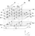
도 3을 참조하면, 메모리 셀 어레이(110)는 복수의 메모리 블록들(BLK1~BLKz)을 포함한다. 각 메모리 블록은 3차원 구조를 가질 수 있다. 각 메모리 블록은 기판 위에 적층된 복수의 메모리 셀들을 포함한다. 이러한 복수의 메모리 셀들은 +X 방향, +Y 방향 및 +Z 방향을 따라 배열된다. 각 메모리 블록의 구조는 도 4 및 도 5를 참조하여 더 상세히 설명된다.Referring to FIG. 3 , the
도 4는 도 3의 메모리 블록들(BLK1~BLKz) 중 어느 하나의 메모리 블록(BLKa)을 보여주는 회로도이다.FIG. 4 is a circuit diagram showing one memory block BLKa among the memory blocks BLK1 to BLKz of FIG. 3 .
도 4를 참조하면 메모리 블록(BLKa)은 복수의 셀 스트링들(CS11~CS1m, CS21~CS2m)을 포함한다. 실시 예로서, 복수의 셀 스트링들(CS11~CS1m, CS21~CS2m) 각각은 'U'자형으로 형성될 수 있다. 메모리 블록(BLKa) 내에서, 행 방향(즉 +X 방향)으로 m개의 셀 스트링들이 배열된다. 도 4에서, 열 방향(즉 +Y 방향)으로 2개의 셀 스트링들이 배열되는 것으로 도시되었다. 하지만 이는 설명의 편의를 위한 것으로서 열 방향으로 3개 이상의 셀 스트링들이 배열될 수 있음이 이해될 것이다.Referring to FIG. 4 , the memory block BLKa includes a plurality of cell strings CS11 to CS1m and CS21 to CS2m. As an embodiment, each of the plurality of cell strings CS11 to CS1m and CS21 to CS2m may be formed in a 'U' shape. Within the memory block BLKa, m cell strings are arranged in a row direction (ie, +X direction). In FIG. 4 , it is illustrated that two cell strings are arranged in a column direction (ie, a +Y direction). However, this is for convenience of explanation, and it will be understood that three or more cell strings may be arranged in a column direction.
복수의 셀 스트링들(CS11~CS1m, CS21~CS2m) 각각은 적어도 하나의 소스 선택 트랜지스터(SST), 제 1 내지 제 n 메모리 셀들(MC1~MCn), 파이프 트랜지스터(PT), 그리고 적어도 하나의 드레인 선택 트랜지스터(DST)을 포함한다.Each of the plurality of cell strings CS11 to CS1m and CS21 to CS2m includes at least one source selection transistor SST, first to nth memory cells MC1 to MCn, a pipe transistor PT, and at least one drain. It includes a selection transistor (DST).
선택 트랜지스터들(SST, DST) 및 메모리 셀들(MC1~MCn) 각각은 유사한 구조를 가질 수 있다. 실시 예로서, 선택 트랜지스터들(SST, DST) 및 메모리 셀들(MC1~MCn) 각각은 채널층, 터널링 절연막, 전하 저장막 및 블로킹 절연막을 포함할 수 있다. 실시 예로서, 채널층을 제공하기 위한 필라(pillar)가 각 셀 스트링(each cell string)에 제공될 수 있다. 실시 예로서, 채널층, 터널링 절연막, 전하 저장막 및 블로킹 절연막 중 적어도 하나를 제공하기 위한 필라가 각 셀 스트링에 제공될 수 있다.Each of the selection transistors SST and DST and the memory cells MC1 to MCn may have a similar structure. As an embodiment, each of the selection transistors SST and DST and the memory cells MC1 to MCn may include a channel layer, a tunneling insulating layer, a charge storage layer, and a blocking insulating layer. As an embodiment, a pillar for providing a channel layer may be provided to each cell string. As an embodiment, a pillar for providing at least one of a channel layer, a tunneling insulating layer, a charge storage layer, and a blocking insulating layer may be provided in each cell string.
각 셀 스트링의 소스 선택 트랜지스터(SST)는 공통 소스 라인(CSL)과 메모리 셀들(MC1~MCp) 사이에 연결된다.The source select transistor SST of each cell string is connected between the common source line CSL and the memory cells MC1 to MCp.
실시 예로서, 동일한 행에 배열된 셀 스트링들의 소스 선택 트랜지스터들은 행 방향으로 신장되는 소스 선택 라인에 연결되고, 상이한 행에 배열된 셀 스트링들의 소스 선택 트랜지스터들은 상이한 소스 선택 라인들에 연결된다. 도 4에서, 제 1 행의 셀 스트링들(CS11~CS1m)의 소스 선택 트랜지스터들은 제 1 소스 선택 라인(SSL1)에 연결되어 있다. 제 2 행의 셀 스트링들(CS21~CS2m)의 소스 선택 트랜지스터들은 제 2 소스 선택 라인(SSL2)에 연결되어 있다.As an embodiment, source select transistors of cell strings arranged in the same row are connected to source select lines extending in a row direction, and source select transistors of cell strings arranged in different rows are connected to different source select lines. In FIG. 4 , the source select transistors of the cell strings CS11 to CS1m in the first row are connected to the first source select line SSL1. Source select transistors of the cell strings CS21 to CS2m in the second row are connected to the second source select line SSL2.
다른 실시 예로서, 셀 스트링들(CS11~CS1m, CS21~CS2m)의 소스 선택 트랜지스터들은 하나의 소스 선택 라인에 공통 연결될 수 있다.As another embodiment, the source select transistors of the cell strings CS11 to CS1m and CS21 to CS2m may be connected in common to one source select line.
각 셀 스트링의 제 1 내지 제 n 메모리 셀들(MC1~MCn)은 소스 선택 트랜지스터(SST)와 드레인 선택 트랜지스터(DST) 사이에 연결된다.The first to nth memory cells MC1 to MCn of each cell string are connected between the source select transistor SST and the drain select transistor DST.
제 1 내지 제 n 메모리 셀들(MC1~MCn)은 제 1 내지 제 p 메모리 셀들(MC1~MCp)과 제 p+1 내지 제 n 메모리 셀들(MCp+1~MCn)로 구분될 수 있다. 제 1 내지 제 p 메모리 셀들(MC1~MCp)은 +Z 방향과 역방향으로 순차적으로 배열되며, 소스 선택 트랜지스터(SST)와 파이프 트랜지스터(PT) 사이에서 직렬 연결된다. 제 p+1 내지 제 n 메모리 셀들(MCp+1~MCn)은 +Z 방향으로 순차적으로 배열되며, 파이프 트랜지스터(PT)와 드레인 선택 트랜지스터(DST) 사이에서 직렬 연결된다. 제 1 내지 제 p 메모리 셀들(MC1~MCp)과 제 p+1 내지 제 n 메모리 셀들(MCp+1~MCn)은 파이프 트랜지스터(PT)를 통해 연결된다. 각 셀 스트링의 제 1 내지 제 n 메모리 셀들(MC1~MCn)의 게이트들은 각각 제 1 내지 제 n 워드 라인들(WL1~WLn)에 연결된다.The first to nth memory cells MC1 to MCn may be divided into first to pth memory cells MC1 to MCp and p+1 to nth memory cells MCp+1 to MCn. The first to pth memory cells MC1 to MCp are sequentially arranged in the +Z direction and the reverse direction, and are connected in series between the source select transistor SST and the pipe transistor PT. The p+1th to nth memory cells MCp+1 to MCn are sequentially arranged in the +Z direction and connected in series between the pipe transistor PT and the drain select transistor DST. The first to pth memory cells MC1 to MCp and the p+1 to nth memory cells MCp+1 to MCn are connected through a pipe transistor PT. Gates of the first to n th memory cells MC1 to MCn of each cell string are connected to the first to n th word lines WL1 to WLn, respectively.
각 셀 스트링의 파이프 트랜지스터(PT)의 게이트는 파이프 라인(PL)에 연결된다.The gate of the pipe transistor PT of each cell string is connected to the pipeline PL.
각 셀 스트링의 드레인 선택 트랜지스터(DST)은 해당 비트 라인과 메모리 셀들(MCp+1~MCn) 사이에 연결된다. 행 방향으로 배열되는 셀 스트링들은 행 방향으로 신장되는 드레인 선택 라인에 연결된다. 제 1 행의 셀 스트링들(CS11~CS1m)의 드레인 선택 트랜지스터들은 제 1 드레인 선택 라인(DSL1)에 연결된다. 제 2 행의 셀 스트링들(CS21~CS2m)의 드레인 선택 트랜지스터들은 제 2 드레인 선택 라인(DSL2)에 연결된다.The drain select transistor DST of each cell string is connected between a corresponding bit line and memory cells MCp+1 to MCn. The cell strings arranged in the row direction are connected to the drain select line extending in the row direction. Drain select transistors of the cell strings CS11 to CS1m in the first row are connected to the first drain select line DSL1. Drain select transistors of the cell strings CS21 to CS2m in the second row are connected to the second drain select line DSL2.
열 방향으로 배열되는 셀 스트링들은 열 방향으로 신장되는 비트 라인에 연결된다. 도 4에서, 제 1 열의 셀 스트링들(CS11, CS21)은 제 1 비트 라인(BL1)에 연결되어 있다. 제 m 열의 셀 스트링들(CS1m, CS2m)은 제 m 비트 라인(BLm)에 연결되어 있다.Cell strings arranged in the column direction are connected to bit lines extending in the column direction. In FIG. 4 , the cell strings CS11 and CS21 of the first column are connected to the first bit line BL1. The cell strings CS1m and CS2m of the mth column are connected to the mth bit line BLm.
행 방향으로 배열되는 셀 스트링들 내에서 동일한 워드 라인에 연결되는 메모리 셀들은 하나의 페이지를 구성한다. 예를 들면, 제 1 행의 셀 스트링들(CS11~CS1m) 중 제 1 워드 라인(WL1)과 연결된 메모리 셀들은 하나의 페이지를 구성한다. 제 2 행의 셀 스트링들(CS21~CS2m) 중 제 1 워드 라인(WL1)과 연결된 메모리 셀들은 다른 하나의 페이지를 구성한다. 드레인 선택 라인들(DSL1, DSL2) 중 어느 하나가 선택됨으로써 하나의 행 방향으로 배열되는 셀 스트링들이 선택될 것이다. 워드 라인들(WL1~WLn) 중 어느 하나가 선택됨으로써 선택된 셀 스트링들 중 하나의 페이지가 선택될 것이다.Memory cells connected to the same word line in cell strings arranged in a row direction constitute one page. For example, among the cell strings CS11 to CS1m in the first row, memory cells connected to the first word line WL1 constitute one page. Among the cell strings CS21 to CS2m in the second row, memory cells connected to the first word line WL1 constitute another page. When one of the drain select lines DSL1 and DSL2 is selected, cell strings arranged in one row direction are selected. When one of the word lines WL1 to WLn is selected, one page of the selected cell strings is selected.
다른 실시 예로서, 제 1 내지 제 m 비트 라인들(BL1~BLm) 대신 이븐 비트 라인들 및 오드 비트 라인들이 제공될 수 있다. 그리고 행 방향으로 배열되는 셀 스트링들(CS11~CS1m 또는 CS21~CS2m) 중 짝수 번째 셀 스트링들은 이븐 비트 라인들에 각각 연결되고, 행 방향으로 배열되는 셀 스트링들(CS11~CS1m 또는 CS21~CS2m) 중 홀수 번째 셀 스트링들은 오드 비트 라인들에 각각 연결될 수 있다.As another embodiment, even bit lines and odd bit lines may be provided instead of the first to m th bit lines BL1 to BLm. And among the cell strings (CS11 to CS1m or CS21 to CS2m) arranged in the row direction, even-numbered cell strings are connected to the even bit lines, respectively, and the cell strings (CS11 to CS1m or CS21 to CS2m) arranged in the row direction Odd-numbered cell strings may be respectively connected to odd bit lines.
실시 예로서, 제 1 내지 제 n 메모리 셀들(MC1~MCn) 중 적어도 하나 이상은 더미 메모리 셀로서 이용될 수 있다. 예를 들어, 적어도 하나 이상의 더미 메모리 셀들은 소스 선택 트랜지스터(SST)와 메모리 셀들(MC1~MCp) 사이의 전계(electric field)를 감소시키기 위해 제공된다. 또는, 적어도 하나 이상의 더미 메모리 셀들은 더미 메모리 셀들은 드레인 선택 트랜지스터(DST)와 메모리 셀들(MCp+1~MCn) 사이의 전계를 감소시키기 위해 제공된다. 더 많은 더미 메모리 셀들이 제공될수록, 메모리 블록(BLKa)에 대한 동작의 신뢰성이 향상되는 반면, 메모리 블록(BLKa)의 크기는 증가한다. 더 적은 메모리 셀들이 제공될수록, 메모리 블록(BLKa)의 크기는 감소하는 반면 메모리 블록(BLKa)에 대한 동작의 신뢰성은 저하될 수 있다.As an example embodiment, at least one of the first to n th memory cells MC1 to MCn may be used as a dummy memory cell. For example, one or more dummy memory cells are provided to reduce an electric field between the source select transistor SST and the memory cells MC1 to MCp. Alternatively, at least one dummy memory cell is provided to reduce an electric field between the drain select transistor DST and the memory cells MCp+1 to MCn. As more dummy memory cells are provided, the operation reliability of the memory block BLKa improves, while the size of the memory block BLKa increases. As fewer memory cells are provided, the size of the memory block BLKa decreases while the reliability of an operation of the memory block BLKa may deteriorate.
적어도 하나 이상의 더미 메모리 셀들을 효율적으로 제어하기 위해, 더미 메모리 셀들 각각은 요구되는 문턱 전압을 가질 수 있다. 메모리 블록(BLKa)에 대한 소거 동작 이전 또는 이후에, 더미 메모리 셀들 중 전부 혹은 일부에 대한 프로그램 동작들이 수행될 수 있다. 프로그램 동작이 수행된 뒤에 소거 동작이 수행되는 경우, 더미 메모리 셀들의 문턱 전압은 각각의 더미 메모리 셀들에 연결된 더미 워드 라인들에 인가되는 전압을 제어함으로써 더미 메모리 셀들은 요구되는 문턱 전압을 가질 수 있다.In order to efficiently control at least one or more dummy memory cells, each of the dummy memory cells may have a required threshold voltage. Program operations may be performed on all or some of the dummy memory cells before or after the erase operation on the memory block BLKa. When an erase operation is performed after a program operation is performed, the dummy memory cells may have a required threshold voltage by controlling voltages applied to dummy word lines connected to the dummy memory cells. .
도 5는 도 3의 메모리 블록들(BLK1~BLKz) 중 어느 하나의 메모리 블록(BLKb)의 다른 실시 예를 보여주는 회로도이다.FIG. 5 is a circuit diagram showing another embodiment of one memory block BLKb among the memory blocks BLK1 to BLKz of FIG. 3 .
도 5를 참조하면 메모리 블록(BLKb)은 복수의 셀 스트링들(CS11'~CS1m', CS21'~CS2m')을 포함한다. 복수의 셀 스트링들(CS11'~CS1m', CS21'~CS2m') 각각은 +Z 방향을 따라 신장된다. 복수의 셀 스트링들(CS11'~CS1m', CS21'~CS2m') 각각은, 메모리 블록(BLK1') 하부의 기판(미도시) 위에 적층된, 적어도 하나의 소스 선택 트랜지스터(SST), 제 1 내지 제 n 메모리 셀들(MC1~MCn) 그리고 적어도 하나의 드레인 선택 트랜지스터(DST)를 포함한다.Referring to FIG. 5 , the memory block BLKb includes a plurality of cell strings CS11' to CS1m' and CS21' to CS2m'. Each of the plurality of cell strings CS11' to CS1m' and CS21' to CS2m' extends along the +Z direction. Each of the plurality of cell strings CS11' to CS1m' and CS21' to CS2m' includes at least one source select transistor SST stacked on a substrate (not shown) under the memory block BLK1', a first to nth memory cells MC1 to MCn, and at least one drain select transistor DST.
각 셀 스트링의 소스 선택 트랜지스터(SST)은 공통 소스 라인(CSL)과 메모리 셀들(MC1~MCn) 사이에 연결된다. 동일한 행에 배열된 셀 스트링들의 소스 선택 트랜지스터들은 동일한 소스 선택 라인에 연결된다. 제 1 행에 배열된 셀 스트링들(CS11'~CS1m')의 소스 선택 트랜지스터들은 제 1 소스 선택 라인(SSL1)에 연결된다. 제 2 행에 배열된 셀 스트링들(CS21'~CS2m')의 소스 선택 트랜지스터들은 제 2 소스 선택 라인(SSL2)에 연결된다. 다른 실시 예로서, 셀 스트링들(CS11'~CS1m', CS21'~CS2m')의 소스 선택 트랜지스터들은 하나의 소스 선택 라인에 공통 연결될 수 있다.The source select transistor SST of each cell string is connected between the common source line CSL and the memory cells MC1 to MCn. Source select transistors of the cell strings arranged in the same row are connected to the same source select line. The source select transistors of the cell strings CS11' to CS1m' arranged in the first row are connected to the first source select line SSL1. The source select transistors of the cell strings CS21' to CS2m' arranged in the second row are connected to the second source select line SSL2. As another embodiment, the source select transistors of the cell strings CS11' to CS1m' and CS21' to CS2m' may be connected in common to one source select line.
각 셀 스트링의 제 1 내지 제 n 메모리 셀들(MC1~MCn)은 소스 선택 트랜지스터(SST)과 드레인 선택 트랜지스터(DST) 사이에서 직렬 연결된다. 제 1 내지 제 n 메모리 셀들(MC1~MCn)의 게이트들은 각각 제 1 내지 제 n 워드 라인들(WL1~WLn)에 연결된다.The first to nth memory cells MC1 to MCn of each cell string are connected in series between the source select transistor SST and the drain select transistor DST. Gates of the first to n th memory cells MC1 to MCn are connected to the first to n th word lines WL1 to WLn, respectively.
각 셀 스트링의 드레인 선택 트랜지스터(DST)는 해당 비트 라인과 메모리 셀들(MC1~MCn) 사이에 연결된다. 행 방향으로 배열되는 셀 스트링들의 드레인 선택 트랜지스터들은 행 방향으로 신장되는 드레인 선택 라인에 연결된다. 제 1 행의 셀 스트링들(CS11'~CS1m')의 드레인 선택 트랜지스터들은 제 1 드레인 선택 라인(DSL1)에 연결된다. 제 2 행의 셀 스트링들(CS21'~CS2m')의 드레인 선택 트랜지스터들은 제 2 드레인 선택 라인(DSL2)에 연결된다.The drain select transistor DST of each cell string is connected between the corresponding bit line and the memory cells MC1 to MCn. Drain select transistors of the cell strings arranged in the row direction are connected to drain select lines extending in the row direction. Drain select transistors of the cell strings CS11' to CS1m' in the first row are connected to the first drain select line DSL1. Drain select transistors of the cell strings CS21' to CS2m' in the second row are connected to the second drain select line DSL2.
결과적으로, 각 셀 스트링에 파이프 트랜지스터(PT)가 제외된 것을 제외하면 도 5의 메모리 블록(BLKb)은 도 4의 메모리 블록(BLKa)과 유사한 등가 회로를 갖는다.As a result, the memory block BLKb of FIG. 5 has an equivalent circuit similar to that of the memory block BLKa of FIG. 4 except that the pipe transistor PT is excluded from each cell string.
다른 실시 예로서, 제 1 내지 제 m 비트 라인들(BL1~BLm) 대신 이븐 비트 라인들 및 오드 비트 라인들이 제공될 수 있다. 그리고 행 방향으로 배열되는 셀 스트링들(CS11'~CS1m' 또는 CS21'~CS2m') 중 짝수 번째 셀 스트링들은 이븐 비트 라인들에 각각 연결되고, 행 방향으로 배열되는 셀 스트링들(CS11'~CS1m' 또는 CS21'~CS2m') 중 홀수 번째 셀 스트링들은 오드 비트 라인들에 각각 연결될 수 있다.As another embodiment, even bit lines and odd bit lines may be provided instead of the first to m th bit lines BL1 to BLm. In addition, even-numbered cell strings among the cell strings (CS11' to CS1m' or CS21' to CS2m') arranged in the row direction are connected to the even bit lines, respectively, and the cell strings arranged in the row direction (CS11' to CS1m ' or CS21' to CS2m'), odd-numbered cell strings may be respectively connected to odd bit lines.
실시 예로서, 제 1 내지 제 n 메모리 셀들(MC1~MCn) 중 적어도 하나 이상은 더미 메모리 셀로서 이용될 수 있다. 예를 들어, 적어도 하나 이상의 더미 메모리 셀들은 소스 선택 트랜지스터(SST)와 메모리 셀들(MC1~MCn) 사이의 전계(electric field)를 감소시키기 위해 제공된다. 또는, 적어도 하나 이상의 더미 메모리 셀들은 더미 메모리 셀들은 드레인 선택 트랜지스터(DST)와 메모리 셀들(MC1~MCn) 사이의 전계를 감소시키기 위해 제공된다. 더 많은 더미 메모리 셀들이 제공될수록, 메모리 블록(BLKb)에 대한 동작의 신뢰성이 향상되는 반면, 메모리 블록(BLKb)의 크기는 증가한다. 더 적은 메모리 셀들이 제공될수록, 메모리 블록(BLKb)의 크기는 감소하는 반면 메모리 블록(BLKb)에 대한 동작의 신뢰성은 저하될 수 있다.As an example embodiment, at least one of the first to n th memory cells MC1 to MCn may be used as a dummy memory cell. For example, one or more dummy memory cells are provided to reduce an electric field between the source select transistor SST and the memory cells MC1 to MCn. Alternatively, at least one dummy memory cell is provided to reduce an electric field between the drain select transistor DST and the memory cells MC1 to MCn. As more dummy memory cells are provided, the operation reliability of the memory block BLKb improves, while the size of the memory block BLKb increases. As fewer memory cells are provided, the size of the memory block BLKb decreases while the reliability of an operation of the memory block BLKb may deteriorate.
적어도 하나 이상의 더미 메모리 셀들을 효율적으로 제어하기 위해, 더미 메모리 셀들 각각은 요구되는 문턱 전압을 가질 수 있다. 메모리 블록(BLKb)에 대한 소거 동작 이전 또는 이후에, 더미 메모리 셀들 중 전부 혹은 일부에 대한 프로그램 동작들이 수행될 수 있다. 프로그램 동작이 수행된 뒤에 소거 동작이 수행되는 경우, 더미 메모리 셀들의 문턱 전압은 각각의 더미 메모리 셀들에 연결된 더미 워드 라인들에 인가되는 전압을 제어함으로써 더미 메모리 셀들은 요구되는 문턱 전압을 가질 수 있다.In order to efficiently control at least one or more dummy memory cells, each of the dummy memory cells may have a required threshold voltage. Program operations may be performed on all or some of the dummy memory cells before or after the erase operation on the memory block BLKb. When an erase operation is performed after a program operation is performed, the dummy memory cells may have a required threshold voltage by controlling voltages applied to dummy word lines connected to the dummy memory cells. .
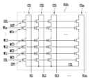
도 6은 도 2의 메모리 셀 어레이(110)에 포함된 복수의 메모리 블록들(BLK1~BLKz) 중 어느 하나의 메모리 블록(BLKc)의 실시 예를 보여주는 회로도이다.FIG. 6 is a circuit diagram showing an embodiment of one memory block BLKc among a plurality of memory blocks BLK1 to BLKz included in the
도 6을 참조하면, 메모리 블록(BKLc)은 복수의 셀 스트링들(CS1~CSm)을 포함한다. 복수의 셀 스트링들(CS1~CSm)은 복수의 비트 라인들(BL1~BLm)에 각각 연결될 수 있다. 복수의 셀 스트링들(CS1~CSm)각각은 적어도 하나 이상의 소스 선택 트랜지스터(SST), 제1 내지 제n 메모리 셀들(MC1~MCn), 및 적어도 하나 이상의 드레인 선택 트랜지스터(DST)를 포함한다.Referring to FIG. 6 , the memory block BKLc includes a plurality of cell strings CS1 to CSm. The plurality of cell strings CS1 to CSm may be respectively connected to the plurality of bit lines BL1 to BLm. Each of the plurality of cell strings CS1 to CSm includes at least one source select transistor SST, first to n th memory cells MC1 to MCn, and at least one drain select transistor DST.
선택 트랜지스터들(SST, DST) 및 메모리 셀들(MC1~MCn) 각각은 유사한 구조를 가질 수 있다. 실시 예로서, 선택 트랜지스터들(SST, DST) 및 메모리 셀들(MC1~MCn) 각각은 채널층, 터널링 절연막, 전하 저장막 및 블로킹 절연막을 포함할 수 있다. 실시 예로서, 채널층을 제공하기 위한 필라(pillar)가 각 셀 스트링(each cell string)에 제공될 수 있다. 실시 예로서, 채널층, 터널링 절연막, 전하 저장막 및 블로킹 절연막 중 적어도 하나를 제공하기 위한 필라가 각 셀 스트링에 제공될 수 있다.Each of the selection transistors SST and DST and the memory cells MC1 to MCn may have a similar structure. As an embodiment, each of the selection transistors SST and DST and the memory cells MC1 to MCn may include a channel layer, a tunneling insulating layer, a charge storage layer, and a blocking insulating layer. As an embodiment, a pillar for providing a channel layer may be provided to each cell string. As an embodiment, a pillar for providing at least one of a channel layer, a tunneling insulating layer, a charge storage layer, and a blocking insulating layer may be provided in each cell string.
각 셀 스트링의 소스 선택 트랜지스터(SST)는 공통 소스 라인(CSL)과 메모리 셀들(MC1~MCn) 사이에 연결된다.The source select transistor SST of each cell string is connected between the common source line CSL and the memory cells MC1 to MCn.
각 셀 스트링의 제 1 내지 제 n 메모리 셀들(MC1~MCn)은 소스 선택 트랜지스터(SST)와 드레인 선택 트랜지스터(DST) 사이에 연결된다.The first to nth memory cells MC1 to MCn of each cell string are connected between the source select transistor SST and the drain select transistor DST.
각 셀 스트링의 드레인 선택 트랜지스터(DST)은 해당 비트 라인과 메모리 셀들(MC1~MCn) 사이에 연결된다.The drain select transistor DST of each cell string is connected between the corresponding bit line and the memory cells MC1 to MCn.
동일한 워드 라인에 연결되는 메모리 셀들은 하나의 페이지를 구성한다. 드레인 선택 라인(DSL)이 선택됨으로써 셀 스트링들(CS1~CSm)이 선택될 것이다. 워드 라인들(WL1~WLn) 중 어느 하나가 선택됨으로써 선택된 셀 스트링들 중 하나의 페이지가 선택될 것이다.Memory cells connected to the same word line constitute one page. As the drain select line DSL is selected, the cell strings CS1 to CSm are selected. When one of the word lines WL1 to WLn is selected, one page of the selected cell strings is selected.
다른 실시 예로서, 제 1 내지 제 m 비트 라인들(BL1~BLm) 대신 이븐 비트 라인들 및 오드 비트 라인들이 제공될 수 있다. 셀 스트링들(CS1~CSm) 중 짝수 번째 셀 스트링들은 이븐 비트 라인들에 각각 연결되고, 홀수 번째 셀 스트링들은 오드 비트 라인들에 각각 연결될 수 있다.As another embodiment, even bit lines and odd bit lines may be provided instead of the first to m th bit lines BL1 to BLm. Among the cell strings CS1 to CSm, even-numbered cell strings may be connected to even bit lines, respectively, and odd-numbered cell strings may be connected to odd bit lines, respectively.
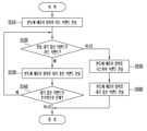
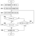
도 7은 본 발명의 일 실시 예에 따른 메모리 컨트롤러(200)의 동작 방법을 나타내는 순서도이다. 한편, 도 8은 통상적인 메모리 컨트롤러(200)의 동작 방법에 따른 반도체 메모리 장치의 동작을 설명하기 위한 도면이다. 또한, 도 9는 도 7에 도시된 메모리 컨트롤러(200)의 동작 방법에 따라 제어되는 반도체 메모리 장치의 동작을 설명하기 위한 도면이다. 이하, 도 7 내지 도 9를 함께 참조하여, 본 발명의 일 실시 예에 따른 메모리 컨트롤러(200)의 동작 방법을 설명하기로 한다.7 is a flowchart illustrating an operating method of the
먼저, 도 8을 참조하면, 시간(t1)에 메모리 컨트롤러(200)로부터 반도체 메모리 장치(100)로 리드 커맨드(CMDRD)가 전송된다. 이에 따라, 반도체 메모리 장치(100)의 제어 로직(140)은 리드 동작을 위한 프리차지 신호(SIGPRC)를 생성하여 전압 생성부(150)로 전달한다. 이에 따라 프리차지 구간(PRC) 동안 전압 생성부(150)의 프리차지 동작이 수행된다.First, referring to FIG. 8 , a read command CMDRD is transmitted from the
전압 생성부(150)의 프리차지 동작이 완료되면, 이후 리드 구간(READ) 동안 반도체 메모리 장치(100)의 리드 동작이 수행된다. 프리차지 구간(PRC) 동안의 프리차지 동작에 의해, 전압 생성부(150)는 리드 동작을 위해 필요한 전압들, 예를 들어 리드 전압(Vread) 및 패스 전압(Vpass)을 생성할 수 있다. 제어 로직(140)은 주변 회로를 제어하여 리드 동작을 수행한다.After the precharge operation of the
리드 구간(READ)이 완료되면, 이후 디스차지 구간(DSC) 동안 전압 생성부(150)의 디스차지 동작이 수행된다. 이를 위해, 제어 로직(140)은 디스차지 신호(SIGDSC)를 생성하여 전압 생성부(150)로 전달한다.When the read period READ is completed, the discharge operation of the
상기 디스차지 동작이 완료됨으로써 리드 동작이 완료된다. 한편, 반도체 메모리 장치(100)의 추가적인 리드 동작이 필요한 경우, 메모리 컨트롤러(200)는 시간(t2)에 다시 반도체 메모리 장치(100)로 리드 커맨드(CMDRD)를 전송할 것이다. 이에 따라, 전술한 바와 같이 프리차지 구간(PRC), 리드 구간(READ) 및 디스차지 구간(DSC)을 통해 리드 동작이 수행된다.When the discharge operation is completed, the read operation is completed. Meanwhile, when an additional read operation of the
또한, 반도체 메모리 장치(100)의 추가적인 리드 동작이 또다시 필요한 경우, 메모리 컨트롤러(200)는 시간(t3)에 다시 반도체 메모리 장치(100)로 리드 커맨드(CMDRD)를 전송할 것이다. 이에 따라, 전술한 바와 같이 프리차지 구간(PRC), 리드 구간(READ) 및 디스차지 구간(DSC)을 통해 리드 동작이 수행된다.Also, when an additional read operation of the
도 8에 도시된 바와 같이, 통상적인 메모리 컨트롤러(200) 및 반도체 메모리 장치(100)의 동작 방식에 의하면, 메모리 컨트롤러(200)가 연속된 리드 커맨드(CMDRD)를 반도체 메모리 장치(100)로 전달하는 경우에, 리드 동작 사이의 불필요한 디스차지 구간(DSC) 및 프리차지 구간(PRC)이 발생한다. 이에 따라 반도체 메모리 장치(100)의 전체적인 리드 시간(read time)이 증가한다. 결과적으로, 반도체 메모리 장치(100)의 동작 속도가 저하된다. 이하 도 7 및 도 9를 참조하여, 본 발명의 일 실시 예에 따른 메모리 컨트롤러(200) 및 반도체 메모리 장치(100)의 동작 방법을 설명하기로 한다.As shown in FIG. 8 , according to the general operation method of the
호스트(300)로부터 리드 요청을 수신한 경우, 메모리 컨트롤러(200)는 이에 대응하는 리드 커맨드(CMDRD)를 반도체 메모리 장치(100)로 전송한다(S110). 반도체 메모리 장치(100)로 리드 커맨드(CMDRD)가 전송되면, 반도체 메모리 장치(100)의 제어 로직(140)은 프리차지 신호(SIGPRC)의 전송 여부를 결정한다. 전압 생성부(150)의 차지 펌프가 디스차지 된 상태이면, 제어 로직(140)은 프리차지 신호(SIGPRC)를 전압 생성부(150)로 전달하여 차지 펌프를 프리차지하도록 한다. 도 9에 도시된 바와 같이, 시간(t4)에서 메모리 컨트롤러(200)는 리드 커맨드(CMDRD)를 반도체 메모리 장치(100)로 전송할 것이다. 리드 커맨드(CMDRD)를 수신하면, 반도체 메모리 장치(100)의 제어 로직(140)은 프리차지 신호(SIGPRC)를 전압 생성부(150)로 전달한다. 이후 프리차지 구간(PRC) 동안 전압 생성부(150)의 프리차지 동작이 수행된다.When a read request is received from the
프리차지 동작이 완료되면, 반도체 메모리 장치(100)의 제어 로직(140)은 전압 생성부(150), 어드레스 디코더(120), 읽기 및 쓰기 회로(130)를 제어하여 수신한 리드 커맨드(CMDRD)에 대응하는 리드 동작을 수행하도록 한다.When the precharge operation is completed, the
단계(S110)에서 전송된 리드 커맨드에 따르 리드 동작이 완료된 이후에, 반도체 메모리 장치(100)는 전압 생성부(150)의 디스차지 동작을 수행하지 않고, 메모리 컨트롤러(200)로부터의 커맨드를 기다린다.After the read operation according to the read command transmitted in step S110 is completed, the
메모리 컨트롤러(200)는, 반도체 메모리 장치(100)로 전송 대기 중인 커맨드가 리드 커맨드인지 여부를 판단한다(S120). 메모리 컨트롤러(200)는 커맨드 큐(미도시) 포함할 수 있으며, 상기 커맨드 큐에 반도체 메모리 장치(100)로 전송될 커맨드들이 저장되어 있을 수 있다. 메모리 컨트롤러(200)는 상기 커맨드 큐를 참조하여, 반도체 메모리 장치로 전송될 커맨드가 리드 커맨드인지 여부를 판단한다.The
단계(S120)의 판단 결과 전송 대기 중인 커맨드가 리드 커맨드인 경우, 전압 생성부(150)의 차지 펌프를 디스차지할 필요가 없으며, 현재 프리차지 된 상태의 전압 생성부(150)가 리드 동작을 위한 전압들을 생성하도록 할 수 있다. 이에 따라, 불필요한 디스차지 구간(DSC) 및 프리차지 구간(PRC)을 생략하도록 하기 위해, 전송 대기 중인 커맨드, 즉 리드 커맨드를 반도체 메모리 장치(100)로 전송한다(S130). 반도체 메모리 장치(100)는 디스차지 커맨드(CMDDSC)를 수신하지 않고, 시간(t5)에서 전송 대기 중인 리드 커맨드(CMDRD)를 수신한다. 따라서 반도체 메모리 장치(100)는 전압 생성부(150)의 디스차지 동작 또는 프리차지 동작 없이, 단계(S130)에 의해 수신된 리드 커맨드(CMDRD)에 대응하는 리드 동작을 수행하도록 한다.As a result of the determination in step S120, if the command waiting to be transmitted is a read command, there is no need to discharge the charge pump of the
이후 단계(S140)에서, 대기 중인 커맨드가 추가적으로 존재하는지 여부를 판단한다. 대기 중인 커맨드가 없으면 메모리 컨트롤러의 동작은 종료될 것이다. 대기 중인 커맨드가 존재하는 경우, 다시 단계(S120)로 진행하여, 전송 대기 중인 커맨드가 리드 커맨드인지 여부를 판단한다.In a subsequent step (S140), it is determined whether there is an additional waiting command. If there is no waiting command, the operation of the memory controller will end. If there is a waiting command, the process proceeds to step S120 again, and it is determined whether the waiting command is a read command.
단계(S120)의 판단 결과 전송 대기 중인 커맨드가 또다시 리드 커맨드(CMDRD)인 경우, 메모리 컨트롤러(200)는 해당 리드 커맨드(CMDRD)를 반도체 메모리 장치(100)로 전송할 것이다(S130). 이에 따라, 시간(t6)에서 반도체 메모리 장치(100)는 리드 커맨드(CMDRD)를 수신하고, 이에 대응하는 리드 동작을 수행할 것이다. 이후 단계(S140)가 반복된다.As a result of the determination in step S120, if the command waiting to be transmitted is the read command CMDRD again, the
단계(S120)의 판단 결과, 전송 대기 중인 커맨드가 리드 커맨드가 아닌 경우, 메모리 컨트롤러(200)는 전송 대기 중인 커맨드를 반도체 메모리 장치(100)로 전달하기 이전에, 디스차지 커맨드(CMDDSC)를 반도체 메모리 장치(100)로 전송한다(S150). 도 9를 참조하면, 세 번째 리드 동작이 수행된 이후에 전송 대기 중인 커맨드가 프로그램 커맨드(CMDPGM)인 경우가 도시되어 있다. 따라서, 메모리 컨트롤러(200)는 전송 대기 중인 프로그램 커맨드(CMDPGM)를 전송하기 이전에, 디스차지 커맨드(CMDDSC)를 반도체 메모리 장치(100)로 전송한다.As a result of the determination in step S120, when the command waiting to be transmitted is not a read command, the
구체적으로, 시간(t7)에 반도체 메모리 장치(100)는 디스차지 커맨드(CMDDSC)를 수신한다. 이에 따라, 제어 로직(140)은 디스차지 신호(SIGDSC)를 전압 생성부(150)로 전달할 것이다. 디스차지 신호(SIGDSC)에 기초하여, 디스차지 구간(DSC)동안 전압 생성부(150)는 디스차지 동작을 수행한다.Specifically, at time t7 , the
이후, 시간(t8)에 메모리 컨트롤러(200)는 반도체 메모리 장치(100)로 대기 중인 커맨드, 즉 프로그램 커맨드(CMDPGM)를 전송한다(S160). 반도체 메모리 장치(100)는 프로그램 커맨드(CMDPGM)를 수신한다. 시간(t8)에 전압 생성부(150)가 디스차지 된 상태이므로, 제어 로직(140)은 프리차지 신호(SIGPRC)를 전압 생성부(150)로 전달할 것이다. 프리차지 신호(SIGPRC)에 기초하여, 프리차지 구간(PRC)동안 전압 생성부(150)는 프리차지 동작을 수행한다.Thereafter, at time t8, the
프리차지 동작이 완료된 이후에, 반도체 메모리 장치(100)는 수신된 프로그램 커맨드(CMDPGM)에 기초하여, 프로그램 구간(PGM) 동안 프로그램 동작을 수행한다.After the precharge operation is completed, the
프로그램 동작이 완료된 이후에, 전압 생성부(150)가 디스차지될 필요가 있다. 도 7에는 도시되어 있지 않으나, 메모리 컨트롤러(200)는 반도체 메모리 장치(100)로 디스차지 커맨드(CMDDSC)를 전송할 수 있다. 도 9의 시간(t9)에서, 반도체 메모리 장치(100)는 디스차지 커맨드(CMDDSC)를 수신한다. 이에 따라, 제어 로직(140)은 디스차지 신호(SIGDSC)를 전압 생성부(150)로 전달할 것이다. 디스차지 신호(SIGDSC)에 기초하여, 디스차지 구간(DSC)동안 전압 생성부(150)는 디스차지 동작을 수행한다.After the program operation is completed, the
단계들(S120, S130, S140, S150, S160)을 참조하여 보면, 본 발명의 일 실시 예에 따른 메모리 컨트롤러의 동작 방법에서, 단계(S110)의 리드 커맨드 전송 이후에 전송 대기 중인 커맨드의 유형에 기초하여, 디스차지 커맨드의 전송 여부가 결정됨을 알 수 있다. 예를 들어, 단계(S120)의 판단 결과 전송 대기 중인 커맨드가 리드 커맨드인 경우, 다른 커맨드의 전송 없이 전송 대기 중인 리드 커맨드가 반도체 메모리 장치로 전송될 것이다(S130). 다른 예에서, 단계(S120)의 판단 결과 전송 대기 중인 커맨드가 리드 커맨드가 아닌 경우, 디스차지 커맨드(CMDDSC)가 생성되어 반도체 메모리 장치(100)로 전송될 것이다(S150).Referring to steps S120, S130, S140, S150, and S160, in the operating method of the memory controller according to an embodiment of the present invention, after transmitting the read command in step S110, the type of command waiting for transmission is determined. Based on this, it can be seen that whether or not to transmit the discharge command is determined. For example, if the command waiting to be transmitted is a read command as a result of the determination in step S120, the read command waiting to be transmitted will be transmitted to the semiconductor memory device without transmitting another command (S130). In another example, when the command waiting to be transmitted is not a read command as a result of the determination in step S120, a discharge command CMDDSC is generated and transmitted to the semiconductor memory device 100 (S150).
상술한 바와 같이, 본 발명의 일 실시 예에 따른 메모리 컨트롤러의 동작 방법에 의하면, 반도체 메모리 장치(100)의 리드 동작 이후에, 반도체 메모리 장치(100)로 전송될 커맨드의 유형에 기초하여 디스차지 커맨드(CMDDSC)의 전송 여부를 결정하도록 한다. 이에 따라 연속적인 리드 동작 사이에서 전압 생성부(150)의 불필요한 디스차지 동작 및 프리차지 동작이 생략될 수 있다.As described above, according to the operating method of the memory controller according to an embodiment of the present invention, after a read operation of the
특히, 도 9를 참조하면, 연속적인 리드 구간(READ) 사이의 디스차지 구간(DSC) 및 프리차지 구간(PRC)을 제거하여, 반도체 메모리 장치(100)의 전체적인 리드 시간이 줄어드는 것을 알 수 있다. 결과적으로, 반도체 메모리 장치(100) 및 이를 포함하는 저장 장치(10)의 동작 속도가 향상된다.In particular, referring to FIG. 9 , it can be seen that the overall read time of the
한편, 본 발명의 또 다른 실시 예에 따른 반도체 메모리 장치(100)의 제어 로직(140)은, 메모리 셀 어레이(110)에 대한 리드 동작을 수행한 이후에 수신되는 커맨드에 기초하여, 상기 전압 생성부의 디스차지 동작을 제어하도록 구성된다. 이 경우, 메모리 컨트롤러(200)는 디스차지 커맨드(CMDDSC)를 생성하지 않고 단지 통상적인 리드 커맨드(CMDRD), 프로그램 커맨드(CMDPGM) 등 만을 반도체 메모리 장치(100)로 전송하도록 구성된다. 상술한 실시 예에서, 반도체 메모리 장치(100)의 제어 로직(140)은 수신되는 커맨드들에 기초하여, 전압 생성부(150)의 디스차지 동작 및 프리차지 동작의 수행 여부를 결정하도록 한다. 이하 도 10 및 도 11을 참조하여, 본 발명의 또 다른 실시 예에 따른 반도체 메모리 장치(100)의 동작에 대해서 설명하기로 한다.Meanwhile, the
도 10은 본 발명의 일 실시 예에 따른 반도체 메모리 장치(100)의 동작 방법을 나타내는 순서도이다. 한편, 도 11은 도 10에 도시된 방법에 따른 반도체 메모리 장치(100)의 동작을 설명하기 위한 도면이다. 이하, 도 10 및 도 11을 함께 참조하여, 본 발명의 일 실시 예에 따른 반도체 메모리 장치(100) 의 동작 방법을 설명하기로 한다.10 is a flowchart illustrating an operating method of the
단계(S210)에서, 반도체 메모리 장치(100)는 메모리 컨트롤러(200)로부터 리드 커맨드(CMDRD)를 수신한다. 도 11에 도시된 바와 같이, 시간(t10)에서 반도체 메모리 장치(100)는 리드 커맨드(CMDRD)를 수신할 것이다. 이에 따라, 반도체 메모리 장치(100)는 수신한 리드 커맨드(CMDRD)에 기초하여, 프리차지 구간(PRC) 동안 리드 동작에 사용되는 리드 전압 생성을 위해 전압 생성부를 프리차지할 것이다(S220).In step S210 , the
이후 단계(S230)에서, 리드 구간(READ) 동안 수신한 리드 커맨드(CMDRD)에 기초하여 리드 동작을 수행한다. 리드 동작이 완료되면, 제어 로직(140)은 리드 동작의 완료 시점으로부터, 미리 결정된 기준 시간(TREF) 내에 추가 커맨드를 수신하였는지 여부를 판단한다(S240). 기준 시간(TREF) 내 추가 커맨드를 수신하였는지 여부를 판단하기 위해, 제어 로직(140)은 내부적으로 기준 시간(TREF)의 도과 여부를 결정하기 위한 타이머(미도시)를 포함할 수 있다.In step S230 thereafter, a read operation is performed based on the read command CMDRD received during the read period READ. When the read operation is completed, the
도 11을 참조하면, 첫번째 리드 동작이 완료된 시점으로부터 기준 시간(TREF)이 도과하기 이전인 시간(t11)에 리드 커맨드(CMDRD)를 수신한다. 이에 따라, 단계(S240)로부터 단계(S270)로 진행하여, 수신한 커맨드가 리드 커맨드인지 여부를 판단한다. 도 11의 시간(t11)에서 수신된 커맨드가 리드 커맨드(CMDRD)이므로, 이후 단계(S230)로 진행하여 수신한 리드 커맨드(CMDRD)에 대응한 리드 동작을 수행할 것이다. 이에 따라, 전압 생성부(150)의 디스차지 동작 및 프리차지 동작 없이 연속적인 리드 동작이 수행된다.Referring to FIG. 11 , a read command (CMDRD ) is received at a time (t11) before the reference time (TREF ) elapses from the time when the first read operation is completed. Accordingly, the process proceeds from step S240 to step S270, and it is determined whether or not the received command is a lead command. Since the command received at time t11 of FIG. 11 is the read command (CMDRD ), the process proceeds to step S230 to perform a read operation corresponding to the received read command (CMDRD ). Accordingly, a continuous read operation is performed without the discharge operation and the pre-charge operation of the
단계(S230)에 의해 두 번째 리드 동작의 수행이 완료되면, 다시 단계(S240)로 진행하여 기준 시간(TREF) 내에 추가 커맨드를 수신하였는지 여부를 판단한다. 도 11을 참조하면, 두 번째 리드 동작이 완료되고 기준 시간(TREF)이 도과할 때까지 추가 커맨드가 수신되지 않았으므로, 단계(S250)의 판단 결과 단계(S260)로 진행하여, 전압 생성부(150)를 디스차지하도록 한다. 도 11에서, 시간(t12)에서 반도체 메모리 장치(100)는 리드 커맨드(CMDRD)를 수신하였으나 이는 두 번째 리드 동작의 완료 시점으로부터 기준 시간(TREF)이 완료된 이후이다. 이에 따라, 시간(t12)에서 리드 커맨드(CMDRD)를 수신하는 것은 도 10의 단계(S210)에 대응하게 된다.When the second read operation is completed by step S230, the process proceeds to step S240 again to determine whether an additional command is received within the reference time TREF . Referring to FIG. 11, since the additional command is not received until the second read operation is completed and the reference time TREF has elapsed, the decision result of step S250 proceeds to step S260, and the voltage generator (150) to be discharged. In FIG. 11 , at time t12 , the
따라서, 디스차지 구간(DSC)이 지난 후에 단계(S220)로 진행하여, 수신한 리드 커맨드(CMDRD)에 기초하여 전압 생성부(150)를 프리차지 하고, 이후 단계(S230)로 진행하여 리드 동작을 수행한다.Therefore, after the discharge period DSC has passed, the process proceeds to step S220 to precharge the
상기 세 번째 리드 동작이 완료된 시점으로부터 기준 시간(TREF)이 도과하기 이전에 추가 커맨드를 수신하였는지 여부를 판단한다(S240). 도 11의 시간(t13)에서 프로그램 커맨드(CMDPGM)가 수신되었으므로, 단계(S270)로 진행하여 수신한 커맨드가 리드 커맨드인지 여부를 판단한다.It is determined whether an additional command is received before the reference time TREF elapses from the time when the third read operation is completed (S240). Since the program command (CMDPGM ) is received at time t13 of FIG. 11, the process proceeds to step S270 to determine whether the received command is a read command.
시간(t13)에서 수신한 커맨드가 리드 커맨드가 아닌 프로그램 커맨드(CMDPGM)이므로, 단계(S270)의 판단 결과 단계(S260)로 진행하여 전압 생성부(150)를 디스차지한다.Since the command received at time t13 is not a read command but a program command (CMDPGM ), the determination result of step S270 proceeds to step S260 to discharge the
이후 도 11에 도시된 바와 같이, 디스차지 구간(DSC) 동안 디스차지 동작이 완료된 후에, 프리차지 구간(PRC) 동안 수신한 프로그램 커맨드(CMDPDM)에 따른 프리차지 동작을 수행하고, 이어 프로그램 구간(PGM)에서 프로그램 동작을 수행하며, 마지막으로 디스차지 구간(DSC) 동안 디스차지 동작을 수행함을 알 수 있을 것이다.Thereafter, as shown in FIG. 11, after the discharge operation is completed during the discharge period (DSC), the precharge operation according to the received program command (CMDPDM ) is performed during the precharge period (PRC), and then the program period It will be appreciated that the program operation is performed in (PGM) and, finally, the discharge operation is performed during the discharge period (DSC).
도 12는 도 1에 도시된 메모리 컨트롤러의 일 예를 나타내는 블록도이다.FIG. 12 is a block diagram illustrating an example of the memory controller shown in FIG. 1 .
도 12를 참조하면, 메모리 컨트롤러(200)는 반도체 메모리 장치(100) 및 호스트(HOST)와 연결된다. 반도체 메모리 장치(100)는 도 2를 참조하여 설명된 반도체 메모리 장치일 수 있다. 메모리 컨트롤러(200)는 도 1의 메모리 컨트롤러(200)에 대응된다. 이하, 중복되는 설명은 생략된다.Referring to FIG. 12 , the
메모리 컨트롤러(200)는 호스트(Host)로부터의 요청에 응답하여, 반도체 메모리 장치(100)를 액세스하도록 구성된다. 예를 들면, 메모리 컨트롤러(200)는 반도체 메모리 장치(100)의 읽기, 쓰기, 소거, 그리고 배경(background) 동작을 제어하도록 구성된다. 메모리 컨트롤러(200)는 반도체 메모리 장치(100) 및 호스트(Host) 사이에 인터페이스를 제공하도록 구성된다. 메모리 컨트롤러(200)는 반도체 메모리 장치(100)를 제어하기 위한 펌웨어(firmware)를 구동하도록 구성된다.The
메모리 컨트롤러(200)는 램(210, Random Access Memory), 프로세싱 유닛(220, processing unit), 호스트 인터페이스(230, host interface), 메모리 인터페이스(240, memory interface) 및 에러 정정 블록(250)을 포함한다. 램(210)은 프로세싱 유닛(220)의 동작 메모리, 반도체 메모리 장치(100) 및 호스트(Host) 사이의 캐시 메모리, 그리고 반도체 메모리 장치(100) 및 호스트(Host) 사이의 버퍼 메모리 중 적어도 하나로서 이용된다. 또한, 램(210)은 반도체 메모리 장치(100)로 전달할 커맨드들을 임시 저장하는 커맨드 큐로서 이용될 수도 있다.The
프로세싱 유닛(220)은 메모리 컨트롤러(200)의 제반 동작을 제어한다.The
호스트 인터페이스(230)는 호스트(Host) 및 컨트롤러(200) 사이의 데이터 교환을 수행하기 위한 프로토콜을 포함한다. 예시적인 실시 예로서, 메모리 컨트롤러(200)는 USB (Universal Serial Bus) 프로토콜, MMC (multimedia card) 프로토콜, PCI (peripheral component interconnection) 프로토콜, PCI-E (PCI-express) 프로토콜, ATA (Advanced Technology Attachment) 프로토콜, Serial-ATA 프로토콜, Parallel-ATA 프로토콜, SCSI (small computer small interface) 프로토콜, ESDI (enhanced small disk interface) 프로토콜, 그리고 IDE (Integrated Drive Electronics) 프로토콜, 사유(private) 프로토콜 등과 같은 다양한 인터페이스 프로토콜들 중 적어도 하나를 통해 호스트(Host)와 통신하도록 구성된다.The
메모리 인터페이스(240)는 반도체 메모리 장치(100)와 인터페이싱한다. 예를 들면, 메모리 인터페이스는 낸드 인터페이스 또는 노어 인터페이스를 포함한다.The
에러 정정 블록(250)은 에러 정정 코드(ECC, Error Correcting Code)를 이용하여 반도체 메모리 장치(100)로부터 수신된 데이터의 에러를 검출하고, 정정하도록 구성된다. 프로세싱 유닛(220)은 에러 정정 블록(250)의 에러 검출 결과에 따라 읽기 전압을 조절하고, 재 읽기를 수행하도록 반도체 메모리 장치(100)를 제어할 것이다. 예시적인 실시 예로서, 에러 정정 블록은 메모리 컨트롤러(200)의 구성 요소로서 제공될 수 있다.The
메모리 컨트롤러(200) 및 반도체 메모리 장치(100)는 하나의 반도체 장치로 집적될 수 있다. 예시적인 실시 예로서, 메모리 컨트롤러(200) 및 반도체 메모리 장치(100)는 하나의 반도체 장치로 집적되어, 메모리 카드를 구성할 수 있다. 예를 들면, 메모리 컨트롤러(200) 및 반도체 메모리 장치(100)는 하나의 반도체 장치로 집적되어 PC 카드(PCMCIA, personal computer memory card international association), 컴팩트 플래시 카드(CF), 스마트 미디어 카드(SM, SMC), 메모리 스틱, 멀티미디어 카드(MMC, RS-MMC, MMCmicro), SD 카드(SD, miniSD, microSD, SDHC), 유니버설 플래시 기억장치(UFS) 등과 같은 메모리 카드를 구성할 것이다.The
메모리 컨트롤러(200) 및 반도체 메모리 장치(100)는 하나의 반도체 장치로 집적되어 반도체 드라이브(SSD, Solid State Drive)를 구성할 수 있다. 반도체 드라이브(SSD)는 반도체 메모리에 데이터를 저장하도록 구성되는 저장 장치를 포함한다. 메모리 컨트롤러(200) 및 반도체 메모리 장치(100)를 포함하는 저장 장치가 반도체 드라이브(SSD)로 이용되는 경우, 저장 장치에 연결된 호스트(Host)의 동작 속도는 획기적으로 개선된다.The
다른 예로서, 메모리 컨트롤러(200) 및 반도체 메모리 장치(100)를 포함하는 저장 장치는 컴퓨터, UMPC (Ultra Mobile PC), 워크스테이션, 넷북(net-book), PDA (Personal Digital Assistants), 포터블(portable) 컴퓨터, 웹 타블렛(web tablet), 무선 전화기(wireless phone), 모바일 폰(mobile phone), 스마트폰(smart phone), e-북(e-book), PMP(portable multimedia player), 휴대용 게임기, 네비게이션(navigation) 장치, 블랙박스(black box), 디지털 카메라(digital camera), 3차원 수상기(3-dimensional television), 디지털 음성 녹음기(digital audio recorder), 디지털 음성 재생기(digital audio player), 디지털 영상 녹화기(digital picture recorder), 디지털 영상 재생기(digital picture player), 디지털 동영상 녹화기(digital video recorder), 디지털 동영상 재생기(digital video player), 정보를 무선 환경에서 송수신할 수 있는 장치, 홈 네트워크를 구성하는 다양한 전자 장치들 중 하나, 컴퓨터 네트워크를 구성하는 다양한 전자 장치들 중 하나, 텔레매틱스 네트워크를 구성하는 다양한 전자 장치들 중 하나, RFID 장치, 또는 컴퓨팅 시스템을 구성하는 다양한 구성 요소들 중 하나 등과 같은 전자 장치의 다양한 구성 요소들 중 하나로 제공된다.As another example, a storage device including the
예시적인 실시 예로서, 반도체 메모리 장치(100) 및 이를 포함하는 저장 장치는 다양한 형태들의 패키지로 실장될 수 있다. 예를 들면, 반도체 메모리 장치(100) 또는 저장 장치는 PoP(Package on Package), Ball grid arrays(BGAs), Chip scale packages(CSPs), Plastic Leaded Chip Carrier(PLCC), Plastic Dual In Line Package(PDIP), Die in Waffle Pack, Die in Wafer Form, Chip On Board(COB), Ceramic Dual In Line Package(CERDIP), Plastic Metric Quad Flat Pack(MQFP), Thin Quad Flatpack(TQFP), Small Outline(SOIC), Shrink Small Outline Package(SSOP), Thin Small Outline(TSOP), Thin Quad Flatpack(TQFP), System In Package(SIP), Multi-Chip Package(MCP), Wafer-level Fabricated Package(WFP), Wafer-Level Processed Stack Package(WSP) 등과 같은 방식으로 패키지화되어 실장될 수 있다.As an exemplary embodiment, the
도 13은 도 1의 저장 장치의 응용 예를 보여주는 블록도이다.13 is a block diagram illustrating an application example of the storage device of FIG. 1 .
도 13을 참조하면, 저장 장치(2000)는 반도체 메모리 장치(2100) 및 컨트롤러(2200)를 포함한다. 반도체 메모리 장치(2100)는 다수의 반도체 메모리 칩들을 포함한다. 다수의 반도체 메모리 칩들은 다수의 그룹들로 분할된다.Referring to FIG. 13 , a
도 13에서, 다수의 그룹들은 각각 제 1 내지 제 k 채널들(CH1~CHk)을 통해 컨트롤러(2200)와 통신하는 것으로 도시되어 있다. 각 반도체 메모리 칩은 도 2를 참조하여 설명된 반도체 메모리 장치(100)와 마찬가지로 구성되고, 동작할 것이다.In FIG. 13 , a plurality of groups are illustrated as communicating with the
각 그룹은 하나의 공통 채널을 통해 컨트롤러(2200)와 통신하도록 구성된다. 컨트롤러(2200)는 도 13을 참조하여 설명된 메모리 컨트롤러(200)와 마찬가지로 구성되고, 다수의 채널들(CH1~CHk)을 통해 반도체 메모리 장치(2100)의 다수의 메모리 칩들을 제어하도록 구성된다.Each group is configured to communicate with the
도 14는 도 13을 참조하여 설명된 저장 장치를 포함하는 컴퓨팅 시스템을 보여주는 블록도이다.FIG. 14 is a block diagram illustrating a computing system including the storage device described with reference to FIG. 13 .
컴퓨팅 시스템(3000)은 중앙 처리 장치(3100), 램(3200, RAM, Random Access Memory), 사용자 인터페이스(3300), 전원(3400), 시스템 버스(3500), 그리고 저장 장치(2000)를 포함한다.The
저장 장치(2000)는 시스템 버스(3500)를 통해, 중앙처리장치(3100), 램(3200), 사용자 인터페이스(3300), 그리고 전원(3400)에 전기적으로 연결된다. 사용자 인터페이스(3300)를 통해 제공되거나, 중앙 처리 장치(3100)에 의해서 처리된 데이터는 저장 장치(2000)에 저장된다.The
도 14에서, 반도체 메모리 장치(2100)는 컨트롤러(2200)를 통해 시스템 버스(3500)에 연결되는 것으로 도시되어 있다. 그러나, 반도체 메모리 장치(2100)는 시스템 버스(3500)에 직접 연결되도록 구성될 수 있다. 이때, 컨트롤러(2200)의 기능은 중앙 처리 장치(3100) 및 램(3200)에 의해 수행될 것이다.In FIG. 14 , the
도 14에서, 도 13을 참조하여 설명된 저장 장치(2000)가 제공되는 것으로 도시되어 있다. 그러나, 저장 장치(2000)는, 도 12를 참조하여 설명된 메모리 컨트롤러(200) 및 반도체 메모리 장치(100)를 포함하는 저장 장치로 대체될 수 있다.In FIG. 14 , the
본 명세서와 도면에 개시된 본 발명의 실시 예들은 본 발명의 기술 내용을 쉽게 설명하고 본 발명의 이해를 돕기 위해 특정 예를 제시한 것일 뿐이며, 본 발명의 범위를 한정하고자 하는 것은 아니다. 여기에 개시된 실시 예들 이외에도 본 발명의 기술적 사상에 바탕을 둔 다른 변형 예들이 실시 가능하다는 것은 본 발명이 속하는 기술 분야에서 통상의 지식을 가진 자에게 자명한 것이다.Embodiments of the present invention disclosed in the present specification and drawings are only presented as specific examples to easily explain the technical content of the present invention and help understanding of the present invention, and are not intended to limit the scope of the present invention. It is obvious to those skilled in the art that other modified examples based on the technical spirit of the present invention can be implemented in addition to the embodiments disclosed herein.
10: 저장 장치100: 반도체 메모리 장치
110: 메모리 셀 어레이120: 어드레스 디코더
130: 읽기 및 쓰기 회로140: 제어 로직
150: 전압 생성부200: 메모리 컨트롤러
300: 호스트10: storage device 100: semiconductor memory device
110: memory cell array 120: address decoder
130: read and write circuit 140: control logic
150: voltage generator 200: memory controller
300: host
Claims (15)
Translated fromKorean상기 반도체 메모리 장치로 제1 리드 커맨드를 전송하는 단계; 및
상기 제1 리드 커맨드의 전송 이후에, 전송 대기 중인 커맨드의 유형에 기초하여, 상기 반도체 메모리 장치의 전압 생성부가 디스차지 동작을 수행하도록 제어하는 디스차지 커맨드의 생성 여부를 결정하는 단계를 포함하는, 메모리 컨트롤러의 동작 방법.As an operating method of a memory controller for controlling the operation of a semiconductor memory device:
transmitting a first read command to the semiconductor memory device; and
After transmitting the first read command, determining whether to generate a discharge command for controlling a voltage generator of the semiconductor memory device to perform a discharge operation, based on a type of command waiting to be transmitted, How the memory controller works.
상기 디스차지 커맨드의 생성 여부를 결정하는 단계에서는 상기 디스차지 커맨드를 생성하지 않을 것을 결정하고,
상기 디스차지 커맨드의 생성 여부를 결정하는 단계 이후에, 상기 반도체 메모리 장치로 상기 제2 리드 커맨드를 전송하는 단계를 더 포함하는 것을 특징으로 하는, 메모리 컨트롤러의 동작 방법.The method of claim 1, wherein when the command waiting to be transmitted is a second read command,
In the step of determining whether to generate the discharge command, it is determined not to generate the discharge command;
The method of operating a memory controller of claim 1, further comprising transmitting the second read command to the semiconductor memory device after determining whether to generate the discharge command.
상기 디스차지 커맨드의 생성 여부를 결정하는 단계 이후에,
상기 디스차지 커맨드를 생성하여 상기 반도체 메모리 장치로 전송하는 단계; 및
상기 전송 대기 중인 커맨드를 상기 반도체 메모리 장치로 전송하는 단계를 더 포함하는 것을 특징으로 하는, 메모리 컨트롤러의 동작 방법.The method of claim 1 , wherein when the command waiting to be transmitted is a program command or an erase command, determining whether to generate the discharge command determines to generate the discharge command,
After determining whether to generate the discharge command,
generating the discharge command and transmitting it to the semiconductor memory device; and
The method of operating a memory controller of claim 1 , further comprising transmitting the waiting command to the semiconductor memory device.
상기 전송 대기 중인 커맨드를 상기 반도체 메모리 장치로 전송하는 단계 이후에, 상기 디스차지 커맨드를 생성하여 상기 반도체 메모리 장치로 전송하는 단계를 더 포함하는 것을 특징으로 하는, 메모리 컨트롤러의 동작 방법.According to claim 3,
The method of operating a memory controller of claim 1, further comprising generating the discharge command and transmitting the command to the semiconductor memory device after the step of transmitting the waiting command to the semiconductor memory device.
복수의 동작 전압을 생성하기 위한 전압 생성부를 포함하는 반도체 메모리 장치; 및
상기 반도체 메모리 장치의 동작을 제어하는 메모리 컨트롤러를 포함하고,
상기 메모리 컨트롤러는, 상기 반도체 메모리 장치의 연속적인 리드 동작 시에, 상기 연속적인 리드 동작 사이의 상기 전압 생성부의 프리차지 동작 및 디스차지 동작을 생략하도록 상기 반도체 메모리 장치를 제어하는 것을 특징으로 하는, 저장 장치.As a storage device:
a semiconductor memory device including a voltage generator for generating a plurality of operating voltages; and
a memory controller controlling an operation of the semiconductor memory device;
The memory controller controls the semiconductor memory device to omit a pre-charge operation and a discharge operation of the voltage generator between the continuous read operations during the continuous read operation of the semiconductor memory device. storage device.
전송 대기 중인 커맨드에 기초하여, 상기 디스차지 커맨드의 생성 여부를 결정하는 것을 특징으로 하는, 저장 장치.The method of claim 6 , wherein when the read operation of the semiconductor memory device is completed, the memory controller:
and determining whether to generate the discharge command based on a command waiting to be transmitted.
상기 메모리 컨트롤러는 상기 디스차지 커맨드의 생성없이 상기 전송 대기 중인 커맨드를 상기 반도체 메모리 장치로 전송하는 것을 특징으로 하는, 저장 장치.The method of claim 7, when the command waiting to be transmitted is a read command,
The storage device of claim 1 , wherein the memory controller transmits the waiting command to the semiconductor memory device without generating the discharge command.
상기 메모리 컨트롤러는 상기 디스차지 커맨드를 생성하여 상기 반도체 메모리 장치로 전송하고,
상기 전송 대기 중인 커맨드를 상기 반도체 메모리 장치로 전송하는 것을 특징으로 하는, 저장 장치.The method of claim 7, wherein when the command waiting to be transmitted is not a lead command,
The memory controller generates the discharge command and transmits it to the semiconductor memory device;
and transmitting the waiting command to the semiconductor memory device.
상기 메모리 셀 어레이에 포함된 메모리 셀들 중 적어도 하나에 대한 동작을 수행하기 위한 전압을 생성하는 전압 생성부; 및
상기 전압 생성부의 동작을 제어하는 제어 로직을 포함하는 반도체 메모리 장치로서,
상기 제어 로직은, 상기 메모리 셀 어레이에 포함된 상기 메모리 셀들 중 적어도 하나에 대한 리드 동작을 수행한 이후에 수신되는 커맨드에 기초하여, 상기 전압 생성부의 디스차지 동작을 제어하도록 구성되는, 반도체 메모리 장치.a memory cell array including a plurality of memory cells;
a voltage generator configured to generate a voltage for performing an operation on at least one of the memory cells included in the memory cell array; and
A semiconductor memory device including a control logic for controlling an operation of the voltage generator,
The control logic is configured to control a discharge operation of the voltage generator based on a command received after performing a read operation on at least one of the memory cells included in the memory cell array. .
상기 메모리 셀들 중 적어도 하나에 대한 리드 동작이 완료된 때로부터 미리 결정된 기준 시간 이내에 리드 커맨드가 수신되는 경우,
상기 제어 로직은, 상기 전압 생성부의 디스차지 동작 없이 상기 수신한 리드 커맨드에 대응하는 리드 동작을 수행하도록 상기 전압 생성부를 제어하는 것을 특징으로 하는, 반도체 메모리 장치.According to claim 10,
When a read command is received within a predetermined reference time from when a read operation for at least one of the memory cells is completed,
The semiconductor memory device of claim 1 , wherein the control logic controls the voltage generator to perform a read operation corresponding to the received read command without a discharge operation of the voltage generator.
상기 메모리 셀들 중 적어도 하나에 대한 리드 동작이 완료된 때로부터 미리 결정된 기준 시간 이내에 리드 커맨드가 아닌 커맨드가 수신된 경우, 상기 제어 로직은:
디스차지 동작 및 프리차지 동작을 수행하고, 이후 상기 수신한 커맨드에 기초한 동작을 수행하도록 상기 전압 생성부를 제어하는 것을 특징으로 하는, 반도체 메모리 장치.According to claim 10,
When a command other than a read command is received within a predetermined reference time from when a read operation for at least one of the memory cells is completed, the control logic:
The semiconductor memory device characterized by controlling the voltage generator to perform a discharge operation and a precharge operation, and then perform an operation based on the received command.
상기 메모리 셀들 중 적어도 하나에 대한 리드 동작이 완료된 때로부터 미리 결정된 기준 시간 이내에 커맨드가 수신되지 않는 경우, 상기 제어 로직은 디스차지 동작을 수행하도록 상기 전압 생성부를 제어하는 것을 특징으로 하는, 반도체 메모리 장치.According to claim 10,
The semiconductor memory device of claim 1 , wherein the control logic controls the voltage generator to perform a discharge operation when a command is not received within a predetermined reference time from completion of a read operation of at least one of the memory cells. .
상기 메모리 셀 어레이에 공급되는 전압을 생성하는 전압 생성부를 포함하는 주변 회로;
상기 메모리 셀 어레이에 대한 리드 동작 및 상기 전압 생성부에 대한 프리차지 동작 및 디스차지 동작을 선택적으로 수행하도록, 상기 주변 회로를 제어하도록 구성되는 제어 로직; 및
복수의 연속 리드 동작 중 상기 제어 로직에 디스차지 커맨드를 제공하도록 구성되는 컨트롤러를 포함하는 메모리 시스템으로서:
상기 디스차지 커맨드에 응답하여, 상기 제어 로직은 상기 연속적인 리드 동작 사이의 디스차지 및 프리차지 동작을 생략하도록 상기 주변 회로를 제어하는 것을 특징으로 하는, 메모리 시스템.memory cell array;
a peripheral circuit including a voltage generating unit generating a voltage supplied to the memory cell array;
a control logic configured to control the peripheral circuit to selectively perform a read operation of the memory cell array and a pre-charge operation and a discharge operation of the voltage generator; and
A memory system comprising a controller configured to provide a discharge command to the control logic during a plurality of consecutive read operations, comprising:
In response to the discharge command, the control logic controls the peripheral circuit to omit a discharge and precharge operation between the consecutive read operations.
상기 메모리 셀 어레이에 공급되는 전압을 생성하는 전압 생성부를 포함하는 주변 회로; 및
상기 메모리 셀 어레이에 대한 리드 동작을 수행하도록 상기 주변 회로를 제어하도록 구성되는 제어 로직을 포함하는 메모리 장치로서,
이전의 리드 동작이 완료된 이후 미리 결정된 시간 동안 다음의 리드 동작을 위한 리드 커맨드가 제공되지 않는 경우, 상기 제어 로직은 상기 이전의 리드 동작을 위한 상기 전압 생성부의 디스차지 동작 및 상기 다음의 리드 동작을 위한 상기 전압 생성부의 프리 차지 동작을 수행하도록 상기 주변 회로를 제어하는 것을 특징으로 하는, 메모리 장치.memory cell array;
a peripheral circuit including a voltage generating unit generating a voltage supplied to the memory cell array; and
A memory device including control logic configured to control the peripheral circuit to perform a read operation on the memory cell array,
When a read command for the next read operation is not provided for a predetermined time after the completion of the previous read operation, the control logic performs a discharge operation of the voltage generator for the previous read operation and the next read operation. and controlling the peripheral circuit to perform a pre-charge operation of the voltage generator for the memory device.
Priority Applications (3)
| Application Number | Priority Date | Filing Date | Title |
|---|---|---|---|
| KR1020180036822AKR102531995B1 (en) | 2018-03-29 | 2018-03-29 | Semiconductor memory device, storage device having the same, and method for operating memory controller |
| US16/191,793US10566067B2 (en) | 2018-03-29 | 2018-11-15 | Semiconductor memory device, storage device having the same, and method of operating memory controller |
| CN201811497053.3ACN110322919B (en) | 2018-03-29 | 2018-12-07 | Semiconductor memory device, memory device and method of operating memory controller |
Applications Claiming Priority (1)
| Application Number | Priority Date | Filing Date | Title |
|---|---|---|---|
| KR1020180036822AKR102531995B1 (en) | 2018-03-29 | 2018-03-29 | Semiconductor memory device, storage device having the same, and method for operating memory controller |
Publications (2)
| Publication Number | Publication Date |
|---|---|
| KR20190114309A KR20190114309A (en) | 2019-10-10 |
| KR102531995B1true KR102531995B1 (en) | 2023-05-15 |
Family
ID=68055360
Family Applications (1)
| Application Number | Title | Priority Date | Filing Date |
|---|---|---|---|
| KR1020180036822AActiveKR102531995B1 (en) | 2018-03-29 | 2018-03-29 | Semiconductor memory device, storage device having the same, and method for operating memory controller |
Country Status (3)
| Country | Link |
|---|---|
| US (1) | US10566067B2 (en) |
| KR (1) | KR102531995B1 (en) |
| CN (1) | CN110322919B (en) |
Families Citing this family (3)
| Publication number | Priority date | Publication date | Assignee | Title |
|---|---|---|---|---|
| KR20220104514A (en)* | 2021-01-18 | 2022-07-26 | 에스케이하이닉스 주식회사 | Page buffer, semiconductor memory device having the same, and operating method thereof |
| US11941285B2 (en)* | 2021-04-20 | 2024-03-26 | Micron Technology, Inc. | Mitigating slow read disturb in a memory sub-system |
| US20240264745A1 (en)* | 2023-02-06 | 2024-08-08 | Micron Technology, Inc. | Efficiency for consecutive read operations |
Family Cites Families (22)
| Publication number | Priority date | Publication date | Assignee | Title |
|---|---|---|---|---|
| US7145186B2 (en)* | 2004-08-24 | 2006-12-05 | Micron Technology, Inc. | Memory cell with trenched gated thyristor |
| KR101100359B1 (en)* | 2006-12-29 | 2011-12-30 | 샌디스크 코포레이션 | How to Read a Nonvolatile Memory Cell Considering the Storage State of Adjacent Memory Cells |
| KR20100107609A (en)* | 2009-03-26 | 2010-10-06 | 삼성전자주식회사 | Resistive memory device, memory system including the same, and writing method of the same |
| KR101012982B1 (en) | 2009-06-30 | 2011-02-10 | 주식회사 하이닉스반도체 | Operation method of nonvolatile memory device |
| KR101083676B1 (en)* | 2010-04-30 | 2011-11-16 | 주식회사 하이닉스반도체 | Semiconductor memory device |
| KR101666941B1 (en)* | 2010-07-06 | 2016-10-17 | 삼성전자주식회사 | Non-volatile memory device, method of operating the same, and semiconductor system having the same |
| KR20120042274A (en) | 2010-10-25 | 2012-05-03 | 에스케이하이닉스 주식회사 | Flash memory device and operating method thereof |
| JP5462847B2 (en)* | 2011-09-29 | 2014-04-02 | センシンテクノ株式会社 | Lead sulfate battery removal device for lead acid battery |
| KR102084547B1 (en)* | 2013-01-18 | 2020-03-05 | 삼성전자주식회사 | Nonvolatile memory device, memory system having the same, external power controlling method thereof |
| JP2014179148A (en)* | 2013-03-15 | 2014-09-25 | Toshiba Corp | Nonvolatile semiconductor memory device |
| KR102120823B1 (en)* | 2013-08-14 | 2020-06-09 | 삼성전자주식회사 | Method of controlling read sequence of nov-volatile memory device and memory system performing the same |
| KR102140785B1 (en)* | 2014-06-27 | 2020-08-03 | 삼성전자주식회사 | Resistive Memory Device and Methods of Operating the Resistive Memory Device |
| KR102197787B1 (en) | 2014-07-03 | 2021-01-04 | 삼성전자주식회사 | Non-volatile memory device and operating method of the same |
| KR20160071951A (en)* | 2014-12-12 | 2016-06-22 | 에스케이하이닉스 주식회사 | Semiconductor device and operating method thereof |
| CN107615249B (en)* | 2015-05-14 | 2020-11-27 | 爱德斯托科技有限公司 | Memory device and method of controlling the same |
| KR102285785B1 (en)* | 2015-06-02 | 2021-08-04 | 삼성전자 주식회사 | Resistive Memory Device and Memory System including the Resistive Memory Device |
| KR20170083346A (en)* | 2016-01-08 | 2017-07-18 | 에스케이하이닉스 주식회사 | Semiconductor memory device and operating method thereof |
| KR102512448B1 (en)* | 2016-03-28 | 2023-03-22 | 에스케이하이닉스 주식회사 | Memory system and operation method thereof |
| KR102637160B1 (en)* | 2016-04-14 | 2024-02-19 | 삼성전자주식회사 | Storage device including nonvolatile memory device and operating method of storage device |
| KR102663261B1 (en)* | 2016-09-08 | 2024-05-03 | 에스케이하이닉스 주식회사 | Semiconductor memory device and operating method thereof |
| JP2019164850A (en)* | 2018-03-19 | 2019-09-26 | 東芝メモリ株式会社 | Memory system |
| JP2019164858A (en)* | 2018-03-19 | 2019-09-26 | 東芝メモリ株式会社 | Memory system |
- 2018
- 2018-03-29KRKR1020180036822Apatent/KR102531995B1/enactiveActive
- 2018-11-15USUS16/191,793patent/US10566067B2/enactiveActive
- 2018-12-07CNCN201811497053.3Apatent/CN110322919B/enactiveActive
Non-Patent Citations (2)
| Title |
|---|
| 일본공개특허 제2014-179148호(2014.09.25.) 1부.* |
| 한국공개특허 제10-2011-0121183호(2011.11.07.) 1부.* |
Also Published As
| Publication number | Publication date |
|---|---|
| CN110322919B (en) | 2023-05-16 |
| KR20190114309A (en) | 2019-10-10 |
| CN110322919A (en) | 2019-10-11 |
| US10566067B2 (en) | 2020-02-18 |
| US20190304555A1 (en) | 2019-10-03 |
Similar Documents
| Publication | Publication Date | Title |
|---|---|---|
| KR102409791B1 (en) | Semiconductor memory device and method for operating thereof | |
| KR20200021821A (en) | Memory controller and operating method thereof | |
| KR102362858B1 (en) | Semiconductor memory device and method for operating the same | |
| KR20210106753A (en) | Semiconductor memory device and method for operating the same | |
| KR102563185B1 (en) | Controller and operating method thereof | |
| US11901017B2 (en) | Semiconductor memory device and method of operating the same | |
| KR20190102596A (en) | Semiconductor memory device and methode for operating thereof | |
| KR20190033791A (en) | Controller, semiconductor memory device and memory system having the same | |
| US12300326B2 (en) | Semiconductor memory device and operating method thereof | |
| KR20230020768A (en) | Semiconductor memory device and operation method thereof | |
| CN111341370A (en) | Semiconductor memory device, controller, memory device and operating method thereof | |
| KR102531995B1 (en) | Semiconductor memory device, storage device having the same, and method for operating memory controller | |
| US11120876B2 (en) | Semiconductor memory device | |
| KR20220031464A (en) | Semiconductor device and operating method thereof | |
| KR20220019574A (en) | Semiconductor memory device and operating method thereof | |
| US10468091B2 (en) | Semiconductor memory device and method for operating the same | |
| KR20200021819A (en) | Memory controller, storage system and operating method thereof | |
| KR20220031466A (en) | Semiconductor memory device | |
| US12417800B2 (en) | Semiconductor memory device and controller for reading data without discharging word lines based on read command type | |
| US11699487B2 (en) | Semiconductor memory device performing read operation, and method for the semiconductor memory device | |
| US20220051723A1 (en) | Semiconductor memory device and method of operating the same | |
| KR20220145695A (en) | Controller and operating method thereof | |
| KR20220118238A (en) | Semiconductor memory device, controller and operating method thereof | |
| KR20220036603A (en) | Semiconductor memory device, controller and memory system having the same | |
| KR102831453B1 (en) | Semiconductor memory device and operation method thereof |
Legal Events
| Date | Code | Title | Description |
|---|---|---|---|
| PA0109 | Patent application | Patent event code:PA01091R01D Comment text:Patent Application Patent event date:20180329 | |
| PG1501 | Laying open of application | ||
| PA0201 | Request for examination | Patent event code:PA02012R01D Patent event date:20210319 Comment text:Request for Examination of Application Patent event code:PA02011R01I Patent event date:20180329 Comment text:Patent Application | |
| E902 | Notification of reason for refusal | ||
| PE0902 | Notice of grounds for rejection | Comment text:Notification of reason for refusal Patent event date:20220906 Patent event code:PE09021S01D | |
| E701 | Decision to grant or registration of patent right | ||
| PE0701 | Decision of registration | Patent event code:PE07011S01D Comment text:Decision to Grant Registration Patent event date:20230328 | |
| GRNT | Written decision to grant | ||
| PR0701 | Registration of establishment | Comment text:Registration of Establishment Patent event date:20230509 Patent event code:PR07011E01D | |
| PR1002 | Payment of registration fee | Payment date:20230510 End annual number:3 Start annual number:1 | |
| PG1601 | Publication of registration |