KR102531991B1 - Semiconductor device and manufacturing method of the semiconductor device - Google Patents
Semiconductor device and manufacturing method of the semiconductor deviceDownload PDFInfo
- Publication number
- KR102531991B1 KR102531991B1KR1020207004433AKR20207004433AKR102531991B1KR 102531991 B1KR102531991 B1KR 102531991B1KR 1020207004433 AKR1020207004433 AKR 1020207004433AKR 20207004433 AKR20207004433 AKR 20207004433AKR 102531991 B1KR102531991 B1KR 102531991B1
- Authority
- KR
- South Korea
- Prior art keywords
- conductor
- insulator
- oxide
- transistor
- semiconductor device
- Prior art date
- Legal status (The legal status is an assumption and is not a legal conclusion. Google has not performed a legal analysis and makes no representation as to the accuracy of the status listed.)
- Active
Links
Images


Classifications
- H01L29/78648—
- H—ELECTRICITY
- H10—SEMICONDUCTOR DEVICES; ELECTRIC SOLID-STATE DEVICES NOT OTHERWISE PROVIDED FOR
- H10D—INORGANIC ELECTRIC SEMICONDUCTOR DEVICES
- H10D84/00—Integrated devices formed in or on semiconductor substrates that comprise only semiconducting layers, e.g. on Si wafers or on GaAs-on-Si wafers
- H10D84/80—Integrated devices formed in or on semiconductor substrates that comprise only semiconducting layers, e.g. on Si wafers or on GaAs-on-Si wafers characterised by the integration of at least one component covered by groups H10D12/00 or H10D30/00, e.g. integration of IGFETs
- H10D84/811—Combinations of field-effect devices and one or more diodes, capacitors or resistors
- H10D84/813—Combinations of field-effect devices and capacitor only
- H01L21/823412—
- H01L21/823475—
- H01L27/0629—
- H01L27/088—
- H01L29/66969—
- H01L29/7869—
- H—ELECTRICITY
- H10—SEMICONDUCTOR DEVICES; ELECTRIC SOLID-STATE DEVICES NOT OTHERWISE PROVIDED FOR
- H10B—ELECTRONIC MEMORY DEVICES
- H10B12/00—Dynamic random access memory [DRAM] devices
- H—ELECTRICITY
- H10—SEMICONDUCTOR DEVICES; ELECTRIC SOLID-STATE DEVICES NOT OTHERWISE PROVIDED FOR
- H10B—ELECTRONIC MEMORY DEVICES
- H10B12/00—Dynamic random access memory [DRAM] devices
- H10B12/01—Manufacture or treatment
- H10B12/02—Manufacture or treatment for one transistor one-capacitor [1T-1C] memory cells
- H10B12/05—Making the transistor
- H—ELECTRICITY
- H10—SEMICONDUCTOR DEVICES; ELECTRIC SOLID-STATE DEVICES NOT OTHERWISE PROVIDED FOR
- H10B—ELECTRONIC MEMORY DEVICES
- H10B12/00—Dynamic random access memory [DRAM] devices
- H10B12/30—DRAM devices comprising one-transistor - one-capacitor [1T-1C] memory cells
- H—ELECTRICITY
- H10—SEMICONDUCTOR DEVICES; ELECTRIC SOLID-STATE DEVICES NOT OTHERWISE PROVIDED FOR
- H10D—INORGANIC ELECTRIC SEMICONDUCTOR DEVICES
- H10D30/00—Field-effect transistors [FET]
- H10D30/60—Insulated-gate field-effect transistors [IGFET]
- H10D30/67—Thin-film transistors [TFT]
- H10D30/6728—Vertical TFTs
- H—ELECTRICITY
- H10—SEMICONDUCTOR DEVICES; ELECTRIC SOLID-STATE DEVICES NOT OTHERWISE PROVIDED FOR
- H10D—INORGANIC ELECTRIC SEMICONDUCTOR DEVICES
- H10D30/00—Field-effect transistors [FET]
- H10D30/60—Insulated-gate field-effect transistors [IGFET]
- H10D30/67—Thin-film transistors [TFT]
- H10D30/674—Thin-film transistors [TFT] characterised by the active materials
- H10D30/6755—Oxide semiconductors, e.g. zinc oxide, copper aluminium oxide or cadmium stannate
- H—ELECTRICITY
- H10—SEMICONDUCTOR DEVICES; ELECTRIC SOLID-STATE DEVICES NOT OTHERWISE PROVIDED FOR
- H10D—INORGANIC ELECTRIC SEMICONDUCTOR DEVICES
- H10D86/00—Integrated devices formed in or on insulating or conducting substrates, e.g. formed in silicon-on-insulator [SOI] substrates or on stainless steel or glass substrates
- H10D86/40—Integrated devices formed in or on insulating or conducting substrates, e.g. formed in silicon-on-insulator [SOI] substrates or on stainless steel or glass substrates characterised by multiple TFTs
- H10D86/421—Integrated devices formed in or on insulating or conducting substrates, e.g. formed in silicon-on-insulator [SOI] substrates or on stainless steel or glass substrates characterised by multiple TFTs having a particular composition, shape or crystalline structure of the active layer
- H10D86/423—Integrated devices formed in or on insulating or conducting substrates, e.g. formed in silicon-on-insulator [SOI] substrates or on stainless steel or glass substrates characterised by multiple TFTs having a particular composition, shape or crystalline structure of the active layer comprising semiconductor materials not belonging to the Group IV, e.g. InGaZnO
- H—ELECTRICITY
- H10—SEMICONDUCTOR DEVICES; ELECTRIC SOLID-STATE DEVICES NOT OTHERWISE PROVIDED FOR
- H10D—INORGANIC ELECTRIC SEMICONDUCTOR DEVICES
- H10D86/00—Integrated devices formed in or on insulating or conducting substrates, e.g. formed in silicon-on-insulator [SOI] substrates or on stainless steel or glass substrates
- H10D86/40—Integrated devices formed in or on insulating or conducting substrates, e.g. formed in silicon-on-insulator [SOI] substrates or on stainless steel or glass substrates characterised by multiple TFTs
- H10D86/481—Integrated devices formed in or on insulating or conducting substrates, e.g. formed in silicon-on-insulator [SOI] substrates or on stainless steel or glass substrates characterised by multiple TFTs integrated with passive devices, e.g. auxiliary capacitors
- H—ELECTRICITY
- H10—SEMICONDUCTOR DEVICES; ELECTRIC SOLID-STATE DEVICES NOT OTHERWISE PROVIDED FOR
- H10D—INORGANIC ELECTRIC SEMICONDUCTOR DEVICES
- H10D86/00—Integrated devices formed in or on insulating or conducting substrates, e.g. formed in silicon-on-insulator [SOI] substrates or on stainless steel or glass substrates
- H10D86/40—Integrated devices formed in or on insulating or conducting substrates, e.g. formed in silicon-on-insulator [SOI] substrates or on stainless steel or glass substrates characterised by multiple TFTs
- H10D86/60—Integrated devices formed in or on insulating or conducting substrates, e.g. formed in silicon-on-insulator [SOI] substrates or on stainless steel or glass substrates characterised by multiple TFTs wherein the TFTs are in active matrices
- H—ELECTRICITY
- H10—SEMICONDUCTOR DEVICES; ELECTRIC SOLID-STATE DEVICES NOT OTHERWISE PROVIDED FOR
- H10B—ELECTRONIC MEMORY DEVICES
- H10B41/00—Electrically erasable-and-programmable ROM [EEPROM] devices comprising floating gates
- H10B41/70—Electrically erasable-and-programmable ROM [EEPROM] devices comprising floating gates the floating gate being an electrode shared by two or more components
- H—ELECTRICITY
- H10—SEMICONDUCTOR DEVICES; ELECTRIC SOLID-STATE DEVICES NOT OTHERWISE PROVIDED FOR
- H10D—INORGANIC ELECTRIC SEMICONDUCTOR DEVICES
- H10D84/00—Integrated devices formed in or on semiconductor substrates that comprise only semiconducting layers, e.g. on Si wafers or on GaAs-on-Si wafers
- H10D84/01—Manufacture or treatment
- H10D84/0123—Integrating together multiple components covered by H10D12/00 or H10D30/00, e.g. integrating multiple IGBTs
- H10D84/0126—Integrating together multiple components covered by H10D12/00 or H10D30/00, e.g. integrating multiple IGBTs the components including insulated gates, e.g. IGFETs
- H10D84/0149—Manufacturing their interconnections or electrodes, e.g. source or drain electrodes
- H—ELECTRICITY
- H10—SEMICONDUCTOR DEVICES; ELECTRIC SOLID-STATE DEVICES NOT OTHERWISE PROVIDED FOR
- H10D—INORGANIC ELECTRIC SEMICONDUCTOR DEVICES
- H10D84/00—Integrated devices formed in or on semiconductor substrates that comprise only semiconducting layers, e.g. on Si wafers or on GaAs-on-Si wafers
- H10D84/01—Manufacture or treatment
- H10D84/02—Manufacture or treatment characterised by using material-based technologies
- H10D84/03—Manufacture or treatment characterised by using material-based technologies using Group IV technology, e.g. silicon technology or silicon-carbide [SiC] technology
- H10D84/038—Manufacture or treatment characterised by using material-based technologies using Group IV technology, e.g. silicon technology or silicon-carbide [SiC] technology using silicon technology, e.g. SiGe
Landscapes
- Engineering & Computer Science (AREA)
- Manufacturing & Machinery (AREA)
- Thin Film Transistor (AREA)
- Semiconductor Memories (AREA)
- Metal-Oxide And Bipolar Metal-Oxide Semiconductor Integrated Circuits (AREA)
Abstract
Translated fromKorean
Description
Translated fromKorean본 발명의 일 형태는 반도체 장치, 및 반도체 장치의 구동 방법에 관한 것이다. 또는, 본 발명의 일 형태는 반도체 웨이퍼, 모듈, 및 전자 기기에 관한 것이다.One embodiment of the present invention relates to a semiconductor device and a method for driving the semiconductor device. Alternatively, one embodiment of the present invention relates to semiconductor wafers, modules, and electronic devices.
또한 본 명세서 등에서 반도체 장치란, 반도체 특성을 이용함으로써 기능할 수 있는 장치 전반을 가리킨다. 트랜지스터 등의 반도체 소자를 비롯하여, 반도체 회로, 연산 장치, 기억 장치는 반도체 장치의 일 형태이다. 표시 장치(액정 표시 장치, 발광 표시 장치 등), 투영 장치, 조명 장치, 전기 광학 장치, 축전 장치, 기억 장치, 반도체 회로, 촬상 장치, 및 전자 기기 등은 반도체 장치를 가진다고 할 수 있는 경우가 있다.In this specification and the like, a semiconductor device refers to all devices that can function by utilizing semiconductor characteristics. Semiconductor elements such as transistors, semiconductor circuits, arithmetic devices, and storage devices are one form of semiconductor devices. Display devices (liquid crystal display devices, light emitting display devices, etc.), projection devices, lighting devices, electro-optical devices, power storage devices, storage devices, semiconductor circuits, imaging devices, and electronic equipment may be said to have semiconductor devices. .
또한 본 발명의 일 형태는 상기 기술분야에 한정되지 않는다. 본 명세서 등에서 개시(開示)하는 발명의 일 형태는 물건, 방법, 또는 제조 방법에 관한 것이다. 또는, 본 발명의 일 형태는 공정(process), 기계(machine), 제품(manufacture), 또는 조성물(composition of matter)에 관한 것이다.Also, one embodiment of the present invention is not limited to the above technical fields. One embodiment of the invention disclosed in this specification and the like relates to an object, method, or manufacturing method. Alternatively, one form of the invention relates to a process, machine, manufacture, or composition of matter.
반도체 박막을 사용하여 트랜지스터를 구성하는 기술이 주목을 받고 있다. 상기 트랜지스터는 집적 회로(IC)나 화상 표시 장치(단순히 표시 장치라고도 표기함) 등의 전자 디바이스에 널리 응용되고 있다. 트랜지스터에 적용 가능한 반도체 박막으로서 실리콘계 반도체 재료가 널리 알려져 있지만, 그 외의 재료로서 산화물 반도체가 주목을 받고 있다.A technique for constructing a transistor using a semiconductor thin film is attracting attention. The transistor is widely applied to electronic devices such as integrated circuits (ICs) and image display devices (simply referred to as display devices). Although silicon-based semiconductor materials are widely known as semiconductor thin films applicable to transistors, oxide semiconductors are attracting attention as other materials.
예를 들어, 산화물 반도체로서 산화 아연 또는 In-Ga-Zn계 산화물을 활성층으로 하는 트랜지스터를 사용하여 표시 장치를 제작하는 기술이 개시되어 있다(특허문헌 1 및 특허문헌 2 참조).For example, a technique for fabricating a display device using a transistor having zinc oxide or an In—Ga—Zn-based oxide as an oxide semiconductor as an active layer is disclosed (see
또한 근년, 산화물 반도체를 가지는 트랜지스터를 사용하여 기억 장치의 집적 회로를 제작하는 기술이 공개되어 있다(특허문헌 3 참조). 또한 기억 장치뿐만 아니라, 연산 장치 등도 산화물 반도체를 가지는 트랜지스터에 의하여 제작되고 있다.In recent years, a technique for fabricating an integrated circuit of a memory device using a transistor having an oxide semiconductor has been disclosed (see Patent Document 3). In addition, not only memory devices but also arithmetic devices and the like are made of transistors having oxide semiconductors.
여기서, 전자 기기의 고성능화, 소형화, 경량화에 따라 집적 회로는 고집적화되고, 트랜지스터의 크기는 미세화되고 있다. 이에 따라서, 트랜지스터 제작의 프로세스 룰도, 45nm, 32nm, 22nm로 해마다 작아지고 있다. 이에 따라, 산화물 반도체를 가지는 트랜지스터도 미세한 구조에 있어서 설계대로 양호한 전기 특성을 가지는 것이 요구되고 있다.Here, with the high performance, miniaturization, and light weight of electronic devices, integrated circuits are highly integrated and the size of transistors is miniaturized. Correspondingly, process rules for manufacturing transistors are also becoming smaller year by year, such as 45 nm, 32 nm, and 22 nm. Accordingly, a transistor having an oxide semiconductor is also required to have good electrical characteristics as designed in a fine structure.
본 발명의 일 형태는 미세화 또는 고집적화가 가능한 반도체 장치를 제공하는 것을 과제 중 하나로 한다. 또는, 본 발명의 일 형태는 양호한 전기 특성을 가지는 반도체 장치를 제공하는 것을 과제 중 하나로 한다. 또는, 본 발명의 일 형태는 오프 전류가 작은 반도체 장치를 제공하는 것을 과제 중 하나로 한다. 또는, 본 발명의 일 형태는 온 전류가 큰 트랜지스터를 제공하는 것을 과제 중 하나로 한다. 또는, 본 발명의 일 형태는 신뢰성이 높은 반도체 장치를 제공하는 것을 과제 중 하나로 한다. 또는, 본 발명의 일 형태는 소비전력이 저감된 반도체 장치를 제공하는 것을 과제 중 하나로 한다. 또는, 본 발명의 일 형태는 생산성이 높은 반도체 장치를 제공하는 것을 과제 중 하나로 한다.An object of one embodiment of the present invention is to provide a semiconductor device capable of miniaturization or high integration. Alternatively, one aspect of the present invention makes it one of the tasks to provide a semiconductor device having good electrical characteristics. Alternatively, one aspect of the present invention makes it one of the objects to provide a semiconductor device having a small off-state current. Alternatively, one aspect of the present invention makes it one of the tasks to provide a transistor with a large on-state current. Alternatively, one aspect of the present invention makes it one of the tasks to provide a highly reliable semiconductor device. Alternatively, one of the objects of one embodiment of the present invention is to provide a semiconductor device with reduced power consumption. Alternatively, one aspect of the present invention makes it one of the subjects to provide a semiconductor device with high productivity.
또는, 본 발명의 일 형태는 데이터 유지가 장기간 가능한 반도체 장치를 제공하는 것을 과제 중 하나로 한다. 또는, 본 발명의 일 형태는 정보 기록 속도가 빠른 반도체 장치를 제공하는 것을 과제 중 하나로 한다. 또는, 본 발명의 일 형태는 설계 자유도가 높은 반도체 장치를 제공하는 것을 과제 중 하나로 한다. 또는, 본 발명의 일 형태는 소비전력을 억제할 수 있는 반도체 장치를 제공하는 것을 과제 중 하나로 한다. 또는, 본 발명의 일 형태는 신규 반도체 장치를 제공하는 것을 과제 중 하나로 한다.Alternatively, one of the objects of one embodiment of the present invention is to provide a semiconductor device capable of holding data for a long period of time. Alternatively, one of the objects of one embodiment of the present invention is to provide a semiconductor device having a high information recording speed. Alternatively, one aspect of the present invention makes it one of the tasks to provide a semiconductor device with a high degree of design freedom. Alternatively, one of the objects of one embodiment of the present invention is to provide a semiconductor device capable of suppressing power consumption. Alternatively, one aspect of the present invention makes providing a novel semiconductor device one of the tasks.
또한 이들 과제의 기재는 다른 과제의 존재를 방해하는 것은 아니다. 또한 본 발명의 일 형태는 이들 과제의 모두를 해결할 필요는 없는 것으로 한다. 또한 이들 이외의 과제는, 명세서, 도면, 청구항 등의 기재로부터 저절로 명백해지는 것이며, 명세서, 도면, 청구항 등의 기재로부터 이들 이외의 과제를 추출할 수 있다.In addition, the description of these subjects does not obstruct the existence of other subjects. In one embodiment of the present invention, it is not necessary to solve all of these problems. In addition, subjects other than these are self-evident from descriptions such as specifications, drawings, and claims, and subjects other than these can be extracted from descriptions such as specifications, drawings, and claims.
본 발명의 일 형태는 제 1 절연체, 제 1 절연체 위의 제 1 도전체 및 제 2 도전체, 제 1 도전체와 제 2 도전체 사이에 배치된 제 3 도전체, 제 1 절연체 및 제 1 도전체 내지 제 3 도전체를 덮도록 형성된 유전체, 유전체 위의 산화물, 제 1 도전체와 제 3 도전체 사이에 위치하고 산화물과 접하는 제 2 절연체, 제 2 도전체와 제 3 도전체 사이에 위치하고 산화물과 접하는 제 3 절연체, 제 2 절연체와 접하는 제 4 도전체, 제 3 절연체와 접하는 제 5 도전체, 그리고 제 3 도전체와 중첩되는 제 6 도전체를 가지는 반도체 장치이다.One aspect of the present invention is a first insulator, a first conductor and a second conductor over the first insulator, a third conductor disposed between the first conductor and the second conductor, the first insulator and the first conductor. A dielectric formed to cover the body to the third conductor, an oxide on the dielectric, a second insulator located between the first conductor and the third conductor and in contact with the oxide, located between the second conductor and the third conductor and A semiconductor device having a third insulator in contact with the second insulator, a fourth conductor in contact with the second insulator, a fifth conductor in contact with the third insulator, and a sixth conductor overlapping the third conductor.
본 발명의 일 형태는 제 1 절연체, 제 1 절연체 위의 제 1 도전체 및 제 2 도전체, 제 1 도전체와 제 2 도전체 사이에 배치된 제 3 도전체, 제 1 절연체 및 제 1 도전체 내지 제 3 도전체를 덮도록 형성된 유전체, 유전체 위의 산화물, 제 1 도전체와 제 3 도전체 사이에 위치하고 산화물과 접하는 제 2 절연체, 제 2 도전체와 제 3 도전체 사이에 위치하고 산화물과 접하는 제 3 절연체, 제 2 절연체와 접하는 제 4 도전체, 제 3 절연체와 접하는 제 5 도전체, 그리고 제 3 도전체와 중첩되는 제 6 도전체를 가지고, 산화물, 제 2 절연체, 및 제 4 도전체는 제 1 트랜지스터를 구성하고, 산화물, 제 3 절연체, 및 제 5 도전체는 제 2 트랜지스터를 구성하고, 제 1 도전체, 유전체, 및 산화물은 제 1 용량 소자를 구성하고, 제 2 도전체, 유전체, 및 산화물은 제 2 용량 소자를 구성하고, 제 1 트랜지스터 및 제 2 트랜지스터는 제 1 용량 소자와 제 2 용량 소자 사이에 배치되고, 제 1 트랜지스터의 소스 및 드레인 중 한쪽은 제 2 트랜지스터의 소스 및 드레인 중 한쪽과 공유되고, 제 1 트랜지스터의 소스 및 드레인 중 다른 쪽은 제 1 용량 소자의 한쪽 전극과 공유되고, 제 2 트랜지스터의 소스 및 드레인 중 다른 쪽은 제 2 용량 소자의 한쪽 전극과 공유되고, 제 1 트랜지스터의 채널 길이는 제 4 도전체의 짧은 변과 평행한 방향의 길이보다 길고, 제 2 트랜지스터의 채널 길이는 제 5 도전체의 짧은 변과 평행한 방향의 길이보다 긴 반도체 장치이다.One aspect of the present invention is a first insulator, a first conductor and a second conductor over the first insulator, a third conductor disposed between the first conductor and the second conductor, the first insulator and the first conductor. A dielectric formed to cover the body to the third conductor, an oxide on the dielectric, a second insulator located between the first conductor and the third conductor and in contact with the oxide, located between the second conductor and the third conductor and A third insulator in contact with the second insulator, a fourth conductor in contact with the second insulator, a fifth conductor in contact with the third insulator, and a sixth conductor overlapping the third conductor, the oxide, the second insulator, and the fourth conductor The body constitutes a first transistor, the oxide, the third insulator, and the fifth conductor constitute a second transistor, the first conductor, the dielectric, and the oxide constitute a first capacitive element, and the second conductor , dielectric, and oxide constitute a second capacitive element, a first transistor and a second transistor are disposed between the first capacitive element and the second capacitive element, and one of the source and drain of the first transistor is of the second transistor. One of the source and drain is shared, the other of the source and drain of the first transistor is shared with one electrode of the first capacitive element, and the other of the source and drain of the second transistor is shared with one electrode of the second capacitive element. shared, the channel length of the first transistor is longer than the length in the direction parallel to the short side of the fourth conductor, and the channel length of the second transistor is longer than the length in the direction parallel to the short side of the fifth conductor. am.
상기 반도체 장치는 제 1 트랜지스터 위, 제 2 트랜지스터 위, 제 1 용량 소자 위, 및 제 2 용량 소자 위에 제공된 제 4 절연체를 가지고, 제 4 절연체는 산화물을 노출시키는 개구를 가지고, 개구 내에 제 6 도전체가 제공되고, 제 4 절연체 위 및 제 6 도전체 위에 배선으로서 기능하는 제 7 도전체를 가진다.The semiconductor device has a fourth insulator provided over the first transistor, over the second transistor, over the first capacitive element, and over the second capacitive element, the fourth insulator having an opening exposing the oxide, and a sixth conductive element in the opening. A body is provided and has a seventh conductor functioning as a wire over the fourth insulator and over the sixth conductor.
상기 반도체 장치에서, 제 1 도전체 내지 제 5 도전체는 산화물의 긴 변 방향과 대략 직교하여 제공되고, 제 7 도전체는 산화물의 긴 변 방향과 대략 평행하게 제공된다.In the above semiconductor device, the first to fifth conductors are provided substantially orthogonal to the long side direction of the oxide, and the seventh conductor is provided substantially parallel to the long side direction of the oxide.
상기 반도체 장치에서, 산화물은 In, 원소 M(M은 Al, Ga, Y, 또는 Sn), 및 Zn을 포함한다.In the above semiconductor device, the oxide includes In, an element M (M is Al, Ga, Y, or Sn), and Zn.
본 발명의 일 형태에 의하여, 미세화 또는 고집적화가 가능한 반도체 장치를 제공할 수 있다. 또는 본 발명의 일 형태에 의하여, 양호한 전기 특성을 가지는 반도체 장치를 제공할 수 있다. 또는 본 발명의 일 형태에 의하여, 오프 전류가 작은 반도체 장치를 제공할 수 있다. 또는 본 발명의 일 형태에 의하여, 온 전류가 큰 트랜지스터를 제공할 수 있다. 또는 본 발명의 일 형태에 의하여, 신뢰성이 높은 반도체 장치를 제공할 수 있다. 또는 본 발명의 일 형태에 의하여, 소비전력이 저감된 반도체 장치를 제공할 수 있다. 또는 본 발명의 일 형태에 의하여, 생산성이 높은 반도체 장치를 제공할 수 있다.According to one embodiment of the present invention, a semiconductor device capable of miniaturization or high integration can be provided. Alternatively, according to one embodiment of the present invention, a semiconductor device having good electrical characteristics can be provided. Alternatively, according to one embodiment of the present invention, a semiconductor device having a small off-state current can be provided. Alternatively, according to one embodiment of the present invention, a transistor having a large on-state current can be provided. Alternatively, according to one embodiment of the present invention, a highly reliable semiconductor device can be provided. Alternatively, according to one embodiment of the present invention, a semiconductor device with reduced power consumption can be provided. Alternatively, according to one embodiment of the present invention, a semiconductor device with high productivity can be provided.
또는, 데이터 유지가 장기간 가능한 반도체 장치를 제공할 수 있다. 또는, 정보의 기록 속도가 빠른 반도체 장치를 제공할 수 있다. 또는, 설계 자유도가 높은 반도체 장치를 제공할 수 있다. 또는, 소비전력을 억제할 수 있는 반도체 장치를 제공할 수 있다. 또는, 신규 반도체 장치를 제공할 수 있다.Alternatively, a semiconductor device capable of holding data for a long period of time can be provided. Alternatively, a semiconductor device having a high information recording speed can be provided. Alternatively, a semiconductor device with a high degree of design freedom can be provided. Alternatively, a semiconductor device capable of suppressing power consumption can be provided. Alternatively, a novel semiconductor device can be provided.
또한 이들 효과의 기재는 다른 효과의 존재를 방해하는 것은 아니다. 또한 본 발명의 일 형태는 이들 효과 모두를 가질 필요는 없다. 또한 이들 외의 효과는 명세서, 도면, 청구항 등의 기재로부터 저절로 명백해지는 것이며 명세서, 도면, 청구항 등의 기재로부터 이들 외의 효과를 추출할 수 있다.In addition, the description of these effects does not prevent the existence of other effects. Also, one embodiment of the present invention need not have all of these effects. In addition, effects other than these are self-evident from descriptions such as specifications, drawings, and claims, and effects other than these can be extracted from descriptions such as specifications, drawings, and claims.
도 1은 본 발명의 일 형태에 따른 반도체 장치의 상면도 및 단면도.
도 2는 본 발명의 일 형태에 따른 반도체 장치의 상면도 및 단면도.
도 3은 본 발명의 일 형태에 따른 반도체 장치의 상면도 및 단면도.
도 4는 본 발명의 일 형태에 따른 반도체 장치의 상면도 및 단면도.
도 5는 본 발명의 일 형태에 따른 반도체 장치의 상면도 및 단면도.
도 6은 본 발명의 일 형태에 따른 반도체 장치의 상면도 및 단면도.
도 7은 본 발명의 일 형태에 따른 반도체 장치의 단면도.
도 8은 본 발명의 일 형태에 따른 반도체 장치의 단면도.
도 9는 본 발명의 일 형태에 따른 반도체 장치의 제작 방법을 도시한 상면도 및 단면도.
도 10은 본 발명의 일 형태에 따른 반도체 장치의 제작 방법을 도시한 상면도 및 단면도.
도 11은 본 발명의 일 형태에 따른 반도체 장치의 제작 방법을 도시한 상면도 및 단면도.
도 12는 본 발명의 일 형태에 따른 반도체 장치의 제작 방법을 도시한 상면도 및 단면도.
도 13은 본 발명의 일 형태에 따른 반도체 장치의 제작 방법을 도시한 상면도 및 단면도.
도 14는 본 발명의 일 형태에 따른 반도체 장치의 제작 방법을 도시한 상면도 및 단면도.
도 15는 본 발명의 일 형태에 따른 반도체 장치의 제작 방법을 도시한 상면도 및 단면도.
도 16은 본 발명의 일 형태에 따른 반도체 장치의 제작 방법을 도시한 상면도 및 단면도.
도 17은 본 발명의 일 형태에 따른 반도체 장치의 제작 방법을 도시한 상면도 및 단면도.
도 18은 본 발명의 일 형태에 따른 반도체 장치의 제작 방법을 도시한 상면도 및 단면도.
도 19는 본 발명의 일 형태에 따른 반도체 장치의 제작 방법을 도시한 상면도 및 단면도.
도 20은 본 발명의 일 형태에 따른 반도체 장치의 제작 방법을 도시한 상면도 및 단면도.
도 21은 본 발명의 일 형태에 따른 반도체 장치의 단면도.
도 22는 본 발명의 일 형태에 따른 반도체 장치의 회로도.
도 23은 본 발명의 일 형태에 따른 반도체 장치의 상면도.
도 24는 본 발명의 일 형태에 따른 기억 장치의 구성을 도시한 단면도.
도 25는 본 발명의 일 형태에 따른 기억 장치의 구성을 도시한 단면도.
도 26은 본 발명의 일 형태에 따른 기억 장치의 구성을 도시한 회로도 및 단면도.
도 27은 본 발명의 일 형태에 따른 기억 장치의 구성예를 도시한 블록도.
도 28은 본 발명의 일 형태에 따른 기억 장치의 구성예를 도시한 블록도 및 회로도.
도 29는 본 발명의 일 형태에 따른 기억 장치의 소비전력을 설명하는 도면.
도 30은 본 발명의 일 형태에 따른 AI 시스템의 구성예를 도시한 블록도.
도 31은 본 발명의 일 형태에 따른 AI 시스템의 응용예를 설명하는 블록도.
도 32는 본 발명의 일 형태에 따른 AI 시스템이 제공된 IC의 구성예를 도시한 사시 모식도.
도 33은 본 발명의 일 형태에 따른 전자 기기를 도시한 도면.1 is a top view and cross-sectional view of a semiconductor device according to one embodiment of the present invention.
2 is a top view and cross-sectional view of a semiconductor device according to one embodiment of the present invention.
3 is a top view and cross-sectional view of a semiconductor device according to one embodiment of the present invention.
4 is a top view and cross-sectional view of a semiconductor device according to one embodiment of the present invention.
5 is a top view and cross-sectional view of a semiconductor device according to one embodiment of the present invention.
6 is a top view and cross-sectional view of a semiconductor device according to one embodiment of the present invention.
7 is a cross-sectional view of a semiconductor device according to one embodiment of the present invention.
8 is a cross-sectional view of a semiconductor device according to one embodiment of the present invention.
9 is a top view and cross-sectional view illustrating a method of manufacturing a semiconductor device according to one embodiment of the present invention.
10 is a top view and cross-sectional view illustrating a method of manufacturing a semiconductor device according to one embodiment of the present invention.
11 is a top view and cross-sectional view illustrating a method of manufacturing a semiconductor device according to one embodiment of the present invention.
12 is a top view and cross-sectional view illustrating a method of manufacturing a semiconductor device according to one embodiment of the present invention.
13 is a top view and cross-sectional view illustrating a method of manufacturing a semiconductor device according to one embodiment of the present invention.
14 is a top view and cross-sectional view illustrating a method of manufacturing a semiconductor device according to one embodiment of the present invention.
15 is a top view and cross-sectional view illustrating a method of manufacturing a semiconductor device according to one embodiment of the present invention.
16 is a top view and cross-sectional view illustrating a method of manufacturing a semiconductor device according to one embodiment of the present invention.
17 is a top view and cross-sectional view illustrating a method of manufacturing a semiconductor device according to one embodiment of the present invention.
18 is a top view and cross-sectional view illustrating a method of manufacturing a semiconductor device according to one embodiment of the present invention.
Fig. 19 is a top view and cross-sectional view showing a method of manufacturing a semiconductor device according to one embodiment of the present invention.
Fig. 20 is a top view and cross-sectional view illustrating a method of manufacturing a semiconductor device according to one embodiment of the present invention.
21 is a cross-sectional view of a semiconductor device according to one embodiment of the present invention.
22 is a circuit diagram of a semiconductor device according to one embodiment of the present invention.
Fig. 23 is a top view of a semiconductor device according to one embodiment of the present invention;
Fig. 24 is a cross-sectional view showing the configuration of a storage device according to one embodiment of the present invention.
Fig. 25 is a cross-sectional view showing the configuration of a storage device according to one embodiment of the present invention.
Fig. 26 is a circuit diagram and cross-sectional view showing the configuration of a storage device according to one embodiment of the present invention.
Fig. 27 is a block diagram showing a configuration example of a storage device according to one embodiment of the present invention.
Fig. 28 is a block diagram and circuit diagram showing a configuration example of a storage device according to one embodiment of the present invention.
Fig. 29 is a diagram explaining power consumption of a storage device according to one embodiment of the present invention;
Fig. 30 is a block diagram showing a configuration example of an AI system according to one embodiment of the present invention.
Fig. 31 is a block diagram for explaining an application example of an AI system according to one embodiment of the present invention.
Fig. 32 is a schematic perspective view showing a configuration example of an IC provided with an AI system according to one embodiment of the present invention;
33 is a diagram showing an electronic device according to one embodiment of the present invention.
이하에서, 실시형태에 대하여 도면을 참조하면서 설명한다. 다만, 실시형태는 많은 상이한 형태로 실시할 수 있고, 취지 및 그 범위에서 벗어남이 없이 그 형태 및 자세한 사항을 다양하게 변경할 수 있는 것은 통상의 기술자라면 용이하게 이해할 수 있다. 따라서, 본 발명은 이하의 실시형태의 기재 내용에 한정하여 해석되는 것은 아니다.EMBODIMENT OF THE INVENTION Below, embodiment is described, referring drawings. However, the embodiment can be implemented in many different forms, and those skilled in the art can easily understand that the form and details can be changed in various ways without departing from the spirit and scope thereof. Therefore, the present invention is not construed as being limited to the description of the following embodiments.
또한 도면에서, 크기, 층의 두께, 또는 영역은 명료화를 위하여 과장되어 있는 경우가 있다. 따라서, 반드시 그 스케일에 한정되는 것은 아니다. 또한 도면은 이상적인 예를 모식적으로 나타낸 것이며, 도면에 나타낸 형상 또는 값 등에 한정되지 않는다. 예를 들어, 실제의 제조 공정에서, 에칭 등의 처리에 의하여 층이나 레지스트 마스크 등이 의도치 않게 감소되는 경우가 있지만, 이해를 용이하게 하기 위하여 생략하여 도시하는 경우가 있다. 또한 도면에서, 동일한 부분 또는 같은 기능을 가지는 부분에는 동일한 부호를 상이한 도면 사이에서 공통적으로 사용하고, 이에 대한 반복적인 설명은 생략하는 경우가 있다. 또한 같은 기능을 가리키는 경우에는, 해치 패턴을 동일하게 하고, 특별히 부호를 붙이지 않는 경우가 있다.Also, in the drawings, the size, layer thickness, or area may be exaggerated for clarity. Therefore, it is not necessarily limited to that scale. In addition, the drawing schematically shows an ideal example, and is not limited to the shape or value shown in the drawing. For example, in an actual manufacturing process, there are cases where a layer, a resist mask, or the like is unintentionally reduced by processing such as etching. In addition, in the drawings, the same reference numerals are commonly used in different drawings for the same parts or parts having the same functions, and repetitive explanations thereof are omitted in some cases. Also, when referring to the same function, the same hatch pattern may be used and no special code is attached.
또한 특히 상면도('평면도'라고도 함)나 사시도 등에서, 발명에 대한 이해를 용이하게 하기 위하여 일부의 구성 요소의 기재를 생략하는 경우가 있다. 또한 일부의 숨은선 등의 기재를 생략하는 경우가 있다.In particular, description of some constituent elements may be omitted in order to facilitate understanding of the invention, especially in a top view (also referred to as a 'plan view') or a perspective view. In addition, descriptions of some hidden lines and the like may be omitted.
또한 본 명세서 등에서, 제 1, 제 2 등으로 붙여지는 서수사는 편의상 사용하는 것이며, 공정 순서 또는 적층 순서를 나타내는 것이 아니다. 그러므로, 예를 들어 '제 1'을 '제 2' 또는 '제 3' 등으로 적절히 치환하여 설명할 수 있다. 또한 본 명세서 등에 기재되어 있는 서수사와, 본 발명의 일 형태를 특정하기 위하여 사용되는 서수사는 일치하지 않는 경우가 있다.In this specification and the like, ordinal numerals such as 1st, 2nd, etc. are used for convenience and do not indicate a process order or stacking order. Therefore, for example, 'first' may be appropriately replaced with 'second' or 'third' for explanation. In addition, there are cases in which the ordinal numbers described in this specification and the like do not coincide with the ordinal numbers used to specify one embodiment of the present invention.
또한 본 명세서에서, '위', '아래' 등 배치를 나타내는 어구는, 구성끼리의 위치 관계를 도면을 참조하여 설명하기 위하여 편의상 사용하고 있다. 또한 구성끼리의 위치 관계는 각 구성을 묘사하는 방향에 따라 적절히 변화되는 것이다. 따라서, 명세서에서 설명한 어구에 한정되지 않고, 상황에 따라 적절히 환언할 수 있다.In addition, in this specification, phrases indicating arrangement, such as 'above' and 'below', are used for convenience in order to describe the positional relationship between components with reference to the drawings. In addition, the positional relationship between the components changes appropriately according to the direction in which each component is described. Therefore, it is not limited to the phrases explained in the specification, and can be appropriately rephrased depending on the situation.
또한 본 명세서 등에서, 트랜지스터란, 게이트와 드레인과 소스를 포함하는 적어도 3개의 단자를 가지는 소자이다. 그리고, 드레인(드레인 단자, 드레인 영역, 또는 드레인 전극)과 소스(소스 단자, 소스 영역, 또는 소스 전극) 사이에 채널 형성 영역을 가지고, 채널 형성 영역을 통하여 소스와 드레인 사이에 전류를 흘릴 수 있다. 또한 본 명세서 등에서 채널 형성 영역이란 전류가 주로 흐르는 영역을 말한다.In this specification and the like, a transistor is an element having at least three terminals including a gate, drain, and source. In addition, a channel formation region is provided between the drain (drain terminal, drain region, or drain electrode) and the source (source terminal, source region, or source electrode), and current can flow between the source and the drain through the channel formation region. . Also, in this specification and the like, a channel formation region refers to a region through which current mainly flows.
또한 소스나 드레인의 기능은 상이한 극성의 트랜지스터를 채용하는 경우나, 회로 동작에서 전류의 방향이 변화하는 경우 등에는 바뀌는 경우가 있다. 그러므로, 본 명세서 등에서는, 소스나 드레인의 용어는 바꾸어 사용할 수 있는 경우가 있다.In addition, the functions of the source and drain may change when transistors of different polarities are employed or when the direction of current changes in circuit operation. Therefore, in this specification and the like, the terms source and drain may be used interchangeably.
또한 채널 길이란, 예를 들어 트랜지스터의 상면도에서, 반도체(또는 트랜지스터가 온 상태일 때 반도체 내에서 전류가 흐르는 부분)와 게이트 전극이 서로 중첩되는 영역, 또는 채널이 형성되는 영역에서의 소스와 드레인 사이의 거리를 말한다. 또한 하나의 트랜지스터에서, 채널 길이가 모든 영역에서 같은 값을 취한다고 할 수는 없다. 즉, 하나의 트랜지스터의 채널 길이는, 하나의 값으로 정해지지 않는 경우가 있다. 그러므로, 본 명세서에서 채널 길이는 채널이 형성되는 영역에서의 어느 하나의 값, 최댓값, 최솟값, 또는 평균값으로 한다.In addition, the channel length means, for example, in a top view of a transistor, a region where a semiconductor (or a portion in which current flows when the transistor is in an on state) and a gate electrode overlap each other, or a region where a channel is formed refers to the distance between drains. Also, in one transistor, it cannot be said that the channel length takes the same value in all regions. That is, there are cases where the channel length of one transistor is not determined by one value. Therefore, in this specification, the channel length is any one value, maximum value, minimum value, or average value in the region where the channel is formed.
또한 트랜지스터의 구조에 따라서는, 실제로 채널이 형성되는 영역에서의 채널 길이(이하, '실효적인 채널 길이'라고도 함)와 트랜지스터의 상면도에서 나타내어진 채널 길이(이하, '외관상 채널 길이'라고도 함)가 상이한 경우가 있다. 예를 들어, 게이트 전극이 반도체의 측면을 덮는 경우, 실효적인 채널 길이가 외관상 채널 길이보다 커져, 그 영향을 무시할 수 없는 경우가 있다. 예를 들어, 미세하고 게이트 전극이 반도체의 측면을 덮는 트랜지스터에서는, 반도체의 측면에 형성되는 채널 형성 영역의 비율이 커지는 경우가 있다. 이 경우에는 외관상 채널 길이보다 실효적인 채널 길이가 커진다.In addition, depending on the structure of the transistor, the channel length in the area where the channel is actually formed (hereinafter also referred to as 'effective channel length') and the channel length shown in the top view of the transistor (hereinafter also referred to as 'apparent channel length') ) may be different. For example, when the gate electrode covers the side surface of the semiconductor, the effective channel length apparently becomes larger than the channel length, and the effect cannot be ignored in some cases. For example, in a thin transistor in which the gate electrode covers the side surface of the semiconductor, the ratio of the channel formation region formed on the side surface of the semiconductor may increase. In this case, the effective channel length is larger than the apparent channel length.
채널 폭이란, 예를 들어 트랜지스터의 상면도에서, 반도체(또는 트랜지스터가 온 상태일 때 반도체 내에서 전류가 흐르는 부분)와 게이트 전극이 서로 중첩되는 영역, 또는 채널이 형성되는 영역에서의 채널 길이 방향을 기준으로 하여 수직 방향의 채널 형성 영역의 길이를 말한다. 또한 하나의 트랜지스터에서 채널 폭이 모든 영역에서 같은 값을 취한다고 할 수는 없다. 즉, 하나의 트랜지스터의 채널 폭은 하나의 값으로 정해지지 않는 경우가 있다. 그러므로, 본 명세서에서 채널 폭은 채널이 형성되는 영역에서의 어느 하나의 값, 최댓값, 최솟값, 또는 평균값으로 한다.The channel width is, for example, in a top view of a transistor, a region where a semiconductor (or a portion in which current flows when the transistor is in an on state) and a gate electrode overlap each other, or a channel length direction in a region where a channel is formed. It refers to the length of the channel formation region in the vertical direction based on . Also, it cannot be said that the channel width of one transistor takes the same value in all regions. That is, there are cases in which the channel width of one transistor is not determined by one value. Therefore, in this specification, the channel width is any one value, maximum value, minimum value, or average value in the region where the channel is formed.
또한 트랜지스터의 구조에 따라서는, 실제로 채널이 형성되는 영역에서의 채널 폭(이하, '실효적인 채널 폭'이라고도 함)과 트랜지스터의 상면도에서 나타내어진 채널 폭(이하, '외관상 채널 폭'이라고도 함)이 상이한 경우가 있다. 예를 들어, 게이트 전극이 반도체의 측면을 덮는 경우, 실효적인 채널 폭이 외관상 채널 폭보다 커져, 그 영향을 무시할 수 없는 경우가 있다. 예를 들어, 미세하고 게이트 전극이 반도체의 측면을 덮는 트랜지스터에서는, 반도체의 측면에 형성되는 채널 형성 영역의 비율이 커지는 경우가 있다. 이 경우에는 외관상 채널 폭보다 실효적인 채널 폭이 커진다.Depending on the structure of the transistor, the channel width in the region where the channel is actually formed (hereinafter also referred to as 'effective channel width') and the channel width shown in the top view of the transistor (hereinafter also referred to as 'external channel width') ) may be different. For example, when the gate electrode covers the side surface of the semiconductor, the effective channel width apparently becomes larger than the channel width, and the effect may not be ignored. For example, in a thin transistor in which the gate electrode covers the side surface of the semiconductor, the ratio of the channel formation region formed on the side surface of the semiconductor may increase. In this case, the effective channel width becomes larger than the apparent channel width.
이러한 경우, 실효적인 채널 폭의 실측에 의한 견적이 어려워지는 경우가 있다. 예를 들어, 설계값으로부터 실효적인 채널 폭을 어림잡기 위해서는, 반도체의 형상이 미리 알려져 있다는 가정이 필요하다. 따라서, 반도체의 형상을 정확하게 알 수 없는 경우에는 실효적인 채널 폭을 정확하게 측정하기 어렵다.In such a case, it may be difficult to estimate the effective channel width by actual measurement. For example, in order to estimate an effective channel width from a design value, it is necessary to assume that the shape of a semiconductor is known in advance. Therefore, it is difficult to accurately measure an effective channel width when the shape of the semiconductor is not accurately known.
따라서, 본 명세서에서는, 외관상 채널 폭을 '둘러싸인 채널 폭(SCW: Surrounded Channel Width)'이라고 부르는 경우가 있다. 또한 본 명세서에서는 단순히 채널 폭이라고 기재한 경우에는, 둘러싸인 채널 폭 또는 외관상 채널 폭을 가리키는 경우가 있다. 또는, 본 명세서에서 단순히 채널 폭이라고 기재한 경우에는, 실효적인 채널 폭을 가리키는 경우가 있다. 또한 채널 길이, 채널 폭, 실효적인 채널 폭, 외관상 채널 폭, 및 둘러싸인 채널 폭 등은, 단면 TEM 이미지 등을 해석하는 등에 의하여 값을 결정할 수 있다.Therefore, in this specification, the apparent channel width is sometimes referred to as 'surrounded channel width (SCW)'. Also, in this specification, when simply described as a channel width, it may refer to an enclosed channel width or an apparent channel width. Alternatively, when simply described as a channel width in this specification, it may indicate an effective channel width. Further, values of the channel length, channel width, effective channel width, apparent channel width, and enclosed channel width can be determined by analyzing a cross-sectional TEM image or the like.
또한 반도체의 불순물이란, 예를 들어 반도체를 구성하는 주성분 외의 것을 말한다. 예를 들어, 농도가 0.1atomic% 미만인 원소는 불순물이라고 할 수 있다. 불순물이 포함됨으로써, 예를 들어 반도체의 DOS(Density of States)가 높아지거나, 결정성의 저하 등이 일어나는 경우가 있다. 반도체가 산화물 반도체인 경우, 반도체의 특성을 변화시키는 불순물로서는, 예를 들어 1족 원소, 2족 원소, 13족 원소, 14족 원소, 15족 원소, 및 산화물 반도체의 주성분 외의 전이 금속(transition metal) 등이 있고, 예를 들어 수소, 리튬, 소듐, 실리콘, 붕소, 인, 탄소, 질소 등이 있다. 산화물 반도체의 경우, 물도 불순물로서 기능하는 경우가 있다. 또한 산화물 반도체의 경우, 예를 들어 불순물의 혼입으로 인하여 산소 결손이 형성되는 경우가 있다. 또한 반도체가 실리콘인 경우, 반도체의 특성을 변화시키는 불순물로서는, 예를 들어 산소, 수소를 제외한 1족 원소, 2족 원소, 13족 원소, 15족 원소 등이 있다.In addition, the impurity of a semiconductor means things other than the main component which comprises a semiconductor, for example. For example, an element with a concentration of less than 0.1 atomic % may be referred to as an impurity. When impurities are contained, for example, the DOS (Density of States) of the semiconductor may increase or the crystallinity may decrease. When the semiconductor is an oxide semiconductor, the impurity that changes the characteristics of the semiconductor includes, for example, a
또한 본 명세서 등에서, 산화질화 실리콘막이란, 그 조성으로서 질소보다 산소의 함유량이 많은 것이다. 예를 들어, 바람직하게는 산소가 55atomic% 이상 65atomic% 이하, 질소가 1atomic% 이상 20atomic% 이하, 실리콘이 25atomic% 이상 35atomic% 이하, 수소가 0.1atomic% 이상 10atomic% 이하의 농도 범위에서 포함되는 것을 말한다. 또한 질화산화 실리콘막이란, 그 조성으로서 산소보다 질소의 함유량이 많은 것이다. 예를 들어, 바람직하게는 질소가 55atomic% 이상 65atomic% 이하, 산소가 1atomic% 이상 20atomic% 이하, 실리콘이 25atomic% 이상 35atomic% 이하, 수소가 0.1atomic% 이상 10atomic% 이하의 농도 범위에서 포함되는 것을 말한다.In this specification and the like, the silicon oxynitride film has a higher content of oxygen than nitrogen as its composition. For example, preferably, oxygen is 55 atomic% or more and 65 atomic% or less, nitrogen is 1 atomic% or more and 20 atomic% or less, silicon is 25 atomic% or more and 35 atomic% or less, and hydrogen is 0.1 atomic% or more and 10 atomic% or less. say Further, the silicon nitride oxide film has a higher content of nitrogen than oxygen as its composition. For example, preferably, nitrogen is 55 atomic% or more and 65 atomic% or less, oxygen is 1 atomic% or more and 20 atomic% or less, silicon is 25 atomic% or more and 35 atomic% or less, and hydrogen is 0.1 atomic% or more and 10 atomic% or less. say
또한 본 명세서 등에서, '막'이라는 용어와 '층'이라는 용어는 서로 바꿀 수 있다. 예를 들어, '도전층'이라는 용어를 '도전막'이라는 용어로 변경할 수 있는 경우가 있다. 또는, 예를 들어 '절연막'이라는 용어를 '절연층'이라는 용어로 변경할 수 있는 경우가 있다.In this specification and the like, the terms 'film' and 'layer' are interchangeable. For example, there are cases where the term 'conductive layer' can be changed to the term 'conductive film'. Alternatively, in some cases, for example, the term 'insulating film' can be changed to the term 'insulating layer'.
또한 본 명세서 등에서, '절연체'라는 용어를 절연막 또는 절연층이라고 환언할 수 있다. 또한 '도전체'라는 용어를 도전막 또는 도전층이라고 환언할 수 있다. 또한 '반도체'라는 용어를 반도체막 또는 반도체층이라고 환언할 수 있다.Also, in this specification and the like, the term 'insulator' may be referred to as an insulating film or an insulating layer. Also, the term 'conductor' may be referred to as a conductive film or a conductive layer. Also, the term 'semiconductor' can be rephrased as a semiconductor film or semiconductor layer.
또한 본 명세서 등에 기재되는 트랜지스터는, 명시되어 있는 경우를 제외하고, 전계 효과 트랜지스터로 한다. 또한 본 명세서 등에 기재되는 트랜지스터는, 명시되어 있는 경우를 제외하고, n채널형 트랜지스터로 한다. 따라서, 그 문턱 전압('Vth'라고도 함)은 명시되어 있는 경우를 제외하고, 0V보다 큰 것으로 한다.In addition, the transistors described in this specification and the like are field effect transistors, except where otherwise indicated. In addition, the transistors described in this specification and the like are n-channel transistors, except where otherwise indicated. Therefore, the threshold voltage (also referred to as 'Vth') is greater than 0V except where specified.
또한 본 명세서 등에서, '평행'이란, 2개의 직선이 -10° 이상 10° 이하의 각도로 배치되어 있는 상태를 말한다. 따라서, -5° 이상 5° 이하의 경우도 포함된다. 또한 '실질적으로 평행'이란, 2개의 직선이 -30° 이상 30° 이하의 각도로 배치되어 있는 상태를 말한다. 또한 '수직'이란, 2개의 직선이 80° 이상 100° 이하의 각도로 배치되어 있는 상태를 말한다. 따라서, 85° 이상 95° 이하의 경우도 포함된다. 또한 '실질적으로 수직'이란, 2개의 직선이 60° 이상 120° 이하의 각도로 배치되어 있는 상태를 말한다.In this specification and the like, "parallel" refers to a state in which two straight lines are arranged at an angle of -10° or more and 10° or less. Therefore, the case of -5° or more and 5° or less is included. Also, 'substantially parallel' refers to a state in which two straight lines are arranged at an angle of -30° or more and 30° or less. Also, 'perpendicular' refers to a state in which two straight lines are arranged at an angle of 80° or more and 100° or less. Therefore, cases of 85° or more and 95° or less are included. Also, 'substantially vertical' refers to a state in which two straight lines are arranged at an angle of 60° or more and 120° or less.
또한 본 명세서에서 배리어막이란, 수소 등의 불순물 및 산소의 투과를 억제하는 기능을 가지는 막이고, 상기 배리어막이 도전성을 가지는 경우에는, 도전성 배리어막이라고 부르는 경우가 있다.In this specification, a barrier film is a film having a function of suppressing permeation of impurities such as hydrogen and oxygen, and when the barrier film has conductivity, it may be referred to as a conductive barrier film.
본 명세서 등에서, 금속 산화물(metal oxide)이란 넓은 표현에서의 금속의 산화물이다. 금속 산화물은, 산화물 절연체, 산화물 도전체(투명 산화물 도전체를 포함함), 산화물 반도체(Oxide Semiconductor 또는 단순히 OS라고도 함) 등으로 분류된다. 예를 들어, 트랜지스터의 활성층에 금속 산화물을 사용한 경우, 상기 금속 산화물을 산화물 반도체라고 부르는 경우가 있다. 즉, OS FET(Field Effect Transistor)라고 기재하는 경우에는, 산화물 또는 산화물 반도체를 가지는 트랜지스터로 환언할 수 있다.In this specification and the like, a metal oxide is an oxide of a metal in a broad expression. Metal oxides are classified into oxide insulators, oxide conductors (including transparent oxide conductors), oxide semiconductors (also referred to as oxide semiconductors or simply OSs), and the like. For example, when a metal oxide is used for an active layer of a transistor, the metal oxide is sometimes referred to as an oxide semiconductor. That is, when described as an OS FET (Field Effect Transistor), it can be rephrased as a transistor having an oxide or an oxide semiconductor.
(실시형태 1)(Embodiment 1)
본 발명의 일 형태의 반도체 장치는 채널 형성 영역에 산화물을 가지는 반도체 장치이다. 본 실시형태에서는 반도체 장치의 일 형태를 도 1 내지 도 20을 사용하여 설명한다.A semiconductor device of one embodiment of the present invention is a semiconductor device having an oxide in a channel formation region. In this embodiment, one embodiment of the semiconductor device will be described using FIGS. 1 to 20 .
<반도체 장치의 구성예><Configuration Example of Semiconductor Device>
이하에서는, 본 발명의 일 형태에 따른 트랜지스터(200a), 트랜지스터(200b), 트랜지스터(140a), 트랜지스터(140b), 용량 소자(100a), 및 용량 소자(100b)를 가지는 반도체 장치의 일례에 대하여 설명한다. 이하에서는, 반도체 장치의 일 형태를 도 1 내지 도 20을 사용하여 설명한다.Hereinafter, an example of a semiconductor device including the
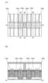
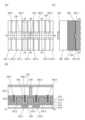
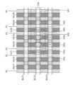
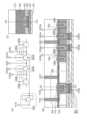
도 1의 (A) 및 도 2의 (A)는 트랜지스터(200a), 트랜지스터(200b), 트랜지스터(140a), 트랜지스터(140b), 용량 소자(100a), 및 용량 소자(100b)를 가지는 반도체 장치의 상면도이다. 또한 도 1의 (B) 및 도 2의 (B)는 도 1의 (A) 및 도 2의 (A)에 A1-A2의 일점쇄선으로 나타낸 부분의 단면도이다. 또한 도 2의 (C)는 도 2의 (A)에 A3-A4의 일점쇄선으로 나타낸 부분의 단면도이다. 도 1의 (A) 및 도 2의 (A)의 상면도에서는, 도면의 명료화를 위하여 일부 요소를 생략하여 도시하였다. 또한 도 2는 도 1의 각 구성 요소에 부호를 부여한 도면이다.1(A) and 2(A) are semiconductor
본 발명의 일 형태의 반도체 장치는 도 1 및 도 2에 도시된 바와 같이, 트랜지스터(200a), 트랜지스터(200b), 트랜지스터(140a), 트랜지스터(140b), 용량 소자(100a), 및 용량 소자(100b)를 가진다. 또한 반도체 장치는 층간막으로서 기능하는 절연체(210) 및 절연체(280), 플러그로서 기능하는 도전체(240), 그리고 도전체(240)와 전기적으로 접속되고 배선으로서 기능하는 도전체(245)를 가진다.As shown in FIGS. 1 and 2 , the semiconductor device of one embodiment of the present invention includes a
여기서, 트랜지스터(200a) 및 트랜지스터(200b)는 도 1의 (A)에 도시된 부분에서 A1-A2 간의 일점쇄선과 A5-A6 간의 일점쇄선이 교차되는 점을 중심으로 한 점대칭 구성을 가진다.Here, the
마찬가지로, 트랜지스터(140a) 및 트랜지스터(140b)는 도 1의 (A)에 도시된 부분에서 A1-A2 간의 일점쇄선과 A5-A6 간의 일점쇄선이 교차되는 점을 중심으로 한 점대칭 구성을 가진다.Similarly, the
마찬가지로, 용량 소자(100a) 및 용량 소자(100b)는 도 1의 (A)에 도시된 부분에서 A1-A2 간의 일점쇄선과 A5-A6 간의 일점쇄선이 교차되는 부분을 중심으로 한 점대칭 구성을 가진다.Similarly, the
상기 구성에 의하여, 트랜지스터(200a) 및 트랜지스터(200b)는 공통의 플러그로서 기능하는 도전체(240)와 접속될 수 있다. 즉, 트랜지스터(200a) 및 트랜지스터(200b)에서 소스 및 드레인 중 한쪽과 전기적으로 접속되는 배선을 공통화할 수 있다. 따라서, 트랜지스터(200a), 트랜지스터(200b), 트랜지스터(140a), 트랜지스터(140b), 용량 소자(100a), 및 용량 소자(100b)를 가지는 반도체 장치의 점유 면적을 축소할 수 있다.With the above configuration, the
또한 반도체 장치는 트랜지스터(200a), 트랜지스터(200b), 트랜지스터(140a), 트랜지스터(140b), 용량 소자(100a), 및 용량 소자(100b)를 덮도록 절연체(273)가 제공되는 것이 바람직하다. 절연체(273)로서 하프늄, 알루미늄, 갈륨, 이트륨, 지르코늄, 텅스텐, 타이타늄, 탄탈럼, 니켈, 저마늄, 또는, 마그네슘 등에서 선택된 1종 또는 2종 이상이 포함된 금속 산화물을 사용할 수 있다. 특히, 산화 알루미늄은 배리어성이 높으므로, 0.5nm 이상 3.0nm 이하의 박막이더라도 수소 및 질소의 확산을 억제할 수 있다.In the semiconductor device, an
또한 산화 알루미늄은 산화물(230)과 근접한 상태에서 열처리를 수행함으로써, 산화물(230) 내의 수소를 추출하는 경우가 있다. 또한 산화 알루미늄과 접하는 산화물(230)에 영역(242)(영역(242_1) 내지 영역(242_5))이 제공되어 있는 경우, 영역(242) 내의 수소를 산화 알루미늄이 흡수하고, 수소가 저감된 영역(242)은 산화물(230)의 다른 영역 내의 수소를 흡수하는 경우가 있다. 따라서, 산화물(230) 내의 수소 농도를 저감할 수 있다.Further, aluminum oxide may be subjected to heat treatment in a state close to the
또한 절연체(273) 위에 절연체(280)를 제공하는 것이 바람직하다. 절연체(280)는 막 내의 물 또는 수소 등의 불순물 농도가 저감되어 있는 것이 바람직하다.It is also preferable to provide an
절연체(280) 및 절연체(273)의 개구의 내벽에 접하여 도전체(240)가 형성된다. 상기 개구의 바닥 부분의 적어도 일부에는 영역(242_3)이 위치하고, 도전체(240)는 영역(242_3)과 접한다(도 2의 (B) 참조).A
또한 개구의 측벽부에 산화 알루미늄을 형성한 후에 도전체(240)를 형성하여도 좋다. 개구의 측벽부에 산화 알루미늄을 형성함으로써, 외측으로부터의 산소 투과를 억제하여 도전체(240)의 산화를 방지할 수 있다. 또한 도전체(240)로부터 물, 수소 등의 불순물이 외부로 확산되는 것을 방지할 수 있다. 상기 산화 알루미늄의 형성은 개구에 ALD법 등을 사용하여 산화 알루미늄을 성막하고, 이방성 에칭을 수행함으로써 형성할 수 있다.Alternatively, the
도전체(240)는 트랜지스터(200a)의 소스 및 드레인 중 한쪽으로서의 기능을 가지고, 또한 트랜지스터(200b)의 소스 및 드레인 중 한쪽으로서의 기능도 가진다. 상기 구성으로 함으로써, 인접한 트랜지스터(200a)와 트랜지스터(200b)의 간격을 작게 할 수 있다. 따라서, 트랜지스터를 고밀도로 배치할 수 있게 되어 반도체 장치의 고집적화가 가능해진다.The
또한 도 7은 도 2의 (A)에 A5-A6의 일점쇄선으로 나타낸 부분의 단면도이다. 즉, 도전체(240)와, 트랜지스터(200a) 및 트랜지스터(200b)의 산화물(230)(영역(242_3))이 접하는 영역의 단면도이다.Fig. 7 is a cross-sectional view of the portion indicated by the dashed-dotted line A5-A6 in Fig. 2(A). That is, it is a cross-sectional view of a region where the
일례로서, 도 7의 (A)에 도시된 바와 같이, 도전체(240)는 산화물(230)(영역(242_3))의 상면 및 산화물(230)(영역(242_3))의 A5 측 및 A6 측의 양 측면에서 산화물(230)(영역(242_3))과 접하여도 좋다. 즉, 도전체(240)와 산화물(230)(영역(242_3))이 접하는 영역이 말안장과 같은 단면 형상을 가진다(말안장 면 접촉(saddle-surface contact)이라고 부를 수 있음). 상기 구성으로 함으로써, 도전체(240)와 산화물(230)(영역(242_3))이 접하는 영역의 면적을 크게 할 수 있다. 따라서, 도전체(240)와 산화물(230)(영역(242_3))의 접촉 저항을 더 저감할 수 있다.As an example, as shown in (A) of FIG. 7 , the
또한 도 7의 (B)에 도시된 바와 같이, 도전체(240)는 산화물(230)(영역(242_3))의 상면 및 산화물(230)(영역(242_3))의 한쪽 측면에서 산화물(230)(영역(242_3))과 접하여도 좋다. 예를 들어, 도 7의 (B)는 도전체(240)가 산화물(230)(영역(242_3))의 A5 측의 측면과 접하는 영역의 일례를 도시한 것이다. 또한 도 7의 (C)에 도시된 바와 같이, 도전체(240)는 산화물(230)(영역(242_3))의 A6 측의 측면과 접하는 영역을 가져도 좋다. 상기 구성으로 함으로써, 도전체(240)와 산화물(230)(영역(242_3))이 접하는 영역의 면적을 크게 할 수 있다. 따라서, 도전체(240)와 산화물(230)(영역(242_3))의 접촉 저항을 저감할 수 있다.Also, as shown in (B) of FIG. 7 , the
또한 트랜지스터(200a)의 소스 및 드레인 중 다른 쪽과 용량 소자(100a)를 중첩시켜 제공한다. 마찬가지로, 트랜지스터(200b)의 소스 및 드레인 중 다른 쪽과 용량 소자(100b)를 중첩시켜 제공한다.In addition, the other of the source and drain of the
이상과 같이, 본 발명의 일 형태의 반도체 장치는 트랜지스터(200a), 트랜지스터(200b), 용량 소자(100a), 및 용량 소자(100b)를 같은 층에 배치할 수 있는 구성이 되어 있다. 상기 구성으로 함으로써, 반도체 장치는 트랜지스터 및 용량 소자를 고밀도로 배치할 수 있기 때문에 고집적화할 수 있다.As described above, in the semiconductor device of one embodiment of the present invention, the
또한 영역(242_2)은 트랜지스터(200a)의 소스 및 드레인 중 다른 쪽과 용량 소자(100a)의 한쪽 전극을 겸하는 구성이 되어 있다. 마찬가지로, 영역(242_4)은 트랜지스터(200b)의 소스 및 드레인 중 다른 쪽과 용량 소자(100b)의 한쪽 전극을 겸하는 구성이 되어 있다. 상기 구성에 의하여, 용량 소자(100a)와 트랜지스터(200a) 사이를 접속하는 공정, 및 용량 소자(100b)와 트랜지스터(200b) 사이를 접속하는 공정을 삭감할 수 있다. 따라서, 공정 수를 저감하고 생산 비용을 삭감할 수 있다.Also, the region 242_2 serves as both the other of the source and drain of the
본 발명의 일 형태에서는, 복수의 용량 소자, 복수의 트랜지스터, 및 각 구조를 접속하는 플러그를 상술한 구성으로 함으로써, 미세화 또는 고집적화가 가능한 반도체 장치를 제공할 수 있다.In one embodiment of the present invention, a semiconductor device capable of miniaturization or high integration can be provided by using the configuration described above for a plurality of capacitive elements, a plurality of transistors, and a plug connecting each structure.
[트랜지스터(200a) 및 트랜지스터(200b)][
도 1 및 도 2에 도시된 바와 같이, 트랜지스터(200a)는 기판(미도시) 위에 배치된 절연체(210) 위의 절연체(212), 절연체(212)에 매립되도록 배치된 도전체(203_1), 도전체(203_1) 위 및 절연체(212) 위의 절연체(214), 절연체(214) 위의 도전체(235_2) 및 도전체(235_3), 절연체(214), 도전체(235_2), 및 도전체(235_3)를 덮도록 형성된 유전체(278), 유전체(278) 위의 산화물(230), 도전체(235_2)와 도전체(235_3) 사이에 위치하고 산화물(230)과 접하는 절연체(250_2), 그리고 절연체(250_2)와 접하는 도전체(260_2)를 가진다.1 and 2, the
또한 도 1 및 도 2에 도시된 바와 같이, 트랜지스터(200b)는 기판(미도시) 위에 배치된 절연체(210) 위의 절연체(212), 절연체(212)에 매립되도록 배치된 도전체(203_2), 도전체(203_2) 위 및 절연체(212) 위의 절연체(214), 절연체(214) 위의 도전체(235_3) 및 도전체(235_4), 절연체(214), 도전체(235_3), 및 도전체(235_4)를 덮도록 형성된 유전체(278), 유전체(278) 위의 산화물(230), 도전체(235_3)와 도전체(235_4) 사이에 위치하고 산화물(230)과 접하는 절연체(250_3), 그리고 절연체(250_3)와 접하는 도전체(260_3)를 가진다.1 and 2, the
또한 트랜지스터(200a) 및 트랜지스터(200b)에서는, 산화물(230)을 단층으로 하는 구성에 대하여 나타내었지만, 본 발명은 이에 한정되는 것은 아니다. 예를 들어 2층, 3층, 또는 4층 이상의 적층 구조로 하여도 좋다.In the
또한 트랜지스터(200a) 및 트랜지스터(200b)에서는, 도전체(260_2) 및 도전체(260_3)를 단층 구성으로 나타내었지만, 본 발명은 이에 한정되는 것은 아니다. 예를 들어, 도전체(260_2) 및 도전체(260_3)를 2층 이상의 적층 구조로 하여도 좋다.In the
여기서, 상술한 바와 같이 트랜지스터(200a) 및 트랜지스터(200b)는 도 1의 (A)에 도시된 부분에서 A1-A2 간의 일점쇄선과 A5-A6 간의 일점쇄선이 교차되는 점을 중심으로 한 점대칭 구성을 가진다.Here, as described above, the
즉, 트랜지스터(200b)는 트랜지스터(200a)가 가지는 구조와 각각 대응하는 구조를 가진다. 따라서 도면에서는, 트랜지스터(200a) 및 트랜지스터(200b)에 있어서 대응하는 구성에는 기본적으로 3자릿수의 같은 숫자를 부호로서 부여한다. 또한 이하에서는, 특히 언급하지 않는 한, 트랜지스터(200b)에 대해서는 트랜지스터(200a)의 설명을 참작할 수 있다.That is, the
예로서, 트랜지스터(200a)의 도전체(203_1), 절연체(250_2), 도전체(260_2)는 각각, 트랜지스터(200b)의 도전체(203_2), 절연체(250_3), 도전체(260_3)에 대응한다.For example, the conductor 203_1, the insulator 250_2, and the conductor 260_2 of the
또한 산화물(230)은 트랜지스터(200a)와 트랜지스터(200b)에서 공통의 구조이다. 따라서, 산화물(230)은 트랜지스터(200a)의 채널 형성 영역으로서 기능하는 영역, 트랜지스터(200a)의 소스 및 드레인 중 한쪽으로서 기능하는 영역, 트랜지스터(200b)의 채널 형성 영역으로서 기능하는 영역, 트랜지스터(200b)의 소스 및 드레인 중 한쪽으로서 기능하는 영역, 그리고 트랜지스터(200a) 및 트랜지스터(200b)의 소스 및 드레인 중 다른 쪽으로서 기능하는 영역을 가진다.Also, the
상기 구성에 의하여, 소스 및 드레인 중 한쪽과 전기적으로 접속되는 플러그를 공통화할 수 있다. 특히, 트랜지스터(200a)와 트랜지스터(200b)가 산화물(230)을 공유함으로써, 트랜지스터(200a)의 제 1 게이트로서 기능하는 도전체(260_2)와 트랜지스터(200b)의 제 1 게이트로서 기능하는 도전체(260_3) 사이를 최소 가공 치수로 하여도 좋다. 도전체(260_2)와 도전체(260_3) 사이의 거리를 최소 가공 치수로 함으로써, 2개의 트랜지스터의 점유 면적을 축소할 수 있다.With the above configuration, a plug electrically connected to one of the source and the drain can be shared. In particular, since the
산화물(230)로서 예를 들어, In-M-Zn 산화물(원소 M은 알루미늄, 갈륨, 이트륨, 주석, 구리, 바나듐, 베릴륨, 붕소, 타이타늄, 철, 니켈, 저마늄, 지르코늄, 몰리브데넘, 란타넘, 세륨, 네오디뮴, 하프늄, 탄탈럼, 텅스텐, 또는 마그네슘 등에서 선택된 1종 또는 복수 종류) 등의 금속 산화물로 대표되는 산화물 반도체를 사용하면 좋다. 특히 원소 M으로서는, 알루미늄, 갈륨, 이트륨, 또는 주석이 적합하다. 또는 산화물(230)로서 In-Ga 산화물, In-Zn 산화물을 사용하여도 좋다.As the
채널 형성 영역에 산화물 반도체를 사용한 트랜지스터(200a) 및 트랜지스터(200b)는 비도통 상태에서 누설 전류가 매우 작으므로 저소비전력의 반도체 장치를 제공할 수 있다. 또한 산화물 반도체는 스퍼터링법 등을 사용하여 성막할 수 있기 때문에, 고집적형 반도체 장치를 구성하는 트랜지스터(200a) 및 트랜지스터(200b)에 사용할 수 있다.Since the
여기서, 도 2의 (B)에서의 트랜지스터(200a)의 채널 근방의 영역의 확대도를 도 8의 (A)에 도시하였다.Here, an enlarged view of the region near the channel of the
도 8의 (A)에 도시된 바와 같이, 산화물(230)은 트랜지스터(200a)의 채널 형성 영역으로서 기능하는 영역(234), 및 트랜지스터(200a)의 소스 또는 드레인으로서 기능하는 영역(231)(영역(231a) 및 영역(231b))을 가진다. 도 8에서는 영역(234) 근방을 파선으로 나타내었다. 도 8에서는 도면의 명료화를 위하여 영역(234)의 위치를 산화물(230)의 중앙 부근에 도시하였지만, 이에 한정되지 않고, 산화물(230)과 절연체(250_2)의 계면 부근, 또는 산화물(230)과 유전체(278)의 계면 부근, 또는 파선으로 나타낸 범위의 산화물(230) 전체로 하여도 좋다.As shown in FIG. 8(A), the
소스 또는 드레인으로서 기능하는 영역(231)은 산소 농도가 낮고 캐리어 밀도가 높은 저저항화된 영역이다. 또한 채널 형성 영역으로서 기능하는 영역(234)은 소스 또는 드레인으로서 기능하는 영역(231)보다 산소 농도가 높고 캐리어 밀도가 낮은 고저항 영역이다.The region 231 serving as a source or drain is a low-resistance region with low oxygen concentration and high carrier density. Further, the
또한 산화물(230)의 영역(231)에서, 적어도 산화물(230)의 표면 및 표면 근방(도면에서 영역(242_2) 및 영역(242_3)으로 나타내어짐)만 저저항화되어 있으면 된다. 즉, 저저항화된 영역(231)에서 영역(242_2) 및 영역(242_3)이 가장 저저항화되어 있는 것이 바람직하다.Further, in the region 231 of the
또한 영역(231)은 알루미늄, 루테늄, 타이타늄, 탄탈럼, 텅스텐, 크로뮴 등의 금속 원소, 희가스, 그리고 수소 및 질소 등의 불순물 원소 중 적어도 하나의 농도가 영역(234)보다 높은 것이 바람직하다. 또한 영역(231)에서, 영역(242_2) 및 영역(242_3)은 알루미늄, 루테늄, 타이타늄, 탄탈럼, 텅스텐, 크로뮴 등의 금속 원소, 희가스, 그리고 수소 및 질소 등의 불순물 원소 중 적어도 하나의 농도가 다른 영역보다 높은 것이 바람직하다.In the region 231, the concentration of at least one of metal elements such as aluminum, ruthenium, titanium, tantalum, tungsten, and chromium, rare gases, and impurity elements such as hydrogen and nitrogen is preferably higher than that of the
예를 들어, 영역(231)은 산화물(230) 외에, 알루미늄, 루테늄, 타이타늄, 탄탈럼, 텅스텐, 크로뮴 등의 금속 원소 중에서 선택되는 어느 하나 또는 복수의 금속 원소를 가지는 것이 바람직하다. 산화물(230)에 금속 원소가 첨가됨으로써, 영역(231)을 저저항화할 수 있다. 또한 영역(231)은 산화물(230) 내의 금속 원소와, 첨가된 금속 원소가 합금화한 영역(242_2) 및 영역(242_3)을 가져도 좋다.For example, the region 231 preferably has one or a plurality of metal elements selected from metal elements such as aluminum, ruthenium, titanium, tantalum, tungsten, and chromium, in addition to the
영역(242_2) 및 영역(242_3)을 형성하기 위해서는, 예를 들어 산화물(230)의 영역(231)에 접하여 금속막, 금속 원소를 가지는 산화막, 또는 금속 원소를 가지는 질화막을 제공하면 좋다. 이로써, 상기 막 내의 금속 원소가 산화물 반도체에 첨가되고, 산화물 반도체 내에 금속 화합물을 형성하는 경우가 있다. 상기 금속 화합물은 산화물(230)에 포함되는 수소를 끌어당기는 경우가 있다.In order to form the region 242_2 and the region 242_3, for example, a metal film, an oxide film containing a metal element, or a nitride film containing a metal element may be provided in contact with the region 231 of the
또한 산화물(230)에서, 각 영역의 경계는 명확히 검출하기가 어려운 경우가 있다. 각 영역 내에서 검출되는 금속 원소, 그리고 수소 및 질소 등의 불순물 원소의 농도는 영역마다의 단계적인 변화에 한정되지 않고, 각 영역 내에서도 연속적으로 변화(그러데이션이라고도 함)되어도 좋다. 즉, 채널 형성 영역에 가까운 영역일수록 금속 원소, 그리고 수소 및 질소 등의 불순물 원소의 농도가 감소되어 있으면 좋다.Also, in the
또한 산화물(230)의 각 영역으로서, 트랜지스터(200a)에서는 도전체(260_2) 및 절연체(250_2)를 마스크로 하여 산화물(230)에 불순물 또는 금속 원소를 첨가함으로써, 자기 정합(自己整合)적으로 저저항화된 영역을 형성한다. 또한 트랜지스터(200b)에서는, 도전체(260_3) 및 절연체(250_3)를 마스크로 하여 산화물(230)에 불순물 또는 금속 원소를 첨가함으로써, 자기 정합적으로 저저항화된 영역을 형성한다. 그러므로, 트랜지스터(200a) 및 트랜지스터(200b)를 가지는 반도체 장치를 복수 동시에 형성하는 경우, 반도체 장치 간의 전기 특성 편차를 작게 할 수 있다.Further, as each region of the
또한 도 8의 (A)에 도시된 바와 같이, 트랜지스터(200a)의 채널 길이는 영역(234)의 길이와 대략 동등하다. 영역(234)의 길이는 도전체(260_2)의 양쪽 측면과 산화물(230)이 절연체(250_2)를 개재(介在)하여 중첩되는 영역의 길이에, 도전체(260_2)의 짧은 변의 바닥면과 산화물(230)이 절연체(250_2)를 개재하여 중첩되는 영역의 길이를 더한 길이와 대략 동등하다. 즉, 트랜지스터(200a)의 채널 길이는 도전체(260_2)의 짧은 변에 평행한 방향의 길이 260W보다 길게 할 수 있다.Also, as shown in (A) of FIG. 8 , the channel length of the
트랜지스터(200a)를 미세화하여 길이 260W를 더 미세하게 제작하여도 트랜지스터(200a)의 채널 길이를 길이 260W보다 길게 할 수 있기 때문에, 트랜지스터의 단채널 효과를 억제할 수 있다. 또한 트랜지스터(200a)의 채널 길이는 길이 260W의 1.5배 이상 10배 이하로 한다.Since the channel length of the
또한 트랜지스터(200b)의 구성 및 효과에 대하여도 상술한 트랜지스터(200a)의 구성 및 효과를 참작할 수 있다.Also, regarding the configuration and effects of the
이하에서는, 본 발명의 일 형태에 따른 트랜지스터(200a) 및 트랜지스터(200b)의 자세한 구성에 대하여 설명한다. 또한 이하에서도 트랜지스터(200b)의 구성에 대해서는 트랜지스터(200a)를 참작할 수 있다.Hereinafter, detailed configurations of the
트랜지스터(200a)의 제 2 게이트 전극으로서 기능하는 도전체(203_1)는 산화물(230) 및 도전체(260_2)와 중첩되도록 배치한다.The conductor 203_1 serving as the second gate electrode of the
여기서, 도전체(260_2)는 트랜지스터(200a)의 제 1 게이트 전극으로서 기능하는 경우가 있다. 또한 도전체(203_1)는 트랜지스터(200a)의 제 2 게이트 전극으로서 기능하는 경우가 있다.Here, the conductor 260_2 may function as a first gate electrode of the
또한 도전체(203_1)에 인가하는 전위는 접지 전위나 도전체(260_2)에 인가하는 전위와 상이한 임의의 전위로 하여도 좋다. 예를 들어, 도전체(203_1)에 인가하는 전위를, 도전체(260_2)에 인가하는 전위와 연동시키지 않고 독립적으로 변화시킴으로써 트랜지스터(200a)의 문턱 전압을 제어할 수 있다. 특히, 도전체(203_1)에 음의 전위를 인가함으로써, 트랜지스터(200a)의 문턱 전압을 0V보다 크게 하여 오프 전류를 저감할 수 있게 된다. 따라서, 도전체(260_2)에 인가하는 전압이 0V일 때의 드레인 전류를 작게 할 수 있다.Further, the potential applied to the conductor 203_1 may be a ground potential or an arbitrary potential different from the potential applied to the conductor 260_2. For example, the threshold voltage of the
한편, 도전체(203_1)에 인가하는 전위는 도전체(260_2)에 인가하는 전위와 같은 전위로 하여도 좋다. 도전체(203_1)에 인가하는 전위를, 도전체(260_2)에 인가하는 전위와 같은 전위로 하는 경우, 도전체(203_1)는 산화물(230)에서의 영역(234)보다 채널 폭 방향의 길이가 크게 되도록 크게 제공하여도 좋다. 특히, 도전체(203_1)는 채널 폭 방향에서 산화물(230)의 영역(234)의 단부보다 외측의 영역까지 연장되어 있는 것이 바람직하다. 즉, 산화물(230)의 채널 폭 방향의 측면의 외측에서 도전체(203_1)와 도전체(260_2)는 절연체를 개재하여 중첩되어 있는 것이 바람직하다.On the other hand, the potential applied to the conductor 203_1 may be the same as the potential applied to the conductor 260_2. When the potential applied to the conductor 203_1 is the same as the potential applied to the conductor 260_2, the length of the conductor 203_1 in the channel width direction is greater than that of the
상기 구성을 가짐으로써, 도전체(260_2) 및 도전체(203_1)에 전위를 인가한 경우, 도전체(260_2)로부터 발생하는 전계와 도전체(203_1)로부터 발생하는 전계가 연결됨으로써 폐회로를 형성하고, 산화물(230)에 형성되는 채널 형성 영역을 덮을 수 있다.By having the above configuration, when a potential is applied to the conductor 260_2 and the conductor 203_1, the electric field generated from the conductor 260_2 and the electric field generated from the conductor 203_1 are connected to form a closed circuit, , may cover a channel formation region formed in the
즉, 제 1 게이트 전극으로서의 기능을 가지는 도전체(260_2)의 전계와 제 2 게이트 전극으로서의 기능을 가지는 도전체(203_1)의 전계에 의하여 영역(234)의 채널 형성 영역을 전기적으로 둘러쌀 수 있다. 본 명세서에서 제 1 게이트 전극 및 제 2 게이트 전극의 전계에 의하여, 채널 형성 영역을 전기적으로 둘러싸는 트랜지스터의 구조를 surrounded channel(S-channel) 구조라고 부른다.That is, the channel formation region of the
절연체(210)는 아래층으로부터 물 또는 수소 등의 불순물이 트랜지스터에 혼입되는 것을 방지하는 배리어 절연막으로서 기능할 수 있다. 절연체(210)에는 물 또는 수소 등의 불순물의 투과를 억제하는 기능을 가지는 절연성 재료를 사용하는 것이 바람직하다. 예를 들어, 절연체(210)로서 질화 실리콘, 산화 알루미늄, 산화 하프늄, 실리콘 및 하프늄을 포함한 산화물(하프늄 실리케이트), 알루미늄 및 하프늄을 포함한 산화물(하프늄 알루미네이트) 등을 사용하는 것이 바람직하다. 이로써, 수소, 물 등의 불순물이 절연체(210)보다 위층으로 확산되는 것을 억제할 수 있다. 또한 절연체(210)는 수소 원자, 수소 분자, 물 분자, 질소 원자, 질소 분자, 산화 질소 분자(N2O, NO, NO2 등), 구리 원자 등의 불순물 중 적어도 하나의 투과를 억제하는 기능을 가지는 것이 바람직하다. 또한 이하에서, 불순물의 투과를 억제하는 기능을 가지는 절연성 재료에 대하여 기재하는 경우도 마찬가지이다.The
또한 절연체(210)에는 산소(예를 들어, 산소 원자 또는 산소 분자 등)의 투과를 억제하는 기능을 가지는 절연성 재료를 사용하는 것이 바람직하다. 이로써, 절연체(214) 등에 포함되는 산소가 아래쪽으로 확산되는 것을 억제할 수 있다.In addition, it is preferable to use an insulating material having a function of suppressing transmission of oxygen (eg, oxygen atoms or oxygen molecules) for the
절연체(250_2)는 트랜지스터(200a)의 제 1 게이트 절연막으로서 기능할 수 있고, 절연체(214)는 트랜지스터(200a)의 제 2 게이트 절연막으로서 기능할 수 있다. 또한 트랜지스터(200a)에서는, 절연체(214)를 단층 구성으로 나타내었지만, 본 발명은 이에 한정되는 것은 아니다. 예를 들어, 절연체(214)는 2층 이상을 적층한 구조로 하여도 좋다.The insulator 250_2 may function as a first gate insulating film of the
산화물(230)에는 산화물 반도체로서 기능하는 금속 산화물(이하, 산화물 반도체라고도 함)을 사용하는 것이 바람직하다. 금속 산화물로서는, 에너지 갭이 2eV 이상, 바람직하게는 2.5eV 이상인 것을 사용하는 것이 바람직하다. 이와 같이, 에너지 갭이 넓은 금속 산화물을 사용함으로써, 트랜지스터의 오프 전류를 저감할 수 있다.It is preferable to use a metal oxide that functions as an oxide semiconductor (hereinafter, also referred to as an oxide semiconductor) for the
산화물 반도체를 사용한 트랜지스터는 비도통 상태에서 누설 전류가 매우 작기 때문에, 저소비전력의 반도체 장치를 제공할 수 있다. 또한 산화물 반도체는 스퍼터링법 등을 사용하여 성막할 수 있기 때문에, 고집적형 반도체 장치를 구성하는 트랜지스터에 사용할 수 있다.Since a transistor using an oxide semiconductor has a very small leakage current in a non-conducting state, a semiconductor device with low power consumption can be provided. In addition, since an oxide semiconductor can be formed into a film using a sputtering method or the like, it can be used for a transistor constituting a highly integrated semiconductor device.
산화물 반도체는 적어도 인듐 또는 아연을 포함하는 것이 바람직하다. 특히 인듐 및 아연을 포함하는 것이 바람직하다. 또한 이들에 더하여, 알루미늄, 갈륨, 이트륨, 또는 주석 등이 포함되어 있는 것이 바람직하다. 또한 붕소, 실리콘, 타이타늄, 철, 니켈, 저마늄, 지르코늄, 몰리브데넘, 란타넘, 세륨, 네오디뮴, 하프늄, 탄탈럼, 텅스텐, 또는 마그네슘 등에서 선택된 1종 또는 복수 종류가 포함되어 있어도 좋다.The oxide semiconductor preferably contains at least indium or zinc. Particularly preferred are those containing indium and zinc. In addition to these, aluminum, gallium, yttrium, or tin is preferably contained. Further, one or more selected from among boron, silicon, titanium, iron, nickel, germanium, zirconium, molybdenum, lanthanum, cerium, neodymium, hafnium, tantalum, tungsten, magnesium, and the like may be contained.
여기서는, 산화물 반도체가 인듐, 원소 M, 및 아연을 가지는 In-M-Zn 산화물인 경우를 생각한다. 또한 원소 M은 알루미늄, 갈륨, 이트륨, 또는 주석 등으로 한다. 그 외의 원소 M에 적용 가능한 원소로서는 붕소, 실리콘, 타이타늄, 철, 니켈, 저마늄, 지르코늄, 몰리브데넘, 란타넘, 세륨, 네오디뮴, 하프늄, 탄탈럼, 텅스텐, 마그네슘 등이 있다. 다만, 원소 M으로서 상술한 원소를 복수 조합하여도 되는 경우가 있다.Here, the case where the oxide semiconductor is an In—M—Zn oxide containing indium, element M, and zinc is considered. Element M is aluminum, gallium, yttrium, or tin. Other elements applicable to the element M include boron, silicon, titanium, iron, nickel, germanium, zirconium, molybdenum, lanthanum, cerium, neodymium, hafnium, tantalum, tungsten, and magnesium. However, there are cases in which a plurality of elements described above may be combined as the element M.
또한 본 명세서 등에서, 질소를 가지는 금속 산화물도 금속 산화물(metal oxide)이라고 총칭하는 경우가 있다. 또한 질소를 가지는 금속 산화물을 금속 산질화물(metal oxynitride)이라고 불러도 좋다.Also, in this specification and the like, metal oxides containing nitrogen may also be collectively referred to as metal oxides. Also, a metal oxide having nitrogen may be called a metal oxynitride.
여기서, 산화물 반도체는 산화물 반도체를 구성하는 원소 외에, 알루미늄, 루테늄, 타이타늄, 탄탈럼, 크로뮴, 텅스텐 등의 금속 원소를 첨가함으로써, 금속 화합물이 되어 저저항화되는 경우가 있다. 또한 바람직하게는 알루미늄, 타이타늄, 탄탈럼, 텅스텐 등을 사용하는 것이 바람직하다. 산화물 반도체에 금속 원소를 첨가하기 위해서는, 예를 들어 산화물 반도체 위에, 상기 금속 원소를 포함하는 금속막, 금속 원소를 가지는 질화막, 또는 금속 원소를 가지는 산화막을 제공하면 좋다. 또한 상기 막을 제공함으로써, 상기 막과 산화물 반도체의 계면, 또는 상기 계면 근방에 위치하는 산화물 반도체 내의 일부의 산소가 상기 막 등에 흡수됨으로써 산소 결손이 형성되어, 산화물 반도체의 상기 계면 또는 계면 근방이 저저항화되는 경우가 있다.Here, the oxide semiconductor may become a metal compound and have low resistance by adding metal elements such as aluminum, ruthenium, titanium, tantalum, chromium, and tungsten in addition to the elements constituting the oxide semiconductor. Also preferably, it is preferable to use aluminum, titanium, tantalum, tungsten or the like. In order to add a metal element to the oxide semiconductor, for example, a metal film containing the metal element, a nitride film containing the metal element, or an oxide film containing the metal element may be provided over the oxide semiconductor. Further, by providing the film, oxygen vacancies are formed by absorbing a part of oxygen in the film or the like at the interface between the film and the oxide semiconductor, or in the oxide semiconductor positioned near the interface, so that the interface or the vicinity of the interface of the oxide semiconductor has low resistance. There are times when you get angry.
상기 계면 근방에 형성된 산소 결손의 주변은 변형을 가진다. 또한 상기 막을 스퍼터링법으로 성막하는 경우, 스퍼터링 가스에 희가스가 포함되면 상기 막의 성막 중에 희가스가 산화물 반도체 내에 혼입되는 경우가 있다. 산화물 반도체 내에 희가스가 혼입함으로써, 상기 계면 또는 계면 근방, 및 희가스의 주변에서는, 변형 또는 구조의 불균일이 생긴다. 또한 상기 희가스로서는 He, Ar 등을 들 수 있다. 또한 He보다 Ar이, 원자 반지름이 크기 때문에 더 바람직하다. 상기 Ar이 산화물 반도체 내에 혼입함으로써, 변형 또는 구조의 불균일이 적합하게 생긴다. 이들 변형, 또는 구조가 불균일한 영역에서는, 결합한 산소의 수가 적은 금속 원자가 증가할 것으로 생각된다. 결합한 산소의 수가 적은 금속 원자가 증가함으로써 상기 계면 또는 계면 근방, 및 희가스의 주변이 저저항화되는 경우가 있다.The periphery of the oxygen vacancies formed near the interface has strain. Further, when the film is formed by sputtering, if the sputtering gas contains a rare gas, the rare gas may be mixed into the oxide semiconductor during film formation. When the rare gas mixes in the oxide semiconductor, deformation or structural non-uniformity occurs at the interface or in the vicinity of the interface, and around the rare gas. Moreover, He, Ar, etc. are mentioned as said noble gas. Moreover, Ar is more preferable than He because it has a larger atomic radius. By incorporating Ar into the oxide semiconductor, deformation or structural non-uniformity arises favorably. In these strains or regions where the structure is non-uniform, it is thought that metal atoms with a small number of bonded oxygens increase. When the number of metal atoms with a small number of bonded oxygen increases, the resistance of the interface or the vicinity of the interface and the periphery of the rare gas may be reduced.
또한 산화물 반도체로서, 결정성의 산화물 반도체를 사용하는 경우, 상기 변형, 또는 구조가 불균일한 영역에서는, 결정성이 무너지고 비정질인 것처럼 관찰되는 경우가 있다.Further, when a crystalline oxide semiconductor is used as the oxide semiconductor, crystallinity collapses and may be observed as being amorphous in the region where the strain or structure is non-uniform.
또한 산화물 반도체 위에, 금속막, 금속 원소를 가지는 질화막, 또는 금속 원소를 가지는 산화막을 제공한 후, 질소를 포함하는 분위기하에서 열처리를 수행하면 좋다. 질소를 포함하는 분위기하에서의 열처리에 의하여, 금속막으로부터 금속 원소가 산화물 반도체로 확산되어, 산화물 반도체에 금속 원소를 첨가할 수 있다.Further, after providing a metal film, a nitride film containing a metal element, or an oxide film containing a metal element over the oxide semiconductor, heat treatment may be performed in an atmosphere containing nitrogen. By heat treatment in an atmosphere containing nitrogen, the metal element diffuses from the metal film into the oxide semiconductor, and the metal element can be added to the oxide semiconductor.
또한 산화물 반도체에 존재하는 수소는, 산화물 반도체의 저저항화된 영역으로 확산되고, 저저항화된 영역에 존재하는 산소 결손 내에 들어간 경우, 비교적으로 안정적인 상태가 된다. 또한 산화물 반도체에 존재하는 산소 결손 내의 수소는, 250℃ 이상의 열처리에 의하여 산소 결손으로부터 빠져나가 산화물 반도체의 저저항화된 영역으로 확산되고, 저저항화된 영역에 존재하는 산소 결손 내에 들어가, 비교적으로 안정적인 상태가 되는 것이 알려져 있다. 따라서, 열처리에 의하여, 산화물 반도체의 저저항화된 영역은 더 저저항화되고, 저저항화되지 않은 산화물 반도체는 고순도화(물, 수소 등의 불순물의 저감)되어 더 고저항화되는 경향이 있다.Further, hydrogen existing in the oxide semiconductor diffuses into the low-resistance region of the oxide semiconductor and enters into an oxygen vacancy existing in the low-resistance region, resulting in a relatively stable state. In addition, hydrogen in oxygen vacancies present in the oxide semiconductor escapes from the oxygen vacancies by heat treatment at 250° C. or higher, diffuses into the low-resistance region of the oxide semiconductor, enters the oxygen vacancies present in the low-resistance region, and is relatively It is known to be in a stable state. Therefore, by the heat treatment, the low-resistance region of the oxide semiconductor tends to have a lower resistance, and the oxide semiconductor that has not had a low-resistance has a higher purity (reduction of impurities such as water and hydrogen) and a higher resistance. .
또한 산화물 반도체는 수소 또는 질소 등의 불순물 원소가 존재하면 캐리어 밀도가 증가한다. 산화물 반도체 내의 수소는 금속 원자와 결합하는 산소와 반응하여 물이 되어, 산소 결손을 형성하는 경우가 있다. 상기 산소 결손에 수소가 들어감으로써, 캐리어 밀도가 증가한다. 또한 수소의 일부가 금속 원자와 결합하는 산소와 결합하여, 캐리어인 전자를 생성하는 경우가 있다. 즉, 질소 또는 수소를 가지는 산화물 반도체는 저저항화된다.Also, the carrier density of the oxide semiconductor increases when an impurity element such as hydrogen or nitrogen is present. Hydrogen in the oxide semiconductor reacts with oxygen bonded to a metal atom to become water, forming oxygen vacancies in some cases. When hydrogen enters the oxygen vacancies, the carrier density increases. Also, in some cases, a part of hydrogen is combined with oxygen bonded to a metal atom to generate electrons as carriers. That is, the oxide semiconductor containing nitrogen or hydrogen has low resistance.
따라서, 산화물 반도체에 대하여, 선택적으로 금속 원소, 그리고 수소 및 질소 등의 불순물 원소를 첨가함으로써, 산화물 반도체에 고저항 영역 및 저저항 영역을 제공할 수 있다. 즉, 산화물(230)을 선택적으로 저저항화함으로써, 산화물(230)에 캐리어 밀도가 낮은 반도체로서 기능하는 영역과, 소스 또는 드레인으로서 기능하는 저저항화된 영역을 제공할 수 있다.Therefore, a high-resistance region and a low-resistance region can be provided in the oxide semiconductor by selectively adding a metal element and an impurity element such as hydrogen and nitrogen to the oxide semiconductor. That is, by selectively reducing the resistance of the
여기서, 트랜지스터(200a)에서는 도전체(260_2)와 도전체(235_2) 사이 및 도전체(260_2)와 도전체(235_3) 사이에 기생 용량이 형성되는 경우가 있다. 마찬가지로, 트랜지스터(200b)에서는 도전체(260_3)와 도전체(235_3) 사이 및 도전체(260_3)와 도전체(235_4) 사이에 기생 용량이 형성되는 경우가 있다.Here, in the
이 경우에는, 도 4의 (B)에 도시된 바와 같이, 도전체(235_2)의 측면에 절연체(220_2)를 제공하고, 도전체(235_3)의 측면에 절연체(220_3)를 제공하는 구성으로 함으로써, 트랜지스터(200a)의 기생 용량을 저감할 수 있다. 트랜지스터(200b)도 마찬가지로, 도전체(235_4)의 측면에 절연체(220_4)를 제공하는 구성으로 함으로써, 트랜지스터(200b)의 기생 용량을 저감할 수 있다. 기생 용량을 저감함으로써, 트랜지스터(200a) 및 트랜지스터(200b)를 고속으로 동작할 수 있다.In this case, as shown in (B) of FIG. 4 , the insulator 220_2 is provided on the side of the conductor 235_2 and the insulator 220_3 is provided on the side of the conductor 235_3. , the parasitic capacitance of the
여기서, 도 2에 도시된 바와 같이, 트랜지스터(200a) 및 트랜지스터(200b)를 덮도록 절연체(273)를 제공하여도 좋다(도 2 참조).Here, as shown in FIG. 2, an
예를 들어 절연체(273)로서 하프늄, 알루미늄, 갈륨, 이트륨, 지르코늄, 텅스텐, 타이타늄, 탄탈럼, 니켈, 저마늄, 또는 마그네슘 등에서 선택된 1종 또는 2종 이상이 포함된 금속 산화물을 사용할 수 있다. 특히, 산화 알루미늄은 배리어성이 높으므로, 0.5nm 이상 3.0nm 이하의 박막이더라도 수소 및 질소의 확산을 억제할 수 있다.For example, as the
또한 산화 알루미늄은 산화물(230)과 근접한 상태에서 열처리를 수행함으로써, 산화물(230) 내의 수소를 추출하는 경우가 있다. 또한 산화 알루미늄과 접하는 산화물(230)에 영역(242)이 제공되어 있는 경우, 영역(242) 내의 수소를 산화 알루미늄이 흡수하고, 수소가 저감된 영역(242)은 산화물(230)의 다른 영역 내의 수소를 흡수하는 경우가 있다. 따라서, 산화물(230) 내의 수소 농도를 저감할 수 있다. 또한 절연체(273)와 절연체(250_2) 및 절연체(250_3)가 접하는 영역을 가짐으로써, 절연체(250_2) 및 절연체(250_3)에 산소를 공급할 수 있는 경우가 있다.Further, aluminum oxide may be subjected to heat treatment in a state close to the
[트랜지스터(140a) 및 트랜지스터(140b)][
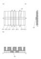
도 1 및 도 2에 도시된 바와 같이, 트랜지스터(140a) 및 트랜지스터(140b)는 상술한 트랜지스터(200a) 및 트랜지스터(200b)의 구성과는 트랜지스터(200a)의 제 2 게이트 전극으로서 기능하는 도전체(203_1) 및 트랜지스터(200b)의 제 2 게이트 전극으로서 기능하는 도전체(203_2)를 가지지 않는 점이 상이하다. 그 다른 구성에 대해서는, 트랜지스터(200a) 및 트랜지스터(200b)와 같은 구성이다.As shown in FIGS. 1 and 2, the
도 1 및 도 2에 도시된 바와 같이, 트랜지스터(140a) 및 트랜지스터(140b)는 트랜지스터(200a) 및 트랜지스터(200b)의 A1-A2 방향의 양단을 끼우도록 인접하여 배치되어 있다. 즉, 트랜지스터(200a)의 A1 방향으로 인접하도록 트랜지스터(140a)가 배치되고, 트랜지스터(200b)의 A2 방향으로 인접하도록 트랜지스터(140b)가 배치된다.1 and 2,
예를 들어, 트랜지스터(200a), 트랜지스터(200b), 용량 소자(100a), 및 용량 소자(100b)로 구성된 메모리 셀을 복수로 가지는 반도체 장치에서, 상기 메모리 셀이 도 1 및 도 2의 A1-A2 방향 및 A3-A4 방향으로 연속적으로 배치되어 있는 경우, A1-A2 방향에서는 인접한 메모리 셀은 공통의 산화물(230)을 가지기 때문에, 인접한 메모리 셀 간에서 트랜지스터가 전기적으로 접속된다.For example, in a semiconductor device having a plurality of memory cells including a
트랜지스터(140a) 및 트랜지스터(140b)를 가짐으로써, 인접한 메모리 셀 간을 전기적으로 분리할 수 있다. 즉, 트랜지스터(140a)는 A1 방향으로 인접한 메모리 셀과 전기적으로 분리되는 기능을 가지고, 트랜지스터(140b)는 A2 방향으로 인접한 메모리 셀과 전기적으로 분리될 수 있는 기능을 가진다. 이러한 기능은 트랜지스터(140a) 및 트랜지스터(140b)를 항상 오프 상태로 하면 좋다. 트랜지스터(140a) 및 트랜지스터(140b)를 항상 오프 상태로 하기 위해서는, 트랜지스터(140a)의 제 1 게이트 전극의 기능을 가지는 도전체(260_1) 및 트랜지스터(140b)의 제 1 게이트 전극의 기능을 가지는 도전체(260_4)에 트랜지스터(140a) 및 트랜지스터(140b) 각각이 오프 상태가 되는 전위를 공급하면 좋다.By having the
또한 도 3에 도시된 바와 같이, 트랜지스터(140a)의 제 2 게이트 전극의 기능을 가지는 도전체(205_1) 및 트랜지스터(140b)의 제 2 게이트 전극의 기능을 가지는 도전체(205_2)를 제공하여도 좋다. 이러한 구성으로 함으로써, 예를 들어 도전체(205_1) 및 도전체(205_2)에 음의 전위를 공급함으로써, 트랜지스터(140a) 및 트랜지스터(140b)가 오프 상태가 되는, 도전체(260_1)에 공급되는 전위 및 도전체(260_4)에 공급되는 전위를 낮게 억제할 수 있다. 또한 오프 전류를 저감할 수도 있다.3, even if a conductor 205_1 having the function of the second gate electrode of the
또는, 도전체(205_1)와 도전체(260_1)를 접속하여 같은 전위를 공급하고, 도전체(205_2)와 도전체(260_4)를 접속하여 같은 전위를 공급하여도 좋다.Alternatively, the same potential may be supplied by connecting the conductor 205_1 and the conductor 260_1, and the same potential may be supplied by connecting the conductor 205_2 and the conductor 260_4.
[용량 소자(100a) 및 용량 소자(100b)][
도 1 및 도 2에 도시된 바와 같이, 용량 소자(100a)는 트랜지스터(200a)와 중첩되는 영역에 제공된다. 마찬가지로, 용량 소자(100b)는 트랜지스터(200b)와 중첩되는 영역에 제공된다. 또한 도 8의 (B)에는 도 1 및 도 2에 A7-A8의 일점쇄선으로 나타낸 부분의 단면도를 도시하였다.As shown in FIGS. 1 and 2 , the
또한 트랜지스터(200a)의 설명과 마찬가지로, 용량 소자(100b)는 용량 소자(100a)가 가지는 구조에 각각 대응하는 구조를 가진다. 따라서, 도면에서는, 용량 소자(100a) 및 용량 소자(100b)에 있어서 대응하는 구성에는 기본적으로 3자릿수의 같은 숫자를 부호로서 부여한다. 따라서, 이하에서는, 특히 언급하지 않는 한, 용량 소자(100b)에 대해서는 용량 소자(100a)의 설명을 참작할 수 있다.Similarly to the description of the
용량 소자(100a)는 도전체(235_2), 도전체(235_2)를 덮도록 배치된 유전체(278), 및 유전체(278) 위의 산화물(230)을 가진다. 또한 용량 소자(100b)는 도전체(235_4), 도전체(235_4)를 덮도록 배치된 유전체(278), 및 유전체(278) 위의 산화물(230)을 가진다.The
또한 산화물(230)이 가지는 영역(242_2)은 용량 소자(100a)의 한쪽 전극과 트랜지스터(200a)의 소스 및 드레인 중 다른 쪽을 겸하는 구성이 되어 있다. 도전체(235_2)는 용량 소자(100a)의 다른 쪽 전극으로서의 기능을 가진다. 도전체(235_2)와 영역(242_2)은 유전체(278)를 개재하여 중첩된다. 마찬가지로, 산화물(230)이 가지는 영역(242_4)은 용량 소자(100b)의 한쪽 전극과 트랜지스터(200b)의 소스 및 드레인 중 다른 쪽을 겸하는 구성이 되어 있다. 도전체(235_4)는 용량 소자(100b)의 다른 쪽 전극으로서의 기능을 가진다. 도전체(235_4)와 영역(242_4)은 유전체(278)를 개재하여 중첩된다.Also, the region 242_2 of the
도 1의 (B), 도 2의 (B), 및 도 8의 (B)에 도시된 바와 같이, 용량 소자(100a) 및 용량 소자(100b)는 대략 평탄한 면 위에 용량 소자를 배치할 수 있기 때문에, 유전체(278)의 피복성이 향상되므로, 유전체(278)를 얇게 할 수 있고, 용량 소자(100a) 및 용량 소자(100b)의 용량값을 크게 할 수 있어 바람직하다.As shown in FIGS. 1(B), 2(B), and 8(B), the
또한 유전체(278)는 유전율이 큰 절연체를 사용하는 것이 바람직하다. 예를 들어 알루미늄 및 하프늄 중 한쪽 또는 양쪽의 산화물을 포함하는 절연체를 사용할 수 있다. 알루미늄 및 하프늄 중 한쪽 또는 양쪽의 산화물을 포함하는 절연체로서, 산화 알루미늄, 산화 하프늄, 알루미늄 및 하프늄을 포함한 산화물(하프늄 알루미네이트) 등을 사용하는 것이 바람직하다.In addition, it is preferable to use an insulator having a high permittivity for the dielectric 278 . For example, an insulator comprising an oxide of one or both of aluminum and hafnium can be used. As the insulator containing an oxide of one or both of aluminum and hafnium, it is preferable to use aluminum oxide, hafnium oxide, an oxide containing aluminum and hafnium (hafnium aluminate), or the like.
또한 유전체(278)는 적층 구조이어도 좋다. 예를 들어, 산화 실리콘, 산화질화 실리콘, 질화산화 실리콘, 질화 실리콘, 산화 알루미늄, 산화 하프늄, 알루미늄 및 하프늄을 포함한 산화물(하프늄 알루미네이트) 등으로부터 2층 이상을 선택하여 적층 구조로 하여도 좋다. 예를 들어, ALD법으로 산화 하프늄, 산화 알루미늄, 및 산화 하프늄을 순차적으로 성막하여 적층 구조로 하는 것이 바람직하다. 유전체(278)의 막 두께는 0.1nm 이상 20nm 이하, 바람직하게는 0.3nm 이상 10nm 이하, 더 바람직하게는 1nm 이상 5nm 이하로 한다.Also, the dielectric 278 may have a laminated structure. For example, two or more layers may be selected from among silicon oxide, silicon oxynitride, silicon nitride oxide, silicon nitride, aluminum oxide, hafnium oxide, and an oxide containing aluminum and hafnium (hafnium aluminate) to form a laminated structure. For example, it is preferable to sequentially form a film of hafnium oxide, aluminum oxide, and hafnium oxide by an ALD method to obtain a laminated structure. The film thickness of the dielectric 278 is 0.1 nm or more and 20 nm or less, preferably 0.3 nm or more and 10 nm or less, and more preferably 1 nm or more and 5 nm or less.
<기판><substrate>
트랜지스터를 형성하는 기판으로서는, 예를 들어 절연체 기판, 반도체 기판, 또는 도전체 기판을 사용하면 좋다. 절연체 기판으로서는, 예를 들어 유리 기판, 석영 기판, 사파이어 기판, 안정화 지르코니아 기판(이트리아 안정화 지르코니아 기판 등), 수지 기판 등이 있다. 또한 반도체 기판으로서는, 예를 들어 실리콘, 저마늄 등의 반도체 기판, 또는 탄소화 실리콘, 실리콘 저마늄, 비소화 갈륨, 인화 인듐, 산화 아연, 산화 갈륨으로 이루어지는 화합물 반도체 기판 등이 있다. 또한 상술한 반도체 기판 내부에 절연체 영역을 가지는 반도체 기판, 예를 들어 SOI(Silicon On Insulator) 기판 등이 있다. 도전체 기판으로서는, 흑연 기판, 금속 기판, 합금 기판, 도전성 수지 기판 등이 있다. 또는, 금속의 질화물을 가지는 기판, 금속의 산화물을 가지는 기판 등이 있다. 또한 절연체 기판에 도전체 또는 반도체가 제공된 기판, 반도체 기판에 도전체 또는 절연체가 제공된 기판, 도전체 기판에 반도체 또는 절연체가 제공된 기판 등이 있다. 또는, 이들 기판에 소자가 제공된 것을 사용하여도 좋다. 기판에 제공되는 소자로서는, 용량 소자, 저항 소자, 스위칭 소자, 발광 소자, 기억 소자 등이 있다.As the substrate for forming the transistor, for example, an insulator substrate, a semiconductor substrate, or a conductor substrate may be used. Examples of the insulator substrate include a glass substrate, a quartz substrate, a sapphire substrate, a stabilized zirconia substrate (such as an yttria stabilized zirconia substrate), and a resin substrate. Examples of the semiconductor substrate include a semiconductor substrate made of silicon or germanium, or a compound semiconductor substrate made of silicon carbide, silicon germanium, gallium arsenide, indium phosphide, zinc oxide, or gallium oxide. In addition, there is a semiconductor substrate having an insulator region inside the above-described semiconductor substrate, for example, a silicon on insulator (SOI) substrate. Examples of the conductive substrate include a graphite substrate, a metal substrate, an alloy substrate, and a conductive resin substrate. Alternatively, there are a substrate having a metal nitride, a substrate having a metal oxide, and the like. Further, there are a substrate in which a conductor or a semiconductor is provided on an insulator substrate, a substrate in which a conductor or an insulator is provided on a semiconductor substrate, a substrate in which a semiconductor or an insulator is provided on a conductor substrate, and the like. Alternatively, those substrates provided with elements may be used. Elements provided on the substrate include capacitive elements, resistive elements, switching elements, light emitting elements, memory elements, and the like.
또한 기판으로서 가요성 기판을 사용하여도 좋다. 또한 가요성 기판 위에 트랜지스터를 제공하는 방법으로서는, 비가요성 기판 위에 트랜지스터를 제작한 후, 트랜지스터를 박리하고, 가요성 기판인 기판으로 전치(轉置)하는 방법도 있다. 그 경우에는, 비가요성 기판과 트랜지스터 사이에 박리층을 제공하면 좋다. 또한 기판으로서 섬유를 짠 시트, 필름, 또는 포일 등을 사용하여도 좋다. 또한 기판이 신축성을 가져도 좋다. 또한 기판은 구부리거나 당기는 것을 중지하였을 때, 원래의 형상으로 되돌아가는 성질을 가져도 좋다. 또는, 원래의 형상으로 되돌아가지 않는 성질을 가져도 좋다. 기판은, 예를 들어 5μm 이상 700μm 이하, 바람직하게는 10μm 이상 500μm 이하, 더 바람직하게는 15μm 이상 300μm 이하의 두께가 되는 영역을 가진다. 기판을 얇게 하면, 트랜지스터를 가지는 반도체 장치를 경량화할 수 있다. 또한 기판을 얇게 함으로써, 유리 등을 사용한 경우에도 신축성을 가지는 경우나, 구부리거나 당기는 것을 중지하였을 때 원래의 형상으로 되돌아가는 성질을 가지는 경우가 있다. 그러므로, 낙하 등으로 인하여 기판 위의 반도체 장치에 가해지는 충격 등을 완화할 수 있다. 즉, 튼튼한 반도체 장치를 제공할 수 있다.Also, a flexible substrate may be used as the substrate. Further, as a method of providing a transistor on a flexible substrate, there is also a method of fabricating a transistor on a non-flexible substrate, then removing the transistor and transferring the transistor to a substrate that is a flexible substrate. In that case, a separation layer may be provided between the non-flexible substrate and the transistor. Further, as the substrate, a woven sheet, film, or foil may be used. Further, the substrate may have elasticity. Further, the substrate may have a property of returning to its original shape when bending or pulling is stopped. Alternatively, it may have a property of not returning to its original shape. The substrate has a region having a thickness of, for example, 5 μm or more and 700 μm or less, preferably 10 μm or more and 500 μm or less, and more preferably 15 μm or more and 300 μm or less. If the substrate is thin, the weight of the semiconductor device including the transistor can be reduced. In addition, by making the substrate thin, there are cases where it has elasticity even when glass or the like is used, or it has the property of returning to its original shape when bending or pulling is stopped. Therefore, an impact or the like applied to the semiconductor device on the substrate due to a drop or the like can be alleviated. That is, a robust semiconductor device can be provided.
가요성 기판인 기판으로서는, 예를 들어 금속, 합금, 수지, 또는 유리, 혹은 이들의 섬유 등을 사용할 수 있다. 가요성 기판인 기판은 선팽창률이 낮을수록 환경으로 인한 변형이 억제되어 바람직하다. 가요성 기판인 기판으로서는, 예를 들어 선팽창률이 1×10⁻³/K 이하, 5×10⁻⁵/K 이하, 또는 1×10⁻⁵/K 이하인 재질을 사용하면 좋다. 수지로서는, 예를 들어 폴리에스터, 폴리올레핀, 폴리아마이드(나일론, 아라미드 등), 폴리이미드, 폴리카보네이트, 아크릴 등이 있다. 특히, 아라미드는 선팽창률이 낮기 때문에, 가요성 기판인 기판으로서 적합하다.As the substrate that is a flexible substrate, for example, metal, alloy, resin, glass or fiber thereof can be used. The substrate, which is a flexible substrate, preferably has a lower coefficient of linear expansion since deformation due to the environment is suppressed. As the substrate that is a flexible substrate, a material having a coefficient of linear expansion of, for example, 1×10⁻³ /K or less, 5×10⁻⁵ /K or less, or 1×10⁻⁵ /K or less may be used. Examples of the resin include polyester, polyolefin, polyamide (nylon, aramid, etc.), polyimide, polycarbonate, acrylic, and the like. In particular, since aramid has a low coefficient of linear expansion, it is suitable as a substrate that is a flexible substrate.
<절연체><insulator>
절연체로서는, 절연성을 가지는 산화물, 질화물, 산화질화물, 질화산화물, 금속 산화물, 금속 산화질화물, 금속 질화산화물 등이 있다.Examples of the insulator include insulating oxides, nitrides, oxynitrides, nitride oxides, metal oxides, metal oxynitrides, and metal nitride oxides.
트랜지스터를 수소 등의 불순물 및 산소의 투과를 억제하는 기능을 가지는 절연체로 둘러쌈으로써, 트랜지스터의 전기 특성을 안정적으로 할 수 있다. 예를 들어, 절연체(210) 및 절연체(273)로서 수소 등의 불순물 및 산소의 투과를 억제하는 기능을 가지는 절연체를 사용하면 좋다.By surrounding the transistor with an insulator having a function of suppressing permeation of impurities such as hydrogen and oxygen, the electrical characteristics of the transistor can be made stable. For example, as the
수소 등의 불순물 및 산소의 투과를 억제하는 기능을 가지는 절연체로서는, 예를 들어 붕소, 탄소, 질소, 산소, 플루오린, 마그네슘, 알루미늄, 실리콘, 인, 염소, 아르곤, 갈륨, 저마늄, 이트륨, 지르코늄, 란타넘, 네오디뮴, 하프늄, 또는 탄탈럼을 포함하는 절연체를 단층으로 또는 적층으로 사용하면 좋다.As an insulator having a function of suppressing permeation of impurities such as hydrogen and oxygen, for example, boron, carbon, nitrogen, oxygen, fluorine, magnesium, aluminum, silicon, phosphorus, chlorine, argon, gallium, germanium, yttrium, An insulator containing zirconium, lanthanum, neodymium, hafnium, or tantalum may be used as a single layer or as a laminate.
또한 예를 들어 절연체(210) 및 절연체(273)로서는, 산화 알루미늄, 산화 마그네슘, 산화 갈륨, 산화 저마늄, 산화 이트륨, 산화 지르코늄, 산화 란타넘, 산화 네오디뮴, 산화 하프늄, 실리콘 및 하프늄을 포함한 산화물, 알루미늄 및 하프늄을 포함한 산화물, 또는 산화 탄탈럼 등의 금속 산화물, 질화산화 실리콘, 또는 질화 실리콘 등을 사용하면 좋다. 또한 예를 들어 절연체(210) 및 절연체(273)는 산화 알루미늄 및 산화 하프늄 등을 가지는 것이 바람직하다.Further, for example, as the
절연체(214) 및 절연체(250)(절연체(250_1), 절연체(250_2), 절연체(250_3), 및 절연체(250_4))는 비유전율이 높은 절연체를 가지는 것이 바람직하다. 예를 들어, 절연체(214) 및 절연체(250)는 산화 갈륨, 산화 하프늄, 산화 지르코늄, 알루미늄 및 하프늄을 가지는 산화물, 알루미늄 및 하프늄을 가지는 산화질화물, 실리콘 및 하프늄을 가지는 산화물, 실리콘 및 하프늄을 가지는 산화질화물, 또는 실리콘 및 하프늄을 가지는 질화물 등을 가지는 것이 바람직하다.The
또는, 절연체(214) 및 절연체(250)는 산화 실리콘 또는 산화질화 실리콘과, 비유전율이 높은 절연체의 적층 구조를 가지는 것이 바람직하다. 산화 실리콘 및 산화질화 실리콘은 열적으로 안정적이기 때문에, 비유전율이 높은 절연체와 조합함으로써, 열적으로 안정적이고 또한 비유전율이 높은 적층 구조로 할 수 있다. 예를 들어, 절연체(250)에서 산화 알루미늄, 산화 갈륨, 또는 산화 하프늄이 산화물(230)과 접하는 구조로 함으로써, 산화 실리콘 또는 산화질화 실리콘에 포함되는 실리콘이 산화물(230)에 혼입되는 것을 억제할 수 있다. 또한 예를 들어, 절연체(250)에서 산화 실리콘 또는 산화질화 실리콘이 산화물(230)과 접하는 구조로 함으로써, 산화 알루미늄, 산화 갈륨, 또는 산화 하프늄과, 산화 실리콘 또는 산화질화 실리콘의 계면에 트랩 중심이 형성되는 경우가 있다. 상기 트랩 중심은 전자를 포획함으로써 트랜지스터의 문턱 전압을 양의 방향으로 변동시킬 수 있는 경우가 있다.Alternatively, the
절연체(212), 절연체(220)(절연체(220_1), 절연체(220_2), 절연체(220_3), 절연체(220_4), 및 절연체(220_5)), 및 절연체(280)는 비유전율이 낮은 절연체를 가지는 것이 바람직하다. 예를 들어, 절연체(212), 절연체(220), 및 절연체(280)는, 산화 실리콘, 산화질화 실리콘, 질화산화 실리콘, 플루오린을 첨가한 산화 실리콘, 탄소를 첨가한 산화 실리콘, 탄소 및 질소를 첨가한 산화 실리콘, 공공(空孔)을 가지는 산화 실리콘, 또는 수지 등을 가지는 것이 바람직하다. 또는, 절연체(212), 절연체(220), 및 절연체(280)는 산화 실리콘, 산화질화 실리콘, 질화산화 실리콘, 플루오린을 첨가한 산화 실리콘, 탄소를 첨가한 산화 실리콘, 탄소 및 질소를 첨가한 산화 실리콘, 또는 공공을 가지는 산화 실리콘과, 수지의 적층 구조를 가지는 것이 바람직하다. 산화 실리콘 및 산화질화 실리콘은 열적으로 안정적이기 때문에, 수지와 조합함으로써 열적으로 안정적이며 비유전율이 낮은 적층 구조로 할 수 있다. 수지로서는, 예를 들어 폴리에스터, 폴리올레핀, 폴리아마이드(나일론, 아라미드 등), 폴리이미드, 폴리카보네이트, 또는 아크릴 등이 있다.The
<도전체><Conductor>
도전체(203)(도전체(203_1) 및 도전체(203_2)), 도전체(205)(도전체(205_1) 및 도전체(205_2)), 도전체(235)(도전체(235_1), 도전체(235_2), 도전체(235_3), 도전체(235_4), 및 도전체(235_5)), 도전체(260)(도전체(260_1), 도전체(260_2), 도전체(260_3), 및 도전체(260_4)), 도전체(240), 및 도전체(245)로서는, 알루미늄, 크로뮴, 구리, 은, 금, 백금, 탄탈럼, 니켈, 타이타늄, 몰리브데넘, 텅스텐, 하프늄, 바나듐, 나이오븀, 망가니즈, 마그네슘, 지르코늄, 베릴륨, 인듐, 루테늄 등에서 선택된 금속 원소를 1종 이상 포함하는 재료를 사용할 수 있다. 또한 인 등의 불순물 원소를 함유시킨 다결정 실리콘으로 대표되는, 전기 전도도가 높은 반도체, 니켈실리사이드 등의 실리사이드를 사용하여도 좋다.Conductor 203 (conductor 203_1 and conductor 203_2), conductor 205 (conductor 205_1 and conductor 205_2), conductor 235 (conductor 235_1), Conductor 235_2, Conductor 235_3, Conductor 235_4, and Conductor 235_5), Conductor 260 (Conductor 260_1, Conductor 260_2, Conductor 260_3), and the conductor 260_4), the
또한 특히 도전체(260)로서, 산화물(230)에 적용 가능한 금속 산화물에 포함되는 금속 원소 및 산소를 포함하는 도전성 재료를 사용하여도 좋다. 또한 상술한 금속 원소 및 질소를 포함하는 도전성 재료를 사용하여도 좋다. 예를 들어, 질화 타이타늄, 질화 탄탈럼 등의 질소를 포함하는 도전성 재료를 사용하여도 좋다. 또한 인듐 주석 산화물, 산화 텅스텐을 포함하는 인듐 산화물, 산화 텅스텐을 포함하는 인듐 아연 산화물, 산화 타이타늄을 포함하는 인듐 산화물, 산화 타이타늄을 포함하는 인듐 주석 산화물, 인듐 아연 산화물, 실리콘을 첨가한 인듐 주석 산화물을 사용하여도 좋다. 또한 질소를 포함하는 인듐 갈륨 아연 산화물을 사용하여도 좋다. 이와 같은 재료를 사용함으로써, 산화물(230)에 포함되는 수소를 포획할 수 있는 경우가 있다. 또는, 외방의 절연체 등으로부터 혼입되는 수소를 포획할 수 있는 경우가 있다.In particular, as the
또한 상기 재료로 형성되는 도전층을 복수 적층하여 사용하여도 좋다. 예를 들어, 상술한 금속 원소를 포함하는 재료와, 산소를 포함하는 도전성 재료를 조합한 적층 구조로 하여도 좋다. 또한 상술한 금속 원소를 포함하는 재료와, 질소를 포함하는 도전성 재료를 조합한 적층 구조로 하여도 좋다. 또한 상술한 금속 원소를 포함하는 재료와, 산소를 포함하는 도전성 재료와, 질소를 포함하는 도전성 재료를 조합한 적층 구조로 하여도 좋다.Alternatively, a plurality of conductive layers formed of the above materials may be stacked and used. For example, it is good also as a laminated structure combining the material containing the metal element mentioned above and the electrically conductive material containing oxygen. Furthermore, it is good also as a laminated structure combining the material containing the metal element mentioned above and the electrically conductive material containing nitrogen. Further, it is good also as a laminated structure in which the material containing the metal element mentioned above, the conductive material containing oxygen, and the conductive material containing nitrogen are combined.
또한 트랜지스터의 채널 형성 영역에 산화물을 사용하는 경우, 게이트 전극으로서 상술한 금속 원소를 포함하는 재료와 산소를 포함하는 도전성 재료를 조합한 적층 구조를 사용하는 것이 바람직하다. 이 경우에는, 산소를 포함하는 도전성 재료를 채널 형성 영역 측에 제공하면 좋다. 산소를 포함하는 도전성 재료를 채널 형성 영역 측에 제공함으로써, 상기 도전성 재료로부터 이탈된 산소가 채널 형성 영역에 공급되기 쉬워진다.Further, when using an oxide in the channel formation region of the transistor, it is preferable to use a laminated structure in which a material containing the metal element described above and a conductive material containing oxygen are combined as the gate electrode. In this case, a conductive material containing oxygen may be provided on the channel formation region side. By providing a conductive material containing oxygen to the channel formation region side, oxygen released from the conductive material is easily supplied to the channel formation region.
<금속 산화물><Metal Oxide>
산화물(230)로서, 산화물 반도체로서 기능하는 금속 산화물(이하, 산화물 반도체라고도 함)을 사용하는 것이 바람직하다. 이하에서는, 본 발명에 따른 반도체층 및 산화물(230)에 적용 가능한 금속 산화물에 대하여 설명한다.As the
산화물 반도체는 적어도 인듐 또는 아연을 포함하는 것이 바람직하다. 특히 인듐 및 아연을 포함하는 것이 바람직하다. 또한 이들에 더하여, 알루미늄, 갈륨, 이트륨, 또는 주석 등이 포함되어 있는 것이 바람직하다. 또한 붕소, 실리콘, 타이타늄, 철, 니켈, 저마늄, 지르코늄, 몰리브데넘, 란타넘, 세륨, 네오디뮴, 하프늄, 탄탈럼, 텅스텐, 또는 마그네슘 등에서 선택된 1종 또는 복수 종류가 포함되어 있어도 좋다.The oxide semiconductor preferably contains at least indium or zinc. Particularly preferred are those containing indium and zinc. In addition to these, aluminum, gallium, yttrium, or tin is preferably contained. Further, one or more selected from among boron, silicon, titanium, iron, nickel, germanium, zirconium, molybdenum, lanthanum, cerium, neodymium, hafnium, tantalum, tungsten, magnesium, and the like may be contained.
여기서는, 산화물 반도체가 인듐, 원소 M, 및 아연을 가지는 In-M-Zn 산화물인 경우를 생각한다. 또한 원소 M은 알루미늄, 갈륨, 이트륨, 또는 주석 등으로 한다. 그 외의 원소 M에 적용 가능한 원소로서는 붕소, 실리콘, 타이타늄, 철, 니켈, 저마늄, 지르코늄, 몰리브데넘, 란타넘, 세륨, 네오디뮴, 하프늄, 탄탈럼, 텅스텐, 마그네슘 등이 있다. 다만, 원소 M으로서 상술한 원소를 복수 조합하여도 되는 경우가 있다.Here, the case where the oxide semiconductor is an In—M—Zn oxide containing indium, element M, and zinc is considered. Element M is aluminum, gallium, yttrium, or tin. Other elements applicable to the element M include boron, silicon, titanium, iron, nickel, germanium, zirconium, molybdenum, lanthanum, cerium, neodymium, hafnium, tantalum, tungsten, and magnesium. However, there are cases in which a plurality of elements described above may be combined as the element M.
[금속 산화물의 구성][Composition of metal oxide]
이하에서는 본 발명의 일 형태에 개시되는 트랜지스터에 사용할 수 있는 CAC(Cloud-Aligned Composite)-OS의 구성에 대하여 설명한다.Hereinafter, the configuration of a Cloud-Aligned Composite (CAC)-OS that can be used for a transistor disclosed in one embodiment of the present invention will be described.
또한 본 명세서 등에서, CAAC(c-axis aligned crystal) 및 CAC(Cloud-Aligned Composite)라고 기재하는 경우가 있다. 또한 CAAC는 결정 구조의 일례를 나타내고, CAC는 기능 또는 재료의 구성의 일례를 나타낸다.In this specification and the like, it is sometimes described as CAAC (c-axis aligned crystal) and CAC (Cloud-Aligned Composite). Also, CAAC represents an example of a crystal structure, and CAC represents an example of a structure of a function or material.
CAC-OS 또는 CAC-metal oxide란, 재료의 일부에서는 도전성의 기능을 가지고, 재료의 일부에서는 절연성의 기능을 가지고, 재료의 전체에서는 반도체로서의 기능을 가진다. 또한 CAC-OS 또는 CAC-metal oxide를 트랜지스터의 활성층에 사용하는 경우, 도전성의 기능은 캐리어가 되는 전자(또는 홀)를 흘리는 기능이고, 절연성의 기능은 캐리어가 되는 전자를 흘리지 않는 기능이다. 도전성의 기능과 절연성의 기능을 각각 상보적으로 작용시킴으로써, 스위칭 기능(On/Off시키는 기능)을 CAC-OS 또는 CAC-metal oxide에 부여할 수 있다. CAC-OS 또는 CAC-metal oxide에서 각각의 기능을 분리시킴으로써, 양쪽의 기능을 최대한 높일 수 있다.CAC-OS or CAC-metal oxide has a conductive function in a part of the material, an insulating function in a part of the material, and a semiconductor function in the entire material. In addition, when CAC-OS or CAC-metal oxide is used in the active layer of a transistor, the function of conductivity is the function of allowing electrons (or holes) to flow as carriers, and the function of insulation is the function of preventing electrons that become carriers from flowing. A switching function (the function of turning on/off) can be given to the CAC-OS or CAC-metal oxide by complementarily working the conductive function and the insulating function, respectively. By separating each function from CAC-OS or CAC-metal oxide, the functions of both can be maximized.
또한 CAC-OS 또는 CAC-metal oxide는 도전성 영역 및 절연성 영역을 가진다. 도전성 영역은 상술한 도전성의 기능을 가지고, 절연성 영역은 상술한 절연성의 기능을 가진다. 또한 재료 내에서 도전성 영역과 절연성 영역은 나노 입자 레벨로 분리되어 있는 경우가 있다. 또한 도전성 영역과 절연성 영역은 각각 재료 내에 편재하는 경우가 있다. 또한 도전성 영역은 주변이 흐릿해져 클라우드상으로 연결되어 관찰되는 경우가 있다.Also, the CAC-OS or CAC-metal oxide has a conductive region and an insulating region. The conductive region has the above-described conductive function, and the insulating region has the above-described insulating function. In some cases, the conductive region and the insulating region are separated at the level of nanoparticles in the material. In addition, the conductive region and the insulating region may be unevenly distributed in each material. In addition, there are cases in which the conductive region is observed in a cloud form with the periphery blurred.
또한 CAC-OS 또는 CAC-metal oxide에서 도전성 영역과 절연성 영역은 각각 0.5nm 이상 10nm 이하, 바람직하게는 0.5nm 이상 3nm 이하의 크기로 재료 내에 분산되어 있는 경우가 있다.Also, in the CAC-OS or CAC-metal oxide, the conductive region and the insulating region may be dispersed within the material in a size of 0.5 nm or more and 10 nm or less, preferably 0.5 nm or more and 3 nm or less, respectively.
또한 CAC-OS 또는 CAC-metal oxide는 상이한 밴드 갭을 가지는 성분으로 구성된다. 예를 들어, CAC-OS 또는 CAC-metal oxide는 절연성 영역에 기인하는 와이드 갭을 가지는 성분과 도전성 영역에 기인하는 내로 갭을 가지는 성분으로 구성된다. 상기 구성의 경우, 캐리어를 흘릴 때 내로 갭을 가지는 성분에서 주로 캐리어가 흐른다. 또한 내로 갭을 가지는 성분이 와이드 갭을 가지는 성분에 상보적으로 작용하고, 내로 갭을 가지는 성분에 연동하여 와이드 갭을 가지는 성분에도 캐리어가 흐른다. 그러므로, 상기 CAC-OS 또는 CAC-metal oxide를 트랜지스터의 채널 형성 영역에 사용하는 경우, 트랜지스터의 온 상태에서 높은 전류 구동력, 즉 큰 온 전류 및 높은 전계 효과 이동도를 얻을 수 있다.Also, CAC-OS or CAC-metal oxide is composed of components having different band gaps. For example, a CAC-OS or CAC-metal oxide is composed of a component having a wide gap due to an insulating region and a component having a narrow gap due to a conductive region. In the case of the above configuration, the carrier mainly flows in the component having a gap inside when the carrier flows. In addition, the component having a narrow gap acts complementary to the component having a wide gap, and carriers also flow to the component having a wide gap in association with the component having a narrow gap. Therefore, when the CAC-OS or CAC-metal oxide is used in the channel formation region of the transistor, high current driving force, that is, large on-current and high field effect mobility can be obtained in the on-state of the transistor.
즉, CAC-OS 또는 CAC-metal oxide는 매트릭스 복합재(matrix composite) 또는 금속 매트릭스 복합재(metal matrix composite)라고 부를 수도 있다.That is, the CAC-OS or CAC-metal oxide may be referred to as a matrix composite or a metal matrix composite.
[금속 산화물의 구조][Structure of metal oxide]
산화물 반도체는 단결정 산화물 반도체와 이 외의 비단결정 산화물 반도체로 나누어진다. 비단결정 산화물 반도체로서는, 예를 들어 CAAC-OS(c-axis aligned crystalline oxide semiconductor), 다결정 산화물 반도체, nc-OS(nanocrystalline oxide semiconductor), a-like OS(amorphous-like oxide semiconductor), 및 비정질 산화물 반도체 등이 있다.Oxide semiconductors are divided into single-crystal oxide semiconductors and non-single-crystal oxide semiconductors. As the non-single crystal oxide semiconductor, for example, CAAC-OS (c-axis aligned crystalline oxide semiconductor), polycrystalline oxide semiconductor, nc-OS (nanocrystalline oxide semiconductor), a-like OS (amorphous-like oxide semiconductor), and amorphous oxide semiconductors, etc.
CAAC-OS는 c축 배향성을 가지며 a-b면 방향에서 복수의 나노 결정이 연결되어 변형을 가지는 결정 구조가 되어 있다. 또한 변형이란, 복수의 나노 결정이 연결되는 영역에서, 격자 배열이 정렬된 영역과 격자 배열이 정렬된 다른 영역 사이에서 격자 배열의 방향이 변화되어 있는 부분을 가리킨다.The CAAC-OS has a c-axis orientation, and a crystal structure having deformation by connecting a plurality of nanocrystals in the a-b plane direction. In addition, strain refers to a portion in which the direction of a lattice array is changed between an area where a lattice array is aligned and another area where a lattice array is aligned in a region where a plurality of nanocrystals are connected.
나노 결정은 육각형이 기본이지만, 정육각형에 한정되지 않고, 비정육각형인 경우가 있다. 또한 변형에서 오각형 및 칠각형 등의 격자 배열을 가지는 경우가 있다. 또한 CAAC-OS에서, 변형 근방에서도 명확한 결정립계(그레인 바운더리라고도 함)를 확인할 수 없다. 즉, 격자 배열의 변형에 의하여 결정립계의 형성이 억제되어 있는 것을 알 수 있다. 이는, CAAC-OS가 a-b면 방향에서 산소 원자의 배열이 조밀하지 않거나, 금속 원소가 치환됨으로써 원자 사이의 결합 거리가 변화되는 것 등에 의하여, 변형을 허용할 수 있기 때문이라고 생각된다.Although nanocrystals are basically hexagonal, they are not limited to regular hexagons and may be non-regular hexagons. In addition, there is a case of having a lattice arrangement such as a pentagon or heptagon in deformation. Also, in CAAC-OS, clear grain boundaries (also called grain boundaries) cannot be confirmed even in the vicinity of deformation. That is, it can be seen that the formation of grain boundaries is suppressed by the deformation of the lattice arrangement. This is considered to be because the CAAC-OS can tolerate deformation due to a non-dense arrangement of oxygen atoms in the a-b plane direction or a change in interatomic bond distance by substitution of a metal element.
또한 CAAC-OS는 인듐 및 산소를 가지는 층(이하, In층)과 원소 M, 아연, 및 산소를 가지는 층(이하, (M, Zn)층)이 적층된 층상의 결정 구조(층상 구조라고도 함)를 가지는 경향이 있다. 또한 인듐과 원소 M은 서로 치환할 수 있고, (M, Zn)층의 원소 M이 인듐과 치환된 경우, (In, M, Zn)층이라고 나타낼 수도 있다. 또한 In층의 인듐이 원소 M과 치환된 경우, (In, M)층이라고 나타낼 수도 있다.In addition, the CAAC-OS has a layered crystal structure in which a layer containing indium and oxygen (hereinafter, an In layer) and a layer containing element M, zinc, and oxygen (hereinafter, a (M, Zn) layer) are stacked (also referred to as a layered structure). ) tend to have Also, indium and element M may be substituted for each other, and when element M of the (M, Zn) layer is substituted with indium, it may be referred to as a (In, M, Zn) layer. Also, when indium in the In layer is substituted with element M, it can also be referred to as an (In, M) layer.
CAAC-OS는 결정성이 높은 산화물 반도체이다. 한편, CAAC-OS는 명확한 결정립계를 확인할 수 없기 때문에, 결정립계에 기인하는 전자 이동도의 저하가 일어나기 어렵다고 할 수 있다. 또한 산화물 반도체의 결정성은 불순물의 혼입이나 결함의 생성 등에 의하여 저하하는 경우가 있기 때문에, CAAC-OS는 불순물이나 결함(산소 결손 등)이 적은 산화물 반도체라고도 할 수 있다. 따라서, CAAC-OS를 가지는 산화물 반도체는 물리적 성질이 안정된다. 그러므로, CAAC-OS를 가지는 산화물 반도체는 열에 강하고 신뢰성이 높다.CAAC-OS is an oxide semiconductor with high crystallinity. On the other hand, since the CAAC-OS cannot confirm clear grain boundaries, it can be said that the decline in electron mobility due to grain boundaries is unlikely to occur. In addition, since the crystallinity of an oxide semiconductor may deteriorate due to contamination of impurities or formation of defects, CAAC-OS can be said to be an oxide semiconductor with few impurities or defects (oxygen vacancies, etc.). Therefore, the oxide semiconductor having the CAAC-OS has stable physical properties. Therefore, an oxide semiconductor having a CAAC-OS is resistant to heat and has high reliability.
nc-OS는 미소한 영역(예를 들어 1nm 이상 10nm 이하의 영역, 특히 1nm 이상 3nm 이하의 영역)에서 원자 배열에 주기성을 가진다. 또한 nc-OS는 상이한 나노 결정 사이에서 결정 방위에 규칙성이 보이지 않는다. 그러므로 막 전체에서 배향성이 보이지 않는다. 따라서, nc-OS는 분석 방법에 따라서는 a-like OS나 비정질 산화물 반도체와 구별이 되지 않는 경우가 있다.The nc-OS has periodicity in atomic arrangement in a minute region (for example, a region of 1 nm or more and 10 nm or less, particularly a region of 1 nm or more and 3 nm or less). In the nc-OS, there is no regularity in crystal orientation between different nanocrystals. Therefore, orientation is not seen in the entire film. Therefore, there are cases where the nc-OS cannot be distinguished from an a-like OS or an amorphous oxide semiconductor depending on the analysis method.
a-like OS는, nc-OS와 비정질 산화물 반도체의 중간의 구조를 가지는 산화물 반도체이다. a-like OS는, 공동(void) 또는 저밀도 영역을 가진다. 즉, a-like OS는 nc-OS 및 CAAC-OS에 비하여 결정성이 낮다.The a-like OS is an oxide semiconductor having an intermediate structure between an nc-OS and an amorphous oxide semiconductor. The a-like OS has voids or low-density areas. That is, the a-like OS has lower crystallinity than the nc-OS and CAAC-OS.
산화물 반도체는 다양한 구조를 취하며, 각각이 상이한 특성을 가진다. 본 발명의 일 형태의 산화물 반도체는 비정질 산화물 반도체, 다결정 산화물 반도체, a-like OS, nc-OS, CAAC-OS 중 2종 이상을 가져도 좋다.Oxide semiconductors take on various structures, each having different characteristics. The oxide semiconductor of one embodiment of the present invention may include at least two of an amorphous oxide semiconductor, a polycrystalline oxide semiconductor, an a-like OS, an nc-OS, and a CAAC-OS.
[산화물 반도체를 가지는 트랜지스터][Transistor having an oxide semiconductor]
이어서, 상기 산화물 반도체를 트랜지스터에 사용하는 경우에 대하여 설명한다.Next, a case of using the oxide semiconductor for a transistor will be described.
또한 상기 산화물 반도체를 트랜지스터에 사용함으로써, 높은 전계 효과 이동도의 트랜지스터를 실현할 수 있다. 또한 신뢰성이 높은 트랜지스터를 실현할 수 있다.Further, by using the oxide semiconductor for a transistor, a transistor with high field effect mobility can be realized. Also, a highly reliable transistor can be realized.
또한 트랜지스터에는 캐리어 밀도가 낮은 산화물 반도체를 사용하는 것이 바람직하다. 산화물 반도체막의 캐리어 밀도를 낮추는 경우에서는, 산화물 반도체막 내의 불순물 농도를 낮추고, 결함 준위 밀도를 낮추면 좋다. 본 명세서 등에서, 불순물 농도가 낮고 결함 준위 밀도가 낮은 것을 고순도 진성 또는 실질적으로 고순도 진성이라고 한다. 예를 들어, 산화물 반도체는 캐리어 밀도가 8×10¹¹/cm3 미만, 바람직하게는 1×10¹¹/cm3 미만, 더 바람직하게는 1×10¹⁰/cm3 미만이고, 1×10⁻⁹/cm3 이상으로 하면 좋다.In addition, it is preferable to use an oxide semiconductor having a low carrier density for the transistor. In the case of lowering the carrier density of the oxide semiconductor film, the impurity concentration in the oxide semiconductor film may be lowered and the density of defect states lowered. In this specification and the like, a state in which the impurity concentration is low and the density of defect states is low is referred to as highly purified intrinsic or substantially highly purified intrinsic. For example, an oxide semiconductor has a carrier density of less than 8×10¹¹ /cm3 , preferably less than 1×10¹¹ /cm3 , more preferably less than 1×10¹⁰ /cm3 , and 1×10⁻⁹ / cm3 or more is good.
또한 고순도 진성 또는 실질적으로 고순도 진성인 산화물 반도체막은 결함 준위 밀도가 낮기 때문에, 트랩 준위 밀도도 낮아지는 경우가 있다.Further, since the highly purified intrinsic or substantially highly purified intrinsic oxide semiconductor film has a low density of defect states, the density of trap states may also be low.
또한 산화물 반도체의 트랩 준위에 포획된 전하는, 소실될 때까지 걸리는 시간이 길고, 마치 고정 전하처럼 작용하는 경우가 있다. 그러므로, 트랩 준위 밀도가 높은 산화물 반도체에 채널 형성 영역이 형성되는 트랜지스터는 전기 특성이 불안정하게 되는 경우가 있다.In addition, charges trapped in the trap levels of the oxide semiconductor take a long time to disappear and act like fixed charges in some cases. Therefore, a transistor in which a channel formation region is formed in an oxide semiconductor having a high trap state density may have unstable electrical characteristics.
따라서, 트랜지스터의 전기 특성을 안정적으로 하기 위해서는, 산화물 반도체 내의 불순물 농도를 저감하는 것이 유효하다. 또한 산화물 반도체 내의 불순물 농도를 저감하기 위해서는, 근접한 막 내의 불순물 농도도 저감하는 것이 바람직하다. 불순물로서는, 수소, 질소, 알칼리 금속, 알칼리 토금속, 철, 니켈, 실리콘 등이 있다.Therefore, in order to stabilize the electrical characteristics of the transistor, it is effective to reduce the impurity concentration in the oxide semiconductor. Further, in order to reduce the impurity concentration in the oxide semiconductor, it is preferable to also reduce the impurity concentration in adjacent films. Examples of impurities include hydrogen, nitrogen, alkali metals, alkaline earth metals, iron, nickel, and silicon.
[불순물][impurities]
여기서, 산화물 반도체 내에서의 각 불순물의 영향에 대하여 설명한다.Here, the influence of each impurity in the oxide semiconductor will be described.
산화물 반도체에서 14족 원소 중 하나인 실리콘이나 탄소가 포함되면, 산화물 반도체에서 결함 준위가 형성된다. 그러므로, 산화물 반도체에서의 실리콘이나 탄소의 농도와 산화물 반도체와의 계면 또는 계면 근방의 실리콘이나 탄소의 농도(이차 이온 질량 분석법(SIMS: Secondary Ion Mass Spectrometry)에 의하여 얻어지는 농도)를 2×10¹⁸atoms/cm3 이하, 바람직하게는 2×10¹⁷atoms/cm3 이하로 한다.When silicon or carbon, which is one of group 14 elements, is included in the oxide semiconductor, a defect level is formed in the oxide semiconductor. Therefore, the concentration of silicon or carbon in the oxide semiconductor and the concentration of silicon or carbon at or near the interface with the oxide semiconductor (concentration obtained by secondary ion mass spectrometry (SIMS)) is 2×10¹⁸ atoms. /cm3 or less, preferably 2×10¹⁷ atoms/cm3 or less.
또한 산화물 반도체에 알칼리 금속 또는 알칼리 토금속이 포함되면, 결함 준위를 형성하여 캐리어를 생성하는 경우가 있다. 따라서, 알칼리 금속 또는 알칼리 토금속이 포함되어 있는 산화물 반도체를 사용한 트랜지스터는 노멀리 온 특성이 되기 쉽다. 그러므로, 산화물 반도체 내의 알칼리 금속 또는 알칼리 토금속의 농도를 저감하는 것이 바람직하다. 구체적으로는, SIMS에 의하여 얻어지는 산화물 반도체 내의 알칼리 금속 또는 알칼리 토금속의 농도를 1×10¹⁸atoms/cm3 이하, 바람직하게는 2×10¹⁶atoms/cm3 이하로 한다.In addition, when an alkali metal or an alkaline earth metal is contained in an oxide semiconductor, a carrier may be generated by forming a defect level. Therefore, a transistor using an oxide semiconductor containing an alkali metal or an alkaline earth metal tends to have a normally-on characteristic. Therefore, it is desirable to reduce the concentration of alkali metal or alkaline earth metal in the oxide semiconductor. Specifically, the concentration of an alkali metal or alkaline earth metal in an oxide semiconductor obtained by SIMS is 1×10¹⁸ atoms/cm3 or less, preferably 2×10¹⁶ atoms/cm3 or less.
또한 산화물 반도체에서 질소가 포함되면, 캐리어인 전자가 생김으로써 캐리어 밀도가 증가하여 n형화되기 쉽다. 이 결과, 질소가 포함되어 있는 산화물 반도체를 반도체에 사용한 트랜지스터는 노멀리 온 특성이 되기 쉽다. 따라서, 상기 산화물 반도체에서, 질소는 가능한 한 저감되어 있는 것이 바람직하다. 예를 들어, 산화물 반도체 내의 질소 농도는, SIMS에서, 5×10¹⁹atoms/cm3 미만, 바람직하게는 5×10¹⁸atoms/cm3 이하, 더 바람직하게는 1×10¹⁸atoms/cm3 이하, 더욱 바람직하게는 5×10¹⁷atoms/cm3 이하로 한다.Also, when nitrogen is included in the oxide semiconductor, carrier density increases due to the generation of electrons, which are carriers, so that the oxide semiconductor tends to be n-type. As a result, a transistor using an oxide semiconductor containing nitrogen as a semiconductor tends to have a normally-on characteristic. Therefore, in the oxide semiconductor, nitrogen is preferably reduced as much as possible. For example, the nitrogen concentration in the oxide semiconductor is, in SIMS, less than 5×10¹⁹ atoms/cm3 , preferably 5×10¹⁸ atoms/cm3 or less, more preferably 1×10¹⁸ atoms/cm3 or less. , more preferably 5×10¹⁷ atoms/cm3 or less.
또한 산화물 반도체에 포함되는 수소는 금속 원자와 결합하는 산소와 반응하여 물이 되기 때문에, 산소 결손을 형성하는 경우가 있다. 상기 산소 결손에 수소가 들어감으로써 캐리어인 전자가 생성되는 경우가 있다. 또한 수소의 일부가 금속 원자와 결합하는 산소와 결합하여, 캐리어인 전자를 생성하는 경우가 있다. 따라서, 수소가 포함된 산화물 반도체를 사용한 트랜지스터는 노멀리 온 특성이 되기 쉽다. 그러므로, 산화물 반도체 내의 수소는 가능한 한 저감되어 있는 것이 바람직하다. 구체적으로는, 산화물 반도체에서 SIMS에 의하여 얻어지는 수소 농도를 1×10²⁰atoms/cm3 미만, 바람직하게는 1×10¹⁹atoms/cm3 미만, 더 바람직하게는 5×10¹⁸atoms/cm3 미만, 더 바람직하게는 1×10¹⁸atoms/cm3 미만으로 한다.Also, since hydrogen contained in the oxide semiconductor reacts with oxygen bonded to a metal atom to become water, oxygen vacancies may be formed. When hydrogen enters the oxygen vacancies, electrons serving as carriers may be generated. Also, in some cases, a part of hydrogen is combined with oxygen bonded to a metal atom to generate electrons as carriers. Therefore, a transistor using an oxide semiconductor containing hydrogen tends to have a normally-on characteristic. Therefore, it is desirable that hydrogen in the oxide semiconductor be reduced as much as possible. Specifically, the hydrogen concentration obtained by SIMS in the oxide semiconductor is less than 1×10²⁰ atoms/cm3 , preferably less than 1×10¹⁹ atoms/cm3 , and more preferably less than 5×10¹⁸ atoms/cm3 . , more preferably less than 1×10¹⁸ atoms/cm3 .
불순물이 충분히 저감된 산화물 반도체를 트랜지스터의 채널 형성 영역에 사용함으로써, 안정된 전기 특성을 부여할 수 있다.Stable electrical characteristics can be imparted by using an oxide semiconductor in which impurities are sufficiently reduced in the channel formation region of the transistor.
<반도체 장치의 제작 방법><Method of manufacturing semiconductor device>
다음으로, 본 발명에 따른 트랜지스터(200a), 트랜지스터(200b), 용량 소자(100a), 및 용량 소자(100b)를 가지는 반도체 장치의 제작 방법에 대하여 도 9 내지 도 20을 사용하여 설명한다. 또한 도 9 내지 도 20에서, 각 도면의 (A)는 상면도이다. 각 도면의 (B)는 각 도면의 (A)에 A1-A2의 일점쇄선으로 나타낸 부분의 단면도이다. 또한 각 도면의 (C)는 각 도면의 (A)에 A3-A4의 일점쇄선으로 나타낸 부분의 단면도이다.Next, a method of fabricating a semiconductor device having the
우선, 기판(미도시)을 준비하고, 상기 기판 위에 절연체(210)를 성막한다. 절연체(210)의 성막은 스퍼터링법, 화학 기상 성장(CVD: Chemical Vapor Deposition)법, 분자선 에피택시(MBE: Molecular Beam Epitaxy)법, 펄스 레이저 퇴적(PLD: Pulsed Laser Deposition)법, 또는 ALD법 등을 사용하여 수행할 수 있다.First, a substrate (not shown) is prepared, and an
또한 CVD법은 플라스마를 이용하는 플라스마 CVD(PECVD: Plasma Enhanced CVD)법, 열을 이용하는 열 CVD(TCVD: Thermal CVD)법, 광을 이용하는 광 CVD(Photo CVD)법 등으로 분류할 수 있다. 또한 사용하는 원료 가스에 따라 금속 CVD(MCVD: Metal CVD)법, 유기 금속 CVD(MOCVD: Metal Organic CVD)법으로 나눌 수 있다.In addition, the CVD method can be classified into a plasma enhanced CVD (PECVD) method using plasma, a thermal CVD (TCVD) method using heat, and a photo CVD (photo CVD) method using light. In addition, depending on the source gas used, it can be divided into a metal CVD (MCVD) method and a metal organic CVD (MOCVD) method.
플라스마 CVD법은 비교적 저온에서 고품질의 막을 얻을 수 있다. 또한 열 CVD법은 플라스마를 사용하지 않기 때문에, 피처리물에 대한 플라스마 대미지를 작게 할 수 있는 성막 방법이다. 예를 들어, 반도체 장치에 포함되는 배선, 전극, 소자(트랜지스터, 용량 소자 등) 등은 플라스마로부터 전하를 받음으로써 차지 업하는 경우가 있다. 이때, 축적된 전하에 의하여 반도체 장치에 포함되는 배선, 전극, 소자 등이 파괴되는 경우가 있다. 한편, 플라스마를 사용하지 않는 열 CVD법의 경우, 이와 같은 플라스마 대미지가 생기지 않기 때문에, 반도체 장치의 수율을 높일 수 있다. 또한 열 CVD법에서는 성막 중의 플라스마 대미지가 생기지 않기 때문에 결함이 적은 막을 얻을 수 있다.The plasma CVD method can obtain a high-quality film at a relatively low temperature. Further, since the thermal CVD method does not use plasma, it is a film forming method capable of reducing plasma damage to the object to be processed. For example, wires, electrodes, elements (transistors, capacitive elements, etc.) included in semiconductor devices may be charged up by receiving charge from plasma. At this time, wiring, electrodes, elements, etc. included in the semiconductor device may be destroyed by the accumulated charge. On the other hand, in the case of a thermal CVD method that does not use plasma, since such plasma damage does not occur, the yield of the semiconductor device can be increased. Further, in the thermal CVD method, since plasma damage does not occur during film formation, a film with few defects can be obtained.
또한 ALD법도 피처리물에 대한 대미지를 작게 할 수 있는 성막 방법이다. 또한 ALD법도 성막 중의 플라스마 대미지가 생기지 않기 때문에, 결함이 적은 막을 얻을 수 있다.Further, the ALD method is also a film forming method capable of reducing damage to an object to be treated. In addition, since plasma damage does not occur during film formation also in the ALD method, a film with few defects can be obtained.
CVD법 및 ALD법은 타깃 등으로부터 방출되는 입자가 퇴적되는 성막 방법과 달리, 피처리물의 표면에서의 반응에 의하여 막이 형성되는 성막 방법이다. 따라서, 피처리물의 형상의 영향을 받기 어렵고, 양호한 단차 피복성을 가지는 성막 방법이다. 특히, ALD법은 우수한 단차 피복성과 우수한 두께 균일성을 가지기 때문에, 종횡비가 높은 개구부의 표면을 피복하는 경우 등에 적합하다. 다만, ALD법은 성막 속도가 비교적 느리기 때문에, 성막 속도가 빠른 CVD법 등의 다른 성막 방법과 조합하여 사용하는 것이 바람직한 경우도 있다.Unlike a film formation method in which particles emitted from a target or the like are deposited, the CVD method and the ALD method are film formation methods in which a film is formed by a reaction on the surface of an object to be treated. Therefore, it is a film forming method that is less affected by the shape of the object to be processed and has good step coverage. In particular, since the ALD method has excellent step coverage and excellent thickness uniformity, it is suitable for covering the surface of an opening with a high aspect ratio. However, since the film formation speed of the ALD method is relatively slow, there are cases where it is preferable to use it in combination with other film formation methods such as CVD method, which has a high film formation speed.
CVD법 및 ALD법은 원료 가스의 유량비에 의하여, 얻어지는 막의 조성을 제어할 수 있다. 예를 들어, CVD법 및 ALD법에서는 원료 가스의 유량비에 의하여 임의의 조성의 막을 성막할 수 있다. 또한 예를 들어 CVD법 및 ALD법에서는 성막하면서 원료 가스의 유량비를 변화시킴으로써, 조성이 연속적으로 변화된 막을 성막할 수 있다. 원료 가스의 유량비를 변화시키면서 성막하는 경우, 복수의 성막실을 사용하여 성막하는 경우에 비하여, 반송이나 압력 조정에 걸리는 시간만큼, 성막에 걸리는 시간을 짧게 할 수 있다. 따라서, 반도체 장치의 생산성을 높일 수 있는 경우가 있다.The CVD method and the ALD method can control the composition of the obtained film by the flow rate ratio of the raw material gas. For example, in the CVD method and the ALD method, a film having an arbitrary composition can be formed according to the flow rate ratio of the raw material gas. Further, for example, in the CVD method and the ALD method, a film having a continuously changed composition can be formed by changing the flow rate ratio of the raw material gas while forming the film. When film formation is performed while changing the flow rate ratio of source gas, the time required for film formation can be shortened by the time required for conveyance or pressure adjustment, compared to the case where film formation is performed using a plurality of film formation chambers. Therefore, the productivity of a semiconductor device can be improved in some cases.
예를 들어, 절연체(210)로서 스퍼터링법으로 산화 알루미늄을 성막하면 좋다. 또한 절연체(210)는 다층 구조로 하여도 좋다. 예를 들어, 스퍼터링법으로 산화 알루미늄을 성막하고, 상기 산화 알루미늄 위에, ALD법으로 산화 알루미늄을 성막하는 구조로 하여도 좋다. 또는, ALD법으로 산화 알루미늄을 성막하고, 상기 산화 알루미늄 위에 스퍼터링법으로 산화 알루미늄을 성막하는 구조로 하여도 좋다.For example, aluminum oxide may be formed as the
다음으로 절연체(210) 위에 도전체(203_1) 및 도전체(203_2)가 되는 도전막을 성막한다. 도전체(203_1) 및 도전체(203_2)가 되는 도전막의 성막은 스퍼터링법, CVD법, MBE법, PLD법, 또는 ALD법 등을 사용하여 수행할 수 있다. 또한 도전체(203_1) 및 도전체(203_2)가 되는 도전막은 다층막으로 할 수 있다. 예를 들어, 도전체(203_1) 및 도전체(203_2)가 되는 도전막으로서 텅스텐을 성막한다.Next, conductive films to be the conductors 203_1 and 203_2 are formed over the
다음으로, 리소그래피법을 사용하여 도전체(203_1) 및 도전체(203_2)가 되는 도전막을 가공하여 도전체(203_1) 및 도전체(203_2)를 형성한다.Next, the conductive films to be the conductors 203_1 and 203_2 are processed using a lithography method to form the conductors 203_1 and 203_2.
또한 리소그래피법에서는, 우선 마스크를 통하여 레지스트를 노광한다. 다음으로, 노광된 영역을 현상액을 사용하여 제거 또는 잔존시켜 레지스트 마스크를 형성한다. 다음으로, 상기 레지스트 마스크를 통하여 에칭 처리함으로써 도전체, 반도체, 또는 절연체 등을 원하는 형상으로 가공할 수 있다. 예를 들어, KrF 엑시머 레이저 광, ArF 엑시머 레이저 광, EUV(Extreme Ultraviolet)광 등을 사용하여 레지스트를 노광함으로써 레지스트 마스크를 형성하면 좋다. 또한 기판과 투영 렌즈 사이에 액체(예를 들어 물)를 채워 노광하는 액침 기술을 사용하여도 좋다. 또한 상술한 광 대신에, 전자빔이나 이온빔을 사용하여도 좋다. 또한 전자빔이나 이온빔을 사용하는 경우에는 마스크는 불필요하다. 또한 레지스트 마스크의 제거에는, 애싱 등의 드라이 에칭 처리를 수행하거나, 웨트 에칭 처리를 수행하거나, 드라이 에칭 처리 후에 웨트 에칭 처리를 수행하거나, 또는 웨트 에칭 처리 후에 드라이 에칭 처리를 수행할 수 있다.In the lithography method, first, a resist is exposed through a mask. Next, a resist mask is formed by removing or remaining the exposed area using a developer. Next, by performing an etching process through the resist mask, a conductor, semiconductor, or insulator may be processed into a desired shape. For example, a resist mask may be formed by exposing the resist using KrF excimer laser light, ArF excimer laser light, EUV (Extreme Ultraviolet) light, or the like. In addition, an immersion technique may be used in which a liquid (for example, water) is filled between the substrate and the projection lens for exposure. Also, instead of the light described above, an electron beam or an ion beam may be used. In addition, in the case of using an electron beam or an ion beam, a mask is unnecessary. For the removal of the resist mask, a dry etching process such as ashing can be performed, a wet etching process can be performed, a wet etching process can be performed after the dry etching process, or a dry etching process can be performed after the wet etching process.
또한 레지스트 마스크 대신에 절연체나 도전체로 이루어지는 하드 마스크를 사용하여도 좋다. 하드 마스크를 사용하는 경우, 도전체(203_1) 및 도전체(203_2)가 되는 도전막 위에 하드 마스크 재료가 되는 절연막이나 도전막을 형성하고, 그 위에 레지스트 마스크를 형성하고, 하드 마스크 재료를 에칭함으로써 원하는 형상의 하드 마스크를 형성할 수 있다. 도전체(203_1) 및 도전체(203_2)가 되는 도전막의 에칭은 레지스트 마스크를 제거한 후에 수행하여도 좋고 레지스트 마스크를 남긴 채 수행하여도 좋다. 후자의 경우, 에칭 중에 레지스트 마스크가 소실되는 경우가 있다. 도전체(203_1) 및 도전체(203_2)가 되는 도전막의 에칭 후에 하드 마스크를 에칭에 의하여 제거하여도 좋다. 한편, 하드 마스크의 재료가 후공정에 영향을 미치지 않거나, 또는 후공정에서 이용될 수 있는 경우, 반드시 하드 마스크를 제거할 필요는 없다.Alternatively, a hard mask made of an insulator or conductor may be used instead of a resist mask. In the case of using a hard mask, an insulating film or a conductive film serving as a hard mask material is formed on the conductive films to be the conductors 203_1 and 203_2, a resist mask is formed thereon, and the hard mask material is etched to obtain a desired material. A hard mask of the shape can be formed. Etching of the conductive films to be the conductors 203_1 and 203_2 may be performed after removing the resist mask or may be performed with the resist mask remaining. In the latter case, there are cases where the resist mask is lost during etching. After etching the conductive films to be the conductors 203_1 and 203_2, the hard mask may be removed by etching. On the other hand, if the material of the hard mask does not affect the subsequent process or can be used in the subsequent process, it is not necessarily necessary to remove the hard mask.
드라이 에칭 장치로서는 평행 평판형 전극을 가지는 용량 결합형 플라스마(CCP: Capacitively Coupled Plasma) 에칭 장치를 사용할 수 있다. 평행 평판형 전극을 가지는 용량 결합형 플라스마 에칭 장치는 평행 평판형 전극의 한쪽 전극에 고주파 전원을 인가하는 구성이어도 좋다. 또는 평행 평판형 전극의 한쪽 전극에 복수의 상이한 고주파 전원을 인가하는 구성이어도 좋다. 또는 평행 평판형 전극 각각에 같은 주파수의 고주파 전원을 인가하는 구성이어도 좋다. 또는 평행 평판형 전극 각각에 주파수가 상이한 고주파 전원을 인가하는 구성이어도 좋다. 또는 고밀도 플라스마원을 가지는 드라이 에칭 장치를 사용할 수 있다. 고밀도 플라스마원을 가지는 드라이 에칭 장치로서는, 예를 들어 유도 결합형 플라스마(ICP: Inductively Coupled Plasma) 에칭 장치 등을 사용할 수 있다.As the dry etching device, a capacitively coupled plasma (CCP) etching device having a parallel plate type electrode may be used. A capacitance-coupled plasma etching device having a parallel plate type electrode may have a configuration in which a high frequency power source is applied to one electrode of the parallel plate type electrode. Alternatively, a structure in which a plurality of different high-frequency power sources are applied to one electrode of the parallel plate type electrode may be used. Alternatively, a structure in which a high-frequency power supply of the same frequency is applied to each of the parallel plate type electrodes may be used. Alternatively, a structure may be employed in which high-frequency power supplies having different frequencies are applied to each of the parallel plate type electrodes. Alternatively, a dry etching apparatus having a high-density plasma source may be used. As the dry etching device having a high-density plasma source, for example, an inductively coupled plasma (ICP) etching device or the like can be used.
다음으로, 절연체(210) 위, 도전체(203_1) 위, 및 도전체(203_2) 위에 절연체(212)가 되는 절연막을 성막한다. 절연체(212)가 되는 절연막의 성막은 스퍼터링법, CVD법, MBE법, PLD법, 또는 ALD법 등을 사용하여 수행할 수 있다. 예를 들어, 절연체(212)가 되는 절연막으로서, CVD법으로 산화 실리콘을 성막한다.Next, an insulating film serving as the
여기서, 절연체(212)가 되는 절연막의 막 두께는 도전체(203_1)의 막 두께 및 도전체(203_2)의 막 두께 이상으로 하는 것이 바람직하다. 예를 들어, 도전체(203_1)의 막 두께 및 도전체(203_2)의 막 두께를 1로 하면 절연체(212)가 되는 절연막의 막 두께는 1 이상 3 이하로 한다.Here, the film thickness of the insulating film serving as the
다음으로, 절연체(212)가 되는 절연막에 CMP(chemical Mechanical Polishing) 처리를 수행함으로써, 절연체(212)가 되는 절연막의 일부를 제거하여 도전체(203_1)의 표면 및 도전체(203_2)의 표면을 노출시킨다. 이로써, 상면이 평탄한 도전체(203_1) 및 도전체(203_2)와 절연체(212)를 형성할 수 있다(도 9 참조).Next, a chemical mechanical polishing (CMP) process is performed on the insulating film to be the
이하에서는, 상기와 다른 도전체(203_1) 및 도전체(203_2)의 형성 방법에 대하여 설명한다.Hereinafter, a method of forming the conductor 203_1 and the conductor 203_2 different from the above will be described.
절연체(210) 위에 절연체(212)를 성막한다. 절연체(212)의 성막은 스퍼터링법, CVD법, MBE법, PLD법, 또는 ALD법 등을 사용하여 수행할 수 있다.An
다음으로, 절연체(212)에, 절연체(210)에 도달하는 개구를 형성한다. 개구란, 예를 들어 홈이나 슬릿 등도 포함된다. 또한 개구가 형성된 영역을 가리키고 개구부라고 하는 경우가 있다. 개구의 형성은 웨트 에칭을 사용하여도 좋지만, 드라이 에칭을 사용하는 것이 미세 가공에는 더 바람직하다. 또한 절연체(210)는 절연체(212)를 에칭하여 홈을 형성할 때의 에칭 스토퍼막으로서 기능하는 절연체를 선택하는 것이 바람직하다. 예를 들어, 홈을 형성하는 절연체(212)에 산화 실리콘막을 사용한 경우에는, 절연체(210)는 질화 실리콘막, 산화 알루미늄막, 또는 산화 하프늄막을 사용하면 좋다.Next, an opening reaching the
개구의 형성 후에, 도전체(203_1) 및 도전체(203_2)가 되는 도전막을 성막한다. 상기 도전막은 산소의 투과를 억제하는 기능을 가지는 도전체를 포함하는 것이 바람직하다. 예를 들어, 질화 탄탈럼, 질화 텅스텐, 질화 타이타늄 등을 사용할 수 있다. 또는 탄탈럼, 텅스텐, 타이타늄, 몰리브데넘, 알루미늄, 구리, 몰리브데넘 텅스텐 합금과의 적층막으로 할 수 있다. 도전체(203_1) 및 도전체(203_2)가 되는 도전막의 성막은 스퍼터링법, CVD법, MBE법, PLD법, 또는 ALD법 등을 사용하여 수행할 수 있다.After the opening is formed, conductive films to be the conductors 203_1 and 203_2 are formed. The conductive film preferably includes a conductor having a function of suppressing oxygen permeation. For example, tantalum nitride, tungsten nitride, titanium nitride and the like can be used. Alternatively, a laminated film of tantalum, tungsten, titanium, molybdenum, aluminum, copper, or a molybdenum-tungsten alloy can be used. The formation of the conductive films to be the conductors 203_1 and 203_2 may be performed using a sputtering method, a CVD method, an MBE method, a PLD method, or an ALD method.
예를 들어, 도전체(203_1) 및 도전체(203_2)가 되는 도전막을 다층 구조로 하는 경우, 예를 들어 스퍼터링법으로 질화 탄탈럼, 또는 질화 탄탈럼 위에 질화 타이타늄을 적층한 막을 성막하면 좋다. 상기 금속 질화물을 도전체(203_1) 및 도전체(203_2)가 되는 도전막의 아래층에 사용함으로써, 후술하는 도전체(203_1) 및 도전체(203_2)가 되는 도전막의 위층의 도전막으로서 구리 등 확산되기 쉬운 금속을 사용하여도, 상기 금속이 도전체(203_1) 및 도전체(203_2)로부터 밖으로 확산되는 것을 방지할 수 있다.For example, when the conductive films used as the conductor 203_1 and the conductor 203_2 have a multilayer structure, it is preferable to form tantalum nitride or a film obtained by stacking titanium nitride on tantalum nitride by, for example, sputtering. By using the metal nitride in a layer below the conductive films to be the conductors 203_1 and 203_2, copper or the like is diffused as a conductive film above the conductive films to be the conductors 203_1 and 203_2 described later. Even if an easy metal is used, diffusion of the metal outward from the conductor 203_1 and the conductor 203_2 can be prevented.
다음으로, 도전체(203_1) 및 도전체(203_2)가 되는 도전막의 위층의 도전막을 성막한다. 상기 도전막의 성막은 도금법, 스퍼터링법, CVD법, MBE법, PLD법, 또는 ALD법 등을 사용하여 수행할 수 있다. 예를 들어, 도전체(203_1) 및 도전체(203_2)가 되는 도전막의 위층의 도전막으로서 구리 등의 저저항 도전성 재료를 성막한다.Next, a conductive film is formed above the conductive films to be the conductors 203_1 and 203_2. The formation of the conductive film may be performed using a plating method, a sputtering method, a CVD method, an MBE method, a PLD method, or an ALD method. For example, a low-resistance conductive material such as copper is formed as a conductive film above the conductive films serving as the conductors 203_1 and 203_2.
다음으로, CMP 처리를 수행함으로써, 도전체(203_1) 및 도전체(203_2)가 되는 도전막의 위층, 그리고 도전체(203_1) 및 도전체(203_2)가 되는 도전막의 아래층의 일부를 제거하여 절연체(212)를 노출시킨다. 그 결과, 개구부에만 도전체(203_1) 및 도전체(203_2)가 되는 도전막이 잔존한다. 이로써, 상면이 평탄한 도전체(203_1) 및 도전체(203_2)를 형성할 수 있다. 또한 상기 CMP 처리에 의하여 절연체(212)의 일부가 제거되는 경우가 있다. 이상이 도전체(203_1) 및 도전체(203_2)의 다른 형성 방법이다.Next, by performing a CMP process, a part of the upper layer of the conductive film to be the conductor 203_1 and the conductor 203_2 and the lower layer of the conductive film to be the conductor 203_1 and the conductor 203_2 are removed to form an insulator ( 212) is exposed. As a result, conductive films serving as the conductors 203_1 and 203_2 remain only in the openings. Accordingly, the conductors 203_1 and 203_2 having flat top surfaces can be formed. Also, in some cases, a portion of the
다음으로, 도전체(203_1) 위 및 도전체(203_2) 위에 절연체(214)를 성막한다. 절연체(214)의 성막은 스퍼터링법, CVD법, MBE법, PLD법, 또는 ALD법 등을 사용하여 수행할 수 있다(도 9 참조).Next, an
다음으로, 가열 처리를 수행하는 것이 바람직하다. 가열 처리는 250℃ 이상 650℃ 이하, 바람직하게는 300℃ 이상 500℃ 이하, 더 바람직하게는 320℃ 이상 450℃ 이하에서 수행하면 좋다. 가열 처리는 질소 또는 불활성 가스 분위기, 또는 산화성 가스를 10ppm 이상, 1% 이상, 또는 10% 이상 포함하는 분위기에서 수행한다. 가열 처리는 감압 상태에서 수행하여도 좋다. 또는, 가열 처리는 질소 또는 불활성 가스 분위기에서 가열 처리한 후에, 이탈된 산소를 보충하기 위하여 산화성 가스를 10ppm 이상, 1% 이상, 또는 10% 이상 포함하는 분위기에서 가열 처리를 수행하여도 좋다. 가열 처리에 의하여, 절연체(214)에 포함되는 수소나 물 등의 불순물을 제거하는 등을 할 수 있다. 또는 가열 처리에서, 감압 상태에서 산소를 포함하는 플라스마 처리를 수행하여도 좋다. 산소를 포함하는 플라스마 처리에는, 예를 들어 마이크로파를 사용한 고밀도 플라스마를 발생시키는 전원을 가지는 장치를 사용하는 것이 바람직하다. 또는, 기판 측에 RF(Radio Frequency)를 인가하는 전원을 가져도 좋다. 또한 가열 처리는 수행하지 않아도 되는 경우가 있다.Next, it is preferable to perform heat treatment. The heat treatment may be performed at 250°C or more and 650°C or less, preferably 300°C or more and 500°C or less, and more preferably 320°C or more and 450°C or less. The heat treatment is performed in a nitrogen or inert gas atmosphere, or an atmosphere containing 10 ppm or more, 1% or more, or 10% or more of an oxidizing gas. Heat treatment may be performed under reduced pressure. Alternatively, the heat treatment may be performed in an atmosphere containing 10 ppm or more, 1% or more, or 10% or more of an oxidizing gas in order to compensate for the released oxygen after the heat treatment in a nitrogen or inert gas atmosphere. By the heat treatment, impurities such as hydrogen and water contained in the
다음으로, 도전체(235)(도전체(235_1), 도전체(235_2), 도전체(235_3), 도전체(235_4), 및 도전체(235_5))가 되는 도전막을 성막한다. 도전체(235)가 되는 도전막의 성막은 스퍼터링법, CVD법, MBE법, PLD법, 또는 ALD법 등을 사용하여 수행할 수 있다.Next, conductive films to be the conductors 235 (conductor 235_1, conductor 235_2, conductor 235_3, conductor 235_4, and conductor 235_5) are formed. The formation of the conductive film to be the
다음으로, 리소그래피법에 의하여 도전체(235)가 되는 도전막을 가공하여 도전체(235)(도전체(235_1), 도전체(235_2), 도전체(235_3), 도전체(235_4), 및 도전체(235_5))를 형성한다. 여기서, 도전체(235)는 도전체(235_2)와 도전체(235_3) 사이가 도전체(203_1)와 중첩되도록 배치하고, 도전체(253_3)와 도전체(235_4) 사이가 도전체(203_2)와 중첩되도록 배치한다(도 9 참조).Next, the conductive film to be the
다음으로, 절연체(214) 및 도전체(235)를 덮도록 유전체(278)를 성막한다(도 10 참조). 유전체(278)의 성막은 스퍼터링법, CVD법, MBE법, PLD법, 또는 ALD법 등을 사용하여 수행할 수 있다.Next, a
다음으로, 유전체(278) 위에 산화물(230)이 되는 산화막을 성막한다(도 11 참조). 산화물(230)이 되는 산화막의 성막은 스퍼터링법, CVD법, MBE법, PLD법, 또는 ALD법 등을 사용하여 수행할 수 있다.Next, an oxide film to be the
예를 들어, 산화물(230)이 되는 산화막을 스퍼터링법으로 성막하는 경우에는, 스퍼터링 가스로서 산소, 또는 산소와 희가스의 혼합 가스를 사용한다. 스퍼터링 가스에 포함되는 산소의 비율을 높임으로써, 성막되는 산화막 내의 과잉 산소를 증가시킬 수 있다. 또한 산화물(230)이 되는 산화막을 스퍼터링법으로 성막하는 경우에는, 상기 In-M-Zn 산화물 타깃을 사용할 수 있다.For example, when forming an oxide film to be the
특히, 산화물(230)이 되는 산화막의 성막 시에, 스퍼터링 가스에 포함되는 산소의 일부가 유전체(278)를 통과하여 절연체(214)에 공급되는 경우가 있다.Particularly, when forming an oxide film to be the
또한 산화물(230)이 되는 산화막의 스퍼터링 가스에 포함되는 산소의 비율은 70% 이상, 바람직하게는 80% 이상, 더 바람직하게는 100%로 하면 좋다.Further, the ratio of oxygen contained in the sputtering gas of the oxide film to be the
산화물(230)이 되는 산화막으로서, 스퍼터링법에 의하여 성막하는 경우에는, 예를 들어 In:Ga:Zn=4:2:4.1[원자수비]의 타깃, In:Ga:Zn=1:1:1[원자수비]의 타깃, 또는 In:Ga:Zn=1:1:0.5[원자수비]의 타깃 등을 사용하여 성막한다.As an oxide film to be the
본 실시형태에서는 산화물(230)이 되는 산화막을 단층으로 하는 구성에 대하여 나타내었지만, 본 발명은 이에 한정되는 것은 아니다. 예를 들어, 2층, 3층, 또는 4층 이상의 적층 구조로 하여도 좋다. 적층 구조로 하는 경우, 스퍼터링법에 의하여 성막할 때는 In, Ga 및 Zn의 원자수비가 상이한 복수의 타깃을 사용하여 적층 구조로 하여도 좋다. 또는, 스퍼터링 가스에 포함되는 산소의 비율을 변화시켜 적층 구조로 하여도 좋다. 또는, In, Ga 및 Zn의 원자수비 및 스퍼터링 가스에 포함되는 산소의 비율을 변화시켜 적층 구조로 하여도 좋다.In this embodiment, the structure in which the oxide film serving as the
다음으로, 가열 처리를 수행하여도 좋다. 가열 처리는 상술한 가열 처리와 같은 조건을 사용할 수 있다. 가열 처리에 의하여 산화물(230)이 되는 산화막 내의 수소나 물 등의 불순물을 제거하는 등을 할 수 있다. 예를 들어, 질소 분위기에서 400℃의 온도에서 1시간의 처리를 수행한 후에, 연속적으로 산소 분위기에서 400℃의 온도에서 1시간의 처리를 수행한다.Next, heat treatment may be performed. The heat treatment may use the same conditions as the heat treatment described above. Impurities such as hydrogen and water in the oxide film to be the
다음으로, 산화물(230)이 되는 산화막을 가공하여 산화물(230)을 형성한다. 이때, 산화물(230)과 중첩되지 않는 영역의 유전체(278)가 에칭되어, 절연체(214)의 표면이 노출되는 경우가 있다(도 11 참조).Next, the oxide film to be the
여기서, 도 11의 (A)에 도시된 바와 같이, 산화물(230)의 긴 변은 도전체(235)의 긴 변에 평행한 방향과 직교되는 방향으로 신장되도록 형성한다. 또한 적어도 일부가 도전체(203)와 중첩되도록 형성한다.Here, as shown in (A) of FIG. 11 , the long side of the
또한 상기 산화막의 가공은 리소그래피법을 사용하여 수행하면 좋다. 또한 상기 가공에는 드라이 에칭법이나 웨트 에칭법을 사용할 수 있다. 드라이 에칭법에 의한 가공은 미세 가공에 적합하다.Further, processing of the oxide film may be performed using a lithography method. In addition, a dry etching method or a wet etching method can be used for the above process. Processing by the dry etching method is suitable for microfabrication.
또한 에칭 마스크로서는, 레지스트 마스크 대신에 절연체나 도전체로 이루어지는 하드 마스크를 사용하여도 좋다. 하드 마스크를 사용하는 경우, 산화물(230)이 되는 산화막 위에 하드 마스크 재료가 되는 절연막이나 도전막을 형성하고, 그 위에 레지스트 마스크를 형성하고, 하드 마스크 재료를 에칭함으로써 원하는 형상의 하드 마스크를 형성할 수 있다. 산화물(230)이 되는 산화막의 에칭은 레지스트 마스크를 제거한 후에 수행하여도 좋고, 레지스트 마스크를 남긴 채 수행하여도 좋다. 후자의 경우, 에칭 중에 레지스트 마스크가 소실되는 경우가 있다. 산화물(230)이 되는 산화막의 에칭 후에 하드 마스크를 에칭에 의하여 제거하여도 좋다.As an etching mask, a hard mask made of an insulator or a conductor may be used instead of a resist mask. In the case of using a hard mask, a hard mask having a desired shape can be formed by forming an insulating film or a conductive film as a hard mask material on an oxide film to be the
여기까지의 드라이 에칭 등의 처리를 수행함으로써, 에칭 가스 등에 기인한 불순물이 산화물(230) 등의 표면 또는 내부에 부착 또는 확산되는 경우가 있다. 불순물로서는, 예를 들어 플루오린 또는 염소 등이 있다.By performing processes such as dry etching up to this point, impurities due to the etching gas or the like may adhere to or diffuse to the surface or inside of the
상기 불순물 등을 제거하기 위하여 세정을 수행한다. 세정 방법으로서는, 세정액 등을 사용한 웨트 세정, 플라스마를 사용한 플라스마 처리, 또는 열처리에 의한 세정 등이 있고, 상기 세정을 적절히 조합하여 수행하여도 좋다.Washing is performed to remove the impurities and the like. As the cleaning method, wet cleaning using a cleaning liquid or the like, plasma treatment using plasma, cleaning by heat treatment, or the like may be performed in an appropriate combination of the cleaning methods.
웨트 세정으로서는, 옥살산, 인산, 또는 플루오린화 수소산 등을 탄산수 또는 순수로 희석한 수용액을 사용하여 세정 처리를 수행하여도 좋다. 또는, 순수 또는 탄산수를 사용한 초음파 세정을 수행하여도 좋다.As wet cleaning, cleaning treatment may be performed using an aqueous solution obtained by diluting oxalic acid, phosphoric acid, hydrofluoric acid, or the like with carbonated water or pure water. Alternatively, ultrasonic cleaning using pure water or carbonated water may be performed.
다음으로, 가열 처리를 수행하여도 좋다. 가열 처리의 조건은 상술한 가열 처리의 조건을 사용할 수 있다.Next, heat treatment may be performed. The conditions for the heat treatment can use the conditions for the heat treatment described above.
다음으로, 절연체(214), 도전체(235), 및 산화물(230) 위에 절연막(250A)을 성막한다(도 12 참조). 절연막(250A)의 성막은 스퍼터링법, CVD법, MBE법, PLD법, 또는 ALD법 등을 사용하여 수행할 수 있다. 여기서 절연막(250A)을 적층 구조로 하여도 좋다. 예를 들어, 절연막(250A)을 2층 구조로 하는 경우, 스퍼터링법을 사용하여 산소를 포함한 분위기하에서 절연막(250A)의 두 번째 층을 성막함으로써, 절연막(250A)의 첫 번째 층에 산소를 첨가할 수 있다.Next, an insulating
여기서, 가열 처리를 수행하여도 좋다. 상기 가열 처리는 상술한 가열 처리 조건을 사용할 수 있다. 상기 가열 처리에 의하여 절연막(250A) 내의 수분 농도 및 수소 농도를 저감시킬 수 있다.Heat treatment may be performed here. The heat treatment may use the heat treatment conditions described above. By the heat treatment, the moisture concentration and the hydrogen concentration in the insulating
다음으로, 절연막(250A) 위에 도전막(260A)을 성막한다(도 13 참조). 도전막(260A)의 성막은 스퍼터링법, CVD법, MBE법, PLD법, 또는 ALD법 등을 사용하여 수행할 수 있다. 도전막(260A)은 2층 이상의 적층 구조로 하여도 좋다. 예를 들어, 질화 타이타늄을 CVD법 또는 ALD법을 사용하여 성막한 후에 CVD법에 의하여 텅스텐을 성막하여도 좋다.Next, a
다음으로, CMP 처리를 수행함으로써, 도전막(260A)의 일부를 제거하여 절연막(250A)의 일부를 노출시킴으로써, 도전체(260)(도전체(260_1), 도전체(260_2), 도전체(260_3), 및 도전체(260_4))를 형성한다(도 14 참조).Next, by performing a CMP process, a portion of the
다음으로, 노출된 부분의 절연막(250A), 즉 도전체(235)의 상면과 중첩되는 영역의 절연막(250A)을 에칭하여 절연체(250)(절연체(250_1), 절연체(250_2), 절연체(250_3), 및 절연체(250_4))를 형성한다. 이에 의하여, 도전체(235)의 상면과 중첩되는 영역의 산화물(230)이 노출된다(도 15 참조).Next, the exposed portion of the insulating
다음으로, 산화물(230) 위, 절연체(250) 위, 및 도전체(260) 위에 막(242A)을 성막한다(도 16 참조).Next, a
막(242A)은 금속막, 금속 원소를 가지는 질화막, 또는 금속 원소를 가지는 산화막을 사용한다. 막(242A)은, 예를 들어 알루미늄, 루테늄, 타이타늄, 탄탈럼, 텅스텐, 크로뮴 등의 금속 원소를 포함하는 막으로 한다. 또한 막(242A)의 성막은 스퍼터링법, CVD법, MBE법, PLD법, 또는 ALD법 등을 사용하여 수행할 수 있다.As the
다음으로, 가열 처리를 수행한다. 질소를 포함하는 분위기하에서의 열처리에 의하여 막(242A)으로부터, 막(242A)의 성분인 금속 원소가 산화물(230)로, 또는 산화물(230)의 성분인 금속 원소가 막(242A)으로 확산되어, 산화물(230)의 표층에 저저항화된 영역(242)(영역(242_1), 영역(242_2), 영역(242_3), 및 영역(242_4))을 형성할 수 있다. 그 후, 막(242A)을 제거하여도 좋다(도 17 참조).Next, heat treatment is performed. By heat treatment in an atmosphere containing nitrogen, the metal element, which is a component of the
가열 처리는 250℃ 이상 650℃ 이하, 바람직하게는 300℃ 이상 500℃ 이하, 더 바람직하게는 320℃ 이상 450℃ 이하에서 수행하면 좋다. 또한 가열 처리는 질소 또는 불활성 가스 분위기에서 수행한다. 또한 가열 처리는 감압 상태에서 수행하여도 좋다.The heat treatment may be performed at 250°C or more and 650°C or less, preferably 300°C or more and 500°C or less, and more preferably 320°C or more and 450°C or less. Heat treatment is performed in a nitrogen or inert gas atmosphere. Also, the heat treatment may be performed under reduced pressure.
또한 질소 또는 불활성 가스 분위기에서 가열 처리한 후에, 산화성 가스를 10ppm 이상, 1% 이상, 또는 10% 이상 포함하는 분위기에서 가열 처리를 수행하여도 좋다. 가열 처리는 250℃ 이상 650℃ 이하, 바람직하게는 300℃ 이상 500℃ 이하, 더 바람직하게는 320℃ 이상 450℃ 이하에서 수행하면 좋다.Further, after the heat treatment in a nitrogen or inert gas atmosphere, the heat treatment may be performed in an atmosphere containing 10 ppm or more, 1% or more, or 10% or more of an oxidizing gas. The heat treatment may be performed at 250°C or more and 650°C or less, preferably 300°C or more and 500°C or less, and more preferably 320°C or more and 450°C or less.
여기서, 막(242A)의 금속 원소 및 산화물(230)의 금속 원소에 의하여 금속 화합물을 형성함으로써, 저저항화된 영역(242)이 형성된다. 또한 영역(242)은 막(242A)의 성분과 산화물(230)의 성분을 포함하는 금속 화합물을 가지는 층으로 한다. 예를 들어, 영역(242)은 산화물(230)의 금속 원소와 막(242A)의 금속 원소가 합금화된 층을 가져도 좋다. 합금화됨으로써 금속 원소는 비교적으로 안정적인 상태가 되고, 신뢰성이 높은 반도체 장치를 제공할 수 있다.Here, by forming a metal compound with the metal element of the
또한 산화물(230) 내의 수소는 영역(231)으로 확산되고, 영역(231)에 존재하는 산소 결손 내에 들어간 경우, 비교적으로 안정적인 상태가 된다. 또한 영역(234)에 존재하는 산소 결손 내의 수소는, 250℃ 이상의 열처리에 의하여 산소 결손으로부터 빠져나가 영역(231)으로 확산되고, 영역(231)에 존재하는 산소 결손 내에 들어가, 비교적으로 안정적인 상태가 된다. 따라서, 열처리에 의하여 영역(231)은 더 저저항화되고, 영역(234)은 고순도화(물, 수소 등의 불순물의 저감)되어 더 고저항화된다.In addition, hydrogen in the
상기 영역(242)의 형성 공정 또는 가열 처리에서, 산화물(230)의 영역(231)의 산소가 영역(242)에 흡수됨으로 인하여 영역(231)에 산소 결손이 생기는 경우가 있다. 산화물(230) 내의 수소가 상기 산소 결손에 들어감으로써, 영역(231)의 캐리어 밀도는 증가한다. 따라서, 산화물(230)의 영역(231)은 n형이 되어 저저항화된다.In the process of forming the
상기 구성으로 함으로써, 산화물(230)의 각 영역을 자기 정합적으로 형성할 수 있다. 따라서, 미세화 또는 고집적화된 반도체 장치도 좋은 수율로 제조할 수 있다.With the above configuration, each region of the
따라서, 각 영역의 범위를 적절히 선택함으로써, 회로 설계에 맞추어 요구에 걸맞은 전기 특성을 가지는 트랜지스터를 용이하게 제공할 수 있다.Therefore, by appropriately selecting the range of each region, it is possible to easily provide a transistor having electrical characteristics that meet the requirements according to the circuit design.
여기서, 상술한 막(242A)을 사용하여 영역(231)을 형성하는 방법과는 별도로, 또는 추가적으로, 이온화된 원료 가스를 질량 분리시키지 않고 첨가하는 이온 도핑법 등을 사용하여 영역(231)을 형성하여도 좋다. 여기서, 도전체(235)의 상면과 중첩되는 영역 근방의 산화물(230)에는 상기 이온이 도달할 수 있지만, 기타 영역의 산화물(230)에는 상기 이온이 도달할 수 없다. 따라서, 자기 정합적으로 영역(231)을 형성할 수 있다.Here, the region 231 is formed by using an ion doping method or the like in which ionized source gas is added without mass separation, separately from or additionally to the method of forming the region 231 using the above-described
이온 도핑법 등에서 질량 분리를 수행하는 경우, 첨가하는 이온종 및 그 농도를 엄밀하게 제어할 수 있다. 한편, 질량 분리를 수행하지 않는 경우, 단시간에 고농도의 이온을 첨가할 수 있다. 또한 원자 또는 분자의 클러스터를 생성하여 이온화하는 이온 도핑법을 사용하여도 좋다. 또한 도펀트를 이온, 도너, 억셉터, 불순물, 또는 원소 등으로 환언하여도 좋다.When mass separation is performed by an ion doping method or the like, the ion species to be added and their concentrations can be strictly controlled. On the other hand, when mass separation is not performed, high-concentration ions can be added in a short time. Alternatively, an ion doping method may be used in which clusters of atoms or molecules are generated and ionized. The dopant may also be referred to as an ion, donor, acceptor, impurity, or element.
도펀트로서는, 산소 결손을 형성하는 원소, 또는 산소 결손과 결합하는 원소 등을 사용하면 좋다. 이와 같은 원소로서는, 대표적으로는 수소, 붕소, 탄소, 질소, 플루오린, 인, 황, 염소, 타이타늄, 희가스 등을 들 수 있다. 또한 희가스 원소의 대표적인 예로서는, 헬륨, 네온, 아르곤, 크립톤, 및 제논 등이 있다.As the dopant, an element that forms oxygen vacancies or an element that bonds with oxygen vacancies may be used. Representative examples of such an element include hydrogen, boron, carbon, nitrogen, fluorine, phosphorus, sulfur, chlorine, titanium, rare gases and the like. Representative examples of rare gas elements include helium, neon, argon, krypton, and xenon.
다음으로, 절연체(273)를 성막한다. 절연체(273)의 성막은 스퍼터링법, CVD법, MBE법, PLD법 또는 ALD법 등을 사용하여 수행할 수 있다. 예를 들어 절연체(273)로서는, 스퍼터링법에 의하여 산화 알루미늄을 성막하면 좋다(도 18 참조).Next, an
다음으로, 절연체(280)를 성막한다. 절연체(280)의 성막은 스퍼터링법, CVD법, MBE법, PLD법, 또는 ALD법 등을 사용하여 수행할 수 있다. 또는, 스핀 코팅법, 딥법(dipping method), 액적 토출법(잉크젯법 등), 인쇄법(스크린 인쇄, 오프셋 인쇄 등), 닥터 나이프법, 롤 코터법, 또는 커튼 코터법 등을 사용하여 수행할 수 있다. 본 실시형태에서는, 절연체(280)로서 산화질화 실리콘을 사용한다.Next, an
절연체(280)는 상면이 평탄성을 가지도록 형성하는 것이 바람직하다. 예를 들어, 절연체(280)는 성막 직후에 상면이 평탄성을 가져도 좋다. 또는, 예를 들어 절연체(280)는 성막 후에 기판 뒷면 등의 기준면과 평행하게 되도록 절연체 등을 상면으로부터 제거함으로써 평탄성을 가져도 좋다. 이와 같은 처리를 평탄화 처리라고 부른다. 평탄화 처리로서는 CMP 처리, 드라이 에칭 처리 등이 있다. 본 실시형태에서는, 평탄화 처리로서 CMP 처리를 사용한다(도 19 참조).The top surface of the
또한 도면에서는 절연체(280)를 단층 구조로 하였지만, 2층 이상의 적층 구조로 하여도 좋다. 예를 들어, 기판의 휨을 억제하기 위하여, 압축 응력을 가지는 층과 인장 응력을 가지는 층을 적층함으로써, 내부 응력을 상쇄하여도 좋다.In the drawings, the
다음으로 절연체(280)에, 산화물(230)의 영역(231)이 가지는 영역(242_3)에 도달하는 개구를 형성한다. 상기 공정은 개구의 종횡비가 크므로, 예를 들어 하드 마스크를 사용하여 이방성 에칭을 수행하는 것이 바람직하다. 또한 종횡비가 큰 이방성 에칭에는 드라이 에칭을 사용하는 것이 바람직하다.Next, an opening reaching the region 242_3 of the region 231 of the
여기서, 이온 주입법, 이온화된 원료 가스를 질량 분리시키지 않고 첨가하는 이온 도핑법, 플라스마 잠입 이온 주입법 등을 사용하여, 영역(231)이 가지는 영역(242_3)에 이온 주입을 수행하여도 좋다. 개구 이외에는 절연체(280)에 의하여 이온이 도달할 수 있다. 즉, 자기 정합적으로 개구에 이온 주입할 수 있다. 이 이온 주입에 의하여, 개구의 영역(231)이 가지는 영역(242_3)의 캐리어 밀도를 더 높게 할 수 있기 때문에, 도전체(240)와, 영역(231)이 가지는 영역(242_3)의 접촉 저항을 저감할 수 있는 경우가 있다.Here, ion implantation may be performed into the region 242_3 of the region 231 by using an ion implantation method, an ion doping method in which ionized source gas is added without mass separation, a plasma immersion ion implantation method, or the like. Ions may reach other than the opening through the
다음으로, 도전체(240)가 되는 도전막을 성막한다. 도전체(240)가 되는 도전막은 물 또는 수소 등 불순물의 투과를 억제하는 기능을 가지는 도전체를 포함하는 적층 구조로 하는 것이 바람직하다. 예를 들어, 질화 탄탈럼, 질화 타이타늄 등과, 텅스텐, 몰리브데넘, 구리 등의 적층으로 할 수 있다. 도전체(240)가 되는 도전막의 성막은 스퍼터링법, CVD법, MBE법, PLD법, 또는 ALD법 등을 사용하여 수행할 수 있다.Next, a conductive film to be the
다음으로, CMP 처리를 수행함으로써, 절연체(280) 위의 도전체(240)가 되는 도전막을 제거한다. 그 결과, 상기 개구에만 상기 도전막이 잔존함으로써, 상면이 평탄한 도전체(240)를 형성할 수 있다.Next, the conductive film to be the
또한 개구의 측벽부에 산화 알루미늄을 형성한 후에 도전체(240)를 형성하여도 좋다. 개구의 측벽부에 산화 알루미늄을 형성함으로써, 외측으로부터의 산소 투과를 억제하여 도전체(240)의 산화를 방지할 수 있다. 또한 도전체(240)로부터 물, 수소 등의 불순물이 외부로 확산되는 것을 방지할 수 있다. 상기 산화 알루미늄의 형성은 개구에 ALD법 등을 사용하여 산화 알루미늄을 성막하고, 이방성 에칭을 수행함으로써 형성할 수 있다.Alternatively, the
다음으로, 도전체(245)가 되는 도전막을 성막한다. 도전체(245)가 되는 도전막의 성막은 스퍼터링법, CVD법, MBE법, PLD법, 또는 ALD법 등을 사용하여 수행할 수 있다. 다음으로, 리소그래피법에 의하여 도전체(245)가 되는 도전막을 가공하여 도전체(245)를 형성한다. 도전체(245)는 A1-A2 방향과 평행한 방향으로 신장하여 형성한다(도 20 참조).Next, a conductive film to be the
이상과 같이, 도 1에 도시된 트랜지스터(200a), 트랜지스터(200b), 트랜지스터(140a), 트랜지스터(140b), 용량 소자(100a), 및 용량 소자(100b)를 가지는 반도체 장치를 제작할 수 있다.As described above, a semiconductor device including the
<반도체 장치의 변형예><Modified Example of Semiconductor Device>
도 5는 트랜지스터(200a), 트랜지스터(200b), 트랜지스터(140a), 트랜지스터(140b), 용량 소자(100a), 및 용량 소자(100b)를 가지는 반도체 장치의 일례를 도시한 것이다. 도 5의 (A)에는 반도체 장치의 상면을 도시하였다. 또한 도면의 명료화를 위하여, 도 5의 (A)에서 일부의 막은 생략되어 있다. 또한 도 5의 (B)는 도 5의 (A)에 도시된 일점쇄선 A1-A2에 대응하는 단면도이다. 또한 도 5의 (C)는 도 5의 (A)에 도시된 일점쇄선 A3-A4에 대응하는 단면도이다.5 shows an example of a semiconductor
도 5에 도시된 반도체 장치는 영역(242)(영역(242_1), 영역(242_2), 영역(242_3), 영역(242_4), 및 영역(242_5))을 가지지 않고, 절연체(250)가 절연체(250_1), 절연체(250_2), 절연체(250_3), 및 절연체(250_4)로 분리되지 않는 구성이고, 도전체(260)가 2층 구조인 점에서 도 1 및 도 2에 도시된 반도체 장치와 다르다.The semiconductor device shown in FIG. 5 does not have a region 242 (region 242_1, region 242_2, region 242_3, region 242_4, and region 242_5), and an
기타 구성, 효과에 대해서는 도 1 및 도 2에 도시된 반도체 장치를 참작할 수 있다.For other configurations and effects, the semiconductor device shown in FIGS. 1 and 2 can be considered.
도 6은 트랜지스터(200a), 트랜지스터(200b), 트랜지스터(140a), 트랜지스터(140b), 용량 소자(100a), 및 용량 소자(100b)를 가지는 반도체 장치의 일례를 도시한 것이다. 도 6의 (A)에는 반도체 장치의 상면을 도시하였다. 또한 도면의 명료화를 위하여, 도 6의 (A)에서 일부의 막은 생략되어 있다. 또한 도 6의 (B)는 도 6의 (A)에 도시된 일점쇄선 A1-A2에 대응하는 단면도이다. 또한 도 6의 (C)는 도 6의 (A)에 도시된 일점쇄선 A3-A4에 대응하는 단면도이다.6 shows an example of a semiconductor
도 6에 도시된 반도체 장치는 도전체(235)(도전체(235_1), 도전체(235_2), 도전체(235_3), 도전체(235_4), 및 도전체(235_5))의 측면에 접하여 절연체(220)(절연체(220_1), 절연체(220_2), 절연체(220_3), 절연체(220_4), 및 절연체(220_5))를 가지는 점에서 도 5에 도시된 반도체 장치와 다른 구성이다.The semiconductor device shown in FIG. 6 is an insulator in contact with side surfaces of conductors 235 (conductor 235_1, conductor 235_2, conductor 235_3, conductor 235_4, and conductor 235_5). 220 (insulator 220_1, insulator 220_2, insulator 220_3, insulator 220_4, and insulator 220_5), which is different from the semiconductor device shown in FIG.
도전체(235_2)의 측면에 절연체(220_2)를 제거하고, 도전체(235_3)의 측면에 절연체(220_3)를 제공하는 구성으로 함으로써, 트랜지스터(200a)의 기생 용량을 저감할 수 있다. 트랜지스터(200b)도 마찬가지로, 도전체(235_3)의 측면에 절연체(220_3)를 제공하고, 도전체(235_4)의 측면에 절연체(220_4)를 제공하는 구성으로 함으로써, 트랜지스터(200b)의 기생 용량을 저감할 수 있다. 기생 용량을 저감함으로써, 트랜지스터(200a) 및 트랜지스터(200b)를 고속으로 동작할 수 있다. 기타 구성, 효과에 대해서는 도 5에 도시된 반도체 장치를 참작할 수 있다. 또한 도 5 및 도 6에 도시된 반도체 장치는 도 3에 도시된 바와 같이, 트랜지스터(140a)의 제 2 게이트 전극의 기능을 가지는 도전체(205_1) 및 트랜지스터(140b)의 제 2 게이트 전극의 기능을 가지는 도전체(205_2)를 가지는 구성으로 하여도 좋다.By removing the insulator 220_2 from the side of the conductor 235_2 and providing the insulator 220_3 to the side of the conductor 235_3, the parasitic capacitance of the
<반도체 장치의 응용예><Application examples of semiconductor devices>
상기에서는, 반도체 장치의 구성예로서 트랜지스터(200a), 트랜지스터(200b), 트랜지스터(140a), 트랜지스터(140b), 용량 소자(100a), 및 용량 소자(100b)를 들었지만, 본 실시형태에 나타내는 반도체 장치는 이에 한정되는 것은 아니다. 예를 들어, 도 21에 도시된 바와 같이 셀(600)과, 셀(600)과 같은 구성을 가지는 셀(601)이 트랜지스터(140b)를 통하여 접속되어 있는 구성으로 하여도 좋다. 또한 본 명세서에서는, 트랜지스터(200a), 트랜지스터(200b), 용량 소자(100a), 및 용량 소자(100b)를 가지는 반도체 장치를 셀이라고 부른다. 또한 트랜지스터(200a), 트랜지스터(200b), 트랜지스터(140a), 트랜지스터(140b), 용량 소자(100a), 및 용량 소자(100b)의 구성에 대해서는 상술한 트랜지스터(200a), 트랜지스터(200b), 트랜지스터(140a), 트랜지스터(140b), 용량 소자(100a), 및 용량 소자(100b)에 따른 기재를 참작할 수 있다.In the above,
도 21은 트랜지스터(200a), 트랜지스터(200b), 용량 소자(100a), 및 용량 소자(100b)를 가지는 셀(600)과, 셀(600)과 같은 구성을 가지는 셀(601)이 트랜지스터(140b)를 통하여 접속되어 있는 단면도이다.21 shows a
도 21에 도시된 바와 같이, 셀(600)과 셀(601) 사이에는 트랜지스터(140b)가 배치되어 있고, 트랜지스터(140b)를 항상 오프 상태로 함으로써, 셀(600)과 셀(601)을 전기적으로 분리할 수 있다. 트랜지스터(140b)의 기능 및 효과에 대해서는 상술한 트랜지스터(140a) 및 트랜지스터(140b)의 설명을 참작할 수 있다.As shown in FIG. 21 , a
상술한 바와 같이, 본 실시형태에 나타내는 구성으로 트랜지스터(200a), 트랜지스터(200b), 용량 소자(100a), 및 용량 소자(100b)를 형성함으로써, 셀의 면적을 저감하고, 반도체 장치의 미세화 또는 고집적화를 도모할 수 있다.As described above, by forming the
[셀 어레이의 구조][Structure of Cell Array]
여기서, 본 실시형태의 셀 어레이의 일례를 도 22에 도시하였다. 예를 들어, 도 1에 도시된 반도체 장치의 구성을 하나의 셀로 하고, 상기 셀을 행렬로, 또는 매트릭스상으로 배치함으로써 셀 어레이를 구성할 수 있다.Here, an example of the cell array of this embodiment is shown in FIG. For example, the configuration of the semiconductor device shown in FIG. 1 can be configured as one cell, and a cell array can be configured by arranging the cells in a matrix or matrix.
도 22는 도 1에 도시된 셀의 구성을 매트릭스상으로 배치한 일 형태를 도시한 회로도이다. 도 22에 도시된 셀 어레이에서는, 배선 BL이 행 방향으로 연장되고, 배선 WL이 열 방향으로 연장된다.FIG. 22 is a circuit diagram showing one form in which the cell configuration shown in FIG. 1 is arranged in a matrix. In the cell array shown in Fig. 22, the wiring BL extends in the row direction and the wiring WL extends in the column direction.
도 22에 도시된 바와 같이, 셀을 구성하는 트랜지스터(200a)와 트랜지스터(200b)의 소스 및 드레인 중 한쪽이 공통의 배선 BL(BL01, BL02, BL03)과 전기적으로 접속된다. 또한 상기 배선 BL은 행 방향으로 배치된 셀(600)이 가지는 트랜지스터(200a)와 트랜지스터(200b)의 소스 및 드레인 중 한쪽에도 전기적으로 접속된다. 한편, 셀(600)을 구성하는, 트랜지스터(200a)의 제 1 게이트 및 트랜지스터(200b)의 제 1 게이트는 각각 상이한 배선 WL(WL01 내지 WL06)에 전기적으로 접속된다. 또한 이들 배선 WL은 열 방향으로 배치된 셀(600)이 가지는 트랜지스터(200a)의 제 1 게이트 및 트랜지스터(200b)의 제 1 게이트에 각각 전기적으로 접속된다. 또한 행 방향으로 배치된 인접한 셀(600) 사이에 트랜지스터(140a) 및 트랜지스터(140b)가 배치된다. 트랜지스터(140a)의 제 1 게이트 및 트랜지스터(140b)의 제 1 게이트는 각각 상이한 배선 IL(IL01 및 IL02)에 전기적으로 접속된다. 또한 이들 배선 IL은 열 방향으로 배치된 트랜지스터(140a)의 제 1 게이트 및 트랜지스터(140b)의 제 1 게이트에 각각 전기적으로 접속된다. 배선 IL에는 트랜지스터(140a) 및 트랜지스터(140b) 각각이 항상 오프 상태가 되는 전위를 공급함으로써, 인접한 셀 간을 전기적으로 분리할 수 있다.As shown in Fig. 22, one of the sources and drains of the
예를 들어, 도 21에 도시된 BL02, WL03, WL04에 접속된 셀(600)에서는, 도 21에 도시된 바와 같이, 도전체(240)가 BL02에 전기적으로 접속되고, 도전체(260_2)가 WL03에 전기적으로 접속되고, 도전체(260_3)가 WL04에 전기적으로 접속된다.For example, in the
또한 각 셀(600)이 가지는 트랜지스터(200a) 및 트랜지스터(200b)에는 제 2 게이트 BG가 제공되어도 좋다. BG에 인가되는 전위에 의하여 트랜지스터의 문턱값을 제어할 수 있다. 상기 BG는 트랜지스터(400)에 접속되어 있고, BG에 인가되는 전위는 트랜지스터(400)에 의하여 제어할 수 있다. 또한 셀(600)이 가지는 용량 소자(100a)의 도전체(235_2) 및 용량 소자(100b)의 도전체(235_4)는 각각 상이한 배선 PL에 전기적으로 접속된다.In addition, a second gate BG may be provided to the
또한 도 22에 도시된 회로도의 각 배선 및 각 부분의 레이아웃을 나타낸 모식도를 도 23에 도시하였다. 도 23에 도시된 바와 같이, 산화물(230) 및 배선 WL을 매트릭스상으로 배치함으로써, 도 22에 도시된 회로도의 반도체 장치를 형성할 수 있다. 여기서, 배선 BL은 배선 WL 및 산화물(230)과는 상이한 층에 제공하는 것이 바람직하다. 특히, 배선 BL보다 아래층에 용량 소자(100a) 및 용량 소자(100b)를 제공함으로써, 산화물(230)의 긴 변 방향과 배선 BL이 대략 평행하게 되는 레이아웃을 실현할 수 있다. 따라서, 셀의 레이아웃을 단순화할 수 있고, 설계의 자유도가 향상되고, 공정 비용을 저감할 수 있다.In addition, a schematic diagram showing the layout of each wiring and each part of the circuit diagram shown in FIG. 22 is shown in FIG. 23 . As shown in FIG. 23, the semiconductor device of the circuit diagram shown in FIG. 22 can be formed by arranging the
또한 상기 셀 어레이를 평면뿐만 아니라 적층하는 구성으로 하여도 좋다. 복수의 셀 어레이를 적층함으로써, 셀 어레이의 전유 면적을 늘리지 않고 셀을 집적하여 배치할 수 있다. 즉, 3D 셀 어레이를 구성할 수 있다.In addition, the cell array may be configured not only to be flat but also to be stacked. By stacking a plurality of cell arrays, cells can be integrated and arranged without increasing the exclusive area of the cell array. That is, a 3D cell array can be configured.
상술한 바와 같이, 본 발명의 일 형태에 의하여, 미세화 또는 고집적화가 가능한 반도체 장치를 제공할 수 있다. 또는 본 발명의 일 형태에 의하여, 양호한 전기 특성을 가지는 반도체 장치를 제공할 수 있다. 또는 본 발명의 일 형태에 의하여, 오프 전류가 작은 반도체 장치를 제공할 수 있다. 또는 본 발명의 일 형태에 의하여, 온 전류가 큰 트랜지스터를 제공할 수 있다. 또는 본 발명의 일 형태에 의하여, 신뢰성이 높은 반도체 장치를 제공할 수 있다. 또는 본 발명의 일 형태에 의하여, 소비전력이 저감된 반도체 장치를 제공할 수 있다. 또는 본 발명의 일 형태에 의하여, 생산성이 높은 반도체 장치를 제공할 수 있다.As described above, according to one embodiment of the present invention, a semiconductor device capable of miniaturization or high integration can be provided. Alternatively, according to one embodiment of the present invention, a semiconductor device having good electrical characteristics can be provided. Alternatively, according to one embodiment of the present invention, a semiconductor device having a small off-state current can be provided. Alternatively, according to one embodiment of the present invention, a transistor having a large on-state current can be provided. Alternatively, according to one embodiment of the present invention, a highly reliable semiconductor device can be provided. Alternatively, according to one embodiment of the present invention, a semiconductor device with reduced power consumption can be provided. Alternatively, according to one embodiment of the present invention, a semiconductor device with high productivity can be provided.
이상, 본 실시형태에 나타낸 구성, 방법 등은 다른 실시형태에 나타낸 구성, 방법 등과 적절히 조합하여 사용할 수 있다.As described above, the configurations, methods, etc. shown in this embodiment can be used in appropriate combination with the configurations, methods, etc. shown in other embodiments.
(실시형태 2)(Embodiment 2)
본 실시형태에서는 반도체 장치의 일 형태를 도 24를 사용하여 설명한다.In this embodiment, one embodiment of the semiconductor device will be described using FIG. 24 .
[기억 장치 1][Memory 1]
도 24에 도시된 기억 장치는 트랜지스터(200a), 트랜지스터(200b), 용량 소자(100a), 용량 소자(100b), 트랜지스터(140a), 트랜지스터(140b), 및 트랜지스터(300)를 가진다. 도 24는 트랜지스터(300)의 채널 길이 방향의 단면도이다. 도 25는 도 24에 W1-W2의 일점쇄선으로 나타낸 부분의 단면도이다. 즉, 트랜지스터(300)의 채널 폭 방향의 트랜지스터(300) 근방의 단면도이다.The memory device shown in FIG. 24 includes a
트랜지스터(200a) 및 트랜지스터(200b)는 산화물 반도체를 가지는 반도체층에 채널이 형성되는 트랜지스터이다. 트랜지스터(200a) 및 트랜지스터(200b)는 오프 전류가 작기 때문에, 이를 기억 장치에 사용함으로써 장기간에 걸쳐 기억 내용을 유지할 수 있다. 즉, 리프레시 동작을 필요로 하지 않거나, 또는 리프레시 동작의 빈도가 매우 적기 때문에, 기억 장치의 소비전력을 충분히 저감할 수 있다.The
도 24에 도시된 기억 장치에서, 배선(3001)은 트랜지스터(300)의 소스 및 드레인 중 한쪽과 전기적으로 접속되고, 배선(3002)은 트랜지스터(300)의 소스 및 드레인 중 다른 쪽과 전기적으로 접속되고, 배선(3007)은 트랜지스터(300)의 게이트와 전기적으로 접속되어 있다. 또한 배선(3003)은 트랜지스터(200a)의 소스 및 드레인 중 한쪽 그리고 트랜지스터(200b)의 소스 및 드레인 중 한쪽과 전기적으로 접속되고, 배선(3004a)은 트랜지스터(200a)의 제 1 게이트와 전기적으로 접속되고, 배선(3004b)은 트랜지스터(200b)의 제 1 게이트와 전기적으로 접속되고, 배선(3006a)은 트랜지스터(200a)의 제 2 게이트와 전기적으로 접속되고, 배선(3006b)은 트랜지스터(200b)의 제 2 게이트와 전기적으로 접속되어 있다. 또한 배선(3005a)은 용량 소자(100a)의 전극 중 한쪽과 전기적으로 접속되고, 배선(3005b)은 용량 소자(100b)의 전극 중 한쪽과 전기적으로 접속되어 있다.In the memory device shown in FIG. 24 , a
도 24에 도시된 반도체 장치는 후술하는 DOSRAM과 같은 산화물 트랜지스터를 제공한 기억 장치에 적용할 수 있다. 트랜지스터(200a) 및 트랜지스터(200b)의 오프 전류가 작고, 소스 및 드레인 중 다른 쪽(용량 소자(100a) 및 용량 소자(100b)의 전극 중 다른 쪽이라고도 할 수 있다)의 전위를 유지할 수 있다는 특성을 가짐으로써, 정보의 기록, 유지, 판독이 가능하다.The semiconductor device shown in Fig. 24 can be applied to a storage device provided with an oxide transistor, such as a DOSRAM described later. Characteristics that the off-state currents of the
<기억 장치 1의 구조><Structure of
본 발명의 일 형태의 반도체 장치는 도 24에 도시된 바와 같이, 트랜지스터(200a), 트랜지스터(200b), 용량 소자(100a), 용량 소자(100b), 트랜지스터(140a), 트랜지스터(140b), 및 트랜지스터(300)를 가진다. 트랜지스터(200a), 트랜지스터(200b), 트랜지스터(140a), 트랜지스터(140b), 용량 소자(100a), 및 용량 소자(100b)는 트랜지스터(300)의 위쪽에 제공되고, 트랜지스터(200a), 트랜지스터(200b), 트랜지스터(140a), 트랜지스터(140b), 용량 소자(100a), 및 용량 소자(100b)는 같은 층에 배치된다. 또한 트랜지스터(200a), 트랜지스터(200b), 트랜지스터(140a), 트랜지스터(140b), 용량 소자(100a), 및 용량 소자(100b)의 구성에 대해서는 상술한 실시형태를 참작할 수 있다.As shown in FIG. 24 , a semiconductor device of one embodiment of the present invention includes a
트랜지스터(300)는 기판(311) 위에 제공되고, 도전체(316), 절연체(315), 기판(311)의 일부로 이루어지는 반도체 영역(313), 및 소스 또는 드레인으로서 기능하는 저저항 영역(314a) 및 저저항 영역(314b)을 가진다.The
트랜지스터(300)는, 도 25에 도시된 바와 같이 반도체 영역(313)의 상면 및 채널 폭 방향의 측면이 절연체(315)를 개재하여 도전체(316)로 덮여 있다. 이와 같이, 트랜지스터(300)를 Fin형으로 함으로써, 실효적인 채널 폭이 증대함으로써 트랜지스터(300)의 온 특성을 향상시킬 수 있다. 또한 게이트 전극의 전계의 기여를 높일 수 있기 때문에, 트랜지스터(300)의 오프 특성을 향상시킬 수 있다.As shown in FIG. 25 , in the
트랜지스터(300)는 p채널형 및 n채널형 중 어느 것이어도 좋다.The
반도체 영역(313)의 채널이 형성되는 영역, 그 근방의 영역, 소스 또는 드레인이 되는 저저항 영역(314a) 및 저저항 영역(314b) 등에서 실리콘계 반도체 등의 반도체를 포함하는 것이 바람직하고, 단결정 실리콘을 포함하는 것이 바람직하다. 또는, Ge(저마늄), SiGe(실리콘 저마늄), GaAs(갈륨 비소), GaAlAs(갈륨 알루미늄 비소) 등을 가지는 재료로 형성하여도 좋다. 결정 격자에 응력을 가하여, 격자 간격을 변화시킴으로써 유효 질량을 제어한 실리콘을 사용한 구성으로 하여도 좋다. 또는 GaAs와 GaAlAs 등을 사용함으로써, 트랜지스터(300)를 HEMT(High Electron Mobility Transistor)로 하여도 좋다.The region where the channel is formed in the
저저항 영역(314a) 및 저저항 영역(314b)은 반도체 영역(313)에 적용되는 반도체 재료에 더하여 비소, 인 등의 n형 도전성을 부여하는 원소 또는 붕소 등의 p형 도전성을 부여하는 원소를 포함한다.In addition to the semiconductor material applied to the
게이트 전극으로서 기능하는 도전체(316)는 비소, 인 등의 n형 도전성을 부여하는 원소, 또는 붕소 등의 p형 도전성을 부여하는 원소를 포함하는 실리콘 등의 반도체 재료, 금속 재료, 합금 재료, 또는 금속 산화물 재료 등의 도전성 재료를 사용할 수 있다.The
또한 도전체의 재료에 따라 일함수가 정해지기 때문에, 도전체의 재료를 변경함으로써 문턱 전압을 조정할 수 있다. 구체적으로는, 도전체에 질화 타이타늄이나 질화 탄탈럼 등의 재료를 사용하는 것이 바람직하다. 또한 도전성과 매립성을 양립하기 위하여 도전체에 텅스텐이나 알루미늄 등의 금속 재료를 적층으로 하여 사용하는 것이 바람직하고, 특히 텅스텐을 사용하는 것이 내열성의 관점에서 바람직하다.In addition, since the work function is determined according to the material of the conductor, the threshold voltage can be adjusted by changing the material of the conductor. Specifically, it is preferable to use a material such as titanium nitride or tantalum nitride for the conductor. In order to achieve both conductivity and embedding, it is preferable to use a metal material such as tungsten or aluminum as a laminate for the conductor, and it is particularly preferable from the viewpoint of heat resistance to use tungsten.
또한 도 24에 도시된 트랜지스터(300)는 일례이며, 그 구조에 한정되지 않고, 회로 구성이나 구동 방법에 따라 적절한 트랜지스터를 사용하면 좋다.The
트랜지스터(300)를 덮도록 절연체(320), 절연체(322), 절연체(324), 및 절연체(326)가 순차적으로 적층되어 제공되어 있다.An
절연체(320), 절연체(322), 절연체(324), 및 절연체(326)로서, 예를 들어 산화 실리콘, 산화질화 실리콘, 질화산화 실리콘, 질화 실리콘, 산화 알루미늄, 산화질화 알루미늄, 질화산화 알루미늄, 질화 알루미늄 등을 사용하면 좋다.As the
절연체(322)는, 그 아래쪽에 제공되는 트랜지스터(300) 등에 의하여 생기는 단차를 평탄화하는 평탄화막으로서의 기능을 가져도 좋다. 예를 들어, 절연체(322)의 상면은 평탄성을 높이기 위하여 화학 기계 연마(CMP)법 등을 사용한 평탄화 처리에 의하여 평탄화되어 있어도 좋다.The
또한 절연체(324)에는 기판(311) 또는 트랜지스터(300) 등으로부터 트랜지스터(200a) 및 트랜지스터(200b)가 제공되는 영역으로 수소나 불순물이 확산되지 않도록 하는 배리어성을 가지는 막을 사용하는 것이 바람직하다.In addition, it is preferable to use a film having a barrier property for the
수소에 대한 배리어성을 가지는 막의 일례로서, 예를 들어 CVD법으로 형성한 질화 실리콘을 사용할 수 있다. 여기서, 트랜지스터(200a) 및 트랜지스터(200b) 등의 산화물 반도체를 가지는 반도체 소자로 수소가 확산됨으로써 상기 반도체 소자의 특성이 저하하는 경우가 있다. 따라서, 트랜지스터(200a) 및 트랜지스터(200b)와, 트랜지스터(300) 사이에 수소의 확산을 억제하는 막을 사용하는 것이 바람직하다. 수소의 확산을 억제하는 막이란, 구체적으로는 수소의 이탈량이 적은 막으로 한다.As an example of a film having hydrogen barrier properties, silicon nitride formed by, for example, a CVD method can be used. Here, when hydrogen is diffused into a semiconductor element having an oxide semiconductor, such as the
수소의 이탈량은, 예를 들어 승온 이탈 가스 분석법(TDS) 등을 사용하여 분석할 수 있다. 예를 들어, 절연체(324)의 수소 이탈량은 TDS 분석에서 막의 표면 온도가 50℃ 내지 500℃의 범위에서 수소 원자로 환산한 이탈량이, 절연체(324)의 면적당으로 환산하여 10×1015atoms/cm2 이하, 바람직하게는 5×10¹⁵atoms/cm2 이하이면 좋다.The release amount of hydrogen can be analyzed using, for example, temperature rising release gas analysis (TDS) or the like. For example, the desorption amount of hydrogen from the
또한 절연체(326)는 절연체(324)보다 비유전율이 낮은 것이 바람직하다. 예를 들어, 절연체(326)의 비유전율은 4 미만이 바람직하고, 3 미만이 더 바람직하다. 또한 예를 들어 절연체(326)의 비유전율은 절연체(324)의 비유전율의 0.7배 이하가 바람직하고, 0.6배 이하가 더 바람직하다. 비유전율이 낮은 재료를 층간막으로 함으로써, 배선 사이에 생기는 기생 용량을 저감할 수 있다.In addition, the
또한 절연체(320), 절연체(322), 절연체(324), 및 절연체(326)에는 트랜지스터(300)와 전기적으로 접속되는 도전체(328) 및 도전체(330) 등이 매립되어 있다. 또한 도전체(328) 및 도전체(330)는 플러그 또는 배선으로서 기능한다. 또한 플러그 또는 배선으로서 기능하는 도전체에는 복수의 구조를 합쳐 동일한 부호를 부여하는 경우가 있다. 또한 본 명세서 등에서, 배선과, 배선과 전기적으로 접속되는 플러그가 일체물이어도 좋다. 즉, 도전체의 일부가 배선으로서 기능하는 경우 및 도전체의 일부가 플러그로서 기능하는 경우도 있다.
각 플러그 및 배선(도전체(328) 및 도전체(330) 등)의 재료로서는, 금속 재료, 합금 재료, 금속 질화물 재료, 또는 금속 산화물 재료 등의 도전성 재료를 단층으로 또는 적층하여 사용할 수 있다. 내열성과 도전성을 양립하는 텅스텐이나 몰리브데넘 등의 고융점 재료를 사용하는 것이 바람직하고, 텅스텐을 사용하는 것이 바람직하다. 또는, 알루미늄이나 구리 등의 저저항 도전성 재료로 형성하는 것이 바람직하다. 저저항 도전성 재료를 사용함으로써 배선 저항을 낮출 수 있다.As the material for each plug and wiring (
절연체(326) 및 도전체(330) 위에 배선층을 제공하여도 좋다. 예를 들어, 도 24에서, 절연체(350) 및 절연체(352)가 순차적으로 적층되어 제공되어 있다. 또한 절연체(350) 및 절연체(352)에는 도전체(356)가 형성되어 있다. 도전체(356)는 플러그 또는 배선으로서 기능한다. 또한 도전체(356)는 도전체(328) 및 도전체(330)와 같은 재료를 사용하여 제공할 수 있다.A wiring layer may be provided over the
또한 예를 들어 절연체(350)에는 절연체(324)와 마찬가지로, 수소에 대한 배리어성을 가지는 절연체를 사용하는 것이 바람직하다. 또한 도전체(356)는 수소에 대한 배리어성을 가지는 도전체를 포함하는 것이 바람직하다. 특히, 수소에 대한 배리어성을 가지는 절연체(350)가 가지는 개구부에, 수소에 대한 배리어성을 가지는 도전체가 형성된다. 상기 구성에 의하여, 트랜지스터(300)와, 트랜지스터(200a), 트랜지스터(200b), 트랜지스터(140a), 및 트랜지스터(140b)는 배리어층에 의하여 분리할 수 있어, 트랜지스터(300)로부터 트랜지스터(200a), 트랜지스터(200b), 트랜지스터(140a), 및 트랜지스터(140b)로의 수소의 확산을 억제할 수 있다.For example, as in the case of the
또한 수소에 대한 배리어성을 가지는 도전체로서는, 예를 들어 질화 탄탈럼 등을 사용하면 좋다. 또한 질화 탄탈럼과 도전성이 높은 텅스텐을 적층함으로써, 배선으로서의 도전성을 유지한 채, 트랜지스터(300)로부터의 수소의 확산을 억제할 수 있다. 이 경우, 수소에 대한 배리어성을 가지는 질화 탄탈럼층이, 수소에 대한 배리어성을 가지는 절연체(350)와 접하는 구조인 것이 바람직하다.As the conductor having barrier properties to hydrogen, for example, tantalum nitride or the like may be used. Further, by laminating tantalum nitride and highly conductive tungsten, diffusion of hydrogen from the
상기에서, 도전체(356)를 포함하는 배선층에 대하여 설명하였지만, 본 실시형태에 따른 기억 장치는 이에 한정되는 것이 아니다. 도전체(356)를 포함하는 배선층과 같은 배선층을 3층 이하로 하여도 좋고, 도전체(356)를 포함하는 배선층과 같은 배선층을 5층 이상으로 하여도 좋다.In the above, the wiring layer including the
또한 절연체(354) 및 도전체(356) 위에 배선층을 제공하여도 좋다. 예를 들어 도 24에서, 절연체(360), 절연체(362), 및 도전체(366)를 포함한 배선층과, 절연체(372), 절연체(374), 및 도전체(376)를 포함한 배선층이 순차적으로 적층되어 제공되어 있다. 또한 절연체(360), 절연체(362), 및 도전체(366)를 포함한 배선층과, 절연체(372), 절연체(374), 및 도전체(376)를 포함한 배선층 사이에 복수의 배선층을 가져도 좋다. 또한 도전체(366) 및 도전체(376)는 플러그 또는 배선으로서 기능한다. 또한 절연체(360) 내지 절연체(374)는 상술한 절연체와 같은 재료를 사용하여 제공할 수 있다.A wiring layer may also be provided over the
절연체(374) 위에는 절연체(210) 및 절연체(212)가 순차적으로 적층되어 제공되어 있다. 절연체(210) 및 절연체(212) 중 어느 것에는 산소나 수소에 대하여 배리어성이 있는 물질을 사용하는 것이 바람직하다.On the
절연체(210)에는, 예를 들어 기판(311) 또는 트랜지스터(300)를 제공하는 영역 등으로부터 트랜지스터(200a), 트랜지스터(200b), 트랜지스터(140a), 및 트랜지스터(140b)를 제공하는 영역으로 수소나 불순물이 확산되지 않도록 하는 배리어성을 가지는 막을 사용하는 것이 바람직하다. 따라서, 절연체(324)와 같은 재료를 사용할 수 있다.The
수소에 대한 배리어성을 가지는 막의 일례로서, CVD법으로 형성한 질화 실리콘을 사용할 수 있다. 여기서, 트랜지스터(200a) 및 트랜지스터(200b) 등의 산화물 반도체를 가지는 반도체 소자로 수소가 확산됨으로써 상기 반도체 소자의 특성이 저하하는 경우가 있다. 따라서, 트랜지스터(200a), 트랜지스터(200b), 트랜지스터(140a), 및 트랜지스터(140b)와 트랜지스터(300) 사이에 수소의 확산을 억제하는 막을 사용하는 것이 바람직하다. 수소의 확산을 억제하는 막이란, 구체적으로는 수소의 이탈량이 적은 막으로 한다.As an example of a film having barrier properties to hydrogen, silicon nitride formed by a CVD method can be used. Here, when hydrogen is diffused into a semiconductor element having an oxide semiconductor, such as the
또한 수소에 대한 배리어성을 가지는 막으로서, 예를 들어 절연체(210)에는 산화 알루미늄, 산화 하프늄, 산화 탄탈럼 등의 금속 산화물을 사용하는 것이 바람직하다.As a film having barrier properties against hydrogen, it is preferable to use a metal oxide such as aluminum oxide, hafnium oxide, or tantalum oxide for the
특히, 산화 알루미늄은 산소, 및 트랜지스터의 전기 특성의 변동 요인이 되는 수소, 수분 등의 불순물의 양쪽에 대하여 막을 투과시키지 않도록 하는 차단 효과가 높다. 따라서, 산화 알루미늄은 트랜지스터의 제작 공정 중 및 제작 후에서 수소, 수분 등의 불순물이 트랜지스터(200a), 트랜지스터(200b), 트랜지스터(140a), 및 트랜지스터(140b)에 혼입되는 것을 방지할 수 있다. 또한 트랜지스터(200a), 트랜지스터(200b), 트랜지스터(140a), 및 트랜지스터(140b)를 구성하는 산화물로부터의 산소의 방출을 억제할 수 있다. 그러므로, 트랜지스터(200a), 트랜지스터(200b), 트랜지스터(140a), 및 트랜지스터(140b)에 대한 보호막으로서 사용하는 것에 적합하다.In particular, aluminum oxide has a high barrier effect of preventing the film from permeating both oxygen and impurities such as hydrogen and moisture, which are factors that change the electrical characteristics of the transistor. Therefore, aluminum oxide can prevent impurities such as hydrogen and moisture from entering the
또한 예를 들어 절연체(212)에는 절연체(320)와 같은 재료를 사용할 수 있다. 또한 유전율이 비교적 낮은 재료를 층간막으로 함으로써, 배선 사이에 생기는 기생 용량을 저감할 수 있다. 예를 들어, 절연체(212)로서 산화 실리콘막이나 산화질화 실리콘막 등을 사용할 수 있다.In addition, for example, the same material as the
또한 절연체(210), 절연체(212), 절연체(214), 및 절연체(216)에는 도전체(218), 및 트랜지스터(200a)나 트랜지스터(200b)를 구성하는 도전체 등이 매립되어 있다. 또한 도전체(218)는 트랜지스터(200a) 및 트랜지스터(200b) 또는 트랜지스터(300)와 전기적으로 접속하는 플러그 또는 배선으로서의 기능을 가진다. 도전체(218)는, 도전체(328) 및 도전체(330)와 같은 재료를 사용하여 제공할 수 있다.In addition, the
특히, 절연체(210) 및 절연체(214)와 접하는 영역의 도전체(218)는 산소, 수소, 및 물에 대한 배리어성을 가지는 도전체인 것이 바람직하다. 상기 구성에 의하여, 트랜지스터(300)와, 트랜지스터(200a), 트랜지스터(200b), 트랜지스터(140a), 및 트랜지스터(140b)를 산소, 수소, 및 물에 대한 배리어성을 가지는 층에 의하여 분리할 수 있어, 트랜지스터(300)로부터 트랜지스터(200a), 트랜지스터(200b), 트랜지스터(140a), 및 트랜지스터(140b)로의 수소 확산을 억제할 수 있다.In particular, it is preferable that the
절연체(212)의 위쪽에는 트랜지스터(200a), 트랜지스터(200b), 트랜지스터(140a), 트랜지스터(140b), 용량 소자(100a), 및 용량 소자(100b)가 제공되어 있다. 또한 트랜지스터(200a), 트랜지스터(200b), 트랜지스터(140a), 트랜지스터(140b), 용량 소자(100a), 및 용량 소자(100b)의 구조는 상술한 실시형태에서 설명한 트랜지스터(200a), 트랜지스터(200b), 트랜지스터(140a), 트랜지스터(140b), 용량 소자(100a), 및 용량 소자(100b)를 사용하면 좋다. 또한 도 24에 도시된 트랜지스터(200a), 트랜지스터(200b), 트랜지스터(140a), 트랜지스터(140b), 용량 소자(100a), 및 용량 소자(100b)는 일례이고, 그 구조에 한정되지 않고, 회로 구성이나 구동 방법에 따라 적절한 트랜지스터를 사용하면 좋다.A
또한 도전체(248)를 도전체(218)와 접하도록 제공함으로써, 트랜지스터(300)와 접속되는 도전체(253)를 트랜지스터(200a) 및 트랜지스터(200b)의 위쪽으로 추출할 수 있다. 도 24에서는 배선(3002)을 트랜지스터(200a) 및 트랜지스터(200b) 위쪽으로 추출하였지만, 이에 한정되지 않고, 배선(3001) 또는 배선(3007) 등을 트랜지스터(200a) 및 트랜지스터(200b)의 위쪽으로 추출하는 구성으로 하여도 좋다.In addition, by providing the
이상이 구성예에 대한 설명이다. 본 구성을 사용함으로써, 산화물 반도체를 가지는 트랜지스터를 사용한 반도체 장치에서 전기 특성의 변동을 억제하면서, 신뢰성을 향상시킬 수 있다. 또는, 온 전류가 큰 산화물 반도체를 가지는 트랜지스터를 제공할 수 있다. 또는, 오프 전류가 작은 산화물 반도체를 가지는 트랜지스터를 제공할 수 있다. 또는, 소비전력이 저감된 반도체 장치를 제공할 수 있다.The above is the description of the configuration example. By using this configuration, it is possible to improve reliability while suppressing fluctuations in electrical characteristics in a semiconductor device using a transistor having an oxide semiconductor. Alternatively, a transistor having an oxide semiconductor having a large on-state current can be provided. Alternatively, a transistor having an oxide semiconductor having a small off-state current can be provided. Alternatively, a semiconductor device with reduced power consumption can be provided.
<기억 장치 2><
도 26에 도시된 반도체 장치는 트랜지스터(400), 트랜지스터(200a), 트랜지스터(200b), 트랜지스터(140a), 트랜지스터(140b), 용량 소자(100a), 및 용량 소자(100b)를 가지는 기억 장치이다. 이하에서 기억 장치로서의 일 형태에 대하여 도 26을 사용하여 설명한다.The semiconductor device shown in FIG. 26 is a memory
본 실시형태에서 설명하는 반도체 장치에서의 트랜지스터(400), 트랜지스터(200a), 트랜지스터(200b), 용량 소자(100a), 및 용량 소자(100b)의 접속 관계의 일례를 나타낸 회로도를 도 26의 (A)에 도시하였다. 또한 도 26의 (A)에 도시된 배선(1003) 내지 배선(1010) 등을 대응시킨 반도체 장치의 단면도를 도 26의 (B)에 도시하였다. 또한 도 26의 (B)에 W3-W4의 일점쇄선으로 나타낸 부분의 단면도를 도 26의 (C)에 도시하였다. 도 26의 (C)는 트랜지스터(400)의 채널 형성 영역에서의 채널 폭 방향의 단면도이다.26 ( shown in A). Further, FIG. 26(B) is a cross-sectional view of the semiconductor device in which the
도 26에 도시된 바와 같이, 트랜지스터(200a)는 게이트가 배선(1004a)에, 소스 및 드레인 중 한쪽이 배선(1003)에 전기적으로 접속된다. 또한 트랜지스터(200a)의 소스 및 드레인 중 다른 쪽이 용량 소자(100a)의 전극 중 한쪽을 겸한다. 용량 소자(100a)의 전극 중 다른 쪽이 배선(1005a)에 전기적으로 접속된다. 트랜지스터(200b)는 게이트가 배선(1004b)에, 소스 및 드레인 중 한쪽이 배선(1003)에 전기적으로 접속된다. 또한 트랜지스터(200b)의 소스 및 드레인 중 다른 쪽이 용량 소자(100b)의 전극 중 한쪽을 겸한다. 용량 소자(100b)의 전극 중 다른 쪽이 배선(1005b)에 전기적으로 접속된다. 또한 트랜지스터(400)의 드레인이 배선(1010)에 전기적으로 접속된다. 또한 트랜지스터(200a)의 제 2 게이트, 트랜지스터(200b)의 제 2 게이트, 트랜지스터(400)의 소스, 트랜지스터(400)의 제 1 게이트, 및 트랜지스터(400)의 제 2 게이트는 배선(1006a), 배선(1006b), 배선(1007), 배선(1008), 및 배선(1009)을 통하여 각각 전기적으로 접속된다.As shown in Fig. 26, the gate of the
여기서, 배선(1004a)에 전위를 인가함으로써, 트랜지스터(200a)의 온 상태, 오프 상태를 제어할 수 있다. 트랜지스터(200a)를 온 상태로 하여 배선(1003)에 전위를 인가함으로써, 트랜지스터(200a)를 통하여 용량 소자(100a)에 전하를 공급할 수 있다. 이때, 트랜지스터(200a)를 오프 상태로 함으로써, 용량 소자(100a)에 공급된 전하를 유지할 수 있다. 또한 배선(1005a)은 임의의 전위를 공급함으로써, 용량 결합에 의하여 트랜지스터(200a)와 용량 소자(100a)의 접속 부분의 전위를 제어할 수 있다. 예를 들어, 배선(1005a)에 접지 전위를 공급하면 상기 전하를 유지하기 쉬워진다.Here, by applying a potential to the
마찬가지로 배선(1004b)에 전위를 인가함으로써, 트랜지스터(200b)의 온 상태, 오프 상태를 제어할 수 있다. 트랜지스터(200b)를 온 상태로 하여 배선(1003)에 전위를 인가함으로써, 트랜지스터(200b)를 통하여 용량 소자(100b)에 전하를 공급할 수 있다. 이때, 트랜지스터(200b)를 오프 상태로 함으로써, 용량 소자(100b)에 공급된 전하를 유지할 수 있다. 또한 배선(1005b)은 임의의 전위를 공급함으로써, 용량 결합에 의하여 트랜지스터(200b)와 용량 소자(100b)의 접속 부분의 전위를 제어할 수 있다. 예를 들어, 배선(1005b)에 접지 전위를 공급하면 상기 전하를 유지하기 쉬워진다. 또한 배선(1010)에 음의 전위를 인가함으로써, 트랜지스터(400)를 통하여 트랜지스터(200a) 및 트랜지스터(200b) 각각의 제 2 게이트에 음의 전위를 공급하고, 트랜지스터(200a) 및 트랜지스터(200b)의 문턱 전압을 0V보다 크게 하고, 오프 전류를 저감하고, 제 1 게이트 전압이 0V일 때의 드레인 전류를 매우 작게 할 수 있다.Similarly, by applying a potential to the
트랜지스터(400)의 제 1 게이트 및 제 2 게이트를 소스와 다이오드 접속하고, 트랜지스터(400)의 소스와 트랜지스터(200a) 및 트랜지스터(200b) 각각의 제 2 게이트를 접속하는 구성으로 함으로써, 배선(1010)에 의하여 트랜지스터(200a) 및 트랜지스터(200b) 각각의 제 2 게이트 전압을 제어할 수 있다. 트랜지스터(200a) 및 트랜지스터(200b) 각각의 제 2 게이트의 음의 전위를 유지할 때, 트랜지스터(400)의 제 1 게이트-소스 간의 전압, 및 제 2 게이트-소스 간의 전압은 0V가 된다. 트랜지스터(400)의 제 1 게이트 전압이 0V일 때의 드레인 전류가 매우 작고, 문턱 전압이 트랜지스터(200a) 및 트랜지스터(200b)보다 크기 때문에, 이 구성으로 함으로써, 트랜지스터(400)에 전원 공급을 하지 않아도 트랜지스터(200a) 및 트랜지스터(200b) 각각의 제 2 게이트의 음의 전위를 장시간 유지할 수 있다.By diode-connecting the first gate and the second gate of the
또한 트랜지스터(200a) 및 트랜지스터(200b) 각각의 제 2 게이트의 음의 전위를 유지함으로써, 트랜지스터(200a) 및 트랜지스터(200b)에 전원 공급을 하지 않아도 트랜지스터(200a) 및 트랜지스터(200b)의 제 1 게이트 전압이 0V일 때의 드레인 전류를 매우 작게 할 수 있다. 즉, 트랜지스터(200a), 트랜지스터(200b), 및 트랜지스터(400)에 전원 공급을 하지 않아도, 용량 소자(100a) 및 용량 소자(100b)에 전하를 장시간 유지할 수 있다. 예를 들어, 이와 같은 반도체 장치를 기억 소자로서 사용함으로써, 전원 공급 없이 장시간의 기억 유지를 수행할 수 있다. 따라서, 리프레시 동작의 빈도가 적거나, 또는 리프레시 동작을 필요로 하지 않는 기억 장치를 제공할 수 있다.In addition, by maintaining the negative potential of the second gate of each of the
또한 트랜지스터(200a), 트랜지스터(200b), 트랜지스터(400), 용량 소자(100a), 및 용량 소자(100b)의 접속 관계는 도 26의 (A) 및 (B)에 도시된 것에 한정되지 않는다. 필요한 회로 구성에 따라 접속 관계를 적절히 변경할 수 있다.Also, the connection relationship between the
<기억 장치 2의 구조><Structure of
도 26의 (B)는 용량 소자(100a), 용량 소자(100b), 트랜지스터(200a), 트랜지스터(200b), 트랜지스터(140a), 트랜지스터(140b), 및 트랜지스터(400)를 가지는 기억 장치의 단면도이다. 또한 도 26에 도시된 기억 장치에서, 상술한 실시형태 및 <기억 장치 1의 구조>에 나타낸 반도체 장치 및 기억 장치를 구성하는 구조와 같은 기능을 가지는 구조에는 같은 부호를 부기한다.26(B) is a cross-sectional view of a storage device having a
본 발명의 일 형태의 기억 장치는 도 26에 도시된 바와 같이 트랜지스터(400), 트랜지스터(200a), 트랜지스터(200b), 트랜지스터(140a), 트랜지스터(140b), 용량 소자(100a), 및 용량 소자(100b)를 가진다. 트랜지스터(400), 트랜지스터(200a), 트랜지스터(200b), 트랜지스터(140a), 트랜지스터(140b), 용량 소자(100a), 및 용량 소자(100b)는 같은 층에 배치된다.As shown in FIG. 26 , a memory device according to one embodiment of the present invention includes a
또한 트랜지스터(200a), 트랜지스터(200b), 트랜지스터(140a), 트랜지스터(140b), 용량 소자(100a), 및 용량 소자(100b)로서는, 상술한 실시형태 및 도 1에서 설명한 반도체 장치가 가지는 용량 및 트랜지스터를 사용하면 좋다. 또한 도 26에 도시된 용량 소자(100a), 용량 소자(100b), 트랜지스터(200a), 트랜지스터(200b), 트랜지스터(140a), 트랜지스터(140b), 및 트랜지스터(400)는 일례이고, 그 구조에 한정되지 않고, 회로 구성이나 구동 방법에 따라 적절한 트랜지스터를 사용하면 좋다.In addition, as the
트랜지스터(400)는 트랜지스터(200)와 같은 층에 형성되어 있고, 병렬로 제작할 수 있는 트랜지스터이다. 트랜지스터(400)는 제 1 게이트 전극으로서 기능하는 도전체(460), 제 2 게이트 전극으로서 기능하는 도전체(405), 도전체(460)의 측면과 접하는 절연체(450), 및 소스 또는 드레인으로서 기능하는 산화물(230)을 가진다. 또한 제 2 게이트 전극으로서 기능하는 도전체(405)는 배선으로서 기능하는 도전체(403)와 전기적으로 접속되어 있다.The
트랜지스터(400)에서 도전체(405)는 도전체(203_1) 및 도전체(203_2)와 같은 층이다. 절연체(450)는 절연체(250_1), 절연체(250_2), 절연체(250_3), 및 절연체(250_4)와 같은 층이다. 도전체(460)는 도전체(260_1), 도전체(260_2), 도전체(260_3), 및 도전체(260_4)와 같은 층이다.In
트랜지스터(400)의 활성층으로서 기능하는 산화물(230)은 산소 결손이 저감되고 수소 또는 물 등의 불순물이 저감되어 있다. 이에 의하여, 트랜지스터(400)의 문턱 전압을 0V보다 크게 하고, 오프 전류를 저감하고, 제 2 게이트 전압 및 제 1 게이트 전압이 0V일 때의 드레인 전류를 매우 작게 할 수 있다.The
본 구조를 사용함으로써, 산화물 반도체를 가지는 트랜지스터를 사용한 반도체 장치에서 전기 특성의 변동을 억제하면서, 신뢰성을 향상시킬 수 있다. 또는, 산화물 반도체를 가지는 트랜지스터를 사용한 반도체 장치에서 소비전력을 저감할 수 있다. 또는, 산화물 반도체를 가지는 트랜지스터를 사용한 반도체 장치에서 미세화 또는 고집적화를 도모할 수 있다. 또는, 미세화 또는 고집적화된 반도체 장치를 좋은 생산성으로 제공할 수 있다.By using this structure, it is possible to improve reliability while suppressing fluctuations in electrical characteristics in a semiconductor device using a transistor having an oxide semiconductor. Alternatively, power consumption can be reduced in a semiconductor device using a transistor having an oxide semiconductor. Alternatively, miniaturization or high integration can be achieved in a semiconductor device using a transistor having an oxide semiconductor. Alternatively, miniaturized or highly integrated semiconductor devices can be provided with good productivity.
이상, 본 실시형태에 나타낸 구성, 방법 등은 다른 실시형태에 나타내는 구성, 방법 등과 적절히 조합하여 사용할 수 있다.As described above, the configurations, methods, etc. shown in this embodiment can be used in appropriate combination with the configurations, methods, etc. shown in other embodiments.
(실시형태 3)(Embodiment 3)
본 실시형태에서는, 도 27 및 도 28을 사용하여, 본 발명의 일 형태에 따른, 산화물을 반도체에 사용한 트랜지스터(이하, OS 트랜지스터라고도 부름), 및 용량 소자가 적용되어 있는 기억 장치의 일례로서, DOSRAM(등록 상표)에 대하여 설명한다. DOSRAM이란 'Dynamic Oxide Semiconductor RAM'의 약칭이고, 1T(트랜지스터) 1C(용량)형 메모리 셀을 가지는 RAM을 가리킨다. 또한 이하에서 DOSRAM과 같이 OS 트랜지스터를 사용한 메모리 장치를 OS 메모리라고 부르는 경우가 있다.In the present embodiment, referring to FIGS. 27 and 28 , as an example of a storage device to which a transistor using an oxide as a semiconductor (hereinafter also referred to as an OS transistor) and a capacitance element according to one embodiment of the present invention are applied, DOSRAM (registered trademark) will be described. DOSRAM is an abbreviation of 'Dynamic Oxide Semiconductor RAM', and refers to RAM having 1T (transistor) and 1C (capacitance) type memory cells. In addition, in the following, a memory device using an OS transistor, such as a DOSRAM, may be referred to as an OS memory.
DOSRAM에서는, 메모리 셀에 OS 트랜지스터가 사용되는 메모리 장치(이하, 'OS 메모리'라고 부름)가 적용되어 있다. OS 메모리는 적어도 용량 소자와, 용량 소자의 충방전을 제어하는 OS 트랜지스터를 가지는 메모리이다. OS 트랜지스터는 오프 전류가 매우 작은 트랜지스터이기 때문에, OS 메모리는 우수한 유지 특성을 가지고, 비휘발성 메모리로서 기능시킬 수 있다.In DOSRAM, a memory device (hereinafter referred to as 'OS memory') in which OS transistors are used in memory cells is applied. The OS memory is a memory having at least a capacitance element and an OS transistor that controls charging and discharging of the capacitance element. Since the OS transistor is a transistor with a very small off current, the OS memory has excellent retention characteristics and can function as a non-volatile memory.
<<DOSRAM(1400)>><<DOSRAM(1400)>>
도 27에 DOSRAM의 구성예를 도시하였다. 도 27에 도시된 바와 같이, DOSRAM(1400)은 컨트롤러(1405), 행 회로(1410), 열 회로(1415), 메모리 셀 및 감지 증폭기 어레이(1420)(이하, 'MC-SA 어레이(1420)'라고 부름)를 가진다.Fig. 27 shows a configuration example of DOSRAM. As shown in FIG. 27, a
행 회로(1410)는 디코더(1411), 워드선 드라이버 회로(1412), 열 실렉터(1413), 감지 증폭기 드라이버 회로(1414)를 가진다. 열 회로(1415)는 글로벌 감지 증폭기 어레이(1416), 입출력 회로(1417)를 가진다. 글로벌 감지 증폭기 어레이(1416)는 복수의 글로벌 감지 증폭기(1447)를 가진다. MC-SA 어레이(1420)는 메모리 셀 어레이(1422), 감지 증폭기 어레이(1423), 글로벌 비트선(GBLL, GBLR)을 가진다.The
(MC-SA 어레이(1420))(MC-SA Array (1420))
MC-SA 어레이(1420)는 메모리 셀 어레이(1422)를 감지 증폭기 어레이(1423) 위에 적층한 적층 구조를 가진다. 글로벌 비트선(GBLL, GBLR)은 메모리 셀 어레이(1422) 위에 적층되어 있다. DOSRAM(1400)에서는 비트선의 구조에, 로컬 비트선과 글로벌 비트선으로 계층화된 계층 비트선 구조가 채용되어 있다.The MC-
메모리 셀 어레이(1422)는 N개(N은 2 이상의 정수(整數))의 로컬 메모리 셀 어레이(1425<0> 내지 1425<N-1>)를 가진다. 도 28의 (A)에 로컬 메모리 셀 어레이(1425)의 구성예를 도시하였다. 로컬 메모리 셀 어레이(1425)는 복수의 메모리 셀(1445), 복수의 워드선(WL), 복수의 비트선(BLL, BLR)을 가진다. 도 28의 (A)의 예에서는 로컬 메모리 셀 어레이(1425)의 구조는 오픈 비트선형이지만, 폴디드 비트선형이어도 좋다.The
도 28의 (B)에 공통의 비트선(BLL(BLR))에 접속되는, 페어의 한 쌍의 메모리 셀(1445a) 및 메모리 셀(1445b)의 회로 구성예를 도시하였다. 메모리 셀(1445a)은 트랜지스터(MW1a), 용량 소자(CS1a), 단자(B1a, B2a)를 가지고, 워드선(WLa), 비트선(BLL(BLR))에 접속된다. 또한 메모리 셀(1445b)은 트랜지스터(MW1b), 용량 소자(CS1b), 단자(B1b, B2b)를 가지고, 워드선(WLb), 비트선(BLL(BLR))에 접속된다. 또한 이하에서, 메모리 셀(1445a) 및 메모리 셀(1445b) 중 어느 쪽에 특별히 한정되지 않는 경우에는, 메모리 셀(1445) 및 이에 부속하는 구성에 a 또는 b의 부호를 부여하지 않는 경우가 있다.28(B) shows an example circuit configuration of a pair of
트랜지스터(MW1a)는 용량 소자(CS1a)의 충방전을 제어하는 기능을 가지고, 트랜지스터(MW1b)는 용량 소자(CS1b)의 충방전을 제어하는 기능을 가진다. 트랜지스터(MW1a)의 게이트는 워드선(WLa)에 전기적으로 접속되고, 제 1 단자는 비트선(BLL(BLR))에 전기적으로 접속되고, 제 2 단자는 용량 소자(CS1a)의 제 1 단자에 전기적으로 접속되어 있다. 또한 트랜지스터(MW1b)의 게이트는 워드선(WLb)에 전기적으로 접속되고, 제 1 단자는 비트선(BLL(BLR))에 전기적으로 접속되고, 제 2 단자는 용량 소자(CS1b)의 제 1 단자에 전기적으로 접속되어 있다. 이와 같이, 비트선(BLL(BLR))이 트랜지스터(MW1a)의 제 1 단자와 트랜지스터(MW1b)의 제 1 단자에 공통적으로 사용된다.The transistor MW1a has a function of controlling the charging and discharging of the capacitive element CS1a, and the transistor MW1b has a function of controlling the charging and discharging of the capacitive element CS1b. The gate of the transistor MW1a is electrically connected to the word line WLa, the first terminal is electrically connected to the bit line BLL(BLR), and the second terminal is electrically connected to the first terminal of the capacitive element CS1a. are electrically connected. Also, the gate of the transistor MW1b is electrically connected to the word line WLb, the first terminal is electrically connected to the bit line BLL (BLR), and the second terminal is electrically connected to the first terminal of the capacitance element CS1b. is electrically connected to In this way, the bit line BLL(BLR) is commonly used for the first terminal of the transistor MW1a and the first terminal of the transistor MW1b.
트랜지스터(MW1)는 용량 소자(CS1)의 충방전을 제어하는 기능을 가진다. 용량 소자(CS1)의 제 2 단자는 단자(B2)에 전기적으로 접속되어 있다. 단자(B2)에는 정전압(예를 들어 저전원 전압)이 입력된다.The transistor MW1 has a function of controlling the charging and discharging of the capacitance element CS1. The second terminal of the capacitive element CS1 is electrically connected to the terminal B2. A constant voltage (for example, a low power supply voltage) is input to the terminal B2.
상기 실시형태에 나타내는 반도체 장치를 메모리 셀(1445a, 1445b)에 사용하는 경우, 트랜지스터(MW1a)로서 트랜지스터(200a)를, 트랜지스터(MW1b)로서 트랜지스터(200b)를 사용하고, 용량 소자(CS1a)로서 용량 소자(100a)를 사용하고, 용량 소자(CS1b)로서 용량 소자(100b)를 사용할 수 있다. 이로써, 상면에서 보았을 때의 트랜지스터와 용량 소자 한 쌍당 점유 면적을 저감할 수 있기 때문에, 본 실시형태에 따른 기억 장치를 고집적화시킬 수 있다. 따라서, 본 실시형태에 따른 기억 장치의 단위 면적당 기억 용량을 증가시킬 수 있다.When the semiconductor device shown in the above embodiment is used for the
트랜지스터(MW1)는 백 게이트를 구비하고, 백 게이트는 단자(B1)에 전기적으로 접속되어 있다. 그러므로, 단자(B1)의 전압에 따라, 트랜지스터(MW1)의 문턱 전압을 변경할 수 있다. 예를 들어, 단자(B1)의 전압은 고정 전압(예를 들어 음의 정전압)이어도 좋고, DOSRAM(1400)의 동작에 따라 단자(B1)의 전압을 변화시켜도 좋다.Transistor MW1 has a back gate, and the back gate is electrically connected to terminal B1. Therefore, the threshold voltage of the transistor MW1 can be changed according to the voltage of the terminal B1. For example, the voltage of the terminal B1 may be a fixed voltage (for example, a negative constant voltage), or the voltage of the terminal B1 may be changed according to the operation of the
트랜지스터(MW1)의 백 게이트를 트랜지스터(MW1)의 게이트, 제 1 단자, 또는 제 2 단자에 전기적으로 접속하여도 좋다. 또는, 트랜지스터(MW1)에 백 게이트를 제공하지 않아도 된다.The back gate of the transistor MW1 may be electrically connected to the gate, the first terminal, or the second terminal of the transistor MW1. Alternatively, it is not necessary to provide a back gate to the transistor MW1.
감지 증폭기 어레이(1423)는 N개의 로컬 감지 증폭기 어레이(1426<0> 내지 1426<N-1>)를 가진다. 로컬 감지 증폭기 어레이(1426)는 하나의 스위치 어레이(1444), 복수의 감지 증폭기(1446)를 가진다. 감지 증폭기(1446)에는 비트선쌍이 전기적으로 접속되어 있다. 감지 증폭기(1446)는 비트선쌍을 프리차지하는 기능, 비트선쌍의 전압차를 증폭하는 기능, 이 전압차를 유지하는 기능을 가진다. 스위치 어레이(1444)는 비트선쌍을 선택하고, 선택한 비트선쌍과 글로벌 비트선쌍 사이를 도통 상태로 하는 기능을 가진다.
여기서, 비트선쌍이란 감지 증폭기에 의하여 동시에 비교되는 2개의 비트선을 가리킨다. 글로벌 비트선쌍이란, 글로벌 감지 증폭기에 의하여 동시에 비교되는 2개의 글로벌 비트선을 가리킨다. 비트선쌍을 한 쌍의 비트선이라고 부를 수 있고, 글로벌 비트선쌍을 한 쌍의 글로벌 비트선이라고 부를 수 있다. 여기서는, 비트선(BLL)과 비트선(BLR)이 한 쌍의 비트선쌍을 이룬다. 글로벌 비트선(GBLL)과 글로벌 비트선(GBLR)이 한 쌍의 글로벌 비트선쌍을 이룬다. 이하, 비트선쌍(BLL, BLR), 글로벌 비트선쌍(GBLL, GBLR)이라고도 표기한다.Here, the bit line pair refers to two bit lines that are simultaneously compared by the sense amplifier. A global bit line pair refers to two global bit lines that are simultaneously compared by a global sense amplifier. A bit line pair may be referred to as a pair of bit lines, and a global bit line pair may be referred to as a pair of global bit lines. Here, the bit line BLL and the bit line BLR form a pair of bit lines. A global bit line GBLL and a global bit line GBLR form a pair of global bit lines. Hereinafter, they are also referred to as bit line pairs (BLL, BLR) and global bit line pairs (GBLL, GBLR).
(컨트롤러(1405))(controller 1405)
컨트롤러(1405)는 DOSRAM(1400)의 동작 전반을 제어하는 기능을 가진다. 컨트롤러(1405)는 외부로부터 입력되는 명령 신호를 논리 연산하여 동작 모드를 결정하는 기능, 결정한 동작 모드가 실행되도록 행 회로(1410), 열 회로(1415)의 제어 신호를 생성하는 기능, 외부로부터 입력되는 어드레스 신호를 유지하는 기능, 내부 어드레스 신호를 생성하는 기능을 가진다.The
(행 회로(1410))(row circuit 1410)
행 회로(1410)는 MC-SA 어레이(1420)를 구동하는 기능을 가진다. 디코더(1411)는 어드레스 신호를 디코드하는 기능을 가진다. 워드선 드라이버 회로(1412)는 액세스 대상 행의 워드선(WL)을 선택하는 선택 신호를 생성한다.The
열 실렉터(1413), 감지 증폭기 드라이버 회로(1414)는 감지 증폭기 어레이(1423)를 구동하기 위한 회로이다. 열 실렉터(1413)는 액세스 대상 열의 비트선을 선택하기 위한 선택 신호를 생성하는 기능을 가진다. 열 실렉터(1413)의 선택 신호에 의하여, 각 로컬 감지 증폭기 어레이(1426)의 스위치 어레이(1444)가 제어된다. 감지 증폭기 드라이버 회로(1414)의 제어 신호에 의하여, 복수의 로컬 감지 증폭기 어레이(1426)는 독립적으로 구동된다.The
(열 회로(1415))(heat circuit 1415)
열 회로(1415)는 데이터 신호(WDA[31:0])의 입력을 제어하는 기능, 데이터 신호(RDA[31:0])의 출력을 제어하는 기능을 가진다. 데이터 신호(WDA[31:0])는 기록 데이터 신호이고, 데이터 신호(RDA[31:0])는 판독 데이터 신호이다.The
글로벌 감지 증폭기(1447)는 글로벌 비트선쌍(GBLL, GBLR)에 전기적으로 접속되어 있다. 글로벌 감지 증폭기(1447)는 글로벌 비트선쌍(GBLL, GBLR) 사이의 전압차를 증폭하는 기능, 이 전압차를 유지하는 기능을 가진다. 글로벌 비트선쌍(GBLL, GBLR)에 대한 데이터의 기록 및 판독은 입출력 회로(1417)에 의하여 수행된다.The
DOSRAM(1400)의 기록 동작의 개요를 설명한다. 입출력 회로(1417)에 의하여, 데이터가 글로벌 비트선쌍에 기록된다. 글로벌 비트선쌍의 데이터는 글로벌 감지 증폭기 어레이(1416)에 의하여 유지된다. 어드레스가 지정하는 로컬 감지 증폭기 어레이(1426)의 스위치 어레이(1444)에 의하여 글로벌 비트선쌍의 데이터가 대상 열의 비트선쌍에 기록된다. 로컬 감지 증폭기 어레이(1426)는 기록된 데이터를 증폭하고 유지한다. 지정된 로컬 메모리 셀 어레이(1425)에서 행 회로(1410)에 의하여 대상 행의 워드선(WL)이 선택되고, 선택 행의 메모리 셀(1445)에 로컬 감지 증폭기 어레이(1426)의 유지 데이터가 기록된다.An overview of the write operation of the
DOSRAM(1400)의 판독 동작의 개요를 설명한다. 어드레스 신호에 의하여 로컬 메모리 셀 어레이(1425)의 1행이 지정된다. 지정된 로컬 메모리 셀 어레이(1425)에서 대상 행의 워드선(WL)이 선택 상태가 되고, 메모리 셀(1445)의 데이터가 비트선에 기록된다. 로컬 감지 증폭기 어레이(1426)에 의하여 각 열의 비트선쌍의 전압차가 데이터로서 검출되며 유지된다. 스위치 어레이(1444)에 의하여 로컬 감지 증폭기 어레이(1426)의 유지 데이터 중, 어드레스 신호가 지정하는 열의 데이터가 글로벌 비트선쌍에 기록된다. 글로벌 감지 증폭기 어레이(1416)는 글로벌 비트선쌍의 데이터를 검출하고 유지한다. 글로벌 감지 증폭기 어레이(1416)의 유지 데이터는 입출력 회로(1417)에 출력된다. 이상으로 판독 동작이 완료된다.An overview of the read operation of the
용량 소자(CS1)의 충방전에 의하여 데이터를 재기록하기 때문에, DOSRAM(1400)에는 원리적으로는 재기록 횟수에 제약은 없으며 낮은 에너지로 데이터의 기록 및 판독이 가능하다. 또한 메모리 셀(1445)의 회로 구성이 단순하기 때문에 대용량화가 용이하다.Since data is rewritten by charging and discharging the capacitance element CS1, in principle, the
트랜지스터(MW1)는 OS 트랜지스터이다. OS 트랜지스터는 오프 전류가 매우 작기 때문에, 용량 소자(CS1)로부터 전하가 누설되는 것을 억제할 수 있다. 따라서, DOSRAM(1400)의 유지 시간은 DRAM에 비하여 매우 길다. 따라서 리프레시의 빈도를 저감할 수 있기 때문에, 리프레시 동작에 필요한 전력을 삭감할 수 있다. 따라서, DOSRAM(1400)은 대용량의 데이터를 고빈도로 재기록하는 메모리 장치, 예를 들어 화상 처리에 이용되는 프레임 메모리에 적합하다.Transistor MW1 is an OS transistor. Since the off-state current of the OS transistor is very small, charge leakage from the capacitance element CS1 can be suppressed. Therefore, the retention time of the
MC-SA 어레이(1420)가 적층 구조임으로써, 로컬 감지 증폭기 어레이(1426)의 길이와 같은 정도의 길이로 비트선을 짧게 할 수 있다. 비트선을 짧게 함으로써, 비트선 용량이 작아지므로 메모리 셀(1445)의 유지 용량을 저감할 수 있다. 또한 로컬 감지 증폭기 어레이(1426)에 스위치 어레이(1444)를 제공함으로써, 긴 비트선의 개수를 줄일 수 있다. 이상의 이유로, DOSRAM(1400)의 액세스 시에 구동하는 부하가 저감되고, 소비전력을 저감할 수 있다.Since the MC-
따라서, OS 트랜지스터를 사용한 DOSRAM은 대용량화가 용이하다. 또한 OS 트랜지스터를 사용한 DOSRAM은 장시간의 유지가 가능하므로, 리프레시 동작의 페널티를 실질적으로 무시할 수 있다. 또한 OS 트랜지스터를 사용한 DOSRAM은 백 게이트의 전위를 이용하여 주변 회로의 파워 게이팅을 수행할 수 있다.Therefore, it is easy to increase the capacity of DOSRAM using OS transistors. Also, since the DOSRAM using the OS transistor can be maintained for a long time, the penalty of the refresh operation can be practically ignored. In addition, DOSRAM using OS transistors can perform power gating of peripheral circuits using the potential of the back gate.
여기서, OS 트랜지스터를 사용한 DOSRAM과 일반적인 DRAM의 소비전력을 비교한 그래프를 도 29에 도시하였다. 또한 세로축은 실제 경우의 일반적인 DRAM의 소비전력을 1로 한 비율(A.U: 임의 단위)이다(Power consumption). 또한 실제 경우는 하루 중 10%가 액티브, 90%가 스탠바이 또는 셀프 리프레시 모드인 것으로 상정하였다. 도시된 바와 같이, OS 트랜지스터를 사용한 DOSRAM의 소비전력은 리프레시 동작의 빈도를 저감한 경우(DOSRAM in low refresh rate mode), 일반적인 DRAM의 소비전력의 약 20%를 삭감할 수 있다고 추정된다. 또한 OS 트랜지스터를 사용한 DOSRAM의 소비전력은 파워 게이팅을 수행한 경우(DOSRAM in power gating mode), 약 60%를 삭감할 수 있다고 추정된다.29 shows a graph comparing power consumption between a DOSRAM using an OS transistor and a general DRAM. In addition, the vertical axis is the ratio (A.U: arbitrary unit) of the power consumption of general DRAM in the actual case to 1 (Power consumption). Also, in the actual case, it is assumed that 10% of the day is active and 90% is in standby or self-refresh mode. As shown, it is estimated that the power consumption of DOSRAM using the OS transistor can be reduced by about 20% of the power consumption of general DRAM when the refresh operation frequency is reduced (DOSRAM in low refresh rate mode). In addition, it is estimated that the power consumption of DOSRAM using OS transistors can be reduced by about 60% when power gating is performed (DOSRAM in power gating mode).
본 실시형태에 나타낸 구성은 다른 실시형태에 나타내는 구성과 적절히 조합하여 사용할 수 있다.The structure shown in this embodiment can be used in combination with the structure shown in other embodiments as appropriate.
(실시형태 4)(Embodiment 4)
본 실시형태에서는, 도 30을 사용하여, 상기 실시형태에 나타낸 반도체 장치를 적용한 AI 시스템에 대하여 설명을 한다.In this embodiment, an AI system to which the semiconductor device shown in the above embodiment is applied will be described using FIG. 30 .
도 30은 AI 시스템(4041)의 구성예를 도시한 블록도이다. AI 시스템(4041)은 연산부(4010)와, 제어부(4020)와, 입출력부(4030)를 가진다.Fig. 30 is a block diagram showing a configuration example of the
연산부(4010)는 아날로그 연산 회로(4011)와, DOSRAM(4012)과, NOSRAM(4013)과, FPGA(4014)를 가진다. DOSRAM(4012)으로서 상기 실시형태에 나타낸 DOSRAM(1400)을 사용할 수 있다.The
제어부(4020)는 CPU(Central Processing Unit)(4021)와, GPU(Graphics Processing Unit)(4022)와, PLL(Phase Locked Loop)(4023)과, SRAM(Static Random Access Memory)(4024)과, PROM(Programmable Read Only Memory)(4025)과, 메모리 컨트롤러(4026)와, 전원 회로(4027)와, PMU(Power Management Unit)(4028)를 가진다.The
입출력부(4030)는 외부 기억 제어 회로(4031)와, 음성 코덱(4032)과, 영상 코덱(4033)과, 범용 입출력 모듈(4034)과, 통신 모듈(4035)을 가진다.The input/
연산부(4010)는 뉴럴 네트워크에 의한 학습 또는 추론을 실행할 수 있다.The
아날로그 연산 회로(4011)는 A/D(아날로그/디지털) 변환 회로, D/A(디지털/아날로그) 변환 회로, 및 적화 연산 회로를 가진다.The analog
아날로그 연산 회로(4011)는 OS 트랜지스터를 사용하여 형성하는 것이 바람직하다. OS 트랜지스터를 사용한 아날로그 연산 회로(4011)는 아날로그 메모리를 가지고, 학습 또는 추론에 필요한 적화 연산을 저소비전력으로 실행할 수 있게 된다.The analog
DOSRAM(4012)은 OS 트랜지스터를 사용하여 형성된 DRAM이고, DOSRAM(4012)은 CPU(4021)로부터 송신되는 디지털 데이터를 일시적으로 저장하는 메모리이다. DOSRAM(4012)은 OS 트랜지스터를 포함한 메모리 셀과, Si 트랜지스터를 포함한 판독 회로부를 가진다. 상기 메모리 셀과 판독 회로부는 적층된 상이한 층에 제공할 수 있기 때문에, DOSRAM(4012)은 전체의 회로 면적을 작게 할 수 있다.The
뉴럴 네트워크를 사용한 계산은 입력 데이터가 1000개를 넘는 경우가 있다. 상기 입력 데이터를 SRAM(4024)에 저장하는 경우, SRAM(4024)은 회로 면적에 제한이 있어 기억 용량이 작기 때문에, 상기 입력 데이터를 작게 나누어 저장할 수밖에 없다. DOSRAM(4012)은 제한된 회로 면적에서도 메모리 셀을 높은 집적도로 배치할 수 있고, SRAM(4024)에 비하여 기억 용량이 크다. 그러므로, DOSRAM(4012)은 상기 입력 데이터를 효율적으로 저장할 수 있다.Calculations using neural networks may have more than 1000 input data. When the input data is stored in the
NOSRAM(4013)은 OS 트랜지스터를 사용한 비휘발성 메모리이다. NOSRAM(등록 상표)이란 'Nonvolatile Oxide Semiconductor RAM'의 약칭이고, 게인 셀형(2T형, 3T형)의 메모리 셀을 가지는 RAM을 가리킨다. 본 실시형태의 NOSRAM에도 DOSRAM과 마찬가지로 OS 메모리를 적용할 수 있다.The
NOSRAM(4013)은 플래시 메모리나, ReRAM(Resistive Random Access Memory), MRAM(Magnetoresistive Random Access Memory) 등의 다른 비휘발성 메모리에 비하여, 데이터를 기록할 때의 소비전력이 작다. 또한 플래시 메모리나 ReRAM과 달리, 데이터를 기록할 때 소자가 열화되지 않고, 데이터의 기록 가능 횟수에 제한이 없다.The
또한 NOSRAM(4013)은, 1비트의 2레벨 데이터 외에, 2비트 이상의 멀티 레벨 데이터를 기억할 수 있다. NOSRAM(4013)은 멀티 레벨 데이터를 기억함으로써, 1비트당 메모리 셀 면적을 작게 할 수 있다.In addition, the
또한 NOSRAM(4013)은 디지털 데이터 외에 아날로그 데이터를 기억할 수 있다. 그러므로, 아날로그 연산 회로(4011)는 NOSRAM(4013)을 아날로그 메모리로서 사용할 수도 있다. NOSRAM(4013)은 아날로그 데이터를 그대로 기억할 수 있기 때문에, D/A 변환 회로나 A/D 변환 회로가 불필요하다. 그러므로, NOSRAM(4013)은 주변 회로의 면적을 작게 할 수 있다. 또한 본 명세서에서 아날로그 데이터란, 3비트(8레벨) 이상의 분해능을 가지는 데이터를 가리킨다. 상술한 멀티 레벨 데이터가 아날로그 데이터에 포함되는 경우도 있다.Also, the
뉴럴 네트워크의 계산에 사용되는 데이터나 파라미터는, 일단 NOSRAM(4013)에 저장할 수 있다. 상기 데이터나 파라미터는, CPU(4021)를 통하여 AI 시스템(4041)의 외부에 제공된 메모리에 저장하여도 좋지만, 내부에 제공된 NOSRAM(4013)이 더 고속으로, 그리고 저소비전력으로 상기 데이터나 파라미터를 저장할 수 있다. 또한 NOSRAM(4013)은 DOSRAM(4012)보다 비트선을 길게 할 수 있기 때문에, 기억 용량을 크게 할 수 있다.Data and parameters used for calculation of the neural network can be temporarily stored in the
FPGA(4014)는 OS 트랜지스터를 사용한 FPGA이다. 본 실시형태의 FPGA는 컨피규레이션 메모리 및 레지스터에 OS 메모리를 적용할 수 있다. 여기서는, 이와 같은 FPGA를 'OS-FPGA'라고 부른다. AI 시스템(4041)은 FPGA(4014)를 사용함으로써, 후술하는 딥 뉴럴 네트워크(DNN), 컨볼루셔널 뉴럴 네트워크(CNN), 리커런트 뉴럴 네트워크(RNN), 자기 부호화기(autoencorder), 딥 볼츠만 머신(DBM), 딥 빌리프 뉴럴 네트워크(DBN) 등의 뉴럴 네트워크의 접속을 하드웨어로 구성할 수 있다. 상기 뉴럴 네트워크의 접속을 하드웨어로 구성함으로써, 더 고속으로 실행할 수 있다.The
FPGA(4014)는 OS-FPGA이다. OS-FPGA는 SRAM으로 구성되는 FPGA보다 메모리 면적을 작게 할 수 있다. 그러므로, 컨텍스트 전환 기능을 추가하여도 면적 증가가 적다. 또한 OS-FPGA는 부스팅에 의하여 데이터나 파라미터를 고속으로 전할 수 있다.The
AI 시스템(4041)은 아날로그 연산 회로(4011), DOSRAM(4012), NOSRAM(4013), 및 FPGA(4014)를 하나의 다이(칩) 위에 제공할 수 있다. 그러므로, AI 시스템(4041)은 고속으로, 그리고 저소비전력으로 뉴럴 네트워크의 계산을 실행할 수 있다. 또한 아날로그 연산 회로(4011), DOSRAM(4012), NOSRAM(4013), 및 FPGA(4014)는 같은 제조 프로세스에서 제작할 수 있다. 그러므로, AI 시스템(4041)은 낮은 비용으로 제작할 수 있다.The
또한 연산부(4010)는 DOSRAM(4012), NOSRAM(4013), 및 FPGA(4014)를 모두 가질 필요는 없다. AI 시스템(4041)이 해결하려고 하는 과제에 따라 DOSRAM(4012), NOSRAM(4013), 및 FPGA(4014) 중 하나 또는 복수를 선택하여 제공하면 좋다.Also, the
AI 시스템(4041)은 해결하려고 하는 과제에 따라 딥 뉴럴 네트워크(DNN), 컨볼루셔널 뉴럴 네트워크(CNN), 리커런트 뉴럴 네트워크(RNN), 자기 부호화기, 딥 볼츠만 머신(DBM), 딥 빌리프 뉴럴 네트워크(DBN) 등의 기법을 실행할 수 있다. PROM(4025)은 이들 기법 중 적어도 하나를 실행하기 위한 프로그램을 저장할 수 있다. 또한 상기 프로그램의 일부 또는 모두를 NOSRAM(4013)에 저장하여도 좋다.The
라이브러리로서 존재하는 기존의 프로그램은 GPU의 처리를 전제로 하는 것이 많다. 그러므로, AI 시스템(4041)은 GPU(4022)를 가지는 것이 바람직하다. AI 시스템(4041)은 학습과 추론에 사용되는 적화 연산 중, 보틀넥이 되는 적화 연산을 연산부(4010)에서 실행하고, 그 이외의 적화 연산을 GPU(4022)에서 실행할 수 있다. 이로써, 학습과 추론을 고속으로 실행할 수 있다.Existing programs that exist as libraries are often premised on GPU processing. Therefore, the
전원 회로(4027)는 논리 회로용 저전원 전위를 생성할뿐더러, 아날로그 연산을 위한 전위 생성도 수행한다. 전원 회로(4027)는 OS 메모리를 사용하여도 좋다. 전원 회로(4027)는 기준 전위를 OS 메모리에 저장함으로써, 소비전력을 저감할 수 있다.The
PMU(4028)는 AI 시스템(4041)의 전력 공급을 일시적으로 오프로 하는 기능을 가진다.The
CPU(4021) 및 GPU(4022)는 레지스터로서 OS 메모리를 가지는 것이 바람직하다. CPU(4021) 및 GPU(4022)는 OS 메모리를 가짐으로써, 전력 공급이 오프가 되어도 OS 메모리 내에 데이터(논리값)를 계속 유지할 수 있다. 그 결과, AI 시스템(4041)은 전력을 절약할 수 있다.It is preferable that the
PLL(4023)은 클럭을 생성하는 기능을 가진다. AI 시스템(4041)은 PLL(4023)이 생성한 클럭을 기준으로 동작을 수행한다. PLL(4023)은 OS 메모리를 가지는 것이 바람직하다. PLL(4023)은 OS 메모리를 가짐으로써, 클럭의 발진 주기를 제어하는 아날로그 전위를 유지할 수 있다.The
AI 시스템(4041)은 DRAM 등의 외부 메모리에 데이터를 저장하여도 좋다. 그러므로, AI 시스템(4041)은 외부의 DRAM과의 인터페이스로서 기능하는 메모리 컨트롤러(4026)를 가지는 것이 바람직하다. 또한 메모리 컨트롤러(4026)는 CPU(4021) 또는 GPU(4022) 가까이에 배치하는 것이 바람직하다. 이로써, 데이터를 고속으로 주고받을 수 있다.The
제어부(4020)에 도시된 회로의 일부 또는 전부는, 연산부(4010)와 같은 다이 위에 형성할 수 있다. 이로써, AI 시스템(4041)은 고속으로, 그리고 저소비전력으로 뉴럴 네트워크의 계산을 실행할 수 있다.Some or all of the circuits shown in the
뉴럴 네트워크의 계산에 사용되는 데이터는 외부 기억 장치(HDD(Hard Disk Drive), SSD(Solid State Drive) 등)에 저장되는 경우가 많다. 그러므로, AI 시스템(4041)은 외부 기억 장치와의 인터페이스로서 기능하는 외부 기억 제어 회로(4031)를 가지는 것이 바람직하다.Data used for neural network calculations is often stored in an external storage device (HDD (Hard Disk Drive), SSD (Solid State Drive), etc.). Therefore, the
뉴럴 네트워크를 사용한 학습과 추론은 음성이나 영상을 취급하는 경우가 많기 때문에, AI 시스템(4041)은 음성 코덱(4032) 및 영상 코덱(4033)을 가진다. 음성 코덱(4032)은 음성 데이터의 인코드(부호화) 및 디코드(복호화)를 수행하고, 영상 코덱(4033)은 영상 데이터의 인코드 및 디코드를 수행한다.Since learning and reasoning using neural networks often deal with voice or video, the
AI 시스템(4041)은 외부 센서로부터 얻어진 데이터를 사용하여 학습 또는 추론을 수행할 수 있다. 그러므로, AI 시스템(4041)은 범용 입출력 모듈(4034)을 가진다. 범용 입출력 모듈(4034)은, 예를 들어 USB(Universal Serial Bus)나 I2C(Inter-Integrated Circuit) 등을 포함한다.The
AI 시스템(4041)은 인터넷을 경유하여 얻어진 데이터를 사용하여 학습 또는 추론을 수행할 수 있다. 그러므로, AI 시스템(4041)은 통신 모듈(4035)을 가지는 것이 바람직하다.The
아날로그 연산 회로(4011)는 멀티 레벨의 플래시 메모리를 아날로그 메모리로서 사용하여도 좋다. 그러나, 플래시 메모리는 재기록 가능 횟수에 제한이 있다. 또한 멀티 레벨의 플래시 메모리는 임베디드로 형성하는(연산 회로와 메모리를 같은 다이 위에 형성하는) 것이 매우 어렵다.The analog
또한 아날로그 연산 회로(4011)는 ReRAM을 아날로그 메모리로서 사용하여도 좋다. 그러나, ReRAM은 재기록 가능 횟수에 제한이 있고, 기억 정확도의 관점에서도 문제가 있다. 또한 2개의 단자로 이루어지는 소자이기 때문에, 데이터의 기록과 판독을 나누는 회로 설계가 복잡해진다.Also, the
또한 아날로그 연산 회로(4011)는 MRAM을 아날로그 메모리로서 사용하여도 좋다. 그러나, MRAM은 저항 변화율이 낮기 때문에, 기억 정확도의 관점에서 문제가 있다.Also, the
이상을 감안하여, 아날로그 연산 회로(4011)에는 OS 메모리를 아날로그 메모리로서 사용하는 것이 바람직하다.In view of the above, it is preferable to use an OS memory as an analog memory for the analog
본 실시형태에 나타낸 구성은 다른 실시형태에 나타내는 구성과 적절히 조합하여 사용할 수 있다.The structure shown in this embodiment can be used in combination with the structure shown in other embodiments as appropriate.
(실시형태 5)(Embodiment 5)
<AI 시스템의 응용예><AI system application example>
본 실시형태에서는, 상기 실시형태에 나타낸 AI 시스템의 응용예에 대하여 도 31을 사용하여 설명한다.In this embodiment, an application example of the AI system shown in the above embodiment will be described using FIG. 31 .
도 31의 (A)는, 도 30에서 설명한 AI 시스템(4041)을 병렬로 배치하고, 버스선을 통하여 시스템 사이에서의 신호의 송수신을 가능하게 한 AI 시스템(4041A)이다.FIG. 31(A) is an
도 31의 (A)에 도시된 AI 시스템(4041A)은 복수의 AI 시스템(4041_1) 내지 AI 시스템(4041_n)(n은 자연수)을 가진다. AI 시스템(4041_1) 내지 AI 시스템(4041_n)은 버스선(4098)을 통하여 서로 접속되어 있다.The
또한 도 31의 (B)는, 도 30에서 설명한 AI 시스템(4041)을 도 31의 (A)와 마찬가지로 병렬로 배치하고, 네트워크를 통하여 시스템 사이에서의 신호의 송수신을 가능하게 한 AI 시스템(4041B)이다.31(B) is an
도 31의 (B)에 도시된 AI 시스템(4041B)은 복수의 AI 시스템(4041_1) 내지 AI 시스템(4041_n)을 가진다. AI 시스템(4041_1) 내지 AI 시스템(4041_n)은 네트워크(4099)를 통하여 서로 접속되어 있다.The
네트워크(4099)는 AI 시스템(4041_1) 내지 AI 시스템(4041_n)의 각각에 통신 모듈을 제공하고, 무선 또는 유선에 의한 통신을 수행하는 구성으로 하면 좋다. 통신 모듈은 안테나를 통하여 통신을 수행할 수 있다. 예를 들어 World Wide Web(WWW)의 기반인 인터넷, 인트라넷, 엑스트라넷, PAN(Personal Area Network), LAN(Local Area Network), CAN(Campus Area Network), MAN(Metropolitan Area Network), WAN(Wide Area Network), GAN(Global Area Network) 등의 컴퓨터 네트워크에 각 전자 기기를 접속시켜 통신을 수행할 수 있다. 무선 통신을 수행하는 경우, 통신 프로토콜 또는 통신 기술로서, LTE(Long Term Evolution), GSM(Global System for Mobile Communication: 등록 상표), EDGE(Enhanced Data Rates for GSM Evolution), CDMA2000(Code Division Multiple Access 2000), W-CDMA(등록 상표) 등의 통신 규격, 또는 Wi-Fi(등록 상표), Bluetooth(등록 상표), ZigBee(등록 상표) 등의 IEEE에 의하여 통신 규격화된 사양을 사용할 수 있다.The
도 31의 (A), (B)의 구성으로 함으로써, 외부의 센서 등으로 얻어진 아날로그 신호를 별개의 AI 시스템으로 처리할 수 있다. 예를 들어, 생체 정보와 같은, 뇌파, 맥박, 혈압, 체온 등의 정보를 뇌파 센서, 맥파 센서, 혈압 센서, 온도 센서와 같은 각종 센서로 취득하고, 별개의 AI 시스템으로 아날로그 신호를 처리할 수 있다. 별개의 AI 시스템의 각각에서 신호의 처리 또는 학습을 수행함으로써 하나의 AI 시스템당 정보 처리량을 적게 할 수 있다. 그러므로, 더 적은 연산량으로 신호의 처리 또는 학습을 수행할 수 있다. 그 결과, 인식 정확도를 높일 수 있다. 각각의 AI 시스템으로 얻어진 정보로부터, 복잡하게 변화하는 생체 정보의 변화를 순식간에 통합적으로 파악할 수 있다는 것 등을 기대할 수 있다.By adopting the configurations of (A) and (B) in FIG. 31 , analog signals obtained by an external sensor or the like can be processed by a separate AI system. For example, information such as brain waves, pulse rate, blood pressure, and body temperature, such as biometric information, can be acquired with various sensors such as brain wave sensors, pulse wave sensors, blood pressure sensors, and temperature sensors, and analog signals can be processed by a separate AI system. there is. By performing signal processing or learning in each of the separate AI systems, the amount of information processing per AI system can be reduced. Therefore, signal processing or learning can be performed with a smaller amount of computation. As a result, recognition accuracy can be increased. From the information obtained by each AI system, it can be expected that complex changes in biometric information can be grasped in an instant and integrated.
본 실시형태에 나타낸 구성은 다른 실시형태에 나타내는 구성과 적절히 조합하여 사용할 수 있다.The structure shown in this embodiment can be used in combination with the structure shown in other embodiments as appropriate.
(실시형태 6)(Embodiment 6)
본 실시형태에는 상기 실시형태에 나타낸 AI 시스템이 제공된 IC의 일례를 나타낸다.In this embodiment, an example of the IC provided with the AI system shown in the above embodiment is shown.
상기 실시형태에 나타낸 AI 시스템은 CPU 등의 Si 트랜지스터로 이루어지는 디지털 처리 회로, OS 트랜지스터를 사용한 아날로그 연산 회로, OS-FPGA, 및 DOSRAM, NOSRAM 등의 OS 메모리를 하나의 다이에 집적할 수 있다.The AI system shown in the above embodiment can integrate a digital processing circuit made of Si transistors such as a CPU, an analog arithmetic circuit using OS transistors, an OS-FPGA, and an OS memory such as DOSRAM and NOSRAM on one die.
도 32에 AI 시스템을 제공한 IC의 일례를 도시하였다. 도 32에 도시된 AI 시스템 IC(7000)는 리드(7001) 및 회로부(7003)를 가진다. AI 시스템 IC(7000)는, 예를 들어 프린트 기판(7002)에 실장된다. 이와 같은 IC 칩이 복수 조합되고, 각각이 프린트 기판(7002) 위에서 전기적으로 접속됨으로써 전자 부품이 실장된 기판(실장 기판(7004))이 완성된다. 회로부(7003)에는 상기 실시형태에 나타낸 각종 회로가 하나의 다이에 제공되어 있다. 회로부(7003)는 적층 구조를 가지고, Si 트랜지스터층(7031), 배선층(7032), OS 트랜지스터층(7033)으로 크게 나누어진다. OS 트랜지스터층(7033)을 Si 트랜지스터층(7031)에 적층하여 제공할 수 있기 때문에, AI 시스템 IC(7000)의 소형화가 용이하다.32 shows an example of an IC providing an AI system. The
도 32에서는, AI 시스템 IC(7000)의 패키지에 QFP(Quad Flat Package)를 적용하였지만, 패키지의 형태는 이에 한정되지 않는다.In FIG. 32, QFP (Quad Flat Package) is applied to the package of the
CPU 등의 디지털 처리 회로, OS 트랜지스터를 사용한 아날로그 연산 회로, OS-FPGA, 및 DOSRAM, NOSRAM 등의 OS 메모리는 모두, Si 트랜지스터층(7031), 배선층(7032), 및 OS 트랜지스터층(7033)에 형성할 수 있다. 즉, 상기 AI 시스템을 구성하는 소자는 동일한 제조 프로세스에서 형성할 수 있다. 그러므로, 본 실시형태에 나타내는 IC는 구성하는 소자가 증가하여도 제조 프로세스를 증가시킬 필요가 없어, 상기 AI 시스템을 낮은 비용으로 제공할 수 있다.Digital processing circuits such as CPUs, analog arithmetic circuits using OS transistors, OS-FPGAs, and OS memories such as DOSRAM and NOSRAM are all in the
본 실시형태에 나타낸 구성은 다른 실시형태에 나타내는 구성과 적절히 조합하여 사용할 수 있다.The structure shown in this embodiment can be used in combination with the structure shown in other embodiments as appropriate.
(실시형태 7)(Embodiment 7)
<전자 기기><Electronic Devices>
본 발명의 일 형태에 따른 반도체 장치는 다양한 전자 기기에 사용할 수 있다. 도 33에 본 발명의 일 형태에 따른 반도체 장치를 사용한 전자 기기의 구체적인 예를 도시하였다.A semiconductor device according to one embodiment of the present invention can be used in various electronic devices. 33 shows a specific example of an electronic device using a semiconductor device according to one embodiment of the present invention.
도 33의 (A)에 모니터(830)를 도시하였다. 모니터(830)는, 표시부(831), 하우징(832), 스피커(833) 등을 가진다. 또한 LED 램프, 조작 키(전원 스위치 또는 조작 스위치를 포함함), 접속 단자, 각종 센서, 마이크로폰 등을 가질 수 있다. 또한 모니터(830)는 리모트 컨트롤러(834)에 의하여 조작할 수 있다.The
또한 모니터(830)는 방송 전파를 수신하여 텔레비전 장치로서 기능할 수 있다.Also, the
모니터(830)가 수신할 수 있는 방송 전파로서는, 지상파 또는 위성으로부터 송신되는 전파 등을 들 수 있다. 또한 방송 전파로서, 아날로그 방송, 디지털 방송 등이 있고, 또한 영상 및 음성, 또는 음성만의 방송 등이 있다. 예를 들어 UHF대(300MHz 이상 3GHz 이하) 및 VHF대(30MHz 이상 300MHz 이하) 중 특정 주파수 대역에서 송신되는 방송 전파를 수신할 수 있다. 또한 예를 들어 복수의 주파수 대역에서 수신한 복수의 데이터를 사용함으로써, 전송 레이트를 높일 수 있어, 더 많은 정보를 얻을 수 있다. 이로써 풀 하이비전을 넘는 해상도를 가지는 영상을 표시부(831)에 표시시킬 수 있다. 예를 들어, 4K-2K, 8K-4K, 16K-8K, 또는 그 이상의 해상도를 가지는 영상을 표시시킬 수 있다.Broadcast radio waves that can be received by the
또한 인터넷이나 LAN(Local Area Network), Wi-Fi(등록 상표) 등의 컴퓨터 네트워크를 통한 데이터 전송 기술에 의하여 송신된 방송의 데이터를 사용하여, 표시부(831)에 표시되는 화상을 생성하는 구성으로 하여도 좋다. 이때, 모니터(830)에 튜너를 가지지 않아도 된다.In addition, it is configured to generate an image displayed on the display unit 831 using broadcast data transmitted by data transmission technology through a computer network such as the Internet, LAN (Local Area Network), or Wi-Fi (registered trademark). You can do it. At this time, the
또한 모니터(830)는 컴퓨터와 접속되고, 컴퓨터용 컴퓨터로서 사용할 수 있다. 또한 컴퓨터와 접속된 모니터(830)는 복수의 사람이 동시에 열람할 수 있으므로 회의 시스템으로서 사용할 수 있다. 또한 네트워크를 통한 컴퓨터의 정보 표시나, 모니터(830) 자체의 네트워크로의 접속에 의하여 모니터(830)를 영상 회의 시스템에 사용할 수 있다.Also, the
또한 모니터(830)는 디지털 사이니지로서 사용할 수도 있다.Also, the
예를 들어, 본 발명의 일 형태의 반도체 장치를 표시부의 구동 회로나 화상 처리부에 사용할 수 있다. 본 발명의 일 형태의 반도체 장치를 표시부의 구동 회로나 화상 처리부에 사용함으로써, 고속 동작이나 신호 처리를 저소비전력으로 실현할 수 있다.For example, the semiconductor device of one embodiment of the present invention can be used in a drive circuit of a display unit or an image processing unit. By using the semiconductor device of one embodiment of the present invention in the drive circuit of the display unit or the image processing unit, high-speed operation and signal processing can be realized with low power consumption.
또한 본 발명의 일 형태의 반도체 장치를 사용한 AI 시스템을 모니터(830)의 화상 처리부에 사용함으로써, 노이즈 제거 처리, 계조 변환 처리, 색조 보정 처리, 휘도 보정 처리 등의 화상 처리를 수행할 수 있다. 또한 해상도의 업컨버트에 따른 화소간 보간 처리나, 프레임 주파수의 업컨버트에 따른 프레임간 보간 처리 등을 실행할 수 있다. 또한 계조 변환 처리는 화상의 계조수를 변환할 뿐만 아니라, 계조수를 크게 하는 경우의 계조값의 보간을 수행할 수 있다. 또한 다이내믹 레인지를 넓히는 하이 다이내믹 레인지(HDR) 처리도 계조 변환 처리에 포함된다.In addition, by using the AI system using the semiconductor device of one embodiment of the present invention in the image processing unit of the
도 33의 (B)에 도시된 비디오 카메라(2940)는 하우징(2941), 하우징(2942), 표시부(2943), 조작 스위치(2944), 렌즈(2945), 및 접속부(2946) 등을 가진다. 조작 스위치(2944) 및 렌즈(2945)는 하우징(2941)에 제공되어 있고, 표시부(2943)는 하우징(2942)에 제공되어 있다. 또한 비디오 카메라(2940)는 하우징(2941)의 내측에 안테나, 배터리 등을 구비한다. 그리고, 하우징(2941)과 하우징(2942)은 접속부(2946)에 의하여 접속되어 있고, 하우징(2941)과 하우징(2942) 사이의 각도는 접속부(2946)에 의하여 변경할 수 있는 구조가 되어 있다. 하우징(2941)에 대한 하우징(2942)의 각도에 따라, 표시부(2943)에 표시되는 화상의 방향의 변경이나, 화상의 표시/비표시의 전환을 수행할 수 있다.A
예를 들어, 본 발명의 일 형태의 반도체 장치를 표시부의 구동 회로나 화상 처리부에 사용할 수 있다. 본 발명의 일 형태의 반도체 장치를 표시부의 구동 회로나 화상 처리부에 사용함으로써, 고속 동작이나 신호 처리를 저소비전력으로 실현할 수 있다.For example, the semiconductor device of one embodiment of the present invention can be used in a drive circuit of a display unit or an image processing unit. By using the semiconductor device of one embodiment of the present invention in the drive circuit of the display unit or the image processing unit, high-speed operation and signal processing can be realized with low power consumption.
또한 본 발명의 일 형태의 반도체 장치를 사용한 AI 시스템을 비디오 카메라(2940)의 화상 처리부에 사용함으로써, 비디오 카메라(2940) 주위의 환경에 따른 촬영을 실현할 수 있다. 구체적으로는, 주위의 밝기에 따라 최적의 노출로 촬영할 수 있다. 또한 역광에서의 촬영이나 옥외와 옥내 등, 밝기가 상이한 상황을 동시에 촬영하는 경우에는, 하이 다이내믹 레인지(HDR) 촬영을 수행할 수 있다.Furthermore, by using the AI system using the semiconductor device of one embodiment of the present invention in the image processing unit of the
또한 AI 시스템은 촬영자의 버릇을 학습하고, 촬영의 보조를 수행할 수 있다. 구체적으로는 촬영자의 손떨림의 버릇을 학습하고, 촬영 중의 손떨림을 보정함으로써, 촬영된 화상에는 손떨림으로 인한 화상의 흔들림이 가능한 한 포함되지 않도록 할 수 있다. 또한 촬영 중에 줌 기능을 사용할 때에는 피사체가 항상 화상의 중심으로 촬영되도록 렌즈의 방향 등을 제어할 수 있다.In addition, the AI system can learn the habits of the photographer and assist in shooting. Specifically, by learning the hand shake habit of the photographer and correcting the hand shake during shooting, it is possible to prevent the shake of the image due to the hand shake from being included in the captured image as much as possible. In addition, when using the zoom function during photographing, the direction of the lens may be controlled so that the subject is always photographed in the center of the image.
도 33의 (C)에 도시된 정보 단말(2910)은 하우징(2911), 표시부(2912), 마이크로폰(2917), 스피커부(2914), 카메라(2913), 외부 접속부(2916), 및 조작 스위치(2915) 등을 가진다. 표시부(2912)에는 가요성 기판이 사용된 표시 패널 및 터치 스크린을 구비한다. 또한 정보 단말(2910)은 하우징(2911)의 내측에 안테나, 배터리 등을 구비한다. 정보 단말(2910)은, 예를 들어 스마트폰, 휴대 전화, 태블릿형 정보 단말, 태블릿형 퍼스널 컴퓨터, 전자 서적 단말 등으로서 사용할 수 있다.The
예를 들어, 본 발명의 일 형태의 반도체 장치를 사용한 기억 장치는 상술한 정보 단말(2910)의 제어 정보나, 제어 프로그램 등을 장기간 유지할 수 있다.For example, a storage device using the semiconductor device of one embodiment of the present invention can hold control information, control programs, and the like of the
또한 본 발명의 일 형태의 반도체 장치를 사용한 AI 시스템을 정보 단말(2910)의 화상 처리부에 사용함으로써, 노이즈 제거 처리, 계조 변환 처리, 색조 보정 처리, 휘도 보정 처리 등의 화상 처리를 수행할 수 있다. 또한 해상도의 업컨버트에 따른 화소간 보간 처리나, 프레임 주파수의 업컨버트에 따른 프레임간 보간 처리 등을 실행할 수 있다. 또한 계조 변환 처리는 화상의 계조수를 변환할 뿐만 아니라, 계조수를 크게 하는 경우의 계조값의 보간을 수행할 수 있다. 또한 다이내믹 레인지를 넓히는 하이 다이내믹 레인지(HDR) 처리도 계조 변환 처리에 포함된다.Further, by using the AI system using the semiconductor device of one embodiment of the present invention in the image processing unit of the
또한 AI 시스템은 사용자의 조작 버릇을 학습하고, 정보 단말(2910)의 조작의 보조를 수행할 수 있다. AI 시스템을 탑재한 정보 단말(2910)은 사용자의 손가락의 동작이나 시선 등으로 터치 입력을 예측할 수 있다.In addition, the AI system can learn the user's operating habit and assist the operation of the
도 33의 (D)에 도시된 노트북형 퍼스널 컴퓨터(2920)는 하우징(2921), 표시부(2922), 키보드(2923), 및 포인팅 디바이스(2924) 등을 가진다. 또한 노트북형 퍼스널 컴퓨터(2920)는 하우징(2921)의 내측에 안테나, 배터리 등을 구비한다.A notebook type
예를 들어, 본 발명의 일 형태의 반도체 장치를 사용한 기억 장치는 노트북형 퍼스널 컴퓨터(2920)의 제어 정보나, 제어 프로그램 등을 장기간 유지할 수 있다.For example, a storage device using the semiconductor device of one embodiment of the present invention can hold control information, control programs, and the like of the notebook type
또한 본 발명의 일 형태의 반도체 장치를 사용한 AI 시스템을 노트북형 퍼스널 컴퓨터(2920)의 화상 처리부에 사용함으로써 노이즈 제거 처리, 계조 변환 처리, 색조 보정 처리, 휘도 보정 처리 등의 화상 처리를 수행할 수 있다. 또한 해상도의 업 컨버트에 따른 화소간 보간 처리나, 프레임 주파수의 업컨버트에 따른 프레임간 보간 처리 등을 실행할 수 있다. 또한 계조 변환 처리는 화상의 계조수를 변환할 뿐만 아니라, 계조수를 크게 하는 경우의 계조값의 보간을 수행할 수 있다. 또한 다이내믹 레인지를 넓히는 하이 다이내믹 레인지(HDR) 처리도 계조 변환 처리에 포함된다.In addition, by using the AI system using the semiconductor device of one embodiment of the present invention in the image processing unit of the notebook type
또한 AI 시스템은 사용자의 버릇을 학습하고 노트북형 퍼스널 컴퓨터(2920) 조작의 보조를 수행할 수 있다. AI 시스템을 탑재한 노트북형 퍼스널 컴퓨터(2920)는, 사용자의 손가락의 움직임이나 시선 등으로부터, 표시부(2922)로의 터치 입력을 예측할 수 있다. 또한 텍스트의 입력에서는 과거의 텍스트 입력 정보나, 앞뒤의 텍스트나, 사진 등의 도면으로부터 입력을 예측하여 변환의 보조를 수행한다. 따라서 입력 오타나 변환 오류를 가능한 한 저감할 수 있다.In addition, the AI system can learn the habits of the user and assist in operating the notebook type
도 33의 (E)는 자동차의 일례를 도시한 외관도이고, 도 33의 (F)는 내비게이션 장치(860)를 도시한 것이다. 자동차(2980)는 차체(2981), 차륜(2982), 대시보드(2983), 및 라이트(2984) 등을 가진다. 또한 자동차(2980)는 안테나, 배터리 등을 구비한다. 내비게이션 장치(860)는 표시부(861), 조작 버튼(862), 및 외부 입력 단자(863)를 구비한다. 자동차(2980)와 내비게이션 장치(860)는 각각 독립되어 있어도 좋지만, 내비게이션 장치(860)가 자동차(2980)에 제공되고, 연동하여 기능하는 구성으로 하는 것이 바람직하다.FIG. 33(E) is an external view showing an example of a car, and FIG. 33(F) shows a
예를 들어, 본 발명의 일 형태의 반도체 장치를 사용한 기억 장치는, 자동차(2980)나 내비게이션 장치(860)의 제어 정보나, 제어 프로그램 등을 장기간 유지할 수 있다. 또한 본 발명의 일 형태의 반도체 장치를 사용한 AI 시스템을 자동차(2980)의 제어 장치 등에 사용함으로써, AI 시스템은 운전자의 운전 기술이나 버릇을 학습하고, 안전 운전의 보조나, 휘발유나 배터리 등의 연료를 효율적으로 이용하는 운전의 보조를 수행할 수 있다. 안전 운전의 보조로서는, 운전자의 운전 기술이나 버릇을 학습할 뿐만 아니라, 자동차(2980)의 속도나 이동 방법 등의 자동차의 거동, 내비게이션 장치(860)에 저장된 도로 정보 등을 복합적으로 학습하여, 주행 중의 차선으로부터의 이탈 방지나, 다른 자동차, 보행자, 구조체 등과의 충돌 회피를 실현할 수 있다. 구체적으로는, 진행 방향에 급커브가 존재하는 경우, 내비게이션 장치(860)는 그 도로 정보를 자동차(2980)로 송신하여 자동차(2980)의 속도 제어나 핸들 조작의 보조를 수행할 수 있다.For example, a storage device using the semiconductor device of one embodiment of the present invention can hold control information, control programs, and the like of the
본 실시형태는 다른 실시형태 등에 기재된 구성과 적절히 조합하여 실시할 수 있다.This embodiment can be implemented in appropriate combination with the configurations described in other embodiments and the like.
100a: 용량 소자, 100b: 용량 소자, 140a: 트랜지스터, 140b: 트랜지스터, 200: 트랜지스터, 200a: 트랜지스터, 200b: 트랜지스터, 203: 도전체, 203_1: 도전체, 203_2: 도전체, 205: 도전체, 205_1: 도전체, 205_2: 도전체, 210: 절연체, 212: 절연체, 214: 절연체, 216: 절연체, 218: 도전체, 220: 절연체, 220_1: 절연체, 220_2: 절연체, 220_3: 절연체, 220_4: 절연체, 220_5: 절연체, 224: 절연체, 230: 산화물, 231: 영역, 231a: 영역, 231b: 영역, 234: 영역, 235: 도전체, 235_1: 도전체, 235_2: 도전체, 235_3: 도전체, 235_4: 도전체, 235_5: 도전체, 240: 도전체, 242: 영역, 242_1: 영역, 242_2: 영역, 242_3: 영역, 242_4: 영역, 242_5: 영역, 242A: 막, 245: 도전체, 248: 도전체, 250: 절연체, 250_1: 절연체, 250_2: 절연체, 250_3: 절연체, 250_4: 절연체, 250A: 절연막, 253: 도전체, 253_3: 도전체, 260: 도전체, 260_1: 도전체, 260_2: 도전체, 260_3: 도전체, 260_4: 도전체, 260A: 도전막, 273: 절연체, 278: 유전체, 280: 절연체, 300: 트랜지스터, 311: 기판, 313: 반도체 영역, 314a: 저저항 영역, 314b: 저저항 영역, 315: 절연체, 316: 도전체, 320: 절연체, 322: 절연체, 324: 절연체, 326: 절연체, 328: 도전체, 330: 도전체, 350: 절연체, 352: 절연체, 354: 절연체, 356: 도전체, 360: 절연체, 362: 절연체, 366: 도전체, 372: 절연체, 374: 절연체, 376: 도전체, 400: 트랜지스터, 403: 도전체, 405: 도전체, 450: 절연체, 460: 도전체, 600: 셀, 601: 셀, 830: 모니터, 831: 표시부, 832: 하우징, 833: 스피커, 834: 리모트 컨트롤러, 860: 내비게이션 장치, 861: 표시부, 862: 조작 버튼, 863: 외부 입력 단자, 1003: 배선, 1004a: 배선, 1004b: 배선, 1005a: 배선, 1005b: 배선, 1006a: 배선, 1006b: 배선, 1007: 배선, 1008: 배선, 1009: 배선, 1010: 배선, 1400: DOSRAM, 1405: 컨트롤러, 1410: 행 회로, 1411: 디코더, 1412: 워드선 드라이버 회로, 1413: 열 실렉터, 1414: 감지 증폭기 드라이버 회로, 1415: 열 회로, 1416: 글로벌 감지 증폭기 어레이, 1417: 입출력 회로, 1420: MC-SA 어레이, 1422: 메모리 셀 어레이, 1423: 감지 증폭기 어레이, 1425: 로컬 메모리 셀 어레이, 1426: 로컬 감지 증폭기 어레이, 1444: 스위치 어레이, 1445: 메모리 셀, 1445a: 메모리 셀, 1445b: 메모리 셀, 1446: 감지 증폭기, 1447: 글로벌 감지 증폭기, 2000: CDMA, 2910: 정보 단말, 2911: 하우징, 2912: 표시부, 2913: 카메라, 2914: 스피커부, 2915: 조작 스위치, 2916: 외부 접속부, 2917: 마이크로폰, 2920: 노트북형 퍼스널 컴퓨터, 2921: 하우징, 2922: 표시부, 2923: 키보드, 2924: 포인팅 디바이스, 2940: 비디오 카메라, 2941: 하우징, 2942: 하우징, 2943: 표시부, 2944: 조작 스위치, 2945: 렌즈, 2946: 접속부, 2980: 자동차, 2981: 차체, 2982: 차륜, 2983: 대시보드, 2984: 라이트, 3001: 배선, 3002: 배선, 3003: 배선, 3004a: 배선, 3004b: 배선, 3005a: 배선, 3005b: 배선, 3006a: 배선, 3006b: 배선, 3007: 배선, 4010: 연산부, 4011: 아날로그 연산 회로, 4012: DOSRAM, 4013: NOSRAM, 4014: FPGA, 4020: 제어부, 4021: CPU, 4022: GPU, 4023: PLL, 4024: SRAM, 4025: PROM, 4026: 메모리 컨트롤러, 4027: 전원 회로, 4028: PMU, 4030: 입출력부, 4031: 외부 기억 제어 회로, 4032: 음성 코덱, 4033: 영상 코덱, 4034: 범용 입출력 모듈, 4035: 통신 모듈, 4041: AI 시스템, 4041_n: AI 시스템, 4041_1: AI 시스템, 4041A: AI 시스템, 4041B: AI 시스템, 4098: 버스선, 4099: 네트워크, 7000: AI 시스템 IC, 7001: 리드, 7002: 프린트 기판, 7003: 회로부, 7004: 실장 기판, 7031: Si 트랜지스터층, 7032: 배선층, 7033: OS 트랜지스터층100a: Capacitance element, 100b: Capacitance element, 140a: Transistor, 140b: Transistor, 200: Transistor, 200a: Transistor, 200b: Transistor, 203: Conductor, 203_1: Conductor, 203_2: Conductor, 205: Conductor, 205_1: conductor, 205_2: conductor, 210: insulator, 212: insulator, 214: insulator, 216: insulator, 218: conductor, 220: insulator, 220_1: insulator, 220_2: insulator, 220_3: insulator, 220_4: insulator , 220_5: insulator, 224: insulator, 230: oxide, 231: region, 231a: region, 231b: region, 234: region, 235: conductor, 235_1: conductor, 235_2: conductor, 235_3: conductor, 235_4 : conductor, 235_5: conductor, 240: conductor, 242: region, 242_1: region, 242_2: region, 242_3: region, 242_4: region, 242_5: region, 242A: film, 245: conductor, 248: conductive body, 250: insulator, 250_1: insulator, 250_2: insulator, 250_3: insulator, 250_4: insulator, 250A: insulation film, 253: conductor, 253_3: conductor, 260: conductor, 260_1: conductor, 260_2: conductor , 260_3: conductor, 260_4: conductor, 260A: conductive film, 273: insulator, 278: dielectric, 280: insulator, 300: transistor, 311: substrate, 313: semiconductor region, 314a: low resistance region, 314b: low resistance 315: insulator, 316: conductor, 320: insulator, 322: insulator, 324: insulator, 326: insulator, 328: conductor, 330: conductor, 350: insulator, 352: insulator, 354: insulator, 356: conductor, 360: insulator, 362: insulator, 366: conductor, 372: insulator, 374: insulator, 376: conductor, 400: transistor, 403: conductor, 405: conductor, 450: insulator, 460 : conductor, 600: cell, 601: cell, 830: monitor, 831: display, 832: housing, 833: speaker, 834: remote controller, 860: navigation device, 861: display, 862: operation button, 863: exterior Input terminal, 1003: wiring, 1004a: wiring, 1004b: wiring, 1005a: wiring, 1005b: wiring, 1006a: wiring, 1006b: wiring, 1007: wiring, 1008: wiring, 1009: wiring, 1010: wiring, 1400: DOSRAM , 1405: controller, 1410: row circuit, 1411: decoder, 1412: word line driver circuit, 1413: column selector, 1414: sense amplifier driver circuit, 1415: column circuit, 1416: global sense amplifier array, 1417: input/output circuit, 1420: MC-SA array, 1422: memory cell array, 1423: sense amplifier array, 1425: local memory cell array, 1426: local sense amplifier array, 1444: switch array, 1445: memory cell, 1445a: memory cell, 1445b: 1446: sense amplifier, 1447: global sense amplifier, 2000: CDMA, 2910: information terminal, 2911: housing, 2912: display unit, 2913: camera, 2914: speaker unit, 2915: operation switch, 2916: external connection unit, 2917: microphone, 2920: notebook type personal computer, 2921: housing, 2922: display unit, 2923: keyboard, 2924: pointing device, 2940: video camera, 2941: housing, 2942: housing, 2943: display unit, 2944: operation switch; 2945: lens, 2946: connection, 2980: vehicle, 2981: body, 2982: wheel, 2983: dashboard, 2984: light, 3001: wiring, 3002: wiring, 3003: wiring, 3004a: wiring, 3004b: wiring, 3005a : wiring, 3005b: wiring, 3006a: wiring, 3006b: wiring, 3007: wiring, 4010: calculation unit, 4011: analog operation circuit, 4012: DOSRAM, 4013: NOSRAM, 4014: FPGA, 4020: control unit, 4021: CPU, 4022 : GPU, 4023: PLL, 4024: SRAM, 4025: PROM, 4026: memory controller, 4027: power circuit, 4028: PMU, 4030: input/output unit, 4031: external memory control circuit, 4032: audio codec, 4033: video codec , 4034: general-purpose input/output module, 4035: communication module, 4041: AI system, 4041_n: AI system, 4041_1: AI system, 4041A: AI system, 4041B: AI system, 4098: bus line, 4099: network, 7000: AI system IC, 7001: lead, 7002: printed circuit board, 7003: circuit part, 7004: mounting board, 7031: Si transistor layer, 7032: wiring layer, 7033: OS transistor layer
Claims (11)
Translated fromKorean제 1 절연체와,
상기 제 1 절연체 위의 제 1 도전체 및 제 2 도전체와,
상기 제 1 도전체와 상기 제 2 도전체 사이에 배치된 제 3 도전체와,
상기 제 1 절연체 및 상기 제 1 도전체 내지 상기 제 3 도전체를 덮는 유전체와,
상기 유전체 위의 산화물과,
상기 제 1 도전체와 상기 제 3 도전체 사이에 위치하고, 상기 산화물에 접하는 제 2 절연체와,
상기 제 2 도전체와 상기 제 3 도전체 사이에 위치하고, 상기 산화물에 접하는 제 3 절연체와,
상기 제 2 절연체에 접하는 제 4 도전체와,
상기 제 3 절연체에 접하는 제 5 도전체와,
상기 제 3 도전체와 중첩되는 제 6 도전체를 가지는, 반도체 장치.As a semiconductor device,
a first insulator;
a first conductor and a second conductor on the first insulator;
a third conductor disposed between the first conductor and the second conductor;
dielectrics covering the first insulator and the first to third conductors;
an oxide on the dielectric;
a second insulator positioned between the first conductor and the third conductor and in contact with the oxide;
a third insulator positioned between the second conductor and the third conductor and in contact with the oxide;
a fourth conductor in contact with the second insulator;
a fifth conductor in contact with the third insulator;
A semiconductor device having a sixth conductor overlapping the third conductor.
제 1 절연체와,
상기 제 1 절연체 위의 제 1 도전체 및 제 2 도전체와,
상기 제 1 도전체와 상기 제 2 도전체 사이에 배치된 제 3 도전체와,
상기 제 1 절연체 및 상기 제 1 도전체 내지 상기 제 3 도전체를 덮는 유전체와,
상기 유전체 위의 산화물과,
상기 제 1 도전체와 상기 제 3 도전체 사이에 위치하고, 상기 산화물에 접하는 제 2 절연체와,
상기 제 2 도전체와 상기 제 3 도전체 사이에 위치하고, 상기 산화물에 접하는 제 3 절연체와,
상기 제 2 절연체에 접하는 제 4 도전체와,
상기 제 3 절연체에 접하는 제 5 도전체와,
상기 제 3 도전체와 중첩되는 제 6 도전체를 가지고,
제 1 트랜지스터는 상기 산화물, 상기 제 2 절연체, 및 상기 제 4 도전체를 포함하고,
제 2 트랜지스터는 상기 산화물, 상기 제 3 절연체, 및 상기 제 5 도전체를 포함하고,
제 1 용량 소자는 상기 제 1 도전체, 상기 유전체, 및 상기 산화물을 포함하고,
제 2 용량 소자는 상기 제 2 도전체, 상기 유전체, 및 상기 산화물을 포함하고,
상기 제 1 트랜지스터 및 상기 제 2 트랜지스터는 상기 제 1 용량 소자와 상기 제 2 용량 소자 사이에 배치되고,
상기 제 1 트랜지스터의 소스 및 드레인 중 한쪽은 상기 제 2 트랜지스터의 소스 및 드레인 중 한쪽을 겸하고,
상기 제 1 트랜지스터의 소스 및 드레인 중 다른 쪽은 상기 제 1 용량 소자의 한쪽 전극을 겸하고,
상기 제 2 트랜지스터의 소스 및 드레인 중 다른 쪽은 상기 제 2 용량 소자의 한쪽 전극을 겸하고,
상기 제 1 트랜지스터의 채널 길이는 상기 제 4 도전체의 짧은 변에 평행한 방향의 길이보다 길고,
상기 제 2 트랜지스터의 채널 길이는 상기 제 5 도전체의 짧은 변에 평행한 방향의 길이보다 긴, 반도체 장치.As a semiconductor device,
a first insulator;
a first conductor and a second conductor on the first insulator;
a third conductor disposed between the first conductor and the second conductor;
dielectrics covering the first insulator and the first to third conductors;
an oxide on the dielectric;
a second insulator positioned between the first conductor and the third conductor and in contact with the oxide;
a third insulator positioned between the second conductor and the third conductor and in contact with the oxide;
a fourth conductor in contact with the second insulator;
a fifth conductor in contact with the third insulator;
a sixth conductor overlapping the third conductor;
The first transistor includes the oxide, the second insulator, and the fourth conductor,
The second transistor includes the oxide, the third insulator, and the fifth conductor,
the first capacitive element includes the first conductor, the dielectric, and the oxide;
the second capacitive element includes the second conductor, the dielectric, and the oxide;
the first transistor and the second transistor are disposed between the first capacitive element and the second capacitive element;
one of the source and drain of the first transistor also serves as one of the source and drain of the second transistor;
the other of the source and drain of the first transistor also serves as one electrode of the first capacitive element;
The other of the source and drain of the second transistor also serves as one electrode of the second capacitive element,
A channel length of the first transistor is longer than a length in a direction parallel to a short side of the fourth conductor;
The semiconductor device of claim 1 , wherein a channel length of the second transistor is longer than a length in a direction parallel to a short side of the fifth conductor.
상기 산화물은 상기 제 2 절연체의 측면과 바닥면에 접하고,
상기 산화물은 상기 제 3 절연체의 측면과 바닥면에 접하고,
상기 제 2 절연체는 상기 제 4 도전체의 측면과 바닥면에 접하고,
상기 제 3 절연체는 상기 제 5 도전체의 측면과 바닥면에 접하는, 반도체 장치.According to claim 1 or 2,
The oxide is in contact with the side surface and the bottom surface of the second insulator,
The oxide is in contact with the side surface and the bottom surface of the third insulator,
The second insulator is in contact with the side surface and the bottom surface of the fourth conductor,
The third insulator is in contact with a side surface and a bottom surface of the fifth conductor.
상기 제 1 트랜지스터 위, 상기 제 2 트랜지스터 위, 상기 제 1 용량 소자 위, 및 상기 제 2 용량 소자 위에 제공된 제 4 절연체와,
상기 제 4 절연체에 포함되고 상기 산화물을 노출시키는 개구를 가지고,
상기 개구 내에 상기 제 6 도전체가 제공되고,
상기 제 4 절연체 위 및 상기 제 6 도전체 위에 배선으로서 기능하는 제 7 도전체가 제공되는, 반도체 장치.According to claim 2,
a fourth insulator provided over the first transistor, over the second transistor, over the first capacitive element, and over the second capacitive element;
having an opening included in the fourth insulator and exposing the oxide;
the sixth conductor is provided within the opening;
and a seventh conductor functioning as a wire is provided over the fourth insulator and over the sixth conductor.
상기 제 1 도전체 내지 상기 제 5 도전체는 상기 산화물의 긴 변 방향과 직교하여 제공되고,
상기 제 7 도전체는 상기 산화물의 긴 변 방향과 평행하게 제공되는, 반도체 장치.According to claim 4,
The first to fifth conductors are provided perpendicular to the long side direction of the oxide,
and the seventh conductor is provided parallel to a long side direction of the oxide.
상기 산화물은 In, 원소M, 및 Zn을 포함하는(원소M은 Al, Ga, Y, 또는 Sn 인), 반도체 장치.According to claim 1 or 2,
wherein the oxide includes In, elementM , and Zn, wherein elementM is Al, Ga, Y, or Sn.
제 1 절연체와,
상기 제 1 절연체 위의 제 1 도전체, 제 2 도전체, 제 3 도전체, 제 4 도전체, 및 제 5 도전체와,
상기 제 1 절연체 및 상기 제 1 도전체 내지 상기 제 5 도전체를 덮는 유전체와,
상기 유전체 위의 산화물과,
상기 제 1 도전체와 상기 제 2 도전체 사이에 위치하고, 상기 산화물에 접하는 제 2 절연체와,
상기 제 2 도전체와 상기 제 3 도전체 사이에 위치하고, 상기 산화물에 접하는 제 3 절연체와,
상기 제 3 도전체와 상기 제 4 도전체 사이에 위치하고, 상기 산화물에 접하는 제 4 절연체와,
상기 제 4 도전체와 상기 제 5 도전체 사이에 위치하고, 상기 산화물에 접하는 제 5 절연체와,
상기 제 2 절연체에 접하는 제 6 도전체와,
상기 제 3 절연체에 접하는 제 7 도전체와,
상기 제 4 절연체에 접하는 제 8 도전체와,
상기 제 5 절연체에 접하는 제 9 도전체와,
상기 제 2 도전체와 중첩되는 제 10 도전체와,
상기 제 5 도전체와 중첩되는 제 11 도전체를 가지고,
제 1 트랜지스터는 상기 산화물, 상기 제 2 절연체, 및 상기 제 6 도전체를 포함하고,
제 2 트랜지스터는 상기 산화물, 상기 제 3 절연체, 및 상기 제 7 도전체를 포함하고,
제 3 트랜지스터는 상기 산화물, 상기 제 4 절연체, 및 상기 제 8 도전체를 포함하고,
제 4 트랜지스터는 상기 산화물, 상기 제 5 절연체, 및 상기 제 9 도전체를 포함하고,
제 1 용량 소자는 상기 제 1 도전체, 상기 유전체, 및 상기 산화물을 포함하고,
제 2 용량 소자는 상기 제 3 도전체, 상기 유전체, 및 상기 산화물을 포함하고,
제 3 용량 소자는 상기 제 4 도전체, 상기 유전체, 및 상기 산화물을 포함하고,
상기 제 6 도전체는 제 1 메모리 회로의 워드선으로서 기능하고,
상기 제 7 도전체는 제 2 메모리 회로의 워드선으로서 기능하고,
상기 제 9 도전체는 제 3 메모리 회로의 워드선으로서 기능하고,
상기 제 8 도전체에는 상기 제 3 트랜지스터를 오프로 하는 전압이 인가되는, 반도체 장치.As a semiconductor device,
a first insulator;
first conductors, second conductors, third conductors, fourth conductors, and fifth conductors on said first insulator;
dielectrics covering the first insulator and the first to fifth conductors;
an oxide on the dielectric;
a second insulator positioned between the first conductor and the second conductor and in contact with the oxide;
a third insulator positioned between the second conductor and the third conductor and in contact with the oxide;
a fourth insulator positioned between the third conductor and the fourth conductor and in contact with the oxide;
a fifth insulator positioned between the fourth conductor and the fifth conductor and in contact with the oxide;
a sixth conductor in contact with the second insulator;
a seventh conductor in contact with the third insulator;
an eighth conductor in contact with the fourth insulator;
a ninth conductor in contact with the fifth insulator;
a tenth conductor overlapping the second conductor;
an eleventh conductor overlapping the fifth conductor;
The first transistor includes the oxide, the second insulator, and the sixth conductor,
The second transistor includes the oxide, the third insulator, and the seventh conductor,
a third transistor includes the oxide, the fourth insulator, and the eighth conductor;
The fourth transistor includes the oxide, the fifth insulator, and the ninth conductor,
the first capacitive element includes the first conductor, the dielectric, and the oxide;
the second capacitive element includes the third conductor, the dielectric, and the oxide;
a third capacitive element includes the fourth conductor, the dielectric, and the oxide;
the sixth conductor functions as a word line of the first memory circuit;
the seventh conductor functions as a word line of a second memory circuit;
the ninth conductor functions as a word line of a third memory circuit;
The semiconductor device of claim 1 , wherein a voltage for turning off the third transistor is applied to the eighth conductor.
상기 제 8 도전체에 인가되는 상기 전압에 의하여, 인접한 메모리 회로와 전기적으로 분리되는, 반도체 장치.According to claim 7,
A semiconductor device electrically separated from an adjacent memory circuit by the voltage applied to the eighth conductor.
상기 제 10 도전체 및 상기 제 11 도전체는 상기 제 1 메모리 회로 내지 상기 제 3 메모리 회로의 비트선으로서 기능하는 배선에 전기적으로 접속되는, 반도체 장치.According to claim 7,
wherein the tenth conductor and the eleventh conductor are electrically connected to wirings functioning as bit lines of the first to third memory circuits.
상기 제 1 용량 소자 내지 상기 제 3 용량 소자는 각각 상기 제 1 메모리 회로 내지 상기 제 3 메모리 회로의 용량으로서 기능하는, 반도체 장치.According to claim 7,
wherein the first capacitive element to the third capacitance element function as capacitances of the first memory circuit to the third memory circuit, respectively.
제 1 절연체에 접하는 제 1 도전체, 제 2 도전체, 및 제 3 도전체를 형성하는 단계와,
상기 제 1 도전체 내지 상기 제 3 도전체의 상면과 측면을 덮는 유전체를 형성하는 단계와,
상기 유전체 위에 산화물을 형성하는 단계와,
상기 산화물에 접하는 제 2 절연체를 형성하는 단계와,
상기 제 2 절연체 위에 제 4 도전체 및 제 5 도전체를 형성하는 단계와,
상기 제 2 절연체를 에칭하여 제 3 절연체 및 제 4 절연체를 형성하는 단계와,
상기 산화물의 상기 제 1 도전체 위 부분의 도전성을 높이는 단계와,
상기 제 3 도전체 위에 제 6 도전체를 형성하는 단계를 가지며,
상기 제 3 절연체는 상기 제 1 도전체와 상기 제 3 도전체 사이에 있고,
상기 제 4 절연체는 상기 제 2 도전체와 상기 제 3 도전체 사이에 있고,
상기 제 4 도전체는 상기 제 3 절연체와 중첩되고,
상기 제 5 도전체는 상기 제 4 절연체와 중첩되는, 반도체 장치의 제작 방법.As a method of manufacturing a semiconductor device,
forming a first conductor, a second conductor, and a third conductor in contact with the first insulator;
forming a dielectric covering upper and side surfaces of the first to third conductors;
forming an oxide over the dielectric;
forming a second insulator in contact with the oxide;
forming a fourth conductor and a fifth conductor on the second insulator;
etching the second insulator to form a third insulator and a fourth insulator;
increasing the conductivity of a portion of the oxide above the first conductor;
forming a sixth conductor over the third conductor;
the third insulator is between the first conductor and the third conductor;
the fourth insulator is between the second conductor and the third conductor;
the fourth conductor overlaps the third insulator;
wherein the fifth conductor overlaps the fourth insulator.
Priority Applications (1)
| Application Number | Priority Date | Filing Date | Title |
|---|---|---|---|
| KR1020237015654AKR102708847B1 (en) | 2017-08-25 | 2018-08-21 | Semiconductor device, and manufacturing method for semiconductor device |
Applications Claiming Priority (3)
| Application Number | Priority Date | Filing Date | Title |
|---|---|---|---|
| JPJP-P-2017-161809 | 2017-08-25 | ||
| JP2017161809 | 2017-08-25 | ||
| PCT/IB2018/056301WO2019038664A1 (en) | 2017-08-25 | 2018-08-21 | Semiconductor device, and manufacturing method for semiconductor device |
Related Child Applications (1)
| Application Number | Title | Priority Date | Filing Date |
|---|---|---|---|
| KR1020237015654ADivisionKR102708847B1 (en) | 2017-08-25 | 2018-08-21 | Semiconductor device, and manufacturing method for semiconductor device |
Publications (2)
| Publication Number | Publication Date |
|---|---|
| KR20200038941A KR20200038941A (en) | 2020-04-14 |
| KR102531991B1true KR102531991B1 (en) | 2023-05-11 |
Family
ID=65439974
Family Applications (2)
| Application Number | Title | Priority Date | Filing Date |
|---|---|---|---|
| KR1020207004433AActiveKR102531991B1 (en) | 2017-08-25 | 2018-08-21 | Semiconductor device and manufacturing method of the semiconductor device |
| KR1020237015654AActiveKR102708847B1 (en) | 2017-08-25 | 2018-08-21 | Semiconductor device, and manufacturing method for semiconductor device |
Family Applications After (1)
| Application Number | Title | Priority Date | Filing Date |
|---|---|---|---|
| KR1020237015654AActiveKR102708847B1 (en) | 2017-08-25 | 2018-08-21 | Semiconductor device, and manufacturing method for semiconductor device |
Country Status (4)
| Country | Link |
|---|---|
| US (2) | US11296231B2 (en) |
| JP (2) | JP7265479B2 (en) |
| KR (2) | KR102531991B1 (en) |
| WO (1) | WO2019038664A1 (en) |
Families Citing this family (8)
| Publication number | Priority date | Publication date | Assignee | Title |
|---|---|---|---|---|
| WO2021024083A1 (en)* | 2019-08-08 | 2021-02-11 | 株式会社半導体エネルギー研究所 | Semiconductor device |
| DE112020004469T5 (en) | 2019-09-20 | 2022-08-04 | Semiconductor Energy Laboratory Co., Ltd. | semiconductor device |
| DE112020006360T5 (en)* | 2019-12-27 | 2022-10-27 | Semiconductor Energy Laboratory Co., Ltd. | semiconductor device |
| JP7665363B2 (en)* | 2021-03-17 | 2025-04-21 | キヤノン株式会社 | Electronic device, control method, and program |
| CN114429958B (en)* | 2022-01-28 | 2025-10-03 | 芯盟科技有限公司 | Dynamic random access memory structure and forming method thereof |
| WO2025153928A1 (en)* | 2024-01-17 | 2025-07-24 | 株式会社半導体エネルギー研究所 | Semiconductor device |
| WO2025163446A1 (en)* | 2024-01-31 | 2025-08-07 | 株式会社半導体エネルギー研究所 | Semiconductor device |
| WO2025177133A1 (en)* | 2024-02-22 | 2025-08-28 | 株式会社半導体エネルギー研究所 | Semiconductor device and semiconductor device manufacturing method |
Citations (2)
| Publication number | Priority date | Publication date | Assignee | Title |
|---|---|---|---|---|
| WO2016174546A1 (en) | 2015-04-28 | 2016-11-03 | Semiconductor Energy Laboratory Co., Ltd. | Semiconductor device and manufacturing method thereof |
| US9666491B1 (en) | 2016-06-16 | 2017-05-30 | United Microelectronics Corp. | Method of forming semiconductor device |
Family Cites Families (20)
| Publication number | Priority date | Publication date | Assignee | Title |
|---|---|---|---|---|
| TW469601B (en) | 2000-12-08 | 2001-12-21 | Ememory Technology Inc | Dual bit trench type gate non-volatile flash memory cell structure and the operating method thereof |
| US7015537B2 (en) | 2004-04-12 | 2006-03-21 | Silicon Storage Technology, Inc. | Isolation-less, contact-less array of nonvolatile memory cells each having a floating gate for storage of charges, and methods of manufacturing, and operating therefor |
| JP5078246B2 (en) | 2005-09-29 | 2012-11-21 | 株式会社半導体エネルギー研究所 | Semiconductor device and manufacturing method of semiconductor device |
| EP1770788A3 (en) | 2005-09-29 | 2011-09-21 | Semiconductor Energy Laboratory Co., Ltd. | Semiconductor device having oxide semiconductor layer and manufacturing method thereof |
| JP5064747B2 (en) | 2005-09-29 | 2012-10-31 | 株式会社半導体エネルギー研究所 | Semiconductor device, electrophoretic display device, display module, electronic device, and method for manufacturing semiconductor device |
| US8120095B2 (en) | 2007-12-13 | 2012-02-21 | International Business Machines Corporation | High-density, trench-based non-volatile random access SONOS memory SOC applications |
| US8081515B2 (en) | 2008-04-04 | 2011-12-20 | Trom | Trench monos memory cell and array |
| WO2011052367A1 (en) | 2009-10-30 | 2011-05-05 | Semiconductor Energy Laboratory Co., Ltd. | Semiconductor device |
| WO2011114905A1 (en) | 2010-03-19 | 2011-09-22 | Semiconductor Energy Laboratory Co., Ltd. | Semiconductor memory device |
| JP2012126877A (en)* | 2010-11-24 | 2012-07-05 | Toyo Ink Sc Holdings Co Ltd | Pressure sensitive adhesive composition and pressure sensitive adhesive film using the same |
| WO2012121265A1 (en) | 2011-03-10 | 2012-09-13 | Semiconductor Energy Laboratory Co., Ltd. | Memory device and method for manufacturing the same |
| US8779488B2 (en)* | 2011-04-15 | 2014-07-15 | Semiconductor Energy Laboratory Co., Ltd. | Semiconductor memory device |
| US8809854B2 (en) | 2011-04-22 | 2014-08-19 | Semiconductor Energy Laboratory Co., Ltd. | Semiconductor device |
| JP6014362B2 (en) | 2011-05-19 | 2016-10-25 | 株式会社半導体エネルギー研究所 | Method for manufacturing semiconductor device |
| US8704221B2 (en)* | 2011-12-23 | 2014-04-22 | Semiconductor Energy Laboratory Co., Ltd. | Semiconductor device |
| US9312257B2 (en) | 2012-02-29 | 2016-04-12 | Semiconductor Energy Laboratory Co., Ltd. | Semiconductor device |
| JP6100559B2 (en) | 2012-03-05 | 2017-03-22 | 株式会社半導体エネルギー研究所 | Semiconductor memory device |
| US9029822B2 (en) | 2012-11-17 | 2015-05-12 | Avalanche Technology, Inc. | High density resistive memory having a vertical dual channel transistor |
| JP2017120833A (en)* | 2015-12-28 | 2017-07-06 | 株式会社半導体エネルギー研究所 | Semiconductor device and manufacturing method thereof, semiconductor substrate, circuit board, and electronic device |
| KR20170096956A (en) | 2016-02-17 | 2017-08-25 | 가부시키가이샤 한도오따이 에네루기 켄큐쇼 | Semiconductor device and electronic device |
- 2018
- 2018-08-21KRKR1020207004433Apatent/KR102531991B1/enactiveActive
- 2018-08-21USUS16/637,384patent/US11296231B2/enactiveActive
- 2018-08-21KRKR1020237015654Apatent/KR102708847B1/enactiveActive
- 2018-08-21JPJP2019537425Apatent/JP7265479B2/enactiveActive
- 2018-08-21WOPCT/IB2018/056301patent/WO2019038664A1/ennot_activeCeased
- 2022
- 2022-03-30USUS17/708,084patent/US11901460B2/enactiveActive
- 2023
- 2023-04-14JPJP2023066035Apatent/JP2023086808A/ennot_activeWithdrawn
Patent Citations (2)
| Publication number | Priority date | Publication date | Assignee | Title |
|---|---|---|---|---|
| WO2016174546A1 (en) | 2015-04-28 | 2016-11-03 | Semiconductor Energy Laboratory Co., Ltd. | Semiconductor device and manufacturing method thereof |
| US9666491B1 (en) | 2016-06-16 | 2017-05-30 | United Microelectronics Corp. | Method of forming semiconductor device |
Also Published As
| Publication number | Publication date |
|---|---|
| WO2019038664A1 (en) | 2019-02-28 |
| US11296231B2 (en) | 2022-04-05 |
| JP7265479B2 (en) | 2023-04-26 |
| KR20230066494A (en) | 2023-05-15 |
| KR102708847B1 (en) | 2024-09-23 |
| JP2023086808A (en) | 2023-06-22 |
| JPWO2019038664A1 (en) | 2020-09-17 |
| US11901460B2 (en) | 2024-02-13 |
| US20220352378A1 (en) | 2022-11-03 |
| KR20200038941A (en) | 2020-04-14 |
| US20210384353A1 (en) | 2021-12-09 |
Similar Documents
| Publication | Publication Date | Title |
|---|---|---|
| JP7120837B2 (en) | SEMICONDUCTOR DEVICE AND METHOD FOR MANUFACTURING SEMICONDUCTOR DEVICE | |
| KR102531991B1 (en) | Semiconductor device and manufacturing method of the semiconductor device | |
| JP7051561B2 (en) | Semiconductor device | |
| JP7245371B2 (en) | semiconductor equipment | |
| US11770939B2 (en) | Semiconductor device | |
| KR102447148B1 (en) | Semiconductor device and method of manufacturing semiconductor device | |
| US20210125988A1 (en) | Semiconductor Device and Method for Manufacturing Semiconductor Device |
Legal Events
| Date | Code | Title | Description |
|---|---|---|---|
| PA0105 | International application | Patent event date:20200214 Patent event code:PA01051R01D Comment text:International Patent Application | |
| PG1501 | Laying open of application | ||
| PA0201 | Request for examination | Patent event code:PA02012R01D Patent event date:20210611 Comment text:Request for Examination of Application | |
| E902 | Notification of reason for refusal | ||
| PE0902 | Notice of grounds for rejection | Comment text:Notification of reason for refusal Patent event date:20220811 Patent event code:PE09021S01D | |
| E701 | Decision to grant or registration of patent right | ||
| PE0701 | Decision of registration | Patent event code:PE07011S01D Comment text:Decision to Grant Registration Patent event date:20230213 | |
| A107 | Divisional application of patent | ||
| GRNT | Written decision to grant | ||
| PA0104 | Divisional application for international application | Comment text:Divisional Application for International Patent Patent event code:PA01041R01D Patent event date:20230509 | |
| PR0701 | Registration of establishment | Comment text:Registration of Establishment Patent event date:20230509 Patent event code:PR07011E01D | |
| PR1002 | Payment of registration fee | Payment date:20230509 End annual number:3 Start annual number:1 | |
| PG1601 | Publication of registration |