KR102531868B1 - Organic light emitting display device and method for manufacturing the same - Google Patents
Organic light emitting display device and method for manufacturing the sameDownload PDFInfo
- Publication number
- KR102531868B1 KR102531868B1KR1020180008287AKR20180008287AKR102531868B1KR 102531868 B1KR102531868 B1KR 102531868B1KR 1020180008287 AKR1020180008287 AKR 1020180008287AKR 20180008287 AKR20180008287 AKR 20180008287AKR 102531868 B1KR102531868 B1KR 102531868B1
- Authority
- KR
- South Korea
- Prior art keywords
- layer
- organic
- light emitting
- inorganic
- display area
- Prior art date
- Legal status (The legal status is an assumption and is not a legal conclusion. Google has not performed a legal analysis and makes no representation as to the accuracy of the status listed.)
- Active
Links
- 238000000034methodMethods0.000titleclaimsdescription31
- 238000004519manufacturing processMethods0.000titleclaimsdescription12
- 239000010410layerSubstances0.000claimsabstractdescription291
- 239000012044organic layerSubstances0.000claimsabstractdescription63
- 239000000758substrateSubstances0.000claimsabstractdescription35
- 238000005538encapsulationMethods0.000claimsabstractdescription34
- 239000010409thin filmSubstances0.000claimsabstractdescription32
- 239000010408filmSubstances0.000claimsdescription46
- 239000011347resinSubstances0.000claimsdescription30
- 229920005989resinPolymers0.000claimsdescription30
- 239000000463materialSubstances0.000claimsdescription25
- 238000004380ashingMethods0.000claimsdescription10
- 239000011368organic materialSubstances0.000claimsdescription10
- -1tin nitrideChemical class0.000claimsdescription10
- 229910010272inorganic materialInorganic materials0.000claimsdescription9
- 239000011147inorganic materialSubstances0.000claimsdescription9
- RRHGJUQNOFWUDK-UHFFFAOYSA-NIsopreneChemical compoundCC(=C)C=CRRHGJUQNOFWUDK-UHFFFAOYSA-N0.000claimsdescription8
- 229910052782aluminiumInorganic materials0.000claimsdescription8
- 238000004140cleaningMethods0.000claimsdescription8
- 150000004767nitridesChemical class0.000claimsdescription8
- 229910052581Si3N4Inorganic materials0.000claimsdescription6
- VYPSYNLAJGMNEJ-UHFFFAOYSA-NSilicium dioxideChemical compoundO=[Si]=OVYPSYNLAJGMNEJ-UHFFFAOYSA-N0.000claimsdescription6
- HQVNEWCFYHHQES-UHFFFAOYSA-Nsilicon nitrideChemical compoundN12[Si]34N5[Si]62N3[Si]51N64HQVNEWCFYHHQES-UHFFFAOYSA-N0.000claimsdescription6
- 229910052814silicon oxideInorganic materials0.000claimsdescription6
- 239000004925Acrylic resinSubstances0.000claimsdescription5
- 229920000178Acrylic resinPolymers0.000claimsdescription5
- XUIMIQQOPSSXEZ-UHFFFAOYSA-NSiliconChemical compound[Si]XUIMIQQOPSSXEZ-UHFFFAOYSA-N0.000claimsdescription5
- GWEVSGVZZGPLCZ-UHFFFAOYSA-NTitan oxideChemical compoundO=[Ti]=OGWEVSGVZZGPLCZ-UHFFFAOYSA-N0.000claimsdescription5
- XAGFODPZIPBFFR-UHFFFAOYSA-NaluminiumChemical compound[Al]XAGFODPZIPBFFR-UHFFFAOYSA-N0.000claimsdescription5
- 150000003949imidesChemical class0.000claimsdescription5
- TWNQGVIAIRXVLR-UHFFFAOYSA-Noxo(oxoalumanyloxy)alumaneChemical compoundO=[Al]O[Al]=OTWNQGVIAIRXVLR-UHFFFAOYSA-N0.000claimsdescription5
- 229910052710siliconInorganic materials0.000claimsdescription5
- 239000010703siliconSubstances0.000claimsdescription5
- OGIDPMRJRNCKJF-UHFFFAOYSA-Ntitanium oxideInorganic materials[Ti]=OOGIDPMRJRNCKJF-UHFFFAOYSA-N0.000claimsdescription5
- 239000004593EpoxySubstances0.000claimsdescription4
- JOYRKODLDBILNP-UHFFFAOYSA-NEthyl urethaneChemical compoundCCOC(N)=OJOYRKODLDBILNP-UHFFFAOYSA-N0.000claimsdescription4
- NRTOMJZYCJJWKI-UHFFFAOYSA-NTitanium nitrideChemical compound[Ti]#NNRTOMJZYCJJWKI-UHFFFAOYSA-N0.000claimsdescription4
- 239000001913celluloseSubstances0.000claimsdescription4
- 229920002678cellulosePolymers0.000claimsdescription4
- PMHQVHHXPFUNSP-UHFFFAOYSA-Mcopper(1+);methylsulfanylmethane;bromideChemical compoundBr[Cu].CSCPMHQVHHXPFUNSP-UHFFFAOYSA-M0.000claimsdescription4
- RVTZCBVAJQQJTK-UHFFFAOYSA-Noxygen(2-);zirconium(4+)Chemical compound[O-2].[O-2].[Zr+4]RVTZCBVAJQQJTK-UHFFFAOYSA-N0.000claimsdescription4
- 125000000843phenylene groupChemical groupC1(=C(C=CC=C1)*)*0.000claimsdescription4
- 125000000391vinyl groupChemical group[H]C([*])=C([H])[H]0.000claimsdescription4
- 229920002554vinyl polymerPolymers0.000claimsdescription4
- 229910001928zirconium oxideInorganic materials0.000claimsdescription4
- BCZWPKDRLPGFFZ-UHFFFAOYSA-NazanylidyneceriumChemical compound[Ce]#NBCZWPKDRLPGFFZ-UHFFFAOYSA-N0.000claimsdescription3
- 229910000420cerium oxideInorganic materials0.000claimsdescription3
- 238000005229chemical vapour depositionMethods0.000claimsdescription3
- 238000000576coating methodMethods0.000claimsdescription3
- 238000001704evaporationMethods0.000claimsdescription3
- 229910052735hafniumInorganic materials0.000claimsdescription3
- 229910000449hafnium oxideInorganic materials0.000claimsdescription3
- WIHZLLGSGQNAGK-UHFFFAOYSA-Nhafnium(4+);oxygen(2-)Chemical compound[O-2].[O-2].[Hf+4]WIHZLLGSGQNAGK-UHFFFAOYSA-N0.000claimsdescription3
- 239000000395magnesium oxideSubstances0.000claimsdescription3
- CPLXHLVBOLITMK-UHFFFAOYSA-Nmagnesium oxideInorganic materials[Mg]=OCPLXHLVBOLITMK-UHFFFAOYSA-N0.000claimsdescription3
- AXZKOIWUVFPNLO-UHFFFAOYSA-Nmagnesium;oxygen(2-)Chemical compound[O-2].[Mg+2]AXZKOIWUVFPNLO-UHFFFAOYSA-N0.000claimsdescription3
- BMMGVYCKOGBVEV-UHFFFAOYSA-Noxo(oxoceriooxy)ceriumChemical compound[Ce]=O.O=[Ce]=OBMMGVYCKOGBVEV-UHFFFAOYSA-N0.000claimsdescription3
- BPUBBGLMJRNUCC-UHFFFAOYSA-Noxygen(2-);tantalum(5+)Chemical compound[O-2].[O-2].[O-2].[O-2].[O-2].[Ta+5].[Ta+5]BPUBBGLMJRNUCC-UHFFFAOYSA-N0.000claimsdescription3
- 238000007650screen-printingMethods0.000claimsdescription3
- MZLGASXMSKOWSE-UHFFFAOYSA-Ntantalum nitrideChemical compound[Ta]#NMZLGASXMSKOWSE-UHFFFAOYSA-N0.000claimsdescription3
- XOLBLPGZBRYERU-UHFFFAOYSA-Ntin dioxideChemical compoundO=[Sn]=OXOLBLPGZBRYERU-UHFFFAOYSA-N0.000claimsdescription3
- 229910001887tin oxideInorganic materials0.000claimsdescription3
- ZVWKZXLXHLZXLS-UHFFFAOYSA-Nzirconium nitrideChemical compound[Zr]#NZVWKZXLXHLZXLS-UHFFFAOYSA-N0.000claimsdescription3
- 238000005530etchingMethods0.000claimsdescription2
- VBJZVLUMGGDVMO-UHFFFAOYSA-Nhafnium atomChemical compound[Hf]VBJZVLUMGGDVMO-UHFFFAOYSA-N0.000claimsdescription2
- 239000000113methacrylic resinSubstances0.000claimsdescription2
- 229910001936tantalum oxideInorganic materials0.000claimsdescription2
- 229910052751metalInorganic materials0.000description12
- 239000002184metalSubstances0.000description11
- 229920000642polymerPolymers0.000description11
- PXHVJJICTQNCMI-UHFFFAOYSA-NNickelChemical compound[Ni]PXHVJJICTQNCMI-UHFFFAOYSA-N0.000description9
- 229910052760oxygenInorganic materials0.000description8
- KDLHZDBZIXYQEI-UHFFFAOYSA-NPalladiumChemical compound[Pd]KDLHZDBZIXYQEI-UHFFFAOYSA-N0.000description7
- QVGXLLKOCUKJST-UHFFFAOYSA-Natomic oxygenChemical compound[O]QVGXLLKOCUKJST-UHFFFAOYSA-N0.000description7
- 239000001301oxygenSubstances0.000description7
- BASFCYQUMIYNBI-UHFFFAOYSA-NplatinumChemical compound[Pt]BASFCYQUMIYNBI-UHFFFAOYSA-N0.000description7
- 239000002356single layerSubstances0.000description7
- 239000011575calciumSubstances0.000description6
- 239000011651chromiumSubstances0.000description6
- 239000011229interlayerSubstances0.000description6
- 239000011777magnesiumSubstances0.000description6
- 239000010931goldSubstances0.000description5
- 229910044991metal oxideInorganic materials0.000description5
- 150000004706metal oxidesChemical class0.000description5
- 239000010936titaniumSubstances0.000description5
- 229910052804chromiumInorganic materials0.000description4
- 239000010949copperSubstances0.000description4
- 229910052749magnesiumInorganic materials0.000description4
- 229910052759nickelInorganic materials0.000description4
- 238000004626scanning electron microscopyMethods0.000description4
- 229910052709silverInorganic materials0.000description4
- VYZAMTAEIAYCRO-UHFFFAOYSA-NChromiumChemical compound[Cr]VYZAMTAEIAYCRO-UHFFFAOYSA-N0.000description3
- ZOKXTWBITQBERF-UHFFFAOYSA-NMolybdenumChemical compound[Mo]ZOKXTWBITQBERF-UHFFFAOYSA-N0.000description3
- 229910052779NeodymiumInorganic materials0.000description3
- 239000004642PolyimideSubstances0.000description3
- 229910004298SiO 2Inorganic materials0.000description3
- RTAQQCXQSZGOHL-UHFFFAOYSA-NTitaniumChemical compound[Ti]RTAQQCXQSZGOHL-UHFFFAOYSA-N0.000description3
- XLOMVQKBTHCTTD-UHFFFAOYSA-NZinc monoxideChemical compound[Zn]=OXLOMVQKBTHCTTD-UHFFFAOYSA-N0.000description3
- 229910045601alloyInorganic materials0.000description3
- 239000000956alloySubstances0.000description3
- 229910052791calciumInorganic materials0.000description3
- 229910052737goldInorganic materials0.000description3
- 229910052738indiumInorganic materials0.000description3
- APFVFJFRJDLVQX-UHFFFAOYSA-Nindium atomChemical compound[In]APFVFJFRJDLVQX-UHFFFAOYSA-N0.000description3
- 229910052741iridiumInorganic materials0.000description3
- 229910052744lithiumInorganic materials0.000description3
- 239000007769metal materialSubstances0.000description3
- 230000000116mitigating effectEffects0.000description3
- 229910052750molybdenumInorganic materials0.000description3
- 239000011733molybdenumSubstances0.000description3
- 229910052763palladiumInorganic materials0.000description3
- 229910052697platinumInorganic materials0.000description3
- 229920000058polyacrylatePolymers0.000description3
- 229920000139polyethylene terephthalatePolymers0.000description3
- 229920001721polyimidePolymers0.000description3
- 238000007789sealingMethods0.000description3
- 239000004065semiconductorSubstances0.000description3
- 239000000126substanceSubstances0.000description3
- 229910052719titaniumInorganic materials0.000description3
- 229910018072Al 2 O 3Inorganic materials0.000description2
- OYPRJOBELJOOCE-UHFFFAOYSA-NCalciumChemical compound[Ca]OYPRJOBELJOOCE-UHFFFAOYSA-N0.000description2
- 229920008347Cellulose acetate propionatePolymers0.000description2
- RYGMFSIKBFXOCR-UHFFFAOYSA-NCopperChemical compound[Cu]RYGMFSIKBFXOCR-UHFFFAOYSA-N0.000description2
- GYHNNYVSQQEPJS-UHFFFAOYSA-NGalliumChemical compound[Ga]GYHNNYVSQQEPJS-UHFFFAOYSA-N0.000description2
- XEEYBQQBJWHFJM-UHFFFAOYSA-NIronChemical compound[Fe]XEEYBQQBJWHFJM-UHFFFAOYSA-N0.000description2
- WHXSMMKQMYFTQS-UHFFFAOYSA-NLithiumChemical compound[Li]WHXSMMKQMYFTQS-UHFFFAOYSA-N0.000description2
- FYYHWMGAXLPEAU-UHFFFAOYSA-NMagnesiumChemical compound[Mg]FYYHWMGAXLPEAU-UHFFFAOYSA-N0.000description2
- URLKBWYHVLBVBO-UHFFFAOYSA-NPara-XyleneChemical groupCC1=CC=C(C)C=C1URLKBWYHVLBVBO-UHFFFAOYSA-N0.000description2
- 239000004697PolyetherimideSubstances0.000description2
- 239000004734Polyphenylene sulfideSubstances0.000description2
- 229910004205SiNXInorganic materials0.000description2
- BQCADISMDOOEFD-UHFFFAOYSA-NSilverChemical compound[Ag]BQCADISMDOOEFD-UHFFFAOYSA-N0.000description2
- 229910010413TiO 2Inorganic materials0.000description2
- 238000000277atomic layer chemical vapour depositionMethods0.000description2
- 238000000231atomic layer depositionMethods0.000description2
- 150000001875compoundsChemical class0.000description2
- 229910052802copperInorganic materials0.000description2
- 230000007547defectEffects0.000description2
- JAONJTDQXUSBGG-UHFFFAOYSA-Ndialuminum;dizinc;oxygen(2-)Chemical compound[O-2].[O-2].[O-2].[O-2].[O-2].[Al+3].[Al+3].[Zn+2].[Zn+2]JAONJTDQXUSBGG-UHFFFAOYSA-N0.000description2
- 230000000694effectsEffects0.000description2
- 229910052733galliumInorganic materials0.000description2
- PCHJSUWPFVWCPO-UHFFFAOYSA-NgoldChemical compound[Au]PCHJSUWPFVWCPO-UHFFFAOYSA-N0.000description2
- 229910003437indium oxideInorganic materials0.000description2
- PJXISJQVUVHSOJ-UHFFFAOYSA-Nindium(iii) oxideChemical compound[O-2].[O-2].[O-2].[In+3].[In+3]PJXISJQVUVHSOJ-UHFFFAOYSA-N0.000description2
- 238000002347injectionMethods0.000description2
- 239000007924injectionSubstances0.000description2
- 239000011810insulating materialSubstances0.000description2
- GKOZUEZYRPOHIO-UHFFFAOYSA-Niridium atomChemical compound[Ir]GKOZUEZYRPOHIO-UHFFFAOYSA-N0.000description2
- 125000005395methacrylic acid groupChemical group0.000description2
- 239000000203mixtureSubstances0.000description2
- 239000000178monomerSubstances0.000description2
- QEFYFXOXNSNQGX-UHFFFAOYSA-Nneodymium atomChemical compound[Nd]QEFYFXOXNSNQGX-UHFFFAOYSA-N0.000description2
- 230000035515penetrationEffects0.000description2
- 229920003023plasticPolymers0.000description2
- 229920003229poly(methyl methacrylate)Polymers0.000description2
- 229920001601polyetherimidePolymers0.000description2
- 239000005020polyethylene terephthalateSubstances0.000description2
- 239000004926polymethyl methacrylateSubstances0.000description2
- 229920000069polyphenylene sulfidePolymers0.000description2
- 239000004332silverSubstances0.000description2
- 238000004544sputter depositionMethods0.000description2
- 239000012780transparent materialSubstances0.000description2
- WFKWXMTUELFFGS-UHFFFAOYSA-NtungstenChemical compound[W]WFKWXMTUELFFGS-UHFFFAOYSA-N0.000description2
- 229910052721tungstenInorganic materials0.000description2
- 239000010937tungstenSubstances0.000description2
- 230000000007visual effectEffects0.000description2
- OKTJSMMVPCPJKN-UHFFFAOYSA-NCarbonChemical compound[C]OKTJSMMVPCPJKN-UHFFFAOYSA-N0.000description1
- 229920002284Cellulose triacetatePolymers0.000description1
- IMROMDMJAWUWLK-UHFFFAOYSA-NEthenolChemical compoundOC=CIMROMDMJAWUWLK-UHFFFAOYSA-N0.000description1
- YCKRFDGAMUMZLT-UHFFFAOYSA-NFluorine atomChemical compound[F]YCKRFDGAMUMZLT-UHFFFAOYSA-N0.000description1
- 229910001374InvarInorganic materials0.000description1
- 239000004952PolyamideSubstances0.000description1
- ATJFFYVFTNAWJD-UHFFFAOYSA-NTinChemical compound[Sn]ATJFFYVFTNAWJD-UHFFFAOYSA-N0.000description1
- NNLVGZFZQQXQNW-ADJNRHBOSA-N[(2r,3r,4s,5r,6s)-4,5-diacetyloxy-3-[(2s,3r,4s,5r,6r)-3,4,5-triacetyloxy-6-(acetyloxymethyl)oxan-2-yl]oxy-6-[(2r,3r,4s,5r,6s)-4,5,6-triacetyloxy-2-(acetyloxymethyl)oxan-3-yl]oxyoxan-2-yl]methyl acetateChemical compoundO([C@@H]1O[C@@H]([C@H]([C@H](OC(C)=O)[C@H]1OC(C)=O)O[C@H]1[C@@H]([C@@H](OC(C)=O)[C@H](OC(C)=O)[C@@H](COC(C)=O)O1)OC(C)=O)COC(=O)C)[C@@H]1[C@@H](COC(C)=O)O[C@@H](OC(C)=O)[C@H](OC(C)=O)[C@H]1OC(C)=ONNLVGZFZQQXQNW-ADJNRHBOSA-N0.000description1
- 239000002253acidSubstances0.000description1
- NIXOWILDQLNWCW-UHFFFAOYSA-Nacrylic acid groupChemical groupC(C=C)(=O)ONIXOWILDQLNWCW-UHFFFAOYSA-N0.000description1
- 150000001408amidesChemical class0.000description1
- 229910021417amorphous siliconInorganic materials0.000description1
- 150000008378aryl ethersChemical class0.000description1
- UMIVXZPTRXBADB-UHFFFAOYSA-NbenzocyclobuteneChemical compoundC1=CC=C2CCC2=C1UMIVXZPTRXBADB-UHFFFAOYSA-N0.000description1
- 230000015572biosynthetic processEffects0.000description1
- 230000000903blocking effectEffects0.000description1
- 229910052793cadmiumInorganic materials0.000description1
- BDOSMKKIYDKNTQ-UHFFFAOYSA-Ncadmium atomChemical compound[Cd]BDOSMKKIYDKNTQ-UHFFFAOYSA-N0.000description1
- 229910052799carbonInorganic materials0.000description1
- 238000006243chemical reactionMethods0.000description1
- 239000002131composite materialSubstances0.000description1
- 230000003111delayed effectEffects0.000description1
- 230000002542deteriorative effectEffects0.000description1
- AJNVQOSZGJRYEI-UHFFFAOYSA-Ndigallium;oxygen(2-)Chemical compound[O-2].[O-2].[O-2].[Ga+3].[Ga+3]AJNVQOSZGJRYEI-UHFFFAOYSA-N0.000description1
- 239000011737fluorineSubstances0.000description1
- 229910052731fluorineInorganic materials0.000description1
- 229910001195gallium oxideInorganic materials0.000description1
- 239000007789gasSubstances0.000description1
- 229910052732germaniumInorganic materials0.000description1
- GNPVGFCGXDBREM-UHFFFAOYSA-Ngermanium atomChemical compound[Ge]GNPVGFCGXDBREM-UHFFFAOYSA-N0.000description1
- 239000011521glassSubstances0.000description1
- 230000005484gravityEffects0.000description1
- CJNBYAVZURUTKZ-UHFFFAOYSA-Nhafnium(iv) oxideChemical compoundO=[Hf]=OCJNBYAVZURUTKZ-UHFFFAOYSA-N0.000description1
- 230000005525hole transportEffects0.000description1
- 229910001026inconelInorganic materials0.000description1
- AMGQUBHHOARCQH-UHFFFAOYSA-Nindium;oxotinChemical group[In].[Sn]=OAMGQUBHHOARCQH-UHFFFAOYSA-N0.000description1
- 230000008595infiltrationEffects0.000description1
- 238000001764infiltrationMethods0.000description1
- 229910052742ironInorganic materials0.000description1
- 229910000833kovarInorganic materials0.000description1
- 239000002346layers by functionSubstances0.000description1
- 239000004973liquid crystal related substanceSubstances0.000description1
- PQXKHYXIUOZZFA-UHFFFAOYSA-Mlithium fluorideInorganic materials[Li+].[F-]PQXKHYXIUOZZFA-UHFFFAOYSA-M0.000description1
- WPBNNNQJVZRUHP-UHFFFAOYSA-Lmanganese(2+);methyl n-[[2-(methoxycarbonylcarbamothioylamino)phenyl]carbamothioyl]carbamate;n-[2-(sulfidocarbothioylamino)ethyl]carbamodithioateChemical compound[Mn+2].[S-]C(=S)NCCNC([S-])=S.COC(=O)NC(=S)NC1=CC=CC=C1NC(=S)NC(=O)OCWPBNNNQJVZRUHP-UHFFFAOYSA-L0.000description1
- 150000002894organic compoundsChemical class0.000description1
- 230000000149penetrating effectEffects0.000description1
- ISWSIDIOOBJBQZ-UHFFFAOYSA-Nphenol groupChemical groupC1(=CC=CC=C1)OISWSIDIOOBJBQZ-UHFFFAOYSA-N0.000description1
- 239000005011phenolic resinSubstances0.000description1
- 239000004033plasticSubstances0.000description1
- 229920002647polyamidePolymers0.000description1
- 239000004417polycarbonateSubstances0.000description1
- 229920000515polycarbonatePolymers0.000description1
- 229910021420polycrystalline siliconInorganic materials0.000description1
- 229920000728polyesterPolymers0.000description1
- 239000010935stainless steelSubstances0.000description1
- 229910001220stainless steelInorganic materials0.000description1
- JBQYATWDVHIOAR-UHFFFAOYSA-NtellanylidenegermaniumChemical compound[Te]=[Ge]JBQYATWDVHIOAR-UHFFFAOYSA-N0.000description1
- ILJSQTXMGCGYMG-UHFFFAOYSA-Ntriacetic acidChemical compoundCC(=O)CC(=O)CC(O)=OILJSQTXMGCGYMG-UHFFFAOYSA-N0.000description1
- YVTHLONGBIQYBO-UHFFFAOYSA-Nzinc indium(3+) oxygen(2-)Chemical compound[O--].[Zn++].[In+3]YVTHLONGBIQYBO-UHFFFAOYSA-N0.000description1
- 239000011787zinc oxideSubstances0.000description1
Images


Classifications
- H—ELECTRICITY
- H10—SEMICONDUCTOR DEVICES; ELECTRIC SOLID-STATE DEVICES NOT OTHERWISE PROVIDED FOR
- H10K—ORGANIC ELECTRIC SOLID-STATE DEVICES
- H10K59/00—Integrated devices, or assemblies of multiple devices, comprising at least one organic light-emitting element covered by group H10K50/00
- H10K59/80—Constructional details
- H10K59/87—Passivation; Containers; Encapsulations
- H10K59/871—Self-supporting sealing arrangements
- H10K59/8722—Peripheral sealing arrangements, e.g. adhesives, sealants
- H—ELECTRICITY
- H10—SEMICONDUCTOR DEVICES; ELECTRIC SOLID-STATE DEVICES NOT OTHERWISE PROVIDED FOR
- H10K—ORGANIC ELECTRIC SOLID-STATE DEVICES
- H10K50/00—Organic light-emitting devices
- H10K50/80—Constructional details
- H10K50/84—Passivation; Containers; Encapsulations
- H—ELECTRICITY
- H10—SEMICONDUCTOR DEVICES; ELECTRIC SOLID-STATE DEVICES NOT OTHERWISE PROVIDED FOR
- H10K—ORGANIC ELECTRIC SOLID-STATE DEVICES
- H10K59/00—Integrated devices, or assemblies of multiple devices, comprising at least one organic light-emitting element covered by group H10K50/00
- H10K59/80—Constructional details
- H10K59/87—Passivation; Containers; Encapsulations
- H10K59/873—Encapsulations
- H—ELECTRICITY
- H10—SEMICONDUCTOR DEVICES; ELECTRIC SOLID-STATE DEVICES NOT OTHERWISE PROVIDED FOR
- H10K—ORGANIC ELECTRIC SOLID-STATE DEVICES
- H10K50/00—Organic light-emitting devices
- H10K50/80—Constructional details
- H10K50/84—Passivation; Containers; Encapsulations
- H10K50/844—Encapsulations
- H10K50/8445—Encapsulations multilayered coatings having a repetitive structure, e.g. having multiple organic-inorganic bilayers
- H—ELECTRICITY
- H10—SEMICONDUCTOR DEVICES; ELECTRIC SOLID-STATE DEVICES NOT OTHERWISE PROVIDED FOR
- H10K—ORGANIC ELECTRIC SOLID-STATE DEVICES
- H10K59/00—Integrated devices, or assemblies of multiple devices, comprising at least one organic light-emitting element covered by group H10K50/00
- H10K59/10—OLED displays
- H10K59/12—Active-matrix OLED [AMOLED] displays
- H10K59/121—Active-matrix OLED [AMOLED] displays characterised by the geometry or disposition of pixel elements
- H10K59/1213—Active-matrix OLED [AMOLED] displays characterised by the geometry or disposition of pixel elements the pixel elements being TFTs
- H—ELECTRICITY
- H10—SEMICONDUCTOR DEVICES; ELECTRIC SOLID-STATE DEVICES NOT OTHERWISE PROVIDED FOR
- H10K—ORGANIC ELECTRIC SOLID-STATE DEVICES
- H10K59/00—Integrated devices, or assemblies of multiple devices, comprising at least one organic light-emitting element covered by group H10K50/00
- H10K59/10—OLED displays
- H10K59/12—Active-matrix OLED [AMOLED] displays
- H10K59/122—Pixel-defining structures or layers, e.g. banks
- H—ELECTRICITY
- H10—SEMICONDUCTOR DEVICES; ELECTRIC SOLID-STATE DEVICES NOT OTHERWISE PROVIDED FOR
- H10K—ORGANIC ELECTRIC SOLID-STATE DEVICES
- H10K59/00—Integrated devices, or assemblies of multiple devices, comprising at least one organic light-emitting element covered by group H10K50/00
- H10K59/10—OLED displays
- H10K59/12—Active-matrix OLED [AMOLED] displays
- H10K59/123—Connection of the pixel electrodes to the thin film transistors [TFT]
- H—ELECTRICITY
- H10—SEMICONDUCTOR DEVICES; ELECTRIC SOLID-STATE DEVICES NOT OTHERWISE PROVIDED FOR
- H10K—ORGANIC ELECTRIC SOLID-STATE DEVICES
- H10K59/00—Integrated devices, or assemblies of multiple devices, comprising at least one organic light-emitting element covered by group H10K50/00
- H10K59/10—OLED displays
- H10K59/12—Active-matrix OLED [AMOLED] displays
- H10K59/124—Insulating layers formed between TFT elements and OLED elements
- H—ELECTRICITY
- H10—SEMICONDUCTOR DEVICES; ELECTRIC SOLID-STATE DEVICES NOT OTHERWISE PROVIDED FOR
- H10K—ORGANIC ELECTRIC SOLID-STATE DEVICES
- H10K59/00—Integrated devices, or assemblies of multiple devices, comprising at least one organic light-emitting element covered by group H10K50/00
- H10K59/80—Constructional details
- H10K59/87—Passivation; Containers; Encapsulations
- H10K59/873—Encapsulations
- H10K59/8731—Encapsulations multilayered coatings having a repetitive structure, e.g. having multiple organic-inorganic bilayers
- H—ELECTRICITY
- H10—SEMICONDUCTOR DEVICES; ELECTRIC SOLID-STATE DEVICES NOT OTHERWISE PROVIDED FOR
- H10K—ORGANIC ELECTRIC SOLID-STATE DEVICES
- H10K71/00—Manufacture or treatment specially adapted for the organic devices covered by this subclass
- H—ELECTRICITY
- H10—SEMICONDUCTOR DEVICES; ELECTRIC SOLID-STATE DEVICES NOT OTHERWISE PROVIDED FOR
- H10K—ORGANIC ELECTRIC SOLID-STATE DEVICES
- H10K71/00—Manufacture or treatment specially adapted for the organic devices covered by this subclass
- H10K71/10—Deposition of organic active material
- H10K71/12—Deposition of organic active material using liquid deposition, e.g. spin coating
- H—ELECTRICITY
- H10—SEMICONDUCTOR DEVICES; ELECTRIC SOLID-STATE DEVICES NOT OTHERWISE PROVIDED FOR
- H10K—ORGANIC ELECTRIC SOLID-STATE DEVICES
- H10K77/00—Constructional details of devices covered by this subclass and not covered by groups H10K10/80, H10K30/80, H10K50/80 or H10K59/80
- H10K77/10—Substrates, e.g. flexible substrates
- H10K77/111—Flexible substrates
- H—ELECTRICITY
- H10—SEMICONDUCTOR DEVICES; ELECTRIC SOLID-STATE DEVICES NOT OTHERWISE PROVIDED FOR
- H10K—ORGANIC ELECTRIC SOLID-STATE DEVICES
- H10K2102/00—Constructional details relating to the organic devices covered by this subclass
- H—ELECTRICITY
- H10—SEMICONDUCTOR DEVICES; ELECTRIC SOLID-STATE DEVICES NOT OTHERWISE PROVIDED FOR
- H10K—ORGANIC ELECTRIC SOLID-STATE DEVICES
- H10K2102/00—Constructional details relating to the organic devices covered by this subclass
- H10K2102/301—Details of OLEDs
- H10K2102/311—Flexible OLED
- H—ELECTRICITY
- H10—SEMICONDUCTOR DEVICES; ELECTRIC SOLID-STATE DEVICES NOT OTHERWISE PROVIDED FOR
- H10K—ORGANIC ELECTRIC SOLID-STATE DEVICES
- H10K2102/00—Constructional details relating to the organic devices covered by this subclass
- H10K2102/301—Details of OLEDs
- H10K2102/351—Thickness
- H—ELECTRICITY
- H10—SEMICONDUCTOR DEVICES; ELECTRIC SOLID-STATE DEVICES NOT OTHERWISE PROVIDED FOR
- H10K—ORGANIC ELECTRIC SOLID-STATE DEVICES
- H10K59/00—Integrated devices, or assemblies of multiple devices, comprising at least one organic light-emitting element covered by group H10K50/00
- H10K59/10—OLED displays
- H10K59/12—Active-matrix OLED [AMOLED] displays
- H10K59/1201—Manufacture or treatment
- Y—GENERAL TAGGING OF NEW TECHNOLOGICAL DEVELOPMENTS; GENERAL TAGGING OF CROSS-SECTIONAL TECHNOLOGIES SPANNING OVER SEVERAL SECTIONS OF THE IPC; TECHNICAL SUBJECTS COVERED BY FORMER USPC CROSS-REFERENCE ART COLLECTIONS [XRACs] AND DIGESTS
- Y02—TECHNOLOGIES OR APPLICATIONS FOR MITIGATION OR ADAPTATION AGAINST CLIMATE CHANGE
- Y02E—REDUCTION OF GREENHOUSE GAS [GHG] EMISSIONS, RELATED TO ENERGY GENERATION, TRANSMISSION OR DISTRIBUTION
- Y02E10/00—Energy generation through renewable energy sources
- Y02E10/50—Photovoltaic [PV] energy
- Y02E10/549—Organic PV cells
- Y—GENERAL TAGGING OF NEW TECHNOLOGICAL DEVELOPMENTS; GENERAL TAGGING OF CROSS-SECTIONAL TECHNOLOGIES SPANNING OVER SEVERAL SECTIONS OF THE IPC; TECHNICAL SUBJECTS COVERED BY FORMER USPC CROSS-REFERENCE ART COLLECTIONS [XRACs] AND DIGESTS
- Y02—TECHNOLOGIES OR APPLICATIONS FOR MITIGATION OR ADAPTATION AGAINST CLIMATE CHANGE
- Y02P—CLIMATE CHANGE MITIGATION TECHNOLOGIES IN THE PRODUCTION OR PROCESSING OF GOODS
- Y02P70/00—Climate change mitigation technologies in the production process for final industrial or consumer products
- Y02P70/50—Manufacturing or production processes characterised by the final manufactured product
Landscapes
- Engineering & Computer Science (AREA)
- Microelectronics & Electronic Packaging (AREA)
- Chemical & Material Sciences (AREA)
- Inorganic Chemistry (AREA)
- Physics & Mathematics (AREA)
- Optics & Photonics (AREA)
- Manufacturing & Machinery (AREA)
- Geometry (AREA)
- Electroluminescent Light Sources (AREA)
- Devices For Indicating Variable Information By Combining Individual Elements (AREA)
Abstract
Translated fromKorean
Description
Translated fromKorean본 발명은 유기 발광 표시 장치 및 그 제조방법에 관한 것이다.The present invention relates to an organic light emitting display device and a manufacturing method thereof.
표시 장치는 이미지, 텍스트와 같은 시각 정보를 사용자에게 제공하기 위하여 사용되는 장치이다. 이러한 표시 장치는 이미지, 텍스트와 같은 시각 정보를 표현하기 위하여 다양한 형태로 제작되고 있다.A display device is a device used to provide visual information such as images and text to users. These display devices are manufactured in various forms to express visual information such as images and text.
유기 발광 표시 장치는 유기 화합물을 전기적으로 여기시켜 발광시키는 자발광형 표시장치로서, 낮은 전압에서 구동이 가능하고, 박형화가 용이하며, 시야각이 넓고, 응답속도가 신속하여, 액정장치의 결점을 해결할 수 있는 차세대 표시장치로 주목받고 있다.An organic light emitting display device is a self-emitting display device that electrically excites organic compounds to emit light. It can be driven at a low voltage, is easy to thin, has a wide viewing angle, and has a fast response speed, thereby solving the drawbacks of liquid crystal devices. It is attracting attention as a next-generation display device capable of
최근 유기 발광 표시 장치의 박형화 및/또는 플렉서블화를 위하여, 유기발광 소자를 밀봉하는 수단으로 유기막과 무기막을 포함하는 박막 봉지(thin film encapsulation: TFE)층이 이용되고 있다. 상기 박막 봉지층은 유기막과 무기막이 교대로 적층된 다층 박막 구조이다. 이러한 봉지층의 단부에 유기막이 노출되면, 해당 노출부위는 수분과 산소의 침입 경로가 되므로, 상기 봉지층의 단부를 무기막으로 봉지하는 기술이 개시되고 있다. 그러나 상기 봉지층의 적어도 일부에서 무기막끼리 서로 접촉하는 경우, 무기막에 응력이 집중되어 크랙이 발생할 가능성이 있다.Recently, a thin film encapsulation (TFE) layer including an organic layer and an inorganic layer is used as a means for encapsulating the organic light emitting device in order to make the organic light emitting display device thinner and/or flexible. The thin film encapsulation layer has a multilayer thin film structure in which organic layers and inorganic layers are alternately stacked. When the organic film is exposed at the end of the encapsulation layer, the exposed portion becomes an infiltration path for moisture and oxygen, and thus, a technique of sealing the end of the encapsulation layer with an inorganic film has been disclosed. However, when inorganic films come into contact with each other in at least a portion of the encapsulation layer, stress is concentrated on the inorganic films, and cracks may occur.
본 발명의 일 실시예는 봉지층의 형상을 일부 변형시켜, 외력 충격에 대한 스트레스를 흡수하고 유연성을 부여하여 크랙(crack) 발생을 억제하고 봉지층의 강건 구조를 구현할 수 있는 유기 발광 표시 장치 및 그 제조방법에 관한 것이다.An embodiment of the present invention is an organic light emitting display device capable of suppressing crack generation and realizing a robust structure of an encapsulation layer by partially deforming the shape of an encapsulation layer to absorb stress from external impact and impart flexibility, and It is about its manufacturing method.
본 발명의 일 실시예는, 표시영역과 비표시영역을 포함하는 기판; 상기 기판의 표시영역 상에 배치된 박막 트랜지스터; 상기 박막 트랜지스터 상에 배치된 절연층; 상기 절연층 상에 배치되며, 상기 박막 트랜지스터와 연결되는 유기발광소자; 및 상기 유기발광소자를 덮는 봉지층을 포함하고,One embodiment of the present invention, a substrate including a display area and a non-display area; a thin film transistor disposed on the display area of the substrate; an insulating layer disposed on the thin film transistor; an organic light emitting element disposed on the insulating layer and connected to the thin film transistor; And an encapsulation layer covering the organic light emitting device,
상기 봉지층은, 상기 유기발광소자에서 상기 비표시영역으로 연장된 제1무기막; 상기 제1무기막 상에 배치된 유기막; 상기 유기막에서 상기 비표시영역으로 연장된 제2무기막; 및 상기 비표시영역에서 상기 유기막과 이격되어 상기 제1무기막과 상기 제2무기막 사이에 배치된 유기 패턴층을 포함하고, 상기 제1무기막의 적어도 일부와 상기 제2무기막의 적어도 일부는 비표시영역에서 서로 접촉하는 유기 발광 표시 장치를 제공한다.The encapsulation layer may include a first inorganic layer extending from the organic light emitting device to the non-display area; an organic layer disposed on the first inorganic layer; a second inorganic layer extending from the organic layer to the non-display area; and an organic pattern layer spaced apart from the organic layer in the non-display area and disposed between the first inorganic layer and the second inorganic layer, wherein at least a portion of the first inorganic layer and at least a portion of the second inorganic layer are An organic light emitting display device contacting each other in a non-display area is provided.
상기 유기 패턴층의 적어도 일부는 상기 절연층과 평면적으로 중첩될 수 있다.At least a portion of the organic pattern layer may planarly overlap the insulating layer.
상기 유기 패턴층은 상기 유기막과 동일한 물질로 이루어질 수 있다.The organic pattern layer may be made of the same material as the organic layer.
상기 유기막은 아크릴계 수지, 메타크릴계 수지, 이소프렌계 수지, 비닐계 수지, 에폭시계 수지, 우레탄계 수지, 셀룰로오스계 수지, 페닐렌계 수지, 및 이미드계 수지로 구성된 군에서 선택된 1종 이상의 유기물을 포함할 수 있다.The organic layer may contain at least one organic material selected from the group consisting of an acrylic resin, a methacrylic resin, an isoprene-based resin, a vinyl-based resin, an epoxy-based resin, a urethane-based resin, a cellulose-based resin, a phenylene-based resin, and an imide-based resin. can
상기 유기 패턴층은 폭이 10 ㎛ 이상이며, 두께가 0.1 ㎛ 이상일 수 있다.The organic pattern layer may have a width of 10 μm or more and a thickness of 0.1 μm or more.
상기 제1무기막과 제2무기막은 평면상에서 실질적으로 동일한 면적을 가지며, 상기 유기막은 상기 제1무기막과 제2무기막보다 면적이 작을 수 있다.The first inorganic layer and the second inorganic layer may have substantially the same area on a plane, and the organic layer may have a smaller area than the first inorganic layer and the second inorganic layer.
상기 제1무기막 및 제2무기막은 각각 독립적으로 실리콘 산화물, 실리콘 질화물, 실리콘 산화질화물, 알루미늄 산화물, 알루미늄 질화물, 알루미늄 산화 질화물, 티타늄 산화물, 티타늄 질화물, 탄탄륨 산화물, 탄탈륨 질화물, 하프늄 산화물, 하프늄 질화물, 지르코늄 산화물, 지르코늄 질화물, 세륨 산화물, 세륨 질화물, 주석 산화물, 주석 질화물, 및 마그네슘 산화물로 구성된 군에서 선택된 1종 이상의 무기물을 포함할 수 있다.The first inorganic film and the second inorganic film are independently silicon oxide, silicon nitride, silicon oxynitride, aluminum oxide, aluminum nitride, aluminum oxynitride, titanium oxide, titanium nitride, tantanium oxide, tantalum nitride, hafnium oxide, and hafnium. It may include at least one inorganic material selected from the group consisting of nitride, zirconium oxide, zirconium nitride, cerium oxide, cerium nitride, tin oxide, tin nitride, and magnesium oxide.
상기 기판의 비표시영역에 배치된 댐부를 더 포함할 수 있다.A dam part disposed in a non-display area of the substrate may be further included.
상기 절연층은 상기 댐부 방향으로 경사진 측부를 가질 수 있다.The insulating layer may have a side portion inclined toward the dam portion.
상기 유기 패턴층은, 상기 댐부와 상기 절연층의 경사진 측부 사이에 위치할 수 있다.The organic pattern layer may be positioned between the dam portion and an inclined side portion of the insulating layer.
상기 유기 패턴층은, 상기 제1무기막과 상기 제2무기막이 서로 접촉하는 상기 비표시영역의 적어도 일부와, 상기 절연층의 경사진 측부의 적어도 일부가 평면 상에서 서로 중첩되는 영역에 배치될 수 있다.The organic pattern layer may be disposed in a region where at least a portion of the non-display area where the first inorganic layer and the second inorganic layer contact each other and at least a portion of an inclined side of the insulating layer overlap each other on a plane. there is.
상기 댐부는 서로 다른 높이를 갖는 복수의 댐부로 이루어질 수 있다.The dam part may include a plurality of dam parts having different heights.
상기 유기발광소자와 상기 봉지층 사이에, 유기 발광 소자의 화소 영역을 정의하는 화소 정의막을 포함하며, 상기 댐부는 상기 절연층 및 상기 화소 정의막 중 적어도 하나와 동일한 물질로 이루어질 수 있다.A pixel defining layer defining a pixel region of the organic light emitting device may be included between the organic light emitting diode and the encapsulation layer, and the dam may be made of the same material as at least one of the insulating layer and the pixel defining layer.
상기 댐부는, 상기 절연층과 동일한 물질로 이루어진 제1층; 및 상기 제1층 상에 상기 화소 정의막과 동일한 물질로 이루어진 제2층을 포함하는 복수의 층일 수 있다.The dam unit may include a first layer made of the same material as the insulating layer; and a second layer formed of the same material as the pixel defining layer on the first layer.
본 발명의 다른 일 실시예는, 표시영역과 비표시영역을 포함하는 기판의 표시영역에 박막 트랜지스터를 배치하는 단계; 상기 박막 트랜지스터 상에 절연층을 형성하는 단계; 상기 절연층 상에 유기발광소자를 배치하고, 상기 박막 트랜지스터와 연결하는 단계; 및 상기 유기발광소자를 덮는 봉지층을 형성하는 단계를 포함하고,Another embodiment of the present invention includes disposing a thin film transistor in a display area of a substrate including a display area and a non-display area; forming an insulating layer on the thin film transistor; disposing an organic light emitting device on the insulating layer and connecting it to the thin film transistor; And forming an encapsulation layer covering the organic light emitting device,
상기 봉지층을 형성하는 단계는, 상기 유기발광소자에서 상기 비표시영역으로 연장되는 제1무기막을 형성하는 단계; 상기 제1무기막 상에 유기막을 형성하는 단계; 상기 유기막의 일부를 제거하되, 상기 비표시영역에서 유기막의 일부를 잔류시켜 상기 유기막에서 이격된 유기 패턴층을 형성하는 단계; 및 상기 유기막에서 상기 비표시영역으로 연장되는 제2무기막을 형성하는 단계를 포함하는 유기 발광 표시장치의 제조방법을 제공한다.Forming the encapsulation layer may include forming a first inorganic layer extending from the organic light emitting device to the non-display area; forming an organic layer on the first inorganic layer; forming an organic pattern layer spaced apart from the organic layer by removing a portion of the organic layer and leaving a portion of the organic layer in the non-display area; and forming a second inorganic layer extending from the organic layer to the non-display area.
상기 제1무기막과 제2무기막은 평면상에서 실질적으로 동일한 면적을 가지며, 상기 유기막은 상기 제1무기막과 제2무기막보다 면적이 작을 수 있다.The first inorganic layer and the second inorganic layer may have substantially the same area on a plane, and the organic layer may have a smaller area than the first inorganic layer and the second inorganic layer.
상기 유기막은, 잉크젯 방식, 슬릿 코팅 방식, 스크린 프린팅 방식, 증발법(Evaporation) 및 화학기상증착법 중 어느 하나의 방법에 의해 형성될 수 있다.The organic layer may be formed by any one of an inkjet method, a slit coating method, a screen printing method, an evaporation method, and a chemical vapor deposition method.
상기 유기 패턴층을 형성하는 단계는, 세정 마스크를 이용하는 에싱(ashing) 공정에 의해 이루어질 수 있다.The forming of the organic pattern layer may be performed by an ashing process using a cleaning mask.
상기 기판의 비표시영역에 형성된 절연층을 에칭하여 댐부를 형성하는 단계;를 더 포함할 수 있다.The method may further include forming a dam portion by etching an insulating layer formed in a non-display area of the substrate.
상기 유기 패턴층은, 상기 댐부와 상기 절연층의 일 측부 사이에 위치할 수 있다.The organic pattern layer may be positioned between the dam portion and one side portion of the insulating layer.
본 발명의 일 실시예에 따른 유기발광 표시장치는, 비표시영역에서 서로 접촉하는 제1무기막과 제2무기막의 사이에, 스트레스를 흡수하고 유연성을 부여하는 별도의 유기 패턴층을 포함한다. 이에 따라, 외력에 의한 충격을 완화하고 크랙 발생을 억제하여 강건한 봉지 구조를 구현할 수 있다.An organic light emitting display device according to an exemplary embodiment of the present invention includes a separate organic pattern layer that absorbs stress and imparts flexibility between a first inorganic layer and a second inorganic layer that contact each other in a non-display area. Accordingly, it is possible to implement a robust encapsulation structure by mitigating impact caused by external force and suppressing crack generation.
또한 본 발명의 일 실시예에 따른 유기발광 표시장치는, 별도의 제조공정 추가 없이, 유기막과 유기 패턴층을 동시에 형성할 수 있다. 이에 따라 유기발광 표시장치의 제조비용이 저렴하다.In addition, the organic light emitting display device according to an exemplary embodiment of the present invention may simultaneously form an organic layer and an organic pattern layer without adding a separate manufacturing process. Accordingly, the manufacturing cost of the organic light emitting display device is low.
도 1은 본 발명의 일 실시예에 따른 유기발광 표시장치의 단면도이다.
도 2는 본 발명의 다른 일 실시예에 따른 유기발광 표시장치의 단면도이다.
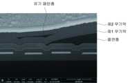
도 3은 종래 봉지층을 구비하는 유기발광 표시장치의 단면 구조를 나타내는 SEM (Scanning Electron Microscopy) 사진이다.
도 4는 본 발명의 일 실시예에 따라 유기 패턴층을 구비하는 유기발광 표시장치의 단면 구조를 나타내는 SEM (Scanning Electron Microscopy) 사진이다.
도 5 내지 도 8은 도 1의 유기발광 표시장치의 제조방법을 개략적으로 도시한 단면도들이다.1 is a cross-sectional view of an organic light emitting display device according to an exemplary embodiment of the present invention.
2 is a cross-sectional view of an organic light emitting display device according to another exemplary embodiment of the present invention.
3 is a SEM (Scanning Electron Microscopy) photograph showing a cross-sectional structure of an organic light emitting display device having a conventional encapsulation layer.
4 is a SEM (Scanning Electron Microscopy) photograph showing a cross-sectional structure of an organic light emitting display device having an organic pattern layer according to an exemplary embodiment of the present invention.
5 to 8 are cross-sectional views schematically illustrating a manufacturing method of the organic light emitting display device of FIG. 1 .
본 발명의 이점 및 특징, 그리고 그것들을 달성하는 방법은 첨부되는 도면과 함께 상세하게 후술되어 있는 실시예들을 참조하면 명확해질 것이다. 그러나 본 발명은 이하에서 개시되는 실시예들에 한정되는 것이 아니라 서로 다른 다양한 형태로 구현될 것이며, 단지 본 실시예들은 본 발명의 개시가 완전하도록 하며, 본 발명이 속하는 기술분야에서 통상의 지식을 가진 자에게 발명의 범주를 완전하게 알려주기 위해 제공되는 것이며, 본 발명은 청구항의 범주에 의해 정의될 뿐이다. 따라서, 몇몇 실시예에서, 잘 알려진 공정 단계들, 잘 알려진 소자 구조 및 잘 알려진 기술들은 본 발명이 모호하게 해석되는 것을 피하기 위하여 구체적으로 설명되지 않는다. 명세서 전체에 걸쳐 동일 참조 부호는 동일 구성 요소를 지칭한다.Advantages and features of the present invention, and methods of achieving them, will become clear with reference to the detailed description of the following embodiments taken in conjunction with the accompanying drawings. However, the present invention is not limited to the embodiments disclosed below, but will be implemented in various different forms, only these embodiments make the disclosure of the present invention complete, and common knowledge in the art to which the present invention belongs. It is provided to fully inform the holder of the scope of the invention, and the present invention is only defined by the scope of the claims. Thus, in some embodiments, well-known process steps, well-known device structures, and well-known techniques have not been described in detail in order to avoid obscuring the interpretation of the present invention. Like reference numbers designate like elements throughout the specification.
다른 정의가 없다면, 본 명세서에서 사용되는 모든 용어(기술 및 과학적 용어를 포함)는 본 발명이 속하는 기술분야에서 통상의 지식을 가진 자에게 공통적으로 이해될 수 있는 의미로 사용될 수 있을 것이다. 또 일반적으로 사용되는 사전에 정의되어 있는 용어들은 명백하게 특별히 정의되어 있지 않은 한 이상적으로 또는 과도하게 해석되지 않는다.Unless otherwise defined, all terms (including technical and scientific terms) used in this specification may be used in a meaning commonly understood by those of ordinary skill in the art to which the present invention belongs. In addition, terms defined in commonly used dictionaries are not interpreted ideally or excessively unless explicitly specifically defined.
또한, 도면에서 나타난 각 구성의 크기 및 두께는 설명의 편의를 위해 임의로 나타내었으므로, 본 발명이 반드시 도시된 바에 한정되지 않는다. 도면에서 여러 층 및 영역을 명확하게 표현하기 위하여 두께를 확대하여 나타내었다. 그리고 도면에서, 설명의 편의를 위해, 일부 층 및 영역의 두께를 과장되게 나타내었다.In addition, since the size and thickness of each component shown in the drawings are arbitrarily shown for convenience of explanation, the present invention is not necessarily limited to the shown bar. In the drawings, the thickness is shown enlarged to clearly express the various layers and regions. And in the drawings, for convenience of explanation, the thicknesses of some layers and regions are exaggerated.
또한, 명세서 전체에서, 어떤 부분이 어떤 구성요소를 "포함" 한다고 할 때, 이는 특별히 반대되는 기재가 없는 한, 다른 구성요소를 제외하는 것이 아니라 다른 구성요소를 더 포함할 수 있는 것을 의미한다. 또한, 명세서 전체에서, "위에" 또는 "상에"라 함은 대상 부분의 위 또는 아래에 위치하는 경우 뿐만 아니라 그 중간에 또 다른 부분이 있는 경우도 포함함을 의미하는 것이며, 반드시 중력 방향을 기준으로 위쪽에 위치하는 것을 의미하는 것은 아니다.Also, throughout the specification, when a certain part "includes" a certain component, it means that it may further include other components, not excluding other components, unless otherwise stated. In addition, throughout the specification, "above" or "on" means not only the case of being located above or below the target part, but also the case of another part in the middle thereof, and must necessarily specify the direction of gravity It does not mean that it is located above the standard.
또한, 명세서 전체에서, "평면상"이라 할 때, 이는 대상 부분을 위에서 보았을 때를 의미하며, "단면상"이라 할 때, 이는 대상 부분을 수직으로 자른 단면을 옆에서 보았을 때를 의미한다.In addition, throughout the specification, when it is referred to as "planar image", it means when the target part is viewed from above, and when it is referred to as "cross-sectional image", it means when a cross section of the target part cut vertically is viewed from the side.
이하, 도 1을 참조하여 본 발명의 일 실시예를 설명한다.Hereinafter, an embodiment of the present invention will be described with reference to FIG. 1 .
도 1은 본 발명의 일 실시예에 따른 유기 발광 표시 장치(10)의 구조를 개략적으로 나타낸 단면도이다.1 is a cross-sectional view schematically illustrating a structure of an organic light
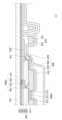
도 1을 참조하면, 본 발명의 일 실시예에 따른 유기 발광 표시 장치(10)는 기판(101), 기판(101)의 표시영역(DA) 상에 위치하는 표시부(100)와, 상기 표시영역(DA) 및 상기 비표시영역(NDA)에 걸쳐서 상기 표시부(100)를 밀봉하는 봉지층(300)을 포함한다.Referring to FIG. 1 , an organic light
기판(101)은 다양한 소재를 포함할 수 있다. 일례로, 기판(101)은 SiO2를 주성분으로 하는 투명한 유리 재질로 이루어질 수 있다. 그러나, 기판(101)은 반드시 이에 한정되는 것은 아니며, 투명한 플라스틱 재질로 형성되어 가요성을 가질 수 있다. 플라스틱 재질은 절연성 유기물인 폴리에테르술폰(PES, polyethersulphone), 폴리아크릴레이트(PAR, polyacrylate), 폴리에테르 이미드(PEI, polyetherimide), 폴리에틸렌 나프탈레이트(PEN, polyethyelenen napthalate), 폴리에틸렌 테레프탈레이드(PET, polyethyeleneterepthalate), 폴리페닐렌 설파이드(polyphenylene sulfide: PPS), 폴리아릴레이트(polyallylate), 폴리이미드(polyimide), 폴리카보네이트(PC), 셀룰로오스 트리 아세테이트(TAC), 및 셀룰로오스 아세테이트 프로피오네이트(cellulose acetate propionate: CAP)로 이루어진 그룹으로부터 선택되는 유기물일 수 있다.The
화상이 기판(101) 방향으로 구현되는 배면 발광형인 경우, 기판(101)은 투명한 재질로 형성해야 한다. 그러나 화상이 기판(101)의 반대 방향으로 구현되는 전면 발광형인 경우에 기판(101)은 반드시 투명한 재질로 형성할 필요는 없으며, 금속 재질로 이루어질 수 있다. 일 실시예로서, 기판(101)은 당 분야의 공지된 금속으로 구성될 수 있으며, 일례를 들면 철, 크롬, 망간, 니켈, 티타늄, 몰리브덴, 스테인레스 스틸(SUS), Invar 합금, Inconel 합금 및 Kovar 합금으로 이루어진 군으로부터 선택된 하나 이상을 포함할 수 있다.In the case of a bottom emission type in which an image is implemented in the direction of the
기판(101)은 표시부(100)에 의해 발광되어 사용자가 인식할 수 있는 화상을 구현하는 표시영역(DA)과, 나머지 부분인 비표시영역(NDA)을 포함할 수 있다. 표시 영역(DA)에는 유기발광소자(100b)가 배치되고, 비표시영역(NDA)에는 유기발광소자(100b)로 전원을 공급하는 전원 배선(220)이 배치될 수 있다. 또한, 비표시영역에는 전원 공급장치(미도시) 또는 신호 생성장치(미도시)로부터 전기적 신호를 표시영역(DA)으로 전달하는 패드부(미도시)가 배치될 수 있다.The
상기 표시부(100)를 보다 자세히 설명하면, 기판(101) 상에는 버퍼층(102)이 배치될 수 있다. 버퍼층(102)은 기판(101)의 상부에 평탄면을 제공할 수 있고, 기판(101)을 통하여 침투하는 이물 또는 습기를 차단할 수 있다. 일례로, 버퍼층(102)은 실리콘 옥사이드, 실리콘 나이트라이드, 실리콘 옥시나이트라이드, 알루미늄옥사이드, 알루미늄나이트라이드, 티타늄옥사이드 또는 티타늄나이트라이드 등의 무기물이나, 폴리이미드, 폴리에스테르, 아크릴 등의 유기물을 함유할 수 있고, 예시한 재료들 중 복수의 적층체로 이루어질 수 있다. 상기 버퍼층(102)은 표시영역(DA) 상에 형성되고, 비표시영역(NDA)까지 배치되도록 연장되어 형성된다.Describing the
표시영역(DA)에는 박막 트랜지스터(100a) 및 박막 트랜지스터(100a)와 전기적으로 연결된 유기발광소자(100b)가 위치할 수 있다.A
박막 트랜지스터(100a)는 활성층(103), 게이트 전극(105), 소스 전극(107) 및 드레인 전극(108)을 포함할 수 있다. 이하에서는 박막 트랜지스터(100a)가 활성층(103), 게이트 전극(105), 소스 전극(107) 및 드레인 전극(108)이 순차적으로 배치된 탑 게이트 타입(top gate type)인 경우를 설명한다. 그러나 본 실시예는 이에 한정되지 않고 바텀 게이트 타입(bottom gate type) 등 다양한 타입의 박막 트랜지스터(100a)가 채용될 수 있다.The
활성층(103)(active layer)은 버퍼층(102) 상에 배치된다. 활성층(103)은 당 분야에 공지된 반도체 물질, 예컨대 비정질 실리콘(amorphous silicon) 또는 다결정 실리콘(poly crystalline silicon)을 포함할 수 있다. 일 실시예로서, 상기 활성층(103)은 유기 반도체 물질 등을 함유할 수 있다. 또 다른 실시예로서, 상기 활성층(103)은 산화물 반도체 물질을 함유할 수 있다. 구체적인 일례를 들면, 활성층(103)은 아연(Zn), 인듐(In), 갈륨(Ga), 주석(Sn) 카드뮴(Cd), 게르마늄(Ge) 등과 같은 12, 13, 14족 금속 원소 및 이들의 조합에서 선택된 물질의 산화물을 포함할 수 있다.An
게이트 절연막(104: gate insulating layer)은 활성층(103) 상에 배치되고, 활성층(103)과 게이트 전극(105)을 절연하는 역할을 한다. 게이트 절연막(104)은 실리콘산화물 및 실리콘질화물 중 적어도 하나의 무기 물질로 이루어진 막이 단층 또는 다층으로 이루어질 수 있다. 게이트 절연막(104)은 표시영역(DA) 뿐만 아니라 비표시영역(NDA)의 일부까지 연장될 수 있다.A gate insulating layer (104) is disposed on the
게이트 전극(105)은 게이트 절연막(104)의 상부에 배치된다. 게이트 전극(105)은 박막 트랜지스터(100a)에 온/오프 신호를 인가하는 게이트 라인(미도시)과 연결될 수 있다. 게이트 전극(105)은 당 분야의 공지된 저저항 금속 물질로 이루어질 수 있다. 인접층과의 밀착성, 적층되는 층의 표면 평탄성, 및 가공성 등을 고려하여, 상기 게이트 전극(105)은 알루미늄(Al), 백금(Pt), 팔라듐(Pd), 은(Ag), 마그네슘(Mg), 금(Au), 니켈(Ni), 네오디뮴(Nd), 이리듐(Ir), 크롬(Cr), 리튬(Li), 칼슘(Ca), 몰리브덴(Mo), 티타늄(Ti), 텅스텐(W), 구리(Cu) 중 하나 이상의 물질로 단층 또는 다층으로 이루어질 수 있다.The
게이트 전극(105) 상에는 층간 절연막(106)이 배치된다. 층간 절연막(106)은 소스 전극(107) 및 드레인 전극(108)과 게이트 전극(105)을 절연한다. 층간 절연막(106)은 표시영역(DA) 뿐만 아니라 비표시영역(NDA)의 일부까지 연장되어 배치될 수 있다. 층간 절연막(106)은 무기 물질로 이루어진 막이 단층 또는 다층으로 이루어질 수 있다. 일례로, 무기 물질은 금속 산화물 또는 금속 질화물일 수 있으며, 구체적인 예를 들면 실리콘 산화물(SiO2), 실리콘 질화물(SiNx), 실리콘산 질화물(SiON), 알루미늄 산화물(Al2O3), 티타늄 산화물(TiO2), 탄탈 산화물(Ta2O5), 하프늄 산화물(HfO2), 또는 지르코늄 산화물(ZrO2) 등을 포함할 수 있다.An interlayer insulating
소스 전극(107) 및 드레인 전극(108)은 층간 절연막(106) 상에 배치된다. 소스 전극(107) 및 드레인 전극(108)은 각각 당 분야에 공지된 금속으로 단층 또는 다층으로 이루어질 수 있다. 상기 금속의 구체적인 예를 들면, 알루미늄(Al), 백금(Pt), 팔라듐(Pd), 은(Ag), 마그네슘(Mg), 금(Au), 니켈(Ni), 네오디뮴(Nd), 이리듐(Ir), 크롬(Cr), 리튬(Li), 칼슘(Ca), 몰리브덴(Mo), 티타늄(Ti), 텅스텐(W), 구리(Cu) 중 하나 이상일 수 있다. 소스 전극(107) 및 드레인 전극(108)은 활성층(103)의 영역과 접촉하도록 배치된다. 구체적으로, 층간 절연막(106) 및 게이트 절연막(104)은 활성층(103)의 소스 영역 및 드레인 영역을 노출하도록 형성되고, 이러한 활성층(103)의 노출된 소스 영역 및 드레인 영역과 접하도록 소스 전극(107) 및 드레인 전극(108)이 형성된다.A
이와 같은 박막 트랜지스터(100a)는 유기발광소자(100b)에 전기적으로 연결되어 유기발광소자(100b)를 구동하며, 절연층(109)으로 덮여 보호된다.The
절연층(109)은 박막 트랜지스터(100a)로부터 비롯된 단차를 해소하고 상면을 평탄하게 하여, 하부 요철에 의해 유기 발광 소자(100b)에 불량이 발생하는 것을 방지한다. 절연층(109)은 당 분야의 공지된 무기 절연막, 유기 절연막, 또는 이들 모두를 사용하여 단층 또는 다층으로 이루어질 수 있다. 상기 무기 절연막을 구성하는 물질의 일례를 들면, SiO2, SiNx, SiON, Al2O3, TiO2, Ta2O5, HfO2, ZrO2, BST, PZT 또는 이들의 혼합물 등을 포함할 수 있다. 유기 절연막은 당 업계의 공지된 범용 고분자를 사용할 수 있으며, 구체적으로 Polymethylmethacrylate (PMMA)나, Polystylene (PS), 페놀계 그룹을 갖는 고분자 유도체, 아크릴계 고분자, 이미드계 고분자, 아릴에테르계 고분자, 아마이드계 고분자, 불소계 고분자, p-자일렌계 고분자, 비닐알콜계 고분자 및 이들의 블렌드 등을 포함할 수 있다. 또한, 절연층(109)은 무기 절연막과 유기 절연막의 복합 적층체로 구성될 수도 있다.The insulating
절연층(109) 상에는 유기발광소자(100b)가 배치된다. 유기발광소자(100b)는 박막 트랜지스터(100a)와 전기적으로 연결되며, 제1 전극(110), 제1 전극(110)과 대향하는 제2 전극(113), 및 제1 전극(110)과 제2 전극(113) 사이에 개재되는 중간층(112)을 포함한다.An organic
제1 전극(110)은 절연층(109) 상에 배치되고, 절연층(109)에 마련된 컨택홀을 통하여 박막 트랜지스터(100a), 구체적으로 드레인 전극(108)과 전기적으로 연결될 수 있다. 제1 전극(110)은 다양한 형태를 가질 수 있는데, 예를 들면 아일랜드 형태로 패터닝될 수 있다. 상기 제1 전극(110)은 반사 전극일 수 있다. 일례로, 제1 전극(110)은 Ag, Mg, Al, Pt, Pd, Au, Ni, Nd, Ir, Cr 및 이들의 화합물 등으로 이루어진 반사막과, 그 반사막 상에 배치된 투명 또는 반투명 전극층을 구비할 수 있다. 투명 또는 반투명 전극층은 인듐틴옥사이드(ITO; indium tin oxide), 인듐징크옥사이드(IZO; indium zinc oxide), 징크옥사이드(ZnO; zinc oxide), 인듐옥사이드(In2O3; indium oxide), 인듐갈륨옥사이드(IGO; indium gallium oxide) 및 알루미늄징크옥사이드(AZO; aluminum zinc oxide)로 이루어진 군에서 선택되는 적어도 하나 이상을 구비할 수 있다.The
제1 전극(110)과 대향하도록 배치된 제2 전극(113)은, 투명 또는 반투명 전극일 수 있다. 일례로, 제2 전극(113)은 Li, Ca, LiF/Ca, LiF/Al, Al, Ag, Mg 및 이들의 화합물을 포함하는 일함수가 작은 금속 박막으로 이루어질 수 있다. 또한, 금속 박막 위에 ITO, IZO, ZnO 또는 In2O3 등의 투명 전극 형성용 물질로 보조 전극층이나 버스 전극을 더 구비할 수 있다. 따라서, 제2 전극(113)은 중간층(112)에 포함된 유기 발광층에서 방출된 광을 투과시킬 수 있다. 즉, 유기 발광층에서 방출되는 광은 직접 또는 반사 전극으로 구성된 제1 전극(110)에 의해 반사되어, 제2 전극(113) 측으로 방출될 수 있다.The
여기서, 본 실시예의 표시부(100)는 전면 발광형으로 제한되지 않으며, 유기 발광층에서 방출된 광이 기판(101)측으로 방출되는 배면 발광형일 수도 있다. 이 경우, 제1 전극(110)은 투명 또는 반투명 전극으로 구성되고, 제2 전극(113)은 반사 전극으로 구성될 수 있다. 또한, 본 실시예의 표시부(100)는 전면 및 배면 양 방향으로 광을 방출하는 양면 발광형일 수도 있다.Here, the
한편, 제1 전극(110) 상에는 절연물로 화소 정의막(119)이 배치된다. 화소 정의막(119)은 제1 전극(110)의 소정의 영역을 노출하며, 노출된 영역에 유기 발광층을 포함하는 중간층(112)이 위치한다. 즉, 화소 정의막(119)은 유기발광소자의 화소 영역을 정의한다. 화소 정의막(119)은 폴리이미드, 폴리아마이드, 아크릴 수지, 벤조사이클로부텐 및 페놀 수지로 이루어진 군에서 선택되는 하나 이상의 유기 절연물질을 포함할 수 있다.Meanwhile, a
중간층(112)에 포함된 유기 발광층은 저분자 유기물 또는 고분자 유기물일 수 있다. 상기 유기 발광층 이외에, 중간층(112)은 정공수송층(HTL; hole transport layer), 정공주입층(HIL; hole injection layer), 전자수송층(ETL; electron transport layer) 및 전자 주입층(EIL; electron injection layer) 등과 같이 당 분야의 공지된 기능층을 선택적으로 더 포함할 수 있다.The organic emission layer included in the
도 1에서는 하나의 유기 발광 소자(OLED)만을 도시하였으나, 표시부(100)는 복수의 유기 발광소자(100b)를 포함할 수 있다. 각 유기발광소자(100b)마다 하나의 화소를 형성할 수 있으며, 각 화소별로 적색, 녹색, 청색 또는 백색의 색을 구현할 수 있다. 또한 상기 방출되는 광을 소정의 컬러로 변환하는 색변환층이나, 컬러 필터를 더 구비할 수 있다.Although only one organic light emitting diode (OLED) is shown in FIG. 1 , the
봉지층(300)은 표시부(100)를 밀봉하여, 표시부(100)가 열화되는 것을 방지한다. 이러한 봉지층(300)은 다수의 박막층이 적층된 구조로서, 무기막과 유기막이 교대로 적층된 구조일 수 있다.The
본 실시예에서, 봉지층(300)은 상기 유기발광소자(100b)에서 상기 비표시영역(NDA)으로 연장된 제1무기막(310); 상기 제1무기막(310) 상의 유기막(320); 상기 유기막(320)에서 상기 비표시영역(NDA)으로 연장된 제2무기막(330); 및 상기 비표시영역(NDA)에서 상기 유기막(320)과 이격되어 상기 제1무기막(310)과 상기 제2무기막(330) 사이에 배치된 유기 패턴층(340)을 포함한다.In this embodiment, the
제1무기막(310)은 유기발광소자(100b)를 밀봉하고 비표시영역(NDA)의 일부까지 덮도록 연장하여 배치됨으로써, 산소나 수분의 침투를 견고히 막아주는 역할을 할 수 있다. 제1무기막(310)은 당 분야의 공지된 금속 산화물 또는 금속 질화물을 포함하는 단일막 또는 적층막일 수 있다. 구체적으로, 상기 제1무기막(310)은 실리콘 산화물, 실리콘 질화물, 실리콘 산화 질화물, 알루미늄 산화물, 알루미늄 질화물, 알루미늄 산화 질화물, 티타늄 산화물, 티타늄 질화물, 탄탄륨 산화물, 탄탈륨 질화물, 하프늄 산화물, 하프늄 질화물, 지르코늄 산화물, 지르코늄 질화물, 세륨 산화물, 세륨 질화물, 주석 산화물, 주석 질화물, 및 마그네슘 산화물로 구성된 군에서 선택된 1종 이상의 무기물을 포함할 수 있다.The first
유기막(320)은 제1무기막(310)의 일부를 덮으며, 상기 제1무기막(310)의 내부 응력을 완화하거나 제1무기막(310)의 미세크랙과 핀홀을 채워 외부의 수분이나 산소의 투과 방지 효과를 증진시킬 수 있다. 상기 유기막(320)은 당 분야의 공지된 고분자를 포함하는 단일막 또는 적층막일 수 있다. 일례로, 상기 유기막(320)은 아크릴계 수지, 메타크릴계 수지, 이소프렌계 수지, 비닐계 수지, 에폭시계 수지, 우레탄계 수지, 셀룰로오스계 수지, 페닐렌계 수지, 및 이미드계 수지로 구성된 군에서 선택된 1종 이상의 유기물을 포함할 수 있다. 유기막(320)은 제1무기막(310)의 일부를 덮도록 배치되므로, 상기 유기막(320)의 면적은 제1무기막(310) 및 후술되는 제2무기막(330)의 면적보다 작을 수 있다.The
제2무기막(330)은 유기막(320)에서 상기 비표시영역(NDA)의 일부까지 연장하여 덮음으로써 산소나 수분의 침투를 견고히 막아주는 역할을 할 수 있다. 제2무기막(330)은 제1무기막(310)과 평면상에서 실질적으로 동일한 면적을 가질 수 있다. 이러한 제2무기막(330)은 당 분야의 공지된 금속 산화물 또는 금속 질화물을 포함하는 단일막 또는 적층막일수 있으며, 전술한 제1무기막(310)의 성분과 동일하거나 또는 상이할 수 있다.The second
한편 제1무기막(310)과 제2무기막(330)은 실질적으로 동일한 면적을 가지며, 이들 사이에 개재(介在)된 유기막(320)은 상기 제1무기막(310)과 제2무기막(330)보다 면적이 작으므로, 비표시영역(NDA)에서 제1무기막(310)의 적어도 일부와 제2무기막(330)의 적어도 일부가 서로 접촉하는 영역이 존재하게 된다. 이와 같이 무기막들(310, 330)끼리 서로 접촉하는 비표시영역(NDA)에서는 그 계면에서 벗겨짐이 생기기 쉬우며, 응력이 집중하여 상대적으로 크랙(crack)이 발생될 가능성이 높다. 특히 외력에 의한 충격이 가해질 경우, 무기막들(310, 330)끼리 접촉하는 비표시영역(NDA)의 일 영역이 약점(weak point)으로 작용하게 되어, 하기 도 3에서와 같이 크랙이 쉽게 발생하게 되므로, 제품 불량이 필연적으로 초래된다.Meanwhile, the first
이에, 본 발명에서는 비표시영역(NDA)에서 서로 접촉하는 제1무기막(310)과 제2무기막(330)의 사이에, 유기막(320)과 이격된 유기 패턴층(340)을 별도로 구비한다. 이러한 유기 패턴층(340)은 무기막들(310, 330) 간의 스트레스를 흡수하고 유연성을 부여하는 역할을 함으로써, 외력에 의한 충격을 완화하고 크랙 발생을 억제하여 강건한 봉지 구조를 구현할 수 있다.Therefore, in the present invention, the
이때 봉지층(300)의 구조와 유기발광 표시장치(10)의 공정 효율 등을 고려하여, 타 영역 대비 크랙이 발생되기 쉬운 특정 위치에 유기 패턴층(340)을 배치하는 것이 요구된다. 일 구현예에 따르면, 상기 유기 패턴층(340)은 비표시영역(NDA)에서 유기막(320)과 이격되어 서로 접촉하는 제1무기막(310)과 제2무기막(330) 사이에 배치될 수 있다. 바람직한 일 구현예에 따르면, 상기 유기 패턴층(340)은 하기 도 4에서와 같이 제1무기막(310)과 제2무기막(330)이 직접 접촉하는 비표시영역(NDA)의 적어도 일부와, 절연층(109)의 경사진 측부(예컨대, 에지)의 적어도 일부가 평면 상에서 서로 중첩되는 영역에 배치될 수 있다. 이러한 유기 패턴층(340)의 적어도 일부는 표시부(100)의 절연층(109)과 평면 상에서 중첩될 수 있다. 전술한 위치에 배치된 유기 패턴층(340)은, 서로 접촉하는 무기막(310, 330)들간의 스트레스를 흡수하여 유연성을 부여하고 크랙 발생을 억제할 수 있다.At this time, considering the structure of the
상기 유기 패턴층(340)은, 유기막(320)의 제조공정 중에 제거되는 유기막(320)의 일부를 잔류시킴으로써 구성될 수 있다. 이에 따라, 유기패턴층(340)은 유기막(320)과 이격된 상태로 존재하되, 상기 유기막(320)과 동일한 물질로 이루어질 수 있다. 일례로, 유기 패턴층(340)은 아크릴계 수지, 메타크릴계 수지, 이소프렌계 수지, 비닐계 수지, 에폭시계 수지, 우레탄계 수지, 셀룰로오스계 수지, 페닐렌계 수지, 및 이미드계 수지로 구성된 군에서 선택된 1종 이상의 유기물을 포함할 수 있다. 또한 봉지층의 구조 및 충격완화 효과 등을 고려하여, 유기 패턴층(340)은 폭이 10 ㎛ 이상이며, 두께가 0.1 ㎛ 이상일 수 있다. 구체적으로, 모노머 제팅 라인과 중첩되는 것을 방지하기 위해서, 유기 패턴층(340)의 폭은 10 내지 100 ㎛일 수 있다. 또한 제2 무기막(330)의 프로파일에 영향을 주지 않기 위해서, 유기 패턴층(340)의 두께는 0.1 내지 0.6 ㎛ 일 수 있다.The
도 1에서는 봉지층으로서 제1무기막(310), 유기막(320), 제2 무기막(330)이 순차적으로 적층되고, 비표시영역(NDA)에서 서로 접촉하는 제1무기막(310)과 제2무기막(330) 사이에 유기 패턴층(340)이 배치되는 실시예를 구체적으로 예시하고 있다. 그러나 이에 한정되지 않으며, 비표시영역(NDA)에서 접촉하는 무기막들 사이에 유기 패턴층(340)이 존재하기만 한다면, 무기막과 유기막이 적층되는 구조 및 봉지층의 개수는 특별히 제한되지 않는다. 즉, 봉지층(300)은 교대로 배치된 복수 개의 무기막(미도시) 및 유기막(미도시)을 더 포함할 수 있으며, 이러한 무기막 및 유기막의 적층 횟수 또한 특별히 제한되지 않는다.In FIG. 1 , a first
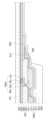
도 2는 본 발명의 다른 실시예에 따른 유기발광 표시장치(11)의 단면을 간략히 도시한 단면도이다. 도 2에서 도 1과 동일한 참조 부호는 동일한 부재를 나타낸다.2 is a schematic cross-sectional view of an organic light emitting
이하 도 2에 대한 설명에서는 도 1과 중복되는 내용은 다시 설명하지 않으며, 차이점에 대해서만 설명한다.In the following description of FIG. 2 , contents overlapping with those of FIG. 1 will not be described again, and only differences will be described.
도 2를 참조하면, 본 실시예에 따른 유기발광 표시장치(11)는, 도 1과 비교하여 기판(101)의 비표시영역(NDA)에 배치된 댐부(120)를 더 포함할 수 있다.Referring to FIG. 2 , the organic light emitting
표시영역(DA)의 외곽에 배치되는 댐부(120)는, 봉지층(300)의 유기막(320) 형성시, 유기막(320)을 형성하기 위한 유기물이 기판(101)의 가장자리 방향으로 흐르는 것을 차단함으로써 유기막(320)의 에지 테일이 형성되는 것을 방지할 수 있다. 댐부(120)는 소정의 높이를 가져 표시 영역(DA)을 에워싸도록 배치될 수 있다.The
댐부(120)는 절연층(109) 및 화소 정의막(119) 중 적어도 어느 하나와 동일한 물질로 이루어질 수 있다. 상기 댐부(120)는 복수의 층으로 이루어질 수 있다. 일례로, 댐부(120)는 절연층(109)과 동일한 물질로 이루어진 제1층(121)과, 제1층(122) 상에 화소 정의막(119)과 동일한 물질로 이루어진 제2층(122)을 포함할 수 있다. 다만, 본 발명은 이에 제한되지 않으며, 댐부(120)는 한 층으로 구성될 수 있다.The
또한, 댐부(120)는 두 개 이상의 복수 개로 구성될 수 있다. 일례로 서로 다른 높이를 갖는 복수의 댐부(120)로 이루어질 수 있다. 댐부(120)가 복수 개로 구성되는 경우, 기판(101)의 외곽으로 갈수록 댐부(120)의 높이가 증가할 수 있다.In addition, the
도 2에 따른 유기발광 표시장치(11)에서, 제1무기막(310)과 제2무기막(330)은 댐부(120)를 덮도록 기판(101)의 외측까지 연장될 수 있다. 이에 따라, 외부의 수분 및 산소의 침투를 지연하거나 또는 차단시킬 수 있다. 또한 댐부(120)는 유기막(320) 형성시 유기물이 기판의 가장자리 방향으로 흐르는 것을 차단하므로, 유기막(320)은 표시영역(DA)과 비표시영역(NDA)에서 댐부(120)의 내측에 위치하게 된다. 또한 유기 패턴층(340)은 상기 댐부(120)와 상기 절연층(109)의 경사진 측부(에지) 사이에 위치할 수 있다.In the organic light emitting
댐부(120)는 전원 배선(220)의 적어도 일부와 중첩하여 접하도록 배치될 수 있다. 일례로, 댐부(120)는 전원 배선(220)의 적어도 외측 가장자리와 중첩하여 접하도록 배치될 수 있다. 절연층(109) 및 화소 정의막(119) 중 적어도 어느 하나와 동일한 재질로 이루어지는 댐부(120)는 금속과의 접합력이 우수할 수 있다. 따라서, 댐부(120)가 금속 재질로 이루어지는 전원 배선(220)과 접하도록 배치되면, 댐부(120)가 우수한 접합력을 가지고 안정적으로 구성될 수 있다.The
한편, 도 2에서는 댐부(120)가 전원 배선(220)의 외측 가장자리와 중첩하여 배치된 예를 도시하고 있으나, 본 발명은 이에 한정되는 것은 아니며, 댐부(120)는 전원 배선(220) 상에만 배치될 수도 있고, 전원 배선(220)을 덮도록 배치될 수도 있다.Meanwhile, FIG. 2 shows an example in which the
도 5 내지 도 8은 도 1의 유기 발광 표시 장치의 제조방법을 개략적으로 도시한 단면도들이다.5 to 8 are cross-sectional views schematically illustrating a manufacturing method of the organic light emitting diode display of FIG. 1 .
도 5를 참조하면, 기판(101) 상에 표시부(100)를 형성하고, 상기 표시부(100)에서 비표시영역(NDA)의 일부를 덮도록 연장하여 제1 무기막(310)을 형성한다.Referring to FIG. 5 , a
표시부(100)는 도 1에서 예시된 구성을 가질 수 있을 뿐 아니라, 공지된 다양한 유기발광 디스플레이가 적용될 수 있으므로, 이의 구체적인 제조 방법은 생략한다.Since the
제1 무기막(310)은 당 업계에 공지된 금속 산화물, 금속 질화물 등의 무기물질로 형성될 수 있다. 이와 같은 제1무기막(310)은 스퍼터링, 원자층 증착법, 화학기상증착법 등의 방법을 통해 증착될 수 있다.The first
제1 무기막(310)을 형성한 이후에, 도 6과 같이 유기막(320)을 형성한다.After forming the first
유기막(320)은 당 분야에 공지된 유기물, 예컨대 모노머 및/또는 고분자를 제한 없이 사용할 수 있다. 이러한 유기막은 당 분야에 공지된 다양한 공정방법에 의해 형성될 수 있으며, 일례로 잉크젯 방식, 슬릿 코팅 방식, 스크린 프린팅 방식, 증발법(Evaporation) 또는 화학기상증착법 중 어느 하나의 방법에 의해 형성될 수 있다.An organic material known in the art, such as a monomer and/or a polymer, may be used as the
유기막(320)을 형성한 후에는, 도 7과 같이 유기막(320)의 일부를 제거한다. 보다 상세하게는, 유기막(320)의 테일을 제거하되, 상기 비표시영역(NDA)에서 유기막(320)의 일부를 잔류시켜 상기 유기막(320)과 이격된 유기 패턴층(340)을 형성한다.After forming the
유기 패턴층(340)은 세정 마스크를 이용한 에싱(ashing) 공정에 의해 형성될 수 있다. 에싱(ashing) 공정은 건식 에칭(Dry etch) 개념으로, O2, N2O 또는 NH3 등의 가스(gas)를 플라즈마 상태에서 가속시켜 하부에 남아있는 탄소(Carbon base)계 유기물들을 제거 및 세정하는 공정이다. 바람직하게는 산소 에싱(O2 ashing) 공정에 의해 형성될 수 있다. 구체적인 일례를 들면, 챔버 내에서 유기막(320) 상에 세정 마스크(미도시)를 배치한 후, 상기 세정 마스크를 이용하여 에싱(ashing) 공정을 실시한다. 특히 본 발명에서는 에싱 공정에 적용되는 세정 마스크의 디자인을 일부 변형함으로써, 제거되는 유기막의 패턴을 자유롭게 제어할 수 있으며, 이로 인해 비표시영역(NDA) 중 절연층(109)의 일 측부(에지)에 위치하는 유기 패턴층(340)만 잔류시키고, 그 외 유기막(320)의 테일은 제거된다.The
상기 세정 마스크는 디자인이 일부 변형된 것을 제외하고는, 에싱 공정분야에 적용되는 마스크를 제한 없이 사용할 수 있다. 또한 에싱 공정의 조건은 특별히 제한되지 않으며, 일례로 챔버의 내부 압력, 산소 유량, 인가 전력 등의 조건을 당 분야에 공지된 범위 내에서 적절히 조절할 수 있다.As the cleaning mask, any mask applied to the ashing process field may be used without limitation, except that the design is partially modified. In addition, the conditions of the ashing process are not particularly limited, and conditions such as the internal pressure of the chamber, the oxygen flow rate, and applied power may be appropriately adjusted within a range known in the art.
다음으로, 도 8과 같이 유기막(320)을 덮고 비표시영역(NDA)의 일부까지 덮을 수 있도록 연장하여 제2 무기막(330)을 형성한다.Next, as shown in FIG. 8 , a second
제2 무기막(330)은 스퍼터링, 원자층 증착법, 화학기상증착법 등에 의해 형성할 수 있다. 제2 무기막(330)은 당 업계에 공지된 금속 산화물, 금속 질화물 등의 무기물질로 형성될 수 있다. 일례로 전술한 제1무기막(310)과 동일하거나 또는 상이할 수 있다.The second
한편 도면에 도시하지는 않았으나, 기판(101)의 비표시영역(NDA)에 배치된 댐부(120)를 형성하는 단계를 추가로 포함할 수 있다. 댐부(120)는 도 2에 예시된 구성을 가질 수 있으므로, 이의 구체적인 제조 방법은 생략한다. 일례를 들면, 댐부(120)은 절연층(109) 및 화소 정의막(119) 중 적어도 하나와 동일한 물질로 동일한 공정에 의해 형성할 수 있으므로, 하프톤 마스크를 사용하여 노광 공정을 통해 노광량을 조절하여 절연층(109)과 화소 정의막(119) 중 적어도 하나와 댐부(41)를 동시에 형성할 수 있다. 그러나 이에 한정되지 않는다.Meanwhile, although not shown in the drawings, a step of forming the
전술한 본 발명의 유기 발광 표시 장치는, 비표시영역(NDA)에서 직접 접촉하는 무기막들 사이에, 스트레스를 흡수하고 유연성을 부여하는 유기 패턴층을 별도로 구비함에 따라 크랙 발생 억제 및 봉지층의 강건 구조를 구현할 수 있다. 이러한 유기 발광 표시장치는, 평판 표시 장치(FPD: Flat Panel Display Device) 뿐 아니라, 곡면형 표시 장치(Curved Display Device), 폴더블 표시 장치(Foldable Display Device) 및 플렉서블 표시 장치(Flexible Display Device) 등의 당 분야의 표시 장치에 모두 적용될 수 있다.The above-described organic light emitting display device of the present invention includes an organic pattern layer that absorbs stress and imparts flexibility between inorganic layers that directly contact in the non-display area (NDA), thereby suppressing crack generation and sealing the encapsulation layer. A robust structure can be implemented. Such an organic light emitting display device includes not only a flat panel display device (FPD), but also a curved display device, a foldable display device, a flexible display device, and the like. may be applied to all display devices in the art.
이상, 첨부된 도면을 참조하여 본 발명의 실시예를 설명하였지만, 본 발명이 속하는 기술분야에서 통상의 지식을 가진 자는 본 발명이 그 기술적 사상이나 필수적인 특징으로 변경하지 않고서 다른 구체적인 형태로 실시될 수 있다는 것을 이해할 수 있을 것이다. 그러므로 이상에서 기술한 실시예는 모든 면에서 예시적인 것이며 한정적이 아닌 것으로 이해해야만 한다.Although the embodiments of the present invention have been described with reference to the accompanying drawings, those skilled in the art can implement the present invention in other specific forms without changing its technical spirit or essential features. You will understand that there is Therefore, it should be understood that the embodiments described above are illustrative in all respects and not restrictive.
10, 11: 유기 발광 표시 장치
100: 표시부
100a: 박막 트랜지스터
100b: 유기 발광 소자
101: 기판
109: 절연층
120: 댐부
300: 봉지층
310: 제1무기막
320: 유기막
330: 제2무기막
340: 유기 패턴층10, 11: organic light emitting display device
100: display unit
100a: thin film transistor
100b: organic light emitting element
101: substrate
109: insulating layer
120: dam part
300: encapsulation layer
310: first inorganic film
320: organic film
330: second inorganic film
340: organic pattern layer
Claims (20)
Translated fromKorean상기 기판의 표시영역 상에 배치된 박막 트랜지스터;
상기 박막 트랜지스터 상에 배치된 절연층;
상기 절연층 상에 배치되며, 상기 박막 트랜지스터와 연결되는 유기발광소자; 및
상기 유기발광소자를 덮는 봉지층을 포함하고,
상기 봉지층은,
상기 유기발광소자에서 상기 비표시영역으로 연장된 제1무기막;
상기 제1무기막 상에 배치된 유기막;
상기 유기막에서 상기 비표시영역으로 연장된 제2무기막; 및
상기 비표시영역에서 상기 유기막과 이격되어 상기 제1무기막과 상기 제2무기막 사이에 배치된 유기 패턴층을 포함하고,
상기 제1무기막의 적어도 일부와 상기 제2무기막의 적어도 일부는 비표시영역에서 서로 접촉하며,
상기 유기 패턴층의 두께는 상기 유기막의 두께 보다 작은 것인, 유기 발광 표시 장치.a substrate including a display area and a non-display area;
a thin film transistor disposed on the display area of the substrate;
an insulating layer disposed on the thin film transistor;
an organic light emitting element disposed on the insulating layer and connected to the thin film transistor; and
An encapsulation layer covering the organic light emitting device,
The encapsulation layer,
a first inorganic layer extending from the organic light emitting device to the non-display area;
an organic layer disposed on the first inorganic layer;
a second inorganic layer extending from the organic layer to the non-display area; and
an organic pattern layer spaced apart from the organic layer in the non-display area and disposed between the first inorganic layer and the second inorganic layer;
At least a portion of the first inorganic layer and at least a portion of the second inorganic layer contact each other in a non-display area;
The organic light emitting display device, wherein the thickness of the organic pattern layer is smaller than the thickness of the organic layer.
상기 유기 패턴층의 적어도 일부는 상기 절연층과 평면적으로 중첩되는 유기 발광 표시 장치.According to claim 1,
At least a portion of the organic pattern layer overlaps the insulating layer in a planar manner.
상기 유기 패턴층은 상기 유기막과 동일한 물질로 이루어진 유기 발광 표시 장치.According to claim 1,
The organic light emitting display device of claim 1 , wherein the organic pattern layer is made of the same material as the organic layer.
상기 유기막은 아크릴계 수지, 메타크릴계 수지, 이소프렌계 수지, 비닐계 수지, 에폭시계 수지, 우레탄계 수지, 셀룰로오스계 수지, 페닐렌계 수지, 및 이미드계 수지로 구성된 군에서 선택된 1종 이상의 유기물을 포함하는 유기 발광 표시장치.According to claim 1,
The organic layer includes at least one organic material selected from the group consisting of acrylic resin, methacrylic resin, isoprene-based resin, vinyl-based resin, epoxy-based resin, urethane-based resin, cellulose-based resin, phenylene-based resin, and imide-based resin. organic light emitting display.
상기 유기 패턴층은 폭이 10 ㎛ 이상이며, 두께가 0.1 ㎛ 이상인, 유기 발광 표시 장치.According to claim 1,
The organic pattern layer has a width of 10 μm or more and a thickness of 0.1 μm or more.
상기 제1무기막과 제2무기막은 평면상에서 실질적으로 동일한 면적을 가지며,
상기 유기막은 상기 제1무기막과 제2무기막보다 면적이 작은, 유기 발광 표시 장치.According to claim 1,
The first inorganic film and the second inorganic film have substantially the same area on a plane,
The organic layer may have a smaller area than the first inorganic layer and the second inorganic layer.
상기 제1무기막 및 제2무기막은 각각 독립적으로 실리콘 산화물, 실리콘 질화물, 실리콘 산화 질화물, 알루미늄 산화물, 알루미늄 질화물, 알루미늄 산화 질화물, 티타늄 산화물, 티타늄 질화물, 탄탄륨 산화물, 탄탈륨 질화물, 하프늄 산화물, 하프늄 질화물, 지르코늄 산화물, 지르코늄 질화물, 세륨 산화물, 세륨 질화물, 주석 산화물, 주석 질화물, 및 마그네슘 산화물로 구성된 군에서 선택된 1종 이상의 무기물을 포함하는 유기 발광 표시 장치.According to claim 1,
The first inorganic layer and the second inorganic layer may independently form silicon oxide, silicon nitride, silicon oxynitride, aluminum oxide, aluminum nitride, aluminum oxynitride, titanium oxide, titanium nitride, tantalum oxide, tantalum nitride, hafnium oxide, and hafnium. An organic light emitting display device comprising at least one inorganic material selected from the group consisting of nitride, zirconium oxide, zirconium nitride, cerium oxide, cerium nitride, tin oxide, tin nitride, and magnesium oxide.
상기 기판의 비표시영역에 배치된 댐부를 더 포함하는 유기 발광 표시 장치.According to claim 1,
The organic light emitting display device further comprises a dam portion disposed in a non-display area of the substrate.
상기 절연층은 상기 댐부 방향으로 경사진 측부를 갖는 유기 발광 표시 장치.According to claim 8,
The organic light emitting display device of claim 1 , wherein the insulating layer has a side portion inclined toward the dam portion.
상기 유기 패턴층은, 상기 댐부와 상기 절연층의 경사진 측부 사이에 위치하는 유기 발광 표시 장치.According to claim 9,
The organic pattern layer is positioned between the dam portion and the inclined side of the insulating layer.
상기 유기 패턴층은, 상기 제1무기막과 상기 제2무기막이 서로 접촉하는 상기 비표시영역의 적어도 일부와, 상기 절연층의 경사진 측부의 적어도 일부가 평면 상에서 중첩되는 영역에 배치되는, 유기 발광 표시 장치.According to claim 9,
The organic pattern layer may be disposed in a region where at least a portion of the non-display area where the first inorganic layer and the second inorganic layer contact each other and at least a portion of an inclined side portion of the insulating layer overlap on a plane. light-emitting display device.
상기 댐부는 서로 다른 높이를 갖는 복수의 댐부로 이루어진 유기 발광 표시 장치.According to claim 8,
The organic light emitting display device of claim 1 , wherein the dam portion includes a plurality of dam portions having different heights.
상기 유기발광소자와 상기 봉지층 사이에, 유기 발광 소자의 화소 영역을 정의하는 화소 정의막을 포함하며,
상기 댐부는 상기 절연층 및 상기 화소 정의막 중 적어도 하나와 동일한 물질로 이루어진 유기 발광 표시 장치.According to claim 8,
A pixel defining layer defining a pixel region of the organic light emitting device is included between the organic light emitting device and the encapsulation layer;
The dam part is made of the same material as at least one of the insulating layer and the pixel defining layer.
상기 댐부는, 상기 절연층과 동일한 물질로 이루어진 제1층; 및
상기 제1층 상에 상기 화소 정의막과 동일한 물질로 이루어진 제2층을 포함하는 복수의 층인 유기 발광 표시 장치.According to claim 13,
The dam unit may include a first layer made of the same material as the insulating layer; and
An organic light emitting display device comprising a plurality of layers including a second layer made of the same material as the pixel defining layer on the first layer.
상기 박막 트랜지스터 상에 절연층을 형성하는 단계;
상기 절연층 상에 유기발광소자를 배치하고, 상기 박막 트랜지스터와 연결하는 단계; 및
상기 유기발광소자를 덮는 봉지층을 형성하는 단계를 포함하며,
상기 봉지층을 형성하는 단계는,
상기 유기발광소자에서 상기 비표시영역으로 연장되도록 제1무기막을 형성하는 단계;
상기 제1무기막 상에 유기막을 형성하는 단계;
상기 유기막의 일부를 제거하되, 상기 비표시영역에서 유기막의 일부를 잔류시켜, 상기 유기막과 이격되고 상기 유기막의 두께 보다 작은 두께를 갖는 유기 패턴층을 형성하는 단계; 및
상기 유기막에서 상기 비표시영역으로 연장되도록 제2무기막을 형성하는 단계
를 포함하는 제1항에 기재된 유기 발광 표시장치의 제조방법.disposing a thin film transistor in a display area of a substrate including a display area and a non-display area;
forming an insulating layer on the thin film transistor;
disposing an organic light emitting device on the insulating layer and connecting it to the thin film transistor; and
Forming an encapsulation layer covering the organic light emitting device,
Forming the encapsulation layer,
forming a first inorganic layer extending from the organic light emitting device to the non-display area;
forming an organic layer on the first inorganic layer;
forming an organic pattern layer spaced apart from the organic layer and having a thickness smaller than that of the organic layer by removing a portion of the organic layer and leaving a portion of the organic layer in the non-display area; and
Forming a second inorganic layer to extend from the organic layer to the non-display area
A method of manufacturing the organic light emitting display device according to claim 1, comprising:
상기 제1무기막과 제2무기막은 평면상에서 실질적으로 동일한 면적을 가지며,
상기 유기막은 상기 제1무기막과 제2무기막보다 면적이 작은, 유기 발광 표시 장치의 제조방법.According to claim 15,
The first inorganic film and the second inorganic film have substantially the same area on a plane,
The organic layer has a smaller area than the first inorganic layer and the second inorganic layer.
상기 유기막은 잉크젯 방식, 슬릿 코팅 방식, 스크린 프린팅 방식, 증발법(Evaporation) 및 화학기상증착법 중 어느 하나의 방법에 의해 형성되는, 유기 발광 표시장치의 제조방법.According to claim 15,
The organic layer is formed by any one of an inkjet method, a slit coating method, a screen printing method, an evaporation method, and a chemical vapor deposition method.
상기 유기 패턴층을 형성하는 단계는, 세정 마스크를 이용하는 에싱(ashing) 공정에 의해 이루어지는 유기 발광 표시 장치의 제조방법.According to claim 15,
The forming of the organic pattern layer is performed by an ashing process using a cleaning mask.
상기 기판의 비표시영역에 형성된 절연층을 에칭하여 댐부를 형성하는 단계;를 더 포함하는 유기 발광 표시 장치의 제조방법.According to claim 15,
The method of manufacturing the organic light emitting display device further comprising forming a dam by etching the insulating layer formed in the non-display area of the substrate.
상기 유기 패턴층은, 상기 댐부와 상기 절연층의 일 측부 사이에 위치하는 유기 발광 표시 장치의 제조방법.According to claim 19,
The organic pattern layer is positioned between the dam portion and one side of the insulating layer.
Priority Applications (5)
| Application Number | Priority Date | Filing Date | Title |
|---|---|---|---|
| KR1020180008287AKR102531868B1 (en) | 2018-01-23 | 2018-01-23 | Organic light emitting display device and method for manufacturing the same |
| US16/246,865US10991909B2 (en) | 2018-01-23 | 2019-01-14 | Organic light emitting display device and method of manufacturing the same |
| US17/211,007US11616212B2 (en) | 2018-01-23 | 2021-03-24 | Organic light emitting display device and method of manufacturing the same |
| US18/175,909US11963387B2 (en) | 2018-01-23 | 2023-02-28 | Organic light emitting display device and method of manufacturing the same |
| KR1020230059377AKR102730851B1 (en) | 2018-01-23 | 2023-05-08 | Organic light emitting display device and method for manufacturing the same |
Applications Claiming Priority (1)
| Application Number | Priority Date | Filing Date | Title |
|---|---|---|---|
| KR1020180008287AKR102531868B1 (en) | 2018-01-23 | 2018-01-23 | Organic light emitting display device and method for manufacturing the same |
Related Child Applications (1)
| Application Number | Title | Priority Date | Filing Date |
|---|---|---|---|
| KR1020230059377ADivisionKR102730851B1 (en) | 2018-01-23 | 2023-05-08 | Organic light emitting display device and method for manufacturing the same |
Publications (2)
| Publication Number | Publication Date |
|---|---|
| KR20190090110A KR20190090110A (en) | 2019-08-01 |
| KR102531868B1true KR102531868B1 (en) | 2023-05-17 |
Family
ID=67298753
Family Applications (2)
| Application Number | Title | Priority Date | Filing Date |
|---|---|---|---|
| KR1020180008287AActiveKR102531868B1 (en) | 2018-01-23 | 2018-01-23 | Organic light emitting display device and method for manufacturing the same |
| KR1020230059377AActiveKR102730851B1 (en) | 2018-01-23 | 2023-05-08 | Organic light emitting display device and method for manufacturing the same |
Family Applications After (1)
| Application Number | Title | Priority Date | Filing Date |
|---|---|---|---|
| KR1020230059377AActiveKR102730851B1 (en) | 2018-01-23 | 2023-05-08 | Organic light emitting display device and method for manufacturing the same |
Country Status (2)
| Country | Link |
|---|---|
| US (3) | US10991909B2 (en) |
| KR (2) | KR102531868B1 (en) |
Families Citing this family (11)
| Publication number | Priority date | Publication date | Assignee | Title |
|---|---|---|---|---|
| KR101974086B1 (en)* | 2016-09-30 | 2019-05-02 | 삼성디스플레이 주식회사 | Display module |
| KR102531868B1 (en) | 2018-01-23 | 2023-05-17 | 삼성디스플레이 주식회사 | Organic light emitting display device and method for manufacturing the same |
| CN110504386B (en)* | 2019-08-29 | 2022-04-22 | 京东方科技集团股份有限公司 | A display substrate, its preparation method, and display device |
| CN110867526B (en)* | 2019-11-25 | 2023-04-18 | 京东方科技集团股份有限公司 | Display substrate, preparation method thereof and display device |
| CN111384069B (en)* | 2020-03-25 | 2022-12-27 | 京东方科技集团股份有限公司 | Display substrate, preparation method thereof and display panel |
| CN111725419B (en)* | 2020-06-02 | 2021-11-23 | 武汉华星光电半导体显示技术有限公司 | Flexible display and preparation method thereof |
| CN112420948B (en)* | 2020-11-16 | 2022-09-06 | 合肥维信诺科技有限公司 | Display panel and display device |
| KR20220087611A (en)* | 2020-12-17 | 2022-06-27 | 삼성디스플레이 주식회사 | Display device and method for manufacturing the same |
| JP7445093B2 (en)* | 2021-08-03 | 2024-03-06 | ヌヴォトンテクノロジージャパン株式会社 | variable capacitance element |
| CN114203779B (en)* | 2021-12-03 | 2023-06-02 | 深圳市华星光电半导体显示技术有限公司 | OLED display panel and electronic equipment |
| CN117377333A (en)* | 2023-09-22 | 2024-01-09 | 合肥维信诺科技有限公司 | Photoelectric conversion device |
Family Cites Families (21)
| Publication number | Priority date | Publication date | Assignee | Title |
|---|---|---|---|---|
| US8330712B2 (en)* | 2008-12-22 | 2012-12-11 | Lg Display Co., Ltd. | Electrophoretic display device including buffer pattern in non-display region |
| KR102034253B1 (en)* | 2013-04-12 | 2019-10-21 | 삼성디스플레이 주식회사 | Organic light emitting display apparatus and the manufacturing method thereof |
| JP6169439B2 (en) | 2013-08-21 | 2017-07-26 | 株式会社ジャパンディスプレイ | Organic electroluminescence display device and manufacturing method thereof |
| KR102262598B1 (en)* | 2014-09-03 | 2021-06-09 | 엘지디스플레이 주식회사 | Organic light emitting diode display device and method of fabricating the same |
| KR102250048B1 (en)* | 2014-09-16 | 2021-05-11 | 삼성디스플레이 주식회사 | Organic light emitting display device |
| KR102295614B1 (en) | 2014-09-29 | 2021-08-27 | 엘지디스플레이 주식회사 | Organic light emitting display device |
| KR102250584B1 (en)* | 2014-10-31 | 2021-05-10 | 엘지디스플레이 주식회사 | Organic light emitting display device |
| KR102391361B1 (en) | 2015-01-14 | 2022-04-27 | 삼성디스플레이 주식회사 | Organic light emitting diode display |
| KR102404577B1 (en)* | 2015-03-27 | 2022-06-03 | 삼성디스플레이 주식회사 | Organic light emitting display device |
| KR101943687B1 (en) | 2015-06-19 | 2019-01-30 | 삼성에스디아이 주식회사 | Organic light emmiting diode display apparatus |
| KR102486876B1 (en)* | 2015-07-07 | 2023-01-11 | 삼성디스플레이 주식회사 | Organic light-emitting display apparatus and manufacturing the same |
| KR102396295B1 (en) | 2015-08-04 | 2022-05-11 | 삼성디스플레이 주식회사 | Flexible display apparatus and manufacturing method thereof |
| CN105261712B (en) | 2015-08-31 | 2017-07-25 | 上海和辉光电有限公司 | A kind of flexible OLED display panel |
| KR102384292B1 (en) | 2015-10-06 | 2022-04-08 | 삼성디스플레이 주식회사 | Display apparatus and method for manufacturing the same |
| US10074826B2 (en) | 2015-10-06 | 2018-09-11 | Samsung Display Co., Ltd. | Display apparatus and method of manufacturing the same |
| KR102554963B1 (en)* | 2015-10-29 | 2023-07-11 | 엘지디스플레이 주식회사 | Organic light emitting display device |
| KR102572722B1 (en)* | 2016-05-11 | 2023-09-01 | 삼성디스플레이 주식회사 | Display apparatus |
| KR102799673B1 (en)* | 2016-11-29 | 2025-04-22 | 엘지디스플레이 주식회사 | Organic light emitting display device |
| US10559772B2 (en)* | 2017-03-31 | 2020-02-11 | Sharp Kabushiki Kaisha | Display device and production method thereof |
| WO2019012680A1 (en)* | 2017-07-14 | 2019-01-17 | シャープ株式会社 | Electro-optical device production method and electro-optical device |
| KR102531868B1 (en) | 2018-01-23 | 2023-05-17 | 삼성디스플레이 주식회사 | Organic light emitting display device and method for manufacturing the same |
- 2018
- 2018-01-23KRKR1020180008287Apatent/KR102531868B1/enactiveActive
- 2019
- 2019-01-14USUS16/246,865patent/US10991909B2/enactiveActive
- 2021
- 2021-03-24USUS17/211,007patent/US11616212B2/enactiveActive
- 2023
- 2023-02-28USUS18/175,909patent/US11963387B2/enactiveActive
- 2023-05-08KRKR1020230059377Apatent/KR102730851B1/enactiveActive
Also Published As
| Publication number | Publication date |
|---|---|
| KR20230070420A (en) | 2023-05-23 |
| US20210234126A1 (en) | 2021-07-29 |
| US10991909B2 (en) | 2021-04-27 |
| US11616212B2 (en) | 2023-03-28 |
| US20230217688A1 (en) | 2023-07-06 |
| US20190229289A1 (en) | 2019-07-25 |
| KR20190090110A (en) | 2019-08-01 |
| US11963387B2 (en) | 2024-04-16 |
| KR102730851B1 (en) | 2024-11-15 |
Similar Documents
| Publication | Publication Date | Title |
|---|---|---|
| KR102531868B1 (en) | Organic light emitting display device and method for manufacturing the same | |
| KR102611205B1 (en) | Organic light emitting display device | |
| JP6986115B2 (en) | Organic light emission display device and its manufacturing method | |
| US10593747B2 (en) | Organic light-emitting display apparatus and manufacturing method thereof | |
| KR102477299B1 (en) | Display device | |
| KR102639567B1 (en) | Display device | |
| US20210066419A1 (en) | Display device and method of manufacturing the same | |
| KR102314470B1 (en) | Organic light emitting display device | |
| US20250107324A1 (en) | Display apparatus | |
| US20160020427A1 (en) | Organic light emitting display apparatus and method of manufacturing the same | |
| KR20210154304A (en) | Ink composite organic material display device using the same, and manufacturing of the display device |
Legal Events
| Date | Code | Title | Description |
|---|---|---|---|
| PA0109 | Patent application | Patent event code:PA01091R01D Comment text:Patent Application Patent event date:20180123 | |
| PG1501 | Laying open of application | ||
| A201 | Request for examination | ||
| PA0201 | Request for examination | Patent event code:PA02012R01D Patent event date:20210105 Comment text:Request for Examination of Application Patent event code:PA02011R01I Patent event date:20180123 Comment text:Patent Application | |
| E902 | Notification of reason for refusal | ||
| PE0902 | Notice of grounds for rejection | Comment text:Notification of reason for refusal Patent event date:20220914 Patent event code:PE09021S01D | |
| E701 | Decision to grant or registration of patent right | ||
| PE0701 | Decision of registration | Patent event code:PE07011S01D Comment text:Decision to Grant Registration Patent event date:20230209 | |
| GRNT | Written decision to grant | ||
| PR0701 | Registration of establishment | Comment text:Registration of Establishment Patent event date:20230509 Patent event code:PR07011E01D | |
| PR1002 | Payment of registration fee | Payment date:20230510 End annual number:3 Start annual number:1 | |
| PG1601 | Publication of registration |